KR20110119665A - Large area, homogeneous array fabrication including controlled tip loading vapor deposition - Google Patents
Large area, homogeneous array fabrication including controlled tip loading vapor deposition Download PDFInfo
- Publication number
- KR20110119665A KR20110119665A KR1020117017430A KR20117017430A KR20110119665A KR 20110119665 A KR20110119665 A KR 20110119665A KR 1020117017430 A KR1020117017430 A KR 1020117017430A KR 20117017430 A KR20117017430 A KR 20117017430A KR 20110119665 A KR20110119665 A KR 20110119665A
- Authority
- KR
- South Korea
- Prior art keywords
- tip
- array
- tips
- article
- substrate
- Prior art date
Links
Images


Classifications
-
- G—PHYSICS
- G03—PHOTOGRAPHY; CINEMATOGRAPHY; ANALOGOUS TECHNIQUES USING WAVES OTHER THAN OPTICAL WAVES; ELECTROGRAPHY; HOLOGRAPHY
- G03F—PHOTOMECHANICAL PRODUCTION OF TEXTURED OR PATTERNED SURFACES, e.g. FOR PRINTING, FOR PROCESSING OF SEMICONDUCTOR DEVICES; MATERIALS THEREFOR; ORIGINALS THEREFOR; APPARATUS SPECIALLY ADAPTED THEREFOR
- G03F7/00—Photomechanical, e.g. photolithographic, production of textured or patterned surfaces, e.g. printing surfaces; Materials therefor, e.g. comprising photoresists; Apparatus specially adapted therefor
- G03F7/0002—Lithographic processes using patterning methods other than those involving the exposure to radiation, e.g. by stamping
-
- G—PHYSICS
- G03—PHOTOGRAPHY; CINEMATOGRAPHY; ANALOGOUS TECHNIQUES USING WAVES OTHER THAN OPTICAL WAVES; ELECTROGRAPHY; HOLOGRAPHY
- G03F—PHOTOMECHANICAL PRODUCTION OF TEXTURED OR PATTERNED SURFACES, e.g. FOR PRINTING, FOR PROCESSING OF SEMICONDUCTOR DEVICES; MATERIALS THEREFOR; ORIGINALS THEREFOR; APPARATUS SPECIALLY ADAPTED THEREFOR
- G03F7/00—Photomechanical, e.g. photolithographic, production of textured or patterned surfaces, e.g. printing surfaces; Materials therefor, e.g. comprising photoresists; Apparatus specially adapted therefor
-
- B—PERFORMING OPERATIONS; TRANSPORTING
- B82—NANOTECHNOLOGY
- B82Y—SPECIFIC USES OR APPLICATIONS OF NANOSTRUCTURES; MEASUREMENT OR ANALYSIS OF NANOSTRUCTURES; MANUFACTURE OR TREATMENT OF NANOSTRUCTURES
- B82Y10/00—Nanotechnology for information processing, storage or transmission, e.g. quantum computing or single electron logic
-
- B—PERFORMING OPERATIONS; TRANSPORTING
- B82—NANOTECHNOLOGY
- B82Y—SPECIFIC USES OR APPLICATIONS OF NANOSTRUCTURES; MEASUREMENT OR ANALYSIS OF NANOSTRUCTURES; MANUFACTURE OR TREATMENT OF NANOSTRUCTURES
- B82Y40/00—Manufacture or treatment of nanostructures
-
- G—PHYSICS
- G01—MEASURING; TESTING
- G01Q—SCANNING-PROBE TECHNIQUES OR APPARATUS; APPLICATIONS OF SCANNING-PROBE TECHNIQUES, e.g. SCANNING PROBE MICROSCOPY [SPM]
- G01Q60/00—Particular types of SPM [Scanning Probe Microscopy] or microscopes; Essential components thereof
-
- G—PHYSICS
- G01—MEASURING; TESTING
- G01Q—SCANNING-PROBE TECHNIQUES OR APPARATUS; APPLICATIONS OF SCANNING-PROBE TECHNIQUES, e.g. SCANNING PROBE MICROSCOPY [SPM]
- G01Q80/00—Applications, other than SPM, of scanning-probe techniques
Abstract
팁들의 어레이를, 팁으로부터 기판으로 물질의 이어지는 침착을 위한 물질로 로딩하기 위한 개선된 방법. 팁 로딩은 기판 위에 비-특이적 물질 침착물의 양을 감소시키는 조절된 증착에 의해 수행될 수 있다. 개선된 나노규모 및 마이크로규모의 공학 및 석판술이 수득될 수 있다. 응용은 줄기 세포 연구 및 줄기 세포 분화 조절을 포함하는 더 나은 세포 연구를 포함한다.An improved method for loading an array of tips with a material for subsequent deposition of material from the tip to the substrate. Tip loading may be performed by controlled deposition which reduces the amount of non-specific material deposits on the substrate. Improved nanoscale and microscale engineering and lithography can be obtained. Applications include better cell research, including stem cell research and stem cell differentiation regulation.
Description
관련 출원Related application
본 출원은 2009년 1월 26일에 출원된 미국 가출원 제61/147,448호를 우선권 주장하며, 이 가출원은 그 전문이 본원에 참고로 포함된다.This application claims priority to US Provisional Application No. 61 / 147,448, filed January 26, 2009, which is hereby incorporated by reference in its entirety.
마이크로구조 및 나노구조를 포함하는, 넓은 면적의 구조를 제작하기 위한 기존의 방법 및 장치에 개선의 필요성이 존재한다. 예를 들어, 하나의 중요한 기술 분야는 팁, 또는 팁들의 어레이로부터 기판으로 물질을 전이시키는 능력이다. 예를 들어, 도트(dot)와 선(line)이 본 방법에 의해 형성될 수 있으며, 이는 직접 쓰기 패턴형성 또는 석판술 방법이다. 나노규모 팁들은 나노규모 구조를 형성하는 데 사용될 수 있다. 그러한 구조를 위한 하나의 응용은 예를 들어 줄기 세포를 포함하는 세포의 더 나은 설계를 포함한다. There is a need for improvement in existing methods and apparatus for fabricating large area structures, including microstructures and nanostructures. For example, one important technical field is the ability to transfer material from a tip, or an array of tips, to a substrate. For example, dots and lines may be formed by the present method, which is a direct writing pattern formation or lithography method. Nanoscale tips can be used to form nanoscale structures. One application for such structures involves better design of cells, including, for example, stem cells.
요약 summary
본원에 기재된 실시양태는 예를 들어 물품, 장치, 기기, 소프트웨어, 제조 방법 및 사용 방법을 포함한다. Embodiments described herein include, for example, articles, devices, devices, software, methods of manufacture, and methods of use.
예를 들어, 하나의 실시양태는 팁들을 포함하는 캔틸레버의 적어도 하나의 어레이를 포함하며, 여기서 상기 팁들을 포함하는 캔틸레버는 팁으로부터 기판 위에 물질을 침착시키기에 적합화되고, 상기 어레이는 평방 인치 당 적어도 1,000개의 팁 밀도를 가지며, 상기 어레이는 기판 위의 물질의 비-특이적 침착을 실질적으로 방지하도록 제한된 양으로 상기 물질로 균일하게 피복된다.For example, one embodiment includes at least one array of cantilevers comprising tips, wherein the cantilevers comprising the tips are adapted to deposit material onto the substrate from the tips, wherein the array is per square inch. With at least 1,000 tip densities, the array is uniformly coated with the material in a limited amount to substantially prevent non-specific deposition of material on the substrate.
캔틸레버의 어레이는 캔틸레버의 2차원 어레이일 수 있다. 팁들을 포함하는 캔틸레버의 어레이는 캔틸레버의 2차원 어레이일 수 있는데, 여기서 x-방향에서 팁들은 x-방향으로 5 내지 100 nm의 캔틸레버 간격을 가지며, y-방향에서는 50 마이크로미터 내지 150 마이크로미터의 간격을 갖는다. 캔틸레버의 어레이는 캔틸레버의 2차원 직교 어레이일 수 있다.The array of cantilevers can be a two dimensional array of cantilevers. The array of cantilevers comprising the tips can be a two-dimensional array of cantilevers, wherein the tips in the x-direction have cantilever spacings of 5 to 100 nm in the x-direction and between 50 and 150 micrometers in the y-direction. With intervals. The array of cantilevers can be a two dimensional orthogonal array of cantilevers.
팁들은 나노스코프 (nanoscopic) 팁이다. 상기 팁들은 주사 프로브 현미경 팁일 수 있다. 상기 팁은 원자력 현미경 팁일 수 있다. 상기 팁은 중공(hollow) 팁일 수 있다. 상기 팁은 중실(solid) 팁일 수 있다.The tips are nanoscopic tips. The tips may be scanning probe microscope tips. The tip may be an atomic force microscope tip. The tip may be a hollow tip. The tip may be a solid tip.
상기 어레이는 평방 인치 당 적어도 10,000개의 팁 밀도, 또는 평방 인치 당 적어도 40,000개의 팁 밀도, 또는 평방 인치 당 적어도 70,000개의 팁 밀도를 가질 수 있다.The array can have at least 10,000 tip densities per square inch, or at least 40,000 tip densities per square inch, or at least 70,000 tip densities per square inch.
상기 물질은 적어도 1종의 유기 물질을 포함할 수 있다. 상기 물질은 적어도 1종의 황 화합물을 포함할 수 있다. 상기 물질은 적어도 1종의 티올 화합물을 포함할 수 있다. 상기 물질은 적어도 1종의 관능화된 또는 비-관능화된 알칸티올 화합물을 포함할 수 있다. 상기 물질은 실질적으로 용매를 함유하지 않을 수 있다. The material may comprise at least one organic material. The material may comprise at least one sulfur compound. The material may comprise at least one thiol compound. The material may comprise at least one functionalized or non-functionalized alkanethiol compound. The material may be substantially free of solvent.
상기 기판은 상기 물질에 공유 결합하거나 화학적으로 흡착하도록 적합화될 수 있다. The substrate may be adapted to covalently bond or chemically adsorb the material.
균일한 피복은 기판 위의 물질의 침착을 위해 실질적으로 동일한 반점 크기를 생성할 수 있다. 또한, 비-특이적 침착의 실질적인 방지가 기판의 적어도 1 평방 cm에 걸쳐 관찰될 수 있다.Uniform coating can produce substantially the same spot size for the deposition of material on the substrate. In addition, substantial prevention of non-specific deposition can be observed over at least one square cm of the substrate.
또 다른 실시양태는, 팁들을 포함하는 캔틸레버의 어레이 위에 적어도 1종의 물질을 증기 피복하는 것을 포함하며, 여기서 팁들을 포함하는 캔틸레버가 팁으로부터 기판 위에 물질을 침착시키기에 적합화되어 있고, 상기 어레이가 평방 인치 당 적어도 1,000 개의 팁 밀도를 가지며, 증기 피복된 물질의 양은, 상기 물질의 기판에 대한 비특이적 침착을 실질적으로 방지하도록 제한되는 것인 방법을 제공한다.Another embodiment includes vapor coating at least one material on an array of cantilevers comprising tips, wherein the cantilever comprising tips is adapted to deposit material onto the substrate from the tip, the array Has at least 1,000 tip densities per square inch, and the amount of vapor coated material is limited to substantially prevent nonspecific deposition of the material on the substrate.
증기 피복은 1 기압 미만의 압력 및 25℃를 초과하는 온도에서 수행될 수 있다. 증기 피복은 500 mtorr 미만의 압력 및 50℃ 내지 120℃의 온도에서 수행될 수 있다. 증기 피복은 프로그램가능한 진공 오븐을 이용하는 적어도 2회의 증기 피복 주기를 포함하는 방법으로 수행될 수 있다. 증기 피복은 제1 배기 단계, 이어서 제1 가열 단계, 이어서 제1 냉각 단계, 및 그 다음 적어도 제2 배기 단계, 이어서 제2 가열 단계 및 제2 냉각 단계로 수행될 수 있다. 상기 물질은 티올을 포함할 수 있다.Steam coating can be carried out at pressures below 1 atmosphere and at temperatures above 25 ° C. Vapor coating can be performed at a pressure of less than 500 mtorr and at a temperature of 50 ° C to 120 ° C. Steam coating can be carried out in a method comprising at least two steam coating cycles using a programmable vacuum oven. Vapor coating can be performed in a first evacuation step, followed by a first heating step, then a first cooling step, and then at least a second evacuation step, followed by a second heating step and a second cooling step. The material may comprise thiols.
또 다른 실시양태는, 팁들의 어레이 위에 적어도 1종의 물질을 증기 피복하는 것을 포함하며, 여기서 상기 팁들이 팁으로부터 기판 위에 물질을 침착시키기에 적합화되어 있고, 어레이가 평방 인치 당 적어도 1,000개의 팁 밀도를 가지며, 증기 피복된 물질의 양은, 기판 위에 상기 물질의 비-특이적 침착을 실질적으로 방지하도록 제한되는 것인 방법을 제공한다. 팁들은 캔틸레버의 말단에 배치될 수 있다. 별법으로, 팁들은 캔틸레버의 말단에 배치될 수 없다. 중합체성 스탬프를 비롯한, 팁들을 포함하는 스탬프가 사용될 수 있다. 예를 들어 중합체 펜 석판술의 사용을 참조하라. Another embodiment includes vapor coating at least one material over an array of tips, wherein the tips are adapted for depositing material onto the substrate from the tip, wherein the array is at least 1,000 tips per square inch. The density, and the amount of vapor coated material provides a method wherein the amount is limited to substantially prevent non-specific deposition of the material on a substrate. The tips may be disposed at the distal end of the cantilever. Alternatively, the tips may not be placed at the end of the cantilever. Stamps including tips may be used, including polymeric stamps. See for example the use of polymer pen lithography.
하나의 응용은 줄기 세포를 포함하는 세포를 성장시키기 위한 용도를 포함한다. 그러나, 다른 응용들도 찾아볼 수 있다.One application involves the use of growing cells, including stem cells. However, other applications can also be found.
하나 이상의 실시양태에서 적어도 하나의 장점을 찾아볼 수 있다. 예를 들어, 하나의 실시양태에서, 개선은 균일한 침착 및 2-차원 펜 어레이(2D 나노 프린트어레이(PrintArray™))의, 기판 표면에 대한 더 나은 평탄화를 기반으로 할 수 있다. 2D 펜 어레이가 기판 표면에 대하여 적절하게 평탄화되지 않을 경우, 일부 펜 팁들은 다른 팁들보다 먼저 표면에 닿을 수 있고, 일부 펜 팁들은 기판 표면에 전혀 닿지 않을 수 있고/거나, 기판 표면 위에 이들 팁에 의해 가해진 부하가 상이하여 불균일하고 일관성없는 패턴을 초래할 수 있다. 적어도 하나의 개선의 장점은 2D 펜 어레이의 모든 팁들이 거의 동일하게 작용하는 힘으로 표면을 살짝 건드릴 때를 확신있게 결정하는 것일 수 있다. 분화 연구 및 상업화를 포함하는, 줄기 세포 연구 및 상업화를 포함하는 세포 연구 및 상업화의 결과를 개선하는 데 있어서, 하나 이상의 장점이 수득될 수 있다. 다른 장점을 이하에 나타낸다.At least one advantage may be found in one or more embodiments. For example, in one embodiment, the improvement may be based on uniform deposition and better planarization of the substrate surface of the two-dimensional pen array (2D Nano PrintArray ™). If the 2D pen array is not properly planarized with respect to the substrate surface, some pen tips may touch the surface before the other tips, and some pen tips may not touch the substrate surface at all, and / or may have these tips on the substrate surface. The load applied by them can be different, resulting in a non-uniform and inconsistent pattern. The advantage of at least one improvement may be to confidently determine when all the tips of the 2D pen array touch the surface with a force that acts about the same. One or more advantages can be obtained in improving the results of cell research and commercialization, including stem cell research and commercialization, including differentiation research and commercialization. Other advantages are shown below.
특허 또는 출원 파일은 컬러로 작업된 적어도 하나의 도면을 포함한다. 컬러 도면(들)을 갖는 본 특허 또는 특허 출원 공보의 사본은 신청하고 필요한 요금을 지불하면 관청으로부터 제공될 것이다.
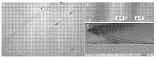
도 1: 캔틸레버 역 반사를 이용하는 2D 펜어레이 접근.
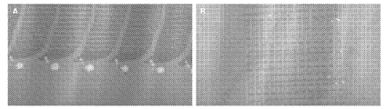
도 2: 제1 초기 팁-표면 접촉 점 너머 표면 내로 팁을 구동 시 2D 펜어레이를 사용하여 제작된 어레이. (A) 휘어진 직사각 어레이의 광학 사진. (B) 2D 펜어레이의 단일 팁의 SEM 사진.
도 3: 도트 대신 선의 형태로 음각 형태의 형성.
도 4: 팁 품질. (A) 팁이 없으면 어레이도 없는 결과를 가져왔다. (B) 팁이 평면을 벗어나면, 양각 및 음각 패턴이 나란히 존재한다. (C) 평면을 벗어난 팁들의 SEM 사진.
도 5: 2D 칩 증기-피복. (A) 전체 기판에 걸쳐 접근 도트를 보여주는 광학 사진. (B) 피복 위 칩으로 인하여 티올 분자의 비특이적 침착.
도 6: 3개의 z-축 모터 위에 안착된, 스캐너 위에 탑재된 2D 나노 펜어레이.
도 7: 뷰포트를 통해서 본 캔틸레버.
도 8: "악어 눈 (Alligator Eye)" 과정을 이용하는 미세 평탄화 접근.
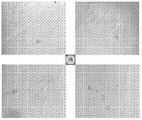
도 9: 상기 악어-눈 평탄화 과정을 이용하는 5 평방 mm 패턴형성된 기판의 네 귀퉁이의 광학 사진.
도 10: 높은 정밀도 평탄화 과정을 이용하여 제작된 어레이의 고해상도 광학 사진.
도 11: 제작된 어레이의 고해상도 광학 및 지형학적 AFM 사진.
도 12: DPN 제작을 위해 사용될 수 있는 제1 세대 냉각 시스템.
도 13: 상이한 온도에서 제작된 어레이의 지형학적 및 높이 윤곽. (A) 25℃에서 및 (B) 18℃에서.
도 14: 제2 세대 냉각 시스템.
도 15: 다양한 기판 온도로 생성된 16-머캅토헥사데칸 티올 도트의 지형학적 AFM 사진 및 등고선 그래프.
도 16: 4 및 0.4 초의 2가지 상이한 체류 시간을 갖는 16-머캅토헥사데칸 티올에 대한 도트 직경 및 온도 그래프 (각각 시리즈 1 및 2).
도 17: 0.4초의 체류 시간에서 1-옥타데칸 티올의 온도에 대한 지형학적 AFM 사진 및 도트 직경 등고선 그래프.
도 18: 실질적인 열적 변동 없이 온도를 적어도 수십 시간 동안 일정하게 유지하는, 열 싱크를 위해 보다 나은 재료 및 디자인이 도입된 펠티에 (Peltier) 모듈에 근거한 제3 세대의 가열 및 냉각 스테이지.
도 19: 제3 세대의 가열 및 냉각 스테이지를 이용하여 제작된 어레이의 광학 사진.
도 20: 상이한 온도 및 습도에서 생성된 AUT 나노도트의 마찰 AFM 사진.
도 21: 1D 팁 어레이 및 60℃ 및 65% RH에서의 가열 스테이지를 이용하여 제작된 어레이.
도 22: 가열 모드에서 제3 세대 스테이지 시스템을 이용하는, AUT 피복된 2D 펜 어레이를 이용하는 균일한 어레이 패턴의 모서리-대-모서리 생성.
도 23 - DAPI (청색), 뉴클레오스타민 (녹색), 액틴 (적색) 및 STRO-1(자색)으로 염색된 ODT 기판의 1x1 mm 부분.
도 24 - DAPI (청색), 뉴클레오스타민 (녹색), 액틴 (적색) 및 STRO-1(자색)으로 염색된 ODT 기판.The patent or application file includes at least one drawing worked in color. Copies of this patent or patent application publication with color drawing (s) will be provided from the Office upon request and payment of the necessary fee.
1: 2D penarray approach using cantilever back reflection.
2: Array fabricated using a 2D penarray when driving a tip into a surface beyond a first initial tip-surface contact point. (A) Optical photo of the curved rectangular array. (B) SEM photo of single tip of 2D pen array.
3: Formation of intaglio form in the form of lines instead of dots.
4: Tip quality. (A) Without the tip, there was no array. (B) When the tip is out of plane, there are embossed and engraved patterns side by side. (C) SEM photo of tips out of plane.
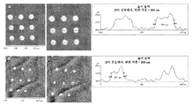
5: 2D chip vapor-coating. (A) Optical photo showing approach dots across the entire substrate. (B) Nonspecific deposition of thiol molecules due to chips on the coating.
6: 2D nano-pen array mounted on a scanner, seated on three z-axis motors.
7: Cantilever seen through a viewport.
8: Fine planarization approach using “Alligator Eye” procedure.
9: Optical photo of four corners of a 5 square mm patterned substrate using the alligator-eye planarization process.
10: High resolution optical photo of an array fabricated using a high precision planarization procedure.
11: High resolution optical and topographic AFM photographs of the fabricated array.
12: First generation cooling system that can be used for DPN fabrication.
13: Topographic and height contours of arrays fabricated at different temperatures. (A) at 25 ° C. and (B) at 18 ° C.
14: Second Generation Cooling System.
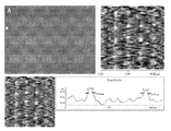
Fig. 15: Topographic AFM photographs and contour plots of 16-mercaptohexadecane thiol dots produced at various substrate temperatures.
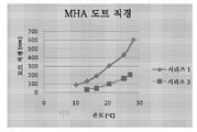
Figure 16: Dot diameter and temperature graphs for 16-mercaptohexadecane thiols with two different residence times of 4 and 0.4 seconds (
17: Topographic AFM photographs and dot diameter contour plots for the temperature of 1-octadecane thiol at a residence time of 0.4 seconds.
FIG. 18: Third generation heating and cooling stage based on Peltier module incorporating better materials and designs for the heat sink, keeping the temperature constant for at least tens of hours without substantial thermal fluctuations.
19: Optical photograph of an array fabricated using third generation heating and cooling stages.
20: Friction AFM photographs of AUT nanodots produced at different temperatures and humidity.
FIG. 21: Array fabricated using a 1D tip array and heating stage at 60 ° C. and 65% RH.
Figure 22: Edge-to-edge generation of a uniform array pattern using an AUT coated 2D pen array, using a third generation stage system in heating mode.
Figure 23-1x1 mm portion of ODT substrate stained with DAPI (blue), nucleotamine (green), actin (red) and STRO-1 (purple).
Figure 24-ODT substrates stained with DAPI (blue), nucleotamine (green), actin (red) and STRO-1 (purple).
상세한 설명details
도입 Introduction
본원에 인용된 모든 참고문헌은 그 전문이 본원에 참고로 포함된다.All references cited herein are hereby incorporated by reference in their entirety.
2009년 1월 26일에 출원된 우선권 미국 가출원 제61/147,448호는 그 전문이 본원에 참고로 포함된다. 뿐만 아니라, 2009년 1월 26일에 출원된 미국 가출원 제61/147,449호는 그 전문이 본원에 참고로 포함된다. 2009년 1월 26일에 출원된 미국 가출원 제 61/147,451호는 그 전문이 본원에 참고로 포함된다. 2009년 1월 26일에 출원된 미국 가출원 제 61/147,452호는 그 전문이 본원에 참고로 포함된다.Priority US Provisional Application No. 61 / 147,448, filed January 26, 2009, is incorporated herein by reference in its entirety. In addition, US Provisional Application No. 61 / 147,449, filed Jan. 26, 2009, is hereby incorporated by reference in its entirety. US Provisional Application No. 61 / 147,451, filed January 26, 2009, is incorporated by reference in its entirety. US Provisional Application No. 61 / 147,452, filed January 26, 2009, is incorporated herein by reference in its entirety.
예를 들어 평탄화 및 기판 온도 조절에 대한 실시양태를 포함하는 본원에 기재된 실시양태는 제작, 이미지화 및 다른 응용을 위해 사용될 수 있다.Embodiments described herein, including for example embodiments for planarization and substrate temperature control, can be used for fabrication, imaging, and other applications.
하나의 바람직한 실시양태는 물질이 팁으로부터, 또는 팁들의 어레이로부터 기판으로 전달되는 공정에 대한 조절을 개선하기 위한 상기 방법 및 물품의 용도이다. 하나의 바람직한 실시양태는 나노스코프 팁들의 고밀도 어레이와 함께 사용하는 것이다. 또 다른 바람직한 실시양태는 줄기 세포 연구 및 상업적 용도를 포함하는 세포 연구 및 상업적 용도를 위한, 제작된 어레이의 용도이다.One preferred embodiment is the use of the method and article to improve control over the process by which material is transferred from the tip, or from the array of tips to the substrate. One preferred embodiment is to use with a high density array of nanoscope tips. Another preferred embodiment is the use of the fabricated array for cell research and commercial use, including stem cell research and commercial use.
하나의 실시양태에서, 딥 펜 나노리소그래피 (Dip Pen Nanolithography)® (DPN®) 공정을 이용하는 줄기 세포 분화를 위한 주형화된 금 표면의 cm2 면적의 생성은 예를 들어 펜 팁을 잉크로 피복함, 비특이적 침착, 및 기판 표면에 대하여 2D 펜 어레이를 평탄화하는 것을 포함하는 여러 가지 문제점을 내포한다. 2D 펜 어레이의 평탄화가 적절히 행해지지 않을 경우, 패턴 변형, 어레이 내 및 어레이들 사이의 불균일 구조, 휨, 및 음각 형태가 나타날 수 있다. 이러한 문제점들 외에도, 제작된 구조가 일부 경우에, 줄기 세포 분화를 개시하기 위해 100 nm 보다 작아야 한다. 마지막으로, 모서리에서 모서리까지 패턴형성된, 균일한 대형 기판의 제작을 위한 신뢰할만한 상업적 과정이 필요하다. 이러한 사안들을 극복하기 위해, 2D 패턴화 공정, 특히 일관되고 균일한 패턴을 생성하기 위해 펜 팁의 증기-피복과 결합된 2D 평탄화에 대한 더 많은 이해가 필요하다.In one embodiment, creation of a cm 2 area of the templated gold surface for stem cell differentiation using the Dip Pen Nanolithography® (DPN®) process, for example, coating the pen tip with ink. It presents several problems, including non-specific deposition, and planarizing the 2D pen array with respect to the substrate surface. If the planarization of the 2D pen array is not done properly, pattern deformation, uneven structures, warpage, and intaglio shapes in and between the arrays may appear. In addition to these problems, the fabricated structure should in some cases be smaller than 100 nm to initiate stem cell differentiation. Finally, there is a need for a reliable commercial process for the fabrication of large, uniform substrates patterned from edge to edge. To overcome these issues, more understanding of the 2D patterning process, especially 2D planarization combined with vapor-coating of the pen tip, is required to produce a consistent and uniform pattern.
하나의 응용에서, 이들 측면은 줄기 세포의 분화에 직접 영향을 줄 수 있으며, 여기서 균일한 패턴형성은 더 나은 분화를 초래할 수 있다.In one application, these aspects can directly affect the differentiation of stem cells, where uniform patterning can lead to better differentiation.
기판에 대하여 어레이를 평탄화하기 위해, 예를 들어 나노잉크(NanoInk)에 의해 최근 개발된 평탄화 소프트웨어를 이용하여, 이미 수립된 과정을 따를 수 있다. 2008년 2월 5일에 출원된 미국 특허 가출원 제61/026,196호(및 또한 2009년 8월 13일에 공고된 WO 2009/099,619)를 참조하라. 상기 공정 도중 사람의 개입 및 판단에 대한 필요가 있을 수 있으며, 일부 경우에 팁들이 언제 표면에 닿았는지를 판단하기 어려울 수가 있고, 이는 예를 들어 불균일 패턴형성을 포함하는 기술적 문제점을 초래할 수 있다.To planarize the array with respect to the substrate, one may follow a procedure already established, for example using planarization software recently developed by NanoInk. See U.S. Provisional Application No. 61 / 026,196, filed February 5, 2008 (and also WO 2009 / 099,619, published August 13, 2009). There may be a need for human intervention and judgment during the process, and in some cases it may be difficult to determine when the tips touched the surface, which may lead to technical problems including, for example, non-uniform patterning.
상기 과정을 시험하기 위해, 2D 펜 어레이를 옥타데칸티올(ODT)로 증기-피복할 수 있다. 평탄화는, 캔틸레버가 평탄화되었는지 여부를 결정하기 위해 상기 캔틸레버의 배면으로부터 반사를 모니터링함으로써 광학 시스템을 이용하여 수행된다. 상기 과정은 팁들이 표면 위에 얼마나 멀리 또는 얼마나 많이 압박되는지에 의존하며, 이는 도 1A 및 B에 나타난 것과 같이 캔틸레버의 배면으로부터 빛의 반사를 변화시키는 원인이 된다. 상기 사진은 캔틸레버의 배면 위의 두 상이한 반사를 주황 내지 붉은 색으로 보여준다.To test this procedure, the 2D pen array can be vapor-coated with octadecanethiol (ODT). Planarization is performed using an optical system by monitoring reflections from the back of the cantilever to determine whether the cantilever is flattened. The process depends on how far or how much the tips are pressed onto the surface, which causes a change in the reflection of light from the back of the cantilever as shown in FIGS. 1A and B. The picture shows two different reflections on the back of the cantilever in orange to red.
상기 예에서, 가해진 부하가 무엇인지는 알려지지 않았을지라도 변화가 분명하며; 일부 경우에는 캔틸레버의 배면으로부터 반사의 변화가 그다지 분명하지 않으므로 이들 팁이 표면에 언제 닿았는지를 알기가 매우 어렵다. 일부 경우에는 또한, 상이한 시스템을 이용하여 같은 과정을 반복하여 같은 결과에 도달하기가 어려울 수 있다. 편향의 변화는 예민할 수도 있지만, 그리 민감하지 않을 수도 있으며, Z-압전기 센서가 100 nm 또는 수 마이크로미터만큼 작동할 때 두 반사들 사이에 분리점 또는 예리한 전이가 없다.In the above example, the change is clear although it is not known what the applied load is; In some cases, the change in reflection from the back of the cantilever is not so obvious, so it is very difficult to know when these tips touched the surface. In some cases, it may also be difficult to reach the same result by repeating the same process using different systems. The change in deflection may be sensitive, but not very sensitive, and there is no split point or sharp transition between the two reflections when the Z-piezoelectric sensor operates by 100 nm or several micrometers.
더 높은 힘을 가하는 데 있어서 문제점은 도 2A에 나타난 것과 같은 휘는 현상일 수 있으며, 밝은 도트들은 제1 팁-표면 접촉의 접근 도트이고 (접촉점 "a"), 직사각형 도트 어레이(18 x 40 μm2)인 고안되고 실행된 패턴은 직경 1 μm이고 4 μm 만큼 떨어져 있는 도트를 포함한다. 상기 광학 사진에서, 어레이는 전반부의 경우 휘었고, 후반부의 경우에는 부하의 감소 또는 접촉점으로부터 "a-x 마이크로미터" 굽은 캔틸레버의 증가로 인하여 조절되기 시작할 것인데, 이는 패턴의 절반이 수행된 후에는 팁이 표면 내로 덜 구동됨을 의미한다. 이러한 현상은 초기 접촉 점을 너머 표면 안으로 팁을 구동시킴으로 인해 관찰된다. 이들 팁은 일정한 이동 자유(FOT)를 가지고 평탄 면으로부터 굽어지도록 고안될 수 있다. FOT는 도 2B에서 보는 바와 같은, 팁의 첨필과 칩 받침대 사이의 거리의 차이다. 상기 전형적인 2D 칩의 경우, FOT는 16.8 μm이고 이 숫자는 칩들 간에 변한다.The problem with applying a higher force can be a warping phenomenon as shown in Figure 2A, where the bright dots are the access dots of the first tip-surface contact (contact point "a"), and the rectangular dot array (18 x 40 μm 2 The designed and executed pattern of) includes
표면 위에 높은 부하를 가하거나 초기 접촉 점 너머 표면 내로 팁을 구동시키는 것으로부터 발생되는 추가의 사안은 도트 대신 선의 형태로 음각 형태의 변형 및 형성에 있다. 이러한 현상은 도 3에서 보는 바와 같이, 팁이 표면 내로 얼마나 많이 구동되는지, 그리고 직사각형 어레이가 휘어질 수 있는지 여부에 의존한다. 도 3A는 각 어레이의 시작에서 밝은 접근 도트와 유사한 양각의 밝은 도트 대신 휘어진 어레이 내에 음각 선의 형성을 나타낸다. 유사하게, 도 3B는 각 어레이의 시작에서 밝은 접근 도트와 유사한 양각의 밝은 도트 대신 직사각형 어레이 내 음각 선의 형성을 나타낸다. 이들 어레이는 휘지 않는데, 그 이유는 팁들이 표면 내로 접촉 점 너머 구동되었지만 휘는 현상을 위한 문턱을 통과하지는 않았기 때문이다.A further issue arising from applying a high load on the surface or driving the tip into the surface beyond the initial contact point lies in the deformation and formation of the intaglio form in the form of lines instead of dots. This phenomenon depends on how much the tip is driven into the surface and whether the rectangular array can bend, as shown in FIG. 3. 3A shows the formation of negative lines in a curved array instead of embossed bright dots similar to bright approach dots at the beginning of each array. Similarly, FIG. 3B shows the formation of negative lines in a rectangular array instead of embossed bright dots similar to bright approach dots at the beginning of each array. These arrays do not bend because the tips are driven beyond the contact point into the surface but have not passed through the threshold for bowing.
2D 펜어레이의 품질은 큰 면적의 제작이 필요할 경우 중요한 역할을 한다; 칩 위의 임의의 소실되거나 손상된 팁, 팁의 평면성, 및 평면을 벗어난 팁의 존재가 불균일한 기판 제작을 초래할 것이다. 도 4는 소실된 및 평면을 벗어난 팁을 갖는 2D 펜 어레이를 사용하여 제작된 기판을 보여준다. 도 4A에서는, 붉은 화살표로 나타낸 여러 개의 소실된 어레이가 존재한다. 이들 소실된 어레이는 팁 제작으로 인하여 소실된 팁들 또는 운송 및 조립 도중 손상에 직접 관계된다. 팁 제작 도중, 일부 평면을 벗어난 팁들은 다소간 굽어질 수 있으며, 이는, 도 4B의 광학 사진에서 나타난 것과 같이, 상이한 패턴이 제작되는 것을 초래할 수 있고, 여기서 양각 및 음각 패턴은 팁들과 표면 사이에 상이한 접촉으로 인하여 나란히 생성되었다. 평면을 벗어난 팁은 붉은 화살표로 나타낸 도 4C에서 보인다.The quality of 2D pen arrays plays an important role when a large area of manufacture is required; Any missing or damaged tip on the chip, the planarity of the tip, and the presence of the out-of-plane tip will result in non-uniform substrate fabrication. 4 shows a substrate fabricated using a 2D pen array with missing and off-plane tips. In Figure 4A, there are several missing arrays, indicated by red arrows. These missing arrays are directly related to the missing tips due to tip fabrication or damage during transportation and assembly. During tip fabrication, some off-plane tips may bend somewhat, which may result in different patterns being fabricated, as shown in the optical photograph of FIG. 4B, where the embossed and intaglio patterns differ between the tips and the surface. Due to the contact generated side by side. The out-of-plane tip is shown in FIG. 4C, shown by the red arrow.
팁을 피복하는 것, 및 피복을 조절하는 것은 2009년 2월 12일에 공고된 WO 2009/020658(노스웨스턴 유니버시티 (Northwestern University))에 기재되어 있다. 상기 PCT 출원은 잉크 젯 인쇄를 기재하며, 본원에 제공된 하나의 실시양태는 잉크 젯 인쇄를 제외한다. 상기 PCT 출원은 또한 잉크 물질이 어디에 배치될 수 있는지를 조절하기 위해 캔틸레버의 조절된 표면 처리를 기재하였고, 본원에서 제공된 하나의 실시양태는 잉크 물질이 어디에 배치될 수 있는지를 조절하는 데 있어서 캔틸레버의 조절된 표면 처리는 제외한다.Coating the tips, and adjusting the coatings, are described in WO 2009/020658 (Northwestern University), published February 12, 2009. The PCT application describes ink jet printing, one embodiment provided herein excludes ink jet printing. The PCT application also describes a controlled surface treatment of the cantilever to control where the ink material can be placed, and one embodiment provided herein provides for controlling where the ink material can be placed. Controlled surface treatment is excluded.
기기사용Use of device
본원에 기재된 실시양태를 실시하기 위해 사용될 수 있는 기기의 사용은 엔스크립터 (NSCRIPTOR), DPN5000, 및 NLP 2000을 포함하는 나노잉크 사(NanoInk, Inc.)의 제품인 기기, 및 잉크, 기판, 소프트웨어 등을 포함하는 이들 기기에 관련된 요소를 포함한다. 기기는 나노석판술을 포함하여 직접 석판인쇄를 기록할 수 있게 한다. 패턴화를 위한 하나의 기기는 예를 들어 2009년 1월 22일에 공고된 미국 특허 공보 2009/0023607(Rozhok et al.)에 기재되어 있다.Use of the instrument that can be used to practice the embodiments described herein includes instruments that are products of NanoInk, Inc., including NSCRIPTOR, DPN5000, and NLP 2000, and inks, substrates, software, and the like. Includes elements related to these devices, including. The instrument allows for the direct recording of lithography, including nanolithography. One device for patterning is described, for example, in US Patent Publication 2009/0023607 (Rozhok et al.), Published January 22, 2009.
큼직한 평행의 2차원 어레이가 예를 들어 2008년 5월 8일에 공고된 미국 특허 공고 2008/0105042(Mirkin, Fraga/a, et al.)에 기재되어 있다.Large parallel two-dimensional arrays are described, for example, in US Patent Publication 2008/0105042 (Mirkin, Fraga / a, et al.), Published May 8, 2008.
뷰포트를 포함하는 개선된 어레이가 예를 들어 2008년 3월 11일에 출원된 미국 특허 출원 12/073,909(Haaheim et al.)(공고, 2008/0309688)에 기재되어 있다.An improved array comprising viewports is described, for example, in US patent application 12 / 073,909 (Haaheim et al., Published on March 11, 2008, published 2008/0309688).
중합체 펜 석판술 및 팁 어레이가 2009년 10월 29일에 공고된 WO 2009/132,321(노스웨스턴 유니버시티)에 기재되어 있다.Polymer pen lithography and tip arrays are described in WO 2009 / 132,321 (Northwestern University), published October 29, 2009.
팁들과, 티올 및 기타 황 화합물을 포함하는 침착 물질을 사용하는 직접 기록하는 나노석판술이 예를 들어 미국 특허 제6,635,311호 및 6,827,979호(Mirkin et al.)에 기재되어 있다. 평행 프로브 어레이가 예를 들어 미국 특허 제6,867,443호(Liu et al.)에 기재되어 있다.Direct writing nanolithography using tips and deposition materials comprising thiols and other sulfur compounds is described, for example, in US Pat. Nos. 6,635,311 and 6,827,979 to Mirkin et al. Parallel probe arrays are described, for example, in US Pat. No. 6,867,443 to Liu et al.
또한 하기 문헌을 참조하라: (1) ["Applications of dip-pen nanolithography" Salaita et al., Nature Nanotechnology, vol. 2, March 2007, 145-155], (2) ["Dip Pen Nanolithography: A Desktop Nanofab Approach Using High Throughput Flexible Nanopatterning, Haaheim, Scanning, 2008, 30, 137-150], (3) ["The Evolution of Dip-Pen Nanolithography" Ginger, Angewandte Chemie, 2004, 43, 30-45].See also the following references: (1) ["Applications of dip-pen nanolithography" Salaita et al., Nature Nanotechnology, vol. 2, March 2007, 145-155], (2) ["Dip Pen Nanolithography: A Desktop Nanofab Approach Using High Throughput Flexible Nanopatterning, Haaheim, Scanning, 2008, 30, 137-150], (3) [" The Evolution of Dip-Pen Nanolithography "Ginger, Angewandte Chemie, 2004, 43, 30-45].
에칭 패턴화된 표면이 예를 들어 미국 특허 제7,291,284호(Mirkin et al.)에 기재되어 있다. Etch patterned surfaces are described, for example, in US Pat. No. 7,291,284 to Mirkin et al.
주사 프로브 접촉 인쇄가 예를 들어 미국 특허 제7,344,756호에 기재되어 있다.Scanning probe contact printing is described, for example, in US Pat. No. 7,344,756.
나노석판술 기기 및 공정을 제어하기 위한 소프트웨어가 예를 들어 미국 특허 제7,060,977호(Cruchon-Dupeyrat) 및 7,279,046호(Nelson et al.)에 기재되어 있다.Software for controlling nanolithography devices and processes is described, for example, in US Pat. Nos. 7,060,977 (Cruchon-Dupeyrat) and 7,279,046 (Nelson et al.).
정렬 방법은 예를 들어, 본원에 참고로 포함되는, 2007년 8월 30일에 출원된 미국 특허 출원 11/848,211에 기재되어 있다.Alignment methods are described, for example, in US patent application Ser. No. 11 / 848,211, filed August 30, 2007, which is incorporated herein by reference.
캔틸레버 및 캔틸레버의 어레이Array of cantilevers and cantilevers
캔틸레버는 당 분야에 공지되어 있으며, 예를 들어 AFM 캔틸레버일 수 있다. 캔틸레버는 예를 들어 중실 팁, 중공 팁, 나노스코프 팁, 주사 프로브 현미경 팁 및 AFM 팁을 포함하는 팁들을 그 위에 포함할 수 있다. 예를 들어 질화 규소 및 규소를 포함하는 공지의 물질이 사용될 수 있다. 캔틸레버 및 팁들은 고밀도 어레이를 위해 적합화될 수 있다. 예를 들어, 캔틸레버는 굽어지고 팁들은 연장될 수 있다.Cantilevers are known in the art and may be, for example, AFM cantilevers. The cantilever can include tips thereon including, for example, a solid tip, a hollow tip, a nanoscope tip, a scanning probe microscope tip, and an AFM tip. Known materials can be used, including, for example, silicon nitride and silicon. Cantilevers and tips can be adapted for high density arrays. For example, the cantilever can be bent and the tips can extend.
하나의 실시양태는 (i) 복수의 캔틸레버의 2-차원 어레이; 및 (ii) 어레이를 위한 지지체를 포함하며, 여기서 상기 어레이가 복수의 바닥 열을 포함하고, 각각의 바닥 열은 상기 바닥 열로부터 뻗어있는 복수의 캔틸레버를 포함하며, 상기 각각의 캔틸레버는 상기 바닥 열로부터 떨어진 캔틸레버 말단에 팁을 포함하고, 상기 어레이는 팁들이 실질적으로 평면인 표면과 접촉할 때 상기 어레이의 팁-아닌 요소의 실질적인 접촉을 방지하도록 적합화되는 것인 물품이다. One embodiment includes (i) a two-dimensional array of a plurality of cantilevers; And (ii) a support for the array, wherein the array comprises a plurality of bottom rows, each bottom row including a plurality of cantilevers extending from the bottom row, wherein each cantilever is the bottom row. And a tip at the cantilever end away from the array, wherein the array is adapted to prevent substantial contact of non-tip elements of the array when the tips contact a substantially planar surface.
하나의 실시양태는 또한 (i) 복수의 캔틸레버의 2-차원 어레이, 및 (ii) 어레이를 위한 지지체를 포함하며, 여기서 상기 어레이가 복수의 바닥 열을 포함하고, 각각의 바닥 열은 복수의 캔틸레버를 포함하며, 상기 각각의 캔틸레버는 상기 바닥으로부터 떨어진 캔틸레버 말단에 팁을 포함하고, 상기 캔틸레버의 수는 250개를 초과하며, 상기 팁들은 캔틸레버에 비하여 예를 들어 적어도 4 마이크로미터의 정점 높이를 갖는 것인 물품이다.One embodiment also includes (i) a two-dimensional array of a plurality of cantilevers, and (ii) a support for the array, wherein the array comprises a plurality of bottom rows, each bottom row comprising a plurality of cantilevers Each cantilever includes a tip at a cantilever end away from the bottom, the number of the cantilever is greater than 250, and the tips have a peak height of, for example, at least 4 micrometers relative to the cantilever; It is an article.
또 다른 실시양태는 복수의 캔틸레버의 2-차원 어레이를 포함하며, 여기서 상기 어레이가 복수의 바닥 열을 포함하고, 각각의 바닥 열은 복수의 캔틸레버를 포함하며, 상기 각각의 캔틸레버는 상기 바닥으로부터 떨어진 캔틸레버 말단에 팁을 포함하고, 상기 캔틸레버의 수는 250개를 초과하며, 상기 팁들은 캔틸레버의 팁 측 위에 금속으로 피복되고, 상기 캔틸레버는 예를 들어 그들의 바닥으로부터 적어도 10°의 각으로 굽어져 있는 것인 물품을 제공한다.Another embodiment includes a two-dimensional array of a plurality of cantilevers, wherein the array comprises a plurality of bottom rows, each bottom row including a plurality of cantilevers, each cantilever being away from the bottom. A tip at the cantilever end, the number of the cantilever exceeds 250, the tips being covered with metal on the tip side of the cantilever, the cantilever being bent at an angle of at least 10 ° from their bottom, for example It provides an article.
캔틸레버의 2-차원 어레이는 당 분야에 공지되어 있다. 예를 들어, 2-차원 어레이는, 바람직하게는 서로에 대하여 실질적으로 수직인, 길이와 폭을 제공하는 일련의 열과 행일 수 있다. 상기 어레이는 제1 차원 및 제2 차원을 포함할 수 있다. 2-차원 어레이는 서로의 옆에 배치되어 제2 차원을 구축한, 일련의 1차원 어레이일 수 있다. 두 차원은 수직일 수 있다. 캔틸레버는 자유로운 말단 및 결합된 말단을 포함할 수 있다. 캔틸레버는 자유로운 말단 또는 그 근처에, 결합된 말단으로부터 멀리에 팁들을 포함할 수 있다. 하나의 열의 캔틸레버는 다음 열 위의 캔틸레버와 같은 방향을 가리키거나, 하나의 열의 캔틸레버는 다음 열 위의 캔틸레버와 반대 방향을 가리킬 수 있다.Two-dimensional arrays of cantilevers are known in the art. For example, a two-dimensional array can be a series of columns and rows providing length and width, preferably substantially perpendicular to each other. The array can include a first dimension and a second dimension. The two-dimensional array may be a series of one-dimensional arrays arranged next to each other to build a second dimension. The two dimensions can be vertical. Cantilevers can include free ends and linked ends. The cantilever can include tips at or near its free end, away from the joined end. One row of cantilevers may point in the same direction as the cantilever on the next row, or one row of cantilevers may point in the opposite direction to the cantilever on the next row.
2-차원 어레이는 두 부분을 합하여 제작될 수 있으며, 각각의 부분은 2차원으로 패턴형성된 표면을 가지고 2차원으로 서로 짝지어질 수 있도록 적합화되어 있다.Two-dimensional arrays can be made by combining two parts, each of which is adapted to be paired with each other in two dimensions with a patterned surface in two dimensions.
하나의 중요한 변수는 의도된 목적을 위해 실제로 기능할 수 있는 어레이 중 캔틸레버의 분량 또는 백분율이다. 일부 경우에, 일부의 캔틸레버는 불완전하게 형성될 수 있거나, 아니면 형성 후 손상될 수 있다. 캔틸레버 수율은 사용가능한 캔틸레버의 상기 백분율을 반영한다. 바람직하게는, 상기 어레이는 적어도 75%, 또는 적어도 80%, 또는 적어도 90%, 또는 적어도 95%, 또는 더욱 바람직하게는 적어도 약 98%, 또는 더욱 바람직하게는 적어도 99%의 캔틸레버 수율로 특징된다. 캔틸레버 수율을 특징화함에 있어서, 내부 캔틸레버에 비하여 모서리의 가공에 의해 손상되는, 열의 말단에 있는 캔틸레버는 무시될 수 있다. 예를 들어, 가운데 75%가 측정될 수 있다. 많은 경우에, 모서리 효과가 웨이퍼 제작에 공지되어 있는 바, 제작은 모서리보다는 가운데에서 더 잘 수행될 것이다. 결함 밀도는 일부 경우에, 중앙으로부터 모서리로 이동함에 따라 증가할 것이다.One important variable is the amount or percentage of cantilever in the array that can actually function for the intended purpose. In some cases, some cantilevers may be incompletely formed or otherwise damaged after formation. Cantilever yield reflects this percentage of available cantilever. Preferably, the array is characterized by a cantilever yield of at least 75%, or at least 80%, or at least 90%, or at least 95%, or more preferably at least about 98%, or more preferably at least 99%. . In characterizing the cantilever yield, the cantilever at the end of the row, which is damaged by the processing of the edges as compared to the inner cantilever, can be ignored. For example, the middle 75% can be measured. In many cases, edge effects are known in wafer fabrication, and fabrication will perform better in the center than edges. Defect density will increase in some cases as it moves from center to edge.
어레이는 팁들이 실질적으로 평면인 표면과 접촉할 때 상기 어레이의 팁-아닌 요소들의 실질적인 접촉을 방지하도록 적합화될 수 있다. 예를 들어, 캔틸레버 암은 표면과 접촉해서는 안되며, 따라서 예를 들어 굽힘 등에 의해 적합화될 수 있다. 예를 들어 긴 팁을 포함하는 팁들이 이를 위해 또한 적합화될 수 있다. 상기 결과를 수득하는 데 유용할 수 있는 인자들은 긴 팁들의 사용, 캔틸레버 암의 굽어짐, 팁 평탄화, 열 평탄화, 및 모든 차원에서 캔틸레버의 평탄화를 포함한다. 인자들의 하나 이상의 조합이 사용될 수 있다.The array may be adapted to prevent substantial contact of non-tip elements of the array when the tips contact a substantially planar surface. For example, the cantilever arm should not be in contact with the surface and thus can be adapted, for example by bending or the like. Tips, including for example long tips, may also be adapted for this. Factors that may be useful in obtaining the results include the use of long tips, bending of the cantilever arm, tip flattening, thermal flattening, and flattening of the cantilever in all dimensions. Combinations of one or more factors may be used.
캔틸레버 팁들은 당 분야에 통상적인 것보다 길 수 있다. 예를 들어, 팁들은 캔틸레버에 비하여 평균 적어도 4 마이크로미터의 정점 높이를 가질 수 있고, 필요하다면, 팁들은 캔틸레버에 비하여 평균 적어도 7 마이크로미터의 정점 높이를 가질 수 있다. 뿐만 아니라, 팁 정점 높이는 적어도 10 마이크로미터, 또는 적어도 15 마이크로미터, 또는 적어도 20 마이크로미터일 수 있다. 특정 상한이 존재하지 않으며, 당 분야에 공지된 기술 및 개선이 사용될 수 있다. 이러한 긴 길이는 팁만이 표면에 접촉할 것을 보장하는 데 도움을 줄 수 있다. 정점 높이는 다수의 팁 정점 높이의 평균으로 취할 수 있고, 일반적으로 정점 높이는 팁들 간에 실질적으로 변동하지 않도록 설계된다. 실시예에 나타낸 방법들을 포함하여 당 분야에 공지된 방법들이 팁 정점 높이를 측정하기 위해 사용될 수 있다.Cantilever tips may be longer than conventional in the art. For example, the tips may have an average peak height of at least 4 micrometers relative to the cantilever, and if necessary, the tips may have an average peak height of at least 7 micrometers relative to the cantilever. In addition, the tip vertex height may be at least 10 micrometers, or at least 15 micrometers, or at least 20 micrometers. There is no specific upper limit, and techniques and improvements known in the art can be used. This long length may help to ensure that only the tip contacts the surface. The vertex height can be taken as an average of a number of tip vertex heights, and in general the vertex height is designed so that it does not substantially vary between the tips. Methods known in the art, including those shown in the Examples, can be used to measure tip vertex heights.
어레이를 위한 변수를 측정함에 있어서, 평균 측정이 사용될 수 있다. 평균 측정은 예를 들어 대표적인 사진 또는 현미경사진을 검토하는 것을 포함하여, 당 분야에 공지된 방법에 의해 수득될 수 있다. 전체 어레이를 측정할 필요는 없는데, 이는 비현실적일 수 있기 때문이다.In measuring the parameters for the array, an average measurement can be used. Average measurements can be obtained by methods known in the art, including, for example, reviewing representative photographs or micrographs. It is not necessary to measure the entire array because it can be impractical.
바람직한 실시양태는 아니지만, 일부 실시양태에서 팁이 없는 캔틸레버가 사용될 수 있다. 예를 들어, 하나의 실시양태는 (i) 복수의 캔틸레버의 2-차원 어레이를 포함하며, 여기서 상기 어레이가 복수의 바닥 열을 포함하고, 각각의 바닥 열은 상기 바닥 열로부터 뻗어있는 복수의 캔틸레버를 포함하며, 상기 각각의 캔틸레버는 팁이 없는 캔틸레버이며, 상기 캔틸레버는 그들이 바닥으로부터 일정 각으로 굽어져 있는 것인 물품을 제공한다.Although not a preferred embodiment, in some embodiments a tipless cantilever can be used. For example, one embodiment includes (i) a two-dimensional array of a plurality of cantilevers, wherein the array comprises a plurality of bottom rows, each bottom row of a plurality of cantilevers extending from the bottom row. Wherein each cantilever is a tipless cantilever and the cantilever provides an article in which they are bent at an angle from the bottom.
또한, 상기 캔틸레버는 패턴형성될 표면을 향하여 굽어지는 것을 포함하여 굽어질 수 있다. 굽어짐을 유도하기 위해 당 분야에 공지된 방법이 사용될 수 있다. 캔틸레버는 상기 바닥 및 지지체로부터 멀어지는 각으로 굽어질 수 있다. 상기 캔틸레버는 캔틸레버의 굽어짐에 적합화된 다수의 층을 포함할 수 있다. 예를 들어, 시차 열 팽창 또는 캔틸레버 비모르프(bimorph)가 상기 캔틸레버를 구부리는 데 사용될 수 있다. 캔틸레버 굽어짐은 적어도 2종의 상이한 물질을 사용하여 유도될 수 있다. 별법으로, 같은 물질을 사용하지만 상이한 응력으로 캔틸레버 굽어짐을 제공할 수 있다. 또 다른 방법은 하나의 물질을 포함하는 캔틸레버 위에 같은 물질이지만 고유 응력 구배를 갖는 제2 층을 침착시키는 것이다. 별법으로, 캔틸레버의 표면을 산화시킬 수 있다. 캔틸레버는 그들의 바닥으로부터 예를 들어 적어도 5°의 각으로, 또는 그들의 바닥으로부터 적어도 10°, 또는 그들의 바닥으로부터 적어도 15°의 각으로 굽어질 수 있다. 실시예에 나타낸 방법을 포함하여 당 분야에 공지된 방법이 이를 측정하는 데 사용될 수 있다. 각의 평균 값이 사용될 수 있다. 상기 캔틸레버는 평균 약 10 마이크로미터 내지 약 50 마이크로미터, 또는 약 15 마이크로미터 내지 약 40 마이크로미터 굽어질 수 있다. 이러한 굽어짐의 거리는 실시예에 나타낸 방법을 포함하여 당 분야에 공지된 방법으로 측정될 수 있다. 평균 거리가 사용될 수 있다. 상기 굽어짐은 기판 조도 및 형태학 및 어레이 내 팁의 오정렬에 대하여 보다 큰 내성을 초래할 수 있으므로, 예를 들어 약 ±20 마이크로미터 이하 또는 약 ±10 마이크로미터 이하의 오정렬이 보상될 수 있다.In addition, the cantilever can be bent including bending towards the surface to be patterned. Methods known in the art can be used to induce bending. The cantilever can be bent at an angle away from the bottom and the support. The cantilever may comprise a plurality of layers adapted for bending of the cantilever. For example, differential thermal expansion or cantilever bimorph can be used to bend the cantilever. Cantilever bending can be induced using at least two different materials. Alternatively, cantilever bending can be provided using the same material but at different stresses. Another method is to deposit a second layer of the same material but with an inherent stress gradient on the cantilever comprising one material. Alternatively, the surface of the cantilever can be oxidized. The cantilever can be bent at an angle of at least 5 ° from their bottom, or at least 10 ° from their bottom, or at least 15 ° from their bottom. Methods known in the art, including those shown in the Examples, can be used to measure them. The average value of the angle can be used. The cantilever can be bent on average from about 10 micrometers to about 50 micrometers, or from about 15 micrometers to about 40 micrometers. Such bend distance can be measured by methods known in the art, including those shown in the Examples. Average distance can be used. Such bending can result in greater resistance to substrate roughness and morphology and misalignment of the tips in the array, such that misalignment of about ± 20 micrometers or less or about ± 10 micrometers or less may be compensated for.
구부림을 용이하게 하기 위해, 캔틸레버는 2개의 주요 층 및 임의의 접착 층과 같은 다수의 층을 포함할 수 있고, 예를 들어 비모르프 캔틸레버일 수 있다. 캔틸레버는 상기 캔틸레버의 팁 측 위에 금속 또는 금속 산화물로 피복될 수 있다. 금속은 상기 금속 또는 금속 산화물이 캔틸레버를 열로 구부리는 데 도움을 주기 유용하다면 특별히 제한되지 않는다. 예를 들어, 상기 금속은 금과 같은 비활성 금속일 수 있다.To facilitate bending, the cantilever may comprise a number of layers, such as two main layers and any adhesive layer, and may be, for example, a bimorph cantilever. The cantilever can be coated with metal or metal oxide on the tip side of the cantilever. The metal is not particularly limited as long as the metal or metal oxide is useful to assist in bending the cantilever to heat. For example, the metal may be an inert metal such as gold.
바람직한 실시양태에서, 어레이는 캔틸레버가 표면을 향해서 굽어지고 또한 단지 영상화를 위해 사용되는 팁에 비하여 통상의 것보다 긴 팁을 포함하도록 적합화될 수 있다.In a preferred embodiment, the array can be adapted such that the cantilever bends towards the surface and also includes a tip that is longer than usual compared to the tip used only for imaging.
팁은 사용 전에 제작 및 날카롭게 될 수 있으며 예를 들어 100 nm 미만의 평균 곡률 반경을 가질 수 있다. 평균 곡률 반경은 예를 들어 10 nm 내지 100 nm, 또는 20 nm 내지 100 nm, 또는 30 nm 내지 90 nm이다. 팁의 모양은 예를 들어 피라미드형, 원뿔형, 쐐기 및 박스형을 포함하여 다양할 수 있다. 팁은 중공 팁이거나 중공 팁을 포함하는 구멍, 및 팁의 말단을 통과하는 미세유체 채널을 이용한 미세제작을 통해 형성된 천공 팁을 포함할 수 있다. 유체 물질은 팁의 말단에 저장되거나 팁을 통해 흐를 수 있다.The tip may be manufactured and sharpened before use and may have an average radius of curvature of less than 100 nm, for example. The average radius of curvature is for example 10 nm to 100 nm, or 20 nm to 100 nm, or 30 nm to 90 nm. The shape of the tip may vary, including, for example, pyramidal, conical, wedge and box shaped. The tip may include a hole that is or is a hollow tip, and a perforated tip formed through microfabrication with a microfluidic channel passing through the tip of the tip. Fluid material may be stored at the end of the tip or flow through the tip.
팁의 기하학은 다양할 수 있고, 예를 들어 중실 팁 또는 중공 팁일 수 있다. WO 2005/115630(PCT/US2005/014899)(Henderson et al.)은 표면 위에 물질을 침착시키기 위한 팁의 기하학을 기재하고 있으며, 이는 본원에 사용될 수 있다.The geometry of the tip can vary and can be, for example, a solid tip or a hollow tip. WO 2005/115630 (PCT / US2005 / 014899) (Henderson et al.) Describes the geometry of a tip for depositing material on a surface, which can be used herein.
상기 2차원 어레이는 두 차원 (즉, 길이 차원 및 폭 차원) 각각에서의 팁 간격으로 특징될 수 있다. 팁 간격은 예를 들어, 팁 어레이 제작 방법으로부터 채택되거나 제작된 어레이로부터 직접 관찰될 수 있다. 팁 간격은 높은 밀도의 팁과 캔틸레버를 제공하도록 설계될 수 있다. 예를 들어, 팁 밀도는 평방 인치 당 적어도 1,000개, 또는 평방 인치 당 적어도 10,000개, 또는 평방 인치 당 적어도 40,000개, 또는 평방 인치 당 적어도 70,000개일 수 있다. 상기 어레이는 2차원 어레이의 제1 차원에서 300 마이크로미터 미만, 그리고 상기 2차원 어레이의 제2 차원에서 300 마이크로미터 미만의 팁 간격으로 특징될 수 있다. 훨씬 더 높은 밀도를 수득하기 위해, 팁 간격은 예를 들어, 하나의 차원에서 약 200 마이크로미터 미만, 그리고 또 다른 차원에서 약 100 마이크로미터 미만, 또는 약 50 마이크로미터 미만일 수 있다. 별법으로, 팁 간격은 예를 들어 하나의 차원에서 100 마이크로미터 미만, 그리고 제2 방향에서 25 마이크로미터 미만일 수 있다. 상기 어레이는 2차원 어레이의 적어도 하나의 차원에서 100 마이크로미터 이하의 팁 간격으로 특징될 수 있다. 하나의 실시양태에서, 팁 간격은 하나의 차원에서 약 70 마이크로미터 내지 약 110 마이크로미터, 그리고 제2 차원에서 약 5 마이크로미터 내지 약 35 마이크로미터일 수 있다. 제작 방법은 시간 경과에 따라 더 조밀한 팁 간격을 허용할 것이므로 팁 간격에 특정한 하한이 존재하지 않는다. 하한의 예는 1 마이크로미터, 또는 5 마이크로미터, 또는 10 마이크로미터를 포함하며, 따라서 예를 들어 팁 간격은 1 마이크로미터 내지 300 마이크로미터, 또는 1 마이크로미터 내지 100 마이크로미터일 수 있다.The two-dimensional array can be characterized by tip spacing in each of two dimensions (ie, length dimension and width dimension). Tip spacing can be observed, for example, directly from an array fabricated or adopted from a tip array fabrication method. Tip spacing can be designed to provide high density tips and cantilevers. For example, the tip density may be at least 1,000 per square inch, or at least 10,000 per square inch, or at least 40,000 per square inch, or at least 70,000 per square inch. The array may be characterized by a tip spacing less than 300 micrometers in the first dimension of the two-dimensional array and less than 300 micrometers in the second dimension of the two-dimensional array. To obtain even higher densities, the tip spacing can be, for example, less than about 200 micrometers in one dimension, and less than about 100 micrometers, or less than about 50 micrometers in another dimension. Alternatively, the tip spacing can be, for example, less than 100 micrometers in one dimension and less than 25 micrometers in the second direction. The array may be characterized by tip spacing of 100 micrometers or less in at least one dimension of the two-dimensional array. In one embodiment, the tip spacing can be from about 70 micrometers to about 110 micrometers in one dimension, and from about 5 micrometers to about 35 micrometers in the second dimension. There is no specific lower limit for tip spacing as the fabrication method will allow denser tip spacing over time. Examples of the lower limit include 1 micrometer, or 5 micrometers, or 10 micrometers, so for example the tip spacing can be 1 micrometer to 300 micrometers, or 1 micrometer to 100 micrometers.
2차원 어레이 위의 캔틸레버의 수는 특별히 제한되지 않지만, 적어도 약 3개, 적어도 약 5개, 적어도 약 250개, 또는 적어도 약 1,000개, 또는 적어도 약 10,000개, 또는 적어도 약 50,000개, 또는 적어도 약 55,000개, 또는 적어도 약 100,000개, 또는 약 25,000개 내지 약 75,000개일 수 있다. 그 수는 특정 기기 및 패턴형성을 위한 공간 제약에 허용되는 양까지 증가될 수 있다. 예를 들어 제작의 용이함, 품질 및 특정 밀도 요구와 같은 인자들을 가중하여 특정 응용에 대하여 적합한 균형이 이루어질 수 있다.The number of cantilevers on the two-dimensional array is not particularly limited, but at least about 3, at least about 5, at least about 250, or at least about 1,000, or at least about 10,000, or at least about 50,000, or at least about 55,000, or at least about 100,000, or about 25,000 to about 75,000. The number can be increased to an amount that allows for space constraints for specific devices and patterning. For example, an appropriate balance can be achieved by weighting factors such as ease of manufacture, quality and specific density requirements.
팁들은 일관성있게 표면에 닿기 위해 일관된 간격을 갖도록 설계될 수 있다. 예를 들어 각각의 팁은 팁 말단을 지지체에 연결하는 거리 D로 특징될 수 있고, 상기 팁 어레이는 팁 말단의 지지체에 이르는 평균 거리 D'로 특징되며, 팁의 적어도 90%에 있어서, D는 D'의 50 마이크로미터 내에 있다. 또 다른 실시양태에서, 팁의 적어도 90%에 있어서, D는 D'의 10 마이크로미터 내에 있다. 팁 말단과 지지체 사이의 거리는 예를 들어 약 10 마이크로미터 내지 약 50 마이크로미터일 수 있다. 상기 거리는 예를 들어, 바닥 열 높이, 굽어짐의 거리, 및 팁 높이의 부가적 조합을 포함할 수 있다.The tips may be designed to have a consistent spacing to reach the surface consistently. For example, each tip may be characterized by the distance D connecting the tip end to the support, and the tip array is characterized by an average distance D 'from the tip end to the support, wherein at least 90% of the tip, D is Within 50 microns of D '. In another embodiment, for at least 90% of the tips, D is within 10 microns of D '. The distance between the tip end and the support can be, for example, about 10 micrometers to about 50 micrometers. The distance may include, for example, an additional combination of bottom row height, bend distance, and tip height.
바닥 열 길이는 특별히 제한되지 않는다. 예를 들어, 바닥 열은 적어도 약 1 mm의 평균 길이를 가질 수 있다. 바닥 열에 대한 평균 길이는 예를 들어, 약 0.1 mm 내지 약 30 mm, 또는 약 0.1 mm 내지 약 15 mm, 또는 약 0.1 mm 내지 약 5 mm, 또는 약 0.5 mm 내지 약 3 mm일 수 있다.The bottom row length is not particularly limited. For example, the bottom row may have an average length of at least about 1 mm. The average length for the bottom row may be, for example, about 0.1 mm to about 30 mm, or about 0.1 mm to about 15 mm, or about 0.1 mm to about 5 mm, or about 0.5 mm to about 3 mm.
바닥 열은 지지체에 대하여 적어도 약 5 마이크로미터의 높이를 가질 수 있다. 이 높이는 특별히 제한되지 않지만, 적절한 캔틸레버 굽어짐과 함께 사용되도록 적합화될 수 있다.The bottom row may have a height of at least about 5 micrometers relative to the support. This height is not particularly limited but may be adapted for use with suitable cantilever bends.
캔틸레버 힘 상수는 특별히 제한되지 않는다. 예를 들어, 캔틸레버는 약 0.001 N/m 내지 약 10 N/m의 평균 힘 상수, 그렇지 않으면 약 0.05 N/m 내지 약 1 N/m의 평균 힘 상수, 그렇지 않으면 약 0.1 N/m 내지 약 1 N/m, 또는 약 0.1 N/m 내지 약 0.6 N/m의 평균 힘 상수를 가질 수 있다.The cantilever force constant is not particularly limited. For example, the cantilever may have an average force constant of about 0.001 N / m to about 10 N / m, otherwise an average force constant of about 0.05 N / m to about 1 N / m, otherwise about 0.1 N / m to about 1 N / m, or from about 0.1 N / m to about 0.6 N / m.
캔틸레버를 바닥에 접착시키기 위해 다양한 방법이 사용될 수 있으며, 그 방법은 특별히 제한되지 않는다. 접착 방법은 예를 들어 문헌[Madou, Fundamentals of Microfabrication, 2nd Ed., pages 484-494]에 기재되어 있는데, 이는 예를 들어 양극 접착, 정전기 접착 또는 말로리 (Mallory) 방법으로도 알려진 전기장-보조 열 접착을 기재하고 있다. 낮은 공정 온도를 제공하는 방법이 사용될 수 있다. 예를 들어, 캔틸레버는 비-접착제 접착에 의해 바닥에 결합될 수 있다. 접착의 예는 정전기 접착, 전기장-보조 열 접착, 규소 융합 접착, 중간층을 이용하는 열 접착, 공융 접착, 금 확산 접착, 금 열압축 접착, 접착제 접착, 및 유리 프릿 접착을 포함한다.Various methods can be used to adhere the cantilever to the floor, and the method is not particularly limited. Bonding methods are described, for example, in Madou, Fundamentals of Microfabrication, 2nd Ed., Pages 484-494, which, for example, are electric field-assisted heat, also known as anodic bonding, electrostatic bonding, or the Mallory method. Adhesion is described. Methods that provide low process temperatures may be used. For example, the cantilever can be bonded to the bottom by non-adhesive adhesion. Examples of adhesion include electrostatic bonding, electric field-assisted thermal bonding, silicon fusion bonding, thermal bonding using an interlayer, eutectic bonding, gold diffusion bonding, gold thermocompression bonding, adhesive bonding, and glass frit bonding.
캔틸레버는 그들이 힘 피드백을 포함하는 피드백에 적합화되지 않도록 설계될 수 있다. 별법으로, 적어도 하나의 캔틸레버가 힘 피드백을 포함하는 피드백에 적합화될 수 있다. 또는 실질적으로 모든 캔틸레버가 힘 피드백을 포함하는 피드백에 적합화될 수 있다. 예를 들어, 90%를 초과, 또는 95%를 초과, 또는 99%를 초과하는 캔틸레버가 힘 피드백을 포함하는 피드백에 적합화될 수 있다. Cantilevers can be designed such that they are not adapted to feedback including force feedback. Alternatively, at least one cantilever can be adapted to feedback including force feedback. Or substantially all cantilevers can be adapted to feedback including force feedback. For example, more than 90%, or more than 95%, or more than 99% cantilevers can be adapted to feedback including force feedback.
캔틸레버는 정전기적 결합에 의해 바닥에 결합될 수 있다.The cantilever can be coupled to the bottom by electrostatic bonding.
캔틸레버는 예를 들어 규소, 폴리결정성 규소, 질화 규소, 또는 규소 풍부한 질화물을 포함하여, AFM 프로브에 사용되는 재료로 제조될 수 있다. 캔틸레버는 길이, 폭 및 높이 또는 두께를 가질 수 있다. 상기 길이는 예를 들어 약 10 마이크로미터 내지 약 80 마이크로미터, 또는 약 25 마이크로미터 내지 약 65 마이크로미터일 수 있다. 폭은 예를 들어 5 마이크로미터 내지 약 25 마이크로미터, 또는 약 10 마이크로미터 내지 약 20 마이크로미터일 수 있다. 두께는 예를 들어 100 nm 내지 약 700 nm, 또는 약 250 nm 내지 약 550 nm일 수 있다. 팁이 없는 캔틸레버가 상기 어레이, 어레이의 제조 방법, 및 어레이를 사용하는 방법에 사용될 수 있다.Cantilevers can be made of materials used in AFM probes, including, for example, silicon, polycrystalline silicon, silicon nitride, or silicon rich nitrides. Cantilevers can have length, width and height or thickness. The length can be for example about 10 micrometers to about 80 micrometers, or about 25 micrometers to about 65 micrometers. The width can be, for example, from 5 micrometers to about 25 micrometers, or from about 10 micrometers to about 20 micrometers. The thickness can be for example from 100 nm to about 700 nm, or from about 250 nm to about 550 nm. Tipless cantilevers can be used in the array, the method of making the array, and the method of using the array.
캔틸레버는 바닥 열 위에 지지될 수 있고, 상기 바닥 열은 다시 어레이를 위한 더 큰 지지체 위에 지지될 수 있다. 바닥 열은 어레이를 위한 더 큰 지지체로부터 뻗어있을 수 있다. 상기 어레이 지지체는 약 2 평방 cm 이하, 그렇지 않으면 약 0.5 평방 cm 내지 약 1.5 평방 cm인 표면적으로 특징될 수 있다. 그 크기는 기기와 짝을 이루기 위해 필요한 대로 조절될 수 있다.The cantilever can be supported on the bottom row, which in turn can be supported on a larger support for the array. The bottom row may extend from the larger support for the array. The array support may be characterized by a surface area of about 2 square cm or less, otherwise from about 0.5 square cm to about 1.5 square cm. Its size can be adjusted as necessary to mate with the device.
어레이는 수동적인 펜 또는 능동적인의 펜의 사용을 위해 적합화될 수 있다. 각 팁의 조절은 예를 들어 압전기, 전기용량, 또는 열전기적 작동에 의해 수행될 수 있다.The array can be adapted for the use of a passive pen or active pen. The adjustment of each tip can be performed, for example, by piezoelectric, capacitive, or thermoelectric operation.
하나의 실시양태에서, 인접한 팁들 사이의 거리는 예를 들어 x-방향에서 5 내지 100 nm, y-방향에서 50 마이크로미터 내지 150 마이크로미터일 수 있다. 예를 들어, 하기 실시예에서, 밝은 도트들은 x-방향에서 20 nm 간격을 두고 보이며, 이는 두 인접한 팁들 사이와 같은 거리이다. 상기 도트들은 y-방향으로 90 μm 간격을 두고 있으며, 이는 캔틸레버의 총 길이이다.In one embodiment, the distance between adjacent tips can be, for example, 5 to 100 nm in the x-direction and 50 to 150 micrometers in the y-direction. For example, in the examples below, bright dots are visible at 20 nm intervals in the x-direction, which is the same distance between two adjacent tips. The dots are spaced 90 μm in the y-direction, which is the total length of the cantilever.
하나의 실시양태는 캔틸레버를 사용하지 않는 팁의 어레이를 제공한다.One embodiment provides an array of tips that do not use cantilevers.
잉크ink
팁들은 패턴형성 화합물 또는 잉크 물질로 피복될 수 있다. 피복은 특별히 제한되지 않으며; 상기 패턴형성 화합물 또는 잉크 물질은 팁 말단에 배치될 수 있다. 패턴 형성 화합물 및 물질은 나노석판술 인쇄의 분야에 공지되어 있으며, 유기 화합물 및 무기 물질, 화학약품, 생물학적 물질, 비반응성 물질 및 반응성 물질, 분자 화합물 및 입자, 나노입자, 자가 조립된 단일층을 형성하는 물질, 용해성 화합물, 중합체, 세라믹, 금속, 자성 물질, 금속 산화물, 주족 원소, 화합물 및 물질의 혼합물, 전도성 중합체, 핵산 물질, RNA, DNA, PNA, 단백질 및 펩티드, 항체, 효소, 지질, 탄수화물을 포함하는 생체 분자, 및 심지어 바이러스 같은 유기체를 포함한다. 본 출원에 기재된 미국 특허 제6,827,979호를 포함하는 참고문헌이, 사용될 수 있는 다수의 패턴형성 화합물을 기재하고 있다. 티올 및 술피드를 포함하는 황-함유 화합물이 사용될 수 있다.The tips may be coated with a patterning compound or ink material. The coating is not particularly limited; The patterning compound or ink material may be disposed at the tip end. Pattern forming compounds and materials are known in the art of nanolithography printing, and include organic and inorganic materials, chemicals, biological materials, non-reactive materials and reactive materials, molecular compounds and particles, nanoparticles, self-assembled monolayers. Forming materials, soluble compounds, polymers, ceramics, metals, magnetic materials, metal oxides, main group elements, compounds and mixtures of materials, conductive polymers, nucleic acid materials, RNA, DNA, PNA, proteins and peptides, antibodies, enzymes, lipids, Biomolecules, including carbohydrates, and even organisms such as viruses. References, including US Pat. No. 6,827,979, described in this application, describe a number of patterning compounds that can be used. Sulfur-containing compounds can be used, including thiols and sulfides.
침착될 물질, 또는 잉크가 당 분야에 공지되어 있고, 예를 들어 관능기를 가진 티올을 포함하는, 예를 들어 관능기를 갖는 유기 화합물일 수 있다. 예를 들어, 잉크는 X-R-Y로 표시될 수 있는데, 여기서 Y는 기판 표면과 상호작용하도록 적합화된 관능기이고, R 은 알킬렌 기와 같은 스페이서 기이며, X는 아미노, 카르복실산, 히드록실, 아미노 또는 알킬과 같은 기이다.The material to be deposited, or the ink, is known in the art and may be, for example, an organic compound having a functional group, including a thiol having a functional group. For example, the ink may be represented as XRY, where Y is a functional group adapted to interact with the substrate surface, R is a spacer group such as an alkylene group, and X is amino, carboxylic acid, hydroxyl, amino Or a group such as alkyl.
증착deposition
증착은 당 분야에 공지되어 있다. 예를 들어 미국 특허 제6,827,979호(Mirkin et al.)를 참조하라. 캔틸레버가 팁들을 포함하는, 캔틸레버의 어레이는 팁 위에 물질을 증착시키기에 적합화될 수 있다.Deposition is known in the art. See, eg, US Pat. No. 6,827,979 to Mirkin et al. The array of cantilevers, in which the cantilever includes tips, can be adapted to deposit material onto the tips.
팁 위에 잉크를 침착시키는 것도 예를 들어 미국 특허 제7,034,854호 및 또한 2008년 8월 8일에 출원된 미국 특허 출원 12/222,464(Mirkin et al.)에 기재되어 있다.Depositing ink on the tip is also described, for example, in US Pat. No. 7,034,854 and also in US patent application 12 / 222,464 filed on August 8, 2008 (Mirkin et al.).
팁 위에 물질을 침착시키는 것은 팁으로부터 기판으로 물질의 개선된 침착을 제공하는 균일한 침착일 수 있다. 예를 들어, 비특이적 침착의 양이 최소화되거나 실질적으로 없어질 수 있다. 2차원 고밀도 어레이를 포함하는, 고밀도 팁 어레이가 사용될 수 있다.Depositing the material over the tip may be a uniform deposition that provides improved deposition of the material from the tip to the substrate. For example, the amount of nonspecific deposition can be minimized or substantially eliminated. High density tip arrays can be used, including two-dimensional high density arrays.
팁은 나노스코프 팁, 주사 프로브 현미경 팁, 원자력 현미경 팁, 중공 팁, 또는 중실 팁일 수 있다.The tip may be a nanoscope tip, scanning probe microscope tip, atomic force microscope tip, hollow tip, or solid tip.
증착은 1기압 미만의 압력에서 수행될 수 있다. 압력은 예를 들어 300 mtorr 이하일 수 있지만, 상기 압력은 목표하는 압력이 팁을 고르게 피복하는데 사용되는 화합물의 융점을 낮출 수 있기만 하다면, 760 torr 미만의 임의 압력일 수 있다.Deposition can be performed at a pressure of less than 1 atmosphere. The pressure can be, for example, 300 mtorr or less, but the pressure can be any pressure less than 760 torr so long as the desired pressure can lower the melting point of the compound used to evenly coat the tip.
증착의 추가 예는 실시예에 제공된다.Further examples of deposition are provided in the Examples.
평탄화Flatten
2008년 2월 5일에 출원된 미국 가출원 61/026,196(Haaheim et al.)은 다양한 실시양태에서 평탄화 방법 및 소프트웨어 및 기기사용을 기재하고 있으며, 그 전문이 본원에 참고로 도입된다.United States provisional application 61 / 026,196 filed February 5, 2008 (Haaheim et al.) Describes planarization methods and software and instrumentation use in various embodiments, which are incorporated herein by reference in their entirety.
하나의 평탄화 실시양태는, 팁들을 그 위에 포함하는 캔틸레버의 적어도 하나의 어레이를 제공하고, 기판을 제공하고, 상기 어레이와 기판을 서로에 대하여 평탄화하는 것을 포함하며, 여기서 상기 캔틸레버가 관찰시 팁 부근에 적어도 하나의 상대적으로 밝은 반점을 포함하고, 여기서 팁 부근의 상대적으로 밝은 반점이 팁과 기판의 접촉을 결정하기 위해 관찰되는 것인 방법을 제공한다. One planarization embodiment includes providing at least one array of cantilevers comprising tips thereon, providing a substrate, and planarizing the array and the substrate relative to each other, wherein the cantilever is near the tip when viewed. At least one relatively bright spot, wherein the relatively bright spot near the tip is observed to determine contact of the tip with the substrate.
또 다른 평탄화 실시양태는, 팁들을 그 위에 포함하는 캔틸레버의 적어도 하나의 어레이를 제공하고, 기판을 제공하고, 상기 어레이 및/또는 기판을 서로에 대하여 가까이 움직이는 것을 포함하며, 여기서 상기 캔틸레버가 어레이 내 뷰포트를 통해 관찰시 팁 부근에 적어도 2개의 상대적으로 밝은 반점을 포함하고, 상기 팁 부근의 상대적으로 밝은 반점들이 팁과 기판의 접촉을 결정하기 위해 관찰되는 것인 방법을 제공한다.Another planarization embodiment includes providing at least one array of cantilevers comprising tips thereon, providing a substrate, and moving the array and / or substrate close to each other, wherein the cantilever is within the array. When viewed through the viewport it provides a method comprising at least two relatively bright spots near the tip, wherein the relatively bright spots near the tip are observed to determine contact of the tip with the substrate.
또 다른 평탄화 실시양태는, 팁들을 그 위에 포함하는 캔틸레버의 적어도 하나의 어레이를 제공하고, 기판을 제공하고, 상기 어레이 및/또는 기판을 서로에 대하여 가까이 움직이는 것을 포함하며, 여기서 상기 캔틸레버가 어레이 내 뷰포트를 통해 관찰시 팁 부근에 적어도 하나의 표지를 포함하고, 상기 팁 부근의 표지의 밝기가 팁과 기판의 접촉을 결정하기 위해 관찰되는 것인 방법을 제공한다.Another planarization embodiment includes providing at least one array of cantilevers comprising tips thereon, providing a substrate, and moving the array and / or substrate close to each other, wherein the cantilever is within the array. At least one mark near the tip when viewed through the viewport, wherein the brightness of the mark near the tip is observed to determine contact of the tip with the substrate.
하나의 말단에 적어도 하나의 팁을 포함하는 캔틸레버가 제공될 수 있으며, 이는, 관찰시 상기 팁 부근에 적어도 하나의 상대적으로 밝은 반점, 또는 표지를 포함한다. 상기 캔틸레버는 캔틸레버의 어레이의 부분일 수 있다. 캔틸레버 및 팁은 예를 들어 AFM 캔틸레버 또는 AFM 팁일 수 있다.A cantilever can be provided comprising at least one tip at one end, which includes at least one relatively bright spot, or label, near the tip when viewed. The cantilever may be part of an array of cantilevers. The cantilever and tip can be for example an AFM cantilever or an AFM tip.
캔틸레버 및 기판은 서로에 대하여 더 가까이 움직일 수 있다.The cantilever and the substrate can move closer to each other.
팁이 기판 표면과 접촉할 때, 팁과 기판의 접촉을 결정하기 위해 상대적으로 밝은 반점이 관찰될 수 있다. 상대적으로 밝은 반점은 더 희미해질 수 있고, 팁이 기판 내로 구동됨에 따라 어떤 지점에서 완전히 사라진다.When the tip is in contact with the substrate surface, relatively bright spots can be observed to determine the contact of the tip with the substrate. Relatively bright spots may fade out and disappear completely at some point as the tip is driven into the substrate.
표지, 또는 상대적으로 밝은 반점은, 적어도 2개의 붉은 상대적으로 밝은 반점을 포함하여, 2개의 상대적으로 밝은 반점일 수 있다.The marker, or relatively bright spot, may be two relatively bright spots, including at least two red relatively bright spots.
밝기의 변화는 기판에 대하여 약 1 마이크로미터 내지 약 10 마이크로미터, 또는 약 3 마이크로미터 내지 약 5 마이크로미터의 움직임을 나타낼 수 있다.The change in brightness may indicate movement of about 1 micrometer to about 10 micrometers, or about 3 micrometers to about 5 micrometers relative to the substrate.
상기 어레이는 2차원 어레이의 부분일 수 있고, 상기 어레이는, 상기 표지 및 밝은 반점을 관찰하기 위해, 적어도 하나의 뷰포트, 또는 적어도 6개의 뷰포트를 포함할 수 있다.The array may be part of a two dimensional array, and the array may include at least one viewport, or at least six viewports, to observe the marker and bright spots.
평탄화 단계는 적어도 하나의 거시적 평탄화 단계 및 적어도 하나의 미시적 평탄화 단계를 포함하는 더 큰 공정의 부분일 수 있다. The planarization step may be part of a larger process that includes at least one macro planarization step and at least one micro planarization step.
기판 온도 조절Board Temperature Control
기판의 온도를 조절하기 위해, 또 하나의 실시양태는 적어도 하나의 팁, 및 그 팁 위에 침착된 물질을 포함하는 적어도 하나의 캔틸레버를 제공하고, 상기 캔틸레버를 기판과 접촉시켜 상기 물질이 팁으로부터 기판 위에 침착되게 함으로써 물질 침착물을 형성하는 것을 포함하고, 여기서 상기 기판의 온도는 물질 침착물의 크기를 조절하도록 적합화되는 것인 방법을 제공한다.In order to control the temperature of the substrate, another embodiment provides at least one cantilever comprising at least one tip and a material deposited thereon, the cantilever being brought into contact with the substrate such that the material is removed from the tip. Forming a material deposit by allowing it to deposit thereon, wherein the temperature of the substrate is adapted to control the size of the material deposit.
또 다른 실시양태는 적어도 하나의 열 싱크, 적어도 하나의 가열 또는 냉각 스테이지, 적어도 하나의 진공 시스템을 포함하는 장치를 제공하며, 상기 장치는 물질이 침착될 기판과 함께 기능하고 기판 온도를 침착 도중 실질적으로 일정하게 유지하도록 적합화된다.Another embodiment provides an apparatus comprising at least one heat sink, at least one heating or cooling stage, at least one vacuum system, the apparatus functioning with the substrate on which the material is to be deposited and substantially reducing the substrate temperature during deposition. Is adapted to remain constant.
또 다른 실시양태는, 기판에 직접 부착된 장치를 사용하여 기판의 온도를 조절함으로써, 팁으로부터 기판에 물질의 침착 속도를 조절하는 것을 포함한다.Another embodiment includes controlling the rate of deposition of the material from the tip to the substrate by controlling the temperature of the substrate using an apparatus attached directly to the substrate.
기판의 온도는 물질 침착물의 크기를 조절하도록 적합화될 수 있다. 예를 들어, 기판의 온도는 25℃ 미만 또는 그를 초과하도록 적합화될 수 있다. 온도를 낮춤으로써, 물질 침착물의 크기는 감소되거나 적어질 수 있다. 특히, 크기는 침착이 25℃에서 수행될 경우의 크기에 비하여 더 작아질 수 있다. 예를 들어, 직경 또는 폭이 감소될 수 있다. 기판 온도는 예를 들어 20℃ 미만, 또는 15℃ 미만, 또는 10℃ 미만으로 낮아질 수 있다. 온도 범위는 예를 들어 5℃ 내지 25℃일 수 있다. The temperature of the substrate can be adapted to control the size of the material deposits. For example, the temperature of the substrate can be adapted to be below or above 25 ° C. By lowering the temperature, the size of the material deposits can be reduced or reduced. In particular, the size can be smaller compared to the size when the deposition is performed at 25 ° C. For example, the diameter or width can be reduced. The substrate temperature may be lowered, for example, below 20 ° C., or below 15 ° C., or below 10 ° C. The temperature range can be for example 5 ° C to 25 ° C.
뿐만 아니라, 일정한 온도 수준이 수득될 수 있다. 예를 들어, 기판의 온도는 적어도 30분, 또는 적어도 1시간, 또는 적어도 5시간, 또는 적어도 10시간, 또는 적어도 20시간, 또는 적어도 48시간 동안 실질적으로 일정한 온도를 제공하도록 적합화될 수 있다. In addition, constant temperature levels can be obtained. For example, the temperature of the substrate may be adapted to provide a substantially constant temperature for at least 30 minutes, or at least 1 hour, or at least 5 hours, or at least 10 hours, or at least 20 hours, or at least 48 hours.
기판의 온도를 조절하기 위해 장치가 사용될 수 있다. 예를 들어, 장치는 적어도 하나의 열 싱크, 적어도 하나의 가열 스테이지 또는 적어도 하나의 냉각 스테이지, 적어도 하나의 진공 시스템을 포함할 수 있다. 진공 시스템이 상기 기판을 유지하도록 사용될 수 있다. 상기 장치는 기판에 직접 접촉할 수 있다. 열 싱크는 예를 들어 알루미늄, 구리 또는 다른 금속과 같은 매우 열 전도성인 금속을 포함할 수 있다. 열 싱크는 적층되거나 이격된 금속성 블럭들을 포함할 수 있고, 돌출부(fin)를 포함할 수 있다. 열전기 냉각기 또는 가열기가 사용될 수 있다. 펠티에 (Peltier) 장치가 당 분야에 공지되어 있다. 예를 들어 미국 특허 제5,171,992호 (Claber) 및 7,238,294호(Koops)를 참조하라. 장치는 예를 들어 기판을 위한 환경 챔버와 함께 사용하는 것을 포함하는, 나노석판술 기기와 함께 사용되도록 적합화될 수 있다.A device can be used to control the temperature of the substrate. For example, the apparatus may comprise at least one heat sink, at least one heating stage or at least one cooling stage, at least one vacuum system. A vacuum system can be used to hold the substrate. The device may be in direct contact with the substrate. The heat sink may comprise a very thermally conductive metal such as, for example, aluminum, copper or other metals. The heat sink may include stacked or spaced metallic blocks and may include a fin. Thermoelectric coolers or heaters may be used. Peltier devices are known in the art. See, eg, US Pat. Nos. 5,171,992 (Claber) and 7,238,294 (Koops). The device may be adapted for use with a nanolithography device, including using with an environmental chamber for a substrate, for example.
온도 조절을 초래하는 전압 및 전류는 펄스 전류 또는 실질적으로 일정한 전류로 사용될 수 있다. The voltages and currents resulting in temperature regulation can be used as pulse currents or substantially constant currents.
기판의 온도는, 침착된 물질이 약 500 nm 이하, 또는 약 100 nm 이하의 가로 차원을 가질 수 있도록 적합화될 수 있다. 범위는 예를 들어 약 15 nm 내지 약 5 마이크로미터, 또는 약 50 nm 내지 약 1 마이크로미터일 수 있다. 침착된 물질은 도트 또는 선일 수 있으며, 가로 차원은 도트 직경 또는 선의 폭일 수 있다.The temperature of the substrate may be adapted such that the deposited material may have a transverse dimension of about 500 nm or less, or about 100 nm or less. The range can be, for example, about 15 nm to about 5 micrometers, or about 50 nm to about 1 micrometer. The deposited material may be dots or lines and the transverse dimension may be the dot diameter or the width of the lines.
온도 조절을 포함하는 시료 스테이지는 예를 들어, 그 사이에 TEC(열 전기 냉각기, Thermo Electric Cooler)가 놓여 있는, 상단에 더 작은 금속 캡을 갖는 구리의 기계절단된 조각일 수 있다. 상기 상단의 조각은 예를 들어 그 안에 파묻힌 RTD, 및 시료를 제자리에 유지하도록 진공을 사용하는 것을 허용하는 중앙의 상단 위에 구멍을 가질 수 있다. 상기 금속 부분은 유사한 열적 특성을 갖는 임의의 재료로 만들어질 수 있다. The sample stage including temperature control can be, for example, a machine cut piece of copper with a smaller metal cap on top, with a TEC (thermo electric cooler) in between. The top piece may have a hole over the center top, for example, allowing the RTD embedded therein, and the use of a vacuum to hold the sample in place. The metal part may be made of any material having similar thermal properties.
돌출부는 냉각 모드에 있을 때 주위 공기에 대하여 큰 표면적을 드러냄으로써 시료 스테이지의 하부의 열 확산 속도를 증가시키는 데 사용된다. 상단의 판은 이용가능한 표면의 가장 적은 면적을 갖는다; 이는 고온 모드일 때 열이 방사되는 것을 방지하고, 냉각 모드일 때 냉기가 주위 온도를 흡수하는 것을 방지한다. 이러한 디자인은; 시료의 모서리 및 바로 바깥쪽 면적을 절연체로 덮는 것으로부터 유익을 얻을 것이다. 에어로겔이 사용될 수 있다.The protrusions are used to increase the rate of heat diffusion at the bottom of the sample stage by exposing a large surface area to the ambient air when in the cooling mode. The upper plate has the smallest area of available surface; This prevents heat from radiating when in the high temperature mode and prevents the cold from absorbing ambient temperature when in the cooling mode. Such a design is; It will benefit from covering the edges and the immediate outer area of the sample with an insulator. Aerogels may be used.
제어 박스는 기성품인 와틀로 (Watlow) PID 조절기, RTD 온도 센서, 12V DC 전력 공급장치, 및 증폭기 회로로 구성될 수 있다. 2개의 NPN 트랜지스터를 사용하여 증폭기를 고안할 수 있다. 와틀로 조절기의 출력은 상기 2개의 트랜지스터 증폭기를 구동할 수 있다. 증폭기는 낮은 노이즈 스테이지를 제공하는 거의 일정한 전류로 TEC(열 전기 냉각기)를 구동시킬 수 있다.The control box can consist of a ready-made Watlow PID regulator, an RTD temperature sensor, a 12V DC power supply, and an amplifier circuit. The amplifier can be designed using two NPN transistors. The output of the regulator in Wattle can drive the two transistor amplifiers. The amplifier can drive a TEC (thermoelectric cooler) with almost constant current providing a low noise stage.
상기 스테이지는 가열 및 냉각의 양자에 사용될 수 있다. TEC는 가열을 위해서는 고온 면이 위로 가게, 냉각을 위해서는 냉각 면이 위로 가게 위치할 수 있다.The stage can be used for both heating and cooling. The TEC can be positioned with the hot side up for heating and the cooling side up for cooling.
응용Applications
응용은 전자제품, 반도체, 미세기계가공, 포토닉스 및 생물학적 응용을 포함할 수 있다. 세포의 성장이 하나의 응용이다.Applications may include electronics, semiconductors, micromachining, photonics and biological applications. Cell growth is one application.
세포 공학Cell engineering
생물학적 세포 및 세포 생물학이 당 분야에 일반적으로 알려져 있다. 예를 들어 문헌[Cell Biology, 2nd Ed., Pollard & Earnshaw, 2008]을 참조하라. 세포는 원핵 또는 진핵 세포일 수 있다. 세포는 체세포일 수 있다. 세포는 전능성, 다능성, 중복성, 단능성일 수 있고, 자가-재생성이고/거나 분화가능하다. 세포는 전구 세포, 말단에 분화된 세포 등일 수 있다. 본원에 기재된 방법 및 장치에 의해 광범하게 다양한 세포가 연구될 수 있고 상업적으로 사용될 수 있다. Biological cells and cell biology are generally known in the art. See, eg, Cell Biology, 2nd Ed., Pollard & Earnshaw, 2008. The cell may be a prokaryotic or eukaryotic cell. The cell may be a somatic cell. The cells can be omnipotent, pluripotent, redundant, pluripotent, self-renewal and / or differentiateable. The cell may be a progenitor cell, a cell differentiated at the end, or the like. A wide variety of cells can be studied and used commercially by the methods and devices described herein.
뿐만 아니라, 줄기 세포 및 줄기 세포 생물학이 당 분야에 일반적으로 알려져 있다. 예를 들어 문헌[Essentials of Stem Cell Biology, ed. R. Lanza, 2006; Ferreira et al., Cell Stem Cell 3, August 7, 2008, 136-146]을 참조하라. 줄기 세포의 예는 성인 줄기 세포 및 배아 줄기 세포; 인체 줄기 세포; 포유류 줄기 세포; 쥐 줄기 세포; 조혈 줄기 세포, 신경 줄기 세포, 근육 줄기 세포; 중간엽 줄기 세포; 피부 줄기 세포; 및 배아 줄기 세포를 비제한적으로 포함한다. 줄기 세포는 예를 들어 간 및 췌장을 포함하는 다양한 기관으로부터 취할 수 있다. 하나의 실시양태에서, 인체 배아 줄기 세포는 사용될 수 있는 줄기 세포의 종류에서 제외된다.In addition, stem cell and stem cell biology are generally known in the art. See, eg, Essentials of Stem Cell Biology, ed. R. Lanza, 2006; Ferreira et al.,
세포 계통은 뼈형성 계통, 연골형성 계통, 신경형성 계통, 지방생성 계통 및 근육성 계통을 비제한적으로 포함한다.Cell lineages include, but are not limited to, bone formation lines, cartilage lines, neurogenic lines, adipogenic lines, and muscular lines.
줄기 세포 증식 및 분화를 조절하기 위한 시험관 내 조건이 당 분야에 공지되어 있다. In vitro conditions for regulating stem cell proliferation and differentiation are known in the art.
조직 공학이 당 분야에 일반적으로 알려져 있다. 예를 들어, 문헌[Principles of Tissue Engineering, 2nd Ed., ed. Lanza et al., 2000] 및 [Burdick, Tissue Engineering, Vol 14, 00, 2008, 1-15]를 참조하라. 세포는 2차원 및 3차원 환경에서 배양될 수 있다.Tissue engineering is generally known in the art. See, eg, Principles of Tissue Engineering, 2nd Ed., Ed. Lanza et al., 2000 and Burdick, Tissue Engineering, Vol 14, 00, 2008, 1-15. The cells can be cultured in two and three dimensional environments.
패턴형성 및 줄기 세포 분화는 예를 들어 2008년 7월 12일에 출원된 영국 가출원 08127899.6 및 2008년 9월 22일에 출원된 미국 가출원 61/099,182(Curran et al.)에 기재되어 있다 (또한 2009년 7월 10일에 출원된 PCT/IB2009/006521 및 2010년 1월 14일에 출원된 미국 가출원 61/295,133을 참조하라). 다양한 세포 및 줄기 세포의 예가 거기에 기재되어 있다.Patterning and stem cell differentiation are described, for example, in British Provisional Application 08127899.6, filed July 12, 2008 and US Provisional Application No. 61 / 099,182, filed September 22, 2008 (also 2009). See PCT / IB2009 / 006521, filed July 10, and US Provisional Application No. 61 / 295,133, filed January 14, 2010). Examples of various cells and stem cells are described there.
기판이 예를 들어 줄기 세포를 포함하는, 예를 들어 세포와 같은 기타 물체와 그의 접촉에 있어 균일하도록, 모서리-대-모서리 패턴형성이 바람직하다. 세포 접착, 증식 및 분화가 당 분야에 공지되어 있다. 예를 들어 문헌[Kong et al., PNAS, March 22, 2005, vol. 102, no. 12, 4300-4305] 및 [Lee et al., Nano Letters, 2004, 4, 8, 1501-1506]을 참조하라. Edge-to-edge patterning is preferred so that the substrate is uniform in contact with other objects, such as, for example, cells, including stem cells. Cell adhesion, proliferation and differentiation are known in the art. See, eg, Kong et al., PNAS, March 22, 2005, vol. 102, no. 12, 4300-4305 and Lee et al., Nano Letters, 2004, 4, 8, 1501-1506.
미세-환경에서 줄기 세포는 예를 들어 문헌[Saha et al., Current Opinion in Chemical Biology, 2007, 11, 381-387]에 기재되어 있다.Stem cells in a micro-environment are described, for example, in Saha et al., Current Opinion in Chemical Biology, 2007, 11, 381-387.
세포 접착 및 성장은 예를 들어 문헌[Arnold et al., ChemPhysChem 2004, 5, 383-388]에 기재되어 있다.Cell adhesion and growth are described, for example, in Arnold et al.,
세포 형태학 및 나노패턴-유도된 변화가 예를 들어 문헌[Vim et al., Biomaterials, 2005, 26, 5405-5413]에 기재되어 있다.Cell morphology and nanopattern-induced changes are described, for example, in Vim et al., Biomaterials, 2005, 26, 5405-5413.
실시예 Example
DPN 변수가 개발되었고 단일 및 1D 팁을 이용하여 금 위에 다양한 잉크를 패턴형성하기 위해 조절되었으며, 이들 팁을 위해 공지된 잉크화 공정이 침지피복이다. 균일한 팁 피복이 균일한 구조의 제작을 위한 DPN에서 중요 변수이다. 그러나 이는, 팁들 위에 티올 결정이 임의 방식으로 형성됨으로 인하여 침지피복에 의해 상업적으로 이루어지기가 어려울 수 있다. 높은 처리량 및 넓은 면적의 제작을 위해 펜 팁의 균일한 잉크 피복은 2D 펜 어레이를 사용하여 이루어질 수 있다. 2D 칩은 팁과 규소 지지체를 가로지르는 티올 결정의 가교, 및 침지 및 건조 시 용매로 인하여 팁에 나타날 수도 있는 손상으로 인하여, 용액 침지-피복에 의해 피복될 수 없다.DPN parameters have been developed and adjusted to pattern various inks on gold using single and 1D tips, and the known inkification process for these tips is immersion coating. Uniform tip coating is an important parameter in the DPN for the fabrication of uniform structures. However, this can be difficult to achieve commercially by immersion coating because thiol crystals are formed on the tips in any manner. Uniform ink coating of the pen tip can be achieved using a 2D pen array for high throughput and large area fabrication. 2D chips cannot be coated by solution dipping-coating due to crosslinking of the thiol crystals across the tip and the silicon support, and damage that may appear on the tip due to solvents during dipping and drying.
실시예 1: 증기 피복Example 1: Steam Coating
이들 팁을 균일하게 피복하기 위해, 증기-피복에 근거한 새로운 과정이 몇 가지 티올 잉크에 대하여 개발되었고, 상기 과정은 고체일 경우 그들의 융점 및 액체일 경우 비점에 의존한다. 2D 펜 어레이는 진공 오븐을 이용하여 증기-피복되었다. 진공 하에 팁들을 증기-피복할 때, 이는 티올 잉크의 융점을 원하는 작업 온도로 낮출 것이다. 이는 이들 분자의 기체 상으로의 증발을 용이하게 하고 상기 티올 분자들을 다시 펜 팁 위에 응결시키기 위해 수행되었다. 펜 어레이를 폐쇄된 용기에서 고체 잉크 물질 바로 위에 위치시켰다. 피복은 760 torr에서 티올 화합물의 융점에 따라 50 내지 90℃에서 수행되었다. 피복에 사용된 압력은 300 mtorr 아래였다. 피복 공정은 프로그램가능한 오븐을 사용하여 적어도 2 또는 3회 주기를 포함하였다. 제1 주기는 칩들과 티올 화합물을 주석 (tin) 위에 부하하는 것을 수반하였고, 상기 주석은 알루미늄 포일에 싸여 있었다. 오븐 챔버를 펌프로 -300 mtorr 이하의 압력에 도달하도록 감압하며, 이는 1시간 내에 도달될 수 있다. 다음, 온도를 원하는 설정점까지 점차 증가시켰다. 온도를 상기 설정점에서 3시간 동안 일정하게 유지한 다음 6 시간 동안 25℃로 점차 식혔다. 다음, 상기 계를 실온에서 밤새 두었다. 상기 전체 공정을 3회 반복하여 펜 팁의 균일한 피복을 보장하였다.In order to uniformly coat these tips, a new process based on vapor-coating has been developed for several thiol inks, which process depends on their melting point when solid and boiling point when liquid. The 2D pen array was vapor-coated using a vacuum oven. When vapor-coating the tips under vacuum, this will lower the melting point of the thiol ink to the desired operating temperature. This was done to facilitate the evaporation of these molecules into the gas phase and to condense the thiol molecules back onto the pen tip. The pen array was placed directly above the solid ink material in a closed container. Coating was carried out at 50-90 ° C. depending on the melting point of the thiol compound at 760 torr. The pressure used for the coating was below 300 mtorr. The coating process included at least two or three cycles using a programmable oven. The first cycle involved loading chips and thiol compounds onto tin, which was wrapped in aluminum foil. The oven chamber is pumped down to reach a pressure of -300 mtorr or less, which can be reached within 1 hour. Then the temperature was gradually increased to the desired set point. The temperature was kept constant for 3 hours at this set point and then gradually cooled to 25 ° C. for 6 hours. The system was then left overnight at room temperature. The entire process was repeated three times to ensure uniform coverage of the pen tip.
진공 하에 순환시키는 것 외에, 최소량의 필요한 티올 화합물을 칭량하였다. 상기 필요한 양은 여러 번의 실험을 진행하고 칩을 피복할 때 매번 사용된 양을 변화시켜, 2D 펜 어레이를 고르게 피복하는 데 필요한 평균 양을 찾음으로써 결정되었다. 이는 비-특이적 침착을 초래하는 임의의 과도한 피복을 방지하도록 수행되었다. 그 예를, 상기 과정을 사용하여 피복된 2D 펜 어레이의 도 5A에 나타낸다. 20 nm 간격으로 떨어져 있는 밝은 도트를 x-방향에서 볼 수 있고, 이는 두 인접한 팁들 사이와 같은 거리이다. 상기 도트는 y-방향으로 90 마이크로미터 간격을 가졌는데, 이는 캔틸레버의 총 길이이다. 도트는 상기 광학 사진에서 보듯이 전체 1 -cm2를 가로질러 균일하게 나타나는데, 여기서는 기판의 단지 일부만을 캡쳐하였다 (1100 x 670 평방 마이크로미터 면적).In addition to circulating under vacuum, the minimum amount of thiol compound required was weighed. The required amount was determined by running several experiments and varying the amount used each time to coat the chip to find the average amount needed to evenly coat the 2D pen array. This was done to prevent any excessive coating resulting in non-specific deposition. An example is shown in FIG. 5A of a 2D pen array coated using the above procedure. Bright dots that are spaced 20 nm apart can be seen in the x-direction, which is the same distance between two adjacent tips. The dots were spaced 90 micrometers in the y-direction, which is the total length of the cantilever. Dots appear uniform across the entire 1-cm 2 as seen in the above optical photograph, where only a portion of the substrate was captured (1100 × 670 square micrometer area).
도 5B에 나타난 것과 같이, 불균일한 도트는 불균일한 피복을 초래한다. 불균일한 피복 및 팁 위에 및 칩의 배면에 과도한 티올 분자로 인하여, 광학 사진 도 5B에서 보는 바와 같이 상이한 반점 크기 뿐만 아니라 비-특이적 침착이 시료를 가로질러 관찰된다. As shown in Figure 5B, the non-uniform dots result in non-uniform coating. Due to the non-uniform coating and excessive thiol molecules on the tip and on the back of the chip, different spot sizes as well as non-specific deposits are observed across the sample as shown in the optical photograph FIG. 5B.
실시예 2: 평탄화Example 2: Planarization
균일하고 고품질의 패턴형성을 이루기 위해, 상기 언급된 사안들이 해결되어야 한다. 신규의 개선된 과정은 기판 표면에 대하여 2D 나노 프린트어레이를 평탄화하는 방법, 및 모든 팁들이 균일하지만, 거의 같은 부하로 표면과 살짝만 접촉할 것을 보장하는 방법을 조처한다. 평탄화는, 역시 나노잉크에 의해 개발된, 2D-평탄화 사용자 인터페이스와 결합된 나노잉크 엔스크립터™에 의해 수행되었다. 평탄화는 두 단계로 수행되었는데, 하나는 거시적-규모로, 하나는 더 정밀한 광학 편향을 이용하는 미시적-규모로 수행되었다. 먼저, 거시적 규모의 평탄화는 스캐너의 z-축 모터를 사용하여 2D 칩의 기판에 대한 평행성을 감시함으로써 수행되었다 (도 6). 이 시점에서, 2D 칩은 여전히 표면 위 수백 마이크로미터에 있다. 둘째로, 펜 캔틸레버를 표면에 대하여 구부리고, 기기의 광학을 이용하여 초점을 맞추었는데, 이 시점에서 평탄화 프로토콜과 결합된 정밀한 광학 편향을 이용하여 평탄화가 수행된다. 뷰포트(도 6의 삽입물에 나타낸 것과 같은 A1-3 및 B1-3)를 통해 캔틸레버의 변화를 모니터링하고, 이 변화를 z-모니터 및 z-압전기로 조절하였다.In order to achieve uniform and high quality pattern formation, the above-mentioned issues must be solved. The new improved procedure measures how to planarize the 2D nano printarray with respect to the substrate surface and how to ensure that all the tips are uniform, but only slightly in contact with the surface with about the same load. Planarization was performed by a Nanoink Enscriptor ™ coupled with a 2D-flattening user interface, also developed by NanoInk. Planarization was performed in two steps, one at the macro-scale and one at the micro-scale using more precise optical deflection. First, macroscopic leveling was performed by monitoring the parallelism of the 2D chip to the substrate using the scanner's z-axis motor (FIG. 6). At this point, the 2D chip is still hundreds of micrometers above the surface. Secondly, the pen cantilever was bent against the surface and focused using the instrument's optics, at which point planarization is performed using precise optical deflection combined with the planarization protocol. The change in the cantilever was monitored through the viewport (A1-3 and B1-3 as shown in the insert of FIG. 6) and this change was controlled by z-monitor and z-piezoelectric.
다음 단계를 사용하여 2D 칩을 패턴화될 표면에 대하여 평탄화하였다:The 2D chip was planarized against the surface to be patterned using the following steps:
1) 아래에 놓인 캔틸레버가 규소 지지체 구조를 통해 관찰될 수 있는 뷰포트 상에 광학기의 초점을 맞추고, 기기 상의 광학 시스템을 사용하여 캔틸레버가 평탄화되었는지 여부를 결정한다.1) Focus the optics onto the viewport where the underlying cantilever can be observed through the silicon support structure and determine whether the cantilever is flattened using the optical system on the instrument.
2) 도 7에서 뷰포트를 통해 보듯이 캔틸레버의 암(arm)은 녹색으로 보이고,역 피라미드 형태인 팁은 바닥에 2개의 붉은 도트를 갖는다.2) As shown through the viewport in FIG. 7, the arm of the cantilever appears green and the tip, which is in the form of an inverted pyramid, has two red dots at the bottom.
3) z-모터를 사용하고 6개 뷰포트 중 임의의 것을 표면 위 약 수십 마이크로미터 까지 모니터링하기 위한 광학기를 사용하여, 팁이 표면에 접근할 때, 캔틸레버의 암의 색상에 이동이나 변화가 없다. 3) Using z-motors and optics to monitor any of the six viewports up to several tens of micrometers above the surface, there is no shift or change in the color of the cantilever's arm when the tip approaches the surface.
4) 접촉 전과 후에 캔틸레버 외관의 변화를 도 8에 나타낸다. 팁의 외관은 도 8A, B 및 C 각각에서 보듯이, 그들이 표면 위의 상이한 상태를 통해 움직임에 따라, 그들이 기판 표면과 처음 접촉할 때, 그리고 z-압전기가 표면의 처음 접촉을 너머 수 마이크로미터 구동될 때 변한다. 관찰된 변화는 캔틸레버의 말단에 2개의 붉은 도트에 있다. 캔틸레버가 표면 위에 있을 때, 2개의 밝은 도트가 보이지만 (도 8A), 팁들이 표면과 접촉하면, 2개의 밝은 도트가 희미해지기 시작한다 (도 8B). 이시점에서, 팁들은 표면과 막 닿기 시작한다. 마지막으로, 팁들이 표면 위로 더 구동될 때, 2개의 붉은 도트는 완전히 사라진다. 처음 닿은 데부터 붉은 도트가 완전히 희미해진 데 까지의 위치는 3 내지 5 마이크로미터이며, 정확한 양은 칩들 간에 변한다. 상기 신규의 평탄화 과정을 "악어-눈 평탄화 접근법 (Alligator-Eyes Leveling Approach)"이라 할 수 있다. 이론에 국한되지 않지만, 2개의 붉은 도트는 캔틸레버 및 팁의 디자인 및 천연광 (예를 들어 레이저 광이 아닌)으로부터 나타난다.4) The change in the appearance of the cantilever before and after the contact is shown in FIG. 8. The appearance of the tips is shown in FIGS. 8A, B and C, respectively, as they move through different states on the surface, when they first make contact with the substrate surface, and the z-piezo can be micrometers beyond the initial contact of the surface. Changes when driven. The observed change is in two red dots at the ends of the cantilever. When the cantilever is on the surface, two bright dots are visible (FIG. 8A), but when the tips contact the surface, the two bright dots begin to fade (FIG. 8B). At this point, the tips just begin to touch the surface. Finally, when the tips are driven further onto the surface, the two red dots disappear completely. The position from the first touch to the complete fading of the red dot is 3 to 5 micrometers, and the exact amount varies between chips. The new flattening process may be referred to as the "Alligator-Eyes Leveling Approach". Without being bound by theory, two red dots emerge from the design of the cantilever and tip and from natural light (eg not laser light).
5) 표면과 접촉할 때, 각 뷰포트에서 캔틸레버의 상대적인 "눈들이 희미해지는" 특성을 관찰 및 기록한 후, 전체 어레이의 z-모든 위치를 기록한다. 각 뷰포트에 대하여, 팁들이 표면과 접촉하고 붉은 도트가 희미해질 때 z-프로브 값(z-압전기 위치로부터 판독)을 기록한다; 이들 두 값을 합하여 평탄화 소프트웨어 내에 입력한다. 상기 공정을 3개 뷰포트에 대하여 반복한다.5) Observe and record the relative "eyes blurring" properties of the cantilever in each viewport when in contact with the surface, then record the z-all positions of the entire array. For each viewport, record the z-probe value (read from z-piezoelectric position) when the tips are in contact with the surface and the red dot is blurred; These two values are summed and entered into the flattening software. Repeat the process for three viewports.
6) 평탄화 소프트웨어 내에 이들 변수를 입력한 후, "평탄화 실행"을 누르면, 각각의 z-축 모터가 입력 z프로브 값을 기반으로 그들의 위치를 정정한다. 3개 뷰포트 사이의 z-위치 차이가 1 마이크로미터 미만이 될 때까지 상기 과정을 반복한다.6) After entering these variables into the smoothing software, press "Run Flattening", each z-axis motor will correct their position based on the input z probe value. Repeat this process until the z-position difference between the three viewports is less than 1 micron.
7) 임의의 선택된 뷰포트를 사용하여, 상기 어레이를 z-모든 위치를 이용하여 표면과 접촉시키고, 캔틸레버가 표면에 닿을 때까지 1 마이크로미터 미만의 증분으로 최종 접근을 수행한다. 모든 뷰포트가 눈들이 희미해지는 데 같은 변화를 나타내도록 압전기를 완전히 늘리고, 모든-z를 1 마이크로미터 정도 당긴다. 이 시점에서 시스템이 평탄화되고 모든 팁들이 표면에 균일하게 닿으며, 고안된 석판술 어레이가 수행될 수 있다. 7) Using any selected viewport, the array is contacted with the surface using z-all positions and the final approach is taken in increments of less than 1 micron until the cantilever touches the surface. Fully extend the piezo and pull every -z about 1 micron so that all viewports show the same change as the eyes fade. At this point the system is flattened and all the tips evenly touch the surface, and the designed lithography array can be performed.
8) 상기 접근법을 이용하여, 초기 접촉 후 100 nm 내지 수 마이크로미터, 및 눈들이 완전히 보이지 않는 데 이르는 임의의 초기 z-위치가 균일한 접촉 및 균일한 제작과 함께 우수한 석판술을 초래할 수 있다. 그러나, 접촉 이전 눈들이 완전히 적색일 때, 2D 펜 어레이는 어떠한 도트도 전혀 패턴화하지 않을 수 있다. 눈들이 완전히 희미해져 상기 붉은 도트가 사라지고 팁들이 기판 내로 더 압박될 때, 도 1에 나타난 것과 같이 캔틸레버의 배면 위에 편향이 나타나기 시작하며, 이것이 뒤틀어진 패턴형성을 초래할 것이다.8) Using this approach, any initial z-position from 100 nm to a few micrometers after initial contact, and completely invisible, can lead to good lithography with uniform contact and uniform fabrication. However, when the eyes before contact are completely red, the 2D pen array may not pattern any dots at all. When the eyes are completely blurred and the red dot disappears and the tips are pressed further into the substrate, deflections begin to appear on the back of the cantilever as shown in FIG. 1, which will result in twisted pattern formation.
9) 평탄화 후, 고안된 패턴을 수행하면, 임의의 뷰포트로부터 보이는 바 팁들은 그들이 표면으로 들어가고 그로부터 나올 때 깜박거리기 시작한다 (붉은 눈 비접촉 - 흐린 눈 접촉).9) After flattening, following the designed pattern, the bar tips visible from any viewport begin to blink as they enter and exit the surface (red eye contactless-blurred eye contact).
10) 평탄화 외에도, 시료 홀더 위에 시료를 로딩하는 데, 충분한 주의와 연습이 따라야 한다. 시료의 배면은 시스템을 평탄화하기 어렵게 만드는 어떠한 조각이나 작은 오염도 없어야 한다: 이는 시료 홀더 및 기판의 배면을 아세톤과 같은 유기 용매로 닦은 다음 공기 또는 질소 건조시킴으로써 이루어진다.10) In addition to planarization, sufficient care and practice should be followed to load the sample onto the sample holder. The back of the sample should be free of any debris or minor contamination that would make the system difficult to planarize: this is accomplished by wiping the back of the sample holder and substrate with an organic solvent such as acetone and then air or nitrogen drying.
11) 기판은 뷰포트 2 및 3에 대하여 중앙에 있어야 한다. 11) The substrate should be centered with respect to
12) 각각의 다른 종류의 티올 잉크를 위해 상이한 DPN 환경 조건이 사용되어야 한다.12) Different DPN environmental conditions should be used for each different kind of thiol ink.
13) 일단 2D 펜어레이가 시스템 위에 평탄화되면, 각 시료들 간에 경미한 평탄화와 함께 다양한 시료들이 동시에 제작될 수 있다.13) Once the 2D pen array is planarized on the system, various samples can be produced simultaneously with slight planarization between each sample.
상기 평탄화 기술은 기판에 대하여 2D 칩을 평탄화하기 위한 신속 정확한 방법을 제공함으로써 캔틸레버와 표면 사이의 균일한 접촉을 제공하며, 이는 대형 기판에 걸쳐서 재현가능하고 정확하며 균일한 패턴형성을 초래할 것이다.The planarization technique provides a uniform and accurate contact between the cantilever and the surface by providing a quick and accurate way to planarize the 2D chip with respect to the substrate, which will result in reproducible, accurate and uniform pattern formation over a large substrate.
도 9는 모서리에서 모서리로 5 mm2 시료를 패턴형성하는 예를 나타내며, 상기 광학 현미경 사진에서 보듯이, 전체 면적에 걸쳐 균일한 도트가 제작되고, 이는 제작 후 그 면적에 걸쳐 균일한 균질의 4 x 6 도트 어레이를 초래하도록 5 mm2 에칭된 금 기판을 나타내며, 그 아래에는 구조의 균일성을 나타내는 제작된 기판의 네 모퉁이의 부분이 있다.FIG. 9 shows an example of patterning a 5 mm 2 sample from corner to corner, as shown in the above optical micrograph, a uniform dot is produced over the entire area, which is 4 of homogeneous homogeneous over the area after fabrication. Shown is a 5 mm 2 etched gold substrate to result in an x 6 dot array, below which there are four corner portions of the fabricated substrate that exhibit uniformity of the structure.
도 10은 도트의 4개 행 및 12개 열의 일관된 어레이의 고해상도 광학 사진을 제공하며, 각각의 3개 열은 적색 박스 내 영역에서 상단으로부터 시작해서 바닥까지, 상이한 체류 시간(각각 10, 5, 1, 0.1초)으로 제작된 도트로 이루어져 있다. 나타난 바와 같이, 이들 도트는 같은 열 및 행에서, 그리고 어레이들 간에 균일하다. 각각의 어레이가 시작될 때, 제1 접촉점에 관련된 하나의 도트가 존재한다. 이들 광학 사진에서 보는 바와 같이, 변형, 휨, 비-특이적 침착, 음각 형태가 없고, 모든 어레이가 잘 정의되고, 직선이며 예리하다.FIG. 10 provides a high resolution optical photograph of a coherent array of four rows and twelve columns of dots, each of which has three different residence times, starting from the top to the bottom, in areas within the red box (10, 5, 1 respectively). , 0.1 seconds). As shown, these dots are uniform in the same column and row and between arrays. When each array starts, there is one dot associated with the first contact point. As seen in these optical photographs, there is no deformation, warpage, non-specific deposition, engraved shape, and all arrays are well defined, straight and sharp.
1D 프로브 어레이 패턴형성과 유사하게, 도트의 피치 및 크기는 2D 펜어레이를 사용하여 조절될 수 있다. 도 11은 악어-눈 평탄화 후 패턴형성 결과의 예를 제공한다. 도 11A(5Ox)의 광학 사진은 1 μm 만큼 떨어진 나노도트로 이루어진 직사각형 어레이를 나타내고, 이 규모에서, 본 발명자들은 형태가 현미경 해상도보다 작기 때문에 형태를 분석할 수 없었다. 도 11B 및 11C는 90 nm의 평균 도트 직경을 갖는 제작된 도트 어레이의 지형학적 AFM 사진 및 선 윤곽을 나타낸다. 상기 고-정밀도 평탄화 기술은 기판에 대하여 2D 펜어레이를 평탄화하기 위한 신속, 정확하며 재현가능한 프로토콜을 제공하며, 대형 기판에 걸쳐 고품질의 균일한 패턴형성을 초래한다.Similar to the 1D probe array patterning, the pitch and size of the dots can be adjusted using 2D pen arrays. 11 provides an example of patterning results after crocodile-eye flattening. The optical photograph of FIG. 11A (5Ox) shows a rectangular array of nanodots separated by 1 μm, and at this scale, we could not analyze the shape because it was smaller than the microscope resolution. 11B and 11C show topographic AFM photographs and line contours of fabricated dot arrays having an average dot diameter of 90 nm. The high-precision planarization technology provides a fast, accurate and reproducible protocol for planarizing 2D penarrays over substrates, resulting in high quality uniform pattern formation over large substrates.
실시예 4: 온도 조절에 의한 DPN 인쇄를 이용하는, 금 기판 위 티올 분자의 확산 속도의 조절Example 4 Control of Diffusion Rate of Thiol Molecules on Gold Substrate Using DPN Printing by Temperature Control
줄기 세포 분화를 위한 DPN 및 2D 펜어레이를 이용하여 금 기판 위에 티올화된 분자 나노구조를 성공적으로 제작하기 위해 몇 가지 문제점이 조처될 필요가 있다. 기판 전체에 걸쳐 균일한 반점 직경, 100 nm 미만으로 반점 직경의 재현, 재현가능한 프로토콜, 티올화된 분자 확산의 조절 (확산을 늦추거나 가속화), 및 비-특이적 침착의 최소화와 같은 중요한 변수들이 균일한 줄기 세포 분화를 수득하기 위해 조처되어야 하는 실질적으로 중요한 주요 사안이다. 이들 문제점은 티올화된 피복된 팁과 기판 시스템을 가열 또는 냉각시킬 수 있는 가열 및 냉각 스테이지를 사용함으로써 조처될 수 있다.Several problems need to be addressed to successfully fabricate thiolated molecular nanostructures on gold substrates using DPN and 2D penarrays for stem cell differentiation. Important variables include uniform spot diameters across the substrate, reproducibility of spot diameters below 100 nm, reproducible protocols, control of thiolated molecular diffusion (slowing or accelerating diffusion), and minimization of non-specific deposition. It is a key issue of substantial importance that must be addressed to obtain uniform stem cell differentiation. These problems can be addressed by using a thiolated coated tip and a heating and cooling stage that can heat or cool the substrate system.
제1 세대:First generation:
과거에, 하나의 사안은 종종, 비제한적으로, ODT (1-옥타데칸 티올), HDT (1-헥사데칸 티올) 및 MUD (11-머캅토-1-운데칸올)과 같은, 피복된 2D 펜어레이로부터 다수의 저융점 티올 분자의 신속한 확산이었다. 이들 분자는 실온에서 신속히 확산되었으며, 이는 종종, 피복된 팁과 금 기판 사이에 최소의 가능한 접촉 점(체류 시간 0.01 sec)을 사용하여 100 nm를 초과하는 나노구조의 제작을 초래하였다. 이러한 문제점을 피하기 위해, 본 발명자들은 기판을 냉각시키는 냉각 스테이지를 고안하였다. 상기 냉각 시스템은 전력 공급, 열전기 냉각기 또는 가열기라고도 불리는 펠티에 모듈을 갖는 스테이지로서 알루미늄의 중실 블럭, 회로 판, 및 디지털 가열기 조절기로 이루어져 있다. 펄스 방식으로 전압을 인가함으로써 알루미늄 스테이지와 기판을 10℃ 미만까지 냉각시킬 수 있다. 도 12는 이러한 디자인의 요소들을 보여준다.In the past, one issue was often, but not limited to, coated 2D pens, such as ODT (1-octadecane thiol), HDT (1-hexadecane thiol) and MUD (11-mercapto-1-undecanol). Rapid diffusion of many low melting thiol molecules from the array. These molecules diffused rapidly at room temperature, which often resulted in the fabrication of nanostructures in excess of 100 nm using the smallest possible point of contact between the coated tip and the gold substrate (retention time 0.01 sec). To avoid this problem, the inventors devised a cooling stage to cool the substrate. The cooling system is a stage with a Peltier module, also called a power supply, thermoelectric cooler or heater, consisting of a solid block of aluminum, a circuit board, and a digital heater regulator. By applying a voltage in a pulsed manner, the aluminum stage and the substrate can be cooled to less than 10 ° C. 12 shows the elements of this design.
제1 세대 냉각 시스템은 생성된 패턴의 도트 직경 값을 감소시킬 수 있었지만, 몇 가지 문제점을 가졌다. 스테이지 냉각이 연속적이거나 변동가능하게 조절되는 방식이 아니라, 오히려 펄스 방식으로 수행되었기 때문에, 이는 패턴 제작 도중 노이즈를 도입한다. 더욱이, 온도는 수 분을 넘지 못하는 동안 16℃ 아래로 유지되지 않았고, 이는 제작 및 이미지화 도중 이동을 초래하였다. 흥미롭게도, 주위 온도보다 낮은 온도에서, 약 18℃에서, 팁으로부터 기판 표면까지 티올 분자의 확산 속도는 더 낮았고, 생성된 도트는 도 2에 나타낸 것과 같이 더 작은 직경을 나타냈다. 25℃ 및 18℃에서 5초의 체류 시간을 갖는 지형학적 AFM (TAFM) 사진은 각각 460 및 256 nm의 반점 직경을 나타낸다. 이들 어레이는 ODT 피복된 팁을 사용하여 금 박막 위에 제작되었고, 제작된 기판을 AFM 이미지화 전에 금 에칭제를 사용하여 에칭하였다. 또한, 도 13A 및 13B에서 보듯이, 13A에서는 2개의 어레이가 우측으로, 13B에서는 좌측으로 뒤틀렸는데, 이는 냉각 시스템이 원하는 온도를 유지할 수 없었기 때문이다.The first generation cooling system could reduce the dot diameter value of the resulting pattern, but had some problems. This introduces noise during pattern fabrication because the stage cooling is performed in a pulsed fashion rather than in a continuous or variably controlled manner. Moreover, the temperature did not remain below 16 ° C. for less than a few minutes, which caused a shift during fabrication and imaging. Interestingly, at temperatures lower than ambient temperature, at about 18 ° C., the diffusion rate of thiol molecules from the tip to the substrate surface was lower and the resulting dots showed smaller diameters as shown in FIG. 2. Topographic AFM (TAFM) images with retention times of 5 seconds at 25 ° C and 18 ° C show spot diameters of 460 and 256 nm, respectively. These arrays were fabricated on gold thin films using ODT coated tips, and the fabricated substrates were etched using gold etchant prior to AFM imaging. Also, as shown in Figures 13A and 13B, the two arrays were twisted to the right at 13A and to the left at 13B because the cooling system was unable to maintain the desired temperature.
제2 세대:Second generation:
제1 세대 냉각 스테이지와 관련된 고유의 문제점으로 인하여, 제2 세대가 개발되었다. 연속적인 전류 흐름을 이용하여, 보다 긴 시간인 대략 40 분 동안 일정 온도를 유지할 수 있었기 때문에 제1 디자인에 비하여 대단히 개선된 것이었다. 새로 고안된 스테이지는 도 14에 나타낸 것과 같이, 적층되고 각 블럭 사이에 5 mm만큼의 간격을 갖는 알루미늄 블럭이었다. 블럭의 간격은 공기가 들어가는 것을 허용하고 열 전이를 수행한다.Due to the inherent problems associated with the first generation cooling stage, the second generation has been developed. Using continuous current flow, it was a significant improvement over the first design because it was able to maintain a constant temperature for a longer time, approximately 40 minutes. The newly designed stage was an aluminum block, stacked and spaced by 5 mm between each block, as shown in FIG. 14. The spacing of the blocks allows air to enter and performs heat transfer.
제1 세대 냉각 스테이지의 결과와 유사하게, 신규 디자인은 시스템을 냉각시킬 수 있었고, 생성된 도트 직경을 감소시켰다. 지형학적 AFM 사진 및 등고선 그래프는 온도 감소와 함께 도트 직경 값의 감소가 관찰됨을 보여준다 (도 15). 4 sec 체류 시간을 이용하여, 도트 직경은 28℃에서 제작 시 610 nm로부터 10℃에서 82 nm로 감소했고, 이는 일상적으로 제작될 수 있다. 상기 크기를 수득하는 것은 제1 세대 냉각 시스템을 이용해서는 어려웠다. 더욱이, 더 짧은 체류 시간(0.4 sec)을 사용하여, 직경 값은 일상적으로 35 nm까지 더 감소될 수 있다. 흥미롭게도, 체류 시간 및 온도 양자에 대하여 거의 1차의 관계를 볼 수 있다 (도 16). (4 및 0.4 sec의 두 상이한 OT에서 MHA에 대한 R2는 각각 0.948 및 0.971이다.)Similar to the results of the first generation cooling stage, the new design was able to cool the system and reduce the resulting dot diameter. Topographical AFM photographs and contour plots show that a decrease in dot diameter value is observed with decreasing temperature (FIG. 15). Using a 4 sec dwell time, the dot diameter decreased from 610 nm to 82 nm at 10 ° C. when fabricated at 28 ° C., which can be produced routinely. Obtaining this size was difficult using first generation cooling systems. Moreover, using shorter residence times (0.4 sec), the diameter value can be further reduced to 35 nm routinely. Interestingly, one can see a nearly linear relationship with both residence time and temperature (FIG. 16). (R2 for MHA in two different OTs of 4 and 0.4 sec is 0.948 and 0.971, respectively.)
생성된 도트 직경 값에 미치는 온도의 영향이 다른 티올화된 분자에도 적용가능한지 여부를 확인하기 위해, 1-옥타데칸티올을 잉크로 사용하고, 기록 온도를 16-머캅토헥사데칸티올의 온도와 유사하게 변화시켰다. 20.9℃ 및 16℃의 기록 온도의 경우, 158 nm로부터 40 nm로의 도트 직경 값의 감소가 관찰되었다. 도트 직경 값 대 온도의 그래프는 0.9998의 R2 값을 생성하였다.To determine whether the effect of temperature on the resulting dot diameter value is applicable to other thiolated molecules, 1-octadecanethiol is used as ink, and the recording temperature is similar to that of 16-mercaptohexadecanethiol. Changed. For recording temperatures of 20.9 ° C and 16 ° C, a decrease in dot diameter value from 158 nm to 40 nm was observed. The graph of dot diameter value versus temperature produced an R2 value of 0.9998.
제3 세대:3rd generation:
1 mm2 이상의 범위의 넓은 면적을 패턴형성할 때, 가장 짧은 체류 시간을 사용하는 것이 두 가지 이유에서 필요한데, 먼저는 가장 높은 처리량을 위해 모서리-대-모서리 기록 시간을 가속화하기 위한 것이고, 또한 제작 시간의 길이에 대하여 비-특이적인 침착을 방지하기 위함이며, 상기 시간은 바람직하게는 2시간 미만이고, 열적 이동 없이 제2 세대를 이용하여 수득된 최대 기록 시간은 40분이었는데, 이는 도트들 간에 280 nm 이하의 피치를 갖는 고밀도 어레이를 제작하는 데 불충분하며, 이러한 이유로 신규의 스테이지 디자인 및 재료로 인하여 임의의 이동 없이 수십 시간 동안 온도를 일정하게 유지시키는 냉각 및 가열 스테이지로 제3 세대가 설계되었다. 도 18은 가열 및 냉각 시스템을 보여준다. 열 소산을 위해 구리가 사용되며, 열 싱크는 다수의 돌출부 및 높은 표면적을 갖는다. 진공 시스템이 기판을 유지시킨다.When patterning a large area in the range of 1 mm 2 or more, it is necessary to use the shortest residence time for two reasons, first to accelerate the edge-to-edge writing time for the highest throughput, and also to manufacture To prevent non-specific deposition over the length of time, the time is preferably less than 2 hours and the maximum recording time obtained using the second generation without thermal transfer was 40 minutes, which was between dots The third generation is designed as a cooling and heating stage that is insufficient to fabricate high density arrays with pitches of 280 nm or less, which keeps the temperature constant for tens of hours without any movement due to the new stage design and materials. . 18 shows a heating and cooling system. Copper is used for heat dissipation, and the heat sink has a large number of protrusions and a high surface area. The vacuum system holds the substrate.
다양한 체류 시간을 갖는 도트의 어레이의 도 19에 나타낸 예는 ODT 피복된 2D 펜 어레이 및 신규의 냉각 시스템을 이용하여 제작되었다. The example shown in FIG. 19 of an array of dots with various residence times was made using an ODT coated 2D pen array and a novel cooling system.
보다 높은 융점의 티올 분자는 보다 낮은 융점의 티올 분자만큼 쉽게 팁으로부터 기판 표면으로 확산되지 않으므로, 가능한 가장 짧은 체류 시간을 이용하여 확산 속도를 증가시키기 위해 다양한 설정이 필요하다. 예를 들어, 아민 관능기를 갖는 티올 분자(1-아미노운데칸 티올 (AUT))를 사용하여, 온도 증가에 의해 확산 속도가 증가되는지 여부를 시험하였다. 도 20은 다양한 온도에서 다양한 체류 시간을 사용하여 단일 팁을 이용하여 제작된 AUT 나노구조의 마찰 AFM 사진을 보여준다. 이들 사진에서 보듯이, 온도 증가는 생성된 반점 직경의 증가를 초래한다. 뿐만 아니라, 반점 직경은 도 20C 및 D에서 나타나듯이 습도 증가에 따라 증가하였다.Since the higher melting thiol molecules do not diffuse from the tip to the substrate surface as easily as the lower melting thiol molecules, various settings are needed to increase the diffusion rate using the shortest possible residence time. For example, thiol molecules with amine functionality (1-aminoundecane thiol (AUT)) were used to test whether the diffusion rate was increased by increasing temperature. FIG. 20 shows a friction AFM image of AUT nanostructures fabricated using a single tip using various residence times at various temperatures. As shown in these photographs, an increase in temperature results in an increase in the resulting spot diameter. In addition, the spot diameter increased with increasing humidity as shown in FIGS. 20C and D.
같은 어레이 내에 생성된 반점의, 팁들간의 어레이 균일성을 시험하기 위해, 본 발명자들은 진공 하에 증기-피복을 이용하여 AUT로 피복된 52개 팁으로 이루어진 10개의 펜 어레이를 사용하였다. 도 21에 나타나듯이, 광학 암시야 현미경 및 AFM 마찰 사진은 같은 어레이 내에서, 그리고 같은 체류 시간을 이용하는 어레이들 간에 반점 직경의 변화를 나타내지 않았다. 이들 어레이는 60℃ 및 65% 상대 습도에서 제작되었다. 더욱이, 체류 시간의 감소는 10 내지 0.1 초의 경우 각각 460 nm로부터 74 nm로의 감소를 초래하였다. 커서 윤곽은 도트 직경의 감소를 나타낸다. To test the array uniformity between the tips, the spots generated in the same array, we used a ten-pen array of 52 tips coated with AUT using a vapor-coated under vacuum. As shown in FIG. 21, optical darkfield microscopy and AFM rubbing showed no change in spot diameter within the same array and between arrays using the same dwell time. These arrays were fabricated at 60 ° C. and 65% relative humidity. Moreover, the reduction in residence time resulted in a decrease from 460 nm to 74 nm, respectively, for 10 to 0.1 seconds. Cursor outlines indicate a decrease in dot diameter.
더 높은 처리량을 위하여, 2D 펜어레이는 진공 하에 AUT로 증기-피복되었다. 모서리-대-모서리 균일 어레이는 도 22에서 보듯이, 60℃에서 5 mm2 기판 위에 생성되었다. 침착을 더 잘 조절하고, 평탄화 도중 또는 패턴 수행 이전 제1 접촉 점을 없애기 위해, 상기 스테이지는 원하는 티올의 확산을 극적으로 늦추도록 낮은 온도에서 수행되었으며, 이는 패턴형성 이전 임의의 침착 없이 또는 최소한의 침착으로 평탄화 및 접근을 가능하게 하고, 초기의 접근 도트가 제거될 수 있게 할 것이다. 상기 스테이지가 열적 변화로 인하여 팽창 또는 수축하는 일부 경우에, 이는 금속의 팽창으로 인하여 원래 z-높이(팁과 표면 사이의 접촉)의 차이를 초래할 수 있다. 이러한 변화는 원하는 패턴에 대하여 Z-압전기에 가해지는 전압을 증가 또는 감소시킴으로써 보상될 수 있다.For higher throughput, the 2D penarray was vapor-coated with AUT under vacuum. An edge-to-edge uniform array was created on a 5 mm 2 substrate at 60 ° C., as shown in FIG. 22. In order to better control the deposition and to eliminate the first contact point during planarization or prior to patterning, the stage was performed at low temperatures to dramatically slow the diffusion of the desired thiol, which was performed with or without any deposition prior to patterning. Deposition will allow for planarization and access and allow early access dots to be removed. In some cases where the stage expands or contracts due to thermal changes, this can lead to differences in the original z-height (contact between tip and surface) due to expansion of the metal. This change can be compensated for by increasing or decreasing the voltage applied to the Z-piezoelectric for the desired pattern.
실시예 5: 균일한 표면이 중간엽 줄기 세포 반응에 미치는 효과Example 5: Effect of Uniform Surfaces on Mesenchymal Stem Cell Responses
딥 펜 나노석판술을 사용하여 2D 나노인쇄 어레이를 갖는 금 표면 위에 나노미터 규모로 침착된 메틸 기를 갖는 티올화된 잉크(ODT)를 사용하여 5 mm2의 균일한 나노패턴을 생성하였다. 나노패턴은 280 nm의 고정된 거리(피치, dα)만큼 떨어져 있고 고정된 직경(dβ 약 65-70 nm)을 갖는 일련의 평행 도트를 포함하였다. 론자(Lonza)로부터 입수된 세포를 4개 통로로 통과시키고, 24 웰 플레이트에서 1 ml의 기본 배지(론자, 중간엽 세포 성장 배지)와 함께 웰 당 50,000개 세포의 농도로 ODT 기판과 접촉시켜 배양하였다.Dip pen nanolithography was used to create 5 mm 2 uniform nanopatterns using thiolated inks (ODTs) with methyl groups deposited on the nanometer scale on a gold surface with 2D nanoprinted arrays. The nanopatterns included a series of parallel dots separated by a fixed distance (pitch, dα) of 280 nm and with a fixed diameter (dβ about 65-70 nm). Cells obtained from Lonza are passed through four passages and cultured by contacting the ODT substrate at a concentration of 50,000 cells per well with 1 ml of basal medium (Lonza, mesenchymal cell growth medium) in a 24 well plate It was.
시료를 중간엽 줄기 세포 표지인 STRO-1 및 뉴클레오스테민, 핵 (DAPI) 및 액틴 섬유에 대하여 염색하였다. 시료를 ODT 기판 위에 놓고 형광 안정화 탑재 배지인 벡타쉴드(Vectashield)를 올려놓았다. 상기 시료를 자이스 (Zeiss) 모델 악시오 (Axio) 이미지화 현미경으로 분석하였다. 도 23 및 24를 참조하라.Samples were stained for mesenchymal stem cell markers STRO-1 and nucleostamine, nucleus (DAPI) and actin fibers. The sample was placed on an ODT substrate and loaded with Vectashield, a fluorescence stabilization mounting medium. The samples were analyzed with a Zeiss model Axio imaging microscope. See FIGS. 23 and 24.
티슈노스틱 (TissueGnostic™) 분석은 각각의 세포가 중간엽 줄기 세포 표지인 STRO-1 및 뉴크레오스타민의 양자를 발현하였음을 나타냈다. 이들 결과는, 중간엽 줄기 세포 표지의 세포 형태학 및 발현을 근거로, 그 반응이 ODT 기판에 걸쳐 균일하였음을 보여준다.TissueGnostic ™ analysis showed that each cell expressed both mesenchymal stem cell markers STRO-1 and nucreostamine. These results show that, based on cell morphology and expression of mesenchymal stem cell labels, the response was uniform across the ODT substrate.
Claims (29)
Applications Claiming Priority (2)
| Application Number | Priority Date | Filing Date | Title |
|---|---|---|---|
| US14744809P | 2009-01-26 | 2009-01-26 | |
| US61/147,448 | 2009-01-26 |
Publications (1)
| Publication Number | Publication Date |
|---|---|
| KR20110119665A true KR20110119665A (en) | 2011-11-02 |
Family
ID=41786393
Family Applications (1)
| Application Number | Title | Priority Date | Filing Date |
|---|---|---|---|
| KR1020117017430A KR20110119665A (en) | 2009-01-26 | 2010-01-25 | Large area, homogeneous array fabrication including controlled tip loading vapor deposition |
Country Status (8)
| Country | Link |
|---|---|
| US (1) | US20100229264A1 (en) |
| EP (1) | EP2389613A1 (en) |
| JP (1) | JP2012515559A (en) |
| KR (1) | KR20110119665A (en) |
| AU (1) | AU2010206592A1 (en) |
| CA (1) | CA2750425A1 (en) |
| SG (1) | SG172854A1 (en) |
| WO (1) | WO2010085767A1 (en) |
Families Citing this family (6)
| Publication number | Priority date | Publication date | Assignee | Title |
|---|---|---|---|---|
| WO2010085768A1 (en) * | 2009-01-26 | 2010-07-29 | Nanoink,Inc. | Large area, homogeneous array fabbrication including leveling with use of bright spots |
| AU2010206594A1 (en) * | 2009-01-26 | 2011-07-28 | Nanoink, Inc. | Large area, homogeneous array fabrication including homogeneous substrates |
| US9267963B2 (en) * | 2012-11-08 | 2016-02-23 | The Board Of Trustees Of The Leland Stanford Junior University | Interferometric atomic-force microscopy device and method |
| US9040339B2 (en) | 2013-10-01 | 2015-05-26 | The Pen | Practical method of producing an aerogel composite continuous thin film thermoelectric semiconductor material |
| US9276190B2 (en) | 2013-10-01 | 2016-03-01 | The Pen | Practical method of producing an aerogel composite continuous thin film thermoelectric semiconductor material by modified MOCVD |
| EP3257088B1 (en) * | 2015-02-13 | 2020-10-07 | Pen, The | Practical method of producing an aerogel composite continuous thin film thermoelectric semiconductor material |
Family Cites Families (37)
| Publication number | Priority date | Publication date | Assignee | Title |
|---|---|---|---|---|
| GB8910566D0 (en) * | 1989-05-08 | 1989-06-21 | Amersham Int Plc | Imaging apparatus and method |
| US5171992A (en) | 1990-10-31 | 1992-12-15 | International Business Machines Corporation | Nanometer scale probe for an atomic force microscope, and method for making same |
| US6635311B1 (en) * | 1999-01-07 | 2003-10-21 | Northwestern University | Methods utilizing scanning probe microscope tips and products therefor or products thereby |
| US6827979B2 (en) * | 1999-01-07 | 2004-12-07 | Northwestern University | Methods utilizing scanning probe microscope tips and products therefor or produced thereby |
| IL134631A0 (en) * | 2000-02-20 | 2001-04-30 | Yeda Res & Dev | Constructive nanolithography |
| EP1146376A1 (en) * | 2000-04-12 | 2001-10-17 | Triple-O Microscopy GmbH | Method and apparatus for the controlled conditioning of scanning probes |
| US7291284B2 (en) * | 2000-05-26 | 2007-11-06 | Northwestern University | Fabrication of sub-50 nm solid-state nanostructures based on nanolithography |
| US6642129B2 (en) * | 2001-07-26 | 2003-11-04 | The Board Of Trustees Of The University Of Illinois | Parallel, individually addressable probes for nanolithography |
| CA2474557A1 (en) | 2002-01-31 | 2003-08-21 | Atofina | Antistatic strenique polymer compositions |
| US7279046B2 (en) * | 2002-03-27 | 2007-10-09 | Nanoink, Inc. | Method and apparatus for aligning patterns on a substrate |
| US7060977B1 (en) * | 2002-05-14 | 2006-06-13 | Nanoink, Inc. | Nanolithographic calibration methods |
| EP1363164B1 (en) | 2002-05-16 | 2015-04-29 | NaWoTec GmbH | Procedure for etching of materials at the surface with focussed electron beam induced chemical reactions at said surface |
| CN100352659C (en) * | 2002-07-11 | 2007-12-05 | 威利特国际有限公司 | Method for coating printed images |
| WO2004044552A2 (en) * | 2002-11-12 | 2004-05-27 | Nanoink, Inc. | Methods and apparatus for ink delivery to nanolithographic probe systems |
| US20050003172A1 (en) * | 2002-12-17 | 2005-01-06 | General Electric Company | 7FAstage 1 abradable coatings and method for making same |
| US20040228962A1 (en) * | 2003-05-16 | 2004-11-18 | Chang Liu | Scanning probe microscopy probe and method for scanning probe contact printing |
| US7326380B2 (en) * | 2003-07-18 | 2008-02-05 | Northwestern University | Surface and site-specific polymerization by direct-write lithography |
| US20050088173A1 (en) * | 2003-10-24 | 2005-04-28 | Abraham David W. | Method and apparatus for tunable magnetic force interaction in a magnetic force microscope |
| US20050196535A1 (en) * | 2004-03-02 | 2005-09-08 | Weigel Scott J. | Solvents and methods using same for removing silicon-containing residues from a substrate |
| EP1748846B1 (en) | 2004-04-30 | 2015-04-01 | Bioforce Nanosciences, Inc. | Method and apparatus for depositing material onto a surface |
| US20060242740A1 (en) * | 2004-08-11 | 2006-10-26 | California Institute Of Technology | Method and device for surfactant activated Dip-Pen Nanolithography |
| JP5172331B2 (en) * | 2005-03-31 | 2013-03-27 | 独立行政法人科学技術振興機構 | Cantilever for scanning probe microscope and scanning probe microscope having the same |
| GB0509213D0 (en) * | 2005-05-04 | 2005-06-15 | Univ Durham | A method for creating a chemically patterned surface |
| WO2007126689A1 (en) * | 2006-04-19 | 2007-11-08 | Northwestern University | Article for parallel lithography with two-dimensional pen arrays |
| US8192795B2 (en) * | 2006-06-28 | 2012-06-05 | Northwestern University | Etching and hole arrays |
| US8256017B2 (en) * | 2006-08-31 | 2012-08-28 | Nanoink, Inc. | Using optical deflection of cantilevers for alignment |
| US7992431B2 (en) * | 2006-11-28 | 2011-08-09 | Drexel University | Piezoelectric microcantilevers and uses in atomic force microscopy |
| WO2008112713A1 (en) * | 2007-03-13 | 2008-09-18 | Nanoink, Inc. | Nanolithography with use of viewports |
| US20080242559A1 (en) * | 2007-03-28 | 2008-10-02 | Northwestern University | Protein and peptide arrays |
| WO2008141048A1 (en) | 2007-05-09 | 2008-11-20 | Nanoink, Inc. | Compact nanofabrication apparatus |
| EP2185975A1 (en) * | 2007-08-08 | 2010-05-19 | Northwestern University | Independently-addressable, self-correcting inking for cantilever arrays |
| WO2009070796A1 (en) * | 2007-11-29 | 2009-06-04 | President And Fellows Of Harvard College | Assembly and deposition of materials using a superhydrophobic surface structure |
| KR20100121634A (en) | 2008-02-05 | 2010-11-18 | 나노잉크, 인크. | Array and cantilever array leveling |
| CN102037407B (en) | 2008-04-25 | 2014-01-01 | 西北大学 | Polymer pen lithography |
| WO2010085768A1 (en) * | 2009-01-26 | 2010-07-29 | Nanoink,Inc. | Large area, homogeneous array fabbrication including leveling with use of bright spots |
| AU2010206594A1 (en) * | 2009-01-26 | 2011-07-28 | Nanoink, Inc. | Large area, homogeneous array fabrication including homogeneous substrates |
| CA2750434A1 (en) * | 2009-01-26 | 2010-07-29 | Nanoink, Inc. | Large area, homogeneous array fabrication including substrate temperature control |
-
2010
- 2010-01-25 JP JP2011548193A patent/JP2012515559A/en active Pending
- 2010-01-25 SG SG2011049004A patent/SG172854A1/en unknown
- 2010-01-25 CA CA2750425A patent/CA2750425A1/en not_active Abandoned
- 2010-01-25 AU AU2010206592A patent/AU2010206592A1/en not_active Abandoned
- 2010-01-25 KR KR1020117017430A patent/KR20110119665A/en not_active Application Discontinuation
- 2010-01-25 EP EP10702947A patent/EP2389613A1/en not_active Withdrawn
- 2010-01-25 US US12/656,311 patent/US20100229264A1/en not_active Abandoned
- 2010-01-25 WO PCT/US2010/022013 patent/WO2010085767A1/en active Application Filing
Also Published As
| Publication number | Publication date |
|---|---|
| US20100229264A1 (en) | 2010-09-09 |
| JP2012515559A (en) | 2012-07-12 |
| WO2010085767A1 (en) | 2010-07-29 |
| CA2750425A1 (en) | 2010-07-29 |
| AU2010206592A1 (en) | 2011-07-28 |
| SG172854A1 (en) | 2011-08-29 |
| EP2389613A1 (en) | 2011-11-30 |
Similar Documents
| Publication | Publication Date | Title |
|---|---|---|
| KR101291671B1 (en) | Thermal control of deposition in dip pen nanolithography | |
| US8220317B2 (en) | Massively parallel lithography with two-dimensional pen arrays | |
| KR20110119666A (en) | Large area, homogeneous array fabrication including substrate temperature control | |
| JP2010521325A (en) | Nanolithography using viewport | |
| KR20110119665A (en) | Large area, homogeneous array fabrication including controlled tip loading vapor deposition | |
| US8214916B2 (en) | Large area, homogeneous array fabrication including leveling with use of bright spots | |
| KR20110124214A (en) | Large area, homogeneous array fabrication including homogeneous substrates | |
| CN110127588A (en) | The probe of passivation layer for process substrate material | |
| Wang | Microelectromechanical and microfluidic systems for scanning probe lithography |
Legal Events
| Date | Code | Title | Description |
|---|---|---|---|
| WITN | Application deemed withdrawn, e.g. because no request for examination was filed or no examination fee was paid |