KR20110088545A - Method for producing an optoelectronic semiconductor chip and optoelectronic semiconductor chip - Google Patents
Method for producing an optoelectronic semiconductor chip and optoelectronic semiconductor chip Download PDFInfo
- Publication number
- KR20110088545A KR20110088545A KR1020117012745A KR20117012745A KR20110088545A KR 20110088545 A KR20110088545 A KR 20110088545A KR 1020117012745 A KR1020117012745 A KR 1020117012745A KR 20117012745 A KR20117012745 A KR 20117012745A KR 20110088545 A KR20110088545 A KR 20110088545A
- Authority
- KR
- South Korea
- Prior art keywords
- dopant
- layer
- doped
- codopant
- functional layer
- Prior art date
Links
- 239000004065 semiconductor Substances 0.000 title claims abstract description 228
- 230000005693 optoelectronics Effects 0.000 title claims abstract description 31
- 238000004519 manufacturing process Methods 0.000 title claims abstract description 19
- 239000010410 layer Substances 0.000 claims abstract description 295
- 239000002346 layers by function Substances 0.000 claims abstract description 128
- 238000000034 method Methods 0.000 claims abstract description 91
- 239000002019 doping agent Substances 0.000 claims abstract description 74
- 230000003213 activating effect Effects 0.000 claims abstract description 4
- 239000000463 material Substances 0.000 claims description 58
- 230000005670 electromagnetic radiation Effects 0.000 claims description 31
- 239000011777 magnesium Substances 0.000 claims description 10
- 229910052739 hydrogen Inorganic materials 0.000 claims description 9
- 239000001257 hydrogen Substances 0.000 claims description 9
- 229910052749 magnesium Inorganic materials 0.000 claims description 9
- FYYHWMGAXLPEAU-UHFFFAOYSA-N Magnesium Chemical compound [Mg] FYYHWMGAXLPEAU-UHFFFAOYSA-N 0.000 claims description 8
- UFHFLCQGNIYNRP-UHFFFAOYSA-N Hydrogen Chemical compound [H][H] UFHFLCQGNIYNRP-UHFFFAOYSA-N 0.000 claims description 7
- 230000006698 induction Effects 0.000 claims description 7
- 238000010521 absorption reaction Methods 0.000 claims description 6
- 230000015556 catabolic process Effects 0.000 abstract description 3
- 238000001994 activation Methods 0.000 description 73
- 230000004913 activation Effects 0.000 description 71
- 239000000758 substrate Substances 0.000 description 53
- 239000002800 charge carrier Substances 0.000 description 23
- 150000001875 compounds Chemical class 0.000 description 19
- 239000013078 crystal Substances 0.000 description 17
- 229910002601 GaN Inorganic materials 0.000 description 12
- 230000000694 effects Effects 0.000 description 12
- 230000004888 barrier function Effects 0.000 description 9
- 230000008569 process Effects 0.000 description 9
- 238000000407 epitaxy Methods 0.000 description 7
- 238000009792 diffusion process Methods 0.000 description 6
- 230000010287 polarization Effects 0.000 description 6
- 230000005855 radiation Effects 0.000 description 6
- 239000010409 thin film Substances 0.000 description 6
- 239000000203 mixture Substances 0.000 description 5
- XLOMVQKBTHCTTD-UHFFFAOYSA-N Zinc monoxide Chemical compound [Zn]=O XLOMVQKBTHCTTD-UHFFFAOYSA-N 0.000 description 4
- 230000005284 excitation Effects 0.000 description 4
- 229910052594 sapphire Inorganic materials 0.000 description 4
- 239000010980 sapphire Substances 0.000 description 4
- 229910000980 Aluminium gallium arsenide Inorganic materials 0.000 description 3
- 238000010438 heat treatment Methods 0.000 description 3
- 238000005259 measurement Methods 0.000 description 3
- -1 nitride compound Chemical class 0.000 description 3
- 150000004767 nitrides Chemical class 0.000 description 3
- 230000009467 reduction Effects 0.000 description 3
- 230000003595 spectral effect Effects 0.000 description 3
- 229910002704 AlGaN Inorganic materials 0.000 description 2
- 230000001133 acceleration Effects 0.000 description 2
- 230000032683 aging Effects 0.000 description 2
- 238000000137 annealing Methods 0.000 description 2
- 125000004429 atom Chemical group 0.000 description 2
- 230000008901 benefit Effects 0.000 description 2
- 230000015572 biosynthetic process Effects 0.000 description 2
- 238000007796 conventional method Methods 0.000 description 2
- 230000006378 damage Effects 0.000 description 2
- 230000007423 decrease Effects 0.000 description 2
- 238000006731 degradation reaction Methods 0.000 description 2
- 238000013461 design Methods 0.000 description 2
- 238000011161 development Methods 0.000 description 2
- 230000018109 developmental process Effects 0.000 description 2
- 238000010586 diagram Methods 0.000 description 2
- 238000005530 etching Methods 0.000 description 2
- 150000002431 hydrogen Chemical class 0.000 description 2
- 229910052751 metal Inorganic materials 0.000 description 2
- 239000002184 metal Substances 0.000 description 2
- 239000011241 protective layer Substances 0.000 description 2
- 238000013139 quantization Methods 0.000 description 2
- 238000007725 thermal activation Methods 0.000 description 2
- 229910052718 tin Inorganic materials 0.000 description 2
- 238000012546 transfer Methods 0.000 description 2
- 239000011787 zinc oxide Substances 0.000 description 2
- 229910004613 CdTe Inorganic materials 0.000 description 1
- 229910001218 Gallium arsenide Inorganic materials 0.000 description 1
- JMASRVWKEDWRBT-UHFFFAOYSA-N Gallium nitride Chemical compound [Ga]#N JMASRVWKEDWRBT-UHFFFAOYSA-N 0.000 description 1
- 229910019080 Mg-H Inorganic materials 0.000 description 1
- 238000001069 Raman spectroscopy Methods 0.000 description 1
- GWEVSGVZZGPLCZ-UHFFFAOYSA-N Titan oxide Chemical compound O=[Ti]=O GWEVSGVZZGPLCZ-UHFFFAOYSA-N 0.000 description 1
- 229910003363 ZnMgO Inorganic materials 0.000 description 1
- 229910052782 aluminium Inorganic materials 0.000 description 1
- 229910052790 beryllium Inorganic materials 0.000 description 1
- 229910052793 cadmium Inorganic materials 0.000 description 1
- CXKCTMHTOKXKQT-UHFFFAOYSA-N cadmium oxide Inorganic materials [Cd]=O CXKCTMHTOKXKQT-UHFFFAOYSA-N 0.000 description 1
- 229910052980 cadmium sulfide Inorganic materials 0.000 description 1
- CFEAAQFZALKQPA-UHFFFAOYSA-N cadmium(2+);oxygen(2-) Chemical compound [O-2].[Cd+2] CFEAAQFZALKQPA-UHFFFAOYSA-N 0.000 description 1
- 229910052791 calcium Inorganic materials 0.000 description 1
- 229910052799 carbon Inorganic materials 0.000 description 1
- 230000008859 change Effects 0.000 description 1
- 229910052804 chromium Inorganic materials 0.000 description 1
- 230000007547 defect Effects 0.000 description 1
- 230000002950 deficient Effects 0.000 description 1
- 230000001419 dependent effect Effects 0.000 description 1
- 239000007789 gas Substances 0.000 description 1
- 229910052737 gold Inorganic materials 0.000 description 1
- 230000005525 hole transport Effects 0.000 description 1
- 229910052738 indium Inorganic materials 0.000 description 1
- APFVFJFRJDLVQX-UHFFFAOYSA-N indium atom Chemical compound [In] APFVFJFRJDLVQX-UHFFFAOYSA-N 0.000 description 1
- 229910003437 indium oxide Inorganic materials 0.000 description 1
- RHZWSUVWRRXEJF-UHFFFAOYSA-N indium tin Chemical compound [In].[Sn] RHZWSUVWRRXEJF-UHFFFAOYSA-N 0.000 description 1
- PJXISJQVUVHSOJ-UHFFFAOYSA-N indium(iii) oxide Chemical compound [O-2].[O-2].[O-2].[In+3].[In+3] PJXISJQVUVHSOJ-UHFFFAOYSA-N 0.000 description 1
- 238000002347 injection Methods 0.000 description 1
- 239000007924 injection Substances 0.000 description 1
- 238000003780 insertion Methods 0.000 description 1
- 230000037431 insertion Effects 0.000 description 1
- 230000001678 irradiating effect Effects 0.000 description 1
- 150000002739 metals Chemical class 0.000 description 1
- 229910052757 nitrogen Inorganic materials 0.000 description 1
- IJGRMHOSHXDMSA-UHFFFAOYSA-N nitrogen Substances N#N IJGRMHOSHXDMSA-UHFFFAOYSA-N 0.000 description 1
- QJGQUHMNIGDVPM-UHFFFAOYSA-N nitrogen group Chemical group [N] QJGQUHMNIGDVPM-UHFFFAOYSA-N 0.000 description 1
- 238000013021 overheating Methods 0.000 description 1
- 229910052760 oxygen Inorganic materials 0.000 description 1
- 229910052763 palladium Inorganic materials 0.000 description 1
- 230000000704 physical effect Effects 0.000 description 1
- 229910052697 platinum Inorganic materials 0.000 description 1
- 238000012545 processing Methods 0.000 description 1
- 239000002096 quantum dot Substances 0.000 description 1
- 238000002407 reforming Methods 0.000 description 1
- 229910052711 selenium Inorganic materials 0.000 description 1
- SBIBMFFZSBJNJF-UHFFFAOYSA-N selenium;zinc Chemical compound [Se]=[Zn] SBIBMFFZSBJNJF-UHFFFAOYSA-N 0.000 description 1
- 229910052710 silicon Inorganic materials 0.000 description 1
- 239000010703 silicon Substances 0.000 description 1
- 229910052709 silver Inorganic materials 0.000 description 1
- 238000004611 spectroscopical analysis Methods 0.000 description 1
- 229910052712 strontium Inorganic materials 0.000 description 1
- 229910052717 sulfur Inorganic materials 0.000 description 1
- 229910052714 tellurium Inorganic materials 0.000 description 1
- XOLBLPGZBRYERU-UHFFFAOYSA-N tin dioxide Chemical compound O=[Sn]=O XOLBLPGZBRYERU-UHFFFAOYSA-N 0.000 description 1
- 229910001887 tin oxide Inorganic materials 0.000 description 1
- 239000010936 titanium Substances 0.000 description 1
- 229910052719 titanium Inorganic materials 0.000 description 1
- OGIDPMRJRNCKJF-UHFFFAOYSA-N titanium oxide Inorganic materials [Ti]=O OGIDPMRJRNCKJF-UHFFFAOYSA-N 0.000 description 1
- 229910052725 zinc Inorganic materials 0.000 description 1
- 239000011701 zinc Substances 0.000 description 1
Images


Classifications
-
- H—ELECTRICITY
- H01—ELECTRIC ELEMENTS
- H01L—SEMICONDUCTOR DEVICES NOT COVERED BY CLASS H10
- H01L33/00—Semiconductor devices having potential barriers specially adapted for light emission; Processes or apparatus specially adapted for the manufacture or treatment thereof or of parts thereof; Details thereof
- H01L33/005—Processes
- H01L33/0095—Post-treatment of devices, e.g. annealing, recrystallisation or short-circuit elimination
-
- H—ELECTRICITY
- H01—ELECTRIC ELEMENTS
- H01L—SEMICONDUCTOR DEVICES NOT COVERED BY CLASS H10
- H01L33/00—Semiconductor devices having potential barriers specially adapted for light emission; Processes or apparatus specially adapted for the manufacture or treatment thereof or of parts thereof; Details thereof
- H01L33/02—Semiconductor devices having potential barriers specially adapted for light emission; Processes or apparatus specially adapted for the manufacture or treatment thereof or of parts thereof; Details thereof characterised by the semiconductor bodies
- H01L33/26—Materials of the light emitting region
- H01L33/30—Materials of the light emitting region containing only elements of Group III and Group V of the Periodic Table
- H01L33/32—Materials of the light emitting region containing only elements of Group III and Group V of the Periodic Table containing nitrogen
- H01L33/325—Materials of the light emitting region containing only elements of Group III and Group V of the Periodic Table containing nitrogen characterised by the doping materials
-
- H—ELECTRICITY
- H01—ELECTRIC ELEMENTS
- H01L—SEMICONDUCTOR DEVICES NOT COVERED BY CLASS H10
- H01L2924/00—Indexing scheme for arrangements or methods for connecting or disconnecting semiconductor or solid-state bodies as covered by H01L24/00
- H01L2924/0001—Technical content checked by a classifier
- H01L2924/0002—Not covered by any one of groups H01L24/00, H01L24/00 and H01L2224/00
-
- H—ELECTRICITY
- H01—ELECTRIC ELEMENTS
- H01L—SEMICONDUCTOR DEVICES NOT COVERED BY CLASS H10
- H01L33/00—Semiconductor devices having potential barriers specially adapted for light emission; Processes or apparatus specially adapted for the manufacture or treatment thereof or of parts thereof; Details thereof
- H01L33/02—Semiconductor devices having potential barriers specially adapted for light emission; Processes or apparatus specially adapted for the manufacture or treatment thereof or of parts thereof; Details thereof characterised by the semiconductor bodies
- H01L33/16—Semiconductor devices having potential barriers specially adapted for light emission; Processes or apparatus specially adapted for the manufacture or treatment thereof or of parts thereof; Details thereof characterised by the semiconductor bodies with a particular crystal structure or orientation, e.g. polycrystalline, amorphous or porous
Landscapes
- Engineering & Computer Science (AREA)
- Manufacturing & Machinery (AREA)
- Computer Hardware Design (AREA)
- Microelectronics & Electronic Packaging (AREA)
- Power Engineering (AREA)
- Led Devices (AREA)
Abstract
광전 반도체 칩의 제조 방법이 제공되며, 본 방법은 A) 적어도 하나의 도핑된 기능층(7)을 구비한 반도체 층시퀀스(200)를 형성하는 단계(상기 기능층은 적어도 하나의 도펀트 및 적어도 하나의 코도펀트(co-dopant)를 함유한 결합 착물을 포함하고, 이때 상기 도펀트 및 코도펀트 중에 선택된 하나는 전자 수용체이고 다른 하나는 전자 공여체임), B) 에너지(14, 15) 입력을 이용한 상기 결합 착물 파괴에 의해 상기 도펀트를 활성화하는 단계(이때 상기 코도펀트는 적어도 일부는 반도체 층시퀀스(200)에 잔류하고 적어도 일부는 도펀트와 결합 착물을 형성하지 않음)를 포함한다. 또한, 광전 반도체 칩이 제공된다.A method of manufacturing an optoelectronic semiconductor chip is provided, the method comprising the steps of: A) forming a semiconductor layer sequence 200 having at least one doped functional layer 7 wherein the functional layer comprises at least one dopant and at least one A conjugated complex containing a co-dopant, wherein one selected from the dopant and the co-dopant is an electron acceptor and the other is an electron donor), B) the energy (14, 15) input using Activating the dopant by bond complex breakdown, wherein the codopant remains at least partially in the semiconductor layer sequence 200 and at least some does not form a bond complex with the dopant. Also provided is an optoelectronic semiconductor chip.
Description
본 특허 출원은 독일 특허 출원 10 2008 056371.4의 우선권을 청구하며, 그 공개 내용은 여기서 참조로 포함된다.This patent application claims the priority of
광전 반도체 칩의 제조 방법 및 광전 반도체 칩이 제공된다.A method for manufacturing an optoelectronic semiconductor chip and an optoelectronic semiconductor chip are provided.
반도체 칩에서 고도핑됨과 동시에 고가의 결정을 포함한 반도체층을 제조할 때는 많은 물질에 있어서, 특히 대역폭 반도체에 있어서 고유의 도핑 외에 제2물질과의 코도핑(co-doping)이 필요하다. 예를 들면, 전하 캐리어 농도를 증가시키기 위해, 즉 정공 농도를 증가시키기 위해 높은 p형 도핑을 원하는 경우 전자 수용체 물질이 삽입된다. 이와 동시에 결정 품질의 저하에 반작용하려면, 부가적으로 전자 공여체 물질이 코도펀트로서 삽입되나, 이를 통해 결정의 전기적 중성도가 적어도 일부 다시 발생한다. 코도핑은 제조 방법에 의해서도 예기치 않게 필요할 수 있다. 이와 같이 상술한 예에서 p형 도핑됨과 동시에 n형으로 코도핑된 층들의 경우 코도핑에 의해 매우 낮은 p형 도핑, 또는 진성의 전하 캐리어 농도, 또는 n형 도핑이 발생한다. 언급한 예에서 원하는 높은 p형 전도도를 위한 높은 정공 농도를 위해, 코도펀트의 보상 효과가 다시 상쇄되어야 하며, 이는 소위 전기 전도도의 활성화, 상기 제공된 예에서는 p형 전도도의 활성화 또는 도펀트의 활성화라고 한다.In addition to the inherent doping of many materials, especially in bandwidth semiconductors, co-doping with a second material is required when fabricating a semiconductor layer containing expensive crystals while being highly doped in a semiconductor chip. For example, electron acceptor materials are inserted when high p-type doping is desired to increase the charge carrier concentration, ie increase the hole concentration. At the same time, in order to counteract the degradation of crystal quality, additionally an electron donor material is inserted as a co-dopant, through which the electrical neutrality of the crystal is at least partially regenerated. Co-doping may also be unexpectedly required by the method of manufacture. As described above, in the above-described example, in the case of p-doped and n-doped layers, co-doping causes very low p-type doping, or intrinsic charge carrier concentration, or n-type doping. For the high hole concentrations for the desired high p-type conductivity in the examples mentioned, the compensating effect of the codopant must be offset again, which is called activation of electrical conductivity, activation of p-type conductivity or activation of dopant in the examples provided above. .
이와 같이 코도핑된 반도체 물질의 전기적 활성화는 일반적으로 순수하게 열에 의한 어닐링 단계의 형태의 활성화에 의해 이루어진다. 이를 위해, 코도펀트는 도펀트보다 더 용이하게 휘발되고 코도펀트는 열적 어닐링 단계에 의해 특정한 정도까지 또는 완전히, 즉 예를 들면 0.001% 내지 100%까지, 도핑된 반도체층으로부터 방출될 수 있어야 한다. 이러한 방법은 예를 들면 GaN계 광방출 다이오드(LED)의 p형측 활성화를 위해 필요하다. 이러한 활성화를 위해, 예를 들면 특히, 특정 분위기하의 소위 RTP-("rapid thermal processing"-) 공정에 기반을 두어 수립된 방법이 있다. 종래의 활성화 공정은 웨이퍼 결합물에서 700 내지 1000℃의 고온일 때는 RTP 공정의 형태로, 또는 관형 노(tube furnace)에서 웨이퍼 결합물에서 500 내지 600℃로 더 낮은 온도일 때는 비교적 현저히 더 긴 시간동안 다른 가스 혼합물을 사용하여 이루어진다.Electrical activation of such co-doped semiconductor material is generally accomplished by activation in the form of purely annealing steps with heat. For this purpose, the codopant is more easily volatilized than the dopant and the codopant must be able to be released from the doped semiconductor layer to a certain extent or completely, ie, by 0.001% to 100%, by a thermal annealing step. This method is required for p-type activation of, for example, GaN-based light emitting diodes (LEDs). For this activation, for example, there is a method established based in particular on the so-called RTP- ("rapid thermal processing"-) process under a specific atmosphere. Conventional activation processes are in the form of an RTP process at high temperatures of 700 to 1000 ° C. in the wafer bond or relatively longer times at lower temperatures of 500 to 600 ° C. in the wafer bond in a tube furnace. While other gas mixtures are made.
그러나, 공지된 방법은, 예를 들면 소위 매립된 p형 도핑된 층의 경우와 마찬가지로, 어떠한 이유로든 도핑된 반도체 물질로부터 코도펀트가 확산되는 것을 방지하기에 충분한 역할을 하지 않는다. 이때, 노출되어 있는, 즉 결정 표면 근방에 위치하며 상기 기술한 종래 방법을 사용하는 코도핑된 p형층들에서 달성할 수 있는 활성화도, 그리고 하나 이상의 층들, 특히 n형 도핑된 층들 하부에 매립된 p형 도핑된 층들에서 달성활 수 있는 활성화도에는 현저한 차이가 있다. 후자의 경우, 공지된 활성화 방법을 이용하면 미미한 정도로만 활성화되거나 전혀 활성화될 수 없다. 이로써, 예를 들면 LED와 같은 소자에서 측정 가능한 구동 전압은 현저히 증가한다.However, known methods do not play a sufficient role in preventing the co-dopant from diffusing from the doped semiconductor material for any reason, as is the case for example with so-called buried p-type doped layers. The degree of activation that can be achieved in the co-doped p-type layers that are exposed, i.e. near the crystal surface and using the conventional method described above, and embedded below one or more layers, in particular n-type doped layers There is a significant difference in the degree of activation that can be achieved in p-type doped layers. In the latter case, using only known methods of activation can only be activated to a slight extent or not at all. This significantly increases the drive voltage measurable in devices such as LEDs, for example.
적어도 일 실시예의 과제는 적어도 하나의 도핑된 기능층을 포함하는 광전 반도체 칩의 제조 방법을 제공하는 것이다. 다른 적어도 일 실시예의 과제는 광전 반도체 칩을 제공하는 것이다.An object of at least one embodiment is to provide a method of manufacturing an optoelectronic semiconductor chip comprising at least one doped functional layer. Another object of at least one embodiment is to provide an optoelectronic semiconductor chip.
이러한 과제는 독립 청구항의 방법 및 물건에 의하여 해결된다. 방법 및 물건의 유리한 실시예 및 발전예는 종속항에 특징지워지며, 또한 이하의 설명 및 도면으로부터 기인한다.This problem is solved by the method and the object of the independent claims. Advantageous embodiments and developments of the method and the object are characterized by the dependent claims, which also arise from the following description and drawings.
적어도 일 실시예에 따르면, 광전 반도체 칩의 제조 방법은, 특히:According to at least one embodiment, a method of manufacturing an optoelectronic semiconductor chip, in particular:
A) 적어도 하나의 도핑된 기능층을 포함하는 반도체 층시퀀스의 형성 단계로, 이때 상기 기능층은 적어도 하나의 도펀트 및 적어도 하나의 코도펀트(co-dopant)를 함유한 결합 착물을 포함하고, 상기 도펀트 및 코도펀트 중 선택된 하나는 전자 수용체이고, 다른 하나는 전자 공여체이도록 하는 단계,A) forming a semiconductor layer sequence comprising at least one doped functional layer, wherein the functional layer comprises a binding complex containing at least one dopant and at least one co-dopant, wherein Selected one of the dopant and the codopant is an electron acceptor and the other is an electron donor,
B) 에너지 입력을 이용한 상기 결합 착물의 파괴에 의해 도펀트를 활성화하는 단계로, 이때 코도펀트는 적어도 일부는 반도체 층시퀀스에 잔류하고 적어도 일부는 도펀트와의 결합 착물을 형성하지 않도록 하는 단계를 포함한다.B) activating the dopant by disrupting the bond complex using energy input, wherein the codopant comprises at least a portion remaining in the semiconductor layer sequence and at least some not forming a bond complex with the dopant. .
적어도 하나의 다른 실시예에 따르면, 광전 반도체 칩은 특히 적어도 하나의 도핑된 기능층을 구비한 광전 반도체 칩을 포함하며, 상기 기능층은 도펀트 및 코도펀트를 함유하고, 이때 반도체 층시퀀스는 격자 구조를 가진 반도체 물질을 포함하고, 상기 도펀트 및 코도펀트로부터 선택된 하나는 전자 수용체이고 다른 하나는 전자 공여체이며, 코도펀트는 반도체 물질에 결합되거나/결합되고 격자점 사이에 배치되고, 코도펀트는 적어도 부분적으로, 도펀트와의 결합 착물을 형성하지 않는다.According to at least one other embodiment, the optoelectronic semiconductor chip comprises in particular an optoelectronic semiconductor chip with at least one doped functional layer, said functional layer containing a dopant and a codopant, wherein the semiconductor layer sequence is a lattice structure A semiconductor material, wherein one selected from the dopant and the codopant is an electron acceptor and the other is an electron donor, the codopant is bonded to the semiconductor material and / or disposed between the lattice points and the codopant is at least partially As such, it does not form a binding complex with the dopant.
이하에서 기술하는 실시예, 특징 및 특징들의 조합은 명백하게 다른 언급이 없는 한 광전 반도체 칩 및 광전 반도체 칩의 제조 방법에 대하여 동일하게 관련한다.The embodiments, features, and combinations of features described below are equally relevant to the optoelectronic semiconductor chip and the method for manufacturing the optoelectronic semiconductor chip unless explicitly stated otherwise.
하나의 층 또는 하나의 부재가 다른 층 또는 다른 부재의 "상" 또는 "상부"에 배치되거나 적층되어 있다는 것은, 여기서 그리고 이하에서, 상기 하나의 층 또는 하나의 부재가 상기 다른 층 또는 다른 부재상에서 직접적인 기계적 및/또는 전기적 접촉을 하면서 직접 배치되어 있음을 의미할 수 있다. 또한, 상기 하나의 층 또는 하나의 부재가 간접적으로 상기 다른 층 또는 다른 부재의 상에 또는 상부에 배치되어 있음을 의미할 수도 있다. 이때, 부가적인 층들 및/또는 부재들이 상기 하나의 층과 다른 층 사이에 또는 상기 하나의 부재와 다른 부재 사이에 배치되어 있을 수 있다.The fact that one layer or one member is disposed or stacked on the "top" or "top" of another layer or another member, here and hereinafter, the one layer or one member on the other layer or another member It may mean that they are placed directly in direct mechanical and / or electrical contact. It may also mean that the one layer or one member is indirectly disposed on or on the other layer or another member. At this time, additional layers and / or members may be disposed between the one layer and the other layer or between the one member and the other member.
하나의 층 또는 하나의 부재가 2개의 다른 층들 또는 부재들의 "사이에" 배치되어 있다는 것은, 여기서 그리고 이하에서, 상기 하나의 층 또는 하나의 부재가 상기 2개의 다른 층들 또는 부재들 중 하나와 직접적인 기계적 및/또는 전기적 접촉을 하면서 또는 간접적인 접촉을 하면서, 그리고 상기 2개의 다른 층들 또는 부재들 중 다른 하나와 직접적인 기계적 및/또는 전기적 접촉을 하면서 또는 간접적인 접촉을 하면서 직접 배치되어 있는 것을 의미할 수 있다. 이때, 간접적인 접촉 시, 부가적 층들 및/또는 부재들이 상기 하나의 층과 상기 2개의 다른 층들 중 적어도 하나와의 사이에 또는 상기 하나의 부재와 상기 2개의 다른 부재들 중 적어도 하나와의 사이에 배치되어 있을 수 있다.The fact that one layer or one member is disposed “between” two other layers or members is herein and hereinafter that the one layer or one member is directly in contact with one of the two other layers or members. By mechanical and / or electrical contact or indirect contact, and by direct mechanical and / or electrical contact or indirect contact with the other of the two other layers or members. Can be. Here, in indirect contact, additional layers and / or members are between the one layer and at least one of the two other layers or between the one member and at least one of the two other members. It may be disposed in.
본원에서, "도핑된 기능층"이란 개념은 항상, 앞서 기술한 의미에서의 도펀트 및 코도펀트를 함유한 층을 의미한다.As used herein, the concept of “doped functional layer” always means a layer containing dopants and co-dopants in the meaning described above.
방법 단계(B)에서 목적에 따른 에너지 입력에 의해 결합 착물은 도핑된 기능층에서, 고유 도펀트의 도핑 특성에 미치는 코도펀트의 보상 효과가 상쇄될 수 있도록 조절될 수 있다. 상기 도핑된 기능층은, 예를 들면, 상기 도핑된 기능층의 도펀트와 코도펀트간의 원자 결합 형태로 또는 도펀트, 코도펀트 및 반도체 물질간의 결합 착물 형태로 존재한다. 종래의 방법에 비해, 본 명세서에서 기술한 방법을 이용하면, 적합한 공정 조건에 따라, 상기 파괴된 결합 또는 결합 착물의 직접적인 재형성이 방지될 수 있다. 특히, 코도펀트는 다른 위치에, 즉 도펀트측이 아닌 곳에서, 도핑된 기능층의 반도체 물질의 결정 격자내에 또는 반도체 층시퀀스의 다른 층의 반도체 물질의 결정 격자내에 결합되거나 격자 사이에 누적될 수 있고, 이러한 위치에서는 코도펀트가 더 이상 도펀트에 보상 효과를 미칠 수 없다. 이를 통해, 도펀트에 의해 삽입된 자유 전하 캐리어, 즉 보상되지 않은 전하 캐리어의 수가 증가하며, 이때 코도펀트가 도핑된 기능층 또는 반도체 층시퀀스로부터 방출되지 않아도 된다. 이와 같이 달성 가능한 전도도가 더 높음에 따라, 상기와 같이 활성화된 광전 반도체 칩의 구동 전압도 감소한다.By means of energy input according to the purpose in method step (B), the binding complex can be adjusted in the doped functional layer such that the compensating effect of the codopant on the doping properties of the intrinsic dopant can be offset. The doped functional layer is present, for example, in the form of an atomic bond between the dopant and the codopant of the doped functional layer or in the form of a bond complex between the dopant, the codopant and the semiconductor material. Compared with the conventional method, using the method described herein, according to suitable process conditions, direct reforming of the broken bond or bond complex can be prevented. In particular, the codopant may be bonded or accumulated between the lattice at other locations, ie not at the dopant side, within the crystal lattice of the semiconductor material of the doped functional layer or within the crystal lattice of the semiconductor material of another layer of the semiconductor layer sequence. In this position, the co-dopant can no longer compensate for the dopant. This increases the number of free charge carriers inserted by the dopant, i.e., uncompensated charge carriers, so that the codopant does not have to be released from the doped functional layer or semiconductor layer sequence. As the thus achievable conductivity is higher, the drive voltage of the optoelectronic semiconductor chip thus activated is also reduced.
코도펀트가 적어도 부분적으로 도펀트와의 결합 착물을 형성하지 않는다는 것은, 여기서 그리고 이하에서, 특히, 코도펀트의 적어도 일부분이 도핑된 기능층에 존재하고, 이러한 부분은 도펀트의 일부와 결합 착물을 형성하지 않아서, 상기 도펀트의 부분이 도핑된 기능층에서 자유 전하 캐리어 밀도 증가에 기여할 수 있다는 것을 의미할 수 있다. 이때, "자유 전하캐리어"라는 개념은 p형 도핑된 층에서 특히 정공, 즉 전자가 결핍되고 p형 반도체의 전기 전도도에 결정적인 기여를 하는 지점을 포함하며, n형 도핑된 층에서는 전자를 포함한다.The fact that the codopant does not at least partially form a binding complex with the dopant is here and hereinafter, in particular, at least a portion of the codopant is present in the doped functional layer, which portion does not form a binding complex with a portion of the dopant. As such, it may mean that portions of the dopant may contribute to an increase in free charge carrier density in the doped functional layer. The concept of "free charge carrier" then includes points in the p-type doped layer that are particularly deficient in holes, ie electrons, and which make a decisive contribution to the electrical conductivity of the p-type semiconductor, including electrons in the n-type doped layer. .
특히, 광전 반도체 칩은 광방출 다이오드(LED) 또는 레이저다이오드로서 제조되거나 형성될 수 있고, 전자기 복사를 방출하기에 적합한 활성 영역을 구비한 적어도 하나의 활성층을 포함할 수 있다. 여기서 그리고 이하에서, "광" 또는 "전자기 복사"는 특히, 200 nm 이상부터 20000 nm 이하인 적외 파장 영역으로부터 자외 파장 영역까지에서 적어도 하나의 파장 또는 파장 영역을 가진 전자기 복사와 동일한 의미를 가질 수 있다. 이때, 광 또는 전자기 복사는 약 350 nm과 약 1000 nm사이에서 하나 이상의 파장을 가지는 가시 파장 영역, 즉 근적외 내지 청색 파장 영역을 포함할 수 있다.In particular, the optoelectronic semiconductor chip may be manufactured or formed as a light emitting diode (LED) or a laser diode and may comprise at least one active layer having an active region suitable for emitting electromagnetic radiation. Here and hereinafter, "light" or "electromagnetic radiation" may have the same meaning as electromagnetic radiation having at least one wavelength or wavelength region, in particular from the infrared wavelength region to the ultraviolet wavelength region of 200 nm or more to 20000 nm or less. . In this case, the light or electromagnetic radiation may include a visible wavelength region, that is, a near infrared to blue wavelength region, having one or more wavelengths between about 350 nm and about 1000 nm.
반도체 칩은 활성층에서의 활성 영역으로서, 예를 들면 pn접합, 이중 이종 구조, 단일 양자 우물 구조(SQW 구조) 또는 다중 양자 우물 구조(MQW 구조)를 포함할 수 있다. 양자 우물 구조란 명칭은 본 출원의 범위내에서 특히 전하 캐리어가 속박("confinement")에 의해 에너지 상태의 양자화를 경험할 수 있는 모든 구조를 포함한다. 특히, 양자 우물 구조라는 명칭은 양자화의 차원성에 대한 정보는 담고 있지 않다. 상기 명칭은 특히 양자상자, 양자선, 양자점 및 이들 구조의 각 조합을 포함한다. 반도체 층시퀀스는 활성 영역을 구비한 활성층외에 다른 기능층들 및 기능 영역들을 포함할 수 있고, 이는 p형- 및 n형 도핑된 전하 캐리어 수송층들, 즉 전자- 및 정공 수송층들, p-, n- 및 도핑되지 않은 속박-, 클래딩- 및 도파층들, 장벽층들, 평탄화층들, 버퍼층들, 보호층들, 전극들 및 언급한 층들의 조합으로부터 선택된다. 전극은 각각 Ag, Au, Sn, Ti, Pt, Pd, Cr, Al 및/또는 Ni를 함유한 하나 이상의 금속층들 그리고/또는 가령 아연산화물, 주석산화물, 카드뮴산화물, 티타늄산화물, 인듐산화물 또는 인듐주석산화물(ITO)과 같은 투명 전도 산화물을 함유한 하나 이상의 층들을 포함할 수 있다. 또한, 가령 버퍼층, 장벽층 및/또는 보호층과 같은 부가적 층들이 반도체 층시퀀스의 배열 방향에 대해 수직으로, 예를 들면 반도체 층시퀀스의 둘레에 배치될 수 있으며, 즉 가령 반도체 층시퀀스의 측면에 배치될 수 있다.The semiconductor chip may include, for example, a pn junction, a double heterostructure, a single quantum well structure (SQW structure) or a multi quantum well structure (MQW structure) as an active region in the active layer. The term quantum well structure includes all structures within the scope of the present application that in particular charge carriers may experience quantization of energy states by "confinement". In particular, the term quantum well structure does not contain information about the dimensionality of quantization. The name includes in particular quantum boxes, quantum lines, quantum dots and each combination of these structures. The semiconductor layer sequence may comprise other functional layers and functional regions in addition to the active layer having the active region, which is p- and n-type doped charge carrier transport layers, ie electron- and hole transport layers, p-, n And undoped bondage-, cladding- and waveguide layers, barrier layers, planarization layers, buffer layers, protective layers, electrodes and a combination of the mentioned layers. The electrode may comprise one or more metal layers each containing Ag, Au, Sn, Ti, Pt, Pd, Cr, Al and / or Ni and / or zinc oxide, tin oxide, cadmium oxide, titanium oxide, indium oxide or indium tin, respectively. It may include one or more layers containing a transparent conductive oxide, such as oxide (ITO). In addition, additional layers such as buffer layers, barrier layers and / or protective layers can also be arranged perpendicular to the direction of the arrangement of the semiconductor layer sequence, for example around the semiconductor layer sequence, ie the sides of the semiconductor layer sequence. Can be placed in.
반도체 층시퀀스 또는 반도체 칩은 에피택시 층시퀀스, 즉 에피택시얼 성장된 반도체 층시퀀스로 형성되거나 그것일 수 있다. 이때, 반도체 칩 또는 반도체 층시퀀스는 특히 질화물 반도체계로서 형성될 수 있거나 그것일 수 있다. 질화물 반도체계란 개념은 모든 질화물 화합물 반도체 물질을 포함한다. 이때, III 주족의 원소들과 질화물의 2성분, 3성분 및/또는 4성분 화합물로 이루어진 반도체 구조를 가리킬 수 있다. 이와 같은 물질에 대한 예는 BN, AlGaN, GaN, InAlGaN 또는 다른 III-V 화합물이 있다. 이러한 견지에서, 반도체 층시퀀스 또는 반도체 칩은 InAlGaN계로 형성될 수 있다. InAlGaN계 반도체 칩 및 반도체 층시퀀스에는, 특히, 에피택시얼 제조된 반도체 층시퀀스가 일반적으로 서로 다른 개별층들로 이루어진 하나의 층 시퀀스를 포함하고, 상기 층 시퀀스가 포함하는 적어도 하나의 개별층은 III-V 화합물 반도체 물질계인 InxAlyGa1-x-yN의 물질을 함유하는 경우의 반도체 칩 및 반도체 층시퀀스가 속한다. 이때 0≤x≤1, 0≤y≤1, x+y≤1이다. 바람직하게는, 적어도 하나의 InGaAlN계 활성층을 포함하는 반도체 층시퀀스는 예를 들면 자외 파장 영역에서 녹색 또는 녹황색 파장 영역에 이르기까지 전자기 복사를 방출할 수 있다.The semiconductor layer sequence or semiconductor chip may be formed or formed of an epitaxy layer sequence, ie, an epitaxially grown semiconductor layer sequence. At this time, the semiconductor chip or the semiconductor layer sequence may in particular be formed as or be a nitride semiconductor based. The concept of nitride semiconductors includes all nitride compound semiconductor materials. In this case, the semiconductor structure may include a bicomponent, tricomponent and / or quaternary compound of elements of the III main group and nitride. Examples of such materials are BN, AlGaN, GaN, InAlGaN or other III-V compounds. In this regard, the semiconductor layer sequence or semiconductor chip may be formed of InAlGaN based. In the InAlGaN-based semiconductor chip and semiconductor layer sequence, in particular, the epitaxially fabricated semiconductor layer sequence generally comprises one layer sequence consisting of different individual layers, and at least one individual layer included in the layer sequence The semiconductor chip and the semiconductor layer sequence in the case of containing a material of In x Al y Ga 1-xy N which is a III-V compound semiconductor material system belong. At this time, 0≤x≤1, 0≤y≤1, and x + y≤1. Preferably, the semiconductor layer sequence comprising at least one InGaAlN-based active layer can emit electromagnetic radiation, for example from the ultraviolet wavelength region to the green or green yellow wavelength region.
또한, 반도체 층시퀀스는 AlGaAs계로 형성될 수 있다. AlGaAs계 반도체 칩 및 반도체 층시퀀스에는, 특히, 에피택시얼 제조된 반도체 층시퀀스가 일반적으로 서로 다른 개별층들로 이루어진 층시퀀스를 포함하고, 상기 층시퀀스가 포함하는 적어도 하나의 개별층은 III-V 화합물 반도체 물질계인 AlxGa1-xAs의 물질을 함유하는 경우의 반도체 칩 및 반도체 층시퀀스가 속한다. 이때 0≤x≤1이다. 특히, AlGaAs계 물질을 포함하는 활성층은 적색 내지 적외 파장 영역에서 하나 이상의 스펙트럼 성분을 포함한 전자기 복사를 방출하기에 적합할 수 있다. 또한, 이와 같은 물질은 열거한 원소에 대해 대안적 또는 부가적으로 In 및/또는 P를 포함할 수 있다.In addition, the semiconductor layer sequence may be formed of AlGaAs. In the AlGaAs-based semiconductor chip and the semiconductor layer sequence, in particular, the epitaxially produced semiconductor layer sequence generally comprises a layer sequence consisting of different layers, and the at least one individual layer included in the layer sequence is III-. The semiconductor chip and the semiconductor layer sequence in the case of containing a material of Al x Ga 1-x As which is a V compound semiconductor material system belong. At this time, 0≤x≤1. In particular, the active layer comprising AlGaAs-based material may be suitable for emitting electromagnetic radiation including one or more spectral components in the red to infrared wavelength range. Such materials may also include In and / or P alternatively or additionally to the listed elements.
대안적 또는 부가적으로, 반도체 층시퀀스는 InGaAlP계일 수 있고, 즉 반도체 층시퀀스는 서로 상이한 개별층들을 포함할 수 있으며, 상기 개별층들 중 적어도 하나의 개별층은 III-V 화합물 반도체 물질계인 InxAlyGa1 -x- yP의 물질을 포함한다. 이때 0≤x≤1, 0≤y≤1, x+y≤1이다. 예를 들면, 바람직하게는, 적어도 하나의 InGaAlP계 활성층을 포함하는 반도체 층시퀀스 또는 반도체 칩은 예를 들면 녹색 내지 적색 파장 영역에서 하나 이상의 스펙트럼 성분을 포함한 전자기 복사를 방출할 수 있다.Alternatively or additionally, the semiconductor layer sequence may be InGaAlP based, that is, the semiconductor layer sequence may include individual layers that are different from each other, and at least one individual layer of the individual layers is In-III, which is a III-V compound semiconductor material system. x Al y Ga 1 -x- y P. At this time, 0≤x≤1, 0≤y≤1, and x + y≤1. For example, preferably, a semiconductor layer sequence or semiconductor chip comprising at least one InGaAlP-based active layer can emit electromagnetic radiation including one or more spectral components in the green to red wavelength region, for example.
대안적 또는 부가적으로, 반도체 층시퀀스 또는 반도체 칩은 III-V 화합물 반도체 물질계외에 또는 그 대신에, II-VI 화합물 반도체 물질계도 포함할 수 있다. II-VI 화합물 반도체 물질은 예를 들면 Be, Mg, Ca, Sr, Cd, Zn, Sn과 같은 제2주족 또는 제2부족의 적어도 하나의 원소, 및 예를 들면 O, S, Se, Te와 같은 제6주족의 원소를 포함할 수 있다. 특히, II-VI 화합물 반도체 물질은 2성분, 3성분 또는 4성분 화합물을 포함하고, 상기 화합물은 제2주족 또는 제2부족의 적어도 하나의 원소 및 제6주족의 적어도 하나의 원소를 포함한다. 이러한 2성분, 3성분 또는 4성분 화합물은 예를 들면 하나 이상의 도펀트 및 부가 성분을 포함할 수 있다. 예를 들면 II/VI 화합물 반도체 물질에는 ZnO, ZnMgO, CdS, ZnCdS, MgBeO가 속한다.Alternatively or additionally, the semiconductor layer sequence or semiconductor chip may also include II-VI compound semiconductor material systems in addition to or instead of III-V compound semiconductor materials. The II-VI compound semiconductor material is at least one element of the second main group or the second group such as, for example, Be, Mg, Ca, Sr, Cd, Zn, Sn, and, for example, O, S, Se, Te It may contain elements of the same sixth main group. In particular, the II-VI compound semiconductor material comprises a bicomponent, tricomponent or quaternary compound, the compound comprising at least one element of the second main group or the second group and at least one element of the sixth main group. Such bicomponent, tricomponent or quaternary compounds may include, for example, one or more dopants and additional components. For example, II / VI compound semiconductor materials include ZnO, ZnMgO, CdS, ZnCdS, MgBeO.
앞서 기술한 모든 물질들은 제공된 수식에 따라 반드시 수학적으로 정학한 조성을 포함할 필요는 없다. 오히려, 상기 물질의 물리적 특성을 실질적으로 변경하지 않는 부가 성분 및 하나 이상의 도펀트가 포함될 수 있다. 그러나, 결정 격자의 핵심 성분만은 비록 이들이 다른 미량의 성분으로 일부 대체될 수 있다고 하더라도 상기 제공된 수식에 포함되는 것이 간단하다.All of the materials described above do not necessarily have to contain mathematically correct compositions in accordance with the formulas provided. Rather, additional components and one or more dopants may be included that do not substantially alter the physical properties of the material. However, only the key components of the crystal lattice are simple to include in the formulas provided above, although they may be partially replaced by other minor components.
반도체 층시퀀스는 앞서 열거한 III-V 또는 II-VI 화합물 반도체 물질계가 증착된 기판을 더 포함할 수 있다. 기판은 예를 들면 앞서 열거한 화합물 반도체 물질계를 가진 반도체 물질을 포함할 수 있다. 예를 들면, 기판은 GaP, GaN, SiC, Si 및/또는 Ge 또는 사파이어를 포함할 수 있거나 이러한 물질로 구성될 수 있다. 기판은 성장 기판으로서 형성될 수 있으며, 이는 반도체 층시퀀스가 기판상에 에피택시얼 성장되고, 상기 반도체 층시퀀스에서 기판으로부터 가장 멀리 이격된 기능층은 성장 방향에서 최상부층인 것을 의미한다. 이에 대해 대안적으로, 기판은 캐리어 기판으로서 형성될 수 있으며, 캐리어 기판상에는 성장 기판상에 먼저 성장된 반도체 층시퀀스가 예를 들면 재본딩에 의해 이송되되, 성장 방향에서 볼 때 성장 기판상에서 최상부에 위치한 반도체 층시퀀스의 층이 재본딩 이후 캐리어 기판에 가장 가깝게 위치하는 방식으로 이송된다. 성장 기판은 이송 단계 이후에 부분적으로 또는 완전히 제거될 수 있어서, 먼저 성장 기판상에 성장된 반도체 층시퀀스의 층이 노출될 수 있다. 특히, 캐리어 기판을 포함한 광전 반도체 칩은 박막 반도체 칩으로서 형성되거나 그것일 수 있다.The semiconductor layer sequence may further include a substrate on which the above-described III-V or II-VI compound semiconductor material system is deposited. The substrate may, for example, comprise a semiconductor material having a compound semiconductor material system as listed above. For example, the substrate may comprise or consist of GaP, GaN, SiC, Si and / or Ge or sapphire. The substrate may be formed as a growth substrate, which means that the semiconductor layer sequence is epitaxially grown on the substrate and the functional layer spaced farthest from the substrate in the semiconductor layer sequence is the top layer in the growth direction. Alternatively, the substrate may be formed as a carrier substrate, on which the semiconductor layer sequence first grown on the growth substrate is transferred, for example by rebonding, on top of the growth substrate in the growth direction. The layers of the located semiconductor layer sequence are transferred in a manner that is located closest to the carrier substrate after rebonding. The growth substrate may be partially or completely removed after the transfer step, so that a layer of semiconductor layer sequence grown on the growth substrate may first be exposed. In particular, the optoelectronic semiconductor chip including the carrier substrate may be formed as or be a thin film semiconductor chip.
박막 반도체 칩은 특히 이하의 특징적 특성들 중 적어도 하나를 특징으로 한다:The thin film semiconductor chip is particularly characterized by at least one of the following characteristic characteristics:
- 복사 생성 에피택시 층시퀀스에서 캐리어를 향해 있는 제1주요면에 반사층이 적층되거나 형성되고, 상기 반사층은 에피택시 층시퀀스에서 생성된 전자기 복사의 적어도 일부를 상기 층시퀀스에 재귀 반사함; A reflective layer is laminated or formed on the first major surface facing the carrier in the radiation generating epitaxy layer sequence, the reflective layer retroreflecting at least a portion of the electromagnetic radiation generated in the epitaxy layer sequence to the layer sequence;
- 에피택시 층시퀀스의 두께는 20 ㎛ 이하의 범위, 특히 10 ㎛의 범위를 가짐; 그리고The thickness of the epitaxy layer sequence is in the range of up to 20 μm, in particular in the range of 10 μm; And
- 에피택시 층시퀀스는 혼합 구조를 가진 적어도 하나의 면을 구비한 적어도 하나의 반도체층을 포함하고, 상기 혼합 구조는 이상적인 경우 광이 에피택시 층시퀀스에서 거의 에르고딕으로 분포하도록 유도하며, 즉 가능한 한 에르고딕적으로 확률적 분산 거동을 포함함.The epitaxy layer sequence comprises at least one semiconductor layer with at least one side with a mixed structure, which, in an ideal case, leads the light to be nearly ergodic distributed in the epitaxy layer sequence, i.e. Includes an ergodic stochastic variance behavior.
박막 발광 다이오드 칩의 기본 원리는 예를 들면 I.Schnitzer et al., Appl. Phys. Lett. 63(6), 1993.10.18, 2174-2176에 기술되어 있으며, 그 공개 내용은 이와 관련하여서만 참조로 포함된다.The basic principle of a thin film light emitting diode chip is described, for example, in I. Schnitzer et al., Appl. Phys. Lett. 63 (6), October 18, 1993, 2174-2176, the disclosure content of which is hereby incorporated by reference only.
방법 단계(A)에서 반도체 층시퀀스로서 예를 들면 도핑된 기능층은 개별층의 형태 또는 도핑된 기능적 층 스택의 형태로 제공될 수 있다. 또한, 반도체 층시퀀스는 반도체 칩의 일부 완성된 부품으로서 제공되거나 그와 같이 형성될 수 있다. 이는 예를 들면, 반도체 층시퀀스가 가령 성장 기판과 같은 기판을 포함하고, 상기 기판상에 도펀트 및 코도펀를 함유한 도핑된 기능층을 포함하여 복수 개의 기능층들이 성장되되, 상기 도펀트 및 코도펀트를 함유한 도핑된 기능층이 성장 방향에서 볼 때 최상부에 위치한 층으로서 성장되는 것을 의미할 수 있다. 또는, 기판은 도핑된 기능층을 포함한 반도체 층시퀀스가 이송되는 캐리어 기판일 수 있으며, 이후에 성장 기판이 제거되어 도핑된 기능층이 노출된다.In the method step (A), for example, the doped functional layer can be provided in the form of a separate layer or in the form of a doped functional layer stack as a semiconductor layer sequence. In addition, the semiconductor layer sequence may be provided as or may be formed as some completed part of a semiconductor chip. This includes, for example, a semiconductor layer sequence comprising a substrate, such as a growth substrate, wherein a plurality of functional layers are grown, including a doped functional layer containing dopants and codopants on the substrate, wherein the dopant and codopant It may mean that the doped functional layer containing is grown as a layer located on the top when viewed in the growth direction. Alternatively, the substrate may be a carrier substrate to which a semiconductor layer sequence including the doped functional layer is transferred, and then the growth substrate is removed to expose the doped functional layer.
또한, 반도체 층시퀀스는 방법 단계(A)에서 복수 개의 기능층들을 포함하여 형성될 수 있으며, 이때 도펀트 및 코도펀트를 함유한 도핑된 기능층은 2개의 다른 기능층들 사이에 배치되어, 도핑된 기능층이 반도체 층시퀀스에서 최상부에 위치한 층이 아니도록 형성된다. 성장 방향에서 도핑된 기능층 상부 및 하부에 각각 하나 이상의 다른 기능층들이 배치되고, 이때 적어도 도핑된 기능층에 직접 인접하는 층들이 도핑된 기능층과 상이하며, 특히 상이하게 도핑된다면, 여기서 그리고 이하에서 상기 도핑된 기능층은 소위 "매립된" 층이라고 할 수 있다.In addition, the semiconductor layer sequence may be formed comprising a plurality of functional layers in method step A, wherein a doped functional layer containing a dopant and a codopant is disposed between two other functional layers, The functional layer is formed such that it is not the topmost layer in the semiconductor layer sequence. One or more other functional layers are respectively arranged above and below the doped functional layer in the growth direction, wherein at least the layers directly adjacent to the doped functional layer are different from the doped functional layer, in particular if differently doped here and below Wherein the doped functional layer can be referred to as a so-called "buried" layer.
특히, 반도체 칩은 방법 단계(A)에서 이미 완성될 수 있으며, 이는 반도체 층시퀀스가 방법 단계(A)이후에 반도체 칩의 구동을 위해 필요한 모든 반도체 층시퀀스의 기능층들을 이미 포함하고 있음을 의미한다. 반도체 층시퀀스는 예를 들면 웨이퍼 결합물에서 형성될 수 있다. 이와 같이 완성된 반도체 층시퀀스는 웨이퍼 결합물에서 또는, 방법 단계(A)의 실시 이후 그에 상응하여 개별화된 이미 개별적인 반도체 칩들로 형성 및 제공될 수 있다.In particular, the semiconductor chip can already be completed in method step A, which means that the semiconductor layer sequence already contains the functional layers of all the semiconductor layer sequences necessary for driving the semiconductor chip after the method step A. do. The semiconductor layer sequence can be formed, for example, in a wafer combination. The semiconductor layer sequence thus completed may be formed and provided in a wafer combination, or as already individual semiconductor chips individually correspondingly after the implementation of method step A).
반도체 칩 또는 반도체 층시퀀스는 예를 들면 p형 도핑된 층 및 성장 방향에서 그 이후에 배치된 n형 도핑된 층 사이에서 활성 영역을 포함할 수 있고, 따라서 성장 방향에서 볼 때 분극은, p형 도핑된 영역이 성장 방향에서 n형 도핑된 영역보다 뒤에 위치하는 종래의 반도체 칩에 비해 역으로 된다. 성장 기판 또는 캐리어 기판을 포함한 반도체 칩의 형성에 따라, n형 도핑된 층 또는 p형 도핑된 층은 매립된 도핑된 기능층으로서 형성될 수 있다.The semiconductor chip or semiconductor layer sequence may comprise an active region, for example, between a p-type doped layer and an n-type doped layer disposed thereafter in the growth direction, such that the polarization in the growth direction is p-type. The doped region is reversed compared to the conventional semiconductor chip located behind the n-type doped region in the growth direction. Depending on the formation of the semiconductor chip including the growth substrate or the carrier substrate, the n-type doped layer or p-type doped layer may be formed as a buried doped functional layer.
매립되고 도핑된 기능층은 예를 들면 광전 반도체 칩에서 적어도 하나의 n형 도핑된("n형") 터널 접합층 및 적어도 하나의 p형 도핑된 ("p형") 터널 접합층을 포함한 적어도 하나의 터널 접합을 구비하여 형성될 수 있다. 도펀트 및 코도펀트를 함유한 적어도 하나의 도핑된 기능층은 적어도 하나의 n형 도핑된 터널 접합층 또는 적어도 하나의 p형 도핑된 터널 접합층으로 형성될 수 있다. 터널 접합뒤에는 반도체 층시퀀스내부에서 기판과 멀어지는 방향으로 활성 영역을 구비한 활성층이 배치될 수 있다. 이때 적어도 하나의 n형 터널접합층과 적어도 하나의 p형 터널접합층 사이에 도핑되지 않은 영역이 배치될 수 있으며, 상기 도핑되지 않은 영역은 도핑되지 않은 적어도 하나의 중간층으로 이루어질 수 있어서, 상기 n형 터널접합층 및 p형 터널접합층은 서로 직접 접해있지 않고 적어도 하나의 비도핑된 중간층에 의해 서로 분리된다. "터널 접합층"이란 개념은 반도체 층시퀀스 또는 반도체 칩의 나머지 기능층과 구분하기 위해 사용되며, 이와 같이 불리는 n형 터널접합층 또는 p형 터널접합층이 터널 접합에 배치되어 있음을 의미한다.The buried and doped functional layer includes at least one n-type doped ("n-type") tunnel junction layer and at least one p-type doped ("p-type") tunnel junction layer, for example in an optoelectronic semiconductor chip. It can be formed with one tunnel junction. The at least one doped functional layer containing the dopant and the codopant may be formed of at least one n-type doped tunnel junction layer or at least one p-type doped tunnel junction layer. After the tunnel junction, an active layer having an active region in a direction away from the substrate in the semiconductor layer sequence may be disposed. In this case, an undoped region may be disposed between the at least one n-type tunnel junction layer and the at least one p-type tunnel junction layer, and the undoped region may be formed of at least one intermediate layer that is not doped. The type tunnel junction layer and the p-type tunnel junction layer are not directly in contact with each other and are separated from each other by at least one undoped intermediate layer. The concept of "tunnel junction layer" is used to distinguish the semiconductor layer sequence or the remaining functional layers of the semiconductor chip, which means that an n-type tunnel junction layer or a p-type tunnel junction layer, which is called as such, is disposed at the tunnel junction.
n형 터널접합층과 p형 터널접합층이 도핑되지 않은 영역에 의해 서로 분리됨으로써, 서로 다른 전하 캐리어가 경계면에서 보상되는 부정적 효과가 방지되며, 그렇지 않으면, p형 터널접합층 및 n형 터널접합층이 직접 접해있을 때는 전하 캐리어가 경계면을 넘어 확산될 수 있다. 도핑되지 않은 영역이 n형 터널접합층과 p형 터널접합층 사이에 삽입됨으로써 터널 접합내에서 낮은 전하 캐리어 밀도를 가진 영역이 생성되긴 하나, 도핑되지 않은 하나 이상의 중간층의 형태로 삽입되는 상기 비도핑 영역은, n형 터널접합층과 직접 인접한 p형 터널접합층 사이의 경계면에서 상기 경계면을 넘어 이루어지는 확산에 의해 전하 캐리어들이 쌍방간 보상되는 영역에 비해, 터널 접합의 전기적 특성에 미치는 부정적 효과, 특히 순방향 전압에 미치는 부정적 효과가 덜해질 수 있다.By separating the n-type tunnel junction layer and the p-type tunnel junction layer from each other by an undoped region, a negative effect that different charge carriers are compensated at the interface is prevented, otherwise, the p-type tunnel junction layer and the n-type tunnel junction layer are prevented. When the layers are in direct contact, charge carriers can diffuse beyond the interface. The undoped region is inserted between the n-type tunnel junction layer and the p-type tunnel junction layer, thereby creating a region with a low charge carrier density in the tunnel junction, but being undoped in the form of one or more undoped intermediate layers. Regions have a negative effect on the electrical properties of tunnel junctions, in particular compared to regions where charge carriers are bilaterally compensated by diffusion across the interface at the interface between the n-type tunnel junction layer and the directly adjacent p-type tunnel junction layer. The negative effect on the forward voltage can be lessened.
또한, 반도체 층시퀀스 또는 반도체 칩은 포개어져 성장된 복수 개의 활성층들을 구비한 적층형 LED로서 형성될 수 있으며, 이때 각 활성층은, 매번 적어도 하나의 n형 도핑된 층과 p형 도핑된 층 사이에, 또한 예를 들면 터널 접합층과 조합된 형태로 배치된다. 이를 통해, 적층형 LED로서 형성된 반도체 층시퀀스는 적어도 하나의 매립형 도핑된 기능층을 포함할 수 있다.In addition, the semiconductor layer sequence or semiconductor chip may be formed as a stacked LED having a plurality of stacked and grown active layers, wherein each active layer is provided between at least one n-type doped layer and a p-type doped layer each time. It is also arranged in combination with, for example, the tunnel junction layer. As such, the semiconductor layer sequence formed as a stacked LED may include at least one buried doped functional layer.
반도체 층시퀀스 또는 반도체 칩에 대해 앞서 기술한, 정규 분극 또는 역 분극, 터널 접합층 및 적층된 활성 영역들의 형태를 가진 구조는 당업자에게 공지되어 있으며 여기서 더 이상 상술하지 않는다. 이러한 모든 구조에 있어서, 상기 구조가 매립된 도핑된 기능층들을 포함할 수 있고, 이러한 기능층들이 도펀트 및 코도펀트를 포함할 수 있으며, 코도펀트를 위한 확산 장벽으로서 역할할 수 있는 층들에 인접해 있다는 것은 공통적이다. 이와 같이 매립된 도핑된 기능층에서는, 종래의 도펀트 활성화가 예를 들면 앞서 기술한 종래의 RTP 방법을 이용할 경우 거의 불가능하거나 전혀 가능하지 않을 수 있다.Structures having the form of normal polarization or reverse polarization, tunnel junction layers, and stacked active regions, described above for semiconductor layer sequences or semiconductor chips, are known to those skilled in the art and are not described herein any further. In all such structures, the structure may comprise buried doped functional layers, which may include dopants and codopants, adjacent to layers that may serve as a diffusion barrier for the codopant. It is common. In such buried doped functional layers, conventional dopant activation may be nearly impossible or not at all possible, for example, using the conventional RTP method described above.
p형 도핑된 기능층을 위한 도펀트, 즉 적어도 하나의 적합한 전자 수용체는 적어도, 도달해야할 도핑 세기가 높은 경우에 일반적으로 도핑된 기능층의 반도체 물질에 순수한 형태로 삽입될 수 없다. 그 대신, 도펀트는 적어도 하나의 다른 물질과의 착물로, 즉 코도펀트로서 존재한다. 상기 다른 물질은 반도체 물질을 위한 전자 공여체로서 역할하는 경우가 많으며, 전자 공여체는 전자 수용체 물질, 즉 도펀트를 전기적 효과면에서 보상한다. 특히, 도핑된 기능층은 p형 도핑된 층일 수 있으며, 이러한 p형 도핑된 층에서 도펀트는 전자 수용체 물질을 포함하거나 전자 수용체 물질인 반면, 코도펀트는 전자 공여체 물질을 포함하거나 전자 공여체 물질이다. 방법 단계(B)에 따른 활성화 단계는, 반도체 물질내에서 도펀트의 적어도 일부분의 전기적 효과를 지속적으로 만들기에 적합하며, 즉 p형 전도도를 증가시키기에 적합하다.The dopant for the p-type doped functional layer, ie at least one suitable electron acceptor, cannot be inserted in pure form into the semiconductor material of the doped functional layer, generally at least when the doping intensity to be reached is high. Instead, the dopant is present in complex with at least one other material, ie as a codopant. The other material often serves as an electron donor for the semiconductor material, which compensates the electron acceptor material, ie the dopant, in terms of electrical effects. In particular, the doped functional layer may be a p-type doped layer in which the dopant comprises or is an electron acceptor material, while the co-dopant comprises an electron donor material or is an electron donor material. The activation step according to method step (B) is suitable for continually creating an electrical effect of at least a portion of the dopant in the semiconductor material, ie for increasing the p-type conductivity.
더욱 바람직하게는, 도펀트는 가령 질화물 화합물 반도체계와 같이 대역폭 반도체계에서 p형 도핑된 기능층을 위해 마그네슘을 포함하거나 마그네슘이다. 마그네슘은 일반적으로 코도펀트로서의 수소와의 착물로 반도체 물질에 삽입된다. 방법 단계(B)에 따른 활성화 단계에 의해, p형 도펀트로서의 마그네슘의 적어도 일부분의 전기적 효과가 발생한다. 이러한 효과는 수소에 의해 보상된다. 가령 ZnSe와 같은 II-VI 화합물 반도체계에서 도펀트는 예를 들면 질소를 포함하거나 질소이다. 여기서 바람직하게는, 코도펀트는 수소일 수 있다.More preferably, the dopant comprises or is magnesium for the p-type doped functional layer in a bandwidth semiconductor system, such as for example a nitride compound semiconductor system. Magnesium is generally incorporated into semiconductor materials in complex with hydrogen as a codopant. The activation step according to method step (B) produces an electrical effect of at least a portion of magnesium as a p-type dopant. This effect is compensated for by hydrogen. In II-VI compound semiconductor systems such as ZnSe, for example, the dopant contains or is nitrogen. Preferably here, the codopant may be hydrogen.
또는, 도핑된 기능층은 n형 도핑된 층일 수 있고, 즉 도펀트는 전자 공여체 물질인 반면, 코도펀트는 전자 수용체 물질이다. 이러한 점은 예를 들면, 상대적으로 낮은 밴드갭을 포함한 반도체 물질, 가령 CdTe 또는 GaAs계 화합물 반도체 물질을 위해 매우 적합할 수 있다.Alternatively, the doped functional layer may be an n-type doped layer, ie the dopant is an electron donor material, while the codopant is an electron acceptor material. This may be well suited, for example, for semiconductor materials with relatively low bandgap, such as CdTe or GaAs based compound semiconductor materials.
본 명세서에서 기술한 방법에서는 코도펀트의 방출이 불필요하므로, 특히, 코도펀트가 근본적 이유로 바깥으로 확산할 수 없는 경우의 도핑된 기능층들을 위해 적합한데, 상기 이유는 가령, 도핑된 기능층이 앞의 의미에서 매립된 층이기 때문이다. 그러므로, 본 명세서에 기술한 방법은 이러한 층들을 활성화할 수 있는 가능성을 최초로 제공할 수 있다. 앞서 기술한 PILS("polarity inverted LED structures") 및 적층 LED를 위해 이러한 방식의 활성화는 필수적인데, 이러한 경우들에 있어 예를 들면 도펀트로서의 Mg 및 코도펀트로서의 수소를 포함하는 p형 도핑된 기능층은 코도펀트의 방출만을 목적으로 하는 RTP계 온도 조절 단계에 의해서는 활성화될 수 없기 때문이다. 상기 적층 LED는 가령 GaN계 또는 앞서 열거한 화합물 반도체 물질들 중 다른 것을 기반으로 한다. 상기 온도 조절 단계는 코도펀트의 방출만을 목표로 한다.Since the method described herein does not require the release of the codopant, it is particularly suitable for doped functional layers where the codopant cannot diffuse out for fundamental reasons, for example, where the doped functional layer is This is because it is a buried layer in the sense of. Therefore, the method described herein may initially offer the possibility to activate these layers. This type of activation is essential for PILS ("polarity inverted LED structures") and stacked LEDs as described above, in which case the p-type doped functional layer comprises Mg as dopant and hydrogen as co-dopant, for example. This is because it cannot be activated by the RTP-based temperature control step for the purpose of only release of the codopant. The stacked LEDs are based, for example, on GaN-based or other of the compound semiconductor materials listed above. The temperature control step targets only the release of the codopant.
도펀트 또는 결정 원자를 위해 도펀트를 부동태화하는 코도펀트의 결합을 목적에 따라 그리고 가능한 한 영구적으로 파괴하기 위해 에너지 공급 및 입력이 필요하다. 이때, 방법 단계(B)에서 에너지는 도핑된 기능층에서 전류 생성에 의해 입력될 수 있다. 이러한 점은 여기서 그리고 이하에서 소위 "전기적 활성화"라고 할 수 있다. 전기적 활성화에서, 적어도 도핑된 기능층은 외부 전류원에 전기적으로 연결될 수 있다. 또한, 예를 들면 방법 단계(A)에서 반도체 층시퀀스와 관련하여 이미 완성 및 형성된 광전 반도체 칩은 특정한 시간 동안 전기적으로 동작할 수 있으며, 즉 외부 전류원 및 전압원에 연결될 수 있다. 광전 반도체 칩은 웨이퍼 결합물에서 있을 수 있어서, 복수 개의 광전 반도체 칩들 또는 반도체 층시퀀스들이 동시에 활성화될 수 있다. 이에 대해 대안적으로, 반도체 칩은 이미 방법 단계(A)에서 개별화되고 그로 인하여 웨이퍼 결합물로부터 분리되어 있을 수 있어서, 반도체 칩은 개별적으로 그리고 웨이퍼 결합물의 다른 반도체 칩과 무관하게 활성화될 수 있다. 이하에서 기술하는 필요 전류 밀도와 관련하여, 개별화된 반도체 층시퀀스 또는 개별화된 광전 반도체 칩의 전기적 활성화는 유리할 수 있는데, 이러한 방법의 치수 결정은 더 큰 웨이퍼 디스크에서 기술적으로 한정적으로만 가능할 수 있기 때문이다.Energy supply and input is needed to destroy the bonds of the codopant that passivates the dopant for the dopant or crystal atom, as intended and as permanently as possible. At this time, energy in the method step (B) can be input by current generation in the doped functional layer. This may be referred to here and hereinafter as "electrical activation." In electrical activation, at least the doped functional layer can be electrically connected to an external current source. In addition, the optoelectronic semiconductor chip already completed and formed in connection with the semiconductor layer sequence, for example in method step A, may be electrically operated for a certain time, ie connected to an external current source and a voltage source. The optoelectronic semiconductor chip can be in a wafer combination such that a plurality of optoelectronic semiconductor chips or semiconductor layer sequences can be activated simultaneously. Alternatively to this, the semiconductor chip can already be individualized in the method step (A) and thereby separated from the wafer assembly, so that the semiconductor chip can be activated individually and independently of the other semiconductor chips of the wafer combination. With regard to the required current densities described below, the electrical activation of an individualized semiconductor layer sequence or an individualized optoelectronic semiconductor chip may be advantageous, since dimensional determination of this method may only be technically limited in larger wafer disks. to be.
이에 대해 대안적으로, 전류는 접촉 없이 외부의 적합한 코일 장치를 이용한 유도(induction)에 의하여 생성될 수 있다. 이때, 도핑된 기능층의 연장면에 대해 평행한 평면에는 적어도 상기 도핑된 기능층에서 또는 부가적으로 반도체 층시퀀스의 다른 층들에서 원전류(circular current) 또는 복수 개의 원전류가 반도체 층시퀀스의 성장 방향에 대해 수직으로, 그리고 그로 인하여 반도체 칩의 구동 조건적 전류 방향에 대해 수직으로 지향되어 발생할 수 있다.Alternatively, the current can be generated by induction with an external suitable coil device without contact. At this time, in a plane parallel to the extended surface of the doped functional layer, a circular current or a plurality of original currents are grown in the semiconductor layer sequence at least in the doped functional layer or additionally in other layers of the semiconductor layer sequence. And perpendicular to the direction and thereby perpendicular to the driving conditional current direction of the semiconductor chip.
방법 단계(A)에서 반도체 층시퀀스가 예를 들면 성장 기판으로서 전기 절연성 사파이어 기판상에서 형성되면, 전기적 연결에 의한 전기적 활성화는 반도체 층시퀀스가 전기 전도 캐리어 기판상에 재본딩되고 성장 기판이 제거된 후에 시작될 수 있다. 이에 대해 대안적 또는 부가적으로, 경우에 따라서 더 이상 필요하지 않은 재본딩 단계 전에 이미 전기적 활성화가 유도에 의해 실시될 수 있다.If the semiconductor layer sequence is formed on an electrically insulating sapphire substrate, for example, as a growth substrate in the method step (A), electrical activation by electrical connection occurs after the semiconductor layer sequence is rebonded onto the electrically conductive carrier substrate and the growth substrate is removed. Can be started. Alternatively or in addition to this, in some cases, electrical activation may already be effected by induction before the rebonding step, which is no longer necessary.
전기적 연결 및 유도에 의한 전기적 활성화의 경우, 필요 구동 전압이 최소값이 되도록 지속적으로 감소하는 것을 관찰할 수 있으며, 상기 최소값은 영구적으로 유지된다. 이때, 생성된 전류 밀도는 50 A/㎠일 수 있고, 이때 전류 밀도가 더 높으면 활성화를 가속화시킬 수 있다.In the case of electrical activation by electrical connection and induction, one can observe that the required drive voltage continues to decrease to a minimum value, which is kept permanent. At this time, the generated current density may be 50 A /
또한, 더욱 바람직하게는 전류 생성을 위해 부가적으로, 열 에너지가 공급될 수 있어서, 반도체 층시퀀스의 온도 또는 광전 반도체 칩의 온도, 적어도 도핑된 기능층의 온도는 증가한다. 도핑된 기능층의 온도는 약 80℃ 이상이고 더욱 바람직하게는 100℃ 이상일 수 있다. 또한, 이와 같은 온도에서 생성된 전류 밀도는 10 A/㎠ 이상일 수 있다. 공지된 활성화 방법에 비해, 본 명세서에 기술된 활성화 방법의 경우 온도는 400℃ 이하이고, 또한 300℃ 이하일 수 있다. 온도가 더 높게 증가하면 활성화는 거의 지수적으로(exponential) 가속화될 수 있으며, 이와 동시에 필요한 전류 밀도가 더 낮아질 수 있다. 측정을 통해, 약 300℃일 때 예를 들면 약 1분이후에 이미 구동 전압의 감소에 있어 포화가 나타날 수 있음이 확인되었다. 활성화 시간은 매우 정확해야 하는데, 즉 특히 너무 길게 선택되면 안되며, 그렇지 않으면 반도체 층시퀀스의 시효에 의해 광 방출의 추가적 감소가 나타날 수 있기 때문이다. 물론, 제공되는 파라미터 범위에서는, 포화가 레벨 감소된 구동 전압에서 이루어지는 경우보다, 시효가 현저히 늦게 시작하고 더 천천히 진행한다. 특히, 활성화 시간의 경우, 전기적 활성화뿐만 아니라 이하에서 기술하는 대안적이고 부가적인 활성화 공정에서도 10분 이하 걸릴 수 있고, 더욱 바람직하게는 5분 이하 걸릴 수 있다.Further, more preferably, additionally, thermal energy can be supplied for current generation, so that the temperature of the semiconductor layer sequence or the temperature of the optoelectronic semiconductor chip, at least the temperature of the doped functional layer, is increased. The temperature of the doped functional layer may be at least about 80 ° C and more preferably at least 100 ° C. In addition, the current density generated at such a temperature may be 10 A /
열 에너지는 외부의 열원, 즉 가령 가열에 의해 공급될 수 있다. 대안적 또는 부가적으로, 열 에너지는, 오믹 손실에 의해 자체적으로 생성되는 전류에 의해서도 공급될 수 있다. 입력된 열 에너지에 의해 발생하는 온도 증가의 영향은 생성된 전류 흐름과 함께, 코더펀트 즉 앞서 언급한 수소가 위치를 옮길 수 있어, 고유의 도펀트, 즉 예를 들면 앞서 언급한 마그네슘이 활성화된다.Thermal energy can be supplied by an external heat source, ie by heating. Alternatively or additionally, the thermal energy can also be supplied by a current which is itself generated by ohmic losses. The effect of the temperature increase caused by the input thermal energy is that, together with the generated current flow, the coder punt, ie, the aforementioned hydrogen, can be shifted so that the inherent dopant, ie the aforementioned magnesium, is activated.
전류의 생성 및/또는 열 에너지의 입력에 대해 대안적 또는 부가적으로, 방법 단계(B)에서는 전자기 복사가 조사되면서 에너지가 입력될 수 있다. 이러한 점은 여기서 그리고 이하에서 "전자기 활성화"라고도 할 수 있다. 전자기 활성화는, 방법 단계(A)에서 형성된 반도체 층시퀀스가 전자기 복사로 조사될 수 있고, 상기 전자기 복사는 도핑된 기능층 및/또는 반도체층 시퀀스의 다른 층의 흡수 파장 또는 흡수 대역과 공명 또는 비공명하는 것을 의미할 수 있다.Alternatively or additionally to the generation of current and / or input of thermal energy, in step B, energy can be input while electromagnetic radiation is irradiated. This point may also be referred to herein as " electromagnetic activation ". Electromagnetic activation is such that the semiconductor layer sequence formed in method step (A) is irradiated with electromagnetic radiation, the electromagnetic radiation being resonant or non-resonant with the absorption wavelength or absorption band of the doped functional layer and / or another layer of the semiconductor layer sequence. Can mean resonating.
전자기 복사가 조사됨으로써, 예를 들면, 부가적인 전하 캐리어들이 생성될 수 있고, 상기 전하 캐리어들은 앞서 언급한 전기적 활성화와 관련하여 더 큰 전류가 유도되도록 할 수 있다. 특히, 이러한 점은, 예를 들면, 도핑된 기능층에 진성적으로 매우 적은 수의 자유 전하 캐리어가 존재하거나 자유 전하 캐리어가 전혀 존재하지 않는 경우에도 유리할 수 있다. 또한, 공명 조사의 경우, 전하 캐리어는 활성화가 시작될 층들, 즉 가령 도핑된 기능층에서 목적에 따라 여기될 수 있다. 또한, 도핑된 기능층의 활성화는 전자기 활성화에 의해서만 이루어질 수 있다.By irradiating electromagnetic radiation, additional charge carriers can be generated, for example, which can cause a larger current to be induced in connection with the aforementioned electrical activation. In particular, this may be advantageous, for example, even when there are essentially very few free charge carriers or no free charge carriers present in the doped functional layer. Also, in the case of resonance irradiation, the charge carriers can be excited according to the purpose in the layers from which activation will begin, ie the doped functional layer. In addition, activation of the doped functional layer can only be achieved by electromagnetic activation.
이때, 조사된 전자기 복사의 주파수는 전자기 활성화 방식을 결정한다. 마이크로파 복사, 즉 약 1 밀리미터 이상이며 약 1 미터 이하의 파장 또는 약 300 MHz 내지 약 300 GHz의 주파수를 가진 전자기 복사를 이용하면 통상적 반도체 물질에서의 활성화는 일반적으로 비공명으로 이루어진다. 이때, 원자 결합물에의 에너지 전달은 특히 로톤 및/또는 포논의 여기에 의해 이루어질 수 있다. 포논은 도핑된 기능층에서 통상적으로 수 10 meV의 여기 에너지를 가질 수 있고, 로톤은 통상적으로 1 meV 미만부터 수 meV에 이르는 여기 에너지를 가질 수 있다. 로톤은 원자의 고유 회전뿐만 아니라 가령 여기자와 같은 착물의 고유 회전도 포함할 수 있다. 소위 테라헤르츠 복사, 즉 약 100 마이크로미터 이상이며 약 1 밀리미터 이하의 파장 또는 약 300 GHz 내지 약 3 THz의 주파수를 가진 전자기 복사를 사용하면, 일반적인 반도체 물질에서 일반적으로 공명 활성화를 가리키며, 상기 공명 활성화에서 격자 진동, 즉 포논이 직접적으로 생성될 수 있다.At this time, the frequency of the irradiated electromagnetic radiation determines the electromagnetic activation method. Activation in conventional semiconductor materials is generally non-resonant using microwave radiation, ie electromagnetic radiation having a wavelength of about 1 millimeter or greater and less than about 1 meter or a frequency of about 300 MHz to about 300 GHz. The energy transfer to the atomic bond can then be achieved in particular by excitation of rotons and / or phonons. The phonon may typically have an excitation energy of a few 10 meV in the doped functional layer, and the rotone may typically have an excitation energy ranging from less than 1 meV to several meV. Rotons can include the intrinsic rotation of atoms as well as the intrinsic rotation of complexes such as excitons. The use of so-called terahertz radiation, ie at least about 100 micrometers and electromagnetic radiation having a wavelength of about 1 millimeter or less, or a frequency of about 300 GHz to about 3 THz, generally refers to resonance activation in common semiconductor materials, the resonance activation The lattice vibrations, ie phonons, can be produced directly.
가령 주파수, 출력, 분위기, 시간, 전자기 복사를 흡수할 수 있는 부가적 서셉터와 같은 공정 조건은 전자기 활성화의 정도 및 성공을 정의한다. 특히, 전자기 활성화는 공명 활성화 및 비공명 활성화의 혼합을 이용하여 실시할 수 있다. 예를 들면, 출력이 100 내지 4000 와트일 때 p-GaN소재의 매립된 도핑된 기능층을 위해 조사된 전자기 복사의 주파수는 5와 10 GHz사이일 수 있다. 바람직하게는, 상기 조사 과정은 10초 내지 1시간까지 이르는 시간에 걸쳐 이루어질 수 있다. 소위 "hot spots" 및 소위 "arcing", 즉 국부적 과열 및 플래시오버(flashover)를 방지하기 위해 주파수도 변경될 수 있다. 또한, 부가적 또는 대안적으로, 반도체 층시퀀스는 전자기 복사의 조사를 위한 장치에 대해 상대적으로 또는 그 반대의 방향으로 회전되거나/회전되고 평행이동될 수 있다.Process conditions such as frequency, power, atmosphere, time, and additional susceptors capable of absorbing electromagnetic radiation define the extent and success of electromagnetic activation. In particular, electromagnetic activation can be carried out using a mixture of resonance activation and non-resonance activation. For example, when the output is 100 to 4000 watts, the frequency of the electromagnetic radiation irradiated for the buried doped functional layer of p-GaN material may be between 5 and 10 GHz. Preferably, the irradiation process may be carried out over a time ranging from 10 seconds to 1 hour. The frequency can also be changed to prevent so-called "hot spots" and so-called "arcing", ie local overheating and flashover. Additionally or alternatively, the semiconductor layer sequence can be rotated and / or rotated and translated relative to or against the device for the irradiation of electromagnetic radiation.
전자기 복사를 이용한 활성화는, 칩 사이클에서 언제든 사용할 수 있다는 부가적 이점이 있다. 종래의 열 활성화 시, 활성화 단계는 칩 사이클 범위내에서 항상 제1공정 단계 중 한 단계인데, 이를 위해 앞서 기술한 바와 같이 통상적으로 매우 높은 온도, 예를 들면 700℃가 넘는 온도가 필요하기 때문이다; 이러한 높은 온도는 일반적으로, 칩 사이클의 방법 단계(A)내에서 점진적으로 반도체 층시퀀스상에 적층되는 많은 "후속 구성 요소" 또는 "후속 층들"을 손상시킨다. 그에 반해, 사용된 물질, 예를 들면 p-GaN 소재의 도핑된 기능층에 전자기 복사를 목적한 바에 따라 커플링시키면, 이러한 공정 단계는 차후의 시점에 공정 사이클에 통합될 수 있는데, 전자기 복사의 파장 특성은, 바로, 활성화 에너지가 상당히 선택적으로 정확히, 상기 전자기 복사가 "사용되는" 이 곳에서, 그리고 거의 이 곳에서만, 말하자면 예를 들면 활성화하는 도펀트-코도펀트- 또는 도펀트-코도펀트 반도체 결정-결합 착물에서 커플링되도록 조절될 수 있기 때문이다. 이로써, 설계 자유도가 더 많아지며 소위 칩 플로우에서 예를 들면 개별 고정의 가능한 순서와 관련하여 더 큰 자유도가 있다. 또한, 활성화 효율은 증가할 수 있고, 예를 들면 활성화가 메사 식각 이후에 실시됨으로써, 즉 생성된 평탄부에 의해 노출된 결정면이 더 크게 존재하고 따라서 코도펀트가 더욱 양호하게 배출될 수 있는 시점에 실시됨으로써 증가할 수 있다.Activation with electromagnetic radiation has the additional advantage that it can be used at any time in the chip cycle. In conventional thermal activation, the activation step is always one of the first process steps within the chip cycle range, as this typically requires a very high temperature, for example above 700 ° C, as described above. ; This high temperature generally damages many "following components" or "following layers" that are gradually deposited on the semiconductor layer sequence within the method step (A) of the chip cycle. In contrast, if electromagnetic radiation is coupled to the material used, for example a p-GaN material doped functional layer, as desired, this process step can be incorporated into the process cycle at a later point in time. The wavelength characteristic is that the dopant-codopant- or dopant-codopant semiconductor crystal, ie activating here and almost only, where, for example, the electromagnetic radiation is "used" exactly, with the activation energy fairly selective. Because it can be adjusted to couple in the binding complex. This gives more design freedom and greater freedom in the so-called chip flow, for example with regard to the possible ordering of the individual fixtures. In addition, the activation efficiency can be increased, for example, at the time when activation is carried out after mesa etching, i.e. at the point where the crystal plane exposed by the generated flat part is larger and thus the co- dopant can be discharged better. May be increased by implementation.
방법 단계(A)에서 형성된 반도체 층시퀀스 또는 광전 반도체 칩은 상호간에 직접 접하여 배치된 복수 개의, 즉 적어도 2개의 도핑된 기능층들 또는 복수 개의 도핑된 기능층들을 포함할 수 있고, 이러한 기능층들 사이에 또 다른 기능층들이 배치된다. 복수 개의 도핑된 기능층들의 활성화는 방법 단계(B)에서 동시에 이루어질 수 있다. 이에 대해 대안적으로, 도핑된 기능층들 각각은 각각 앞서 언급한 파라미터와 관련하여 활성화를 위해 맞춰진 방법 단계(B)에서 활성화될 수 있다.The semiconductor layer sequence or the optoelectronic semiconductor chip formed in the method step (A) may comprise a plurality, i.e., at least two, doped functional layers or a plurality of doped functional layers disposed in direct contact with each other. Another functional layer is arranged in between. Activation of the plurality of doped functional layers may occur simultaneously in method step (B). Alternatively to this, each of the doped functional layers can be activated in a method step (B) each adapted for activation in connection with the aforementioned parameters.
코도펀트의 국부적 결합 상태의 변화 증명 작업은 다양한 방식으로 실시하거나 수행될 수 있다. 매우 민감한 방법은 예를 들면 문헌 Zvanut et al., APL 95, 1884 (2004)에 기술된 바와 같은 스핀 공명이며, 상기 문헌의 공개 내용은 이와 관련된 한 참조로 포함된다. 코도펀트의 변경된 결합의 결과는, 이러한 결합의 주변에서 괄목할만한 전하 캐리어의 변경된 g-인자이며, 이때 g 인자는 소위 자이로 자기 인자 또는 소위 란데 인자(lande factor)라고 한다. 변경된 g 인자는 변경된 공명 주파수에서 나타난다.Proof of change in the local binding state of the codopant can be carried out or performed in various ways. A very sensitive method is spin resonance as described, for example, in Zvanut et al., APL 95, 1884 (2004), the disclosure content of which is incorporated by reference in this regard. The result of altered binding of the codopant is the remarkable altered g-factor of the charge carriers around the bond, where the g factor is called the gyro magnetic factor or the so-called lande factor. The altered g factor appears at the altered resonance frequency.
또한, 코도펀트의 결합 상태는 직접적으로 결정 격자에서 상기 결합 상태의 특징적인 진동 주파수에 의해 증명할 수 있다. 그러므로, 예를 들면 GaN에서 Mg-H 및 N-H 결합은 결정 격자에서의 위치 및 결합 상태에 따라 2000과 4000 파동수의 에너지를 가진 진동 모드를 포함하며, 이는 라만 분광법 및 적외(푸리에) 분광법을 이용하여 증명할 수 있고, 가령 Neugebauer and van de Walle, PRL 75, 4452(1995), Van de Walle, Phys. Rev. B 56, 10020(1997), Kaschner et al., APL 74, 328(1999), Harima et al., APL 75, 1383, (1999) 및 Cusco et al., APL 84, 897(2004)에 기술된 바와 같으며, 이 문헌들의 공개 내용은 이와 관련된 한 참조로 포함된다.In addition, the binding state of the codopant can be demonstrated directly by the characteristic vibrational frequency of the binding state in the crystal lattice. Thus, for example, Mg-H and NH bonds in GaN include vibration modes with energies of 2000 and 4000 waves, depending on the position and bonding state in the crystal lattice, using Raman spectroscopy and infrared (Fourier) spectroscopy. And Neugebauer and van de Walle, PRL 75, 4452 (1995), Van de Walle, Phys. Rev. B 56, 10020 (1997), Kaschner et al., APL 74, 328 (1999), Harima et al., APL 75, 1383, (1999) and Cusco et al., APL 84, 897 (2004). The disclosures of these documents are incorporated by reference in this regard.
이하, 본 발명의 다른 이점, 유리한 실시예 및 발전예는 도 1a 내지 5와 관련하여 기술된 실시예로부터 도출된다.Hereinafter, other advantages, advantageous embodiments and developments of the present invention are derived from the embodiments described with reference to FIGS. 1A to 5.
도 1a 내지 1d는 다양한 실시예에 따른 광전 반도체 칩 제조 방법의 방법 단계들의 개략도이다.
도 2 내지 4는 다른 실시예에 따른 광전 반도체 칩 제조 방법의 방법 단계들의 개략도이다.
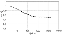
도 5는 활성화 시간에 따른 구동 전압 측정 그래프이다.1A-1D are schematic diagrams of method steps of a method of manufacturing an optoelectronic semiconductor chip according to various embodiments.
2-4 are schematic diagrams of method steps of a method of manufacturing an optoelectronic semiconductor chip according to another embodiment.
5 is a driving voltage measurement graph according to an activation time.
실시예 및 도면에서 동일하거나 동일한 효과를 가진 구성요소는 각각 동일한 참조번호를 가질 수 있다. 도시된 요소 및 요소들간의 크기비는 기본적으로 정확한 척도로 볼 수 없으며, 오히려 예를 들면 층, 부품, 소자, 영역과 같은 개별 요소는 더 나은 표현력 및/또는 더 나은 이해도를 위해 과장되어 두껍거나 큰 치수로 도시되어 있을 수 있다.In the embodiments and the drawings, the components having the same or the same effects may have the same reference numerals. The depicted elements and size ratios between the elements are not basically seen on an accurate scale, but rather individual elements such as layers, components, elements, regions, for example, are exaggerated and thick for better expression and / or better understanding. It may be shown in large dimensions.
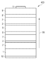
도 1a 내지 1d에는 광전 반도체 칩의 제조 방법에 대한 방법 단계(A)의 다양한 실시예가 도시되어 있다. 이때, 도 1a 내지 1d에 따르면, 각각, 반도체 층시퀀스(100, 200, 300 또는 400)가 형성되고, 상기 층시퀀스는 적어도 하나의 기판(1), 도핑된 기능층(7), 활성 영역(8) 및 다른 기능층(9)을 포함한다. 전기 접촉을 위해, 도핑된 기능층(7)과 다른 방향을 향해 있는 기판(1)의 측 및 기판(1)과 다른 방향을 향해 있는 각 반도체 층시퀀스(100, 200, 300, 400)의 표면에는 전극층들(10, 11)이 적층되고, 전극층들은 하나 이상의 금속 및/또는 일반 설명부에 기술된 바와 같은 하나 이상의 투명 전도 산화물을 포함할 수 있다. 도시된 실시예의 반도체 층시퀀스는 순수하게 예시적인 의미로 질화물 화합물 반도체 층시퀀스로서 형성된다. 이에 대해 대안적 또는 부가적으로, 반도체 층시퀀스는 일반 설명부에 기술된 다른 화합물 반도체 물질들도 포함할 수 있다.1A-1D show various embodiments of method step (A) for a method of manufacturing an optoelectronic semiconductor chip. 1A to 1D, a
또한, 이하에서, 각각 제조될 반도체 칩과 관련하여 순수하게 예시적으로 이미 완성된 반도체 층시퀀스(100, 200, 300, 400), 즉 각각의 층 구조물과 관련하여 이미 완성된 반도체 칩에 상응하는 반도체 층시퀀스가 형성된다. 이에 대해 대안적으로, 또한 부분적으로만 완성된 반도체 층시퀀스가 방법 단계(A)에서 형성될 수 있고, 상기 층시퀀스는 적어도 상기 도핑된 기능층(7)을 포함한다. 또한, 반도체 층시퀀스는 방법 단계(A)에서 아직은, 이후에 실시될 개별화 단계 이전의 웨이퍼 결합물에서 형성되고 제공될 수 있다.Further, hereinafter, purely illustratively already completed
이하의 설명은 순수하게 예시적인 의미로서 도핑된 기능층(7), 즉 p형 도핑된 층 및 다른 기능층들에 한정한다. 상기 다른 기능층들은 적합하게 n형 또는 p형으로 형성된다. 이에 대해 대안적으로, 도핑된 기능층(7) 및 다른 기능층들의 분극, 또는 도펀트 및 경우에 따라서 코도펀트의 분극은 뒤바뀔 수 있는데, 즉 특히 도핑된 기능층(7)은 n형 도핑되어 형성된다.The following description is purely illustrative and limited to the doped
도 1a의 실시예에 따른 반도체 층시퀀스(100)의 기판(1)은 성장 기판으로, 상기 성장 기판상에는 그 위에 위치한 층들(7, 8, 9)이 방법 단계(A)의 범위 내에서 에피택시얼 성장된다. 도 1a에서 성장 방향은 이하의 도면 1b 내지 1d와 마찬가지로 화살표(99)를 이용하여 표시되어 있다.The
상기 실시예에서, 바람직하게는 n형 기판이 성장 기판으로서 역할한다. 가능한 n형 기판은 예를 들면 n-GaN, n-SiC, n-Si(111)이다. 그러나, 예를 들면 사파이어와 같이 전기적으로 비전도성인 기판도 사용될 수 있으며, 이때 전극층(10)은 층들(7, 8, 9)을 향해 있는 기판(1)의 측에 배치된다.In this embodiment, preferably the n-type substrate serves as a growth substrate. Possible n-type substrates are, for example, n-GaN, n-SiC, n-Si (111). However, an electrically nonconductive substrate may also be used, for example sapphire, with the
기능층(9)은 n형층이며, 도시된 실시예에서는 규소로 도핑된 갈륨질화물층으로서 형성된다. 기능층(9) 상부에 활성층(8)이 성장되며, 활성층은 복사 생성을 위해 구비된 단일 양자 우물 구조 또는 다중 양자 우물 구조를 활성 영역으로서 포함한다. 바람직하게는, 활성층(8)은 III-V 반도체 물질계인 InyGa1-yN을 기반으로 하며, 이때 교번적으로 배치된 광학적 활성층들 및 장벽층들을 포함하고, 0≤y≤1이다. 바람직하게는, 활성층(8)은 자외, 청색, 청녹색, 황색 또는 적색의 스펙트럼 영역에서 전자기 복사를 생성하기에 적합하며, 이때 방출된 전자기 복사의 파장은 활성층(8)의 조성 및 구조를 이용하여 조절될 수 있다. 바람직하게는, 활성층에서 인듐 농도는 10과 60% 사이이다.The
활성층(8)상에는 도핑된 기능층(7)이 에피택시얼 성장되어 있으며, 도핑된 기능층은 GaN 또는 AlGaN을 반도체 물질로서 포함할 뿐만 아니라, p형 도핑을 위한 도펀트로서 마그네슘을, 코도펀트로서의 수소를 포함하고, 이는 가령 결정 성장 동안 도펀트의 삽입에 의하여 진성 결함이 삽임됨에 따라 반도체 물질의 결정 품질이 저하되는 것에 대해 반작용하기 위함이다. 도펀트 및 코도펀트는 결합 착물을 형성하여, 도펀트에 의해 고유로 생성되는 자유 전하 캐리어들이 보상되고, 반도체 결정의 전기적 중성도가 적어도 부분적으로 재형성된다.A doped
반도체 층시퀀스(100)의 구조는 기판(1)과 활성층(8) 사이에 n형 기능층(9)의 배치, 그리고 성장 방향(99)에서 활성층(8)상에 형성된 p형 도핑된 기능층(7)의 배치와 관련하여 종래 광방출 다이오드(LED)의 상응하며, 가령 버퍼층, 장벽층 및/또는 확산 차단층과 같은 다른 기능층을 더 포함할 수 있고, 이러한 다른 기능층은 개관상의 이유로 미도시되었다.The structure of the
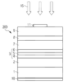
도 1b에서 다른 실시예에 따른 반도체 층시퀀스(200)는 반도체 층시퀀스(100)에 비해 뒤바뀐 분극을 가지며, 이때 성장 기판(1)과 활성층(8) 사이에 p형 도핑된 기능층(7)이 형성되고, 성장 방향(99)에서 활성층(8)상에 n형 도핑된 다른 기능층(9)이 형성된다. 층들(7, 8, 9)의 각각의 층 조성은 앞의 실시예에 상응한다.In FIG. 1B, the
또한, 반도체 층시퀀스(200)는 앞의 실시예와 마찬가지로 n형 성장 기판으로서 형성된 기판(1)과 p형 도핑된 기능층(7)사이에서 규소 도핑된 GaN 소재의 n형의 다른 기능층(2)을 포함한다. n형의 다른 기능층(2)에 p형 도핑된 기능층(7)의 효과적인 전기적 연결을 위해 이러한 기능층들 사이에는 고도핑된 n형 터널 접합층(4), 확산 장벽층(5) 및 고도핑된 p형 터널 접합층(6)을 구비한 터널 접합(3)이 형성된다. 터널 접합(3)은 일반 설명부에 기술된 바와 같이 형성되며, 이때 p형 터널 접합층(6)은 p형 도핑된 기능층(7)과 마찬가지로 도펀트로서 마그네슘을, 코도펀트로서 수소를 포함한다. 따라서, 고도핑된 p형 터널 접합층(6)은 도핑된 기능층(7)과 마찬가지로, 본 설명의 견지에서 활성화되어야 할 도핑된 기능층으로서 형성된다.In addition, the
도 1a에 따른 실시예의 반도체 층시퀀스(100)와 달리, 반도체 층시퀀스(200)에서 도핑된 기능층(6, 7)은 소위 매립된 도핑된 기능층으로서 형성되며, 상기 기능층은 다른 기능 반도체층들 사이에 배치된다. 코도펀트의 방출을 이용하는 공지된 활성화 방법에 의한 층들(6, 7)의 활성화는 반도체 층시퀀스(200)를 위해 불가능하다.Unlike the
반도체 층시퀀스(200)는 가령 기판(1)과 기능층(2)사이의 버퍼층 및/또는 도핑된 기능층(7)과 활성층(8) 사이의 확산 장벽층과 같은 다른 기능층들(미도시)을 포함할 수 있다.The
도 1c에는 박막 반도체 칩으로서 형성된 반도체 층시퀀스(300)가 도시되어 있으며, 상기 층시퀀스도 마찬가지로 매립된 도핑된 기능층(7)을 포함한다. 층들(7, 8, 9)은 도 1a의 층들(7, 8, 9)에 상응하며, 이때 성장 이후에 예를 들면 사파이어 소재의 성장 기판상에 위치한 상기 층들은 재본딩을 이용하여 캐리어 기판(1)상에 이송되었고, 따라서 성장 방향(99)은 캐리어 기판(1)의 방향을 가리킨다. 성장 기판은 재본딩 이후 제거되었다. 반도체 층시퀀스(300)는 예를 들면 캐리어 기판(1)과 p형 도핑된 기능층(7)사이의 반사층과 같이 다른 기능층들을 포함할 수 있거나/포함할 수 있고 일반 설명부에 기술된 박막 반도체 칩의 다른 특성을 가질 수 있다. 재본딩에 의해, 도핑된 기능층(7)도 마찬가지로 매립된 층으로서 존재하며, 상기 매립된 층은 코도펀트의 방출에 기반을 둔 공지된 활성화 방법을 이용하여서는 재본딩 이후에 활성화될 수 없다. 공지된 활성화 방법에서는, 바람직하게는 활성화가 재본딩 이전의 시점에서 실시되어야 하며, 상기 시점에서는 도핑된 기능층(7)이 여전히 노출되어 있다.1C shows a
캐리어 기판상의 박막 반도체 칩으로서 형성되는 방식에 대해 대안적으로, p형 성장 기판상에서의 에피택시얼 성장에 의해서도 기판(1)과 활성층(8)사이에 도핑된 기능층(7)을 포함하는 층들(7, 8, 9)의 층시퀀스가 형성될 수 있다. 이 경우, p형 기판은 예를 들면 p-GaN, p-SiC 또는 p-Si(111)로 형성될 수 있고, 이때 성장 방향(99)은 기판(1)으로부터 멀어지는 방향으로 지향되어 있을 것이다.Alternatives to the manner of forming as a thin film semiconductor chip on a carrier substrate, layers comprising a
도 1d에는 도 1b에 따른 역 구조를 포함하는 반도체 층시퀀스(400)가 도시되어 있으며, 이러한 역 구조도 다른 활성층(8')을 포함한 적층 구조로서 형성된다. 도핑된 기능층(7')은 도핑된 기능층(7)에 상응한다.FIG. 1D shows a
다른 기능층들(3', 9')은 층들(3, 9)에 상응하고, 이때 터널 접합(3)과 마찬가지로 터널 접합(3')은 도 1b와 관련하여 기술한 터널 접합층(4, 6) 및 확산 장벽층(5)을 포함한다(미도시).The other functional layers 3 ', 9' correspond to the
앞의 일반 설명부 및 이하에서 실시예들에 따라 기술한, 이후의 방법 단계(B)에서의 활성화 방법 시, 제조 공정에서 방법 단계(B)에 따른 활성화가 실시되는 시점은 각각의 반도체 층시퀀스의 형성 및 제조 공정과 무관하다. 순수하게 예시적으로, 방법 단계(B)를 위한 실시예가 도 1b에 따른 반도체 층시퀀스(200)에 의거하여 설명된다.In the activation method in the subsequent method step (B), described in accordance with the preceding general description and the embodiments below, the timing at which activation according to the method step (B) is carried out in the manufacturing process is carried out for each semiconductor layer sequence. It is independent of the formation and manufacturing process. Purely illustrative, an embodiment for method step (B) is described based on
도 2의 실시예에 따른 방법 단계(B)에서 도핑된 기능층(7) 및 고도핑된 p형 터널 접합층(6)은 전기 에너지의 형태로 에너지가 입력됨에 따라 활성화된다. 이를 위해, 반도체 층시퀀스(200)은 외부의 전류 공급부 및 전압 공급부(12)에 연결된다. 이때, 도시된 실시예에서, 반도체 층시퀀스(200) 또는 특히 도핑된 기능층(7) 및 고도핑된 p형 터널 접합층(6)에서 전류 밀도는 약 50 A/㎠으로 생성된다. 또한, 반도체 층시퀀스(200)는 열 에너지(13)의 공급에 의해 일반적 주변 온도 및 구동 온도보다 높은 온도가 된다. 도시된 실시예에서, 반도체 층시퀀스(200)는 외부 가열(미도시)에 의해 적어도 80℃의 온도가 되도록 가열된다. 공급된 열 에너지의 적어도 일부분은 주입된 전류의 오믹 손실에 의해 발생할 수 있다.In method step B according to the embodiment of FIG. 2, the doped
실험에 의해, 앞서 언급한 조건에서 전류 공급부 및 전압 공급부(12)에 의해 반도체 층시퀀스(200)를 구동할 때 필요 구동 전압이 시간에 따라 연속적으로 감소하고, 포화값에 도달하며, 상기 포화값은 영구적으로 유지된다는 것이 확인되었다. 이는, 반도체 층시퀀스의 전류-전압 특성이 방법 단계(B)에 의해 개선될 수 있고, 방법 단계(B) 이후에 영구적으로 유지될 수 있음을 의미한다. 도 5에는 전기적 활성화의 활성화 시간(t)(자의적 단위)에 따라 특정한 구동 전류로 인가될 구동 전압(U)(자의적 단위)의 측정값이 도시되어 있다. 또한, 전류 밀도의 증가 및/또는 온도의 증가가 전압 감소의 가속화 및 포화도 도달의 가속화를 야기할 수 있음이 확인되었다.Experimentally, when driving the
반도체 층시퀀스(200)의 상기 언급한 활성화 구동에 의해, 도펀트-코도펀트- 및 도펀트-코도펀트 반도체 결정-결합 착물은 층들(6, 7)에서 파괴될 수 있다. 상기 착물은 방법 단계(A)에서 반도체 층시퀀스(200)의 제조 시 형성된다. 종래의 활성화 방법에 비해 부가적으로, 코도펀트의 적어도 일부가 다른 위치에, 즉 도펀트에서 결합 착물을 형성하는 방식이 아니고, 층들(6, 7)의 반도체 결정에 결합하거나 격자 사이에 누적될 수 있다. 이를 통해, 본 명세서에 기술한 전기적 활성화 경우에는, 공지된 순수한 열 활성화 방법에서 반드시 필요한 바와 같이 코도펀트를 적어도 부분적으로 반도체 층시퀀스로부터 내보낼 필요는 없다. By the above-mentioned activation drive of the
방법 단계(B)를 위해 상기 언급한 유리한 전류 밀도에 의해, 도시된 전기적 활성화는 외부 전류 공급부 및 전압 공급부(12)에 의한 전류 주입을 이용하여 적어도 하나의 매립된 도핑된 기능층(7)을 포함하며 이미 개별화된 반도체 층시퀀스를 위해 매우 적합하고, 상기 층시퀀스에서 종래의 활성화 방법은 기술적으로 거의 실시할 수 없거나 전혀 실시할 수 없다. 그 외에, 본 명세서에 도시된 방법 단계(B)가 웨이퍼 결합물에서의 반도체 층시퀀스에 적용되는 경우도 결코 배제되지 않는다.By virtue of the advantageous current densities mentioned above for method step (B), the electrical activation shown uses at least one buried doped
특히, 웨이퍼 결합물에서의 반도체 층시퀀스 및 이미 개별화된 반도체 층시퀀스를 위해, 도 3의 실시예에 따른 방법 단계(B)가 적합하다. 이때, 장치(14)를 이용하여 유도에 의해 전류가 반도체 층시퀀스(200)에 또는 적어도 도핑된 기능층(7) 및 마찬가지로 활성화될 고도핑 p형 터널 접합층(6)에서 생성되며, 이러한 에너지는 도펀트 및 코도펀트를 함유한 결합 착물의 파괴를 야기한다. 도시된 실시예에서, 유도 장치(14)는 순수하게 예시적인 것으로서 코일로 구현되어 있으며, 이때 본 명세서에서 반도체 층시퀀스(200)에서 충분한 유도 전류를 야기할 수 있는 모든 장치가 적합할 수 있다.In particular, the method step (B) according to the embodiment of FIG. 3 is suitable for the semiconductor layer sequence and the already individualized semiconductor layer sequence in the wafer combination. At this time, current is generated in the
장치(14)에 의해, 자유 전하 캐리어를 이용하여 층들(6, 7)에서 원전류가 유도되고, 원전류에 의해 앞서 도 2와 관련하여 기술한 활성화 효과가 달성될 수 있다. 원전류는 성장 방향(99)에 대해 수직이며 반도체 층시퀀스(200)의 기능층들의 연장면에 대해서는 평행하게 발생한다. 부가적으로, 반도체 층시퀀스(200)에는 열 에너지가 외부 가열(미도시)의 형태로 더 공급될 수 있거나/공급될 수 있고 원전류의 오믹 손실에 의해 더 공급될 수 있다.By means of the
또한, 도 3에 따른 도시된 실시예에서 반도체 층시퀀스(200)는 전자기 복사(15)로 조사되며, 전자기 복사는 기능층 및 특히 활성화될 층들(6, 7)의 흡수 파장과 공명하거나 비공명한다. 전자기 복사(15)가 조사됨으로써 부가적으로 자유 전하 캐리어들이 생성되며, 이러한 전하 캐리어들은 유도된 원전류의 전류 세기를 더 강하게 할 수 있다. 이러한 점은, 활성화될 층들(6, 7)에서 방법 단계(A) 이후에 진성적으로 극히 일부의 자유 전하 캐리어가 존재하거나 자유 전하 캐리어가 전혀 존재하지 않는 경우에, 매우 유리하다. 특히, 공명 조사의 경우, 목적한 바에 따라 활성화될 층들(6, 7)에서는 또 다른 자유 전하 캐리어들이 여기될 수 있어서, 활성화 효율이 향상될 수 있다.In addition, in the illustrated embodiment according to FIG. 3, the
도 4에서 방법 단계(B)를 위한 다른 실시예에 따라 도시된 바와 같이, 활성화, 즉 도펀트 및 코도펀트를 함유한 착물의 파괴는 전자기 복사(15)의 형태로 에너지가 공급되는 경우에만 실시될 수 있다. 전자기 복사(15)의 주파수는 활성화 방식을 결정한다. 마이크로파 복사를 이용하면, 전자기 활성화는 비 공명적으로 수행되며, 테라헤르츠 복사를 이용하면 공명적인 전자기 활성화가 된다. 주파수, 출력, 분위기, 시간 및/또는 전자기 복사(15)에 대한 부가적 흡수 중심과 같은 공정 조건은 활성화 정도와 성공을 정의한다. 비공명인 경우, 특히 포논과 로톤의 여기에 의해 원자 결합물에 에너지가 전달된다. 공명의 경우, 격자 진동, 즉 포논이 직접적으로 생성되며, 포논은 도펀트 및 코도펀트를 함유한 결합 착물을 파괴할 수 있다.As shown in accordance with another embodiment for method step (B) in FIG. 4, activation, ie destruction of complexes containing dopants and codopants, can only be carried out when energy is supplied in the form of
도 3 및 4에 따른 방법 단계(B)는, 유리하게는 웨이퍼레벨에서 칩 사이클이 이루어지는 범위에서 반도체 칩의 제조 공정내에 어느 때에도 또는 개별화 이후에도 사용될 수 있는데, 상기 방법 단계는 비접촉식으로 이루어지고, 도 2의 실시예에 따른 방법 단계(B)와 마찬가지로 활성화되어야 할 노출된 도핑된 기능층(7)을 필요로 하지 않기 때문이다. 그러므로, 설계 및 소위 칩플로우에 있어서 개별 공정의 가능한 순서와 관련하여 더 많은 자유도가 얻어진다. 또한, 활성화 효율은 예를 들면, 활성화가 메사 식각 이후에 실시되어 노출된 반도체 결정 표면이 더 크게 존재하고 적어도 코도펀트의 일부는 배출될 수 있음으로써 증가할 수 있다.The method step (B) according to FIGS. 3 and 4 may advantageously be used at any time within the fabrication process of the semiconductor chip or even after individualization in the range of chip cycles at the wafer level, wherein the method step is made contactless, and FIG. This is because, like the method step (B) according to the embodiment of 2, it does not require an exposed doped
본 명세서에 기술된 방법 단계(B)의 실시예 및 일반 설명부에 따른 다른 실시예는 조합된 형태로 또는 차례로, 활성화될 개별 층들뿐만 아니라 반도체 층시퀀스내에서 활성화될 복수 개의 층들을 위해서도 사용될 수 있다.Embodiments of the method step (B) described herein and other embodiments according to the general description can be used in combination or in turn, for individual layers to be activated as well as for a plurality of layers to be activated in a semiconductor layer sequence. have.
필요 시, 방법 단계(B)에는 이제 활성화된 반도체 층시퀀스를 포함한 반도체 칩의 완성을 위해 또 다른 공지된 방법 단계를 연결할 수 있다.If necessary, method step (B) can now be linked to another known method step for the completion of a semiconductor chip comprising an activated semiconductor layer sequence.
본 발명은 실시예에 의거한 설명에 의하여 이러한 실시예에 한정되지 않는다. 오히려, 본 발명은 각각의 새로운 특징 및 특징들의 각 조합을 포함하며, 이러한 점은 특히, 비록 이러한 특징 또는 이러한 조합이 그 자체로 명백하게 특허청구범위 또는 실시예에 제공되지 않더라도 특허청구범위에서의 특징들의 각 조합을 포괄한다.The present invention is not limited to this embodiment by the description based on the embodiment. Rather, the invention includes each new feature and each combination of features, which in particular is a feature in the claims, even if such feature or such combination is not explicitly presented in the claims or the embodiment itself. Cover each combination of these.
Claims (15)
A) 적어도 하나의 도핑된 기능층(7)을 포함한 반도체 층시퀀스(200)의 제조 단계(상기 기능층은 적어도 하나의 도펀트 및 적어도 하나의 코도펀트를 함유한 결합 착물을 포함하고, 이때 상기 도펀트 및 상기 코도펀트 중 선택된 하나는 전자 수용체이고 다른 하나는 전자 공여체임),
B) 에너지 입력을 이용한 상기 결합 착물의 파괴에 의해 상기 도펀트를 활성화하는 단계(이때 상기 코도펀트는 적어도 일부는 상기 반도체 층시퀀스(200)에 잔류하고, 적어도 일부는 도펀트와의 결합 착물을 형성하지 않음)를 포함하는 것을 특징으로 하는 광전 반도체 칩의 제조 방법.In the manufacturing method of the optoelectronic semiconductor chip,
A) manufacturing a semiconductor layer sequence 200 comprising at least one doped functional layer 7 (the functional layer comprises a bonding complex containing at least one dopant and at least one codopant, wherein the dopant And one selected from said codopant is an electron acceptor and the other is an electron donor),
B) activating the dopant by disrupting the bond complex using energy input, wherein the codopant remains at least partially in the semiconductor layer sequence 200 and at least some does not form a bond complex with the dopant And a method of manufacturing an optoelectronic semiconductor chip.
상기 반도체 층시퀀스(200)는 상기 A 단계에서 형성되되, 상기 도핑된 기능층(7)이 2개의 다른 기능층들(2, 8) 사이에 배치되도록 형성되는 것을 특징으로 하는 광전 반도체 칩의 제조 방법.The method according to claim 1,
The semiconductor layer sequence 200 is formed in step A, wherein the doped functional layer 7 is formed so as to be disposed between two other functional layers 2, 8. Way.
상기 A 단계에서 상기 반도체 층시퀀스(200)는 웨이퍼 결합물에서 완성된 후 개별화되는 것을 특징으로 하는 광전 반도체 칩의 제조 방법.The method according to claim 1 or 2,
In the step A, the semiconductor layer sequence (200) is a method of manufacturing an optoelectronic semiconductor chip, characterized in that the individualized after being completed in the wafer assembly.
상기 도펀트는 마그네슘을 포함하고 상기 코도펀트는 수소를 포함하는 것을 특징으로 하는 광전 반도체 칩의 제조 방법.The method according to any one of claims 1 to 3,
And the dopant comprises magnesium and the codopant comprises hydrogen.
상기 B 단계에서 상기 에너지 입력은 상기 도핑된 기능층(7)에서 전류가 생성됨으로써 실시되는 것을 특징으로 하는 광전 반도체 칩의 제조 방법.The method according to any one of claims 1 to 4,
In step B, the energy input is performed by generating current in the doped functional layer (7).
상기 전류는 접촉 없이 유도에 의해 생성되는 것을 특징으로 하는 광전 반도체 칩의 제조 방법.The method according to claim 5,
And wherein said current is generated by induction without contact.
상기 전류는 상기 적어도 도핑된 기능층(7)이 외부 전류원(12)에 전기적으로 연결됨으로써 생성되는 것을 특징으로 하는 광전 반도체 칩의 제조 방법.The method according to claim 5,
And the current is generated by the at least doped functional layer (7) being electrically connected to an external current source (12).
상기 전류 생성에 대해 부가적으로 열 에너지(13)가 공급되는 것을 특징으로 하는 광전 반도체 칩의 제조 방법.The method according to any one of claims 5 to 7,
Thermal energy (13) is additionally supplied to the current generation.
상기 열 에너지(13)는 적어도 부분적으로 전류에 의해 공급되는 것을 특징으로 하는 광전 반도체 칩의 제조 방법.The method according to claim 8,
The thermal energy (13) is at least partly supplied by a current.
상기 B 단계에서 상기 에너지 입력은 전자기 복사(15)가 조사됨에 따라 실시되는 것을 특징으로 하는 광전 반도체 칩의 제조 방법.The method according to any one of claims 1 to 9,
The energy input in step B is carried out as the electromagnetic radiation (15) is irradiated.
상기 전자기 복사(15)는 적어도 부분적으로 상기 도핑된 기능층(7)의 흡수 파장과 공명하는 것을 특징으로 하는 광전 반도체 칩의 제조 방법.The method according to claim 10,
The electromagnetic radiation (15) resonates at least in part with the absorption wavelength of the doped functional layer (7).
상기 전자기 복사(15)는 적어도 부분적으로 상기 도핑된 기능층(7)의 흡수 파장과 공명하지 않는 것을 특징으로 하는 광전 반도체 칩의 제조 방법.The method according to claim 10 or 11,
The method of manufacturing an optoelectronic semiconductor chip, characterized in that the electromagnetic radiation is not at least partially resonant with the absorption wavelength of the doped functional layer.
상기 반도체 층시퀀스(200)는 격자 구조를 가진 반도체 물질을 포함하고,
상기 도펀트 및 상기 코도펀트 중 선택된 하나는 전자 수용체이고 다른 하나는 전자 공여체이며,
상기 코도펀트는 상기 반도체 물질에 결합되거나/결합되고 격자 사이점에 배치되며, 그리고
상기 코도펀트는 적어도 부분적으로 상기 도펀트와 결합 착물을 형성하지 않는 것을 특징으로 하는 광전 반도체 칩.An optoelectronic semiconductor chip comprising a semiconductor layer sequence 200 having at least one doped functional layer 7 containing at least one dopant and at least one codopant.
The semiconductor layer sequence 200 includes a semiconductor material having a lattice structure,
One selected from the dopant and the codopant is an electron acceptor and the other is an electron donor,
The codopant is bonded to the semiconductor material and / or disposed between lattice points, and
And wherein the codopant does not at least partially form a bond complex with the dopant.
상기 도핑된 기능층(7)은 2개의 다른 기능층들(3, 8) 사이에 배치되는 것을 특징으로 하는 광전 반도체 칩.The method according to claim 13,
The doped functional layer (7) is characterized in that it is arranged between two different functional layers (3, 8).
상기 도펀트는 마그네슘을 포함하고 상기 코도펀트는 수소를 포함하는 것을 특징으로 하는 광전 반도체 칩.The method according to claim 13 or 14,
And the dopant comprises magnesium and the codopant comprises hydrogen.
Applications Claiming Priority (2)
| Application Number | Priority Date | Filing Date | Title |
|---|---|---|---|
| DE102008056371A DE102008056371A1 (en) | 2008-11-07 | 2008-11-07 | Method for producing an optoelectronic semiconductor chip and optoelectronic semiconductor chip |
| DE102008056371.4 | 2008-11-07 |
Publications (1)
| Publication Number | Publication Date |
|---|---|
| KR20110088545A true KR20110088545A (en) | 2011-08-03 |
Family
ID=41667176
Family Applications (1)
| Application Number | Title | Priority Date | Filing Date |
|---|---|---|---|
| KR1020117012745A KR20110088545A (en) | 2008-11-07 | 2009-10-12 | Method for producing an optoelectronic semiconductor chip and optoelectronic semiconductor chip |
Country Status (8)
| Country | Link |
|---|---|
| US (1) | US8598596B2 (en) |
| EP (1) | EP2342762A1 (en) |
| JP (1) | JP5951993B2 (en) |
| KR (1) | KR20110088545A (en) |
| CN (1) | CN102210031B (en) |
| DE (1) | DE102008056371A1 (en) |
| TW (1) | TW201027806A (en) |
| WO (1) | WO2010051786A1 (en) |
Cited By (1)
| Publication number | Priority date | Publication date | Assignee | Title |
|---|---|---|---|---|
| KR20190076011A (en) * | 2016-10-28 | 2019-07-01 | 루미레즈 엘엘씨 | Methods for growing light emitting devices under ultraviolet irradiation |
Families Citing this family (14)
| Publication number | Priority date | Publication date | Assignee | Title |
|---|---|---|---|---|
| KR20180030216A (en) | 2010-09-29 | 2018-03-21 | 루미리즈 홀딩 비.브이. | Wavelength converted light emitting device |
| TWI456790B (en) * | 2012-09-28 | 2014-10-11 | Phostek Inc | Light-emitting diode device |
| US9379259B2 (en) * | 2012-11-05 | 2016-06-28 | International Business Machines Corporation | Double layered transparent conductive oxide for reduced schottky barrier in photovoltaic devices |
| CN103184034B (en) * | 2013-01-04 | 2014-08-20 | 北京阳光溢彩科技有限公司 | Ecological environment-friendly dust inhibitor |
| JP6051901B2 (en) * | 2013-02-05 | 2016-12-27 | 豊田合成株式会社 | Method for producing p-type group III nitride semiconductor |
| US20140353578A1 (en) * | 2013-06-04 | 2014-12-04 | Epistar Corporation | Light-emitting device |
| KR102227981B1 (en) * | 2013-06-20 | 2021-03-16 | 삼성전자주식회사 | Single photon device, apparatus of emitting and transferring single photon, and methodsof manufacturing and operating the same |
| JP6459948B2 (en) * | 2015-12-15 | 2019-01-30 | 株式会社Sumco | Manufacturing method of semiconductor epitaxial wafer and manufacturing method of solid-state imaging device |
| WO2017200845A1 (en) | 2016-05-20 | 2017-11-23 | Lumileds Llc | Method of forming a p-type layer for a light emitting device |
| US10541352B2 (en) | 2016-10-28 | 2020-01-21 | Lumileds Llc | Methods for growing light emitting devices under ultra-violet illumination |
| JP7122119B2 (en) * | 2017-05-25 | 2022-08-19 | 昭和電工光半導体株式会社 | light emitting diode |
| US10439103B2 (en) | 2017-05-25 | 2019-10-08 | Showa Denko K. K. | Light-emitting diode and method for manufacturing tunnel junction layer |
| WO2019152611A1 (en) * | 2018-02-02 | 2019-08-08 | Cornell University | Platforms enabled by buried tunnel junction for integrated photonic and electronic systems |
| JP7149486B2 (en) | 2020-04-21 | 2022-10-07 | 日亜化学工業株式会社 | Method for manufacturing light-emitting element |
Family Cites Families (16)
| Publication number | Priority date | Publication date | Assignee | Title |
|---|---|---|---|---|
| US5306662A (en) | 1991-11-08 | 1994-04-26 | Nichia Chemical Industries, Ltd. | Method of manufacturing P-type compound semiconductor |
| TW329058B (en) * | 1997-03-20 | 1998-04-01 | Ind Tech Res Inst | Manufacturing method for P type gallium nitride |
| JPH11126758A (en) | 1997-10-24 | 1999-05-11 | Pioneer Electron Corp | Manufacture of semiconductor element |
| JP2001044209A (en) * | 1999-07-27 | 2001-02-16 | Furukawa Electric Co Ltd:The | MANUFACTURE OF GaN-BASED SEMICONDUCTOR DEVICE |
| KR20020056566A (en) * | 2000-12-29 | 2002-07-10 | 조장연 | p-type activation of GaN semiconductor films |
| JP2002319703A (en) | 2001-04-20 | 2002-10-31 | Ricoh Co Ltd | Semiconductor device and its manufacturing method |
| DE10152922B4 (en) | 2001-10-26 | 2010-05-12 | Osram Opto Semiconductors Gmbh | Nitride-based semiconductor device |
| TW517403B (en) | 2002-01-10 | 2003-01-11 | Epitech Technology Corp | Nitride light emitting diode and manufacturing method for the same |
| TW540170B (en) * | 2002-07-08 | 2003-07-01 | Arima Optoelectronics Corp | Ohmic contact structure of semiconductor light emitting device and its manufacturing method |
| JP2004128189A (en) | 2002-10-02 | 2004-04-22 | Sanyo Electric Co Ltd | Method for manufacturing gallium nitride system compound semiconductor |
| KR100662191B1 (en) * | 2004-12-23 | 2006-12-27 | 엘지이노텍 주식회사 | Nitride semiconductor LED and fabrication method thereof |
| KR100580752B1 (en) * | 2004-12-23 | 2006-05-15 | 엘지이노텍 주식회사 | Nitride semiconductor led and fabrication method thereof |
| JP5360789B2 (en) * | 2006-07-06 | 2013-12-04 | 独立行政法人産業技術総合研究所 | P-type zinc oxide thin film and method for producing the same |
| KR100748709B1 (en) * | 2006-09-18 | 2007-08-13 | 서울옵토디바이스주식회사 | Light emitting device and method of manufacturing the same |
| JP4827706B2 (en) | 2006-12-04 | 2011-11-30 | シャープ株式会社 | Nitride semiconductor light emitting device |
| DE102007019079A1 (en) * | 2007-01-26 | 2008-07-31 | Osram Opto Semiconductors Gmbh | Optoelectronic semiconductor chip producing method, involves forming epitaxial covering layer that is downstream of semiconductor section, and electrically activating p-doped region of section before or during formation of covering layer |
-
2008
- 2008-11-07 DE DE102008056371A patent/DE102008056371A1/en active Pending
-
2009
- 2009-10-12 WO PCT/DE2009/001415 patent/WO2010051786A1/en active Application Filing
- 2009-10-12 KR KR1020117012745A patent/KR20110088545A/en not_active Application Discontinuation
- 2009-10-12 JP JP2011535002A patent/JP5951993B2/en active Active
- 2009-10-12 CN CN200980144749.0A patent/CN102210031B/en active Active
- 2009-10-12 EP EP09765005A patent/EP2342762A1/en not_active Withdrawn
- 2009-10-12 US US13/128,050 patent/US8598596B2/en active Active
- 2009-11-04 TW TW098137382A patent/TW201027806A/en unknown
Cited By (2)
| Publication number | Priority date | Publication date | Assignee | Title |
|---|---|---|---|---|
| KR20190076011A (en) * | 2016-10-28 | 2019-07-01 | 루미레즈 엘엘씨 | Methods for growing light emitting devices under ultraviolet irradiation |
| JP2020501345A (en) * | 2016-10-28 | 2020-01-16 | ルミレッズ リミテッド ライアビリティ カンパニー | Method for growing light emitting device under ultraviolet irradiation |
Also Published As
| Publication number | Publication date |
|---|---|
| DE102008056371A1 (en) | 2010-05-12 |
| CN102210031B (en) | 2015-07-01 |
| JP2012508458A (en) | 2012-04-05 |
| CN102210031A (en) | 2011-10-05 |
| JP5951993B2 (en) | 2016-07-13 |
| TW201027806A (en) | 2010-07-16 |
| EP2342762A1 (en) | 2011-07-13 |
| US20110278641A1 (en) | 2011-11-17 |
| WO2010051786A1 (en) | 2010-05-14 |
| US8598596B2 (en) | 2013-12-03 |
Similar Documents
| Publication | Publication Date | Title |
|---|---|---|
| KR20110088545A (en) | Method for producing an optoelectronic semiconductor chip and optoelectronic semiconductor chip | |
| TWI420687B (en) | Polarization-reversed iii-nitride light-emitting device | |
| US10304997B2 (en) | III-nitride light emitting device with a region including only ternary, quaternary, and/or quinary III-nitride layers | |
| JP5167127B2 (en) | Optoelectronic semiconductor chip | |
| US11069524B2 (en) | Methods for using remote plasma chemical vapor deposition (RP-CVD) and sputtering deposition to grow layers in light emitting devices | |
| US6720570B2 (en) | Gallium nitride-based semiconductor light emitting device | |
| KR100952401B1 (en) | Light emitting semiconductors devices including wafer bonded heterostructures | |
| US11069836B2 (en) | Methods for growing light emitting devices under ultra-violet illumination | |
| US20060289891A1 (en) | Electronic and/or optoelectronic devices grown on free-standing GaN substrates with GaN spacer structures | |
| Scholz et al. | Efficiency studies on semipolar GaInN–GaN quantum well structures | |
| EP3533088B1 (en) | Methods for growing light emitting devices under ultra-violet illumination | |
| US8952399B2 (en) | Light emitting device comprising a wavelength conversion layer having indirect bandgap energy and made of an N-type doped AlInGaP material | |
| JPWO2008117788A1 (en) | Light emitting element | |
| KR102192601B1 (en) | Methods for using remote plasma chemical vapor deposition (rp-cvd) and sputtering deposition to grow layers in light emitting devices | |
| Cao | III–Nitride Light‐Emitting Diodes on Novel Substrates | |
| JP2009176759A (en) | Gallium nitride compound semiconductor, light-emitting element, illuminating device, and method for producing gallium nitride compound semiconductor | |
| JP2009176758A (en) | Gallium nitride compound semiconductor, light-emitting element, illuminating device, and method for producing gallium nitride compound semiconductor |
Legal Events
| Date | Code | Title | Description |
|---|---|---|---|
| E902 | Notification of reason for refusal | ||
| E601 | Decision to refuse application |