KR20100048995A - Substrate for the epitaxial growth of gallium nitride - Google Patents
Substrate for the epitaxial growth of gallium nitride Download PDFInfo
- Publication number
- KR20100048995A KR20100048995A KR1020107000664A KR20107000664A KR20100048995A KR 20100048995 A KR20100048995 A KR 20100048995A KR 1020107000664 A KR1020107000664 A KR 1020107000664A KR 20107000664 A KR20107000664 A KR 20107000664A KR 20100048995 A KR20100048995 A KR 20100048995A
- Authority
- KR
- South Korea
- Prior art keywords
- layer
- zinc
- substrate
- oxide
- support material
- Prior art date
Links
Images


Classifications
-
- C—CHEMISTRY; METALLURGY
- C30—CRYSTAL GROWTH
- C30B—SINGLE-CRYSTAL GROWTH; UNIDIRECTIONAL SOLIDIFICATION OF EUTECTIC MATERIAL OR UNIDIRECTIONAL DEMIXING OF EUTECTOID MATERIAL; REFINING BY ZONE-MELTING OF MATERIAL; PRODUCTION OF A HOMOGENEOUS POLYCRYSTALLINE MATERIAL WITH DEFINED STRUCTURE; SINGLE CRYSTALS OR HOMOGENEOUS POLYCRYSTALLINE MATERIAL WITH DEFINED STRUCTURE; AFTER-TREATMENT OF SINGLE CRYSTALS OR A HOMOGENEOUS POLYCRYSTALLINE MATERIAL WITH DEFINED STRUCTURE; APPARATUS THEREFOR
- C30B29/00—Single crystals or homogeneous polycrystalline material with defined structure characterised by the material or by their shape
- C30B29/10—Inorganic compounds or compositions
- C30B29/40—AIIIBV compounds wherein A is B, Al, Ga, In or Tl and B is N, P, As, Sb or Bi
- C30B29/403—AIII-nitrides
-
- C—CHEMISTRY; METALLURGY
- C30—CRYSTAL GROWTH
- C30B—SINGLE-CRYSTAL GROWTH; UNIDIRECTIONAL SOLIDIFICATION OF EUTECTIC MATERIAL OR UNIDIRECTIONAL DEMIXING OF EUTECTOID MATERIAL; REFINING BY ZONE-MELTING OF MATERIAL; PRODUCTION OF A HOMOGENEOUS POLYCRYSTALLINE MATERIAL WITH DEFINED STRUCTURE; SINGLE CRYSTALS OR HOMOGENEOUS POLYCRYSTALLINE MATERIAL WITH DEFINED STRUCTURE; AFTER-TREATMENT OF SINGLE CRYSTALS OR A HOMOGENEOUS POLYCRYSTALLINE MATERIAL WITH DEFINED STRUCTURE; APPARATUS THEREFOR
- C30B25/00—Single-crystal growth by chemical reaction of reactive gases, e.g. chemical vapour-deposition growth
- C30B25/02—Epitaxial-layer growth
- C30B25/18—Epitaxial-layer growth characterised by the substrate
-
- H—ELECTRICITY
- H01—ELECTRIC ELEMENTS
- H01L—SEMICONDUCTOR DEVICES NOT COVERED BY CLASS H10
- H01L21/00—Processes or apparatus adapted for the manufacture or treatment of semiconductor or solid state devices or of parts thereof
- H01L21/02—Manufacture or treatment of semiconductor devices or of parts thereof
- H01L21/02104—Forming layers
- H01L21/02365—Forming inorganic semiconducting materials on a substrate
- H01L21/02367—Substrates
- H01L21/0237—Materials
-
- H—ELECTRICITY
- H01—ELECTRIC ELEMENTS
- H01L—SEMICONDUCTOR DEVICES NOT COVERED BY CLASS H10
- H01L21/00—Processes or apparatus adapted for the manufacture or treatment of semiconductor or solid state devices or of parts thereof
- H01L21/02—Manufacture or treatment of semiconductor devices or of parts thereof
- H01L21/02104—Forming layers
- H01L21/02365—Forming inorganic semiconducting materials on a substrate
- H01L21/02436—Intermediate layers between substrates and deposited layers
- H01L21/02439—Materials
- H01L21/02483—Oxide semiconducting materials not being Group 12/16 materials, e.g. ternary compounds
-
- H—ELECTRICITY
- H01—ELECTRIC ELEMENTS
- H01L—SEMICONDUCTOR DEVICES NOT COVERED BY CLASS H10
- H01L21/00—Processes or apparatus adapted for the manufacture or treatment of semiconductor or solid state devices or of parts thereof
- H01L21/02—Manufacture or treatment of semiconductor devices or of parts thereof
- H01L21/02104—Forming layers
- H01L21/02365—Forming inorganic semiconducting materials on a substrate
- H01L21/02436—Intermediate layers between substrates and deposited layers
- H01L21/02439—Materials
- H01L21/02488—Insulating materials
-
- H—ELECTRICITY
- H01—ELECTRIC ELEMENTS
- H01L—SEMICONDUCTOR DEVICES NOT COVERED BY CLASS H10
- H01L21/00—Processes or apparatus adapted for the manufacture or treatment of semiconductor or solid state devices or of parts thereof
- H01L21/02—Manufacture or treatment of semiconductor devices or of parts thereof
- H01L21/02104—Forming layers
- H01L21/02365—Forming inorganic semiconducting materials on a substrate
- H01L21/02436—Intermediate layers between substrates and deposited layers
- H01L21/02494—Structure
- H01L21/02496—Layer structure
- H01L21/02502—Layer structure consisting of two layers
-
- H—ELECTRICITY
- H01—ELECTRIC ELEMENTS
- H01L—SEMICONDUCTOR DEVICES NOT COVERED BY CLASS H10
- H01L21/00—Processes or apparatus adapted for the manufacture or treatment of semiconductor or solid state devices or of parts thereof
- H01L21/02—Manufacture or treatment of semiconductor devices or of parts thereof
- H01L21/02104—Forming layers
- H01L21/02365—Forming inorganic semiconducting materials on a substrate
- H01L21/02518—Deposited layers
- H01L21/02521—Materials
- H01L21/02538—Group 13/15 materials
- H01L21/0254—Nitrides
-
- H—ELECTRICITY
- H01—ELECTRIC ELEMENTS
- H01L—SEMICONDUCTOR DEVICES NOT COVERED BY CLASS H10
- H01L21/00—Processes or apparatus adapted for the manufacture or treatment of semiconductor or solid state devices or of parts thereof
- H01L21/02—Manufacture or treatment of semiconductor devices or of parts thereof
- H01L21/02104—Forming layers
- H01L21/02365—Forming inorganic semiconducting materials on a substrate
- H01L21/02518—Deposited layers
- H01L21/02521—Materials
- H01L21/02551—Group 12/16 materials
- H01L21/02554—Oxides
-
- H—ELECTRICITY
- H01—ELECTRIC ELEMENTS
- H01L—SEMICONDUCTOR DEVICES NOT COVERED BY CLASS H10
- H01L21/00—Processes or apparatus adapted for the manufacture or treatment of semiconductor or solid state devices or of parts thereof
- H01L21/02—Manufacture or treatment of semiconductor devices or of parts thereof
- H01L21/02104—Forming layers
- H01L21/02365—Forming inorganic semiconducting materials on a substrate
- H01L21/02612—Formation types
- H01L21/02617—Deposition types
- H01L21/02631—Physical deposition at reduced pressure, e.g. MBE, sputtering, evaporation
Abstract
Description
본 발명은 특히 발광 다이오드 (LED) 또는 트랜지스터와 같은 전자 부품에 사용되는 III-N 또는 II-VI형 반도체 분야, 특히 질화 갈륨(GaN)에 기초한 것들에 관한 것이다. 보다 구체적으로는, 특히 그 위에 갈륨-질화물-기재 층을 성장시킬 수 있는 새로운 유형의 기판에 관한 것이다. The present invention relates in particular to the field of III-N or II-VI semiconductors used in electronic components such as light emitting diodes (LEDs) or transistors, in particular those based on gallium nitride (GaN). More particularly, it relates to a new type of substrate capable of growing a gallium-nitride-based layer thereon.
질화 갈륨은 약 3.45 eV의 갭(gap)을 가지는 반도체이다. 이것은 파랑부터 보라까지 범위의 파장에서 발광하는 발광 다이오드를 생산하는데 널리 사용된다. 이 다이오드의 필수적인 요소는, 가장 간단하게 표현하면, 기판 위에 침착된 GaN 기재 층을 포함하는 p-n 접합(junction)으로 이루어진다. GaN-기재 층은 일반적으로 일반식 InxGayAl1 -x- yN (여기서 x와 y는 0부터 1까지 변함)인 물질을 포함하는 층을 포함한다. 그들은 보통 매우 고온에서 (1000℃ 내지 1200℃) 트리에틸갈륨 또는 트리메틸갈륨과 같은 유기금속 전구체와 암모니아의 도움으로 MOCVD (유기 금속 화학 기상 증착) 기술을 사용한 헤테로에피택시(heteroepitaxy)에 의해 얻는다. 이러한 고온 때문에, 사용될 수 있는 기판은 사파이어(sapphire) (α-Al2O3, 코런덤(corundum)이라고도 함) 또는 탄화 규소 (SiC)이다. 그러나, GaN과 사파이어 사이의 큰 격자 불일치(lattice mismatch) (약 14%)와 그들 개개의 열 팽창 계수 사이의 큰 차이 때문에, 그로 인해 얻어진 GaN이 저품질의 결정성 및 (1010/cm2까지의 범위의 결함 밀도, 특히 전위 밀도(dislocation density)를 갖는) 많은 결정 결함을 갖게 되어, 발광 강도(emission intensity) (빛 및 에너지 효율)와 다이오드의 수명 모두를 제한한다. Gallium nitride is a semiconductor having a gap of about 3.45 eV. It is widely used to produce light emitting diodes that emit at wavelengths ranging from blue to violet. The essential element of this diode, in the simplest case, consists of a pn junction comprising a GaN substrate layer deposited on a substrate. The GaN- based layer generally comprises a layer comprising a material the general formula In x Ga y Al 1 -x- y N ( where x and y varies from 0 to 1). They are usually obtained by heteroepitaxy using MOCVD (organic metal chemical vapor deposition) technology with the help of ammonia and organometallic precursors such as triethylgallium or trimethylgallium at very high temperatures. Because of this high temperature, substrates that can be used are sapphire (α-Al 2 O 3 , also known as corundum) or silicon carbide (SiC). However, due to the large lattice mismatch between GaN and sapphire (about 14%) and their individual thermal expansion coefficients, the resulting GaN has low crystallinity and (up to 10 10 / cm 2 ) There are many crystal defects in the range of defect densities, especially dislocation densities, which limit both the emission intensity (light and energy efficiency) and the lifetime of the diode.
더욱 최근에는, 더 낮은 증착 온도 때문에 결정학적 견지에서 더 잘 들어맞고 덜 비싼 기판의 사용을 허용하는 대체 증착 방법이 제안되었다. 예로서, PLD (펄스 레이저 증착), PAMBE (플라즈마 보조 분자선 에피택시), RPCVD (리모트 플라즈마 화학 기상 증착) 및 ENABLE (에너제틱 중성 원자 빔 리소그래피/에피택시) 공정을 들 수 있다. 이러한 공정은 GaN을 800℃ 미만, 또는 심지어 100℃ 미만의 임의의 온도에서 침착할 수 있게 한다. 그러므로, 다른 유형의 기판, 특히 격자 변수의 견지에서 더욱 적합한 것을 사용할 수 있게 된다. More recently, alternative deposition methods have been proposed that allow for the use of better and less expensive substrates in crystallographic terms due to lower deposition temperatures. Examples include PLD (pulse laser deposition), PAMBE (plasma assisted molecular beam epitaxy), RPCVD (remote plasma chemical vapor deposition), and ENABLE (energetic neutral atomic beam lithography / epitaxial) processes. This process makes it possible to deposit GaN at any temperature below 800 ° C, or even below 100 ° C. Therefore, it is possible to use other types of substrates, especially those which are more suitable in view of the lattice parameters.
미국 특허 제6 362 496 B1호에는 낮은 온도에서 GaN을 성장시키기 위한, 산화 아연 (ZnO) 층으로 코팅된 보로실리케이트(borosilicate) 유리 기판을 포함하는 기판이 공지되어 있다.U. S. Patent No. 6 362 496 B1 discloses a substrate comprising a borosilicate glass substrate coated with a zinc oxide (ZnO) layer for growing GaN at low temperatures.
산화 아연은 우르자이트(wurtzite)형 육각 구조를 가지는 이점을 가지고, 그의 a축은 약 0.32 nm, 즉 GaN의 a축 길이와 거의 동일한 길이를 갖는다. 결정학적 구조와 격자 변수의 견지에서의 이러한 유사성 (상대적인 면에서 2% 정도(order)) 때문에, GaN의 에피택셜 성장은 꽤 유리하다.Zinc oxide has the advantage of having a wurtzite-shaped hexagonal structure, the a-axis of which is about 0.32 nm, i.e., almost the same length as the a-axis length of GaN. Due to this similarity (about 2% order relative) in terms of crystallographic structure and lattice parameters, epitaxial growth of GaN is quite advantageous.
본 발명의 한 목적은 GaN, 또는, 더욱 일반적으로 말하면, III-N형 (GaN 등) 또는 II-IV형 (ZnO 등)의 반도체의 결정성을 추가적으로 향상시키는 것으로, 특히, 이러한 물질을 포함하는 발광 다이오드의 발광 강도 및 수명을 향상시키기 위함이다.One object of the present invention is to further improve the crystallinity of GaN, or more generally, semiconductors of type III-N (GaN, etc.) or II-IV (ZnO, etc.), in particular comprising This is to improve the light emission intensity and lifetime of the light emitting diode.
본 발명의 또 다른 목적은 그러므로, 반도체 구조가 그 위에 침착될 경우, 이러한 성질을 향상시킬 수 있는 기판을 제공하는 것이다. It is yet another object of the present invention to provide a substrate which can improve these properties when a semiconductor structure is deposited thereon.
본 발명의 또 다른 목적은 경제적으로 및 큰 규모로 생산될 수 있는 기판을 제공하는 것이다. It is a further object of the present invention to provide a substrate which can be produced economically and on a large scale.
이러한 목적을 위하여, 본 발명의 한 주제는 한 면 이상이 하나 이상의 아연-산화물-기재 층을 포함하는 하나 이상의 다층 적층물로 코팅된 지지 물질을 포함하고, 질화 갈륨을 기초로 하는 층의 에피택셜 성장을 위한 기판으로서 사용될 수 있는 기판으로, 상기 기판은 III-N 또는 II-VI형의 반도체 구조로 코팅된 기판이다. 상기 기판은 주석 (Sn), 아연 (Zn), 인듐 (In), 갈륨 (Ga) 및 안티몬 (Sb)로부터 선택된 둘 이상의 원소의 산화물을 포함하는 하나 이상의 중간층이 지지 물질과 상기 하나 이상의 아연-산화물-기재 층 사이에 위치하는 것을 특징으로 한다. For this purpose, one subject of the invention comprises an epitaxial of a layer based on gallium nitride, wherein the support material is coated with at least one multilayer stack comprising at least one side comprising at least one zinc-oxide-based layer. A substrate that can be used as a substrate for growth, wherein the substrate is a substrate coated with a III-N or II-VI type semiconductor structure. The substrate comprises at least one intermediate layer comprising oxides of at least two elements selected from tin (Sn), zinc (Zn), indium (In), gallium (Ga), and antimony (Sb) and the support material and the at least one zinc-oxide. -Between the substrate layers.
본 발명의 또 다른 주제는 한 면 이상이 하나 이상의 아연-산화물-기재 층을 포함하는 하나 이상의 다층 적층물로 코팅된 지지 물질을 포함하고, 질화 갈륨을 기초로 하는 층의 에피택셜 성장을 위한 기판으로서 사용될 수 있는 기판이다. 본 발명에 따른 기판은 주석 (Sn), 아연 (Zn), 갈륨 (Ga) 및 안티몬 (Sb)로부터 선택된 둘 이상의 원소의 산화물을 포함하는 하나 이상의 중간층이 지지 물질과 상기 하나 이상의 아연-산화물-기재 층 사이에 위치하는 것을 특징으로 한다.Another subject matter of the present invention is a substrate for epitaxial growth of a layer based on gallium nitride, comprising a support material coated on at least one multilayer stack with at least one side comprising at least one zinc-oxide-based layer. It can be used as a substrate. Substrates according to the invention comprise at least one intermediate layer comprising oxides of at least two elements selected from tin (Sn), zinc (Zn), gallium (Ga) and antimony (Sb) and the at least one zinc-oxide-based substrate. It is located between the layers.
본 발명의 제1 목적은, 그러므로, 반도체 구조로 코팅된 기판이다. 이는 이하 "코팅된 기판"이라 할 것이다. 본 발명의 제2 목적은 제1 목적물의 생산 즉, III-N 또는 II-VI형의 반도체 구조의 에피택셜 성장에 특별히 알맞은 특정 기판이다.The first object of the present invention is therefore a substrate coated with a semiconductor structure. This will hereinafter be referred to as a "coated substrate". A second object of the present invention is a particular substrate which is particularly suitable for the production of the first object, ie, epitaxial growth of a III-N or II-VI type semiconductor structure.
발명자들은 사실 GaN 층의 결정성, 또는, 더욱 일반적으로는, III-N 또는 II-IV형 반도체 층의 결정성 또한, 지지 물질과 ZnO층 사이에 그러한 중간층을 놓음으로써 향상될 수 있다고 설명한다.The inventors explain that in fact the crystallinity of the GaN layer, or more generally, the crystallinity of the III-N or II-IV type semiconductor layer, can also be improved by placing such intermediate layer between the support material and the ZnO layer.
이 중간층은 특히 결정화된 물질의 양을 증가시킴으로써 및/또는 그 c축 (이 축은 게다가 지지 물질의 표면에 완벽하게 수직이다)을 따라 산화 아연 또는 질화 갈륨의 성장을 촉진시킴으로써 반도체 층의 결정화 성질을 향상시킬 수 있다.This intermediate layer specifically improves the crystallization properties of the semiconductor layer by increasing the amount of crystallized material and / or by promoting the growth of zinc oxide or gallium nitride along its c axis (which is also perfectly perpendicular to the surface of the support material). Can be improved.
이 서브층의 존재가 ZnO/GaN 또는 ZnO/ZnO 적층물의 전자 전도성을 향상시키는 것을 도울 것이라는 것 또한 발명자에게 명백했다. 그 결과, 이러한 층 내에 더 균일한 전류 분배가 존재하고, 양자 수율이 증가하여 그로 인해 발광 강도가 더 높아지고, 부품의 가열(heat-up) 감소로 인해 그 수명이 증가한다. It was also apparent to the inventor that the presence of this sublayer would help to improve the electronic conductivity of the ZnO / GaN or ZnO / ZnO stack. As a result, there is a more uniform current distribution in this layer, the quantum yield is increased thereby resulting in higher luminescence intensity, and its lifetime is increased due to reduced heat-up of the part.
바람직하게는, 지지 물질은 그의 단 한 면만 코팅된다. 이 지지 물질에 침착된 적층물은 바람직하게는 단일의 ZnO-기재 층 및/또는 단일의 중간층을 포함한다. Preferably, the support material is coated only on one side thereof. The laminate deposited on this support material preferably comprises a single ZnO-based layer and / or a single intermediate layer.
지지 물질은 전자장에서 지지체로 사용되는 임의의 유형의 물질, 예를 들어, 사파이어(sapphire), 탄화 규소, 규소, 구리와 같은 금속, 석영, 산화 아연 (ZnO) 및 MgAl2O4 및 LiGaO2와 같은 스피넬일 수 있다. 본 발명의 효과는 유리질 또는 무정형 물질에서 더욱 중요하게 나타난다. 지지 물질은 바람직하게는 실리카 유리 또는 실리카-기재 유리와 같은 유리질 또는 무정형 물질이다. 그것은 또한 유리-세라믹 물질, 즉, 하나 이상의 유리질 상태와 하나 이상의 결정질 상태로 이루어진 물질일 수 있다. 용어 "실리카-기재 유리"는 40% 이상, 일반적으로 50%의 중량 함량(weight content)을 가지는 실리카를 포함하는 유리를 의미하는 것으로 이해된다. 보로실리케이트 유리와 같이 고온 및 열 충격에 강한 유리는 비용 문제 때문에 더 선호된다. 바람직한 유리 중에는, 특히 평면 스크린, 액정 표시 장치 (LCD) 또는 플라즈마 디스플레이 패널 (PDP)의 제조용 기판으로서 사용되는 유리가 있다. 전자 분야에서 사용되는 이러한 유리 기판은 적당한 비용을 위해 대규모로 이용가능하다는 장점이 있다. 그들의 열 팽창 계수 또한 사파이어의 열팽창 계수보다는 GaN의 열 팽창 계수에 더욱 가깝다. 액정 표시 장치를 제조하는 데에 사용되는 유리는 일반적으로 알칼리 금속 산화물을 포함하지 않는 알루미노보로실리케이트(aluminoborosilicate) 유리이다. 플라즈마 디스플레이 패널을 제조하는 데에 사용되는 유리는 일반적으로 알칼리토 및 알칼리 금속 실리케이트로 이루어진 유리이다. 지지 물질이 실리카-기재 유리인 경우, 모든 "저온" GaN 증착 공정과 상용될 수 있도록, 상기 유리의 변형점은 바람직하게는 550℃, 또는 600℃, 심지어 650℃나 700℃ 이상이다. 유리의 변형점은 유리의 점도가 1014.5 푸아즈 (1013.5 Pa.s)와 같아지는 온도에 대응한다.The support material may be any type of material used as a support in the electromagnetic field, for example, sapphire, silicon carbide, silicon, metals such as copper, quartz, zinc oxide (ZnO) and MgAl 2 O 4 and LiGaO 2 and It may be the same spinel. The effect of the invention is more important in glassy or amorphous materials. The support material is preferably a glassy or amorphous material such as silica glass or silica-based glass. It may also be a glass-ceramic material, ie a material consisting of one or more glassy states and one or more crystalline states. The term "silica-based glass" is understood to mean a glass comprising silica having a weight content of at least 40%, generally 50%. High temperature and thermal shock resistant glasses, such as borosilicate glass, are preferred because of cost concerns. Among the preferred glass, there is particularly used glass as a substrate for producing flat screens, liquid crystal displays (LCDs) or plasma display panels (PDPs). Such glass substrates used in electronics have the advantage of being available on a large scale for a reasonable cost. Their coefficient of thermal expansion is also closer to that of GaN than that of sapphire. The glass used to make the liquid crystal display device is generally aluminoborosilicate glass that does not contain alkali metal oxides. The glass used to make the plasma display panel is generally glass composed of alkaline earth and alkali metal silicates. If the support material is silica-based glass, the strain point of the glass is preferably 550 ° C., or 600 ° C., even 650 ° C. or 700 ° C. or higher, so that it can be compatible with all “cold” GaN deposition processes. The strain point of the glass corresponds to the temperature at which the viscosity of the glass is equal to 10 14.5 poise (10 13.5 Pa.s).
중간층은 지지 물질에 이와 직접 접촉하게 침착될 수 있다. The intermediate layer can be deposited in direct contact with the support material.
다르게는, 하나 이상의 서브층이 바람직하게는 지지 물질과 중간층 사이에 위치한다. 이 서브층은 적층물의 부분을 형성하고, 특히 지지 물질이 알칼리 금속 이온을 포함하는 경우 알칼리 금속 이온의 이동에 대한 장벽으로 작용하는 서브층일 수 있다. 용어 "장벽으로 작용"은 층이 중대한 양의 알칼리 금속 이온이 지지 물질로부터 기판의 표면으로 이동하는 것을 막는 것을 의미하는 것으로 이해된다. 지지 물질이 알칼리 금속 (리튬, 나트륨, 칼륨) 이온을 포함하는 경우, 이 경우에, 예를 들어 플라즈마 디스플레이 패널의 제조에 사용되는 유리 기판의 경우, 이러한 이온은 GaN-기재 층으로 이동하기 쉽고, 그의 반도체 성질을 방해한다. 이러한 이동은, 특히 기판이 고온에 가해지는 경우, 따라서 특히 GaN-기재 층이 침착되는 동안 일어날 수 있다. 이는 또한 전자 부품 (다이오드 또는 트랜지스터)이 작동하는 동안 일어날 수 있고, 온도는 더 낮아지지만, 시간은 훨씬 길어진다. 알칼리 금속 이온의 이동에 대해 장벽으로 작용하는 서브층은 다음 물질로 이루어지거나 다음 물질의 어느 하나 또는 그들의 혼합물의 어느 하나에 기초할 수 있다: SiOC, Si3N4, SiO2, TiN 및 Al2O3.Alternatively, one or more sublayers are preferably located between the support material and the intermediate layer. This sublayer forms part of the stack and may be a sublayer which serves as a barrier to the movement of alkali metal ions, especially when the support material comprises alkali metal ions. The term “acting as a barrier” is understood to mean that the layer prevents significant amounts of alkali metal ions from moving from the support material to the surface of the substrate. If the support material comprises alkali metal (lithium, sodium, potassium) ions, in this case, for example for glass substrates used in the manufacture of plasma display panels, these ions are likely to migrate to the GaN-based layer, Interfere with its semiconductor properties. This shift can occur, especially when the substrate is subjected to high temperatures, and therefore especially during the deposition of the GaN-based layer. This can also happen while the electronic component (diode or transistor) is in operation, the temperature is lower, but the time is much longer. Sublayers acting as barriers to the movement of alkali metal ions may consist of the following materials or be based on any one of the following materials or mixtures thereof: SiOC, Si 3 N 4 , SiO 2 , TiN and Al 2 O 3 .
바람직하게, 중간층은 산화 아연의 결정화 및 그 후 질화 갈륨의 결정화에 직접적으로 영향을 미치도록, 아연-산화물-기재 층 아래에 그와 직접 접촉하게 위치한다.Preferably, the intermediate layer is placed in direct contact with the zinc-oxide-based layer below it so as to directly affect the crystallization of zinc oxide and then the gallium nitride crystallization.
바람직한 기판은 그의 단 한 면이 중간층 및 이 중간층에 직접 침착된 아연-산화물-기재 층으로 이루어지는 적층물로 코팅된 지지 물질로 이루어진다.Preferred substrates consist of a support material coated with a laminate whose one side consists of an intermediate layer and a zinc-oxide-based layer deposited directly on the intermediate layer.
중간층은 바람직하게는 아연-산화물 기재 층이 침착되기 전에 무정형이다. 용어 "무정형"은 X선 회절법으로 중대한 양의 결정 상태를 검출할 수 없음을 의미하는 것으로 이해된다. 바람직하게는, 무정형 상태의 비율은 물질의 총 중량에 대해 90 중량% 이상, 특히 95% 및 심지어 99%일 수 있다. 단일의 산화물 (아마 다른 원소로 도핑된, SnO2, ZnO, In2O3, Ga2O3, Sb2O3)은 그들이 침착 동안에, 질화 갈륨의 결정화를 향상시키는 효과를 방해하는, 적어도 우세하게 결정화된 형태로 일반적으로 얻어지기 때문에 제외된다. The intermediate layer is preferably amorphous before the zinc-oxide based layer is deposited. The term "amorphous" is understood to mean that a significant amount of crystal state cannot be detected by X-ray diffraction. Preferably, the proportion of the amorphous state may be at least 90% by weight, in particular 95% and even 99%, relative to the total weight of the material. Single oxides (possibly doped with other elements, SnO 2 , ZnO, In 2 O 3 , Ga 2 O 3 , Sb 2 O 3 ) are at least predominant, preventing them from enhancing the crystallization of gallium nitride during their deposition It is excluded because it is generally obtained in crystallized form.
그러나, 중간층은 아연-산화물-기재 층이 침착된 후, 예를 들어, 열 처리 또는 이온 충격법의 효과 하에, 적어도 부분적으로 결정화될 수 있다. 이는 이어지는 GaN-기재 층의 결정화에 미치는 그의 효과에 영향을 미치지 않는다. 이는 중간층의 최종 기술 효과는 아연-산화물-기재 층의 침착 동안, 아연-산화물-기재 층에 대한 그 영향에 기인하는 듯하기 때문이다. 그 결과, 일단 ZnO-기재 층이 침착되면, 중간층 구조의 임의의 변형이 그 이후의 층의 침착에 영향을 미치지 않는 듯하다.However, the intermediate layer may be at least partially crystallized after the zinc-oxide-based layer is deposited, for example under the effect of heat treatment or ion bombardment. This does not affect its effect on the crystallization of the subsequent GaN-based layer. This is because the final technical effect of the intermediate layer appears to be due to its effect on the zinc-oxide-based layer during the deposition of the zinc-oxide-based layer. As a result, once the ZnO-based layer is deposited, it appears that any deformation of the interlayer structure does not affect the deposition of subsequent layers.
바람직하게는, 중간층은 Sn/Zn, Sn/In, Sn/Ga, Sn/Sb, Zn/In, Zn/Ga, Zn/Sb, In/Ga, In/Sb 및 Ga/Sb 쌍으로부터 선택된 금속 산화물을 함유한다. 또한 중간층은 3 금속 산화물(three metal oxide), 예를 들어, Sn/Zn/In, Sn/Zn/Sb, Sn/Zn/Ga, Zn/In/Sb, Zn/In/Ga, Sn/In/Sb, Sn/In/Ga 산화물 등을 포함할 수 있다. Preferably, the intermediate layer is a metal oxide selected from Sn / Zn, Sn / In, Sn / Ga, Sn / Sb, Zn / In, Zn / Ga, Zn / Sb, In / Ga, In / Sb and Ga / Sb pairs. It contains. In addition, the intermediate layer may be formed of three metal oxides, for example, Sn / Zn / In, Sn / Zn / Sb, Sn / Zn / Ga, Zn / In / Sb, Zn / In / Ga, Sn / In / Sb, Sn / In / Ga oxide, and the like.
중간층이 Sn, Zn, In, Ga 및 Sb로부터 선택된 두 원소의 산화물을 함유하는 경우, 이러한 원소 중 하나의 그 밖의 것에 대한 질량비는 바람직하게는 10/90과 50/50 사이, 특히 20/80과 45/55 사이에서 변한다. 다른 원소에 대한 한 원소의 지나치게 낮은 함량은 (예를 들어, 도핑의 경우) 그들이, 우리가 살펴본 대로 일반적으로 요망되지 않는, 결정화를 더욱 쉽게 하기 때문에, 바람직하지 않다.If the intermediate layer contains oxides of two elements selected from Sn, Zn, In, Ga and Sb, the mass ratio for one or more of these elements is preferably between 10/90 and 50/50, in particular between 20/80 and Varies between 45/55 An excessively low content of one element relative to another (eg in the case of doping) is undesirable because they make crystallization easier, which is not generally desired as we have seen.
바람직하게는, 중간층은 아연 주석 산화물에 기초한 층, 특히 SnZnO 유형의 층이다. 표현 "SnZnO 유형의 층"이란 한편으로는 ZnO 그리고 다른 한 편으로는 SnO 또는 SnO2 사이 임의의 고체 용액으로부터 형성되는 임의의 층을 의미하는 것으로 이해된다. 이러한 층은 화학양론적이거나 그렇지 않을 수 있고, 특히 그것은 아화학양론적 (substoicheometric)일 수 있다. 그러나, 정의된 화합물, 예를 들어 Zn2SnO4의 조성물을 갖는 고체 용액은, 그들이 그들의 침착 동안에 자발적으로 결정화되는 경향을 가지고 있기 때문에 바람직하지 않다. 지금은, 상기 기술한 바와 같이, 중간층이 ZnO-기재 층의 침착 동안에 무정형인 것이 바람직하다.Preferably, the intermediate layer is a layer based on zinc tin oxide, in particular a layer of SnZnO type. The expression “layer of SnZnO type” is understood to mean any layer formed from any solid solution between ZnO on the one hand and SnO or SnO 2 on the other hand. This layer may or may not be stoichiometric, in particular it may be substoicheometric. However, solid solutions with compositions of defined compounds, for example Zn 2 SnO 4 , are not preferred because they tend to crystallize spontaneously during their deposition. It is now preferred that the intermediate layer is amorphous during the deposition of the ZnO-based layer, as described above.
아연 주석 산화물에 기초한 층은 좋은 열 및 화학적 안정성을 나타낸다. 그러나, 이 안정성은 Al, Ga, In, B, Y, La, Ge, Si, P, As, Sb, Bi, Ce, Ti, Zr, Nb 및 Ta로부터 선택된 적어도 한 원자에 의해 도핑됨으로써 향상된다. 또한, 이러한 도핑은 중간층이 스퍼터링, 특히 자기적으로 향상된 스퍼터링 (보통 마그네트론 스퍼터링(magnetron sputtering)이라고 하는 공정)에 의해 생산될 때, 그것을 침착시키는 것을 더 쉽게 할 수 있다. Al 및 Sb 원자, 특히 Sb 원자는, 관련된 이온의 이온 반경이 Sn 및 Zn 원자에 관련된 이온의 이온 반경에 가깝기 때문에 바람직하다. 도펀트 원자의 함량은 층의 금속 이온의 총 량에 대해 바람직하게는 0.5 내지 5 중량%, 특히 0.5 내지 2 중량%이다. Layers based on zinc tin oxide exhibit good thermal and chemical stability. However, this stability is improved by doping with at least one atom selected from Al, Ga, In, B, Y, La, Ge, Si, P, As, Sb, Bi, Ce, Ti, Zr, Nb and Ta. This doping can also make it easier to deposit when the intermediate layer is produced by sputtering, in particular magnetically enhanced sputtering (commonly referred to as magnetron sputtering). Al and Sb atoms, in particular Sb atoms, are preferred because the ionic radius of the related ions is close to the ionic radius of the ions related to the Sn and Zn atoms. The content of dopant atoms is preferably 0.5 to 5% by weight, in particular 0.5 to 2% by weight, relative to the total amount of metal ions in the layer.
바람직하게는, ZnO-기재 층은 ZnO, 특히 그의 육각 형태 (우르자이트형 구조)로 결정화된 다결정질 ZnO로 이루어진 층이다. 이는 밑에 있는 갈륨-질화물-기재 층의 결정화를 향상시키기 위해, 이러한 형태의 ZnO의 결정화를 가능한한 많이 촉진시키는 것이 필수적이기 때문이다.Preferably, the ZnO-based layer is a layer consisting of ZnO, in particular polycrystalline ZnO crystallized in its hexagonal form (urzite structure). This is because it is necessary to promote the crystallization of this form of ZnO as much as possible in order to improve the crystallization of the underlying gallium-nitride-based layer.
본 발명의 본문 내에서 만약 물질이 다수의 결정으로 구성되고, 그 때문에 그것이 단일의 결정이 아니라면, 상기 결정의 배향 (그들 각각에 대해 동일할 수 있는)에 독립적으로 "다결정질"이라고 한다. 바람직하게는, 이러한 ZnO 결정은 특히 기판의 주 표면에 수직인 c-축을 따라 단일의 배향을 가진다. Within the context of the present invention, if a substance consists of multiple crystals and, therefore, is not a single crystal, it is said to be "polycrystalline" independently of the orientation of the crystals (which may be the same for each of them). Preferably, such ZnO crystals have a single orientation, especially along the c-axis perpendicular to the major surface of the substrate.
ZnO-기재 층은 그의 전자 전도도가 충분히 높은 경우, 다층 적층물 내에서 투명한 전극으로 사용될 수 있다. 이러한 목적을 위하여, ZnO-기재 층은 바람직하게는 ZnO 층 또는 그의 전자 전도도를 향상시키도록, 특히 알루미늄 (Al), 인듐 (In) 또는 갈륨 (Ga) 원자로 도핑한 도핑된 ZnO 층이다. 갈륨으로 도핑하는 것은 알루미늄 또는 인듐으로 도핑하는 것에 비해 더욱 선호되는데, 후자는 GaN-기재의 반도체 구조로 이동하기 쉬워, 회로 단락 (short circuit)의 위험을 만들기 때문이다. 그러므로, 상기 정의된 (특히, 실리카-기재 유리로 만들어진) 지지 물질 위에 침착된 적층물을 생성하는 것이 가능하고, 상기 적층물은 갈륨-질화물-기재 층에 대해 헤테로에피택셜 성장 층으로서 작용하는 ZnO에 기초한 층 (특히 ZnO 또는 예를 들어, Al, Ga 또는 In으로 도핑한 도핑된 ZnO)을 포함한다. ZnO-기재 층은 지지 물질 또는 하나 이상의 서브층, 예를 들어, 본 발명에 따른 중간층 위에 직접적으로 증착될 수 있다. ZnO-기재 층의 투명도 때문에, 이 기판은 빛이 기판의 측면에서 발광되는 플립칩 다이오드 구조에 사용될 수 있다. ZnO-기재 층은 그 후 세 가지 별개의 기능 즉, 헤테로에피택시를 촉진시키는 기능, (오믹 접촉(ohmic contact)을 통한) 전류를 제공하는 기능 및 빛의 추출을 허용하는 기능을 갖는다.The ZnO-based layer can be used as a transparent electrode in a multilayer stack if its electron conductivity is high enough. For this purpose, the ZnO-based layer is preferably a doped ZnO layer especially doped with aluminum (Al), indium (In) or gallium (Ga) atoms to enhance the ZnO layer or its electronic conductivity. Doping with gallium is more preferred than doping with aluminum or indium, since the latter is more likely to move to GaN-based semiconductor structures, creating a risk of short circuits. Therefore, it is possible to produce a laminate deposited on a support material (especially made of silica-based glass) as defined above, which laminate acts as a ZnO layer as a heteroepitaxial growth layer for the gallium-nitride-based layer. Based layer (in particular ZnO or doped ZnO doped with, for example, Al, Ga or In). The ZnO-based layer can be deposited directly on the support material or on one or more sublayers, for example an intermediate layer according to the invention. Because of the transparency of the ZnO-based layer, this substrate can be used in flip chip diode structures where light is emitted from the side of the substrate. The ZnO-based layer then has three distinct functions: facilitating heteroepitaxial, providing current (via ohmic contact) and allowing light extraction.
이롭게는, ZnO-기재 층은, 질화 갈륨이 이 후 이 층 위에 직접적으로 침착되는 것이 바람직한 한, 적층물의 마지막 층이고 그런 이유로 대기와 접촉하고 있는 층이다. 본 발명에 따른 기판은 바람직하게는 은 층 또는 니켈 및/또는 크롬을 함유하는 층과 같은 금속 층을 포함하지 않는다. Advantageously, the ZnO-based layer is the last layer of the stack and is therefore in contact with the atmosphere, so long as gallium nitride is subsequently deposited directly on this layer. The substrate according to the invention preferably does not comprise a metal layer, such as a silver layer or a layer containing nickel and / or chromium.
바람직한 기판은 단지 한 면이 아연 주석 산화물에 기초한 층 및 이 층 위에 직접 침착된 아연-산화물-기재 층 (특히 ZnO 층)을 포함하는 적층물로 코팅된 유리 지지 물질로 이루어지고, 알칼리 금속 이온의 이동에 대한 장벽으로 작용하는 서브층이 임의로 지지 물질과 아연 주석 산화물 기재 층 사이에 그들과 직접 접촉하게 위치한다.Preferred substrates consist of a glass support material coated with a laminate comprising, on one side, a layer based on zinc tin oxide and a zinc-oxide-based layer (in particular a ZnO layer) deposited directly on the layer, Sublayers acting as barriers to migration are optionally located in direct contact with them between the support material and the zinc tin oxide base layer.
ZnO-기재 층 (특히 ZnO 층)의 두께는 바람직하게는 10 내지 500 nm이다. 비교적 두꺼운 두께가 특히 미세결정의 크기를 증가시킴으로써 이후의 GaN의 더 나은 성장을 촉진시킨다는 것이 발견되었다. 그러므로, ZnO-기재 층의 두께는 바람직하게는 100 내지 300 nm이다. The thickness of the ZnO-based layer (particularly the ZnO layer) is preferably 10 to 500 nm. It has been found that relatively thick thicknesses promote better growth of subsequent GaN, especially by increasing the size of the microcrystals. Therefore, the thickness of the ZnO-based layer is preferably 100 to 300 nm.
중간층의 두께는 바람직하게는 2 내지 100 nm, 특히 10 내지 50 nm 또는 심지어 20 내지 30 nm이다. 그러한 두께는 산화 아연의 결정 성장을 촉진시킨다. The thickness of the intermediate layer is preferably 2 to 100 nm, in particular 10 to 50 nm or even 20 to 30 nm. Such thickness promotes crystal growth of zinc oxide.
상기 기술된 바와 같이, 본 발명의 주제는 부분적으로는 "코팅된 기판"이다. 이 코팅된 기판은 III-N 또는 II-VI형의 반도체 구조로 코팅된 본 발명에 따른 기판이다. As described above, the subject of the present invention is partly "coated substrate". This coated substrate is a substrate according to the invention coated with a semiconductor structure of type III-N or II-VI.
III-N 유형의 반도체 구조는 바람직하게는 InxGayAl1 -x- yN (x 및 y는 0부터 1까지 변한다)에 기초한 층 및 특히 질화 갈륨 (GaN)에 기초한 층을 하나 이상 포함한다. 용어 "GaN-기재 층"은 일반적으로 도핑되지 않은 질화 갈륨 또는 도핑된 (n- 또는 p-도핑된) 질화 갈륨을 포함하는 임의의 층, 따라서 상기 기술된 일반식 InxGayAl1-x-yN (여기서 y는 0이 아니고 더욱 일반적으로는 0.5보다 큼)을 갖는 층을 의미하는 것으로 이해된다. GaN-기재 층은 도핑되지 않거나, n-도핑 (예를 들어, Si, Ge, Se, Te 등의 원자로 도핑)되거나 또는 p-도핑 (예를 들어 Mg, Zn, Ca, Sr, Ba 등의 원자로 도핑)될 수 있다. A semiconductor structure of type III-N preferably comprises at least one layer based on In x Ga y Al 1 -x- y N (x and y vary from 0 to 1) and in particular one or more layers based on gallium nitride (GaN). do. The term "GaN-based layer" generally refers to any layer comprising undoped gallium nitride or doped (n- or p-doped) gallium nitride, thus the general formula In x Ga y Al 1-xy described above. It is understood to mean a layer with N (where y is not zero and more generally greater than 0.5). GaN-based layers may be undoped, n-doped (eg, doped with Si, Ge, Se, Te, etc.) or p-doped (eg, Mg, Zn, Ca, Sr, Ba, etc.) Doped).
III-N형의 반도체 구조는 바람직하게는 하나 이상의 n-도핑된 GaN 층(예를 들어, Si, Ge, Se, Te 등의 원자로 도핑됨) 및 하나 이상의 p-도핑된 GaN 층 (예를 들어 Mg, Zn, Ca, Sr, Ba 등의 원자로 도핑됨)을 포함한다. ZnO-기재 층은 그 후 바람직하게는 하나 이상의 n-도핑된 GaN 층과 직접 접촉한다. 다르게는, 무정형의 알루미늄 및/또는 질화 갈륨에 기초한 버퍼층이 ZnO-기재 층과 반도체 구조 사이에 위치할 수 있다. 그러한 버퍼층은 GaN-기재 층의 결정화를 추가로 촉진시키려는 의도이다. Semiconductor structures of type III-N are preferably at least one n-doped GaN layer (e.g., doped with atoms such as Si, Ge, Se, Te, etc.) and at least one p-doped GaN layer (e.g., Doped with atoms of Mg, Zn, Ca, Sr, Ba, and the like. The ZnO-based layer is then in direct contact with preferably at least one n-doped GaN layer. Alternatively, a buffer layer based on amorphous aluminum and / or gallium nitride may be located between the ZnO-based layer and the semiconductor structure. Such buffer layers are intended to further promote crystallization of the GaN-based layer.
II-VI형 반도체 구조는 바람직하게는 하나 이상의 ZnO-기재 층을 포함한다. 용어 "ZnO-기재 층"은 산화 아연, 예를 들어, n-도핑된 (Al, In 등 사용) 또는 p-도핑된 산화 아연을 함유하는 임의의 층을 의미하는 것으로 이해된다. 이는 본 발명에 따른 기판의 ZnO-기재 층이 ZnO에 기초한 그들의 반도체 구조를 위한 이상적인 에피택셜 층을 구성할 수 있기 때문이다.The II-VI type semiconductor structure preferably comprises at least one ZnO-based layer. The term “ZnO-based layer” is understood to mean any layer containing zinc oxide, eg, n-doped (using Al, In, etc.) or p-doped zinc oxide. This is because the ZnO-based layers of the substrates according to the invention can constitute an ideal epitaxial layer for their semiconductor structures based on ZnO.
반도체 구조는 나노 와이어 또는 나노 막대(nanorod), 미소 기둥(nanopillar) 또는 나노 와이어라고 일컬어지는 구조와 같은 나노 구조로부터 형성된 하나 이상의 불연속 층을 포함하거나 그것으로 이루어질 수 있다. 이 구조는 일반적으로 기판의 표면에 대략 수직인 축을 따라 향하는 와이어 또는 칼럼(column)의 형태를 취한다. 이 와이어 또는 칼럼은 바람직하게는 50 내지 500 nm의 지름 및 500 nm 내지 5 미크론의 높이를 갖는다. 이 구조는 다이오드 측면에서의 빛 손실을 최소화함으로써 도광(light guiding)을 향상시키는 것을 돕는다. 또한, 이 구조는 빛 증폭을 허용하는 캐비티 효과(cavity effect)를 생성한다.The semiconductor structure may comprise or consist of one or more discontinuous layers formed from nanostructures such as nanowires or nanorods, nanopillars, or structures called nanowires. This structure generally takes the form of a wire or column facing along an axis approximately perpendicular to the surface of the substrate. This wire or column preferably has a diameter of 50 to 500 nm and a height of 500 nm to 5 microns. This structure helps to improve light guiding by minimizing light loss on the diode side. This structure also produces a cavity effect that allows light amplification.
기판의 ZnO-기재 층은 바람직하게는 하나 이상의 이 반도체 구조의 ZnO-기재 층 또는 GaN-기재 층과 직접 접촉하고 있다.The ZnO-based layer of the substrate is preferably in direct contact with at least one ZnO-based layer or GaN-based layer of this semiconductor structure.
본 발명에 따른 기판, 특히 코팅된 본 발명에 따른 기판은 발광 다이오드의 제조에 사용될 수 있다. 이 발광 다이오드는 예를 들어, 레이저 시스템에 통합될 수 있고/있거나 조명 (거리 사인, 거리 조명, 도시 조명, 내부 조명 또는 자동차 조명), 디스플레이 스크린, 데이타 저장 등의 영역에 사용될 수 있다.Substrates according to the invention, in particular coated substrates according to the invention, can be used in the manufacture of light emitting diodes. This light emitting diode can be integrated into a laser system, for example, and / or can be used in areas such as lighting (street signs, street lighting, city lighting, interior lighting or automotive lighting), display screens, data storage and the like.
코팅된 기판이 발광 다이오드의 제작에 사용되는 경우, 반도체 구조는 바람직하게는 이종 접합 (heterojunction) 즉, 서로 다른 에너지 갭을 가지고, 바람직하게는 InxGayAl1 -x- yN (x 및 y는 0부터 1까지 변한다)형의 순수한 화합물 또는 합금으로부터 선택된 다양한 화학적 조성의 반도체 조립체를 포함하는 이종 구조(heterostructure)이다. 변수 x 및 y의 변동은 반도체의 갭이 직접적으로 영향받도록 한다. 얻어진 구조는 일반적으로는 단층 양자 우물(Single quantum well, SQW) 또는 다층 양자 우물(multiple quantum well)형이다. 그러므로 생산된 다이오드는 자외선 및 가시광선 영역, 특히 파랑 또는 녹색 영역을 커버하는 넓은 범위의 전자기 스펙트럼 내에서 발광할 수 있다. 또한, 인광 물질과 결합되는 경우, 다이오드는 흰색 빛을 발광할 수 있다. When the coated substrate is used in the fabrication of light emitting diodes, the semiconductor structure preferably has heterojunctions, ie different energy gaps, preferably In x Ga y Al 1 -x- y N (x and y is a heterostructure comprising semiconductor assemblies of various chemical compositions selected from pure compounds or alloys of the type 0 to 1). Variations in the variables x and y cause the gap of the semiconductor to be directly affected. The structure obtained is generally in the form of a single quantum well (SQW) or multiple quantum wells. The diode thus produced can emit light in a wide range of electromagnetic spectra covering the ultraviolet and visible region, in particular the blue or green region. In addition, when combined with a phosphor, the diode may emit white light.
또한, 본 발명에 따른 기판은 다이오드 외의 반도체 구조 유형, 예를 들어, 바이폴라 트랜지스터, FET (전계 효과 트랜지스터) 특히 MESFET (금속 반도체 전계 효과 트랜지스터) 또는 HFET (이종 구조 전계 효과 트랜지스터)형과 같은 트랜지스터 구조를 위한 기판으로서 사용될 수 있다. GaN-기재 반도체 구조를 사용하는 트랜지스터는 특히 마이크로웨이브 (전형적으로 5-50 GHz) 응용 및/또는 전력 (전형적으로 50W) 응용에 유리하다. 또한, 이 반도체 구조의 투명 특성은 투명한 전자 장치라고 볼 수 있는 것을 의미한다. In addition, the substrate according to the invention has a semiconductor structure type other than a diode, for example a bipolar transistor, a transistor structure such as a FET (field effect transistor), in particular a MESFET (metal semiconductor field effect transistor) or an HFET (heterostructure field effect transistor) type. It can be used as a substrate for. Transistors using GaN-based semiconductor structures are particularly advantageous for microwave (typically 5-50 GHz) applications and / or power (typically 50 W) applications. In addition, the transparent characteristic of this semiconductor structure means what can be seen as a transparent electronic device.
또한, 본 발명의 주제는 상기 하나 이상의 아연-산화물-기재 층 및 상기 하나 이상의 중간층이 스퍼터링에 의해 침착되는, 본 발명에 따른 기판을 얻는 방법이다. 유리하게는, 마그네트론 스퍼터링 공정이 사용된다. 바람직하게는, 지지 물질과 중간층 사이에 위치한 임의적인 서브 층을 결론적으로 포함하는, 적층물의 모든 층이 이 기술로 침착된다. 스퍼터링 공정, 특히 마그네트론 스퍼터링은 아연-산화물-기재 층이 c-축을 따라 성장하고, 따라서 이 동일한 축을 따라 이어지는 GaN의 에피택셜 성장을 허용하는 이점을 갖는다. 마그네트론 공정은 반응성 또는 비반응성 유형일 수 있다. A subject of the invention is also a method of obtaining a substrate according to the invention, wherein said at least one zinc-oxide-based layer and said at least one intermediate layer are deposited by sputtering. Advantageously, a magnetron sputtering process is used. Preferably, all layers of the laminate are deposited with this technique, which in turn comprises an optional sublayer located between the support material and the intermediate layer. The sputtering process, in particular magnetron sputtering, has the advantage that the zinc-oxide-based layer grows along the c-axis, thus allowing epitaxial growth of GaN following this same axis. The magnetron process can be of reactive or non-reactive type.
스퍼터링에 의해 중간층을 침착하는 단계는 바람직하게는 상기 기술된 이유 때문에 무정형 층을 생성한다. Deposition of the intermediate layer by sputtering preferably produces an amorphous layer for the reasons described above.
바람직한 공정은 마그네트론 공정에 의해, 유리 지지 물질 상에 상기 기술한 아연 주석 산화물에 기초한 중간층, 그 후 아연-산화물 층을 침착하는 것으로 이루어진다. 사용된 유리가 알칼리 금속 이온을 함유하는 경우, 또한 마그네트론 공정에 의해 상기 기술된 알칼리 금속 이온의 이동에 대해 장벽으로 작용하는 서브층, 특히 Si3N4층을 침착하는 것이 바람직하다. The preferred process consists in depositing an intermediate layer based on the zinc tin oxide described above, followed by a zinc-oxide layer, on the glass support material by the magnetron process. If the glass used contains alkali metal ions, it is also desirable to deposit sublayers, in particular Si 3 N 4 layers, which act as barriers to the migration of the alkali metal ions described above by the magnetron process.
이 침착 후 바람직하게는 아연-산화물-기재 층의 결정화를 촉진시키도록 의도된 열 처리가 뒤따르고, 이는 아연-산화물-기재 층의 더 나은 결정화가 위에 높인 층의 결정화를 향상시키는 것으로 나타나기 때문이다. 이 열처리는 일반적으로 200 내지 1100℃, 특히 200 내지 700℃의 온도에서 수행된다.This deposition is preferably followed by a heat treatment intended to promote crystallization of the zinc-oxide-based layer, since better crystallization of the zinc-oxide-based layer appears to improve the crystallization of the layer raised above. . This heat treatment is generally carried out at a temperature of 200 to 1100 ° C, in particular 200 to 700 ° C.
다르게는, 또는 추가로, 향상된 ZnO 결정화는 150 내지 400℃, 특히 200 내지 300℃ 온도의 뜨거운 기판 위에 층을 침착하는 것에 의해 얻어질 수 있다.Alternatively, or in addition, improved ZnO crystallization can be obtained by depositing a layer on a hot substrate at a temperature of 150 to 400 ° C., in particular 200 to 300 ° C.
또한, 적층물의 하나 이상의 층, 특히 ZnO-기재 층에 이온 빔, 특히 아르곤 이온 빔을 작용시키는 것이 가능하다. 이온 빔은 바람직하게는 동일한 스퍼터링 침착 챔버 내에 유리하게 위치할 수 있는 이온 건 또는 이온 공급원으로부터 생성된다. 전력, 입사각 및 발산각에 따라, 측방향 에피택시를 촉진시키고 그러므로 변위(dislocation)를 줄이거나 심지어 없애기 위해 ZnO 표면에 특정한 결을 내는 것과 대조적으로, (그의 내화학약품성, 특히 GaN 성장 동안 사용될 수 있는 암모니아에 대한 저항성을 향상시키기 위해) ZnO 층을 매끈하게 하는 것이 가능하다.It is also possible to apply ion beams, in particular argon ion beams, to one or more layers of the stack, in particular ZnO-based layers. The ion beam is preferably generated from an ion gun or ion source that can advantageously be located within the same sputter deposition chamber. Depending on the power, angle of incidence and angle of divergence, in contrast to making specific grains on the ZnO surface to promote lateral epitaxy and thus reduce or even eliminate displacement, it can be used during its chemical resistance, especially during GaN growth. It is possible to smooth the ZnO layer) in order to improve the resistance to ammonia present.
본 발명은 도 1 내지 4로 도시된 다음의 비제한적 예시적인 실시 태양의 도움으로 더 잘 이해될 것이다.
도 1 및 2는 본 발명에 따른 기판의 도식적 묘사이다.
도 3 및 4는 하기에 기술된 시편의 가장자리에서 찍은 주사 전자 현미경 사진이다.
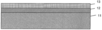
도 1은 본 발명에 따른 바람직한 기판의 도식적 단면을 보여준다. 기판은 ZnO-기재 층 (13)으로 코팅된 중간층 (12)로 이루어진 적층물로 코팅된 지지 물질 (11)로 구성된다.
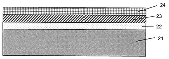
도 2는 본 발명에 따른 다른 바람직한 기판의 도식적 단면을 보여준다. 기판은 ZnO-기재 층 (23)으로 코팅된 중간층 (23)으로 코팅되고 지지 물질 (21)위에 직접 침착된, 알칼리 금속 이온의 이동에 대한 장벽으로 작용하는 층 (22)를 포함하는 적층물로 코팅된 지지 물질 (21)로 구성된다.
도 1 및 2에 나타난 기판에 대하여, 지지 물질 및 적층물의 다양한 층은 명세서의 일반적 부분에서 기술된 것과 같다. 바람직하게는, 지지 물질은, 특히 플라즈마 디스플레이 패널의 제조용으로 의도된 유형의 유리로 만들어진다. 중간층은 유리하게는 특히 Al 또는 Sb로 도핑된 아연 주석 산화물에 기초한다. ZnO-기재 층은 바람직하게는 ZnO 층이다. 알칼리 금속 이온의 이동에 대해 장벽으로 작용하는 임의적 층은 유리하게는 Si3N4 층이다.The invention will be better understood with the aid of the following non-limiting exemplary embodiments shown in FIGS.
1 and 2 are schematic depictions of a substrate according to the present invention.
3 and 4 are scanning electron micrographs taken at the edge of the specimen described below.
1 shows a schematic cross section of a preferred substrate according to the invention. The substrate consists of a
2 shows a schematic cross section of another preferred substrate according to the invention. The substrate is a laminate comprising a
For the substrates shown in FIGS. 1 and 2, the various layers of support material and laminates are as described in the general part of the specification. Preferably, the support material is made of glass of the type intended especially for the manufacture of plasma display panels. The intermediate layer is advantageously based in particular on zinc tin oxide doped with Al or Sb. The ZnO-based layer is preferably a ZnO layer. An optional layer that acts as a barrier to the movement of alkali metal ions is advantageously a Si 3 N 4 layer.
비교예Comparative example
비교예에 따른 기판은 알칼리 금속 이온의 이동에 대해 장벽으로 작용하는 Si3N4 서브층 및 아연 산화물 층으로 코팅된 유리 지지 물질로 이루어진다. The substrate according to the comparative example consists of a glass support material coated with a Si 3 N 4 sublayer and a zinc oxide layer which acts as a barrier to the movement of alkali metal ions.
적층물은 유리/Si3N4 (20 nm)/ZnO (200 nm)이고, 기하학적인 두께가 괄호 안에 나타나 있다. Laminates are glass / Si 3 N 4 (20 nm) / ZnO (200 nm) and geometric thicknesses are shown in parentheses.
사용된 유리는 특허 출원 WO 98/40320에 기술된 것과 같이, 플라즈마 디스플레이 패널의 제조용으로 의도된 유리이다.The glass used is the glass intended for the production of plasma display panels, as described in patent application WO 98/40320.
이 적층물을 마그네트론 스퍼터링으로 침착하였다. Si3N4 층은 5 kW/100 kHz 전력으로 공급되는 규소 타겟을 사용하여 침착하였다. 압력은 2.5 마이크로바이고 플라즈마 기체는 아르곤 (40 sccm (분 당 표준 세제곱 센티미터) 흐름 속도) 및 질소 (58 sccm 흐름 속도)의 혼합물이었다. ZnO 층은 2 밀리바의 압력 및 아르곤 (40 sccm)/산소 (18 sccm) 혼합물 하에서 290 V/50 kHz 전압이 인가된 아연 타겟을 사용하여 침착하였다.This laminate was deposited by magnetron sputtering. Si 3 N 4 The layer was deposited using a silicon target supplied at 5 kW / 100 kHz power. The pressure was 2.5 microbiodes and the plasma gas was a mixture of argon (40 sccm (standard cubic centimeters per minute) flow rate) and nitrogen (58 sccm flow rate). The ZnO layer was deposited using a zinc target applied a voltage of 290 V / 50 kHz under a pressure of 2 millibars and an argon (40 sccm) / oxygen (18 sccm) mixture.
이러한 각 층의 마그네트론 스퍼터링에 의한 침착은 게다가 당업자에게 잘 알려져 있고, 침착의 세부 사항 (사용된 타겟, 압력, 기체 등)은 결과에 중요한 영향을 미치지 않는다. Deposition by magnetron sputtering of each of these layers is further well known to those skilled in the art, and the details of the deposition (targets, pressures, gases, etc. used) do not have a significant effect on the results.
이러한 기판은 그 후 잘 알려진 방식으로 RPCVD (리모트 플라즈마 화학 기상 증착)을 사용하여 80 nm 두께 (C1로 표시됨) 또는 200 nm 두께 (C2로 표시됨)의 GaN 층으로 코팅하였다. 사용된 기판의 본질과 침착 온도의 측면에서 양립될 수 있는 임의의 다른 유형의 침착 공정도 물론 결과에 중대한 영향을 미치지 않고 사용가능하다.This substrate was then coated in a well known manner with a GaN layer of 80 nm thick (denoted C1) or 200 nm thick (denoted C2) using RPCVD (remote plasma chemical vapor deposition). Any other type of deposition process that is compatible in terms of the nature of the substrate used and the deposition temperature is of course available without significant impact on the results.
실시예Example
본 발명에 따른 실시예는 안티몬(Sb)-도핑된 혼합 아연 주석 산화물 층이 Si3N4 서브층과 아연 산화물 층 사이에서, 역시 마그네트론 스퍼터링으로 침착된다는 점에서 비교예와 다르다.The embodiment according to the invention differs from the comparative example in that an antimony (Sb) -doped mixed zinc tin oxide layer is deposited between the Si 3 N 4 sublayer and the zinc oxide layer, also by magnetron sputtering.
SnZnO 층은 안티몬-도핑된 주석/아연 합금, 2 kW 전력 및 50 kHz 주파수, 2 마이크로바 압력 및 아르곤 (12 sccm)/산소 (45 sccm) 혼합물로부터 형성된 타겟을 사용하여 침착하였다.SnZnO layers were deposited using a target formed from an antimony-doped tin / zinc alloy, 2 kW power and 50 kHz frequency, 2 microbar pressure and an argon (12 sccm) / oxygen (45 sccm) mixture.
혼합된 산화물 층은 금속 중량으로, 약 65% Sn, 34% Zn 및 1% Sb을 포함하였다. The mixed oxide layer comprised about 65% Sn, 34% Zn and 1% Sb by weight of the metal.
본 발명에 따른 다양한 실시예는 ZnO 층 및 아연 주석 산화물 층의 두께에서 달랐다.Various embodiments according to the invention differed in the thickness of the ZnO layer and the zinc tin oxide layer.
표 1은 본 발명에 따른 실시예 1 내지 4 각각에 대해 이러한 층 두께를 나타낸다. Table 1 shows this layer thickness for each of Examples 1-4 according to the present invention.
결정화에의 효과Effect on Crystallization
GaN-기재 층의 결정화에 대한 본 발명의 효과는 다양한 방법에 의해 연구되었다. The effect of the present invention on the crystallization of GaN-based layers has been studied by various methods.
제1 방법에 따르면, GaN 결정의 배향은 X선 회절 다이어그램에서 GaN과 관련된 회절 피크 영역을 측정하는 것에 의해 비교된다. According to the first method, the orientation of the GaN crystals is compared by measuring the diffraction peak regions associated with GaN in the X-ray diffraction diagram.
X선 회절은 θ/2θ 배위에서 수행하였다. ZnO와 GaN 사이의 격자 변수의 적은 차이 때문에, 그들의 피크는 부분적으로 겹치고, 그들을 분리하기 위해 수학적 처리가 요구된다. 이 수학적 처리는 특히 ZnO 층 단독의 회절 특성에 기초하였고, 이는 GaN 침착 전에 측정되었다. X-ray diffraction was performed at the θ / 2θ configuration. Because of the small differences in lattice parameters between ZnO and GaN, their peaks partially overlap and mathematical treatment is required to separate them. This mathematical treatment was based in particular on the diffraction properties of the ZnO layer alone, which was measured before GaN deposition.
표 2는 c-축을 따른 결정의 배향에 대응되는 (0002) 결정학적 평면과 관련된 회절 피크의 임의적 단위의 영역을 나타낸다. Table 2 shows regions of arbitrary units of diffraction peaks associated with the (0002) crystallographic plane corresponding to the orientation of the crystal along the c-axis.
이 결과는 중간층을 추가한 덕분에 c-축을 따른 GaN의 배향에서의 매우 큰 향상을 반영한다. This result reflects a very large improvement in the orientation of GaN along the c-axis thanks to the addition of an interlayer.
제2 방법에 따르면, GaN 결정의 배향은 주사 전자 현미경을 사용하여 직접 관찰함에 의해 비교된다.According to the second method, the orientation of GaN crystals is compared by observing directly using a scanning electron microscope.
도 3 및 4는 각각 실시예 C2 및 1의, 100000 배율의 주사 전자 현미경으로 찍은 현미경 사진이다. 현미경 사진은 가장자리에서 찍었고, 따라서 ZnO/GaN 적층물이 보여지도록 하였다. 3 and 4 are micrographs taken with a scanning electron microscope at 100,000 magnification of Examples C2 and 1, respectively. Micrographs were taken at the edges, thus allowing the ZnO / GaN stack to be seen.
도 3에서, 육각형의 GaN 결정은 그의 c-축을 따라 성장하는 경향이 있지만, 축의 방향은 기판에 완벽하게 수직이지는 않는다. In Fig. 3, hexagonal GaN crystals tend to grow along their c-axis, but the direction of the axis is not perfectly perpendicular to the substrate.
그러나, 도 4에서 GaN 결정의 성장 방향은 기판에 완벽하게 수직이고, 따라서 더욱 결점이 없다. However, the growth direction of the GaN crystals in FIG. 4 is perfectly perpendicular to the substrate, and thus more flawless.
제3 방법에 따르면, 적층물의 총 전기 저항성은 4-점 방법 또는 반 데르 포우법을 사용하여 공지된 방법으로 결정되었다. According to the third method, the total electrical resistivity of the laminate was determined by known methods using the four-point method or the van der Poe method.
표 3은 실시예 C1, 3 및 4에서 얻어진 값을 나타낸다.Table 3 shows the values obtained in Examples C1, 3 and 4.
중간층의 추가로 인한 저항성의 저하는 더 적은 양의 구조 결점을 반영하는 전자 전도도의 매우 실질적인 증가에 대응한다. The lowering of the resistance due to the addition of the intermediate layer corresponds to a very substantial increase in electronic conductivity which reflects a smaller amount of structural defects.
본 발명에 따른 기판에서 지지 물질과 아연 산화물 층 사이에 중간층의 개입은 결론적으로 질화 갈륨 층의 결정질 특성을 향상시키고 그의 전자 전도도를 향상시키는 것을 가능하게 한다. 이 결과 이러한 기판을 사용하는 발광 다이오드의 발광 강도 및 수명이 증가한다. Intervention of the interlayer between the support material and the zinc oxide layer in the substrate according to the invention in turn makes it possible to improve the crystalline properties of the gallium nitride layer and to improve its electronic conductivity. As a result, the light emission intensity and lifetime of light emitting diodes using such a substrate are increased.
Claims (21)
상기 기판이 III-N 또는 II-VI형의 반도체 구조로 코팅되며,
주석 (Sn), 아연 (Zn), 인듐 (In), 갈륨 (Ga) 및 안티몬 (Sb)로부터 선택된 둘 이상의 원소의 산화물을 포함하는 하나 이상의 중간층 (12, 23)이 지지 물질 (11, 21)과 상기 하나 이상의 아연-산화물-기재 층 (13, 24) 사이에 위치하는 것을 특징으로 하는 기판.Epitaxial growth of a layer based on gallium nitride, at least one side comprising a support material (11, 21) coated with at least one multilayer stack comprising at least one zinc-oxide-based layer (13, 24) As a substrate that can be used as the substrate for
The substrate is coated with a semiconductor structure of type III-N or II-VI,
One or more intermediate layers 12, 23 comprising oxides of two or more elements selected from tin (Sn), zinc (Zn), indium (In), gallium (Ga) and antimony (Sb) are supported by the support material (11, 21). And the at least one zinc-oxide-based layer (13, 24).
주석 (Sn), 아연 (Zn), 갈륨 (Ga) 및 안티몬 (Sb)로부터 선택된 둘 이상의 원소의 산화물을 포함하는 하나 이상의 중간층 (12, 23)이 지지 물질 (11, 21)과 상기 하나 이상의 아연-산화물-기재 층 (13, 24) 사이에 위치하는 것을 특징으로 하는 기판.Epitaxial growth of a layer based on gallium nitride, at least one side comprising a support material (11, 21) coated with at least one multilayer stack comprising at least one zinc-oxide-based layer (13, 24) As a substrate that can be used as the substrate for
One or more intermediate layers (12, 23) comprising oxides of two or more elements selected from tin (Sn), zinc (Zn), gallium (Ga) and antimony (Sb) support material (11, 21) and said at least one zinc A substrate, which is located between the oxide-based layers (13, 24).
Applications Claiming Priority (2)
| Application Number | Priority Date | Filing Date | Title |
|---|---|---|---|
| FR0756496A FR2918791B1 (en) | 2007-07-13 | 2007-07-13 | SUBSTRATE FOR THE EPITAXIAL GROWTH OF GALLIUM NITRIDE |
| FR0756496 | 2007-07-13 |
Publications (1)
| Publication Number | Publication Date |
|---|---|
| KR20100048995A true KR20100048995A (en) | 2010-05-11 |
Family
ID=39153913
Family Applications (1)
| Application Number | Title | Priority Date | Filing Date |
|---|---|---|---|
| KR1020107000664A KR20100048995A (en) | 2007-07-13 | 2008-07-11 | Substrate for the epitaxial growth of gallium nitride |
Country Status (7)
| Country | Link |
|---|---|
| US (1) | US8278656B2 (en) |
| EP (1) | EP2171751A2 (en) |
| JP (1) | JP5102357B2 (en) |
| KR (1) | KR20100048995A (en) |
| CN (1) | CN101689511A (en) |
| FR (1) | FR2918791B1 (en) |
| WO (1) | WO2009013425A2 (en) |
Cited By (2)
| Publication number | Priority date | Publication date | Assignee | Title |
|---|---|---|---|---|
| US8952243B2 (en) | 2011-03-03 | 2015-02-10 | Samsung Electronics Co., Ltd. | Stacked structure including vertically grown semiconductor, p-n junction device including the stacked structure, and method of manufacturing thereof |
| KR20160091443A (en) * | 2010-11-26 | 2016-08-02 | 가부시키가이샤 고베 세이코쇼 | Oxide for semiconductor layer of thin-film transistor, sputtering target, and thin-film transistor |
Families Citing this family (42)
| Publication number | Priority date | Publication date | Assignee | Title |
|---|---|---|---|---|
| US9157167B1 (en) | 2008-06-05 | 2015-10-13 | Soraa, Inc. | High pressure apparatus and method for nitride crystal growth |
| US8871024B2 (en) | 2008-06-05 | 2014-10-28 | Soraa, Inc. | High pressure apparatus and method for nitride crystal growth |
| US8097081B2 (en) | 2008-06-05 | 2012-01-17 | Soraa, Inc. | High pressure apparatus and method for nitride crystal growth |
| US9404197B2 (en) | 2008-07-07 | 2016-08-02 | Soraa, Inc. | Large area, low-defect gallium-containing nitride crystals, method of making, and method of use |
| WO2011044554A1 (en) | 2009-10-09 | 2011-04-14 | Soraa, Inc. | Method for synthesis of high quality large area bulk gallium based crystals |
| US10036099B2 (en) | 2008-08-07 | 2018-07-31 | Slt Technologies, Inc. | Process for large-scale ammonothermal manufacturing of gallium nitride boules |
| US8979999B2 (en) | 2008-08-07 | 2015-03-17 | Soraa, Inc. | Process for large-scale ammonothermal manufacturing of gallium nitride boules |
| US20100147210A1 (en) * | 2008-12-12 | 2010-06-17 | Soraa, Inc. | high pressure apparatus and method for nitride crystal growth |
| US8878230B2 (en) * | 2010-03-11 | 2014-11-04 | Soraa, Inc. | Semi-insulating group III metal nitride and method of manufacture |
| USRE47114E1 (en) | 2008-12-12 | 2018-11-06 | Slt Technologies, Inc. | Polycrystalline group III metal nitride with getter and method of making |
| US9589792B2 (en) | 2012-11-26 | 2017-03-07 | Soraa, Inc. | High quality group-III metal nitride crystals, methods of making, and methods of use |
| US9543392B1 (en) | 2008-12-12 | 2017-01-10 | Soraa, Inc. | Transparent group III metal nitride and method of manufacture |
| US8987156B2 (en) | 2008-12-12 | 2015-03-24 | Soraa, Inc. | Polycrystalline group III metal nitride with getter and method of making |
| US9250044B1 (en) | 2009-05-29 | 2016-02-02 | Soraa Laser Diode, Inc. | Gallium and nitrogen containing laser diode dazzling devices and methods of use |
| US8509275B1 (en) | 2009-05-29 | 2013-08-13 | Soraa, Inc. | Gallium nitride based laser dazzling device and method |
| US9800017B1 (en) | 2009-05-29 | 2017-10-24 | Soraa Laser Diode, Inc. | Laser device and method for a vehicle |
| WO2011065216A1 (en) | 2009-11-28 | 2011-06-03 | Semiconductor Energy Laboratory Co., Ltd. | Stacked oxide material, semiconductor device, and method for manufacturing the semiconductor device |
| US9564320B2 (en) | 2010-06-18 | 2017-02-07 | Soraa, Inc. | Large area nitride crystal and method for making it |
| US8729559B2 (en) | 2010-10-13 | 2014-05-20 | Soraa, Inc. | Method of making bulk InGaN substrates and devices thereon |
| CN106960866B (en) | 2010-12-17 | 2021-03-12 | 株式会社半导体能源研究所 | Oxide material and semiconductor device |
| US8492185B1 (en) | 2011-07-14 | 2013-07-23 | Soraa, Inc. | Large area nonpolar or semipolar gallium and nitrogen containing substrate and resulting devices |
| US9694158B2 (en) | 2011-10-21 | 2017-07-04 | Ahmad Mohamad Slim | Torque for incrementally advancing a catheter during right heart catheterization |
| US10029955B1 (en) | 2011-10-24 | 2018-07-24 | Slt Technologies, Inc. | Capsule for high pressure, high temperature processing of materials and methods of use |
| TWI515936B (en) * | 2011-12-15 | 2016-01-01 | 友達光電股份有限公司 | Light emitting device and manufacturing method thereof |
| US8482104B2 (en) | 2012-01-09 | 2013-07-09 | Soraa, Inc. | Method for growth of indium-containing nitride films |
| US10145026B2 (en) | 2012-06-04 | 2018-12-04 | Slt Technologies, Inc. | Process for large-scale ammonothermal manufacturing of semipolar gallium nitride boules |
| US9275912B1 (en) | 2012-08-30 | 2016-03-01 | Soraa, Inc. | Method for quantification of extended defects in gallium-containing nitride crystals |
| US9299555B1 (en) | 2012-09-28 | 2016-03-29 | Soraa, Inc. | Ultrapure mineralizers and methods for nitride crystal growth |
| US9650723B1 (en) | 2013-04-11 | 2017-05-16 | Soraa, Inc. | Large area seed crystal for ammonothermal crystal growth and method of making |
| US9231053B2 (en) | 2013-06-25 | 2016-01-05 | Honeywell International Inc. | Light emitting diodes having zinc oxide fibers over silicon substrates |
| KR101439064B1 (en) * | 2013-12-02 | 2014-09-05 | 단국대학교 산학협력단 | Light Emitting Diode having Heterojunction Structure and Method of fabricating the same |
| US9577045B2 (en) | 2014-08-04 | 2017-02-21 | Fairchild Semiconductor Corporation | Silicon carbide power bipolar devices with deep acceptor doping |
| US9419081B2 (en) | 2014-08-21 | 2016-08-16 | Honeywell International Inc. | Reusable substrate bases, semiconductor devices using such reusable substrate bases, and methods for making the reusable substrate bases |
| US20180097073A1 (en) * | 2016-10-03 | 2018-04-05 | Flosfia Inc. | Semiconductor device and semiconductor system including semiconductor device |
| US10174438B2 (en) | 2017-03-30 | 2019-01-08 | Slt Technologies, Inc. | Apparatus for high pressure reaction |
| CN108091708B (en) * | 2017-12-08 | 2020-08-14 | 北京通美晶体技术有限公司 | Germanium single crystal wafer, method for producing the same, method for producing crystal bar, and use of single crystal wafer |
| US11421843B2 (en) | 2018-12-21 | 2022-08-23 | Kyocera Sld Laser, Inc. | Fiber-delivered laser-induced dynamic light system |
| US11239637B2 (en) | 2018-12-21 | 2022-02-01 | Kyocera Sld Laser, Inc. | Fiber delivered laser induced white light system |
| US11466384B2 (en) | 2019-01-08 | 2022-10-11 | Slt Technologies, Inc. | Method of forming a high quality group-III metal nitride boule or wafer using a patterned substrate |
| US11884202B2 (en) | 2019-01-18 | 2024-01-30 | Kyocera Sld Laser, Inc. | Laser-based fiber-coupled white light system |
| WO2021162727A1 (en) | 2020-02-11 | 2021-08-19 | SLT Technologies, Inc | Improved group iii nitride substrate, method of making, and method of use |
| US11721549B2 (en) | 2020-02-11 | 2023-08-08 | Slt Technologies, Inc. | Large area group III nitride crystals and substrates, methods of making, and methods of use |
Family Cites Families (8)
| Publication number | Priority date | Publication date | Assignee | Title |
|---|---|---|---|---|
| JP3595097B2 (en) * | 1996-02-26 | 2004-12-02 | 株式会社東芝 | Semiconductor device |
| US5889295A (en) * | 1996-02-26 | 1999-03-30 | Kabushiki Kaisha Toshiba | Semiconductor device |
| WO2002016679A1 (en) * | 2000-08-18 | 2002-02-28 | Tohoku Techno Arch Co., Ltd. | Polycrystalline semiconductor material and method of manufacture thereof |
| TWI248469B (en) * | 2001-12-25 | 2006-02-01 | Univ Nat Cheng Kung | Manufacturing method of zinc oxide nanowires |
| JP3859148B2 (en) | 2002-10-31 | 2006-12-20 | 信越半導体株式会社 | Method for manufacturing Zn-based semiconductor light emitting device |
| JP4212413B2 (en) | 2003-05-27 | 2009-01-21 | シャープ株式会社 | Oxide semiconductor light emitting device |
| US7208863B2 (en) * | 2004-07-09 | 2007-04-24 | Eastman Kodak Company | Light emitting devices with patterned angular color dependency |
| US20080105293A1 (en) * | 2006-11-02 | 2008-05-08 | Guardian Industries Corp. | Front electrode for use in photovoltaic device and method of making same |
-
2007
- 2007-07-13 FR FR0756496A patent/FR2918791B1/en not_active Expired - Fee Related
-
2008
- 2008-07-11 CN CN200880024413A patent/CN101689511A/en active Pending
- 2008-07-11 KR KR1020107000664A patent/KR20100048995A/en not_active Application Discontinuation
- 2008-07-11 US US12/668,676 patent/US8278656B2/en not_active Expired - Fee Related
- 2008-07-11 JP JP2010515582A patent/JP5102357B2/en not_active Expired - Fee Related
- 2008-07-11 EP EP08826629A patent/EP2171751A2/en not_active Withdrawn
- 2008-07-11 WO PCT/FR2008/051316 patent/WO2009013425A2/en active Application Filing
Cited By (2)
| Publication number | Priority date | Publication date | Assignee | Title |
|---|---|---|---|---|
| KR20160091443A (en) * | 2010-11-26 | 2016-08-02 | 가부시키가이샤 고베 세이코쇼 | Oxide for semiconductor layer of thin-film transistor, sputtering target, and thin-film transistor |
| US8952243B2 (en) | 2011-03-03 | 2015-02-10 | Samsung Electronics Co., Ltd. | Stacked structure including vertically grown semiconductor, p-n junction device including the stacked structure, and method of manufacturing thereof |
Also Published As
| Publication number | Publication date |
|---|---|
| EP2171751A2 (en) | 2010-04-07 |
| US8278656B2 (en) | 2012-10-02 |
| US20100207116A1 (en) | 2010-08-19 |
| JP5102357B2 (en) | 2012-12-19 |
| WO2009013425A2 (en) | 2009-01-29 |
| FR2918791A1 (en) | 2009-01-16 |
| CN101689511A (en) | 2010-03-31 |
| FR2918791B1 (en) | 2009-12-04 |
| JP2010533371A (en) | 2010-10-21 |
| WO2009013425A3 (en) | 2009-03-12 |
Similar Documents
| Publication | Publication Date | Title |
|---|---|---|
| US8278656B2 (en) | Substrate for the epitaxial growth of gallium nitride | |
| TWI484662B (en) | A laminated body and a method for manufacturing the same, and a semiconductor light-emitting element and a solar battery using the same | |
| US7172813B2 (en) | Zinc oxide crystal growth substrate | |
| KR100894878B1 (en) | Method for fabrication of group ? nitride semiconductor | |
| CN111886368B (en) | Group 13 element nitride layer, free-standing substrate, functional element, and method for producing group 13 element nitride layer | |
| JP6868606B2 (en) | Self-supporting substrate made of polycrystalline Group 13 element nitride and light emitting device using it | |
| KR101758548B1 (en) | Gallium nitride self-supported substrate, light-emitting device and manufacturing method therefor | |
| JP6648253B2 (en) | Polycrystalline gallium nitride free-standing substrate and light emitting device using the same | |
| KR20090115826A (en) | Buffering layer for group 3 nitride-based semiconductor devices and its method | |
| KR101458629B1 (en) | MANUFACTURE METHOD FOR ZnO-CONTAINING COMPOUND SEMICONDUCTOR LAYER | |
| JP4036073B2 (en) | Quartz substrate with thin film | |
| JP6934473B2 (en) | Group III nitride semiconductor light emitting device | |
| KR20080005002A (en) | Preparation method of zinc oxide based oxide thin film using sputtering | |
| JP4946576B2 (en) | Light emitting element | |
| KR20080013249A (en) | Zinc oxide based oxide thin film and preparation method thereof |
Legal Events
| Date | Code | Title | Description |
|---|---|---|---|
| WITN | Application deemed withdrawn, e.g. because no request for examination was filed or no examination fee was paid |