KR20090031193A - Method of forming silicon nitride at low temperature, charge trap memory device comprising crystalline nano dots formed using the same and method of manufacturing charge trap memory device - Google Patents
Method of forming silicon nitride at low temperature, charge trap memory device comprising crystalline nano dots formed using the same and method of manufacturing charge trap memory device Download PDFInfo
- Publication number
- KR20090031193A KR20090031193A KR1020080040821A KR20080040821A KR20090031193A KR 20090031193 A KR20090031193 A KR 20090031193A KR 1020080040821 A KR1020080040821 A KR 1020080040821A KR 20080040821 A KR20080040821 A KR 20080040821A KR 20090031193 A KR20090031193 A KR 20090031193A
- Authority
- KR
- South Korea
- Prior art keywords
- silicon nitride
- crystalline silicon
- substrate
- memory device
- forming
- Prior art date
Links
- HQVNEWCFYHHQES-UHFFFAOYSA-N silicon nitride Chemical compound N12[Si]34N5[Si]62N3[Si]51N64 HQVNEWCFYHHQES-UHFFFAOYSA-N 0.000 title claims abstract description 109
- 229910052581 Si3N4 Inorganic materials 0.000 title claims abstract description 46
- 238000000034 method Methods 0.000 title claims abstract description 39
- 238000004519 manufacturing process Methods 0.000 title claims abstract description 12
- 239000000758 substrate Substances 0.000 claims abstract description 65
- 229910021419 crystalline silicon Inorganic materials 0.000 claims abstract description 61
- 239000012495 reaction gas Substances 0.000 claims abstract description 23
- 230000008021 deposition Effects 0.000 claims abstract description 20
- 239000007789 gas Substances 0.000 claims description 38
- 239000002096 quantum dot Substances 0.000 claims description 36
- 230000005641 tunneling Effects 0.000 claims description 23
- 230000000903 blocking effect Effects 0.000 claims description 15
- QGZKDVFQNNGYKY-UHFFFAOYSA-N Ammonia Chemical compound N QGZKDVFQNNGYKY-UHFFFAOYSA-N 0.000 claims description 13
- BLRPTPMANUNPDV-UHFFFAOYSA-N Silane Chemical compound [SiH4] BLRPTPMANUNPDV-UHFFFAOYSA-N 0.000 claims description 13
- XUIMIQQOPSSXEZ-UHFFFAOYSA-N Silicon Chemical compound [Si] XUIMIQQOPSSXEZ-UHFFFAOYSA-N 0.000 claims description 9
- 229910052710 silicon Inorganic materials 0.000 claims description 9
- 239000010703 silicon Substances 0.000 claims description 9
- 238000007740 vapor deposition Methods 0.000 claims description 8
- 230000008569 process Effects 0.000 claims description 7
- IJGRMHOSHXDMSA-UHFFFAOYSA-N Atomic nitrogen Chemical compound N#N IJGRMHOSHXDMSA-UHFFFAOYSA-N 0.000 claims description 6
- PZPGRFITIJYNEJ-UHFFFAOYSA-N disilane Chemical compound [SiH3][SiH3] PZPGRFITIJYNEJ-UHFFFAOYSA-N 0.000 claims description 3
- 229910052757 nitrogen Inorganic materials 0.000 claims description 3
- VEDJZFSRVVQBIL-UHFFFAOYSA-N trisilane Chemical compound [SiH3][SiH2][SiH3] VEDJZFSRVVQBIL-UHFFFAOYSA-N 0.000 claims description 3
- 150000004767 nitrides Chemical class 0.000 abstract description 3
- 238000010494 dissociation reaction Methods 0.000 abstract description 2
- 230000005593 dissociations Effects 0.000 abstract description 2
- 230000015572 biosynthetic process Effects 0.000 abstract 1
- 239000010408 film Substances 0.000 description 70
- 238000002474 experimental method Methods 0.000 description 21
- 238000000151 deposition Methods 0.000 description 17
- VYPSYNLAJGMNEJ-UHFFFAOYSA-N Silicium dioxide Chemical compound O=[Si]=O VYPSYNLAJGMNEJ-UHFFFAOYSA-N 0.000 description 12
- 239000013078 crystal Substances 0.000 description 8
- 229910021417 amorphous silicon Inorganic materials 0.000 description 7
- 239000012535 impurity Substances 0.000 description 7
- 229910000077 silane Inorganic materials 0.000 description 7
- 230000008859 change Effects 0.000 description 6
- 239000002105 nanoparticle Substances 0.000 description 6
- 238000004050 hot filament vapor deposition Methods 0.000 description 5
- 229910004298 SiO 2 Inorganic materials 0.000 description 4
- 229910045601 alloy Inorganic materials 0.000 description 4
- 239000000956 alloy Substances 0.000 description 4
- 229910052681 coesite Inorganic materials 0.000 description 4
- 229910052906 cristobalite Inorganic materials 0.000 description 4
- 239000000463 material Substances 0.000 description 4
- 239000004065 semiconductor Substances 0.000 description 4
- 239000000377 silicon dioxide Substances 0.000 description 4
- 235000012239 silicon dioxide Nutrition 0.000 description 4
- 229910052682 stishovite Inorganic materials 0.000 description 4
- 229910052905 tridymite Inorganic materials 0.000 description 4
- 238000006243 chemical reaction Methods 0.000 description 3
- 230000000694 effects Effects 0.000 description 3
- 238000000024 high-resolution transmission electron micrograph Methods 0.000 description 3
- 229910052751 metal Inorganic materials 0.000 description 3
- 239000002184 metal Substances 0.000 description 3
- 239000000203 mixture Substances 0.000 description 3
- BASFCYQUMIYNBI-UHFFFAOYSA-N platinum Chemical compound [Pt] BASFCYQUMIYNBI-UHFFFAOYSA-N 0.000 description 3
- 229910021420 polycrystalline silicon Inorganic materials 0.000 description 3
- 229920005591 polysilicon Polymers 0.000 description 3
- 230000008901 benefit Effects 0.000 description 2
- 238000009792 diffusion process Methods 0.000 description 2
- 238000005530 etching Methods 0.000 description 2
- 238000002173 high-resolution transmission electron microscopy Methods 0.000 description 2
- 229910052814 silicon oxide Inorganic materials 0.000 description 2
- 239000010409 thin film Substances 0.000 description 2
- ZOXJGFHDIHLPTG-UHFFFAOYSA-N Boron Chemical compound [B] ZOXJGFHDIHLPTG-UHFFFAOYSA-N 0.000 description 1
- OKTJSMMVPCPJKN-UHFFFAOYSA-N Carbon Chemical compound [C] OKTJSMMVPCPJKN-UHFFFAOYSA-N 0.000 description 1
- UFHFLCQGNIYNRP-UHFFFAOYSA-N Hydrogen Chemical compound [H][H] UFHFLCQGNIYNRP-UHFFFAOYSA-N 0.000 description 1
- ZOKXTWBITQBERF-UHFFFAOYSA-N Molybdenum Chemical compound [Mo] ZOKXTWBITQBERF-UHFFFAOYSA-N 0.000 description 1
- -1 Si 3 N 4 Chemical compound 0.000 description 1
- 238000003917 TEM image Methods 0.000 description 1
- 238000002441 X-ray diffraction Methods 0.000 description 1
- 229910021529 ammonia Inorganic materials 0.000 description 1
- 229910021486 amorphous silicon dioxide Inorganic materials 0.000 description 1
- 230000004888 barrier function Effects 0.000 description 1
- 230000005540 biological transmission Effects 0.000 description 1
- 229910052796 boron Inorganic materials 0.000 description 1
- 230000007423 decrease Effects 0.000 description 1
- 230000007547 defect Effects 0.000 description 1
- 238000005137 deposition process Methods 0.000 description 1
- 238000010586 diagram Methods 0.000 description 1
- 229910002804 graphite Inorganic materials 0.000 description 1
- 239000010439 graphite Substances 0.000 description 1
- 238000010438 heat treatment Methods 0.000 description 1
- 238000002347 injection Methods 0.000 description 1
- 239000007924 injection Substances 0.000 description 1
- 239000011810 insulating material Substances 0.000 description 1
- 229910052741 iridium Inorganic materials 0.000 description 1
- GKOZUEZYRPOHIO-UHFFFAOYSA-N iridium atom Chemical compound [Ir] GKOZUEZYRPOHIO-UHFFFAOYSA-N 0.000 description 1
- 238000004518 low pressure chemical vapour deposition Methods 0.000 description 1
- 238000004377 microelectronic Methods 0.000 description 1
- 230000005012 migration Effects 0.000 description 1
- 238000013508 migration Methods 0.000 description 1
- 229910052750 molybdenum Inorganic materials 0.000 description 1
- 239000011733 molybdenum Substances 0.000 description 1
- 229910021421 monocrystalline silicon Inorganic materials 0.000 description 1
- 229910000069 nitrogen hydride Inorganic materials 0.000 description 1
- 230000006911 nucleation Effects 0.000 description 1
- 238000010899 nucleation Methods 0.000 description 1
- 230000003647 oxidation Effects 0.000 description 1
- 238000007254 oxidation reaction Methods 0.000 description 1
- TWNQGVIAIRXVLR-UHFFFAOYSA-N oxo(oxoalumanyloxy)alumane Chemical compound O=[Al]O[Al]=O TWNQGVIAIRXVLR-UHFFFAOYSA-N 0.000 description 1
- 239000002245 particle Substances 0.000 description 1
- 230000002093 peripheral effect Effects 0.000 description 1
- 238000000623 plasma-assisted chemical vapour deposition Methods 0.000 description 1
- 229910052697 platinum Inorganic materials 0.000 description 1
- 239000000376 reactant Substances 0.000 description 1
- 125000006850 spacer group Chemical group 0.000 description 1
- 229910052715 tantalum Inorganic materials 0.000 description 1
- GUVRBAGPIYLISA-UHFFFAOYSA-N tantalum atom Chemical compound [Ta] GUVRBAGPIYLISA-UHFFFAOYSA-N 0.000 description 1
- WFKWXMTUELFFGS-UHFFFAOYSA-N tungsten Chemical compound [W] WFKWXMTUELFFGS-UHFFFAOYSA-N 0.000 description 1
- 229910052721 tungsten Inorganic materials 0.000 description 1
- 239000010937 tungsten Substances 0.000 description 1
Images


Classifications
-
- B—PERFORMING OPERATIONS; TRANSPORTING
- B82—NANOTECHNOLOGY
- B82Y—SPECIFIC USES OR APPLICATIONS OF NANOSTRUCTURES; MEASUREMENT OR ANALYSIS OF NANOSTRUCTURES; MANUFACTURE OR TREATMENT OF NANOSTRUCTURES
- B82Y40/00—Manufacture or treatment of nanostructures
-
- H—ELECTRICITY
- H01—ELECTRIC ELEMENTS
- H01L—SEMICONDUCTOR DEVICES NOT COVERED BY CLASS H10
- H01L21/00—Processes or apparatus adapted for the manufacture or treatment of semiconductor or solid state devices or of parts thereof
- H01L21/02—Manufacture or treatment of semiconductor devices or of parts thereof
- H01L21/02104—Forming layers
- H01L21/02107—Forming insulating materials on a substrate
- H01L21/02109—Forming insulating materials on a substrate characterised by the type of layer, e.g. type of material, porous/non-porous, pre-cursors, mixtures or laminates
- H01L21/02112—Forming insulating materials on a substrate characterised by the type of layer, e.g. type of material, porous/non-porous, pre-cursors, mixtures or laminates characterised by the material of the layer
- H01L21/02123—Forming insulating materials on a substrate characterised by the type of layer, e.g. type of material, porous/non-porous, pre-cursors, mixtures or laminates characterised by the material of the layer the material containing silicon
- H01L21/0217—Forming insulating materials on a substrate characterised by the type of layer, e.g. type of material, porous/non-porous, pre-cursors, mixtures or laminates characterised by the material of the layer the material containing silicon the material being a silicon nitride not containing oxygen, e.g. SixNy or SixByNz
-
- H—ELECTRICITY
- H01—ELECTRIC ELEMENTS
- H01L—SEMICONDUCTOR DEVICES NOT COVERED BY CLASS H10
- H01L21/00—Processes or apparatus adapted for the manufacture or treatment of semiconductor or solid state devices or of parts thereof
- H01L21/02—Manufacture or treatment of semiconductor devices or of parts thereof
- H01L21/02104—Forming layers
- H01L21/02107—Forming insulating materials on a substrate
- H01L21/02225—Forming insulating materials on a substrate characterised by the process for the formation of the insulating layer
- H01L21/0226—Forming insulating materials on a substrate characterised by the process for the formation of the insulating layer formation by a deposition process
- H01L21/02263—Forming insulating materials on a substrate characterised by the process for the formation of the insulating layer formation by a deposition process deposition from the gas or vapour phase
- H01L21/02271—Forming insulating materials on a substrate characterised by the process for the formation of the insulating layer formation by a deposition process deposition from the gas or vapour phase deposition by decomposition or reaction of gaseous or vapour phase compounds, i.e. chemical vapour deposition
-
- H—ELECTRICITY
- H01—ELECTRIC ELEMENTS
- H01L—SEMICONDUCTOR DEVICES NOT COVERED BY CLASS H10
- H01L29/00—Semiconductor devices adapted for rectifying, amplifying, oscillating or switching, or capacitors or resistors with at least one potential-jump barrier or surface barrier, e.g. PN junction depletion layer or carrier concentration layer; Details of semiconductor bodies or of electrodes thereof ; Multistep manufacturing processes therefor
- H01L29/40—Electrodes ; Multistep manufacturing processes therefor
- H01L29/43—Electrodes ; Multistep manufacturing processes therefor characterised by the materials of which they are formed
- H01L29/49—Metal-insulator-semiconductor electrodes, e.g. gates of MOSFET
- H01L29/51—Insulating materials associated therewith
- H01L29/518—Insulating materials associated therewith the insulating material containing nitrogen, e.g. nitride, oxynitride, nitrogen-doped material
Abstract
Description
본 발명은 저온 실리콘 질화물(nitride) 형성방법과 이 방법으로 형성된 결정질 나노 도트를 포함하는 전하 트랩형 메모리 소자 및 그 제조방법에 관한 것이다.BACKGROUND OF THE
실리콘 질화물 막은 우수한 유전상수 및 우수한 내산화 특성을 갖고 있다. 그 결과 실리콘 질화물 막은 마이크로 전자 디바이스에 적용되는데, 예를 들어 배리어층 또는 게이트 절연층으로 사용된다.Silicon nitride films have good dielectric constant and good oxidation resistance. As a result, silicon nitride films are applied to microelectronic devices, for example as barrier layers or gate insulating layers.
결정질 실리콘 질화물 막을 게이트 절연막으로 사용할 경우, 게이트의 유전율이 증가되고, 또한 게이트 재료 내의 불순물이 기판으로 확산되는 것을 방지할 수 있다.When the crystalline silicon nitride film is used as the gate insulating film, the dielectric constant of the gate is increased, and impurities in the gate material can be prevented from diffusing to the substrate.
실리콘 질화물 막은 Si(100)상에 형성된다. 그리고 상기 실리콘 질화물 막은 주로 플라즈마 화학기상 증착법(Plasma-enhanced CVD) 또는 저압 화학기상 증착법(low-pressure CVD)으로 형성된다.A silicon nitride film is formed on Si (100). The silicon nitride film is mainly formed by plasma-enhanced CVD or low-pressure CVD.
그러나 이러한 방법으로 형성된 실리콘 질화물 막은 구조적으로 비정질이다. 두꺼운 비정질 실리콘 질화물 막은 적절히 낮은 누설전류를 갖는다. 그러나 비정질 실리콘 질화물 막의 두께가 얇아질 경우, 예를 들면, 50Å이하일 경우, 누설전류는 증가할 수 있다.However, the silicon nitride film formed in this way is structurally amorphous. Thick amorphous silicon nitride films have a moderately low leakage current. However, when the thickness of the amorphous silicon nitride film becomes thin, for example, 50 mA or less, the leakage current may increase.
한편, Si(100)기판 상의 도핑된 폴리 실리콘 게이트가 존재하고, 상기 도핑된 폴리 실리콘 게이트와 상기 Si(100) 기판 사이에 게이트 절연막으로서 SiO2가 존재할 경우, 상기 도핑된 폴리 실리콘 게이트로부터 도핑물질이 SiO2를 통해서 Si(100)기판으로 확산될 수 있다. 이러한 확산 문제는 게이트 절연막의 두께 기하학이 감소되면서 증가되는데, 그 결과 채널영역에서 장치의 특성이 열화될 수 있다.On the other hand, when a doped polysilicon gate exists on the Si (100) substrate, and SiO2 is present as a gate insulating film between the doped polysilicon gate and the Si (100) substrate, a doped material is removed from the doped polysilicon gate. It may be diffused to the Si (100) substrate through SiO2. This diffusion problem increases as the thickness geometry of the gate insulating layer decreases, and as a result, device characteristics may deteriorate in the channel region.
반면, 상기 게이트 절연막이 비정질 실리콘 질화물일 경우, 상기 도핑물질, 예를 들면 붕소가 상기 Si(100)기판으로 확산되는 것을 막을 수 있다. 그러나 상기 게이트와 상기 Si(100)기판 사이의 계면이 비정질 실리콘 질화물이 되어 액티브 반도체 장치의 채널 내에서 전자 흐름이 중단될 수 있는 바, SiO2를 게이트 절연막으로 사용하였을 때보다 반도체 장치의 특성이 열화될 수 있다.On the other hand, when the gate insulating layer is amorphous silicon nitride, it is possible to prevent the doping material, for example, boron from diffusing into the Si (100) substrate. However, since the interface between the gate and the Si (100) substrate becomes amorphous silicon nitride, electron flow may be interrupted in the channel of the active semiconductor device, which deteriorates the characteristics of the semiconductor device than when
다른 한편으로, SiO2막이 게이트 절연막으로 사용되고, 그 두께가 얇을 때, 트랜지스터의 게이트와 드레인 사이에 전자 터널링으로 인해 허용치 이상의 누설전류가 증가하기 때문에, SiO2막의 두께를 얇게 하기 어렵다.On the other hand, when the SiO2 film is used as the gate insulating film and the thickness thereof is thin, it is difficult to reduce the thickness of the SiO2 film because the leakage current beyond the allowable value increases due to electron tunneling between the gate and the drain of the transistor.
그러나 실리콘 질화물막은 SiO2막보다 큰 벌크 유전율을 갖기 때문에, 얇은 두께의 SiO2막과 동일한 정전 용량 밀도를 갖는 두꺼운 실리콘 질화물이 사용될 수 있다.However, since the silicon nitride film has a bulk dielectric constant larger than that of the
그렇지만, 상기 하였듯이 현재까지 알려진 방법으로 형성되는 실리콘 질화물은 구조적으로 비정질인 바, 그 두께가 얇을 경우, 누설전류는 증가될 수 있다.However, as described above, the silicon nitride formed by the method known to date is structurally amorphous, and when the thickness thereof is thin, the leakage current may be increased.
본 발명이 해결하고자 하는 기술적 과제는 상술한 종래의 문제점을 개선하기 위한 것으로서, 액티브 반도체 장치의 채널에서 전자의 흐름이 중단되는 것을 방지할 수 있고, 두께를 얇게 하더라도 누설전류가 증가되는 것을 방지할 수 있으며, 결정질 실리콘 질화물이 형성될 수 없었던 저온 기판 상에도 결정질 실리콘 질화물 막 또는 나노 도트를 형성할 수 있는 저온 실리콘 질화물 형성 방법을 제공함에 있다.The technical problem to be solved by the present invention is to improve the above-described conventional problems, it is possible to prevent the flow of electrons in the channel of the active semiconductor device, and to prevent the leakage current increases even if the thickness is thin. The present invention provides a low temperature silicon nitride forming method capable of forming a crystalline silicon nitride film or nano dots even on a low temperature substrate on which crystalline silicon nitride could not be formed.
본 발명의 다른 기술적 과제는 이 방법으로 형성된 결정질 나노 도트를 포함하는 전하 트랩형 메모리 소자 및 그 제조방법을 제공함에 있다.Another technical problem of the present invention is to provide a charge trapping memory device including a crystalline nano dot formed by this method and a method of manufacturing the same.
상기 기술적 과제를 해결하기 위하여, 본 발명은 필라멘트를 포함하는 실리콘 질화물(silicon nitride) 증착장치의 챔버에 기판을 로딩하는 제1 단계, 유입될 반응가스를 해리될 수 있는 소정 온도까지 상기 필라멘트의 온도를 높이는 제2 단계 및 상기 챔버에 실리콘 질화물 형성용 반응가스를 공급하는 제3 단계를 포함하고, 상기 필라멘트의 온도는 1400℃-2000℃로 유지하고, 상기 제3 단계에서 상기 챔버의 압력은 수torr-수십torr로 유지하여, 상기 기판 상에 결정질 실리콘 질화물을 형성하는 실리콘 질화물 형성방법을 제공한다. In order to solve the above technical problem, the present invention provides a first step of loading a substrate into a chamber of a silicon nitride deposition apparatus including a filament, the temperature of the filament to a predetermined temperature that can dissociate the reaction gas to be introduced And a third step of supplying a reaction gas for forming silicon nitride to the chamber, wherein the temperature of the filament is maintained at 1400 ° C.-2000 ° C., and the pressure of the chamber in the third step is By maintaining torr-tens of torr, a silicon nitride forming method for forming crystalline silicon nitride on the substrate is provided.
이러한 형성방법에서 상기 기판은 500℃-700℃로 유지될 수 있다.In this forming method, the substrate may be maintained at 500 ° C-700 ° C.
상기 챔버의 압력은 4torr-40torr일 수 있다.The pressure of the chamber may be 4torr-40torr.
상기 반응가스는 실리콘(Si)을 공급하기 위한 제1 소오스 가스와 질소(N)를 공급하기 위한 제2 소오스 가스이고, 상기 제1 소오스 가스는 모노실란(SiH4), 디실란, 트리실란 또는 테트라실란일 수 있다.The reaction gas is a first source gas for supplying silicon (Si) and a second source gas for supplying nitrogen (N), and the first source gas is monosilane (SiH 4), disilane, trisilane, or tetra May be silane.
상기 제1 소오스 가스가 20%의 모노 실란이고, 상기 제2 소오스 가스가 암모니아 가스(NH3)일 때, 상기 제1 및 제2 소오스 가스의 흐름률(flow ratio)은 1:50, 1:100 또는 1:200을 유지할 수 있다.When the first source gas is 20% mono silane and the second source gas is ammonia gas (NH 3), the flow ratio of the first and second source gases is 1:50, 1: 100. Or 1: 200.
상기 다른 기술적 과제를 달성하기 위하여, 본 발명은 기판 상에 순차적으로 적층된 터널링막, 전하 트랩층, 전하 차단층 및 게이트 전극을 포함하는 전하 트랩형 메모리 소자에 있어서, 상기 전하 트랩층은 결정질 실리콘 질화물인 전하 트랩형 메모리 소자를 제공한다.In order to achieve the above technical problem, the present invention is a charge trapping memory device including a tunneling film, a charge trap layer, a charge blocking layer and a gate electrode sequentially stacked on a substrate, the charge trap layer is crystalline silicon Provided is a charge trapping memory device that is nitride.
상기 전하 트랩층은 결정질 실리콘 질화물 나노 도트층일 수 있다.The charge trap layer may be a crystalline silicon nitride nano dot layer.
상기 결정질 실리콘 질화물 나노 도트층은 다결정일 수 있다.The crystalline silicon nitride nano dot layer may be polycrystalline.
상기 터널링막은 비정질일 수 있다.The tunneling film may be amorphous.
상기 다른 기술적 과제를 달성하기 위하여, 본 발명은 전하 트랩 수단을 포함하는 게이트 적층물을 구비하는 전하 트랩형 메모리 소자의 제조 방법에 있어서,In order to achieve the above another technical problem, the present invention provides a method for manufacturing a charge trap type memory device having a gate stack including a charge trap means,
기판 상에 터널링막을 형성하는 단계, 상기 터널링막 상에 상기 전하 트랩 수단으로써 결정질 실리콘 질화물을 형성하는 단계, 상기 결정질 실리콘 질화물을 덮는 전하 차단층을 형성하는 단계 및 상기 전하 차단층 상에 게이트 전극을 형성하는 단계를 포함하는 전하 트랩형 메모리 소자의 제조방법을 제공한다.Forming a tunneling film on a substrate, forming crystalline silicon nitride on the tunneling film by the charge trapping means, forming a charge blocking layer covering the crystalline silicon nitride, and forming a gate electrode on the charge blocking layer. It provides a method of manufacturing a charge trapping memory device comprising the step of forming.
상기 결정질 실리콘 질화물은 열선 기상 증착 장치를 이용하여 형성할 수 있 다. 이때, 상기 결정질 실리콘 질화물은 상기 기술적 과제를 달성하기 위해 제공되는 실리콘 질화물 형성 방법에 따라 형성할 수 있다.The crystalline silicon nitride may be formed using a hot wire vapor deposition apparatus. In this case, the crystalline silicon nitride may be formed according to the silicon nitride forming method provided to achieve the technical problem.
상기 결정질 실리콘 질화물은 상기 결정질 실리콘 질화물 나노 도트로 형성할 수 있다.The crystalline silicon nitride may be formed of the crystalline silicon nitride nano dots.
상기 결정질 실리콘 질화물 나노 도트는 다결정일 수 있다.The crystalline silicon nitride nano dots may be polycrystalline.
본 발명은 기상에서 형성되는 결정질 나노입자를 기판 상에 증착시키는 바, 결정질 실리콘 질화물 막 또는 나노 도트가 형성될 수 없었던 저온의 기판 상에도 결정질 실리콘 질화물 막 또는 나노 도트를 형성할 수 있다. 따라서 불순물의 확산을 방지할 수 있고, 비정질 실리콘 질화물에서 나타나는 누설전류를 줄일 수 있다.According to the present invention, the crystalline nanoparticles formed in the gas phase are deposited on a substrate, whereby a crystalline silicon nitride film or nano dots can be formed even on a low temperature substrate in which the crystalline silicon nitride film or nano dots cannot be formed. Therefore, it is possible to prevent the diffusion of impurities and to reduce the leakage current occurring in the amorphous silicon nitride.
이하, 본 발명의 실시예에 의한 실리콘 나이트라이드막의 형성방법을 첨부된 도면들을 참조하여 상세히 설명한다. 이 과정에서 도면에 도시된 층이나 영역들의 두께는 명세서의 명확성을 위해 과장되게 도시된 것이다. 그러나 본 발명의 실시예는 여러 형태로 변형될 수 있으며, 본 발명의 범위가 아래에서 상술하는 실시예로 한정되는 것으로 해석되어져서는 안 된다.Hereinafter, a method of forming a silicon nitride film according to an embodiment of the present invention will be described in detail with reference to the accompanying drawings. In this process, the thicknesses of layers or regions illustrated in the drawings are exaggerated for clarity. However, the embodiments of the present invention may be modified in various forms, and the scope of the present invention should not be construed as being limited to the embodiments described below.
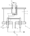
도 1은 본 발명의 실시예에 의한 결정질 실리콘 나이트라이드막의 형성방법에 사용된 막 증착 장치를 보여준다. 도 1에 도시된 막 증착 장치는 열선 기상 증착 장치(Hot Wire CVD)이다.1 shows a film deposition apparatus used in the method for forming a crystalline silicon nitride film according to an embodiment of the present invention. The film deposition apparatus shown in FIG. 1 is a hot wire vapor deposition apparatus (Hot Wire CVD).
도 1을 참조하면, 막 증착 장치(5)는 챔버(1)를 포함하고, 가스 주입구(3), 가스 배출구(4), 필라멘트(21)를 포함한다. 가스 주입구(3)를 통해서 반응가스, 분위기 가스 등과 같은 원료가스가 챔버(1) 내에 주입된다. 챔버(5)에서 실리콘 나이트라이드막이 형성될 경우, 상기 반응가스는 20%의 실란(SiH4)가스와 암모니아 가스(NH3)가 될 수 있다. 그리고 상기 분위기 가스는 H2가 될 수 있다. 가스 배출구(4)를 통해서 챔버(1) 내부의 가스가 챔버(1) 밖으로 배출된다. 필라멘트(21)로부터 챔버(1)내로 주입되는 반응가스를 해리시키기 위한 열이 방출된다. 이를 위해 필라멘트(21)는 소정의 온도로 유지될 수 있다. 예를 들면 챔버(1)에서 결정질 실리콘 나이트라이드막을 형성하기 위해 반응가스가 유입될 때, 필라멘트(21)는 1400℃-2000℃로 유지될 수 있는데, 바람직하게는 1700℃로 유지될 수 있다. 상기 반응가스를 고온 해리시키기 위해 사용되는 필라멘트(21)로는 흑연으로 코팅된 텅스텐(W)과 같이 단일 금속이 사용될 수 있지만, 합금이 사용될 수도 있다. 상기 합금은 몰리브덴(Mo), 백금(Pt), 탄탈륨(Ta), 이리듐(Ir) 등과 같은 금속 발열체의 합금일 수 있다. 필라멘트(21)의 형태는 단일선, 꼬아진 형태일 수도 있고, 어떠한 형태일 수도 있다. 그리고 필라멘트(21)의 수는 한 개 이상일 수 있다.Referring to FIG. 1, the
막 증착 장치(5)는 또한 전극(22), 막 증착 동안 기판(40)을 홀딩하는 기판 홀더(41), 히터(10) 및 전원(24)을 포함한다. 전극(22)을 통해서 전원(23)으로부터 필라멘트에 전압이 인가된다. 필라멘트(21) 및 전극(22)을 통틀어 열선(Hot-Wire)(30)이라 한다. 기판(40) 상에는 박막이나 나노 도트가 형성될 수 있다. 예를 들면, 기판(40) 상에 결정질 실리콘 질화물층이나 결정질 실리콘 질화물 나노 도트가 형성될 수 있다. 이에 대해서는 후술된다. 기판 홀더(41)는 다양한 크기의 기판 을 홀딩할 수 있다. 히터(10)는 막 증착 동안 기판(40)을 일정한 온도로 유지시켜준다. 예를 들면, 결정질 실리콘 나이트라이드막이 형성되는 동안, 히터(10)는 500℃-700℃로 기판의 온도를 유지한다. 전원(24)은 히터(10)에 전력을 공급하는 것으로서, 일정한 교류 및 직류 전압을 인가할 수 있다.The
다음에는 상술한 막 증착 장치(5)를 이용한 결정질 실리콘 질화물의 형성방법(이하, 본 발명의 방법)을 도 2를 참조하여 설명한다.Next, a method of forming crystalline silicon nitride (hereinafter, the method of the present invention) using the above-described
도 2를 참조하면, 본 발명의 방법은 먼저, 챔버(1)에 기판(40)을 로딩한다(100). 이때, 챔버(1) 압력은 수십 mtorr로 유지할 수 있는데, 예를 들면 10-2torr 정도로 유지할 수 있다. 기판(40)은 (100) 실리콘 기판일 수 있다. 이후, 필라멘트(21)가 산화되는 것을 방지하기 위한 분위기 가스로 수소가스(H2)를 주입할 수 있다. 기판(40)과 필라멘트(21) 사이는 기판(40) 상에 결정질 실리콘 질화물 막 또는 결정질 실리콘 질화물 나노 도트를 형성하기에 적합한 소정 거리로 유지할 수 있는데, 예를 들면 기판(40)과 필라멘트(21) 사이의 거리는 6.5cm 정도일 수 있다. 다른 조건이 일정할 때는 기판(40)과 필라멘트(21) 사이의 거리를 조절하여 기판(40) 상에 결정질 실리콘 질화물 막을 형성하거나 결정질 실리콘 질화물 나노 도트를 형성할 수 있다.Referring to FIG. 2, the method of the present invention first loads a
다음, 필라멘트(21)의 온도를 주입될 반응가스를 해리할 수 있을 정도로 높인다(110). 예를 들면, 실리콘 질화물을 형성하기 위한 반응가스가 유입될 때, 필라멘트(21)는 1400℃-2000℃, 바람직하게는 1700℃로 높일 수 있다.Next, the temperature of the
다음, 가스 유입구(3)를 통해서 챔버(1)에 반응가스를 공급한다(120). 상기 반응가스는 실리콘 나이트라이드막을 형성하는데 필요한 소오스 가스일 수 있다. 이 경우에 챔버(1)의 압력은 수 토르(torr)에서 수십 토르로 유지하고, 기판(40)은 500℃-700℃로 유지할 수 있다. 예컨대, 챔버(1)의 압력은 4 torr~40 torr일 수 있다. Next, the reaction gas is supplied to the
상기 소오스 가스는 실리콘(Si)을 공급하기 위한 것으로서, 모노실란, 디실란, 트리실란 또는 테트라실란 등일 수 있고, 질소(N)를 공급하기 위한 암모니아 가스(NH3)일 수 있다. 이때, 상기 소오스 가스의 유량은 20% 실란가스와 암모니아 가스의 비(SiH4(20%):NH3)의 비가 1:50, 1:100 또는 1:200이 되도록 유지한다. 여기서, 암모니아 유량은 200sccm로 일정하게 유지할 수 있다.The source gas is for supplying silicon (Si), and may be monosilane, disilane, trisilane, tetrasilane, or the like, and may be ammonia gas (NH 3) for supplying nitrogen (N). At this time, the flow rate of the source gas is maintained so that the ratio of 20% silane gas and ammonia gas (SiH 4 (20%): NH 3) is 1:50, 1: 100 or 1: 200. Here, the ammonia flow rate can be kept constant at 200 sccm.
상기 유입된 반응가스는 필라멘트(21)를 통과하면서 해리된다. 해리된 반응가스는 기상에서 응축되어 실리콘 질화물의 핵(seed)이 생성되고 결정질의 나노입자가 된다.The introduced reaction gas is dissociated while passing through the
한편, 챔버(1)의 상기 압력조건으로 인해 상기 유입된 반응가스의 과포화도가 낮아진다. 과포화도가 낮아지면, 필라멘트(21) 둘레의 온도가 낮은 영역, 예컨대 온도가 1700℃보다 낮은 영역에서는 상기 유입된 반응가스의 해리가 일어나지 않고, 해리된 반응가스의 핵 형성이 이루어지지 않는다.On the other hand, the degree of supersaturation of the introduced reaction gas is lowered due to the pressure condition of the
이렇게 형성된 나노입자가 기판(40) 상에 증착되어 결정질 실리콘 나이트라이드막이 형성된다. 이때, 증착 시간은 30분 정도일 수 있다. 그러나 증착 시간은 30분으로 한정되지는 않는다. 증착 시간은 30분보다 짧을 수 있는데, 예를 들면 수 초 정도일 수도 있다. 결정질 실리콘 질화물 막은 상기 결정질 실리콘 질화물 나노 도트 입자가 기판(40) 상에 충분히 증착된 결과로 형성되기 때문에, 증착 시간의 조절을 통해서도 기판(40) 상에 결정질 실리콘 질화물 나노 도트를 형성할 수 있다.The nanoparticles thus formed are deposited on the
HWCVD에서 나노입자가 형성되고, 나노입자에 의해 박막이 형성됨은 N. M. Hwang, I. D. Jeon and D. Y. Kim, J. Ceram. Process. Res., 1, 33(2000)에서 찾을 수 있다.In HWCVD, nanoparticles are formed, and thin films are formed by nanoparticles in N. M. Hwang, I. D. Jeon and D. Y. Kim, J. Ceram. Process. Res., 1, 33 (2000).
다음에는 상술한 결정질 실리콘 질화물의 형성방법과 관련하여 본 발명자가 실시한 실험에 대해 설명한다.Next, experiments performed by the present inventors with respect to the above-described method for forming crystalline silicon nitride will be described.
먼저, 본 발명자는 실리콘 질화물의 조성비에 대한 챔버 압력과 필라멘트의 온도의 영향을 알기 위한 제1 및 제2 실험을 하였다.First, the inventors conducted the first and second experiments to know the influence of the chamber pressure and the temperature of the filament on the composition ratio of silicon nitride.
상기 제1 실험은 상술한 실리콘 질화물 형성방법에 따라 실시하였다. 이때, 반응가스로는 20%의 실란가스와 암모니아 가스를 사용하였다. 그리고 상기 실란가스와 상기 암모니아 가스의 비(SiH4(20%):NH3)는 1:200으로 유지하였고, 챔버의 압력은 4torr, 기판 온도는 700℃로 유지하였다.The first experiment was carried out according to the silicon nitride forming method described above. At this time, 20% of silane gas and ammonia gas were used as the reaction gas. The ratio of the silane gas and the ammonia gas (SiH 4 (20%): NH 3) was maintained at 1: 200, the chamber pressure was 4 torr, and the substrate temperature was maintained at 700 ° C.
상기 제2 실험은 상기 제1 실험과 동일하되, 챔버의 압력을 4torr에서 40torr로 다소 높였다.The second experiment was the same as the first experiment, but the pressure of the chamber was slightly increased from 4 tor to 40 torr.
도 3 및 도 4는 각각 상기 제1 및 제2 실험의 결과를 보여주는 엑스선 회절 분석 결과이다.3 and 4 are X-ray diffraction analysis results showing the results of the first and second experiments, respectively.
도 3 및 도 4를 참조하면, 챔버의 반응 압력이 달라짐에 따라, 필라멘트 온 도 변화에 따른 실리콘 질화물의 조성비의 경향이 달라짐을 알 수 있다.3 and 4, as the reaction pressure of the chamber is changed, it can be seen that the tendency of the composition ratio of silicon nitride according to the change in the filament temperature varies.
다음에 본 발명자는 챔버 압력을 일정하게 유지한 상태에서 필라멘트 온도 변화의 영향을 알아보기 위한 제3 및 제4 실험을 실시하였다.Next, the present inventors carried out the third and fourth experiments to determine the effect of the filament temperature change while keeping the chamber pressure constant.
상기 제3 실험에서 5sccm의 20% 실란가스(SiH4(20%))와 200sccm의 암모니아 가스를 사용하였고, 실란가스와 암모니아 가스의 흐름률(flow ratio)은 1:200으로 유지하였다. 그리고 필라멘트 온도는 1430℃, 기판온도는 700℃, 압력은 4torr로 유지한 상태에서 결정질 실리콘 질화물, 예를 들면 Si3N4을 형성하였다.In the third experiment, 5 sccm of 20% silane gas (SiH 4 (20%)) and 200 sccm of ammonia gas were used, and the flow ratio of silane gas and ammonia gas was maintained at 1: 200. In addition, crystalline silicon nitride, for example, Si 3
상기 제4 실험의 실시조건은 필라멘트 온도를 1730℃로 유지한 것을 제외하고 상기 제3 실험과 동일하다.The execution conditions of the fourth experiment are the same as the third experiment except that the filament temperature is maintained at 1730 ° C.
도 5 및 도 6은 각각 상기 제3 및 제4 실험에서 형성한 결정질 실리콘 질화물들에 대한 고해상 투과 전자 현미경 사진을 보여준다.5 and 6 show high resolution transmission electron micrographs of the crystalline silicon nitrides formed in the third and fourth experiments, respectively.
도 5 및 도 6을 비교하면, 상기 제3 및 제4 실험에서 형성된 실리콘 질화물, 예를 들면 Si3N4은 결정질임을 알 수 있고, 결정입자의 크기와 밀도가 다르고 두께도 다른 것을 알 수 있다.5 and 6, it can be seen that the silicon nitride formed in the third and fourth experiments, for example, Si3N4, is crystalline, and has different sizes and densities and different thicknesses of the crystal grains.
이러한 결과로부터 필라멘트 온도의 변화가 결정입자의 크기, 결정입자 밀도 및 막 두께에 영향을 주는 것을 알 수 있었다.From these results, it can be seen that the change in filament temperature affects the grain size, grain density and film thickness.
다음, 본 발명자는 상기 제4 실험에서 다른 조건은 동일하게 하고 챔버 압력만 4torr에서 40torr로 높여서 실리콘 질화물을 형성하는 제5 실험을 실시하였다.Next, the present inventors carried out the fifth experiment in which the silicon nitride was formed by increasing the chamber pressure from 4 tor to 40 torr only with the other conditions being the same in the fourth experiment.
도 7은 상기 제5 실험으로 형성한 실리콘 질화물, 예컨대 Si3N4의 고해상 투과 전자 현미경 사진을 보여준다.7 shows a high resolution transmission electron micrograph of a silicon nitride, such as Si 3
도 7을 참조하면, 상기 제5 실험으로 형성한 실리콘 질화물 역시 결정질임을 알 수 있다. 그리고 기판의 자연 산화막 상에 형성된 실리콘 질화물의 결정성을 볼 때, 상기 자연 산화막 두께가 얇은 부분에 형성된 실리콘 질화물의 결정성 방향이 기판으로 사용된 실리콘 웨이퍼의 방향과 일치되게 나타나는 것을 알 수 있다.Referring to FIG. 7, it can be seen that the silicon nitride formed by the fifth experiment is also crystalline. In addition, when the crystallinity of the silicon nitride formed on the natural oxide film of the substrate is viewed, it can be seen that the crystallinity of the silicon nitride formed in the thin portion of the natural oxide film is consistent with the direction of the silicon wafer used as the substrate.
도 7의 이러한 결과는 자연 산화막이 제거된 실리콘 기판 상에 바로 실리콘 질화물을 성장시키면, 실리콘 기판의 결정방향과 동일한 결정방향을 갖는 실리콘 질화물을 형성할 수 있음을 의미한다. 따라서 실리콘 기판이 단결정일 때, 단결정 실리콘 질화물을 형성할 수 있다.This result of FIG. 7 means that by growing silicon nitride directly on the silicon substrate from which the natural oxide film has been removed, silicon nitride having the same crystal direction as that of the silicon substrate can be formed. Thus, when the silicon substrate is single crystal, single crystal silicon nitride can be formed.
또한, 도 6과 도7을 비교하면, 모든 조건이 동일한 가운데 챔버 압력이 높아지면, 결정입자밀도가 더 높아지고, 결정학적으로 동일한 방향을 나타내는 결정질 영역이 넓어짐을 볼 수 있다.In addition, comparing FIG. 6 and FIG. 7, it can be seen that when all the conditions are the same, when the chamber pressure is increased, the crystal grain density becomes higher, and the crystalline region showing the crystallographically identical direction becomes wider.
한편, 도 5, 도 6 및 도 7에서 실리콘 질화물이 형성되는 기판의 온도는 700℃이다. 이 온도는 기상에 존재하는 원자나 분자가 기판 위에 도달해 실리콘 질화물이 형성될 때, 결정성을 만들 수 없는 온도이다.Meanwhile, the temperature of the substrate on which silicon nitride is formed in FIGS. 5, 6, and 7 is 700 ° C. This temperature is such that when atoms or molecules in the gas phase reach the substrate and silicon nitride forms, crystallinity cannot be made.
그러나 도 5 내지 도 7의 결과를 통해서 알 수 있었듯이, 본 발명의 방법을 따를 경우, 700℃의 기판 상에 형성된 실리콘 질화물에 결정입자들이 존재함을 알 수 있다.However, as can be seen from the results of FIGS. 5 to 7, according to the method of the present invention, it can be seen that the crystal grains are present in the silicon nitride formed on the substrate at 700 ℃.
이러한 결과는 실리콘 질화물이 기판 위에 도달한 원자나 분자에 의해서 만들어지는 것이 아니라 기상 상태의 해리된 반응가스로부터 만들어진 결정성을 가지고 있는 나노입자들이 기판 위에 증착되어 형성되기 때문에 가능하다.This is possible because the silicon nitride is not made by atoms or molecules reaching the substrate, but because nanoparticles with crystallinity made from dissociated reactant gases in the gas phase are deposited on the substrate.
도 5 내지 도 7의 실험 결과는 각 실험 조건에 따라서 결정입자 존재 정도의 차이는 있지만, 종래에는 결코 결정질의 실리콘 질화물이 형성될 수 없었던 저온의 기판 상에도 결정질 실리콘 질화물로 형성된 막이나 나노 도트가 형성될 수 있음을 보인 것이다.Although the results of the experiments of FIGS. 5 to 7 differ in the degree of crystal grains according to each experimental condition, the films or nano dots formed of crystalline silicon nitride are also formed on low temperature substrates where crystalline silicon nitride has never been formed. It can be formed.
다음은 본 발명의 실시예에 의한 결정질 실리콘 질화물 나노 도트를 포함하는 전하 트랩형 메모리 소자(이하, 본 발명의 메모리 소자)에 대해 설명한다.Next, a charge trap type memory device (hereinafter, referred to as the memory device of the present invention) including crystalline silicon nitride nano dots according to an embodiment of the present invention will be described.
도 8을 참조하면, 본 발명의 메모리 소자는 기판(40) 상에 게이트 적층물(50)을 구비한다. 게이트 적층물(50) 양측의 기판(40)에 제1 및 제2 불순물 영역(52, 54)이 존재한다. 제1 및 제2 불순물 영역(52, 54) 중 하나는 소오스 영역으로, 다른 하나는 드레인 영역으로 사용된다. 게이트 적층물(50)은 순차적으로 적층된 터널링막(42), 나노 도트층(44), 전하 차단층(46) 및 게이트 전극(48)을 포함한다. 터널링막(42)은, 예를 들면 실리콘 산화막(SiO2)일 수 있다. 이때, 실리콘 산화막은 비정질일 수 있다. 나노 도트층(44)은 전하 트랩층이고, 복수의 나노 도트(44a)를 포함한다. 나노 도트(44a)는 결정질 실리콘 질화물일 수 있는데, 예를 들면 결정질의 Si3N4 나노 도트일 수 있다. 이러한 나노 도트(44a)는 전하 차단층(46)으로 덮여 있다. 전하 차단층(46)은 나노 도트층(44)에 트랩된 전하가 게이트 전극(48)으로 누설되는 것을 방지한다.Referring to FIG. 8, the memory device of the present invention includes a
도 8에 도시한 본 발명의 전하 트랩형 메모리 소자는 상기한 바와 같은 결정질 실리콘 질화물로 형성된 나노 도트층을 전하 트랩층으로 구비한다. 따라서 결정질 실리콘 질화물의 이점인 얕은 결함(shallow defect)을 줄일 수 있는 바, 큰 ETA 를 얻을 수 있고, 또한 나노 도트의 이점인 측면 이동(lateral migration)이 감소되는 효과를 얻을 수 있다.The charge trapping memory device of the present invention shown in FIG. 8 includes a nano dot layer formed of crystalline silicon nitride as described above as a charge trapping layer. Therefore, it is possible to reduce shallow defects, which is an advantage of crystalline silicon nitride, to obtain a large ETA, and also to reduce an effect of lateral migration, which is an advantage of nano dots.
다음, 도 8의 전하 트랩형 메모리 소자의 제조방법을 도 9 내지 도 11을 참조하여 설명한다.Next, a method of manufacturing the charge trapping memory device of FIG. 8 will be described with reference to FIGS. 9 to 11.
도 9를 참조하면, 기판(40) 상에 터널링막(42)을 형성한다. 터널링막(42)은 비정질 실리콘 산화막, 예컨대 비정질 SiO2막으로 형성할 수 있다. 터널링막(42)은 후속 공정에서 나노 도트층(44)을 형성하는데 적합한 다른 물질막으로 형성할 수도 있다. 터널링막(42)을 형성한 후, 기판(40)을 상술한 열선 기상 증착 장치로 로딩하여 기판 홀더(41)에 홀딩한다. 이후, 열선 기상 증착 장치를 상술한 조건에 따라 가동하여 기판(40) 상에 형성된 터널링막(42) 상에 결정질 나노 도트층(44)을 형성한다. 결정질 나노 도트층(44)이 형성될 수 있는 여러 조건들에 대한 설명은 열선 기상 증착 장치와 관련해서 상술하였는 바, 여기서는 생략한다. 결정질 나노 도트층(44)은 나노 도트층(44)은 복수의 결정질 나노 도트(44a)를 포함한다. 나노 도트(44a)는, 예를 들면 결정질 실리콘 질화물일 수 있다. 터널링막(42)이 비정질 실리콘 산화막일 때, 나노 도트(44a)의 결정상(crystalline phase)은 다결정일 수 있다. 나노 도트층(44)이 결정질 실리콘 질화물 나노 도트층일 때, 그 증착 조건의 일예는 다음과 같은 수 있다. 그러나 상술한 바와 같이 다른 조건에서도 결정질 실리콘 나노 도트층은 형성될 수 있다.9, a
필라멘트 온도:1730℃, 반응압력(열선 기상 증착 장치내 압력):40Torr, 가스 공급비: NH3/SiH4 = 200, 기판(40) 온도: 700℃Filament temperature: 1730 ° C, reaction pressure (pressure in a hot vapor deposition apparatus): 40 Torr, gas supply ratio: NH3 / SiH4 = 200,
터널링막(42) 상에 나노 도트층(44)을 형성한 다음, 기판(40)을 열선 기상 증착 장치로부터 꺼내어 터널링막(42)을 형성할 때 사용한 막 증착장치 또는 그와 유사한 막 증착 장치로 로딩하여 후속 막 증착 공정을 진행한다.After the
다음, 도 10을 참조하면, 터널링막(42) 상에 나노 도트층(44)를 덮는 전하 차단층(46)을 형성한다. 전하 차단층(46)은 나노 도트층(44)에 트랩된 전하가 게이트 전극(48)으로 누설되는 것을 막을 수 있고, 또한 게이트 전극(48)으로부터 나노 도트층(44)으로 전하가 유입되는 것을 막을 수 있는 절연 물질막일 수 있다. 예를 들면, 전하 차단층(46)은 알루미늄 산화막일 수 있다. 전하 차단층(46) 상에 게이트 전극(48)을 형성한다. 게이트 전극(48)은 도핑된 실리콘층, 금속층, 도전성을 갖는 합금층이나 도전성 산화물층일 수도 있다. 게이트 전극(48) 상에 마스크(M1)를 형성한다. 마스크(M1)는 도 8의 게이트 적층물(50)이 형성될 영역을 한정한다. 마스크(M1) 둘레의 게이트 전극(48), 전하 차단층(46), 나노 도트층(44) 및 터널링막(42)을 순차적으로 식각한다. 이 식각은 기판(40)이 노출될 때까지 실시한다. 상기 식각 결과, 도 11에 도시한 바와 같이 기판(40) 상에 게이트 적층물(50)이 형성된다. 이후, 마스크(M1)를 제거한다. 마스크(M1)를 제거한 후에 도 8의 전하 트랩형 메모리 소자의 제1 및 제2 불순물 영역(52, 54), 곧 소오스 및 드레인 영역은 통상적인 공정에 따라 형성할 수 있다. 이 과정에서 게이트 적층물(50)의 측면을 덮는 게이트 스페이서(미도시)를 더 형성할 수 있고, 제1 및 제2 불순물 영역(52, 54)은 LDD(Lightly Doped Drain) 구조로 형성할 수도 있다.Next, referring to FIG. 10, a
도 12는 상술한 전하 트랩형 메모리 소자의 제조 방법에서 나노 도트층(44) 이 결정질 실리콘 질화물 나노 도트층일 때, 나노 도트층(44)에 대한 투과 전자 현미경(TEM) 사진이다.FIG. 12 is a transmission electron microscope (TEM) image of the
도 12를 참조하면, 복수의 원형 물체들(C1)를 볼 수 있는데, 이것이 나노 도트들(44a)이다. 도 13 및 도 14는 도 12의 일부를 확대한 이미지인데, 도 13의 제1 영역(A1)과 도 14의 제2 및 제3 영역(A2, A3)은 나노 도트(44a)를 나타낸다. 도 13 및 도 14를 참조하면, 제1 내지 제3 영역(A1-A3)은 각각 평행한 복수의 제1 내지 제3 선(L1-L3)을 포함하고 있어 그렇지 않은 주변 영역과 확연히 구분되는 것을 알 수 있다. 제1 내지 제3 선(L1-.L3)은 결정면을 나타낸다. 따라서 도 13 및 도 14로부터 나노 도트(44a)의 상(phase)은 결정인 것을 알 수 있다.Referring to FIG. 12, a plurality of circular objects C1 can be seen, which are nano dots 44a. 13 and 14 are enlarged images of part of FIG. 12, wherein the first area A1 of FIG. 13 and the second and third areas A2 and A3 of FIG. 14 represent nano dots 44a. 13 and 14, the first to third regions A1 to A3 each include a plurality of parallel first to third lines L1 to L3, so that the first to third regions A1 to A3 are distinguished from the peripheral region that is not. Able to know. The first to third lines L1 to L3 represent crystal planes. Accordingly, it can be seen from FIGS. 13 and 14 that the phase of the
상기한 설명에서 많은 사항이 구체적으로 기재되어 있으나, 그들은 발명의 범위를 한정하는 것이라기보다, 바람직한 실시예의 예시로서 해석되어야 한다. 예들 들어 본 발명이 속하는 기술 분야에서 통상의 지식을 가진 자라면, 본 발명의 결정질 실리콘 질화물 막 또는 결정질 실리콘 질화물 나노도트 형성방법의 챔버 내 공정 조건들을 조금씩 다르게 할 수 있을 것이다. 또한, 본 발명의 방법을 실리콘 질화물 막 또는 결정질 실리콘 질화물 나노 도트가 사용될 수 있는 여러 반도체 장치의 제조 방법에 적용할 수도 있을 것이다. 때문에 본 발명의 범위는 설명된 실시예에 의하여 정하여 질 것이 아니고 특허 청구범위에 기재된 기술적 사상에 의해 정하여져야 한다.While many details are set forth in the foregoing description, they should be construed as illustrative of preferred embodiments, rather than to limit the scope of the invention. For example, those skilled in the art will be able to vary the process conditions in the chamber of the method of forming the crystalline silicon nitride film or the crystalline silicon nitride nanodot of the present invention. In addition, the method of the present invention may be applied to the manufacturing method of various semiconductor devices in which a silicon nitride film or crystalline silicon nitride nanodots can be used. Therefore, the scope of the present invention should not be defined by the described embodiments, but should be determined by the technical spirit described in the claims.
도 1은 본 발명의 실시예에 의한 저온 결정질 실리콘 질화물 형성에 사용하는 HWCVD(Hot Wire CVD)장치의 단면도이다.1 is a cross-sectional view of a hot wire CVD (HWCVD) apparatus used for forming low temperature crystalline silicon nitride chips according to an embodiment of the present invention.
도 2는 도 1의 장치를 이용한 본 발명에 실시예에 의한 실리콘 질화물의 형성방법을 단계별로 나타낸 블록도이다.2 is a block diagram showing step by step a method of forming silicon nitride according to an embodiment of the present invention using the apparatus of FIG.
도 3 및 도 4는 챔버의 반응 압력의 변화에 따른 결정질 실리콘 질화물의 조성비 변화를 알기 위해 실시한 제1 및 제2 실험의 결과를 나타낸 그래프이다.3 and 4 are graphs showing the results of the first and second experiments conducted to know the change in the composition ratio of the crystalline silicon nitride according to the change in the reaction pressure of the chamber.
도 5 및 도 6은 도 1의 장치를 이용한 실리콘 질화물 증착에서 필라멘트 온도 변화가 실리콘 질화물에 미치는 영향을 알기 위해 실시한 제3 및 제4 실험 결과를 나타낸 고해상 투과 전자 현미경(High Resolution Transmission Electron Microscopy)(HRTEM) 사진이다.5 and 6 are High Resolution Transmission Electron Microscopy showing the results of the third and fourth experiments conducted to determine the effect of the filament temperature change on the silicon nitride in the silicon nitride deposition using the apparatus of FIG. HRTEM) picture.
도 7은 제4 실험과 다른 조건은 동일하되, 압력만 4torr에서 40torr로 높인 제5 실험에 대한 결과를 나타낸 고해상 투과 전자현미경 사진이다.7 is a high resolution transmission electron micrograph showing the results of the fifth experiment with the same conditions as the fourth experiment but the pressure was increased from 4 tor to 40 torr only.
도 8은 결정질 나노 도트층을 전하 트랩층으로 포함하는 본 발명의 실시예에 의한 전하 트랩형 메모리 소자의 단면도이다.8 is a cross-sectional view of a charge trap type memory device according to an embodiment of the present invention including a crystalline nano dot layer as a charge trap layer.
도 9 내지 도 11은 도 8의 메모리 소자의 제조 방법을 단계별로 나타낸 단면도들이다.9 through 11 are cross-sectional views sequentially illustrating a method of manufacturing the memory device of FIG. 8.
도 12는 도 9 내지 도 11의 메모리 소자의 제조 방법에서 형성되는 결정질 나노 도트층에 대한 투과 전자 현미경 사진이다.12 is a transmission electron micrograph of a crystalline nano dot layer formed in the method of manufacturing the memory device of FIGS. 9 to 11.
도 13 및 도 14는 도 12의 일부를 확대하여 보여주는 사진이다.13 and 14 are enlarged photographs of part of FIG. 12.
*도면의 주요 부분에 대한 부호설명** Description of Signs of Major Parts of Drawings *
1 : 진공 챔버 3:가스 주입구1: vacuum chamber: 3: gas inlet
4 : 가스 배출구 5:막 증착장치(HWCVD)4: gas outlet 5: film deposition apparatus (HWCVD)
10:히터 21:필라멘트10: heater 21: filament
22:전극 23, 24:전원22:
30:열선(Hot Wire) 40:기판30: Hot Wire 40: Board
41:기판홀더 42:터널링막 41: substrate holder 42: tunneling film
44:결정질 나노 도트층 44a:결정질 나노 도트 44: crystalline
46:전하 차단층 48:게이트 전극 46: charge blocking layer 48: gate electrode
52, 54:제1 및 제2 불순물 영역 52, 54: First and second impurity regions
C1:원형물체 A1 내지 A3:제1 내지 제3 영역 C1: circular objects A1 to A3: first to third regions
L1:제1 영역(A1)의 선 L2:제2 영역(A2)의 선 L1: line of first region A1 L2: line of second region A2
L3:제3 영역(A3)의 선 M1:마스크 L3: Line M1 of the third region A3: Mask
Claims (15)
Priority Applications (1)
| Application Number | Priority Date | Filing Date | Title |
|---|---|---|---|
| US12/213,329 US20090078989A1 (en) | 2007-09-21 | 2008-06-18 | Method of forming silicon nitride at low temperature, charge trap memory device including crystalline nano dots formed by using the same, and method of manufacturing the charge trap memory device |
Applications Claiming Priority (2)
| Application Number | Priority Date | Filing Date | Title |
|---|---|---|---|
| KR1020070096963 | 2007-09-21 | ||
| KR20070096963 | 2007-09-21 |
Publications (1)
| Publication Number | Publication Date |
|---|---|
| KR20090031193A true KR20090031193A (en) | 2009-03-25 |
Family
ID=40697336
Family Applications (1)
| Application Number | Title | Priority Date | Filing Date |
|---|---|---|---|
| KR1020080040821A KR20090031193A (en) | 2007-09-21 | 2008-04-30 | Method of forming silicon nitride at low temperature, charge trap memory device comprising crystalline nano dots formed using the same and method of manufacturing charge trap memory device |
Country Status (1)
| Country | Link |
|---|---|
| KR (1) | KR20090031193A (en) |
Cited By (1)
| Publication number | Priority date | Publication date | Assignee | Title |
|---|---|---|---|---|
| WO2013039862A2 (en) * | 2011-09-12 | 2013-03-21 | Applied Materials, Inc. | Methods for depositing metal-polymer composite materials atop a substrate |
-
2008
- 2008-04-30 KR KR1020080040821A patent/KR20090031193A/en not_active Application Discontinuation
Cited By (2)
| Publication number | Priority date | Publication date | Assignee | Title |
|---|---|---|---|---|
| WO2013039862A2 (en) * | 2011-09-12 | 2013-03-21 | Applied Materials, Inc. | Methods for depositing metal-polymer composite materials atop a substrate |
| WO2013039862A3 (en) * | 2011-09-12 | 2013-05-10 | Applied Materials, Inc. | Methods for depositing metal-polymer composite materials atop a substrate |
Similar Documents
| Publication | Publication Date | Title |
|---|---|---|
| US20230160060A1 (en) | Methods for selectively depositing an amorphous silicon film on a substrate | |
| US6808986B2 (en) | Method of forming nanocrystals in a memory device | |
| US7341907B2 (en) | Single wafer thermal CVD processes for hemispherical grained silicon and nano-crystalline grain-sized polysilicon | |
| JP2833545B2 (en) | Method for manufacturing semiconductor device | |
| US7528424B2 (en) | Integrated circuitry | |
| JP5240159B2 (en) | Film forming apparatus and film forming method | |
| JP2004529489A (en) | Method of forming high dielectric constant gate insulating layer | |
| US7687349B2 (en) | Growth of silicon nanodots having a metallic coating using gaseous precursors | |
| JP4617574B2 (en) | Nonvolatile semiconductor memory device and manufacturing method thereof | |
| JP2012104735A (en) | Semiconductor device and manufacturing method thereof | |
| US20100035417A1 (en) | Method of fabricating polycrystalline silicon thin film | |
| KR101012103B1 (en) | Method for depositing of ultra fine grain poly silicon thin film | |
| KR20090031193A (en) | Method of forming silicon nitride at low temperature, charge trap memory device comprising crystalline nano dots formed using the same and method of manufacturing charge trap memory device | |
| US20090078989A1 (en) | Method of forming silicon nitride at low temperature, charge trap memory device including crystalline nano dots formed by using the same, and method of manufacturing the charge trap memory device | |
| KR101012102B1 (en) | Method for depositing of ultra fine grain poly silicon thin film | |
| TW200901290A (en) | Method and apparatus for depositing thin film | |
| KR101110079B1 (en) | Method for depositing of ultra fine grain poly silicon thin film | |
| TWI241655B (en) | Method of forming polysilicon layer in semiconductor device | |
| JPH097909A (en) | Method of manufacturing semiconductor device | |
| Xiao et al. | Synthesis of carbon nanotube in sub-100nm vias on Ni silicide | |
| JP3159136B2 (en) | Method for manufacturing semiconductor device | |
| US20110294284A1 (en) | Method for depositing ultra fine grain polysilicon thin film | |
| JP3064363B2 (en) | Method of forming Si thin film | |
| TW202035759A (en) | Selective deposition of metal silicides and selective oxide removal | |
| JP3610172B2 (en) | Manufacturing method of semiconductor memory element |
Legal Events
| Date | Code | Title | Description |
|---|---|---|---|
| WITN | Withdrawal due to no request for examination |