KR20080083799A - Apparatus for driving a light source and method of driving the light source and display device using thereof - Google Patents
Apparatus for driving a light source and method of driving the light source and display device using thereof Download PDFInfo
- Publication number
- KR20080083799A KR20080083799A KR1020070024452A KR20070024452A KR20080083799A KR 20080083799 A KR20080083799 A KR 20080083799A KR 1020070024452 A KR1020070024452 A KR 1020070024452A KR 20070024452 A KR20070024452 A KR 20070024452A KR 20080083799 A KR20080083799 A KR 20080083799A
- Authority
- KR
- South Korea
- Prior art keywords
- power
- light source
- unit
- electrode
- driving
- Prior art date
Links
Images


Classifications
-
- H—ELECTRICITY
- H05—ELECTRIC TECHNIQUES NOT OTHERWISE PROVIDED FOR
- H05B—ELECTRIC HEATING; ELECTRIC LIGHT SOURCES NOT OTHERWISE PROVIDED FOR; CIRCUIT ARRANGEMENTS FOR ELECTRIC LIGHT SOURCES, IN GENERAL
- H05B41/00—Circuit arrangements or apparatus for igniting or operating discharge lamps
- H05B41/14—Circuit arrangements
- H05B41/26—Circuit arrangements in which the lamp is fed by power derived from dc by means of a converter, e.g. by high-voltage dc
- H05B41/28—Circuit arrangements in which the lamp is fed by power derived from dc by means of a converter, e.g. by high-voltage dc using static converters
- H05B41/2806—Circuit arrangements in which the lamp is fed by power derived from dc by means of a converter, e.g. by high-voltage dc using static converters with semiconductor devices and specially adapted for lamps without electrodes in the vessel, e.g. surface discharge lamps, electrodeless discharge lamps
-
- H—ELECTRICITY
- H05—ELECTRIC TECHNIQUES NOT OTHERWISE PROVIDED FOR
- H05B—ELECTRIC HEATING; ELECTRIC LIGHT SOURCES NOT OTHERWISE PROVIDED FOR; CIRCUIT ARRANGEMENTS FOR ELECTRIC LIGHT SOURCES, IN GENERAL
- H05B41/00—Circuit arrangements or apparatus for igniting or operating discharge lamps
- H05B41/14—Circuit arrangements
- H05B41/24—Circuit arrangements in which the lamp is fed by high frequency ac, or with separate oscillator frequency
-
- G—PHYSICS
- G02—OPTICS
- G02F—OPTICAL DEVICES OR ARRANGEMENTS FOR THE CONTROL OF LIGHT BY MODIFICATION OF THE OPTICAL PROPERTIES OF THE MEDIA OF THE ELEMENTS INVOLVED THEREIN; NON-LINEAR OPTICS; FREQUENCY-CHANGING OF LIGHT; OPTICAL LOGIC ELEMENTS; OPTICAL ANALOGUE/DIGITAL CONVERTERS
- G02F1/00—Devices or arrangements for the control of the intensity, colour, phase, polarisation or direction of light arriving from an independent light source, e.g. switching, gating or modulating; Non-linear optics
- G02F1/01—Devices or arrangements for the control of the intensity, colour, phase, polarisation or direction of light arriving from an independent light source, e.g. switching, gating or modulating; Non-linear optics for the control of the intensity, phase, polarisation or colour
- G02F1/13—Devices or arrangements for the control of the intensity, colour, phase, polarisation or direction of light arriving from an independent light source, e.g. switching, gating or modulating; Non-linear optics for the control of the intensity, phase, polarisation or colour based on liquid crystals, e.g. single liquid crystal display cells
- G02F1/133—Constructional arrangements; Operation of liquid crystal cells; Circuit arrangements
- G02F1/1333—Constructional arrangements; Manufacturing methods
- G02F1/1335—Structural association of cells with optical devices, e.g. polarisers or reflectors
-
- H—ELECTRICITY
- H05—ELECTRIC TECHNIQUES NOT OTHERWISE PROVIDED FOR
- H05B—ELECTRIC HEATING; ELECTRIC LIGHT SOURCES NOT OTHERWISE PROVIDED FOR; CIRCUIT ARRANGEMENTS FOR ELECTRIC LIGHT SOURCES, IN GENERAL
- H05B41/00—Circuit arrangements or apparatus for igniting or operating discharge lamps
- H05B41/14—Circuit arrangements
- H05B41/30—Circuit arrangements in which the lamp is fed by pulses, e.g. flash lamp
-
- Y—GENERAL TAGGING OF NEW TECHNOLOGICAL DEVELOPMENTS; GENERAL TAGGING OF CROSS-SECTIONAL TECHNOLOGIES SPANNING OVER SEVERAL SECTIONS OF THE IPC; TECHNICAL SUBJECTS COVERED BY FORMER USPC CROSS-REFERENCE ART COLLECTIONS [XRACs] AND DIGESTS
- Y02—TECHNOLOGIES OR APPLICATIONS FOR MITIGATION OR ADAPTATION AGAINST CLIMATE CHANGE
- Y02B—CLIMATE CHANGE MITIGATION TECHNOLOGIES RELATED TO BUILDINGS, e.g. HOUSING, HOUSE APPLIANCES OR RELATED END-USER APPLICATIONS
- Y02B20/00—Energy efficient lighting technologies, e.g. halogen lamps or gas discharge lamps
Landscapes
- Physics & Mathematics (AREA)
- Nonlinear Science (AREA)
- Mathematical Physics (AREA)
- Chemical & Material Sciences (AREA)
- Crystallography & Structural Chemistry (AREA)
- General Physics & Mathematics (AREA)
- Optics & Photonics (AREA)
- Control Of Indicators Other Than Cathode Ray Tubes (AREA)
- Circuit Arrangements For Discharge Lamps (AREA)
Abstract
Description
도 1은 본 발명의 일 실시예에 의한 광원 구동 장치를 설명하기 위해 도시한 블록도이다.1 is a block diagram illustrating a light source driving apparatus according to an embodiment of the present invention.
도 2는 도 1에 도시된 광원 구동 장치의 일례를 구체적으로 도시한 회로도이다.FIG. 2 is a circuit diagram specifically showing an example of the light source driving device shown in FIG. 1.
도 3은 도 2에 도시된 광원 구동 장치의 동작을 설명하기 위한 파형도이다.FIG. 3 is a waveform diagram illustrating the operation of the light source driving apparatus shown in FIG. 2.
도 4는 도 2에 도시된 광원 구동 장치의 동작을 설명하기 위한 다른 파형도이다.4 is another waveform diagram for describing an operation of the light source driving apparatus illustrated in FIG. 2.
도 5는 도 1에 도시된 광원 구동 장치의 다른 예를 구체적으로 도시한 회로도이다.FIG. 5 is a circuit diagram illustrating in detail another example of the light source driving apparatus illustrated in FIG. 1.
도 6은 도 5에 도시된 광원 구동 장치의 동작을 설명하기 위한 파형도이다.FIG. 6 is a waveform diagram illustrating the operation of the light source driving apparatus illustrated in FIG. 5.
도 7은 본 발명의 다른 실시예에 의한 광원 구동 장치를 설명하기 위해 도시한 블록도이다.7 is a block diagram illustrating a light source driving apparatus according to another embodiment of the present invention.
도 8은 도 7에 도시된 광원 구동 장치를 설명하기 위해 구체적으로 도시한 회로도이다.FIG. 8 is a circuit diagram specifically illustrating the light source driving apparatus shown in FIG. 7.
도 9는 도 8에 도시된 광원 구동 장치의 동작을 설명하기 위해 도시한 도면이다.FIG. 9 is a diagram for explaining an operation of the light source driving apparatus shown in FIG. 8.
도 10은 도 8에 도시된 광원 구동 장치의 동작을 설명하기 위해 도시한 파형도이다.FIG. 10 is a waveform diagram illustrating the operation of the light source driving apparatus illustrated in FIG. 8.
도 11은 본 발명에 의한 광원 구동 방법을 설명하기 위해 도시한 순서도이다.11 is a flowchart illustrating a light source driving method according to the present invention.
도 12는 본 발명에 의한 광원 구동 장치를 구비한 표시 장치의 일 실시예를 도시한 분해 사시도이다.12 is an exploded perspective view illustrating an embodiment of a display device including a light source driving apparatus according to the present invention.
*도면의 주요 부분에 대한 부호의 설명** Description of the symbols for the main parts of the drawings *
100, 300 : 광원 구동 장치 110, 310 : 전원 공급부100, 300: light
120, 320 : 전원 변환부 130, 330 : 제어부120, 320:
200 : 광원 400 : 광학 부재200: light source 400: optical member
500 : 디스플레이 유닛 600 : 고정 부재500: display unit 600: fixed member
700 : 수납 용기700: storage container
본 발명은 광원 구동 장치, 광원 구동 방법 및 이들을 이용한 표시 장치에 관한 것으로서, 보다 상세하게는 최적 구동 효율로 구동하기 위한 교류 전원의 펄스 파형에 대한 스펙이 서로 상이한 광원들에 용이하게 적용할 수 있고, 광원의 구 동 효율을 향상시킴과 동시에 제품의 소형화 및 저 비용화를 도모할 수 있는 광원 구동 장치, 광원 구동 방법 및 이를 이용한 표시 장치에 관한 것이다.The present invention relates to a light source driving apparatus, a light source driving method, and a display device using the same, and more particularly, the specification of the pulse waveform of the AC power source for driving at the optimum driving efficiency can be easily applied to different light sources. The present invention relates to a light source driving apparatus, a light source driving method, and a display device using the same, which can improve driving efficiency of a light source and at the same time reduce the size and cost of a product.
일반적으로, 액정표시장치(Liquid Cristal Display)는 액정을 이용하여 영상을 표시하는 평판표시장치의 하나로써, 다른 디스플레이 장치에 비해 얇고 가벼우며, 낮은 소비전력 및 낮은 구동 전압을 갖는 장점이 있어, 산업 전반에 걸쳐 광범위하게 사용되고 있다.In general, a liquid crystal display (Liquid Cristal Display) is a flat panel display that displays an image using a liquid crystal, it is thin and light compared to other display devices, and has the advantages of low power consumption and low driving voltage, industrial It is widely used throughout.
이러한 액정표시장치는 영상을 표시하기 위한 액정표시패널에 비발광성 소자인 액정을 사용하기 때문에 영상을 표시하기 위해서는 소정 휘도의 광을 출사하는 별도의 광원을 필요로 한다.Since the liquid crystal display uses liquid crystal, which is a non-light emitting element, in a liquid crystal display panel for displaying an image, a separate light source that emits light having a predetermined luminance is required to display an image.
종래의 광원으로는 세관 형상을 갖는 냉음극 형광램프(Cold Cathod Fluorescent Lamp; CCFL)가 주로 이용되어 왔다. 냉음극 형광램프를 사용하는 광원은 광원의 위치에 따라 크게 에지형(edgy type)과 직하형(direct type)으로 분류된다.As a conventional light source, a cold cathode fluorescent lamp (CCFL) having a tubular shape has been mainly used. Light sources using cold cathode fluorescent lamps are classified into edge type and direct type according to the position of the light source.
에지형은 투명 도광판의 측면에 광원을 위치시키고 도광판의 한 면을 이용하여 광을 다중 반사시킴으로써 얻은 광을 액정표시패널로 출사하는 방식이다. 직하형은 다수의 광원을 액정표시패널의 직하부에 위치시키고, 광원의 전면에는 확산판을, 광원의 배면에는 반사판을 배치하여 광원으로부터 출사된 광을 반사, 확산시켜 액정표시패널로 출사하는 방식이다.The edge type is a method of emitting light, which is obtained by placing a light source on a side of a transparent light guide plate and multi-reflecting light using one surface of the light guide plate, to the liquid crystal display panel. The direct type puts a plurality of light sources directly under the liquid crystal display panel, a diffuser plate on the front side of the light source, and a reflecting plate on the back side of the light source to reflect and diffuse the light emitted from the light source to the liquid crystal display panel. to be.
이러한 종래의 광원을 사용하는 액정표시장치는 도광판 또는 확산판 등의 광학 부재에 의한 광 손실이 발생하여 광 이용 효율이 낮아지며, 구조의 복잡성으로 인하여 생산비가 증가하고, 휘도의 균일성이 저하되는 문제점이 있다.In the liquid crystal display using the conventional light source, light loss caused by an optical member such as a light guide plate or a diffusion plate is generated, resulting in low light utilization efficiency, increased production cost due to the complexity of the structure, and uniformity of luminance. There is this.
최근에는 이러한 문제점을 해결하기 위해, 면 형태로 광을 직접 출사하는 면광원 장치에 대한 개발이 진행되고 있다. 면광원 장치는 방전 영역을 갖는 광원과 광원에 방전 전압을 인가하기 위한 전극들을 포함한다. 이러한 면광원 장치는 인가되는 방전 전압에 의해 방전 영역에서 플라즈마 방전을 발생시켜 소정 휘도의 광을 출사한다.In recent years, in order to solve this problem, the development of a surface light source device that emits light directly in the form of a surface is in progress. The surface light source device includes a light source having a discharge region and electrodes for applying a discharge voltage to the light source. Such a surface light source device generates a plasma discharge in a discharge region by the discharge voltage applied thereto and emits light having a predetermined luminance.
이와 같은 면광원 장치는 방전 영역에 충진되는 방전 가스와, 방전 영역을 형성하면서 플라즈마 방전을 일으키기 위한 방전 전압을 제공받는 제1 전극 및 제2 전극을 포함하게 된다. 이로 인하여 면광원 장치는 소정 커패시턴스를 갖게 되므로, 그 구동을 위해서는 정현파 등의 교류 전원이 방전 전압으로 제공되어야 한다.Such a surface light source device includes a discharge gas filled in a discharge region and a first electrode and a second electrode which receive a discharge voltage for generating a plasma discharge while forming the discharge region. As a result, the surface light source device has a predetermined capacitance, and therefore, an AC power source such as a sine wave must be provided as a discharge voltage for driving the surface light source device.
이러한 면광원 장치에 면광원 장치에 교류 전원을 제공하는 방법 및 그 회로 장치는 예를 들어, 미국공개특허공보 US20070018590호, 한국등록특허공보 10-0467875호 및 일본공개특허공보 2006-338897호 등 다양한 문헌을 통해 공지되어 있다.The method and circuit device for providing AC power to the surface light source device for such a surface light source device, for example, US Patent Publication No. US20070018590, Korean Patent Publication No. 10-0467875 and Japanese Patent Publication No. 2006-338897 Known through the literature.
일반적으로, 상술한 바와 같은 면광원 장치의 구동 효율을 결정하는 중요한 요소는 휴지(pause) 기간동안 분리되는 교류 전원의 펄스 형태 및 펄스 폭을 들 수 있다. 전형적인 펄스의 시비율(duty ratio)은 1:5 내지 1:10 사이의 범위이다.In general, an important factor for determining the driving efficiency of the surface light source device as described above is the pulse shape and pulse width of the AC power source separated during the pause period. The duty ratio of a typical pulse ranges between 1: 5 and 1:10.
그러나, 상술한 바와 같이 기 공지된 문헌들에는 면광원 장치의 커패시터의 충방전 시간의 고려없이 휴지 기간동안 분리되는 단극(monopole) 펄스를 제공하거나, 휴지 기간의 고려없이 양극(bipolar) 펄스를 제공하는 장치 및 방법에 관하여 만 개시되어 있어, 구동 효율을 결정하는 요소 중 하나만을 고려할 수 있다. However, as described above, the known documents provide a monopole pulse that is separated during the rest period without considering the charge and discharge time of the capacitor of the surface light source device, or provide a bipolar pulse without considering the rest period. It is only disclosed with respect to the apparatus and method to do so, only one of the factors that determine the driving efficiency can be considered.
따라서, 공지된 문헌에 개시된 장치 및 방법을 사용 시, 단극 펄스를 이용함에 따른 바이어스 스트레스(bias stress)에 의한 광원의 사용 수명이 단축되는 등의 문제점이 있고, 설계자가 원하는 광원의 구동 효율을 달성하기 위하여 충분한 휴지 기간을 보장하기 어려운 문제점이 있다.Therefore, when using the apparatus and method disclosed in the known literature, there is a problem such as shortening the service life of the light source due to the bias stress by using a single-pole pulse, and achieves the drive efficiency of the light source desired by the designer There is a problem that it is difficult to ensure a sufficient rest period in order to.
또한, 광원의 구동 효율, 충분한 전위의 교류 전원을 제공하는 부스트 컨버터(boost converter)등의 구성으로 인한 제품 크기의 증가 및 이로 인한 제조 비용이 증가하는 문제점이 있다. In addition, there is a problem in that the size of the product is increased due to the configuration of the drive efficiency of the light source, a boost converter for providing an alternating current power of sufficient potential, and the like, thereby increasing the manufacturing cost.
또한, 방전 가스의 종류에 따라 구동 효율을 최대화하기 위한 최적의 펄스 폭 및 휴지 기간이 상이하나, 기 설정된 펄스 폭 또는 휴지 기간을 갖는 교류 전원을 광원에 제공함에 따라, 각 방전 가스의 종류를 고려하여 적절한 펄스 폭과 휴지 기간을 갖는 교류 전원을 광원에 제공하기 어려운 문제점이 있다.In addition, although the optimum pulse width and rest period are different for maximizing driving efficiency according to the type of discharge gas, the type of each discharge gas is considered by providing an AC power source having a preset pulse width or rest period to the light source. Therefore, it is difficult to provide an AC power source having an appropriate pulse width and a rest period to the light source.
본 발명은 상기한 문제점을 해결하기 위해 안출된 것으로서, 본 발명의 목적은 최적 구동 효율로 구동하기 위한 교류 전원의 펄스 파형에 대한 스펙이 서로 상이한 광원들에 용이하게 적용할 수 있고, 광원의 구동 효율을 향상시킴과 동시에 제품의 소형화 및 저 비용화를 도모할 수 있는 광원 구동 장치를 제공하는데 있다.SUMMARY OF THE INVENTION The present invention has been made to solve the above problems, and an object of the present invention is to easily apply to light sources having different specifications for pulse waveforms of an AC power source for driving at optimum driving efficiency, and to drive light sources. An object of the present invention is to provide a light source driving apparatus that can improve efficiency and at the same time reduce the size and cost of a product.
본 발명의 다른 목적은 상기 광원 구동 장치의 구동 방법을 제공하는데 있다.Another object of the present invention is to provide a method of driving the light source driving apparatus.
본 발명의 또 다른 목적은 상기 광원 구동 장치를 이용한 표시 장치를 제공 하는데 있다.Another object of the present invention is to provide a display device using the light source driving device.
상기한 본 발명의 목적을 달성하기 위하여, 본 발명에 의한 광원 구동 장치는 외부로부터 입력되는 직류 전원을 상기 광원을 구동하기 위한 교류 전원으로 변환하는 전원 변환부 및 상기 광원을 최적 구동 효율로 구동하기 위해 기 설정된 펄스 파형에 따라 상기 교류 전원이 변환되도록 상기 전원 변환부를 제어하는 제어부를 포함한다.In order to achieve the above object of the present invention, the light source driving apparatus according to the present invention is a power conversion unit for converting a DC power input from the outside into an AC power for driving the light source and driving the light source at the optimum driving efficiency. And a control unit controlling the power conversion unit to convert the AC power according to a preset pulse waveform.
이때, 상기 제어부는 상기 교류 전원이 상기 기 설정된 펄스 파형에 따라 변환되도록 상기 교류 전원의 위상, 펄스 폭 및 휴지 기간 중 적어도 하나를 제어할 수 있다.In this case, the controller may control at least one of a phase, a pulse width, and a rest period of the AC power so that the AC power is converted according to the preset pulse waveform.
바람직하게는, 상기 직류 전원을 제공하는 전원 공급부를 더 포함할 수 있다.Preferably, the power supply unit may further include a DC power supply.
여기서, 상기 전원 변환부는, 상기 직류 전원을 제1 교류 전원으로 변환하는 제1 전원 변환부 및 상기 직류 전원을 제2 교류 전원으로 변환하는 제2 전원 변환부를 포함하고, 상기 제어부는, 상기 직류 전원이 상기 제1 및 제2 교류 전원으로 순차적으로 변환되도록 제어하고, 상기 각 교류 전원이 상기 기 설정된 펄스 파형에 따른 휴지 기간과 상호 반전된 위상을 가지면서 순차적으로 상기 광원에 입력되도록 제어할 수 있다.Here, the power conversion unit includes a first power conversion unit for converting the DC power into a first AC power and a second power conversion unit for converting the DC power into a second AC power, wherein the control unit is the DC power supply The AC power may be controlled to be sequentially converted to the first and second AC powers, and the AC powers may be sequentially input to the light source while having a phase inverted with the rest period according to the preset pulse waveform. .
이때, 상기 제어부는 상기 광원에 형성되어 상기 교류 전원들을 입력받는 전극들 중 일 전극의 전위가 타 전극의 전위보다 교번적으로 높은 값을 갖도록 제어 하여 상기 각 교류 전원을 순차적으로 변환할 수 있다.In this case, the controller may control the potential of one electrode among the electrodes formed in the light source and receiving the AC powers to alternately higher than the potential of the other electrode to sequentially convert each AC power.
이 경우, 상기 제어부는 상기 일 전극의 전위를 상기 교류 전원들에 의해 형성하고, 상기 타 전극의 전위를 접지 전원에 의해 형성할 수 있다.In this case, the controller may form the potential of the one electrode by the AC power sources and the potential of the other electrode by the ground power source.
또한, 상기 제1 및 제2 전원 변환부는 각각 적어도 하나의 인덕터 소자 및 커패시터 소자를 구비한 공진 회로를 포함할 수 있고, 여기서 상기 커패시터 소자는 상기 광원에 형성된 전극들과, 상기 전극들 사이에 배치되는 유전체로 구성될 수 있다.The first and second power conversion units may each include a resonant circuit including at least one inductor element and a capacitor element, wherein the capacitor element is disposed between the electrodes formed on the light source and the electrodes. It can be composed of a dielectric.
또한, 상기 제어부는, 상기 제1 전원 변환부의 공진 회로와 상기 제2 전원 변환부의 공진 회로가 순차적으로 공진하도록 하는 스위칭부 및 상기 스위칭부의 절환 동작을 제어하는 스위칭 신호를 제공하는 컨트롤러부를 포함할 수 있다.The controller may include a switching unit configured to sequentially resonate the resonant circuit of the first power converter and the resonant circuit of the second power converter, and a controller unit to provide a switching signal for controlling a switching operation of the switching unit. have.
바람직하게는, 상기 제1 및 제2 교류 전원을 승압하여 상기 광원으로 제공하는 승압 회로부를 더 포함할 수 있다.Preferably, the apparatus may further include a booster circuit unit configured to boost the first and second AC powers to provide the light sources.
상기 전원 변환부는 적어도 하나의 인덕터 소자 및 커패시터 소자를 구비한 공진 회로를 포함할 수 있다.The power converter may include a resonant circuit including at least one inductor device and a capacitor device.
이 경우, 상기 커패시터 소자는 상기 광원에 형성된 전극들과, 상기 전극들 사이에 배치되는 유전체로 구성될 수 있다.In this case, the capacitor element may be composed of electrodes formed on the light source and a dielectric disposed between the electrodes.
이때, 상기 제어부는, 상기 광원에 전류를 선택적으로 제공하도록 절환 동작을 수행하는 제1 스위칭부, 상기 제1 스위칭부의 동작에 기초하여 상기 공진 회로에 의해 상기 직류 전원이 상기 교류 전원으로 변환되도록 하고, 상기 커패시터 소자의 충전 전위를 단속하여 상기 교류 전원이 상기 기 설정된 펄스 파형에 따른 일 정 전위로 유지된 펄스 폭을 갖도록 절환 동작을 수행하는 제2 스위칭부 및 상기 각 스위칭부의 절환 동작을 제어하는 스위칭 신호를 제공하는 컨트롤러부를 포함할 수 있다.In this case, the controller may be configured to convert the DC power source into the AC power source by the resonance circuit based on an operation of the first switching unit and a switching unit to selectively provide current to the light source. And a second switching unit for controlling the switching operation of the switching element so as to interrupt the charging potential of the capacitor element to perform the switching operation so that the AC power has a pulse width maintained at a constant potential according to the preset pulse waveform. It may include a controller unit for providing a switching signal.
이 경우, 상기 제어부는, 상기 제1 및 제2 스위칭부의 절환 동작에 따라 상기 교류 전윈이 상기 기 설정된 펄스 파형에 따른 휴지 기간을 갖도록 제어할 수 있다.In this case, the controller may control the AC power to have a rest period according to the preset pulse waveform according to the switching operation of the first and second switching units.
상기한 본 발명의 목적을 달성하기 위하여, 본 발명에 의한 제1 전극, 제2 전극 및 상기 양 전극들 사이에 배치되는 유전체를 구비하여 상기 양 전극들에 제공되는 교류 전원에 의해 광원을 구동하는 장치는 직류 전원을 출력하는 전원 공급부, 상기 전원 공급부와 상기 제1 전극 사이에 형성되는 제1 인덕터부, 상기 전원 공급부와 상기 제2 전극 사이에 형성되는 제2 인덕터부, 상기 제1 인덕터부와 상기 제1 전극 사이의 제1 노드에 연결되는 제1 스위칭부, 상기 제2 인덕터부와 상기 제2 전극 사이의 제2 노드에 연결되는 제2 스위칭부 및 상기 제1 인덕터부와 상기 광원 및 상기 제2 인덕터부와 상기 광원에 의해 순차적으로 상기 직류 전원이 제1 및 제2 교류 전원으로 변환되도록 제어하고, 상기 교류 전원들이 상기 광원을 최적 구동 효율로 구동하기 위해 기 설정된 펄스 파형에 따라 순차적으로 상기 광원에 입력되도록 제어하는 컨트롤러부를 포함한다.In order to achieve the above object of the present invention, there is provided a dielectric disposed between the first electrode, the second electrode and the positive electrode according to the present invention for driving the light source by the AC power provided to the positive electrode The apparatus includes a power supply for outputting DC power, a first inductor unit formed between the power supply unit and the first electrode, a second inductor unit formed between the power supply unit and the second electrode, and the first inductor unit; A first switching part connected to a first node between the first electrode, a second switching part connected to a second node between the second inductor part and the second electrode, and the first inductor part and the light source and the A second inductor unit and the light source are sequentially controlled to convert the DC power source into the first and second AC power source, the AC power source to drive the light source at the optimum driving efficiency It includes a controller for controlling to be sequentially input to the light source according to the set pulse waveform.
여기서, 상기 컨트롤러부는, 상기 교류 전원들이 상기 기 설정된 펄스 파형에 따른 휴지 기간과 상호 반전된 위상을 가지면서 순차적으로 상기 광원에 입력되도록 제어할 수 있다.Here, the controller may control the AC power to be sequentially input to the light source while having a phase inverted with the rest period according to the preset pulse waveform.
또한, 상기 제1 인덕터부와 상기 광원은 상기 제1 스위칭부가 턴-오프 시 공진되어 상기 제1 교류 전원으로 변환할 수 있다.In addition, the first inductor unit and the light source may be converted into the first AC power by resonating when the first switching unit is turned off.
또한, 상기 제2 인덕터부와 상기 광원은 상기 제2 스위칭부가 턴-오프 시 공진되어 상기 제2 교류 전원으로 변환할 수 있다.In addition, the second inductor unit and the light source may be converted into the second AC power by resonating when the second switching unit is turned off.
또한, 상기 컨트롤러부는 상기 전극들 중 일 전극의 전위가 타 전극의 전위보다 교번적으로 높은 값을 갖도록 제어하여 상기 각 교류 전원을 순차적으로 변환할 수 있다.In addition, the controller may control the potential of one electrode among the electrodes to have a value that is alternately higher than that of the other electrode, thereby sequentially converting each AC power source.
이때, 상기 일 전극의 전위는 상기 교류 전원들에 의해 형성하고, 상기 타 전극의 전위는 상기 전원 공급부의 접지 전원에 의해 형성할 수 있다.In this case, the potential of the one electrode may be formed by the AC powers, and the potential of the other electrode may be formed by the ground power of the power supply unit.
바람직하게는, 상기 제1 노드와 제2 노드 사이에 연결되는 1차측 코일과, 상기 1차측 코일과 대향 배치되며 상기 제1 및 제2 전극 양단에 연결되는 2차측 코일을 구비하는 승압 회로부를 더 포함할 수 있다.Preferably, the booster circuit further includes a primary coil connected between the first node and the second node, and a secondary coil disposed opposite to the primary coil and connected to both ends of the first and second electrodes. It may include.
상기한 본 발명의 목적을 달성하기 위하여, 본 발명에 의한 제1 전극, 제2 전극 및 상기 양 전극들 사이에 배치되는 유전체를 구비하여 상기 양 전극들에 제공되는 교류 전원에 의해 광원을 구동하는 장치는 직류 전원을 출력하는 전원 공급부, 상기 전원 공급부와 상기 제1 전극 사이에 형성되는 인덕터부, 상기 인덕터부와 상기 제1 전극 사이의 노드에서 상기 광원과 병렬 연결되는 제1 스위칭부, 상기 노드에서 상기 광원과 직렬 연결되는 제2 스위칭부 및 상기 인덕터부와 상기 광원에 의해 상기 직류 전원이 상기 교류 전원으로 변환되도록 제어하고, 상기 교류 전원이 상기 광원을 최적 구동 효율로 구동하기 위해 기 설정된 펄스 파형에 따라 상 기 광원에 입력되도록 제어하는 컨트롤러부를 포함한다.In order to achieve the above object of the present invention, there is provided a dielectric disposed between the first electrode, the second electrode and the positive electrode according to the present invention for driving the light source by the AC power provided to the positive electrode The apparatus includes a power supply for outputting DC power, an inductor formed between the power supply and the first electrode, a first switching unit connected in parallel with the light source at a node between the inductor and the first electrode, the node A second switching unit connected to the light source in series and the inductor unit and the light source control the DC power to be converted to the AC power, and the AC power is preset to drive the light source at an optimal driving efficiency. It includes a controller for controlling to be input to the light source according to the waveform.
이 경우, 상기 컨트롤러부는, 상기 교류 전원이 상기 기 설정된 펄스 파형에 따른 일정 전위로 유지된 펄스 폭과 휴지 기간을 갖도록 상기 스위칭부들의 절환 동작을 제어하는 스위칭 신호를 제공할 수 있다.In this case, the controller unit may provide a switching signal for controlling the switching operation of the switching units such that the AC power has a pulse width and a rest period maintained at a predetermined potential according to the preset pulse waveform.
본 발명의 다른 목적을 달성하기 위하여, 본 발명에 의한 광원 구동 방법은 (a) 외부로부터 입력되는 직류 전원을 상기 광원을 구동하기 위한 교류 전원으로 변환하는 단계 및 (b) 상기 직류 전원을 상기 교류 전원으로 변환할 때, 상기 광원을 최적 구동 효율로 구동하기 위해 기 설정된 펄스 파형에 따라 상기 교류 전원이 변환되도록 제어하는 단계를 포함한다.In order to achieve another object of the present invention, a light source driving method according to the present invention comprises the steps of (a) converting a DC power input from the outside into an AC power for driving the light source and (b) converting the DC power to the AC Controlling the AC power to be converted according to a preset pulse waveform in order to drive the light source at the optimum driving efficiency when converting to power.
여기서, 상기 (b) 단계는, 상기 교류 전원이 상기 기 설정된 펄스 파형에 따라 변환되도록 상기 교류 전원의 위상, 펄스 폭 및 휴지 기간 중 적어도 하나를 제어할 수 있다.Here, the step (b) may control at least one of the phase, pulse width, and the rest period of the AC power source so that the AC power is converted according to the preset pulse waveform.
또한, 상기 (a) 단계는, (c) 상기 직류 전원을 제1 교류 전원으로 변환하는 단계 및 (d) 상기 직류 전원을 제2 교류 전원으로 변환하는 단계를 포함할 수 있다.In addition, the step (a) may include (c) converting the DC power to the first AC power and (d) converting the DC power to the second AC power.
이때, 상기 (b) 단계는, 상기 직류 전원이 상기 제1 및 제2 교류 전원으로 순차적으로 변환되도록 제어하고, 상기 각 교류 전원이 상기 기 설정된 펄스 파형에 따른 휴지 기간과 상호 반전된 위상을 가지면서 순차적으로 상기 광원에 입력되도록 제어할 수 있다.In this case, in the step (b), the DC power is controlled to be sequentially converted to the first and second AC power, and each AC power has a phase inverted with the rest period according to the preset pulse waveform. While being sequentially input to the light source can be controlled.
바람직하게는, (e) 상기 제1 및 제2 교류 전원을 승압하여 상기 광원으로 제 공하는 단계를 더 포함할 수 있다.Preferably, the method may further include boosting the first and second AC power to the light source.
또한, 상기 (b) 단계는, 상기 교류 전원이 상기 기 설정된 펄스 파형에 따른 일정 전위로 유지된 펄스 폭과 휴지 기간을 갖도록 제어할 수 있다.In addition, in the step (b), the AC power may be controlled to have a pulse width and a rest period maintained at a constant potential according to the preset pulse waveform.
본 발명의 또 다른 목적을 달성하기 위하여 본 발명에 의한 표시 장치는 제1 전극, 제2 전극 및 상기 양 전극들 사이에 배치되는 유전체를 구비한 광원부, 상기 광원부에 교류 전원들을 입력하는 광원 구동부 및 상기 광원 구동부에 의해 구동된 상기 광원부로부터 출사되는 광을 이용하여 영상을 표시하는 표시 패널을 포함하고, 상기 광원 구동부는, 외부로부터 입력되는 직류 전원을 상기 교류 전원으로 변환하는 전원 변환부 및 상기 광원을 최적 구동 효율로 구동하기 위해 기 설정된 펄스 파형에 따라 상기 교류 전원이 변환되도록 상기 전원 변환부를 제어하는 제어부를 포함한다.According to another aspect of the present invention, there is provided a display device including a light source unit including a first electrode, a second electrode, and a dielectric disposed between the two electrodes, a light source driver for inputting AC power to the light source unit, And a display panel configured to display an image by using light emitted from the light source driven by the light source driver, wherein the light source driver comprises: a power conversion unit for converting DC power input from the outside into the AC power and the light source And a control unit which controls the power conversion unit to convert the AC power according to a preset pulse waveform in order to drive the optimal driving efficiency.
여기서, 상기 광원부는 상기 유전체가 방전 가스로 구성되어, 상기 제1 및 제2 전극에 입력되는 상기 제1 및 제2 교류 전원에 의해 플라즈마 방전을 이용하여 상기 광을 출사하는 면광원 장치일 수 있다.The light source unit may be a surface light source device in which the dielectric is composed of discharge gas and emits the light by using plasma discharge by the first and second alternating current powers input to the first and second electrodes. .
또한, 상기 제어부는, 상기 교류 전원이 상기 기 설정된 펄스 파형에 따라 변환되도록 상기 교류 전원의 위상, 펄스 폭 및 휴지 기간 중 적어도 하나를 제어할 수 있다.The controller may control at least one of a phase, a pulse width, and a rest period of the AC power so that the AC power is converted according to the preset pulse waveform.
이러한 본 발명에 따른 광원 구동 장치, 광원 구동 방법 및 이들을 이용한 표시 장치에 의하면, 휴지 기간과 펄스 폭을 설계자가 임의로 형성할 수 있는 양극을 갖는 교류 전원을 사용하여 광원의 구동 효율을 향상시킬 수 있다. 또한, 휴지 기간과 펄스 폭을 설계자가 임의로 형성할 수 있는 단극을 갖는 교류 전원을 사용하여 광원의 충방전 시간을 고려할 수 있음으로 광원의 구동 효율을 향상시킬 수 있다. 또한, 방전 가스의 종류를 고려하여 광원의 구동 효율을 최대화하기 위한 교류 전원의 최적의 펄스 폭 및 휴지 기간을 설계자가 임의로 형성할 수 있다. 따라서, 광원을 최적 구동 효율로 구동하기 위한 교류 전압의 펄스 파형에 대한 스펙이 서로 상이한 광원들에 용이하게 적용할 수 있다. 또한, 광원 구동 장치의 구조를 단순화할 수 있어 제품 크기 및 제조 비용의 증가를 방지할 수 있다.According to the light source driving apparatus, the light source driving method, and the display device using the same according to the present invention, the driving efficiency of the light source can be improved by using an AC power source having an anode whose designer can arbitrarily set the rest period and the pulse width. . In addition, the charging and discharging time of the light source can be considered by using an AC power source having a single pole in which the designer can arbitrarily form the rest period and the pulse width, thereby improving driving efficiency of the light source. In addition, in consideration of the type of discharge gas, the designer may arbitrarily form an optimal pulse width and a rest period of the AC power source to maximize the driving efficiency of the light source. Therefore, the specification for the pulse waveform of the alternating voltage for driving the light source at the optimum driving efficiency can be easily applied to the light sources different from each other. In addition, it is possible to simplify the structure of the light source driving device to prevent the increase in product size and manufacturing cost.
이하, 본 발명의 바람직한 실시예들을 첨부된 도면들을 참조하여 상세히 설명한다.Hereinafter, preferred embodiments of the present invention will be described in detail with reference to the accompanying drawings.
도 1은 본 발명의 일 실시예에 의한 광원 구동 장치를 설명하기 위해 도시한 블록도이다.1 is a block diagram illustrating a light source driving apparatus according to an embodiment of the present invention.
도 1을 참조하면, 본 발명에 의한 광원 구동 장치(100)는 광원(200)에 교류 전원(VAC1, VAC2)을 제공하기 위해 전원 공급부(110), 전원 변환부(120) 및 제어부(130)를 포함한다. 이때, 광원(200)은 유전체 배리어 방전 램프(Dielectric Barrier Discharge Lamp, DBD 램프)와 같은 면광원 장치로 구성될 수 있다. Referring to FIG. 1, the light
구체적으로, 전원 공급부(110)는 소정 전위 레벨을 갖는 직류 전원(VD)을 출력한다. 또한, 전원 공급부(110)는 예를 들어, 일정한 전위 레벨의 직류 전원을 출력하는 배터리 또는 외부로부터 입력되는 상용 교류 전원을 직류 전원으로 변환하는 정류기 회로 등으로 구성할 수 있다. In detail, the
이때, 전원 공급부(110)에서 출력되는 직류 전원(VD)은 예를 들어, 24V 또는 120V의 전위 레벨을 가질 수 있다. 또한, 전원 공급부(110)는 상술한 전위 레벨 이외에도 다양한 전위 레벨을 출력하도록 구성할 수 있음은 자명한 사항이다.In this case, the DC power source V D output from the
전원 변환부(120)는 제1 전원 변환부(122) 및 제2 전원 변환부(124)를 포함한다. The
제1 전원 변환부(122)는 전원 공급부(110)에서 출력되는 직류 전원(VD)을 입력받아, 광원(200)의 구동에 적합한 전위 레벨의 제1 교류 전원(VAC1)을 생성하여 출력한다.The
제2 전원 변환부(124)는 제1 전원 변환부(122)와 동일하게 전원 공급부(110)에서 출력되는 직류 전원(VD)을 입력받아, 광원(200)의 구동에 적합한 전위 레벨의 제2 교류 전원(VAC2)을 생성하여 출력한다. The
이때, 제1 교류 전원(VAC1)과 제2 교류 전원(VAC2)은 그 위상과 주기가 동일한 정현파 신호로 출력될 수 있다.In this case, the first AC power supply V AC1 and the second AC power supply V AC2 may be output as sinusoidal signals having the same phase and period.
제어부(130)는 제1 및 제2 전원 변환부(122, 124)에서 직류 전원(VD)이 교류 전원(VAC1, VAC2)으로 변화되는 것을 선택적으로 제어하고, 이에 따라 형성된 제1 및 제2 교류 전원(VAC1, VAC2)을 교번적으로 광원(200)에 입력하도록 제어한다.The
예를 들어, 광원(200)이 DBD 램프와 같은 면광원 장치로 구성되면, 광 원(200)은 플라즈마 방전을 일으키기 위해 교류 전압(VAC1, VAC2)이 인가되는 제1 기판 및 제2 기판과, 제1 및 제2 기판 사이에 방전 기체와 같은 유전체가 배치되는 방전 영역을 구비할 수 있으며, 제1 기판에는 제1 교류 전원(VAC1)을 입력하고, 제2 기판에는 제2 교류 전원(VAC2)을 입력하도록 구성할 수 있다. 여기서, 제1 기판은 제1 교류 전원(AC1)이 입력되는 제1 전극으로 볼 수 있고, 제2 기판은 제2 교류 전원(AC2)이 입력되는 제2 전극으로 볼 수 있다. For example, when the
이때, 제어부(130)는 스위칭부(132)를 포함하여 스위칭부(132)의 절환 동작을 통해 제1 교류 전원(VAC1)을 광원(200)에 인가하고자 하는 경우 제2 전극을 전원 공급부(110)의 접지 전극과 연결하고, 제2 교류 전원(VAC2)을 광원(200)에 인가하고자 하는 경우 제1 전극을 전원 공급부(110)의 접지 전극과 연결할 수 있다.In this case, the
또한, 제어부(130)는 스위칭부(132)의 절환 동작을 제어하기 위한 스위칭 신호를 출력하는 컨트롤러부(134)를 포함할 수 있다.In addition, the
이 경우, 제어부(130)는 제1 교류 전원(VAC1)이 광원(200)에 인가되어 플라즈마 방전이 발생하는 경우와, 제2 교류 전원(VAC2)이 광원(200)에 인가되어 플라즈마 방전이 발생하는 경우에 상술한 제1 및 제2 교류 전원(VAC1, VAC2)은 상기 광원(200)의 최적 구동 효율에 적합한 교류 전원(VAC)의 펄스 폭과 휴지 기간을 가지면서, 상호 반전된 위상을 갖도록 순차적으로 광원(200)에 제공될 수 있다.In this case, the
이러한 본 발명에 의한 광원 구동 장치(100)에 대해 그 구체적인 예들을 통해 보다 상세하게 설명하기로 한다. The light
도 2는 도 1에 도시된 광원 구동 장치의 일례를 구체적으로 도시한 회로도이고, 도 3은 도 2에 도시된 광원 구동 장치의 동작을 설명하기 위한 파형도이며, 도 4는 도 2에 도시된 광원 구동 장치의 동작을 설명하기 위한 다른 파형도이다.FIG. 2 is a circuit diagram illustrating in detail an example of the light source driving apparatus illustrated in FIG. 1, FIG. 3 is a waveform diagram illustrating the operation of the light source driving apparatus illustrated in FIG. 2, and FIG. 4 is illustrated in FIG. 2. It is another waveform diagram for demonstrating operation | movement of a light source drive device.
먼저 도 2를 참조하면, 본 발명의 일 실시예에 의한 광원 구동 장치(100)는 전원 공급부(110), 전원 변환부(120) 및 제어부(130)를 포함한다. First, referring to FIG. 2, the light
구체적으로, 전원 공급부(110)는 배터리 또는 정류기 회로등으로 구성되어, 소정 전위 레벨의 직류 전원(VD)을 출력한다.Specifically, the
전원 변환부(120)는 제1 전원 변환부(122) 및 제2 전원 변환부(124)를 포함한다. The
제1 전원 변환부(122)는 제1 인덕터(LR1)와 커패시터(C)로 형성된 공진 회로를 포함하여, 전원 공급부(110)에 출력되는 직류 전원(VD)을 소정 주기 및 펄스 폭을 갖는 정현파 등의 제1 교류 전원(VAC1)으로 변환한다.The
제2 전원 변환부(124)는 제2 인덕터(LR2)와 커패시터(C)로 형성된 공진 회로를 포함하여, 전원 공급부(110)에 출력되는 직류 전원(VD)을 소정 주기 및 펄스 폭을 갖는 정현파 등의 제2 교류 전원(VAC2)으로 변환한다. The
이때, 제1 및 제2 전원 변환부(122, 124)에 포함된 커패시터(C)는 광원(200) 을 의미하며, 광원(200)은 제1 전극, 제2 전극 및 제1 전극과 제2 전극 사이에 배치되는 유전체로 의해 소정 커패시턴스를 갖는 커패시터(C)의 역할을 수행할 수 있기에 이를 LC 공진을 위한 커패시터로 사용할 수 있다.In this case, the capacitor C included in the first and second
제어부(130)는 스위칭부(132)와 컨트롤러부(134)를 포함한다. The
스위칭부(132)는 제1 인덕터(LR1)와 광원(200)의 제1 전극 사이의 제1 노드(N1)에 연결되어 절환 동작에 의해 제1 노드 즉, 광원(200)의 제1 전극의 전위를 전원 공급부(110)의 접지 전극의 전위(GND)로 형성하는 제1 스위칭부(SW1), 제2 인덕터(LR2)와 광원(200)의 제2 전극 사이의 제2 노드(N2)에 연결되어 절환 동작에 의해 제2 노드 즉, 제2 전극의 전위를 전원 공급부(110)의 접지 전극의 전위(GND)로 형성하는 제2 스위칭부(SW2)를 포함한다.The
컨트롤러부(134)는 각 스위칭부(SW1, SW2)가 모스 트랜지스터와 같은 스위칭 소자로 구성되는 경우, 모스 트랜지스터의 게이트 단자에 스위칭 신호를 선택적으로 입력하기 위한 마이크로 컨트롤러 유닛(MCU) 등으로 형성할 수 있다.The
도 2 내지 도 4를 참조하면, 광원 구동 장치(100)는 6개의 구동 모드(mode1,..., mode6)에 따라 구동할 수 있다.2 to 4, the light
구체적으로, 제1 구동 모드(mode1)에서 컨트롤러부(144)의 제어하에 제2 스위칭부(SW2)는 온(on) 상태에 있고, 제1 스위칭부(SW1)는 모스 트랜지스터와 같은 스위치 소자의 바디 다이오드(body diode)와 기생 커패시터(parastic capacitor)에 의해 제로 전압 스위칭(zero-voltage switching)에 따라 턴-온(turn-on)된다. 제로 전압 스위칭에 의해 스위칭 동작에 의한 손실, 스위칭 동작에 따른 EMI 노이즈 등을 방지하게 된다. 이러한 제로전압 스위칭에 대해서는 다양한 문헌들을 통해 기 공지된 바 그 상세한 설명은 생략하기로 한다.Specifically, in the first driving mode mode1, under the control of the
제2 구동 모드(mode2)에서 제1 스위칭부(SW1)는 온 상태에 있고, 제2 스위칭부(SW2)는 턴-오프(turn-off)된다. 이때, 광원(200)을 하나의 커패시터로 볼 때, 제2 인덕터(LR2)와 광원(200)은 하나의 LC 공진 회로를 형성하게 되고, 제2 노드(N2)와 연결된 광원(200)의 제2 전극은 양(positive) 극성을 갖게 되며, 제1 노드(N1)와 연결된 광원(200)의 제1 전극은 음(negative) 극성을 갖게 된다.In the second driving mode mode2, the first switching unit SW1 is in an on state, and the second switching unit SW2 is turned off. At this time, when the
따라서, 제2 구동 모드(mode2)에서 제2 인덕터(LR2), 광원(200) 및 제1 스위칭부(SW1)을 경유하는 전류의 이동 경로가 형성되어, 제2 스위칭부(SW2)가 턴-오프되는 시점까지 선형적으로 상승하여 피크(peak)값에 도달한 제2 인덕터(LR2)에 흐르는 전류(IL2)는 급격하게 감소하고, 직류 전원(VD)은 LC 공진에 의해 소정 주기 및 펄스 폭을 갖는 정현파 등의 제2 교류 전원(VAC2)으로 변환된다. 이때, 제1 인덕터(LR1)에는 제1 스위칭부(SW1)가 턴-온시부터 선형적으로 상승하는 전류(IL1)가 흐르게된다.Therefore, in the second driving mode mode2, a movement path of a current passing through the second inductor L R2 , the
제3 구동 모드(mode3)에서 광원(200)에 충전된 전하의 방전이 완료되면, 광원(200)의 양단 전위차는 0V로 귀환된다. 이때, 제2 스위칭부(SW2)에 포함된 모스 트랜지스터와 같은 스위치 소자의 바디 다이오드에 의해 제3 구동 모드(mode3)에서 광원(200)의 양단 전위는 0V로 클램핑(clamping) 된다.When the discharge of the charge charged in the
제4 구동 모드(mode4)에서 제2 스위칭부(SW2)는 제로 전압 스위칭에 의해 턴-온된다.In the fourth driving mode mode4, the second switching unit SW2 is turned on by zero voltage switching.
제5 구동 모드(mode5)에서 제2 스위칭부(SW2)는 온 상태에 있고, 제1 스위칭부(SW1)는 턴-오프(turn-off)된다. 이때, 광원(200)을 하나의 커패시터로 볼 때, 제1 인덕터(LR1)와 광원(200)은 하나의 LC 공진 회로를 형성하게 되고, 제1 노드(N1)와 연결된 광원(200)의 제1 전극은 양 극성을 갖게 되고, 제2 노드(N2)와 연결된 광원(200)의 제2 전극은 음 극성을 갖게 된다.In the fifth driving mode mode5, the second switching unit SW2 is in an on state, and the first switching unit SW1 is turned off. At this time, when the
따라서, 제5 구동 모드(mode5)에서 제1 인덕터(LR1), 광원(200) 및 제2 스위칭부(SW2)을 경유하는 전류의 이동 경로가 형성되어, 제1 스위칭부(SW1)가 턴-오프되는 시점까지 선형적으로 상승하여 피크값에 도달한 제1 인덕터(LR1)에 흐르는 전류(IL1)는 급격하게 감소하고, 직류 전원(VD)은 LC 공진에 의해 소정 주기 및 펄스 폭을 갖는 정현파 등의 제1 교류 전원(VAC1)으로 변환된다. 이때, 제2 인덕터(LR2)에는 제2 스위칭부(SW2)가 턴-온시부터 선형적으로 상승하는 전류(IL2)가 흐르게된다.Therefore, in the fifth driving mode mode5, a moving path of a current passing through the first inductor L R1 , the
제6 구동 모드(mode6)에서 광원(200)에 충전된 전하가 방전이 완료되면, 광원(200)의 양단 전위차는 0V로 귀환된다. 이때, 제1 스위칭부(SW1)에 포함된 모스 트랜지스터와 같은 스위치 소자의 바디 다이오드에 의해 제6 구동 모드(mode6)에서 양단 전위는 0V로 클램핑된다.When the charge charged in the
이후, 제1 구동 모드(mode1) 내지 제6 구동 모드(mode6)를 반복적으로 수행하여 광원(200)에는 교번적으로 양극(bipolar) 전원이 인가되고, 제3 구동 모드(mode3)와 제4 구동 모드(mode4)에서와 같이 양극 전원이 교번적으로 인가될 때, 휴지(pause) 기간을 보장할 수 있게 된다. 또한, 양극 전원을 광원(200)에 인가함으로써, 바이어스 스트레스를 감소시키게 되어 광원(200)의 사용 수명을 연장시키게 된다.Subsequently, bipolar power is alternately applied to the
이때, 광원(200)에 인가되는 제1 및 제2 교류 전원(VAC1, VAC2)의 피크 전압은 다음의 수학식 1을 통해 도출할 수 있다.In this case, the peak voltages of the first and second AC power sources V AC1 and V AC2 applied to the
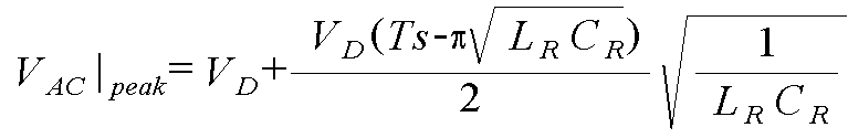
여기서, Ts는 1 사이클의 주기를 의미한다.Here, Ts means a cycle of one cycle.
상술한 수학식 1을 참조하면, 광원 구동 장치(100)의 설계자는 서로 상이한 방전 가스가 충진되어 광원(200)의 구동 효율을 최대화하기 위한 최적의 펄스 폭, 휴지 기간 및 펄스의 주기에 대한 정보가 광원(200)의 제조사로부터 제조 스펙으로 제공되면, 제1 및 제2 인덕터(LR1, LR2)의 값을 설정하여 최적의 펄스 폭(![]()
![]()
도 5는 도 1에 도시된 광원 구동 장치의 다른 예를 구체적으로 도시한 회로 도이고, 도 6은 도 5에 도시된 광원 구동 장치의 동작을 설명하기 위한 파형도이다.FIG. 5 is a circuit diagram specifically illustrating another example of the light source driving apparatus shown in FIG. 1, and FIG. 6 is a waveform diagram for describing an operation of the light source driving apparatus illustrated in FIG. 5.
도 5 및 도 6을 참조하면, 광원 구동 장치(100)는 전원 공급부(110), 제1 전원 변환부(120), 제2 전원 변환부(130) 및 제어부(140)를 포함한다. 5 and 6, the light
여기서, 본 발명의 다른 실시예에 의한 광원 구동 장치(100)는 도 2에 도시된 본 발명의 일 실시예에 의한 광원 구동 장치(100)와 제1 전원 변환부(120)와 제2 전원 변환부(130)의 구성이 상이하고 나머지 부분은 실질적으로 동일하게 구성되는 바, 그 동일한 구성 요소는 동일한 도면 부호를 사용하여 설명하기로 하고, 그 중복되는 상세한 설명은 생략하기로 한다.Here, the light
제1 전원 변환부(120)는 제1 인덕터(LR1)와 커패시터(C)로 형성된 공진 회로를 포함하여, 전원 공급부(110)에 출력되는 직류 전원(VD)을 소정 주기를 갖는 정현파 등의 제1 교류 전원(VAC1)으로 변환한다. 이때, 제1 전원 변환부(120)에는 광원(200)에 입력되는 제1 교류 전원(VAC1)의 전위가 소정 레벨 승압되어 제공할 수 있도록 하는 승압 회로부(TF)를 포함한다. The
제2 전원 변환부(130)는 제2 인덕터(LR2)와 커패시터(C)로 형성된 공진 회로를 포함하여, 전원 공급부(110)에 출력되는 직류 전원(VD)을 소정 주기를 갖는 정현파 등의 제2 교류 전원(VAC2)으로 변환한다. 이때, 제2 전원 변환부(130) 또한 제1 전원 변환부(120)와 마찬가지로, 광원(200)에 입력되는 제2 교류 전원(VAC2)의 전위 가 소정 레벨 승압되어 제공할 수 있도록 하는 승압 회로부(TF)를 포함한다.The
이때, 제1 및 제2 전원 변환부(120, 130)는 하나의 승압 회로부(TF)를 공통으로 사용할 수 있다.In this case, the first and second
이와 같이, 도 5에 도시된 바와 같은 구성에 의하면, 도 6에 도시된 바와 같이 광원(200)에 플라즈마 방전을 일으키기 위하여 예를 들어, 2kV의 교류 전원이 필요한 경우, 제1 노드(N1)와 제2 노드(N2)에는 제2 구동 모드(mode2)와 제5 구동 모드(mode5)에서 각각 약 2kV의 전압이 인가되게 된다.As such, according to the configuration as shown in FIG. 5, as shown in FIG. 6, when an AC power source of 2 kV is required to generate plasma discharge to the
만일, 동일한 조건 하에서 도 2에 도시된 바와 같은 구성에 의하면, 도 2에 도시된 제1 노드(N1)와 제2 노드(N2)에 연결된 제1 스위칭부(SW1)와 제2 스위칭부(SW2)에 포함된 스위치 소자는 약 2kV의 내압을 견딜 수 있는 스위치 소자로 구성되어야 한다. According to the configuration as shown in FIG. 2 under the same condition, the first switching unit SW1 and the second switching unit SW2 connected to the first node N1 and the second node N2 shown in FIG. The switch element included in) should be composed of a switch element that can withstand a voltage of about 2 kV.
그러나, 도 5에 도시된 바와 같이 승압 회로부(TF)를 포함하는 구성에 의하면, 도 6에 도시된 바와 같이 동일한 조건 하에서 제1 노드(N1)와 제2 노드(N2)에 약 400V의 전위만 인가되더라도, 권선비가 1:5인 변압기를 사용하면, 광원(200)에 2kV의 전원이 입력될 수 있기 때문에 제1 및 제2 스위칭부(SW1, SW2)에 포함된 스위치 소자는 약 400V의 내압만을 견딜 수 있는 스위치 소자로 구성할 수 있다. 이는 스위치 소자를 구성하기 위한 제조 비용을 감소시킬 수 있음을 의미한다. 또한, 양극 전원을 광원(200)에 인가함으로써, 바이어스 스트레스를 감소시키게 되어 광원(200)의 사용 수명을 연장시키게 된다.However, according to the configuration including the booster circuit unit TF as shown in FIG. 5, only a potential of about 400 V is applied to the first node N1 and the second node N2 under the same conditions as shown in FIG. 6. Even when applied, when a transformer having a winding ratio of 1: 5 is used, 2 kV of power may be input to the
이때, 광원(200)에 인가되는 제1 및 제2 교류 전원(VAC1, VAC2)의 피크 전압은 다음의 수학식 2를 통해 도출할 수 있다.In this case, the peak voltages of the first and second AC power sources V AC1 and V AC2 applied to the

여기서, n은 승합 회로부(TF)를 구성하는 1차측 코일과 2차측 코일의 권선비를 의미한다.Here, n denotes a winding ratio between the primary coil and the secondary coil constituting the multiplier circuit unit TF.
상술한 수학식 2를 참조하면, 광원 구동 장치(100)의 설계자는 서로 상이한 방전 가스가 충진되어 광원(200)의 구동 효율을 최대화하기 위한 최적의 펄스 폭, 휴지 기간 및 펄스의 주기에 대한 정보가 광원(200)의 제조사로부터 제조 스펙으로 제공되면, 제1 및 제2 인덕터(LR1, LR2)의 값을 설정하여 최적의 펄스 폭(![]()
![]()
도 7은 본 발명의 다른 실시예에 의한 광원 구동 장치를 설명하기 위해 도시한 블록도이고, 도 8은 도 7에 도시된 광원 구동 장치를 설명하기 위해 구체적으로 도시한 회로도이다. 또한, 도 9는 도 8에 도시된 광원 구동 장치의 동작을 설명하기 위해 도시한 도면이고, 도 10은 도 8에 도시된 광원 구동 장치의 동작을 설명하 기 위해 도시한 파형도이다.FIG. 7 is a block diagram illustrating a light source driving apparatus according to another exemplary embodiment of the present invention, and FIG. 8 is a circuit diagram specifically illustrating the light source driving apparatus illustrated in FIG. 7. 9 is a view illustrating the operation of the light source driving apparatus illustrated in FIG. 8, and FIG. 10 is a waveform diagram illustrating the operation of the light source driving apparatus illustrated in FIG. 8.
도 7을 참조하면, 본 발명에 의한 광원 구동 장치(300)는 광원(200)에 교류 전원(VAC)을 제공하기 위해 전원 공급부(310), 전원 변환부(320) 및 제어부(330)를 포함한다. 이때, 광원(200)은 유전체 배리어 방전 램프(Dielectric Barrier Discharge Lamp, DBD 램프)와 같은 면광원 장치로 구성될 수 있다. Referring to FIG. 7, the light
구체적으로, 전원 공급부(310)는 소정 전위 레벨을 갖는 직류 전원(VD)을 출력한다. 전원 공급부(310)는 도 2에서 설명한 전원 공급부(110)와 실질적으로 동일하게 형성되는 바 그 중복되는 상세한 설명은 생략하기로 한다.In detail, the
전원 변환부(320)는 전원 공급부(310)에서 출력되는 직류 전원(VD)을 입력받아, 광원(200)의 구동에 적합한 전위 레벨의 교류 전원(VAC)을 생성하여 출력한다.The
제어부(330)는 스위칭부(332) 및 컨트롤러부(334)를 포함한다.The
스위칭부(332)는 절환 동작에 의해 광원(200)에 입력되는 전류를 제어하여 전원 변환부(320)에 의해 직류 전원(VD)이 교류 전원(VAC)으로 변환되도록 제어하다. 또한, 스위칭부(332)는 컨트롤러부(334)의 제어하에 직류 전원(VD)이 교류 전원(VAC)으로 전원 변환부(320)를 통해 변환될 때, 광원(200)의 최적 구동 효율에 적합한 교류 전원(VAC)의 펄스 폭과 휴지 기간을 가지면서, 소정 시간동안 교류 전원(VAC)의 피크값이 일정 전위로 유지되도록 절환 동작을 수행한다.The
컨트롤러부(334)는 각 스위칭부(SW1, SW2)가 모스 트랜지스터와 같은 스위칭 소자로 구성되는 경우, 모스 트랜지스터의 게이트 단자에 스위칭 신호를 선택적으로 입력하기 위한 마이크로 컨트롤러 유닛(MCU) 등으로 형성할 수 있다.The
이러한 본 발명에 의한 광원 구동 장치(300)에 대해 그 구체적인 예를 통해 보다 상세하게 설명하기로 한다. The light
도 8을 참조하면, 본 발명의 다른 실시예에 의한 광원 구동 장치(300)는 전원 공급부(310), 전원 변환부(320) 및 제어부(330)을 포함한다.Referring to FIG. 8, the light
구체적으로, 전원 공급부(310)는 배터리 또는 정류기 회로등으로 구성되어, 소정 전위 레벨의 직류 전원(VD)을 출력한다. Specifically, the
전원 변환부(320)는 인덕터(LR)와 커패시터(C)로 형성된 공진 회로를 포함하여, 전원 공급부(310)에 출력되는 직류 전원(VD)을 소정 주기 및 펄스 폭을 갖는 정현파 등의 교류 전원(VAC)으로 변환한다.The
이때, 전원 변환부(320)에 포함된 커패시터(C)는 광원(200)을 의미하며, 광원(200)은 제1 전극, 제2 전극 및 제1 전극과 제2 전극 사이에 배치되는 유전체로 의해 소정 커패시턴스를 갖는 커패시터(C)의 역할을 수행할 수 있기에 이를 LC 공진을 위한 커패시터로 사용한다.In this case, the capacitor C included in the
제어부(330)는 스위칭부(332)와 컨트롤러부(334)를 포함한다. The
스위칭부(332)는 인덕터(LR1)와 광원(200)의 제1 전극 사이의 제3 노드(N3) 에 연결되어 절환 동작에 의해 제3 노드 즉, 광원(200)의 제1 전극의 전위를 전원 공급부(110)의 접지 전극의 전위(GND)로 형성하는 제1 스위칭부(SW1), 제2 인덕터(LR2)와 광원(200)의 제2 전극 사이의 제2 노드(N2)에 연결되어 절환 동작에 의해 제2 노드 즉, 제2 전극의 전위를 전원 공급부(110)의 접지 전극의 전위(GND)로 형성하는 제2 스위칭부(SW2)를 포함한다.The
컨트롤러부(334)는 각 스위칭부(SW1, SW2)가 모스 트랜지스터와 같은 스위칭 소자로 구성되는 경우, 모스 트랜지스터의 게이트 단자에 스위칭 신호를 선택적으로 입력하기 위한 마이크로 컨트롤러 유닛(MCU) 등으로 형성할 수 있다.The
이때, 컨트롤러부(334)는 스위칭부(332)가 절환 동작에 의해 광원(200)에 입력되는 전류를 제어하여 전원 변환부(320)에 의해 직류 전원(VD)이 교류 전원(VAC)으로 변환되도록 제어하고, 직류 전원(VD)이 교류 전원(VAC)으로 변환될 때, 광원(200)의 최적 구동 효율에 적합한 교류 전원(VAC)의 펄스 폭과 휴지 기간을 가지면서, 소정 시간동안 교류 전원(VAC)의 피크값이 일정 전위로 유지되도록 스위칭 신호를 제1 및 제2 스위칭부(SW1, SW2)에 선택적으로 제공한다.At this time, the
도 8 내지 도 10을 참조하면, 광원 구동 장치(300)는 7개의 구동 모드(mode1,..., mode7)에 따라 구동할 수 있다.8 to 10, the light
구체적으로, 제1 구동 모드(mode1)에서 컨트롤러부(334)의 제어하에 제1 스위칭부(SW1)는 온 상태로 형성되면, 전원 공급부(310)에서 공급되는 전류는 인덕 터(LR)와 제1 스위칭부(SW1)를 경유하는 전류 경로를 통해 흐르게 되고, 인덕터(LR)에 흐르는 전류는 선형적으로 증가하게 된다. Specifically, when the first switching unit SW1 is formed in the on state under the control of the
제2 구동 모드(mode2)에서 제1 스위칭부(SW1)가 턴-오프되고, 제2 스위칭부(SW2)가 턴-온되면, 제1 스위칭부(SW1)의 기생 커패시터(parastic capaciter, PC1)는 충전되고, 광원(200)의 커패시터(C) 또한, 인덕터(LR)와 제2 스위칭부(SW2)를 경유하는 전류 경로를 통해 충전된다.When the first switching unit SW1 is turned off in the second driving mode mode2 and the second switching unit SW2 is turned on, the parasitic capacitor PC1 of the first switching unit SW1 is turned on. Is charged, and the capacitor C of the
제3 구동 모드(mode3)에서 광원(200)은 충전 전위가 기 설정된 방전 전압의 전위로 형성되면, 광원(200)은 플라즈마 방전을 통해 소정 휘도의 광을 출사한다. 또한, 제3 구동 모드(mode3)에서 광원(200)의 커패시터(C)가 최대 충전 전위로 충전되고, 제1 및 제2 스위칭부(SW2)는 턴-오프된다. 이때, 인덕터(LR)에 흐르는 전류는 커패시터(C)의 충전 전위가 전원 전압(VD)의 전위에 비해 상대적으로 고 전위로 형성되어 인덕터(LR)는 역 바이어스가 인가된다. 따라서, 인덕터(LR)에 흐르는 전류의 방향은 역으로 형성된다. 이에 의해, 제3 구동 모드(mode3)에서 제1 스위칭부(SW1)의 기생 커패시터(PC1)는 방전된다. In the third driving mode mode3, when the charging potential is formed at the preset discharge voltage, the
제4 구동 모드(mode4)에서 제1 스위칭부(SW1)는 턴-온되고, 제2 스위칭부(SW2)는 오프 상태를 유지하여, 인덕터에 흐르는 전류는 선형적으로 증가하게 된다. 이때, 제3 구동 모드(mode3)와 제4 구동 모드(mode4) 사이에서 제1 스위칭부(SW1)의 기생 커패시터(PC1)가 완전히 방전될 때, 제1 스위칭부(SW1)의 바디 다 이오드(BD1)가 턴-온되기 때문에 제4 구동 모드에서 제1 스위칭부(SW1)는 제로 전압 스위칭된다.In the fourth driving mode mode4, the first switching unit SW1 is turned on and the second switching unit SW2 is kept in an off state, so that the current flowing in the inductor increases linearly. At this time, when the parasitic capacitor PC1 of the first switching unit SW1 is completely discharged between the third driving mode mode3 and the fourth driving mode mode4, the body diode of the first switching unit SW1 ( Since the BD1 is turned on, the first switching unit SW1 is zero voltage switched in the fourth driving mode.
이후, 제5 구동 모드(mode5)에서 제1 스위칭부(SW1)가 턴-오프되면, 제1 스위칭부(SW1)의 기생 커패시터(PC1)는 다시 충전을 시작한다. Thereafter, when the first switching unit SW1 is turned off in the fifth driving mode mode5, the parasitic capacitor PC1 of the first switching unit SW1 starts charging again.
제6 구동 모드(mode6)에서 제1 스위칭부(SW1)는 오프 상태를 유지하고, 제2 스위칭부(SW2)가 턴-온되면, 광원(200)의 커패시터(C)는 방전을 개시한다. 이때, 커패시터(C)는 인덕터에 흐르는 전류의 방향이 역으로 형성될 때까지 방전을 수행한다. 이때, 제5 구동 모드(mode5)와 제6 구동 모드(mode6) 사이에서 제1 스위칭부(SW1)의 전압이 광원(200)에 인가된 전압의 전위 레벨을 초과하는 경우, 제2 스위칭부(SW2)의 바디 다이오드(BD2)가 턴-온되기 때문에 제6 구동 모드(mode6)에서 제2 스위칭부(SW2)는 제로 전압 스위칭된다.In the sixth driving mode mode6, the first switching unit SW1 maintains the off state, and when the second switching unit SW2 is turned on, the capacitor C of the
또한, 제6 구동 모드(mode6)에서 제1 스위칭부(SW2)의 바디 다이오드(BD1)에 의해 광원(200)의 양단 전위는 0V로 클램핑(clamping) 된다.In addition, in the sixth driving mode mode6, the potential of both ends of the
제7 구동 모드(mode7)에서 제1 스위칭부(SW1)가 오프 상태를 유지하고, 제2 스위칭부(SW2)가 온 상태를 유지하면, 제1 스위칭부(SW1)의 바디 다이오드(BD1)를 통해 전류는 계속적으로 흐르게된다. In the seventh driving mode mode7, when the first switching unit SW1 maintains the off state and the second switching unit SW2 maintains the on state, the body diode BD1 of the first switching unit SW1 is turned off. Through this current flows continuously.
이후, 제1 구동 모드(mode1) 내지 제7 구동 모드(mode7)를 반복적으로 수행하여 광원(200)에는 단극(unipolar) 전원이 인가된다. 그러나, 본 발명의 다른 실시예에 의한 전원 구동 장치(300)에 의하면, 광원(200)에 인가되는 교류 전원의 피크 전위 레벨을 소정 시간동안 일정하게 유지함에 따라 광원(200)에 포함된 커패시 터(C)의 방전 시간을 충분히 고려할 수 있게 되어, 광원(200)의 구동 효율이 향상된다. 또한, 광원(200)에 단극 전원이 인가될 때 충분한 휴지 기간을 보장할 수 있게 된다.Subsequently, unipolar power is applied to the
도 11은 본 발명에 의한 광원 구동 방법을 설명하기 위해 도시한 순서도이다.11 is a flowchart illustrating a light source driving method according to the present invention.
도 11을 참조하면, 본 발명에 의한 광원 구동 방법은 직류 전원을 교류 전원으로 변환하는 단계(S100) 및 직류 전원을 교류 전원으로 변환할 때, 광원을 최적 구동 효율로 구동하기 위해 기 설정된 펄스 파형에 따라 교류 전원이 변환되도록 제어하는 단계(S200)를 포함한다.Referring to FIG. 11, in the method of driving a light source according to the present invention, a step of converting a direct current power source into an alternating current power source (S100) and a preset pulse waveform for driving the light source at an optimal driving efficiency when converting the direct current power source into an alternating current power source In accordance with the control step to convert the AC power (S200).
이하에서는 도 2 내지 도 6에서 설명한 본 발명의 일 실시예에 의한 광원 구동 장치(100)를 사용하는 경우와, 도 7 내지 도 10에서 설명한 본 발명의 다른 실시예에 의한 광원 구동 장치(300)를 사용하는 경우로 구분하여 본 발명에 의한 광원 구동 방법에 대해 설명하기로 한다.Hereinafter, the light
먼저, 도 2 내지 도 6 및 도 11을 참조하면, 단계 S100에서, 제1 전원 변환부(122)는 제어부(130)의 제2 스위칭부(SW2)가 도 4에 도시된 바와 같이 제4 구동 모드(mode4)에 따라 턴-온되고, 제5 구동 모드(mode5)에서 제1 스위칭부(SW1)가 턴-오프되면, 제1 인덕터(LR1)와 커패시터(C)로 형성된 공진 회로를 이용하여, 직류 전원(VD)을 소정 주기 및 펄스 폭을 갖는 정현파 등의 제1 교류 전원(VAC1)으로 변환한다.First, referring to FIGS. 2 to 6 and 11, in step S100, the
또한, 단계 S100에서 제2 전원 변환부(124)는 제어부(130)의 제1 스위칭부(SW1)가 도 4에 도시된 바와 같이 제2 구동 모드(mode2)에 따라 온 상태에 있고, 제3 구동 모드(mode3)에서 제2 스위칭부(SW2)가 턴-오프되면, 제2 인덕터(LR2)와 커패시터(C)로 형성된 공진 회로를 이용하여, 직류 전원(VD)을 소정 주기 및 펄스 폭을 갖는 정현파 등의 제2 교류 전원(VAC2)으로 변환한다. In operation S100, the second
단계 S200에서, 제어부(130)는 스위칭부(132)의 절환 동작에 의해 제1 노드(N1) 또는 제2 노드(N2)의 전위를 선택적으로 접지 전원의 전위(GND)로 형성하여, 제1 전원 변환부(122)와 제2 전원 변환부(124)의 전원 변환 동작을 제어하고, 도 2 내지 도 4에서 설명한 바와 같은 6개의 구동 모드(mode1,..., mode6)에 따라 광원(200)에 구동한다.In step S200, the
이러한 각각의 구동 모드(mode1,..., mode6)에 관하여는 상술한 바 있음으로, 그 중복되는 구체적인 설명은 생략하기로 한다.Each driving mode (mode1, ..., mode6) has been described above, and the overlapping detailed description thereof will be omitted.
또한, 단계 S100과 단계 S200에서 도 5에 도시된 바와 같이 제1 및 제2 교류 전원(VAC1, VAC2)은 승압 회로부(TF)를 구비하는 경우, 직류 전원(VD)을 교류 전원으로 변환 시 소정 전위 레벨로 승압한 제1 및 제2 교류 전원을 생성할 수 있다.In addition, as shown in FIG. 5 in steps S100 and S200, when the first and second AC power sources V AC1 and V AC2 include the boosting circuit unit TF, the DC power source V D is converted into an AC power source. The first and second AC powers boosted to a predetermined potential level may be generated during the conversion.
이러한 단계들을 수행하는 본 발명의 일 실시예에 의한 광원 구동 방법에 의하면, 정현파 형상의 양극 전원을 교번적으로 광원(200)에 인가할 수 있고, 광원(200)의 스펙에 적합하도록 펄스 폭을 가변적으로 형성할 수 있으며, 양극 전원이 인가될 때 휴지 기간을 보장할 수 있게 된다. 또한, 양극 전원을 광원(200)에 인가함으로써, 바이어스 스트레스를 감소시키게 되어 광원(200)의 사용 수명을 연장시키게 된다.According to the light source driving method according to an embodiment of the present invention performing these steps, a sinusoidal anode power can be alternately applied to the
또 다른 예로, 도 7 내지 도 11을 참조하면, 단계 S100에서, 전원 변환부(320)는 제어부(330)의 제2 스위칭부(SW2)가 도 10에 도시된 바와 같이 제2 구동 모드(mode2)와 제6 구동 모드에 따라 온 상태로 형성되고 제1 스위칭부(SW1)가 오프 상태로 형성되면, 인덕터(LR)와 커패시터(C)로 형성된 공진 회로를 이용하여, 직류 전원(VD)을 교류 전원(VAC)으로 변환한다.As another example, referring to FIGS. 7 to 11, in operation S100, the
단계 S200에서, 제어부(330)의 제2 스위칭부(SW2)가 제3 내지 제5 구동 모드(mode3 ~ mode5)에 따라 오프 상태로 형성됨에 따라 교류 전원의 피크 전위 레벨을 소정 시간동안 일정하게 유지한 교류 전원(VAC)이 광원(200)에 인가된다. 또한, 각 스위칭부(SW1, SW2)의 바디 다이오드와 기생 커패시터에 의해 각 스위칭부는 제로 전압 스위칭을 한다. 또한, 제1 스위칭부(SW1)의 바디 다이오드에 의해 광원(200)에 인가되는 교류 전압(VAC)은 제7 구동 모드(mode7)에서 0V로 클램핑되어 단극 전원이 광원(200)에 인가된다.In step S200, as the second switching unit SW2 of the
이러한 단계들을 수행하는 본 발명의 다른 실시예에 의한 광원 구동 방법에 의하면, 단극 전원이 광원(200)에 인가되지만, 교류 전원(VAC)의 피크 전위 레벨을 소정 시간동안 일정하게 유지함에 따라 광원(200)에 포함된 커패시터(C)의 방전 시간을 충분히 고려할 수 있게 되어, 광원(200)의 구동 효율이 향상된다. 또한, 광 원(200)에 단극 전원이 인가될 때 충분한 휴지 기간을 보장할 수 있게 된다. 또한, 교류 전원(VAC)의 피크 전위 레벨이 유지되는 시간 및 펄스 폭을 광원(200)의 스펙에 적합하도록 가변적으로 형성할 수 있게 된다. According to the light source driving method according to another embodiment of the present invention performing these steps, although the single-pole power is applied to the
여기서, 단계 S100 및 S200의 단계가 순차적으로 진행하는 것으로 설명하여 직류 전원이 교류 전원으로 변환된 후, 변환된 교류 전원이 광원을 최적 구동 효율로 구동하기 위해 기 설정된 펄스 파형에 따라 교류 전원이 변환되는 것으로 설명하였다. 그러나 실제로는 단계 S100와 단계 S200은 제어부(130, 330)의 제어하에 스위칭부(SW1, SW2)가 절환동작을 수행하면, 각 교류 전원이 생성된 후 광원(200)에 인가되어, 제1 교류 전원(VAC1)의 기 정의된 전위 레벨에서 플라즈마 방전이 일어나 광이 출사되므로, 상호 연동하여 구동하는 단계들이다. Here, the steps S100 and S200 are described as being sequentially performed. After the DC power is converted into the AC power, the converted AC power is converted according to a preset pulse waveform to drive the light source with optimal driving efficiency. As described. However, in practice, in steps S100 and S200, when the switching units SW1 and SW2 perform a switching operation under the control of the
도 12는 본 발명에 의한 광원 구동 장치를 구비한 표시 장치의 일 실시예를 도시한 분해 사시도이다.12 is an exploded perspective view illustrating an embodiment of a display device including a light source driving apparatus according to the present invention.
도 12를 참조하면, 본 발명에 의한 표시 장치(1000)는 광원 구동부(100), 광원(200), 디스플레이 유닛(400) 및 수납 용기(600)를 포함한다.Referring to FIG. 12, the
여기서, 광원 구동부(100)는 도 1 내지 도 10에서 설명한 본 발명의 일 실시예 및 다른 실시예에 의한 광원 구동 장치(100, 300)와 실질적으로 동일한 구성을 갖는다. 여기서는 일례로 도 1에 도시된 광원 구동부(100)만을 표시하였으며, 광원 구동 장치(100, 300)에 대해서는 기 설명한 바, 그 중복되는 상세한 설명은 생략하기로 한다.Here, the light
광원(200)은 제1 기판(210) 및 제1 기판(210)과 결합하여 내부 공간을 형성하는 제2 기판(220)으로 이루어진 면광원으로 구성된다.The
제1 기판(210)과 제2 기판(220)은 사각형의 평판 형상을 가지며, 가시 광선은 투과시키고 자외선은 차단하는 투명한 기판으로 이루어진다. 이때, 제1 기판(210)과 제2 기판(220)은 일례로 융해된 납유리 등의 접착 수단을 통해 상호 결합될 수 있으며, 양 기판(210, 220) 사이의 내부 공간은 방전 영역으로 사용하여 플라즈마 방전을 위한 방전 가스가 충진된다. The
디스플레이 유닛(500)은 영상을 표시하는 액정표시패널(510), 액정표시패널(510)을 구동하기 위한 구동 신호를 제공하는 데이터 및 게이트 인쇄회로기판(520, 530)을 포함한다. 데이터 및 게이트 인쇄회로기판(520, 530)으로부터 제공되는 구동 신호는 데이터 테이프 캐리어 패키지(Tape Carrier package, TCP)(540) 및 게이트 TCP(550)를 통해 액정표시패널(510)로 인가된다.The
액정표시패널(510)은 박막 트랜지스터(Thin Film Transistor, 이하 TFT) 기판(512), TFT 기판(512)와 대향하여 결합되는 컬러필터 기판(514) 및 상기 양 기판(512, 514) 사이에 개재된 액정(516)을 포함한다.The liquid
TFT 기판(512)은 스위칭 소자인 TFT(미도시)가 매트릭스(matrix) 형태로 형성된 투명한 유리기판이다. TFT들의 소오스 및 게이트 단자에는 각각 데이터 및 게이트 라인이 연결되고, 드레인 단자에는 투명한 도전성 재질로 이루어진 화소전극(미도시)이 연결된다.The
컬러필터 기판(514)은 색화소인 RGB 화소(미도시)가 박막공정에 의해 형성된 기판이다. 컬러필터 기판(514)에는 투명한 도전성 재질로 이루어진 공통전극(미도시)이 형성된다.The
이러한 구성을 갖는 액정표시패널(510)은 상기 TFT의 게이트 단자에 전원이 인가되어 TFT가 턴-온(turn on)되면, 화소 전극과 공통 전극 사이에는 전계가 형성된다. 이러한 전계에 의해 TFT 기판(512)과 컬러필터 기판(514)과의 사이에 개재된 액정(516)의 배열이 변화되고, 액정(516)의 배열 변화에 따라서 광원(200)으로부터 공급되는 광의 투과도가 변경되어 원하는 계조의 영상을 얻게 된다.In the liquid
수납 용기(700)는 광원(200)을 수납하기 위해 바닥부(710) 및 바닥부(710)의 가장자리로부터 수납 공간을 형성하기 위해 연장된 복수의 측벽(720)으로 이루어진다. 복수의 측벽(720)은 바닥부(710)의 가장자리로부터 수직하게 연장되고, 수납된 광원(200)의 네 측면과 접하게 되어 광원(200)의 유동을 방지한다.The
한편, 표시 장치(1000)는 광원(200)으로부터 출사되는 광의 특성을 향상시키기 위한 광학 부재(400) 및 액정표시패널(510)을 고정하기 위한 고정 부재(600)를 더 포함한다.The
광학 부재(400)는 광원(200)과 액정표시패널(510) 사이에 배치된다. 광학 부재(400)는 광원(200)으로부터 출사되는 광의 경로를 변경시켜, 휘도 균일도를 향상시키거나, 정면 휘도를 향상시키는 역할을 수행한다. 이를 위해, 광학 부재(400)는 광원(200)으로부터 출사되는 광을 확산시키기 위한 확산판(도시하지 않음), 확산판의 상부에 배치되어 확산판으로부터 출사되는 광을 액정표시패널(510) 방향으로 집광하여 광의 정면 휘도를 향상시키기 위한 집광 시트(도시하지 않음) 및 집광 시트 의 하부 또는 상부에 배치되어 광을 확산시키기 위한 확산 시트(도시하지 않음)를 포함할 수 있다.The
고정 부재(600)는 액정표시패널(510)의 가장자리를 감싸면서 수납용기(600)에 결합되어 액정표시패널(510)을 광학 부재(400)의 상부에 고정한다. 이러한 고정 부재(600)는 외부 충격에 의한 액정표시패널(510)의 파손을 방지하고, 액정표시패널(510)이 수납 용기(700)로부터 이탈되는 것을 방지한다.The fixing
한편, 도시되지는 않았으나, 액정표시장치(1000)는 광원(200) 및 광학 부재(400)를 수납용기(700)에 고정하며, 액정표시패널(510)의 수납 위치를 가이드하기 위한 별도의 고정 수단을 더 포함할 수 있다.Although not shown, the liquid
상기한 바와 같이 본 발명에 의하면, 휴지 기간과 펄스 폭을 설계자가 임의로 형성할 수 있는 양극을 갖는 교류 전원을 사용하여 광원의 구동 효율을 향상시킬 수 있고, 사용 수명을 연장시킬 수 있다. As described above, according to the present invention, the driving efficiency of the light source can be improved and the service life can be extended by using an AC power source having an anode whose designer can arbitrarily form the rest period and the pulse width.
또한, 휴지 기간과 펄스 폭을 설계자가 임의로 형성할 수 있는 단극을 갖는 교류 전원을 사용하여 광원의 충방전 시간을 고려할 수 있음으로 광원의 구동 효율을 향상시킬 수 있다.In addition, the charging and discharging time of the light source can be considered by using an AC power source having a single pole in which the designer can arbitrarily form the rest period and the pulse width, thereby improving driving efficiency of the light source.
또한, 방전 가스의 종류를 고려하여 광원의 구동 효율을 최대화하기 위한 교류 전원의 최적의 펄스 폭 및 휴지 기간을 설계자가 임의로 형성할 수 있다. 따라서, 광원을 최적 구동 효율로 구동하기 위한 교류 전압의 펄스 파형에 대한 스펙이 서로 상이한 광원들에 용이하게 적용할 수 있다.In addition, in consideration of the type of discharge gas, the designer may arbitrarily form an optimal pulse width and a rest period of the AC power source to maximize the driving efficiency of the light source. Therefore, the specification for the pulse waveform of the alternating voltage for driving the light source at the optimum driving efficiency can be easily applied to the light sources different from each other.
또한, 광원 구동 장치의 구조를 단순화할 수 있어 제품 크기 및 제조 비용의 증가를 방지할 수 있다.In addition, it is possible to simplify the structure of the light source driving device to prevent the increase in product size and manufacturing cost.
상기에서는 본 발명의 바람직한 실시예들을 참조하여 설명하였지만, 해당 분야의 숙련된 당업자는 하기의 특허 청구의 범위에 기재된 본 발명의 사상 및 영역으로부터 벗어나지 않는 범위 내에서 본 발명을 다양하게 수정 및 변경시킬 수 있음을 이해할 수 있을 것이다. While the foregoing has been described with reference to preferred embodiments of the present invention, those skilled in the art will be able to make various modifications and changes to the present invention without departing from the spirit and scope of the invention as set forth in the claims below. It will be appreciated.
Claims (32)
Priority Applications (2)
| Application Number | Priority Date | Filing Date | Title |
|---|---|---|---|
| KR1020070024452A KR101433658B1 (en) | 2007-03-13 | 2007-03-13 | Apparatus for driving a light source and method of driving the light source and display device using thereof |
| US11/853,344 US8049431B2 (en) | 2007-03-13 | 2007-09-11 | Apparatus and method for driving a light source, and display apparatus using the same |
Applications Claiming Priority (1)
| Application Number | Priority Date | Filing Date | Title |
|---|---|---|---|
| KR1020070024452A KR101433658B1 (en) | 2007-03-13 | 2007-03-13 | Apparatus for driving a light source and method of driving the light source and display device using thereof |
Publications (2)
| Publication Number | Publication Date |
|---|---|
| KR20080083799A true KR20080083799A (en) | 2008-09-19 |
| KR101433658B1 KR101433658B1 (en) | 2014-08-26 |
Family
ID=39761990
Family Applications (1)
| Application Number | Title | Priority Date | Filing Date |
|---|---|---|---|
| KR1020070024452A KR101433658B1 (en) | 2007-03-13 | 2007-03-13 | Apparatus for driving a light source and method of driving the light source and display device using thereof |
Country Status (2)
| Country | Link |
|---|---|
| US (1) | US8049431B2 (en) |
| KR (1) | KR101433658B1 (en) |
Families Citing this family (3)
| Publication number | Priority date | Publication date | Assignee | Title |
|---|---|---|---|---|
| DE102007054330A1 (en) * | 2007-11-14 | 2009-05-20 | Osram Gesellschaft mit beschränkter Haftung | Ballast with DBD lamp |
| KR20160027457A (en) * | 2014-08-29 | 2016-03-10 | 삼성디스플레이 주식회사 | Voltage converter and display device including the same |
| CN205407592U (en) * | 2016-01-29 | 2016-07-27 | 深圳嘉润茂电子有限公司 | No -voltage quasi -resonance boost circuit |
Family Cites Families (6)
| Publication number | Priority date | Publication date | Assignee | Title |
|---|---|---|---|---|
| JPH0934564A (en) * | 1995-07-18 | 1997-02-07 | Chiyoda:Kk | Input waveform follow-up type ac power unit |
| US6259615B1 (en) * | 1999-07-22 | 2001-07-10 | O2 Micro International Limited | High-efficiency adaptive DC/AC converter |
| JP2002352989A (en) * | 2001-05-25 | 2002-12-06 | Mitsubishi Electric Corp | Lighting equipment for electric discharge lamp |
| JP4438513B2 (en) * | 2004-05-26 | 2010-03-24 | パナソニック電工株式会社 | Discharge lamp lighting device and lighting fixture |
| JP4318659B2 (en) * | 2005-03-28 | 2009-08-26 | Tdk株式会社 | Discharge lamp driving device |
| DE102005034505A1 (en) * | 2005-07-20 | 2007-02-01 | Patent-Treuhand-Gesellschaft für elektrische Glühlampen mbH | Circuit arrangement with transformerless converter with choke for the pulsed operation of dielectric barrier discharge lamps |
-
2007
- 2007-03-13 KR KR1020070024452A patent/KR101433658B1/en active IP Right Grant
- 2007-09-11 US US11/853,344 patent/US8049431B2/en not_active Expired - Fee Related
Also Published As
| Publication number | Publication date |
|---|---|
| KR101433658B1 (en) | 2014-08-26 |
| US20080224628A1 (en) | 2008-09-18 |
| US8049431B2 (en) | 2011-11-01 |
Similar Documents
| Publication | Publication Date | Title |
|---|---|---|
| US7253565B2 (en) | Apparatus for supplying power, backlight assembly and liquid crystal display apparatus having the same | |
| TWI242177B (en) | Power supply for an LCD panel | |
| EP2237645B1 (en) | Current balancing apparatus, power supply apparatus, lighting apparatus, and current balancing method thereof | |
| KR101152118B1 (en) | Driving apparatus of display device and dc-dc converter | |
| US8816952B2 (en) | Apparatus and method for driving lamp of liquid crystal display device | |
| KR20100114177A (en) | Method of supplying power, apparatus for performing the method and display apparatus having the apparatus | |
| US7635955B2 (en) | Back light assembly and display apparatus having the same | |
| KR101026806B1 (en) | Display device, driving device of light source for display device and dc-dc converter | |
| JP2011124234A (en) | Drive device of light source for display device and display device | |
| US8907585B2 (en) | Method of driving light source, light source module for performing the method and display apparatus having the light source module | |
| US7852018B2 (en) | Apparatus and method of driving lamp of liquid crystal display device | |
| US6597130B2 (en) | Driving apparatus of discharge tube lamp | |
| US8243005B2 (en) | Apparatus and method for driving lamp of liquid crystal display device | |
| KR101433658B1 (en) | Apparatus for driving a light source and method of driving the light source and display device using thereof | |
| KR101134462B1 (en) | Apparatus for driving backlight and method for driving the same, back light unit and display apparatus having the same | |
| KR100864739B1 (en) | Flat Backlight Driving Circuit of Liquid Crystal Display Device | |
| KR100838415B1 (en) | Flat Backlight Driving Circuit of Liquid Crystal Display Device | |
| KR100478412B1 (en) | Inverter for external electrode fluorescent lamp | |
| KR101067041B1 (en) | Method for driving backlight | |
| KR100528698B1 (en) | Apparatus and method for driving of lamp | |
| KR100677967B1 (en) | Power supply circuit for liquid crystal display | |
| KR20060016224A (en) | Inverter for external electrode fluorescent lamp | |
| KR20060100693A (en) | Back-light unit of liquid crystal display device | |
| KR20050093895A (en) | Inverter in flat fluorescent lamp and method of inverting using the same | |
| KR20060024052A (en) | Inverter and inverting method for flat fluorescent lamp, backlight assembly and liquid crystal display having the same |
Legal Events
| Date | Code | Title | Description |
|---|---|---|---|
| A201 | Request for examination | ||
| E902 | Notification of reason for refusal | ||
| AMND | Amendment | ||
| E601 | Decision to refuse application | ||
| J201 | Request for trial against refusal decision | ||
| AMND | Amendment | ||
| B701 | Decision to grant | ||
| GRNT | Written decision to grant | ||
| FPAY | Annual fee payment |
Payment date: 20180727 Year of fee payment: 5 |