KR20070093405A - Optical film having a surface with rounded structures - Google Patents
Optical film having a surface with rounded structures Download PDFInfo
- Publication number
- KR20070093405A KR20070093405A KR1020077014880A KR20077014880A KR20070093405A KR 20070093405 A KR20070093405 A KR 20070093405A KR 1020077014880 A KR1020077014880 A KR 1020077014880A KR 20077014880 A KR20077014880 A KR 20077014880A KR 20070093405 A KR20070093405 A KR 20070093405A
- Authority
- KR
- South Korea
- Prior art keywords
- optical
- optical film
- light
- light source
- optical device
- Prior art date
Links
Images


Classifications
-
- G—PHYSICS
- G02—OPTICS
- G02B—OPTICAL ELEMENTS, SYSTEMS OR APPARATUS
- G02B6/00—Light guides; Structural details of arrangements comprising light guides and other optical elements, e.g. couplings
-
- G—PHYSICS
- G02—OPTICS
- G02B—OPTICAL ELEMENTS, SYSTEMS OR APPARATUS
- G02B6/00—Light guides; Structural details of arrangements comprising light guides and other optical elements, e.g. couplings
- G02B6/0001—Light guides; Structural details of arrangements comprising light guides and other optical elements, e.g. couplings specially adapted for lighting devices or systems
- G02B6/0011—Light guides; Structural details of arrangements comprising light guides and other optical elements, e.g. couplings specially adapted for lighting devices or systems the light guides being planar or of plate-like form
- G02B6/0033—Means for improving the coupling-out of light from the light guide
- G02B6/005—Means for improving the coupling-out of light from the light guide provided by one optical element, or plurality thereof, placed on the light output side of the light guide
- G02B6/0053—Prismatic sheet or layer; Brightness enhancement element, sheet or layer
-
- G—PHYSICS
- G02—OPTICS
- G02B—OPTICAL ELEMENTS, SYSTEMS OR APPARATUS
- G02B6/00—Light guides; Structural details of arrangements comprising light guides and other optical elements, e.g. couplings
- G02B6/0001—Light guides; Structural details of arrangements comprising light guides and other optical elements, e.g. couplings specially adapted for lighting devices or systems
- G02B6/0011—Light guides; Structural details of arrangements comprising light guides and other optical elements, e.g. couplings specially adapted for lighting devices or systems the light guides being planar or of plate-like form
- G02B6/0033—Means for improving the coupling-out of light from the light guide
- G02B6/0056—Means for improving the coupling-out of light from the light guide for producing polarisation effects, e.g. by a surface with polarizing properties or by an additional polarizing elements
-
- G—PHYSICS
- G02—OPTICS
- G02F—OPTICAL DEVICES OR ARRANGEMENTS FOR THE CONTROL OF LIGHT BY MODIFICATION OF THE OPTICAL PROPERTIES OF THE MEDIA OF THE ELEMENTS INVOLVED THEREIN; NON-LINEAR OPTICS; FREQUENCY-CHANGING OF LIGHT; OPTICAL LOGIC ELEMENTS; OPTICAL ANALOGUE/DIGITAL CONVERTERS
- G02F1/00—Devices or arrangements for the control of the intensity, colour, phase, polarisation or direction of light arriving from an independent light source, e.g. switching, gating or modulating; Non-linear optics
- G02F1/01—Devices or arrangements for the control of the intensity, colour, phase, polarisation or direction of light arriving from an independent light source, e.g. switching, gating or modulating; Non-linear optics for the control of the intensity, phase, polarisation or colour
- G02F1/13—Devices or arrangements for the control of the intensity, colour, phase, polarisation or direction of light arriving from an independent light source, e.g. switching, gating or modulating; Non-linear optics for the control of the intensity, phase, polarisation or colour based on liquid crystals, e.g. single liquid crystal display cells
- G02F1/133—Constructional arrangements; Operation of liquid crystal cells; Circuit arrangements
- G02F1/1333—Constructional arrangements; Manufacturing methods
- G02F1/1335—Structural association of cells with optical devices, e.g. polarisers or reflectors
Abstract
Description
본 발명은 실질적으로 반구형의 표면 구조물을 포함하는 광학 필름 그리고 이러한 광학 필름을 합체한 광학 장치에 관한 것이다.The present invention relates to optical films comprising substantially hemispherical surface structures and to optical devices incorporating such optical films.
액정 디스플레이("LCD: liquid crystal display") 등의 디스플레이 장치는 예컨대 텔레비전, 핸드-헬드 장치, 디지털 스틸 카메라, 비디오 카메라 및 컴퓨터 모니터를 포함한 다양한 적용 분야에서 사용된다. LCD는 중량, 유닛 크기 및 전력 소비의 감소 그리고 또한 밝기의 증가 등의 전통적인 음극선관("CRT: cathode ray tube") 디스플레이보다 우수한 여러 개의 장점을 제공한다. 그러나, LCD 패널은 자체 발광성(self-illuminating)이 아니므로, 때때로 백라이트 조명 조립체 또는 "백라이트(backlight)"를 요구한다. 백라이트는 전형적으로 1개 이상의 광원[예컨대, 냉음극 형광관("CCFT: cold cathode fluorescent tube") 또는 발광 다이오드("LED: light emitting diode")로부터 실질적으로 평면형의 출력부로 광을 커플링한다. 그 다음에, 실질적으로 평면형의 출력부는 LCD 패널에 커플링된다.Display devices such as liquid crystal displays ("LCDs") are used in a variety of applications, including, for example, televisions, hand-held devices, digital still cameras, video cameras, and computer monitors. LCDs offer several advantages over traditional cathode ray tube ("CRT") displays, such as reduced weight, unit size and power consumption, and also increased brightness. However, LCD panels are not self-illuminating and therefore sometimes require a backlight illumination assembly or "backlight." The backlight typically couples light from one or more light sources (eg, a cold cathode fluorescent tube ("CCFT") or light emitting diode ("LED") to a substantially planar output. Then, the substantially planar output is coupled to the LCD panel.
LCD의 성능은 종종 그 밝기에 의해 판정된다. LCD의 밝기는 대량의 광원 또는 더 밝은 광원을 사용함으로써 향상될 수 있다. 큰 면적의 디스플레이에서, 밝 기를 유지하기 위해 직접-조명 방식(direct-lit type)의 LCD 백라이트를 사용할 것이 종종 필요하며, 광원을 위한 이용 가능한 공간은 주변부에 대해 선형으로 커지지만 조명 영역은 주변부의 제곱에 따라 커지기 때문이다. 그러므로, LCD 텔레비전은 전형적으로 도광부 모서리-조명 방식(light-guide edge-lit type)의 LCD 백라이트 대신에 직접-조명식 백라이트를 사용한다. 추가의 광원 및/또는 더 밝은 광원은 더 많은 에너지를 소비할 수 있으며, 이것은 디스플레이 장치로의 전력 할당을 감소시킬 수 있는 능력에 반한다. 휴대 장치에 대해, 이것은 배터리 수명의 감소와 상호 관련될 수 있다. 또한, 디스플레이 장치에 광원을 추가하는 것은 제조 비용 및 중량을 증가시킬 수 있고, 때때로 디스플레이 장치의 신뢰성 감소를 유도할 수 있다.The performance of an LCD is often determined by its brightness. The brightness of the LCD can be improved by using a large amount of light sources or brighter light sources. In large area displays, it is often necessary to use a direct-lit type LCD backlight to maintain brightness, while the available space for the light source grows linearly with respect to the periphery, but the illumination area Because it grows with squares. Therefore, LCD televisions typically use direct-illuminated backlights instead of light-guide edge-lit type LCD backlights. Additional light sources and / or brighter light sources may consume more energy, which is contrary to the ability to reduce power allocation to the display device. For a portable device, this may correlate with a reduction in battery life. In addition, adding a light source to the display device can increase manufacturing cost and weight, and sometimes can lead to reduced reliability of the display device.
또한, LCD의 밝기는 (예컨대, 선호되는 관찰 축을 따라 디스플레이 장치 내에서 이용 가능한 광을 더 많이 유도하기 위해) LCD 장치 내에서 이용 가능한 광을 효율적으로 이용함으로써 향상될 수 있다. 예컨대, 3M 컴퍼니로부터 입수 가능한 상표명 비쿠이티 밝기 향상 필름("BEF: Brightness Enhancement Film")은 관찰 범위 외부측의 백라이트로부터 나오는 광 중 일부가 실질적으로 관찰 축을 따르도록 재유도하는 프리즘 표면 구조물을 갖는다. 잔여 광 중 적어도 일부는 BEF와 그 후방 반사기 등의 반사성 구성 요소 사이에서의 광 중 일부의 다중 반사를 통해 재생된다. 이것은 실질적으로 관찰 축을 따른 광학 이득을 가져오고, 또한 LCD의 조명의 개선된 공간적 균일성을 가져온다. 이와 같이, BEF는 예컨대 밝기를 향상시키고 공간적 균일성을 개선시키기 때문에 유리하다. 배터리 전력 공급식 휴대 장치 에 대해, 이것은 더 긴 동작 시간 또는 더 작은 배터리 크기 그리고 더 우수한 관찰 경험을 제공하는 디스플레이를 유도할 수 있다.In addition, the brightness of the LCD can be improved by efficiently utilizing the light available within the LCD device (eg, to induce more light available within the display device along the preferred viewing axis). For example, the trade name Bicuiti Brightness Enhancement Film ("BEF") available from 3M Company has a prism surface structure that reinduces some of the light from the backlight outside the viewing range substantially along the viewing axis. At least some of the remaining light is reproduced through multiple reflections of some of the light between reflective components such as the BEF and its back reflector. This substantially results in optical gain along the viewing axis, and also results in improved spatial uniformity of the illumination of the LCD. As such, BEF is advantageous because, for example, it improves brightness and improves spatial uniformity. For battery powered portable devices, this can lead to a display that provides longer operating time or smaller battery size and a better viewing experience.
하나의 실시예에서, 본 발명은, 광원, 그리고 광원으로부터 광을 수용하도록 배치되는 제1 표면 그리고 광원으로부터 멀어지는 방향으로 향하는 제2 표면을 갖는 광학 필름을 포함하며, 제2 표면은 2-차원 어레이의 조밀하게 충전된 실질적으로 반구형의 구조물을 포함하는 광학 장치에 관한 것이다. 일부의 예시 실시예에서, 광학 필름은 편광자를 추가로 포함한다.In one embodiment, the present invention includes an optical film having a light source and a first surface disposed to receive light from the light source and a second surface facing away from the light source, the second surface being a two-dimensional array An optical device comprising a densely packed substantially hemispherical structure of. In some exemplary embodiments, the optical film further comprises a polarizer.
또 다른 실시예에서, 본 발명은, 광원, 그리고 광원으로부터 광을 수용하도록 배치되는 제1 표면 그리고 광원으로부터 멀어지는 방향으로 향하는 제2 표면을 갖는 광학 필름을 포함하며, 제2 표면은 제1 반경을 갖는 제1의 복수개의 실질적으로 반구형의 구조물 그리고 제2 반경을 갖는 제2의 복수개의 실질적으로 반구형의 구조물을 구비한 2-차원 어레이를 포함하는 광학 장치에 관한 것이다. 제2 반경은 제1 반경과 상이하다. 제1 및 제2의 복수개의 구조물은 조밀하게 충전된다.In yet another embodiment, the present invention includes an optical film having a light source and a first surface disposed to receive light from the light source and a second surface facing away from the light source, the second surface having a first radius An optical device comprising a two-dimensional array having a first plurality of substantially hemispherical structures having a second plurality of substantially hemispherical structures having a second radius. The second radius is different from the first radius. The first and second plurality of structures are densely packed.
또 다른 실시예에서, 본 발명은, 광원, 그리고 광원으로부터 광을 수용하도록 배치되는 제1 표면 그리고 광원으로부터 멀어지는 방향으로 향하는 제2 표면을 갖는 광학 필름을 포함하며, 제2 표면은 실질적으로 동일한 반경을 갖는 복수개의 조밀하게 충전된 실질적으로 반구형의 구조물을 구비한 2-차원 어레이를 포함하는 광학 장치에 관한 것이다. 일부의 예시 실시예에서, 광학 필름은 2-차원 어레이를 포함하는 제2 표면의 광학적 특성과 상이한 광학적 특성을 갖는 기판 부분을 추가로 포함한다.In yet another embodiment, the present invention includes an optical film having a light source and a first surface disposed to receive light from the light source and a second surface facing away from the light source, the second surface having substantially the same radius An optical device comprising a two-dimensional array having a plurality of densely filled substantially hemispherical structures having a structure. In some exemplary embodiments, the optical film further includes a portion of the substrate having optical properties that differ from the optical properties of the second surface comprising the two-dimensional array.
본 발명의 광학 필름 및 광학 장치의 이들 및 다른 태양은 도면과 함께 다음의 상세한 설명으로부터 당업자에게 더 용이하게 명확해질 것이다.These and other aspects of the optical films and optical devices of the present invention will become more readily apparent to those skilled in the art from the following detailed description in conjunction with the drawings.
당업자라면 본 발명을 수행 및 사용하는 방법을 더 용이하게 이해할 것이고, 그 예시 실시예가 도면을 참조하여 아래에서 상세하게 설명될 것이다.Those skilled in the art will more readily understand how to perform and use the present invention, and exemplary embodiments thereof will be described in detail below with reference to the drawings.
도1A는 평면형 도광부 모서리-조명식 백라이트를 개략적으로 도시하고 있다.1A schematically illustrates a planar light guide edge-illuminated backlight.
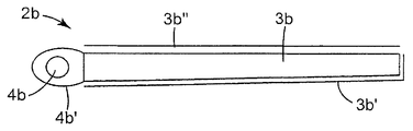
도1B는 웨지형 도광부 모서리-조명식 백라이트를 개략적으로 도시하고 있다.1B schematically illustrates a wedge shaped light guide edge-illuminated backlight.
도1C는 연장된 광원을 이용한 백라이트를 개략적으로 도시하고 있다.1C schematically shows a backlight with an extended light source.
도1D는 직접-조명식 백라이트를 개략적으로 도시하고 있다.1D schematically depicts a direct-lighted backlight.
도2는 백라이트 위에 배치되는 본 발명에 따른 광학 필름의 예시 실시예를 개략적으로 도시하고 있다.2 schematically illustrates an exemplary embodiment of an optical film according to the invention disposed over a backlight.
도3A는 본 발명에 따라 구성된 예시의 광학 필름의 부분 개략 사시도이다.3A is a partial schematic perspective view of an exemplary optical film constructed in accordance with the present invention.
도3B는 도3A에 도시된 예시의 광학 필름에 대한 등광도 극 좌표 선도(iso-candela polar plot)이다.FIG. 3B is an iso-candela polar plot for the example optical film shown in FIG. 3A.
도3C는 0˚, 45˚, 90˚ 및 135˚ 각도에서 취해지는 도3B에 도시된 데이터의 단면을 나타내는 구형 분포 선도(rectangular distribution plot)를 포함하고 있다.FIG. 3C includes a rectangular distribution plot showing the cross section of the data shown in FIG. 3B taken at 0 °, 45 °, 90 ° and 135 ° angles.
도4A는 본 발명에 따라 구성된 또 다른 예시의 광학 필름의 부분 개략 사시도이다.4A is a partial schematic perspective view of another exemplary optical film constructed in accordance with the present invention.
도4B는 도4A에 도시된 예시의 광학 필름에 대한 등광도 극 좌표 선도이다.FIG. 4B is an isochronous polar coordinate plot for the example optical film shown in FIG. 4A.
도4C는 0˚, 45˚, 90˚ 및 135˚ 각도에서 취해지는 도4B에 도시된 데이터의 단면을 나타내는 구형 분포 선도를 포함하고 있다.FIG. 4C includes a spherical distribution diagram showing the cross section of the data shown in FIG. 4B taken at 0 °, 45 °, 90 ° and 135 ° angles.
도5A는 본 발명에 따라 구성된 또 다른 예시의 광학 필름의 부분 개략 사시도이다.5A is a partial schematic perspective view of another exemplary optical film constructed in accordance with the present invention.
도5B는 도5A에 도시된 예시의 광학 필름에 대한 등광도 극 좌표 선도이다.FIG. 5B is an isochronous polar coordinate plot for the example optical film shown in FIG. 5A.
도5C는 0˚, 45˚, 90˚ 및 135˚ 각도에서 취해지는 도5B에 도시된 데이터의 단면을 나타내는 구형 분포 선도를 포함하고 있다.FIG. 5C includes a spherical distribution diagram showing the cross section of the data shown in FIG. 5B taken at 0, 45, 90, and 135 degrees.
본 발명은 광의 각도 분포를 제어할 수 있는 광학 필름 그리고 이러한 광학 필름을 합체한 광학 장치에 관한 것이다. 특히, 본 발명에 따른 광학 필름은 LCD 백라이트 등의 백라이트로부터의 광의 각도 출력 분포를 제어할 수 있다.The present invention relates to an optical film capable of controlling the angular distribution of light and an optical device incorporating such an optical film. In particular, the optical film according to the present invention can control the angular output distribution of light from a backlight such as an LCD backlight.
도1A 내지 도1D는 LCD 패널과 함께 사용될 수 있는 백라이트 등의 광학 장치의 여러 개의 예를 도시하고 있다. 도1A는 백라이트(2a)를 도시하고 있다. 백라이트(2a)는 실질적으로 평면형의 도광부로서 도시되어 있는 도광부(3a), CCFT 또는 LED의 어레이 등의 도광부(3a)의 1개, 2개 또는 그 이상의 측면 상에 배치되는 광원(4a), 광원(4a) 주위에 배치되는 램프 반사기(4a'), 후방 반사기(3a') 그리고 임의의 적절한 광학 필름일 수 있는 1개 이상의 광학 필름(3a")을 포함한다. 도1B는 웨지형 도광부로서 도시되어 있는 도광부(3b), 1개 이상의 CCFT 또는 LED의 어레이 등의 도광부(3b)의 1개의 측면 상에 배치되는 광원(4b), 광원(4b) 주위에 배치되는 램프 반사기(4b'), 후방 반사기(3b') 그리고 임의의 적절한 광학 필름일 수 있는 1개 이상의 광학 필름(3b")을 포함하는 백라이트(2b)를 도시하고 있다. 도1C는 표면 방출-방식 광원일 수 있는 연장된 광원(4c) 그리고 연장된 광원(4c) 위에 배치되는 1개 이상의 광학 필름(4c")을 포함하는 백라이트(2c)를 도시하고 있다. 도1D는 CCFT 또는 LED의 어레이 등의 3개 이상의 광원(4d), 후방 반사기(5a), 확산판(4d') 그리고 임의의 적절한 광학 필름일 수 있는 1개 이상의 광학 필름(4d")을 포함하는 직접-조명식 백라이트(2d)의 부분 개략도이다.1A-1D show several examples of optical devices such as backlights that may be used with LCD panels. 1A shows the
이러한 백라이트는 LCD를 사용한 디스플레이 장치 등의 다양한 다른 광학 장치(예컨대, 텔레비전, 모니터 등)에서 사용될 수 있다. 당업자가 이해하는 바와 같이, 디스플레이 장치는 창을 갖는 케이스, 적어도 1개의 광원을 포함할 수 있는 백라이트, 도광부 등의 광-분배 요소, 본 발명에 따른 광학 필름, 다른 적절한 광학 필름 그리고 광학 필름과 광학 창 사이에 위치되고 광학 필름을 통해 전달되는 광을 수용하도록 배치되는 LCD 패널 등의 광-관문 장치(light-gating device)를 포함할 수 있다. 본 발명에 따른 광학 필름은 당업자에게 공지된 임의의 적절한 광원과 연계하여 사용될 수 있고, 디스플레이 장치는 임의의 다른 적절한 요소를 포함할 수 있다.Such backlights can be used in a variety of other optical devices (eg, televisions, monitors, etc.), such as display devices using LCDs. As will be appreciated by those skilled in the art, a display device may include a case with a window, a backlight that may include at least one light source, a light-distributing element such as a light guide, an optical film according to the invention, other suitable optical films and optical films; Light-gating devices, such as LCD panels, positioned between the optical windows and arranged to receive light transmitted through the optical film. The optical film according to the invention can be used in conjunction with any suitable light source known to those skilled in the art, and the display device can comprise any other suitable element.
도2는 광학 필름(6)의 표면(14)(예컨대, 제1 표면)이 백라이트로부터 광을 수용하도록 백라이트(20) 그리고 백라이트(20) 위에 배치되는 본 발명에 따른 광학 필름(6)의 단면도이다. 백라이트(20)는 광원(24), 도광부 등의 광 분배 요소(23) 그리고 후방 반사기(25)를 포함할 수 있다. 본 발명에 따른 광학 필름(6)은 2-차 원 어레이의 조밀하게 충전된 실질적으로 반구형의 구조물(8)을 보유하는 구조물 형성 표면(10)(예컨대, 제2 표면)을 갖는다. 본 발명의 전형적인 실시예에서, 구조물 형성 표면(10)은 백라이트(20)로부터 멀어지는 방향으로 향한다. 광학 필름(6)은 기판 부분(12)을 추가로 포함할 수 있다. 당업자가 이해하는 바와 같이, 2-차원 어레이의 조밀하게 충전된 실질적으로 반구형의 구조물(8) 그리고 기판 부분(12)은 광학 필름(6)을 생성시키기 위해 단일의 부품으로서 그리고 일부의 경우에 동일한 재료로부터 형성될 수 있거나, 이들은 별개로 형성되고 그 다음에 예컨대 적절한 접착제를 사용하여 단일의 부품을 생성시키도록 함께 접합될 수 있다. 일부의 예시 실시예에서, 조밀하게 충전된 실질적으로 반구형의 구조물(8)의 어레이는 기판 부분(12) 상에 형성될 수 있다.2 shows a cross-sectional view of an optical film 6 according to the invention in which the surface 14 of the optical film 6 (eg, the first surface) is disposed above the
광학 필름(6)의 조밀하게 충전된 실질적으로 반구형의 구조물(8)의 2-차원 어레이는 광학 필름(6)을 통해 전달되는 광의 방향 특히 출력 광의 각도 분산(angular spread)을 제어하는 데 사용될 수 있다. 조밀하게 충전된 실질적으로 반구형의 구조물(8)은 나란한 상태로 그리고 서로에 밀접한 상태로, 그리고 일부의 예시 실시예에서 실질적으로 접촉한 상태로 또는 서로에 바로 인접한 상태로 표면(10) 상에 배열될 수 있다. 다른 예시 실시예에서, 실질적으로 반구형의 구조물(8)은 광학 필름(6)의 이득이 적어도 약 1.1이면 서로로부터 이격될 수 있다. 예컨대, 구조물(8)은 구조물 형성 표면(10)의 주어진 유용 면적의 적어도 약 50%를 점유할 정도까지 이격될 수 있거나, 다른 예시 실시예에서, 구조물(8)은 구조물 형성 표면(10)의 주어진 유용 면적의 20% 이상을 점유할 정도까지 추가로 이격될 수 있다.A two-dimensional array of the densely packed substantially
본 발명에 따라 구성된 전형적인 예시의 광학 필름은 대개 적어도 약 1.1 내지 적어도 약 1.5의 광학 이득을 제공할 수 있다. 일부의 예시의 광학 이득 수치는 약 1.2, 1.4 및 1.5를 포함한다. 본 발명의 목적을 위해, "이득(gain)"은 이러한 광학 필름 없는 동일한 광학 시스템의 축 방향 출력 휘도에 대한 본 발명에 따라 구성된 광학 필름을 갖는 광학 시스템의 축 방향 출력 휘도의 비율로서 정의된다. 본 발명의 전형적인 실시예에서, 실질적으로 반구형의 구조물(8)(또는 그에 의해 덮인 주어진 유용 면적)의 크기, 형상 및 간격은 적어도 약 1.1의 광학 이득을 제공하도록 선택된다.Typical exemplary optical films constructed in accordance with the present invention may generally provide an optical gain of at least about 1.1 to at least about 1.5. Some exemplary optical gain figures include about 1.2, 1.4, and 1.5. For the purposes of the present invention, "gain" is defined as the ratio of the axial output brightness of an optical system with an optical film constructed according to the present invention to the axial output brightness of the same optical system without such an optical film. In a typical embodiment of the present invention, the size, shape and spacing of the substantially hemispherical structure 8 (or a given useful area covered by it) are selected to provide an optical gain of at least about 1.1.
전형적으로, 2-차원 어레이의 조밀하게 충전된 실질적으로 반구형의 구조물을 갖는 구조물 형성 표면을 갖는 예시의 광학 필름으로 인한 광학 이득은 둥근 구조물(돌출부 및 오목부 등)의 형상이 반구형으로부터 벗어남에 따라 감소할 것이다. 본 발명의 전형적인 실시예는 그 구조물의 반경의 약 60% 내에 있는 높이 또는 깊이를 갖는 돌출부 또는 오목부를 포함한다. 더 바람직하게는, 본 발명의 실시예는 그 구조물의 반경의 약 40% 내에 있는 높이 또는 깊이를 갖는 돌출부 또는 오목부를 포함하고, 가장 바람직하게는, 본 발명의 실시예는 그 구조물의 반경의 약 20% 내에 있는 높이 또는 깊이를 갖는 돌출부 또는 오목부를 포함한다. 적어도 그 구조물의 반경의 약 60% 내에 있는 높이 또는 깊이를 갖는 이러한 돌출부 또는 오목부는 "실질적으로 반구형(substantially hemispherical)"으로서 호칭될 것이다. 구조물들 사이의 더 큰 간격(더 작은 표면 덮힘률)이 또한 이득 면에서의 감 소를 유도할 수 있다.Typically, the optical gain due to an exemplary optical film having a structure-forming surface with a densely packed substantially hemispherical structure in a two-dimensional array is as the shape of the round structure (such as protrusions and recesses) deviates from the hemispherical shape. Will decrease. Typical embodiments of the present invention include protrusions or recesses having a height or depth within about 60% of the radius of the structure. More preferably, embodiments of the present invention include protrusions or recesses having a height or depth that is within about 40% of the radius of the structure, and most preferably, embodiments of the present invention provide about about the radius of the structure. Protrusions or indentations having a height or depth within 20%. Such protrusions or recesses having a height or depth at least within about 60% of the radius of the structure will be referred to as "substantially hemispherical". Larger spacing between structures (smaller surface coverage) can also lead to a reduction in gain.
실질적으로 반구형의 구조물(8)의 적절한 예시의 반경은 약 5, 8, 10, 12.5, 15, 17.5, 20, 25, 37.5, 45, 50, 60, 70 및 80 ㎛ 그리고 이들 예시 수치들 중 임의의 수치들 사이의 임의의 범위 내에서 한정되는 반경을 포함한다. 일부의 예시 실시예에서, 실질적으로 반구형의 구조물(8)은 더 작을 수 있지만, 회절 효과를 일으키지 않을 정도로 작지 않아야 하거나, 이들은 예컨대 약 100 또는 150 ㎛ 반경 정도로 더 클 수 있다. 전형적으로, 실질적으로 반구형의 구조물(8)의 크기는 광학 필름을 포함한 디스플레이 장치의 관찰자에게 용이하게 식별 가능하지 않도록 충분히 작아야 한다. 직접-조명식 백라이트에서의 사용을 위해 특히 적절한 일부의 예시 실시예에서, 실질적으로 반구형의 구조물(8)의 간격, 크기 및 형상은 본 발명의 광학 필름이 백라이트에서 사용되는 광원을 관찰자로부터 은폐하는 것을 돕도록 선택될 수 있다.Suitable example radiuses of the substantially
광학 필름(6)의 요망된 성질에 따라, 실질적으로 반구형의 구조물(8)은 실질적으로 동일한 형상 및/또는 크기일 수 있거나, 이들은 적어도 2개 이상의 실질적으로 상이한 형상 및 크기로 형성될 수 있다. 예컨대, 본 발명에 따라 구성된 광학 필름은 표면(10)의 더 큰 부분을 덮기 위해 더 큰 크기의 실질적으로 반구형의 구조물 그리고 더 큰 크기의 구조물들 사이에 배치되는 더 작은 크기의 실질적으로 반구형의 구조물을 포함할 수 있다. 이러한 예시 실시예에서, 더 작은 구조물의 반경은 이웃하는 더 큰 구조물의 반경의 약 40%일 수 있거나, 이것은 더 작은 구조물이 더 큰 구조물로써 2-차원 어레이 내에 조밀하게 충전되게 할 정도로 충분히 작은 또 다른 적절한 반경일 수 있다. 다른 예시 실시예에서, 실질적으로 반구형의 구조물(8)은 적어도 3개의 실질적으로 상이한 반경으로 형성될 수 있다.Depending on the desired properties of the optical film 6, the substantially
실질적으로 반구형의 구조물(8) 그리고 일부의 실시예에서 표면(10)을 포함한 기판 부분(12)의 적어도 인접한 부분은 저굴절률 또는 고굴절률 중합체 재료 등의 투명한 경화성 재료로부터 형성될 수 있다. 고굴절률 재료로써, 더 높은 광학 이득이 더 좁은 관찰 각도를 희생하여 성취될 수 있으며, 한편 더 낮은 굴절률 재료로써, 더 넓은 관찰 각도가 더 낮은 광학 이득을 희생하여 성취될 수 있다. 예시의 적절한 고굴절률 수지는 미국 특허 제5,254,390호 및 제4,576,850호에서 개시된 것들 등의 이온화 방사선 경화성 수지를 포함하며, 그 개시 내용은 본 발명과 일관되는 정도까지 참조로 여기에서 합체되어 있다.Substantially
일부의 예시 실시예에서, 실질적으로 반구형의 구조물(8)의 굴절률은 적어도 기판 부분의 층보다 높다. 실질적으로 반구형의 구조물(8)을 형성하는 데 적절한 일부의 공지된 재료는 약 1.6, 1.65, 1.7 또는 그 이상의 굴절률을 갖는다. 다른 예시 실시예에서, 실질적으로 반구형의 구조물(8)은 약 1.58의 굴절률을 갖는 아크릴 등의 더 낮은 굴절률을 갖는 재료로부터 형성될 수 있다. 일부의 이러한 예시 실시예에서, 약 1.66의 굴절률을 갖는 폴리에틸렌 테레프탈레이트 기판에 대해, 구조물(8)(그리고, 아마도, 필름의 인접한 부분)의 양호한 범위는 약 1.55 내지 약 1.65이다.In some exemplary embodiments, the refractive index of the substantially
기판 부분(12)은 2-차원 어레이의 조밀하게 충전된 실질적으로 반구형의 구조물(8)의 광학적 특성과 상이한 추가의 광학적 특성을 가질 수 있으며, 그 결과 기판 부분은 광이 표면(10) 상에 배치된 2-차원 어레이에 의해 조정되는 방식과 상이한 방식으로 광을 조정한다. 이러한 조정은 본 발명의 광학 필름을 통해 전달되는 광의 편광, 확산 또는 추가의 재유도를 포함할 수 있다. 이것은 예컨대 이러한 추가의 광학적 특성을 갖는 광학 필름을 기판 부분 내에 포함함으로써 또는 이러한 추가의 광학적 특성을 부여하도록 기판 부분 자체를 구성함으로써 성취될 수 있다. 이러한 추가의 광학적 특성을 갖는 예시의 적절한 필름은 편광 필름, 확산 필름, BEF 등의 밝기 향상 필름, 방향 전환 필름(turning film) 그리고 이들의 임의의 조합을 포함하지만 이들에 제한되지 않는다. 방향 전환 필름은 예컨대 역전형 프리즘 필름(예컨대, 반전형 BEF) 또는 역전형 프리즘 필름과 대체로 유사한 방식으로 광을 재유도하는 또 다른 구조물일 수 있다. 일부의 예시 실시예에서, 기판 부분(12)은 다층 반사성 편광자 예컨대 상표명 비쿠이티 이중 밝기 향상 필름("DBEF: Dual Brightness Enhancement Film") 등의 선형 반사성 편광자 또는 상표명 비쿠이티 확산 반사성 편광 필름("DRPF: Diffuse Reflective Polarizer Film") 등의 연속 상 및 분산 상을 갖는 확산 반사성 편광자를 포함할 수 있으며, 이들 모두는 3M 컴퍼니로부터 입수 가능하다. 추가예에서 또는 대체예에서, 기판 부분은 폴리카보네이트 층("PC: polycarbonate"), 폴리 메틸 메타크릴레이트 층("PMMA: poly methyl methacrylate"), 폴리에틸렌 테레프탈레이트("PET: polyethylene tetephthalate") 또는 당업자에게 공지된 임의의 다른 적절한 필름 또는 재료를 포함할 수 있다. 예시의 적절한 기판 부분 두께는 PET에 대해 약 125 ㎛ 그리고 PC에 대해 약 130 ㎛를 포함한다.Substrate portion 12 may have additional optical properties that differ from the optical properties of a densely packed substantially
일부의 디스플레이 장치 적용 분야는 더 큰 원통 대칭성의 등광도 선도에 의해 명시될 것인 더 큰 원통 대칭성인 출력을 성취하는 것으로부터 및/또는 대응하는 구형 분포 선도의 비교적 큰 반치 반폭(half width at half maximum)에 의해 명시될 것인 비교적 넓은 관찰 각도를 갖는 출력을 성취하는 것으로부터 이익을 얻을 수 있다. 본 발명의 전형적인 예시 실시예는 약 33˚ 초과 예컨대 약 35˚ 내지 약 40˚ 이상인 구형 분포 선도의 반치 반폭을 가질 수 있다.Some display device applications have a relatively large half width at half from achieving a larger cylindrical symmetry output that will be manifested by an isotropic plot of larger cylindrical symmetry and / or corresponding spherical distribution plots. It is possible to benefit from achieving an output with a relatively wide viewing angle which will be specified by maximum). Exemplary exemplary embodiments of the present invention may have a half-width half-width of a spherical distribution plot that is greater than about 33 degrees, such as about 35 degrees to about 40 degrees or more.
전통적으로, 확산부가 디스플레이 장치의 시계를 넓히는 데 사용되었다. 대부분의 전통적인 확산부와 달리, 본 발명의 광학 필름은 주로 산란성 입사 광에 의존하지 않거나, 확산부의 본체 내에서의 굴절률의 변동으로 인해 이것을 재유도한다. 대신에, 본 발명은 이들의 구조물 형성 표면의 기하학적 구성으로 인해 입사 광의 각도 분산을 유발시킬 수 있는 광학 필름을 제공하고, 또한 적어도 1.1의 이득을 제공한다.Traditionally, diffusers have been used to widen the field of view of display devices. Unlike most traditional diffusers, the optical film of the present invention does not rely mainly on scattered incident light or reinduces it due to variations in refractive index within the body of the diffuser. Instead, the present invention provides optical films that can cause angular dispersion of incident light due to the geometry of their structure-forming surfaces and also provides a gain of at least 1.1.
예Yes
본 발명은 본 발명에 따라 구성된 일부의 예시의 광학 필름의 모델링된 성질을 나타내는 다음의 예를 참조하여 추가로 설명될 것이다.The present invention will be further described with reference to the following examples showing the modeled properties of some exemplary optical films constructed in accordance with the present invention.
예 1Example 1
도3A는 본 발명에 따른 예시의 모델링된 광학 필름(106)의 부분 개략 사시도이다. 예시의 광학 필름(106)은 기판 부분(112) 그리고 2-차원 어레이의 조밀하게 충전된 반구형의 돌출부(108)를 보유하는 구조물 형성 표면(110)을 포함한다. 이러한 예시 실시예에서, 돌출부(108)는 서로에 바로 인접한다. 이러한 예시 실시예 의 각각의 돌출부는 약 25 ㎛의 반경 그리고 약 1.58의 굴절률을 갖는다. 기판 부분은 약 1.66의 굴절률을 갖는 실질적으로 평면형의 필름으로서 모델링된다.3A is a partial schematic perspective view of an exemplary modeled
도3B는 2-차원 어레이의 조밀하게 충전된 반구형의 돌출부(108)가 광원으로 멀어지는 방향으로 향한 상태로 백라이트 위에 위치되는 실질적으로 도3A에 도시된 것과 같은 구조물을 갖는 광학 필름으로부터 나오는 광에 대한 계산된 극 좌표 등광도 분포 선도를 나타낸다. 모든 예의 분포는 다음의 모델을 사용하여 계산된다: 즉, 램버시안 소스(Lambertian source)가 광학 필름을 통한 광의 제1 통과에 대해 사용되고, 잔여 광은 약 77.4%의 반사율을 갖는 램버시안 반사기를 사용하여 재생된다. 당업자가 이해하는 바와 같이, 등광도 분포 선도는 광학 필름을 통과한 검출된 입사 광속의 360˚ 패턴을 도시하고 있다. 도3B로부터 명확한 바와 같이, 이러한 예시 실시예의 출력 광 분포는 비교적 높은 정도의 원통 대칭성을 갖고, 세기는 큰 각도에서 2차 피크를 형성하지 않고 비교적 단조적으로 감소한다.FIG. 3B illustrates light from an optical film having a structure substantially as shown in FIG. 3A positioned over the backlight with the densely packed
도3C는 구형 광도 분포 선도를 도시하고 있다. 당업자가 이해하는 바와 같이, 구형 분포 선도에 대한 각각의 곡선은 극 좌표 선도의 상이한 단면에 대응한다. 예컨대, 0˚로서 지정된 곡선은 0˚와 180˚를 연결하는 중심을 통과하는 선을 따른 극 좌표 선도의 단면을 나타내고, 45˚로서 지정된 곡선은 45˚와 225˚를 연결하는 중심을 통과하는 선을 따른 극 좌표 선도의 단면을 나타내고, 90˚로서 지정된 곡선은 90˚와 270˚를 연결하는 중심을 통과하는 선을 따른 극 좌표 선도의 단면을 나타내고, 135˚로서 지정된 곡선은 135˚와 315˚를 연결하는 중심을 통과하는 선을 따른 극 좌표 선도의 단면을 나타낸다. 또한, 도3C는 이러한 예시 실시예의 출력 광 분포의 비교적 높은 정도의 원통 대칭성 그리고 또한 큰 각도에서 2차 피크 없이 비교적 단조적으로 감소하는 세기를 도시하고 있다. 이러한 결론은 상이한 각도에 대한 구형 세기 선도들 사이의 비교적 작은 차이에 의해 도시되어 있다. 또한, 구형 선도는 약 40˚의 평균 반치 반폭을 갖는 곡선의 뚜렷한 폭을 도시하고 있으며, 이것은 증가된 크기의 확산 그리고 넓혀진 관찰 각도를 지시한다. 도3A에 따라 구성된 예시의 이득 확산부에 대한 모델링된 광학 이득은 약 1.48인 것으로 밝혀졌다.3C shows a spherical luminous intensity distribution diagram. As will be appreciated by those skilled in the art, each curve for the spherical distribution plot corresponds to a different cross section of the polar plot. For example, a curve designated as 0 ° represents a cross section of a polar coordinate line along a line through the center connecting 0 ° and 180 °, and a curve designated as 45 ° passes through a center connecting 45 ° and 225 °. The curve designated as 90 ° represents the cross section of the polar coordinate diagram along the line passing through the center connecting 90 ° and 270 °, and the curve designated as 135 ° is 135 ° and 315 °. Represents the cross-section of a polar coordinate line along a line through the center connecting. 3C also illustrates the relatively high degree of cylindrical symmetry of the output light distribution of this example embodiment and also the intensity decreasing relatively monotonically without secondary peaks at large angles. This conclusion is illustrated by the relatively small difference between the sphere intensity plots for the different angles. The spherical plot also shows the clear width of the curve with an average half-width half width of about 40 °, which indicates an increased magnitude of diffusion and a wider viewing angle. The modeled optical gain for the example gain diffusion constructed in accordance with FIG. 3A was found to be about 1.48.
예 2Example 2
도4A는 본 발명에 따라 구성된 예시의 광학 필름(206)의 부분 개략 사시도이다. 예시의 광학 필름(206)은 기판 부분(212) 그리고 2-차원 어레이의 조밀하게 충전된 반구형의 돌출부(208a, 208b)를 보유하는 구조물 형성 표면(210)을 포함한다. 이러한 예시 실시예의 2-차원 어레이의 조밀하게 충전된 반구형의 돌출부는 서로에 바로 인접하게 배치되는 대략 동일한 크기를 갖는 큰 돌출부(208a) 그리고 대략 동일한 크기를 갖는 작은 돌출부(208b)를 포함하며, 그 결과 작은 돌출부(208a)는 큰 돌출부(208a)에 의해 공간이 남겨진 영역 내에 위치된다. 이러한 구성은 높은 밀도로 표면(210)을 충전하는 것을 돕는다. 큰 돌출부(208a)는 약 25 ㎛ 반경의 반구로서 모델링되며, 각각의 작은 돌출부(208b)는 주위의 큰 돌출부(208a)들 사이에 그리고 주위의 큰 돌출부(208a)에 바로 인접하게 끼워지도록 된 치수로 형성되고, 약 10 ㎛의 반경을 갖는다. 이러한 예시 실시예의 각각의 돌출부는 약 1.58의 굴절률을 갖는다. 기판 부분은 약 1.66의 굴절률을 갖는 실질적으 로 평면형의 필름으로서 모델링된다.4A is a partial schematic perspective view of an exemplary
도4B는 2-차원 어레이의 조밀하게 충전된 반구형의 돌출부(208a, 208b)가 광원으로 멀어지는 방향으로 향한 상태로 백라이트 위에 위치되는 실질적으로 도4A에 도시된 것과 같은 구조물을 갖는 광학 필름으로부터 나오는 광에 대한 계산된 극 좌표 등광도 분포 선도를 나타낸다. 도4B로부터 명확한 바와 같이, 이러한 예시 실시예의 출력 광 분포는 비교적 높은 정도의 원통 대칭성을 갖고, 세기는 큰 각도에서 2차 피크를 형성하지 않고 비교적 단조적으로 감소한다.FIG. 4B shows light exiting from an optical film having a structure substantially as shown in FIG. 4A, positioned over the backlight with the densely packed
도4C는 0˚, 45˚, 90˚ 및 135˚에서 극 좌표 선도의 상이한 단면에 대응하는 구형 광도 분포 선도이다. 또한, 도4C는 이러한 예시 실시예의 출력 광 분포의 비교적 높은 정도의 원통 대칭성 그리고 또한 큰 각도에서 2차 피크 없이 비교적 단조적으로 감소하는 세기를 도시하고 있다. 이러한 결론은 상이한 각도에 대한 구형 광도 선도들 사이의 비교적 작은 차이에 의해 도시되어 있다. 또한, 구형 선도는 약 37˚의 평균 반치 반폭을 갖는 곡선의 뚜렷한 폭을 도시하고 있으며, 이것은 넓혀진 관찰 각도를 지시한다. 도4A에 따라 구성된 예시의 광학 필름에 대한 모델링된 광학 이득은 약 1.50인 것으로 밝혀졌다.4C is a spherical luminous intensity distribution plot corresponding to different cross sections of the polar coordinate plot at 0 °, 45 °, 90 ° and 135 °. 4C also shows a relatively high degree of cylindrical symmetry of the output light distribution of this exemplary embodiment and also the intensity decreasing relatively monotonically without secondary peaks at large angles. This conclusion is illustrated by the relatively small difference between the spherical luminosity plots for the different angles. The spherical diagram also shows the clear width of the curve with an average half-width half width of about 37 °, indicating the widened viewing angle. The modeled optical gain for the exemplary optical film constructed according to FIG. 4A was found to be about 1.50.
예 3Example 3
도5A는 본 발명에 따라 구성된 예시의 광학 필름(306)의 부분 개략 사시도이다. 예시의 광학 필름(306)은 기판 부분(312) 그리고 2-차원 어레이의 조밀하게 충전된 반구형의 오목부(308)를 보유하는 구조물 형성 표면을 포함한다. 이러한 예시 실시예에서, 오목부(308)는 서로에 바로 인접한다. 이러한 예시 실시예의 각 각의 오목부는 약 25 ㎛의 반경을 갖고, 약 1.58의 굴절률을 갖는 필름 부분 내에 배치된다. 기판 부분은 약 1.66의 굴절률을 갖는 실질적으로 평면형의 필름으로서 모델링된다.5A is a partial schematic perspective view of an exemplary
도5B는 2-차원 어레이의 조밀하게 충전된 반구형의 오목부(308)가 광원으로 멀어지는 방향으로 향한 상태로 백라이트 위에 위치되는 실질적으로 도5A에 도시된 것과 같은 구조물을 갖는 광학 필름으로부터 나오는 광에 대한 계산된 극 좌표 등광도 분포 선도를 나타낸다. 도5B로부터 명확한 바와 같이, 이러한 예시 실시예의 출력 광 분포는 비교적 높은 정도의 원통 대칭성을 갖고, 세기는 큰 각도에서 2차 피크를 형성하지 않고 비교적 단조적으로 감소한다.FIG. 5B shows light from an optical film having a structure substantially as shown in FIG. 5A positioned over the backlight with the densely packed
도5C는 0˚, 45˚, 90˚ 및 135˚에서 극 좌표 선도의 상이한 단면에 대응하는 구형 광도 분포 선도이다. 또한, 도5C는 이러한 예시 실시예의 출력 광 분포의 비교적 높은 정도의 원통 대칭성 그리고 또한 큰 각도에서 2차 피크 없이 비교적 단조적으로 감소하는 세기를 도시하고 있다. 이러한 결론은 상이한 각도에 대한 구형 세기 선도들 사이의 미소한 차이에 의해 도시되어 있다. 또한, 구형 선도는 약 43˚의 평균 반치 반폭을 갖는 곡선의 뚜렷한 폭을 도시하고 있으며, 이것은 증가된 크기의 확산 그리고 넓혀진 관찰 각도를 지시한다. 도5A에 따라 구성된 예시의 광학 필름에 대한 모델링된 광학 이득은 약 1.21인 것으로 밝혀졌다.5C is a spherical luminous intensity distribution plot corresponding to different cross sections of the polar coordinate plot at 0 °, 45 °, 90 ° and 135 °. 5C also shows a relatively high degree of cylindrical symmetry of the output light distribution of this exemplary embodiment and also the intensity decreasing relatively monotonically without secondary peaks at large angles. This conclusion is illustrated by the slight differences between the sphere intensity plots for the different angles. The spherical plot also shows the clear width of the curve with an average half-width half width of about 43 °, which indicates an increased magnitude of diffusion and a wider viewing angle. The modeled optical gain for the exemplary optical film constructed according to FIG. 5A was found to be about 1.21.
본 발명에 따른 예시의 광학 필름은 공구, 분무 코팅, 잉크 제트 인쇄 또는 당업자에게 공지된 임의의 다른 방법으로부터의 미세-복제(micro-replication)에 의해 형성될 수 있다.Exemplary optical films according to the present invention may be formed by micro-replication from tools, spray coating, ink jet printing or any other method known to those skilled in the art.
이와 같이, 본 발명은 관찰 측면 상에서의 광의 특정한 제어 가능한 각도 분산 그리고 전달 손실 없는 광의 더 큰 원통 대칭성의 출력 분포를 나타내도록 구성될 수 있는 광학 필름을 제공한다. 나아가, 본 발명의 광학 필름은 광학 이득을 나타낸다. 이득 및 각도 분산의 크기는 표면 구조물의 특정한 구성에 의존할 것이고, 특정한 적용 분야에 대해 요망된 성능을 성취하도록 변동될 수 있다. 추가로, 본 발명의 실시예의 구조물은 증가된 강인성(robustness)을 가질 수 있도록 형성되며, 이것은 표면 특징부가 둥글기 때문이다.As such, the present invention provides an optical film that can be configured to exhibit a specific controllable angular dispersion of light on the viewing side and an output distribution of greater cylindrical symmetry of light without transmission loss. Furthermore, the optical film of the present invention exhibits optical gain. The magnitude of the gain and angular dispersion will depend on the particular configuration of the surface structure and can be varied to achieve the desired performance for the particular application. In addition, the structures of the embodiments of the present invention are formed to have increased robustness because the surface features are rounded.
본 발명의 광학 필름 및 장치가 특정한 예시 실시예를 참조하여 설명되었지만, 당업자라면 변화 및 변경이 본 발명의 사상 및 범주로부터 벗어나지 않고 그에 대해 수행될 수 있다는 것을 용이하게 이해할 것이다.Although the optical film and apparatus of the present invention have been described with reference to specific exemplary embodiments, those skilled in the art will readily appreciate that changes and modifications may be made thereto without departing from the spirit and scope of the invention.
Claims (20)
Applications Claiming Priority (2)
| Application Number | Priority Date | Filing Date | Title |
|---|---|---|---|
| US11/026,940 | 2004-12-30 | ||
| US11/026,940 US7416309B2 (en) | 2004-12-30 | 2004-12-30 | Optical film having a surface with rounded structures |
Publications (1)
| Publication Number | Publication Date |
|---|---|
| KR20070093405A true KR20070093405A (en) | 2007-09-18 |
Family
ID=36178348
Family Applications (1)
| Application Number | Title | Priority Date | Filing Date |
|---|---|---|---|
| KR1020077014880A KR20070093405A (en) | 2004-12-30 | 2005-12-20 | Optical film having a surface with rounded structures |
Country Status (7)
| Country | Link |
|---|---|
| US (2) | US7416309B2 (en) |
| EP (1) | EP1831740A1 (en) |
| JP (1) | JP2008527627A (en) |
| KR (1) | KR20070093405A (en) |
| CN (1) | CN101095071A (en) |
| TW (1) | TW200643459A (en) |
| WO (1) | WO2006073806A1 (en) |
Cited By (2)
| Publication number | Priority date | Publication date | Assignee | Title |
|---|---|---|---|---|
| KR100965207B1 (en) * | 2008-04-21 | 2010-06-24 | (주)엔티아이 | An optical film for back light unit and manufacturing method of an optical film thereof |
| KR101225472B1 (en) * | 2008-01-08 | 2013-01-24 | 돌비 레버러토리즈 라이쎈싱 코오포레이션 | A display device with reduced parallax |
Families Citing this family (49)
| Publication number | Priority date | Publication date | Assignee | Title |
|---|---|---|---|---|
| JP4410123B2 (en) * | 2005-02-10 | 2010-02-03 | 株式会社東芝 | Organic EL display |
| WO2006122056A2 (en) * | 2005-05-09 | 2006-11-16 | Kids Story Book, Llc | Personalized digital sound recording |
| US20070001185A1 (en) * | 2005-06-29 | 2007-01-04 | Lu Ying T | LED backlight module |
| KR20070077285A (en) * | 2006-01-23 | 2007-07-26 | 삼성전자주식회사 | Backlight assembly and display device having the same |
| US20080002256A1 (en) * | 2006-06-30 | 2008-01-03 | 3M Innovative Properties Company | Optical article including a beaded layer |
| KR100837402B1 (en) * | 2006-08-24 | 2008-06-12 | 삼성전자주식회사 | Wide angle diffuser and liquid crystal display employing the same |
| US7481563B2 (en) * | 2006-09-21 | 2009-01-27 | 3M Innovative Properties Company | LED backlight |
| US8134656B2 (en) * | 2006-11-29 | 2012-03-13 | Sharp Kabushiki Kaisha | Backlight device, display device, and television receiver |
| US7604381B2 (en) * | 2007-04-16 | 2009-10-20 | 3M Innovative Properties Company | Optical article and method of making |
| EP2500767A1 (en) | 2007-05-20 | 2012-09-19 | 3M Innovative Properties Company | Semi-specular reflecting components in backlights, which have a thin hollow cavity and recycle the light |
| KR101488042B1 (en) * | 2007-05-20 | 2015-01-29 | 쓰리엠 이노베이티브 프로퍼티즈 컴파니 | Design parameters for thin hollow cavity backlights of the light-recycling type |
| US9028108B2 (en) * | 2007-05-20 | 2015-05-12 | 3M Innovative Properties Company | Collimating light injectors for edge-lit backlights |
| JP2010528432A (en) * | 2007-05-20 | 2010-08-19 | スリーエム イノベイティブ プロパティズ カンパニー | White light backlight using color LED light source efficiently and similar products |
| KR101464795B1 (en) | 2007-05-20 | 2014-11-27 | 쓰리엠 이노베이티브 프로퍼티즈 컴파니 | Light recycling hollow cavity type display backlight |
| CN101743488B (en) * | 2007-07-17 | 2014-02-26 | 科锐公司 | Optical elements with internal optical features and methods of fabricating same |
| KR20100074125A (en) * | 2007-08-14 | 2010-07-01 | 다이니폰 인사츠 가부시키가이샤 | Optical control sheet, surface illuminant device, and transmission type display device |
| TW200907417A (en) * | 2007-08-15 | 2009-02-16 | Delta Electronics Inc | Backlight module and optical film thereof |
| TWI407153B (en) * | 2007-10-05 | 2013-09-01 | Hon Hai Prec Ind Co Ltd | Prism sheet and backlight module using the same |
| CN101419299A (en) * | 2007-10-24 | 2009-04-29 | 鸿富锦精密工业(深圳)有限公司 | Back light module unit and prismatic lens thereof |
| TW200921006A (en) * | 2007-11-12 | 2009-05-16 | Whe-Yi Chiang | Lighting device |
| US20090185395A1 (en) * | 2008-01-22 | 2009-07-23 | Foxlink Image Technology Co., Ltd. | Back-light module |
| KR101571576B1 (en) | 2008-02-07 | 2015-11-24 | 쓰리엠 이노베이티브 프로퍼티즈 컴파니 | Hollow backlight with structured films |
| KR20100126389A (en) * | 2008-02-22 | 2010-12-01 | 쓰리엠 이노베이티브 프로퍼티즈 컴파니 | Backlights having selected output light flux distributions and display systems using same |
| US8449151B2 (en) * | 2008-03-21 | 2013-05-28 | Kimoto Co., Ltd. | Light control film, backlight device using the same, and method for manufacturing mold for forming uneven pattern |
| CN106932964B (en) * | 2008-03-31 | 2020-09-29 | 3M创新有限公司 | Optical film |
| WO2009123928A1 (en) * | 2008-03-31 | 2009-10-08 | 3M Innovative Properties Company | Low layer count reflective polarizer with optimized gain |
| EP2297607B1 (en) * | 2008-06-04 | 2014-04-23 | 3M Innovative Properties Company | Hollow backlight with tilted light source |
| US20090316417A1 (en) * | 2008-06-20 | 2009-12-24 | Rohm And Haas Denmark Finance A/S | Light-redirecting article |
| JP5199780B2 (en) * | 2008-08-11 | 2013-05-15 | 株式会社クラレ | Surface light source element, light control member used therefor, and image display device using the same |
| US20100128351A1 (en) * | 2008-11-21 | 2010-05-27 | 3M Innovative Properties Company | Curved sided cone structures for controlling gain and viewing angle in an optical film |
| US20100157609A1 (en) * | 2008-12-24 | 2010-06-24 | Wu Yii-Der | Brightness enhancement film |
| US20100252961A1 (en) * | 2009-04-06 | 2010-10-07 | 3M Innovative Properties Company | Optical film replication on low thermal diffusivity tooling with conformal coating |
| EP2293140A1 (en) * | 2009-08-01 | 2011-03-09 | Bayer MaterialScience AG | Multi-layer lighting device with improved characteristics and application thereof |
| US20110096403A1 (en) * | 2009-10-22 | 2011-04-28 | Lin Cheng | Anti-glare optical module and method for manufacturing the same |
| EP2493941B1 (en) * | 2009-10-30 | 2017-09-20 | 3M Innovative Properties Company | Optical device with antistatic property |
| GB2475705A (en) * | 2009-11-26 | 2011-06-01 | Sharp Kk | Camera flash |
| US8993993B2 (en) * | 2010-05-11 | 2015-03-31 | Samsung Electronics Co., Ltd. | Semiconductor light emitting device and method for fabricating the same |
| KR101664507B1 (en) | 2011-12-08 | 2016-10-10 | 엘지이노텍 주식회사 | Display device |
| JP2015015264A (en) * | 2012-04-10 | 2015-01-22 | マイクロコントロールシステムズ株式会社 | Light distribution control type led illumination apparatus and illumination method using the same |
| TWI472851B (en) * | 2012-10-09 | 2015-02-11 | Au Optronics Corp | Display, backlight module, and frame structure thereof |
| KR101901255B1 (en) | 2012-12-28 | 2018-09-21 | 엘지디스플레이 주식회사 | Display device |
| US9952372B2 (en) * | 2013-03-15 | 2018-04-24 | Cree, Inc. | Luminaire utilizing waveguide |
| WO2015031947A1 (en) * | 2013-09-05 | 2015-03-12 | Beyond Lighting Pty Ltd | Compact modular light fitting unit |
| CN103545411A (en) * | 2013-10-30 | 2014-01-29 | 华南理工大学 | LED patterned substrate with main patterns and secondary patterns and LED chip |
| US9651740B2 (en) * | 2014-01-09 | 2017-05-16 | Cree, Inc. | Extraction film for optical waveguide and method of producing same |
| CN103744135B (en) * | 2014-01-22 | 2016-03-23 | 东莞轩朗实业有限公司 | A kind of brightness enhancement film of composite structure |
| KR101526792B1 (en) * | 2014-03-06 | 2015-06-05 | 현대자동차주식회사 | Back light unit for outside mirror of vehicle |
| CN106352903A (en) * | 2016-08-19 | 2017-01-25 | 深圳市金立通信设备有限公司 | Light sensor, terminal and installation method of light sensor |
| CN109375423B (en) * | 2018-12-26 | 2022-02-22 | 上海创功通讯技术有限公司 | Backlight plate, display screen, electronic product and manufacturing method of backlight plate |
Family Cites Families (78)
| Publication number | Priority date | Publication date | Assignee | Title |
|---|---|---|---|---|
| US2403731A (en) * | 1943-04-01 | 1946-07-09 | Eastman Kodak Co | Beam splitter |
| US3213753A (en) * | 1962-01-24 | 1965-10-26 | Polaroid Corp | Multilayer lenticular light polarizing device |
| US3532876A (en) * | 1963-10-17 | 1970-10-06 | Josef Muller | Light fitting having at least one tubular lamp and a transparent covering of synthetic resin glass with a prismatic surface |
| US3349238A (en) * | 1964-12-31 | 1967-10-24 | Smithcraft Corp | Glare-free office lighting device and the like |
| FR2211862A5 (en) * | 1972-12-27 | 1974-07-19 | Cloup Jean | |
| US3912921A (en) * | 1974-05-28 | 1975-10-14 | Bausch & Lomb | Luminaire having a radial polarizing structure |
| US4576850A (en) * | 1978-07-20 | 1986-03-18 | Minnesota Mining And Manufacturing Company | Shaped plastic articles having replicated microstructure surfaces |
| JPS5819804A (en) * | 1981-07-28 | 1983-02-05 | 株式会社東芝 | Lighting apparatus |
| US5056892A (en) * | 1985-11-21 | 1991-10-15 | Minnesota Mining And Manufacturing Company | Totally internally reflecting thin, flexible film |
| US5254390B1 (en) * | 1990-11-15 | 1999-05-18 | Minnesota Mining & Mfg | Plano-convex base sheet for retroreflective articles |
| US5769522A (en) * | 1991-09-09 | 1998-06-23 | Enplas Corporation | Surface light source device |
| US5349503A (en) | 1991-12-31 | 1994-09-20 | At&T Bell Laboratories | Illuminated transparent display with microtextured back reflector |
| JP3006306B2 (en) * | 1992-09-16 | 2000-02-07 | インターナショナル・ビジネス・マシーンズ・コーポレイション | Optical film and liquid crystal display device using the optical film |
| KR0168879B1 (en) * | 1992-12-25 | 1999-04-15 | 기따지마 요시또시 | Renticular lens, surface light source and liquid crystal display apparatus |
| JPH06308485A (en) | 1993-04-21 | 1994-11-04 | Hitachi Ltd | Display device |
| JP2599121Y2 (en) * | 1993-05-07 | 1999-08-30 | 株式会社エンプラス | Surface light source device |
| JPH07159607A (en) | 1993-12-06 | 1995-06-23 | Sekisui Chem Co Ltd | Optical control sheet and surface light emitting device provided therewith |
| JPH08166502A (en) | 1994-12-13 | 1996-06-25 | Hoya Corp | Microlens array and its production |
| JP4168179B2 (en) * | 1995-03-03 | 2008-10-22 | スリーエム カンパニー | Light directional films having structured surfaces of various heights and light directional products made from the films |
| JPH08271888A (en) | 1995-03-29 | 1996-10-18 | Sumitomo Bakelite Co Ltd | Light control sheet for liquid crystal display device |
| KR100468560B1 (en) * | 1995-06-26 | 2005-08-04 | 미네소타 마이닝 앤드 매뉴팩춰링 캄파니 | Multilayer polymer film with additional coatings or layers |
| US5917664A (en) * | 1996-02-05 | 1999-06-29 | 3M Innovative Properties Company | Brightness enhancement film with soft cutoff |
| US5919551A (en) * | 1996-04-12 | 1999-07-06 | 3M Innovative Properties Company | Variable pitch structured optical film |
| JP4076028B2 (en) * | 1997-02-18 | 2008-04-16 | 大日本印刷株式会社 | Polarized light separation film, backlight, and liquid crystal display device |
| US5995288A (en) * | 1997-04-22 | 1999-11-30 | Dai Nippon Printing Co., Ltd. | Optical sheet optical sheet lamination light source device, and light-transmissive type display apparatus |
| US6280063B1 (en) * | 1997-05-09 | 2001-08-28 | 3M Innovative Properties Company | Brightness enhancement article |
| US5932626A (en) * | 1997-05-09 | 1999-08-03 | Minnesota Mining And Manufacturing Company | Optical product prepared from high index of refraction brominated monomers |
| TW496992B (en) * | 1997-07-29 | 2002-08-01 | Alps Electric Co Ltd | Reflector having pits and projections on a surface thereof, manufacturing method for the same, and reflection type liquid crystal display device using the same |
| JP4118389B2 (en) * | 1997-12-29 | 2008-07-16 | 日本ライツ株式会社 | Light guide plate and flat illumination device |
| US6157486A (en) * | 1998-01-13 | 2000-12-05 | 3M Innovative Properties Company | Retroreflective dichroic reflector |
| JPH11305011A (en) * | 1998-04-22 | 1999-11-05 | Dainippon Printing Co Ltd | Lens film and surface light source device |
| JP3822361B2 (en) | 1998-07-10 | 2006-09-20 | 株式会社日立製作所 | Light distribution control element and display device including the same |
| US6005713A (en) * | 1998-08-21 | 1999-12-21 | 3M Innovative Properties Company | Multilayer polarizer having a continuous and disperse phase |
| KR100450542B1 (en) * | 1998-10-29 | 2004-10-01 | 가부시키가이샤 히타치세이사쿠쇼 | Illuminating apparatus and liquid crystal display using the same |
| US6208466B1 (en) * | 1998-11-25 | 2001-03-27 | 3M Innovative Properties Company | Multilayer reflector with selective transmission |
| TW579438B (en) * | 1999-02-04 | 2004-03-11 | Keiwa Inc | Light diffusion plate and backlight device using the same |
| US6827456B2 (en) * | 1999-02-23 | 2004-12-07 | Solid State Opto Limited | Transreflectors, transreflector systems and displays and methods of making transreflectors |
| US6752505B2 (en) * | 1999-02-23 | 2004-06-22 | Solid State Opto Limited | Light redirecting films and film systems |
| US20050024849A1 (en) * | 1999-02-23 | 2005-02-03 | Parker Jeffery R. | Methods of cutting or forming cavities in a substrate for use in making optical films, components or wave guides |
| JP2000329940A (en) | 1999-05-24 | 2000-11-30 | Nitto Denko Corp | Polarizing member and optical member |
| JP3666339B2 (en) * | 2000-01-28 | 2005-06-29 | セイコーエプソン株式会社 | projector |
| US6876408B2 (en) * | 2000-02-14 | 2005-04-05 | Fuji Photo Film Co., Ltd. | Collimating plate, lighting apparatus and liquid crystal display apparatus |
| JP2001228315A (en) * | 2000-02-14 | 2001-08-24 | Nitto Denko Corp | Reflecting plate and liquid crystal display device |
| US6347874B1 (en) * | 2000-02-16 | 2002-02-19 | 3M Innovative Properties Company | Wedge light extractor with risers |
| JP2002014208A (en) * | 2000-04-26 | 2002-01-18 | Sharp Corp | Optical film, light reflecting film, liquid crystal display panel, method and apparatus for producing optical film, method for producing patterning roller, and method and apparatus for sticking optical film therefor |
| JP4408166B2 (en) * | 2000-04-27 | 2010-02-03 | 大日本印刷株式会社 | Directional diffusion film and manufacturing method thereof, surface light source device and liquid crystal display device |
| JP4652527B2 (en) * | 2000-05-16 | 2011-03-16 | 株式会社きもと | Light diffusing sheet |
| WO2002063352A2 (en) * | 2000-12-15 | 2002-08-15 | Reflexite Corporation | Light redirecting film |
| JP5054872B2 (en) * | 2001-02-22 | 2012-10-24 | 恵和株式会社 | Light diffusion sheet and backlight unit using the same |
| TW557371B (en) * | 2001-07-02 | 2003-10-11 | Sumitomo Chemical Co | Semi-transparent-semi-reflectivity film, semi- transparent-semi-reflectivity polarized film, polarized light device using these films, and liquid crystal display device using these films |
| US20030035231A1 (en) * | 2001-08-03 | 2003-02-20 | Epstein Kenneth A. | Optical film having microreplicated structures; and methods |
| KR100438524B1 (en) * | 2001-12-26 | 2004-07-03 | 엘지.필립스 엘시디 주식회사 | BackLight Unit |
| WO2003069222A1 (en) * | 2002-01-18 | 2003-08-21 | Mitsubishi Rayon Co., Ltd. | Light source device |
| KR20030065102A (en) | 2002-01-31 | 2003-08-06 | 주식회사 송산 | Diffuse film of back light set |
| JP4197100B2 (en) * | 2002-02-20 | 2008-12-17 | 大日本印刷株式会社 | Anti-reflective article |
| JP4161590B2 (en) | 2002-02-22 | 2008-10-08 | セイコーエプソン株式会社 | Microlens manufacturing method, microlens, optical film, projection screen, and projector system |
| KR20030096509A (en) * | 2002-06-12 | 2003-12-31 | 삼성전자주식회사 | Prism sheet and lcd having the same |
| US20040114354A1 (en) * | 2002-09-10 | 2004-06-17 | Rajendra Jagad | Light emitting source, printed circuit board and power source combination and its method of use |
| US6859326B2 (en) * | 2002-09-20 | 2005-02-22 | Corning Incorporated | Random microlens array for optical beam shaping and homogenization |
| US6848795B2 (en) * | 2002-10-24 | 2005-02-01 | Eastman Kodak Company | Increased contrast overhead projection films |
| US6811274B2 (en) * | 2002-12-04 | 2004-11-02 | General Electric Company | Polarization sensitive optical substrate |
| TW582552U (en) * | 2003-03-24 | 2004-04-01 | Shih-Chieh Tang | Brightness unit structure for a brightness enhancement film |
| KR100725011B1 (en) * | 2003-11-12 | 2007-06-04 | 엘지전자 주식회사 | Prism sheet and back light assembly |
| EP1625430A2 (en) * | 2003-05-02 | 2006-02-15 | Reflexite Corporation | Light-redirecting optical structures |
| JP2005055481A (en) * | 2003-06-09 | 2005-03-03 | Toyota Industries Corp | Optical element, planar illumination apparatus and display apparatus |
| JP2005063926A (en) | 2003-06-27 | 2005-03-10 | Toyota Industries Corp | Light emitting device |
| US6997595B2 (en) * | 2003-08-18 | 2006-02-14 | Eastman Kodak Company | Brightness enhancement article having trapezoidal prism surface |
| KR100717499B1 (en) * | 2003-11-12 | 2007-05-14 | 엘지전자 주식회사 | Prism sheet, back light assembly and display device |
| US7142767B2 (en) * | 2003-12-31 | 2006-11-28 | 3M Innovative Properties Company | Scratch-resistant light directing films |
| US7286280B2 (en) * | 2004-05-07 | 2007-10-23 | The University Of British Columbia | Brightness enhancement film for backlit image displays |
| US7236303B2 (en) * | 2004-06-15 | 2007-06-26 | Eastman Kodak Company | Thermoplastic optical feature with high apex sharpness |
| US20050276949A1 (en) * | 2004-06-15 | 2005-12-15 | Eastman Kodak Company | Optical film and method of manufacture |
| KR20060002446A (en) * | 2004-07-02 | 2006-01-09 | 엘지전자 주식회사 | Prism sheet of liquid crystal display and back light unit using the prism sheet thereof |
| KR20060018146A (en) * | 2004-08-23 | 2006-02-28 | 엘지전자 주식회사 | Prism sheet of liquid crystal display and back light unit using the prism sheet thereof |
| US20060103777A1 (en) | 2004-11-15 | 2006-05-18 | 3M Innovative Properties Company | Optical film having a structured surface with rectangular based prisms |
| US7220026B2 (en) * | 2004-12-30 | 2007-05-22 | 3M Innovative Properties Company | Optical film having a structured surface with offset prismatic structures |
| US7320538B2 (en) * | 2004-12-30 | 2008-01-22 | 3M Innovative Properties Company | Optical film having a structured surface with concave pyramid-shaped structures |
| CN101218519B (en) * | 2005-06-09 | 2010-09-08 | 友辉光电股份有限公司 | Moire-reducing optical substrates with irregular prism structures |
-
2004
- 2004-12-30 US US11/026,940 patent/US7416309B2/en active Active
-
2005
- 2005-12-20 KR KR1020077014880A patent/KR20070093405A/en not_active Application Discontinuation
- 2005-12-20 JP JP2007549469A patent/JP2008527627A/en not_active Withdrawn
- 2005-12-20 WO PCT/US2005/046156 patent/WO2006073806A1/en active Application Filing
- 2005-12-20 EP EP05854810A patent/EP1831740A1/en not_active Withdrawn
- 2005-12-20 CN CNA2005800456371A patent/CN101095071A/en active Pending
- 2005-12-29 TW TW094147348A patent/TW200643459A/en unknown
-
2008
- 2008-07-07 US US12/168,290 patent/US20080266904A1/en not_active Abandoned
Cited By (3)
| Publication number | Priority date | Publication date | Assignee | Title |
|---|---|---|---|---|
| KR101225472B1 (en) * | 2008-01-08 | 2013-01-24 | 돌비 레버러토리즈 라이쎈싱 코오포레이션 | A display device with reduced parallax |
| US9810943B2 (en) | 2008-01-08 | 2017-11-07 | Dolby Laboratories Licensing Corporation | Parallax reduction |
| KR100965207B1 (en) * | 2008-04-21 | 2010-06-24 | (주)엔티아이 | An optical film for back light unit and manufacturing method of an optical film thereof |
Also Published As
| Publication number | Publication date |
|---|---|
| US20060146562A1 (en) | 2006-07-06 |
| EP1831740A1 (en) | 2007-09-12 |
| TW200643459A (en) | 2006-12-16 |
| WO2006073806A1 (en) | 2006-07-13 |
| US20080266904A1 (en) | 2008-10-30 |
| CN101095071A (en) | 2007-12-26 |
| US7416309B2 (en) | 2008-08-26 |
| JP2008527627A (en) | 2008-07-24 |
Similar Documents
| Publication | Publication Date | Title |
|---|---|---|
| US7416309B2 (en) | Optical film having a surface with rounded structures | |
| JP6986568B2 (en) | How to use a one-sided backlight, a multi-view display, and a tilted grating | |
| US7220026B2 (en) | Optical film having a structured surface with offset prismatic structures | |
| US7320538B2 (en) | Optical film having a structured surface with concave pyramid-shaped structures | |
| US20060250707A1 (en) | Optical film having a surface with rounded pyramidal structures | |
| TWI464494B (en) | Illumination assembly and system | |
| US7621665B2 (en) | Light source device, display device, terminal device, and optical member | |
| US20060103777A1 (en) | Optical film having a structured surface with rectangular based prisms | |
| KR20190051991A (en) | Mode-selectable backlight, method, and display employing directional scattering features | |
| US20070024994A1 (en) | Structured optical film with interspersed pyramidal structures | |
| US7722238B2 (en) | Light source device, display using same, and terminal device | |
| US20090128914A1 (en) | Diffuser plate, backlight and display have the same | |
| TW200837455A (en) | Back-lit displays with high illumination uniformity | |
| WO2009149010A1 (en) | Hollow backlight with tilted light source | |
| TW200949381A (en) | Hollow backlight with structured films | |
| JP2005327600A (en) | Surface lighting device and liquid crystal display device using the same | |
| JP2010510545A (en) | Backlight display with improved illuminance uniformity | |
| TWI626482B (en) | Viewing angle switchable back light unit | |
| KR20080007532A (en) | Backlight apparatus with particular light-redirecting film | |
| JP2022546678A (en) | display system | |
| TWI831941B (en) | Mode-switchable backlight, privacy display, and method employing emitter arrays | |
| JP2008209713A (en) | Optical sheet, and backlight unit and display using the same |
Legal Events
| Date | Code | Title | Description |
|---|---|---|---|
| WITN | Application deemed withdrawn, e.g. because no request for examination was filed or no examination fee was paid |