KR20070060924A - Silicon wet etching method using parylene mask and method of manufacturing nozzle plate of inkjet printhead using the wet etching method - Google Patents
Silicon wet etching method using parylene mask and method of manufacturing nozzle plate of inkjet printhead using the wet etching method Download PDFInfo
- Publication number
- KR20070060924A KR20070060924A KR1020050121124A KR20050121124A KR20070060924A KR 20070060924 A KR20070060924 A KR 20070060924A KR 1020050121124 A KR1020050121124 A KR 1020050121124A KR 20050121124 A KR20050121124 A KR 20050121124A KR 20070060924 A KR20070060924 A KR 20070060924A
- Authority
- KR
- South Korea
- Prior art keywords
- silicon substrate
- forming
- etching
- silicon
- wet etching
- Prior art date
Links
- XUIMIQQOPSSXEZ-UHFFFAOYSA-N Silicon Chemical compound [Si] XUIMIQQOPSSXEZ-UHFFFAOYSA-N 0.000 title claims abstract description 152
- 229910052710 silicon Inorganic materials 0.000 title claims abstract description 152
- 239000010703 silicon Substances 0.000 title claims abstract description 152
- 238000000034 method Methods 0.000 title claims abstract description 78
- 238000001039 wet etching Methods 0.000 title claims abstract description 65
- 238000004519 manufacturing process Methods 0.000 title claims abstract description 12
- 229920000052 poly(p-xylylene) Polymers 0.000 title abstract description 5
- 239000000758 substrate Substances 0.000 claims abstract description 151
- 238000005530 etching Methods 0.000 claims abstract description 62
- VYPSYNLAJGMNEJ-UHFFFAOYSA-N Silicium dioxide Chemical compound O=[Si]=O VYPSYNLAJGMNEJ-UHFFFAOYSA-N 0.000 claims description 55
- 229910052814 silicon oxide Inorganic materials 0.000 claims description 55
- 229920002120 photoresistant polymer Polymers 0.000 claims description 47
- WGTYBPLFGIVFAS-UHFFFAOYSA-M tetramethylammonium hydroxide Chemical compound [OH-].C[N+](C)(C)C WGTYBPLFGIVFAS-UHFFFAOYSA-M 0.000 claims description 24
- 238000001020 plasma etching Methods 0.000 claims description 22
- 238000000059 patterning Methods 0.000 claims description 13
- 238000004380 ashing Methods 0.000 claims description 7
- KWYUFKZDYYNOTN-UHFFFAOYSA-M Potassium hydroxide Chemical compound [OH-].[K+] KWYUFKZDYYNOTN-UHFFFAOYSA-M 0.000 claims description 6
- 238000001312 dry etching Methods 0.000 claims description 6
- 230000001590 oxidative effect Effects 0.000 claims description 5
- 238000000151 deposition Methods 0.000 claims description 4
- 239000012528 membrane Substances 0.000 claims description 2
- 238000007254 oxidation reaction Methods 0.000 abstract description 9
- 230000007547 defect Effects 0.000 abstract description 7
- 238000010586 diagram Methods 0.000 description 12
- 238000004140 cleaning Methods 0.000 description 7
- KFZMGEQAYNKOFK-UHFFFAOYSA-N Isopropanol Chemical compound CC(C)O KFZMGEQAYNKOFK-UHFFFAOYSA-N 0.000 description 6
- 230000003647 oxidation Effects 0.000 description 6
- 238000007796 conventional method Methods 0.000 description 4
- 239000002253 acid Substances 0.000 description 3
- 239000013078 crystal Substances 0.000 description 3
- 229910021421 monocrystalline silicon Inorganic materials 0.000 description 3
- CSCPPACGZOOCGX-UHFFFAOYSA-N Acetone Chemical compound CC(C)=O CSCPPACGZOOCGX-UHFFFAOYSA-N 0.000 description 2
- QAOWNCQODCNURD-UHFFFAOYSA-N Sulfuric acid Chemical compound OS(O)(=O)=O QAOWNCQODCNURD-UHFFFAOYSA-N 0.000 description 2
- 238000000347 anisotropic wet etching Methods 0.000 description 2
- 238000007599 discharging Methods 0.000 description 2
- 238000000206 photolithography Methods 0.000 description 2
- 239000004065 semiconductor Substances 0.000 description 2
- 230000015572 biosynthetic process Effects 0.000 description 1
- 239000011248 coating agent Substances 0.000 description 1
- 238000000576 coating method Methods 0.000 description 1
- 238000004891 communication Methods 0.000 description 1
- 230000003247 decreasing effect Effects 0.000 description 1
- 238000011161 development Methods 0.000 description 1
- SWXVUIWOUIDPGS-UHFFFAOYSA-N diacetone alcohol Natural products CC(=O)CC(C)(C)O SWXVUIWOUIDPGS-UHFFFAOYSA-N 0.000 description 1
- -1 for example Chemical compound 0.000 description 1
- 239000012212 insulator Substances 0.000 description 1
- 239000000463 material Substances 0.000 description 1
- 238000005459 micromachining Methods 0.000 description 1
- 238000012986 modification Methods 0.000 description 1
- 230000004048 modification Effects 0.000 description 1
- 125000004430 oxygen atom Chemical group O* 0.000 description 1
- 238000005192 partition Methods 0.000 description 1
- 230000035515 penetration Effects 0.000 description 1
- 238000005498 polishing Methods 0.000 description 1
- 230000000452 restraining effect Effects 0.000 description 1
- 239000000126 substance Substances 0.000 description 1
Images


Classifications
-
- B—PERFORMING OPERATIONS; TRANSPORTING
- B41—PRINTING; LINING MACHINES; TYPEWRITERS; STAMPS
- B41J—TYPEWRITERS; SELECTIVE PRINTING MECHANISMS, i.e. MECHANISMS PRINTING OTHERWISE THAN FROM A FORME; CORRECTION OF TYPOGRAPHICAL ERRORS
- B41J2/00—Typewriters or selective printing mechanisms characterised by the printing or marking process for which they are designed
- B41J2/005—Typewriters or selective printing mechanisms characterised by the printing or marking process for which they are designed characterised by bringing liquid or particles selectively into contact with a printing material
- B41J2/01—Ink jet
- B41J2/135—Nozzles
- B41J2/16—Production of nozzles
- B41J2/1607—Production of print heads with piezoelectric elements
- B41J2/161—Production of print heads with piezoelectric elements of film type, deformed by bending and disposed on a diaphragm
-
- B—PERFORMING OPERATIONS; TRANSPORTING
- B41—PRINTING; LINING MACHINES; TYPEWRITERS; STAMPS
- B41J—TYPEWRITERS; SELECTIVE PRINTING MECHANISMS, i.e. MECHANISMS PRINTING OTHERWISE THAN FROM A FORME; CORRECTION OF TYPOGRAPHICAL ERRORS
- B41J2/00—Typewriters or selective printing mechanisms characterised by the printing or marking process for which they are designed
- B41J2/005—Typewriters or selective printing mechanisms characterised by the printing or marking process for which they are designed characterised by bringing liquid or particles selectively into contact with a printing material
- B41J2/01—Ink jet
- B41J2/135—Nozzles
- B41J2/16—Production of nozzles
- B41J2/1621—Manufacturing processes
- B41J2/1626—Manufacturing processes etching
- B41J2/1628—Manufacturing processes etching dry etching
-
- B—PERFORMING OPERATIONS; TRANSPORTING
- B41—PRINTING; LINING MACHINES; TYPEWRITERS; STAMPS
- B41J—TYPEWRITERS; SELECTIVE PRINTING MECHANISMS, i.e. MECHANISMS PRINTING OTHERWISE THAN FROM A FORME; CORRECTION OF TYPOGRAPHICAL ERRORS
- B41J2/00—Typewriters or selective printing mechanisms characterised by the printing or marking process for which they are designed
- B41J2/005—Typewriters or selective printing mechanisms characterised by the printing or marking process for which they are designed characterised by bringing liquid or particles selectively into contact with a printing material
- B41J2/01—Ink jet
- B41J2/135—Nozzles
- B41J2/16—Production of nozzles
- B41J2/1621—Manufacturing processes
- B41J2/1626—Manufacturing processes etching
- B41J2/1629—Manufacturing processes etching wet etching
-
- B—PERFORMING OPERATIONS; TRANSPORTING
- B41—PRINTING; LINING MACHINES; TYPEWRITERS; STAMPS
- B41J—TYPEWRITERS; SELECTIVE PRINTING MECHANISMS, i.e. MECHANISMS PRINTING OTHERWISE THAN FROM A FORME; CORRECTION OF TYPOGRAPHICAL ERRORS
- B41J2/00—Typewriters or selective printing mechanisms characterised by the printing or marking process for which they are designed
- B41J2/005—Typewriters or selective printing mechanisms characterised by the printing or marking process for which they are designed characterised by bringing liquid or particles selectively into contact with a printing material
- B41J2/01—Ink jet
- B41J2/135—Nozzles
- B41J2/16—Production of nozzles
- B41J2/1621—Manufacturing processes
- B41J2/164—Manufacturing processes thin film formation
-
- B—PERFORMING OPERATIONS; TRANSPORTING
- B41—PRINTING; LINING MACHINES; TYPEWRITERS; STAMPS
- B41J—TYPEWRITERS; SELECTIVE PRINTING MECHANISMS, i.e. MECHANISMS PRINTING OTHERWISE THAN FROM A FORME; CORRECTION OF TYPOGRAPHICAL ERRORS
- B41J2/00—Typewriters or selective printing mechanisms characterised by the printing or marking process for which they are designed
- B41J2/005—Typewriters or selective printing mechanisms characterised by the printing or marking process for which they are designed characterised by bringing liquid or particles selectively into contact with a printing material
- B41J2/01—Ink jet
- B41J2/135—Nozzles
- B41J2/14—Structure thereof only for on-demand ink jet heads
- B41J2002/14411—Groove in the nozzle plate
Landscapes
- Engineering & Computer Science (AREA)
- Manufacturing & Machinery (AREA)
- Particle Formation And Scattering Control In Inkjet Printers (AREA)
- Weting (AREA)
Abstract
Description
도 1a는 본 발명에 따른 실리콘 습식 식각 방법이 구체적으로 적용된 압전 방식의 잉크젯 프린트헤드를 부분 절단하여 나타낸 분해 사시도이다. Figure 1a is an exploded perspective view showing a part of the piezoelectric inkjet printhead to which the silicon wet etching method according to the present invention is specifically applied.
도 1b는 도 1a에 표시된 A-A'선을 따른 프린트헤드의 수직 단면도이다.FIG. 1B is a vertical sectional view of the printhead along the line AA ′ shown in FIG. 1A.
도 1c는 도 1b에 표시된 B-B'선을 따른 프린트헤드의 수직 단면도이다.FIG. 1C is a vertical sectional view of the printhead along the line BB ′ shown in FIG. 1B.
도 2a 내지 도 2d는 실리콘 기판의 표면에 실리콘 습식 식각용 마스크로서 패럴린 마스크를 형성하는 단계를 설명하기 위한 도면들이다. 2A to 2D are diagrams for describing a step of forming a paraline mask as a silicon wet etching mask on a surface of a silicon substrate.
도 3은 패럴린 마스크를 사용하여 실리콘 기판을 1차 습식 식각하는 단계를 설명하기 위한 도면이다. FIG. 3 is a diagram for describing a first wet etching process of a silicon substrate using a paraline mask.
도 4a 내지 도 4d는 실리콘 기판의 표면에 실리콘 산화막으로 이루어진 식각 마스크를 형성하는 단계를 설명하기 위한 도면들이다. 4A to 4D are diagrams for describing a step of forming an etching mask made of a silicon oxide film on a surface of a silicon substrate.
도 5는 실리콘 산화막 마스크를 사용하여 실리콘 기판을 2차 습식 식각하는 단계를 설명하기 위한 도면이다. FIG. 5 is a diagram for describing a second wet etching process of a silicon substrate using a silicon oxide mask.
도 6a 내지 도 6c는 실리콘 기판의 저면에 노즐의 잉크 토출구를 형성하는 단계들을 설명하기 위한 도면들이다. 6A to 6C are diagrams for describing steps of forming an ink discharge port of a nozzle on a bottom surface of a silicon substrate.
도 7a 내지 도 7d는 본 발명에 따라 도 3에 도시된 단계에서 형성된 리스트릭터의 형상과 종래의 방법에 의해 형성된 리스트릭터의 형상을 비교하여 보여주는 도면들이다. 7A to 7D are diagrams showing the shape of the restrictor formed in the step shown in FIG. 3 according to the present invention and the shape of the restrictor formed by a conventional method.
도 8은 본 발명에 따라 형성된 댐퍼의 균일도와 종래의 방법에 의해 형성된 댐퍼의 균일도를 비교하여 보여주는 그래프이다. 8 is a graph showing the uniformity of the damper formed according to the present invention and the uniformity of the damper formed by a conventional method.
<도면의 주요 부분에 대한 부호의 설명><Explanation of symbols for the main parts of the drawings>
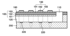
100...상부 기판 101...제1 실리콘층100 ...
102...중간 산화막 103...제2 실리콘층102
110...잉크 인렛 120...매니폴드110 ... ink inlet 120 ... manifold
125...격벽 130...압력 챔버125 Bulkhead 130 Pressure chamber
180...실리콘 산화막 190...압전 액츄에이터180
191...하부 전극 192...압전막191
193...상부 전극 200...하부 기판(노즐 플레이트)193 ...
210...노즐 211...댐퍼210 Nozzle 211 Damper
212...잉크 토출구 220...리스트릭터212
본 발명은 실리콘 습식 식각 방법에 관한 것으로, 더욱 상세하게는 패럴린 마스크를 이용하여 실리콘 기판을 습식 식각하는 방법과 이 방법을 이용하여 잉크젯 프린트 헤드의 노즐 플레이트를 제조하는 방법에 관한 것이다.The present invention relates to a silicon wet etching method, and more particularly, to a method of wet etching a silicon substrate using a paraline mask and a method of manufacturing a nozzle plate of an inkjet print head using the method.
일반적으로 실리콘 기판을 습식 식각 할 때에는, 식각 마스크로서 실리콘 산화막을 사용하고 있다. 상기 실리콘 산화막은 통상적으로 실리콘 기판을 대략 1000℃ 정도에서 열산화시킴에 의해 실리콘 기판의 표면에 소정 두께로 형성된다. 이어서, 포토레지스트를 이용하여 실리콘 산화막을 소정 패턴으로 패터닝 하여 식각 마스크를 형성한다. 이와 같이 실리콘 산화막으로 이루어진 식각 마스크를 이용하여 실리콘용 에칭액(etchant), 예컨대 테트라메틸 수산화 암모늄(TMAH: Tetramethyl Ammonium Hydroxide) 또는 수산화 칼륨(KOH)으로 실리콘 기판을 식각하게 된다. Generally, when wet etching a silicon substrate, a silicon oxide film is used as an etching mask. The silicon oxide film is typically formed to a predetermined thickness on the surface of the silicon substrate by thermally oxidizing the silicon substrate at about 1000 ° C. Subsequently, the silicon oxide film is patterned into a predetermined pattern using a photoresist to form an etching mask. As described above, the silicon substrate is etched using an etching mask made of silicon oxide, for example, tetramethyl ammonium hydroxide (TMAH) or potassium hydroxide (KOH).
상기한 습식 식각 공정에 의해 실리콘 기판에 홈, 트랜치 및 홀과 같은 요소를 두 개 이상 형성하는 경우가 있다. 이 경우, 상기 요소들의 종횡비 또는 깊이에 차이가 있을 경우에는, 두 번 또는 그 이상의 습식 식각 공정을 반복하여 수행하게 되며, 이에 필요한 식각 마스크도 두 번 이상 형성되어야 한다. 이에 따라, 식각 마스크로서 실리콘 산화막을 형성하기 위해 실리콘 기판은 반복되는 열산화 공정을 거치게 된다. The wet etching process may form two or more elements such as grooves, trenches, and holes in the silicon substrate. In this case, when there is a difference in aspect ratio or depth of the elements, two or more wet etching processes may be repeatedly performed, and an etching mask required for this may be formed more than once. Accordingly, the silicon substrate is subjected to a repeated thermal oxidation process to form the silicon oxide film as an etching mask.
그런데, 실리콘 기판에 대한 열산화 공정이 반복될수록, 실리콘 기판에는 산소 원자의 내부 침투로 인한 열적 결함이 발생될 가능성이 높아지게 된다. 이와 같이, 실리콘 기판 내부에 결함이 발생될 경우에는, 첫 번째 이후에 형성되는 요소에 대한 습식 식각 공정에서, 상기 결함이 발생된 부위와 그 부근에서의 식각 균일도가 저하되고, 이에 따라 그 부위에 형성되는 요소의 형상 균일도가 저하되는 문제 점이 발생하게 된다. However, as the thermal oxidation process for the silicon substrate is repeated, the silicon substrate becomes more likely to generate thermal defects due to the internal penetration of oxygen atoms. As described above, when a defect is generated in the silicon substrate, in the wet etching process of the element formed after the first, the etching uniformity at the portion where the defect is generated and in the vicinity thereof is lowered, thereby There arises a problem that the shape uniformity of the formed element is lowered.
본 발명은 상기와 같은 종래 기술의 문제점을 해결하기 위하여 창출된 것으로, 특히 상온에서 증착이 가능한 패럴린을 사용하여 식각 마스크를 형성함으로써 실리콘 기판에 대한 열적 결함을 방지하여 식각 균일성을 향상시킬 수 있는 실리콘 습식 식각 방법을 제공하는데 그 목적이 있다. The present invention has been made to solve the problems of the prior art as described above, in particular by forming an etching mask using a paraline that can be deposited at room temperature to prevent thermal defects on the silicon substrate to improve the etching uniformity The purpose of the present invention is to provide a silicon wet etching method.
또한, 본 발명은 상기한 실리콘 습식 식각 방법을 이용하여 잉크젯 프린트헤드의 노즐 플레이트를 제조하는 방법을 제공하는데 다른 목적이 있다. Another object of the present invention is to provide a method of manufacturing a nozzle plate of an inkjet printhead by using the silicon wet etching method described above.
상기의 기술적 과제를 달성하기 위한 본 발명에 따른 실리콘 습식 식각 방법은, Silicon wet etching method according to the present invention for achieving the above technical problem,
적어도 2회의 습식 식각 공정에 의해 실리콘 기판에 서로 다른 형상을 가진 적어도 두 개의 요소를 형성하는 실리콘 습식 식각 방법에 있어서, A silicon wet etching method in which at least two wet etching processes form at least two elements having different shapes on a silicon substrate,
상기 실리콘 기판의 표면에 패럴린으로 이루어진 1차 식각 마스크를 형성하는 단계; 상기 1차 식각 마스크를 이용하여 상기 실리콘 기판을 1차 습식 식각함으로써 제1 요소를 형성하는 단계; 상기 실리콘 기판의 표면에 실리콘 산화막으로 이루어진 2차 식각 마스크를 형성하는 단계; 및 상기 2차 식각 마스크를 이용하여 상기 실리콘 기판을 2차 습식 식각함으로써 제2 요소를 형성하는 단계;를 포함하는 것을 특징으로 한다.Forming a primary etch mask made of paraline on the surface of the silicon substrate; Forming a first element by first wet etching the silicon substrate using the first etching mask; Forming a second etching mask made of a silicon oxide film on a surface of the silicon substrate; And forming a second element by performing secondary wet etching on the silicon substrate using the secondary etching mask.
본 발명에 있어서, 상기 1차 식각 마스크 형성 단계는; 상기 실리콘 기판의 표면에 패럴린을 증착하여 패럴린 막을 형성하는 단계와, 상기 패럴린 막의 표면에 제1 포토레지스트를 도포한 뒤, 상기 제1 포토레지스트를 패터닝하여 상기 제1 요소를 형성하기 위한 제1 개구부를 형성하는 단계와, 상기 제1 개구부를 통해 노출된 부위의 상기 패럴린 막을 제거하여 상기 실리콘 기판의 표면을 부분적으로 노출시키는 단계와, 상기 제1 포토레지스트를 제거하는 단계를 포함할 수 있다, In the present invention, the first etching mask forming step; Depositing paraline on the surface of the silicon substrate to form a paraline film, applying a first photoresist on the surface of the paraline film, and then patterning the first photoresist to form the first element Forming a first opening, partially exposing the surface of the silicon substrate by removing the paraline film in a portion exposed through the first opening, and removing the first photoresist; Can be,
상기 패럴린 막의 부분적인 제거는 반응성 이온 식각(RIE) 또는 O2 에슁(ashing)에 의해 수행될 수 있다. Partial removal of the paraline membrane can be performed by reactive ion etching (RIE) or O 2 ashing.
상기 실리콘 기판에 대한 1차 습식 식각과 2차 습식 식각에 있어서, 실리콘용 에칭액(etchant)으로서 테트라메틸 수산화 암모늄(TMAH) 또는 수산화 칼륨(KOH)이 사용될 수 있다. In the first wet etching and the second wet etching of the silicon substrate, tetramethyl ammonium hydroxide (TMAH) or potassium hydroxide (KOH) may be used as an etchant for silicon.
본 발명에 있어서, 상기 2차 식각 마스크 형성 단계는; 상기 실리콘 기판의 표면에 실리콘 산화막을 형성하는 단계와, 상기 실리콘 산화막의 표면에 제2 포토레지스트를 도포한 뒤, 상기 제2 포토레지스트를 패터닝하여 상기 제2 요소를 형성하기 위한 제2 개구부를 형성하는 단계와, 상기 제2 개구부를 통해 노출된 부위의 상기 실리콘 산화막을 식각하여 상기 실리콘 기판의 표면을 부분적으로 노출시키는 단계와, 상기 제2 포토레지스트를 제거하는 단계를 포함할 수 있다. In the present invention, the second etching mask forming step; Forming a silicon oxide film on a surface of the silicon substrate, applying a second photoresist on the surface of the silicon oxide film, and then patterning the second photoresist to form a second opening for forming the second element And etching the silicon oxide layer of the portion exposed through the second opening to partially expose the surface of the silicon substrate, and removing the second photoresist.
상기 실리콘 산화막은 상기 실리콘 기판을 열산화시킴으로써 형성될 수 있다. The silicon oxide layer may be formed by thermally oxidizing the silicon substrate.
상기 실리콘 산화막에 대한 식각은 반응성 이온 식각(RIE) 또는 BOE(Buffered Oxide Etchant)를 사용한 습식 식각 방법에 의해 수행될 수 있다. The etching of the silicon oxide layer may be performed by a wet etching method using reactive ion etching (RIE) or buffered oxide etchant (BOE).
그리고, 상기의 기술적 과제를 달성하기 위한 본 발명에 따른 잉크젯 프린트헤드의 노즐 플레이트 제조 방법은, And, the nozzle plate manufacturing method of the inkjet printhead according to the present invention for achieving the above technical problem,
다수의 리스트릭터와 다수의 노즐을 가진 잉크젯 프린트헤드의 노즐 플레이트 제조 방법에 있어서,In the nozzle plate manufacturing method of an inkjet printhead having a plurality of restrictors and a plurality of nozzles,
실리콘 기판을 준비하는 단계; 상기 실리콘 기판의 상면에 패럴린으로 이루어진 1차 식각 마스크를 형성하는 단계; 상기 1차 식각 마스크를 이용하여 상기 실리콘 기판의 상면을 1차 습식 식각함으로써 상기 다수의 리스트릭터를 형성하는 단계; 상기 실리콘 기판의 상면에 실리콘 산화막으로 이루어진 2차 식각 마스크를 형성하는 단계; 상기 2차 식각 마스크를 이용하여 상기 실리콘 기판의 상면을 2차 습식 식각함으로써 상기 다수의 노즐 각각의 댐퍼를 형성하는 단계; 상기 실리콘 기판의 저면에 실리콘 산화막으로 이루어진 3차 식각 마스크를 형성하는 단계; 및 상기 3차 식각 마스크를 이용하여 상기 실리콘 기판의 저면을 건식 식각함으로써 상기 다수의 노즐 각각의 잉크 토출구를 상기 댐퍼와 연통되도록 형성하는 단계;를 포함하는 것을 특징으로 한다.Preparing a silicon substrate; Forming a primary etch mask made of paraline on the upper surface of the silicon substrate; Forming a plurality of restrictors by first wet etching the upper surface of the silicon substrate using the first etching mask; Forming a second etching mask made of a silicon oxide layer on an upper surface of the silicon substrate; Forming a damper of each of the plurality of nozzles by performing secondary wet etching on the upper surface of the silicon substrate using the secondary etching mask; Forming a tertiary etching mask made of a silicon oxide layer on a bottom surface of the silicon substrate; And forming an ink discharge port of each of the plurality of nozzles so as to communicate with the damper by dry etching the bottom surface of the silicon substrate using the tertiary etching mask.
본 발명에 있어서, 상기 1차 식각 마스크 형성 단계는; 상기 실리콘 기판의 상면에 패럴린을 증착하여 패럴린 막을 형성하는 단계와, 상기 패럴린 막의 표면에 제1 포토레지스트를 도포한 뒤, 상기 제1 포토레지스트를 패터닝하여 상기 다수의 리스트릭터를 형성하기 위한 다수의 제1 개구부를 형성하는 단계와, 상기 다수의 제1 개구부를 통해 노출된 부위의 상기 패럴린 막을 제거하여 상기 실리콘 기판의 상면을 부분적으로 노출시키는 단계와, 상기 제1 포토레지스트를 제거하는 단계를 포함할 수 있다.In the present invention, the first etching mask forming step; Depositing paraline on the upper surface of the silicon substrate to form a paraline film, applying a first photoresist to the surface of the paraline film, and then patterning the first photoresist to form the plurality of restrictors Forming a plurality of first openings, partially removing the paraline film in a portion exposed through the plurality of first openings, partially exposing the top surface of the silicon substrate, and removing the first photoresist It may include the step.
본 발명에 있어서, 상기 다수의 리스트릭터 각각의 모서리 부위는 라운드 형상으로 형성되는 것이 바람직하다. In the present invention, the corner portions of each of the plurality of restrictors are preferably formed in a round shape.
본 발명에 있어서, 상기 2차 식각 마스크 형성 단계는; 상기 실리콘 기판의 표면에 실리콘 산화막을 형성하는 단계와, 상기 실리콘 기판의 상면에 형성된 상기 실리콘 산화막의 상면에 제2 포토레지스트를 도포한 뒤, 상기 제2 포토레지스트를 패터닝하여 상기 다수의 댐퍼를 형성하기 위한 다수의 제2 개구부를 형성하는 단계와, 상기 다수의 제2 개구부를 통해 노출된 부위의 상기 실리콘 산화막을 식각하여 상기 실리콘 기판의 상면을 부분적으로 노출시키는 단계와, 상기 제2 포토레지스트를 제거하는 단계를 포함할 수 있다.In the present invention, the second etching mask forming step; Forming a plurality of dampers by forming a silicon oxide film on a surface of the silicon substrate, applying a second photoresist to an upper surface of the silicon oxide film formed on an upper surface of the silicon substrate, and then patterning the second photoresist. Forming a plurality of second openings, etching the silicon oxide film in a portion exposed through the plurality of second openings to partially expose the top surface of the silicon substrate, and It may include the step of removing.
본 발명에 있어서, 상기 3차 식각 마스크 형성 단계는; 상기 실리콘 기판의 표면에 실리콘 산화막을 형성하는 단계와, 상기 실리콘 기판의 저면에 형성된 상기 실리콘 산화막의 저면에 제3 포토레지스트를 도포한 뒤, 상기 제3 포토레지스트를 패터닝하여 상기 다수의 잉크 토출구를 형성하기 위한 다수의 제3 개구부를 형성하는 단계와, 상기 다수의 제3 개구부를 통해 노출된 부위의 상기 실리콘 산화막을 식각하여 상기 실리콘 기판의 저면을 부분적으로 노출시키는 단계와, 상기 제3 포토레지스트를 제거하는 단계를 포함할 수 있다. In the present invention, the third etching mask forming step; Forming a silicon oxide film on a surface of the silicon substrate, applying a third photoresist to a bottom surface of the silicon oxide film formed on a bottom surface of the silicon substrate, and then patterning the third photoresist to form the plurality of ink discharge ports. Forming a plurality of third openings for forming, etching the silicon oxide film in a portion exposed through the plurality of third openings to partially expose a bottom surface of the silicon substrate, and It may include the step of removing.
본 발명에 있어서, 상기 실리콘 기판에 대한 건식 식각은 ICP RIE 방법에 의해 수행될 수 있다. In the present invention, the dry etching on the silicon substrate may be performed by the ICP RIE method.
이하, 첨부된 도면을 참조하면서 본 발명의 바람직한 실시예를 상세히 설명한다. 도면에서 동일한 참조부호는 동일한 구성요소를 지칭하며, 도면상에서 각 구성요소의 크기는 설명의 명료성과 편의상 과장되어 있을 수 있다. Hereinafter, exemplary embodiments of the present invention will be described in detail with reference to the accompanying drawings. In the drawings, like reference numerals refer to like elements, and the size of each element may be exaggerated for clarity and convenience of description.
그리고, 본 발명에 따른 실리콘 습식 식각 방법에 대한 설명을 용이하게 하기 위하여, 압전 방식의 잉크젯 프린트헤드의 노즐 플레이트를 예로 들어 본 발명을 설명하기로 한다. 일반적으로 잉크젯 프린트헤드는, 인쇄용 잉크의 미소한 액적(droplet)을 기록매체 상의 원하는 위치에 토출시켜서 소정 색상의 화상으로 인쇄하는 장치이다. 이러한 잉크젯 프린트헤드는 잉크 토출 방식에 따라 크게 두 가지로 나뉠 수 있다. 그 하나는 열원을 이용하여 잉크에 버블(bubble)을 발생시켜 그 버블의 팽창력에 의해 잉크를 토출시키는 열구동 방식의 잉크젯 프린트헤드이고, 다른 하나는 압전체를 사용하여 그 압전체의 변형으로 인해 잉크에 가해지는 압력에 의해 잉크를 토출시키는 압전 방식의 잉크젯 프린트헤드이다. And, in order to facilitate the description of the silicon wet etching method according to the present invention, the present invention will be described taking the nozzle plate of the piezoelectric inkjet printhead as an example. In general, an inkjet printhead is a device that prints an image of a predetermined color by ejecting a small droplet of printing ink to a desired position on a recording medium. Such inkjet printheads can be classified into two types according to ink ejection methods. One is a heat-driven inkjet printhead that generates bubbles in the ink by using a heat source and discharges the ink by the expansion force of the bubbles. The other is a piezoelectric inkjet printhead. It is a piezoelectric inkjet printhead which discharges ink by an applied pressure.
그러나, 본 발명은 이하에서 도시되고 설명되는 구체적인 실시예에 한정되지 아니하며, 실리콘 기판에 홈, 트랜치 및 홀 등을 포함하는 다양한 형상의 요소를 적어도 두 개 이상 형성하는 경우에도 적용될 수 있다. However, the present invention is not limited to the specific embodiments shown and described below, and may be applied to the case where at least two elements of various shapes including grooves, trenches and holes are formed in the silicon substrate.
도 1a는 본 발명에 따른 실리콘 습식 식각 방법이 구체적으로 적용된 압전 방식의 잉크젯 프린트헤드를 부분 절단하여 나타낸 분해 사시도이고, 도 1b는 도 1a에 표시된 A-A'선을 따른 프린트헤드의 수직 단면도이며, 도 1c는 도 1b에 표시된 B-B'선을 따른 프린트헤드의 수직 단면도이다.FIG. 1A is an exploded perspective view illustrating a partially cut piezoelectric inkjet printhead to which the silicon wet etching method according to the present invention is specifically applied, and FIG. 1B is a vertical cross-sectional view of the printhead along the line AA ′ of FIG. 1A. FIG. 1C is a vertical sectional view of the printhead along the line BB ′ shown in FIG. 1B.
도 1a 내지 도 1c를 함께 참조하면, 압전 방식의 잉크젯 프린트헤드는, 두 개의 기판, 즉 상부 기판(100)과 하부 기판(200)을 접합함으로써 이루어질 수 있다. 그리고, 상기 상부 기판(100)과 하부 기판(200)에는 잉크 유로가 형성되며, 상부 기판(100)의 상면에는 잉크의 토출을 위한 구동력을 발생시키는 압전 액츄에이터(190)가 마련될 수 있다. 1A to 1C, the piezoelectric inkjet printhead may be formed by bonding two substrates, that is, the
상기 두 개의 기판(100, 200)은 모두 단결정 실리콘 웨이퍼로 이루어진다. 이에 따라, 포토리소그라피(photolithography)와 식각(etching)과 같은 미세 가공(micromachining) 기술을 이용하여 두 개의 기판(100, 200)에 잉크 유로를 이루게 되는 구성 요소들을 보다 미세한 크기로 정밀하고 용이하게 형성할 수 있다. 특히, 상기 상부 기판(100)은 SOI(Silicon-On-Insulator) 웨이퍼로 이루어질 수 있다. SOI 웨이퍼는 일반적으로 제1 실리콘층(101)과, 제1 실리콘층(101) 상에 형성된 중간 산화막(102)과, 중간 산화막(102) 상에 접착되는 제2 실리콘층(103)의 적층 구조를 가지고 있다. The two
상기한 잉크 유로는, 도시되지 않은 잉크 저장고로부터 잉크가 유입되는 잉크 인렛(110)과, 토출될 잉크가 채워지며 잉크를 토출시키기 위한 압력 변화를 발생시키는 다수의 압력 챔버(130)와, 상기 잉크 인렛(110)을 통해 유입된 잉크를 다수의 압력 챔버(130)에 공급하는 공통 유로인 매니폴드(120)와, 상기 매니폴드(120)로부터 각각의 압력 챔버(130)로 잉크를 공급하기 위한 개별 유로인 리스트릭터(220)와, 상기 압력 챔버(130)로부터 잉크가 토출되는 노즐(210)을 포함한다. 이러한 잉크 유로를 형성하는 구성요소들은 상술한 바와 같이 두 개의 기판(100, 200)에 나뉘어져 배치된다. The ink flow path includes an
구체적으로, 상부 기판(100)에는 상기 잉크 인렛(110), 매니폴드(120) 및 다수의 압력 챔버(130)가 형성된다. 상기 매니폴드(120)는 상부 기판(100)의 저면에 소정 깊이로 형성되며, 일방향으로 길게 연장된 형상을 가진다. 상기 잉크 인렛(110)은 상부 기판(100)을 수직으로 관통하여 형성되어 상기 매니폴드(120)의 일단부에 연결된다. 상기 다수의 압력 챔버(130)는 상부 기판(100)의 저면에 소정 깊이로 형성되며, 상기 매니폴드(120)의 양측에 2 열로 배열된다. 그리고, 상기 매니폴드(120)의 내부에는 상기 매니폴드(120)를 좌우로 분리시켜 압력 챔버(130) 상호간의 크로스 토크(cross-talk)를 방지하기 위한 격벽(125)이 그 길이방향으로 길게 형성될 수 있다. Specifically, the
상기 상부 기판(100) 위에는 압전 액츄에이터(190)가 형성된다. 그리고, 상부 기판(100)과 압전 액츄에이터(190) 사이에는 절연막으로서 실리콘 산화막(180)이 형성될 수 있다. 상기 압전 액츄에이터(190)는 공통 전극의 역할을 하는 하부 전극(191)과, 전압의 인가에 따라 변형되는 압전막(192)과, 구동 전극의 역할을 하는 상부 전극(193)을 구비한다. A
상기 하부 기판(200), 즉 노즐 플레이트에는, 상기 매니폴드(120)와 다수의 압력 챔버(130) 각각의 일단부를 연결하는 개별 유로인 다수의 리스트릭터(220)와, 잉크를 토출하기 위한 다수의 노즐(210)이 형성된다. 상기 하부 기판(200)은 반도체 집적회로의 제조에 널리 사용되는 단결정 실리콘 웨이퍼로 이루어지며, 수백 ㎛의 두께, 예컨대 대략 245㎛ 정도의 두께를 가진다. The
상기 다수의 리스트릭터(220) 각각은 상기 하부 기판(200)의 상면에 소정 깊 이, 예컨대 20㎛ ~ 40㎛ 정도의 깊이로 형성되며, 그 일단은 매니폴드(120)에 연결되고 그 타단은 압력 챔버(130)에 연결된다. 이러한 리스트릭터(220)는 매니폴드(120)로부터 압력 챔버(130)로 적정 량의 잉크를 공급하는 역할 뿐만 아니라, 잉크가 토출될 때 압력 챔버(130)로부터 매니폴드(120)쪽으로 잉크가 역류하는 것을 억제하는 역할도 하게 된다. Each of the plurality of
상기 다수의 노즐(210) 각각은 상기 다수의 압력 챔버(130) 각각의 타단부에 대응하는 위치에 상기 하부 기판(200)을 수직으로 관통하도록 형성된다. 상기 노즐(210)은, 하부 기판(200)의 윗 부분에 형성된 댐퍼(211)와, 하부 기판(200)의 아래 부분에 형성되며 잉크가 토출되는 잉크 토출구(212)로 이루어질 수 있다. 상기 잉크 토출구(212)는 일정한 직경을 가진 수직 홀의 형상으로 형성될 수 있고, 상기 댐퍼(211)는 압력 챔버(130)로부터 잉크 토출구(212)쪽으로 가면서 점차 그 단면적이 감소하는 피라미드 형상으로 형성될 수 있다. Each of the plurality of
상기한 바와 같이 형성된 두 개의 기판(100, 200)은 전술한 바와 같이 적층되어 서로 접합됨으로써 본 발명에 따른 압전 방식의 잉크젯 프린트 헤드를 구성하게 된다. 그리고, 두 개의 기판(100, 200) 내부에는 잉크 인렛(110), 매니폴드(120), 리스트릭터(220), 압력 챔버(130) 및 노즐(210)이 차례대로 연결되어 이루어진 잉크 유로가 형성된다. The two
이하에서는, 상기한 구성을 가진 잉크젯 프린트헤드의 노즐 플레이트를 본 발명에 따른 실리콘 습식 식각 방법에 의해 제조하는 방법을 설명하기로 한다.Hereinafter, a method of manufacturing the nozzle plate of the inkjet printhead having the above-described configuration by the silicon wet etching method according to the present invention will be described.
도 2a 내지 도 2d는 실리콘 기판의 표면에 실리콘 습식 식각용 마스크로서 패럴린 마스크를 형성하는 단계를 설명하기 위한 도면들이다. 2A to 2D are diagrams for describing a step of forming a paraline mask as a silicon wet etching mask on a surface of a silicon substrate.
도 2a를 참조하면, 잉크젯 프린트헤드의 하부 기판(도 1a의 200, 이하 노즐 플레이트라고 한다)은 단결정 실리콘 기판으로 이루어진다. 먼저, 대략 650㎛ 두께의 실리콘 기판(200')을 준비한다. 이어서, 실리콘 기판(200')을 화학적-기계적 연마(CMP: Chemical-Mechanical Polishing)에 의해 그 두께를 대략 245㎛ 정도로 감소시킨 다음, 실리콘 기판(200') 전체를 클리닝 한다. 이때, 실리콘 기판(200')의 클리닝에는 아세톤과 이소프로필 알콜(IPA) 등을 사용한 유기 클리닝 방법과, 황산과 BOE(Buffered Oxide Etchant) 등을 사용한 산 클리닝 방법과, SC1 클리닝 방법이 사용될 수 있다. Referring to FIG. 2A, the lower substrate (200 in FIG. 1A, hereinafter referred to as nozzle plate) of the inkjet printhead is made of a single crystal silicon substrate. First, a
이와 같이 클리닝 된 실리콘 기판(200')의 표면에 소정 두께의 패럴린 막(parylene layer, 251)을 형성한다. 상기 패럴린은 반도체 산업 분야에서 코팅 물질로 널리 사용되는 화학물질이며, 상온(room temperature)에서 실리콘 기판(200')의 표면에 용이하게 증착되는 장점이 있다. A
다음으로, 도 2b에 도시된 바와 같이, 실리콘 기판(200') 상면에 형성된 패럴린 막(251)의 표면에 제1 포토레지스트(PR1)를 도포한다. 이어서, 도포된 제1 포토레지스트(PR1)를 패터닝함으로써 실리콘 기판(200')의 상면에 다수의 리스트릭터(도 1a의 220)를 형성하기 위한 다수의 제1 개구부(220')를 형성한다. 이때, 제1 포토레지스트(PR1)의 패터닝은 노광과 현상을 포함하는 잘 알려진 포토리소그라피(photolithography) 방법에 의해 이루어질 수 있으며, 이하에서 설명되는 다른 포 토레지스트들의 패터닝도 이와 동일한 방법으로 이루어질 수 있다.Next, as shown in FIG. 2B, the first photoresist PR 1 is coated on the surface of the
다음으로, 도 2c에 도시된 바와 같이, 상기 다수의 제1 개구부(220')를 통해 노출된 부위의 패럴린 막(251)을 제1 포토레지스트(PR1)를 식각 마스크로 하여 반응성 이온 식각(RIE: Reactive Ion Etching) 또는 O2 에슁(ashing)에 의해 식각함으로써, 실리콘 기판(200')의 상면을 부분적으로 노출시킨다. 이어서, 상기한 유기 클리닝 방법 및/또는 산 클리닝 방법에 의해 상기 제1 포토레지스트(PR1)를 제거한다. 이때, 상기 제1 포토레지스트(PR1)는 에슁(ashing)에 의해 제거될 수도 있다. 이와 같은 제1 포토레지스트(PR1)의 제거 방법은 이하에서 설명되는 다른 포토레지스트들의 제거에도 이용될 수 있다. Next, as illustrated in FIG. 2C, reactive ion etching is performed by using the
상기한 바와 같은 단계들을 거치게 되면, 도 2d에 도시된 바와 같이, 실리콘 기판(200')의 상면에 패럴린 막(251)으로 이루어진 1차 식각 마스크가 형성된다. After the above-described steps, as shown in FIG. 2D, a primary etching mask made of a
도 3은 패럴린 마스크를 사용하여 실리콘 기판을 1차 습식 식각하는 단계를 설명하기 위한 도면이다. FIG. 3 is a diagram for describing a first wet etching process of a silicon substrate using a paraline mask.
도 3을 참조하면, 패럴린 막(251)을 1차 식각 마스크로 하여 노출된 부위의 실리콘 기판(200')의 상면을 1차 습식 식각함으로써 다수의 리스트릭터(220)를 소정 깊이를 가진 홈 형상으로 형성한다. 이때, 실리콘 기판(200')에 대한 습식 식각은 실리콘용 에칭액(etchant)으로서, 예컨대 테트라메틸 수산화 암모늄(TMAH: Tetramethyl Ammonium Hydroxide) 또는 수산화 칼륨(KOH)을 사용할 수 있다. 이때, 상기 다수의 리스트릭터(220) 각각의 측면은 경사지게 형성되고, 그 모서리는 둥글게 형성되는데, 이에 대해서는 뒤에서 도 7a 내지 도 7d를 참조하며 다시 설명하기로 한다. Referring to FIG. 3, the plurality of
실리콘 기판(200')에 대한 1차 습식 식각이 완료되면, 상기 패럴린 막(251)을 제거한다. 이때, 패럴린 막(251)은 반응성 이온 식각(RIE) 또는 O2 에슁(ashing)에 의해 제거될 수 있다. When the first wet etching of the
도 4a 내지 도 4d는 실리콘 기판의 표면에 실리콘 산화막으로 이루어진 식각 마스크를 형성하는 단계를 설명하기 위한 도면들이다. 4A to 4D are diagrams for describing a step of forming an etching mask made of a silicon oxide film on a surface of a silicon substrate.
도 4a를 참조하면, 상기한 바와 같이 다수의 리스트릭터(220)가 형성된 실리콘 기판(200')의 표면에 소정 두께의 실리콘 산화막(252)을 형성한다. 상기 실리콘 산화막(252)은 실리콘 기판(200')을 대략 1000℃ 정도에서 열산화시킴으로써 형성될 수 있다. Referring to FIG. 4A, as described above, the
다음으로, 도 4b에 도시된 바와 같이, 실리콘 기판(200') 상면에 형성된 실리콘 산화막(252)의 표면에 제2 포토레지스트(PR2)를 도포한다. 이어서, 도포된 제2 포토레지스트(PR2)를 패터닝함으로써 실리콘 기판(200')의 상면에 노즐(도 1a의 210)의 댐퍼(도 1a의 211)를 형성하기 위한 다수의 제2 개구부(211')를 형성한다. Next, as shown in FIG. 4B, the second photoresist PR 2 is coated on the surface of the
다음으로, 도 4c에 도시된 바와 같이, 제2 포토레지스트(PR2)를 식각 마스크로 하여 상기 다수의 제2 개구부(211')를 통해 노출된 부위의 실리콘 산화막(252)을 식각함으로써 실리콘 기판(200')의 상면을 부분적으로 노출시킨다. 이때, 실리 콘 산화막(252)에 대한 식각은 반응성 이온 식각(RIE)과 같은 건식 식각 방법 또는 BOE(Buffered Oxide Etchant)를 사용한 습식 식각 방법에 의해 수행될 수 있다. 이어서, 상기한 유기 클리닝 방법 및/또는 산 클리닝 방법에 의해 상기 제2 포토레지스트(PR2)를 제거할 수 있다. 이때, 상기 제2 포토레지스트(PR2)는 에슁(ashing)에 의해 제거될 수도 있다. Next, as illustrated in FIG. 4C, the
상기한 바와 같은 단계들을 거치게 되면, 도 4d에 도시된 바와 같이, 실리콘 기판(200')의 상면에 실리콘 산화막(252)으로 이루어진 2차 식각 마스크가 형성된다. After the above steps, as illustrated in FIG. 4D, a secondary etching mask made of the
도 5는 실리콘 산화막 마스크를 사용하여 실리콘 기판을 2차 습식 식각하는 단계를 설명하기 위한 도면이다. FIG. 5 is a diagram for describing a second wet etching process of a silicon substrate using a silicon oxide mask.
도 5를 참조하면, 실리콘 산화막(252)을 2차 식각 마스크로 하여 노출된 부위의 실리콘 기판(200')의 상면을 소정 깊이, 예컨대 230㎛ ~ 235㎛ 정도의 깊이로 2차 습식 식각함으로써, 다수의 노즐(210) 각각의 댐퍼(211)를 형성한다. 이때, 실리콘 기판(200')에 대한 습식 식각은 실리콘용 에칭액(etchant)으로서, 예컨대 테트라메틸 수산화 암모늄(TMAH: Tetramethyl Ammonium Hydroxide) 또는 수산화 칼륨(KOH)을 사용할 수 있다. 그러면, 실리콘 기판(200') 내부의 결정면에 따른 이방성 습식 식각 특성에 의해, 도 1a에 도시된 바와 같이 피라미드 형태의 댐퍼(211)가 형성될 수 있다.Referring to FIG. 5, by wet etching the upper surface of the exposed
도 6a 내지 도 6c는 실리콘 기판의 저면에 노즐의 잉크 토출구를 형성하는 단계들을 설명하기 위한 도면들이다. 6A to 6C are diagrams for describing steps of forming an ink discharge port of a nozzle on a bottom surface of a silicon substrate.
도 6a를 참조하면, 실리콘 기판(200')의 저면에 형성된 실리콘 산화막(252) 표면에 제3 포토레지스트(PR3)를 도포한다. 이어서, 도포된 제3 포토레지스트(PR3)를 패터닝하여 실리콘 기판(200')의 저면에 노즐(210)의 잉크 토출구(도 1a의 212)를 형성하기 위한 제3 개구부(221')를 형성한다. Referring to FIG. 6A, a third photoresist PR 3 is coated on the surface of the
다음으로, 도 6b에 도시된 바와 같이, 상기 제3 개구부(212')를 통해 노출된 부위의 실리콘 산화막(252)을 제3 포토레지스트(PR3)를 식각 마스크로 하여 습식 식각 또는 건식 식각하여 제거함으로써 실리콘 기판(200')의 저면을 부분적으로 노출시킨 후, 상기 제3 포토레지스트(PR3)를 제거한다. Next, as shown in FIG. 6B, wet etching or dry etching of the
다음에는, 도 6c에 도시된 바와 같이, 실리콘 기판(220')의 저면에 형성된 실리콘 산화막(252)을 3차 식각 마스크로 하여 노출된 부위의 실리콘 기판(200')을 관통되도록 식각함으로써, 상기 댐퍼(211)와 연통되는 잉크 토출구(212)를 형성한다. 이때, 실리콘 기판(200')의 식각은 ICP RIE 방법을 이용한 건식 식각에 의해 수행될 수 있다. Next, as illustrated in FIG. 6C, the
이로써, 실리콘 기판(200')의 상면에 형성된 다수의 리스트릭터(220)와 실리콘 기판(200')을 관통하여 형성된 다수의 노즐(210)을 가진 노즐 플레이트(200)가 완성된다.As a result, the
상기한 바와 같이, 본 발명에 따른 실리콘 습식 식각 방법에서는 패럴린 마스크를 이용하여 1차 습식 식각 공정을 수행하므로, 실리콘 기판(200')에 대한 열 산화 공정의 회수가 줄어들게 된다. 따라서, 열산화 공정에 의해 발생될 수 있는 실리콘 기판(200') 내부의 열적 결함이 방지되거나 줄어들 수 있으므로, 2차 습식 식각에 의해 형성되는 댐퍼(211)의 형상 균일도가 향상될 수 있다. 또한, 댐퍼(211)의 형상 균일도가 향상되면, 이에 따라 잉크 토출구(212)의 길이도 균일하게 형성될 수 있어서 잉크 토출 성능이 향상된다. 이에 대해서는, 뒤에서 도 8을 참조하여 다시 설명하기로 한다. As described above, in the silicon wet etching method according to the present invention, since the first wet etching process is performed using a paraline mask, the number of thermal oxidation processes on the
도 7a 내지 도 7d는 본 발명에 따라 도 3에 도시된 단계에서 형성된 리스트릭터의 형상과 종래의 방법에 의해 형성된 리스트릭터의 형상을 비교하여 보여주는 도면들이다. 7A to 7D are diagrams showing the shape of the restrictor formed in the step shown in FIG. 3 according to the present invention and the shape of the restrictor formed by a conventional method.
도 7a와 도 7b는 본 발명에 따라 패럴린 마스크를 이용하는 습식 식각 공정에 의해 형성된 리스트릭터의 평면과 단면 형상을 보여주며, 도 7c와 도 7d는 종래 기술에 의해 실리콘 산화막 마스크를 이용하는 습식 식각 공정에 의해 형성된 리스트릭터의 평면과 단면 형상을 보여준다. 7A and 7B show a planar and cross-sectional shape of a restrictor formed by a wet etching process using a paraline mask according to the present invention, and FIGS. 7C and 7D show a wet etching process using a silicon oxide mask according to the prior art. It shows the plane and cross-sectional shape of the list formed by.
실리콘 기판 내부의 결정면에 따른 이방성 습식 식각 특성에 의해, 리스트릭터의 측면은 경사면으로 형성된다. 구체적으로, 리스트릭터의 저면은 결정면에 대한 밀러 지수가 (100)이고, 리스트릭터의 측면은 그 밀러 지수가 (110)이다. Due to the anisotropic wet etching characteristic along the crystal plane inside the silicon substrate, the side surface of the restrictor is formed as an inclined plane. Specifically, the bottom of the list has a Miller index for the crystal plane (100) and the side of the list has its Miller index (110).
그런데, 종래 기술에 있어서, 실리콘 산화막은 실리콘 기판과의 접합성이 매우 우수하여, 습식 식각 시에 실리콘 산화막 아래 부분에서의 수평 방향 식각이 매우 적게 이루어진다. 따라서, 도 7c와 도 7d에 도시된 바와 같이, 리스트릭터의 길이 방향 측면과 폭 방향 측면이 거의 직각으로 만나게 되어 리스트릭터의 평면 형 상이 직사각형을 이루게 된다. 이 경우, 잉크가 리스트릭터를 통과할 때 리스트릭터의 뾰족한 모서리 부위에 버블이 트랩될 수 있는 문제점이 있다. By the way, in the prior art, the silicon oxide film has a very good bonding property with the silicon substrate, so that the horizontal etching in the portion under the silicon oxide film is very small during the wet etching. Therefore, as shown in FIGS. 7C and 7D, the longitudinal side and the width side of the restrictor meet at a right angle to form a rectangular shape of the restrictor. In this case, there is a problem that bubbles may be trapped at the pointed corners of the restrictor when the ink passes through the restrictor.
그러나, 본 발명에 있어서는, 실리콘 기판에 대한 패럴린 막의 접합성이 실리콘 산화막에 비해 약하므로, 패럴린 막 아래 부분에서의 수평 방향 식각이 보다 쉽게 이루어지게 된다. 이에 따라, 도 7a와 도 7b에 도시된 바와 같이, 리스트릭터의 모서리 부위가 라운드한 형상으로 이루어질 수 있다. 이 경우, 잉크가 리스트릭터를 통과할 때 버블이 그 모서리 부위에 트랩되는 현상이 최소화될 수 있다.However, in the present invention, since the adhesion of the paraline film to the silicon substrate is weaker than that of the silicon oxide film, the horizontal etching in the portion below the paraline film becomes easier. Accordingly, as shown in FIGS. 7A and 7B, the edge portion of the restrictor may have a rounded shape. In this case, when the ink passes through the restrictor, bubbles trapped at the corners thereof can be minimized.
도 8은 본 발명에 따라 형성된 댐퍼의 균일도와 종래의 방법에 의해 형성된 댐퍼의 균일도를 비교하여 보여주는 그래프이다. 8 is a graph showing the uniformity of the damper formed according to the present invention and the uniformity of the damper formed by a conventional method.
도 8을 보면, 종래 기술에 의해 형성된 댐퍼의 가로와 세로의 수치에 대한 균일도(uniformity)가 대략 0.7~0.8%로서 비교적 높은 수치를 나타내는데 반하여, 본 발명에 의해 형성된 댐퍼의 가로와 세로 수치에 대한 균일도는 대략 0.2~0.3%로서 매우 낮은 수치를 나타냄을 알 수 있다. 여기에서, 균일도는 표준편차/평균으로 나타내므로, 균일도의 수치가 낮을수록 댐퍼의 균일도는 보다 우수하다는 것을 나타낸다. 따라서, 본 발명에 의해 형성된 댐퍼의 균일도가 종래 기술에 의해 형성된 댐퍼의 균일도에 비해 훨씬 우수하다는 것을 알 수 있다. Referring to FIG. 8, while the uniformity of the horizontal and vertical values of the dampers formed by the prior art is about 0.7 to 0.8%, indicating relatively high values, the horizontal and vertical values of the dampers formed by the present invention are shown. The uniformity is about 0.2 ~ 0.3%, it can be seen that the very low value. Here, since uniformity is expressed as standard deviation / average, the lower the uniformity value, the better the damper uniformity is. Thus, it can be seen that the uniformity of the dampers formed by the present invention is much superior to the uniformity of dampers formed by the prior art.
이상에서 설명한 바와 같이, 본 발명에 따른 실리콘 습식 식각 방법에 있어서는, 상온에서 증착이 가능한 패럴린 마스크를 이용하여 1차 습식 식각 공정을 수행하므로, 실리콘 기판에 대한 열산화 공정의 회수가 줄어들게 되어 열산화 공정에 의해 발생될 수 있는 실리콘 기판 내부의 열적 결함이 최소화될 수 있다. 따라서, 습식 식각 공정에 의해 형성되는 요소들의 형상 균일도가 향상되는 장점이 있다. As described above, in the silicon wet etching method according to the present invention, since the first wet etching process is performed by using a paraline mask that can be deposited at room temperature, the number of thermal oxidation processes on the silicon substrate is reduced, and thus heat is reduced. Thermal defects inside the silicon substrate, which may be caused by the oxidation process, can be minimized. Therefore, there is an advantage that the shape uniformity of the elements formed by the wet etching process is improved.
그리고, 패럴린 마스크를 이용하여 노즐 플레이트의 표면에 리스트릭터를 형성하게 되면, 리스트릭터의 모서리 부위가 라운드한 형상으로 이루어질 수 있다. 따라서, 잉크가 리스트릭터를 통과할 때 버블이 그 모서리 부위에 트랩되는 문제점이 해소될 수 있는 장점이 있다. Then, when the restrictor is formed on the surface of the nozzle plate using the paraline mask, the corner portion of the restrictor may have a rounded shape. Therefore, there is an advantage that the problem that the bubble is trapped in the corner portion when the ink passes through the restrictor can be solved.
이상 본 발명의 바람직한 실시예를 상세히 설명했지만, 이는 예시적인 것에 불과하며, 당해 분야에서 통상적 지식을 가진 자라면 이로부터 다양한 변형 및 균등한 타 실시예가 가능하다는 점을 이해할 것이다. 예컨대, 위에서 도시되고 설명된 압전 방식의 잉크젯 프린트헤드는 본 발명을 용이하게 설명하기 위해 예시한 것으로서, 본 발명의 범위가 이에 한정되지는 않는다. 즉, 본 발명은 다양한 종류의 잉크젯 프린트헤드의 노즐 플레이트에 적용될 수 있다. 또한, 본 발명은 실리콘 기판에 리스트릭터와 같은 홈과 노즐과 같은 홀뿐만 아니라 트랜치 등을 포함하는 다양한 형상의 요소를 적어도 2 회의 습식 식각 공정에 의해 형성하는 경우에도 적용될 수 있다. 따라서, 본 발명의 진정한 기술적 보호 범위는 첨부된 특허청구범위에 의해서 정해져야 할 것이다.While the preferred embodiments of the present invention have been described in detail, these are merely exemplary, and those skilled in the art will understand that various modifications and equivalent other embodiments are possible therefrom. For example, the piezoelectric inkjet printhead shown and described above is exemplified for easily explaining the present invention, and the scope of the present invention is not limited thereto. That is, the present invention can be applied to nozzle plates of various types of inkjet printheads. The invention can also be applied to the formation of elements of various shapes, including trenches, such as restrictors and trenches, as well as trenches, in at least two wet etching processes in a silicon substrate. Therefore, the true technical protection scope of the present invention will be defined by the appended claims.
Claims (17)
Priority Applications (3)
| Application Number | Priority Date | Filing Date | Title |
|---|---|---|---|
| KR1020050121124A KR20070060924A (en) | 2005-12-09 | 2005-12-09 | Silicon wet etching method using parylene mask and method of manufacturing nozzle plate of inkjet printhead using the wet etching method |
| US11/505,416 US20070134928A1 (en) | 2005-12-09 | 2006-08-17 | Silicon wet etching method using parylene mask and method of manufacturing nozzle plate of inkjet printhead using the same |
| JP2006282750A JP2007160927A (en) | 2005-12-09 | 2006-10-17 | Silicon wet etching process using parylene mask and method for producing nozzle plate of ink jet printhead using this process |
Applications Claiming Priority (1)
| Application Number | Priority Date | Filing Date | Title |
|---|---|---|---|
| KR1020050121124A KR20070060924A (en) | 2005-12-09 | 2005-12-09 | Silicon wet etching method using parylene mask and method of manufacturing nozzle plate of inkjet printhead using the wet etching method |
Publications (1)
| Publication Number | Publication Date |
|---|---|
| KR20070060924A true KR20070060924A (en) | 2007-06-13 |
Family
ID=38139967
Family Applications (1)
| Application Number | Title | Priority Date | Filing Date |
|---|---|---|---|
| KR1020050121124A KR20070060924A (en) | 2005-12-09 | 2005-12-09 | Silicon wet etching method using parylene mask and method of manufacturing nozzle plate of inkjet printhead using the wet etching method |
Country Status (3)
| Country | Link |
|---|---|
| US (1) | US20070134928A1 (en) |
| JP (1) | JP2007160927A (en) |
| KR (1) | KR20070060924A (en) |
Cited By (2)
| Publication number | Priority date | Publication date | Assignee | Title |
|---|---|---|---|---|
| US8556382B2 (en) | 2008-11-27 | 2013-10-15 | Samsung Electronics Co., Ltd. | Nozzle plate and method of manufacturing the same |
| KR20210096891A (en) * | 2020-01-29 | 2021-08-06 | 주식회사 오럼머티리얼 | Mask and producing method thereof |
Families Citing this family (2)
| Publication number | Priority date | Publication date | Assignee | Title |
|---|---|---|---|---|
| ATE502396T1 (en) * | 2006-12-12 | 2011-04-15 | Nxp Bv | METHOD FOR PRODUCING OPENINGS IN A SUBSTRATE, IN PARTICULAR THROUGH HOLES THROUGH A SUBSTRATE |
| US7531047B1 (en) * | 2007-12-12 | 2009-05-12 | Lexmark International, Inc. | Method of removing residue from a substrate after a DRIE process |
Family Cites Families (5)
| Publication number | Priority date | Publication date | Assignee | Title |
|---|---|---|---|---|
| US5243756A (en) * | 1991-06-28 | 1993-09-14 | Digital Equipment Corporation | Integrated circuit protection by liquid encapsulation |
| JPH09267472A (en) * | 1996-03-29 | 1997-10-14 | Seiko Epson Corp | Ink jet head |
| JP2001189324A (en) * | 1999-12-28 | 2001-07-10 | Ricoh Co Ltd | Semiconductor device |
| US6716661B2 (en) * | 2002-05-16 | 2004-04-06 | Institute Of Microelectronics | Process to fabricate an integrated micro-fluidic system on a single wafer |
| JP4363150B2 (en) * | 2003-10-14 | 2009-11-11 | セイコーエプソン株式会社 | Method for manufacturing droplet discharge head |
-
2005
- 2005-12-09 KR KR1020050121124A patent/KR20070060924A/en not_active Application Discontinuation
-
2006
- 2006-08-17 US US11/505,416 patent/US20070134928A1/en not_active Abandoned
- 2006-10-17 JP JP2006282750A patent/JP2007160927A/en active Pending
Cited By (2)
| Publication number | Priority date | Publication date | Assignee | Title |
|---|---|---|---|---|
| US8556382B2 (en) | 2008-11-27 | 2013-10-15 | Samsung Electronics Co., Ltd. | Nozzle plate and method of manufacturing the same |
| KR20210096891A (en) * | 2020-01-29 | 2021-08-06 | 주식회사 오럼머티리얼 | Mask and producing method thereof |
Also Published As
| Publication number | Publication date |
|---|---|
| US20070134928A1 (en) | 2007-06-14 |
| JP2007160927A (en) | 2007-06-28 |
Similar Documents
| Publication | Publication Date | Title |
|---|---|---|
| KR101153562B1 (en) | Piezoelectric inkjet printhead and method of manufacturing the same | |
| US8043517B2 (en) | Method of forming openings in substrates and inkjet printheads fabricated thereby | |
| JP4731270B2 (en) | Piezoelectric inkjet printhead and method of manufacturing the same | |
| US7537319B2 (en) | Piezoelectric inkjet printhead and method of manufacturing the same | |
| KR100397604B1 (en) | Bubble-jet type ink-jet printhead and manufacturing method thereof | |
| KR100682917B1 (en) | Piezo-electric type inkjet printhead and method of manufacturing the same | |
| US7922289B2 (en) | Nozzle plate of inkjet printhead and method of manufacturing the same | |
| KR20120098434A (en) | Liquid ejection head and process for producing the same | |
| KR20070060924A (en) | Silicon wet etching method using parylene mask and method of manufacturing nozzle plate of inkjet printhead using the wet etching method | |
| US8329047B2 (en) | Method for producing liquid discharge head | |
| JP4693496B2 (en) | Liquid discharge head and manufacturing method thereof | |
| KR20060081110A (en) | Method for forming symmetric nozzles of inkjet printhead | |
| KR100519760B1 (en) | Manufacturing method of piezoelectric ink-jet printhead | |
| JP4993731B2 (en) | Method for manufacturing liquid discharge head | |
| WO2008075715A1 (en) | Method of producing nozzle plate for liquid discharge head, nozzle plate for liquid discharge head, and liquid discharge head | |
| US6958125B2 (en) | Method for manufacturing liquid jet recording head | |
| EP2091741B1 (en) | Method of forming openings in substrates | |
| JP5959979B2 (en) | Substrate having through-hole, substrate for liquid discharge head, and method for manufacturing liquid discharge head | |
| KR100528349B1 (en) | Piezo-electric type inkjet printhead and manufacturing method threrof | |
| KR100561865B1 (en) | Piezo-electric type inkjet printhead and manufacturing method threrof | |
| JP2000334970A (en) | Ink jet head and its manufacture |
Legal Events
| Date | Code | Title | Description |
|---|---|---|---|
| N231 | Notification of change of applicant | ||
| A201 | Request for examination | ||
| E902 | Notification of reason for refusal | ||
| E601 | Decision to refuse application |