KR20060084733A - An organic electroluminescent device and a method for preparing the same - Google Patents
An organic electroluminescent device and a method for preparing the same Download PDFInfo
- Publication number
- KR20060084733A KR20060084733A KR1020050005529A KR20050005529A KR20060084733A KR 20060084733 A KR20060084733 A KR 20060084733A KR 1020050005529 A KR1020050005529 A KR 1020050005529A KR 20050005529 A KR20050005529 A KR 20050005529A KR 20060084733 A KR20060084733 A KR 20060084733A
- Authority
- KR
- South Korea
- Prior art keywords
- light emitting
- layer
- emitting layer
- exciton
- pinning
- Prior art date
Links
- 238000000034 method Methods 0.000 title claims description 21
- 239000010410 layer Substances 0.000 claims abstract description 451
- 239000012044 organic layer Substances 0.000 claims abstract description 21
- 238000004519 manufacturing process Methods 0.000 claims abstract description 12
- 239000000463 material Substances 0.000 claims description 133
- 238000004770 highest occupied molecular orbital Methods 0.000 claims description 41
- 238000002347 injection Methods 0.000 claims description 41
- 239000007924 injection Substances 0.000 claims description 41
- 238000004768 lowest unoccupied molecular orbital Methods 0.000 claims description 41
- 238000010438 heat treatment Methods 0.000 claims description 38
- 238000000576 coating method Methods 0.000 claims description 36
- 229920000642 polymer Polymers 0.000 claims description 33
- 230000005525 hole transport Effects 0.000 claims description 24
- -1 triarylamine compound Chemical class 0.000 claims description 20
- 229920002098 polyfluorene Polymers 0.000 claims description 12
- 229920000265 Polyparaphenylene Polymers 0.000 claims description 10
- 229920000553 poly(phenylenevinylene) Polymers 0.000 claims description 10
- 229920000123 polythiophene Polymers 0.000 claims description 10
- 239000000758 substrate Substances 0.000 claims description 9
- MWPLVEDNUUSJAV-UHFFFAOYSA-N anthracene Chemical compound C1=CC=CC2=CC3=CC=CC=C3C=C21 MWPLVEDNUUSJAV-UHFFFAOYSA-N 0.000 claims description 8
- VBVAVBCYMYWNOU-UHFFFAOYSA-N coumarin 6 Chemical compound C1=CC=C2SC(C3=CC4=CC=C(C=C4OC3=O)N(CC)CC)=NC2=C1 VBVAVBCYMYWNOU-UHFFFAOYSA-N 0.000 claims description 6
- 230000008569 process Effects 0.000 claims description 6
- 150000001412 amines Chemical class 0.000 claims description 5
- UHXOHPVVEHBKKT-UHFFFAOYSA-N 1-(2,2-diphenylethenyl)-4-[4-(2,2-diphenylethenyl)phenyl]benzene Chemical compound C=1C=C(C=2C=CC(C=C(C=3C=CC=CC=3)C=3C=CC=CC=3)=CC=2)C=CC=1C=C(C=1C=CC=CC=1)C1=CC=CC=C1 UHXOHPVVEHBKKT-UHFFFAOYSA-N 0.000 claims description 4
- YLYPIBBGWLKELC-RMKNXTFCSA-N 2-[2-[(e)-2-[4-(dimethylamino)phenyl]ethenyl]-6-methylpyran-4-ylidene]propanedinitrile Chemical compound C1=CC(N(C)C)=CC=C1\C=C\C1=CC(=C(C#N)C#N)C=C(C)O1 YLYPIBBGWLKELC-RMKNXTFCSA-N 0.000 claims description 4
- VQGHOUODWALEFC-UHFFFAOYSA-N 2-phenylpyridine Chemical compound C1=CC=CC=C1C1=CC=CC=N1 VQGHOUODWALEFC-UHFFFAOYSA-N 0.000 claims description 4
- HXWWMGJBPGRWRS-CMDGGOBGSA-N 4- -2-tert-butyl-6- -4h-pyran Chemical compound O1C(C(C)(C)C)=CC(=C(C#N)C#N)C=C1\C=C\C1=CC(C(CCN2CCC3(C)C)(C)C)=C2C3=C1 HXWWMGJBPGRWRS-CMDGGOBGSA-N 0.000 claims description 4
- ZNJRONVKWRHYBF-VOTSOKGWSA-N 4-(dicyanomethylene)-2-methyl-6-julolidyl-9-enyl-4h-pyran Chemical compound O1C(C)=CC(=C(C#N)C#N)C=C1\C=C\C1=CC(CCCN2CCC3)=C2C3=C1 ZNJRONVKWRHYBF-VOTSOKGWSA-N 0.000 claims description 4
- AIXZBGVLNVRQSS-UHFFFAOYSA-N 5-tert-butyl-2-[5-(5-tert-butyl-1,3-benzoxazol-2-yl)thiophen-2-yl]-1,3-benzoxazole Chemical compound CC(C)(C)C1=CC=C2OC(C3=CC=C(S3)C=3OC4=CC=C(C=C4N=3)C(C)(C)C)=NC2=C1 AIXZBGVLNVRQSS-UHFFFAOYSA-N 0.000 claims description 4
- MSDMPJCOOXURQD-UHFFFAOYSA-N C545T Chemical compound C1=CC=C2SC(C3=CC=4C=C5C6=C(C=4OC3=O)C(C)(C)CCN6CCC5(C)C)=NC2=C1 MSDMPJCOOXURQD-UHFFFAOYSA-N 0.000 claims description 4
- NRCMAYZCPIVABH-UHFFFAOYSA-N Quinacridone Chemical compound N1C2=CC=CC=C2C(=O)C2=C1C=C1C(=O)C3=CC=CC=C3NC1=C2 NRCMAYZCPIVABH-UHFFFAOYSA-N 0.000 claims description 4
- 239000000975 dye Substances 0.000 claims description 4
- 150000003413 spiro compounds Chemical class 0.000 claims description 4
- 125000005504 styryl group Chemical group 0.000 claims description 4
- TXBBUSUXYMIVOS-UHFFFAOYSA-N thenoyltrifluoroacetone Chemical compound FC(F)(F)C(=O)CC(=O)C1=CC=CS1 TXBBUSUXYMIVOS-UHFFFAOYSA-N 0.000 claims description 4
- WCPAKWJPBJAGKN-UHFFFAOYSA-N oxadiazole Chemical group C1=CON=N1 WCPAKWJPBJAGKN-UHFFFAOYSA-N 0.000 claims description 3
- 238000005401 electroluminescence Methods 0.000 claims 2
- 125000002496 methyl group Chemical group [H]C([H])([H])* 0.000 claims 1
- 239000011247 coating layer Substances 0.000 description 23
- 239000003960 organic solvent Substances 0.000 description 22
- 239000000203 mixture Substances 0.000 description 21
- CTQNGGLPUBDAKN-UHFFFAOYSA-N O-Xylene Chemical compound CC1=CC=CC=C1C CTQNGGLPUBDAKN-UHFFFAOYSA-N 0.000 description 10
- 239000008096 xylene Substances 0.000 description 10
- 239000011248 coating agent Substances 0.000 description 9
- ZMXDDKWLCZADIW-UHFFFAOYSA-N N,N-Dimethylformamide Chemical compound CN(C)C=O ZMXDDKWLCZADIW-UHFFFAOYSA-N 0.000 description 7
- 229920001609 Poly(3,4-ethylenedioxythiophene) Polymers 0.000 description 7
- 239000011575 calcium Substances 0.000 description 7
- 229920000767 polyaniline Polymers 0.000 description 7
- 238000004528 spin coating Methods 0.000 description 7
- YXFVVABEGXRONW-UHFFFAOYSA-N Toluene Chemical compound CC1=CC=CC=C1 YXFVVABEGXRONW-UHFFFAOYSA-N 0.000 description 6
- 229910052782 aluminium Inorganic materials 0.000 description 6
- 150000001875 compounds Chemical class 0.000 description 6
- MAGFQRLKWCCTQJ-UHFFFAOYSA-M 4-ethenylbenzenesulfonate Chemical compound [O-]S(=O)(=O)C1=CC=C(C=C)C=C1 MAGFQRLKWCCTQJ-UHFFFAOYSA-M 0.000 description 4
- OYPRJOBELJOOCE-UHFFFAOYSA-N Calcium Chemical compound [Ca] OYPRJOBELJOOCE-UHFFFAOYSA-N 0.000 description 4
- IAZDPXIOMUYVGZ-UHFFFAOYSA-N Dimethylsulphoxide Chemical compound CS(C)=O IAZDPXIOMUYVGZ-UHFFFAOYSA-N 0.000 description 4
- WYURNTSHIVDZCO-UHFFFAOYSA-N Tetrahydrofuran Chemical compound C1CCOC1 WYURNTSHIVDZCO-UHFFFAOYSA-N 0.000 description 4
- 229910052791 calcium Inorganic materials 0.000 description 4
- 230000009477 glass transition Effects 0.000 description 4
- KFZMGEQAYNKOFK-UHFFFAOYSA-N Isopropanol Chemical compound CC(C)O KFZMGEQAYNKOFK-UHFFFAOYSA-N 0.000 description 3
- XLOMVQKBTHCTTD-UHFFFAOYSA-N Zinc monoxide Chemical compound [Zn]=O XLOMVQKBTHCTTD-UHFFFAOYSA-N 0.000 description 3
- XAGFODPZIPBFFR-UHFFFAOYSA-N aluminium Chemical compound [Al] XAGFODPZIPBFFR-UHFFFAOYSA-N 0.000 description 3
- 230000000903 blocking effect Effects 0.000 description 3
- 238000010586 diagram Methods 0.000 description 3
- 229910052751 metal Inorganic materials 0.000 description 3
- 239000002184 metal Substances 0.000 description 3
- IBHBKWKFFTZAHE-UHFFFAOYSA-N n-[4-[4-(n-naphthalen-1-ylanilino)phenyl]phenyl]-n-phenylnaphthalen-1-amine Chemical compound C1=CC=CC=C1N(C=1C2=CC=CC=C2C=CC=1)C1=CC=C(C=2C=CC(=CC=2)N(C=2C=CC=CC=2)C=2C3=CC=CC=C3C=CC=2)C=C1 IBHBKWKFFTZAHE-UHFFFAOYSA-N 0.000 description 3
- 239000002356 single layer Substances 0.000 description 3
- 238000002207 thermal evaporation Methods 0.000 description 3
- 238000001771 vacuum deposition Methods 0.000 description 3
- MIOPJNTWMNEORI-GMSGAONNSA-N (S)-camphorsulfonic acid Chemical compound C1C[C@@]2(CS(O)(=O)=O)C(=O)C[C@@H]1C2(C)C MIOPJNTWMNEORI-GMSGAONNSA-N 0.000 description 2
- STTGYIUESPWXOW-UHFFFAOYSA-N 2,9-dimethyl-4,7-diphenyl-1,10-phenanthroline Chemical compound C=12C=CC3=C(C=4C=CC=CC=4)C=C(C)N=C3C2=NC(C)=CC=1C1=CC=CC=C1 STTGYIUESPWXOW-UHFFFAOYSA-N 0.000 description 2
- WBIQQQGBSDOWNP-UHFFFAOYSA-N 2-dodecylbenzenesulfonic acid Chemical compound CCCCCCCCCCCCC1=CC=CC=C1S(O)(=O)=O WBIQQQGBSDOWNP-UHFFFAOYSA-N 0.000 description 2
- 229910016036 BaF 2 Inorganic materials 0.000 description 2
- SMWDFEZZVXVKRB-UHFFFAOYSA-N Quinoline Chemical compound N1=CC=CC2=CC=CC=C21 SMWDFEZZVXVKRB-UHFFFAOYSA-N 0.000 description 2
- FAPWRFPIFSIZLT-UHFFFAOYSA-M Sodium chloride Chemical compound [Na+].[Cl-] FAPWRFPIFSIZLT-UHFFFAOYSA-M 0.000 description 2
- 125000004093 cyano group Chemical group *C#N 0.000 description 2
- 230000007547 defect Effects 0.000 description 2
- 229940060296 dodecylbenzenesulfonic acid Drugs 0.000 description 2
- 238000011156 evaluation Methods 0.000 description 2
- 239000011777 magnesium Substances 0.000 description 2
- 230000007246 mechanism Effects 0.000 description 2
- 150000002739 metals Chemical class 0.000 description 2
- 238000012986 modification Methods 0.000 description 2
- 230000004048 modification Effects 0.000 description 2
- ATGUVEKSASEFFO-UHFFFAOYSA-N p-aminodiphenylamine Chemical compound C1=CC(N)=CC=C1NC1=CC=CC=C1 ATGUVEKSASEFFO-UHFFFAOYSA-N 0.000 description 2
- 238000000197 pyrolysis Methods 0.000 description 2
- XSCHRSMBECNVNS-UHFFFAOYSA-N quinoxaline Chemical compound N1=CC=NC2=CC=CC=C21 XSCHRSMBECNVNS-UHFFFAOYSA-N 0.000 description 2
- 230000003746 surface roughness Effects 0.000 description 2
- YLQBMQCUIZJEEH-UHFFFAOYSA-N tetrahydrofuran Natural products C=1C=COC=1 YLQBMQCUIZJEEH-UHFFFAOYSA-N 0.000 description 2
- 125000005259 triarylamine group Chemical group 0.000 description 2
- 238000007740 vapor deposition Methods 0.000 description 2
- XLYOFNOQVPJJNP-UHFFFAOYSA-N water Substances O XLYOFNOQVPJJNP-UHFFFAOYSA-N 0.000 description 2
- 239000011701 zinc Substances 0.000 description 2
- WECOUKMONWFOGF-UHFFFAOYSA-N 1-[2-[3,5-bis[2-(9h-carbazol-1-yl)-5-methoxyphenyl]phenyl]-4-methoxyphenyl]-9h-carbazole Chemical compound C12=CC=CC=C2NC2=C1C=CC=C2C1=CC=C(OC)C=C1C1=CC(C=2C(=CC=C(OC)C=2)C=2C=3NC4=CC=CC=C4C=3C=CC=2)=CC(C=2C(=CC=C(OC)C=2)C=2C=3NC4=CC=CC=C4C=3C=CC=2)=C1 WECOUKMONWFOGF-UHFFFAOYSA-N 0.000 description 1
- PRUCJKSKYARXJB-UHFFFAOYSA-N 1-[2-[3,5-bis[2-(9h-carbazol-1-yl)phenyl]phenyl]phenyl]-9h-carbazole Chemical compound C12=CC=CC=C2NC2=C1C=CC=C2C1=CC=CC=C1C1=CC(C=2C(=CC=CC=2)C=2C=3NC4=CC=CC=C4C=3C=CC=2)=CC(C=2C(=CC=CC=2)C=2C=3NC4=CC=CC=C4C=3C=CC=2)=C1 PRUCJKSKYARXJB-UHFFFAOYSA-N 0.000 description 1
- AHBDIQVWSLNELJ-UHFFFAOYSA-N 1-[3,5-bis(9h-carbazol-1-yl)phenyl]-9h-carbazole Chemical group C12=CC=CC=C2NC2=C1C=CC=C2C1=CC(C=2C=3NC4=CC=CC=C4C=3C=CC=2)=CC(C2=C3NC=4C(C3=CC=C2)=CC=CC=4)=C1 AHBDIQVWSLNELJ-UHFFFAOYSA-N 0.000 description 1
- DBDOZRBRAYSLFX-UHFFFAOYSA-N 1-[4-[4-(9h-carbazol-1-yl)-2-methylphenyl]-3-methylphenyl]-9h-carbazole Chemical group N1C2=CC=CC=C2C2=C1C(C=1C=C(C(=CC=1)C=1C(=CC(=CC=1)C=1C3=C(C4=CC=CC=C4N3)C=CC=1)C)C)=CC=C2 DBDOZRBRAYSLFX-UHFFFAOYSA-N 0.000 description 1
- IERDDDBDINUYCD-UHFFFAOYSA-N 1-[4-[4-(9h-carbazol-1-yl)phenyl]phenyl]-9h-carbazole Chemical group C12=CC=CC=C2NC2=C1C=CC=C2C(C=C1)=CC=C1C(C=C1)=CC=C1C1=C2NC3=CC=CC=C3C2=CC=C1 IERDDDBDINUYCD-UHFFFAOYSA-N 0.000 description 1
- RICKKZXCGCSLIU-UHFFFAOYSA-N 2-[2-[carboxymethyl-[[3-hydroxy-5-(hydroxymethyl)-2-methylpyridin-4-yl]methyl]amino]ethyl-[[3-hydroxy-5-(hydroxymethyl)-2-methylpyridin-4-yl]methyl]amino]acetic acid Chemical compound CC1=NC=C(CO)C(CN(CCN(CC(O)=O)CC=2C(=C(C)N=CC=2CO)O)CC(O)=O)=C1O RICKKZXCGCSLIU-UHFFFAOYSA-N 0.000 description 1
- GEQBRULPNIVQPP-UHFFFAOYSA-N 2-[3,5-bis(1-phenylbenzimidazol-2-yl)phenyl]-1-phenylbenzimidazole Chemical compound C1=CC=CC=C1N1C2=CC=CC=C2N=C1C1=CC(C=2N(C3=CC=CC=C3N=2)C=2C=CC=CC=2)=CC(C=2N(C3=CC=CC=C3N=2)C=2C=CC=CC=2)=C1 GEQBRULPNIVQPP-UHFFFAOYSA-N 0.000 description 1
- RKVIAZWOECXCCM-UHFFFAOYSA-N 2-carbazol-9-yl-n,n-diphenylaniline Chemical compound C1=CC=CC=C1N(C=1C(=CC=CC=1)N1C2=CC=CC=C2C2=CC=CC=C21)C1=CC=CC=C1 RKVIAZWOECXCCM-UHFFFAOYSA-N 0.000 description 1
- OGGKVJMNFFSDEV-UHFFFAOYSA-N 3-methyl-n-[4-[4-(n-(3-methylphenyl)anilino)phenyl]phenyl]-n-phenylaniline Chemical compound CC1=CC=CC(N(C=2C=CC=CC=2)C=2C=CC(=CC=2)C=2C=CC(=CC=2)N(C=2C=CC=CC=2)C=2C=C(C)C=CC=2)=C1 OGGKVJMNFFSDEV-UHFFFAOYSA-N 0.000 description 1
- RDBHQZLQCUALTF-UHFFFAOYSA-N 4-(4-anilinophenyl)aniline Chemical compound C1=CC(N)=CC=C1C(C=C1)=CC=C1NC1=CC=CC=C1 RDBHQZLQCUALTF-UHFFFAOYSA-N 0.000 description 1
- AWXGSYPUMWKTBR-UHFFFAOYSA-N 4-carbazol-9-yl-n,n-bis(4-carbazol-9-ylphenyl)aniline Chemical compound C12=CC=CC=C2C2=CC=CC=C2N1C1=CC=C(N(C=2C=CC(=CC=2)N2C3=CC=CC=C3C3=CC=CC=C32)C=2C=CC(=CC=2)N2C3=CC=CC=C3C3=CC=CC=C32)C=C1 AWXGSYPUMWKTBR-UHFFFAOYSA-N 0.000 description 1
- DIVZFUBWFAOMCW-UHFFFAOYSA-N 4-n-(3-methylphenyl)-1-n,1-n-bis[4-(n-(3-methylphenyl)anilino)phenyl]-4-n-phenylbenzene-1,4-diamine Chemical compound CC1=CC=CC(N(C=2C=CC=CC=2)C=2C=CC(=CC=2)N(C=2C=CC(=CC=2)N(C=2C=CC=CC=2)C=2C=C(C)C=CC=2)C=2C=CC(=CC=2)N(C=2C=CC=CC=2)C=2C=C(C)C=CC=2)=C1 DIVZFUBWFAOMCW-UHFFFAOYSA-N 0.000 description 1
- 229910001148 Al-Li alloy Inorganic materials 0.000 description 1
- 229910016569 AlF 3 Inorganic materials 0.000 description 1
- 229910004261 CaF 2 Inorganic materials 0.000 description 1
- 241000284156 Clerodendrum quadriloculare Species 0.000 description 1
- LFQSCWFLJHTTHZ-UHFFFAOYSA-N Ethanol Chemical compound CCO LFQSCWFLJHTTHZ-UHFFFAOYSA-N 0.000 description 1
- 101000837344 Homo sapiens T-cell leukemia translocation-altered gene protein Proteins 0.000 description 1
- 229910018068 Li 2 O Inorganic materials 0.000 description 1
- WHXSMMKQMYFTQS-UHFFFAOYSA-N Lithium Chemical compound [Li] WHXSMMKQMYFTQS-UHFFFAOYSA-N 0.000 description 1
- FYYHWMGAXLPEAU-UHFFFAOYSA-N Magnesium Chemical compound [Mg] FYYHWMGAXLPEAU-UHFFFAOYSA-N 0.000 description 1
- YAPIJPOCONTNDY-UHFFFAOYSA-N N1C2=CC=CC=C2C2=C1C(C1=CC=C(C=C1)[SiH2]C=1C=CC(=CC=1)C=1C3=C(C4=CC=CC=C4N3)C=CC=1)=CC=C2 Chemical compound N1C2=CC=CC=C2C2=C1C(C1=CC=C(C=C1)[SiH2]C=1C=CC(=CC=1)C=1C3=C(C4=CC=CC=C4N3)C=CC=1)=CC=C2 YAPIJPOCONTNDY-UHFFFAOYSA-N 0.000 description 1
- 229910052779 Neodymium Inorganic materials 0.000 description 1
- CBENFWSGALASAD-UHFFFAOYSA-N Ozone Chemical compound [O-][O+]=O CBENFWSGALASAD-UHFFFAOYSA-N 0.000 description 1
- 229910006404 SnO 2 Inorganic materials 0.000 description 1
- 102100028692 T-cell leukemia translocation-altered gene protein Human genes 0.000 description 1
- 239000007983 Tris buffer Substances 0.000 description 1
- JHYLKGDXMUDNEO-UHFFFAOYSA-N [Mg].[In] Chemical compound [Mg].[In] JHYLKGDXMUDNEO-UHFFFAOYSA-N 0.000 description 1
- 229920000109 alkoxy-substituted poly(p-phenylene vinylene) Polymers 0.000 description 1
- 239000007864 aqueous solution Substances 0.000 description 1
- 125000005264 aryl amine group Chemical group 0.000 description 1
- QVQLCTNNEUAWMS-UHFFFAOYSA-N barium oxide Inorganic materials [Ba]=O QVQLCTNNEUAWMS-UHFFFAOYSA-N 0.000 description 1
- 230000008901 benefit Effects 0.000 description 1
- XJHCXCQVJFPJIK-UHFFFAOYSA-M caesium fluoride Inorganic materials [F-].[Cs+] XJHCXCQVJFPJIK-UHFFFAOYSA-M 0.000 description 1
- MIOPJNTWMNEORI-UHFFFAOYSA-N camphorsulfonic acid Chemical compound C1CC2(CS(O)(=O)=O)C(=O)CC1C2(C)C MIOPJNTWMNEORI-UHFFFAOYSA-N 0.000 description 1
- 125000000609 carbazolyl group Chemical group C1(=CC=CC=2C3=CC=CC=C3NC12)* 0.000 description 1
- 230000008859 change Effects 0.000 description 1
- 229910052804 chromium Inorganic materials 0.000 description 1
- 239000003086 colorant Substances 0.000 description 1
- 229920001940 conductive polymer Polymers 0.000 description 1
- 229920001577 copolymer Chemical compound 0.000 description 1
- XCJYREBRNVKWGJ-UHFFFAOYSA-N copper(II) phthalocyanine Chemical compound [Cu+2].C12=CC=CC=C2C(N=C2[N-]C(C3=CC=CC=C32)=N2)=NC1=NC([C]1C=CC=CC1=1)=NC=1N=C1[C]3C=CC=CC3=C2[N-]1 XCJYREBRNVKWGJ-UHFFFAOYSA-N 0.000 description 1
- 230000006378 damage Effects 0.000 description 1
- 238000000151 deposition Methods 0.000 description 1
- 238000009792 diffusion process Methods 0.000 description 1
- 238000003618 dip coating Methods 0.000 description 1
- 230000000694 effects Effects 0.000 description 1
- 239000007772 electrode material Substances 0.000 description 1
- 239000011521 glass Substances 0.000 description 1
- 229910052737 gold Inorganic materials 0.000 description 1
- RBTKNAXYKSUFRK-UHFFFAOYSA-N heliogen blue Chemical compound [Cu].[N-]1C2=C(C=CC=C3)C3=C1N=C([N-]1)C3=CC=CC=C3C1=NC([N-]1)=C(C=CC=C3)C3=C1N=C([N-]1)C3=CC=CC=C3C1=N2 RBTKNAXYKSUFRK-UHFFFAOYSA-N 0.000 description 1
- 230000006872 improvement Effects 0.000 description 1
- AMGQUBHHOARCQH-UHFFFAOYSA-N indium;oxotin Chemical compound [In].[Sn]=O AMGQUBHHOARCQH-UHFFFAOYSA-N 0.000 description 1
- 238000007641 inkjet printing Methods 0.000 description 1
- 229910052741 iridium Inorganic materials 0.000 description 1
- 229910052744 lithium Inorganic materials 0.000 description 1
- 229910052749 magnesium Inorganic materials 0.000 description 1
- SJCKRGFTWFGHGZ-UHFFFAOYSA-N magnesium silver Chemical compound [Mg].[Ag] SJCKRGFTWFGHGZ-UHFFFAOYSA-N 0.000 description 1
- 239000011159 matrix material Substances 0.000 description 1
- 238000005259 measurement Methods 0.000 description 1
- 229920006030 multiblock copolymer Polymers 0.000 description 1
- MQCHTHJRANYSEJ-UHFFFAOYSA-N n-[(2-chlorophenyl)methyl]-1-(3-methylphenyl)benzimidazole-5-carboxamide Chemical compound CC1=CC=CC(N2C3=CC=C(C=C3N=C2)C(=O)NCC=2C(=CC=CC=2)Cl)=C1 MQCHTHJRANYSEJ-UHFFFAOYSA-N 0.000 description 1
- 229910052759 nickel Inorganic materials 0.000 description 1
- 230000005693 optoelectronics Effects 0.000 description 1
- 150000004866 oxadiazoles Chemical class 0.000 description 1
- 229910052763 palladium Inorganic materials 0.000 description 1
- 229920003023 plastic Polymers 0.000 description 1
- 229920003227 poly(N-vinyl carbazole) Polymers 0.000 description 1
- 230000000171 quenching effect Effects 0.000 description 1
- 230000006798 recombination Effects 0.000 description 1
- 238000005215 recombination Methods 0.000 description 1
- 230000009467 reduction Effects 0.000 description 1
- YYMBJDOZVAITBP-UHFFFAOYSA-N rubrene Chemical compound C1=CC=CC=C1C(C1=C(C=2C=CC=CC=2)C2=CC=CC=C2C(C=2C=CC=CC=2)=C11)=C(C=CC=C2)C2=C1C1=CC=CC=C1 YYMBJDOZVAITBP-UHFFFAOYSA-N 0.000 description 1
- 229910052709 silver Inorganic materials 0.000 description 1
- 150000003384 small molecules Chemical class 0.000 description 1
- 239000011780 sodium chloride Substances 0.000 description 1
- 239000002904 solvent Substances 0.000 description 1
- 238000005507 spraying Methods 0.000 description 1
- 125000001424 substituent group Chemical group 0.000 description 1
- 238000005979 thermal decomposition reaction Methods 0.000 description 1
- 230000003685 thermal hair damage Effects 0.000 description 1
- 239000010409 thin film Substances 0.000 description 1
- XOLBLPGZBRYERU-UHFFFAOYSA-N tin dioxide Chemical compound O=[Sn]=O XOLBLPGZBRYERU-UHFFFAOYSA-N 0.000 description 1
- 229910001887 tin oxide Inorganic materials 0.000 description 1
- 238000002834 transmittance Methods 0.000 description 1
- 125000005580 triphenylene group Chemical group 0.000 description 1
- YVTHLONGBIQYBO-UHFFFAOYSA-N zinc indium(3+) oxygen(2-) Chemical compound [O--].[Zn++].[In+3] YVTHLONGBIQYBO-UHFFFAOYSA-N 0.000 description 1
- 239000011787 zinc oxide Substances 0.000 description 1
Images


Classifications
-
- H—ELECTRICITY
- H10—SEMICONDUCTOR DEVICES; ELECTRIC SOLID-STATE DEVICES NOT OTHERWISE PROVIDED FOR
- H10K—ORGANIC ELECTRIC SOLID-STATE DEVICES
- H10K50/00—Organic light-emitting devices
- H10K50/10—OLEDs or polymer light-emitting diodes [PLED]
- H10K50/18—Carrier blocking layers
-
- C—CHEMISTRY; METALLURGY
- C09—DYES; PAINTS; POLISHES; NATURAL RESINS; ADHESIVES; COMPOSITIONS NOT OTHERWISE PROVIDED FOR; APPLICATIONS OF MATERIALS NOT OTHERWISE PROVIDED FOR
- C09K—MATERIALS FOR MISCELLANEOUS APPLICATIONS, NOT PROVIDED FOR ELSEWHERE
- C09K11/00—Luminescent, e.g. electroluminescent, chemiluminescent materials
- C09K11/06—Luminescent, e.g. electroluminescent, chemiluminescent materials containing organic luminescent materials
-
- H—ELECTRICITY
- H10—SEMICONDUCTOR DEVICES; ELECTRIC SOLID-STATE DEVICES NOT OTHERWISE PROVIDED FOR
- H10K—ORGANIC ELECTRIC SOLID-STATE DEVICES
- H10K50/00—Organic light-emitting devices
- H10K50/10—OLEDs or polymer light-emitting diodes [PLED]
- H10K50/11—OLEDs or polymer light-emitting diodes [PLED] characterised by the electroluminescent [EL] layers
- H10K50/125—OLEDs or polymer light-emitting diodes [PLED] characterised by the electroluminescent [EL] layers specially adapted for multicolour light emission, e.g. for emitting white light
-
- H—ELECTRICITY
- H10—SEMICONDUCTOR DEVICES; ELECTRIC SOLID-STATE DEVICES NOT OTHERWISE PROVIDED FOR
- H10K—ORGANIC ELECTRIC SOLID-STATE DEVICES
- H10K85/00—Organic materials used in the body or electrodes of devices covered by this subclass
- H10K85/10—Organic polymers or oligomers
- H10K85/111—Organic polymers or oligomers comprising aromatic, heteroaromatic, or aryl chains, e.g. polyaniline, polyphenylene or polyphenylene vinylene
- H10K85/113—Heteroaromatic compounds comprising sulfur or selene, e.g. polythiophene
- H10K85/1135—Polyethylene dioxythiophene [PEDOT]; Derivatives thereof
-
- H—ELECTRICITY
- H10—SEMICONDUCTOR DEVICES; ELECTRIC SOLID-STATE DEVICES NOT OTHERWISE PROVIDED FOR
- H10K—ORGANIC ELECTRIC SOLID-STATE DEVICES
- H10K85/00—Organic materials used in the body or electrodes of devices covered by this subclass
- H10K85/30—Coordination compounds
- H10K85/321—Metal complexes comprising a group IIIA element, e.g. Tris (8-hydroxyquinoline) gallium [Gaq3]
- H10K85/324—Metal complexes comprising a group IIIA element, e.g. Tris (8-hydroxyquinoline) gallium [Gaq3] comprising aluminium, e.g. Alq3
-
- H—ELECTRICITY
- H10—SEMICONDUCTOR DEVICES; ELECTRIC SOLID-STATE DEVICES NOT OTHERWISE PROVIDED FOR
- H10K—ORGANIC ELECTRIC SOLID-STATE DEVICES
- H10K85/00—Organic materials used in the body or electrodes of devices covered by this subclass
- H10K85/60—Organic compounds having low molecular weight
- H10K85/631—Amine compounds having at least two aryl rest on at least one amine-nitrogen atom, e.g. triphenylamine
- H10K85/633—Amine compounds having at least two aryl rest on at least one amine-nitrogen atom, e.g. triphenylamine comprising polycyclic condensed aromatic hydrocarbons as substituents on the nitrogen atom
-
- H—ELECTRICITY
- H10—SEMICONDUCTOR DEVICES; ELECTRIC SOLID-STATE DEVICES NOT OTHERWISE PROVIDED FOR
- H10K—ORGANIC ELECTRIC SOLID-STATE DEVICES
- H10K85/00—Organic materials used in the body or electrodes of devices covered by this subclass
- H10K85/60—Organic compounds having low molecular weight
- H10K85/649—Aromatic compounds comprising a hetero atom
- H10K85/657—Polycyclic condensed heteroaromatic hydrocarbons
-
- Y—GENERAL TAGGING OF NEW TECHNOLOGICAL DEVELOPMENTS; GENERAL TAGGING OF CROSS-SECTIONAL TECHNOLOGIES SPANNING OVER SEVERAL SECTIONS OF THE IPC; TECHNICAL SUBJECTS COVERED BY FORMER USPC CROSS-REFERENCE ART COLLECTIONS [XRACs] AND DIGESTS
- Y10—TECHNICAL SUBJECTS COVERED BY FORMER USPC
- Y10S—TECHNICAL SUBJECTS COVERED BY FORMER USPC CROSS-REFERENCE ART COLLECTIONS [XRACs] AND DIGESTS
- Y10S428/00—Stock material or miscellaneous articles
- Y10S428/917—Electroluminescent
-
- Y—GENERAL TAGGING OF NEW TECHNOLOGICAL DEVELOPMENTS; GENERAL TAGGING OF CROSS-SECTIONAL TECHNOLOGIES SPANNING OVER SEVERAL SECTIONS OF THE IPC; TECHNICAL SUBJECTS COVERED BY FORMER USPC CROSS-REFERENCE ART COLLECTIONS [XRACs] AND DIGESTS
- Y10—TECHNICAL SUBJECTS COVERED BY FORMER USPC
- Y10T—TECHNICAL SUBJECTS COVERED BY FORMER US CLASSIFICATION
- Y10T428/00—Stock material or miscellaneous articles
- Y10T428/24—Structurally defined web or sheet [e.g., overall dimension, etc.]
- Y10T428/24942—Structurally defined web or sheet [e.g., overall dimension, etc.] including components having same physical characteristic in differing degree
Abstract
본 발명은 제1전극; 제2전극; 상기 제1전극과 상기 제2전극 사이에 개재되며 적어도 발광층을 구비하는 유기층을 포함하고, 상기 발광층은 제1발광층 및 제2발광층으로 이루어지되, 상기 제1발광층과 제2발광층 사이에 엑시톤 피닝층(exiton pinning layer)이 개재된 유기 전계 발광 소자 및 이의 제조 방법에 관한 것이다. 상기 유기 전계 발광 소자는 장수명을 가질 수 있다.The present invention is a first electrode; Second electrode; An organic layer interposed between the first electrode and the second electrode and having at least a light emitting layer, wherein the light emitting layer comprises a first light emitting layer and a second light emitting layer, and an exciton pinning layer between the first light emitting layer and the second light emitting layer. The present invention relates to an organic electroluminescent device having an exiton pinning layer and a method of manufacturing the same. The organic EL device may have a long lifespan.
유기 전계 발광 소자Organic electroluminescent element
Description
도 1은 본 발명을 따르는 유기 전계 발광 소자에 구비된 유기층의 일 구현예를 이루는 층들의 HOMO 레벨 및 LUMO 레벨의 차이를 개략적으로 도시한 에너지 밴드 다이어그램이고,1 is an energy band diagram schematically illustrating a difference between a HOMO level and a LUMO level of layers constituting an embodiment of an organic layer provided in an organic EL device according to the present invention.
도 2는 본 발명을 따르는 유기 전계 발광 소자의 일 구현예의 구조를 개략적으로 도시한 것이고,2 schematically shows the structure of one embodiment of an organic electroluminescent device according to the invention,
도 3은 본 발명의 일구현예에 따른 유기 전계 발광 소자의 수명 특성을 나타낸 그래프이다.3 is a graph showing the life characteristics of the organic EL device according to an embodiment of the present invention.
본 발명은 유기 전계 발광 소자 및 이의 제조 방법에 관한 것으로서, 보다 상세하게는 엑시톤 피닝층이 삽입된 발광층을 구비함으로써, 수명 특성이 향상된 유기 전계 발광 소자 및 이의 제조 방법에 관한 것이다.The present invention relates to an organic electroluminescent device and a method for manufacturing the same, and more particularly, to an organic electroluminescent device and a method for manufacturing the same, having an emission layer having an exciton pinning layer inserted therein.
유기 전계 발광 소자는 형광 또는 인광 유기층에 전류를 흘려주면, 전자와 정공이 유기층에서 결합하면서 빛이 발생하는 현상을 이용한 자발광형 소자로서, 경량이고, 부품이 간소하며, 제작 공정이 간단한 구조를 지니고 있으며, 고화질 및 광시야각 구현이 가능하다. 또한, 동영상을 완벽하게 구현할 수 있고, 고색순도 구현이 가능하며, 저소비전력, 저전압 구동으로 휴대용 전자기기에 적합한 전기적 특성을 갖고 있다.The organic electroluminescent device is a self-luminous device using a phenomenon in which light is generated when electrons and holes are combined in an organic layer when a current flows through a fluorescent or phosphorescent organic layer. The organic light emitting device has a light weight, simple components, and a simple manufacturing process. It has high quality and wide viewing angle. In addition, video can be fully realized, high color purity can be realized, and low power consumption and low voltage driving make it suitable for portable electronic devices.
유기 전계 발광 소자는 발광층을 이루는 물질의 분자량에 따라 저분자 OLED(Small Molecular OLED : SMOLED)와 고분자 OLED(Polymer LED : PLED)로 구분할 수 있다.Organic electroluminescent devices may be classified into small molecule OLEDs (SMOLEDs) and polymer OLEDs (Polymer LEDs) (PLEDs) according to the molecular weight of the light emitting layer.
저분자 OLED의 적어도 발광층을 포함하는 유기층은 정공 및 전자가 효율적으로 이동할 수 있도록, 정공 주입층, 정공 수송층, 전자 수송층 및/또는 전자 주입층 등을 더 포함하는 다층 구조를 갖는 경우가 많다. 상기 층들은 진공 열증착법, 기상 증착법 또는 코팅법 등을 이용하여 형성될 수 있다.The organic layer including at least the light emitting layer of the low molecular OLED often has a multilayer structure further including a hole injection layer, a hole transport layer, an electron transport layer, and / or an electron injection layer so that holes and electrons can efficiently move. The layers may be formed using vacuum thermal evaporation, vapor deposition or coating.
이에 반하여, 고분자 OLED는 저분자 OLED에 비하여, 제1전극 및 제2전극 사이에 개재된 유기층의 기계적 강도 및 열적 안정성 등이 높으며, 구동 전압이 낮고, 발광 고분자의 다양한 분자 구조에 따른 다양한 발광 색상을 가질 수 있다는 장점을 갖는다. 이러한 고분자 OLED의 유기층은 발광 고분자를 적절한 유기 용매에 용해시킨 용액을 스핀 캐스팅(spin casting), 잉크젯 프린팅(ink jet printing) 등과 같은 코팅법을 이용하여 형성될 수 있다.On the contrary, the polymer OLED has higher mechanical strength and thermal stability of the organic layer interposed between the first electrode and the second electrode than the low molecular OLED, and has a low driving voltage and various light emission colors according to various molecular structures of the light emitting polymer. It has the advantage that it can have. The organic layer of the polymer OLED may be formed using a coating method such as spin casting, ink jet printing, or the like, in which a light emitting polymer is dissolved in a suitable organic solvent.
이와 같은 SMOLED 및 PLED를 포함하는 유기 전계 발광 소자는 기본적으로 정공 및 전자를 전달할 수 있는 제1전극 및 제2전극과 상기 제1전극 및 제2전극 사이에 개재된 발광층을 포함한다. 상기 정공 및 전자가 발광층에서 결합하여 엑시톤 을 형성하는데, 상기 엑시톤이 여기하면서 발광하게 된다. 이와 같은 엑시톤을 제어함으로써, 유기 전계 발광 소자의 효율 및 수명을 향상시키려는 연구가 활발히 진행되고 있다.The organic EL device including the SMOLED and the PLED basically includes a first electrode and a second electrode capable of transferring holes and electrons, and a light emitting layer interposed between the first electrode and the second electrode. The holes and the electrons combine in the emission layer to form excitons, which excite to emit light. By controlling such excitons, studies are being actively conducted to improve the efficiency and lifespan of organic electroluminescent devices.
예를 들어, 미국 특허 제6,451,415 B1호(S.R.Forrest 등)에는 엑시톤 블록킹층(exiton blocking layer)을 구비한 유기 감광 전기 소자(organic photosensitive optoelectronic device)가 개시되어 있다. 상기 특허의 엑시톤 블록킹층은 전자 수송층 또는 전하 수송층으로의 엑시톤 확산을 방지하는 역할을 한다고 개시되어 있다. 또한, 엑시톤 블록킹층은 전자 수송층 또는 전자 수송층에 인접하여 배치되어 있다. 따라서, 엑시톤 영역(exciton zone)은 유기 감광 전기 소자를 이루는 복수의 층들 중 여러 층들에 결쳐 존재하게 된다.For example, US Pat. No. 6,451,415 B1 (S.R.Forrest et al.) Discloses an organic photosensitive optoelectronic device having an exciton blocking layer. The exciton blocking layer of the patent is disclosed to serve to prevent exciton diffusion into the electron transport layer or the charge transport layer. The exciton blocking layer is disposed adjacent to the electron transport layer or the electron transport layer. Thus, an exciton zone is present in a plurality of layers of the plurality of layers constituting the organic photosensitive electric element.
그러나, 종래의 유기 전계 발광 소자로는 만족할 만한 수준의 수명 특성을 갖는 유기 전계 발광 소자를 얻을 수 없는 바, 이의 개선이 시급하다. However, the conventional organic electroluminescent device cannot obtain an organic electroluminescent device having satisfactory lifespan characteristics, and therefore an improvement thereof is urgent.
본 발명은, 전술한 바와 같은 종래 기술의 문제점을 해결하기 위하여, 엑시톤 피닝층(exiton pinning layer)이 삽입된 발광층을 구비한 유기 전계 발광 소자 및 이의 제조 방법을 제공하는 것을 목적으로 한다.SUMMARY OF THE INVENTION An object of the present invention is to provide an organic electroluminescent device having a light emitting layer in which an exciton pinning layer is inserted and a method for manufacturing the same, in order to solve the problems of the prior art as described above.
상기 본 발명의 과제를 이루기 위하여, 본 발명의 제1태양은,In order to achieve the above object of the present invention, the first aspect of the present invention,
제1전극; 제2전극; 상기 제1전극과 상기 제2전극 사이에 개재되며 적어도 발광층을 구비하는 유기층을 포함하고, 상기 발광층은 제1발광층 및 제2발광층으로 이루어지되, 상기 제1발광층과 제2발광층 사이에 엑시톤 피닝층(exiton pinning layer)이 개재된 유기 전계 발광 소자를 제공한다.A first electrode; Second electrode; An organic layer interposed between the first electrode and the second electrode and having at least a light emitting layer, wherein the light emitting layer comprises a first light emitting layer and a second light emitting layer, and an exciton pinning layer between the first light emitting layer and the second light emitting layer. Provided is an organic electroluminescent device interposed with an exiton pinning layer.
상기 본 발명의 다른 과제를 이루기 위하여, 본 발명의 제2태양은,In order to achieve the another object of the present invention, the second aspect of the present invention,
기판 상에 제1전극을 형성하는 단계; 상기 제1전극 상부에 유기층을 형성하는 단계; 및 상기 유기층 상부에 제2전극을 형성하는 단계;를 포함하고, 상기 유기층 형성 단계가, 제1발광층을 형성하는 단계; 상기 제1발광층 상부에 엑시톤 피닝층을 형성하는 단계; 및 상기 엑시톤 피닝층 상부에 제2발광층을 형성하는 단계;를 포함하는 유기 전계 발광 소자의 제조 방법을 제공한다.Forming a first electrode on the substrate; Forming an organic layer on the first electrode; And forming a second electrode on the organic layer, wherein the forming of the organic layer comprises: forming a first light emitting layer; Forming an exciton pinning layer on the first light emitting layer; And forming a second light emitting layer on the exciton pinning layer.
상기 유기 전계 발광 소자는 엑시톤 피닝층이 삽입된 발광층을 구비하는 바, 수명 특성이 현저히 향상될 수 있다. 뿐만 아니라, 발광층 중 엑시톤 피닝층의 위치를 제어함으로써, 유기 전계 발광 소자의 수명을 제어할 수도 있다.The organic electroluminescent device has a light emitting layer in which an exciton pinning layer is inserted, and thus lifespan characteristics may be remarkably improved. In addition, by controlling the position of the exciton pinning layer in the light emitting layer, it is possible to control the life of the organic EL device.
이하, 본 발명을 보다 상세히 설명한다.Hereinafter, the present invention will be described in more detail.
본 발명을 따르는 유기 전계 발광 소자는 제1전극; 제2전극; 상기 제1전극과 상기 제2전극 사이에 개재되며 적어도 발광층을 구비하는 유기층을 포함하고, 상기 발광층은 제1발광층 및 제2발광층으로 이루어지되, 상기 제1발광층과 제2발광층 사이에 엑시톤 피닝층(exiton pinning layer)이 개재되어 있다. The organic electroluminescent device according to the present invention comprises a first electrode; Second electrode; An organic layer interposed between the first electrode and the second electrode and having at least a light emitting layer, wherein the light emitting layer comprises a first light emitting layer and a second light emitting layer, and an exciton pinning layer between the first light emitting layer and the second light emitting layer. (exiton pinning layer) is interposed.
상기 엑시톤 피닝층은 정공 및 전자가 결합하여 형성된 엑시톤 밀도가 월등히 높은 재결합 영역을 발광층 내에서 피닝(pinning)하는 역할을 한다. 따라서, 발광층 중 엑시톤 밀도가 높은 영역에서 발광이 이루어지기 되므로, 낮은 전류로도 높은 발광 효율을 얻을 수 있게 된다. 또한, 전술한 바와 같은 엑시톤 피닝층에 의한 고효율 발광에 의하여, 발광에 참여하지 못하는 잉여 전류가 감소하게 되므로, 상기 잉여 전류에 의한 발광층의 열적 손상이 최소화 될 수 있다. 뿐만 아니라, 발광층 내부의 엑시톤 피닝층에서 발광이 이루어지게 되므로, 상대적으로 전극 부근으로의 엑시톤 이동이 감소하여, 전극 부근에서 발생하는 엑시톤 소멸(quenching) 효과도 감소될 수 있다. 이와 같은 메커니즘에 의하여 유기 전계 발광 소자의 수명 특성이 향상될 수 있다. 뿐만 아니라, 상기 메커니즘에 따르면, 발광층 중 엑시톤 피닝층의 위치를 조절함으로써, 유기 전계 발광 소자의 수명을 제어할 수도 있다. The exciton pinning layer pins a recombination region having an extremely high exciton density formed by combining holes and electrons in the light emitting layer . Therefore, since light emission is performed in a region of high exciton density in the light emitting layer, high light emission efficiency can be obtained even at a low current. In addition, by the high-efficiency light emission by the exciton pinning layer as described above, since the excess current that does not participate in the light emission is reduced, thermal damage of the light emitting layer due to the excess current can be minimized. In addition, since the light is emitted from the exciton pinning layer inside the light emitting layer, the exciton movement relative to the electrode can be relatively reduced, so that the exciton quenching effect occurring near the electrode can be reduced. By such a mechanism, lifespan characteristics of the organic EL device may be improved. In addition, according to the above mechanism, by controlling the position of the exciton pinning layer in the light emitting layer, it is possible to control the life of the organic electroluminescent device.
이를 위하여, 엑시톤 피닝층을 이루는 물질은 발광층을 이루는 물질의 HOMO(the Highest Occupied Molecular Orbital) 레벨 및/또는 LUMO(the Lowest Unoccupied Molecular Orbital) 레벨보다 작은 HOMO 레벨 및/또는 LUMO 레벨을 갖는 물질로 선택하여야 한다. 이로써, 발광층 내에 HOMO 레벨 및/또는 LUMO 레벨이 인접 영역에 비하여 낮은 영역(즉, 엑시톤 피닝층)이 존재하게 된다.For this purpose, the material forming the exciton pinning layer is selected as a material having a HOMO level and / or LUMO level smaller than the Highest Occupied Molecular Orbital (HOMO) level and / or the Lowest Unoccupied Molecular Orbital (LUMO) level of the material forming the light emitting layer. shall. As a result, a region (i.e., an exciton pinning layer) in which the HOMO level and / or the LUMO level is lower than the adjacent region is present in the light emitting layer.
상기 엑시톤 피닝층이 삽입된 발광층을 구비한 유기층의 에너지 밴드 다이어그램은 도 1을 참조한다.An energy band diagram of the organic layer including the emission layer having the exciton pinning layer inserted therein is illustrated in FIG. 1.
도 1은 정공 주입층(11), 정공 수송층(13), 제1발광층(15a), 엑시톤 피닝층(17) 및 제2발광층(15b)이 차례로 적층된 구조를 갖는 유기층의 에너지 밴드 다이어그램으로서, 각 층의 HOMO 레벨 및 LUMO 레벨 차이를 개략적으로 도시한 것이다.1 is an energy band diagram of an organic layer having a structure in which a
도 1을 참조하면, 상기 제1발광층(15a) 및 제2발광층(15b)은 서로 동일한 HOMO 레벨 및 LUMO 레벨을 갖고 있다. 상기 제1발광층(15a)과 제2발광층(15b) 사 이에 개재된 엑시톤 피닝층(17)의 HOMO 레벨 및 LUMO 레벨은 상기 발광층의 HOMO 레벨 및 LUMO 레벨보다 작다. 따라서, 정공 주입층(11) 및 정공 수송층(13)을 거쳐 제1발광층(15a)에 도달한 정공과 전자 주입층(도1에는 편의상 미도시)으로부터 제2발광층(15b)에 도달한 전자가 서로 결합하여 형성된 엑시톤은 상기 엑시톤 피닝층에서 피닝(pinning)되어 엑시톤 밀도를 증대시킬 수 있다. 이는 본 발명을 따르는 엑시톤 피닝층을 이루는 물질의 HOMO 레벨 및/또는 LUMO 레벨이 도 1에 도시된 바와 같이 엑시톤 피닝층과 인접한 제1발광층 및 제2발광층을 이루는 물질의 HOMO 레벨 및/또는 LUMO 레벨보다 낮기 때문에 가능한 것이다. Referring to FIG. 1, the first
한편, 본 발명을 따르는 유기 전계 발광 소자의 엑시톤 피닝층 및 발광층을 설명함에 있어서, "제1발광층"과 "제2발광층"이라는 용어는 엑시톤 피닝층이 발광층 사이에 삽입됨으로써 두 부분으로 구분되는 발광층 각각을 나타내기 위하여 도입한 용어이다. "제1발광층"은 본 발명을 따르는 발광층 중 제1전극과 엑시톤 피닝층 사이에 구비된 발광층 영역을 가리키는 것이고, "제2발광층"은 본 발명을 따르는 발광층 중 제2전극과 엑시톤 피닝층 사이에 구비된 발광층 영역을 가리키는 것이다.On the other hand, in the description of the exciton pinning layer and the light emitting layer of the organic electroluminescent device according to the present invention, the terms "first light emitting layer" and "second light emitting layer" is the light emitting layer divided into two parts by inserting the exciton pinning layer between the light emitting layer. It is a term introduced to represent each. "First light emitting layer" refers to the light emitting layer region provided between the first electrode and the exciton pinning layer of the light emitting layer according to the present invention, "second light emitting layer" between the second electrode and the exciton pinning layer of the light emitting layer according to the present invention. Point to the provided light emitting layer area.
상기 제1발광층과 상기 제2발광층을 이루는 물질은 서로 동일할 수 있다. 이는 제1발광층 및 엑시톤 피닝층 형성 후 상기 제1발광층을 이루는 물질과 동일한 물질을 이용하여 제2발광층을 형성하는 경우이다. 이 때, 엑시톤 피닝층을 이루는 물질의 HOMO 레벨, LUMO 레벨 또는 이들 모두는 발광층을 이루는 물질의 HOMO 레벨, LUMO 레벨 또는 이들 모두보다 작을 수 있다. The materials constituting the first light emitting layer and the second light emitting layer may be identical to each other. This is a case where the second light emitting layer is formed by using the same material as the material of the first light emitting layer after the first light emitting layer and the exciton pinning layer are formed. At this time, the HOMO level, LUMO level, or both of the material forming the exciton pinning layer may be smaller than the HOMO level, LUMO level, or both of the material forming the light emitting layer.
보다 구체적으로, 상기 제1발광층 및 제2발광층을 이루는 물질이 동일한 경우, 상기 엑시톤 피닝층을 이루는 물질의 HOMO 레벨은 상기 발광층을 이루는 물질의 HOMO 레벨보다 작을 수 있다. 또는, 상기 엑시톤 피닝층을 이루는 물질의 LUMO 레벨은 상기 발광층을 이루는 물질의 LUMO 레벨보다 작을 수 있다. 한편, 상기 엑시톤 피닝층을 이루는 물질의 HOMO 레벨 및 LUMO 레벨은 상기 발광층을 이루는 물질의 HOMO 레벨 및 LUMO 레벨보다 작을 수 있다.More specifically, when the materials forming the first light emitting layer and the second light emitting layer are the same, the HOMO level of the material forming the exciton pinning layer may be smaller than the HOMO level of the material forming the light emitting layer. Alternatively, the LUMO level of the material forming the exciton pinning layer may be smaller than the LUMO level of the material forming the light emitting layer. Meanwhile, the HOMO level and LUMO level of the material constituting the exciton pinning layer may be smaller than the HOMO level and LUMO level of the material constituting the light emitting layer.
이와는 별개로, 상기 제1발광층 및 제2발광층을 이루는 물질은 서로 상이할 수 있다. 즉, 제1발광층 및 엑시톤 피닝층을 형성한 다음, 제2발광층을 제1발광층을 이루는 물질과 상이한 물질로 형성할 수 있다. 제1발광층 및 제2발광층을 이루는 물질은 엑시톤 피닝층을 포함한 발광층의 전체 에너지 밴드 갭 조절, 컬러 튜닝(color tuning) 등을 위하여 서로 상이할 수 있기 때문이다. 이 때, 본 발명을 따르는 엑시톤 피닝층을 이루는 물질의 HOMO 레벨, LUMO 레벨 또는 이들 모두가 상기 제1발광층 및 상기 제2발광층을 이루는 물질의 HOMO 레벨, LUMO 레벨 또는 이들 모두보다 작아야 한다.Apart from this, the materials constituting the first light emitting layer and the second light emitting layer may be different from each other. That is, after forming the first light emitting layer and the exciton pinning layer, the second light emitting layer may be formed of a material different from the material of the first light emitting layer. This is because the materials constituting the first light emitting layer and the second light emitting layer may be different from each other for adjusting the overall energy band gap, color tuning, etc. of the light emitting layer including the exciton pinning layer. At this time, the HOMO level, LUMO level or both of the materials constituting the exciton pinning layer according to the present invention should be smaller than the HOMO level, LUMO level or both of the materials constituting the first light emitting layer and the second light emitting layer.
보다 구체적으로, 상기 제1발광층 및 제2발광층을 이루는 물질이 서로 상이한 경우, 상기 엑시톤 피닝층을 이루는 물질의 HOMO 레벨은 상기 제1발광층을 이루는 물질의 HOMO 레벨과 제2발광층을 이루는 물질의 HOMO 레벨보다 작을 수 있다. 또한, 상기 엑시톤 피닝층을 이루는 물질의 LUMO 레벨은 상기 제1발광층을 이루는 물질의 LUMO 레벨과 제2발광층을 이루는 물질의 LUMO 레벨보다 작을 수 있다. 한편, 상기 엑시톤 피닝층을 이루는 물질의 HOMO 레벨 및 LUMO 레벨이 상기 제1발광 층을 이루는 물질의 HOMO 레벨 및 LUMO 레벨과 상기 제2발광층을 이루는 물질의 HOMO 레벨 및 LUMO 레벨보다 모두 작을 수 있다.More specifically, when the materials constituting the first light emitting layer and the second light emitting layer are different from each other, the HOMO level of the material constituting the exciton pinning layer is the HOMO level of the material constituting the first light emitting layer and the HOMO of the material constituting the second light emitting layer It may be less than the level. In addition, the LUMO level of the material forming the exciton pinning layer may be lower than the LUMO level of the material forming the first light emitting layer and the LUMO level of the material forming the second light emitting layer. The HOMO level and LUMO level of the material constituting the exciton pinning layer may be smaller than both the HOMO level and LUMO level of the material constituting the first light emitting layer and the HOMO level and LUMO level of the material constituting the second light emitting layer.
이와 같은 엑시톤 피닝층 및 발광층을 이루는 물질의 HOMO 레벨 및 LUMO 레벨 차이를 고려하여, 상기 발광층 및 엑시톤 피닝층을 이루는 물질을 동일한 컬러를 내는 물질들로 구성하거나, 또는 상기한 컬러를 내는 물질들로 구성할 수 있다. 예를 들어, 상기 발광층이 청색 발광 물질로 이루어진 경우, 엑시톤 피닝층은 상기 발광층의 청색 발광 물질의 HOMO 레벨 및/또는 LUMO 레벨보다 낮은 HOMO 레벨 및/또는 LUMO 레벨을 갖는 청색 발광 물질로 이루어질 수 있다. 이는 발광층이 적색 발광 물질 또는 녹색 발광 물질로 이루어진 경우에도 동일하게 적용된다. 또는, 상기 발광층이 청색 발광 물질로 이루어진 경우, 상기 엑시톤 피닝층은 녹색 발광 물질 또는 적색 발광 물질로 이루어질 수 있으며, 상기 발광층이 녹색 발광 물질로 이루어진 경우, 상기 엑시톤 피닝층은 적색 발광 물질로 이루어질 수 있다. 이는 통상적으로, 청색 발광 물질, 녹색 발광 물질, 적색 발광 물질이 상기 순서대로 HOMO 레벨 및/또는 LUMO 레벨이 감소한다는 점을 이용한 것이다.In consideration of the difference between the HOMO level and the LUMO level of the materials constituting the exciton pinning layer and the light emitting layer, the materials constituting the light emitting layer and the exciton pinning layer may be formed of materials having the same color, or may be materials having the above color. Can be configured. For example, when the light emitting layer is made of a blue light emitting material, the exciton pinning layer may be made of a blue light emitting material having a HOMO level and / or LUMO level lower than the HOMO level and / or LUMO level of the blue light emitting material of the light emitting layer. . The same applies to the case where the light emitting layer is made of a red light emitting material or a green light emitting material. Alternatively, when the light emitting layer is made of a blue light emitting material, the exciton pinning layer may be made of a green light emitting material or a red light emitting material. When the light emitting layer is made of a green light emitting material, the exciton pinning layer may be made of a red light emitting material. have. This typically utilizes the fact that the blue light emitting material, the green light emitting material, and the red light emitting material decrease in HOMO level and / or LUMO level in this order.
상기 엑시톤 피닝층의 두께는 엑시톤 피닝층을 이루는 물질에 따라 상이할 수 있으나, 10nm 내지 40nm가 바람직하다. 엑시톤 피닝층의 두께가 10nm 미만인 경우, 만족스러운 정도의 엑시톤 피닝 효과를 얻을 수 없다는 문제점이 있을 수 있고, 엑시톤 피닝층의 두께가 40nm를 초과하는 경우에는 엑시톤을 피닝하기보다는 발광층 내에 가두어 버릴 수 있어, 발광층으로부터 방출되는 광의 컬러가 원하는 컬러와 달리 변화될 수 있다는 문제점이 있을 수 있기 때문이다. The thickness of the exciton pinning layer may vary depending on the material forming the exciton pinning layer, but preferably 10 nm to 40 nm. If the thickness of the exciton pinning layer is less than 10 nm, there may be a problem that a satisfactory degree of exciton pinning effect may not be obtained. If the thickness of the exciton pinning layer exceeds 40 nm, it may be confined in the light emitting layer rather than pinning the exciton. This is because there may be a problem that the color of the light emitted from the light emitting layer may be different from the desired color.
상기 발광층의 총두께, 즉, 제1발광층 두께와 제2발광층 두께의 합은 발광층을 이루는 물질에 따라 상이할 수 있으며, 발광층의 전체 두께는 피닝층을 고려하려 최적화되어야 한다. 바람직하게, 상기 발광층의 총두께는 50nm 내지 100nm이다. 상기 발광층의 총두께가 100nm를 초과하는 경우, 효율 감소에 따른 수명 감소가 예상될 수 있다.The total thickness of the light emitting layer, that is, the sum of the thickness of the first light emitting layer and the thickness of the second light emitting layer may be different depending on the material of the light emitting layer, and the overall thickness of the light emitting layer should be optimized to consider the pinning layer. Preferably, the total thickness of the light emitting layer is 50nm to 100nm. If the total thickness of the light emitting layer exceeds 100nm, lifespan decrease due to efficiency reduction may be expected.
상기 엑시톤 피닝층을 이루는 물질은, 발광층을 이루는 물질의 HOMO 레벨, LUMO 레벨 또는 이들 모두와 전술한 바와 같은 관계를 만족시킬 수 있는 물질이라면, 특별한 제한이 없다. 예를 들어, 상기 엑시톤 피닝층을 이루는 물질은 옥사디아졸 다이머 염료(oxadiazole dimer dyes(Bis-DAPOXP)), 스피로 화합물(spiro compounds)(Spiro-DPVBi, Spiro-6P), 트리아릴아민 화합물(triarylamine compounds), 비스(스티릴)아민(bis(styryl)amine)(DPVBi, DSA), Flrpic, CzTT, Anthracene, TPB, PPCP, DST, TPA, OXD-4, BBOT, AZM-Zn등 (이상 청색), 쿠마린 6(Coumarin 6), C545T, 퀴나크리돈(Quinacridone), Ir(ppy)3 등 (이상 녹색), DCM1, DCM2, Eu(thenoyltrifluoroacetone)3 (Eu(TTA)3, 부틸-6-(1,1,7,7-테트라메틸 줄로리딜-9-에닐)-4H-피란) {butyl-6-(1,1,7,7,-tetramethyljulolidyl-9-enyl)-4H-pyran: DCJTB} 등 (이상 적색)을 사용할 수 있다. 또한, 폴리페닐렌비닐렌(PPV)계 고분자 및 이의 유도체, 폴리페닐렌(PPP)계 고분자 및 이의 유도체, 폴리티오펜(PT)계 고분자 및 이의 유도체, 폴리플루오렌(PF)계 고분자 및 이의 유도체 및 폴리스피로플루오렌(PSF)계 고분자 및 이의 유도체로 이루어진 군으로부터 선택 된 하나 이상일 수 있다. 이 중에서도 특히, 폴리플루오렌(PF)계열이 바람직하다. The material forming the exciton pinning layer is not particularly limited as long as it is a material capable of satisfying the above-described relationship with the HOMO level, LUMO level, or both of the material forming the light emitting layer. For example, the material constituting the exciton pinning layer is oxadiazole dimer dyes (Bis-DAPOXP), spiro compounds (Spiro-DPVBi, Spiro-6P), triarylamine compounds (triarylamine compounds), bis (styryl) amine (DPVBi, DSA), Flrpic, CzTT, Anthracene, TPB, PPCP, DST, TPA, OXD-4, BBOT, AZM-Zn, etc. (above blue) , Comarin 6, C545T, Quinacridone, Ir (ppy) 3, etc. (above green), DCM1, DCM2, Eu (thenoyltrifluoroacetone) 3 (Eu (TTA) 3, Butyl-6- (1 , 1,7,7-tetramethyl zulolidil-9-enyl) -4H-pyran) {butyl-6- (1,1,7,7, -tetramethyljulolidyl-9-enyl) -4H-pyran: DCJTB} You can use a light (above red). In addition, polyphenylene vinylene (PPV) polymer and derivatives thereof, polyphenylene (PPP) polymer and derivatives thereof, polythiophene (PT) polymer and derivatives thereof, polyfluorene (PF) polymer and its It may be at least one selected from the group consisting of derivatives and polypyrofluorene (PSF) -based polymer and derivatives thereof. Among these, polyfluorene (PF) series is particularly preferable.
상기 발광층을 이루는 물질로는 발광층을 이루는 물질로서 사용될 수 있는 통상적인 물질을 사용할 수 있다. 그러나, 이 중에서 전술한 바와 같이 엑시톤 피닝층과 HOMO 레벨 및/또는 LUMO 레벨을 만족시킬 수 있는 물질을 선택하여야 함을 물론이다. 예를 들어, 상기 발광층을 이루는 물질은 옥사디아졸 다이머 염료(oxadiazole dimer dyes(Bis-DAPOXP)), 스피로 화합물(spiro compounds)(Spiro-DPVBi, Spiro-6P), 트리아릴아민 화합물(triarylamine compounds), 비스(스티릴)아민(bis(styryl)amine)(DPVBi, DSA), Flrpic, CzTT, Anthracene, TPB, PPCP, DST, TPA, OXD-4, BBOT, AZM-Zn등 (이상 청색), 쿠마린 6(Coumarin 6), C545T, 퀴나크리돈(Quinacridone), Ir(ppy)3 등 (이상 녹색), DCM1, DCM2, Eu(thenoyltrifluoroacetone)3 (Eu(TTA)3, 부틸-6-(1,1,7,7-테트라메틸 줄로리딜-9-에닐)-4H-피란){butyl-6-(1,1,7,7,-tetramethyljulolidyl-9-enyl)-4H-pyran: DCJTB} 등 (이상 적색)을 사용할 수 있다. 또는, 폴리페닐렌비닐렌(PPV)계 고분자 및 이의 유도체, 폴리페닐렌(PPP)계 고분자 및 이의 유도체, 폴리티오펜(PT)계 고분자 및 이의 유도체, 폴리플루오렌(PF)계 고분자 및 이의 유도체 및 폴리스피로플루오렌(PSF)계 고분자 및 이의 유도체로 이루어진 군으로부터 선택된 하나 이상일 수 있다.As the material forming the light emitting layer, a conventional material which may be used as a material forming the light emitting layer may be used. However, of course, as described above, an exciton pinning layer and a material capable of satisfying the HOMO level and / or the LUMO level should be selected. For example, the light emitting layer may include oxadiazole dimer dyes (Bis-DAPOXP), spiro compounds (Spiro-DPVBi, Spiro-6P), and triarylamine compounds. , Bis (styryl) amine (DPVBi, DSA), Flrpic, CzTT, Anthracene, TPB, PPCP, DST, TPA, OXD-4, BBOT, AZM-Zn, etc. (above blue), coumarin 6 (Coumarin 6), C545T, Quinacridone, Ir (ppy) 3, etc. (above green), DCM1, DCM2, Eu (thenoyltrifluoroacetone) 3 (Eu (TTA) 3, Butyl-6- (1,1) , 7,7-tetramethyl zulolidil-9-enyl) -4H-pyran) {butyl-6- (1,1,7,7, -tetramethyljulolidyl-9-enyl) -4H-pyran: DCJTB} You can use a light (above red). Alternatively, polyphenylene vinylene (PPV) polymer and derivatives thereof, polyphenylene (PPP) polymer and derivatives thereof, polythiophene (PT) polymer and derivatives thereof, polyfluorene (PF) polymer and its It may be at least one selected from the group consisting of derivatives and polypyrofluorene (PSF) -based polymer and derivatives thereof.
상기 엑시톤 피닝층 또는 발광층을 이루는 물질일 수 있는 폴리페닐렌비닐렌(PPV)계 고분자 및 이의 유도체, 폴리페닐렌(PPP)계 고분자 및 이의 유도체, 폴리 티오펜(PT)계 고분자 및 이의 유도체, 폴리플루오렌(PF)계 고분자 및 이의 유도체 및 폴리스피로플루오렌(PSF)계 고분자 및 이의 유도체의 비제한적인 예에는, MEH-PPV(poly(2-methoxy-5-(2-ethylhexyloxy)-1,4-phenylnenvinylene : 폴리(2-메톡시-5-(2-에틸헥실옥시)-1,4-페닐렌비닐렌)), 전자 친화력이 큰 치환체인 시아노기(-CN)를 도입한 CN-PPV, PPV의 공액 길이를 균일하게 조절한 CNMBC(conjugated-nonconjugated multiblock copolymer), PAT(poly(3-alkyl-thiophene : 폴리(3-알킬-티오펜), 9-알킬-플루오렌계 고분자, 9,9-디알킬-플루오렌계 고분자 등이 있으나, 이에 한정되는 것은 아니다. Polyphenylene vinylene (PPV) -based polymers and derivatives thereof, polyphenylene (PPP) -based polymers and derivatives thereof, polythiophene (PT) -based polymers and derivatives thereof, which may be the materials forming the exciton pinning layer or the light emitting layer, Non-limiting examples of polyfluorene (PF) polymers and derivatives thereof and polypyrofluorene (PSF) polymers and derivatives thereof include MEH-PPV (poly (2-methoxy-5- (2-ethylhexyloxy) -1 , 4-phenylnenvinylene: Poly (2-methoxy-5- (2-ethylhexyloxy) -1,4-phenylenevinylene)), CN which introduces cyano group (-CN) which is a substituent with a large electron affinity. -Conjugated-nonconjugated multiblock copolymer (CNMBC), PAT (poly (3-alkyl-thiophene), 9-alkyl-fluorene polymer, 9,9-dialkyl-fluorene-based polymers, but is not limited thereto.
상기 본 발명을 따르는 유기 전계 발광 소자의 유기층은 엑시톤 피닝층이 삽입된 발광층 외에, 정공 주입층, 정공 수송층, 전자 마개층, 정공 마개층, 전자 수송층 및 전자 주입층으로 이루어진 군으로부터 선택된 하나 이상의 층을 더 구비할 수 있다. 예를 들어, 도 1에 도시된 바와 같이, 정공 주입층, 정공 수송층, 제1발광층, 엑시톤 피닝층 및 제2발광층을 순서대로 구비할 수 있다. 또는 정공 주입층, 정공 수송층, 제1발광층, 엑시톤 피닝층, 제2발광층 및 전자 주입층을 순서대로 구비할 수 있다. 상기 정공 주입층, 정공 수송층, 전자 마개층, 정공 마개층, 전자 수송층 및 전자 주입층에 대한 보다 상세한 설명은 하기 유기 전계 발광 소자의 제조 방법에 대한 설명을 참조한다.The organic layer of the organic EL device according to the present invention is one or more layers selected from the group consisting of a hole injection layer, a hole transport layer, an electron stopper layer, a hole stopper layer, an electron transport layer and an electron injection layer, in addition to the light emitting layer in which the exciton pinning layer is inserted It may be further provided. For example, as shown in FIG. 1, a hole injection layer, a hole transport layer, a first light emitting layer, an exciton pinning layer, and a second light emitting layer may be provided in order. Alternatively, the hole injection layer, the hole transport layer, the first light emitting layer, the exciton pinning layer, the second light emitting layer and the electron injection layer may be provided in this order. For a more detailed description of the hole injection layer, hole transport layer, electron stopper layer, hole stopper layer, electron transport layer and the electron injection layer refer to the description of the manufacturing method of the organic EL device.
이하, 본 발명을 따르는 유기 전계 발광 소자의 제조 방법을 도 2에 도시된 본 발명을 따르는 유기 전계 발광 소자의 일 구현예를 참조하여 살펴보되, 엑시톤 피닝층이 삽입된 발광층을 제외한 각 층에 대한 설명도 부가하기로 한다. Hereinafter, a method of manufacturing an organic electroluminescent device according to the present invention will be described with reference to an embodiment of the organic electroluminescent device according to the present invention shown in FIG. 2, for each layer except for an emission layer in which an exciton pinning layer is inserted. The description will also be added.
먼저, 제1전극을 기판 위에 형성한다. 여기에서 기판으로는 통상적인 유기 전계 발광 소자에서 사용되는 기판을 사용하는데 투명성, 표면 평활성, 취급용이성 및 방수성 등을 고려하여, 유기기판 또는 투명 플라스틱 기판을 사용할 수 있다.First, a first electrode is formed on a substrate. Herein, a substrate used in a conventional organic EL device may be used, and an organic substrate or a transparent plastic substrate may be used in consideration of transparency, surface smoothness, ease of handling, and waterproofness.
상기 제1전극은 전도성이 우수한 산화인듐주석(ITO), 산화인듐아연(IZO), 산화주석(SnO2), 산화아연(ZnO), In2O3 등을 이용하여 투명 전극으로 구비될 수 있다. 한편, Ag, Al, Mg, Pt, Pd, Au, Ni, Nd, Ir, Cr 및 이들의 화합물로 반사층을 형성한 다음 그 위에 ITO, IZO, ZnO 또는 In2O3로 투명 전극층을 형성하여 반사 전극으로 구비될 수 있는 등, 다양한 변형예가 가능하다.The first electrode may be provided as a transparent electrode using indium tin oxide (ITO), indium zinc oxide (IZO), tin oxide (SnO 2 ), zinc oxide (ZnO), In 2 O 3 , and the like having excellent conductivity. . Meanwhile, a reflective layer is formed of Ag, Al, Mg, Pt, Pd, Au, Ni, Nd, Ir, Cr, or a compound thereof, and then a transparent electrode layer is formed thereon with ITO, IZO, ZnO, or In 2 O 3 to reflect the same. Various modifications are possible, such as being provided as an electrode.
그 다음으로, 상기 제1전극과 접촉하도록 진공 열 증착법 또는 코팅법을 이용하여 선택적으로 정공 주입층을 형성할 수 있다. 상기 정공 주입층을 이루는 물질은 특별히 제한되지 않으며, 구리 프탈로시아닌(CuPc) 또는 스타버스트(Starburst)형 아민류인 TCTA, m-MTDATA, HI406 (이데미쯔사 재료), 용해성이 있는 전도성 고분자인 Pani/DBSA (Polyaniline/Dodecylbenzenesulfonic acid:폴리아닐린/도데실벤젠술폰산) 또는 PEDOT/PSS (Poly(3,4-ethylenedioxythiophene)/Poly(4-styrenesulfonate):폴리(3,4-에틸렌디옥시티오펜)/폴리(4-스티렌술포네이트)), Pani/CSA (Polyaniline/Camphor sulfonic acid:폴리아닐린/캠퍼술폰산) 또는 PANI/PSS (Polyaniline)/Poly(4-styrenesulfonate):폴리아닐린)/폴리(4-스티렌술포 네이트)) 등을 사용할 수 있다.Next, a hole injection layer may be selectively formed using vacuum thermal evaporation or coating to contact the first electrode. The material constituting the hole injection layer is not particularly limited, and copper phthalocyanine (CuPc) or starburst type amines TCTA, m-MTDATA, HI406 (Idemitsu Co., Ltd.), and Pani / DBSA are soluble conductive polymers. (Polyaniline / Dodecylbenzenesulfonic acid: polyaniline / dodecylbenzenesulfonic acid) or PEDOT / PSS (Poly (3,4-ethylenedioxythiophene) / Poly (4-styrenesulfonate): poly (3,4-ethylenedioxythiophene) / poly (4- Styrenesulfonate)), Pani / CSA (Polyaniline / Camphor sulfonic acid: polyaniline / camphorsulfonic acid) or PANI / PSS (Polyaniline) / Poly (4-styrenesulfonate): polyaniline) / poly (4-styrenesulfonate)) Can be used.


Pani/DBSA Pani / DBSA

PEDOT/PSS PEDOT / PSS
이 중에서, PEDOT/PSS는 공기 중 100℃에서 1000 시간 방치하여도 전도성에 변화가 없는 매우 안정한 물질이다. 특히, 상기 정공 주입층을 PEDOT/PSS로 형성할 경우, 물 또는 알코올 용매 등에 상기 물질을 용해시켜 이를 스핀 코팅함으로서 형성할 수 있다. Among these, PEDOT / PSS is a very stable material which does not change conductivity even when left at 100 ° C. for 1000 hours in air. In particular, when the hole injection layer is formed of PEDOT / PSS, the hole injection layer may be formed by dissolving the material in water or an alcohol solvent and spin coating the same.
상기 정공 주입층의 두께는 5nm 내지 100nm, 바람직하게는 5nm 내지 70 nm 일 수 있다. The hole injection layer may have a thickness of 5 nm to 100 nm, preferably 5 nm to 70 nm.
상기 정공 주입층의 두께가 5nm 미만인 경우, 너무 얇아서 정공 주입이 제대로 되지 않는다는 문제점이 있고, 상기 정공 주입층의 두께가 100nm 를 초과하는 경우 빛의 투과도가 저하될 수 있다.When the thickness of the hole injection layer is less than 5 nm, there is a problem that hole injection is not properly performed because it is too thin. When the thickness of the hole injection layer exceeds 100 nm, light transmittance may be reduced.
이 후, 상기 제1전극 또는 상기 정공 주입층에 접촉하도록 진공 열 증착법 또는 코팅법을 이용하여 정공 수송층을 형성한다. 예를 들어, 정공 수송층을 이루는 물질을 다양한 유기 용매에 용해시켜 이를 스핀 코팅함으로써 정공 수송층을 형성할 수 있는데, 상기 유기 용매는 예를 들면, 디메틸 설폭사이드(dimethyl sulfoxide(DMSO)), N,N-디메틸 포름아미드(N,N-dimethyl formamide(DMF), 테트라히드로퓨란(THF)등이 사용될 수 있으며, 이는 당업자에게 용이하게 선택될 수 있는 것이다.Thereafter, a hole transport layer is formed using vacuum thermal evaporation or coating to contact the first electrode or the hole injection layer. For example, the hole transport layer may be dissolved in various organic solvents and spin coated to form a hole transport layer. The organic solvent may be, for example, dimethyl sulfoxide (DMSO), N, N -Dimethyl formamide (N, N-dimethyl formamide (DMF), tetrahydrofuran (THF)) and the like can be used, which can be easily selected by those skilled in the art.
상기 정공 수송층을 이루는 물질은 특별히 제한되지 않으나, 예를 들면 정공 수송 역할을 하는 카바졸기 및/또는 아릴아민기를 갖는 화합물, 프탈로시아닌계 화합물 및 트리페닐렌 유도체로 이루어진 군으로부터 선택된 하나 이상을 포함하는 물질로 이루어질 수 있다. 보다 구체적으로, 상기 정공 수송층은 1,3,5-트리카바졸릴벤젠, 4,4'-비스카바졸릴비페닐, 폴리비닐카바졸, m-비스카바졸릴페닐, 4,4'-비스카바졸릴-2,2'-디메틸비페닐, 4,4',4"-트리(N-카바졸릴)트리페닐아민, 1,3,5-트리(2-카바졸릴페닐)벤젠, 1,3,5-트리스(2-카바졸릴-5-메톡시페닐)벤젠, 비스(4-카바졸릴페닐)실란, N,N'-비스(3-메틸페닐)-N,N'-디페닐-[1,1-비페닐]-4,4'디아민 (TPD), N,N'-디(나프탈렌-1-일)-N,N'-디페닐 벤지딘(α-NPD), N,N'-디페닐-N,N'-비스(1-나프틸)-(1,1'-비페닐)-4,4'-디아민(NPB), IDE320(이데미쯔사), 폴리(9,9-디옥틸플루오렌-co-N-(4-부틸페닐)디페닐아민)(poly(9,9-dioctylfluorene-co-N-(4-butylphenyl)diphenylamine) (TFB) 및 폴리(9,9-디옥틸플루오렌-co-비스-N,N-페닐-1,4-페닐렌디아민(poly(9,9-dioctylfluorene-co-bis-(4-butylphenyl-bis-N,N-phenyl-1,4-phenylenediamin) (PFB) 및 poly(9,9-dioctylfluorene-co-bis-N,N-(4-butylphenyl)-bis-N,N-phenylbenzidine)(BFE)로 이루어진 화합물 중 하나 이상으로 이루어질 수 있으나, 이에 한정되는 것은 아니다.The material constituting the hole transport layer is not particularly limited, and for example, a material including at least one selected from the group consisting of a compound having a carbazole group and / or an arylamine group, a phthalocyanine compound, and a triphenylene derivative serving as a hole transporting role. It may be made of. More specifically, the hole transport layer is 1,3,5-tricarbazolylbenzene, 4,4'-biscarbazolylbiphenyl, polyvinylcarbazole, m-biscarbazolylphenyl, 4,4'-biscarbazolyl -2,2'-dimethylbiphenyl, 4,4 ', 4 "-tri (N-carbazolyl) triphenylamine, 1,3,5-tri (2-carbazolylphenyl) benzene, 1,3,5 -Tris (2-carbazolyl-5-methoxyphenyl) benzene, bis (4-carbazolylphenyl) silane, N, N'-bis (3-methylphenyl) -N, N'-diphenyl- [1,1 -Biphenyl] -4,4'diamine (TPD), N, N'-di (naphthalen-1-yl) -N, N'-diphenyl benzidine (α-NPD), N, N'-diphenyl- N, N'-bis (1-naphthyl)-(1,1'-biphenyl) -4,4'-diamine (NPB), IDE320 (Idemitsu), poly (9,9-dioctylfluorene -co-N- (4-butylphenyl) diphenylamine) (poly (9,9-dioctylfluorene-co-N- (4-butylphenyl) diphenylamine) (TFB) and poly (9,9-dioctylfluorene- co-bis-N, N-phenyl-1,4-phenylenediamine (poly (9,9-dioctylfluorene-co-bis- (4-butylphenyl-bis-N, N-phenyl-1,4-phenylenediamin) ( PFB) and poly (9,9-dioctylfluorene-co-bis-N, N- (4-bu tylphenyl) -bis-N, N-phenylbenzidine) (BFE) It may be composed of one or more of compounds, but is not limited thereto.

상기 정공 수송층은 1nm 내지 100nm, 바람직하게는 5nm 내지 50nm의 두께를 가질 수 있다. 이 중, 5nm 내지 20nm 이하의 두께를 갖는 것이 바람직하다. 상기 정공 수송층의 두께가 1nm 미만인 경우 너무 얇아서 정공 수송 능력이 저하될 수 있고, 상기 정공 수송층의 두께가 100nm를 초과하는 경우 구동전압이 상승될 수 있다는 문제점이 있기 때문이다.The hole transport layer may have a thickness of 1nm to 100nm, preferably 5nm to 50nm. Among these, those having a thickness of 5 nm to 20 nm or less are preferable. This is because when the thickness of the hole transport layer is less than 1 nm, the thickness of the hole transport layer may be reduced, and the driving voltage may increase when the thickness of the hole transport layer exceeds 100 nm.
그리고 나서, 상기 제1전극, 상기 정공 주입층 또는 상기 정공 수송층에 접촉하도록, 전술한 바와 같은 엑시톤 피닝층이 삽입된 발광층을 형성한다. 엑시톤 피닝층 및 발광층을 이루는 물질, 층 두께 등은 전술한 바를 참조한다.Then, the light emitting layer in which the exciton pinning layer as described above is inserted is formed to contact the first electrode, the hole injection layer, or the hole transport layer. The material constituting the exciton pinning layer and the light emitting layer, the layer thickness, and the like are referred to the foregoing.
엑시톤 피닝층이 삽입된 발광층은 진공 열 증착법 또는 코팅법 등을 이용하여 형성할 수 있다. 상기 코팅법은 예를 들면, 스핀 코팅법(spin coating), 딥 코팅법(dip coating), 스프레이 코팅법(spray coating) 및 롤 코팅법(roll coating) 등일 수 있으나, 이에 한정되는 것은 아니다.The light emitting layer into which the exciton pinning layer is inserted may be formed using a vacuum thermal vapor deposition method or a coating method. The coating method may be, for example, a spin coating method, a dip coating method, a spray coating method, a roll coating method, or a roll coating method, but is not limited thereto.
상기 엑시톤 피닝층이 삽입된 발광층 형성 방법의 일 구현예로서, 코팅 공정을 2회 이상 반복할 수 있다. 바람직하게, 상기 코팅 공정은 2회 이상, 보다 바람직하게는 2회, 3회 또는 4회 반복하여 수행할 수 있다. 이 때, 복수의 발광층 코팅 공정들 사이에 엑시톤 피닝층의 코팅 공정을 포함할 수 있다. 상기 엑시톤 피닝층의 코팅 공정 또한 2회 이상 반복하여 수행할 수 있다. 이로써, 발광층 및 엑시톤 피닝층에 존재할 수 있는 핀홀(pin hole) 등과 같은 결함을 감소시킬 수 있다. 이하, 발광층 코팅 공정을 4회 반복하는 코팅 공정을 예로 들어, 엑시톤 피닝층이 삽입된 발광층의 형성 방법을 살펴보도록 한다.As an embodiment of the light emitting layer forming method in which the exciton pinning layer is inserted, the coating process may be repeated two or more times. Preferably, the coating process may be carried out two or more times, more preferably twice, three or four times. At this time, it may include a coating process of the exciton pinning layer between the plurality of light emitting layer coating processes. The coating process of the exciton pinning layer may also be performed repeatedly two or more times. As a result, defects such as pin holes that may be present in the light emitting layer and the exciton pinning layer can be reduced. Hereinafter, a method of forming a light emitting layer in which an exciton pinning layer is inserted will be described as an example of a coating process of repeating the light emitting layer coating process four times.
먼저, 발광층을 이루는 물질 및 유기 용매의 혼합물을 준비한다. 이 때, 상기 유기 용매로는 톨루엔, 크실렌 등을 이용할 수 있다. 상기 혼합물 중 발광층을 이루는 물질의 농도는 0.1wt% 내지 1wt%, 바람직하게는 0.4wt% 내지 0.5wt%일 수 있다. 상기 발광층을 이루는 물질의 농도가 0.1wt% 미만인 경우, 발광층을 소정의 두께로 형성하기에 불충분할 수 있다는 문제점이 발생할 수 있고, 상기 발광층을 이루는 물질의 농도가 1wt%를 초과하는 경우, 코팅막의 표면 특성(예를 들면, 표면 조도(surface roughness)가 불량해지거나, 반복 코팅이 곤란할 수 있다는 문제점이 발생할 수 있기 때문이다. 엑시톤 피닝층을 이루는 물질 및 유기 용매의 혼합물도 상기 농도에 따라 준비한다.First, a mixture of a material and an organic solvent constituting the light emitting layer is prepared. At this time, toluene, xylene, or the like may be used as the organic solvent. The concentration of the material forming the light emitting layer in the mixture may be 0.1wt% to 1wt%, preferably 0.4wt% to 0.5wt%. When the concentration of the material forming the light emitting layer is less than 0.1wt%, there may occur a problem that the light emitting layer may be insufficient to form a predetermined thickness, when the concentration of the material forming the light emitting layer exceeds 1wt%, Problems may arise such as poor surface properties (eg, surface roughness, or difficulty in repeated coatings). Mixtures of materials and organic solvents forming the exciton pinning layer are also prepared according to the above concentrations. .
이 후, 상기 제1전극, 상기 정공 주입층 또는 정공 수송층 상부에 상기 발광층을 이루는 물질을 코팅하여 제1코팅층을 형성한 다음, 상기 제1코팅층 상부에 엑시톤 피닝층을 이루는 물질 및 유기 용매의 혼합물을 코팅하고, 그 상부에 상기 발광층을 이루는 물질과 유기 용매의 혼합물을 코팅하여 제2코팅층을 형성한다. 이와 동일한 방법으로 제2코팅층 상부에 제3코팅층, 제3코팅층 상부에 제4코팅층을 형성한 다음, 유기 용매를 제거하기 위하여 최종 열처리를 수행한다.Thereafter, a first coating layer is formed by coating a material forming the light emitting layer on the first electrode, the hole injection layer, or the hole transport layer, and then a mixture of an organic solvent and a material forming an exciton pinning layer on the first coating layer. And a mixture of a material and an organic solvent forming the light emitting layer thereon to form a second coating layer. In the same manner, a third coating layer is formed on the second coating layer and a fourth coating layer is formed on the third coating layer, and then final heat treatment is performed to remove the organic solvent.
상기 반복 코팅 공정 중, 엑세톤 피닝층을 이루는 물질과 유기 용매의 혼합물 중 유기 용매는 제1코팅층의 일부 이상을 용해시킬 수 있으며, 이는 제2코팅층, 제3코팅층 및 제4코팅층 형성시에도 동일하게 일어나는 현상이다. 이로써, 발광층 및 엑시톤 피닝층에는 코팅법으로 발생할 수 있는 핀홀 등이 거의 발생하지 않게 된다. 상기 유기 용매 제거를 위한 최종 열처리 단계를 거치면, 상기 발광층 및 엑시톤 피닝층이 완성되는데, 이들은 다중층(multi-layer)이 아닌 단일층으로 관찰된다.During the repeated coating process, the organic solvent in the mixture of the material forming the exetone pinning layer and the organic solvent may dissolve at least a portion of the first coating layer, which is the same when forming the second coating layer, the third coating layer and the fourth coating layer. It is a phenomenon that happens. As a result, pinholes or the like that may be generated by the coating method are hardly generated in the light emitting layer and the exciton pinning layer. After the final heat treatment step for removing the organic solvent, the light emitting layer and the exciton pinning layer are completed, which are observed as a single layer rather than a multi-layer.
상기 복수의 코팅 공정에서의 코팅 두께는 형성하고자 하는 엑시톤 피닝층의 두께 및 발광층의 총두께를 고려하여 결정될 수 있다.The coating thickness in the plurality of coating processes may be determined in consideration of the thickness of the exciton pinning layer to be formed and the total thickness of the light emitting layer.
상기 엑시톤 피닝층은 제1코팅층 상부에 형성되는 경우를 예로 들어 설명하였으나, 제2코팅층, 제3코팅층 또는 제4코팅층 상부에 형성될 수도 있는 등 다양한 변형예가 가능하다.Although the exciton pinning layer has been described as an example formed on the first coating layer, various modifications are possible, such as being formed on the second coating layer, the third coating layer, or the fourth coating layer.
상기 엑시톤 피닝층이 삽입된 발광층 형성 방법의 다른 구현예로서, 열처리 공정을 포함하는 코팅 공정을 2회 이상 반복할 수 있다. 바람직하게, 상기 열처리 공정을 포함하는 코팅 공정을 2회 이상, 바람직하게는 2회, 3회 또는 4회 반복하여 수행할 수 있다. 상기 복수의 발광층 코팅 공정들 사이에 엑시톤 피닝층의 코팅 공정을 포함할 수 있다. 상기 엑시톤 피닝층의 코팅 공정 또한 2회 이상 반복하여 수행할 수 있다.As another embodiment of the light emitting layer forming method in which the exciton pinning layer is inserted, a coating process including a heat treatment process may be repeated two or more times. Preferably, the coating process including the heat treatment process may be performed two or more times, preferably two, three or four times. A coating process of an exciton pinning layer may be included between the plurality of light emitting layer coating processes. The coating process of the exciton pinning layer may also be performed repeatedly two or more times.
상기 코팅 공정은 열처리 공정을 수반하는 바, 발광층 및 엑시톤 피닝층에 존재할 수 있는 핀홀(pin hole) 등과 같은 결함을 감소시키는 것은 물론, 발광층 및 엑시톤 피닝층 각각을 이루는 물질의 배향 상태를 개선시키고 밀도도 증가시킬 수 있다. 이하, 발광층 코팅 공정을 4회 반복하는 코팅 공정을 예로 들어 살펴보도록 한다.The coating process is accompanied by a heat treatment process to reduce defects such as pin holes that may be present in the light emitting layer and the exciton pinning layer, as well as to improve the orientation and density of the materials forming the light emitting layer and the exciton pinning layer, respectively. Can also be increased. Hereinafter, the coating process of repeating the light emitting layer coating process four times will be described as an example.
먼저, 발광층을 이루는 물질 및 유기 용매의 혼합물을 준비한다. 이 때, 상기 유기 용매로는 톨루엔, 크실렌 등을 이용할 수 있다. 상기 혼합물 중 발광층을 이루는 물질의 농도는 0.1wt% 내지 1wt%, 바람직하게는 0.4wt% 내지 0.5wt%일 수 있다. 상기 발광층을 이루는 물질의 농도가 0.1wt% 미만인 경우, 발광층을 소정의 두께로 형성하기에 불충분할 수 있다는 문제점이 발생할 수 있고, 상기 발광층을 이루는 물질의 농도가 1wt%를 초과하는 경우, 코팅막의 표면 특성(예를 들면, 표면 조도(surface roughness)가 불량해지거나, 반복 코팅이 곤란할 수 있다는 문제점이 발생할 수 있기 때문이다. 엑시톤 피닝층을 이루는 물질 및 유기 용매의 혼합물도 상기 농도에 따라 준비한다.First, a mixture of a material and an organic solvent constituting the light emitting layer is prepared. At this time, toluene, xylene, or the like may be used as the organic solvent. The concentration of the material forming the light emitting layer in the mixture may be 0.1wt% to 1wt%, preferably 0.4wt% to 0.5wt%. When the concentration of the material forming the light emitting layer is less than 0.1wt%, there may occur a problem that the light emitting layer may be insufficient to form a predetermined thickness, when the concentration of the material forming the light emitting layer exceeds 1wt%, Problems may arise such as poor surface properties (eg, surface roughness, or difficulty in repeated coatings). Mixtures of materials and organic solvents forming the exciton pinning layer are also prepared according to the above concentrations. .
이 후, 상기 제1전극, 상기 정공 주입층 또는 정공 수송층 상부에 상기 발광층을 이루는 물질을 코팅하여 제1코팅층을 형성한 다음, 상기 발광층을 이루는 물질의 유리 전이 온도보다 높고 열분해 온도보다 낮은 온도로 10분 내지 60분 간 열처리하여 제1열처리층을 형성한다. 유리 전이 온도보다 높은 온도로 열처리하는 경우, 상기 발광층을 이루는 물질의 체인 모폴로지(chain morphology)가 변화되어, 상기 발광층의 굴절율 등이 증가될 수 있는데, 이로써 발광층의 휘도를 증가시킬 수 있다. 한편, 열분해 온도보다 낮은 온도로 열처리 하여야 발광층을 이루는 물질의 손상을 감소시킬 수 있기 때문이다. 이와는 별개로 상기 유기 용매의 끊는점(예를 들면, 약 130℃)보다는 높고 상기 발광층을 이루는 물질의 유리 전이 온도보다 낮은 온도로 열처리하는 것도 가능하다.Thereafter, a first coating layer is formed by coating a material forming the light emitting layer on the first electrode, the hole injection layer or the hole transport layer, and then, at a temperature higher than the glass transition temperature and lower than the thermal decomposition temperature of the material forming the light emitting layer. Heat treatment for 10 to 60 minutes to form a first heat treatment layer. When heat treatment at a temperature higher than the glass transition temperature, the chain morphology (chain morphology) of the material constituting the light emitting layer is changed, the refractive index of the light emitting layer may be increased, thereby increasing the brightness of the light emitting layer. On the other hand, since the heat treatment at a temperature lower than the pyrolysis temperature can reduce the damage of the material forming the light emitting layer. Apart from this, it is also possible to heat-treat at a temperature higher than the break point of the organic solvent (eg, about 130 ° C.) and lower than the glass transition temperature of the material forming the light emitting layer.
이 후, 상기 제1열처리층 상부에 엑시톤 피닝층을 이루는 물질과 유기 용매의 혼합물을 코팅한 다음, 엑시톤 피닝층을 이루는 물질의 유리 전이 온도보다 높고 열분해 온도보다 낮은 온도로 10분 내지 60분 동안 열처리한 후, 그 상부에 상기 발광층을 이루는 물질 및 유기 용매의 혼합물을 코팅하여 제2코팅층을 형성하고, 제1코팅층에 대하여 수행한 열처리를 반복하여 제2열처리층을 형성한다. 이를 반복하여 제2열처리층 상부에 제3열처리층, 제3열처리층 상부에 제4열처리층을 형 성한 다음, 유기 용매를 제거하기 위한 최종 열처리 공정을 수행한다. Thereafter, a mixture of an exciton pinning layer material and an organic solvent is coated on the first heat treatment layer, and then 10 minutes to 60 minutes at a temperature higher than the glass transition temperature and lower than the pyrolysis temperature of the material forming the exciton pinning layer. After the heat treatment, a mixture of the material constituting the light emitting layer and the organic solvent is coated on the second layer to form a second coating layer, and the second heat treatment layer is formed by repeating the heat treatment performed on the first coating layer. This process is repeated to form a third heat treatment layer on the second heat treatment layer and a fourth heat treatment layer on the third heat treatment layer, and then perform a final heat treatment process to remove the organic solvent.
이 때, 엑시톤 피닝층을 이루는 물질과 유기 용매의 혼합물 중 유기 용매는 제1열처리층의 일부 이상을 용해시킬 수 있으며, 이는 제2열처리층, 제3열처리층 및 제4열처리층에 동일하게 발생하는 현상이다. 이로써, 발광층 및 엑시톤 피닝층에는 코팅법으로 발생할 수 있는 핀홀 등이 거의 발생하지 않을 뿐만 아니라, 발광층을 이루는 물질 및 엑시톤 피닝층을 이루는 물질의 배향 상태가 개선되고 밀도가 향상될 수 있다. 상기 유기 용매 제거를 위한 최종 열처리 단계를 거치면, 상기 발광층 및 엑시톤 피닝층이 완성되는데, 이들은 다중층(multi-layer)이 아닌 단일층으로 관찰된다.At this time, the organic solvent in the mixture of the material forming the exciton pinning layer and the organic solvent may dissolve at least a portion of the first heat treatment layer, which occurs equally in the second heat treatment layer, the third heat treatment layer and the fourth heat treatment layer. It is a phenomenon. As a result, the light emitting layer and the exciton pinning layer hardly generate pinholes or the like that may be generated by the coating method, and the alignment state of the material forming the light emitting layer and the material forming the exciton pinning layer may be improved and the density may be improved. After the final heat treatment step for removing the organic solvent, the light emitting layer and the exciton pinning layer are completed, which are observed as a single layer rather than a multi-layer.
상기 각 코팅 단계에서의 코팅 두께는 형성하고자 하는 엑시톤 피닝층의 두께 및 발광층의 총두께를 고려하여 결정될 수 있다.The coating thickness in each coating step may be determined in consideration of the thickness of the exciton pinning layer to be formed and the total thickness of the light emitting layer.
상기 엑시톤 피닝층은 제1열처리층 상부에 형성되는 경우를 예로 들어 설명하였으나, 제2열처리층, 제3열처리층 또는 제4열처리층 상부에 형성될 수도 있다.Although the exciton pinning layer has been described as an example formed on the first heat treatment layer, it may be formed on the second heat treatment layer, the third heat treatment layer, or the fourth heat treatment layer.
상기 발광층 위에 정공 마개용 물질을 진공 증착, 또는 스핀 코팅하여 정공 마개층을 선택적으로 형성할 수 있다. 이 때 사용하는 정공 마개층용 물질은 특별히 제한되지는 않으나 전자 수송 능력을 가지면서 발광 화합물 보다 높은 이온화 퍼텐셜을 가져야 하며 대표적으로 bis(2-methyl-8-quinolato)-(p-phenylphenolato)-aluminum (Balq), bathocuproine(BCP), tris(N-arylbenzimidazole)(TPBI)등이 사용된다.A hole capping layer may be selectively formed on the light emitting layer by vacuum deposition or spin coating of a material for hole closure. The material for the hole plug layer used at this time is not particularly limited, but should have ionization potential higher than that of the light emitting compound with electron transport ability, and is typically bis (2-methyl-8-quinolato)-(p-phenylphenolato) -aluminum ( Balq), bathocuproine (BCP), tris (N-arylbenzimidazole) (TPBI), and the like.
정공 마개층의 두께는 1nm 내지 100nm, 바람직하게는 5nm 내지 50nm인 것이 바람직하다. 정공 마개층의 두께가 1nm 미만인 경우에는 정공 마개 특성을 잘 구현하지 못하고, 100nm를 초과하는 경우에는 구동전압이 상승될 수 있는 문제점이 있기 때문이다. The thickness of the hole plug layer is preferably 1 nm to 100 nm, preferably 5 nm to 50 nm. This is because when the hole plug layer has a thickness of less than 1 nm, the hole plug property may not be well realized, and when the hole stopper layer exceeds 100 nm, the driving voltage may increase.

상기 발광층 또는 정공 마개층 상부에 전자 수송 물질을 진공 증착 또는 스핀 코팅하여 전자 수송층을 선택적으로 형성한다. 전자 수송 물질은 특별히 제한되지는 않으며 Alq3, 루브렌, 퀴놀린계 저분자 및 고분자 화합물, 퀴녹살린(quinoxaline)계 저분자 및 고분자 화합물 등 종래 공지된 전자 수송 재료를 단독으로 또는 2종 이상 혼합하여 사용할 수 있고, 다른 층이 적층된 2층 이상일 수도 있다. An electron transport layer is optionally formed by vacuum deposition or spin coating an electron transport material on the light emitting layer or the hole stopper layer. The electron transporting material is not particularly limited, and conventionally known electron transporting materials such as Alq 3 , rubrene, quinoline-based low molecular weight and high molecular compounds, quinoxaline-based low molecular weight and high molecular compounds may be used alone or in combination of two or more thereof. It may be two or more layers in which other layers are laminated.
상기 전자 수송층의 두께는 1nm 내지 100nm, 바람직하게는 10nm 내지 50nm 일 수 있다. 상기 전자수송층의 두께가 1nm 미만인 경우에는 전자수송능력이 저하되고, 100nm를 초과하는 경우에는 구동전압 상승될 수 있다는 문제점이 있기 때문이다. The electron transport layer may have a thickness of 1 nm to 100 nm, preferably 10 nm to 50 nm. This is because when the thickness of the electron transport layer is less than 1 nm, the electron transport capacity may be lowered, and when the thickness of the electron transport layer exceeds 100 nm, the driving voltage may increase.
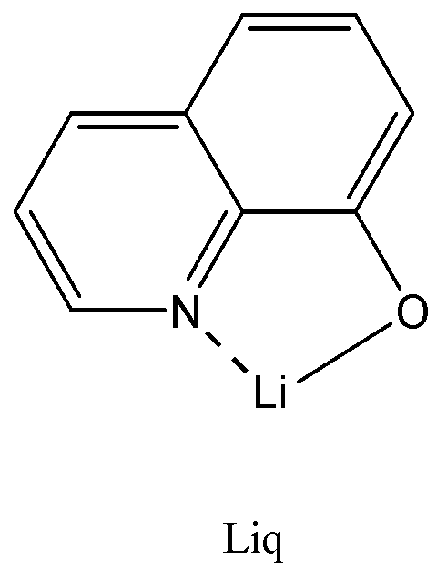
상기 발광층, 정공 마개층 또는 전자 수송층 상부에 전자 주입층을 진공 증착법 또는 스핀 코팅법을 이용하여 선택적으로 형성될 수 있다. 상기 전자 주입층 형성 재료로서는 BaF2, LiF, NaF, MgF2, AlF3, CaF2, NaCl, CsF, Li2O, BaO, Liq 등의 물질을 이용할 수 있으나, 이에 한정되는 것은 아니다.An electron injection layer may be selectively formed on the light emitting layer, the hole plug layer, or the electron transport layer by using a vacuum deposition method or a spin coating method. As the electron injection layer forming material, a material such as BaF 2 , LiF, NaF, MgF 2 , AlF 3 , CaF 2 , NaCl, CsF, Li 2 O, BaO, Liq, or the like may be used, but is not limited thereto.
상기 전자 주입층의 두께는 0.1nm 내지 30nm, 바람직하게는 1nm 내지 10nm 일 수 있다. 이 중, 2nm 내지 6nm가 특히 적합한 두께이다. 상기 전자주입층의 두께가 0.1nm 미만인 경우에는 효과적인 전자주입층으로서 역할을 못할 수 있고, 상기 전자주입층의 두께가 30nm를 초과하는 경우에는 구동전압이 증가하거나 발광 효율이 감소할 수 있다. The electron injection layer may have a thickness of 0.1 nm to 30 nm, preferably 1 nm to 10 nm. Of these, 2 nm to 6 nm are particularly suitable thicknesses. When the thickness of the electron injection layer is less than 0.1 nm, it may not serve as an effective electron injection layer, and when the thickness of the electron injection layer exceeds 30 nm, the driving voltage may increase or the luminous efficiency may decrease.
이어서, 상기 전자주입층 상부에 제 2 전극용 물질을 증착하여 제 2 전극을 형성함으로써 유기 전계 발광 소자가 완성된다.Subsequently, an organic electroluminescent device is completed by depositing a second electrode material on the electron injection layer to form a second electrode.
상기 제 2 전극용 물질인 금속으로는 리튬(Li), 마그네슘(Mg), 알루미늄(Al), 알루미늄-리튬(Al-Li), 칼슘(Ca), 마그네슘-인듐(Mg-In), 마그네슘-은(Mg-Ag), 칼슘(Ca)-알루미늄(Al) 등을 이용하나, 상기 예시된 금속 및 금속의 조합에 한정되는 것은 아니다. 이 중, 칼슘과 알루미늄의 2층으로 이루어진 제 2 전극은 예를 들면, 칼슘은 2nm 내지 10nm의 두께를 갖는 층으로 구비되고, 알루미늄은 100nm 내지 300nm의 두께를 갖는 층으로 구비될 수 있다.As the metal for the second electrode, lithium (Li), magnesium (Mg), aluminum (Al), aluminum-lithium (Al-Li), calcium (Ca), magnesium-indium (Mg-In), magnesium- Silver (Mg-Ag), calcium (Ca) -aluminum (Al) and the like are used, but are not limited to the metals and combinations of the metals exemplified above. Among these, the second electrode composed of two layers of calcium and aluminum, for example, calcium may be provided as a layer having a thickness of 2 nm to 10 nm, and aluminum may be provided as a layer having a thickness of 100 nm to 300 nm.
상기 제1전극 및 제2전극은 각각 양극 및 음극으로서의 역할을 할 수 있으 며, 그 반대도 물론 가능하다. 본 발명을 따르는 유기 전계 발광 소자는 다양한 형태의 유기 전계 발광 표시 장치에 구비될 수 있으며, 특히, 능동 매트릭스 유기 전계 발광 표시 장치에 구비되는 경우, 상기 제1전극은 박막 트랜지스터의 드레인 전극과 전기적으로 연결될 수 있다. The first electrode and the second electrode may serve as an anode and a cathode, respectively, and vice versa. The organic electroluminescent device according to the present invention may be provided in various types of organic electroluminescent display devices. In particular, in the active matrix organic electroluminescent display device, the first electrode may be electrically connected to the drain electrode of the thin film transistor. Can be connected.
이상, 본 발명의 유기 전계 발광 소자의 일 구현예 및 그 제조방법을 도 2에 도시된 바와 같이 기판, 제1전극, 정공 주입층, 정공 수송층, 제1발광층, 엑시톤 피닝층, 제2발광층, 전자 주입층 및 제2전극을 차례로 구비한 유기 전계 발광 소자를 예로 들어 설명하였으나, 이에 한정되지 않음은 물론이다.As described above, an embodiment of the organic electroluminescent device and a method of manufacturing the same according to an embodiment of the present invention include a substrate, a first electrode, a hole injection layer, a hole transport layer, a first light emitting layer, an exciton pinning layer, a second light emitting layer, Although the organic electroluminescent device having the electron injection layer and the second electrode in sequence has been described as an example, the present invention is not limited thereto.
이하, 본 발명을 하기 실시예를 들어 설명하기로 하되, 본 발명이 하기 실시예로만 한정되는 것은 아니다.Hereinafter, the present invention will be described with reference to the following examples, but the present invention is not limited only to the following examples.
실시예Example
실시예 1Example 1
제1전극은 코닝(Corning) 15Ω/cm2 (1200Å) ITO 유리 기판을 50mm x 50mm x 0.7mm 크기로 잘라서 이소프로필 알코올과 순수 물 속에서 각 5 분 동안 초음파 세정한 후, 30분 동안 UV, 오존 세정하여 사용하였다. The first electrode cuts Corning 15Ω / cm 2 (1200Å) ITO glass substrate into 50mm x 50mm x 0.7mm size and ultrasonically cleans for 5 minutes in isopropyl alcohol and pure water, and then UV, 30 minutes, Ozone washed and used.
상기 기판 상부에 PEDOT/PSS(Bayer사 제품의 정공 주입 물질) 수용액을 스핀 코팅하여 5nm 두께의 정공 주입층을 형성한 다음, 상기 정공 주입층 상부에 자체적으로 합성한 BFE를 2000rpm으로 스핀 코팅하여 50nm 두께의 정공 수송층을 형성하였다. Spin coating PEDOT / PSS (Bayer's hole injection material) aqueous solution on the substrate to form a hole injection layer having a thickness of 5 nm, and then sponically coating BFE synthesized on the hole injection layer at 2000 rpm to 50 nm. A hole transport layer of thickness was formed.
그리고나서, 자체 합성한 청색 발광 물질 TS9과 크실렌을 혼합하여 TS9과 크실렌의 혼합물을 얻었다. 이 때, 상기 혼합물 중 TS9의 농도가 0.4wt%가 되도록 하였다. 상기 TS9과 크실렌의 혼합물 중 일부를 상기 정공 수송층 상부에 스핀 코팅하여 25nm 두께의 제1코팅층을 형성한 다음, 200℃의 온도로 30분간 열처리하여 25nm 두께의 제1열처리층을 형성하였다. 이로써, 상기 정공 수송층 상부에 제1발광층을 형성하였다.Then, the self-synthesizing blue light emitting material TS9 and xylene were mixed to obtain a mixture of TS9 and xylene. At this time, the concentration of TS9 in the mixture was adjusted to 0.4 wt%. A portion of the mixture of TS9 and xylene was spin-coated on the hole transport layer to form a first coating layer having a thickness of 25 nm, and then heat-treated at a temperature of 200 ° C. for 30 minutes to form a first heat treatment layer having a thickness of 25 nm. As a result, a first light emitting layer was formed on the hole transport layer.
이 후, COVION사의 적색 발광 물질과 크실렌을 혼합하여 적색 발광 물질과 크실렌의 혼합물을 얻었다. 이 때, 상기 혼합물 중 적색 발광 물질의 농도가 0.4wt%가 되도록 하였다. 상기 혼합물 중 일부를 상기 제1발광층 상부에 스핀 코팅하여 30nm 두께의 코팅층을 형성한 다음, 200℃의 온도로 30분간 열처리하여 30nm 두께의 엑시톤 피닝층을 형성하였다.Thereafter, the red light emitting material and xylene of COVION Co., Ltd. were mixed to obtain a mixture of the red light emitting material and xylene. At this time, the concentration of the red light emitting material in the mixture was adjusted to 0.4 wt%. A part of the mixture was spin-coated on the first light emitting layer to form a coating layer having a thickness of 30 nm, and then heat treated at a temperature of 200 ° C. for 30 minutes to form an exciton pinning layer having a thickness of 30 nm.
그 다음으로, 상기 TS9과 크실렌의 혼합물 중 일부를 상기 엑시톤 피닝층 상부에 스핀 코팅하여 25nm 두께의 제2코팅층을 형성한 다음, 200℃의 온도로 30분간 열처리하여 25nm 두께의 제2열처리층을 형성하였다. Subsequently, a part of the mixture of TS9 and xylene is spin-coated on the exciton pinning layer to form a second coating layer having a thickness of 25 nm, and then heat-treated at a temperature of 200 ° C. for 30 minutes to form a second heat treatment layer having a thickness of 25 nm. Formed.
이 후, 상기 TS9과 크실렌의 혼합물 중 일부를 상기 제2열처리층 상부에 스핀 코팅하여 25nm 두께의 제3코팅층을 형성한 다음, 200℃의 온도로 30분간 열처리하여 25nm 두께의 제3열처리층을 형성하였다.Thereafter, a part of the mixture of TS9 and xylene is spin-coated on the second heat treatment layer to form a third coating layer having a thickness of 25 nm, and then heat-treated at a temperature of 200 ° C. for 30 minutes to form a third heat treatment layer having a thickness of 25 nm. Formed.
마지막으로, 상기 TS9과 크실렌의 혼합물 중 일부를 상기 제3열처리층 상부에 스핀 코팅하여 25nm 두께의 제4코팅층을 형성한 다음, 200℃의 온도로 30분간 열처리하여 25nm 두께의 제4열처리층을 형성하여, 단일층 형태를 갖는 제2발광층을 상기 엑시톤 피닝층 상부에 형성하였다. 이로써, 엑시톤 피닝층이 삽입된 발광층을 얻었다.Finally, a part of the mixture of TS9 and xylene is spin-coated on the third heat treatment layer to form a fourth coating layer having a thickness of 25 nm, and then heat treated at a temperature of 200 ° C. for 30 minutes to form a fourth heat treatment layer having a thickness of 25 nm. A second light emitting layer having a single layer form was formed on the exciton pinning layer. This obtained the light emitting layer in which the exciton pinning layer was inserted.
상기 제2발광층 상부에 전자 주입층으로서 3.1nm 두께의 BaF2를 형성한 다음, 제2전극으로서 Ca 2.2nm, Al 200nm를 형성하여, 유기 전계 발광 소자를 제작하였다. 이를 샘플 1이라고 한다.An organic electroluminescent device was manufactured by forming BaF 2 having a thickness of 3.1 nm as an electron injection layer on the second emission layer, and then forming Ca 2.2 nm and Al 200 nm as a second electrode. This is called
실시예 2Example 2
상기 실시예 1 중, 엑시톤 피닝층을 제1열처리층 상부에 형성한 것 대신, 제2열처리층 상부에 형성하였다는 점을 제외하고는 상기 실시예 1과 동일한 방법으로 유기 전계 발광 소자를 제작하였다. 이를 샘플 2라고 한다.An organic electroluminescent device was manufactured in the same manner as in Example 1, except that the exciton pinning layer was formed on the second heat treatment layer instead of the first heat treatment layer. . This is called sample 2.
실시예 3Example 3
상기 실시예 1 중, 엑시톤 피닝층을 제1열처리층 상부에 형성한 것 대신, 제3열처리층 상부에 형성하였다는 점을 제외하고는 상기 실시예 1과 동일한 방법으로 유기 전계 발광 소자를 제작하였다. 이를 샘플 3이라고 한다.An organic electroluminescent device was manufactured in the same manner as in Example 1, except that the exciton pinning layer was formed on the third heat treatment layer instead of the first heat treatment layer. . This is called sample 3.
평가예 - 수명 측정Evaluation Example-Life Measurement
상기 샘플 1, 2 및 3에 대하여 수명 특성을 평가하여 도 3에 나타내었다. 수명 특성 평가는 포토다이오드(photodiode)를 이용하여 시간에 따라 휘도를 측정함으로써 평가하였으며, 도 3에는 초기 휘도에 대비한 휘도 비율을 나타낸 것이다. The life characteristics of the
도 3에 따르면, 엑시톤 피닝층의 위치에 따라 수명 곡선의 형태가 바뀌는 것을 알 수 있다. According to Figure 3, it can be seen that the shape of the life curve is changed according to the position of the exciton pinning layer .
전술한 바와 같은 본 발명을 따르는 유기 전계 발광 소자는 발광층 사이에 엑시톤 피닝층이 삽입되어 있는 바, 발광층에서 정공 및 전자의 결합으로 발생한 엑시톤의 여기가 보다 효과적으로 이루어질 수 있어, 유기 전계 발광 소자의 수명을 향상시킬 수 있다.In the organic electroluminescent device according to the present invention as described above, since the exciton pinning layer is inserted between the light emitting layers, excitons generated by the combination of holes and electrons in the light emitting layer can be made more effectively, and thus the life of the organic electroluminescent device Can improve.
Claims (18)
Priority Applications (4)
| Application Number | Priority Date | Filing Date | Title |
|---|---|---|---|
| KR1020050005529A KR20060084733A (en) | 2005-01-20 | 2005-01-20 | An organic electroluminescent device and a method for preparing the same |
| CNA2005100992313A CN1809236A (en) | 2005-01-20 | 2005-09-07 | Organic light emitting device and method for preparing the same |
| US11/328,157 US20060158105A1 (en) | 2005-01-20 | 2006-01-10 | Organic light emitting device and method for preparing the same |
| JP2006007759A JP5073208B2 (en) | 2005-01-20 | 2006-01-16 | Organic electroluminescent device and manufacturing method thereof |
Applications Claiming Priority (1)
| Application Number | Priority Date | Filing Date | Title |
|---|---|---|---|
| KR1020050005529A KR20060084733A (en) | 2005-01-20 | 2005-01-20 | An organic electroluminescent device and a method for preparing the same |
Publications (1)
| Publication Number | Publication Date |
|---|---|
| KR20060084733A true KR20060084733A (en) | 2006-07-25 |
Family
ID=36683179
Family Applications (1)
| Application Number | Title | Priority Date | Filing Date |
|---|---|---|---|
| KR1020050005529A KR20060084733A (en) | 2005-01-20 | 2005-01-20 | An organic electroluminescent device and a method for preparing the same |
Country Status (4)
| Country | Link |
|---|---|
| US (1) | US20060158105A1 (en) |
| JP (1) | JP5073208B2 (en) |
| KR (1) | KR20060084733A (en) |
| CN (1) | CN1809236A (en) |
Cited By (6)
| Publication number | Priority date | Publication date | Assignee | Title |
|---|---|---|---|---|
| KR100760901B1 (en) * | 2005-12-06 | 2007-09-21 | 한국전자통신연구원 | The White Organic Light Emitting Device |
| WO2008020696A1 (en) * | 2006-08-14 | 2008-02-21 | Inktec Co., Ltd. | Organic electroluminescent device and preparation method thereof |
| WO2009028832A2 (en) * | 2007-08-24 | 2009-03-05 | Electronics And Telecommunications Research Institute | Hybrid white organic light emitting device and method of manufacturing the same |
| KR100952420B1 (en) * | 2008-08-04 | 2010-04-14 | 한국전자통신연구원 | The organic light emitting diode and manufacturing method thereof |
| KR100957781B1 (en) * | 2007-08-24 | 2010-05-13 | 한국전자통신연구원 | The hybrid white organic emitting device and the method of manufacturing the Same |
| US9426067B2 (en) | 2012-06-12 | 2016-08-23 | International Business Machines Corporation | Integrated switch for dynamic orchestration of traffic |
Families Citing this family (8)
| Publication number | Priority date | Publication date | Assignee | Title |
|---|---|---|---|---|
| JP5109303B2 (en) | 2006-07-31 | 2012-12-26 | ソニー株式会社 | Organic light emitting device and display device |
| US20080286445A1 (en) * | 2007-05-17 | 2008-11-20 | Semiconductor Energy Laboratory Co., Ltd. | Composition, and method of fabricating light-emitting element |
| US8242489B2 (en) * | 2009-12-17 | 2012-08-14 | Global Oled Technology, Llc. | OLED with high efficiency blue light-emitting layer |
| US8962994B2 (en) | 2010-10-22 | 2015-02-24 | Xerox Corporation | Photovoltaic device |
| US10615345B2 (en) * | 2016-06-03 | 2020-04-07 | The Trustees Of Princeton University | Method and device for using an organic underlayer to enable crystallization of disordered organic thin films |
| JP7266441B2 (en) * | 2019-02-15 | 2023-04-28 | 三星ディスプレイ株式會社 | Organic light-emitting device and electronic device including the same |
| CN110323347B (en) | 2019-05-09 | 2021-08-20 | 京东方科技集团股份有限公司 | Quantum dot electroluminescent device, display panel and display device |
| CN117598041A (en) * | 2022-05-26 | 2024-02-23 | 京东方科技集团股份有限公司 | Light-emitting device and display device |
Family Cites Families (14)
| Publication number | Priority date | Publication date | Assignee | Title |
|---|---|---|---|---|
| JP3451680B2 (en) * | 1993-11-15 | 2003-09-29 | 三菱化学株式会社 | Organic electroluminescent device |
| US6451415B1 (en) * | 1998-08-19 | 2002-09-17 | The Trustees Of Princeton University | Organic photosensitive optoelectronic device with an exciton blocking layer |
| US6893743B2 (en) * | 2000-10-04 | 2005-05-17 | Mitsubishi Chemical Corporation | Organic electroluminescent device |
| US6573651B2 (en) * | 2000-12-18 | 2003-06-03 | The Trustees Of Princeton University | Highly efficient OLEDs using doped ambipolar conductive molecular organic thin films |
| EP2276084A1 (en) * | 2001-03-14 | 2011-01-19 | The Trustees of Princeton University | Materials and devices for blue phosphorescence based organic light emitting diodes |
| DE60239198D1 (en) * | 2001-05-16 | 2011-03-31 | Univ Princeton | HIGHLY EFFICIENT MULTI-COLORED ELECTROPHOSPHORESCENT OLEDS |
| JP2002359073A (en) * | 2001-05-31 | 2002-12-13 | Ricoh Co Ltd | Method of manufacturing organic electroluminescence element |
| JP3967946B2 (en) * | 2002-03-26 | 2007-08-29 | 松下電工株式会社 | Organic electroluminescence device |
| DE10224021B4 (en) * | 2002-05-24 | 2006-06-01 | Novaled Gmbh | Phosphorescent light emitting device with organic layers |
| JP2005150078A (en) * | 2003-10-24 | 2005-06-09 | Pentax Corp | White organic electroluminescent element |
| US7030554B2 (en) * | 2004-02-06 | 2006-04-18 | Eastman Kodak Company | Full-color organic display having improved blue emission |
| TW200541401A (en) * | 2004-02-13 | 2005-12-16 | Idemitsu Kosan Co | Organic electroluminescent device |
| JP2005276583A (en) * | 2004-03-24 | 2005-10-06 | Idemitsu Kosan Co Ltd | Organic electroluminescent element and indicating device |
| JP4782791B2 (en) * | 2004-09-22 | 2011-09-28 | ドーサン・コーポレーション | White organic electroluminescent device using three primary colors |
-
2005
- 2005-01-20 KR KR1020050005529A patent/KR20060084733A/en not_active Application Discontinuation
- 2005-09-07 CN CNA2005100992313A patent/CN1809236A/en active Pending
-
2006
- 2006-01-10 US US11/328,157 patent/US20060158105A1/en not_active Abandoned
- 2006-01-16 JP JP2006007759A patent/JP5073208B2/en active Active
Cited By (11)
| Publication number | Priority date | Publication date | Assignee | Title |
|---|---|---|---|---|
| KR100760901B1 (en) * | 2005-12-06 | 2007-09-21 | 한국전자통신연구원 | The White Organic Light Emitting Device |
| WO2008020696A1 (en) * | 2006-08-14 | 2008-02-21 | Inktec Co., Ltd. | Organic electroluminescent device and preparation method thereof |
| KR100881455B1 (en) * | 2006-08-14 | 2009-02-06 | 주식회사 잉크테크 | Organic Electroluminescent Device and preparation method thereof |
| US8866128B2 (en) | 2006-08-14 | 2014-10-21 | Inktec Co., Ltd. | Organic electroluminescent device and preparation method thereof |
| WO2009028832A2 (en) * | 2007-08-24 | 2009-03-05 | Electronics And Telecommunications Research Institute | Hybrid white organic light emitting device and method of manufacturing the same |
| WO2009028832A3 (en) * | 2007-08-24 | 2009-04-23 | Korea Electronics Telecomm | Hybrid white organic light emitting device and method of manufacturing the same |
| KR100957781B1 (en) * | 2007-08-24 | 2010-05-13 | 한국전자통신연구원 | The hybrid white organic emitting device and the method of manufacturing the Same |
| KR100952420B1 (en) * | 2008-08-04 | 2010-04-14 | 한국전자통신연구원 | The organic light emitting diode and manufacturing method thereof |
| US9426067B2 (en) | 2012-06-12 | 2016-08-23 | International Business Machines Corporation | Integrated switch for dynamic orchestration of traffic |
| US9660910B2 (en) | 2012-06-12 | 2017-05-23 | International Business Machines Corporation | Integrated switch for dynamic orchestration of traffic |
| US9906446B2 (en) | 2012-06-12 | 2018-02-27 | International Business Machines Corporation | Integrated switch for dynamic orchestration of traffic |
Also Published As
| Publication number | Publication date |
|---|---|
| CN1809236A (en) | 2006-07-26 |
| JP2006202747A (en) | 2006-08-03 |
| JP5073208B2 (en) | 2012-11-14 |
| US20060158105A1 (en) | 2006-07-20 |
Similar Documents
| Publication | Publication Date | Title |
|---|---|---|
| JP5073208B2 (en) | Organic electroluminescent device and manufacturing method thereof | |
| JP4722695B2 (en) | Organic light emitting device | |
| CN101340749B (en) | Organic light emitting device | |
| JP5068558B2 (en) | Organic light emitting device | |
| KR101407574B1 (en) | White light emitting device | |
| JP5420825B2 (en) | Organic light emitting device | |
| CN101295769B (en) | Organic light emitting device and method of manufacturing the same | |
| KR100922759B1 (en) | Organic light emitting device | |
| KR101681789B1 (en) | Organic el display unit, method of manufacturing the same, and solution used in method | |
| KR100741104B1 (en) | An organic light emitting device | |
| US20090218934A1 (en) | Organic light-emitting device | |
| US20090211640A1 (en) | Electron injecting layer including superacid salt, lithium salt or mixture thereof, photovoltaic device including the electron injecting layer, method of manufacturing the photovoltaic device, and organic light-emitting device including the electron injecting layer | |
| JP2009164578A (en) | Organic light-emitting device | |
| KR20090050369A (en) | Organic luminescence display device | |
| KR20070087773A (en) | An organic light emitting device and a flat display device comprising the same | |
| US20090085470A1 (en) | Organic light emitting device | |
| KR20100011290A (en) | A method for preparing an organic light emitting device and am organic light emitting device | |
| US8142910B2 (en) | Organic light-emitting device | |
| US7679282B2 (en) | Polymer and small molecule based hybrid light source | |
| KR20090125616A (en) | A method for preparing an organic light emitting device and am organic light emitting device | |
| US20170229672A1 (en) | Organic light emitting devices and methods of making them | |
| KR100659131B1 (en) | An organic light emitting device | |
| KR100651659B1 (en) | Oranic electroluminescence display device | |
| KR101035359B1 (en) | Organic light emitting device and a method for preparing the same | |
| JP2008282957A (en) | Organic light-emitting device |
Legal Events
| Date | Code | Title | Description |
|---|---|---|---|
| N231 | Notification of change of applicant | ||
| A201 | Request for examination | ||
| E601 | Decision to refuse application |