KR102576552B1 - Methods for Growing Single Crystal Silicon Ingots Using the Continuous Czochralski Method - Google Patents
Methods for Growing Single Crystal Silicon Ingots Using the Continuous Czochralski Method Download PDFInfo
- Publication number
- KR102576552B1 KR102576552B1 KR1020217037242A KR20217037242A KR102576552B1 KR 102576552 B1 KR102576552 B1 KR 102576552B1 KR 1020217037242 A KR1020217037242 A KR 1020217037242A KR 20217037242 A KR20217037242 A KR 20217037242A KR 102576552 B1 KR102576552 B1 KR 102576552B1
- Authority
- KR
- South Korea
- Prior art keywords
- silicon ingot
- monocrystalline silicon
- melt
- silicon
- ingot
- Prior art date
- Legal status (The legal status is an assumption and is not a legal conclusion. Google has not performed a legal analysis and makes no representation as to the accuracy of the status listed.)
- Active
Links
Images


Classifications
-
- C—CHEMISTRY; METALLURGY
- C30—CRYSTAL GROWTH
- C30B—SINGLE-CRYSTAL GROWTH; UNIDIRECTIONAL SOLIDIFICATION OF EUTECTIC MATERIAL OR UNIDIRECTIONAL DEMIXING OF EUTECTOID MATERIAL; REFINING BY ZONE-MELTING OF MATERIAL; PRODUCTION OF A HOMOGENEOUS POLYCRYSTALLINE MATERIAL WITH DEFINED STRUCTURE; SINGLE CRYSTALS OR HOMOGENEOUS POLYCRYSTALLINE MATERIAL WITH DEFINED STRUCTURE; AFTER-TREATMENT OF SINGLE CRYSTALS OR A HOMOGENEOUS POLYCRYSTALLINE MATERIAL WITH DEFINED STRUCTURE; APPARATUS THEREFOR
- C30B15/00—Single-crystal growth by pulling from a melt, e.g. Czochralski method
- C30B15/002—Continuous growth
-
- C—CHEMISTRY; METALLURGY
- C30—CRYSTAL GROWTH
- C30B—SINGLE-CRYSTAL GROWTH; UNIDIRECTIONAL SOLIDIFICATION OF EUTECTIC MATERIAL OR UNIDIRECTIONAL DEMIXING OF EUTECTOID MATERIAL; REFINING BY ZONE-MELTING OF MATERIAL; PRODUCTION OF A HOMOGENEOUS POLYCRYSTALLINE MATERIAL WITH DEFINED STRUCTURE; SINGLE CRYSTALS OR HOMOGENEOUS POLYCRYSTALLINE MATERIAL WITH DEFINED STRUCTURE; AFTER-TREATMENT OF SINGLE CRYSTALS OR A HOMOGENEOUS POLYCRYSTALLINE MATERIAL WITH DEFINED STRUCTURE; APPARATUS THEREFOR
- C30B29/00—Single crystals or homogeneous polycrystalline material with defined structure characterised by the material or by their shape
- C30B29/02—Elements
- C30B29/06—Silicon
-
- C—CHEMISTRY; METALLURGY
- C30—CRYSTAL GROWTH
- C30B—SINGLE-CRYSTAL GROWTH; UNIDIRECTIONAL SOLIDIFICATION OF EUTECTIC MATERIAL OR UNIDIRECTIONAL DEMIXING OF EUTECTOID MATERIAL; REFINING BY ZONE-MELTING OF MATERIAL; PRODUCTION OF A HOMOGENEOUS POLYCRYSTALLINE MATERIAL WITH DEFINED STRUCTURE; SINGLE CRYSTALS OR HOMOGENEOUS POLYCRYSTALLINE MATERIAL WITH DEFINED STRUCTURE; AFTER-TREATMENT OF SINGLE CRYSTALS OR A HOMOGENEOUS POLYCRYSTALLINE MATERIAL WITH DEFINED STRUCTURE; APPARATUS THEREFOR
- C30B15/00—Single-crystal growth by pulling from a melt, e.g. Czochralski method
- C30B15/007—Pulling on a substrate
-
- C—CHEMISTRY; METALLURGY
- C30—CRYSTAL GROWTH
- C30B—SINGLE-CRYSTAL GROWTH; UNIDIRECTIONAL SOLIDIFICATION OF EUTECTIC MATERIAL OR UNIDIRECTIONAL DEMIXING OF EUTECTOID MATERIAL; REFINING BY ZONE-MELTING OF MATERIAL; PRODUCTION OF A HOMOGENEOUS POLYCRYSTALLINE MATERIAL WITH DEFINED STRUCTURE; SINGLE CRYSTALS OR HOMOGENEOUS POLYCRYSTALLINE MATERIAL WITH DEFINED STRUCTURE; AFTER-TREATMENT OF SINGLE CRYSTALS OR A HOMOGENEOUS POLYCRYSTALLINE MATERIAL WITH DEFINED STRUCTURE; APPARATUS THEREFOR
- C30B15/00—Single-crystal growth by pulling from a melt, e.g. Czochralski method
- C30B15/10—Crucibles or containers for supporting the melt
-
- C—CHEMISTRY; METALLURGY
- C30—CRYSTAL GROWTH
- C30B—SINGLE-CRYSTAL GROWTH; UNIDIRECTIONAL SOLIDIFICATION OF EUTECTIC MATERIAL OR UNIDIRECTIONAL DEMIXING OF EUTECTOID MATERIAL; REFINING BY ZONE-MELTING OF MATERIAL; PRODUCTION OF A HOMOGENEOUS POLYCRYSTALLINE MATERIAL WITH DEFINED STRUCTURE; SINGLE CRYSTALS OR HOMOGENEOUS POLYCRYSTALLINE MATERIAL WITH DEFINED STRUCTURE; AFTER-TREATMENT OF SINGLE CRYSTALS OR A HOMOGENEOUS POLYCRYSTALLINE MATERIAL WITH DEFINED STRUCTURE; APPARATUS THEREFOR
- C30B15/00—Single-crystal growth by pulling from a melt, e.g. Czochralski method
- C30B15/14—Heating of the melt or the crystallised materials
-
- C—CHEMISTRY; METALLURGY
- C30—CRYSTAL GROWTH
- C30B—SINGLE-CRYSTAL GROWTH; UNIDIRECTIONAL SOLIDIFICATION OF EUTECTIC MATERIAL OR UNIDIRECTIONAL DEMIXING OF EUTECTOID MATERIAL; REFINING BY ZONE-MELTING OF MATERIAL; PRODUCTION OF A HOMOGENEOUS POLYCRYSTALLINE MATERIAL WITH DEFINED STRUCTURE; SINGLE CRYSTALS OR HOMOGENEOUS POLYCRYSTALLINE MATERIAL WITH DEFINED STRUCTURE; AFTER-TREATMENT OF SINGLE CRYSTALS OR A HOMOGENEOUS POLYCRYSTALLINE MATERIAL WITH DEFINED STRUCTURE; APPARATUS THEREFOR
- C30B15/00—Single-crystal growth by pulling from a melt, e.g. Czochralski method
- C30B15/20—Controlling or regulating
-
- C—CHEMISTRY; METALLURGY
- C30—CRYSTAL GROWTH
- C30B—SINGLE-CRYSTAL GROWTH; UNIDIRECTIONAL SOLIDIFICATION OF EUTECTIC MATERIAL OR UNIDIRECTIONAL DEMIXING OF EUTECTOID MATERIAL; REFINING BY ZONE-MELTING OF MATERIAL; PRODUCTION OF A HOMOGENEOUS POLYCRYSTALLINE MATERIAL WITH DEFINED STRUCTURE; SINGLE CRYSTALS OR HOMOGENEOUS POLYCRYSTALLINE MATERIAL WITH DEFINED STRUCTURE; AFTER-TREATMENT OF SINGLE CRYSTALS OR A HOMOGENEOUS POLYCRYSTALLINE MATERIAL WITH DEFINED STRUCTURE; APPARATUS THEREFOR
- C30B15/00—Single-crystal growth by pulling from a melt, e.g. Czochralski method
- C30B15/30—Mechanisms for rotating or moving either the melt or the crystal
- C30B15/305—Stirring of the melt
-
- C—CHEMISTRY; METALLURGY
- C30—CRYSTAL GROWTH
- C30B—SINGLE-CRYSTAL GROWTH; UNIDIRECTIONAL SOLIDIFICATION OF EUTECTIC MATERIAL OR UNIDIRECTIONAL DEMIXING OF EUTECTOID MATERIAL; REFINING BY ZONE-MELTING OF MATERIAL; PRODUCTION OF A HOMOGENEOUS POLYCRYSTALLINE MATERIAL WITH DEFINED STRUCTURE; SINGLE CRYSTALS OR HOMOGENEOUS POLYCRYSTALLINE MATERIAL WITH DEFINED STRUCTURE; AFTER-TREATMENT OF SINGLE CRYSTALS OR A HOMOGENEOUS POLYCRYSTALLINE MATERIAL WITH DEFINED STRUCTURE; APPARATUS THEREFOR
- C30B15/00—Single-crystal growth by pulling from a melt, e.g. Czochralski method
- C30B15/36—Single-crystal growth by pulling from a melt, e.g. Czochralski method characterised by the seed, e.g. its crystallographic orientation
Landscapes
- Chemical & Material Sciences (AREA)
- Engineering & Computer Science (AREA)
- Crystallography & Structural Chemistry (AREA)
- Materials Engineering (AREA)
- Metallurgy (AREA)
- Organic Chemistry (AREA)
- Crystals, And After-Treatments Of Crystals (AREA)
Abstract
연속 쵸크랄스키 방법에 의해 단결정 실리콘 잉곳을 성장시키기 위한 방법이 개시된다. 용융물 깊이 및 열 조건들은 실리콘 용융물이 소비됨에 따라 연속적으로 보충되기 때문에 성장 동안 일정하고, 도가니 위치는 고정된다. 임계 v/G는 고온 구역 구성에 의해 결정되고, 성장 동안 용융물에 실리콘의 연속 보충은 잉곳의 본체의 상당 부분의 성장 동안 임계 v/G와 일치하는 일정한 인상 속도로 잉곳의 성장을 가능하게 한다.A method for growing single crystal silicon ingots by the continuous Czochralski method is disclosed. The melt depth and thermal conditions are constant during growth because the silicon melt is continuously replenished as it is consumed, and the crucible position is fixed. The critical v/G is determined by the hot zone configuration, and continuous replenishment of silicon to the melt during growth enables growth of the ingot at a constant pull rate consistent with the critical v/G during growth of a significant portion of the body of the ingot.
Description
관련 출원(들)에 대한 상호 참조Cross reference to related application(s)
본 출원은 2019년 4월 18일자로 출원된 미국 가출원 제62/835,735호의 우선권의 혜택을 주장하며, 그것의 개시는 그 전체가 제시된 것처럼 참조에 의해 포함된다.This application claims the benefit of priority from U.S. Provisional Application No. 62/835,735, filed on April 18, 2019, the disclosure of which is incorporated by reference as if set forth in its entirety.
기술분야technology field
본 개시의 분야는 연속 쵸크랄스키 방법을 사용하여 단결정 실리콘 잉곳을 성장시키기 위한 방법에 관한 것이다.The field of the present disclosure relates to methods for growing single crystal silicon ingots using the continuous Czochralski method.
반도체 전자 컴포넌트들의 제조를 위한 대부분의 프로세스들에서 출발 물질인 단결정 실리콘은 통상적으로 쵸크랄스키(Czochralski)("Cz") 방법에 의해 준비된다. 이 방법에서, 다결정 실리콘("폴리실리콘")은 도가니에 장입되고 용융되며, 시드 결정이 용융된 실리콘과 접촉되고, 느린 추출에 의해 단결정이 성장된다. 목(neck)의 형성이 완료된 후, 결정의 직경은 예를 들어 원하는 또는 목표 직경에 도달할 때까지 인상 속도(pulling rate) 및/또는 용융물 온도를 감소시킴으로써 확대된다. 다음으로, 대략 일정한 직경을 갖는 결정의 원통형 본체는 감소하는 용융물 레벨을 보상하면서 인상 속도와 용융물 온도를 제어함으로써 성장된다. 성장 프로세스가 거의 끝나가지만 도가니에서 용융된 실리콘이 비워지기 전에, 결정 직경은 전형적으로 점진적으로 감소되어, 말단 원뿔(end-cone) 형태의 꼬리 단부를 형성한다. 말단 원뿔은 통상적으로 도가니에 공급되는 결정 인상 속도와 열을 증가시킴으로써 형성된다. 직경이 충분히 작아지면, 결정은 용융물로부터 분리된다.Monocrystalline silicon, which is the starting material in most processes for the manufacture of semiconductor electronic components, is typically prepared by the Czochralski ("Cz") method. In this method, polycrystalline silicon ("polysilicon") is charged into a crucible and melted, a seed crystal is contacted with the molten silicon, and a single crystal is grown by slow extraction. After formation of the neck is complete, the diameter of the crystal is enlarged, for example by reducing the pulling rate and/or melt temperature until a desired or target diameter is reached. Next, a cylindrical body of crystal with approximately constant diameter is grown by controlling the pull rate and melt temperature while compensating for the decreasing melt level. Near the end of the growth process but before the crucible is emptied of molten silicon, the crystal diameter typically gradually decreases, forming an end-cone shaped tail end. End cones are typically formed by increasing the crystal pulling rate and heat supplied to the crucible. When the diameter is sufficiently small, the crystal separates from the melt.
쵸크랄스키 성장 기술들은 배치 쵸크랄스키 방법 및 연속 쵸크랄스키 방법을 포함한다. 배치 CZ에서, 단일 다결정 충전물은 도가니에 장입되며, 단일 충전물은 단결정 실리콘 잉곳을 성장시키기에 충분하고, 그 후에 도가니는 본질적으로 실리콘 용융물이 고갈된다. 연속 쵸크랄스키(CCZ) 성장에서, 다결정 실리콘은 성장 프로세스 동안 용융물을 보충하기 위해 용융된 실리콘에 연속적으로 또는 주기적으로 첨가될 수 있고, 결과적으로, 다수의 잉곳은 성장 프로세스 동안 단일 도가니로부터 인상될 수 있다.Czochralski growth techniques include the batch Czochralski method and the continuous Czochralski method. In batch CZ, a single polycrystalline charge is charged into the crucible, and a single charge is sufficient to grow a single crystal silicon ingot, after which the crucible is essentially depleted of silicon melt. In continuous Czochralski (CCZ) growth, polycrystalline silicon may be continuously or periodically added to the molten silicon to replenish the melt during the growth process, and as a result, multiple ingots may be pulled from a single crucible during the growth process. can
CCZ 프로세스를 수행하기 위해, 전통적인 배치 쵸크랄스키 성장 챔버 및 장치는 성장 잉곳의 속성들에 악영향을 주지 않고 추가 다결정 실리콘을 용융물에 연속 또는 반연속 방식으로 공급하기 위한 수단을 포함하기 위해 수정된다. 시드 결정이 용융물로부터 연속적으로 성장됨에 따라, 입상 다결정 실리콘과 같은 고체 다결정 실리콘은 용융물을 보충하기 위해 용융물에 첨가된다. 용융물에 첨가된 부가 고체 다결정 실리콘의 공급 속도는 전형적으로 프로세스 매개변수들을 유지하기 위해 제어된다. 동시 결정 성장에 활동을 보충하는 이것의 역효과들을 감소시키기 위해, 전통적인 석영 도가니는 종종 추가된 재료가 전달되는 외부 또는 환형 용융물 구역을 실리콘 잉곳이 인상되는 내부 성장 구역과 함께 제공하기 위해 수정된다. 이들 구역들은 서로 유체 흐름 연통된다.To perform the CCZ process, the traditional batch Czochralski growth chamber and apparatus are modified to include means for continuously or semi-continuously supplying additional polycrystalline silicon to the melt without adversely affecting the properties of the growing ingot. As seed crystals are continuously grown from the melt, solid polycrystalline silicon, such as granular polycrystalline silicon, is added to the melt to replenish it. The feed rate of additional solid polycrystalline silicon added to the melt is typically controlled to maintain process parameters. To reduce the adverse effects of this compensating activity for simultaneous crystal growth, traditional quartz crucibles are often modified to provide an outer or annular melt zone into which added material is delivered, with an inner growth zone into which the silicon ingot is pulled. These zones are in fluid flow communication with each other.
현대 마이크로전자 디바이스의 연속적으로 수축하는 크기는 실리콘 기판의 품질에 도전적인 제한들을 부과하며, 이는 본질적으로 성장된 미소결함들의 크기 및 분포에 의해 결정된다. 쵸크랄스키(CZ) 프로세스 및 부유 구역(Float Zone)(FZ) 프로세스에 의해 성장되는 실리콘 결정들에 형성된 미소결함들의 대부분은 실리콘의 고유 점 결함들의 응집체들 - 공공들(vacancies) 및 자체간극들(또는, 간단히, 간극들)이다.The continuously shrinking size of modern microelectronic devices imposes challenging limits on the quality of a silicon substrate, which is essentially determined by the size and distribution of grown microdefects. Most of the micro-defects formed in silicon crystals grown by the Czochralski (CZ) process and the Float Zone (FZ) process are aggregates of point defects inherent in silicon - vacancies and interstitial spaces. (or, simply, gaps).
일련의 연구들은 간극 응집체들이 이하의 2개의 형태로 존재하는 것을 수립하였다 - B 와류 결함(또는 B-결함들)로 칭해지는 구형 간극 클러스터들, 및 A 와류 결함(또는 A-결함들)로 칭해지는 전위 루프들. D-결함들로서 공지되어 있는 나중에 발견된 공공 응집체들은 8면체 보이드들로서 식별되었다. 보론코프(Voronkov)는 결정 성장 조건들을 기초로 실리콘 결정들에서 관찰된 미소결함 분포들에 대한 잘 허용된 설명을 제공하였다. 보론코프의 모델, 또는 이론에 따르면, 용융물/결정 계면 부근의 온도 필드는 용융물/결정 계면으로부터 - 각각의 평형 농도들에 존재하는 경우 - 결정 벌크로의 확산을 위한 구동력들을 제공하는 점 결함들의 재결합을 추진한다. 확산 및 대류 둘 다에 의한, 점 결함들의 이송과, 그들의 재결합 사이의 상호작용은 재결합 길이로 칭해지는, 게면에서 떨어진 단거리를 너머 점 결함 농도를 설정한다. 전형적으로, 초과 점 결함 농도로 칭해지는, 재결합 길이를 넘는 공공 농도와 간극 농도 사이의 차이는 본질적으로 결정의 측방 표면에서 떨어져서 고정된 채로 유지된다. 신속히 인상된 결정에서, 재결합 길이를 넘는 확산에 의한 점 결함들의 공간 재분배는 일반적으로 - 점 결함들의 싱크 또는 소스로서의 역할을 하는 결정의 측방 표면에 가까운 영역을 제외하고 - 중요하지 않다. 따라서, 재결합 길이를 넘는 초과 점 결함 농도가 양이면, 공공들은 초과하여 남아 있고, 응집되어 더 낮은 온도들에서 D-결함들을 형성한다. 초과 점 결함 농도가 음이면, 간극들은 지배적 점 결함들로 남아 있고, 응집되어 A-결함들 및 B-결함들을 형성한다. 초과 점 결함 농도가 일부 검출 임계치 아래이면, 어떤 검출가능 미소결함들도 형성되지 않는다. 따라서, 전형적으로, 성장된 미소결함들의 타입은 재결합 길이를 너머 설정된 초과 점 결함 농도에 의해 간단히 결정된다. 초과 점 결함 농도를 설정하는 프로세스는 초기 혼입으로 칭해지고 지배적 점 결함 종들은 혼입된 지배적 점 결함으로 칭해진다. 혼입된 점 결함들의 타입은 결정 인상 속도(v) 대 계면(G) 부근의 축방향 온도 기울기의 크기의 비율에 의해 결정된다. 더 높은 v/G에서, 점 결함들의 대류는 그들의 확산을 지배하고, 공공들은 계면에서의 공공 농도가 간극 농도보다 더 높으므로, 혼입된 지배적 점 결함들로 남아 있다. 더 낮은 v/G에서, 확산은 대류를 지배하여, 지배적 점 포인트들로서 신속한 확산 간극들의 혼입을 허용한다. 그것의 임계 값에 가까운 v/G에서, 점 결함들 둘 다는 매우 낮고 비교가능한 농도들로 혼입되어, 서로 상호 전멸시키고 따라서 더 낮은 온도들에서 임의의 미소결함들의 잠재적 형성을 억제한다. 관찰된 공간 미소결함 분포는 전형적으로 G의 반경방향 비균일성에 의해 야기된, v/G의 변동 및 v의 축방향 변동에 의해 설명될 수 있다. 반경방향 미소결함 분포의 두드러진 특징은 비교적 더 낮은 혼힙된 공공 농도의 영역들에서 - 임계 v/G보다 아주 조금 위에 있는 v/G의 작은 범위에서 공공들과 산소의 상호작용을 통해 형성된 산화물 입자들이다. 이들 입자들은 열 산화에 의해 산화 유도 적층 흠(oxidation-induced stacking fault)(OSF) 링으로서 드러날 수 있는 좁은 공간 대역을 형성한다. 상당히 자주, OSF 링은 V/I 경계로 공지되어 있는, 공공-지배되고 간극-지배되는 인접 결정 영역들 사이의 경계를 표시한다.A series of studies have established that interstitial aggregates exist in two forms - spherical interstitial clusters, termed B eddy defects (or B-defects), and A vortex defects (or A-defects). dislocation loops being released. Later discovered vacancy aggregates, known as D-defects, were identified as octahedral voids. Voronkov provided a well-accepted explanation for the microdefect distributions observed in silicon crystals based on the crystal growth conditions. According to Voronkov's model, or theory, the temperature field near the melt/crystal interface recombines point defects that provide the driving forces for diffusion from the melt/crystal interface - if present at their respective equilibrium concentrations - into the crystalline bulk. promote The interaction between transport of point defects and their recombination, both by diffusion and convection, establishes the concentration of point defects over a short distance away from the surface, termed the recombination length. Typically, the difference between the vacancies and interstitial concentrations over the recombination length, termed the excess point defect concentration, remains essentially fixed away from the lateral surface of the crystal. In a rapidly pulled crystal, the spatial redistribution of point defects by diffusion over the recombination length is generally insignificant—except for regions close to the lateral surface of the crystal that serve as sinks or sources of point defects. Thus, if the excess point defect concentration over the recombination length is positive, the vacancies remain in excess and aggregate to form D-defects at lower temperatures. If the excess point defect concentration is negative, the voids remain dominant point defects and aggregate to form A-defects and B-defects. If the excess point defect concentration is below some detection threshold, no detectable microdefects are formed. Thus, typically, the type of microdefects grown is simply determined by the set excess point defect concentration over the recombination length. The process of establishing the excess point defect concentration is referred to as initial incorporation and the dominant point defect species are referred to as incorporated dominant point defects. The type of point defects incorporated is determined by the ratio of the crystal pulling rate (v) to the magnitude of the axial temperature gradient near the interface (G). At higher v/G, convection of point defects dominates their diffusion, and vacancies remain entrained dominant point defects since the vacancy concentration at the interface is higher than the interstitial concentration. At lower v/G, diffusion dominates convection, allowing rapid entrainment of diffusion gaps as dominant point points. At v/G close to its critical value, both point defects are incorporated at very low and comparable concentrations, mutually annihilating each other and thus inhibiting the potential formation of any microdefects at lower temperatures. The observed spatial defect distribution can be explained by variations in v/G and axial variations in v, typically caused by radial non-uniformity in G. A striking feature of the radial microdefect distribution is the oxide particles formed through the interaction of vacancies with oxygen in regions of relatively lower mixed vacancy concentration - a small range of v/G just above the critical v/G. . These particles, by thermal oxidation, form narrow spatial bands that can appear as oxidation-induced stacking fault (OSF) rings. Quite often, an OSF ring marks a boundary between adjacent vacancy-dominated and gap-dominated crystal regions, known as a V/I boundary.
그러나, 많은 현대 프로세스들에서 더 낮은 속도들로 성장된 CZ 결정들 내의 미소결함 분포들은 결정들의 측방 표면들에 의해 유도되는 확산을 포함하여, 결정 벌크에서의 점 결함들의 확산에 영향을 받는다. 따라서, CZ 결정들에서의 미소결함 분포들의 정확한 정량화는 바람직하게는 둘 다 축방향으로 그리고 반경방향으로 2차원 점 결함 확산을 포함한다. 점 결함 농도 필드만을 정량화하는 것은 형성되는 미소결함들의 타입이 그것에 의해 직접 결정됨에 따라, CZ 결정에서 미소결함 분포를 질적으로 캡처할 수 있다. 그러나, 미소결함 분포의 더 정확한 정량화를 위해, 점 결함들의 응집을 캡처하는 것이 필요하다. 전통적으로, 미소결함 분포는 점 결함들의 초기 혼입 및 미소결함들의 후속 형성을 분리함으로써 정량화된다. 이 접근법은 더 높은 온도들에서의 영역들(미소결함 밀도가 무시가능함)로부터 더 낮은 온도들에서의 영역들(미소결함들은 더 높은 밀도들로 존재하고 점 결함들을 소비함)로, 핵형성 영역 부근의 지배적 점 결함들의 확산을 무시한다. 대안적으로, 결정 내의 모든 위치에서 미소결함 모집단들의 크기 분포들을 예측하는 것에 기초하는 엄격한 수치 시뮬레이션은 수치적으로 고가이다.However, in many modern processes microdefect distributions in CZ crystals grown at lower rates are subject to diffusion of point defects in the crystal bulk, including diffusion induced by the lateral surfaces of the crystals. Thus, accurate quantification of microdefect distributions in CZ crystals preferably includes two-dimensional point defect spread both in the axial direction and in the radial direction. Quantifying only the point defect concentration field can qualitatively capture the microdefect distribution in a CZ crystal, as the type of microdefects that form is directly determined by it. However, for a more accurate quantification of microdefect distribution, it is necessary to capture agglomerations of point defects. Traditionally, microdefect distribution is quantified by separating the initial incorporation of point defects and the subsequent formation of microdefects. This approach moves from areas at higher temperatures (microdefect density is negligible) to areas at lower temperatures (microdefects exist in higher densities and consume point defects), the nucleation area Neglect the diffusion of dominant point defects in the vicinity. Alternatively, rigorous numerical simulations based on predicting size distributions of microdefect populations at every location within the crystal are numerically expensive.
공공 및 간극 지배된 재료 사이의 전이는 v/G의 임계 값에 발생하며, 이는 현재 약 2.5x10⁻⁵ cm2/sK인 것으로 나타난다. v/G의 값이 임계 값을 초과하면, 공공들은 지배적 고유 점 결함이며, 그들의 농도는 증가 v/G에 따라 증가한다. v/G의 값이 임계 값 미만이면, 실리콘 자체간극들은 지배적인 고유 점 결함이며, 그들의 농도는 감소 v/G에 따라 증가한다. 따라서, 성장 속도(v에 영향을 줌)뿐만 아니라, 고온 구역 구성들(G에 영향을 줌)과 같은, 프로세스 조건들은 단결정 실리콘 내의 고유 점 결함들이 지배적으로 공공들(여기서, v/G는 일반적으로 임계 값보다 더 큼) 또는 자체간극들(여기서, v/G는 일반적으로 임계 값 미만임)인지를 결정하기 위해 제어될 수 있다.The transition between void and interstitial dominated materials occurs at a critical value of v/G, which is currently shown to be about 2.5×10 −5 cm 2 /sK. When the value of v/G exceeds a critical value, vacancies are dominant intrinsic point defects, and their concentration increases with increasing v/G. When the value of v/G is below the critical value, silicon self-voids are the dominant intrinsic point defects, and their concentration increases with decreasing v/G. Thus, the process conditions, such as the growth rate (which affects v), as well as the hot zone configurations (which affects G), suggest that intrinsic point defects in monocrystalline silicon are predominantly vacancies (where v/G is generally greater than a threshold value) or self gaps (where v/G is generally less than a threshold value).
응집된 결함 형성은 일반적으로 2개의 단계에서 발생한다. 우선, 결함 "핵형성"이 발생하며, 이는 주어진 온도에서 과포화되는 고유 점 결함들의 결과이며; 이러한 "핵형성 임계" 온도 위에서, 고유 점 결함들은 실리콘 격자에서 가용성을 유지한다. 응집된 고유 점 결함들에 대한 핵형성 온도는 약 1000 ℃보다 더 크다.Aggregated defect formation generally occurs in two stages. First, defect “nucleation” occurs, which is the result of intrinsic point defects supersaturating at a given temperature; Above this “nucleation critical” temperature, intrinsic point defects remain soluble in the silicon lattice. The nucleation temperature for aggregated intrinsic point defects is greater than about 1000 °C.
이러한 "핵형성 임계" 온도에 도달되면, 고유 점 결함들이 응집되며; 즉, 실리콘 격자의 "고용체"로부터의 이들 점 결함들의 석출이 발생한다. 고유 점 결함들은 그들이 존재하는 잉곳의 부분의 온도가 제2 임계 온도(즉, "확산도 임계치") 위에 유지하는 한 실리콘 격자를 통해 계속 확산할 것이다. 이러한 "확산도 임계" 온도 아래에서, 고유 점 결함들은 상업적으로 실용적인 시간 기간들 내에서 더 이상 움직이지 않는다.Upon reaching this “nucleation critical” temperature, intrinsic point defects aggregate; That is, precipitation of these point defects from the "solid solution" of the silicon lattice occurs. Intrinsic point defects will continue to diffuse through the silicon lattice as long as the temperature of the portion of the ingot in which they reside remains above a second threshold temperature (ie, the “diffusion threshold”). Below this "diffusion threshold" temperature, intrinsic point defects no longer move within commercially practical time periods.
잉곳이 "확산도 임계" 온도 위에 남아 있지만, 공공 또는 간극 고유 점 결함들은 응집된 공공 결함들 또는 간극 결함들 각각이 이미 존재한 부위들로 실리콘 격자를 통해 확산하여, 주어진 응집된 결함으로 하여금 크기가 증가되게 된다. 성장은 이들 응집된 결함 부위들이 본질적으로 "싱크들"로서의 역할을 하기 때문에 발생하여, 응집의 더 유리한 에너지 상태 때문에 고유 점 결함들을 끌어당기고 수집한다.While the ingot remains above the "diffusion threshold" temperature, the vacancies or interstitial intrinsic point defects will diffuse through the silicon lattice to sites where each of the coagulated vacancy or interstitial defects is already present, causing a given agglomerated defect to will increase Growth occurs because these aggregated defect sites essentially act as "sinks", attracting and collecting intrinsic point defects due to the more favorable energy state of aggregation.
공공 타입 결함들은 적외선 스캐닝 마이크로스코피 및 레이저 스캐닝 토모그래피와 같은 적외선 광 스캐닝 기술들에 의해 관찰된 특정 등급들의 벌크 결함들뿐만 아니라, D-결함들, 흐름 패턴 결함들(Flow Pattern Defects)(FPDs), 게이트 산화물 무결성(Gate Oxide Integrity)(GOI) 결함들, 결정 유래 입자(Crystal Originated Particle)(COP) 결함들, 결정 유래 광 점 결함들(Light Point Defects)(LPDs)로서 그러한 관찰가능 결정 결함들의 근원인 것으로 인식된다. 또한 초과 공공들의 영역들에 산소 또는 이산화 실리콘의 클러스터들이 존재한다. 이들 클러스터들의 일부는 작고 비교적 변형없이 남아 있어, 본질적으로 그러한 실리콘으로부터 준비되는 다수의 디바이스에 어떤 피해를 야기하지 않는다. 이들 클러스터들의 일부는 링 산화 유도 적층 흠(oxidation induced stacking fault)(OISF)에 대한 핵들로서의 역할을 하기에 충분히 크다. 이러한 특정 결함은 초과 공공들의 존재에 의해 촉매화되는 이전에 핵형성된 산소 응집체들에 의해 용이하게 되는 것으로 추측된다. 산화물 클러스터들은 중간 공공 농도가 있을 때 1000 ℃ 아래의 CZ 성장에 주로 형성된다.Void type defects include D-defects, Flow Pattern Defects (FPDs), as well as certain classes of bulk defects observed by infrared light scanning techniques such as infrared scanning microscopy and laser scanning tomography. Sources of observable crystal defects such as Gate Oxide Integrity (GOI) defects, Crystal Originated Particle (COP) defects, Crystal Originated Light Point Defects (LPDs) is recognized as being There are also clusters of oxygen or silicon dioxide in the regions of excess vacancies. Some of these clusters remain small and relatively intact, essentially not causing any damage to many devices prepared from such silicon. Some of these clusters are large enough to serve as nuclei for ring oxidation induced stacking faults (OISF). It is speculated that this particular defect is facilitated by previously nucleated oxygen aggregates catalyzed by the presence of excess vacancies. Oxide clusters are mainly formed in CZ growth below 1000 °C in the presence of intermediate vacancies.
자체간극들에 관한 결함들은 덜 연구된다. 그들은 일반적으로 간극-타입 전위 루프들 또는 네트워크들의 낮은 밀도들인 것으로 간주된다. 그러한 결함들은 게이트 산화물 무결성 실패들, 즉 중요한 웨이퍼 성능 기능에 책임이 없지만, 그들은 통상적으로 전류 누설 문제들과 연관된 다른 타입들의 디바이스 고장들의 원인인 것으로 광범위하게 인식된다.Defects related to self gaps are less studied. They are generally considered to be low densities of gap-type dislocation loops or networks. Such defects are not responsible for gate oxide integrity failures, i.e. critical wafer performance functions, but they are widely recognized as contributing to other types of device failures typically associated with current leakage problems.
이와 관련하여, 일반적으로 말하면, 실리콘 격자에서의 간극 형태의 산소는 전형적으로 실리콘의 점 결함으로 간주되지만, 고유 점 결함으로 간주되지 않는 반면, 실리콘 격자 공공들 및 실리콘 자체간극들(또는, 간단히, 간극들)은 전형적으로 고유 점 결함들인 것으로 간주된다는 점이 주목되어야 한다. 따라서, 본질적으로 모든 미소결함들은 일반적으로 응집된 점 결함들로서 설명될 수 있는 한편, D-결함들(또는 보이드들)뿐만 아니라, A-결함들 및 B-결함들(즉, 간극 결함들)은 응집된 고유 점 결함들로서 더 구체적으로 설명될 수 있다. 산소 클러스터들은 공공들을 흡수함으로써 형성되며; 따라서, 산소 클러스터들은 양 공공들 및 산소의 응집체들로 간주될 수 있다.In this regard, generally speaking, oxygen in the form of interstitials in the silicon lattice is typically considered a point defect in silicon, but not an intrinsic point defect, whereas silicon lattice vacancies and silicon interstitial spaces (or simply, It should be noted that gaps) are typically considered to be intrinsic point defects. Thus, while essentially all microdefects can generally be described as aggregated point defects, D-defects (or voids) as well as A-defects and B-defects (i.e. interstitial defects) It can be more specifically described as aggregated intrinsic point defects. Oxygen clusters are formed by absorbing vacancies; Thus, oxygen clusters can be regarded as aggregates of both vacancies and oxygen.
쵸크랄스키 실리콘에서의 그러한 공공 및 자체간극 응집된 점 결함들의 밀도는 이력적으로 약 1 x 10³/cm3 내지 약 1 x 10⁷/cm3의 범위 내에 있었던 반면, 산소 클러스터들의 밀도는 약 1 x 10⁸/cm3 내지 1 x 10¹⁰/cm3에서 변화된다는 점이 추가로 주목되어야 한다. 따라서, 응집된 고유 점 결함들은 그러한 결함들이 복합 및 고도 집적 회로들의 생산에서 단결정 실리콘 재료의 수율 가능성에 심하게 영향을 줄 수 있기 때문에, 디바이스 제조자들에게 중요성을 신속히 증가시키고 있다.The density of such vacancies and self-interstitial aggregated point defects in Czochralski silicon has historically ranged from about 1 x 10 3 /cm 3 to about 1 x 10 7 /cm 3 , while the density of oxygen clusters is about It should be further noted that it varies from 1 x 10 8 /cm 3 to 1 x 10 10 /cm 3 . Accordingly, aggregated intrinsic point defects are rapidly increasing in importance to device manufacturers since such defects can severely affect the yield potential of single crystal silicon material in the production of complex and highly integrated circuits.
상술한 것을 고려하여, 많은 응용들에서, 실리콘 웨이퍼들로 나중에 슬라이스되는, 실리콘 결정의 일부 또는 전부는 이들 응집된 고유 점 결함들이 실질적으로 없는 것이 바람직하다. 지금까지, 실질적으로 결함이 없는 실리콘 결정들을 성장시키기 위한 몇 가지 접근법들이 보고되었다. 일반적으로 말하면, 모든 이들 접근법들은 성장 CZ 단결정 실리콘 결정에 존재하는 고유 점 결함들의 초기 타입 및 농도를 결정하기 위해 v/G의 비율을 제어하는 것을 수반한다. 추가로, 그러나, 그러한 접근법들은 고유 점 결함들의 농도를 억제하고, 따라서 결정의 일부 또는 전부에서 응집된 고유 점 결함들의 형성을 실질적으로 제한하거나 회피하기 위해 연장된 확산 시간을 하용하도록 결정의 후속 열 이력을 제어하는 것을 수반할 수 있다. (예를 들어, 미국 특허 번호: 6,287,380; 6,254,672; 5,919,302; 6,312,516 및 6,328,795를 참조하며; 그것의 전체 내용들은 본원에 참조로 이로써 포함된다.) 대안적으로, 그러나, 그러한 접근법들은 신속히 냉각된 실리콘(RCS) 성장 프로세스를 수반할 수 있으며, 결정의 후속 열 이력은 이때 결정의 일부에서 응집된 고유 점 결함들의 형성을 제어하기 위해 목표 핵형성 온도를 통해 적어도 해당 일부를 신속히 냉각하도록 제어된다. 이들 접근법들 중 하나 또는 둘 다는 또한 목표 핵형성 온도를 통해 결정의 일부를 신속히 냉각하기 전에, 성장된 결정의 적어도 해당 일부가 고유 점 결함들의 농도를 감소시키기 위해 연장된 시간 기간 동안 핵형성 온도 위에 남아 있는 것을 허용하는 것을 포함하며, 따라서 응집된 고유 점 결함들의 형성을 그 안에서 실질적으로 제한하거나 회피한다. (예를 들어, 미국 특허 출원 공개 번호 2003/0196587을 참조하며, 그것의 전체 개시는 본원에 참조로 포함된다.) 게다가, 방법들은 응고된 잉곳의 냉각 속도의 동시 제어 및 계면(G) 부근의 축방향 온도 기울기의 반경방향 변동에 의해 잉곳의 중앙으로부터 가장자리로 응집된 점 결함들을 감소시키거나 제거하기 위해 개발되었다. (예를 들어, 미국 특허 번호 8,673,248을 참조하며, 그것의 전체 개시는 본원에 참조로 포함된다.)In view of the foregoing, in many applications it is desirable that some or all of the silicon crystal, which is later sliced into silicon wafers, be substantially free of these aggregated intrinsic point defects. To date, several approaches have been reported for growing substantially defect-free silicon crystals. Generally speaking, all these approaches involve controlling the ratio of v/G to determine the initial type and concentration of intrinsic point defects present in the growing CZ monocrystalline silicon crystal. Additionally, however, such approaches suppress the concentration of intrinsic point defects, and thus allow for extended diffusion times to substantially limit or avoid the formation of agglomerated intrinsic point defects in some or all of the crystal following subsequent heating of the crystal. It may involve controlling history. (See, eg, U.S. Patent Nos: 6,287,380; 6,254,672; 5,919,302; 6,312,516 and 6,328,795; the entire contents of which are hereby incorporated by reference.) Alternatively, however, such approaches may be RCS) growth process, wherein the subsequent thermal history of the crystal is controlled to rapidly cool at least a portion of the crystal through a target nucleation temperature to control the formation of aggregated intrinsic point defects in the portion. One or both of these approaches may also ensure that at least a portion of the grown crystal is above the nucleation temperature for an extended period of time to reduce the concentration of intrinsic point defects before rapidly cooling a portion of the crystal through a target nucleation temperature. and allowing them to remain, thus substantially limiting or avoiding therein the formation of aggregated intrinsic point defects. (See, eg, U.S. Patent Application Publication No. 2003/0196587, the entire disclosure of which is incorporated herein by reference.) Additionally, methods are provided for simultaneous control of the cooling rate of the solidified ingot and near interface G. It was developed to reduce or eliminate point defects agglomerated from the center to the edge of an ingot by radial fluctuations in the axial temperature gradient. (See, eg, US Patent No. 8,673,248, the entire disclosure of which is incorporated herein by reference.)
응집된 점 결함들, 예를 들어, 결정 유래 피트들(crystal originated pits)(COP)의 결핍으로 제조자 요건들을 충족하는 연마된 실리콘 웨이퍼들은 중성 실리콘 또는 완벽한 실리콘으로 지칭될 수 있다. 완벽한 실리콘 웨이퍼들은 예를 들어, 더 높은 에피택셜 방식으로 증착된 웨이퍼들에 대한 더 낮은 비용의 연마된 웨이퍼 대안으로서의 많은 반도체 응용들에 바람직하다. 마지막 20년 동안, 많은 실리콘 웨이퍼 공급자들은 전통적으로 시장 내 비용 압박들에 더 민감한 주로 메모리(DRAM/NAND/FLASH) 시장으로의 판매를 위해 200mm 및 300mm 직경 둘 다에서의 결함이 없고 및 COP가 없는 웨이퍼 제품들을 개발하였다. 허용가능 결함도에 대한 산업 표준은 고객 애플리케이션 디바이스 노드들이 축소됨에 따라 허용가능 레벨의 광 점 산란(light point scatterings)(LLS) 및 게이트 산화물 강도(Gate Oxide Intensity)(GOI)의 측면에서 이러한 시간 프레임에 걸쳐 진화하였다. 예를 들어, 산업 COP가 없는 사양은 한때, 0.12um 크기 이하에서 수백개 미만일 수 있었다. 더 많은 현재 표준들은 완벽한 실리콘으로서의 자격을 얻기 위해 0.026um 크기 이하에서 20 COP 미만을 요구한다. 다른 예로서, MOS 트랜지스터에서의 GOI에 대한 과거 표준은 8MV 이하(B-모드)에서 95%이었다. 현재, 사양들은 10 내지 12MV(D-mode)에서 99%로 이동하고 있다. 이러한 요건 외에, BMD 밀도(벌크 마이크로 결함들) 및 BMD 크기 분포에 의해 전통적으로 측정되는 바와 같은 웨이퍼 전체에 걸친 개선된 반경방향 산소 석출을 위한 요구는 디바이스 노드들이 축소되므로 처리 동안의 기판 슬립 또는 디바이스 리소그래피 동안의 패턴화된 오버레이에 영향을 줄 수 있는 뒤틀림을 회피하기 위해 필요하다. 이들 사양들(LLS, GOI, BMD 균일성 등)이 엄격해졌으므로, 결함 및 COP가 없는 실리콘 성장을 위한 제어 윈도우는 상당히 축소되어, 프로세스의 결정 처리량을 상당히 감소시킨다. 이것은 허용가능 대역 구조의 윈도우(조작의 프로세스 윈도우로 직접 변환될 수 있음)가 사양들에 따라 시간이 지나면서 이동했기 때문이다.Polished silicon wafers that meet manufacturer requirements with a lack of aggregated point defects, eg, crystal originated pits (COP), may be referred to as neutral silicon or perfect silicon. Perfect silicon wafers are desirable for many semiconductor applications, for example as a lower cost polished wafer alternative to more epitaxially deposited wafers. In the last 20 years, many silicon wafer suppliers have introduced defect-free and COP-free wafers at both 200mm and 300mm diameters for sale primarily to the memory (DRAM/NAND/FLASH) market, which is traditionally more sensitive to cost pressures within the market. Wafer products were developed. The industry standard for acceptable defectivity is this time frame in terms of acceptable levels of light point scatterings (LLS) and Gate Oxide Intensity (GOI) as customer application device nodes shrink. evolved over For example, specifications without industrial COPs could once be less than a few hundred at 0.12um size and smaller. More current standards require less than 20 COPs at 0.026um size and below to qualify as perfect silicon. As another example, the past standard for GOI in MOS transistors was 95% at 8MV or less (B-mode). Currently, specifications are moving from 10 to 12 MV (D-mode) to 99%. In addition to these requirements, the demand for improved radial oxygenation across the wafer as traditionally measured by BMD density (bulk micro-defects) and BMD size distribution is driven by device nodes shrinking so that substrate slip during processing or device This is necessary to avoid warping that can affect the patterned overlay during lithography. Since these specifications (LLS, GOI, BMD uniformity, etc.) have been tightened, the control window for defect- and COP-free silicon growth is significantly reduced, significantly reducing the crystal throughput of the process. This is because the window of the acceptable band structure (which can be directly translated into the process window of operation) has shifted over time according to specifications.
본 섹션은 아래에서 설명 및/또는 청구되는 본 개시의 다양한 양태들에 관련될 수 있는 기술의 다양한 양태들을 독자에게 소개하도록 의도되는 것이다. 이 논의는 본 개시의 다양한 양태들의 더 나은 이해를 용이하게 하기 위해 독자에게 배경 정보를 제공하는 데 도움이 될 것으로 여겨진다. 따라서, 이러한 진술은 종래 기술의 인정으로서가 아니라 이러한 관점에서 읽혀야 함을 이해해야 한다.This section is intended to introduce the reader to various aspects of the technology that may relate to the various aspects of the present disclosure described and/or claimed below. It is believed that this discussion will be helpful in providing background information to the reader to facilitate a better understanding of the various aspects of the present disclosure. Accordingly, it should be understood that these statements are to be read in this light and not as admissions of prior art.
본 개시의 일 양태는 연속 쵸크랄스키 방법에 의해 단결정 실리콘 잉곳을 준비하는 방법에 관한 것이다. 방법은 다결정 실리콘의 초기 충전물을 도가니에 추가하는 단계; 다결정 실리콘의 초기 충전물을 포함하는 도가니를 가열하여 실리콘 용융물이 도가니 내에 형성되게 하는 단계 - 실리콘 용융물은 용융된 실리콘의 초기 체적을 포함하고 초기 용융물 상승 레벨을 가짐 -; 실리콘 시드 결정을 실리콘 용융물과 접촉시키는 단계; 목 부분을 성장시키기 위해 실리콘 시드 결정을 회수하는 단계 - 실리콘 시드 결정은 목 부분의 성장 동안 목 부분 인상 속도로 회수됨 -; 목 부분에 인접한 바깥쪽으로 벌어지는 시드 원뿔을 성장시키기 위해 실리콘 시드 결정을 회수하는 단계 - 실리콘 시드 결정은 바깥쪽으로 벌어지는 시드 원뿔의 성장 동안 시드 원뿔 인상 속도로 회수됨 -; 및 바깥쪽으로 벌어지는 시드 원뿔에 인접한 단결정 실리콘 잉곳의 본체를 성장시키기 위해 실리콘 시드 결정을 회수하는 단계를 포함하며, 실리콘 용융물은 단결정 실리콘 잉곳의 본체의 성장 동안 용융된 실리콘의 체적 및 용융물 상승 레벨을 포함하고; 단결정 실리콘 잉곳의 본체는 초기 가변 본체 인상 속도 및 일정한 본체 인상 속도로 성장되며, 단결정 실리콘 잉곳의 본체는 단결정 실리콘 잉곳의 본체의 길이의 약 20% 미만에 대해 초기 가변 본체 인상 속도로 성장되고 단결정 실리콘 잉곳의 본체의 길이의 적어도 약 30%에 대한 성장 동안 일정한 본체 인상 속도로 성장되고; 추가로 다결정은 도가니에 연속적으로 공급되며 그것에 의해 단결정 실리콘 잉곳의 본체의 성장 동안 도가니에서 용융된 실리콘의 체적 및 용융물 상승 레벨을 보충한다.One aspect of the present disclosure relates to a method of preparing a single crystal silicon ingot by the continuous Czochralski method. The method includes adding an initial charge of polycrystalline silicon to a crucible; heating a crucible containing an initial charge of polycrystalline silicon such that a silicon melt is formed within the crucible, the silicon melt comprising an initial volume of molten silicon and having an initial melt rise level; contacting a silicon seed crystal with a silicon melt; recovering silicon seed crystals for growing the neck, wherein the silicon seed crystals are withdrawn at a neck pulling rate during growth of the neck; retrieving silicon seed crystals to grow an outward diverging seed cone adjacent to the neck, wherein the silicon seed crystals are withdrawn at a seed cone pulling rate during growth of the outward diverging seed cone; and retrieving the silicon seed crystal to grow a body of the monocrystalline silicon ingot adjacent to the outwardly flared seed cone, wherein the silicon melt comprises a volume of molten silicon and a melt rise level during growth of the body of the monocrystalline silicon ingot. do; The body of the monocrystalline silicon ingot is grown at an initial variable body pull rate and a constant body pull rate, the body of the monocrystalline silicon ingot is grown at an initial variable body pull rate for less than about 20% of the length of the body of the monocrystalline silicon ingot, and the monocrystalline silicon grown at a constant body pull rate during growth for at least about 30% of the length of the body of the ingot; In addition polycrystal is continuously supplied to the crucible thereby replenishing the volume of melted silicon and the level of melt rise in the crucible during the growth of the body of the single crystal silicon ingot.
본 개시의 위에서 언급된 양태들과 관련하여 언급된 특징들의 다양한 개선이 존재한다. 추가 특징들은 또한 본 개시의 위에서 언급된 양태들에 포함될 수 있다. 이러한 개선 및 추가 특징들은 개별적으로 또는 임의의 조합으로 존재할 수 있다. 예를 들어, 본 개시의 예시된 실시예들 중 임의의 것과 관련하여 아래에서 논의되는 다양한 특징들은 단독으로 또는 임의의 조합으로 본 개시의 임의의 전술한 양태들에 포함될 수 있다.There are various refinements of the noted features in connection with the above-mentioned aspects of the present disclosure. Additional features may also be included in the above-mentioned aspects of the present disclosure. These improvements and additional features may exist individually or in any combination. For example, the various features discussed below in connection with any of the illustrated embodiments of the present disclosure may be included in any of the foregoing aspects of the present disclosure, either singly or in any combination.
도 1a(초기 본체 성장), 도 1b(중기 본체 성장), 및 도 1c(말기 본체 성장)는 예시적 배치 쵸크랄스키 프로세스 동안 결정 길이의 함수로서 용융물 체적 또는 깊이 및 도가니 위치를 예시한다.
도 2는 예시적 배치 Cz 프로세스에 의해 성장되는 잉곳에서 충분한 결함도 제어를 달성하도록 요구되는 인상 속도의 일정한 변화를 도시하는 그래프이다.
도 3은 인가된 자기장으로 예시적 배치 Cz 프로세스에 의해 성장되는 잉곳에서 충분한 결함도 제어를 달성하도록 요구되는 인상 속도 프로파일을 도시하는 그래프이다.
도 4는 본 발명의 방법에 따른 예시적 연속 Cz 프로세스에 의해 성장되는 잉곳에서 충분한 결함도 제어를 달성하도록 요구되는 인상 속도 프로파일을 도시하는 그래프이다.
도 5는 본 발명의 방법에 따른 예시적 연속 Cz 프로세스에 적합한 예시적 도가니 구성을 도시한다.
도 6a, 도 6b, 및 도 6c는 본 발명의 방법에 따른 예시적 연속 Cz 프로세스의 용융물 레벨 및 잉곳 성장을 예시한다.
도 7a 및 도 7b는 본 발명의 방법에 따른 예시적 연속 Cz 프로세스에 의한 잉곳의 성장 동안 실리콘 용융물에 인가되는 자기장들을 예시한다.
대응하는 참조 기호들은 도면들 전체에서 대응하는 부분들을 나타낸다.1A (early body growth), 1B (mid-stage body growth), and 1C (late body growth) illustrate melt volume or depth and crucible location as a function of crystal length during an exemplary batch Czochralski process.
Figure 2 is a graph showing the constant change in pull rate required to achieve sufficient defectivity control in an ingot grown by an exemplary batch Cz process.
3 is a graph showing the pull rate profile required to achieve sufficient defectivity control in an ingot grown by an exemplary batch Cz process with an applied magnetic field.
4 is a graph illustrating the pull rate profile required to achieve sufficient defectivity control in an ingot grown by an exemplary continuous Cz process according to the method of the present invention.
5 shows an exemplary crucible configuration suitable for an exemplary continuous Cz process according to the method of the present invention.
6A, 6B, and 6C illustrate melt level and ingot growth of an exemplary continuous Cz process according to the method of the present invention.
7A and 7B illustrate magnetic fields applied to a silicon melt during growth of an ingot by an exemplary continuous Cz process according to the method of the present invention.
Corresponding reference signs indicate corresponding parts throughout the drawings.
본 발명의 맥락에서, "완벽한 실리콘"은 Perfect SiliconTM(SunEdison Semiconductor, Ltd.)의 표준들을 충족하거나 초과하기 위한 조건들 하에 성장되는 쵸크랄스키 성장 단결정 실리콘 잉곳들로부터 슬라이스된 단결정 실리콘 웨이퍼들을 지칭한다. 이들 표준들은 응집된 결함들, 직접 표면 산화물 결함들(direct surface oxide defects)(DSOD), 결정 유래 피트들 또는 입자들(COP), D-결함들, 및 I-결함들 등에 대한 산업 사양들을 충족하거나 초과하는 잉곳을 포함한다. 예를 들어, "완벽한 실리콘" 웨이퍼들은 검출불가능 FPD(세코 에칭 기술에 의한 흐름 패턴 결함) 및 DSOD(전기 절연파괴 후의 직접 표면 산화물 결함 입자 카운트) 및 세코 에칭 기술에 의한 제로 I-결함(A-결함)에 의해 특징화될 수 있다. 세코 에치는 실리콘의 다양한 결정 (100),(111), 및 (110) 평면들에서 전위들 및 다른 격자 결함들을 적절히 드러내기 위해, 알칼리 중크롬산염 및 플루오르화 수소산의 희석 수용액을 적용하는 것을 포함한다. 에치는 리니지(저각도 그레인 경계들) 및 슬립 라인들 둘 다를 끌어낸다. 본 발명의 방법은 단결정 실리콘 잉곳의 본체의 길이의 적어도 약 70%에 걸쳐, 예컨대 단결정 실리콘 잉곳의 본체의 길이의 적어도 약 80%에 걸쳐, 또는 심지어 단결정 실리콘 잉곳의 본체의 길이의 적어도 약 90%에 걸쳐 완벽한 실리콘을 포함하는 단결정 실리콘 잉곳의 성장을 가능하게 한다. 일부 실시예들에서, 단결정 실리콘 잉곳의 본체의 길이의 적어도 약 70%에 걸쳐, 예컨대 단결정 실리콘 잉곳의 본체의 길이의 적어도 약 80%에 걸쳐, 또는 심지어 단결정 실리콘 잉곳의 본체의 길이의 적어도 약 90%에 걸쳐 성장되는 잉곳들로부터 슬라이스된 웨이퍼들은 검출불가능 FPD(세코 에칭 기술에 의한 흐름 패턴 결함) 및 DSOD(전기 절연파괴 후의 직접 표면 산화물 결함 입자 카운트) 및 세코 에칭 기술에 의한 제로 I-결함(A-결함)에 의해 특징화된다. 일부 실시예들에서, 단결정 실리콘 잉곳의 본체의 길이의 적어도 약 70%에 걸쳐, 예컨대 단결정 실리콘 잉곳의 본체의 길이의 적어도 약 80%에 걸쳐, 또는 심지어 단결정 실리콘 잉곳의 본체의 길이의 적어도 약 90%에 걸쳐 성장되는 잉곳들로부터 슬라이스된 웨이퍼들은 8MV 이하(B-모드)에서 95%, 바람직하게는 10 내지 12MV(D-모드)에서 99%로 MOS 트랜지스터의 GOI에 의해 특징화된다.In the context of the present invention, “perfect silicon” refers to monocrystalline silicon wafers sliced from Czochralski grown monocrystalline silicon ingots grown under conditions to meet or exceed the standards of Perfect Silicon ™ (SunEdison Semiconductor, Ltd.) do. These standards meet industry specifications for agglomerated defects, direct surface oxide defects (DSOD), crystal derived pits or particles (COP), D-defects, and I-defects, etc. Includes ingots that exceed or exceed For example, "perfect silicon" wafers have undetectable FPD (flow pattern defects by Saeco etch technique) and DSOD (direct surface oxide defect particle counts after electrical breakdown) and zero I-defects (A-defects by Saeko etch technique). defects) can be characterized. Seco etch involves the application of a dilute aqueous solution of alkali dichromate and hydrofluoric acid to properly reveal dislocations and other lattice defects in the various crystalline (100), (111), and (110) planes of silicon. . The etch brings out both lineage (low angle grain boundaries) and slip lines. The method of the present invention may be performed over at least about 70% of the length of the body of the monocrystalline silicon ingot, such as over at least about 80% of the length of the body of the monocrystalline silicon ingot, or even at least about 90% of the length of the body of the monocrystalline silicon ingot. It enables the growth of single-crystal silicon ingots containing perfect silicon over In some embodiments, over at least about 70% of the length of the body of the monocrystalline silicon ingot, such as over at least about 80% of the length of the body of the monocrystalline silicon ingot, or even at least about 90% of the length of the body of the monocrystalline silicon ingot. Wafers sliced from ingots grown over % showed undetectable FPD (flow pattern defects by Seco etch technique) and DSOD (Direct Surface Oxide Defect Particle Counts after Electrical Dielectric Breakdown) and zero I-defects by Saeco etch technique ( A-defect). In some embodiments, over at least about 70% of the length of the body of the monocrystalline silicon ingot, such as over at least about 80% of the length of the body of the monocrystalline silicon ingot, or even at least about 90% of the length of the body of the monocrystalline silicon ingot. Wafers sliced from ingots grown over % are characterized by the GOI of the MOS transistors at 95% below 8MV (B-mode), preferably 99% at 10-12MV (D-mode).
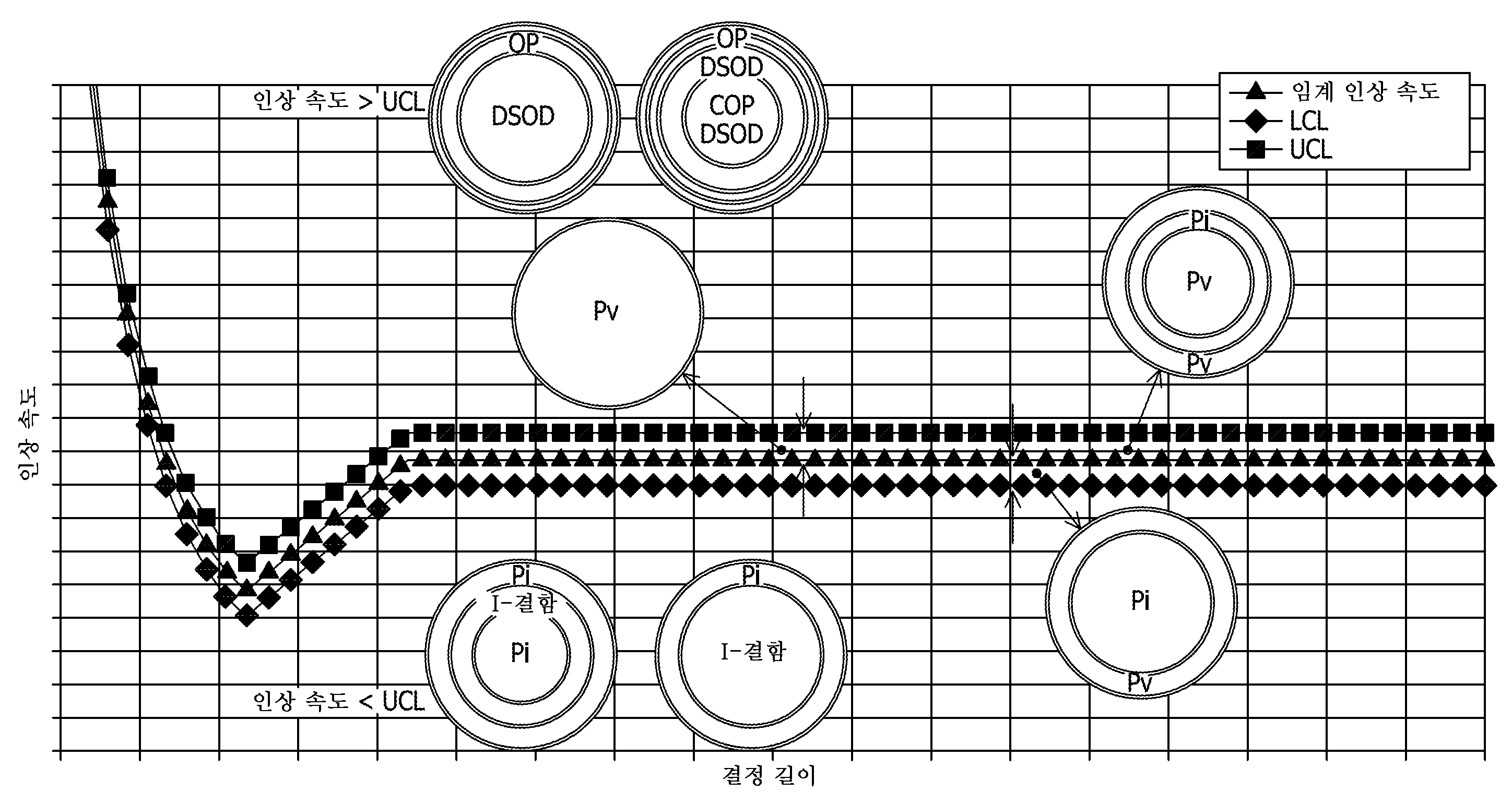
단결정 실리콘 잉곳을 성장시키기 위한 종래의 배치 쵸크랄스키 프로세스에서, 결정 용융물/계면 및 열 조건 둘 다는 잉곳 성장 동안의 실리콘 용융물의 소비 및 도가니 위치의 가변성으로 인해 잉곳 길이를 증가시키는 함수로서 연속적으로 변화된다. 도가니의 용융물 고갈 및 이동의 도면은 도 1에서 발견될 수 있다. 도 1a(초기 본체 성장), 도 1b(중기 본체 성장), 및 도 1c(말기 본체 성장)는 배치 Cz 프로세스 동안 결정 길이의 함수로서 용융물 레벨 및 도가니 높이를 예시한다. 용융물 조건들, 예를 들어, 질량 및 상승 레벨들, 및 도가니 위치가 배치 프로세스 동안 연속적으로 변화되고 있으므로, 결함도를 최소화하는데 필요한 v/G 비율(성장 속도(V)/축방향 온도 기울기(G))은 결정 길이에 걸쳐 연속적으로 변화되어, 결정의 품질을 변경한다. 프로세스 윈도우 내에서 사양을 충족하기 위한 원하는 품질을 유지하기 위해, 몇 가지 매개변수들의 연속 제어 조정은 위치에 따라 필요하다. 이들 매개변수들은 도가니 회전 속도(C/R), 시드 회전 속도(S/R), 시드 리프트 속도(S/L), 히터 전력, 반사기 높이 등을 포함한다. 도 2를 참조하여, 도 2는 예시적 배치 Cz 프로세스에 의해 성장되는 잉곳에서 충분한 결함도 제어를 달성하도록 요구되는 인상 속도의 일정한 변화를 도시하는 그래프이다. 삼각형(---▲---)에 의해 정의되는 라인은 임계 v/G 값을 달성하기 위한 일정하게 변화하는 임계 인상 속도이다. 인상 속도는 정사각형(---■---)에 의해 표시되는 상부 임계 인상 속도("UCL") 및 다이아몬드(---◆---)에 의해 표시되는 하부 임계 인상 속도("LCL") 내에서 변화되고 허용가능 결함도 제어를 여전히 달성할 수 있다. 이들 3개의 라인은 완벽한 실리콘을 생성할 수 있는 인상 속도를 나타낸다. 상부 및 하부 인상 속도 경계들 내에서, 변화하는 지배적 고유 점 결함들을 갖는 완벽한 실리콘이 생성될 수 있다. 예를 들어, 공공 지배적("Pv") 실리콘은 적용된 인상 속도가 도 2(및 도 3 및 도 4)에서 삼각형 및 정사각형으로 라벨링된 라인들 사이에서 제어될 때 생성되고, 간극 지배적("Pi") 실리콘은 적용된 인상 속도가 도 2(및 도 3 및 도 4)에서 삼각형 및 다이아몬드로 라벨링된 라인들 사이에서 제어될 때 생성된다. 도 2(및 도 3 및 도 4)에 도시된 예, 잉곳 성장의 초기 및 중기 위치들에서, 공공 지배적 점 결함들을 갖는 완벽한 실리콘은 "Pv"로 라벨링된 잉곳 단면의 표현에 의해 도시된 바와 같이, 성장될 수 있다. 도 2는 잉곳이 중앙으로부터 가장자리로 공공 지배적인 것을 도시한다. 도 2에 도시된 예에서, 나중의 성장에서, 잉곳은 공공 지배적 점 결함들 및 간극 지배적 점 결함들의 영역들에 의해 특징화되며, 이는 "Pi"로 라벨링된 단면 영역들에 표현된다. 예를 들어, 중앙으로부터 전체 잉곳의 반경 미만의 반경방향 길이로 간극 지배적인 잉곳이 성장될 수 있으며, 이는 잉곳의 가장자리에 대한 공공 지배적 재료의 대역에 의해 둘러싸여진다. 더 나중의 영역에서, 잉곳의 단면은 가장자리에서 공공 지배적 재료의 다른 대역에 의해 둘러싸여지는, 간극 지배적 재료의 대역에 의해 둘러싸여지는, 중앙 내의 공공 지배적 재료를 도시한다. 이들 도면들은 단지 예시를 위한 것이고 본 발명의 방법에 제한적인 것으로 의도되지 않는다. 완벽한 실리콘, 즉, 검출가능한 응집된 점 결함들이 없는 잉곳들 및 이들로부터 슬라이스된 웨이퍼들은 잉곳의 인상 속도에 의해 부분적으로 초과 점 결함들(공공 및 간극 실리콘)의 적절한 제어에서 기인한다. 공공들 및 간극들과 같은, 고유 점 결함들은 쵸크랄스키 방법에 의해 성장되는 잉곳들에서 발생한다. 그러한 결함들의 존재는 실리콘이 완벽한지에 영향을 미치지 않는다. 오히려, 완벽한 실리콘은 COP들, DSOD들, 및 I-결함들과 같은, 응집된 점 결함들이 없는 것으로서 특징화된다.In the conventional batch Czochralski process for growing single crystal silicon ingots, both the crystal melt/interfacial and thermal conditions change continuously as a function of increasing ingot length due to variability in crucible position and consumption of the silicon melt during ingot growth. do. A diagram of the melt depletion and movement of the crucible can be found in FIG. 1 . 1A (early body growth), 1B (mid-stage body growth), and 1C (late body growth) illustrate melt level and crucible height as a function of crystal length during a batch Cz process. As melt conditions, e.g., mass and elevation levels, and crucible position are continuously changing during the batch process, the v/G ratio required to minimize the degree of defect (growth rate (V)/axial temperature gradient (G) )) is continuously varied over the crystal length, changing the quality of the crystal. In order to maintain the desired quality to meet specifications within the process window, continuous controlled adjustments of several parameters are required from location to location. These parameters include crucible rotation speed (C/R), seed rotation speed (S/R), seed lift speed (S/L), heater power, reflector height, and the like. Referring to FIG. 2, FIG. 2 is a graph showing the constant change in pull rate required to achieve sufficient defectivity control in ingots grown by the exemplary batch Cz process. The line defined by the triangle (---▲---) is the constantly varying threshold pull-up speed to achieve the threshold v/G value. The pull-up rates are the upper critical pull-up rate ("UCL") represented by squares (---■---) and the lower critical pull-up rate ("LCL") represented by diamonds (---◆---). can be varied within and still achieve acceptable fault control. These three lines represent the pull rates that can produce perfect silicon. Within the upper and lower pull rate boundaries, perfect silicon with varying dominant intrinsic point defects can be created. For example, vacancy-dominant (“Pv”) silicon is produced when the applied pull rate is controlled between the lines labeled triangle and square in FIG. 2 (and FIGS. 3 and 4), and the gap-dominant (“Pi” ) silicon is produced when the applied pull rate is controlled between the lines labeled triangles and diamonds in FIG. 2 (and FIGS. 3 and 4). In the example shown in Fig. 2 (and Figs. 3 and 4), at the early and intermediate positions of ingot growth, perfect silicon with vacancy-dominant point defects is shown by the representation of the ingot cross-section labeled "Pv". , can be grown. Figure 2 shows that the ingot is void dominant from the center to the edge. In the example shown in FIG. 2 , in later growth, the ingot is characterized by regions of void-dominant point defects and interstitial-dominant point defects, which are represented in the cross-sectional regions labeled “Pi”. For example, a gap-dominant ingot can be grown from the center to a radial length less than the radius of the entire ingot, which is surrounded by a zone of void-dominant material to the edges of the ingot. In a later region, the cross-section of the ingot shows a vacancy-dominant material in the center, surrounded by a zone of interstitial dominant material, surrounded by another zone of vacancy-dominant material at the edges. These drawings are for illustrative purposes only and are not intended to be limiting to the method of the present invention. Perfect silicon, i.e., ingots free of detectable aggregated point defects and wafers sliced from them, is due in part to proper control of excess point defects (void and interstitial silicon) by the pulling rate of the ingot. Intrinsic point defects, such as voids and interstices, occur in ingots grown by the Czochralski method. The presence of such defects does not affect whether the silicon is perfect. Rather, perfect silicon is characterized as being free of aggregated point defects, such as COPs, DSODs, and I-defects.
도 2(및 또한 도 3 및 도 4)는 또한 임의의 결정 길이에서 임계 v/G의 상한 및 하한 밖의 인상 속도들의 함수로서 잉곳을 초래할 수 있는 응집된 결함들을 나타낸다. 상부 임계 인상 속도가 초과되면(v/G가 임계 v/G보다 더 높으면) 발생할 수 있는 결함들은 직접 표면 산화물 결함들(DSOD) 또는 결정 유래 피트들 또는 입자들(COP)을 포함한다. 인상 속도가 하부 임계 인상 속도 아래이면(v/G가 임계 v/G보다 더 낮으면) 발생할 수 있는 결함들은 I-결함들을 포함한다. 이들 결함들이 발생하는 대역들은 또한 잉곳 단면들에 도시된다. 지배적 초과 점 결함이 공공들인 영역들에서, 공공 결함들의 응집체들은 Cz 실리콘 결정 성장 및 냉각 동안 공공들의 응집 및 석출에 의해 COP, DSOD와 같은 벌키 결함을 형성한다. 지배적 초과 점 결함이 간극 실리콘 원자들인 영역들에서, 그들은 응집되어 간극 실리콘의 응집/석출에 의해 I-결함과 같은 벌크 결함을 형성하고 전위를 펀치 아웃한다. v/G의 임의의 작은 편차는 공공 또는 간극 실리콘 원자의 응집에 의해 결함을 형성할 것이다.Figure 2 (and also Figures 3 and 4) also shows aggregated defects that can result in an ingot as a function of pulling rates outside the upper and lower limits of the critical v/G at any crystal length. Defects that may occur if the upper critical pulling rate is exceeded (v/G is higher than the critical v/G) include direct surface oxide defects (DSOD) or crystal derived pits or particles (COP). If the pulling speed is below the lower threshold pulling speed (v/G is lower than the threshold v/G), the defects that may occur include I-defects. The zones where these defects occur are also shown in the ingot cross sections. In regions where the dominant excess point defects are vacancies, aggregates of vacancy defects form bulky defects such as COP, DSOD by aggregation and precipitation of vacancies during Cz silicon crystal growth and cooling. In regions where the dominant excess point defects are interstitial silicon atoms, they aggregate to form bulk defects such as I-defects by aggregation/precipitation of interstitial silicon and punch out dislocations. Any small deviation of v/G will form defects by aggregation of vacancy or interstitial silicon atoms.
자기장들, 예를 들어, 수평 또는 첨두는 도가니 내에서 용융물 흐름 패턴을 변경하고 결정/용융물 계면의 형상 및 높이의 향상된 제어를 가능하게 하기 위해 인가될 수 있으며, 이는 그것에 의해 품질 제어를 향상시킨다. 그러나, 인상 속도들 및 다른 매개변수들은 도 3에 예시된 바와 같이, 허용가능 결함도 제어를 달성하기 위해 여전히 변화되어야 한다. 도 3은 인가된 자기장으로 예시적 배치 Cz 프로세스에 의해 성장되는 잉곳에서 충분한 결함도 제어를 달성하도록 요구되는 인상 속도 프로파일들을 도시하는 그래프이다. 삼각형(---▲---)에 의해 정의되는 라인은 임계 v/G 값을 달성하기 위한 임계 인상 속도이며, 이는 필요에 따라, 단결정 실리콘 잉곳의 성장 동안 연속적으로 변화된다. 인상 속도는 정사각형(---■---)에 의해 표시되는 상부 임계 인상 속도("UCL") 및 다이아몬드(---◆---)에 의해 표시되는 하부 임계 인상 속도("LCL") 내에서 변화되고 허용가능 결함도 제어를 여전히 달성할 수 있다. 단결정 실리콘 잉곳의 단면에서의 고유 점 결함 및 응집된 점 결함의 영역들은 실질적으로 도 2의 설명에서 상술된 바와 같다.Magnetic fields, eg horizontal or peaking, can be applied to change the melt flow pattern within the crucible and enable improved control of the shape and height of the crystal/melt interface, thereby improving quality control. However, pull speeds and other parameters must still be varied to achieve acceptable defectivity control, as illustrated in FIG. 3 . FIG. 3 is a graph illustrating pull rate profiles required to achieve sufficient defectivity control in an ingot grown by an exemplary batch Cz process with an applied magnetic field. The line defined by the triangle (---▲---) is the critical pulling rate to achieve the critical v/G value, which is continuously varied during the growth of the monocrystalline silicon ingot as needed. The pull-up rates are the upper critical pull-up rate ("UCL") represented by squares (---■---) and the lower critical pull-up rate ("LCL") represented by diamonds (---◆---). can be varied within and still achieve acceptable fault control. The regions of intrinsic point defects and aggregated point defects in the cross section of the single crystal silicon ingot are substantially as described above in the description of FIG. 2 .
본 발명의 방법에 따르면, 단결정 실리콘 잉곳은 용융물이 소비됨에 따라 연속적으로 보충되기 때문에 성장 동안 실질적으로 일정하게 남아 있기 위해 용융물 깊이를 가능하게 하는 조건들(즉, 용융된 실리콘의 상승 레벨) 및 열 조건들 하에 연속 쵸크랄스키(CCZ) 방법에 의해 성장된다. 일부 실시예들에서, 용융된 실리콘의 실질적으로 일정한 상승 레벨을 유지하는 것은 고정된 위치에 도가니를 유지하는 것을 가능하게 한다. v/G가 적절한 고온 구역 구성에서 고정되면, 프로세스 윈도우는 결정 길이의 상당 부분에 걸쳐 고정될 것이다(즉, 어떤 제어 조정도 없음). 프로세스 조건들(S/R, 전력, 기체 흐름 및 압력, 자속 밀도, 첨두 또는 HMCZ MGP 위치)이 설정되면, 기체 흐름 및/또는 챔버 압력 및 C/R은 산소 함량을 제어하기 위해 사용된다. 따라서, 본 발명의 방법은 인상 속도가 잉곳의 상당한 길이의 성장 동안 일정한 연속 쵸크랄스키(CCZ) 방법에 의한 단결정 실리콘 잉곳의 성장을 가능하게 하고, 이 방법에 따른 성장된 잉곳은 잉곳의 축방향 길이의 상당 부분에 걸쳐 균일한 허용가능 결함도 제어, Oi 균일성, 및 BMD 균일성을 갖는다.According to the method of the present invention, conditions (i.e., rising levels of molten silicon) and heat enabling the melt depth to remain substantially constant during growth as the single crystal silicon ingot is continuously replenished as the melt is consumed. It is grown by the continuous Czochralski (CCZ) method under conditions. In some embodiments, maintaining a substantially constant elevated level of molten silicon makes it possible to maintain the crucible in a fixed position. If v/G is fixed in the appropriate hot zone configuration, the process window will be fixed (i.e., no control adjustments) over a significant portion of the crystal length. Once the process conditions (S/R, power, gas flow and pressure, flux density, peak or HMCZ MGP position) are established, gas flow and/or chamber pressure and C/R are used to control the oxygen content. Thus, the method of the present invention enables the growth of a single crystal silicon ingot by the continuous Czochralski (CCZ) method in which the pulling rate is constant during the growth of a significant length of the ingot, and the ingot grown according to this method has an axial direction of the ingot Uniform acceptable defectivity control, Oi uniformity, and BMD uniformity over a significant portion of the length.
모든 조건들이 정상 상태로 설정된 후에, 전체 결정 길이에서 원하는 결함도 제어를 갖는 단결정 실리콘 잉곳을 생산하기 위한 인상 속도는 일정해서, 종래의 Cz 프로세스와 비교하여 프로세스 제어로 인해 생산의 품질 손실들을 상당히 감소시킬 것이다. 도 4는 본 발명에 따른 예시적 연속 쵸크랄스키 성장 방법 동안 단결정 실리콘 잉곳의 축방향 길이의 함수로서의 인상 속도의 그래프이다. 도 4에 도시된 바와 같이, 일정한 인상 속도는 단결정 실리콘 잉곳의 본체 부분의 성장의 상당 부분에 걸쳐 유지된다. 삼각형(---▲---)에 의해 정의되는 라인은 임계 v/G 값을 달성하기 위한 임계 인상 속도이며, 이는 초기 변화하는 영역 다음에, 단결정 실리콘 잉곳의 본체 부분의 성장의 상당 부분에 걸쳐 일정한 인상 속도의 영역을 갖는다. 인상 속도는 정사각형(---■---)에 의해 표시되는 상부 임계 인상 속도("UCL") 및 다이아몬드(---◆---)에 의해 표시되는 하부 임계 인상 속도("LCL") 내에서 변화되고 허용가능 결함도 제어를 여전히 달성할 수 있다. 단결정 실리콘 잉곳의 단면에서의 고유 점 결함 및 응집된 점 결함의 영역들은 실질적으로 도 2의 설명에 상술된 바와 같다.After all conditions are set to a steady state, the pulling rate to produce a single crystal silicon ingot with the desired defectivity control over the entire crystal length is constant, significantly reducing quality losses in production due to process control compared to the conventional Cz process will do 4 is a graph of pull rate as a function of axial length of a single crystal silicon ingot during an exemplary continuous Czochralski growth method according to the present invention. As shown in Fig. 4, a constant pull rate is maintained throughout a significant portion of the growth of the body portion of the single crystal silicon ingot. The line defined by the triangle (---▲---) is the critical pull-up rate to achieve the critical v/G value, which follows the initial changing region, for a significant portion of the growth of the body portion of the monocrystalline silicon ingot. It has a region of constant pulling speed throughout. The pull-up rates are the upper critical pull-up rate ("UCL") represented by squares (---■---) and the lower critical pull-up rate ("LCL") represented by diamonds (---◆---). can be varied within and still achieve acceptable fault control. The regions of intrinsic point defects and aggregated point defects in the cross section of the single crystal silicon ingot are substantially as described above in the description of FIG. 2 .
본 발명의 방법에 따른 CCZ 프로세스에서, 다결정 실리콘 공급은 결정 성장에 연속적이며, 그것에 의해 용융물 체적은 결정 길이에 관계없이 초기 충전물 용융 깊이와 실질적으로 동일하게 유지된다. 용융물 상승이 성장 결정 중량과 연속적으로 공급된 다결정 실리콘 사이의 질량 균형에 의해 제어되므로, 용융물 및 성장 결정에서의 열 조건은 축방향 성장 전체에서 변화되지 않는다. 그 후에, 원하는 결정/용융물 계면이 자기장, C/R 및 S/R, 인상 속도, 히터 전력 등과 같은 매개변수들에 의해 결정되고 고정되면, 결함 품질 및 Oi 제어는 결정 축방향 성장 전체에서 일정하게 유지될 것이다. 게다가, 열 조건들 및 결정/용융물 계면이 결정 성장 동안 고정되기 때문에, 주어진 HZ 및 결정/용융물 계면에 대한 일정한 인상 속도는 준정상 상태 제어에서 전체 결정 길이에 걸쳐 사용될 수 있다.In the CCZ process according to the method of the present invention, the polycrystalline silicon supply is continuous with the crystal growth, whereby the melt volume remains substantially the same as the initial charge melt depth regardless of the crystal length. Since the melt rise is controlled by the mass balance between the growing crystal weight and the continuously supplied polycrystalline silicon, the thermal conditions in the melt and growing crystal do not change throughout axial growth. Then, once the desired crystal/melt interface is determined and fixed by parameters such as magnetic field, C/R and S/R, pulling speed, heater power, etc., the defect quality and Oi control remain constant throughout the crystal axial growth. will be maintained Moreover, since the thermal conditions and crystal/melt interface are fixed during crystal growth, a constant pull rate for a given HZ and crystal/melt interface can be used over the entire crystal length in quasi-steady state control.
본 발명의 방법에 따르면, 결함도 제어에 대한 요건들을 충족하는 단결정 실리콘 잉곳의 성장을 달성하는데 적합한 열 조건은 고온 구역 구성에 의해 설정된다. 성장 방법은 연속 쵸크랄스키 방법이다. 따라서, 퍼니스 챔버는 다결정 실리콘의 연속 공급을 위한 수단, 예를 들어 공급 튜브를 포함한다. 도가니에 첨가되는 고체 폴리실리콘은 전형적으로 입상 폴리실리콘이지만, 청크 폴리실리콘이 사용될 수 있으며, 그것은 입상 폴리실리콘과 함께 사용하도록 최적화된 폴리실리콘 공급기를 사용하여 도가니에 공급된다. 청크 폴리실리콘은 전형적으로 3 내지 45 밀리미터의 크기(예를 들어, 최대 치수)를 갖고, 입상 폴리실리콘은 전형적으로 400 내지 1400 미크론의 크기를 갖는다. 입상 폴리실리콘은 더 작은 크기로 인해, 공급 속도의 쉽고 정확한 제어를 제공하는 것을 포함하여 몇 가지 장점을 갖는다. 그러나, 입상 폴리실리콘의 비용은 전형적으로 화학 기상 증착 프로세스, 또는 그것의 생산에서 사용되는 다른 제조 방법들로 인해, 청크 폴리실리콘의 비용보다 높다. 청크 폴리실리콘은 그것의 더 큰 크기를 고려하여, 더 저렴하고 더 높은 공급 속도가 가능하다는 장점을 갖는다. 가열 유닛들, 냉각 재킷의 위치, 및 전력 제어의 동작은 다결정 실리콘 공급기를 수용하기 위해 조정된다.According to the method of the present invention, thermal conditions suitable for achieving the growth of a single crystal silicon ingot that meets the requirements for defectivity control are set by a high-temperature zone configuration. The growth method is the continuous Czochralski method. Thus, the furnace chamber comprises means for a continuous supply of polycrystalline silicon, for example a supply tube. The solid polysilicon added to the crucible is typically granular polysilicon, but chunk polysilicon may be used, which is fed to the crucible using a polysilicon feeder optimized for use with granular polysilicon. Chunk polysilicon typically has a size (eg, maximum dimension) of 3 to 45 millimeters, and granular polysilicon typically has a size of 400 to 1400 microns. Granular polysilicon has several advantages, including providing easy and precise control of the feed rate due to its smaller size. However, the cost of granular polysilicon is typically higher than that of chunk polysilicon due to the chemical vapor deposition process, or other fabrication methods used in its production. Chunk polysilicon has the advantage of being cheaper and allowing for higher feed rates, given its larger size. The operation of the heating units, the location of the cooling jacket, and power control are coordinated to accommodate the polycrystalline silicon supply.
상이한 용융물 구역들로 용융물을 분리하는 복수의 위어(weir)(20, 30, 40) 또는 유체 장벽들을 갖는 도가니(10)의 도면은 도 5에 도시된다. 예시된 실시예에서, 도가니 조립체(10)는 실리콘 용융물의 내부 용융물 구역(22)을 정의하는 제1 위어(20)(광범위하게, 유체 장벽)를 포함한다. 내부 용융물 구역(22)은 단결정 실리콘 잉곳(50)이 성장되는 성장 영역이다. 제2 위어(30)는 실리콘 용융물의 중간 용융물 구역(32)을 정의한다. 최종적으로, 제3 위어(40)는 실리콘 용융물의 외부 용융물 구역(42)을 정의한다. 공급 튜브(도시되지 않음)는 잉곳의 성장 동안 실질적으로 일정한 용융물 상승 레벨 및 체적을 유지하기에 충분한 속도로 입상, 청크, 또는 입상 및 청크의 조합일 수 있는 다결정 실리콘을 외부 용융물 구역(42)으로 공급한다. 제1 위어(20), 제2 위어(30), 및 제3 위어(40) 각각은 일반적으로 환형 형상을 갖고, 용융된 실리콘이 내부 용융물 구역(22)의 성장 영역을 향해 반경방향 내부로 흐르는 것을 허용하기 위해 그 안에 정의된 적어도 하나의 개구부를 갖는다. 도 5에 도시된 도가니 구성은 예시적이고 본 발명의 프로세스를 수행하는데 적합하다. CCZ에 적합한 다른 구성들은 본 발명의 범위로부터 벗어나지 않고 사용될 수 있다. 예를 들어, 도가니(10)는 제2 위어(30)가 없을 수 있고/있거나 제3 위어(40)가 없을 수 있다.A view of a
일반적으로, 잉곳이 인발되는(drawn) 용융물은 다결정 실리콘을 도가니에 장입하여 초기 실리콘 충전물을 형성함으로써 형성된다. 일반적으로, 초기 충전물은 다결정 실리콘의 약 100 킬로그램 내지 약 200 킬로그램이며, 이는 입상, 청크, 또는 입상 및 청크의 조합일 수 있다. 초기 충전물들의 질량은 원하는 결정 직경 및 HZ 디자인에 의존한다. 초기 충전물은 다결정 실리콘이 결정 성장 동안 연속적으로 공급되기 때문에, 결정의 길이를 반영하지 않는다. 예를 들어, 다결정 실리콘이 연속적으로 공급되고 챔버 높이가 충분히 크면, 결정 길이는 2000 mm, 3000 mm, 또는 심지어 4000 mm 길이로 연장될 수 있다. 도가니는 도 5에 도시된 구성, 또는 CCZ 성장에 적합한 다른 구성을 가질 수 있다. 다결정 실리콘의 다양한 공급원들은 예를 들어, 유동화된 베드 반응기에서 실란 또는 할로실란의 열 분해에 의해 생성되는 입상 다결정 실리콘 또는 지멘스(Siemens) 반응기에서 생산되는 다결정 실리콘을 포함하여 사용될 수 있다. 다결정 실리콘이 도가니에 추가되어 충전물을 형성하면, 충전물은 대략 실리콘의 용융 온도(예를 들어, 약 1412 ℃)보다 높은 온도로 가열되어 충전물을 용융시키고, 그것에 의해 용융된 실리콘을 포함하는 실리콘 용융물을 형성한다. 실리콘 용융물은 용융된 실리콘의 초기 체적을 갖고 초기 용융물 상승 레벨을 가지며, 이들 매개변수들은 초기 충전물의 크기에 의해 결정된다. 일부 실시예들에서, 실리콘 용융물을 포함하는 도가니는 적어도 약 1425 ℃, 적어도 약 1450 ℃ 또는 심지어 적어도 약 1500 ℃의 온도로 가열된다.Generally, the melt from which the ingot is drawn is formed by charging polycrystalline silicon into a crucible to form an initial silicon charge. Typically, the initial charge is about 100 kilograms to about 200 kilograms of polycrystalline silicon, which can be granular, chunky, or a combination of granular and chunky. The mass of the initial charges depends on the desired crystal diameter and HZ design. The initial charge does not reflect the length of the crystal because polycrystalline silicon is supplied continuously during crystal growth. For example, if the polycrystalline silicon is supplied continuously and the chamber height is sufficiently large, the crystal length can extend to 2000 mm, 3000 mm, or even 4000 mm length. The crucible may have the configuration shown in FIG. 5, or any other configuration suitable for CCZ growth. A variety of sources of polycrystalline silicon may be used including, for example, granular polycrystalline silicon produced by thermal decomposition of silane or halosilane in a fluidized bed reactor or polycrystalline silicon produced in a Siemens reactor. When polycrystalline silicon is added to the crucible to form a charge, the charge is heated to a temperature above approximately the melting temperature of silicon (e.g., about 1412° C.) to melt the charge, thereby forming a silicon melt comprising molten silicon. form The silicon melt has an initial volume of molten silicon and an initial melt rise level, these parameters being determined by the size of the initial charge. In some embodiments, a crucible containing a silicon melt is heated to a temperature of at least about 1425 °C, at least about 1450 °C or even at least about 1500 °C.
충전물이 액화되어 용융된 실리콘을 포함하는 실리콘 용융물을 형성하면, 실리콘 시드 결정이 하강되어 용융물과 접촉한다. 그 다음, 실리콘 시드 결정은 실리콘이 그것(즉, 도 5를 참조하여, 시드 결정 부분 및 목(52))에 부착되는 상태에서 용융물로부터 회수되며 그것에 의해 용융물의 표면 근처에 또는 표면에 용융물/고체 계면을 형성한다. 일반적으로, 목 부분을 형성하기 위한 초기 인상 속도는 높다. 일부 실시예들에서, 실리콘 시드 결정 및 목 부분은 적어도 약 1.0 ㎜/분, 예컨대 약 1.5 ㎜/분 내지 약 6 ㎜/분, 예컨대 약 3 ㎜/분 내지 약 5 ㎜/분의 목 부분 인상 속도로 회수된다. 일부 실시예들에서, 실리콘 시드 결정 및 도가니는 반대 방향들, 즉, 역회전으로 회전된다. 역회전은 실리콘 용융물에서 대류를 달성한다. 결정의 회전은 대칭 온도 프로파일을 제공하고, 불순물들의 각도 변동을 억제하고 또한 결정 용융물 계면 형상을 제어하기 위해 주로 사용된다. 일부 실시예들에서, 실리콘 시드 결정은 약 5 rpm 내지 약 30 rpm, 또는 약 5 rpm 내지 약 20 rpm, 또는 약 8 rpm 내지 약 20 rpm, 또는 약 10 rpm 내지 약 20 rpm의 속도로 회전된다. 일부 실시예들에서, 도가니는 약 0.5 rpm 내지 약 10 rpm, 또는 약 1 rpm 내지 약 10 rpm, 또는 약 4 rpm 내지 약 10 rpm, 또는 약 5 rpm 내지 약 10 rpm의 속도로 회전된다. 일부 실시예들에서, 시드 결정은 도가니보다 더 빠른 속도로 회전된다. 일부 실시예들에서, 시드 결정은 도가니의 회전 속도 더 높은 적어도 1 rpm, 예컨대 더 높은 적어도 약 3 rpm, 또는 더 높은 적어도 약 5 rpm인 속도로 회전된다. 일반적으로, 목 부분(52)은 약 300 밀리미터 내지 약 700 밀리미터, 예컨대 약 450 밀리미터 내지 약 550 밀리미터의 길이를 갖는다. 그러나, 목 부분(52)의 길이는 이들 범위들 밖에서 달라질 수 있다.When the charge liquefies to form a silicon melt comprising molten silicon, the silicon seed crystals are lowered into contact with the melt. The silicon seed crystal is then withdrawn from the melt with the silicon attached to it (i.e., the seed crystal portion and
목(52) 형성 후, 도 5를 참조하여, 목(52)에 인접한 바깥쪽으로 벌어지는 시드 원뿔 부분(54)이 성장된다. 일반적으로, 인상 속도는 목 부분 인상 속도로부터 바깥쪽으로 벌어지는 시드 원뿔 부분(54)을 성장시키는데 적합한 속도로 감소된다. 예를 들어, 바깥쪽으로 벌어지는 시드 원뿔의 성장 동안의 시드 원뿔 인상 속도는 약 0.5㎜/분 내지 약 2.0㎜/분, 예컨대 약 1.0㎜/분이다. 일부 실시예들에서, 바깥쪽으로 벌어지는 시드 원뿔(54)은 약 100 밀리미터 내지 약 400 밀리미터, 예를 들어 약 150 밀리미터 내지 약 250 밀리미터의 길이를 갖는다. 바깥쪽으로 벌어지는 시드 원뿔(54)의 길이는 이러한 범위들 밖에서 달라질 수 있다. 일부 실시예들에서, 바깥쪽으로 벌어지는 시드 원뿔(54)은 약 150㎜, 적어도 약 150 밀리미터, 약 200㎜, 적어도 약 200 밀리미터, 약 300㎜, 적어도 약 300㎜, 약 450㎜, 또는 심지어 적어도 약 450㎜의 말단 직경으로 성장된다. 바깥쪽으로 벌어지는 시드 원뿔(54)의 말단 직경은 일반적으로 단결정 실리콘 잉곳의 본체의 일정한 직경의 직경과 등가이다.After forming the
목(52) 및 목 부분에 인접한 바깥쪽으로 벌어지는 시드 원뿔(54)의 형성 후, 원뿔 부분에 인접한 일정한 직경을 갖는 잉곳 본체(56)가 이때 성장된다. 잉곳 본체(56)의 일정한 직경 부분은 원주 가장자리, 원주 가장자리에 평행한 중심 축, 및 중심 축으로부터 원주 가장자리로 연장되는 반경을 갖는다. 중심 축은 또한 바깥쪽으로 벌어지는 시드 원뿔(54) 및 목(52)을 통과한다. 잉곳 본체(56)의 직경은 변화될 수 있고 일부 실시예들에서, 직경은 약 150 mm, 적어도 약 150 밀리미터, 약 200 mm, 적어도 약 200 밀리미터, 약 300 mm, 적어도 약 300 mm, 약 450 mm, 또는 심지어 적어도 약 450 mm일 수 있다. 단결정 실리콘 잉곳의 잉곳 본체(52)는 결국 적어도 약 1000 밀리미터 길이, 예컨대 적어도 1400 밀리미터 길이, 예컨대 적어도 1500 밀리미터 길이, 또는 적어도 2000 밀리미터 길이, 또는 적어도 2200 밀리미터, 예컨대 2200 밀리미터, 또는 적어도 약 3000 밀리미터 길이, 또는 적어도 약 4000 밀리미터 길이인 것으로 성장된다.After the formation of the
도 4는 본 발명의 방법의 일부 실시예들에 따른 단결정 실리콘 잉곳의 본체를 인상하기 위한 예시적이고 비제한적 인상 속도 프로토콜을 예시한다. 예시적 예시로부터 분명한 바와 같이, 인상 속도는 비교적 높은 인상 속도로부터 최소 인상 속도로 감소하고, 그 다음 단결정 실리콘 잉곳의 본체의 성장의 상당 부분에 대해 일정한 인상 속도로 상승한다. 본 발명의 프로세스에 따르면, 인상 속도들은 완벽한 실리콘, 즉, 응집된 결함들, 직접 표면 산화 결함들(DSOD), 결정 유래 피트들(COP), D-결함들, 및 I-결함들 등 중에서 선택되는 검출가능 결핍 응집된 결함들에 의해 특징화되는 실리콘을 달성하기 위해 선택된다. 초기 높은 인상 속도는 약 0.5 mm/분 내지 약 2.0 mm/분, 예컨대 약 1.0 mm/분이며, 그 다음 약 0.4 mm/분 내지 약 0.8 mm/분, 약 0.4 mm/분 내지 약 0.7 mm/분, 또는 약 0.4 mm/분 내지 약 0.65 mm/분의 일정한 인상 속도로 증가하기 전에, 약 0.4 mm/분만큼 낮거나 심지어 약 0.3 mm/분만큼 낮을 수 있는 인상 속도로 감소할 수 있다.4 illustrates an exemplary, non-limiting pull rate protocol for pulling a body of a single crystal silicon ingot according to some embodiments of the method of the present invention. As is evident from the illustrative example, the pulling rate decreases from a relatively high pulling rate to a minimum pulling rate, and then rises to a constant pulling rate for a significant portion of the growth of the body of the monocrystalline silicon ingot. According to the process of the present invention, pull rates are selected from among perfect silicon, i.e., aggregated defects, direct surface oxidation defects (DSOD), crystal derived pits (COP), D-defects, and I-defects, etc. are selected to achieve silicon characterized by detectable deficient aggregated defects. The initial high pull speed is about 0.5 mm/min to about 2.0 mm/min, such as about 1.0 mm/min, followed by about 0.4 mm/min to about 0.8 mm/min, about 0.4 mm/min to about 0.7 mm/min. , or at a pull rate that can be as low as about 0.4 mm/min or even as low as about 0.3 mm/min, before increasing to a constant pull rate of about 0.4 mm/min to about 0.65 mm/min.
본 발명의 방법을 수행하는데 적합한 퍼니스 챔버(100) 내의 고온 구역 구성의 예시적이고 비제한적 예시는 도 6a, 도 6b, 및 도 6c에 도시된다. 다른 고온 구역 구성들은 본 발명의 방법을 수행하는데 적합하다. 고온 구역 구성은 냉각 재킷(102), 반사기(104), 측면 히터(106), 및 하단 히터(108)를 포함한다. 성장 결정 직경 및 메니스커스의 형상 및 높이는 상단 윈도우에 위치된 카메라(도시되지 않음)에 의해 감시된다. 카메라로부터 획득되는 데이터는 측면 히터(106) 및 하단 히터(108)에 피드백을 가능하게 한다. 결정 성장 동안, 전력 분포는 용융물/고체 계면의 균일성을 가능하게 하기 위해, 즉, 메니스커스의 원하는 형상 및 높이를 유지하기 위해 히터들 사이에서 조정될 수 있다. 반사기(104)는 히터 및 도가니를 포함하는 퍼니스의 고온 부분으로부터 용융물로 열 유속을 반사시켜야 한다. 반사기(104)는 퍼니스의 고온 부분으로부터 저온 부분(냉각 재킷(102)에 의해 유지됨)으로 열 전달을 감소시키고 그것에 의해 퍼니스의 이들 2개의 영역 사이에 분리를 유지한다. 반사기는 축방향 및 반경방향 온도 기울기들을 제어하는 것을 도우며, 이는 성장 잉곳으로의 용융된 실리콘의 응고 및 결정화를 추진한다.An illustrative, non-limiting example of a hot zone configuration within the
도 6a, 도 6b, 및 도 6c는 도 4에 도시된 인상 속도의 영역들에 대응하는 제1 단계, 제2 단계, 및 제3 단계를 각각 도시한다. 즉, 도 6a에 도시된 제1 단계는 도 4에서 인상 속도가 높고 최소치로 감소하는 영역에 대응한다. 도 6b에 도시된 제2 단계는 도 4에서 인상 속도가 최소치에 있고 일정한 인상 속도로 증가하는 영역에 대응한다. 도 6c에 도시된 제3 단계는 도 4에서 일정한 인상 속도의 영역에 대응한다. 각각의 단계 동안, 용융물(110)은 다결정 실리콘이 잉곳(112)의 성장 동안 용융물(도 5 참조)로 연속적으로 공급되므로 본 발명의 실시예들에 따른 일정한 용융물 체적 및 용융물 상승 레벨을 보유한다.6A, 6B, and 6C respectively show a first step, a second step, and a third step corresponding to the areas of the pulling speed shown in FIG. 4 . That is, the first step shown in FIG. 6A corresponds to the region in FIG. 4 where the pulling speed is high and decreases to a minimum value. The second step shown in FIG. 6B corresponds to the region in FIG. 4 where the pulling speed is at a minimum and increases at a constant pulling speed. The third step shown in FIG. 6C corresponds to the region of constant pulling speed in FIG. 4 . During each step, the
가변 인상 속도에 의해 특징화된 단결정 실리콘 잉곳의 본체를 성장시키는 초기 영역은 단결정 실리콘 잉곳의 본체의 총 길이의 약 20% 미만을 포함할 수 있다. 일부 실시예들에서, 가변 인상 속도 체제는 단결정 실리콘 잉곳의 본체의 길이의 약 5% 내지 약 20%, 예컨대 단결정 실리콘 잉곳의 본체의 길이의 약 5% 내지 약 15%, 또는 단결정 실리콘 잉곳의 본체의 길이의 약 10% 내지 약 15%를 포함할 수 있다. 가변 인상 속도 조건들 하에 성장되는 단결정 실리콘 잉곳의 본체의 길이의 퍼센티지는 잉곳의 본체의 총 길이에 부분적으로 의존한다. 예를 들어, 가변 속도 조건들 하에 인상되는 잉곳의 본체의 길이는 약 50 mm 내지 약 200 mm 사이, 약 100 mm 내지 약 200 mm 사이, 예컨대 약 150 mm 내지 약 200 mm 사이에서 변화될 수 있다. 200 mm가 가변 속도 조건들 하에 성장되고, 잉곳의 본체의 총 길이가 1400 mm이면, 본체의 약 14%가 가변 속도 조건들 하에 성장되는 한편, 본체의 약 9%만이 2200 mm의 총 본체 길이에 대해 가변 속도 조건들 하에 성장된다.The initial region for growing the body of the monocrystalline silicon ingot characterized by the variable pull rate may include less than about 20% of the total length of the body of the monocrystalline silicon ingot. In some embodiments, the variable pull rate regime is about 5% to about 20% of the length of the body of the monocrystalline silicon ingot, such as about 5% to about 15% of the length of the body of the monocrystalline silicon ingot, or the body of the monocrystalline silicon ingot. It may comprise about 10% to about 15% of the length of. The percentage of the length of the body of a single crystal silicon ingot grown under variable pull rate conditions depends in part on the total length of the body of the ingot. For example, the length of the body of the ingot being pulled under variable speed conditions may vary between about 50 mm and about 200 mm, between about 100 mm and about 200 mm, such as between about 150 mm and about 200 mm. If 200 mm is grown under variable speed conditions and the total length of the body of the ingot is 1400 mm, about 14% of the body is grown under variable speed conditions, while only about 9% of the body is grown to a total body length of 2200 mm. grown under variable rate conditions.
본체의 초기 영역이 가변 인상 속도 조건들 하에 성장된 후에, 본체의 나머지는 일정한 인상 속도 하에 성장된다. 일부 실시예들에서, 잉곳의 본체는 단결정 실리콘 잉곳의 본체의 길이의 적어도 약 30%, 예컨대 단결정 실리콘 잉곳의 본체의 길이의 적어도 약 50%, 단결정 실리콘 잉곳의 본체의 길이의 적어도 약 70%, 단결정 실리콘 잉곳의 본체의 길이의 적어도 약 80%, 또는 심지어 단결정 실리콘 잉곳의 본체의 길이의 적어도 약 90%의 성장 동안 일정한 본체 인상 속도로 성장된다. 일부 실시예들에서, 일정한 본체 인상 속도는 약 0.4 mm/분 내지 약 0.8 mm/분, 약 0.4 mm/분 내지 약 0.7 mm/분, 또는 약 0.4 mm/분 내지 약 0.65 mm/분이다.After the initial region of the body is grown under variable pulling speed conditions, the rest of the body is grown under constant pulling speed. In some embodiments, the body of the ingot is at least about 30% of the length of the body of the monocrystalline silicon ingot, such as at least about 50% of the length of the body of the monocrystalline silicon ingot, at least about 70% of the length of the body of the monocrystalline silicon ingot, The monocrystalline silicon ingot is grown at a constant body pull rate during growth of at least about 80% of the length of the body, or even at least about 90% of the length of the body of the monocrystalline silicon ingot. In some embodiments, the constant body pull rate is between about 0.4 mm/min and about 0.8 mm/min, between about 0.4 mm/min and about 0.7 mm/min, or between about 0.4 mm/min and about 0.65 mm/min.
단결정 실리콘 잉곳의 본체의 성장 동안, 다결정 실리콘, 즉, 입상, 청크, 또는 입상 및 청크의 조합은 용융된 실리콘에 첨가되며 그것에 의해 용융된 실리콘의 일정한 체적 및 일정한 용융물 상승 레벨을 달성한다. 본 발명의 방법에 따르면, 단결정 실리콘 잉곳의 본체의 축방향 길이의 상당 부분의 성장 동안 실질적으로 일정한 용융물 체적의 유지는 일정한 인상 속도로 단결정 실리콘 잉곳의 본체의 축방향 길이의 상당 부분에 걸쳐 높은 잉곳 품질의 달성을 가능하게 한다. 일정한 용융물 체적은 결정 길이에 관계없이 잉곳의 본체의 상당 부분에 걸쳐 일정한 결정/용융물 계면 및 따라서 균일한 결정 품질을 유지하는 것을 가능하게 한다. 따라서, 일부 실시예들에서, 용융된 실리콘의 체적은 단결정 실리콘 잉곳의 본체의 적어도 약 90%의 성장 동안 약 1.0 체적 % 이하만큼, 또는 단결정 실리콘 잉곳의 본체의 적어도 약 90%의 성장 동안 약 0.5 체적 % 이하만큼, 또는 심지어 단결정 실리콘 잉곳의 본체의 적어도 약 90%의 성장 동안 약 0.1 체적 % 이하만큼 변화된다. 다른 방식으로 서술하면, 일부 실시예들에서, 용융물 상승 레벨은 단결정 실리콘 잉곳의 본체의 적어도 약 90%의 성장 동안 약 +/- 0.5 밀리미터 미만만큼 변화된다.During the growth of the body of the single crystal silicon ingot, polycrystalline silicon, i.e. granules, chunks, or a combination of granules and chunks, is added to the molten silicon to thereby achieve a constant volume of molten silicon and a constant melt rise level. According to the method of the present invention, maintenance of a substantially constant melt volume during growth of a substantial portion of the axial length of the body of the monocrystalline silicon ingot is achieved by forming a high ingot over a substantial portion of the axial length of the body of the monocrystalline silicon ingot at a constant pulling rate. enable quality to be achieved. A constant melt volume makes it possible to maintain a constant crystal/melt interface and thus uniform crystal quality over a significant portion of the body of the ingot, regardless of the crystal length. Thus, in some embodiments, the volume of molten silicon is less than or equal to about 1.0 volume percent during growth of at least about 90% of the body of the monocrystalline silicon ingot, or about 0.5% during growth of at least about 90% of the body of the monocrystalline silicon ingot. change by no more than about 0.1 volume percent, or even less than about 0.1 volume percent during growth of at least about 90% of the body of the monocrystalline silicon ingot. Stated another way, in some embodiments, the melt rise level varies by less than about +/-0.5 millimeters during the growth of at least about 90% of the body of the monocrystalline silicon ingot.
추가로, 본 발명의 프로세스에 따르면, 실리콘 용융물을 포함하는 도가니에 자기장이 인가될 수 있다. 적절한 결정/용융물 계면, 즉 메니스커스의 형상 및 높이를 설정하기 위해, 첨두 또는 수평 자기장이 인가될 수 있다. 자기장은 주로 원하는 결정/용융물 계면 형상 및 높이를 고정하기 위해 사용되며, 산소 함량 Oi의 제어는 부차적인 목적이다.Additionally, according to the process of the present invention, a magnetic field may be applied to the crucible containing the silicon melt. A peak or horizontal magnetic field may be applied to establish the appropriate crystal/melt interface, i.e., the shape and height of the meniscus. The magnetic field is mainly used to fix the desired crystal/melt interface shape and height, with control of the oxygen content Oi being a secondary purpose.
용융물 흐름 및 용융물/고체 계면의 형상의 제어, 및 그에 따른 잉곳의 품질은 단결정 실리콘 잉곳의 본체의 성장 동안 실리콘 용융물에 자기장을 인가함으로써 향상될 수 있다. 일부 실시예들에서, 인가된 자기장은 단결정 실리콘 잉곳의 본체의 성장의 적어도 약 70% 동안, 또는 단결정 실리콘 잉곳의 본체의 성장의 약 70% 내지 약 90% 동안 실질적으로 일정한 용융물/고체 계면 프로파일을 유지한다. 자기장은 전자기력을 인가하고, 이는 실리콘 용융물 흐름에 영향을 미치므로, 용융물 내의 열 전달이 영향을 받는다. 그것은 결정/용융물 계면의 프로파일 및 성장 결정의 온도를 변경하며, 이는 완벽한 실리콘의 중요 제어 매개변수이다.Control of the melt flow and the shape of the melt/solid interface, and thus the quality of the ingot, can be improved by applying a magnetic field to the silicon melt during growth of the body of the single crystal silicon ingot. In some embodiments, the applied magnetic field has a substantially constant melt/solid interface profile during at least about 70% of the growth of the body of the monocrystalline silicon ingot, or about 70% to about 90% of the growth of the body of the monocrystalline silicon ingot. keep The magnetic field applies an electromagnetic force, which affects the flow of the silicon melt, thus affecting the heat transfer within the melt. It changes the profile of the crystal/melt interface and the temperature of the growing crystal, which are important control parameters for perfect silicon.
자기장은 잉곳 내의 산소 함량 및 균일성에 영향을 미친다. 잉곳의 산소 공급원은 석영 도가니 벽의 용해, 용융물이 없는 표면에서의 SiOx(g)의 증발(용융물 흐름 역학에 의해 제어됨), 및 성장 결정 정면에의 혼입으로부터 오는 것이다. 자기장은 산소 증발 및 혼입에 영향을 줄 수 있는 성장 동안의 대류성 용융물 흐름에 영향을 미친다. 시간 증분에 의한 단결정 실리콘 잉곳으로의 산소 혼입의 변동은 이하의 수학식에 따라 용융물 내의 산소의 확산 및 대류에 의해 제어된다:The magnetic field affects the oxygen content and uniformity within the ingot. The source of oxygen in the ingot comes from melting of the quartz crucible wall, evaporation of SiOx(g) at the melt-free surface (controlled by melt flow dynamics), and entrainment at the growing crystal front. The magnetic field affects convective melt flow during growth which can affect oxygen evaporation and entrainment. The variation of oxygen incorporation into the monocrystalline silicon ingot with time increment is controlled by diffusion and convection of oxygen in the melt according to the following equation:
C는 응고되는 실리콘 내의 산소의 농도이고, t는 시간이고, v는 대류 속도(용융물 흐름 속도), ρ(rho)는 실리콘 용융물의 밀도이고, 는 기울기(d/dx)이다. 인가되는 자기장은 용융물 속도(v), 및 용융물 내 산소 농도의 기울기()에 영향을 준다. 자기장이 정상 상태의 용융물 흐름을 야기하므로, 잉곳 내로의 산소의 혼입 Oi은 시간에 따라 일정하며, 이는 반경방향 및 축방향 산소 농도 균일성을 향상시킨다. SOURCE 항은 2개의 매개변수, 즉 산소의 생성인 석영(SiO2) 도가니의 용해(Si(l)+SiO2(s)→SiOx(g)), 및 용융물로부터의 산소(SiOx(g))의 제거(소실)인 증발로부터 유도된다. 배치 Cz 프로세스에서, 이 SOURCE 항은 일정하지 않다. 대신에, 결정이 성장함에 따라 용융물 질량이 감소하기 때문에, 이것은 결정 길이에 따라 달라진다. 잉곳이 그것의 본체 길이의 상당 부분을 성장시킨 때, 남은 용융물 체적은 적고, 그에 의해 도가니와 접촉하는 실리콘 용융물의 양이 감소되므로, 이는 도가니로부터 용융물 내로 혼입되는 산소 농도를 낮춘다. 따라서, 다른 항들(확산, 대류, 증발)이 일정한 경우, 응고 실리콘 결정에 혼입된 산소가 감소된다. 용융물이 없는 표면(용융물과 기체 사이의 접촉 표면) 면적은 SiOx(g)의 증발 속도에 영향을 준다. 배치 Cz 프로세스에서의 작은 용융물 질량은 도 1c에 도시된 바와 같이 도가니의 형상으로 인해 비교적 작은 표면적을 갖는다. SiOx(g)의 증발이 적다는 것은 응고 실리콘 결정에 더 많은 산소가 혼입됨을 의미한다. 본 발명의 방법에 따르면, 결정 잉곳이 성장함에 따라 폴리실리콘이 첨가되기 때문에 용융물 질량은 일정하게 유지된다. 따라서, 모든 source 항(SiO2 도가니가 용융물 내로 용해되는 것에 의한 산소의 발생, 및 용융물이 없는 표면을 통한 SiOx(g) 기체의 증발)은 일정하다. 따라서, 확산 및 대류 항은 응고 실리콘 결정의 산소에 영향을 미친다. 인가되는 자기장은 용융물 흐름을 더 안정적으로 만들고(즉, 용융물 흐름은 시간에 독립적인 정상 상태처럼 일정함), 따라서 혼입 산소는 잉곳의 전체 길이의 성장 동안 축방향 및 반경방향에서 균일하고 안정적이다. 일부 실시예들에서, 간극 산소(간극 oxygen)는 약 4 PPMA 내지 약 18 PPMA의 농도로 잉곳에 혼입될 수 있다. 일부 실시예들에서, 간극 산소는 약 10 PPMA 내지 약 35 PPMA의 농도로 잉곳에 혼입될 수 있다. 일부 실시예들에서, 잉곳은 약 15 PPMA 이하 또는 약 10 PPMA 이하의 농도로 산소를 포함한다. 간극 산소는 SEMI MF 1188-1105에 따라 측정될 수 있다.C is the concentration of oxygen in the solidifying silicon, t is time, v is the convection velocity (melt flow rate), ρ (rho) is the density of the silicon melt, is the slope (d/dx). The applied magnetic field determines the melt velocity (v), and the slope of the oxygen concentration in the melt ( ) affect Since the magnetic field causes steady-state melt flow, the entrainment Oi of oxygen into the ingot is constant with time, which improves the radial and axial oxygen concentration uniformity. The SOURCE term consists of two parameters: the melting of a quartz (SiO 2 ) crucible, the production of oxygen (Si(l)+SiO 2 (s)→SiOx(g)), and oxygen from the melt (SiOx(g)). It is derived from evaporation, which is the removal (loss) of In a batch Cz process, this SOURCE term is not constant. Instead, it depends on the crystal length, as the melt mass decreases as the crystal grows. When the ingot has grown a significant portion of its body length, the remaining melt volume is small, thereby reducing the amount of silicon melt in contact with the crucible, which lowers the oxygen concentration entrained from the crucible into the melt. Therefore, when the other terms (diffusion, convection, evaporation) are constant, the oxygen incorporated into the solidified silicon crystal is reduced. The area of the melt-free surface (the contact surface between the melt and the gas) affects the evaporation rate of SiOx(g). The small melt mass in the batch Cz process has a relatively small surface area due to the shape of the crucible, as shown in FIG. 1C. Less evaporation of SiOx(g) means more oxygen is incorporated into the solidified silicon crystals. According to the method of the present invention, the melt mass remains constant because the polysilicon is added as the crystal ingot grows. Thus, all source terms (evolution of oxygen by dissolution of the SiO 2 crucible into the melt, and evaporation of SiO x (g) gas through the melt-free surface) are constant. Thus, the diffusion and convection terms affect the oxygen in the solidifying silicon crystal. The applied magnetic field makes the melt flow more stable (i.e., the melt flow is constant as a time-independent steady state), so the entrained oxygen is uniform and stable in the axial and radial directions during the growth of the full length of the ingot. In some embodiments, interstitial oxygen may be incorporated into the ingot at a concentration of about 4 PPMA to about 18 PPMA. In some embodiments, interstitial oxygen may be incorporated into the ingot at a concentration of about 10 PPMA to about 35 PPMA. In some embodiments, the ingot includes oxygen at a concentration of less than about 15 ppma or less than about 10 ppma. Interstitial oxygen can be measured according to SEMI MF 1188-1105.
일부 실시예들에서, 수평 자기장은 단결정 실리콘 잉곳의 본체의 성장 동안 실리콘 용융물에 인가된다. 그러한 수평 필드는 도 7a에 예시되며, 이는 도 5에 도시된 바와 같이 도가니 및 성장 잉곳에 걸쳐 중첩되는 수평 자기장의 도면이다. 수평 자기장이 있는 상태에서의 결정 성장은 실리콘 용융물을 보유하는 도가니를 기존 전자석(200)의 극들 사이에 배치함으로써 달성된다. 일부 실시예들에서, 수평 자기장은 용융물 영역에서 약 0.2 테슬라 내지 약 0.4 테슬라의 자속 밀도를 가질 수 있다. 용융물 내에서의 자기장 변동은 주어진 강도에서 +/- 약 0.03 테슬라 미만이다. 수평 자기장의 인가는 용융물 대류를 유도하는 힘들에 반대로, 유체 운동과 반대 방향으로 축 방향을 따르는 로렌츠 힘을 발생시킨다. 따라서, 용융물 내의 대류가 억제되고, 계면 근처의 결정에서 축방향 온도 기울기가 증가한다. 그러면, 용융물-결정 계면은 계면 근처의 결정에서 증가된 축 방향 온도 기울기를 수용하기 위해 결정 측으로 위를 향해 이동하고, 도가니 내의 용융물 대류로 인한 기여도는 감소한다.In some embodiments, a horizontal magnetic field is applied to the silicon melt during growth of the body of the monocrystalline silicon ingot. Such a horizontal field is illustrated in FIG. 7A , which is a view of the superimposed horizontal magnetic field across the crucible and growing ingot as shown in FIG. 5 . Crystal growth in the presence of a horizontal magnetic field is achieved by placing a crucible holding a silicon melt between the poles of an
일부 실시예들에서, 단결정 실리콘 잉곳의 본체의 성장 동안 첨두 자기장이 실리콘 용융물에 인가된다. 첨두 필드는 도 7b에 예시되며, 이는 도 5에 도시된 바와 같이 도가니 및 성장 잉곳에 걸쳐 중첩되는 첨두 자기장의 도면이다. 첨두 자기장은 2개의 제어 매개변수, 즉 자속 밀도 및 자기장 형상을 갖는다. 첨두 자기장은 잉곳 축 근처의 용융물 내의 더 깊은 수직(축방향) 자기장과 결합하여, 용융물의 가장 가까운 표면에 수평(반경방향) 자기장 성분을 인가한다. 첨두 자기장은 반대 방향으로 전류를 운반하는 한 쌍의 헬름홀츠 코일을 사용하여 생성된다. 결과적으로, 잉곳 축을 따라 수직으로, 2개의 자기장 사이의 중간 위치에서 자기장은 서로 상쇄되어 수직 자기장 성분을 0으로, 또는 0에 가깝게 만든다. 예를 들어, 첨두 자속 밀도는 전형적으로 축 방향에서 약 0 내지 약 0.2 테슬라이다. 반경 방향의 자속 밀도는 일반적으로 수직 방향의 자속 밀도보다 높다. 예를 들어, 첨두 자속 밀도는 전형적으로 반경방향 위치에서 약 0 내지 약 0.6T, 예를 들어 반경방향 위치에 따라 약 0.2 내지 약 0.5T이다. 반경방향 첨두 자기장은 용융물의 흐름을 억제하여 용융물을 안정화시킨다. 즉, 반경방향 첨두 자기장의 인가는 결정 성장이 일어나는 고체-액체 계면에 인접한 부분에서 대류를 유도하고, 용융물의 나머지 부분들에서 대류를 억제하여, 균일한 산소 분포를 실현하기 위한 효과적인 방법으로 작용한다. 열 용융물 대류는 용융물이 없는 표면 및 용융물 도가니 계면에서 첨두 자기장에 의해 동시에 국부적으로 독립적으로 제어될 수 있다. 이는 결정 회전 속도에 관계없이 자속 밀도만으로 성장 결정의 산소 농도를 제어하는 것을 가능하게 한다. 축방향 또는 반경방향 자기장이 있는 경우, 결정 회전 속도의 제어를 통해 산소 농도의 제어가 달성된다. 첨두 자기장의 인가는 약 15 PPMA 이하 또는 약 10 PPMA 이하와 같이 인가된 자기장 없이 성장된 잉곳보다 적은 산소 함량을 포함하는 잉곳에서의 성장을 가능하게 할 수 있다. 간극 산소는 SEMI MF 1188-1105에 따라 측정될 수 있다.In some embodiments, a peak magnetic field is applied to the silicon melt during growth of the body of the monocrystalline silicon ingot. The peak field is illustrated in FIG. 7B , which is a view of the peak magnetic field superimposed over the crucible and growing ingot as shown in FIG. 5 . The peak magnetic field has two control parameters: magnetic flux density and magnetic field shape. The peak magnetic field couples with the vertical (axial) magnetic field deeper in the melt near the axis of the ingot, applying a horizontal (radial) magnetic field component to the nearest surface of the melt. Peak magnetic fields are created using a pair of Helmholtz coils carrying current in opposite directions. As a result, perpendicularly along the ingot axis, at an intermediate position between the two magnetic fields, the magnetic fields cancel each other out, making the vertical magnetic field component equal to or close to zero. For example, the peak magnetic flux density is typically from about 0 to about 0.2 Tesla in the axial direction. The flux density in the radial direction is generally higher than that in the vertical direction. For example, the peak magnetic flux density is typically from about 0 to about 0.6T at a radial location, such as from about 0.2 to about 0.5T depending on the radial location. The radial peak magnetic field restrains the flow of the melt and stabilizes it. That is, the application of a radial peak magnetic field induces convection in the portion adjacent to the solid-liquid interface where crystal growth occurs and suppresses convection in the remaining portions of the melt, acting as an effective method for realizing a uniform oxygen distribution. . Thermal melt convection can be simultaneously and locally independently controlled by peak magnetic fields at the melt-free surface and at the melt crucible interface. This makes it possible to control the oxygen concentration of the growing crystal only with the magnetic flux density regardless of the crystal rotation speed. In the presence of an axial or radial magnetic field, control of the oxygen concentration is achieved through control of the crystal rotation speed. Application of a peak magnetic field may enable growth in ingots that contain less oxygen content than ingots grown without an applied magnetic field, such as less than about 15 ppma or less than about 10 ppma. Interstitial oxygen can be measured according to SEMI MF 1188-1105.
본 발명의 방법은 완벽한 실리콘에 대한 산업 사양들을 충족하거나 초과하는 연속 쵸크랄스키 방법에 의한 단결정 실리콘 잉곳들의 성장을 가능하게 한다. 완벽한 실리콘 결정들의 성장에 기여하는 인자들은 완벽한 실리콘을 성장시키기 위한 임계 인상 속도를 결정하는 것, 단결정 실리콘 잉곳의 본체의 성장의 상당 부분에 걸쳐 임계 속도로 일정한 인상 속도를 유지하는 것, 및 자기장을 인가하여 용융물/고체 계면의 형상 및 높이를 유지하는 것을 포함한다. 인상 속도 및 자기장의 구성들이 결정되면, 인상 속도는 일정한 용융물 체적 및 용융물 상승 레벨을 유지하기 위해 다결정 실리콘의 연속 첨가로 인하여 일정한 속도로 유지될 수 있다. 따라서, 성장 잉곳들의 종래의 방법들과 달리, 인상 속도는 잉곳의 성장의 상당 부분에 걸쳐 일정하다. 본원에 개시된 방법에 의해 가능하게 되는 프로세스 제어들을 고려하여, 본 발명의 방법은 단결정 실리콘 잉곳의 본체의 길이의 적어도 약 70%에 걸쳐, 예컨대 단결정 실리콘 잉곳의 본체의 길이의 적어도 약 80%에 걸쳐, 또는 심지어 단결정 실리콘 잉곳의 본체의 길이의 적어도 약 90%에 걸쳐 완벽한 실리콘을 포함하는 단결정 실리콘 잉곳의 성장을 가능하게 한다.The method of the present invention enables the growth of monocrystalline silicon ingots by the continuous Czochralski method that meets or exceeds industry specifications for perfect silicon. The factors contributing to the growth of perfect silicon crystals are determining the critical pull rate for growing perfect silicon, maintaining a constant pull rate at the critical rate over a significant portion of the growth of the body of a single crystal silicon ingot, and maintaining a magnetic field. and maintaining the shape and height of the melt/solid interface. Once the configurations of the pull rate and magnetic field are determined, the pull rate can be maintained at a constant rate due to the continuous addition of polycrystalline silicon to maintain a constant melt volume and melt lift level. Thus, unlike conventional methods of growing ingots, the pulling rate is constant over a significant portion of the growth of the ingot. In view of the process controls enabled by the method disclosed herein, the method of the present invention may be performed over at least about 70% of the length of the body of the monocrystalline silicon ingot, such as over at least about 80% of the length of the body of the monocrystalline silicon ingot. , or even a single crystal silicon ingot comprising perfect silicon over at least about 90% of the length of the body of the single crystal silicon ingot.
본 명세서에 사용될 때, 용어 "약", "실질적으로", "본질적으로" 및 "대략"은 치수들, 농도들, 온도들, 또는 다른 물리적 또는 화학적 속성들 또는 특성들의 범위들과 함께 사용될 때, 예를 들어 반올림, 측정 방법론, 또는 다른 통계적 변동에 기인하는 변동들을 포함하여 속성들 또는 특성들의 범위의 상한 및/또는 하한에 존재할 수 있는 변동들을 포함하도록 의도된다.As used herein, the terms "about", "substantially", "essentially" and "approximately" when used in conjunction with dimensions, concentrations, temperatures, or other physical or chemical properties or ranges of properties. , variations that may exist at the upper and/or lower limits of a range of attributes or characteristics, including variations due to, for example, rounding, measurement methodology, or other statistical variation.
본 개시 및 그 실시예(들)의 요소들을 소개할 때, 단수 표현(관사 "a", "an", "the" 및 "상기(said)")은 하나 이상의 그러한 요소가 존재함을 의미하는 것으로 의도된다. 용어 "포함하는(comprising, including)", "함유하는" 및 "갖는"은 포괄적인 것으로 의도되고, 나열된 요소들 이외의 추가 요소들이 존재할 수 있음을 의미한다. 특정 배향(예를 들어, "위쪽", "아래쪽", "측면" 등)을 나타내는 용어들의 사용은 설명의 편의를 위한 것이며, 설명된 항목의 임의의 특정 배향을 요구하지 않는다.When introducing elements of this disclosure and its embodiment(s), the singular expressions (the articles “a”, “an”, “the” and “said”) imply that one or more such elements are present. it is intended to The terms "comprising, including", "including" and "having" are intended to be inclusive and mean that additional elements may be present other than those listed. The use of terms denoting a particular orientation (eg, “top”, “bottom”, “side”, etc.) is for convenience of description and does not require any particular orientation of the described item.
본 개시의 범위를 벗어나지 않고서 상기 구성들 및 방법들에서 다양한 변경이 이루어질 수 있으므로, 상기 설명에 포함되고 첨부된 도면(들)에 도시된 모든 사항은 제한적인 의미가 아니라 예시적인 것으로 해석되어야 한다.As various changes could be made in the above configurations and methods without departing from the scope of the present disclosure, it is intended that all matter contained in the above description and shown in the accompanying drawing(s) be interpreted as illustrative and not in a limiting sense.
Claims (25)
다결정 실리콘의 초기 충전물을 도가니에 추가하는 단계;
상기 다결정 실리콘의 초기 충전물을 포함하는 도가니를 가열하여 실리콘 용융물이 상기 도가니에 형성되게 하는 단계 - 상기 실리콘 용융물은 용융된 실리콘의 초기 체적을 포함하며 초기 용융물 상승 레벨(initial melt elevation level)을 가짐 -;
실리콘 시드 결정을 실리콘 용융물과 접촉시키는 단계;
상기 실리콘 시드 결정을 회수(withdrawing)하여, 목 부분을 성장시키는 단계 - 상기 실리콘 시드 결정은 상기 목 부분의 성장 동안 목 부분 인상 속도(neck portion pull rate)로 회수됨 -;
상기 실리콘 시드 결정을 회수하여, 상기 목 부분에 인접한 바깥쪽으로 벌어지는 시드 원뿔(outwardly flaring seed-cone)을 성장시키는 단계 - 상기 실리콘 시드 결정은 상기 바깥쪽으로 벌어지는 시드 원뿔의 성장 동안 시드 원뿔 인상 속도로 회수됨 -; 및
상기 실리콘 시드 결정을 회수하여, 상기 바깥쪽으로 벌어지는 시드 원뿔에 인접한 상기 단결정 실리콘 잉곳의 본체를 성장시키는 단계 - 상기 실리콘 용융물은 상기 단결정 실리콘 잉곳의 본체의 성장 동안 용융된 실리콘의 체적 및 용융물 상승 레벨을 포함함 -
를 포함하고,
상기 단결정 실리콘 잉곳의 본체는, 인상 속도가 제1 인상 속도로부터 제2 인상 속도로 감소하는 제1 가변 영역 및 상기 인상 속도가 상기 제2 인상 속도로부터 일정한 본체 인상 속도로 증가하는 제2 가변 영역을 갖는 초기 가변 본체 인상 속도 조건들 하에서 성장되고, 상기 단결정 실리콘 잉곳의 본체는 상기 단결정 실리콘 잉곳의 본체의 길이의 약 20% 미만에 대해서는 상기 초기 가변 본체 인상 속도 조건들 하에서 성장되며 상기 단결정 실리콘 잉곳의 본체의 길이의 적어도 약 30%에 대한 성장 동안에는 상기 일정한 본체 인상 속도로 성장되고, 상기 일정한 본체 인상 속도는 상기 일정한 본체 인상 속도로 성장되는 상기 단결정 실리콘 잉곳의 본체의 길이에 걸쳐 응집된 점 결함들(agglomerated point defects)을 회피하기에 충분한 일정한 임계 인상 속도이고;
다결정이 상기 도가니에 연속적으로 공급되어, 그에 의해 상기 단결정 실리콘 잉곳의 본체의 성장 동안 상기 도가니에서 용융된 실리콘의 체적 및 용융물 상승 레벨을 보충하고;
자기장이 상기 단결정 실리콘 잉곳의 본체의 성장 동안 상기 실리콘 용융물에 인가되는, 방법.As a method for preparing a single crystal silicon ingot by the continuous Czochralski method,
adding an initial charge of polycrystalline silicon to the crucible;
heating a crucible containing an initial charge of polycrystalline silicon such that a silicon melt is formed in the crucible, the silicon melt comprising an initial volume of molten silicon and having an initial melt elevation level; ;
contacting a silicon seed crystal with a silicon melt;
withdrawing the silicon seed crystal to grow a neck portion, wherein the silicon seed crystal is withdrawn at a neck portion pull rate during growth of the neck portion;
Retrieving the silicon seed crystal and growing an outwardly flaring seed-cone adjacent to the neck, the silicon seed crystal being recovered at a seed cone pulling rate during growth of the outwardly flaring seed-cone. become -; and
Recovering the silicon seed crystal and growing a body of the monocrystalline silicon ingot adjacent to the outward diverging seed cone, wherein the silicon melt increases the melt rise level and the volume of molten silicon during growth of the body of the monocrystalline silicon ingot. contains -
including,
The main body of the single crystal silicon ingot has a first variable region in which the pulling rate decreases from the first pulling rate to the second pulling rate, and a second variable region in which the pulling rate increases from the second pulling rate to a constant main body pulling rate grown under initial variable body pulling speed conditions having a body of the monocrystalline silicon ingot grown under the initial variable body pulling speed conditions for less than about 20% of the length of the body of the monocrystalline silicon ingot; Point defects aggregated over the length of the body of the monocrystalline silicon ingot grown at the constant body pull rate during growth for at least about 30% of the length of the body, wherein the constant body pull rate is grown at the constant body pull rate a constant critical pull rate sufficient to avoid agglomerated point defects;
polycrystal is continuously supplied to the crucible, thereby replenishing the melt rise level and the volume of silicon melted in the crucible during growth of the body of the single crystal silicon ingot;
wherein a magnetic field is applied to the silicon melt during growth of the body of the monocrystalline silicon ingot.
수평 자기장이 상기 단결정 실리콘 잉곳의 본체의 성장 동안 상기 실리콘 용융물에 인가되는, 방법.According to claim 1,
wherein a horizontal magnetic field is applied to the silicon melt during growth of the body of the monocrystalline silicon ingot.
첨두 자기장이 상기 단결정 실리콘 잉곳의 본체의 성장 동안 상기 실리콘 용융물에 인가되는, 방법.According to claim 1,
wherein a peak magnetic field is applied to the silicon melt during growth of the body of the monocrystalline silicon ingot.
상기 인가된 자기장은 상기 단결정 실리콘 잉곳의 본체의 성장의 약 70% 내지 약 90% 동안 실질적으로 일정한 용융물/고체 계면 프로파일을 유지하는, 방법.According to claim 1,
wherein the applied magnetic field maintains a substantially constant melt/solid interface profile during about 70% to about 90% of the growth of the body of the monocrystalline silicon ingot.
상기 단결정 실리콘 잉곳의 본체는 적어도 약 1000 밀리미터 길이, 적어도 1400 밀리미터 길이, 또는 적어도 1500 밀리미터 길이인, 방법.According to claim 1,
The method of claim 1 , wherein the body of the monocrystalline silicon ingot is at least about 1000 millimeters long, at least 1400 millimeters long, or at least 1500 millimeters long.
상기 단결정 실리콘 잉곳의 본체는 적어도 2000 밀리미터 길이, 적어도 2200 밀리미터 길이, 적어도 약 3000 밀리미터 길이, 또는 적어도 약 4000 밀리미터 길이인, 방법.According to claim 1,
The method of claim 1 , wherein the body of the monocrystalline silicon ingot is at least 2000 millimeters long, at least 2200 millimeters long, at least about 3000 millimeters long, or at least about 4000 millimeters long.
상기 단결정 실리콘 잉곳의 본체는 적어도 약 150 밀리미터 또는 적어도 약 200 밀리미터의 직경을 갖는, 방법.According to claim 1,
wherein the body of the monocrystalline silicon ingot has a diameter of at least about 150 millimeters or at least about 200 millimeters.
상기 단결정 실리콘 잉곳의 본체는 적어도 약 300 밀리미터 또는 적어도 약 450 밀리미터의 직경을 갖는, 방법.According to claim 1,
wherein the body of the monocrystalline silicon ingot has a diameter of at least about 300 millimeters or at least about 450 millimeters.
상기 일정한 본체 인상 속도는 약 0.4 mm/분 내지 약 0.8 mm/분, 약 0.4 mm/분 내지 약 0.7 mm/분, 또는 약 0.4 mm/분 내지 약 0.65 mm/분인, 방법.According to claim 1,
wherein the constant body pull rate is between about 0.4 mm/min and about 0.8 mm/min, between about 0.4 mm/min and about 0.7 mm/min, or between about 0.4 mm/min and about 0.65 mm/min.
상기 단결정 실리콘 잉곳의 본체는 상기 단결정 실리콘 잉곳의 본체의 길이의 약 5% 내지 약 20%에 대해 상기 초기 가변 본체 인상 속도 조건들 하에서 성장되는, 방법.According to claim 1,
wherein the body of the monocrystalline silicon ingot is grown under the initial variable body pull rate conditions for about 5% to about 20% of the length of the body of the monocrystalline silicon ingot.
상기 단결정 실리콘 잉곳의 본체는 상기 단결정 실리콘 잉곳의 본체의 길이의 적어도 약 50%에 대한 성장 동안 상기 일정한 본체 인상 속도로 성장되는, 방법.According to claim 1,
wherein the body of the monocrystalline silicon ingot is grown at the constant body pull rate during growth for at least about 50% of the length of the body of the monocrystalline silicon ingot.
상기 단결정 실리콘 잉곳의 본체는 상기 단결정 실리콘 잉곳의 본체의 길이의 적어도 약 70%에 대한 성장 동안 상기 일정한 본체 인상 속도로 성장되는, 방법.According to claim 1,
wherein the body of the monocrystalline silicon ingot is grown at the constant body pull rate during growth for at least about 70% of the length of the body of the monocrystalline silicon ingot.
상기 단결정 실리콘 잉곳의 본체는 상기 단결정 실리콘 잉곳의 본체의 길이의 적어도 약 80%에 대한 성장 동안 상기 일정한 본체 인상 속도로 성장되는, 방법.According to claim 1,
wherein the body of the monocrystalline silicon ingot is grown at the constant body pull rate during growth for at least about 80% of the length of the body of the monocrystalline silicon ingot.
상기 단결정 실리콘 잉곳의 본체는 상기 단결정 실리콘 잉곳의 본체의 길이의 적어도 약 90%에 대한 성장 동안 상기 일정한 본체 인상 속도로 성장되는, 방법.According to claim 1,
wherein the body of the monocrystalline silicon ingot is grown at the constant body pull rate during growth for at least about 90% of the length of the body of the monocrystalline silicon ingot.
상기 일정한 본체 인상 속도는 상기 단결정 실리콘 잉곳의 본체의 길이의 적어도 70%에 걸쳐 응집된 점 결함들을 회피하기에 충분한 일정한 임계 인상 속도인, 방법.According to claim 1,
wherein the constant body pull rate is a constant threshold pull rate sufficient to avoid agglomerated point defects over at least 70% of the length of the body of the monocrystalline silicon ingot.
상기 일정한 본체 인상 속도는 상기 단결정 실리콘 잉곳의 본체의 길이의 적어도 90%에 걸쳐 응집된 점 결함들을 회피하기에 충분한 일정한 임계 인상 속도인, 방법.According to claim 1,
wherein the constant body pull rate is a constant threshold pull rate sufficient to avoid agglomerated point defects over at least 90% of the length of the body of the monocrystalline silicon ingot.
상기 용융된 실리콘의 체적은 상기 단결정 실리콘 잉곳의 본체의 적어도 약 90%의 성장 동안 약 1.0 체적% 이하만큼 변화되는, 방법.According to claim 1,
wherein the volume of the molten silicon varies by no more than about 1.0 volume percent during growth of at least about 90% of the body of the monocrystalline silicon ingot.
상기 용융된 실리콘의 체적은 상기 단결정 실리콘 잉곳의 본체의 적어도 약 90%의 성장 동안 약 0.5 체적% 이하만큼 변화되는, 방법.According to claim 1,
wherein the volume of the molten silicon varies by no more than about 0.5 volume percent during growth of at least about 90% of the body of the monocrystalline silicon ingot.
상기 용융된 실리콘은 체적은 상기 단결정 실리콘 잉곳의 본체의 적어도 약 90%의 성장 동안 약 0.1 체적% 이하만큼 변화되는, 방법.According to claim 1,
wherein the molten silicon varies in volume by no more than about 0.1 volume percent during growth of at least about 90% of the body of the monocrystalline silicon ingot.
상기 용융물 상승 레벨은 상기 단결정 실리콘 잉곳의 본체의 적어도 약 90%의 성장 동안 약 +/- 0.5 밀리미터 미만만큼 변화되는, 방법.According to claim 1,
wherein the melt rise level varies by less than about +/-0.5 millimeters during growth of at least about 90% of the body of the monocrystalline silicon ingot.
상기 단결정 실리콘 잉곳의 본체는 상기 단결정 실리콘 잉곳의 본체의 길이의 적어도 약 70%에 걸쳐 완벽한 실리콘(perfect silicon)을 포함하는, 방법.According to claim 1,
The method of claim 1 , wherein the body of the monocrystalline silicon ingot comprises perfect silicon over at least about 70% of the length of the body of the monocrystalline silicon ingot.
상기 단결정 실리콘 잉곳의 본체는 상기 단결정 실리콘 잉곳의 본체의 길이의 적어도 약 80%에 걸쳐 완벽한 실리콘을 포함하는, 방법.According to claim 1,
The method of claim 1 , wherein the body of the monocrystalline silicon ingot comprises perfect silicon over at least about 80% of the length of the body of the monocrystalline silicon ingot.
상기 단결정 실리콘 잉곳의 본체는 상기 단결정 실리콘 잉곳의 본체의 길이의 적어도 약 90%에 걸쳐 완벽한 실리콘을 포함하는, 방법.According to claim 1,
The method of claim 1 , wherein the body of the monocrystalline silicon ingot comprises perfect silicon over at least about 90% of the length of the body of the monocrystalline silicon ingot.
상기 제1 인상 속도는 약 0.5 mm/분 내지 약 2.0 mm/분이고, 상기 제2 인상 속도는 약 0.4 mm/분 미만이고, 상기 일정한 본체 인상 속도는 약 0.4 mm/분 내지 약 0.8 mm/분인, 방법.According to claim 1,
Wherein the first pull speed is from about 0.5 mm/min to about 2.0 mm/min, the second pull speed is less than about 0.4 mm/min, and the constant body pull speed is from about 0.4 mm/min to about 0.8 mm/min. method.
상기 제1 인상 속도는 약 1.0 mm/분이고, 상기 제2 인상 속도는 약 0.3 mm/분 내지 약 0.4 mm/분이고, 상기 일정한 본체 인상 속도는 약 0.4 mm/분 내지 약 0.65 mm/분인, 방법.According to claim 1,
The first pull speed is about 1.0 mm/min, the second pull speed is about 0.3 mm/min to about 0.4 mm/min, and the constant body pulling speed is about 0.4 mm/min to about 0.65 mm/min.
Applications Claiming Priority (3)
| Application Number | Priority Date | Filing Date | Title |
|---|---|---|---|
| US201962835735P | 2019-04-18 | 2019-04-18 | |
| US62/835,735 | 2019-04-18 | ||
| PCT/US2020/027953 WO2020214531A1 (en) | 2019-04-18 | 2020-04-13 | Methods for growing a single crystal silicon ingot using continuous czochralski method |
Publications (2)
| Publication Number | Publication Date |
|---|---|
| KR20210154193A KR20210154193A (en) | 2021-12-20 |
| KR102576552B1 true KR102576552B1 (en) | 2023-09-07 |
Family
ID=70465569
Family Applications (1)
| Application Number | Title | Priority Date | Filing Date |
|---|---|---|---|
| KR1020217037242A Active KR102576552B1 (en) | 2019-04-18 | 2020-04-13 | Methods for Growing Single Crystal Silicon Ingots Using the Continuous Czochralski Method |
Country Status (8)
| Country | Link |
|---|---|
| US (1) | US11408090B2 (en) |
| EP (1) | EP3956499B1 (en) |
| JP (2) | JP2022529451A (en) |
| KR (1) | KR102576552B1 (en) |
| CN (1) | CN113728129B (en) |
| SG (1) | SG11202111451WA (en) |
| TW (1) | TWI821556B (en) |
| WO (1) | WO2020214531A1 (en) |
Families Citing this family (3)
| Publication number | Priority date | Publication date | Assignee | Title |
|---|---|---|---|---|
| US11767611B2 (en) * | 2020-07-24 | 2023-09-26 | Globalwafers Co., Ltd. | Methods for producing a monocrystalline ingot by horizontal magnetic field Czochralski |
| US20220349087A1 (en) * | 2021-04-28 | 2022-11-03 | Globalwafers Co., Ltd. | Methods for producing silicon ingots by horizontal magnetic field czochralski |
| US20250293073A1 (en) | 2024-03-18 | 2025-09-18 | Globalwafers Co., Ltd. | Reclaimable donor substrates for use in preparing multiple silicon-on-insulator structures |
Citations (1)
| Publication number | Priority date | Publication date | Assignee | Title |
|---|---|---|---|---|
| KR100526081B1 (en) | 1998-10-14 | 2005-11-08 | 엠이엠씨 일렉트로닉 머티리얼즈 인코포레이티드 | Method for preparing defect free silicon crystals which allows for variability in process conditions |
Family Cites Families (46)
| Publication number | Priority date | Publication date | Assignee | Title |
|---|---|---|---|---|
| US4104026A (en) | 1976-03-12 | 1978-08-01 | University Of Virginia | Immunoassay separation technique |
| DE3049376A1 (en) | 1980-12-29 | 1982-07-29 | Heliotronic Forschungs- und Entwicklungsgesellschaft für Solarzellen-Grundstoffe mbH, 8263 Burghausen | METHOD FOR PRODUCING VERTICAL PN TRANSITIONS WHEN DRAWING SILICO DISC FROM A SILICONE MELT |
| JPH0733305B2 (en) | 1987-03-20 | 1995-04-12 | 三菱マテリアル株式会社 | Method for manufacturing double quartz crucible |
| JPH0633218B2 (en) | 1987-12-08 | 1994-05-02 | 日本鋼管株式会社 | Silicon single crystal manufacturing equipment |
| US4943160A (en) * | 1988-07-25 | 1990-07-24 | Massachusetts Institute Of Technology | Interface angle estimation system |
| EP0450089A4 (en) | 1989-10-16 | 1992-07-08 | Nkk Corporation | Apparatus for manufacturing silicon single crystals |
| JPH04317493A (en) | 1991-04-15 | 1992-11-09 | Nkk Corp | Producing device for silicon single crystal |
| TW440613B (en) | 1996-01-11 | 2001-06-16 | Mitsubishi Material Silicon | Method for pulling single crystal |
| JP3769800B2 (en) | 1996-01-12 | 2006-04-26 | 株式会社Sumco | Single crystal pulling device |
| DE19637182A1 (en) | 1996-09-12 | 1998-03-19 | Wacker Siltronic Halbleitermat | Process for the production of silicon wafers with low defect density |
| EP1273684B1 (en) | 1997-04-09 | 2005-09-14 | MEMC Electronic Materials, Inc. | Low defect density, vacancy dominated silicon |
| JP4510948B2 (en) * | 1998-03-25 | 2010-07-28 | シルトロニック・ジャパン株式会社 | Manufacturing method of silicon single crystal wafer |
| US6077343A (en) | 1998-06-04 | 2000-06-20 | Shin-Etsu Handotai Co., Ltd. | Silicon single crystal wafer having few defects wherein nitrogen is doped and a method for producing it |
| JP2003517412A (en) | 1998-06-26 | 2003-05-27 | エムイーエムシー・エレクトロニック・マテリアルズ・インコーポレイテッド | Method for growing defect-free silicon crystals with arbitrarily large diameter |
| US6312516B2 (en) | 1998-10-14 | 2001-11-06 | Memc Electronic Materials, Inc. | Process for preparing defect free silicon crystals which allows for variability in process conditions |
| JP3601324B2 (en) | 1998-11-19 | 2004-12-15 | 信越半導体株式会社 | Silicon single crystal wafer with few crystal defects and method of manufacturing the same |
| KR100745311B1 (en) | 1999-09-23 | 2007-08-01 | 엠이엠씨 일렉트로닉 머티리얼즈 인코포레이티드 | Czochralski method to grow single crystal silicon by controlling the cooling rate |
| JP2001089294A (en) | 1999-09-27 | 2001-04-03 | Mitsubishi Materials Silicon Corp | Continuous pulling method of silicon single crystal free of point defect aggregates. |
| JP3994602B2 (en) | 1999-11-12 | 2007-10-24 | 信越半導体株式会社 | Silicon single crystal wafer, manufacturing method thereof, and SOI wafer |
| JP4718668B2 (en) | 2000-06-26 | 2011-07-06 | 株式会社Sumco | Epitaxial wafer manufacturing method |
| EP1346086A2 (en) * | 2000-11-30 | 2003-09-24 | MEMC Electronic Materials, Inc. | Process for controlling thermal history of vacancy-dominated, single crystal silicon |
| US6846539B2 (en) * | 2001-01-26 | 2005-01-25 | Memc Electronic Materials, Inc. | Low defect density silicon having a vacancy-dominated core substantially free of oxidation induced stacking faults |
| JP2005015313A (en) * | 2003-06-27 | 2005-01-20 | Shin Etsu Handotai Co Ltd | Method for manufacturing single crystal, and single crystal |
| JP4407192B2 (en) * | 2003-07-29 | 2010-02-03 | 信越半導体株式会社 | Single crystal manufacturing method |
| US7635414B2 (en) | 2003-11-03 | 2009-12-22 | Solaicx, Inc. | System for continuous growing of monocrystalline silicon |
| JP2005162599A (en) * | 2003-12-03 | 2005-06-23 | Siltron Inc | Single crystal silicon ingot and wafer having homogeneous vacancy defect, and method and apparatus for making same |
| JP2007022863A (en) | 2005-07-19 | 2007-02-01 | Sumco Corp | Method for growing silicon single crystal and method for manufacturing silicon wafer |
| JP4483729B2 (en) * | 2005-07-25 | 2010-06-16 | 株式会社Sumco | Silicon single crystal manufacturing method |
| JP4792903B2 (en) * | 2005-10-04 | 2011-10-12 | 信越半導体株式会社 | Semiconductor wafer manufacturing method and semiconductor ingot cutting position determination system |
| WO2007137182A2 (en) | 2006-05-19 | 2007-11-29 | Memc Electronic Materials, Inc. | Controlling agglomerated point defect and oxygen cluster formation induced by the lateral surface of a silicon single crystal during cz growth |
| JP5246163B2 (en) * | 2007-08-21 | 2013-07-24 | 株式会社Sumco | Silicon single crystal wafer for IGBT and manufacturing method of silicon single crystal wafer for IGBT |
| FR2929960B1 (en) | 2008-04-11 | 2011-05-13 | Apollon Solar | PROCESS FOR PRODUCING CRYSTALLINE SILICON OF PHOTOVOLTAIC QUALITY BY ADDING DOPING IMPURITIES |
| CN102112665B (en) * | 2008-08-07 | 2012-12-12 | Memc电子材料有限公司 | Generating a pumping force in a silicon melt by applying a time-varying magnetic field |
| MY159737A (en) | 2010-09-03 | 2017-01-31 | Gtat Ip Holding Llc | Silicon single crystal doped with gallium, indium, or aluminum |
| KR20140097971A (en) | 2011-04-14 | 2014-08-07 | 지티 어드밴스드 씨제트 엘엘씨 | Silicon ingot having uniform multiple dopants and method and apparatus for producing same |
| MY166030A (en) * | 2011-04-20 | 2018-05-21 | Gtat Ip Holding Llc | Side feed system for czochralski growth of silicon ingots |
| CN102260900B (en) | 2011-07-14 | 2013-11-27 | 西安华晶电子技术股份有限公司 | Device for improving consistency of longitudinal resistivity of single crystal silicon and treatment process thereof |
| JP5470349B2 (en) | 2011-10-17 | 2014-04-16 | ジルトロニック アクチエンゲゼルシャフト | P-type silicon single crystal and manufacturing method thereof |
| DE102012214085B4 (en) | 2012-08-08 | 2016-07-07 | Siltronic Ag | Single crystal silicon wafer and process for its production |
| US20140144371A1 (en) * | 2012-11-29 | 2014-05-29 | Solaicx, Inc. | Heat Shield For Improved Continuous Czochralski Process |
| US20150333193A1 (en) | 2012-12-31 | 2015-11-19 | Memc Electronic Matrials S.P.A. | Indium-doped silicon wafer and solar cell using the same |
| CN104711674B (en) * | 2013-12-09 | 2017-06-06 | 有研半导体材料有限公司 | A kind of method of the micro- stomatal frequency in reduction pulling of silicon single crystal inside |
| KR20150107241A (en) * | 2014-03-13 | 2015-09-23 | (주)기술과가치 | Method for manufacturing ingot and apparatus for the same |
| JP6222013B2 (en) | 2014-08-29 | 2017-11-01 | 信越半導体株式会社 | Resistivity control method |
| KR101680213B1 (en) * | 2015-04-06 | 2016-11-28 | 주식회사 엘지실트론 | Method for growing silicon single crystal ingot |
| CN105887194A (en) | 2016-05-30 | 2016-08-24 | 上海超硅半导体有限公司 | Growth method of type-n monocrystalline silicon |
-
2020
- 2020-04-13 JP JP2021561639A patent/JP2022529451A/en active Pending
- 2020-04-13 CN CN202080029515.8A patent/CN113728129B/en active Active
- 2020-04-13 SG SG11202111451WA patent/SG11202111451WA/en unknown
- 2020-04-13 EP EP20722205.0A patent/EP3956499B1/en active Active
- 2020-04-13 WO PCT/US2020/027953 patent/WO2020214531A1/en not_active Ceased
- 2020-04-13 KR KR1020217037242A patent/KR102576552B1/en active Active
- 2020-04-14 US US16/847,760 patent/US11408090B2/en active Active
- 2020-04-16 TW TW109112866A patent/TWI821556B/en active
-
2025
- 2025-07-09 JP JP2025115522A patent/JP2025157326A/en active Pending
Patent Citations (1)
| Publication number | Priority date | Publication date | Assignee | Title |
|---|---|---|---|---|
| KR100526081B1 (en) | 1998-10-14 | 2005-11-08 | 엠이엠씨 일렉트로닉 머티리얼즈 인코포레이티드 | Method for preparing defect free silicon crystals which allows for variability in process conditions |
Also Published As
| Publication number | Publication date |
|---|---|
| US20200332439A1 (en) | 2020-10-22 |
| CN113728129A (en) | 2021-11-30 |
| TW202104678A (en) | 2021-02-01 |
| CN113728129B (en) | 2024-09-03 |
| JP2022529451A (en) | 2022-06-22 |
| EP3956499B1 (en) | 2023-11-29 |
| US11408090B2 (en) | 2022-08-09 |
| SG11202111451WA (en) | 2021-11-29 |
| KR20210154193A (en) | 2021-12-20 |
| TWI821556B (en) | 2023-11-11 |
| JP2025157326A (en) | 2025-10-15 |
| EP3956499A1 (en) | 2022-02-23 |
| WO2020214531A1 (en) | 2020-10-22 |
Similar Documents
| Publication | Publication Date | Title |
|---|---|---|
| KR102658843B1 (en) | Methods for growing a nitrogen doped single crystal silicon ingot using continuous czochralski method and a single crystal silicon ingot grown by this method | |
| US11680336B2 (en) | Methods for growing a nitrogen doped single crystal silicon ingot using continuous Czochralski method | |
| JP2025157326A (en) | Method for growing single crystal silicon ingots using the continuous Czochralski method | |
| US11680335B2 (en) | Single crystal silicon ingot having axial uniformity | |
| JP7672989B2 (en) | Manufacturing method of ingot with reduced distortion in the latter half of the body length |
Legal Events
| Date | Code | Title | Description |
|---|---|---|---|
| PA0105 | International application |
Patent event date: 20211115 Patent event code: PA01051R01D Comment text: International Patent Application |
|
| PG1501 | Laying open of application | ||
| E701 | Decision to grant or registration of patent right | ||
| PE0701 | Decision of registration |
Patent event code: PE07011S01D Comment text: Decision to Grant Registration Patent event date: 20230620 |
|
| GRNT | Written decision to grant | ||
| PR0701 | Registration of establishment |
Comment text: Registration of Establishment Patent event date: 20230905 Patent event code: PR07011E01D |
|
| PR1002 | Payment of registration fee |
Payment date: 20230905 End annual number: 3 Start annual number: 1 |
|
| PG1601 | Publication of registration |