KR101823725B1 - Exposure apparatus and method of manufacturing device - Google Patents
Exposure apparatus and method of manufacturing device Download PDFInfo
- Publication number
- KR101823725B1 KR101823725B1 KR1020140100267A KR20140100267A KR101823725B1 KR 101823725 B1 KR101823725 B1 KR 101823725B1 KR 1020140100267 A KR1020140100267 A KR 1020140100267A KR 20140100267 A KR20140100267 A KR 20140100267A KR 101823725 B1 KR101823725 B1 KR 101823725B1
- Authority
- KR
- South Korea
- Prior art keywords
- exposure
- variation
- optical system
- angle
- projection optical
- Prior art date
Links
Images


Classifications
-
- G—PHYSICS
- G03—PHOTOGRAPHY; CINEMATOGRAPHY; ANALOGOUS TECHNIQUES USING WAVES OTHER THAN OPTICAL WAVES; ELECTROGRAPHY; HOLOGRAPHY
- G03F—PHOTOMECHANICAL PRODUCTION OF TEXTURED OR PATTERNED SURFACES, e.g. FOR PRINTING, FOR PROCESSING OF SEMICONDUCTOR DEVICES; MATERIALS THEREFOR; ORIGINALS THEREFOR; APPARATUS SPECIALLY ADAPTED THEREFOR
- G03F7/00—Photomechanical, e.g. photolithographic, production of textured or patterned surfaces, e.g. printing surfaces; Materials therefor, e.g. comprising photoresists; Apparatus specially adapted therefor
- G03F7/70—Microphotolithographic exposure; Apparatus therefor
- G03F7/70483—Information management; Active and passive control; Testing; Wafer monitoring, e.g. pattern monitoring
-
- G—PHYSICS
- G03—PHOTOGRAPHY; CINEMATOGRAPHY; ANALOGOUS TECHNIQUES USING WAVES OTHER THAN OPTICAL WAVES; ELECTROGRAPHY; HOLOGRAPHY
- G03F—PHOTOMECHANICAL PRODUCTION OF TEXTURED OR PATTERNED SURFACES, e.g. FOR PRINTING, FOR PROCESSING OF SEMICONDUCTOR DEVICES; MATERIALS THEREFOR; ORIGINALS THEREFOR; APPARATUS SPECIALLY ADAPTED THEREFOR
- G03F7/00—Photomechanical, e.g. photolithographic, production of textured or patterned surfaces, e.g. printing surfaces; Materials therefor, e.g. comprising photoresists; Apparatus specially adapted therefor
- G03F7/70—Microphotolithographic exposure; Apparatus therefor
- G03F7/70216—Mask projection systems
- G03F7/70308—Optical correction elements, filters or phase plates for manipulating imaging light, e.g. intensity, wavelength, polarisation, phase or image shift
Abstract
An exposure apparatus projects an image of a pattern formed on a mask onto a substrate through a projection optical system. The exposure apparatus includes a prediction unit configured to predict a variation in imaging characteristics of a projection optical system caused by a thermal action due to exposure using a model equation that models variations in imaging characteristics, And a correction unit configured to correct the imaging characteristic based on the correction value. The model equations model the variation of the imaging characteristics and include the synthesis of a plurality of functions that exhibit time dependency. Each of the plurality of functions has an exposure angle dependence of exposure, and the exposure angle dependence of the plurality of functions is different from each other.
Description
The present invention relates to an exposure apparatus and a method of manufacturing a device.
In a fabrication process for a semiconductor device formed from microscopic patterns such as LSI and VSLI, a reduction projection (hereinafter referred to as " reduction projection ") is performed to perform a reduction exposure of a circuit pattern drawn on a mask (reticle) on a substrate (wafer) coated with a photosensitizer to form a print pattern An exposure apparatus is used. With the increasing packaging density of semiconductor devices, there is a need for additional micropatterning. With the development of resist processes, exposure devices are increasingly required to cope with micro patterning.
As means for increasing the resolving power of the exposure apparatus, a method of changing the exposure wavelength to a shorter wavelength and a method of increasing the NA (numerical aperture) of the projection optical system are available. As the resolving power increases, the depth of focus of the projection optical system decreases. Therefore, it is important for them to improve the focus accuracy of the matching between the image plane (focal plane) and the wafer plane of the projection optical system.
In addition, one of the important optical characteristics of the projection exposure apparatus is alignment accuracy that accurately overlaps each pattern over a plurality of steps. An important factor affecting this alignment accuracy includes the magnification error of the projection optical system. Since the size of the pattern used for VLSI tends to decrease year by year, there is an increasing need for improved alignment accuracy. Therefore, it is very important to keep the magnification of the projection optical system at a predetermined value.
The projection optical system absorbs a part of the exposure energy. It is known that the temperature of the projection optical system changes due to the heat generated by absorption and the optical characteristics of the projection optical system such as the refractive index change. If the projection optical system continues to be irradiated with exposure light for a long time, the imaging characteristics (e.g., focus, curvature, magnification, distortion, astigmatism and wavefront aberration) of the projection optical system fluctuate. As a result, line width errors, alignment errors, and the like may occur by an amount that can not be ignored in terms of device manufacturing.
For this reason, there has been proposed a method for compensating for the fluctuation of the imaging characteristic according to the irradiation state of the exposure energy on the projection optical system. For example, according to Japanese Patent Laid-Open No. 63-16725, the variation amount of the imaging characteristic according to the exposure energy state of the projection optical system is calculated by a model equation using the exposure amount, exposure time, non-exposure time, The variation of the imaging characteristic of the optical system is corrected based on the calculation result. The model formula has a coefficient unique to the optical imaging system for each imaging characteristic. Setting these coefficients appropriately can acquire and correct the variation of the imaging characteristic of the projection optical system.
In addition, an exposure apparatus capable of acquiring a higher resolving power for projection of a specific pattern by changing the illumination shape has been proposed. In such an apparatus, the distribution of the light source generated on the pupil plane of the projection optical system changes according to the exposure conditions (for example, the projection system NA, the numerical aperture of the illumination system, the exposure region, the exposure center position and the mask used for exposure) The variation amounts of the imaging characteristics generated with respect to the respective exposure conditions are different from each other.
Therefore, in order to accurately correct the fluctuation of the imaging characteristic in accordance with the light source distribution state of the illumination light, it is necessary to adjust the exposure conditions based on the difference in the light source distribution state, reticle transmittance, exposure area, scan speed, exposure amount, It is necessary to calculate an optimum correction coefficient for the correction coefficient.
However, the correction coefficient is different for each exposure condition, and it takes a lot of time to catch the thermal fluctuation phenomenon accompanying the exposure. Japanese Patent Application Laid-Open No. 2002-15997 discloses a method of predicting variation in imaging characteristics caused by lens heating, for example, using the following model equations.
[Equation 1]
Where τ 1 and τ 2 are time constants, and A 1 and A 2 are amplitude.
In addition, the amplitudes A 1 and A 2 assume a linear dependency on a parameter proportional to the power incident on the lens, such as a part of the parameter indicating the amplitude, in particular, the light intensity, the size of the upper surface, the reticle transmittance and the wafer reflectance .
&Quot; (2) "
&Quot; (3) "
Here, I is the exposure intensity (W / m 2 ), S is the size of the upper surface or mask area (m 2 ) at the wafer level, Tr is the reticle transmittance (net fraction or percentage), W ref1 is the wafer reflectance Fraction or percent), and μ 1 and μ 2 are correction factors. As described above, a model expression is known which is obtained by modeling a linear dependence of a parameter proportional to the power incident on the lens, as a model expression for predicting the variation of the imaging characteristic.
However, if the dependence of the amplitudes A 1 and A 2 on the exposure angle of view is assumed to be linear in the same manner, as in the case of the model equation described above, the variation is relatively large, immediately after the operation of the apparatus or immediately after the change of the exposure conditions It is not possible to appropriately predict the imaging characteristic in the time zone.
In consideration of this point, the present invention provides an exposure technique capable of predicting a change in the imaging characteristic of the projection optical system at the time of changing the exposure angle of view and correcting the imaging characteristic.
According to one aspect of the present invention, there is provided an exposure apparatus for projecting an image of a pattern formed on a mask onto a substrate through a projection optical system, the apparatus comprising: a thermal modeling unit And a correction unit configured to correct the imaging characteristic based on the prediction result obtained by the prediction unit, wherein the model equation is a correction value for the variation of the imaging characteristic Each of the plurality of functions having an exposure field angle dependence, and the exposure field angle dependency of the plurality of functions are different from each other.
According to the present invention, it is possible to predict the fluctuation of the imaging characteristic of the projection optical system and correct the imaging characteristic even when changing the exposure angle of view. It is possible to properly predict the fluctuation of the imaging characteristic and correct the imaging characteristic even when the energy distribution incident on the projection optical system changes upon changing the exposure angle of view.
Other features of the present invention will become apparent from the following description of exemplary embodiments (with reference to the accompanying drawings).
1 is a block diagram showing a configuration of an exposure apparatus according to an embodiment.
2 is a graph showing an example of aberration variation characteristics of a projection optical system.
Figs. 3A and 3B are graphs each showing an example of the prediction result of the imaging magnification variation characteristic of the projection optical system. Fig.
FIGS. 4A and 4B are graphs each showing an example of the prediction result of the imaging magnification variation characteristic of the projection optical system. FIG.
5A and 5B are graphs each showing an example of the prediction result of the imaging magnification variation characteristic of the projection optical system.
6A and 6B are graphs each showing an example of the prediction result of the imaging magnification variation characteristic of the projection optical system.
7A and 7B are graphs each showing an example of prediction results of imaging magnification variation characteristics of a projection optical system.
Embodiments of the present invention will be described in detail below with reference to the accompanying drawings. It should be noted that the components described in the embodiments are merely examples. The technical scope of the present invention is determined by the scope of the claims and is not limited by the following individual embodiments.
In this specification, it is assumed that the imaging characteristic includes at least one of focus, curvature of the image surface, magnification, distortion, astigmatism, spherical aberration, coma and wavefront aberration. As is known in the art, the wavefront aberration is expressed as a respective term obtained when the wavefront shape is developed using Zernike polynomials. In addition, these aberrations are often referred to as "aberrations ".
[First Embodiment]
1 is a block diagram showing a schematic configuration of a scanning type exposure apparatus (hereinafter, simply referred to as an exposure apparatus) according to the present embodiment. The exposure apparatus projects the pattern formed on the mask onto the substrate via the projection optical system. Referring to FIG. 1, the pulse
The
The beam emitted from the pulsed
The aperture of the
The
The reticle (or mask) 109 is used as an original. A circuit pattern of the semiconductor device to be printed is formed on the
The
The field lens driving device 113 (driving unit) uses a pneumatic pressure, a piezoelectric element or the like to move a field forming part of the lens system (optical element) of the projection
The
The wafer stage 116 (substrate stage) for holding the wafer can move in the three-dimensional direction and move in the optical axis direction (Z direction) of the projection
The
In addition, the projection
In the detecting
Hereinafter, the model equation for the aberration variation (variation of the imaging characteristic) of the projection
2 shows an example of a change with time of aberration of the projection
The time constants TS1 and TS2 in Fig. 2 are equivalent to the time constants of the heat transfer characteristics of the projection
However, it takes more than a predetermined time to capture the thermal fluctuation phenomenon, and it takes a lot of time to obtain the maximum fluctuation amount F1 under a large number of exposure conditions. The maximum variation F1 is different for each exposure condition. In addition, it is difficult to completely capture the thermal fluctuation phenomenon accompanying exposure.
Under the circumstances, the fluctuation of the imaging characteristic caused by the lens heating is expressed using a model equation, and the maximum variation F1 under the minimum number of exposure conditions is used to efficiently predict the variation of the imaging characteristic with respect to each exposure condition It is acquired at the time of inspection. In this case, the
The variation of the imaging characteristic is expressed by the following exponential function model equation, for example. The model equations are the synthesis of a plurality of functions expressing the time dependence modeling the variation of the imaging characteristics. Each function A i (1-e -t / tau ) has a dependence on the exposure angle of view. The exposure image angle dependency will be described below with reference to equations (7) to (10).
&Quot; (4) "
Where i is a natural number, τ i is a time constant, and A i is the amplitude of each exponential function. Each function is defined for each coefficient (τ i ) and for each A i , and Equation (4) represents a common function. Since the right side of the equation (4) converges to e -t / ? I = 0 for t?, The maximum variation F1 is given by F1 = A 1 + A 2 + ... + A i .
In order to cope with various exposure conditions, the model equation is generally expressed as a function of time constant (< EMI ID = 1.0 >) as a function of a number of exposure parameters such as, for example, projection numerical aperture (NA), illumination system sigma value, light intensity, exposure angle of view, reticle transmittance, τ i ) and amplitude (A i ).
However, if, for example, the time constant? I is used as a continuous variable for the projection system numerical aperture (NA), the illumination system? Value and the exposure angle of view, a different time constant is used each time these exposure conditions are changed It is necessary to add a large number of imaging characteristic predictions. This is undesirable for the system.
For this reason, in general, the amplitude A i can be calculated by using a finite number of time constants? I for each projection system, for example, the projection system numerical aperture NA, the illumination system? Value, Such as exposure angle, exposure angle of view, reticle transmittance, and wafer reflectivity.
In addition, the number of exponential functions to be combined can be set to about 2 or 3 as a sufficient number to achieve the required accuracy for the projection system. However, the spirit of the present invention is not limited to this example.
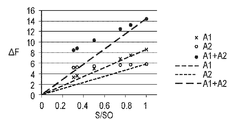
The imaging magnification will be illustrated as an imaging characteristic. 3A and 3B show the relationship between the imaging magnification variation and the exposure field angle when, for example, the imaging magnification variation is represented by an exponential function model equation using two time constants. Each of the vertical axes in Figs. 3A and 3B represents a deviation from the ideal imaging magnification (imaging magnification variation:? F), and time constants? 1 and? 2 are, for example,? 1 = 10000 sec,? 2 = 500 sec.
3A shows the imaging magnification variation? F with respect to the exposure imaging angle ratio (S / So) for the coefficients (A 1 and A 2 in Equation (4)) acquired by fitting using two preset time constants. 3A, "X "," o ", and "" represent A 1 , A 2, and A 1 + A 2 , respectively. The abscissa of FIG. 3A expresses the ratio (exposure imaging angle ratio: S / S0) obtained by normalizing the exposure angle of view S by the maximum exposure angle of view S0 of the apparatus.
3B is a graph plotting the imaging magnification variation? F at each exposure angle of view as a function of time. It should be noted that this graph expresses the imaging magnification variation at S / S0 = 1.0, 0.75 and 0.5 as typical exposure angle-of-view angles, but omits imaging magnification fluctuation at different exposure angles of view.
3A and 3B, exposure conditions except the exposure angle of view, for example, the numerical aperture (NA) of the projection optical system, the value of the illumination system σ, the light intensity (accurately indicating the reticle irradiation energy per unit exposure area), the reticle transmittance And the wafer reflectance are assumed to be constant conditions.
At the time of inspection of the projection optical system, A 1 and A 2 are acquired as A0 1 and A0 2 , respectively, at the maximum exposure angle of view of the apparatus. At the time of changing the exposure angle of view, A 1 and A 2 are predicted by a model equation using parameters that change the power incident on the lens, such as exposure angle of view, reticle transmittance, and wafer reflectance.
Assuming a proportional relationship between the respective parameters, A 1 and A 2 are expressed by the following equations.
&Quot; (5) "
&Quot; (6) "
Where I is the exposure intensity (W / m 2), S is the set exposure view angle (m 2) and, S0 is the maximum exposure view angle (m 2), and Tr is the reticle transmission, W refl is the wafer reflectivity, A0 1 2 and A0 is a coefficient calculated from the amount of change in imaging magnification maximum exposure view angle (S0).
At the change of the exposure angle of view, A 1 and A 2 are predicted in the manner shown in Figs. 4A and 4B. The relationship between the vertical axis and the horizontal axis in Figs. 4A and 4B is the same as that in Figs. 3A and 3B. Figure 4b is a graph plotting the imaging magnification changes (ΔF) as a function of time by using the floating coefficients A 1 and A 2 in Fig. 4a. The variation characteristic predicted value F (t) of the imaging magnification at the time of changing the exposure angle of view represents a predetermined difference from the actual imaging magnification variation. If this difference does not satisfy the required accuracy of the projection system, A 1 and A 2 can be obtained by multiplying the maximum exposure
&Quot; (7) "
&Quot; (8) "
In this case, the power exponent C is an integer that defines the exposure angle dependence of exposure, and is predetermined for each system by simulation or from experimental results.
At the change of the exposure angle of view, A 1 and A 2 are predicted in the manner shown in Fig. 5A. 5B is a graph plotting the imaging magnification variation as a function of time using the coefficients A 1 and A 2 . The relationship between the vertical axis and the horizontal axis in Figs. 5A and 5B is the same as that in Figs. 3A and 3B. The imaging magnification prediction value at the time of changing the exposure angle of view can be approximated to the actual imaging magnification variation by modeling the imaging magnification prediction value at the change of the exposure angle of view with respect to the exposure angle of view using a specific function.
It is assumed that the variation estimated value F (t) of the imaging magnification at the change of the exposure angle of view represents a predetermined difference from the actual imaging magnification variation and does not satisfy the required accuracy of the projection system despite the use of this model equation . In this case, the modeling is further performed at the time of the adjustment of the constant C. For example, a method of approximating the fluctuation predicted value F (t) with the actual imaging magnification fluctuation by adjusting the constant C based on the actual device data can be considered.
For example, as shown in FIG. 3B, the imaging magnification variation is changed from 1.0 to 3/4 or 1/2 by changing the exposed angle of view of the exposure angle S to the maximum exposure angle S0 of the projection exposure system As a function of time. Coefficients A 1 and A 2 are then obtained in accordance with the obtained imaging magnification function, and each exposure field angle ratios.
The integer C is determined from the acquired set of A 1 and A 2 so as to minimize the difference between the variation estimated value [F (t)] of the imaging magnification and the actual imaging magnification variation.
Optimizing the integer C in this way can further improve prediction accuracy. At the change of the exposure angle of view, A 1 and A 2 become the values shown in FIG. 6A.
However, as shown in Fig. 6B, according to this model equation, the energy absorbed by the projection optical system and the thermal energy emitted by the projection optical system to generate heat reach an equilibrium state. It is sometimes impossible to accurately predict the state in which the imaging magnification significantly changes in the middle of the period from the start of exposure to the equilibrium state or after the stop of exposure or the change of the exposure condition to the equilibrium state even though the state of stable image formation magnification can be accurately predicted Do.
Therefore, in the embodiment of the present invention, the model equation for predicting the imaging magnification variation is defined as follows. In Equations (9) and (10), C 1 and C 2 are constants defining exposure field angle dependency and are predetermined for each system by simulation or from experimental results.
&Quot; (9) "
&Quot; (10) "
In this case, the power exponent (C 1 , C 2 ) is a different integer that defines the exposure angle dependence of exposure angle. C 1 and C 2 are predetermined from the experimental results. At the change of the exposure angle of view, A 1 and A 2 are predicted in the manner shown in Fig. 7A. FIG. 7B is a graph plotting the imaging magnification variation as a function of time using the coefficients A 1 and A 2 . The model using the constants C 1 and C 2 defining the exposure field angle dependency is a model in which the energy absorbed by the projection optical system to generate heat and the thermal energy emitted by the projection optical system reach the equilibrium state, The stable state can be accurately predicted. In addition, the model can accurately predict a state in which the image forming magnification significantly changes on the way from the start of exposure to the equilibrium state, or after the stop of exposure or the change of the exposure condition, to the parallel state.
According to the model equation represented by the expressions (9) and (10), it is possible to accurately predict the imaging magnification variation and to minimize the error.
The main controller 103 (prediction unit) predicts the imaging magnification variation using the above-described model equation. The
The
The present embodiment illustrates variation in imaging magnification. Obviously, however, the projection optical system may exhibit a different exposure angle dependence from that described above depending on the configuration. In this case, a model equation having an optimal set of time constants and an angle-of-view dependence for each time constant may be set.
In addition, this embodiment illustrates variation in imaging magnification. However, this embodiment can be applied to the fluctuation of any imaging characteristic caused by thermal action (for example, heat absorption and heat emission) by the lens or mirror at the time of exposure by the projection optical system, , Top surface curvature, distortion, astigmatism and wavefront aberration.
In addition, this embodiment illustrates a scanning type exposure apparatus. However, the embodiment can be applied to a step-and-repeat scheme stepper exposure apparatus. The scanning type exposure apparatus is generally configured to change the exposure angle of view based on the illumination magnitude in the X direction and the scanning distance in the Y direction. If the illumination size does not vary in the Y direction, there is no problem in reading the parameters that determine the incident area of the exposure light on the projection optical system as the illumination magnitude in the X direction.
Unlike the scanning type exposure apparatus, in the stepper type exposure apparatus, the fluctuation of the imaging characteristic does not simply depend on the exposure angle of view, and the imaging characteristic is sometimes changed in accordance with the size of the shot in the X and Y directions. In this case, for example, it is effective to set a model equation for the set of optimal time constants and the angle dependence of the angle corresponding to each time constant by using the size of the shot in the X and Y directions as parameters.
[Second Embodiment]
A method of manufacturing a device according to an embodiment of the present invention is suitable for manufacturing a device having a microstructure such as a semiconductor device or a liquid crystal display device. For example, a semiconductor device is manufactured through a pre-process to form an integrated circuit on a wafer (substrate) and a post-process to complete the integrated circuit chip as a product on a wafer formed in the entire process . The entire process includes exposing an image of a pattern on a mask onto a wafer coated with a photosensitizer by illuminating the mask using an exposure apparatus, and developing the wafer. The post process includes an assembly step (dicing and bonding) and a packaging step (encapsulation).
For example, a liquid crystal display device is manufactured through a process of forming a transparent electrode. The process for forming the transparent electrode includes the steps of applying a photosensitive agent to a glass substrate on which a transparent conductive film is deposited, exposing the glass substrate coated with the photosensitive agent using the above-described exposure apparatus, and developing the glass substrate. The device manufacturing method of this embodiment is more advantageous than the conventional method in terms of at least one of device performance, quality, productivity, and production cost.
Although embodiments of the present invention have been described above, the present invention is not limited to these embodiments, and various modifications and changes may be made within the spirit and scope of the present invention.
While the present invention has been described with reference to exemplary embodiments, it is to be understood that the invention is not limited to the disclosed exemplary embodiments. The scope of the following claims is to be accorded the broadest interpretation so as to encompass all such modifications and equivalent structures and functions.
Claims (17)
A prediction unit configured to predict variations in imaging characteristics of the projection optical system caused by thermal action due to exposure using a model equation that models variation in imaging characteristics,
And a correction unit configured to correct the imaging characteristic based on the prediction result acquired by the prediction unit,
Wherein the model expression modeling the variation of the imaging characteristic and the synthesis of a plurality of functions indicating time dependence, each of the plurality of functions having an exposure field angle dependency, and the exposure field angle dependence of the plurality of functions being different from each other
Wherein an exposure field angle dependence of the plurality of functions is determined such that a difference between a variation in the imaging characteristic obtained in advance and a variation in the imaging characteristic predicted using the model equation becomes smaller.
Wherein each of the plurality of functions has a coefficient defined by a power of a ratio obtained by normalizing a set exposure angle of view to a maximum exposure angle of view of the projection optical system, wherein the plurality of functions are set such that the values of the exponents of the powers are different from each other , An exposure apparatus.
Wherein the prediction unit predicts at least one of a focus, an upper surface curvature, a magnification, a distortion, an astigmatism, and a wavefront aberration of the projection optical system using the model equation as the imaging characteristic.
The correction unit includes a control unit configured to control a drive unit configured to control an aperture stop of the projection optical system and a drive unit configured to move an optical element of the projection optical system,
Wherein the control unit performs control so as to correct the imaging characteristic using the prediction result acquired by the prediction unit.
Wherein the correction unit comprises:
A mask stage control unit configured to control a position or an angle of the mask by driving a mask stage that holds the mask,
Further comprising a substrate stage control unit configured to control a position or an angle of the substrate by driving a substrate stage holding the substrate,
Wherein the mask stage control unit and the substrate stage control unit perform control to correct the imaging characteristic using the prediction result acquired by the prediction unit.
Exposing the substrate using an exposure apparatus,
Developing the exposed substrate, wherein the exposure apparatus projects an image of a pattern formed on the mask through a projection optical system onto a substrate,
The exposure apparatus includes:
A prediction unit configured to predict variations in imaging characteristics of the projection optical system caused by thermal action due to exposure using a model equation that models variation in imaging characteristics,
And a correction unit configured to correct the imaging characteristic based on the prediction result acquired by the prediction unit,
Wherein the model expression modeling the variation of the imaging characteristic and the synthesis of a plurality of functions exhibiting time dependence, each of the plurality of functions having an exposure angle dependence of exposure, the exposure angle dependence of the plurality of functions being different from each other,
Wherein an exposure field angle dependency of the plurality of functions is determined such that a difference between the fluctuation of the imaging characteristic obtained in advance and the variation of the imaging characteristic predicted using the model equation becomes smaller.
Wherein said exposure angle dependency represents a dependency of a size of a top surface at a wafer level.
Wherein the exposure angle dependency exhibits a dependence of a size of a top surface at a wafer level.
The exposure angle dependency of the plurality of functions is determined by a difference between a variation of the imaging characteristic obtained in advance and a variation of the imaging characteristic predicted by using the model formula so that the accuracy of prediction using the model formula satisfies a predetermined value The exposure apparatus comprising:
The exposure angle dependency of the plurality of functions is determined by a difference between a variation of the imaging characteristic obtained in advance and a variation of the imaging characteristic predicted by using the model formula so that the accuracy of prediction using the model formula satisfies a predetermined value Wherein the thickness of the device is determined to be small.
Wherein an exposure field angle dependency of the plurality of functions is determined so as to minimize a difference between a variation in the imaging characteristic obtained in advance and a variation in the imaging characteristic predicted using the model equation.
Wherein an exposure field angle dependence of the plurality of functions is determined so as to minimize a difference between a variation in the imaging characteristic obtained in advance and a variation in the imaging characteristic predicted using the model equation.
When two directions orthogonal to the optical axis of the projection optical system and orthogonal to each other are defined as the first direction and the second direction,
Wherein the exposure angle dependence of the exposure angle represents at least one of the dependence of the exposure angle of view in the first direction and the dependence of the exposure angle of view in the second direction.
When two directions orthogonal to the optical axis of the projection optical system and orthogonal to each other are defined as the first direction and the second direction,
Wherein the exposure angle dependence of exposure shows at least one dependence of the exposure angle dependence in the first direction and the exposure angle dependency in the second direction.
When two directions orthogonal to the optical axis of the projection optical system and orthogonal to each other are defined as the first direction and the second direction,
Wherein the exposure angle dependence of exposure shows both dependence of the exposure angle dependency in the first direction and the exposure angle dependency in the second direction.
When two directions orthogonal to the optical axis of the projection optical system and orthogonal to each other are defined as the first direction and the second direction,
Wherein the exposure angle dependence of the exposure angle indicates the dependence of both the exposure angle dependency of the exposure in the first direction and the exposure angle dependence of the exposure angle in the second direction.
Applications Claiming Priority (2)
| Application Number | Priority Date | Filing Date | Title |
|---|---|---|---|
| JPJP-P-2013-168336 | 2013-08-13 | ||
| JP2013168336A JP6381188B2 (en) | 2013-08-13 | 2013-08-13 | Exposure apparatus and device manufacturing method |
Publications (2)
| Publication Number | Publication Date |
|---|---|
| KR20150020066A KR20150020066A (en) | 2015-02-25 |
| KR101823725B1 true KR101823725B1 (en) | 2018-01-30 |
Family
ID=52466620
Family Applications (1)
| Application Number | Title | Priority Date | Filing Date |
|---|---|---|---|
| KR1020140100267A KR101823725B1 (en) | 2013-08-13 | 2014-08-05 | Exposure apparatus and method of manufacturing device |
Country Status (3)
| Country | Link |
|---|---|
| US (1) | US9348235B2 (en) |
| JP (1) | JP6381188B2 (en) |
| KR (1) | KR101823725B1 (en) |
Families Citing this family (10)
| Publication number | Priority date | Publication date | Assignee | Title |
|---|---|---|---|---|
| US10451977B2 (en) | 2014-12-02 | 2019-10-22 | Asml Netherlands B.V. | Lithographic method and apparatus |
| JP6613074B2 (en) * | 2015-08-20 | 2019-11-27 | キヤノン株式会社 | Determination method, exposure apparatus, program, and article manufacturing method |
| WO2017050523A1 (en) | 2015-09-24 | 2017-03-30 | Asml Netherlands B.V. | Method of reducing effects of reticle heating and/or cooling in a lithographic process |
| JP6554141B2 (en) * | 2017-05-26 | 2019-07-31 | キヤノン株式会社 | Determination method, exposure method, information processing apparatus, program, and article manufacturing method |
| JP6944323B2 (en) * | 2017-09-21 | 2021-10-06 | キヤノン株式会社 | Calculation method, exposure method, program, exposure equipment, and manufacturing method of goods |
| JP7054365B2 (en) * | 2018-05-25 | 2022-04-13 | キヤノン株式会社 | Evaluation method, exposure method, and article manufacturing method |
| EP3702839B1 (en) * | 2019-02-27 | 2021-11-10 | ASML Netherlands B.V. | Method of reducing effects of lens heating and/or cooling in a lithographic process |
| JP2020187334A (en) * | 2019-05-17 | 2020-11-19 | キヤノン株式会社 | Exposure device and article manufacturing method |
| JP7213757B2 (en) * | 2019-05-31 | 2023-01-27 | キヤノン株式会社 | Exposure apparatus and article manufacturing method |
| JP7431694B2 (en) * | 2020-07-28 | 2024-02-15 | キヤノン株式会社 | Information processing device, film forming device, article manufacturing method, and program |
Citations (1)
| Publication number | Priority date | Publication date | Assignee | Title |
|---|---|---|---|---|
| JP2013115348A (en) * | 2011-11-30 | 2013-06-10 | Canon Inc | Calculation method of variation in imaging characteristics of projection optical system, exposure device and manufacturing method of device |
Family Cites Families (7)
| Publication number | Priority date | Publication date | Assignee | Title |
|---|---|---|---|---|
| JPS58179834A (en) | 1982-04-14 | 1983-10-21 | Canon Inc | Copying device and focus correcting method |
| JP3720582B2 (en) * | 1998-06-04 | 2005-11-30 | キヤノン株式会社 | Projection exposure apparatus and projection exposure method |
| TW500987B (en) * | 2000-06-14 | 2002-09-01 | Asm Lithography Bv | Method of operating an optical imaging system, lithographic projection apparatus, device manufacturing method, and device manufactured thereby |
| JP2002184687A (en) * | 2000-10-02 | 2002-06-28 | Canon Inc | Aligner |
| JP2006019561A (en) * | 2004-07-02 | 2006-01-19 | Canon Inc | Exposure method |
| US7403264B2 (en) * | 2004-07-08 | 2008-07-22 | Asml Netherlands B.V. | Lithographic projection apparatus and a device manufacturing method using such lithographic projection apparatus |
| JP5264116B2 (en) * | 2007-07-26 | 2013-08-14 | キヤノン株式会社 | Imaging characteristic variation prediction method, exposure apparatus, and device manufacturing method |
-
2013
- 2013-08-13 JP JP2013168336A patent/JP6381188B2/en not_active Expired - Fee Related
-
2014
- 2014-08-05 KR KR1020140100267A patent/KR101823725B1/en active IP Right Grant
- 2014-08-07 US US14/453,944 patent/US9348235B2/en active Active
Patent Citations (1)
| Publication number | Priority date | Publication date | Assignee | Title |
|---|---|---|---|---|
| JP2013115348A (en) * | 2011-11-30 | 2013-06-10 | Canon Inc | Calculation method of variation in imaging characteristics of projection optical system, exposure device and manufacturing method of device |
Also Published As
| Publication number | Publication date |
|---|---|
| US9348235B2 (en) | 2016-05-24 |
| JP6381188B2 (en) | 2018-08-29 |
| US20150049315A1 (en) | 2015-02-19 |
| JP2015037124A (en) | 2015-02-23 |
| KR20150020066A (en) | 2015-02-25 |
Similar Documents
| Publication | Publication Date | Title |
|---|---|---|
| KR101823725B1 (en) | Exposure apparatus and method of manufacturing device | |
| KR100971561B1 (en) | Exposure apparatus and method of manufacturing device | |
| JP5264116B2 (en) | Imaging characteristic variation prediction method, exposure apparatus, and device manufacturing method | |
| JP6039932B2 (en) | Exposure apparatus, exposure method, and article manufacturing method | |
| US9513564B2 (en) | Exposure method, exposure apparatus, and device manufacturing method | |
| JP5815987B2 (en) | Exposure apparatus and device manufacturing method | |
| US9116444B2 (en) | Method of calculating amount of fluctuation of imaging characteristic of projection optical system, exposure apparatus, and method of fabricating device | |
| JP6422307B2 (en) | Exposure method, exposure apparatus, and article manufacturing method | |
| KR102300753B1 (en) | Determination method, exposure method, information processing apparatus, program, and article manufacturing method | |
| JP5094517B2 (en) | Exposure apparatus, measurement method, stabilization method, and device manufacturing method | |
| JP7022531B2 (en) | Exposure method, exposure equipment, and manufacturing method of goods | |
| JP2001244182A (en) | Method of measuring variations in image formation characteristics of projection optical system due to exposure heat and aligner | |
| JP2006019561A (en) | Exposure method | |
| KR101039288B1 (en) | Exposure apparatus, measurement method, stabilization method, and device fabrication method |
Legal Events
| Date | Code | Title | Description |
|---|---|---|---|
| A201 | Request for examination | ||
| E902 | Notification of reason for refusal | ||
| E90F | Notification of reason for final refusal | ||
| E701 | Decision to grant or registration of patent right | ||
| GRNT | Written decision to grant |