KR101622613B1 - Scanning electron microscope - Google Patents
Scanning electron microscope Download PDFInfo
- Publication number
- KR101622613B1 KR101622613B1 KR1020147018326A KR20147018326A KR101622613B1 KR 101622613 B1 KR101622613 B1 KR 101622613B1 KR 1020147018326 A KR1020147018326 A KR 1020147018326A KR 20147018326 A KR20147018326 A KR 20147018326A KR 101622613 B1 KR101622613 B1 KR 101622613B1
- Authority
- KR
- South Korea
- Prior art keywords
- pattern
- signal waveform
- sample
- scanning
- electron
- Prior art date
Links
Images


Classifications
-
- H—ELECTRICITY
- H01—ELECTRIC ELEMENTS
- H01J—ELECTRIC DISCHARGE TUBES OR DISCHARGE LAMPS
- H01J37/00—Discharge tubes with provision for introducing objects or material to be exposed to the discharge, e.g. for the purpose of examination or processing thereof
- H01J37/26—Electron or ion microscopes; Electron or ion diffraction tubes
- H01J37/28—Electron or ion microscopes; Electron or ion diffraction tubes with scanning beams
-
- G—PHYSICS
- G01—MEASURING; TESTING
- G01B—MEASURING LENGTH, THICKNESS OR SIMILAR LINEAR DIMENSIONS; MEASURING ANGLES; MEASURING AREAS; MEASURING IRREGULARITIES OF SURFACES OR CONTOURS
- G01B15/00—Measuring arrangements characterised by the use of electromagnetic waves or particle radiation, e.g. by the use of microwaves, X-rays, gamma rays or electrons
- G01B15/04—Measuring arrangements characterised by the use of electromagnetic waves or particle radiation, e.g. by the use of microwaves, X-rays, gamma rays or electrons for measuring contours or curvatures
-
- H—ELECTRICITY
- H01—ELECTRIC ELEMENTS
- H01J—ELECTRIC DISCHARGE TUBES OR DISCHARGE LAMPS
- H01J2237/00—Discharge tubes exposing object to beam, e.g. for analysis treatment, etching, imaging
- H01J2237/004—Charge control of objects or beams
- H01J2237/0048—Charging arrangements
-
- H—ELECTRICITY
- H01—ELECTRIC ELEMENTS
- H01J—ELECTRIC DISCHARGE TUBES OR DISCHARGE LAMPS
- H01J2237/00—Discharge tubes exposing object to beam, e.g. for analysis treatment, etching, imaging
- H01J2237/04—Means for controlling the discharge
- H01J2237/049—Focusing means
- H01J2237/0492—Lens systems
-
- H—ELECTRICITY
- H01—ELECTRIC ELEMENTS
- H01J—ELECTRIC DISCHARGE TUBES OR DISCHARGE LAMPS
- H01J2237/00—Discharge tubes exposing object to beam, e.g. for analysis treatment, etching, imaging
- H01J2237/244—Detection characterized by the detecting means
- H01J2237/24495—Signal processing, e.g. mixing of two or more signals
-
- H—ELECTRICITY
- H01—ELECTRIC ELEMENTS
- H01J—ELECTRIC DISCHARGE TUBES OR DISCHARGE LAMPS
- H01J2237/00—Discharge tubes exposing object to beam, e.g. for analysis treatment, etching, imaging
- H01J2237/26—Electron or ion microscopes
- H01J2237/28—Scanning microscopes
- H01J2237/2809—Scanning microscopes characterised by the imaging problems involved
- H01J2237/281—Bottom of trenches or holes
-
- H—ELECTRICITY
- H01—ELECTRIC ELEMENTS
- H01J—ELECTRIC DISCHARGE TUBES OR DISCHARGE LAMPS
- H01J2237/00—Discharge tubes exposing object to beam, e.g. for analysis treatment, etching, imaging
- H01J2237/26—Electron or ion microscopes
- H01J2237/28—Scanning microscopes
- H01J2237/2813—Scanning microscopes characterised by the application
- H01J2237/2814—Measurement of surface topography
- H01J2237/2815—Depth profile
-
- H—ELECTRICITY
- H01—ELECTRIC ELEMENTS
- H01J—ELECTRIC DISCHARGE TUBES OR DISCHARGE LAMPS
- H01J2237/00—Discharge tubes exposing object to beam, e.g. for analysis treatment, etching, imaging
- H01J2237/26—Electron or ion microscopes
- H01J2237/28—Scanning microscopes
- H01J2237/2813—Scanning microscopes characterised by the application
- H01J2237/2817—Pattern inspection
Landscapes
- Physics & Mathematics (AREA)
- Electromagnetism (AREA)
- General Physics & Mathematics (AREA)
- Chemical & Material Sciences (AREA)
- Analytical Chemistry (AREA)
- Testing Or Measuring Of Semiconductors Or The Like (AREA)
- Length-Measuring Devices Using Wave Or Particle Radiation (AREA)
Abstract
본 발명은, 주사 전자 현미경에 있어서, 시료 표면이 도전성 재료였다고 해도, 구멍 바닥 등으로부터 방출되는 전자를 고효율로 인상하는 전계를 형성하는 것이다. 전자 빔의 주사 위치를 편향시키는 편향기와, 시료를 탑재하기 위한 시료 스테이지를 구비한 주사 전자 현미경에 있어서, 측정 대상 패턴에 대하여 전자 빔을 주사하기 전에, 당해 측정 대상 패턴의 하층에 위치하는 다른 패턴에 대한 전자 빔 조사를 행하도록, 상기 편향기 또는 상기 시료 스테이지를 제어하도록 했다.In the scanning electron microscope of the present invention, even if the surface of the sample is a conductive material, an electric field for raising the electrons emitted from the hole bottom or the like with high efficiency is formed. In a scanning electron microscope having a deflector for deflecting the scanning position of an electron beam and a sample stage for mounting a sample, before scanning the electron beam with respect to the measurement target pattern, To control the deflecting device or the sample stage.
Description
본 발명은 주사 전자 현미경에 관한 것이며, 특히 시료에 대전(帶電)을 부착시켜서 신호 파형이나 화상을 형성하는 주사 전자 현미경에 관한 것이다.TECHNICAL FIELD The present invention relates to a scanning electron microscope, and more particularly, to a scanning electron microscope which forms a signal waveform or an image by attaching a charge to a sample.
주사 전자 현미경(SEM; Scanning Electron Microscope)을 사용한 반도체 디바이스의 계측·검사에서는, 전자선을 시료에 조사(照射)하기 때문에 디바이스 표면에는 대전이 형성된다. 대전은 화상의 왜곡이나 콘트라스트 이상 등을 야기하는 요인이 되는 경우가 있다.In the measurement and inspection of a semiconductor device using a scanning electron microscope (SEM), a sample is irradiated with an electron beam, so that a charge is formed on the surface of the device. There is a case where the charging causes a distortion of an image or an abnormal contrast.
특허문헌 1에서는, 전자선을 컨텍트 홀에 조사하는 것에 의해, 기판에 흐르는 흡수 전류값을 측정함으로써 홀 형상의 관찰을 행하는 방법을 제안하고 있다.
또한 특허문헌 2에서는, 전자선의 조사에 의해, 시료 표면의 전위 분포를 균일하게 함으로써 화상의 재현성 향상을 목적으로 한 방법이 제안되어 있다. 예를 들면, 1500eV의 에너지로 시료를 조사할 경우, 10V의 전위차에 의해, 6㎚의 측장(測長) 오차가 발생하는 것이 나타나 있다. 이 때문에, 시료 상에 설치한 대전 제어 전극에 의해 표면의 전위를 일정하게 하는 방법이 제안되어 있다.
특허문헌 3, 4에서는, SEM을 사용해서 절연물 시료를 관찰했을 때에 형성되는 대전의 완화 혹은 안정화를 목적으로 한 방법이 제안되어 있다. 특허문헌 3에서는, 시료의 표면 전계 강도나 화상 취득 시의 일차 전자 빔의 주사 방법을 제어함으로써, 일차 전자 빔 조사에 의해서 생성되는 대전을 완화 혹은 안정화하여, 일차 전자 빔의 조사에 의해서 생성되는 동적인 대전의 영향을 받기 어렵게 한다. 또한 특허문헌 4에서는, SEM을 사용해서 기판 표면의 형상 검사나 측장을 행할 때에, 기판 상의 대전이 평형 상태에 도달할 때까지의 전자 빔의 주사 횟수에 대응하는 반사 전자의 신호 파형을 측정해서, 피주사 영역의 물질의 에지를 동정(同定)한다. 혹은, 기판 상의 대전이 평형 상태에 도달할 때까지의 전자 빔의 주사 횟수에 대응하는 반사 전자의 신호 파형을 측정하여, 기지 물질의 당해 주사 횟수에 대응하는 반사 전자의 신호 파형과 비교함으로써, 피주사 영역의 미지 물질을 동정한다는 것이 제안되어 있다.
상기와 같이 대전을 억제하는 방법이 제안되는 한편, 대전을 활용한 관찰 방법도 제안되어 있다. 반도체 디바이스의 패턴 미세화와 함께, 수직 방향으로 쌓아올리는 집적화가 진행되고 있다. 구조의 쌓아올림과 함께, 깊은 구멍이나 깊은 홈과 같은 고(高)애스팩트비(패턴 높이/구멍 직경, 홈 폭)를 가진 디바이스가 등장해오고 있다. 이러한 패턴의 검사로서, 표면의 치수 관리와 함께, 구멍 바닥, 홈 바닥의 치수 관리가 요구된다.A method of suppressing charging as described above has been proposed, and an observation method utilizing charging has also been proposed. As the pattern of the semiconductor device is miniaturized, integration in the vertical direction is progressing. Devices with high aspect ratio (pattern height / hole diameter, groove width), such as deep holes or deep grooves, have emerged along with stacking of structures. Inspection of such a pattern requires dimension management of the surface and dimensional control of the hole bottom and groove bottom.
고애스팩트비 시료의 관찰에서는, 패턴 바닥으로부터의 이차 전자의 검출량이 적기 때문에 일반적으로 콘트라스트가 부여되지 않아 관찰·계측이 곤란하다. 이 때문에, 대전을 이용한 관찰이 사용되고 있다. 표면이 대전하는 재료(절연체)인 경우에는, 관찰 전에 표면을 저배율로 사전 조사(프리 도스)함으로써 시료 표면에 양(正)대전이 형성된다. 그 후, 고배율로 관찰을 행함으로써, 표면의 양대전에 의해 구멍 바닥의 이차 전자를 인상(引上)함에 의해 관찰하고 있다.In the observation of the high aspect ratio sample, since the amount of secondary electrons detected from the bottom of the pattern is small, contrast is not generally given, and observation and measurement are difficult. For this reason, observations using charge are used. When the surface is a material (insulator) charged on the surface, a positive charge is formed on the surface of the sample by pre-irradiation (pre-dosing) of the surface at a low magnification before observation. Thereafter, observations were made at a high magnification, and secondary electrons at the bottom of the hole were observed by pulling up two surfaces of the surface.
특허문헌 5에서는, 표면에 형성한 양대전의 양에 의해 임의의 깊이에서의 치수 계측을 행하는 방법을 제안하고 있다. 표면의 대전량을 조정함으로써 이차 전자의 인상이 가능한 깊이를 제어할 수 있다고 되어 있다.
깊은 구멍이나 깊은 홈의 치수나 검사를 행할 경우, 전술과 같이 시료 표면에 양대전을 부착시킴으로써, 구멍 바닥 등과 시료 표면 사이에, 전자를 인상하기 위한 전계를 형성하는 프리 도스법은 매우 유효한 방법이다. 그러나, 시료 표면이 도전성 재료인 경우 대전을 형성할 수 없다. 상기 각 특허문헌의 방법에서는, 시료 표면이 도전성 재료인 경우에 구멍 바닥으로부터 방출되는 전자를 인상하기 위한 전계를 형성할 수는 없었다. 이하에, 시료 표면이 도전성 재료였다고 해도, 구멍 바닥 등으로부터 방출되는 전자를 고효율로 인상하는 전계를 형성하는 것을 목적으로 하는 주사 전자 현미경에 대하여 설명한다.When the dimensions or inspection of deep holes or deep grooves are carried out, the pre-dosing method of forming an electric field for attracting electrons between the hole bottom and the like and the sample surface by attaching positive charge to the surface of the sample as described above is a very effective method . However, if the surface of the sample is a conductive material, electrification can not be formed. In the methods of the above patent documents, when the sample surface is a conductive material, an electric field for pulling up electrons emitted from the bottom of the hole could not be formed. Hereinafter, a scanning electron microscope for the purpose of forming an electric field for pulling up electrons emitted from the bottom of a hole with high efficiency even if the surface of the sample is a conductive material will be described.
상기 목적을 달성하기 위한 일 태양으로서 이하에, 전자원(電子源)과, 당해 전자원으로부터 방출된 전자 빔을 집속(集束)하는 대물렌즈와, 당해 전자 빔의 주사 위치를 편향시키는 편향기와, 시료를 탑재하기 위한 시료 스테이지를 구비한 주사 전자 현미경에 있어서, 측정 대상 패턴에 대하여 빔을 주사하기 전에, 당해 측정 대상 패턴의 하층에 위치하는 하층 패턴이, 하층에 위치하는 다른 패턴에 대한 빔 조사를 행하도록, 상기 편향기, 혹은 시료 스테이지를 제어하는 제어 장치를 구비한 주사 전자 현미경을 제안한다.In order to achieve the above object, the present invention provides an electron source, an objective lens for focusing an electron beam emitted from the electron source, a deflector for deflecting the scanning position of the electron beam, In a scanning electron microscope having a sample stage for mounting a sample, before scanning a beam with respect to a measurement target pattern, a lower layer pattern positioned under the measurement target pattern is irradiated with a beam And a control device for controlling the deflector or the sample stage so as to perform the scanning electron microscope.
상기 구성에 따르면, 시료 표면이 도전성 재료였다고 해도 구멍 바닥이나 깊은 홈 등으로부터 방출되는 전자를 고효율로 유도하는 것이 가능해진다.According to the above configuration, even if the surface of the sample is a conductive material, it is possible to induce electrons emitted from the bottom of holes or deep grooves with high efficiency.
도 1은 주사 전자 현미경에 의한 측정 대상의 하나인 깊은 홈 구조체의 일례를 나타내는 도면.
도 2는 시료에 빔 주사했을 때에 얻어지는 SEM 화상과 라인 프로파일의 일례를 나타내는 도면.
도 3은 전자 빔 조사에 의거한 예비 대전 형성과 SEM상(像) 형성 공정을 나타내는 플로차트.
도 4는 예비 대전 형성을 위한 전자 빔 조사 위치와 SEM상 형성을 위한 빔 조사 위치의 관계를 나타내는 도면.
도 5는 상층 패턴의 레이아웃 데이터와 하층 패턴의 레이아웃 데이터를 중첩한 중첩 레이아웃 데이터를 나타내는 도면.
도 6은 예비 대전용 빔의 조사 위치와 SEM 화상 취득 영역의 위치 관계를 나타내는 도면.
도 7은 다른 조건 하에서 취득한 신호 파형예를 나타내는 도면.
도 8은 예비 대전용 빔 조사를 행했을 때와 행하지 않았을 때에 검출되는 전자의 에너지 분포를 나타내는 도면.
도 9는 에너지 필터에의 인가 전압과 검출되는 전자의 에너지 분포의 관계를 나타내는 도면.
도 10은 에너지 필터에의 인가 전압과 취득되는 신호 파형의 관계를 나타내는 도면.
도 11은 다른 인가 전압을 에너지 필터에 인가했을 때에 얻어지는 복수의 신호 파형으로부터 구해지는 차(差) 파형의 일례를 나타내는 도면.
도 12는 주사 전자 현미경의 개요를 나타내는 도면.
도 13은 주사 전자 현미경을 포함하는 반도체 계측 시스템의 일례를 나타내는 도면.
도 14는 SEM상 형성 영역과 예비 대전 조사 영역을 설정하는 GUI(Graphical User Interface)의 일례를 나타내는 도면.
도 15는 GUI 화면 상에 표시하는 레이어의 선택 화면의 일례를 나타내는 도면.
도 16은 측정 대상 패턴의 선택에 의거하여 대전용 빔의 조사 영역을 결정하는 공정을 나타내는 플로차트.
도 17은 예비 대전용 빔의 조사 전후에서 취득한 신호 파형에 의거하여 패턴의 치수 측정을 행하는 공정을 나타내는 플로차트.
도 18은 다른 에너지 필터 조건에서 취득된 복수의 파형에 의거하여 패턴의 치수 측정을 행하는 공정을 나타내는 플로차트.
도 19는 복수의 검출기를 사용해서 다른 에너지의 전자를 변별 검출하는 주사 전자 현미경의 검출 광학계를 나타내는 도면.1 is a view showing an example of a deep groove structure which is one of objects to be measured by a scanning electron microscope;
2 is a view showing an example of an SEM image and a line profile obtained when a beam is scanned on a sample.
FIG. 3 is a flowchart showing a preliminary electrification formation and an SEM image formation step based on electron beam irradiation.
4 is a view showing a relationship between an electron beam irradiation position for preliminary charging and a beam irradiation position for forming a SEM image.
5 is a diagram showing superposed layout data in which layout data of an upper layer pattern and layout data of a lower layer pattern are superimposed.
6 is a view showing a positional relationship between an irradiation position of a preliminary charging beam and an SEM image acquisition area;
7 is a diagram showing an example of a signal waveform acquired under different conditions;
8 is a diagram showing the energy distribution of electrons detected when the preliminary charging beam is irradiated and when not irradiated.
9 is a diagram showing the relationship between the voltage applied to the energy filter and the energy distribution of the detected electrons.
10 is a diagram showing a relationship between an applied voltage to an energy filter and a signal waveform to be acquired;
11 is a diagram showing an example of difference waveforms obtained from a plurality of signal waveforms obtained when another applied voltage is applied to an energy filter;
12 is a diagram showing an outline of a scanning electron microscope.
13 is a view showing an example of a semiconductor metrology system including a scanning electron microscope.
14 is a diagram showing an example of a GUI (Graphical User Interface) for setting a SEM image forming area and a pre-charging irradiation area;
15 is a diagram showing an example of a layer selection screen displayed on a GUI screen;
16 is a flowchart showing a process of determining an irradiation area of a charging beam based on selection of a pattern to be measured.
Fig. 17 is a flowchart showing a step of measuring the dimension of a pattern based on the signal waveform acquired before and after irradiation of the preliminary charging beam. Fig.
Fig. 18 is a flowchart showing a step of measuring dimensions of a pattern based on a plurality of waveforms obtained under different energy filter conditions. Fig.
19 is a view showing a detection optical system of a scanning electron microscope for discriminating and detecting electrons of different energy using a plurality of detectors.
깊은 구멍, 깊은 홈과 같은 고애스팩트비(깊이/패턴 폭)의 패턴의 SEM을 사용한 관찰에서는, 구멍 바닥으로부터 방출된 전자가 깊은 구멍 측벽에 충돌하여, 구멍 바닥의 콘트라스트가 현저하게 저하되어 버리기 때문에, 시료 표면을 양대전시켜 표면과 패턴 바닥 사이에 전위차(전계)를 형성하여, 패턴 바닥으로부터 방출된 전자의 인상을 행하는 방법이 유효하다. 이 방법은 표면이 대전하는 시료인 경우에만 유효하다.In the observation using a SEM of a pattern of a high aspect ratio (depth / pattern width) such as a deep hole and a deep groove, electrons emitted from the bottom of the hole collide with the deep hole sidewall, and the contrast of the bottom of the hole remarkably decreases Therefore, a method of positively charging the surface of the sample to form a potential difference (electric field) between the surface and the bottom of the pattern, and pulling up electrons emitted from the bottom of the pattern is effective. This method is effective only when the surface is a charged sample.
예를 들면, 표면이 도체로 이루어지는 패턴에서는 표면에 양대전을 형성할 수 없어 패턴 내에 전자의 인상 전계를 형성할 수 없다.For example, in the case of a pattern whose surface is made of a conductor, it is impossible to form positive charge on the surface, and an impression electric field of electrons can not be formed in the pattern.
그래서, 이하에 설명하는 실시예에서는, 예를 들면 패턴 바닥이 부유 전극인 경우, 미리 패턴 바닥에만 전자선을 조사해 둠으로써 패턴 바닥을 음(負)대전시켜(국소 예비 조사), 패턴 바닥과 표면 사이에 인상 전계를 형성하는 방법을 제안한다. 국소 예비 조사에 의해 측벽이 음대전함으로써 발생하는 전위 장벽의 영향을 회피하기 위해, 국소 예비 조사를 행한 장소와는 다른 장소(단 패턴 바닥의 부유 전극이 이어진 장소)에서 관찰을 행한다. 표면과 패턴 바닥에 전위차가 부여되어 있으므로, 검출 이차 전자를 에너지로 변별하여 표면과 패턴 바닥의 신호를 분리, 강조한다.In the embodiment described below, for example, when the bottom of the pattern is a floating electrode, the bottom of the pattern is negatively charged (local preliminary irradiation) by irradiating only the bottom of the pattern with the electron beam in advance, A method of forming an impulsive electric field is proposed. Observation is performed at a place different from the place where the local preliminary irradiation is performed (the place where the floating electrode at the bottom of the single pattern is connected) in order to avoid the influence of the potential barrier generated by negative charging of the side wall by the local preliminary irradiation. Since the potential difference is given to the surface and the bottom of the pattern, the secondary electrons are separated by energy to separate and emphasize the signals from the surface and the bottom of the pattern.
도 12는, 이상과 같은 예비 대전용의 빔 조사와, 신호 파형에 의거한 패턴의 측정을 행하는 주사 전자 현미경의 일례를 나타내는 도면이다. 전자원(1201)으로부터 인출 전극(1202)에 의하여 인출되고, 도시하지 않은 가속 전극에 의하여 가속된 전자 빔(1203)은, 집속 렌즈의 일 형태인 콘덴서 렌즈(1204)에 의하여 좁혀진 후에, 주사 편향기(1205)에 의해 시료(1209) 상에서 일차원적 혹은 이차원적으로 주사된다. 전자 빔(1203)은 시료 스테이지(1208)에 내장된 전극에 인가된 음(負)전압에 의해 감속됨과 함께, 대물렌즈(1206)의 렌즈 작용에 의하여 집속되어 시료(1209) 상에 조사된다.12 is a diagram showing an example of a scanning electron microscope for carrying out the beam irradiation for preliminary charging as described above and the measurement of a pattern based on the signal waveform. The
전자 빔(1203)이 시료(1209)에 조사되면, 당해 조사 개소로부터 이차 전자, 및 후방 산란 전자와 같은 전자(1210)가 방출된다. 방출된 전자(1210)는, 시료에 인가되는 음전압에 의거한 가속 작용에 의하여 전자원 방향으로 가속되고, 변환 전극(1212)에 충돌하여 이차 전자(1211)를 발생시킨다. 변환 전극(1212)으로부터 방출된 이차 전자(1211)는 검출기(1213)에 의하여 포착되고, 포착된 이차 전자량에 따라서 검출기(1213)의 출력이 변화한다. 이 출력에 따라서 도시하지 않은 표시 장치의 휘도가 변화한다. 예를 들면 이차원상(二次元像)을 형성할 경우에는, 주사 편향기(1205)에의 편향 신호와 검출기(1213)의 출력의 동기를 취함으로써 주사 영역의 화상을 형성한다. 또한, 주사 편향기(1205)에는, 시야 내의 이차원적인 주사를 행하는 편향 신호에 부가하여, 시야를 이동시키기 위한 편향 신호가 중첩해서 공급되는 경우가 있다. 이 편향 신호에 의한 편향은 이미지 쉬프트 편향이라고도 불리며, 시료 스테이지에 의한 시료 이동 등을 행하지 않고, 전자 현미경의 시야 위치의 이동을 가능하게 한다. 본 실시예에서는 이미지 쉬프트 편향과 주사 편향을 공통의 편향기에 의하여 행하는 예를 나타내고 있지만, 이미지 쉬프트용의 편향기와 주사용의 편향기를 별개로 설치하도록 해도 된다.When the
또한, 시료로부터 방출된 전자를 에너지 변별하기 위한 에너지 필터(1218)가 시료(1209)와 변환 전극(1212) 사이에 설치되어 있다. 에너지 필터는, 예를 들면 3매의 메쉬 전극에 의하여 구성되며, 시료(1209)로부터 변환 전극(1212)을 향한 전자를 반사하는 전계를 형성한다. 메쉬 전극에 인가하는 전압을 조정함으로써 통과 가능한 전자의 에너지의 조정을 행할 수 있다.An
또, 도 12의 예에서는 시료로부터 방출된 전자를 변환 전극에서 일단(一端) 변환해서 검출하는 예에 대하여 설명하고 있지만, 물론 이러한 구성으로 한정되는 것은 아니며, 예를 들면 가속된 전자의 궤도 상에 전자배상관(電子倍像管)이나 검출기의 검출면을 배치하는 바와 같은 구성으로 하는 것도 가능하다.In the example of Fig. 12, an example is described in which electrons emitted from a sample are converted and detected at one end by a converting electrode. However, the present invention is not limited to such an arrangement. For example, It is also possible to arrange the detection surface of the electron multiplier tube or the detector.
제어 장치(1220)는, 주사 전자 현미경의 각 구성을 제어함과 함께, 검출된 전자에 의거하여 화상을 형성하는 기능이나, 라인 프로파일이라 불리는 검출 전자의 강도 분포에 의거하여, 시료 상에 형성된 패턴의 패턴 폭을 측정하는 기능을 구비하고 있다. 또한, 도 12에 예시하는 주사 전자 현미경에는, 시료실(1207)에 시료를 도입할 때에, 시료 분위기를 예비 배기하는 예비 배기실(1215)과, 공기 청정 공간을 형성하는 미니 인바이러먼트(MINI ENVIRONMENT)(1217)가 설치되어 있다. 또한, 그들의 공간의 사이에는 진공 봉지(封止)를 행하기 위한 진공 밸브(1214, 1216)가 설치되어 있다.The
도 13은 SEM을 포함하는 측정 혹은 검사 시스템의 상세 설명도이다. 본 시스템에는, SEM 본체(1301), 당해 SEM 본체의 제어 장치(1220), 및 연산 처리 장치(1302)로 이루어지는 주사 전자 현미경 시스템이 포함되어 있다. 연산 처리 장치(1302)에는, 제어 장치(1220)에 소정의 제어 신호를 공급 및 SEM 본체(1301)에서 얻어진 신호의 신호 처리를 실행하는 연산 처리부(1303)와, 얻어진 화상 정보나 레시피 정보를 기억하는 메모리(1304)가 내장되어 있다. 또, 본 실시예에서는, 제어 장치(1220)와 연산 처리 장치(1302)가 별체인 것으로 해서 설명하지만 일체형의 제어 장치여도 된다.13 is a detailed explanatory view of a measurement or inspection system including an SEM. The present system includes a scanning electron microscope system comprising a SEM
시료로부터 방출된 전자 혹은 변환 전극에서 발생한 전자는, 검출기(1213)에서 포착되어 제어 장치(1220)에 내장된 A/D 변환기에 의해 디지털 신호로 변환된다. 연산 처리 장치(1302)에 내장되는 CPU, ASIC, FPGA 등의 화상 처리 하드웨어에 의하여 목적에 따른 화상 처리가 행해진다.Electrons emitted from the sample or electrons generated in the conversion electrode are captured by a
연산 처리부(1303)에는, 입력 장치(1310)에 의하여 입력된 측정 조건 등에 의거하여, SEM의 광학 조건을 설정하는 광학 조건 설정부(1305), 후술하는 대전 빔 조사 영역(혹은 위치)을 선택하는 대전 빔 조사 부위 선택부(1306)가 내장되어 있다. 또한, 연산 처리부(1303)에는, 입력 장치(1310)에 의하여 입력된 조건에 따라서 설계 데이터 기억 매체(1309)로부터 설계 데이터를 판독하며, 필요에 따라서 벡터 데이터로부터 레이아웃 데이터로 변환하는 설계 데이터 추출부(1307)가 내장되어 있다. 또한, 취득된 신호 파형에 의거하여 패턴의 치수를 측정하는 패턴 측정부(1308)가 내장되어 있다. 패턴 측정부(1308)에서는, 예를 들면 검출 신호에 의거하여 라인 프로파일을 형성하고, 프로파일의 피크간의 치수 측정을 실행한다.The
또, 빔의 조사 위치 혹은 주사 위치의 변경은, 시료 스테이지(1208)의 구동 신호 혹은 편향기(1205)에의 공급 신호를 제어함으로써 실행한다.The irradiation position or the scanning position of the beam is changed by controlling the drive signal of the
또한 연산 처리 장치(1302)와 네트위크를 경유해서 접속되어 있는 입력 장치(1310)에 설치된 표시 장치에는, 조작자에 대해서 화상이나 검사 결과 등을 표시하는 GUI가 표시된다.The display device provided in the
또, 연산 처리 장치(1302)에 있어서의 제어나 처리의 일부 또는 전부를, CPU나 화상의 축적이 가능한 메모리를 탑재한 전자계산기 등에 할당해서 처리·제어하는 것도 가능하다. 또한, 제어 장치(1220)와 연산 처리 장치(1302)를 하나의 연산 장치로 하도록 해도 된다. 또한, 입력 장치(1310)는, 검사 등에 필요해지는 전자 디바이스의 좌표, 패턴의 종류, 촬영 조건(광학 조건이나 스테이지의 이동 조건)을 포함하는 측정 조건을, 촬상 레시피로서 설정하는 촬상 레시피 작성 장치로서도 기능한다. 또한, 입력 장치(1310)는, 입력된 좌표 정보나 패턴의 종류에 관한 정보를, 설계 데이터의 레이어 정보나 패턴의 식별 정보와 대조하여, 필요한 정보를 설계 데이터 기억 매체(1309)로부터 판독하는 기능도 구비하고 있다.It is also possible to allocate some or all of the control and processing in the
설계 데이터 기억 매체(1309)에 기억되는 설계 데이터는 GDS 포맷이나 OASIS 포맷 등으로 표현되어 있으며 소정의 형식으로 기억되어 있다. 또한, 설계 데이터는, 설계 데이터를 표시하는 소프트웨어가 그 포맷 형식을 표시할 수 있고, 도형 데이터로서 취급할 수 있으면 그 종류는 상관없다. 또한, 도형 데이터는, 설계 데이터에 의거하여 형성되는 패턴의 이상(理想) 형상을 나타내는 선분 화상 정보를 대체하여 노광 시뮬레이션을 실시함으로써, 실제 패턴에 가까워지는 바와 같은 변형 처리가 실시된 선분 화상 정보여도 된다.Design data stored in the design
[실시예 1][Example 1]
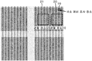
예비 대전 빔의 조사에 의거해서 패턴의 측정을 행하는 구체적인 방법에 대하여 이하에 설명한다. 도 1은 5종류의 재료로 구성되는 깊은 홈 패턴의 상면도(Top View)와 측면도(Side View)를 나타내는 도면이다. 도 1에 있어서, 재료 A는 도체, 재료 B, C, E는 절연체, 재료 D는 도체(부유 전극)이다. 통상의 주사를 행하여 관찰했을 때에 얻어지는 화상을 도 2에 나타낸다. 파형 신호(라인 프로파일)를 보면 알 수 있는 바와 같이, 홈 바닥의 검출 신호량이 적기 때문에, 재료 C와 재료 D의 콘트라스트가 부여되지 않아 경계의 판정이 곤란하다. 이 깊은 홈 패턴에서는, 패턴의 최상부가 도체이기 때문에 저배율 조사에 의해 표면에 양대전을 형성할 수 없다. 이 때문에, 단순한 예비 대전을 행하기 위한 프리 도스법에 의한 홈 바닥 전자의 인상이 곤란하다.A specific method of measuring the pattern based on the irradiation of the pre-charged beam will be described below. 1 is a view showing a top view and a side view of a deep groove pattern made of five kinds of materials. In Fig. 1, the material A is a conductor, the materials B, C and E are an insulator, and the material D is a conductor (floating electrode). An image obtained when normal scanning is performed and observed is shown in Fig. As can be seen from the waveform signal (line profile), since the detection signal amount of the groove bottom is small, the contrast between the material C and the material D is not given and it is difficult to determine the boundary. In this deep groove pattern, since the uppermost portion of the pattern is a conductor, positive charges can not be formed on the surface by the low magnification irradiation. Therefore, it is difficult to raise the bottom electron of the groove by the pre-dosing method for simple preliminary charging.
본 실시예에서는, 저부에 복수의 재료가 혼재하는 시료여도, 콘트라스트를 명확히 하기 위하여, 측정 대상 패턴에 대해서 빔을 주사하기 전에, 당해 측정 대상 패턴의 하층에 위치하는 하층 패턴이, 하층에 위치하는 다른 패턴에 대한 빔 조사를 행하도록, 시야(Field Of View : FOV)를 이동시킴으로써, 예비 대전용의 빔을 측정 대상 패턴과는 다른 위치에 조사하는 예를 설명한다. 이하, 전자선(전자 빔)을 국소적으로 조사함(이 이후, 국소 예비 조사라 함)으로써 홈 바닥을 음대전시키는 예에 대하여 설명한다.In order to clarify the contrast even in the case of a sample in which a plurality of materials are mixed in the bottom portion in the present embodiment, a lower layer pattern positioned under the measurement target pattern is positioned on the lower layer An example will be described in which the beam for preliminary charging is irradiated to a position different from the measurement target pattern by moving the field of view (FOV) so as to perform beam irradiation for another pattern. Hereinafter, an example in which the groove bottom is negatively charged by locally irradiating the electron beam (electron beam) (hereinafter referred to as local preliminary irradiation) will be described.
도 3은, 예비 대전 빔 조사 공정을 포함하는 SEM 관찰 공정을 나타내는 플로차트이다. 우선 국소 예비 조사를 행하는 장소의 선정으로서, 관찰 장소와 홈 바닥이 이어져 있는 장소를 선택한다(스텝 9). 또한, 국소 예비 조사 조건이나 관찰 조건의 설정을 행한다(스텝 10). 여기에서, 관찰 장소와 국소 예비 조사의 장소를 구별하는 이유로서, 국소 예비 조사에 의한 홈 내의 대전이 있다. 도 4에 국소 예비 조사 및 관찰 시의 홈 내 대전 분포를 나타낸다. 국소 예비 조사를 행하면 홈 바닥으로부터 방출된 이차 전자가 부착함으로써 홈의 측벽에 음대전이 축적된다. 홈 측벽의 음대전은, 홈 바닥에서 발생한 이차 전자에 대하여 장벽 전위(홈 바닥 방향으로 되밂)를 형성하기 때문에, 국소 예비 조사와 같은 홈의 관찰을 행하면, 국소 예비 조사의 효과가 없어진다. 이 때문에, 국소 예비 조사와 관찰을 홈 바닥의 재료 D가 이어진 다른 장소에서 실시할 필요가 있다. 홈 바닥을 국소 예비 조사함으로써 부유 전극인 재료 D를 음으로 대전시킨다(스텝 11). 이에 따라, 관찰 장소의 홈 내에는 표면으로부터 홈 바닥 방향으로 전계가 형성된다. 그 후, 재료 D가 이어진 관찰 장소로 이동(스텝 12)하여 미리 설정한 배율로 관찰을 실시한다(스텝 13). 홈 바닥의 음대전으로 형성된 전계에 의하여, 홈 바닥으로부터 방출된 이차 전자가 인상되어 홈 바닥의 콘트라스트가 증가한다.3 is a flow chart showing an SEM observing step including a pre-charging beam irradiation step. First, as a selection of a place for performing the local preliminary investigation, a place where the observation place and the groove bottom are connected is selected (step 9). In addition, local preliminary irradiation conditions and observation conditions are set (step 10). Here, as a reason for distinguishing the observation place from the place of the local preliminary investigation, there is a competition in the groove by the local preliminary investigation. Fig. 4 shows the in-groove charge distribution at the time of local preliminary irradiation and observation. When local preliminary irradiation is performed, negative charges are accumulated on the sidewall of the groove due to adhesion of the secondary electrons emitted from the bottom of the groove. Negative charging of the groove sidewall forms a barrier potential (toward the groove bottom) with respect to the secondary electrons generated at the bottom of the groove, so that when the groove is observed such as local preliminary irradiation, the effect of local preliminary irradiation is lost. For this reason, it is necessary to conduct local preliminary irradiation and observation at a place where the material D of the groove bottom is connected. The bottom of the groove is locally preliminarily irradiated to negatively charge the material D as the floating electrode (step 11). Accordingly, an electric field is formed in the groove of the observation place from the surface to the groove bottom direction. Thereafter, the material D is moved to the observation place where the observation is made (step 12), and observation is performed at a preset magnification (step 13). By the electric field formed by the negative charge of the groove bottom, the secondary electrons emitted from the groove bottom are pulled up, and the contrast of the groove bottom increases.
본 실시예에서는, 관찰과는 다른 장소를 국소 예비 조사함으로써, 표면에 대해서 홈의 바닥을 음대전시켜, 홈 바닥으로부터의 이차 전자 검출수를 증가시킨다.In this embodiment, by locally preliminarily irradiating a spot different from the observation, the bottom of the groove is negatively charged with respect to the surface, and the number of secondary electrons detected from the bottom of the groove is increased.
다음으로, 국소 예비 조사를 행하는 장소의 지정 방법에 대하여 설명한다. 상기에서 설명한 바와 같이, 관찰 장소의 홈 바닥을 음대전시키기 위해서는, 하층의 재료 D가 관찰 장소와 이어진 장소를 조사할 필요가 있다. 이 때문에, 디바이스의 하층의 레이아웃 패턴과 저배율로 취득한 관찰 화상을 중합시킴으로써 조사 장소를 결정한다. 도 5에, 라인 & 스페이스 및 구멍 패턴의 저배율로 취득한 관찰 화상과 디바이스 하층의 레이아웃 패턴을 중합시킨 예를 나타낸다. 하층의 레이아웃과 실제의 관찰상을 동시에 표시시키는 GUI를 구비함으로써, 관찰 장소와 접속된 장소를 확인해서 예비 조사 장소를 설정할 수 있다.Next, a description will be given of a method of designating a place for performing the local preliminary survey. As described above, in order to negatively charge the bottom of the groove at the observation place, it is necessary to investigate the place where the material D of the lower layer is connected to the observation place. Therefore, the irradiation site is determined by superimposing the observation image acquired at a low magnification with the layout pattern of the lower layer of the device. Fig. 5 shows an example in which an observation image obtained with a low magnification of line & space and hole patterns and a layout pattern of a device lower layer are superimposed. By providing a GUI that simultaneously displays the layout of the lower layer and the actual observation image, it is possible to set the preliminary irradiation site by checking the location connected to the observation site.
예비 조사 장소의 지정은 커서 박스를 사용해서 오퍼레이터가 임의로 설정한다. 국소 예비 조사의 조건 설정으로서, 조사 범위, 조사 시간, 조사 전류량을 지정한다. 미리 조사 전류량과 대전 축적량(음대전 전위)의 관계가 구해져 있을 경우에는, 필요한 전위를 지정함으로써 조사 시간 혹은 조사 전류량 중 어느 하나를 파라미터로 해서 자동으로 결정한다.The designation of the preliminary survey site is set by the operator using a cursor box. As the condition setting of the local preliminary investigation, the irradiation range, the irradiation time, and the irradiation current amount are designated. When the relationship between the irradiation current amount and the charge accumulation amount (negative charging potential) is found in advance, the necessary potential is automatically specified by using either the irradiation time or the irradiation current amount as a parameter.
관찰 조건 설정으로서, 관찰 장소, 관찰 배율, 조사 전류량, 프레임수를 지정한다. 관찰 장소의 지정은 예비 조사와 마찬가지로, 커서 박스를 사용해서 GUI의 화면 상에서 지정한다. 또한, 하층 패턴인 재료 D의 영역이 넓을 경우에는, 도 6에 나타내는 바와 같이, 1회의 국소 예비 조사에 의해 복수의 장소를 관찰할 수 있어, 국소 예비 조사의 실시 빈도를 줄이는 것이 가능하다. 국소 예비 조사와 관찰의 빈도를 오퍼레이터가 조합시켜서 지정하는 것도 가능하다. 이러한 설정 내용은 레시피로서 장치 내 메모리 또는 하드디스크 상에 보존되어 다른 측정에서 재이용하는 것도 가능하다. 조건 설정 후에는 레시피의 실행에 의해 자동으로 예비 조사 및 관찰이 실행된다.As the observation condition setting, the observation place, the observation magnification, the irradiation current amount, and the frame number are specified. The designation of the observation place is specified on the screen of the GUI using the cursor box as in the preliminary investigation. Further, when the area of the material D as the lower layer pattern is wide, as shown in Fig. 6, it is possible to observe a plurality of places by one local preliminary irradiation, and it is possible to reduce the frequency of the local preliminary irradiation. It is also possible to designate the frequency of local preliminary investigation and observation by a combination of operators. Such a setting can be saved as a recipe on the device memory or hard disk and reused in other measurements. After the conditions are set, preliminary investigation and observation are automatically performed by execution of the recipe.
본 실시예에 따른 패턴 바닥 신호의 강조는, 패턴의 바닥이 부유 전극이면, 깊은 홈에만 한하지 않고, 깊은 구멍, Via 형상 등에도 적용이 가능하다.If the bottom of the pattern is the floating electrode, the emphasis of the pattern bottom signal according to the present embodiment is applicable not only to the deep groove, but also to the deep hole, the Via shape, and the like.
도 14는, 관찰 조건(측정용 화상의 취득 조건) 및 예비 대전 조건을, 설계 데이터에 의거하여 작성된 레이아웃 데이터 상에서 설정하기 위한 GUI 화면의 일례를 나타내는 도면이다. 이 GUI 화면은, 예를 들면 입력 장치(1310)에 표시 화면에 표시된다. 도 14에 예시하는 GUI 화면에는, 레이아웃 데이터를 표시하기 위한 표시 영역(1401)과, 빔의 조사 조건을 설정하는 설정 윈도우가 마련되어 있다. 설정 윈도우에는, 관찰용의 빔 조건을 설정하기 위한 윈도우와, 대전 형성용의 빔 조건을 설정하기 위한 윈도우가 마련되어 있다. 또, 필요에 따라서 다른 파라미터를 설정 가능하게 하기 위한 다른 윈도우를 마련하도록 해도 된다.14 is a diagram showing an example of a GUI screen for setting observation conditions (acquisition conditions for measurement images) and preliminary charging conditions on layout data created based on design data. This GUI screen is displayed on the display screen on the
관찰용 빔의 설정 윈도우로서는, 예를 들면 측정 혹은 시야 위치를 설정하기 위한 위치 정보 설정 윈도우(Location), 패턴의 종류를 설정하기 위한 설정 윈도우(Pattern Type), 빔의 가속 전압을 설정하는 설정 윈도우(Vacc : Acceleration Voltage), 프레임 적산수(Number of Frames), 시야의 크기(FOV), 빔 전류(Probe Current)가 있다. 표시 영역(1401)에 표시되는 레이아웃 데이터는, 예를 들면 측정 위치 혹은 시야 위치의 설정에 의거하여 설계 데이터 기억 매체(1309)로부터 판독하도록 하면 된다. 이 경우, 측정 위치나 시야 위치의 좌표 정보와 설정되는 시야의 크기에 따라서 부분적인 설계 데이터를 판독함과 함께, 당해 부분을 레이아웃 데이터화해서 표시 화면에 표시시킨다. 또한, 설계 데이터에는 패턴이나 레이어의 식별 정보가 기억되어 있기 때문에, 패턴이나 레이어의 식별 정보 및 좌표 정보 등의 선택에 의거하여 설계 데이터를 판독하도록 해도 된다.Examples of the setting window for the observation beam include a position information setting window for setting a measurement or visual field position, a setting window for setting the type of pattern, a setting window for setting the acceleration voltage of the beam, Accumulation Voltage, Number of Frames, FOV, and Probe Current. The layout data displayed in the
예를 들면 도 14에 예시하는 GUI 화면에서 위치 정보, 시야의 크기를 선택하면, 당해 지정 영역에 상당하는 레이아웃 데이터가 판독되고 표시 장치에 표시된다. 또한, 도 15에 예시하는 바와 같은 레이어 선택 윈도우를 사용해서 표시 영역(1401)에 표시되는 레이어를 선택하도록 해도 된다. 전술한 바와 같이, 각 레이어에는 식별 정보가 부가되어 있기 때문에, 이 식별 정보를 참조함으로써 원하는 레이어의 선택적인 표시가 가능해진다.For example, when the position information and the size of the visual field are selected on the GUI screen shown in Fig. 14, the layout data corresponding to the designated area is read and displayed on the display device. Alternatively, a layer displayed in the
또한, 대전 형성용 빔 조건의 설정 윈도우(1402)는 빔 조사 조건의 종류를 결정하는 윈도우이다. 이 윈도우에서는, 예를 들면 예비 조사를 하지 않음(off), 관찰용의 시야와 예비 대전용의 시야를 일치시킨 상태에서 예비 조사를 행함(On-Site), 및 관찰용의 시야와 예비 대전용의 시야를 이간시켜서 예비 조사를 행함(Off-Site) 등의 설정이 가능하게 되어 있다. 또한, 그 밖에 예비 조사 영역의 크기(Pre-Dose FOV), 예비 조사 시간(Pre-Dose time), 및 관찰 영역(1403)과 예비 대전 빔 조사 영역(1404) 사이의 거리(Distance)를 설정하기 위한 윈도우가 마련되어 있다. 또, 도 14의 예에서는 예비 대전 빔 조사 영역(1404)이 소정의 크기를 갖고 있지만, 이에 한하는 것은 아니며, 스폿 형상의 빔을 깊은 구멍이나 깊은 홈에 선택적으로 조사하도록 해도 된다.The setting
도 16은, 측정 대상으로 되는 패턴의 종류나 장소(좌표 등의 위치 정보)의 선택에 의거하여, 자동적으로 예비 대전용 빔의 조사 영역 혹은 조사 위치를 결정하는 공정을 나타내는 플로차트이다. 우선, 입력 장치(1310)의 표시 장치에 표시된 GUI 화면 상에서 측정 대상으로 되는 패턴의 종류나 장소의 선택을 행한다(스텝 1601). 설계 데이터 추출부(1307)는, 그 선택에 의거하여 선택된 패턴 종류나 장소의 정보에 의거하여, 설계 데이터 기억 매체(1309)로부터 설계 데이터의 판독을 행하여 레이아웃 데이터화 한다(스텝 1602). 전술한 바와 같이, 설계 데이터의 패턴이나 레이어에는 식별 정보가 부가되어 있으므로, 그 정보를 참조함으로써 원하는 패턴이나 영역에 속하는 패턴의 레이아웃 데이터를 판독한다. 다음으로, GUI 화면 상에서 원하는 측정 부위나 화상 취득 영역을 선택한다(스텝 1603).Fig. 16 is a flowchart showing a step of automatically determining an irradiation area or irradiating position of a preliminary charging beam on the basis of a type of a pattern to be measured and a selection of a place (position information such as coordinates). First, the type and location of the pattern to be measured are selected on the GUI screen displayed on the display device of the input device 1310 (step 1601). The design
대전 빔 조사 부위 선택부(1306)는, 선택된 측정 부위 혹은 화상 취득 영역에 따라서 대전용 빔 조사 부위 등의 선택을 행한다(스텝 1604). 여기에서, 대전용 빔 조사 대상으로서 적절한 패턴은, (A) 측정 대상 패턴과 하층 배선(부유 전극)이 같은 다른 패턴(상층 패턴)이며, 또한 (B) 관찰용의 빔 조사 영역과 겹치지 않는 영역에 존재하는 패턴이다. 조건(A)에 대해서는, 설계 데이터를 참조하면 상층 패턴과 하층 패턴의 중첩 부위를 특정할 수 있으며, 또한 조건(B)에 대해서는 스텝 1603 등에서의 설정에 의해, 관찰용 빔의 조사 영역(시야)을 특정할 수 있으므로, 조건(A)과 조건(B)의 앤드 조건에 의거하여 대전용 빔의 조사 부위의 범위 축소를 행하도록 하면, 연산 처리부(1303)에서의 연산에 의거하여 자동적으로 대전용 빔의 조사 부위의 선택이 가능해진다. 대전용 빔의 조사 부위 후보가 복수 추출되거나 혹은 후보가 없는 경우에는, 한층 더 범위 축소를 재촉하는 메시지나 에러 메시지를 발생시킴으로써, 메뉴얼 어시스트에 의한 선택을 하도록 해도 된다. 또한, 조건(A)(B)에 한하지 않고, 다른 조건을 사용한 범위 축소를 자동으로 행하도록 해도 된다. 자동 선택된 대전용 빔의 조사 조건을 레시피로서 예를 들면 메모리(1304)에 등록한다(스텝 1605).The charged-beam-irradiation-site selection unit 1306 selects a charged-beam-irradiation site or the like in accordance with the selected measurement site or image acquisition region (step 1604). Here, a suitable pattern for the charging beam irradiation target is a region (A) in which the measurement target pattern and the lower layer wiring (floating electrode) are different from each other (upper layer pattern) . ≪ / RTI > With respect to the condition (A), it is possible to specify the overlapped portion between the upper layer pattern and the lower layer pattern by referring to the design data, and with regard to the condition (B), the irradiation region (field of view) It is possible to reduce the range of the irradiated portion of the charging beam based on the end conditions of the conditions A and B so that the irradiation area of the charging beam is automatically reduced based on the calculation in the
이상과 같은 자동 선택 기능을 마련함으로써, 적절히 예비 대전용 빔의 조사 위치를 설정하는 것이 가능해진다.By providing the automatic selection function as described above, it is possible to appropriately set the irradiation position of the preliminary charging beam.
[실시예 2][Example 2]
다음으로 제2 실시예에 대하여 이하 설명한다. 애스팩트비가 높은 시료의 관찰에서는, 표면과 패턴 바닥의 콘트라스트가 지나치게 부여되게 되어, 패턴 바닥의 관찰이 곤란한 경우가 있다. 그러한 경우에 다른 조건에서 취득한 화상을 사용함으로써 패턴 바닥의 신호를 강조하는 방법에 대하여 설명한다. 본 실시예에서는, 국소 예비 조사를 행하지 않는 조건에서 관찰한 화상과, 홈 바닥에 국소 예비 조사를 실시한 후에 관찰한 화상을 조합시킴으로써 구멍 바닥의 신호를 강조한다. 도 7에 국소 예비 조사를 행하지 않고 관찰했을 때의 신호 파형(1)과 국소 예비 조사 후에 관찰한 신호 파형을 나타낸다. 표면의 대전 상태는 변하지 않기 때문에 표면의 신호 파형은 변화하지 않는다. 한편, 홈 내의 신호 파형은 예비 조사에 의하여 재료 D가 음대전하기 때문에 (2)에서 신호량이 증가한다. 여기에서, 예비 조사 후의 관찰 시의 신호 파형으로부터 예비 조사 없이 관찰한 신호 파형을 뺌으로써 홈 바닥만의 신호를 남길 수 있어, 홈 내의 신호를 강조하는 것이 가능하다.Next, the second embodiment will be described below. In the observation of a sample having a high aspect ratio, the contrast between the surface and the bottom of the pattern is excessively applied, so that it may be difficult to observe the bottom of the pattern. In such a case, a method of emphasizing the signal at the bottom of the pattern by using an image obtained under other conditions will be described. In this embodiment, the signal at the bottom of the hole is emphasized by combining the image observed under the condition that the local preliminary irradiation is not performed and the image observed after the local preliminary irradiation at the bottom of the groove. Fig. 7 shows the
도 17은 전술한 바와 같은 측정을 자동적으로 실행하기 위한 플로차트의 일례를 나타내는 도면이다. 우선, 측정 대상 패턴에 대해서 빔 조사를 행하여 제1 신호 파형(22)을 취득한다(스텝 1701, 1702). 다음으로 시료에 대한 빔의 조사 위치를 이미지 쉬프트나 스테이지 이동에 의하여 이동시켜 대전용의 빔을 조사한다(스텝 1703). 그리고, 다시 측정 대상 패턴에 대해서 빔을 조사하여 제2 신호 파형(23)을 취득한다(스텝 1704, 1705). 패턴 측정부(1308)는, 제1 신호 파형(22)과 제2 신호 파형(23)의 차분 연산(제2 신호 파형-제1 신호 파형)을 행하고, 얻어진 차분 프로파일(24)을 사용해서 치수 측정을 실행한다(스텝 1706, 1707).17 is a diagram showing an example of a flowchart for automatically performing the measurement as described above. First, beam irradiation is performed on the measurement object pattern to acquire the first signal waveform 22 (steps 1701 and 1702). Next, the irradiation position of the beam with respect to the sample is moved by the image shift or the stage movement to irradiate the charging beam (step 1703). Then, the
이상과 같은 처리를 자동 실행하는 레시피를 메모리(1304)에 미리 등록시켜둠으로써, 구멍 바닥이나 홈 바닥의 측정이나 관찰을 자동적으로 실행하는 것이 가능해진다.By registering in advance the recipe in the
또, 이 차분 연산은 재료 A의 휘도 정보를 없애는 효과뿐만 아니라, 재료 C와 재료 D의 콘트라스트를 명확히 하는 효과도 있다. 예비 대전 빔 조사를 행함으로써 재료 D가 선택적으로 대전하기 때문에 재료 D의 휘도는 크게 향상된다. 한편, 재료 C로부터 방출된 전자는, 재료 D의 대전의 영향에 의해 약간 검출 효율이 향상하지만, 재료 C 자체가 대전해 있다고는 할 수 없으므로, 상대적으로 검출 효율의 향상은 한정되어 있다. 따라서, 재료 D의 선택적인 대전에 의해 재료 C와 재료 D의 콘트라스트를 크게 할 수 있어, 차분 연산에 의하여 재료 C의 피크를 두드러지게 하는 것이 가능해진다. 이렇게 재료 C의 피크를 현재화(顯在化)함으로써, 예를 들면 재료 C의 만듦새를 적정하게 평가하는 것이 가능해진다.This difference calculation has an effect of clarifying not only the effect of eliminating the luminance information of the material A but also the contrast of the material C and the material D. [ Since the material D is selectively charged by performing the pre-charging beam irradiation, the luminance of the material D is greatly improved. On the other hand, the electrons emitted from the material C slightly improve detection efficiency due to the influence of the charging of the material D, but the improvement of the detection efficiency is relatively limited since the material C itself can not be said to be charged. Therefore, the contrast of the material C and the material D can be increased by selective charging of the material D, and the peak of the material C can be marked by the difference calculation. By peeling the peak of the material C in this way, it becomes possible to appropriately evaluate the build of the material C, for example.
[실시예 3][Example 3]
다음으로 제3 실시예에 대하여 설명한다. 본 실시예에서는, 검출 전자의 에너지에 따른 변별에 의해, 패턴 바닥 신호를 강조하는 방법에 대하여 나타낸다. 도 8에 도 1의 구조에 대하여, 예비 조사 유무의 조건에서 관찰했을 때에 각 장소로부터 검출되는 전자의 에너지 분포를 나타낸다. 신호 파형(25)(도 8의 (a))은 예비 조사 없음일 때의 신호 파형이고, 신호 파형(26)(도 8의 (b))은 예비 조사 있음일 때의 신호 파형이다. 예비 조사 없음의 조건에서 관찰했을 경우에는, 표면 및 홈 바닥에 전위차가 없기 때문에, 검출되는 전자의 에너지 분포는 거의 동등해진다. 또한, 홈 바닥의 검출 신호량은 표면에 대해서 적다. 한편, 예비 조사 후에 관찰했을 경우에는, 홈 바닥이 음대전해 있기 때문에, 홈 바닥으로부터의 검출 전자의 에너지 분포는 표면으로부터의 검출 전자의 분포와 다르다. 이 때문에, 예비 조사 후에 관찰할 때에는, 에너지에 따라서 검출 전자를 변별함으로써, 홈 바닥의 신호를 강조할 수 있다.Next, the third embodiment will be described. In this embodiment, a method of emphasizing the bottom signal of the pattern by differentiation according to the energy of the detection electrons is described. Fig. 8 shows the energy distribution of electrons detected from each place when observed under the condition of preliminary irradiation with respect to the structure of Fig. The signal waveform 25 (FIG. 8A) is a signal waveform when no preliminary irradiation is performed, and the signal waveform 26 (FIG. 8B) is a signal waveform when preliminary irradiation exists. When observed under the condition of no preliminary irradiation, since there is no potential difference between the surface and the bottom of the groove, the energy distribution of the detected electrons becomes almost equal. Further, the detection signal amount of the groove bottom is small with respect to the surface. On the other hand, when observed after the preliminary irradiation, the energy distribution of the detection electrons from the bottom of the groove is different from the distribution of the detection electrons from the surface because the groove bottom is transmitted to the acoustic band. Therefore, when observing after the preliminary irradiation, the signal at the bottom of the groove can be emphasized by discriminating the detection electrons according to the energy.
도 9에 예비 조사 후의 전자 빔 주사에 의하여 얻어진 전자의 에너지 분포의 신호 파형(26)을 나타낸다. 도 9에 예시하는 바와 같이, 재료마다 다른 에너지 분포를 갖고 있기 때문에, 본 예의 경우, 3개의 피크로 이루어지는 에너지 분포 정보를 얻을 수 있다. 여기에서, 에너지 밴드(EF1-EF2)의 전자가 선택적으로 검출할 수 있으면, 재료 C의 콘트라스트를 강조한 신호 파형이나 화상을 형성할 수 있고, EF2 이상의 에너지 밴드의 전자를 선택적으로 검출할 수 있으면, 재료 C의 콘트라스트를 강조한 신호 파형이나 화상을 형성할 수 있다. 에너지 필터는 에너지가 낮은 전자를 커트하는 하이패스 필터이며, 인가 전압의 적절한 선택에 의해 통과하는 전자의 에너지를 선택할 수 있다.Fig. 9 shows a
도 10은 에너지 필터(1218)에의 인가 전압을 조정함으로써 얻어지는 파형 신호의 종류를 나타내는 도면이다. 도 10의 (1)의 신호 파형(27)은, 검출수가 많은 재료 A의 신호량이 많고 구멍 바닥의 신호량이 적기 때문에 구멍 바닥이 어두운 상태의 파형이다. 다음으로, 에너지 필터에의 인가 전압을 EF1로 설정하면, 음대전이 없어 상대적으로 에너지가 낮은 재료 A로부터 방출되는 전자가 에너지 필터(1218)의 통과가 제한되기 때문에, 도 10의 (2)의 신호 파형(28)과 같이 상대적으로 재료 C, D의 신호량이 증가하여 구멍 바닥이 밝은 신호 파형이나 화상을 형성할 수 있다. 또한, 에너지 필터에의 인가 전압을 EF2로 설정하면, 재료 A, C로부터 방출되는 전자가 에너지 필터(1218)의 통과가 제한되기 때문에, 도 10의 (3)의 신호 파형(29)과 같이 재료 D의 신호가 강조된 신호 파형이나 화상을 얻을 수 있다.10 is a diagram showing a kind of a waveform signal obtained by adjusting the voltage applied to the
또한, 도 11에 예시하는 바와 같이, 신호 파형(28)으로부터 신호 파형(29)을 감산함으로써, 재료 C, D의 신호가 혼재한 신호 파형으로부터 재료 D에 상당하는 정보를 없앨 수 있기 때문에, 재료 C의 신호를 강조하는 것이 가능해진다. 도 18은 도 11에 예시하는 바와 같은 재료 C의 신호를 강조한 신호 파형을 사용한 측정을 행하는 공정을 나타내는 플로차트이다. 우선, 대전 빔 조사 개소에 대전 빔을 조사한다(스텝 1801). 다음으로 제어 장치(1220)는, 에너지 필터(1218)에의 인가 전압을 조건 1(EF1)로 설정하여, 측정 대상 패턴에 빔을 조사함으로써 제1 신호 파형을 취득한다(스텝 1802, 1803). 다음으로, 에너지 필터에의 인가 전압을 조건 2(EF2)로 설정하여, 측정 대상 패턴에 빔을 조사함으로써 제2 신호 파형을 취득한다(스텝 1804, 1805).11, information corresponding to the material D can be eliminated from the signal waveform in which the signals of the materials C and D are mixed by subtracting the
패턴 측정부(1308)는, 제1 신호 파형(28)과 제2 신호 파형(29)의 차분 연산(제2 신호 파형-제1 신호 파형)을 행하고, 얻어진 차분 프로파일(30)을 사용해서 치수 측정을 실행한다(스텝 1806, 1807).The
이상과 같이, 에너지 필터에의 인가 전압 조정이나 차분 연산 등을 행함으로써, 원하는 재료로부터 방출되는 전자에 의거한 신호를 강조할 수 있어, 목적에 따라서 적절한 신호 처리를 행할 수 있다.As described above, the signal based on the electrons emitted from the desired material can be emphasized by adjusting the applied voltage to the energy filter and calculating the difference, and appropriate signal processing can be performed according to the purpose.
또, 전술한 실시예에서는 에너지 변별을 행하기 위하여 메쉬 형상 전극과 같은 전위 장벽을 형성하는 전위 장벽 형성부를 적용한 예를 설명했지만, 예를 들면 다른 에너지의 전자를 궤도 분리함으로써, 시료로부터 방출되는 전자의 에너지 변별하는 것도 가능하다. 도 19는, 다른 위치에 설치된 검출기(1907, 1908)를 사용해서, 다른 에너지 밴드의 전자를 검출하는 장치 구성을 나타내는 도면이다. 시료(1901)로부터 방출된 전자(1902)는, 직교 전자계(電磁界) 발생기(1903)의 편향 작용에 의하여, 전자 빔의 이상 광축(1904)으로부터 이축(離軸)하도록 검출기를 향해서 편향된다. 직교 전자계 발생기(1903)는, 전자(1902)를 검출기측으로 편향시키는 전계에 직교하도록 자계가 형성되도록 자장 발생기가 설치되어 있다. 이 자계는, 전자(1902)에는 검출기측으로 전자(1902)를 유도하도록 작용하는 반면, 시료에 조사되는 전자 빔을 전계의 편향 작용과 역방향으로 편향시키기 때문에, 적정한 조정에 의하여, 전자 빔을 편향시키지 않고 시료로부터 방출되는 전자를 선택적으로 검출기측으로 유도할 수 있다.In the above-described embodiment, the potential barrier forming portion for forming the potential barrier such as the mesh electrode is applied to perform energy discrimination. However, for example, by electronically separating electrons of different energy, electrons emitted from the sample It is also possible to distinguish the energy of 19 is a view showing an apparatus configuration for detecting electrons of different energy
또한, 직교 전자계 발생기(1903)는 에너지가 약한 전자를 보다 크게 편향시키기 위해, 제1 에너지 밴드(EF1-EF2)의 전자를 하측의 검출기(1908)를 사용해서 검출하고, 제2 에너지 밴드(≥EF2)의 전자를 상측의 검출기(1907)를 사용해서 검출하도록, 직교 전자계 발생기(1903)를 조정함으로써 에너지 변별 검출을 행할 수 있다. 이 경우, 증폭기(1809)의 증폭률을 적정하게 설정한 후, 2개의 검출기의 출력을 합성하면, 원하는 재료의 휘도를 선택적으로 강화한 신호를 형성할 수 있다.Further, the orthogonal
이상과 같이, 다른 에너지 변별 검출법에 의해서도, 구멍 바닥 등으로부터 방출되는 전자에 의거한 재료 단위로의 신호의 강조 처리를 행할 수 있다.As described above, it is also possible to emphasize the signal in the material unit based on the electrons emitted from the hole bottom or the like by other energy discrimination detection method.
1 : 라인 2 : 스페이스
3 : 재료 A 4 : 재료 B
5 : 재료 C 6 : 재료 D
7 : 재료 E 8 : 신호 파형
9 : 예비 조사 장소의 선택 10 : 예비 조사, 관찰 조건 설정
11 : 패턴 바닥의 조사 12 : 장소의 변경(관찰 장소로 이동)
13 : 관찰 14 : 설계 데이터(하층의 레이아웃)
15 : 홈의 측벽(음대전) 16 : 하층의 레이아웃(홈)
17 : 관찰 화상
18 : 구멍 패턴에서의 하층의 레이아웃
19 : 예비 조사 영역 20 : 관찰 장소(1)
21 : 관찰 장소(2)
22 : 제1 신호 파형(예비 조사 없이 관찰했을 때의 신호 파형)
23 : 제2 신호 파형(예비 조사 후, 관찰했을 때의 신호 파형)
24 : 차분 프로파일(차(差) 파형((2)-(1)))
25 : 신호 파형(예비 조사 없이 관찰했을 때의 검출 전자의 에너지 분포)
26 : 신호 파형(예비 조사 후, 관찰했을 때의 검출 전자의 에너지 분포)
27 : 신호 파형(에너지 변별 없음에서의 신호 파형)
28 : 신호 파형(EF1로 에너지 변별했을 때의 신호 파형)
29 : 신호 파형(EF2로 에너지 변별했을 때의 신호 파형)
30 : 차분 프로파일(에너지 변별 화상간의 차 파형((2)-(3)))1: Line 2: Space
3: Material A 4: Material B
5: material C 6: material D
7: Material E 8: Signal waveform
9: Selection of preliminary survey site 10: Preliminary survey, setting observation condition
11: Investigation of pattern bottom 12: Change of place (move to observation place)
13: Observation 14: Design data (lower layer layout)
15: side wall of groove (negative charge) 16: layout of lower layer (groove)
17: Observation image
18: Layout of lower layer in hole pattern
19: preliminary irradiation area 20: observation place (1)
21: Observation place (2)
22: First signal waveform (signal waveform observed without preliminary irradiation)
23: Second signal waveform (signal waveform after observation after preliminary irradiation)
24: Differential profile (difference waveform ((2) - (1)))
25: Signal waveform (energy distribution of detected electrons when observed without preliminary irradiation)
26: Signal waveform (energy distribution of detected electrons when observed after preliminary irradiation)
27: Signal waveform (signal waveform without energy discrimination)
28: Signal waveform (Signal waveform when energy is discriminated by EF1)
29: Signal waveform (signal waveform when energy is discriminated by EF2)
30: Differential profile (difference waveform between the energy discrimination images ((2) - (3)))
Claims (10)
측정 대상인 홀 패턴 또는 홈모양 패턴에 대하여 빔을 주사하기 전에, 당해 홀 패턴 또는 홈모양 패턴과 공통의 하층 패턴을 갖는 다른 패턴에 예비 대전용의 빔 조사(照射)를 행하도록, 상기 편향기, 혹은 시료 스테이지를 제어하는 제어 장치를 구비한 것을 특징으로 하는 주사 전자 현미경.A scanning electron microscope having an electron source (electron source), an objective lens for focusing an electron beam emitted from the electron source, a deflector for deflecting the scanning position of the electron beam, and a sample stage for mounting the sample, In the microscope,
Before irradiating the beam with respect to the hole pattern or the groove pattern to be measured, irradiates a beam for preliminary charging to another pattern having a lower layer pattern common to the hole pattern or the groove pattern, Or a control device for controlling the sample stage.
상기 제어 장치는, 상기 측정 대상 패턴의 주사 영역과 이간한 위치에 위치하는 상기 다른 패턴에 상기 빔을 조사하도록, 상기 편향기, 혹은 시료 스테이지를 제어하는 것을 특징으로 하는 주사 전자 현미경.The method according to claim 1,
Wherein the control device controls the deflector or the sample stage so as to irradiate the beam to the other pattern located at a position spaced apart from the scan area of the measurement target pattern.
깊은 홈, 혹은 깊은 구멍 패턴으로서, 홈 바닥, 혹은 구멍 바닥에 절연체로 포위된 부유 전극이 위치하는 측정 대상 패턴에 상기 전자 빔을 주사하기 전에, 상기 부유 전극의 당해 측정 대상 패턴과는 다른 위치에, 예비 대전용의 전자 빔을 조사해서, 당해 부유 전극을 대전(帶電)시키는 것을 특징으로 하는 패턴 측정 방법.A method of measuring a pattern using a scanning electron microscope which forms a signal waveform of a pattern included in the sample by irradiating the electron beam emitted from the electron source to the sample,
A deep groove or a deep hole pattern is formed at a position different from the measurement target pattern of the floating electrode before the electron beam is scanned on the measurement target pattern on which the floating electrode surrounded by the insulator is located on the bottom of the groove or on the bottom of the hole And irradiating an electron beam for preliminary charging to charge the floating electrode.
상기 시료는 표면이 도전체인 것을 특징으로 하는 패턴 측정 방법.The method of claim 3,
Wherein the surface of the sample is a conductive one.
상기 도전체와 부유 전극 사이에 절연체가 배치되어 있는 것을 특징으로 하는 패턴 측정 방법.5. The method of claim 4,
And an insulator is disposed between the conductor and the floating electrode.
측정 대상인 홀 패턴 또는 홈모양 패턴에 상기 전자 빔을 주사해서 제1 신호 파형을 형성하고, 당해 홀 패턴 또는 홈모양 패턴에 대한 전자 빔의 주사 후, 당해 홀 패턴 또는 홈모양 패턴과 공통의 하층 패턴을 갖는 다른 패턴에 예비 대전용의 빔 조사를 행하여, 당해 예비 대전용의 빔 조사 후, 상기 측정 대상 패턴에 상기 전자 빔을 주사해서 제2 신호 파형을 형성하고, 당해 제2 신호 파형으로부터, 상기 제1 신호 파형을 감산하는 제어 장치를 구비한 것을 특징으로 하는 주사 전자 현미경.A scanning electron microscope comprising an electron source, an objective lens for focusing the electron beam emitted from the electron source, a deflector for deflecting the scanning position of the electron beam, and a sample stage for mounting the sample,
Forming a first signal waveform by scanning the electron beam on a hole pattern or a groove pattern to be measured and scanning the electron beam with respect to the hole pattern or the groove pattern to form a lower layer pattern And irradiates the measurement target pattern with the electron beam to form a second signal waveform, and from the second signal waveform, the beam of the preliminary charge And a control device for subtracting the first signal waveform.
상기 제어 장치는, 상기 측정 대상 패턴의 주사 영역과 이간한 위치에 위치하는 상기 다른 패턴에 상기 빔을 조사하도록, 상기 편향기, 혹은 시료 스테이지를 제어하는 것을 특징으로 하는 주사 전자 현미경.The method according to claim 6,
Wherein the control device controls the deflector or the sample stage so as to irradiate the beam to the other pattern located at a position spaced apart from the scan area of the measurement target pattern.
측정 대상인 홀 패턴 또는 홈모양 패턴에 대하여 빔을 주사하기 전에, 당해 홀 패턴 또는 홈모양 패턴과 공통의 하층 패턴을 갖는 다른 패턴에 예비 대전용의 빔 조사를 행하도록, 상기 편향기, 혹은 시료 스테이지를 제어함과 함께, 상기 에너지 변별기에 의하여 변별된 제1 에너지 밴드의 전자에 의거한 제1 신호 파형, 및/또는 제2 에너지 밴드의 전자에 의거한 제2 신호 파형을 형성하는 제어 장치를 구비한 것을 특징으로 하는 주사 전자 현미경.1. An electron source comprising: an electron source; an objective lens for focusing the electron beam emitted from the electron source; a deflector for deflecting the scanning position of the electron beam; a sample stage for mounting the sample; In a scanning electron microscope having an energy discriminator,
Before the beam is scanned with respect to the hole pattern or the groove pattern to be measured, a beam for preliminary charging is applied to another pattern having a lower layer pattern common to the hole pattern or groove pattern, And a control device for controlling a first signal waveform based on electrons of the first energy band and / or a second signal waveform based on electrons of the second energy band, which is discriminated by the energy discriminator And a scanning electron microscope.
상기 제2 에너지 밴드는, 상기 제1 에너지 밴드보다 에너지가 높고, 상기 제어 장치는 제2 신호 파형으로부터 상기 제1 신호 파형을 감산하는 것을 특징으로 하는 주사 전자 현미경.9. The method of claim 8,
Wherein the second energy band is higher in energy than the first energy band and the control device subtracts the first signal waveform from the second signal waveform.
상기 제어 장치는, 상기 제1 신호 파형, 상기 제2 신호 파형, 및/또는 제2 신호 파형으로부터 제1 신호 파형을 감산한 차(差) 파형을 사용해서 상기 패턴의 치수 측정을 실행하는 것을 특징으로 하는 주사 전자 현미경.9. The method of claim 8,
The control device performs dimension measurement of the pattern using a difference waveform obtained by subtracting the first signal waveform from the first signal waveform, the second signal waveform, and / or the second signal waveform A scanning electron microscope.
Applications Claiming Priority (3)
| Application Number | Priority Date | Filing Date | Title |
|---|---|---|---|
| JP2012072710A JP5932428B2 (en) | 2012-03-28 | 2012-03-28 | Scanning electron microscope |
| JPJP-P-2012-072710 | 2012-03-28 | ||
| PCT/JP2013/053790 WO2013145924A1 (en) | 2012-03-28 | 2013-02-18 | Scanning electron microscope |
Publications (2)
| Publication Number | Publication Date |
|---|---|
| KR20140109920A KR20140109920A (en) | 2014-09-16 |
| KR101622613B1 true KR101622613B1 (en) | 2016-05-20 |
Family
ID=49259206
Family Applications (1)
| Application Number | Title | Priority Date | Filing Date |
|---|---|---|---|
| KR1020147018326A KR101622613B1 (en) | 2012-03-28 | 2013-02-18 | Scanning electron microscope |
Country Status (4)
| Country | Link |
|---|---|
| US (1) | US9472376B2 (en) |
| JP (1) | JP5932428B2 (en) |
| KR (1) | KR101622613B1 (en) |
| WO (1) | WO2013145924A1 (en) |
Families Citing this family (7)
| Publication number | Priority date | Publication date | Assignee | Title |
|---|---|---|---|---|
| US9330884B1 (en) * | 2014-11-11 | 2016-05-03 | ICT Integrated Circuit Testing Gesellschaft für Halbleiterprüftechnik mbH | Dome detection for charged particle beam device |
| JP2019185972A (en) | 2018-04-06 | 2019-10-24 | 株式会社日立ハイテクノロジーズ | Scanning electron microscopy system and pattern depth measurement method |
| JP2019184354A (en) * | 2018-04-06 | 2019-10-24 | 株式会社日立ハイテクノロジーズ | Electronic microscope device, inspection system using electronic microscope device, and inspection method using electronic microscope device |
| JP7150634B2 (en) * | 2019-02-21 | 2022-10-11 | 株式会社荏原製作所 | Electron beam irradiation device and electron beam alignment method |
| JP2021005497A (en) * | 2019-06-26 | 2021-01-14 | キオクシア株式会社 | Electron microscope and beam irradiation method |
| JP7149906B2 (en) | 2019-08-07 | 2022-10-07 | 株式会社日立ハイテク | Scanning electron microscope and pattern measurement method |
| JP7218034B1 (en) * | 2022-11-04 | 2023-02-06 | 株式会社Photo electron Soul | LOCAL OBSERVATION METHOD, PROGRAM, RECORDING MEDIUM AND ELECTRON BEAM APPLICATION DEVICE |
Citations (2)
| Publication number | Priority date | Publication date | Assignee | Title |
|---|---|---|---|---|
| US20090001279A1 (en) * | 2007-06-29 | 2009-01-01 | Atsushi Kobaru | Charged particle beam apparatus |
| JP2010175249A (en) | 2009-01-27 | 2010-08-12 | Hitachi High-Technologies Corp | Method and device for measuring height of sample |
Family Cites Families (12)
| Publication number | Priority date | Publication date | Assignee | Title |
|---|---|---|---|---|
| US4327292A (en) * | 1980-05-13 | 1982-04-27 | Hughes Aircraft Company | Alignment process using serial detection of repetitively patterned alignment marks |
| JPH01115042A (en) * | 1987-10-28 | 1989-05-08 | Hitachi Ltd | Sample stand of scanning type electronic microscope |
| JP2650930B2 (en) * | 1987-11-24 | 1997-09-10 | 株式会社日立製作所 | Superlattice device fabrication method |
| JPH0529424A (en) | 1991-07-19 | 1993-02-05 | Fujitsu Ltd | Inspection of semiconductor device |
| EP0548573B1 (en) * | 1991-11-27 | 1998-02-25 | Hitachi, Ltd. | Electron beam apparatus |
| JPH05259240A (en) * | 1992-03-11 | 1993-10-08 | Matsushita Electron Corp | Evaluating method of semiconductor device |
| JP3749107B2 (en) * | 1999-11-05 | 2006-02-22 | ファブソリューション株式会社 | Semiconductor device inspection equipment |
| JP4418304B2 (en) | 2004-06-03 | 2010-02-17 | 株式会社日立ハイテクノロジーズ | Sample observation method |
| JP2008004376A (en) | 2006-06-22 | 2008-01-10 | Seiko Epson Corp | Device, method for producing thin film, and method for manufacturing device, and electronic equipment |
| TWI585806B (en) * | 2008-04-11 | 2017-06-01 | 荏原製作所股份有限公司 | Sample observation method and apparatus, and inspection method and apparatus using the same |
| JP2010118414A (en) | 2008-11-11 | 2010-05-27 | Topcon Corp | Semiconductor inspection device |
| JP5537288B2 (en) * | 2010-06-30 | 2014-07-02 | 株式会社日立ハイテクノロジーズ | Electron beam irradiation method and scanning electron microscope |
-
2012
- 2012-03-28 JP JP2012072710A patent/JP5932428B2/en active Active
-
2013
- 2013-02-18 WO PCT/JP2013/053790 patent/WO2013145924A1/en active Application Filing
- 2013-02-18 US US14/379,715 patent/US9472376B2/en active Active
- 2013-02-18 KR KR1020147018326A patent/KR101622613B1/en active IP Right Grant
Patent Citations (2)
| Publication number | Priority date | Publication date | Assignee | Title |
|---|---|---|---|---|
| US20090001279A1 (en) * | 2007-06-29 | 2009-01-01 | Atsushi Kobaru | Charged particle beam apparatus |
| JP2010175249A (en) | 2009-01-27 | 2010-08-12 | Hitachi High-Technologies Corp | Method and device for measuring height of sample |
Also Published As
| Publication number | Publication date |
|---|---|
| US20150008322A1 (en) | 2015-01-08 |
| WO2013145924A1 (en) | 2013-10-03 |
| JP5932428B2 (en) | 2016-06-08 |
| JP2013206641A (en) | 2013-10-07 |
| US9472376B2 (en) | 2016-10-18 |
| KR20140109920A (en) | 2014-09-16 |
Similar Documents
| Publication | Publication Date | Title |
|---|---|---|
| KR101622613B1 (en) | Scanning electron microscope | |
| US8890068B2 (en) | Charged particle ray apparatus and pattern measurement method | |
| JP5948084B2 (en) | Scanning electron microscope | |
| KR101709433B1 (en) | Sample observation device | |
| US8779357B1 (en) | Multiple image metrology | |
| US7521678B2 (en) | Charged particle beam apparatus, charged particle beam focusing method, microstructure measuring method, microstructure inspecting method, semiconductor device manufacturing method, and program | |
| US9275829B2 (en) | Image forming device and computer program | |
| WO2016017561A1 (en) | Charged particle beam device | |
| JP2010175249A (en) | Method and device for measuring height of sample | |
| JP2014146526A (en) | Electron beam device, and electron beam observation method | |
| US9786468B2 (en) | Charged particle beam device | |
| JP5222994B2 (en) | Sample observation method and scanning electron microscope | |
| KR20180095635A (en) | Overlay error measuring device, and computer program | |
| US11011348B2 (en) | Scanning electron microscope and sample observation method using scanning electron microscope | |
| US10755890B2 (en) | Charged particle beam apparatus | |
| US20160093465A1 (en) | Defect inspection apparatus and defect inspection method | |
| JP5619118B2 (en) | Charged particle beam equipment | |
| JP5965851B2 (en) | Sample observation equipment | |
| JP5712073B2 (en) | Automatic determination method of inspection condition / measurement condition of sample and scanning microscope | |
| JP2006172919A (en) | Scanning electron microscope having three-dimensional shape analysis function | |
| JP2011179819A (en) | Pattern measuring method and computer program | |
| US20240144560A1 (en) | Training Method for Learning Apparatus, and Image Generation System | |
| KR20230018315A (en) | Method, apparatus, and program for determining condition related to captured image of charged particle beam apparatus | |
| JP2009224289A (en) | Charged particle beam apparatus |
Legal Events
| Date | Code | Title | Description |
|---|---|---|---|
| A201 | Request for examination | ||
| E902 | Notification of reason for refusal | ||
| E701 | Decision to grant or registration of patent right |