KR101320686B1 - Error Correcting Device and Method for Memory - Google Patents
Error Correcting Device and Method for Memory Download PDFInfo
- Publication number
- KR101320686B1 KR101320686B1 KR1020110120241A KR20110120241A KR101320686B1 KR 101320686 B1 KR101320686 B1 KR 101320686B1 KR 1020110120241 A KR1020110120241 A KR 1020110120241A KR 20110120241 A KR20110120241 A KR 20110120241A KR 101320686 B1 KR101320686 B1 KR 101320686B1
- Authority
- KR
- South Korea
- Prior art keywords
- memory cell
- memory
- additional information
- data stored
- information
- Prior art date
Links
Images


Classifications
-
- G—PHYSICS
- G11—INFORMATION STORAGE
- G11C—STATIC STORES
- G11C29/00—Checking stores for correct operation ; Subsequent repair; Testing stores during standby or offline operation
- G11C29/04—Detection or location of defective memory elements, e.g. cell constructio details, timing of test signals
- G11C29/08—Functional testing, e.g. testing during refresh, power-on self testing [POST] or distributed testing
- G11C29/12—Built-in arrangements for testing, e.g. built-in self testing [BIST] or interconnection details
- G11C29/38—Response verification devices
- G11C29/42—Response verification devices using error correcting codes [ECC] or parity check
-
- G—PHYSICS
- G06—COMPUTING; CALCULATING OR COUNTING
- G06F—ELECTRIC DIGITAL DATA PROCESSING
- G06F11/00—Error detection; Error correction; Monitoring
- G06F11/07—Responding to the occurrence of a fault, e.g. fault tolerance
- G06F11/08—Error detection or correction by redundancy in data representation, e.g. by using checking codes
- G06F11/10—Adding special bits or symbols to the coded information, e.g. parity check, casting out 9's or 11's
- G06F11/1008—Adding special bits or symbols to the coded information, e.g. parity check, casting out 9's or 11's in individual solid state devices
-
- G—PHYSICS
- G11—INFORMATION STORAGE
- G11C—STATIC STORES
- G11C7/00—Arrangements for writing information into, or reading information out from, a digital store
- G11C7/10—Input/output [I/O] data interface arrangements, e.g. I/O data control circuits, I/O data buffers
- G11C7/1006—Data managing, e.g. manipulating data before writing or reading out, data bus switches or control circuits therefor
Abstract
본 발명에 따른 메모리의 오류 정정 장치는 메모리 셀을 복수개 포함하는 메모리 코어, 상기 복수개의 메모리 셀 중 특정 메모리 셀로부터 읽힌 데이터에 대해 오류 발생 여부를 판별하기 위한 부가 정보를 결정하는 제어부, 상기 부가 정보를 상기 메모리 코어에 요청하여 상기 메모리 코어로부터 수신하는 제1입출력부, 상기 부가 정보로부터 상기 데이터의 신뢰도 정보를 추출하는 처리부, 및 상기 신뢰도 정보를 상기 처리부로부터 입력받아 출력하는 제2입출력부를 포함하고, 상기 부가 정보는 상기 메모리 코어에 포함된 복수개의 메모리 셀 중 상기 특정 메모리 셀에 간섭을 일으키는 적어도 하나 이상의 메모리 셀에 저장된 데이터를 포함한다.An error correction apparatus for a memory according to the present invention includes a memory core including a plurality of memory cells, a controller configured to determine additional information for determining whether an error occurs with respect to data read from a specific memory cell among the plurality of memory cells, and the additional information. A first input / output unit for requesting the memory core to receive from the memory core, a processing unit for extracting reliability information of the data from the additional information, and a second input / output unit for receiving and outputting the reliability information from the processing unit; The additional information may include data stored in at least one memory cell that interferes with the specific memory cell among a plurality of memory cells included in the memory core.
Description
본 발명은 메모리의 오류 정정 장치 및 방법에 관한 것이다. The present invention relates to an apparatus and a method for error correction of a memory.
최근에 수많은 전자 제품에서 사용되는 프로세서(processor) 및 램(RAM) 등의 주기억장치의 처리속도가 고속화됨에 따라 보조기억장치의 처리속도에 의해서 전자 제품의 연산 처리 속도가 결정되는 병목 현상이 심화되고 있다. 기존의 보조기억장치로는 주로 HDD(Hard Disk Drive)와 같은 자기 저장장치, 또는 CD나 DVD와 같은 광디스크 장치(ODD: Optic Disk Drive)들이 사용되어 왔다. 광디스크 장치는 데이터의 입출력이 제한되며 데이터 출력 속도가 매우 느린 단점이 있다. 또한, 자기 저장장치는 광디스크 장치에 비해 속도가 빠르긴 하지만 여전히 병목현상을 야기한다. 더욱이 자기 저장장치는 외부 충격등에 의해 쉽게 데이터가 훼손되거나 소실될 우려가 있다. Recently, as processing speeds of main memory devices such as processors and RAMs used in many electronic products have been increased, bottlenecks in which computational processing speeds of electronic products are determined by processing speeds of auxiliary memory devices have increased. have. Existing auxiliary memory devices have been mainly used magnetic storage devices such as HDD (Hard Disk Drive), or optical disk devices (ODD: Optic Disk Drive) such as CD or DVD. Optical disk devices have a disadvantage in that data input / output is limited and data output speed is very slow. Magnetic storage devices are also faster than optical disk devices, but still cause bottlenecks. Moreover, the magnetic storage device may be easily damaged or lost due to external impact.
이에 따라, 기존의 MOSFET 구조를 응용한 반도체 소자로 구성된 SSD(Solid State Drive)가 주목받고 있다. SSD는 HDD에 비해 처리 속도가 빠를 뿐 아니라 데이터가 저장된 소자로 임의 접속(Random Access)을 하므로 탐색시간 없이 고속으로 데이터를 입출력할 수 있다. 또한, 기계적 지연이나 실패율이 현저히 낮으며 외부의 충격으로부터 데이터 손상률이 매우 낮은 장점이 있다. 또한, SSD는 소모 전력이 낮으며 추가의 기계장치를 구동할 필요없이 저발열, 저소음 및 저전력으로 구동하는 것이 가능하다. 따라서. HDD에 비해 SSD를 포함하는 최종 제품의 소형화 및 정량화가 가능하다. Accordingly, attention has been paid to solid state drives (SSDs) composed of semiconductor devices using a conventional MOSFET structure. SSDs have faster processing speeds than HDDs and do random access to devices that store data, allowing data to be input and output at high speed without searching. In addition, the mechanical delay or failure rate is significantly lower, and the data corruption rate from external shock is very low. In addition, SSDs consume less power and can run with lower heat, lower noise and lower power without the need for additional machinery. therefore. Compared to HDD, the final product including SSD can be miniaturized and quantified.
SSD로는 일반적으로 노어(NOR) 플래시 메모리 및 낸드(NAND) 플래시 메모리가 있다. 그 중, 낸드 플래시 메모리는 직렬연결 방식으로서 회로의 집적도가 높아 대용량 제작이 용이하고 읽기 및/또는 쓰기의 속도가 빠르다. 더욱이 데이터 저장능력도 뛰어나 대부분의 대용량 SSD로서는 낸드 플래시 메모리가 사용되고 있다. SSDs generally include NOR flash memory and NAND flash memory. Among them, NAND flash memory is connected in series, and the circuit density is high, so that a large capacity is easily manufactured and the read and / or write speed is high. In addition, NAND flash memory is used as a large capacity SSD because of its excellent data storage capability.
낸드 플래시 메모리 소자는 미세 고정의 사용 및 셀당 저장 비트수의 증가로 인해 미세화 및 다치화되는 추세이다. 이와 같은 추세에서 저장 밀도는 증가하지만 소자의 신뢰성은 악화되고 그 수명이 단축되는 부작용이 증대되고 있다. NAND flash memory devices are becoming more and more miniaturized due to the use of fine pinning and an increase in the number of storage bits per cell. In this trend, storage densities increase, but side effects of deteriorating device reliability and shortening lifetime are increasing.
도1을 참조하여, 낸드 플래시 메모리의 저장 밀도가 증가함에 따라 야기될 수 있는 문제점 및 오류 정정 부호의 필요성에 대해 설명한다. 여기서, SLC(Single Level Cell) 플래시 메모리는 1비트의 정보를 저장하는 낸드 소자이고, MLC(Multi Level Cell) 플래시 메모리는 2 비트의 정보를 저장하는 낸드 소자이고, TLC(Tri-Level Cell) 플래시 메모리는 3 비트의 정보를 저장하는 낸드 소자이고, 그리고 QLC(Quad Level Cell) 플래시 메모리는 4 비트의 정보를 저장하는 낸드 소자이다. Referring to Fig. 1, a description will be given of the problems that may arise as the storage density of the NAND flash memory increases and the necessity of error correction codes. Here, the SLC flash memory is a NAND device that stores 1 bit of information, and the multi-level cell (MLC) flash memory is a NAND device that stores 2 bits of information, and a TLC flash is used. The memory is a NAND element that stores three bits of information, and the QLC (Quad Level Cell) flash memory is a NAND element that stores four bits of information.
도1을 참조하면, 한 셀당 저장하는 비트의 수가 증가함에 따라, 읽기 동작시 레벨 간 간섭에 의한 오류가 발생할 확률이 높아짐을 알 수 있다. 또한, 읽기/쓰기 동작이 반복될수록 오류 발생 확률이 크게 증가하여 제품의 신뢰도가 떨어지는 문제가 발생한다. 따라서, 적정한 가격의 안정적인 낸드 플래시 메모리를 제작하기 위해 많은 처리량을 저전력으로 프로세스할 수 있는 오류정정회로가 필수적이다. Referring to FIG. 1, it can be seen that as the number of bits stored per cell increases, the probability of an error due to inter-level interference during a read operation increases. In addition, as the read / write operation is repeated, the probability of an error is greatly increased, resulting in a problem of inferior product reliability. Therefore, an error correction circuit that can process a large amount of throughput at low power is essential to produce a stable NAND flash memory at an appropriate price.
상술한 바와 같이 오류를 정정하기 위해 오류정정부호가 일반적으로 사용된다. 오류정정부호는 오류를 검출하고 이를 정정하기 위해 여분의 비트들을 필요로 한다. 이는 상기 여분의 비트들을 저장하기 위한 여분의 셀면적이 요구됨을 의미한다. 하지만, 저장 매체의 저장용량을 최대화하기 위해서는 여분의 비트들을 저정하기 위한 셀면적을 최소화해야 하며, 이는 여분의 비트들을 감소시킬 필요성이 있음을 의미한다. As described above, error correction codes are generally used to correct errors. The error correcting code needs extra bits to detect and correct the error. This means that an extra cell area is required for storing the extra bits. However, in order to maximize the storage capacity of the storage medium, it is necessary to minimize the cell area for storing the extra bits, which means that there is a need to reduce the extra bits.
기존의 RS(Reed-Solomon) 부호와 같은 BCH 부호는 오류 개수가 증가함에 따라 그 복잡도가 지수적으로 증가하고 많은 수의 여분의 비트를 필요로 하므로, 이들을 대체할 새로운 오류 정정부호에 대한 필요성이 대두되고 있다. BCH codes, like conventional Reed-Solomon (RS) codes, have an exponential increase in complexity as the number of errors increases and require a large number of extra bits, thus necessitating a new error correction code to replace them. It is emerging.
오류 정정부호는 오류 정정을 위해 해당 비트에 대한 정보를 필요로 한다. 디지털 통신 및 저장 시스템에서는 비트에 대한 신뢰성 정보가 경판정(hard decision) 또는 연판정(soft decision)된 값으로 주어진다. 경판정된 값은 비트가 0인지 1인지에 대한 정보만 제공하므로 신뢰성 정보가 부족한 반면, 연판정된 값은 보다 많은 신뢰성 정보를 제공하므로 오류 정정에 매우 유리하다. The error correction code needs information about the corresponding bit to correct the error. In digital communication and storage systems, reliability information for a bit is given as a hard decision or a soft decision. The hard decision value lacks reliability information because it provides only information on whether a bit is 0 or 1, while the soft decision value provides more reliability information, which is very advantageous for error correction.
플래시 메모리에서는 일반적으로 경판정된 값만을 얻을 수 있다. 연판정된 값을 얻기 위해서는 플래시 메모리가 포함된 전체 시스템의 출력 속도가 낮아지므로, 연판정된 값을 얻기 위해서는 메모리 칩 자체가 연판정을 통해 오류 정정을 수행하도록 설계되어야 한다. 그러나, 이러한 경우에도 추가적인 내부회로가 요구되므로 그 복잡도가 높아지므로 오류 정정 부호의 사용이 오히려 제한될 수 있다. 이러한 이유로 현재 시장에서 연판정된 값을 사용하는 플래시 메모리의 비중이 매우 낮다.In flash memory, generally only hard decisions can be obtained. Since the output speed of the entire system including the flash memory is lowered to obtain the soft decision value, the memory chip itself must be designed to perform error correction through the soft decision to obtain the soft decision value. However, even in such a case, since an additional internal circuit is required, the complexity thereof may be increased, and thus the use of an error correction code may be rather limited. For this reason, the proportion of flash memory using soft-determined values in the market is very low.
따라서, 복잡도를 높이지 않으면서도 오류 정정에 연판정된 값을 이용하는 것과 같은 결과를 얻을 수 있는 방법 및 시스템에 대한 필요성이 증대되고 있다. Thus, there is an increasing need for a method and system that can achieve results such as using soft-determined values for error correction without increasing complexity.
본 발명은 종래기술의 문제점을 해결하기 위해 안출된 것으로써, 추가적인 회로나 오류에 관한 연판정된 값을 사용하기 위한 별도의 메모리 칩 설계 및 구현없이 연판정된 값과 유사한 신뢰도 정보를 얻을 수 있는 메모리의 오류 정정 장치 및 방법을 제공하고자 한다. The present invention has been made to solve the problems of the prior art, it is possible to obtain the reliability information similar to the soft-determined value without a separate memory chip design and implementation for using the soft-determined value for the additional circuit or error An error correction apparatus and a method of a memory are provided.
본 발명이 이루고자 하는 기술적 과제들은 이상에서 언급한 기술적 과제들로 제한되지 않으며, 언급되지 않은 또 다른 기술적 과제들은 본 발명의 기재로부터 당해 분야에서 통상의 지식을 가진 자에게 명확하게 이해될 수 있을 것이다.The technical objects to be achieved by the present invention are not limited to the above-mentioned technical problems, and other technical subjects which are not mentioned can be clearly understood by those skilled in the art from the description of the present invention .
본 발명의 실시예에 따른 메모리의 오류 정정 장치는 메모리 셀을 복수개 포함하는 메모리 코어; 상기 복수개의 메모리 셀 중 특정 메모리 셀로부터 읽힌 데이터에 대해 오류 발생 여부를 판별하기 위한 부가 정보를 결정하는 제어부; 상기 부가 정보를 상기 메모리 코어에 요청하여 상기 메모리 코어로부터 수신하는 제1입출력부; 상기 부가 정보로부터 상기 데이터의 신뢰도 정보를 추출하는 처리부; 및 상기 신뢰도 정보를 상기 처리부로부터 입력받아 출력하는 제2입출력부를 포함하고, 상기 부가 정보는 상기 메모리 코어에 포함된 복수개의 메모리 셀 중 상기 특정 메모리 셀에 간섭을 일으키는 적어도 하나 이상의 메모리 셀에 저장된 데이터를 포함한다. An error correction apparatus for a memory according to an embodiment of the present invention includes a memory core including a plurality of memory cells; A controller configured to determine additional information for determining whether an error occurs with respect to data read from a specific memory cell among the plurality of memory cells; A first input / output unit for requesting the additional information from the memory core and receiving the additional information; A processor configured to extract reliability information of the data from the additional information; And a second input / output unit configured to receive the reliability information from the processor and to output the reliability information, wherein the additional information includes data stored in at least one memory cell that interferes with the specific memory cell among a plurality of memory cells included in the memory core. It includes.
본 발명의 실시예에 따른 메모리의 오류 정정 방법은 메모리 코어에 포함된 복수개의 메모리 셀 중 특정 메모리 셀로부터 읽힌 데이터에 대해 오류 발생 여부를 판별하기 위한 부가 정보를 결정하는 단계; 상기 부가 정보를 상기 메모리 코어에 요청하는 단계; 상기 요청한 부가 정보를 상기 메모리 코어로부터 수신하는 단계; 상기 부가 정보로부터 상기 데이터의 신뢰도 정보를 추출하는 단계; 및 상기 신뢰도 정보를 출력하는 단계를 포함하고, 상기 부가 정보는 상기 메모리 코어에 포함된 복수개의 메모리 셀 중 상기 특정 메모리 셀에 간섭을 일으키는 적어도 하나 이상의 메모리 셀에 저장된 데이터를 포함한다. An error correction method of a memory according to an embodiment of the present invention includes determining additional information for determining whether an error occurs with respect to data read from a specific memory cell among a plurality of memory cells included in a memory core; Requesting the additional information from the memory core; Receiving the requested additional information from the memory core; Extracting reliability information of the data from the additional information; And outputting the reliability information, wherein the additional information includes data stored in at least one memory cell that interferes with the specific memory cell among a plurality of memory cells included in the memory core.
본 발명에 따르면, 추가적인 회로나 오류에 관한 연판정된 값을 사용하기 위한 별도의 메모리 칩 설계 및 구현없이 연판정된 값과 유사한 신뢰도 정보를 얻을 수 있는 메모리의 오류 정정 장치 및 방법을 제공할 수 있다. According to the present invention, it is possible to provide an error correction apparatus and method for a memory capable of obtaining reliability information similar to the soft-determined value without designing and implementing a separate memory chip for using a soft-determined value for an additional circuit or error. have.
또한, 본 발명에 따르면, 메모리 코어에 저장되는 데이터의 오류 정정을 비롯한 데이터 관리 효율 및 성능을 높일 수 있다. In addition, according to the present invention, data management efficiency and performance including error correction of data stored in the memory core can be improved.
도1은 플래시 메모리 셀에 저장되는 비트 수에 따른 문턱 전압의 분포를 도시한다.
도2는 간섭이 없는 경우에 그레이 매핑(gray mapping)이 적용된 MLC 플래시 메모리 셀에서의 문턱 전압의 분포를 도시한다.
도3은 낸드 플래시 메모리 어레이에서 메모리 셀 간에 간섭 오류를 일으키는 메모리 셀들을 도시한다.
도4는 본 발명의 실시예에 따른 메모리의 오류 정정 장치에 대한 기능 블록을 도시한다.
도5는 짝홀 비트라인 구조에서 LSB를 먼저 쓰고 MSB를 나중에 쓰는 낸드 플래시 메모리에 대한 채널 모델링을 통해 짝 비트라인의 문턱 전압 분포를 도시한다. 1 illustrates a distribution of threshold voltages according to the number of bits stored in a flash memory cell.
Figure 2 shows the distribution of threshold voltages in an MLC flash memory cell to which gray mapping has been applied in the absence of interference.
3 illustrates memory cells that cause interference errors between memory cells in a NAND flash memory array.
4 shows a functional block for an error correction apparatus of a memory according to an embodiment of the present invention.
FIG. 5 illustrates threshold voltage distributions of paired bit lines through channel modeling for a NAND flash memory that writes LSB first and MSB later in an even-hole bit line structure.
이하, 본 발명의 바람직한 실시예의 상세한 설명이 첨부된 도면들을 참조하여 설명된다. 그러나, 본 발명의 실시형태는 여러 가지의 다른 형태로 변형될 수 있으며, 본 발명의 범위가 이하 설명하는 실시형태로만 한정되는 것은 아니다. 도면에서의 요소들의 형상 및 크기 등은 보다 명확한 설명을 위해 과장될 수 있으며, 도면들 중 인용부호들 및 동일한 구성요소들에 대해서는 비록 다른 도면상에 표시되더라도 가능한 한 동일한 인용부호들로 표시됨을 유의해야 한다. 참고로 본 발명을 설명함에 있어서 관련된 공지 기능 혹은 구성에 대한 구체적인 설명이 본 발명의 요지를 불필요하게 흐릴 수 있다고 판단되는 경우 그 상세한 설명을 생략한다. DETAILED DESCRIPTION OF THE PREFERRED EMBODIMENTS Hereinafter, a detailed description of preferred embodiments of the present invention will be given with reference to the accompanying drawings. However, the embodiments of the present invention may be modified into various other forms, and the scope of the present invention is not limited to the embodiments described below. The shape and the size of the elements in the drawings may be exaggerated for clarity of explanation and the same reference numerals are used for the same elements and the same elements are denoted by the same quote symbols as possible even if they are displayed on different drawings Should be. In the following description, well-known functions or constructions are not described in detail to avoid unnecessarily obscuring the subject matter of the present invention.
일반적으로, 플래시 메모리 장치는 병렬로 연결된 다이(die)를 기본 구조로 가지며, 다이는 한번에 지울(erase) 수 있는 단위인 메모리 블록으로 구성된다. 각 메모리 블록은 읽기(read) 및/또는 쓰기(write)의 단위인 페이지(page)로 구성된다. 따라서, 오류 정정은 읽기/쓰기 단위인 페이지 단위로 수행됨이 바람직하다. 페이지의 단위는 다양하며, 일반적으로 SLC 소자에서는 1KB를 사용하고 MLC 소자에서는 4KB 또는 8KB가 페이지 단위로서 자주 사용된다. In general, a flash memory device has a basic structure of dies connected in parallel, and a die is composed of memory blocks that are units that can be erased at one time. Each memory block is composed of pages, which are units of read and / or write. Therefore, the error correction is preferably performed in units of pages that are read / write units. The unit of the page varies, and in general, 1KB is used in the SLC device, and 4KB or 8KB is frequently used as the page unit in the MLC device.
플래시 메모리에서는 메모리 셀에 쓰기를 수행하면서 해당 메모리 셀에 인접한 다른 메모리 셀에 영향을 주는 메모리 셀 간 간섭 현상이 일어나 오류가 유발된다. 이러한 간섭 현상이 메모리 셀에서 일어나는 오류에 미치는 영향을 매우 크다. In flash memory, an error occurs because a memory cell interference occurs while writing to a memory cell affecting another memory cell adjacent to the memory cell. This interference phenomenon has a great effect on the error occurring in the memory cell.
도2는 간섭이 없는 경우에 그레이 매핑이 적용된 MLC 플래시 메모리 셀에서의 문턱 전압의 분포를 도시한다. 도2에서 상태 PV0는 11비트, 상태 PV1은 01 비트, 상태 PV2는 00 비트, 및 상태 PV3는 10 비트가 각각 저장되는 것을 나타낸다. 도2에서 R1, R2 및 R3로 표시된 각 상태의 참조 전압(reference voltage)에 대해서, 상태 PV0를 제외한 상태 PV1, PV2 및 PV3는 서로 비슷한 정도의 오류율을 가짐을 알 수 있다. 즉, 상기 참조 전압(R1, R2, R3)을 각각 침범하는 분포가 상태 PV0를 제외하고는 상태 PV1, PV2 및 PV3끼리 서로 유사하다. 하지만, 메모리 셀간의 간섭 현상이 발생하면 각각의 상태(PV0, PV1, PV2, PV3)에 해당하는 문턱 전압의 분포가 변하게 된다. 이는 도5에 도시된다. Figure 2 shows the distribution of threshold voltages in an MLC flash memory cell to which gray mapping has been applied in the absence of interference. In Fig. 2, state PV0 represents 11 bits, state PV1 represents 01 bits, state PV2 represents 00 bits, and state PV3 represents 10 bits, respectively. 2, the states PV1, PV2, and PV3 except for the state PV0 have similar error rates with respect to reference voltages of the states indicated by R1, R2, and R3. That is, the distributions that invade the reference voltages R1, R2, and R3, respectively, are similar to each other except for the state PV0. However, when interference between memory cells occurs, the distribution of threshold voltages corresponding to the states PV0, PV1, PV2, and PV3 is changed. This is shown in FIG.
도5는 짝홀 비트라인 구조에서 LSB를 먼저 쓰고 MSB를 나중에 쓰는 낸드 플래시 메모리에 대한 채널 모델링을 통해 짝 비트라인의 문턱 전압 분포를 도시한다. 도5로부터, 메모리 셀간의 간섭이 발생한 경우 각 상태별로 문턱 전압의 분포가 전압이 높아지는 방향으로 변하는 것을 알 수 있다. FIG. 5 illustrates threshold voltage distributions of paired bit lines through channel modeling for a NAND flash memory that writes LSB first and MSB later in an even-hole bit line structure. 5, it can be seen that when interference between memory cells occurs, the distribution of threshold voltages for each state changes in a direction in which the voltage increases.
메모리 셀이 주변의 메모리 셀로부터 간섭을 받는 경우, 해당 메모리 셀의 문턱 전압의 변화는 상기 주변의 메모리 셀의 문턱 전압의 변화량에 비례한다. 즉, 주변의 메모리 셀에서 문턱 전압이 크게 변하는 상태 변화일수록 해당 메모리 셀에서 큰 간섭 현상을 일으킨다. 따라서, 특정 메모리 셀 주변의 다른 메모리 셀의 값을 읽어서 데이터를 읽고자 하는 상기 특정 메모리 셀이 어느 정도의 간섭을 받았는지를 추정할 수 있다. When a memory cell is interfered with by surrounding memory cells, the change in the threshold voltage of the corresponding memory cell is proportional to the amount of change in the threshold voltage of the surrounding memory cell. In other words, a state change in which a threshold voltage is greatly changed in a neighboring memory cell causes a greater interference phenomenon in the corresponding memory cell. Therefore, by reading the values of other memory cells around the specific memory cell, it is possible to estimate how much interference the specific memory cell intended to read the data has received.
여기서, 특정 메모리 셀에 간섭을 일으켜 문턱 전압의 변화를 일으키는 주변의 메모리 셀은 비트 라인(bit line)의 구조에 따라 다르다. 비트 라인 구조에는 짝홀 비트 라인(even/odd bit line)과 전체 비트 라인(all bit line) 구조가 있다. Here, the peripheral memory cells that interfere with a specific memory cell and change the threshold voltage depend on the structure of the bit line. The bit line structure includes an even / odd bit line and an all bit line structure.
도3은 낸드 플래시 메모리 어레이에서 메모리 셀 간에 간섭 오류를 일으키는 메모리 셀들을 도시한다. 도3에서 주변의 메모리 셀들로부터 간섭을 받는 피해 메모리 셀(victim memory cell)은 V로 표시되고 워드라인(word line) N 및 비트 라인(bit line) M의 교차점에 위치한다. 전체 비트 라인과 짝홀 비트 라인 중 홀 비트 라인인 경우, 피해 메모리 셀(V)에 간섭을 일으키는 주변 메모리 셀은 피해 메모리 셀(V)와 인접하면서 워드라인 N+1에 위치하는 메모리 셀들(I3, I4 및 I5)을 포함한다. 짝홀 비트 라인 중 짝 비트 라인인 경우, 피해 메모리 셀(V)에 간섭을 일으키는 주변 메모리 셀은 메모리 셀(V)와 인접하면서 워드라인 N+1에 위치하는 메모리 셀들(I3, I4 및 I5)과 워드라인 N에 위치하는 메모리 셀들(I1, I2)을 포함한다. 3 illustrates memory cells that cause interference errors between memory cells in a NAND flash memory array. In FIG. 3, a victim memory cell which is interrupted from neighboring memory cells is denoted by V and is located at the intersection of the word line N and the bit line M. In FIG. In the case of a hole bit line among all bit lines and an even-numbered bit line, neighboring memory cells which interfere with the damaged memory cell V are adjacent to the damaged memory cell V and are located at the word
이때, 모든 경우에 대해서 피해 메모리 셀(V)에 가장 큰 간섭 현상을 일으키는 메모리 셀은 상기 피해 메모리 셀(V)과 동일한 비트 라인(M)에 위치하고 워드 라인(N+1)에 위치하는 메모리 셀(I3)이다. 비트 라인의 구조에 따라 상기 피해 메모리 셀(V)에 그 다음으로 많은 간섭을 야기하는 메모리 셀은 I1 및 I2, 또는 I4 및 I5이다. In this case, in all cases, the memory cell causing the greatest interference to the damaged memory cell V is located on the same bit line M as the damaged memory cell V and is located on the word
이상에서 설명한 것을 바탕으로 데이터를 읽고자 하는 메모리 셀에서의 오류 발생 여부 및/또는 간섭 발생 여부를 판단하기 위해 상기 메모리 셀의 주변 메모리 셀에 대한 데이터를 이용한다. 이때, 필요에 따라 상기 주변 메모리 셀은 해당 메모리 셀에 가장 간섭을 많이 야기하는 하나의 메모리 셀일 수도 있으며, 필요에 따라서 복수개의 메모리 셀을 포함할 수 있다. 예컨대, 피해 메모리 셀(V)에 야기되는 간섭 현상 및/또는 이로 인한 오류 발생 여부를 판단하기 위해 메모리 셀(I3)에 대한 데이터를 이용할 수 있으며, 필요에 따라서는 메모리 셀(I1 및 I2, 또는 I4 및 I5)에 대한 데이터를 이용할 수도 있다. Based on the above description, data about peripheral memory cells of the memory cell is used to determine whether an error occurs and / or interference in the memory cell to which the data is to be read. In this case, the peripheral memory cell may be one memory cell that causes the most interference with the corresponding memory cell, and may include a plurality of memory cells as necessary. For example, data for the memory cell I3 may be used to determine whether interference caused by the damaged memory cell V and / or an error caused by the damage memory cell V occur, and if necessary, the memory cells I1 and I2, or Data for I4 and I5) may be used.
도4는 본 발명의 실시예에 따른 메모리의 오류 정정 장치에 대한 기능 블록을 도시한다. 본 발명의 실시예에 따른 메모리의 오류 정정 장치는 메모리 셀을 복수개 포함하는 메모리 코어(300), 상기 복수개의 메모리 셀 중 특정 메모리 셀로부터 읽힌 데이터에 대해 오류 발생 여부를 판별하기 위해 어느 정도의 부가 정보가 필요한지를 판단하는 제어부(100), 상기 필요한 정도의 부가 정보를 상기 메모리 코어(300)에 요청하여 상기 메모리 코어로부터 수신하는 제1입출력부(200), 상기 부가 정보로부터 상기 데이터의 신뢰도 정보를 추출하는 처리부(500) 및 상기 신뢰도 정보를 상기 처리부로부터 입력받아 출력하는 제2입출력부(600)를 포함할 수 있다. 4 shows a functional block for an error correction apparatus of a memory according to an embodiment of the present invention. An error correction apparatus for a memory according to an exemplary embodiment of the present invention includes a
도4에서 메모리 코어는 플래시 메모리 코어(300)를 그 예로 도시하고 있다. 메모리 코어(300)는 복수의 메모리 셀을 도3에 도시된 바와 같이 어레이 형태로 포함할 수 있다. 또한, 메모리 코어(300)는 상기 복수의 메모리 셀 중 특정 셀을 선택하는 회로, 전압 발생 회로 및 기타 상기 복수의 메모리 셀에 데이터를 쓰기/읽기/지우기 등을 수행하기 위한 회로를 포함할 수 있다. 4 illustrates a
제어부(100)는 복수개의 메모리 셀 중 특정 메모리 셀로부터 읽힌 데이터에 대해 오류 발생 여부를 판별하기 위해 어느 정도의 부가 정보가 필요한지를 판단한다. 예컨대, 상기 특정 메모리 셀은 도3에 도시된 피해 메모리 셀(V)일 수 있다. 이때, 상기 부가 정보는 상기 특정 메모리 셀에 간섭을 일으킬 수 있는 메모리 셀들에 저장된 데이터일 수 있다. 예컨대, 도3에 도시된 메모리 셀(I3)에 저장된 데이터가 부가 정보로서 요구될 수 있다. 또한, 필요에 따라 도3에 도시된 메모리 셀(I1 및 I2, 또는 I4 및 I5)에 저장된 데이터가 부가 정보로서 더 요구될 수 있다. The
제1입출력부(200)는 제어부(100)의 요청에 따라 부가 정보를 메모리 코어(300)에 요청할 수 있다. 또한, 제1입출력부(200)는 또한 메모리 코어(300)로부터 수집된 상기 부가 정보를 입력받아 처리부(500)로 출력할 수 있다. 이때, 상기 제1입출력부(200)는 반드시 단독구성일 필요는 없으며 제어부(100), 메모리 코어(300) 또는 처리부(500)에 통합되어 구현되는 것도 가능하다. The first input /
처리부(500)는 상기 부가 정보를 이용하여 상기 특정 메모리 셀로부터 읽은 데이터의 신뢰도 정보를 추출할 수 있다. 즉, 주변 메모리 셀에 어떤 데이터가 쓰기되었는지에 따라 피해 메모리 셀에 야기되는 간섭의 정도가 다르다. 주변 메모리 셀에 쓰여진 데이터가 문턱 전압의 큰 변화를 야기하는 상태인 경우 상기 피해 메모리 셀에 더욱 큰 간섭이 야기될 수 있다. 또한, 상기 특정 메모리 셀에 어떤 데이터가 저장되었는지에 따라서도 오류 발생 정도는 달라진다. 이들을 고려하여 상기 처리부(500)는 상기 특정 메모리 셀의 오류 발생 정도에 대한 신뢰도 정보를 추출할 수 있다. The
여기서 본 발명의 실시예에 따른 메모리의 오류 정정 장치는 패턴 저장부(400)를 더 포함할 수 있으며, 상기 처리부(500)는 상기 패턴 저장부(400)의 정보를 이용하여 신뢰도 정보를 추출할 수 있다. Here, the error correction apparatus of the memory according to the embodiment of the present invention may further include a
이때, 패턴저장부(400)는 상기 특정 메모리 셀에 저장된 데이터와, 상기 특정 메모리 셀에 간섭을 일으킬 수 있는 메모리 셀에 저장된 데이터에 따라 상기 특정 메모리 셀에서 발생할 수 있는 오류율을 저장하고 있을 수 있다. In this case, the
SLC 소자를 제외하고 MLC, TLC, QLC 등의 소자에서는 하나의 메모리 셀에 두 개 이상의 비트가 저장되기 때문에 문턱 전압에 의해 지정되는 각 상태(state)에 대한 비트 매핑(bit mapping)이 필요하다. 비트 매핑은 메모리 셀 내의 비트들끼리 연관 관계를 가지게 하여 오류 패턴을 파악하는데 큰 영향을 미칠 수 있다. 도2를 참조하면, 간섭현상이 발생하지 않았을 때 그레이 매핑(Gray mapping)이 적용된 2비트를 저장하는 MLC 플래시 메모리 셀의 문턱 전압 분포를 확인할 수 있다. 이 경우 비트 매핑에 따른 오류율의 차이가 발생한다. Except for SLC devices, in devices such as MLC, TLC, and QLC, two or more bits are stored in one memory cell, and thus, bit mapping for each state specified by a threshold voltage is required. Bit mapping can have a significant effect on identifying an error pattern by having bits in a memory cell correlate with each other. Referring to FIG. 2, the threshold voltage distribution of an MLC flash memory cell storing two bits to which gray mapping is applied when no interference occurs. In this case, a difference in error rate occurs due to bit mapping.
하지만, 주변의 메모리 셀로부터 간섭 현상이 발생한 경우의 예가 도5에 도시된다. 이때에는 문턱 전압의 분포가 더욱 비대칭으로 변하게 되어, 비트 매핑에 따른 오류율의 차이가 더 커짐을 알 수 있다. 예를 들어, 최초에 메모리 셀의 LSB를 1로 쓴 경우에 대해서, 동일 메모리 셀의 MSB를 1로 쓰는 경우와 0으로 쓰는 경우에는 서로 초기 오류율의 차이가 커진다. 따라서 특정 메모리 셀에 저장된 데이터를 메모리 셀의 오류율 판단에 이용할 수 있다. 이때, 메모리 셀에 저장된 전체 비트를 포함하는 정보를 메모리 셀의 오류율 판단에 이용하는 경우 더욱 정확한 신뢰도를 얻을 수 있다. However, an example in which an interference phenomenon occurs from neighboring memory cells is shown in FIG. At this time, it can be seen that the distribution of the threshold voltage becomes more asymmetrical, resulting in a larger difference in error rate according to bit mapping. For example, when the LSB of the memory cell is first written as 1, when the MSB of the same memory cell is written by 1 and when it is written by 0, the difference in initial error rate increases. Therefore, data stored in a specific memory cell can be used to determine an error rate of the memory cell. In this case, more accurate reliability may be obtained when information including all bits stored in the memory cell is used to determine an error rate of the memory cell.
따라서, 상기 패턴저장부는 피해 메모리 셀에 저장된 데이터의 패턴에 따른 오류 정도에 관한 정보를 포함할 수 있다. 이러한 패턴에 따른 오류 정도의 계산은 실제 메모리에 패턴을 쓰고 읽는 방식으로 통계치를 얻음으로서 획득할 수 있다. 또는 채널 모델을 구성하여 계산할 수 있다. Accordingly, the pattern storage unit may include information regarding an error degree according to a pattern of data stored in the damaged memory cell. The calculation of the degree of error according to this pattern can be obtained by obtaining statistics by writing and reading the pattern into the real memory. Alternatively, the channel model can be configured and calculated.
예컨대, 채널 모델을 적용하는 경우 아래 표1과 같은 값을 얻을 수 있다. For example, when the channel model is applied, values as shown in Table 1 below can be obtained.
[표1] Table 1
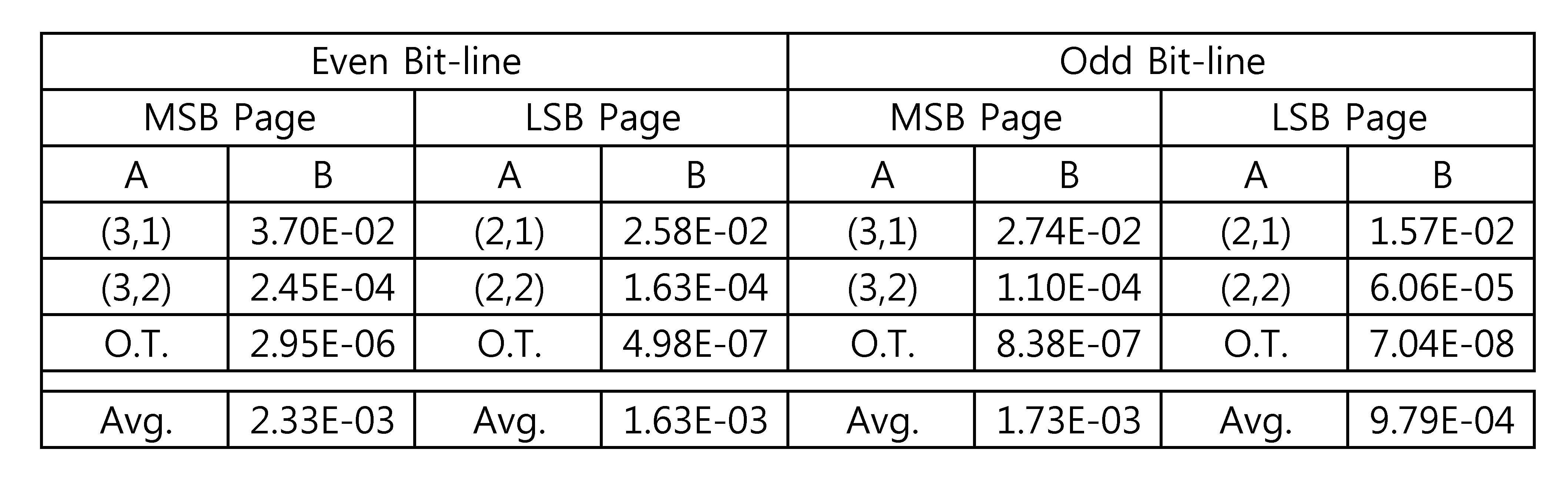
표1은 짝홀 비트 라인 구조에서 LSB(PV0 또는 PV2)를 먼저 쓰고 MSB(PV1, PV3)를 나중에 쓰는 낸드 플래시 메모리에 대한 채널 모델링 결과이다. 표1에는, 읽으려는 메모리 셀, 예컨대 도3에서 피해 메모리 셀(V)과 이 피해 메모리 셀(V)에 간섭을 일으킬 수 있는 메모리 셀, 예컨대 도3에서 메모리 셀(I3)에 각각 저장된 데이터에 따른 초기 오류율을 나타낸다. Table 1 shows the channel modeling results for NAND flash memories that write LSB (PV0 or PV2) first and MSB (PV1, PV3) later in the even-hole bit line structure. Table 1 shows the memory cells to be read, for example, the damaged memory cells V in FIG. 3 and the data stored in the memory cells that may cause interference in the damaged memory cells V, for example, in the memory cells I3 in FIG. Initial error rate accordingly.
표1을 참조하면, A에서 (i, j)는 읽으려는 메모리 셀(V)의 상태가 PVi이고 이에 간섭을 일으키는 메모리 셀(I3)의 상태가 PVj인 경우를 나타낸다. 이때, B는 해당 A 조건에 따른 오류율을 나타낸다. O.T는 나머지 경우에 대한 총 초기 오류율을, Avg.는 평균 초기 오류율을 나타낸다. Referring to Table 1, (i, j) in A represents a case where the state of the memory cell V to be read is PVi and the state of the memory cell I3 that causes interference is PVj. In this case, B represents an error rate according to the corresponding A condition. O.T represents the total initial error rate for the remaining cases and Avg. Represents the average initial error rate.
패턴저장부(400)는 피해 메모리 셀(V)에 저장된 데이터와 이에 간섭을 일으키는 메모리 셀에 저장된 데이터의 패턴에 따른 각각의 오류율을 포함할 수 있다. The
따라서, 처리부(500)는 특정 메모리 셀에 간섭을 일으킬 수 있는 메모리 셀에 저장된 데이터를 부가 정보로서 제1입출력부(200)로부터 입력받아, 상기 패턴저장부(400)로부터 상기 특정 메모리 셀에 저장된 데이터와 상기 간섭을 일으킬 수 있는 메모리 셀에 저장된 데이터의 패턴을 찾아 그 오류율을 찾을 수 있다. 이에 따라, 처리부(500)는 상기 특정 메모리 셀에서 읽은 데이터의 신뢰도 정보를 추출할 수 있다. Therefore, the
제2입출력부(600)는 처리부(500)로부터 신뢰도 정보를 입력받아 외부로 출력할 수 있다. 이때, 상기 제2입출력부(600)는 상기 처리부(500)에 통합되어 구현되는 것도 가능하다. 또한, 제2입출력부(600)는 상기 신뢰도 정보를 필요에 따라 변환하여 출력할 수 있다. 예컨대, 메모리 셀에 저장된 데이터에 오류가 발생하였고 이 오류 정정이 필요한 경우 이를 명령하는 값을 출력할 수 있다. The second input /
이와 같이 본 발명의 실시예에 따라 메모리의 오류 정정 장치를 구성할 경우, 추가적인 회로나, 오류에 관한 연판정된 값을 사용하기 위한 별도의 메모리 칩 설계 및 구현없이 연판정된 값과 유사한 신뢰도 정보를 얻을 수 있다. 이에 따라 메모리 코어에 저장되는 데이터의 오류 정정을 비롯한 데이터 관리 효율 및 성능을 높일 수 있다. As described above, in the case of configuring an error correction apparatus of a memory according to an exemplary embodiment of the present invention, reliability information similar to the soft decision value without additional circuits or a separate memory chip design and implementation for using the soft decision value for an error may be used. Can be obtained. Accordingly, data management efficiency and performance, including error correction of data stored in the memory core, can be improved.
또한, 본 발명의 실시예에 따른 메모리의 오류 정정 방법은 메모리 코어에 포함된 복수개의 메모리 셀 중 특정 메모리 셀로부터 읽힌 데이터에 대해 오류 발생 여부를 판별하기 위해 어느 정도의 부가 정보가 필요한지를 판단하는 단계, 상기 필요한 정도의 부가 정보를 상기 메모리 코어에 요청하는 단계, 상기 요청한 부가 정보를 상기 메모리 코어로부터 수신하는 단계, 상기 부가 정보로부터 상기 데이터의 신뢰도 정보를 추출하는 단계, 및 상기 신뢰도 정보를 출력하는 단계를 포함할 수 있다. In addition, the error correction method of the memory according to an embodiment of the present invention determines how much additional information is required to determine whether an error occurs for data read from a specific memory cell of a plurality of memory cells included in the memory core Requesting the memory core for the necessary degree of additional information; receiving the requested additional information from the memory core; extracting reliability information of the data from the additional information; and outputting the reliability information. It may include the step.
또한, 본 발명의 실시예에 따라 상기 부가 정보로부터 상기 데이터의 신뢰도 정보를 추출하는 단계는, 상기 특정 메모리 셀에 저장된 데이터와 상기 적어도 하나 이상의 메모리 셀에 저장된 데이터에 따라 상기 특정 메모리 셀의 오류율을 저장하고 있는 패턴저장부와 상기 특정 메모리 셀에 저장된 데이터 및 상기 부가 정보를 비교하여 상기 신뢰도 정보를 추출할 수 있다. The extracting of the reliability information of the data from the additional information may include determining an error rate of the specific memory cell according to data stored in the specific memory cell and data stored in the at least one memory cell. The reliability information may be extracted by comparing the stored pattern storage unit with data stored in the specific memory cell and the additional information.
이상 첨부된 도면을 참조하여 본 발명의 실시예를 설명하였지만, 본 발명이 속하는 기술분야의 당업자는 본 발명이 그 기술적 사상이나 필수적 특징을 변경하지 않고 다른 구체적인 형태로 실시될 수 있다는 것을 이해할 수 있을 것이다. 그러므로 이상에서 기술한 실시예들은 모든 면에서 예시적인 것이며 한정적인 것이 아닌 것으로서 이해되어야 하고, 본 발명의 범위는 상기 상세한 설명보다는 후술하는 특허청구범위에 의하여 나타내어지며, 특허청구범위의 의미 및 범위 그리고 그 등가개념으로부터 도출되는 모든 변경 또는 변형된 형태가 본 발명의 범위에 포함되는 것으로 해석되어야 한다.While the present invention has been particularly shown and described with reference to exemplary embodiments thereof, it is evident that many alternatives, modifications and variations will be apparent to those skilled in the art. will be. Therefore, it should be understood that the above-described embodiments are to be considered in all respects as illustrative and not restrictive, the scope of the invention being indicated by the appended claims rather than the foregoing description, It is intended that all changes and modifications derived from the equivalent concept be included within the scope of the present invention.
100: 제어부
200: 제1입출력부
300: 플래시 메모리 코어
400: 패턴 저장부
500: 처리부
600: 제2입출력부100:
200: first input and output unit
300: flash memory core
400: pattern storage unit
500:
600: second input and output unit
Claims (8)
상기 복수개의 메모리 셀 중 특정 메모리 셀로부터 읽힌 데이터에 대해 오류 발생 여부를 판별하기 위한 부가 정보를 결정하는 제어부;
상기 부가 정보를 상기 메모리 코어에 요청하여 상기 메모리 코어로부터 수신하는 제1입출력부;
상기 부가 정보로부터 상기 데이터의 신뢰도 정보를 추출하는 처리부; 및
상기 신뢰도 정보를 상기 처리부로부터 입력받아 출력하는 제2입출력부를 포함하고,
상기 부가 정보는 상기 메모리 코어에 포함된 복수개의 메모리 셀 중 상기 특정 메모리 셀에 간섭을 일으키는 적어도 하나 이상의 메모리 셀에 저장된 데이터를 포함하는 것을 특징으로 하는 메모리의 오류 정정 장치.A memory core including a plurality of memory cells;
A controller configured to determine additional information for determining whether an error occurs with respect to data read from a specific memory cell among the plurality of memory cells;
A first input / output unit for requesting the additional information from the memory core and receiving the additional information;
A processor configured to extract reliability information of the data from the additional information; And
And a second input / output unit configured to receive the reliability information from the processing unit and output the received reliability information.
And the additional information includes data stored in at least one memory cell that interferes with the specific memory cell among a plurality of memory cells included in the memory core.
상기 특정 메모리 셀에 저장된 데이터와 상기 적어도 하나 이상의 메모리 셀에 저장된 데이터에 따라 상기 특정 메모리 셀의 오류율을 저장하고 있는 패턴저장부를 더 포함하고,
상기 처리부는 상기 특정 메모리 셀에 저장된 데이터 및 상기 부가 정보와 상기 패턴저장부를 비교하여 상기 신뢰도 정보를 추출하는 것을 특징으로 하는 메모리의 오류 정정 장치. The method of claim 1,
The apparatus may further include a pattern storage unit configured to store an error rate of the specific memory cell according to data stored in the specific memory cell and data stored in the at least one memory cell.
And the processor extracts the reliability information by comparing the data stored in the specific memory cell and the additional information with the pattern storage unit.
상기 복수개의 메모리 셀은 어레이 형태를 가지며,
상기 적어도 하나 이상의 메모리 셀은 상기 특정 메모리 셀에 인접한 것을 특징으로 하는 메모리의 오류 정정 장치. The method according to claim 1 or 3,
The plurality of memory cells has an array form,
And at least one memory cell is adjacent to the particular memory cell.
상기 부가 정보를 상기 메모리 코어에 요청하는 단계;
상기 요청한 부가 정보를 상기 메모리 코어로부터 수신하는 단계;
상기 부가 정보로부터 상기 데이터의 신뢰도 정보를 추출하는 단계; 및
상기 신뢰도 정보를 출력하는 단계를 포함하고,
상기 부가 정보는 상기 메모리 코어에 포함된 복수개의 메모리 셀 중 상기 특정 메모리 셀에 간섭을 일으키는 적어도 하나 이상의 메모리 셀에 저장된 데이터를 포함하는 것을 특징으로 하는 메모리의 오류 정정 방법.Determining additional information for determining whether an error occurs with respect to data read from a specific memory cell among a plurality of memory cells included in the memory core;
Requesting the additional information from the memory core;
Receiving the requested additional information from the memory core;
Extracting reliability information of the data from the additional information; And
Outputting the reliability information;
And the additional information includes data stored in at least one memory cell that interferes with the specific memory cell among a plurality of memory cells included in the memory core.
상기 부가 정보로부터 상기 데이터의 신뢰도 정보를 추출하는 단계는:
상기 특정 메모리 셀에 저장된 데이터와 상기 적어도 하나 이상의 메모리 셀에 저장된 데이터에 따라 상기 특정 메모리 셀의 오류율을 저장하고 있는 패턴저장부와 상기 특정 메모리 셀에 저장된 데이터 및 상기 부가 정보를 비교하여 상기 신뢰도 정보를 추출하는 것을 특징으로 하는 메모리의 오류 정정 방법. The method of claim 5,
Extracting reliability information of the data from the additional information may include:
The reliability information is compared with a pattern storage unit storing an error rate of the specific memory cell according to data stored in the specific memory cell and data stored in the at least one memory cell, data stored in the specific memory cell, and the additional information. Error correction method of the memory, characterized in that for extracting.
상기 복수개의 메모리 셀은 어레이 형태를 가지며,
상기 적어도 하나 이상의 메모리 셀은 상기 특정 메모리 셀에 인접한 것을 특징으로 하는 메모리의 오류 정정 방법.The method according to claim 5 or 7,
The plurality of memory cells has an array form,
And at least one memory cell is adjacent to the particular memory cell.
Priority Applications (1)
| Application Number | Priority Date | Filing Date | Title |
|---|---|---|---|
| KR1020110120241A KR101320686B1 (en) | 2011-11-17 | 2011-11-17 | Error Correcting Device and Method for Memory |
Applications Claiming Priority (1)
| Application Number | Priority Date | Filing Date | Title |
|---|---|---|---|
| KR1020110120241A KR101320686B1 (en) | 2011-11-17 | 2011-11-17 | Error Correcting Device and Method for Memory |
Publications (2)
| Publication Number | Publication Date |
|---|---|
| KR20130054699A KR20130054699A (en) | 2013-05-27 |
| KR101320686B1 true KR101320686B1 (en) | 2013-10-18 |
Family
ID=48663442
Family Applications (1)
| Application Number | Title | Priority Date | Filing Date |
|---|---|---|---|
| KR1020110120241A KR101320686B1 (en) | 2011-11-17 | 2011-11-17 | Error Correcting Device and Method for Memory |
Country Status (1)
| Country | Link |
|---|---|
| KR (1) | KR101320686B1 (en) |
Citations (4)
| Publication number | Priority date | Publication date | Assignee | Title |
|---|---|---|---|---|
| KR960012005A (en) * | 1994-09-13 | 1996-04-20 | 기다오까 다까시 | Semiconductor memory |
| KR20090075101A (en) * | 2008-01-03 | 2009-07-08 | 삼성전자주식회사 | Memory device and error control codes decoding method |
| KR20090080634A (en) * | 2008-01-22 | 2009-07-27 | 삼성전자주식회사 | Apparatus and method of memory programming |
| KR20100013844A (en) * | 2008-08-01 | 2010-02-10 | 삼성전자주식회사 | Memory device and method of data decision of memory device |
-
2011
- 2011-11-17 KR KR1020110120241A patent/KR101320686B1/en active IP Right Grant
Patent Citations (4)
| Publication number | Priority date | Publication date | Assignee | Title |
|---|---|---|---|---|
| KR960012005A (en) * | 1994-09-13 | 1996-04-20 | 기다오까 다까시 | Semiconductor memory |
| KR20090075101A (en) * | 2008-01-03 | 2009-07-08 | 삼성전자주식회사 | Memory device and error control codes decoding method |
| KR20090080634A (en) * | 2008-01-22 | 2009-07-27 | 삼성전자주식회사 | Apparatus and method of memory programming |
| KR20100013844A (en) * | 2008-08-01 | 2010-02-10 | 삼성전자주식회사 | Memory device and method of data decision of memory device |
Also Published As
| Publication number | Publication date |
|---|---|
| KR20130054699A (en) | 2013-05-27 |
Similar Documents
| Publication | Publication Date | Title |
|---|---|---|
| US9665295B2 (en) | Data storage system with dynamic erase block grouping mechanism and method of operation thereof | |
| KR102174293B1 (en) | Proactive corrective action in memory based on probabilistic data structures | |
| US8719491B2 (en) | Encoding flash memory data with a randomizer using different seeds for different sectors | |
| US10084479B2 (en) | Low BER hard-decision LDPC decoder | |
| US8432735B2 (en) | Memory system and related method of programming | |
| KR20110092091A (en) | Flash memory device and reading method thereof | |
| US9582224B2 (en) | Memory control circuit unit, memory storage apparatus and data accessing method | |
| CN109599143B (en) | Memory system with read threshold mechanism and method of operation thereof | |
| KR20130135938A (en) | Methods, devices, and systems for data sensing | |
| Tanakamaru et al. | Highly reliable and low power SSD using asymmetric coding and stripe bitline-pattern elimination programming | |
| TW201611018A (en) | Method of performing wear management in non-volatile memory devices | |
| US10169141B2 (en) | Modifiable stripe length in flash memory devices | |
| Wei et al. | NRC: A nibble remapping coding strategy for NAND flash reliability extension | |
| US10042565B2 (en) | All-flash-array primary storage and caching appliances implementing triple-level cell (TLC)-NAND semiconductor microchips | |
| US10360986B1 (en) | Memory management method and storage controller | |
| CN103942115A (en) | Data storage fault-tolerant coding method of NAND flash memory system | |
| US20180275917A1 (en) | Memory controller, memory system, and control method | |
| US20230244566A1 (en) | Managing write disturb for units of memory in a memory sub-system | |
| US10956064B2 (en) | Adjusting code rates to mitigate cross-temperature effects in a non-volatile memory (NVM) | |
| US8276033B2 (en) | Data writing method for a flash memory, and flash memory controller and flash memory storage apparatus using the same | |
| CN108255634A (en) | A kind of method for reading data and device | |
| CN116954491A (en) | Method of operation for a memory controller and memory system including a memory controller | |
| US11869614B2 (en) | Cell statistics generator for NVM devices | |
| US11656789B2 (en) | Asymmetric read sense | |
| KR101320686B1 (en) | Error Correcting Device and Method for Memory |
Legal Events
| Date | Code | Title | Description |
|---|---|---|---|
| A201 | Request for examination | ||
| E902 | Notification of reason for refusal | ||
| E701 | Decision to grant or registration of patent right | ||
| GRNT | Written decision to grant | ||
| FPAY | Annual fee payment |
Payment date: 20161004 Year of fee payment: 4 |
|
| FPAY | Annual fee payment |
Payment date: 20170928 Year of fee payment: 5 |
|
| FPAY | Annual fee payment |
Payment date: 20181002 Year of fee payment: 6 |