KR101256032B1 - Solid state switching circuit - Google Patents
Solid state switching circuit Download PDFInfo
- Publication number
- KR101256032B1 KR101256032B1 KR1020077018199A KR20077018199A KR101256032B1 KR 101256032 B1 KR101256032 B1 KR 101256032B1 KR 1020077018199 A KR1020077018199 A KR 1020077018199A KR 20077018199 A KR20077018199 A KR 20077018199A KR 101256032 B1 KR101256032 B1 KR 101256032B1
- Authority
- KR
- South Korea
- Prior art keywords
- diode
- transformer
- energy storage
- switching device
- series combination
- Prior art date
Links
Images


Classifications
-
- H—ELECTRICITY
- H02—GENERATION; CONVERSION OR DISTRIBUTION OF ELECTRIC POWER
- H02M—APPARATUS FOR CONVERSION BETWEEN AC AND AC, BETWEEN AC AND DC, OR BETWEEN DC AND DC, AND FOR USE WITH MAINS OR SIMILAR POWER SUPPLY SYSTEMS; CONVERSION OF DC OR AC INPUT POWER INTO SURGE OUTPUT POWER; CONTROL OR REGULATION THEREOF
- H02M3/00—Conversion of dc power input into dc power output
- H02M3/22—Conversion of dc power input into dc power output with intermediate conversion into ac
- H02M3/24—Conversion of dc power input into dc power output with intermediate conversion into ac by static converters
- H02M3/28—Conversion of dc power input into dc power output with intermediate conversion into ac by static converters using discharge tubes with control electrode or semiconductor devices with control electrode to produce the intermediate ac
- H02M3/325—Conversion of dc power input into dc power output with intermediate conversion into ac by static converters using discharge tubes with control electrode or semiconductor devices with control electrode to produce the intermediate ac using devices of a triode or a transistor type requiring continuous application of a control signal
- H02M3/335—Conversion of dc power input into dc power output with intermediate conversion into ac by static converters using discharge tubes with control electrode or semiconductor devices with control electrode to produce the intermediate ac using devices of a triode or a transistor type requiring continuous application of a control signal using semiconductor devices only
-
- H—ELECTRICITY
- H03—ELECTRONIC CIRCUITRY
- H03K—PULSE TECHNIQUE
- H03K17/00—Electronic switching or gating, i.e. not by contact-making and –breaking
- H03K17/16—Modifications for eliminating interference voltages or currents
- H03K17/168—Modifications for eliminating interference voltages or currents in composite switches
-
- H—ELECTRICITY
- H02—GENERATION; CONVERSION OR DISTRIBUTION OF ELECTRIC POWER
- H02M—APPARATUS FOR CONVERSION BETWEEN AC AND AC, BETWEEN AC AND DC, OR BETWEEN DC AND DC, AND FOR USE WITH MAINS OR SIMILAR POWER SUPPLY SYSTEMS; CONVERSION OF DC OR AC INPUT POWER INTO SURGE OUTPUT POWER; CONTROL OR REGULATION THEREOF
- H02M3/00—Conversion of dc power input into dc power output
- H02M3/02—Conversion of dc power input into dc power output without intermediate conversion into ac
- H02M3/04—Conversion of dc power input into dc power output without intermediate conversion into ac by static converters
- H02M3/10—Conversion of dc power input into dc power output without intermediate conversion into ac by static converters using discharge tubes with control electrode or semiconductor devices with control electrode
- H02M3/145—Conversion of dc power input into dc power output without intermediate conversion into ac by static converters using discharge tubes with control electrode or semiconductor devices with control electrode using devices of a triode or transistor type requiring continuous application of a control signal
- H02M3/155—Conversion of dc power input into dc power output without intermediate conversion into ac by static converters using discharge tubes with control electrode or semiconductor devices with control electrode using devices of a triode or transistor type requiring continuous application of a control signal using semiconductor devices only
-
- H—ELECTRICITY
- H02—GENERATION; CONVERSION OR DISTRIBUTION OF ELECTRIC POWER
- H02M—APPARATUS FOR CONVERSION BETWEEN AC AND AC, BETWEEN AC AND DC, OR BETWEEN DC AND DC, AND FOR USE WITH MAINS OR SIMILAR POWER SUPPLY SYSTEMS; CONVERSION OF DC OR AC INPUT POWER INTO SURGE OUTPUT POWER; CONTROL OR REGULATION THEREOF
- H02M7/00—Conversion of ac power input into dc power output; Conversion of dc power input into ac power output
- H02M7/42—Conversion of dc power input into ac power output without possibility of reversal
- H02M7/44—Conversion of dc power input into ac power output without possibility of reversal by static converters
- H02M7/48—Conversion of dc power input into ac power output without possibility of reversal by static converters using discharge tubes with control electrode or semiconductor devices with control electrode
- H02M7/505—Conversion of dc power input into ac power output without possibility of reversal by static converters using discharge tubes with control electrode or semiconductor devices with control electrode using devices of a thyratron or thyristor type requiring extinguishing means
- H02M7/515—Conversion of dc power input into ac power output without possibility of reversal by static converters using discharge tubes with control electrode or semiconductor devices with control electrode using devices of a thyratron or thyristor type requiring extinguishing means using semiconductor devices only
- H02M7/523—Conversion of dc power input into ac power output without possibility of reversal by static converters using discharge tubes with control electrode or semiconductor devices with control electrode using devices of a thyratron or thyristor type requiring extinguishing means using semiconductor devices only with LC-resonance circuit in the main circuit
-
- H—ELECTRICITY
- H03—ELECTRONIC CIRCUITRY
- H03K—PULSE TECHNIQUE
- H03K17/00—Electronic switching or gating, i.e. not by contact-making and –breaking
- H03K17/16—Modifications for eliminating interference voltages or currents
- H03K17/161—Modifications for eliminating interference voltages or currents in field-effect transistor switches
- H03K17/162—Modifications for eliminating interference voltages or currents in field-effect transistor switches without feedback from the output circuit to the control circuit
-
- H—ELECTRICITY
- H03—ELECTRONIC CIRCUITRY
- H03K—PULSE TECHNIQUE
- H03K2217/00—Indexing scheme related to electronic switching or gating, i.e. not by contact-making or -breaking covered by H03K17/00
- H03K2217/0036—Means reducing energy consumption
Landscapes
- Engineering & Computer Science (AREA)
- Power Engineering (AREA)
- Dc-Dc Converters (AREA)
Abstract
솔리드 스테이트 스위칭 회로는 트랜스포머의 1차측에 초기 저장된 에너지가, 스위칭 디바이스가 도전되지 않을 때, 부하로의 에너지의 전달을 위해 트랜스포머의 2차측에 연결된 공명 회로에서 회복되는 회로의 스위칭 디바이스와 직렬인 트랜스포머를 사용한다.
스위칭 회로, DC 파워 소스, 스위칭 디바이스, 트랜스포머, 프리휠링 다이오드, 로드 임피던스, 초크, 다이오드, 트랜스퍼 에너지 저장 커패시터, 트랜스포머 에너지 저장 커패시터, 공명 인덕터.
Solid state switching circuits are transformers in which the energy initially stored on the primary side of the transformer is in series with the switching device of the circuit, which is recovered from a resonance circuit connected to the secondary side of the transformer for the transfer of energy to the load when the switching device is not conducting. Use
Switching circuits, DC power sources, switching devices, transformers, freewheeling diodes, load impedances, chokes, diodes, transfer energy storage capacitors, transformer energy storage capacitors, resonant inductors.
Description
본 발명은 비교적 낮은 스위칭 회로 손실 및 솔리드 스테이트 스위칭 디바이스 및 연관된 프리휠링 다이오드의 감소된 턴온/턴오프 스트레스를 가진 솔리드 스테이트 스위칭 회로에 관한 것이다.The present invention relates to solid state switching circuits with relatively low switching circuit losses and reduced turn on / turn off stress of solid state switching devices and associated freewheeling diodes.
솔리드 스테이트 스위칭 다바이스와 연관된 스위칭 손실을 줄이기 위한 일반적으로 받아들여지는 3가지 방법이 있다: (1) 공명 모드 스위칭의 사용; (2) 액티브 스너버 회로의 사용; (3) 스위칭 디바이스와 직렬인 인덕터 및 스위칭 디바이스와 병렬인 스너버 커패시터의 사용.There are three generally accepted methods for reducing switching losses associated with solid state switching devices: (1) the use of resonance mode switching; (2) use of active snubber circuits; (3) Use of an inductor in series with the switching device and a snubber capacitor in parallel with the switching device.
공명 모드 스위칭은 고정된 시간 동안 스위칭 디바이스를 턴온한다. 출력 파워 스위칭 디바이스의 동작 주파수를 변경함으로써 컨트롤된다. 그러나, 동작 주파수를 변화시키는 것은 일부 패러시틱 파워 회로 오실레이션을 여기시키기 쉽다. 또한, 동작 주파수를 변화시키는 것은 출력 리플 전압 또는 리플 전류를 필터링하여 걸러내는 것을 더 힘들게 한다.Resonance mode switching turns on the switching device for a fixed time. The output power is controlled by changing the operating frequency of the switching device. However, changing the operating frequency tends to excite some parasitic power circuit oscillations. In addition, changing the operating frequency makes it more difficult to filter out the output ripple voltage or ripple current.
추가의 파워 컴포넌트, 열 싱크, 및 컨트롤 회로를 포함하는 액티브 스너버 회로의 사용은 스위칭 회로의 비용 및 복잡도를 증가시킨다.The use of active snubber circuits, including additional power components, heat sinks, and control circuits, increases the cost and complexity of the switching circuits.
도 1은 스위칭 디바이스(SW) 및 직렬 인덕터(L10)를 가진 스위칭 회로를 사 용하는 전형적인 스탭 다운 스위치 모드(벅 쵸퍼) 파워 서플라이(101)를 도시한다. 스위칭 디바이스(SW)는 양극성 트랜지스터, 절연 게이트 양극성 트랜지스터(IGBT), 또는 전계효과 트랜지스터와 같은, 임의의 적합한 솔리드 스테이트 스위칭 회로일 수 있다. 터미널(1 및 2)은 (도면에 도시되지 않은) 적합한 DC 파워 소스의 출력부에 연결된다. 커패시터(C10)는 DC 소스의 출력 전압에 대하여 리플 필터로써 역할한다. 급속 복구 다이오드로써 일반적으로 주지되어 있는 다이오드 군에서 선택되어진 프리휠링 다이오드(D10)는 디바이스(DW)가 턴오프되었을 때, 직렬 인덕터(L20)에 전류를 제공한다. 다이오드(Ds), 저항(Rs), 및 커패스터(Cs)는 디바이스(SW)가 최초 턴오프되었을 때, 전류를 전송하는 스너버 회로를 형성한다. 로드(RL)는 터미널(4 및 5)에 연결된다. 직렬 인덕터(L10)의 사용은 스위칭 디바이스의 크리티컬 턴온 타임 동안 동시적인 고전압 및 고전류를 방지함으로써, 스위칭 디바이스(SW)에 가해지는 스트레스를 감소시킨다. 부가적으로, 직렬 인덕터는 다이오드가 순방향 바이어스에서 역방향 바이어스로 전환하고, 전류 도전이 멈출 때, 역방향 전류의 변화율을 컨트롤함으로써 프리휠링 다이오드(D10)에 가해지는 스트레스를 감소시킨다. 그러나, 직렬 인덕터는 스위칭 디바이스(SW)가 턴오프할 때, 부정적인 영향을 가진다. 직렬 인덕터(L10)는 턴오프 동안 스위칭 디바이스(SW)에 걸친 고전압을 일으킨다. 또한, 인덕터(L10)는 스위칭 디바이스의 턴오프 후에 프리휠링 다이오드(D10) 내의 전류 변화율을 감소시킨다. 이러한 결과는 다이오드(D10)가 스위칭 디바이스(SW)가 턴오프 한 후 즉시 풀 전류를 전달할 수 없게 한 다. 인덕터(L20)는 전류를 흐르도록 포싱하기 때문에, 일부 전류 경로가 제공되어야 한다. 일반적으로, 저항(R20)과 직렬인 제2다이오드(D20)는 8 내지 10 마이크로초(μs)의 비교적 긴 시간 동안 다이오드(D10) 내의 전류가 증가하는 동안 전류에 대한 병렬 경로를 제공하도록 요구받는다. 직렬 인덕터의 사용과 연관된 문제점들은 비교적 높은 스위칭 손실 및 추가 회로의 비용에서 극복될 수 있다.1 shows a typical step down switch mode (buck chopper)
일 형태에 있어서, 본 발명은 종래의 직렬 인덕터의 이점을 달성하고, 부가적으로, 트랜스포머의 2차측에 연결된 공명 회로를 수단으로 트랜스포머의 1차측에 최초로 저장된 에너지를 복구하기 위해, 스위칭 디바이스와 직렬인 트랜스포머의 1차측을 사용하는 솔리드 스테이트 스위칭 회로를 제공하는 방법 및 장치이다.In one aspect, the present invention achieves the advantages of a conventional series inductor and additionally is in series with the switching device to recover energy initially stored on the primary side of the transformer by means of a resonance circuit connected to the secondary side of the transformer. A method and apparatus for providing a solid state switching circuit using the primary side of an in-transformer.
다른 형태에 있어서, 본 발명은 스위칭 디바이스 및 급속 복구 다이오드의 상당한 디레이팅 없이 그 리버스 di/dt 레이팅된 값을 넘지않는 스위칭 디바이스 및 급속 복구 다이오드를 가진 솔리드 스테이트 스위칭 회로를 제공하는 방법 및 장치이다.In another aspect, the present invention is a method and apparatus for providing a solid state switching circuit having a switching device and a fast recovery diode not exceeding its reverse di / dt rated value without significant derating of the switching device and the fast recovery diode.
본 발명의 다른 형태는 본 명세서 및 첨부된 청구항에 설명된다.Other forms of the invention are described herein and in the appended claims.
본 발명을 설명하기 위한 목적으로, 바람직한 형태의 도면이 이해를 위해 도시되어 있어나, 본 발명은 도시된 엄격한 배열 및 수단에 제한되지 않는다.BRIEF DESCRIPTION OF THE DRAWINGS For the purpose of illustrating the invention, the drawings of the preferred form are shown for understanding, but the invention is not limited to the strict arrangement and means shown.
도 1은 종래기술의 솔리드 스테이트 스위칭 회로의 개략적인 도면이다.1 is a schematic diagram of a solid state switching circuit of the prior art.
도 2는 본 발명의 솔리드 스테이트 스위칭 회로의 일 예의 개략적인 도면이 다.2 is a schematic diagram of an example of a solid state switching circuit of the present invention.
도 3은 본 발명의 솔리드 스테이트 스위칭 회로의 일 예에서 사용된 스위칭 디바이스의 턴온 및 턴오프 동안의 예시적인 파형의 도면이다.3 is a diagram of exemplary waveforms during turn on and turn off of a switching device used in an example of a solid state switching circuit of the present invention.
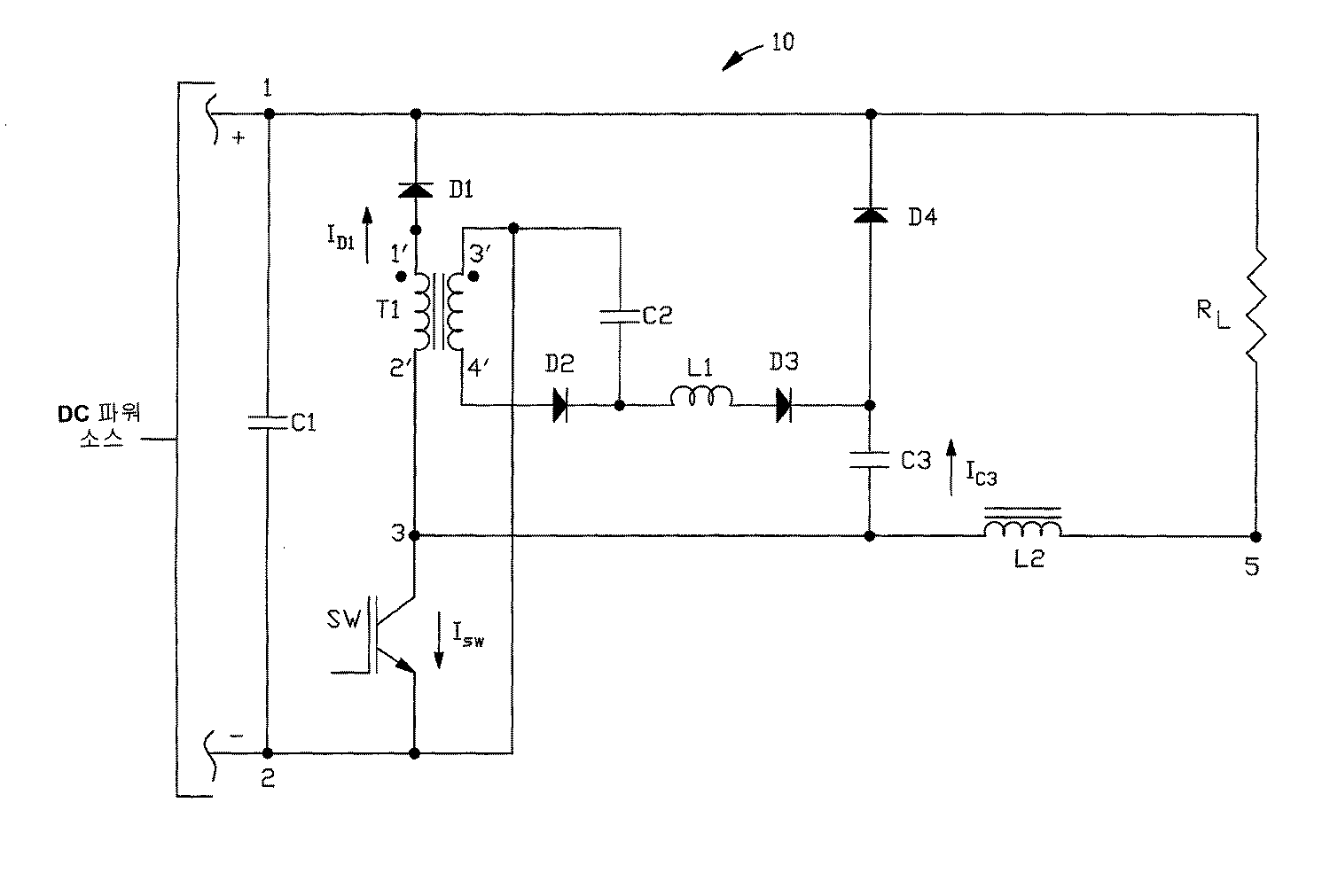
도면을 참조하면, 유사한 참조번호는 유사한 엘리먼트를 지시하고, 도 2에 본 발명의 솔리드 스테이트 스위칭 회로(10)의 일 예의 도면이 도시되어 있다. 터미널(1 및 2)은 (도면에 도시되지 않은) 각각 DC 파워 소스의 파지티브 및 네거티브 터미널로의 커넥션 포인트를 나타낸다. 제한이 아닌 예시의 방법으로, DC 소스는 AC-투-DC 브릿지 정류기일 수 있다. 옵션의 커패시터(C1)는 DC 파워 소스로부터의 출력 전압에 대한 AC 리플 필터로써 역할한다.Referring to the drawings, like reference numerals designate like elements, and in FIG. 2 an example of a solid
본 발명의 범위를 제한하지 않는 예시적인 이 예에서, 솔리드 스테이트 스위칭 디바이스(SW)는 트랜스포머(T1)의 1차측 및 프리휠링 다이오드(D1)와 함께 직렬 회로를 형성한다. 트랜스포머(T1)의 제1 및 제2권선에 인접한 점은 권선의 파지티브 극성을 나타낸다. 디바이스(SW)는 특정 어플리케이션에 대하여 적합한 양극성 트랜지스터, 절연 게이트 양극성 트랜지스터(IGBT), 또는 전계효과 트랜지스터와 같은 임의의 솔리드 스테이트 스위칭 디바이스일 수 있다. 선택된 스위칭 디바이스에 적합하고 주지되어 있는 (도면에 도시되지 않은) 적합한 게이트 회로는 스위칭 디바이스(SW)를 위해 제공될 수 있다. 이 게이트 회로는 스위칭 디바이스의 턴온 및/또는 턴오프를 컨트롤한다. 프리휠링 다이오드, 트랜스포머의 제1권선 및 스위칭 디바이스의 직렬 조합을 포함하는 회로는 터미널(1 및 2)에 걸쳐 연결된다. 부하(RL)는 도 2에 도시된 바와 같이 터미널(1 및 5)에 연결된다. 저항성 부하가 도시되어 있으나, 다른 임피던스 특성을 가진 부하가 사용될 수 있다. 부하(RL)는 부하 전류의 연속적인 흐름을 제공하는 초크(L2)와 직렬로 연결된다. 로드 임피던스 및 초크의 직렬 조합을 포함하는 회로는 도 2에 도시된 바와 같이 터미널(1 및 3)에 걸쳐 연결된다.In this illustrative example that does not limit the scope of the present invention, the solid state switching device SW forms a series circuit with the primary side of the transformer T1 and the freewheeling diode D1. The points adjacent to the first and second windings of the transformer T1 indicate the positive polarity of the winding. The device SW may be any solid state switching device such as a bipolar transistor, an insulated gate bipolar transistor (IGBT), or a field effect transistor suitable for a particular application. Suitable gate circuits (not shown) that are suitable and well known for the selected switching device may be provided for the switching device SW. This gate circuit controls the turn on and / or turn off of the switching device. Circuits comprising a freewheeling diode, a first winding of a transformer and a series combination of switching devices are connected across
도 3은 도2에 도시된 회로에 대하여 시간에 대하여 변하는 전압 및 전류 크기를 도시되어 있고, 스위칭 디바이스(SW)는 도전 상태를 위한 턴온에서 비도전상태를 위한 턴오프로 변환한다. 스위칭 디바이스(SW)가 턴온하기 전에, 전류는 부하(RL), 초크(L2), 트랜스포머(T1)의 1차측, 및 다이오드(D1)에 의해 형성된 회로 경로로 흐른다. 디바이스(SW)가 도 3의 시간(t1)에 도시된 바와 같은 도전 상태를 위한 턴온하기 위해 초기에 게이팅될 때, 트랜스포머(T1)의 1차측에 걸린 (터미널(1 및 2)에 걸린) 버스 전압 및 전류(ID1)는, 트랜스포머(T1)의 1차측 및 다이오드(D1)를 통해, 감소되기 시작한다. 전류는 쵸크(L2)에서 비교적 일정하기 때문에, 전류(ID1)의 강하는 스위칭 디바이스(SW)를 통해 흐르는 전류(ISW)의 증가를 야기한다. 전류(ID1)는 버스 전압을 트랜스포머(T1)의 인덕턴스로 나눈 값과 대략 동등한 비율로 강하한다. 여기에 사용된 본 발명의 일 설명예에 대하여, 600 볼트 DC의 버스 전압, 2.0μH의 트랜스포머 인덕턴스를 가지고, 전류(ID1)의 변화율은 마이크로초 당 네거티브 300 암페어일 것이다. 트랜스포머(T1)의 1차측 및 다이오 드(D1)를 통한 감소되는 전류는 제로 전류를 통해, 다이오드가 시간(t2)에서 그것의 상대적으로 작은 역방향 누설 전류로 복구할 때까지, 다이오드(D1)를 통해 (도 3에 도시되지 않은) 역방향 전류로 패싱한다. 그 시간에서, 다이오드(D1)는 전류를 차단하고 그 터미널에 걸린 전압을 지지하고, 디바이스(SW)는 풀 로드 전류(ISW)를 전달한다. 시간(t1)에서 시간(t2)까지, 스위치 디바이스(SW) 및 다이오드(D1)는 그들의 터미널에 걸린 고전압을 가지지 않는다. 트랜스포머(T1)의 1차측에만 고전압이 걸린다.FIG. 3 shows the voltage and current magnitudes varying with time for the circuit shown in FIG. 2, and the switching device SW converts from a turn on for a conductive state to a turn off for a non-conductive state. Before the switching device SW turns on, current flows into the circuit path formed by the load R L , the choke L2, the primary side of the transformer T1, and the diode D1. When device SW is initially gated to turn on for the conductive state as shown at time t 1 of FIG. 3, it is caught on the primary side of transformer T1 (hung on
스위칭 디바이스(SW)의 턴오프는 시간(t4)에서 개시되어, 시간(t6)까지 비도전 상태로 전환된다. 디바이스(SW)가 전달하는 전류는 커패시터(C3) 및 다이오드(D4)를 통해 로드 임피던스로 다이버팅되고, 도 2 및 도 3에서 전류(IC3)로 지시되어 있다. 커패시터(C3)의 충전은 아래에 설명되어 있다. 1차측 트랜스포머 터미널(2')이 1차측 트랜스포머 터미널(1') 보다 더 높은 전압이도록 트랜스포머(T1)의 1차측이 바이어싱될 때까지, 이 전압은 비도전인 디바이스(SW)에 걸쳐 증가한다. 트랜스포머의 1차측이 이렇게 바이어싱되었을 때, 전류는 트랜스포머의 2차측을 흐르기 시작하고, 다이오드(D2) 및 커패시터(C2)를 통과한다. 오퍼레이팅 스위칭 주파수에서, 트랜스포머(T1)의 2차측은 커패시터(C2)에 의해 효과적으로 쇼트 회로가 된다. 다이오드(D1)는 트랜스포머(T1)의 손실 인덕턴스와 동등한 인덕티브 임피던스와 직렬로 연결된다. 현재의 예에 대하여, 트랜스포머(T1)의 1차 권선의 임피던스는 0.1μH 이하이다. 트랜스포머의 1차측과 트랜스포머의 2차측 사이의 크로즈 커플링은, 전형적으로, 디바이스(SW)에 걸친 전압의 크기를 (터미널(1 및 2)사이의) 버스 전압 및 커패시터(C2)에 걸린 전압의 합에 트랜스포머(T1)의 권선비를 곱한 값으로 제한된다. 프리휠링 다이오드(D1)는 순방향 바이어싱 컨덕션으로 재빨리 구동된다. 1차 권선의 인덕턴스가 본 특정 예에서 20배 이상 감소되었기 때문에, 전류(ID1)는 1/20의 시간에 최대값으로 상승한다. 본 예에 대하여, 1,000 암페어의 최대 스위치 디바이스 전류(ISW), 250 볼트의 스위치 디바이스 오버 볼트(VOV), 및 0.1μH의 1차 권선 인덕턴스(L)를 가지고, 다이오드(D1)가 풀 컨덕션에 도달하는 시간(ΔT, 도 3의 t7-t4)은 다음의 식으로부터 계산된다:The turn off of the switching device SW is initiated at time t 4 and switched to the non-conductive state by time t 6 . The current delivered by the device SW is diverted to the load impedance through capacitor C3 and diode D4 and is indicated as current I C3 in FIGS. 2 and 3. The charging of capacitor C3 is described below. This voltage increases across the non-conductive device SW until the primary side of the transformer T1 is biased such that the primary transformer terminal 2 'is higher than the primary transformer terminal 1'. . When the primary side of the transformer is so biased, current begins to flow through the secondary side of the transformer and passes through diode D2 and capacitor C2. At the operating switching frequency, the secondary side of transformer T1 is effectively short circuited by capacitor C2. Diode D1 is connected in series with an inductive impedance equivalent to the lossy inductance of transformer T1. For the present example, the impedance of the primary winding of transformer T1 is 0.1 μH or less. The close coupling between the primary side of the transformer and the secondary side of the transformer typically determines the magnitude of the voltage across the device SW (between
VOV=L·[ΔISW/ΔT]; 선택된 값을 대입하면,V OV = L [ΔI SW / ΔT]; If you assign the selected value,
250V=[0.1×10⁻⁶H]·[(1,000A-0)/ΔT]; 그 결과는,250 V = [0.1 × 10 −6 H]. [(1,000 A-0) / ΔT]; The result is,
ΔT=0.4μs이다. ΔT = 0.4 μs.
트랜스포머(T1)의 1차 권선에 걸친 실제 전압이 파지티브 오프셋 전압을 가진 쿼터 사이클 사인파 형태일 것이기 때문에, 상기 계산은 간단하다. 현재의 예에 대한 실제 시간은 상기 계산된 값과 대략 동등한 0.44μs이하일 수 있다.The calculation is simple because the actual voltage across the primary winding of transformer T1 will be in the form of a quarter cycle sine wave with a positive offset voltage. The actual time for the present example may be less than 0.44 μs approximately equivalent to the calculated value.
본 발명에서, 종래기술 도 1에서 사용된 제2다이오드(D20)는 1차 권선과 직렬인 다이오드가 다이오드(D1)에 대한 짧은 시간 간격(ΔT)으로 인해 도전이 시작될 때까지 전류를 전달할 필요가 없다. 상술한 바와 같이, 도 1의 종래 기술에 대하여, 다이오드(D1)에 대응하는 시간 간격(ΔT)는 8 내지 10μs에 속한다.In the present invention, the second diode D20 used in the prior art FIG. 1 needs to carry current until the diode starts in series with the primary winding due to a short time interval ΔT for the diode D1. none. As described above, for the prior art of FIG. 1, the time interval ΔT corresponding to the diode D1 belongs to 8 to 10 μs.
트랜스포머(T1)의 1차측에서 트랜스포머(T2)의 2차측으로 전달된 에너지는 (트랜스포머 에너지 저장 커패시터라 불리는) 커패시터(C2)에 전하로 저장된다. 후속 스위치 온 사이클이 (도시되지 않은 종래의 게이팅 회로에 의해) 디바이스(SW)의 다음 턴온에서 시작될 때, 커패시터(C2), 인덕터(L1), 다이오드(D3), 및 커패시터(C3)로 구성된 회로는 저장된 전하를 커패시터(C2)로부터 커패시터(C3)로 전달하기 위해 이전 스위치 온 사이클(도 3의 t1에서 t2)로부터 적절히 바이어싱된다. 커패시터(C2), 인덕터(L1, 공명 인덕터), 및 커패시터(C3)는 공명회로를 형성하고, 커패시터(C3)에 걸친 전압은 후속 스위치 온 사이클의 시작에서 네거티브이다. 결과적으로, 이 공명회로는 도 3에 도시된 바와 같이 시간(t3)에서 디바이스(SW)의 턴온 후에 짧게 C3(VC3)상의 파지티브 전압으로 공명("링")할 것이다. 또한, 다이오드(D3)는 제1하프 사이클 후 공명 회로의 공명을 차단하고, 결과적으로 커패시터(C2, 트랜스포머 에너지 저장 커패시터)로부터 커패시터(C3, 트랜스퍼 에너지 저장 커패시터)로 저장된 전하를 전달시킨다.The energy transferred from the primary side of transformer T1 to the secondary side of transformer T2 is stored as a charge in capacitor C2 (called a transformer energy storage capacitor). When the subsequent switch on cycle begins at the next turn on of the device SW (by conventional gating circuit not shown), a circuit consisting of capacitor C2, inductor L1, diode D3, and capacitor C3 Is properly biased from the previous switch on cycle (t1 to t2 in FIG. 3) to transfer the stored charge from capacitor C2 to capacitor C3. Capacitor C2, inductor L1, resonant inductor, and capacitor C3 form a resonant circuit, and the voltage across capacitor C3 is negative at the beginning of the subsequent switch on cycle. As a result, this resonant circuit will resonate (“ring”) to a positive voltage on C3 (V C3 ) shortly after the device SW is turned on at time t3 as shown in FIG. 3. In addition, the diode D3 blocks the resonance of the resonance circuit after the first half cycle, and consequently transfers the stored charge from the capacitor C2 to the transformer energy storage capacitor.
후속 스위치 오프 사이클(도 3의 t4에서 t7)이 디바이스(SW)의 턴오프에서 시작할 때, 커패시터(C3)에 저장된 전화는 다이오드(D4)를 통해 로드(RL)로 흐른다. 이러한 모드에서, 스너버 회로 및 디바이스(SW)와 같은 커패시터(C3) 및 다이오드(D4) 기능은 디바이스(SW)의 턴오프 동안 동시에 고전압 및 고전류에 놓이지 않는다. 본 발명의 솔리드 스테이트 스위칭 회로는 복수의 트랜스포머(T1)에 최초 저장된 에너지의 복구를 제공한다(회로 컴포넌트 내의 패러시틱 손실은 제외함). 스위칭 디바이스 내의 손실 감소와 함께, 스위칭 회로의 동작 주파수가 증가되고, 차례로, 연관된 파워 컨포넌트의 비용이 절감되고, 회로의 소음 레벨이 감소될 수 있는 이점이 있다.When the next switch off cycle (t 7 in t 4 of FIG. 3) starts at the turn off of the device SW, the telephone stored in the capacitor C3 flows through the diode D4 to the load R L. In this mode, capacitor C3 and diode D4 functions, such as snubber circuits and device SW, are not placed at high voltage and high current simultaneously during turn off of device SW. The solid state switching circuit of the present invention provides recovery of energy initially stored in the plurality of transformers T1 (excluding the parasitic losses in the circuit components). With the reduction in losses in the switching device, there is an advantage that the operating frequency of the switching circuit is increased, which in turn reduces the cost of the associated power component and reduces the noise level of the circuit.
제한이 아닌 예시의 방법으로, 도 2에 도시된 본 발명의 솔리드 스테이트 스위칭 회로의 일 예에 대한 선택된 컴포넌트는 다음과 같다:By way of example and not by way of limitation, selected components for an example of the solid state switching circuit of the present invention shown in FIG. 2 are as follows:

종래기술의 어플리케이션과 본 발명의 솔리드 스테이트 스위칭 회로의 어플리케이션의 비교는 본 발명의 이점을 보다 더 잘 설명해줄 것이다. 600 볼트 DC의 (터미널(1 및 2)에 인가되는) 입력전압(Vin), 0 내지 200 볼트 DC 범위의 (터미널(1 및 5)에 인가되는) (출력(로드) 전압(Vout), 0 내지 1,000 암페어 범위의 출력(로드) 전류(Iout), 10kHz의 동작 주파수(f)를 가진, 도 1에 도시된 바와 같은 종래의 DC-투-DC 벅 쵸퍼 파워 서플라이를 고려해보자. 고출력의, 급속 복구 다이오드(D10)에 대한 전형적인 설계 요구사항은 리버스 복수 동안 전류의 변화율이 400 암패어/마이크로초 이하로 유지되어야 한다는 것이다. 600 볼트 DC 입력을 가진, 종래의 직렬 인덕터 스위칭 회로를 사용하면, 1.5μH의 최소 인덕턴스를 가진 직렬 인덕터(L10)가 요구되고, 설계 오차는 전형적으로 2.0μH의 인덕턴스(L)를 가진 직렬 인덕터의 보수적 선택을 지시할 것이다. 이러한 어플리케이션에서, 선택된 직렬 인덕터 내의 손실(P( IND )loss)은 다음 식으로부터 계산된다:The comparison between the application of the prior art and the application of the solid state switching circuit of the present invention will further illustrate the advantages of the present invention. Input voltage V in (applied to
P( IND )loss=0.5·L·f·[Iout]2; 선택된 값을 대입하면,P ( IND ) loss = 0.5 · L · f · [I out ] 2 ; If you assign the selected value,
P( IND )loss=0.5·[2.0×10-6H]·[10,000Hz]·[1,000A]2; 그 결과는P ( IND ) loss = 0.5 · [2.0 × 10 −6 H] · [10,000 Hz] · [1,000 A] 2 ; The result is
P( IND )loss=10,000 와트이다.P ( IND ) loss = 10,000 watts.
이러한 200kW(Vout·Iout) 출력 파워 서플라이에 대하여, 10,000 와트는 스위칭 회로에서의 5 퍼센트 손실을 나타낸다. 간략함을 위하여, 다이오드(D4) 내의 리버스 회복 전류로부터의 손실은 전형적으로 1,000 와트 미만이기 때문에 계산에서 무시된다. For such 200kW (V out · I out) output power supply, 10,000 watts represents a 5 percent loss in the switching circuit. For simplicity, the loss from reverse recovery current in diode D4 is typically ignored in the calculation because it is less than 1,000 watts.
1μs내로 서플라이 입력 전압(Vin) 보다 낮은 스위칭 디바이스에 걸친 전압 상승을 제한하는 것을 요구하는 전형적인 설계를 가진 스위칭 디바이스의 턴오프에서의 스위칭 손실을 줄이기 위해, 도 1에 도시된 종래의 스너버 회로가 사용된다면, 스너버 커패시터(Cs)에 대하여, 1.6μF의 최소 커패시턴스가 요구된다. 또한, 전형적으로 250 오버슈트라 가정하면, 선택된 스너버 커패시터 상의 피크 전압(Vcap)은 850 볼트일 수 있다. 이 어플리케이션에서, 선택된 스너버 커패시터 내 의 최대 손실(P(CAP)loss)은 다음 식으로부터 계산될 수 있다:The conventional snubber circuit shown in FIG. 1 to reduce the switching losses at the turn-off of a switching device with a typical design that requires limiting the voltage rise across the switching device below the supply input voltage (V in ) within 1 μs. If is used, for a snubber capacitor C s , a minimum capacitance of 1.6 μF is required. Also, assuming typically 250 overshoot, the peak voltage (V cap ) on the selected snubber capacitor can be 850 volts. In this application, the maximum loss (P (CAP) loss ) in the selected snubber capacitor can be calculated from the following equation:
P(CAP)loss=0.5·Cs·[Vcap]2·f; 선택된 값을 대입하면,P (CAP) loss = 0.5 Cs [V cap ] 2 · f; If you assign the selected value,
P(CAP)loss=0.5·[2.0×10-6μF]·{[600V]2+[250V]2}·[10,000Hz];그 결과는P (CAP) loss = 0.5 · [2.0 × 10 −6 μF] · {[600V] 2 + [250V] 2 } · [10,000 Hz];
P(CAP)loss=4,225 와트이다.P (CAP) loss = 4,225 watts.
또한, 디바이스(SW)가 턴오프된 후 짧게, 커패시터(CS)가 저항(RS)을 통해 850에서 600볼트로 방전될 때, 그리고, 디바이스(SW)가 턴온된 때, 커패시터(CS)가 저항(RS)를 통해 600에서 0볼트로 방전될 때, 손실이 발생된다.In addition, shortly after the device SW is turned off, when the capacitor CS is discharged from 850 to 600 volts through the resistor R S , and when the device SW is turned on, the capacitor CS When discharged from 600 to 0 volts through resistor RS, a loss occurs.
결론적으로, 유사한 종래 기술의 어플리케이션은 200kW 출력 파워 서플라이의 대략 7.5퍼센트인 14,225 와트(P( IND )loss+P(CAP)loss)의 전체 손실을 일으킨다. 전형적으로, 동작 주파수(f)를 2 또는 3kHz로 감소시킴으로써 이러한 높은 레벨의 손실을 감소시킬 수 있다.In conclusion, a similar prior art application produces a total loss of 14,225 watts (P ( IND ) loss + P (CAP) loss ), which is approximately 7.5 percent of a 200 kW output power supply. Typically, this high level of loss can be reduced by reducing the operating frequency f to 2 or 3 kHz.
상술된 종래기술의 파워 서플라이와 같은 동등한 출력 파라미터를 가지고, 본 발명의 솔리드 스테이트 스위칭 회로를 사용하는 벅 쵸퍼 파워 서플라이를 사용하는 어플리케이션에 대하여, 직렬 트랜스포머(T1)의 선택된 인덕턴스는 2.0μH이고, T1의 누설 인덕턴스는 0.1μH 미만이고, 스너버 커패시터(CS)의 선택된 커패시턴스는 4.0μF이다. 이 경우에, 전체 스위칭 회로의 손실은 300와트 미만으로 계산될 수 있다.For applications using a buck chopper power supply using the solid state switching circuit of the present invention having the same output parameters as the prior art power supplies described above, the selected inductance of the series transformer T1 is 2.0 μH, and T1. The leakage inductance of is less than 0.1 μH, and the selected capacitance of the snubber capacitor C S is 4.0 μF. In this case, the loss of the entire switching circuit can be calculated to be less than 300 watts.
본 발명의 예는 특정 전기적 컴포넌트에 대한 참조를 포함한다. 당업자들은 본 발명의 원하는 결과를 달성하거나 원하는 컨디션을 생성할 수 있는 동일한 타입이지만 필수적이지 않은 컴포넌트를 빼고도 본 발명을 실시할 수 있을 것이다. 예를 들어, 단일 컴포넌트가 복수의 컴포넌트를 대체할 수 있고, 또는 그 역도 가능하다. 또한, 본 발명을 설명하기 위해 스탭 다운 스위치 모드 파워 서플라이가 사용되었으나, 본 발명의 스위칭 회로는 다른 회로 토폴로지의 어플리케이션을 가질 수 있다. Examples of the present invention include references to specific electrical components. Those skilled in the art will be able to practice the invention without the components of the same type but not essential to achieve the desired result of the invention or to produce the desired condition. For example, a single component can replace multiple components, or vice versa. In addition, although a step down switch mode power supply has been used to illustrate the present invention, the switching circuit of the present invention may have applications in other circuit topologies.
본 발명의 상술한 예들은 설명을 주목적으로 제공된 것이고, 본 발명의 제한으로써 간주되지 않아야 한다. 본 발명은 다양한 실시예를 참조하여 서술되었으나, 본 명세서에 사용된 단어는 제한의 의미가 아니라 설명과 기술을 위한 것이다. 본 발명은 본 명세서에서 특정 수단, 재료, 및 환경을 참조하여 서술되었으나, 본 발명은 본 명세서에 서술된 특정의 것에 제한되지 않으며, 본 발명은 첨부된 청구항의 범위에 속하는, 모든 기능적으로 동등한 구조, 방법, 및 사용으로 확장된다. 본 명세서를 본 당업자들은 다양한 수정을 가할 수 있고, 변형은 그 형태에서 본 발명의 범위 및 정신을 벗어나지 않고 만들어질 수 있다. The foregoing examples of the invention are provided for the purpose of explanation and should not be regarded as a limitation of the invention. Although the present invention has been described with reference to various embodiments, the words used herein are for the purpose of description and description, not of limitation. Although the invention has been described herein with reference to specific means, materials, and environments, the invention is not limited to the specifics described herein, and the invention is within the scope of the appended claims, all functionally equivalent structures. , Methods, and uses. Those skilled in the art can make various modifications to the present specification, and modifications can be made in the form without departing from the scope and spirit of the invention.
Claims (4)
Applications Claiming Priority (3)
| Application Number | Priority Date | Filing Date | Title |
|---|---|---|---|
| US11/097,525 | 2005-04-01 | ||
| US11/097,525 US7184279B2 (en) | 2005-04-01 | 2005-04-01 | Solid state switching circuit |
| PCT/US2006/011557 WO2006107688A2 (en) | 2005-04-01 | 2006-03-30 | Solid state switching circuit |
Publications (2)
| Publication Number | Publication Date |
|---|---|
| KR20070121643A KR20070121643A (en) | 2007-12-27 |
| KR101256032B1 true KR101256032B1 (en) | 2013-04-18 |
Family
ID=37070182
Family Applications (1)
| Application Number | Title | Priority Date | Filing Date |
|---|---|---|---|
| KR1020077018199A KR101256032B1 (en) | 2005-04-01 | 2006-03-30 | Solid state switching circuit |
Country Status (7)
| Country | Link |
|---|---|
| US (1) | US7184279B2 (en) |
| EP (1) | EP1864373A4 (en) |
| JP (1) | JP4759046B2 (en) |
| KR (1) | KR101256032B1 (en) |
| AU (1) | AU2006232207B2 (en) |
| BR (1) | BRPI0609490A2 (en) |
| WO (1) | WO2006107688A2 (en) |
Families Citing this family (6)
| Publication number | Priority date | Publication date | Assignee | Title |
|---|---|---|---|---|
| US8035938B2 (en) | 2005-01-31 | 2011-10-11 | Georgia Tech Research Corporation | Active current surge limiters |
| JP4885232B2 (en) | 2005-10-24 | 2012-02-29 | ジョージア テック リサーチ コーポレイション | Reduction of inrush current due to voltage drop |
| CA2683429C (en) | 2007-04-05 | 2017-03-07 | Georgia Tech Research Corporation | Voltage surge and overvoltage protection |
| US7859864B2 (en) * | 2007-11-28 | 2010-12-28 | Fuji Electric Systems Co., Ltd. | Switching power supply device |
| US9299524B2 (en) | 2010-12-30 | 2016-03-29 | Innovolt, Inc. | Line cord with a ride-through functionality for momentary disturbances |
| CA2833384C (en) | 2011-04-18 | 2019-08-20 | Innovolt, Inc. | Voltage sag corrector using a variable duty cycle boost converter |
Citations (4)
| Publication number | Priority date | Publication date | Assignee | Title |
|---|---|---|---|---|
| US4415959A (en) * | 1981-03-20 | 1983-11-15 | Vicor Corporation | Forward converter switching at zero current |
| JPH01164267A (en) * | 1987-12-17 | 1989-06-28 | Origin Electric Co Ltd | Switching regulator |
| JP2000166224A (en) * | 1998-11-27 | 2000-06-16 | Mitsubishi Electric Corp | Chopper circuit |
| US6917527B2 (en) * | 2003-01-23 | 2005-07-12 | Yokogawa Electric Corporation | Switching power supply |
Family Cites Families (9)
| Publication number | Priority date | Publication date | Assignee | Title |
|---|---|---|---|---|
| US5132889A (en) * | 1991-05-15 | 1992-07-21 | Ibm Corporation | Resonant-transition DC-to-DC converter |
| US5434768A (en) | 1993-02-12 | 1995-07-18 | Rompower | Fixed frequency converter switching at zero voltage |
| US5418709A (en) * | 1993-03-24 | 1995-05-23 | The United States Of America As Represented By The Administrator Of The National Aeronautics And Space Administration | Forback DC-to-DC converter |
| US6249444B1 (en) * | 1999-11-01 | 2001-06-19 | Astec International Limited | Offset resonant ZVS forward converter |
| US6317341B1 (en) * | 2000-11-09 | 2001-11-13 | Simon Fraidlin | Switching circuit, method of operation thereof and single stage power factor corrector employing the same |
| US6650552B2 (en) * | 2001-05-25 | 2003-11-18 | Tdk Corporation | Switching power supply unit with series connected converter circuits |
| DE10257578A1 (en) * | 2001-12-21 | 2003-07-03 | Fuji Electric Co Ltd | Switching Power Supply |
| TW583830B (en) * | 2002-11-04 | 2004-04-11 | Potrans Electrical Corp Ltd | Converter with active LC shock absorbing circuit |
| US7180759B2 (en) * | 2004-11-03 | 2007-02-20 | Square D Company | Push-pull inverter with snubber energy recovery |
-
2005
- 2005-04-01 US US11/097,525 patent/US7184279B2/en not_active Expired - Fee Related
-
2006
- 2006-03-30 JP JP2008504330A patent/JP4759046B2/en not_active Expired - Fee Related
- 2006-03-30 AU AU2006232207A patent/AU2006232207B2/en not_active Ceased
- 2006-03-30 EP EP06739999A patent/EP1864373A4/en not_active Withdrawn
- 2006-03-30 KR KR1020077018199A patent/KR101256032B1/en not_active IP Right Cessation
- 2006-03-30 BR BRPI0609490-2A patent/BRPI0609490A2/en not_active IP Right Cessation
- 2006-03-30 WO PCT/US2006/011557 patent/WO2006107688A2/en active Application Filing
Patent Citations (4)
| Publication number | Priority date | Publication date | Assignee | Title |
|---|---|---|---|---|
| US4415959A (en) * | 1981-03-20 | 1983-11-15 | Vicor Corporation | Forward converter switching at zero current |
| JPH01164267A (en) * | 1987-12-17 | 1989-06-28 | Origin Electric Co Ltd | Switching regulator |
| JP2000166224A (en) * | 1998-11-27 | 2000-06-16 | Mitsubishi Electric Corp | Chopper circuit |
| US6917527B2 (en) * | 2003-01-23 | 2005-07-12 | Yokogawa Electric Corporation | Switching power supply |
Also Published As
| Publication number | Publication date |
|---|---|
| AU2006232207A1 (en) | 2006-10-12 |
| US20060221651A1 (en) | 2006-10-05 |
| KR20070121643A (en) | 2007-12-27 |
| EP1864373A2 (en) | 2007-12-12 |
| WO2006107688A3 (en) | 2007-04-19 |
| JP2008535461A (en) | 2008-08-28 |
| JP4759046B2 (en) | 2011-08-31 |
| EP1864373A4 (en) | 2011-07-27 |
| AU2006232207B2 (en) | 2008-09-25 |
| BRPI0609490A2 (en) | 2011-10-11 |
| US7184279B2 (en) | 2007-02-27 |
| WO2006107688A2 (en) | 2006-10-12 |
Similar Documents
| Publication | Publication Date | Title |
|---|---|---|
| US6069803A (en) | Offset resonance zero volt switching flyback converter | |
| US7915876B2 (en) | Power converter with snubber | |
| US5132889A (en) | Resonant-transition DC-to-DC converter | |
| US4788634A (en) | Resonant forward converter | |
| US7023186B2 (en) | Two stage boost converter topology | |
| JP4824524B2 (en) | Unidirectional DC-DC converter and control method thereof | |
| US7782639B2 (en) | Adaptively configured and autoranging power converter arrays | |
| US6525513B1 (en) | Soft switching topological circuit in boost or buck converter | |
| US8908401B2 (en) | Multiphase soft-switched DC-DC converter | |
| JPS62178169A (en) | Single ended type dc-dc converter without switching loss | |
| JP2002504297A (en) | High efficiency DC boost converter | |
| JP2004514398A (en) | Leak energy recovery system and method for flyback converter | |
| WO2008005394A2 (en) | High-efficiency power converter system | |
| EP0712546A1 (en) | Pulse width modulated dc-to-dc boost converter | |
| KR101256032B1 (en) | Solid state switching circuit | |
| US5977754A (en) | Offset resonance zero volt switching boost converter | |
| US6791279B1 (en) | Single-switch electronic dimming ballast | |
| CN115868105A (en) | Soft switching pulse width modulation DC-DC power converter | |
| JPH07163139A (en) | High efficiency regulator of switching method | |
| JP6458235B2 (en) | Switching power supply | |
| US6442052B1 (en) | High efficiency power converter with fast transient response | |
| JPH07123707A (en) | Partial resonance type constant-frequency pwm controlled dc-dc converter | |
| US10250249B1 (en) | Recuperative gate drive circuit and method | |
| JP4123508B2 (en) | Switching power supply | |
| Nathan et al. | Designing for zero-voltage switching in phase-modulated series resonant converters |
Legal Events
| Date | Code | Title | Description |
|---|---|---|---|
| A201 | Request for examination | ||
| E902 | Notification of reason for refusal | ||
| E701 | Decision to grant or registration of patent right | ||
| GRNT | Written decision to grant | ||
| FPAY | Annual fee payment |
Payment date: 20160318 Year of fee payment: 4 |
|
| FPAY | Annual fee payment |
Payment date: 20170317 Year of fee payment: 5 |
|
| LAPS | Lapse due to unpaid annual fee |