KR101073043B1 - Display apparatus - Google Patents
Display apparatus Download PDFInfo
- Publication number
- KR101073043B1 KR101073043B1 KR1020040093635A KR20040093635A KR101073043B1 KR 101073043 B1 KR101073043 B1 KR 101073043B1 KR 1020040093635 A KR1020040093635 A KR 1020040093635A KR 20040093635 A KR20040093635 A KR 20040093635A KR 101073043 B1 KR101073043 B1 KR 101073043B1
- Authority
- KR
- South Korea
- Prior art keywords
- display device
- light
- lamp
- blocking member
- inverter
- Prior art date
Links
Images


Classifications
-
- G—PHYSICS
- G02—OPTICS
- G02F—OPTICAL DEVICES OR ARRANGEMENTS FOR THE CONTROL OF LIGHT BY MODIFICATION OF THE OPTICAL PROPERTIES OF THE MEDIA OF THE ELEMENTS INVOLVED THEREIN; NON-LINEAR OPTICS; FREQUENCY-CHANGING OF LIGHT; OPTICAL LOGIC ELEMENTS; OPTICAL ANALOGUE/DIGITAL CONVERTERS
- G02F1/00—Devices or arrangements for the control of the intensity, colour, phase, polarisation or direction of light arriving from an independent light source, e.g. switching, gating or modulating; Non-linear optics
- G02F1/01—Devices or arrangements for the control of the intensity, colour, phase, polarisation or direction of light arriving from an independent light source, e.g. switching, gating or modulating; Non-linear optics for the control of the intensity, phase, polarisation or colour
- G02F1/13—Devices or arrangements for the control of the intensity, colour, phase, polarisation or direction of light arriving from an independent light source, e.g. switching, gating or modulating; Non-linear optics for the control of the intensity, phase, polarisation or colour based on liquid crystals, e.g. single liquid crystal display cells
- G02F1/133—Constructional arrangements; Operation of liquid crystal cells; Circuit arrangements
- G02F1/1333—Constructional arrangements; Manufacturing methods
- G02F1/1335—Structural association of cells with optical devices, e.g. polarisers or reflectors
-
- G—PHYSICS
- G02—OPTICS
- G02F—OPTICAL DEVICES OR ARRANGEMENTS FOR THE CONTROL OF LIGHT BY MODIFICATION OF THE OPTICAL PROPERTIES OF THE MEDIA OF THE ELEMENTS INVOLVED THEREIN; NON-LINEAR OPTICS; FREQUENCY-CHANGING OF LIGHT; OPTICAL LOGIC ELEMENTS; OPTICAL ANALOGUE/DIGITAL CONVERTERS
- G02F1/00—Devices or arrangements for the control of the intensity, colour, phase, polarisation or direction of light arriving from an independent light source, e.g. switching, gating or modulating; Non-linear optics
- G02F1/01—Devices or arrangements for the control of the intensity, colour, phase, polarisation or direction of light arriving from an independent light source, e.g. switching, gating or modulating; Non-linear optics for the control of the intensity, phase, polarisation or colour
- G02F1/13—Devices or arrangements for the control of the intensity, colour, phase, polarisation or direction of light arriving from an independent light source, e.g. switching, gating or modulating; Non-linear optics for the control of the intensity, phase, polarisation or colour based on liquid crystals, e.g. single liquid crystal display cells
- G02F1/133—Constructional arrangements; Operation of liquid crystal cells; Circuit arrangements
- G02F1/1333—Constructional arrangements; Manufacturing methods
- G02F1/133382—Heating or cooling of liquid crystal cells other than for activation, e.g. circuits or arrangements for temperature control, stabilisation or uniform distribution over the cell
- G02F1/133385—Heating or cooling of liquid crystal cells other than for activation, e.g. circuits or arrangements for temperature control, stabilisation or uniform distribution over the cell with cooling means, e.g. fans
-
- G—PHYSICS
- G02—OPTICS
- G02F—OPTICAL DEVICES OR ARRANGEMENTS FOR THE CONTROL OF LIGHT BY MODIFICATION OF THE OPTICAL PROPERTIES OF THE MEDIA OF THE ELEMENTS INVOLVED THEREIN; NON-LINEAR OPTICS; FREQUENCY-CHANGING OF LIGHT; OPTICAL LOGIC ELEMENTS; OPTICAL ANALOGUE/DIGITAL CONVERTERS
- G02F1/00—Devices or arrangements for the control of the intensity, colour, phase, polarisation or direction of light arriving from an independent light source, e.g. switching, gating or modulating; Non-linear optics
- G02F1/01—Devices or arrangements for the control of the intensity, colour, phase, polarisation or direction of light arriving from an independent light source, e.g. switching, gating or modulating; Non-linear optics for the control of the intensity, phase, polarisation or colour
- G02F1/13—Devices or arrangements for the control of the intensity, colour, phase, polarisation or direction of light arriving from an independent light source, e.g. switching, gating or modulating; Non-linear optics for the control of the intensity, phase, polarisation or colour based on liquid crystals, e.g. single liquid crystal display cells
- G02F1/133—Constructional arrangements; Operation of liquid crystal cells; Circuit arrangements
- G02F1/1333—Constructional arrangements; Manufacturing methods
- G02F1/1335—Structural association of cells with optical devices, e.g. polarisers or reflectors
- G02F1/1336—Illuminating devices
- G02F1/133602—Direct backlight
- G02F1/133608—Direct backlight including particular frames or supporting means
-
- H—ELECTRICITY
- H05—ELECTRIC TECHNIQUES NOT OTHERWISE PROVIDED FOR
- H05K—PRINTED CIRCUITS; CASINGS OR CONSTRUCTIONAL DETAILS OF ELECTRIC APPARATUS; MANUFACTURE OF ASSEMBLAGES OF ELECTRICAL COMPONENTS
- H05K7/00—Constructional details common to different types of electric apparatus
- H05K7/20—Modifications to facilitate cooling, ventilating, or heating
- H05K7/20954—Modifications to facilitate cooling, ventilating, or heating for display panels
- H05K7/20963—Heat transfer by conduction from internal heat source to heat radiating structure
-
- G—PHYSICS
- G02—OPTICS
- G02F—OPTICAL DEVICES OR ARRANGEMENTS FOR THE CONTROL OF LIGHT BY MODIFICATION OF THE OPTICAL PROPERTIES OF THE MEDIA OF THE ELEMENTS INVOLVED THEREIN; NON-LINEAR OPTICS; FREQUENCY-CHANGING OF LIGHT; OPTICAL LOGIC ELEMENTS; OPTICAL ANALOGUE/DIGITAL CONVERTERS
- G02F2201/00—Constructional arrangements not provided for in groups G02F1/00 - G02F7/00
- G02F2201/36—Airflow channels, e.g. constructional arrangements facilitating the flow of air
-
- G—PHYSICS
- G02—OPTICS
- G02F—OPTICAL DEVICES OR ARRANGEMENTS FOR THE CONTROL OF LIGHT BY MODIFICATION OF THE OPTICAL PROPERTIES OF THE MEDIA OF THE ELEMENTS INVOLVED THEREIN; NON-LINEAR OPTICS; FREQUENCY-CHANGING OF LIGHT; OPTICAL LOGIC ELEMENTS; OPTICAL ANALOGUE/DIGITAL CONVERTERS
- G02F2201/00—Constructional arrangements not provided for in groups G02F1/00 - G02F7/00
- G02F2201/46—Fixing elements
- G02F2201/465—Snap -fit
Abstract
표시품질을 향상시킬 수 있는 표시 장치가 개시된다. 백라이트 어셈블리는 구동신호에 응답하여 광을 발생하는 램프유닛, 구동신호를 램프유닛으로 전달하는 와이어 및 광학시트류로 이루어져, 표시 패널의 후면에 구비되어 광을 발생한다. 수납부재는 바닥면과 바닥면으로부터 연장된 측벽에 의해서 정의된 수납공간에 백라이트 어셈블리와 표시 패널 및 광학시트류를 수납한다. 수납부재 바닥면에는 홀이 형성되어 램프로부터 발생된 열을 방출시킨다. 또한, 수납부재 바닥면에 수납된 반사시트에는 차광부재가 부착되어 수납부재 배면으로 광이 누설되는 것을 방지한다.Disclosed is a display device capable of improving display quality. The backlight assembly includes a lamp unit for generating light in response to the driving signal, a wire for transmitting the driving signal to the lamp unit, and an optical sheet, and is disposed on the rear surface of the display panel to generate light. The housing member accommodates the backlight assembly, the display panel, and the optical sheets in the storage space defined by the bottom surface and sidewalls extending from the bottom surface. Holes are formed in the bottom surface of the receiving member to release heat generated from the lamp. In addition, a light blocking member is attached to the reflective sheet accommodated on the bottom surface of the housing member to prevent light from leaking to the bottom of the housing member.
Description
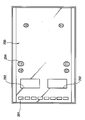
도 1은 본 발명의 일 실시예에 따른 표시 장치를 나타낸 분해 사시도이다.1 is an exploded perspective view illustrating a display device according to an exemplary embodiment of the present invention.
도 2는 도 1에 도시된 제1 사이드 몰드 프레임의 일부분을 확대한 사시도이다. FIG. 2 is an enlarged perspective view of a portion of the first side mold frame illustrated in FIG. 1.
도 3은 도 1에 도시된 수납용기의 배면도이다. 3 is a rear view of the storage container shown in FIG. 1.
도 4는 도 1에 도시된 반사시트의 배면도이다. 4 is a rear view of the reflective sheet shown in FIG. 1.
도 5는 도 1에 도시된 수납용기와 인버터의 결합상태를 나타낸 사시도이다. 5 is a perspective view showing a coupling state of the storage container and the inverter shown in FIG.
도 6은 도 1에 도시된 인버터와 보호케이스간의 결합 상태를 나타낸 사시도이다.6 is a perspective view showing a coupling state between the inverter and the protective case shown in FIG.
도 7a 및 도 7b는 본 발명에 따른 개구부 및 광차단부재를 적용하기 전과 후의 램프유닛의 표면 온도를 측정하여 나타낸 도면들이다. 7A and 7B are diagrams illustrating the surface temperature of the lamp unit before and after applying the opening and the light blocking member according to the present invention.
*도면의 주요 부분에 대한 부호의 설명** Description of the symbols for the main parts of the drawings *
100 : 디스플레이 유닛 110 : 표시 패널100: display unit 110: display panel
200 : 백라이트 어셈블리 290 : 수납용기200: backlight assembly 290: storage container
210 : 램프 유닛 294 : 돌출부210: lamp unit 294: protrusion
211 : 램프 500 : 탑 샤시211: Lamp 500: Top Chassis
본 발명은 표시 장치에 관한 것으로, 더욱 상세하게는 표시품질을 향상시킬 수 있는 표시 장치에 관한 것이다.The present invention relates to a display device, and more particularly, to a display device capable of improving display quality.
액정표시 장치는 영상을 표시하는 액정 표시 패널 및 상기 액정 표시 패널의 후면에 구비되어 상기 액정 표시 패널에 광을 제공하는 백라이트 어셈블리를 포함한다.The liquid crystal display includes a liquid crystal display panel for displaying an image and a backlight assembly provided on a rear surface of the liquid crystal display panel to provide light to the liquid crystal display panel.
상기 백라이트 어셈블리는 램프 구동신호에 응답하여 광을 발생하는 램프유닛, 상기 램프유닛 하부에 배치되어 상기 램프유닛에서 발생하는 광을 상기 액정 표시 패널 방향으로 반사하는 반사시트 및 상기 램프유닛 상부에 배치되는 광학시트류를 포함한다.The backlight assembly may include a lamp unit generating light in response to a lamp driving signal, a reflection sheet disposed under the lamp unit to reflect light generated from the lamp unit toward the liquid crystal display panel, and an upper portion of the lamp unit. Optical sheets;
상기 액정 표시 패널과 백라이트 어셈블리는 수납용기에 수납된다.The liquid crystal display panel and the backlight assembly are accommodated in a storage container.
최근 들어, 액정표시 장치의 사이즈가 대형화됨에 따라서 복수의 램프들을 평행하게 바텀샤시 바닥면에 배치하는 직하형 백라이트 어셈블리를 적용하고 있으나, 상기 복수의 램프들로부터 발생하는 열에 의하여 상기 액정 표시 패널에 내재된 액정을 열화시킬뿐만 아니라, 액정표시 장치의 각종 부품들을 변형시킨다. 이로써, 액정표시 장치의 표시품질이 저하되는 문제점이 있다.Recently, as the size of the liquid crystal display device increases, a direct type backlight assembly for arranging a plurality of lamps in parallel with the bottom chassis bottom is applied. However, the heat generated from the plurality of lamps is inherent to the liquid crystal display panel. In addition to deteriorating the liquid crystal, various components of the liquid crystal display are deformed. Thereby, there exists a problem that the display quality of a liquid crystal display device falls.
또한, 상기 램프를 도광판 측면에 배치하는 에지(edge)형 백라이트 어셈블리를 적용한 액정표시 장치에서도, 상기 램프를 수납하는 외곽의 크기가 작아지는 추세에 의하여 상기 램프로부터 발생되는 열에 의해 액정표시 장치의 표시품질이 저 하되는 문제점이 있다.In addition, even in a liquid crystal display device using an edge type backlight assembly in which the lamp is disposed on the side of the light guide plate, the display of the liquid crystal display device is caused by the heat generated from the lamp due to the tendency that the size of the outer side of the lamp housing is reduced. There is a problem of poor quality.
이에 본 발명의 기술적 과제는 이러한 종래의 문제점을 해결하기 위한 것으로, 본 발명의 목적은 램프로부터 발생된 열에 의해서 표시품질이 저하되는 것을 방지하여 향상된 외관 품질을 갖는 표시 장치를 제공하는 것이다.Accordingly, an object of the present invention is to solve such a conventional problem, and an object of the present invention is to provide a display device having improved appearance quality by preventing display quality from being degraded by heat generated from a lamp.
상기한 본 발명의 목적을 실현하기 위한 하나의 특징에 따른 표시 장치는 표시 패널, 백라이트 어셈블리, 수납용기 및 광차단부재를 포함한다. 상기 표시 패널은 영상을 표시한다. 상기 백라이트 어셈블리는 광원과, 상기 광원 상부에 구비되는 광학시트와, 상기 광원 하부에 구비되는 반사시트를 포함한다. 상기 수납용기는 개구부가 형성된 바닥면과 상기 바닥면에서 연장된 측벽에 의해 정의된 수납공간에 상기 표시 패널 및 백라이트 어셈블리를 수납한다. 상기 광차단부재는 상기 반사시트 배면에 배치된다. According to an aspect of the present invention, a display device includes a display panel, a backlight assembly, a storage container, and a light blocking member. The display panel displays an image. The backlight assembly includes a light source, an optical sheet provided above the light source, and a reflecting sheet provided below the light source. The storage container accommodates the display panel and the backlight assembly in a storage space defined by a bottom surface having an opening and sidewalls extending from the bottom surface. The light blocking member is disposed on the rear surface of the reflective sheet.
상기 백라이트 어셈블리는 구동신호에 응답하여 광을 발생하는 램프유닛, 상기 램프유닛 상부에 구비되는 확산시트 및 프리즘 시트 등과 같은 광학시트, 상기 구동신호를 상기 램프유닛으로 전달하는 램프 와이어 및 상기 광을 입력받아 상기 표시 패널 방향으로 가이드하는 도광판 및 도광판으로부터 누설된 광을 반사하는 반사시트로 이루어진다. 복수 개의 램프가 표시 패널 하부에 평행하게 배치되는 직하형 표시 장치에 있어서 상기 도광판은 생략될 수 있다.The backlight assembly may include a lamp unit generating light in response to a driving signal, an optical sheet such as a diffusion sheet and a prism sheet provided on the lamp unit, a lamp wire transferring the driving signal to the lamp unit, and the light input. And a light guide plate that guides the light guide plate toward the display panel and reflects light leaked from the light guide plate. The light guide plate may be omitted in the direct type display device in which a plurality of lamps are disposed below the display panel.
이러한 표시 장치에 의하면, 수납용기 배면에 열 방출을 위한 개구부를 형성 하므로써, 램프로부터 발생된 열이 액정 표시 패널에 미치는 악영향을 줄여 표시품질이 저하되는 것을 방지할 수 있다.According to such a display device, by forming an opening for dissipating heat on the rear surface of the storage container, it is possible to reduce the adverse effect of heat generated from the lamp on the liquid crystal display panel and to prevent the display quality from being lowered.
이하, 첨부한 도면들을 참조하여, 본 발명의 바람직한 실시예를 보다 상세하게 설명하고자 한다.Hereinafter, with reference to the accompanying drawings, it will be described in detail a preferred embodiment of the present invention.
도 1은 본 발명의 일 실시예에 따른 표시 장치를 나타낸 분해 사시도이다.1 is an exploded perspective view illustrating a display device according to an exemplary embodiment of the present invention.
도 1을 참조하면, 본 발명의 일 실시예에 따른 표시 장치는 광을 이용하여 영상을 표시하는 디스플레이 유닛(100), 상기 디스플레이 유닛(100)의 후면에 배치되어 상기 디스플레이 유닛(100)으로 상기 광을 제공하는 백라이트 어셈블리(200), 상기 디스플레이 유닛(100) 및 백라이트 어셈블리(200)를 수납하는 수납용기(290)를 포함한다.Referring to FIG. 1, a display device according to an exemplary embodiment of the present invention may include a
상기 디스플레이 유닛(100)은 영상을 표시하는 표시 패널(110), 상기 표시 패널(110)을 구동하기 위한 게이트측 및 데이터측 인쇄회로기판(120, 130)으로 이루어진다. 상기 표시 패널(110)은 제1 기판(미도시), 상기 제1 기판과 마주하는 제2 기판(미도시) 및 상기 제1 기판과 제2 기판과의 사이에 개재된 액정층(미도시)을 포함한다. The
상기 제1 기판은 스위칭 소자인 박막트랜지스터(TFT)가 매트릭스 형태로 형성되어 있는 투명한 유리 기판이다. 상기 박막트랜지스터의 소스 단자에는 데이터 라인이 연결되며, 게이트 단자에는 게이트 라인이 연결된다. 또한, 상기 박막트랜지스터의 드레인 단자에는 투명한 도전성 재질로 이루어진 화소 전극이 연결된다.The first substrate is a transparent glass substrate in which a thin film transistor (TFT), which is a switching element, is formed in a matrix form. The data line is connected to the source terminal of the thin film transistor, and the gate line is connected to the gate terminal. In addition, a pixel electrode made of a transparent conductive material is connected to the drain terminal of the thin film transistor.
상기 제2 기판은 상기 제1 기판에 일정 간격 이격되어 대향 배치된 컬러필터 기판이다. 상기 컬러필터 기판은 광이 통과함에 따라 소정의 색으로 발현되는 색화소인 RGB 화소가 박막 공정에 의해 형성된 기판이다. 상기 제1 기판의 전면에는 ITO로 이루어진 공통 전극이 형성된다.The second substrate is a color filter substrate disposed to face the first substrate at a predetermined interval. The color filter substrate is a substrate in which an RGB pixel, which is a color pixel expressed in a predetermined color as light passes, is formed by a thin film process. A common electrode made of ITO is formed on the front surface of the first substrate.
이러한 구성을 갖는 액정 표시 패널(110)은 상기 박막트랜지스터의 게이트 단자 및 소스 단자에 전원이 인가되어 TFT가 턴-온(turn on)되면, 화소 전극과 공통 전극 사이에는 전계가 형성된다. 이러한 전계에 의해 TFT 기판(미도시)과 컬러필터 기판(미도시)과의 사이에 주입된 액정의 배열각이 변화되고, 변화된 배열각에 따라서 광투과도가 변경되어 원하는 계조의 영상을 얻게 된다.In the liquid
상기 백라이트 어셈블리(200)는 광을 발생하기 위한 복수의 램프(211)로 이루어진 램프 유닛(210), 상기 램프들(211)을 고정하기 위한 램프홀더(220), 상기 램프유닛(210)의 광을 확산하기 위한 확산판(240), 상기 확산판(240) 상부에 구비되어 광의 휘도 균일성 또는 시야각을 향상시키기 위한 광학 시트류(243)를 구비한다.The
상기 램프 유닛(210)은 병렬로 배치된 막대 형상의 복수의 램프들(211)인 것을 도시하였으나, U자 형상의 램프가 사용되어질 수 있다. 또한, 상기 램프(211)는 램프 전극이 내부에 구비된 CCFL(Cold cathode fluorescent Lamp) 혹은 램프 전극이 외부에 구비된 EEFL(External Electrode Lamp) 사용되어질 수 있다. 또한, 광원으로써 상기 램프유닛(210)은 LED(light-emitting diode)로 대체되어질 수 있다. Although the
인버터(700)는 상기 램프 유닛(210)에 구동신호를 인가하며, 보통 PCB(Printed circuit board) 형태로 제작되어 진다. 인버터 보호부재(800)는 금속 으로 이루어져, 상기 인버터(700)로부터 발생하는 EMI(electromagnetic interference)를 방지한다.The
램프홀더(220)는 상기 램프(211)의 전극부위를 감싸면서 상기 수납용기(290)와 결합하여 상기 램프(211)의 유동을 방지한다. 반사시트(245) 및 수납용기(290)는 상기 램프홀더(220)와 결합하기 결합홀(2451, 291)이 형성되어 있다.The
반사시트(245)는 상기 램프유닛(210) 하부에 구비되어 상기 램프유닛(210)으로부터 출사된 광을 상기 표시 패널(110) 방향으로 반사시키며, 상기 램프홀더(220)에 대응하는 영역에는 홀(2451)이 형성되어 있다.The
램프 고정부(230)는 서로 인접하는 램프들이 수평 방향으로 일정 간격을 유지하도록 상기 램프(211)를 고정한다. 또한 램프 고정부는(230)은 확산판(240)이 램프유닛(210)과 일정 간격을 유지할 수 있도록 확산판 지지부를 더 포함한다. 상기 램프 고정부는(230)은 상기 반사시트(245)에 형성된 홀을 관통하여 상기 수납용기(290)와 결합한다.The
한편, 상기 백라이트 어셈블리(200)는 제1 및 제2 사이드 몰드 프레임(250, 260)을 더 포함한다. 상기 제1 및 제2 사이드 몰드 프레임(250, 260)은 상기 수납용기(290)와 결합하여 상기 램프유닛(210)의 양단을 수납하도록 한다. Meanwhile, the
또한, 상기 제1 및 제2 사이드 몰드 프레임(250, 260)의 상부면은 확산판(240) 및 광학시트(243)가 안착된다. 상기 제1 및 제2 사이드 몰드 프레임(250, 260) 중 적어도 하나는 상기 확산판(240)의 유동을 방지하는 확산판 유동 방지부(252)와 광학시트 고정부(253)를 더 포함한다.
In addition, the upper surfaces of the first and second side mold frames 250 and 260 are mounted with the
여기서, 상기 제1 및 제2 사이드 몰드 프레임(250, 260)은 20(W/m*k) 이상의 열 전도율을 갖는 플라스틱(이하, 방열 플라스틱이라 칭함) 재질로 이루어 질 수 있다. 상기 방열 플라스틱의 일 예로 쿨폴리머(CoolPolymer)사에서 제조된 쿨폴리(CoolPoly)라는 제품을 들 수 있다. 상기한 쿨폴리는 열 전도성 플라스틱으로써, 10(W/m*k) 내지 100(W/m*k) 범위의 열 전도율을 갖는 것으로 알려져 있다. 여기서, 상기 W, m 및 k는 와트(Watt), 미터(m) 및 켈빈(K)을 각각 나타낸다.The first and second side mold frames 250 and 260 may be made of a plastic material (hereinafter referred to as heat dissipating plastic) having a thermal conductivity of 20 (W / m * k) or more. An example of the heat dissipating plastic may include a product called CoolPoly manufactured by CoolPolymer. The cool poly is a thermally conductive plastic and is known to have a thermal conductivity in the range of 10 (W / m * k) to 100 (W / m * k). Here, W, m and k represent Watt, Meter, and Kelvin, respectively.
상기 램프유닛(210)에서 발생된 열은 상기 제1 및 제2 사이드 몰드 프레임(250, 260)에 전달된다. 방열 플라스틱 재질로 이루어진 상기 제1 및 제2 로워 몰드 프레임(250, 260)은 전달된 상기 열을 후술할 수납용기(290)로 전달한다.Heat generated from the
확산판(240)은 램프유닛(210)으로부터 입사된 광을 확산출사하며, 광학시트(243)는 확산판(240)으로부터 입사된 광의 품질표시를 향상시킨다. 광학시트(243)는 확산판(240)으로부터 출사된 광을 확산 출사하는 확산시트, 정면 휘도를 증가시키는 프리즘 시트, 특정 방향으로 진동하는 광은 투과시키고 나머지 광은 반사시키는 반사편광시트 중 필요에 따라 선택적으로 구성할 수 있다.The
미들 몰드 프레임(400)은 수납용기(290)와 결합하여 확산판(240) 및 광학시트(243)의 유동을 방지한다. 또한, 미들 몰드 프레임(400) 상부면에는 표시 패널(110)이 안착된다. 미들 몰드 프레임(400) 상부면에는 표시 패널(110)의 안착되어질 때, 그 위치를 가이드 해주는 패널 가이드 부재(401)를 더 포함하며, 패널 가이드 부재(401)는 고무와 같은 탄력부재로 형성되는 것이 바람직하다. 패널 가이드 부재(401)는 미들 몰드 프레임(400)에 일체로 형성될 수도 있다. 패널 가이드 부재 (401)는 미들 몰드 프레임(400) 상부면 모서리 영역에 형성되는 것이 바람직하다.The
수납용기(290)는 바닥면 및 측벽으로 이루어진 수납공간에 표시 패널(110) 및 백라이트 어셈블리(200)를 수납하며, 금속으로 이루어진다.The
탑 샤시(500)는 상기 수납용기(290)와 결합하여 디스플레이 유닛(100) 및 백라이트 어셈블리(200)를 지정된 위치에 고정시킨다.The
도 2는 도 1에 도시된 제1 사이드 몰드 프레임의 일부분을 확대한 사시도이다. FIG. 2 is an enlarged perspective view of a portion of the first side mold frame illustrated in FIG. 1.
도 2를 참조하면, 제1 사이드 몰드 프레임(250)의 상부면(251)에는 확산판(240) 및 광학시트(243)가 안착된다. 여기서는 편의상 광학시트(243)는 생략하고 확산판(240)만이 안착된 것만을 도시하였다. Referring to FIG. 2, the
제1 사이드 몰드 프레임(250)의 상부면(251)에는 확산판 고정부(252) 및 광학시트 고정부(253)가 배치된다. 상기 확산판 고정부(252)는 제1 사이드 몰드 프레임(250)의 상부면(251)에서 돌출되어 형성되고, 확산판 함몰부(241)와 결합하여 확산판(240)이 유동되는 것을 방지한다. 광학시트 고정부(252)는 확산판 고정부(251) 상부면 상에 돌출되어 형성되며, 광학시트(243)에 형성된 홈과 결합하여 광학시트가 유동되는 것을 방지한다. 여기서, 상기 광학시트 고정부(252)는 상기 확산판 고정부(252)의 상부면이 아닌 제1 사이드 몰드 프레임(250)의 상부면(251)에 형성될 수도 있다.The diffusion
도 3은 도 1에 도시된 수납용기의 배면도이다. 3 is a rear view of the storage container shown in FIG. 1.
도 3을 참조하면, 수납용기(290)는 금속 재질로 이루어져 있으며, 바닥면 및 측벽으로 이루어진 공간에 표시 패널(110) 및 백라이트 어셈블리(200)를 수납한다. Referring to FIG. 3, the
상기 수납용기(290)의 바닥면에는 램프홀더(210)와 결합하기 위한 결합홀(291) 및 램프유닛(210)에서 발생하는 열을 수납용기(290) 외부로 방출하기 위한 개구부(292, 293)가 형성되어 있다. 상기 수납용기(290)와 인버터(700) 사이에 갭(gap)이 형성되면 유속 증가에 따른 자연대류에 의해 백라이트 어셈블리(200) 내부의 열이 더욱 빨리 방출된다. 따라서, 개구부(292, 293)는 인버터(700)에 대응하는 수납용기(290) 바닥면 영역에 형성되는 것이 바람직하다. 또한, 수납용기(290)의 배면에는 인버터(700) 및 인버터 보호부재(800)를 고정하기 위한 돌출부(294)가 돌출되어 형성된다.
도 4는 도 1에 도시된 반사시트의 배면도이다. 4 is a rear view of the reflective sheet shown in FIG. 1.
도 4를 참조하면, 램프유닛(210)과 마주보는 반사시트(245) 표면은 광반사 물질이 형성되어 있어서, 램프유닛(210)으로부터 입사된 광을 표시 패널(110) 방향으로 반사시킨다. 또한, 반사시트(245)는 램프홀더(210)가 수납용기(290)와 결합 체결할 수 있도록 결합홀(2451)이 형성되어 있다. 수납용기(290)에 형성된 개구부(292, 293)에 대응하는 반사시트(245) 배면 영역에는 수납용기(290) 외부로 광이 누설되는 것을 방지하기 위한 광차단부재(2452, 2453)가 부착된다. Referring to FIG. 4, a light reflecting material is formed on a surface of the
상기 광차단부재(2452, 2453)는 카본(carbon)을 포함하는 폴리에스터(polyester) 필름이나 PET(polyethylene terephthalate) 재질로 형성되며, 광학밀도가 높아 광이 거의 투과하지 못한다. 상기 광차단부재(2452, 2453) 일면에는 접착제가 형성되어져 있으며, 반사시트(245)의 균일성을 위해 두께가 25um 내지 188um 되는 것이 바람직하다. 또한, 상기 광차단부재(2452, 2453)의 크기는 수납용기(290)에 형성된 개구부(292, 293)보다 어느 정도 크게 형성하는 것이 바람직하다.The
도 5는 도 1에 도시된 수납용기와 인버터의 결합상태를 나타낸 사시도이다. 5 is a perspective view showing a coupling state of the storage container and the inverter shown in FIG.
도 5를 참조하면, 인버터(700)는 램프 유닛(210)에 구동신호를 인가하며, 보통 PCB(Printed circuit board) 형태로 제작된다. 수납용기(290) 배면에는 인버터(700)를 지지하고 나사 체결하기 위한 돌출부(294)가 형성되어 있다. Referring to FIG. 5, the
상기 돌출부(294) 상부면에는 인버터(700)를 나사 체결하기 위한 나사 체결부(2942) 및 인버터(700)를 가이드 하기 위한 가이드 돌기(2941)가 형성되어 있다. 인버터(700)는 나사 체결부(2942)와 가이드 돌기(2941)에 각각 대응하는 홀이 구비되어 있다. 인버터(700)는 수납용기(290) 배면에 있는 돌출부(294) 상부면에 형성된 가이드 돌기(2941)와 인버터(700)에 형성된 홀을 이용하여 안착된다. The upper surface of the
도 6은 도 1에 도시된 인버터와 보호케이스간의 결합 상태를 나타낸 사시도이다.6 is a perspective view showing a coupling state between the inverter and the protective case shown in FIG.
도 1, 도 5 및 도 6을 참조하면, 보호부재(800)는 금속 재질로 이루어져, 인버터(700)로부터 발생하는 EMI(ElectroMagnetic Interference)를 차폐한다. 상기 보호케이스(800)는 인버터(700) 및 수납용기(290)와 나사 체결하기 위한 제1 나사홈(810)과 제2 나사홈(820)이 각각 형성되어 있다. 1, 5 and 6, the
수납용기(290) 배면에 있는 돌출부(294) 상부면에 형성된 가이드 돌기(2941)를 이용하여 인버터(700)를 안착한다. 이어, 나사체결부(2942)와 인버터(700)에 형 성된 홀들 각각에 대응하는 제1 및 제2 나사홈(810, 820)에 제1 및 제2 나사(812, 822) 각각을 이용하여 고정한다.The
도 7a 및 도 7b는 본 발명에 따른 개구부 및 광차단부재를 적용하기 전과 후의 램프유닛의 표면 온도를 측정하여 나타낸 도면들이다. 특히, 도 7b에서는 인버터(700)에 대응하는 수납용기(290)의 배면 영역에 개구부(292, 293)를 형성하였고, 광차단부재(2452, 2453)로 0.05mm 두께의 PET(polyethylene terephthalate)를 부착한 후에 램프유닛(210)의 표면온도를 측정하였다. 7A and 7B are diagrams illustrating the surface temperature of the lamp unit before and after applying the opening and the light blocking member according to the present invention. In particular, in FIG. 7B,
도 7a에 나타낸 바와 같이, 개구부 및 광차단부재를 적용하기 전에는 램프 전극부의 일측에 근접하는 영역에서는 76.2℃, 75.4℃ 및 75.9℃가 측정되었고, 램프 전극부의 타측에 근접하는 영역에서는 111.8℃, 99.4℃ 및 106.9℃가 측정되었으며, 램프들의 중앙부에 대응하는 영역에서는 84.5℃, 88.9℃ 및 85.4℃가 측정되었다.As shown in FIG. 7A, before applying the opening and the light blocking member, 76.2 ° C., 75.4 ° C., and 75.9 ° C. were measured in an area near one side of the lamp electrode part, and 111.8 ° C. and 99.4 in an area near the other side of the lamp electrode part. ° C and 106.9 ° C were measured, and 84.5 ° C, 88.9 ° C and 85.4 ° C in the region corresponding to the center of the lamps.
하지만, 도 7b에 나타낸 바와 같이, 개구부 및 광차단부재를 적용한 후에는 램프 전극부의 일측에 근접하는 영역에서는 71.5℃, 71.5℃ 및 71.7℃가 측정되었고, 램프 전극부의 타측에 근접하는 영역에서는 101.6℃, 98.8℃ 및 105.9℃가 측정되었으며, 램프들의 중앙부에 대응하는 영역에서는 80.3℃, 81.2℃ 및 85.8℃가 측정되었다.However, as shown in FIG. 7B, after the opening and the light blocking member were applied, 71.5 ° C., 71.5 ° C., and 71.7 ° C. were measured in an area close to one side of the lamp electrode part, and 101.6 ° C. in an area near the other side of the lamp electrode part. , 98.8 ° C. and 105.9 ° C. were measured, and 80.3 ° C., 81.2 ° C. and 85.8 ° C. were measured in the region corresponding to the center of the lamps.
따라서, 본 발명에 따른 개구부 및 광차단부재를 적용함에 따라 램프유닛(210)의 표면온도는 4 내지 10 ℃ 낮아짐을 확인할 수 있다.Therefore, it can be seen that the surface temperature of the
이상에서 설명한 바와 같이, 본 발명에 따르면 수납용기 배면에 열 방출을 위한 개구부를 형성하므로써, 램프로부터 발생된 열이 액정 표시 패널에 미치는 악영향을 줄여 표시품질이 저하되는 것을 방지할 수 있다. As described above, according to the present invention, by forming an opening for dissipating heat in the rear of the storage container, it is possible to reduce the adverse effect of heat generated from the lamp on the liquid crystal display panel and to prevent the display quality from being lowered.
또한, 상기 개구부에 대응하는 반사시트 배면 영역에 광차단부재를 부착하므로써, 광이 백라이트 어셈블리의 외부로 누설되는 것을 방지할 수 있다. In addition, by attaching the light blocking member to the reflective sheet rear region corresponding to the opening, it is possible to prevent the light from leaking to the outside of the backlight assembly.
또한, 램프에 전원전압을 인가하는 인버터에 대응되는 수납용기 배면 영역에 열 방출을 위한 개구부를 형성시키므로써, 대류효과에 의한 방열효과를 증대시킬 수 있다.In addition, by forming an opening for dissipating heat in the rear region of the storage container corresponding to the inverter for applying a power voltage to the lamp, it is possible to increase the heat radiation effect by the convection effect.
이상 실시예를 참조하여 설명하였지만, 해당 기술 분야의 숙련된 당업자는 하기의 특허 청구의 범위에 기재된 본 발명의 사상 및 영역으로부터 벗어나지 않는 범위 내에서 본 발명을 다양하게 수정 및 변경시킬 수 있음을 이해할 수 있을 것이다.Although described with reference to the embodiments above, those skilled in the art will understand that the present invention can be variously modified and changed without departing from the spirit and scope of the invention as set forth in the claims below. Could be.
Claims (18)
Priority Applications (5)
| Application Number | Priority Date | Filing Date | Title |
|---|---|---|---|
| KR1020040093635A KR101073043B1 (en) | 2004-11-16 | 2004-11-16 | Display apparatus |
| JP2005044636A JP4786194B2 (en) | 2004-11-16 | 2005-02-21 | Display device |
| TW094127867A TWI457640B (en) | 2004-11-16 | 2005-08-16 | Display device and method of manufacturing thereof |
| US11/205,514 US7570341B2 (en) | 2004-11-16 | 2005-08-17 | Heat-dissipating display device and method of manufacturing thereof |
| CNB2005101133707A CN100555038C (en) | 2004-11-16 | 2005-10-11 | Display device and manufacture method thereof |
Applications Claiming Priority (1)
| Application Number | Priority Date | Filing Date | Title |
|---|---|---|---|
| KR1020040093635A KR101073043B1 (en) | 2004-11-16 | 2004-11-16 | Display apparatus |
Publications (2)
| Publication Number | Publication Date |
|---|---|
| KR20060054809A KR20060054809A (en) | 2006-05-23 |
| KR101073043B1 true KR101073043B1 (en) | 2011-10-12 |
Family
ID=36385871
Family Applications (1)
| Application Number | Title | Priority Date | Filing Date |
|---|---|---|---|
| KR1020040093635A KR101073043B1 (en) | 2004-11-16 | 2004-11-16 | Display apparatus |
Country Status (5)
| Country | Link |
|---|---|
| US (1) | US7570341B2 (en) |
| JP (1) | JP4786194B2 (en) |
| KR (1) | KR101073043B1 (en) |
| CN (1) | CN100555038C (en) |
| TW (1) | TWI457640B (en) |
Families Citing this family (34)
| Publication number | Priority date | Publication date | Assignee | Title |
|---|---|---|---|---|
| KR20060054826A (en) * | 2004-11-16 | 2006-05-23 | 삼성전자주식회사 | Reflector sheet, back light assembly having the same and display device |
| TWI322301B (en) * | 2005-02-25 | 2010-03-21 | Au Optronics Corp | Backlight module and heat-dissipating structure thereof |
| KR20060104356A (en) * | 2005-03-30 | 2006-10-09 | 삼성전자주식회사 | Back light assembly and liquid crystal display apparatus having the same |
| US9104058B2 (en) | 2005-06-27 | 2015-08-11 | Graftech International Holdings Inc. | Optimized frame system for a liquid crystal display device |
| US9081220B2 (en) | 2005-06-27 | 2015-07-14 | Graftech International Holdings Inc. | Optimized frame system for a display device |
| TWI285776B (en) * | 2005-10-06 | 2007-08-21 | Au Optronics Corp | Backlight module and liquid crystal display device incorporating the same |
| US8400607B2 (en) * | 2005-10-11 | 2013-03-19 | Barco N.V. | Display assemblies and methods of display |
| KR101195227B1 (en) * | 2005-12-14 | 2012-10-29 | 삼성디스플레이 주식회사 | Liquid crystal display |
| TWI333580B (en) * | 2006-02-08 | 2010-11-21 | Chimei Innolux Corp | Backlight module and liquid crystal display using the same |
| KR101307998B1 (en) * | 2006-06-30 | 2013-09-12 | 엘지디스플레이 주식회사 | Fixing structure of inverter of liquid crystal display device |
| KR101295074B1 (en) | 2006-07-20 | 2013-08-08 | 삼성디스플레이 주식회사 | Backlight unit and liquid crystal display having the same |
| KR20080008751A (en) | 2006-07-21 | 2008-01-24 | 삼성전자주식회사 | Display device |
| KR101290284B1 (en) * | 2006-08-01 | 2013-08-07 | 삼성디스플레이 주식회사 | Backlight assembly, liquid crystal display having backlight assembly and method of assembling the Backlight assembly |
| KR101385231B1 (en) * | 2006-08-24 | 2014-04-14 | 삼성디스플레이 주식회사 | Flat panel display |
| JP2008116832A (en) | 2006-11-07 | 2008-05-22 | Funai Electric Co Ltd | Liquid crystal display device |
| KR101338020B1 (en) * | 2006-11-20 | 2013-12-06 | 삼성디스플레이 주식회사 | Liquid crystal display device |
| TWI344571B (en) * | 2006-12-06 | 2011-07-01 | Au Optronics Corp | Flat panel display module |
| JP5233116B2 (en) * | 2006-12-25 | 2013-07-10 | 三菱電機株式会社 | Display device |
| KR100851164B1 (en) * | 2006-12-29 | 2008-08-08 | 엘지이노텍 주식회사 | Backlight unit and display device having the same |
| KR101340517B1 (en) * | 2007-01-20 | 2013-12-12 | 삼성디스플레이 주식회사 | Receiving member, backlight unit and liquid crystal display having the same |
| WO2008111264A1 (en) * | 2007-03-09 | 2008-09-18 | Sharp Kabushiki Kaisha | Illumination device for display device, and display device |
| US8210733B2 (en) * | 2007-03-09 | 2012-07-03 | Sharp Kabushiki Kaisha | Lighting device for display device and display device |
| CN101657674B (en) * | 2007-03-09 | 2012-01-25 | 夏普株式会社 | Lighting device for display device and display device |
| TWI391741B (en) * | 2007-05-30 | 2013-04-01 | Au Optronics Corp | Backlight module capable of reducing leakage light for use in a liquid crystal display device |
| KR100877413B1 (en) * | 2007-06-04 | 2009-01-07 | 엘지전자 주식회사 | Backlight unit and liquid crystal display comprising the same |
| JP4212062B1 (en) * | 2008-01-21 | 2009-01-21 | オリオン電機株式会社 | LCD panel |
| KR101511493B1 (en) | 2008-11-27 | 2015-04-14 | 삼성디스플레이 주식회사 | Liquid crystal display module and display apparatus set having the same, and method of assembling the liquid crystal display module |
| JP5650382B2 (en) * | 2009-05-18 | 2015-01-07 | 帝人デュポンフィルム株式会社 | Light reflection film |
| JP2010276908A (en) * | 2009-05-29 | 2010-12-09 | Victor Co Of Japan Ltd | Casing structure and image display device |
| US20130010214A1 (en) * | 2010-04-16 | 2013-01-10 | Sharp Kabushiki Kaisha | Lighting device, display device and television receiver |
| CN102033358A (en) * | 2011-01-21 | 2011-04-27 | 威胜集团有限公司 | LED liquid crystal display component |
| JP5845795B2 (en) | 2011-10-12 | 2016-01-20 | 船井電機株式会社 | Display device |
| KR101813656B1 (en) | 2011-03-15 | 2018-01-02 | 삼성디스플레이 주식회사 | A liquid crystal display |
| CN102943985B (en) * | 2012-11-29 | 2016-04-13 | 深圳市华星光电技术有限公司 | A kind of backlight module and display device thereof |
Family Cites Families (17)
| Publication number | Priority date | Publication date | Assignee | Title |
|---|---|---|---|---|
| JP2865501B2 (en) * | 1992-10-16 | 1999-03-08 | シャープ株式会社 | Liquid crystal display |
| JPH09171173A (en) * | 1995-12-20 | 1997-06-30 | Hitachi Ltd | Dustproof device for liquid crystal panel |
| JPH10240147A (en) * | 1997-02-27 | 1998-09-11 | Canon Inc | Liquid crystal device |
| JP3961642B2 (en) * | 1997-10-14 | 2007-08-22 | 株式会社アイ・オー・データ機器 | LCD display |
| KR100258839B1 (en) * | 1998-01-24 | 2000-06-15 | 윤종용 | Lcd module |
| KR100784804B1 (en) * | 2001-05-07 | 2007-12-14 | 삼성전자주식회사 | Liquid crystal display device and method for assembling the same |
| JP2003036032A (en) * | 2001-07-23 | 2003-02-07 | Sony Corp | Display device |
| JP4115715B2 (en) * | 2002-03-01 | 2008-07-09 | シャープ株式会社 | Backlight device |
| CN2546911Y (en) * | 2002-04-10 | 2003-04-23 | 廖骏吉 | Negative phototropic cover radiating structure |
| KR100873067B1 (en) * | 2002-07-11 | 2008-12-11 | 삼성전자주식회사 | Back light assembly and liquid crystal display having the same |
| KR20040009902A (en) * | 2002-07-26 | 2004-01-31 | 삼성전자주식회사 | Back light assembly using the same and liquid crystal display device |
| KR100463870B1 (en) * | 2002-09-03 | 2004-12-30 | 엘지.필립스 엘시디 주식회사 | Liquid crystal display device |
| JP2004109306A (en) * | 2002-09-17 | 2004-04-08 | Sharp Corp | Thin display apparatus |
| JP2004220980A (en) * | 2003-01-16 | 2004-08-05 | Tama Electric Co Ltd | Backlight device |
| JP4543813B2 (en) * | 2004-08-04 | 2010-09-15 | ソニー株式会社 | Backlight device and liquid crystal display device including the backlight device |
| JP4706206B2 (en) * | 2004-08-18 | 2011-06-22 | ソニー株式会社 | Heat dissipation device and display device |
| KR101248899B1 (en) * | 2006-01-20 | 2013-04-01 | 엘지디스플레이 주식회사 | Liquid crystal display device module |
-
2004
- 2004-11-16 KR KR1020040093635A patent/KR101073043B1/en not_active IP Right Cessation
-
2005
- 2005-02-21 JP JP2005044636A patent/JP4786194B2/en not_active Expired - Fee Related
- 2005-08-16 TW TW094127867A patent/TWI457640B/en not_active IP Right Cessation
- 2005-08-17 US US11/205,514 patent/US7570341B2/en not_active Expired - Fee Related
- 2005-10-11 CN CNB2005101133707A patent/CN100555038C/en not_active Expired - Fee Related
Also Published As
| Publication number | Publication date |
|---|---|
| JP4786194B2 (en) | 2011-10-05 |
| TW200617482A (en) | 2006-06-01 |
| US7570341B2 (en) | 2009-08-04 |
| TWI457640B (en) | 2014-10-21 |
| KR20060054809A (en) | 2006-05-23 |
| CN1776494A (en) | 2006-05-24 |
| JP2006146119A (en) | 2006-06-08 |
| CN100555038C (en) | 2009-10-28 |
| US20060103774A1 (en) | 2006-05-18 |
Similar Documents
| Publication | Publication Date | Title |
|---|---|---|
| KR101073043B1 (en) | Display apparatus | |
| KR102279386B1 (en) | Display appartus | |
| JP2006146119A5 (en) | ||
| US7513661B2 (en) | Backlight unit and liquid crystal display device having the same | |
| KR101214945B1 (en) | Backlight assembly and display device using the same | |
| KR101777527B1 (en) | Backlight module and liquid crystal display module using same | |
| JP5064528B2 (en) | Backlight unit and liquid crystal display device including the same | |
| US10809554B2 (en) | Display apparatus | |
| KR20080012702A (en) | Back-light assembly and liquid crystal display including the same | |
| US7782419B2 (en) | Backlight unit and liquid crystal display device having the same | |
| JP2000029004A (en) | Liquid crystal display device | |
| WO2011052259A1 (en) | Lighting device, and display device | |
| KR102100234B1 (en) | Display module and displyay apparatus having the same | |
| KR20080068327A (en) | Liquid crystal display device | |
| KR100975813B1 (en) | Display apparatus | |
| KR20070051990A (en) | Liquid crystal display apparatus | |
| KR101158599B1 (en) | Backlight unit and liquid crystal display having the same | |
| KR20080018486A (en) | Liquid crystal display | |
| KR20060000721A (en) | Display apparatus | |
| KR20080067851A (en) | Backlight assembly and liquid crystal display device including the same | |
| KR20070059268A (en) | Liquid crystal display device | |
| KR20060005154A (en) | Back light assembly and display device having the same | |
| KR20070042332A (en) | Chassis and backlight assembly and liquid crystal display device comprising the same | |
| KR20080041920A (en) | Backlightunit and display device including same | |
| KR20050072622A (en) | Flat panel diplay apparatus |
Legal Events
| Date | Code | Title | Description |
|---|---|---|---|
| A201 | Request for examination | ||
| E902 | Notification of reason for refusal | ||
| E701 | Decision to grant or registration of patent right | ||
| GRNT | Written decision to grant | ||
| FPAY | Annual fee payment |
Payment date: 20141001 Year of fee payment: 4 |
|
| LAPS | Lapse due to unpaid annual fee |