KR100787352B1 - Composition for Hard Mask and Method for Forming Pattern of Semiconductor Device using it - Google Patents
Composition for Hard Mask and Method for Forming Pattern of Semiconductor Device using it Download PDFInfo
- Publication number
- KR100787352B1 KR100787352B1 KR1020050014889A KR20050014889A KR100787352B1 KR 100787352 B1 KR100787352 B1 KR 100787352B1 KR 1020050014889 A KR1020050014889 A KR 1020050014889A KR 20050014889 A KR20050014889 A KR 20050014889A KR 100787352 B1 KR100787352 B1 KR 100787352B1
- Authority
- KR
- South Korea
- Prior art keywords
- hard mask
- film
- pattern
- forming
- composition
- Prior art date
Links
- 238000000034 method Methods 0.000 title claims abstract description 63
- 239000000203 mixture Substances 0.000 title claims abstract description 37
- 239000004065 semiconductor Substances 0.000 title claims abstract description 14
- 238000005530 etching Methods 0.000 claims abstract description 29
- 150000001875 compounds Chemical class 0.000 claims abstract description 27
- 229920005575 poly(amic acid) Polymers 0.000 claims abstract description 15
- 238000000151 deposition Methods 0.000 claims abstract description 7
- 239000011248 coating agent Substances 0.000 claims abstract description 5
- 238000000576 coating method Methods 0.000 claims abstract description 5
- 229920002120 photoresistant polymer Polymers 0.000 claims description 29
- 150000007974 melamines Chemical class 0.000 claims description 12
- 238000001459 lithography Methods 0.000 claims description 8
- 239000003960 organic solvent Substances 0.000 claims description 8
- ZMXDDKWLCZADIW-UHFFFAOYSA-N N,N-Dimethylformamide Chemical compound CN(C)C=O ZMXDDKWLCZADIW-UHFFFAOYSA-N 0.000 claims description 6
- 229910052799 carbon Inorganic materials 0.000 claims description 5
- -1 diamine compound Chemical class 0.000 claims description 5
- FXHOOIRPVKKKFG-UHFFFAOYSA-N N,N-Dimethylacetamide Chemical compound CN(C)C(C)=O FXHOOIRPVKKKFG-UHFFFAOYSA-N 0.000 claims description 4
- SECXISVLQFMRJM-UHFFFAOYSA-N N-Methylpyrrolidone Chemical compound CN1CCCC1=O SECXISVLQFMRJM-UHFFFAOYSA-N 0.000 claims description 2
- 239000000758 substrate Substances 0.000 claims description 2
- 229940113088 dimethylacetamide Drugs 0.000 claims 1
- 229910052814 silicon oxide Inorganic materials 0.000 claims 1
- 238000004519 manufacturing process Methods 0.000 abstract description 4
- 230000007261 regionalization Effects 0.000 abstract description 4
- 229910052581 Si3N4 Inorganic materials 0.000 abstract description 2
- HQVNEWCFYHHQES-UHFFFAOYSA-N silicon nitride Chemical compound N12[Si]34N5[Si]62N3[Si]51N64 HQVNEWCFYHHQES-UHFFFAOYSA-N 0.000 abstract description 2
- 229910003481 amorphous carbon Inorganic materials 0.000 description 11
- 238000002360 preparation method Methods 0.000 description 6
- 239000000463 material Substances 0.000 description 5
- 230000018109 developmental process Effects 0.000 description 4
- 230000000694 effects Effects 0.000 description 3
- 239000002184 metal Substances 0.000 description 3
- 238000007796 conventional method Methods 0.000 description 2
- 230000008021 deposition Effects 0.000 description 2
- ANSXAPJVJOKRDJ-UHFFFAOYSA-N furo[3,4-f][2]benzofuran-1,3,5,7-tetrone Chemical compound C1=C2C(=O)OC(=O)C2=CC2=C1C(=O)OC2=O ANSXAPJVJOKRDJ-UHFFFAOYSA-N 0.000 description 2
- 238000002156 mixing Methods 0.000 description 2
- 230000000704 physical effect Effects 0.000 description 2
- 238000003756 stirring Methods 0.000 description 2
- CBCKQZAAMUWICA-UHFFFAOYSA-N 1,4-phenylenediamine Chemical compound NC1=CC=C(N)C=C1 CBCKQZAAMUWICA-UHFFFAOYSA-N 0.000 description 1
- SHLOOFPNCHEUCJ-UHFFFAOYSA-N 2-n,4-n,6-n-tris(dimethoxymethyl)-1,3,5-triazine-2,4,6-triamine Chemical compound COC(OC)NC1=NC(NC(OC)OC)=NC(NC(OC)OC)=N1 SHLOOFPNCHEUCJ-UHFFFAOYSA-N 0.000 description 1
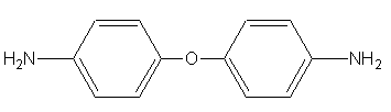
- HLBLWEWZXPIGSM-UHFFFAOYSA-N 4-Aminophenyl ether Chemical compound C1=CC(N)=CC=C1OC1=CC=C(N)C=C1 HLBLWEWZXPIGSM-UHFFFAOYSA-N 0.000 description 1
- 0 CCC*(C)*c(cc1)ccc1NC(c(cc(C(O)=O)c(C(Nc1ccc(*C(C)(C)CC)cc1)=O)c1)c1C(O)=O)=O Chemical compound CCC*(C)*c(cc1)ccc1NC(c(cc(C(O)=O)c(C(Nc1ccc(*C(C)(C)CC)cc1)=O)c1)c1C(O)=O)=O 0.000 description 1
- 229920000877 Melamine resin Polymers 0.000 description 1
- PZTSHYVIFAQPAY-UHFFFAOYSA-N N-(dimethoxymethyl)-1,3,5-triazin-2-amine Chemical compound COC(OC)NC1=NC=NC=N1 PZTSHYVIFAQPAY-UHFFFAOYSA-N 0.000 description 1
- XUIMIQQOPSSXEZ-UHFFFAOYSA-N Silicon Chemical compound [Si] XUIMIQQOPSSXEZ-UHFFFAOYSA-N 0.000 description 1
- 239000007983 Tris buffer Substances 0.000 description 1
- 101100107923 Vitis labrusca AMAT gene Proteins 0.000 description 1
- 230000003667 anti-reflective effect Effects 0.000 description 1
- 125000003178 carboxy group Chemical group [H]OC(*)=O 0.000 description 1
- 229940126214 compound 3 Drugs 0.000 description 1
- FFUAGWLWBBFQJT-UHFFFAOYSA-N hexamethyldisilazane Chemical compound C[Si](C)(C)N[Si](C)(C)C FFUAGWLWBBFQJT-UHFFFAOYSA-N 0.000 description 1
- 230000010354 integration Effects 0.000 description 1
- 239000012528 membrane Substances 0.000 description 1
- 239000011368 organic material Substances 0.000 description 1
- 229910052710 silicon Inorganic materials 0.000 description 1
- 239000010703 silicon Substances 0.000 description 1
- 238000004528 spin coating Methods 0.000 description 1
Images


Classifications
-
- H—ELECTRICITY
- H01—ELECTRIC ELEMENTS
- H01L—SEMICONDUCTOR DEVICES NOT COVERED BY CLASS H10
- H01L21/00—Processes or apparatus adapted for the manufacture or treatment of semiconductor or solid state devices or of parts thereof
- H01L21/02—Manufacture or treatment of semiconductor devices or of parts thereof
- H01L21/027—Making masks on semiconductor bodies for further photolithographic processing not provided for in group H01L21/18 or H01L21/34
- H01L21/0271—Making masks on semiconductor bodies for further photolithographic processing not provided for in group H01L21/18 or H01L21/34 comprising organic layers
- H01L21/0273—Making masks on semiconductor bodies for further photolithographic processing not provided for in group H01L21/18 or H01L21/34 comprising organic layers characterised by the treatment of photoresist layers
- H01L21/0274—Photolithographic processes
-
- A—HUMAN NECESSITIES
- A61—MEDICAL OR VETERINARY SCIENCE; HYGIENE
- A61B—DIAGNOSIS; SURGERY; IDENTIFICATION
- A61B17/00—Surgical instruments, devices or methods, e.g. tourniquets
- A61B17/24—Surgical instruments, devices or methods, e.g. tourniquets for use in the oral cavity, larynx, bronchial passages or nose; Tongue scrapers
- A61B17/244—Surgical instruments, devices or methods, e.g. tourniquets for use in the oral cavity, larynx, bronchial passages or nose; Tongue scrapers for cleaning of the tongue
-
- A—HUMAN NECESSITIES
- A61—MEDICAL OR VETERINARY SCIENCE; HYGIENE
- A61C—DENTISTRY; APPARATUS OR METHODS FOR ORAL OR DENTAL HYGIENE
- A61C17/00—Devices for cleaning, polishing, rinsing or drying teeth, teeth cavities or prostheses; Saliva removers; Dental appliances for receiving spittle
-
- G—PHYSICS
- G03—PHOTOGRAPHY; CINEMATOGRAPHY; ANALOGOUS TECHNIQUES USING WAVES OTHER THAN OPTICAL WAVES; ELECTROGRAPHY; HOLOGRAPHY
- G03F—PHOTOMECHANICAL PRODUCTION OF TEXTURED OR PATTERNED SURFACES, e.g. FOR PRINTING, FOR PROCESSING OF SEMICONDUCTOR DEVICES; MATERIALS THEREFOR; ORIGINALS THEREFOR; APPARATUS SPECIALLY ADAPTED THEREFOR
- G03F7/00—Photomechanical, e.g. photolithographic, production of textured or patterned surfaces, e.g. printing surfaces; Materials therefor, e.g. comprising photoresists; Apparatus specially adapted therefor
- G03F7/004—Photosensitive materials
- G03F7/038—Macromolecular compounds which are rendered insoluble or differentially wettable
- G03F7/0387—Polyamides or polyimides
-
- H—ELECTRICITY
- H01—ELECTRIC ELEMENTS
- H01L—SEMICONDUCTOR DEVICES NOT COVERED BY CLASS H10
- H01L21/00—Processes or apparatus adapted for the manufacture or treatment of semiconductor or solid state devices or of parts thereof
- H01L21/02—Manufacture or treatment of semiconductor devices or of parts thereof
- H01L21/02104—Forming layers
- H01L21/02107—Forming insulating materials on a substrate
- H01L21/02109—Forming insulating materials on a substrate characterised by the type of layer, e.g. type of material, porous/non-porous, pre-cursors, mixtures or laminates
- H01L21/02112—Forming insulating materials on a substrate characterised by the type of layer, e.g. type of material, porous/non-porous, pre-cursors, mixtures or laminates characterised by the material of the layer
- H01L21/02118—Forming insulating materials on a substrate characterised by the type of layer, e.g. type of material, porous/non-porous, pre-cursors, mixtures or laminates characterised by the material of the layer carbon based polymeric organic or inorganic material, e.g. polyimides, poly cyclobutene or PVC
-
- H—ELECTRICITY
- H01—ELECTRIC ELEMENTS
- H01L—SEMICONDUCTOR DEVICES NOT COVERED BY CLASS H10
- H01L21/00—Processes or apparatus adapted for the manufacture or treatment of semiconductor or solid state devices or of parts thereof
- H01L21/02—Manufacture or treatment of semiconductor devices or of parts thereof
- H01L21/04—Manufacture or treatment of semiconductor devices or of parts thereof the devices having potential barriers, e.g. a PN junction, depletion layer or carrier concentration layer
- H01L21/18—Manufacture or treatment of semiconductor devices or of parts thereof the devices having potential barriers, e.g. a PN junction, depletion layer or carrier concentration layer the devices having semiconductor bodies comprising elements of Group IV of the Periodic Table or AIIIBV compounds with or without impurities, e.g. doping materials
- H01L21/30—Treatment of semiconductor bodies using processes or apparatus not provided for in groups H01L21/20 - H01L21/26
- H01L21/31—Treatment of semiconductor bodies using processes or apparatus not provided for in groups H01L21/20 - H01L21/26 to form insulating layers thereon, e.g. for masking or by using photolithographic techniques; After treatment of these layers; Selection of materials for these layers
- H01L21/312—Organic layers, e.g. photoresist
Landscapes
- Engineering & Computer Science (AREA)
- Physics & Mathematics (AREA)
- General Physics & Mathematics (AREA)
- Health & Medical Sciences (AREA)
- Condensed Matter Physics & Semiconductors (AREA)
- Manufacturing & Machinery (AREA)
- Computer Hardware Design (AREA)
- Microelectronics & Electronic Packaging (AREA)
- Power Engineering (AREA)
- Life Sciences & Earth Sciences (AREA)
- Surgery (AREA)
- Veterinary Medicine (AREA)
- Spectroscopy & Molecular Physics (AREA)
- Public Health (AREA)
- General Health & Medical Sciences (AREA)
- Dentistry (AREA)
- Animal Behavior & Ethology (AREA)
- Heart & Thoracic Surgery (AREA)
- Medical Informatics (AREA)
- Molecular Biology (AREA)
- Biomedical Technology (AREA)
- Oral & Maxillofacial Surgery (AREA)
- Nuclear Medicine, Radiotherapy & Molecular Imaging (AREA)
- Otolaryngology (AREA)
- Epidemiology (AREA)
- Pulmonology (AREA)
- Photosensitive Polymer And Photoresist Processing (AREA)
- Materials For Photolithography (AREA)
- Drying Of Semiconductors (AREA)
Abstract
본 발명은 하드마스크용 조성물 및 이를 이용한 반도체 소자의 패턴 형성 방법에 관한 것으로, 더욱 상세하게는 피식각층 상부에 폴리아믹산(polyamic acid)계 화합물을 포함하는 하드마스크용 조성물 및 이를 이용하여 제 1 하드마스크막을 코팅하고 그 상부에 실리콘 질화막(SiON)을 이용한 제 2 하드마스크막을 순차적으로 증착하여 우수한 식각 선택비를 가지는 이중 하드마스크막을 형성함으로써 균일한 패턴을 형성하는, 모든 반도체 소자의 제조 공정 시에 사용할 수 있는 패턴 형성 방법에 관한 것이다. The present invention relates to a hard mask composition and a method for forming a pattern of a semiconductor device using the same, and more particularly, to a hard mask composition including a polyamic acid compound on an etched layer and a first hard using the same. During the manufacturing process of all semiconductor devices, a uniform pattern is formed by coating a mask film and sequentially depositing a second hard mask film using a silicon nitride film (SiON) thereon to form a double hard mask film having an excellent etching selectivity. It is related with the pattern formation method which can be used.
Description
도 1a 내지 도 1c는 종래 방법에 따른 반도체 소자의 패턴 형성 방법을 도시한 단면도.1A to 1C are cross-sectional views illustrating a method of forming a pattern of a semiconductor device according to a conventional method.
도 2a 내지 도 2d는 본 발명에 따른 반도체 소자의 패턴 형성 방법을 도시한 단면도.2A to 2D are cross-sectional views illustrating a method of forming a pattern of a semiconductor device according to the present invention.
도 3은 본 발명의 실시예 1 에 의해 형성된 포토레지스트 패턴 사진.Figure 3 is a photoresist pattern photo formed by Example 1 of the present invention.
도 4는 본 발명의 실시예 2 에 의해 형성된 포토레지스트 패턴 사진.4 is a photoresist pattern photo formed by Example 2 of the present invention.
< 도면의 주요 부분에 대한 간단한 설명 ><Brief description of the main parts of the drawing>
1, 21 : 피식각층 1-1, 21-1 : 피식각층 패턴1, 21: etched layer 1-1, 21-1: etched layer pattern
3 : 비결정성(amorphous) 탄소층 3-1 : 비결정성 탄소층 패턴3: Amorphous Carbon Layer 3-1: Amorphous Carbon Layer Pattern
5, 25 : SiON막 5-1, 25-1 : SiON막 패턴5, 25: SiON film 5-1, 25-1: SiON film pattern
7, 27 : 반사방지막 7-1, 27-1 : 반사방지막 패턴7, 27: antireflection film 7-1, 27-1: antireflection film pattern
9, 29 : 포토레지스트막 9-1, 29-1 : 포토레지스트막 패턴9, 29: photoresist film 9-1, 29-1: photoresist film pattern
23 : 제 1 하드마스크막 23-1 : 제 1 하드마스크막 패턴23: first hard mask film 23-1: first hard mask film pattern
본 발명은 하드마스크용 조성물 및 이를 이용한 반도체 소자의 패턴 형성 방법에 관한 것으로, 더욱 상세하게는 피식각층 상부에 폴리아믹산(polyamic acid)계 화합물을 포함하는 하드마스크용 조성물 및 이를 이용하여 제 1 하드마스크막을 코팅하고 그 상부에 실리콘 질화막(SiON)을 이용한 제 2 하드마스크막을 순차적으로 증착하여 우수한 식각 선택비를 가지는 이중 하드마스크막을 형성함으로써 균일한 패턴을 형성하는, 모든 반도체 소자의 제조 공정 시에 사용할 수 있는 패턴 형성 방법에 관한 것이다. The present invention relates to a hard mask composition and a method for forming a pattern of a semiconductor device using the same, and more particularly, to a hard mask composition including a polyamic acid compound on an etched layer and a first hard using the same. During the manufacturing process of all semiconductor devices, a uniform pattern is formed by coating a mask film and sequentially depositing a second hard mask film using a silicon nitride film (SiON) thereon to form a double hard mask film having an excellent etching selectivity. It is related with the pattern formation method which can be used.
반도체 장치의 제조 기술의 발달과 메모리 소자의 응용 분야가 확장되어 감에 따라, 최근 집적도가 향상된 대용량 메모리 소자를 제조하기 위한 방법의 개발이 요구되고 있다. 이와 같은 방법의 일환으로서 게이트(gate) 및 비트 라인(bit-line)과 같은 라인 패턴 형성 공정이나, 비트라인 콘택(bit-line contact)과 같은 콘택홀 패턴 형성 공정 시에 리소그래피 공정이 필수적으로 적용되고 있다.As the development of semiconductor device manufacturing technology and the application field of memory devices expand, the development of a method for manufacturing a large capacity memory device having an improved degree of integration is required in recent years. As part of such a method, a lithography process is indispensable in the process of forming a line pattern such as a gate and a bit-line or forming a contact hole pattern such as a bit-line contact. It is becoming.
상기 리소그래피 공정은 종래의 I-line 또는 KrF(248nm)의 장파장 광원 대신 화학증폭성의 원자외선(Deep Ultra Violet; DUV) 광원과 같은 단파장 광원을 노광원으로 사용하여 패턴 선폭(critical dimension; CD)을 0.07㎛이하로 형성할 수 있도록 개선하였다. The lithography process uses a short wavelength light source, such as a chemically amplified deep ultra violet (DUV) light source, as an exposure source, instead of a conventional long wavelength light source of I-line or KrF (248 nm), to use a pattern dimension (CD). Improvement was made to form less than 0.07㎛.
한편, 상기 리소그래피 공정 시에는 DUV 광원인 ArF(193nm) 또는 VUV(157nm) 광원 등에 대해 고해상도(resolution)를 가지는 화학증폭형 포토레지스트 (Chemically Amplified Photoresist)의 개선이 필요하다.Meanwhile, in the lithography process, it is necessary to improve a chemically amplified photoresist having a high resolution with respect to an ArF (193 nm) or a VUV (157 nm) light source, which is a DUV light source.
이때, 상기 화학증폭형 포토레지스트는 식각 가스에 대한 저항(etch resistance)이 금속층과 같은 피식각층에 비해 매우 낮기 때문에, 고집적화의 금속 패턴을 형성하기 위하여 피식각층 상부에 포토레지스트막을 100nm 두께 이하로 형성하는 경우, 안정한 식각 선택비를 얻을 수 없어 균일한 패턴을 형성하는 것이 어렵다.In this case, since the chemically amplified photoresist has a very low etch resistance compared to an etched layer such as a metal layer, a photoresist film is formed on the etched layer to have a thickness of 100 nm or less to form a highly integrated metal pattern. In this case, a stable etching selectivity cannot be obtained and it is difficult to form a uniform pattern.
이를 개선하기 위하여, 종래에는 피식각층과 포토레지스트막 사이에 비결정성(amorphous) 탄소(carbon)를 이용한 유기계 막과 SiON을 이용한 무기계 막을 형성한 다음, 이를 하드마스크막으로 이용하는 식각 공정을 수행한다. 이때, 상기 비결정성 탄소는 유기물과 같은 물성을 가지면서, 400℃ 이상의 고온에서도 물성 변화가 전혀 없는 물질이므로, 그 상부에 무기계 막을 안정하게 형성할 수 있다. 또한, 이러한 구성의 하드마스크막은 식각 공정이 종결된 후에도 제거가 용이하다.In order to improve this, conventionally, an organic film using amorphous carbon and an inorganic film using SiON are formed between the etching target layer and the photoresist film, and then an etching process using the same as a hard mask film is performed. At this time, the amorphous carbon is a material having the same physical properties as the organic material, there is no change in physical properties even at a high temperature of 400 ℃ or more, it is possible to stably form an inorganic film on the top. In addition, the hard mask film having such a structure can be easily removed even after the etching process is completed.
종래 상기 비결정성 탄소를 이용한 패턴 형성 방법을 도 1a 내지 도 1c에 도시한 도면을 참고하여 설명할 수 있다.Conventionally, the pattern forming method using the amorphous carbon can be described with reference to the drawings illustrated in FIGS. 1A to 1C.
도 1a를 참조하면, 피식각층(1) 상부에 비결정성 탄소층(3), SiON막(5), 반사방지막(bottom anti-reflection layer)(7) 및 포토레지스트막(9)을 순차적으로 형성한다.Referring to FIG. 1A, an
이때, 상기 비결정성 탄소층은 CDD 방법을 이용하여 약 200∼700nm두께로 형성하고, 상기 SiON막은 a-carbon CVD 장비(AMAT 사)를 이용하여 30∼100nm두께로 형성한다.In this case, the amorphous carbon layer is formed to a thickness of about 200 ~ 700nm using a CDD method, and the SiON film is formed to a thickness of 30 ~ 100nm using a-carbon CVD equipment (AMAT).
상기 포토레지스트막(9)에 대한 리소그래피 공정을 수행하여 포토레지스트 패턴(9-1)을 형성한 다음, 이를 식각 마스크로 상기 비결정성 탄소층(3), SiON막(5) 및 반사방지막(7)에 대한 식각 공정을 수행하여 도 1b에 도시한 바와 같은 비결정성 탄소층 패턴(3-1), SiON막 패턴(5-1) 및 반사방지막 패턴(7-1)이 적층된 패턴을 형성한다.A photoresist pattern 9-1 is formed by performing a lithography process on the
그 다음, 상기 도 1b의 적층 패턴을 식각 마스크로 상기 금속의 피식각층(1)을 식각하고, 현상하여 도 1c에 도시한 바와 같이 피식각층 패턴(1-1)을 형성한다.Next, the
하지만, 이와 같은 방법은 상기 비결정성 탄소층(3)을 형성하기 위하여 신규한 증착 장비와 신규한 비결정성 탄소 가스 물질 등을 개발해야 하므로, 공정 비용이 증가하고, 공정 단계가 복잡해지는 단점이 있다. However, this method has to develop a new deposition equipment and a new amorphous carbon gas material, etc. to form the amorphous carbon layer (3), there is a disadvantage that the process cost increases, the process step is complicated .
이에 본 발명자들은 상기와 같은 문제점에 대한 연구를 하던 중 고가의 장비 개발 없이도, 균일한 패턴을 형성할 수 있는 새로운 개념의 하드마스크용 물질을 개발하여 본 발명을 완성하였다. Accordingly, the present inventors have completed the present invention by developing a new concept of hard mask material capable of forming a uniform pattern without the development of expensive equipment while studying the above problems.
본 발명에서는 피식각층 패턴을 형성하기 위한 패턴 형성 공정 시에, 우수한 식각 선택비를 가지는 하드마스크막을 형성할 수 있는 신규한 구성의 하드마스크용 조성물을 제공하고, 이를 이용하여 균일한 패턴을 형성할 수 있는 반도체 소자의 패턴 형성 방법을 제공하는 것을 목적으로 한다.The present invention provides a hard mask composition having a novel structure capable of forming a hard mask film having an excellent etching selectivity in a pattern forming process for forming an etched layer pattern, and forming a uniform pattern by using the same. It is an object of the present invention to provide a method for forming a pattern of a semiconductor device.
상기 목적을 달성하기 위하여 본 발명에서는 In the present invention to achieve the above object
(i) 하기 화학식 1로 표시되는 반복단위를 포함하는 폴리아믹산계 화합물; (ii) 멜라민(melamine) 유도체; 및 (iii) 유기 용매를 포함하는 하드마스크용 조성물을 제조한다.(i) a polyamic acid compound including a repeating unit represented by Formula 1 below; (ii) melamine derivatives; And (iii) to prepare a composition for a hard mask comprising an organic solvent.
[화학식 1][Formula 1]

상기 식에서In the above formula
R은 -NH 또는 
상기 (i) 폴리아믹산계 화합물은 하기 화학식 2 의 1,2,4,5-벤젠테트라카복실릭 디안하이드라이드(1,2,4,5-benzenetetracarboxylic dianhydride) 화합물과 디아민 화합물(amine compound)을 실온에서 1 : 1 당량으로 반응시켜 얻을 수 있다.The polyamic acid-based compound (i) is a 1,2,4,5-benzenetetracarboxylic dianhydride (1,2,4,5-benzenetetracarboxylic dianhydride) compound and a diamine compound of the formula (2) at room temperature It can be obtained by reacting at 1: 1 equivalent in.
[화학식 2] [Formula 2]

이때, 상기 디아민 화합물은 하드마스크막의 용해도 및 코팅 특성을 향상시키기 위해 포함되는 물질로서, 예를 들면 하기 화학식 3의 화합물인 1,4-페닐렌디아민(phenylenediamine) 또는 화학식 4의 화합물인 4,4'-옥시디아닐린(4,4'-oxydianiline)으로 나타낼 수 있다.In this case, the diamine compound is a material included to improve the solubility and coating properties of the hard mask film, for example, 1,4-phenylenediamine (Compound 3) or 4,4 Compound (4) It may be represented by '-oxydianiline (4,4'-oxydianiline).
[화학식 3][Formula 3]

[화학식 4][Formula 4]
상기 (ii) 멜라민 유도체는 본 발명의 하드마스크막용 조성물에 대한 베이크 공정 시에 상기 폴리아믹산계 화합물의 카르복시기와 가교 결합을 형성하여, 하드마스크막이 현상액 등에 용해되는 것을 방지한다. 상기 멜라민 유도체는 상기 역할을 수행할 수 있는 한 특별히 제한을 두지 않으나, 하기 화학식 5의 2,4,6-트리스(디메톡시메틸아미노)-1,3,5-트리아진(2,4,6-tris(dimethoxymethylamino)-1,3,5-triazine)인 것이 바람직하다.The melamine derivative (ii) forms a crosslink with the carboxyl group of the polyamic acid compound during the baking step of the composition for a hard mask film of the present invention, thereby preventing the hard mask film from being dissolved in a developer or the like. The melamine derivative is not particularly limited as long as it can play the role, 2,4,6-tris (dimethoxymethylamino) -1,3,5-triazine (2,4,6) -tris (dimethoxymethylamino) -1,3,5-triazine).
[화학식 5][Formula 5]

상기 (ii) 멜라민 유도체는 상기 폴리아믹산계 화합물 100중량부에 대해 1∼5중량부, 바람직하게는 3중량부로 포함된다. 만약, 상기 멜라민 화합물의 함량이 1중량부 미만일 경우에는 후속 현상 공정 시에 하드마스크막이 현상액 등에 용해되고, 5중량부를 초과할 경우에는 상기 범위에서 얻어지는 효과와 효과면에 있어서 큰 차이가 없으므로 비경제적이다.The melamine derivative (ii) is included in an amount of 1 to 5 parts by weight, preferably 3 parts by weight, based on 100 parts by weight of the polyamic acid compound. If the content of the melamine compound is less than 1 part by weight, the hard mask film is dissolved in a developer or the like in a subsequent development process, and if it exceeds 5 parts by weight, there is no significant difference in the effects and effects obtained in the above range. to be.
상기 (iii) 유기용매는 상기 화합물들을 용해시킬 수 있는 유기용매이면 특별히 제한을 두지 않으나, 디메틸포름아미드, 1-메틸-2-피롤리돈 및 디메틸아세트아마이드를 단독으로 또는 혼합하여 사용하는 것이 바람직하다.The organic solvent (iii) is not particularly limited as long as it is an organic solvent capable of dissolving the compounds, but it is preferable to use dimethylformamide, 1-methyl-2-pyrrolidone and dimethylacetamide alone or in combination. Do.
또한, 상기 (iii) 유기용매는 상기 폴리아믹산계 화합물 및 멜라민 유도체의 혼합물 100중량부에 대해 300∼2000중량부로 포함되는데, 유기용매의 함량이 2000중량부를 초과할 경우에는 충분한 두께의 하드마스크막을 얻을 수 없고, 300중량부 미만일 경우에는 하드마스크막이 두껍게 형성되어 패턴을 수직으로 식각하기 어렵다.In addition, the organic solvent (iii) is included in an amount of 300 to 2000 parts by weight based on 100 parts by weight of the mixture of the polyamic acid compound and the melamine derivative. When the content of the organic solvent exceeds 2000 parts by weight, a hard mask film having a sufficient thickness may be formed. If it is not obtained and less than 300 parts by weight, the hard mask film is formed thick, making it difficult to etch the pattern vertically.
상기와 같이 폴리아믹산계 화합물에 멜라민 유도체를 포함하는 본원 발명의 하드마스크용 조성물의 경우, 내열성이 강할 뿐만 아니라, 포토레지스트막을 형성할 때 이용되는 일반적인 장비를 적용하여 막을 형성할 수 있을 만큼 취급이 용이하다.In the case of the hard mask composition of the present invention comprising a melamine derivative in the polyamic acid compound as described above, not only the heat resistance is strong, but also the handling is sufficient to form a film by applying general equipment used for forming the photoresist film. It is easy.
따라서 본 발명의 하드마스크용 조성물을 피식각층 상부에 스핀-코팅하여 제 1 하드마스크막을 형성하고 그 상부에 SiON 막을 이용한 제 2 하드마스크막을 증착하면, 식각 선택비가 높은 이중 하드마스크막을 형성할 수 있어 균일한 패턴을 형성할 수 있을 뿐만 아니라, 종래 방법에 비해 공정 비용이나 공정 단계를 감소시킬 수 있다. Therefore, by forming a first hard mask film by spin-coating the composition for a hard mask of the present invention on an etched layer and depositing a second hard mask film using a SiON film thereon, a double hard mask film having a high etching selectivity can be formed. Not only can a uniform pattern be formed, but also process cost or process steps can be reduced compared to the conventional method.
또한, 본 발명에서는In the present invention,
(a) 반도체 기판에 피식각층 형성 후 본원 발명의 하드마스크용 조성물을 이용하여 하드마스크막을 형성하는 단계;(a) forming a hard mask film using the composition for hard mask of the present invention after forming an etching target layer on a semiconductor substrate;
(b) 상기 상부에 포토레지스트 패턴을 형성하는 단계;(b) forming a photoresist pattern on the upper portion;
(c) 상기 포토레지스트 패턴을 식각 마스크로 하여 하드마스크 패턴을 형성하는 단계; 및(c) forming a hard mask pattern using the photoresist pattern as an etching mask; And
(d) 상기 하드마스크 패턴을 식각 마스크로 하여 피식각층 패턴을 형성하는 단계를 포함하는 반도체 소자의 패턴 형성 방법을 제공한다.(d) forming a pattern of an etched layer using the hard mask pattern as an etching mask;
상기 본원 발명의 패턴 형성 방법을 보다 구체적으로 설명하면,Referring to the pattern formation method of the present invention in more detail,
상기 (a) 하드마스크막을 형성하는 단계는Forming the hard mask layer (a)
(a-1) 피식각층 상부에 본 발명의 하드마스크용 조성물을 코팅하는 단계;(a-1) coating the composition for a hard mask of the present invention on the etched layer;
(a-2) 상기 하드마스크용 조성물을 200∼400℃에서 5∼10분간 베이크 하여 경화된 제 1 하드마스크막을 형성하는 단계;(a-2) baking the hard mask composition at 200 to 400 ° C. for 5 to 10 minutes to form a hardened first hard mask film;
(a-3) 상기 제 1 하드마스크막 상부에 제 2 하드마스크막을 증착하는 단계; 및(a-3) depositing a second hard mask layer on the first hard mask layer; And
(a-4) 상기 제 2 하드마스크막을 200∼400℃에서 5∼10분간 베이크 하여 경화된 이중 하드마스크막을 형성하는 단계를 포함한다.(a-4) forming the cured double hard mask film by baking the second hard mask film at 200 to 400 ° C. for 5 to 10 minutes.
이때, 상기 제 1 하드마스크막은 약 200∼700nm두께, 바람직하게는 400nm두께로 형성하고, 상기 제 2 하드마스크막은 SiON막을 이용하여 30∼100nm두께로 형성한다.In this case, the first hard mask film is formed to a thickness of about 200 to 700 nm, preferably 400 nm, and the second hard mask film is formed to a thickness of 30 to 100 nm using a SiON film.
상기 (b) 포토레지스트 패턴을 형성하는 단계는 상기 경화된 제 2 하드마스크막 상부에 반사방지막 및 포토레지스트막을 순차적으로 형성하고 리소그래피 공정을 수행하여 포토레지스트 패턴을 형성하는 단계를 포함한다.The forming of the photoresist pattern includes sequentially forming an antireflection film and a photoresist film on the cured second hard mask film and performing a lithography process to form a photoresist pattern.
또한, 상기 (c) 하드마스크 패턴을 형성하는 단계는 상기 포토레지스트 패턴을 식각 마스크로 하여 상기 피식각층이 노출될 때까지 상기 이중 하드마스크막 및 반사방지막에 대한 식각 공정을 수행하여 이중 하드마스크막 패턴과 반사방지막 패턴이 적층된 패턴을 형성하는 단계를 포함한다.In the forming of the (c) hard mask pattern, the double hard mask layer may be formed by etching the double hard mask layer and the anti-reflective layer until the etched layer is exposed using the photoresist pattern as an etch mask. And forming a pattern in which the pattern and the anti-reflection film pattern are stacked.
상기 모든 식각 공정은 Cl2, Ar 또는 C2F6 가스를 단독으로 또는 혼합하여 수행한다. All the etching processes are carried out by mixing Cl 2 , Ar or C 2 F 6 gas alone or in combination.
이하, 본 발명중 상기 반도체 소자의 패턴 형성 방법에 관하여 도면을 들어 더욱 상세히 설명한다.Hereinafter, the pattern forming method of the semiconductor device of the present invention will be described in more detail with reference to the drawings.
도 2a를 참조하면, 피식각층(21) 상부에 본 발명의 하드마스크용 조성물을 이용한 제 1 하드마스크막(23)과 SiON막을 이용한 제 2 하드마스크막으로 이루어진 이중 하드마스크막을 형성한다.Referring to FIG. 2A, a double hard mask layer including a first
이때, 상기 제 1 하드마스크막은 종래 포토레지스트막을 코팅할 때 사용하는 장비를 이용하여 400nm 두께로 코팅한 다음, (i) 200℃에서 5분간 및 (ii) 400℃에서 5분간의 베이크 공정으로 경화시켜 형성한다. 이때, 상기 베이크 공정은 200∼400℃에서 5∼10분간 베이크 하는 1 단계 공정일 수 있으나, 상기와 같이 나누어 2 단계 베이크 공정으로 수행할 경우 더 우수한 경화 효과를 얻을 수 있다.At this time, the first hard mask film is coated with a thickness of 400nm using equipment used to coat the conventional photoresist film, and then cured by (i) 5 minutes at 200 ℃ and (ii) 5 minutes at 400 ℃ baking process To form. In this case, the baking process may be a one-step process to bake for 5 to 10 minutes at 200 to 400 ℃, it can be obtained by performing a two-step bake process as described above can achieve a better curing effect.
또한, 상기 제 2 하드마스크막은 60nm두께로 형성한 다음, 상기 제 1 하드마스크막과 동일한 조건의 베이크 공정으로 경화시켜 형성한다. In addition, the second hard mask film is formed to a thickness of 60nm, and then hardened by a bake process under the same conditions as the first hard mask film.
이어서, 포토레지스트막(29)에 대한 리소그래피 공정을 수행하여 도 2b에 도시한 바와 같이 포토레지스트 패턴(29-1)을 형성한다.Next, a lithography process is performed on the
또한, 상기 도 2b의 포토레지스트 패턴(29-1)을 식각 마스크로 상기 반사방지막(27), 상기 제 2 하드마스크(25) 및 제 1 하드마스크막(23)에 대한 식각 공정을 수행하여 도 2c에 도시한 바와 같이 반사방지막 패턴(27-1), 제 2 하드마스크막 패턴(25-1) 및 제 1 하드마스크막 패턴(23-1)이 적층되어 있는 적층 패턴을 형성한다.In addition, an etching process is performed on the
그 다음, 상기 도 2c의 적층 패턴을 식각 마스크로 하여 상기 피식각층(21)에 대한 식각 공정을 수행하고, 현상하여 도 2d에 도시한 바와 같은 피식각층 패턴(21-1)을 형성한다.Next, an etching process is performed on the etched
이때, 상기 모든 식각 공정은 Cl2, Ar 또는 C2F6 가스를 단독으로 또는 혼합하여 수행한다. At this time, all the etching process is carried out by mixing alone or mixed Cl 2 , Ar or C 2 F 6 gas.
본 발명은 상기 패턴 형성 방법에 의하여 제조된 반도체 소자를 또한 제공한다.The present invention also provides a semiconductor device manufactured by the pattern forming method.
이하, 본 발명을 실시예에 의해 상세히 설명한다. 단, 하기 실시예는 본 발명을 예시하기 위한 것일 뿐, 본 발명의 내용이 하기 실시예에 의해 한정되는 것은 아니다.Hereinafter, the present invention will be described in detail by way of examples. However, the following examples are only for illustrating the present invention, and the content of the present invention is not limited by the following examples.
I. 본 발명의 하드마스크용 조성물의 제조I. Preparation of Hard Mask Composition of the Present Invention
제조예 1Preparation Example 1
상기 화학식 2의 화합물(21.8g)과 상기 화학식 3의 화합물(10.8g)을 디메틸아세트아마이드(230g)에 용해시킨 다음 상온에서 약 24시간 교반하여 상기 화학식 1의 폴리아믹산계 화합물(R=NH)이 포함된 혼합물을 얻었다. 상기 혼합물에 상기 화학식 5의 화합물(3g)을 첨가한 다음 상온에서 24시간 동안 더 교반하여 본 발명의 하드마스크용 조성물을 제조하였다.The compound of Formula 2 (21.8 g) and the compound of Formula 3 (10.8 g) are dissolved in dimethylacetamide (230 g) and then stirred at room temperature for about 24 hours to give a polyamic acid compound of Formula 1 (R = NH) This contained mixture was obtained. The compound of
제조예 2Preparation Example 2
상기 화학식 2의 화합물(21.8g)과 상기 화학식 4의 화합물(20g)을 디메틸아세트아마이드(290g)에 용해시킨 다음 상온에서 약 24시간 교반하여 상기 화학식 1의 폴리아믹산계 화합물(R=
II. 본 발명의 패턴 형성II. Pattern Formation of the Invention
실시예 1Example 1
헥사메틸디실라잔(HMDS) 처리된 실리콘 웨이퍼에 피식각층을 증착하고, 그 상부에 상기 제조예 1의 하드마스크용 조성물을 스핀 코팅하고 (i) 200℃에서 5 분간, (ii) 400℃에서 5분간 베이크 하여 경화된 제 1 하드마스크막을 형성하였다. 상기 경화된 제 1 하드마스크막 상부에 제 2 하드마스크막인 SiON막을 60nm로 증착 하고 상기 제 1 하드마스크막과 동일한 베이크 조건으로 경화시켜 이중 하드마스크막을 형성하였다.A etched layer is deposited on a hexamethyldisilazane (HMDS) -treated silicon wafer, and spin-coated the hardmask composition of Preparation Example 1 on top of (i) at 200 ° C. for 5 minutes, and (ii) at 400 ° C. It baked for 5 minutes and formed the hardened 1st hard mask film | membrane. A SiON film, which is a second hard mask film, was deposited at 60 nm on the cured first hard mask film, and cured under the same baking conditions as the first hard mask film to form a double hard mask film.
그리고 상기 제 2 하드마스크막 상부에 반사방지막((주)동진 케미컬 DAR202) 및 포토레지스트막을 형성한 다음, ArF 광원을 이용한 리소그래피 공정을 수행하여 포토레지스트 패턴을 형성하였다. An anti-reflection film (Dongjin Chemical Co., Ltd. DAR202) and a photoresist film were formed on the second hard mask film, and then a photoresist pattern was formed by performing a lithography process using an ArF light source.
상기 포토레지스트 패턴을 식각 마스크로 하여 상기 반사방지막 및 하드마스크막을 식각하여 하드마스크 패턴을 형성한 다음, 이를 식각 마스크로 하여 상기 피식각층 패턴에 대해 Cl2, Ar 및 C2F6 의 혼합 가스를 이용한 식각 공정을 수행함으로써 피치(pitch) 160의 패턴을 얻었다(도 3 참조).The anti-reflection film and the hard mask film are etched using the photoresist pattern as an etch mask to form a hard mask pattern, and then a mixed gas of Cl 2 , Ar, and C 2 F 6 is applied to the etched layer pattern using the etch mask. By performing the etching process used, a pattern of pitch 160 was obtained (see FIG. 3).
실시예 2Example 2
상기 실시예 1에서 사용하는 제조예 1의 조성물 대신 상기 제조예 2의 하드마스크용 조성물을 사용하는 것을 제외하고는 상기 실시예 1과 동일한 방법으로 피치 160의 패턴을 얻었다(도 4 참조).A pattern of pitch 160 was obtained in the same manner as in Example 1 except for using the hardmask composition of Preparation Example 2 instead of the composition of Preparation Example 1 used in Example 1 (see FIG. 4).
이상에서 살펴본 바와 같이, 본 발명에서는 폴리아믹산계 화합물을 포함하는 하드마스크용 조성물을 제공하고, 이를 이용한 제 1 하드마스크막과 SiON을 이용한 제 2 하드마스크막의 이중 하드마스크막에 대하여 식각 공정을 수행함으로써, 균일한 피식각층 패턴을 얻을 수 있을 뿐만 아니라, 상기 제 1 하드마스크막을 형성하기 위한 신규한 증착 장비 및 하드마스크막 형성 물질을 개발할 필요가 없어 공정 비용 및 공정 단계를 감소시킬 수 있다.As described above, in the present invention, a composition for a hard mask including a polyamic acid compound is provided, and an etching process is performed on a double hard mask layer of a first hard mask layer using the same and a second hard mask layer using SiON. As a result, not only a uniform etching layer pattern may be obtained, but also a new deposition apparatus and a hard mask layer forming material for forming the first hard mask layer need not be developed, thereby reducing process costs and process steps.
Claims (17)


Priority Applications (3)
| Application Number | Priority Date | Filing Date | Title |
|---|---|---|---|
| KR1020050014889A KR100787352B1 (en) | 2005-02-23 | 2005-02-23 | Composition for Hard Mask and Method for Forming Pattern of Semiconductor Device using it |
| US11/296,758 US7737227B2 (en) | 2005-02-23 | 2005-12-07 | Composition for an organic hard mask and method for forming a pattern on a semiconductor device using the same |
| US12/730,163 US7776515B2 (en) | 2005-02-23 | 2010-03-23 | Method for forming a pattern on a semiconductor device using an organic hard mask |
Applications Claiming Priority (1)
| Application Number | Priority Date | Filing Date | Title |
|---|---|---|---|
| KR1020050014889A KR100787352B1 (en) | 2005-02-23 | 2005-02-23 | Composition for Hard Mask and Method for Forming Pattern of Semiconductor Device using it |
Publications (2)
| Publication Number | Publication Date |
|---|---|
| KR20060094175A KR20060094175A (en) | 2006-08-29 |
| KR100787352B1 true KR100787352B1 (en) | 2007-12-18 |
Family
ID=36913326
Family Applications (1)
| Application Number | Title | Priority Date | Filing Date |
|---|---|---|---|
| KR1020050014889A KR100787352B1 (en) | 2005-02-23 | 2005-02-23 | Composition for Hard Mask and Method for Forming Pattern of Semiconductor Device using it |
Country Status (2)
| Country | Link |
|---|---|
| US (2) | US7737227B2 (en) |
| KR (1) | KR100787352B1 (en) |
Families Citing this family (43)
| Publication number | Priority date | Publication date | Assignee | Title |
|---|---|---|---|---|
| US7151040B2 (en) * | 2004-08-31 | 2006-12-19 | Micron Technology, Inc. | Methods for increasing photo alignment margins |
| US7910288B2 (en) | 2004-09-01 | 2011-03-22 | Micron Technology, Inc. | Mask material conversion |
| US7115525B2 (en) * | 2004-09-02 | 2006-10-03 | Micron Technology, Inc. | Method for integrated circuit fabrication using pitch multiplication |
| US7655387B2 (en) | 2004-09-02 | 2010-02-02 | Micron Technology, Inc. | Method to align mask patterns |
| US7390746B2 (en) * | 2005-03-15 | 2008-06-24 | Micron Technology, Inc. | Multiple deposition for integration of spacers in pitch multiplication process |
| US7253118B2 (en) | 2005-03-15 | 2007-08-07 | Micron Technology, Inc. | Pitch reduced patterns relative to photolithography features |
| US7611944B2 (en) | 2005-03-28 | 2009-11-03 | Micron Technology, Inc. | Integrated circuit fabrication |
| US7429536B2 (en) | 2005-05-23 | 2008-09-30 | Micron Technology, Inc. | Methods for forming arrays of small, closely spaced features |
| US7560390B2 (en) | 2005-06-02 | 2009-07-14 | Micron Technology, Inc. | Multiple spacer steps for pitch multiplication |
| US7396781B2 (en) | 2005-06-09 | 2008-07-08 | Micron Technology, Inc. | Method and apparatus for adjusting feature size and position |
| US7413981B2 (en) | 2005-07-29 | 2008-08-19 | Micron Technology, Inc. | Pitch doubled circuit layout |
| US8123968B2 (en) | 2005-08-25 | 2012-02-28 | Round Rock Research, Llc | Multiple deposition for integration of spacers in pitch multiplication process |
| US7816262B2 (en) | 2005-08-30 | 2010-10-19 | Micron Technology, Inc. | Method and algorithm for random half pitched interconnect layout with constant spacing |
| US7829262B2 (en) | 2005-08-31 | 2010-11-09 | Micron Technology, Inc. | Method of forming pitch multipled contacts |
| US7759197B2 (en) | 2005-09-01 | 2010-07-20 | Micron Technology, Inc. | Method of forming isolated features using pitch multiplication |
| US7393789B2 (en) | 2005-09-01 | 2008-07-01 | Micron Technology, Inc. | Protective coating for planarization |
| US7776744B2 (en) * | 2005-09-01 | 2010-08-17 | Micron Technology, Inc. | Pitch multiplication spacers and methods of forming the same |
| US7572572B2 (en) | 2005-09-01 | 2009-08-11 | Micron Technology, Inc. | Methods for forming arrays of small, closely spaced features |
| US7842558B2 (en) | 2006-03-02 | 2010-11-30 | Micron Technology, Inc. | Masking process for simultaneously patterning separate regions |
| US7902074B2 (en) | 2006-04-07 | 2011-03-08 | Micron Technology, Inc. | Simplified pitch doubling process flow |
| US8003310B2 (en) | 2006-04-24 | 2011-08-23 | Micron Technology, Inc. | Masking techniques and templates for dense semiconductor fabrication |
| US7488685B2 (en) | 2006-04-25 | 2009-02-10 | Micron Technology, Inc. | Process for improving critical dimension uniformity of integrated circuit arrays |
| US7795149B2 (en) | 2006-06-01 | 2010-09-14 | Micron Technology, Inc. | Masking techniques and contact imprint reticles for dense semiconductor fabrication |
| US7723009B2 (en) | 2006-06-02 | 2010-05-25 | Micron Technology, Inc. | Topography based patterning |
| US7611980B2 (en) | 2006-08-30 | 2009-11-03 | Micron Technology, Inc. | Single spacer process for multiplying pitch by a factor greater than two and related intermediate IC structures |
| US7666578B2 (en) | 2006-09-14 | 2010-02-23 | Micron Technology, Inc. | Efficient pitch multiplication process |
| US7923373B2 (en) | 2007-06-04 | 2011-04-12 | Micron Technology, Inc. | Pitch multiplication using self-assembling materials |
| US7718546B2 (en) * | 2007-06-27 | 2010-05-18 | Sandisk 3D Llc | Method for fabricating a 3-D integrated circuit using a hard mask of silicon-oxynitride on amorphous carbon |
| US8563229B2 (en) | 2007-07-31 | 2013-10-22 | Micron Technology, Inc. | Process of semiconductor fabrication with mask overlay on pitch multiplied features and associated structures |
| US7737039B2 (en) | 2007-11-01 | 2010-06-15 | Micron Technology, Inc. | Spacer process for on pitch contacts and related structures |
| US7659208B2 (en) | 2007-12-06 | 2010-02-09 | Micron Technology, Inc | Method for forming high density patterns |
| US7790531B2 (en) | 2007-12-18 | 2010-09-07 | Micron Technology, Inc. | Methods for isolating portions of a loop of pitch-multiplied material and related structures |
| US8030218B2 (en) | 2008-03-21 | 2011-10-04 | Micron Technology, Inc. | Method for selectively modifying spacing between pitch multiplied structures |
| US8076208B2 (en) * | 2008-07-03 | 2011-12-13 | Micron Technology, Inc. | Method for forming transistor with high breakdown voltage using pitch multiplication technique |
| US8492282B2 (en) | 2008-11-24 | 2013-07-23 | Micron Technology, Inc. | Methods of forming a masking pattern for integrated circuits |
| US20110156012A1 (en) * | 2009-11-12 | 2011-06-30 | Sony Corporation | Double layer hardmask for organic devices |
| US8278122B2 (en) * | 2010-01-29 | 2012-10-02 | Taiwan Semiconductor Manufacturing Company, Ltd. | Method for forming MTJ cells |
| JP2013004669A (en) * | 2011-06-15 | 2013-01-07 | Toshiba Corp | Pattern formation method, electronic device manufacturing method and electronic device |
| KR101754901B1 (en) | 2014-05-16 | 2017-07-06 | 제일모직 주식회사 | Hardmask composition and method of forming patterns using the hardmask composition |
| KR102316585B1 (en) | 2015-03-10 | 2021-10-26 | 삼성전자주식회사 | Polymer for hard mask, hard mask composition including the polymer, and method for forming pattern of semiconductor device using the hard mask composition |
| US10211151B2 (en) * | 2016-06-30 | 2019-02-19 | International Business Machines Corporation | Enhanced self-alignment of vias for asemiconductor device |
| JP7021636B2 (en) * | 2016-09-01 | 2022-02-17 | 日産化学株式会社 | Resist underlayer film forming composition containing novolak resin containing triaryldiamine |
| KR102350590B1 (en) * | 2021-05-17 | 2022-01-12 | 영창케미칼 주식회사 | Spin on carbon hardmask compositions with low evaporation loss and patterning method by using the same |
Family Cites Families (6)
| Publication number | Priority date | Publication date | Assignee | Title |
|---|---|---|---|---|
| US3900662A (en) | 1973-01-17 | 1975-08-19 | Du Pont | Bondable adhesive coated polyimide film and laminates |
| JP2953562B2 (en) | 1994-07-18 | 1999-09-27 | 東京応化工業株式会社 | Lithographic base material and multilayer resist material using the same |
| US5885343A (en) | 1997-05-30 | 1999-03-23 | Shipley Company, L.L.C. | Dyed silica pigments and products made from same |
| JP4665333B2 (en) * | 2000-11-27 | 2011-04-06 | 東レ株式会社 | Positive photosensitive resin precursor composition |
| TW574620B (en) * | 2001-02-26 | 2004-02-01 | Toray Industries | Precursor composition of positive photosensitive resin and display device using it |
| US7129011B2 (en) * | 2003-06-06 | 2006-10-31 | Arch Specialty Chemicals, Inc. | Photosensitive resin compositions |
-
2005
- 2005-02-23 KR KR1020050014889A patent/KR100787352B1/en not_active IP Right Cessation
- 2005-12-07 US US11/296,758 patent/US7737227B2/en not_active Expired - Fee Related
-
2010
- 2010-03-23 US US12/730,163 patent/US7776515B2/en not_active Expired - Fee Related
Non-Patent Citations (1)
| Title |
|---|
| B.Prince, "Semiconductor memories" pp.90-91 |
Also Published As
| Publication number | Publication date |
|---|---|
| US7776515B2 (en) | 2010-08-17 |
| KR20060094175A (en) | 2006-08-29 |
| US20100176492A1 (en) | 2010-07-15 |
| US7737227B2 (en) | 2010-06-15 |
| US20060189150A1 (en) | 2006-08-24 |
Similar Documents
| Publication | Publication Date | Title |
|---|---|---|
| KR100787352B1 (en) | Composition for Hard Mask and Method for Forming Pattern of Semiconductor Device using it | |
| TWI639645B (en) | Resist underlayer film forming composition containing novolac resin using bisphenol aldehyde | |
| TWI609030B (en) | Polymer, organic layer composition, and method of forming patterns | |
| TWI424984B (en) | Aromatic ring-containing compound for resist underlayer, and resist underlayer composition | |
| KR102076528B1 (en) | Composition for forming resist underlayer film, which contains novolac resin having polynuclear phenol | |
| KR102367638B1 (en) | Composition for resist underlayer film formation containing novolak resin into which aromatic vinyl compound was incorporated through addition | |
| TWI667547B (en) | Polymer, organic layer composition, and method of forming patterns | |
| TW201620981A (en) | Resist underlayer film forming composition containing novolac resin to which aromatic methylol compound reacted | |
| KR20080034120A (en) | Coating-type underlayer film forming composition containing naphthalene resin derivative for lithography | |
| KR100764375B1 (en) | Polymer for Hardmask of Semiconductor Device and Composition Containing the Same | |
| TWI602845B (en) | Polymer, organic layer composition, organic layer, and method of forming patterns | |
| US8617792B2 (en) | Aromatic ring-containing polymer for resist underlayer, resist underlayer composition including the same, and method of patterning device using the same | |
| TWI639056B (en) | Organic layer composition, and method of forming patterns | |
| US20070148974A1 (en) | Hardmask compositions for resist underlayer films | |
| KR20120004192A (en) | Aromatic ring-containing compound for resist underlayer, resist underlayer composition including same, and method of patterning device using same | |
| TW201816517A (en) | Polymer, organic layer composition, and method of forming patterns | |
| KR101976016B1 (en) | Polymer, organic layer composition, organic layer, and method of forming patterns | |
| CN116997861A (en) | Composition for forming resist underlayer film | |
| WO2022138454A1 (en) | Resist underlayer film formation composition | |
| WO2008075860A1 (en) | High etch resistant hardmask composition having antireflective properties, method for forming patterned material layer using the hardmask composition and semiconductor integrated circuit device produced using the method | |
| WO2023063148A1 (en) | Resist underlayer film-forming composition | |
| KR102499391B1 (en) | High-density resist underlayer film composition for ultrathin film formation | |
| WO2023149553A1 (en) | Method for improving hardness of fired product | |
| WO2024106454A1 (en) | Resist underlayer film-forming composition containing curcumin derivative |
Legal Events
| Date | Code | Title | Description |
|---|---|---|---|
| A201 | Request for examination | ||
| E902 | Notification of reason for refusal | ||
| E902 | Notification of reason for refusal | ||
| E701 | Decision to grant or registration of patent right | ||
| GRNT | Written decision to grant | ||
| G170 | Re-publication after modification of scope of protection [patent] | ||
| FPAY | Annual fee payment |
Payment date: 20111121 Year of fee payment: 5 |
|
| FPAY | Annual fee payment |
Payment date: 20121121 Year of fee payment: 6 |
|
| LAPS | Lapse due to unpaid annual fee |