KR100574414B1 - Frequency selected, variable output inductor heater system and method - Google Patents
Frequency selected, variable output inductor heater system and method Download PDFInfo
- Publication number
- KR100574414B1 KR100574414B1 KR1020007000258A KR20007000258A KR100574414B1 KR 100574414 B1 KR100574414 B1 KR 100574414B1 KR 1020007000258 A KR1020007000258 A KR 1020007000258A KR 20007000258 A KR20007000258 A KR 20007000258A KR 100574414 B1 KR100574414 B1 KR 100574414B1
- Authority
- KR
- South Korea
- Prior art keywords
- induction heating
- delete delete
- frequency
- circuit
- heating system
- Prior art date
Links
Images


Classifications
-
- H—ELECTRICITY
- H01—ELECTRIC ELEMENTS
- H01L—SEMICONDUCTOR DEVICES NOT COVERED BY CLASS H10
- H01L21/00—Processes or apparatus adapted for the manufacture or treatment of semiconductor or solid state devices or of parts thereof
- H01L21/67—Apparatus specially adapted for handling semiconductor or electric solid state devices during manufacture or treatment thereof; Apparatus specially adapted for handling wafers during manufacture or treatment of semiconductor or electric solid state devices or components ; Apparatus not specifically provided for elsewhere
- H01L21/67005—Apparatus not specifically provided for elsewhere
- H01L21/67011—Apparatus for manufacture or treatment
- H01L21/67098—Apparatus for thermal treatment
- H01L21/67109—Apparatus for thermal treatment mainly by convection
-
- H—ELECTRICITY
- H05—ELECTRIC TECHNIQUES NOT OTHERWISE PROVIDED FOR
- H05B—ELECTRIC HEATING; ELECTRIC LIGHT SOURCES NOT OTHERWISE PROVIDED FOR; CIRCUIT ARRANGEMENTS FOR ELECTRIC LIGHT SOURCES, IN GENERAL
- H05B6/00—Heating by electric, magnetic or electromagnetic fields
- H05B6/02—Induction heating
- H05B6/36—Coil arrangements
- H05B6/44—Coil arrangements having more than one coil or coil segment
-
- C—CHEMISTRY; METALLURGY
- C23—COATING METALLIC MATERIAL; COATING MATERIAL WITH METALLIC MATERIAL; CHEMICAL SURFACE TREATMENT; DIFFUSION TREATMENT OF METALLIC MATERIAL; COATING BY VACUUM EVAPORATION, BY SPUTTERING, BY ION IMPLANTATION OR BY CHEMICAL VAPOUR DEPOSITION, IN GENERAL; INHIBITING CORROSION OF METALLIC MATERIAL OR INCRUSTATION IN GENERAL
- C23C—COATING METALLIC MATERIAL; COATING MATERIAL WITH METALLIC MATERIAL; SURFACE TREATMENT OF METALLIC MATERIAL BY DIFFUSION INTO THE SURFACE, BY CHEMICAL CONVERSION OR SUBSTITUTION; COATING BY VACUUM EVAPORATION, BY SPUTTERING, BY ION IMPLANTATION OR BY CHEMICAL VAPOUR DEPOSITION, IN GENERAL
- C23C16/00—Chemical coating by decomposition of gaseous compounds, without leaving reaction products of surface material in the coating, i.e. chemical vapour deposition [CVD] processes
- C23C16/44—Chemical coating by decomposition of gaseous compounds, without leaving reaction products of surface material in the coating, i.e. chemical vapour deposition [CVD] processes characterised by the method of coating
- C23C16/46—Chemical coating by decomposition of gaseous compounds, without leaving reaction products of surface material in the coating, i.e. chemical vapour deposition [CVD] processes characterised by the method of coating characterised by the method used for heating the substrate
-
- C—CHEMISTRY; METALLURGY
- C30—CRYSTAL GROWTH
- C30B—SINGLE-CRYSTAL GROWTH; UNIDIRECTIONAL SOLIDIFICATION OF EUTECTIC MATERIAL OR UNIDIRECTIONAL DEMIXING OF EUTECTOID MATERIAL; REFINING BY ZONE-MELTING OF MATERIAL; PRODUCTION OF A HOMOGENEOUS POLYCRYSTALLINE MATERIAL WITH DEFINED STRUCTURE; SINGLE CRYSTALS OR HOMOGENEOUS POLYCRYSTALLINE MATERIAL WITH DEFINED STRUCTURE; AFTER-TREATMENT OF SINGLE CRYSTALS OR A HOMOGENEOUS POLYCRYSTALLINE MATERIAL WITH DEFINED STRUCTURE; APPARATUS THEREFOR
- C30B25/00—Single-crystal growth by chemical reaction of reactive gases, e.g. chemical vapour-deposition growth
- C30B25/02—Epitaxial-layer growth
- C30B25/10—Heating of the reaction chamber or the substrate
-
- H—ELECTRICITY
- H05—ELECTRIC TECHNIQUES NOT OTHERWISE PROVIDED FOR
- H05B—ELECTRIC HEATING; ELECTRIC LIGHT SOURCES NOT OTHERWISE PROVIDED FOR; CIRCUIT ARRANGEMENTS FOR ELECTRIC LIGHT SOURCES, IN GENERAL
- H05B6/00—Heating by electric, magnetic or electromagnetic fields
- H05B6/02—Induction heating
- H05B6/06—Control, e.g. of temperature, of power
Abstract
코일(1)의 복수의 영역(7,8,9)을 이용하는 유도가열 시스템은, 특히 반도체 및 다른 박막 처리 응용에 대해 균일성을 향상기키기 위해 선택적 가열제어를 제공한다. 다른 공진 주파수를 갖도록 영역(7,8,9)을 배치함에 의해, 전원(20)은, 그의 주파수출력을 변경함으로써 다양한 영역(7,8,9)을 제어할 수 있다. 또한, 주파수제어와 함께 영역들 사이의 스위칭, 다양한 주파수를 통한 스위프, 다른 주파수에 걸쳐 전력을 동시에 제공, 각 주파수에서 거주 시간을 변경, 또는 각 주파수에 대해 다른 전력을 출력하는 등에 의해 차동 가열을 제어하도록 전원(20)이 작용할 수 있다. 따라서, 각 영역은 원하는 유도가열특성을 얻도록 적절하게 동조된다. Induction heating systems using a plurality of regions 7, 8, 9 of the coil 1 provide selective heating control to improve uniformity, especially for semiconductor and other thin film processing applications. By arranging the regions 7, 8, 9 so as to have different resonant frequencies, the power supply 20 can control the various regions 7, 8, 9 by changing its frequency output. In addition, with differential frequency control, differential heating is achieved by switching between regions, sweeping through different frequencies, providing power simultaneously across different frequencies, changing residence times at each frequency, or outputting different power for each frequency. Power source 20 may act to control. Thus, each zone is properly tuned to achieve the desired induction heating characteristics.
Description
본 발명은 고주파 에너지를 이용하여 물체(objects) 내의 전류를 유도하여 물체를 직접적으로 또는 간접적으로 가열하는 시스템("유도가열시스템")에 관한 것이다. 특히, 본 발명은 화학기상증착에 의해 가열된 반도체 웨이퍼상에 층들이 형성되는 반도체처리장치용 가열 시스템에 관한 것이다. The present invention relates to a system (“induction heating system”) for heating an object directly or indirectly by inducing a current in the objects using high frequency energy. In particular, the present invention relates to a heating system for a semiconductor processing apparatus in which layers are formed on a semiconductor wafer heated by chemical vapor deposition.
반도체 웨이퍼상에 에피택셜 실리콘이나 폴리실리콘 등의 층을 형성하기 위한 장치는 주지되어 있다. 반도체 웨이퍼상에 재료층을 형성할 때의 문제들 중 하나는 반도체 웨이퍼의 온도를 증착 공정, 즉, 가열(heat-up), 처리 및 냉각(cool-down) 공정 동안에 웨이퍼 전체에 걸쳐 균일하게 유지하는 것이다. 웨이퍼상의 재료층의 증착속도는 웨이퍼의 온도에 의존하므로, 웨이퍼의 중앙과 에지 사이의 온도 변화는 웨이퍼상에 바람직하지 않게도 불균일한 두께를 갖는 층의 증착을 유발하게 된다. 그리고 가열, 처리 및 냉각 공정동안의 불균일한 온도는 웨이퍼에 스트레스를 야기시켜서 바람직하지 않은 슬립(slip)이 생길 수 있다. 따라서, 실리콘 웨이퍼상에 재료층을 증착하는 동안 웨이퍼 표면에서의 온도 변화를 최소화하는 것이 중요하다.Background Art Apparatuses for forming a layer of epitaxial silicon, polysilicon or the like on a semiconductor wafer are well known. One of the problems in forming a material layer on a semiconductor wafer is to keep the temperature of the semiconductor wafer uniform throughout the wafer during the deposition process, i.e., heat-up, processing and cool-down processes. It is. Since the deposition rate of the material layer on the wafer depends on the temperature of the wafer, a change in temperature between the center and the edge of the wafer will result in the deposition of an undesirably non-uniform thickness on the wafer. In addition, uneven temperatures during the heating, processing and cooling processes can cause stress on the wafer resulting in undesirable slippage. Therefore, it is important to minimize the temperature change at the wafer surface during the deposition of the material layer on the silicon wafer.
웨이퍼 전체에 걸쳐 균일한 온도를 달성하도록 개발된 몇몇 종래 시스템들은 웨이퍼의 모든 부분에 걸쳐서 균일한 방식으로 열을 가하는 것을 개시하고 있다. 그러나, 열 손실은 통상 중앙보다는 웨이퍼의 에지에서 통상 더 크기 때문에, 이러한 종래의 시스템들에 의해서는 웨이퍼의 중앙과 바깥쪽 부분 사이에 현저한 온도차가 생길 수 있고, 따라서 웨이퍼 표면 전체에 걸쳐 온도 구배(gradient)를 최소화하는 데에는 크게 효과적이지 못하였다. Some conventional systems developed to achieve uniform temperature throughout the wafer disclose the application of heat in a uniform manner across all portions of the wafer. However, since heat loss is usually greater at the edge of the wafer than at the center, such conventional systems can produce a significant temperature difference between the center and the outer portion of the wafer, thus resulting in a temperature gradient across the wafer surface. It was not very effective in minimizing the gradient.
몇몇 최근의 가열 구조는 복수의 독립적인 제어영역(controlled zones)내에 배열된 가열 램프(lamp)를 구비한 램프 어셈블리를 이용하여 서로 다른 가열량이 웨이퍼의 외측 및 중앙 부분에 인가되도록 한다. 이러한 방식으로, 웨이퍼의 여러 부분에 다른 양의 열을 인가하여 웨이퍼 전체에 걸쳐서 보다 균일한 온도를 달성함으로써 웨이퍼 상의 열손실 변화가 보상될 수 있다. 이러한 기술에 의해 웨이퍼 전체에 걸쳐서 10℃ 미만의 온도차를 유지할 수 있다. Some modern heating schemes utilize lamp assemblies with heating lamps arranged in a plurality of independent controlled zones to allow different amounts of heating to be applied to the outer and center portions of the wafer. In this way, changes in heat loss on the wafer can be compensated by applying different amounts of heat to different portions of the wafer to achieve more uniform temperatures throughout the wafer. By this technique, a temperature difference of less than 10 ° C can be maintained throughout the wafer.
이러한 멀티플 영역 가열 어셈블리에서 이용되는 가열 램프는 몇가지 단점을 가질 수 있다. 통상 텅스텐 할로겐 타입인 이 램프들 각각은, 유한한 수명을 가지며 따라서 주기적으로 교체되어야만 한다. 이러한 램프의 교체는 에이징으로 인한 램프의 주기적 조정과 함께 제조 비용을 증가시킬 뿐만 아니라 화학 기상 증착(CVD) 시스템의 처리량을 감소시킨다. Heat lamps used in such multiple zone heating assemblies can have several disadvantages. Each of these lamps, usually of tungsten halogen type, has a finite life and therefore must be replaced periodically. Such lamp replacement not only increases the manufacturing cost with periodic adjustment of the lamp due to aging, but also reduces the throughput of chemical vapor deposition (CVD) systems.
게다가, 방사상으로 가열되는 CVD 시스템에서 이러한 가열 램프를 사용하게 되면 바람직하지 않게도 반응체임버의 석영(quartz) 벽을 주기적으로 세정하여 체임버 벽으로부터 증착된 재료를 제거하여야 한다. 램프 가열형 CVD 반응 체임버내의 벽이 가열되므로 웨이퍼 위 뿐만 아니라 체임버 벽에도 재료 층이 증착된다. 이 체임버 벽상에 결과적으로 형성된 막은 가열 램프로부터 방출되는 방사 에너지의 일부를 흡수하여 체임버 벽의 온도를 부분적으로 상승시킨다. 그 결과, 재료층은 끊임없이 증가하는 속도로 체임버 벽상에 증착되어, "눈덩이(snowball)" 효과를 형성한다. 따라서, 램프가열형 CVD 체임버의 경우 그 벽이 매우 청결하게 유지되어야 하는 것이 중요하다. 이로 인해 벽이 자주, 몇몇 경우에는 작동후에 매번 에칭되어야 한다. 벽의 세정은 통상 에피택셜 층의 증착후에 2 내지 4 분 정도 소요되고 이 세정시간은 폴리실리콘층을 증착하는 후에는 더욱 길어진다. 미온의 벽(warm wall)을 갖는 CVD 시스템에서 전체 사이클은 5 내지 10 분사이에 있을 수 있으므로, 벽의 세정이 총 사이클 시간중 상당부분을 차지하며, 따라서, CVD 시스템의 처리량을 현저히 감소시킬 수 있다. In addition, the use of such a heating lamp in a radially heated CVD system undesirably necessitates periodic cleaning of the quartz wall of the reaction chamber to remove deposited material from the chamber wall. The walls in the lamp-heated CVD reaction chamber are heated so that a layer of material is deposited on the chamber wall as well as on the wafer. The resulting film on the chamber wall absorbs a portion of the radiant energy emitted from the heating lamp and partially raises the temperature of the chamber wall. As a result, the layer of material is deposited on the chamber walls at a constantly increasing rate, forming a "snowball" effect. Therefore, in the case of lamp-heated CVD chambers, it is important that the walls be kept very clean. This causes the walls to be etched frequently, in some cases after each operation. Cleaning of the walls usually takes about 2 to 4 minutes after deposition of the epitaxial layer and this cleaning time is longer after depositing the polysilicon layer. In a CVD system with warm walls, the entire cycle can be between 5 and 10 injections, so cleaning of the walls accounts for a significant portion of the total cycle time, thus significantly reducing the throughput of the CVD system. have.
따라서, 상술한 단점이 없이 반도체 웨이퍼를 균일하고 정확하게 가열하는 화학기상증착 시스템용 가열 시스템을 제공하는 것이 바람직하다.Accordingly, it is desirable to provide a heating system for chemical vapor deposition systems that uniformly and accurately heats semiconductor wafers without the drawbacks described above.
따라서, 본 발명의 목적은 유도 가열 시스템에 의해 가열된 물체의 복수의 영역(zones) 각각에 전달된 전력의 제어가 가능한 것이다. It is therefore an object of the present invention to be able to control the power delivered to each of a plurality of zones of an object heated by an induction heating system.
또한, 본 발명의 목적은 유도 가열 시스템에 의해 가열된 물체의 온도 프로파일에 대해 세밀하고 정확한 제어를 가능하도록 하는 것이다.It is also an object of the present invention to enable fine and accurate control over the temperature profile of the object heated by the induction heating system.
또한, 본 발명의 목적은 유도 가열 시스템에 의해 가열된 물체에서 빠른 온도 변화를 가능하게 하는 동시에, 정확한 비율로 상기 물체의 복수의 영역에 온도를 유지하도록 하는 것이다.It is also an object of the present invention to enable rapid temperature changes in an object heated by an induction heating system, while maintaining the temperature in a plurality of areas of the object at an accurate rate.
또한, 본 발명의 목적은 물체가 가열된 상태로부터 냉각됨에 따라 정확한 비율로 상기 물체의 복수의 영역의 온도를 유지하는 것이다. It is also an object of the present invention to maintain the temperature of a plurality of regions of the object at an accurate rate as the object is cooled from the heated state.
본 발명의 다른 목적은 유도 가열 시스템내에서 물체의 급속한 냉각을 가능하게 하면서 동시에 서로 정확한 비율로 상기 물체의 복수의 영역의 온도를 유지하 는 것이다. Another object of the present invention is to enable rapid cooling of objects in an induction heating system while at the same time maintaining the temperatures of the plurality of regions of the object in an exact proportion to each other.
또한, 본 발명의 목적은 다중영역(multi-zone) 유도 가열 시스템에서 고전류 스위치에 대한 필요성을 제거하는 것이다. It is also an object of the present invention to eliminate the need for high current switches in multi-zone induction heating systems.
본 발명의 또 다른 목적은 다중영역 유도 가열 시스템에서 단일전원의 사용을 가능하게 하는 것이다.Another object of the invention is to enable the use of a single power source in a multi-zone induction heating system.
또한, 본 발명의 목적은 다중영역 유도 가열 시스템의 영역 간에 상호동작을 제거하거나 크게 감소시키는 것이다.It is also an object of the present invention to eliminate or greatly reduce the interaction between regions of a multizone induction heating system.
또한, 본 발명의 목적은 다중영역 유도 가열 시스템에서 고전원 이용을 얻는 것이다. It is also an object of the present invention to obtain high power utilization in multi-zone induction heating systems.
따라서, 본 발명의 한 실시예는 물체에 가열을 제공하는 시스템에 관한 것으로, 가열될 물체내 또는 가열될 물체의 근방에 위치한 서셉터(susceptor)내에서 순환 전류를 유도하는 근방의 유도 코일의 부분으로 전달되는 전력의 정확한 제어를 통하여 상기 가열되는 물체의 복수의 영역에 축적된 에너지의 정확한 제어가 가능하다. Thus, one embodiment of the invention relates to a system for providing heating to an object, wherein the portion of the induction coil in the vicinity that induces a circulating current in the susceptor located in or near the object to be heated. Accurate control of the power delivered to the device enables accurate control of energy stored in a plurality of regions of the heated object.
한 실시예는 유도 코일의 부분("탭" 된 유도 코일)으로의 분할을 이용하고 각 부분에 대해 공진 커패시터를 선택함으로써, 공진 주파수가 각 부분마다 다르도록 하여 이러한 목적을 달성한다. 주파수에 응하는 전원이 코일에 접속되어 전원의 출력 주파수가 제1 부분에 대한 공진 주파수로부터 제2 부분의 공진 주파수로, 제3 부분의 공진 주파수로 등 전력이 모든(또는 모든 소망하는) 부분으로 적용될 때까지 계속 스위칭된다. One embodiment achieves this goal by using splitting of the induction coil into parts (" tapped " induction coils) and selecting a resonant capacitor for each part, so that the resonant frequency is different for each part. A power source corresponding to the frequency is connected to the coil so that the output frequency of the power source is from the resonant frequency for the first part to the resonant frequency of the second part, from the resonant frequency of the third part, and so on to all (or all desired) parts. The switching continues until applied.
도 1은 공진 회로에서의 순환 전류를 도시한 도면.1 shows a circulating current in a resonant circuit.
도 2는 탭형(tapped) 코일로 스위칭된 전력을 포함하는 시스템을 도시한 도면.2 shows a system including power switched to a tapped coil.
도 3은 탭형 코일로 스위칭된 전력을 포함하는 시스템에 대한 다른 구성을 도시한 도면.3 illustrates another configuration for a system that includes power switched to a tapped coil.
도 4는 주파수 응답 전력 시스템(frequency agile power system)을 도시한 도면.4 illustrates a frequency agile power system.
도 5는 스위치를 갖는 멀티플 탭 코일 구성을 구비한 시스템을 도시한 도면.5 illustrates a system with a multiple tap coil configuration with a switch.
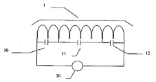
일반적으로, 유도 가열 시스템은 전원, 유도 코일, 가열될 물체, 및 필요한 경우 코일의 자계로부터 에너지를 흡수하여 이 에너지를 가열될 물체에 재전달하는 "서셉터"를 포함한다. 시스템은 가열될 물체 또는 (존재하는 경우) 서셉터내를 순환하는 전류의 유도 원리에 기초하여 동작한다. 일반적으로, 가열될 물체가 적절한 전도성을 가지고 있지 않거나(따라서, 유도된 가열 전류를 서포트할 수 없는 경우) 또는 그러한 전류에 의해 손상될 수 있는 경우에 서셉터가 사용된다. 커다란 물체에서의 실질적인 가열 또는 작은 물체의 급속한 가열을 얻기 위해서는 큰 전류가 요구된다. 큰 전류를 갖는 코일은 그 근방에 큰 자계를 생성하고 이 자계 내에 에너지가 저장된다. 이 자계의 대부분은 서셉터 내 또는 가열될 물체 내에 유도된 전류에 의해 상쇄될 수 있지만, 저장하는데 충분한 정도의 상당한 에너지가 남아있게 된다. 이러한 에너지는 전기적으로 인덕턴스로서 나타내는데, 인덕터내에 큰 전류를 생성하기 위해서 고전압을 요구한다. 고전압과 대전류의 존재는, 전류가 그 각 사이클마다 감쇠할 때 시스템 내의 어디인가에 자계에 의해 발현되는 에너지가 저장되지 않는다면 전원으로부터 상당한 전력을 요구한다. 전기 용량(capacitance)이 코일과 직렬 또는 병렬로 배치되고, 또한 교류전류의 주파수가 적절히 선택되는 경우, 에너지가 용량내에 저장될 수 있어서 커패시터가 없는 경우에 요구되는 것 보다 훨씬 작게 전원을 제작할 수 있다. 따라서, 유도 가열 시스템은 코일이 커패시터와 "공진"되도록 배치되는 것이 전형적이다. 즉, 커패시터는 전기 회로가 전원의 동작 주파수에서 공진하도록 하는 값을 가지며 직렬 또는 병렬로 배치된다. 그러한 배열이 도 1에서 도시되어 있다. 여기서 코일(1)은 이 코일과 병렬로 접속된 커패시터(2)를 갖는다. 저항(3)은 가열된 물체 또는 서셉터 및 코일과 커패시터에서의 에너지 손실로부터 기인하는 등가 저항을 나타낸다. 에너지는 코일 및 커패시터에 교대로 저장되는데, 이 에너지는 코일과 커패시터 사이에서 전원의 교류출력의 매 사이클마다 두번씩 교환된다. 이 시스템에 의해 전원은 공진 회로의 손실만을 공급할 수 있는데, 공진 회로의 손실은 원리적으로는 가열된 물체(존재한다면, 서셉터) 및 코일 자체에서 손실되는 에너지이며, 코일은 그 코일을 통해 흐르는 전류에 의해 가열된다. "양호도(quality factor)"를 나타내는 "Q"는 Generally, an induction heating system includes a power source, an induction coil, an object to be heated, and a "susceptor" which absorbs energy from the magnetic field of the coil and, if necessary, re-delivers this energy to the object to be heated. The system operates based on the principle of induction of an object to be heated or a current circulating in the susceptor (if present). In general, susceptors are used where the object to be heated does not have adequate conductivity (and therefore cannot support the induced heating current) or may be damaged by such current. Large currents are required to obtain substantial heating of large objects or rapid heating of small objects. Coils with large currents generate large magnetic fields in the vicinity of which energy is stored. Most of this magnetic field can be canceled by currents induced in the susceptor or in the object to be heated, but a significant amount of energy remains to store. This energy is represented electrically as an inductance, which requires a high voltage to generate a large current in the inductor. The presence of high voltages and large currents requires significant power from the power supply unless the energy expressed by the magnetic field is stored somewhere in the system when the current decays each cycle. If the capacitance is placed in series or in parallel with the coil, and the frequency of the alternating current is properly selected, energy can be stored in the capacity, making the power supply much smaller than required in the absence of a capacitor. . Thus, induction heating systems are typically arranged such that the coil is "resonant" with the capacitor. That is, the capacitors have a value that causes the electrical circuit to resonate at the operating frequency of the power supply and are arranged in series or in parallel. Such an arrangement is shown in FIG. 1. The

이며, 이 때 L은 코일(1)의 인덕턴스, R은 등가 저항(3), 그리고 ω는 각주파수(단위는 Hz로서 주파수의 2pi 배)로서, 공진조건이 성립하는 경우에, 커패시터(2)의 용량 C를 다음의 공식에 따라서 선택함으로써, 전류(4)는 전류(5)보다 Q배 높게 된다. Where L is the inductance of the

통상 Q는 유도 가열 시스템의 경우 대략 10이고, 그래서 전원은 순환 전류의 1/10만을 공급할 필요가 있다. 반대로 보면, 이러한 방법에 의해 전원의 10배의 코일 전류를 쉽게 얻을 수 있다. 이러한 "공진" 시스템은 주지되어 있으며 반도체 처리 시스템을 포함하는 유도 가열 응용분야에서 수년동안 성공적으로 사용되어 오고 있다. Normally Q is approximately 10 for an induction heating system, so the power source only needs to supply 1/10 of the circulating current. On the contrary, the coil current of 10 times the power can be easily obtained by this method. Such "resonant" systems are well known and have been used successfully for many years in induction heating applications, including semiconductor processing systems.
현 상황에서, 이런 방법으로 서셉터의 복수 영역을 가열하여 높은 수준의 온도 균일성을 제공하는 것이 바람직하다. 이를 위하여 복수의 코일, 즉, 코일의 여러 부분에서의 전류가 달라지도록 하는 전기적 탭을 갖는 코일이 이용된다. 코일의 다른 부분에서의 다른 전류는 서셉터 또는 가열될 물체의 물리적 영역내에 다른 전류를 유도하여, 선택적으로 그리고 정확한 양으로 상기 영역에 에너지를 축적할 수 있는 능력을 부여한다. 하지만, 코일의 여러 부분의 상호 결합(mutual coupling)때문에 시스템이 공진하게 될 때 문제가 발생한다. In the present situation, it is desirable to heat multiple regions of the susceptor in this manner to provide a high level of temperature uniformity. For this purpose a plurality of coils, i.e. coils with electrical taps which allow currents in different parts of the coil to be varied, are used. Different currents in different parts of the coil induce other currents in the physical area of the susceptor or object to be heated, giving them the ability to accumulate energy in the area selectively and in precise amounts. However, problems arise when the system resonates due to the mutual coupling of the various parts of the coil.
전류가 다중 섹션 코일중 하나의 섹션에 유도될 때, 그 전류에 의해 자계가 생성된다. 자력선은 가열될 물체 및 (존재한다면) 서셉터를 차단하여, 다중 섹션 코일의 상기 섹션과 관련된 서셉터 또는 가열될 물체의 물리적 영역에 소망하는 순환전류 및 그 결과 얻어지는 원하는 가열이 생성된다. 그러나, 이러한 자력선은 코일의 다른 부분과도 교차하여 그 다른 코일 세그먼트내에 전류가 유도되도록 하는데, 가열될 물체 또는 (존재한다면) 서셉터의 원하지 않는 물리적 영역에 가열이 일어난다. 모든 자력선이 코일의 다른 부분과 교차하는 것이 아니므로, 가열은 소망하는 영역(즉, 코일의 구동부와 관련된 영역)에서 가장 클 것이지만, 다른 영역에서의 소망하지 않는 가열에 의해 온도 분포를 정확하게 제어하는 능력이 방해받는다. 가열될 물체 또는 서셉터가 코일로부터 더 멀리 이동하면, 코일의 여러 세그먼트 사이의 상호작용이 증가하고 여러 영역에 축적된 에너지를 제어하는 능력은 열화된다. When a current is induced in one section of a multi-section coil, a magnetic field is created by that current. The magnetic field lines block the object to be heated and (if present) the susceptor, producing the desired circulating current and the resulting desired heating in the physical region of the susceptor or object to be heated associated with the section of the multi-section coil. However, these lines of magnetic force also intersect other parts of the coil and cause current to be induced in that other coil segment, causing heating to occur in the object to be heated or in the unwanted physical region of the susceptor (if present). Since not all magnetic lines of force cross the other part of the coil, heating will be the largest in the desired area (i.e., the area associated with the drive of the coil), but precisely control the temperature distribution by undesired heating in other areas. Ability is hindered As the object or susceptor to be heated moves further away from the coil, the interaction between the various segments of the coil increases and the ability to control the energy accumulated in the various regions deteriorates.
코일의 소망하는 세그먼트를 통해서만 전원 전류가 흐르도록 전원을 코일의 한 탭으로부터 다른 탭으로 스위칭하는 전자 스위치를 사용하는 것이 실용적일 수 있다. 도 2에는, 공진 커패시터를 갖는 탭형 코일과 스위치를 갖는 전원(17, 18, 19)이 도시되어 있다. 스위치(13, 14)가 닫히면, 전원(17)이 코일(1)의 코일 섹션(7)에 접속된다. 스위치(15, 16)가 개방되어 있는 경우에도, 코일 섹션(8,9)의 권선을 통과하는 코일 섹션(7)의 자력선에 의해 야기되는, 코일 섹션(8, 9)사이의 상호결합 및 코일 섹션(7, 9) 사이의 상호결합은 그 결합된 코일(8,9)내에 순환전류를 생성할 수 있다. 그 각각의 코일 섹션과 공진 루프를 형성하는 코일 섹션(8, 9)를 가르지르는 커패시터(11, 12) 때문에 상기 전류가 흐를 수 있다. 도 3에 도시된 바와 같이 스위치 위치를 이동시켜서 구동되지 않은 코일 섹션 내에 유도된 순환 전류를 차단할 수 있지만, 이는 스위치가 전체 순환 전류를 운반한다는 것을 의미라는데, 여기서 전체 순환전류는 상술한 바와 같이 공진의 다중화 효과로 인해 수천 암페어가 될 수 있다. 또한, 실제적인 이유로, 커패시터를 코일에 매우 근접하게 배치하여 커패시터와 코일 사이의 리드선의 인덕턴스를 낮출 필요가 필요가 있을 수 잇다. 이것이 행해지지 않으면, 대전류에 의해 고전압이 커패시터를 가로질러 나타나게 되며 또한 접속 리드를 둘러싸고 있는 높은 자계로 인해 국부적 도전표면에 손실이 발생하게 된다. 이것에 의해 적합한 우수한 스위치가 있을 지라도, 스위칭 장치를 장착할 공간이 남지 않을 수도 있다. It may be practical to use an electronic switch to switch the power supply from one tap of the coil to another so that power current flows only through the desired segment of the coil. 2 shows a
도 2의 회로가 상기 섹션의 부적절한 분리를 제공하고, 따라서 가열될 물체 또는 (존재한다면) 서셉터내의 에너지 축적에 대한 부적절한 제어를 제공하며 또한 도 3의 회로가 반도체 스위치의 비실용적인 선택과 위치를 요구하는 경우에는, 다른 접근이 필요하다. 이러한 경우에, 필요한 것은 에너지를 유도 가열 코일의 개개의 섹션에 선택적으로 축적하는 방법인데, 그러한 방법은 각 섹션에 축적된 에너지의 양에 대해 세밀한 제어를 가능하게 하는 한편, 코일의 여러 섹션 사이에서의 재빠른 스위칭을 가능하게 하여, 전체적으로 가열될 물체의 세밀하고 정확한 제어를 가능하게 한다. The circuit of FIG. 2 provides inadequate separation of the section, thus providing inadequate control over the accumulation of energy in the object to be heated or (if present) the susceptor and also the circuit of FIG. If required, another approach is required. In this case, what is needed is a method of selectively accumulating energy in individual sections of the induction heating coil, which allows fine control over the amount of energy accumulated in each section, while between the different sections of the coil. This enables quick switching of the components, enabling precise and accurate control of the object to be heated as a whole.
또한, 다중영역 유도 코일 및 '스폿' 온도 감시 시스템을 이용하여 정확한 양의 에너지를 웨이퍼의 영역들에 축적할 수도 있다. 상기 다중영역 코일은 웨이퍼를 차례로 가열하는 서셉터의 여러 부분들에 정확한 양의 에너지를 효과적으로 전달하도록 별도로 전력 공급되어야 하는 몇개의 섹션을 포함할 수 있다. 그러나, 상기 코일 세크멘트들에 대하여 별도로 전력을 공급하는 것은 본 명세서에서 설명하는 이유때문에 전원 설계의 새로운 접근을 필요로 한다.In addition, a multi-domain induction coil and 'spot' temperature monitoring system may be used to accumulate the correct amount of energy in areas of the wafer. The multi-zone coil may include several sections that must be separately powered to effectively deliver the correct amount of energy to the various parts of the susceptor that in turn heats the wafer. However, separately powering the coil segments requires a new approach to power design for the reasons described herein.
일 실시예에서는, 도 4에 도시된 바와 같이, 코일(1)이 탭에 의해 섹션들(7,8,9)로 분할되어 있다. 커패시터들(10,11,12)은 각각 코일 섹션들(7,8,9)과 병렬로 배치되며, 주파수 응답 전원(20)은 전체 코일(1)과 병렬로 배치된다. 커패시터(10,11,12)의 용량치는 각각 주파수(f1,f2,f3)에서 코일 섹션들(7,8,9)과 공진하도록 선택된다. 즉, 커패시터(10)의 용량은 다음 식에 따라 선택된다 :In one embodiment, as shown in FIG. 4, the

상기 식에서, L7은 코일 섹션(7)의 인덕턴스이고 C10은 커패시터(10)의 용량이다.In the above formula, L 7 is the inductance of the
커패시터(11,12)의 용량은 유사하게 코일 섹션(8)과 커패시터(11)가 바람직하게는 주파수 f1이 아닌 주파수 f2에서 공진하며 코일 부분(9)과 커패시터(12)는 바람직하게는 주파수 f1 및 f2와 다른 주파수 f3에서 공진하도록 선택된다. 물론, 더 많은 탭들이 코일상에 제공될 수 있어서 상기 코일 섹션들이 더 많게 또는 더 적게 형성되고 그리고 상기 섹션 각각이 다른 주파수에서 공진하도록 할 수 있다.The capacitance of the
코일(1) 섹션들 각각이 다른 주파수에서 공진하는 상태로, 주파수들(f1,f2,f3)에서 전원 공급부(20)의 주파수를 선택하여 각각 코일 섹션들(7,8,9) 내에 전류를 여기시킬 수 있다. 만약 제어 시스템이 그와 같이 배치되어 있으면, 전원의 주파수는 f1에서 f2, f3로 그리고 다시 f1으로 연속적으로 순환되도록 할 수 있다. 따라서, 각 코일 세그멘트는 차례대로 여기되며, 가열될 물체 또는 서셉터의 대응하는 영역들에 차례대로 에너지를 선택적으로 제공할 수 있다. With each of the
나머지 영역들에 대해 각 영역들에 공급되는 전력을 제어하기 위해 상기한 배치에 적어도 여러가지 사용가능한 방법들이 있다. 일 실시예에서는, 각 주파수에서 전원 공급이 정지되는 시간을 변화시켜서 각 사이클에서 각 영역에 축적되는 에너지를 결정할 수 있다. 다른 실시예에서는, 각 주파수에서 전원 공급이 정지되는 기간중에 전원에 의해 공급되는 전력을 변화시킬 수 있는 한편, 임의의 주어진 주파수에서 전원 공급이 정지되는 기간은 일정하게 유지될 수 있다. 또 다른 실시예에서는, 전원 공급의 주파수가 정확한 공진으로부터 벗어나서 공진 소자들 내의 순환전류에 영향을 미칠 수 있는 한편, 각 영역에 대한 전력과 시간은 일정하게 고정된다. 이러한 제어 방법은, 사이클의 각 스텝에서의 정지 시간, 사이클의 각 스텝중에 공급되는 전력, 및 사이클의 각 스텝에서 발생되는 정확한 주파수(이들 모두는 원하는 에너지(즉, 온도) 프로파일을 얻도록 적절히 변화딜 수 있음)와 조합할 수 있음은 명백하다.There are at least various methods available in the above arrangement to control the power supplied to each of the remaining areas. In one embodiment, the time at which the power supply is stopped at each frequency may be varied to determine the energy accumulated in each region in each cycle. In another embodiment, the power supplied by the power source may be changed during the period of stopping power supply at each frequency, while the period of stopping power supply at any given frequency may be kept constant. In yet another embodiment, the frequency of the power supply can deviate from the correct resonance and affect the circulating current in the resonant elements, while the power and time for each region are kept constant. This control method is appropriately varied to obtain the stopping time at each step of the cycle, the power supplied during each step of the cycle, and the exact frequency generated at each step of the cycle, all of which will yield the desired energy (ie, temperature) profile. It can be obvious that the combination thereof).
당업자라면, 주어진 전력량에 대하여 전원 공급부로부터 전압 또는 전류가 과잉으로 공급될 가능성을 방지하기 위하여 전원의 전압 및 전류가 서로 거의 위상이 같도록 각 스텝에서 주파수를 유지하는 것이 요구될 수 있는 점을 알 수 있을 것이다. 소정의 경우에 이것이 바람직한 정도로, 주파수를 조정함에 의해 전력을 제어할 능력이 제한될 수 있고, 원하는 온도 또는 에너지 프로파일을 얻기 위해서는 각 스텝에서의 타이밍 또는 전력 레벨의 조정이 필요할 수 있다.One skilled in the art knows that for a given amount of power it may be required to maintain the frequency at each step so that the voltage and current of the power supply are approximately in phase with each other to prevent the possibility of excessive supply of voltage or current from the power supply. Could be. In some cases, to the extent that this is desirable, the ability to control power by adjusting the frequency may be limited, and adjustment of timing or power levels at each step may be necessary to achieve the desired temperature or energy profile.
또한, 도 2 및 도 4의 방법을 조합할 수도 있다. 당업자라면 전원(20)의 주파수 범위가 분할되는 불연속적인 주파수 대역들의 수에 제한이 있을 수도 있음을 이해할 수 있을 것이다. 이 제한은 전원으로부터의 에너지가 상기한 바와 같이 회로 "Q"에 의해 결정되는 작은 범위의 주파수들의 공진 섹션에 공급되는 사실에 의해 설정된다. 회로 "Q"를 10 또는 20 보다 훨씬 크게 설정하는 것이 불가능 또는 바람직하지 않기 때문에, 10의 회로 "Q"를 갖는 섹션은 대략 (1-1/Q)fr<f<(1+1/Q)fr에 의해 한정되는 주파수 대역에서 에너지를 흡수하게 되는데, 상기 식에서 fr은 코일의 섹션 및 이에 대응하는 커패시터의 공진 주파수이다. 따라서, 구동되는 섹션 근방의 공진 주파수를 갖는 다른 섹션들의 원치 않는 여기를 방지하도록 각 코일 섹션의 공진 주파수를 충분히 분리시킬 필요가 있다.It is also possible to combine the methods of FIGS. 2 and 4. Those skilled in the art will appreciate that there may be a limit to the number of discrete frequency bands in which the frequency range of the
영역들의 수가 많고 상기 영역들 모두를 커버하기에는 전원(20)의 주파수 범위가 불충분한 경우, 도 2 및 도 4에 나타낸 방식들을 조합할 수 있다. 즉, 도 5에 도시된 바와 같이 2개(또는 그 이상)의 코일(21,22)을 배치할 수 있는데, 각 ㅋ코일은 도 2 또는 도 4의 방식으로 탭(tap)되지만, 스위치(23,24)에 의해 전원(20)에서 분리됨으로써 전원(20)이 한번에 코일들(21,22)중 하나에만 접속되도록 할 수 있다. 이 배치에 의해, 제한된 주파수 범위를 갖는 단일 주파수 응답 전원을 이용하여 복수의 영역들을 고정확도로 제어할 수 있게 된다.If the number of regions is large and the frequency range of the
Claims (101)
Applications Claiming Priority (3)
| Application Number | Priority Date | Filing Date | Title |
|---|---|---|---|
| US5202997P | 1997-07-09 | 1997-07-09 | |
| US60/052,029 | 1997-07-09 | ||
| PCT/US1998/014125 WO1999003308A1 (en) | 1997-07-09 | 1998-07-08 | Frequency selected, variable output inductor heater system and method |
Publications (2)
| Publication Number | Publication Date |
|---|---|
| KR20010021699A KR20010021699A (en) | 2001-03-15 |
| KR100574414B1 true KR100574414B1 (en) | 2006-04-27 |
Family
ID=21974964
Family Applications (1)
| Application Number | Title | Priority Date | Filing Date |
|---|---|---|---|
| KR1020007000258A KR100574414B1 (en) | 1997-07-09 | 1998-07-08 | Frequency selected, variable output inductor heater system and method |
Country Status (5)
| Country | Link |
|---|---|
| US (1) | US6316754B1 (en) |
| EP (1) | EP0995340A1 (en) |
| JP (1) | JP2001509634A (en) |
| KR (1) | KR100574414B1 (en) |
| WO (1) | WO1999003308A1 (en) |
Cited By (1)
| Publication number | Priority date | Publication date | Assignee | Title |
|---|---|---|---|---|
| WO2017023008A1 (en) * | 2015-08-04 | 2017-02-09 | 삼성전자주식회사 | Induction heating device and control method therefor |
Families Citing this family (25)
| Publication number | Priority date | Publication date | Assignee | Title |
|---|---|---|---|---|
| GB2340681B (en) * | 1998-08-14 | 2003-07-30 | Mars Inc | Oscillators |
| US7212414B2 (en) * | 1999-06-21 | 2007-05-01 | Access Business Group International, Llc | Adaptive inductive power supply |
| JP3839228B2 (en) | 2000-07-31 | 2006-11-01 | 株式会社神戸製鋼所 | Raw tire preheating method and apparatus |
| EP1194008B1 (en) * | 2000-09-29 | 2010-01-20 | BSH Bosch und Siemens Hausgeräte GmbH | Inverter circuit and its method of controlling |
| WO2003003399A1 (en) * | 2001-06-27 | 2003-01-09 | Koninklijke Philips Electronics N.V. | Method and device for evaporating a getter material in a vacuum tube |
| JP2003017237A (en) * | 2001-06-28 | 2003-01-17 | Harison Toshiba Lighting Corp | Induction heating roller device, fixing device and image forming device |
| JP2004013016A (en) * | 2002-06-10 | 2004-01-15 | Toshiba Tec Corp | Fixing device and image forming apparatus |
| JP3834540B2 (en) | 2002-10-10 | 2006-10-18 | 株式会社神戸製鋼所 | Raw tire preheating method and apparatus |
| JP4422422B2 (en) * | 2003-03-25 | 2010-02-24 | 東芝テック株式会社 | Fixing device |
| WO2005008876A2 (en) * | 2003-07-09 | 2005-01-27 | Board Of Regents, The University Of Texas System | Methods and systems for simultaneous multiple frequency voltage generation |
| GB0324831D0 (en) * | 2003-10-24 | 2003-11-26 | British Nuclear Fuels Plc | Induction heating |
| US6875966B1 (en) | 2004-03-15 | 2005-04-05 | Nexicor Llc | Portable induction heating tool for soldering pipes |
| CN101371618B (en) * | 2006-01-09 | 2012-12-05 | 应达公司 | Induction heating apparatus for strip materials with variable parameters |
| JP5202839B2 (en) * | 2006-12-25 | 2013-06-05 | 東京エレクトロン株式会社 | Film forming apparatus and film forming method |
| US8884201B2 (en) * | 2008-09-15 | 2014-11-11 | The Boeing Company | Systems and methods for fabrication of thermoplastic components |
| JP5350747B2 (en) | 2008-10-23 | 2013-11-27 | 東京エレクトロン株式会社 | Heat treatment equipment |
| DE102009048490A1 (en) * | 2009-09-24 | 2011-04-07 | E.G.O. Elektro-Gerätebau GmbH | Method for adjusting a heat output of an induction heater and associated induction heater |
| US9089007B2 (en) * | 2012-04-27 | 2015-07-21 | Applied Materials, Inc. | Method and apparatus for substrate support with multi-zone heating |
| CN104372309B (en) * | 2013-08-12 | 2018-09-14 | 北京北方华创微电子装备有限公司 | Heating device, reaction chamber and plasma processing device |
| US9789421B2 (en) | 2014-06-11 | 2017-10-17 | Corner Star Limited | Induction heater system for a fluidized bed reactor |
| GB201511349D0 (en) | 2015-06-29 | 2015-08-12 | Nicoventures Holdings Ltd | Electronic aerosol provision systems |
| GB201511359D0 (en) | 2015-06-29 | 2015-08-12 | Nicoventures Holdings Ltd | Electronic vapour provision system |
| GB201511358D0 (en) | 2015-06-29 | 2015-08-12 | Nicoventures Holdings Ltd | Electronic aerosol provision systems |
| DE102016119328A1 (en) | 2016-10-11 | 2018-04-12 | Osram Opto Semiconductors Gmbh | Heating device, method and system for the production of semiconductor chips in the wafer composite |
| CN106947954B (en) * | 2017-04-27 | 2019-06-18 | 京东方科技集团股份有限公司 | A kind of preparation method of vapor deposition apparatus and film |
Citations (1)
| Publication number | Priority date | Publication date | Assignee | Title |
|---|---|---|---|---|
| US4755648A (en) * | 1985-12-12 | 1988-07-05 | Fuji Electric Co., Ltd. | Cyclical, multiple frequency high-frequency induction heating apparatus |
Family Cites Families (4)
| Publication number | Priority date | Publication date | Assignee | Title |
|---|---|---|---|---|
| US2669647A (en) | 1952-06-13 | 1954-02-16 | Gen Engineering Company Canada | Dual frequency induction heating apparatus |
| US4093839A (en) | 1976-04-02 | 1978-06-06 | Ajax Magnethermic Corporation | Apparatus and method for inductively heating metallic tubing having an upset portion |
| US4506131A (en) | 1983-08-29 | 1985-03-19 | Inductotherm Industries Inc. | Multiple zone induction coil power control apparatus and method |
| GB8505811D0 (en) * | 1985-03-06 | 1985-04-11 | Bekaert Sa Nv | Induction heating |
-
1998
- 1998-07-08 KR KR1020007000258A patent/KR100574414B1/en not_active IP Right Cessation
- 1998-07-08 WO PCT/US1998/014125 patent/WO1999003308A1/en not_active Application Discontinuation
- 1998-07-08 US US09/462,402 patent/US6316754B1/en not_active Expired - Fee Related
- 1998-07-08 EP EP98933258A patent/EP0995340A1/en not_active Withdrawn
- 1998-07-08 JP JP2000501636A patent/JP2001509634A/en active Pending
Patent Citations (1)
| Publication number | Priority date | Publication date | Assignee | Title |
|---|---|---|---|---|
| US4755648A (en) * | 1985-12-12 | 1988-07-05 | Fuji Electric Co., Ltd. | Cyclical, multiple frequency high-frequency induction heating apparatus |
Cited By (4)
| Publication number | Priority date | Publication date | Assignee | Title |
|---|---|---|---|---|
| WO2017023008A1 (en) * | 2015-08-04 | 2017-02-09 | 삼성전자주식회사 | Induction heating device and control method therefor |
| KR20170016608A (en) * | 2015-08-04 | 2017-02-14 | 삼성전자주식회사 | Induction heating apparatus and controlling method thereof |
| US11249119B2 (en) | 2015-08-04 | 2022-02-15 | Samsung Electronics Co., Ltd. | Induction heating apparatus and controlling method thereof |
| KR102368372B1 (en) * | 2015-08-04 | 2022-02-28 | 삼성전자주식회사 | Induction heating apparatus and controlling method thereof |
Also Published As
| Publication number | Publication date |
|---|---|
| KR20010021699A (en) | 2001-03-15 |
| WO1999003308A1 (en) | 1999-01-21 |
| EP0995340A1 (en) | 2000-04-26 |
| US6316754B1 (en) | 2001-11-13 |
| JP2001509634A (en) | 2001-07-24 |
Similar Documents
| Publication | Publication Date | Title |
|---|---|---|
| KR100574414B1 (en) | Frequency selected, variable output inductor heater system and method | |
| JP3160559B2 (en) | Substrate heating apparatus and substrate heating method | |
| US10096454B2 (en) | Plasma processing apparatus | |
| KR102062415B1 (en) | Current peak spreading schemes for multiplexed heated array | |
| KR102315349B1 (en) | Pixelated temperature controlled substrate support assembly | |
| US11694881B2 (en) | Stage and plasma processing apparatus | |
| KR102302723B1 (en) | Tunable temperature controlled substrate support assembly | |
| US9530619B2 (en) | Plasma processing apparatus and filter unit | |
| CN113013014A (en) | Plasma processing apparatus, substrate processing apparatus, and filter apparatus | |
| EP1744345A1 (en) | Multi chamber plasma process system | |
| US9754766B2 (en) | Plasma processing apparatus | |
| US6031211A (en) | Zone heating system with feedback control | |
| US20120138599A1 (en) | Semiconductor substrate heat treatment apparatus | |
| US20170373659A1 (en) | Method for designing filter | |
| US20220148859A1 (en) | Multi-zone heating apparatus, bottom electrode assembly, plasma processing apparatus, and temperature adjusting method | |
| US11276601B2 (en) | Apparatus and methods for manipulating power at an edge ring in a plasma processing device | |
| KR20170019321A (en) | Magnetized edge ring for extreme edge control | |
| TWI797519B (en) | Multi-zone electrostatic chuck | |
| JP2002217278A (en) | Plasma cvd device | |
| JP2024014205A (en) | Plasma processing equipment and temperature control method | |
| CN114446755A (en) | Apparatus for processing substrate and method for processing substrate | |
| TW202226444A (en) | Electrostatic chuck assembly for plasma processing apparatus | |
| KR20200135603A (en) | A substrate treating apparatus including a filter unit and the filter unit and a substrate treating method | |
| JP2000111609A (en) | Temperature adjusting stage of board and power circuit therefor |
Legal Events
| Date | Code | Title | Description |
|---|---|---|---|
| A201 | Request for examination | ||
| E902 | Notification of reason for refusal | ||
| E902 | Notification of reason for refusal | ||
| E701 | Decision to grant or registration of patent right | ||
| GRNT | Written decision to grant | ||
| LAPS | Lapse due to unpaid annual fee |