KR100259287B1 - Apparatus for controlling gray scale level of display device - Google Patents
Apparatus for controlling gray scale level of display device Download PDFInfo
- Publication number
- KR100259287B1 KR100259287B1 KR1019970069285A KR19970069285A KR100259287B1 KR 100259287 B1 KR100259287 B1 KR 100259287B1 KR 1019970069285 A KR1019970069285 A KR 1019970069285A KR 19970069285 A KR19970069285 A KR 19970069285A KR 100259287 B1 KR100259287 B1 KR 100259287B1
- Authority
- KR
- South Korea
- Prior art keywords
- gray scale
- scale level
- voltage source
- segment
- level control
- Prior art date
Links
Images


Classifications
-
- G—PHYSICS
- G09—EDUCATION; CRYPTOGRAPHY; DISPLAY; ADVERTISING; SEALS
- G09G—ARRANGEMENTS OR CIRCUITS FOR CONTROL OF INDICATING DEVICES USING STATIC MEANS TO PRESENT VARIABLE INFORMATION
- G09G3/00—Control arrangements or circuits, of interest only in connection with visual indicators other than cathode-ray tubes
- G09G3/04—Control arrangements or circuits, of interest only in connection with visual indicators other than cathode-ray tubes for presentation of a single character by selection from a plurality of characters, or by composing the character by combination of individual elements, e.g. segments using a combination of such display devices for composing words, rows or the like, in a frame with fixed character positions
- G09G3/06—Control arrangements or circuits, of interest only in connection with visual indicators other than cathode-ray tubes for presentation of a single character by selection from a plurality of characters, or by composing the character by combination of individual elements, e.g. segments using a combination of such display devices for composing words, rows or the like, in a frame with fixed character positions using controlled light sources
- G09G3/12—Control arrangements or circuits, of interest only in connection with visual indicators other than cathode-ray tubes for presentation of a single character by selection from a plurality of characters, or by composing the character by combination of individual elements, e.g. segments using a combination of such display devices for composing words, rows or the like, in a frame with fixed character positions using controlled light sources using electroluminescent elements
- G09G3/14—Semiconductor devices, e.g. diodes
-
- G—PHYSICS
- G09—EDUCATION; CRYPTOGRAPHY; DISPLAY; ADVERTISING; SEALS
- G09G—ARRANGEMENTS OR CIRCUITS FOR CONTROL OF INDICATING DEVICES USING STATIC MEANS TO PRESENT VARIABLE INFORMATION
- G09G2320/00—Control of display operating conditions
- G09G2320/02—Improving the quality of display appearance
- G09G2320/0271—Adjustment of the gradation levels within the range of the gradation scale, e.g. by redistribution or clipping
-
- G—PHYSICS
- G09—EDUCATION; CRYPTOGRAPHY; DISPLAY; ADVERTISING; SEALS
- G09G—ARRANGEMENTS OR CIRCUITS FOR CONTROL OF INDICATING DEVICES USING STATIC MEANS TO PRESENT VARIABLE INFORMATION
- G09G2330/00—Aspects of power supply; Aspects of display protection and defect management
- G09G2330/02—Details of power systems and of start or stop of display operation
- G09G2330/021—Power management, e.g. power saving
Abstract
Description
본 발명은 디스플레이 소자에 관한 것으로, 특히 디스플레이 소자의 그레이 스케일 레벨(gray scale level) 제어장치에 관한 것이다.BACKGROUND OF THE INVENTION 1. Field of the Invention The present invention relates to display elements, and more particularly to a gray scale level control device for display elements.
일반적으로 디스플레이 소자에서의 그레이 스케일 레벨이란 백에서 흑까지의 색표를 그 목적에 상응하는 방식에 따라 나열한 무체색의 색표 계열을 의미한다.In general, a gray scale level in a display device refers to a colorless color table series in which the color tables from white to black are arranged in a manner corresponding to the purpose.
예를 들면 흑백 텔레비젼의 경우에 이 그레이 스케일을 사용하면 어떤 색이 흑백화면에서 어떻게 표시되는지를 알 수 있다.For example, in the case of black and white television, using this gray scale shows what colors are displayed on the black and white screen.
이와 같은 그레이 스케일 레벨을 설정하는 방법에 있어서는 디스플레이 소자마다 약간씩 다르다.The method of setting such a gray scale level is slightly different for each display element.
그 디스플레이 소자들 중에서 정전류원을 사용하는 유기전계발광소자의 그레이 스케일 레벨 설정방법을 한 예를 들어 설명하면 다음과 같다.An example of the gray scale level setting method of the organic light emitting display device using the constant current source among the display elements will be described as follows.
유기전계발광소자에서는 일반적으로 일정한 주파수를 가지는 교류파형을 이용하여 PWM(Pulse Width Modulation)제어를 할 수 있는 제어부를 구동회로에 첨가하는 방식을 많이 사용하고 있다.BACKGROUND OF THE INVENTION In general, organic light emitting diodes use a method of adding a control unit to a driving circuit to control a pulse width modulation (PWM) using an AC waveform having a constant frequency.
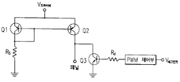
도 1은 종래 기술에 따른 유기전계발광소자의 그레이 스케일 레벨을 조절하는 회로를 보여주는 도면으로서, 도 1에 도시된 바와 같이, 소자의 세그먼트(segment) 구동부에 PWM 제어부를 첨가한 방식이다.FIG. 1 is a diagram illustrating a circuit for adjusting a gray scale level of an organic light emitting diode according to the prior art. As shown in FIG. 1, a PWM controller is added to a segment driving part of a device.
이 방식은 세그먼트의 신호에 따라 세그먼트 구동부에 첨가된 PWM 제어부를 조절함으로써, 소자에 인가되는 신호의 펄스 폭을 조절하여 그레이 스케일 레벨을 설정한다.This method sets the gray scale level by adjusting the pulse width of the signal applied to the device by adjusting the PWM control unit added to the segment driver in accordance with the signal of the segment.
그러나, 이러한 방식은 응답시간의 문제를 안고 있다.However, this method has a problem of response time.
일반적으로 유기전계발광소자의 응답시간은 수 μ 초에서 수백 n초 정도인 것으로 알려져 있는데, 이는 X-Y 심플 매트릭스(simple matrix)구조인 경우에 화면이 커지게 되면 PWM 제어시 응답시간과 그레이 스케일 레벨 사이에는 심각한 문제를 일으킬 수 있게 된다.In general, the response time of organic light emitting diodes is known to be several μs to several hundreds of ns. In the case of the XY simple matrix structure, when the screen becomes large, the response time between the PWM control and the gray scale level is increased. Can cause serious problems.
즉, 소자에 인가되는 펄스 폭이 너무 짧은 경우에는 소자의 응답시간이 그 펄스 폭에 적절히 대응하지 못하는 문제가 발생되는 것이다.That is, when the pulse width applied to the device is too short, a problem occurs that the response time of the device does not adequately correspond to the pulse width.
그러므로 이러한 문제를 해결하기 위해서는 세그먼트 구동부로 인가되는 신호를 적절히 조절하여 PWM 제어부를 조절하는 방법을 이용하든지, 아니면 세그먼트 구동부에서 PWM 제어부로 인가되는 신호를 적절히 조절하는 방법을 이용해야 한다.Therefore, in order to solve this problem, it is necessary to use a method of adjusting the PWM controller by appropriately adjusting the signal applied to the segment driver or a method of appropriately adjusting the signal applied to the PWM controller from the segment driver.
그러나, 이는 회로부의 크기를 크게 증가시키는 원인이 되며, 그것은 바로 원가 상승의 요인과 직결이 되기 때문에 실용화에는 적합하지 않다.However, this causes a large increase in the size of the circuit portion, which is directly connected to the factor of the cost increase, which is not suitable for practical use.
종래 기술에 따른 디스플레이 소자의 그레이 스케일 레벨 제어장치에 있어서는 다음과 같은 문제점이 있었다.The gray scale level control device of the display device according to the prior art has the following problems.
디스플레이의 화면이 커지게 되면 PWM 제어시 소자에 인가되는 펄스 폭이 짧으면 소자의 응답시간이 이를 따라가지 못하여 소자의 화면 구동이 원활하지가 않으며, 이를 해결하기 위해서는 회로부의 크기가 증가되므로 원가가 상승된다.If the screen of the display becomes large, if the pulse width applied to the device during PWM control is short, the response time of the device does not follow this, and the screen of the device is not smoothly driven. do.
본 발명은 이와 같은 문제를 해결하기 위한 것으로, 디스플레이 소자의 응답시간에 관계없이 간단하게 그레이 스케일 레벨을 조절할 수 있는 디스플레이 소자의 그레이 스케일 레벨 제어장치를 제공하는데 그 목적이 있다.An object of the present invention is to provide a gray scale level control apparatus for a display device capable of simply adjusting the gray scale level regardless of the response time of the display device.
제1도는 종래 기술에 따른 디스플레이 소자의 그레이 스케일 레벨 제어장치의 구성을 보여주는 회로도1 is a circuit diagram showing the configuration of a gray scale level control apparatus for a display element according to the prior art.
제2도는 본 발명에 따른 디스플레이 소자의 그레이 스케일 레벨 제어장치의 구성을 보여주는 회로도2 is a circuit diagram showing the configuration of a gray scale level control device for a display element according to the present invention.
제3도는 최대 전류가 흐를 때의 전류 제한 저항의 회로3 shows the circuit of the current limiting resistor when the maximum current flows.
제4도는 최소 전류가 흐를 때의 전류 제어 저항의 회로4 is a circuit of the current control resistor when the minimum current flows.
* 도면의 주요부분에 대한 부호의 설명* Explanation of symbols for main parts of the drawings
Q1-Q8 : 트랜지스터 R : 저항Q1-Q8: Transistor R: Resistor
본 발명에 따른 디스플레이 소자의 그레이 스케일 레벨 제어장치의 주요 특징은 정전류원의 바이어스 저항을 세그먼트 전압원에 따라 다단계로 가변되도록 제어하여 디스플레이 소자에 인가하는 전류를 조절하는데 있다.The main feature of the gray scale level control device of the display device according to the present invention is to control the bias resistance of the constant current source to be varied in multiple stages according to the segment voltage source to adjust the current applied to the display device.
본 발명의 다른 특징은 구동 전원을 바이어스 저항에 따라 제한된 전류로 디스플레이 소자에 인가하는 정전류원과, 바이어스 저항을 세그먼트 전압원에 따라 다단계의 등가저항값으로 제어하는 그레이 스케일 레벨 제어기로 구성되는데 있다.Another feature of the present invention is composed of a constant current source for applying the driving power to the display element with a limited current according to the bias resistor, and a gray scale level controller for controlling the bias resistor to a multi-step equivalent resistance value according to the segment voltage source.
상기와 같은 특징을 갖는 본 발명에 따른 디스플레이 소자의 그레이 스케일 레벨 제어장치를 첨부된 도면을 참조하여 설명하면 다음과 같다.Referring to the accompanying drawings, a gray scale level control apparatus for a display device according to the present invention having the above characteristics is as follows.
먼저, 본 발명의 기술사상은 디스플레이 소자에 사용되는 정전류원의 전류미러측에 흐를 수 있는 최대 전류가 전류제어측에 있는 저항의 크기에 의해 제한된 다는데 있다.First, the technical idea of the present invention is that the maximum current that can flow on the current mirror side of the constant current source used in the display element is limited by the size of the resistor on the current control side.
그러므로 본 발명에서는 전류제어측의 저항 크기를 세그먼트 구동부에 인가되는 신호의 크기에 반비례되도록 A/D 변환기를 사용하여 정전류원에서 흐를 수 있는 최대 전류를 제한함으로써 디스플레이 소자에 흐르는 전류를 조절하여 소자의 밝기를 조절하는 것이다.Therefore, in the present invention, the current flowing through the display device is controlled by limiting the maximum current that can flow in the constant current source using an A / D converter so that the resistance of the current control side is inversely proportional to the signal applied to the segment driver. To adjust the brightness.
도 2는 본 발명에 따른 디스플레이 소자의 그레이 스케일 레벨 조절하는 회로를 보여주는 도면으로서, 그 구성을 살펴보면 도 2에 도시된 바와 같이, 2개의 pnp형 트랜지스터(Q1, Q2)는 정전류원을 이루는 트랜지스터이고, 정전류의 크기를 조절하는 다수개의 전류 제한 저항(R, 2R)들이 트랜지스터(Q1)의 컬렉터에 연결되어 있다.FIG. 2 is a diagram illustrating a gray scale level control circuit of a display device according to the present invention. As shown in FIG. 2, two pnp transistors Q1 and Q2 are transistors forming a constant current source. A plurality of current limiting resistors R and 2R, which adjust the magnitude of the constant current, is connected to the collector of transistor Q1.
이 전류 제한 저항들은 트라이앵글 형태로 다단으로 병렬 접속되어 있으며, 각 단의 전류 제한 저항 끝에는 스위칭 트랜지스터(Q4-Q8)가 연결된다.These current limiting resistors are connected in parallel in multiple stages in a triangle form, and switching transistors Q4-Q8 are connected to ends of the current limiting resistors in each stage.
그리고, 스위칭 트랜지스터(Q4-Q8)는 아날로그 세그먼트 전압원(이하, V세그먼트라 한다)을 디지탈 세그머트 전압원으로 변환하여 다단 출력하는 A/D 변환기에 연결된다.The switching transistors Q4-Q8 are connected to an A / D converter that converts an analog segment voltage source (hereinafter referred to as a V segment ) into a digital segment voltage source and outputs in multiple stages.
이 V세그먼트에 입력되는 신호의 크기는 정전류원에서 전류의 크기를 조절하는 저항의 크기를 조절한다.The magnitude of the signal input into this V segment controls the magnitude of the resistor that controls the magnitude of the current in the constant current source.
즉, 도 2에 도시된 바와 같이, R1이 A/D 변환기의 MSB(Most Significant Bit)라고 하고 R4를 LSB(Least Significant Bit)라고 하면, V세그먼트에 입력되는 신호가 클 경우(예를 들면, A/D 변환 후의 출력 신호가 1111일 경우)에는 디스플레이 소자에 흐르는 전류의 크기를 조절하는 저항의 크기는 (418/153)R이 된다.That is, as shown in FIG. 2, when R1 is the most significant bit (MSB) of the A / D converter and R4 is the least significant bit (LSB), when the signal input to the V segment is large (for example, When the output signal after the A / D conversion is 1111), the size of the resistor for adjusting the amount of current flowing through the display element is (418/153) R.
그리고, V세그먼트에 입력되는 신호가 작을 경우(예를 들면, A/D 변환 후의 출력 신호가 0000일 경우)에는 디스플레이 소자에 흐르는 전류의 크기를 조절하는 저항의 크기는 10R이 된다.When the signal input to the V segment is small (for example, when the output signal after A / D conversion is 0000), the resistance for adjusting the magnitude of the current flowing through the display element is 10R.
이는 4비트의 A/D 변환기를 사용할 때, 디스플레이 소자에 흐를 수 있는 최대 전류는 153(V드라이버-0.2)/418R이 되고, 디스플레이 소자에 흐를 수 있는 최소 전류는 (V드라이버-0.2)/10R이 된다.This means that when using a 4-bit A / D converter, the maximum current that can flow to the display element is 153 (V driver -0.2) / 418R, and the minimum current that can flow to the display element is (V driver -0.2) / 10R. Becomes
여기서, 기본 저항인 R의 크기는 소자의 초기 상태를 측정하여 정할 수 있다.Here, the size of the basic resistance R can be determined by measuring the initial state of the device.
이와 같이 구성되는 본 발명의 동작을 설명하면 다음과 같다.Referring to the operation of the present invention configured as described above are as follows.
도 2에서 정전류원의 a 지점이 V드라이버보다 0.7V 이상 낮으면 트랜지스터 Q1 과 Q2는 온(ON)상태가 되고, 디스플레이 소자에 연결된 전류 미러측에는 전류 제한 저항으로 제한된 전류가 흐르게 된다.In FIG. 2, when the point a of the constant current source is 0.7 V or more lower than the V driver , the transistors Q1 and Q2 are turned on, and the current limited by the current limiting resistor flows to the current mirror side connected to the display element.
한편, 전류 제한 저항은 A/D 변환기의 출력에 따라 저항의 크기가 조절되며, 이는 A/D 변환기에 입력되는 V세그먼트의 크기에 의해 결정된다.On the other hand, the current limiting resistance is adjusted according to the output of the A / D converter, which is determined by the size of the V segment input to the A / D converter.
최종적인 루프(loop)의 형성은 A/D 변환기를 온/오프시키는 V인에이블신호에 의하여 결정되며 이것은 전력 소모를 최소한으로 하기 위한 방법이다.The final loop formation is determined by the V enable signal that turns the A / D converter on and off, which is a way to minimize power consumption.
만약 V인에이블이 하이(high)상태이면 A/D 변환기가 동작상태로 되고, 트랜지스터 Q8이 온 상태로 되어 b지점이 그라운드와 연결되어 전류 제한 저항이 루프를 형성하게 됨으로써 디스플레이 소자에 전류를 공급한다.If the V enable is high, the A / D converter is turned on, transistor Q8 is turned on, point b is connected to ground, and a current-limiting resistor forms a loop to supply current to the display device. do.
그리고, A/D 변환기의 출력 신호가 1111인 경우 회로의 동작을 보면, 하이의 상태가 저항 R1을 거쳐서 트랜지스터 Q4를 온 시키면 트랜지스터 Q4와 연결된 저항 R이 그라운드와 연결된다.When the output signal of the A / D converter is 1111, when the circuit is operated, when the high state turns on the transistor Q4 through the resistor R1, the resistor R connected to the transistor Q4 is connected to the ground.
또한, 저항 R2, R3 그리고 R4도 모두 같은 결과를 나타내게 된다.In addition, the resistors R2, R3 and R4 all show the same result.
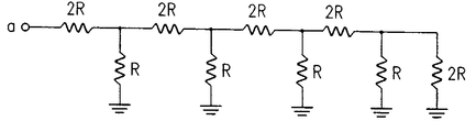
결국 등가회로는 도 3에 도시된 바와 같은 형태가 되고 도 3의 a지점에서 측정한 등가저항의 값은 (418/153)R이 된다.As a result, the equivalent circuit becomes as shown in FIG. 3 and the value of the equivalent resistance measured at point a in FIG. 3 becomes (418/153) R.
그리고, V인에이블이 하이상태를 유지하고 A/D 변환기의 출력 신호가 0000인 경우 회로의 동작을 보면, 트래지스터 Q8은 온 상태이고 이는 b지점이 그라운드와 연결되어 있어서 전류 제한 저항이 루프를 형성하여 디스플레이 소자에 전류를 공급하고 있음을 알 수 있다.And if the V enable remains high and the output signal of the A / D converter is 0000, the operation of the circuit shows that transistor Q8 is on, where point b is connected to ground, so that the current limiting resistor It can be seen that the current is supplied to the display element by forming the same.
그리고, 저항 R1과 연결된 단자가 로우(LOW)상태이기 때문에 트랜지스터 Q4는 오프상태이고, 이는 트랜지스터 Q4와 연결된 저항 R이 플로팅(floating) 상태인 것을 의미한다.Since the terminal connected to the resistor R1 is in a low state, the transistor Q4 is in an off state, which means that the resistor R connected to the transistor Q4 is in a floating state.
또한, R2, R3 그리고 R4와 연결된 트랜지스터 Q5, Q6 그리고 Q7도 모두 같은 결과를 가져온다.In addition, transistors Q5, Q6 and Q7 connected to R2, R3 and R4 all have the same result.
이때의 등가회로를 보면 도 4에 도시된 바와 같다.The equivalent circuit at this time is as shown in FIG.
여기서, 도 4의 a지점에서 측정한 등가저항의 값은 10R이 된다.Here, the value of the equivalent resistance measured at point a of FIG. 4 is 10R.
따라서, A/D 변환기의 출력이 4비트인 것을 사용한다면, 그레이 스케일 레벨은 모두 24인 16단계의 정밀도를 가지고 조절된다.Thus, if the output of the A / D converter uses 4 bits, the gray scale level is adjusted with 16 levels of precision, all 2 4 .
이때, 조절되는 저항의 크기는 최대 10R에서 최소 (418/153)R까지 이다.At this time, the size of the resistance to be adjusted is from the maximum 10R to the minimum (418/153) R.
그리고, 표준저항인 R의 크기는 소자의 상태에 따라 적절히 조절할 수 있다.The size of R, which is a standard resistor, can be appropriately adjusted according to the state of the device.
또한, V인에이블이 로우 상태가 되어 A/D 변환기가 선택되지 않았을 경우에는 트랜지스터 Q8이 오프 상태이기 때문에 전류 제한 저항에 따라 루프가 형성되지 않고, 이는 소자에 전류가 공급되지 않으므로 전력의 소모도 최소한으로 할 수 있는 잇점이 있다.In addition, when the V enable is low and the A / D converter is not selected, the transistor Q8 is off, so a loop is not formed according to the current limiting resistor, which also consumes power because no current is supplied to the device. There is a benefit to be minimal.
본 발명에 따른 디스플레이 소자의 그레이 스케일 레벨 제어장치에 있어서는 다음과 같은 효과가 있다.The gray scale level control apparatus of the display element according to the present invention has the following effects.
첫째, 디스플레이 소자의 응답시간에 관계없이 간단하게 그레이 스케일 레벨을 조절할 수 있으므로 소자의 특성에 크게 영향을 받지 않는다.First, since the gray scale level can be easily adjusted regardless of the response time of the display device, the characteristics of the device are not significantly affected.
둘째, 구동회로에서 그레이 스케일 레벨의 설정 속도는 전류제어측의 저항의 크기를 설정하는 시간에 의해서만 제한되고 저항의 크기를 조절하는 방법은 기존의 A/D 변환기를 사용할 수 있으므로 간단한 X-Y 매트릭스 구조의 패널을 이용하여도 동영상의 구현을 가능하게 한다.Second, the setting speed of the gray scale level in the driving circuit is limited only by the time to set the size of the resistance of the current control side, and the method of adjusting the size of the resistance can use a conventional A / D converter. The panel also enables the implementation of the video.
셋째, 회로 구성이 간단하므로 제조원가를 절감할 수 있다.Third, since the circuit configuration is simple, manufacturing cost can be reduced.
Claims (8)
Priority Applications (1)
| Application Number | Priority Date | Filing Date | Title |
|---|---|---|---|
| KR1019970069285A KR100259287B1 (en) | 1997-12-16 | 1997-12-16 | Apparatus for controlling gray scale level of display device |
Applications Claiming Priority (1)
| Application Number | Priority Date | Filing Date | Title |
|---|---|---|---|
| KR1019970069285A KR100259287B1 (en) | 1997-12-16 | 1997-12-16 | Apparatus for controlling gray scale level of display device |
Publications (2)
| Publication Number | Publication Date |
|---|---|
| KR19990050213A KR19990050213A (en) | 1999-07-05 |
| KR100259287B1 true KR100259287B1 (en) | 2000-06-15 |
Family
ID=19527460
Family Applications (1)
| Application Number | Title | Priority Date | Filing Date |
|---|---|---|---|
| KR1019970069285A KR100259287B1 (en) | 1997-12-16 | 1997-12-16 | Apparatus for controlling gray scale level of display device |
Country Status (1)
| Country | Link |
|---|---|
| KR (1) | KR100259287B1 (en) |
Cited By (1)
| Publication number | Priority date | Publication date | Assignee | Title |
|---|---|---|---|---|
| KR100708243B1 (en) | 2003-02-06 | 2007-04-16 | 엔이씨 일렉트로닉스 가부시키가이샤 | Current-drive circuit and apparatus for display panel |
Families Citing this family (6)
| Publication number | Priority date | Publication date | Assignee | Title |
|---|---|---|---|---|
| KR100483534B1 (en) * | 1997-12-29 | 2005-09-30 | 삼성전자주식회사 | LCD Display Power Supply Sequence Circuit |
| KR100446694B1 (en) * | 2001-07-16 | 2004-09-01 | 주식회사 자스텍 | Current Driving Apparatus for Electroluminescent Display Device using Current-Mirror |
| US7102600B2 (en) * | 2001-08-02 | 2006-09-05 | Seiko Epson Corporation | System and method for manufacturing a electro-optical device |
| KR100480695B1 (en) * | 2001-12-29 | 2005-04-06 | 엘지전자 주식회사 | Driving structure for Organic Electro Luminescence Device |
| KR100442257B1 (en) * | 2002-01-09 | 2004-07-30 | 엘지전자 주식회사 | Data Derive Circuit of Active Matrix Organic Electroluminescence of Current Writing Type |
| KR100480723B1 (en) * | 2002-10-29 | 2005-04-07 | 엘지전자 주식회사 | Apparatus for Controlling Current of The Flat Panel Display Device |
-
1997
- 1997-12-16 KR KR1019970069285A patent/KR100259287B1/en not_active IP Right Cessation
Cited By (1)
| Publication number | Priority date | Publication date | Assignee | Title |
|---|---|---|---|---|
| KR100708243B1 (en) | 2003-02-06 | 2007-04-16 | 엔이씨 일렉트로닉스 가부시키가이샤 | Current-drive circuit and apparatus for display panel |
Also Published As
| Publication number | Publication date |
|---|---|
| KR19990050213A (en) | 1999-07-05 |
Similar Documents
| Publication | Publication Date | Title |
|---|---|---|
| US7256552B2 (en) | LED control circuit | |
| KR100454134B1 (en) | A drive circuit for an organic EL apparatus | |
| KR100694371B1 (en) | Programmable led driver pad | |
| KR100771363B1 (en) | Light-emitting element driver | |
| KR910005362B1 (en) | Display driver | |
| US6992647B2 (en) | Organic EL drive circuit and organic EL display device using the same | |
| CN1551075B (en) | Current-drive circuit and apparatus for display panel | |
| US7659873B2 (en) | Current control circuit, LED current control apparatus, and light emitting apparatus | |
| KR100259287B1 (en) | Apparatus for controlling gray scale level of display device | |
| JPH0822263A (en) | Led lighting circuit | |
| KR100796480B1 (en) | Driving IC of an active matrix Electroluminesence Device | |
| US20050116904A1 (en) | Drive device and drive method of light emitting display panel | |
| CN210325157U (en) | Backlight driving circuit, backlight driving device and display device | |
| KR100556480B1 (en) | apparatus for current control of flat panel display device | |
| KR101243144B1 (en) | driving circuit of LED driver for LCD panel | |
| JP5258199B2 (en) | LED drive circuit | |
| JPS6474598A (en) | Thin film el display device | |
| KR100262337B1 (en) | A current controlled fed driving circuit for gray scale processing using the switched resister | |
| CN216793271U (en) | Pixel driving unit and display circuit | |
| US4037153A (en) | Digital meters | |
| JP2971305B2 (en) | Light control device | |
| KR100257567B1 (en) | Driving method of gray procrss field emission display element of current control method using switched resistor | |
| JP2003101073A (en) | Dual voltage power supply apparatus | |
| KR100429202B1 (en) | Light Emission Diode in Voltage mode | |
| KR960003397B1 (en) | Display tube control system |
Legal Events
| Date | Code | Title | Description |
|---|---|---|---|
| A201 | Request for examination | ||
| E902 | Notification of reason for refusal | ||
| E701 | Decision to grant or registration of patent right | ||
| GRNT | Written decision to grant | ||
| FPAY | Annual fee payment |
Payment date: 20070221 Year of fee payment: 8 |
|
| LAPS | Lapse due to unpaid annual fee |