JP7706331B2 - Inspection device and inspection method - Google Patents
Inspection device and inspection method Download PDFInfo
- Publication number
- JP7706331B2 JP7706331B2 JP2021171036A JP2021171036A JP7706331B2 JP 7706331 B2 JP7706331 B2 JP 7706331B2 JP 2021171036 A JP2021171036 A JP 2021171036A JP 2021171036 A JP2021171036 A JP 2021171036A JP 7706331 B2 JP7706331 B2 JP 7706331B2
- Authority
- JP
- Japan
- Prior art keywords
- height
- probe
- positioning
- wafer
- chuck top
- Prior art date
- Legal status (The legal status is an assumption and is not a legal conclusion. Google has not performed a legal analysis and makes no representation as to the accuracy of the status listed.)
- Active
Links
Images


Classifications
-
- G—PHYSICS
- G01—MEASURING; TESTING
- G01R—MEASURING ELECTRIC VARIABLES; MEASURING MAGNETIC VARIABLES
- G01R31/00—Arrangements for testing electric properties; Arrangements for locating electric faults; Arrangements for electrical testing characterised by what is being tested not provided for elsewhere
- G01R31/28—Testing of electronic circuits, e.g. by signal tracer
- G01R31/2851—Testing of integrated circuits [IC]
- G01R31/2855—Environmental, reliability or burn-in testing
- G01R31/286—External aspects, e.g. related to chambers, contacting devices or handlers
- G01R31/2868—Complete testing stations; systems; procedures; software aspects
-
- G—PHYSICS
- G01—MEASURING; TESTING
- G01R—MEASURING ELECTRIC VARIABLES; MEASURING MAGNETIC VARIABLES
- G01R31/00—Arrangements for testing electric properties; Arrangements for locating electric faults; Arrangements for electrical testing characterised by what is being tested not provided for elsewhere
- G01R31/28—Testing of electronic circuits, e.g. by signal tracer
- G01R31/2851—Testing of integrated circuits [IC]
- G01R31/2855—Environmental, reliability or burn-in testing
- G01R31/286—External aspects, e.g. related to chambers, contacting devices or handlers
- G01R31/2865—Holding devices, e.g. chucks; Handlers or transport devices
- G01R31/2867—Handlers or transport devices, e.g. loaders, carriers, trays
-
- G—PHYSICS
- G01—MEASURING; TESTING
- G01R—MEASURING ELECTRIC VARIABLES; MEASURING MAGNETIC VARIABLES
- G01R1/00—Details of instruments or arrangements of the types included in groups G01R5/00 - G01R13/00 and G01R31/00
- G01R1/02—General constructional details
- G01R1/06—Measuring leads; Measuring probes
- G01R1/067—Measuring probes
- G01R1/073—Multiple probes
- G01R1/07307—Multiple probes with individual probe elements, e.g. needles, cantilever beams or bump contacts, fixed in relation to each other, e.g. bed of nails fixture or probe card
- G01R1/07342—Multiple probes with individual probe elements, e.g. needles, cantilever beams or bump contacts, fixed in relation to each other, e.g. bed of nails fixture or probe card the body of the probe being at an angle other than perpendicular to test object, e.g. probe card
-
- G—PHYSICS
- G01—MEASURING; TESTING
- G01R—MEASURING ELECTRIC VARIABLES; MEASURING MAGNETIC VARIABLES
- G01R31/00—Arrangements for testing electric properties; Arrangements for locating electric faults; Arrangements for electrical testing characterised by what is being tested not provided for elsewhere
- G01R31/28—Testing of electronic circuits, e.g. by signal tracer
- G01R31/2851—Testing of integrated circuits [IC]
- G01R31/2886—Features relating to contacting the IC under test, e.g. probe heads; chucks
- G01R31/2887—Features relating to contacting the IC under test, e.g. probe heads; chucks involving moving the probe head or the IC under test; docking stations
-
- G—PHYSICS
- G01—MEASURING; TESTING
- G01R—MEASURING ELECTRIC VARIABLES; MEASURING MAGNETIC VARIABLES
- G01R31/00—Arrangements for testing electric properties; Arrangements for locating electric faults; Arrangements for electrical testing characterised by what is being tested not provided for elsewhere
- G01R31/28—Testing of electronic circuits, e.g. by signal tracer
- G01R31/2851—Testing of integrated circuits [IC]
- G01R31/2886—Features relating to contacting the IC under test, e.g. probe heads; chucks
- G01R31/2889—Interfaces, e.g. between probe and tester
-
- G—PHYSICS
- G01—MEASURING; TESTING
- G01R—MEASURING ELECTRIC VARIABLES; MEASURING MAGNETIC VARIABLES
- G01R31/00—Arrangements for testing electric properties; Arrangements for locating electric faults; Arrangements for electrical testing characterised by what is being tested not provided for elsewhere
- G01R31/28—Testing of electronic circuits, e.g. by signal tracer
- G01R31/2851—Testing of integrated circuits [IC]
- G01R31/2886—Features relating to contacting the IC under test, e.g. probe heads; chucks
- G01R31/2891—Features relating to contacting the IC under test, e.g. probe heads; chucks related to sensing or controlling of force, position, temperature
Landscapes
- Engineering & Computer Science (AREA)
- Physics & Mathematics (AREA)
- General Physics & Mathematics (AREA)
- Computer Hardware Design (AREA)
- Microelectronics & Electronic Packaging (AREA)
- General Engineering & Computer Science (AREA)
- Environmental & Geological Engineering (AREA)
- Testing Or Measuring Of Semiconductors Or The Like (AREA)
- Tests Of Electronic Circuits (AREA)
Description
本開示は、検査装置及び検査方法に関する。 This disclosure relates to an inspection device and an inspection method.
特許文献1には、プローブカードとウェハとを加圧接触させてウェハ検査を行うウェハ検査装置が開示されている。このウェハ検査装置では、バキューム機構の真空引きにより囲繞空間内でプローブカードとウェハとの間に加えられる真空吸引力の圧力が、それに先立つ移動ステージとチャックトップの押し上げによりプローブカードとウェハとの間に加えられた押圧力の圧力に略精確に一致するようになっている。
本開示にかかる技術は、基板を検査する検査装置において、プローブの高さによらず、プローブと基板を適切に接触させる。 The technology disclosed herein allows an inspection device that inspects substrates to properly contact a probe with a substrate, regardless of the probe's height.
本開示の一態様は、基板を検査する検査装置であって、基板が載置される載置部材と、基板に接触するプローブを有するプローブカードを保持する保持部と、前記載置部材の上面または前記保持部の下面に接触して前記プローブに対する前記載置部材の高さを規定する複数の位置決め部材と、前記位置決め部材の高さを調節する調節機構と、前記プローブ、前記載置部材及び前記位置決め部材を検出するための検出部と、制御部と、を備え、前記制御部は、前記検出部を用いた前記プローブの検出結果に基づいて、前記プローブの高さを取得する工程と、前記検出部を用いた前記載置部材の検出結果に基づいて、前記載置部材の高さを取得する工程と、前記検出部を用いた前記位置決め部材の検出結果に基づいて、前記位置決め部材の高さを取得する工程と、前記検出部を用いた前記プローブ、前記載置部材及び前記位置決め部材の検出結果に基づいて、オーバードライブ量がゼロになる基準高さに、前記調節機構を用いて、前記位置決め部材を位置決めする工程と、所望のオーバードライブ量となる前記位置決め部材の高さを取得し、その高さになるまで前記調節機構の駆動量を調整しつつ、前記載置部材を上昇させる工程と、を実行するように構成されている。 One aspect of the present disclosure is an inspection device for inspecting a substrate, comprising: a mounting member on which a substrate is placed; a holding section for holding a probe card having a probe that contacts the substrate; a plurality of positioning members that contact the upper surface of the mounting member or the lower surface of the holding section to determine the height of the mounting member relative to the probe; an adjustment mechanism for adjusting the height of the positioning members; a detection section for detecting the probes, the mounting member, and the positioning members; and a control section. The control section is configured to execute the steps of: acquiring the height of the probe based on the detection result of the probe using the detection section; acquiring the height of the mounting member based on the detection result of the mounting member using the detection section; acquiring the height of the positioning member based on the detection result of the positioning member using the detection section; positioning the positioning member using the adjustment mechanism to a reference height at which the overdrive amount is zero based on the detection result of the probe, the mounting member, and the positioning member using the detection section; and acquiring the height of the positioning member that results in a desired overdrive amount, and raising the mounting member while adjusting the drive amount of the adjustment mechanism until the height is reached.
本開示によれば、基板を検査する検査装置において、プローブの高さによらず、プローブと基板を適切に接触させることができる。 According to the present disclosure, in an inspection device for inspecting a substrate, the probe can be brought into proper contact with the substrate regardless of the height of the probe.
半導体製造プロセスでは、半導体ウェハ(以下、「ウェハ」という。)上に所定の回路パターンを持つ多数の半導体デバイスが形成される。形成された半導体デバイスは、電気的特性等の検査が行われ、良品と不良品とに選別される。半導体デバイスの検査は、例えば、各半導体デバイスに分割される前のウェハの状態で、検査装置を用いて行われる。 In the semiconductor manufacturing process, a large number of semiconductor devices with a predetermined circuit pattern are formed on a semiconductor wafer (hereafter referred to as "wafer"). The formed semiconductor devices are inspected for electrical characteristics, etc., and sorted into good and bad products. Semiconductor devices are inspected, for example, using inspection equipment while they are still in the wafer state before being divided into individual semiconductor devices.
検査装置には、多数の針状の接触端子であるプローブを多数有するプローブカードが設けられている。電気的特性の検査の際はまず、ウェハとプローブカードとが近づけられ、ウェハに形成されている半導体デバイスの各電極にプローブカードのプローブが接触する。この状態で、プローブカードの上方に設けられたテスタから各プローブを介して半導体デバイスに電気信号が供給される。そして、各プローブを介して半導体デバイスからテスタが受信した電気信号に基づいて、当該半導体デバイスが不良品か否か判別される。 The inspection device is equipped with a probe card that has a large number of probes, which are numerous needle-shaped contact terminals. When inspecting electrical characteristics, the wafer and the probe card are first brought close together, and the probes of the probe card come into contact with each electrode of the semiconductor device formed on the wafer. In this state, an electrical signal is supplied to the semiconductor device via each probe from a tester provided above the probe card. Then, based on the electrical signal received by the tester from the semiconductor device via each probe, it is determined whether or not the semiconductor device is defective.
このような電気的特性検査を行う検査装置としては、ウェハが載置されるチャックトップと、プローブカードを保持するポゴフレームとの間の密閉空間を減圧し、当該空間に含まれるウェハとプローブカードのプローブとを接触させるものが知られている。この検査装置では、上記密閉空間を減圧して縮めることにより、チャックトップをプローブカード側に引き寄せ、すなわち上昇させ、チャックトップ上のウェハをプローブカードのプローブに当接させる。このとき、チャックトップの高さは、当該チャックトップ上のウェハがプローブに接触してから所定のオーバードライブ量の分高くなる高さとされる。これにより、ウェハ上の保護膜等の有無によらず、ウェハの電極とプローブとを接触させている。 A known testing device for such electrical characteristic testing is one that reduces the pressure of the sealed space between the chuck top on which the wafer is placed and the pogo frame that holds the probe card, and brings the wafer contained in that space into contact with the probes of the probe card. In this testing device, the sealed space is reduced in pressure and contracted, so that the chuck top is pulled toward the probe card, i.e., raised, and the wafer on the chuck top is brought into contact with the probes of the probe card. At this time, the height of the chuck top is set to a height that is a predetermined overdrive amount higher than the wafer on the chuck top comes into contact with the probes. This allows the electrodes of the wafer to come into contact with the probes, regardless of the presence or absence of a protective film on the wafer.
なお、チャックトップは、アライナによって保持され、当該アライナによって水平方向及び上下方向に移動可能である。ただし、チャックトップ上のウェハとプローブとが接触し電気的特性の検査を行う段階では、チャックトップは、アライナに支持されておらず、上記密閉空間を形成するベローズに支持されている。
また、チャックトップの高さは、従来、ポゴフレームまたはアライナを基準に設定される。具体的には、チャックトップの高さは、従来、例えばポゴフレームまたはアライナに設けられた高さセンサによる検出結果に基づき、ポゴフレームまたはアライナからチャックトップまでの距離が所定の値になるように設定される。
The chuck top is held by an aligner and can be moved horizontally and vertically by the aligner. However, at the stage where the wafer on the chuck top comes into contact with the probes and electrical characteristics are inspected, the chuck top is not supported by the aligner but by the bellows that form the sealed space.
Conventionally, the height of the chuck top is set based on the pogo frame or the aligner, for example, based on the detection result of a height sensor provided on the pogo frame or the aligner, so that the distance from the pogo frame or the aligner to the chuck top is a predetermined value.
ところで、プローブカードのプローブの高さ(具体的にはプローブのウェハへの接触端の高さ)は、プローブカードの温度によって変わり、また、ポゴフレームが熱膨張または熱収縮することによっても変わる。したがって、電気的特性の検査を行う時のチャックトップの高さを、上述のようにポゴフレームまたはアライナを基準に設定すると、プローブとウェハ(具体的には電極)とを適切に接触させられないことがある。 Incidentally, the height of the probe of the probe card (specifically, the height of the contact end of the probe with the wafer) changes depending on the temperature of the probe card and also changes due to the thermal expansion or contraction of the pogo frame. Therefore, if the height of the chuck top when testing electrical characteristics is set based on the pogo frame or aligner as described above, it may not be possible to properly contact the probe with the wafer (specifically, the electrode).
上述を鑑み、本開示にかかる技術は、基板を検査する検査装置において、プローブの高さによらず、プローブと基板を適切に接触させる。 In view of the above, the technology disclosed herein allows a probe to appropriately contact a substrate in an inspection device that inspects substrates, regardless of the height of the probe.
以下、本実施形態にかかる検査装置及び検査方法について、図面を参照しながら説明する。なお、本明細書及び図面において、実質的に同一の機能構成を有する要素においては、同一の符号を付することにより重複説明を省略する。 The inspection device and inspection method according to this embodiment will be described below with reference to the drawings. Note that in this specification and drawings, elements having substantially the same functional configuration are given the same reference numerals to avoid redundant description.
<検査装置>
図1及び図2はそれぞれ、本実施形態にかかる検査装置の構成の概略を示す横断面図及び縦断面図である。なお、図2では、後述のアライナについてはその一部のみを示している。
<Inspection equipment>
1 and 2 are a cross-sectional view and a longitudinal-sectional view, respectively, showing the outline of the configuration of an inspection apparatus according to this embodiment, in which only a part of an aligner, which will be described later, is shown.
図1及び図2の検査装置1は、基板としてのウェハWを検査するものであり、具体的には、ウェハWに形成された検査対象デバイスとしての半導体デバイスの電気的特性検査を行うものである。検査装置1は、筐体10を有し、該筐体10には、搬入出領域11、搬送領域12、検査領域13が設けられている。搬入出領域11は、検査装置1に対してウェハWの搬入出が行われる領域である。搬送領域12は、搬入出領域11と検査領域13とを接続する領域である。また、検査領域13は、ウェハWに形成された半導体デバイスの電気的特性検査が行われる領域である。
The
搬入出領域11には、複数のウェハWを収容したカセットCを受け入れるポート20、後述のプローブカードを収容するローダ21、検査装置1の各構成要素の制御等を行う制御部22が設けられている。制御部22は、例えばCPUやメモリ等を備えたコンピュータにより構成され、各種情報を記憶する記憶部(図示せず)を有している。記憶部には、例えば、検査処理等を実現するプログラムが格納されている。なお、上記プログラムは、コンピュータに読み取り可能な記憶媒体に記録されていたものであって、当該記憶媒体から上記制御部22にインストールされたものであってもよい。上記記憶媒体は一時的なものであっても非一時的なものであってもよい。なお、プログラムの一部または全ては専用ハードウェア(回路基板)で実現してもよい。また、上記記憶部は、例えばHDD等のストレージデバイス、プログラムの演算に係る一時的に必要な情報を記憶するRAM等のメモリ、またはこれらの組み合わせである。
The loading/
搬送領域12には、ウェハW等を保持した状態で自在に移動可能な搬送装置30が配置されている。この搬送装置30は、搬入出領域11のポート20内のカセットCと、検査領域13との間でウェハWの搬送を行う。また、搬送装置30は、検査領域13内の後述のポゴフレームに固定されたプローブカードのうちメンテナンスを必要とするものを搬入出領域11のローダ21へ搬送する。さらに、搬送装置30は、新規な又はメンテナンス済みのプローブカードをローダ21から検査領域13内へ搬送する。
In the
検査領域13は、テスタ40が複数設けられている。具体的には、検査領域13は、例えば、図2に示すように、鉛直方向に3つに分割され、各分割領域13aには、水平方向(図のX方向)に配列された4つのテスタ40からなるテスタ列が設けられている。また、各分割領域13aには、1つの移動機構としてのアライナ50と、1つの上カメラ60が設けられている。なお、テスタ40、アライナ50、上カメラ60の数や配置は任意に選択できる。
The
テスタ40は、電気的特性検査用の電気信号をウェハWとの間で送受するものである。
アライナ50は、後述のチャックトップ70を保持して、水平方向(図のX方向及びY方向、図のZ軸を中心としたθ方向)及び上下方向(図のZ方向)に移動させることが可能に構成されている。また、このアライナ50は、チャックトップ70に載置されたウェハWと後述のプローブカードのプローブとの位置合わせに用いられる。
The
The
上カメラ60は、下方を撮像するように設けられている。一実施形態において、上カメラ60は、水平に移動自在に構成されている。上カメラ60は、例えば、当該上カメラ60が設けられた検査内の各テスタ40の手前側(図のY方向負側)の領域であって、後述のポゴフレームと平面視では重ならない領域に位置して、アライナ50上のチャックトップ70に載置されたウェハWを撮像する。
なお、上カメラ60は、制御部22により制御される。また、上カメラ60による撮像結果は制御部22に出力される。
The
The
チャックトップ70は、載置部材の一例であり、ウェハWが載置される。チャックトップ70は、例えば、載置されたウェハWを吸着等により保持することができる。
The
この検査装置1では、搬送装置30が一のテスタ40へ向けてウェハWを搬送している間に、他のテスタ40は他のウェハWに形成された電子デバイスの電気的特性の検査を行うことができる。
In this
<検査領域>
続いて、図3~図5を用いて、検査領域13のより詳細な構成について説明する。図3は、検査領域13の側断面図である。図4は、後述のポゴフレームの周辺の断面図である。図5は、後述のポゴフレームの下面の模式部分拡大図である。図5では、後述のプローブの図示は省略している。
<Inspection area>
Next, the configuration of the
検査領域13の各分割領域13aには、前述のように、アライナ50及び上カメラ60が設けられている。また、図3に示すように、各分割領域13aには、後述の下カメラ80、ポゴフレーム90及びプローブカード100が設けられている。
As described above, an
アライナ50は、例えばXステージ51、Yステージ52及びZステージ53を有する。
The
Xステージ51は、アライナ50による移動平面(XY平面)の座標系を構成するX軸方向に、ガイドレール51aに沿って移動する。このXステージ51に対しては、Xステージ51のX方向にかかる位置、すなわちチャックトップ70のX軸方向にかかる位置を検出する位置検出機構(図示せず)が設けられている。上記位置検出機構は、例えばリニアエンコーダである。
The X-stage 51 moves along the
Yステージ52は、Xステージ51上を移動する。具体的には、アライナ50による移動平面(XY平面)の座標系を構成するY軸方向に、ガイドレール52aに沿って移動する。このYステージ52に対しては、Yステージ52のY軸方向にかかる位置、すなわちチャックトップ70のY軸方向にかかる位置を検出する位置検出機構(図示せず)が設けられている。上記位置検出機構は、例えばリニアエンコーダである。
The
Zステージ53は、アライナ50による移動平面(XY平面)と直交する高さ方向(Z方向)に伸縮自在な伸縮軸53aにより、上記高さ方向(Z方向)に移動する。このZステージ53に対しては、Zステージ53のZ方向にかかる位置、すなわちチャックトップ70のZ方向にかかる位置を検出する位置検出機構(図示せず)が設けられている。上記位置検出機構は、例えばリニアエンコーダである。
また、Zステージ53上にチャックトップ70が着脱自在に吸着保持される。Zステージ53によるチャックトップ70の吸着保持は、吸着保持機構(図示せず)による真空吸着等により行われる。
The
Further, a
下カメラ80は、検出部の一例であり、プローブカード100に設けられた後述のプローブ及び後述の位置決めピンを検出するためのものである。また、下カメラ80は、撮像部の一例であり、上方を撮像する。
The
下カメラ80は、アライナ50に固定されている。具体的には、下カメラ80は、アライナ50のZステージ53に固定されている。このように固定されているため、下カメラ80は、アライナ50により、チャックトップ70と共に移動可能である。
下カメラ80は、例えば、ポゴフレーム90に固定されたプローブカード100の下方の領域に位置して、当該プローブカード100を撮像する。
The
The
なお、アライナ50や下カメラ80は、制御部22により制御される。また、下カメラ80による撮像結果と、Xステージ51、Yステージ52及びZステージ53に設けられた位置検出機構による位置検出結果とは、制御部22に出力される。
The
テスタ40は、図4に示すように、テスタマザーボード41を底部に有する。テスタマザーボード41には、複数の検査回路基板(図示せず)が立設状態で装着されている。また、テスタマザーボード41の底面には複数の電極(図示せず)が設けられている。
さらに、テスタ40の下方には、ポゴフレーム90が設けられている。
4, the
Furthermore, a
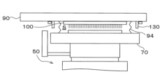
ポゴフレーム90は、保持部の一例であり、プローブカード100を保持する。また、ポゴフレーム90は、プローブカード100とテスタ40とを電気的に接続する。このポゴフレーム90は、上述の電気的な接続のために、ポゴピン91を有し、具体的には、多数のポゴピン91を保持するポゴブロック92を有する。また、ポゴフレーム90は、ポゴブロック92が取り付けられるフレーム本体93を有する。
ポゴフレーム90の下面には、プローブカード100が、所定の位置に位置合わせされた状態で固定される。
The
A
なお、排気機構(図示せず)によって、テスタマザーボード41はポゴフレーム90に真空吸着され、プローブカード100は、ポゴフレーム90に真空吸着される。これら真空吸着を行うための真空吸引力により、ポゴフレーム90の各ポゴピン91の下端は、プローブカード100の後述のカード本体101の上面における、対応する電極に接触し、各ポゴピン91の上端は、テスタマザーボード41の下面の対応する電極に押し付けられる。
The
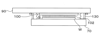
プローブカード100は、複数の電極が上面に設けられた円板状のカード本体101を有する。カード本体101の下面には、下方へ向けて延びる針状の接触端子であるプローブ102が複数設けられている。
カード本体101の上面に設けられた上述の複数の電極はそれぞれ対応するプローブ102と電気的に接続されている。また、検査時には、プローブ102はそれぞれ、ウェハWに形成された半導体デバイスの電極(図示せず)と接触する。したがって、電気的特性検査時には、ポゴピン91、カード本体101の上面に設けられた電極及びプローブ102を介して、テスタマザーボード41とウェハW上の半導体デバイスとの間で、検査にかかる電気信号が送受される。
The
The above-mentioned plurality of electrodes provided on the upper surface of the
なお、検査装置1は、ウェハWに形成された複数の半導体デバイスの電気的特性検査を一括で行うために、プローブ102は、カード本体101の下面略全体を覆うように多数設けられている。
In order for the
また、ポゴフレーム90の下面には、ベローズ94が取り付けられている。ベローズ94は、筒状部材の一例であり、伸縮自在に構成され且つ筒状に形成されており、チャックトップ70とポゴフレーム90との間に密閉空間Sを形成する。また、ベローズ94は、プローブカード100を囲繞するようにポゴフレーム90から垂下する。このベローズ94は、図4において点線で示すように、プローブカード100の下方の位置にチャックトップ70を吸着保持する。
A bellows 94 is attached to the underside of the
さらに、ベローズ94は、チャックトップ70を吸着保持することにより、プローブカード100及びウェハWを含む密閉空間Sを形成する。密閉空間Sは、ポゴフレーム90、ベローズ94及びチャックトップ70で囲まれ、ポゴフレーム90のフレーム本体93に形成された排気路93aの一端に連通している。排気路93aの他端には、減圧機構110と大気開放機構120とが接続されている。
Furthermore, the
減圧機構110は、密閉空間Sを減圧する。これにより、ウェハWとプローブ102との接触状態が維持される。減圧機構110は、密閉空間Sを排気する真空ポンプや真空ポンプによる排気の開始と停止を切り換える切換弁等を有し、制御部22により制御される。
The
大気開放機構120は、密閉空間Sを大気圧に戻すための機構であり、密閉空間Sに大気を導入する。大気開放機構120は、密閉空間Sへの大気導入の開始と停止を切り換える切換弁等を有し、制御部22により制御される。
密閉空間Sを大気圧に戻すために、大気を導入する代わりに不活性ガス等を導入するようにしてもよい。
The
In order to return the sealed space S to atmospheric pressure, an inert gas or the like may be introduced instead of the air.
さらに、本実施形態では、位置決めピン130が複数設けられている。位置決めピン130は、位置決め部材の一例であり、ポゴフレーム90側から下方に突出し、チャックトップ70の上面に接触しプローブ102に対するチャックトップ70の高さを規定する。位置決めピン130は、具体的には、ポゴフレーム90の下面から下方に突出し、その下端がチャックトップ70の上面に接触し、当該チャックトップ70の上面の高さを規定する。
Furthermore, in this embodiment, multiple positioning pins 130 are provided. The positioning pins 130 are an example of a positioning member, and protrude downward from the
また、複数の位置決めピン130は、例えば、図5に示すように、ベローズ94の外側の領域に、当該ベローズ94の外周に沿って、プローブカード100の中心を中心とした同一円周上に、互いに間隔を空けて(具体的には等間隔で)設けられている。各位置決めピン130の形状は例えば円柱状である。
なお、位置決めピン130の数は、図5の例の4つに限られず、当該位置決めピン130で高さを規定するチャックトップ70の姿勢を水平に維持可能であれば、5つ以上または3つであってもよい。
5, the positioning pins 130 are provided in the outer region of the
The number of positioning pins 130 is not limited to four as shown in the example of Figure 5, and may be five or more or three as long as the posture of the
また、本実施形態では、位置決めピン130毎に、当該位置決めピン130の高さを調節する調節機構140が設けられている。
調節機構140は、具体的には、位置決めピン130の下端の高さを調節する。言い換えると、調節機構140は、位置決めピン130のポゴフレーム90の下面から下方への突出長さ(すなわち突出量)を調節する。
調節機構140は、例えば、対応する位置決めピン130の高さを調節するために、当該位置決めピン130の昇降を駆動する駆動部(図示せず)を有する。駆動部は、上述の昇降のための駆動力を発生する駆動ユニットとして、例えばモータ(図示せず)を有する。また、駆動部は、モータに接続されたエンコーダ(図示せず)を有する。エンコーダは、モータによる位置決めピン130の移動量に応じたパルス数を、制御部22に出力する。制御部22は、このエンコーダからの出力に基づいて、対応する位置決めピン130の高さを取得することができる。
In this embodiment, an
Specifically, the
The
また、調節機構140の駆動部に対しては、当該駆動部の負荷を検出する検出部として、トルク検出部が設けられている。トルク検出部は、例えば、駆動部のモータのトルクを検出し、検出結果を制御部22に出力する。制御部22は、このトルク検出部からの出力に基づいて、対応する位置決めピン130とチャックトップ70との接触を検知することができる。
The drive unit of the
<検査装置1を用いた検査処理>
続いて、検査装置1を用いた検査処理について、図6~図12を用いて説明する。
<Inspection process using
Next, the inspection process using the
(S1:搬入)
まず、所望の分割領域13aへの検査対象のウェハWの搬入が行われる。
具体的には、搬送装置30等が制御部22により制御され、搬入出領域11のポート20内のカセットCからウェハWが取り出されて、例えば中段の分割領域13a内に搬入され、アライナ50に吸着保持されたチャックトップ70上に載置される。
(S1: Carry-in)
First, a wafer W to be inspected is carried into a desired
Specifically, the
(S2:プローブの水平方向にかかる位置及び高さの取得)
次いで、制御部22により、下カメラ80を用いたプローブ102の検出結果に基づいて、プローブ102の水平方向にかかる位置(以下、「水平位置」という。)と高さが取得される。具体的には、制御部22の制御の下、図6に示すように、プローブカード100の下方の領域に下カメラ80が位置するよう、チャックトップ70がアライナ50によって移動される。そして、制御部22により、下カメラ80の撮像結果とアライナ50の位置検出機構の検出結果とに基づいて、プローブ102の水平位置と高さが取得される。
(S2: Acquisition of horizontal position and height of probe)
Next, the
プローブ102の水平位置及び高さとは、例えば、プローブカード100に設けられたプローブ102のうちの、予め定められた複数箇所のプローブ102の下端の重心に係る水平位置及び高さである。
The horizontal position and height of the
(S3:位置決めピンの高さの取得)
次いで、制御部22により、下カメラ80を用い、位置決めピン130の高さが取得される。具体的には、制御部22の制御の下、図7に示すように、位置決めピン130の下方の領域に下カメラ80が位置するよう、チャックトップ70がアライナ50によって移動される。そして、制御部22により、下カメラ80の撮像結果とアライナ50の位置検出機構の検出結果とに基づいて、位置決めピン130の高さが取得される。なお、位置決めピン130の高さとは、具体的には位置決めピン130の下端の高さである。
また、一実施形態において、位置決めピン130の高さは位置決めピン130毎に取得される。
(S3: Obtaining the height of the positioning pin)
Next, the
Additionally, in one embodiment, the height of the locating pins 130 is obtained for each locating
(S4:ウェハの水平位置及び高さの取得)
次いで、制御部22により、上カメラ60を用いて、アライナ50に保持されたチャックトップ70上のウェハWの水平位置と高さが取得される。具体的には、制御部22の制御の下、図8に示すように、上カメラ60の下方の領域に、チャックトップ70がアライナ50によって移動される。そして、制御部22により、上カメラ60の撮像結果とアライナ50の位置検出機構の検出結果とに基づいて、チャックトップ70上のウェハWの水平位置と高さが取得される。
上記ウェハWの水平位置とは、例えば、ウェハWに設けられた電極のうちの、予め定められた複数箇所の電極の重心に係る水平位置である。
(S4: Obtaining horizontal position and height of wafer)
Next, the
The horizontal position of the wafer W is, for example, a horizontal position related to the center of gravity of electrodes provided on the wafer W at a plurality of predetermined locations.
(S5:チャックトップの高さの取得)
また、制御部22により、上カメラ60を用いて、アライナ50に保持されたチャックトップ70の高さが取得される。具体的には、制御部22の制御の下、図9に示すように、上カメラ60の下方の領域に、チャックトップ70がアライナ50によって移動される。そして、制御部22により、上カメラ60の撮像結果とアライナ50の位置検出機構の検出結果とに基づいて、位置決めピン130が接触するチャックトップ70の高さが取得される。なお、チャックトップ70の高さとは、具体的にはチャックトップ70の外周部の上面の高さである。
(S5: Obtaining the height of the chuck top)
Furthermore, the
(S6:位置決めピンを基準高さに調整)
その後、制御部22により取得した、プローブ102の高さ、位置決めピン130の高さ、ウェハWの高さ及びチャックトップ70の高さに基づいて、位置決めピン130の高さすなわち下方への突出長さが、オーバードライブ量ODがゼロになるように、設定される。つまり、調節機構140により、位置決めピン130は、オーバードライブ量ODがゼロになる基準高さに位置決めされる。この基準高さは、プローブ102がウェハWに接触するタイミングと、位置決めピン130がチャックトップ70に接触するタイミングとが、ほぼ同じとなるように設定される。
なお、位置決めピン130の高さの設定に、制御部22により取得したウェハWの高さを用いなくてもよく、代わりに、予め記憶されたウェハWの厚さの情報等を用いてもよい。
(S6: Adjust the positioning pin to the reference height)
Thereafter, based on the heights of the
It should be noted that the height of the
(S7:プローブカードの下方へのウェハWの移動)
ステップS2~S6の後、制御部22の制御の下、図10に示すように、チャックトップ70がアライナ50によってプローブカード100の下方へ移動される。このとき、ウェハWとプローブカード100のプローブ102とは、ステップS2及びステップS4での取得結果に基づいて位置合わせされる。
(S7: Movement of wafer W below probe card)
After steps S2 to S6, under the control of the
(S8:密閉空間の形成)
続いて、制御部22の制御の下、チャックトップ70がアライナ50によって上昇され、図11に示すように、密閉空間Sが形成される。具体的には、例えば、制御部22の制御の下、チャックトップ70が、アライナ50によって、ベローズ94の下端に当接するまで上昇され、その後、当該ベローズ94によって吸着保持される。これにより、ポゴフレーム90、ベローズ94及びチャックトップ70で囲まれ、内部にプローブカード100とウェハWを含む密閉空間Sが形成される。
(S8: Formation of sealed space)
Next, under the control of the
(S9:密閉空間の減圧及び位置決めピンとチャックトップとの接触)
次いで、制御部22の制御の下、密閉空間Sが減圧されると共に、基準高さにそれぞれ調整された位置決めピン130とチャックトップ70の上面とが接触される。この接触により、プローブ102に対し、チャックトップ70上のウェハWは平行に維持される。
(S9: Decompression of the sealed space and contact between the positioning pin and the chuck top)
Next, under the control of the
具体的には、例えば、制御部22の制御の下、チャックトップ70がアライナ50からから切り離されると共に、密閉空間Sが減圧機構110によって減圧される。これにより、チャックトップ70が上昇し、図12に示すように、チャックトップ70上のウェハWとプローブ102とが接触すると共に、位置決めピン130の下端とチャックトップ70の上面とが接触する。
Specifically, for example, under the control of the
(S10:チャックトップの上昇及び位置決めピン130の高さの調整)
その後、制御部22により、所望のオーバードライブ量ODとなる位置決めピン130の高さすなわち目標高さが取得され、調節機構140による位置決めピン130の上昇の駆動量の調整が行われつつ、チャックトップ70が上昇される。具体的には、制御部22により、全ての位置決めピン130について、目標高さが記憶部(図示せず)から取得されると共に、位置決めピン130の高さと関係する、調節機構140による位置決めピン130の駆動量がモニタされ、それぞれの位置決めピン130が目標高さまで移動される。このとき、密閉空間Sの減圧が継続されることにより、位置決めピン130の上昇に追従して、チャックトップ70が上昇される。その結果、プローブ102を所望の接触圧でウェハWに均一に接触させることができる。
(S10: Raise the chuck top and adjust the height of the positioning pin 130)
Thereafter, the
また、このチャックトップ70の上昇の際、全ての位置決めピン130とチャックトップ70との接触が維持されるよう、調節機構140による位置決めピン130の昇降の駆動量が調整される。これにより、チャックトップ70の平行度を維持することができる。
In addition, when the
(S11:検査)
そして、制御部22の制御により、ウェハWに形成された電子デバイスの電気的特性検査が行われる。
電気的特性検査用の電気信号は、テスタ40からポゴピン91やプローブ102等を介して電子デバイスに入力される。
(S11: Inspection)
Then, under the control of the
An electrical signal for the electrical characteristic test is input from the
(S12.搬出)
その後、検査後のウェハWが搬出される。
具体的には、制御部22の制御の下、ベローズ94に吸着されていたチャックトップ70がアライナ50に受け渡され保持される。また、アライナ50に保持されたチャックトップ70上の検査後のウェハWが、搬送装置30によって、検査領域13から搬出され、搬入出領域11のポート20内のカセットCに戻される。
なお、上記ステップS1~S12はウェハW毎に行われる。また、一のテスタ40での検査中、アライナ50によって、他のテスタ40への検査対象のウェハWの搬送や他のテスタ40からの検査後のウェハWの回収が行われる。
(S12. Export)
Thereafter, the inspected wafer W is carried out.
Specifically, under the control of the
The above steps S1 to S12 are performed for each wafer W. During inspection in one
<本実施形態の主な効果>
本実施形態では、検査を行う際に、カメラにより取得した結果より算出した位置決めピン130の基準高さ、すなわちプローブ102がウェハWに接触する接触高さ(オーバードライブ量ODがゼロの位置)を基準にし、位置決めピン130を上昇させつつ、チャックトップ70を上昇させる。そのため、プローブ102とウェハWを適切に接触させることができる。また、位置決めピン130によってチャックトップ70の平行度は維持されるので、所望のオーバードライブ量で面内均一に接触させることができる。
さらに、本実施形態では、下カメラ80を用いて、位置決めピン130(の下端)を実際に検出している。そして、その検出結果に基づいて、位置決めピン130の基準高さを設定している。そのため、位置決めピン130の状態(例えば位置決めピン130の熱膨張度合いや位置決めピン130の傾き)によらず、位置決めピン130(の下端)を目標高さにすることができる。したがって、位置決めピン130の状態によらず、プローブ102とウェハWとを適切に接触させることができる。
<Main Effects of the Present Embodiment>
In this embodiment, when performing inspection, the reference height of the positioning pins 130 calculated from the results obtained by the camera, i.e., the contact height at which the
Furthermore, in this embodiment, the
今回開示された実施形態はすべての点で例示であって制限的なものではないと考えられるべきである。上記の実施形態は、添付の請求の範囲及びその主旨を逸脱することなく、様々な形態で省略、置換、変更されてもよい。 The embodiments disclosed herein should be considered in all respects as illustrative and not restrictive. The above-described embodiments may be omitted, substituted, or modified in various ways without departing from the scope and spirit of the appended claims.
例えば、位置決めピン130が、チャックトップ70側に設けられ、ポゴフレーム90の下面に接触する形態であってもよい。
For example, the
1 検査装置
22 制御部
70 チャックトップ
80 下カメラ
90 ポゴフレーム
100 プローブカード
102 プローブ
130 位置決めピン
140 調節機構
W ウェハ
1
Claims (5)
基板が載置される載置部材と、
基板に接触するプローブを有するプローブカードを保持する保持部と、
前記載置部材の上面または前記保持部の下面に接触して前記プローブに対する前記載置部材の高さを規定する複数の位置決め部材と、
前記位置決め部材の高さを調節する調節機構と、
前記プローブ、前記載置部材及び前記位置決め部材を検出するための検出部と、
制御部と、を備え、
前記制御部は、
前記検出部を用いた前記プローブの検出結果に基づいて、前記プローブの高さを取得する工程と、
前記検出部を用いた前記載置部材の検出結果に基づいて、前記載置部材の高さを取得する工程と、
前記検出部を用いた前記位置決め部材の検出結果に基づいて、前記位置決め部材の高さを取得する工程と、
前記検出部を用いた前記プローブ、前記載置部材及び前記位置決め部材の検出結果に基づいて、オーバードライブ量がゼロになる基準高さに、前記調節機構を用いて、前記位置決め部材を位置決めする工程と、
所望のオーバードライブ量となる前記位置決め部材の高さを取得し、その高さになるまで前記調節機構の駆動量を調整しつつ、前記載置部材を上昇させる工程と、を実行するように構成されている、検査装置。 An inspection device for inspecting a substrate, comprising:
a mounting member on which a substrate is placed;
a holder for holding a probe card having a probe that contacts a substrate;
a plurality of positioning members that contact an upper surface of the mounting member or a lower surface of the holding portion to determine a height of the mounting member relative to the probe;
an adjustment mechanism for adjusting the height of the positioning member;
a detection unit for detecting the probe, the placement member, and the positioning member;
A control unit,
The control unit is
acquiring a height of the probe based on a detection result of the probe using the detection unit;
acquiring a height of the mounting member based on a detection result of the mounting member using the detection unit;
acquiring a height of the positioning member based on a detection result of the positioning member using the detection unit;
using the adjustment mechanism to position the positioning member to a reference height at which an amount of overdrive becomes zero based on a detection result of the probe, the placement member, and the positioning member using the detection unit;
and acquiring a height of the positioning member that results in a desired amount of overdrive, and raising the placement member while adjusting the drive amount of the adjustment mechanism until the height is reached.
前記密閉空間を減圧する排気経路と、をさらに備え、
前記制御部は、前記基板及び前記プローブカードを含む前記密閉空間を減圧させる工程を実行するように構成されている、請求項1または2に記載の検査装置。 A stretchable cylindrical member that forms a sealed space between the mounting member and the holding portion;
An exhaust path for reducing the pressure in the sealed space,
The inspection apparatus according to claim 1 , wherein the control unit is configured to execute a step of reducing the pressure of the sealed space containing the substrate and the probe card.
前記検査装置は、
基板が載置される載置部材と、
基板に接触するプローブを有するプローブカードを保持する保持部と、
前記載置部材の上面または前記保持部の下面に接触して前記プローブに対する前記載置部材の高さを規定する複数の位置決め部材と、
前記位置決め部材の高さを調節する調節機構と、
前記プローブ、前記載置部材及び前記位置決め部材を検出するための検出部と、を備え、
前記検出部を用いた前記プローブの検出結果に基づいて、前記プローブの高さを取得する工程と、
前記検出部を用いた前記載置部材の検出結果に基づいて、前記載置部材の高さを取得する工程と、
前記検出部を用いた前記位置決め部材の検出結果に基づいて、前記位置決め部材の高さを取得する工程と、
前記検出部を用いた前記プローブ、前記載置部材及び前記位置決め部材の検出結果に基づいて、オーバードライブ量がゼロになる基準高さに、前記調節機構を用いて、前記位置決め部材を位置決めする工程と、
所望のオーバードライブ量となる前記位置決め部材の高さを取得し、その高さになるまで前記調節機構の駆動量を調整しつつ、前記載置部材を上昇させる工程と、を含む、検査方法。
An inspection method for inspecting a substrate by an inspection device, comprising:
The inspection device includes:
a mounting member on which a substrate is placed;
a holder for holding a probe card having a probe that contacts a substrate;
a plurality of positioning members that contact an upper surface of the mounting member or a lower surface of the holding portion to determine a height of the mounting member relative to the probe;
an adjustment mechanism for adjusting the height of the positioning member;
a detection unit for detecting the probe, the placement member, and the positioning member,
acquiring a height of the probe based on a detection result of the probe using the detection unit;
acquiring a height of the mounting member based on a detection result of the mounting member using the detection unit;
acquiring a height of the positioning member based on a detection result of the positioning member using the detection unit;
using the adjustment mechanism to position the positioning member to a reference height at which an amount of overdrive becomes zero based on a detection result of the probe, the placement member, and the positioning member using the detection unit;
obtaining a height of the positioning member that results in a desired amount of overdrive, and raising the placement member while adjusting the drive amount of the adjustment mechanism until the height is reached.
Priority Applications (4)
| Application Number | Priority Date | Filing Date | Title |
|---|---|---|---|
| JP2021171036A JP7706331B2 (en) | 2021-10-19 | 2021-10-19 | Inspection device and inspection method |
| KR1020220127464A KR102796484B1 (en) | 2021-10-19 | 2022-10-06 | Inspection apparatus and inspection method |
| US17/961,471 US11933839B2 (en) | 2021-10-19 | 2022-10-06 | Inspection apparatus and inspection method |
| CN202211226623.1A CN115993470A (en) | 2021-10-19 | 2022-10-09 | Inspection apparatus and inspection method |
Applications Claiming Priority (1)
| Application Number | Priority Date | Filing Date | Title |
|---|---|---|---|
| JP2021171036A JP7706331B2 (en) | 2021-10-19 | 2021-10-19 | Inspection device and inspection method |
Publications (2)
| Publication Number | Publication Date |
|---|---|
| JP2023061192A JP2023061192A (en) | 2023-05-01 |
| JP7706331B2 true JP7706331B2 (en) | 2025-07-11 |
Family
ID=85981308
Family Applications (1)
| Application Number | Title | Priority Date | Filing Date |
|---|---|---|---|
| JP2021171036A Active JP7706331B2 (en) | 2021-10-19 | 2021-10-19 | Inspection device and inspection method |
Country Status (4)
| Country | Link |
|---|---|
| US (1) | US11933839B2 (en) |
| JP (1) | JP7706331B2 (en) |
| KR (1) | KR102796484B1 (en) |
| CN (1) | CN115993470A (en) |
Families Citing this family (2)
| Publication number | Priority date | Publication date | Assignee | Title |
|---|---|---|---|---|
| KR20230064155A (en) * | 2021-11-03 | 2023-05-10 | 삼성전자주식회사 | Test apparatus and methods for smiconductor equipment |
| KR102640026B1 (en) * | 2023-10-26 | 2024-02-23 | 타코(주) | probe card |
Citations (3)
| Publication number | Priority date | Publication date | Assignee | Title |
|---|---|---|---|---|
| JP2018148066A (en) | 2017-03-07 | 2018-09-20 | 東京エレクトロン株式会社 | Inspection device and contact method |
| JP2019110259A (en) | 2017-12-20 | 2019-07-04 | 東京エレクトロン株式会社 | Prober |
| JP2020145214A (en) | 2019-03-04 | 2020-09-10 | 東京エレクトロン株式会社 | Cleaning method in inspection device and inspection device |
Family Cites Families (8)
| Publication number | Priority date | Publication date | Assignee | Title |
|---|---|---|---|---|
| KR20000002612A (en) * | 1998-06-22 | 2000-01-15 | 윤종용 | Horizontal maintainer of probe card |
| JP4246010B2 (en) * | 2003-07-30 | 2009-04-02 | 東京エレクトロン株式会社 | Inspection device |
| JP4413130B2 (en) * | 2004-11-29 | 2010-02-10 | Okiセミコンダクタ株式会社 | Semiconductor device inspection method using probe card and semiconductor device inspected by the inspection method |
| JP2007183193A (en) * | 2006-01-10 | 2007-07-19 | Micronics Japan Co Ltd | Probing device |
| KR101028433B1 (en) * | 2008-11-20 | 2011-04-15 | 주식회사 쎄믹스 | Wafer probe station and its control method |
| JP5952645B2 (en) * | 2012-06-06 | 2016-07-13 | 東京エレクトロン株式会社 | Wafer inspection interface and wafer inspection apparatus |
| JP6423660B2 (en) * | 2014-09-09 | 2018-11-14 | 東京エレクトロン株式会社 | Method for determining pressure setting value for inspection in wafer inspection apparatus |
| KR20190021101A (en) * | 2017-08-22 | 2019-03-05 | 삼성전자주식회사 | Probe card, test apparatus comprising the probe card, testing method for testing and manufacturing semiconductor using the probe card |
-
2021
- 2021-10-19 JP JP2021171036A patent/JP7706331B2/en active Active
-
2022
- 2022-10-06 KR KR1020220127464A patent/KR102796484B1/en active Active
- 2022-10-06 US US17/961,471 patent/US11933839B2/en active Active
- 2022-10-09 CN CN202211226623.1A patent/CN115993470A/en active Pending
Patent Citations (3)
| Publication number | Priority date | Publication date | Assignee | Title |
|---|---|---|---|---|
| JP2018148066A (en) | 2017-03-07 | 2018-09-20 | 東京エレクトロン株式会社 | Inspection device and contact method |
| JP2019110259A (en) | 2017-12-20 | 2019-07-04 | 東京エレクトロン株式会社 | Prober |
| JP2020145214A (en) | 2019-03-04 | 2020-09-10 | 東京エレクトロン株式会社 | Cleaning method in inspection device and inspection device |
Also Published As
| Publication number | Publication date |
|---|---|
| KR102796484B1 (en) | 2025-04-15 |
| KR20230055953A (en) | 2023-04-26 |
| US20230124392A1 (en) | 2023-04-20 |
| CN115993470A (en) | 2023-04-21 |
| US11933839B2 (en) | 2024-03-19 |
| JP2023061192A (en) | 2023-05-01 |
Similar Documents
| Publication | Publication Date | Title |
|---|---|---|
| JP6031292B2 (en) | Board contact method to probe card | |
| KR102479608B1 (en) | Contact accuracy assurance method, contact accuracy assurance mechanism, and inspection device | |
| JP7153556B2 (en) | Temperature measurement member, inspection device and temperature measurement method | |
| US11067624B2 (en) | Inspection system | |
| WO2016024346A1 (en) | Prober and probe testing method | |
| JP7706331B2 (en) | Inspection device and inspection method | |
| CN113874693A (en) | Mounting table, inspection device, and temperature correction method | |
| JP7634823B2 (en) | Prober and probe inspection method | |
| CN111446183A (en) | Chuck top, inspection device and method for recovering chuck top | |
| US11467208B2 (en) | Contact release method in inspection apparatus and inspection apparatus | |
| JPH07161788A (en) | Burn-in contactor and probe card | |
| JP7737852B2 (en) | Inspection device and inspection method | |
| JP7784890B2 (en) | Inspection device and inspection method | |
| JP2021038999A (en) | Electric connection device, inspection device, and electric connection method between contact object and contact piece | |
| JP7558038B2 (en) | Contact releasing method for inspection device and inspection device | |
| US12399215B2 (en) | Housing and prober | |
| JP7584737B2 (en) | Prober control device and prober control method | |
| JPH02281157A (en) | Semiconductor inspection apparatus |
Legal Events
| Date | Code | Title | Description |
|---|---|---|---|
| A621 | Written request for application examination |
Free format text: JAPANESE INTERMEDIATE CODE: A621 Effective date: 20240723 |
|
| TRDD | Decision of grant or rejection written | ||
| A977 | Report on retrieval |
Free format text: JAPANESE INTERMEDIATE CODE: A971007 Effective date: 20250530 |
|
| A01 | Written decision to grant a patent or to grant a registration (utility model) |
Free format text: JAPANESE INTERMEDIATE CODE: A01 Effective date: 20250603 |
|
| A61 | First payment of annual fees (during grant procedure) |
Free format text: JAPANESE INTERMEDIATE CODE: A61 Effective date: 20250701 |
|
| R150 | Certificate of patent or registration of utility model |
Ref document number: 7706331 Country of ref document: JP Free format text: JAPANESE INTERMEDIATE CODE: R150 |