JP7689432B2 - Microfluidic Chip Adapter - Google Patents
Microfluidic Chip Adapter Download PDFInfo
- Publication number
- JP7689432B2 JP7689432B2 JP2021040447A JP2021040447A JP7689432B2 JP 7689432 B2 JP7689432 B2 JP 7689432B2 JP 2021040447 A JP2021040447 A JP 2021040447A JP 2021040447 A JP2021040447 A JP 2021040447A JP 7689432 B2 JP7689432 B2 JP 7689432B2
- Authority
- JP
- Japan
- Prior art keywords
- microchannel
- pipette
- hole
- micro
- chip
- Prior art date
- Legal status (The legal status is an assumption and is not a legal conclusion. Google has not performed a legal analysis and makes no representation as to the accuracy of the status listed.)
- Active
Links
Images


Landscapes
- Micromachines (AREA)
- Physical Or Chemical Processes And Apparatus (AREA)
Description
本発明は、マイクロ流路チップの表面のマイクロ流路に連通する貫通孔が開口する周囲に密着し、ピペットからマイクロ流路に試料を注入する為に用いられるマイクロ流路チップ用アダプタに関し、更に詳しくは、ピペットからマイクロ流路へ試料を注入するまで、マイクロ流路を減菌状態とすることが可能なマイクロ流路チップ用アダプタに関する。 The present invention relates to a microchannel chip adapter that is fitted to the periphery of the through-holes on the surface of the microchannel chip that communicate with the microchannels, and is used to inject a sample from a pipette into the microchannel. More specifically, the present invention relates to a microchannel chip adapter that can sterilize the microchannel until the sample is injected from the pipette into the microchannel.
マイクロ流路チップは、2枚の積層する基板に、幅500nm乃至1mm程度の微細なマイクロ流路とマイクロ流路を外部に開口させる貫通孔が形成されたデバイスであり、貫通孔から有機化合物、生体試料などの微量の試料をマイクロ流路に注入し、試料を混合、反応、合成、抽出、分析する等の用途で用いられている。 A microchannel chip is a device that has two laminated substrates with minute microchannels about 500 nm to 1 mm wide and through-holes that open the microchannels to the outside. A small amount of sample, such as an organic compound or a biological sample, is injected into the microchannel through the through-hole, and the sample is mixed, reacted, synthesized, extracted, analyzed, etc.
ピペットやチューブの先端を貫通孔内に直接挿入して試料をマイクロ流路へ注入しようとすると、ピペットやチューブの先端がマイクロ流路の底面に当接して、マイクロ流路の底面を破損させたり、試料がマイクロ流路内に注入されない場合がある、そこで、従来、図9に示すように、チューブ110の先端を支持する連結孔101が貫通する筒状本体102で構成され、連結孔101がマイクロ流路チップ120のマイクロ流路121に連通する貫通孔122に連通する位置で、貫通孔122の開口の周囲のマイクロ流路チップ120の表面に、底面を密着させたマイクロ流路チップ用アダプタ100が知られている(特許文献1)。
When attempting to inject a sample into a microchannel by directly inserting the tip of a pipette or tube into a through-hole, the tip of the pipette or tube may come into contact with the bottom of the microchannel, damaging the bottom of the microchannel or preventing the sample from being injected into the microchannel. To address this issue, a
このマイクロ流路チップ用アダプタ100によれば、チューブ110の先端がマイクロ流路121に達する前に、その先端を筒状本体102を貫通する連結孔101内に位置決めできるので、マイクロ流路120が破損する恐れがない。また、マイクロ流路チップ用アダプタ100の底面が、貫通孔122が開口する周囲でマイクロ流路チップ120の表面に密着するので、マイクロ流路チップ用アダプタ100とマイクロ流路チップ120の表面との隙間から試料が漏れ出ることなく、チューブから連通孔101と貫通孔122を介してマイクロ流路121に試料が注入される。
With this
一方、マイクロ流路チップのマイクロ流路が貫通孔から外部に連通した状態では、空中雑菌などのさまざまな微生物、水分、酸素が混入し、そのままピペットやチューブからこれらの微生物、水分、酸素により分解又は侵襲されやすい試料を注入すると、反応が阻害されて正確な試験結果が得られない。このため、従来は、ピペットやチューブから試料を注入する直前に、マイクロ流路チップに対して、紫外線照射、放射線照射、電子線照射、コロナ放電照射、プラズマ照射、蒸気加圧滅菌(オートクレーブ)等の減菌処理を行っている。しかしながら、これらの減菌処理を実行した後、ピペットやチューブでマイクロ流路チップ用アダプタの連通孔を塞ぐまで、マイクロ流路は外気にふれるので、その間に減菌処理した状態を維持できず、また、試料を注入する毎にその直前に減菌処理を行うので煩雑であった。 On the other hand, when the microchannels of the microchannel chip are connected to the outside through the through-holes, various microorganisms such as airborne germs, moisture, and oxygen are mixed in, and if a sample that is easily decomposed or invaded by these microorganisms, moisture, and oxygen is injected from a pipette or tube in this state, the reaction is inhibited and accurate test results cannot be obtained. For this reason, conventionally, just before injecting the sample from the pipette or tube, the microchannel chip is sterilized by ultraviolet irradiation, radiation irradiation, electron beam irradiation, corona discharge irradiation, plasma irradiation, steam pressure sterilization (autoclave), etc. However, after performing these sterilization processes, the microchannels are exposed to the outside air until the communication holes of the microchannel chip adapter are blocked with a pipette or tube, so the sterilized state cannot be maintained during that time, and it is also cumbersome to perform sterilization just before each sample injection.
そこで、図9に示すマイクロ流路チップ120は、貫通孔122が穿設された上面基板123と下面基板124を積層させてマイクロ流路チップ120とする際に、図8に示すように、下面基板124上のマイクロ流路121が形成される部位に非接着薄膜層125を形成しておき、非接着薄膜層125を残して、上面基板123と下面基板124の対向する全面を接合し、一体化している。これによって、マイクロ流路チップ120のマイクロ流路121が形成される部位では、下面基板124上の非接着薄膜層125が上面基板123の下面に密着し、その間の隙間は外部から遮断される。
In the
チューブ110の先端からマイクロ流路121に試料を注入する際には、その直前若しくは試料の注入とともに、マイクロ流路チップ用アダプタ100の連通孔101に挿入されるチューブ110からマイクロ流路チップ120の貫通孔122へ陽圧を加え、図9に示すように、下面基板124上の非接着薄膜層125と上面基板123との間に試料を注入するマイクロ流路121の空間を形成する。このマイクロ流路チップ120によれば、マイクロ流路チップ120を製造した図8の状態で減菌処理を行っておけば、試料をマイクロ流路121へ注入する直前までマイクロ流路121内を減菌した状態とすることができる。
When injecting a sample from the tip of the
また、マイクロ流路131内への液状試料の注入量を制御する為の特許文献2に記載の図10、図11に示すマイクロバルブ140を用いて、マイクロ流路チップ130のマイクロ流路131を開閉し、試料を注入するまでマイクロ流路131を外気と遮断し、減菌状態とすることもできる。
In addition, the micro-valve 140 shown in Figs. 10 and 11 described in
このマイクロ流路チップ130の上面基板132に取り付けられマイクロバルブ140は、第1シート部材141と第1シート部材141より相対的に薄い第2シート部材142とを重ねて形成され、第1シート部材141と第2シート部材142の間に空気流路143に連通する凹部144が形成されている。図10に示すように、重ねられた2枚の第1シート部材141と第2シート部材142とが外力を受けない自由状態では、2枚の積層された第1シート部材141と第2シート部材142とが、マイクロ流路131を横断するように上面基板132から挿入され、マイクロ流路131はマイクロバルブ140によって遮断される。
The
マイクロ流路131に試料を注入する際には、空気流路143から凹部144へ加圧空気を送り込み、第1シート部材141と第2シート部材142との間の凹部144を膨隆させる。その結果、図11に示すように、凹部144の部分で相対的に薄い第2シート部材142が第1シート部材141に比べて大きく湾曲し、重ねられた第1シート部材141と第2シート部材142の全体が湾曲して、マイクロ流路131に試料を注入する隙間が形成される。
When injecting a sample into the
従って、このマイクロ流路チップ130によれば、マイクロバルブ140を閉じ制御し、マイクロ流路131を遮断した図10の状態で減菌処理を行い、試料を注入する際に、マイクロバルブ140を開制御すれば、マイクロ流路131へ試料を注入する直前までマイクロ流路131内を減菌した状態とすることができる。
Therefore, with this
従来のマイクロ流路チップ120は、上面基板123と下面基板124を積層させてマイクロ流路チップ120とする際に、マイクロ流路121の微小幅に一致する非接着薄膜層125を形成しなければならず、汎用の製造工程でマイクロ流路チップ120を製造することができない。
In
また、チューブ110の先端からマイクロ流路121に試料を注入する毎に、チューブ110からマイクロ流路チップ120の貫通孔122へ陽圧を加えてマイクロ流路121の空間を形成する必要があり、更に、一体化した下面基板124と上面基板123との間に加圧した空気を加えるので、非接着薄膜層125の縁で下面基板124から上面基板123が剥離し、その間の隙間から試料が漏れ出したり、下面基板124と上面基板123を接着する接着剤の溶剤がマイクロ流路121内に侵入する恐れがある。
In addition, each time a sample is injected from the tip of the
更に、試料をマイクロ流路121内に注入する際に、マイクロ流路121もが加圧されるので、大気圧下での試料の反応や変化を観察することができない。
Furthermore, when the sample is injected into the
特許文献2に記載のマイクロ流路チップ130によってマイクロ流路131を減菌状態とするには、複雑な構造のマイクロバルブ140を上面基板132を貫通させてその一部をマイクロ流路131を遮断するように配置しなければならず、マイクロ流路チップ130全体の構造が複雑となり、微小幅や長さのマイクロ流路131を備えたマイクロ流路チップ130の製造は極めて困難であった。
In order to sterilize the
また、空気流路143から凹部144へ加圧空気を送り込む加圧手段を要するとともに、マイクロ流路チップ120と同様に、マイクロ流路131へ試料を注入する毎に、加圧手段によって凹部144へ加圧空気を送り込む必要があり繁雑となっていた。
In addition, a pressurizing means is required to send pressurized air from the
本発明は、このような従来の問題点を考慮してなされたものであり、ありふれた構造のマイクロ流路チップに減菌処理を行って、マイクロ流路を減菌した状態に維持することができるマイクロ流路チップ用アダプタを提供することを目的とする。 The present invention was made in consideration of these conventional problems, and aims to provide an adapter for a microchannel chip that can perform a sterilization process on a microchannel chip of a common structure and maintain the microchannel in a sterilized state.
また、ピペットの先端から試料を連結孔へ差し込むだけで、ピペットから減菌状体のマイクロ流路へ試料を注入すること可能なマイクロ流路チップ用アダプタを提供することを目的とする。 Another objective of the present invention is to provide an adapter for a microchannel chip that enables a sample to be injected from a pipette into a microchannel in a sterilized state simply by inserting the sample from the tip of the pipette into the connecting hole.
上述の目的を達成するため、請求項1に記載のマイクロ流路チップ用アダプタは、ピペットの先端を支持する連結孔が貫通する筒状本体を備え、
マイクロ流路チップのマイクロ流路に連通する貫通孔に連結孔が連通する位置で、マイクロ流路チップの表面の貫通孔が開口する周囲に密着し、ピペットからマイクロ流路に試料が注入されるマイクロ流路チップ用アダプタであって、
筒状本体は、PDMS(ポリジメチルシロキサン)を成形材料として、連結孔が貫通する筒状に成形され、ピペットの先端を貫通自在とする0.1mm以下の厚さで、連結孔を遮蔽し、マイクロ流路を外部と遮断して密封する薄膜が、筒状本体の連結孔の内壁面に一体に形成されていることを特徴とする。
In order to achieve the above object, a microchannel chip adaptor according to the present invention comprises a cylindrical body having a connecting hole passing therethrough for supporting a tip of a pipette,
A micro-channel chip adaptor that is in close contact with a periphery of an opening of a through-hole on a surface of a micro-channel chip at a position where a connecting hole communicates with a through-hole communicating with a micro-channel of the micro-channel chip, and that allows a sample to be injected from a pipette into the micro-channel,
The cylindrical main body is molded using PDMS (polydimethylsiloxane) as a molding material into a cylindrical shape with a connecting hole passing therethrough, and is characterized in that a thin film with a thickness of 0.1 mm or less so that the tip of a pipette can be freely passed through it , which covers the connecting hole and isolates and seals the microflow path from the outside, is formed integrally on the inner wall surface of the connecting hole of the cylindrical main body.
連結孔が薄膜で遮蔽されたアダプタを、マイクロ流路チップの表面の貫通孔が開口する周囲に密着させるだけで、マイクロ流路は、外部と遮断され密封される。従って、アダプタが密着するマイクロ流路チップ毎、減菌処理を行えば、マイクロ流路は減菌状態で維持される。 By simply placing an adapter, whose connection holes are sealed with a thin film, in close contact with the surface of the microchannel chip where the through-holes are open, the microchannel is sealed off and isolated from the outside. Therefore, if a sterilization process is performed for each microchannel chip to which the adapter is in close contact, the microchannel will be maintained in a sterilized state.
連結孔を遮蔽する薄膜は、連結孔に挿入するピペットの先端を容易に貫通させることが可能な0.1mm以下の厚さなので、連結孔にピペットを挿入させるだけで、その先端から減菌状態のマイクロ流路へ試料を注入できる。 The thin film covering the connecting hole has a thickness of 0.1 mm or less, which allows the tip of a pipette to be easily inserted into the connecting hole. Therefore, by simply inserting a pipette into the connecting hole, a sample can be injected from the tip of the pipette into the sterilized microchannel.
PDMS(ポリジメチルシロキサン)からなる筒状本体と一体に形成される薄膜は、弾性変形するので、ピペットの先端を貫通させた薄膜がピペットの外周面に密着し、ピペットから注入圧をかけて試料を注入しても、ピペットと連結孔の隙間から試料が漏れ出ない。 The thin film formed integrally with the cylindrical body made of PDMS (polydimethylsiloxane) is elastically deformable, so the thin film penetrated by the tip of the pipette adheres closely to the outer surface of the pipette, and even when the sample is injected by applying injection pressure from the pipette, the sample does not leak out from the gap between the pipette and the connecting hole.
弾性材料の熱硬化性樹脂であるPDMS(ポリジメチルシロキサン)で成形する筒状本体は、マイクロ流路チップとともに加熱、加圧する減菌処理の際に耐性を有する。 The cylindrical body is made of PDMS (polydimethylsiloxane), an elastic thermosetting resin, and is resistant to the sterilization process in which it is heated and pressurized together with the microchannel chip.
請求項2に記載のマイクロ流路チップ用アダプタは、連結孔内に、筒状本体の底面に開口する小径孔と平面に開口する大径孔を区切る段部が形成され、薄膜は、段部に沿って連結孔の内壁面に一体に形成されていることを特徴とする。
The microchannel chip adapter described in
連結孔に挿入するピペットの外周面に段部を当接させて、先細りのピペットの先端がマイクロ流路の底面に達する前に、ピペットの挿入位置を位置決めできる。 By abutting the step against the outer peripheral surface of the pipette to be inserted into the connecting hole, the insertion position of the pipette can be determined before the tapered tip of the pipette reaches the bottom of the microchannel.
小径孔と大径孔を区切る段部の形成位置で、金型のコアとキャビティを対向させれば、その間に段部に沿った薄膜を一体に形成できる。 By aligning the core and cavity of the mold at the position where the step separating the small diameter hole and the large diameter hole is formed, a thin film can be integrally formed along the step between them.
請求項3に記載のマイクロ流路チップ用アダプタは、連結孔の内壁面に、ピペットの先端が挿入される開口から薄膜に向かって、連結孔を先細りとするテーパー面が形成されていることを特徴とする。
The microchannel chip adapter described in
連結孔へのピペットの挿入方向が薄膜の鉛直線方向と一致しない場合であっても、ピペットの先端は、テーパー面に沿って薄膜に向かって案内される。 Even if the insertion direction of the pipette into the connecting hole does not coincide with the vertical direction of the thin film, the tip of the pipette is guided toward the thin film along the tapered surface.
請求項4に記載のマイクロ流路チップ用アダプタは、筒状本体の底面に沿った外側に一体に成形されたフランジ板を更に備え、フランジ板の底面は、連結孔の底面側の開口に向かって緩やかに湾曲する吸盤状に形成されていることを特徴とする。
The microchannel chip adapter described in
PDMSの弾性で、フランジ板は、貫通孔の開口周囲の表面にアダプタを密着して取り付ける吸着板として作用する。 Due to the elasticity of the PDMS, the flange plate acts as an adhesive plate that closely attaches the adapter to the surface surrounding the through-hole opening.
マイクロ流路チップの表面に吸着するフランジ板と筒状本体とは、弾性材料からなるPDMSで一体に連結されるので、ピペットの挿入方向と筒状本体の連結孔の中心軸方向が一致しない場合であっても、筒状本体がピペットの挿入方向に追従して傾斜し、筒状本体を破損させることなく、ピペットを容易に連結孔へ挿入できる。 The flange plate that adheres to the surface of the microchannel chip and the cylindrical body are connected together with PDMS, an elastic material. Therefore, even if the insertion direction of the pipette does not match the central axis direction of the connecting hole of the cylindrical body, the cylindrical body tilts to follow the insertion direction of the pipette, allowing the pipette to be easily inserted into the connecting hole without damaging the cylindrical body.
また、マイクロ流路チップの表面に吸着するフランジ板に対して筒状本体が傾斜しても、筒状本体への外力が解かれるとマイクロ流路チップの表面に起立する姿勢に復帰し、連結孔に挿入されたピペットは、マイクロ流路チップの表面に対して起立する状態で支持される。 In addition, even if the cylindrical body is tilted relative to the flange plate that is attached to the surface of the micro-channel chip, when the external force on the cylindrical body is released, it returns to a position in which it stands upright on the surface of the micro-channel chip, and the pipette inserted into the connecting hole is supported in an upright position relative to the surface of the micro-channel chip.
請求項1の発明によれば、アダプタを、マイクロ流路チップの表面の貫通孔が開口する周囲に密着させるだけで、マイクロ流路は、外部と遮断され密封され、アダプタが密着するマイクロ流路チップごと減菌処理を行うことにより、試料を注入する直前までマイクロ流路を減菌状態に維持される。
According to the invention of
アダプタは、熱硬化性樹脂であるPDMS(ポリジメチルシロキサン)で成形されるので、マイクロ流路チップとともに加熱、加圧しても、アダプタが変形したり、変色することがない。 The adapter is made of PDMS (polydimethylsiloxane), a thermosetting resin, so it will not deform or discolor even when heated and pressurized together with the microchannel chip.
また、マイクロ流路へ試料を注入する際には、ピペットの先端をアダプタの連結孔へ挿入し、その先端を薄膜に貫通させるだけで、減菌状態のマイクロ流路へ試料を注入できる。 When injecting a sample into the microchannel, the tip of the pipette can be inserted into the connecting hole of the adapter and the tip can be pierced through the thin membrane to inject the sample into the sterilized microchannel.
ピペットの先端から試料を注入する際には、ピペットの先端が貫通する薄膜がピペットの外周面に密着するので、注入圧をかけて試料を注入しても、ピペットと連結孔の隙間から試料が漏れ出ない。 When a sample is injected from the tip of the pipette, the thin film that the tip of the pipette penetrates adheres closely to the outer surface of the pipette, so even if injection pressure is applied to inject the sample, the sample does not leak out from the gap between the pipette and the connecting hole.
また、筒状本体がPDMSを成形材料として成形されるので、ピペットやからマイクロ流路へ試料を送液する送液の状態を半透明なマイクロ流路チップ用アダプタを通して観察できる。 In addition, because the cylindrical body is molded using PDMS as the molding material, the state of sample delivery from the pipette to the microchannel can be observed through the semi-transparent microchannel chip adapter.
ピペットを支持する連結孔の内壁面に薄膜が一体に形成されたマイクロ流路チップ用アダプタを金型を用いて成形することによって量産できる。 The adapter for the microchannel chip, which has a thin film integrally formed on the inner wall surface of the connecting hole that supports the pipette, can be mass-produced by molding it using a mold.
請求項2の発明によれば、先細りのピペットの先端がマイクロ流路の底面に当接してマイクロ流路を破損したり、ピペットの先端がマイクロ流路の底面で覆われて、試料がマイクロ流路に注入できないといった問題が生じない。
According to the invention of
また、小径孔と大径孔を区切る段部と薄膜が同一平面に沿って成形されるので、段部と薄膜を成形する金型の成形面が凹凸のない平坦面となり、金型の形状を単純化できる。 In addition, because the step and thin film that separate the small and large diameter holes are molded along the same plane, the molding surface of the mold that molds the step and thin film is flat and free of irregularities, allowing the shape of the mold to be simplified.
請求項3の発明によれば、連結孔へのピペットの挿入方向が薄膜の鉛直線方向と一致しない場合であっても、ピペットの先端は、テーパー面に沿って薄膜に向かって案内され、確実に薄膜を貫通する。
According to the invention of
請求項4の発明によれば、フランジ板が吸着板として作用し、貫通孔の開口周囲に密着するので、貫通孔の開口の周囲から試料が漏れ出ない。
According to the invention of
また、接着剤を用いずに、マイクロ流路チップ用アダプタをマイクロ流路チップの表面に密着させるので、接着剤に含まれる溶剤、接着成分などが連結孔や貫通孔を通過する試料に混じることがない。 In addition, because the microchannel chip adapter is attached to the surface of the microchannel chip without using adhesive, the solvent and adhesive components contained in the adhesive do not mix with the sample passing through the connecting holes or through-holes.
また、マイクロ流路に連通する貫通孔が開口するマイクロ流路チップの表面にアダプタを押しつけて密着させるだけで、マイクロ流路を外部と遮断した密封状態とすることができる。 In addition, the microchannel can be sealed off from the outside by simply pressing the adapter against the surface of the microchannel chip where the through-hole that connects to the microchannel is open.
また、マイクロ流路チップの貫通孔が開口する表面の開口周囲に、フランジ板を吸着してマイクロ流路チップ用アダプタを密着して取り付けることができるので、マイクロ流路の位置、数や、貫通孔の位置、数が異なる種々の形状のマイクロ流路チップに対して、汎用の形状としたマイクロ流路チップ用アダプタを密着させて、マイクロ流路を外部から遮断できる。 In addition, the flange plate can be attached by suction to the periphery of the opening on the surface of the microchannel chip where the through-holes are located, and the microchannel chip adapter can be attached in close contact with the periphery of the opening. This allows the general-purpose shaped microchannel chip adapter to be attached to microchannel chips of various shapes with different positions and numbers of microchannels and different positions and numbers of through-holes, thereby isolating the microchannels from the outside.
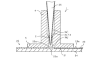
以下、本発明の第1実施の形態に係るマイクロ流路チップ用アダプタ1を、図1乃至図5を用いて説明する。以下の本明細書中の説明では、図1に図示する方向を上下方向として説明する。このマイクロ流路チップ用アダプタ1は、有機化合物、生体試料などの微量試料を先端25aから排出若しくは吸引するピペット25と、幅及び深さが500nm乃至1mmのマイクロ流路21内に注入される試料を混合、反応、合成、抽出、分離、分析するマイクロ流路チップ20とを連結する用途で用いられる。
The
マイクロ流路チップ20は、下面側のマイクロ流路21を構成する凹溝と上面から凹溝に貫通する複数の貫通孔22、22が形成されたPDMS(ポリジメチルシロキサン)からなる上層基板23のマイクロ流路21が露出する上層基板23の一面側に、上層基板23と同一の輪郭のPDMSからなる下層基板24を貼り付けて形成され、上下に一体に積層される上層基板23と下層基板24との間に、幅及び深さが500nm乃至1mmのマイクロ流路21が形成され、外部から遮断されたマイクロ流路21に、上層基板23の表面23aに開口する複数の貫通孔22、22がそれぞれ連通している。
The
マイクロ流路チップ用アダプタ1は、先細りのピペット25を挿入する連結孔3が鉛直方向に形成された円筒状の筒状本体4と、筒状本体4の底面4aに沿った外側に一体に形成され、円形の輪郭のフランジ板5とが、PDMS(ポリジメチルシロキサン)を成形材料として、後述する金型30を用いたインジェクション成形で一体に成形されている。
The
筒状本体4を上下方向の中心軸に沿って貫通する円筒孔である連結孔3は、図1に示すように、筒状本体4の上方に開口し、上方からピペット25を挿入自在とする大きさの大径部3aと、底面に開口し、大径部3aより細幅で、先細りのピペット25の中間外周面が当接する内径の小径孔3bとが、同一鉛直軸線に沿って形成され、大径部3aと小径孔3bは、その間の段部3cにより区切られている。
The connecting
本実施の形態では、段部3cに沿って小径孔3bの内壁面と一体に薄膜2が形成され、薄膜2によって、大径部3aと小径孔3bの間が遮断されている。薄膜2の厚さは、連結孔3に挿入するピペット25の先端25aによって容易に破られる厚さにとなっていて、PDMSで形成される薄膜2は、0.1mm以下の厚さとなっている。
In this embodiment, the
フランジ板5は、筒状本体4の連結孔3の中心軸周りの円環状に形成され、その底面5aは、連結孔3の中心軸に向かって上方に緩やかに湾曲する吸盤状に形成されている。フランジ板5の底面5aを吸盤状とすることにより、筒状本体4が起立する姿勢のマイクロ流路チップ用アダプタ1の中心を、マイクロ流路チップ20の貫通孔22が開口に向けて押し付けると、筒状本体4の連結孔3とマイクロ流路チップ20の貫通孔22が連通する位置で、フランジ板5が吸着板として作用し、マイクロ流路チップ用アダプタ1が貫通孔22の開口周囲の表面23aに密着して取り付けられる。
The
このマイクロ流路チップ用アダプタ1は、PDMSを成形材料として、図5に示す金型30を用いたインジェクション成形で、連結孔3a、3bが鉛直方向に形成された円筒状の筒状本体4と、連結孔3の一部を遮断する薄膜2と、フランジ板5とが一体に成形される。すなわち、図5に示すように、キャビテイ32側の突部32aで連結孔3の大径孔3aを、コア31側の突部31aで小径孔3bを成形し、突部32a、31a間の隙間で0.1mm以下の厚みの薄膜2を成形する。これにより、スライド金型等の複雑な金型構造を用いずに、コア31とキャビテイ32からなる簡単な構造の金型30によって連結孔3の一部を遮断する薄膜2を形成できる。金型を用いたマイクロ流路チップ用アダプタ1の成形は、インジェクション成形の他、トランスファー成形、コンプレッション成形等の種々の他の成形法で成形してもよい。
This
本実施の形態では、図2に示すように、同一の形状に成形されたマイクロ流路チップ用アダプタ1、1が、それぞれマイクロ流路21の両側で連通する一組の貫通孔22、22である注入孔22aと排出孔22bの開口周囲の表面23aに密着して取り付けられている。これにより、マイクロ流路21が外部に連通する注入孔22aと排出孔22bの開口は、その周囲の表面23aに密着するマイクロ流路チップ用アダプタ1、1に覆われる。マイクロ流路チップ用アダプタ1、1の連通孔12は、薄膜2で遮断されているので、マイクロ流路21の内部は、外部と完全に遮断された密封状態となる。
In this embodiment, as shown in FIG. 2,
このマイクロ流路チップ用アダプタ1、1が取り付けられたマイクロ流路チップ20に対して、紫外線照射、放射線照射、電子線照射、コロナ放電照射、プラズマ照射、蒸気加圧滅菌(オートクレーブ)等の減菌処理を行えば、マイクロ流路チップ20のマイクロ流路21へ試料を注入する直前まで、マイクロ流路21内を減菌した状態に維持することができる。
By subjecting the
本実施の形態にかかるマイクロ流路チップ用アダプタ1によれば、同一形状に量産したマイクロ流路チップ用アダプタ1のフランジ板5を吸着板として作用させ、注入孔22aや排出孔22bの数、開口位置が異なる種々のマイクロ流路チップ20に対して、注入孔22aや排出孔22bの各開口にマイクロ流路チップ用アダプタ1を押し付けて密着させるだけで、マイクロ流路21を密封状態として減菌処理を行うことができる。
According to the
ピペット25からマイクロ流路チップ20のマイクロ流路21へ試料を注入する際には、図3に示すように、ピペット25の先端25aを、注入孔22aの周囲に取り付けられたマイクロ流路チップ用アダプタ1の大径孔3aに挿入し、先細りのピペット25の中間の外周面が大径孔3aと小径孔3bを区切る段部3cに当接するまでピペット25を押し込む。この状態で、ピペット25の先端25aは、薄膜2を貫通して小径孔3b内に挿入される。小径孔3bは、注入孔22aを介してマイクロ流路21に連通しているので、ピペット25の先端25aから試料を吐出することによって、減菌状態のマイクロ流路21内に試料を注入できる。
When injecting a sample from the
マイクロ流路チップ用アダプタ1の円筒状の筒状本体4とフランジ板5は、PDMSからなる弾性材料で成形されているので、ピペット25をマイクロ流路チップ用アダプタ1の連結孔3の軸方向に対して傾斜する姿勢で挿入しても、筒状本体4は、ピペット25の挿入方向に追従して屈曲し、ピペット25の先端25aを薄膜2に貫通させることができ、また、ピペット25への外力を解けば、筒状本体4は、マイクロ流路チップ20の表面23aに対して鉛直方向に起立する姿勢に復帰し、連結孔3に挿入されたピペット25を鉛直方向に沿って支持できる。従って、マイクロ流路21へ試料を注入する際に、複数のピペット25を手で持たずに、マイクロ流路チップ用アダプタ1の連結孔3に挿入させた状態で保持することができる。
The
また、ピペット25の先端25aからマイクロ流路21へ注入される試料は、ピペット25を貫通させたPDMSの弾性材料からなる薄膜2がピペット25の中間の外周面にリング状に弾性接触するので、連結孔3の大径孔3a側に漏れ出ることがなく、ピペット25から所定の注入圧を加えてマイクロ流路21へ試料を注入しても、連結孔3の開口から試料が漏れ出ることがない。
In addition, the sample injected from the
尚、ピペット25から試料を注入する際には、ピペット25等の細長の治具を用いて排出孔22bの周囲に取り付けられたマイクロ流路チップ用アダプタ1の薄膜2を破り、排出孔22bを外部に連通させてもよい。
When injecting a sample from the
次に、本発明の第2実施の形態に係るマイクロ流路チップ用アダプタ10を、図6と図7を用いて説明する。第2実施の形態の説明において、第1実施の形態にかかる構成と同一若しくは同様に作用する構成については、同一番号を付してその詳細な説明を省略する。
Next, a
マイクロ流路チップ用アダプタ10は、先細りのピペット25を挿入する連結孔12が鉛直方向の中心軸に沿って形成された円筒形の筒状本体13からなり、筒状本体13は、PDMSを成形材料として、図中の薄膜11の部分をパーティングラインとするコアとキャビティからなる金型でインジェクション成形される。この筒状本体13についても、インジェクション成形の他、トランスファー成形、コンプレッション成形等の種々の他の成形法で成形してもよい。
The
筒状本体13を成形する際に、筒状本体13の底面13aを成形するコア金型の成形面は、算術平均荒さRaが、500nm以下で好ましくは300nm以下の鏡面としている。筒状本体13の底面13aを形成する成形材料は、金型内で流動性の高いPDMSであるので、鏡面加工された金型の成形面への転写性にすぐれ、筒状本体13の底面13aも成形面の算術平均荒さRaにほぼ等しい鏡面とすることができる。また、後述するように、マイクロ流路チップ用アダプタ10をマイクロ流路チップ20の表面23aに強固に一体化するため、マイクロ流路チップ用アダプタ10を固着する上層基板23の表面23aも同様に鏡面加工した金型の成形面で成形する。
When molding the
連結孔12は、図6に示すように、内壁面が上方に向かって拡径するテーパー面12a1となった逆裁頭円錐形の大径孔12aと、大径孔12aの下方で、筒状本体13の底面13aに開口する円柱形の小径孔12bとからなっている。大径孔12aの下端と小径孔12bは、同一の内径となっていて、同一鉛直軸線上に形成された大径孔12aと小径孔12bとの間は、小径孔12bの上端の内壁面に一体に形成され、連結孔12に挿入するピペット25の先端25aを容易に貫通させることが可能な0.1mm以下の厚さの薄膜11によって区切られている。
As shown in FIG. 6, the connecting
このように構成されたマイクロ流路チップ用アダプタ10は、鉛直方向に沿って起立する姿勢の筒状本体13の底面13aを、貫通孔22の開口を中心とするマイクロ流路チップ20の表面23aに密着させ、マイクロ流路チップ用アダプタ1を、貫通孔22の開口周囲の表面23aに一体に接合する。
The
この実施の形態では、接合する筒状本体13の底面13aと、マイクロ流路チップ20の貫通孔22が開口する周囲の表面23aとに、予めプラズマを照射するプラズマ処理を行う表面改質処理を行った後、起立姿勢の筒状本体13の底面13aを、貫通孔22が開口する周囲の表面23aに密着し、両者を一体に接合する。接合工程で、接合面となる筒状本体13の底面13aとマイクロ流路チップ20の表面23aは、上述の通り、算術平均荒さRaが300nm以下に鏡面加工されているので、対向して接する全ての表面改質されたこれらの接合面が隙間なく密着し、その結果、筒状本体13の底面13aと、マイクロ流路チップ20の表面23aとは、むらなく強固に一体化される。
In this embodiment, the bottom surface 13a of the
尚、プラズマを照射するプラズマ処理は、真空プラズマ処理と大気圧プラズマ処理のいずれであってもよく、また、接合面を表面改質する処理としては、プラズマ処理の他に、エキシマランプから接合面に真空紫外線(VUV)を照射する真空紫外線(VUV)処理、コロナー放電処理等であってもよい。 The plasma treatment in which plasma is irradiated may be either vacuum plasma treatment or atmospheric plasma treatment, and the treatment for modifying the surface of the bonding surface may be, in addition to plasma treatment, vacuum ultraviolet (VUV) treatment in which vacuum ultraviolet (VUV) rays are irradiated from an excimer lamp to the bonding surface, corona discharge treatment, etc.
図6に示すように、マイクロ流路チップ20の貫通孔22が開口する周囲の表面23aに、マイクロ流路チップ用アダプタ10が起立姿勢で取り付けられると、マイクロ流路チップ20の連結孔12の小径孔12bがマイクロ流路チップ20の貫通孔22を介してマイクロ流路21に連通するが、連結孔12は薄膜11によって遮断されているので、マイクロ流路21の内部は、外部と完全に遮断された密封状態となる。
As shown in FIG. 6, when the
従って、マイクロ流路チップ用アダプタ10が取り付けられたマイクロ流路チップ20に対して、紫外線照射、放射線照射、電子線照射、コロナ放電照射、プラズマ照射、蒸気加圧滅菌(オートクレーブ)等の減菌処理を行えば、マイクロ流路チップ20のマイクロ流路21に試料を注入する直前まで、マイクロ流路21内を減菌した状態で維持することができる。
Therefore, if the
マイクロ流路チップ20のマイクロ流路21へピペット25から試料を注入する際には、図7に示すように、ピペット25の先端25aを、マイクロ流路チップ用アダプタ10の大径孔12aに挿入する。大径孔12aの内面は、薄膜11に向かって傾斜するテーパー面12a1となっているので、ピペット25を大径孔12a内で更に下方に押しすすめると、その先端25aは、テーパー面12a1に案内され、薄膜11を貫通して小径孔12b内に挿入される。
When injecting a sample from a
この状態で、小径孔12bの内径は、下方に向かって先細りの形状に形成されたピペット25の中間部の外径にほぼ等しい内径となっているので、ピペット25の先端25aは、マイクロ流路チップ20に達する前に、連結孔12の小径孔3b内に位置決めされる。
In this state, the inner diameter of the
ピペット25の先端25aが挿入された小径孔12bは、貫通孔22(注入孔22a)を介してマイクロ流路21に連通しているので、ピペット25の先端25aから試料を吐出することによって、減菌状態のマイクロ流路21内に試料を注入できる。
The
ピペット25の先端25aが挿入された筒状本体13の連結孔12と連結孔が連通する貫通孔22の周囲は、表面改質された筒状本体13の底面13aとマイクロ流路チップ20の表面23aとが隙間なく密着して一体化されているので、ピペット25から所定の注入圧をかけて、試料をマイクロ流路21へ注入しても、マイクロ流路チップ用アダプタ10とマイクロ流路チップ20の表面23aとの隙間から試料が漏れ出ることがない。
The periphery of the connecting
また、ピペット25の先端25aからマイクロ流路21へ注入される試料は、ピペット25を貫通させたPDMSの弾性材料からなる薄膜11がピペット25の中間の外周面にリング状に弾性接触するので、連結孔12の大径孔12a側に漏れ出ることがなく、ピペット25から所定の注入圧を加えてマイクロ流路21へ試料を注入しても、連結孔12の開口から試料が漏れ出ることがない。
In addition, the sample injected from the
本実施の形態においても、マイクロ流路チップ20がマイクロ流路21に連通する排出孔22bを備えている場合には、排出口22bの開口周囲に、マイクロ流路チップ用アダプタ10を取り付けてもよく、ピペット25から試料を注入する際に、ピペット25等の細長の治具を用いてマイクロ流路チップ用アダプタ10の薄膜11を破り、排出孔22bを外部に連通させてもよい。
In this embodiment, if the
上述の第1、第2実施の形態では、ピペット25の先端25aからマイクロ流路21へ試料を注入する際に、注入孔22aの開口周囲に取り付けられるマイクロ流路チップ用アダプタ1,10の薄膜2,11にピペット25の先端25aを貫通させて、薄膜2,11を破いたが、予め細長の治具で薄膜2,11に開口を形成した後、ピペット25を連結孔12に挿入し、その先端25aから試料を注入してもよい。
In the first and second embodiments described above, when injecting a sample from the
また、薄膜2,11は、連結孔3、12を遮断するものであれば、連結孔3,12のいずれの位置に設けてもよい。
Furthermore, the
また、上述の各実施の形態では、マイクロ流路チップ用アダプタ1、10を、フランジ板5や表面改質工程を用いて、マイクロ流路チップ20の表面23aに密着する状態で取り付けているが、両面に粘着層を有する両面テープや接着剤を用いて、マイクロ流路チップ用アダプタ1、10を、マイクロ流路チップ20の貫通孔22が開口する開口周囲の表面23aに密着させて取り付けてもよい。
In addition, in each of the above-mentioned embodiments, the
本発明は、減菌状態としたマイクロ流路チップのマイクロ流路へ、ピペットから試料を注入するために、マイクロ流路チップに取り付けられるマイクロ流路チップ用アダプタに適している。 The present invention is suitable for a microchannel chip adapter that is attached to a microchannel chip in order to inject a sample from a pipette into the microchannel of the sterilized microchannel chip.
1、10 マイクロ流路チップ用アダプタ
2、11 薄膜
3、12 連結孔
20 マイクロ流路チップ
21 マイクロ流路
22 貫通孔
25 ピペット
1, 10
Claims (4)
マイクロ流路チップのマイクロ流路に連通する貫通孔に前記連結孔が連通する位置で、マイクロ流路チップの表面の前記貫通孔が開口する周囲に密着し、前記ピペットから前記マイクロ流路に試料が注入されるマイクロ流路チップ用アダプタであって、
前記筒状本体は、PDMS(ポリジメチルシロキサン)を成形材料として、前記連結孔が貫通する筒状に成形され、
前記ピペットの先端を貫通自在とする0.1mm以下の厚さで、前記連結孔を遮蔽し、前記マイクロ流路を外部と遮断して密封する薄膜が、前記筒状本体の前記連結孔の内壁面に一体に形成されていることを特徴とするマイクロ流路チップ用アダプタ。 A pipette tip is supported by a connecting hole extending through a cylindrical body.
a micro-channel chip adaptor that is in close contact with a periphery of an opening of a through-hole on a surface of a micro-channel chip at a position where the connecting hole is in communication with a through-hole that is in communication with a micro-channel of the micro-channel chip, and allows a sample to be injected from the pipette into the micro-channel,
The cylindrical main body is molded into a cylindrical shape with the connecting hole passing therethrough using PDMS (polydimethylsiloxane) as a molding material,
a thin film having a thickness of 0.1 mm or less , through which the tip of the pipette can be freely passed, that blocks the connecting hole and seals the microchannel by isolating it from the outside , is integrally formed on an inner wall surface of the connecting hole of the cylindrical main body.
前記薄膜は、前記段部に沿って前記連結孔の内壁面に一体に形成されていることを特徴とする請求項1に記載のマイクロ流路チップ用アダプタ。 A step portion is formed in the connecting hole to separate a small diameter hole that opens to the bottom surface of the cylindrical main body and a large diameter hole that opens to a flat surface,
2. The micro-channel chip adaptor according to claim 1, wherein the thin film is integrally formed on an inner wall surface of the connection hole along the step portion.
前記フランジ板の底面は、前記連結孔の底面側の開口に向かって緩やかに湾曲する吸盤状に形成されていることを特徴とする請求項1乃至請求項3のいずれか1項に記載のマイクロ流路チップ用アダプタ。 The cylindrical body further includes a flange plate integrally formed on the outside along the bottom surface thereof,
4. The micro-channel chip adaptor according to claim 1, wherein the bottom surface of the flange plate is formed in a suction cup shape that is gently curved toward the opening on the bottom side of the connection hole.
Priority Applications (1)
| Application Number | Priority Date | Filing Date | Title |
|---|---|---|---|
| JP2021040447A JP7689432B2 (en) | 2021-03-12 | 2021-03-12 | Microfluidic Chip Adapter |
Applications Claiming Priority (1)
| Application Number | Priority Date | Filing Date | Title |
|---|---|---|---|
| JP2021040447A JP7689432B2 (en) | 2021-03-12 | 2021-03-12 | Microfluidic Chip Adapter |
Publications (2)
| Publication Number | Publication Date |
|---|---|
| JP2022139882A JP2022139882A (en) | 2022-09-26 |
| JP7689432B2 true JP7689432B2 (en) | 2025-06-06 |
Family
ID=83399714
Family Applications (1)
| Application Number | Title | Priority Date | Filing Date |
|---|---|---|---|
| JP2021040447A Active JP7689432B2 (en) | 2021-03-12 | 2021-03-12 | Microfluidic Chip Adapter |
Country Status (1)
| Country | Link |
|---|---|
| JP (1) | JP7689432B2 (en) |
Citations (4)
| Publication number | Priority date | Publication date | Assignee | Title |
|---|---|---|---|---|
| JP2012159358A (en) | 2011-01-31 | 2012-08-23 | Konica Minolta Holdings Inc | Inspection system and liquid feeding device used in the same |
| WO2017073601A1 (en) | 2015-10-30 | 2017-05-04 | コニカミノルタ株式会社 | Liquid feeding method, liquid feeding device, and analysis device |
| JP2017523412A (en) | 2014-07-18 | 2017-08-17 | テカン・トレーディング・アクチェンゲゼルシャフトTECAN Trading AG | Microfluidic cartridge with pipette operation guide |
| JP2019203806A (en) | 2018-05-24 | 2019-11-28 | フコク物産株式会社 | adapter |
-
2021
- 2021-03-12 JP JP2021040447A patent/JP7689432B2/en active Active
Patent Citations (4)
| Publication number | Priority date | Publication date | Assignee | Title |
|---|---|---|---|---|
| JP2012159358A (en) | 2011-01-31 | 2012-08-23 | Konica Minolta Holdings Inc | Inspection system and liquid feeding device used in the same |
| JP2017523412A (en) | 2014-07-18 | 2017-08-17 | テカン・トレーディング・アクチェンゲゼルシャフトTECAN Trading AG | Microfluidic cartridge with pipette operation guide |
| WO2017073601A1 (en) | 2015-10-30 | 2017-05-04 | コニカミノルタ株式会社 | Liquid feeding method, liquid feeding device, and analysis device |
| JP2019203806A (en) | 2018-05-24 | 2019-11-28 | フコク物産株式会社 | adapter |
Also Published As
| Publication number | Publication date |
|---|---|
| JP2022139882A (en) | 2022-09-26 |
Similar Documents
| Publication | Publication Date | Title |
|---|---|---|
| US8956530B2 (en) | System for separating bodily fluid constituents and method for producing such a system | |
| US9168524B2 (en) | Microfluidic storage device for pre-storing of fluid, method for its production and a use thereof | |
| US7842157B2 (en) | Method for bonding plastic micro chip | |
| US8900529B2 (en) | Microfluidic chamber device and fabrication | |
| KR100883951B1 (en) | Device with own sealing fluid port | |
| JPWO2008087800A1 (en) | Microchip manufacturing method and microchip | |
| KR20110072275A (en) | Microfluidic device and its manufacturing method | |
| US20210016280A1 (en) | Microfluidic package, holder, nad methods of making the same | |
| US12017220B2 (en) | Microfluidic chip and valve, production process and uses | |
| JP2012159337A (en) | Sample liquid supply jig, sample liquid supply jig set and microchip set | |
| JP5187442B2 (en) | Microchip | |
| JP7689432B2 (en) | Microfluidic Chip Adapter | |
| JPWO2018012429A1 (en) | Fluid device, method of manufacturing fluid device, and valve for fluid device | |
| JP7052102B2 (en) | adapter | |
| US10946376B2 (en) | Carrier element for introducing a dry substance into a flow cell | |
| JP2010517001A (en) | Microfluidic chip having side openings for fluid introduction | |
| US20110135538A1 (en) | Microchip | |
| JP2007240461A (en) | Plastic microchip, joining method therefor, and biochip or micro analytical chip using the same | |
| JP2019093377A (en) | Fluid chip, fluid device and method for manufacturing therefor | |
| US20100310437A1 (en) | Microchip and Method for Manufacturing the Same | |
| CN109196328A (en) | Accessories for liquid injection | |
| JP2015216851A (en) | Cell culture devices | |
| JP7173759B2 (en) | microfluidic chip | |
| JP2010217145A (en) | Microchip and microchip set | |
| WO2010016371A1 (en) | Microchip, microchip manufacturing method and microchip manufacturing device |
Legal Events
| Date | Code | Title | Description |
|---|---|---|---|
| A621 | Written request for application examination |
Free format text: JAPANESE INTERMEDIATE CODE: A621 Effective date: 20240227 |
|
| A977 | Report on retrieval |
Free format text: JAPANESE INTERMEDIATE CODE: A971007 Effective date: 20241129 |
|
| A131 | Notification of reasons for refusal |
Free format text: JAPANESE INTERMEDIATE CODE: A131 Effective date: 20241218 |
|
| A521 | Request for written amendment filed |
Free format text: JAPANESE INTERMEDIATE CODE: A523 Effective date: 20250128 |
|
| TRDD | Decision of grant or rejection written | ||
| A01 | Written decision to grant a patent or to grant a registration (utility model) |
Free format text: JAPANESE INTERMEDIATE CODE: A01 Effective date: 20250513 |
|
| A61 | First payment of annual fees (during grant procedure) |
Free format text: JAPANESE INTERMEDIATE CODE: A61 Effective date: 20250527 |
|
| R150 | Certificate of patent or registration of utility model |
Ref document number: 7689432 Country of ref document: JP Free format text: JAPANESE INTERMEDIATE CODE: R150 |