JP7682425B2 - Fault detection circuit and passenger monitoring device - Google Patents
Fault detection circuit and passenger monitoring device Download PDFInfo
- Publication number
- JP7682425B2 JP7682425B2 JP2025512856A JP2025512856A JP7682425B2 JP 7682425 B2 JP7682425 B2 JP 7682425B2 JP 2025512856 A JP2025512856 A JP 2025512856A JP 2025512856 A JP2025512856 A JP 2025512856A JP 7682425 B2 JP7682425 B2 JP 7682425B2
- Authority
- JP
- Japan
- Prior art keywords
- transistor
- terminal
- light
- led
- diode
- Prior art date
- Legal status (The legal status is an assumption and is not a legal conclusion. Google has not performed a legal analysis and makes no representation as to the accuracy of the status listed.)
- Active
Links
Images


Classifications
-
- H—ELECTRICITY
- H05—ELECTRIC TECHNIQUES NOT OTHERWISE PROVIDED FOR
- H05B—ELECTRIC HEATING; ELECTRIC LIGHT SOURCES NOT OTHERWISE PROVIDED FOR; CIRCUIT ARRANGEMENTS FOR ELECTRIC LIGHT SOURCES, IN GENERAL
- H05B45/00—Circuit arrangements for operating light-emitting diodes [LED]
- H05B45/50—Circuit arrangements for operating light-emitting diodes [LED] responsive to malfunctions or undesirable behaviour of LEDs; responsive to LED life; Protective circuits
- H05B45/54—Circuit arrangements for operating light-emitting diodes [LED] responsive to malfunctions or undesirable behaviour of LEDs; responsive to LED life; Protective circuits in a series array of LEDs
-
- H—ELECTRICITY
- H05—ELECTRIC TECHNIQUES NOT OTHERWISE PROVIDED FOR
- H05B—ELECTRIC HEATING; ELECTRIC LIGHT SOURCES NOT OTHERWISE PROVIDED FOR; CIRCUIT ARRANGEMENTS FOR ELECTRIC LIGHT SOURCES, IN GENERAL
- H05B47/00—Circuit arrangements for operating light sources in general, i.e. where the type of light source is not relevant
- H05B47/20—Responsive to malfunctions or to light source life; for protection
- H05B47/23—Responsive to malfunctions or to light source life; for protection of two or more light sources connected in series
Landscapes
- Circuit Arrangement For Electric Light Sources In General (AREA)
- Testing Of Short-Circuits, Discontinuities, Leakage, Or Incorrect Line Connections (AREA)
Description
本開示は、故障検出回路及び乗員監視装置に関するものである。 The present disclosure relates to a fault detection circuit and an occupant monitoring device.
従来、LED(Light Emitting Diode)などの半導体発光素子を光源に用いた車両用灯具の点灯を制御するための点灯制御回路が知られている。例えば、特許文献1には、N(Nは正の整数)個直列に接続された半導体光源であって、N個の半導体光源に静電保護素子がそれぞれ並列接続されているものを負荷として、N個の半導体光源に対する電流と電圧を制御する制御手段と、N個の半導体光源の電流が異常値を示すときに断線検出信号を出力する断線検出手段と、N個の半導体光源のうち複数個の半導体光源を検出対象として、複数個の半導体光源の両端電圧の総和が複数個の半導体光源のフォワード電圧の総和よりも低下したことを検出する複数の電圧低下検出手段と、複数の電圧低下検出手段の検出出力の論理和を断線検出信号として出力する電圧低下論理手段とを備えてなる車両用灯具の点灯制御回路が開示されている。Conventionally, there is known a lighting control circuit for controlling the lighting of a vehicle lamp using a semiconductor light emitting element such as an LED (Light Emitting Diode) as a light source. For example, Patent Document 1 discloses a lighting control circuit for a vehicle lamp, which includes a control means for controlling the current and voltage to N semiconductor light sources (N is a positive integer) connected in series, with electrostatic protection elements connected in parallel to each of the N semiconductor light sources as a load, a disconnection detection means for outputting a disconnection detection signal when the current of the N semiconductor light sources shows an abnormal value, a plurality of voltage drop detection means for detecting that the sum of the voltages across the plurality of semiconductor light sources is lower than the sum of the forward voltages of the plurality of semiconductor light sources, with a plurality of semiconductor light sources being detection targets, and a voltage drop logic means for outputting the logical sum of the detection outputs of the plurality of voltage drop detection means as a disconnection detection signal.
LEDなどの半導体発光素子は、車両用灯具以外にも様々な機器の光源として用いられる場合がある。例えば、乗員監視装置(Driver Monitoring System;DMS)では、車室内の乗員を照射するための光源として、IR-LED(Infra-Red LED)を直列に複数個接続したものが使用される。この場合、IR-LEDは、乗員に赤外線を確実に照射するために、設置スペースの限られた車室内において、当該IR-LEDが実装された基板の設置角度を調整して、赤外線の照射方向を変えられることが望ましい。Semiconductor light-emitting elements such as LEDs may be used as light sources for various devices other than vehicle lighting. For example, in a driver monitoring system (DMS), a number of IR-LEDs (Infra-Red LEDs) connected in series are used as a light source for irradiating passengers in the vehicle cabin. In this case, in order to reliably irradiate passengers with infrared rays, it is desirable to be able to change the direction of infrared radiation by adjusting the installation angle of the board on which the IR-LEDs are mounted in a vehicle cabin where installation space is limited.
一方、乗員監視装置において照明光源に用いられるIR-LEDについても、故障検出は必要である。そこで、特許文献1記載の点灯制御回路における故障検出の手法を、乗員監視装置で用いられるIR-LEDの故障検出に応用することが考えられる。しかしながら、特許文献1記載の点灯制御回路は、半導体光源から照射される光の照射方向を可変とすることについて考慮されていない。そのため、特許文献1に記載された故障検出の手法を、乗員監視装置で用いられるIR-LEDの故障検出に応用することは困難であった。On the other hand, fault detection is also necessary for IR-LEDs used as illumination light sources in passenger monitoring devices. It is therefore conceivable that the fault detection technique in the lighting control circuit described in Patent Document 1 could be applied to fault detection of IR-LEDs used in passenger monitoring devices. However, the lighting control circuit described in Patent Document 1 does not take into consideration varying the direction of light emitted from the semiconductor light source. For that reason, it has been difficult to apply the fault detection technique described in Patent Document 1 to fault detection of IR-LEDs used in passenger monitoring devices.
本開示は上記のような課題を解決するためになされたもので、発光素子により照射される光の照射方向が調整可能であり、かつ当該発光素子の故障を検出可能な故障検出回路を得ることを目的とする。The present disclosure has been made to solve the above-mentioned problems, and aims to obtain a fault detection circuit that is capable of adjusting the direction of light emitted by a light-emitting element and detecting a fault in the light-emitting element.
本開示に係る故障検出回路は、駆動電圧を出力する駆動回路が実装された第1の基板と、駆動回路から出力された駆動電圧により駆動する、互いに直列に接続された複数の発光素子と、当該複数の発光素子のうちの1つ以上の故障を検出するための故障検出部とが実装された第2の基板と、を備え、第1の基板と第2の基板とは、別々の基板として構成されているものである。故障検出部は、複数の発光素子のそれぞれに対して並列に設けられた抵抗と、抵抗のそれぞれに対して並列に設けられた第1のトランジスタと、第1のトランジスタのそれぞれに対して並列に設けられ、かつ互いに直列に接続された第2のトランジスタと、第2のトランジスタのそれぞれの出力信号の論理積を示す信号を出力する第3のトランジスタと、第3のトランジスタの出力信号の反転信号を故障検出信号として出力する第4のトランジスタと、を含んで構成される。 The fault detection circuit according to the present disclosure includes a first substrate on which a drive circuit that outputs a drive voltage is mounted, a plurality of light-emitting elements connected in series to each other and driven by the drive voltage output from the drive circuit, and a fault detection unit for detecting a fault in one or more of the plurality of light-emitting elements, the first substrate and the second substrate being configured as separate substrates. The fault detection unit includes resistors provided in parallel with each of the plurality of light-emitting elements, first transistors provided in parallel with each of the resistors, second transistors provided in parallel with each of the first transistors and connected in series with each other, a third transistor that outputs a signal indicating the logical product of each output signal of the second transistor, and a fourth transistor that outputs an inverted signal of the output signal of the third transistor as a fault detection signal.
本開示によれば、発光素子により照射される光の照射方向が調整可能であり、かつ当該発光素子の故障を検出可能な故障検出回路を得ることができる。 According to the present disclosure, it is possible to obtain a fault detection circuit that is capable of adjusting the direction of light emitted by a light-emitting element and detecting a fault in the light-emitting element.
以下、本開示の実施の形態について、図面を参照しながら詳細に説明する。
実施の形態1.
Hereinafter, embodiments of the present disclosure will be described in detail with reference to the drawings.
Embodiment 1.
図1は、実施の形態1に係る故障検出回路1を備えた乗員監視装置(Driver Monitoring System;DMS)10の構成例を示す図である。図1に示す乗員監視装置10は、例えば車両100に搭載され、車両100の乗員を監視する。
Figure 1 is a diagram showing an example configuration of a driver monitoring system (DMS) 10 equipped with a fault detection circuit 1 according to embodiment 1. The
図1に示すように、乗員監視装置10は、カメラ(撮像装置)11、投光器12、及び制御装置(ECU)13を含んで構成される。なお、乗員監視装置10は、車両100の主電源がオンとなった場合(例えば、イグニッションがオンとなった場合)に動作を開始し、オフとなった場合に動作を終了する。As shown in Fig. 1, the
カメラ11は、例えば車両100のインストゥルメントパネルのうち、運転席の正面に近い位置(例えばメータ付近)に取り付けられている。カメラ11の撮影範囲は、乗員(ドライバ)が運転席に着座したときに、乗員の顔が通常の場合に位置するであろう空間領域を含むように設定されている。すなわち、カメラ11は、運転席に着座した乗員の顔を正面から撮影できるように配置されている。The
このカメラ11は、乗員監視装置10の動作中、繰り返し定期的に(例えば1秒に30回)乗員の顔を撮影し、その撮影の結果得た撮像画像(すなわち、顔を含む画像)を、撮影順に逐次制御装置13に出力する。While the
なお、カメラ11は、撮影の際には、主に近赤外光を利用する。具体的には、カメラ11には、近赤外光以外の光をほぼ遮るフィルタが取り付けられており、そのフィルタ越しに受けた光を用いて撮影を行うようになっている。Camera 11 mainly uses near-infrared light when taking pictures. Specifically,
投光器12は、運転席に着座した乗員の顔に主に近赤外光を照射するための装置である。この投光器12によって照射された近赤外光が乗員の顔で反射することで、カメラ11によって撮影される顔の撮像画像が、外部の環境に大きく影響されることなく、鮮明になる。The
投光器12としては、例えば近赤外光を照射する発光素子(IR-LED)が用いられる。この投光器12は、例えば車両100のインストゥルメントパネルのうち、運転席の正面に近い位置に取り付けられている。そして、投光器12は、乗員が運転席に着座したときに、乗員の顔が通常の場合に位置するであろう空間領域に赤外光が照射されるように、配置されている。
For example, a light-emitting element (IR-LED) that emits near-infrared light is used as the
なお、投光器12は、制御装置13からの制御に基づいて、カメラ11による撮影のタイミングに合わせて光を照射するようになっていてもよいし、乗員監視装置10の動作中は常時光を照射し続けるようになっていてもよい。In addition, the
制御装置(ECU)13は、いずれも不図示のCPU、RAM、ROM、フラッシュメモリ、及びI/O等を有するマイコン等からなる。そして、CPUがROMから読み出したプログラムをRAMに読み出して実行し、その実行の際に、必要に応じてフラッシュメモリ、カメラ11等から情報を取得する。このようなCPU等の動作により、制御装置13の動作が実現する。The control device (ECU) 13 is composed of a microcomputer having a CPU, RAM, ROM, flash memory, and I/O, all of which are not shown. The CPU reads a program from the ROM into the RAM and executes it, and during execution, obtains information from the flash memory,
具体的には、制御装置13は、カメラ11から受信した乗員の顔の撮像画像に基づいて、乗員の顔動作状態を逐次判定し、その判定結果に基づいて、所定の処理を実行する。ここで、乗員の顔動作状態とは、乗員の顔の動作の状態をいう。例えば、顔の向き、開眼度(すなわち、瞼の開き度合い)、及び視線方向(すなわち、乗員が見ている方向)は、それぞれ顔動作状態の一種である。Specifically, the
<故障検出回路1>
故障検出回路1は、例えば乗員監視装置10に設けられる。この場合、故障検出回路1は、投光器12に用いられるLEDの故障を検出する。
<Fault detection circuit 1>
The failure detection circuit 1 is provided in, for example, an
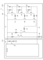
故障検出回路1の構成例を図2に示す。故障検出回路1は、例えば図2に示すように、第1の基板PL1と第2の基板PL2とを備えている。第1の基板PL1と第2の基板PL2とは、別々の基板として構成されている。なお、故障検出回路1による故障検出の対象となるLED、すなわち投光器12に用いられるIR-LEDは、複数個が直列に接続された状態で、第2の基板PL2に実装されている。図2の例では、3つのIR-LED31~33(以下、単に「LED31~33」ともいう。)が直列に接続された状態で、第2の基板PL2に実装されている。
An example of the configuration of the fault detection circuit 1 is shown in Figure 2. For example, as shown in Figure 2, the fault detection circuit 1 includes a first board PL1 and a second board PL2. The first board PL1 and the second board PL2 are configured as separate boards. The LEDs that are the subject of fault detection by the fault detection circuit 1, i.e., the IR-LEDs used in the
一方、第1の基板PL1には、駆動回路であるLED-DR21が実装されている。LED-DR21は、LED31~33が駆動するための駆動電圧を出力するほか、LED31~33の動作を制御する。On the other hand, the first board PL1 is equipped with a drive circuit, LED-DR21. LED-DR21 outputs a drive voltage for driving
第1の基板PL1と第2の基板PL2とは、接続線(例えば車両ハーネス)により接続された状態で、互いに離間して車両100に配置されている。例えば、第1の基板PL1は、上述の制御装置(ECU)13の内部に収容された状態で配置される。一方、第2の基板PL2は、上述の投光器12の内部に収容された状態で配置される。このとき、第1の基板PL1と第2の基板PL2とは、いずれも、他方の基板の設置角度にかかわらず、自身の設置角度を任意に調整可能となるように構成されている。以下、第1の基板PL1及び第2の基板PL2について説明する。The first substrate PL1 and the second substrate PL2 are arranged on the
<第1の基板PL1>
第1の基板PL1には、駆動回路であるLED-DR21が実装されている。LED-DR21は、プラス端子が接続線L1に接続され、マイナス端子が接続線L2に接続されている。
<First substrate PL1>
The first substrate PL1 is mounted with a drive circuit LED-DR21. The LED-DR21 has a positive terminal connected to the connection line L1 and a negative terminal connected to the connection line L2.
LED-DR21は、所定の電圧値を有する駆動電圧をプラス端子から発生させる。これにより、LED-DR21は、接続線L1を介して、第2の基板PL2に実装されたLED31~33を駆動するための直流電流(以下、単に「電流」ともいう。)をLED31~33に供給する。なお、以下の説明では、LED-DR21が上記駆動電圧を発生させたときの接続線L1の電圧を「入力電圧」ともいう。 LED-DR21 generates a drive voltage having a predetermined voltage value from the positive terminal. As a result, LED-DR21 supplies a direct current (hereinafter also simply referred to as "current") for driving LEDs 31-33 mounted on the second board PL2 to LEDs 31-33 via connection line L1. In the following explanation, the voltage of connection line L1 when LED-DR21 generates the drive voltage is also referred to as the "input voltage".
また、LED-DR21は、入力電圧の電圧値を監視するための端子である電圧モニター端子22を備えている。電圧モニター端子22は、信号線及び抵抗を介して接続線L1と接続されている。LED-DR21は、電圧モニター端子22を介して入力電圧を随時監視しており、当該入力電圧の電圧値に基づいて、LED31~33に故障が発生したことを検出する。
LED-DR21 also has a
<第2の基板PL2>
第2の基板PL2には、LED-DR21から出力された駆動電圧により駆動する、互いに直列に接続された3つのLED31~33と、当該3つのLED31~33のうちの1つ以上の故障を検出する故障検出部40と、が実装されている。
<Second substrate PL2>
The second substrate PL2 is equipped with three
なお、ここでは、説明の便宜上、3つのLED31~33が直列に接続された例を説明するが、LEDの個数はこれに限らず、複数であればよい。また、ここでは、説明の便宜上、図2の左右方向における左方の端部、及び図2の上下方向における上方の端部を「一方の端部」といい、図2の左右方向における右方の端部、及び図2の上下方向における下方の端部を「他方の端部」という。
Note that, for ease of explanation, an example in which three
第2の基板PL2において、直列に接続された3つのLED31~33のうち、一方の端部のLED31は、アノードが、接続線L1を介してLED-DR21のプラス端子に接続され、カソードが、当該LED31の他方の端部側に隣接するLED32のアノードに接続されている。On the second substrate PL2, of the three
LED32は、アノードが、当該LED32の一方の端部側に隣接するLED31のカソードに接続され、カソードが、当該LED32の他方の端部側に隣接するLED33のアノードに接続されている。The anode of
他方の端部のLED33は、アノードが、当該LED33の一方の端部側に隣接するLED32のカソードに接続され、カソードが、接続線L2を介してLED-DR21のマイナス端子に接続されている。なお、接続線L2は、抵抗50を介してグランドに接地されている。The anode of the LED 33 at the other end is connected to the cathode of the
<故障検出部40>
故障検出部40は、3つのLED31~33のうちの1つ以上の故障を検出する。ここで、故障検出部40により検出される故障は、オープン故障及びショート故障の双方である。
<
The
故障検出部40は、抵抗41~49と、第1のトランジスタ51~53と、第2のトランジスタ61~63と、第3のトランジスタ71と、第4のトランジスタ81と、を含んで構成されている。The
<抵抗41~49>
抵抗41~43は、LED31~33のそれぞれに対して並列に設けられている。具体的には、抵抗41は、一方の端部がLED31のアノードに接続され、他方の端部がLED31のカソードに接続されている。同様に、抵抗42は、一方の端部がLED32のアノードに接続され、他方の端部がLED32のカソードに接続されている。また、抵抗43は、一方の端部がLED33のアノードに接続され、他方の端部がLED33のカソードに接続されている。なお、抵抗41~43の抵抗値は、LED31~33のオン抵抗よりも大きく設定されている
<
The
抵抗44は、一方の端部が第1のトランジスタ51のコレクタ端子に接続され、他方の端部が第2のトランジスタ61のベース端子に接続されている。同様に、抵抗45は、一方の端部が第1のトランジスタ52のコレクタ端子に接続され、他方の端部が第2のトランジスタ62のベース端子に接続されている。また、抵抗46は、一方の端部が第1のトランジスタ53のコレクタ端子に接続され、他方の端部が第2のトランジスタ63のベース端子に接続されている。One end of
抵抗47は、一方の端部が第2のトランジスタ63のエミッタ端子に接続され、他方の端部が第3のトランジスタ71のベース端子に接続されている。また、抵抗48は、一方の端部がLED-DR21のプラス端子に接続され、他方の端部が第3のトランジスタ71のコレクタ端子に接続されている。また、抵抗49は、一方の端部がLED-DR21のプラス端子に接続され、他方の端部が第4のトランジスタ81のコレクタ端子に接続されている。One end of
<第1のトランジスタ51~53>
第1のトランジスタ51~53は、PNPトランジスタであり、抵抗41~43のそれぞれに対して並列に設けられている。
<
The
具体的には、第1のトランジスタ51は、エミッタ端子が、LED31のアノードに接続され、ベース端子がLED31のカソードに接続されている。また、コレクタ端子は、抵抗44を介して、第1のトランジスタ51に対応する第2のトランジスタ61のベース端子に接続されている。Specifically, the emitter terminal of the
同様に、第1のトランジスタ52は、エミッタ端子が、LED32のアノードに接続され、ベース端子がLED32のカソードに接続されている。また、コレクタ端子は、抵抗45を介して、第1のトランジスタ52に対応する第2のトランジスタ62のベース端子に接続されている。Similarly, the
また、第1のトランジスタ53は、エミッタ端子が、LED33のアノードに接続され、ベース端子がLED33のカソードに接続されている。また、コレクタ端子は、抵抗46を介して、第1のトランジスタ53に対応する第2のトランジスタ63のベース端子に接続されている。The emitter terminal of the
<第2のトランジスタ61~63>
第2のトランジスタ61~63は、NPNトランジスタであり、第1のトランジスタ51~53のそれぞれに対して並列に、かつ、互いに直列に接続して設けられている。
<
The
具体的には、第2のトランジスタ61~63のうち、一方の端部のLED31に対応する第2のトランジスタ61は、コレクタ端子が、LED-DR21のプラス端子に接続され、ベース端子が、抵抗44を介して、当該第2のトランジスタ61に対応する第1のトランジスタ51のコレクタ端子に接続されている。また、エミッタ端子は、当該第2のトランジスタ61の他方の端部側に隣接する第2のトランジスタ62のコレクタ端子に接続されている。Specifically, of the
第2のトランジスタ61~63のうち、一方の端部と他方の端部との間のLED32に対応する第2のトランジスタ62は、コレクタ端子が、当該第2のトランジスタ62の一方の端部側に隣接する第2のトランジスタ61のエミッタ端子に接続され、ベース端子が、抵抗45を介して、第2のトランジスタ62に対応する第1のトランジスタ52のコレクタ端子に接続されている。また、エミッタ端子は、当該第2のトランジスタ62の他方の端部側に隣接する第2のトランジスタ63のコレクタ端子に接続されている。Of the
また、第2のトランジスタ61~63のうち、他方の端部のLED33に対応する第2のトランジスタ63は、コレクタ端子が、当該第2のトランジスタ63の一方の端部側に隣接する第2のトランジスタ62のエミッタ端子に接続され、ベース端子が、抵抗46を介して、第2のトランジスタ63に対応する第1のトランジスタ53のコレクタ端子に接続されている。また、エミッタ端子は、第3のトランジスタ71のベース端子に接続されている。Among the
<第3のトランジスタ71>
第3のトランジスタ71は、NPNトランジスタであり、第2のトランジスタ61~63のそれぞれの出力信号の論理積を示す信号を出力する。具体的には、第3のトランジスタ71は、コレクタ端子が、抵抗48を介して、LED-DR21のプラス端子に接続され、ベース端子が、抵抗47を介して、他方の端部のLED33に対応する第2のトランジスタ63のエミッタ端子に接続されている。また、エミッタ端子は、LED-DR21のマイナス端子に接続されている。
<
The
<第4のトランジスタ81>
第4のトランジスタ81は、NPNトランジスタであり、第3のトランジスタ71の出力信号の反転信号を故障検出信号として出力する。具体的には、第4のトランジスタ81は、コレクタ端子が、抵抗49を介して、LED-DR21のプラス端子に接続され、ベース端子が、第3のトランジスタ71のコレクタ端子に接続されている。また、エミッタ端子は、LED-DR21のマイナス端子に接続されている。
<
The
以上のように構成された故障検出回路1では、3つのLED31~33は、当該各LED31~33に対応して設けられた、抵抗41~43、第1のトランジスタ51~53、及び第2のトランジスタ61~63とともに素子ユニットを構成する。そして、故障検出回路1では、各LED31~33は、第2の基板PL2に対して当該素子ユニット単位で実装可能に構成されている。In the fault detection circuit 1 configured as described above, the three
次に、図2に示す故障検出回路1の動作例について説明する。なお、以下の説明では、故障検出回路1の動作例を、(1)3つのLEDがいずれも正常に動作している(故障が発生していない)場合(以下、「正常動作時」ともいう。)、(2)3つのLEDのうちの1つ以上のLEDがショート故障した場合(以下、「ショート故障時」ともいう。)、(3)3つのLEDのうちの1つ以上のLEDがオープン故障した場合(以下、「オープン故障時」ともいう。)、の3通りに分けて説明する。Next, an example of the operation of the fault detection circuit 1 shown in Fig. 2 will be described. In the following description, the example of the operation of the fault detection circuit 1 will be described in three cases: (1) when all three LEDs are operating normally (no fault has occurred) (hereinafter also referred to as "normal operation"); (2) when one or more of the three LEDs have a short circuit failure (hereinafter also referred to as "short circuit failure"); and (3) when one or more of the three LEDs have an open circuit failure (hereinafter also referred to as "open circuit failure").
なお、故障検出回路1の動作例において、LED-DR21が駆動電圧を出力する前の状態(初期状態)では、第1のトランジスタ51~53、第2のトランジスタ61~63、第3のトランジスタ71、及び第4のトランジスタ81はいずれもオフである。In addition, in an example of operation of the fault detection circuit 1, in the state before LED-DR21 outputs the drive voltage (initial state), the
(1)正常動作時
まず、LED-DR21は駆動電圧を出力する。これにより、接続線L1に電流が生じる。また、LED-DR21は、電圧モニター端子22を介して、入力電圧の監視を開始する。
(1) During normal operation First, the LED-
このとき、抵抗41の抵抗値は、LED31のオン抵抗よりも大きいため、接続線L1に生じた電流のほとんどはLED31へ流れ、さらにLED32~33へ流れる。これにより、LED31~33が動作(発光)し、各LEDに所定の順方向電圧(Vf)が発生する。この順方向電圧により、第1のトランジスタ51~53では、エミッタ-ベース間に電位差が発生し、第1のトランジスタ51~53がオンとなる。At this time, because the resistance value of
第1のトランジスタ51~53がオンとなると、第2のトランジスタ61~63のベース端子に電流が流れ、第2のトランジスタ61~63もオンとなる。第2のトランジスタ61~63がオンとなると、第3のトランジスタ71のベース端子に電流が流れ、第3のトランジスタ71もオンとなる。When the
第3のトランジスタ71がオンとなると、第4のトランジスタ81のベース端子には接続線L1からの電流が流れず、第4のトランジスタ81はオフのままとなる。第4のトランジスタ81がオフのままであると、LED-DR21が電圧モニター端子22を介して監視する入力電圧の電圧値は、LED-DR21が出力した駆動電圧の電圧値とほぼ同じとなる。この場合、LED-DR21は、LEDの故障を検出しない。そして、故障検出回路1は、LED31~33の正常動作が継続する間は、上記のように動作する。
When the
(2)ショート故障時
例えば、正常動作時において、3つのLEDのうち、LED31のみがショート故障したとする。このとき、LED31には接続線L1に生じた電流のほとんどが流れるが、LED31がショート故障していることにより、LED31には順方向電圧が発生しない。その結果、第1のトランジスタ51では、エミッタ-ベース間での電圧降下が発生せず、エミッタ-ベース間が同電位となる。これにより、第1のトランジスタ51がオフとなる。第1のトランジスタ51がオフとなると、第2のトランジスタ61のベース端子に電流が流れず、第2のトランジスタ61もオフとなる。
(2) In the event of a short circuit For example, assume that during normal operation, only LED31 of the three LEDs experiences a short circuit. At this time, most of the current generated in the connection line L1 flows through LED31, but since LED31 has a short circuit, no forward voltage is generated in LED31. As a result, in the
一方、LED32~33は正常に動作しているため、第1のトランジスタ52~53、及び第2のトランジスタ62~63はいずれもオンのままとなる。 On the other hand, since LEDs 32-33 are operating normally, the first transistors 52-53 and the second transistors 62-63 both remain on.
第2のトランジスタ61がオフとなると、第2のトランジスタ62~63がオンであっても、第2のトランジスタ61~63全体には電流が流れないため、第3のトランジスタ71のベース端子にも電流が流れない。その結果、第3のトランジスタ71もオフとなる。この場合、第3のトランジスタ71がオフとなることは、第3のトランジスタ71が、第2のトランジスタ61~63による出力信号の論理積(AND)を示す信号を出力することと同義である。When the
第3のトランジスタ71がオフとなると、接続線L1からの電流が抵抗48を介して第4のトランジスタ81のベース端子に流れ、第4のトランジスタ81がオンとなる。この場合、第4のトランジスタ81がオンとなることは、第4のトランジスタ81が、第3のトランジスタ71よる出力信号の反転信号を出力することと同義である。When the
第4のトランジスタ81がオンとなると、接続線L1とL2とが短絡する。すると、LED-DR21が電圧モニター端子22を介して監視する入力電圧の電圧値はほぼ0となる。LED-DR21は、入力電圧の電圧値がほぼ0となったことをもって、LEDの故障を検出する。この場合、第4のトランジスタ81がオンとなることは、第4のトランジスタ81が故障検出信号を出力することと同義である。
When the
なお、上記の動作は、3つのLEDのうち、1つ以上のLEDがショート故障した場合について同様である。例えば、上記の動作は、LED32のみ、又はLED33のみがショート故障した場合はもとより、例えばLED31とLED32とがショート故障した場合、又は、3つのLED31~33がすべてショート故障した場合などについても同様である。The above operation is similar when one or more of the three LEDs have a short circuit. For example, the above operation is similar not only when only LED 32 or only LED 33 has a short circuit, but also when, for example,
(3)オープン故障時
例えば、正常動作時において、3つのLEDのうち、LED31のみがオープン故障したとする。このとき、接続線L1に生じた電流は、抵抗41を介してLED32へ流れる。このとき、抵抗41では電圧降下が生じ、第1のトランジスタ51のエミッタ-ベース間に電位差が生じるが、その電位差はわずかであり、第1のトランジスタ51をオンさせるには至らない。これにより、第1のトランジスタ51がオフとなる。
(3) In the event of an open circuit fault For example, assume that, during normal operation, only LED 31 of the three LEDs experiences an open circuit fault. At this time, a current generated in connection line L1 flows to
第1のトランジスタ51がオフとなった後は、故障検出回路1は、上述したショート故障の場合と同様に動作する。すなわち、第1のトランジスタ51がオフとなると、第2のトランジスタ61のベース端子に電流が流れず、第2のトランジスタ61もオフとなる。After the
一方、LED32~33は正常に動作しているため、第1のトランジスタ52~53、及び第2のトランジスタ62~63はいずれもオンのままとなる。 On the other hand, since LEDs 32-33 are operating normally, the first transistors 52-53 and the second transistors 62-63 both remain on.
第2のトランジスタ61がオフとなると、第2のトランジスタ62~63がオンであっても、第2のトランジスタ61~63全体には電流が流れないため、第3のトランジスタ71のベース端子にも電流が流れない。その結果、第3のトランジスタ71もオフとなる。この場合、第3のトランジスタ71がオフとなることは、第3のトランジスタ71が、第2のトランジスタ61~63による出力信号の論理積(AND)を示す信号を出力することと同義である。When the
第3のトランジスタ71がオフとなると、接続線L1からの電流が抵抗48を介して第4のトランジスタ81のベース端子に流れ、第4のトランジスタ81がオンとなる。この場合、第4のトランジスタ81がオンとなることは、第4のトランジスタ81が、第3のトランジスタ71よる出力信号の反転信号を出力することと同義である。When the
第4のトランジスタ81がオンとなると、接続線L1とL2とが短絡し、LED-DR21が電圧モニター端子22を介して監視する入力電圧の電圧値はほぼ0となる。この場合、LED-DR21は、LEDの故障を検出する。この場合、第4のトランジスタ81がオンとなることは、第4のトランジスタ81が故障検出信号を出力することと同義である。
When the
なお、上記の動作は、3つのLEDのうち、1つ以上のLEDがオープン故障した場合について同様である。例えば、上記の動作は、LED32のみ、又はLED33のみがオープン故障した場合はもとより、例えばLED31とLED32とがオープン故障した場合、又は、3つのLED31~33がすべてオープン故障した場合などについても同様である。The above operation is similar when one or more of the three LEDs have an open circuit failure. For example, the above operation is similar not only when only LED 32 or only LED 33 has an open circuit failure, but also when, for example,
このように、実施の形態1によれば、故障検出回路1は、複数のLEDが直列に接続された状態において、当該複数のLEDのうちの1つ以上に発生した故障(ショート故障及びオープン故障)を正確に検出することができる。また、実施の形態1によれば、故障検出回路1の要部である故障検出部40は、トランジスタ及び抵抗をそれぞれ複数個用いるだけの単純な回路により構成することができる。例えば、上述した3つのLED31~33に対しては、8つのトランジスタ(符号51~53、61~63、71、及び81)と9つの抵抗(符号41~49)を用いるだけで、故障検出部40を構成することができる。
Thus, according to the first embodiment, the fault detection circuit 1 can accurately detect faults (short circuit faults and open circuit faults) that occur in one or more of the multiple LEDs when the multiple LEDs are connected in series. Also, according to the first embodiment, the
また、特に、LEDとしてIR-LEDを用いた場合、IR-LEDは他のLEDと比べて順方向電圧が小さく、かつ個々のIR-LEDごとの順方向電圧のばらつきも大きい傾向にある。そのため、従来は、複数のIR-LEDを直列に接続した場合、それらのうちの1つに発生したショート故障を検出することが困難な場合があった。 In particular, when IR-LEDs are used as the LEDs, the forward voltage of IR-LEDs is smaller than that of other LEDs, and the forward voltage of each individual IR-LED tends to vary widely. For this reason, in the past, when multiple IR-LEDs were connected in series, it was sometimes difficult to detect a short circuit failure that occurred in one of the IR-LEDs.
例えば、複数のIR-LEDを直列に接続した場合における、従来のショート故障の検出方法として、LED-DRが個々のIR-LEDのアノード側の電圧を監視し、当該電圧が閾値電圧を下回った場合に、当該IR-LEDのショート故障を検出する方法がある。For example, a conventional method for detecting a short circuit failure when multiple IR-LEDs are connected in series is for the LED-DR to monitor the voltage on the anode side of each IR-LED, and when that voltage falls below a threshold voltage, detect a short circuit failure of that IR-LED.
しかしながら、IR-LEDは上述の通り、他のLEDと比べて順方向電圧が小さく、かつ個々のIR-LEDごとの順方向電圧のばらつきも大きい傾向にあるため、複数が直列に接続された場合、上記従来の方法では、IR-LEDがショート故障しているのにLED-DRがその旨を検出できない、又は、IR-LEDがショート故障してないのにLED-DRが誤ってショート故障を検出してしまう場合がある。However, as mentioned above, IR-LEDs have a smaller forward voltage than other LEDs, and the forward voltage of each individual IR-LED tends to vary greatly. Therefore, when multiple IR-LEDs are connected in series, the conventional method described above may result in the LED-DR being unable to detect a short circuit in an IR-LED, or the LED-DR may mistakenly detect a short circuit in an IR-LED when there is no short circuit.
また、この問題に対応するため、LED-DRが各IR-LEDの両端の電圧を監視する方法も考えられるが、この方法では、IR-LEDがLED-DRと別基板になった場合に、基板間をつなぐ配線が増加したり、LED-DRのモニター端子が増加したりする場合がある。 To address this issue, one option would be for the LED-DR to monitor the voltage across both ends of each IR-LED. However, with this method, if the IR-LEDs are on a separate board from the LED-DR, it may be necessary to increase the amount of wiring connecting the boards, or the number of monitor terminals on the LED-DR.
この点、実施の形態1では、複数のIR-LEDが直列に接続された状態においても、当該複数のIR-LEDのうちの1つ以上に発生したショート故障を正確に検出することができる。また、実施の形態1では、個々のIR-LEDのショート故障の検出に際しても、第1の基板PL1と第2の基板PL2とをつなぐ配線が増加したり、LED-DRのモニター端子が増加したりすることもない。In this regard, in the first embodiment, even when multiple IR-LEDs are connected in series, it is possible to accurately detect a short circuit failure that occurs in one or more of the multiple IR-LEDs. Furthermore, in the first embodiment, even when detecting a short circuit failure in an individual IR-LED, there is no need to increase the wiring connecting the first board PL1 and the second board PL2, or to increase the monitor terminals of the LED-DR.
また、実施の形態1によれば、第1の基板PL1及び第2の基板PL2は、上述のように、接続線L1及びL2を介して接続された状態で、互いに離間して設置される。例えば、第1の基板PL1は、車両100に設置された制御装置13の内部に収容され、第2の基板PL2は、車両100に設置された投光器12の内部に収容される。このとき、投光器12と制御装置13とは、車両100において物理的に離れた位置にある。
According to embodiment 1, the first substrate PL1 and the second substrate PL2 are installed at a distance from each other while being connected via the connection lines L1 and L2 as described above. For example, the first substrate PL1 is housed inside the
この状態において、第1の基板PL1及び第2の基板PL2は、一方の基板の設置角度が、他方の基板の設置角度によらず任意に調整可能に構成されている。ここで、設置角度とは、例えばピッチ(Pitch)角、ヨー(Yaw)角、及びロール(Roll)角をいう。In this state, the first substrate PL1 and the second substrate PL2 are configured so that the installation angle of one substrate can be adjusted arbitrarily regardless of the installation angle of the other substrate. Here, the installation angle refers to, for example, the pitch angle, yaw angle, and roll angle.
第1の基板PL1及び第2の基板PL2の設置角度の一例を図3に示す。両基板の設置角度は、例えば図3に示すようなピッチ角、ヨー角、及びロール角で表される。An example of the installation angle of the first substrate PL1 and the second substrate PL2 is shown in Figure 3. The installation angles of both substrates are expressed, for example, by the pitch angle, yaw angle, and roll angle as shown in Figure 3.
例えば、第1の基板PL1は、第2の基板PL2がどのような設置角度で設置されているかにかかわらず、任意に設置角度を調整可能である。同様に、第2の基板PL2は、第1の基板PL1がどのような設置角度で設置されているかにかかわらず、任意に設置角度を調整可能である。For example, the first substrate PL1 can be adjusted to any installation angle regardless of the installation angle at which the second substrate PL2 is installed. Similarly, the second substrate PL2 can be adjusted to any installation angle regardless of the installation angle at which the first substrate PL1 is installed.
特に、実施の形態1では、直列に接続されたLEDが実装された第2の基板PL2の設置角度を、第1の基板PL1の設置角度にかかわらず任意に調整可能であるため、LEDによる乗員の照明度合を簡単に調整することができる。また、このとき作業員は、第1の基板PL1及び第2の基板PL2を接続する接続線L1及びL2の配線には何ら手を加える必要がないため、きわめて作業性がよい。In particular, in the first embodiment, the installation angle of the second substrate PL2 on which the LEDs connected in series are mounted can be adjusted as desired regardless of the installation angle of the first substrate PL1, so that the degree of illumination of the occupants by the LEDs can be easily adjusted. In addition, the worker does not need to make any changes to the wiring of the connection lines L1 and L2 that connect the first substrate PL1 and the second substrate PL2, so the workability is extremely good.
さらに、実施の形態1では上述のように、各LED31~33は、当該各LED31~33に対応して設けられた抵抗41~43、第1のトランジスタ51~53、及び第2のトランジスタ61~63とともに素子ユニットを構成する。そして、実施の形態1では、各LED31~33は、第2の基板PL2に対して当該素子ユニット単位で実装可能に構成されている。
Furthermore, as described above in embodiment 1, each of the
例えば、実施の形態1において、作業者が第2の基板PL2に対して4つ目のLED34(不図示)を追加する場合を考える。この場合、作業者は、LED34と、LED34に並列に接続された抵抗44と、抵抗44に並列に接続された第1のトランジスタ54と、第1のトランジスタ54に並列に接続された第2のトランジスタ64と、第1のトランジスタ54のコレクタ端子と第2のトランジスタ64のベース端子とを接続する抵抗(いずれも不図示)とを、1つの素子ユニットとして構成する。そして、作業者は、当該素子ユニットを例えば接続線L1と第3のトランジスタ71のベース端子との間に追加する。For example, in the first embodiment, consider a case where an operator adds a fourth LED 34 (not shown) to the second substrate PL2. In this case, the operator configures the LED 34, a
このとき、作業者は、当該素子ユニットを接続線L1と第3のトランジスタ71のベース端子との間に追加するだけでよく、その他の配線(例えば、接続線L1及びL2、第3のトランジスタ71の配線、並びに第4のトランジスタ81の配線)、及び端子(例えば電圧モニター端子22)に関する構成には何ら手を加える必要がない。また、作業者は、素子ユニットを追加したとしても、第1の基板PL1と第2の基板PL2とを接続する接続線を増やす必要もない。さらに、この場合でも、作業者は、1つのLEDの追加に対し、トランジスタ及び抵抗をそれぞれ2つ追加するだけでよく、故障検出部40の規模及び部品点数が極端に増えることもない。In this case, the worker only needs to add the element unit between the connection line L1 and the base terminal of the
このように、実施の形態1では、作業者が第2の基板PL2に対してLEDを追加する場合でも、既存の配線及び端子構成には大幅な変更を加えることなく、LEDを素子ユニット単位で簡単に追加することができる。 Thus, in embodiment 1, even when an operator adds LEDs to the second substrate PL2, the LEDs can be easily added on an element unit basis without making significant changes to the existing wiring and terminal configuration.
なお、作業者は、第2の基板PL2からLEDを取り外す場合でも、上記と同様の手順で、既存の配線及び端子構成には大幅な変更を加えることなく、LEDを素子ユニット単位で簡単に取り外すことができる。 Furthermore, when removing LEDs from the second substrate PL2, the worker can easily remove the LEDs as element units by following the same procedure as described above, without making any significant changes to the existing wiring and terminal configuration.
なお、上記の説明では、故障検出回路1が乗員監視装置10に設けられた場合について説明した。しかしながら、故障検出回路1はこれに限らず、例えば互いに直列に接続された複数の発光素子を用いる装置であれば適用可能である。In the above description, the fault detection circuit 1 is provided in the
以上のように、実施の形態1によれば、故障検出回路1は、駆動電圧を出力する駆動回路21が実装された第1の基板PL1と、駆動回路21から出力された駆動電圧により駆動する、互いに直列に接続された複数の発光素子31~33と、当該複数の発光素子のうちの1つ以上の故障を検出する故障検出部40とが実装された第2の基板PL2と、を備え、第1の基板PL1と第2の基板PL2とは、別々の基板として構成されている。これにより、実施の形態1に係る故障検出回路1は、発光素子により照射される光の照射方向が調整可能であり、かつ当該発光素子の故障を検出可能となる。As described above, according to the first embodiment, the fault detection circuit 1 includes a first substrate PL1 on which a
また、故障検出部40は、複数の発光素子31~33のそれぞれに対して並列に設けられた抵抗41~43と、抵抗41~43のそれぞれに対して並列に設けられた第1のトランジスタ51~53と、第1のトランジスタ51~53のそれぞれに対して並列に設けられ、かつ互いに直列に接続された第2のトランジスタ61~63と、第2のトランジスタ61~63のそれぞれの出力信号の論理積を示す信号を出力する第3のトランジスタ71と、第3のトランジスタ71の出力信号の反転信号を故障検出信号として出力する第4のトランジスタ81と、を含んで構成される。これにより、実施の形態1に係る故障検出回路1は、トランジスタと抵抗の組み合わせにより故障検出部40を構成することができる。
また、各発光素子31~33は、当該各発光素子に対応して設けられた抵抗41~43、第1のトランジスタ51~53及び第2のトランジスタ61~63とともに素子ユニットを構成し、第2の基板PL2に対して当該素子ユニット単位で実装可能である。これにより、実施の形態1に係る故障検出回路1は、発光素子を素子ユニット単位で容易に実装することができる。 Each of the light-emitting elements 31-33, together with the resistors 41-43, first transistors 51-53, and second transistors 61-63 provided corresponding to that light-emitting element, constitutes an element unit, and that element unit can be mounted on the second substrate PL2. This allows the fault detection circuit 1 according to embodiment 1 to easily mount the light-emitting elements on an element unit basis.
また、発光素子31~33はダイオードであり、第1のトランジスタ51~53はPNPトランジスタであり、第2のトランジスタ61~63、第3のトランジスタ71、及び第4のトランジスタ81はNPNトランジスタであり、駆動回路21のプラス端子が、直列に接続された複数のダイオードのうちの一方の端部のダイオードのアノードに接続され、駆動回路21のマイナス端子が、複数のダイオードのうちの他方の端部のダイオードのカソードに接続される。
また、抵抗41~43は、一方の端部が、対応するダイオードのアノードに接続され、他方の端部が、対応するダイオードのカソードに接続され、第1のトランジスタ51~53は、エミッタ端子が、対応するダイオードのアノードに接続され、ベース端子が、当該ダイオードのカソードに接続され、コレクタ端子が、対応する第2のトランジスタ61~63のベース端子に接続される。
また、一方の端部のダイオードに対応する第2のトランジスタ61は、コレクタ端子が、駆動回路21のプラス端子に接続され、ベース端子が、対応する第1のトランジスタ51のコレクタ端子に接続され、エミッタ端子が、他方の端部側に隣接する第2のトランジスタ62のコレクタ端子に接続される。
また、他方の端部のダイオードに対応する第2のトランジスタ63は、コレクタ端子が、一方の端部側に隣接する第2のトランジスタ62のエミッタ端子に接続され、ベース端子が、対応する第1のトランジスタ53のコレクタ端子に接続され、エミッタ端子が、第3のトランジスタ71のベース端子に接続される。
また、一方の端部と他方の端部との間のダイオードに対応する第2のトランジスタ62は、コレクタ端子が、一方の端部側に隣接する第2のトランジスタ61のエミッタ端子に接続され、ベース端子が、対応する第1のトランジスタ52のコレクタ端子に接続され、エミッタ端子が、他方の端部側に隣接する第2のトランジスタ63のコレクタ端子に接続される。
また、第3のトランジスタ71は、コレクタ端子が、駆動回路21のプラス端子に接続され、ベース端子が、他方の端部のダイオードに対応する第2のトランジスタ63のエミッタ端子に接続され、エミッタ端子が、駆動回路21のマイナス端子に接続される。
また、第4のトランジスタ81は、コレクタ端子が、駆動回路21のプラス端子に接続され、ベース端子が、第3のトランジスタ71のコレクタ端子に接続され、エミッタ端子が、駆動回路21のマイナス端子に接続されている。
これにより、実施の形態1に係る故障検出回路1は、トランジスタと抵抗の組み合わせによりダイオードの故障を検出することができる。
In addition, the light-emitting
In addition, one end of the
In addition, the
Furthermore, the
In addition, the
In addition, the
In addition, the
As a result, the failure detection circuit 1 according to the first embodiment can detect a failure in a diode by using a combination of a transistor and a resistor.
また、故障検出部40は、互いに直列に接続された複数の発光素子31~33のうちの1つ以上に発生したオープン故障及びショート故障を検出する。これにより、実施の形態1に係る故障検出回路1は、検出対象の故障の種類としてオープン故障及びショート故障の双方を検出することができる。In addition, the
また、実施の形態1によれば、乗員監視装置10は、上記故障検出回路1が設けられ、乗員を撮像する撮像装置11と、乗員に光を照射するための光源として、複数の発光素子31~33を用いた投光器12と、撮像装置11による撮像画像に基づいて所定の処理を実行する制御装置13と、を備え、第1の基板PL1は制御装置13の内部に配置され、第2の基板PL2は投光器12の内部に配置され、第1の基板PL1及び第2の基板PL2のうちの一方の設置角度は、他方の設置角度によらずに調整可能である。これにより、実施の形態1に係る乗員監視装置10は、乗員に照射する光の照射角度を任意に調整することができる。
According to the first embodiment, the
なお、本開示は、実施の形態の任意の構成要素の変形、若しくは実施の形態において任意の構成要素の省略が可能である。 In addition, this disclosure allows for the modification of any of the components of the embodiments or the omission of any of the components of the embodiments.
本開示は、発光素子により照射される光の照射方向が調整可能であり、かつ当該発光素子の故障を検出可能であり、故障検出回路に用いるのに適している。The present disclosure is capable of adjusting the direction of light emitted by a light-emitting element and detecting a fault in the light-emitting element, making it suitable for use in a fault detection circuit.
1 故障検出回路、10 乗員監視装置、11 カメラ(撮像装置)、12 投光器、13 制御装置、21 駆動回路、22 電圧モニター端子、31~33 発光素子(LED)、40 故障検出部、41~50 抵抗、51~53 第1のトランジスタ、61~63 第2のトランジスタ、71 第3のトランジスタ、81 第4のトランジスタ、100 車両、L1 接続線、L2 接続線、PL1 第1の基板、PL2 第2の基板。 1 Fault detection circuit, 10 Occupant monitoring device, 11 Camera (imaging device), 12 Floodlight, 13 Control device, 21 Drive circuit, 22 Voltage monitor terminal, 31-33 Light-emitting element (LED), 40 Fault detection section, 41-50 Resistors, 51-53 First transistor, 61-63 Second transistor, 71 Third transistor, 81 Fourth transistor, 100 Vehicle, L1 Connecting line, L2 Connecting line, PL1 First board, PL2 Second board.
Claims (5)
前記駆動回路から出力された駆動電圧により駆動する、互いに直列に接続された複数の発光素子と、当該複数の発光素子のうちの1つ以上の故障を検出する故障検出部とが実装された第2の基板と、を備え、
前記第1の基板と前記第2の基板とは、別々の基板として構成され、
前記故障検出部は、
前記複数の発光素子のそれぞれに対して並列に設けられた抵抗と、
前記抵抗のそれぞれに対して並列に設けられた第1のトランジスタと、
前記第1のトランジスタのそれぞれに対して並列に設けられ、かつ互いに直列に接続された第2のトランジスタと、
前記第2のトランジスタのそれぞれの出力信号の論理積を示す信号を出力する第3のトランジスタと、
前記第3のトランジスタの出力信号の反転信号を故障検出信号として出力する第4のトランジスタと、
を含んで構成されたことを特徴とする故障検出回路。 a first substrate on which a drive circuit for outputting a drive voltage is mounted;
a second substrate on which are mounted a plurality of light-emitting elements connected in series with each other and driven by a drive voltage output from the drive circuit, and a fault detection unit that detects a fault in one or more of the plurality of light-emitting elements;
The first substrate and the second substrate are configured as separate substrates ,
The failure detection unit
A resistor provided in parallel with each of the plurality of light-emitting elements;
a first transistor provided in parallel with each of the resistors;
second transistors provided in parallel with each of the first transistors and connected in series with each other;
a third transistor for outputting a signal indicating a logical product of the output signals of the second transistors;
a fourth transistor that outputs an inverted signal of the output signal of the third transistor as a failure detection signal;
A fault detection circuit comprising :
ことを特徴とする請求項1に記載の故障検出回路。 The fault detection circuit according to claim 1, characterized in that each of the light-emitting elements constitutes an element unit together with the resistor, the first transistor, and the second transistor provided corresponding to the respective light-emitting element, and the element unit can be mounted on the second substrate.
前記第1のトランジスタはPNPトランジスタであり、
前記第2のトランジスタ、前記第3のトランジスタ、及び前記第4のトランジスタはNPNトランジスタであり、
前記駆動回路のプラス端子が、直列に接続された複数のダイオードのうちの一方の端部のダイオードのアノードに接続され、
前記駆動回路のマイナス端子が、前記複数のダイオードのうちの他方の端部のダイオードのカソードに接続され、
前記抵抗は、
一方の端部が、対応する前記ダイオードのアノードに接続され、他方の端部が、対応する前記ダイオードのカソードに接続され、
前記第1のトランジスタは、
エミッタ端子が、対応する前記ダイオードのアノードに接続され、ベース端子が、当該ダイオードのカソードに接続され、コレクタ端子が、対応する前記第2のトランジスタのベース端子に接続され、
前記一方の端部のダイオードに対応する前記第2のトランジスタは、
コレクタ端子が、前記駆動回路のプラス端子に接続され、ベース端子が、対応する前記第1のトランジスタのコレクタ端子に接続され、エミッタ端子が、他方の端部側に隣接する第2のトランジスタのコレクタ端子に接続され、
前記他方の端部のダイオードに対応する前記第2のトランジスタは、
コレクタ端子が、一方の端部側に隣接する第2のトランジスタのエミッタ端子に接続され、ベース端子が、対応する前記第1のトランジスタのコレクタ端子に接続され、エミッタ端子が、前記第3のトランジスタのベース端子に接続され、
前記一方の端部と前記他方の端部との間のダイオードに対応する前記第2のトランジスタは、コレクタ端子が、一方の端部側に隣接する第2のトランジスタのエミッタ端子に接続され、ベース端子が、対応する前記第1のトランジスタのコレクタ端子に接続され、エミッタ端子が、他方の端部側に隣接する第2のトランジスタのコレクタ端子に接続され、
前記第3のトランジスタは、
コレクタ端子が、前記駆動回路のプラス端子に接続され、ベース端子が、前記他方の端部のダイオードに対応する前記第2のトランジスタのエミッタ端子に接続され、エミッタ端子が、前記駆動回路のマイナス端子に接続され、
前記第4のトランジスタは、
コレクタ端子が、前記駆動回路のプラス端子に接続され、ベース端子が、前記第3のトランジスタのコレクタ端子に接続され、エミッタ端子が、前記駆動回路のマイナス端子に接続されている
ことを特徴とする請求項1に記載の故障検出回路。 the light emitting element is a diode,
the first transistor is a PNP transistor;
the second transistor, the third transistor, and the fourth transistor are NPN transistors;
a positive terminal of the drive circuit is connected to an anode of a diode at one end of a plurality of diodes connected in series;
a negative terminal of the drive circuit is connected to the cathode of the diode at the other end of the plurality of diodes;
The resistor is
One end is connected to the anode of the corresponding diode, and the other end is connected to the cathode of the corresponding diode;
The first transistor is
an emitter terminal connected to the anode of the corresponding diode, a base terminal connected to the cathode of the diode, and a collector terminal connected to the base terminal of the corresponding second transistor;
The second transistor corresponding to the diode at one end is
a collector terminal connected to the positive terminal of the drive circuit, a base terminal connected to the collector terminal of the corresponding first transistor, and an emitter terminal connected to the collector terminal of an adjacent second transistor on the other end side;
The second transistor corresponding to the diode at the other end is
a collector terminal is connected to an emitter terminal of a second transistor adjacent to one end side, a base terminal is connected to a collector terminal of the corresponding first transistor, and an emitter terminal is connected to a base terminal of the third transistor;
The second transistor corresponding to the diode between the one end and the other end has a collector terminal connected to an emitter terminal of the second transistor adjacent to the one end side, a base terminal connected to a collector terminal of the corresponding first transistor, and an emitter terminal connected to a collector terminal of the second transistor adjacent to the other end side;
The third transistor is
a collector terminal connected to the positive terminal of the drive circuit, a base terminal connected to the emitter terminal of the second transistor corresponding to the diode at the other end, and an emitter terminal connected to the negative terminal of the drive circuit;
The fourth transistor is
2. The fault detection circuit according to claim 1, wherein a collector terminal is connected to a positive terminal of the drive circuit, a base terminal is connected to a collector terminal of the third transistor, and an emitter terminal is connected to a negative terminal of the drive circuit.
互いに直列に接続された複数の発光素子のうちの1つ以上に発生したオープン故障及びショート故障を検出する
ことを特徴とする請求項1から請求項3のうちのいずれか1項に記載の故障検出回路。 The failure detection unit
4. The failure detection circuit according to claim 1 , further comprising: a detection circuit for detecting an open failure and a short failure occurring in one or more of a plurality of light-emitting elements connected in series with each other.
乗員を撮像する撮像装置と、
前記乗員に光を照射するための光源として、前記複数の発光素子を用いた投光器と、
前記撮像装置による撮像画像に基づいて所定の処理を実行する制御装置と、を備え、
前記第1の基板は前記制御装置の内部に配置され、前記第2の基板は前記投光器の内部に配置され、
前記第1の基板及び前記第2の基板のうちの一方の設置角度は、他方の設置角度によらずに調整可能である
ことを特徴とする乗員監視装置。 An occupant monitoring device including the failure detection circuit according to any one of claims 1 to 3 ,
An imaging device for imaging an occupant;
a floodlight using the plurality of light-emitting elements as a light source for irradiating the occupant with light;
a control device that executes a predetermined process based on an image captured by the imaging device,
the first board is disposed inside the control device, and the second board is disposed inside the light projector;
An occupant monitoring device, characterized in that an installation angle of one of the first board and the second board can be adjusted independently of an installation angle of the other board.
Applications Claiming Priority (1)
| Application Number | Priority Date | Filing Date | Title |
|---|---|---|---|
| PCT/JP2023/015532 WO2024218880A1 (en) | 2023-04-19 | 2023-04-19 | Failure detection circuit and occupant monitoring device |
Publications (3)
| Publication Number | Publication Date |
|---|---|
| JPWO2024218880A1 JPWO2024218880A1 (en) | 2024-10-24 |
| JPWO2024218880A5 JPWO2024218880A5 (en) | 2025-05-02 |
| JP7682425B2 true JP7682425B2 (en) | 2025-05-23 |
Family
ID=93152130
Family Applications (1)
| Application Number | Title | Priority Date | Filing Date |
|---|---|---|---|
| JP2025512856A Active JP7682425B2 (en) | 2023-04-19 | 2023-04-19 | Fault detection circuit and passenger monitoring device |
Country Status (2)
| Country | Link |
|---|---|
| JP (1) | JP7682425B2 (en) |
| WO (1) | WO2024218880A1 (en) |
Citations (4)
| Publication number | Priority date | Publication date | Assignee | Title |
|---|---|---|---|---|
| WO2013080689A1 (en) | 2011-11-28 | 2013-06-06 | コニカミノルタ株式会社 | Illumination device and light-emission module |
| WO2018235127A1 (en) | 2017-06-19 | 2018-12-27 | 三菱電機株式会社 | Automotive lighting system |
| US10178734B1 (en) | 2018-01-29 | 2019-01-08 | Valeo North America, Inc. | Individual LED short circuit detection |
| JP2022502820A (en) | 2018-09-28 | 2022-01-11 | ヴァレオ ビジョンValeo Vision | Voltage-controlled matrix light source with diagnostic circuit for automobiles |
Family Cites Families (3)
| Publication number | Priority date | Publication date | Assignee | Title |
|---|---|---|---|---|
| JP2016054069A (en) * | 2014-09-03 | 2016-04-14 | 市光工業株式会社 | Lightning circuit for vehicular lamp fitting, light source unit for vehicular lamp fitting, and vehicular lamp fitting |
| JP7453546B2 (en) * | 2020-07-28 | 2024-03-21 | 株式会社デンソーウェーブ | Light emitting part failure detection system |
| JP7535017B2 (en) * | 2021-07-26 | 2024-08-15 | 株式会社小糸製作所 | Lighting fixtures |
-
2023
- 2023-04-19 JP JP2025512856A patent/JP7682425B2/en active Active
- 2023-04-19 WO PCT/JP2023/015532 patent/WO2024218880A1/en active Pending
Patent Citations (4)
| Publication number | Priority date | Publication date | Assignee | Title |
|---|---|---|---|---|
| WO2013080689A1 (en) | 2011-11-28 | 2013-06-06 | コニカミノルタ株式会社 | Illumination device and light-emission module |
| WO2018235127A1 (en) | 2017-06-19 | 2018-12-27 | 三菱電機株式会社 | Automotive lighting system |
| US10178734B1 (en) | 2018-01-29 | 2019-01-08 | Valeo North America, Inc. | Individual LED short circuit detection |
| JP2022502820A (en) | 2018-09-28 | 2022-01-11 | ヴァレオ ビジョンValeo Vision | Voltage-controlled matrix light source with diagnostic circuit for automobiles |
Also Published As
| Publication number | Publication date |
|---|---|
| WO2024218880A1 (en) | 2024-10-24 |
| JPWO2024218880A1 (en) | 2024-10-24 |
Similar Documents
| Publication | Publication Date | Title |
|---|---|---|
| US9942971B2 (en) | Detecting outages in a LED lamp assembly | |
| US9371037B2 (en) | Lighting device of a motor vehicle | |
| JP6849342B2 (en) | Lighting circuit and vehicle lighting | |
| KR20170045218A (en) | Apparatus and method for led running light control and status | |
| JP2003208993A (en) | LED lighting device | |
| US9096173B2 (en) | Control circuit for a dual-function signaling or lighting device and corresponding control method | |
| US20180334085A1 (en) | Vehicular lamp | |
| DE102006006778B4 (en) | Vehicle lighting system | |
| JP7682425B2 (en) | Fault detection circuit and passenger monitoring device | |
| JP4923197B2 (en) | Vehicle lighting | |
| JP6782176B2 (en) | Lighting circuit and vehicle lighting | |
| US20180270937A1 (en) | Method for operating a first and a second light-emitting unit of a motor vehicle, and circuit arrangement | |
| US11872932B2 (en) | Lighting circuit for automotive lamp | |
| US9374871B2 (en) | Method and system for controlling a plurality of light modules in a light and/or signaling system based on failure event of the plurality of light module | |
| US10124722B2 (en) | Control circuit to control at least one lighting device in a vehicle | |
| US11582850B2 (en) | Fault diagnosis device for robot and robot system | |
| JP2006216304A (en) | Driving circuit | |
| JP4947806B2 (en) | Car lighting equipment | |
| US12256474B2 (en) | Short circuit detection module | |
| CN109792816B (en) | Sequentially operating adjustment of light sources and apparatus for performing the method | |
| JP2017056762A (en) | Vehicle headlight system | |
| KR100672258B1 (en) | Fault indicator of vehicle direction indicator | |
| CN112714719B (en) | System for automatic monitoring of vehicle status and method for monitoring vehicle status signaling device | |
| JP2003341425A (en) | Lighting circuit of lighting system | |
| JP2023160071A (en) | Vehicle lighting system |
Legal Events
| Date | Code | Title | Description |
|---|---|---|---|
| A521 | Request for written amendment filed |
Free format text: JAPANESE INTERMEDIATE CODE: A523 Effective date: 20250228 |
|
| A621 | Written request for application examination |
Free format text: JAPANESE INTERMEDIATE CODE: A621 Effective date: 20250228 |
|
| A871 | Explanation of circumstances concerning accelerated examination |
Free format text: JAPANESE INTERMEDIATE CODE: A871 Effective date: 20250228 |
|
| TRDD | Decision of grant or rejection written | ||
| A01 | Written decision to grant a patent or to grant a registration (utility model) |
Free format text: JAPANESE INTERMEDIATE CODE: A01 Effective date: 20250415 |
|
| A61 | First payment of annual fees (during grant procedure) |
Free format text: JAPANESE INTERMEDIATE CODE: A61 Effective date: 20250513 |
|
| R150 | Certificate of patent or registration of utility model |
Ref document number: 7682425 Country of ref document: JP Free format text: JAPANESE INTERMEDIATE CODE: R150 |