JP7668616B2 - High contrast optical film and device including same - Google Patents
High contrast optical film and device including same Download PDFInfo
- Publication number
- JP7668616B2 JP7668616B2 JP2019548475A JP2019548475A JP7668616B2 JP 7668616 B2 JP7668616 B2 JP 7668616B2 JP 2019548475 A JP2019548475 A JP 2019548475A JP 2019548475 A JP2019548475 A JP 2019548475A JP 7668616 B2 JP7668616 B2 JP 7668616B2
- Authority
- JP
- Japan
- Prior art keywords
- optical
- layers
- optical film
- layer
- examples
- Prior art date
- Legal status (The legal status is an assumption and is not a legal conclusion. Google has not performed a legal analysis and makes no representation as to the accuracy of the status listed.)
- Active
Links
- 239000012788 optical film Substances 0.000 title claims description 512
- 230000003287 optical effect Effects 0.000 claims description 472
- 230000010287 polarization Effects 0.000 claims description 274
- 238000002834 transmittance Methods 0.000 claims description 110
- 239000011112 polyethylene naphthalate Substances 0.000 claims description 11
- 229920000642 polymer Polymers 0.000 claims description 11
- 239000005020 polyethylene terephthalate Substances 0.000 claims description 10
- 229920000139 polyethylene terephthalate Polymers 0.000 claims description 10
- -1 polyethylene naphthalate Polymers 0.000 claims description 8
- 229920003207 poly(ethylene-2,6-naphthalate) Polymers 0.000 claims description 6
- 229920001577 copolymer Polymers 0.000 claims description 3
- 239000010410 layer Substances 0.000 description 968
- 239000010408 film Substances 0.000 description 138
- 125000006850 spacer group Chemical group 0.000 description 66
- 239000004973 liquid crystal related substance Substances 0.000 description 49
- 230000005540 biological transmission Effects 0.000 description 38
- 230000006870 function Effects 0.000 description 36
- 239000000463 material Substances 0.000 description 35
- 230000036961 partial effect Effects 0.000 description 26
- 230000000052 comparative effect Effects 0.000 description 23
- 230000000670 limiting effect Effects 0.000 description 20
- 230000002708 enhancing effect Effects 0.000 description 16
- 238000000034 method Methods 0.000 description 16
- 238000012417 linear regression Methods 0.000 description 14
- 238000000576 coating method Methods 0.000 description 13
- 230000008569 process Effects 0.000 description 13
- 239000011248 coating agent Substances 0.000 description 12
- 229920000515 polycarbonate Polymers 0.000 description 12
- 239000004417 polycarbonate Substances 0.000 description 12
- 230000008859 change Effects 0.000 description 11
- 230000001965 increasing effect Effects 0.000 description 8
- 238000004519 manufacturing process Methods 0.000 description 8
- 210000001747 pupil Anatomy 0.000 description 8
- 238000013461 design Methods 0.000 description 5
- 239000000203 mixture Substances 0.000 description 5
- 229920001634 Copolyester Polymers 0.000 description 4
- 229920000106 Liquid crystal polymer Polymers 0.000 description 4
- 239000004977 Liquid-crystal polymers (LCPs) Substances 0.000 description 4
- 238000002835 absorbance Methods 0.000 description 4
- 229910052782 aluminium Inorganic materials 0.000 description 4
- XAGFODPZIPBFFR-UHFFFAOYSA-N aluminium Chemical compound [Al] XAGFODPZIPBFFR-UHFFFAOYSA-N 0.000 description 4
- 238000005266 casting Methods 0.000 description 4
- 238000004891 communication Methods 0.000 description 4
- 238000001125 extrusion Methods 0.000 description 4
- 239000012530 fluid Substances 0.000 description 4
- 238000010521 absorption reaction Methods 0.000 description 3
- 230000000712 assembly Effects 0.000 description 3
- 238000000429 assembly Methods 0.000 description 3
- 230000008901 benefit Effects 0.000 description 3
- 230000007423 decrease Effects 0.000 description 3
- 230000004313 glare Effects 0.000 description 3
- 238000001746 injection moulding Methods 0.000 description 3
- 229920000058 polyacrylate Polymers 0.000 description 3
- 230000001681 protective effect Effects 0.000 description 3
- 230000003595 spectral effect Effects 0.000 description 3
- LYCAIKOWRPUZTN-UHFFFAOYSA-N Ethylene glycol Chemical compound OCCO LYCAIKOWRPUZTN-UHFFFAOYSA-N 0.000 description 2
- GWEVSGVZZGPLCZ-UHFFFAOYSA-N Titan oxide Chemical compound O=[Ti]=O GWEVSGVZZGPLCZ-UHFFFAOYSA-N 0.000 description 2
- 239000002253 acid Substances 0.000 description 2
- 239000000853 adhesive Substances 0.000 description 2
- 230000001070 adhesive effect Effects 0.000 description 2
- 238000000151 deposition Methods 0.000 description 2
- 238000010586 diagram Methods 0.000 description 2
- 239000011521 glass Substances 0.000 description 2
- 238000010030 laminating Methods 0.000 description 2
- 238000003475 lamination Methods 0.000 description 2
- 230000028161 membrane depolarization Effects 0.000 description 2
- 229910052751 metal Inorganic materials 0.000 description 2
- 239000002184 metal Substances 0.000 description 2
- 229920000728 polyester Polymers 0.000 description 2
- 238000012545 processing Methods 0.000 description 2
- 230000009467 reduction Effects 0.000 description 2
- 230000002829 reductive effect Effects 0.000 description 2
- 238000002310 reflectometry Methods 0.000 description 2
- 238000000611 regression analysis Methods 0.000 description 2
- 238000001228 spectrum Methods 0.000 description 2
- OGIDPMRJRNCKJF-UHFFFAOYSA-N titanium oxide Inorganic materials [Ti]=O OGIDPMRJRNCKJF-UHFFFAOYSA-N 0.000 description 2
- 238000001429 visible spectrum Methods 0.000 description 2
- 229920000089 Cyclic olefin copolymer Polymers 0.000 description 1
- 239000004713 Cyclic olefin copolymer Substances 0.000 description 1
- 239000004372 Polyvinyl alcohol Substances 0.000 description 1
- 239000012790 adhesive layer Substances 0.000 description 1
- 239000003463 adsorbent Substances 0.000 description 1
- 239000000956 alloy Substances 0.000 description 1
- 229910045601 alloy Inorganic materials 0.000 description 1
- 230000004075 alteration Effects 0.000 description 1
- 239000006117 anti-reflective coating Substances 0.000 description 1
- 238000013459 approach Methods 0.000 description 1
- 238000010923 batch production Methods 0.000 description 1
- 230000015572 biosynthetic process Effects 0.000 description 1
- 239000002131 composite material Substances 0.000 description 1
- 238000001816 cooling Methods 0.000 description 1
- 238000002425 crystallisation Methods 0.000 description 1
- 230000008025 crystallization Effects 0.000 description 1
- 230000005684 electric field Effects 0.000 description 1
- 238000005516 engineering process Methods 0.000 description 1
- 238000011067 equilibration Methods 0.000 description 1
- 230000001747 exhibiting effect Effects 0.000 description 1
- 210000000887 face Anatomy 0.000 description 1
- 238000007710 freezing Methods 0.000 description 1
- 230000008014 freezing Effects 0.000 description 1
- 238000009998 heat setting Methods 0.000 description 1
- WGCNASOHLSPBMP-UHFFFAOYSA-N hydroxyacetaldehyde Natural products OCC=O WGCNASOHLSPBMP-UHFFFAOYSA-N 0.000 description 1
- 238000005286 illumination Methods 0.000 description 1
- 230000006872 improvement Effects 0.000 description 1
- 238000010348 incorporation Methods 0.000 description 1
- 238000002329 infrared spectrum Methods 0.000 description 1
- 230000002452 interceptive effect Effects 0.000 description 1
- 238000005297 material degradation process Methods 0.000 description 1
- 239000000155 melt Substances 0.000 description 1
- 238000000465 moulding Methods 0.000 description 1
- 230000008447 perception Effects 0.000 description 1
- 229920003229 poly(methyl methacrylate) Polymers 0.000 description 1
- 239000004926 polymethyl methacrylate Substances 0.000 description 1
- 229920002451 polyvinyl alcohol Polymers 0.000 description 1
- 230000001902 propagating effect Effects 0.000 description 1
- 239000011241 protective layer Substances 0.000 description 1
- 239000011347 resin Substances 0.000 description 1
- 229920005989 resin Polymers 0.000 description 1
- 230000004044 response Effects 0.000 description 1
- 239000004065 semiconductor Substances 0.000 description 1
- 238000000926 separation method Methods 0.000 description 1
- 229910052709 silver Inorganic materials 0.000 description 1
- 239000004332 silver Substances 0.000 description 1
- 239000002356 single layer Substances 0.000 description 1
- 239000000126 substance Substances 0.000 description 1
- 239000000758 substrate Substances 0.000 description 1
- 238000012360 testing method Methods 0.000 description 1
- 238000003856 thermoforming Methods 0.000 description 1
- 229920001169 thermoplastic Polymers 0.000 description 1
- 239000004416 thermosoftening plastic Substances 0.000 description 1
- 238000000411 transmission spectrum Methods 0.000 description 1
Images


Classifications
-
- G—PHYSICS
- G02—OPTICS
- G02B—OPTICAL ELEMENTS, SYSTEMS OR APPARATUS
- G02B5/00—Optical elements other than lenses
- G02B5/30—Polarising elements
- G02B5/3025—Polarisers, i.e. arrangements capable of producing a definite output polarisation state from an unpolarised input state
- G02B5/3033—Polarisers, i.e. arrangements capable of producing a definite output polarisation state from an unpolarised input state in the form of a thin sheet or foil, e.g. Polaroid
- G02B5/3041—Polarisers, i.e. arrangements capable of producing a definite output polarisation state from an unpolarised input state in the form of a thin sheet or foil, e.g. Polaroid comprising multiple thin layers, e.g. multilayer stacks
-
- G—PHYSICS
- G02—OPTICS
- G02B—OPTICAL ELEMENTS, SYSTEMS OR APPARATUS
- G02B27/00—Optical systems or apparatus not provided for by any of the groups G02B1/00 - G02B26/00, G02B30/00
- G02B27/28—Optical systems or apparatus not provided for by any of the groups G02B1/00 - G02B26/00, G02B30/00 for polarising
- G02B27/283—Optical systems or apparatus not provided for by any of the groups G02B1/00 - G02B26/00, G02B30/00 for polarising used for beam splitting or combining
-
- G—PHYSICS
- G02—OPTICS
- G02B—OPTICAL ELEMENTS, SYSTEMS OR APPARATUS
- G02B5/00—Optical elements other than lenses
- G02B5/08—Mirrors
- G02B5/0816—Multilayer mirrors, i.e. having two or more reflecting layers
- G02B5/0825—Multilayer mirrors, i.e. having two or more reflecting layers the reflecting layers comprising dielectric materials only
-
- G—PHYSICS
- G02—OPTICS
- G02B—OPTICAL ELEMENTS, SYSTEMS OR APPARATUS
- G02B5/00—Optical elements other than lenses
- G02B5/18—Diffraction gratings
- G02B5/1814—Diffraction gratings structurally combined with one or more further optical elements, e.g. lenses, mirrors, prisms or other diffraction gratings
-
- G—PHYSICS
- G02—OPTICS
- G02B—OPTICAL ELEMENTS, SYSTEMS OR APPARATUS
- G02B5/00—Optical elements other than lenses
- G02B5/20—Filters
- G02B5/28—Interference filters
- G02B5/285—Interference filters comprising deposited thin solid films
-
- G—PHYSICS
- G02—OPTICS
- G02B—OPTICAL ELEMENTS, SYSTEMS OR APPARATUS
- G02B5/00—Optical elements other than lenses
- G02B5/30—Polarising elements
- G02B5/3025—Polarisers, i.e. arrangements capable of producing a definite output polarisation state from an unpolarised input state
- G02B5/3033—Polarisers, i.e. arrangements capable of producing a definite output polarisation state from an unpolarised input state in the form of a thin sheet or foil, e.g. Polaroid
- G02B5/3041—Polarisers, i.e. arrangements capable of producing a definite output polarisation state from an unpolarised input state in the form of a thin sheet or foil, e.g. Polaroid comprising multiple thin layers, e.g. multilayer stacks
- G02B5/305—Polarisers, i.e. arrangements capable of producing a definite output polarisation state from an unpolarised input state in the form of a thin sheet or foil, e.g. Polaroid comprising multiple thin layers, e.g. multilayer stacks including organic materials, e.g. polymeric layers
-
- G—PHYSICS
- G02—OPTICS
- G02B—OPTICAL ELEMENTS, SYSTEMS OR APPARATUS
- G02B27/00—Optical systems or apparatus not provided for by any of the groups G02B1/00 - G02B26/00, G02B30/00
- G02B27/10—Beam splitting or combining systems
-
- G—PHYSICS
- G02—OPTICS
- G02B—OPTICAL ELEMENTS, SYSTEMS OR APPARATUS
- G02B27/00—Optical systems or apparatus not provided for by any of the groups G02B1/00 - G02B26/00, G02B30/00
- G02B27/28—Optical systems or apparatus not provided for by any of the groups G02B1/00 - G02B26/00, G02B30/00 for polarising
-
- G—PHYSICS
- G02—OPTICS
- G02B—OPTICAL ELEMENTS, SYSTEMS OR APPARATUS
- G02B5/00—Optical elements other than lenses
- G02B5/30—Polarising elements
- G02B5/3083—Birefringent or phase retarding elements
-
- G—PHYSICS
- G02—OPTICS
- G02F—OPTICAL DEVICES OR ARRANGEMENTS FOR THE CONTROL OF LIGHT BY MODIFICATION OF THE OPTICAL PROPERTIES OF THE MEDIA OF THE ELEMENTS INVOLVED THEREIN; NON-LINEAR OPTICS; FREQUENCY-CHANGING OF LIGHT; OPTICAL LOGIC ELEMENTS; OPTICAL ANALOGUE/DIGITAL CONVERTERS
- G02F1/00—Devices or arrangements for the control of the intensity, colour, phase, polarisation or direction of light arriving from an independent light source, e.g. switching, gating or modulating; Non-linear optics
- G02F1/01—Devices or arrangements for the control of the intensity, colour, phase, polarisation or direction of light arriving from an independent light source, e.g. switching, gating or modulating; Non-linear optics for the control of the intensity, phase, polarisation or colour
- G02F1/13—Devices or arrangements for the control of the intensity, colour, phase, polarisation or direction of light arriving from an independent light source, e.g. switching, gating or modulating; Non-linear optics for the control of the intensity, phase, polarisation or colour based on liquid crystals, e.g. single liquid crystal display cells
- G02F1/133—Constructional arrangements; Operation of liquid crystal cells; Circuit arrangements
- G02F1/1333—Constructional arrangements; Manufacturing methods
- G02F1/1335—Structural association of cells with optical devices, e.g. polarisers or reflectors
- G02F1/133528—Polarisers
- G02F1/133536—Reflective polarizers
Landscapes
- Physics & Mathematics (AREA)
- General Physics & Mathematics (AREA)
- Optics & Photonics (AREA)
- Nonlinear Science (AREA)
- Mathematical Physics (AREA)
- Chemical & Material Sciences (AREA)
- Crystallography & Structural Chemistry (AREA)
- Polarising Elements (AREA)
- Liquid Crystal (AREA)
- Optical Elements Other Than Lenses (AREA)
Description
本開示は、液晶ディスプレイに使用され得る反射型偏光子フィルムに関する。 This disclosure relates to a reflective polarizer film that can be used in liquid crystal displays.
光学ディスプレイは、ラップトップコンピュータ、ハンドヘルド計算機、デジタル時計などに広く使用されている。よく知られている液晶ディスプレイ(LCD)は、このような光学ディスプレイの一般的な例である。LCDディスプレイでは、液晶の一部は電界を印加することによって変化された光学的状態を有する。本プロセスは情報の「ピクセル」を表示するのに必要なコントラストを生成する。いくつかの例では、LCDディスプレイは、ディスプレイアセンブリの光特性を変化させるために、反射型偏光子を含む様々な光学フィルムの組み合わせを含むことができる。 Optical displays are widely used in laptop computers, handheld calculators, digital watches, and the like. The well-known liquid crystal display (LCD) is a common example of such an optical display. In an LCD display, portions of the liquid crystal have their optical state changed by the application of an electric field. This process creates the contrast required to display a "pixel" of information. In some examples, LCD displays can include a combination of various optical films, including reflective polarizers, to change the optical properties of the display assembly.
LCDディスプレイは、照明の種類を基準として分類することができる。「反射型」ディスプレイは、「前方」からディスプレイに入る周囲光によって照明される。通常、つや消しアルミニウム反射体はLCDアセンブリの「背後」に配設される。別の一般的な例は、周囲光の強度が見るためには不十分な場合の用途において、反射型のつや消しアルミニウム表面用に「バックライト」アセンブリを組み込むことである。典型的なバックライトアセンブリは、光キャビティと、光を発生するランプ又は他の構造とを含む。周囲光及びバックライトの両方の条件下で見ることを意図されたディスプレイは、「半透過型」と呼ばれる。半透過型ディスプレイの1つの問題は、典型的なバックライトは、従来のつや消しアルミニウムの表面ほど効率的な反射体ではないことである。更に、バックライトは、光の偏光をランダム化する傾向があり、LCDディスプレイを照明するために利用可能な光の量を更に減少させる。したがって、LCDディスプレイにバックライトを追加することは、概ね、周囲光下で見たときに、ディスプレイの明るさが低くなる。 LCD displays can be classified based on the type of illumination. "Reflective" displays are illuminated by ambient light that enters the display from the "front". Typically, a brushed aluminum reflector is disposed "behind" the LCD assembly. Another common example is the incorporation of a "backlight" assembly for a reflective brushed aluminum surface in applications where the intensity of the ambient light is insufficient for viewing. A typical backlight assembly includes a light cavity and a lamp or other structure that generates the light. Displays that are intended to be viewed under both ambient and backlit conditions are called "transflective". One problem with transflective displays is that a typical backlight is not as efficient a reflector as a traditional brushed aluminum surface. Additionally, the backlight tends to randomize the polarization of the light, further reducing the amount of light available to illuminate the LCD display. Thus, adding a backlight to an LCD display generally results in a less bright display when viewed under ambient light.
いくつかの例では、本開示は、複数の干渉層を含む光学フィルムを記載し、各干渉層が主に光干渉によって光を反射又は透過し、干渉層の総数は約1000未満であり、所定の波長範囲内で実質的な垂直入射光に対して、複数の干渉層は、第1の偏光状態に対して約85%を超える平均光透過率、直交する第2の偏光状態に対して約80%を超える平均光反射率、及び第2の偏光状態に対して約0.2%未満の平均光透過率を有する。 In some examples, the present disclosure describes an optical film including a plurality of interference layers, each of which reflects or transmits light primarily by optical interference, the total number of interference layers being less than about 1000, and for substantially normally incident light within a predetermined wavelength range, the plurality of interference layers have an average optical transmittance of greater than about 85% for a first polarization state, an average optical reflectance of greater than about 80% for an orthogonal second polarization state, and an average optical transmittance of less than about 0.2% for the second polarization state.
いくつかの例では、本開示は、複数の干渉層を含む光学フィルムを記載し、各干渉層が主に光干渉によって光を反射又は透過し、干渉層の総数は約1000未満であり、所定の波長範囲内の実質的な垂直入射光に対して、光学フィルムは、第1の偏光状態(a)に対して平均光透過率(Ta)及び平均光反射率(Ra)、直交する第2の偏光状態(b)に対して平均光透過率(Tb)及び平均光反射率(Rb)、Tb/Rbは約0.002未満であり、Ra/Taは約0.17未満である。 In some examples, the present disclosure describes an optical film including a plurality of interference layers, each of which reflects or transmits light primarily by optical interference, the total number of interference layers being less than about 1000, and for substantially normally incident light within a predetermined wavelength range, the optical film has an average optical transmittance (T a ) and average optical reflectance (R a ) for a first polarization state (a), an average optical transmittance (T b ) and average optical reflectance (R b ) for an orthogonal second polarization state ( b ), where T b / R b is less than about 0.002 and R a /T a is less than about 0.17.
いくつかの例では、本開示は、(N)個の連続番号が付けられた層を含む光学フィルムを記載し、(N)は200超で1000未満の整数であり、各層は約200nm未満の平均厚さを有し、適合曲線は、層数の関数としての各層の厚さをプロットする層厚さプロファイルに適用される最良適合回帰であり、第1の層から(第N)の層まで延びる領域における適合曲線の平均傾斜は約0.2nm/層未満であり、所定の波長範囲内の実質的な垂直入射光に対して、光学フィルムは、第1の偏光状態に対して約85%を超える平均光透過率、及び直交する第2の偏光状態に対して約80%を超える平均光反射率を有する。 In some examples, the present disclosure describes an optical film including (N) consecutively numbered layers, where (N) is an integer greater than 200 and less than 1000, each layer having an average thickness less than about 200 nm, the fitted curve being a best fit regression applied to a layer thickness profile plotting the thickness of each layer as a function of the number of layers, the average slope of the fitted curve in the region extending from the first layer to the (Nth) layer being less than about 0.2 nm/layer, and for substantially normally incident light within a predetermined wavelength range, the optical film has an average optical transmittance of greater than about 85% for a first polarization state and an average optical reflectance of greater than about 80% for an orthogonal second polarization state.
いくつかの例では、本開示は、(N)個の連続番号が付けられた層を含む光学フィルムを記載し、(N)は200超の整数であり、約200nm超の厚さを有する層の10%未満であり、適合曲線は、層数の関数としての光学フィルムの層厚さに適用される最良適合回帰であり、第1の層から(第N)の層まで延びる領域における適合曲線の平均傾斜は約0.2nm未満である。 In some examples, the present disclosure describes an optical film that includes (N) consecutively numbered layers, where (N) is an integer greater than 200, and less than 10% of the layers have a thickness greater than about 200 nm, and the fitted curve is a best fit regression applied to the layer thickness of the optical film as a function of the number of layers, and the average slope of the fitted curve in the region extending from the first layer to the (Nth) layer is less than about 0.2 nm.
いくつかの例では、本開示は、1から(N)の連続番号が付けられた複数の干渉層を含む光学フィルムを記載し、(N)は50超で1000未満の整数であり、光学フィルムは所定の波長範囲内で第1の偏光状態を有する光の少なくとも80%を透過し、また所定の波長範囲内で直交する第2の偏光状態を有する光の少なくとも80%を反射し、適合曲線は、層数の関数としての光学フィルムの層厚さに適用される最良適合回帰であり、第1の層から(第N)の層まで延びる領域において、適合曲線の最大傾斜と最小傾斜との差は約0.70nm/層未満であり、最大傾斜及び最小傾斜は、25から50の隣接する層のいずれかのグループにわたって評価される。 In some examples, the disclosure describes an optical film including a plurality of interference layers numbered consecutively from 1 to (N), where (N) is an integer greater than 50 and less than 1000, the optical film transmits at least 80% of light having a first polarization state within a predetermined wavelength range and reflects at least 80% of light having an orthogonal second polarization state within the predetermined wavelength range, the fit curve being a best fit regression applied to the layer thickness of the optical film as a function of the number of layers, the difference between the maximum and minimum slopes of the fit curve in a region extending from the first layer to the (Nth)th layer being less than about 0.70 nm/layer, and the maximum and minimum slopes being evaluated over any group of 25 to 50 adjacent layers.
いくつかの例では、本開示は、所定の波長範囲内で第1の偏光状態を有する光の少なくとも80%を透過し、また所定の波長範囲内で直交する第2の偏光状態を有する光の少なくとも80%を反射する光学フィルムを記載し、光学フィルムは(N)個の層の積層体を含み、(N)は50超で1000未満の整数であり、(N)層の積層体における連続的に配設された層の複数の重複しないグループに対して、各グループにおける層は1から(m)までの番号が付けられ、(m)は25超であり、各重複しないグループに対して、適合曲線は、層数の関数としてのグループの層厚さに適用される最良適合回帰であり、グループ内の第1の層からグループ内の(第m)の層まで延びる領域において、適合曲線は、複数の重複しないグループにおける適合曲線の平均傾斜間の最大差が0.70nm/層未満であるような平均傾斜を有する。 In some examples, the present disclosure describes an optical film that transmits at least 80% of light having a first polarization state within a predetermined wavelength range and reflects at least 80% of light having an orthogonal second polarization state within the predetermined wavelength range, the optical film comprising a stack of (N) layers, where (N) is an integer greater than 50 and less than 1000, and for a plurality of non-overlapping groups of sequentially arranged layers in the stack of (N) layers, the layers in each group are numbered from 1 to (m), where (m) is greater than 25, and for each non-overlapping group, the fitted curve is a best fit regression applied to the layer thickness of the group as a function of the number of layers, and in the region extending from the first layer in the group to the (mth) layer in the group, the fitted curve has an average slope such that the maximum difference between the average slopes of the fitted curves in the plurality of non-overlapping groups is less than 0.70 nm/layer.
いくつかの例では、本開示は、複数の交互する第1及び第2の層を含む光学フィルムを記載し、第1の層及び第2の層の各々は、主に光干渉によって光を反射又は透過し、第1の層及び第2の層のそれぞれの総数は、400未満であり、かつ100を超え、隣接する第1の層及び第2の層の各対に対して、第1の層の平面において、第1の層はx方向に沿って最大屈折率n1xを有し、第2の層はx方向に沿って最大屈折率n2xを有し、n1xとn2xとの差は約0.24より大きく、第1の層のx方向の最大角度範囲は、約2度未満である。 In some examples, the present disclosure describes an optical film including a plurality of alternating first and second layers, each of which reflects or transmits light primarily by optical interference, a total number of each of the first and second layers being less than 400 and greater than 100, and for each pair of adjacent first and second layers, in the plane of the first layers, the first layer has a maximum refractive index n1 x along the x-direction and the second layer has a maximum refractive index n2 x along the x-direction, the difference between n1 x and n2 x being greater than about 0.24, and the maximum angular extent of the first layers in the x-direction is less than about 2 degrees.
いくつかの例では、本開示は、複数の交互する高屈折率及び低屈折率の干渉層を含む光学フィルムを記載し、各干渉層は主に光干渉によって光を反射又は透過し、干渉層の総数は300超であり、干渉層ごとの光学フィルムの光学的パワーは約0.7超である。 In some examples, the present disclosure describes optical films that include multiple alternating high and low refractive index interference layers, each of which reflects or transmits light primarily by optical interference, the total number of interference layers being greater than 300, and the optical power of the optical film per interference layer being greater than about 0.7.
いくつかの例では、本開示は、複数の交互する高屈折率及び低屈折率の干渉層を含む光学フィルムを記載し、各干渉層は主に光干渉によって光を反射又は透過し、複数の干渉層の干渉層当たりの光学的パワーは、(-0.0012*N+1.46)を超え、(N)は、交互する高屈折率の干渉層及び低屈折率の干渉層の総数であり、(N)は100超1000未満である。 In some examples, the present disclosure describes an optical film including a plurality of alternating high and low refractive index interference layers, each of which reflects or transmits light primarily by optical interference, and the optical power per interference layer of the plurality of interference layers is greater than (-0.0012 * N+1.46), where (N) is the total number of alternating high refractive index interference layers and low refractive index interference layers, and (N) is greater than 100 and less than 1000.
いくつかの例では、本開示は、主に光干渉によって光を反射し、透過する複数の干渉層を含む光学フィルムを記載し、所定の波長範囲内の実質的な垂直入射光に対して、複数の干渉層は第1の偏光状態を有する光の少なくとも80%を透過し、直交する第2の偏光状態を有する光の少なくとも80%を反射し、約2.5超の平均光密度を有し、複数の干渉層は複数の光学積層体に分割され、隣接する光学積層体の各対は、主に光干渉によって光を反射又は透過しない1つ以上のスペーサ層によって分離され、各光学積層体が、所定の波長範囲内で第1の偏光状態を有する光の少なくとも50%を透過し、また所定の波長範囲内で第2の偏光状態を有する光の少なくとも50%を反射し、各光学積層体における干渉層は、順番に番号が付けられ、各光学積層体は、光学積層体の厚さを干渉層数と関係づける最良適合線形方程式を有し、線形方程式は、積層体内の第1の干渉層から積層体内の最後の干渉層まで延びる領域内の平均傾斜を有し、複数の光学積層体にかかる線形方程式の平均傾斜間の最大差は、約20%未満である。 In some examples, the present disclosure describes an optical film that includes a plurality of interference layers that reflect and transmit light primarily by optical interference, where for substantially normally incident light within a predetermined wavelength range, the plurality of interference layers transmit at least 80% of the light having a first polarization state and reflect at least 80% of the light having an orthogonal second polarization state, and have an average optical density of greater than about 2.5, where the plurality of interference layers are divided into a plurality of optical stacks, where each pair of adjacent optical stacks is separated by one or more spacer layers that do not reflect or transmit light primarily by optical interference, and where each optical stack has an average optical density of greater than about 2.5. The optical stack transmits at least 50% of light having a first polarization state within a predetermined wavelength range and reflects at least 50% of light having a second polarization state within a predetermined wavelength range, the interference layers in each optical stack are numbered in sequence, each optical stack has a best-fit linear equation relating the thickness of the optical stack to the number of interference layers, the linear equation has an average slope in a region extending from the first interference layer in the stack to the last interference layer in the stack, and the maximum difference between the average slopes of the linear equations across the optical stacks is less than about 20%.
いくつかの例では、本開示は、所定の波長範囲内で第1の偏光状態を有する光の少なくとも80%を透過し、また所定の波長範囲内で直交する第2の偏光状態を有する光の少なくとも80%を反射する光学フィルムを記載し、光学フィルムは、200以上かつ400以下の連続的に配設された単位セルを含み、各単位セルは低屈折率の第1の層及び隣接する高屈折率の第2の層を備え、各単位セルに対する高屈折率と低屈折率との差は約0.24を超え、各単位セルは、所定の波長範囲における中心波長の半分に等しい合計光学厚さを有し、連続的に配設された単位セル内の隣接する単位セルの対の少なくとも80%の各々に対して、隣接する単位セルの中心波長の平均に対する、隣接する単位セルの中心波長の差の比は、約2%未満である。 In some examples, the present disclosure describes an optical film that transmits at least 80% of light having a first polarization state within a predetermined wavelength range and reflects at least 80% of light having an orthogonal second polarization state within the predetermined wavelength range, the optical film including at least 200 and no more than 400 consecutively arranged unit cells, each unit cell having a first layer of low refractive index and an adjacent second layer of high refractive index, the difference between the high and low refractive index for each unit cell being greater than about 0.24, each unit cell having a total optical thickness equal to half the central wavelength in the predetermined wavelength range, and for each of at least 80% of pairs of adjacent unit cells in the consecutively arranged unit cells, the ratio of the difference in the central wavelength of the adjacent unit cells to the average of the central wavelengths of the adjacent unit cells is less than about 2%.
いくつかの例では、本開示は、所定の波長範囲において主に光干渉によって光を反射又は透過する複数の干渉層を含む光学フィルムを記載し、干渉層の屈折率間同士の最大差はΔnであり、適合曲線は、層数の関数としての光学フィルムの層厚さに適用される最良適合回帰であり、適合曲線は、複数の干渉層を横切って延びる領域内の平均傾斜Kを有し、Δn/Kは、約1.2を超える。 In some examples, the present disclosure describes an optical film that includes multiple interference layers that reflect or transmit light primarily by optical interference in a predetermined wavelength range, where the maximum difference between the refractive indices of the interference layers is Δn, the fit curve is a best fit regression applied to the layer thickness of the optical film as a function of the number of layers, the fit curve has an average slope K within a region extending across the multiple interference layers, and Δn/K is greater than about 1.2.
いくつかの例では、本開示は、第2の所定の波長範囲ではなく、第1の所定の波長範囲において光を透過又は反射するように最適化された第1の単位セルを連続的に配設される(Ma)を含む光学フィルムを記載し、第1の単位セルの各々は第1の高屈折率層と第2の低屈折率層とを備え、(Mb)の連続的に配設された第2の単位セルは、第1の所定の波長範囲ではなく、第2の所定の波長範囲において光を透過又は反射するように最適化され、第2の単位セルの各々は第3の高屈折率層と第4の低屈折率層とを備え、(Ma)個の連続的に配設された第1の単位セルに対して、第2の低屈折率層の屈折率の平均に対する第1の高屈折率層の屈折率の平均の比×(Ma)は、約300を超え、(Mb)個の連続的に配設された第2の単位セルに対して、第4の低屈折率層の屈折率の平均に対する第3の高屈折率層の屈折率の平均の比×(Mb)は、約300を超え、約0度から約30度の任意の入射角度で光学フィルムに入射する光は、第1の所定の波長範囲及び第2の所定の波長範囲内の任意の波長を有し、第1の偏光状態に対する光学フィルムの平均光透過率(Ta)対、直交する第2の偏光状態に対する光学フィルムの平均光透過率(Tb)は、約1000:1以上である。 In some examples, the present disclosure describes an optical film that includes (M a ) consecutively arranged first unit cells optimized to transmit or reflect light in a first predetermined wavelength range rather than a second predetermined wavelength range, each of the first unit cells comprising a first high refractive index layer and a second low refractive index layer, (M b ) consecutively arranged second unit cells optimized to transmit or reflect light in a second predetermined wavelength range rather than the first predetermined wavelength range, each of the second unit cells comprising a third high refractive index layer and a fourth low refractive index layer, wherein for the (M a ) consecutively arranged first unit cells, a ratio of the average of the refractive index of the first high refractive index layer to the average of the refractive index of the second low refractive index layer times (M a ) is greater than about 300, and for the (M b ) consecutively arranged second unit cells, a ratio of the average of the refractive index of the third high refractive index layer to the average of the refractive index of the fourth low refractive index layer times (M b ) is greater than about 300, and for light incident on the optical film at any angle of incidence from about 0 degrees to about 30 degrees, having any wavelength within a first predetermined wavelength range and a second predetermined wavelength range, the average light transmission of the optical film for a first polarization state (T a ) to an orthogonal second polarization state (T b ) is greater than or equal to about 1000:1.
いくつかの例では、本開示は、光源を含むディスプレイアセンブリと、液晶ディスプレイアセンブリと、液晶ディスプレイアセンブリと光源との間に配設された詳細に述べた光学フィルムのうちの1つを記載する。 In some examples, the present disclosure describes a display assembly including a light source, a liquid crystal display assembly, and one of the detailed optical films disposed between the liquid crystal display assembly and the light source.
いくつかの例では、本開示は、光源を含むディスプレイアセンブリと、光源によって照射されるように構成された液晶層と、ディスプレイアセンブリの軸方向に輝度を増加させるために、光源と液晶層との間に配設された1つ以上の輝度向上フィルムと、1つ以上の輝度向上フィルムと液晶層との間に配設され、第1の偏光状態を有する光を実質的に透過し、直交する第2の偏光状態を有する光を実質的に反射するように構成された反射型偏光子と、第2の偏光状態に対して約0.2%未満の平均光透過率を有する反射型偏光子とを記載し、光源と液晶層との間には吸収偏光子は配設されず、第2の偏光状態に対する比較ディスプレイアセンブリの反射型偏光子の平均透過率が約1.0%超であることを除いては、ディスプレイアセンブリのコントラスト比は同じ構造を有する比較ディスプレイアセンブリのコントラスト比の少なくとも2倍である。 In some examples, the disclosure describes a display assembly including a light source, a liquid crystal layer configured to be illuminated by the light source, one or more brightness enhancing films disposed between the light source and the liquid crystal layer to increase brightness in an axial direction of the display assembly, a reflective polarizer disposed between the one or more brightness enhancing films and the liquid crystal layer and configured to substantially transmit light having a first polarization state and substantially reflect light having an orthogonal second polarization state, and the reflective polarizer has an average light transmission of less than about 0.2% for the second polarization state, and no absorbing polarizer is disposed between the light source and the liquid crystal layer, and the contrast ratio of the display assembly is at least twice that of a comparative display assembly having the same structure, except that the average transmission of the reflective polarizer of the comparative display assembly for the second polarization state is greater than about 1.0%.
いくつかの例では、本開示は、光源を含むディスプレイアセンブリと、光源によって照射されるように構成された液晶層と、ディスプレイアセンブリの軸方向に輝度を増加させるために、光源と液晶層との間に配設された1つ以上の輝度向上フィルムと、1つ以上の輝度向上フィルムと液晶層との間に配設され、主に光干渉によって光を透過又は反射する複数の干渉層を備える反射型偏光子とを記載し、所定の波長範囲内の実質的な垂直入射光に対して、複数の干渉層が第1の偏光状態を有する光の少なくとも80%を透過し、直交する第2の偏光状態を有する光の約0.2%未満を透過するように、光源と液晶層との間には吸収偏光子は配設されない。 In some examples, the disclosure describes a display assembly including a light source, a liquid crystal layer configured to be illuminated by the light source, one or more brightness enhancing films disposed between the light source and the liquid crystal layer to increase brightness in an axial direction of the display assembly, and a reflective polarizer disposed between the one or more brightness enhancing films and the liquid crystal layer and including a plurality of interference layers that transmit or reflect light primarily by optical interference, where no absorbing polarizer is disposed between the light source and the liquid crystal layer such that for substantially normally incident light within a predetermined wavelength range, the plurality of interference layers transmit at least 80% of light having a first polarization state and transmit less than about 0.2% of light having an orthogonal second polarization state.
いくつかの例では、本開示は、複数の干渉層を有する反射型偏光子を含む光学積層体を記載し、各干渉層が主に光干渉によって光を反射又は透過し、所定の波長を有する実質的な垂直入射光に対して、複数の干渉層は第1の偏光状態に対して約85%を超える光学透過率、直交する第2の偏光状態に対して約80%を超える光学反射率、及び第2の偏光状態に対して約0.1%未満の光透過率を有し、反射型偏光子に結合され、実質的に同一の広がりを有する吸収性偏光子と、所定の波長を有する実質的な垂直入射光に対して、吸収性偏光子は第1の偏光状態に対して第1の光学透過率を有し、第2の偏光状態に対して約50%を超える光吸収率と、第2の偏光状態に対する第2の光透過率とを有し、第2の光透過率の第1の光透過率に対する比は約0.001を超える。 In some examples, the present disclosure describes an optical stack that includes a reflective polarizer having a plurality of interference layers, each of which reflects or transmits light primarily by optical interference, and for substantially normally incident light having a predetermined wavelength, the plurality of interference layers have an optical transmittance greater than about 85% for a first polarization state, an optical reflectance greater than about 80% for an orthogonal second polarization state, and an optical transmittance less than about 0.1% for the second polarization state; and an absorptive polarizer coupled to the reflective polarizer and substantially coextensive therewith, and for substantially normally incident light having a predetermined wavelength, the absorptive polarizer has a first optical transmittance for the first polarization state, an optical absorbance greater than about 50% for the second polarization state, and a second optical transmittance for the second polarization state, and the ratio of the second optical transmittance to the first optical transmittance is greater than about 0.001.
いくつかの例では、本開示は、光軸に中心を有する観察者に物体を表示する光学系を記載し、非ゼロの光学的パワーを有する少なくとも1つの光学レンズと、光学レンズの第1の主面に配設され光学レンズの第1の主面に適合する反射型偏光子であって、第1の偏光状態を有する光を実質的に透過し、直交する第2の偏光状態を有する光を実質的に反射する反射型偏光子と、光学レンズの異なる第2の主面に配設され光学レンズの異なる第2の主面に適合する部分反射体であって、所定の波長範囲に対して少なくとも30%の平均光反射率を有し、第2の偏光状態を有する光軸に沿った入射光に対する光学系の平均光透過率が約0.1%未満である、部分反射体と、を含む。 In some examples, the present disclosure describes an optical system for displaying an object to an observer centered on an optical axis, comprising at least one optical lens having a non-zero optical power, a reflective polarizer disposed on a first major surface of the optical lens and conforming to the first major surface of the optical lens, the reflective polarizer substantially transmitting light having a first polarization state and substantially reflecting light having an orthogonal second polarization state, and a partial reflector disposed on a different second major surface of the optical lens and conforming to the different second major surface of the optical lens, the partial reflector having an average optical reflectance of at least 30% for a predetermined wavelength range, and an average optical transmission of the optical system for light incident along the optical axis having the second polarization state of less than about 0.1%.
いくつかの例では、本開示は、偏光ビームスプリッタ(PBS)を記載し、PBSは、第1のプリズム及び第2のプリズムと、第1のプリズム及び第2のプリズムの間に配設され接着された反射型偏光子とを含み、反射型偏光子は、第1の偏光状態を有する偏光を実質的に反射し、直交する第2の偏光状態を有する偏光を実質的に透過し、所定の波長を有する入射光がPBSの入力側からPBSに入射し、反射偏光子に少なくとも1回遭遇した後にPBSの出力側からPBSを出射し、入射光の平均強度に対する出射光の平均強度の比は、入射光が第1の偏光状態を有するとき約90%を超えるように、また入射光が第2の偏光状態を有するとき約0.2%未満である。 In some examples, the present disclosure describes a polarizing beam splitter (PBS), the PBS including a first prism and a second prism and a reflective polarizer disposed and bonded between the first prism and the second prism, the reflective polarizer substantially reflects polarized light having a first polarization state and substantially transmits polarized light having an orthogonal second polarization state, incident light having a predetermined wavelength enters the PBS at an input side of the PBS and exits the PBS at an output side of the PBS after encountering the reflective polarizer at least once, the ratio of the average intensity of the exiting light to the average intensity of the incident light being greater than about 90% when the incident light has the first polarization state and less than about 0.2% when the incident light has the second polarization state.
いくつかの例では、本明細書に記載の光学フィルムを含む液晶ディスプレイ投影システムを記載する。 In some examples, liquid crystal display projection systems are described that include the optical films described herein.
いくつかの例では、本開示は、ディスプレイアセンブリは、光源と、光源によって照射されるように構成された液晶層と、第1項から第126項のいずれか一項に記載の光学フィルムを含む反射型偏光子であって、液晶層に隣接して配設された反射型偏光子とを含む。
In some examples, the present disclosure provides a display assembly that includes a light source, a liquid crystal layer configured to be illuminated by the light source, and a reflective polarizer that includes an optical film described in any one of
1つ以上の例の詳細を、添付の図面及び以下の説明で示す。他の特徴、目的及び利点は、説明及び図面から、並びに特許請求の範囲から明らかとなるであろう。 The details of one or more examples are set forth in the accompanying drawings and the description below. Other features, objects, and advantages will be apparent from the description and drawings, and from the claims.
本明細書に記載される光学フィルムはディスプレイアセンブリにおいて使用され、周辺光の下で見たときにディスプレイの輝度を向上させ、ディスプレイアセンブリの全厚を減少させ、又は他の有用な利点を提供する。いくつかの例では、本明細書に記載の光学フィルムは、反射型偏光として使用することができ、これは直交する反射偏光状態においてフィルムを透過した光と比較して、通過偏光状態においては、光学フィルムを透過する所望の波長範囲内で入射光の比較的高いコントラスト比を示す。いくつかの例では、記載された光学フィルムは、比較的少数(例えば、総層1000以下)の全光学層を使用しつつ、少なくとも1000:1のコントラスト比を示し得る。いくつかの例では、本明細書に記載の光学フィルムの特性及び構造は、全厚さが著しく薄い(例えば、約100μm未満)ままで、高コントラスト比を示す反射型偏光子を提供し得る。 The optical films described herein can be used in display assemblies to improve the brightness of the display when viewed under ambient light, reduce the overall thickness of the display assembly, or provide other useful advantages. In some examples, the optical films described herein can be used as reflective polarizers that exhibit a relatively high contrast ratio of incident light in a desired wavelength range transmitted through the optical film in a pass polarization state compared to light transmitted through the film in an orthogonal reflection polarization state. In some examples, the described optical films can exhibit a contrast ratio of at least 1000:1 while using a relatively small number of total optical layers (e.g., 1000 total layers or less). In some examples, the properties and structure of the optical films described herein can provide reflective polarizers that exhibit high contrast ratios while remaining extremely thin in total thickness (e.g., less than about 100 μm).
本明細書中に記載される光学フィルムは、所定の波長範囲内で光を選択的に透過及び反射するように構成される複数の光学層(例えば、干渉層)を有する多層光学フィルムとして特徴付けられ得る。このようないくつかの例では、光学フィルムは、反射型偏光子又は異なる偏光状態の光を選択的に透過及び反射するRPとして機能し得る。例えば、図1は、中心軸に沿って配設された複数の干渉層102を含み、合計(N)個の干渉層102を有する光学フィルム100を形成する、多層光学フィルム100の一例を示す概略斜視図である。図は、光学フィルム100の知覚において参照されるX、Y及びZ方向を規定する座標系を含む。
The optical films described herein may be characterized as multilayer optical films having multiple optical layers (e.g., interference layers) configured to selectively transmit and reflect light within a predetermined wavelength range. In some such examples, the optical film may function as a reflective polarizer or RP that selectively transmits and reflects light of different polarization states. For example, FIG. 1 is a schematic perspective view of an example of a multilayer
使用中、入射光110として描かれる光学フィルム100の主面(例えば、フィルム表面104)に入射する光は、光学フィルム100の第1層に入り、複数の干渉層102を通って伝搬し、入射光110の偏光状態に依存して、光干渉による選択反射又は透過を受ける。入射光110は、互いに直交する第1の偏光状態(a)及び第2の偏光状態(b)を含んでもよい。第1の偏光状態(a)は、「通過」状態と考えることができ、一方で第2の偏光状態(b)は、「反射」状態と考え得る。入射光110は複数の干渉層102を通って伝搬し、第2の偏光状態(b)における光の一部は第2の偏光状態(b)において合焦する層によって反射され、光学フィルム100によって反射され、一方で第1の偏光状態(a)の光の一部は、光学フィルム100を全体的に通過する。
In use, light incident on a major surface (e.g., film surface 104) of the
いくつかの実施例では、光学フィルム100は、入射光110の第1及び第2の偏光状態(a)及び(b)の反射率及び透過率の観点から特徴付けることができる。例えば、光学フィルム100を透過する所定の波長に対する入射光110の量は、Taに直交する第1の偏光状態(a)に対する光透過率(Ta)のパーセント、及び第2の偏光状態(b)に対する光透過率(Tb)のパーセントとして表し得る。光学フィルム100によって反射される所定の波長範囲に対する入射光110の量は、Taに直交する第1の偏光状態(a)に対する光反射過率(Ra)、及び第2の偏光状態(b)に対する光反射率(Rb)のパーセントとして表し得る。所与の光学フィルムについて、例えば、吸収による透過率、反射率、及び損失の合計は、所定の波長範囲内の光に対して100%である。本開示において、光学フィルム100は、所定の波長範囲内の光に対して比較的に低い吸光度を有し得る。いくつかの例では、光学フィルム100による入射光110の比較的に低い吸収度により、光学フィルム100内で発生する熱を少なくすることができ、全体としてより効率的な反射フィルムをもたらし得る。
In some examples, the
所定の波長範囲は、例えば、可視光(例えば、約400~約700nm)、近赤外線(例えば、約800~約1300nm)、液晶ディスプレイバックライトの出力を基準とする範囲(425~675nm)等を含む、任意の好適な波長範囲であり得る。いくつかの例では、光学フィルム100は、2つ以上の所定の波長範囲、例えば可視光及び近赤外線の、異なる偏光状態の光を透過及び反射するように構成されてもよい。例えば、所定の波長範囲は、約430nm~約465nmの第1の範囲、約490nm~約555nmの第2の範囲、及び約600nm~約665nmの第3の範囲を含み得る。このようないくつかの例では、光学フィルム100は、図4に関して以下に更に説明するように、各々が複数の干渉層を含む多数の積層体/パケットを含んでよく、各積層体/パケットは、異なる所定の波長範囲に向けられ得る。
The predetermined wavelength range may be any suitable wavelength range, including, for example, visible light (e.g., about 400 to about 700 nm), near infrared (e.g., about 800 to about 1300 nm), a range based on the output of a liquid crystal display backlight (425 to 675 nm), and the like. In some examples, the
いくつかの例では、以下に更に説明するように、干渉層は、一連の2層単位セルとして特徴付けられてもよい。各単位セルの厚さは、所定の波長範囲内の目標波長を反射するように構成されてもよい。いくつかの例では、単位セルに対する反射率の中心波長は、2層単位セルの光学的厚さの2倍に相当する。したがって、所定の波長範囲(例えば400~1000nm)を反射するために、積層体/パケット内の単位セルは、左帯域端、右帯域端、及びそれらの間の波長をカバーするために、異なる厚さを有するであろう。 In some examples, as described further below, the interference layer may be characterized as a series of bilayer unit cells. The thickness of each unit cell may be configured to reflect a target wavelength within a predetermined wavelength range. In some examples, the center wavelength of reflectivity for a unit cell corresponds to twice the optical thickness of the bilayer unit cell. Thus, to reflect a predetermined wavelength range (e.g., 400-1000 nm), the unit cells in a stack/packet will have different thicknesses to cover the left band edge, the right band edge, and the wavelengths in between.
いくつかの非限定的な例において、光学フィルム100は、約1000(N)未満の干渉層102を含むことができ、各干渉層102は、入射光110を主に光学的干渉によって反射するか、又は透過する。例えば、1000(N)未満の総干渉層102を有する光学フィルム100が設けられているが、いくつかの例では、光学フィルム100は、1000を超える総干渉層102を含んでもよく、記載された光学特性のいくつかを依然として得ることができる。その他の例では、ディスプレイアセンブリ(例えば、LCDディスプレイ)の全厚さを減少させることが多くの用途において好ましいように、フィルムの全厚さを減少させるために、より少ない総層を使用して所望の光学性能を達成することが望ましい場合がある。加えて、又あるいは干渉層の総数102が少ないことにより、製造工程における複雑さを軽減するだけでなく、ばらつき(例えば、ブロック又は通過状態におけるスペクトル変動)が出る可能性を低減し、又は最終の光学フィルムにおける製造誤差(例えば、層同士の間の脱分極、通過状態透過率の減少等による増加したブロック状態透過率)も低減し得る。いくつかの例では、他の層に、光学フィルム100は、900(N)未満の総層、又は800(N)未満の総層を含み得る。
In some non-limiting examples, the
このようないくつかの例では、全部で約1000の(N)干渉層102を使用することで、光学フィルムは、所定の波長範囲内の実質的な垂直入射光110に対して、第1の偏光状態(a)に対して約85%を超える平均光透過率(Ta)、直交する第2偏光状態(b)に対して約80%を超える平均光反射率(Rb)、及び第2の偏光状態(b)に対して約0.2%未満の平均光透過率(Tb)を有し得る。
In some such examples, using a total of about 1000 (N) interference layers 102, the optical film may have, for substantially normally
いくつかの例では、光学フィルム100は、フィルムの光透過率又は反射率の点に特徴があってよい。いくつかの例では、所定の波長範囲内での入射光110(例えば、空気から光学フィルム100への)に対する光学フィルム100の第1/通過偏光状態(a)の平均光透過率(Ta)は、1000以下の総(N)干渉層102を使用する場合、約85%を超えてよく、いくつかの例では87%を超えてよく、またいくつかの例では89%を超えてよい。いくつかの例では、所定の波長範囲内での入射光110に対する光学フィルム100の第2/反射偏光状態(b)の平均光透過率(Tb)は、1000以下の総(N)干渉層102を使用する場合、約0.15%未満でよく、いくつかの例では0.10%未満でよい。
In some examples, the
いくつかの例では、光学フィルム100は、複数の干渉層102を通る光透過率の点に特徴があってよい(例えば、空気とフィルムとの境界面での反射率に関連する損失を無視する)。いくつかの例では、所定の波長範囲内での入射光110に対する複数の干渉層102を通る第1/通過偏光状態(a)の平均光透過率(Ta)は、1000未満の総(N)干渉層102を使用する場合、約90%を超えてよく、いくつかの例では95%を超えてよく、またいくつかの例では98%を超えてよい。
In some examples, the
光学フィルム100の特性及び構造は、比較的高いコントラスト比を有するフィルムを提供し得る。コントラスト比は、特定の波長範囲に対して、第2の直交する偏光状態(b)(例えば、「反射」状態)で光学フィルム100を透過する法線入射光110で割ることによって、第1の偏光状態(a)(例えば、通過状態)における光学フィルム100を透過する法線入射光110の比として定義し得る。
The properties and structure of the
いくつかの例では、光学フィルム100の透過率及び反射率の程度は、所与の偏光状態における反射率に対する透過率の比に特徴があってよい。例えば、第1の偏光状態(a)における光反射率のパーセントに対する光透過率パーセントの比は、所定の波長範囲内の入射光110に対して(Ra/Ta)で表してよく、また、第2の偏光状態(b)における光反射率のパーセントに対する光透過率のパーセントの比は、所定の波長範囲内の入射光110に対して(Tb/Rb)で表してよい。いくつかの例では、Ra/Ta比は、比較的低くてもよく、例えば、約0.17未満であってもよく、Tb/Rb比は、比較的低く、例えば、約0.002未満であってもよい。
In some examples, the degree of transmission and reflectance of the
いくつかの非限定的な例において、約1000未満の干渉層102である合計(N)の光学フィルム100は、主に光干渉によって光を反射するか、又は透過し、所定の波長範囲内の実質的な垂直入射光110に対して、光学フィルム100のTb/Rb比は、約0.002未満(例えば、0.001未満)であり、Ra/Taは、約0.017未満(例えば、0.14未満)であり、Ta及びRaは、所定の波長範囲内の入射光110に対して、第1の偏光状態(a)(例えば、「通過」状態)のそれぞれに対する平均光透過率及び反射率であり、Tb及びRbは、第2の偏光状態(b)(例えば、「ブロック」状態)のそれぞれに対する平均光透過率及び反射率である。
In some non-limiting examples,
いくつかの例では、光学フィルム100は、第1の偏光状態(a)に対する光透過率のパーセントと、第2の偏光状態(b)に対する光透過率のパーセントとの比について特徴がある。例えば、第1の偏光状態(a)及び第2の偏光状態(b)の光学フィルム100に対する光透過率を表す比Ta/Tbは、約425を超え得る。
In some examples, the
加えて、又あるいは光学フィルム100は、第2の偏光状態(b)及び第1の偏光状態(a)に対する光反射率のパーセントの比の点に特徴がある。例えば、第2の偏光状態(b)及び第1の偏光状態(a)の光学フィルム100に対する光透過率を表す比Rb/Raは、約6.7を超え得る。
Additionally or alternatively, the
いくつかの例では、光学フィルム100の透過率及び反射率の特性は、所定の波長範囲内の入射光に特徴があってよく、この所定の範囲内の波長範囲は約30°未満、例えば約20°未満、又は約10°未満の設定角度内で表面104に入射角を有し、表面104の法線から測定された入射角は、法線を表す0°であった。例えば、いくつかの非限定的な例において、所定の波長範囲(例えば、約400nm~約700nmの可視光)内で約10°未満の入射角で入射する光学フィルム100の表面104の入射光は、第1偏光状態(a)に対して約85%超の平均光透過率(Ta)、第2の偏光状態(b)に対して約80%超の平均光反射率(Rb)、及び第2の偏光状態(b)に対して約0.2%未満の平均光透過率(Rb)であり得る。
In some examples, the transmittance and reflectance properties of the
いくつかの例では、光学フィルム100の干渉層102は、異なる屈折率の特性を示す2つの異なるポリマー材料の交互層(例えば、A及びB)を含み得る。例えば、図2は、交互干渉層102a、102bを示す光学フィルム100のセグメントの概略斜視図である。図2は、光学フィルム100の光学特性を説明するのを助けるためにX、Y及びZ軸を定義する座標系を含む。
In some examples, the
図2にて示すように、光学フィルム100は、図面及び説明全体を通して、材料「(A)」及び材料「(B)」と呼ばれる異なる光学材料の交互層(例えば、ABABA...)を含む。更に以下に記載されるように、2つの異なる材料の様々な層は、共に接着される多数の光学層102(ABABA...)を形成するために、層が共に押し出される押出/ラミネーションプロセスを通して形成されてもよい。
As shown in FIG. 2, the
いくつかの例では、押出プロセス中、光学層102は、フィルムの様々な干渉特性を付与するために延伸されてもよい。例えば、A及びBの光学材料の層は、1つの軸(例えば、X軸)に沿って延伸され(例えば、5:1の比又は6:1の比で)、直交軸(例えば、Y軸)に沿っては顕著には(1:1)延伸されない。X軸は「延伸」方向と称され、一方でY軸は「横」方向と呼ばれる。
In some examples, during the extrusion process, the
A層及びB層を形成するために使用される光学材料は、延伸プロセスの結果、フィルムに特定の光学特性を付与するように選択され得る。例えば、光学層102bを形成する(B)材料は、延伸プロセスによって実質的に変更されない公称屈折率(例えば、n2=1.64)を有し得る。このように、x方向及びy方向(n2x及びn2y)の両方における「B」層102bの屈折又は屈折率は、延伸プロセス後に両方向に対して実質的に同じであってもよい。それに対して、光学層102aを形成する(A)材料は、延伸プロセスにより変化する屈折率を有し得る。例えば、(A)材料の一軸延伸層102aは、X軸又は延伸方向120(例えば、n1x=1.88)でより高い屈折率を有し、Y軸又は非延伸方向122(例えば、n1y=1.64)と関連する異なる屈折率を有してもよい。延伸方向の屈折率が高くなるため、材料(A)を含む層102aは、高屈折率(HIR)層102aと考えてよく、一方で材料(B)を含む層102bは、低屈折率(LIR)層102bと考えてよい。いくつかの例では、交互するAB層の屈折率は、適切な材料選択及び加工条件によって制御する。いくつかの例では、層102の光学特性は、非延伸軸122に対して配向された所定の波長範囲内で入射光110の第1の偏光状態(a)成分を実質的に透過させる光学フィルム100を反射型偏光子として作用させ得る。一方で、延伸軸120は、所定の波長範囲内の第2の偏光状態(b)における入射光110の成分が光干渉を通して実質的に反射される反射軸に対応するであろう。
The optical materials used to form the A and B layers may be selected to impart specific optical properties to the film as a result of the stretching process. For example, the (B) material forming the
いくつかの例では、光学フィルム100は、延伸軸120に沿った交互するHIR層102aとLIR層102bとの間の屈折率(即ち、Δnx=n1x-n2x)の差に特徴があってよい。このようないくつかの例では、非延伸軸方向122に沿った交互するHIR層102aとLIR層102bとの間の屈折率は、非延伸軸方向122(すなわち、Δny=n1y-n2y)における屈折率の差が約0.0であるように、実質的に同じであってもよい。いくつかの例では、HIR層102aとLIR層102bとの間のΔnxを増加させることで、同じ光パワーを有する、より低いΔnxを有する光学フィルムと比較して、より少ない総数の干渉層を使用して、所与の波長範囲に対する偏光が十分に透過/反射し得る。
In some examples, the
好ましくは、各層102のX軸が各層についてX-Y平面(図2)内の最大屈折率を得るための方向を表すように、干渉層102の各々の延伸軸の方向は、実質的に整列される(例えば、整列されるか、又はほぼ整列される)。しかしながら、機械公差及び干渉層102の数によって、干渉層(例えば、層に対する最大屈折率又は最大屈折を得る方向を表す)の各々に対する延伸軸120は、約±2°の変動内に整列されてもよい。
Preferably, the orientation of the stretch axis of each of the interference layers 102 is substantially aligned (e.g., aligned or approximately aligned) such that the X-axis of each
いくつかの非限定的な例において、光学フィルム100は、主に光干渉によって光を反射又は透過する、合計で200超で1000(N)未満の第1の層102a及び第2の層102bを含み得る。例えば、光学フィルム100は、400未満で100超の第1の層102a、及び400未満で100超の第2の層102bを含み得る。いくつかのそのような例では、隣接する第1の層102a及び第2の層102bの各対に対して、層は、それぞれの層について得られる最大屈折率の方向を表す延伸軸を規定し得る(例えば、2つの層に対する屈折率n1x及びn2xに対応するX軸/方向120)。主軸(例えば、Δnx=n1x-n2x)に対する第1の層102aと第2の層102bとの間の屈折率の違いは、約0.24を超え得る。いくつかのそのような例では、干渉層102が、それぞれの延伸軸の方向の最大角度範囲を約2度未満に規定するように、第1の光学層102a及び第2の光学層102bの各々に対するそれぞれの延伸軸の方向は、実質的に整列されてもよい。
In some non-limiting examples, the
複数の干渉層102を含む光学フィルム100は、任意の好適な技術を使用して形成され得る。例えば、光学材料A及び光学材料Bを含む層102a及び層102bは、それぞれ、共押出し、キャスティング及び配向プロセスを使用して作製されて数十から数百の干渉層102の積層体/パケットを形成し、その後、押出された層を延伸又は配向させて、干渉層102の積層体/パケットを形成する。各積層体/パケットは、光学フィルム100の所望の特性により約200~約1000の総干渉層を含み得る。本明細書で使用されるように、「積層体/パケット」は、交互する干渉層102a、102bの連続セットを指すために使用され、このセットには積層体/パケット内に形成された(例えば、連続的に配設された)スペーサ又は非干渉層のいずれも存在しない。いくつかの例では、スペーサ、非干渉層、又は他の層は、所与の積層体/パケットの外側に加えてよく、これにより、積層体/パケット内の干渉層102の交互するパターンを破壊することなく、フィルムの外側層を形成する。
The
いくつかの例では、光学フィルム100は、共押出しによって作製され得る。この作製方法は、(a)完成フィルムに使用される第1のポリマー及び第2のポリマーに対応する樹脂の少なくとも第1の流れ及び第2の流れを提供することと、(b)好適なフィードブロックを使用して、第1のストリーム及び第2のストリームを複数の層に分割することと、を含み、フィードブロックは、(i)第1の流れチャネル及び第2の流れチャネルを含む勾配プレートであって、第1のチャネルが流れチャネルに沿って第1の位置から第2の位置へ変化する断面積を有する勾配プレートと、(ii)第1の流れチャネルと流体連通する第1の複数の導管及び、第2の流れチャネルと流体連通する第2の複数の導管とを有する供給管プレートであって、各導管がそのそれぞれのスロットダイを供給し、各導管が第1の端部と第2の端部を有し、導管の第1の端部が流れチャネルと流体連通し、導管の第2の端部がスロットダイと流体連通する供給管プレートと、(iii)所望により導管の近位に配設された軸方向のロッドヒータとを備える供給管を備えるようなものであり、(c)複合ストリームを押出ダイに通過させて、各層が隣接する層の主面に概ね平行である多層ウェブを形成し、(d)多層ウェブを、キャスティングホイール又はキャスティングドラムと呼ばれることもあるチルロール上にキャストして、キャスト多層フィルムを形成することを含む。このキャストフィルムは、仕上げフィルムと同じ数の層を有し得るが、キャストフィルムの層は、典型的には、完成フィルムの層よりもはるかに厚い。
In some examples, the
冷却後、多層ウェブを再加熱し、引き伸ばし、又は延伸して、近仕上げ多層光学フィルムを製造することができる。引き伸ばし又は延伸は、2つの目的、すなわち、層を所望の最終的な厚さプロファイルまで薄くすること、また層の少なくともいくつかが複屈折となるように層を配向することを達成する。配向又は延伸は、クロスウェブ方向(例えば、テンターを介して)に沿って、ダウンウェブ方向に沿って(例えば、長さ配向器を介して)、又はそれらの任意の組合せで、同時に又は連続的に、達成することができる。1つの方向にのみ延伸される場合、延伸は「拘束しない」(フィルムは延伸方向に直角な面内方向に寸法的に緩和可能である)、又は「拘束する」(フィルムが拘束され、延伸方向に直角な面内方向で寸法的に緩和できない)。面内方向に沿って延伸される場合、延伸は対称的であり、即ち、直交する面内方向に沿って等しいか、又は非対称的である。あるいは、フィルムはバッチプロセスで延伸されてもよい。いずれの場合も、後続又は同時のドロー低減、応力又は歪み平衡、ヒートセット、及び他の処理操作もフィルムに適用することができる。 After cooling, the multilayer web can be reheated and stretched or drawn to produce a near-finished multilayer optical film. Stretching or drawing accomplishes two objectives: thinning the layers to the desired final thickness profile and orienting the layers so that at least some of them are birefringent. Orientation or drawing can be accomplished along the crossweb direction (e.g., via a tenter), along the downweb direction (e.g., via a length orienter), or any combination thereof, either simultaneously or sequentially. If drawn in only one direction, the drawing can be "unconstrained" (the film can relax dimensionally in the in-plane direction perpendicular to the drawing direction) or "constrained" (the film is constrained and cannot relax dimensionally in the in-plane direction perpendicular to the drawing direction). If drawn along an in-plane direction, the drawing is symmetric, i.e., equal or asymmetric along the orthogonal in-plane direction. Alternatively, the film may be drawn in a batch process. In either case, subsequent or simultaneous draw reduction, stress or strain equilibration, heat setting, and other processing operations can also be applied to the film.
好ましくは様々な層のポリマーは、流れに著しい障害なく共押出できるように、例えば溶融粘度のような類似のレオロジー的特性を有するように選択される。押出条件は、それぞれのポリマーを供給流及び溶解流として、連続的かつ安定した様式で、適切に供給、溶解、混合及びポンプ注入するように選択され得る。溶融ストリームの各々を形成し、維持するために使用される温度は、温度範囲の下限で凍結、結晶化又は過度な圧力低下を回避し、温度範囲の上限で材料劣化を回避する範囲内で選択され得る。 Preferably, the polymers of the various layers are selected to have similar rheological properties, such as melt viscosity, so that they can be coextruded without significant impediment to flow. Extrusion conditions can be selected to adequately feed, melt, mix, and pump the respective polymers as feed and melt streams in a continuous and stable manner. The temperatures used to form and maintain each of the melt streams can be selected within a range that avoids freezing, crystallization, or excessive pressure drop at the lower end of the temperature range, and material degradation at the upper end of the temperature range.
光学フィルム102に好適な例示的な(A)材料は、例えば、(a)ポリエチレンナフタレート(PEN)、PEN及びポリエステル(例えば、ポリエチレンテレフタレート(PET)又は二安息香酸)を含有するコポリマー、グリコール変性ポリエチレンテレフタレート等を含み得る。光学フィルム102に好適な例示的な(B)材料は、例えば、PENをベースとするコポリエステル、PETをベースとするコポリエステル、ポリカーボネート(PC)、又はこれら3種類の材料のブレンドなどを含み得る。適度な数層で高い反射率を得るためには、隣接するマイクロ層は、以下に記載される厚さプロファイルに加えて、少なくとも0.2のx軸に沿った偏光された光に対する屈折率(Δnx)の差を示すことができる。
Exemplary (A) materials suitable for the
いくつかの例では、複数の干渉層102のそれぞれのHIR層102a及びLIR層102bに対する延伸軸122(例えば、図2のY軸)は、互いに実質的に整列(例えば、平行に、又はほぼ平行に整列)し得る。いくつかの例では、製造公差のため、延伸軸122の整列は、2°までの変動を含み得る。
In some examples, the stretch axes 122 (e.g., Y-axis in FIG. 2) for each of the
光学フィルム100は、いくつかの例では、1000以下の総(N)干渉層102を有するものとして記載され得るが、層(N)の総数の下限度は、記載された光学特性を得るように構成された、任意の好適な量であり得ることが理解されるであろう。いくつかの例では、得られる光学特性と、得られたフィルムの層(N)の総数/フィルムの厚さとの間にはトレードオフが存在する。例えば、いくつかの例において、フィルムのコントラスト比が、上述したような製造上の問題を何ら有しない、光学フィルム100に含まれる干渉層102の総数を増加することによって全体的に増加してよいが、フィルムの厚さはまた、層の数が増加するにつれて増加するであろう。いくつかの例では、最新の薄型光学ディスプレイ装置のように、フィルムの全体的な厚さは、このような光学ディスプレイユニットにおいてスペースの利用可能性が制限されるため、制限要因であり得る。いくつかの例では、光学フィルム100は、他のフィルム構造(例えば、いくつかの従来のディスプレイユニットで使用される結合吸収偏光子及び反射偏光)と比較して、フィルム厚が著しく減少する(例えば、半分)が、1つ以上の光学特性(例えば、コントラスト比)の有意な増加を提供し得る。更に、フィルムの過剰な厚さは、フィルムを伝搬する通過状態光の脱偏光のため、全体的なコントラスト比を減少させる危険性を有する。
Although the
いくつかの例では、光学フィルム100は、任意の非干渉又は保護層を含む、全厚さが約100μm未満の任意のフィルム100を有する、約200~約1000の総干渉層102を有し得る。いくつかの例では、光学フィルム100は、光学フィルム100の層全体にわたって、約100μm未満(例えば、60μm未満)の合計厚さを有し得る。
In some examples, the
いくつかの例では、個々の干渉層102の厚さは、30%未満の干渉層102の厚さが約200nm超(例えば、干渉層102の5%未満が200nm超の厚さを有するか、又はすべての干渉層102が約200nm未満の厚さを有する)の厚さを有するように、比較的薄くてよいが、光学フィルム100内の位置に応じて変化してもよい。例えば、個々の干渉層102の厚さは、個々の干渉層102の厚さが、全体的に、第1の層番号から第Nの層番号へと移動するにつれ変化する(例えば、局所的な変動とは別に増加する)。いくつかの例では、光学フィルム100は、フィルムの厚さプロファイルに関して特徴があってよい。例えば、図3は、層番号に応じて個々の干渉層102の相対的な厚さを示す光学フィルム100の例示的な厚さプロファイルのプロットである(例えば、層番号1~Nは、層の厚さが全体的に層1から層Nまで増加するようにプロットされる)。適合曲線300は、第1層から第N層まで延びる領域に設定することができ(例えば、任意の非干渉層、スペーサ層、又は積層体/パケットを形成しない他の任意の光学層を除く)、適合曲線300が光学フィルム100の層厚プロファイルに適用される最適適合回帰を表す。いくつかの例では、適合曲線300は、2次、3次、4次、又は5次の多項式回帰分析、指数回帰分析などを表し得る。
In some examples, the thickness of the individual interference layers 102 may be relatively thin, such that less than 30% of the interference layers 102 have a thickness greater than about 200 nm (e.g., less than 5% of the interference layers 102 have a thickness greater than 200 nm, or all of the interference layers 102 have a thickness less than about 200 nm), but may vary depending on location within the
図3にて示すように、適合曲線300は、層番号に応じて光学フィルム100の個々の干渉層102の層厚プロファイルを表す平均傾斜を有するものとして表される。具体的には、x軸は、1~Nと番号が付けられた連続番号が付けられた干渉層102の層番号を表し、y軸は、所与の層番号についての平均厚さ(例えば、図1のX-Y平面全体に対する平均厚さ)を表す。本明細書で使用されるように、「連続番号が付けられた」干渉層102は、特定方向(例えば、図1においてZ軸に沿って移動する方向)に連続番号が付けられた干渉層102を指すために使用される。いくつかの例では、干渉層102は、図1に示すように、単一の積層体/パケットを形成するように連続的に配設されてもよい。その他の例では、連続番号が付けられた干渉層102は、光学的干渉によって機能せず、連続番号が付けられた干渉層102の一部として番号付けされない、1つ以上のスペーサ層(例えば、場合により、以下の図4に記載される非干渉層408などのような、より厚い非干渉層)を含んでもよい。例えば、いくつかの例において、1~Nで連続番号が付けられた干渉層102は、スペーサ層(例えば、1~m層を含む第1の積層体及び(m+1)~N層を含む第2の積層体)によって分離された連続的に配設された干渉層102を含む、各積層体/パケットを備える干渉層の2つの積層体/パケットを表し得る。このように、スペーサ層は、図3に示される厚さプロファイルを構成する層として数に入れない。
As shown in FIG. 3, the fitted
いくつかの非限定的な例において、適合曲線300の傾斜は、正の傾斜(例えば、0超)であり、連続的に1からNに番号が付けられた光学フィルム100の干渉層102全体を平均化して層当たり約0.2nm未満であってよく、Nは200超であり、約200nm超の厚さを有する干渉層102の30%未満である。例えば、干渉層102の10%未満は、約200nm超の厚さを有することができ、いくつかの例では、干渉層102の5%未満の厚さは、約200nm超の厚さを有することができ、いくつかの例では、1からNに連続番号が付けられた干渉層102の全ては、約200nm未満の厚さを有し得る。
In some non-limiting examples, the slope of the fitted
いくつかの非限定的な例において、光学フィルム100は、Nの連続番号が付けられた干渉層102を含むことができ、Nは200超1000未満の整数であり、各層102は約200nm未満の平均厚さを有する。このようないくつかの例では、層番号に応じて個々の光学層102のそれぞれの厚さをプロットする厚さプロファイルに適用される最適回帰を表す適合曲線300は、約0.2nm/層の第1層から第N層まで測定した平均傾斜を定義し得る。このようないくつかの例では、光学フィルム100の厚さプロファイルのため、フィルムは、所定の波長範囲内の垂直入射光110に対して、第1の偏光状態(a)の約85%超の平均光透過率(Ta)、直交する第2偏光状態(b)の約80%超の平均光反射率(Tb)を定義し得る。
In some non-limiting examples, the
いくつかの例では、傾斜は、層ごとに厚さが連続的かつ一定に変化することを表す、すべての干渉層102を通して実質的に同じであってもよい。いくつかのそのような例では、平均傾斜は、隣接する干渉層202同士の間の層厚においてほぼ一定のステップ変化を有するものとして特徴付けられ得る。例えば、傾斜が約0.2nmで実質的に一定である場合には、層番号xは、tnmの厚さを有することができ、一方で層番号(x+1)は、(t+0.2nm)の厚さを有し得る。 In some examples, the slope may be substantially the same throughout all of the interference layers 102, representing a continuous and constant change in thickness from layer to layer. In some such examples, the average slope may be characterized as having a nearly constant step change in layer thickness between adjacent interference layers 202. For example, if the slope is substantially constant at about 0.2 nm, layer number x may have a thickness of t nm, while layer number (x+1) may have a thickness of (t+0.2 nm).
いくつかの例では、隣接する干渉層102同士の間の層厚の相対的変化は、適合曲線300の傾斜が全ての干渉層102を通して実質的に同じでなくてよいように、光学フィルム100内の位置に応じて変化し得る。いくつかのそのような例では、適合曲線300の傾斜は、最大傾斜及び最小傾斜で特徴付けられ得る。例えば、光学フィルム100は、Nの連続番号が付けられた干渉層102を含むことができ、Nは50超で1000未満の整数である。最適適合回帰を表す適合曲線300は、層番号に応じて個々の干渉層102のそれぞれの厚さをプロットする厚さプロファイルに適用することができ、層番号に応じて最大傾斜及び最小傾斜の両方を定義し得る。このようないくつかの例では、最大傾斜と最小傾斜との差は、約0.70nm/層未満(例えば、約0.57nm/層未満)であってもよく、最大傾斜及び最小傾斜は、25~50の隣接する干渉層102のいずれかのグループにわたって各々が評価される。いくつかのそのような例では、光学フィルム100の厚さプロファイルのため、フィルムは、所定の波長範囲内の垂直入射光110に対して、第1の偏光状態(a)の約80%超の平均光透過率(Ta)、直交する第2偏光状態(b)の約80%超の平均光反射率(Tb)を定義し得る。
In some examples, the relative change in layer thickness between adjacent interference layers 102 may vary with position within the
いくつかの例では、光学フィルム100は、適合曲線300の平均傾斜(例えばΔnx/Kであり、Kは適合曲線300の平均傾斜を表す)に対する、複数の干渉層102の屈折率間の最大差(例えば、干渉層102aと干渉層102bとの間の最大Δnx)の比に特徴があり得る。より低い平均傾斜は、光学フィルム100の間の光干渉を改善し得る。いくつかの例では、Δnx/K比を上げるために比較的大きな(例えば、1超)光学フィルム100を設計するには、より高いコントラスト比となり得る。
In some examples, the
いくつかの非限定的な例では、光学フィルム100は、約1.2超のΔnx/Kを規定し得る。このようないくつかの例では、光学フィルムは、所定の波長範囲に対して、約1.4超、1.6超、1.8超、2.0超、又は約3.0超の光学密度を規定し得る。本明細書で使用される「光学密度」は、対象とする波長範囲(例えば、400nm~700nm)全体に平均化された-log(Tb)として計算される。いくつかの例では、光学密度が高いほど、光学フィルムに対するコントラスト比は高くなる。
In some non-limiting examples, the
いくつかのそのような例では、適合曲線300の傾斜302は、干渉層102のサブグループにわたる平均傾斜を表し得る。例えば、複数の干渉層102は、光学フィルム100内の連続的に配設された干渉層102の複数の重複しないグループに分割されてもよい。本発明で使用する場合、「連続的に配設された」干渉層102は、干渉層が互いに直接隣接することを意味し、層が連続的に配設された内で任意の2つの隣接する干渉層102の間に配設された、任意のスペーサ層(例えば、図4において後述する非干渉層408)を含まない。連続的に配設された干渉層102の各グループに対して、層は、1からmまで連続番号を付けることができ、mは25超でN未満であり、Nは、光学フィルム100内の干渉層102の総数(例えば、50~1000層)を表す。適合曲線300は、層番号に応じて干渉層102の厚さプロファイル全体に適用し得る。結果として生じる平均傾斜302(例えば、m層数当たりの厚さ変化)は、m層の各サブグループに対して決定され得る。いくつかのそのような例では、すべてのサブグループの平均傾斜間の最大差(例えば、あるグループから測定された最大傾斜と、異なるグループから測定された最小傾斜との間の差)は、0.70nm/層未満であってもよい。
In some such examples, the
光学フィルム100の厚さプロファイルを考慮すると、異なる干渉層102の少なくとも一部の相対的な厚さは、光学フィルム100内の干渉層102の積層体/パケット全体を通して異なることが分かるであろう。いくつかの例では、複数の干渉層102の厚さの差は、干渉層102のいくつかの平均厚さの差に特徴があってよい。例えば、光学フィルム100は、約50nm未満の平均厚さ(例えば、層番号1)を規定する少なくとも1つの干渉層102を含むことができ、干渉層102の少なくとも1つの他の平均厚さは、約100nm超であってよい(例えば、層数N)。いくつかの例では、光学フィルム100は、少なくとも約30%未満の平均厚さの差を有する少なくとも2つの干渉層102を含み得る(例えば、層番号1は、層番号Nの平均厚さより少なくとも30%未満の平均厚さを規定する)。
Considering the thickness profile of the
いくつかの例では、干渉層102の相対的な厚さは、単位セル106a、単位セル106bの光学的厚さに関して説明し得る。使用されるように、「単位セル」は、1つのHIR層102a及び1つのLIR層102bが連続的に配設された対を意味するために使用され、全体には単位セル106と称する。図2内では、2つのそれぞれの単位セル106のみが示されている(例えば、単位セル106a及び単位セル106b)が、光学フィルム100は、数十から数百の単位セル106を含み得る。いくつかの例では、単位セル106は、1以上のスペーサ層によって、異なる積層体/パケットに連続的に配設又は分離されてもよい。
In some examples, the relative thicknesses of the
単位セル106の「光学厚さ」(τ)は、単位セルの各HIR層102a(dHIR)の厚さ×対象の波長における延伸方向(例えば、n1x)のHIR層の屈折率+セルの各LIR層102b(dLIR)の厚さ×対象の同じ波長における延伸方向(例えば、n2x)のLIR層の屈折率と定義され得る。各単位セル106は、単位セルが所定の波長範囲内の異なるそれぞれの中心波長の約半分に等しいそれぞれの光学的厚さを規定するようなサイズであり得る。例えば、単位セル106aは、中心波長(λa)に対応してよく、それによって、(τa=λa/2=dHIR
*n1x+dLIR
*n2x)の光学厚さ(τa)を規定する。光学フィルム100内の各単位セル106は、所定の波長範囲内のフィルムに所望の透過特性及び反射特性を提供するために、所定の波長範囲内の異なる中心波長に対応し得る。
The "optical thickness" (τ) of a
いくつかの例では、単位セル106の光学厚さ(τ)は、所与の単位セルの固有帯域幅が隣接する単位セルの固有帯域幅と重なるように、制御され得る。隣接する単位セル106の固有帯域幅を重ねることによって、干渉層102によって得られる強め合い干渉は高いままである。光学フィルム100で得られる強め合い干渉を改善する1つの手法は、隣接する単位セル106の光学的厚さ(τ)の差を比較的小さく維持して、十分な量の固有帯域幅オーバーラップを生成することである。いくつかの例では、単位セル106の光学厚さ(τ)は、隣接する単位セルの10%未満が1%を超える光学的厚さ(τ)の差を有するように制御され得る。例えば、以下に更に説明する実施例1の光学フィルムは、隣接する単位セルの6%未満が、光学厚さ(τ)において1%を超える差を有し、隣接する単位セルの1.2%未満は、光学的厚さ(τ)において1.5%超の差を有した。
In some examples, the optical thickness (τ) of the
いくつかの例では、隣接する単位セル同士(例えば、単位セル106aと単位セル106b)の間の光学的厚さの変化は、所望の光学特性を得るために比較的小さくてよい。例えば、いくつかの非限定的な例において、光学フィルム100は、連続的に配設された単位セル106を約100と約400の間に含むことができ、各々は、少なくとも約0.24の屈折率(例えばΔnx)の差を有する1つのHIR層102a及び1つのLIR層102bを有する。各単位セル106は、所定の波長範囲内で、それぞれ、また異なる中心波長(例えばλ/2)の約半分に等しい光学的厚さ(τ)をそれぞれ規定する。いくつかのそのような例では、隣接する一対の単位セルの少なくとも80%に対して(例えば、単位セル106a及び単位セル106bは隣接する単位セルの一対108を形成する)、隣接する単位セル106a、単位セル106bの中央波長の差に対する、隣接する単位セル106a、単位セル106bの中心波長の平均に対する比は、約2%未満(例えば、abs([λa(n)-λa(n+1)]/[(λa(n)-λa(n+1))/2])<2%)である。
In some examples, the change in optical thickness between adjacent unit cells (e.g., unit cell 106a and unit cell 106b) may be relatively small to obtain desired optical properties. For example, in some non-limiting examples, the
いくつかの例では、光学フィルム100は、干渉層102の光パワーに関して特徴があってよい。「光パワー」は、ブロックされた偏光状態(b)に対する関心領域にわたる1/(波長)空間における光学濃度の積分として定義し得る。いくつかの例では、より高い光パワーは、関心領域におけるより高いコントラスト比に対応し得る。光学フィルム100の意図された用途によって、光学フィルムに対して特定量の光学パワーが所望され得る。しかしながら、干渉層当たりの光パワーは、層当たりの光パワーが、層の総数の増加とともに減少するように、全体的に干渉層の総数に反比例する。他の光学特性(例えば、所定の波長範囲の十分な適用範囲)を得るために有用である一方で、干渉層の総数を増加させることは、層当たりの光パワーの全体的な減少につながることがある。本明細書に記載される光学フィルムは、従来の反射型偏光子フィルムを用いて得られるものよりも、所与の数の干渉層に対して、一層高い光パワーを層ごとに提供し得る。
In some examples, the
いくつかの非限定的な例において、光学フィルム100は、約100~約1000の交互するHIR102a層及びLIR102b層を含み、各干渉層102は、主に光干渉によって光を反射又は透過させる。いくつかのそのような例では、光学フィルムは、干渉層102当たり約(-0.0012*N+1.46)を超える光学フィルム100の光学パワーを規定することができ、Nは干渉層102の総数を表す(例えば、Nは約100から約1000までの間である)。
In some non-limiting examples, the
加えて、又あるいは、いくつかの非限定的な例において、光学フィルム100は、少なくとも合計で約300の交互するHIR102a層及びLIR102b層を含み、各干渉層102は、主に光干渉によって光を反射又は透過させ、光学フィルム100が干渉層102当たりの光パワーが約0.7を超えることを規定する。
Additionally or alternatively, in some non-limiting examples, the
更に以下に記載した図15は、開示に従って準備した、実施例1の非限定的な光学フィルムの数に対する層当たりの光パワーを示す。市販されているか又は文献に記載されているかのいずれかである、従来の反射型偏光子フィルムのいくつかの比較例をまた、図15のプロットに含む(表6参照)。図15及び表6にて示すように、実施例1の光学フィルムは、合計650の干渉層を含み、1層当たり約0.74個の光パワーを規定する。 Figure 15, described further below, shows the optical power per layer versus number for a non-limiting optical film of Example 1 prepared in accordance with the disclosure. Several comparative examples of conventional reflective polarizer films, either commercially available or described in the literature, are also included in the plot of Figure 15 (see Table 6). As shown in Figure 15 and Table 6, the optical film of Example 1 includes a total of 650 interference layers, providing an optical power of about 0.74 per layer.
いくつかの例では、光学フィルム100の複数の干渉層102は、各干渉層102が近くの干渉層に直接隣接して最大1000の個別層の光学積層体/パケットを形成するように、連続的に配設され得る。その他の例では、光学フィルム100は、スペーサ層(例えば、主に光干渉によって光を反射又は透過しない光学層)として作用する比較的厚い非干渉層によって分離された2つ以上の積層体/パケット干渉層102に分離し得る。例えば、図4Aは、光学フィルム100に関して上記に記載される1つ以上の光学特性を示すように形成することが可能な光学フィルム400の別の例を示す。図4Aにて示すように、光学フィルム400は、2つの光学積層体/パケット406a、406bに分離された複数の干渉層402を含み、各々が複数の干渉層402を含む。光学積層体/パケット406a、406bは、比較的厚い(例えば、個々の干渉層402と比較して厚い)スペーサ層408によって分離される。
In some examples, the
光学フィルム100と同様に、光学フィルム400は、光学積層体/パケット406a、406bの間に分割された数十から数百の干渉層402を含み得る。光学フィルム400が合計(N=Na+Nb)の連続する番号が付けられた干渉層402を含むように、第1の光学積層体/パケット406aは、合計(Na)の干渉層402を含み、第2の積層体/パケット406bは、合計(Nb)の干渉層402を含む。
Similar to the
各干渉層402は、図1及び図2に関して説明した干渉層102と実質的に同じであってもよい。例えば、干渉層402は、HIR層(例えば、HIR層102aに類似)及びLIR層(例えば、LIR層102aに類似)を交互にする。更に、光学フィルム100の場合と同様に、いくつかの例において、光学フィルム400の光学積層体/パケット406a、406bの干渉層402の総数(例えばN)は、上述したように1000未満、又は800未満であってもよい。
Each
いくつかの例では、光学積層体/パケット406a、406bは、実質的に同じ(例えば、同じ又は略同じ)総数の干渉層402を含み得る。例えば、光学積層体/パケット406a、406bは、それぞれ独立して、約50~約400の干渉層402を含んでよく、各光学積層体/パケット406a、406b内の干渉層402の総数は同一である(例えば、Na=Nb)。いくつかの例では、単一の光学積層体/パケット406a、406b内の干渉層402の総数は、約325層であってもよい。その他の例では、光学積層体/パケット406a、406bは、異なる総数(例えばNa≠Nb)の干渉層402を含み得る。
In some examples, the optical stacks/
スペーサ層408は、主に光干渉によって光を反射又は透過しない任意の好適な光学材料(例えば、非干渉層)を含み得る。いくつかの例では、スペーサ層408は、ポリエチレンナフタレート(PEN)、PEN及びポリエステル(例えば、ポリエチレンテレフタレート(PET)又は二安息香酸)を含有するコポリマー、グリコール変性ポリエチレンテレフタレート、ポリカーボネート(PC)、又はこれら4つのクラスの材料のブレンド等を含み得る。いくつかの例では、スペーサ層408は、共押出又はラミネーションによって形成することができ、それによって、2つの積層体/パケットの間にスペーサ層408とともに光学積層体/パケット406a、406bを薄層化する。加えて、又あるいは、スペーサ層408は、光学積層体/パケット406a、406bと光学的に結合されてもよい(例えば、光が大きな反射又は屈折を受けずにスペーサ層408を透過するように、それぞれの積層体/パケット406a、406bに接着されてよい)。
The
スペーサ層408は、個々の干渉層402と比較して比較的厚くてよい。例えば、スペーサ層408は、約500nm超の平均厚さを有し得る。加えて、又あるいはスペーサ層408は、所定の波長範囲における最大波長の少なくとも10倍である平均厚さを有し得る。例えば、所定の波長範囲が可視光(例えば、約400~約700nm)を含む場合、スペーサ層408の厚さは、7000nmを超え得る。いくつかの例では、スペーサ層408は、所定の波長範囲における最大波長の少なくとも50倍である平均厚さを有し得る。いくつかの例では、スペーサ層408は、流れが乱れるのを低減するのを助けることができ、そうしなければ、共押出しプロセス中に多層光学積層体/パケット406a、406bの形成が発生し得る。
The
いくつかの例では、光学積層体/パケット406a、406bは、異なる所定の波長範囲の光を透過又は反射するように独立して最適化されてもよい。このように、光学フィルム400は、多数の別個の波長範囲にわたるその偏光状態に応じて光を透過及び反射するように構成され得る。例えば、第1の光学積層体/パケット406aは、可視スペクトル内(例えば、約400~約700nm)で光を透過及び反射するように構成され得るが、一方で、第2の光学積層体/パケット406bは、近赤外スペクトル内(例えば、約800~約1300nm)で光を透過及び反射するように構成され得る。
In some examples, the optical stacks/
いくつかの例では、光学フィルム400が連続した所定の波長範囲(例えば、約400~約1300nm)でその偏光状態に依存して光を透過及び反射するように、2つの光学積層体/パケット406a、406bは、構成されてもよい。例えば、それぞれの積層体/パケット406a、406bの所定の波長範囲は、実質的に連続的な(例えば連続的又はほぼ連続的な)所定の波長範囲に対して互いに当接するか又は重なり合うように、光学積層体/パケット406a、406bを構成され得る。
In some examples, the two optical stacks/
いくつかの例では、第1の光学積層体/パケット406aは、第1の所定の波長範囲内で異なる偏光状態の光を透過又は反射するように構成された、交互するHIR層及びLIR層の1~(Na)まで番号が付けられて連続的に配設された干渉層402を含み得る。直接隣接するHIR及びLIR干渉層402の対は、単位セル405を特徴とし、第1の光学積層体/パケット406aが合計で約(Ma=Na/2)個の単位セル405を有し得る。同様に、第2の光学積層体/パケット406bは、第2の所定の波長範囲内で異なる偏光状態の光を透過又は反射するように構成された、交互するHIR層及びLIR層の1~(Nb)まで番号が付けられて連続的に配設された干渉層402又は約(Mb=Nb/2)個の単位セル405を含み得る。それぞれの単位セル405を形成するそれぞれのHIR及びLIR干渉層402は、HIR層の平均屈折率とLIR層の平均屈折率との比、例えば(n1x/n2x)を特徴とし得る。
In some examples, the first optical stack/
いくつかの例では、光学積層体/パケットが、所定の波長範囲内で光を反射し、透過するために比較的高いコントラスト比(例えば、1000:1を超える)を示すように、HIR(例えば、n1x)及びLIR(例えば、n2x)干渉層402の屈折率と、それぞれの光学積層体/パケット406内の単位セル405の総数(例えば、M)とを選択してよい。いくつかの例では、各光学積層体/パケット406は、以下の式:[(n1x/n2x)*M>300]を満たすように構成され得る。
In some examples, the refractive indices of the HIR (e.g., n1x) and LIR (e.g., n2x ) interference layers 402 and the total number (e.g., M ) of
いくつかの非限定的な例において、光学フィルム400は、交互に配設された第1のHIR及び第2のLIR干渉層402の第1の単位セル405を連続的に配設されたMa-を含み得る。第1の単位セル405は、第1の所定の波長範囲(例えば、約400~約700nm)で光を透過又は反射するように最適化されてもよいが、第2の所定の波長の範囲(例えば、約800~約1300nm)では最適化されなくてよい。いくつかのそのような例では、第1のHIR層(n1x)の平均屈折率に対する第2のLIR層(n2x)の平均屈折率の比×第1の単位セル405の総数(Ma)が約300超であるように、交互に配設された第1のHIR及び第2のLIR干渉層402は、それぞれ(n1x)及び(n2x)の平均屈折率を規定してよい。更に、光学フィルムは、交互に配設された第3のHIR及び第4のLIR干渉層402の第2の単位セル405を連続的に配設されたMbを含み得る。第2の単位セル405は、第2の所定の波長範囲(例えば、約400~約700nm)で光を透過又は反射するように最適化されてもよいが、第1の所定の波長範囲(例えば、約800~約1300nm)では最適化されなくてよい。第3のHIR層(n3x)の平均屈折率に対する第4のLIR層(n4x)の平均屈折率の比×第2の単位セル405(Mb)の総数が約300超であるように、交互する第3のHIR干渉層及び第4のLIR干渉層402は、それぞれ(n3x)及び(n4x)の平均屈折率を規定してよい。このようないくつかの例では、第1及び第2の所定の波長範囲内の任意の波長を有する、約30度未満の任意の入射角で光学フィルム400上に入射する光入射は、(Ta)対(Tb)の比が約1000:1を超えるように、第1の偏光状態(a)に対する平均光透過率(例えば、Ta)、及び第2の偏光状態(b)に対する平均光透過率(例えば、Tb)を受けてよい。
In some non-limiting examples, the
いくつかのそのような例では、光学フィルム400の多数の積層体/パケット406設計により、例えば、同一の連続した所定の波長範囲内で光を反射し透過するように構成された干渉層の単一パケットのみを含む光学フィルムと比較して、フィルムを製造するためのより効率的なプロセスを提供することができ、これは、層の総数及び大きな単一の積層体を形成する複雑さを低減する。
In some such examples, the multiple stack/packet 406 design of the
光学フィルム100の場合と同様に、いくつかの例において、所定の波長範囲(例えば、可視光又は約400~約700nm)内の実質的な垂直入射光110(例えば、表面404に対して直角又は略直角)に対する光学フィルム400の透過率及び反射率の程度は、第1/通過偏光状態(a)に対する平均光透過率(Ta)及び光反射率(Ra)と、第2/反射偏光状態(b)に対する平均光透過率(Tb)及び光反射率(Rb)を有することを特徴とし得る。光学フィルム400の光透過率及び反射率の値は、光学フィルム100に関して上述した値と実質的に同じであってよい。例えば、光学フィルム400の平均光透過率(Ta)は、第1/通過偏光状態(a)に対して約80%超でよく、平均光反射率(Rb)は直交する第2/反射偏光状態(b)に対して約80%超でよく、平均光透過率(Tb)は直交する第2/反射偏光状態(b)に対して約0.2%未満でよい。いくつかの例では、各光学積層体/パケット406a、406bは、所定の波長範囲内で第1の偏光状態(a)を有する垂直入射光110の少なくとも50%を透過し、所定の波長範囲内で第2の偏光状態(b)で垂直入射光110の少なくとも50%を反射するという特徴があってよい。
As with
図4Bは、層番号に応じて個々の干渉層402の厚さを示す光学フィルム400の例示的な厚さプロファイルのプロットであり、複数の干渉層402は、1~Nの順に連続番号が付けられ、Nは光学フィルム400における干渉層402の総数(例えば、N=Na+Nb)を表す。図4Bに示すように、スペーサ層408は、光学フィルム400の厚さプロファイルのプロットから除外される。
4B is an exemplary thickness profile plot of
光学フィルム400の厚さプロファイルは、2つの適合曲線410、412に特徴があり得、各々はそれぞれの光学積層体/パケット406a、406bの厚さプロファイルに対応する。適合曲線410、412は、それぞれの積層体/パケット内の干渉層402を基準として光学フィルム400の層厚さプロファイルに適用される最適適合回帰を表す。例えば、適合曲線410は、第1の積層体/パケット406aの厚さプロファイルを表し、これは、1~Naへ連続番号が付けられた干渉層402を表し、適合曲線412は、第2の積層体/パケット406aの厚さプロファイルを表し、これは、(Na+1)~(Na+Nb)に連続番号が付けられた干渉層402を表す(例えば、第2の積層体/パケット406bの1~Nbまで連続番号が付けられた干渉層402に対応する)。
The thickness profile of the
図4Bにて示すように、各光学積層体/パケット406a及び406bは、それぞれの傾斜を規定する層厚さプロファイル(例えば、個々の層厚さを層数に対してプロットする)を含み得る。いくつかの例では、適合曲線410、412の平均傾斜は、それぞれの光学積層体/パケット406a、406b内の干渉層402に対して0.2nm/層数未満であってもよい。光学フィルム400の各光学積層体/パケット406a、406bは、約400未満の総干渉層402を含んでよく、各干渉層402のそれぞれ個別の層厚さは比較的薄い(例えば、約200nm未満の平均厚さを有する)。
As shown in FIG. 4B, each optical stack/
いくつかの例では、適合曲線410、412の平均傾斜は、それぞれの光学積層体/パケット406a、406b内の干渉層402のサブグループ全体の平均傾斜を表し得る。例えば、第1の光学積層体/パケット406a内の干渉層402は、連続的に配設された干渉層402の複数の重複しないグループに分割されてもよい。連続的に配設された干渉層402の各グループに対して、層は、1~mまで連続番号を付けることができ、mはNa/10超であるが、Na未満であり、Naは第1の光学積層体/パケット406a内の干渉層402の総数を表す。適合曲線410は、層番号に応じて各グループの層に対する厚さプロファイルに適用してよく、結果として生じる各グループに対する平均傾斜(例えば、m層数当たりの厚さ変化)は、層の各グループに対して決定される。すべてのグループの平均傾斜間の最大差(例えば、あるグループから測定された最大傾斜と、異なるグループから測定された最小傾斜との間の差)は、0.70nm/層未満(例えば0.57nm/層未満)であってもよく、最大傾斜及び最小傾斜は、各々、25~50の隣接する層の任意のグループ全体で評価される。
In some examples, the average slope of the fitted
いくつかの例では、光学フィルム400の層厚さプロファイルは、層番号に応じて各光学積層体/パケット406a、406bの厚さプロファイルに適用される最適適合線形方程式に特徴があってよい。例えば、図4Cは、干渉層番号に応じて第1及び第2の光学積層体/パケット406a、406bの厚さを示す光学フィルム400の例示的な厚さプロファイルの一対のプロットである。図示するように、第1の光学積層体/パケット406aは、1~Naに連続番号が付けられた干渉層402を含み、第2の光学積層体/パケット406bは、1~Nbに連続番号が付けられた干渉層402を含む。最適線形回帰420、422を各プロット(例えば、線形最小二乗回帰)に適用して、それぞれ関連する最適適合回帰に対するそれぞれの平均傾斜を提供し得る。いくつかの例では、光学フィルム400内のすべての光学積層体/パケット406a、406bに対する最適線形回帰420、422の平均傾斜間の最大差は、約20%未満であってもよい。例えば、非限定的な実施例1及び図9の光学フィルムに関して以下に説明すると、実施例1の光学フィルムを形成するパケット1及びパケット2の傾斜は、各々、0.17nm/層及び0.18nm/層の平均傾斜を示し、約6%の傾斜において差を有する結果となる。
In some examples, the layer thickness profile of the
いくつかの例では、第1及び第2の光学積層体/パケット406a、406bは、領域424及び領域426内のステッチを含み得る。ステッチングは、各パケットに関連付けられた反射された帯域間にほんのわずかな量の重なりが存在する場合に、少なくとも2つのパケットが存在する光学設計を記述する。これにより、各層に関連する光学的パワーを増加させる、個々のパケットにおいて、より低い傾斜を使用することができる。図13は、ステッチ層の設計の例を示す。このような例では、層408(例えば、所与の積層体/パケットを有するスペーサ層408に隣接する第1の30の干渉層402)に隣接するそれぞれの光学積層体/パケット406a、406bの層に対する層の厚さの変化は、光学積層体/パケット406a、406b内の他の干渉層402に対する厚さ/層の変化に比例して増加し得る。この変化は、光学積層体/パケット406a、406bがスペーサ層408に対して隣接する側部を有する厚さプロファイルの端部に、僅かなカールを有する層の厚さプロファイルとして図4Cの領域424及び領域426に示されている。
In some examples, the first and second optical stacks/
いくつかの非限定的な例において、光学フィルム400は、所定の波長範囲の実質的な垂直入射光に対して、複数の干渉層402が第1の偏光状態(例えば、Ta)を有する光の少なくとも80%を透過し、直交する第2の偏光状態(例えば、Tb)を有する光の少なくとも80%を反射するように、主に光干渉によって光を反射し、透過する複数の干渉層402を含み得る。複数の干渉層402は、複数の光学積層体/パケット406a、406bに分割されてもよく、隣接する光学積層体/パケット406a、406bの各対が主に光干渉によって光を反射又は透過しない1個以上のスペーサ層408によって分離され、各光学積層体/パケット406a、406bが所定の波長範囲内で第1の偏光状態(a)を有する光の少なくとも50%を透過し、所定の波長範囲内で第2の偏光状態(b)を有する光の少なくとも50%を反射する。各光学積層体/パケット406a、406b内では、干渉層402は、連続番号が付けられてもよく(例えばNa又はNb)、各光学積層体/パケット406a、406bは、光学積層体/パケット406a、406bの厚さを干渉層番号と関係づける最良適合線形方程式(例えば、適合線420、422)を有し、線形方程式は、積層体/パケットにおける第1の干渉層402から積層体/パケットにおける最後の干渉層(例えば、第1の光学積層体/パケット406aの層番号1~Naに適用される線420)まで延びる領域における平均傾斜(例えば、積層体厚/積層体数)を有し、光学フィルム400内の複数の光学積層体/パケット406a、406bの最良適合線形方程式の平均傾斜間の最大差は、約20%未満であってもよい。このようないくつかの例では、光学フィルム400は、約2.5超の平均光密度を有し得る。
In some non-limiting examples, the
図5A及び図5Bは、本開示による代表的な光学フィルム(例えば、光学フィルム400)のための例示的な透過プロットであり、可視スペクトルに対応する特定波長範囲400~700nm内の垂直入射光110に対する第1の偏光状態及び第2の偏光状態(例えば、それぞれ通過及び反射偏光状態)に対する透過率を示す。図5Bは、第2の偏光状態(b)(例えば、反射偏光状態)に対する透過率の対数プロットを示す。試験された代表的な光学フィルム400は、2つの光学積層体(例えば、406a、406b)を含み、各々は、325個の干渉層402を有し、Lambda900分光計(パーキンエルマー社製)を用いて第1の偏光状態及び第2の偏光状態について測定された透過スペクトルをそれぞれ備える。示されているように、可視スペクトル範囲にわたる全体の第2の偏光状態(b)における透過(例えば、反射軸、Tb)は、0.1%よりも著しく低かった。
5A and 5B are exemplary transmission plots for a representative optical film (e.g., optical film 400) according to the present disclosure showing the transmission for a first and second polarization state (e.g., pass and reflection polarization states, respectively) for normally
いくつかの例では、光学フィルム100、400は、干渉層102、402の積層体/パケットのうちの1つ以上を分離及び/又は保護するのに使用され得る1つ以上の非干渉層を含むか、又は非干渉層と組み合わされてもよい。例えば、図6は、光学フィルム100、400に関して上記に記載される1つ以上の特性を示すように形成可能な光学フィルム600の別の例を示す。図6で示すように、光学フィルム600は、比較的厚い非干渉層608同士の間に積層された2つの光学積層体/パケット606a、606bに分割された複数の干渉層602を含む。図6において示すように、第1の光学積層体/パケット606aは、非干渉層608aと非干渉層608bとの間に設定され、一方で第2の光学積層体/パケット606bは、非干渉層608b及び非干渉層608cが互いに直接的に隣接し、第1及び第2の光学積層体/パケット606a、606b間のスペーサ層として作用するように、非干渉層608cと非干渉層608dとの間に設定される。いくつかの例では、それらの相対的な厚さのため、光学積層体/パケット606a、606bの外側の非干渉層608a及び非干渉層608dは、それぞれの積層体/パケットを意図しない損傷(例えば、ひっかき傷)から保護することを助け得る。いくつかの例では、非干渉層608a及び非干渉層608bは、約1.57の反応指数を規定し得る。
In some examples, the
加えて、又あるいは、1つ以上の非干渉層608は、ハードコート(ひっかき防止コーティング)、拡散コーティング、反射防止コーティング、又は防幻コーティングなどのコーティングを含み得る。 Additionally or alternatively, one or more of the non-interferometric layers 608 may include a coating such as a hard coat (anti-scratch coating), a diffusive coating, an anti-reflective coating, or an anti-glare coating.
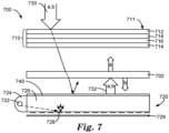
図7は、反射型偏光子光学フィルム702、液晶ディスプレイアセンブリ(LCD)710及び光源720を含む、例示的な表示アセンブリ700の図である。ここに示すように、LCDアセンブリ710は、光学フィルム702及び光源720によって提供される偏光によって照明される。LCDアセンブリ710は、外側吸収偏光子フィルム712、1つ以上のガラス層714、及び液晶層716を有する多層構造を含み得る。
Figure 7 is a diagram of an
図7は、ディスプレイアセンブリ700を通して送達される2つのタイプの光を示す。周囲光730は、LCDアセンブリ710を通過するディスプレイ面711に入射する光、光学フィルム702、及び光フィルム702に反射される光源720の拡散反射面を示す。光は、光源720のバックライトアセンブリからも発生することができる。例えば、光源720は、反射ランプハウジング724内にランプ722を含むエッジ照明バックライトを含み得る。ランプ722からの光は、光ガイド726に結合され、そこで、光は、スポット728(例えば、酸化チタン着色材料の不連続層)のような拡散反射構造に衝突するまで伝搬する。スポットのこの不連続なアレイは、ランプ光を取り出し、それをLCDアセンブリ710の方へ向けるように配設される。光源720に入る周囲光730は、スポットにぶつかるか、又はスポット間の間隙領域を通って光ガイドから漏れ得る。拡散反射層729(例えば、酸化チタン着色材料の層)は、光ガイド726の下に配設されて、このような光線を遮り、反射し得る。全体的に、光源720からLCDアセンブリ710に向かって出射する全ての光線は、光束732として示される。この光束は、「(a)」と称する第1の偏光状態を有する光を透過し、直交する偏光状態(b)を有する光を有効に反射する光学フィルム702を入射する。光学フィルム702は、上述した光学フィルム100、400、600のいずれかに対応し得る。
FIG. 7 shows two types of light delivered through the
いくつかの例では、LCDディスプレイアセンブリは、吸収偏光フィルム及び光源720とLCDアセンブリ710との間に反射型偏光子フィルム(AP/RPフィルム)を含み得る。このような例では、APフィルムは、典型的には、ディスプレイアセンブリに十分なコントラストを生成するために使用され得るが、一方でRPフィルムを含むことにより、APフィルムのみのシステムと比較して、AP/RPフィルムの組合せの輝度、特に高い周囲光環境又は高いグレア条件が改善される。驚くべきことに、AP/RPフィルムは、高周囲光環境(例えば、外部条件)であってもディスプレイアセンブリ700に輝度又はコントラストをそれほど低下させることなく、本明細書に記載の高コントラスト反射型偏光子(RP)光学フィルム702で代用し得るということが判明した。例えば、後方のAPフィルムが存在しないディスプレイアセンブリ700に光学フィルム702のみを含むことで、周囲光を光学フィルム702から望ましくないように反射させて高レベルのグレアを生じさせる一方で、実際には、グレアにおける無視できない又は比較的僅かな増加が観察されることが理論付けられた。
In some examples, the LCD display assembly may include an absorbing polarizing film and a reflective polarizer film (AP/RP film) between the
いくつかの例では、光学フィルム702を含むディスプレイアセンブリ700は、AP/RPフィルムを含む同等のディスプレイアセンブリと比較して、約10%~約15%の向上した輝度を示すことができる。
In some examples, a
いくつかの例では、ディスプレイアセンブリ700は、ディスプレイアセンブリ700の軸方向に輝度を増加させるために、光源720と光学フィルム702との間に配設された1つ以上の輝度向上フィルム740を含み得る。例示的な輝度向上フィルム740としては、例えば、転向フィルム、プリズムフィルムなどが挙げられる。
In some examples, the
いくつかの非限定的な例において、ディスプレイアセンブリ700は、光源720、光源720によって照明されるように構成されたLCDアセンブリ710、ディスプレイアセンブリ700の軸方向の輝度を増加させるために光源720とLCDアセンブリ710との間に配設された1つ以上の輝度向上フィルム740、及び1つ以上の輝度向上フィルム740とLCDアセンブリ710との間に配設され、第1の偏光状態(a)を有する光を実質的に透過し、直交する第2の偏光状態(b)を有する光を実質的に反射するように構成された光学フィルム702(例えば、RP)を含み得る。光学フィルム702は、光源720とLCDアセンブリ710との間に配設された吸収偏光子(AP)のない第2の偏光状態(例えば、Tb)に対して約0.2%未満の平均光透過率を規定し得る。このようないくつかの例では、ディスプレイアセンブリ700は、第2の偏光状態(b)に対する比較ディスプレイアセンブリのRPの平均透過率が約1.0%超であることを除いては、同じ構造を有する比較ディスプレイアセンブリのコントラスト比の少なくとも2倍のコントラスト比を規定し得る。
In some non-limiting examples, the
加えて、又あるいは、いくつかの非限定的な例において、ディスプレイアセンブリ700は、光源720、光源720によって照明されるように構成されたLCDアセンブリ710、ディスプレイアセンブリ700の軸方向の輝度を増加させるために光源720とLCDアセンブリ710との間に配設された1つ以上の輝度増強フィルム740、及び1つ以上の輝度増加フィルム740とLCDアセンブリ710との間に配設された光学フィルム702を含み得る。光学フィルム702は、主に光干渉によって光を透過又は反射する複数の干渉層を含んでよく、その結果、所定の波長範囲内の実質的な垂直入射光に対して、光源720とLCDアセンブリ710との間に配設された吸収偏光子(AP)がない状態で、複数の干渉層が第1の偏光状態(例えばTa)を有する光の少なくとも80%を透過し、直交する第2の偏光状態(例えば、Tb)を有する光の約0.2%未満を透過する。
Additionally or alternatively, in some non-limiting examples, the
図8は、AP/RPフィルムを有するディスプレイアセンブリと比較して、視野角の機能として光学フィルム702を含むディスプレイアセンブリ700の例示的な輝度プロファイルである。曲線800は、ディスプレイアセンブリ700用の光学フィルム702の輝度プロファイルを表し、一方で曲線802はAP/RPフィルム(例えば、日東電工株式会社(東京)から入手可能なAPCF)を含む、同等のディスプレイアセンブリについての輝度プロファイルを表す。図示されるように、光学フィルム702は、軸外観察位置に対する輝度プロファイルのわずかな改善を提供する一方で、通常の視野角(例えば、±20°)に対する比較観察輝度プロファイルを提供する。(例えば、50°超)。
8 is an exemplary luminance profile of a
いくつかのそのような例では、従来のAP/RPフィルムとは対照的に光学フィルム702の使用は、本明細書に記載された高コントラストRP光学フィルムを従来のAP/RPフィルムの厚さのほぼ半分に形成し得るので、LCDディスプレイアセンブリの全体的な厚さを大幅に減少させ得る。AP/RPフィルムとは対照的に、ディスプレイアセンブリ700において光学フィルム702のみを使用することにより、ディスプレイアセンブリの厚さの減少に関連する利益をもたらし得るが、いくつかの例では、吸収偏光フィルムは、所望により、LCDアセンブリ710と光学フィルム702(図示せず)との間に含まれてもよい。このようないくつかの例では、吸収偏光子/光学フィルム702の組合せは、従来のAP/RPフィルムと比較して、改善された輝度及び/又はコントラスト比を提供し得る。
In some such examples, the use of
いくつかの例では、ディスプレイアセンブリ700の光学フィルム702は、第1の偏光状態(a)を有する光を実質的に透過させ、直交する第2の偏光状態(b)を有する光を実質的に反射するために高コントラストRPとしての役割をし得る。いくつかの例では、光学フィルム702は第2の偏光状態(b)に対して約0.2%未満の平均光透過率を規定し、光源720と液晶層716との間には吸収偏光子は配設されず、また、第2の偏光状態に対する比較ディスプレイアセンブリの反射型偏光子の平均透過率が約1.0%超であることを除いては、ディスプレイアセンブリ700のコントラスト比は同じ構造を有する比較ディスプレイアセンブリのコントラスト比の少なくとも2倍である。
In some examples, the
いくつかの例では、本明細書で説明される光学フィルム100、200、400、600の1つ以上は、光軸(例えば、仮想現実ディスプレイシステム)を中心として観察者に物体を表示するように設計された光学系に組み込まれてもよい。このような光学系は、1つ以上の光学レンズの第1の主面上に配設され、それに適合する反射型偏光子(例えば、光学フィルム100、200、400、600)を有する非ゼロの光学パワーを有する1つ以上の光学レンズと、1つ以上の光学レンズの第2の主面上に配設され、適合する部分反射体を含み得る。いくつかの例では、レンズ及び反射型偏光子は、1つ又は2つの直交軸を中心として凸状であってもよく、コンパクトな構成で高い視野、高いコントラスト、低い色収差、低い歪み及び/又は高い効率を有するシステムを生成するために、絞り面(例えば、射出瞳又は入射瞳)と像面(例えば、ディスプレイパネル又は画像記録装置の表面)との間に配設されてもよく、このコンパクトな構成は例えば、バーチャルリアリティディスプレイなどのヘッドマウントディスプレイや、携帯電話に含まれるカメラなどの様々な装置において有用である。
In some examples, one or more of the
図10は、像面1030、絞り面1035、及び像面1030と絞り面1035との間に配設された光学積層体1010を含む、例示的な光学系1000(例えば、仮想現実ディスプレイシステム)の概略的な断面図である。x-y-z座標系は、図10に示されている。像面1030は、偏光又は非偏光を発するディスプレイパネルなどの画像形成装置の出力面であってもよく、一方、絞り面1035は光学系1000の射出瞳であってもよく、第2の光学系の入射瞳と重なるようになっていてもよく、これは例えば観察者の眼又はカメラであってよい。
10 is a schematic cross-sectional view of an exemplary optical system 1000 (e.g., a virtual reality display system) including an
いくつかの例では、光学積層体1010は、第1の主面1014及び第2の主面1016を有する光学レンズ1012、第1の主面1014に配設された反射型偏光子1027(例えば、光学フィルム100、200、400、600)、及び光学フィルム1012の第2の主面1016に配設された部分反射体1017を含み得る。いくつかの例では、光学積層体1010はまた、それぞれ第1の主面1014及び第2の主面1016上に配設された1以上の1/4波長リターダ1015、1025を含み得る。
In some examples, the
図10において示すように、光学積層体1010は、第1の軸及び/又は第2の軸(例えば、それぞれx軸及びy軸)に直交するように、像面1030に向かって凸状であり得る。光学積層体1010は、反射型偏光子1027にコーティング又はラミネートされた任意の第1の1/4波長リターダ1025で反射型偏光子1027を最初に形成し、その後、得られたフィルムを光学レンズ1012に対応するように任意の形状に熱成形することによって作製することができる。部分反射体1017及び任意の第2の1/4波長リターダ1015は、1/4波長リターダを部分反射体フィルム上にコーティングすることにより、部分反射体コーティングを1/4波長リターダフィルム上にコーティングすることにより、部分反射体フィルム及び1/4波長リターダフィルムを一緒にラミネートすることにより、又はフィルムインサート成形プロセスにおいて最初にレンズ1012(反射型偏光子1027を含むフィルム上に形成され得る)を形成し、次いで部分反射体1017を第2の主面1016上にコーティングすることによって製造し得る。いくつかの例では、レンズ1012は、反射型偏光子1027及び部分反射体1017の第1のフィルムと第2のフィルムとの間にレンズ1012を射出成形することによって形成され得る。第1のフィルム及び第2のフィルムは、射出成形工程の前に熱成形されてもよい。
10, the
画像源1031は、像面1030を含み、絞り面1035は、光学系1000のための射出瞳である。いくつかの例では、画像源1031は、表示パネルであってもよい。他の例では、表示パネルは存在しなくてもよく、代わりに、像面1030は、光学系1000の外部の物体から反射された光を受け取るようになった開口である。
Image source 1031 includes
いくつかの例では、入射瞳1034を有する第2の光学系1033は、入射瞳1034と重なる絞り面1035を有する光学系1000に近接配設されてもよい。第2の光学系1033は、例えば、像面637を透過した画像を記録するようになったカメラであってもよい。いくつかの例では、第2の光学系1033は視聴者の目であり、入射瞳1034は視聴者の眼の瞳孔である。このような例では、光学系1000は、ヘッドマウントディスプレイにおける使用になっていてもよい。
In some examples, a second
反射型偏光子1027は、本明細書で説明する光学フィルム100、200、400、600のいずれか1つとし得る。例えば、反射型偏光子は、少なくとも50の連続的に番号が付けられた干渉層を含むことができ、各層は比較的薄くてもよく(例えば、約200nm未満の平均厚さを有する)、適合曲線は、層厚さプロファイル反射型偏光子1027に適用される最良適合回帰であり、層数(例えば、図3の曲線300)に応じて、第1の層から第Nの層まで延びる領域における適合曲線の平均傾斜は、約0.2nm/層未満である。反射型偏光子1027は、第1の偏光状態(a)(例えば第1の方向に直線偏光される)を有する光を実質的に透過し、直交する第2の偏光状態(b)(例えば、第1の方向に直交する第2の方向に直線偏光される)を有する光を実質的に反射する。
The
部分反射体1017は、所定の波長範囲において少なくとも30%の平均光反射率と、少なくとも30%の光透過率とを有し、これは、本明細書中の他の箇所で記載された波長範囲のいずれかであってもよい。任意の好適な部分反射体が使用されてよい。一部の例では、部分反射体1017は、例えば、ハーフミラーであってもよい。いくつかの例では、部分反射体1017は、透明基板上に金属(例えば、銀又はアルミニウム)の薄い層をコーティングすることによって構成され得る。加えて、又あるいは、部分反射体1017は、例えば、レンズの表面上に薄膜誘電体コーティングを堆積することによって、又はレンズの表面に金属コーティング及び誘電体コーティングの組み合わせを堆積させることによって形成され得る。いくつかの例では、部分反射体1017は、それ自体が反射型偏光子であってもよい。
The
任意の第1の1/4波長リターダ1015及び第2の1/4波長リターダ1025は、例えば、米国特許出願公開第2002/0180916号(Schadtら)、第2003/028048号(Cherkaouiら)及び第2005/0072959号(Moiaら)に記載された線状光重合性ポリマー(LPP)材料及び液晶ポリマー(LCP)材料を含む任意の適切な材料から形成されるコーティング又はフィルムであってもよい。適切なLPP材料としては、ROP-131 EXP 306 LPPが、適切なLCP材料には、ROF-5185 EXP 410 LCPが挙げられ、両方ともスイスのアルシュヴィルにあるRolic Technologiesから入手可能である。いくつかの例では、1/4波長リターダ1015、1025は、所定波長範囲内の少なくとも1つの波長における1/4波長リターダであってもよい。
The optional first
光学系1000の動作中、光線1037及び光線1038は各々、像面1030及び絞り面1035を通して透過する。光線1037及び光線1038は各々、像面1030から絞り面1035(例えばヘッドマウントディスプレイの用途において)へと透過することができ、又は光線1037及び光線1038は、絞り面1035から像面1030(例えばカメラの用途において)へと透過し得る。光線1038は、光路が光学系1000のための折り返した光軸1040を規定する中心光線であり、これは、折り畳まれた光軸1040を中心とし得る。光線1038は、光軸1040からの大きな偏差なしに光学積層体1010を通過し得る。
During operation of the
光線1037の経路は、光学積層体1010によって偏向され得る。光線1037は、部分反射体1017(任意の第2の1/4波長リターダ1015を含む)を通して、レンズ1012を通して透過する。レンズ1012を通過する第1の通過後、光線は、任意の第1の1/4波長リターダ1025を通過し、反射型偏光子1027から反射する。2つの1/4波長リターダ1015、1025を光学積層体1010に組み込む例においては、1/4波長リターダ1015、1025は、1/4波長リターダ1015、1025が反射型偏光子1027と画像源1031との間に位置するように、レンズ1012の両側に配設し得る。このようないくつかの例では、画像源1031は、1/4波長リターダ1015、1025を通過した後、光が反射型偏光子1027のブロック軸に沿って偏光され、結果として反射型偏光子1027がフィルム上に最初に入射したときに反射型偏光子1027から反射するように、反射型偏光子1027の通過軸(a)に沿った偏光を有する光を発するようになっていてもよい。光線1037は、最初に反射型偏光子1027から反射した後、第1の1/4波長リターダ1025を通過して戻り、次いで部分反射体1017から反射し(図示されていない他の光線は、部分反射体1017を通過し)、レンズ1012及び第1の1/4波長リターダ1025を通過して戻り、次いで再び反射型偏光子1027に入射する。第1の1/4波長リターダ1025を通過し、部分反射体1017から反射し、第1の1/4波長リターダ1025通過して戻った後、光線1037は、反射型偏光子1027の通過軸(a)に沿った偏光を有する。したがって、光線1037は、反射型偏光子1027を通って透過され、次いで絞り面1035を通って第2の光学系1033内に伝達される。
The path of the
単一の集積光学積層体1010の設計は、コンパクトなシステムにおいて高い視野を提供し得る。像面1030の外縁を透過する光線1037は、θの視野角を有する折り返された光軸1040において絞り面1035と交差する主光線であり、これは、例えば、少なくとも40度、少なくとも45度、又は少なくとも50度であり得る。絞り面1035における視野は、例えば、2θであり、これは、少なくとも80度、少なくとも90度、又は少なくとも100度であってもよい。
The design of the single
いくつかの非限定的な例において、光学系1000は、1つ以上の光学レンズ1012の第1の主面1014上に配設され、それに適合する反射型偏光子1027を有する非ゼロの光学パワーと、1つ以上の光学レンズ1012の異なる第2の主面1016上に配設され、それに適合する部分反射体1017を有する1つ以上の光学レンズ1012を含み得る。反射型偏光子1027は、第2の偏光状態(b)を有する光軸1040に沿った入射光1037に対する光学系1000の平均光透過率が約0.1%未満であるように、第1の偏光状態(a)を有する光1037を実質的に透過させ、所定の波長範囲に対して少なくとも30%の平均光反射率を有する部分反射体1017で直交する第2の偏光状態(b)を有する光を実質的に反射する。
In some non-limiting examples, the
1つ以上の反射型偏光子を含む光軸に中心を有する観察者に物体を表示するための光学系の更なる例は、米国特許出願第14/865,017号に開示され記載されており、この特許出願は、参照によりその全体を本明細書に組み込むものとする。本明細書に記載される光学フィルム100、200、400、600のうちの1つ以上は、ここに記載されている反射型偏光子のようなシステムにおいて使用することができる。
Further examples of optical systems for displaying objects to a viewer centered on an optical axis that include one or more reflective polarizers are disclosed and described in U.S. Patent Application No. 14/865,017, which is incorporated herein by reference in its entirety. One or more of the
いくつかの例では、本明細書に記載される光学フィルム100、200、400、600のうちの1つ以上は、偏光ビームスプリッタ(PBS)内に反射型偏光子として組み込まれてもよい。PBSは、無偏光を2つの偏光状態に効果的に分割するために使用し得る。PBSシステムは、第2の直交する偏光状態(b)で偏光を実質的に反射しつつ、第1の偏光状態(a)で光を実質的に透過させるために、半導体、フォトニクス機器、又は他の光学系において使用し得る。いくつかの例では、PBSシステムは、出力偏光ビームを約90°の分離で分割する一方で、0°又は45°の入射角で光を受け取るように設計され得る。
In some examples, one or more of the
図11は、第1のプリズム1102、第2のプリズム1104、反射型偏光子1110、及び光源1150を含む、例示的なPBS1100の概略断面図である。第1のプリズム1102は、光源1150からの入射光を受けるための入力面1112と、出力面1114と、第1の斜辺1116とを含む。いくつかの例では、入力面1112及び出力面114は、第1プリズム1102を通過する光を受けて透過するための活性領域を有するように更に形成されてもよい。第2のプリズム1104は、出力面1118及び第2の斜辺1120を含む。
11 is a schematic cross-sectional view of an
反射型偏光子1110は、それぞれの第1のプリズム1102及び第2のプリズム1104の第1斜辺1116及び第2の斜辺1120の間に配設される。反射型偏光子1110は、本明細書で説明する光学フィルム100、200、400、600のうちのいずれかであり得る。例えば、反射型偏光子1110は、少なくとも50の連続的に番号が付けられた干渉層を含んでよく、各層は比較的薄くてもよく(例えば、約200nm未満の平均厚さを有する)、適合曲線は、層数の関数としての(例えば、図3の曲線300)層厚さプロファイル反射型偏光子1110に適用される最良適合回帰であり、第1の層から第Nの層まで延びる領域における適合曲線の平均傾斜は約0.2nm/層未満である。
The
第1のプリズム1102及び第2のプリズム1104は、ガラス又はポリマー材料を含み得る。第1のプリズム1102及び第2のプリズム1104に適したポリマー材料は、例えば、アクリルポリマー(例えば、ポリメチルメタクリレート)、環状オレフィンコポリマー、ポリカーボネート及びこれらの組み合わせなどの透明な光学ポリマーを含む。いくつかの例では、第1のプリズム1102及び第2のプリズム1104は、日立化成株式会社(日本、東京)から「OPTOREZ OZ-1330」シリーズのポリマーとして取引上の表示で市販されているアクリルポリマーのような熱可塑性アクリルポリマーを使用する射出成形によって形成され得る。いくつかの例では、第1のプリズム1102及び第2のプリズム1104を、2つのプリズム間の光学変化を減少させるために同じポリマー材料を使用して形成することが望ましいが、しかしながら、他の例では、第1のプリズム1102及び第2のプリズム1104は、異なる材料を用いて形成し得る。いくつかの例では、第1のプリズム1102及び第2のプリズム1104は、同様のサイズとすることができるが、他の例では、第1のプリズム1102は、第2のプリズム1104の体積よりも小さい体積を有し得る。いくつかの例では、第1のプリズム1102の体積は、第2のプリズム1104の体積の約半分(又は約60%以下、又は約40%以下)以下であってもよい。第1のプリズム1102のどの部分を除去し得るかの選択は、部分的には、エンベロープ1152内で発生する入射光、透過光及び反射光の光路に依存する。
The
動作中、光源1150は、中心光線1154を含むエンベロープ1152を有する光ビームを生成する。光源1150からの光は、所定の波長範囲を有する非偏光であってもよい。中心光線1154は、プリズムを透過し、次に約45°の入射角で反射型偏光子1110に入射する入力面1112を通して第1のプリズム1102に入る。その点で、次に中心光線1154は、その光の偏光状態に従って、反射型偏光子1110を透過し、反射型偏光子1110を反射する。例えば、第1の偏光状態(a)(例えば、通過状態)に対応する光は、反射型偏光子1110を通過し、出力面1118に到達する第1の偏光状態(a)を有する透過光線1156として第2のプリズム1104を通って進む。第2の直交する偏光状態(b)(例えば、ブロック/反射)に対応する光は、第2の直交する偏光状態(b)を有する反射光線1158として反射型偏光子1110から反射する。光線1154と反射型偏光子1110との間の入射角度によって、反射光線1158は、反射型偏光子1110で出力面1114の方向に反射する。いくつかの例では、透過光線1156及び反射光線1158は、互いに90°で進行する。
In operation, the
PBS1100は、第1のプリズム1102及び第2のプリズム1104の出力又は他のうちの面の1つ以上に取り付けられた追加の構成要素(図示せず)を含み得る。加えて、又あるいはPBS1100は、異なる光学系に組み込まれてもよい。種々の構成要素若しくはPBS1100又はPBS1100に結合されたそれらの構成要素は、光学的に透明な接着剤を介して直接接触又は取り付けをすることができるであろう。いくつかの例では、反射型偏光子1110は、光学的に透明な接着剤層を使用して、第1のプリズム1102及び第2のプリズム1104の一方又は両方に取り付けられる。PBSの設計及びPBSシステムを組み込んだ光学系の更なる例は、米国特許出願第14/865,017号に開示され記載されており、この特許出願は、参照によりその全体が本明細書に組み込まれるものとする。
The
いくつかの非限定的な例では、PBS1100は、第1のプリズム1102及び第2のプリズム1104、並びに第1のプリズム1102と第2のプリズム1104との間に配設されて接着される(例えば、第1の斜辺1116及び第2の斜辺1120に沿って)反射型偏光子1110を含み得る。このような例では、例えば、所定の波長を有する入射光(例えば光線1154)がPBS1100の入力面1112からPBS1100に入り、反射型偏光子1110に少なくとも1回当たった後にPBS1110の出力面(例えば出力面1118又は1114)を通って出射するときに、入射光(例えば、光線1154)の平均強度に対する出射光(例えば、透過光線1156又は反射光線1158)の平均強度の比は、入射光が第1の偏光状態(a)を有するとき約90%を超えるように、及び入射光が第2の偏光状態(b)を有するとき約0.2%未満であるように、反射型偏光子1110は、第1の偏光状態(a)を有する偏光を実質的に反射することができ、直交する第2の偏光状態(b)を有する偏光を実質的に透過させ得る。
In some non-limiting examples, the
実施例1-複屈折反射型偏光子光学フィルムを、以下のように準備した。2つの多層光学パケットは、ポリエチレンナフタレート(PEN)及び低屈折率の等方性層の325個の交互層から構成される各パケットと共押出しされ、これは屈折率が約1.57であり、一軸方向で実質的に等方性を維持するように、ポリカーボネートとコポリエステル(PC:coPET)とのブレンドを用いて製造され、PC:coPETのモル比は約42.5mol%PC及び57.5mol%coPETであり、そして摂氏105℃のTgを有する。この等方性材料は、2つの非延伸方向における屈折率を伸張させた後、非延伸方向における複屈折材料の屈折率と実質的に整合したままとなるように選択され、一方で延伸方向において、複屈折層と非複屈折層との間には屈折率の実質的な不整合が存在する。PEN及びPC/coPETポリマーは、別個の押出機から多層の共押出フィードブロックに供給され、これらは、合計652層に対して、積層された光学パケットの外側で、PC/coPETのより厚い保護境界層を加えて、325個の交互する光学層(それぞれ「パケット1」及び「パケット2」)のパケットに組み立てられた。
Example 1 - A birefringent reflective polarizer optical film was prepared as follows: Two multilayer optical packets were coextruded with each packet consisting of 325 alternating layers of polyethylene naphthalate (PEN) and a low refractive index isotropic layer, which has a refractive index of about 1.57, was made with a blend of polycarbonate and copolyester (PC:coPET) to remain substantially isotropic in one axial direction, with a molar ratio of PC:coPET of about 42.5 mol% PC and 57.5 mol% coPET, and has a Tg of 105 degrees Celsius. The isotropic material was selected such that after stretching, the refractive index in the two non-stretch directions remains substantially matched to the refractive index of the birefringent material in the non-stretch direction, while in the stretch direction there is a substantial mismatch in refractive index between the birefringent and non-birefringent layers. The PEN and PC/coPET polymers were fed from separate extruders into a multilayer coextrusion feedblock, which were assembled into packets of 325 alternating optical layers ("
実施例1の高コントラストの反射型偏光子(HCRP)光学フィルム用のこの層プロファイルは、パケット1及びパケット2とともに図9に示されている。最小二乗線形回帰を用いるとパケット1の平均傾斜は約0.17nm/層で、パケット2の平均傾斜は、約0.18nm/層であり、約6%の2つのパケットに対するそれぞれの傾斜に差を示している。実施例1のフィルムは、約63.2μmの静電容量ゲージで測定した結果、得られた全厚さを有した。
This layer profile for the high contrast reflective polarizer (HCRP) optical film of Example 1 is shown in FIG. 9 along with
実施例1の複数の干渉層のアライメントを評価するために、フィルムの光軸を、フィルムの各主面に入射する直線偏光について決定した。フィルムの光軸は、フィルムの平面内での入射偏光の配向に対応し、これは、最小量の直線偏光がフィルムを通過することを可能にする(例えば、図2の延伸軸120と位置合わせされる)。理想的なシナリオでは、フィルムの光軸は、偏光された光がフィルムに入射する表面とは無関係に同一である。しかしながら、製造プロセスのばらつきや、複数の干渉層の個々の光軸のずれに起因して、フィルムの光軸は、どの表面に偏光された光が入射するかに依存し得る。いくつかの実施例では、複数の層間の位置ずれの程度が大きいほど、フィルムのための光軸の差が大きくなる。2つの表面に対するフィルムの光軸間の差は、いくつかの例では、複数の干渉層間の位置合わせを評価するための測定基準として使用し得る。実施例1のフィルムについての2つの光軸を、直線偏光を使用して2つの表面について測定した。偏光をフィルムの第1の主面に直接投影し、フィルムを通過する偏光の最小量が得られるまでフィルムを回転させた。第1の主面の光軸は、偏光の偏光軸と平行であるとしてマークされた。このプロセスをフィルムの第2の主面に対して繰り返した。実施例1のフィルムに対する第1の主面及び第2の主面に対する光軸間の差は、複数の干渉層間の強い整合を示す0.1度未満であると決定された。
To evaluate the alignment of the interference layers of Example 1, the optical axis of the film was determined for linearly polarized light incident on each major surface of the film. The optical axis of the film corresponds to the orientation of the incident polarized light in the plane of the film, which allows the minimum amount of linearly polarized light to pass through the film (e.g., aligned with the
実施例2-光学フィルムが静電容量ゲージで測定したところ、約66.7μmの厚さを有していたことを除いては、複屈折反射型偏光子光学フィルムは、実施例1のフィルムと同じプロセス条件を用いて作製した。 Example 2 - A birefringent reflective polarizer optical film was made using the same process conditions as the film of Example 1, except that the optical film had a thickness of about 66.7 μm as measured with a capacitance gauge.
実施例3-複屈折反射型偏光子光学フィルムを、以下のように準備した。2つの多層光学パケットは、90/10coPEN(例えば、90mol%のポリエチレンナフタレート(PEN)及び10mol%のポリエチレンテレフタレート(PET))の325の交互層を備える各光学パケットと、上記実施例1に記載のPC/coPETの低屈折率等方性層と共押出しした。90/10coPEN及びPC/coPETポリマーを分離押出成形機から多層共押出しフィードブロックまで供給し、325個の交互する光学層のパケット、及び積層された光学パケットの外側にcoPENのより厚い保護境界層を加えて全部で652層に組み立てた。このフィルムは、約63.2μmの静電容量ゲージで測定した結果、得られた物理的全厚さを有していた。 Example 3 - A birefringent reflective polarizer optical film was prepared as follows. Two multilayer optical packets were coextruded with each optical packet comprising 325 alternating layers of 90/10 coPEN (e.g., 90 mol% polyethylene naphthalate (PEN) and 10 mol% polyethylene terephthalate (PET)) and a low refractive index isotropic layer of PC/coPET as described in Example 1 above. The 90/10 coPEN and PC/coPET polymers were fed from separate extruders to a multilayer coextrusion feedblock and assembled into a packet of 325 alternating optical layers, plus thicker protective boundary layers of coPEN on the outside of the stacked optical packets for a total of 652 layers. The film had a total physical thickness as measured with a capacitance gauge of about 63.2 μm.
下記の表1は、実施例1から実施例3の光学フィルムについて、450~650nmの可視スペクトル範囲での第1の偏光状態(a)及び第2の偏光状態(b)(例えば、通過軸及びブロック軸)に関する比較による平均透過プロファイルを提供し、市販の吸収偏光子(AP)及び反射型偏光子(RP)、及び文献に参照されたものと比較している。

下記の表2は、表1の値を基準として、例示的なフィルム1から3について計算された第1の偏光状態(a)及び直交する第2の偏光状態(b)における透過率及び反射率値を表す。これらの値は、フィルム層による吸収に関連する光エネルギーの無視できる損失を仮定して計算される。

図12は、本明細書に記載の、従来の反射型偏光子と比較した例示的な反射型偏光子フィルム用の例示的な厚さプロファイル(層厚さ対層数)のプロットである。フィルムは、以下の表3に記載されている。フィルム1206及びフィルム1208は、3M社(ミネソタ州セントポール)から入手可能な市販の多層反射型偏光子フィルムを表す。フィルム1210は、275層を有する代表的な従来の偏光フィルムであり、これは最大厚さ対最小厚さが2.2の比を有し、厚さは、その特許に記載されるように連続的に変化する。ライン1202及びライン1204は、それぞれ、HCPRの実施例1における第1及び第2の光学積層体/パケットに対応する。層厚さプロファイルは、原子間力顕微鏡(AFM)を使用して測定された。

以下の表4は、図12に示すフィルム/パケット1202-1208のそれぞれについて、最も高い勾配領域と最低勾配領域との間の計算された差を表す。所与の領域のそれぞれの傾きは、25層の範囲にわたる最小二乗線形回帰を使用して決定された。

実施例4-実施例1、実施例2及び実施例3に関して記載したのと同様の製造プロセスを用いて光学フィルムを作製した。実施例1、実施例2及び実施例3よりも低い傾斜/層プロファイルを利用する別の層厚さプロファイルを実施した。特に、2つの多層光積層体/パケットは、ポリエチレンナフタレート(PEN)のHIR層と、LIR等方性層の325の交互層を含む各々と共押出しされ、LIR等方性層は、20重量%のPETg(イーストマン・ケミカルズ社、テネシー州ノックスビル)と80重量%のXylex(Sabic社、テキサス州ヒューストン)とのブレンドで製造され、ポリカーボネートとコポリエステルの合金であった。LIR層の屈折率は約1.57であり、一軸方向時に実質的に等方性を維持した。この等方性材料は、延伸後、延伸方向のその屈折率が、実質的に変化せず、延伸されていない方向のHIR層の屈折率と類似するように選択され、一方で、延伸方向におけるHIR層の屈折率は、同一の方向におけるLIR層の屈折率と実質的に不一致であった。HIR層及びLIR層の材料は、多層共押出フィードブロックを供給する別の押出機から供され、これらは325個の交互する光学層の2つのパケットへと組み立てられ、各パケットの各側に等方性LIR材料でできた厚い保護境界層を加え、合計で653層であり、積層された光学パケットの間のスペーサ層は、光学的及び機械的に単一層であると考えられる。第1のパケット(例えば、「パケット1」)は、比較的薄い交互するHIR/LIR層から構成され、一方で、第2のパケット(例えば、「パケット2」)は、比較的厚い交互するHIR/LIR層から構成され、それぞれ約390nm~約620nm及び約600nm~約900nmの所定の波長範囲に対応する。フィルムは、米国特許第6,916,440号に記載されているように、放物線状テンター内で延伸され、その全体が参照により本明細書に組み込まれる。フィルムは、約316°F(例えば、158℃)の温度で延伸された。フィルムは、横方向に約6:1の比で延伸され、機械の方向に約0.46:1の比で延伸され、すなわちフィルムは機械方向に弛緩される。
Example 4 - Optical films were made using a manufacturing process similar to that described for Examples 1, 2, and 3. An alternative layer thickness profile was implemented utilizing a lower gradient/layer profile than Examples 1, 2, and 3. In particular, two multilayer optical stacks/packets were coextruded with an HIR layer of polyethylene naphthalate (PEN) and each containing 325 alternating layers of an LIR isotropic layer, the latter made of a blend of 20% by weight PETg (Eastman Chemicals, Knoxville, TN) and 80% by weight Xylex (Sabic, Houston, TX), an alloy of polycarbonate and copolyester. The refractive index of the LIR layer was approximately 1.57 and remained substantially isotropic when uniaxially oriented. This isotropic material was selected so that after stretching, its refractive index in the stretch direction would not change substantially and would be similar to that of the HIR layer in the unstretched direction, while the refractive index of the HIR layer in the stretch direction was substantially mismatched to that of the LIR layer in the same direction. The HIR and LIR layer materials came from separate extruders feeding a multi-layer coextrusion feedblock, which were assembled into two packets of 325 alternating optical layers, plus a thick protective boundary layer of isotropic LIR material on each side of each packet, for a total of 653 layers, with the spacer layer between the stacked optical packets considered optically and mechanically to be a single layer. The first packet (e.g., "
図13は、AFMから得られた実施例4の光学フィルムの層厚さプロファイルのプロットを示す。最小二乗線形回帰を用いて、パケット1の平均傾斜は、約0.104nm/層で計算され、パケット2の平均傾斜は、約0.141nm/層で計算された。実施例4のフィルムは、約65.7μmの静電容量ゲージで測定した結果、得られた全厚さを有した。450~650nmの波長範囲にわたって評価された平均通過状態透過率(Ta)は約89.1%であり、平均ブロック/反射状態透過率(Tb)は、約0.057%であった。
13 shows a plot of the layer thickness profile of the optical film of Example 4 obtained from AFM. Using least squares linear regression, the average slope of
図14は、実施例4のフィルムに対するブロック状態透過率(Tb)を375~850nmの波長範囲にわたるプロットを示す。 FIG. 14 shows a plot of the block state transmission (T b ) for the film of Example 4 over the wavelength range of 375-850 nm.
実施例5-以下の表5は、実施例における市販のRP2及びRP3と比較した、上述した実施例1及び実施例4の光学フィルムに対するΔnx/K比を示す。ここに示すように、実施例1及び実施例4の光学フィルムの各それぞれのパケットは、1.2を超えるΔnx/K比を示し、一方で、実施例における市販のRP2及びRP3は、1未満のΔnx/K比を示す。

実施例6-以下の表5は、実施例1の光学フィルムの光学密度、光学的パワー、及び他の光学特性を示す。また、表5には、従来の反射型偏光子フィルムの24の比較試料について得られた結果も含まれている。比較サンプルは、市販されているか、又は文献に開示された技術のいずれかを用いて得られた種々の偏光子フィルムに対応する。表6に列挙されたフィルムの合計層数に対する層当たりの光学的パワーは、図15中にプロットされている。図15にて示すように、実施例1及び実施例4の光学フィルムは、各々(-0.0012*N+1.46)を超える層当たりの光学的パワーを示す(線で図示)。

実施例7-比較ディスプレイアセンブリの調査は、iPad4(アップル社、カリフォルニア州クパチーノ)のLCDディスプレイを使用して実施した。3つの反射型偏光子は、後方の反射型偏光子(例えば、ディスプレイアセンブリ700における光学フィルム702の位置)としてディスプレイアセンブリで試験を行った。試験した反射型偏光子は、ポリビニルアルコールタイプの吸着偏光子(「比較AP/RPフィルム」)にラミネートされたiPad4のストックRPフィルム、RP(「比較RPフィルム」)が存在しないiPad4のストックRPフィルム、及び実施例1の高コントラスト反射型偏光子光学フィルムを含んだ。偏光子光学フィルムをLCDディスプレイに接着するために使用される接着剤は、ミネソタ州セントポールの3M社から入手可能な、透明なOCA8171であった。試験に使用された光源は、iPad4装置に備えた輝度向上フィルム(例えば、プリズムフィルム/拡散シート)を具備するストックバックライトである。
Example 7 - Comparative display assembly studies were conducted using the LCD display of an iPad 4 (Apple Inc., Cupertino, Calif.). Three reflective polarizers were tested in the display assembly as rear reflective polarizers (e.g., in the position of
3つの異なるディスプレイアセンブリの光学性能は、市販のコノスコープELDIM L80(ELDIM SA社、フランス、エルヴィルサンクレール)を使用して試験した。ディスプレイアセンブリの輝度及びコントラストの結果は、比較AP/RPフィルムに関して規格化された値とともに表7に示される。結果を示す。実施例1の光学フィルムは、比較AP/RPフィルム及びRPフィルムの両方と比較して、優れた輝度を示した。加えて、実施例1の光学フィルムは、ストックの比較RPフィルム単独よりはるかに大きいコントラスト比を示したが、これは、ディスプレイアセンブリ中に後方のAP層が存在しないにもかかわらず、比較AP/RPのコントラスト比に匹敵するものであった。

第1項:一例において、複数の干渉層を含む光学フィルムであって、各干渉層は主に光干渉によって光を反射又は透過し、干渉層の総数は約1000未満であり、所定の波長範囲内の実質的な垂直入射光に対して、複数の干渉層は、第1の偏光状態に対して約85%を超える平均光透過率、直交する第2の偏光状態に対して約80%を超える平均光反射率、及び第2の偏光状態に対して約0.2%未満の平均光透過率を有する。 Clause 1: In one example, an optical film includes a plurality of interference layers, each of which reflects or transmits light primarily by optical interference, the total number of interference layers being less than about 1000, and for substantially normally incident light within a predetermined wavelength range, the plurality of interference layers have an average optical transmittance of greater than about 85% for a first polarization state, an average optical reflectance of greater than about 80% for an orthogonal second polarization state, and an average optical transmittance of less than about 0.2% for the second polarization state.
第2項:第1項に記載の光学フィルムのいくつかの例においては、複数の干渉層は、所定の波長範囲における第1の偏光状態に対して約90%を超える平均光透過率を有する。
Clause 2: In some examples of the optical film described in
第3項:第1項に記載の光学フィルムのいくつかの例においては、複数の干渉層は、所定の波長範囲における第1の偏光状態に対して約95%を超える平均光透過率を有する。
Clause 3: In some examples of the optical film described in
第4項:第1項に記載の光学フィルムのいくつかの例においては、複数の干渉層は、所定の波長範囲における第1の偏光状態に対して約98%を超える平均光透過率を有する。
Clause 4: In some examples of the optical film described in
第5項:第1項から第4項のいずれかに記載の光学フィルムのいくつかの例においては、複数の干渉層は、所定の波長範囲における第2の偏光状態に対して約0.15%未満の平均光透過率を有する。
Clause 5: In some examples of the optical film described in any of
第6項:第1項から第5項のいずれかに記載の光学フィルムのいくつかの例においては、複数の干渉層は、所定の波長範囲における第2の偏光状態に対して約0.10%未満の平均光透過率を有する。
Clause 6: In some examples of the optical film described in any of
第7項:第1項から第6項のいずれかに記載の光学フィルムのいくつかの例においては、所定の波長範囲で約10度の入射角で光学フィルムに入射する光に対して、複数の干渉層は、第1の偏光状態に対して約85%を超える平均光透過率、第2の偏光状態に対して約80%を超える平均光反射率、及び第2の偏光状態に対して約0.2%未満の平均光透過率を有する。
Clause 7: In some examples of the optical film described in any of
第8項:第1項から第7項のいずれかに記載の光学フィルムのいくつかの例においては、所定の波長範囲で約20度の入射角で光学フィルムに入射する光に対して、複数の干渉層は、第1の偏光状態に対して約85%を超える平均光透過率、第2の偏光状態に対して約80%を超える平均光反射率、及び第2の偏光状態に対して約0.2%未満の平均光透過率を有する。
Clause 8: In some examples of the optical film described in any of
第9項:第1項に記載の光学フィルムのいくつかの例においては、所定の波長範囲で約30度の入射角で光学フィルムに入射する光に対して、複数の干渉層は、第1の偏光状態に対して約85%を超える平均光透過率、第2の偏光状態に対して約80%を超える平均光反射率、及び第2の偏光状態に対して約0.2%未満の平均光透過率を有する。
Clause 9: In some examples of the optical film described in
第10項:一例においては、光学フィルムが複数の干渉層を含み、各干渉層は主に光干渉によって光を反射又は透過し、干渉層の総数は約1000未満であり、所定の波長範囲内の実質的な垂直入射光に対して、光学フィルムは、第1の偏光状態に対して平均光透過率Ta及び平均光反射率Ra、直交する第2の偏光状態に対して平均光透過率Tb及び平均光反射率Rbを有し、Tb/Rbは約0.002未満であり、Ra/Taは約0.17未満である。 Clause 10: In one example, an optical film includes a plurality of interference layers, each of which reflects or transmits light primarily by optical interference, the total number of interference layers being less than about 1000, and for substantially normally incident light within a predetermined wavelength range, the optical film has an average optical transmittance T a and an average optical reflectance R a for a first polarization state and an average optical transmittance T b and an average optical reflectance R b for an orthogonal second polarization state, where T b /R b is less than about 0.002 and R a /T a is less than about 0.17.
第11項:第10項の光学フィルムのいくつかの例では、Ta/Tbは、約425を超える。
Clause 11: In some examples of the optical film of
第12項:第10項又は第11項の光学フィルムのいくつかの例では、Rb/Raは、約6.7を超える。
Item 12: In some examples of the optical film of
第13項:第10項から第12項のいずれかに記載の光学フィルムのいくつかの例においては、複数の干渉層のTaは、所定の波長範囲で約90%を超える。
Clause 13: In some examples of the optical film described in any of
第14項:第10項から第13項のいずれかに記載の光学フィルムのいくつかの例においては、複数の干渉層のTaは、所定の波長範囲で約95%を超える。
Clause 14: In some examples of the optical film described in any of
第15項:第10項から第14項のいずれかに記載の光学フィルムのいくつかの例においては、複数の干渉層のTaは、所定の波長範囲で約98%を超える。
Clause 15: In some examples of the optical film described in any of
第16項:第10項から第15項のいずれかに記載の光学フィルムのいくつかの例においては、Tbは所定の波長範囲内で約0.15%未満である。
Item 16: In some examples of the optical film according to any of
第17項:第10項から第16項のいずれかに記載の光学フィルムのいくつかの例においては、Tbは所定の波長範囲内で約0.10%未満である。
Item 17: In some examples of the optical film according to any of
第18項:第10項から第17項のいずれかに記載の光学フィルムのいくつかの例においては、所定の波長範囲で約10度の入射角で光学フィルムに入射する光に対して、Taは約85%を超え、Rbは約80%を超え、Tbは約0.2%未満である。
Clause 18: In some examples of the optical film described in any of
第19項:第10項から第18項のいずれかに記載の光学フィルムのいくつかの例においては、所定の波長範囲で約20度の入射角で光学フィルムに入射する光に対して、Taは約85%を超え、Rbは約80%を超え、Tbは約0.2%未満である。
Clause 19: In some examples of the optical film described in any of
第20項:第10項から第19項のいずれかに記載の光学フィルムのいくつかの例においては、所定の波長範囲で約30度の入射角で光学フィルムに入射する光に対して、Taは約85%を超え、Rbは約80%を超え、Tbは約0.2%未満である。
Clause 20: In some examples of the optical film described in any of
第21項:第1項から第20項のいずれかに記載の光学フィルムのいくつかの例においては、光学フィルムは2つの干渉層の間に配設された少なくとも1つの非干渉層を含み、少なくとも1つの非干渉層の各々は主に光干渉によって光を反射又は透過しない。
Clause 21: In some examples of the optical film described in any of
第22項:第21項に記載の光学フィルムのいくつかの例においては、少なくとも1つの非干渉層の各々の平均厚さは、所定の波長範囲内の最大波長の少なくとも10倍である。 Clause 22: In some examples of the optical film described in clause 21, the average thickness of each of the at least one non-interference layer is at least 10 times the maximum wavelength within the predetermined wavelength range.
第23項:第21項に記載の光学フィルムのいくつかの例においては、少なくとも1つの非干渉層の各々の平均厚さは、所定の波長範囲内の最大波長の少なくとも50倍である。 Clause 23: In some examples of the optical film described in clause 21, the average thickness of each of the at least one non-interference layer is at least 50 times the maximum wavelength within the predetermined wavelength range.
第24項:第1項から第23項のいずれかに記載の光学フィルムのいくつかの例においては、所定の波長範囲は約400nm~約700nmである。
Clause 24: In some examples of the optical film described in any of
第25項:第1項から第24項のいずれかに記載の光学フィルムのいくつかの例においては、所定の波長範囲は約400nm~約700nm、及び約800nm~約1300nmである。
Clause 25: In some examples of the optical film described in any one of
第26項:第1項から第25項のいずれかに記載の光学フィルムのいくつかの例においては、干渉層の総数は約900未満である。
Clause 26: In some examples of the optical film described in any of
第27項:第1項から第26項のいずれかに記載の光学フィルムのいくつかの例においては、干渉層の総数は約800未満である。
Clause 27: In some examples of the optical film described in any of
第28項:第1項から第27項のいずれかに記載の光学フィルムのいくつかの例においては、光学フィルムは約60μm未満の厚さを有する。
Clause 28: In some examples of the optical film described in any of
第29項:第1項から第28項のいずれかに記載の光学フィルムのいくつかの例においては、複数の干渉層は、複数の交互する高屈折率の第1の層及び低屈折率の第2の層を含む。
Clause 29: In some examples of the optical film described in any of
第30項:一例において、光学フィルムはN個の連続的に番号が付けられた層を含み、Nは200超で1000未満の整数であり、各層は約200nm未満の平均厚さを有し、適合曲線は層数の関数としての各層の厚さをプロットする層厚さプロファイルに適用される最良適合回帰であり、第1の層から第Nの層まで延びる領域における適合曲線の平均傾斜は約0.2nm/層未満であり、所定の波長範囲内の実質的な垂直入射光に対して、光学フィルムは、第1の偏光状態に対して約85%を超える平均光透過率、及び直交する第2の偏光状態に対して約80%を超える平均光反射率を有する。 Clause 30: In one example, the optical film includes N consecutively numbered layers, N being an integer greater than 200 and less than 1000, each layer having an average thickness less than about 200 nm, the fitted curve being a best fit regression applied to a layer thickness profile plotting the thickness of each layer as a function of the number of layers, the average slope of the fitted curve in a region extending from the first layer to the Nth layer being less than about 0.2 nm/layer, and for substantially normally incident light within a predetermined wavelength range, the optical film has an average optical transmittance of greater than about 85% for a first polarization state and an average optical reflectance of greater than about 80% for an orthogonal second polarization state.
第31項:一例において、光学フィルムはN個の連続的に番号が付けられた層を含み、Nは200を超える整数であり、10%未満の層は約200ナノメートル(nm)を超える平均厚さを有し、適合曲線は層数の関数としての光学フィルムの層厚さに適用される最良適合回帰であり、第1の層から第Nの層まで延びる領域における適合曲線の平均傾斜は約0.2nm未満である。 Clause 31: In one example, the optical film includes N consecutively numbered layers, N being an integer greater than 200, less than 10% of the layers having an average thickness greater than about 200 nanometers (nm), the fitted curve being a best fit regression applied to the layer thickness of the optical film as a function of the number of layers, and the average slope of the fitted curve in the region extending from the first layer to the Nth layer is less than about 0.2 nm.
第32項:第31項に記載の光学フィルムのいくつかの例においては、N個の連続的に番号が付けられた層における少なくとも1つの番号が付けられた層の平均厚さは、N個の連続的に番号が付けられた層における少なくとも1つの他の番号が付けられた層の平均厚さよりも少なくとも30%未満である。 Clause 32: In some examples of the optical film described in clause 31, the average thickness of at least one numbered layer in the N consecutively numbered layers is at least 30% less than the average thickness of at least one other numbered layer in the N consecutively numbered layers.
第33項:第30項又は第32項に記載の光学フィルムのいくつかの例においては、最良適合回帰は、最良適合線形回帰、最良適合非線形回帰、最良適合多項式回帰、及び最良適合指数回帰のうち1つ以上である。
Clause 33: In some examples of the optical film described in
第34項:第30項から第33項のいずれか一項に記載の光学フィルムのいくつかの例においては、光学フィルムはN個の連続的に番号が付けられた層における2つの連続的に番号が付けられた層間に配設された少なくとも1つのスペーサ層を含み、少なくとも1つのスペーサ層における各スペーサ層は約500nmを超える平均厚さを有する。
Clause 34: In some examples of the optical film described in any one of
第35項:第30項から第34項のいずれか一項に記載の光学フィルムのいくつかの例においては、光学フィルムはN個の連続的に番号が付けられた層における2つの連続的に番号が付けられた層間に配設された少なくとも1つのスペーサ層を含み、少なくとも1つのスペーサ層における各スペーサ層は、所定の波長範囲内の最大波長の少なくとも10倍である平均厚さを有する。
Clause 35: In some examples of the optical film described in any one of
第36項:第30項から第35項のいずれか一項に記載の光学フィルムのいくつかの例においては、光学フィルムはN個の連続的に番号が付けられた層における2つの連続的に番号が付けられた層間に配設された少なくとも1つのスペーサ層を含み、少なくとも1つのスペーサ層における各スペーサ層は、所定の波長範囲内の最大波長の少なくとも50倍である平均厚さを有する。
Clause 36: In some examples of the optical film described in any one of
第37項:第30項から第36項のいずれか一項に記載の光学フィルムのいくつかの例においては、N個の連続的に番号が付けられた層における少なくとも1つの層の平均厚さは約50nm未満であり、N個の連続的に番号が付けられた層における少なくとも1つの他の層の平均厚さは約100nm超である。
Clause 37: In some examples of the optical film described in any one of
第38項:第30項から第37項のいずれか一項に記載の光学フィルムのいくつかの例においては、N個の連続的に番号が付けられた層は連続的に配設される。
Clause 38: In some examples of the optical film described in any one of
第39項:第30項から第38項のいずれか一項に記載の光学フィルムのいくつかの例においては、最良適合回帰は、最良適合線形回帰、最良適合非線形回帰、最良適合多項式回帰、及び最良適合指数回帰のうち1つ以上である。
Clause 39: In some examples of the optical film described in any one of
第40項:第30項から第39項のいずれか一項に記載の光学フィルムのいくつかの例においては、N個の連続的に番号が付けられた層は、複数の交互する高屈折率の第1の層及び低屈折率の第2の層を備える。
Clause 40: In some examples of the optical film described in any one of
第41項:一例において、光学フィルムは1からNまで連続的に番号が付けられた複数の層を含み、Nは50超で1000未満の整数であり、光学フィルムは所定の波長範囲内で第1の偏光状態を有する光の少なくとも80%を透過し、所定の波長範囲内で直交する第2の偏光状態を有する光の少なくとも80%を反射し、適合曲線は層数の関数としての光学フィルムの層厚さに適用される最良適合回帰であり、第1の層から第Nの層まで延びる領域において、適合曲線の最大傾斜と最小傾斜との差は約0.70nm/層未満であり、最大傾斜及び最小傾斜は、各々、25から50の隣接する層のいずれかのグループにわたって評価される。 Clause 41: In one example, an optical film includes a plurality of layers numbered consecutively from 1 to N, where N is an integer greater than 50 and less than 1000, the optical film transmits at least 80% of light having a first polarization state within a predetermined wavelength range and reflects at least 80% of light having an orthogonal second polarization state within a predetermined wavelength range, the fit curve is a best fit regression applied to the layer thickness of the optical film as a function of the number of layers, in a region extending from the first layer to the Nth layer, the difference between the maximum slope and the minimum slope of the fit curve is less than about 0.70 nm/layer, and the maximum slope and minimum slope are each evaluated over any group of 25 to 50 adjacent layers.
第42項:第41項に記載の光学フィルムのいくつかの例においては、複数の層中の各層は、約200nm未満の平均厚さを有する。 Clause 42: In some examples of the optical film described in clause 41, each layer in the plurality of layers has an average thickness of less than about 200 nm.
第43項:第41項又は第42項に記載の光学フィルムのいくつかの例においては、複数の層における番号が付けられた層は、連続的に配設される。 Clause 43: In some examples of the optical film described in clause 41 or clause 42, the numbered layers in the plurality of layers are disposed consecutively.
第44項:第41項から第43項のいずれかに記載の光学フィルムのいくつかの例においては、所定の波長範囲において実質的な垂直入射光に対して、第1の層から第Nの層まで延びる領域における適合曲線の平均傾斜は約0.2nm未満である。 Clause 44: In some examples of the optical film described in any of clauses 41 to 43, for substantially normal incidence light in a given wavelength range, the average slope of the fitted curve in a region extending from the first layer to the Nth layer is less than about 0.2 nm.
第45項:第41項から第44項のいずれかに記載の光学フィルムのいくつかの例においては、最良適合回帰は、最良適合線形回帰、最良適合非線形回帰、最良適合多項式回帰、及び最良適合指数回帰のうち1つ以上である。 Clause 45: In some examples of the optical film described in any of clauses 41 to 44, the best fit regression is one or more of best fit linear regression, best fit nonlinear regression, best fit polynomial regression, and best fit exponential regression.
第46項:第41項から第45項のいずれかに記載の光学フィルムのいくつかの例においては、光学フィルムは1個からN個の連続的に番号が付けられた複数の層における2つの連続的に番号が付けられた層間に配設されたスペーサ層を含み、スペーサ層は、所定の波長範囲における最大波長の少なくとも10倍である平均厚さを有する。 Clause 46: In some examples of the optical film described in any of clauses 41 to 45, the optical film includes a spacer layer disposed between two consecutively numbered layers in the plurality of 1 to N consecutively numbered layers, the spacer layer having an average thickness that is at least 10 times the maximum wavelength in the predetermined wavelength range.
第47項:第46項に記載の光学フィルムのいくつかの例においては、スペーサ層は、所定の波長範囲における最大波長の少なくとも50倍である平均厚さを有する。 Clause 47: In some examples of the optical film described in clause 46, the spacer layer has an average thickness that is at least 50 times the maximum wavelength in the predetermined wavelength range.
第48項:第41項から第47項のいずれかに記載の光学フィルムのいくつかの例においては、1個からN個の連続的に番号が付けられた複数の層における少なくとも1つの層の平均厚さは約50nm未満であり、1個からN個の連続的に番号が付けられた複数の層における少なくとも1つの層の平均厚さは約100nm超である。 Clause 48: In some examples of the optical film described in any of clauses 41 to 47, at least one layer in the plurality of 1 to N consecutively numbered layers has an average thickness of less than about 50 nm, and at least one layer in the plurality of 1 to N consecutively numbered layers has an average thickness of more than about 100 nm.
第49項:第41項から第48項のいずれかに記載の光学フィルムのいくつかの例においては、N個の連続的に番号が付けられた層は、複数の交互する高屈折率の第1の層及び低屈折率の第2の層を含む。 Clause 49: In some examples of the optical film described in any of clauses 41 to 48, the N consecutively numbered layers include a plurality of alternating first layers of high refractive index and second layers of low refractive index.
第50項:一例において、光学フィルムは、所定の波長範囲内で第1の偏光状態を有する光の少なくとも80%を透過し、所定の波長範囲内で直交する第2の偏光状態を有する光の少なくとも80%を反射し、光学フィルムは、N層の積層体を含み、Nは50超で1000未満の整数であり、N層の積層体において連続的に配設された層の複数の重複しないグループに対して、各グループにおける層は1からmまでの番号を付けられ、mは25を超え、各重複しないグループに対して、適合曲線は層数の関数としてのグループの層厚さに適用される最良適合回帰であり、グループ内の第1の層からグループ内の第mの層まで延びる領域において、適合曲線は、複数の重複しないグループにおける適合曲線の平均傾斜間の最大差が0.70nm/層未満であるような平均傾斜を有する。 Clause 50: In one example, an optical film transmits at least 80% of light having a first polarization state within a predetermined wavelength range and reflects at least 80% of light having an orthogonal second polarization state within the predetermined wavelength range, the optical film comprising a stack of N layers, N being an integer greater than 50 and less than 1000, for a plurality of non-overlapping groups of consecutively arranged layers in the stack of N layers, the layers in each group being numbered from 1 to m, m being greater than 25, for each non-overlapping group, the fitted curve being a best fit regression applied to the layer thickness of the group as a function of the number of layers, in a region extending from the first layer in the group to the mth layer in the group, the fitted curve has an average slope such that the maximum difference between the average slopes of the fitted curves in the plurality of non-overlapping groups is less than 0.70 nm/layer.
第51項:第51項に記載の光学フィルムのいくつかの例においては、N層の積層体における少なくとも1つの層の平均厚さは、N層の積層体おける少なくとも1つの他の層の平均厚さよりも少なくとも30%未満である。 Clause 51: In some examples of the optical film described in clause 51, the average thickness of at least one layer in the N-layer stack is at least 30% less than the average thickness of at least one other layer in the N-layer stack.
第52項:第51項又は第52項に記載の光学フィルムのいくつかの例においては、最良適合回帰は、最良適合線形回帰、最良適合非線形回帰、最良適合多項式回帰、及び最良適合指数回帰のうち1つ以上である。 Clause 52: In some examples of the optical film described in clause 51 or clause 52, the best fit regression is one or more of best fit linear regression, best fit nonlinear regression, best fit polynomial regression, and best fit exponential regression.
第53項:第50項から第52項のいずれかに記載の光学フィルムのいくつかの例においては、N層の積層体における少なくとも1つの層の平均厚さは、約50nm未満であり、N層の積層体における少なくとも1つの他の層の平均厚さは約100nmを超える。
Clause 53: In some examples of the optical film described in any of
第54項:一例においては、光学フィルムは、複数の交互する第1の層及び第2の層を含み、各第1の層及び各第2の層は主に光干渉によって光を反射又は透過し、第1の層及び第2の層の各々の総数は、400未満で、かつ100を超え、隣接する第1の層及び第2の層の各対に対して、第1の層の平面内において、第1の層はx方向に沿って最大屈折率n1xを有し、第2の層はx方向に沿って屈折率n2xを有し、n1xとn2xとの差は約0.24を超え、第1の層のx方向の最大角度範囲は、約2度未満である。 Clause 54: In one example, an optical film includes a plurality of alternating first layers and second layers, each of which reflects or transmits light primarily by optical interference, a total number of each of the first layers and second layers being less than 400 and greater than 100, and for each pair of adjacent first and second layers, within the plane of the first layers, the first layer has a maximum refractive index n1 x along the x-direction and the second layer has a refractive index n2 x along the x-direction, the difference between n1 x and n2 x being greater than about 0.24, and the maximum angular extent of the first layers in the x-direction is less than about 2 degrees.
第55項:第54項に記載の光学フィルムのいくつかの例においては、複数の交互する第1の層及び第2の層は、連続的に配設される。 Clause 55: In some examples of the optical film described in clause 54, the multiple alternating first layers and second layers are disposed in a continuous manner.
第56項:第54項又は第55項に記載の光学フィルムのいくつかの例においては、複数の交互する第1の層及び第2の層は、連続的に配設された合計N個の層を含み、光学フィルムは所定の波長範囲内で第1の偏光状態を有する光の少なくとも80%を透過し、及び所定の波長範囲内で第2の偏光状態を有する光の少なくとも80%を反射し、適合曲線は、層数の関数としての光学フィルムの層厚さに適用される最良適合回帰であり、したがって、第1の層から第Nの層まで延びる領域には、約0.2nm/層数未満の傾斜が含まれる。 Clause 56: In some examples of the optical film described in clause 54 or clause 55, the plurality of alternating first and second layers includes a total of N layers arranged in series, the optical film transmits at least 80% of light having a first polarization state within a predetermined wavelength range and reflects at least 80% of light having a second polarization state within a predetermined wavelength range, and the fit curve is a best fit regression applied to the layer thickness of the optical film as a function of the number of layers, such that the region extending from the first layer to the Nth layer includes a slope of less than about 0.2 nm/number of layers.
第57項:第54項から第56項のいずれかに記載の光学フィルムのいくつかの例においては、最良適合回帰は、最良適合線形回帰、最良適合非線形回帰、最良適合多項式回帰、及び最良適合指数回帰のうち1つ以上である。 Clause 57: In some examples of the optical film described in any of clauses 54 to 56, the best fit regression is one or more of best fit linear regression, best fit nonlinear regression, best fit polynomial regression, and best fit exponential regression.
第58項:第54項から第57項のいずれかに記載の光学フィルムのいくつかの例においては、複数の交互する第1の層及び第2の層の各層は、1層当たり約200nm未満の平均厚さを有する。 Clause 58: In some examples of the optical film described in any of clauses 54 to 57, each of the multiple alternating first and second layers has an average thickness of less than about 200 nm per layer.
第59項:第54項から第58項のいずれかに記載の光学フィルムのいくつかの例においては、複数の交互する第1の層及び第2の層は、少なくとも2つの積層体を含み、各々が複数の交互する第1の層及び第2の層を含み、光学フィルムは更に2つの積層体同士の間に配設されたスペーサ層を含み、スペーサ層は、所定の波長範囲における最大波長の少なくとも10倍である平均厚さを有する。 Clause 59: In some examples of the optical film described in any of clauses 54 to 58, the plurality of alternating first and second layers includes at least two laminates, each of which includes a plurality of alternating first and second layers, and the optical film further includes a spacer layer disposed between the two laminates, the spacer layer having an average thickness that is at least 10 times the maximum wavelength in the predetermined wavelength range.
第60項:第59項に記載の光学フィルムのいくつかの例においては、スペーサ層は、所定の波長範囲における最大波長の少なくとも50倍である平均厚さを有する。 Clause 60: In some examples of the optical film described in clause 59, the spacer layer has an average thickness that is at least 50 times the maximum wavelength in the predetermined wavelength range.
第61項:第54項から第60項のいずれかに記載の光学フィルムのいくつかの例においては、複数の交互する第1の層及び第2の層における少なくとも1つの層の平均厚さは約50nm未満であり、複数の交互する第1の層及び第2の層における少なくとも1つの他の層の平均厚さは約100nmを超える。 Clause 61: In some examples of the optical film described in any of clauses 54 to 60, the average thickness of at least one layer in the plurality of alternating first and second layers is less than about 50 nm, and the average thickness of at least one other layer in the plurality of alternating first and second layers is greater than about 100 nm.
第62項:一例において、光学フィルムは、複数の交互する高屈折率及び低屈折率の干渉層を含み、各干渉層は主に光干渉によって光を反射又は透過し、干渉層の総数は300超であり、光学フィルムの干渉層当たりの光学的パワーは約0.7超である。 Clause 62: In one example, the optical film includes a plurality of alternating high and low refractive index interference layers, each of which reflects or transmits light primarily by optical interference, the total number of interference layers is greater than 300, and the optical power per interference layer of the optical film is greater than about 0.7.
第63項:第62項に記載の光学フィルムのいくつかの例においては、高屈折率の干渉層及び低屈折率の干渉層の総数は、1000未満である。 Clause 63: In some examples of the optical film described in clause 62, the total number of high refractive index interference layers and low refractive index interference layers is less than 1,000.
第64項:第62項又は第63項に記載の光学フィルムのいくつかの例においては、高屈折率の干渉層及び低屈折率の干渉層は少なくとも2つの積層体を含み、各々は高屈折率の干渉層及び低屈折率の干渉層を含み、光学フィルムは更に2つの積層体同士の間に配設されたスペーサ層を含み、スペーサ層は、所定の波長範囲における最大波長の少なくとも10倍である平均厚さを有する。 Clause 64: In some examples of the optical film described in clause 62 or clause 63, the high refractive index interference layer and the low refractive index interference layer include at least two laminates, each of which includes a high refractive index interference layer and a low refractive index interference layer, and the optical film further includes a spacer layer disposed between the two laminates, and the spacer layer has an average thickness that is at least 10 times the maximum wavelength in the predetermined wavelength range.
第65項:第62項から第64項のいずれかに記載の光学フィルムのいくつかの例においては、スペーサ層は、所定の波長範囲における最大波長の少なくとも50倍である平均厚さを有する。 Clause 65: In some examples of the optical film described in any of clauses 62 to 64, the spacer layer has an average thickness that is at least 50 times the maximum wavelength in the predetermined wavelength range.
第66項:第62項から第65項のいずれかに記載の光学フィルムのいくつかの例においては、複数の交互する高屈折率の干渉層及び低屈折率の干渉層における少なくとも1つの層の平均厚さは、約50nm未満であり、複数の交互する高屈折率の干渉層及び低屈折率の干渉層における少なくとも1つの他の層の平均厚さは、約100nm超である。 Clause 66: In some examples of the optical film described in any of clauses 62 to 65, the average thickness of at least one layer in the plurality of alternating high refractive index interference layers and low refractive index interference layers is less than about 50 nm, and the average thickness of at least one other layer in the plurality of alternating high refractive index interference layers and low refractive index interference layers is greater than about 100 nm.
第67項:一例において、光学フィルムは複数の交互する高屈折率及び低屈折率の干渉層を含み、各干渉層は主に光干渉によって光を反射又は透過し、複数の干渉層の干渉層当たりの光学的パワーは、-0.0012*N+1.46を超え、Nは、交互する高屈折率の干渉層及び低屈折率の干渉層の総数であり、Nは100超で、かつ1000未満である。 Clause 67: In one example, an optical film includes a plurality of alternating high and low refractive index interference layers, each of which reflects or transmits light primarily by optical interference, and an optical power per interference layer of the plurality of interference layers is greater than -0.0012 * N+1.46, where N is the total number of alternating high refractive index interference layers and low refractive index interference layers, and N is greater than 100 and less than 1000.
第68項:第67項に記載の光学フィルムのいくつかの例においては、高屈折率の干渉層及び低屈折率の干渉層の総数は、1000未満である。 Clause 68: In some examples of the optical film described in clause 67, the total number of high refractive index interference layers and low refractive index interference layers is less than 1,000.
第69項:第67項又は第68項に記載の光学フィルムのいくつかの例においては、高屈折率の干渉層及び低屈折率の干渉層は少なくとも2つの積層体を含み、各々は高屈折率の干渉層及び低屈折率の干渉層を含み、光学フィルムは更に2つの積層体同士の間に配設されたスペーサ層を含み、スペーサ層は、所定の波長範囲における最大波長の少なくとも10倍である平均厚さを有する。 Clause 69: In some examples of the optical film described in clause 67 or clause 68, the high refractive index interference layer and the low refractive index interference layer include at least two laminates, each including a high refractive index interference layer and a low refractive index interference layer, and the optical film further includes a spacer layer disposed between the two laminates, the spacer layer having an average thickness that is at least 10 times the maximum wavelength in the predetermined wavelength range.
第70項:第69項に記載の光学フィルムのいくつかの例においては、スペーサ層は、所定の波長範囲における最大波長の少なくとも50倍である平均厚さを有する。 Clause 70: In some examples of the optical film described in clause 69, the spacer layer has an average thickness that is at least 50 times the maximum wavelength in the predetermined wavelength range.
第71項:第67項から第70項のいずれかに記載の光学フィルムのいくつかの例においては、複数の交互する高屈折率の干渉層及び低屈折率の干渉層における少なくとも1つの層の平均厚さは、約50nm未満であり、複数の交互する高屈折率の干渉層及び低屈折率の干渉層における少なくとも1つの他の層の平均厚さは、約100nm超である。 Clause 71: In some examples of the optical film described in any of clauses 67 to 70, the average thickness of at least one layer in the plurality of alternating high refractive index interference layers and low refractive index interference layers is less than about 50 nm, and the average thickness of at least one other layer in the plurality of alternating high refractive index interference layers and low refractive index interference layers is greater than about 100 nm.
第72項:一例において、光学フィルムは、主に光干渉によって光を反射し、透過する複数の干渉層を含み、所定の波長範囲内の実質的な垂直入射光に対して、複数の干渉層が第1の偏光状態を有する光の少なくとも80%を透過し、直交する第2の偏光状態を有する光の少なくとも80%を反射し、約2.5超の平均光密度を有し、複数の干渉層は複数の光学積層体に分割され、隣接する光学積層体の各対は主に光干渉によって光を反射又は透過しない1つ以上のスペーサ層によって分離され、各光学積層体は、所定の波長範囲内で第1の偏光状態を有する光の少なくとも50%を透過し、所定の波長範囲内で第2の偏光状態を有する光の少なくとも50%を反射し、各光学積層体における干渉層は、順番に番号が付けられ、各光学積層体は光学積層体の厚さを干渉層数と関係づける最良適合線形方程式を有し、線形方程式は、積層体内の第1の干渉層から積層体内の最後の干渉層まで延びる領域内の平均傾斜を有し、複数の光学積層体にかかる線形方程式の平均傾斜間の最大差は、約20%未満である。 Clause 72: In one example, an optical film includes a plurality of interference layers that reflect and transmit light primarily by optical interference, where for substantially perpendicular incident light within a predetermined wavelength range, the plurality of interference layers transmit at least 80% of light having a first polarization state and reflect at least 80% of light having an orthogonal second polarization state, and have an average optical density of greater than about 2.5, the plurality of interference layers are divided into a plurality of optical stacks, each pair of adjacent optical stacks being separated by one or more spacer layers that do not reflect or transmit light primarily by optical interference, and each optical stack is separated by one or more spacer layers that do not reflect or transmit light primarily by optical interference. The stack transmits at least 50% of light having a first polarization state within a predetermined wavelength range and reflects at least 50% of light having a second polarization state within a predetermined wavelength range, the interference layers in each optical stack are numbered in sequence, each optical stack has a best-fit linear equation relating the thickness of the optical stack to the number of interference layers, the linear equation has an average slope in a region extending from the first interference layer in the stack to the last interference layer in the stack, and the maximum difference between the average slopes of the linear equations across the optical stacks is less than about 20%.
第73項:第72項に記載の光学フィルムのいくつかの例においては、各光学積層体は複数の干渉層の少なくとも50の干渉層を含む。 Clause 73: In some examples of the optical film described in clause 72, each optical stack includes at least 50 interference layers of the plurality of interference layers.
第74項:第72項又は第73項に記載の光学フィルムのいくつかの例においては、光学フィルムは複数の干渉層の1000層よりも少ない層を含む。 Clause 74: In some examples of the optical film described in clause 72 or clause 73, the optical film includes fewer than 1000 layers of the multiple interference layers.
第75項:第72項から第74項のいずれかに記載の光学フィルムのいくつかの例においては、1つ以上のスペーサ層は、所定の波長範囲における最大波長の少なくとも10倍である平均厚さを有する。 Clause 75: In some examples of the optical film described in any of clauses 72 to 74, one or more spacer layers have an average thickness that is at least 10 times the maximum wavelength in the predetermined wavelength range.
第76項:第72項から第75項のいずれかに記載の光学フィルムのいくつかの例においては、1つ以上のスペーサ層は、所定の波長範囲における最大波長の少なくとも50倍である平均厚さを有する。 Clause 76: In some examples of the optical film described in any of clauses 72 to 75, one or more spacer layers have an average thickness that is at least 50 times the maximum wavelength in the predetermined wavelength range.
第77項:第72項から第76項のいずれかに記載の光学フィルムのいくつかの例においては、複数の干渉層における少なくとも1つの層の平均厚さは約50nm未満であり、複数の干渉層における少なくとも1つの他の層の平均厚さは約100nmを超える。 Clause 77: In some examples of the optical film described in any of clauses 72 to 76, the average thickness of at least one layer in the plurality of interference layers is less than about 50 nm, and the average thickness of at least one other layer in the plurality of interference layers is greater than about 100 nm.
第78項:一例において、光学フィルムは所定の波長範囲内で第1の偏光状態を有する光の少なくとも80%を透過し、所定の波長範囲内で直交する第2の偏光状態を有する光の少なくとも80%を反射する光学フィルムであって、100以上かつ400以下の連続的に配設された単位セルを含み、各単位セルは低屈折率の第1の層及び隣接する高屈折率の第2の層を含み、各単位セルに対する高屈折率と低屈折率との差は約0.24を超え、各単位セルは、所定の波長範囲における異なる中心波長の半分に等しい合計光学厚さを有し、連続的に配設された単位セル内の隣接する単位セルの対の少なくとも80%の各々に対して、隣接する単位セルの中心波長の平均に対する隣接する単位セルの中心波長の差の比は、約2%未満である。 Clause 78: In one example, an optical film transmits at least 80% of light having a first polarization state within a predetermined wavelength range and reflects at least 80% of light having an orthogonal second polarization state within the predetermined wavelength range, the optical film comprising at least 100 and at most 400 consecutively arranged unit cells, each unit cell comprising a first layer of low refractive index and an adjacent second layer of high refractive index, the difference between the high and low refractive indexes for each unit cell being greater than about 0.24, each unit cell having a total optical thickness equal to half the distinct central wavelengths in the predetermined wavelength range, and for each of at least 80% of pairs of adjacent unit cells in the consecutively arranged unit cells, the ratio of the difference in the central wavelengths of the adjacent unit cells to the average of the central wavelengths of the adjacent unit cells is less than about 2%.
第79項:第78項に記載の光学フィルムのいくつかの例においては、連続的に配設された単位セルにおける少なくとも1つの層の平均厚さは、連続的に配設される単位セルにおける少なくとも1つの他の層の平均厚さよりも少なくとも30%未満である。 Clause 79: In some examples of the optical film described in clause 78, the average thickness of at least one layer in the successively arranged unit cells is at least 30% less than the average thickness of at least one other layer in the successively arranged unit cells.
第80項:第78項又は第79項に記載の光学フィルムのいくつかの例においては、連続的に配設された単位セルは合計N個の連続的に配設された層を含み、N個の連続的に配設された層の各層は約200nm未満の平均厚さを有し、適合曲線は層数の関数としての光学フィルムの層厚さに適用される最良適合回帰であり、第1の層から第Nの層まで延びる領域における適合曲線の平均傾斜は約0.2nm未満であり、所定の波長範囲内の実質的な垂直入射光に対して、光学フィルムは、第1の偏光状態に対して約80%を超える平均光透過率、及び直交する第2の偏光状態に対して約80%を超える平均光反射率を有する。 Clause 80: In some examples of the optical film described in clause 78 or clause 79, the continuously arranged unit cell includes a total of N continuously arranged layers, each layer of the N continuously arranged layers has an average thickness of less than about 200 nm, the fitted curve is a best fit regression applied to the layer thickness of the optical film as a function of the number of layers, the average slope of the fitted curve in a region extending from the first layer to the Nth layer is less than about 0.2 nm, and for substantially normally incident light within a predetermined wavelength range, the optical film has an average optical transmittance of greater than about 80% for a first polarization state and an average optical reflectance of greater than about 80% for an orthogonal second polarization state.
第81項:第78項から第80項のいずれかに記載の光学フィルムのいくつかの例においては、最良適合回帰は、最良適合線形回帰、最良適合非線形回帰、最良適合多項式回帰、及び最良適合指数回帰のうち1つ以上である。 Clause 81: In some examples of the optical film described in any of clauses 78 to 80, the best fit regression is one or more of best fit linear regression, best fit nonlinear regression, best fit polynomial regression, and best fit exponential regression.
第82項:第78項から第81項のいずれかに記載の光学フィルムのいくつかの例においては、N個の連続的に配設された層の積層体における少なくとも1つの層の平均厚さは約50nm未満であり、N個の連続的に配設された層における少なくとも1つの他の層の平均厚さは約100nm未満である。 Clause 82: In some examples of the optical film described in any of clauses 78 to 81, at least one layer in the stack of N consecutively arranged layers has an average thickness of less than about 50 nm, and at least one other layer in the stack of N consecutively arranged layers has an average thickness of less than about 100 nm.
第83項:一例において、光学フィルムは、所定の波長範囲において主に光干渉によって光を反射又は透過する複数の干渉層を含み、干渉層の屈折率間の最大差はΔnであり、適合曲線は層数の関数としての光学フィルムの層厚さに適用される最良適合回帰であり、適合曲線は、複数の干渉層を横切って延びる領域内の平均傾斜Kを有し、Δn/Kは、約1.2を超える。 Clause 83: In one example, an optical film includes a plurality of interference layers that reflect or transmit light primarily by optical interference in a predetermined wavelength range, the maximum difference between the refractive indices of the interference layers is Δn, the fit curve is a best-fit regression applied to the layer thickness of the optical film as a function of the number of layers, the fit curve has an average slope K within a region extending across the plurality of interference layers, and Δn/K is greater than about 1.2.
第84項:第83項に記載の光学フィルムのいくつかの例においては、Δn/Kは、約1.5を超える。 Clause 84: In some examples of the optical film described in clause 83, Δn/K is greater than about 1.5.
第85項:第83項又は第84項に記載の光学フィルムのいくつかの例においては、所定の波長範囲において約2.0を超える光学密度を有する。 Clause 85: Some examples of the optical film described in clause 83 or clause 84 have an optical density of greater than about 2.0 in a given wavelength range.
第86項:第83項から第85項のいずれかに記載の光学フィルムのいくつかの例においては、所定の波長範囲において約3.0を超える光学密度を有する。 Item 86: Some examples of the optical film described in any of items 83 to 85 have an optical density of greater than about 3.0 in a given wavelength range.
第87項:第83項から第86項のいずれかに記載の光学フィルムのいくつかの例においては、所定の波長範囲において約3.0を超える光学密度を有する。 Clause 87: Some examples of the optical film described in any of clauses 83 to 86 have an optical density of greater than about 3.0 in a given wavelength range.
第88項:第83項から第87項のいずれかに記載の光学フィルムのいくつかの例においては、Δnは、約0.24を超える。 Clause 88: In some examples of the optical film described in any of clauses 83 to 87, Δn is greater than about 0.24.
第89項:第83項から第88項のいずれかに記載の光学フィルムのいくつかの例においては、複数の干渉層は、合計N個の連続的に配設された層を含み、Nは1000未満であり、N個の連続的に配設された各層は、約200nm未満の平均厚さを有し、適合曲線は層数の関数としての光学フィルムの層厚さに適用される最良適合回帰であり、第1の層から第Nの層まで延びる領域における適合曲線の平均傾斜は約0.2nm未満であり、所定の波長範囲内の実質的な垂直入射光に対して、光学フィルムは、第1の偏光状態に対して約80%を超える平均光透過率、及び直交する第2の偏光状態に対して約80%を超える平均光反射率を有する。 Clause 89: In some examples of the optical film described in any of clauses 83 to 88, the plurality of interference layers includes a total of N consecutively arranged layers, N is less than 1000, each of the N consecutively arranged layers has an average thickness of less than about 200 nm, the fitted curve is a best fit regression applied to the layer thickness of the optical film as a function of the number of layers, the average slope of the fitted curve in a region extending from the first layer to the Nth layer is less than about 0.2 nm, and for substantially normally incident light within a predetermined wavelength range, the optical film has an average optical transmittance of greater than about 80% for a first polarization state and an average optical reflectance of greater than about 80% for an orthogonal second polarization state.
第90項:第89項に記載の光学フィルムのいくつかの例においては、最良適合回帰は、最良適合線形回帰、最良適合非線形回帰、最良適合多項式回帰、及び最良適合指数回帰のうち1つ以上である。 Clause 90: In some examples of the optical film described in clause 89, the best fit regression is one or more of best fit linear regression, best fit nonlinear regression, best fit polynomial regression, and best fit exponential regression.
第91項:第89項又は第90項に記載の光学フィルムのいくつかの例においては、N個の連続的に配設された層における少なくとも1つの層の平均厚さは、約50nm未満であり、N個の連続的に配設された層における少なくとも1つの他の層の平均厚さは約100nmを超える。
Clause 91: In some examples of the optical film described in clause 89 or
第92項:第83項から第91項のいずれかに記載の光学フィルムのいくつかの例においては、光学フィルムは複数の干渉層のうち2つの層の間に配設されたスペーサ層を含み、スペーサ層は、所定の波長範囲における最大波長の少なくとも10倍である平均厚さを有する。 Clause 92: In some examples of the optical film described in any of clauses 83 to 91, the optical film includes a spacer layer disposed between two of the interference layers, the spacer layer having an average thickness that is at least 10 times the maximum wavelength in the predetermined wavelength range.
第93項:第92項に記載の光学フィルムのいくつかの例においては、スペーサ層は、所定の波長範囲における最大波長の少なくとも50倍である平均厚さを有する。 Clause 93: In some examples of the optical film described in clause 92, the spacer layer has an average thickness that is at least 50 times the maximum wavelength in the predetermined wavelength range.
第94項:一例において、光学フィルムは、第2の所定の波長範囲ではなく、第1の所定の波長範囲において光を透過又は反射するように最適化されたMaの連続的に配設された第1の単位セルであって、各々が第1の高屈折率層と第2の低屈折率層とを含む第1の単位セルと、第1の所定の波長範囲ではなく、第2の所定の波長範囲において光を透過又は反射するように最適化されたMbの連続的に配設された第2の単位セルであって、各々が第3の高屈折率層と第4の低屈折率層とを含む第2の単位セルと、を含み、Maの連続的に配設された第1の単位セルに対して、第2の低屈折率層の屈折率の平均に対する第1の高屈折率層の屈折率の平均の比×Maは、約300を超え、Mbの連続的に配設された第2の単位セルに対して、第4の低屈折率層の屈折率の平均に対する第3の高屈折率層の屈折率の平均の比×Mbは、約300を超え、約0度から約30度の任意の入射角度で光学フィルムに入射する光は、第1の所定の波長範囲及び第2の所定の波長範囲内の任意の波長を有し、第1の偏光状態に対する光学フィルムの平均光透過率Ta対、直交する第2の偏光状態に対する光学フィルムの平均光透過率Tbの比は、約1000:1以上である。 Clause 94: In one example, an optical film includes contiguously arranged first unit cells M a optimized to transmit or reflect light in a first predetermined wavelength range and not in a second predetermined wavelength range, each of the first unit cells including a first high refractive index layer and a second low refractive index layer, and contiguously arranged second unit cells M b optimized to transmit or reflect light in a second predetermined wavelength range and not in the first predetermined wavelength range, each of the second unit cells including a third high refractive index layer and a fourth low refractive index layer, wherein for the contiguously arranged first unit cells M a , a ratio of the average of the refractive index of the first high refractive index layer to the average of the refractive index of the second low refractive index layer× M a is greater than about 300, and for the contiguously arranged second unit cells M b , a ratio of the average of the refractive index of the third high refractive index layer to the average of the refractive index of the fourth low refractive index layer×M b is greater than about 300, and light incident on the optical film at any angle of incidence from about 0 degrees to about 30 degrees has any wavelength within a first predetermined wavelength range and a second predetermined wavelength range, and the ratio of the average light transmittance T a of the optical film for a first polarization state to the average light transmittance T b of the optical film for an orthogonal second polarization state is greater than or equal to about 1000:1.
第95項:第94項に記載の光学フィルムのいくつかの例においては、第1の所定の波長範囲及び第2の所定の波長範囲は、電磁スペクトルのそれぞれ可視及び赤外範囲内にある。 Clause 95: In some examples of the optical film described in clause 94, the first predetermined wavelength range and the second predetermined wavelength range are in the visible and infrared ranges, respectively, of the electromagnetic spectrum.
第96項:第94項又は第95項に記載の光学フィルムのいくつかの例においては、第1の所定の波長範囲は約400nm~約700nmである。 Clause 96: In some examples of the optical film described in clause 94 or clause 95, the first predetermined wavelength range is from about 400 nm to about 700 nm.
第97項:第94項から第96項のいずれかに記載の光学フィルムのいくつかの例においては、第2の所定の波長範囲は約800nm~約1300nmである。 Item 97: In some examples of the optical film described in any of items 94 to 96, the second predetermined wavelength range is from about 800 nm to about 1300 nm.
第98項:第94項から第97項のいずれかに記載の光学フィルムのいくつかの例においては、Maの連続的に配設された第1の単位セル及びMbの連続的に配設された第2の単位セルは、各々、合計約400未満の干渉層を含み、各干渉層は約200nm未満の平均厚さを有し、適合曲線は層数の関数としてのMaの連続的に配設された第1の単位セルの層厚さに適用される最良適合回帰であり、第1の干渉層から(2*Ma)層まで延びる領域における適合曲線の平均傾斜は約0.2nm/層未満であり、第1の所定の波長範囲内の実質的な垂直入射光に対し、光学フィルムは、第1の偏光状態に対して約80%を超える平均光透過率、及び直交する第2の偏光状態に対し約80%を超える平均光反射率を有する。 Clause 98: In some examples of the optical film of any of clauses 94 to 97, the contiguously arranged first unit cells of M a and the contiguously arranged second unit cells of M b each comprise a total of less than about 400 interference layers, each interference layer having an average thickness of less than about 200 nm, the fitted curve being a best fit regression applied to the layer thickness of the contiguously arranged first unit cells of M a as a function of the number of layers, the average slope of the fitted curve in a region extending from the first interference layer to the (2 * M a) layer being less than about 0.2 nm/layer, and for substantially normally incident light within a first predetermined wavelength range, the optical film has an average optical transmittance of greater than about 80% for a first polarization state and an average optical reflectance of greater than about 80% for an orthogonal second polarization state.
第99項:第94項から第98項のいずれかに記載の光学フィルムのいくつかの例においては、最良適合回帰は、最良適合線形回帰、最良適合非線形回帰、最良適合多項式回帰、及び最良適合指数回帰のうち1つ以上である。 Clause 99: In some examples of the optical film described in any of clauses 94 to 98, the best fit regression is one or more of best fit linear regression, best fit nonlinear regression, best fit polynomial regression, and best fit exponential regression.
第100項:第94項から第99項のいずれかに記載の光学フィルムのいくつかの例においては、Maの連続的に配設された第1の単位セルにおける少なくとも1つの干渉層の平均厚さは、約50nm未満であり、Maの連続的に配設された第1の単位セルにおける少なくとも1つの他の干渉層の平均厚さは約100nmを超える。 Item 100: In some examples of the optical film described in any of items 94 to 99, the average thickness of at least one interference layer in the consecutively arranged first unit cells of M a is less than about 50 nm, and the average thickness of at least one other interference layer in the consecutively arranged first unit cells of M a is greater than about 100 nm.
第101項:第94項から第100項のいずれかに記載の光学フィルムのいくつかの例においては、光学フィルムはMaの連続的に配設された第1の単位セルとMbの連続的に配設された第2の単位セルとの間に配設されたスペーサ層を含み、スペーサ層は、第1及び第2の所定の波長範囲における最大波長の少なくとも10倍である平均厚さを有する。 Item 101: In some examples of the optical film described in any of items 94 to 100, the optical film includes a spacer layer disposed between the contiguous first unit cells of M a and the contiguous second unit cells of M b , the spacer layer having an average thickness that is at least 10 times the maximum wavelength in the first and second predetermined wavelength ranges.
第102項:第101項に記載の光学フィルムのいくつかの例においては、スペーサ層は、第1及び第2の所定の波長範囲における最大波長の少なくとも50倍である平均厚さを有する。 Clause 102: In some examples of the optical film described in clause 101, the spacer layer has an average thickness that is at least 50 times the maximum wavelength in the first and second predetermined wavelength ranges.
第103項:第30項から第100項のいずれかに記載の光学フィルムのいくつかの例においては、所定の波長範囲内の実質的な垂直入射光に対して、光学フィルムは、第1の偏光状態に対して平均光透過率Ta及び平均光反射率Ra、並びに直交する第2の偏光状態に対して平均光透過率Tb及び平均光反射率Rbを有し、Tb/Rbは約0.002未満であり、Ra/Taは約0.17未満である。
Clause 103: In some examples of the optical film described in any of
第104項:第103項の光学フィルムのいくつかの例では、Ta/Tbは、約425を超える。 Item 104: In some examples of the optical film of Item 103, T a /T b is greater than about 425.
第105項:第103項又は第104項の光学フィルムのいくつかの例では、Rb/Raは、約6.7を超える。
Item 105: In some examples of the optical film of Item 103 or
第106項:第103項から第105項のいずれかに記載の光学フィルムのいくつかの例においては、所定の波長範囲は約400nm~約700nmである。 Item 106: In some examples of the optical film described in any one of items 103 to 105, the predetermined wavelength range is from about 400 nm to about 700 nm.
第107項:第103項から第106項のいずれかに記載の光学フィルムのいくつかの例においては、所定の波長範囲は約400nm~約700nm、及び約800nm~約1300nmである。 Clause 107: In some examples of the optical film described in any of clauses 103 to 106, the predetermined wavelength ranges are from about 400 nm to about 700 nm and from about 800 nm to about 1300 nm.
第108項:第103項から第107項のいずれかに記載の光学フィルムのいくつかの例においては、層に対するTaは、所定の波長範囲で約90%を超える。 Item 108: In some examples of the optical film described in any of items 103 to 107, the T a for the layer is greater than about 90% over the predetermined wavelength range.
第109項:第103項から第108項のいずれかに記載の光学フィルムのいくつかの例においては、層に対するTaは、所定の波長範囲で約95%を超える。 Item 109: In some examples of the optical film described in any of items 103 through 108, the T a for the layer is greater than about 95% over the predetermined wavelength range.
第110項:第103項から第109項のいずれかに記載の光学フィルムのいくつかの例においては、層に対するTaは、所定の波長範囲で約98%を超える。 Item 110: In some examples of the optical film described in any of items 103 to 109, the T a for the layer is greater than about 98% over the predetermined wavelength range.
第111項:第103項から第110項のいずれかに記載の光学フィルムのいくつかの例においては、Tbは所定の波長範囲内において約0.15%未満である。 Item 111: In some examples of the optical film according to any one of items 103 to 110, T b is less than about 0.15% within the specified wavelength range.
第112項:第103項から第111項のいずれかに記載の光学フィルムのいくつかの例においては、Tbは所定の波長範囲内において約0.10%未満である。 Item 112: In some examples of the optical film according to any of items 103 to 111, T b is less than about 0.10% within the specified wavelength range.
第113項:第103項から第112項のいずれかに記載の光学フィルムのいくつかの例においては、所定の波長範囲で約10度の入射角で光学フィルムに入射する光に対して、Taは約85%を超え、Rbは約80%を超え、Tbは約0.2%未満である。 Item 113: In some examples of the optical film described in any of items 103 to 112, for light incident on the optical film at an angle of incidence of about 10 degrees for a given wavelength range, T a is greater than about 85%, R b is greater than about 80%, and T b is less than about 0.2%.
第114項:第103項から第113項のいずれかに記載の光学フィルムのいくつかの例においては、所定の波長範囲で約20度の入射角で光学フィルムに入射する光に対して、Taは約85%を超え、Rbは約80%を超え、Tbは約0.2%未満である。 Item 114: In some examples of the optical film described in any of items 103 to 113, for light incident on the optical film at an angle of incidence of about 20 degrees for a given wavelength range, T a is greater than about 85%, R b is greater than about 80%, and T b is less than about 0.2%.
第115項:第103項から第114項のいずれかに記載の光学フィルムのいくつかの例においては、所定の波長範囲で約30度の入射角で光学フィルムに入射する光に対して、Taは約85%を超え、Rbは約80%を超え、Tbは約0.2%未満である。 Item 115: In some examples of the optical film described in any of items 103 to 114, for light incident on the optical film at an angle of incidence of about 30 degrees for a given wavelength range, T a is greater than about 85%, R b is greater than about 80%, and T b is less than about 0.2%.
第116項:第30項から第115項のいずれかに記載の光学フィルムのいくつかの例においては、光学フィルムは約60μm未満の厚さを有する。
Clause 116: In some examples of the optical film described in any of
第117項:第30項から第116項のいずれかに記載の光学フィルムのいくつかの例においては、層は、複数の交互する高屈折率の第1の層及び低屈折率の第2の層を含む。
Clause 117: In some examples of the optical film described in any of
第118項:第30項から第117項のいずれかに記載の光学フィルムのいくつかの例においては、層の総数は約900未満である。
Item 118: In some examples of optical films described in any of
第119項:第30項から第118項のいずれかに記載の光学フィルムのいくつかの例においては、層の総数は約800未満である。
Item 119: In some examples of optical films described in any of
第120項:第1項から第119項のいずれかに記載の光学フィルムのいくつかの例においては、光学フィルムは1000:1を超えるコントラスト比を有する。
Clause 120: In some examples of the optical film described in any of
第121項:第1項から第120項のいずれかに記載の光学フィルムのいくつかの例においては、所定の波長範囲において光学フィルムは約2.0を超える光学密度を有する。
Clause 121: In some examples of the optical film described in any of
第122項:第1項から第121項のいずれかに記載の光学フィルムのいくつかの例においては、光学フィルムは、干渉層当たり約0.7を超える光学的パワーを有する。
Clause 122: In some examples of the optical film described in any of
第123項:第1項から第122項のいずれかに記載の光学フィルムのいくつかの例においては、所定の波長範囲は、約430nm~約465nm、490nm~約555nm、及び約600nm~約665nmの3つの所定の波長範囲を含む。
Clause 123: In some examples of the optical film described in any of
第124項:第1項から第123項のいずれかに記載の光学フィルムのいくつかの例においては、交互する高屈折率の第1の層及び低屈折率の第2の層は、第1の偏光状態に対応する軸に対して約0.24を超える屈折率間の差を規定する。
Clause 124: In some examples of the optical film described in any of
第125項:第124項に記載の光学フィルムのいくつかの例においては、交互する高屈折率の第1の層と低屈折率の第2の層との屈折率間の最大差はΔnであり、適合曲線は、層数の関数としての光学フィルムの層厚さに適用される最良適合回帰であり、適合曲線は、複数の干渉層を横切って延びる領域内の平均傾斜Kを有し、Δn/Kは、約1.2を超える。 Clause 125: In some examples of the optical film described in clause 124, the maximum difference between the refractive indices of the alternating high refractive index first layers and low refractive index second layers is Δn, the fit curve is a best fit regression applied to the layer thickness of the optical film as a function of the number of layers, the fit curve has an average slope K in a region extending across the multiple interference layers, and Δn/K is greater than about 1.2.
第126項:第125項に記載の光学フィルムのいくつかの例においては、Δn/Kは、約1.5を超える。 Item 126: In some examples of the optical film described in Item 125, Δn/K is greater than about 1.5.
第127項:一例において、ディスプレイアセンブリは、光源と、液晶ディスプレイアセンブリと、液晶表示アセンブリと光源との間に配設された前項のいずれかに記載の光学フィルムとを備える。 Clause 127: In one example, a display assembly includes a light source, a liquid crystal display assembly, and an optical film according to any of the preceding clauses disposed between the liquid crystal display assembly and the light source.
第128項:第127項のディスプレイアセンブリのいくつかの例において、光源は光学フィルムに向かう光を方向付けるように構成された光ガイドを含み、液晶ディスプレイアセンブリは液晶層及び吸収型偏光子を含み、液晶層は光学フィルムと吸収型偏光子との間に配設される。 Clause 128: In some examples of the display assembly of clause 127, the light source includes a light guide configured to direct light toward the optical film, and the liquid crystal display assembly includes a liquid crystal layer and an absorptive polarizer, the liquid crystal layer being disposed between the optical film and the absorptive polarizer.
第129項:第127項又は第128項のディスプレイアセンブリのいくつかの例において、ディスプレイアセンブリは液晶層と光学フィルムとの間の吸収型偏光子フィルムを含まない。 Clause 129: In some examples of the display assembly of clause 127 or clause 128, the display assembly does not include an absorbing polarizer film between the liquid crystal layer and the optical film.
第130項:第127項又は第128項のディスプレイアセンブリのいくつかの例において、ディスプレイアセンブリは更に、液晶層と光学フィルムとの間に配設された吸収型偏光子を含む。 Clause 130: In some examples of the display assembly of clause 127 or clause 128, the display assembly further includes an absorbing polarizer disposed between the liquid crystal layer and the optical film.
第131項:一例において、ディスプレイアセンブリは、光源と、光源によって照射されるように構成された液晶層と、ディスプレイアセンブリの軸方向に輝度を増加させるために、光源と液晶層との間に配設された1つ以上の輝度向上フィルムと、1つ以上の輝度向上フィルムと液晶層との間に配設され、第1の偏光状態を有する光を実質的に透過し、直交する第2の偏光状態を有する光を実質的に反射するように構成された反射型偏光子とを、含み、反射型偏光子は、第2の偏光状態に対して約0.2%未満の平均光透過率を有し、光源と液晶層との間には吸収型偏光子は配設されず、第2の偏光状態に対する比較ディスプレイアセンブリの反射型偏光子の平均透過率が約1.0%超であることを除いては、ディスプレイアセンブリのコントラスト比は同じ構造を有する比較ディスプレイアセンブリのコントラスト比の少なくとも2倍である。 Clause 131: In one example, a display assembly includes a light source, a liquid crystal layer configured to be illuminated by the light source, one or more brightness enhancing films disposed between the light source and the liquid crystal layer to increase brightness in an axial direction of the display assembly, and a reflective polarizer disposed between the one or more brightness enhancing films and the liquid crystal layer and configured to substantially transmit light having a first polarization state and substantially reflect light having an orthogonal second polarization state, the reflective polarizer having an average light transmission of less than about 0.2% for the second polarization state, no absorptive polarizer is disposed between the light source and the liquid crystal layer, and the contrast ratio of the display assembly is at least twice the contrast ratio of a comparative display assembly having the same structure, except that the average transmission of the reflective polarizer of the comparative display assembly for the second polarization state is greater than about 1.0%.
第132項:第131項のディスプレイアセンブリのいくつかの例において、反射型偏光子は、第1項から第126項のいずれか一項に記載の光学フィルムを含む。
Item 132: In some examples of the display assembly of item 131, the reflective polarizer includes an optical film described in any one of
第133項:一例において、ディスプレイアセンブリは、光源と、光源によって照射されるように構成された液晶層と、ディスプレイアセンブリの軸方向に輝度を増加させるために、光源と液晶層との間に配設された1つ以上の輝度向上フィルムと、1つ以上の輝度向上フィルムと液晶層との間に配設され、主に光干渉によって光を透過又は反射する複数の干渉層を含む反射型偏光子と、を含み、所定の波長範囲内の実質的な垂直入射光に対して、複数の干渉層が第1の偏光状態を有する光の少なくとも80%を透過し、直交する第2の偏光状態を有する光の約0.2%未満を透過し、光源と液晶層との間には吸収型偏光子は配設されない。 Clause 133: In one example, a display assembly includes a light source, a liquid crystal layer configured to be illuminated by the light source, one or more brightness enhancing films disposed between the light source and the liquid crystal layer to increase brightness in an axial direction of the display assembly, and a reflective polarizer disposed between the one or more brightness enhancing films and the liquid crystal layer and including a plurality of interference layers that transmit or reflect light primarily by optical interference, wherein for substantially normally incident light within a predetermined wavelength range, the plurality of interference layers transmit at least 80% of light having a first polarization state and transmit less than about 0.2% of light having an orthogonal second polarization state, and no absorptive polarizer is disposed between the light source and the liquid crystal layer.
第134項:第133項のディスプレイアセンブリのいくつかの例において、反射型偏光子は、第1項から第126項のいずれか一項に記載の光学フィルムを含む。
Clause 134: In some examples of the display assembly of clause 133, the reflective polarizer includes an optical film described in any one of
第135項:一例において、光学積層体は複数の干渉層を含む反射型偏光子であって、各干渉層が主に光干渉によって光を反射又は透過し、所定の波長を有する実質的な垂直入射光に対して、複数の干渉層は第1の偏光状態に対して約85%を超える光学透過率、直交する第2の偏光状態に対し約80%を超える光学反射率、及び第2の偏光状態に対して約0.1%未満の光透過率を有する反射型偏光子と、反射型偏光子に結合され、実質的に同一の広がりを有する吸収型偏光子と、を含み、所定の波長を有する実質的な垂直入射光に対して、吸収型偏光子は第1の偏光状態に対して第1の光学透過率を有し、第2の偏光状態に対して約50%を超える光吸収率と、第2の偏光状態に対する第2の光透過率とを有し、第2の光透過率の第1の光透過率に対する比は約0.001を超える。 Clause 135: In one example, the optical stack is a reflective polarizer including a plurality of interference layers, each of which reflects or transmits light primarily by optical interference, and for substantially perpendicular incident light having a predetermined wavelength, the plurality of interference layers include a reflective polarizer having an optical transmittance of greater than about 85% for a first polarization state, an optical reflectance of greater than about 80% for an orthogonal second polarization state, and an optical transmittance of less than about 0.1% for the second polarization state, and an absorptive polarizer coupled to the reflective polarizer and substantially coextensive therewith, and for substantially perpendicular incident light having a predetermined wavelength, the absorptive polarizer has a first optical transmittance for the first polarization state, an optical absorbance of greater than about 50% for the second polarization state, and a second optical transmittance for the second polarization state, and the ratio of the second optical transmittance to the first optical transmittance is greater than about 0.001.
第136項:第135項に記載の光学積層体のいくつかの例においては、第2の光透過率の第1の光透過率に対する比は約0.01を超える。 Clause 136: In some examples of the optical laminate described in clause 135, the ratio of the second light transmittance to the first light transmittance is greater than about 0.01.
第137項:第135項又は第136項に記載の光学積層体のいくつかの例においては、第2の光透過率の第1の光透過率に対する比は約0.1を超える。 Clause 137: In some examples of the optical laminate described in clause 135 or clause 136, the ratio of the second light transmittance to the first light transmittance is greater than about 0.1.
第138項:第135項から第137項のいずれか一項に記載の光学積層体のいくつかの例においては、所定の波長は約550nmである。 Clause 138: In some examples of the optical laminate described in any one of clauses 135 to 137, the predetermined wavelength is about 550 nm.
第139項:第135項から第138項のいずれか一項に記載の光学積層体のいくつかの例においては、反射型偏光子は、第1項から第126項のいずれか一項に記載の光学フィルムを含む。
Item 139: In some examples of the optical laminate described in any one of items 135 to 138, the reflective polarizer includes an optical film described in any one of
第140項:一例において、光軸に中心を有する観察者に物体を表示する光学系であって、非ゼロの光学的パワーを有する少なくとも1つの光学レンズと、光学レンズの第1の主面に配設され光学レンズの第1の主面に適合する反射型偏光子であって、第1の偏光状態を有する光を実質的に透過し、直交する第2の偏光状態を有する光を実質的に反射する反射型偏光子と、光学レンズの異なる第2の主面に配設され光学レンズの異なる第2の主面に適合する部分反射体であって、所定の波長範囲に対して少なくとも30%の平均光反射率を有し、第2の偏光状態を有する光軸に沿った入射光に対する光学系の平均光透過率が約0.1%未満である、部分反射体と、を含む。 Clause 140: In one example, an optical system for displaying an object to an observer centered on an optical axis includes at least one optical lens having a non-zero optical power, a reflective polarizer disposed on a first major surface of the optical lens and conforming to the first major surface of the optical lens, the reflective polarizer substantially transmitting light having a first polarization state and substantially reflecting light having an orthogonal second polarization state, and a partial reflector disposed on a different second major surface of the optical lens and conforming to the different second major surface of the optical lens, the partial reflector having an average optical reflectance of at least 30% for a predetermined wavelength range, and an average optical transmittance of the optical system for light incident along the optical axis having the second polarization state of less than about 0.1%.
第141項:第140項に記載の光学系のいくつかの例においては、反射型偏光子はN個の連続的に番号が付けられた干渉層を含み、ここで、Nは50を超える整数であり、各層は約200nm未満の平均厚さを有し、適合曲線は層数の関数としての各層の厚さをプロットする層厚さプロファイルに適用される最良適合回帰であり、第1の層から第Nの層まで延びる領域における適合曲線の平均傾斜は約0.2nm/層未満である。
Clause 141: In some examples of the optical system described in
第142項:第140項又は第141項に記載の光学系のいくつかの例においては、反射型偏光子は、第1項から第126項のいずれか一項に記載の光学フィルムを含む。
Clause 142: In some examples of the optical system described in
第143項:第140項から第142項のいずれかに記載の光学系のいくつかの例においては、少なくとも1つの光学レンズの第1の主面は少なくとも第1の方向に沿って湾曲する。
Clause 143: In some examples of the optical system described in any of
第144項:第140項から第143項のいずれかに記載の光学系のいくつかの例においては、少なくとも1つの光学レンズの第2の主面は少なくとも第1の方向に沿って湾曲する。
Clause 144: In some examples of the optical system described in any of
第145項:第140項から第144項のいずれかに記載の光学系のいくつかの例においては、第1の主面及び第2の主面の各々は、相互に直交する2つの方向に沿って湾曲する。
Clause 145: In some examples of the optical system described in any of
第146項:一例において、偏光ビームスプリッタ(PBS)であって、第1及び第2のプリズムと、第1のプリズム及び第2のプリズムの間に配設され接着された反射型偏光子と、を備え、反射型偏光子は第1の偏光状態を有する偏光を実質的に反射し、直交する第2の偏光状態を有する光を実質的に透過し、所定の波長を有する入射光がPBSの入力側からPBSに入射し、反射型偏光子に少なくとも1回遭遇した後にPBSの出力側からPBSを出射し、入射光の平均強度に対する出射光の平均強度の比は、入射光が第1の偏光状態を有するとき約90%を超え、入射光が第2の偏光状態を有するとき約0.2%未満である。 Clause 146: In one example, a polarizing beam splitter (PBS) includes first and second prisms and a reflective polarizer disposed and bonded between the first and second prisms, the reflective polarizer substantially reflecting polarized light having a first polarization state and substantially transmitting light having an orthogonal second polarization state, wherein incident light having a predetermined wavelength enters the PBS at an input side of the PBS and exits the PBS at an output side of the PBS after encountering the reflective polarizer at least once, and the ratio of the average intensity of the exiting light to the average intensity of the incident light is greater than about 90% when the incident light has the first polarization state and is less than about 0.2% when the incident light has the second polarization state.
第147項:第146項のPBSのいくつかの例において、反射型偏光子はN個の連続的に番号が付けられた干渉層を含み、Nは50を超える整数であり、各層は約200nm未満の平均厚さを有し、適合曲線は層数の関数としての各層の厚さをプロットする層厚さプロファイルに適用される最良適合回帰であり、第1の層から第Nの層まで延びる領域における適合曲線の平均傾斜は約0.2nm/層未満である。 Clause 147: In some examples of the PBS of clause 146, the reflective polarizer includes N consecutively numbered interference layers, N being an integer greater than 50, each layer having an average thickness less than about 200 nm, the fitted curve being a best fit regression applied to a layer thickness profile plotting the thickness of each layer as a function of the number of layers, and the average slope of the fitted curve in the region extending from the first layer to the Nth layer is less than about 0.2 nm/layer.
第148項:第146項又は第147項のPBSのいくつかの例において、反射型偏光子は、第1項から第126項のいずれか一項に記載の光学フィルムを含む。
Item 148: In some examples of the PBS of items 146 or 147, the reflective polarizer includes an optical film described in any one of
第149項:第146項から第148項のいずれか一項に記載のPBSのいくつかの例においては、第1のプリズム及び第2のプリズムのうちの少なくとも1つはポリマーである。 Item 149: In some examples of the PBS described in any one of items 146 to 148, at least one of the first prism and the second prism is a polymer.
第150項:第146項から第149項のいずれか一項に記載のPBSのいくつかの例においては、所定の波長は約400nm~約700nmの範囲内である。 Clause 150: In some examples of the PBS described in any one of clauses 146 to 149, the predetermined wavelength is in the range of about 400 nm to about 700 nm.
第151項:一例において、液晶表示投影システムは、第1項から第126項のいずれか一項に記載の光学フィルムを含む。
Clause 151: In one example, a liquid crystal display projection system includes an optical film described in any one of
第152項:第151項の液晶ディスプレイ投影システムのいくつかの例において、システムは光学フィルムの隣に位置する1つ以上の光波リターダ層を含み、1つ以上の光波リターダ層は入射光の偏光状態を修正するように構成される。 Clause 152: In some examples of the liquid crystal display projection system of clause 151, the system includes one or more light wave retarder layers positioned adjacent to the optical film, the one or more light wave retarder layers configured to modify the polarization state of the incident light.
第153項:第152項の液晶ディスプレイ投影システムのいくつかの例において、少なくとも1つの光波リターダ層は光学フィルムに直接光学的に結合される。 Clause 153: In some examples of the liquid crystal display projection system of clause 152, at least one light wave retarder layer is optically coupled directly to the optical film.
第154項:第152項又は第153項の液晶ディスプレイ投影システムのいくつかの例において、少なくとも1つの光波リターダ層は光学フィルムから離間する。 Clause 154: In some examples of the liquid crystal display projection system of clause 152 or clause 153, at least one light wave retarder layer is spaced apart from the optical film.
第155項:一例において、ディスプレイアセンブリは、光源と、光源によって照射されるように構成された液晶層と、第1項から第126項のいずれか一項に記載の光学フィルムを含む反射型偏光子であって、反射型偏光子に隣接して配設された反射型偏光子と、を含む。
Clause 155: In one example, a display assembly includes a light source, a liquid crystal layer configured to be illuminated by the light source, and a reflective polarizer including an optical film described in any one of
第156項:一例において、光学は、複数の干渉層であって、各々が主に光干渉によって光を反射又は透過する複数の干渉層と、所定の波長範囲内の実質的な垂直入射光に対して、複数の干渉層が第1の偏光状態に対して約85%を超える平均光透過率を有するように総数が約800未満の干渉層と、直交する第2の偏光状態に対して約80%を超える平均光反射率と、第2の偏光状態に対して約0.2%未満の平均光透過率とを有する。 Clause 156: In one example, an optical system includes a plurality of interference layers, each of which reflects or transmits light primarily by optical interference, a total number of less than about 800 such that, for substantially normally incident light within a predetermined wavelength range, the plurality of interference layers has an average optical transmittance for a first polarization state that is greater than about 85%, an average optical reflectance for an orthogonal second polarization state that is greater than about 80%, and an average optical transmittance for the second polarization state that is less than about 0.2%.
第157項:第156項に記載の光学フィルムのいくつかの例においては、光学フィルムは2つの干渉層同士の間に配設された少なくとも1つの非干渉層を更に含み、少なくとも1つの非干渉層の各々は主に光干渉によって光を反射又は透過しない。 Clause 157: In some examples of the optical film described in clause 156, the optical film further includes at least one non-interference layer disposed between the two interference layers, and each of the at least one non-interference layer does not reflect or transmit light primarily due to optical interference.
第158項:第157項に記載の光学フィルムのいくつかの例においては、少なくとも1つの非干渉層の各々の平均厚さは、所定の波長範囲内の最大波長の少なくとも10倍である。 Clause 158: In some examples of the optical film described in clause 157, the average thickness of each of the at least one non-interference layer is at least 10 times the maximum wavelength within the predetermined wavelength range.
第159項:第157項に記載の光学フィルムのいくつかの例においては、少なくとも1つの非干渉層の各々の平均厚さは、所定の波長範囲内の最大波長の少なくとも50倍である。 Clause 159: In some examples of the optical film described in clause 157, the average thickness of each of the at least one non-interference layer is at least 50 times the maximum wavelength within the predetermined wavelength range.
第160項:第156項に記載の光学フィルムのいくつかの例においては、所定の波長範囲は約400nm~約700nmである。 Clause 160: In some examples of the optical film described in clause 156, the predetermined wavelength range is from about 400 nm to about 700 nm.
第161項:第156項に記載の光学フィルムのいくつかの例においては、所定の波長範囲は約400nm~約700nm、及び約800nm~約1300nmである。 Clause 161: In some examples of the optical film described in clause 156, the predetermined wavelength ranges are from about 400 nm to about 700 nm and from about 800 nm to about 1300 nm.
第162項:第156項に記載の光学フィルムのいくつかの例においては、複数の干渉層は、複数の交互する高屈折率の第1の層及び低屈折率の第2の層を備える。 Clause 162: In some examples of the optical film described in clause 156, the multiple interference layers include multiple alternating first layers of high refractive index and second layers of low refractive index.
第163項:第156項に記載の光学フィルムのいくつかの例においては、複数の干渉層は、所定の波長範囲における第1の偏光状態に対して約90%を超える平均光透過率を有する。 Clause 163: In some examples of the optical film described in clause 156, the interference layers have an average optical transmittance of greater than about 90% for a first polarization state in a predetermined wavelength range.
第164項:第156項に記載の光学フィルムのいくつかの例においては、複数の干渉層は、所定の波長範囲における第1の偏光状態に対して約95%を超える平均光透過率を有する。 Clause 164: In some examples of the optical film described in clause 156, the interference layers have an average optical transmittance of greater than about 95% for the first polarization state in the predetermined wavelength range.
第165項:第156項に記載の光学フィルムのいくつかの例においては、複数の干渉層は、所定の波長範囲における第1の偏光状態に対して約98%を超える平均光透過率を有する。 Clause 165: In some examples of the optical film described in clause 156, the interference layers have an average light transmittance of greater than about 98% for the first polarization state in the predetermined wavelength range.
第166項:第156項に記載の光学フィルムのいくつかの例においては、複数の干渉層は、所定の波長範囲における第2の偏光状態に対して約0.15%未満の平均光透過率を有する。 Clause 166: In some examples of the optical film described in clause 156, the interference layers have an average optical transmittance for the second polarization state in the predetermined wavelength range of less than about 0.15%.
第167項:第156項に記載の光学フィルムのいくつかの例においては、複数の干渉層は、所定の波長範囲における第2の偏光状態に対して約0.10%未満の平均光透過率を有する。 Clause 167: In some examples of the optical film described in clause 156, the interference layers have an average optical transmittance of less than about 0.10% for the second polarization state in the predetermined wavelength range.
第168項:第156項に記載の光学フィルムのいくつかの例においては、光学フィルムは所定の波長範囲で約10度の入射角で光学フィルムに入射する光に対して、複数の干渉層は、第1の偏光状態に対して約85%を超える平均光透過率、第2の偏光状態に対して約80%を超える平均光反射率、及び第2の偏光状態に対して約0.2%未満の平均光透過率を有する。 Clause 168: In some examples of the optical film described in clause 156, the optical film has an average optical transmittance of greater than about 85% for a first polarization state, an average optical reflectance of greater than about 80% for a second polarization state, and an average optical transmittance of less than about 0.2% for a second polarization state for light incident on the optical film at an angle of incidence of about 10 degrees in a predetermined wavelength range.
第169項:第156項に記載の光学フィルムのいくつかの例においては、光学フィルムは所定の波長範囲で約20度の入射角で光学フィルムに入射する光に対して、複数の干渉層は、第1の偏光状態に対して約85%を超える平均光透過率、第2の偏光状態に対して約80%を超える平均光反射率、及び第2の偏光状態に対して約0.2%未満の平均光透過率を有する。 Clause 169: In some examples of the optical film described in clause 156, the optical film has an average optical transmittance of greater than about 85% for a first polarization state, an average optical reflectance of greater than about 80% for a second polarization state, and an average optical transmittance of less than about 0.2% for a second polarization state for light incident on the optical film at an angle of incidence of about 20 degrees in a predetermined wavelength range.
第170項:第156項に記載の光学フィルムのいくつかの例においては、光学フィルムは所定の波長範囲で約30度の入射角で光学フィルムに入射する光に対して、複数の干渉層は、第1の偏光状態に対して約85%を超える平均光透過率、第2の偏光状態に対して約80%を超える平均光反射率、及び第2の偏光状態に対して約0.2%未満の平均光透過率を有する。 Clause 170: In some examples of the optical film described in clause 156, the optical film has an average optical transmittance of greater than about 85% for a first polarization state, an average optical reflectance of greater than about 80% for a second polarization state, and an average optical transmittance of less than about 0.2% for a second polarization state for light incident on the optical film at an angle of incidence of about 30 degrees in a predetermined wavelength range.
第171項:一例においては、光学フィルムは、複数の干渉層を備え、各干渉層が主に光干渉によって光を反射又は透過し、所定の波長範囲内の実質的な垂直入射光に対して、光学フィルムは、第1の偏光状態に対して平均光透過率Ta及び平均光反射率Ra、直交する第2の偏光状態に対して平均光透過率Tb及び平均光反射率Rb、約0.002未満のTb/Rb、並びに約0.17未満のRa/Taを有するように、干渉層の総数は約800未満である。 Clause 171: In one example, an optical film comprises a plurality of interference layers, each of which reflects or transmits light primarily by optical interference, and the total number of interference layers is less than about 800, such that for substantially normally incident light within a predetermined wavelength range, the optical film has an average optical transmittance T a and an average optical reflectance R a for a first polarization state, an average optical transmittance T b and an average optical reflectance R b for an orthogonal second polarization state, T b /R b less than about 0.002, and R a /T a less than about 0.17.
第172項:第171項に記載の光学フィルムのいくつかの例においては、複数の干渉層は連続的に配設される。 Clause 172: In some examples of the optical film described in clause 171, the multiple interference layers are arranged in succession.
第173項:第171項に記載の光学フィルムのいくつかの例においては、光学フィルムは更に、複数の干渉層において2つの干渉層同士の間に配設された少なくとも1つの非干渉層を含み、少なくとも1つの非干渉層の各々は主に光干渉によって光を反射又は透過しない。 Clause 173: In some examples of the optical film described in clause 171, the optical film further includes at least one non-interference layer disposed between two interference layers in the plurality of interference layers, and each of the at least one non-interference layer does not reflect or transmit light primarily due to optical interference.
第174項:第171項の光学フィルムのいくつかの例では、Ta/Tbは、約425を超える。 Item 174: In some examples of the optical film of Item 171, T a /T b is greater than about 425.
第175項:第171項の光学フィルムのいくつかの例では、Rb/Raは、約6.7を超える。 Item 175: In some examples of the optical film of Item 171, R b /R a is greater than about 6.7.
第176項:一例において、光学フィルムは、N個の連続的に番号が付けられた層であって、Nが200超で800未満の整数であり、各層が約200nm未満の平均厚さを有する、N個の連続的に番号が付けられた層と、層数の関数としての光学フィルムの厚さに適用される最良適合回帰である適合曲線と、を備え、所定の波長範囲内の実質的な垂直入射光に対して、光学フィルムは、第1の偏光状態に対して約85%を超える平均光透過率、直交する第2の偏光状態に対して約80%を超える平均光反射率を有するように、第1の層から第Nの層まで延びる領域における適合曲線の平均傾斜は約0.2nm未満である。 Clause 176: In one example, an optical film comprises N consecutively numbered layers, where N is an integer greater than 200 and less than 800, each layer having an average thickness less than about 200 nm, and a fitted curve that is a best-fit regression applied to the thickness of the optical film as a function of the number of layers, such that for substantially normally incident light within a predetermined wavelength range, the optical film has an average optical transmittance of greater than about 85% for a first polarization state and an average optical reflectance of greater than about 80% for an orthogonal second polarization state, the average slope of the fitted curve in a region extending from the first layer to the Nth layer is less than about 0.2 nm.
第177項:第176項に記載の光学フィルムのいくつかの例においては、N個の連続的に番号が付けられた層は連続的に配設される。 Clause 177: In some examples of the optical film described in clause 176, the N consecutively numbered layers are disposed consecutively.
第178項:第176項に記載の光学フィルムのいくつかの例においては、最良適合回帰は、最良適合線形回帰、最良適合非線形回帰、最良適合多項式回帰、及び最良適合指数回帰のうち1つ以上である。 Clause 178: In some examples of the optical film described in clause 176, the best fit regression is one or more of best fit linear regression, best fit nonlinear regression, best fit polynomial regression, and best fit exponential regression.
第179項:第176項に記載の光学フィルムのいくつかの例においては、光学フィルムは、N個の連続的に番号が付けられた層における2つの連続的に番号が付けられた層同士の間に配設されたスペーサ層を更に備え、スペーサ層は所定の波長範囲における最大波長の少なくとも10倍である平均厚さを有する。 Clause 179: In some examples of the optical film described in clause 176, the optical film further comprises a spacer layer disposed between two consecutively numbered layers in the N consecutively numbered layers, the spacer layer having an average thickness that is at least 10 times the maximum wavelength in the predetermined wavelength range.
第180項:第176項に記載の光学フィルムのいくつかの例においては、N個の連続的に番号が付けられた層における少なくとも1つの層の平均厚さは約50nm未満であり、N個の連続的に番号が付けられた層における少なくとも1つの他の層の平均厚さは約100nm超である。 Clause 180: In some examples of the optical film described in clause 176, at least one layer in the N consecutively numbered layers has an average thickness of less than about 50 nm, and at least one other layer in the N consecutively numbered layers has an average thickness of more than about 100 nm.
第181項:一例において、光学フィルムは、N個の連続的に番号が付けられた層であって、Nは200を超える整数であり、各層は約200nm未満の平均厚さを有する、N個の連続する数の層と、層数の関数としての光学フィルムの厚さに適用される最良適合回帰である適合曲線とを備え、第1の層から第Nの層まで延びる領域における適合曲線の平均傾斜は約0.2nm未満である。 Clause 181: In one example, an optical film comprises N consecutively numbered layers, where N is an integer greater than 200, each layer having an average thickness of less than about 200 nm, and a fitted curve that is a best fit regression applied to the thickness of the optical film as a function of the number of layers, the average slope of the fitted curve in the region extending from the first layer to the Nth layer being less than about 0.2 nm.
第182項:第181項に記載の光学フィルムのいくつかの例においては、光学フィルムは、N個の連続的に番号が付けられた層における2つの連続的に番号が付けられた層同士の間に配設された少なくとも1つのスペーサ層を更に備え、少なくとも1つのスペーサ層における各スペーサ層は約500nmを超える平均厚さを有する。 Clause 182: In some examples of the optical film described in clause 181, the optical film further comprises at least one spacer layer disposed between two consecutively numbered layers in the N consecutively numbered layers, each spacer layer in the at least one spacer layer having an average thickness greater than about 500 nm.
第183項:第181項に記載の光学フィルムのいくつかの例においては、N個の連続的に番号が付けられた層は連続的に配設される。 Clause 183: In some examples of the optical film described in clause 181, the N consecutively numbered layers are disposed consecutively.
第184項:第181項に記載の光学フィルムのいくつかの例においては、N個の連続的に番号が付けられた層における少なくとも1つの番号が付けられた層の平均厚さは、N個の連続的に番号が付けられた層における少なくとも1つの他の番号が付けられた層の平均厚さの少なくとも30%未満である。 Clause 184: In some examples of the optical film described in clause 181, the average thickness of at least one numbered layer in the N consecutively numbered layers is at least 30% less than the average thickness of at least one other numbered layer in the N consecutively numbered layers.
第185項:一例において、光学フィルムは、1からNまで連続的に番号が付けられた複数の層であって、Nは50超で800未満の整数であり、光学フィルムは所定の波長範囲内で第1の偏光状態を有する光の少なくとも80%を透過し、及び所定の波長範囲内で直交する第2の偏光状態を有する光の少なくとも80%を反射する複数の層と、層数の関数としての光学フィルムの厚さに適用される最良適合回帰である適合曲線と、を備え、第1の層から第Nの層まで延びる領域において、適合曲線の最大傾斜と最小傾斜との間の差は約0.70nm/層未満である。 Clause 185: In one example, an optical film comprises a plurality of layers numbered consecutively from 1 to N, where N is an integer greater than 50 and less than 800, the optical film transmitting at least 80% of light having a first polarization state within a predetermined wavelength range and reflecting at least 80% of light having an orthogonal second polarization state within the predetermined wavelength range, and a fitted curve that is a best-fit regression applied to the thickness of the optical film as a function of the number of layers, where the difference between the maximum slope and the minimum slope of the fitted curve in a region extending from the first layer to the Nth layer is less than about 0.70 nm/layer.
第186項:第185項に記載の光学フィルムのいくつかの例においては、複数の層における各層は、約200nm未満の平均厚さを有する。 Clause 186: In some examples of the optical film described in clause 185, each layer in the plurality of layers has an average thickness of less than about 200 nm.
第187項:第181項に記載の光学フィルムのいくつかの例においては、複数の層において番号が付けられた層は、連続的に配設される。 Clause 187: In some examples of the optical film described in clause 181, the numbered layers in the plurality of layers are disposed consecutively.
第188項:一例において、光学フィルムは所定の波長範囲内で第1の偏光状態を有する光の少なくとも80%を透過し、所定の波長範囲内で直交する第2の偏光状態を有する光の少なくとも80%を反射し、光学フィルムはN層の積層体を備え、Nは50超で800未満の整数であり、N層の積層体において連続的に配設された層の複数の重複しないグループに対して、各グループにおける層は1からmまでの番号が付けられ、mはN/10を超え、各グループに対して、適合曲線は、層数の関数としてのグループの厚さに適用される最良適合回帰であり、グループ内の第1の層からグループ内の第mの層まで延びる領域において、適合曲線は、複数の重複しないグループにおける適合曲線の平均傾斜間の最大差が0.70nm/層未満であるような平均傾斜を有する。 Clause 188: In one example, an optical film transmits at least 80% of light having a first polarization state within a predetermined wavelength range and reflects at least 80% of light having an orthogonal second polarization state within the predetermined wavelength range, the optical film comprising a stack of N layers, N being an integer greater than 50 and less than 800, for a plurality of non-overlapping groups of consecutively arranged layers in the stack of N layers, the layers in each group being numbered from 1 to m, m being greater than N/10, for each group, the fitted curve being a best fit regression applied to the thickness of the group as a function of the number of layers, in a region extending from the first layer in the group to the mth layer in the group, the fitted curve has an average slope such that the maximum difference between the average slopes of the fitted curves in the plurality of non-overlapping groups is less than 0.70 nm/layer.
第189項:一例において、光学フィルムは、複数の交互する第1の層及び第2の層であって、各第1の層及び各第2の層は主に光干渉によって光を反射又は透過し、第1の層及び第2の層の総数は、400未満で、かつ100を超え、隣接する第1の層及び第2の層の各対に対して、第1の層の平面内において、第1の層はx方向に沿って最大屈折率n1xを有し、第2の層はx方向に沿って最大屈折率n2xを有し、n1xとn2xとの間の差は約0.24を超え、第1の層のx方向の最大角度範囲は、約2度未満である。 Clause 189: In one example, an optical film comprises a plurality of alternating first and second layers, each of which reflects or transmits light primarily by optical interference, a total number of first and second layers being less than 400 and greater than 100, and for each pair of adjacent first and second layers, within the plane of the first layers, the first layer has a maximum refractive index n1 x along the x-direction and the second layer has a maximum refractive index n2 x along the x-direction, the difference between n1 x and n2 x being greater than about 0.24, and the maximum angular extent of the first layers in the x-direction is less than about 2 degrees.
第190項:第189項に記載の光学フィルムのいくつかの例においては、複数の交互する第1の層及び第2の層は、連続的に配設される。 Clause 190: In some examples of the optical film described in clause 189, the multiple alternating first layers and second layers are disposed in a continuous manner.
第191項:一例において、光学フィルムは複数の交互する高屈折率及び低屈折率の干渉層を含み、各干渉層は主に光干渉によって光を反射又は透過し、層の総数は300超であり、干渉層ごとの光学フィルムの光学的パワーは約0.7超である。 Clause 191: In one example, an optical film includes a plurality of alternating high and low refractive index interference layers, each of which reflects or transmits light primarily by optical interference, the total number of layers is greater than 300, and the optical power of the optical film per interference layer is greater than about 0.7.
第192項:第191項に記載の光学フィルムのいくつかの例においては、干渉層の総数は800未満である。 Clause 192: In some examples of the optical film described in clause 191, the total number of interference layers is less than 800.
第193項:一例において、光学フィルムは、複数の交互する高屈折率及び低屈折率の干渉層を含み、各干渉層が主に光干渉によって光を反射又は透過し、複数の干渉層の干渉層当たりの光学的パワーは、-0.0012*N+1.5を超え、Nは干渉層の総数であり、Nは100超で1000未満の整数である。 Clause 193: In one example, an optical film includes a plurality of alternating high and low refractive index interference layers, each of which reflects or transmits light primarily by optical interference, and an optical power per interference layer of the plurality of interference layers is greater than −0.0012 * N+1.5, where N is the total number of interference layers, and N is an integer greater than 100 and less than 1000.
第194項:一例において、光学フィルムは、主に光干渉によって光を反射し、透過する複数の干渉層を備え、所定の波長範囲内の実質的な垂直入射光に対して、複数の干渉層は第1の偏光状態を有する光の少なくとも80%を透過し、直交する第2の偏光状態を有する光の少なくとも80%を反射し、約2.5超の平均光密度を有し、複数の干渉層は複数の光学積層体に分割され、隣接する光積層体の各対は主に光干渉によって光を反射又は透過しない1つ以上のスペーサ層によって分離され、各光学積層体は、所定の波長範囲内で第1の偏光状態を有する光の少なくとも50%を透過し、また所定の波長範囲内で第2の偏光状態を有する光の少なくとも50%を反射し、各光学積層体における干渉層は、順番に番号が付けられ、各光学積層体は光学積層体の厚さを干渉層数と関係づける最良適合線形方程式を有し、線形方程式は、積層体内の第1の干渉層から積層体内の最後の干渉層まで延びる領域内の平均傾斜を有し、複数の光学積層体にかかる線形方程式の平均傾斜間の最大差は、約20%未満である。 Clause 194: In one example, an optical film comprises a plurality of interference layers that reflect and transmit light primarily by optical interference, where for substantially normally incident light within a predetermined wavelength range, the plurality of interference layers transmit at least 80% of light having a first polarization state and reflect at least 80% of light having an orthogonal second polarization state, and have an average optical density of greater than about 2.5, the plurality of interference layers are divided into a plurality of optical stacks, each pair of adjacent optical stacks being separated by one or more spacer layers that do not reflect or transmit light primarily by optical interference, and each optical stack has an average optical density of greater than about 2.5. The stack transmits at least 50% of light having a first polarization state within a predetermined wavelength range and reflects at least 50% of light having a second polarization state within a predetermined wavelength range, the interference layers in each optical stack are numbered in sequence, each optical stack has a best-fit linear equation relating the thickness of the optical stack to the number of interference layers, the linear equation has an average slope in a region extending from the first interference layer in the stack to the last interference layer in the stack, and the maximum difference between the average slopes of the linear equations across the optical stacks is less than about 20%.
第195項:第194項に記載の光学フィルムのいくつかの例においては、各光学積層体は複数の干渉層の少なくとも50の干渉層を含む。 Clause 195: In some examples of the optical film described in clause 194, each optical stack includes at least 50 interference layers of the plurality of interference layers.
第196項:一例において、ディスプレイシステムは、光源と、光源によって照射されるように構成された液晶層と、ディスプレイシステムの軸方向に輝度を増加させるために、光源と液晶層との間に配設された1つ以上の輝度向上フィルムと、1つ以上の輝度向上フィルムと液晶層との間に配設され、第1の偏光状態を有する光を実質的に透過し、直交する第2の偏光状態を有する光を実質的に反射するように構成された反射型偏光子と、を備え、反射型偏光子は、第2の偏光状態に対して約0.2%未満の平均光透過率を有し、光源と液晶層との間には吸収型偏光子は配設されず、第2の偏光状態に対する比較ディスプレイシステムの反射型偏光子の平均透過率が約1.0%超であることを除いては、ディスプレイシステムのコントラスト比は同じ構造を有する比較ディスプレイシステムのコントラスト比の少なくとも2倍である。 Clause 196: In one example, a display system includes a light source, a liquid crystal layer configured to be illuminated by the light source, one or more brightness enhancing films disposed between the light source and the liquid crystal layer to increase brightness in an axial direction of the display system, and a reflective polarizer disposed between the one or more brightness enhancing films and the liquid crystal layer and configured to substantially transmit light having a first polarization state and substantially reflect light having an orthogonal second polarization state, the reflective polarizer having an average light transmission of less than about 0.2% for the second polarization state, no absorptive polarizer is disposed between the light source and the liquid crystal layer, and the contrast ratio of the display system is at least twice the contrast ratio of a comparative display system having the same structure, except that the average transmission of the reflective polarizer of the comparative display system for the second polarization state is greater than about 1.0%.
第197項:一例において、ディスプレイシステムは、光源と、光源によって照射されるように構成された液晶層と、ディスプレイシステムの軸方向に輝度を増加させるために、光源と液晶層との間に配設された1つ以上の輝度向上フィルムと、1つ以上の輝度向上フィルムと液晶層との間に配設され、主に光干渉によって光を透過又は反射する複数の干渉層を有する反射型偏光子と、を備え、所定の波長範囲内の実質的な垂直入射光に対して、複数の干渉層が第1の偏光状態を有する光の少なくとも80%を透過し、直交する第2の偏光状態を有する光の約0.2%未満を透過し、光源と液晶層との間には吸収型偏光子は配設されない。 Clause 197: In one example, a display system includes a light source, a liquid crystal layer configured to be illuminated by the light source, one or more brightness enhancing films disposed between the light source and the liquid crystal layer to increase brightness in an axial direction of the display system, and a reflective polarizer disposed between the one or more brightness enhancing films and the liquid crystal layer and having a plurality of interference layers that transmit or reflect light primarily by optical interference, wherein for substantially normally incident light within a predetermined wavelength range, the plurality of interference layers transmit at least 80% of light having a first polarization state and transmit less than about 0.2% of light having an orthogonal second polarization state, and no absorptive polarizer is disposed between the light source and the liquid crystal layer.
第198項:一例において、光学フィルムは所定の波長範囲内で第1の偏光状態を有する光の少なくとも80%を透過し、所定の波長範囲内で直交する第2の偏光状態を有する光の少なくとも80%を反射する光学フィルムであって、200以上400以下の連続的に配設された単位セルを備え、各単位セルが低屈折率の第1の層及び隣接する高屈折率の第2の層を備え、各単位セルに対する高指数と低指数との差は約0.24を超え、各単位セルは、所定の波長範囲における異なる中心波長の半分に等しい合計光学厚さを有し、連続的に配設された単位セル内の隣接する単位セルの対の少なくとも80%の各々に対して、単位セルの中心波長の平均に対する単位セルの中心波長の差の比は、約2%未満である。 Clause 198: In one example, an optical film transmits at least 80% of light having a first polarization state within a predetermined wavelength range and reflects at least 80% of light having an orthogonal second polarization state within the predetermined wavelength range, the optical film comprising 200 to 400 consecutively arranged unit cells, each unit cell comprising a first layer of low refractive index and an adjacent second layer of high refractive index, the difference between the high and low indexes for each unit cell being greater than about 0.24, each unit cell having a total optical thickness equal to half the distinct central wavelengths in the predetermined wavelength range, and for each of at least 80% of adjacent pairs of unit cells in the consecutively arranged unit cells, the ratio of the difference in the central wavelengths of the unit cells to the average of the central wavelengths of the unit cells is less than about 2%.
第199項:一例において、光学フィルムは、所定の波長範囲において主に光干渉によって光を反射又は透過する複数の干渉層であって、干渉層の屈折率間の最大差はΔnである複数の干渉層と、層数の関数としての光学フィルムの厚さに適用される最良適合回帰である適合曲線とを備え、適合曲線は、複数の干渉層を横切って延びる領域内の平均傾斜Kを有し、Δn/Kは、約1.2を超える。 Clause 199: In one example, an optical film includes a plurality of interference layers that reflect or transmit light primarily by optical interference in a predetermined wavelength range, the maximum difference between the refractive indices of the interference layers being Δn, and a fitted curve that is a best-fit regression applied to the thickness of the optical film as a function of the number of layers, the fitted curve having an average slope K within a region extending across the plurality of interference layers, and Δn/K being greater than about 1.2.
第200項:第199項に記載の光学フィルムのいくつかの例において、Δn/Kは約1.5を超える。 Item 200: In some examples of the optical film described in Item 199, Δn/K is greater than about 1.5.
第201項:第199項に記載の光学フィルムのいくつかの例において、光学フィルムは所定の波長範囲において約2.0を超える光学密度を有する。 Clause 201: In some examples of the optical film described in clause 199, the optical film has an optical density greater than about 2.0 in the specified wavelength range.
第202項:第199項に記載の光学フィルムのいくつかの例において、光学フィルムは所定の波長範囲において約3.0を超える光学密度を有する。 Clause 202: In some examples of the optical film described in clause 199, the optical film has an optical density greater than about 3.0 in the specified wavelength range.
第203項:一例において、光学フィルムは、第2の所定の波長範囲ではなく、第1の所定の波長範囲において光を透過又は反射するように最適化されたMの連続的に配設された第1の単位セルであって、第1の所定の波長範囲ではなく、第2の所定の波長範囲において光を透過又は反射するように最適化されたNの連続的に配設された第2の単位セルであって、第1の単位セル及び第2の単位セルは低屈折率層及び隣接する高屈折率層を備え、Mの連続的に配設された第1の単位セルに対して、第2の層の屈折率の平均に対する第1の層の屈折率の平均の比×Mは約300を超え、Nの連続的に配設された第2の単位セルに対して、第2の層の屈折率の平均に対する第1の層の屈折率の平均の比×Nは約300を超え、約0度から約30度の任意の入射角度で光学フィルムに入射する光に対して、第1の所定の波長範囲及び第2の所定の波長範囲内の任意の波長を有し、第1の偏光状態に対する光学フィルムの平均光透過率Ta対、直交する第2の偏光状態に対する光学フィルムの平均光透過率Tbの比は、約1000未満である。 Clause 203: In one example, an optical film includes M contiguously arranged first unit cells optimized to transmit or reflect light in a first predetermined wavelength range and not in a second predetermined wavelength range, and N contiguously arranged second unit cells optimized to transmit or reflect light in the second predetermined wavelength range and not in the first predetermined wavelength range, the first unit cells and the second unit cells comprising a low refractive index layer and an adjacent high refractive index layer, wherein for the M contiguously arranged first unit cells, a ratio of the average refractive index of the first layer to the average refractive index of the second layer×M is greater than about 300, and for the N contiguously arranged second unit cells, a ratio of the average refractive index of the first layer to the average refractive index of the second layer×N is greater than about 300, and the average light transmittance T of the optical film for a first polarization state is greater than about 300 for light incident on the optical film at any angle of incidence from about 0 degrees to about 30 degrees, having any wavelength within the first predetermined wavelength range and the second predetermined wavelength range. The ratio of the average light transmission T b of the optical film to the second, orthogonal polarization state, a , is less than about 1,000.
第204項:第203項に記載の光学フィルムのいくつかの例においては、第1の所定の波長範囲及び第2の所定の波長範囲は、電磁スペクトルのそれぞれ可視及び赤外範囲内にある。 Clause 204: In some examples of the optical film described in clause 203, the first predetermined wavelength range and the second predetermined wavelength range are in the visible and infrared ranges, respectively, of the electromagnetic spectrum.
第205項:一例において、偏光ビームスプリッタ(PBS)は、第1のプリズム及び第2のプリズムの間に配設され接着された反射型偏光子を備え、所定の波長を有する入射光がPBSの入力側からPBSに入射し、反射型偏光子に少なくとも1回遭遇した後にPBSの出力側からPBSを出るときに、入射光の平均強度に対する出射光の平均強度の比は、入射光が第1の偏光状態を有するとき約90%を超えるように、また入射光が第2の偏光状態を有するとき約0.2%未満であるように、反射型偏光子は、第1の偏光状態を有する光を実質的に反射し、対向する第2の偏光状態を有する光を実質的に透過する。 Clause 205: In one example, a polarizing beam splitter (PBS) includes a reflective polarizer disposed and bonded between a first prism and a second prism, such that when incident light having a predetermined wavelength enters the PBS at an input side of the PBS and exits the PBS at an output side of the PBS after encountering the reflective polarizer at least once, the ratio of the average intensity of the exiting light to the average intensity of the incident light is greater than about 90% when the incident light has a first polarization state and is less than about 0.2% when the incident light has a second polarization state.
第206項:第205項のPBSのいくつかの例において、第1のプリズム及び第2のプリズムのうちの少なくとも1つはポリマーである。 Clause 206: In some examples of the PBS of clause 205, at least one of the first prism and the second prism is a polymer.
第207項:第205項のPBSのいくつかの例において、反射型偏光子は、N個の連続的に番号を付けられた層を備え、Nは50を超える整数であり、各層は約200nm未満の平均厚さを有し、適合曲線は、層数の関数としての光学フィルムの厚さに適用される最良適合回帰であり、第1の層から第Nの層まで延びる領域における適合曲線の平均傾斜は約0.2nm未満である。 Clause 207: In some examples of the PBS of clause 205, the reflective polarizer comprises N consecutively numbered layers, N being an integer greater than 50, each layer having an average thickness less than about 200 nm, the fitted curve being a best fit regression applied to the thickness of the optical film as a function of the number of layers, and the average slope of the fitted curve in the region extending from the first layer to the Nth layer is less than about 0.2 nm.
第208項:第205項のPBSのいくつかの例において、所定の波長は約400nm~約700nmの範囲内である。 Clause 208: In some examples of the PBS of clause 205, the predetermined wavelength is in the range of about 400 nm to about 700 nm.
第209項:第205項のPBSのいくつかの例において、反射型偏光子は、第1項から第208項のいずれかに記載の光学フィルムを含む。
Clause 209: In some examples of the PBS of clause 205, the reflective polarizer includes an optical film described in any one of
第210項:一例において、光軸に中心を有する観察者に物体を表示する光学系は、非ゼロの光学的パワーを有する1つ以上の光学レンズと、1つ以上の光学レンズの第1の主面に配設され光学レンズの第1の主面に適合する反射型偏光子であって、第1の偏光状態を有する光を実質的に透過し、直交する第2の偏光状態を有する光を実質的に反射する反射型偏光子と、1つ以上の光学レンズの異なる第2の主面に配設され光学レンズの異なる第2の主面に適合する部分反射体であって、所定の波長範囲に対して少なくとも30%の平均光反射率を有し、第2の偏光状態を有する光軸に沿った入射光に対する光学系の平均光透過率が約0.1%未満である、部分反射体と、を含む。 Clause 210: In one example, an optical system for displaying an object to an observer centered on an optical axis includes one or more optical lenses having non-zero optical power, a reflective polarizer disposed on a first major surface of the one or more optical lenses and conforming to the first major surface of the optical lenses, the reflective polarizer substantially transmitting light having a first polarization state and substantially reflecting light having an orthogonal second polarization state, and a partial reflector disposed on a different second major surface of the one or more optical lenses and conforming to the different second major surface of the optical lenses, the partial reflector having an average optical reflectance of at least 30% for a predetermined wavelength range, and an average optical transmission of the optical system for light incident along the optical axis having the second polarization state of less than about 0.1%.
第211項:第210項に記載の光学系のいくつかの例においては、反射型偏光子は、N個の連続的に番号を付けられた層を備え、Nは50を超える整数であり、各層が約200nm未満の平均厚さを有する、N個の連続する数の層と、層数の関数としての光学フィルムの厚さに適用される最良適合回帰である適合曲線と、を備え、第1の層から第Nの層まで延びる領域における適合曲線の平均傾斜は約0.2nm未満である。 Clause 211: In some examples of the optical system described in clause 210, the reflective polarizer comprises N consecutively numbered layers, where N is an integer greater than 50, each layer having an average thickness of less than about 200 nm, and a fitted curve that is a best fit regression applied to the thickness of the optical film as a function of the number of layers, the average slope of the fitted curve in the region extending from the first layer to the Nth layer being less than about 0.2 nm.
第212項:第210項に記載の光学系のいくつかの例においては、少なくとも1つの光学レンズの第1の表面は1つ以上の第1の方向に沿って湾曲する。 Clause 212: In some examples of the optical system described in clause 210, the first surface of at least one optical lens is curved along one or more first directions.
第213項:第210項に記載の光学系のいくつかの例においては、1つ以上の光学レンズの第2の表面は少なくとも第1の方向に沿って湾曲する。 Clause 213: In some examples of the optical system described in clause 210, the second surface of one or more optical lenses is curved along at least the first direction.
第214項:第210項に記載の光学系のいくつかの例においては、第1の主面及び第2の表面の各々は、相互に直交する2つの方向に沿って湾曲する。 Clause 214: In some examples of the optical system described in clause 210, each of the first principal surface and the second surface is curved along two mutually orthogonal directions.
第215項:第210項に記載の光学系のいくつかの例においては、反射型偏光子は、第1項から第214項のいずれかに記載の光学フィルムを含む。
Clause 215: In some examples of the optical system described in clause 210, the reflective polarizer includes an optical film described in any one of
第216項:一例において、光学積層体であって、複数の干渉層を含む反射型偏光子を備え、各干渉層が主に光干渉によって光を反射又は透過し、所定の波長を有する実質的な垂直入射光に対して、複数の干渉層は第1の偏光状態に対して約85%を超える光学透過率、直交する第2の偏光状態に対して約80%を超える光学反射率、及び第2の偏光状態に対して約0.1%未満の光透過率を有し、反射型偏光子に結合され、実質的に同一の広がりを有する吸収型偏光子を備え、所定の波長を有する実質的な垂直入射光に対して、吸収型偏光子は第1の偏光状態に対して第1の光学透過率を有し、第2の偏光状態に対して約50%を超える光吸収率と、第2の偏光状態に対する第2の光透過率とを有し、第2の光透過率の第1の光透過率に対する比は約0.001を超える。 Clause 216: In one example, an optical stack includes a reflective polarizer including a plurality of interference layers, each of which reflects or transmits light primarily by optical interference, and for substantially perpendicular incident light having a predetermined wavelength, the plurality of interference layers have an optical transmittance of greater than about 85% for a first polarization state, an optical reflectance of greater than about 80% for an orthogonal second polarization state, and an optical transmittance of less than about 0.1% for the second polarization state, and an absorptive polarizer coupled to the reflective polarizer and substantially coextensive therewith, and for substantially perpendicular incident light having a predetermined wavelength, the absorptive polarizer has a first optical transmittance for the first polarization state, an optical absorbance of greater than about 50% for the second polarization state, and a second optical transmittance for the second polarization state, and the ratio of the second optical transmittance to the first optical transmittance is greater than about 0.001.
第217項:第216項に記載の光学積層体のいくつかの例においては、所定の波長は約550nmである。 Clause 217: In some examples of the optical laminate described in clause 216, the predetermined wavelength is about 550 nm.
第218項:第1項から第217項のいずれか一項に記載の光学フィルムのいくつかの例においては、光学フィルムの所定波長範囲は、約430nm~約465nm、490nm~約555nm、及び約600nm~約665nmである。
Clause 218: In some examples of the optical film described in any one of
第219項:第1項から第218項のいずれか一項に記載の光学フィルムのいくつかの例においては、光学フィルムの所定波長範囲は、約400nm~約430nm、450nm~約500nm、及び約550nm~約600nmである。
Clause 219: In some examples of the optical film described in any one of
様々な例について説明した。上記その他の例は、以下の特許請求の範囲の範囲内である。 Various examples have been described above. These and other examples are within the scope of the following claims.
Claims (3)
前記複数の干渉層は、高屈折率の第1の干渉層と低屈折率の第2の干渉層との交互層を 含み、第1の干渉層のそれぞれはポリエチレンナフタレートのポリマー、またはポリエチ レンナフタレート及びポリエチレンテレフタレートのコポリマーを含む、
光学フィルム。 a plurality of interference layers, each of which reflects or transmits light primarily by optical interference, the total number of said interference layers being less than 1000; for normally incident light within a predetermined wavelength range spanning 400 nm to 700 nm, said plurality of interference layers have an average optical transmittance of greater than 90% for a first polarization state, an average optical reflectance of greater than 80% for an orthogonal second polarization state, and an average optical transmittance of less than 0.2% for said second polarization state ;
The plurality of interference layers include alternating layers of a first interference layer having a high refractive index and a second interference layer having a low refractive index , and each of the first interference layers includes a polymer of polyethylene naphthalate or a copolymer of polyethylene naphthalate and polyethylene terephthalate.
Optical film.
前記反射偏光子に結合され、前記反射偏光子と同一の広がりを有する吸収偏光子とを備え、
400nm~700nm及び800nm~1300nmの所定の波長の垂直入射光に対して、前記複数の干渉層が、前記第2の偏光状態に対して0.1%未満の光透過率を有し、前記吸収偏光子が前記第1の偏光状態に対して第1の光透過率、前記第2の偏光状態に対して50%を超える光吸収率、前記第2の偏光状態に対して第2の光透過率を有し、前記第1の光透過率に対する前記第2の光透過率の比が0.01超である、光学積層体。 10. The optical film of claim 1 , wherein the average thickness of each interference layer is less than 200 nm;
an absorbing polarizer coupled to the reflective polarizer and coextensive with the reflective polarizer;
For normally incident light of a predetermined wavelength between 400 nm and 700 nm and between 800 nm and 1300 nm, the plurality of interference layers have an optical transmittance of less than 0.1% for the second polarization state, the absorbing polarizer has a first optical transmittance for the first polarization state, an optical absorptance of greater than 50% for the second polarization state, and a second optical transmittance for the second polarization state, and a ratio of the second optical transmittance to the first optical transmittance is greater than 0.01.
前記反射偏光子に結合され、前記反射偏光子と同一の広がりを有する吸収偏光子とを備え、
400nm~700nm及び800nm~1300nmの所定の波長の垂直入射光に対して、前記複数の干渉層が、前記第2の偏光状態に対して0.1%未満の光透過率を有し、前記吸収偏光子が前記第1の偏光状態に対して第1の光透過率、前記第2の偏光状態に対して50%を超える光吸収率、前記第2の偏光状態に対して第2の光透過率を有し、前記第1の光透過率に対する前記第2の光透過率の比が0.01超である、光学積層体。 a reflective polarizer comprising a plurality of interference layers, each of which reflects or transmits light primarily by optical interference, the total number of the interference layers being less than 1000, and for normally incident light within a predetermined wavelength range spanning 400 nm to 700 nm , the plurality of interference layers have an average optical transmittance for a first polarization state that is greater than 90% , an average optical reflectance for an orthogonal second polarization state that is greater than 80%, and an average optical transmittance for the second polarization state that is less than 0.2%, and the average thickness of each interference layer is less than 200 nm ;
an absorbing polarizer coupled to the reflective polarizer and coextensive with the reflective polarizer;
For normally incident light of a predetermined wavelength between 400 nm and 700 nm and between 800 nm and 1300 nm, the plurality of interference layers have an optical transmittance of less than 0.1% for the second polarization state, the absorbing polarizer has a first optical transmittance for the first polarization state, an optical absorptance of greater than 50% for the second polarization state, and a second optical transmittance for the second polarization state, and a ratio of the second optical transmittance to the first optical transmittance is greater than 0.01.
Priority Applications (2)
| Application Number | Priority Date | Filing Date | Title |
|---|---|---|---|
| JP2022061515A JP7641928B2 (en) | 2017-03-06 | 2022-04-01 | High contrast optical film and device including same |
| JP2023111085A JP2023126923A (en) | 2017-03-06 | 2023-07-06 | High contrast optical film and devices including the same |
Applications Claiming Priority (3)
| Application Number | Priority Date | Filing Date | Title |
|---|---|---|---|
| US201762467712P | 2017-03-06 | 2017-03-06 | |
| US62/467,712 | 2017-03-06 | ||
| PCT/IB2018/051186 WO2018163009A1 (en) | 2017-03-06 | 2018-02-26 | High contrast optical film and devices including the same |
Related Child Applications (2)
| Application Number | Title | Priority Date | Filing Date |
|---|---|---|---|
| JP2022061515A Division JP7641928B2 (en) | 2017-03-06 | 2022-04-01 | High contrast optical film and device including same |
| JP2023111085A Division JP2023126923A (en) | 2017-03-06 | 2023-07-06 | High contrast optical film and devices including the same |
Publications (2)
| Publication Number | Publication Date |
|---|---|
| JP2020510239A JP2020510239A (en) | 2020-04-02 |
| JP7668616B2 true JP7668616B2 (en) | 2025-04-25 |
Family
ID=61627134
Family Applications (3)
| Application Number | Title | Priority Date | Filing Date |
|---|---|---|---|
| JP2019548475A Active JP7668616B2 (en) | 2017-03-06 | 2018-02-26 | High contrast optical film and device including same |
| JP2022061515A Active JP7641928B2 (en) | 2017-03-06 | 2022-04-01 | High contrast optical film and device including same |
| JP2023111085A Pending JP2023126923A (en) | 2017-03-06 | 2023-07-06 | High contrast optical film and devices including the same |
Family Applications After (2)
| Application Number | Title | Priority Date | Filing Date |
|---|---|---|---|
| JP2022061515A Active JP7641928B2 (en) | 2017-03-06 | 2022-04-01 | High contrast optical film and device including same |
| JP2023111085A Pending JP2023126923A (en) | 2017-03-06 | 2023-07-06 | High contrast optical film and devices including the same |
Country Status (6)
| Country | Link |
|---|---|
| US (3) | US11493677B2 (en) |
| EP (2) | EP3593180B1 (en) |
| JP (3) | JP7668616B2 (en) |
| KR (1) | KR102648211B1 (en) |
| CN (4) | CN110383123B (en) |
| WO (1) | WO2018163009A1 (en) |
Families Citing this family (37)
| Publication number | Priority date | Publication date | Assignee | Title |
|---|---|---|---|---|
| EP3593180B1 (en) * | 2017-03-06 | 2024-09-25 | 3M Innovative Properties Company | High contrast optical film and devices including the same |
| WO2019003109A1 (en) | 2017-06-26 | 2019-01-03 | 3M Innovative Properties Company | Roll of film including multilayer birefringent reflective polarizer having low pass axis variation |
| JP7387591B2 (en) | 2017-06-26 | 2023-11-28 | スリーエム イノベイティブ プロパティズ カンパニー | A roll of film containing a multilayer birefringent reflective polarizer and a polyvinyl alcohol layer, with small variations in the pass axis. |
| US12013559B2 (en) | 2017-10-09 | 2024-06-18 | 3M Innovative Properties Company | Optical components and optical systems |
| US11543572B2 (en) | 2017-10-10 | 2023-01-03 | 3M Innovative Properties Company | Curved reflective polariser films and methods of shaping |
| JP7346396B2 (en) | 2017-10-20 | 2023-09-19 | スリーエム イノベイティブ プロパティズ カンパニー | optical assembly |
| JP7213240B2 (en) | 2017-10-27 | 2023-01-26 | スリーエム イノベイティブ プロパティズ カンパニー | Molded optical film and method of molding optical film |
| KR102760535B1 (en) | 2017-12-20 | 2025-01-24 | 쓰리엠 이노베이티브 프로퍼티즈 컴파니 | Optical stacks and polarizing beam splitters |
| US12053945B2 (en) | 2018-06-04 | 2024-08-06 | 3M Innovative Properties Company | Thermoformed abrasion-resistant multilayer optical film and method of making the same |
| JP7482790B2 (en) | 2018-06-14 | 2024-05-14 | スリーエム イノベイティブ プロパティズ カンパニー | Optical assembly having protective coating - Patents.com |
| KR102532479B1 (en) * | 2018-09-27 | 2023-05-16 | 도요보 가부시키가이샤 | multilayer laminated film |
| WO2020178923A1 (en) * | 2019-03-01 | 2020-09-10 | シャープ株式会社 | Display device |
| JP7641914B2 (en) * | 2019-05-01 | 2025-03-07 | スリーエム イノベイティブ プロパティズ カンパニー | Polarizer Film |
| JP7235585B2 (en) * | 2019-05-09 | 2023-03-08 | 東芝産業機器システム株式会社 | LAMINATED CORE MANUFACTURING SYSTEM AND LAMINATED CORE MANUFACTURING METHOD |
| WO2020234801A1 (en) | 2019-05-23 | 2020-11-26 | 3M Innovative Properties Company | Optical film and optical stack |
| CN113874762B (en) | 2019-05-23 | 2025-03-07 | 3M创新有限公司 | Multilayer optical film |
| CN114502993B (en) * | 2019-09-27 | 2024-09-27 | 3M创新有限公司 | Reflective polarizer and optical system |
| CN111221173B (en) * | 2019-11-06 | 2021-07-06 | 惠州市华星光电技术有限公司 | Backlight module and display device |
| EP4069498A1 (en) | 2019-12-06 | 2022-10-12 | 3M Innovative Properties Company | Optical assembly with encapsulated multilayer optical film and methods of making same |
| JP7676399B2 (en) * | 2019-12-09 | 2025-05-14 | スリーエム イノベイティブ プロパティズ カンパニー | Optical filter and optical system |
| JP2023507842A (en) * | 2019-12-23 | 2023-02-27 | スリーエム イノベイティブ プロパティズ カンパニー | Optical stacks and displays |
| EP4097516B1 (en) * | 2020-01-31 | 2025-06-04 | 3M Innovative Properties Company | Polarization beam splitter and hot mirror for heads up display |
| JP7654002B2 (en) * | 2020-02-07 | 2025-03-31 | スリーエム イノベイティブ プロパティズ カンパニー | REFLECTIVE POLARIZER AND DISPLAY SYSTEM - Patent application |
| US20210263205A1 (en) * | 2020-02-26 | 2021-08-26 | Facebook Technologies, Llc | Polymer thin films having high optical anisotropy |
| CN111258099B (en) * | 2020-02-28 | 2022-07-26 | 京东方科技集团股份有限公司 | Display panel and display device |
| JP7664948B2 (en) * | 2020-05-08 | 2025-04-18 | スリーエム イノベイティブ プロパティズ カンパニー | Optical Film |
| US12351024B2 (en) * | 2020-05-08 | 2025-07-08 | 3M Innovative Properties Company | Display system for vehicle |
| WO2021224761A1 (en) * | 2020-05-08 | 2021-11-11 | 3M Innovative Properties Company | Optical construction and display system including same |
| US20230273359A1 (en) * | 2020-05-08 | 2023-08-31 | 3M Innovative Properties Company | Optical film |
| WO2021224782A1 (en) * | 2020-05-08 | 2021-11-11 | 3M Innovative Properties Company | Optical construction and display system |
| WO2022027589A1 (en) * | 2020-08-07 | 2022-02-10 | 3M Innovative Properties Company | Optical stack and housing for electronic device |
| US11880104B2 (en) * | 2020-10-15 | 2024-01-23 | 3M Innovative Properties Company | Reflective polarizer and display system including same |
| CN116802524A (en) * | 2020-12-07 | 2023-09-22 | 3M创新有限公司 | Optical films, optical structures and display systems |
| WO2022200904A1 (en) * | 2021-03-26 | 2022-09-29 | 3M Innovative Properties Company | Optical film and optical system |
| JP2024021120A (en) * | 2022-08-03 | 2024-02-16 | Toppanホールディングス株式会社 | light control sheet |
| WO2024062333A1 (en) * | 2022-09-19 | 2024-03-28 | 3M Innovative Properties Company | Optical film, backlight, and display system |
| WO2025003847A1 (en) * | 2023-06-30 | 2025-01-02 | 3M Innovative Properties Company | Optical film and optical system including same |
Citations (3)
| Publication number | Priority date | Publication date | Assignee | Title |
|---|---|---|---|---|
| JP2007298958A (en) | 2006-04-05 | 2007-11-15 | Nitto Denko Corp | Liquid crystal panel and liquid crystal display |
| WO2015141533A1 (en) | 2014-03-19 | 2015-09-24 | 帝人株式会社 | Reflective polarizing film for liquid-crystal-display polarizer, liquid-crystal-display polarizer comprising same, liquid-crystal-display optical element, and liquid-crystal display |
| JP2015169769A (en) | 2014-03-06 | 2015-09-28 | 帝人株式会社 | Multilayer uniaxially oriented film, reflective polarizing plate comprising the same, optical member for liquid crystal display device employing ips system, and liquid crystal display device employing ips system |
Family Cites Families (55)
| Publication number | Priority date | Publication date | Assignee | Title |
|---|---|---|---|---|
| US6160597A (en) | 1993-02-17 | 2000-12-12 | Rolic Ag | Optical component and method of manufacture |
| US5828488A (en) * | 1993-12-21 | 1998-10-27 | Minnesota Mining And Manufacturing Co. | Reflective polarizer display |
| US6025897A (en) | 1993-12-21 | 2000-02-15 | 3M Innovative Properties Co. | Display with reflective polarizer and randomizing cavity |
| US5882774A (en) * | 1993-12-21 | 1999-03-16 | Minnesota Mining And Manufacturing Company | Optical film |
| DE69423651T2 (en) * | 1993-12-21 | 2000-09-21 | Minnesota Mining And Mfg. Co., Saint Paul | MULTI-LAYER OPTICAL FILM |
| US6096375A (en) | 1993-12-21 | 2000-08-01 | 3M Innovative Properties Company | Optical polarizer |
| JPH08286034A (en) | 1995-04-17 | 1996-11-01 | Fuji Photo Optical Co Ltd | Polarized light beam splitter |
| US6080467A (en) * | 1995-06-26 | 2000-06-27 | 3M Innovative Properties Company | High efficiency optical devices |
| US6072629A (en) * | 1997-02-26 | 2000-06-06 | Reveo, Inc. | Polarizer devices and methods for making the same |
| EP0890866B1 (en) | 1997-06-09 | 2004-04-28 | Seiko Epson Corporation | Electronic watch |
| US6111697A (en) * | 1998-01-13 | 2000-08-29 | 3M Innovative Properties Company | Optical device with a dichroic polarizer and a multilayer optical film |
| KR100452608B1 (en) * | 1999-04-20 | 2004-10-14 | 다이니폰 인사츠 가부시키가이샤 | Polarized light extraction optical element |
| GB9930557D0 (en) | 1999-12-23 | 2000-02-16 | Rolic Ag | Optically active materials |
| US20020015910A1 (en) * | 2000-01-12 | 2002-02-07 | William Roberts | Anti-reflective coating conformality control |
| EP1227347A1 (en) | 2001-01-29 | 2002-07-31 | Rolic AG | Optical device and method for manufacturing same |
| US6939499B2 (en) | 2001-05-31 | 2005-09-06 | 3M Innovative Properties Company | Processes and apparatus for making transversely drawn films with substantially uniaxial character |
| US6899440B2 (en) | 2002-05-17 | 2005-05-31 | Infocus Corporation | Polarized light source system with mirror and polarization converter |
| CN100492070C (en) * | 2004-09-14 | 2009-05-27 | 富士胶片株式会社 | Cellulose acylate film, polarizing plate and liquid crystal display |
| US20060227421A1 (en) * | 2005-04-06 | 2006-10-12 | Stover Carl A | Optical bodies including strippable boundary layers |
| US7385763B2 (en) * | 2005-04-18 | 2008-06-10 | 3M Innovative Properties Company | Thick film multilayer reflector with tailored layer thickness profile |
| US20060255486A1 (en) * | 2005-05-10 | 2006-11-16 | Benson Olester Jr | Method of manufacturing composite optical body containing inorganic fibers |
| US20070097509A1 (en) * | 2005-10-31 | 2007-05-03 | Nevitt Timothy J | Optical elements for high contrast applications |
| FR2897693B1 (en) * | 2006-02-23 | 2008-11-21 | Essilor Int | POLARIZING OPTICAL ELEMENT COMPRISING A POLARIZER FILM AND METHOD OF FARBINATING SUCH A ELEMENT |
| US20070236636A1 (en) * | 2006-03-31 | 2007-10-11 | Watson Philip E | Contrast ratio enhancement optical stack |
| DE102006037431A1 (en) * | 2006-08-09 | 2008-04-17 | Ovd Kinegram Ag | Production of multi-layer bodies useful in element for security- and value document such as banknotes and credit cards, by forming a relief structure in an area of replication layer and applying a layer on carrier and/or replication layer |
| US7826009B2 (en) | 2006-12-21 | 2010-11-02 | 3M Innovative Properties Company | Hybrid polarizer |
| JP5336475B2 (en) | 2007-05-20 | 2013-11-06 | スリーエム イノベイティブ プロパティズ カンパニー | Optical recycling hollow cavity type display backlight |
| WO2009123928A1 (en) * | 2008-03-31 | 2009-10-08 | 3M Innovative Properties Company | Low layer count reflective polarizer with optimized gain |
| US8012571B2 (en) * | 2008-05-02 | 2011-09-06 | 3M Innovative Properties Company | Optical film comprising birefringent naphthalate copolyester having branched or cyclic C4-C10 alkyl units |
| CN102216843B (en) * | 2008-07-10 | 2014-08-27 | 金泰克斯公司 | Rearview mirror assemblies with anisotropic polymer laminates |
| KR101613758B1 (en) | 2008-11-19 | 2016-04-19 | 쓰리엠 이노베이티브 프로퍼티즈 컴파니 | Reflective Film Combinations With Output Confinement in Both Polar and Azimuthal Directions and Related Constructions |
| CN102317819B (en) * | 2008-12-22 | 2015-09-16 | 3M创新有限公司 | There is the multi-layer optical film of juxtaposed polarizer/polarizer region |
| WO2011050268A1 (en) | 2009-10-24 | 2011-04-28 | 3M Innovative Properties Company | Immersed reflective polarizer with high off-axis reflectivity |
| JP5022480B2 (en) * | 2010-06-30 | 2012-09-12 | 帝人株式会社 | Liquid crystal panel for liquid crystal display device and liquid crystal display device comprising the same |
| WO2011074701A1 (en) | 2009-12-18 | 2011-06-23 | 帝人株式会社 | Multi-layer stretch film |
| JP2013526730A (en) | 2010-05-21 | 2013-06-24 | スリーエム イノベイティブ プロパティズ カンパニー | Color-reducing partially reflective multilayer optical film |
| JP5992908B2 (en) * | 2010-06-30 | 2016-09-14 | スリーエム イノベイティブ プロパティズ カンパニー | Retardation film combined with spatially selective birefringence reduction |
| US9477011B2 (en) * | 2010-06-30 | 2016-10-25 | Yufeng Liu | Multilayer optical film |
| JP2012088613A (en) * | 2010-10-21 | 2012-05-10 | Teijin Dupont Films Japan Ltd | Uniaxially stretched multilayer laminate film and uniaxially stretched multilayer laminate film laminate comprising the same |
| US20120161344A1 (en) * | 2010-12-27 | 2012-06-28 | Skc Haas Display Films Co., Ltd. | Method of manufacturing a diffusely-reflecting polarizer having a nearly isotropic continuous phase |
| JP5934552B2 (en) | 2011-04-11 | 2016-06-15 | 住友化学株式会社 | Optical film, surface light source device and liquid crystal display device |
| CN103620452B (en) | 2011-06-17 | 2016-03-02 | 帝人株式会社 | Reflective polarizer films, the liquid crystal display optical parts formed by it and liquid crystal indicator |
| WO2013059231A1 (en) * | 2011-10-20 | 2013-04-25 | 3M Innovative Properties Company | Apodized broadband partial reflectors |
| EP2769250B1 (en) * | 2011-10-20 | 2021-12-01 | 3M Innovative Properties Company | Apodized broadband partial reflectors having differing optical packets |
| WO2013057845A1 (en) * | 2011-10-20 | 2013-04-25 | 帝人デュポンフィルム株式会社 | Uniaxially oriented multi-layer laminate film |
| CN103975271A (en) * | 2012-03-30 | 2014-08-06 | 日东电工株式会社 | Method for manufacturing liquid crystal display device |
| WO2014046225A1 (en) | 2012-09-24 | 2014-03-27 | 帝人株式会社 | Uniaxially stretched multi-layer laminate film, polarizing plate comprising same, optical member for liquid crystal display device, and liquid crystal display device |
| CN105103045A (en) * | 2012-12-18 | 2015-11-25 | 兰斯维克托公司 | Liquid crystal optical device with advanced electric field control capability |
| US9279921B2 (en) * | 2013-04-19 | 2016-03-08 | 3M Innovative Properties Company | Multilayer stack with overlapping harmonics for wide visible-infrared coverage |
| US10185068B2 (en) | 2013-09-06 | 2019-01-22 | 3M Innovative Properties Company | Multilayer reflective polarizer |
| US9823395B2 (en) * | 2014-10-17 | 2017-11-21 | 3M Innovative Properties Company | Multilayer optical film having overlapping harmonics |
| CN105093555B (en) | 2015-07-13 | 2018-08-14 | 深圳多新哆技术有限责任公司 | Short distance optical amplifier module and the nearly eye display optics module for using it |
| JP6457636B2 (en) | 2015-09-03 | 2019-01-23 | スリーエム イノベイティブ プロパティズ カンパニー | Optical laminate and optical system |
| US11156757B2 (en) * | 2017-03-06 | 2021-10-26 | 3M Innovative Properties Company | High contrast optical film and devices including the same |
| EP3593180B1 (en) * | 2017-03-06 | 2024-09-25 | 3M Innovative Properties Company | High contrast optical film and devices including the same |
-
2018
- 2018-02-26 EP EP18710918.6A patent/EP3593180B1/en active Active
- 2018-02-26 JP JP2019548475A patent/JP7668616B2/en active Active
- 2018-02-26 KR KR1020197028997A patent/KR102648211B1/en active Active
- 2018-02-26 CN CN201880016559.XA patent/CN110383123B/en active Active
- 2018-02-26 WO PCT/IB2018/051186 patent/WO2018163009A1/en unknown
- 2018-02-26 CN CN202110903401.8A patent/CN113608292B/en active Active
- 2018-02-26 EP EP24201607.9A patent/EP4478120A3/en active Pending
- 2018-02-26 CN CN202110902960.7A patent/CN113608291B/en active Active
- 2018-02-26 CN CN202110902684.4A patent/CN113640911B/en active Active
- 2018-02-26 US US16/487,109 patent/US11493677B2/en active Active
-
2021
- 2021-09-23 US US17/448,540 patent/US11846792B2/en active Active
-
2022
- 2022-04-01 JP JP2022061515A patent/JP7641928B2/en active Active
-
2023
- 2023-07-06 JP JP2023111085A patent/JP2023126923A/en active Pending
- 2023-11-16 US US18/511,500 patent/US20240085608A1/en active Pending
Patent Citations (3)
| Publication number | Priority date | Publication date | Assignee | Title |
|---|---|---|---|---|
| JP2007298958A (en) | 2006-04-05 | 2007-11-15 | Nitto Denko Corp | Liquid crystal panel and liquid crystal display |
| JP2015169769A (en) | 2014-03-06 | 2015-09-28 | 帝人株式会社 | Multilayer uniaxially oriented film, reflective polarizing plate comprising the same, optical member for liquid crystal display device employing ips system, and liquid crystal display device employing ips system |
| WO2015141533A1 (en) | 2014-03-19 | 2015-09-24 | 帝人株式会社 | Reflective polarizing film for liquid-crystal-display polarizer, liquid-crystal-display polarizer comprising same, liquid-crystal-display optical element, and liquid-crystal display |
Also Published As
| Publication number | Publication date |
|---|---|
| JP7641928B2 (en) | 2025-03-07 |
| EP4478120A3 (en) | 2025-03-05 |
| JP2020510239A (en) | 2020-04-02 |
| US20240085608A1 (en) | 2024-03-14 |
| CN110383123B (en) | 2022-05-27 |
| WO2018163009A1 (en) | 2018-09-13 |
| US11846792B2 (en) | 2023-12-19 |
| EP3593180B1 (en) | 2024-09-25 |
| KR20190118667A (en) | 2019-10-18 |
| JP2023126923A (en) | 2023-09-12 |
| US20220003911A1 (en) | 2022-01-06 |
| EP4478120A2 (en) | 2024-12-18 |
| EP3593180A1 (en) | 2020-01-15 |
| KR102648211B1 (en) | 2024-03-14 |
| JP2022091938A (en) | 2022-06-21 |
| CN113640911A (en) | 2021-11-12 |
| CN113608292A (en) | 2021-11-05 |
| CN113608291B (en) | 2024-03-08 |
| CN113640911B (en) | 2024-05-28 |
| CN110383123A (en) | 2019-10-25 |
| US11493677B2 (en) | 2022-11-08 |
| US20210116747A1 (en) | 2021-04-22 |
| CN113608291A (en) | 2021-11-05 |
| CN113608292B (en) | 2023-10-03 |
Similar Documents
| Publication | Publication Date | Title |
|---|---|---|
| JP7641928B2 (en) | High contrast optical film and device including same | |
| US11156757B2 (en) | High contrast optical film and devices including the same | |
| JP7618732B2 (en) | Optical components and optical systems | |
| CN111247462B (en) | Optical film and polarizing beam splitter | |
| KR102227059B1 (en) | Multilayer reflective polarizer | |
| JP6576913B2 (en) | Multilayer optical film | |
| CN112400125B (en) | Optical system and optical film | |
| KR20200100066A (en) | Optical stack and polarized beam splitter | |
| JP2023169289A (en) | Broadband visible reflector | |
| US20240168210A1 (en) | Optical film and optical system |
Legal Events
| Date | Code | Title | Description |
|---|---|---|---|
| A621 | Written request for application examination |
Free format text: JAPANESE INTERMEDIATE CODE: A621 Effective date: 20210225 |
|
| A977 | Report on retrieval |
Free format text: JAPANESE INTERMEDIATE CODE: A971007 Effective date: 20211228 |
|
| A131 | Notification of reasons for refusal |
Free format text: JAPANESE INTERMEDIATE CODE: A131 Effective date: 20220104 |
|
| RD03 | Notification of appointment of power of attorney |
Free format text: JAPANESE INTERMEDIATE CODE: A7423 Effective date: 20220310 |
|
| A521 | Request for written amendment filed |
Free format text: JAPANESE INTERMEDIATE CODE: A523 Effective date: 20220401 |
|
| A131 | Notification of reasons for refusal |
Free format text: JAPANESE INTERMEDIATE CODE: A131 Effective date: 20220809 |
|
| A521 | Request for written amendment filed |
Free format text: JAPANESE INTERMEDIATE CODE: A523 Effective date: 20221108 |
|
| A02 | Decision of refusal |
Free format text: JAPANESE INTERMEDIATE CODE: A02 Effective date: 20230307 |
|
| A521 | Request for written amendment filed |
Free format text: JAPANESE INTERMEDIATE CODE: A523 Effective date: 20230706 |
|
| A911 | Transfer to examiner for re-examination before appeal (zenchi) |
Free format text: JAPANESE INTERMEDIATE CODE: A911 Effective date: 20230713 |
|
| A912 | Re-examination (zenchi) completed and case transferred to appeal board |
Free format text: JAPANESE INTERMEDIATE CODE: A912 Effective date: 20230804 |
|
| A521 | Request for written amendment filed |
Free format text: JAPANESE INTERMEDIATE CODE: A523 Effective date: 20241007 |
|
| A521 | Request for written amendment filed |
Free format text: JAPANESE INTERMEDIATE CODE: A523 Effective date: 20241007 |
|
| A61 | First payment of annual fees (during grant procedure) |
Free format text: JAPANESE INTERMEDIATE CODE: A61 Effective date: 20250415 |
|
| R150 | Certificate of patent or registration of utility model |
Ref document number: 7668616 Country of ref document: JP Free format text: JAPANESE INTERMEDIATE CODE: R150 |