JP7635608B2 - Image forming device - Google Patents
Image forming device Download PDFInfo
- Publication number
- JP7635608B2 JP7635608B2 JP2021059081A JP2021059081A JP7635608B2 JP 7635608 B2 JP7635608 B2 JP 7635608B2 JP 2021059081 A JP2021059081 A JP 2021059081A JP 2021059081 A JP2021059081 A JP 2021059081A JP 7635608 B2 JP7635608 B2 JP 7635608B2
- Authority
- JP
- Japan
- Prior art keywords
- drum
- main body
- electrical contact
- contact surface
- developing
- Prior art date
- Legal status (The legal status is an assumption and is not a legal conclusion. Google has not performed a legal analysis and makes no representation as to the accuracy of the status listed.)
- Active
Links
- 238000000034 method Methods 0.000 claims description 57
- 239000000758 substrate Substances 0.000 description 10
- 238000010586 diagram Methods 0.000 description 3
- 238000013459 approach Methods 0.000 description 1
- 230000000694 effects Effects 0.000 description 1
Images


Landscapes
- Electrophotography Configuration And Component (AREA)
Description
本開示は、現像カートリッジとドラムカートリッジとを備えるプロセスカートリッジを備える画像形成装置に関する。 This disclosure relates to an image forming apparatus equipped with a process cartridge that includes a developing cartridge and a drum cartridge.
従来、画像形成装置として、接点を備える本体筐体と、本体筐体の開口を開閉可能なカバーと、現像カートリッジとドラムカートリッジとを備えるプロセスカートリッジとを備えるものが知られている(特許文献1参照)。プロセスカートリッジは、本体筐体の開口を通して本体筐体に着脱可能である。プロセスカートリッジは、本体筐体の接点と接触する電気的接触面を有するICチップを有する。プロセスカートリッジが本体筐体に装着されたときに、接点および電気的接触面は、開口の近くに位置する。 Conventionally, there is known an image forming apparatus that includes a main body housing with contacts, a cover that can open and close an opening in the main body housing, and a process cartridge that includes a developing cartridge and a drum cartridge (see Patent Document 1). The process cartridge is attachable to and detachable from the main body housing through the opening in the main body housing. The process cartridge has an IC chip with an electrical contact surface that contacts the contacts on the main body housing. When the process cartridge is attached to the main body housing, the contacts and the electrical contact surface are located near the opening.
従来技術では、ユーザがカバーを開き、プロセスカートリッジを本体筐体から取り外すときに、ユーザの手が、本体筐体の接点およびICチップの電気的接触面に近づく。すると、ユーザの手と本体筐体の接点およびICチップの電気的接触面との間で、放電が生じるおそれがある。
そこで、本開示は、ユーザがカバーを開き、プロセスカートリッジを本体筐体から取り外すときに、ユーザの手が、本体筐体の接点およびICチップの電気的接触面に近づき、ユーザの手と本体筐体の接点およびICチップの電気的接触面との間で放電が生じることを抑制することを目的とする。
In the conventional technology, when a user opens the cover and removes the process cartridge from the main body housing, the user's hand comes close to the contact of the main body housing and the electrical contact surface of the IC chip, which may cause discharge between the user's hand and the contact of the main body housing and the electrical contact surface of the IC chip.
Therefore, the present disclosure aims to prevent discharges from occurring between the user's hands and the electrical contact surfaces of the contacts on the main housing and the IC chip when the user opens the cover and removes the process cartridge from the main housing, which may occur when the user's hands come close to the electrical contact surfaces of the contacts on the main housing and the IC chip.
前記課題を解決するため、本開示の画像形成装置は、開口を有する本体筐体であって、接点を備える本体筐体と、前記開口を開閉可能なカバーと、第1方向において、前記開口を通して前記本体筐体に着脱可能なプロセスカートリッジであって、現像カートリッジとドラムカートリッジとを備えるプロセスカートリッジと、を備える。
前記現像カートリッジは、第2方向に延びる現像軸を中心に回転可能な現像ローラと、トナーを収容可能な現像筐体と、を備える。
前記ドラムカートリッジは、第2方向に延びるドラム軸を中心に回転可能な感光ドラムと、前記現像カートリッジが着脱可能なドラムフレームと、を備える。
前記プロセスカートリッジは、前記本体筐体の前記接点と接触する電気的接触面であって、前記プロセスカートリッジの前記第2方向の一端部に位置する電気的接触面を有するICチップと、前記プロセスカートリッジが前記本体筐体に装着された状態において、前記第1方向において、前記電気的接触面よりも前記開口の近くに位置する壁であって、前記第1方向において、前記接点および前記電気的接触面と重なる壁を有する。
In order to solve the above-mentioned problem, the image forming apparatus of the present disclosure comprises a main body housing having an opening, the main body housing having contacts, a cover capable of opening and closing the opening, and a process cartridge that is detachable from the main body housing through the opening in a first direction, the process cartridge including a developing cartridge and a drum cartridge.
The developing cartridge includes a developing roller that is rotatable about a developing axis that extends in the second direction, and a developing housing that can accommodate toner.
The drum cartridge includes a photosensitive drum rotatable about a drum axis extending in a second direction, and a drum frame to which the developing cartridge is detachably attached.
The process cartridge has an IC chip having an electrical contact surface that contacts the contacts of the main body housing, the electrical contact surface being located at one end of the process cartridge in the second direction, and a wall that is located closer to the opening in the first direction than the electrical contact surface when the process cartridge is attached to the main body housing, and that overlaps with the contacts and the electrical contact surface in the first direction.
この構成によれば、ユーザがカバーを開き、プロセスカートリッジを本体筐体から取り外すときに、ユーザの手が、本体筐体の接点およびICチップの電気的接触面に近づき、ユーザの手と本体筐体の接点およびICチップの電気的接触面との間で放電が生じることを抑制することができる。 With this configuration, when a user opens the cover and removes the process cartridge from the main body housing, the user's hand comes close to the electrical contact surface of the contacts on the main body housing and the IC chip, which can prevent discharge from occurring between the user's hand and the electrical contact surface of the contacts on the main body housing and the IC chip.
また、前記本体筐体は、第1本体サイドフレームと、前記第2方向において前記第1本体サイドフレームと離れて位置する第2本体サイドフレームと、を有し、前記プロセスカートリッジが前記本体筐体に装着された状態において、前記電気的接触面は、前記第2方向において、前記ドラムフレームと前記第1本体サイドフレームとの間に位置してもよい。 The main body housing may have a first main body side frame and a second main body side frame positioned away from the first main body side frame in the second direction, and when the process cartridge is attached to the main body housing, the electrical contact surface may be positioned between the drum frame and the first main body side frame in the second direction.
また、前記壁は、前記第2方向における前記ドラムフレームと前記第1本体サイドフレームとの間に、ユーザの指が入ることを遮ることが望ましい。 It is also desirable that the wall prevents the user's fingers from getting between the drum frame and the first main body side frame in the second direction.
また、前記電気的接触面は、前記第1方向および前記第2方向と交差する第3方向を向いていてもよい。 The electrical contact surface may also face a third direction that intersects the first direction and the second direction.
また、前記接点は、第1接点と、第2接点と、を有し、前記電気的接触面は、前記第1接点と接触する第1電気的接触面であって、前記現像筐体の前記第2方向の一端部に位置する第1電気的接触面と、前記第2接点と接触する第2電気的接触面であって、前記ドラムフレームの前記第2方向の一端部に位置する第2電気的接触面と、を有してもよい。
前記プロセスカートリッジが前記本体筐体に装着された状態において、前記第2電気的接触面は、前記第1方向において、前記第1電気的接触面よりも前記開口の近くに位置し、前記壁は、前記第1方向において、前記第2接点および前記第2電気的接触面と重なっていることが望ましい。
The contact may have a first contact and a second contact, and the electrical contact surface may have a first electrical contact surface that contacts the first contact, the first electrical contact surface being located at one end of the developing housing in the second direction, and a second electrical contact surface that contacts the second contact, the second electrical contact surface being located at one end of the drum frame in the second direction.
When the process cartridge is attached to the main body housing, it is desirable that the second electrical contact surface is located closer to the opening in the first direction than the first electrical contact surface, and that the wall overlaps with the second contact and the second electrical contact surface in the first direction.
また、前記感光ドラムは、前記ドラムフレームの前記第1方向の一端部に位置し、前記第2電気的接触面は、前記第1方向において、前記ドラムフレームの前記第1方向の前記一端部よりも、前記ドラムフレームの前記第1方向の他端部に近い位置に位置していてもよい。 The photosensitive drum may be located at one end of the drum frame in the first direction, and the second electrical contact surface may be located in a position in the first direction closer to the other end of the drum frame in the first direction than to the one end of the drum frame in the first direction.
また、前記ドラムカートリッジは、前記第2電気的接触面を保持するドラムチップホルダと、前記ドラムチップホルダを移動可能に保持するドラムホルダカバーと、をさらに有し、前記壁は、前記ドラムホルダカバーから延びていてもよい。 The drum cartridge may further include a drum tip holder that holds the second electrical contact surface and a drum holder cover that movably holds the drum tip holder, and the wall may extend from the drum holder cover.
また、前記壁は、前記ドラムホルダカバーから前記第1方向および前記第2方向と交差する第3方向に延びていてもよい。 The wall may also extend from the drum holder cover in a third direction that intersects the first direction and the second direction.
また、前記現像カートリッジは、前記第1電気的接触面を保持する現像チップホルダと、前記現像チップホルダを移動可能に保持する現像ホルダカバーと、をさらに有してもよい。 The developing cartridge may further include a developing chip holder that holds the first electrical contact surface, and a developing holder cover that movably holds the developing chip holder.
また、前記第1電気的接触面は、前記第1方向および前記第2方向と交差する第3方向を向き、前記第2電気的接触面は、前記第3方向を向いていてもよい。 Furthermore, the first electrical contact surface may face a third direction intersecting the first direction and the second direction, and the second electrical contact surface may face the third direction.
また、前記本体筐体は、第1本体サイドフレームと、前記第2方向において前記第1本体サイドフレームと離れて位置する第2本体サイドフレームと、を有し、前記プロセスカートリッジが前記本体筐体に装着された状態において、前記第1電気的接触面は、前記第2方向において、前記現像筐体と前記第1本体サイドフレームとの間に位置し、前記プロセスカートリッジが前記本体筐体に装着された状態において、前記第2電気的接触面は、前記第2方向において、前記ドラムフレームと前記第1本体サイドフレームとの間に位置してもよい。 The main body housing may have a first main body side frame and a second main body side frame positioned away from the first main body side frame in the second direction, and when the process cartridge is attached to the main body housing, the first electrical contact surface may be positioned between the developing housing and the first main body side frame in the second direction, and when the process cartridge is attached to the main body housing, the second electrical contact surface may be positioned between the drum frame and the first main body side frame in the second direction.
また、前記壁は、前記ドラムフレームから延びていてもよい。 The wall may also extend from the drum frame.
また、前記壁は、前記ドラムフレームの前記第1方向の他端部から前記第2方向に延びていてもよい。 The wall may also extend in the second direction from the other end of the drum frame in the first direction.
また、前記壁は、前記現像筐体から延びていてもよい。 The wall may also extend from the developing housing.
また、前記壁は、前記現像筐体から前記第2方向に延びていてもよい。 The wall may also extend from the developing housing in the second direction.
また、前記電気的接触面は、前記本体筐体に対して移動可能に保持されていてもよい。 The electrical contact surface may also be held movably relative to the main body housing.
また、前記現像筐体は、前記現像ローラを回転可能に保持し、前記ドラムフレームは、前記感光ドラムを回転可能に保持していてもよい。 The developing housing may rotatably hold the developing roller, and the drum frame may rotatably hold the photosensitive drum.
また、前記第2方向は、前記第1方向と交差していてもよい。 The second direction may also intersect with the first direction.
本開示によれば、ユーザがカバーを開き、プロセスカートリッジを本体筐体から取り外すときに、ユーザの手が、本体筐体の接点およびICチップの電気的接触面に近づき、ユーザの手と本体筐体の接点およびICチップの電気的接触面との間で放電が生じることを抑制することができる。 According to the present disclosure, when a user opens the cover and removes the process cartridge from the main body housing, it is possible to prevent the user's hand from coming close to the electrical contact surfaces of the contacts on the main body housing and the IC chip, resulting in a discharge between the user's hand and the electrical contact surfaces of the contacts on the main body housing and the IC chip.
次に、本開示の実施形態について、適宜図面を参照しながら詳細に説明する。
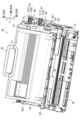
図1に示すように、画像形成装置1は、本体筐体10と、カバーCVと、プロセスカートリッジ20とを備える。本体筐体10は、開口OPを有する。カバーCVは、開口OPを開ける開位置と開口OPを閉じる閉位置との間を移動可能である。なお、図1では、便宜上、本体筐体10の大きさを小さく図示している。
Next, an embodiment of the present disclosure will be described in detail with reference to the drawings as appropriate.
As shown in Fig. 1, the image forming apparatus 1 includes a
カバーCVが開位置に位置する状態で、プロセスカートリッジ20は、第1方向において、開口OPを通して本体筐体10に着脱可能である。第1方向は、図1の左右方向、つまり本体筐体10の前後方向である。プロセスカートリッジ20は、現像カートリッジ30と、ドラムカートリッジ40とを備える。現像カートリッジ30は、ドラムカートリッジ40の後述するドラムフレーム41に着脱可能である。
When the cover CV is in the open position, the
現像カートリッジ30は、現像筐体31と、現像ローラ32とを備える。現像筐体31は、トナーを収容可能である。現像筐体31は、現像ローラ32を回転可能に保持する。現像筐体31は、後述する第1外表面S1と、第2方向において第1外表面S1と離れて位置する後述する第2外表面S2とを有する(図2参照)。
The developing
現像ローラ32は、後述する感光ドラム42にトナーを供給するローラである。現像ローラ32は、第2方向に延びる現像軸X1を中心に回転可能である。現像ローラ32は、第1方向における現像筐体31の一端部に位置する。
The developing
本実施形態では、第2方向は、第1方向と交差する。また、第1方向および第2方向と交差する方向を、第3方向とする。本実施形態では、第3方向は、第1方向および第2方向と直交する。 In this embodiment, the second direction intersects with the first direction. Also, the direction that intersects with the first and second directions is called the third direction. In this embodiment, the third direction is perpendicular to the first and second directions.
ドラムカートリッジ40は、ドラムフレーム41と、感光ドラム42とを備える。ドラムフレーム41は、感光ドラム42を回転可能に保持する。感光ドラム42は、第2方向に延びるドラム軸X2を中心に回転可能である。感光ドラム42は、ドラムフレーム41の第1方向の一端部に位置する。
The
図2および図4に示すように、現像カートリッジ30は、ギヤカバーGCと、現像ICチップC1と、現像チップホルダ50とをさらに備える。ギヤカバーGCは、現像ローラ32を駆動するためのギヤを覆うカバーである。
As shown in Figures 2 and 4, the developing
図2に示すように、ギヤカバーGCは、現像筐体31の第1外表面S1に位置する。現像ICチップC1は、現像カートリッジ30に関する現像情報を記憶している。現像情報としては、例えば、現像カートリッジ30内のトナーの残量や現像ローラ32の寿命などが挙げられる。現像ICチップC1は、第1電気的接触面としての現像電気的接触面C11と、現像情報が記憶された現像メモリを備えた現像基板C12とを有する。
As shown in FIG. 2, the gear cover GC is located on the first outer surface S1 of the developing
現像基板C12は、第1面と、第1面の反対側に位置する第2面と、を有する。
一例として、現像電気的接触面C11は、現像基板C12の第1面に位置している。現像メモリは、現像基板C12の第2面に位置している。現像電気的接触面C11は、配線を介して現像メモリと電気的に接続されている。現像メモリは、現像基板C12および現像電気的接触面C11から離れた位置に位置していてもよい。
The developed substrate C12 has a first surface and a second surface located opposite the first surface.
As an example, the developer electrical contact surface C11 is located on a first surface of the developer substrate C12. The developer memory is located on a second surface of the developer substrate C12. The developer electrical contact surface C11 is electrically connected to the developer memory via wiring. The developer memory may be located at a position away from the developer substrate C12 and the developer electrical contact surface C11.
現像電気的接触面C11は、第2方向における現像筐体31の一端部に位置する。プロセスカートリッジ20が本体筐体10に装着された状態において、現像電気的接触面C11は、後述する現像本体接点13A(図3(b)参照)に接触する。
The developing electrical contact surface C11 is located at one end of the developing
現像電気的接触面C11は、第3方向を向いている。現像電気的接触面C11は、第2方向において現像筐体31の第1外表面S1から離れている。現像電気的接触面C11は、現像基板C12および現像チップホルダ50を介して、ギヤカバーGCに取り付けられている。
The developer electrical contact surface C11 faces the third direction. The developer electrical contact surface C11 is separated from the first outer surface S1 of the
図2および図4に示すように、ドラムカートリッジ40は、ロックレバーLと、ドラムICチップC2と、ドラムチップホルダ60とを備える。ロックレバーLは、ドラムフレーム41に現像カートリッジ30をロックするための部材である。ドラムICチップC2は、ドラムカートリッジ40に関するドラム情報を記憶している。ドラム情報としては、例えば、感光ドラム42の寿命などが挙げられる。図2に示すように、ドラムICチップC2は、第2電気的接触面としてのドラム電気的接触面C21と、ドラム情報が記憶されたドラムメモリを備えたドラム基板C22とを有する。
As shown in Figures 2 and 4, the
ドラム基板C22は、第1面と、第1面の反対側に位置する第2面と、を有する。
一例として、ドラム電気的接触面C21は、ドラム基板C22の第1面に位置している。ドラムメモリは、ドラム基板C22の第2面に位置している。ドラム電気的接触面C21は、配線を介してドラムメモリと電気的に接続されている。ドラムメモリは、ドラム基板C22およびドラム電気的接触面C21から離れた位置に位置していてもよい。
The drum substrate C22 has a first surface and a second surface located opposite to the first surface.
As an example, the drum electrical contact surface C21 is located on a first surface of the drum substrate C22. The drum memory is located on a second surface of the drum substrate C22. The drum electrical contact surface C21 is electrically connected to the drum memory via wiring. The drum memory may be located at a position away from the drum substrate C22 and the drum electrical contact surface C21.
ドラム電気的接触面C21は、第2方向におけるドラムフレーム41の一端部に位置する。ドラム電気的接触面C21は、第1方向において、ドラムフレーム41の第1方向の一端部よりも、ドラムフレーム41の第1方向の他端部に近い位置に位置する。ドラム電気的接触面C21は、第3方向を向いている。
The drum electrical contact surface C21 is located at one end of the
ドラムフレーム41に現像カートリッジ30が装着された状態において、ドラム電気的接触面C21は、現像電気的接触面C11と第1方向に並ぶ。つまり、ドラムフレーム41に現像カートリッジ30が装着された状態において、ドラム電気的接触面C21と現像電気的接触面C11は、第2方向におけるプロセスカートリッジ20の一端部に位置する。プロセスカートリッジ20が本体筐体10に装着された状態において、ドラム電気的接触面C21は、後述するドラム本体接点13B(図9参照)に接触する。プロセスカートリッジ20が本体筐体10に装着された状態において、ドラム電気的接触面C21は、第1方向において、現像電気的接触面C11よりも開口OPの近くに位置する。
When the developing
ドラムフレーム41は、第1サイドフレームSF1と、第2サイドフレームSF2とを有する。第2サイドフレームSF2は、第2方向において、第1サイドフレームSF1と離れて位置する。現像カートリッジ30がドラムフレーム41に装着された状態において、現像筐体31は、第2方向において、第1サイドフレームSF1と第2サイドフレームSF2の間に位置する。
The
ドラム電気的接触面C21は、ドラム基板C22およびドラムチップホルダ60を介して第1サイドフレームSF1に取り付けられている。現像カートリッジ30がドラムフレーム41に装着された状態において、現像電気的接触面C11およびドラム電気的接触面C21は、第2方向において、第1サイドフレームSF1に対して現像筐体31の反対側に位置する。
The drum electrical contact surface C21 is attached to the first side frame SF1 via the drum base plate C22 and the
ロックレバーLは、ドラムフレーム41に現像カートリッジ30をロックするための部材である。ロックレバーLは、第2方向におけるドラムフレーム41の他端部に位置する。ロックレバーLは、第2サイドフレームSF2に取り付けられている。現像カートリッジ30がドラムフレーム41に装着された状態において、現像電気的接触面C11およびドラム電気的接触面C21は、第2方向において、現像筐体31に対して、ロックレバーLの反対側に位置する。
The lock lever L is a member for locking the developing
図3に示すように、現像チップホルダ50は、現像電気的接触面C11が現像筐体31に対して移動可能となるように、現像ICチップC1の現像電気的接触面C11を保持するホルダである。現像チップホルダ50は、現像ホルダ51と、現像進退部材52と、現像バネ53と、現像ホルダカバー54とを備える。現像ホルダ51は、現像ICチップC1を保持する部材である。また、現像ホルダ51は、第3方向において、現像進退部材52を移動可能に保持している。
As shown in FIG. 3, the
現像バネ53は、現像ホルダ51と現像進退部材52の間に位置する。現像バネ53は、コイルバネである。現像バネ53は、現像進退部材52を現像ICチップC1から離れる方向に付勢する。
The
現像ホルダカバー54は、ギヤカバーGCに取り付けられている。現像ホルダカバー54がギヤカバーGCに取り付けられている状態で、現像ホルダ51は、第2方向において、現像ホルダカバー54とギヤカバーGCの間に位置する。現像ホルダカバー54およびギヤカバーGCは、現像チップホルダ50を第1方向および第3方向に移動可能に保持している。
The developing
ドラムチップホルダ60は、ドラム電気的接触面C21がドラムフレーム41に対して移動可能となるように、ドラムICチップC2のドラム電気的接触面C21を保持するホルダである。ドラムチップホルダ60は、ドラムホルダ61と、ドラム進退部材62と、ドラムバネ63と、ドラムホルダカバー64とを備える。ドラムホルダ61は、ドラムICチップC2を保持する部材である。また、ドラムホルダ61は、第3方向において、ドラム進退部材62を移動可能に保持している。
The
ドラムバネ63は、ドラムホルダ61とドラム進退部材62の間に位置する。ドラムバネ63は、コイルバネである。ドラムバネ63は、ドラム進退部材62をドラムICチップC2から離れる方向に付勢する。
The
ドラムホルダカバー64は、第1サイドフレームSF1に取り付けられている。ドラムホルダカバー64が第1サイドフレームSF1に取り付けられている状態で、ドラムホルダ61は、第2方向において、ドラムホルダカバー64と第1サイドフレームSF1の間に位置する。ドラムホルダカバー64および第1サイドフレームSF1は、ドラムチップホルダ60を第1方向および第3方向に移動可能に保持している。
The
本体筐体10は、第1ガイド11と、第2ガイド12と、第1接点としての現像本体接点13Aと、第2接点としてのドラム本体接点13Bとを有する。第1ガイド11は、プロセスカートリッジ20を本体筐体10に装着する間に、現像進退部材52の下端およびドラム進退部材62の下端と接触して、現像進退部材52およびドラム進退部材62をガイドするガイドである。第2ガイド12は、プロセスカートリッジ20を本体筐体10に装着する間に、現像ホルダ51の上端およびドラムホルダ61の上端と接触して、現像ホルダ51およびドラムホルダ61をガイドするガイドである。現像本体接点13Aは、現像電気的接触面C11と接触する接点である。現像本体接点13Aは、図示せぬ制御部と現像ICチップC1とを電気的に接続させる。
The
ドラム本体接点13Bは、ドラム電気的接触面C21と接触する接点である。ドラム本体接点13Bは、図示せぬ制御部とドラムICチップC2とを電気的に接続させる。
The drum
図3(a)は、プロセスカートリッジ20が本体筐体10に装着されていないときの、プロセスカートリッジ20の状態を示す。また、図3(b)は、プロセスカートリッジ20が本体筐体10に装着されたときの、プロセスカートリッジ20の状態を示す。
Figure 3(a) shows the state of the
図3(a)に示すように、プロセスカートリッジ20が本体筐体10に装着されていないときは、現像ホルダ51と現像進退部材52が、現像バネ53によって離れた状態にある。また、ドラムホルダ61とドラム進退部材62が、ドラムバネ63によって離れた状態にある。
As shown in FIG. 3A, when the
図3(b)に示すように、プロセスカートリッジ20が本体筐体10に装着されたときは、現像ホルダ51は、現像進退部材52および現像バネ53を介して、本体筐体10の第1ガイド11によって所定位置に位置決めされ、現像電気的接触面C11は、現像本体接点13Aに接触する。また、ドラムホルダ61は、ドラム進退部材62およびドラムバネ63を介して、本体筐体10の第1ガイド11によって所定位置に位置決めされ、ドラム電気的接触面C21は、ドラム本体接点13Bに接触する。
As shown in FIG. 3(b), when the
図3(b)の状態の現像バネ53は、図3(a)の状態の現像バネ53よりも縮む。そのため、図3(b)の状態では、現像バネ53の弾性力により、電気的接触面C11が、本体筐体10の現像本体接点13Aに押し付けられる。
図3(b)の状態のドラムバネ63は、図3(a)の状態のドラムバネ63よりも縮む。そのため、図3(b)の状態では、ドラムバネ63の弾性力により、電気的接触面C21が、本体筐体10のドラム本体接点13Bに押し付けられる。
The developing
The
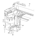
図4に示すように、ドラムカートリッジ40は、ドラムホルダ―カバー64から第3方向に延びる壁W1を有する。壁W1は、ドラムホルダ―カバー64と一体または別体に形成することができる。壁W1は、詳細は図示しないが、箱状に形成されている。壁W1の形状は、特に限定されない。壁W1は、棒、リブなどで構成されていてもよい。また、壁W1は、スリットや穴を有していてもよい。図3(b)に示すように、壁W1は、第2ガイド12と向かい合う面W11を有する。面W11は、第2ガイド12の面W11と向かい合う部分と平行に延びている。これにより、第2ガイド12と壁W1の間にユーザの指が入ることを効果的に遮る。
As shown in FIG. 4, the
図5に示すように、壁W1は、プロセスカートリッジ20が本体筐体10に装着された状態において、第1方向において、ドラム電気的接触面C21よりも開口OPの近くに位置する。壁W1は、プロセスカートリッジ20が本体筐体10に装着された状態において、第1方向において、ドラム本体接点13Bおよびドラム電気的接触面C21と重なる。
As shown in FIG. 5, when the
本体筐体10は、第1本体サイドフレームF1と、第2方向において、第1本体サイドフレームF1と離れて位置する第2本体サイドフレームF2とを有する。プロセスカートリッジ20が本体筐体10に装着された状態において、現像電気的接触面C11は、第2方向において、現像筐体31と第1本体サイドフレームF1との間に位置する。また、ドラム電気的接触面C21は、第2方向において、ドラムフレーム41の第1サイドフレームSF1と第1本体サイドフレームF1との間に位置する。
The
図6に示すように、壁W1は、第2方向におけるドラムフレーム41の第1サイドフレームSF1と第1本体サイドフレームF1との間に、ユーザの指が入ることを遮る。
As shown in FIG. 6, the wall W1 prevents the user's fingers from entering between the first side frame SF1 and the first main body side frame F1 of the
以上によれば、本実施形態において以下のような効果を得ることができる。
プロセスカートリッジ20が本体筐体10に装着された状態において、壁W1がドラム電気的接触面C21よりも開口OPの近くに位置する。壁W1は、第1方向においてドラム本体接点13Bおよびドラム電気的接触面C21と重なる。そのため、ユーザがカバーCVを開き、プロセスカートリッジ20を本体筐体10から取り外すときに、ユーザの手が、本体筐体10のドラム本体接点13Bおよびドラム電気的接触面C21に近づき、ユーザの手と本体筐体10のドラム本体接点13Bおよびドラム電気的接触面C21との間で放電が生じることを抑制することができる。
As described above, the following effects can be obtained in this embodiment.
When the
なお、本開示は前記実施形態に限定されることなく、以下に例示するように様々な形態で利用できる。
下の説明においては、前記実施形態と略同様の構造となる部材には同一の符号を付し、その説明は省略する。
The present disclosure is not limited to the above-described embodiment, but can be used in various forms as exemplified below.
In the following description, members having substantially the same structure as those in the above embodiment are given the same reference numerals, and the description thereof will be omitted.
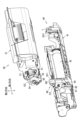
図7、図8は、本開示の第2実施形態を示している。第2実施形態では、ドラムカートリッジ40は、ドラムフレーム41の第1サイドフレームSF1から延びる壁W2を有する。壁W2は、ドラムフレーム41の第1方向の他端部から第2方向に延びている。壁W2は、第1サイドフレームSF1と一体または別体に形成することができる。
Figures 7 and 8 show a second embodiment of the present disclosure. In the second embodiment, the
図9、図10は、本開示の第3実施形態を示している。第3実施形態では、現像カートリッジ30は、現像筐体31から第2方向に延びる壁W3を有する。壁W3は、現像筐体31と一体または別体に形成することができる。
Figures 9 and 10 show a third embodiment of the present disclosure. In the third embodiment, the developing
前記した実施形態および変形例で説明した各要素を、任意に組み合わせて実施してもよい。 The elements described in the above embodiments and variations may be implemented in any combination.
1 画像形成装置
10 本体筐体
13A 現像本体接点
13B ドラム本体接点
20 プロセスカートリッジ
30 現像カートリッジ
31 現像筐体
32 現像ローラ
40 ドラムカートリッジ
41 ドラムフレーム
42 感光ドラム
C1 現像ICチップ
C2 ドラムICチップ
C11 現像電気的接触面
C21 ドラム電気的接触面
CV カバー
OP 開口
W1 壁
W2 壁
W3 壁
X1 現像軸
X4 ドラム軸
REFERENCE SIGNS LIST 1
Claims (16)
前記開口を開閉可能なカバーと、
第1方向において、前記開口を通して前記本体筐体に着脱可能なプロセスカートリッジであって、現像カートリッジとドラムカートリッジとを備えるプロセスカートリッジと、を備える画像形成装置であって、
前記現像カートリッジは、
第2方向に延びる現像軸を中心に回転可能な現像ローラと、
トナーを収容可能な現像筐体と、
前記現像筐体の前記第2方向の一端部に位置する第1電気的接触面を有する第1ICチップと、を備え、
前記ドラムカートリッジは、
第2方向に延びるドラム軸を中心に回転可能な感光ドラムと、
前記現像カートリッジが着脱可能なドラムフレームと、
前記ドラムフレームの前記第2方向の一端部に位置する第2電気的接触面を有する第2ICチップと、を備え、
前記第1電気的接触面は、前記第1接点と接触し、前記第2電気的接触面は、前記第2接点と接触し、
前記プロセスカートリッジは、前記プロセスカートリッジが前記本体筐体に装着された状態において、前記第1方向において、前記第2電気的接触面よりも前記開口の近くに位置する壁であって、前記第1方向において、前記第2接点および前記第2電気的接触面と重なる壁を有することを特徴とする画像形成装置。 a main body housing having an opening and including a first contact and a second contact;
a cover capable of opening and closing the opening;
an image forming apparatus including a process cartridge that is detachably mountable to the main body through the opening in a first direction, the process cartridge including a developing cartridge and a drum cartridge,
The developing cartridge includes:
a developing roller rotatable around a developing axis extending in the second direction;
a developing housing capable of accommodating toner;
a first IC chip having a first electrical contact surface located at one end of the developing housing in the second direction ,
The drum cartridge is
a photosensitive drum rotatable around a drum axis extending in a second direction;
a drum frame to which the developing cartridge can be detachably attached;
a second IC chip having a second electrical contact surface located at one end of the drum frame in the second direction ;
the first electrical contact surface contacts the first contact and the second electrical contact surface contacts the second contact;
An image forming apparatus characterized in that the process cartridge has a wall that is located closer to the opening in the first direction than the second electrical contact surface when the process cartridge is attached to the main body housing, and that overlaps with the second contact and the second electrical contact surface in the first direction.
前記プロセスカートリッジが前記本体筐体に装着された状態において、
前記第1電気的接触面は、前記第2方向において、前記現像筐体と前記第1本体サイドフレームとの間に位置し、
前記第2電気的接触面は、前記第2方向において、前記ドラムフレームと前記第1本体サイドフレームとの間に位置することを特徴とする請求項1に記載の画像形成装置。 the main body housing has a first main body side frame and a second main body side frame positioned away from the first main body side frame in the second direction,
When the process cartridge is attached to the main body housing,
the first electrical contact surface is located between the developing housing and the first main body side frame in the second direction,
2. The image forming apparatus according to claim 1, wherein the second electrical contact surface is located between the drum frame and the first main body side frame in the second direction.
前記第2電気的接触面は、前記第1方向において、前記第1電気的接触面よりも前記開口の近くに位置することを特徴とする請求項1から請求項4のいずれか1項に記載の画像形成装置。 When the process cartridge is attached to the main body housing,
5. The image forming apparatus according to claim 1, wherein the second electrical contact surface is located closer to the opening than the first electrical contact surface is in the first direction.
前記第2電気的接触面は、前記第1方向において、前記ドラムフレームの前記第1方向の前記一端部よりも、前記ドラムフレームの前記第1方向の他端部に近い位置に位置することを特徴とする請求項1から請求項5のいずれか1項に記載の画像形成装置。 The photosensitive drum is located at one end of the drum frame in the first direction,
6. An image forming apparatus according to claim 1, wherein the second electrical contact surface is located at a position in the first direction closer to the other end of the drum frame in the first direction than to the one end of the drum frame in the first direction .
前記第2電気的接触面を保持するドラムチップホルダと、
前記ドラムチップホルダを移動可能に保持するドラムホルダカバーと、をさらに有し、
前記壁は、前記ドラムホルダカバーから延びていることを特徴とする請求項1から請求項6のいずれか1項に記載の画像形成装置。 The drum cartridge is
a drum tip holder for holding the second electrical contact surface;
A drum holder cover that movably holds the drum tip holder,
7. The image forming apparatus according to claim 1 , wherein the wall extends from the drum holder cover.
前記第1電気的接触面を保持する現像チップホルダと、
前記現像チップホルダを移動可能に保持する現像ホルダカバーと、をさらに有することを特徴とする請求項1から請求項8のいずれか1項に記載の画像形成装置。 The developing cartridge includes:
a developer chip holder for holding the first electrical contact surface;
9. The image forming apparatus according to claim 1 , further comprising: a developing holder cover that movably holds the developing chip holder.
14. The image forming apparatus according to claim 1, wherein the first electrical contact surface and the second electrical contact surface are held movably relative to the main body housing.
前記ドラムフレームは、前記感光ドラムを回転可能に保持することを特徴とする請求項1から請求項14のいずれか1項に記載の画像形成装置。 the developing housing rotatably holds the developing roller,
15. The image forming apparatus according to claim 1, wherein the drum frame rotatably holds the photosensitive drum.
Priority Applications (1)
| Application Number | Priority Date | Filing Date | Title |
|---|---|---|---|
| JP2021059081A JP7635608B2 (en) | 2021-03-31 | 2021-03-31 | Image forming device |
Applications Claiming Priority (1)
| Application Number | Priority Date | Filing Date | Title |
|---|---|---|---|
| JP2021059081A JP7635608B2 (en) | 2021-03-31 | 2021-03-31 | Image forming device |
Publications (2)
| Publication Number | Publication Date |
|---|---|
| JP2022155717A JP2022155717A (en) | 2022-10-14 |
| JP7635608B2 true JP7635608B2 (en) | 2025-02-26 |
Family
ID=83558864
Family Applications (1)
| Application Number | Title | Priority Date | Filing Date |
|---|---|---|---|
| JP2021059081A Active JP7635608B2 (en) | 2021-03-31 | 2021-03-31 | Image forming device |
Country Status (1)
| Country | Link |
|---|---|
| JP (1) | JP7635608B2 (en) |
Citations (9)
| Publication number | Priority date | Publication date | Assignee | Title |
|---|---|---|---|---|
| JP2000132068A (en) | 1998-10-28 | 2000-05-12 | Canon Inc | Process cartridge and electrophotographic image forming apparatus |
| JP2006119467A (en) | 2004-10-22 | 2006-05-11 | Canon Inc | Process cartridge and electrophotographic image forming apparatus |
| JP2012203989A (en) | 2011-03-23 | 2012-10-22 | Brother Ind Ltd | Waterproof structure of operation panel |
| JP2015138246A (en) | 2014-01-24 | 2015-07-30 | 京セラドキュメントソリューションズ株式会社 | image forming apparatus |
| JP2018146829A (en) | 2017-03-07 | 2018-09-20 | ブラザー工業株式会社 | Drum cartridge and process cartridge |
| JP2019159048A (en) | 2018-03-12 | 2019-09-19 | ブラザー工業株式会社 | Drum cartridge and image forming apparatus |
| JP2020112833A (en) | 2016-06-30 | 2020-07-27 | ブラザー工業株式会社 | Developer cartridge |
| JP2020181084A (en) | 2019-04-25 | 2020-11-05 | キヤノン株式会社 | Process cartridge and image forming apparatus |
| JP2021039174A (en) | 2019-08-30 | 2021-03-11 | ブラザー工業株式会社 | Drum cartridge and image forming apparatus |
Family Cites Families (1)
| Publication number | Priority date | Publication date | Assignee | Title |
|---|---|---|---|---|
| JPH10228224A (en) * | 1997-02-14 | 1998-08-25 | Canon Inc | Process cartridge and electrophotographic image forming apparatus |
-
2021
- 2021-03-31 JP JP2021059081A patent/JP7635608B2/en active Active
Patent Citations (9)
| Publication number | Priority date | Publication date | Assignee | Title |
|---|---|---|---|---|
| JP2000132068A (en) | 1998-10-28 | 2000-05-12 | Canon Inc | Process cartridge and electrophotographic image forming apparatus |
| JP2006119467A (en) | 2004-10-22 | 2006-05-11 | Canon Inc | Process cartridge and electrophotographic image forming apparatus |
| JP2012203989A (en) | 2011-03-23 | 2012-10-22 | Brother Ind Ltd | Waterproof structure of operation panel |
| JP2015138246A (en) | 2014-01-24 | 2015-07-30 | 京セラドキュメントソリューションズ株式会社 | image forming apparatus |
| JP2020112833A (en) | 2016-06-30 | 2020-07-27 | ブラザー工業株式会社 | Developer cartridge |
| JP2018146829A (en) | 2017-03-07 | 2018-09-20 | ブラザー工業株式会社 | Drum cartridge and process cartridge |
| JP2019159048A (en) | 2018-03-12 | 2019-09-19 | ブラザー工業株式会社 | Drum cartridge and image forming apparatus |
| JP2020181084A (en) | 2019-04-25 | 2020-11-05 | キヤノン株式会社 | Process cartridge and image forming apparatus |
| JP2021039174A (en) | 2019-08-30 | 2021-03-11 | ブラザー工業株式会社 | Drum cartridge and image forming apparatus |
Also Published As
| Publication number | Publication date |
|---|---|
| JP2022155717A (en) | 2022-10-14 |
Similar Documents
| Publication | Publication Date | Title |
|---|---|---|
| CN209895138U (en) | developer cartridge | |
| JP6809337B2 (en) | Development cartridge | |
| JP7732242B2 (en) | Process cartridge | |
| JP7600535B2 (en) | Process cartridge | |
| JP4433036B2 (en) | Electronic module and electronic device | |
| JP7524583B2 (en) | Developing cartridge | |
| JP7512652B2 (en) | Cartridges and how to recycle them | |
| JP7697230B2 (en) | Process cartridge | |
| JP7484344B2 (en) | Image forming device | |
| JP7666017B2 (en) | Developing cartridge | |
| JP7635608B2 (en) | Image forming device | |
| JP7631997B2 (en) | Developing cartridge | |
| JP7790143B2 (en) | toner cartridge | |
| JP2007003660A (en) | Image forming device | |
| US12360493B2 (en) | Developing cartridge | |
| JP7721983B2 (en) | Process cartridge | |
| CN218068575U (en) | Developing cartridge, process cartridge and electronic image forming apparatus | |
| JP4016503B2 (en) | Electronic device having an open / close lid | |
| JP7596890B2 (en) | Cartridge System | |
| JP7185654B2 (en) | washing machine | |
| WO2022270242A1 (en) | Drum cartridge and process cartridge | |
| JP2024004353A (en) | Developer cartridges, drum cartridges and process cartridges | |
| JP2011069953A (en) | Rotating-body cover | |
| JP2022157973A (en) | toner cartridges and drum cartridges | |
| CN223582329U (en) | Developing and processing boxes |
Legal Events
| Date | Code | Title | Description |
|---|---|---|---|
| A621 | Written request for application examination |
Free format text: JAPANESE INTERMEDIATE CODE: A621 Effective date: 20240227 |
|
| A977 | Report on retrieval |
Free format text: JAPANESE INTERMEDIATE CODE: A971007 Effective date: 20240806 |
|
| A131 | Notification of reasons for refusal |
Free format text: JAPANESE INTERMEDIATE CODE: A131 Effective date: 20240827 |
|
| A521 | Request for written amendment filed |
Free format text: JAPANESE INTERMEDIATE CODE: A523 Effective date: 20241011 |
|
| TRDD | Decision of grant or rejection written | ||
| A01 | Written decision to grant a patent or to grant a registration (utility model) |
Free format text: JAPANESE INTERMEDIATE CODE: A01 Effective date: 20250114 |
|
| A61 | First payment of annual fees (during grant procedure) |
Free format text: JAPANESE INTERMEDIATE CODE: A61 Effective date: 20250127 |
|
| R150 | Certificate of patent or registration of utility model |
Ref document number: 7635608 Country of ref document: JP Free format text: JAPANESE INTERMEDIATE CODE: R150 |