JP7608896B2 - Light emitting device and projector - Google Patents
Light emitting device and projector Download PDFInfo
- Publication number
- JP7608896B2 JP7608896B2 JP2021042110A JP2021042110A JP7608896B2 JP 7608896 B2 JP7608896 B2 JP 7608896B2 JP 2021042110 A JP2021042110 A JP 2021042110A JP 2021042110 A JP2021042110 A JP 2021042110A JP 7608896 B2 JP7608896 B2 JP 7608896B2
- Authority
- JP
- Japan
- Prior art keywords
- layer
- semiconductor layer
- refractive index
- light emitting
- diameter
- Prior art date
- Legal status (The legal status is an assumption and is not a legal conclusion. Google has not performed a legal analysis and makes no representation as to the accuracy of the status listed.)
- Active
Links
Images


Landscapes
- Projection Apparatus (AREA)
- Semiconductor Lasers (AREA)
Description
本発明は、発光装置およびプロジェクターに関する。 The present invention relates to a light-emitting device and a projector.
半導体レーザーは、高輝度の次世代光源として期待されている。特に、ナノコラムを適用した半導体レーザーは、ナノコラムによるフォトニック結晶の効果によって、狭放射角で高出力の発光が実現できると期待されている。 Semiconductor lasers are expected to be the next generation of high-brightness light sources. In particular, semiconductor lasers that incorporate nanocolumns are expected to be able to achieve high-output light emission with a narrow radiation angle due to the photonic crystal effect of the nanocolumns.
例えば特許文献1には、n型のGaN層と、発光層と、p型のGaN層と、を備えた柱状部を複数有する発光装置が記載されている。 For example, Patent Document 1 describes a light-emitting device having multiple columnar sections each including an n-type GaN layer, a light-emitting layer, and a p-type GaN layer.
しかしながら、特許文献1では、p型のGaN層における柱状部の径がn型のGaN層における柱状部の径よりも大きいため、p型のGaN層における積層体の面内方向の平均屈折率は、n型のGaN層における積層体の面内方向の平均屈折率よりも大きくなる。そのため、発光層で発生する光がp型のGaN層側に漏れてしまい、光閉じ込め係数が低下する場合がある。 However, in Patent Document 1, the diameter of the columnar portion in the p-type GaN layer is larger than the diameter of the columnar portion in the n-type GaN layer, so the average refractive index in the in-plane direction of the stack in the p-type GaN layer is larger than the average refractive index in the in-plane direction of the stack in the n-type GaN layer. As a result, light generated in the light-emitting layer may leak to the p-type GaN layer side, reducing the optical confinement coefficient.
本発明に係る発光装置の一態様は、
複数の柱状部を有する積層体を有し、
複数の前記柱状部の各々は、
第1導電型の第1半導体層と、
前記第1導電型とは異なる第2導電型の第2半導体層と、
前記第1半導体層と前記第2半導体層との間に設けられた発光層と、
を有し、
前記第1半導体層における前記柱状部の最大径は、前記第2半導体層における前記柱状部の最大径よりも小さく、
前記第1半導体層における前記柱状部の径は、前記積層体の積層方向における第1位置で、前記第2半導体層における前記柱状部の最小径よりも小さく、かつ、前記積層方向における前記第1位置と異なる第2位置で最大であり、
前記第1半導体層の前記第1位置における屈折率は、前記第2半導体層の屈折率および前記第1半導体層の前記第2位置における屈折率よりも高い。
One aspect of the light emitting device according to the present invention is
A laminate having a plurality of columnar portions,
Each of the plurality of columnar portions is
A first semiconductor layer of a first conductivity type;
a second semiconductor layer of a second conductivity type different from the first conductivity type;
a light emitting layer provided between the first semiconductor layer and the second semiconductor layer;
having
a maximum diameter of the columnar portion in the first semiconductor layer is smaller than a maximum diameter of the columnar portion in the second semiconductor layer;
a diameter of the columnar portion in the first semiconductor layer is smaller than a minimum diameter of the columnar portion in the second semiconductor layer at a first position in a stacking direction of the stacked body, and is maximum at a second position different from the first position in the stacking direction;
The refractive index of the first semiconductor layer at the first position is higher than the refractive index of the second semiconductor layer and the refractive index of the first semiconductor layer at the second position.
本発明に係る発光装置の一態様は、
複数の柱状部を有する積層体を有し、
複数の前記柱状部の各々は、
第1導電型の第1半導体層と、
前記第1導電型とは異なる第2導電型の第2半導体層と、
前記第1半導体層と前記第2半導体層との間に設けられた発光層と、
を有し、
前記第1半導体層における前記柱状部の最大径は、前記第2半導体層における前記柱状部の最大径よりも小さく、
前記第1半導体層は、
第1層と、
前記第1層と前記発光層との間に設けられた第2層と、
前記第1層と前記第2層との間に設けられた第3層と、
を有し、
前記第1層における前記柱状部の径は、前記第2半導体層における前記柱状部の最小径、および前記第2層における前記柱状部の径よりも小さく、
前記第1層の屈折率は、前記第2半導体層の屈折率および前記第2層の屈折率よりも高く、
前記第2層の屈折率は、前記第3層の屈折率よりも高い。
One aspect of the light emitting device according to the present invention is
A laminate having a plurality of columnar portions,
Each of the plurality of columnar portions is
A first semiconductor layer of a first conductivity type;
a second semiconductor layer of a second conductivity type different from the first conductivity type;
a light emitting layer provided between the first semiconductor layer and the second semiconductor layer;
having
a maximum diameter of the columnar portion in the first semiconductor layer is smaller than a maximum diameter of the columnar portion in the second semiconductor layer;
The first semiconductor layer is
A first layer;
a second layer provided between the first layer and the light-emitting layer;
a third layer disposed between the first layer and the second layer;
having
a diameter of the columnar portion in the first layer is smaller than a minimum diameter of the columnar portion in the second semiconductor layer and a diameter of the columnar portion in the second layer;
a refractive index of the first layer is higher than a refractive index of the second semiconductor layer and a refractive index of the second layer;
The refractive index of the second layer is higher than the refractive index of the third layer.
本発明に係る発光装置の一態様は、
複数の柱状部を有する積層体を有し、
複数の前記柱状部の各々は、
第1導電型の第1半導体層と、
前記第1導電型とは異なる第2導電型の第2半導体層と、
前記第1半導体層と前記第2半導体層との間に設けられた発光層と、
を有し、
前記第1半導体層における前記柱状部の最大径は、前記第2半導体層における前記柱状部の最大径よりも小さく、
前記第1半導体層は、第1InGaN層を有し、
前記第1InGaN層における前記柱状部の径は、前記第2半導体層における前記柱状部の最小径よりも小さく、
前記第2半導体層は、GaN層およびAlGaN層の少なくとも一方を有する。
One aspect of the light emitting device according to the present invention is
A laminate having a plurality of columnar portions,
Each of the plurality of columnar portions is
A first semiconductor layer of a first conductivity type;
a second semiconductor layer of a second conductivity type different from the first conductivity type;
a light emitting layer provided between the first semiconductor layer and the second semiconductor layer;
having
a maximum diameter of the columnar portion in the first semiconductor layer is smaller than a maximum diameter of the columnar portion in the second semiconductor layer;
the first semiconductor layer comprises a first InGaN layer;
a diameter of the columnar portion in the first InGaN layer is smaller than a minimum diameter of the columnar portion in the second semiconductor layer;
The second semiconductor layer includes at least one of a GaN layer and an AlGaN layer.
本発明に係るプロジェクターの一態様は、
前記発光装置の一態様を有する。
One aspect of the projector according to the present invention is
The present invention has one aspect of the light emitting device.
以下、本発明の好適な実施形態について、図面を用いて詳細に説明する。なお、以下に説明する実施形態は、特許請求の範囲に記載された本発明の内容を不当に限定するものではない。また、以下で説明される構成の全てが本発明の必須構成要件であるとは限らない。 Below, preferred embodiments of the present invention will be described in detail with reference to the drawings. Note that the embodiments described below do not unduly limit the content of the present invention described in the claims. Furthermore, not all of the configurations described below are necessarily essential components of the present invention.
1. 第1実施形態
1.1. 発光装置
1.1.1. 全体の構成
まず、第1実施形態に係る発光装置について、図面を参照しながら説明する。図1は、第1実施形態に係る発光装置100を模式的に示す断面図である。
1. First embodiment 1.1. Light emitting device 1.1.1. Overall configuration First, the light emitting device according to the first embodiment will be described with reference to the drawings. Fig. 1 is a cross-sectional view that shows a schematic diagram of a
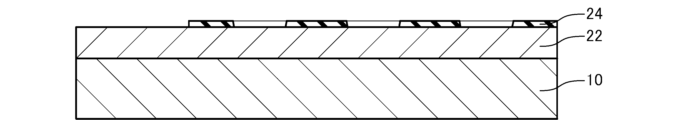
発光装置100は、図1に示すように、例えば、基板10と、積層体20と、第1電極40と、第2電極42と、を有している。発光装置100は、半導体レーザーである。
As shown in FIG. 1, the light-
基板10は、例えば、Si基板、GaN基板、サファイア基板、SiC基板などである。
The
積層体20は、基板10に設けられている。図示の例では、積層体20は、基板10上に設けられている。積層体20は、例えば、バッファー層22と、柱状部30と、を有している。
The laminate 20 is provided on the
本明細書では、積層体20の積層方向(以下、単に「積層方向」ともいう)において、発光層34を基準とした場合、発光層34から第2半導体層36に向かう方向を「上」とし、発光層34から第1半導体層32に向かう方向を「下」として説明する。また、積層方向と直交する方向を「面内方向」ともいう。また、「積層体20の積層方向」とは、柱状部30の第1半導体層32と発光層34との積層方向のことである。
In this specification, in the stacking direction of the laminate 20 (hereinafter also simply referred to as the "stacking direction"), when the
バッファー層22は、基板10上に設けられている。バッファー層22は、例えば、Siがドープされたn型のGaN層である。バッファー層22上には、柱状部30を形成するためのマスク層24が設けられている。マスク層24は、例えば、酸化シリコン層、チタン層、酸化チタン層、酸化アルミニウム層などである。
The
柱状部30は、バッファー層22上に設けられている。柱状部30は、バッファー層22から上方に突出した柱状の形状を有している。言い換えれば、柱状部30は、バッファー層22を介して基板10から上方に突出している。柱状部30は、例えば、ナノコラム、ナノワイヤー、ナノロッド、ナノピラーとも呼ばれる。柱状部30の平面形状は、例えば、六角形などの多角形、円である。
The
柱状部30の径は、例えば、50nm以上500nm以下である。柱状部30の径を500nm以下とすることによって、高品質な結晶の発光層34を得ることができ、かつ、発光層34に内在する歪を低減することができる。これにより、発光層34で発生する光を高い効率で増幅することができる。
The diameter of the
なお、「柱状部の径」とは、柱状部30の平面形状が円の場合は、直径であり、柱状部30の平面形状が円ではない形状の場合は、最小包含円の直径である。例えば、柱状部30の径は、柱状部30の平面形状が多角形の場合、該多角形を内部に含む最小の円の直径であり、柱状部30の平面形状が楕円の場合、該楕円を内部に含む最小の円の直径である。
The "diameter of the columnar portion" refers to the diameter when the planar shape of the
柱状部30は、複数設けられている。隣り合う柱状部30の間隔は、例えば、1nm以上500nm以下である。複数の柱状部30は、積層方向からみて、所定の方向に所定のピッチで配列されている。複数の柱状部30は、例えば、三角格子状、正方格子状に配置されている。複数の柱状部30は、フォトニック結晶の効果を発現することができる。
A plurality of
なお、「柱状部のピッチ」とは、所定の方向に沿って隣り合う柱状部30の中心間の距離である。「柱状部の中心」とは、柱状部30の平面形状が円の場合は、該円の中心であり、柱状部30の平面形状が円ではない形状の場合は、最小包含円の中心である。例えば、柱状部30の中心は、柱状部30の平面形状が多角形の場合、該多角形を内部に含む最小の円の中心であり、柱状部30の平面形状が楕円の場合、該楕円を内部に含む最小の円の中心である。
The "pitch of the columnar portions" refers to the distance between the centers of adjacent
柱状部30は、第1半導体層32と、発光層34と、第2半導体層36と、を有している。
The
第1半導体層32は、バッファー層22上に設けられている。第1半導体層32は、基板10と発光層34との間に設けられている。第1半導体層32は、第1導電型の半導体層である。第1半導体層32は、例えば、Siがドープされたn型の半導体層である。第1半導体層32は、GaおよびNを含む。
The
発光層34は、第1半導体層32と第2半導体層36との間に設けられている。発光層34は、電流が注入されることで光を発生させる。発光層34は、例えば、ウェル層と、バリア層と、を有している。ウェル層およびバリア層は、不純物が意図的にドープされていないi型の半導体層である。ウェル層は、例えば、InGaN層である。バリア層は、例えば、GaN層である。発光層34は、ウェル層とバリア層とから構成されたMQW(Multiple Quantum Well)構造を有している。
The light-emitting
なお、発光層34を構成するウェル層およびバリア層の数は、特に限定されない。例えば、ウェル層は、1層だけ設けられていてもよく、この場合、発光層34は、SQW(Single Quantum Well)構造を有している。
The number of well layers and barrier layers constituting the light-emitting
第2半導体層36は、発光層34上に設けられている。第2半導体層36は、第1導電型と異なる第2導電型の半導体層である。第2半導体層36は、例えば、Mgがドープされた半導体層である。第2半導体層36は、GaおよびNを含む。第1半導体層32および第2半導体層36は、発光層34に光を閉じ込める機能を有するクラッド層である。
The
なお、図示はしないが、第1半導体層32と発光層34との間、および発光層34と第2半導体層36との間の少なくとも一方に、i型のInGaN層およびGaN層からなるOCL(Optical Confinement Layer)が設けられていてもよい。また、第2半導体層36は、p型のAlGaN層からなるEBL(Electron Blocking Layer)を有してもよい。
Although not shown, an OCL (Optical Confinement Layer) made of an i-type InGaN layer and a GaN layer may be provided at least one between the
発光装置100では、p型の第2半導体層36、i型の発光層34、およびn型の第1半導体層32により、pinダイオードが構成される。発光装置100では、第1電極40と第2電極42との間に、pinダイオードの順バイアス電圧を印加すると、発光層34に電流が注入されて発光層34において電子と正孔との再結合が起こる。この再結合により発光が生じる。発光層34で発生した光は、面内方向に伝搬し、複数の柱状部30によるフォトニック結晶の効果により定在波を形成して、発光層34で利得を受けてレーザー発振する。そして、発光装置100は、+1次回折光および-1次回折光をレーザー光として、積層方向に出射する。
In the light-emitting
なお、図示はしないが、基板10とバッファー層22との間、または基板10の下に反射層が設けられていてもよい。該反射層は、例えば、DBR(Distributed Bragg Reflector)層である。該反射層によって、発光層34において発生した光を反射させることができ、発光装置100は、第2電極42側からのみ光を出射することができる。
Although not shown, a reflective layer may be provided between the
第1電極40は、バッファー層22上に設けられている。バッファー層22は、第1電極40とオーミックコンタクトしていてもよい。第1電極40は、第1半導体層32と電気的に接続されている。図示の例では、第1電極40は、バッファー層22を介して、第1半導体層32と電気的に接続されている。第1電極40は、発光層34に電流を注入するための一方の電極である。第1電極40としては、例えば、バッファー層22側から、Cr層、Ni層、Au層の順序で積層したものなどを用いる。
The
第2電極42は、第2半導体層36上に設けられている。第2半導体層36は、第2電極42とオーミックコンタクトしていてもよい。第2電極42は、発光層34に電流を注入するための他方の電極である。第2電極42としては、例えば、ITO(indium tin oxide)などを用いる。
The
なお、上記では、InGaN系の発光層34について説明したが、発光層34としては、出射される光の波長に応じて、電流が注入されることで発光可能な様々な材料系を用いることができる。例えば、AlGaN系、AlGaAs系、InGaAs系、InGaAsP系、InP系、GaP系、AlGaP系などの半導体材料を用いることができる。
Although the above describes an InGaN-based light-emitting
1.1.2. 柱状部の詳細な説明
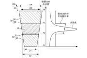
図2は、柱状部30を模式的に示す断面図である。なお、上述した図1では、柱状部30を簡略化して図示している。
1.1.2 Detailed Description of the Columnar Section Fig. 2 is a cross-sectional view that shows a schematic view of the
柱状部30の径は、例えば、図1および図2に示すように、基板10から第2電極42に向かにつれて大きくなる。柱状部30の径は、例えば、基板10から第2電極42に向かって漸増している。柱状部30は、例えば、基板10から第2電極42に向かにつれて径が大きくなるテーパー形状を有している。
The diameter of the
第1半導体層32は、積層方向における第1位置P1および第2位置P2を有する。第2位置P2は、積層方向において第1位置P1と異なる位置である。図示の例では、第1位置P1は、第1半導体層32の基板10側の端の位置である。第2位置P2は、第1半導体層32の発光層34側の端の位置である。
The
第1半導体層32における柱状部30の径は、第1位置P1で最小である。第1半導体層32における柱状部30の径は、第2位置P2で最大である。柱状部30は、第1位置P1において、第1半導体層32における最小径D1を有する。柱状部30は、第2位置P2において、第1半導体層32における最大径D2を有する。第1半導体層32の径は、積層方向において、一定ではない。第1半導体層32における柱状部30の径は、発光層34から遠ざかるにつれて小さくなる。すなわち、第1半導体層32における柱状部30の径は、基板10から発光層34に向かうにつれて大きくなる。
The diameter of the
第1半導体層32の第1位置P1における屈折率は、第1半導体層32の第2位置P2における屈折率よりも高い。第1半導体層32の屈折率は、例えば、第1位置P1で最も高い。第1半導体層32の屈折率は、例えば、第2位置P2で最も低い。第1半導体層32の屈折率は、積層方向において、一定ではない。第1半導体層32の第1位置P1における屈折率は、第2半導体層36の屈折率よりも高い。第1半導体層32の屈折率は、発光層34から遠ざかるにつれて高くなる。すなわち、第1半導体層32の屈折率は、基板10から発光層34に向かうにつれて低くなる。
The refractive index of the
第1半導体層32は、InGaN層50と、GaN層52と、を有している。第1位置P1には、InGaN層50が設けられている。第2位置P2には、GaN層52が設けられている。InGaN層50のInの組成は、発光層34から遠ざかるにつれて高くなる。そのため、第1半導体層32の屈折率は、発光層34から遠ざかるにつれて高くなる。InGaN層50の屈折率は、第2半導体層36の屈折率よりも高い。ここでいう「組成が高い」とは、構成材料の組成式において当該元素の数が大きいことを意味する。例えば、InGaNの組成式がInxGa1-xNである場合において、Inの組成が高いとは、組成式InxGa1-xNにおいてxの値が大きいことを意味する。
The
第2半導体層36は、積層方向における第3位置P3および第4位置P4を有する。第4位置P4は、積層方向において第3位置P3と異なる位置である。図示の例では、第3位置P3は、第2半導体層36の発光層34側の端の位置である。第4位置P4は、第2半導体層36の第2電極42側の端の位置である。
The
第2半導体層36における柱状部30の径は、第3位置P3で最小である。第2半導体層36における柱状部30の径は、第4位置P4で最大である。柱状部30は、第3位置P3において、第2半導体層36における最小径D3を有する。柱状部30は、第4位置P4において、第2半導体層36における最大径D4を有する。第1半導体層32における柱状部30の最大径D2は、第2半導体層36における柱状部30の最小径D3よりも小さい。第1半導体層32における柱状部30の最大径D2は、第2半導体層36における柱状部30の最大径D4よりも小さい。第1半導体層32における柱状部30の径は、第1位置P1で、第2半導体層36における柱状部30の最小径D3よりも小さい。
The diameter of the
第2半導体層36の径は、積層方向において、一定ではない。第2半導体層36における柱状部30の径は、発光層34から遠ざかるにつれて大きくなる。すなわち、第2半導体層36における柱状部30の径は、発光層34から第2電極42に向かうにつれて大きくなる。
The diameter of the
第2半導体層36の屈折率は、例えば、第3位置P3で最も高い。第2半導体層36の屈折率は、例えば、第4位置P4で最も低い。第2半導体層36の屈折率は、積層方向において、一定ではない。第2半導体層36の屈折率は、発光層34から遠ざかるにつれて低くなる。すなわち、第2半導体層36の屈折率は、発光層34から第2電極42に向かうにつれて低くなる。
The refractive index of the
第2半導体層36は、GaN層60と、AlGaN層62と、を有している。第3位置P3には、GaN層60が設けられている。第4位置P4には、AlGaN層62が設けられている。AlGaN層62のInの組成は、発光層34から遠ざかるにつれて高くなる。そのため、第2半導体層36の屈折率は、発光層34から遠ざかるにつれて低くなる。AlGaN層62の屈折率は、第1半導体層32の屈折率よりも低い。
The
1.1.3. 作用効果
発光装置100では、第1半導体層32における柱状部30の最大径D2は、第2半導体層36における柱状部30の最大径D4よりも小さい。第1半導体層32における柱状部30の径は、積層方向における第1位置P1で、第2半導体層36における柱状部30の最小径D3よりも小さく、かつ、積層方向における第1位置P1と異なる第2位置P2で最大である。第1半導体層32の第1位置P1における屈折率は、第2半導体層36の屈折率、および第1半導体層32の第2位置P2における屈折率よりも高い。
1.1.3. Effects In the
そのため、発光装置100では、図2に示すように、第1位置P1における積層体20の面内方向の平均屈折率と、第2半導体層36おける積層体20の面内方向の平均屈折率(第2半導体層36が設けられた部分の積層体20の面内方向の平均屈折率)と、の差を小さくすることができる。さらに、第1位置P1における積層体20の面内方向の平均屈折率と、第2位置P2おける積層体20の面内方向の平均屈折率と、の差を小さくすることができる。そのため、図2に示すように、積層方向における光強度のピークを、発光層34の位置に合わせることができる。図示の例では、第1位置P1における積層体20の面内方向の平均屈折率、第2位置P2の位置における積層体20の面内方向の平均屈折率、および第2半導体層36おける積層体20の面内方向の平均屈折率は、互いに等しい。
Therefore, in the
例えば、図3に示すように、第1半導体層1032の第1位置P1における屈折率、第1半導体層1032の第2位置P2における屈折率、および第2半導体層1036の屈折率が互いに等しい場合、第1位置P1における積層体の面内方向の平均屈折率は、第2位置P2における積層体の面内方向の平均屈折率、第2半導体層1036における積層体の面内方向の平均屈折率よりも低くなる。そのため、積層方向における光強度のピークは、発光層1034の位置に合わず、第2電極側にずれる。なお、図3は、参考例に係る発光装置1000の柱状部1030を模式的に示す図である。
For example, as shown in FIG. 3, when the refractive index at the first position P1 of the
以上のように、発光装置100では、発光装置1000に比べて、発光層34に光を閉じ込めることができ、光閉じ込め係数を向上させることができる。その結果、利得の高い半導体レーザーを実現することができる。
As described above, in the
発光装置100では、第1半導体層32における柱状部30の径は、第1位置P1で最小であり、第1半導体層32の屈折率は、第1位置P1で最も高い。そのため、発光装置100では、第1半導体層の屈折率が第1位置P1で最も高くない場合に比べて、第1位置P1における積層体20の面内方向の平均屈折率と、第1位置P1以外の位置における第1半導体層32が設けられた部分(積層体20の部分)の面内方向の平均屈折率と、の差を小さくすることができる。
In the
発光装置100では、第1半導体層32における柱状部30の径は、発光層34から遠ざかるにつれて小さくなり、第1半導体層32の屈折率は、発光層34から遠ざかるにつれて高くなる。そのため、発光装置100では、第1半導体層32における積層体20の面内方向の平均屈折率を、例えば、積層方向において一定にすることができる。
In the
発光装置100では、第1半導体層32は、InGaN層50と、GaN層52と、を有し、第1位置P1にはInGaN層50が設けられ、第2位置P2にはGaN層52が設けられている。そのため、発光装置100では、第1半導体層32の第1位置P1の屈折率を、第1半導体層32の第2位置P2の屈折率よりも、高くすることができる。
In the
発光装置100では、積層方向において、第2半導体層36における柱状部30の径、および第2半導体層36の屈折率は、一定ではなく、第2半導体層36における柱状部30の径は、積層方向における第3位置P3で最小であり、第2半導体層36の屈折率は、第3位置P3で最も高い。そのため、発光装置100では、図2に示すように、第3位置P3における積層体20の面内方向の平均屈折率と、第3位置P3以外の位置における積層体20の面内方向の平均屈折率と、の差を小さくすることができる。図2に示す例では、当該差は、ゼロである。
In the
発光装置100では、第2半導体層36における柱状部30の径は、発光層34から遠ざかるにつれて大きくなり、第2半導体層36の屈折率は、発光層34から遠ざかるにつれて低くなる。そのため、発光装置100では、第2半導体層36における積層体20の面内方向の平均屈折率を、例えば、積層方向において一定にすることができる。例えば、第1半導体層32における積層体20の面内方向の平均屈折率、および第2半導体層36における積層体20の面内方向の平均屈折率を、積層方向において一定にすることができれば、発光層34に関して、第1半導体層32における積層体20の面内方向の平均屈折率と、第2半導体層36における積層体20の面内方向の平均屈折率と、を対称にすることができる。これにより、光閉じ込め係数を、より向上させることができる。
In the
発光装置100では、第2半導体層36における柱状部30の径は、積層方向において第3位置P3と異なる第4位置P4で最大であり、第2半導体層36は、GaN層60と、AlGaN層62と、を有し、第3位置P3にはGaN層60が設けられ、第4位置P4にはAlGaN層62が設けられている。そのため、発光装置100では、第2半導体層36の第4位置P4の屈折率を、第2半導体層36の第3位置P3の屈折率よりも、低くすることができる。
In the
1.2. 発光装置の製造方法
次に、第1実施形態に係る発光装置100の製造方法について、図面を参照しながら説明する。図4は、第1実施形態に係る発光装置100の製造工程を模式的に示す断面図である。
1.2 Manufacturing Method of the Light-Emitting Device Next, a manufacturing method of the light-emitting
図4に示すように、基板10上に、バッファー層22をエピタキシャル成長させる。エピタキシャル成長させる方法としては、例えば、MOCVD(Metal Organic Chemical Vapor Deposition)法、MBE(Molecular Beam Epitaxy)法などが挙げられる。
As shown in FIG. 4, the
次に、バッファー層22上に、マスク層24を形成する。マスク層24は、例えば、電子ビーム蒸着法やスパッタ法などによる成膜、およびパターニングによって形成される。パターニングは、フォトリソグラフィーおよびエッチングによって行われる。
Next, a
図1に示すように、マスク層24をマスクとしてバッファー層22上に、第1半導体層32、発光層34、および第2半導体層36を、この順でエピタキシャル成長させる。エピタキシャル成長させる方法としては、例えば、MOCVD法、MBE法などが挙げられる。本工程により、複数の柱状部30を形成することができる。
As shown in FIG. 1, the
第1半導体層32の成長は、例えば、1原子層または2原子層ずつInGaNのエピタキシャル成長を繰り返しながら、所定の成膜温度、およびInを放出するためのシャッターの開放時間を適宜選択することにより、基板10から発光層34に向かうにつれてInの組成が低くなるように行われる。
The growth of the
第2半導体層36の成長は、例えば、1原子層または2原子層ずつAlGaNのエピタキシャル成長を繰り返しながら、所定の成膜温度、およびAlを放出するためのシャッターの開放時間を適宜選択することにより、発光層34から第2電極42に向かうにつれてAlの組成が高くなるように行われる。ここでいう「組成が高い」とは、構成材料の組成式において当該元素の数が大きいことを意味する。例えば、AlGaNの組成式がAlxGa1-xNである場合において、Alの組成が高いとは、組成式AlxGa1-xNにおいてxの値が大きいことを意味する。
The
柱状部30は、基板10から第2電極42に向かにつれて径が大きくなるような成膜温度および成膜速度で成長される。
The
次に、バッファー層22上に第1電極40を形成し、第2半導体層36上に第2電極42を形成する。第1電極40および第2電極42は、例えば、真空蒸着法などにより形成される。なお、第1電極40および第2電極42の形成順序は、特に限定されない。
Next, a
以上の工程により、発光装置100を製造することができる。
The above steps allow the
2. 第2実施形態
2.1. 発光装置
次に、第2実施形態に係る発光装置について、図面を参照しながら説明する。図5は、第2実施形態に係る発光装置200を模式的に示す断面図である。図6は、図5に示す第1半導体層32の領域αの拡大図である。図7は、図5に示す第2半導体層36の領域βの拡大図である。なお、便宜上、図5では、柱状部30を簡略化して図示している。
2. Second embodiment 2.1. Light-emitting device Next, a light-emitting device according to a second embodiment will be described with reference to the drawings. Fig. 5 is a cross-sectional view that shows a schematic diagram of a light-emitting
以下、第2実施形態に係る発光装置200において、上述した第1実施形態に係る発光装置100の構成部材と同様の機能を有する部材については同一の符号を付し、その詳細な説明を省略する。
In the following description of the light-emitting
発光装置200では、図6に示すように、第1半導体層32は、InGaN層およびGaN層の多層積層構造を有する点において、上述した発光装置100と異なる。さらに、発光装置200では、図7に示すように、第2半導体層36は、AlGaN層およびGaN層の多層積層構造を有する点において、上述した発光装置100と異なる。
As shown in FIG. 6, the
第1半導体層32は、図6に示すように、例えば、第1層としての第1InGaN層210と、第2層としての第2InGaN層212と、第3InGaN層214と、第4InGaN層216と、第3層としての第1GaN層220と、第2GaN層222と、第3GaN層224と、第4GaN層226と、を有している。InGaN層210,212,214,216の屈折率は、GaN層220,222,224,226の屈折率よりも高い。
6, the
第1InGaN層210は、基板10と第2InGaN層212との間に設けられている。第1InGaN層210における柱状部30の径は、InGaN層212,214,216における柱状部30の径よりも小さい。第1InGaN層210における柱状部30の径は、第2半導体層36における柱状部30の最小径D3よりも小さい。
The
第1InGaN層210の屈折率は、第2半導体層36の屈折率よりも高い。第1InGaN層210の屈折率は、InGaN層212,214,216の屈折率よりも高い。第1InGaN層210のInの組成は、InGaN層212,214,216のInの組成よりも高い。第1InGaN層210の屈折率は、第2半導体層36の屈折率よりも高い。第1InGaN層210の組成式は、InxGa1-xNであり、第2InGaN層212の組成式は、InyGa1-yNであり、x、yは、0<y<x<1を満たす。
The refractive index of the
第2InGaN層212は、第1InGaN層210と発光層34との間に設けられている。第2InGaN層212は、第1InGaN層210と第3InGaN層214との間に設けられている。第2InGaN層212は、第1GaN層220と第2GaN層222とに挟まれている。第1GaN層220は、第1InGaN層210と第2InGaN層212との間に設けられている。第2InGaN層212における柱状部30の径は、InGaN層214,216における柱状部30の径よりも小さい。第2InGaN層212の屈折率は、InGaN層214,216の屈折率よりも高い。第2InGaN層212のInの組成は、InGaN層214,216のInの組成よりも高い。
The
第3InGaN層214は、第2InGaN層212と第4InGaN層216との間に設けられている。第3InGaN層214は、第2GaN層222と第3GaN層224とに挟まれている。第3InGaN層214における柱状部30の径は、第4InGaN層216における柱状部30の径よりも小さい。第3InGaN層214の屈折率は、第4InGaN層216の屈折率よりも高い。第3InGaN層214のInの組成は、第4InGaN層216のInの組成よりも高い。
The
第4InGaN層216は、第3InGaN層214と発光層34との間に設けられている。第4InGaN層216は、第3GaN層224と第4GaN層226とに挟まれている。
The fourth InGaN layer 216 is provided between the
上記のように、第1半導体層32は、基板10から発光層34に向けて、Inの組成が低くなる複数のInGaN層を有している。InGaN層の数は、2層以上であれば、特に限定されない。第1半導体層32のInGaN層およびGaN層は、超格子(SL)疑似混晶を構成していてもよい。
As described above, the
第2半導体層36は、図7に示すように、GaN層およびAlGaN層の少なくとも一方を有している。図示の例では、第2半導体層36は、第1AlGaN層230と、第2AlGaN層232と、第3AlGaN層234と、第4AlGaN層236と、第5GaN層240と、第6GaN層242と、第7GaN層244と、第8GaN層246と、を有している。AlGaN層230,232,234,236の屈折率は、GaN層240,242,244,246の屈折率よりも低い。
As shown in FIG. 7, the
第1AlGaN層230は、第2AlGaN層232と第2電極42との間に設けられている。第1AlGaN層230における柱状部30の径は、AlGaN層232,234,236における柱状部30の径よりも大きい。第1AlGaN層230の屈折率は、AlGaN層232,234,236の屈折率よりも低い。第1AlGaN層230のAlの組成は、AlGaN層232,234,236のAlの組成よりも高い。
The
第2AlGaN層232は、第1AlGaN層230と発光層34との間に設けられている。第2AlGaN層232は、第1AlGaN層230と第3AlGaN層234との間に設けられている。第2AlGaN層232は、第5GaN層240と第6GaN層242とに挟まれている。第5GaN層240は、第1AlGaN層230と第2AlGaN層232との間に設けられている。第2AlGaN層232における柱状部30の径は、AlGaN層234,236における柱状部30の径よりも大きい。第2AlGaN層232の屈折率は、AlGaN層234,236の屈折率よりも低い。第2AlGaN層232のAlの組成は、AlGaN層234,236のAlの組成よりも高い。
The
第3AlGaN層234は、第2AlGaN層232と第4AlGaN層236との間に設けられている。第3AlGaN層234は、第6GaN層242と第7GaN層244とに挟まれている。第3AlGaN層234における柱状部30の径は、第4AlGaN層236における柱状部30の径よりも大きい。第3AlGaN層234の屈折率は、第4AlGaN層236の屈折率よりも低い。第3AlGaN層234のAlの組成は、第4AlGaN層236のAlの組成よりも高い。
The
第4AlGaN層236は、第3AlGaN層234と発光層34との間に設けられている。第4AlGaN層236は、第7GaN層244と第8GaN層246とに挟まれている。
The
上記のように、第2半導体層36は、発光層34から第2電極42に向けて、Alの組成が高くなる複数のAlGaN層を有している。AlGaN層の数は、2層以上であれば、特に限定されない。第2半導体層36のAlGaN層およびGaN層は、超格子(SL)疑似混晶を構成していてもよい。
As described above, the
発光装置200は、例えば、以下の作用効果を有する。
The
発光装置200では、第1半導体層32は、第1InGaN層210と、第1InGaN層210と発光層34との間に設けられた第2InGaN層212と、第1InGaN層210と第2InGaN層212との間に設けられた第1GaN層220と、を有する。第1InGaN層210における柱状部30の径は、第2半導体層36における柱状部30の最小径D3、および第2InGaN層212における柱状部30の径よりも小さい。第1InGaN層210の屈折率は、第2半導体層36の屈折率および第2InGaN層212の屈折率よりも高く、第2InGaN層212の屈折率は、第1GaN層220の屈折率よりも高い。
In the
そのため、発光装置200では、例えば、第1InGaN層の屈折率、第2半導体層の屈折率、および第2InGaN層の屈折率が互いに等しい場合に比べて、第1InGaN層210における積層体20の面内方向の平均屈折率と、第2半導体層36における積層体20の面内方向の平均屈折率と、の差を小さくすることができる。さらに、第1InGaN層210における積層体20の面内方向の平均屈折率と、第2InGaN層212における積層体20の面内方向の平均屈折率と、の差を小さくすることができる。これにより、積層方向における光強度のピークを、発光層34の位置に合わせることができる。その結果、発光層34に光を閉じ込めることができ、光閉じ込め係数を向上させることができる。
Therefore, in the
発光装置200では、第1半導体層32は、第1InGaN層210と発光層34との間に設けられた第2InGaN層212と、第1InGaN層210と第2InGaN層212との間に設けられた第1GaN層220と、を有する。第1InGaN層210における柱状部30の径は、第2InGaN層212における柱状部30の径よりも小さく、第1InGaN層210の組成式は、InxGa1-xNであり、第2InGaN層212の組成式は、InyGa1-yNであり、x、yは、0<y<x<1を満たす。
In the
そのため、発光装置200では、第1InGaN層210の屈折率を第2InGaN層212の屈折率よりも高くすることができる。これにより、第1InGaN層210の屈折率と第2InGaN層212の屈折率とが互いに等しい場合に比べて、第1InGaN層210における積層体20の面内方向の平均屈折率と、第2InGaN層212における積層体20の面内方向の平均屈折率と、の差を小さくすることができる。
Therefore, in the
さらに、発光装置200では、第1InGaN層210と第2InGaN層212との間に設けられた第1GaN層220を有するため、1層のInGaN層を薄くすることができる。これにより、InGaN層に欠陥が発生する可能性を小さくすることができる。
Furthermore, since the
発光装置200では、第2半導体層36は、第1AlGaN層230と、第1AlGaN層230と発光層34との間に設けられた第2AlGaN層232と、第1AlGaN層230と第2AlGaN層232との間に設けられた第5GaN層240と、を有する。第1AlGaN層230における柱状部30の径は、第2AlGaN層232における柱状部30の径よりも大きく、第1AlGaN層230の屈折率は、第2AlGaN層232の屈折率よりも低い。
In the
そのため、発光装置200では、第1AlGaN層230の屈折率と第2AlGaN層232の屈折率とが互いに等しい場合に比べて、第1AlGaN層230における積層体20の面内方向の平均屈折率と、第2AlGaN層232における積層体20の面内方向の平均屈折率と、の差を小さくすることができる。さらに、1層のAlGaN層を薄くすることができるため、AlGaN層に欠陥が発生する可能性を小さくすることができる。
Therefore, in the
2.2. 発光装置の製造方法
次に、第2実施形態に係る発光装置200の製造方法について、説明する。第2実施形態に係る発光装置200の製造方法では、第1半導体層32を成長させる際に、短周期でシャッターを切り替えて、InGaN層およびGaN層を積層させる。さらに、第2半導体層36を成長させる際に、短周期でシャッターを切り替えて、AlGaN層およびGaN層を積層させる。以上のこと以外は、第2実施形態に係る発光装置200の製造方法は、上述した第1実施形態に係る発光装置100の製造方法と、基本的に同じである。
2.2. Manufacturing Method of the Light-Emitting Device Next, a manufacturing method of the light-emitting
3. 第3実施形態
次に、第3実施形態に係るプロジェクターについて、図面を参照しながら説明する。図8は、本実施形態に係るプロジェクター900を模式的に示す図である。
3. Third Embodiment Next, a projector according to a third embodiment will be described with reference to the drawings. Fig. 8 is a diagram that illustrates a
プロジェクター900は、例えば、光源として、発光装置100を有している。
The
プロジェクター900は、図示しない筐体と、筐体内に備えられている赤色光、緑色光、青色光をそれぞれ出射する赤色光源100R、緑色光源100G、青色光源100Bと、を有している。なお、便宜上、図8では、赤色光源100R、緑色光源100G、および青色光源100Bを簡略化している。
プロジェクター900は、さらに、筐体内に備えられている、第1光学素子902Rと、第2光学素子902Gと、第3光学素子902Bと、第1光変調装置904Rと、第2光変調装置904Gと、第3光変調装置904Bと、投射装置908と、を有している。第1光変調装置904R、第2光変調装置904G、および第3光変調装置904Bは、例えば、透過型の液晶ライトバルブである。投射装置908は、例えば、投射レンズである。
The
赤色光源100Rから出射された光は、第1光学素子902Rに入射する。赤色光源100Rから出射された光は、第1光学素子902Rによって集光される。なお、第1光学素子902Rは、集光以外の機能を有していてもよい。後述する第2光学素子902Gおよび第3光学素子902Bについても同様である。
Light emitted from
第1光学素子902Rによって集光された光は、第1光変調装置904Rに入射する。第1光変調装置904Rは、入射した光を画像情報に応じて変調させる。そして、投射装置908は、第1光変調装置904Rによって形成された像を拡大してスクリーン910に投射する。
The light collected by the first
緑色光源100Gから出射された光は、第2光学素子902Gに入射する。緑色光源100Gから出射された光は、第2光学素子902Gによって集光される。
The light emitted from the
第2光学素子902Gによって集光された光は、第2光変調装置904Gに入射する。第2光変調装置904Gは、入射した光を画像情報に応じて変調させる。そして、投射装置908は、第2光変調装置904Gによって形成された像を拡大してスクリーン910に投射する。
The light collected by the second
青色光源100Bから出射された光は、第3光学素子902Bに入射する。青色光源100Bから出射された光は、第3光学素子902Bによって集光される。
The light emitted from the blue
第3光学素子902Bによって集光された光は、第3光変調装置904Bに入射する。第3光変調装置904Bは、入射した光を画像情報に応じて変調させる。そして、投射装置908は、第3光変調装置904Bによって形成された像を拡大してスクリーン910に投射する。
The light collected by the third
また、プロジェクター900は、第1光変調装置904R、第2光変調装置904G、および第3光変調装置904Bから出射された光を合成して投射装置908に導くクロスダイクロイックプリズム906を有することができる。
The
第1光変調装置904R、第2光変調装置904G、および第3光変調装置904Bによって変調された3つの色光は、クロスダイクロイックプリズム906に入射する。クロスダイクロイックプリズム906は、4つの直角プリズムを貼り合わせて形成され、その内面に赤色光を反射する誘電体多層膜と青色光を反射する誘電体多層膜とが配置されている。これらの誘電体多層膜によって3つの色光が合成され、カラー画像を表す光が形成される。そして、合成された光は、投射装置908によりスクリーン910上に投射され、拡大された画像が表示される。
The three color lights modulated by the first
なお、赤色光源100R、緑色光源100G、および青色光源100Bは、発光装置100を映像の画素として画像情報に応じて制御することで、第1光変調装置904R、第2光変調装置904G、および第3光変調装置904Bを用いずに、直接的に映像を形成してもよい。そして、投射装置908は、赤色光源100R、緑色光源100G、および青色光源100Bによって形成された映像を、拡大してスクリーン910に投射してもよい。
The
また、上記の例では、光変調装置として透過型の液晶ライトバルブを用いたが、液晶以外のライトバルブを用いてもよいし、反射型のライトバルブを用いてもよい。このようなライトバルブとしては、例えば、反射型の液晶ライトバルブや、デジタルマイクロミラーデバイス(Digital Micro Mirror Device)が挙げられる。また、投射装置の構成は、使用されるライトバルブの種類によって適宜変更される。 In the above example, a transmissive liquid crystal light valve was used as the light modulation device, but a light valve other than liquid crystal may be used, or a reflective light valve may be used. Examples of such light valves include a reflective liquid crystal light valve and a digital micro mirror device. The configuration of the projection device may be changed as appropriate depending on the type of light valve used.
また、光源を、光源からの光をスクリーン上で走査させることにより、表示面に所望の大きさの画像を表示させる画像形成装置である走査手段を有するような走査型の画像表示装置の光源装置にも適用することが可能である。 The light source can also be applied to a light source device of a scanning type image display device having a scanning means, which is an image forming device that displays an image of a desired size on a display surface by scanning light from the light source on a screen.
上述した実施形態に係る発光装置は、プロジェクター以外にも用いることが可能である。プロジェクター以外の用途には、例えば、屋内外の照明、ディスプレイ、レーザープリンター、スキャナー、車載用ライト、光を用いるセンシング機器、通信機器等の光源がある。 The light-emitting device according to the above-described embodiment can be used for purposes other than projectors. Examples of uses other than projectors include light sources for indoor and outdoor lighting, displays, laser printers, scanners, car lights, sensing devices that use light, and communication devices.
上述した実施形態および変形例は一例であって、これらに限定されるわけではない。例えば、各実施形態および各変形例を適宜組み合わせることも可能である。 The above-described embodiment and modified examples are merely examples, and the present invention is not limited to these. For example, each embodiment and each modified example can be combined as appropriate.
本発明は、実施の形態で説明した構成と実質的に同一の構成、例えば、機能、方法及び結果が同一の構成、あるいは目的及び効果が同一の構成を含む。また、本発明は、実施の形態で説明した構成の本質的でない部分を置き換えた構成を含む。また、本発明は、実施の形態で説明した構成と同一の作用効果を奏する構成又は同一の目的を達成することができる構成を含む。また、本発明は、実施の形態で説明した構成に公知技術を付加した構成を含む。 The present invention includes configurations that are substantially the same as the configurations described in the embodiments, for example configurations with the same functions, methods and results, or configurations with the same purpose and effect. The present invention also includes configurations in which non-essential parts of the configurations described in the embodiments are replaced. The present invention also includes configurations that achieve the same effects as the configurations described in the embodiments, or configurations that can achieve the same purpose. The present invention also includes configurations in which publicly known technology is added to the configurations described in the embodiments.
上述した実施形態および変形例から以下の内容が導き出される。 The following can be derived from the above-described embodiment and variant examples:
発光装置の一態様は、
複数の柱状部を有する積層体を有し、
複数の前記柱状部の各々は、
第1導電型の第1半導体層と、
前記第1導電型とは異なる第2導電型の第2半導体層と、
前記第1半導体層と前記第2半導体層との間に設けられた発光層と、
を有し、
前記第1半導体層における前記柱状部の最大径は、前記第2半導体層における前記柱状部の最大径よりも小さく、
前記第1半導体層における前記柱状部の径は、前記積層体の積層方向における第1位置で、前記第2半導体層における前記柱状部の最小径よりも小さく、かつ、前記積層方向における前記第1位置と異なる第2位置で最大であり、
前記第1半導体層の前記第1位置における屈折率は、前記第2半導体層の屈折率および前記第1半導体層の前記第2位置における屈折率よりも高い。
One aspect of the light emitting device is
A laminate having a plurality of columnar portions,
Each of the plurality of columnar portions is
A first semiconductor layer of a first conductivity type;
a second semiconductor layer of a second conductivity type different from the first conductivity type;
a light emitting layer provided between the first semiconductor layer and the second semiconductor layer;
having
a maximum diameter of the columnar portion in the first semiconductor layer is smaller than a maximum diameter of the columnar portion in the second semiconductor layer;
a diameter of the columnar portion in the first semiconductor layer is smaller than a minimum diameter of the columnar portion in the second semiconductor layer at a first position in a stacking direction of the stacked body, and is maximum at a second position different from the first position in the stacking direction;
The refractive index of the first semiconductor layer at the first position is higher than the refractive index of the second semiconductor layer and the refractive index of the first semiconductor layer at the second position.
この発光装置によれば、光閉じ込め係数を向上させることができる。 This light emitting device can improve the light confinement coefficient.
発光装置の一態様において、
前記第1半導体層における前記柱状部の径は、前記第1位置で最小であり、
前記第1半導体層の屈折率は、前記第1位置で最も高くてもよい。
In one embodiment of the light emitting device,
a diameter of the columnar portion in the first semiconductor layer is smallest at the first position,
The refractive index of the first semiconductor layer may be highest at the first location.
この発光装置によれば、第1位置における積層体20の面内方向の平均屈折率と、第1位置以外の位置における第1半導体層が設けられた部分(積層体の部分)の面内方向の平均屈折率と、の差を小さくすることができる。
This light-emitting device can reduce the difference between the average refractive index in the in-plane direction of the
発光装置の一態様において、
前記第1半導体層における前記柱状部の径は、前記発光層から遠ざかるにつれて小さくなってもよい。
In one embodiment of the light emitting device,
The diameter of the columnar portion in the first semiconductor layer may decrease with increasing distance from the light emitting layer.
発光装置の一態様において、
前記第1半導体層の屈折率は、前記発光層から遠ざかるにつれて高くなってもよい。
In one embodiment of the light emitting device,
The refractive index of the first semiconductor layer may increase with increasing distance from the light emitting layer.
この発光装置によれば、第1半導体層における積層体の面内方向の平均屈折率を、例えば、積層方向において一定にすることができる。 With this light-emitting device, the average refractive index in the in-plane direction of the stack in the first semiconductor layer can be made constant, for example, in the stacking direction.
発光装置の一態様において、
前記第1半導体層は、InGaN層と、GaN層と、を有し、
前記第1位置には前記InGaN層が設けられ、
前記第2位置には前記GaN層が設けられていてもよい。
In one embodiment of the light emitting device,
The first semiconductor layer includes an InGaN layer and a GaN layer,
The InGaN layer is provided at the first position;
The GaN layer may be provided at the second location.
この発光装置によれば、第1半導体層の第1位置の屈折率を、第1半導体層の第2位置の屈折率よりも、高くすることができる。 With this light emitting device, the refractive index at the first position of the first semiconductor layer can be made higher than the refractive index at the second position of the first semiconductor layer.
発光装置の一態様において、
前記積層方向において、前記第2半導体層における前記柱状部の径、および前記第2半導体層の屈折率は、一定ではなく、
前記第2半導体層における前記柱状部の径は、前記積層方向における第3位置で最小であり、
前記第2半導体層の屈折率は、前記第3位置で最も高くてもよい。
In one embodiment of the light emitting device,
In the stacking direction, a diameter of the columnar portion in the second semiconductor layer and a refractive index of the second semiconductor layer are not constant,
a diameter of the columnar portion in the second semiconductor layer is smallest at a third position in the stacking direction,
The refractive index of the second semiconductor layer may be highest at the third position.
この発光装置によれば、第3位置における積層体の面内方向の平均屈折率と、第3位置以外の位置における積層体の面内方向の平均屈折率と、の差を小さくすることができる。 This light-emitting device can reduce the difference between the average refractive index in the in-plane direction of the stack at the third position and the average refractive index in the in-plane direction of the stack at positions other than the third position.
発光装置の一態様において、
前記第2半導体層における前記柱状部の径は、前記発光層から遠ざかるにつれて大きくなってもよい。
In one embodiment of the light emitting device,
The diameter of the columnar portion in the second semiconductor layer may increase with increasing distance from the light emitting layer.
発光装置の一態様において、
前記第2半導体層の屈折率は、前記発光層から遠ざかるにつれて低くなってもよい。
In one embodiment of the light emitting device,
The refractive index of the second semiconductor layer may decrease with increasing distance from the light emitting layer.
この発光装置によれば、第2半導体層における積層体の面内方向の平均屈折率を、例えば、積層方向において一定にすることができる。 With this light-emitting device, the average refractive index in the in-plane direction of the stack in the second semiconductor layer can be made constant, for example, in the stacking direction.
発光装置の一態様において、
前記第2半導体層における前記柱状部の径は、前記積層方向において前記第3位置と異なる第4位置で最大であり、
前記第2半導体層は、GaN層と、AlGaN層と、を有し、
前記第3位置には前記GaN層が設けられ、
前記第4位置には前記AlGaN層が設けられていてもよい。
In one embodiment of the light emitting device,
a diameter of the columnar portion in the second semiconductor layer is maximum at a fourth position different from the third position in the stacking direction,
the second semiconductor layer includes a GaN layer and an AlGaN layer;
The GaN layer is provided at the third position;
The AlGaN layer may be provided at the fourth position.
この発光装置によれば、第2半導体層の第4位置の屈折率を、第2半導体層の第3位置の屈折率よりも、低くすることができる。 With this light emitting device, the refractive index at the fourth position of the second semiconductor layer can be made lower than the refractive index at the third position of the second semiconductor layer.
発光装置の一態様は、
複数の柱状部を有する積層体を有し、
複数の前記柱状部の各々は、
第1導電型の第1半導体層と、
前記第1導電型とは異なる第2導電型の第2半導体層と、
前記第1半導体層と前記第2半導体層との間に設けられた発光層と、
を有し、
前記第1半導体層における前記柱状部の最大径は、前記第2半導体層における前記柱状部の最大径よりも小さく、
前記第1半導体層は、
第1層と、
前記第1層と前記発光層との間に設けられた第2層と、
前記第1層と前記第2層との間に設けられた第3層と、
を有し、
前記第1層における前記柱状部の径は、前記第2半導体層における前記柱状部の最小径、および前記第2層における前記柱状部の径よりも小さく、
前記第1層の屈折率は、前記第2半導体層の屈折率および前記第2層の屈折率よりも高く、
前記第2層の屈折率は、前記第3層の屈折率よりも高い、発光装置。
One aspect of the light emitting device is
A laminate having a plurality of columnar portions,
Each of the plurality of columnar portions is
A first semiconductor layer of a first conductivity type;
a second semiconductor layer of a second conductivity type different from the first conductivity type;
a light emitting layer provided between the first semiconductor layer and the second semiconductor layer;
having
a maximum diameter of the columnar portion in the first semiconductor layer is smaller than a maximum diameter of the columnar portion in the second semiconductor layer;
The first semiconductor layer is
A first layer;
a second layer provided between the first layer and the light-emitting layer;
a third layer disposed between the first layer and the second layer;
having
a diameter of the columnar portion in the first layer is smaller than a minimum diameter of the columnar portion in the second semiconductor layer and a diameter of the columnar portion in the second layer;
a refractive index of the first layer is higher than a refractive index of the second semiconductor layer and a refractive index of the second layer;
A light emitting device, wherein the refractive index of the second layer is higher than the refractive index of the third layer.
この発光装置によれば、光閉じ込め係数を向上させることができる。 This light emitting device can improve the light confinement coefficient.
発光装置の一態様は、
複数の柱状部を有する積層体を有し、
複数の前記柱状部の各々は、
第1導電型の第1半導体層と、
前記第1導電型とは異なる第2導電型の第2半導体層と、
前記第1半導体層と前記第2半導体層との間に設けられた発光層と、
を有し、
前記第1半導体層における前記柱状部の最大径は、前記第2半導体層における前記柱状部の最大径よりも小さく、
前記第1半導体層は、第1InGaN層を有し、
前記第1InGaN層における前記柱状部の径は、前記第2半導体層における前記柱状部の最小径よりも小さく、
前記第2半導体層は、GaN層およびAlGaN層の少なくとも一方を有する。
One aspect of the light emitting device is
A laminate having a plurality of columnar portions,
Each of the plurality of columnar portions is
A first semiconductor layer of a first conductivity type;
a second semiconductor layer of a second conductivity type different from the first conductivity type;
a light emitting layer provided between the first semiconductor layer and the second semiconductor layer;
having
a maximum diameter of the columnar portion in the first semiconductor layer is smaller than a maximum diameter of the columnar portion in the second semiconductor layer;
the first semiconductor layer comprises a first InGaN layer;
a diameter of the columnar portion in the first InGaN layer is smaller than a minimum diameter of the columnar portion in the second semiconductor layer;
The second semiconductor layer includes at least one of a GaN layer and an AlGaN layer.
この発光装置によれば、光閉じ込め係数を向上させることができる。 This light emitting device can improve the light confinement coefficient.
発光装置の一態様において、
前記第1半導体層は、
前記第1InGaN層と前記発光層との間に設けられた第2InGaN層と、
前記第1InGaN層と前記第2InGaN層との間に設けられたGaN層と、
を有し、
前記第1InGaN層における前記柱状部の径は、前記第2InGaN層における前記柱状部の径よりも小さく、
前記第1InGaN層の組成式は、InxGa1-xNであり、
前記第2InGaN層の組成式は、InyGa1-yNであり、
前記x、前記yは、0<y<x<1を満たす。
この発光装置によれば、第1InGaN層の屈折率を第2InGaN層の屈折率よりも高くすることができ
In one embodiment of the light emitting device,
The first semiconductor layer is
a second InGaN layer provided between the first InGaN layer and the light emitting layer;
a GaN layer provided between the first InGaN layer and the second InGaN layer;
having
a diameter of the columnar portion in the first InGaN layer is smaller than a diameter of the columnar portion in the second InGaN layer;
The composition formula of the first InGaN layer is In x Ga 1-x N,
The composition formula of the second InGaN layer is In y Ga 1-y N,
The x and y satisfy 0<y<x<1.
According to this light emitting device, the refractive index of the first InGaN layer can be made higher than the refractive index of the second InGaN layer.
発光装置の一態様において、
前記第2半導体層は、
第1AlGaN層と、
前記第1AlGaN層と前記発光層との間に設けられた第2AlGaN層と、
前記第1AlGaN層と前記第2AlGaN層との間に設けられたGaN層と、
を有し、
前記第1AlGaN層における前記柱状部の径は、前記第2AlGaN層における前記柱状部の径よりも大きく、
前記第1AlGaN層の屈折率は、前記第2AlGaN層の屈折率よりも低い、発光装置。
In one embodiment of the light emitting device,
The second semiconductor layer is
a first AlGaN layer;
a second AlGaN layer provided between the first AlGaN layer and the light emitting layer;
a GaN layer provided between the first AlGaN layer and the second AlGaN layer;
having
a diameter of the columnar portion in the first AlGaN layer is larger than a diameter of the columnar portion in the second AlGaN layer;
A light emitting device, wherein the first AlGaN layer has a lower refractive index than the second AlGaN layer.
この発光装置によれば、第1AlGaN層における積層体の面内方向の平均屈折率と、第2AlGaN層における積層体の面内方向の平均屈折率と、の差を小さくすることができる。 This light-emitting device can reduce the difference between the average refractive index in the in-plane direction of the stack in the first AlGaN layer and the average refractive index in the in-plane direction of the stack in the second AlGaN layer.
プロジェクターの一態様は、
前記発光装置の一態様を有する。
One aspect of the projector is
The present invention has one aspect of the light emitting device.
10…基板、20…積層体、22…バッファー層、24…マスク層、30…柱状部、32…第1半導体層、34…発光層、36…第2半導体層、40…第1電極、42…第2電極、50…InGaN層、52…GaN層、60…GaN層、62…AlGaN層、100…発光装置、100R…赤色光源、100G…緑色光源、100B…青色光源、200…発光装置、210…第1InGaN層、212…第2InGaN層、214…第3InGaN層、216…第4InGaN層、220…第1GaN層、222…第2GaN層、224…第3GaN層、226…第4GaN層、230…第1AlGaN層、232…第2AlGaN層、234…第3AlGaN層、236…第4AlGaN層、240…第5GaN層、242…第6GaN層、244…第7GaN層、246…第8GaN層、900…プロジェクター、902R…第1光学素子、902G…第2光学素子、902B…第3光学素子、904R…第1光変調装置、904G…第2光変調装置、904B…第3光変調装置、906…クロスダイクロイックプリズム、908…投射装置、910…スクリーン、1000…発光装置、1030…柱状部、1032…第1半導体層、1034…発光層、1036…第2半導体層 10...substrate, 20...laminated body, 22...buffer layer, 24...mask layer, 30...columnar portion, 32...first semiconductor layer, 34...light-emitting layer, 36...second semiconductor layer, 40...first electrode, 42...second electrode, 50...InGaN layer, 52...GaN layer, 60...GaN layer, 62...AlGaN layer, 100...light-emitting device, 100R...red light source, 100G...green light source, 100B...blue light source, 200...light-emitting device, 210...first InGaN layer, 212...second InGaN layer, 214...third InGaN layer, 216...fourth InGaN layer, 220...first GaN layer, 222...second GaN layer, 224...third GaN layer, 226...fourth GaN layer, 230...th 1AlGaN layer, 232...second AlGaN layer, 234...third AlGaN layer, 236...fourth AlGaN layer, 240...fifth GaN layer, 242...sixth GaN layer, 244...seventh GaN layer, 246...eighth GaN layer, 900...projector, 902R...first optical element, 902G...second optical element, 902B...third optical element, 904R...first light modulation device, 904G...second light modulation device, 904B...third light modulation device, 906...cross dichroic prism, 908...projection device, 910...screen, 1000...light emitting device, 1030...columnar portion, 1032...first semiconductor layer, 1034...light emitting layer, 1036...second semiconductor layer
Claims (12)
複数の前記柱状部の各々は、
第1導電型の第1半導体層と、
前記第1導電型とは異なる第2導電型の第2半導体層と、
前記第1半導体層と前記第2半導体層との間に設けられた発光層と、
を有し、
前記第1半導体層における前記柱状部の最大径は、前記第2半導体層における前記柱状
部の最大径よりも小さく、
前記第1半導体層における前記柱状部の径は、前記積層体の積層方向における第1位置
で、前記第2半導体層における前記柱状部の最小径よりも小さく、かつ、前記積層方向に
おける前記第1位置と異なる第2位置で最大であり、
前記第1半導体層の前記第1位置における屈折率は、前記第2半導体層の屈折率および
前記第1半導体層の前記第2位置における屈折率よりも高く、
前記第1半導体層における前記柱状部の径は、前記発光層から遠ざかるにつれて小さく
なり、
前記第1半導体層の屈折率は、前記発光層から遠ざかるにつれて高くなる、発光装置。 A laminate having a plurality of columnar portions,
Each of the plurality of columnar portions is
A first semiconductor layer of a first conductivity type;
a second semiconductor layer of a second conductivity type different from the first conductivity type;
a light emitting layer provided between the first semiconductor layer and the second semiconductor layer;
having
a maximum diameter of the columnar portion in the first semiconductor layer is smaller than a maximum diameter of the columnar portion in the second semiconductor layer;
a diameter of the columnar portion in the first semiconductor layer is smaller than a minimum diameter of the columnar portion in the second semiconductor layer at a first position in a stacking direction of the stacked body, and is maximum at a second position different from the first position in the stacking direction;
a refractive index of the first semiconductor layer at the first position is higher than a refractive index of the second semiconductor layer and a refractive index of the first semiconductor layer at the second position;
The diameter of the columnar portion in the first semiconductor layer decreases with increasing distance from the light emitting layer.
And,
A light emitting device , wherein the refractive index of the first semiconductor layer increases with increasing distance from the light emitting layer .
前記第1半導体層における前記柱状部の径は、前記第1位置で最小であり、
前記第1半導体層の屈折率は、前記第1位置で最も高い、発光装置。 In claim 1,
a diameter of the columnar portion in the first semiconductor layer is smallest at the first position,
A light emitting device, wherein the refractive index of the first semiconductor layer is highest at the first location.
複数の前記柱状部の各々は、
第1導電型の第1半導体層と、
前記第1導電型とは異なる第2導電型の第2半導体層と、
前記第1半導体層と前記第2半導体層との間に設けられた発光層と、
を有し、
前記第1半導体層における前記柱状部の最大径は、前記第2半導体層における前記柱状
部の最大径よりも小さく、
前記第1半導体層における前記柱状部の径は、前記積層体の積層方向における第1位置
で、前記第2半導体層における前記柱状部の最小径よりも小さく、かつ、前記積層方向に
おける前記第1位置と異なる第2位置で最大であり、
前記第1半導体層の前記第1位置における屈折率は、前記第2半導体層の屈折率および
前記第1半導体層の前記第2位置における屈折率よりも高く、
前記第1半導体層は、InGaN層と、GaN層と、を有し、
前記第1位置には前記InGaN層が設けられ、
前記第2位置には前記GaN層が設けられている、発光装置。 A laminate having a plurality of columnar portions,
Each of the plurality of columnar portions is
A first semiconductor layer of a first conductivity type;
a second semiconductor layer of a second conductivity type different from the first conductivity type;
a light emitting layer provided between the first semiconductor layer and the second semiconductor layer;
having
The maximum diameter of the columnar portion in the first semiconductor layer is
Smaller than the maximum diameter of the
The diameter of the columnar portion in the first semiconductor layer is a first position in the stacking direction of the stacked body.
and the diameter of the second semiconductor layer is smaller than the minimum diameter of the columnar portion in the stacking direction.
the second position is different from the first position,
The refractive index of the first semiconductor layer at the first position is equal to the refractive index of the second semiconductor layer and
a refractive index higher than the refractive index at the second position of the first semiconductor layer,
The first semiconductor layer includes an InGaN layer and a GaN layer,
The InGaN layer is provided at the first position;
The GaN layer is disposed at the second location.
前記積層方向において、前記第2半導体層における前記柱状部の径、および前記第2半
導体層の屈折率は、一定ではなく、
前記第2半導体層における前記柱状部の径は、前記積層方向における第3位置で最小で
あり、
前記第2半導体層の屈折率は、前記第3位置で最も高い、発光装置。 In any one of claims 1 to 3 ,
In the stacking direction, a diameter of the columnar portion in the second semiconductor layer and a refractive index of the second semiconductor layer are not constant,
a diameter of the columnar portion in the second semiconductor layer is smallest at a third position in the stacking direction,
A light emitting device, wherein the refractive index of the second semiconductor layer is highest at the third position.
前記第2半導体層における前記柱状部の径は、前記発光層から遠ざかるにつれて大きく
なる、発光装置。 In claim 4 ,
A light emitting device, wherein a diameter of the columnar portion in the second semiconductor layer increases with increasing distance from the light emitting layer.
前記第2半導体層の屈折率は、前記発光層から遠ざかるにつれて低くなる、発光装置。 In claim 5 ,
A light emitting device, wherein the refractive index of the second semiconductor layer decreases with increasing distance from the light emitting layer.
前記第2半導体層における前記柱状部の径は、前記積層方向において前記第3位置と異
なる第4位置で最大であり、
前記第2半導体層は、GaN層と、AlGaN層と、を有し、
前記第3位置には前記GaN層が設けられ、
前記第4位置には前記AlGaN層が設けられている、発光装置。 In any one of claims 4 to 6 ,
a diameter of the columnar portion in the second semiconductor layer is maximum at a fourth position different from the third position in the stacking direction,
the second semiconductor layer includes a GaN layer and an AlGaN layer;
The GaN layer is provided at the third position;
The AlGaN layer is provided at the fourth location.
複数の前記柱状部の各々は、
第1導電型の第1半導体層と、
前記第1導電型とは異なる第2導電型の第2半導体層と、
前記第1半導体層と前記第2半導体層との間に設けられた発光層と、
を有し、
前記第1半導体層における前記柱状部の最大径は、前記第2半導体層における前記柱状
部の最大径よりも小さく、
前記第1半導体層は、
第1層と、
前記第1層と前記発光層との間に設けられた第2層と、
前記第1層と前記第2層との間に設けられた第3層と、
を有し、
前記第1層における前記柱状部の径は、前記第2半導体層における前記柱状部の最小径
、および前記第2層における前記柱状部の径よりも小さく、
前記第1層の屈折率は、前記第2半導体層の屈折率および前記第2層の屈折率よりも高
く、
前記第2層の屈折率は、前記第3層の屈折率よりも高い、発光装置。 A laminate having a plurality of columnar portions,
Each of the plurality of columnar portions is
A first semiconductor layer of a first conductivity type;
a second semiconductor layer of a second conductivity type different from the first conductivity type;
a light emitting layer provided between the first semiconductor layer and the second semiconductor layer;
having
a maximum diameter of the columnar portion in the first semiconductor layer is smaller than a maximum diameter of the columnar portion in the second semiconductor layer;
The first semiconductor layer is
A first layer;
a second layer provided between the first layer and the light-emitting layer;
a third layer disposed between the first layer and the second layer;
having
a diameter of the columnar portion in the first layer is smaller than a minimum diameter of the columnar portion in the second semiconductor layer and a diameter of the columnar portion in the second layer;
a refractive index of the first layer is higher than a refractive index of the second semiconductor layer and a refractive index of the second layer;
A light emitting device, wherein the refractive index of the second layer is higher than the refractive index of the third layer.
複数の前記柱状部の各々は、
第1導電型の第1半導体層と、
前記第1導電型とは異なる第2導電型の第2半導体層と、
前記第1半導体層と前記第2半導体層との間に設けられた発光層と、
を有し、
前記第1半導体層における前記柱状部の最大径は、前記第2半導体層における前記柱状
部の最大径よりも小さく、
前記第1半導体層は、第1InGaN層を有し、
前記第1InGaN層における前記柱状部の径は、前記第2半導体層における前記柱状
部の最小径よりも小さく、
前記第2半導体層は、GaN層およびAlGaN層の少なくとも一方を有する、発光装
置。 A laminate having a plurality of columnar portions,
Each of the plurality of columnar portions is
A first semiconductor layer of a first conductivity type;
a second semiconductor layer of a second conductivity type different from the first conductivity type;
a light emitting layer provided between the first semiconductor layer and the second semiconductor layer;
having
a maximum diameter of the columnar portion in the first semiconductor layer is smaller than a maximum diameter of the columnar portion in the second semiconductor layer;
the first semiconductor layer includes a first InGaN layer;
a diameter of the columnar portion in the first InGaN layer is smaller than a minimum diameter of the columnar portion in the second semiconductor layer;
The second semiconductor layer includes at least one of a GaN layer and an AlGaN layer.
前記第1半導体層は、
前記第1InGaN層と前記発光層との間に設けられた第2InGaN層と、
前記第1InGaN層と前記第2InGaN層との間に設けられたGaN層と、
を有し、
前記第1InGaN層における前記柱状部の径は、前記第2InGaN層における前記
柱状部の径よりも小さく、
前記第1InGaN層の組成式は、InxGa1-xNであり、
前記第2InGaN層の組成式は、InyGa1-yNであり、
前記x、前記yは、0<y<x<1を満たす、発光装置。 In claim 9 ,
The first semiconductor layer is
a second InGaN layer provided between the first InGaN layer and the light emitting layer;
a GaN layer provided between the first InGaN layer and the second InGaN layer;
having
a diameter of the columnar portion in the first InGaN layer is smaller than a diameter of the columnar portion in the second InGaN layer;
The composition formula of the first InGaN layer is InxGa1-xN,
The composition formula of the second InGaN layer is InGa1-yN,
A light emitting device, wherein the x and y satisfy 0<y<x<1.
前記第2半導体層は、
第1AlGaN層と、
前記第1AlGaN層と前記発光層との間に設けられた第2AlGaN層と、
前記第1AlGaN層と前記第2AlGaN層との間に設けられたGaN層と、
を有し、
前記第1AlGaN層における前記柱状部の径は、前記第2AlGaN層における前記
柱状部の径よりも大きく、
前記第1AlGaN層の屈折率は、前記第2AlGaN層の屈折率よりも低い、発光装
置。 In any one of claims 8 to 10 ,
The second semiconductor layer is
a first AlGaN layer;
a second AlGaN layer provided between the first AlGaN layer and the light emitting layer;
a GaN layer provided between the first AlGaN layer and the second AlGaN layer;
having
a diameter of the columnar portion in the first AlGaN layer is larger than a diameter of the columnar portion in the second AlGaN layer;
A light emitting device, wherein the first AlGaN layer has a lower refractive index than the second AlGaN layer.
Priority Applications (1)
| Application Number | Priority Date | Filing Date | Title |
|---|---|---|---|
| JP2021042110A JP7608896B2 (en) | 2021-03-16 | 2021-03-16 | Light emitting device and projector |
Applications Claiming Priority (1)
| Application Number | Priority Date | Filing Date | Title |
|---|---|---|---|
| JP2021042110A JP7608896B2 (en) | 2021-03-16 | 2021-03-16 | Light emitting device and projector |
Publications (2)
| Publication Number | Publication Date |
|---|---|
| JP2022142100A JP2022142100A (en) | 2022-09-30 |
| JP7608896B2 true JP7608896B2 (en) | 2025-01-07 |
Family
ID=83426556
Family Applications (1)
| Application Number | Title | Priority Date | Filing Date |
|---|---|---|---|
| JP2021042110A Active JP7608896B2 (en) | 2021-03-16 | 2021-03-16 | Light emitting device and projector |
Country Status (1)
| Country | Link |
|---|---|
| JP (1) | JP7608896B2 (en) |
Citations (4)
| Publication number | Priority date | Publication date | Assignee | Title |
|---|---|---|---|---|
| US20160365480A1 (en) | 2015-06-09 | 2016-12-15 | Zetian Mi | High efficiency visible and ultraviolet nanowire emitters |
| JP2018142660A (en) | 2017-02-28 | 2018-09-13 | 学校法人上智学院 | Optical device and manufacturing method of optical device |
| JP2019083232A (en) | 2017-10-27 | 2019-05-30 | セイコーエプソン株式会社 | Light emitting device, method of manufacturing the same, and projector |
| JP2020024982A (en) | 2018-08-06 | 2020-02-13 | セイコーエプソン株式会社 | Light-emitting device and projector |
-
2021
- 2021-03-16 JP JP2021042110A patent/JP7608896B2/en active Active
Patent Citations (4)
| Publication number | Priority date | Publication date | Assignee | Title |
|---|---|---|---|---|
| US20160365480A1 (en) | 2015-06-09 | 2016-12-15 | Zetian Mi | High efficiency visible and ultraviolet nanowire emitters |
| JP2018142660A (en) | 2017-02-28 | 2018-09-13 | 学校法人上智学院 | Optical device and manufacturing method of optical device |
| JP2019083232A (en) | 2017-10-27 | 2019-05-30 | セイコーエプソン株式会社 | Light emitting device, method of manufacturing the same, and projector |
| JP2020024982A (en) | 2018-08-06 | 2020-02-13 | セイコーエプソン株式会社 | Light-emitting device and projector |
Also Published As
| Publication number | Publication date |
|---|---|
| JP2022142100A (en) | 2022-09-30 |
Similar Documents
| Publication | Publication Date | Title |
|---|---|---|
| CN111755580B (en) | Lighting devices and projectors | |
| CN110808536B (en) | Lighting devices and projectors | |
| US11626533B2 (en) | Light emitting device and projector | |
| JP7531805B2 (en) | Light emitting device and projector | |
| JP7230901B2 (en) | Light-emitting device and projector | |
| JP7595299B2 (en) | Light emitting device and projector | |
| JP7203390B2 (en) | Light-emitting device and projector | |
| JP7515109B2 (en) | Light emitting device and projector | |
| JP7807732B2 (en) | Light-emitting device and projector | |
| JP7591785B2 (en) | Method for manufacturing a light emitting device | |
| US11803115B2 (en) | Light-emitting device and projector | |
| JP7655502B2 (en) | Light emitting device and projector | |
| JP7560829B2 (en) | Light emitting device and projector | |
| CN114976874B (en) | Light emitting device and projector | |
| US20230139048A1 (en) | Light-emitting device and projector | |
| JP2021125622A (en) | Light emitting device and projector | |
| JP7176700B2 (en) | Light-emitting device and projector | |
| JP7608896B2 (en) | Light emitting device and projector | |
| JP7634836B2 (en) | Light emitting device and projector | |
| JP2023065943A (en) | Light-emitting device and projector | |
| JP2021136325A (en) | Light emitting device and projector |
Legal Events
| Date | Code | Title | Description |
|---|---|---|---|
| RD04 | Notification of resignation of power of attorney |
Free format text: JAPANESE INTERMEDIATE CODE: A7424 Effective date: 20210914 |
|
| RD03 | Notification of appointment of power of attorney |
Free format text: JAPANESE INTERMEDIATE CODE: A7423 Effective date: 20211101 |
|
| A621 | Written request for application examination |
Free format text: JAPANESE INTERMEDIATE CODE: A621 Effective date: 20240308 |
|
| A977 | Report on retrieval |
Free format text: JAPANESE INTERMEDIATE CODE: A971007 Effective date: 20240911 |
|
| A131 | Notification of reasons for refusal |
Free format text: JAPANESE INTERMEDIATE CODE: A131 Effective date: 20240917 |
|
| A521 | Request for written amendment filed |
Free format text: JAPANESE INTERMEDIATE CODE: A523 Effective date: 20241112 |
|
| TRDD | Decision of grant or rejection written | ||
| A01 | Written decision to grant a patent or to grant a registration (utility model) |
Free format text: JAPANESE INTERMEDIATE CODE: A01 Effective date: 20241119 |
|
| A61 | First payment of annual fees (during grant procedure) |
Free format text: JAPANESE INTERMEDIATE CODE: A61 Effective date: 20241202 |
|
| R150 | Certificate of patent or registration of utility model |
Ref document number: 7608896 Country of ref document: JP Free format text: JAPANESE INTERMEDIATE CODE: R150 |