JP7602002B2 - Semiconductor substrates, solar cells and photovoltaic power generation modules - Google Patents
Semiconductor substrates, solar cells and photovoltaic power generation modules Download PDFInfo
- Publication number
- JP7602002B2 JP7602002B2 JP2023221309A JP2023221309A JP7602002B2 JP 7602002 B2 JP7602002 B2 JP 7602002B2 JP 2023221309 A JP2023221309 A JP 2023221309A JP 2023221309 A JP2023221309 A JP 2023221309A JP 7602002 B2 JP7602002 B2 JP 7602002B2
- Authority
- JP
- Japan
- Prior art keywords
- semiconductor substrate
- texture structure
- top surface
- pyramidal
- type conductive
- Prior art date
- Legal status (The legal status is an assumption and is not a legal conclusion. Google has not performed a legal analysis and makes no representation as to the accuracy of the status listed.)
- Active
Links
Images


Classifications
-
- H—ELECTRICITY
- H10—SEMICONDUCTOR DEVICES; ELECTRIC SOLID-STATE DEVICES NOT OTHERWISE PROVIDED FOR
- H10F—INORGANIC SEMICONDUCTOR DEVICES SENSITIVE TO INFRARED RADIATION, LIGHT, ELECTROMAGNETIC RADIATION OF SHORTER WAVELENGTH OR CORPUSCULAR RADIATION
- H10F77/00—Constructional details of devices covered by this subclass
- H10F77/70—Surface textures, e.g. pyramid structures
- H10F77/703—Surface textures, e.g. pyramid structures of the semiconductor bodies, e.g. textured active layers
-
- H—ELECTRICITY
- H10—SEMICONDUCTOR DEVICES; ELECTRIC SOLID-STATE DEVICES NOT OTHERWISE PROVIDED FOR
- H10F—INORGANIC SEMICONDUCTOR DEVICES SENSITIVE TO INFRARED RADIATION, LIGHT, ELECTROMAGNETIC RADIATION OF SHORTER WAVELENGTH OR CORPUSCULAR RADIATION
- H10F77/00—Constructional details of devices covered by this subclass
- H10F77/70—Surface textures, e.g. pyramid structures
- H10F77/707—Surface textures, e.g. pyramid structures of the substrates or of layers on substrates, e.g. textured ITO layer on a glass substrate
-
- H—ELECTRICITY
- H10—SEMICONDUCTOR DEVICES; ELECTRIC SOLID-STATE DEVICES NOT OTHERWISE PROVIDED FOR
- H10F—INORGANIC SEMICONDUCTOR DEVICES SENSITIVE TO INFRARED RADIATION, LIGHT, ELECTROMAGNETIC RADIATION OF SHORTER WAVELENGTH OR CORPUSCULAR RADIATION
- H10F10/00—Individual photovoltaic cells, e.g. solar cells
- H10F10/10—Individual photovoltaic cells, e.g. solar cells having potential barriers
- H10F10/14—Photovoltaic cells having only PN homojunction potential barriers
- H10F10/146—Back-junction photovoltaic cells, e.g. having interdigitated base-emitter regions on the back side
-
- H—ELECTRICITY
- H10—SEMICONDUCTOR DEVICES; ELECTRIC SOLID-STATE DEVICES NOT OTHERWISE PROVIDED FOR
- H10F—INORGANIC SEMICONDUCTOR DEVICES SENSITIVE TO INFRARED RADIATION, LIGHT, ELECTROMAGNETIC RADIATION OF SHORTER WAVELENGTH OR CORPUSCULAR RADIATION
- H10F10/00—Individual photovoltaic cells, e.g. solar cells
- H10F10/10—Individual photovoltaic cells, e.g. solar cells having potential barriers
- H10F10/16—Photovoltaic cells having only PN heterojunction potential barriers
- H10F10/164—Photovoltaic cells having only PN heterojunction potential barriers comprising heterojunctions with Group IV materials, e.g. ITO/Si or GaAs/SiGe photovoltaic cells
- H10F10/165—Photovoltaic cells having only PN heterojunction potential barriers comprising heterojunctions with Group IV materials, e.g. ITO/Si or GaAs/SiGe photovoltaic cells the heterojunctions being Group IV-IV heterojunctions, e.g. Si/Ge, SiGe/Si or Si/SiC photovoltaic cells
- H10F10/166—Photovoltaic cells having only PN heterojunction potential barriers comprising heterojunctions with Group IV materials, e.g. ITO/Si or GaAs/SiGe photovoltaic cells the heterojunctions being Group IV-IV heterojunctions, e.g. Si/Ge, SiGe/Si or Si/SiC photovoltaic cells the Group IV-IV heterojunctions being heterojunctions of crystalline and amorphous materials, e.g. silicon heterojunction [SHJ] photovoltaic cells
-
- H—ELECTRICITY
- H10—SEMICONDUCTOR DEVICES; ELECTRIC SOLID-STATE DEVICES NOT OTHERWISE PROVIDED FOR
- H10F—INORGANIC SEMICONDUCTOR DEVICES SENSITIVE TO INFRARED RADIATION, LIGHT, ELECTROMAGNETIC RADIATION OF SHORTER WAVELENGTH OR CORPUSCULAR RADIATION
- H10F19/00—Integrated devices, or assemblies of multiple devices, comprising at least one photovoltaic cell covered by group H10F10/00, e.g. photovoltaic modules
- H10F19/90—Structures for connecting between photovoltaic cells, e.g. interconnections or insulating spacers
- H10F19/902—Structures for connecting between photovoltaic cells, e.g. interconnections or insulating spacers for series or parallel connection of photovoltaic cells
- H10F19/908—Structures for connecting between photovoltaic cells, e.g. interconnections or insulating spacers for series or parallel connection of photovoltaic cells for back-contact photovoltaic cells
-
- H—ELECTRICITY
- H10—SEMICONDUCTOR DEVICES; ELECTRIC SOLID-STATE DEVICES NOT OTHERWISE PROVIDED FOR
- H10F—INORGANIC SEMICONDUCTOR DEVICES SENSITIVE TO INFRARED RADIATION, LIGHT, ELECTROMAGNETIC RADIATION OF SHORTER WAVELENGTH OR CORPUSCULAR RADIATION
- H10F71/00—Manufacture or treatment of devices covered by this subclass
- H10F71/121—The active layers comprising only Group IV materials
-
- H—ELECTRICITY
- H10—SEMICONDUCTOR DEVICES; ELECTRIC SOLID-STATE DEVICES NOT OTHERWISE PROVIDED FOR
- H10F—INORGANIC SEMICONDUCTOR DEVICES SENSITIVE TO INFRARED RADIATION, LIGHT, ELECTROMAGNETIC RADIATION OF SHORTER WAVELENGTH OR CORPUSCULAR RADIATION
- H10F77/00—Constructional details of devices covered by this subclass
- H10F77/10—Semiconductor bodies
- H10F77/14—Shape of semiconductor bodies; Shapes, relative sizes or dispositions of semiconductor regions within semiconductor bodies
- H10F77/148—Shapes of potential barriers
-
- H—ELECTRICITY
- H10—SEMICONDUCTOR DEVICES; ELECTRIC SOLID-STATE DEVICES NOT OTHERWISE PROVIDED FOR
- H10F—INORGANIC SEMICONDUCTOR DEVICES SENSITIVE TO INFRARED RADIATION, LIGHT, ELECTROMAGNETIC RADIATION OF SHORTER WAVELENGTH OR CORPUSCULAR RADIATION
- H10F77/00—Constructional details of devices covered by this subclass
- H10F77/10—Semiconductor bodies
- H10F77/16—Material structures, e.g. crystalline structures, film structures or crystal plane orientations
- H10F77/162—Non-monocrystalline materials, e.g. semiconductor particles embedded in insulating materials
- H10F77/164—Polycrystalline semiconductors
- H10F77/1642—Polycrystalline semiconductors including only Group IV materials
-
- H—ELECTRICITY
- H10—SEMICONDUCTOR DEVICES; ELECTRIC SOLID-STATE DEVICES NOT OTHERWISE PROVIDED FOR
- H10F—INORGANIC SEMICONDUCTOR DEVICES SENSITIVE TO INFRARED RADIATION, LIGHT, ELECTROMAGNETIC RADIATION OF SHORTER WAVELENGTH OR CORPUSCULAR RADIATION
- H10F77/00—Constructional details of devices covered by this subclass
- H10F77/20—Electrodes
- H10F77/206—Electrodes for devices having potential barriers
- H10F77/211—Electrodes for devices having potential barriers for photovoltaic cells
- H10F77/219—Arrangements for electrodes of back-contact photovoltaic cells
-
- H—ELECTRICITY
- H10—SEMICONDUCTOR DEVICES; ELECTRIC SOLID-STATE DEVICES NOT OTHERWISE PROVIDED FOR
- H10F—INORGANIC SEMICONDUCTOR DEVICES SENSITIVE TO INFRARED RADIATION, LIGHT, ELECTROMAGNETIC RADIATION OF SHORTER WAVELENGTH OR CORPUSCULAR RADIATION
- H10F77/00—Constructional details of devices covered by this subclass
- H10F77/30—Coatings
- H10F77/306—Coatings for devices having potential barriers
- H10F77/311—Coatings for devices having potential barriers for photovoltaic cells
- H10F77/315—Coatings for devices having potential barriers for photovoltaic cells the coatings being antireflective or having enhancing optical properties
Description
本発明は、太陽光発電電池の技術分野に関し、特に半導体基板、太陽電池及び太陽光発電モジュールに関する。 The present invention relates to the technical field of photovoltaic cells, and in particular to semiconductor substrates, solar cells, and photovoltaic modules.
従来の結晶シリコン電池は、両面接触金属化設計を採用している。太陽光スペクトルの利用が高められるように、電池の正面又は裏面には、テクスチャーを有する光閉じ込め構造を用いて入射光の電池中の伝送路を増加させる必要がある。しかし、従来のテクスチャー表面は、後の膜層パッシベーション及びスラリー接触界面にある程度影響を与え、更に電池性能にも影響を与えてしまった。 Traditional crystalline silicon cells adopt a double-sided contact metallization design. To enhance the utilization of the solar spectrum, the front or back of the cell needs to have a textured light trapping structure to increase the transmission path of the incident light in the cell. However, the traditional textured surface has some effect on the subsequent film layer passivation and slurry contact interface, which further affects the cell performance.
本発明は、従来の太陽電池の表面テクスチャー構造が後の膜層パッシベーション及びスラリー接触界面に影響を与え、更に電池性能にも影響を与えるという問題を解決する半導体基板、太陽電池及び太陽光発電モジュールを提供する。 The present invention provides a semiconductor substrate, solar cell, and photovoltaic module that solves the problem that the surface texture structure of conventional solar cells affects subsequent film layer passivation and the slurry contact interface, and further affects cell performance.
本発明の第1態様において、本発明は、半導体基板を提供する。前記半導体基板の後面は、N型導電領域及びP型導電領域を有し、前記N型導電領域には、第1非ピラミッド状テクスチャー構造が設けられ、前記P型導電領域には、第2非ピラミッド状テクスチャー構造が設けられ、
前記第1非ピラミッド状テクスチャー構造の頂部表面と前記第2非ピラミッド状テクスチャー構造の頂部表面とは、何れも多角形平面であり、且つ前記第1非ピラミッド状テクスチャー構造の頂部表面の1次元サイズは、前記第2非ピラミッド状テクスチャー構造の頂部表面の1次元サイズよりも小さく、
前記第1非ピラミッド状テクスチャー構造の頂部表面の1次元サイズは、5μm以上であり、且つ12μm以下であり、前記第2非ピラミッド状テクスチャー構造の頂部表面の1次元サイズは、10μm以上であり、且つ40μm以下である。
In a first aspect, the present invention provides a semiconductor substrate, the rear surface of the semiconductor substrate having an N-type conductivity region and a P-type conductivity region, the N-type conductivity region being provided with a first non-pyramidal texture structure and the P-type conductivity region being provided with a second non-pyramidal texture structure;
a top surface of the first non-pyramidal texture structure and a top surface of the second non-pyramidal texture structure are both polygonal planes, and a one-dimensional size of the top surface of the first non-pyramidal texture structure is smaller than a one-dimensional size of the top surface of the second non-pyramidal texture structure;
The first non-pyramidal textured structure has a top surface with a one-dimensional size of 5 μm or more and 12 μm or less, and the second non-pyramidal textured structure has a top surface with a one-dimensional size of 10 μm or more and 40 μm or less.
1つの可能な設計において、前記第1非ピラミッド状テクスチャー構造の頂部表面の1次元サイズは、7μm以上であり、且つ10μm以下である。 In one possible design, the one-dimensional size of the top surface of the first non-pyramidal texture structure is 7 μm or more and 10 μm or less.
1つの可能な設計において、前記第2非ピラミッド状テクスチャー構造の頂部表面の1次元サイズは、15μm以上であり、且つ35μm以下である。 In one possible design, the one-dimensional size of the top surface of the second non-pyramidal texture structure is greater than or equal to 15 μm and less than or equal to 35 μm.
1つの可能な設計において、前記第1非ピラミッド状テクスチャー構造は、少なくとも部分的に積載された2つ以上の第1サブ構造と、隣接する非積載に配列された2つ以上の第2サブ構造と、を含み、
前記少なくとも部分的に積載された2つ以上の第1サブ構造のうち、前記後面から離間し且つ前記後面に垂直な方向における最外側の前記第1サブ構造の頂部表面の1次元サイズは、5μm以上であり、且つ12μm以下であり、
前記後面から離間する前記第2サブ構造の頂部表面の1次元サイズは、5μm以上であり、且つ12μm以下である。
In one possible design, the first non-pyramidal textured structure includes two or more first sub-structures that are at least partially stacked and two or more second sub-structures that are arranged in an adjacent non-stacked manner;
a one-dimensional size of a top surface of an outermost first substructure of the at least partially stacked first substructures in a direction spaced from and perpendicular to the rear surface is 5 μm or more and 12 μm or less;
The top surface of the second substructure spaced from the rear surface has a size in one dimension that is greater than or equal to 5 μm and less than or equal to 12 μm.
1つの可能な設計において、前記第2非ピラミッド状テクスチャー構造は、少なくとも部分的に積載された2つ以上の第3サブ構造と、隣接する非積載に配列された2つ以上の第4サブ構造と、を含み、
前記少なくとも部分的に積載された2つ以上の第3サブ構造のうち、前記後面から離間し且つ前記後面に垂直な方向における最外側の前記第3サブ構造の頂部表面の1次元サイズは、10μm以上であり、且つ40μm以下であり、
前記後面から離間する前記第4サブ構造の頂部表面の1次元サイズは、10μm以上であり、且つ40μm以下である。
In one possible design, the second non-pyramidal textured structure includes two or more third substructures in at least a partially stacked arrangement and two or more fourth substructures in an adjacent non-stacked arrangement;
a one-dimensional size of a top surface of an outermost third substructure of the at least partially stacked two or more third substructures in a direction spaced from and perpendicular to the rear surface is 10 μm or more and 40 μm or less;
The top surface of the fourth substructure spaced from the rear surface has a size in one dimension not less than 10 μm and not more than 40 μm.
1つの可能な設計において、前記N型導電領域と前記P型導電領域との間には、境界線があり、前記N型導電領域及び/又は前記P型導電領域の前記境界線に近接する位置には、ボイドが設けられている。 In one possible design, there is a boundary between the N-type conductivity region and the P-type conductivity region, and voids are provided in the N-type conductivity region and/or the P-type conductivity region adjacent to the boundary.
1つの可能な設計において、前記N型導電領域及び/又は前記P型導電領域の、前記境界線から5μm~15μm離れた位置には、ボイドが設けられている。 In one possible design, voids are provided in the N-type and/or P-type conductive regions at a distance of 5 μm to 15 μm from the boundary line.
1つの可能な設計において、前記N型導電領域及び/又は前記P型導電領域の、前記境界線から5μm~10μm離れた位置には、ボイドが設けられている。 In one possible design, voids are provided in the N-type conductive region and/or the P-type conductive region at a distance of 5 μm to 10 μm from the boundary line.
1つの可能な設計において、前記ボイドの直径は、1μm~10μmである。 In one possible design, the voids have a diameter of 1 μm to 10 μm.
1つの可能な設計において、前記ボイドの直径は、1μm~5μmである。 In one possible design, the voids have a diameter of 1 μm to 5 μm.
1つの可能な設計において、前記ボイドの深さは、0.5μm~2μmである。 In one possible design, the voids are 0.5 μm to 2 μm deep.
1つの可能な設計において、隣接する2つの前記N型導電領域の間の間隔又は隣接する2つの前記P型導電領域の間の間隔は、0.8mm~1.2mmであり、前記半導体基板の後面における前記N型導電領域の分布割合は、50%~85%であり、前記半導体基板の後面における前記P型導電領域の分布割合は、15%~50%である。 In one possible design, the spacing between two adjacent N-type conductive regions or the spacing between two adjacent P-type conductive regions is 0.8 mm to 1.2 mm, the distribution ratio of the N-type conductive regions on the rear surface of the semiconductor substrate is 50% to 85%, and the distribution ratio of the P-type conductive regions on the rear surface of the semiconductor substrate is 15% to 50%.
1つの可能な設計において、前記多角形平面の形状は、菱形、方形、台形、略菱形、略方形及び略台形のうちの少なくとも一種を含む。 In one possible design, the shape of the polygonal plane includes at least one of a rhombus, a rectangle, a trapezoid, an approximate rhombus, an approximate rectangle, and an approximate trapezoid.
1つの可能な設計において、前記半導体基板は、P型結晶シリコン基板である。 In one possible design, the semiconductor substrate is a P-type crystalline silicon substrate.
本発明の第2態様において、本発明は、太陽電池を更に提供する。当該太陽電池は、
上記半導体基板と、
前記半導体基板の後面のN型導電領域に設けられるトンネル酸化層と、
前記半導体基板の後面のP型導電領域に設けられる局所裏面電界と、
前記トンネル酸化層の前記半導体基板から離反する側に設けられる多結晶シリコン薄膜層と、
前記局所裏面電界に設けられる共晶層と、
前記多結晶シリコン薄膜層の前記トンネル酸化層から離反する側と前記P型導電領域とに設けられる後面パッシベーション層と、
前記後面パッシベーション層を通り抜けて前記局所裏面電界とのオーム接触を形成する第1電極と、
前記後面パッシベーション層と前記多結晶シリコン薄膜層とを順次通り抜けてオーム接触を形成する第2電極と、を備える。
In a second aspect of the present invention, the present invention further provides a solar cell, comprising:
The semiconductor substrate;
a tunnel oxide layer disposed in an N-type conductive region on a rear surface of the semiconductor substrate;
a local back surface field provided in a P-type conductivity region on a rear surface of the semiconductor substrate;
a polycrystalline silicon thin film layer provided on a side of the tunnel oxide layer away from the semiconductor substrate;
a eutectic layer provided on the local back surface field;
a backside passivation layer disposed on the side of the polysilicon thin film layer away from the tunnel oxide layer and on the P-type conductive region;
a first electrode passing through the back surface passivation layer to form an ohmic contact with the local back surface field;
a second electrode passing through the rear passivation layer and the polysilicon thin film layer to form an ohmic contact therewith.
1つの可能な設計において、前記半導体基板の前面に設けられ且つ前記半導体基板から離間する方向に順次積層設置された前面パッシベーション層及び反射防止層を更に備える。 In one possible design, the device further includes a front passivation layer and an anti-reflection layer disposed on the front surface of the semiconductor substrate and stacked in sequence in a direction away from the semiconductor substrate.
本発明の第3態様において、本発明は、太陽光発電モジュールを更に提供する。前記太陽光発電モジュールは、上記太陽電池を備え、前記太陽電池は、全一枚の形態又は分割された複数枚の形態で電気的に接続されて太陽電池ストリングとなる。 In a third aspect of the present invention, the present invention further provides a photovoltaic power generation module. The photovoltaic power generation module includes the above-mentioned solar cell, and the solar cell is electrically connected in the form of a single sheet or in the form of multiple divided sheets to form a solar cell string.
本発明は、以下の有利な作用効果を有する。
本発明の半導体基板の後面がN型導電領域及びP型導電領域を有し、N型導電領域に第1非ピラミッド状テクスチャー構造が設けられ、P型導電領域に第2非ピラミッド状テクスチャー構造が設けられ、第1非ピラミッド状テクスチャー構造の頂部表面と前記第2非ピラミッド状テクスチャー構造の頂部表面とが何れも多角形平面であり、且つ第1非ピラミッド状テクスチャー構造の頂部表面の1次元サイズが第2非ピラミッド状テクスチャー構造の頂部表面の1次元サイズよりも小さいと限定し、且つ第1非ピラミッド状テクスチャー構造の頂部表面の1次元サイズ範囲と第2非ピラミッド状テクスチャー構造の頂部表面の1次元サイズ範囲とを更に限定する。本発明では、N型導電タイプドーピング及びP型導電タイプドーピングのドーピング特性について、異なるサイズの非ピラミッド状テクスチャー構造を対応的に設計し、より対応性のあるように該当領域のパッシベーション品質を高め、スラリーとの間の接触特徴を向上させ、作製された太陽電池がより高い電池変換効率を得ることができる。
The present invention has the following advantageous effects.
The present invention provides a semiconductor substrate having an N-type conductive region and a P-type conductive region, the N-type conductive region is provided with a first non-pyramidal texture structure, the P-type conductive region is provided with a second non-pyramidal texture structure, the top surface of the first non-pyramidal texture structure and the top surface of the second non-pyramidal texture structure are both polygonal planes, the one-dimensional size of the top surface of the first non-pyramidal texture structure is smaller than the one-dimensional size of the top surface of the second non-pyramidal texture structure, and the one-dimensional size range of the top surface of the first non-pyramidal texture structure and the one-dimensional size range of the top surface of the second non-pyramidal texture structure are further limited. In the present invention, the non-pyramidal texture structures of different sizes are correspondingly designed for the doping characteristics of N-type conductive type doping and P-type conductive type doping, so that the passivation quality of the corresponding region is more correspondingly improved, the contact characteristics between the slurry are improved, and the fabricated solar cell can obtain a higher cell conversion efficiency.
以上の一般的な記述及び後述する細部の記述が単に例示であり、本発明を制限できないことは、理解されるべきである。 It should be understood that the above general description and the following detailed description are merely illustrative and are not intended to limit the present invention.
ここでの図面は、明細書に組み込まれ、かつ本明細書の一部を構成し、本発明に合致する実施例を示し、明細書と共に本発明の原理を説明するために用いられる。 The drawings herein are incorporated in and constitute a part of the specification, illustrate embodiments consistent with the present invention, and together with the specification serve to explain the principles of the present invention.
本発明の解決手段をよりよく理解するために、以下に図面を参照しながら本発明の実施例を詳細に説明する。 To better understand the solution of the present invention, an embodiment of the present invention will be described in detail below with reference to the drawings.
明らかなように、説明される実施例は、本発明の一部の実施例だけであり、全ての実施例ではない。本発明における実施例に基づいて、当業者が進歩性に値する労働を必要とすることなく得られる全ての他の実施例は、いずれも本発明の保護範囲に属する。 As is clear, the described embodiments are only some of the embodiments of the present invention, and not all of the embodiments. All other embodiments that a person skilled in the art can obtain based on the embodiments of the present invention without requiring any labor equivalent to an inventive step are all within the scope of protection of the present invention.
本発明の実施例において使用される用語は、特定の実施例を説明する目的だけであり、本発明を制限することを意図するものではない。本発明の実施例及び添付の特許請求の範囲に使用される単数の形式の「一種」、「前記」及び「当該」も、コンテキストが他の意味を明確に示さない限り、複数の形式を含むことを意図する。 The terms used in the embodiments of the present invention are for the purpose of describing particular embodiments only and are not intended to limit the present invention. The singular forms "a," "the," and "the" used in the embodiments of the present invention and the appended claims are also intended to include the plural forms unless the context clearly dictates otherwise.
理解すべきことは、本明細書に使用される用語「及び/又は」が関連対象を説明する関連関係だけであり、三種類の関係が存在してもよいことを示す。例えば、A及び/又はBは、Aが単独で存在すること、A及びBが同時に存在すること、Bが単独で存在するという三種類の状況を示すことができる。また、本明細書における記号「/」は、一般的に前後関連対象が「又は」の関係であることを示す。 It should be understood that the term "and/or" as used herein is only a relational relationship that describes related objects, and indicates that three types of relations may exist. For example, A and/or B can indicate three situations: A exists alone, A and B exist simultaneously, and B exists alone. Also, the symbol "/" in this specification generally indicates that the related objects before and after are in an "or" relationship.
注意すべきことは、本発明の実施例に記載された「上」、「下」、「左」、「右」等の方位言葉は、図面に示された角度で説明され、本発明の実施例を限定するものと理解すべきではない。なお、コンテキストにおいて、さらに理解すべきこととしては、1つの素子が他の素子の「上」または「下」に接続されることを言及する場合、それは他の素子の「上」または「下」に直接接続され得るだけでなく、中間素子により他の素子の「上」または「下」に間接的に接続されてもよい。 It should be noted that directional terms such as "up," "down," "left," and "right" described in the embodiments of the present invention are described in terms of angles shown in the drawings and should not be understood as limiting the embodiments of the present invention. It should be further understood that, in context, when referring to an element being connected "above" or "below" another element, it may not only be directly connected "above" or "below" the other element, but may also be indirectly connected "above" or "below" the other element through an intermediate element.
IBC(Interdigitated Back Contact)電池は、全ての電極が半導体基板の後面に設けられるバックコンタクト太陽電池であり、半導体基板の前面に電極の遮蔽がないため、前面の全面積が太陽光を受信可能である。これにより、IBC電池は、高い光電変換効率を有する。IBC電池の半導体基板の後面は、一般的に研磨又は部分テクスチャリングを用いて一定のテクスチャー構造を形成する。従来のテクスチャー構造は、後の膜層パッシベーション及びスラリー接触界面にある程度影響を与え、更にIBC電池の光電変換効率に影響を与える。 An IBC (Interdigitated Back Contact) cell is a back-contact solar cell in which all electrodes are provided on the rear surface of a semiconductor substrate, and since there is no shielding of electrodes on the front surface of the semiconductor substrate, the entire area of the front surface can receive sunlight. This allows IBC cells to have high photoelectric conversion efficiency. The rear surface of the semiconductor substrate of an IBC cell is generally formed with a certain texture structure by polishing or partial texturing. The conventional texture structure affects the subsequent film layer passivation and slurry contact interface to some extent, which further affects the photoelectric conversion efficiency of the IBC cell.
これに鑑みて、第1態様において、図1に示すように、本発明は、半導体基板1を提供する。前記半導体基板1の後面は、N型導電領域11及びP型導電領域12を有し、図2と図3に示すように、前記N型導電領域11には、第1非ピラミッド状テクスチャー構造111が設けられ、図4と図5に示すように、前記P型導電領域12には、第2非ピラミッド状テクスチャー構造121が設けられ、
前記第1非ピラミッド状テクスチャー構造111の頂部表面と前記第2非ピラミッド状テクスチャー構造121の頂部表面とは、何れも多角形平面であり、且つ前記第1非ピラミッド状テクスチャー構造111の頂部表面の1次元サイズL1は、前記第2非ピラミッド状テクスチャー構造121の頂部表面の1次元サイズL2よりも小さく、
前記第1非ピラミッド状テクスチャー構造111の頂部表面の1次元サイズL1は、5μm以上であり、且つ12μm以下であり、前記第2非ピラミッド状テクスチャー構造121の頂部表面の1次元サイズL2は、10μm以上であり、且つ40μm以下である。
In view of this, in a first aspect, the present invention provides a
a top surface of the first
The one-dimensional size L1 of the top surface of the first
説明すべきことは、半導体基板1は、一般的に前面及び後面を有し、半導体基板1の前面は、受光面、即ち、太陽光線の照射を受ける表面(受光面)を指してもよく、半導体基板1の後面は、前記前面に背向する面である。非ピラミッド状は、ピラミッド状微細構造の塔端が破壊されて形成された塔基/四角台状又は階段状の形態と理解可能である。非ピラミッド状テクスチャー構造は、半導体基板1に対して化学エッチング、レーザエッチング、機械法又はプラズマエッチング等のプロセスを行って形成されてもよい。非ピラミッド状テクスチャー構造の頂部表面の1次元サイズは、具体的に表面の長さ、幅、対角線長さ、円形の直径等であってもよく、ここで限定されない。幾つかの実例において、非ピラミッド状テクスチャー構造の頂部表面を表す1次元サイズを測定するときに、テスト機器(光学顕微鏡、原子間力顕微鏡、走査型電子顕微鏡、透過型電子顕微鏡等)を介して膜層表面の標定を直接測定してもよい。
It should be noted that the
好ましくは、半導体基板1は、単結晶シリコン基板、多結晶シリコン基板、微結晶シリコン基板又は炭化ケイ素基板のうちの一種であってもよい。幾つかの実施例において、前記半導体基板は、P型結晶シリコン基板であり、前記第1非ピラミッド状テクスチャー構造111の頂部表面の1次元サイズは、5μm、6μm、7μm、8μm、9μm、10μm、11μm又は12μm等であってもよく、無論上記範囲内の他の値であってもよく、ここで限定されない。前記多角形平面の形状は、菱形、方形、台形、略菱形、略方形、略台形のうちの少なくとも一種を含む。前記第2非ピラミッド状テクスチャー構造121の頂部表面の1次元サイズは、10μm、15μm、20μm、25μm、30μm、35μm又は40μm等であってもよく、無論上記範囲内の他の値であってもよく、ここで限定されない。
Preferably, the
理解できるように、本発明の半導体基板は、後面にN型導電領域11及びP型導電領域12を有し、N型導電領域11及びP型導電領域12は、太陽電池の作製時に、N型導電タイプドーピング及びP型導電タイプドーピングにそれぞれ用いられる。本発明では、N型導電領域11に第1非ピラミッド状テクスチャー構造111が設けられ、P型導電領域12に第2非ピラミッド状テクスチャー構造121が設けられている。ピラミッド状テクスチャー構造よりも、太陽電池の作製中において、非ピラミッド状テクスチャー構造は、半導体基板1上の後期の膜層の形成に有利であり、更により高いパッシベーション品質を取得可能であり、非ピラミッド状テクスチャー構造がスラリーとの間のより良好な接触特徴を有し、スクリーン印刷金属スラリーが電極を形成するときにより良好に充填されることができ、より優れた電極接触が得られ、更により高い開放電圧及びフィルファクタが得られ、更により高い電池転化効率が得られる。
As can be seen, the semiconductor substrate of the present invention has an N-type
本発明では、第1非ピラミッド状テクスチャー構造111の頂部表面と前記第2非ピラミッド状テクスチャー構造121の頂部表面とが何れも多角形平面であり、且つ前記第1非ピラミッド状テクスチャー構造111の頂部表面の1次元サイズが前記第2非ピラミッド状テクスチャー構造121の頂部表面の1次元サイズよりも小さいと限定し、且つ更に前記第1非ピラミッド状テクスチャー構造111の頂部表面の1次元サイズ範囲及び前記第2非ピラミッド状テクスチャー構造121の頂部表面の1次元サイズ範囲を限定する。本発明では、N型導電タイプドーピング及びP型導電タイプドーピングのドーピング特性について、異なるサイズの非ピラミッド状テクスチャー構造を対応的に設計し、より対応性のあるように該当領域のパッシベーション品質を高め、スラリーとの間の接触特徴を向上させ、作製された太陽電池がより高い電池変換効率を得ることができる。
In the present invention, the top surface of the first non-pyramidal
好ましくは、前記第1非ピラミッド状テクスチャー構造111の頂部表面の1次元サイズは、7μm以上であり、且つ10μm以下である。
Preferably, the one-dimensional size of the top surface of the first
理解できるように、第1非ピラミッド状テクスチャー構造111の頂部表面の1次元サイズに対する更なる限定により、太陽電池を作製する過程において、N型導電領域11がより高いパッシベーション品質と、スラリーとの間のより良好な接触特徴とを取得可能であり、更により高い開放電圧及びフィルファクタが得られ、更により高い電池転化効率が得られる。
As can be seen, the further limitation on the one-dimensional size of the top surface of the first non-pyramidal
好ましくは、前記第2非ピラミッド状テクスチャー構造121の頂部表面の1次元サイズは、15μm以上であり、且つ35μm以下である。
Preferably, the one-dimensional size of the top surface of the second
理解できるように、第2非ピラミッド状テクスチャー構造121の頂部表面の1次元サイズに対する更なる限定により、太陽電池を作製する過程において、P型導電領域12がより高いパッシベーション品質と、スラリーとの間のより良好な接触特徴とを取得可能であり、更により高い開放電圧及びフィルファクタが得られ、更により高い電池転化効率が得られる。
As can be seen, the further limitation on the one-dimensional size of the top surface of the second non-pyramidal
幾つかの実施例において、図2に示すように、前記第1非ピラミッド状テクスチャー構造111は、少なくとも部分的に積載された2つ以上の第1サブ構造1111と、隣接する非積載に配列された2つ以上の第2サブ構造1112と、を含み、
前記少なくとも部分的に積載された2つ以上の第1サブ構造1111のうち、前記後面から離間し且つ前記後面に垂直な方向における最外側の前記第1サブ構造1111の頂部表面の1次元サイズL11は、5μm以上であり、且つ12μm以下であり、
前記後面から離間する前記第2サブ構造1112の頂部表面の1次元サイズL12は、5μm以上であり、且つ12μm以下である。
In some embodiments, as shown in FIG. 2, the first non-pyramidal
Among the at least two or more
The top surface of the
説明すべきことは、前記後面から離間し且つ前記後面に垂直な方向は、積載方向と理解されてもよい。 It should be noted that the direction away from and perpendicular to the rear surface may be understood as the loading direction.
理解できるように、本発明の第1非ピラミッド状テクスチャー構造111が、少なくとも部分的に積載された2つ以上の第1サブ構造1111と、隣接する非積載に配列された2つ以上の第2サブ構造1112とを含むことにより、第1非ピラミッド状テクスチャー構造111の粗さを所望範囲内に制御可能であり、太陽電池のスクリーン印刷段に有利であり、N型導電領域11でのスラリー接触を強化し、スラリー引張力を高め、セル品質及び歩留りを向上させ、太陽電池の開放電圧も高め、フィルファクタ及び光電変換効率を向上させることができる。
As can be seen, the first non-pyramidal
幾つかの実施例において、図4に示すように、前記第2非ピラミッド状テクスチャー構造121は、少なくとも部分的に積載された2つ以上の第3サブ構造1211と、隣接する非積載に配列された2つ以上の第4サブ構造1212とを含み、
前記少なくとも部分的に積載された2つ以上の第3サブ構造1211のうち、前記後面から離間し且つ前記後面に垂直な方向における最外側の前記第3サブ構造1211の頂部表面の1次元サイズは、10μm以上であり、且つ40μm以下であり、
前記後面から離間する前記第4サブ構造1212の頂部表面の1次元サイズは、10μm以上であり、且つ40μm以下である。
In some embodiments, as shown in FIG. 4, the second non-pyramidal
Among the two or more
The one-dimensional size of the top surface of the
理解できるように、本発明の第2非ピラミッド状テクスチャー構造121が、少なくとも部分的に積載された2つ以上の第3サブ構造1211と、隣接する非積載に配列された2つ以上の第4サブ構造1212とを含むことにより、第2非ピラミッド状テクスチャー構造121の粗さを所望範囲内に制御可能であり、太陽電池のスクリーン印刷段に有利であり、N型導電領域11でのスラリー接触を強化し、スラリー引張力を高め、セル品質及び歩留りを向上させ、太陽電池の開放電圧も高め、フィルファクタ及び光電変換効率を向上させることができる。
As can be seen, the second non-pyramidal
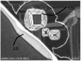
幾つかの実施例において、図6に示すように、前記N型導電領域11と前記P型導電領域12との間には、境界線13があり、図6-8に示すように、前記N型導電領域11及び/又は前記P型導電領域12の前記境界線13に近接する位置には、ボイド131が設けられている。
In some embodiments, as shown in FIG. 6, there is a
理解できるように、前記N型導電領域11及び/又は前記P型導電領域12の前記境界線13に近接する位置に設けられたボイド131により、キャリアの伝送に有利し、更に電池性能の向上にも有利し、また、900-1200バンドの反射率も1%~10%向上することができる。
As can be seen, the
幾つかの実施例において、ボイド131は、太陽電池の作製中において、レーザ光でP型導電領域12の余計な膜層を除去するときに、レーザ光が近傍のN型導電領域11へ熱ダメージを与え、その表面膜層を破壊し、後のアルカリ研磨過程において熱ダメージ領域をエッチングして形成されたものである。
In some embodiments, the
幾つかの実施例において、前記N型導電領域及び/又は前記P型導電領域の前記境界線13から5μm~15μm離れた位置には、ボイド131が設けられている。
In some embodiments, a
好ましくは、ボイド131の設置位置は、5μm、6μm、7μm、8μm、9μm、10μm、11μm、12μm、13μm、14μm又は15μm等であってもよく、無論上記範囲内の他の値であってもよく、ここで限定されない。 Preferably, the placement position of the void 131 may be 5 μm, 6 μm, 7 μm, 8 μm, 9 μm, 10 μm, 11 μm, 12 μm, 13 μm, 14 μm, or 15 μm, etc., and of course may be other values within the above range, and is not limited here.
好ましくは、前記N型導電領域11及び/又は前記P型導電領域12の前記境界線13から5μm~10μm離れた位置には、ボイド131が設けられている。
Preferably, a
幾つかの実施例において、前記ボイド131の直径は、1μm~10μmである。
In some embodiments, the diameter of the
好ましくは、前記ボイド131の直径は、1μm、2μm、3μm、4μm、5μm、6μm、7μm、8μm、9μm又は10μm等であってもよく、無論上記範囲内の他の値であってもよく、ここで限定されない。 Preferably, the diameter of the void 131 may be 1 μm, 2 μm, 3 μm, 4 μm, 5 μm, 6 μm, 7 μm, 8 μm, 9 μm or 10 μm, etc., and of course may be other values within the above range, and is not limited here.
好ましくは、前記ボイド131の直径は、1μm~5μmである。 Preferably, the diameter of the void 131 is between 1 μm and 5 μm.
幾つかの実施例において、前記ボイド131の深さは、0.5μm~2μmである。
In some embodiments, the depth of the
好ましくは、前記ボイド131の深さは、0.5μm、0.6μm、0.7μm、0.8μm、0.9μm、1μm、1.1μm、1.2μm、1.3μm、1.4μm、1.5μm、1.6μm、1.7μm、1.8μm、1.9μm又は2μm等であってもよく、無論上記範囲内の他の値であってもよく、ここで限定されない。ここで、前記ボイド131の深度値は、3D顕微鏡による走査で取得されてもよい。幾つかの具体的な実施例において、ボイド131深さは、アルカリ研磨エッチング深さの1/2~1/3(研磨面エッチングに基づく)であってもよい。 Preferably, the depth of the void 131 may be 0.5 μm, 0.6 μm, 0.7 μm, 0.8 μm, 0.9 μm, 1 μm, 1.1 μm, 1.2 μm, 1.3 μm, 1.4 μm, 1.5 μm, 1.6 μm, 1.7 μm, 1.8 μm, 1.9 μm, 2 μm, etc., and may of course be other values within the above range, and is not limited thereto. Here, the depth value of the void 131 may be obtained by scanning with a 3D microscope. In some specific embodiments, the void 131 depth may be 1/2 to 1/3 of the alkaline polishing etching depth (based on the polishing surface etching).
幾つかの実施例において、隣接する2つの前記N型導電領域11の間の間隔又は隣接する2つの前記P型導電領域12の間の間隔は、0.8mm~1.2mmであり、前記半導体基板1の後面における前記N型導電領域11の分布割合は、50%~85%であり、前記半導体基板1の後面における前記P型導電領域12の分布割合は、15%~50%である。
In some embodiments, the distance between two adjacent N-type
好ましくは、隣接する2つの前記N型導電領域11の間の間隔又は隣接する2つの前記P型導電領域12の間の間隔は、0.8mm、0.85mm、0.9mm、0.95mm、1.0mm、1.05mm、1.1mm、1.15mm又は1.2mm等であってもよく、無論上記範囲内の他の値であってもよく、ここで限定されない。前記半導体基板1の後面における前記N型導電領域11の分布割合は、50%、55%、60%、65%、70%、75%、80%又は85%等であってもよく、無論上記範囲内の他の値であってもよく、ここで限定されない。対応的に、前記半導体基板1の後面における前記P型導電領域12の分布割合は、50%、45%、40%、35%、30%、25%、20%、又は15%等であってもよく、無論上記範囲内の他の値であってもよく、ここで限定されない。
Preferably, the interval between two adjacent N-type
理解できるように、半導体基板1上の隣接する2つの前記N型導電領域11の間の間隔又は隣接する2つの前記P型導電領域12の間の間隔に対する限定と、前記半導体基板1の後面におけるN型導電領域11及びP型導電領域12の分布割合に対する限定により、太陽電池を作製する過程において、優れた導電性を有するPN結合を半導体基板1に形成可能であり、作製された太陽電池の光電性能を向上させることができる。
As can be seen, by limiting the spacing between two adjacent N-type
幾つかの具体的な実施例では、本発明の半導体基板1の作製において、まず、アルカリ研磨を用いて小塔基の形態を有する裏面構造を作製し、対応する膜層を堆積したものをN型導電領域とし、その後、レーザ光による膜切りを用いてP型導電領域を特定し、再度アルカリ研磨を用いてレーザ光ダメージを除去して大塔基の平面表面形態を形成する。レーザ光でP型領域の余計な膜層を除去するときに、レーザ光が近傍のN型導電領域に熱ダメージを与え、その表面膜層を破壊し、後のアルカリ研磨過程において熱ダメージ領域をエッチングしてボイドを形成する。作製過程において、レーザ光のプロセスを調整して熱ダメージを境界からの一定の範囲内に制御してもよい。
In some specific examples, in the fabrication of the
説明すべきことは、本発明の半導体基板1は、太陽電池の製造過程において形成されてもよく、太陽電池の製造過程前のオリジナル基板(シリコンスライス)の作製時に形成されてもよい。
It should be noted that the
第2態様において、本発明は、太陽電池を更に提供する。図9に示すように、太陽電池は、本発明の上記半導体基板1、トンネル酸化層2、局所裏面電界3、多結晶シリコン薄膜層4、共晶層5、後面パッシベーション層6、第1電極7及び第2電極8を備える。
半導体基板1は、単結晶シリコン基板、多結晶シリコン基板、微結晶シリコン基板又は炭化ケイ素基板のうちの一種であってもよい。幾つかの実施例において、前記半導体基板は、P型結晶シリコン基板である。
In a second aspect, the present invention further provides a solar cell, which includes the
The
トンネル酸化層2は、前記半導体基板1の後面のN型導電領域11に設けられている。トンネル酸化層2は、酸化ケイ素層、酸化アルミニウム層、酸窒化ケイ素層、酸化モリブデン層、酸化ハフニウム層のうちの一種又は複数種の積層構造であってもよい。他の実施例において、トンネル酸化層2は、酸素含有窒化ケイ素層、酸素含有炭化ケイ素層等であってもよい。幾つかの実行可能な実施形態において、オゾン酸化法、高温熱酸化法、硝酸酸化法、化学蒸着法、低圧化学蒸着法を用いて半導体基板1の後面のN型導電領域11をエッチングした後で処理し、トンネル酸化層2を形成してもよい。
The tunnel oxide layer 2 is disposed on the N-type
局所裏面電界3は、前記半導体基板1の後面のP型導電領域12に設けられている。P型導電領域12に局所裏面電界3が形成されることにより、作製された太陽電池の開放電圧を高め、アルミニウムシリコン接触抵抗Rsを低減し、電池の光電変換効率を効果的に向上させることができる。幾つかの具体的な実施例において、局所裏面電界3は、アルミニウム裏面電界である。
The local
多結晶シリコン薄膜層4は、前記トンネル酸化層2の前記半導体基板1から離反する側に設けられている。多結晶シリコン薄膜は、結晶シリコンの電学特性を有し、非結晶シリコン薄膜のコストが低く、設備が簡単であり且つ大面積で作製できる等の利点もある。物理蒸着法、化学蒸着法、プラズマ強化化学蒸着法、原子層蒸着法のうちの何れか一種の方法でトンネル酸化層2の表面に堆積して多結晶シリコン薄膜層4を形成してもよい。
The polycrystalline silicon thin film layer 4 is provided on the side of the tunnel oxide layer 2 that faces away from the
共晶層5は、前記局所裏面電界3に設けられている。幾つかの具体的な実施例において、共晶層5は、シリコンアルミニウム共晶層である。
A
後面パッシベーション層6は、前記多結晶シリコン薄膜層4の前記トンネル酸化層2から離反する側と前記P型導電領域12とに設けられ、後面パッシベーション層6は、半導体基板1の後面に対してパッシベーション作用を果たし、後面パッシベーション層6は、1層又は複数層のパッシベーション層によって構成されてもよい。後面パッシベーション層6は、酸化アルミニウム、窒化ケイ素、酸化ケイ素、酸窒化ケイ素、炭素ドープ酸窒化ケイ素層等のパッシベーション層を含んでもよい。幾つかの具体的な実施例において、後面パッシベーション層6は、第1後面パッシベーション層61及び第2後面パッシベーション層62を含み、第1後面パッシベーション層61と第2後面パッシベーション層62は、半導体基板1後面から離反する方向に沿って順次設けられている。幾つかの具体的な実施例において、第1後面パッシベーション層61は、酸化アルミニウム層であってもよく、第2後面パッシベーション層62は、窒化ケイ素層であってもよい。
The
第1電極7は、前記後面パッシベーション層6を通り抜けて前記局所裏面電界3とのオーム接触を形成する。
The
第2電極8は、前記後面パッシベーション層6と前記多結晶シリコン薄膜層4とを順次通り抜けてオーム接触を形成する。第1電極7及び第2電極8は、後面パッシベーション層6の表面に塗布された金属導電スラリーによって焼成され形成されてもよい。幾つかの実施例において、前記第1電極7及び/又は第2電極8の材料は、銀、アルミニウム、銅、ニッケル等の金属材料を含む。1つの具体的な実施例において、第1電極7は、アルミニウム材料を含み、第2電極は、銀材料を含む。
The
幾つかの具体的な実施例において、図9に示すように、太陽電池は、
前記半導体基板1の前面に設けられ且つ前記半導体基板1から離間する方向に順次積層設置された前面パッシベーション層9と反射防止層10とを更に備える。前面パッシベーション層9は、半導体基板1の前面に対してパッシベーション作用を果たし、前面パッシベーション層9は、1層又は複数層のパッシベーション層によって構成されてもよい。前面パッシベーション層9は、酸化アルミニウム、窒化ケイ素、酸化ケイ素、酸窒化ケイ素、炭素ドープ酸窒化ケイ素層等のパッシベーション層を含んでもよい。幾つかの具体的な実施例において、前面パッシベーション層9は、酸化アルミニウム層であってもよい。反射防止層10は、光の反射を防止したり減少したりすることができ、太陽エネルギーを十分に利用する目的を果たすことができる。反射防止層10は、化学蒸着法、物理蒸着法及び高温窒化等の方法によって前面パッシベーション層9に形成されてもよい。幾つかの具体的な実施例において、反射防止層10は、酸窒化ケイ素層であってもよい。
In some specific embodiments, as shown in FIG. 9, the solar cell comprises:
The
第3態様において、本発明は、太陽光発電モジュールを更に提供する。前記太陽光発電モジュールは、上記太陽電池を備え、太陽光発電モジュールの電池転化効率を向上可能である。当該太陽光発電モジュールは、上記太陽電池を備え、前記太陽電池は、全一枚又は分割された複数枚(例えば、1/2等分スライス、1/3等分スライス、1/4等分スライス等の分割された複数枚)の形式で電気的に接続されて複数の電池ストリングを形成し、前記複数の電池ストリングは、直列接続及び/又は並列接続の方式で電気的に接続されている。幾つかの実施例において、前記太陽光発電モジュールは、パッケージ材料層及び蓋板を更に備え、前記パッケージ材料層は、前記複数の太陽電池ストリングを封止し、前記蓋板は、前記パッケージ材料層を覆う。例えば、前記パッケージ材料層の材質は、EVA、POE又はPET等の有機材料であってもよく、前記蓋板は、ガラス蓋板、プラスチック蓋板等の透光機能を有する蓋板であってもよい。 In a third aspect, the present invention further provides a photovoltaic module. The photovoltaic module includes the solar cell described above, and can improve the cell conversion efficiency of the photovoltaic module. The photovoltaic module includes the solar cell described above, and the solar cell is electrically connected in the form of a whole sheet or multiple divided sheets (e.g., multiple divided sheets such as 1/2 slices, 1/3 slices, 1/4 slices, etc.) to form multiple battery strings, and the multiple battery strings are electrically connected in a series connection and/or parallel connection manner. In some embodiments, the photovoltaic module further includes a packaging material layer and a cover plate, the packaging material layer seals the multiple solar cell strings, and the cover plate covers the packaging material layer. For example, the material of the packaging material layer may be an organic material such as EVA, POE, or PET, and the cover plate may be a cover plate having a light-transmitting function such as a glass cover plate or a plastic cover plate.
第4態様において、本発明は、上記太陽電池を作製するための太陽電池の作製方法を更に提供する。作製方法は、以下のステップを含む。 In a fourth aspect, the present invention further provides a method for producing the solar cell described above. The method includes the following steps:
ステップS1では、半導体基板1を提供し、半導体基板1に対してテクスチャリング処理及び酸化処理を順次行う。
In step S1, a
ステップS2では、半導体基板1の前面上且つ前記半導体基板1から離間する方向に、設置された前面パッシベーション層9及び反射防止層10を順次積層する。
In step S2, a
ステップS3では、半導体基板1の後面を酸洗した後、アルカリ溶液を用いて半導体基板1の後面を研磨処理することにより、半導体基板1の後面に第1非ピラミッド状テクスチャー構造111を形成するようにする。
In step S3, the rear surface of the
ステップS4では、前記半導体基板1の後面の第1非ピラミッド状テクスチャー構造111にトンネル酸化層2が形成され、トンネル酸化層2の表面に堆積して多結晶シリコン薄膜層4が形成される。幾つかの具体的な実施例において、更に、多結晶シリコン薄膜層4に対してドーピング処理を行ってドーピング導電層を形成してもよい。
In step S4, a tunnel oxide layer 2 is formed on the first
ステップS5では、レーザ光による膜切りを用いてP型導電領域12を特定し形成し、第1非ピラミッド状テクスチャー構造111が形成された領域をN型導電領域11とし、アルカリ溶液を用いて半導体基板1の後面のP型導電領域12に対して研磨処理を行うことにより、半導体基板1後面のP型導電領域12に第2非ピラミッド状テクスチャー構造121が形成されるようにする。前記第1非ピラミッド状テクスチャー構造111の頂部表面と前記第2非ピラミッド状テクスチャー構造121の頂部表面とは、何れも多角形平面であり、且つ前記第1非ピラミッド状テクスチャー構造111の頂部表面の1次元サイズL1は、前記第2非ピラミッド状テクスチャー構造121の頂部表面の1次元サイズL2よりも小さく、前記第1非ピラミッド状テクスチャー構造111の頂部表面の1次元サイズL1は、5μm以上であり、且つ12μm以下であり、前記第2非ピラミッド状テクスチャー構造121の頂部表面の1次元サイズL2は、10μm以上であり、且つ40μm以下である。幾つかの具体的な実施例において、レーザ光による膜切りの条件は、レーザタイプとして波長355nmの紫外レーザ又は波長556nmの緑色レーザを選択し、スポットサイズが30μm~100μmであることを含む。幾つかの具体的な実施例において、レーザ光でP型導電領域12の余計な膜層を除去するときに、レーザ光が近傍のN型導電領域11に熱ダメージを与え、その表面膜層を破壊し、後のアルカリ研磨過程において熱ダメージ領域をエッチングしてボイド131を形成する。作製中に、レーザ膜切りパラメータを調整することにより、熱損失を一定の範囲内に制御することができる。
In step S5, a P-type
ステップS6では、前記半導体基板1の後面のP型導電領域12においてパターン化を行い、局所裏面電界3及び共晶層5を形成する。
In step S6, the P-type
ステップS7では、多結晶シリコン薄膜層4の表面及び前記P型導電領域12に後面パッシベーション層6を堆積する。幾つかの具体的な実施例において、後面パッシベーション層6が第1後面パッシベーション層61及び第2後面パッシベーション層62を含み、作製時に、多結晶シリコン薄膜層4表面及び前記P型導電領域12に第1後面パッシベーション層61を堆積してから、第2後面パッシベーション層62を堆積する。
In step S7, a
比較例
比較例は、太陽電池を提供する。太陽電池は、半導体基板を備え、前記半導体基板の後面は、N型導電領域及びP型導電領域を有し、前記N型導電領域と前記P型導電領域とには、同じ非ピラミッド状テクスチャー構造が設けられている。
Comparative Example The comparative example provides a solar cell comprising a semiconductor substrate, a rear surface of the semiconductor substrate having an N-type conductivity region and a P-type conductivity region, the N-type conductivity region and the P-type conductivity region being provided with the same non-pyramidal texture structure.
比較例の電池構造よりも、本発明の太陽電池の後面のN型導電領域とP型導電領域とに異なるサイズ規格の第1非ピラミッド状テクスチャー構造及び第2非ピラミッド状テクスチャー構造がそれぞれ設けられ、他の構造及び作製方法が何れも同じであり、対比試験によって以下のこを発見した。 Compared to the cell structure of the comparative example, a first non-pyramidal texture structure and a second non-pyramidal texture structure of different size standards are provided in the N-type conductive region and the P-type conductive region of the rear surface of the solar cell of the present invention, respectively, and the other structures and manufacturing methods are the same. Through comparative testing, the following was discovered.
[表1]本発明の太陽電池と比較例の太陽電池との性能対比表

ただし、太陽電池の変換効率=(開放電圧*短絡電流*フィルファクタ)/(電池面積*光照射幅)10*100%である。開放電圧、短絡電流、フィルファクタが変換効率に比例することが分かる。表1のデータから、半導体基板1に異なる規格サイズの非ピラミッドテクスチャー構造を設ける太陽電池の変換効率が半導体基板1に規格の一致する非ピラミッドテクスチャー構造を設ける太陽電池の変換効率よりも0.17%高いことが分かる。
However, the conversion efficiency of a solar cell = (open circuit voltage * short circuit current * fill factor) / (cell area * light irradiation width) 10 * 100%. It can be seen that the open circuit voltage, short circuit current, and fill factor are proportional to the conversion efficiency. From the data in Table 1, it can be seen that the conversion efficiency of a solar cell in which a non-pyramid texture structure of a different standard size is provided on the
上述したのは、本発明の好適な実施例に過ぎず、本発明を制限するためのものではない。当業者にとって、本発明は、様々な変更や変化を有することができる。本発明の精神及び原則内でなされた如何なる修正、均等物による置換、改良等は、いずれも本発明の保護範囲内に含まれるべきである。 The above is merely a preferred embodiment of the present invention, and is not intended to limit the present invention. For those skilled in the art, the present invention may have various modifications and variations. Any modifications, equivalent replacements, improvements, etc. made within the spirit and principle of the present invention should be included within the protection scope of the present invention.
1-半導体基板
11-N型導電領域
111-第1非ピラミッド状テクスチャー構造
1111-第1サブ構造
1112-第2サブ構造
12-P型導電領域
121-第2非ピラミッド状テクスチャー構造
1211-第3サブ構造
1212-第4サブ構造
13-境界線
131-ボイド
2-トンネル酸化層
3-局所裏面電界
4-多結晶シリコン薄膜層
5-共晶層
6-後面パッシベーション層
61-第1後面パッシベーション層
62-第2後面パッシベーション層
7-第1電極
8-第2電極
9-前面パッシベーション層
10-反射防止層
1 - semiconductor substrate 11 - N-type conductivity region 111 - first non-pyramidal textured structure 1111 - first sub-structure 1112 - second sub-structure 12 - P-type conductivity region 121 - second non-pyramidal textured structure 1211 - third sub-structure 1212 - fourth sub-structure 13 - boundary line 131 - void 2 - tunnel oxide layer 3 - local back surface field 4 - polycrystalline silicon thin layer 5 - eutectic layer 6 - rear passivation layer 61 - first rear passivation layer 62 - second rear passivation layer 7 - first electrode 8 - second electrode 9 - front passivation layer 10 - anti-reflection layer
Claims (8)
前記半導体基板の後面は、N型導電領域及びP型導電領域を有し、前記N型導電領域には、第1非ピラミッド状テクスチャー構造が設けられ、前記P型導電領域には、第2非ピラミッド状テクスチャー構造が設けられ、
前記第1非ピラミッド状テクスチャー構造の頂部表面と前記第2非ピラミッド状テクスチャー構造の頂部表面とは、何れも多角形平面であり、且つ前記第1非ピラミッド状テクスチャー構造の頂部表面の1次元サイズは、前記第2非ピラミッド状テクスチャー構造の頂部表面の1次元サイズよりも小さく、
前記第1非ピラミッド状テクスチャー構造の頂部表面の1次元サイズは、5μm以上であり、且つ12μm以下であり、前記第2非ピラミッド状テクスチャー構造の頂部表面の1次元サイズは、10μm以上であり、且つ40μm以下であり、
非ピラミッド状は、ピラミッド状微細構造の塔端が破壊されて形成された塔基、四角台状又は階段状の形態であり、前記1次元サイズは、前記多角形平面の対角線長さであり、
前記第1非ピラミッド状テクスチャー構造は、
少なくとも部分的に積層された2つ以上の第1サブ構造と、隣接する非積層に配列された2つ以上の第2サブ構造と、を含み、
前記少なくとも部分的に積層された2つ以上の第1サブ構造のうち、前記後面から離間し且つ前記後面に垂直な方向における最外側の前記第1サブ構造の頂部表面の1次元サイズは、5μm以上であり、且つ12μm以下であり、
前記後面から離間する前記第2サブ構造の頂部表面の1次元サイズは、5μm以上であり、且つ12μm以下であり、
前記N型導電領域と前記P型導電領域との間には、境界線があり、前記P型導電領域の前記境界線に近接する位置には、前記N型導電領域に近接する熱ダメージ領域をアルカリ研磨エッチングしたボイドが設けられ、前記ボイドの深さは、アルカリ研磨エッチング深さの1/2~1/3であり、且つ、前記ボイドの深さは、0.5μm~2μmであることを特徴とする半導体基板。 A semiconductor substrate,
a rear surface of the semiconductor substrate having an N-type conductivity region and a P-type conductivity region, the N-type conductivity region being provided with a first non-pyramidal texture structure and the P-type conductivity region being provided with a second non-pyramidal texture structure;
a top surface of the first non-pyramidal texture structure and a top surface of the second non-pyramidal texture structure are both polygonal planes, and a one-dimensional size of the top surface of the first non-pyramidal texture structure is smaller than a one-dimensional size of the top surface of the second non-pyramidal texture structure;
The first non-pyramidal texture structure has a top surface having a one-dimensional size of 5 μm or more and 12 μm or less, and the second non-pyramidal texture structure has a top surface having a one-dimensional size of 10 μm or more and 40 μm or less;
The non-pyramidal shape is a tower base formed by breaking the tower end of a pyramidal microstructure, a square trapezoid, or a stepped shape, and the one-dimensional size is the diagonal length of the polygonal plane;
The first non-pyramidal texture structure comprises:
two or more first substructures in an at least partially stacked arrangement and two or more second substructures in an adjacent non-stacked arrangement;
a one-dimensional size of a top surface of an outermost first substructure in a direction spaced from and perpendicular to the rear surface among the two or more first substructures that are at least partially stacked is 5 μm or more and 12 μm or less;
a first dimension of a top surface of the second substructure spaced from the rear surface is greater than or equal to 5 μm and less than or equal to 12 μm;
A semiconductor substrate characterized in that there is a boundary between the N-type conductive region and the P-type conductive region, and a void is provided in a position close to the boundary of the P-type conductive region by alkaline polishing etching of a thermally damaged region close to the N-type conductive region, and the depth of the void is 1/2 to 1/3 of the alkaline polishing etching depth, and the depth of the void is 0.5 μm to 2 μm .
前記半導体基板の後面は、N型導電領域及びP型導電領域を有し、前記N型導電領域には、第1非ピラミッド状テクスチャー構造が設けられ、前記P型導電領域には、第2非ピラミッド状テクスチャー構造が設けられ、
前記第1非ピラミッド状テクスチャー構造の頂部表面と前記第2非ピラミッド状テクスチャー構造の頂部表面とは、何れも多角形平面であり、且つ前記第1非ピラミッド状テクスチャー構造の頂部表面の1次元サイズは、前記第2非ピラミッド状テクスチャー構造の頂部表面の1次元サイズよりも小さく、
前記第1非ピラミッド状テクスチャー構造の頂部表面の1次元サイズは、5μm以上であり、且つ12μm以下であり、前記第2非ピラミッド状テクスチャー構造の頂部表面の1次元サイズは、10μm以上であり、且つ40μm以下であり、
非ピラミッド状は、ピラミッド状微細構造の塔端が破壊されて形成された塔基、四角台状又は階段状の形態であり、前記1次元サイズは、前記多角形平面の対角線長さであり、
前記第2非ピラミッド状テクスチャー構造は、
少なくとも部分的に積層された2つ以上の第3サブ構造と、隣接する非積層に配列された2つ以上の第4サブ構造と、を含み、
前記少なくとも部分的に積層された2つ以上の第3サブ構造のうち、前記後面から離間し且つ前記後面に垂直な方向における最外側の前記第3サブ構造の頂部表面の1次元サイズは、10μm以上であり、且つ40μm以下であり、
前記後面から離間する前記第4サブ構造の頂部表面の1次元サイズは、10μm以上であり、且つ40μm以下であり、
前記N型導電領域と前記P型導電領域との間には、境界線があり、前記P型導電領域の前記境界線に近接する位置には、前記N型導電領域に近接する熱ダメージ領域をアルカリ研磨エッチングしたボイドが設けられ、前記ボイドの深さは、アルカリ研磨エッチング深さの1/2~1/3であり、且つ、前記ボイドの深さは、0.5μm~2μmであることを特徴とする半導体基板。 A semiconductor substrate,
a rear surface of the semiconductor substrate having an N-type conductivity region and a P-type conductivity region, the N-type conductivity region being provided with a first non-pyramidal texture structure and the P-type conductivity region being provided with a second non-pyramidal texture structure;
a top surface of the first non-pyramidal texture structure and a top surface of the second non-pyramidal texture structure are both polygonal planes, and a one-dimensional size of the top surface of the first non-pyramidal texture structure is smaller than a one-dimensional size of the top surface of the second non-pyramidal texture structure;
The first non-pyramidal texture structure has a top surface having a one-dimensional size of 5 μm or more and 12 μm or less, and the second non-pyramidal texture structure has a top surface having a one-dimensional size of 10 μm or more and 40 μm or less;
The non-pyramidal shape is a tower base formed by breaking the tower end of a pyramidal microstructure, a square trapezoid, or a stepped shape, and the one-dimensional size is the diagonal length of the polygonal plane;
The second non-pyramidal texture structure comprises:
two or more third substructures in an at least partially stacked arrangement; and two or more fourth substructures in an adjacent non-stacked arrangement;
a one-dimensional size of a top surface of an outermost third substructure in a direction spaced from and perpendicular to the rear surface among the two or more third substructures that are at least partially stacked is 10 μm or more and 40 μm or less;
a first dimension of a top surface of the fourth substructure spaced from the rear surface is greater than or equal to 10 μm and less than or equal to 40 μm;
A semiconductor substrate characterized in that there is a boundary between the N-type conductive region and the P-type conductive region, and a void is provided in a position close to the boundary of the P-type conductive region by alkaline polishing etching of a thermally damaged region close to the N-type conductive region, and the depth of the void is 1/2 to 1/3 of the alkaline polishing etching depth, and the depth of the void is 0.5 μm to 2 μm .
前記半導体基板の後面のN型導電領域に設けられるトンネル酸化層と、
前記半導体基板の後面のP型導電領域に設けられる局所裏面電界と、
前記トンネル酸化層の前記半導体基板から離反する側に設けられる多結晶シリコン薄膜層と、
前記局所裏面電界に設けられる共晶層と、
前記多結晶シリコン薄膜層の前記トンネル酸化層から離反する側と前記P型導電領域とに設けられる後面パッシベーション層と、
前記後面パッシベーション層を通り抜けて前記局所裏面電界とのオーム接触を形成する第1電極と、
前記後面パッシベーション層を通り抜けて前記多結晶シリコン薄膜層とオーム接触を形成する第2電極と、を備えることを特徴とする太陽電池。 A semiconductor substrate according to claim 1 or 2;
a tunnel oxide layer disposed in an N-type conductive region on a rear surface of the semiconductor substrate;
a local back surface field provided in a P-type conductivity region on a rear surface of the semiconductor substrate;
a polycrystalline silicon thin film layer provided on a side of the tunnel oxide layer away from the semiconductor substrate;
a eutectic layer provided on the local back surface field;
a backside passivation layer disposed on the side of the polysilicon thin film layer away from the tunnel oxide layer and on the P-type conductive region;
a first electrode passing through the back surface passivation layer to form an ohmic contact with the local back surface field;
a second electrode passing through the rear passivation layer and forming an ohmic contact with the polycrystalline silicon thin film layer.
前記太陽光発電モジュールは、請求項6に記載の太陽電池を備え、前記太陽電池は、全一枚の形態又は分割された複数枚の形態で電気的に接続されて太陽電池ストリングとなることを特徴とする太陽光発電モジュール。
A photovoltaic module, comprising:
The photovoltaic power generation module comprises the solar cell according to claim 6 , and the solar cell is electrically connected in the form of a whole sheet or in the form of multiple divided sheets to form a solar cell string.
Applications Claiming Priority (3)
| Application Number | Priority Date | Filing Date | Title |
|---|---|---|---|
| CN202210704732.3A CN115224137B (en) | 2022-06-21 | 2022-06-21 | Semiconductor substrates and solar cells and photovoltaic modules |
| CN202210704732.3 | 2022-06-21 | ||
| JP2022113517A JP7453283B2 (en) | 2022-06-21 | 2022-07-14 | Semiconductor substrates, solar cells and photovoltaic modules |
Related Parent Applications (1)
| Application Number | Title | Priority Date | Filing Date |
|---|---|---|---|
| JP2022113517A Division JP7453283B2 (en) | 2022-06-21 | 2022-07-14 | Semiconductor substrates, solar cells and photovoltaic modules |
Publications (2)
| Publication Number | Publication Date |
|---|---|
| JP2024039048A JP2024039048A (en) | 2024-03-21 |
| JP7602002B2 true JP7602002B2 (en) | 2024-12-17 |
Family
ID=82748114
Family Applications (2)
| Application Number | Title | Priority Date | Filing Date |
|---|---|---|---|
| JP2022113517A Active JP7453283B2 (en) | 2022-06-21 | 2022-07-14 | Semiconductor substrates, solar cells and photovoltaic modules |
| JP2023221309A Active JP7602002B2 (en) | 2022-06-21 | 2023-12-27 | Semiconductor substrates, solar cells and photovoltaic power generation modules |
Family Applications Before (1)
| Application Number | Title | Priority Date | Filing Date |
|---|---|---|---|
| JP2022113517A Active JP7453283B2 (en) | 2022-06-21 | 2022-07-14 | Semiconductor substrates, solar cells and photovoltaic modules |
Country Status (5)
| Country | Link |
|---|---|
| US (1) | US12191411B2 (en) |
| EP (1) | EP4297102A1 (en) |
| JP (2) | JP7453283B2 (en) |
| CN (3) | CN115224137B (en) |
| AU (2) | AU2022206808B1 (en) |
Families Citing this family (17)
| Publication number | Priority date | Publication date | Assignee | Title |
|---|---|---|---|---|
| CN115224137B (en) | 2022-06-21 | 2023-09-15 | 浙江晶科能源有限公司 | Semiconductor substrates and solar cells and photovoltaic modules |
| CN118281091B (en) * | 2022-12-30 | 2025-12-16 | 比亚迪股份有限公司 | Texturing pretreatment silicon wafer, preparation method thereof, texturing sheet and solar cell |
| CN115954413B (en) * | 2023-02-13 | 2025-09-26 | 英利能源发展有限公司 | A selective texturing method for SE battery |
| CN117059681B (en) * | 2023-10-09 | 2024-03-29 | 晶科能源(海宁)有限公司 | Solar cells and manufacturing methods thereof, photovoltaic modules |
| CN117153911B (en) * | 2023-10-26 | 2024-05-24 | 晶科能源(海宁)有限公司 | Solar cell and photovoltaic module |
| CN118053921A (en) * | 2023-12-15 | 2024-05-17 | 浙江晶科能源有限公司 | Solar cell and preparation method thereof, photovoltaic module |
| CN118053928A (en) | 2023-12-15 | 2024-05-17 | 浙江晶科能源有限公司 | Solar cells and photovoltaic modules |
| CN118053922A (en) * | 2023-12-15 | 2024-05-17 | 浙江晶科能源有限公司 | Solar cell and preparation method thereof, photovoltaic module |
| CN118053927A (en) | 2023-12-15 | 2024-05-17 | 浙江晶科能源有限公司 | Solar cell and preparation method thereof, photovoltaic module |
| CN119008726A (en) | 2023-12-15 | 2024-11-22 | 浙江晶科能源有限公司 | Solar cell, preparation method thereof and photovoltaic module |
| CN117727809B (en) | 2024-02-08 | 2024-08-06 | 浙江晶科能源有限公司 | Solar cells and photovoltaic modules |
| CN118335814A (en) * | 2024-04-03 | 2024-07-12 | 浙江晶科能源有限公司 | Back contact solar cells, photovoltaic modules |
| CN118676228A (en) * | 2024-07-15 | 2024-09-20 | 浙江爱旭太阳能科技有限公司 | Solar cell, battery assembly and photovoltaic system |
| CN119836011A (en) * | 2024-09-05 | 2025-04-15 | 隆基绿能科技股份有限公司 | Solar cell and preparation method |
| CN119584714A (en) * | 2024-12-02 | 2025-03-07 | 隆基绿能科技股份有限公司 | Solar cell and photovoltaic module |
| CN119497463A (en) * | 2025-01-17 | 2025-02-21 | 通威太阳能(成都)有限公司 | Back contact solar cell and preparation method thereof, photovoltaic module |
| CN120302765B (en) * | 2025-06-09 | 2025-12-02 | 浙江晶科能源有限公司 | Back contact battery and its preparation method |
Citations (12)
| Publication number | Priority date | Publication date | Assignee | Title |
|---|---|---|---|---|
| JP2002224878A (en) | 2000-10-26 | 2002-08-13 | Toshiba Corp | Laser processing method, laser processing apparatus, and semiconductor device manufacturing method |
| JP2012243797A (en) | 2011-05-16 | 2012-12-10 | Mitsubishi Electric Corp | Manufacturing method of solar cell |
| WO2013125036A1 (en) | 2012-02-24 | 2013-08-29 | 三菱電機株式会社 | Photovoltaic element, method for manufacturing same, and photovoltaic module |
| JP2014086708A (en) | 2012-10-29 | 2014-05-12 | Sharp Corp | Method of manufacturing back-electrode-type solar cell and back-electrode-type solar cell |
| JP2015185587A (en) | 2014-03-20 | 2015-10-22 | シャープ株式会社 | Photoelectric conversion element and method for producing photoelectric conversion element |
| WO2016158226A1 (en) | 2015-03-31 | 2016-10-06 | 株式会社カネカ | Solar cell and method for manufacturing same |
| JP2016225627A (en) | 2015-05-28 | 2016-12-28 | エルジー エレクトロニクス インコーポレイティド | Solar cell and manufacturing method thereof |
| CN108666376A (en) | 2018-07-11 | 2018-10-16 | 泰州隆基乐叶光伏科技有限公司 | A kind of p-type back contacts solar cell and preparation method thereof |
| US20190207040A1 (en) | 2017-12-29 | 2019-07-04 | Sunpower Corporation | Chemical polishing of solar cell surfaces and the resulting structures |
| JP2019149444A (en) | 2018-02-27 | 2019-09-05 | パナソニック株式会社 | Solar cell and manufacturing method of solar cell |
| CN111108609A (en) | 2017-09-22 | 2020-05-05 | 荷兰应用自然科学研究组织Tno | Interdigitated back contact solar cell with p-type conductivity |
| JP2021197507A (en) | 2020-06-17 | 2021-12-27 | 株式会社カネカ | Method for manufacturing solar cell |
Family Cites Families (24)
| Publication number | Priority date | Publication date | Assignee | Title |
|---|---|---|---|---|
| JPH0996595A (en) * | 1995-09-29 | 1997-04-08 | Nippon Telegr & Teleph Corp <Ntt> | Preparation of sample |
| AUPO638997A0 (en) | 1997-04-23 | 1997-05-22 | Unisearch Limited | Metal contact scheme using selective silicon growth |
| JP2006332273A (en) | 2005-05-25 | 2006-12-07 | Sharp Corp | Back electrode type solar cell |
| KR101155343B1 (en) * | 2008-02-25 | 2012-06-11 | 엘지전자 주식회사 | Fabrication method of back contact solar cell |
| KR101573934B1 (en) * | 2009-03-02 | 2015-12-11 | 엘지전자 주식회사 | Solar cell and manufacturing mehtod of the same |
| JP5778247B2 (en) | 2010-03-26 | 2015-09-16 | テトラサン インコーポレイテッド | Doping through shielded electrical contacts and passivated dielectric layers in high efficiency crystalline solar cells, and their structure and manufacturing method |
| JP2013110187A (en) | 2011-11-18 | 2013-06-06 | Sharp Corp | Photoelectric conversion element and manufacturing method thereof |
| US9583651B2 (en) * | 2011-12-26 | 2017-02-28 | Solexel, Inc. | Systems and methods for enhanced light trapping in solar cells |
| JP6126219B2 (en) | 2013-06-07 | 2017-05-10 | 信越化学工業株式会社 | Back contact solar cell |
| CN103811591B (en) * | 2014-02-27 | 2016-10-05 | 友达光电股份有限公司 | Fabrication method of back contact solar cell |
| US9263625B2 (en) * | 2014-06-30 | 2016-02-16 | Sunpower Corporation | Solar cell emitter region fabrication using ion implantation |
| CN205194713U (en) | 2015-10-30 | 2016-04-27 | 中国科学院物理研究所 | A silicon chip for solar cell |
| KR102600379B1 (en) * | 2015-12-21 | 2023-11-10 | 상라오 징코 솔라 테크놀러지 디벨롭먼트 컴퍼니, 리미티드 | Solar cell and method for fabricating therefor |
| CN108831937A (en) | 2018-06-25 | 2018-11-16 | 江苏顺风光电科技有限公司 | A kind of suede surface modification method of N-type solar cell |
| CN112442739B (en) * | 2019-08-28 | 2022-07-15 | 松山湖材料实验室 | Pyramid rapid texturing liquid and its texturing method and silicon wafer product |
| CN114267580B (en) | 2020-09-16 | 2025-09-19 | 松山湖材料实验室 | Back structure etching method and etching liquid of double-sided PERC solar cell |
| CN212750903U (en) * | 2020-10-15 | 2021-03-19 | 嘉兴阿特斯光伏技术有限公司 | Solar cell |
| CN214797433U (en) * | 2021-02-25 | 2021-11-19 | 一道新能源科技(衢州)有限公司 | IBC solar cell |
| CN113224202B (en) | 2021-03-15 | 2023-04-28 | 浙江爱旭太阳能科技有限公司 | POLO-IBC solar cell and preparation method thereof |
| CN113594296B (en) | 2021-07-26 | 2025-03-11 | 西安隆基乐叶光伏科技有限公司 | A solar cell and a method for manufacturing the same |
| CN115528121B (en) | 2021-08-04 | 2025-05-27 | 上海晶科绿能企业管理有限公司 | Solar cells and photovoltaic modules |
| CN113540269B (en) * | 2021-09-14 | 2022-04-12 | 浙江晶科能源有限公司 | Solar cell, preparation method thereof and photovoltaic module |
| CN114335247A (en) | 2021-12-29 | 2022-04-12 | 湖州爱康光电科技有限公司 | Double-texturing cleaning process and device for heterojunction battery |
| CN115224137B (en) | 2022-06-21 | 2023-09-15 | 浙江晶科能源有限公司 | Semiconductor substrates and solar cells and photovoltaic modules |
-
2022
- 2022-06-21 CN CN202210704732.3A patent/CN115224137B/en active Active
- 2022-06-21 CN CN202311059481.9A patent/CN116936658A/en active Pending
- 2022-06-21 CN CN202311056820.8A patent/CN117476785A/en active Pending
- 2022-07-14 JP JP2022113517A patent/JP7453283B2/en active Active
- 2022-07-22 AU AU2022206808A patent/AU2022206808B1/en active Active
- 2022-07-25 US US17/872,035 patent/US12191411B2/en active Active
- 2022-07-27 EP EP22187232.8A patent/EP4297102A1/en active Pending
-
2023
- 2023-12-27 JP JP2023221309A patent/JP7602002B2/en active Active
-
2024
- 2024-02-06 AU AU2024200716A patent/AU2024200716B2/en active Active
Patent Citations (12)
| Publication number | Priority date | Publication date | Assignee | Title |
|---|---|---|---|---|
| JP2002224878A (en) | 2000-10-26 | 2002-08-13 | Toshiba Corp | Laser processing method, laser processing apparatus, and semiconductor device manufacturing method |
| JP2012243797A (en) | 2011-05-16 | 2012-12-10 | Mitsubishi Electric Corp | Manufacturing method of solar cell |
| WO2013125036A1 (en) | 2012-02-24 | 2013-08-29 | 三菱電機株式会社 | Photovoltaic element, method for manufacturing same, and photovoltaic module |
| JP2014086708A (en) | 2012-10-29 | 2014-05-12 | Sharp Corp | Method of manufacturing back-electrode-type solar cell and back-electrode-type solar cell |
| JP2015185587A (en) | 2014-03-20 | 2015-10-22 | シャープ株式会社 | Photoelectric conversion element and method for producing photoelectric conversion element |
| WO2016158226A1 (en) | 2015-03-31 | 2016-10-06 | 株式会社カネカ | Solar cell and method for manufacturing same |
| JP2016225627A (en) | 2015-05-28 | 2016-12-28 | エルジー エレクトロニクス インコーポレイティド | Solar cell and manufacturing method thereof |
| CN111108609A (en) | 2017-09-22 | 2020-05-05 | 荷兰应用自然科学研究组织Tno | Interdigitated back contact solar cell with p-type conductivity |
| US20190207040A1 (en) | 2017-12-29 | 2019-07-04 | Sunpower Corporation | Chemical polishing of solar cell surfaces and the resulting structures |
| JP2019149444A (en) | 2018-02-27 | 2019-09-05 | パナソニック株式会社 | Solar cell and manufacturing method of solar cell |
| CN108666376A (en) | 2018-07-11 | 2018-10-16 | 泰州隆基乐叶光伏科技有限公司 | A kind of p-type back contacts solar cell and preparation method thereof |
| JP2021197507A (en) | 2020-06-17 | 2021-12-27 | 株式会社カネカ | Method for manufacturing solar cell |
Also Published As
| Publication number | Publication date |
|---|---|
| JP2024039048A (en) | 2024-03-21 |
| US20230411543A1 (en) | 2023-12-21 |
| AU2024200716B2 (en) | 2025-06-19 |
| CN115224137B (en) | 2023-09-15 |
| AU2022206808B1 (en) | 2023-11-23 |
| JP2024000941A (en) | 2024-01-09 |
| US12191411B2 (en) | 2025-01-07 |
| AU2024200716A1 (en) | 2024-02-22 |
| CN117476785A (en) | 2024-01-30 |
| JP7453283B2 (en) | 2024-03-19 |
| CN116936658A (en) | 2023-10-24 |
| CN115224137A (en) | 2022-10-21 |
| EP4297102A1 (en) | 2023-12-27 |
Similar Documents
| Publication | Publication Date | Title |
|---|---|---|
| JP7602002B2 (en) | Semiconductor substrates, solar cells and photovoltaic power generation modules | |
| CN116314382A (en) | Solar cell and manufacturing method thereof, photovoltaic module and photovoltaic system | |
| US20250176308A1 (en) | Solar cell and manufacturing method therefor | |
| WO2025157046A1 (en) | Back-contact cell and manufacturing method therefor | |
| JP7618868B1 (en) | Solar cell and its manufacturing method, photovoltaic module | |
| CN118507552A (en) | Back contact battery and manufacturing method thereof | |
| JP7595198B1 (en) | Solar cell and its manufacturing method, photovoltaic module | |
| CN118969870A (en) | Back contact battery and manufacturing method thereof | |
| JP5734447B2 (en) | Photovoltaic device manufacturing method and photovoltaic device | |
| JP7527510B1 (en) | Solar cell and its manufacturing method, photovoltaic module | |
| CN116666460A (en) | Solar cell and preparation method, photovoltaic module | |
| EP4629780A1 (en) | Solar cell, method for manufacturing the same, and photovoltaic module | |
| CN116469948A (en) | A kind of TOPCon battery and preparation method thereof | |
| CN117727808B (en) | Solar cell, preparation method thereof, laminated cell and photovoltaic module | |
| CN119997620A (en) | Solar cell and method for preparing same, and solar cell module | |
| US20260047230A1 (en) | Solar cell | |
| JP7777615B2 (en) | Solar cell and its manufacturing method, photovoltaic module | |
| WO2026011586A1 (en) | Solar cell | |
| JP2026012122A (en) | solar cells | |
| CN120603370A (en) | Solar cell and photovoltaic module | |
| CN121548115A (en) | Solar cells | |
| CN121099775A (en) | Solar cells, their fabrication methods, and photovoltaic modules |
Legal Events
| Date | Code | Title | Description |
|---|---|---|---|
| A621 | Written request for application examination |
Free format text: JAPANESE INTERMEDIATE CODE: A621 Effective date: 20231227 |
|
| A871 | Explanation of circumstances concerning accelerated examination |
Free format text: JAPANESE INTERMEDIATE CODE: A871 Effective date: 20240205 |
|
| A131 | Notification of reasons for refusal |
Free format text: JAPANESE INTERMEDIATE CODE: A131 Effective date: 20240305 |
|
| A521 | Request for written amendment filed |
Free format text: JAPANESE INTERMEDIATE CODE: A523 Effective date: 20240603 |
|
| A131 | Notification of reasons for refusal |
Free format text: JAPANESE INTERMEDIATE CODE: A131 Effective date: 20240716 |
|
| A521 | Request for written amendment filed |
Free format text: JAPANESE INTERMEDIATE CODE: A523 Effective date: 20241015 |
|
| TRDD | Decision of grant or rejection written | ||
| A01 | Written decision to grant a patent or to grant a registration (utility model) |
Free format text: JAPANESE INTERMEDIATE CODE: A01 Effective date: 20241126 |
|
| A61 | First payment of annual fees (during grant procedure) |
Free format text: JAPANESE INTERMEDIATE CODE: A61 Effective date: 20241205 |
|
| R150 | Certificate of patent or registration of utility model |
Ref document number: 7602002 Country of ref document: JP Free format text: JAPANESE INTERMEDIATE CODE: R150 |