JP7591663B2 - Apparatus for a non-combustible aerosol delivery device - Google Patents
Apparatus for a non-combustible aerosol delivery device Download PDFInfo
- Publication number
- JP7591663B2 JP7591663B2 JP2023544256A JP2023544256A JP7591663B2 JP 7591663 B2 JP7591663 B2 JP 7591663B2 JP 2023544256 A JP2023544256 A JP 2023544256A JP 2023544256 A JP2023544256 A JP 2023544256A JP 7591663 B2 JP7591663 B2 JP 7591663B2
- Authority
- JP
- Japan
- Prior art keywords
- circuit
- switching element
- inductive
- switching
- control
- Prior art date
- Legal status (The legal status is an assumption and is not a legal conclusion. Google has not performed a legal analysis and makes no representation as to the accuracy of the status listed.)
- Active
Links
Images
Classifications
-
- A—HUMAN NECESSITIES
- A24—TOBACCO; CIGARS; CIGARETTES; SIMULATED SMOKING DEVICES; SMOKERS' REQUISITES
- A24F—SMOKERS' REQUISITES; MATCH BOXES; SIMULATED SMOKING DEVICES
- A24F40/00—Electrically operated smoking devices; Component parts thereof; Manufacture thereof; Maintenance or testing thereof; Charging means specially adapted therefor
- A24F40/20—Devices using solid inhalable precursors
-
- A—HUMAN NECESSITIES
- A24—TOBACCO; CIGARS; CIGARETTES; SIMULATED SMOKING DEVICES; SMOKERS' REQUISITES
- A24F—SMOKERS' REQUISITES; MATCH BOXES; SIMULATED SMOKING DEVICES
- A24F40/00—Electrically operated smoking devices; Component parts thereof; Manufacture thereof; Maintenance or testing thereof; Charging means specially adapted therefor
- A24F40/40—Constructional details, e.g. connection of cartridges and battery parts
- A24F40/46—Shape or structure of electric heating means
- A24F40/465—Shape or structure of electric heating means specially adapted for induction heating
-
- A—HUMAN NECESSITIES
- A24—TOBACCO; CIGARS; CIGARETTES; SIMULATED SMOKING DEVICES; SMOKERS' REQUISITES
- A24F—SMOKERS' REQUISITES; MATCH BOXES; SIMULATED SMOKING DEVICES
- A24F40/00—Electrically operated smoking devices; Component parts thereof; Manufacture thereof; Maintenance or testing thereof; Charging means specially adapted therefor
- A24F40/50—Control or monitoring
- A24F40/57—Temperature control
-
- H—ELECTRICITY
- H02—GENERATION; CONVERSION OR DISTRIBUTION OF ELECTRIC POWER
- H02M—APPARATUS FOR CONVERSION BETWEEN AC AND AC, BETWEEN AC AND DC, OR BETWEEN DC AND DC, AND FOR USE WITH MAINS OR SIMILAR POWER SUPPLY SYSTEMS; CONVERSION OF DC OR AC INPUT POWER INTO SURGE OUTPUT POWER; CONTROL OR REGULATION THEREOF
- H02M7/00—Conversion of AC power input into DC power output; Conversion of DC power input into AC power output
- H02M7/42—Conversion of DC power input into AC power output without possibility of reversal
- H02M7/44—Conversion of DC power input into AC power output without possibility of reversal by static converters
- H02M7/48—Conversion of DC power input into AC power output without possibility of reversal by static converters using discharge tubes with control electrode or semiconductor devices with control electrode
- H02M7/53—Conversion of DC power input into AC power output without possibility of reversal by static converters using discharge tubes with control electrode or semiconductor devices with control electrode using devices of a triode or transistor type requiring continuous application of a control signal
- H02M7/537—Conversion of DC power input into AC power output without possibility of reversal by static converters using discharge tubes with control electrode or semiconductor devices with control electrode using devices of a triode or transistor type requiring continuous application of a control signal using semiconductor devices only, e.g. single switched pulse inverters
- H02M7/5387—Conversion of DC power input into AC power output without possibility of reversal by static converters using discharge tubes with control electrode or semiconductor devices with control electrode using devices of a triode or transistor type requiring continuous application of a control signal using semiconductor devices only, e.g. single switched pulse inverters in a bridge configuration
-
- H—ELECTRICITY
- H05—ELECTRIC TECHNIQUES NOT OTHERWISE PROVIDED FOR
- H05B—ELECTRIC HEATING; ELECTRIC LIGHT SOURCES NOT OTHERWISE PROVIDED FOR; CIRCUIT ARRANGEMENTS FOR ELECTRIC LIGHT SOURCES, IN GENERAL
- H05B6/00—Heating by electric, magnetic or electromagnetic fields
- H05B6/02—Induction heating
- H05B6/06—Control, e.g. of temperature, of power
-
- H—ELECTRICITY
- H05—ELECTRIC TECHNIQUES NOT OTHERWISE PROVIDED FOR
- H05B—ELECTRIC HEATING; ELECTRIC LIGHT SOURCES NOT OTHERWISE PROVIDED FOR; CIRCUIT ARRANGEMENTS FOR ELECTRIC LIGHT SOURCES, IN GENERAL
- H05B6/00—Heating by electric, magnetic or electromagnetic fields
- H05B6/02—Induction heating
- H05B6/10—Induction heating apparatus, other than furnaces, for specific applications
- H05B6/105—Induction heating apparatus, other than furnaces, for specific applications using a susceptor
- H05B6/108—Induction heating apparatus, other than furnaces, for specific applications using a susceptor for heating a fluid
Landscapes
- Physics & Mathematics (AREA)
- Electromagnetism (AREA)
- Engineering & Computer Science (AREA)
- Power Engineering (AREA)
- General Induction Heating (AREA)
- Non-Mechanical Conveyors (AREA)
- Spray Control Apparatus (AREA)
- Plasma Technology (AREA)
- Electronic Switches (AREA)
Description
本発明は、非燃焼性エアロゾル供給デバイス用の装置に関し、より詳細には、使用時にエアロゾル生成材料を加熱するサセプタの誘導加熱用の誘導素子を備えた非燃焼性エアロゾル供給デバイス用の装置に関する。 The present invention relates to an apparatus for a non-combustible aerosol delivery device, and more particularly to an apparatus for a non-combustible aerosol delivery device having an inductive element for inductive heating of a susceptor which heats an aerosol-generating material in use.
(背景)
シガレット、シガー等の喫煙品は、使用中にタバコを燃焼させて、タバコ煙を生成する。燃焼なしに化合物を放出させる製品の創出によって、これらの物品の代替物を提供しようとする試みがなされている。このような製品の例は、いわゆる「非燃焼加熱式」製品又はタバコ加熱デバイス若しくは製品であり、材料を燃焼させずに加熱することによって化合物を放出させる。この材料は、例えばタバコ又は他の非タバコ製品が考えられ、ニコチンを含んでいてもよいし、含んでいなくてもよい。
(background)
Smoking articles, such as cigarettes, cigars, etc., burn tobacco during use to produce tobacco smoke. Attempts have been made to provide an alternative to these items by creating products that release compounds without combustion. Examples of such products are the so-called "heat-not-burn" products or tobacco heating devices or products, which release compounds by heating a material without burning it. The material may be, for example, tobacco or other non-tobacco products, which may or may not contain nicotine.
(概要)
本開示の第1の態様によれば、非燃焼性エアロゾル供給デバイス用の装置であって、エアロゾル生成材料を加熱することによりエアロゾルを生成するように構成されたサセプタ構成体を誘導加熱する誘導素子を含む誘導回路と、入力直流電流から、誘導素子を駆動してサセプタ構成体を誘導加熱する誘導回路に変動電圧を供給するように構成された駆動回路と、駆動回路が、誘導回路に供給された電圧の極性を繰り返し切り替える第1のモードと、駆動回路が、非ゼロの大きさの第1の電圧を誘導回路に供給することと、実質的に電圧を誘導回路に供給しないことと、を繰り返し切り替える第2のモードと、において、駆動回路を選択的に動作させるように構成された制御回路と、を備えた、装置が提供される。
(overview)
According to a first aspect of the present disclosure, there is provided an apparatus for a non-combustible aerosol delivery device, the apparatus comprising: an induction circuit including an inductive element configured to inductively heat a susceptor structure configured to generate an aerosol by heating an aerosol-generating material; a drive circuit configured to supply a varying voltage from an input direct current to the induction circuit that drives the inductive element to inductively heat the susceptor structure; and a control circuit configured to selectively operate the drive circuit in a first mode in which the drive circuit repeatedly switches the polarity of the voltage supplied to the induction circuit, and a second mode in which the drive circuit repeatedly switches between supplying a first voltage of non-zero magnitude to the induction circuit and supplying substantially no voltage to the induction circuit.
駆動回路は、Hブリッジ構成に配置された複数のスイッチング素子を備えていてもよい。複数のスイッチング素子は、第1のスイッチング素子及び第2のスイッチング素子を含む高位側スイッチング素子ペアと、第3のスイッチング素子及び第4のスイッチング素子を含む低位側スイッチング素子ペアと、を含んでいてもよく、第1のスイッチング素子及び第3のスイッチング素子が、誘導回路の第1側に電気接続され、第2のスイッチング素子及び第4のスイッチング素子が、誘導回路の第2側に電気接続されている。 The drive circuit may include a plurality of switching elements arranged in an H-bridge configuration. The plurality of switching elements may include a high-side switching element pair including a first switching element and a second switching element, and a low-side switching element pair including a third switching element and a fourth switching element, where the first switching element and the third switching element are electrically connected to a first side of the inductive circuit, and the second switching element and the fourth switching element are electrically connected to a second side of the inductive circuit.
駆動回路は、使用時、高位側スイッチング素子ペア間の第1の点と低位側スイッチング素子ペア間の第2の点との間に電位を接続するように構成されていてもよい。 The drive circuit may be configured, in use, to connect a potential between a first point between the high side switching element pair and a second point between the low side switching element pair.
第1のモードにおいて、制御回路は、第1のスイッチング素子及び第4のスイッチング素子に電流を流して、誘導回路の電圧がプラス極性を有し得るようにすることと、第2のスイッチング素子及び第3のスイッチング素子に電流を流して、誘導回路の電圧がマイナス極性を有し得るようにすることと、の間で駆動回路を切り替えさせるようにしてもよい。第2のモードにおいて、制御回路は、第1のスイッチング素子及び第4のスイッチング素子に電流を流して、誘導回路の電圧がプラス極性を有し得るようにすること、又は、第2のスイッチング素子及び第3のスイッチング素子に電流を流して、誘導回路の電圧がマイナス極性を有し得るようにすることと、実質的に電圧を誘導回路に供給しないことと、の間で駆動回路を切り替えさせるようにしてもよい。 In the first mode, the control circuit may switch the drive circuit between passing a current through the first switching element and the fourth switching element so that the voltage of the induction circuit has a positive polarity and passing a current through the second switching element and the third switching element so that the voltage of the induction circuit has a negative polarity. In the second mode, the control circuit may switch the drive circuit between passing a current through the first switching element and the fourth switching element so that the voltage of the induction circuit has a positive polarity, or passing a current through the second switching element and the third switching element so that the voltage of the induction circuit has a negative polarity and substantially not supplying a voltage to the induction circuit.
制御回路は、任意のある時点で電流を流すスイッチング素子を制御するように構成された1つ又は複数の駆動信号を供給することにより、駆動回路を第1のモード又は第2のモードで動作させるように構成されていてもよい。 The control circuit may be configured to operate the drive circuit in the first mode or the second mode by providing one or more drive signals configured to control a switching element that conducts current at any one time.
制御回路は、第1の駆動信号を供給することにより、第1のスイッチング素子及び第3のスイッチング素子のスイッチングを制御するように構成されていてもよい。制御回路は、第2の駆動信号を供給することにより、第2のスイッチング素子及び第4のスイッチング素子のスイッチングを制御するように構成されていてもよい。 The control circuit may be configured to control the switching of the first switching element and the third switching element by supplying a first drive signal. The control circuit may be configured to control the switching of the second switching element and the fourth switching element by supplying a second drive signal.
第1のモードにおいては、第1の駆動信号の値が第1の駆動周波数で切り替わるようになっていてもよく、また、第2の駆動信号が第1の駆動信号に対して反転することにより、誘導回路の電圧の極性を第1の駆動周波数で切り替えさせるようにしてもよい。第2のモードにおいては、第1の駆動信号の値が第2の駆動周波数で切り替わるようになっていてもよく、また、第2の駆動信号は、第2のスイッチング素子に電流が流れることを実質的に防止した状態に第2のスイッチング素子を維持するとともに、第4のスイッチング素子電流が流れることを許容する状態に第4のスイッチング素子を維持するように構成されていてもよい。 In the first mode, the value of the first drive signal may be switched at a first drive frequency, and the second drive signal may be inverted with respect to the first drive signal to switch the polarity of the voltage of the induction circuit at the first drive frequency. In the second mode, the value of the first drive signal may be switched at a second drive frequency, and the second drive signal may be configured to maintain the second switching element in a state that substantially prevents current from flowing through the second switching element, and to maintain the fourth switching element in a state that allows current to flow through the fourth switching element.
制御回路は、第1の駆動信号に少なくとも部分的に基づいて、第2の駆動信号を決定するように構成されていてもよい。 The control circuit may be configured to determine the second drive signal based at least in part on the first drive signal.
制御回路は、第1の駆動信号のほか、制御信号に基づいて、第2の駆動信号を決定するように構成されていてもよい。 The control circuit may be configured to determine the second drive signal based on the control signal in addition to the first drive signal.
制御回路は、第1の駆動信号及び制御信号を出力するように構成されたコントローラを備えていてもよい。 The control circuit may include a controller configured to output the first drive signal and the control signal.
制御信号は、第1のモード及び第2のモードのいずれでドライバ構成を動作させるかを決定するように構成されていてもよい。 The control signal may be configured to determine whether the driver configuration operates in a first mode or a second mode.
制御回路は、第1の駆動信号及び制御信号を入力として受信し、第2の駆動信号を出力するように構成された信号処理素子を備えていてもよい。 The control circuit may include a signal processing element configured to receive as inputs the first drive signal and the control signal and to output a second drive signal.
信号処理素子は、NOR(否定論理和)ゲートであってもよい。 The signal processing element may be a NOR (negative OR) gate.
制御回路は、スイッチング素子のスイッチング周波数を制御して、誘導素子に供給される変動電流の周波数を制御することにより、誘導素子がサセプタ構成体を加熱する程度を制御するように構成されていてもよい。 The control circuit may be configured to control the switching frequency of the switching element to control the frequency of the fluctuating current supplied to the inductive element, thereby controlling the degree to which the inductive element heats the susceptor structure.
スイッチング素子は、トランジスタであってもよく、制御回路は、トランジスタそれぞれに供給される各スイッチング電位を制御することにより、トランジスタのスイッチングを制御するように構成されていてもよい。 The switching elements may be transistors, and the control circuit may be configured to control the switching of the transistors by controlling the respective switching potentials supplied to each of the transistors.
トランジスタはそれぞれ、nチャネル電界効果トランジスタであってもよい。トランジスタはそれぞれ、例えばnチャネル金属酸化物半導体電界効果トランジスタであってもよい。 Each of the transistors may be an n-channel field effect transistor. Each of the transistors may be, for example, an n-channel metal oxide semiconductor field effect transistor.
トランジスタはそれぞれ、ソース、ドレイン、及びゲートを備えていてもよく、使用時、各スイッチング電位が、各トランジスタのゲートに供給される。 Each transistor may have a source, a drain and a gate, and in use, a respective switching potential is provided to the gate of each transistor.
誘導回路は、誘導素子を含むLC共振回路であってもよい。 The inductive circuit may be an LC resonant circuit including an inductive element.
LC共振回路は、容量素子と直列に配置された誘導素子を含んでいてもよい。 The LC resonant circuit may include an inductive element arranged in series with a capacitive element.
制御回路は、第1のモード及び第2のモードのいずれで駆動回路が動作するかを制御することにより、誘導素子がサセプタ構成体を加熱する程度を制御するように構成されていてもよい。 The control circuit may be configured to control whether the drive circuit operates in the first mode or the second mode, thereby controlling the extent to which the inductive element heats the susceptor structure.
本開示の第2の態様によれば、本開示の第1の態様に記載の装置を備えた非燃焼性エアロゾル供給デバイスが提供される。 According to a second aspect of the present disclosure, there is provided a non-combustible aerosol delivery device comprising the apparatus described in the first aspect of the present disclosure.
この非燃焼性エアロゾル供給デバイスは、使用時の入力直流電流及び/又は使用時のスイッチング電位を供給するように構成されたDC(直流)電源を備えていてもよい。 The non-combustible aerosol delivery device may include a DC (direct current) power source configured to provide an input direct current during use and/or a switching potential during use.
この非燃焼性エアロゾル供給デバイスは、使用時、誘導素子により誘導加熱されるように構成されたサセプタ構成体を備えていてもよい。 The non-combustible aerosol delivery device may include a susceptor structure configured to be inductively heated by an inductive element in use.
本開示の第3の態様によれば、本開示の第2の態様に記載の非燃焼性エアロゾル供給デバイスと、エアロゾル生成材料と、を備えた非燃焼性エアロゾル供給システムであって、使用時、エアロゾル生成材料が、サセプタにより加熱されてエアロゾルを生成するように構成された、非燃焼性エアロゾル供給システムが提供される。 According to a third aspect of the present disclosure, there is provided a non-combustible aerosol delivery system comprising the non-combustible aerosol delivery device according to the second aspect of the present disclosure and an aerosol generating material, the non-combustible aerosol delivery system being configured such that, in use, the aerosol generating material is heated by a susceptor to generate an aerosol.
エアロゾル生成材料は、タバコであってもよいし、タバコを含んでいてもよい。 The aerosol-generating material may be or may include tobacco.
本開示の第4の態様によれば、非燃焼性エアロゾル供給デバイス用の装置を制御する方法であって、装置が、エアロゾル生成材料を加熱することによりエアロゾルを生成するように構成されたサセプタ構成体を誘導加熱する誘導素子を含む誘導回路と、入力直流電流から、誘導素子を駆動してサセプタ構成体を誘導加熱する誘導回路に変動電圧を供給するように構成された駆動回路と、制御回路と、を備え、当該方法が、制御回路によって、駆動回路が、誘導回路に供給された電圧の極性を繰り返し切り替える第1のモードと、駆動回路が、非ゼロの大きさの第1の電圧を誘導回路に供給することと、実質的に電圧を誘導回路に供給しないことと、を繰り返し切り替える第2のモードと、において、駆動回路を選択的に動作させるステップを含む、方法が提供される。 According to a fourth aspect of the present disclosure, there is provided a method of controlling an apparatus for a non-combustible aerosol delivery device, the apparatus comprising an induction circuit including an induction element for inductively heating a susceptor structure configured to generate an aerosol by heating an aerosol-generating material, a drive circuit configured to provide a varying voltage from an input direct current to the induction circuit for driving the induction element to inductively heat the susceptor structure, and a control circuit, the method including the step of selectively operating the drive circuit by the control circuit in a first mode in which the drive circuit repeatedly switches the polarity of the voltage supplied to the induction circuit, and a second mode in which the drive circuit repeatedly switches between supplying a first voltage of non-zero magnitude to the induction circuit and supplying substantially no voltage to the induction circuit.
本発明の別の特徴及び利点については、本発明の好適な実施形態に関する以下の説明から明らかとなるであろうが、これは、添付の図面を参照しつつ、一例として示しているに過ぎない。 Further features and advantages of the present invention will become apparent from the following description of a preferred embodiment of the invention, given by way of example only and with reference to the accompanying drawings.
(詳細な説明)
誘導加熱は、電磁誘導によって導電体(サセプタと称する場合がある)を加熱するプロセスである。誘導加熱器は、電磁石等の誘導素子と、交流電流等の変動電流を電磁石に通過させる回路とを備えていてもよい。電磁石中の変動電流は、変動磁界を生成する。変動磁界は、電磁石に対して好適に配置されたサセプタに侵入して、サセプタの内側に渦電流を生成する。サセプタは、渦電流に対する電気抵抗を有するため、この抵抗に対する渦電流の流れによって、サセプタがジュール加熱により加熱される。また、サセプタが鉄、ニッケル、又はコバルト等の強磁性材料を含む場合は、サセプタ中の磁気ヒステリシス損すなわち変動磁界との位置合わせの結果としての磁性材料中の磁気双極子の向きの変化によっても熱が生成され得る。
Detailed Description
Induction heating is a process in which an electrical conductor, sometimes called a susceptor, is heated by electromagnetic induction. An induction heater may include an inductive element, such as an electromagnet, and a circuit that passes a varying current, such as an alternating current, through the electromagnet. The varying current in the electromagnet generates a varying magnetic field. The varying magnetic field penetrates a susceptor suitably positioned relative to the electromagnet and generates eddy currents inside the susceptor. The susceptor has an electrical resistance to the eddy currents, so that the flow of eddy currents against this resistance heats the susceptor by Joule heating. Heat can also be generated by magnetic hysteresis losses in the susceptor, i.e., changes in the orientation of magnetic dipoles in the magnetic material as a result of alignment with the varying magnetic field, if the susceptor comprises a ferromagnetic material, such as iron, nickel, or cobalt, due to magnetic hysteresis losses in the susceptor, i.e., changes in the orientation of magnetic dipoles in the magnetic material as a result of alignment with the varying magnetic field.
誘導加熱においては、例えば伝導による加熱と比較して、サセプタの内側で熱が生成されるため、急速加熱が可能となる。さらに、誘導加熱器とサセプタとの間の物理的な接触が一切不要なため、構成及び用途の自由度が増す。 In induction heating, heat is generated inside the susceptor, which allows for rapid heating compared to heating by conduction, for example. Furthermore, no physical contact between the induction heater and the susceptor is required, allowing greater freedom in configuration and application.
誘導加熱器は、抵抗器により与えられる抵抗(R)と、誘導素子(例えば、サセプタを誘導加熱するように構成可能な電磁石)により与えられるインダクタンス(L)と、キャパシタにより与えられるキャパシタンス(C)とからなる直列に接続されたRLC回路を備えていてもよい。場合によっては、インダクタ及び抵抗器を接続する回路の部品のオーム抵抗による抵抗が与えられるため、RLC回路は、必ずしもこのように抵抗器を含んでいる必要はない。このような回路は、例えばLC回路と称する場合もある。このような回路は、電気的共振を示す場合があり、回路素子のインピーダンス又はアドミッタンスの虚部が互いに打ち消し合う特定の共振周波数で発生する。RLC又はLC回路において共振が発生するのは、インダクタの磁場が減衰することで巻線に電流が生じ、これがキャパシタを充電する一方、放電するキャパシタが電流を供給することによりインダクタに磁場を構築するためである。回路が共振周波数で駆動されると、インダクタ及びキャパシタの直列インピーダンスが最小となり、回路電流が最大となる。したがって、RLC又はLC回路を共振周波数又はその近傍で駆動すると、効果的及び/又は効率的な誘導加熱がもたらされ得る。 An induction heater may comprise an RLC circuit in series with a resistance (R) provided by a resistor, an inductance (L) provided by an inductive element (e.g., an electromagnet that can be configured to inductively heat a susceptor), and a capacitance (C) provided by a capacitor. In some cases, an RLC circuit does not necessarily need to include a resistor in this way, since the resistance is provided by the ohmic resistance of the circuit components connecting the inductor and resistor. Such circuits may be referred to as LC circuits, for example. Such circuits may exhibit electrical resonance, which occurs at a particular resonant frequency where the imaginary parts of the impedances or admittances of the circuit elements cancel each other. Resonance occurs in an RLC or LC circuit because the decaying magnetic field of the inductor creates a current in the winding that charges the capacitor, while the discharging capacitor provides a current that builds up a magnetic field in the inductor. When the circuit is driven at the resonant frequency, the series impedance of the inductor and capacitor is minimized and the circuit current is maximized. Thus, driving an RLC or LC circuit at or near the resonant frequency may result in effective and/or efficient induction heating.
トランジスタは、電気信号をスイッチングする半導体デバイスである。トランジスタは通常、電子回路に接続する少なくとも3つの端子を備える。 A transistor is a semiconductor device that switches electrical signals. A transistor typically has at least three terminals that connect to an electronic circuit.
電界効果トランジスタ(FET)は、印加電界の効果の利用によってトランジスタの有効コンダクタンスを変化させ得るトランジスタである。電界効果トランジスタは、ボディB、ソース端子S、ドレイン端子D、及びゲート端子Gを備え得る。電界効果トランジスタは、電荷キャリア(電子又はホール)がソースSとドレインDとの間で流れ得る半導体を含むアクティブチャネルを備える。チャネルの伝導度すなわちドレインD及びソースS端子間の伝導度は、例えばゲート端子Gに印加された電位により生成されるゲートG及びソースS端子間の電位差の関数である。エンハンスメントモードFETにおいては、ゲートG-ソースS間電圧が実質的にゼロの場合にFETがオフとなり(すなわち、電流が実質的に通過しなくなり)、ゲートG-ソース間電圧が実質的にゼロではない場合にオンとなり得る(すなわち、電流が実質的に通過する)。 A field effect transistor (FET) is a transistor that can change the effective conductance of the transistor by utilizing the effect of an applied electric field. A field effect transistor can have a body B, a source terminal S, a drain terminal D, and a gate terminal G. A field effect transistor has an active channel that includes a semiconductor through which charge carriers (electrons or holes) can flow between the source S and drain D. The conductivity of the channel, i.e., the conductivity between the drain D and source S terminals, is a function of the potential difference between the gate G and source S terminals, generated, for example, by a potential applied to the gate terminal G. In an enhancement mode FET, the FET can be off (i.e., substantially no current passes) when the gate G-source S voltage is substantially zero and on (i.e., substantially no current passes) when the gate G-source voltage is not substantially zero.
nチャネル(又は、n型)電界効果トランジスタ(n-FET)は、チャネルがn型半導体を含む電界効果トランジスタであり、電子が多数キャリアでホールが少数キャリアである。例えば、n型半導体は、ドナー不純物(例えば、リン等)がドープされた真性半導体(例えば、シリコン等)を含み得る。nチャネルFETにおいては、ドレイン端子Dがソース端子Sよりも高い電位に置かれる(すなわち、ドレイン-ソース電圧が正、言い換えると、ソース-ドレイン電圧が負となる)。nチャネルFETを「オン」にするため(すなわち、電流が通過し得るようにするため)、ソース端子Sの電位よりも高いスイッチング電位がゲート端子Gに印加される。 An n-channel (or n-type) field effect transistor (n-FET) is a field effect transistor whose channel comprises an n-type semiconductor, where electrons are the majority carriers and holes are the minority carriers. For example, the n-type semiconductor may comprise an intrinsic semiconductor (such as silicon) doped with a donor impurity (such as phosphorus). In an n-channel FET, the drain terminal D is placed at a higher potential than the source terminal S (i.e., the drain-source voltage is positive, or in other words, the source-drain voltage is negative). To turn the n-channel FET "on" (i.e., to allow current to pass through it), a switching potential higher than the potential of the source terminal S is applied to the gate terminal G.
pチャネル(又は、p型)電界効果トランジスタ(p-FET)は、チャネルがp型半導体を含む電界効果トランジスタであり、ホールが多数キャリアで電子が少数キャリアである。例えば、p型半導体は、アクセプタ不純物(例えば、ホウ素等)がドープされた真性半導体(例えば、シリコン等)を含み得る。pチャネルFETにおいては、ソース端子Sがドレイン端子Dよりも高い電位に置かれる(すなわち、ドレイン-ソース電圧が負、言い換えると、ソース-ドレイン電圧が正となる)。pチャネルFETを「オン」にするため(すなわち、電流が通過し得るようにするため)、ソース端子Sの電位よりも低い(例えば、ドレイン端子Dの電位よりは高くてもよい)スイッチング電位がゲート端子Gに印加される。 A p-channel (or p-type) field effect transistor (p-FET) is a field effect transistor whose channel comprises a p-type semiconductor, where holes are the majority carriers and electrons are the minority carriers. For example, the p-type semiconductor may comprise an intrinsic semiconductor (such as silicon) doped with an acceptor impurity (such as boron). In a p-channel FET, the source terminal S is placed at a higher potential than the drain terminal D (i.e., the drain-source voltage is negative, or in other words, the source-drain voltage is positive). To turn the p-channel FET "on" (i.e., to allow current to pass through it), a switching potential lower than the potential of the source terminal S (but which may be higher than the potential of the drain terminal D) is applied to the gate terminal G.
金属酸化物半導体電界効果トランジスタ(MOSFET)は、ゲート端子Gが絶縁層によって半導体チャネルから電気的に絶縁された電界効果トランジスタである。いくつかの例においては、ゲート端子Gが金属で、絶縁層が酸化物(例えば、二酸化シリコン等)の「金属酸化物半導体」であってもよい。ただし、他の例においては、ゲートが金属以外の材料(ポリシリコン等)であること、及び/又は、絶縁層が酸化物以外の材料(他の誘電体材料等)であることも可能である。それにも関わらず、このようなデバイスを通常は金属酸化物半導体電界効果トランジスタ(MOSFET)と称し、本明細書において、金属酸化物半導体電界効果トランジスタ(metal-oxide-semiconductor field effect transistor)又はMOSFETという用語は、このようなデバイスを含むものと解釈すべきことが了解される。 A metal-oxide-semiconductor field effect transistor (MOSFET) is a field effect transistor in which the gate terminal G is electrically isolated from the semiconductor channel by an insulating layer. In some examples, the gate terminal G may be a metal and the insulating layer may be an oxide (e.g., silicon dioxide, etc.), making it a "metal-oxide-semiconductor". However, in other examples, the gate may be a material other than a metal (e.g., polysilicon) and/or the insulating layer may be a material other than an oxide (e.g., other dielectric materials). Nevertheless, such devices are typically referred to as metal-oxide-semiconductor field effect transistors (MOSFETs), and it is understood that in this specification, the term metal-oxide-semiconductor field effect transistor or MOSFET should be interpreted to include such devices.
MOSFETは、半導体がn型のnチャネル(又は、n型)MOSFETであってもよい。nチャネルMOSFET(n-MOSFET)は、nチャネルFETに関して上述したのと同じように動作し得る。別の例として、MOSFETは、半導体がp型のpチャネル(又は、p型)MOSFETであってもよい。pチャネルMOSFET(p-MOSFET)は、pチャネルFETに関して上述したのと同じように動作し得る。n-MOSFETは通常、p-MOSFETよりもソース-ドレイン抵抗が低い。このため、「オン」状態(すなわち、電流が通過する状態)において、n-MOSFETは通常、p-MOSFETと比較して発熱が少なく、したがって、p-MOSFETよりも動作時のエネルギー消費が少なくて済む。さらに、n-MOSFETは通常、p-MOSFETと比較して、スイッチング時間(すなわち、ゲート端子Gに供給されるスイッチング電位を変化させてから、電流が通過するか否かをMOSFETが変化させるまでの特性応答時間)が短い。これにより、スイッチングレートを高くするとともにスイッチング制御を改善することができる。 The MOSFET may be an n-channel (or n-type) MOSFET, with the semiconductor being n-type. An n-channel MOSFET (n-MOSFET) may operate in the same manner as described above for an n-channel FET. As another example, the MOSFET may be a p-channel (or p-type) MOSFET, with the semiconductor being p-type. A p-channel MOSFET (p-MOSFET) may operate in the same manner as described above for a p-channel FET. An n-MOSFET typically has a lower source-drain resistance than a p-MOSFET. As a result, in the "on" state (i.e., when current is passing through it), an n-MOSFET typically generates less heat than a p-MOSFET, and therefore consumes less energy to operate than a p-MOSFET. In addition, an n-MOSFET typically has a shorter switching time (i.e., the characteristic response time between changing the switching potential supplied to the gate terminal G and the MOSFET changing whether or not current is passing through it) than a p-MOSFET. This allows for higher switching rates and improved switching control.
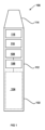
図1は、一例に係る、デバイス100を模式的に示している。デバイス100は、非燃焼性エアロゾル供給デバイス100である。非燃焼性エアロゾル供給デバイス100は、DC電源104(本例においては、バッテリ104)、回路106、誘導素子108、及びエアロゾル生成材料116を加熱するように構成されたサセプタ110を備える。DC電源104は、回路106に電気接続されている。DC電源104は、DC電力を回路106に供給するように構成されている。回路106は、誘導素子108に電気接続されている。誘導素子108は、例えば電磁石(例えば、コイル又はソレノイド)であってよく、例えば平面状であってよく、例えば銅により形成されていてもよい。回路106は、DC電源104からの入力DC電流を変動(例えば、交流)電流に変換するように構成されている。回路106は、誘導素子108に変動電流を送り込むように構成されている。
1 is a schematic diagram of a
サセプタ110は、誘導素子108に対して、誘導素子108から当該サセプタ110に誘導エネルギーを伝達するように構成されている。サセプタは、鉄、ニッケル、及びコバルト等の例示的な金属のうちの1つ又は組み合わせを含み得る強磁性部を備えていてもよい。誘導素子108は、変動電流が送り込まれると、上述の通り、ジュール加熱及び/又は磁気ヒステリシス加熱によってサセプタ110を加熱する。サセプタ110は、使用時、例えば伝導、対流、及び/又は放射による加熱によってエアロゾル生成材料116を加熱することにより、エアロゾルを生成するように構成されている。いくつかの例において、サセプタ110及びエアロゾル生成材料116は、非燃焼性エアロゾル供給デバイス100に対する挿入及び/若しくは取り出し、並びに使い捨てが可能な一体型ユニットを構成する。例えば、エアロゾル生成材料116及びサセプタ110は、消耗品に含まれていてもよい。このような例においては、デバイス100及び物品を併せて非燃焼性エアロゾル供給システムと称する場合もある。他の例においては、エアロゾル生成材料116が交換可能である一方、サセプタ110がデバイス100の永久部品を構成していてもよい。いくつかの例において、誘導素子108は、例えば交換のため、デバイス100から取り出し可能であってもよい。非燃焼性エアロゾル供給デバイス100は、手持ち式であってもよい。非燃焼性エアロゾル供給デバイス100は、エアロゾル生成材料116を加熱することにより、ユーザが吸引するエアロゾルを生成するように構成されていてもよい。
The
図1を再び参照して、非燃焼性エアロゾル供給デバイス100は、バッテリ104、回路106、誘導素子108、サセプタ110、及びエアロゾル生成材料116を収容する外側本体112を備える。外側本体112は、使用時に生成されたエアロゾルがデバイス100から出られるようにしたマウスピース114を備える。
Referring again to FIG. 1, the non-combustible
使用時、ユーザは、例えばそれ自体既知のボタン(図示せず)又はパフ検出器(図示せず)を介して、回路106を起動することにより、誘導素子108に変動電流を送り込んでサセプタ116を誘導加熱し、ひいてはエアロゾル生成材料116を加熱することによって、エアロゾル生成材料116からエアロゾルを生成させることができる。エアロゾルは、空気入口(図示せず)からデバイス100に取り込まれた空気中に生成され、マウスピース114まで搬送されてデバイス100から出ていく。
In use, a user can activate the
少なくともいくつかの例においては、蒸気が生成された後、少なくとも一部が凝縮してエアロゾルを形成してから非燃焼性エアロゾル供給デバイスを出てユーザに吸引される。 In at least some instances, after the vapor is generated, at least a portion of it condenses to form an aerosol that exits the non-combustible aerosol delivery device and is inhaled by the user.
この点、最初の留意点として、蒸気は一般的に、臨界温度よりも低い温度で気相の物質であり、例えば、温度を下げることなく圧力を上げることによって液体へと凝縮可能であることを意味する。一方、エアロゾルは一般的に、空気又は別の気体中の微細な固体粒子又は液滴のコロイドである。「コロイド」は、微視的に分散した不溶性粒子が別の物質中に懸濁した物質である。 The first thing to note here is that a vapor is generally a substance in the gas phase below its critical temperature, meaning that it can be condensed into a liquid, for example by increasing the pressure, without decreasing the temperature. An aerosol, on the other hand, is generally a colloid of fine solid particles or liquid droplets in air or another gas. A "colloid" is a substance in which microscopically dispersed insoluble particles are suspended in another substance.
便宜上、本明細書において、エアロゾル(aerosol)という用語は、エアロゾル、蒸気、又はエアロゾル及び蒸気の組み合わせを意味するものとする。 For convenience, the term aerosol is used herein to mean an aerosol, a vapor, or a combination of an aerosol and a vapor.
エアロゾル生成材料は、例えば加熱、照射、又はその他任意の方法でエネルギー供給された場合にエアロゾルを生成可能な材料である。エアロゾル生成材料は、例えば固体、液体、又はゲルの形態であってもよく、活性物質及び/又は香味料を含んでいてもよいし、含んでいなくてもよい。いくつかの実施形態において、エアロゾル生成材料は、「アモルファス固体」を含んでいてもよく、これは代替として、「モノリシック固体」(すなわち、非繊維質)と称する場合もある。いくつかの実施形態において、アモルファス固体は、乾燥ゲルであってもよい。アモルファス固体は、液体等の何らかの流体を内部に保持可能な固体材料である。いくつかの実施形態において、エアロゾル生成材料は、例えばおよそ50wt%、60wt%、又は70wt%~およそ90wt%、95wt%、又は100wt%のアモルファス固体を含んでいてもよい。 An aerosol-generating material is a material capable of generating an aerosol when energized, e.g., by heating, irradiating, or in any other manner. The aerosol-generating material may be in the form of, e.g., a solid, liquid, or gel, and may or may not contain actives and/or flavorings. In some embodiments, the aerosol-generating material may comprise an "amorphous solid," which may alternatively be referred to as a "monolithic solid" (i.e., non-fibrous). In some embodiments, the amorphous solid may be a dry gel. An amorphous solid is a solid material capable of holding some fluid, such as a liquid, within it. In some embodiments, the aerosol-generating material may comprise, e.g., from about 50 wt%, 60 wt%, or 70 wt% to about 90 wt%, 95 wt%, or 100 wt% amorphous solid.
エアロゾル生成材料は、1つ若しくは複数の活性物質及び/若しくは香料、1つ若しくは複数のエアロゾル形成材料、並びに任意選択として、1つ若しくは複数の他の機能材料を含んでいてもよい。 The aerosol generating material may include one or more active substances and/or flavorings, one or more aerosol forming materials, and optionally one or more other functional materials.
本明細書において使用する活性物質は、生理学的活性材料(生理学的反応の実現又は増強が意図される材料)であってもよい。活性物質は、例えば栄養補助食品、向精神薬、精神活性剤から選択されるようになっていてもよい。活性物質は、自然に存在するものであってもよいし、合成して得られるものであってもよい。活性物質は、例えばニコチン、カフェイン、タウリン、テイン、B6、B12、若しくはC等のビタミン類、メラトニン、カンナビノイド、又はこれらの構成物質、誘導体、若しくは組み合わせを含んでいてもよい。活性物質は、タバコ、大麻、又は別の植物の1つ又は複数の構成物質、誘導体、又は抽出物を含んでいてもよい。 As used herein, an active substance may be a physiologically active material (a material intended to produce or enhance a physiological response). The active substance may be selected from, for example, a dietary supplement, a psychotropic drug, or a psychoactive agent. The active substance may be naturally occurring or synthetically derived. The active substance may include, for example, nicotine, caffeine, taurine, theine, vitamins such as B6, B12, or C, melatonin, cannabinoids, or constituents, derivatives, or combinations thereof. The active substance may include one or more constituents, derivatives, or extracts of tobacco, cannabis, or another plant.
いくつかの実施形態において、活性物質は、ニコチンを含む。いくつかの実施形態において、活性物質は、カフェイン、メラトニン、又はビタミンB12を含む。 In some embodiments, the active agent includes nicotine. In some embodiments, the active agent includes caffeine, melatonin, or vitamin B12.
1つ又は複数の他の機能材料は、pH調整剤、着色剤、防腐剤、バインダ、充填剤、安定剤、及び/又は酸化防止剤のうちの1つ又は複数を含んでいてもよい。 The one or more other functional materials may include one or more of a pH adjuster, a colorant, a preservative, a binder, a filler, a stabilizer, and/or an antioxidant.
エアロゾル形成材料は、エアロゾルを形成可能な1つ又は複数の構成物質を含んでいてもよい。いくつかの実施形態において、エアロゾル形成材料は、グリセロール、プロピレングリコール、ジエチレングリコール、トリエチレングリコール、テトラエチレングリコール、1,3-ブチレングリコール、エリスリトール、メソ-エリスリトール、バニリン酸エチル、ラウリン酸エチル、ジエチル硫酸塩、クエン酸トリエチル、トリアセチン、ジアセチン混合物、安息香酸ベンジル、フェニル酢酸ベンジル、トリブチリン、酢酸ラウリル、ラウリン酸、ミリスチン酸、及び炭酸プロピレンのうちの1つ又は複数を含んでいてもよい。 The aerosol-forming material may include one or more constituents capable of forming an aerosol. In some embodiments, the aerosol-forming material may include one or more of glycerol, propylene glycol, diethylene glycol, triethylene glycol, tetraethylene glycol, 1,3-butylene glycol, erythritol, meso-erythritol, ethyl vanillate, ethyl laurate, diethyl sulfate, triethyl citrate, triacetin, diacetin mixture, benzyl benzoate, benzyl phenylacetate, tributyrin, lauryl acetate, lauric acid, myristic acid, and propylene carbonate.
消耗品は、エアロゾル生成材料を含む物品又はエアロゾル生成材料から成る物品であって、その一部又は全部がユーザによる使用時に消費されることが意図される。消耗品は、エアロゾル生成材料格納エリア、エアロゾル生成材料移動コンポーネント、エアロゾル生成エリア、ハウジング、ラッパー、マウスピース、フィルタ、及び/又はエアロゾル変性剤等の1つ又は複数の他のコンポーネントを備えていてもよい。また、消耗品は、使用時に熱を放出してエアロゾル生成材料からエアロゾルを生成させる加熱器等のエアロゾル生成器を備えていてもよい。上述の通り、加熱器は、例えば燃焼性材料、電気伝導により加熱可能な材料、又はサセプタを含んでいてもよい。 A consumable is an article that includes or is composed of an aerosol-generating material, some or all of which is intended to be consumed upon use by a user. A consumable may include one or more other components, such as an aerosol-generating material storage area, an aerosol-generating material transfer component, an aerosol-generating area, a housing, a wrapper, a mouthpiece, a filter, and/or an aerosol modifier. A consumable may also include an aerosol generator, such as a heater that, upon use, releases heat to generate an aerosol from the aerosol-generating material. As discussed above, the heater may include, for example, a combustible material, a material that can be heated by electrical conduction, or a susceptor.
回路106、誘導素子108、サセプタ110、及び/又は全体としてのデバイス100は、様々な温度へのエアロゾル生成材料116の加熱によって、エアロゾル生成材料116の燃焼なく、エアロゾル生成材料116の少なくとも1つの成分を揮発させるように構成されていてもよい。例えば、温度範囲は、およそ50℃~およそ250℃、およそ50℃~およそ150℃、およそ50℃~およそ120℃、およそ50℃~およそ100℃、およそ50℃~およそ80℃、又はおよそ60℃~およそ70℃等、およそ50℃~およそ350℃であってもよい。いくつかの例において、温度範囲は、およそ160℃~およそ280℃又はおよそ170℃~およそ220℃である。いくつかの例において、温度範囲は、この範囲以外であってもよく、温度範囲の上限は、280℃前後であってもよいし、300℃より高くてもよい。
The
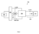
ここで図2を参照して、この図は、一例に係る、非燃焼性エアロゾル供給デバイス100の誘導素子108に対する回路106をより詳しく模式的に示している。
Referring now to FIG. 2, this diagram illustrates in greater detail a schematic diagram of the
回路106は、ドライバ構成204を備えるが、本明細書においては駆動回路204とも称する。また、回路106は、ドライバ制御構成208及びコントローラ220を備えるが、本明細書においては一体的に制御回路と称する場合もある。また、コントローラ220がバッテリ104に電気接続されることにより、バッテリ104がDC電圧をコントローラ220に供給するようになっている。例として、コントローラ220は、バッテリ104から電力を受電するように構成され、回路106及び、場合によっては、デバイス100の他の構成素子に電気信号を出力する複数の出力を備えた処理ユニット(例えば、MCU)である。ドライバ構成204は、相対的に高い電位+v202を供給するコントローラ220のプラス端子と、例としてグランドに接続され、相対的に低い電位GND206を供給するコントローラ220のマイナス端子と、に電気接続されている。例として、コントローラ220によりドライバ構成204に出力される電圧は、バッテリ104によりコントローラ220に供給される電圧と実質的に等しい。したがって、ドライバ構成204には、ある電圧が生じる。
The
ドライバ構成204は、インダクタンスLを有する誘導素子108を含むLC誘導回路205及びキャパシタンスCを有するキャパシタ210(本例においては、誘導素子108に直列に接続されている)に電気接続されている。
The
ドライバ構成204は、バッテリ104からの入力直流電流によりコントローラ220を介して、変動電圧をLC回路205に供給するように構成されている。これにより、使用時には、変動電流が誘導素子108に流れる。
The
ドライバ制御構成208は、ドライバ構成204又はその構成素子を制御して、ドライバ構成によりLC回路205に出力される電圧を制御するように構成されている。具体的に、本例においては、以下により詳しく説明する通り、ドライバ制御構成208は、様々な時間におけるドライバ構成204のトランジスタへのスイッチング電位の供給を制御することによって、ドライバ構成204に変動電流を生成させるように構成されている。
The
ドライバ制御構成208は、コントローラ220を介して、本例においてはスイッチング電位の起源でもあるバッテリ104に電気接続されている。
The
また、本例においては、ドライバ制御構成208がコントローラ220のプラス及びマイナス端子に接続されていることから、ドライバ制御構成208への電位の供給ひいては給電によって、ドライバ構成204を制御するスイッチング電位をドライバ制御構成208が生成可能となる。本例において、ドライバ制御構成208は、バッテリ電圧+vをドライバ構成204に供給する端子とは異なるコントローラ220の端子に接続されている。これについては、以降の図面を参照しつつ、以下により詳しく説明する。
Furthermore, in this example, the
ドライバ制御構成208は、コントローラ220からの制御信号を受信するためのコントローラ220に対する別途接続部221を備える。図2においては、単一のラインとして単純化された形態で別途接続部221を示している。接続部221の別途詳細については、図4を参照しつつ以下に説明する。
The
バッテリ104を起源としてコントローラ220により供給された電位による給電によって、ドライバ制御構成208は、スイッチング電位を供給してドライバ構成204を制御するように構成されている。スイッチング電位は、ドライバ構成204のトランジスタのスイッチングに適するように選択される。スイッチング電位は、例えばバッテリ電圧+v以下であってもよい。スイッチング電位の値は、ドライバ構成204に用いられるトランジスタの種類によって決まり得る。
Powered by a potential sourced from the
本例において、ドライバ制御構成208は、LC回路205に供給される変動(例えば、交流)電圧の周波数ひいては誘導素子108に送り込まれる変動電流の周波数を制御するように構成されている。前述の通り、LC回路は、共振を示す場合がある。いくつかの例において、ドライバ制御構成208は、LC回路205の共振周波数又はその近くとなるように、LC回路に送り込まれる変動電流の周波数(駆動周波数)を制御する。例えば、駆動周波数は、MHzの範囲(例えば、0.5~1.5MHzの範囲(例えば、1MHz))であってもよい。別の例において、駆動周波数は、kHzの範囲(例えば、100kHz~1MHzの範囲(例えば、400kHz前後))であってもよい。当然のことながら、例えば特定のLC回路205(及び/若しくはその構成素子)並びに/又はサセプタ110の使用に応じて、他の周波数が用いられるようになっていてもよい。例えば、当然のことながら、LC回路205の共振周波数は、回路205のインダクタンスL及びキャパシタンスCに依存し、ひいては、使用されるインダクタ108、キャパシタ210、及びサセプタ110に依存し得る。
In this example, the
使用時、ドライバ制御構成208は、例えばユーザにより起動されると、変動電流をLC回路205ひいては誘導素子108に送り込んでサセプタ116を誘導加熱するようにドライバ構成204を制御する。これにより、誘導素子108がエアロゾル生成材料(図2には示さず)を加熱して、例えばユーザが吸引するエアロゾルを生成する。
In use, when activated, for example, by a user, the
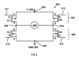
ここで図3を参照して、この図は、ドライバ構成204をより詳しく模式的に示している。ドライバ構成204は、Hブリッジ構成に配置された複数のトランジスタ(本例においては、4つのトランジスタQ1、Q2、Q3、Q4)を備える(なお、Hブリッジ構成に配置又は接続されたトランジスタをHブリッジと称する場合もある)。
Referring now to FIG. 3, this diagram shows a more detailed schematic of the
Hブリッジ構成は、高位側ペア304のトランジスタQ1、Q2及び低位側ペア306のトランジスタQ3、Q4を含む。高位側ペア304の第1のトランジスタQ1は、低位側ペア306の第3のトランジスタQ3に対して電気的に隣り合い、高位側ペア304の第2のトランジスタQ2は、低位側ペア314の第4のトランジスタQ4に対して電気的に隣り合う。高位側ペア304は、低位側ペア306を接続する第2の電位GND206よりも高い第1の電位+v202に接続するためのものである。
The H-bridge configuration includes transistors Q1, Q2 of the high-
本例において、ドライバ構成204は、高位側ペア304のトランジスタQ1、Q2間の第1の点322と低位側ペア306のトランジスタQ3、Q4間の第2の点320との間に、コントローラ220(図3には示さず)から供給されたバッテリ電位+vを接続するように構成されている。具体的に、第1の点322は、正のバッテリ電圧出力+vを与えるコントローラ220の端子に接続するためのものであり、第2の点320は、バッテリ104のマイナス端子につながるコントローラ220の端子に接続するためのものである。したがって、使用時には、第1の点322と第2の点320との間に電位差が生じる。
In this example, the
図2を参照して説明した通り、ドライバ構成204は、誘導素子(図3には示さず)を備えたLC回路205に電気接続され、これを駆動するように構成されている。具体的に、(LC回路205の一部としての)誘導素子は、高位側ペアの一方のトランジスタQ2及び低位側ペアの一方のトランジスタQ4の間の第3の点324と高位側ペアの他方のトランジスタQ1及び低位側第2のペアの他方のトランジスタQ3の間の第4の点326との間に接続される。
As described with reference to FIG. 2, the
本例において、トランジスタQ1、Q2、Q3、Q4はそれぞれ、nチャネル電界効果トランジスタである。各電界効果トランジスタQ1、Q2、Q3、Q4は、使用時、スイッチング電位による制御によって、電流を選択的に通過させることができる。各電界効果トランジスタQ1、Q2、Q3、Q4は、ソースS、ドレインD、及びゲートGを備える。スイッチング電位は各電界効果トランジスタQ1、Q2、Q3、Q4のゲートGに供給され、これによって上述の通り、各電界効果トランジスタQ1、Q2、Q3、Q4のソースSとドレインDとの間に電流が通過可能となる。したがって、スイッチング電位が供給された場合には電界効果トランジスタQ1、Q2、Q3、Q4が「オン」となって電流が通過し、スイッチング電位が供給されない場合には電界効果トランジスタQ1、Q2、Q3、Q4が「オフ」となって電流が実質的に通過しなくなる高抵抗を有するように、各電界効果トランジスタQ1、Q2、Q3、Q4が構成されている。 In this example, the transistors Q1, Q2, Q3, and Q4 are n-channel field effect transistors. When in use, each of the field effect transistors Q1, Q2, Q3, and Q4 can selectively pass a current by controlling a switching potential. Each of the field effect transistors Q1, Q2, Q3, and Q4 has a source S, a drain D, and a gate G. A switching potential is supplied to the gate G of each of the field effect transistors Q1, Q2, Q3, and Q4, which allows a current to pass between the source S and the drain D of each of the field effect transistors Q1, Q2, Q3, and Q4, as described above. Thus, each of the field effect transistors Q1, Q2, Q3, and Q4 is configured to have a high resistance such that when a switching potential is supplied, the field effect transistors Q1, Q2, Q3, and Q4 are "on" and a current passes therethrough, and when a switching potential is not supplied, the field effect transistors Q1, Q2, Q3, and Q4 are "off" and substantially no current passes therethrough.
図3に示す例において、各電界効果トランジスタQ1、Q2、Q3、Q4は、スイッチング電圧を搬送する関連のスイッチング電圧ライン311、312、313、314を(それぞれ)有する。
In the example shown in FIG. 3, each field effect transistor Q1, Q2, Q3, and Q4 has an associated
ドライバ制御構成208(図3には示さず、図2参照)は、各電界効果トランジスタQ1、Q2、Q3、Q4に対するスイッチング電位の供給の制御によって、各トランジスタQ1、Q2、Q3、Q4が「オン」モード(すなわち、電流が通過する低抵抗モード)になるか、「オフ」モード(すなわち、実質的に電流が通過しない高抵抗モード)になるかを制御するように構成されている。 Driver control arrangement 208 (not shown in FIG. 3, see FIG. 2) is configured to control the supply of switching potentials to each field effect transistor Q1, Q2, Q3, Q4 to control whether each transistor Q1, Q2, Q3, Q4 is in an "on" mode (i.e., a low resistance mode in which current passes) or an "off" mode (i.e., a high resistance mode in which substantially no current passes).
各電界効果トランジスタQ1、Q2、Q3、Q4へのスイッチング電位の供給のタイミングを制御することにより、ドライバ制御構成208は、変動(例えば、交流)電圧がLC回路205に供給され、その誘導素子(図3には示さず)に変動電流が供給されるようにしてもよい。
By controlling the timing of the supply of switching potentials to each of the field effect transistors Q1, Q2, Q3, and Q4, the
以下により詳しく論じる通り、ドライバ制御構成208は、電界効果トランジスタQ1、Q2、Q3、Q4の「オン」及び「オフ」スイッチングのシーケンス制御によって誘導回路に供給される変動電圧を制御するのに使用可能である。
As discussed in more detail below, the
例えば、第1の時間においては、ドライバ制御構成208が第1のスイッチング状態であってもよく、スイッチング電位が第1及び第4の電界効果トランジスタQ1、Q4に供給される一方、第2及び第3の電界効果トランジスタQ2、Q3には供給されない。このため、第1及び第4の電界効果トランジスタQ1、Q4が低抵抗モードとなる一方、第2及び第3の電界効果トランジスタQ2、Q3が高抵抗モードとなる。したがって、この第1の時間においては、ドライバ構成204の第1の点322から、第1の電界効果トランジスタQ1と、第1の方向(図3の意味で左から右)にLC回路205と、第4の電界効果トランジスタQ4と、を通って、ドライバ構成204の第2の点320まで電流が流れ得る。ただし、第2の時間においては、ドライバ制御構成208が第2のスイッチング状態であってもよく、スイッチング電位が第2及び第3の電界効果トランジスタQ2、Q3に供給される一方、第1及び第4の電界効果トランジスタQ1、Q4には供給されない。このため、第2及び第3の電界効果トランジスタQ2、Q3が低抵抗モードとなる一方、第1及び第4の電界効果トランジスタQ1、Q4が高抵抗モードとなる。したがって、この第2の時間においては、ドライバ構成204の第1の点322から、第2の電界効果トランジスタQ2と、第1の方向と反対の第2の方向(すなわち、図3の意味で右から左)にLC回路205と、第3の電界効果トランジスタQ3と、を通って、ドライバ構成204の第2の点320まで電流が流れ得る。したがって、第1及び第2のスイッチング状態の切り替えにより、ドライバ制御構成208は、LC回路205に交流電圧、ひいては、誘導素子108に変動電流を供給(すなわち、送り込む)ようにドライバ構成204を制御可能である。
For example, at a first time, the
上述のような動作において、HブリッジのトランジスタQ1、Q2、Q3、Q4はそれぞれ、一部の時間に「オン」となり、他の時間に「オフ」となる。Hブリッジは、高位側ペア304の第1のトランジスタが「オン」で、Hブリッジの反対側の低位側ペア306の一方のトランジスタも「オン」となる第1のスイッチング状態と、高位側ペア304の他方のトランジスタが「オン」で、低位側ペア306の他方のトランジスタも「オン」となる第2のスイッチング状態と、の間で切り替わる。これにより、ドライバ構成204によって誘導回路205に供給される電圧の極性が繰り返し切り替わる。本明細書において、この種の動作は、ドライバ構成204が「フルブリッジ」モードで動作しているものと称する場合がある。
In such operation, each of the transistors Q1, Q2, Q3, and Q4 of the H-bridge is "on" part of the time and "off" other times. The H-bridge switches between a first switching state in which a first transistor of the high-
上述のフルブリッジモードで動作するほか、ドライバ構成204は、非ゼロの大きさの電圧を誘導回路205に供給することと、実質的に電圧を誘導回路205に供給しないことと、の間でHブリッジが繰り返し切り替わる第2のモードでも動作するように構成されている。例として、これを「ハーフブリッジ」モードでの動作と称する場合がある。ハーフブリッジモードにおいて、ドライバ構成204は、電圧を誘導回路205に供給する第3のスイッチング状態と実質的に電圧を誘導回路205に供給しない第4のスイッチング状態との間で切り替わるように構成されている。例えば、第3のスイッチング状態においては、第1及び第4のトランジスタQ1、Q4が「オン」となる一方、第2及び第3のトランジスタQ2、Q3が「オフ」となり得る。したがって、第3のスイッチング状態においては、第1のトランジスタQ1及び第4のトランジスタQ4に電流が流れるため、図3において左から右に示す方向で誘導回路205にも流れ得る。第4のスイッチング状態においては、トランジスタQ1、Q2、Q3、Q4がすべてオフとなるか、又は、少なくとも高位側ペア304の両トランジスタ若しくは低位側ペア306の両トランジスタがオフとなり得るため、電流が誘導回路205を通ってグランド206に流れる経路が存在しない。したがって、ハーフブリッジモードにおけるHブリッジは、電圧が誘導回路205に供給されるスイッチング状態と実質的に電圧が誘導回路205に供給されないスイッチング状態との間で切り替わる。
In addition to operating in the full-bridge mode described above, the
同様に、Hブリッジ204がハーフブリッジモードで動作している場合は、第3のスイッチング状態で第2のトランジスタQ2及び第3のトランジスタQ3に(図3に示す意味で右から左に)電流が流れて電圧を誘導回路205に供給し得る一方、第4のスイッチング状態においては実質的に電圧が誘導回路205に供給されない。
Similarly, when the H-
言い換えると、ハーフブリッジモードで動作している場合、ドライバ構成204は、ある状態で正電圧又は負電圧を誘導回路205に供給することと、別の状態で実質的に電圧を誘導回路205に供給しないことと、の間で交互に切り替わる。これは、正電圧を誘導回路205に供給することと、負電圧を誘導回路205に供給することと、の間でドライバ構成204が繰り返し切り替わるフルブリッジモードと対比可能である。
In other words, when operating in half-bridge mode, the
例として、ハーフブリッジモードにおいては、電圧が誘導回路に供給される時間の割合がフルブリッジモードよりも小さい。したがって、Hブリッジをハーフブリッジモードで動作させることにより、フルブリッジモードと比較した場合に、誘導素子108によるサセプタ110への電力の伝達が抑えられるため、サセプタ110がデバイス100により加熱される程度も抑えることができる。例として、デバイス100は、サセプタ110を加熱させるのが望ましい程度に応じて、フルブリッジモード及びハーフブリッジモードの一方で選択的に動作するように構成されていてもよい。一例として、サセプタ110の温度を目標温度まで上げるのに用いられる加熱電力と比較した場合、サセプタ110を目標温度に維持するのに用いられる加熱電力は小さくなると考えられる。このような例において、デバイス100は、フルブリッジモードで動作して、サセプタ110の温度を高くする大電力を供給することにより、例えばサセプタ110を目標動作温度まで昇温させてエアロゾル生成材料116を加熱するように構成されていてもよい。その後、目標動作温度に十分達した場合、デバイス100は、ハーフブリッジモードでの動作に切り替わって、サセプタ110を目標温度に維持するためのより小さな加熱電力を供給するようにしてもよい。
As an example, in half-bridge mode, a voltage is provided to the inductive circuit for a smaller percentage of time than in full-bridge mode. Thus, operating the H-bridge in half-bridge mode reduces the power transfer to the
また、サセプタ110が誘導素子108により加熱される程度を制御する他の手段がデバイス100により用いられるようになっていてもよい。例えば、ドライバ構成204が駆動される周波数、すなわち、ドライバ構成204によって誘導回路205に供給される電圧の変更又は切り替えが行われる周波数を制御することにより、誘導素子108の加熱電力が制御されるようになっていてもよい。例として、フルブリッジモード又はハーフブリッジモードで動作する場合の駆動周波数を切り替えることにより、誘導素子108の加熱電力の調整がなされるようになっていてもよい。例として、フルブリッジモードでの動作からハーフブリッジモードでの動作への切り替えにより加熱電力が大幅に抑えられ、例えば、4分の1に抑えられるようになっていてもよい。したがって、例えば、駆動周波数の調整により加熱電力が微調整され得る一方、フルブリッジモードとハーフブリッジモードとの間のモード切り替えによって、加熱電力が大きく調整され得る。
The
供給される加熱電力は、DC供給電圧及びサセプタ110の見掛けのインピーダンスに依存する。例えば、バッテリ104が3ボルトを供給し、サセプタ110の見掛けのインピーダンスが0.4オームである場合、利用可能な加熱電力は、(3ボルト×3ボルト)/0.4オーム=22.5ワットと決定され得る。ただし、バッテリ104が4.2ボルトを供給する場合、利用可能な加熱電力は、(4.2ボルト×4.2ボルト)/0.4オーム=44.1ワットと決定され得る。したがって、バッテリ電圧が4.2ボルトである例において、例えばサセプタ110を所望の温度に維持するのに必要と決定された電力と考えられる1.5ワットの加熱電力を供給するには、利用可能な44.1ワットの電力のうちの1.5ワットを供給するものとする。これは、本例において、44.1/1.5又は、等価的に、29.4:1の比で電力を制御する必要があることを意味する。ハーフブリッジモードへの切り替えによって、利用可能な電力が4分の1に抑えられるため、本例においては、サセプタの温度を維持するのに、利用可能な11ワット前後の電力のうちの1.5ワットを供給するものとする。これは、7.35:1前後の比である。したがって、ハーフブリッジモードへの切り替えによって、所望の加熱電力を供給するために制御する必要がある供給電力の範囲が抑えられる。
The heating power provided depends on the DC supply voltage and the apparent impedance of the
いくつかの例において、駆動周波数の制御による加熱電力の制御は、国際公開第2018/178114A2号に記載のように実行されるが、そのすべての内容を参照により本明細書に援用する。例えば、コントローラ220は、誘導回路205の共振周波数でHブリッジ204を駆動するように構成されてもよく、この共振周波数は、加熱電力を最大化するため、測定されるようになっていてもよいし、例えば予め定められていてもよい。誘導回路108の共振周波数での駆動と比較して加熱電力を抑えるため、コントローラ220は、誘導回路205の共振周波数と異なる(例えば、共振周波数よりも低い)周波数でHブリッジを駆動するようにしてもよい。これを回路の「オフレゾナンス」駆動と称する場合があり、サセプタ110が誘導素子108により加熱される程度を抑えることができる。オフレゾナンス駆動の場合は、回路が共振周波数で駆動される場合と比較して、共振回路に流れる電流が小さくなる。したがって、所与の供給電圧に関し、インダクタ108からサセプタ110へのエネルギー伝達が小さくなるため、サセプタ110が誘導加熱される程度は、所与の供給電圧に対して回路が共振周波数で駆動される場合と比較して低くなる。Hブリッジが共振回路205を駆動する周波数が共振周波数から(上下いずれかに)離れるほど、サセプタ110が誘導加熱される程度が低くなる。
In some examples, the control of the heating power by controlling the drive frequency is performed as described in WO 2018/178114 A2, the entire contents of which are incorporated herein by reference. For example, the
いくつかの例においては、ドライバ構成204の駆動周波数の制御による加熱電力の制御の追加又は代替として、Hブリッジ204の入力電圧が制御されるようになっていてもよい。例えば、入力電圧の低減により、サセプタ110が加熱される程度を抑え、入力電圧の増大により、サセプタ110が加熱される程度を増すようにしてもよい。
In some examples, the input voltage of the H-
図4は、回路106の別途詳細であり、特に、ドライバ制御構成の詳細を示している(ドライバ制御構成の構成素子の表現が異なるため、図4では標識化しておらず、図2のドライバ制御構成208参照)。
Figure 4 shows further details of
図4に示すように、ドライバ制御構成208は、供給ライン311、313を介して、スイッチング電位を第1のトランジスタQ1及び第2のトランジスタQ3に供給するように構成された第1のドライバ410を備える。また、ドライバ制御構成208は、供給ライン312、314を介して、スイッチング電位を第2のトランジスタQ2及び第4のトランジスタQ4に供給するように構成された第2のドライバ420を備える。上述の通り、第1のドライバ410及び第2のドライバ420は、バッテリ電圧+vを与えるコントローラ220の端子とバッテリ104のマイナス端子につながるコントローラ220の端子との間に接続されている。本例において、第1のドライバ410及び第2のドライバ420は、Hブリッジ204と並列に接続されている。図4に示すように、第1及び第2のドライバ410、420、第3及び第4のトランジスタQ3、Q4、並びにバッテリ104のマイナス端子につながるコントローラ220の端子間には、抵抗器320が電気接続されている。例として、抵抗器320は、Hブリッジ204を通ってグランドGND206に流れる電流を(例えば、コントローラ220により)モニタリングする電流源抵抗器として用いられるようになっていてもよい。
4, the
第1のドライバ410及び第2のドライバ420は、当該第1のドライバ410及び当該第2のドライバ420により各供給ライン311、312、313、314を介してトランジスタQ1、Q2、Q3、Q4に供給されるスイッチング電位を制御する各駆動信号1010、1020を受信する。第1及び第2の駆動信号1010、1020は、以下により詳しく論じる通り、コントローラ220及びドライバ制御構成208の他の回路に由来する。本例において、駆動信号1010、1020は、高低の値間で切り替わる矩形波信号であり、以下の議論では「1」及び「0」と標識化する。一例においては、ドライバ構成204をフルブリッジモードで動作させるため、駆動信号1010、1020が相互に逆位相である。すなわち、第1の駆動信号1010が値1を有する場合は第2の駆動信号1020が値0を有し、その逆もまた同様である。例えば、第1の駆動信号1010が位相0°の矩形波信号である一方、第2の駆動信号1020が位相180°の矩形波信号であってもよい。
The first driver 410 and the second driver 420 receive respective drive signals 1010, 1020 that control the switching potentials provided by the first driver 410 and the second driver 420 to the transistors Q1, Q2, Q3, Q4 via the
任意のある時点で、第1の信号1010の値が1であるか0であるかによって、第1のドライバ410が第1のトランジスタQ1及び第3のトランジスタQ3に供給するスイッチング電位が決まる。同様に、任意のある時点で、第2の信号1020の値が1であるか0であるかによって、第2のドライバ420が第2のトランジスタQ2及び第4のトランジスタQ4に供給するスイッチング電位が決まる。一例において、第1の駆動信号1010の値が1である場合、第1のドライバ410は、スイッチング電位を第1のトランジスタQ1及び第3のトランジスタQ3に供給して、第1のトランジスタQ1を「オン」、第3のトランジスタQ3を「オフ」にするが、ここで上述の通り、所与のトランジスタが「オン」である場合は電流が流れ、所与のトランジスタが「オフ」である場合は電流が流れ得ない。これは、上述の第1のスイッチング状態に対応する。さらに、本例において、第1の駆動信号1010の値が0である場合、第1のドライバ410は、スイッチング電位を第1のトランジスタQ1及び第3のトランジスタQ3に供給して、第1のトランジスタQ1を「オフ」、第3のトランジスタQ3を「オン」にする。これは、上述の第2のスイッチング状態に対応する。 At any one time, the value of the first signal 1010, whether it is 1 or 0, determines the switching potential that the first driver 410 supplies to the first transistor Q1 and the third transistor Q3. Similarly, at any one time, the value of the second signal 1020, whether it is 1 or 0, determines the switching potential that the second driver 420 supplies to the second transistor Q2 and the fourth transistor Q4. In one example, when the value of the first drive signal 1010 is 1, the first driver 410 supplies switching potentials to the first transistor Q1 and the third transistor Q3 to turn the first transistor Q1 "on" and the third transistor Q3 "off," where, as described above, when a given transistor is "on," current can flow and when a given transistor is "off," current cannot flow. This corresponds to the first switching state described above. Furthermore, in this example, when the value of the first drive signal 1010 is 0, the first driver 410 supplies a switching potential to the first transistor Q1 and the third transistor Q3 to turn the first transistor Q1 "off" and the third transistor Q3 "on". This corresponds to the second switching state described above.
同様に、同じ例において、第2の駆動信号1020の値が1である場合、第2のドライバ420は、スイッチング電位を第2のトランジスタQ2及び第4のトランジスタQ4に供給して、第2のトランジスタQ2を「オン」、第4のトランジスタQ4を「オフ」にし、第2の駆動信号1020の値が0である場合、第2のドライバ420は、スイッチング電位を第2のトランジスタQ2及び第4のトランジスタQ4に供給して、第2のトランジスタQ2を「オフ」、第4のトランジスタQ4を「オン」にする。これは、以下の表1のようにまとめられる。 Similarly, in the same example, when the value of the second drive signal 1020 is 1, the second driver 420 supplies a switching potential to the second transistor Q2 and the fourth transistor Q4 to turn the second transistor Q2 "on" and the fourth transistor Q4 "off", and when the value of the second drive signal 1020 is 0, the second driver 420 supplies a switching potential to the second transistor Q2 and the fourth transistor Q4 to turn the second transistor Q2 "off" and the fourth transistor Q4 "on". This is summarized in Table 1 below.
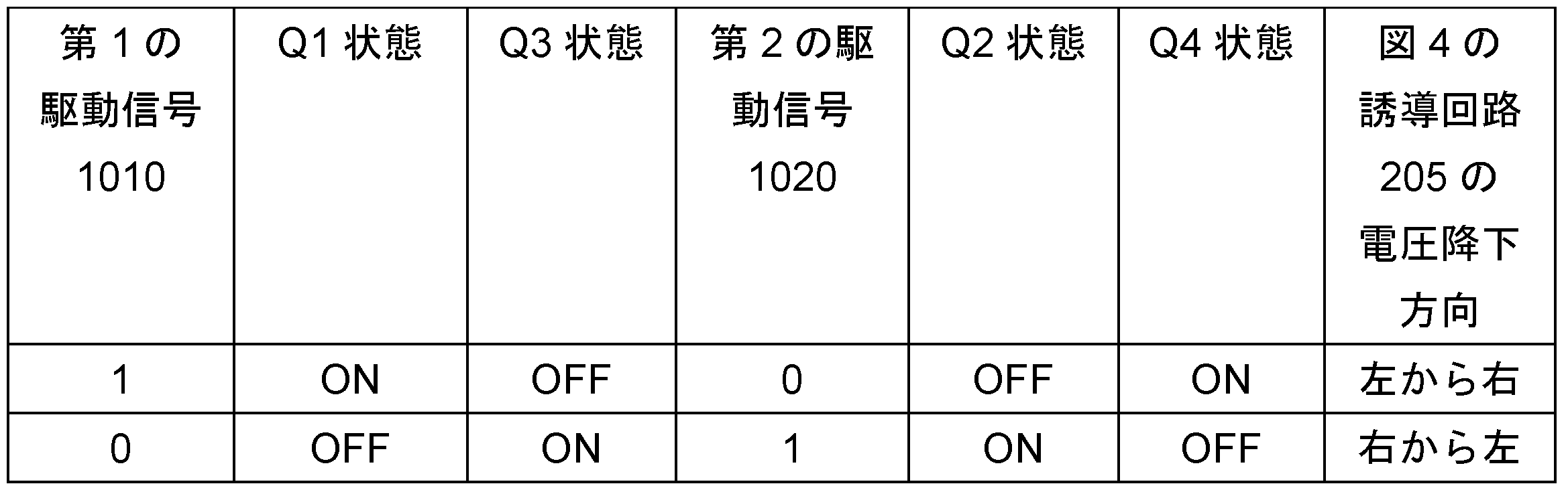
上述の構成では、相互に逆位相の第1及び第2の駆動信号1010、1020を供給することにより、第1及び第2の駆動信号1010、1020の値が切り替わる場合に、誘導回路205の電圧が繰り返し極性を切り替える、言い換えると、誘導回路205の電圧降下方向が繰り返し方向を変えるフルブリッジモードでドライバ構成204を動作させるようにする。駆動信号1010、1020が矩形波信号であることから、このモードで動作する場合は、実質的に任意のある時点で、誘導回路205の電圧が一方向又は他方向に降下している。
In the above configuration, by providing first and second drive signals 1010, 1020 that are out of phase with each other, the
これは、第1のトランジスタQ1及び第4のトランジスタQ4が第1の矩形波電圧信号を誘導回路205に供給し、第2のトランジスタQ2及び第3のトランジスタQ3が第2の矩形波電圧信号を誘導回路205に供給し、第1及び第2の矩形波信号が相互に180°位相がずれているものと考えられる。本例において、第1及び第2の矩形波信号はそれぞれ、DC電源電圧(例えば、4V)と0Vとの間で切り替わる。したがって、フルブリッジ動作の効果は、DC電源電圧の2倍で組み合わされた矩形波信号を供給するものと考えられる。
This can be thought of as the first transistor Q1 and the fourth transistor Q4 providing a first square wave voltage signal to the
ここで図4を再び参照して、第1及び第2のドライバ410、420を備えたドライバ制御構成208は、論理ゲート430を備えることが見て取れる。論理ゲート430は、第1の駆動信号1010を第1の入力として、制御信号1030を第2の入力として取得し、第2の駆動信号1020を出力として供給する。論理ゲート430に入力される第1の駆動信号1010及び制御信号1030はいずれも、コントローラ220からの出力である。図4は、図2を参照して簡単に上述したコントローラ220とドライバ制御構成208との間の接続部221をより詳しく示している。接続部221のうちの第1の接続部221aが第1の駆動信号1010を第1のドライバ410及び論理ゲート430の第1の入力に搬送する。接続部221のうちの第2の接続部が制御信号1030を論理ゲート430の第2の入力に搬送する。
Referring now to FIG. 4 again, it can be seen that the
論理ゲート430は、両入力である第1の駆動信号1010及び制御信号1030の値が0である場合、第2の駆動信号1020に値1を出力するNORゲートである。それ以外の場合すなわちいずれかの入力の値が1である場合、NORゲート430は、第2の駆動信号1020に値0を出力する。 The logic gate 430 is a NOR gate that outputs a value of 1 to the second drive signal 1020 if both inputs, the first drive signal 1010 and the control signal 1030, have a value of 0. Otherwise, that is, if either input has a value of 1, the NOR gate 430 outputs a value of 0 to the second drive signal 1020.
コントローラ220が出力する第1の駆動信号1010及び制御信号1030の様々な値に対してNORゲート430が出力する第2の駆動信号1020を以下の表2に示す。
The second drive signal 1020 output by the NOR gate 430 for various values of the first drive signal 1010 and the control signal 1030 output by the
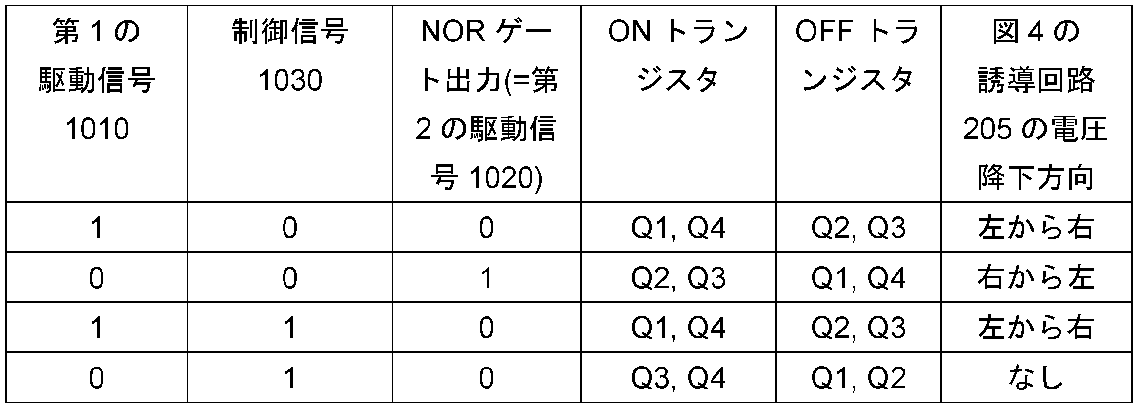
表2の最初の2行は、Hブリッジがフルブリッジモードにおいて切り替わる状態すなわち上述の第1のスイッチング状態及び第2のスイッチング状態を表す。表2の3行目及び4行目は、Hブリッジがハーフブリッジモードにおいて切り替わる状態を表す。 The first two rows of Table 2 represent the states in which the H-bridge switches in full-bridge mode, i.e., the first and second switching states described above. The third and fourth rows of Table 2 represent the states in which the H-bridge switches in half-bridge mode.
表2の最初の2行に見られるように、制御信号1030の値が0である場合、第1の駆動信号1010の値が1である場合は第2の駆動信号1020の値が0であり、第1の駆動信号1010の値が0である場合は第2の駆動信号1020の値が1である。このため、制御信号1030の値が0である場合は、表1を参照して上述した通り、ドライバ構成204により誘導回路205に供給される電圧の極性が第1の駆動信号1010の周波数で切り替わる。
As can be seen in the first two rows of Table 2, when the value of the control signal 1030 is 0, when the value of the first drive signal 1010 is 1, the value of the second drive signal 1020 is 0, and when the value of the first drive signal 1010 is 0, the value of the second drive signal 1020 is 1. Thus, when the value of the control signal 1030 is 0, the polarity of the voltage supplied to the
ただし、表2の3行目及び4行目に見られるように、制御信号1030の値が1である場合は、第1の駆動信号1010の値に関わらず、第2の駆動信号1020の値が0である。これは、ドライバ構成204をハーフブリッジモードで動作させる効果を有する。すなわち、制御信号1030が値1を維持する状態では、第4のトランジスタQ4がオンを維持する一方、第2のトランジスタQ2がオフを維持する。したがって、第1の駆動信号1010の値が1である場合は第1のトランジスタQ1がオン(且つ、第2のトランジスタQ2がオフ)であり、図4に示すように、誘導回路205の電圧が左から右に降下する。言い換えると、この状態においては、誘導回路205の左側が回路205の右側よりも高い電位差にある。ただし、第1の駆動信号1010の値が0である場合は、第1のトランジスタQ1がオフである一方、第2のトランジスタQ2もオフを維持する。したがって、この状態においては、第3及び第4のトランジスタQ3、Q4がオンであるにも関わらず、高位側ペアのトランジスタQ1、Q2がいずれもオフであるため、実質的に電圧が誘導回路205に供給されない。したがって、ドライバ構成204は、第1のドライバ410に供給される矩形波の第1の駆動信号1010の値が1である場合にのみ、電流を誘導回路205に送り込むように動作する。すなわち、本例において、ハーフブリッジモードで動作する場合、実質的に半分の時間は電圧が誘導回路205に供給され、実質的に残り半分の時間は電圧が誘導回路205に供給されない。
However, as can be seen in the third and fourth rows of Table 2, when the value of the control signal 1030 is 1, the value of the second drive signal 1020 is 0, regardless of the value of the first drive signal 1010. This has the effect of operating the
これは、繰り返しになるが、第1のトランジスタQ1及び第4のトランジスタQ4が第1の矩形波電圧信号を誘導回路205に供給し、残りの時間は電圧が誘導回路205に供給されないものと考えられる。したがって、フルブリッジ動作と比較したハーフブリッジ動作の効果は、半分の時間はDC電源電圧で動作する矩形波信号すなわちDC電源電圧の大きさの矩形波信号を供給する一方、残りの時間は実質的に電圧を供給しないものと考えられる。これは、フルブリッジモードで供給される矩形波の電圧の半分の大きさの電圧で矩形波信号が動作するものと考えられる。このため、ハーフブリッジモードにおいて供給される電力は、フルブリッジモードでの動作と比較した場合に、4分の1に抑えられる。
This can be thought of as the first transistor Q1 and the fourth transistor Q4 supplying a first square wave voltage signal to the
したがって、上記説明から、ドライバ構成204がフルブリッジモードで動作するかハーフブリッジモードで動作するかの選択に制御信号1030を使用可能であることが分かる。NORゲート430を含む構成は、制御信号1030に基づいて、第2の駆動信号1020を第1の駆動信号1010と逆位相にするか、又は、第1の駆動信号1010が矩形波として進行する間、第2の駆動信号1020を低位に保持する単純な構成を提供する。したがって、本例においては、一方の矩形波駆動信号である第1の駆動信号1010及び制御信号1030をドライバ制御構成208に供給しさえすればよい。第2の駆動信号1020は、これら2つの信号の入力に応答してNORゲート430から出力されるため、コントローラ220によって別途生成する必要がない。第2の駆動信号1020を供給するとともにドライバ構成204をフルブリッジ動作とハーフブリッジ動作との間で切り換え得る単純な構成がこのように与えられる。
Thus, from the above description, it can be seen that the control signal 1030 can be used to select whether the
第1の駆動信号1010及び制御信号1030を制御することによって、コントローラ220は、ドライバ構成204の動作を制御することにより、誘導素子108によるサセプタ110の加熱を制御することができる。上述の通り、コントローラ220は、制御信号1030を使用して、ドライバ構成204がハーフブリッジとして動作するかフルブリッジとして動作するかを制御することができる。これは、サセプタ110に供給される加熱電力の制御に使用可能である。例えば、上述の通り、ハーフブリッジモードでの動作によって、誘導回路205により供給される加熱電力は、フルブリッジモードでの動作と比較した場合に、4分の1に抑えられる。また、上述の通り、コントローラ220は、例えば第1の駆動信号1010の周波数の制御によって、誘導回路205が駆動される周波数を制御することにより、サセプタ110が加熱される程度を制御するようにしてもよい。この構成により、誘導回路205が駆動される周波数をコントローラ220が変更しようとする場合、これは、第1の駆動信号1010の周波数を変えるだけで行うことができる。
By controlling the first drive signal 1010 and the control signal 1030, the
上記例において、ドライバ構成204は、Hブリッジ構成に配置された4つのトランジスタQ1、Q2、Q3、Q4を備えるが、当然のことながら、他の例においては、他のトランジスタを備えていてもよく、Hブリッジ構成の一部であってもよいし、Hブリッジ構成の一部でなくてもよい。
In the above example, the
上述の例において、トランジスタQ1、Q2、Q3、Q4はそれぞれ、nチャネルトランジスタ(例えば、エンハンスメントモードnチャネル金属酸化物半導体電界効果トランジスタ)である。ただし、他の例においては、トランジスタQ1、Q2、Q3、Q4のうちの1つ又は複数がpチャネル電界効果トランジスタ(例えば、エンハンスメントモードpチャネル金属酸化物半導体電界効果トランジスタ)であってもよい。 In the above examples, transistors Q1, Q2, Q3, and Q4 are each n-channel transistors (e.g., enhancement mode n-channel metal oxide semiconductor field effect transistors). However, in other examples, one or more of transistors Q1, Q2, Q3, and Q4 may be p-channel field effect transistors (e.g., enhancement mode p-channel metal oxide semiconductor field effect transistors).
同じく上述の通り、nチャネルFETの場合は、ドレイン端子Dがソース端子Sよりも高い電位に置かれ(すなわち、ドレイン-ソース電圧が正、言い換えると、ソース-ドレイン電圧が負となり)、nチャネルFETを「オン」にする(すなわち、電流が通過できるようにする)ため、ゲート端子Gに印加されるスイッチング電位がソース端子Sでの電位よりも高い。 Also as mentioned above, for an n-channel FET, the drain terminal D is placed at a higher potential than the source terminal S (i.e., the drain-source voltage is positive, or in other words, the source-drain voltage is negative), and in order to turn the n-channel FET "on" (i.e., to allow current to pass), the switching potential applied to the gate terminal G is higher than the potential at the source terminal S.
上記例においては、電界効果トランジスタQ1、Q2、Q3、Q4が金属酸化物電界効果トランジスタであるものの、当然のことながら、これは必ずしも必要なことではなく、他の例においては、他種のトランジスタ(例えば、高電子移動度トランジスタ(HEMT))が用いられるようになっていてもよい。いくつかの例においては、SiC(炭化ケイ素)及びGaN(窒化ガリウム)等の広バンドギャップ材料を採用したトランジスタが用いられるようになっていてもよく、例えばFET又はHEMTであってもよい。 In the above examples, the field effect transistors Q1, Q2, Q3, and Q4 are metal oxide field effect transistors, but of course this is not necessary and in other examples other types of transistors (e.g., high electron mobility transistors (HEMTs)) may be used. In some examples, transistors employing wide bandgap materials such as SiC (silicon carbide) and GaN (gallium nitride) may be used, and may be, for example, FETs or HEMTs.
上述の例においては、コントローラ220を介して供給される同じバッテリ電圧+vによってドライバ制御構成208が給電されるものの、他の例においては、ドライバ制御構成208の電位がバッテリ電圧+vと異なっていてもよい。例えば、ドライバ制御構成208及びドライバ構成204の電位は、コントローラ220からの異なる出力を介して供給されるようになっていてもよい。
Although in the above example, the
上述の例においては、バッテリ電圧+vをドライバ構成204に供給する端子とは異なるコントローラ220の端子にドライバ制御構成208が接続されているものの、他の例においては、電位をドライバ構成204に供給するのと同じ端子によって、ドライバ制御構成208に電位が供給されるようになっていてもよい。
In the above example, the
上述の例において、非燃焼性エアロゾル供給デバイス100は、当該デバイスが生成したエアロゾルをユーザが吸引し得るマウスピースを備える。ただし、他の例においては、デバイス100がマウスピースを備えていなくてもよい。例えば、エアロゾル生成材料116を含む物品は、ユーザが口にくわえて生成エアロゾルを吸引し得る部分を備えていてもよい。
In the above example, the non-combustible
いくつかの例において、非燃焼性エアロゾル供給システムは、ベーピングデバイス又は電子ニコチン送達システム(END)としても知られる電子タバコであるが、エアロゾル生成材料中のニコチンの存在は要件ではないことに留意されたい。 In some instances, the non-combustible aerosol delivery system is an electronic cigarette, also known as a vaping device or electronic nicotine delivery system (END), although it should be noted that the presence of nicotine in the aerosol generating material is not a requirement.
いくつかの例において、非燃焼性エアロゾル供給システムは、非燃焼加熱式システムとしても知られるエアロゾル生成材料加熱システムである。このようなシステムの一例は、タバコ加熱システムである。 In some examples, the non-combustion aerosol delivery system is an aerosol-generating material heating system, also known as a non-combustion heating system. One example of such a system is a tobacco heating system.
いくつかの例において、非燃焼性エアロゾル供給システムは、エアロゾル生成材料(これらのうちの1つが加熱されるようになっていてもよいし、複数が加熱されるようになっていてもよい)の組み合わせによってエアロゾルを生成する混成システムである。エアロゾル生成材料はそれぞれ、例えば固体、液体、又はゲルの形態であってもよく、ニコチンを含んでいてもよいし、含んでいなくてもよい。いくつかの例において、混成システムは、液体若しくはゲルエアロゾル生成材料並びに固体エアロゾル生成材料を含む。固体エアロゾル生成材料は、例えばタバコ又は非タバコ製品を含んでいてもよい。 In some examples, the non-combustion aerosol delivery system is a hybrid system that generates aerosol through a combination of aerosol-generating materials, one or more of which may be heated. Each of the aerosol-generating materials may be, for example, in solid, liquid, or gel form, and may or may not contain nicotine. In some examples, the hybrid system includes liquid or gel aerosol-generating materials as well as solid aerosol-generating materials. The solid aerosol-generating materials may include, for example, tobacco or non-tobacco products.
非燃焼性エアロゾル供給システムは、非燃焼性エアロゾル供給デバイスと、非燃焼性エアロゾル供給デバイスとともに使用する消耗品と、を備えていてもよい。 The non-combustible aerosol delivery system may include a non-combustible aerosol delivery device and a consumable for use with the non-combustible aerosol delivery device.
いくつかの例において、本開示は、エアロゾル生成材料を含み、非燃焼性エアロゾル供給デバイスとともに使用するように構成された消耗品に関する。本開示の全体を通して、これらの消耗品を物品又はエアロゾル生成物品と称する場合がある。 In some examples, the present disclosure relates to consumables that include aerosol generating materials and are configured for use with non-combustible aerosol delivery devices. Throughout this disclosure, these consumables may be referred to as articles or aerosol product items.
いくつかの例において、非燃焼性エアロゾル供給システムは、消耗品を受容するエリア、エアロゾル生成器、エアロゾル生成エリア、ハウジング、マウスピース、フィルタ、及び/又はエアロゾル変性剤を備えていてもよい。 In some examples, the non-combustible aerosol delivery system may include an area for receiving a consumable, an aerosol generator, an aerosol generating area, a housing, a mouthpiece, a filter, and/or an aerosol modifier.
いくつかの例において、非燃焼性エアロゾル供給デバイスとともに使用する消耗品は、エアロゾル生成材料、エアロゾル生成材料格納エリア、エアロゾル生成材料移動コンポーネント、エアロゾル生成器、エアロゾル生成エリア、ハウジング、ラッパー、フィルタ、マウスピース、及び/又はエアロゾル変性剤を備えていてもよい。 In some examples, consumables for use with non-combustible aerosol delivery devices may include aerosol generating materials, aerosol generating material storage areas, aerosol generating material transfer components, aerosol generators, aerosol generating areas, housings, wrappers, filters, mouthpieces, and/or aerosol modifiers.
いくつかの例において、送達される物質は、エアロゾル生成材料であってもよいし、エアロゾル化の対象ではない材料であってもよい。いずれの材料も、必要に応じて、1つ若しくは複数の活性構成物質、1つ若しくは複数の香料、1つ若しくは複数のエアロゾル形成材料、並びに/又は1つ若しくは複数の他の機能材料を含んでいてもよい。 In some instances, the substance being delivered may be an aerosol-generating material or a material that is not subject to aerosolization. Either material may optionally include one or more active constituents, one or more flavorings, one or more aerosol-forming materials, and/or one or more other functional materials.
材料は、支持部上又は支持部中に存在して、基板を形成していてもよい。支持部は、例えば紙、ボール紙、板紙、厚紙、再生材料、プラスチック材料、セラミック材料、複合材、ガラス、金属、又は合金であってもよいし、これらの材料を含んでいてもよい。いくつかの例において、支持部は、サセプタを備える。いくつの例において、サセプタは、材料内に埋め込まれている。いくつかの代替例において、サセプタは、材料の片側又は両側にある。 The material may be on or in the support to form a substrate. The support may be or include, for example, paper, cardboard, paperboard, recycled material, plastic material, ceramic material, composite material, glass, metal, or alloy. In some examples, the support includes a susceptor. In some examples, the susceptor is embedded within the material. In some alternative examples, the susceptor is on one or both sides of the material.
サセプタは、交番磁場等の変動磁界の侵入により加熱可能な材料である。サセプタは、変動磁界の侵入によって加熱材料の誘導加熱が生じるように、導電性材料であってもよい。加熱材料は、変動磁界の侵入によって当該加熱材料の磁気ヒステリシス加熱が生じるように、磁性材料であってもよい。サセプタは、導電性及び磁性の両加熱メカニズムで加熱可能となるように、両特性であってもよい。本明細書においては、変動磁界を生成するように構成されたデバイスを誘導素子と称するが、磁場生成器と称する場合もある。 A susceptor is a material that can be heated by the penetration of a fluctuating magnetic field, such as an alternating magnetic field. The susceptor may be a conductive material, such that the penetration of the fluctuating magnetic field results in inductive heating of the heating material. The heating material may be a magnetic material, such that the penetration of the fluctuating magnetic field results in magnetic hysteresis heating of the heating material. The susceptor may be bi-directional, such that it can be heated by both conductive and magnetic heating mechanisms. In this specification, a device configured to generate a fluctuating magnetic field is referred to as an inductive element, but may also be referred to as a magnetic field generator.
エアロゾル生成器は、エアロゾル生成材料からエアロゾルを生成するように構成された装置である。本開示の例において、エアロゾル生成器は、エアロゾル生成材料に熱エネルギーを加えることにより、エアロゾル生成材料から1つ又は複数の揮発性物質を放出させてエアロゾルを形成するように構成されている。 The aerosol generator is a device configured to generate an aerosol from an aerosol-generating material. In an example of the present disclosure, the aerosol generator is configured to release one or more volatile substances from the aerosol-generating material to form an aerosol by applying thermal energy to the aerosol-generating material.
上記例は、本発明の説明に役立つ実例として理解されるものとする。任意の一例に関して記載の任意の特徴は、単独又は他の記載特徴との組み合わせにて使用可能であり、また、例のその他いずれか又はその任意の組み合わせの1つ又は複数の特徴との組み合わせにて使用可能であることが了解されるものとする。さらに、本発明の範囲から逸脱することなく、添付の特許請求の範囲に規定の上述していない同等物及び改良も採用可能である。 The above examples are to be understood as illustrative examples of the invention. It is to be understood that any feature described with respect to any example can be used alone or in combination with other described features, and can also be used in combination with one or more features of any other example or any combination thereof. Moreover, equivalents and modifications not described above may be employed without departing from the scope of the invention as defined in the appended claims.
Claims (26)
エアロゾル生成材料を加熱することによりエアロゾルを生成するように構成されたサセプタ構成体を誘導加熱する誘導素子を含む誘導回路と、
入力直流電流から、前記誘導素子を駆動して前記サセプタ構成体を誘導加熱する前記誘導回路に変動電圧を供給するように構成された駆動回路と、
前記駆動回路が、前記誘導回路に供給された前記変動電圧の極性を繰り返し切り替える第1のモードと、
前記駆動回路が、非ゼロの大きさの第1の電圧を前記誘導回路に供給することと、実質的に電圧を前記誘導回路に供給しないことと、を繰り返し切り替える第2のモードと、
において、前記駆動回路を選択的に動作させるように構成された制御回路と、
を備えた、装置。 1. An apparatus for a non-combustible aerosol delivery device, comprising:
an inductive circuit including an inductive element for inductively heating a susceptor structure configured to generate an aerosol by heating an aerosol-generating material;
a drive circuit configured to provide a varying voltage from an input DC current to the induction circuit that drives the inductive element to inductively heat the susceptor structure;
a first mode in which the drive circuit repeatedly switches the polarity of the varying voltage supplied to the inductive circuit;
a second mode in which the drive circuit repeatedly switches between supplying a first voltage of non-zero magnitude to the inductive circuit and supplying substantially no voltage to the inductive circuit; and
a control circuit configured to selectively operate the drive circuit;
An apparatus comprising:
前記第1のスイッチング素子及び前記第4のスイッチング素子に電流を流して、前記誘導回路の前記変動電圧がプラス極性を有し得るようにすることと、
前記第2のスイッチング素子及び前記第3のスイッチング素子に電流を流して、前記誘導回路の前記変動電圧がマイナス極性を有し得るようにすることと、
の間で前記駆動回路を切り替えさせ、
前記第2のモードにおいて、前記制御回路が、
前記第1のスイッチング素子及び前記第4のスイッチング素子に電流を流して、前記誘導回路の前記変動電圧がプラス極性を有し得るようにすること、又は、前記第2のスイッチング素子及び前記第3のスイッチング素子に電流を流して、前記誘導回路の前記変動電圧がマイナス極性を有し得るようにすることと、
実質的に電圧を前記誘導回路に供給しないことと、
の間で前記駆動回路を切り替えさせる、請求項3に記載の装置。 In the first mode, the control circuit:
Applying current to the first switching element and the fourth switching element such that the fluctuating voltage of the inductive circuit has a positive polarity;
Passing a current through the second switching element and the third switching element such that the fluctuating voltage of the inductive circuit has a negative polarity;
switching the drive circuit between
In the second mode, the control circuit:
Passing a current through the first switching element and the fourth switching element so that the fluctuating voltage of the induction circuit has a positive polarity, or passing a current through the second switching element and the third switching element so that the fluctuating voltage of the induction circuit has a negative polarity;
providing substantially no voltage to the inductive circuit;
The apparatus of claim 3 , wherein the drive circuit is switched between
前記第2のモードにおいて、前記第1の駆動信号の前記値が第2の駆動周波数で切り替わり、前記第2の駆動信号が、前記第2のスイッチング素子に電流が流れることを実質的に防止した状態に前記第2のスイッチング素子を維持するとともに、前記第4のスイッチング素子に電流が流れることを許容する状態に前記第4のスイッチング素子を維持するように構成された、請求項6に記載の装置。 In the first mode, the first drive signal switches in value at a first drive frequency and the second drive signal is inverted relative to the first drive signal, thereby causing the polarity of the varying voltage in the inductive circuit to switch at the first drive frequency;
7. The apparatus of claim 6, wherein in the second mode, the value of the first drive signal switches at a second drive frequency, and the second drive signal is configured to maintain the second switching element in a state that substantially prevents current from flowing through the second switching element and to maintain the fourth switching element in a state that allows current to flow through the fourth switching element.
前記エアロゾル生成材料と、
を備えた非燃焼性エアロゾル供給システムであって、
使用時、前記エアロゾル生成材料が、前記サセプタ構成体により加熱されて前記エアロゾルを生成するように構成された、非燃焼性エアロゾル供給システム。 A non-combustible aerosol delivery device according to any one of claims 21 to 23;
the aerosol-forming material;
A non-combustible aerosol delivery system comprising:
A non-combustion aerosol delivery system configured such that, in use, the aerosol-forming material is heated by the susceptor structure to generate the aerosol.
前記装置が、
エアロゾル生成材料を加熱することによりエアロゾルを生成するように構成されたサセプタ構成体を誘導加熱する誘導素子を含む誘導回路と、
入力直流電流から、前記誘導素子を駆動して前記サセプタ構成体を誘導加熱する前記誘導回路に変動電圧を供給するように構成された駆動回路と、
制御回路と、
を備え、
前記方法が、前記制御回路によって、前記駆動回路が、前記誘導回路に供給された前記変動電圧の極性を繰り返し切り替える第1のモードと、前記駆動回路が、非ゼロの大きさの第1の電圧を前記誘導回路に供給することと、実質的に電圧を前記誘導回路に供給しないことと、を繰り返し切り替える第2のモードと、において、前記駆動回路を選択的に動作させるステップを含む、方法。 1. A method of controlling an apparatus for a non-combustible aerosol delivery device, comprising:
The apparatus,
an inductive circuit including an inductive element for inductively heating a susceptor structure configured to generate an aerosol by heating an aerosol-generating material;
a drive circuit configured to provide a varying voltage from an input direct current to the induction circuit that drives the inductive element to inductively heat the susceptor structure;
A control circuit;
Equipped with
The method includes selectively operating the drive circuit by the control circuit in a first mode in which the drive circuit repeatedly switches the polarity of the varying voltage supplied to the induction circuit, and a second mode in which the drive circuit repeatedly switches between supplying a first voltage of non-zero magnitude to the induction circuit and supplying substantially no voltage to the induction circuit.
Applications Claiming Priority (3)
| Application Number | Priority Date | Filing Date | Title |
|---|---|---|---|
| US202163200252P | 2021-02-24 | 2021-02-24 | |
| US63/200,252 | 2021-02-24 | ||
| PCT/GB2022/050468 WO2022180377A1 (en) | 2021-02-24 | 2022-02-21 | Apparatus for a non-combustible aerosol provision device |
Publications (2)
| Publication Number | Publication Date |
|---|---|
| JP2024506499A JP2024506499A (en) | 2024-02-14 |
| JP7591663B2 true JP7591663B2 (en) | 2024-11-28 |
Family
ID=80628467
Family Applications (1)
| Application Number | Title | Priority Date | Filing Date |
|---|---|---|---|
| JP2023544256A Active JP7591663B2 (en) | 2021-02-24 | 2022-02-21 | Apparatus for a non-combustible aerosol delivery device |
Country Status (12)
| Country | Link |
|---|---|
| US (1) | US20240225130A9 (en) |
| EP (1) | EP4298865A1 (en) |
| JP (1) | JP7591663B2 (en) |
| KR (1) | KR20230147680A (en) |
| CN (1) | CN117598027A (en) |
| AR (1) | AR124936A1 (en) |
| AU (1) | AU2022226448A1 (en) |
| BR (1) | BR112023015298A2 (en) |
| CA (1) | CA3209211A1 (en) |
| IL (1) | IL304776A (en) |
| MX (1) | MX2023009755A (en) |
| WO (1) | WO2022180377A1 (en) |
Citations (6)
| Publication number | Priority date | Publication date | Assignee | Title |
|---|---|---|---|---|
| CN103956930A (en) | 2014-05-19 | 2014-07-30 | 电子科技大学 | Frequency modulation method for full-bridge inverter circuit |
| US20180301934A1 (en) | 2017-04-18 | 2018-10-18 | Infineon Technologies Austria Ag | Flexible bridge amplifier for wireless power |
| JP2020512662A (en) | 2017-03-31 | 2020-04-23 | ブリティッシュ アメリカン タバコ (インヴェストメンツ) リミテッドBritish American Tobacco (Investments) Limited | Equipment for resonant circuits |
| JP2020525000A (en) | 2017-06-30 | 2020-08-27 | フィリップ・モーリス・プロダクツ・ソシエテ・アノニム | Aerosol generator and aerosol generation system having an induction heating system with efficient power control |
| WO2020260885A1 (en) | 2019-06-28 | 2020-12-30 | Nicoventures Trading Limited | Apparatus for an aerosol generating device |
| JP2021506249A (en) | 2017-12-21 | 2021-02-22 | ニコベンチャーズ トレーディング リミテッド | Circuits for induction elements for aerosol generation devices |
Family Cites Families (5)
| Publication number | Priority date | Publication date | Assignee | Title |
|---|---|---|---|---|
| CN102013861B (en) * | 2010-09-14 | 2012-12-26 | 成都芯源系统有限公司 | Direct-current brushless motor system and driving method thereof |
| GB201705208D0 (en) * | 2017-03-31 | 2017-05-17 | British American Tobacco Investments Ltd | Temperature determination |
| KR102172413B1 (en) * | 2017-10-11 | 2020-10-30 | 엘지전자 주식회사 | Induction heating apparatus |
| GB201820143D0 (en) * | 2018-12-11 | 2019-01-23 | Nicoventures Trading Ltd | Aerosol generating apparatus and method of operating same |
| CN212012474U (en) * | 2020-06-06 | 2020-11-24 | 西安甘鑫电子科技有限公司 | LLC control circuit of wide range input/output |
-
2022
- 2022-02-21 JP JP2023544256A patent/JP7591663B2/en active Active
- 2022-02-21 CN CN202280030447.6A patent/CN117598027A/en active Pending
- 2022-02-21 US US18/547,008 patent/US20240225130A9/en active Pending
- 2022-02-21 EP EP22707817.7A patent/EP4298865A1/en active Pending
- 2022-02-21 AU AU2022226448A patent/AU2022226448A1/en not_active Abandoned
- 2022-02-21 WO PCT/GB2022/050468 patent/WO2022180377A1/en not_active Ceased
- 2022-02-21 MX MX2023009755A patent/MX2023009755A/en unknown
- 2022-02-21 BR BR112023015298A patent/BR112023015298A2/en not_active Application Discontinuation
- 2022-02-21 CA CA3209211A patent/CA3209211A1/en active Pending
- 2022-02-21 KR KR1020237032032A patent/KR20230147680A/en active Pending
- 2022-02-22 AR ARP220100370A patent/AR124936A1/en not_active Application Discontinuation
-
2023
- 2023-07-26 IL IL304776A patent/IL304776A/en unknown
Patent Citations (6)
| Publication number | Priority date | Publication date | Assignee | Title |
|---|---|---|---|---|
| CN103956930A (en) | 2014-05-19 | 2014-07-30 | 电子科技大学 | Frequency modulation method for full-bridge inverter circuit |
| JP2020512662A (en) | 2017-03-31 | 2020-04-23 | ブリティッシュ アメリカン タバコ (インヴェストメンツ) リミテッドBritish American Tobacco (Investments) Limited | Equipment for resonant circuits |
| US20180301934A1 (en) | 2017-04-18 | 2018-10-18 | Infineon Technologies Austria Ag | Flexible bridge amplifier for wireless power |
| JP2020525000A (en) | 2017-06-30 | 2020-08-27 | フィリップ・モーリス・プロダクツ・ソシエテ・アノニム | Aerosol generator and aerosol generation system having an induction heating system with efficient power control |
| JP2021506249A (en) | 2017-12-21 | 2021-02-22 | ニコベンチャーズ トレーディング リミテッド | Circuits for induction elements for aerosol generation devices |
| WO2020260885A1 (en) | 2019-06-28 | 2020-12-30 | Nicoventures Trading Limited | Apparatus for an aerosol generating device |
Also Published As
| Publication number | Publication date |
|---|---|
| KR20230147680A (en) | 2023-10-23 |
| JP2024506499A (en) | 2024-02-14 |
| US20240130438A1 (en) | 2024-04-25 |
| IL304776A (en) | 2023-09-01 |
| EP4298865A1 (en) | 2024-01-03 |
| AR124936A1 (en) | 2023-05-24 |
| BR112023015298A2 (en) | 2023-11-07 |
| AU2022226448A9 (en) | 2024-05-09 |
| WO2022180377A1 (en) | 2022-09-01 |
| US20240225130A9 (en) | 2024-07-11 |
| CN117598027A (en) | 2024-02-23 |
| CA3209211A1 (en) | 2022-09-01 |
| AU2022226448A1 (en) | 2023-08-10 |
| MX2023009755A (en) | 2023-08-30 |
Similar Documents
| Publication | Publication Date | Title |
|---|---|---|
| RU2741921C1 (en) | Electronic circuit for induction element in aerosol-generating device | |
| US12137743B2 (en) | Aerosol generating apparatus using induction heating method and aerosol generating method using induction heating method | |
| RU2770618C1 (en) | Resonant circuit for aerosol generation system | |
| US20240130011A1 (en) | Circuitry for a plurality of induction elements for an aerosol generating device | |
| CN110522092B (en) | Induction heating device for heating an aerosol-forming substrate | |
| KR20220146604A (en) | Apparatus for an aerosol generating device | |
| JP7591663B2 (en) | Apparatus for a non-combustible aerosol delivery device | |
| JP7717260B2 (en) | Devices and Delivery Systems | |
| CA3169948C (en) | Apparatus for supplying a varying current to an inductive element of an aerosol generating device | |
| CA3121583C (en) | Circuitry for a plurality of induction elements for an aerosol generating device | |
| JP2025528363A (en) | Electronic circuit for an aerosol generator of an aerosol delivery device |
Legal Events
| Date | Code | Title | Description |
|---|---|---|---|
| A621 | Written request for application examination |
Free format text: JAPANESE INTERMEDIATE CODE: A621 Effective date: 20230915 |
|
| A977 | Report on retrieval |
Free format text: JAPANESE INTERMEDIATE CODE: A971007 Effective date: 20240814 |
|
| A131 | Notification of reasons for refusal |
Free format text: JAPANESE INTERMEDIATE CODE: A131 Effective date: 20240827 |
|
| A521 | Request for written amendment filed |
Free format text: JAPANESE INTERMEDIATE CODE: A523 Effective date: 20241028 |
|
| TRDD | Decision of grant or rejection written | ||
| A01 | Written decision to grant a patent or to grant a registration (utility model) |
Free format text: JAPANESE INTERMEDIATE CODE: A01 Effective date: 20241105 |
|
| A61 | First payment of annual fees (during grant procedure) |
Free format text: JAPANESE INTERMEDIATE CODE: A61 Effective date: 20241118 |
|
| R150 | Certificate of patent or registration of utility model |
Ref document number: 7591663 Country of ref document: JP Free format text: JAPANESE INTERMEDIATE CODE: R150 |