JP7584635B2 - Fabrication of diffractive optical elements with variable refractive index profiles by inkjet printing deposition - Google Patents
Fabrication of diffractive optical elements with variable refractive index profiles by inkjet printing deposition Download PDFInfo
- Publication number
- JP7584635B2 JP7584635B2 JP2023518166A JP2023518166A JP7584635B2 JP 7584635 B2 JP7584635 B2 JP 7584635B2 JP 2023518166 A JP2023518166 A JP 2023518166A JP 2023518166 A JP2023518166 A JP 2023518166A JP 7584635 B2 JP7584635 B2 JP 7584635B2
- Authority
- JP
- Japan
- Prior art keywords
- optical structure
- doe
- substrate
- thickness
- refractive index
- Prior art date
- Legal status (The legal status is an assumption and is not a legal conclusion. Google has not performed a legal analysis and makes no representation as to the accuracy of the status listed.)
- Active
Links
Images


Classifications
-
- G—PHYSICS
- G02—OPTICS
- G02B—OPTICAL ELEMENTS, SYSTEMS OR APPARATUS
- G02B5/00—Optical elements other than lenses
- G02B5/18—Diffraction gratings
- G02B5/1847—Manufacturing methods
- G02B5/1857—Manufacturing methods using exposure or etching means, e.g. holography, photolithography, exposure to electron or ion beams
-
- B—PERFORMING OPERATIONS; TRANSPORTING
- B29—WORKING OF PLASTICS; WORKING OF SUBSTANCES IN A PLASTIC STATE IN GENERAL
- B29D—PRODUCING PARTICULAR ARTICLES FROM PLASTICS OR FROM SUBSTANCES IN A PLASTIC STATE
- B29D11/00—Producing optical elements, e.g. lenses or prisms
- B29D11/0074—Production of other optical elements not provided for in B29D11/00009- B29D11/0073
- B29D11/00769—Producing diffraction gratings
-
- G—PHYSICS
- G03—PHOTOGRAPHY; CINEMATOGRAPHY; ANALOGOUS TECHNIQUES USING WAVES OTHER THAN OPTICAL WAVES; ELECTROGRAPHY; HOLOGRAPHY
- G03F—PHOTOMECHANICAL PRODUCTION OF TEXTURED OR PATTERNED SURFACES, e.g. FOR PRINTING, FOR PROCESSING OF SEMICONDUCTOR DEVICES; MATERIALS THEREFOR; ORIGINALS THEREFOR; APPARATUS SPECIALLY ADAPTED THEREFOR
- G03F7/00—Photomechanical, e.g. photolithographic, production of textured or patterned surfaces, e.g. printing surfaces; Materials therefor, e.g. comprising photoresists; Apparatus specially adapted therefor
- G03F7/0005—Production of optical devices or components in so far as characterised by the lithographic processes or materials used therefor
-
- G—PHYSICS
- G03—PHOTOGRAPHY; CINEMATOGRAPHY; ANALOGOUS TECHNIQUES USING WAVES OTHER THAN OPTICAL WAVES; ELECTROGRAPHY; HOLOGRAPHY
- G03F—PHOTOMECHANICAL PRODUCTION OF TEXTURED OR PATTERNED SURFACES, e.g. FOR PRINTING, FOR PROCESSING OF SEMICONDUCTOR DEVICES; MATERIALS THEREFOR; ORIGINALS THEREFOR; APPARATUS SPECIALLY ADAPTED THEREFOR
- G03F7/00—Photomechanical, e.g. photolithographic, production of textured or patterned surfaces, e.g. printing surfaces; Materials therefor, e.g. comprising photoresists; Apparatus specially adapted therefor
- G03F7/16—Coating processes; Apparatus therefor
Landscapes
- Physics & Mathematics (AREA)
- General Physics & Mathematics (AREA)
- Engineering & Computer Science (AREA)
- Manufacturing & Machinery (AREA)
- Optics & Photonics (AREA)
- Health & Medical Sciences (AREA)
- Ophthalmology & Optometry (AREA)
- Mechanical Engineering (AREA)
- Diffracting Gratings Or Hologram Optical Elements (AREA)
Description
本開示の実施形態は、概して光学デバイスに関する。より具体的には、本明細書に記載の実施形態は、プロファイル及び又は屈折率が可変的な光学デバイス構造を有する光学デバイス、及び光学デバイスを製造する方法に関する。 Embodiments of the present disclosure relate generally to optical devices. More specifically, embodiments described herein relate to optical devices having optical device structures with variable profiles and/or refractive indices, and methods of manufacturing optical devices.
回折光学素子(DOE:Diffractive optic element)は、合波、集光、又は他の機能といった光を操作するソリューションのために使われる一般的な光学素子である。DOEの応用例として、ユーザの視野内の画像を拡張又は変える仮想現実及び拡張現実製品が挙げられる。仮想現実は、一般的に、コンピュータが生成したシミュレート環境であると考えられ、そこではユーザが物理的に存在しているように見える。仮想現実の経験は、3Dで生成可能であり、ユーザの視野内の実際の環境に視覚的に取って代わる仮想現実環境を表示するためのレンズとしてのニアアイディスプレイパネルを有する眼鏡又は他のウェアラブルディスプレイ装置といった、ヘッドマウントディスプレイ(HMD:head-mounted display)で見ることができる。 Diffractive optical elements (DOEs) are common optical elements used for light manipulation solutions such as combining, focusing, or other functions. Applications of DOEs include virtual reality and augmented reality products that augment or change the image in a user's field of view. Virtual reality is generally considered to be a computer-generated simulated environment in which the user appears to be physically present. Virtual reality experiences can be generated in 3D and viewed with a head-mounted display (HMD), such as glasses or other wearable display devices with near-eye display panels as lenses to display a virtual reality environment that visually replaces the real environment in the user's field of view.
しかしながら、拡張現実では、ユーザが眼鏡又は他のHMDデバイスの表示レンズを介して周囲環境を見ることができるが、表示のために生成され環境の一部として出現する仮想オブジェクトの画像も見ることができる経験が可能となる。拡張現実は、音声入力及び触覚入力といった任意の種類の入力、並びに、ユーザが経験する環境を強化又は拡張する仮想画像、グラフィックス及びビデオを含みうる。新たな技術として、拡張現実には多くの課題及び設計上の制約が存在する。 Augmented reality, however, allows for an experience where a user can see the surrounding environment through the viewing lenses of glasses or other HMD device, but can also see images of virtual objects that are generated for display and appear as part of the environment. Augmented reality can include any type of input, such as voice and haptic input, as well as virtual images, graphics, and video that enhance or extend the environment experienced by the user. As an emerging technology, augmented reality presents many challenges and design constraints.
そのような課題の1つが、周囲環境に重ねて仮想画像を表示することである。拡張導波路コンバイナは、画像を重ねる際に補助するために使用される。生成された光は、拡張導波路コンバイナに入射し(in-couple)、拡張導波路コンバイナを通って伝播し、拡張導波コンバイナから出射して(out-couple)、周囲環境に重ね合わさる。光は、表面レリーフ格子を使用して、拡張導波コンバイナに入射し、及び拡張導波コンバイナから出射する。出射する光の回折効率及び指向性が、十分には制御できない虞がある。 One such challenge is displaying a virtual image overlaid on the surrounding environment. An extended waveguide combiner is used to assist in overlaying the image. The generated light is in-coupled to the extended waveguide combiner, propagates through the extended waveguide combiner, and out-coupled to be overlaid on the surrounding environment. Light is in-coupled to and out of the extended waveguide combiner using a surface relief grating. The diffraction efficiency and directionality of the outgoing light may not be well controlled.
したがって、当該技術分野で必要とされているものは、DOE作製のための改良されたシステム及び方法である。 Therefore, what is needed in the art are improved systems and methods for fabricating DOEs.
本開示の実施形態は、概して光学デバイスに関する。より具体的には、本明細書に記載の実施形態は、基板の表面にわたって深さ又は屈折率の少なくとも一方が変化する光学デバイス構造を有する光学デバイス、及び光学デバイスを製造する方法に関する。特定の実施形態によれば、インクジェットプロセスを使用して、体積が可変的な光学素子が堆積させられ、当該可変的な光学素子がエッチングされて、回折光学素子(DOE)が形成される。体積的な可変性は、光学デバイスの厚さ、又は、組み合わせて堆積させられた2つ以上の回折材料の相対的体積に関係しうる。他の実施形態によれば、シングルプロファイルのDOEが基板上に堆積しており、インクジェットプロセスが、体積的に可変的な有機材料をDOEの上に堆積させる。DOE及び有機材料がエッチングされて上記構造のプロファイルが変更され、その後、有機材料が除去されて、変更されたプロファイルのDOEが得られる。 Embodiments of the present disclosure relate generally to optical devices. More specifically, embodiments described herein relate to optical devices having optical device structures that vary in depth or refractive index across a surface of a substrate, and methods of fabricating optical devices. According to certain embodiments, an inkjet process is used to deposit a volumetrically variable optical element, which is then etched to form a diffractive optical element (DOE). The volumetric variability may relate to the thickness of the optical device, or the relative volumes of two or more diffractive materials deposited in combination. According to other embodiments, a single-profile DOE is deposited on a substrate, and an inkjet process deposits a volumetrically variable organic material on top of the DOE. The DOE and organic material are etched to change the profile of the structure, and the organic material is then removed to obtain a DOE with a changed profile.
特定の実施形態によれば、回折光学素子(DOE:diffractive optics element)を作製するためのシステムが開示され、本システムは、1つ以上のプロセッサであって、当該システムに、インクジェットプロセスを使用して、基板の一部分に、厚さを有する膜層を堆積させることであって、膜層が当該膜層の屈折特性を変えるために体積的に変えられる、膜層を堆積させることと、を行わせる1つ以上のプロセッサを備える。 According to certain embodiments, a system for fabricating a diffractive optics element (DOE) is disclosed, the system including one or more processors that cause the system to deposit, using an inkjet process, a film layer having a thickness on a portion of a substrate, the film layer being volumetrically altered to change refractive properties of the film layer.
特定の実施形態において、命令を格納する非一過性コンピュータ可読記憶媒体が開示され、命令は、処理システムのプロセッサによって実行されると、処理システムに、基板を受け取ることと、インクジェットプロセスを使用して、基板の一部分に、厚さを有する膜層を堆積させることであって、膜層が当該膜層の屈折特性を変えるために体積的に変えられる、膜層を堆積させることと、を行わせる。 In certain embodiments, a non-transitory computer-readable storage medium is disclosed that stores instructions that, when executed by a processor of a processing system, cause the processing system to receive a substrate and deposit, using an inkjet process, a film layer having a thickness on a portion of the substrate, where the film layer is volumetrically altered to alter refractive properties of the film layer.
特定の実施形態において、回折光学素子(DOE:diffractive optics element)を作製するためのシステムが開示され、本システムは、1つ以上のプロセッサであって、当該システムに、均一なDOEが設けられた基板を受け取ることと、インクジェットプロセスを使用して、厚さを有しかつ体積的に変えられる膜層をDOE上に堆積させて、封入された均一なDOEを形成することを行わせる1つ以上のプロセッサを備える。 In certain embodiments, a system for fabricating a diffractive optics element (DOE) is disclosed that includes one or more processors that cause the system to receive a substrate having a uniform DOE thereon and deposit, using an inkjet process, a film layer having a thickness and volumetrically variable on the DOE to form an encapsulated uniform DOE.
本開示の上記の特徴を詳細に理解することができるように、上記で簡単に要約した本開示のより具体的な説明を、実施形態を参照することによって行うことができ、そのいくつかを添付の図面に示す。しかしながら、添付図面は例示的な実施形態を示しているにすぎず、従って、本開示の範囲を限定すると見なすべきではなく、他の等しく有効な実施形態も許容されうることに注意されたい。 So that the above features of the present disclosure may be understood in detail, a more particular description of the present disclosure briefly summarized above can be made by reference to embodiments, some of which are illustrated in the accompanying drawings. It should be noted, however, that the accompanying drawings illustrate only exemplary embodiments and therefore should not be considered as limiting the scope of the present disclosure, as other equally effective embodiments may be permitted.
理解が容易になるよう、可能な場合には、各図に共通する同一の要素を示すために同一の参照番号を使用した。一実施形態の構成要素及び特徴は、さらなる記述がなくとも、他の実施形態に有益に組み込まれ得ると想定されている。 To facilitate understanding, wherever possible, identical reference numbers have been used to indicate identical elements common to the figures. It is contemplated that components and features of one embodiment may be beneficially incorporated in other embodiments without further description.
本開示の実施形態は、概して光学デバイスに関する。より具体的には、本明細書に記載の実施形態は、基板の表面にわたって深さ又は屈折率の少なくとも一方が変化する光学デバイス構造を有する光学デバイス、及び光学デバイスを製造する方法に関する。特定の実施形態によれば、インクジェットプロセスを使用して、体積が可変的な光学素子が堆積させられ、当該可変的な光学素子がエッチングされて、回折光学素子(DOE)が形成される。体積的な可変性は、光学デバイスの厚さ、又は、組み合わせて堆積させられた2つ以上の回折材料の相対的な体積に関係しうる。他の実施形態によれば、シングルプロファイルのDOEが基板上に堆積しており、インクジェットプロセスが、体積的に可変的な有機材料をDOEの上に堆積させる。DOE及び有機物質がエッチングされて上記構造のプロファイルが変更され、その後、有機物質が除去されて、変更されたプロファイルのDOEが得られる。 Embodiments of the present disclosure relate generally to optical devices. More specifically, embodiments described herein relate to optical devices having optical device structures that vary in depth or refractive index across a surface of a substrate, and methods of fabricating optical devices. According to certain embodiments, an inkjet process is used to deposit a volumetrically variable optical element, which is then etched to form a diffractive optical element (DOE). The volumetric variability may relate to the thickness of the optical device, or the relative volumes of two or more diffractive materials deposited in combination. According to other embodiments, a single-profile DOE is deposited on a substrate, and an inkjet process deposits a volumetrically variable organic material on top of the DOE. The DOE and organic material are etched to modify the profile of the structure, and the organic material is then removed to obtain a DOE with a modified profile.
従来では、可変的な厚さプロファイルを有するDOEは、オーバーコート(overcoat)、フォトリソグラフィ、及びエッチングを含む、DOEの可変的なプロファイルを定めるための複数のステップを要する反復プロセスを介して開発されてきた。時間が掛かり高価であることに加えて、繰り返して堆積されてエッチングされた各層には、プロセスエラー、汚染、誤配置などを介して、エラーが追加的に導入されるリスクが伴う。 Traditionally, DOEs with variable thickness profiles have been developed through an iterative process that requires multiple steps to define the variable profile of the DOE, including overcoats, photolithography, and etching. In addition to being time-consuming and expensive, each repeatedly deposited and etched layer carries the risk of introducing additional errors through process errors, contamination, misplacement, etc.
特定の実施形態によれば、従来のアプローチの欠点は、インクジェットプロセスを使用して可変プロファイル構造を基板上に堆積させ、当該構造をエッチングして所望の輪郭を描くDOEを得ることで、少なくとも部分的に回避することができる。幾つかの実施形態において、可変プロファイル構造は、インクジェット堆積プロセスの可変的なフロー特性を使用して、堆積された構造のコースにわたって可変的な厚さを提供するために、体積的に可変である。他の実施形態において、可変プロファイル構造は、厚さを一定の厚さに維持しつつ、様々な屈折率(RI)特性を有する材料の可変的な体積を提供するために、体積的に可変である。いくつかの実施形態によれば、プロファイルは、様々なRI特性を有する材料の可変的な組成に加えて、可変的な厚さを有しうる。
例示的なシステム
According to certain embodiments, the drawbacks of the conventional approach can be at least partially avoided by depositing a variable profile structure on a substrate using an inkjet process and etching the structure to obtain a DOE with a desired contour. In some embodiments, the variable profile structure is volumetrically variable to provide a variable thickness over the course of the deposited structure using the variable flow characteristics of the inkjet deposition process. In other embodiments, the variable profile structure is volumetrically variable to provide a variable volume of material with different refractive index (RI) properties while maintaining a constant thickness. According to some embodiments, the profile can have a variable thickness in addition to a variable composition of material with different RI properties.
Exemplary System
図1は、特定の実施形態に係る、可変屈折率(RI:refractive index)プロファイルを有する回折光学素子(DOE)を作製するためのシステム100を示している。前処理システム104が、後述するインクジェット堆積システム108を使用して1つ以上の構造を堆積させる前に基板を処理するための1つ以上のシステムを含む。前処理システム104は、化学気相堆積(CVD:chemical vapor deposition)、原子層堆積(ALD:atomic layer deposition)、物理的気相堆積(PVD:physical vapor deposition)といった、任意の種類の堆積プロセス、エピタキシベースの処理システムなど、又は、基板上に材料を堆積させることができ又は基板上での材料の蓄積を別様に提供することができる他のシステムを含みうる。前処理システム104は、単独で、又は堆積プロセスを実行できるシステムと組み合わせて、基板及び/又は当該基板上に堆積した材料をエッチングすることができる1つ以上のシステムをさらに含みうる。前処理システム104は、基板又は当該基板上に設けられた材料に所望のパターンを適用するための耐エッチングマスクといった、1つ以上の処理マスクを適用するためのシステムをさらに含みうる。例として、フォトレジストシステムが、スピンコーティングシステム、フォトリソグラフィシステム、上記のような堆積システム、又は、単独で、若しくは上述したような堆積及びエッチングのためのシステムと組み合わせて、処理マスクを適用することができる他のシステムを含みうる。当業者には分かるであろうが、研磨、洗浄、又は、インクジェット堆積システム108による堆積の前に必要となりうる他のプロセスなど、基板を前処理するための他のシステムが存在しうる。
FIG. 1 illustrates a
前処理システム104の結果として、インクジェット堆積システム108によるさらなる処理のために、1つ以上のDOE構造を含みうる又はDOE構造を含まない可能性がある基板が、提供される。
As a result of the
インクジェット堆積システム108は、液体、液体と粒状物質の組み合わせ、又はこれら(集合的に「液体(fluid)」)の1つ以上の組み合わせの所定の体積(volume)を提供することができるシステムであり、上記所定の体積は、ノズル内に堆積させられる液滴でまとめられている。インクジェット堆積システム108は、1つより多いノズルを含みうる。流体の例には、フォトレジストマスク有機膜に似た有機膜液、その屈折率(RI)特性のために選択された液体であって、ダイヤモンドといった粒子を含みうる液体、又は、高RI特性を有する他の材料が含まれる。有機膜の例は、紫外線硬化性エポキシ、熱硬化性エポキシ、及び/又はアクリレートを含み、屈折率材料の例は、ナノ粒子/ナノダイヤモンドインク、ゾルゲルインクといった無機薄膜材料を含む。ゾル-ゲル材料の例は、チタンイソプロポキシド、チタン(IV)ブトキシドを含む。ナノ粒子を含む材料の場合、このようなナノ粒子の例は、TiO2及びZrO2を含む。ここでいうインクジェット堆積システム108の一例が、ズース マイクロテック(SUSS MICROTEC)社のLP50 Advanced Research Inkjet Printerを含む。 The inkjet deposition system 108 is a system capable of providing a volume of liquid, a combination of liquid and particulate matter, or a combination of one or more of these (collectively "fluids"), organized into droplets that are deposited in a nozzle. The inkjet deposition system 108 may include more than one nozzle. Examples of fluids include organic film liquids similar to photoresist mask organic films, liquids selected for their refractive index (RI) properties, which may include particles such as diamond, or other materials with high RI properties. Examples of organic films include UV curable epoxies, thermally curable epoxies, and/or acrylates, and examples of refractive index materials include inorganic thin film materials such as nanoparticle/nanodiamond inks, sol-gel inks, etc. Examples of sol-gel materials include titanium isopropoxide, titanium (IV) butoxide. For materials that include nanoparticles, examples of such nanoparticles include TiO2 and ZrO2 . An example of an inkjet deposition system 108 herein includes a SUSS MICROTEC LP50 Advanced Research Inkjet Printer.
1つ以上のノズル及び関連するポンプは、各液滴において所定の体積の液体を提供し、単位時間当たりに堆積させる液滴の数を変えることができ、インクジェット堆積システム108が、基板上に堆積される材料の厚さを変えることを可能にする。単位時間あたりに堆積させる液滴の数を変えることで、ウェッジといった可変的なプロファイル形状の材料を、基板上に堆積させることができる。代替的又は追加的に、液滴に含まれる2つ以上の液体の相対的体積(relative volume)を変えることができ、線形的、指数関数的、幾何学的、又は可変的なレートで変化する可変屈折率の特性を有する一貫したプロファイル形状を、基板上に堆積させることが可能となる。いくつかの実施形態によれば、堆積させられる液体を構成する材料の相対的体積は、可変的な体積により堆積させることができ、堆積中に液体の相対的体積が変化するにつれて追加的に変化しうる可変プロファイル構造が可能となる。 One or more nozzles and associated pumps provide a predetermined volume of liquid in each droplet, allowing the number of droplets deposited per unit time to be varied, enabling the inkjet deposition system 108 to vary the thickness of the material deposited on the substrate. By varying the number of droplets deposited per unit time, a variable profile shape of material, such as a wedge, can be deposited on the substrate. Alternatively or additionally, the relative volumes of two or more liquids contained in the droplets can be varied, allowing a consistent profile shape to be deposited on the substrate, with a variable refractive index characteristic that changes at a linear, exponential, geometric, or variable rate. According to some embodiments, the relative volumes of the materials that make up the deposited liquid can be deposited with variable volumes, allowing for a variable profile structure that can additionally change as the relative volumes of the liquids change during deposition.
システム100は、インクジェット堆積システム108によって堆積された構造内にフォトレジストを堆積させるためのフォトレジストシステム112をさらに含む。堆積させられるフォトレジストは、ポジ又はネガトーンのフォトレジストといった有機フォトレジスト材料、金属含有ハードマスク、炭素含有ハードマスク、有機平坦化層、又は他の適切なフォトレジストマスクでありうる。堆積させられるフォトレジストマスクは、フォトレジストシステム112によって、フォトリソグラフィ、PVD、CVD、プラズマ強化CVD(PECVD:plasma enhanced CVD)、流動性CVD(FCVD:flowable CVD)、ALD、及びスピンオンプロセスのうちの1つ以上を含みうる適切なプロセスによって、さらにパターニングされうる。インクジェット堆積システム108内での堆積の後の特定の実施形態において、基板は、任意選択的に、以下に説明するような用途のためにフォトレジストシステム112を飛び越えて進むことができ、その場合に、インクジェット堆積システム108によって堆積された材料が、エッチングシステム116内で直接的にエッチングされる。
The
システム100は、インクジェット堆積システム108及び(必要に応じて)フォトレジストシステム112による堆積の後に、基板をエッチングするためのエッチシステム116をさらに含む。好適なエッチングプロセスは、ウェットエッチング、ドライエッチング、反応性イオンエッチング、プラズマエッチングを含むが、これらに限定されない。特定の実施形態によれば、エッチングシステム116が、堆積させられたパターニングされたマスクに従って、インクジェット堆積した材料をエッチングして、可変RIプロファイルを有する1つ以上のDOE構造を形成するために使用される。可変RIプロファイルは、構造の形状にわたる可変的な厚さ、2つ以上の堆積した材料の可変的な相対的体積濃度、又はこれらの組み合わせに因り、可変的なRI特性を有しうる。システム100から得られる可変的なRIプロファイル構造については、以下でさらに説明する。エッチングシステム116は、破片を除去しかつエッチングプロセスがもたらした構造的異常を洗浄するための1つ以上の洗浄システムをさらに含む。
The
システム100は、浸潤システム120をさらに含む。エッチングプロセス、及びシステム100の他の部分に関連付けられたアニールプロセス(図示せず)の結果として、得られたDOE構造にボイド又は隙間が形成されることがある。特定の実施形態によれば、DOEとなる構造が堆積された後に、DOEを形成するためのエッチングの前又は後で、アニールプロセスが実施されうる。DOEの屈折特性への影響を緩和するために、基板上に形成されたDOEは、任意選択的に、浸潤システム120に提供されうる。浸潤プロセスの例には、ALD又は化学気相堆積(CVD)が含まれ、浸潤前駆体の例には、[Ti(NMe2)4](TDMAT)、TiCl4、及び[Ti(iOPr)4](TTIP)が含まれる。ここでいう浸潤プロセスは、光学構造内の隙間を埋めるために、光学構造内に浸潤前駆体を提供する。特定の実施形態において、浸潤プロセスにより、光学構造の上に膜層が残ることがあり、これは除去することができる。
The
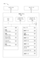
図2は、特定の実施形態に係る、可変屈折率プロファイルを有する回折光学素子の作製のためのフロー図200を示している。ブロック204において、図3の工程308に示される基板304のような基板が、例えば、図1の前処理システム104によって処理される。ブロック208において、インクジェット堆積システム108が、図3の工程312に示されるように、インクジェットノズル324を使用して、可変的なRI勾配を有する光学構造314を基板304上に堆積させる。可変的なRI勾配は、堆積させられる液滴の体積を変えることで実現することができ、その結果、図3に描かれたウェッジといった可変的な厚さプロファイルを有する構造が得られる。
Figure 2 illustrates a flow diagram 200 for fabricating a diffractive optical element with a variable refractive index profile, according to certain embodiments. In
ブロック212において、フォトレジストシステム112が、図3の工程316に示されるように、光学構造314上にフォトレジストマスク328を施す。特定の実施形態によれば、フォトレジストマスク328は、パターン332を含みうる。
In
ブロック216において、エッチングシステム116が、図3の工程320に示されるように、光学構造314及びフォトレジストマスク328をエッチングし、その結果、光学構造314が、所望の可変的なRIプロファイルを有するDOEとなる。この文脈では、エッチングシステム116は、イオンビームエッチングシステムを含みうるが、他の実施形態において、ドライエッチングシステムが利用される。ブロック220において、光学構造314及び基板304が洗浄され、幾つかの実施形態では、光学構造314に形成された隙間の緩和のために浸潤システム120に提供される。幾つかの実施形態において、洗浄プロセスがO2アッシング(灰化)プロセスを利用し、他の実施形態において、湿式洗浄プロセスが利用されうる。
In
代替的に、ブロック204において、図4の工程408に示される基板404のような基板が、例えば、図1の前処理システム104によって処理される。ブロック208において、インクジェット堆積システム108が、図4の工程412に示されるように、インクジェットノズル424A及び424Bを使用して、可変的なRI勾配を有する光学構造414を基板404上に堆積させる。
Alternatively, in
特定の実施形態によれば、インクジェットノズル424Aは、第1の溶液を堆積させる。第1の溶液は、ゾル-ゲル溶液又はナノ粒子溶液であってもよい。第1の溶液は、二酸化ケイ素(SiO2)、シリコンオキシカーバイド(SiOC)、二酸化ジルコニウム(ZrO2)、及び/又は二酸化チタン(TiO2)を含みうる。第1の溶液中のSiO2、SiOC、ZrO2、及び/又はTiO2の比率は、第1の屈折率をもたらすように制御される。例えば、第1の溶液は、SiO2、SiOC、及び/又はZrO2に対して第1の比率のTiO2を含みうる。一実施形態において、SiO2のゾル-ゲル前駆体は、オルトケイ酸テトラメチル(TMOS)、メチルトリメトキシシラン(MTMS)、及びオルトケイ酸テトラエチル(TEOS)を含みうる。
According to a particular embodiment, the
特定の実施形態によれば、インクジェットノズル424Bは、第2の溶液を堆積させる。第2の溶液は、ゾルーゲル溶液又はナノ粒子溶液でありうる。第2の溶液は、SiO2、SiOC、ZrO2、及び/又はTiO2を含むことができる。第2の溶液中のSiO2、SiOC、ZrO2、及び/又はTiO2の比率は、第2の屈折率をもたらすように制御される。第2の屈折率は、第1の屈折率とは異なっていてよい。例えば、第2の溶液は、第1の屈折率よりも高い屈折率となる第2の屈折率をもたらすように、SiO2、SiOC、及び/又はZrO2に対して、第1の比率よりも高い比率となる第2の比率のTiO2を含んでよく、或いは、第2の比率は、第1の屈折率よりも低い屈折率となる第2の屈折率をもたらすように、SiO2、SiOC、及び/又はZrO2に対して、第1の比率よりも低い比率のTiO2を有してもよい。
According to a particular embodiment, the
光学構造414の堆積中に、インクジェットノズル424A及びインクジェットノズル424Bから堆積させられる液滴の相対的体積を変えて、各ノズルにより堆積させられる体積を調整することで各ノズルによって提供される材料のそれぞれの相対濃度を変えることによって、可変RI勾配を実現することができ、結果的に、図4に示すような可変的なRI勾配プロファイルを有する構造が得られる。特定の実施形態によれば、可変的なRI勾配は、図3及び4に示された技術を組み合わせることによって実現されうる。
During deposition of the
代替的な例を続けると、ブロック212において、フォトレジストシステム112が、図4の工程416に示されるように、光学構造414上にフォトレジストマスク428を施す。特定の実施形態によれば、フォトレジストマスク428は、パターン432を含みうる。
Continuing with the alternative example, in
代替的な例を続けると、ブロック216において、エッチングシステム116が、図4の工程420に示されるように、光学構造414及びフォトレジストマスク428をエッチングし、その結果、光学構造414が、所望の可変的なRIプロファイルを有するDOEとなる。ブロック220において、光学構造414及び基板404が洗浄され、幾つかの実施形態において、光学構造414に形成された隙間の緩和のために浸潤システム120に提供される。
Continuing with the alternative example, in
図5は、特定の実施形態に係る、可変屈折率プロファイルを有する回折光学素子の作製のための方法500を示している。ブロック504において、インクジェット堆積システム108が、基板304を受け取る。
Figure 5 illustrates a
ブロック508において、インクジェット堆積システム108は、インクジェットプロセスを使用して、基板304の一部分又は基板404の上に、図3の光学構造314又は図4の光学構造414といった、厚さを有する光学構造を堆積させ、ここで、光学構造は、当該光学構造の屈折特性を変えるために体積的に変えられる。
In
図6は、特定の実施形態に係る、可変屈折率プロファイルを有する回折光学素子の作製のためのフロー図600を示している。ブロック604において、図7に示される基板704のような基板が、前処理システム104内で処理され、ブロック608において、図7の工程710で示されるように、前処理システム104によってDOE708が堆積されている。
Figure 6 illustrates a flow diagram 600 for fabricating a diffractive optical element with a variable refractive index profile, according to certain embodiments. In
ブロック612において、インクジェット堆積システム108は、図7の工程716に示されるように、インクジェットノズル714を用いてDOE708上に有機膜712を堆積させて、封入されたDOEを形成する。有機膜712は、ウェッジに似た不規則な形状(又は、基板704の上面又は下面に対して非平行な上面を有する他の形状)のプロファイルを有するが、可変的な厚さを有する任意の形状を、インクジェットノズル714によって堆積させることができる。例として、有機膜712は、三角形のプロファイル、又は4より多い辺を有する形状でありうる。特定の実施形態において、有機膜712は、矩形、又は方形などのプロファイルを有する。
In
ブロック616において、エッチングシステム116は、図7の工程718に示されるように、DOE708及び有機膜712をエッチングして、DOE708が、封入された輪郭を描く(profiled)DOEを形成する可変屈折率プロファイルを有するようにする。
In
ブロック620において、図7の工程720に示されるように、基板704及びDOE708が洗浄されて、有機膜712が除去される。特定の実施形態によれば、基板704及びDOE708は、浸潤システム120によってさらに処理されうる。
In
図8は、特定の実施形態に係る、可変屈折率プロファイルを有する回折光学素子の作製のための方法800を示している。
Figure 8 illustrates a
ブロック804において、インクジェット堆積システム108は、均一なDOEが設けられた基板を受け取る。
At
ブロック808において、インクジェット堆積システム108は、インクジェットプロセスを使用して、厚さを有する膜層であって、体積的に変えられた膜層をDOE上に堆積させて、封入された均一なDOEを形成する。
例示的な処理システム
In
Exemplary Processing System
図9は、図1~図8に関して記載したような、特定の実施形態に係る、システム、並びに、可変屈折率プロファイルを有する回折光学素子を製造するための方法及びシステムを操作するために使用されうる例示的な処理システムを示している。 Figure 9 illustrates an exemplary processing system that may be used to operate the system and methods and systems for manufacturing diffractive optical elements with variable refractive index profiles, according to certain embodiments, as described with respect to Figures 1-8.
処理システム900は、データバス916に接続された中央処理ユニット(CPU)902を含む。CPU902は、例えば、メモリ908又はストレージ910に格納されたコンピュータ実行可能な命令を処理して、処理システム900に、例えば、図2、図5、図6、及び図8に関して本明細書に記載された方法を実行させるよう構成されている。CPU902は、単一のCPU、複数のCPU、複数の処理コアを有する単一のCPU、及び、コンピュータ実行可能な命令を実行できる他の形態による処理アーキテクチャを代表するように、含まれている。
The
処理システム900は、入力/出力(I/O)デバイス912、及びインタフェース904をさらに含み、これにより、処理システム900は、例えばキーボード、ディスプレイ、マウスデバイス、ペン入力、及び処理システム900との相互作用を可能にする他のデバイスといった、入力/出力デバイス912と接続することが可能となる。処理システム900は、物理的接続及び無線接続を介して、外部のI/Oデバイス(例えば、外部ディスプレイデバイス)と接続できることに注意されたい。
The
処理システム900は、ネットワークインタフェース906をさらに含み、このネットワークインタフェース906は、処理システム900に、外部ネットワーク914へのアクセス、及びこれにより外部の計算装置へのアクセスを提供する。
The
処理システム900はメモリ908をさらに備え、メモリ908は、本例では、図2、図5、図6、及び図8に記載された動作を実行するための、受信コンポーネント918、堆積コンポーネント920、フォトレジストコンポーネント922、エッチングコンポーネント924、及び浸潤コンポーネント926を含む。
The
なお、図9では、簡略化のため単一のメモリ908として示されているが、メモリ908に格納される様々な態様は、処理システム900から離れたメモリを含む様々な物理メモリに格納することができ、CPU902はこれらすべてに、バス916といった内部データ接続を介してアクセスすることできる。
Note that while shown in FIG. 9 as a
ストレージ910は、図1~図8に関連して説明されるような、基板データ928、光学構造データ930、体積データ932、DOEデータ934、堆積データ936、フォトレジストデータ938、エッチングデータ940、及び浸潤データ942をさらに含む。
図9には示されていないが、他のデータがストレージ910に含まれうる。
Although not shown in FIG. 9, other data may be included in
メモリ908のように、図9では、簡略化のために単一のストレージ910が示されているが、ストレージ910に格納される様々な態様が、様々な物理的ストレージに格納することができ、
CPU902はこれらすべてに、バス916といった内部データ接続、又は、ネットワークインタフェース906といった外部接続を介してアクセスすることできる。当業者であれば、処理システム900の1つ以上の要素が遠隔に位置することができ、ネットワーク914を介してアクセスできることが分かるであろう。
Like
先の記載は、当業者であれば誰でも、本明細書に記載された様々な実施形態を実践できるように提供されている。本明細書で述べた例は、特許請求の範囲に記載される範囲、利用可能性、又は実施形態を限定するものではない。これらの実施形態に対する様々な変更が、当業者には容易に分かり、本明細書で規定される包括的な原則は、他の実施形態に適用することができる。例えば、本開示の範囲から逸脱することなく、上述の要素の機能及び配置に対して変更を加えることができる。様々な実施例では、様々な手順又は構成要素を適宜省略し置換し、追加することができる。例えば、記載された方法は、記載されたものとは異なる順序で実行されてよく、及び/又は、様々なステップが追加され、省略され、又は組み合わされてよい。加えて、幾つかの例に関して記載された特徴を、幾つかの他の例において組み合わせることができる。例えば、本明細書に記載された任意の数の態様を使用して、装置を実現し、又は方法を実施することができる。加えて、本開示の範囲は、本明細書に記載された本開示の様々な態様に加えて又は当該態様とは別の他の構造、機能性、又は構造及び機能性を使用して実施されるこのような装置又は方法をカバーすることが意図される。本明細書に開示された本開示の任意の態様が、請求項の1つ以上の要素によって具現化されうると理解されたい。 The preceding description is provided to enable any person skilled in the art to practice the various embodiments described herein. The examples described herein are not intended to limit the scope, applicability, or embodiments described in the claims. Various modifications to these embodiments will be readily apparent to those skilled in the art, and the generic principles defined herein may be applied to other embodiments. For example, changes may be made to the function and arrangement of the elements described above without departing from the scope of the disclosure. In various examples, various procedures or components may be omitted, substituted, or added as appropriate. For example, the methods described may be performed in an order different from that described, and/or various steps may be added, omitted, or combined. In addition, features described with respect to some examples may be combined in some other examples. For example, an apparatus may be realized or a method may be practiced using any number of the aspects described herein. In addition, the scope of the disclosure is intended to cover such apparatus or methods implemented using other structure, functionality, or structure and functionality in addition to or apart from the various aspects of the disclosure described herein. It should be understood that any aspect of the disclosure disclosed herein may be embodied by one or more elements of a claim.
本明細書では、「例示的な(exemplary)」という用語は、「例、事例、又は実例として機能する」という意味している。本明細書において「例示的」と記載された任意の態様は、必ずしも他の態様よりも好ましい又は有利であると解釈するべきではない。 As used herein, the word "exemplary" means "serving as an example, instance, or illustration." Any aspect described herein as "exemplary" is not necessarily to be construed as preferred or advantageous over other aspects.
本明細書では、項目のリストの「少なくとも1つ(at least one of)」に言及する表現は、単一のメンバを含むこれらの項目の任意の組み合わせを指している。一例として、「a、b、cのうち少なくとも1つ」は、a、b、c、a-b、a-c、b-c、a-b-cのほか、同じ要素の倍数との組み合わせ(例えば、a-a、a-a、a-a-b、a-a-c、a-b-b、a-c-c、b-b、b-b-b、b-b-c、c-c、及びc-c-c、又はa、b及びcの任意の他の順序)が意図されている。 As used herein, references to "at least one of" a list of items refer to any combination of those items, including single members. As an example, "at least one of a, b, c" contemplates a, b, c, a-b, a-c, bc, a-bc, as well as combinations with multiples of the same element (e.g., a-a, a-a, a-a-b, a-a-c, a-bb-b, a-c-c, bb, b-bb-b, b-bb-c, c-c, and c-c-c, or any other permutation of a, b, and c).
本明細書では、「決定する(determining)」という用語は、多種多様な動作を包含する。例えば、「決定する」は、計算、演算、処理、導出、調査、ルックアップ(例えば、テーブル、データベース又は別のデータ構造でルックアップ)、確認等を含みうる。また、「決定する」には、受信(例えば、情報の受信)、アクセス(例えば、メモリ内のデータへのアクセス)等が含まれうる。また、「決定する」には、解決する、選択する、選ぶ、確立するなどが含まれうる。 As used herein, the term "determining" encompasses a wide variety of actions. For example, "determining" can include calculating, computing, processing, deriving, investigating, looking up (e.g., looking up in a table, database, or another data structure), checking, and the like. Also, "determining" can include receiving (e.g., receiving information), accessing (e.g., accessing data in a memory), and the like. Also, "determining" can include resolving, selecting, choosing, establishing, and the like.
本明細書に開示される方法は、方法を達成するための1つ以上のステップ又はアクションを含んでいる。方法のステップ及び/又はアクションは、特許請求の範囲から逸脱することなく、互いに交換されうる。言い換えれば、特定の順序のステップ又はアクションが指定されていない限り、特定のステップ及び/又はアクションの順序及び/又は使用は、請求項の範囲から逸脱することなく変更することができる。さらに、上述した方法の様々な動作が、対応する機能を実行することができる任意の適切な手段によって実施されうる。上記手段は、回路、特定用途向け集積回路(ASIC:application specific integrated circuit)、又はプロセッサを含むがこれらに限定されない、様々なハードウェア及び/又はソフトウェアコンポーネント及び/又はモジュールを含みうる。概して、図に示された動作がある場合に、これらの動作は、同様に付番された、対応するミーンズプラスファンクション(means-plus-function)構成要素を有しうる。 The methods disclosed herein include one or more steps or actions for achieving the method. The steps and/or actions of the method may be interchanged with one another without departing from the scope of the claims. In other words, unless a specific order of steps or actions is specified, the order and/or use of specific steps and/or actions may be modified without departing from the scope of the claims. Furthermore, various operations of the methods described above may be implemented by any suitable means capable of performing the corresponding functions. Such means may include various hardware and/or software components and/or modules, including, but not limited to, circuits, application specific integrated circuits (ASICs), or processors. Generally, where there are operations illustrated in the figures, these operations may have corresponding means-plus-function components similarly numbered.
以下の特許請求の範囲は、本明細書で示された実施形態に限定することを意図したものではなく、特許請求の範囲の文言と一致する全範囲を与えるものである。クレームでは、単数形の要素への言及は、特に明記されていない限り、「1つだけ(one and only one)」という意味ではなく、「1つ以上(one or more)」という意味を意図している。特に断りのない限り、「幾つか(some)」という用語は、1つ以上のものを指している。クレーム要素は、その要素が「~のための手段(means for)」という表現で明示的に記載されているか、又は方法クレームの場合は「~のためのステップ(step for)」という表現を使用して記載されていなければ、米国特許法112条(f)の規定に基づいて解釈されることはないものとする。当業者にとって既知であるか又は後に既知となる、本開示を通じて記載される様々な態様の要素に対する構造的及び機能的同均等物は、参照により本明細書に明示的に組み込まれ、請求項に包含されることが意図されている。さらに、本明細書に開示されたものは、そのような開示が特許請求の範囲に明示的に記載されているどうかにかかわらず、公衆に捧げられることが意図されていない。 The following claims are not intended to be limited to the embodiments set forth herein, but are to be given the full scope consistent with the language of the claims. In the claims, references to elements in the singular are intended to mean "one or more" and not "one and only one" unless otherwise specified. The term "some" refers to one or more, unless otherwise specified. No claim element shall be construed under the provisions of 35 U.S.C. 112(f) unless the element is expressly recited using the phrase "means for" or, in the case of a method claim, using the phrase "step for". Structural and functional equivalents to the elements of the various aspects described throughout this disclosure that are known or later become known to those of ordinary skill in the art are expressly incorporated herein by reference and are intended to be encompassed by the claims. Moreover, nothing disclosed in this specification is intended to be dedicated to the public, regardless of whether such disclosure is expressly set forth in the claims.
以上の記述は本開示の実施形態を対象としているが、本開示の基本的な範囲から逸脱することなく本開示の他の実施形態及びさらなる実施形態が考案されてよく、本開示の範囲は、下記の特許請求の範囲によって規定される。 While the foregoing is directed to embodiments of the present disclosure, other and further embodiments of the present disclosure may be devised without departing from the basic scope thereof, the scope of which is defined by the claims that follow.
Claims (16)
1つ以上のプロセッサであって、前記システムに、
基板を受け取ることと、
インクジェットプロセスを使用して、前記基板の一部分に、厚さを有する光学構造を堆積させることであって、前記光学構造が当該光学構造の屈折特性を変えるために体積を変更可能である、インクジェットプロセスを使用して、前記基板の一部分に、厚さを有する光学構造を堆積させることと、
パターニングされたフォトレジスト層を前記光学構造の上に堆積させることと、
を行わせるよう構成された1つ以上のプロセッサ
を備える、システム。 1. A system for fabricating a diffractive optics element (DOE), comprising:
One or more processors, the system comprising:
Receiving a substrate;
depositing an optical structure having a thickness on a portion of the substrate using an inkjet process, the optical structure being volumetrically alterable to change refractive properties of the optical structure;
depositing a patterned photoresist layer over the optical structure;
A system comprising one or more processors configured to:
前記命令が、処理システムのプロセッサによって実行されると、前記処理システムに、
基板を受け取ることと、
インクジェットプロセスを使用して、前記基板の一部分に、厚さを有する光学構造を堆積させることであって、前記光学構造が当該光学構造の屈折特性を変えるために体積を変更可能である、インクジェットプロセスを使用して、前記基板の一部分に、厚さを有する光学構造を堆積させることと、
パターニングされたフォトレジスト層を前記光学構造の上に堆積させることと、
を行わせる、非一過性コンピュータ可読記憶媒体。 A non-transitory computer readable storage medium storing instructions, comprising:
The instructions, when executed by a processor of a processing system, cause the processing system to:
Receiving a substrate;
depositing an optical structure having a thickness on a portion of the substrate using an inkjet process, the optical structure being volumetrically alterable to change refractive properties of the optical structure;
depositing a patterned photoresist layer over the optical structure;
A non-transitory computer-readable storage medium for causing
1つ以上のプロセッサであって、前記システムに、
DOEが設けられた基板を受け取ることと、
インクジェットプロセスを使用して、厚さを有しかつ体積を変更可能である有機膜層を前記DOE上に堆積させて、封入されたDOEを形成することと、
前記有機膜層と前記DOEの少なくとも一部をエッチングして、前記DOEを封止しかつ所定のプロファイルを有するエッチングされた有機膜層を形成することと、
を行わせる1つ以上のプロセッサ
を備える、システム。 1. A system for fabricating a diffractive optics element (DOE), comprising:
One or more processors, the system comprising:
receiving a substrate having a D OE disposed thereon;
depositing an organic film layer having a thickness and a variable volume on the DOE using an inkjet process to form an encapsulated DOE ;
Etching the organic film layer and at least a portion of the DOE to form an etched organic film layer that encapsulates the DOE and has a predetermined profile;
A system comprising one or more processors configured to:
Applications Claiming Priority (3)
| Application Number | Priority Date | Filing Date | Title |
|---|---|---|---|
| US202063082314P | 2020-09-23 | 2020-09-23 | |
| US63/082,314 | 2020-09-23 | ||
| PCT/US2021/051798 WO2022066941A1 (en) | 2020-09-23 | 2021-09-23 | Fabrication of diffractive optic element having a variable refractive index profile by inkjet printing deposition |
Publications (2)
| Publication Number | Publication Date |
|---|---|
| JP2023542929A JP2023542929A (en) | 2023-10-12 |
| JP7584635B2 true JP7584635B2 (en) | 2024-11-15 |
Family
ID=80740295
Family Applications (1)
| Application Number | Title | Priority Date | Filing Date |
|---|---|---|---|
| JP2023518166A Active JP7584635B2 (en) | 2020-09-23 | 2021-09-23 | Fabrication of diffractive optical elements with variable refractive index profiles by inkjet printing deposition |
Country Status (7)
| Country | Link |
|---|---|
| US (1) | US11867931B2 (en) |
| EP (1) | EP4217772A4 (en) |
| JP (1) | JP7584635B2 (en) |
| KR (1) | KR102915902B1 (en) |
| CN (1) | CN116529642A (en) |
| TW (1) | TWI886340B (en) |
| WO (1) | WO2022066941A1 (en) |
Families Citing this family (3)
| Publication number | Priority date | Publication date | Assignee | Title |
|---|---|---|---|---|
| US12384185B2 (en) | 2022-05-06 | 2025-08-12 | Applied Materials, Inc. | Methods, systems, and apparatus for inkjet printing self-assembled monoloayer (SAM) structures on substrates |
| CN120112820A (en) * | 2022-10-27 | 2025-06-06 | 应用材料公司 | Inkjet gradient refractive index material for modulating grating diffraction efficiency |
| WO2025240108A1 (en) * | 2024-05-14 | 2025-11-20 | Applied Materials, Inc. | Methods to create asymmetric structures with varying height |
Citations (8)
| Publication number | Priority date | Publication date | Assignee | Title |
|---|---|---|---|---|
| JP2017507768A (en) | 2013-12-12 | 2017-03-23 | カティーバ, インコーポレイテッド | Ink base layer processing that controls thickness using halftoning |
| WO2018220272A1 (en) | 2017-06-02 | 2018-12-06 | Dispelix Oy | Method of manufacturing a master plate and a master plate |
| WO2019135837A1 (en) | 2018-01-08 | 2019-07-11 | Digilens, Inc. | Systems and methods for manufacturing waveguide cells |
| WO2019147315A1 (en) | 2018-01-26 | 2019-08-01 | Applied Materials, Inc. | Controlling grating outcoupling strength for ar waveguide combiners |
| US20190258008A1 (en) | 2018-02-21 | 2019-08-22 | Varian Semiconductor Equipment Associates, Inc. | Optical component having variable depth gratings and method of formation |
| US20190324202A1 (en) | 2018-04-23 | 2019-10-24 | Facebook Technologies, Llc | Gratings with variable depths formed using planarization for waveguide displays |
| WO2020131852A1 (en) | 2018-12-17 | 2020-06-25 | Applied Materials, Inc. | Method of forming a plurality of gratings |
| CN111367004A (en) | 2020-04-29 | 2020-07-03 | 刘奡 | Ink-jet printing preparation method of polarizer holographic grating |
Family Cites Families (21)
| Publication number | Priority date | Publication date | Assignee | Title |
|---|---|---|---|---|
| JPH1131863A (en) * | 1997-07-11 | 1999-02-02 | Hitachi Ltd | Method for manufacturing diffraction grating, semiconductor laser manufactured using the same, and optical application system using the same |
| FI114945B (en) * | 2002-09-19 | 2005-01-31 | Nokia Corp | Electrically adjustable diffractive gate element |
| JP2008164680A (en) * | 2006-12-27 | 2008-07-17 | Canon Inc | Optical wave plate and method for producing the wave plate |
| US9333717B2 (en) * | 2008-02-13 | 2016-05-10 | Xyratex Technology Limited | Method of making a waveguide and a waveguide made thereby |
| GB0902398D0 (en) * | 2009-02-13 | 2009-04-01 | Conductive Inkjet Tech Ltd | Diffractive optical elements |
| JP2011191632A (en) * | 2010-03-16 | 2011-09-29 | Canon Inc | Optical element and optical scanner using the same |
| WO2014011328A1 (en) * | 2012-07-09 | 2014-01-16 | Corning Incorporated | Anti-glare and anti-sparkle transparent structures |
| US10677969B2 (en) * | 2013-11-27 | 2020-06-09 | Magic Leap, Inc. | Manufacturing for virtual and augmented reality systems and components |
| CN112558307B (en) * | 2015-03-05 | 2022-08-02 | 奇跃公司 | Improved manufacturing of virtual and augmented reality systems and components |
| EP3078994B1 (en) * | 2015-04-07 | 2020-07-29 | Magic Leap, Inc. | Method of manufacture of a diffraction grating |
| CA3001848C (en) * | 2015-10-15 | 2023-09-19 | Board Of Regents, The University Of Texas System | Versatile process for precision nanoscale manufacturing |
| US10436958B2 (en) | 2016-10-05 | 2019-10-08 | Magic Leap, Inc. | Fabricating non-uniform diffraction gratings |
| US20190326454A1 (en) * | 2017-01-06 | 2019-10-24 | Nanoclear Technologies, Inc. | Methods and systems to boost efficiency of solar cells |
| FI127799B (en) | 2017-06-02 | 2019-02-28 | Dispelix Oy | Method of manufacturing a diffractive grating |
| US10983227B2 (en) * | 2017-08-14 | 2021-04-20 | Kla-Tencor Corporation | On-device metrology using target decomposition |
| EP4286900A3 (en) * | 2017-11-06 | 2024-06-12 | Magic Leap, Inc. | Method and system for tunable gradient patterning using a shadow mask |
| US10983257B1 (en) * | 2017-11-21 | 2021-04-20 | Facebook Technologies, Llc | Fabrication of self-aligned grating elements with high refractive index for waveguide displays |
| US11067726B2 (en) * | 2018-04-23 | 2021-07-20 | Facebook Technologies, Llc | Gratings with variable depths for waveguide displays |
| CN112513688B (en) | 2018-07-19 | 2023-05-26 | 应用材料公司 | Height-variable oblique grating method |
| CN113811803A (en) * | 2019-03-12 | 2021-12-17 | 奇跃公司 | Waveguide with high refractive index material and method of making the same |
| EP4162303A4 (en) * | 2020-06-08 | 2024-10-09 | Board of Regents, The University of Texas System | MANUFACTURING OPTICAL ELEMENTS |
-
2021
- 2021-09-23 WO PCT/US2021/051798 patent/WO2022066941A1/en not_active Ceased
- 2021-09-23 JP JP2023518166A patent/JP7584635B2/en active Active
- 2021-09-23 TW TW110135323A patent/TWI886340B/en active
- 2021-09-23 CN CN202180065290.6A patent/CN116529642A/en active Pending
- 2021-09-23 EP EP21873451.5A patent/EP4217772A4/en active Pending
- 2021-09-23 KR KR1020237013362A patent/KR102915902B1/en active Active
- 2021-09-23 US US17/448,619 patent/US11867931B2/en active Active
Patent Citations (8)
| Publication number | Priority date | Publication date | Assignee | Title |
|---|---|---|---|---|
| JP2017507768A (en) | 2013-12-12 | 2017-03-23 | カティーバ, インコーポレイテッド | Ink base layer processing that controls thickness using halftoning |
| WO2018220272A1 (en) | 2017-06-02 | 2018-12-06 | Dispelix Oy | Method of manufacturing a master plate and a master plate |
| WO2019135837A1 (en) | 2018-01-08 | 2019-07-11 | Digilens, Inc. | Systems and methods for manufacturing waveguide cells |
| WO2019147315A1 (en) | 2018-01-26 | 2019-08-01 | Applied Materials, Inc. | Controlling grating outcoupling strength for ar waveguide combiners |
| US20190258008A1 (en) | 2018-02-21 | 2019-08-22 | Varian Semiconductor Equipment Associates, Inc. | Optical component having variable depth gratings and method of formation |
| US20190324202A1 (en) | 2018-04-23 | 2019-10-24 | Facebook Technologies, Llc | Gratings with variable depths formed using planarization for waveguide displays |
| WO2020131852A1 (en) | 2018-12-17 | 2020-06-25 | Applied Materials, Inc. | Method of forming a plurality of gratings |
| CN111367004A (en) | 2020-04-29 | 2020-07-03 | 刘奡 | Ink-jet printing preparation method of polarizer holographic grating |
Also Published As
| Publication number | Publication date |
|---|---|
| WO2022066941A1 (en) | 2022-03-31 |
| CN116529642A (en) | 2023-08-01 |
| US11867931B2 (en) | 2024-01-09 |
| JP2023542929A (en) | 2023-10-12 |
| US20220091314A1 (en) | 2022-03-24 |
| TWI886340B (en) | 2025-06-11 |
| KR102915902B1 (en) | 2026-01-20 |
| KR20230067688A (en) | 2023-05-16 |
| EP4217772A1 (en) | 2023-08-02 |
| TW202220043A (en) | 2022-05-16 |
| EP4217772A4 (en) | 2025-02-19 |
Similar Documents
| Publication | Publication Date | Title |
|---|---|---|
| JP7584635B2 (en) | Fabrication of diffractive optical elements with variable refractive index profiles by inkjet printing deposition | |
| JP7510877B2 (en) | Controlling the grating outcoupling strength of an AR waveguide coupler | |
| JP7769752B2 (en) | Metasurfaces for redirecting light and methods of fabrication | |
| KR102823974B1 (en) | Microlithographic fabrication of structures | |
| JP7009681B2 (en) | A method of patterning a substrate using layers with multiple materials | |
| JP2026004346A (en) | Gradient encapsulation of waveguide gratings | |
| US11396473B2 (en) | Patterning of high refractive index glasses by plasma etching | |
| US20210191025A1 (en) | Superimposed diffraction gratings for eyepieces | |
| CN113544567A (en) | Overlying sloped surface relief structures using atomic layer deposition | |
| JP6544943B2 (en) | Mask blank, method of manufacturing phase shift mask, phase shift mask, and method of manufacturing semiconductor device | |
| TWI866941B (en) | A method of forming gratings | |
| JP2021530730A (en) | Use of fluidity CVD to fill gaps in micro / nanostructures of optics | |
| JP2023516594A (en) | Method of fabricating a mold for forming an eyepiece with an integrated spacer | |
| US12153344B2 (en) | Lithography method to form structures with slanted angle | |
| WO2024233855A1 (en) | Maskless coating as a patterning mask for external stimuli in depositions | |
| CN115480329B (en) | Multi-order two-dimensional grating structure, manufacturing method thereof, optical waveguide device and AR equipment | |
| CN110121672B (en) | Generate virtual content display | |
| US12493138B2 (en) | Airgap structures for improved eyepiece efficiency | |
| Janssen et al. | Collapse transition of randomly branched polymers: Renormalized field theory | |
| CN109817572A (en) | A kind of production method of lithographic method and damascene structure | |
| Iwamatsu | Cell dynamics approach to the formation of metastable phases during phase transformation | |
| JP2025517460A (en) | Method for improving display efficiency and uniformity of AR waveguides - Patents.com | |
| CN116106994A (en) | Optical films, substrate glass, and pseudo-holographic projection systems | |
| CN116299809A (en) | Preparation method and structure of a heterogeneous helical grating |
Legal Events
| Date | Code | Title | Description |
|---|---|---|---|
| A621 | Written request for application examination |
Free format text: JAPANESE INTERMEDIATE CODE: A621 Effective date: 20230517 |
|
| A977 | Report on retrieval |
Free format text: JAPANESE INTERMEDIATE CODE: A971007 Effective date: 20240326 |
|
| A131 | Notification of reasons for refusal |
Free format text: JAPANESE INTERMEDIATE CODE: A131 Effective date: 20240423 |
|
| A521 | Request for written amendment filed |
Free format text: JAPANESE INTERMEDIATE CODE: A523 Effective date: 20240723 |
|
| TRDD | Decision of grant or rejection written | ||
| A01 | Written decision to grant a patent or to grant a registration (utility model) |
Free format text: JAPANESE INTERMEDIATE CODE: A01 Effective date: 20241015 |
|
| A61 | First payment of annual fees (during grant procedure) |
Free format text: JAPANESE INTERMEDIATE CODE: A61 Effective date: 20241105 |
|
| R150 | Certificate of patent or registration of utility model |
Ref document number: 7584635 Country of ref document: JP Free format text: JAPANESE INTERMEDIATE CODE: R150 |