JP7581361B2 - Power component including a main component and a sensor and emitter unit, and system having the power component - Patents.com - Google Patents
Power component including a main component and a sensor and emitter unit, and system having the power component - Patents.com Download PDFInfo
- Publication number
- JP7581361B2 JP7581361B2 JP2022554547A JP2022554547A JP7581361B2 JP 7581361 B2 JP7581361 B2 JP 7581361B2 JP 2022554547 A JP2022554547 A JP 2022554547A JP 2022554547 A JP2022554547 A JP 2022554547A JP 7581361 B2 JP7581361 B2 JP 7581361B2
- Authority
- JP
- Japan
- Prior art keywords
- power
- sensor
- component
- main component
- emitter unit
- Prior art date
- Legal status (The legal status is an assumption and is not a legal conclusion. Google has not performed a legal analysis and makes no representation as to the accuracy of the status listed.)
- Active
Links
Images


Classifications
-
- G—PHYSICS
- G01—MEASURING; TESTING
- G01R—MEASURING ELECTRIC VARIABLES; MEASURING MAGNETIC VARIABLES
- G01R31/00—Arrangements for testing electric properties; Arrangements for locating electric faults; Arrangements for electrical testing characterised by what is being tested not provided for elsewhere
- G01R31/50—Testing of electric apparatus, lines, cables or components for short-circuits, continuity, leakage current or incorrect line connections
- G01R31/74—Testing of fuses
-
- H—ELECTRICITY
- H01—ELECTRIC ELEMENTS
- H01H—ELECTRIC SWITCHES; RELAYS; SELECTORS; EMERGENCY PROTECTIVE DEVICES
- H01H85/00—Protective devices in which the current flows through a part of fusible material and this current is interrupted by displacement of the fusible material when this current becomes excessive
- H01H85/02—Details
- H01H85/0241—Structural association of a fuse and another component or apparatus
-
- H—ELECTRICITY
- H01—ELECTRIC ELEMENTS
- H01Q—ANTENNAS, i.e. RADIO AERIALS
- H01Q1/00—Details of, or arrangements associated with, antennas
- H01Q1/36—Structural form of radiating elements, e.g. cone, spiral, umbrella; Particular materials used therewith
- H01Q1/38—Structural form of radiating elements, e.g. cone, spiral, umbrella; Particular materials used therewith formed by a conductive layer on an insulating support
-
- H—ELECTRICITY
- H02—GENERATION; CONVERSION OR DISTRIBUTION OF ELECTRIC POWER
- H02H—EMERGENCY PROTECTIVE CIRCUIT ARRANGEMENTS
- H02H3/00—Emergency protective circuit arrangements for automatic disconnection directly responsive to an undesired change from normal electric working condition with or without subsequent reconnection ; integrated protection
- H02H3/02—Details
- H02H3/04—Details with warning or supervision in addition to disconnection, e.g. for indicating that protective apparatus has functioned
- H02H3/044—Checking correct functioning of protective arrangements, e.g. by simulating a fault
-
- H—ELECTRICITY
- H02—GENERATION; CONVERSION OR DISTRIBUTION OF ELECTRIC POWER
- H02J—ELECTRIC POWER NETWORKS; CIRCUIT ARRANGEMENTS OR SYSTEMS FOR SUPPLYING OR DISTRIBUTING ELECTRIC POWER; SYSTEMS FOR STORING ELECTRIC ENERGY
- H02J13/00—Circuit arrangements for providing remote monitoring or remote control of equipment in a power distribution network
- H02J13/12—Monitoring network conditions, e.g. electrical magnitudes or operational status
-
- H—ELECTRICITY
- H02—GENERATION; CONVERSION OR DISTRIBUTION OF ELECTRIC POWER
- H02M—APPARATUS FOR CONVERSION BETWEEN AC AND AC, BETWEEN AC AND DC, OR BETWEEN DC AND DC, AND FOR USE WITH MAINS OR SIMILAR POWER SUPPLY SYSTEMS; CONVERSION OF DC OR AC INPUT POWER INTO SURGE OUTPUT POWER; CONTROL OR REGULATION THEREOF
- H02M1/00—Details of apparatus for conversion
- H02M1/32—Means for protecting converters other than automatic disconnection
-
- H—ELECTRICITY
- H02—GENERATION; CONVERSION OR DISTRIBUTION OF ELECTRIC POWER
- H02M—APPARATUS FOR CONVERSION BETWEEN AC AND AC, BETWEEN AC AND DC, OR BETWEEN DC AND DC, AND FOR USE WITH MAINS OR SIMILAR POWER SUPPLY SYSTEMS; CONVERSION OF DC OR AC INPUT POWER INTO SURGE OUTPUT POWER; CONTROL OR REGULATION THEREOF
- H02M1/00—Details of apparatus for conversion
- H02M1/32—Means for protecting converters other than automatic disconnection
- H02M1/327—Means for protecting converters other than automatic disconnection against abnormal temperatures
-
- H—ELECTRICITY
- H02—GENERATION; CONVERSION OR DISTRIBUTION OF ELECTRIC POWER
- H02M—APPARATUS FOR CONVERSION BETWEEN AC AND AC, BETWEEN AC AND DC, OR BETWEEN DC AND DC, AND FOR USE WITH MAINS OR SIMILAR POWER SUPPLY SYSTEMS; CONVERSION OF DC OR AC INPUT POWER INTO SURGE OUTPUT POWER; CONTROL OR REGULATION THEREOF
- H02M7/00—Conversion of AC power input into DC power output; Conversion of DC power input into AC power output
- H02M7/003—Constructional details, e.g. physical layout, assembly, wiring or busbar connections
-
- H—ELECTRICITY
- H10—SEMICONDUCTOR DEVICES; ELECTRIC SOLID-STATE DEVICES NOT OTHERWISE PROVIDED FOR
- H10D—INORGANIC ELECTRIC SEMICONDUCTOR DEVICES
- H10D8/00—Diodes
- H10D8/80—PNPN diodes, e.g. Shockley diodes or break-over diodes
-
- H—ELECTRICITY
- H10—SEMICONDUCTOR DEVICES; ELECTRIC SOLID-STATE DEVICES NOT OTHERWISE PROVIDED FOR
- H10W—GENERIC PACKAGES, INTERCONNECTIONS, CONNECTORS OR OTHER CONSTRUCTIONAL DETAILS OF DEVICES COVERED BY CLASS H10
- H10W20/00—Interconnections in chips, wafers or substrates
- H10W20/40—Interconnections external to wafers or substrates, e.g. back-end-of-line [BEOL] metallisations or vias connecting to gate electrodes
- H10W20/49—Adaptable interconnections, e.g. fuses or antifuses
- H10W20/493—Fuses, i.e. interconnections changeable from conductive to non-conductive
-
- H—ELECTRICITY
- H10—SEMICONDUCTOR DEVICES; ELECTRIC SOLID-STATE DEVICES NOT OTHERWISE PROVIDED FOR
- H10W—GENERIC PACKAGES, INTERCONNECTIONS, CONNECTORS OR OTHER CONSTRUCTIONAL DETAILS OF DEVICES COVERED BY CLASS H10
- H10W40/00—Arrangements for thermal protection or thermal control
-
- H—ELECTRICITY
- H10—SEMICONDUCTOR DEVICES; ELECTRIC SOLID-STATE DEVICES NOT OTHERWISE PROVIDED FOR
- H10W—GENERIC PACKAGES, INTERCONNECTIONS, CONNECTORS OR OTHER CONSTRUCTIONAL DETAILS OF DEVICES COVERED BY CLASS H10
- H10W42/00—Arrangements for protection of devices
- H10W42/80—Arrangements for protection of devices protecting against overcurrent or overload, e.g. fuses or shunts
-
- H—ELECTRICITY
- H10—SEMICONDUCTOR DEVICES; ELECTRIC SOLID-STATE DEVICES NOT OTHERWISE PROVIDED FOR
- H10W—GENERIC PACKAGES, INTERCONNECTIONS, CONNECTORS OR OTHER CONSTRUCTIONAL DETAILS OF DEVICES COVERED BY CLASS H10
- H10W90/00—Package configurations
-
- H—ELECTRICITY
- H01—ELECTRIC ELEMENTS
- H01H—ELECTRIC SWITCHES; RELAYS; SELECTORS; EMERGENCY PROTECTIVE DEVICES
- H01H85/00—Protective devices in which the current flows through a part of fusible material and this current is interrupted by displacement of the fusible material when this current becomes excessive
- H01H85/02—Details
- H01H85/0241—Structural association of a fuse and another component or apparatus
- H01H2085/0266—Structural association with a measurement device, e.g. a shunt
-
- H—ELECTRICITY
- H01—ELECTRIC ELEMENTS
- H01H—ELECTRIC SWITCHES; RELAYS; SELECTORS; EMERGENCY PROTECTIVE DEVICES
- H01H85/00—Protective devices in which the current flows through a part of fusible material and this current is interrupted by displacement of the fusible material when this current becomes excessive
- H01H85/02—Details
- H01H85/0241—Structural association of a fuse and another component or apparatus
- H01H2085/0283—Structural association with a semiconductor device
-
- H—ELECTRICITY
- H10—SEMICONDUCTOR DEVICES; ELECTRIC SOLID-STATE DEVICES NOT OTHERWISE PROVIDED FOR
- H10W—GENERIC PACKAGES, INTERCONNECTIONS, CONNECTORS OR OTHER CONSTRUCTIONAL DETAILS OF DEVICES COVERED BY CLASS H10
- H10W76/00—Containers; Fillings or auxiliary members therefor; Seals
- H10W76/10—Containers or parts thereof
- H10W76/12—Containers or parts thereof characterised by their shape
- H10W76/13—Containers comprising a conductive base serving as an interconnection
- H10W76/138—Containers comprising a conductive base serving as an interconnection having another interconnection being formed by a cover plate parallel to the conductive base, e.g. sandwich type
-
- H—ELECTRICITY
- H10—SEMICONDUCTOR DEVICES; ELECTRIC SOLID-STATE DEVICES NOT OTHERWISE PROVIDED FOR
- H10W—GENERIC PACKAGES, INTERCONNECTIONS, CONNECTORS OR OTHER CONSTRUCTIONAL DETAILS OF DEVICES COVERED BY CLASS H10
- H10W76/00—Containers; Fillings or auxiliary members therefor; Seals
- H10W76/10—Containers or parts thereof
- H10W76/12—Containers or parts thereof characterised by their shape
- H10W76/15—Containers comprising an insulating or insulated base
-
- Y—GENERAL TAGGING OF NEW TECHNOLOGICAL DEVELOPMENTS; GENERAL TAGGING OF CROSS-SECTIONAL TECHNOLOGIES SPANNING OVER SEVERAL SECTIONS OF THE IPC; TECHNICAL SUBJECTS COVERED BY FORMER USPC CROSS-REFERENCE ART COLLECTIONS [XRACs] AND DIGESTS
- Y02—TECHNOLOGIES OR APPLICATIONS FOR MITIGATION OR ADAPTATION AGAINST CLIMATE CHANGE
- Y02E—REDUCTION OF GREENHOUSE GAS [GHG] EMISSIONS, RELATED TO ENERGY GENERATION, TRANSMISSION OR DISTRIBUTION
- Y02E60/00—Enabling technologies; Technologies with a potential or indirect contribution to GHG emissions mitigation
-
- Y—GENERAL TAGGING OF NEW TECHNOLOGICAL DEVELOPMENTS; GENERAL TAGGING OF CROSS-SECTIONAL TECHNOLOGIES SPANNING OVER SEVERAL SECTIONS OF THE IPC; TECHNICAL SUBJECTS COVERED BY FORMER USPC CROSS-REFERENCE ART COLLECTIONS [XRACs] AND DIGESTS
- Y04—INFORMATION OR COMMUNICATION TECHNOLOGIES HAVING AN IMPACT ON OTHER TECHNOLOGY AREAS
- Y04S—SYSTEMS INTEGRATING TECHNOLOGIES RELATED TO POWER NETWORK OPERATION, COMMUNICATION OR INFORMATION TECHNOLOGIES FOR IMPROVING THE ELECTRICAL POWER GENERATION, TRANSMISSION, DISTRIBUTION, MANAGEMENT OR USAGE, i.e. SMART GRIDS
- Y04S10/00—Systems supporting electrical power generation, transmission or distribution
- Y04S10/30—State monitoring, e.g. fault, temperature monitoring, insulator monitoring, corona discharge
Landscapes
- Engineering & Computer Science (AREA)
- Power Engineering (AREA)
- Physics & Mathematics (AREA)
- General Physics & Mathematics (AREA)
- Protection Of Static Devices (AREA)
- Arrangements For Transmission Of Measured Signals (AREA)
- Rectifiers (AREA)
Description
本発明の実施形態は、電力コンポーネント、特に電力ヒューズ及びパワー半導体デバイス、電力コンポーネントを有するモジュール及びシステム、並びに関連する方法に関する。 Embodiments of the present invention relate to power components, particularly power fuses and power semiconductor devices, modules and systems having power components, and related methods.
パワーエレクトロニクスでは、大電流のスイッチング及び/又はより高い電圧での動作が可能なパワー半導体、並びに対応する半導体ヒューズが、様々な目的のために、例えば増幅器、整流器、及び変換器において広く使用されている。使用されるパワー半導体ダイオード及びパワー半導体スイッチは、多くの場合、数百Vを超える電圧差で動作し、及び/又は同じ半導体片若しくは半導体本体内で大電流、例えば少なくとも数アンペアの電流を処理することが可能である。電流処理能力を更に増加させるために、いくつかのパワー半導体が並列に結合され得る。安全上の理由から、パワー半導体(複数可)は、半導体ヒューズ(複数可)によって保護され得る。 In power electronics, power semiconductors capable of switching large currents and/or operating at higher voltages, as well as corresponding semiconductor fuses, are widely used for various purposes, for example in amplifiers, rectifiers and converters. The power semiconductor diodes and power semiconductor switches used often operate with voltage differences of more than several hundred volts and/or are capable of handling large currents, for example currents of at least several amperes, in the same semiconductor piece or body. To further increase the current handling capacity, several power semiconductors can be coupled in parallel. For safety reasons, the power semiconductor(s) can be protected by a semiconductor fuse(s).
負荷に応じて、パワー半導体(半導体本体)及び/又はヒューズ本体の温度は、動作中に変化し得る。それ故に、電流-電圧特性、ダイオードの順方向電圧降下、及び半導体スイッチのスイッチング特質のようなデバイスの電子的特質は、動作中に変化し得る。これは、並列に結合されたパワー半導体間の電流不均衡につながりさえし得る。同様に、温度は、所与の電流における抵抗及び電圧降下などのヒューズの動作パラメータ、このことからその遮断容量を変化させ得る。 Depending on the load, the temperature of the power semiconductor (semiconductor body) and/or the fuse body may change during operation. Hence, the electronic properties of the devices, such as the current-voltage characteristics, the forward voltage drop of a diode, and the switching characteristics of a semiconductor switch, may change during operation. This may even lead to current imbalances between power semiconductors coupled in parallel. Similarly, temperature may change the operating parameters of a fuse, such as its resistance and voltage drop at a given current, and hence its breaking capacity.
動作中に高電力/高電圧用途におけるデバイスの温度及び他のパラメータを確実に測定することは、複雑及び/又は高価である。これは、デバイス動作に著しい影響を与えることなくセンサが機能しなければならない(物理的)条件へのセンサの所望の適合に起因し得る。 Reliably measuring temperature and other parameters of devices in high power/high voltage applications during operation is complex and/or expensive. This may be due to the desired adaptation of the sensor to the (physical) conditions in which it must function without significantly affecting device operation.
例えば、光ファイバセンサは、原則として、高電圧条件下での測定に適しているが、多くの場合、比較的大きい(ファイバコイル)。更に、複数の異なるセンサが望まれ得る。対応する多数の光ファイバに起因して、セットアップは、より複雑になり得る。これはまた、組み立て及びメンテナンス作業をより困難にし得る。加えて、測定されたデータを測定及び評価することは複雑であり得る。更に、追加の(光)インターフェースが必要とされ得る。 For example, optical fiber sensors are in principle suitable for measurements under high voltage conditions, but are often relatively large (fiber coils). Furthermore, several different sensors may be desired. Due to the corresponding large number of optical fibers, the set-up may become more complex. This may also make assembly and maintenance operations more difficult. In addition, measuring and evaluating the measured data may be complicated. Furthermore, additional (optical) interfaces may be required.
このことから、動作中の電力コンポーネントの特徴付けを更に改善する必要がある。 This calls for further improvements in the characterization of power components during operation.
上記を考慮して、請求項1に記載の電力コンポーネント、請求項17に記載の電力モジュール、請求項20に記載のシステム、請求項28に記載の方法、請求項30に記載の方法、及び請求項31に記載の方法が提供される。 In view of the above, there are provided a power component as claimed in claim 1, a power module as claimed in claim 17, a system as claimed in claim 20, a method as claimed in claim 28, a method as claimed in claim 30, and a method as claimed in claim 31.
電力コンポーネントの実施形態によると、電力コンポーネントは、2つの電気端子と、コンポーネントハウジングと、コンポーネントハウジングによって少なくとも部分的に取り囲まれ、2つの電気端子と接続され、2つの電気端子間を流れる電流を通すように構成されたメインコンポーネントと、メインコンポーネントの動作状態を特徴付ける物理量の値を測定し、物理量の測定された値が符号化された電磁信号を放射するように構成されたセンサ及びエミッタユニットとを含む。センサ及びエミッタユニットは、電磁信号を放射するためのアンテナを含む。アンテナは、メインコンポーネントから離間され、コンポーネントハウジング中、その上、及び/又はそれに配置される。 According to an embodiment of the power component, the power component includes two electrical terminals, a component housing, a main component at least partially surrounded by the component housing and connected to the two electrical terminals and configured to pass an electrical current flowing between the two electrical terminals, and a sensor and emitter unit configured to measure a value of a physical quantity characterizing an operating state of the main component and to emit an electromagnetic signal encoded with the measured value of the physical quantity. The sensor and emitter unit includes an antenna for emitting the electromagnetic signal. The antenna is spaced apart from the main component and is disposed in, on and/or at the component housing.
アンテナは、通常導電性のメインコンポーネントから離間されているので、アンテナの送信/受信特質は、メインコンポーネントによって著しく(負に)影響されず、アンテナは、メインコンポーネントの特質に著しい影響を有さない。更に、電磁信号を放射するためのアンテナを使用することにより、物理量の測定された値を非接触で読み取ることができる。 Since the antenna is spaced apart from the normally conductive main component, the transmission/reception characteristics of the antenna are not significantly (negatively) influenced by the main component and the antenna has no significant effect on the characteristics of the main component. Furthermore, by using the antenna to radiate an electromagnetic signal, the measured value of the physical quantity can be read contactlessly.
これは、いくつかの更なる利点をもたらす。特に、一般的なセットアップ、特に、それらの電力コンポーネントのうちの1つ以上を使用する電力モジュール及びシステムの配線は、変更されないままとすることができる。1つ、いくつか、又は更には多数の電力コンポーネントのメインコンポーネントの動作状態を特徴付ける多数のそれぞれの測定された値であっても、簡単且つ費用効率の高い方法でこのように読み出され得る。センサ及びエミッタユニットは、比較的小さくあり得、及び/又は既存の技術を使用して、それぞれ多数及び比較的低コストで製造され得ることに留意されたい。更に、送信された測定された値は、(その後)更に分析され得る。特に、送信された測定された値は、電力コンポーネント(複数可)の状態ベースの監視及び/若しくは保護のために、電力コンポーネント(複数可)の耐用年数データ及び典型的には統計解析の収集のために、電力コンポーネントの動作の適合若しくは最適化のためにさえ、並びに/又は電力コンポーネント(複数可)の設計の適合若しくは最適化のためにさえ使用され得る。 This brings several further advantages. In particular, the general setup, and in particular the wiring of power modules and systems using one or more of those power components, can remain unchanged. Even a large number of respective measured values characterizing the operating state of one, several or even a large number of main components of the power components can be read out in this way in a simple and cost-effective manner. It should be noted that the sensor and emitter units can be relatively small and/or can be manufactured in large numbers and at relatively low cost, respectively, using existing technologies. Furthermore, the transmitted measured values can (then) be further analyzed. In particular, the transmitted measured values can be used for condition-based monitoring and/or protection of the power component(s), for the collection of service life data and typically statistical analysis of the power component(s), even for adapting or optimizing the operation of the power component(s) and/or for adapting or optimizing the design of the power component(s).
電磁信号は、典型的には、無線周波信号、例えば、極超短波(UHF)無線信号、即ち、300メガヘルツ(MHz)と3ギガヘルツ(GHz)との間の周波範囲内の信号である。 The electromagnetic signal is typically a radio frequency signal, e.g., an ultra-high frequency (UHF) radio signal, i.e., a signal in the frequency range between 300 megahertz (MHz) and 3 gigahertz (GHz).
本出願で使用される「高電圧」という用語は、少なくとも約600V、より典型的には少なくとも約1kV、又は少なくとも約5kVのac電圧及びdc電圧さえ包含するものとする。 The term "high voltage" as used in this application is intended to encompass ac and even dc voltages of at least about 600 V, more typically at least about 1 kV, or even at least about 5 kV.
本出願で使用される「高電流」及び「電流」という用語は、少なくとも約10A、より典型的には少なくとも約50A、又は少なくとも約100A若しくは1kAのac電流及びdc電流さえ包含するものとする。 As used in this application, the terms "high current" and "current" are intended to encompass ac and dc currents of at least about 10 A, more typically at least about 50 A, or even at least about 100 A or 1 kA.
本出願で使用される「高電力」という用語は、少なくとも約2kW、より典型的には少なくとも約5kW、又は少なくとも約15kWの電力さえ包含するものとする。 As used in this application, the term "high power" is intended to encompass powers of at least about 2 kW, more typically at least about 5 kW, or even at least about 15 kW.
同様に、本出願で使用される「電力コンポーネント」という用語は、少なくとも約2kW、より典型的には少なくとも約5kW、又は少なくとも約15kWの電力さえ包含するものとする。 Similarly, the term "power component" as used in this application is intended to encompass a power of at least about 2 kW, more typically at least about 5 kW, or even at least about 15 kW.
それ故に、メインコンポーネントの定格電流は、少なくとも約10Aであり、及び/又はメインコンポーネントの定格電力は、少なくとも約2kWである。 Therefore, the rated current of the main components is at least about 10A and/or the rated power of the main components is at least about 2kW.
更に、電力コンポーネントは、典型的には高電圧コンポーネントである。 Furthermore, power components are typically high voltage components.
特に、メインコンポーネントの定格電圧は、典型的には少なくとも約600V、より典型的には少なくとも約680V、又は少なくとも約1kVでさえ若しくは更に約5kVでさえある。 In particular, the rated voltage of the main components is typically at least about 600V, more typically at least about 680V, or even at least about 1 kV or even about 5 kV.
電力コンポーネントは、電流を制御するように、特に電流を増幅、スイッチング、及び/又は遮断するように構成され得る。 The power components may be configured to control the current, in particular to amplify, switch, and/or interrupt the current.
特に、電力コンポーネントは、パワー半導体デバイス、特に縦型パワー半導体デバイス、又は電力ヒューズ、典型的にはそれぞれのいわゆる半導体ヒューズ、即ち、過負荷及び/又は短絡からパワー半導体デバイスを保護するように適合されたヒューズであり得る。遮断能力(ヒューズが安全に遮ることができる最大電流)は、例えば、ヒューズが適合されるパワー半導体デバイスの定格電流の10倍に相当し得る。 In particular, the power component may be a power semiconductor device, in particular a vertical power semiconductor device, or a power fuse, typically a respective so-called semiconductor fuse, i.e. a fuse adapted to protect the power semiconductor device against overload and/or short circuit. The interrupting capacity (the maximum current that the fuse can safely interrupt) may correspond, for example, to ten times the rated current of the power semiconductor device to which the fuse is adapted.
パワー半導体デバイスは、パワー半導体ダイオード、パワー半導体トランジスタ、及び/若しくはパワー半導体スイッチとして実装され得、並びに/又は1つ以上のパワー半導体ダイオード及び/若しくは1つ以上のパワー半導体スイッチ、特に電力サイリスタ、電力MOSFET、若しくは電力IGBTなどのそれぞれのパワー半導体トランジスタを含み得る。 The power semiconductor device may be implemented as a power semiconductor diode, a power semiconductor transistor, and/or a power semiconductor switch, and/or may include one or more power semiconductor diodes and/or one or more power semiconductor switches, in particular respective power semiconductor transistors such as power thyristors, power MOSFETs, or power IGBTs.
パワー半導体ダイオード及びパワー半導体スイッチのメインコンポーネントは、典型的には、それぞれの(構造化された)半導体本体又はダイを含む。半導体本体又はダイは、2つの電気端子間に機能的に結合された整流接合、特にpn接合を含み得る。デバイスタイプに応じて、半導体本体又はダイはまた、いくつかのpn接合を含み得る。同様に、2つの電気端子はまた、2つよりも多くの端子、例えば、(例えば、ダイオード及び/又はサイリスタを参照する実施形態におけるような)アノード及びカソード端子などの2つの電力端子と、(例えば、MOSFET及び/又はサイリスタを参照する実施形態におけるような)2つの電力端子間の電流を制御及び/又はスイッチングするためのゲート端子などのスイッチング端子とを含み得る。 The main components of power semiconductor diodes and power semiconductor switches typically include a respective (structured) semiconductor body or die. The semiconductor body or die may include a rectifying junction, in particular a pn junction, functionally coupled between two electrical terminals. Depending on the device type, the semiconductor body or die may also include several pn junctions. Similarly, the two electrical terminals may also include more than two terminals, for example two power terminals such as an anode and a cathode terminal (e.g., as in embodiments referring to diodes and/or thyristors) and a switching terminal such as a gate terminal for controlling and/or switching the current between the two power terminals (e.g., as in embodiments referring to MOSFETs and/or thyristors).
電力ヒューズのメインコンポーネントは、典型的には、導電性素子、特に較正された導電体を含むか、又はそれによって形成される。導電性素子は、充填材によって取り囲まれ、それぞれハウジング及びヒューズ本体によって囲まれ得る。加えて、電力ヒューズは、ヒューズトリップを示す及び/又は遠隔シグナリングするための補助スイッチを含み得る。 The main components of a power fuse typically include or are formed by a conductive element, particularly a calibrated electrical conductor. The conductive element may be surrounded by a filler material, which may be surrounded by a housing and a fuse body, respectively. In addition, a power fuse may include an auxiliary switch for indicating fuse trip and/or for remote signaling.
センサ及びエミッタユニットは、典型的には低電力ユニットである。以下では、センサ及びエミッタユニットは、感知及び放射ユニットとも呼ばれる。 The sensor and emitter units are typically low power units. In the following, the sensor and emitter units are also called sensing and emitting units.
本出願で使用される「低電力」という用語は、最大で約5W、より典型的には最大で約2W、又は最大で約1Wの電力さえ包含するものとする。 As used in this application, the term "low power" is intended to encompass powers up to about 5 W, more typically up to about 2 W, or even up to about 1 W.
それ故に、センサ及びエミッタユニットの定格電力は、最大で5W、より典型的には最大で約2W、又は更に最大で約1Wでさえある。 The power rating of the sensor and emitter units is therefore up to 5W, more typically up to about 2W, or even up to about 1W.
これは、内部電源を再充電又は交換することなく、より長い時間にわたってセンサ及びエミッタユニットを動作させることを可能にする。 This allows the sensor and emitter units to operate for longer periods of time without having to recharge or replace the internal power supply.
典型的には、センサ及びエミッタユニットは、低電力エミッタ、特にリーダとの双方向性通信のための低電力トランスポンダを含む。 Typically, the sensor and emitter unit includes a low power emitter, in particular a low power transponder for bidirectional communication with the reader.
低電力トランスポンダは、それぞれのBluetooth(登録商標)トランスポンダ又はRFIDトランスポンダ、特にアクティブRFIDタグ又はパッシブRFIDタグでさえあり得る。 The low power transponder may be a respective Bluetooth® transponder or an RFID transponder, in particular an active RFID tag or even a passive RFID tag.
更に、センサ及びエミッタユニットは、1つ以上のRFIDセンサ又は1つ以上のBluetoothセンサによって提供され得る。 Furthermore, the sensor and emitter unit may be provided by one or more RFID sensors or one or more Bluetooth sensors.
低コストに加えて、RFIDタグは、それらを電力コンポーネントに組み込むことを容易にする小型サイズを可能にする更なる利点を提供する。 In addition to low cost, RFID tags offer the added advantage of small size that makes them easy to incorporate into power components.
パッシブRFIDタグは、RFIDリーダから送られる電磁エネルギーによって電力供給することができるため、内部電源を必要としないという追加の利点を有する。 Passive RFID tags have the added advantage of not requiring an internal power source since they can be powered by electromagnetic energy sent by an RFID reader.
また更に、Bluetoothトランスポンダ又はRFIDトランスポンダを有するセンサ及びエミッタユニットは、設計によって既に、電力コンポーネントについての識別子を電磁信号中に追加的に符号化するように構成され得る。これは、転送された測定された値のより後の評価を容易にし得る。 Furthermore, sensor and emitter units with Bluetooth or RFID transponders may already be configured by design to additionally encode an identifier for the power component in the electromagnetic signal. This may facilitate a later evaluation of the transferred measured values.
代替として又は加えて、センサ及びエミッタユニットは、少なくとも一時的に物理量のいくつかの測定された値を記憶し、物理量のいくつかの測定された値を電磁信号中に、典型的にはそれぞれの測定時間と共に符号化するように構成され得る。 Alternatively or in addition, the sensor and emitter unit may be configured to at least temporarily store some measured values of the physical quantity and to encode some measured values of the physical quantity in the electromagnetic signal, typically together with the respective measurement times.
更に、センサ及びエミッタユニットは、センサユニットと、典型的にはワイヤード接続でセンサユニットと機能的に接続され、アンテナを含むか、又は少なくともアンテナに接続されたエミッタユニットとを含み得る。 Furthermore, the sensor and emitter unit may include a sensor unit and an emitter unit that is operatively connected to the sensor unit, typically by a wired connection, and includes an antenna or at least connected to an antenna.
センサユニットは、典型的には、物理量を表すアナログ入力信号をデジタル値に変換し、デジタル値を記憶し、デジタル値を処理し、並びに/又はデジタル値及び/若しくは処理されたデジタル値をエミッタユニットに転送するように構成される。 The sensor unit is typically configured to convert an analog input signal representing a physical quantity into a digital value, store the digital value, process the digital value, and/or transfer the digital value and/or the processed digital value to the emitter unit.
エミッタユニットは、センサユニットから離間されさえし得る。これは、センサユニットが測定点のより近くに配置され得、対応するデジタル値(複数可)が、雑音の多い条件下であっても、少なくともアンテナの近くに配置されたエミッタユニットに安全に転送され得るので、測定された値(複数可)の測定及び送信を容易にし得る。 The emitter unit may even be spaced apart from the sensor unit. This may facilitate measurement and transmission of the measured value(s) since the sensor unit may be placed closer to the measurement point and the corresponding digital value(s) may be safely transferred, even under noisy conditions, to the emitter unit located at least closer to the antenna.
センサ及びエミッタユニットはまた、1つのエミッタユニットと機能的に結合された2つ以上のセンサユニットを含み得る。 The sensor and emitter unit may also include two or more sensor units operatively coupled to one emitter unit.
代替として、電力コンポーネントは、2つ以上のセンサ及びエミッタユニットを含み得る。 Alternatively, the power component may include two or more sensor and emitter units.
センサ及びエミッタユニット(複数可)は、各々がメインコンポーネントの動作状態を特徴付けるそれぞれの物理量の値を測定するように構成された少なくとも2つのセンサを含み、及び/又は実装し得る。例えば、センサ及びエミッタユニット(複数可)は、2つ以上の温度値(温度とも呼ばれる)を測定するように構成され得る。 The sensor and emitter unit(s) may include and/or implement at least two sensors, each configured to measure a value of a respective physical quantity characterizing an operating state of the main component. For example, the sensor and emitter unit(s) may be configured to measure two or more temperature values (also referred to as temperatures).
特に、センサ及びエミッタユニットは、各々がメインコンポーネントの動作状態を特徴付ける異なる物理量の値を測定するように構成され得る。 In particular, the sensor and emitter units may be configured to measure the value of a different physical quantity, each characterizing the operating state of the main component.
例えば、センサ及びエミッタユニットは、それぞれ、メインコンポーネントの温度、2つの電気端子のうちの1つ若しくは更には各々の温度、2つの電気端子のうちの1つ若しくは更には各々の電圧、並びに/又はメインコンポーネント及び2つの端子の両端の電圧降下を測定するように構成され得る。 For example, the sensor and emitter units may be configured to measure the temperature of the main component, the temperature of one or even each of the two electrical terminals, the voltage of one or even each of the two electrical terminals, and/or the voltage drop across the main component and the two terminals, respectively.
アンテナは、典型的には少なくとも実質的に平坦であり、及び/又はコイルアンテナとして実装される。 The antenna is typically at least substantially flat and/or is implemented as a coil antenna.
更に、アンテナは、外側又はコンポーネントハウジングの表面に配置され得る。これは、送受信状態が通常特に良好なためである。 Furthermore, the antenna may be located on the outside or on the surface of the component housing, since this is where the transmission and reception conditions are usually particularly good.
少なくともアンテナは、典型的にはコンポーネントハウジングに取り付けられ、例えばコンポーネントハウジングの外面に取り付けられる。 At least the antenna is typically mounted to the component housing, for example on an exterior surface of the component housing.
特に、センサ及びエミッタユニットとしてそれぞれ1つ以上のRFIDタグ及びRFIDセンサを有する電力コンポーネントを参照する実施形態では、センサ及びエミッタユニットは、単にコンポーネントハウジングに接着され得る。 In particular, in embodiments that refer to a power component having one or more RFID tags and RFID sensors as sensor and emitter units, respectively, the sensor and emitter units may simply be glued to the component housing.
コンポーネントハウジングは、典型的には、誘電体又はセラミックを含むか、又はそれらから作られさえする。 Component housings typically include or even are made from a dielectric or ceramic.
コンポーネントハウジングは、メインコンポーネントを実質的に囲み得、典型的には、2つの電気端子のための、及び任意選択で、センサ及びエミッタユニットをメインコンポーネントにおける1つ以上の測定点、電気端子、及び/又はメインコンポーネントによって提供される1つ以上の測定端子とさえ接続するための電線のためのそれぞれの開口部、ダクト、又はビアを含む。 The component housing may substantially enclose the main component and typically includes respective openings, ducts, or vias for two electrical terminals and, optionally, for electrical wires for connecting the sensor and emitter units to one or more measurement points, electrical terminals, and/or even one or more measurement terminals provided by the main component.
例えば、測定端子は、温度測定を可能にする一体型構造、例えば、メインコンポーネントのpn接合の近く、メインコンポーネントの半導体本体の中心又はヒューズ本体の中心の近くに配置されたそれぞれの一体型抵抗構造と電気的に接触していることがある。 For example, the measurement terminals may be in electrical contact with an integral structure enabling the temperature measurement, e.g. a respective integral resistive structure located near the pn junction of the main component, near the centre of the semiconductor body of the main component or near the centre of the fuse body.
この点に関して、接合温度は、典型的には、半導体デバイスの動作状態を特徴付けるために特に重要であることに留意されたい。ヒューズに関して、端子における温度及び/又はヒューズ本体のコア温度は、動作状態を特徴付けるために特に重要であり得る。 In this regard, it is noted that the junction temperature is typically of particular importance for characterizing the operating conditions of a semiconductor device. For fuses, the temperature at the terminals and/or the core temperature of the fuse body may be of particular importance for characterizing the operating conditions.
本出願で使用される「ハウジング」という用語は、「ケーシング」という用語を包含するものとする。 The term "housing" as used in this application is intended to encompass the term "casing."
電力コンポーネントとしてパワー半導体デバイスを参照する実施形態では、メインコンポーネントは、典型的には少なくとも実質的に円筒形状であり、より典型的には少なくとも実質的に典型的に平坦な直円筒形状であり、特に(半導体)ウェハディスク形状である。同様に、電気端子(複数可)は、少なくとも実質的にそれぞれの円筒形状であり得、及び/又はコンポーネントハウジングは、少なくとも実質的に中空円筒、典型的には対応する中空直円筒形状であり得る。 In embodiments that refer to a power semiconductor device as the power component, the main component is typically at least substantially cylindrical in shape, more typically at least substantially in the shape of a typically flat right cylinder, in particular in the shape of a (semiconductor) wafer disk. Similarly, the electrical terminal(s) may be at least substantially in the shape of a respective cylinder, and/or the component housing may be at least substantially in the shape of a hollow cylinder, typically in the shape of a corresponding hollow right cylinder.
更に、メインコンポーネント及び/又はメインコンポーネントの半導体本体の直径は、少なくとも約2インチ、典型的には約2インチ~約6インチの範囲である。 Furthermore, the diameter of the main component and/or the semiconductor body of the main component is at least about 2 inches, and typically ranges from about 2 inches to about 6 inches.
半導体本体は、典型的には整流接合を含む。 The semiconductor body typically includes a rectifying junction.
断面、特に、少なくとも実質的に円筒形状の半導体本体の頂部基部及び底部基部によってそれぞれ形成された主表面(複数可)に平行な断面では、整流接合は、少なくとも実質的に半導体本体を通って延在し得、及び/又は少なくとも実質的に主表面(複数可)に平行に向けられ得る。 In a cross section, particularly a cross section parallel to the major surface(s) formed by the top and bottom bases, respectively, of an at least substantially cylindrically shaped semiconductor body, the rectifying junction may extend at least substantially through the semiconductor body and/or may be oriented at least substantially parallel to the major surface(s).
更に、整流接合は、2つの電気端子間に機能的に接続され得、及び/又は2つの電気端子間に電流を通すように構成され得る。 Further, a rectifying junction may be operatively connected between two electrical terminals and/or may be configured to pass electrical current between two electrical terminals.
整流接合は、特に、半導体本体のp型半導体領域とn型半導体領域との間に形成されたPN接合であり得る。 The rectifying junction may in particular be a PN junction formed between a p-type semiconductor region and an n-type semiconductor region of the semiconductor body.
典型的には、p型半導体領域及びn型半導体領域の各々は、2つの電気端子のうちの1つとオーミック接触している及び/又はそれによって少なくとも実質的に覆われる。 Typically, each of the p-type and n-type semiconductor regions is in ohmic contact with and/or at least substantially covered by one of the two electrical terminals.
センサ及びエミッタユニットは、整流接合の温度及び/又は半導体本体のコア温度を測定するように構成され得る。 The sensor and emitter unit may be configured to measure the temperature of the rectifying junction and/or the core temperature of the semiconductor body.
この目的のために、電力コンポーネントは、センサ及びエミッタユニットと(オーミック)接触し、整流接合に若しくはその近くに配置された一体型抵抗構造、並びに/又はセンサ及びエミッタユニットと(オーミック)接触し、半導体本体の中心に若しくはその近くに、特に少なくとも実質的に円筒形状の半導体本体の円筒軸に対して及び/若しくは円筒軸に若しくはその近くに配置された一体型抵抗構造を有し得る。 For this purpose, the power component may have an integrated resistive structure in (ohmic) contact with the sensor and emitter unit and arranged at or near the rectifying junction, and/or an integrated resistive structure in (ohmic) contact with the sensor and emitter unit and arranged at or near the centre of the semiconductor body, in particular relative to and/or at or near the cylindrical axis of an at least substantially cylindrical semiconductor body.
更に、パワー半導体デバイスは、プレスパック半導体デバイス又はプレス半導体デバイスであり得る。 Furthermore, the power semiconductor device may be a press-pack semiconductor device or a pressed semiconductor device.
電力コンポーネントとして電力ヒューズを参照する実施形態では、コンポーネントハウジングは、典型的にはヒューズ本体を提供する。 In embodiments that refer to a power fuse as the power component, the component housing typically provides the fuse body.
電力ヒューズのメインコンポーネントはまた、少なくとも実質的に(直)円筒形状であり得るが、典型的には円筒形状ではない。電力ヒューズは、特にスクエアボディ設計であり得る。電力ヒューズの電気端子は、フラッシュエンド設計を有し得る。 The main components of the power fuse may also be at least substantially (right) cylindrical in shape, but are typically not cylindrical. The power fuse may in particular be of a square body design. The electrical terminals of the power fuse may have a flush end design.
センサ及びエミッタユニットと(オーミック)接触している抵抗構造は、ヒューズ本体の中心、特にヒューズ本体及び/若しくはメインコンポーネントの長手方向軸及び/若しくは円筒軸に対する中心に若しくはその近くに配置され、並びに/又はメインコンポーネントに若しくはその近くに、特にメインコンポーネントの側面に若しくはその近くに配置され得る。 The resistive structure in (ohmic) contact with the sensor and emitter unit may be located at or near the centre of the fuse body, in particular at or near the centre with respect to the longitudinal and/or cylindrical axis of the fuse body and/or main component, and/or at or near the main component, in particular at or near a side of the main component.
実施形態によると、電力モジュールは、本明細書で説明するような少なくとも2つの電力コンポーネント、例えば複数のそれぞれのコンポーネントを含む。 According to an embodiment, the power module includes at least two power components, e.g., a plurality of respective components, as described herein.
典型的には、電力コンポーネントは、互いに対で接続される。 Typically, power components are connected to each other in pairs.
より具体的には、電力モジュールは、並列又は直列に少なくとも対で接続された2つ以上のそれぞれのパワー半導体デバイス、例えば、並列に接続された2つ以上のそれぞれの電力サイリスタを含み得る。電力モジュールは、並列及び/又は直列に少なくとも対で接続された複数のそれぞれのパワー半導体デバイス、例えば、少なくとも並列に対で接続された24個まで又はそれよりも更に多くの電力サイリスタを含みさえし得る。 More specifically, a power module may include two or more respective power semiconductor devices connected in at least pairs in parallel or series, e.g., two or more respective power thyristors connected in parallel. A power module may even include a plurality of respective power semiconductor devices connected in at least pairs in parallel and/or series, e.g., up to 24 or even more power thyristors connected in at least pairs in parallel.
代替として又は加えて、電力モジュールは、直列に接続されたパワー半導体デバイス及び電力ヒューズの1つ以上の対を含み得る。 Alternatively or in addition, the power module may include one or more pairs of power semiconductor devices and power fuses connected in series.
代替として又は加えて、電力モジュールは、直列に接続された第1のパワー半導体デバイス及び第1の電力ヒューズを有する第1のサブモジュールと、第1のサブモジュールと接続され、直列に接続された第2のパワー半導体デバイス及び第2の電力ヒューズを有する第2のサブモジュールとを含み得る。 Alternatively or in addition, the power module may include a first submodule having a first power semiconductor device and a first power fuse connected in series, and a second submodule connected to the first submodule and having a second power semiconductor device and a second power fuse connected in series.
電力モジュールは、電力変換器、特に電力整流器又は電力逆変換器などのパワーエレクトロニクスデバイスを形成し得るか、又はその一部であり得る。 The power module may form or be part of a power electronic device such as a power converter, in particular a power rectifier or a power inverter.
実施形態によると、システムは、本明細書で説明するような1つ以上の電力コンポーネントを含むか、又は本明細書で説明するような1つ以上の電力モジュールと、電力コンポーネント(複数可)から電磁信号(複数可)を受信し、物理量(複数可)の測定された値(複数可)を復号するように構成された受信ユニットと、受信ユニットと接続可能であり、電力コンポーネント(複数可)のメインコンポーネントの動作状態及び/又は電力モジュール(複数可)の動作状態を分析するために、物理量(複数可)の復号された測定された値(複数可)を使用するように構成された評価ユニットとを含む。 According to an embodiment, the system includes one or more power components as described herein or one or more power modules as described herein, a receiving unit configured to receive electromagnetic signal(s) from the power component(s) and decode measured value(s) of the physical quantity(s), and an evaluation unit connectable to the receiving unit and configured to use the decoded measured value(s) of the physical quantity(s) to analyze the operating state of a main component of the power component(s) and/or the operating state of the power module(s).
受信ユニットは、それぞれのリーダ、例えばアクティブRFIDリーダとして実装され得る。 The receiving unit may be implemented as a respective reader, for example an active RFID reader.
更に、受信ユニットは、受信ユニットをデータネットワークに接続するためのネットワークインターフェース、特に、受信ユニットとデータネットワーク、特にグローバルデータネットワークとの間でデジタル信号及び/又はデジタルデータを送受信するように構成されたネットワークインターフェース、例えば、それぞれのワイヤレスインターフェース(例えば、Wi-Fiインターフェース)を含み得る。 Furthermore, the receiving unit may include a network interface for connecting the receiving unit to a data network, in particular a network interface configured for transmitting and receiving digital signals and/or digital data between the receiving unit and a data network, in particular a global data network, for example a respective wireless interface (e.g. a Wi-Fi interface).
データネットワークは、LAN、WAN、又はインターネットなどのTCP/IPを使用するイーサネット(登録商標)ネットワークであり得る。データネットワークは、クラウドなどの分散ストレージユニットを備え得る。アプリケーションに応じて、クラウドは、パブリック、プライベート、ハイブリッド、又はコミュニティクラウドの形態であり得る。 The data network may be a LAN, a WAN, or an Ethernet network using TCP/IP, such as the Internet. The data network may comprise distributed storage units, such as a cloud. Depending on the application, the cloud may be in the form of a public, private, hybrid, or community cloud.
受信ユニットは、典型的には、データネットワークから受信されたコマンドを実行するためにネットワークインターフェースに動作可能に接続される。コマンドは、受信ユニット及び電力コンポーネント(複数可)を制御するための制御コマンドを含み得る。コマンドは、状態要求を含み得る。状態要求に応答して、又は事前の状態要求なしで、受信ユニットは、ネットワークインターフェースに状態情報を送るように適合され得、ネットワークインターフェースは、次いで、ネットワークを通して状態情報を送るように適合される。コマンドは、更新データを含む更新コマンドを含み得る。この場合、受信ユニットは、更新コマンドに応答して、及び更新データを使用して、更新を開始するように適合され得る。 The receiving unit is typically operatively connected to the network interface to execute commands received from the data network. The commands may include control commands for controlling the receiving unit and the power component(s). The commands may include a status request. In response to the status request, or without a prior status request, the receiving unit may be adapted to send status information to the network interface, which is then adapted to send the status information over the network. The commands may include an update command including update data. In this case, the receiving unit may be adapted to initiate an update in response to the update command and using the update data.
同様に、評価ユニットはまた、データネットワークに評価ユニットを接続するための対応するネットワークインターフェースを含み得る。 Similarly, the evaluation unit may also include a corresponding network interface for connecting the evaluation unit to a data network.
それ故に、評価ユニットは、受信ユニットに対して遠隔であり得る。 The evaluation unit can therefore be remote with respect to the receiving unit.
評価ユニットは、典型的には、電力コンポーネント(複数可)の経年劣化状態を推定するために、並びに/又は電力コンポーネント(複数可)についての警告メッセージ、メンテナンス推奨、及び/若しくは制御パラメータを決定するために、復号された測定された値(複数可)を使用するように構成される。 The evaluation unit is typically configured to use the decoded measured value(s) to estimate an aging state of the power component(s) and/or to determine warning messages, maintenance recommendations, and/or control parameters for the power component(s).
特に、評価ユニットは、電流の電流強度と電力コンポーネントのうちの少なくとも2つの間の電流分布とのうちの少なくとも1つを決定するために、復号された測定された値(複数可)を使用するように構成され得る。これらの値は、例えば、電力コンポーネント(複数可)についての制御パラメータ(複数可)、特に、電流強度及び/若しくはスイッチング特性を参照する制御パラメータ(複数可)、並びに/又はメンテナンス推奨を決定するために使用され得る。 In particular, the evaluation unit may be configured to use the decoded measured value(s) to determine at least one of the current intensity of the current and the current distribution between at least two of the power components. These values may be used, for example, to determine control parameter(s) for the power component(s), in particular control parameter(s) referring to the current intensity and/or switching characteristics, and/or maintenance recommendations.
評価ユニットは、制御パラメータ(複数可)を使用して電流分布に影響を及ぼすように構成されさえし得る。 The evaluation unit may even be configured to influence the current distribution using the control parameter(s).
更に、評価ユニットは、電力コンポーネントの異なる物理量の測定された値を復号するように、並びに/又は電力コンポーネントの温度、電圧、及び/若しくは電圧降下の測定された値(複数可)を復号するように構成され得る。 Furthermore, the evaluation unit may be configured to decode measured values of different physical quantities of the power component and/or to decode measured value(s) of temperature, voltage and/or voltage drop of the power component.
また更に、評価ユニットは、電力コンポーネントの現在温度依存特性、特に電力コンポーネントの電気抵抗、電気抵抗率、導電力、及び/又は導電率を決定するように構成され得る。 Furthermore, the evaluation unit may be configured to determine current temperature-dependent properties of the power component, in particular the electrical resistance, electrical resistivity, conductive power, and/or conductivity of the power component.
方法の実施形態によると、本方法は、電力コンポーネントのメインコンポーネントの動作状態を特徴付ける物理量の値を測定するために、電流を通すように構成された電力コンポーネントのセンサ及びエミッタユニット、特に本明細書で説明するような電力コンポーネントのセンサ及びエミッタユニットを使用することと、物理量の測定された値が符号化された電磁信号を放射するために、センサ及びエミッタユニットのアンテナを使用することとを含む。 According to an embodiment of the method, the method comprises using a sensor and emitter unit of the power component configured to pass an electric current, in particular a sensor and emitter unit of the power component as described herein, to measure a value of a physical quantity characterizing an operating state of a main component of the power component, and using an antenna of the sensor and emitter unit to emit an electromagnetic signal in which the measured value of the physical quantity is encoded.
本方法は、典型的には、電磁信号を受信することと、符号化された値を復号することとを更に含む。 The method typically further includes receiving the electromagnetic signal and decoding the encoded value.
更に、本方法は、動作状態を決定するために、電力コンポーネントについての制御パラメータを変更するために、電力コンポーネントの経年劣化状態を推定するために、並びに/又は電力コンポーネントについての警告メッセージ及び/若しくはメンテナンス推奨を決定するために、復号された値を使用することを更に含み得る。 Additionally, the method may further include using the decoded values to determine an operating state, to modify control parameters for the power component, to estimate an aging state of the power component, and/or to determine warning messages and/or maintenance recommendations for the power component.
電力コンポーネント、特に本明細書で説明するような電力コンポーネントを製造するための方法の実施形態によると、本方法は、電流を通すように構成されたメインコンポーネントと、メインコンポーネントの動作状態を特徴付ける物理量の値を測定し、物理量の測定された値が符号化された電磁信号を放射するように構成されたセンサ及びエミッタユニットとを提供することと、誘電体でメインコンポーネントを少なくとも部分的に包み込み、センサ及びエミッタユニットのアンテナがメインコンポーネントから離間されるように誘電体中に、それに、及び/又はその上にセンサ及びエミッタユニットを取り付けることとを含む。 According to an embodiment of a power component, and in particular a method for manufacturing a power component as described herein, the method includes providing a main component configured to pass an electric current and a sensor and emitter unit configured to measure a value of a physical quantity characterizing an operating state of the main component and to emit an electromagnetic signal encoded with the measured value of the physical quantity, at least partially encapsulating the main component in a dielectric material and mounting the sensor and emitter unit in, on and/or on the dielectric material such that an antenna of the sensor and emitter unit is spaced from the main component.
例えば、メインコンポーネントは、誘電体で包み込むことによってモジュールハウジングを設けられ得る。その後、センサ及びエミッタユニットは、モジュールハウジング及び誘電体にそれぞれ取り付けられ、例えば、モジュールハウジングの外側に接着され得る。その後、センサ及びエミッタユニットは、端子における及び/又はメインコンポーネントの測定点に配線され得る。 For example, the main component may be provided with a module housing by encasing it in a dielectric. The sensor and emitter units may then be attached to the module housing and the dielectric, respectively, e.g. glued to the outside of the module housing. The sensor and emitter units may then be wired to the terminals and/or to the measurement points of the main component.
他の実施形態は、(不揮発性)コンピュータ可読記憶媒体又はデバイス、及び1つ以上のコンピュータ可読記憶媒体又はコンピュータ記憶デバイス上に記録された1つ以上のコンピュータプログラムを含む。1つ以上のコンピュータプログラムは、システム、特に本明細書で説明するようなシステムの1つ以上のプロセッサによって実行されると、システムに動作又はプロセスを実行させる命令を含むことによって、特定の動作又はプロセスを実行するように構成することができる。 Other embodiments include a (non-volatile) computer readable storage medium or device, and one or more computer programs recorded on the one or more computer readable storage media or computer storage devices. The one or more computer programs may be configured to perform a particular operation or process by including instructions that, when executed by one or more processors of a system, particularly a system as described herein, cause the system to perform the operation or process.
方法、特に監視方法の実施形態によると、本方法は、本明細書で説明するような電力モジュールを提供することと、電力モジュールの少なくとも2つの電力コンポーネントのセンサ及びエミッタユニットのうちの少なくとも1つから物理量の1つ以上のそれぞれの測定された値を受信することと、受信された測定された値(複数可)を更に処理することとを含む。 According to an embodiment of a method, in particular a monitoring method, the method comprises providing a power module as described herein, receiving one or more respective measured values of the physical quantities from at least one of the sensors and emitter units of at least two power components of the power module, and further processing the received measured value(s).
更なる処理は、典型的には、以下のプロセスのうちの少なくとも1つを含む:温度を決定することと、温度分布を決定することと、温度を監視することと、温度分布を監視することと、電流フローを決定することと、電流フロー分布を決定することと、電流フローを監視することと、電流フロー分布を監視することと、温度分布の不均衡、及び/又は電流フロー分布の不均衡、例えば、所定の時間よりも長く続くときに有害であり得るそれぞれの不均衡を検出すること。 Further processing typically includes at least one of the following processes: determining temperature, determining temperature distribution, monitoring temperature, monitoring temperature distribution, determining current flow, determining current flow distribution, monitoring current flow, monitoring current flow distribution, and detecting imbalances in temperature distribution and/or imbalances in current flow distribution, e.g., each imbalance that may be harmful when it persists for longer than a predetermined time.
電流フロー及び/又は電流フロー分布を決定することは、電力モジュールの電力ヒューズの電気端子間の所与の電気抵抗、特に、電力ヒューズのそれぞれの耐寒性を考慮に入れることを含み得る。 Determining the current flow and/or current flow distribution may include taking into account a given electrical resistance between the electrical terminals of the power fuses of the power module, in particular the cold resistance of each of the power fuses.
本方法は、典型的には、(潜在的に有害な)不均衡(複数可)、温度(複数可)、及び/又は電流を検出した後に、電力モジュールの経年劣化を推定すること、警告(メッセージ)を発すること、電力モジュールのためのメンテナンス又は修理をスケジュールすること、電力モジュールを動作させるために、少なくとも1つの更新された制御パラメータを決定すること、及び/又は電力モジュールを制御するために、少なくとも1つの更新された制御パラメータを使用することを更に含み得る。 The method may typically further include estimating the aging of the power module after detecting the (potentially harmful) imbalance(s), temperature(s), and/or current, issuing a warning (message), scheduling maintenance or repairs for the power module, determining at least one updated control parameter for operating the power module, and/or using the at least one updated control parameter for controlling the power module.
当業者は、以下の発明を実施するための形態を読み、添付の図面を見ることにより、追加の特徴及び利点を認識するであろう。 Those skilled in the art will recognize additional features and advantages upon reading the detailed description below and viewing the accompanying drawings.
図におけるコンポーネントは必ずしも縮尺通りではなく、代わりに本発明の原理を例示することに重点が置かれている。その上、図では、同様の参照番号は対応する部分を示す。図面は、以下の通りである。 The components in the figures are not necessarily to scale, emphasis instead being placed upon illustrating the principles of the present invention. Moreover, in the figures, like reference numbers indicate corresponding parts. The drawings are as follows:
ここで様々な実施形態への参照が詳細に行われ、それらの1つ以上の例が各図面に例示される。各例は説明のために提供されており、限定を意味するものではない。例えば、一実施形態の一部として例示又は説明する特徴は、任意の他の実施形態上で、又はそれと併せて使用されて、また更なる実施形態をもたらすことができる。本開示は、そのような修正及び変形を含むことが意図される。 Reference will now be made in detail to various embodiments, one or more examples of which are illustrated in the various drawings. Each example is provided by way of explanation and not by way of limitation. For example, features illustrated or described as part of one embodiment can be used on or in conjunction with any other embodiment to yield still further embodiments. It is intended that the present disclosure include such modifications and variations.
以下の図面の説明内では、同じ参照番号は、同じ又は同様の構成要素を指す。一般に、個々の実施形態に関する相違点のみを説明する。別段の指定がない限り、一実施形態における部分又は態様の説明は、別の実施形態における対応する部分又は態様にも適用される。 In the following description of the drawings, the same reference numbers refer to the same or similar components. Generally, only the differences with respect to the individual embodiments are described. Unless otherwise specified, a description of a part or aspect in one embodiment also applies to the corresponding part or aspect in another embodiment.
図1Aは、電力コンポーネント100を通る概略断面図を示す。例証的な実施形態では、電力コンポーネント100は、コンポーネントハウジング120を形成するセラミックヒューズ本体によって横方向に取り囲まれた機能的なメインコンポーネントとして導電性素子110を有する電力ヒューズである。ヒューズ本体120は、例えば中空円筒形状であり得る。導電性素子は、2つの電気端子111、112と電気的に接触しており、端子111、112間で電流を通し、所定の閾値電流を超える電流を遮断し得る。電磁信号を放射するためのアンテナ133を有するセンサ及びエミッタユニット130が、ヒューズ本体120の外面上に配置され、それに取り付けられる。配線135によって示すように、センサ及びエミッタユニット130は、導電性素子110の表面に隣接して、又は表面にさえ配置された測定チップと接続され得る。図面における任意の配線は、1本のワイヤ、1対のワイヤ、又は2本よりも更に多くのワイヤに相当し得ることに留意されたい。
1A shows a schematic cross-sectional view through a
それ故に、センサ及びエミッタユニット130は、デバイス動作中に導電性素子110のコア温度値を測定し、電磁信号中に符号化されたコア温度値をアンテナ133を介してリーダ(図示せず)に放射し得る。明確にするために、充填材などの電力ヒューズ100の更なる任意選択の詳細も図1Aに示さない。
Thus, the sensor and
これは、測定された温度値を非接触で転送し、電力コンポーネント100の動作状態を少なくとも特徴付けるために遠隔で更に処理することを可能にする。
This allows the measured temperature values to be transferred contactlessly and further processed remotely to at least characterize the operating condition of the
破線の配線135’によって示すように、センサ及びエミッタユニット130は、代替として又は加えて、端子112(又は両方の端子でさえ)の温度値を測定し、端子温度値(複数可)を符号化された形式で電磁信号で放射し得る。
As indicated by dashed wiring 135', the sensor and
それぞれの温度値は、約-40℃~約125℃(コア温度を測定するため)又は約-40℃~約+85℃(端子温度を測定するため)の温度範囲について、及び/又は少なくとも0.5℃の精度で測定され得る。 Each temperature value may be measured for a temperature range of about -40°C to about 125°C (to measure core temperature) or about -40°C to about +85°C (to measure terminal temperature) and/or with an accuracy of at least 0.5°C.
図1Bは、電力コンポーネント100’のセクションの概略図を示す。電力コンポーネント100’は、図1Aに関して上記で説明した電力コンポーネント100と同様であり、電力ヒューズでもあり得る。しかしながら、電力コンポーネント100’のセンサ及びエミッタユニット130’は、RFID温度センサとして実装される。RFID温度センサ130’は、適切な測定回路を有するセンサユニット131と、フラットコイルアンテナ133を有するエミッタユニット132とを有する。
Figure 1B shows a schematic diagram of a section of a power component 100'. The power component 100' is similar to the
電力コンポーネント100’’のセクションの概略図を例示する図1Cに示すように、RFIDセンサ130’’のセンサユニット131及びエミッタユニット132は、互いに離間され得るが、典型的にはワイヤード接続を介して互いに機能的に結合される。
As shown in FIG. 1C, which illustrates a schematic diagram of a section of the power component 100'', the
図1Dは、電力コンポーネント200を通る概略断面図を示す。電力コンポーネント200は、典型的には、図1A~図1Cに関して上記で説明した電力コンポーネント100~100’’と同様であり、典型的には電力ヒューズ、特にそれぞれの半導体ヒューズでもある。しかしながら、図1Dの例証的な実施形態では、ヒューズ本体(コンポーネントハウジング)220に取り付けられたセンサ及びエミッタユニット230は、それぞれのワイヤ235を介して両方の電気端子211、212と接続される。
FIG. 1D shows a schematic cross-sectional view through a
センサ及びエミッタユニット230は、典型的には、端子211、212における電圧を測定するように構成される。更に、センサ及びエミッタユニット230は、2つの端子211、212間の電圧降下を決定するように構成され得る。
The sensor and
上記で説明したように、センサ及びエミッタユニット230は、Bluetoothセンサ又はRFIDセンサとして、例えばRFID電圧測定センサとして、特に例証的な実施形態におけるそれぞれのバッテリフリーRFIDタグとして実装され得る。
As described above, the sensor and
より具体的には、センサ及びエミッタユニット230は、高電力条件下/高電力用途、特に高電力整流器用途(図2A、2Bも参照)であっても、それぞれ、半導体ヒューズ200及びそのメインコンポーネント(導電性素子)211の両端のAC電圧降下を測定するように構成され得る。
More specifically, the sensor and
電圧測定は、例えば、それらの用途において電流分布(オンライン)を監視するために使用され得る。代替として又は加えて、ヒューズ200の動作状態の情報は、測定された値から決定され得る。
The voltage measurements can be used, for example, to monitor the current distribution (online) in those applications. Alternatively or additionally, information on the operating state of the
センサ及びエミッタユニット230は、ヒューズ200の両端のAC電圧パルスを測定し、平均化され得るそれぞれのRMS値を計算するように構成され得る。この点に関して、測定電圧は正弦波形でないことがあり、例えば、パルスDC電圧さえ使用され得、ゆがんでいる可能性があることに留意されたい。
The sensor and
更に、センサ及びエミッタユニット230は、典型的には、(AC)ヒューズ200が遮断されたときにいかなるアークも作成しないように保護され、例えば2kVのACの完全な電圧降下がヒューズ200及び従ってセンサ及びエミッタユニット230の両端に印加される。しかしながら、これは、典型的には、半導体ヒューズ200が直列に接続されるパワー半導体デバイスの仕様に依存する。
Furthermore, the sensor and
例えば、センサ及びエミッタユニット230は、以下の仕様のうちの1つ以上又は全てさえ満たし得る:
定格測定電圧:80~250mV、
定格周波数:50/60Hz、
測定モード:RMS、任意選択で平均、
測定更新サイクルレート:≦10s、
絶縁電圧入力/出力:5kV、
温度測定範囲:-40~≧125℃、
タイプ:RFID、
リーダと通信するための周波数範囲:UHF、及び、
サイズ:数平方センチメートル、典型的には25cm2未満。
For example, the sensor and
Rated measurement voltage: 80 to 250 mV,
Rated frequency: 50/60Hz,
Measurement mode: RMS, optional average,
Measurement update cycle rate: ≦10 s,
Isolation voltage input/output: 5kV,
Temperature measurement range: -40 to ≧125℃,
Type: RFID,
Frequency range for communicating with the reader: UHF, and
Size: A few square centimetres, typically less than 25 cm2 .
センサ及びエミッタユニット230は、ヒューズ本体220上の補助接点(図示せず)と同様に配置され得る。
The sensor and
更に、センサ及びエミッタユニット230の回路は、典型的には、非導電性ハウジング材料によって囲まれる。これは、それが典型的には高電圧(HV)条件下で、例えばHV電子スタックにおいて使用されるからである。更に、センサ及びエミッタユニット230は、典型的には、近くに多くの金属製(ステンレス鋼、アルミニウム、銅)がある環境において使用される。
Furthermore, the circuitry of the sensor and
任意選択で、センサ及びエミッタユニット230は、図1A~1Cに関して上記で説明したような温度測定のために、特に端子(接続)温度を測定するために更に構成される。
Optionally, the sensor and
図1Eは、縦型パワー半導体デバイスとして、より具体的にはパワー半導体ダイオードとして実装された電力コンポーネント300を通る概略断面図を示す。これは、半導体本体310のp型半導体領域とn型半導体領域との間のPN接合を表す破線によって示し、それらの各々は、2つの電力端子311、312のうちの1つとオーミック接触している。
Figure 1E shows a schematic cross-section through a
例証的な実施形態では、半導体本体310は、例えば(上から見たときに)実質的にリング形状であり得る誘電体コンポーネントハウジング320によって横方向に囲まれている。
In an illustrative embodiment, the
更に、センサ及びエミッタユニット330が、ハウジング320の横方向外側上に及び横方向外側に配置されている。
Further, a sensor and
配線335によって示すように、センサ及びエミッタユニット330は、典型的には、半導体本体310と機能的に接続され、半導体本体310のコア温度、より具体的には、少なくとも電力ダイオード300のPN接合に近い温度を測定するように構成される。
As indicated by wiring 335, the sensor and
この目的のために、一体型抵抗構造は、整流接合に又はその近くに、及びPN接合(円筒軸)に対して典型的には少なくとも実質的に垂直である半導体本体310の中心軸に対する半導体本体の中心に又はその近くに、配置される。
For this purpose, the integrated resistor structure is located at or near the rectifying junction and at or near the center of the semiconductor body relative to the central axis of the
代替として又は加えて、センサ及びエミッタユニット330は、電力端子311、312における電圧を測定するように、及び/又は電力端子311、312間の電圧降下を決定するように構成され得る。これらの測定は、例えば、並列に接続された電力ダイオード間の電流不均衡を直接測定するために使用され得る。
Alternatively or additionally, the sensor and
更に、センサ及びエミッタユニットは、半導体本体中の異なる点で温度を測定するように構成され得る。それ故に、温度プロファイルは、デバイス動作中に決定され得る。特に、複数のそれぞれのセルを典型的に有する電力MOSFET及び電力IGBTを参照する実施形態では、セル間の温度差は、セル間の電流分布、更には経年劣化に関する情報を提供し得る。 Furthermore, the sensor and emitter units may be configured to measure temperature at different points in the semiconductor body. Hence, a temperature profile may be determined during device operation. In particular, in embodiments referring to power MOSFETs and power IGBTs, which typically have multiple respective cells, the temperature difference between the cells may provide information regarding the current distribution between the cells, as well as aging.
更なる実施形態では、センサ及びエミッタユニットは、代替として又は加えて、それぞれのデバイスの動作状態を特徴付ける1つ以上の他の物理量の値を測定するように構成され得る。 In further embodiments, the sensor and emitter units may alternatively or additionally be configured to measure values of one or more other physical quantities characterizing the operating state of the respective device.
センサ及びエミッタユニット330はまた、コンポーネントハウジング320中に少なくとも部分的に配置され得る。例えば、センサ及びエミッタユニット330は、半導体本体310を包み込むために使用される鋳造複合材中に鋳造され得る。
The sensor and
図2Aは、直列に接続された2つの電力コンポーネント200、300によって形成された電力モジュール500、即ち、図1Eに関して上記で説明したようなパワー半導体ダイオード300及び図1Dに関して上記で説明したような対応する半導体ヒューズ200の概略図を示す。
Figure 2A shows a schematic diagram of a
明確にするために、パワー半導体ダイオード300のコア温度、及び端子温度、及びヒューズ200の両端の電圧降下についての値をそれぞれ測定し、非接触で送信するために使用され得るそれぞれのセンサ及びエミッタユニットは、図2Aには示さない。これらの値は、動作中に電力モジュール500又はいくつかの電力モジュールさえも監視するために使用され得る。
For clarity, not shown in FIG. 2A are the respective sensor and emitter units that may be used to measure and contactlessly transmit values for the core and terminal temperatures of the
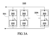
後者は、各々が典型的には図2Aに関して説明したような電力モジュール500に対応する6つの電力モジュール501~506から成る例証的な3相電力整流器600の概略図を示す図2Bと、各々が典型的には図2Aに関して説明したような電力モジュール500に対応するN個の電力モジュール501~50N(Nは、3、7、又は15よりも大きくありさえし得る正の整数である)から成る例証的な電力整流器550の概略図を示す図3Aとに例示する。例示する電力モジュール501~506、501~50Nは、各々が直列に接続されたパワー半導体デバイス及び電力ヒューズを備える、及び/又はそれらから成るそれぞれのサブモジュールと見なされ得る。
The latter is illustrated in FIG. 2B, which shows a schematic diagram of an exemplary three-
電力ヒューズ200の温度測定及び電圧降下測定に基づいて、6つのモジュール501~506の各々を通って流れるそれぞれの電流I1~I6(図2A)及びN個のモジュール501~50Nの各々を通って流れるそれぞれの電流I1~IN(図3A)は、ヒューズ200の各々の両端の電圧降下が測定され、ヒューズ200の各々の抵抗が、測定された対応するヒューズ温度に従って補正され得るので、それぞれ高精度で決定され得る。
Based on the temperature and voltage drop measurements of the
加えて、電力ダイオード300の温度を測定することは、電力整流器550、600内の電流分布を決定するために必要とされないが、電力デバイスの長期監視、経年劣化の推定、及び/又はメンテナンス若しくは修理のスケジューリングのために使用され得る。
In addition, measuring the temperature of the
言い換えれば、電力ダイオード200のみがそれぞれのセンサ及びエミッタユニットを設けられていれば十分であり得る。
In other words, it may be sufficient for only the
他の実施形態では、パワー半導体デバイスにそれぞれのセンサ及びエミッタユニットを設けるだけで十分であり得る。 In other embodiments, it may be sufficient to provide the power semiconductor device with a respective sensor and emitter unit.
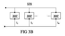
これは、M個の典型的には少なくとも実質的に同一の電力モジュール300’から成る例証的なパワーエレクトロニクスデバイス570の概略図を示す図3Bに例示しており、Mは、1、3、7、又は15よりも大きくありさえする正の整数である。各電力モジュール300’は、図1Eに関して説明したような電力ダイオード300に対応し得る。この実施形態では、パワーエレクトロニクスデバイス570は、電力整流器であり得る。パワーエレクトロニクススイッチングデバイスを参照する実施形態では、各電力モジュール300’は、例えば電力サイリスタであり得る。
This is illustrated in FIG. 3B, which shows a schematic diagram of an illustrative power
例えば、電力モジュール300’のセンサ及びエミッタユニットを使用する温度測定に基づいて、電力モジュール300’の温度の不均衡が決定され得る。それに基づいて、例えば電力モジュール300’の少なくとも実質的に等しい特質を仮定して、M個のモジュール501~50Mを通って流れる電流I1~IMの不均衡が決定され得る。
For example, based on temperature measurements using sensors and emitter units of the power modules 300', a temperature imbalance of the power modules 300' can be determined. Based thereon, an imbalance of the currents I 1 to I M flowing through the
いくつかの用途では、電力モジュールのうちの1つにそれぞれのセンサ及びエミッタユニットを設けるだけで十分でありさえし得る。 In some applications it may even be sufficient to provide each sensor and emitter unit in one of the power modules.
図2Cに例示するように、図1A~2Bに関して上記で説明したような電力コンポーネント(複数可)100~300及び電力モジュール(複数可)500~600のための監視及び/又は制御システム701は、典型的には、電力コンポーネント(複数可)100~300から電磁信号を受信し、物理量(複数可)T、V、ΔVの測定された値(複数可)を復号するように構成された受信ユニット710と、受信ユニット710に接続され、物理量(複数可)T、V、ΔVの復号された測定された値(複数可)に基づいてそれぞれの動作状態(複数可)を決定又は分析さえするように構成された評価ユニット720とを有する。
As illustrated in FIG. 2C, a monitoring and/or
受信ユニット710及び評価ユニット720は、1つのデバイスによって形成され得るか、又は互いに遠隔であり得、及び/若しくはデータネットワークを介して互いに接続され得る。
The receiving
電力モジュールのうちの1つ以上の決定/分析された動作状態に応じて、評価ユニット720は、例えば、警告メッセージを発し、及び/又は電力コンポーネント(複数可)についての制御パラメータを決定し、電力モジュール(複数可)を動作させるために、決定された制御パラメータを使用し得る。後者は、破線矢印によって図2Cに例示する。
Depending on the determined/analyzed operating state of one or more of the power modules, the
監視及び/又は制御システム701並びに電力コンポーネント(複数可)100~300及び電力モジュール(複数可)500~600によって形成されるシステム700は、電力コンポーネント(複数可)の制御及び長期監視の両方を可能にし得る。
The
システム700は、図2Dのフローチャートに例示する方法1000を実行し得る。
The
第1のブロック1100では、電力コンポーネントのセンサ及びエミッタユニット、特に本明細書で説明するような電力コンポーネントのセンサ及びエミッタユニットは、電力コンポーネントの動作状態を特徴付ける物理量の値を測定するために使用される。
In a
その後、ブロック1200では、物理量の測定された値が符号化された電磁信号が、センサ及びエミッタユニットのアンテナを介して放射される。
Then, in
典型的には、ブロック1300では、電磁信号が受信され、符号化された値が復号される。
Typically, in
ブロック1100~1300は、数回、例えば規則的な間隔で、及び/又はいくつかの電力コンポーネントに対して、典型的には並行して実行され得る。 Blocks 1100-1300 may be executed several times, e.g., at regular intervals, and/or for several power components, typically in parallel.
符号化された値(複数可)は、典型的には、動作状態を決定及び/又は特徴付け、電力コンポーネント(複数可)についての警告メッセージ、メンテナンス推奨、及び/又は制御パラメータを決定するために使用される。 The encoded value(s) are typically used to determine and/or characterize operating conditions, determine warning messages, maintenance recommendations, and/or control parameters for the power component(s).
図2Eは、電力コンポーネント、特に本明細書で説明するような電力コンポーネントを製造するための方法2000のフローチャートを示す。
FIG. 2E shows a flow chart of a
ブロック2100では、電流を通すように構成されたメインコンポーネントと、センサ及びエミッタユニットとが提供される。
In
ブロック2200では、メインコンポーネントは、誘電体コンポーネントハウジングと、センサ及びエミッタユニットとが設けられる。これは、センサ及びエミッタユニットのアンテナがコンポーネントハウジングに取り付けられ、メインコンポーネントから離間され、センサ及びエミッタユニットがメインコンポーネントの動作状態を特徴付ける物理量の値を測定し、物理量の測定された値が符号化された電磁信号をアンテナを介して放射することができるように行われる。
In
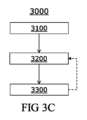
図3Cは、方法3000のフローチャートを示す。
Figure 3C shows a flowchart of
第1のブロック3100では、本明細書で説明するような電力モジュールが提供され得る。
In a
ブロック3200では、1つ以上の物理量のそれぞれの測定された値が、電力モジュールの電力コンポーネントのセンサ及びエミッタユニットのうちの1つ、典型的には2つ、又は全てからさえ受信される。
In
測定された値は、特に、それぞれのメインコンポーネントの温度、2つのそれぞれの電気端子のうちの少なくとも1つの電圧、又はメインコンポーネント及び2つの端子の両端の電圧降下をそれぞれ指し得る。 The measured values may in particular refer to the temperature of the respective main component, the voltage of at least one of the two respective electrical terminals, or the voltage drop across the main component and the two terminals, respectively.
その後、受信された測定された値(複数可)は、ブロック3300において更に処理される。
The received measured value(s) are then further processed in
図3Cの破線矢印によって示すように、ブロック3200、3300は、例えば周期的に(数回)繰り返され得る。 As indicated by the dashed arrows in FIG. 3C, blocks 3200 and 3300 may be repeated, for example, periodically (several times).
更なる処理は、以下のステップのうちの1つ以上を含み得る:
メインコンポーネントの温度分布を決定するステップと、
温度分布を監視するステップと、
メインコンポーネントのうちの1つ以上を通る電流フローを決定するステップと、
メインコンポーネント間の電流フロー分布を決定するステップと、
電流フロー及び/又は電流フロー分布を監視するステップと、
温度分布及び/又は電流フロー分布の不均衡を検出するステップ。
Further processing may include one or more of the following steps:
determining a temperature distribution in a main component;
monitoring the temperature distribution;
determining a current flow through one or more of the main components;
determining a current flow distribution between the main components;
monitoring current flow and/or current flow distribution;
Detecting imbalances in temperature distribution and/or current flow distribution.
例えば、(提供される)電力モジュールは、図3Bに関して上記で説明したような電力モジュール570、又は図2B、3Aに関して上記で説明したような電力モジュール550、600であり得る。電力モジュール550、600を参照する実施形態では、電流フロー及び/又は電流フロー分布は、電力ヒューズの電気端子間の所与の電気抵抗、特に、電力ヒューズのそれぞれの耐寒性を考慮に入れて決定され得る。
For example, the (provided) power module may be the
代替として又は加えて、更なる処理は、以下のステップのうちの1つ以上を含み得る:
電力モジュール又はその1つ以上の電力コンポーネントの経年劣化を推定するステップと、
電力モジュールのためのメンテナンス又は修理をスケジュールするステップと、
電力モジュールを動作させるために、少なくとも1つの更新された制御パラメータを決定するステップと、
電力モジュールを制御するために、少なくとも1つの更新された制御パラメータを使用するステップ。
Alternatively or additionally, the further processing may include one or more of the following steps:
- estimating the aging of the power module or one or more power components thereof;
scheduling maintenance or repairs for the power module;
determining at least one updated control parameter for operating the power module;
Using the at least one updated control parameter to control the power module.
例えば、電力モジュール及びパワーエレクトロニクスデバイスの1つ以上の制御可能な電力コンポーネントのスイッチング特性及び/又は電流強度は、それぞれ、電流及び/又は温度分布をより良くバランスさせるように修正され得る。これは、耐用年数を延ばし得る。 For example, the switching characteristics and/or current strength of one or more controllable power components of the power module and the power electronics device, respectively, may be modified to better balance the current and/or temperature distribution. This may extend the service life.
経年劣化を推定することは、それぞれ、電力モジュール及びその電力コンポーネントの監視されたピーク負荷及び/又は統合負荷に基づき得る。 Estimating aging may be based on monitored peak loads and/or aggregate loads of the power module and its power components, respectively.
監視される負荷は、熱負荷、電流負荷、及びそれらの組み合わせを指し得る。 The loads monitored may refer to thermal loads, current loads, and combinations thereof.
本発明の様々な例証的な実施形態を開示してきたが、本発明の趣旨及び範囲から逸脱することなく、本発明の利点の一部を達成する様々な変更及び修正を行うことができることが当業者には明らかであろう。同じ機能を実行する他のコンポーネントが適切に置換され得ることは、当業者には明らかであろう。特定の図を参照して説明した特徴は、明示的に言及されていない場合であっても、他の図の特徴と組み合わせられ得ることは言及されるべきである。 Although various illustrative embodiments of the present invention have been disclosed, it will be apparent to those skilled in the art that various changes and modifications can be made to achieve some of the advantages of the present invention without departing from the spirit and scope of the invention. It will be apparent to those skilled in the art that other components performing the same functions may be appropriately substituted. It should be noted that features described with reference to a particular figure may be combined with features of other figures, even if not explicitly mentioned.
「下(under)」、「下方(below)」、「下部(lower)」、「上(over)」、「上部(upper)」などの空間的に相対的な用語は、1つの要素の第2の要素に対する位置決めを説明するための記述を容易にするために使用される。これらの用語は、図に図示するものとは異なる向きに加えて、デバイスの異なる向きを包含することを意図される。更に、「第1」、「第2」などの用語は、様々な要素、領域、セクション、等を説明するためにも使用され、また、限定を意図されない。同様の用語は、説明全体を通じて同様の要素を指す。 Spatially relative terms such as "under," "below," "lower," "over," and "upper" are used for ease of description to describe the positioning of one element relative to a second element. These terms are intended to encompass different orientations of the device as well as different orientations than those depicted in the figures. Additionally, terms such as "first," "second," and the like are also used to describe various elements, regions, sections, etc. and are not intended to be limiting. Similar terms refer to similar elements throughout the description.
本明細書で使用される場合、「有する(having)」、「包含する(containing)」、「含む(including)」、「備える(comprising)」などの用語は、述べられた要素又は特徴の存在を示すが、追加の要素又は特徴を除外しないオープンエンドの用語である。冠詞「a」、「an」、及び「the」は、文脈がそうではないと明確に示さない限り、単数形だけでなく複数形も含むことを意図される。 As used herein, terms such as "having," "containing," "including," "comprising," and the like are open-ended terms indicating the presence of stated elements or features, but do not exclude additional elements or features. The articles "a," "an," and "the" are intended to include the plural as well as the singular, unless the context clearly indicates otherwise.
上記の範囲の変形及び応用を念頭に置いて、本発明は前述の説明によって限定されず、添付の図面によっても限定されないことを理解されたい。代わりに、本発明は、以下の特許請求の範囲及びそれらの法的同等物によってのみ限定される。 With the above scope of variations and applications in mind, it should be understood that the present invention is not limited by the foregoing description, nor is it limited by the accompanying drawings. Instead, the present invention is limited only by the following claims and their legal equivalents.
[参照番号]
100~300 電力コンポーネント
110,210,310 電力コンポーネントのメインコンポーネント
111,112,211,212,311,312 電気端子
120,220,320 電力コンポーネントのハウジング
130,230,330 センサ及びエミッタユニット
133 アンテナ
500~600 電力モジュール
700 システム
1000~3300 方法、方法ステップ
以下に、出願当初の特許請求の範囲に記載の事項を、そのまま、付記しておく。
[1] -2つの電気端子(111,112,211,212,311,312)と、
-コンポーネントハウジング(120,220,320)と、
-前記コンポーネントハウジング(120,220,320)によって少なくとも部分的に取り囲まれ、前記2つの電気端子(111,112,211,212,311,312)と接続され、前記2つの電気端子(111,112,211,212,311,312)間を流れる電流を通すように構成されたメインコンポーネント(110,210,310)と、
-前記メインコンポーネント(110,210,310)の動作状態を特徴付ける物理量(T,V,ΔV)の値を測定し、前記物理量の測定された前記値が符号化された電磁信号を放射するように構成されたセンサ及びエミッタユニット(130,230,330)と、を備え、
前記センサ及びエミッタユニット(130,230,330)は、前記電磁信号を放射するためのアンテナ(133)を備え、前記アンテナ(133)は、前記メインコンポーネント(110,210,310)から離間され、前記コンポーネントハウジング(120,220,320)中に、その上に、及びそれに配置される、電力コンポーネント(100~300)。
[2] 前記メインコンポーネント(110,210,310)の定格電流は、少なくとも約10Aであり、前記電力コンポーネント(100~300)は、高電圧コンポーネントであり、前記メインコンポーネント(110,210,310)の定格電圧は、少なくとも約600Vであり、前記メインコンポーネント(110,210,310)の定格電力は、少なくとも約2kWであり、並びに/又は前記電力コンポーネント(100~300)は、前記電流を制御及び/若しくは前記電流を遮断するように構成される、[1]に記載の電力コンポーネント(100~300)。
[3] 前記電力コンポーネント(100~300)は、電力ヒューズ(100,200)、特にそれぞれの半導体ヒューズであるか、又はパワー半導体デバイス(200,300)、特に縦型パワー半導体デバイスであり、並びに/又は、前記電力コンポーネントは、パワー半導体ダイオード及び/若しくはパワー半導体スイッチ、特に電力サイリスタ、電力MOSFET、若しくは電力IGBTを備える、[1]又は[2]に記載の電力コンポーネント(100~300)。
[4] 前記センサ及びエミッタユニット(130,230,330)は低電力トランスポンダを備え、前記センサ及びエミッタユニット(130,230,330)は、少なくとも一時的に前記物理量のいくつかの測定された値を記憶するように構成され、前記センサ及びエミッタユニット(130,230,330)は、前記物理量のいくつかの測定された値を前記電磁信号中に、典型的にはそれぞれの測定時間と共に符号化するように構成され、及び/又は前記センサ及びエミッタユニット(130,230,330)は、前記電力コンポーネントについての識別子を前記電磁信号中に符号化するように構成される、[1]~[3]のいずれか一項に記載の電力コンポーネント(100~300)。
[5] 前記低電力トランスポンダは、Bluetoothトランスポンダ又はRFIDトランスポンダ、特にアクティブRFIDタグ若しくはパッシブRFIDタグである、[4]に記載の電力コンポーネント(100~300)。
[6] 前記センサ及びエミッタユニット(130,230,330)は、センサユニット(131)と前記アンテナ(133)を備えるエミッタユニット(132)とを備え、前記エミッタユニット(132)は、前記センサユニット(131)から離間され、前記センサユニット(131)は、前記物理量(T,V)を表すアナログ入力信号をデジタル値に変換し、前記デジタル値を記憶し、前記デジタル値を処理し、並びに/又は前記デジタル値及び/若しくは処理された前記デジタル値を前記エミッタユニット(132)に転送するように構成され、前記センサ及びエミッタユニット(130,230,330)は、1つ以上のRFIDセンサによって提供され、並びに/又は前記センサ及びエミッタユニット(130,230,330)の定格電力は、最大で5Wである、[1]~[5]のいずれか一項に記載の電力コンポーネント(100~300)。
[7] 前記センサ及びエミッタユニット(130,230,330)は、各々が前記メインコンポーネント(110,210,310)の前記動作状態を特徴付けるそれぞれの物理量を測定するように構成された2つのセンサを備え、前記センサ及びエミッタユニット(130,230,330)は、前記メインコンポーネント(110,210,310)の前記動作状態を各々特徴付ける異なる物理量を測定するように構成され、及び/又は前記センサ及びエミッタユニット(130,230,330)は、前記メインコンポーネント(110,210,310)の温度、前記2つの電気端子(111,112,211,212,311,312)のうちの少なくとも1つの電圧(V)、並びに/又は前記メインコンポーネント(110,210,310)及び/若しくは前記2つの電気端子(111,112,211,212,311,312)の両端の電圧降下(ΔV)を測定するように構成される、[1]~[6]のいずれか一項に記載の電力コンポーネント(100~300)。
[8] 前記電力コンポーネントはパワー半導体デバイス(300)であり、前記メインコンポーネント(110,210,310)は少なくとも実質的に円筒形状であり、前記2つの電気端子(111,112,211,212,311,312)のうちの少なくとも1つは、少なくとも実質的に円筒形状であり、前記コンポーネントハウジング(120,220,320)は少なくとも実質的に中空円筒形状であり、前記メインコンポーネント(310)は、整流接合を備える半導体本体(310)を備え、前記メインコンポーネント(310)及び/又は前記半導体本体(310)の直径は、少なくとも2インチ、典型的には2インチから6インチの範囲であり、及び/又は前記パワー半導体デバイス(300)は、プレスパックデザイン又はプレスデザインを備える、[1]~[7]のいずれか一項に記載の電力コンポーネント(100~300)。
[9] 前記センサ及びエミッタユニット(330)は、前記整流接合の温度及び/又は前記半導体本体(310)のコア温度を測定するように構成される、[8]に記載の電力コンポーネント(100~300)。
[10] 前記整流接合は、断面において、前記半導体本体を少なくとも実質的に通って延在し、前記整流接合は、前記2つの電気端子(311,312)間に機能的に接続され、前記整流接合は、前記2つの電気端子(111,112,211,212,311,312)間で電流を通すように構成され、及び/又は前記整流接合は、前記半導体本体(310)のp型半導体領域とn型半導体領域との間に形成されたPN接合である、[9]に記載の電力コンポーネント(100~300)。
[11] 前記p型半導体領域及び前記n型半導体領域の各々は、前記2つの電気端子(111,112,211,212,311,312)のうちの1つとオーミック接触している、及び/又はそれによって少なくとも実質的に覆われている、[10]に記載の電力コンポーネント(100~300)。
[12] 前記整流接合に若しくはその近くに配置された一体型抵抗構造、及び/又は前記半導体本体(310)の中心に若しくはその近くに配置された一体型抵抗構造を更に備える、[8]~[11]のいずれか一項に記載の電力コンポーネント(100~300)。
[13] 前記電力コンポーネントは電力ヒューズ(100,200)であり、前記コンポーネントハウジング(120,220)はヒューズ本体を提供し、前記メインコンポーネント(110,210)は少なくとも実質的に円筒形状であり、前記電力ヒューズ(100,200)はスクエアボディデザインを備え、及び/又は前記2つの電気端子(111,112,211,212)はフラッシュエンドデザインを備える、[1]~[7]のいずれか一項に記載の電力コンポーネント(100~300)。
[14] 前記電力コンポーネント(100,200)は、前記ヒューズ本体の中心、特に前記ヒューズ本体及び/若しくは前記メインコンポーネント(110,210)の長手方向軸及び/若しくは円筒軸に対する中心に若しくはその近くに、並びに/又は前記メインコンポーネント(110,210)に若しくはその近くに、特に前記メインコンポーネント(110,210)の側面に若しくはその近くに配置された抵抗構造を備える、[13]に記載の電力コンポーネント(100~300)。
[15] 前記コンポーネントハウジング(120,220,320)は、誘電体及び/又はセラミックを備え、前記コンポーネントハウジング(120,220,320)は、前記メインコンポーネント(110,210,310)を実質的に囲み、前記アンテナ(133)は、実質的にフラットアンテナ及び/又はコイルアンテナであり、及び/又は前記アンテナ(133)は、前記コンポーネントハウジング(120,220,320)の外側に配置される、[1]~[14]のいずれか一項に記載の電力コンポーネント(100~300)。
[16] 前記電力コンポーネント(100~300)は、パワー半導体ダイオード及びパワー半導体スイッチ、特に電力サイリスタのうちの1つである、[1]~[15]のいずれか一項に記載の電力コンポーネント(100~300)。
[17] [1]~[16]のいずれか一項に記載の電力コンポーネント(100~300)の少なくとも2つを備える電力モジュール(500~600)であって、前記少なくとも2つの電力コンポーネント(100~300)は、互いに少なくとも対で接続される、電力モジュール(500~600)。
[18] 前記電力モジュールは、電力変換器、特に電力整流器の一部であるか若しくはそれを形成し、及び/又は、
-並列に接続された2つのパワー半導体デバイスと、
-直列に接続されたパワー半導体デバイス及び電力ヒューズと
のうちの少なくとも1つを備える、[17]に記載の電力モジュール(500~600)。
[19] 前記電力モジュールは、
-直列に接続された第1のパワー半導体デバイス及び第1の電力ヒューズを備える第1のサブモジュール(501~506)と、
-前記第1のサブモジュール(501~506)と接続され、直列に接続された第2のパワー半導体デバイス及び第2の電力ヒューズを備える第2のサブモジュール(501~506)と
を備える、[18]に記載の電力モジュール(500~600)。
[20] システム(700)であって、
-[1]~[16]のいずれか一項に記載の電力コンポーネント(100~300)、及び[17]~[19]のいずれか一項に記載の電力モジュール(500~600)のうちの少なくとも1つと、
-前記電力コンポーネント(100~300)から前記電磁信号を受信し、前記物理量の測定された前記値を復号するように構成された受信ユニット(710)と、
-前記受信ユニット(710)と接続可能であり、前記電力コンポーネント(100~300)の前記メインコンポーネント(110,210,310)の前記動作状態及び/又は前記電力モジュール(500~600)の動作状態を分析するために、前記物理量の復号された測定された前記値を使用するように構成された評価ユニット(720)と
を備える、システム(700)。
[21] 前記評価ユニット(720)は、前記電力コンポーネント(100~300)の経年劣化状態を推定するために、及び/又は前記電力コンポーネント(100~300)についての警告メッセージ及び制御パラメータのうちの少なくとも1つを決定するために、復号された測定された前記値を使用するように構成され、前記評価ユニット(720)は、データネットワークに前記評価ユニット(720)を接続するためのネットワークインターフェース、特に前記評価ユニット(720)と前記データネットワークとの間でデジタル信号及び/又はデジタルデータを送受信するように構成されたネットワークインターフェースを備え、及び/又は受信ユニット(710)は、前記データネットワークに前記受信ユニット(710)を接続するためのネットワークインターフェースを備える、[20]に記載のシステム(700)。
[22] [1]~[16]のいずれか一項に記載のいくつかの電力コンポーネント(100~300)、及び/又は[17]~[19]のいずれか一項に記載の電力モジュール(500~600)のいくつかを備える、[20]又は[21]に記載のシステム(700)。
[23] 前記評価ユニット(720)は、前記電流の電流強度と前記電力コンポーネントのうちの2つの間の電流分布とのうちの少なくとも1つを決定するために、復号された測定された前記値を使用するように構成される、[20]~[22]のいずれか一項に記載のシステム(700)。
[24] 前記評価ユニット(720)は、前記電力コンポーネントのうちの少なくとも1つについての制御パラメータ、特に電流強度を参照する制御パラメータを決定するように構成される、[22]又は[23]に記載のシステム(700)。
[25] 前記評価ユニット(720)は、電流分布に影響を与えるように構成される、[23]又は[24]に記載のシステム(700)。
[26] 前記評価ユニット(720)は、前記電力コンポーネント(100~300)の異なる物理量の測定された値を復号するように構成され、並びに/又は前記評価ユニット(720)は、前記電力コンポーネント(100~300)の温度、電圧、及び/若しくは電圧降下の測定された前記値を復号するように構成される、[20]~[25]のいずれか一項に記載のシステム(700)。
[27] 前記評価ユニット(720)は、前記電力コンポーネント(100~300)の現在温度依存特性、特に前記電力コンポーネント(100~300)の電気抵抗、電気抵抗率、導電力、及び/又は導電率を決定するように構成される、[20]~[26]のいずれか一項に記載のシステム(700)。
[28] -電力コンポーネント(100~300)のメインコンポーネント(110,210,310)の動作状態を特徴付ける物理量の値を測定するために、前記電力コンポーネント(100~300)のセンサ及びエミッタユニット(130,230,330)を使用すること(1100)と、ここで、前記メインコンポーネント(110,210,310)は電流を通すように構成され、
-前記物理量の測定された前記値が符号化された電磁信号を放射するために、前記センサ及びエミッタユニット(130,230,330)のアンテナ(133)を使用すること(1200)と、
を備える、方法(1000)。
[29] 前記電力コンポーネント(100~300)は、[1]~[16]のいずれか一項に記載の前記電力コンポーネント(100~300)であり、及び/又は[17]~[19]のいずれか一項に記載の電力モジュール(500~600)によって提供される、[28]に記載の方法。
[30] 電力コンポーネント(100~300)を製造するための方法(2000)であって、前記方法は、
-電流を通すように構成されたメインコンポーネント(110,210,310)と、前記メインコンポーネント(110,210,310)の動作状態を特徴付ける物理量の値を測定し、前記物理量の測定された前記値が符号化された電磁信号を放射するように構成されたセンサ及びエミッタユニット(130,230,330)とを提供すること(2100)と、
-誘電体(120,220,320)で前記メインコンポーネント(110,210,310)を少なくとも部分的に包み込み、前記センサ及びエミッタユニット(130,230,330)のアンテナ(133)が前記メインコンポーネント(110,210,310)から離間されるように、前記センサ及びエミッタユニット(130,230,330)を、前記誘電体(120,220,320)の中に、前記誘電体に、及び/又は前記誘電体の上に取り付けること(2200)と、
を備える、方法。
[31] -[17]~[19]のいずれか一項に記載の電力モジュール(500~600)を提供すること(3100)と、
-前記少なくとも2つの電力コンポーネント(100~300)の前記センサ及びエミッタユニット(130,230,330)のうちの少なくとも1つから物理量(T,V,ΔV)のそれぞれの測定された値を受信すること(3200)と、
-受信された測定された前記値を更に処理すること(3300)と、
を備える、方法(3000)。
[32] 更に処理すること(3300)は、
-温度分布を決定することと、
-温度分布を監視することと、
-電流フロー及び/又は電流フロー分布を決定することと、
-前記電流フロー及び/又は前記電流フロー分布を監視することと、
-前記温度分布及び/又は前記電流フロー分布の不均衡を検出することと
のうちの少なくとも1つを備える、[31]に記載の方法。
[33] 更に処理すること(3300)は、
-前記電力モジュール(500~600)の経年劣化を推定することと、
-前記電力モジュール(500~600)のためのメンテナンス又は修理をスケジュールすることと、
-前記電力モジュール(500~600)を動作させるために、少なくとも1つの更新された制御パラメータを決定することと、
-前記電力モジュール(500~600)を制御するために、前記少なくとも1つの更新された制御パラメータを使用することと
のうちの少なくとも1つを備える、[32]に記載の方法。
[34] 前記電流フロー及び/又は前記電流フロー分布は、前記電力モジュール(500~600)の電力ヒューズ(100,200)の前記電気端子(111,112,211,212)間の所与の電気抵抗、特に、前記電力ヒューズのそれぞれの耐寒性を考慮に入れて決定される、[32]又は[33]に記載の方法。
[Reference Number]
100-300
The following is a summary of the claims as originally filed:
[1] - two electrical terminals (111, 112, 211, 212, 311, 312),
a component housing (120, 220, 320);
a main component (110, 210, 310) that is at least partially surrounded by said component housing (120, 220, 320) and that is connected to said two electrical terminals (111, 112, 211, 212, 311, 312) and that is configured to pass an electric current flowing between said two electrical terminals (111, 112, 211, 212, 311, 312);
a sensor and emitter unit (130, 230, 330) configured to measure values of physical quantities (T, V, ΔV) characterizing an operating state of said main component (110, 210, 310) and to emit electromagnetic signals encoded with said measured values of said physical quantities,
The sensor and emitter unit (130, 230, 330) comprises an antenna (133) for radiating the electromagnetic signal, the antenna (133) being spaced from the main component (110, 210, 310) and disposed in, on and in the component housing (120, 220, 320), a power component (100-300).
[2] The power component (100-300) according to [1], wherein the rated current of the main component (110, 210, 310) is at least about 10 A, the power component (100-300) is a high voltage component, the rated voltage of the main component (110, 210, 310) is at least about 600 V, the rated power of the main component (110, 210, 310) is at least about 2 kW, and/or the power component (100-300) is configured to control the current and/or interrupt the current.
[3] The power component (100-300) according to [1] or [2], wherein the power component (100-300) is a power fuse (100, 200), in particular a respective semiconductor fuse, or a power semiconductor device (200, 300), in particular a vertical power semiconductor device, and/or the power component comprises a power semiconductor diode and/or a power semiconductor switch, in particular a power thyristor, a power MOSFET, or a power IGBT.
[4] The power component (100-300) according to any one of [1] to [3], wherein the sensor and emitter unit (130, 230, 330) comprises a low-power transponder, the sensor and emitter unit (130, 230, 330) is configured to at least temporarily store several measured values of the physical quantities, the sensor and emitter unit (130, 230, 330) is configured to encode several measured values of the physical quantities in the electromagnetic signal, typically together with a time of each measurement, and/or the sensor and emitter unit (130, 230, 330) is configured to encode an identifier for the power component in the electromagnetic signal.
[5] The power component (100-300) according to [4], wherein the low power transponder is a Bluetooth transponder or an RFID transponder, in particular an active RFID tag or a passive RFID tag.
[6] The power component (100-300) according to any one of [1] to [5], wherein the sensor and emitter unit (130, 230, 330) comprises a sensor unit (131) and an emitter unit (132) comprising the antenna (133), the emitter unit (132) being spaced apart from the sensor unit (131), the sensor unit (131) being configured to convert analog input signals representative of the physical quantities (T, V) into digital values, store the digital values, process the digital values, and/or transfer the digital values and/or the processed digital values to the emitter unit (132), the sensor and emitter unit (130, 230, 330) being provided by one or more RFID sensors, and/or the sensor and emitter unit (130, 230, 330) has a rated power of at most 5 W.
[7] The sensor and emitter unit (130, 230, 330) comprises two sensors each configured to measure a respective physical quantity characterizing the operating state of the main component (110, 210, 310), the sensor and emitter unit (130, 230, 330) is configured to measure different physical quantities each characterizing the operating state of the main component (110, 210, 310), and/or the sensor and emitter unit (130, 230, 330) is configured to measure different physical quantities each characterizing the operating state of the main component (110, 210, 310). The power component (100-300) according to any one of [1] to [6], wherein the power component (100-300) is configured to measure a temperature of the main component (110, 210, 310), a voltage (V) of at least one of the two electrical terminals (111, 112, 211, 212, 311, 312), and/or a voltage drop (ΔV) across the main component (110, 210, 310) and/or the two electrical terminals (111, 112, 211, 212, 311, 312).
[8] The power component is a power semiconductor device (300), the main component (110, 210, 310) is at least substantially cylindrical in shape, at least one of the two electrical terminals (111, 112, 211, 212, 311, 312) is at least substantially cylindrical in shape, the component housing (120, 220, 320) is at least substantially hollow cylindrical in shape, the main component (310) comprises a semiconductor body (310) with a rectifying junction, a diameter of the main component (310) and/or the semiconductor body (310) is at least 2 inches, typically in the range of 2 inches to 6 inches, and/or the power semiconductor device (300) comprises a press pack design or a press design. The power component (100-300) according to any one of [1] to [7].
The power component (100-300) according to any one of claims 1 to 8, wherein the sensor and emitter unit (330) is configured to measure a temperature of the rectifying junction and/or a core temperature of the semiconductor body (310).
[10] The power component (100-300) according to [9], wherein the rectifying junction extends, in cross section, at least substantially through the semiconductor body, the rectifying junction is operatively connected between the two electrical terminals (311, 312), the rectifying junction is configured to pass current between the two electrical terminals (111, 112, 211, 212, 311, 312), and/or the rectifying junction is a PN junction formed between a p-type semiconductor region and an n-type semiconductor region of the semiconductor body (310).
[11] The power component (100-300) according to [10], wherein each of the p-type semiconductor region and the n-type semiconductor region is in ohmic contact with and/or at least substantially covered by one of the two electrical terminals (111, 112, 211, 212, 311, 312).
[12] The power component (100-300) according to any one of [8] to [11], further comprising an integrated resistor structure disposed at or near the rectifying junction, and/or an integrated resistor structure disposed at or near the center of the semiconductor body (310).
[13] The power component (100-300) according to any one of [1] to [7], wherein the power component is a power fuse (100, 200), the component housing (120, 220) provides a fuse body, the main component (110, 210) is at least substantially cylindrical in shape, the power fuse (100, 200) has a square body design, and/or the two electrical terminals (111, 112, 211, 212) have a flush end design.
[14] The power component (100, 200) comprises a resistive structure arranged at or near the centre of the fuse body, in particular at or near the centre with respect to the longitudinal axis and/or cylindrical axis of the fuse body and/or the main component (110, 210), and/or on or near the main component (110, 210), in particular on or near a side of the main component (110, 210).
[15] The power component (100-300) according to any one of [1] to [14], wherein the component housing (120, 220, 320) comprises a dielectric and/or a ceramic, the component housing (120, 220, 320) substantially surrounds the main component (110, 210, 310), the antenna (133) is a substantially flat antenna and/or a coil antenna, and/or the antenna (133) is disposed outside the component housing (120, 220, 320).
[16] The power component (100-300) according to any one of [1] to [15], wherein the power component (100-300) is one of a power semiconductor diode and a power semiconductor switch, in particular a power thyristor.
[17] A power module (500-600) comprising at least two of the power components (100-300) according to any one of [1] to [16], wherein the at least two power components (100-300) are connected to each other at least in pairs.
[18] The power module is part of or forms a power converter, in particular a power rectifier, and/or
- two power semiconductor devices connected in parallel,
- A power semiconductor device and a power fuse connected in series;
The power module (500-600) according to [17], comprising at least one of the following:
[19] The power module comprises:
a first sub-module (501-506) comprising a first power semiconductor device and a first power fuse connected in series;
a second sub-module (501-506) connected to the first sub-module (501-506) and comprising a second power semiconductor device and a second power fuse connected in series;
The power module (500-600) according to [18], comprising:
[20] A system (700), comprising:
At least one of a power component (100 to 300) according to any one of [1] to [16] and a power module (500 to 600) according to any one of [17] to [19];
a receiving unit (710) configured to receive said electromagnetic signal from said power component (100-300) and to decode said measured value of said physical quantity;
an evaluation unit (720) connectable to said receiving unit (710) and configured to use the decoded measured values of said physical quantities to analyze the operating state of said main components (110, 210, 310) of said power components (100-300) and/or the operating state of said power modules (500-600);
The system (700) comprises:
[21] The system (700) according to [20], wherein the evaluation unit (720) is configured to use the decoded measured values to estimate an aging state of the power component (100-300) and/or to determine at least one of a warning message and a control parameter for the power component (100-300), the evaluation unit (720) comprising a network interface for connecting the evaluation unit (720) to a data network, in particular a network interface configured for transmitting and receiving digital signals and/or digital data between the evaluation unit (720) and the data network, and/or the receiving unit (710) comprising a network interface for connecting the receiving unit (710) to the data network.
[22] A system (700) according to [20] or [21] comprising some power components (100-300) according to any one of [1] to [16], and/or some power modules (500-600) according to any one of [17] to [19].
[23] The system (700) of any one of [20] to [22], wherein the evaluation unit (720) is configured to use the decoded measured values to determine at least one of a current intensity of the current and a current distribution between two of the power components.
[24] The system (700) according to [22] or [23], wherein the evaluation unit (720) is configured to determine a control parameter for at least one of the power components, in particular a control parameter referring to a current intensity.
[25] The system (700) of [23] or [24], wherein the evaluation unit (720) is configured to influence a current distribution.
[26] The system (700) of any one of [20] to [25], wherein the evaluation unit (720) is configured to decode measured values of different physical quantities of the power components (100-300) and/or the evaluation unit (720) is configured to decode measured values of temperature, voltage, and/or voltage drop of the power components (100-300).
[27] The system (700) according to any one of [20] to [26], wherein the evaluation unit (720) is configured to determine a current temperature dependent characteristic of the power component (100-300), in particular the electrical resistance, the electrical resistivity, the conductive power and/or the conductivity of the power component (100-300).
[28] - using (1100) a sensor and emitter unit (130, 230, 330) of a power component (100-300) for measuring a value of a physical quantity characterizing an operating state of a main component (110, 210, 310) of said power component, wherein said main component (110, 210, 310) is configured to pass an electric current,
- using (1200) an antenna (133) of said sensor and emitter unit (130, 230, 330) for emitting an electromagnetic signal encoded with said measured value of said physical quantity;
The method (1000) comprises:
[29] The method according to [28], wherein the power component (100-300) is the power component (100-300) according to any one of [1] to [16], and/or is provided by a power module (500-600) according to any one of [17] to [19].
[30] A method (2000) for manufacturing an electric power component (100-300), said method comprising the steps of:
providing (2100) a main component (110, 210, 310) configured to pass an electric current and a sensor and emitter unit (130, 230, 330) configured to measure the value of a physical quantity characterizing an operating state of said main component (110, 210, 310) and to emit an electromagnetic signal encoded with said measured value of said physical quantity,
- at least partially encasing said main component (110, 210, 310) in a dielectric (120, 220, 320) and mounting (2200) said sensor and emitter unit (130, 230, 330) in, on and/or on said dielectric (120, 220, 320) such that an antenna (133) of said sensor and emitter unit (130, 230, 330) is spaced from said main component (110, 210, 310);
A method comprising:
[31] - Providing (3100) a power module (500-600) according to any one of [17] to [19];
receiving (3200) measured values of each of the physical quantities (T, V, ΔV) from at least one of the sensor and emitter units (130, 230, 330) of the at least two power components (100-300);
- further processing (3300) of the received measured values;
The method (3000).
[32] The further processing (3300) comprises:
- determining the temperature distribution;
- monitoring the temperature distribution;
- determining the current flow and/or the current flow distribution,
- monitoring said current flow and/or said current flow distribution;
- detecting imbalances in the temperature distribution and/or in the current flow distribution;
The method according to claim 31, comprising at least one of the following:
[33] The further processing (3300) comprises:
- estimating the ageing of said power modules (500-600);
- scheduling maintenance or repairs for said power modules (500-600);
- determining at least one updated control parameter for operating said power modules (500-600);
- using said at least one updated control parameter for controlling said power module (500-600);
The method according to claim 32, comprising at least one of the following:
[34] The method according to [32] or [33], wherein the current flow and/or the current flow distribution is determined taking into account given electrical resistances between the electrical terminals (111, 112, 211, 212) of the power fuses (100, 200) of the power module (500-600), in particular the respective cold resistances of the power fuses.
Claims (18)
-コンポーネントハウジングと、
-前記コンポーネントハウジングによって少なくとも部分的に取り囲まれ、前記2つの電気端子と接続され、前記2つの電気端子間を流れる電流を通すように構成されたメインコンポーネントと、
-前記メインコンポーネントの動作状態を特徴付ける物理量の値を測定し、前記物理量の測定された前記値が測定時間とともに符号化された電磁信号を放射するように構成されたセンサ及びエミッタユニット、ここにおいて、前記センサ及びエミッタユニットは、前記コンポーネントハウジング上に配置され、各々が前記メインコンポーネントの前記動作状態を特徴付けるそれぞれの物理量を測定するように構成された複数のセンサを備え、前記複数のセンサは前記メインコンポーネントの温度、前記2つの電気端子の電圧を測定するように構成される、と、を備え、
前記センサ及びエミッタユニットは、前記電磁信号を放射するためのアンテナを備え、前記アンテナは、前記メインコンポーネントから離間される、パワー半導体デバイス。 - two electrical terminals,
- a component housing;
a main component at least partially surrounded by said component housing, connected to said two electrical terminals and configured to pass an electrical current flowing between said two electrical terminals;
a sensor and emitter unit configured to measure a value of a physical quantity characterizing an operating state of the main component and to emit an electromagnetic signal in which the measured value of the physical quantity is encoded together with a measurement time, wherein the sensor and emitter unit comprises a plurality of sensors arranged on the component housing, each configured to measure a respective physical quantity characterizing the operating state of the main component, the plurality of sensors being configured to measure the temperature of the main component, the voltage at the two electrical terminals,
The sensor and emitter unit comprises an antenna for radiating the electromagnetic signal, the antenna being spaced apart from the main component.
前記パワー半導体デバイスは、高電圧コンポーネントであり、前記メインコンポーネントの定格電圧は、少なくとも約600Vであり、前記メインコンポーネントの定格電力は、少なくとも約2kWであり、
並びに/又は、
前記パワー半導体デバイスは、前記電流を制御及び/若しくは前記電流を遮断するように構成される、
請求項1に記載のパワー半導体デバイス。 The main component has a current rating of at least about 10 A;
The power semiconductor device is a high voltage component, the rated voltage of the main component is at least about 600V, and the rated power of the main component is at least about 2kW;
and/or
The power semiconductor device is configured to control the current and/or block the current.
2. The power semiconductor device according to claim 1.
並びに/又は、
前記パワー半導体デバイスは、パワー半導体ダイオード及び/若しくはパワー半導体スイッチ、特に電力サイリスタ、電力MOSFET、若しくは電力IGBTを備える、請求項1又は2に記載のパワー半導体デバイス。 the power semiconductor device is a vertical power semiconductor device,
and/or
3. The power semiconductor device according to claim 1 or 2, wherein the power semiconductor device comprises a power semiconductor diode and/or a power semiconductor switch, in particular a power thyristor, a power MOSFET or a power IGBT.
前記センサ及びエミッタユニットは、少なくとも一時的に前記物理量のいくつかの測定された値を記憶するように構成され、
及び/又は、
前記センサ及びエミッタユニットは、前記パワー半導体デバイスについての識別子を前記電磁信号中に符号化するように構成される、請求項1~3のいずれか一項に記載のパワー半導体デバイス。 the sensor and emitter unit comprises a low power transponder;
the sensor and emitter unit is adapted to at least temporarily store several measured values of the physical quantity,
and/or
A power semiconductor device according to any preceding claim, wherein the sensor and emitter unit is configured to encode an identifier for the power semiconductor device in the electromagnetic signal.
前記センサユニットは、
前記物理量を表すアナログ入力信号をデジタル値に変換し、
前記デジタル値を記憶し、
前記デジタル値を処理し、
並びに
前記デジタル値及び/若しくは処理された前記デジタル値を前記エミッタユニットに転送するように構成され、
前記センサ及びエミッタユニットは、1つ以上のRFIDセンサによって提供され、 並びに/又は、
前記センサ及びエミッタユニットの定格電力は、最大で5Wである、請求項1~5のいずれか一項に記載のパワー半導体デバイス。 The sensor and emitter unit comprises a sensor unit and an emitter unit having the antenna, the emitter unit being spaced apart from the sensor unit;
The sensor unit includes:
converting an analog input signal representing said physical quantity into a digital value;
storing said digital value;
processing said digital values;
and configured to transfer the digital values and/or the processed digital values to the emitter unit;
the sensor and emitter unit is provided by one or more RFID sensors; and/or
The power semiconductor device according to any one of claims 1 to 5, wherein the sensor and emitter unit has a maximum power rating of 5W.
前記コンポーネントハウジングは、前記メインコンポーネントを実質的に囲み、
前記アンテナは、実質的にフラットアンテナ及び/若しくはコイルアンテナであり、 並びに/又は、
前記アンテナは、前記コンポーネントハウジングの外側に配置される、請求項1~11のいずれか一項に記載のパワー半導体デバイス。 the component housing comprises a dielectric and/or ceramic, the component housing substantially enclosing the main component,
the antenna is a substantially flat antenna and/or a coil antenna; and/or
The power semiconductor device according to any one of claims 1 to 11, wherein the antenna is arranged outside the component housing.
-それぞれの2つの電気端子と、
-それぞれのコンポーネントハウジングと、
-前記コンポーネントハウジングによって少なくとも部分的に取り囲まれ、前記2つの電気端子と接続され、前記2つの電気端子間を流れる電流を通すように構成されたそれぞれのメインコンポーネントと、
-それぞれの前記メインコンポーネントの動作状態を特徴付ける物理量の値を測定し、前記物理量の測定された前記値が測定時間とともに符号化された電磁信号を放射するように構成されたそれぞれのセンサ及びエミッタユニット、ここにおいて、前記センサ及びエミッタユニットは、前記コンポーネントハウジング上に配置され、各々が前記メインコンポーネントの前記動作状態を特徴付けるそれぞれの物理量を測定するように構成された複数のセンサを備え、前記複数のセンサは前記メインコンポーネントの温度、前記2つの電気端子の電圧を測定するように構成される、と、を備え、
前記センサ及びエミッタユニットは、前記電磁信号を放射するためのアンテナを備え、前記アンテナは、前記メインコンポーネントから離間される、電力モジュール。 A power module comprising at least two power components, the at least two power components being connected to each other at least in pairs, at least one of the at least two power components being a power semiconductor device according to any one of claims 1 to 12, each of the at least two power components being:
- two electrical terminals each;
- respective component housings,
- a respective main component at least partially surrounded by said component housing, connected to said two electrical terminals and configured to pass an electrical current flowing between said two electrical terminals;
a respective sensor and emitter unit configured to measure a value of a physical quantity characterizing an operating state of each of the main components and to emit an electromagnetic signal encoded with the measured value of the physical quantity together with a measurement time, wherein the sensor and emitter unit is arranged on the component housing and comprises a plurality of sensors, each configured to measure a respective physical quantity characterizing the operating state of the main component, the plurality of sensors being configured to measure the temperature of the main component, the voltage at the two electrical terminals,
A power module, wherein the sensor and emitter unit comprises an antenna for radiating the electromagnetic signal, the antenna being spaced apart from the main component.
-前記物理量の測定された前記値が測定時間とともに符号化された電磁信号を放射するために、前記センサ及びエミッタユニットのアンテナを使用することと、を備え、
前記電力コンポーネントは、請求項1~12のいずれか一項に記載のパワー半導体デバイスであり、請求項13に記載の電力モジュールによって提供される、方法。 using a sensor and emitter unit of a power component for measuring the value of a physical quantity characterizing an operating state of a main component of said power component, said main component being configured to pass an electric current;
- using an antenna of said sensor and emitter unit to emit an electromagnetic signal in which the measured value of said physical quantity is encoded together with the measurement time,
The method, wherein the power component is a power semiconductor device according to any one of claims 1 to 12 and is provided by a power module according to claim 13 .
-電流を通すように構成されたメインコンポーネントと、前記メインコンポーネントの動作状態を特徴付ける物理量の値を測定し、前記物理量の測定された前記値が測定時間とともに符号化された電磁信号を放射するように構成されたセンサ及びエミッタユニットとを提供することと、
-誘電体で前記メインコンポーネントを少なくとも部分的に包み込み、前記センサ及びエミッタユニットのアンテナを前記メインコンポーネントから離間されるように取り付けることと、
を備える、方法。 A method for manufacturing a power semiconductor device according to any one of claims 1 to 12, said method comprising the steps of:
providing a main component configured to pass an electric current and a sensor and emitter unit configured to measure the value of a physical quantity characterizing an operating state of said main component and to emit an electromagnetic signal in which said measured value of said physical quantity is encoded together with the measurement time;
- at least partially encapsulating the main component in a dielectric material and mounting the antenna of the sensor and emitter unit at a distance from the main component;
A method comprising:
-前記少なくとも2つの電力コンポーネントの前記センサ及びエミッタユニットのうちの少なくとも1つから物理量のそれぞれの測定された値を受信することと、
-受信された測定された前記値を更に処理することと、
を備える、方法。 - providing a power module according to claim 13 ,
receiving respective measured values of physical quantities from at least one of the sensor and emitter units of the at least two power components;
- further processing of the received measured values;
A method comprising:
-温度分布を決定することと、
-温度分布を監視することと、
-電流フロー及び/又は電流フロー分布を決定することと、
-前記電流フロー及び/又は前記電流フロー分布を監視することと、
-前記温度分布及び/又は前記電流フロー分布の不均衡を検出することと、
-前記電力モジュールの経年劣化を推定することと、
-前記電力モジュールのためのメンテナンス又は修理をスケジュールすることと、
-前記電力モジュールを動作させるために、少なくとも1つの更新された制御パラメータを決定することと、
-前記電力モジュールを制御するために、前記少なくとも1つの更新された制御パラメータを使用することと、
のうちの少なくとも1つを備える、請求項16に記載の方法。 The further processing comprises:
- determining the temperature distribution;
- monitoring the temperature distribution;
- determining the current flow and/or the current flow distribution,
- monitoring said current flow and/or said current flow distribution;
- detecting imbalances in the temperature distribution and/or in the current flow distribution;
- estimating the ageing of said power modules;
- scheduling maintenance or repairs for said power modules;
- determining at least one updated control parameter for operating said power module;
- using said at least one updated control parameter for controlling said power module;
20. The method of claim 16 , comprising at least one of:
Applications Claiming Priority (3)
| Application Number | Priority Date | Filing Date | Title |
|---|---|---|---|
| EP20162452.5 | 2020-03-11 | ||
| EP20162452.5A EP3879556A1 (en) | 2020-03-11 | 2020-03-11 | Power component including a main component and a sensor and emitter unit and system with the power component |
| PCT/EP2021/053416 WO2021180419A1 (en) | 2020-03-11 | 2021-02-12 | Power component including a main component and a sensor and emitter unit and system with the power component |
Publications (2)
| Publication Number | Publication Date |
|---|---|
| JP2023517962A JP2023517962A (en) | 2023-04-27 |
| JP7581361B2 true JP7581361B2 (en) | 2024-11-12 |
Family
ID=69810605
Family Applications (1)
| Application Number | Title | Priority Date | Filing Date |
|---|---|---|---|
| JP2022554547A Active JP7581361B2 (en) | 2020-03-11 | 2021-02-12 | Power component including a main component and a sensor and emitter unit, and system having the power component - Patents.com |
Country Status (7)
| Country | Link |
|---|---|
| US (1) | US20230160978A1 (en) |
| EP (1) | EP3879556A1 (en) |
| JP (1) | JP7581361B2 (en) |
| KR (1) | KR102893934B1 (en) |
| CN (1) | CN115280457B (en) |
| CA (1) | CA3171221A1 (en) |
| WO (1) | WO2021180419A1 (en) |
Families Citing this family (2)
| Publication number | Priority date | Publication date | Assignee | Title |
|---|---|---|---|---|
| EP4654242A1 (en) * | 2024-05-21 | 2025-11-26 | Volvo Truck Corporation | Fuse and method to prevent misuse of the same |
| DE102024206454A1 (en) * | 2024-07-09 | 2026-01-15 | Siemens Aktiengesellschaft | Determination of the aging state of electrical equipment |
Citations (8)
| Publication number | Priority date | Publication date | Assignee | Title |
|---|---|---|---|---|
| WO2005020320A1 (en) | 2003-08-22 | 2005-03-03 | The Kansai Electric Power Co., Inc. | Semiconductor device, method for manufacturing same, and power converter using such semiconductor device |
| JP2006108256A (en) | 2004-10-01 | 2006-04-20 | Mitsubishi Electric Corp | Power semiconductor device |
| JP2016522987A (en) | 2013-04-26 | 2016-08-04 | アーベーベー・テクノロジー・アーゲー | Power semiconductor module |
| WO2017078525A1 (en) | 2015-11-06 | 2017-05-11 | Liandon B.V. | System for monitoring electric current in a network, and electrical fuse thereof |
| JP2018518051A (en) | 2015-05-19 | 2018-07-05 | アーベーベー・シュバイツ・アーゲー | Semiconductor device |
| WO2019016949A1 (en) | 2017-07-21 | 2019-01-24 | 東芝三菱電機産業システム株式会社 | Power conversion device equipped with arm fuse blow-out detection means |
| JP2019135819A (en) | 2018-02-05 | 2019-08-15 | 矢崎総業株式会社 | Power semiconductor device, and vehicle power supplying system comprising the same |
| US20200051768A1 (en) | 2018-08-10 | 2020-02-13 | Siemens Aktiengesellschaft | Fuse, fuse body, system and method |
Family Cites Families (14)
| Publication number | Priority date | Publication date | Assignee | Title |
|---|---|---|---|---|
| US3633191A (en) * | 1966-09-20 | 1972-01-04 | Anaconda Wire & Cable Co | Temperature monitored cable system with telemetry readout |
| DE2749359A1 (en) * | 1977-11-04 | 1979-05-10 | Bbc Brown Boveri & Cie | READY-TO-CONNECT SEMI-CONDUCTOR COMPONENT |
| ITMI20031426A1 (en) * | 2003-07-11 | 2005-01-12 | St Microelectronics Srl | INTEGRATED RESISTIVE STRUCTURE MONOLITHICALLY WITH IGBT DEVICES (INSULATED GATE BIPOLAR TRANSISTOR) OF POWER |
| US8134445B2 (en) * | 2004-04-20 | 2012-03-13 | Cooper Technologies Company | RFID open fuse indicator, system, and method |
| JP4157865B2 (en) * | 2004-10-27 | 2008-10-01 | 株式会社日立製作所 | Semiconductor integrated circuit device and non-contact electronic device |
| US7436022B2 (en) * | 2005-02-11 | 2008-10-14 | Alpha & Omega Semiconductors, Ltd. | Enhancing Schottky breakdown voltage (BV) without affecting an integrated MOSFET-Schottky device layout |
| EP1894147B1 (en) * | 2005-05-19 | 2015-10-14 | Semiconductor Energy Laboratory Co., Ltd. | Semiconductor device and wireless communication system using the same |
| JP5556072B2 (en) * | 2009-01-07 | 2014-07-23 | ソニー株式会社 | Semiconductor device, method of manufacturing the same, and millimeter wave dielectric transmission device |
| JP5644521B2 (en) * | 2011-01-14 | 2014-12-24 | ソニー株式会社 | Signal transmission device and electronic device |
| CN105934821B (en) * | 2014-01-21 | 2018-11-23 | Abb瑞士股份有限公司 | Power semiconductor arrangement |
| CN204008933U (en) * | 2014-02-21 | 2014-12-10 | 珠海万力达电气自动化有限公司 | A kind of high voltage converter remote supervision system based on Internet of Things |
| KR102569204B1 (en) * | 2014-06-02 | 2023-08-22 | 아이에스에이 파마슈티컬즈 비.브이. | Synthetic long peptides (slp) for therapeutic vaccination against hepatitis b virus infection |
| US10217920B2 (en) * | 2016-07-06 | 2019-02-26 | Raytheon Bbn Technologies Corp. | Buried sensor system |
| US11368010B2 (en) * | 2020-01-17 | 2022-06-21 | Eaton Intelligent Power Limited | Solid state circuit interrupter with solid state interlocking mechanism |
-
2020
- 2020-03-11 EP EP20162452.5A patent/EP3879556A1/en active Pending
-
2021
- 2021-02-12 KR KR1020227034561A patent/KR102893934B1/en active Active
- 2021-02-12 CN CN202180020625.2A patent/CN115280457B/en active Active
- 2021-02-12 US US17/906,167 patent/US20230160978A1/en active Pending
- 2021-02-12 WO PCT/EP2021/053416 patent/WO2021180419A1/en not_active Ceased
- 2021-02-12 JP JP2022554547A patent/JP7581361B2/en active Active
- 2021-02-12 CA CA3171221A patent/CA3171221A1/en active Pending
Patent Citations (8)
| Publication number | Priority date | Publication date | Assignee | Title |
|---|---|---|---|---|
| WO2005020320A1 (en) | 2003-08-22 | 2005-03-03 | The Kansai Electric Power Co., Inc. | Semiconductor device, method for manufacturing same, and power converter using such semiconductor device |
| JP2006108256A (en) | 2004-10-01 | 2006-04-20 | Mitsubishi Electric Corp | Power semiconductor device |
| JP2016522987A (en) | 2013-04-26 | 2016-08-04 | アーベーベー・テクノロジー・アーゲー | Power semiconductor module |
| JP2018518051A (en) | 2015-05-19 | 2018-07-05 | アーベーベー・シュバイツ・アーゲー | Semiconductor device |
| WO2017078525A1 (en) | 2015-11-06 | 2017-05-11 | Liandon B.V. | System for monitoring electric current in a network, and electrical fuse thereof |
| WO2019016949A1 (en) | 2017-07-21 | 2019-01-24 | 東芝三菱電機産業システム株式会社 | Power conversion device equipped with arm fuse blow-out detection means |
| JP2019135819A (en) | 2018-02-05 | 2019-08-15 | 矢崎総業株式会社 | Power semiconductor device, and vehicle power supplying system comprising the same |
| US20200051768A1 (en) | 2018-08-10 | 2020-02-13 | Siemens Aktiengesellschaft | Fuse, fuse body, system and method |
Also Published As
| Publication number | Publication date |
|---|---|
| CA3171221A1 (en) | 2021-09-16 |
| JP2023517962A (en) | 2023-04-27 |
| US20230160978A1 (en) | 2023-05-25 |
| KR20220150365A (en) | 2022-11-10 |
| CN115280457A (en) | 2022-11-01 |
| KR102893934B1 (en) | 2025-12-02 |
| EP3879556A1 (en) | 2021-09-15 |
| WO2021180419A1 (en) | 2021-09-16 |
| CN115280457B (en) | 2026-01-06 |
Similar Documents
| Publication | Publication Date | Title |
|---|---|---|
| JP7581361B2 (en) | Power component including a main component and a sensor and emitter unit, and system having the power component - Patents.com | |
| US10340494B2 (en) | Electrical bus bar comprising a sensor unit | |
| GopiReddy et al. | Power cycle testing of power switches: A literature survey | |
| Motto et al. | IGBT module with user accessible on-chip current and temperature sensors | |
| JP5001637B2 (en) | Package for high power density devices | |
| CN111830389B (en) | IGBT junction temperature estimation system and method based on emitter power terminal temperature | |
| US10916931B2 (en) | Temperature sensing and fault detection for paralleled double-side cooled power modules | |
| US11349470B2 (en) | Gate driver and protection system for a solid-state switch | |
| CN104101768B (en) | Equipment, method and system for measuring the curent change in integrated circuit | |
| CN105393350B (en) | Power semiconductor modular | |
| KR20160125885A (en) | Multiple coil configuration for faulted circuit indicator | |
| CN116724219A (en) | Gas insulated switchgear and methods of use with gas insulated switchgear | |
| US6667461B1 (en) | Multiple load protection and control device | |
| US9553084B2 (en) | Switching element, semiconductor device, and semiconductor device manufacturing method | |
| CA3089157C (en) | Apparatus, system and method for temperature measurement for dry-type transformer | |
| CN111712896B (en) | Wireless sensing systems and methods for switching devices | |
| US20200357582A1 (en) | Mechatronic module having a hybrid circuit arrangement | |
| JP6533451B2 (en) | Wireless power receiver | |
| US20250323515A1 (en) | Disconnection device for an electric charging device, power supply device with such a disconnection device, and energy storage device with such a disconnection device | |
| US7522405B2 (en) | High current electrical switch and method | |
| Vilchis-Rodriguez et al. | IGBT finite element model for fibre bragg grating sensor installation analysis | |
| Baker et al. | Multi-Chip Temperature Imbalance of SiC MOSFETs in MOSFET vs. Body-Diode Conduction | |
| CN111208460B (en) | Method for prolonging the life of gradient power amplifier and monitoring device for gradient power amplifier | |
| CN111816430B (en) | Power components and transformer devices for resistance welding | |
| KR101162577B1 (en) | Thermal Modeling Method for Busbar with Electrical Connections |
Legal Events
| Date | Code | Title | Description |
|---|---|---|---|
| A521 | Request for written amendment filed |
Free format text: JAPANESE INTERMEDIATE CODE: A523 Effective date: 20221018 |
|
| A621 | Written request for application examination |
Free format text: JAPANESE INTERMEDIATE CODE: A621 Effective date: 20221018 |
|
| RD02 | Notification of acceptance of power of attorney |
Free format text: JAPANESE INTERMEDIATE CODE: A7422 Effective date: 20230104 |
|
| A131 | Notification of reasons for refusal |
Free format text: JAPANESE INTERMEDIATE CODE: A131 Effective date: 20231128 |
|
| A521 | Request for written amendment filed |
Free format text: JAPANESE INTERMEDIATE CODE: A523 Effective date: 20240220 |
|
| A02 | Decision of refusal |
Free format text: JAPANESE INTERMEDIATE CODE: A02 Effective date: 20240528 |
|
| A521 | Request for written amendment filed |
Free format text: JAPANESE INTERMEDIATE CODE: A523 Effective date: 20240903 |
|
| A911 | Transfer to examiner for re-examination before appeal (zenchi) |
Free format text: JAPANESE INTERMEDIATE CODE: A911 Effective date: 20240911 |
|
| TRDD | Decision of grant or rejection written | ||
| A01 | Written decision to grant a patent or to grant a registration (utility model) |
Free format text: JAPANESE INTERMEDIATE CODE: A01 Effective date: 20241001 |
|
| A61 | First payment of annual fees (during grant procedure) |
Free format text: JAPANESE INTERMEDIATE CODE: A61 Effective date: 20241030 |
|
| R150 | Certificate of patent or registration of utility model |
Ref document number: 7581361 Country of ref document: JP Free format text: JAPANESE INTERMEDIATE CODE: R150 |