JP7581312B2 - Display device - Google Patents
Display device Download PDFInfo
- Publication number
- JP7581312B2 JP7581312B2 JP2022211895A JP2022211895A JP7581312B2 JP 7581312 B2 JP7581312 B2 JP 7581312B2 JP 2022211895 A JP2022211895 A JP 2022211895A JP 2022211895 A JP2022211895 A JP 2022211895A JP 7581312 B2 JP7581312 B2 JP 7581312B2
- Authority
- JP
- Japan
- Prior art keywords
- data
- subpixel
- signal
- gate
- row
- Prior art date
- Legal status (The legal status is an assumption and is not a legal conclusion. Google has not performed a legal analysis and makes no representation as to the accuracy of the status listed.)
- Active
Links
- 239000011159 matrix material Substances 0.000 claims description 3
- 239000003990 capacitor Substances 0.000 description 136
- 238000010586 diagram Methods 0.000 description 58
- 230000007704 transition Effects 0.000 description 58
- 238000004364 calculation method Methods 0.000 description 28
- 238000009825 accumulation Methods 0.000 description 18
- 230000004044 response Effects 0.000 description 18
- 230000010354 integration Effects 0.000 description 10
- 101100313728 Vitis vinifera VINST1 gene Proteins 0.000 description 9
- 238000006243 chemical reaction Methods 0.000 description 9
- 230000006870 function Effects 0.000 description 9
- 101100491263 Oryza sativa subsp. japonica AP2-4 gene Proteins 0.000 description 8
- 101100311249 Schizosaccharomyces pombe (strain 972 / ATCC 24843) stg1 gene Proteins 0.000 description 8
- 101100041125 Arabidopsis thaliana RST1 gene Proteins 0.000 description 7
- 101100448781 Oryza sativa subsp. indica GL18 gene Proteins 0.000 description 7
- 101100443250 Saccharomyces cerevisiae (strain ATCC 204508 / S288c) DIG1 gene Proteins 0.000 description 7
- 230000006866 deterioration Effects 0.000 description 7
- 101100443251 Saccharomyces cerevisiae (strain ATCC 204508 / S288c) DIG2 gene Proteins 0.000 description 6
- 101100041128 Schizosaccharomyces pombe (strain 972 / ATCC 24843) rst2 gene Proteins 0.000 description 6
- 230000015556 catabolic process Effects 0.000 description 6
- 238000006731 degradation reaction Methods 0.000 description 6
- 230000007274 generation of a signal involved in cell-cell signaling Effects 0.000 description 6
- 238000000034 method Methods 0.000 description 4
- 101001019455 Homo sapiens ICOS ligand Proteins 0.000 description 3
- 101000885321 Homo sapiens Serine/threonine-protein kinase DCLK1 Proteins 0.000 description 3
- 102100034980 ICOS ligand Human genes 0.000 description 3
- 102100039758 Serine/threonine-protein kinase DCLK1 Human genes 0.000 description 3
- 239000003086 colorant Substances 0.000 description 3
- 230000004048 modification Effects 0.000 description 3
- 238000012986 modification Methods 0.000 description 3
- 238000013528 artificial neural network Methods 0.000 description 2
- 238000010801 machine learning Methods 0.000 description 2
- 238000005070 sampling Methods 0.000 description 2
- 102100040862 Dual specificity protein kinase CLK1 Human genes 0.000 description 1
- 102100040844 Dual specificity protein kinase CLK2 Human genes 0.000 description 1
- 101000749294 Homo sapiens Dual specificity protein kinase CLK1 Proteins 0.000 description 1
- 101000749291 Homo sapiens Dual specificity protein kinase CLK2 Proteins 0.000 description 1
- 230000007423 decrease Effects 0.000 description 1
- 230000000694 effects Effects 0.000 description 1
- 230000005669 field effect Effects 0.000 description 1
- 239000004973 liquid crystal related substance Substances 0.000 description 1
- 229910044991 metal oxide Inorganic materials 0.000 description 1
- 150000004706 metal oxides Chemical class 0.000 description 1
- 239000004065 semiconductor Substances 0.000 description 1
Images


Landscapes
- Control Of Indicators Other Than Cathode Ray Tubes (AREA)
- Devices For Indicating Variable Information By Combining Individual Elements (AREA)
- Control Of El Displays (AREA)
- Electroluminescent Light Sources (AREA)
Description
本発明は、表示装置に関する。 The present invention relates to a display device.
特許文献1には、2つの副画素が1本のデータ線を共有するダブルレート駆動(Double Rate Driving:DRD)を用いた表示装置が開示されている。
特許文献1に記載されている表示装置においては、消費電力の低減の観点において十分でない場合がある。
The display device described in
本発明は、上述した課題に鑑みてなされたものであって、消費電力が低減された表示装置を提供することを目的とする。 The present invention has been made in consideration of the above-mentioned problems, and aims to provide a display device with reduced power consumption.
本発明の一観点によれば、行列状に配列された複数の副画素、行方向に延在する複数のゲート線、および列方向に延在する複数のデータ線を有する表示パネルと、前記複数のゲート線を介して、前記複数の副画素をアクティブにするための複数のゲート信号を前記複数の副画素に供給するゲート駆動部と、前記複数のデータ線を介して、前記複数の副画素の輝度に対応する複数のデータ信号を前記複数の副画素に供給するデータ駆動部と、前記ゲート駆動部および前記データ駆動部を制御するタイミング制御部と、を含み、前記複数の副画素は、第1の行において前記複数のデータ線のうちの第1のデータ線を共有する第1の色の第1の副画素および第2の色の第2の副画素、第2の行において前記第1のデータ線を共有する前記第1の色の第3の副画素および前記第2の色の第4の副画素を含み、前記タイミング制御部は、前記第1の副画素の前記データ信号が前記第3の副画素の前記データ信号に類似すると判定した場合に、前記第1の副画素に続いて前記第3の副画素に前記データ信号を供給させるように、前記ゲート駆動部および前記データ駆動部を制御する、表示装置が提供される。 According to one aspect of the present invention, there is provided a display device including a display panel having a plurality of subpixels arranged in a matrix, a plurality of gate lines extending in a row direction, and a plurality of data lines extending in a column direction; a gate driver that supplies a plurality of gate signals to the plurality of subpixels via the plurality of gate lines to activate the plurality of subpixels; a data driver that supplies a plurality of data signals corresponding to the luminance of the plurality of subpixels via the plurality of data lines to the plurality of subpixels; and a timing controller that controls the gate driver and the data driver, the plurality of subpixels including a first subpixel of a first color and a second subpixel of a second color that share a first data line of the plurality of data lines in a first row, and a third subpixel of the first color and a fourth subpixel of the second color that share the first data line in a second row, and the timing controller controls the gate driver and the data driver to supply the data signal to the third subpixel following the first subpixel when it is determined that the data signal of the first subpixel is similar to the data signal of the third subpixel.
本発明によれば、消費電力が低減された表示装置を提供することができる。 The present invention provides a display device with reduced power consumption.
以下、本発明に係る実施形態について図面を参照しつつ詳細に説明する。各図面を通じて共通する機能を有する要素には同一の符号を付し、重複する説明を省略または簡略化することがある。 Embodiments of the present invention will be described in detail below with reference to the drawings. Elements having common functions throughout the drawings will be given the same reference numerals, and duplicate descriptions may be omitted or simplified.
[第1実施形態]
図1は、本実施形態に係る表示装置10の概略構成を示すブロック図である。本実施形態に係る表示装置10は有機発光ダイオード表示装置であるがこれに限定されない。例えば、本発明に係る表示装置10は液晶表示装置であり得る。表示装置10は、表示パネル100、ゲート駆動部200、データ駆動部300、電源400およびタイミング制御部500を有する。
[First embodiment]
1 is a block diagram showing a schematic configuration of a
表示パネル100は表示装置10の表示画像を構成する。表示パネル100は、ゲート駆動部200から行方向に延在するゲート線GL1~GLnとデータ駆動部300から列方向に延在するデータ線DL1~DLm(m、nは正の整数、以下同様)とが交差して画定される各画素領域に、行列状に配列された複数の副画素Pを含む。ゲート線GL1~GLnの各々に沿って隣接する一対の副画素は、データ線DL1~DLmのうちの1本を共有するように配置されている。
The
ゲート駆動部200は、ゲート制御信号GCSに基づいて決定された順序でゲート線GL1~GLnの各々にゲート信号を出力する。ゲート駆動部200は、レベルシフタ、シフトレジスタ、遅延回路、フリップフロップ等の内部回路を備え、ゲート制御信号GCSに応じて、ゲート開始パルス信号GSP、ゲートシフトクロック信号GSC、ゲート出力イネーブル信号GOE等の制御信号を連続的に生成する。ゲート開始パルス信号GSPは、ゲート駆動部200に含まれるゲートドライバ集積回路の動作の開始のタイミングを制御する。ゲートシフトクロック信号GSCは、ゲートドライバ集積回路に共通に入力されるクロック信号であり、走査信号(ゲート信号)のシフトタイミングを制御する。ゲート出力イネーブル信号GOEは、ゲートドライバ集積回路のタイミング情報を指定する。ゲート駆動部200は、ゲートシフトクロック信号GSCに応じてゲート開始パルス信号GSPをシフトすることにより、連続してゲート信号を生成する。また、ゲート駆動部200は、生成されたゲート信号をゲート線GL1~GLnの各々に供給する。ゲート線GL1~GLnを介して供給されるゲート信号は、表示パネル100に含まれる複数の副画素の各々をアクティブにするために用いられる。ゲート駆動部200は、タイミング制御部500によって出力幅が変調されたデータイネーブル信号DEおよびデータイネーブル信号DEによって出力幅が変化したゲート出力イネーブル信号GOEによってゲート信号の出力幅を制御する。なお、ゲート駆動部200の配置は図1に示さされる形態に限定されない。例えば、ゲート駆動部200は、表示パネル100の両端に存する非表示領域に配されることもできる。
The gate driver 200 outputs gate signals to each of the gate lines GL1 to GLn in an order determined based on the gate control signal GCS. The gate driver 200 includes internal circuits such as a level shifter, a shift register, a delay circuit, and a flip-flop, and continuously generates control signals such as a gate start pulse signal GSP, a gate shift clock signal GSC, and a gate output enable signal GOE in response to the gate control signal GCS. The gate start pulse signal GSP controls the timing of the start of operation of the gate driver integrated circuit included in the gate driver 200. The gate shift clock signal GSC is a clock signal commonly input to the gate driver integrated circuits, and controls the shift timing of the scanning signal (gate signal). The gate output enable signal GOE specifies the timing information of the gate driver integrated circuit. The gate driver 200 continuously generates gate signals by shifting the gate start pulse signal GSP in response to the gate shift clock signal GSC. The gate driver 200 also supplies the generated gate signals to each of the gate lines GL1 to GLn. The gate signals supplied via the gate lines GL1 to GLn are used to activate each of the sub-pixels included in the
データ駆動部300は、タイミング制御部500によって整列された画像データR’G’B’W’を行毎にタイミング制御部500から受信する。データ駆動部300は、ソース・スタート・パルス信号SSP、ソース・シフト・クロック信号SSCおよびソース出力イネーブル信号SOEを含むデータ制御信号DSCをタイミング制御部500から受信する。ソース・スタート・パルス信号SSPは、データ駆動部300に含まれるソースドライバ集積回路のデータサンプリングの開始のタイミングを制御する。ソース・シフト・クロック信号SSCは、ソースドライバ集積回路の各々でデータのサンプリングのタイミングを制御するクロック信号である。ソース出力イネーブル信号SOEは、データ駆動部300からの信号の出力タイミングを制御する。データ駆動部300は、データ制御信号DSCを用いて、画像データRGBWを整列させ、各行に対するアナログのデータ電圧に変換する。なお本発明は、画像データ形式がRGBWの表示装置だけでなく、白色サブピクセルを含まないRGBの表示装置や、黄色サブピクセルを含むRGBYの表示装置にも同じように適用できる。以下の説明ではRGBWを用いるが、それに限定されるものではない。
The
具体的には、データ駆動部300は、ソース出力イネーブル信号SOEに応じてゲート信号がゲート線GL1~GLnの各々に供給される1水平周期毎に、ソース・シフト・クロック信号SSCに応じて整列された画像データR’G’B’W’を1行毎にサンプリングしてデータ電圧DATAに変換する。データ駆動部300は、アナログ信号であるデータ電圧DATAを、データ線DL1~DLmを介しての表示パネル100に含まれる複数の副画素の各々に供給する。データ駆動部300のデータ電圧への変換期間および出力期間は、タイミング制御部500により出力幅が変調されたデータイネーブル信号DEおよびデータイネーブル信号DEにより出力幅が変更されたソース出力イネーブル信号SOEに応じて変更されることができる。データ駆動部300は、データ線方向に配置された同色の副画素を所定の行数だけ連続して発光させるようにデータ電圧を生成し、ゲート信号の出力タイミングと同期させてデータ電圧をデータ線DL1~DLmを介して表示パネル100に含まれる複数の副画素の各々に連続して供給する。複数の副画素に供給される複数のデータ電圧は、それぞれ複数の画素の輝度に対応する。
Specifically, the
電源400は、電源線を介して各副画素Pに高電位側の電源電圧VDDおよび低電位側の電源電圧VSSを供給する。また、電源400は、補償電源線CPLを介して各副画素Pに補償電圧Vrefを供給する。 The power supply 400 supplies a high-potential side power supply voltage VDD and a low-potential side power supply voltage VSS to each subpixel P via a power supply line. The power supply 400 also supplies a compensation voltage Vref to each subpixel P via a compensation power supply line CPL.
タイミング制御部500は、ダブルレート駆動(DRD)により表示パネル100の副画素Pを駆動するための信号を生成する。タイミング制御部500は、データ線DL1~DLmの方向に沿って配置された同色の副画素を所定の行数だけ発光させるように画像データRGBWを整列させる。また、タイミング制御部500は、入力された画像データRGBWを整列させてからデータ駆動部300に出力することにより、副画素Pを1フレーム単位ごとに異なる駆動順序で動作させ、同色の副画素を所定の行数だけ連続して発光させる。
The
また、タイミング制御部500は、ドットクロックDCLK、データイネーブル信号DE、水平同期信号Hsync、垂直同期信号Vsync等の信号を用いてゲート制御信号GCSおよびデータ制御信号DSCを生成する。タイミング制御部500は、表示装置10をDRD方式で駆動するために、生成したゲート制御信号GCSをゲート駆動部200に、データ制御信号DSCをデータ駆動部300にそれぞれ送信する。タイミング制御部500は、データ線DL1~DLmの方向に沿って配置された同色の副画素Pを、DRD法によって同色の副画素を所定の行数だけ連続して発光させるように、ゲート制御信号GCSおよびデータ制御信号DSCを生成することができる。
The
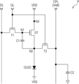
表示装置10に含まれるゲート線GL1~GLn、データ線DL1~DLmおよび副画素Pの接続関係について、図2を参照して詳細に説明する。図2は本実施形態に係る副画素Pの等価回路図である。副画素Pの各々は、有機発光ダイオードOLED、駆動素子DT、第1スイッチ素子T1、第2スイッチ素子T2、第1キャパシタC1、第2キャパシタC2を含む。また、副画素Pはデータ線DL、ゲート線GL、高電位側の電源電圧VDD、低電位側の電源電圧VSSおよび補償電源線CPLと接続される。有機発光ダイオードOLEDは、本実施形態では画素面を構成する赤色(R)、緑色(G)、青色(B)または白色(W)のいずれかの発光色を有する。有機発光ダイオードOLEDのアノードは駆動素子DTを介して電源電圧VDDに接続され、有機発光ダイオードOLEDのカソードは電源電圧VSSに接続される。
The connection relationship between the gate lines GL1 to GLn, the data lines DL1 to DLm, and the sub-pixels P included in the
駆動素子DT、第1スイッチ素子T1および第2スイッチ素子T2はMOSFET(金属酸化膜半導体電界効果トランジスタ)から構成され得る。駆動素子DTのゲートは第1ノードN1を介して第1スイッチ素子T1のソースに接続され、駆動素子DTのドレインは第3ノードN3を介して電源電圧VDDに接続され、駆動素子DTのソースは第2ノードN2を介して有機発光ダイオードOLEDのアノードに接続される。第1スイッチ素子T1のゲートはゲート線GLに接続され、第1スイッチ素子T1のドレインはデータ線DLに接続される。第1キャパシタC1は、第1ノードN1と第2ノードN2との間に接続される。第2スイッチ素子T2のゲートはゲート線GLに接続され、第2スイッチ素子T2のドレインは第2ノードN2に接続され、第2スイッチ素子T2のソースは補償電源線CPLに接続される。第2スイッチ素子T2は、ゲート線GLからのゲート信号に応答して、補償電源線CPLを介して入力される補償電圧Vrefを第2ノードN2に供給し、データ電圧の出力端子である駆動素子DTのドレイン端子の電位を補償する。補償電源線CPLには補償電圧Vrefを安定化させるために第2キャパシタC2が接続されている。 The driving element DT, the first switch element T1 and the second switch element T2 may be composed of MOSFETs (metal oxide semiconductor field effect transistors). The gate of the driving element DT is connected to the source of the first switch element T1 via the first node N1, the drain of the driving element DT is connected to the power supply voltage VDD via the third node N3, and the source of the driving element DT is connected to the anode of the organic light emitting diode OLED via the second node N2. The gate of the first switch element T1 is connected to the gate line GL, and the drain of the first switch element T1 is connected to the data line DL. The first capacitor C1 is connected between the first node N1 and the second node N2. The gate of the second switch element T2 is connected to the gate line GL, the drain of the second switch element T2 is connected to the second node N2, and the source of the second switch element T2 is connected to the compensation power supply line CPL. In response to a gate signal from the gate line GL, the second switch element T2 supplies the compensation voltage Vref input via the compensation power line CPL to the second node N2, thereby compensating for the potential of the drain terminal of the driving element DT, which is the output terminal of the data voltage. A second capacitor C2 is connected to the compensation power line CPL to stabilize the compensation voltage Vref.
ゲート線GLのレベルによって有機発光ダイオードOLEDの駆動または停止が決定され、有機発光ダイオードOLEDが駆動される場合にはデータ線DLの電圧によってその輝度が決定される。有機発光ダイオードOLEDが走査(駆動)される場合にゲート線GLのレベルはハイレベルとなり、それ以外の場合にはゲート線GLのレベルはローレベルとなる。ゲート線GLのレベルがハイレベルとなると、第1スイッチ素子T1がオンされ、データ線DLの電圧に基づく電圧が第1キャパシタC1に充電される。第1キャパシタC1の電圧が駆動素子DTのオン閾値を超えると、駆動素子DTがオンされる。オン状態の駆動素子DTは、ゲート電圧、即ち、データ線DLの電圧と補償電圧Vrefとの間の電位差に応じたドレイン電流を電源電圧VDDから有機発光ダイオードOLEDに供給する。このドレイン電流に応じて、有機発光ダイオードOLEDが発光する。第1キャパシタC1は、いわゆるストレージキャパシタとして機能し、ある走査フレームにおける駆動素子DTのゲート-ソース電圧を次の走査フレームまで保持して有機発光ダイオードOLEDの発光状態または消灯状態を維持する。 The level of the gate line GL determines whether the organic light emitting diode OLED is driven or not, and when the organic light emitting diode OLED is driven, its brightness is determined by the voltage of the data line DL. When the organic light emitting diode OLED is scanned (driven), the level of the gate line GL becomes high level, and otherwise the level of the gate line GL becomes low level. When the level of the gate line GL becomes high level, the first switch element T1 is turned on, and a voltage based on the voltage of the data line DL is charged to the first capacitor C1. When the voltage of the first capacitor C1 exceeds the on threshold of the driving element DT, the driving element DT is turned on. The driving element DT in the on state supplies a drain current corresponding to the gate voltage, that is, the potential difference between the voltage of the data line DL and the compensation voltage Vref, from the power supply voltage VDD to the organic light emitting diode OLED. The organic light emitting diode OLED emits light in response to this drain current. The first capacitor C1 functions as a so-called storage capacitor, and holds the gate-source voltage of the driving element DT in a certain scanning frame until the next scanning frame, thereby maintaining the light-emitting or non-light-emitting state of the organic light-emitting diode OLED.
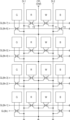
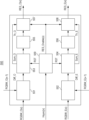
図3は、本実施形態に係る表示パネル100の概略構成を示す平面図である。表示パネル100上には2次元配列された複数の副画素Pを有する画素面が構成される。複数の副画素Pは、緑色副画素G、赤色副画素R、白色副画素W、および青色副画素Bを含む。各色の副画素は、ゲート線GL1~GLnとデータ線DL1~DLmとが交差して画定される各画素領域に配される。各色の副画素Pは、それぞれデータ線DLに沿って列をなすように設けられている。一例として、緑色副画素Gおよび赤色副画素Rは互いに隣接して配列され、1本のデータ線DL1が緑色副画素Gと赤色副画素Rとの間に設けられている。各行において互いに隣接する一対の副画素である緑色副画素Gおよび赤色副画素Rは、各副画素の第1スイッチ素子T1を介して同一のデータ線DL1に接続されている。即ち、一対の副画素である緑色副画素Gおよび赤色副画素Rは、1本のデータ線DL1を共有している。同様に、白色副画素Wおよび青色副画素Bは互いに隣接して配列され、1本のデータ線DL2が白色副画素Wと青色副画素Bとの間に設けられている。各行において互いに隣接する一対の副画素である白色副画素Wおよび青色副画素Bは、各副画素の第1スイッチ素子T1を介して同一のデータ線DL2に接続されている。即ち、一対の副画素である白色副画素Wおよび青色副画素Bは、1本のデータ線DL2を共有している。表示パネル100に含まれるすべての副画素に対して上述のようにデータ線を配することで、表示パネル100に配されるデータ線DL1~DLmの本数は、副画素の列の合計数の半数となる。
FIG. 3 is a plan view showing a schematic configuration of a
また、赤色副画素Rおよび白色副画素Wは互いに隣接して配列され、補償電源線CPLが赤色副画素Rと白色副画素Wとの間に設けられている。各色の副画素は、各副画素の第2スイッチ素子T2を介して補償電源線CPLに接続されている。各行の赤色副画素Rおよび白色副画素Wに含まれる第1スイッチ素子T1のゲートおよび第2スイッチ素子T2のゲートは、それぞれゲート線GL1~GLnのうちの第1ゲート線に接続される。また、同行に配置された緑色副画素Gおよび青色副画素Bに含まれる第1スイッチ素子T1のゲートおよび第2スイッチ素子T2のゲートは、それぞれゲート線GL1~GLnのうちの第1ゲート線とは別の第2ゲート線に接続される。他の行の副画素に対しては、第1のゲート線および第2のゲート線とは別の2本のゲート線が同様の接続関係で配される。表示パネル100に含まれるすべての副画素に対して上述のようにゲート線を配することで、表示パネル100に配されるゲート線GL1~GLnの本数は、副画素の行の合計数の倍となる。なお、緑色副画素G、赤色副画素R、白色副画素W、および青色副画素Bの配列の順序は図3の順序に限定されず適宜変更することができる。また、本実施形態では、奇数列に緑色副画素Gおよび白色副画素Wを配し、偶数列に赤色副画素Rおよび青色副画素Bを配することとしたが、副画素の配列はこれに限定されず適宜変更することができる。さらに、本実施形態では、奇数列に配された緑色副画素Gと偶数列に配された赤色副画素Rが1本のデータ線DL1を共有し、奇数列に配された白色副画素Wと偶数列に配された青色副画素Bとが1本のデータ線DL2を共有することとしたが、データ線を共有する画素列はこれに限定されず適宜変更することができる。例えば、奇数列に配された緑色副画素Gおよび白色副画素Wが1本のデータ線DL1を共有し、偶数列に配された赤色副画素Rおよび青色副画素Bが1本のデータ線DL2を共有するように構成することができる。
The red subpixel R and the white subpixel W are arranged adjacent to each other, and a compensation power line CPL is provided between the red subpixel R and the white subpixel W. The subpixels of each color are connected to the compensation power line CPL via the second switch element T2 of each subpixel. The gates of the first switch element T1 and the second switch element T2 included in the red subpixel R and the white subpixel W of each row are connected to a first gate line among the gate lines GL1 to GLn. The gates of the first switch element T1 and the second switch element T2 included in the green subpixel G and the blue subpixel B arranged in the same row are connected to a second gate line different from the first gate line among the gate lines GL1 to GLn. For the subpixels of the other rows, two gate lines different from the first gate line and the second gate line are arranged in a similar connection relationship. By providing gate lines for all subpixels included in the
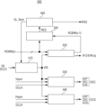
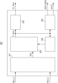
図4は、本実施形態に係るタイミング制御部の概略構成を示すブロック図である。タイミング制御部500は、信号変調部510、行メモリ部520、データ制御信号生成部530、ゲート制御信号生成部540、類似度判定部550およびスケジューラ560を含む。
Figure 4 is a block diagram showing a schematic configuration of the timing control unit according to this embodiment. The
信号変調部510は、データイネーブル信号DEのパルス幅を変調する。例えば、同色の副画素を連続して走査する場合に、変調されたデータイネーブル信号tDEを生成し、
副画素ごとに別個の充電期間を設定することができる。信号変調部510は、変調されたデータイネーブル信号tDEを、行メモリ部520、データ制御信号生成部530およびゲート制御信号生成部540に伝送する。
The
A separate charging period can be set for each sub-pixel. The
行メモリ部520は、行単位で画像データRGBWを保存する。例えば、行メモリ部520は、第x行の画像データRGBW(x)を保存する(xは正の整数、以下同様)。行メモリ部520は第(x-1)行の画像データRGBW(x-1)を類似度判定部550に伝送する。行メモリ部520は、信号変調部510から受信した変調されたデータイネーブル信号tDEに基づいて画像データRGBWを整列させる。行メモリ部520は、整列された画像データR’G’B’W’をデータ駆動部300に伝送する。
The
データ制御信号生成部530は、変調されたデータイネーブル信号tDE、ドットクロックDCLK、垂直同期信号Vsync等の信号を用いてデータ制御信号DSCを生成する。具体的には、データ制御信号生成部530は、変調されたデータイネーブル信号tDEを用いてソース出力イネーブル信号SOEの出力幅を変調し、各副画素のための充電期間を調整する。また、データ制御信号生成部530は、生成したソース・スタート・パルス信号SSP、ソース・シフト・クロック信号SSCをデータ駆動部300に伝送する。
The data control
ゲート制御信号生成部540は、変調されたデータイネーブル信号tDE、ドットクロックDCLK、水平同期信号Hsync等の信号を用いてゲート制御信号GCSを生成する。具体的には、ゲート制御信号生成部540は、変調されたデータイネーブル信号tDEを用いてゲート出力イネーブル信号GOEの出力幅を変調し、副画素のためのゲート信号の供給期間を調整する。また、ゲート制御信号生成部540は、生成したソース・スタート・パルス信号SSP、ソース・シフト・クロック信号SSCをデータ駆動部300に伝送する。
The gate control
類似度判定部550は、2行分の画像データの類似度を判定し、判定結果RESをスケジューラ560に伝送する。例えば、類似度判定部550は。行メモリ部520から第(x-1)行の画像データRGBW(x-1)を受信し、第x行の画像データRGBW(x)と類似しているか判定する。例えば、類似度判定部550は、2行の間の画像データが互いに類似すると判定したときに判定結果RESとして1を出力する。一方、類似度判定部550は、2行の間の画像データが互いに類似しないと判定したときに判定結果RESとして0を出力する。
The
スケジューラ560は、類似度判定部550から受信した判定結果RESに基づき、ゲート信号を送信するゲート線GLの番号を指定するゲート線指定信号GL_Numを生成する。ゲート線指定信号GL_Numは、変調されたデータイネーブル信号tDEを生成するために変調部510に伝送される。また、スケジューラ560は、行メモリ部520から伝送される画像データR’G’B’W’が格納されるべきレジスタを指定するためのレジスタ選択信号RSSをデータ駆動部300に伝送する。データ駆動部300は、受信したレジスタ選択信号RSSに基づき、画像データR’G’B’W’を指定されたレジスタに格納する。
The
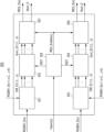
図5は、本実施形態に係るゲート駆動部200の概略構成を示すブロック図である。ゲート駆動部200は、第1レベルシフタ211、第2レベルシフタ212、第1シフトレジスタ221、222および第2シフトレジスタ231、232を含む。
Figure 5 is a block diagram showing a schematic configuration of the gate driver 200 according to this embodiment. The gate driver 200 includes a
第1レベルシフタ211および第2レベルシフタ212は、タイミング制御部500から入力されるクロック信号CLK1のTTL(Transistor-Transistor-Logic)レベルを遷移させる。具体的には、第1レベルシフタ211および第2レベルシフタ212は、表示パネル100に含まれるトランジスタをオン状態とオフ状態との間を遷移させるために、ゲートハイ電圧とゲートロー電圧との間を切り替えるための信号を生成する。第1レベルシフタ211は、生成された信号を第1シフトレジスタ221に伝送する。第2レベルシフタ212は、生成された信号を第1シフトレジスタ222に伝送する。また、第1レベルシフタ211は、タイミング制御部500から入力されるクロック信号CLK2のTTLレベルを遷移させる。具体的には、第1レベルシフタ211および第2レベルシフタ212は、表示パネル100に含まれるトランジスタをオン状態とオフ状態との間を遷移させるために、ゲートハイ電圧とゲートロー電圧との間を切り替えるための信号を生成する。第1レベルシフタ211は、生成された信号を第2シフトレジスタ231に伝送する。第2レベルシフタ212は、生成された信号を第2シフトレジスタ232に伝送する。
The
第1シフトレジスタ221、222の各々は、複数のステージを含む。複数のステージの各々は、Qノード、Qbノード、プルアップ素子およびプルダウン素子を含む。第1シフトレジスタ221、222は、表示パネル100の表示領域110の外側の非表示領域内にゲートインパネル(Gate-In-Panel,GIP)方式で配置される。例えば、第1シフトレジスタ221は、図5に示されるように、平面視において表示領域110の一方の短辺部(図5において左側短辺部)に隣接する非表示領域内に配置されることができる。また、第1シフトレジスタ222は、図5に示されるように、平面視において表示領域110の他方の短辺部(図5において右側短辺部)に隣接する非表示領域内に配置されることができる。第1シフトレジスタ221からのゲート線GLは、第1シフトレジスタ222からのゲート線GLと互いに連結された構造を有し得る。
Each of the
第1シフトレジスタ221は、第1レベルシフタ211から受信された信号に基づきゲート線GLにゲート信号を供給する。また、第1シフトレジスタ222は、第2レベルシフタ212から受信された信号に基づきゲート線GLにゲート信号を供給する。第1シフトレジスタ221、222は、タイミング制御部500からゲートスタート信号VST1を受信する。第1シフトレジスタ221、222は、受信されたゲートスタート信号VST1に基づき、キャリー信号を順次に生成する。第1シフトレジスタ221、222は、生成されたキャリー信号をゲートスタート信号として第1シフトレジスタ221、222に含まれる複数のステージのいずれかに供給する。第1シフトレジスタ221、222は、1フレームの走査開始時または1フレームの走査終了時にタイミング制御部500からリセット信号RST1を受信する。リセット信号RST1を介してQノードをリセットすることで、第1シフトレジスタ221、222のQノードおよびQBノードの電圧を安定的に維持させることができる。
The
第2シフトレジスタ231、232の各々は、複数のステージを含む。複数のステージの各々は、Qノード、Qbノード、プルアップ素子およびプルダウン素子を含む。第2シフトレジスタ231、232は、表示パネル100の表示領域110の外側の非表示領域内にゲートインパネル(Gate-In-Panel,GIP)方式で配置される。例えば、第2シフトレジスタ231は、図5に示されるように、平面視において表示領域110の一方の短辺部(図5において左側短辺部)に隣接する非表示領域内に、第1シフトレジスタ221と重畳するように配置されることができる。また、第2シフトレジスタ232は、図5に示されるように、平面視において表示領域110の他方の短辺部(図5において右側短辺部)に隣接する非表示領域内に、第1シフトレジスタ222と重畳するように配置されることができる。また、第2シフトレジスタ231、232は、それぞれ第1シフトレジスタ221、222と同一の領域に配置されることができる。即ち、本実施形態によるゲート駆動部200は、第2シフトレジスタ231、232から表示領域110までの距離が第1シフトレジスタ221、222からから表示領域110までの距離と同じとなるように構成され得る。また、第2シフトレジスタ231からのゲート線GLは、第2シフトレジスタ232からのゲート線GLと互いに連結された構造を有し得る。
Each of the
第2シフトレジスタ231は、第1レベルシフタ211から受信された信号に基づきゲート線GLにゲート信号を供給する。また、第2シフトレジスタ232は、第2レベルシフタ212から受信された信号に基づきゲート線GLにゲート信号を供給する。第2シフトレジスタ231、232は、タイミング制御部500からゲートスタート信号VST2を受信する。ここで、第2シフトレジスタ231、232がゲートスタート信号VST2を受信するタイミングは、第1シフトレジスタ221、222がゲートスタート信号VST1を受信するタイミングと異なる。第2シフトレジスタ231、232は、受信されたゲートスタート信号VST2に基づき、キャリー信号を順次に生成する。第2シフトレジスタ231、232は、生成されたキャリー信号をゲートスタート信号として第2シフトレジスタ231、232に含まれる複数のステージのいずれかに供給する。第2シフトレジスタ231、232は、1フレームの走査開始時または1フレームの走査終了時にタイミング制御部500からリセット信号RST2を受信する。リセット信号RST2を介してQノードをリセットすることで、第2シフトレジスタ231、232のQノードとQBノードの電圧を安定的に維持させることができる。ここで、第2シフトレジスタ231、232がリセット信号RST2を受信するタイミングは、第1シフトレジスタ221、222がリセット信号RST1を受信するタイミングと異なる。即ち、本実施形態による第2シフトレジスタ231、232は、回路構成上において第1シフトレジスタ221、222から独立して動作する。なお、ゲートスタート信号VST1およびゲートスタート信号VST2として、共通のゲートスタート信号が用いられることもできる。ただし、共通のゲートスタート信号が用いられた場合、ゲートスタート信号が入力されてから最初のクロックが入力されるまでシフトレジスタのステージはオン状態で待機することになる。よって、動作の安定性の観点から、相互に独立した信号であるゲートスタート信号VST1およびゲートスタート信号VST2を用いることが望ましい。
The
図6は本実施形態に係る第1シフトレジスタ221,222に含まれるステージとクロック配線との間の接続を示す回路図である。第1シフトレジスタ221,222は複数のステージを含む。複数のステージの各々は、Qノード、Qbノード、プルアップ素子、プルダウン素子を含む。
FIG. 6 is a circuit diagram showing the connections between the stages included in the
第1シフトレジスタ221,222のプルアップ素子はトランジスタで構成されることができる。プルアップ素子のゲートはQノードと電気的に接続される。プルアップ素子のソースまたはドレインはクロック信号の入力端と電気的に接続される。プルアップ素子のドレインまたはソースはプルダウン素子のソースまたはドレインおよびクロック信号の出力端と電気的に接続される。プルアップ素子は、Qノードの電圧によりオン状態に遷移し、クロック信号を走査信号(ゲート信号)として出力する。
The pull-up elements of the
第1シフトレジスタ221,222のプルダウン素子はトランジスタで構成されることができる。プルアップ素子のゲートはQbノードと電気的に接続される。プルダウン素子のソースまたはドレインはプルアップ素子のドレインまたはソースおよびクロック信号の出力端と電気的に接続される。プルダウン素子のドレインまたはソースは低電位電源GVSSと電気的に接続される。プルダウン素子は、Qbノードの電圧によりオン状態に遷移し、基底電圧をローレベルの走査信号として出力する。
The pull-down elements of the
各ステージにおいて、プルアップ素子がオン状態のときにはプルダウン素子はオフ状態である。即ち、Qノードにプルアップ素子をオン状態にするオン電圧が印加されているとき、Qbノードにプルダウン素子をオフ状態にするオフ電圧が印加されている。この状態をステージのオン状態と呼ぶ。また、各ステージにおいて、プルダウン素子がオン状態のときにはプルアップ素子はオフ状態である。即ち、Qbノードにプルダウン素子をオン状態にするオン電圧が印加されているとき、Qノードにプルアップ素子をオフ状態にするオフ電圧が印加されている。この状態をステージのホールド状態と呼ぶ。 In each stage, when the pull-up element is in the on state, the pull-down element is in the off state. That is, when an on voltage that turns the pull-up element on is applied to the Q node, an off voltage that turns the pull-down element off is applied to the Qb node. This state is called the on state of the stage. Also, in each stage, when the pull-down element is in the on state, the pull-up element is in the off state. That is, when an on voltage that turns the pull-down element on is applied to the Qb node, an off voltage that turns the pull-up element off is applied to the Q node. This state is called the hold state of the stage.
以下に、図6に示されるQ(1)ノードおよびQb(1)ノードを含む第1ステージSTG1について説明する。第1シフトレジスタ221,222は、Q(1)ノードからゲート駆動部の動作の開始を指示するゲートスタート信号VST1の印加を受ける。第1ステージSTG1には3つのプルアップ素子が含まれている。3つのプルアップ素子の各ゲートノードはQ(1)ノードと共通に連結されており、3つのプルアップ素子は、Q(1)ノードの電圧によってオン状態に遷移する。1つめのプルアップ素子のソースまたはドレインはキャリーシフトクロック信号CRCLK1の入力端と連結されており、1つめのプルアップ素子のドレインまたはソースは走査信号の出力端C1と連結されている。よって、プルアップ素子がQノードの電圧によってオン状態に遷移されると、キャリーシフトクロック信号CRCLK1が走査信号の出力端から出力される。キャリーシフトクロックは、キャリー信号を生成するためのクロック信号である。2つめのプルアップ素子のソースまたはドレインはスキャンシフトクロック信号SCCLK1の入力端と連結されており、2つめのプルアップ素子のドレインまたはソースは走査信号の出力端S1と連結されている。よって、プルアップ素子がQノードの電圧によってオン状態に遷移されると、スキャンシフトクロック信号SCCLK1が走査信号の出力端から出力され得る。スキャンシフトクロック信号は、パルスを有する走査信号を生成するためのクロック信号である。例えばスキャンシフトクロック信号SCCLK1は、ゲート線GL1によって伝送されるゲート信号を生成するためのクロック信号である。3つめのプルアップ素子のソースまたはドレインはスキャンシフトクロック信号SCCLK3の入力端と連結されており、3つめのプルアップ素子のドレインまたはソースは走査信号の出力端S3と連結されている。よって、プルアップ素子がQノードの電圧によってオン状態に遷移されると、スキャンシフトクロック信号SCCLK3が走査信号の出力端から出力され得る。例えばスキャンシフトクロック信号SCCLK3は、ゲート線GL3によって伝送されるゲート信号を生成するためのクロック信号である。
The first stage STG1 including the Q(1) node and the Qb(1) node shown in FIG. 6 will be described below. The
また、第1ステージSTG1には3つのプルダウン素子が含まれている。3つのプルダウン素子の各ゲートノードはQb(1)ノードと共通に連結されており、3つのプルダウン素子は、Qb(1)ノードの電圧によってオン状態に遷移する。3つのプルダウン素子の各々はドレインまたはソースは低電位電源GVSSと連結されており、3つのプルダウン素子のソースまたはドレインは走査信号の出力端C1、S1、S3とそれぞれ連結されている。よって、プルダウン素子がQbノードの電圧によってオン状態に遷移されると、ローレベルの走査信号としての基底電圧が出力端C1、S1、S3にそれぞれ出力される。 The first stage STG1 also includes three pull-down elements. The gate nodes of the three pull-down elements are commonly connected to the Qb(1) node, and the three pull-down elements transition to an on state according to the voltage of the Qb(1) node. The drain or source of each of the three pull-down elements is connected to the low-potential power supply GVSS, and the source or drain of each of the three pull-down elements is connected to the output terminals C1, S1, and S3 of the scanning signal, respectively. Therefore, when the pull-down elements transition to an on state according to the voltage of the Qb node, a ground voltage as a low-level scanning signal is output to the output terminals C1, S1, and S3, respectively.
図6に示されるQ(3)ノードおよびQb(3)ノードを含む第3ステージSTG3からQ(11)ノードおよびQb(11)ノードを含む第11ステージSTG11までについても、上述の第1ステージSTG1と同様に構成され得る。なお、第11ステージSTG11に含まれるQ(11)ノードには、リセット信号RST1が印加されるように構成されることができる。また、第1シフトレジスタ221,222は、1つのQbノードが2つのステージによって共有されるように構成されることもできる。例えば、第1ステージSTG1のQb(1)ノードおよび第3ステージSTG3のQb(3)ノードは第1Qb共通ノード(不図示)で構成され、第1ステージSTG1および第3ステージSTG3は、第1Qb共通ノードを共有するように構成されることができる。同様に、第5ステージSTG5のQb(5)ノードおよび第7ステージSTG7のQb(7)ノードは第2Qb共通ノード(不図示)で構成され、第5ステージSTG5および第7ステージSTG7は、第2Qb共通ノードを共有するように構成されることができる。同様に、第9ステージSTG9のQb(9)ノードおよび第11ステージSTG11のQb(11)ノードは第3Qb共通ノード(不図示)で構成され、第9ステージSTG9および第11ステージSTG11は、第3Qb共通ノードを共有するように構成されることができる。上記構成によれば、Qbノードの配置によって占有される領域が減少される。結果として、第1シフトレジスタ221、222が非表示領域を占有する回路面積は減少される。したがって、表示装置10のベゼル幅をより小さくすることができる。なお、第1シフトレジスタ221,222は、第2シフトレジスタ231,232から独立したシフトレジスタであるため、第1シフトレジスタ221,222に含まれるステージは、第2シフトレジスタ231,232に含まれるステージとQbノードを共有しない。
The third stage STG3 including the Q(3) node and the Qb(3) node shown in FIG. 6 to the eleventh stage STG11 including the Q(11) node and the Qb(11) node can be configured in the same manner as the first stage STG1 described above. The Q(11) node included in the eleventh stage STG11 can be configured to receive a reset signal RST1. The
図7は本実施形態に係る第2シフトレジスタ231,232に含まれるステージとクロック配線との間の接続を示す回路図である。第2シフトレジスタ231,232は複数のステージを含む。複数のステージの各々は、Qノード、Qbノード、プルアップ素子、プルダウン素子を含む。
Figure 7 is a circuit diagram showing the connections between the stages included in the
第2シフトレジスタ231,232のプルアップ素子はトランジスタで構成されることができる。プルアップ素子のゲートはQノードと電気的に接続される。プルアップ素子のソースまたはドレインはクロック信号の入力端と電気的に接続される。プルアップ素子のドレインまたはソースはプルダウン素子のソースまたはドレインおよびクロック信号の出力端と電気的に接続される。プルアップ素子は、Qノードの電圧によりオン状態に遷移し、クロック信号を走査信号として出力する。
The pull-up elements of the
第2シフトレジスタ231,232のプルダウン素子はトランジスタで構成されることができる。プルアップ素子のゲートはQbノードと電気的に接続される。プルダウン素子のソースまたはドレインはプルアップ素子のドレインまたはソースおよびクロック信号の出力端と電気的に接続される。プルダウン素子のドレインまたはソースは低電位電源GVSSと電気的に接続される。プルダウン素子は、Qbノードの電圧によりオン状態に遷移し、基底電圧をローレベルの走査信号として出力する。
The pull-down elements of the
各ステージにおいて、プルアップ素子がオン状態のときにはプルダウン素子はオフ状態である。即ち、Qノードにプルアップ素子をオン状態にするオン電圧が印加されているとき、Qbノードにプルダウン素子をオフ状態にするオフ電圧が印加されている。また、各ステージにおいて、プルダウン素子がオン状態のときにはプルアップ素子はオフ状態である。即ち、Qbノードにプルダウン素子をオン状態にするオン電圧が印加されているとき、Qノードにプルアップ素子をオフ状態にするオフ電圧が印加されている。 In each stage, when the pull-up element is on, the pull-down element is off. That is, when an on voltage that turns the pull-up element on is applied to the Q node, an off voltage that turns the pull-down element off is applied to the Qb node. Also, in each stage, when the pull-down element is on, the pull-up element is off. That is, when an on voltage that turns the pull-down element on is applied to the Qb node, an off voltage that turns the pull-up element off is applied to the Q node.
以下に、図7に示されるQ(2)ノードおよびQb(2)ノードを含む第2ステージSTG2について説明する。第2シフトレジスタ231,232は、Q(2)ノードからゲート駆動部の動作の開始を指示するゲートスタート信号VST2の印加を受ける。ゲートスタート信号VST2は、第1シフトレジスタ221,222に印加されるゲートスタート信号VST1から独立した信号である。第2ステージSTG2には3つのプルアップ素子が含まれている。3つのプルアップ素子の各ゲートノードはQ(2)ノードと共通に連結されており、3つのプルアップ素子は、Q(2)ノードの電圧によってオン状態に遷移する。1つめのプルアップ素子のソースまたはドレインはキャリーシフトクロック信号CRCLK2の入力端と連結されており、1つめのプルアップ素子のドレインまたはソースは走査信号の出力端C2と連結されている。よって、プルアップ素子がQノードの電圧によってオン状態に遷移されると、キャリーシフトクロック信号CRCLK2が走査信号の出力端から出力される。2つめのプルアップ素子のソースまたはドレインはスキャンシフトクロック信号SCCLK2の入力端と連結されており、2つめのプルアップ素子のドレインまたはソースは走査信号の出力端S2と連結されている。よって、プルアップ素子がQノードの電圧によってオン状態に遷移されると、スキャンシフトクロック信号SCCLK2が走査信号の出力端から出力され得る。例えばスキャンシフトクロック信号SCCLK2は、ゲート線GL2によって伝送されるゲート信号を生成するためのクロック信号である。3つめのプルアップ素子のソースまたはドレインはスキャンシフトクロック信号SCCLK4の入力端と連結されており、3つめのプルアップ素子のドレインまたはソースは走査信号の出力端S4と連結されている。よって、プルアップ素子がQノードの電圧によってオン状態に遷移されると、スキャンシフトクロック信号SCCLK4が走査信号の出力端から出力され得る。例えばスキャンシフトクロック信号SCCLK4は、ゲート線GL4によって伝送されるゲート信号を生成するためのクロック信号である。
The second stage STG2 including the Q(2) node and the Qb(2) node shown in FIG. 7 will be described below. The
また、第2ステージSTG2には3つのプルダウン素子が含まれている。3つのプルダウン素子の各ゲートノードはQb(2)ノードと共通に連結されており、3つのプルダウン素子は、Qb(2)ノードの電圧によってオン状態に遷移する。3つのプルダウン素子の各々はドレインまたはソースは低電位電源GVSSと連結されており、3つのプルダウン素子のソースまたはドレインは走査信号の出力端C2、S2、S4とそれぞれ連結されている。よって、プルダウン素子がQbノードの電圧によってオン状態に遷移されると、ローレベルの走査信号としての基底電圧が出力端C2、S2、S4にそれぞれ出力される。 The second stage STG2 also includes three pull-down elements. The gate nodes of the three pull-down elements are commonly connected to the Qb(2) node, and the three pull-down elements transition to an on state according to the voltage of the Qb(2) node. The drain or source of each of the three pull-down elements is connected to the low-potential power supply GVSS, and the source or drain of each of the three pull-down elements is connected to the output terminals C2, S2, and S4 of the scanning signal, respectively. Therefore, when the pull-down elements transition to an on state according to the voltage of the Qb node, a ground voltage as a low-level scanning signal is output to the output terminals C2, S2, and S4, respectively.
図7に示されるQ(4)ノードおよびQb(4)ノードを含む第4ステージSTG4からQ(12)ノードおよびQb(12)ノードを含む第12ステージSTG12までについても、上述の第2ステージSTG2と同様に構成され得る。なお、第12ステージSTG12に含まれるQ(12)ノードには、リセット信号RST2が印加されるように構成されることができる。リセット信号RST2は、第1シフトレジスタ221,222に印加されるリセット信号RST1から独立した信号である。また、第2シフトレジスタ231,232は、1つのQbノードが2つのステージによって共有されるように構成されることもできる。例えば、第2ステージSTG2のQb(2)ノードおよび第4ステージSTG4のQb(4)ノードは第4Qb共通ノード(不図示)で構成され、第2ステージSTG2および第4ステージSTG4は、第4Qb共通ノードを共有するように構成されることができる。同様に、第6ステージSTG6のQb(6)ノードおよび第8ステージSTG8のQb(8)ノードは第5Qb共通ノード(不図示)で構成され、第6ステージSTG6および第8ステージSTG8は、第5Qb共通ノードを共有するように構成されることができる。同様に、第10ステージSTG10のQb(10)ノードおよび第12ステージSTG12のQb(12)ノードは第6Qb共通ノード(不図示)で構成され、第10ステージSTG10および第12ステージSTG12は、第6Qb共通ノードを共有するように構成されることができる。上記構成によれば、Qbノードの配置によって占有される領域が減少される。結果として、第2シフトレジスタ231、232が非表示領域を占有する回路面積は減少される。したがって、表示装置10のベゼル幅をより小さくすることができる。なお、第2シフトレジスタ231,232は、第1シフトレジスタ221,222から独立したシフトレジスタであるため、第2シフトレジスタ231,232に含まれるステージは、第1シフトレジスタ221,222に含まれるステージとQbノードを共有しない。
The fourth stage STG4 including the Q(4) node and the Qb(4) node shown in FIG. 7 to the twelfth stage STG12 including the Q(12) node and the Qb(12) node can be configured in the same manner as the second stage STG2 described above. The Q(12) node included in the twelfth stage STG12 can be configured to receive a reset signal RST2. The reset signal RST2 is a signal independent of the reset signal RST1 applied to the
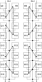
図8は、本実施形態による第1シフトレジスタ221,222に含まれるステージおよび第2シフトレジスタ231,232に含まれるステージとクロック配線との間の接続の一例を示す回路図である
Figure 8 is a circuit diagram showing an example of the connection between the stages included in the
図5に示されるように、第2シフトレジスタ231,232は、平面視において表示パネル100の非表示領域の中に、の第1シフトレジスタ221,222と重畳するように配置されることができる。また、第1シフトレジスタ221,222および第2シフトレジスタ231,232は、GIP方式で実装されることができる。たとえば、第1シフトレジスタ221,222が第1GIPとして表示パネル100の中に実装され、第2シフトレジスタ231,232を第2GIPとして表示パネルの中に実装された場合を、図8を参照しながら説明する。本例において、第1GIPおよび第2GIPは、同一の低電位電源GVSSを共有する同一の回路領域に配される。具体的には、第1GIPの第3ステージSTG3の次段には第2GIPの第2ステージSTG2が配されている。また、第2GIPの第4ステージSTG4の次段には第1GIPの第5ステージSTG5および第2GIPの第4ステージSTG4が配されている。また、第1GIPの第7ステージSTG7の次段には第2GIPの第6ステージSTG6が配されている。ただし、上述の通り、第1GIPおよび第2GIPは、互いに独立したシフトレジスタである。具体的には、第1GIPおよび第2GIPは、入力クロック信号CRCLK,SCCLKを共有しない。また、第1GIPはゲートスタート信号VST1およびリセット信号RST1を受信し、第2GIPは、ゲートスタート信号VST1およびリセット信号RST1からそれぞれ独立した別個のゲートスタート信号VST2およびリセット信号RST2を受信する。第1GIPのステージに入出力されるキャリー信号は第1GIPの他のステージに伝送される一方で、第1GIPのステージに入出力されるキャリー信号は第2GIPのステージには伝送されない。同様に、第2GIPのステージに入出力されるキャリー信号は第2GIPの他のステージに伝送される一方で、第2GIPのステージに入出力されるキャリー信号は第1GIPのステージには伝送されない。即ち、第1GIPは、第2GIPの動作から独立して駆動される。同様に、第2GIPは、第1GIPの動作から独立して駆動される。
As shown in FIG. 5, the
図9は、本実施形態に係る第1GIPの信号出力端および第2GIPの信号出力端とゲート線との間の対応関係を示す図である。本実施形態によれば、第1GIPおよび第2GIPに含まれる走査信号の出力端S1~S16の配置は、ゲート線GL1~GL16の配置と対応していない。即ち、図9に示されるように、第1GIPの第1ステージSTG1の出力端S3のゲート線GL3への出力線は、第2GIPの第2ステージSTG2の出力端S2のゲート線GL2への出力線と交差する。また、第1GIPの第3ステージSTG3の出力端S5のゲート線GL5への出力線は、第2GIPの第2ステージSTG2の出力端S2のゲート線GL2への出力線および第2GIPの第2ステージSTG2の出力端S4のゲート線GL4への出力線と交差する。また、第1GIPの第3ステージSTG3の出力端S7のゲート線GL7への出力線は、第2GIPの第2ステージSTG2の出力端S2のゲート線GL2への出力線、第2GIPの第2ステージSTG2の出力端S4のゲート線GL4への出力線および第2GIPの第4ステージSTG4の出力端S6のゲート線GL6への出力線と交差する。また、第1GIPの第5ステージSTG5の出力端S11のゲート線GL11への出力線は、第2GIPの第6ステージSTG6の出力端S10のゲート線GL10への出力線と交差する。また、第1GIPの第7ステージSTG7の出力端S13のゲート線GL13への出力線は、第2GIPの第6ステージSTG6の出力端S10のゲート線GL10への出力線および第2GIPの第6ステージSTG6の出力端S12のゲート線GL12への出力線と交差する。また、第1GIPの第7ステージSTG7の出力端S15のゲート線GL15への出力線は、第2GIPの第6ステージSTG6の出力端S10のゲート線GL10への出力線、第2GIPの第6ステージSTG6の出力端S12のゲート線GL12への出力線および第2GIPの第8ステージSTG8の出力端S14のゲート線GL14への出力線と交差する。即ち、第1GIPから供給されるゲート信号の出力端から当該出力端に対応するゲート線までを直線で結ぶ経路は、第2GIPから供給されるゲート信号の出力端から当該出力端に対応するゲート線までを直線で結ぶ経路と交差するように構成され得る。なお、第1GIPの第1ステージSTG1の出力端S1のゲート線GL1への出力線および第1GIPの第5ステージSTG5の出力端S9のゲート線GL9への出力線は、第2GIPの信号出力端からの出力線と交差しない。また、第2GIPの第4ステージSTG4の出力端S8のゲート線GL8への出力線および第2GIPの第8ステージSTG8の出力端S16のゲート線GL16への出力線は、第1GIPの信号出力端からの出力線と交差しない。 Figure 9 is a diagram showing the correspondence between the signal output terminals of the first GIP and the second GIP and the gate lines according to this embodiment. According to this embodiment, the arrangement of the output terminals S1 to S16 of the scanning signals included in the first GIP and the second GIP does not correspond to the arrangement of the gate lines GL1 to GL16. That is, as shown in Figure 9, the output line of the output terminal S3 of the first stage STG1 of the first GIP to the gate line GL3 intersects with the output line of the output terminal S2 of the second stage STG2 of the second GIP to the gate line GL2. In addition, the output line of the output terminal S5 of the third stage STG3 of the first GIP to the gate line GL5 intersects with the output line of the output terminal S2 of the second stage STG2 of the second GIP to the gate line GL2 and the output line of the output terminal S4 of the second stage STG2 of the second GIP to the gate line GL4. The output line of the output terminal S7 of the third stage STG3 of the first GIP to the gate line GL7 crosses the output line of the output terminal S2 of the second stage STG2 of the second GIP to the gate line GL2, the output line of the output terminal S4 of the second stage STG2 of the second GIP to the gate line GL4, and the output line of the output terminal S6 of the fourth stage STG4 of the second GIP to the gate line GL6. The output line of the output terminal S11 of the fifth stage STG5 of the first GIP to the gate line GL11 crosses the output line of the output terminal S10 of the sixth stage STG6 of the second GIP to the gate line GL10. The output line of the output terminal S13 of the seventh stage STG7 of the first GIP to the gate line GL13 crosses the output line of the output terminal S10 of the sixth stage STG6 of the second GIP to the gate line GL10 and the output line of the output terminal S12 of the sixth stage STG6 of the second GIP to the gate line GL12. Also, the output line of the output terminal S15 of the seventh stage STG7 of the first GIP to the gate line GL15 crosses the output line of the output terminal S10 of the sixth stage STG6 of the second GIP to the gate line GL10, the output line of the output terminal S12 of the sixth stage STG6 of the second GIP to the gate line GL12, and the output line of the output terminal S14 of the eighth stage STG8 of the second GIP to the gate line GL14. That is, a straight line path from the output terminal of the gate signal supplied from the first GIP to the gate line corresponding to the output terminal can be configured to cross a straight line path from the output terminal of the gate signal supplied from the second GIP to the gate line corresponding to the output terminal. Note that the output line of the output terminal S1 of the first stage STG1 of the first GIP to the gate line GL1 and the output line of the output terminal S9 of the fifth stage STG5 of the first GIP to the gate line GL9 do not cross the output line from the signal output terminal of the second GIP. In addition, the output line from the output end S8 of the fourth stage STG4 of the second GIP to the gate line GL8 and the output line from the output end S16 of the eighth stage STG8 of the second GIP to the gate line GL16 do not intersect with the output line from the signal output end of the first GIP.
図10は、本実施形態に係る第1GIPおよび第2GIPのオン状態とホールド状態の遷移の一例を示す図である。上述の通り、本実施形態に係る第1GIPおよび第2GIPに含まれる各ステージは、プルアップ素子およびプルダウン素子に印加される電圧にしたがってオン状態またはホールド状態となる。ホールド状態にあるステージからは、走査信号は出力されない。一方、オン状態にあるステージからは、走査信号が出力されることができる。しかしながら、同クロックにおいて2以上の走査信号またはキャリー信号が出力端から伝送されないようにするために、オン状態のステージの数を制限する必要がある。具体的には、例えばGIPに入力されるクロック数をxとした場合、オン状態のステージの数は2x未満としなければならない(xは正の整数)。本実施形態の第1GIPは、キャリー信号を介して、順次ホールド状態のステージをオン状態へ遷移させる。また、本実施形態の第1GIPは、キャリー信号を介して、順次オン状態のステージをホールド状態へ遷移させる。同様に、本実施形態の第2GIPは、キャリー信号を介して、順次ホールド状態のステージをオン状態へ遷移させる。また、本実施形態の第2GIPは、キャリー信号を介して、順次オン状態のステージをホールド状態へ遷移させる。第1GIPで用いられるキャリー信号は、第2GIPに伝送されない。よって、第1GIPのステージのオン状態とホールド状態との間の遷移は、第2GIPの動作から独立している。同様に、第1GIPで用いられるキャリー信号は、第2GIPに伝送されない。よって、第2GIPのステージのオン状態とホールド状態との間の遷移は、第1GIPの動作から独立している。 FIG. 10 is a diagram showing an example of the transition between the on state and the hold state of the first GIP and the second GIP according to this embodiment. As described above, each stage included in the first GIP and the second GIP according to this embodiment is in the on state or the hold state according to the voltage applied to the pull-up element and the pull-down element. A stage in the hold state does not output a scan signal. On the other hand, a stage in the on state can output a scan signal. However, in order to prevent two or more scan signals or carry signals from being transmitted from the output terminal in the same clock, it is necessary to limit the number of stages in the on state. Specifically, for example, if the number of clocks input to the GIP is x, the number of stages in the on state must be less than 2x (x is a positive integer). The first GIP of this embodiment sequentially transitions the stages in the hold state to the on state via the carry signal. Also, the first GIP of this embodiment sequentially transitions the stages in the on state to the hold state via the carry signal. Similarly, the second GIP of this embodiment sequentially transitions the stages in the hold state to the on state via the carry signal. In addition, the second GIP of this embodiment transitions the stages in the on state to the hold state sequentially via the carry signal. The carry signal used in the first GIP is not transmitted to the second GIP. Thus, the transition between the on state and the hold state of the stage in the first GIP is independent of the operation of the second GIP. Similarly, the carry signal used in the first GIP is not transmitted to the second GIP. Thus, the transition between the on state and the hold state of the stage in the second GIP is independent of the operation of the first GIP.
図10には、第1GIPおよび第2GIPに含まれる各ステージのオン状態とホールド状態との間の遷移の一例が示されている。本例では、奇数番目のゲート線GL1、GL3、...、GL31には、第1GIPから走査信号(ゲート信号)が伝送される。例えば、図3に示される副画素の配列によれば、第1GIPは、奇数番目のゲート線を介して赤色副画素Rの第1スイッチ素子T1および白色副画素Wの第1スイッチ素子T1にゲート電圧を供給する。一方、偶数番目のゲート線GL2、GL4、...、GL32には、第2GIPから走査信号(ゲート信号)が伝送される。例えば、図3に示される副画素の配列によれば、第2GIPは、偶数番目のゲート線を介して緑色副画素Gの第1スイッチ素子T1および青色副画素Bの第1スイッチ素子T1にゲート電圧を供給する。なお、第1GIPに接続されるゲート線は奇数番目のゲート線に限定されず、第2GIPに接続されるゲート線は偶数番目のゲート線に限定されない。ゲート駆動部の回路設計等に従い、第1GIPおよび第2GIPは、任意の場所に配置されたゲート線と接続され得る。 10 shows an example of the transition between the on state and the hold state of each stage included in the first GIP and the second GIP. In this example, the first GIP transmits a scanning signal (gate signal) to the odd-numbered gate lines GL1, GL3, ..., GL31. For example, according to the arrangement of the subpixels shown in FIG. 3, the first GIP supplies a gate voltage to the first switch element T1 of the red subpixel R and the first switch element T1 of the white subpixel W via the odd-numbered gate lines. On the other hand, the second GIP transmits a scanning signal (gate signal) to the even-numbered gate lines GL2, GL4, ..., GL32. For example, according to the arrangement of the subpixels shown in FIG. 3, the second GIP supplies a gate voltage to the first switch element T1 of the green subpixel G and the first switch element T1 of the blue subpixel B via the even-numbered gate lines. In addition, the gate lines connected to the first GIP are not limited to odd-numbered gate lines, and the gate lines connected to the second GIP are not limited to even-numbered gate lines. Depending on the circuit design of the gate driver, the first GIP and the second GIP can be connected to gate lines located in any position.
図10に示される例では、奇数番目のゲート線を介して所定の数の走査信号が連続して伝送された後に、偶数番目のゲート線を介して所定の数の走査信号が連続して伝送される。例えば、図3に示される副画素の配列によれば、最初に、第1GIPが、奇数番目のゲート線を介して表示パネル100の各行に配された赤色副画素Rおよび白色副画素Wに、走査信号を所定の行数にわたり連続して供給する。次いで、第2GIPが、偶数番目のゲート線を介して表示パネル100の各行に配された緑色副画素Gおよび青色副画素Bに、走査信号を所定の行数に渡り連続して供給する。
In the example shown in FIG. 10, a predetermined number of scanning signals are transmitted continuously through odd-numbered gate lines, and then a predetermined number of scanning signals are transmitted continuously through even-numbered gate lines. For example, according to the arrangement of subpixels shown in FIG. 3, the first GIP first supplies scanning signals continuously through a predetermined number of rows to the red subpixels R and white subpixels W arranged in each row of the
具体的には、クロック(1)において、第1GIPに含まれる第1ステージ、第3ステージ、第5ステージ、第7ステージおよび第2GIPに含まれる第2ステージ、第4ステージ、第6ステージ、第8ステージがオン状態である。このとき、第1GIPは、オン状態のステージに対応するゲート線のグループ(GL1、GL3、GL5、GL7、GL9、GL11、GL13、GL15)を介してゲート信号の供給が可能な状態にある。また、第2GIPは、オン状態のステージに対応するゲート線のグループ(GL2、GL4、GL6、GL8、GL10、GL12、GL14、GL16)を介してゲート信号の供給が可能な状態にある。一方、第1GIPに含まれる第9ステージ、第11ステージ、第13ステージ、第15ステージおよび第2GIPに含まれる第10ステージ、第12ステージ、第14ステージ、第16ステージがホールド状態である。クロック(1)において、例えば、第1GIPは、第3ステージからゲート線GL5に走査信号を伝送する。結果として、ゲート線GL5と電気的に接続されている赤色副画素Rおよび白色副画素Wに走査信号が供給される。第3ステージ以外のステージからゲート線GLに走査信号は伝送されない。なお、第1GIPは、クロック(1)とクロック(2)との間の時刻に、第3ステージからゲート線GL7に走査信号を伝送し得る。 Specifically, in clock (1), the first, third, fifth, and seventh stages included in the first GIP and the second, fourth, sixth, and eighth stages included in the second GIP are in the on state. At this time, the first GIP is in a state in which a gate signal can be supplied via the group of gate lines (GL1, GL3, GL5, GL7, GL9, GL11, GL13, and GL15) corresponding to the on-state stages. Also, the second GIP is in a state in which a gate signal can be supplied via the group of gate lines (GL2, GL4, GL6, GL8, GL10, GL12, GL14, and GL16) corresponding to the on-state stages. Meanwhile, the ninth, eleventh, thirteenth, and fifteenth stages included in the first GIP and the tenth, twelfth, fourteenth, and sixteenth stages included in the second GIP are in the hold state. In clock (1), for example, the first GIP transmits a scanning signal from the third stage to gate line GL5. As a result, the scanning signal is supplied to the red subpixel R and the white subpixel W that are electrically connected to gate line GL5. No scanning signal is transmitted to the gate line GL from stages other than the third stage. Note that the first GIP may transmit a scanning signal from the third stage to gate line GL7 at a time between clock (1) and clock (2).
クロック(2)において、第1GIPに含まれる第1ステージがオン状態からホールド状態に遷移される。一方、クロック(2)において、第1GIPに含まれる第9ステージがホールド状態からオン状態に遷移される。第1GIPに含まれる第1ステージおよび第9ステージ以外のステージは、クロック(1)における状態と同じ状態に維持される。このとき、第1GIPは、オン状態のステージに対応するゲート線のグループ(GL5、GL7、GL9、GL11、GL13、GL15、GL17、GL19)を介してゲート信号の供給が可能な状態にある。また、第2GIPに含まれるすべてのステージは、クロック(1)における状態と同じ状態に維持される。即ち、第2GIPは、オン状態のステージに対応するゲート線のグループ(GL2、GL4、GL6、GL8、GL10、GL12、GL14、GL16)を介してゲート信号の供給が可能な状態にある。クロック(2)において、第1GIPは、第5ステージからゲート線GL9に走査信号を伝送する。結果として、ゲート線GL9と電気的に接続されている赤色副画素Rおよび白色副画素Wに走査信号が供給される。第5ステージ以外のステージからゲート線GLに走査信号は伝送されない。なお、第1GIPは、クロック(2)とクロック(3)との間の時刻に、第5ステージからゲート線GL11に走査信号を伝送し得る。 In clock (2), the first stage included in the first GIP transitions from an on state to a hold state. Meanwhile, in clock (2), the ninth stage included in the first GIP transitions from a hold state to an on state. Stages other than the first stage and the ninth stage included in the first GIP are maintained in the same state as in clock (1). At this time, the first GIP is in a state in which a gate signal can be supplied via the group of gate lines (GL5, GL7, GL9, GL11, GL13, GL15, GL17, GL19) corresponding to the on-state stage. In addition, all stages included in the second GIP are maintained in the same state as in clock (1). That is, the second GIP is in a state in which a gate signal can be supplied via the group of gate lines (GL2, GL4, GL6, GL8, GL10, GL12, GL14, GL16) corresponding to the on-state stage. In clock (2), the first GIP transmits a scanning signal from the fifth stage to the gate line GL9. As a result, the scanning signal is supplied to the red subpixel R and the white subpixel W that are electrically connected to the gate line GL9. No scanning signal is transmitted to the gate line GL from stages other than the fifth stage. Note that the first GIP may transmit a scanning signal from the fifth stage to the gate line GL11 at a time between clock (2) and clock (3).
クロック(3)において、第1GIPに含まれる第3ステージがオン状態からホールド状態に遷移される。一方、クロック(3)において、第1GIPに含まれる第11ステージがホールド状態からオン状態に遷移される。第1GIPに含まれる第3ステージおよび第11ステージ以外のステージならびに第2GIPに含まれるすべてのステージは、クロック(2)における状態と同じ状態に維持される。クロック(3)において、第1GIPは、第7ステージからゲート線GL13に走査信号を伝送する。結果として、ゲート線GL13と電気的に接続されている赤色副画素Rおよび白色副画素Wに走査信号が供給される。第7ステージ以外のステージからゲート線GLに走査信号は伝送されない。なお、第1GIPは、クロック(3)とクロック(4)との間の時刻に、第7ステージからゲート線GL15に走査信号を伝送し得る。 At clock (3), the third stage included in the first GIP transitions from an on state to a hold state. Meanwhile, at clock (3), the eleventh stage included in the first GIP transitions from a hold state to an on state. Stages other than the third stage and the eleventh stage included in the first GIP and all stages included in the second GIP are maintained in the same state as in clock (2). At clock (3), the first GIP transmits a scanning signal from the seventh stage to the gate line GL13. As a result, a scanning signal is supplied to the red subpixel R and the white subpixel W electrically connected to the gate line GL13. No scanning signal is transmitted from stages other than the seventh stage to the gate line GL. Note that the first GIP may transmit a scanning signal from the seventh stage to the gate line GL15 at a time between clock (3) and clock (4).
クロック(4)において、第1GIPに含まれる第5ステージがオン状態からホールド状態に遷移される。一方、クロック(4)において、第1GIPに含まれる第13ステージがホールド状態からオン状態に遷移される。第1GIPに含まれる第5ステージおよび第13ステージ以外のステージならびに第2GIPに含まれるすべてのステージは、クロック(3)における状態と同じ状態に維持される。クロック(4)において、第1GIPは、第9ステージからゲート線GL17に走査信号を伝送する。結果として、ゲート線GL17と電気的に接続されている赤色副画素Rおよび白色副画素Wに走査信号が供給される。第9ステージ以外のステージからゲート線GLに走査信号は伝送されない。なお、第1GIPは、クロック(4)とクロック(5)との間の時刻に、第9ステージからゲート線GL19に走査信号を伝送し得る。 At clock (4), the fifth stage included in the first GIP transitions from an on state to a hold state. Meanwhile, at clock (4), the thirteenth stage included in the first GIP transitions from a hold state to an on state. Stages other than the fifth and thirteenth stages included in the first GIP and all stages included in the second GIP are maintained in the same state as in clock (3). At clock (4), the first GIP transmits a scanning signal from the ninth stage to the gate line GL17. As a result, a scanning signal is supplied to the red subpixel R and the white subpixel W electrically connected to the gate line GL17. No scanning signal is transmitted from stages other than the ninth stage to the gate line GL. Note that the first GIP may transmit a scanning signal from the ninth stage to the gate line GL19 at a time between clock (4) and clock (5).
クロック(5)において、第1GIPに含まれる第7ステージがオン状態からホールド状態に遷移される。一方、クロック(5)において、第1GIPに含まれる第15ステージがホールド状態からオン状態に遷移される。第1GIPに含まれる第7ステージおよび第15ステージ以外のステージならびに第2GIPに含まれるすべてのステージは、クロック(4)における状態と同じ状態に維持される。クロック(5)において、第1GIPは、第11ステージからゲート線GL21に走査信号を伝送する。結果として、ゲート線GL21と電気的に接続されている赤色副画素Rおよび白色副画素Wに走査信号が供給される。第11ステージ以外のステージからゲート線GLに走査信号は伝送されない。なお、第1GIPは、クロック(5)とクロック(6)との間の時刻に、第11ステージからゲート線GL23に走査信号を伝送し得る。 At clock (5), the seventh stage included in the first GIP transitions from an on state to a hold state. Meanwhile, at clock (5), the fifteenth stage included in the first GIP transitions from a hold state to an on state. Stages other than the seventh stage and the fifteenth stage included in the first GIP and all stages included in the second GIP are maintained in the same state as in clock (4). At clock (5), the first GIP transmits a scanning signal from the eleventh stage to the gate line GL21. As a result, the scanning signal is supplied to the red subpixel R and the white subpixel W electrically connected to the gate line GL21. No scanning signal is transmitted from stages other than the eleventh stage to the gate line GL. Note that the first GIP may transmit a scanning signal from the eleventh stage to the gate line GL23 at a time between clock (5) and clock (6).
クロック(6)において、第2GIPに含まれる第2ステージがオン状態からホールド状態に遷移される。一方、クロック(6)において、第2GIPに含まれる第10ステージがホールド状態からオン状態に遷移される。第2GIPに含まれる第2ステージおよび第10ステージ以外のステージならびに第1GIPに含まれるすべてのステージは、クロック(5)における状態と同じ状態に維持される。クロック(6)において、第2GIPは、第4ステージからゲート線GL6に走査信号を伝送する。結果として、ゲート線GL6と電気的に接続されている緑色副画素Gおよび青色副画素Bに走査信号が供給される。第4ステージ以外のステージからゲート線GLに走査信号は伝送されない。なお、第2GIPは、クロック(6)とクロック(7)との間の時刻に、第4ステージからゲート線GL8に走査信号を伝送し得る。 At clock (6), the second stage included in the second GIP transitions from an on state to a hold state. Meanwhile, at clock (6), the tenth stage included in the second GIP transitions from a hold state to an on state. Stages other than the second stage and the tenth stage included in the second GIP and all stages included in the first GIP are maintained in the same state as in clock (5). At clock (6), the second GIP transmits a scanning signal from the fourth stage to the gate line GL6. As a result, the scanning signal is supplied to the green subpixel G and the blue subpixel B electrically connected to the gate line GL6. No scanning signal is transmitted to the gate line GL from stages other than the fourth stage. Note that the second GIP may transmit a scanning signal from the fourth stage to the gate line GL8 at a time between clock (6) and clock (7).
クロック(7)において、第2GIPに含まれる第4ステージがオン状態からホールド状態に遷移される。一方、クロック(7)において、第2GIPに含まれる第12ステージがホールド状態からオン状態に遷移される。第2GIPに含まれる第4ステージおよび第12ステージ以外のステージならびに第1GIPに含まれるすべてのステージは、クロック(6)における状態と同じ状態に維持される。クロック(7)において、第2GIPは、第6ステージからゲート線GL10に走査信号を伝送する。結果として、ゲート線GL10と電気的に接続されている緑色副画素Gおよび青色副画素Bに走査信号が供給される。第6ステージ以外のステージからゲート線GLに走査信号は伝送されない。なお、第2GIPは、クロック(7)とクロック(8)との間の時刻に、第6ステージからゲート線GL12に走査信号を伝送し得る。 At clock (7), the fourth stage included in the second GIP transitions from an on state to a hold state. Meanwhile, at clock (7), the twelfth stage included in the second GIP transitions from a hold state to an on state. Stages other than the fourth stage and the twelfth stage included in the second GIP and all stages included in the first GIP are maintained in the same state as in clock (6). At clock (7), the second GIP transmits a scanning signal from the sixth stage to the gate line GL10. As a result, a scanning signal is supplied to the green subpixel G and the blue subpixel B electrically connected to the gate line GL10. No scanning signal is transmitted from stages other than the sixth stage to the gate line GL. Note that the second GIP may transmit a scanning signal from the sixth stage to the gate line GL12 at a time between clocks (7) and (8).
クロック(8)において、第2GIPに含まれる第6ステージがオン状態からホールド状態に遷移される。一方、クロック(8)において、第2GIPに含まれる第14ステージがホールド状態からオン状態に遷移される。第2GIPに含まれる第6ステージおよび第14ステージ以外のステージならびに第1GIPに含まれるすべてのステージは、クロック(7)における状態と同じ状態に維持される。クロック(8)において、第2GIPは、第8ステージからゲート線GL14に走査信号を伝送する。結果として、ゲート線GL14と電気的に接続されている緑色副画素Gおよび青色副画素Bに走査信号が供給される。第8ステージ以外のステージからゲート線GLに走査信号は伝送されない。なお、第2GIPは、クロック(8)とクロック(9)との間の時刻に、第8ステージからゲート線GL16に走査信号を伝送し得る。 At clock (8), the sixth stage included in the second GIP transitions from an on state to a hold state. Meanwhile, at clock (8), the fourteenth stage included in the second GIP transitions from a hold state to an on state. Stages other than the sixth and fourteenth stages included in the second GIP and all stages included in the first GIP are maintained in the same state as in clock (7). At clock (8), the second GIP transmits a scanning signal from the eighth stage to the gate line GL14. As a result, the scanning signal is supplied to the green subpixel G and the blue subpixel B electrically connected to the gate line GL14. No scanning signal is transmitted from stages other than the eighth stage to the gate line GL. Note that the second GIP may transmit a scanning signal from the eighth stage to the gate line GL16 at a time between clock (8) and clock (9).
クロック(9)において、第2GIPに含まれる第8ステージがオン状態からホールド状態に遷移される。一方、クロック(9)において、第2GIPに含まれる第16ステージがホールド状態からオン状態に遷移される。第2GIPに含まれる第8ステージおよび第16ステージ以外のステージならびに第1GIPに含まれるすべてのステージは、クロック(8)における状態と同じ状態に維持される。クロック(9)において、第2GIPは、第10ステージからゲート線GL18に走査信号を伝送する。結果として、ゲート線GL18と電気的に接続されている緑色副画素Gおよび青色副画素Bに走査信号が供給される。第10ステージ以外のステージからゲート線GLに走査信号は伝送されない。なお、第2GIPは、クロック(9)の後の時刻に、第10ステージからゲート線GL20に走査信号を伝送し得る。 At clock (9), the 8th stage included in the second GIP transitions from an on state to a hold state. Meanwhile, at clock (9), the 16th stage included in the second GIP transitions from a hold state to an on state. Stages other than the 8th stage and the 16th stage included in the second GIP and all stages included in the first GIP are maintained in the same state as in clock (8). At clock (9), the second GIP transmits a scanning signal from the 10th stage to the gate line GL18. As a result, the scanning signal is supplied to the green subpixel G and the blue subpixel B electrically connected to the gate line GL18. The scanning signal is not transmitted to the gate line GL from stages other than the 10th stage. Note that the second GIP may transmit a scanning signal from the 10th stage to the gate line GL20 at a time after clock (9).
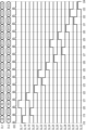
図11は、第1GIPおよび第2GIPに含まれる各ステージのオン状態とホールド状態との間の遷移に関して、図10に示された例とは別の一例を示す表である。図10と同一の構成についてはその記載は省略されることがある。 Figure 11 is a table showing another example, different from the example shown in Figure 10, regarding the transition between the on state and the hold state of each stage included in the first GIP and the second GIP. Descriptions of the same configuration as in Figure 10 may be omitted.
図11に示される例では、偶数番目のゲート線を介して所定の数の走査信号が連続して伝送された後に、奇数番目のゲート線を介して所定の数の走査信号が連続して伝送される。例えば、図3に示される副画素の配列によれば、最初に、第2GIPが、偶数番目のゲート線を介して表示パネル100の各行に配された緑色副画素Gおよび青色副画素Bに、走査信号を所定の行数にわたり連続して供給する。次いで、第1GIPが、奇数番目のゲート線を介して表示パネル100の各行に配された赤色副画素Rおよび白色副画素Wに、走査信号を所定の行数に渡り連続して供給する。
In the example shown in FIG. 11, a predetermined number of scanning signals are transmitted continuously through the even-numbered gate lines, and then a predetermined number of scanning signals are transmitted continuously through the odd-numbered gate lines. For example, according to the arrangement of subpixels shown in FIG. 3, the second GIP first supplies scanning signals continuously through a predetermined number of rows to the green subpixels G and blue subpixels B arranged in each row of the
具体的には、クロック(1)において、第1GIPに含まれる第1ステージ、第3ステージ、第5ステージ、第7ステージおよび第2GIPに含まれる第2ステージ、第4ステージ、第6ステージ、第8ステージがオン状態である。一方、第1GIPに含まれる第9ステージ、第11ステージ、第13ステージ、第15ステージおよび第2GIPに含まれる第10ステージ、第12ステージ、第14ステージ、第16ステージがホールド状態である。クロック(1)において、例えば、第2GIPは、第4ステージからゲート線GL6に走査信号を伝送する。結果として、ゲート線GL6と電気的に接続されている緑色副画素Gおよび青色副画素Bに走査信号が供給される。第4ステージ以外のステージからゲート線GLに走査信号は伝送されない。なお、第2GIPは、クロック(1)とクロック(2)との間の時刻に、第4ステージからゲート線GL8に走査信号を伝送し得る。 Specifically, in clock (1), the first, third, fifth, and seventh stages included in the first GIP and the second, fourth, sixth, and eighth stages included in the second GIP are in the on state. On the other hand, the ninth, eleventh, thirteenth, and fifteenth stages included in the first GIP and the tenth, twelfth, fourteenth, and sixteenth stages included in the second GIP are in the hold state. In clock (1), for example, the second GIP transmits a scanning signal from the fourth stage to the gate line GL6. As a result, the scanning signal is supplied to the green subpixel G and the blue subpixel B electrically connected to the gate line GL6. The scanning signal is not transmitted to the gate line GL from stages other than the fourth stage. Note that the second GIP may transmit a scanning signal from the fourth stage to the gate line GL8 at a time between clock (1) and clock (2).
クロック(2)において、第2GIPに含まれる第2ステージがオン状態からホールド状態に遷移される。一方、クロック(2)において、第2GIPに含まれる第10ステージがホールド状態からオン状態に遷移される。第2GIPに含まれる第2ステージおよび第10ステージ以外のステージならびに第1GIPに含まれるすべてのステージは、クロック(1)における状態と同じ状態に維持される。クロック(2)において、第2GIPは、第6ステージからゲート線GL10に走査信号を伝送する。結果として、ゲート線GL10と電気的に接続されている緑色副画素Gおよび青色副画素Bに走査信号が供給される。第6ステージ以外のステージからゲート線GLに走査信号は伝送されない。なお、第2GIPは、クロック(2)とクロック(3)との間の時刻に、第6ステージからゲート線GL12に走査信号を伝送し得る。 At clock (2), the second stage included in the second GIP transitions from an on state to a hold state. Meanwhile, at clock (2), the tenth stage included in the second GIP transitions from a hold state to an on state. Stages other than the second stage and the tenth stage included in the second GIP and all stages included in the first GIP are maintained in the same state as in clock (1). At clock (2), the second GIP transmits a scanning signal from the sixth stage to the gate line GL10. As a result, a scanning signal is supplied to the green subpixel G and the blue subpixel B electrically connected to the gate line GL10. No scanning signal is transmitted to the gate line GL from stages other than the sixth stage. Note that the second GIP may transmit a scanning signal from the sixth stage to the gate line GL12 at a time between clock (2) and clock (3).
クロック(3)において、第2GIPに含まれる第4ステージがオン状態からホールド状態に遷移される。一方、クロック(3)において、第2GIPに含まれる第12ステージがホールド状態からオン状態に遷移される。第2GIPに含まれる第4ステージおよび第12ステージ以外のステージならびに第1GIPに含まれるすべてのステージは、クロック(2)における状態と同じ状態に維持される。クロック(3)において、第2GIPは、第8ステージからゲート線GL14に走査信号を伝送する。結果として、ゲート線GL14と電気的に接続されている緑色副画素Gおよび青色副画素Bに走査信号が供給される。第8ステージ以外のステージからゲート線GLに走査信号は伝送されない。なお、第2GIPは、クロック(3)とクロック(4)との間の時刻に、第8ステージからゲート線GL16に走査信号を伝送し得る。 At clock (3), the fourth stage included in the second GIP transitions from an on state to a hold state. Meanwhile, at clock (3), the twelfth stage included in the second GIP transitions from a hold state to an on state. Stages other than the fourth stage and the twelfth stage included in the second GIP and all stages included in the first GIP are maintained in the same state as in clock (2). At clock (3), the second GIP transmits a scanning signal from the eighth stage to the gate line GL14. As a result, the scanning signal is supplied to the green subpixel G and the blue subpixel B electrically connected to the gate line GL14. The scanning signal is not transmitted to the gate line GL from stages other than the eighth stage. Note that the second GIP may transmit a scanning signal from the eighth stage to the gate line GL16 at a time between clock (3) and clock (4).
クロック(4)において、第2GIPに含まれる第6ステージがオン状態からホールド状態に遷移される。一方、クロック(4)において、第2GIPに含まれる第14ステージがホールド状態からオン状態に遷移される。第2GIPに含まれる第6ステージおよび第14ステージ以外のステージならびに第1GIPに含まれるすべてのステージは、クロック(3)における状態と同じ状態に維持される。クロック(4)において、第2GIPは、第10ステージからゲート線GL18に走査信号を伝送する。結果として、ゲート線GL18と電気的に接続されている緑色副画素Gおよび青色副画素Bに走査信号が供給される。第10ステージ以外のステージからゲート線GLに走査信号は伝送されない。なお、第2GIPは、クロック(4)とクロック(5)との間の時刻に、第10ステージからゲート線GL20に走査信号を伝送し得る。 At clock (4), the sixth stage included in the second GIP transitions from an on state to a hold state. Meanwhile, at clock (4), the fourteenth stage included in the second GIP transitions from a hold state to an on state. Stages other than the sixth and fourteenth stages included in the second GIP and all stages included in the first GIP are maintained in the same state as in clock (3). At clock (4), the second GIP transmits a scanning signal from the tenth stage to the gate line GL18. As a result, a scanning signal is supplied to the green subpixel G and the blue subpixel B electrically connected to the gate line GL18. No scanning signal is transmitted from stages other than the tenth stage to the gate line GL. Note that the second GIP may transmit a scanning signal from the tenth stage to the gate line GL20 at a time between clock (4) and clock (5).
クロック(5)において、第2GIPに含まれる第8ステージがオン状態からホールド状態に遷移される。一方、クロック(5)において、第2GIPに含まれる第16ステージがホールド状態からオン状態に遷移される。第2GIPに含まれる第8ステージおよび第16ステージ以外のステージならびに第1GIPに含まれるすべてのステージは、クロック(4)における状態と同じ状態に維持される。クロック(5)において、第2GIPは、第12ステージからゲート線GL22に走査信号を伝送する。結果として、ゲート線GL22と電気的に接続されている緑色副画素Gおよび青色副画素Bに走査信号が供給される。第12ステージ以外のステージからゲート線GLに走査信号は伝送されない。なお、第2GIPは、クロック(5)とクロック(6)との間の時刻に、第12ステージからゲート線GL24に走査信号を伝送し得る。 At clock (5), the 8th stage included in the second GIP is transitioned from an on state to a hold state. At clock (5), the 16th stage included in the second GIP is transitioned from a hold state to an on state. The stages other than the 8th stage and the 16th stage included in the second GIP and all the stages included in the first GIP are maintained in the same state as in clock (4). At clock (5), the second GIP transmits a scanning signal from the 12th stage to the gate line GL22. As a result, the scanning signal is supplied to the green subpixel G and the blue subpixel B electrically connected to the gate line GL22. The scanning signal is not transmitted to the gate line GL from the stages other than the 12th stage. Note that the second GIP may transmit a scanning signal from the 12th stage to the gate line GL24 at a time between clock (5) and clock (6).
クロック(6)において、第1GIPに含まれる第1ステージがオン状態からホールド状態に遷移される。一方、クロック(6)において、第1GIPに含まれる第9ステージがホールド状態からオン状態に遷移される。第1GIPに含まれる第1ステージおよび第9ステージ以外のステージならびに第2GIPに含まれるすべてのステージは、クロック(5)における状態と同じ状態に維持される。クロック(6)において、第1GIPは、第3ステージからゲート線GL5に走査信号を伝送する。結果として、ゲート線GL5と電気的に接続されている赤色副画素Rおよび白色副画素Wに走査信号が供給される。第3ステージ以外のステージからゲート線GLに走査信号は伝送されない。なお、第1GIPは、クロック(6)とクロック(7)との間の時刻に、第3ステージからゲート線GL7に走査信号を伝送し得る。 At clock (6), the first stage included in the first GIP transitions from an on state to a hold state. Meanwhile, at clock (6), the ninth stage included in the first GIP transitions from a hold state to an on state. Stages other than the first stage and the ninth stage included in the first GIP and all stages included in the second GIP are maintained in the same state as in clock (5). At clock (6), the first GIP transmits a scanning signal from the third stage to the gate line GL5. As a result, the scanning signal is supplied to the red subpixel R and the white subpixel W electrically connected to the gate line GL5. No scanning signal is transmitted from stages other than the third stage to the gate line GL. Note that the first GIP may transmit a scanning signal from the third stage to the gate line GL7 at a time between clock (6) and clock (7).
クロック(7)において、第1GIPに含まれる第3ステージがオン状態からホールド状態に遷移される。一方、クロック(7)において、第1GIPに含まれる第11ステージがホールド状態からオン状態に遷移される。第1GIPに含まれる第3ステージおよび第11ステージ以外のステージならびに第2GIPに含まれるすべてのステージは、クロック(6)における状態と同じ状態に維持される。クロック(7)において、第1GIPは、第5ステージからゲート線GL9に走査信号を伝送する。結果として、ゲート線GL9と電気的に接続されている赤色副画素Rおよび白色副画素Wに走査信号が供給される。第5ステージ以外のステージからゲート線GLに走査信号は伝送されない。なお、第1GIPは、クロック(7)とクロック(8)との間の時刻に、第5ステージからゲート線GL11に走査信号を伝送し得る。 At clock (7), the third stage included in the first GIP transitions from an on state to a hold state. Meanwhile, at clock (7), the eleventh stage included in the first GIP transitions from a hold state to an on state. Stages other than the third stage and the eleventh stage included in the first GIP and all stages included in the second GIP are maintained in the same state as in clock (6). At clock (7), the first GIP transmits a scanning signal from the fifth stage to the gate line GL9. As a result, a scanning signal is supplied to the red subpixel R and the white subpixel W electrically connected to the gate line GL9. No scanning signal is transmitted from stages other than the fifth stage to the gate line GL. Note that the first GIP may transmit a scanning signal from the fifth stage to the gate line GL11 at a time between clocks (7) and (8).
クロック(8)において、第1GIPに含まれる第5ステージがオン状態からホールド状態に遷移される。一方、クロック(8)において、第1GIPに含まれる第13ステージがホールド状態からオン状態に遷移される。第1GIPに含まれる第5ステージおよび第13ステージ以外のステージならびに第2GIPに含まれるすべてのステージは、クロック(7)における状態と同じ状態に維持される。クロック(8)において、第1GIPは、第7ステージからゲート線GL13に走査信号を伝送する。結果として、ゲート線GL13と電気的に接続されている赤色副画素Rおよび白色副画素Wに走査信号が供給される。第7ステージ以外のステージからゲート線GLに走査信号は伝送されない。なお、第1GIPは、クロック(8)とクロック(9)との間の時刻に、第7ステージからゲート線GL15に走査信号を伝送し得る。 At clock (8), the fifth stage included in the first GIP transitions from an on state to a hold state. At clock (8), the thirteenth stage included in the first GIP transitions from a hold state to an on state. The stages other than the fifth and thirteenth stages included in the first GIP and all the stages included in the second GIP are maintained in the same state as in clock (7). At clock (8), the first GIP transmits a scanning signal from the seventh stage to the gate line GL13. As a result, the scanning signal is supplied to the red subpixel R and the white subpixel W electrically connected to the gate line GL13. The scanning signal is not transmitted to the gate line GL from the stages other than the seventh stage. Note that the first GIP may transmit a scanning signal from the seventh stage to the gate line GL15 at a time between clock (8) and clock (9).
クロック(9)において、第1GIPに含まれる第7ステージがオン状態からホールド状態に遷移される。一方、クロック(9)において、第2GIPに含まれる第15ステージがホールド状態からオン状態に遷移される。第1GIPに含まれる第7ステージおよび第15ステージ以外のステージならびに第2GIPに含まれるすべてのステージは、クロック(8)における状態と同じ状態に維持される。クロック(9)において、第1GIPは、第9ステージからゲート線GL17に走査信号を伝送する。結果として、ゲート線GL17と電気的に接続されている赤色副画素Rおよび白色副画素Wに走査信号が供給される。第9ステージ以外のステージからゲート線GLに走査信号は伝送されない。なお、第1GIPは、クロック(9)の後の時刻に、第9ステージからゲート線GL19に走査信号を伝送し得る。 At clock (9), the seventh stage included in the first GIP transitions from an on state to a hold state. Meanwhile, at clock (9), the fifteenth stage included in the second GIP transitions from a hold state to an on state. Stages other than the seventh stage and the fifteenth stage included in the first GIP and all stages included in the second GIP are maintained in the same state as in clock (8). At clock (9), the first GIP transmits a scanning signal from the ninth stage to the gate line GL17. As a result, the scanning signal is supplied to the red subpixel R and the white subpixel W electrically connected to the gate line GL17. The scanning signal is not transmitted to the gate line GL from stages other than the ninth stage. Note that the first GIP may transmit a scanning signal from the ninth stage to the gate line GL19 at a time after clock (9).
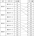
本実施形態によるゲート駆動部は第1GIPとして動作する第1シフトレジスタ221,222および第2GIPとして動作する第2シフトレジスタ231,232を含む。第1GIPは、奇数番目のゲート線と接続される。一方、第2GIPは、偶数番目のゲート線と接続される。第1GIPが走査信号を奇数番目のゲート信号に伝送する期間において、第1GIPに含まれる複数のステージはオン状態とホールド状態との間で遷移され得る。具体的には、第1GIPが走査信号を奇数番目のゲート信号に伝送する期間において、あるステージをオン状態からホールド状態に遷移させるとともに別のステージをホールド状態からオン状態に遷移させる。一方、第1GIPが走査信号を奇数番目のゲート信号に伝送する期間において、第2GIPに含まれるすべてのステージの状態は変更されない。同様に、第2GIPが走査信号を偶数番目のゲート信号に伝送する期間において、第2GIPに含まれる複数のステージはオン状態とホールド状態との間で遷移され得る。具体的には、第2GIPが走査信号を偶数番目のゲート信号に伝送する期間において、あるステージをオン状態からホールド状態に遷移させるとともに別のステージをホールド状態からオン状態に遷移させる。一方、第2GIPが走査信号を偶数番目のゲート信号に伝送する期間において、第1GIPに含まれるすべてのステージの状態は変更されない。即ち、第1GIPは、第2GIPから独立して駆動される。同様に、第2GIPは、第1GIPから独立して駆動される。本実施形態によるゲート駆動部200は、第1GIPを第2GIPから独立に駆動することにより、奇数番目のゲート線に、任意の画素の行数にわたり連続して走査信号を伝送することができる。即ち、ゲート駆動部200は、同じ色を発光する複数の副画素の第1スイッチ素子T1に、任意の行数にわたり連続してゲート信号を供給することができる。本実施形態によるゲート駆動部200は、同じ色を発光する複数の副画素に任意の行数にわたり連続してゲート信号を供給するためにオン状態のステージの数を増加させる必要がない。したがって、オン状態のステージの数を増加させるために入力クロック数を上昇させる必要がない。よって、本実施形態による表示装置10は、消費電力を増大させることなく、同じ色を発光する副画素に、所定の行数にわたり連続して書き込みを行うことができる。
The gate driver according to the present embodiment includes
図12は、本実施形態に係るデータ駆動部300の概略構成を示すブロック図である。データ駆動部300は、データ選択部310およびデータ変換部320を含む。データ選択部310は、行メモリ部520から画像データR’G’B’W’を受信し、スケジューラ560からレジスタ選択信号RSSを受信する。レジスタ選択信号RSSは、入力レジスタ選択信号IRSS、入力有効化信号VALIDおよび出力レジスタ選択信号ORSSを含む。入力レジスタ選択信号IRSSは、画像データR’G’B’W’が格納されるべきレジスタを指定する。出力レジスタ選択信号ORSSは、出力されるべき画像データR’G’B’W’が格納されているレジスタを指定する。入力有効化信号VALIDは、入力レジスタ選択信号IRSSを有効化または無効化する。データ選択部310は複数のレジスタを有し、行メモリ部520から受信した画像データR’G’B’W’を、スケジューラ560から受信したレジスタ選択信号IRSSおよび入力有効化信号VALIDにしたがって格納する。具体的には、データ選択部310は、入力有効化信号VALIDがハイレベルの場合に、レジスタ選択信号IRSSを有効にし、レジスタ選択信号IRSSで指定されたレジスタに画像データR’G’B’W’を格納する。また、データ選択部310は、出力レジスタ選択信号ORSSで指定されたレジスタに格納された画像データR’G’B’W’をデータ変換部320に伝送する。データ変換部320は、データ制御信号DSCを用いて画像データR’G’B’W’をアナログのデータ電圧DATAに変換し、データ線DL1~GLmを介して各画素に伝送する。
Figure 12 is a block diagram showing a schematic configuration of the
図13は、本実施形態に係る類似度判定部550の概略構成を示すブロック図である。類似度判定部550は、第1差分算出部551、第2差分算出部552、第1積算部553、第2積算部554、第1閾値判定部557、第2閾値判定部558およびリセット判定部559を含む。
Fig. 13 is a block diagram showing a schematic configuration of the
第1差分算出部551は、奇数列に配された副画素Pに係る第x行の画像データRGBW_O(x)を行メモリ部520から受信する。受信された画像データRGBW_O(x)は、例えば第x行に配された緑色副画素Gおよび白色副画素Wに書き込まれる画像データのRGBW値である。また、第1差分算出部551は、行メモリ部520から奇数列に配された副画素Pに係る第x-1行の画像データRGBW_O(x-1)を受信する。受信された画像データRGBW_O(x-1)は、画像データRGBW_O(x)の1行前の画像データであり、例えば第x-1行に配された緑色副画素Gおよび白色副画素Wに書き込まれる画像データのRGBW値である。第1差分算出部551は、受信した第x行の画像データRGBW_O(x)と第x-1行の画像データRGBW_O(x-1)との間の差分Diff_Oを計算し、計算の結果を第1積算部553に伝送する。
The first
第1積算部553は、各奇数列における第x行のRGBW値と第x-1行のRGBW値との間の差分Diff_Oのデータを第1差分算出部551から受信する。第1積算部553は、第1差分算出部551から受信した各奇数列の画像データの差分Diff_Oを積算する。例えば表示パネル100に含まれる奇数列の副画素の列数がmである場合、第1積算部553は、第x行のRGBW値と第x-1行のRGBW値との間の差分Diff_Oについて、奇数列の数に対応した(m-1)個の差分値を第1差分算出部551から受信する。第1積算部553は、第1差分算出部551から受信した各列間についての(m-1)個の差分Diff_Oを積算する。第1積算部553は、差分Diff_Oを積算した値Sum_Oを第1閾値判定部557に伝送する。なお、奇数列の画像データの差分Diff_Oの個数が1である場合、第1積算部553は省略され得る。
The
第1閾値判定部557は、第1積算部553から奇数列に係る第x行のRGBW値と奇数列に係る第x-1行のRGBW値との間の差分Diff_Oの積算値Sum_Oを受信する。第1閾値判定部557は、受信された積算値Sum_Oを所定の閾値と比較する。第1閾値判定部557は、受信された積算値Sum_Oが所定の閾値未満であると判断した場合に、奇数列に係る第x行の画像データは奇数列に係る第x-1行の画像データと類似していると判定する。一方、第1閾値判定部557は、受信した積算値Sum_Oが所定の閾値以上であると判断した場合に、奇数列に係る第x行の画像データは奇数列に係る第x-1行の画像データと類似していないと判定する。第1閾値判定部557は、判定の結果である信号RES_O(x)をスケジューラ560に伝送する。例えば、第1閾値判定部557は、奇数列に係る第x行の画像データが奇数列に係る第x-1行の画像データと類似していると判定した場合に信号RES_O(x)として1を出力する。一方、第1閾値判定部557は、奇数列に係る第x行の画像データが奇数列に係る第x-1行の画像データと類似していないと判定した場合に信号RES_O(x)として0を出力する。
The first
第2差分算出部552は、偶数列に配された副画素Pに係る第x行の画像データRGBW_E(x)を行メモリ部520から受信する。受信された画像データRGBW_E(x)は、例えば第x行に配された赤色副画素Rおよび青色副画素Bに書き込まれる画像データのRGBW値である。また、第2差分算出部552は、行メモリ部520から偶数列に配された副画素Pに係る第x-1行の画像データRGBW_E(x-1)を受信する。受信された画像データRGBW_E(x-1)は、画像データRGBW_E(x)の1行前の画像データであり、例えば第x-1行に配された赤色副画素Rおよび青色副画素Bに書き込まれる画像データのRGBW値である。第2差分算出部552は、受信した第x行の画像データRGBW_E(x)と第x-1行の画像データRGBW_E(x-1)との間の差分Diff_Eを計算し、計算の結果を第2積算部554に伝送する。
The second
第2積算部554は、各偶数列における第x行のRGBW値と第x-1行のRGBW値との間の差分Diff_Eのデータを第2差分算出部552から受信する。第2積算部554は、第2差分算出部552から受信した各偶数列の画像データの差分Diff_Eを積算する。例えば表示パネル100に含まれる偶数列の副画素の列数がmである場合、第2積算部554は、第x行のRGBW値と第x-1行のRGBW値との間の差分Diff_Eについて、偶数列の数に対応した(m-1)個の差分値を第2差分算出部552から受信する。第2積算部554は、第2差分算出部552から受信した各列間についての(m-1)個の差分Diff_Eを積算する。第2積算部554は、差分Diff_Eを積算した値Sum_Eを第2閾値判定部558に伝送する。なお、偶数列の画像データの差分Diff_Eの個数が1である場合、第2積算部554は省略され得る。
The
第2閾値判定部558は、第2積算部554から偶数列に係る第x行のRGBW値と偶数列に係る第x-1行のRGBW値との間の差分Diff_Eの積算値Sum_Eを受信する。第2閾値判定部558は、受信された積算値Sum_Eを所定の閾値と比較する。第2閾値判定部558は、受信された積算値Sum_Eが所定の閾値未満であると判断した場合に、偶数列に係る第x行の画像データは偶数列に係る第x-1行の画像データと類似していると判定する。一方、第2閾値判定部558は、受信した積算値Sum_Eが所定の閾値以上であると判断した場合に、偶数列に係る第x行の画像データは偶数列に係る第x-1行の画像データと類似していないと判定する。第2閾値判定部558は、判定の結果である信号RES_E(x)をスケジューラ560に伝送する。例えば、第2閾値判定部558は、偶数列に係る第x行の画像データが偶数列に係る第x-1行の画像データと類似していると判定した場合に信号RES_E(x)として1を出力する。一方、第1閾値判定部557は、偶数列に係る第x行の画像データが偶数列に係る第x-1行の画像データと類似していないと判定した場合に信号RES_E(x)として0を出力する。
The second
リセット判定部559は、水平同期信号Hsyncに基づいてリセット信号を生成する。具体的には、リセット判定部559は、水平同期信号Hsyncがハイレベルからローレベルに遷移するタイミングでリセット信号RSTを第1積算部553および第2積算部554に伝送する。第1積算部553および第2積算部554は、受信したリセット信号RSTに応じて画像データの差分の積算値をリセットして0に戻す。また、リセット判定部559は、水平同期信号Hsyncがハイレベルからローレベルに遷移するタイミングで第1閾値判定部557および第2閾値判定部558にイネーブル信号RES_Enableを伝送する。第1閾値判定部557および第2閾値判定部558は、受信したイネーブル信号RES_Enableに応じて閾値判定の結果である信号RES_O(x)およびRES_E(x)をスケジューラ560に伝送する。
The
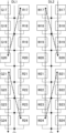
図14は、本実施形態に係るスケジューラ560の概略構成を示すブロック図である。スケジューラ560は、バッファ561、走査順序決定部562、ゲート線決定部563、レジスタ564および選択信号決定部565を含む。
FIG. 14 is a block diagram showing a schematic configuration of a
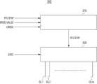
バッファ561は、類似度判定部550から閾値判定の結果である信号RES_O(x)およびRES_E(x)を受信する。バッファ561は、受信した信号RES_O(x)およびRES_E(x)を走査順序決定部562に伝送する。例えば、バッファ561は、信号RES_OおよびRES_Eを任意の行数までバッファに格納し、当該行数分の信号RES_OおよびRES_Eを走査順序決定部562に伝送する。
The
走査順序決定部562は、任意の行数分の閾値判定の結果である信号RESをバッファ561から受信する。走査順序決定部562は、受信した信号RESに基づき、奇数列の副画素の列または偶数列の副画素の列に対して連続して走査する行数を決定する。走査順序決定部562は、連続して走査する行数を示す信号C_Numをゲート線決定部563、レジスタ564および選択信号決定部565に伝送する。
The scanning
ゲート線決定部563は、連続して走査する行数を示す信号C_Numを走査順序決定部562から受信する。ゲート線決定部563は、信号C_Numに基づいてゲート信号が印加されるゲート線の順序を決定する。ゲート線決定部563は、ゲート線指定信号GL_Numを信号変調部510に伝送する。信号変調部510は、ゲート線指定信号GL_Numに基づき変調されたデータイネーブル信号tDEを生成し、行メモリ部520は、信号変調部510から受信した変調されたデータイネーブル信号tDEに基づいて画像データRGBWを整列させる。
The gate
レジスタ564は、連続して走査する行数を示す信号C_Numを走査順序決定部562から受信および格納する。レジスタ564に格納された信号C_Numは、走査順序決定部562が次の任意の行数分について連続して走査する行数を決定する際に呼び出される。走査順序決定部562は、レジスタ564から受信した信号C_Numを用いて、奇数列の副画素の列または偶数列の副画素の列に対して連続して走査する行数を決定する。例えば、走査順序決定部562は、任意の行数分について直前に決定した出力した信号C_Num(x-1)に基づき、連続して走査する行数を示す信号C_Num(x)を決定する。具体的は、連続して走査する行数に上限が定められている場合に、ゲート線決定部563は信号C_Num(x)を信号C_Num(x-1)に応じて修正する。また、例えば奇数列の副画素について信号C_Num(x-1)と信号C_Num(x)との間に連続した類似性が認められる場合に、ゲート線決定部563は、奇数列の副画素について対応する行を連続して走査するように決定する。
The
選択信号決定部565は、連続して走査する行数を示す信号C_Numを走査順序決定部562から受信する。選択信号決定部565は、信号C_Numに基づき、入力レジスタ選択信号IRSS、出力レジスタ選択信号ORSSおよび入力有効化信号VALIDを生成する。入力レジスタ選択信号IRSSは、データ駆動部300に含まれるデータ選択部310において画像データR’G’B’W’が格納されるべきレジスタを指定する。出力レジスタ選択信号ORSSは、データ選択部310から出力されるべき画像データR’G’B’W’が格納されているレジスタを指定する。入力有効化信号VALIDは、入力レジスタ選択信号IRSSを有効化または無効化する。選択信号決定部565は、生成された入力レジスタ選択信号IRSS、出力レジスタ選択信号ORSSおよび入力有効化信号VALIDをデータ選択部310に伝送する。
The selection
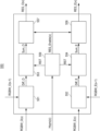
図15は、本実施形態に係るデータ選択部310の概略構成を示すブロック図である。データ選択部310は、データ分割部311-1~311-m、第1レジスタ312-1~312-m、第2レジスタ313-1~313-mおよび選択部314-1~314-mを含む。
Figure 15 is a block diagram showing a schematic configuration of the
データ分割部311-1~311-mは、タイミング制御部500に含まれる行メモリ部520から画像データR’G’B’W’を受信する。また、データ分割部311-1~311-mは、スケジューラ560に含まれる選択信号決定部565から入力レジスタ選択信号IRSSおよび入力有効化信号VALIDを受信する。データ分割部311-1~311-mは、受信された入力レジスタ選択信号IRSSに基づき、受信された画像データR’G’B’W’を分割する。次いでデータ分割部311-1~311-mは、受信された入力レジスタ選択信号IRSSおよび入力有効化信号VALIDに基づき分割された画像データR’G’B’W’を第1レジスタ312-1~312-mまたは第2レジスタ313-1~313-mに伝送する。
The data division units 311-1 to 311-m receive image data R'G'B'W' from the
入力レジスタ選択信号IRSSが第1レジスタ312-1~312-mを指定しており且つ入力有効化信号VALIDが入力レジスタ選択信号IRSSを有効化している場合に、第1レジスタ312-1~312-mは、データ分割部311-1~311-mから受信した分割された画像データR’G’B’W’を格納する。即ち、第1レジスタ312-1~312-mは、画像データを記憶する記憶部として機能する。一方、入力レジスタ選択信号IRSSが第1レジスタ312-1~312-mを指定しているが入力有効化信号VALIDが入力レジスタ選択信号IRSSを無効化している場合に、第1レジスタ312-1~312-mは、データ分割部311-1~311-mから受信した分割された画像データR’G’B’W’を格納しない。 When the input register selection signal IRSS designates the first registers 312-1 to 312-m and the input enable signal VALID activates the input register selection signal IRSS, the first registers 312-1 to 312-m store the divided image data R'G'B'W' received from the data division units 311-1 to 311-m. That is, the first registers 312-1 to 312-m function as a storage unit that stores image data. On the other hand, when the input register selection signal IRSS designates the first registers 312-1 to 312-m but the input enable signal VALID disables the input register selection signal IRSS, the first registers 312-1 to 312-m do not store the divided image data R'G'B'W' received from the data division units 311-1 to 311-m.
入力レジスタ選択信号IRSSが第2レジスタ313-1~313-mを指定しており且つ入力有効化信号VALIDが入力レジスタ選択信号IRSSを有効化している場合に、第2レジスタ313-1~313-mは、データ分割部311-1~311-mから受信した分割された画像データR’G’B’W’を格納する。即ち、第2レジスタ313-1~313-mは、画像データを記憶する記憶部として機能する。一方、入力レジスタ選択信号IRSSが第2レジスタ313-1~313-mを指定しているが入力有効化信号VALIDが入力レジスタ選択信号IRSSを無効化している場合に、第2レジスタ313-1~313-mは、データ分割部311-1~311-mから受信した分割された画像データR’G’B’W’を格納しない。 When the input register selection signal IRSS designates the second registers 313-1 to 313-m and the input enable signal VALID activates the input register selection signal IRSS, the second registers 313-1 to 313-m store the divided image data R'G'B'W' received from the data division units 311-1 to 311-m. That is, the second registers 313-1 to 313-m function as storage units that store image data. On the other hand, when the input register selection signal IRSS designates the second registers 313-1 to 313-m but the input enable signal VALID disables the input register selection signal IRSS, the second registers 313-1 to 313-m do not store the divided image data R'G'B'W' received from the data division units 311-1 to 311-m.
選択部314-1~314-mは、スケジューラ560に含まれる選択信号決定部565から出力レジスタ選択信号ORSSを受信する。選択部314-1~314-mは、出力レジスタ選択信号ORSSが指定する第1レジスタ312-1~312-mまたは第2レジスタ313-1~313-mに格納されている分割された画像データR’G’B’W’(1~m)をデータ変換部320に伝送する。データ変換部320は、データ制御信号DSCを用いて受信された画像データR’G’B’W’をアナログのデータ電圧DATAに変換し、データ線DL1~GLmを介して各画素に伝送する。
The selection units 314-1 to 314-m receive an output register selection signal ORSS from a selection
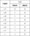
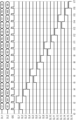
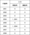
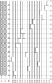
図16および図17を参照して、スケジューラ560への入力信号に応じたデータ選択部310の動作の一例を説明する。図16は、本実施形態に係るスケジューラ560への入力の例を示す表である。図17は、本実施形態に係るデータ選択部310へ入力される信号の例を示す表である。
An example of the operation of the
図16は、第x-7行から第x行までについて、類似度判定部550からスケジューラ560へ入力される信号RES_OおよびRES_Eの値の一例を示している。図16に示されるように、本例では、奇数列についての類似度判定部550の出力信号RES_Oは、第x-7行に対して0を示している。即ち、類似度判定部550は、第x-7行についての奇数列の画像データは、1つ前の行の奇数列の画像データと類似しないと判定している。また、奇数列についての類似度判定部550の出力信号RES_Oは、第x-6行から第x行に対して1を示している。即ち、類似度判定部550は、第x-6行から第x行までについての奇数列の画像データは、それぞれ1つ前の行の奇数列の画像データと類似すると判定している。一方、偶数列についての類似度判定部550の出力信号RES_Eはすべて0を示している。即ち、類似度判定部550は、第x-7行から第x行までについての偶数列の画像データは、それぞれ1つ前の行の偶数列の画像データと類似しないと判定している。
Figure 16 shows an example of the values of signals RES_O and RES_E input from the
図17は、走査番号1~16においてデータ選択部310へ伝送される入力レジスタ選択信号IRSS、入力有効化信号VALID、出力レジスタ選択信号ORSSの一例を示している。本例において、第x-6行から第x行までについての奇数列の画像データ(信号)はそれぞれ1行上に位置する奇数列の画像データと類似している。よって、走査番号1~8において、第x-7行から第x行までについての奇数列の整列された画像データR’G’B’W’が入力データ1~8として先に行メモリ部520からデータ選択部310へ入力される。次いで、走査番号9~16において、第x-7行から第x行までについての偶数列の整列された画像データR’G’B’W’が入力データ9~16として行メモリ部520からデータ選択部310へ入力される。
Figure 17 shows an example of the input register selection signal IRSS, input enable signal VALID, and output register selection signal ORSS transmitted to the
スケジューラ560は、受信された信号RES_Oに基づき、奇数列の入力データ1~8が格納されるレジスタを指定するための入力レジスタ選択信号IRSSを生成する。スケジューラ560は、入力データ1~8を格納すべきレジスタとして第1レジスタ312-1~312-mを指定する入力レジスタ選択信号IRSSをデータ選択部310へ伝送する。また、スケジューラ560は、受信された信号RES_Eに基づき、偶数列の入力データ9~16が格納されるレジスタを指定するための入力レジスタ選択信号IRSSを生成する。スケジューラ560は、入力データ9~16を格納すべきレジスタとして第2レジスタ313-1~313-mを指定する入力レジスタ選択信号IRSSをデータ選択部310へ伝送する。
Based on the received signal RES_O, the
スケジューラ560は、奇数列に対応する入力データ1に対する入力有効化信号VALIDとして1をデータ選択部310に伝送し、入力データ1を第1レジスタ312-1~312-mへ格納することを指定する入力レジスタ選択信号IRSSを有効化する。ここで、スケジューラ560は、受信された信号RES_Oに基づき、入力データ1~8が類似する画像データであると判断している。よって、スケジューラ560は、入力データ2~8に対する入力有効化信号VALIDとして0をデータ選択部310に伝送し、入力データ2~8を第1レジスタ312-1~312-mへ格納することを指定する入力レジスタ選択信号IRSSを無効化する。結果として、第1レジスタ312-1~312-mは更新されず、入力データ1が保持される。本構成により、第1レジスタ312-1~312-mに格納されるデータを更新するために必要な電力の消費が抑制される。なお、本例の場合には、タイミング制御部500は、走査番号2~8において入力レジスタ選択信号IRSSをデータ駆動部300に伝送しないように構成され得る。
The
次いで、スケジューラ560は、偶数列に対応する入力データ9に対する入力有効化信号VALIDとして1をデータ選択部310に伝送し、入力データ9を第2レジスタ313-1~313-mへ格納することを指定する入力レジスタ選択信号IRSSを有効化する。ここで、スケジューラ560は、受信された信号RES_Eに基づき、入力データ9~16が類似しない画像データであると判断している。即ち、第2レジスタ313-1~313-mに格納されている入力データ9を入力データ10~16として利用することはできない。よって、スケジューラ560は、入力データ10~16に対する入力有効化信号VALIDとして1をデータ選択部310に伝送し、入力データ10~16を第2レジスタ313-1~313-mへ格納することを指定する入力レジスタ選択信号IRSSを有効化する。
Then, the
スケジューラ560は、入力データ1~16を出力データ1~16としてデータ変換部320へ順次出力するために、出力レジスタ選択信号ORSSをデータ選択部310へ伝送する。具体的には、スケジューラ560は、走査番号1~8に対しては第1レジスタ312-1~312-mを指定する出力レジスタ選択信号ORSSをデータ選択部310へ伝送し、走査番号9~16に対しては第2レジスタ313-1~313-mを指定する出力レジスタ選択信号ORSSをデータ選択部310へ伝送する。
The
DRDを用いた表示装置においては、互いに異なる色の副画素が1本のデータ線を共有する。したがって、走査される副画素の色を切り替えるたびに画像データの信号(電圧)の不連続性が発生し、結果として表示装置10の消費電力が増加する。DRDを用いた表示装置において消費電力を低減させるためには、同色の副画素を連続して走査し、出力される画像データの信号(電圧)が不連続となる頻度を低減させることが望ましい。しかし、同色の副画素を連続して走査する行数を大きくすると、同じ行に配された他の副画素に対する画像データの書き込みとの間に大きな時間差が生じる。この大きな時間差は、表示する画像の画質を低下させ得る。特に、複数の画素行が互いに類似しない領域を表示する際には、同じ行に配された複数の副画素に対する画像データの書き込みの間に大きな時間差が生じることにより画質の低下が生じ得る。一方で、複数の画素行が互いに類似する領域を表示する際には、同じ行に配された複数の副画素に対する画像データの書き込みの間に大きな時間差が生じても画質の低下が生じにくい。本発明は、表示パネルの各画素行の間の類似度を判定し、判定結果に基づき同色の副画素を連続して走査する。複数の画素行が互いに類似し、同じ行に配された複数の副画素に対する画像データの書き込みの間に大きな時間差が生じても画質の低下が生じにくい領域では同色の副画素を連続して走査する。よって、本発明によれば、DRDを用いた表示装置の表示画質の低下を抑制しながら消費電力を低減させることができる。
In a display device using a DRD, subpixels of different colors share one data line. Therefore, every time the color of the scanned subpixel is switched, a discontinuity occurs in the signal (voltage) of the image data, and as a result, the power consumption of the
図18および図19を参照して、スケジューラ560への入力信号に応じたデータ選択部310の動作の別の一例を説明する。図18は、本実施形態に係るスケジューラ560への入力の例を示す表である。図19は、本実施形態に係るデータ選択部310へ入力される信号の例を示す表である。
With reference to Figures 18 and 19, another example of the operation of the
図18は、第x-15行から第x-8行までについての類似度判定部550からスケジューラ560へ入力された信号RES_OおよびRES_Eの値の一例を示している。図18に示されるように、本例では、奇数列についての類似度判定部550の出力信号RES_Oはすべて0を示している。即ち、類似度判定部550は、第x-15行から第x-8行までについての奇数列の画像データは、それぞれ1つ前の行の奇数列の画像データと類似しないと判定している。同様に、偶数列についての類似度判定部550の出力信号RES_Eはすべて0を示している。即ち、類似度判定部550は、第x-15行から第x-8行までについての偶数列の画像データは、それぞれ1つ前の行の偶数列の画像データと類似しないと判定している。
Figure 18 shows an example of the values of signals RES_O and RES_E input from
図19は、走査番号17~32においてデータ選択部310へ伝送される入力レジスタ選択信号IRSS、入力有効化信号VALID、出力レジスタ選択信号ORSSの一例を示している。本例において、第x-15行から第x-8行までについての奇数列の画像データは前後の行についての奇数列の画像データと類似していない。同様に、第x-15行から第x-8行までについての偶数列の画像データは前後の行についての偶数列の画像データと類似していない。よって、まず走査番号17において、第x-15行についての奇数列の整列された画像データR’G’B’W’が入力データ17として行メモリ部520からデータ選択部310へ入力される。次いで、走査番号18~19において、第x-15行~第x-14行についての偶数列の整列された画像データR’G’B’W’が入力データ18~19として行メモリ部520からデータ選択部310へ入力される。次いで、走査番号20~21において、第x-14行~第x-13行についての奇数列の整列された画像データR’G’B’W’が入力データ20~21として行メモリ部520からデータ選択部310へ入力される。これ以下の走査においても、2行ごとに走査する列を切り替えながら、走査番号22~23、26~27および30~31において、第x-13行から第x-8行までについての偶数列の整列された画像データR’G’B’W’が入力データ22~23、26~27および30~31として行メモリ部520からデータ選択部310へ入力される。同様に、走査番号24~25、28~29および32において、第x-12行から第x-8行までについての奇数列の整列された画像データR’G’B’W’が入力データ24~25、28~29および32として行メモリ部520からデータ選択部310へ入力される。
Figure 19 shows an example of the input register selection signal IRSS, input enable signal VALID, and output register selection signal ORSS transmitted to the
スケジューラ560は、受信された信号RES_Oに基づき、奇数列の入力データ17、20~21、24~25、28~29および32が格納されるレジスタを指定するための入力レジスタ選択信号IRSSを生成する。スケジューラ560は、入力データ17、20~21、24~25、28~29および32を格納すべきレジスタとして第1レジスタ312-1~312-mを指定する入力レジスタ選択信号IRSSをデータ選択部310へ伝送する。また、スケジューラ560は、受信された信号RES_Eに基づき、偶数列の入力データ18~19、22~23、26~27および30~31が格納されるレジスタを指定するための入力レジスタ選択信号IRSSを生成する。スケジューラ560は、入力データ18~19、22~23、26~27および30~31を格納すべきレジスタとして第2レジスタ313-1~313-mを指定する入力レジスタ選択信号IRSSをデータ選択部310へ伝送する。
Based on the received signal RES_O, the
スケジューラ560は、奇数列に対応する入力データ17、20~21、24~25、28~29および32に対する入力有効化信号VALIDとして1をデータ選択部310に伝送し、入力データ17、20~21、24~25、28~29および32を第1レジスタ312-1~312-mへ格納することを指定する入力レジスタ選択信号IRSSを有効化する。ここで、スケジューラ560は、受信された信号RES_Oに基づき、入力データ1~8が類似しない画像データであると判断している。即ち、第2レジスタ313-1~313-mに格納されている入力データ17を入力データ20~21、24~25、28~29および32として利用することはできない。よって、スケジューラ560は、入力データ17、20~21、24~25、28~29および32に対する入力有効化信号VALIDとして1をデータ選択部310に伝送し、入力データ17、20~21、24~25、28~29および32を第1レジスタ312-1~312-mへ格納することを指定する入力レジスタ選択信号IRSSを有効化する。
The
同様に、スケジューラ560は、偶数列に対応する入力データ18~19、22~23、26~27および30~31に対する入力有効化信号VALIDとして1をデータ選択部310に伝送し、入力データ18~19、22~23、26~27および30~31を第2レジスタ313-1~313-mへ格納することを指定する入力レジスタ選択信号IRSSを有効化する。ここで、スケジューラ560は、受信された信号RES_Eに基づき、入力データ9~16が類似しない画像データであると判断している。即ち、第2レジスタ313-1~313-mに格納されている入力データ18を入力データ19、22~23、26~27および30~31として利用することはできない。よって、スケジューラ560は、入力データ18~19、22~23、26~27および30~31に対する入力有効化信号VALIDとして1をデータ選択部310に伝送し、入力データ18~19、22~23、26~27および30~31を第2レジスタ313-1~313-mへ格納することを指定する入力レジスタ選択信号IRSSを有効化する。
Similarly, the
スケジューラ560は、入力データ17~32を出力データ17~32としてデータ変換部320へ順次出力するために、出力レジスタ選択信号ORSSをデータ選択部310へ伝送する。具体的には、スケジューラ560は、走査番号17、20~21、24~25、28~29および32に対しては第1レジスタ312-1~312-mを指定する出力レジスタ選択信号ORSSをデータ選択部310へ伝送し、走査番号18~19、22~23、26~27および30~31に対しては第2レジスタ313-1~313-mを指定する出力レジスタ選択信号ORSSをデータ選択部310へ伝送する。
The
これにより、DRDを用いた表示装置の表示画質の低下を抑制させることができる。 This makes it possible to suppress degradation of the display quality of a display device using a DRD.
以下に、本実施形態に係る表示装置10に表示される画像に基づいて変更される副画素を走査する順序について説明する。図20は、本実施形態に係る表示装置10に表示される画像の一例である。表示装置10に含まれる表示パネル100は、複数の画素行1301~1324を表示している。類似度判定部550は、画素行1301~1309、1313、1317に含まれる奇数列および偶数列に配された副画素に書き込まれた画像データが、これらの画素行の1行上に位置する画素行に含まれる奇数列および偶数列に配された副画素に書き込まれた画像データに類似しないと判定している。一方、類似度判定部550は、画素行1310~1312、1314~1316、1318~1324に含まれる奇数列および偶数列に配された副画素に書き込まれた画素データが、これらの画素行の1行上に位置する画素行に含まれる奇数列および偶数列に配された副画素に書き込まれた画像データに類似すると判定している。
The following describes the order of scanning sub-pixels that is changed based on the image displayed on the
図21は、本実施形態に係る表示装置の副画素が走査される順序を示す模式図である。図21には、図20に示された画素行1301~1308における4列の副画素が示されている。具体的には、図21は、データ線DL1を共有する緑色副画素G1~G8および赤色副画素R1~R8並びにデータ線DL2を共有する白色副画素W1~W8および青色副画素B1~B8を示している。画素行1301~1308の画像データ(画像信号)は奇数列および偶数列ともに類似しないと類似度判定部550によって判定されている。したがって、類似度判定部550からスケジューラ560へ入力される画素行1301~1308についての信号RES_OおよびRES_Eの値はすべて0となる。スケジューラ560は、受信された信号RES_OおよびRES_Eに基づいて入力レジスタ選択信号IRSS、入力有効化信号VALIDおよび出力レジスタ選択信号ORSSを生成する。スケジューラ560は、生成された入力レジスタ選択信号IRSS、入力有効化信号VALIDおよび出力レジスタ選択信号ORSSをデータ駆動部300に伝送する。データ駆動部300は、受信された出力レジスタ選択信号ORSSによって指定された順序で緑色副画素G1~G8、赤色副画素R1~R8、白色副画素W1~W8および青色副画素B1~B8に対して画像データ(画像信号)を伝送する。
Figure 21 is a schematic diagram showing the order in which subpixels of the display device according to this embodiment are scanned. Figure 21 shows four columns of subpixels in
図21に示されるように、画素行1301~1308において、以下に示す順序にて緑色副画素Gおよび赤色副画素Rが走査される。最初に緑色副画素G1が走査された後に、緑色副画素G1と同じ行においてデータ線DL1を共有し、緑色副画素Gの画素列とは異なる画素列に含まれる赤色副画素R1が走査される。その後に、赤色副画素R1の1行下に配された赤色副画素R2が走査される。その後に、赤色副画素R2と同じ行においてデータ線DL1を共有し、赤色副画素Rの画素列とは異なる画素列に含まれる緑色副画素G2が走査される。その後に、緑色副画素G2の1行下に配された緑色副画素G3が走査される。その後に、緑色副画素G3と同じ行においてデータ線DL1を共有し、緑色副画素Gの画素列とは異なる画素列に含まれる赤色副画素R3が走査される。その後に、赤色副画素R3の1行下に配された赤色副画素R4が走査される。その後に、赤色副画素R4と同じ行においてデータ線DL1を共有し、赤色副画素Rの画素列とは異なる画素列に含まれる緑色副画素G4が走査される。その後に、緑色副画素G4の1行下に配された緑色副画素G5が走査される。その後に、緑色副画素G5と同じ行においてデータ線DL1を共有し、緑色副画素Gの画素列とは異なる画素列に含まれる赤色副画素R5が走査される。その後に、赤色副画素R5の1行下に配された赤色副画素R6が走査される。その後に、赤色副画素R6と同じ行においてデータ線DL1を共有し、赤色副画素Rの画素列とは異なる画素列に含まれる緑色副画素G6が走査される。その後に、緑色副画素G6の1行下に配された緑色副画素G7が走査される。その後に、緑色副画素G7と同じ行においてデータ線DL1を共有し、緑色副画素Gの画素列とは異なる画素列に含まれる赤色副画素R7が走査される。その後に、赤色副画素R7の1行下に配された赤色副画素R8が走査される。その後に、赤色副画素R8と同じ行においてデータ線DL1を共有し、赤色副画素Rの画素列とは異なる画素列に含まれる緑色副画素G8が走査される。
21, in
また、図21に示されるように、画素行1301~1308において、以下に示す順序にて白色副画素Wおよび青色副画素Bが走査される。最初に青色副画素B1が走査された後に、青色副画素B1と同じ行においてデータ線DL2を共有し、青色副画素Bの画素列とは異なる画素列に含まれる白色副画素W1が走査される。その後に、白色副画素W1の1行下に配された白色副画素W2が走査される。その後に、白色副画素W2と同じ行においてデータ線DL2を共有し、白色副画素Wの画素列とは異なる画素列に含まれる青色副画素B2が走査される。その後に、青色副画素B2の1行下に配された青色副画素B3が走査される。その後に、青色副画素B3と同じ行においてデータ線DL2を共有し、青色副画素Bの画素列とは異なる画素列に含まれる白色副画素W3が走査される。その後に、白色副画素W3の1行下に配された白色副画素W4が走査される。その後に、白色副画素W4と同じ行においてデータ線DL2を共有し、白色副画素Wの画素列とは異なる画素列に含まれる青色副画素B4が走査される。その後に、青色副画素B4の1行下に配された青色副画素B5が走査される。その後に、青色副画素B5と同じ行においてデータ線DL2を共有し、青色副画素Bの画素列とは異なる画素列に含まれる白色副画素W5が走査される。その後に、白色副画素W5の1行下に配された白色副画素W6が走査される。その後に、白色副画素W6と同じ行においてデータ線DL2を共有し、白色副画素Wの画素列とは異なる画素列に含まれる青色副画素B6が走査される。その後に、青色副画素B6の1行下に配された青色副画素B7が走査される。その後に、青色副画素B7と同じ行においてデータ線DL2を共有し、青色副画素Bの画素列とは異なる画素列に含まれる白色副画素W7が走査される。その後に、白色副画素W7の1行下に配された白色副画素W8が走査される。その後に、白色副画素W8と同じ行においてデータ線DL2を共有し、白色副画素Wの画素列とは異なる画素列に含まれる青色副画素B8が走査される。
As shown in FIG. 21, in
本実施形態において、類似度判定部550は、画素行1301から1308までの画像データは類似していないと判定している。この判定に基づき、スケジューラ560は、各色の副画素を2行ずつ交互に走査するように入力レジスタ選択信号IRSS、入力有効化信号VALIDおよび出力レジスタ選択信号ORSSを生成し、生成された信号をデータ駆動部300に伝送する。データ駆動部300は、受信された出力レジスタ選択信号ORSSによって指定された順序で緑色副画素G1~G8、赤色副画素R1~R8、白色副画素W1~W8および青色副画素B1~B8に対して画像データを書き込む。本実施形態では、画像データが互いに類似しない領域を構成する画素行1301~1308において、同色の副画素を連続して走査する行数を小さくして、同じ行に配された副画素に対する画像データの書き込みの時間差を小さくする。具体的には、本実施形態では、各色の副画素を2行ずつ交互に走査することで、同じ行に配された複数の副画素の間における画像データの書き込みの時間差を小さくしている。よって、本発明によれば、DRDを用いた表示装置において画素行の間で類似していない領域を表示する際に、同じ行に配された複数の副画素の間における画像データの書き込みの時間差に起因する表示画質の低下を抑制させることができる。
In this embodiment, the
図22は、本実施形態に係る表示装置10の図20に示される画素行1301から1308までの副画素を図21に示す順序で走査する場合に、ゲート駆動部200によりゲート線GL1~GL16へ印加されるゲート信号のタイミング図である。
Figure 22 is a timing diagram of gate signals applied to gate lines GL1 to GL16 by the gate driver 200 when scanning sub-pixels from
時刻t0~t1の期間において、ゲート線GL1~GL16にゲート信号は印加されていない。時刻t1~t2の期間において、変調されたデータイネーブル信号tDEに同期してゲート線GL2にゲート信号が印加される。ゲート線GL2にゲート信号が印加されると、緑色副画素G1の第1スイッチ素子T1を介して緑色副画素G1の駆動素子DTのゲートと緑色副画素G1の第1キャパシタC1との間の第1ノードN1にデータ線DL1からデータ信号が印加される。データ線DL1から印加されたデータ信号は、緑色副画素G1に対する画像データに対応する。同様に、ゲート線GL2にゲート信号が印加されると、青色副画素B1の第1スイッチ素子T1を介して青色副画素B1の駆動素子DTのゲートと青色副画素B1の第1キャパシタC1との間の第1ノードN1にデータ線DL2からデータ信号が印加される。データ線DL2から印加されたデータ信号は、青色副画素B1に対する画像データに対応する。 During the period from time t0 to t1, no gate signal is applied to the gate lines GL1 to GL16. During the period from time t1 to t2, a gate signal is applied to the gate line GL2 in synchronization with the modulated data enable signal tDE. When a gate signal is applied to the gate line GL2, a data signal is applied from the data line DL1 to the first node N1 between the gate of the driving element DT of the green subpixel G1 and the first capacitor C1 of the green subpixel G1 via the first switch element T1 of the green subpixel G1. The data signal applied from the data line DL1 corresponds to the image data for the green subpixel G1. Similarly, when a gate signal is applied to the gate line GL2, a data signal is applied from the data line DL2 to the first node N1 between the gate of the driving element DT of the blue subpixel B1 and the first capacitor C1 of the blue subpixel B1 via the first switch element T1 of the blue subpixel B1. The data signal applied from the data line DL2 corresponds to the image data for the blue subpixel B1.
時刻t2~t3の期間において、変調されたデータイネーブル信号tDEに同期してゲート線GL1にゲート信号が印加される。ゲート線GL1にゲート信号が印加されると、赤色副画素R1の第1スイッチ素子T1を介して赤色副画素R1の駆動素子DTのゲートと赤色副画素R1の第1キャパシタC1との間の第1ノードN1にデータ線DL1からデータ信号が印加される。データ線DL1から印加されたデータ信号は、赤色副画素R1に対する画像データに対応する。同様に、ゲート線GL1にゲート信号が印加されると、白色副画素W1の第1スイッチ素子T1を介して白色副画素W1の駆動素子DTのゲートと白色副画素W1の第1キャパシタC1との間の第1ノードN1にデータ線DL2からデータ信号が印加される。データ線DL2から印加されたデータ信号は、白色副画素W1に対する画像データに対応する。 During the period from time t2 to t3, a gate signal is applied to the gate line GL1 in synchronization with the modulated data enable signal tDE. When the gate signal is applied to the gate line GL1, a data signal is applied from the data line DL1 to a first node N1 between the gate of the driving element DT of the red subpixel R1 and the first capacitor C1 of the red subpixel R1 via the first switch element T1 of the red subpixel R1. The data signal applied from the data line DL1 corresponds to image data for the red subpixel R1. Similarly, when a gate signal is applied to the gate line GL1, a data signal is applied from the data line DL2 to a first node N1 between the gate of the driving element DT of the white subpixel W1 and the first capacitor C1 of the white subpixel W1 via the first switch element T1 of the white subpixel W1. The data signal applied from the data line DL2 corresponds to image data for the white subpixel W1.
時刻t3~t4の期間において、変調されたデータイネーブル信号tDEに同期してゲート線GL3にゲート信号が印加される。ゲート線GL3にゲート信号が印加されると、赤色副画素R2の第1スイッチ素子T1を介して赤色副画素R2の駆動素子DTのゲートと赤色副画素R2の第1キャパシタC1との間の第1ノードN1にデータ線DL1からデータ信号が印加される。データ線DL1から印加されたデータ信号は、赤色副画素R2に対する画像データに対応する。同様に、ゲート線GL3にゲート信号が印加されると、白色副画素W2の第1スイッチ素子T1を介して白色副画素W2の駆動素子DTのゲートと白色副画素W2の第1キャパシタC1との間の第1ノードN1にデータ線DL2からデータ信号が印加される。データ線DL2から印加されたデータ信号は、白色副画素W2に対する画像データに対応する。 During the period from time t3 to t4, a gate signal is applied to the gate line GL3 in synchronization with the modulated data enable signal tDE. When the gate signal is applied to the gate line GL3, a data signal is applied from the data line DL1 to the first node N1 between the gate of the driving element DT of the red subpixel R2 and the first capacitor C1 of the red subpixel R2 via the first switch element T1 of the red subpixel R2. The data signal applied from the data line DL1 corresponds to the image data for the red subpixel R2. Similarly, when a gate signal is applied to the gate line GL3, a data signal is applied from the data line DL2 to the first node N1 between the gate of the driving element DT of the white subpixel W2 and the first capacitor C1 of the white subpixel W2 via the first switch element T1 of the white subpixel W2. The data signal applied from the data line DL2 corresponds to the image data for the white subpixel W2.
時刻t4~t5の期間において、変調されたデータイネーブル信号tDEに同期してゲート線GL4にゲート信号が印加される。ゲート線GL4にゲート信号が印加されると、緑色副画素G2の第1スイッチ素子T1を介して緑色副画素G2の駆動素子DTのゲートと緑色副画素G2の第1キャパシタC1との間の第1ノードN1にデータ線DL1からデータ信号が印加される。データ線DL1から印加されたデータ信号は、緑色副画素G2に対する画像データに対応する。同様に、ゲート線GL4にゲート信号が印加されると、青色副画素B2の第1スイッチ素子T1を介して青色副画素B2の駆動素子DTのゲートと青色副画素B2の第1キャパシタC1との間の第1ノードN1にデータ線DL2からデータ信号が印加される。データ線DL2から印加されたデータ信号は、青色副画素B2に対する画像データに対応する。 During the period from time t4 to t5, a gate signal is applied to the gate line GL4 in synchronization with the modulated data enable signal tDE. When the gate signal is applied to the gate line GL4, a data signal is applied from the data line DL1 to the first node N1 between the gate of the driving element DT of the green subpixel G2 and the first capacitor C1 of the green subpixel G2 via the first switch element T1 of the green subpixel G2. The data signal applied from the data line DL1 corresponds to the image data for the green subpixel G2. Similarly, when a gate signal is applied to the gate line GL4, a data signal is applied from the data line DL2 to the first node N1 between the gate of the driving element DT of the blue subpixel B2 and the first capacitor C1 of the blue subpixel B2 via the first switch element T1 of the blue subpixel B2. The data signal applied from the data line DL2 corresponds to the image data for the blue subpixel B2.
時刻t5~t6の期間において、変調されたデータイネーブル信号tDEに同期してゲート線GL6にゲート信号が印加される。ゲート線GL6にゲート信号が印加されると、緑色副画素G3の第1スイッチ素子T1を介して緑色副画素G3の駆動素子DTのゲートと緑色副画素G3の第1キャパシタC1との間の第1ノードN1にデータ線DL1からデータ信号が印加される。データ線DL1から印加されたデータ信号は、緑色副画素G3に対する画像データに対応する。同様に、ゲート線GL6にゲート信号が印加されると、青色副画素B3の第1スイッチ素子T1を介して青色副画素B3の駆動素子DTのゲートと青色副画素B3の第1キャパシタC1との間の第1ノードN1にデータ線DL2からデータ信号が印加される。データ線DL2から印加されたデータ信号は、青色副画素B3に対する画像データに対応する。 During the period from time t5 to t6, a gate signal is applied to the gate line GL6 in synchronization with the modulated data enable signal tDE. When the gate signal is applied to the gate line GL6, a data signal is applied from the data line DL1 to the first node N1 between the gate of the driving element DT of the green subpixel G3 and the first capacitor C1 of the green subpixel G3 via the first switch element T1 of the green subpixel G3. The data signal applied from the data line DL1 corresponds to the image data for the green subpixel G3. Similarly, when a gate signal is applied to the gate line GL6, a data signal is applied from the data line DL2 to the first node N1 between the gate of the driving element DT of the blue subpixel B3 and the first capacitor C1 of the blue subpixel B3 via the first switch element T1 of the blue subpixel B3. The data signal applied from the data line DL2 corresponds to the image data for the blue subpixel B3.
時刻t6~t7の期間において、変調されたデータイネーブル信号tDEに同期してゲート線GL5にゲート信号が印加される。ゲート線GL5にゲート信号が印加されると、赤色副画素R3の第1スイッチ素子T1を介して赤色副画素R3の駆動素子DTのゲートと赤色副画素R3の第1キャパシタC1との間の第1ノードN1にデータ線DL1からデータ信号が印加される。データ線DL1から印加されたデータ信号は、赤色副画素R3に対する画像データに対応する。同様に、ゲート線GL5にゲート信号が印加されると、白色副画素W3の第1スイッチ素子T1を介して白色副画素W3の駆動素子DTのゲートと白色副画素W3の第1キャパシタC1との間の第1ノードN1にデータ線DL2からデータ信号が印加される。データ線DL2から印加されたデータ信号は、白色副画素W3に対する画像データに対応する。 During the period from time t6 to t7, a gate signal is applied to the gate line GL5 in synchronization with the modulated data enable signal tDE. When the gate signal is applied to the gate line GL5, a data signal is applied from the data line DL1 to the first node N1 between the gate of the driving element DT of the red subpixel R3 and the first capacitor C1 of the red subpixel R3 via the first switch element T1 of the red subpixel R3. The data signal applied from the data line DL1 corresponds to the image data for the red subpixel R3. Similarly, when a gate signal is applied to the gate line GL5, a data signal is applied from the data line DL2 to the first node N1 between the gate of the driving element DT of the white subpixel W3 and the first capacitor C1 of the white subpixel W3 via the first switch element T1 of the white subpixel W3. The data signal applied from the data line DL2 corresponds to the image data for the white subpixel W3.
時刻t7~t8の期間において、変調されたデータイネーブル信号tDEに同期してゲート線GL7にゲート信号が印加される。ゲート線GL7にゲート信号が印加されると、赤色副画素R4の第1スイッチ素子T1を介して赤色副画素R4の駆動素子DTのゲートと赤色副画素R4の第1キャパシタC1との間の第1ノードN1にデータ線DL1からデータ信号が印加される。データ線DL1から印加されたデータ信号は、赤色副画素R4に対する画像データに対応する。同様に、ゲート線GL7にゲート信号が印加されると、白色副画素W4の第1スイッチ素子T1を介して白色副画素W4の駆動素子DTのゲートと白色副画素W4の第1キャパシタC1との間の第1ノードN1にデータ線DL2からデータ信号が印加される。データ線DL2から印加されたデータ信号は、白色副画素W4に対する画像データに対応する。 During the period from time t7 to t8, a gate signal is applied to the gate line GL7 in synchronization with the modulated data enable signal tDE. When the gate signal is applied to the gate line GL7, a data signal is applied from the data line DL1 to the first node N1 between the gate of the driving element DT of the red subpixel R4 and the first capacitor C1 of the red subpixel R4 via the first switch element T1 of the red subpixel R4. The data signal applied from the data line DL1 corresponds to the image data for the red subpixel R4. Similarly, when a gate signal is applied to the gate line GL7, a data signal is applied from the data line DL2 to the first node N1 between the gate of the driving element DT of the white subpixel W4 and the first capacitor C1 of the white subpixel W4 via the first switch element T1 of the white subpixel W4. The data signal applied from the data line DL2 corresponds to the image data for the white subpixel W4.
時刻t8~t9の期間において、変調されたデータイネーブル信号tDEに同期してゲート線GL8にゲート信号が印加される。ゲート線GL8にゲート信号が印加されると、緑色副画素G4の第1スイッチ素子T1を介して緑色副画素G4の駆動素子DTのゲートと緑色副画素G4の第1キャパシタC1との間の第1ノードN1にデータ線DL1からデータ信号が印加される。データ線DL1から印加されたデータ信号は、緑色副画素G4に対する画像データに対応する。同様に、ゲート線GL8にゲート信号が印加されると、青色副画素B4の第1スイッチ素子T1を介して青色副画素B4の駆動素子DTのゲートと青色副画素B4の第1キャパシタC1との間の第1ノードN1にデータ線DL2からデータ信号が印加される。データ線DL2から印加されたデータ信号は、青色副画素B4に対する画像データに対応する。 During the period from time t8 to t9, a gate signal is applied to the gate line GL8 in synchronization with the modulated data enable signal tDE. When the gate signal is applied to the gate line GL8, a data signal is applied from the data line DL1 to the first node N1 between the gate of the driving element DT of the green subpixel G4 and the first capacitor C1 of the green subpixel G4 via the first switch element T1 of the green subpixel G4. The data signal applied from the data line DL1 corresponds to the image data for the green subpixel G4. Similarly, when a gate signal is applied to the gate line GL8, a data signal is applied from the data line DL2 to the first node N1 between the gate of the driving element DT of the blue subpixel B4 and the first capacitor C1 of the blue subpixel B4 via the first switch element T1 of the blue subpixel B4. The data signal applied from the data line DL2 corresponds to the image data for the blue subpixel B4.
時刻t9~t10の期間において、変調されたデータイネーブル信号tDEに同期してゲート線GL10にゲート信号が印加される。ゲート線GL10にゲート信号が印加されると、緑色副画素G5の第1スイッチ素子T1を介して緑色副画素G5の駆動素子DTのゲートと緑色副画素G5の第1キャパシタC1との間の第1ノードN1にデータ線DL1からデータ信号が印加される。データ線DL1から印加されたデータ信号は、緑色副画素G5に対する画像データに対応する。同様に、ゲート線GL10にゲート信号が印加されると、青色副画素B5の第1スイッチ素子T1を介して青色副画素B5の駆動素子DTのゲートと青色副画素B5の第1キャパシタC1との間の第1ノードN1にデータ線DL2からデータ信号が印加される。データ線DL2から印加されたデータ信号は、青色副画素B5に対する画像データに対応する。 During the period from time t9 to t10, a gate signal is applied to the gate line GL10 in synchronization with the modulated data enable signal tDE. When the gate signal is applied to the gate line GL10, a data signal is applied from the data line DL1 to the first node N1 between the gate of the driving element DT of the green subpixel G5 and the first capacitor C1 of the green subpixel G5 via the first switch element T1 of the green subpixel G5. The data signal applied from the data line DL1 corresponds to the image data for the green subpixel G5. Similarly, when a gate signal is applied to the gate line GL10, a data signal is applied from the data line DL2 to the first node N1 between the gate of the driving element DT of the blue subpixel B5 and the first capacitor C1 of the blue subpixel B5 via the first switch element T1 of the blue subpixel B5. The data signal applied from the data line DL2 corresponds to the image data for the blue subpixel B5.
時刻t10~t11の期間において、変調されたデータイネーブル信号tDEに同期してゲート線GL9にゲート信号が印加される。ゲート線GL9にゲート信号が印加されると、赤色副画素R5の第1スイッチ素子T1を介して赤色副画素R5の駆動素子DTのゲートと赤色副画素R5の第1キャパシタC1との間の第1ノードN1にデータ線DL1からデータ信号が印加される。データ線DL1から印加されたデータ信号は、赤色副画素R5に対する画像データに対応する。同様に、ゲート線GL9にゲート信号が印加されると、白色副画素W5の第1スイッチ素子T1を介して白色副画素W5の駆動素子DTのゲートと白色副画素W5の第1キャパシタC1との間の第1ノードN1にデータ線DL2からデータ信号が印加される。データ線DL2から印加されたデータ信号は、白色副画素W5に対する画像データに対応する。 During the period from time t10 to t11, a gate signal is applied to the gate line GL9 in synchronization with the modulated data enable signal tDE. When the gate signal is applied to the gate line GL9, a data signal is applied from the data line DL1 to the first node N1 between the gate of the driving element DT of the red subpixel R5 and the first capacitor C1 of the red subpixel R5 via the first switch element T1 of the red subpixel R5. The data signal applied from the data line DL1 corresponds to the image data for the red subpixel R5. Similarly, when a gate signal is applied to the gate line GL9, a data signal is applied from the data line DL2 to the first node N1 between the gate of the driving element DT of the white subpixel W5 and the first capacitor C1 of the white subpixel W5 via the first switch element T1 of the white subpixel W5. The data signal applied from the data line DL2 corresponds to the image data for the white subpixel W5.
時刻t11~t12の期間において、変調されたデータイネーブル信号tDEに同期してゲート線GL11にゲート信号が印加される。ゲート線GL11にゲート信号が印加されると、赤色副画素R6の第1スイッチ素子T1を介して赤色副画素R6の駆動素子DTのゲートと赤色副画素R6の第1キャパシタC1との間の第1ノードN1にデータ線DL1からデータ信号が印加される。データ線DL1から印加されたデータ信号は、赤色副画素R6に対する画像データに対応する。同様に、ゲート線GL11にゲート信号が印加されると、白色副画素W6の第1スイッチ素子T1を介して白色副画素W6の駆動素子DTのゲートと白色副画素W6の第1キャパシタC1との間の第1ノードN1にデータ線DL2からデータ信号が印加される。データ線DL2から印加されたデータ信号は、白色副画素W6に対する画像データに対応する。 During the period from time t11 to t12, a gate signal is applied to the gate line GL11 in synchronization with the modulated data enable signal tDE. When the gate signal is applied to the gate line GL11, a data signal is applied from the data line DL1 to the first node N1 between the gate of the driving element DT of the red subpixel R6 and the first capacitor C1 of the red subpixel R6 via the first switch element T1 of the red subpixel R6. The data signal applied from the data line DL1 corresponds to the image data for the red subpixel R6. Similarly, when a gate signal is applied to the gate line GL11, a data signal is applied from the data line DL2 to the first node N1 between the gate of the driving element DT of the white subpixel W6 and the first capacitor C1 of the white subpixel W6 via the first switch element T1 of the white subpixel W6. The data signal applied from the data line DL2 corresponds to the image data for the white subpixel W6.
時刻t12~t13の期間において、変調されたデータイネーブル信号tDEに同期してゲート線GL12にゲート信号が印加される。ゲート線GL12にゲート信号が印加されると、緑色副画素G6の第1スイッチ素子T1を介して緑色副画素G6の駆動素子DTのゲートと緑色副画素G6の第1キャパシタC1との間の第1ノードN1にデータ線DL1からデータ信号が印加される。データ線DL1から印加されたデータ信号は、緑色副画素G6に対する画像データに対応する。同様に、ゲート線GL12にゲート信号が印加されると、青色副画素B6の第1スイッチ素子T1を介して青色副画素B6の駆動素子DTのゲートと青色副画素B6の第1キャパシタC1との間の第1ノードN1にデータ線DL2からデータ信号が印加される。データ線DL2から印加されたデータ信号は、青色副画素B6に対する画像データに対応する。 During the period from time t12 to t13, a gate signal is applied to the gate line GL12 in synchronization with the modulated data enable signal tDE. When the gate signal is applied to the gate line GL12, a data signal is applied from the data line DL1 to the first node N1 between the gate of the driving element DT of the green subpixel G6 and the first capacitor C1 of the green subpixel G6 via the first switch element T1 of the green subpixel G6. The data signal applied from the data line DL1 corresponds to the image data for the green subpixel G6. Similarly, when a gate signal is applied to the gate line GL12, a data signal is applied from the data line DL2 to the first node N1 between the gate of the driving element DT of the blue subpixel B6 and the first capacitor C1 of the blue subpixel B6 via the first switch element T1 of the blue subpixel B6. The data signal applied from the data line DL2 corresponds to the image data for the blue subpixel B6.
時刻t13~t14の期間において、変調されたデータイネーブル信号tDEに同期してゲート線GL14にゲート信号が印加される。ゲート線GL14にゲート信号が印加されると、緑色副画素G7の第1スイッチ素子T1を介して緑色副画素G7の駆動素子DTのゲートと緑色副画素G7の第1キャパシタC1との間の第1ノードN1にデータ線DL1からデータ信号が印加される。データ線DL1から印加されたデータ信号は、緑色副画素G7に対する画像データに対応する。同様に、ゲート線GL14にゲート信号が印加されると、青色副画素B7の第1スイッチ素子T1を介して青色副画素B7の駆動素子DTのゲートと青色副画素B7の第1キャパシタC1との間の第1ノードN1にデータ線DL2からデータ信号が印加される。データ線DL2から印加されたデータ信号は、青色副画素B7に対する画像データに対応する。 During the period from time t13 to t14, a gate signal is applied to the gate line GL14 in synchronization with the modulated data enable signal tDE. When the gate signal is applied to the gate line GL14, a data signal is applied from the data line DL1 to the first node N1 between the gate of the driving element DT of the green subpixel G7 and the first capacitor C1 of the green subpixel G7 via the first switch element T1 of the green subpixel G7. The data signal applied from the data line DL1 corresponds to the image data for the green subpixel G7. Similarly, when a gate signal is applied to the gate line GL14, a data signal is applied from the data line DL2 to the first node N1 between the gate of the driving element DT of the blue subpixel B7 and the first capacitor C1 of the blue subpixel B7 via the first switch element T1 of the blue subpixel B7. The data signal applied from the data line DL2 corresponds to the image data for the blue subpixel B7.
時刻t14~t15の期間において、変調されたデータイネーブル信号tDEに同期してゲート線GL13にゲート信号が印加される。ゲート線GL13にゲート信号が印加されると、赤色副画素R7の第1スイッチ素子T1を介して赤色副画素R7の駆動素子DTのゲートと赤色副画素R7の第1キャパシタC1との間の第1ノードN1にデータ線DL1からデータ信号が印加される。データ線DL1から印加されたデータ信号は、赤色副画素R7に対する画像データに対応する。同様に、ゲート線GL13にゲート信号が印加されると、白色副画素W7の第1スイッチ素子T1を介して白色副画素W7の駆動素子DTのゲートと白色副画素W7の第1キャパシタC1との間の第1ノードN1にデータ線DL2からデータ信号が印加される。データ線DL2から印加されたデータ信号は、白色副画素W7に対する画像データに対応する。 During the period from time t14 to t15, a gate signal is applied to the gate line GL13 in synchronization with the modulated data enable signal tDE. When the gate signal is applied to the gate line GL13, a data signal is applied from the data line DL1 to the first node N1 between the gate of the driving element DT of the red subpixel R7 and the first capacitor C1 of the red subpixel R7 via the first switch element T1 of the red subpixel R7. The data signal applied from the data line DL1 corresponds to the image data for the red subpixel R7. Similarly, when a gate signal is applied to the gate line GL13, a data signal is applied from the data line DL2 to the first node N1 between the gate of the driving element DT of the white subpixel W7 and the first capacitor C1 of the white subpixel W7 via the first switch element T1 of the white subpixel W7. The data signal applied from the data line DL2 corresponds to the image data for the white subpixel W7.
時刻t15~t16の期間において、変調されたデータイネーブル信号tDEに同期してゲート線GL15にゲート信号が印加される。ゲート線GL15にゲート信号が印加されると、赤色副画素R8の第1スイッチ素子T1を介して赤色副画素R8の駆動素子DTのゲートと赤色副画素R8の第1キャパシタC1との間の第1ノードN1にデータ線DL1からデータ信号が印加される。データ線DL1から印加されたデータ信号は、赤色副画素R8に対する画像データに対応する。同様に、ゲート線GL15にゲート信号が印加されると、白色副画素W8の第1スイッチ素子T1を介して白色副画素W8の駆動素子DTのゲートと白色副画素W8の第1キャパシタC1との間の第1ノードN1にデータ線DL2からデータ信号が印加される。データ線DL2から印加されたデータ信号は、白色副画素W8に対する画像データに対応する。 During the period from time t15 to t16, a gate signal is applied to the gate line GL15 in synchronization with the modulated data enable signal tDE. When the gate signal is applied to the gate line GL15, a data signal is applied from the data line DL1 to the first node N1 between the gate of the driving element DT of the red subpixel R8 and the first capacitor C1 of the red subpixel R8 via the first switch element T1 of the red subpixel R8. The data signal applied from the data line DL1 corresponds to the image data for the red subpixel R8. Similarly, when a gate signal is applied to the gate line GL15, a data signal is applied from the data line DL2 to the first node N1 between the gate of the driving element DT of the white subpixel W8 and the first capacitor C1 of the white subpixel W8 via the first switch element T1 of the white subpixel W8. The data signal applied from the data line DL2 corresponds to the image data for the white subpixel W8.
時刻t16~t17の期間において、変調されたデータイネーブル信号tDEに同期してゲート線GL16にゲート信号が印加される。ゲート線GL16にゲート信号が印加されると、緑色副画素G8の第1スイッチ素子T1を介して緑色副画素G8の駆動素子DTのゲートと緑色副画素G8の第1キャパシタC1との間の第1ノードN1にデータ線DL1からデータ信号が印加される。データ線DL1から印加されたデータ信号は、緑色副画素G8に対する画像データに対応する。同様に、ゲート線GL16にゲート信号が印加されると、青色副画素B8の第1スイッチ素子T1を介して青色副画素B8の駆動素子DTのゲートと青色副画素B8の第1キャパシタC1との間の第1ノードN1にデータ線DL2からデータ信号が印加される。データ線DL2から印加されたデータ信号は、青色副画素B8に対する画像データに対応する。 During the period from time t16 to t17, a gate signal is applied to the gate line GL16 in synchronization with the modulated data enable signal tDE. When the gate signal is applied to the gate line GL16, a data signal is applied from the data line DL1 to the first node N1 between the gate of the driving element DT of the green subpixel G8 and the first capacitor C1 of the green subpixel G8 via the first switch element T1 of the green subpixel G8. The data signal applied from the data line DL1 corresponds to the image data for the green subpixel G8. Similarly, when a gate signal is applied to the gate line GL16, a data signal is applied from the data line DL2 to the first node N1 between the gate of the driving element DT of the blue subpixel B8 and the first capacitor C1 of the blue subpixel B8 via the first switch element T1 of the blue subpixel B8. The data signal applied from the data line DL2 corresponds to the image data for the blue subpixel B8.
ゲート駆動部200は、スケジューラ560からのゲート線指定信号GL_Numに基づき、時刻t1~t17の期間において、図22に示される順序でゲート線GL1~GL16にゲート信号を印加する。データ駆動部300は、時刻t1~t17の期間において、ゲート線GL1~GL16に印加されたゲート信号に応じて、共有されたデータ線DL1を介して緑色副画素Gおよび赤色副画素Rにデータ信号を書き込む。また、データ駆動部300は、時刻t1~t17の期間において、ゲート線GL1~GL16に印加されたゲート信号に応じて、共有されたデータ線DL2を介して白色副画素Wおよび青色副画素Bにデータ信号を書き込む。
The gate driver 200 applies gate signals to the gate lines GL1 to GL16 in the order shown in FIG. 22 during the period from time t1 to t17 based on the gate line designation signal GL_Num from the
図22に示されるタイミング図によれば、データ駆動部300は、画素行1301~1308において、図21に示す順序にて緑色副画素G1~G8、赤色副画素R1~R8、白色副画素W1~W8および青色副画素B1~B8にデータ信号を書き込む。即ち、図21に示される副画素の領域を走査する際に、各色の副画素を2行ずつ交互に走査することで、同じ行に配された複数の副画素の間における画像データの書き込みの時間差を小さくしている。よって、本発明によれば、DRDを用いた表示装置において画素行の間で類似していない領域を表示する際に、同じ行に配された複数の副画素の間における画像データの書き込みの時間差に起因する表示画質の低下を抑制させることができる。
According to the timing diagram shown in FIG. 22, the
図23は、本実施形態に係る表示装置の副画素が走査される順序を示す模式図である。図23には、図20に示された画素行1309~1316における4列の副画素が示されている。具体的には、図23は、データ線DL1を共有する緑色副画素G9~G16および赤色副画素R9~R16並びにデータ線DL2を共有する白色副画素W9~W16および青色副画素B9~B16を示している。画素行1310~1312の画像データ(画像信号)は奇数列、偶数列ともに1行上の画素行の画像データに類似すると類似度判定部550によって判定されている。よって、画素行1310~1312についての信号RES_OおよびRES_Eの値はすべて1となる。一方、画素行1309の画像データは奇数列、偶数列ともに画素行1308の画像データと類似していないため、画素行1309についての信号RES_OおよびRES_Eの値は0となる。また、画素行1314~1316の画像データ(画像信号)は奇数列、偶数列ともに1行上の画素行の画像データに類似すると類似度判定部550によって判定されている。よって、画素行1314~1316についての信号RES_OおよびRES_Eの値はすべて1となる。一方、画素行1313の画像データは奇数列、偶数列ともに画素行1312の画像データと類似していないため、画素行1313についての信号RES_OおよびRES_Eの値は0となる。スケジューラ560は、受信された信号RES_OおよびRES_Eに基づいて入力レジスタ選択信号IRSS、入力有効化信号VALIDおよび出力レジスタ選択信号ORSSを生成する。スケジューラ560は、生成された入力レジスタ選択信号IRSS、入力有効化信号VALIDおよび出力レジスタ選択信号ORSSをデータ駆動部300に伝送する。データ駆動部300は、受信された出力レジスタ選択信号ORSSによって指定された順序で緑色副画素G9~G16、赤色副画素R9~R16、白色副画素W9~W16および青色副画素B9~B16に画像データ(画像信号)を伝送する。
Figure 23 is a schematic diagram showing the order in which subpixels of the display device according to this embodiment are scanned. Figure 23 shows four columns of subpixels in
図23に示されるように、画素行1309~1316において、以下に示す順序にて緑色副画素Gおよび赤色副画素Rが走査される。最初に緑色副画素G9が走査された後に、緑色副画素G9の1行下に配された緑色副画素G10が走査される。その後に、緑色副画素G9と同じ行においてデータ線DL1を共有し、緑色副画素Gの画素列とは異なる画素列に含まれる赤色副画素R9が走査される。その後に、赤色副画素R9の1行下に配された赤色副画素R10が走査される。その後に、赤色副画素R10の1行下に配された赤色副画素R11が走査される。その後に、赤色副画素R11の1行下に配された赤色副画素R12が走査される。その後に、赤色副画素R11と同じ行においてデータ線DL1を共有し、赤色副画素Rの画素列とは異なる画素列に含まれる緑色副画素G11が走査される。その後に、緑色副画素G11の1行下に配された緑色副画素G12が走査される。その後に、緑色副画素G12の1行下に配された緑色副画素G13が走査される。その後に、緑色副画素G13の1行下に配された緑色副画素G14が走査される。その後に、緑色副画素G13と同じ行においてデータ線DL1を共有し、緑色副画素Gの画素列とは異なる画素列に含まれる赤色副画素R13が走査される。その後に、赤色副画素R13の1行下に配された赤色副画素R14が走査される。その後に、赤色副画素R14の1行下に配された赤色副画素R15が走査される。その後に、赤色副画素R15の1行下に配された赤色副画素R16が走査される。その後に、赤色副画素R15と同じ行においてデータ線DL1を共有し、赤色副画素Rの画素列とは異なる画素列に含まれる緑色副画素G15が走査される。その後に、緑色副画素G15の1行下に配された緑色副画素G16が走査される。
23, in
また、図23に示されるように、画素行1309~1316において、以下に示す順序にて白色副画素Wおよび青色副画素Bが走査される。最初に青色副画素B9が走査された後に、青色副画素B9の1行下に配された青色副画素B10が走査される。その後に、青色副画素B9と同じ行においてデータ線DL2を共有し、青色副画素Bの画素列とは異なる画素列に含まれる白色副画素W9が走査される。その後に、白色副画素W9の1行下に配された白色副画素W10が走査される。その後に、白色副画素W10の1行下に配された白色副画素W11が走査される。その後に、白色副画素W11の1行下に配された白色副画素W12が走査される。その後に、白色副画素W11と同じ行においてデータ線DL2を共有し、白色副画素Wの画素列とは異なる画素列に含まれる青色副画素B11が走査される。その後に、青色副画素B11の1行下に配された青色副画素B12が走査される。その後に、青色副画素B12の1行下に配された青色副画素B13が走査される。その後に、青色副画素B13の1行下に配された青色副画素B14が走査される。その後に、青色副画素B13と同じ行においてデータ線DL2を共有し、青色副画素Bの画素列とは異なる画素列に含まれる白色副画素W13が走査される。その後に、白色副画素W13の1行下に配された白色副画素W14が走査される。その後に、白色副画素W14の1行下に配された白色副画素W15が走査される。その後に、白色副画素W15の1行下に配された白色副画素W16が走査される。その後に、白色副画素W15と同じ行においてデータ線DL2を共有し、白色副画素Wの画素列とは異なる画素列に含まれる青色副画素B15が走査される。その後に、青色副画素B15の1行下に配された青色副画素B16が走査される。
As shown in FIG. 23, in
本実施形態において、類似度判定部550は、画素行1309から1312までの画像データは類似していると判定している。また、類似度判定部550は、画素行1313から1316までの画像データは類似していると判定している。これらの判定に基づき、スケジューラ560は、各色の副画素を4行ずつ交互に走査するように入力レジスタ選択信号IRSS、入力有効化信号VALIDおよび出力レジスタ選択信号ORSSを生成し、生成された各信号をデータ駆動部300に伝送する。データ駆動部300は、受信された出力レジスタ選択信号ORSSによって指定された順序で緑色副画素G9~G16、赤色副画素R9~R16、白色副画素W9~W16および青色副画素B9~B16に対して画像データを書き込む。
In this embodiment, the
本実施形態では、画像データが互いに類似する領域を構成する画素行1309~1312および画素行1313~1316において、同色の副画素を連続して走査する行数を大きくして、出力される画像データの信号(電圧)が不連続となる頻度を低減させる。具体的には、本実施形態では、各色の副画素を4行ずつ交互に走査することで、出力される画像データの信号(電圧)が不連続となる頻度を低減させている。例えば、図21に示される副画素の領域では、データ線DL1に接続された緑色副画素G1~G8および赤色副画素R1~R8が走査される際に、走査される副画素の色は8回変更されている。同様に、図21に示される副画素の領域では、データ線DL2に接続された白色副画素W1~W8および青色副画素B1~B8が走査される際に、走査される副画素の色は8回変更されている。即ち、図21に示される副画素の構成される領域を走査する際に、データ線DL1およびデータ線DL2により伝送される画像データの信号(電圧)の不連続性は、それぞれ8回発生し得る。一方、図23に示される副画素の領域では、データ線DL1に接続された緑色副画素G9~G16および赤色副画素R9~R16が走査される際に、走査される副画素の色は4回のみ変更されている。同様に、図23に示される副画素の領域では、データ線DL2に接続された白色副画素W9~W16および青色副画素B9~B16が走査される際に、走査される副画素の色は4回のみ変更されている。即ち、図23に示される副画素の領域を走査する際に、データ線DL1およびデータ線DL2により伝送される画像データの信号(電圧)の不連続性は、それぞれ4回に低減され得る。よって、本願発明によるDRD駆動を用いた表示装置は、副画素への画像データを書き込む際の消費電力を低減させることができる。 In this embodiment, in pixel rows 1309-1312 and pixel rows 1313-1316 that constitute an area in which image data are similar to each other, the number of rows in which subpixels of the same color are scanned consecutively is increased to reduce the frequency of discontinuity in the signal (voltage) of the output image data. Specifically, in this embodiment, the frequency of discontinuity in the signal (voltage) of the output image data is reduced by alternately scanning four rows of subpixels of each color. For example, in the subpixel area shown in FIG. 21, when the green subpixels G1-G8 and the red subpixels R1-R8 connected to the data line DL1 are scanned, the color of the scanned subpixels is changed eight times. Similarly, in the subpixel area shown in FIG. 21, when the white subpixels W1-W8 and the blue subpixels B1-B8 connected to the data line DL2 are scanned, the color of the scanned subpixels is changed eight times. That is, when scanning the region of the subpixels shown in FIG. 21, discontinuity in the signal (voltage) of the image data transmitted by the data line DL1 and the data line DL2 may occur eight times each. On the other hand, in the region of the subpixels shown in FIG. 23, when the green subpixels G9 to G16 and the red subpixels R9 to R16 connected to the data line DL1 are scanned, the color of the scanned subpixels is changed only four times. Similarly, in the region of the subpixels shown in FIG. 23, when the white subpixels W9 to W16 and the blue subpixels B9 to B16 connected to the data line DL2 are scanned, the color of the scanned subpixels is changed only four times. That is, when scanning the region of the subpixels shown in FIG. 23, discontinuity in the signal (voltage) of the image data transmitted by the data line DL1 and the data line DL2 may be reduced to four times each. Therefore, the display device using the DRD drive according to the present invention can reduce the power consumption when writing image data to the subpixels.
なお、図21に示される副画素への画像データの書き込み動作と比較して、図23に示される副画素への画像データの書き込み動作では、同じ行に配された複数の副画素に対する画像データの書き込みの時間差は大きくなる。しかしながら、画素行1309から1312および画素行1313から1316までの画像データは互いに類似している。このため、同じ行に配された複数の副画素に対する画像データの書き込みの時間差が図23に示される領域の画質に与える影響は、図21に示される領域の画質に与える影響よりも小さい。よって、本発明によるDRD駆動を用いた表示装置10は、表示画質の低下を抑制しつつ消費電力を低減させることができる。
Note that, compared to the operation of writing image data to subpixels shown in FIG. 21, the operation of writing image data to subpixels shown in FIG. 23 has a larger time difference in writing image data to multiple subpixels arranged in the same row. However, the image data for
図24は、本実施形態に係る表示装置10の図20に示される画素行1309から1316までの副画素を図23に示す順序で走査する場合に、ゲート駆動部200によりゲート線GL17~GL32へ印加されるゲート信号のタイミング図である。
Figure 24 is a timing diagram of gate signals applied to gate lines GL17 to GL32 by the gate driver 200 when scanning sub-pixels from
時刻t18~t19の期間において、変調されたデータイネーブル信号tDEに同期してゲート線GL18にゲート信号が印加される。ゲート線GL18にゲート信号が印加されると、緑色副画素G9の第1スイッチ素子T1を介して緑色副画素G9の駆動素子DTのゲートと緑色副画素G9の第1キャパシタC1との間の第1ノードN1にデータ線DL1からデータ信号が印加される。データ線DL1から印加されたデータ信号は、緑色副画素G9に対する画像データに対応する。同様に、ゲート線GL18にゲート信号が印加されると、青色副画素B9の第1スイッチ素子T1を介して青色副画素B9の駆動素子DTのゲートと青色副画素B9の第1キャパシタC1との間の第1ノードN1にデータ線DL2からデータ信号が印加される。データ線DL2から印加されたデータ信号は、青色副画素B9に対する画像データに対応する。 During the period from time t18 to t19, a gate signal is applied to the gate line GL18 in synchronization with the modulated data enable signal tDE. When the gate signal is applied to the gate line GL18, a data signal is applied from the data line DL1 to the first node N1 between the gate of the driving element DT of the green subpixel G9 and the first capacitor C1 of the green subpixel G9 via the first switch element T1 of the green subpixel G9. The data signal applied from the data line DL1 corresponds to the image data for the green subpixel G9. Similarly, when a gate signal is applied to the gate line GL18, a data signal is applied from the data line DL2 to the first node N1 between the gate of the driving element DT of the blue subpixel B9 and the first capacitor C1 of the blue subpixel B9 via the first switch element T1 of the blue subpixel B9. The data signal applied from the data line DL2 corresponds to the image data for the blue subpixel B9.
時刻t19~t20の期間において、変調されたデータイネーブル信号tDEに同期してゲート線GL20にゲート信号が印加される。ゲート線GL20にゲート信号が印加されると、緑色副画素G10の第1スイッチ素子T1を介して緑色副画素G10の駆動素子DTのゲートと緑色副画素G10の第1キャパシタC1との間の第1ノードN1にデータ線DL1からデータ信号が印加される。データ線DL1から印加されたデータ信号は、緑色副画素G10に対する画像データに対応する。同様に、ゲート線GL20にゲート信号が印加されると、青色副画素B10の第1スイッチ素子T1を介して青色副画素B10の駆動素子DTのゲートと青色副画素B10の第1キャパシタC1との間の第1ノードN1にデータ線DL2からデータ信号が印加される。データ線DL2から印加されたデータ信号は、青色副画素B10に対する画像データに対応する。 During the period from time t19 to t20, a gate signal is applied to the gate line GL20 in synchronization with the modulated data enable signal tDE. When the gate signal is applied to the gate line GL20, a data signal is applied from the data line DL1 to the first node N1 between the gate of the driving element DT of the green subpixel G10 and the first capacitor C1 of the green subpixel G10 via the first switch element T1 of the green subpixel G10. The data signal applied from the data line DL1 corresponds to the image data for the green subpixel G10. Similarly, when a gate signal is applied to the gate line GL20, a data signal is applied from the data line DL2 to the first node N1 between the gate of the driving element DT of the blue subpixel B10 and the first capacitor C1 of the blue subpixel B10 via the first switch element T1 of the blue subpixel B10. The data signal applied from the data line DL2 corresponds to the image data for the blue subpixel B10.
時刻t20~t21の期間において、変調されたデータイネーブル信号tDEに同期してゲート線GL17にゲート信号が印加される。ゲート線GL17にゲート信号が印加されると、赤色副画素R9の第1スイッチ素子T1を介して赤色副画素R9の駆動素子DTのゲートと赤色副画素R9の第1キャパシタC1との間の第1ノードN1にデータ線DL1からデータ信号が印加される。データ線DL1から印加されたデータ信号は、赤色副画素R9に対する画像データに対応する。同様に、ゲート線GL17にゲート信号が印加されると、白色副画素W9の第1スイッチ素子T1を介して白色副画素W9の駆動素子DTのゲートと白色副画素W9の第1キャパシタC1との間の第1ノードN1にデータ線DL2からデータ信号が印加される。データ線DL2から印加されたデータ信号は、白色副画素W9に対する画像データに対応する。 During the period from time t20 to t21, a gate signal is applied to the gate line GL17 in synchronization with the modulated data enable signal tDE. When the gate signal is applied to the gate line GL17, a data signal is applied from the data line DL1 to the first node N1 between the gate of the driving element DT of the red subpixel R9 and the first capacitor C1 of the red subpixel R9 via the first switch element T1 of the red subpixel R9. The data signal applied from the data line DL1 corresponds to the image data for the red subpixel R9. Similarly, when a gate signal is applied to the gate line GL17, a data signal is applied from the data line DL2 to the first node N1 between the gate of the driving element DT of the white subpixel W9 and the first capacitor C1 of the white subpixel W9 via the first switch element T1 of the white subpixel W9. The data signal applied from the data line DL2 corresponds to the image data for the white subpixel W9.
時刻t21~t22の期間において、変調されたデータイネーブル信号tDEに同期してゲート線GL19にゲート信号が印加される。ゲート線GL19にゲート信号が印加されると、赤色副画素R10の第1スイッチ素子T1を介して赤色副画素R10の駆動素子DTのゲートと赤色副画素R10の第1キャパシタC1との間の第1ノードN1にデータ線DL1からデータ信号が印加される。データ線DL1から印加されたデータ信号は、赤色副画素R10に対する画像データに対応する。同様に、ゲート線GL19にゲート信号が印加されると、白色副画素W10の第1スイッチ素子T1を介して白色副画素W10の駆動素子DTのゲートと白色副画素W10の第1キャパシタC1との間の第1ノードN1にデータ線DL2からデータ信号が印加される。データ線DL2から印加されたデータ信号は、白色副画素W10に対する画像データに対応する。 During the period from time t21 to t22, a gate signal is applied to the gate line GL19 in synchronization with the modulated data enable signal tDE. When the gate signal is applied to the gate line GL19, a data signal is applied from the data line DL1 to a first node N1 between the gate of the driving element DT of the red subpixel R10 and the first capacitor C1 of the red subpixel R10 via the first switch element T1 of the red subpixel R10. The data signal applied from the data line DL1 corresponds to image data for the red subpixel R10. Similarly, when a gate signal is applied to the gate line GL19, a data signal is applied from the data line DL2 to a first node N1 between the gate of the driving element DT of the white subpixel W10 and the first capacitor C1 of the white subpixel W10 via the first switch element T1 of the white subpixel W10. The data signal applied from the data line DL2 corresponds to image data for the white subpixel W10.
時刻t22~t23の期間において、変調されたデータイネーブル信号tDEに同期してゲート線GL21にゲート信号が印加される。ゲート線GL21にゲート信号が印加されると、赤色副画素R11の第1スイッチ素子T1を介して赤色副画素R11の駆動素子DTのゲートと赤色副画素R11の第1キャパシタC1との間の第1ノードN1にデータ線DL1からデータ信号が印加される。データ線DL1から印加されたデータ信号は、赤色副画素R11に対する画像データに対応する。同様に、ゲート線GL21にゲート信号が印加されると、白色副画素W11の第1スイッチ素子T1を介して白色副画素W11の駆動素子DTのゲートと白色副画素W11の第1キャパシタC1との間の第1ノードN1にデータ線DL2からデータ信号が印加される。データ線DL2から印加されたデータ信号は、白色副画素W11に対する画像データに対応する。 During the period from time t22 to t23, a gate signal is applied to the gate line GL21 in synchronization with the modulated data enable signal tDE. When the gate signal is applied to the gate line GL21, a data signal is applied from the data line DL1 to a first node N1 between the gate of the driving element DT of the red subpixel R11 and the first capacitor C1 of the red subpixel R11 via the first switch element T1 of the red subpixel R11. The data signal applied from the data line DL1 corresponds to image data for the red subpixel R11. Similarly, when a gate signal is applied to the gate line GL21, a data signal is applied from the data line DL2 to a first node N1 between the gate of the driving element DT of the white subpixel W11 and the first capacitor C1 of the white subpixel W11 via the first switch element T1 of the white subpixel W11. The data signal applied from the data line DL2 corresponds to image data for the white subpixel W11.
時刻t23~t24の期間において、変調されたデータイネーブル信号tDEに同期してゲート線GL23にゲート信号が印加される。ゲート線GL23にゲート信号が印加されると、赤色副画素R12の第1スイッチ素子T1を介して赤色副画素R12の駆動素子DTのゲートと赤色副画素R12の第1キャパシタC1との間の第1ノードN1にデータ線DL1からデータ信号が印加される。データ線DL1から印加されたデータ信号は、赤色副画素R12に対する画像データに対応する。同様に、ゲート線GL23にゲート信号が印加されると、白色副画素W12の第1スイッチ素子T1を介して白色副画素W12の駆動素子DTのゲートと白色副画素W12の第1キャパシタC1との間の第1ノードN1にデータ線DL2からデータ信号が印加される。データ線DL2から印加されたデータ信号は、白色副画素W12に対する画像データに対応する。 During the period from time t23 to t24, a gate signal is applied to the gate line GL23 in synchronization with the modulated data enable signal tDE. When the gate signal is applied to the gate line GL23, a data signal is applied from the data line DL1 to the first node N1 between the gate of the driving element DT of the red subpixel R12 and the first capacitor C1 of the red subpixel R12 via the first switch element T1 of the red subpixel R12. The data signal applied from the data line DL1 corresponds to the image data for the red subpixel R12. Similarly, when a gate signal is applied to the gate line GL23, a data signal is applied from the data line DL2 to the first node N1 between the gate of the driving element DT of the white subpixel W12 and the first capacitor C1 of the white subpixel W12 via the first switch element T1 of the white subpixel W12. The data signal applied from the data line DL2 corresponds to the image data for the white subpixel W12.
時刻t24~t25の期間において、変調されたデータイネーブル信号tDEに同期してゲート線GL22にゲート信号が印加される。ゲート線GL22にゲート信号が印加されると、緑色副画素G11の第1スイッチ素子T1を介して緑色副画素G11の駆動素子DTのゲートと緑色副画素G11の第1キャパシタC1との間の第1ノードN1にデータ線DL1からデータ信号が印加される。データ線DL1から印加されたデータ信号は、緑色副画素G11に対する画像データに対応する。同様に、ゲート線GL22にゲート信号が印加されると、青色副画素B11の第1スイッチ素子T1を介して青色副画素B11の駆動素子DTのゲートと青色副画素B11の第1キャパシタC1との間の第1ノードN1にデータ線DL2からデータ信号が印加される。データ線DL2から印加されたデータ信号は、青色副画素B11に対する画像データに対応する。 During the period from time t24 to t25, a gate signal is applied to the gate line GL22 in synchronization with the modulated data enable signal tDE. When the gate signal is applied to the gate line GL22, a data signal is applied from the data line DL1 to a first node N1 between the gate of the driving element DT of the green subpixel G11 and the first capacitor C1 of the green subpixel G11 via the first switch element T1 of the green subpixel G11. The data signal applied from the data line DL1 corresponds to image data for the green subpixel G11. Similarly, when a gate signal is applied to the gate line GL22, a data signal is applied from the data line DL2 to a first node N1 between the gate of the driving element DT of the blue subpixel B11 and the first capacitor C1 of the blue subpixel B11 via the first switch element T1 of the blue subpixel B11. The data signal applied from the data line DL2 corresponds to image data for the blue subpixel B11.
時刻t25~t26の期間において、変調されたデータイネーブル信号tDEに同期してゲート線GL24にゲート信号が印加される。ゲート線GL24にゲート信号が印加されると、緑色副画素G12の第1スイッチ素子T1を介して緑色副画素G12の駆動素子DTのゲートと緑色副画素G12の第1キャパシタC1との間の第1ノードN1にデータ線DL1からデータ信号が印加される。データ線DL1から印加されたデータ信号は、緑色副画素G12に対する画像データに対応する。同様に、ゲート線GL24にゲート信号が印加されると、青色副画素B12の第1スイッチ素子T1を介して青色副画素B12の駆動素子DTのゲートと青色副画素B12の第1キャパシタC1との間の第1ノードN1にデータ線DL2からデータ信号が印加される。データ線DL2から印加されたデータ信号は、青色副画素B12に対する画像データに対応する。 During the period from time t25 to t26, a gate signal is applied to the gate line GL24 in synchronization with the modulated data enable signal tDE. When the gate signal is applied to the gate line GL24, a data signal is applied from the data line DL1 to the first node N1 between the gate of the driving element DT of the green subpixel G12 and the first capacitor C1 of the green subpixel G12 via the first switch element T1 of the green subpixel G12. The data signal applied from the data line DL1 corresponds to the image data for the green subpixel G12. Similarly, when a gate signal is applied to the gate line GL24, a data signal is applied from the data line DL2 to the first node N1 between the gate of the driving element DT of the blue subpixel B12 and the first capacitor C1 of the blue subpixel B12 via the first switch element T1 of the blue subpixel B12. The data signal applied from the data line DL2 corresponds to the image data for the blue subpixel B12.
時刻t26~t27の期間において、変調されたデータイネーブル信号tDEに同期してゲート線GL26にゲート信号が印加される。ゲート線GL26にゲート信号が印加されると、緑色副画素G13の第1スイッチ素子T1を介して緑色副画素G13の駆動素子DTのゲートと緑色副画素G13の第1キャパシタC1との間の第1ノードN1にデータ線DL1からデータ信号が印加される。データ線DL1から印加されたデータ信号は、緑色副画素G13に対する画像データに対応する。同様に、ゲート線GL26にゲート信号が印加されると、青色副画素B13の第1スイッチ素子T1を介して青色副画素B13の駆動素子DTのゲートと青色副画素B13の第1キャパシタC1との間の第1ノードN1にデータ線DL2からデータ信号が印加される。データ線DL2から印加されたデータ信号は、青色副画素B13に対する画像データに対応する。 During the period from time t26 to t27, a gate signal is applied to the gate line GL26 in synchronization with the modulated data enable signal tDE. When the gate signal is applied to the gate line GL26, a data signal is applied from the data line DL1 to the first node N1 between the gate of the driving element DT of the green subpixel G13 and the first capacitor C1 of the green subpixel G13 via the first switch element T1 of the green subpixel G13. The data signal applied from the data line DL1 corresponds to the image data for the green subpixel G13. Similarly, when a gate signal is applied to the gate line GL26, a data signal is applied from the data line DL2 to the first node N1 between the gate of the driving element DT of the blue subpixel B13 and the first capacitor C1 of the blue subpixel B13 via the first switch element T1 of the blue subpixel B13. The data signal applied from the data line DL2 corresponds to the image data for the blue subpixel B13.
時刻t27~t28の期間において、変調されたデータイネーブル信号tDEに同期してゲート線GL28にゲート信号が印加される。ゲート線GL28にゲート信号が印加されると、緑色副画素G14の第1スイッチ素子T1を介して緑色副画素G14の駆動素子DTのゲートと緑色副画素G14の第1キャパシタC1との間の第1ノードN1にデータ線DL1からデータ信号が印加される。データ線DL1から印加されたデータ信号は、緑色副画素G14に対する画像データに対応する。同様に、ゲート線GL28にゲート信号が印加されると、青色副画素B14の第1スイッチ素子T1を介して青色副画素B14の駆動素子DTのゲートと青色副画素B14の第1キャパシタC1との間の第1ノードN1にデータ線DL2からデータ信号が印加される。データ線DL2から印加されたデータ信号は、青色副画素B14に対する画像データに対応する。 During the period from time t27 to t28, a gate signal is applied to the gate line GL28 in synchronization with the modulated data enable signal tDE. When the gate signal is applied to the gate line GL28, a data signal is applied from the data line DL1 to the first node N1 between the gate of the driving element DT of the green subpixel G14 and the first capacitor C1 of the green subpixel G14 via the first switch element T1 of the green subpixel G14. The data signal applied from the data line DL1 corresponds to the image data for the green subpixel G14. Similarly, when a gate signal is applied to the gate line GL28, a data signal is applied from the data line DL2 to the first node N1 between the gate of the driving element DT of the blue subpixel B14 and the first capacitor C1 of the blue subpixel B14 via the first switch element T1 of the blue subpixel B14. The data signal applied from the data line DL2 corresponds to the image data for the blue subpixel B14.
時刻t28~t29の期間において、変調されたデータイネーブル信号tDEに同期してゲート線GL25にゲート信号が印加される。ゲート線GL25にゲート信号が印加されると、赤色副画素R13の第1スイッチ素子T1を介して赤色副画素R13の駆動素子DTのゲートと赤色副画素R13の第1キャパシタC1との間の第1ノードN1にデータ線DL1からデータ信号が印加される。データ線DL1から印加されたデータ信号は、赤色副画素R13に対する画像データに対応する。同様に、ゲート線GL25にゲート信号が印加されると、白色副画素W13の第1スイッチ素子T1を介して白色副画素W13の駆動素子DTのゲートと白色副画素W13の第1キャパシタC1との間の第1ノードN1にデータ線DL2からデータ信号が印加される。データ線DL2から印加されたデータ信号は、白色副画素W13に対する画像データに対応する。 During the period from time t28 to t29, a gate signal is applied to the gate line GL25 in synchronization with the modulated data enable signal tDE. When the gate signal is applied to the gate line GL25, a data signal is applied from the data line DL1 to the first node N1 between the gate of the driving element DT of the red subpixel R13 and the first capacitor C1 of the red subpixel R13 via the first switch element T1 of the red subpixel R13. The data signal applied from the data line DL1 corresponds to the image data for the red subpixel R13. Similarly, when a gate signal is applied to the gate line GL25, a data signal is applied from the data line DL2 to the first node N1 between the gate of the driving element DT of the white subpixel W13 and the first capacitor C1 of the white subpixel W13 via the first switch element T1 of the white subpixel W13. The data signal applied from the data line DL2 corresponds to the image data for the white subpixel W13.
時刻t29~t30の期間において、変調されたデータイネーブル信号tDEに同期してゲート線GL27にゲート信号が印加される。ゲート線GL27にゲート信号が印加されると、赤色副画素R14の第1スイッチ素子T1を介して赤色副画素R14の駆動素子DTのゲートと赤色副画素R14の第1キャパシタC1との間の第1ノードN1にデータ線DL1からデータ信号が印加される。データ線DL1から印加されたデータ信号は、赤色副画素R14に対する画像データに対応する。同様に、ゲート線GL27にゲート信号が印加されると、白色副画素W14の第1スイッチ素子T1を介して白色副画素W14の駆動素子DTのゲートと白色副画素W14の第1キャパシタC1との間の第1ノードN1にデータ線DL2からデータ信号が印加される。データ線DL2から印加されたデータ信号は、白色副画素W14に対する画像データに対応する。 During the period from time t29 to t30, a gate signal is applied to the gate line GL27 in synchronization with the modulated data enable signal tDE. When the gate signal is applied to the gate line GL27, a data signal is applied from the data line DL1 to the first node N1 between the gate of the driving element DT of the red subpixel R14 and the first capacitor C1 of the red subpixel R14 via the first switch element T1 of the red subpixel R14. The data signal applied from the data line DL1 corresponds to the image data for the red subpixel R14. Similarly, when a gate signal is applied to the gate line GL27, a data signal is applied from the data line DL2 to the first node N1 between the gate of the driving element DT of the white subpixel W14 and the first capacitor C1 of the white subpixel W14 via the first switch element T1 of the white subpixel W14. The data signal applied from the data line DL2 corresponds to the image data for the white subpixel W14.
時刻t30~t31の期間において、変調されたデータイネーブル信号tDEに同期してゲート線GL29にゲート信号が印加される。ゲート線GL29にゲート信号が印加されると、赤色副画素R15の第1スイッチ素子T1を介して赤色副画素R15の駆動素子DTのゲートと赤色副画素R15の第1キャパシタC1との間の第1ノードN1にデータ線DL1からデータ信号が印加される。データ線DL1から印加されたデータ信号は、赤色副画素R15に対する画像データに対応する。同様に、ゲート線GL29にゲート信号が印加されると、白色副画素W15の第1スイッチ素子T1を介して白色副画素W15の駆動素子DTのゲートと白色副画素W15の第1キャパシタC1との間の第1ノードN1にデータ線DL2からデータ信号が印加される。データ線DL2から印加されたデータ信号は、白色副画素W15に対する画像データに対応する。 During the period from time t30 to t31, a gate signal is applied to the gate line GL29 in synchronization with the modulated data enable signal tDE. When the gate signal is applied to the gate line GL29, a data signal is applied from the data line DL1 to a first node N1 between the gate of the driving element DT of the red subpixel R15 and the first capacitor C1 of the red subpixel R15 via the first switch element T1 of the red subpixel R15. The data signal applied from the data line DL1 corresponds to image data for the red subpixel R15. Similarly, when a gate signal is applied to the gate line GL29, a data signal is applied from the data line DL2 to a first node N1 between the gate of the driving element DT of the white subpixel W15 and the first capacitor C1 of the white subpixel W15 via the first switch element T1 of the white subpixel W15. The data signal applied from the data line DL2 corresponds to image data for the white subpixel W15.
時刻t31~t32の期間において、変調されたデータイネーブル信号tDEに同期してゲート線GL31にゲート信号が印加される。ゲート線GL31にゲート信号が印加されると、赤色副画素R16の第1スイッチ素子T1を介して赤色副画素R16の駆動素子DTのゲートと赤色副画素R16の第1キャパシタC1との間の第1ノードN1にデータ線DL1からデータ信号が印加される。データ線DL1から印加されたデータ信号は、赤色副画素R16に対する画像データに対応する。同様に、ゲート線GL31にゲート信号が印加されると、白色副画素W16の第1スイッチ素子T1を介して白色副画素W16の駆動素子DTのゲートと白色副画素W16の第1キャパシタC1との間の第1ノードN1にデータ線DL2からデータ信号が印加される。データ線DL2から印加されたデータ信号は、白色副画素W16に対する画像データに対応する。 During the period from time t31 to t32, a gate signal is applied to the gate line GL31 in synchronization with the modulated data enable signal tDE. When the gate signal is applied to the gate line GL31, a data signal is applied from the data line DL1 to a first node N1 between the gate of the driving element DT of the red subpixel R16 and the first capacitor C1 of the red subpixel R16 via the first switch element T1 of the red subpixel R16. The data signal applied from the data line DL1 corresponds to image data for the red subpixel R16. Similarly, when a gate signal is applied to the gate line GL31, a data signal is applied from the data line DL2 to a first node N1 between the gate of the driving element DT of the white subpixel W16 and the first capacitor C1 of the white subpixel W16 via the first switch element T1 of the white subpixel W16. The data signal applied from the data line DL2 corresponds to image data for the white subpixel W16.
時刻t32~t33の期間において、変調されたデータイネーブル信号tDEに同期してゲート線GL30にゲート信号が印加される。ゲート線GL30にゲート信号が印加されると、緑色副画素G15の第1スイッチ素子T1を介して緑色副画素G15の駆動素子DTのゲートと緑色副画素G15の第1キャパシタC1との間の第1ノードN1にデータ線DL1からデータ信号が印加される。データ線DL1から印加されたデータ信号は、緑色副画素G15に対する画像データに対応する。同様に、ゲート線GL30にゲート信号が印加されると、青色副画素B15の第1スイッチ素子T1を介して青色副画素B15の駆動素子DTのゲートと青色副画素B15の第1キャパシタC1との間の第1ノードN1にデータ線DL2からデータ信号が印加される。データ線DL2から印加されたデータ信号は、青色副画素B15に対する画像データに対応する。 During the period from time t32 to t33, a gate signal is applied to the gate line GL30 in synchronization with the modulated data enable signal tDE. When the gate signal is applied to the gate line GL30, a data signal is applied from the data line DL1 to a first node N1 between the gate of the driving element DT of the green subpixel G15 and the first capacitor C1 of the green subpixel G15 via the first switch element T1 of the green subpixel G15. The data signal applied from the data line DL1 corresponds to image data for the green subpixel G15. Similarly, when a gate signal is applied to the gate line GL30, a data signal is applied from the data line DL2 to a first node N1 between the gate of the driving element DT of the blue subpixel B15 and the first capacitor C1 of the blue subpixel B15 via the first switch element T1 of the blue subpixel B15. The data signal applied from the data line DL2 corresponds to image data for the blue subpixel B15.
時刻t33~t34の期間において、変調されたデータイネーブル信号tDEに同期してゲート線GL32にゲート信号が印加される。ゲート線GL32にゲート信号が印加されると、緑色副画素G16の第1スイッチ素子T1を介して緑色副画素G16の駆動素子DTのゲートと緑色副画素G16の第1キャパシタC1との間の第1ノードN1にデータ線DL1からデータ信号が印加される。データ線DL1から印加されたデータ信号は、緑色副画素G16に対する画像データに対応する。同様に、ゲート線GL32にゲート信号が印加されると、青色副画素B16の第1スイッチ素子T1を介して青色副画素B16の駆動素子DTのゲートと青色副画素B16の第1キャパシタC1との間の第1ノードN1にデータ線DL2からデータ信号が印加される。データ線DL2から印加されたデータ信号は、青色副画素B16に対する画像データに対応する。 During the period from time t33 to t34, a gate signal is applied to the gate line GL32 in synchronization with the modulated data enable signal tDE. When the gate signal is applied to the gate line GL32, a data signal is applied from the data line DL1 to a first node N1 between the gate of the driving element DT of the green subpixel G16 and the first capacitor C1 of the green subpixel G16 via the first switch element T1 of the green subpixel G16. The data signal applied from the data line DL1 corresponds to image data for the green subpixel G16. Similarly, when a gate signal is applied to the gate line GL32, a data signal is applied from the data line DL2 to a first node N1 between the gate of the driving element DT of the blue subpixel B16 and the first capacitor C1 of the blue subpixel B16 via the first switch element T1 of the blue subpixel B16. The data signal applied from the data line DL2 corresponds to image data for the blue subpixel B16.
ゲート駆動部200は、スケジューラ560からのゲート線指定信号GL_Numに基づき、時刻t18~t34の期間において、図24に示される順序でゲート線GL17~GL32にゲート信号を印加する。データ駆動部300は、時刻t18~t34の期間において、ゲート線GL17~GL32に印加されたゲート信号に応じて、共有されたデータ線DL1を介して緑色副画素Gおよび赤色副画素Rにデータ信号を書き込む。また、データ駆動部300は、時刻t18~t34の期間において、ゲート線GL17~GL32に印加されたゲート信号に応じて、共有されたデータ線DL2を介して白色副画素Wおよび青色副画素Bにデータ信号を書き込む。図24に示されるタイミング図によれば、データ駆動部300は、画素行1309~1316において、図23に示す順序にて緑色副画素G9~G16、赤色副画素R9~R16、白色副画素W9~W16および青色副画素B9~B16にデータ信号を書き込む。
24 based on the gate line designation signal GL_Num from
図24に示されるタイミング図によれば、データ駆動部300は、画素行1309~1316において、図23に示す順序にて緑色副画素G9~G16、赤色副画素R9~R16、白色副画素W9~W16および青色副画素B9~B16にデータ信号を書き込む。即ち、図23に示される副画素の領域を走査する際に、データ線DL1およびデータ線DL2により伝送される画像データの信号(電圧)の不連続性は、それぞれ4回に低減され得る。よって、本願発明によるDRD駆動を用いた表示装置は、副画素への画像データを書き込む際の消費電力を低減させることができる。
According to the timing diagram shown in FIG. 24, the
図25は、本実施形態に係る表示装置の副画素が走査される順序を示す模式図である。図25には、図20に示された画素行1317~1324における4列の副画素が示されている。具体的には、図25は、データ線DL1を共有する緑色副画素G17~G24および赤色副画素R17~R24並びにデータ線DL2を共有する白色副画素W17~W24および青色副画素B17~B24を示している。画素行1318~1324の画像データ(画像信号)は奇数列、偶数列ともに1行上の画素行の画像データに類似すると類似度判定部550によって判定されている。よって、画素行1318~1324についての信号RES_OおよびRES_Eの値はすべて1となる。一方、画素行1317の画像データは奇数列、偶数列ともに画素行1308の画像データと類似していないため、画素行1309についての信号RES_OおよびRES_Eの値は0となる。スケジューラ560は、受信された信号RES_OおよびRES_Eに基づいて入力レジスタ選択信号IRSS、入力有効化信号VALIDおよび出力レジスタ選択信号ORSSを生成する。スケジューラ560は、生成された入力レジスタ選択信号IRSS、入力有効化信号VALIDおよび出力レジスタ選択信号ORSSをデータ駆動部300に伝送する。データ駆動部300は、受信された出力レジスタ選択信号ORSSによって指定された順序で緑色副画素G17~G24、赤色副画素R17~R24、白色副画素W17~W24および青色副画素B17~B24に画像データ(画像信号)を伝送する。
Figure 25 is a schematic diagram showing the order in which subpixels of the display device according to this embodiment are scanned. Figure 25 shows four columns of subpixels in
図25に示されるように、画素行1317~1324において、以下に示す順序にて緑色副画素Gおよび赤色副画素Rが走査される。最初に緑色副画素G17が走査された後に、緑色副画素G17の1行下に配された緑色副画素G18が走査される。その後に、緑色副画素G18の1行下に配された緑色副画素G19が走査される。その後に、緑色副画素G19の1行下に配された緑色副画素G20が走査される。その後に、緑色副画素G17と同じ行においてデータ線DL1を共有し、緑色副画素Gの画素列とは異なる画素列に含まれる赤色副画素R17が走査される。その後に、赤色副画素R17の1行下に配された赤色副画素R18が走査される。その後に、赤色副画素R18の1行下に配された赤色副画素R19が走査される。その後に、赤色副画素R19の1行下に配された赤色副画素R20が走査される。その後に、赤色副画素R20の1行下に配された赤色副画素R21が走査される。その後に、赤色副画素R21の1行下に配された赤色副画素R22が走査される。その後に、赤色副画素R22の1行下に配された赤色副画素R23が走査される。その後に、赤色副画素R23の1行下に配された赤色副画素R24が走査される。その後に、赤色副画素R21と同じ行においてデータ線DL1を共有し、赤色副画素Rの画素列とは異なる画素列に含まれる緑色副画素G21が走査される。その後に、緑色副画素G21の1行下に配された緑色副画素G22が走査される。その後に、緑色副画素G22の1行下に配された緑色副画素G23が走査される。その後に、緑色副画素G23の1行下に配された緑色副画素G24が走査される。
25, in
また、図25に示されるように、画素行1317~1324において、以下に示す順序にて白色副画素Wおよび青色副画素Bが走査される。最初に青色副画素B17が走査された後に、青色副画素B17の1行下に配された青色副画素B18が走査される。その後に、青色副画素B18の1行下に配された青色副画素B19が走査される。その後に、青色副画素B19の1行下に配された青色副画素B20が走査される。その後に、青色副画素B17と同じ行においてデータ線DL2を共有し、青色副画素Bの画素列とは異なる画素列に含まれる白色副画素W17が走査される。その後に、白色副画素W17の1行下に配された白色副画素W18が走査される。その後に、白色副画素W18の1行下に配された白色副画素W19が走査される。その後に、白色副画素W19の1行下に配された白色副画素W20が走査される。その後に、白色副画素W20の1行下に配された白色副画素W21が走査される。その後に、白色副画素W21の1行下に配された白色副画素W22が走査される。その後に、白色副画素W22の1行下に配された白色副画素W23が走査される。その後に、白色副画素W23の1行下に配された白色副画素W24が走査される。その後に、白色副画素W21と同じ行においてデータ線DL2を共有し、白色副画素Wの画素列とは異なる画素列に含まれる青色副画素B21が走査される。その後に、青色副画素B21の1行下に配された青色副画素B22が走査される。その後に、青色副画素B22の1行下に配された青色副画素B23が走査される。その後に、青色副画素B23の1行下に配された青色副画素B24が走査される。
As shown in FIG. 25, in
本実施形態において、類似度判定部550は、画素行1317から1324までの画像データは類似していると判定している。この判定に基づき、スケジューラ560は、各色の副画素を8行ずつ交互に走査するように入力レジスタ選択信号IRSS、入力有効化信号VALIDおよび出力レジスタ選択信号ORSSを生成し、生成された各信号をデータ駆動部300に伝送する。データ駆動部300は、受信された出力レジスタ選択信号ORSSによって指定された順序で緑色副画素G17~G24、赤色副画素R17~R24、白色副画素W17~W24および青色副画素B17~B24に対して画像データを書き込む。
In this embodiment, the
本実施形態では、画像データが互いに類似する領域を構成する画素行1317~1324において、同色の副画素を連続して走査する行数をさらに大きくして、出力される画像データの信号(電圧)が不連続となる頻度をさらに低減させる。具体的には、本実施形態では、各色の副画素を8行ずつ交互に走査することで、出力される画像データの信号(電圧)が不連続となる頻度をさら低減させている。例えば、図23に示される副画素の領域では、データ線DL1に接続された緑色副画素G9~G16および赤色副画素R9~R16が走査される際に、走査される副画素の色は4回変更されている。同様に、図23に示される副画素の領域では、データ線DL2に接続された白色副画素W9~W16および青色副画素B9~B16が走査される際に、走査される副画素の色は4回変更されている。即ち、図23に示される副画素の構成される領域を走査する際に、データ線DL1およびデータ線DL2により伝送される画像データの信号(電圧)の不連続性は、それぞれ4回発生し得る。一方、図25に示される副画素の領域では、データ線DL1に接続された緑色副画素G17~G24および赤色副画素R17~R24が走査される際に、走査される副画素の色は2回のみ変更されている。同様に、図25に示される副画素の領域では、データ線DL2に接続された白色副画素W17~W24および青色副画素B17~B24が走査される際に、走査される副画素の色は2回のみ変更されている。即ち、図25に示される副画素の領域を走査する際に、データ線DL1およびデータ線DL2により伝送される画像データの信号(電圧)の不連続性は、それぞれ2回に低減され得る。よって、本願発明によるDRD駆動を用いた表示装置は、副画素への画像データを書き込む際の消費電力をさらに低減させることができる。
In this embodiment, in
なお、図21および図23に示される副画素への画像データの書き込み動作と比較して、図25に示される副画素への画像データの書き込み動作では、同じ行に配された複数の副画素に対する画像データの書き込みの時間差はさらに大きくなる。しかしながら、画素行1317から1324までの画像データは互いに類似している。このため、同じ行に配された複数の副画素に対する画像データの書き込みの時間差が図25に示される領域の画質に与える影響は、図21および図23に示される領域の画質に与える影響よりも小さい。よって、本発明によるDRD駆動を用いた表示装置10は、表示画質の低下を抑制しつつ消費電力を低減させることができる。
Note that, compared to the operation of writing image data to subpixels shown in Figures 21 and 23, the operation of writing image data to subpixels shown in Figure 25 has a larger time difference in writing image data to multiple subpixels arranged in the same row. However, the image data from
なお、表示パネル100に表示される画像が静止画像の場合、同じ行に配された複数の副画素に対する画像データの書き込みの時間差による表示が質の低下は無視できる。よって、表示装置10に静止画像が表示される場合には、同色の副画素を連続して走査する行数を表示パネルに含まれる画素の行の数と同一とすることができる。たとえば、表示装置10が2160行の画素からなる場合、2160行にわたり同色の副画素を連続して走査することができる。本構成によれば、出力される画像データの信号(電圧)が不連続となる頻度がさらに低減され、表示装置10の消費電力を低減させることができる。
When the image displayed on the
図26は、本実施形態に係る表示装置10の図20に示される画素行1317から1324までの副画素を図25に示す順序で走査する場合に、ゲート駆動部200によりゲート線GL33~GL48へ印加されるゲート信号のタイミング図である。
Figure 26 is a timing diagram of gate signals applied to gate lines GL33 to GL48 by gate driver 200 when scanning sub-pixels from
時刻t35~t36の期間において、変調されたデータイネーブル信号tDEに同期してゲート線GL34にゲート信号が印加される。ゲート線GL34にゲート信号が印加されると、緑色副画素G17の第1スイッチ素子T1を介して緑色副画素G17の駆動素子DTのゲートと緑色副画素G17の第1キャパシタC1との間の第1ノードN1にデータ線DL1からデータ信号が印加される。データ線DL1から印加されたデータ信号は、緑色副画素G17に対する画像データに対応する。同様に、ゲート線GL34にゲート信号が印加されると、青色副画素B17の第1スイッチ素子T1を介して青色副画素B17の駆動素子DTのゲートと青色副画素B17の第1キャパシタC1との間の第1ノードN1にデータ線DL2からデータ信号が印加される。データ線DL2から印加されたデータ信号は、青色副画素B17に対する画像データに対応する。 During the period from time t35 to t36, a gate signal is applied to the gate line GL34 in synchronization with the modulated data enable signal tDE. When the gate signal is applied to the gate line GL34, a data signal is applied from the data line DL1 to the first node N1 between the gate of the driving element DT of the green subpixel G17 and the first capacitor C1 of the green subpixel G17 via the first switch element T1 of the green subpixel G17. The data signal applied from the data line DL1 corresponds to the image data for the green subpixel G17. Similarly, when a gate signal is applied to the gate line GL34, a data signal is applied from the data line DL2 to the first node N1 between the gate of the driving element DT of the blue subpixel B17 and the first capacitor C1 of the blue subpixel B17 via the first switch element T1 of the blue subpixel B17. The data signal applied from the data line DL2 corresponds to the image data for the blue subpixel B17.
時刻t36~t37の期間において、変調されたデータイネーブル信号tDEに同期してゲート線GL36にゲート信号が印加される。ゲート線GL36にゲート信号が印加されると、緑色副画素G18の第1スイッチ素子T1を介して緑色副画素G18の駆動素子DTのゲートと緑色副画素G18の第1キャパシタC1との間の第1ノードN1にデータ線DL1からデータ信号が印加される。データ線DL1から印加されたデータ信号は、緑色副画素G18に対する画像データに対応する。同様に、ゲート線GL36にゲート信号が印加されると、青色副画素B18の第1スイッチ素子T1を介して青色副画素B18の駆動素子DTのゲートと青色副画素B18の第1キャパシタC1との間の第1ノードN1にデータ線DL2からデータ信号が印加される。データ線DL2から印加されたデータ信号は、青色副画素B18に対する画像データに対応する。 During the period from time t36 to t37, a gate signal is applied to the gate line GL36 in synchronization with the modulated data enable signal tDE. When the gate signal is applied to the gate line GL36, a data signal is applied from the data line DL1 to the first node N1 between the gate of the driving element DT of the green subpixel G18 and the first capacitor C1 of the green subpixel G18 via the first switch element T1 of the green subpixel G18. The data signal applied from the data line DL1 corresponds to the image data for the green subpixel G18. Similarly, when a gate signal is applied to the gate line GL36, a data signal is applied from the data line DL2 to the first node N1 between the gate of the driving element DT of the blue subpixel B18 and the first capacitor C1 of the blue subpixel B18 via the first switch element T1 of the blue subpixel B18. The data signal applied from the data line DL2 corresponds to the image data for the blue subpixel B18.
時刻t37~t38の期間において、変調されたデータイネーブル信号tDEに同期してゲート線GL38にゲート信号が印加される。ゲート線GL38にゲート信号が印加されると、緑色副画素G19の第1スイッチ素子T1を介して緑色副画素G19の駆動素子DTのゲートと緑色副画素G19の第1キャパシタC1との間の第1ノードN1にデータ線DL1からデータ信号が印加される。データ線DL1から印加されたデータ信号は、緑色副画素G19に対する画像データに対応する。同様に、ゲート線GL38にゲート信号が印加されると、青色副画素B19の第1スイッチ素子T1を介して青色副画素B19の駆動素子DTのゲートと青色副画素B19の第1キャパシタC1との間の第1ノードN1にデータ線DL2からデータ信号が印加される。データ線DL2から印加されたデータ信号は、青色副画素B19に対する画像データに対応する。 During the period from time t37 to t38, a gate signal is applied to the gate line GL38 in synchronization with the modulated data enable signal tDE. When the gate signal is applied to the gate line GL38, a data signal is applied from the data line DL1 to the first node N1 between the gate of the driving element DT of the green subpixel G19 and the first capacitor C1 of the green subpixel G19 via the first switch element T1 of the green subpixel G19. The data signal applied from the data line DL1 corresponds to the image data for the green subpixel G19. Similarly, when a gate signal is applied to the gate line GL38, a data signal is applied from the data line DL2 to the first node N1 between the gate of the driving element DT of the blue subpixel B19 and the first capacitor C1 of the blue subpixel B19 via the first switch element T1 of the blue subpixel B19. The data signal applied from the data line DL2 corresponds to the image data for the blue subpixel B19.
時刻t38~t39の期間において、変調されたデータイネーブル信号tDEに同期してゲート線GL40にゲート信号が印加される。ゲート線GL40にゲート信号が印加されると、緑色副画素G20の第1スイッチ素子T1を介して緑色副画素G20の駆動素子DTのゲートと緑色副画素G20の第1キャパシタC1との間の第1ノードN1にデータ線DL1からデータ信号が印加される。データ線DL1から印加されたデータ信号は、緑色副画素G20に対する画像データに対応する。同様に、ゲート線GL40にゲート信号が印加されると、青色副画素B20の第1スイッチ素子T1を介して青色副画素B20の駆動素子DTのゲートと青色副画素B20の第1キャパシタC1との間の第1ノードN1にデータ線DL2からデータ信号が印加される。データ線DL2から印加されたデータ信号は、青色副画素B20に対する画像データに対応する。 During the period from time t38 to t39, a gate signal is applied to the gate line GL40 in synchronization with the modulated data enable signal tDE. When the gate signal is applied to the gate line GL40, a data signal is applied from the data line DL1 to a first node N1 between the gate of the driving element DT of the green subpixel G20 and the first capacitor C1 of the green subpixel G20 via the first switch element T1 of the green subpixel G20. The data signal applied from the data line DL1 corresponds to image data for the green subpixel G20. Similarly, when a gate signal is applied to the gate line GL40, a data signal is applied from the data line DL2 to a first node N1 between the gate of the driving element DT of the blue subpixel B20 and the first capacitor C1 of the blue subpixel B20 via the first switch element T1 of the blue subpixel B20. The data signal applied from the data line DL2 corresponds to image data for the blue subpixel B20.
時刻t39~t40の期間において、変調されたデータイネーブル信号tDEに同期してゲート線GL33にゲート信号が印加される。ゲート線GL33にゲート信号が印加されると、赤色副画素R17の第1スイッチ素子T1を介して赤色副画素R17の駆動素子DTのゲートと赤色副画素R11の第1キャパシタC1との間の第1ノードN1にデータ線DL1からデータ信号が印加される。データ線DL1から印加されたデータ信号は、赤色副画素R17に対する画像データに対応する。同様に、ゲート線GL33にゲート信号が印加されると、白色副画素W17の第1スイッチ素子T1を介して白色副画素W17の駆動素子DTのゲートと白色副画素W17の第1キャパシタC1との間の第1ノードN1にデータ線DL2からデータ信号が印加される。データ線DL2から印加されたデータ信号は、白色副画素W17に対する画像データに対応する。 During the period from time t39 to t40, a gate signal is applied to the gate line GL33 in synchronization with the modulated data enable signal tDE. When the gate signal is applied to the gate line GL33, a data signal is applied from the data line DL1 to the first node N1 between the gate of the driving element DT of the red subpixel R17 and the first capacitor C1 of the red subpixel R11 via the first switch element T1 of the red subpixel R17. The data signal applied from the data line DL1 corresponds to the image data for the red subpixel R17. Similarly, when a gate signal is applied to the gate line GL33, a data signal is applied from the data line DL2 to the first node N1 between the gate of the driving element DT of the white subpixel W17 and the first capacitor C1 of the white subpixel W17 via the first switch element T1 of the white subpixel W17. The data signal applied from the data line DL2 corresponds to the image data for the white subpixel W17.
時刻t40~t41の期間において、変調されたデータイネーブル信号tDEに同期してゲート線GL35にゲート信号が印加される。ゲート線GL35にゲート信号が印加されると、赤色副画素R18の第1スイッチ素子T1を介して赤色副画素R18の駆動素子DTのゲートと赤色副画素R18の第1キャパシタC1との間の第1ノードN1にデータ線DL1からデータ信号が印加される。データ線DL1から印加されたデータ信号は、赤色副画素R18に対する画像データに対応する。同様に、ゲート線GL35にゲート信号が印加されると、白色副画素W18の第1スイッチ素子T1を介して白色副画素W18の駆動素子DTのゲートと白色副画素W18の第1キャパシタC1との間の第1ノードN1にデータ線DL2からデータ信号が印加される。データ線DL2から印加されたデータ信号は、白色副画素W18に対する画像データに対応する。 During the period from time t40 to t41, a gate signal is applied to the gate line GL35 in synchronization with the modulated data enable signal tDE. When the gate signal is applied to the gate line GL35, a data signal is applied from the data line DL1 to a first node N1 between the gate of the driving element DT of the red subpixel R18 and the first capacitor C1 of the red subpixel R18 via the first switch element T1 of the red subpixel R18. The data signal applied from the data line DL1 corresponds to image data for the red subpixel R18. Similarly, when a gate signal is applied to the gate line GL35, a data signal is applied from the data line DL2 to a first node N1 between the gate of the driving element DT of the white subpixel W18 and the first capacitor C1 of the white subpixel W18 via the first switch element T1 of the white subpixel W18. The data signal applied from the data line DL2 corresponds to image data for the white subpixel W18.
時刻t41~t42の期間において、変調されたデータイネーブル信号tDEに同期してゲート線GL37にゲート信号が印加される。ゲート線GL37にゲート信号が印加されると、赤色副画素R19の第1スイッチ素子T1を介して赤色副画素R19の駆動素子DTのゲートと赤色副画素R19の第1キャパシタC1との間の第1ノードN1にデータ線DL1からデータ信号が印加される。データ線DL1から印加されたデータ信号は、赤色副画素R19に対する画像データに対応する。同様に、ゲート線GL37にゲート信号が印加されると、白色副画素W19の第1スイッチ素子T1を介して白色副画素W19の駆動素子DTのゲートと白色副画素W19の第1キャパシタC1との間の第1ノードN1にデータ線DL2からデータ信号が印加される。データ線DL2から印加されたデータ信号は、白色副画素W19に対する画像データに対応する。 During the period from time t41 to t42, a gate signal is applied to the gate line GL37 in synchronization with the modulated data enable signal tDE. When the gate signal is applied to the gate line GL37, a data signal is applied from the data line DL1 to a first node N1 between the gate of the driving element DT of the red subpixel R19 and the first capacitor C1 of the red subpixel R19 via the first switch element T1 of the red subpixel R19. The data signal applied from the data line DL1 corresponds to image data for the red subpixel R19. Similarly, when a gate signal is applied to the gate line GL37, a data signal is applied from the data line DL2 to a first node N1 between the gate of the driving element DT of the white subpixel W19 and the first capacitor C1 of the white subpixel W19 via the first switch element T1 of the white subpixel W19. The data signal applied from the data line DL2 corresponds to image data for the white subpixel W19.
時刻t42~t43の期間において、変調されたデータイネーブル信号tDEに同期してゲート線GL39にゲート信号が印加される。ゲート線GL39にゲート信号が印加されると、赤色副画素R20の第1スイッチ素子T1を介して赤色副画素R20の駆動素子DTのゲートと赤色副画素R20の第1キャパシタC1との間の第1ノードN1にデータ線DL1からデータ信号が印加される。データ線DL1から印加されたデータ信号は、赤色副画素R20に対する画像データに対応する。同様に、ゲート線GL39にゲート信号が印加されると、白色副画素W20の第1スイッチ素子T1を介して白色副画素W20の駆動素子DTのゲートと白色副画素W20の第1キャパシタC1との間の第1ノードN1にデータ線DL2からデータ信号が印加される。データ線DL2から印加されたデータ信号は、白色副画素W20に対する画像データに対応する。 During the period from time t42 to t43, a gate signal is applied to the gate line GL39 in synchronization with the modulated data enable signal tDE. When the gate signal is applied to the gate line GL39, a data signal is applied from the data line DL1 to a first node N1 between the gate of the driving element DT of the red subpixel R20 and the first capacitor C1 of the red subpixel R20 via the first switch element T1 of the red subpixel R20. The data signal applied from the data line DL1 corresponds to image data for the red subpixel R20. Similarly, when a gate signal is applied to the gate line GL39, a data signal is applied from the data line DL2 to a first node N1 between the gate of the driving element DT of the white subpixel W20 and the first capacitor C1 of the white subpixel W20 via the first switch element T1 of the white subpixel W20. The data signal applied from the data line DL2 corresponds to image data for the white subpixel W20.
時刻t43~t44の期間において、変調されたデータイネーブル信号tDEに同期してゲート線GL41にゲート信号が印加される。ゲート線GL41にゲート信号が印加されると、赤色副画素R21の第1スイッチ素子T1を介して赤色副画素R21の駆動素子DTのゲートと赤色副画素R21の第1キャパシタC1との間の第1ノードN1にデータ線DL1からデータ信号が印加される。データ線DL1から印加されたデータ信号は、赤色副画素R21に対する画像データに対応する。同様に、ゲート線GL41にゲート信号が印加されると、白色副画素W21の第1スイッチ素子T1を介して白色副画素W21の駆動素子DTのゲートと白色副画素W21の第1キャパシタC1との間の第1ノードN1にデータ線DL2からデータ信号が印加される。データ線DL2から印加されたデータ信号は、白色副画素W21に対する画像データに対応する。 During the period from time t43 to t44, a gate signal is applied to the gate line GL41 in synchronization with the modulated data enable signal tDE. When the gate signal is applied to the gate line GL41, a data signal is applied from the data line DL1 to a first node N1 between the gate of the driving element DT of the red subpixel R21 and the first capacitor C1 of the red subpixel R21 via the first switch element T1 of the red subpixel R21. The data signal applied from the data line DL1 corresponds to image data for the red subpixel R21. Similarly, when a gate signal is applied to the gate line GL41, a data signal is applied from the data line DL2 to a first node N1 between the gate of the driving element DT of the white subpixel W21 and the first capacitor C1 of the white subpixel W21 via the first switch element T1 of the white subpixel W21. The data signal applied from the data line DL2 corresponds to image data for the white subpixel W21.
時刻t44~t45の期間において、変調されたデータイネーブル信号tDEに同期してゲート線GL43にゲート信号が印加される。ゲート線GL43にゲート信号が印加されると、赤色副画素R22の第1スイッチ素子T1を介して赤色副画素R22の駆動素子DTのゲートと赤色副画素R22の第1キャパシタC1との間の第1ノードN1にデータ線DL1からデータ信号が印加される。データ線DL1から印加されたデータ信号は、赤色副画素R22に対する画像データに対応する。同様に、ゲート線GL43にゲート信号が印加されると、白色副画素W22の第1スイッチ素子T1を介して白色副画素W22の駆動素子DTのゲートと白色副画素W22の第1キャパシタC1との間の第1ノードN1にデータ線DL2からデータ信号が印加される。データ線DL2から印加されたデータ信号は、白色副画素W22に対する画像データに対応する。 During the period from time t44 to t45, a gate signal is applied to the gate line GL43 in synchronization with the modulated data enable signal tDE. When the gate signal is applied to the gate line GL43, a data signal is applied from the data line DL1 to the first node N1 between the gate of the driving element DT of the red subpixel R22 and the first capacitor C1 of the red subpixel R22 via the first switch element T1 of the red subpixel R22. The data signal applied from the data line DL1 corresponds to the image data for the red subpixel R22. Similarly, when a gate signal is applied to the gate line GL43, a data signal is applied from the data line DL2 to the first node N1 between the gate of the driving element DT of the white subpixel W22 and the first capacitor C1 of the white subpixel W22 via the first switch element T1 of the white subpixel W22. The data signal applied from the data line DL2 corresponds to the image data for the white subpixel W22.
時刻t45~t46の期間において、変調されたデータイネーブル信号tDEに同期してゲート線GL45にゲート信号が印加される。ゲート線GL45にゲート信号が印加されると、赤色副画素R23の第1スイッチ素子T1を介して赤色副画素R23の駆動素子DTのゲートと赤色副画素R23の第1キャパシタC1との間の第1ノードN1にデータ線DL1からデータ信号が印加される。データ線DL1から印加されたデータ信号は、赤色副画素R23に対する画像データに対応する。同様に、ゲート線GL45にゲート信号が印加されると、白色副画素W23の第1スイッチ素子T1を介して白色副画素W23の駆動素子DTのゲートと白色副画素W23の第1キャパシタC1との間の第1ノードN1にデータ線DL2からデータ信号が印加される。データ線DL2から印加されたデータ信号は、白色副画素W23に対する画像データに対応する。 During the period from time t45 to t46, a gate signal is applied to the gate line GL45 in synchronization with the modulated data enable signal tDE. When the gate signal is applied to the gate line GL45, a data signal is applied from the data line DL1 to the first node N1 between the gate of the driving element DT of the red subpixel R23 and the first capacitor C1 of the red subpixel R23 via the first switch element T1 of the red subpixel R23. The data signal applied from the data line DL1 corresponds to the image data for the red subpixel R23. Similarly, when a gate signal is applied to the gate line GL45, a data signal is applied from the data line DL2 to the first node N1 between the gate of the driving element DT of the white subpixel W23 and the first capacitor C1 of the white subpixel W23 via the first switch element T1 of the white subpixel W23. The data signal applied from the data line DL2 corresponds to the image data for the white subpixel W23.
時刻t46~t47の期間において、変調されたデータイネーブル信号tDEに同期してゲート線GL47にゲート信号が印加される。ゲート線GL47にゲート信号が印加されると、赤色副画素R24の第1スイッチ素子T1を介して赤色副画素R24の駆動素子DTのゲートと赤色副画素R24の第1キャパシタC1との間の第1ノードN1にデータ線DL1からデータ信号が印加される。データ線DL1から印加されたデータ信号は、赤色副画素R24に対する画像データに対応する。同様に、ゲート線GL47にゲート信号が印加されると、白色副画素W24の第1スイッチ素子T1を介して白色副画素W24の駆動素子DTのゲートと白色副画素W24の第1キャパシタC1との間の第1ノードN1にデータ線DL2からデータ信号が印加される。データ線DL2から印加されたデータ信号は、白色副画素W24に対する画像データに対応する。 During the period from time t46 to t47, a gate signal is applied to the gate line GL47 in synchronization with the modulated data enable signal tDE. When the gate signal is applied to the gate line GL47, a data signal is applied from the data line DL1 to the first node N1 between the gate of the driving element DT of the red subpixel R24 and the first capacitor C1 of the red subpixel R24 via the first switch element T1 of the red subpixel R24. The data signal applied from the data line DL1 corresponds to the image data for the red subpixel R24. Similarly, when a gate signal is applied to the gate line GL47, a data signal is applied from the data line DL2 to the first node N1 between the gate of the driving element DT of the white subpixel W24 and the first capacitor C1 of the white subpixel W24 via the first switch element T1 of the white subpixel W24. The data signal applied from the data line DL2 corresponds to the image data for the white subpixel W24.
時刻t47~t48の期間において、変調されたデータイネーブル信号tDEに同期してゲート線GL42にゲート信号が印加される。ゲート線GL42にゲート信号が印加されると、緑色副画素G21の第1スイッチ素子T1を介して緑色副画素G21の駆動素子DTのゲートと緑色副画素G21の第1キャパシタC1との間の第1ノードN1にデータ線DL1からデータ信号が印加される。データ線DL1から印加されたデータ信号は、緑色副画素G21に対する画像データに対応する。同様に、ゲート線GL42にゲート信号が印加されると、青色副画素B21の第1スイッチ素子T1を介して青色副画素B21の駆動素子DTのゲートと青色副画素B21の第1キャパシタC1との間の第1ノードN1にデータ線DL2からデータ信号が印加される。データ線DL2から印加されたデータ信号は、青色副画素B21に対する画像データに対応する。 During the period from time t47 to t48, a gate signal is applied to the gate line GL42 in synchronization with the modulated data enable signal tDE. When the gate signal is applied to the gate line GL42, a data signal is applied from the data line DL1 to the first node N1 between the gate of the driving element DT of the green subpixel G21 and the first capacitor C1 of the green subpixel G21 via the first switch element T1 of the green subpixel G21. The data signal applied from the data line DL1 corresponds to the image data for the green subpixel G21. Similarly, when a gate signal is applied to the gate line GL42, a data signal is applied from the data line DL2 to the first node N1 between the gate of the driving element DT of the blue subpixel B21 and the first capacitor C1 of the blue subpixel B21 via the first switch element T1 of the blue subpixel B21. The data signal applied from the data line DL2 corresponds to the image data for the blue subpixel B21.
時刻t48~t49の期間において、変調されたデータイネーブル信号tDEに同期してゲート線GL44にゲート信号が印加される。ゲート線GL44にゲート信号が印加されると、緑色副画素G22の第1スイッチ素子T1を介して緑色副画素G22の駆動素子DTのゲートと緑色副画素G22の第1キャパシタC1との間の第1ノードN1にデータ線DL1からデータ信号が印加される。データ線DL1から印加されたデータ信号は、緑色副画素G22に対する画像データに対応する。同様に、ゲート線GL44にゲート信号が印加されると、青色副画素B22の第1スイッチ素子T1を介して青色副画素B22の駆動素子DTのゲートと青色副画素B22の第1キャパシタC1との間の第1ノードN1にデータ線DL2からデータ信号が印加される。データ線DL2から印加されたデータ信号は、青色副画素B22に対する画像データに対応する。 During the period from time t48 to t49, a gate signal is applied to the gate line GL44 in synchronization with the modulated data enable signal tDE. When the gate signal is applied to the gate line GL44, a data signal is applied from the data line DL1 to the first node N1 between the gate of the driving element DT of the green subpixel G22 and the first capacitor C1 of the green subpixel G22 via the first switch element T1 of the green subpixel G22. The data signal applied from the data line DL1 corresponds to the image data for the green subpixel G22. Similarly, when a gate signal is applied to the gate line GL44, a data signal is applied from the data line DL2 to the first node N1 between the gate of the driving element DT of the blue subpixel B22 and the first capacitor C1 of the blue subpixel B22 via the first switch element T1 of the blue subpixel B22. The data signal applied from the data line DL2 corresponds to the image data for the blue subpixel B22.
時刻t49~t50の期間において、変調されたデータイネーブル信号tDEに同期してゲート線GL46にゲート信号が印加される。ゲート線GL46にゲート信号が印加されると、緑色副画素G23の第1スイッチ素子T1を介して緑色副画素G23の駆動素子DTのゲートと緑色副画素G23の第1キャパシタC1との間の第1ノードN1にデータ線DL1からデータ信号が印加される。データ線DL1から印加されたデータ信号は、緑色副画素G23に対する画像データに対応する。同様に、ゲート線GL46にゲート信号が印加されると、青色副画素B23の第1スイッチ素子T1を介して青色副画素B23の駆動素子DTのゲートと青色副画素B23の第1キャパシタC1との間の第1ノードN1にデータ線DL2からデータ信号が印加される。データ線DL2から印加されたデータ信号は、青色副画素B23に対する画像データに対応する。 During the period from time t49 to t50, a gate signal is applied to the gate line GL46 in synchronization with the modulated data enable signal tDE. When the gate signal is applied to the gate line GL46, a data signal is applied from the data line DL1 to the first node N1 between the gate of the driving element DT of the green subpixel G23 and the first capacitor C1 of the green subpixel G23 via the first switch element T1 of the green subpixel G23. The data signal applied from the data line DL1 corresponds to the image data for the green subpixel G23. Similarly, when a gate signal is applied to the gate line GL46, a data signal is applied from the data line DL2 to the first node N1 between the gate of the driving element DT of the blue subpixel B23 and the first capacitor C1 of the blue subpixel B23 via the first switch element T1 of the blue subpixel B23. The data signal applied from the data line DL2 corresponds to the image data for the blue subpixel B23.
時刻t50~t51の期間において、変調されたデータイネーブル信号tDEに同期してゲート線GL48にゲート信号が印加される。ゲート線GL48にゲート信号が印加されると、緑色副画素G24の第1スイッチ素子T1を介して緑色副画素G24の駆動素子DTのゲートと緑色副画素G24の第1キャパシタC1との間の第1ノードN1にデータ線DL1からデータ信号が印加される。データ線DL1から印加されたデータ信号は、緑色副画素G24に対する画像データに対応する。同様に、ゲート線GL48にゲート信号が印加されると、青色副画素B24の第1スイッチ素子T1を介して青色副画素B24の駆動素子DTのゲートと青色副画素B24の第1キャパシタC1との間の第1ノードN1にデータ線DL2からデータ信号が印加される。データ線DL2から印加されたデータ信号は、青色副画素B24に対する画像データに対応する。 During the period from time t50 to t51, a gate signal is applied to the gate line GL48 in synchronization with the modulated data enable signal tDE. When the gate signal is applied to the gate line GL48, a data signal is applied from the data line DL1 to the first node N1 between the gate of the driving element DT of the green subpixel G24 and the first capacitor C1 of the green subpixel G24 via the first switch element T1 of the green subpixel G24. The data signal applied from the data line DL1 corresponds to the image data for the green subpixel G24. Similarly, when a gate signal is applied to the gate line GL48, a data signal is applied from the data line DL2 to the first node N1 between the gate of the driving element DT of the blue subpixel B24 and the first capacitor C1 of the blue subpixel B24 via the first switch element T1 of the blue subpixel B24. The data signal applied from the data line DL2 corresponds to the image data for the blue subpixel B24.
ゲート駆動部200は、スケジューラ560からのゲート線指定信号GL_Numに基づき、時刻t35~t51の期間において、図25に示される順序でゲート線GL33~GL48にゲート信号を印加する。データ駆動部300は、時刻t35~t51の期間において、ゲート線GL33~GL48に印加されたゲート信号に応じて、共有されたデータ線DL1を介して緑色副画素Gおよび赤色副画素Rにデータ信号を書き込む。また、データ駆動部300は、時刻t35~t51の期間において、ゲート線GL33~GL48に印加されたゲート信号に応じて、共有されたデータ線DL2を介して白色副画素Wおよび青色副画素Bにデータ信号を書き込む。図26に示されるタイミング図によれば、データ駆動部300は、画素行1317~1324において、図25に示す順序にて緑色副画素G17~G24、赤色副画素R17~R24、白色副画素W17~W24および青色副画素B17~B24にデータ信号を書き込む。
25 in the period from time t35 to t51 based on the gate line designation signal GL_Num from the
図26に示されるタイミング図によれば、データ駆動部300は、画素行1317~1324において、図25に示す順序にて緑色副画素G17~G24、赤色副画素R17~R24、白色副画素W17~W24および青色副画素B17~B24にデータ信号を書き込む。即ち、図25に示される副画素の領域を走査する際に、データ線DL1およびデータ線DL2により伝送される画像データの信号(電圧)の不連続性は、それぞれ2回に低減され得る。よって、本願発明によるDRD駆動を用いた表示装置は、副画素への画像データを書き込む際の消費電力をさらに低減させることができる。
According to the timing diagram shown in FIG. 26, the
図27は、図20に示す表示画像を表示する際の、本実施形態に係る表示装置10の走査時間とデータ信号の書き込みが行われる副画素の行との間の関係を示すグラフである。
Figure 27 is a graph showing the relationship between the scanning time of the
本実施形態において、類似度判定部550は、画素行1301から1308までの画像データは類似しないと判定している。この判定に基づき、データ駆動部300は、画素行1301から1308までの画像領域において、緑色副画素Gと赤色副画素Rとを2行ずつ交互に走査する。同様に、データ駆動部300は、画素行1301から1308までの画像領域に対して、白色副画素Wと青色副画素Bとを2行ずつ交互に走査する。結果として、画素行1301から1308までの画像領域において、同じ行に配された緑色副画素Gと赤色副画素Rとの間の画像データの書き込みの時間差は、図27に示されるように、1[a.u.]である。同様に、画素行1301から1308までの画像領域において、同じ行に配された白色副画素Wと青色副画素Bとの間の画像データの書き込みの時間差は、図27に示されるように、1[a.u.]である。
In this embodiment, the
また、類似度判定部550は、画素行1309から1312および画素行1313から1316までの画像データは類似すると判定している。この判定に基づき、データ駆動部300は、画素行1309から1316までの画像領域において、緑色副画素Gと赤色副画素Rとを4行ずつ交互に走査する。同様に、データ駆動部300は、画素行1309から1316までの画像領域に対して、白色副画素Wと青色副画素Bとを4行ずつ交互に走査する。結果として、画素行1309から1316までの画像領域において、同じ行に配された緑色副画素Gと赤色副画素Rとの間の画像データの書き込みの時間差は、図27に示されるように、2[a.u.]である。同様に、画素行1309から1316までの画像領域において、同じ行に配された白色副画素Wと青色副画素Bとの間の画像データの書き込みの時間差は、図27に示されるように、2[a.u.]である。
The
また、類似度判定部550は、画素行1317から1324までの画像データは類似すると判定している。この判定に基づき、データ駆動部300は、画素行1317から1324までの画像領域において、緑色副画素Gと赤色副画素Rとを8行ずつ交互に走査する。同様に、データ駆動部300は、画素行1317から1324までの画像領域に対して、白色副画素Wと青色副画素Bとを8行ずつ交互に走査する。結果として、画素行1317から1324までの画像領域において、同じ行に配された緑色副画素Gと赤色副画素Rとの間の画像データの書き込みの時間差は、図27に示されるように、4[a.u.]である。同様に、画素行1317から1324までの画像領域において、同じ行に配された白色副画素Wと青色副画素Bとの間の画像データの書き込みの時間差は、図27に示されるように、4[a.u.]である。
The
本実施形態では、画素行の間の画像データの類似度を判定し、判定された類似度に基づいて同色の副画素を連続して走査する行数を決定している。画素行の間の画像データが類似しない画素行の領域では、同色の副画素を連続して走査する行数が小さく設定される。この結果、共有されたデータ線に接続され、同じ行に配された他の色の副画素との間の画像データの書き込みの時間差が小さくなる。よって、本発明によれば、DRDを用いた表示装置において画素行の間で類似していない領域を表示する際に、同じ行に配された複数の副画素の間における画像データの書き込みの時間差に起因する表示画質の低下を抑制させることができる。一方、画素行の間の画像データが類似する画素行の領域では、同じ行に配された副画素の間における画像データの書き込みの時間差による表示画質への影響は小さい。よって、画素行の間の画像データが類似する画素行の領域では、同色の副画素を連続して走査する行数が大きく設定される。即ち、画素行の間の画像データが類似する画素行の領域では、データ線を介して伝送される画像データの信号(電圧)の不連続性が低減される。よって、本発明によるDRD駆動を用いた表示装置10は、表示画質の低下を抑制しつつ消費電力を低減させることができる。
In this embodiment, the similarity of image data between pixel rows is determined, and the number of rows for continuously scanning sub-pixels of the same color is determined based on the determined similarity. In a region of a pixel row where the image data between the pixel rows is not similar, the number of rows for continuously scanning sub-pixels of the same color is set to be small. As a result, the time difference in writing image data between sub-pixels of other colors connected to a shared data line and arranged in the same row is reduced. Therefore, according to the present invention, when displaying a region where the pixel rows are not similar in a display device using a DRD, it is possible to suppress a deterioration in display image quality caused by the time difference in writing image data between multiple sub-pixels arranged in the same row. On the other hand, in a region of a pixel row where the image data between the pixel rows is similar, the effect on the display image quality due to the time difference in writing image data between sub-pixels arranged in the same row is small. Therefore, in a region of a pixel row where the image data between the pixel rows is similar, the number of rows for continuously scanning sub-pixels of the same color is set to be large. That is, in a region of a pixel row where the image data between the pixel rows is similar, the discontinuity of the signal (voltage) of the image data transmitted through the data line is reduced. Therefore, the
[第2実施形態]
本実施形態では、第1実施形態に係る類似度判定部550の変形例を説明する。第1差分算出部551、第2差分算出部552、第1積算部553、第2積算部554、第1閾値判定部557、第2閾値判定部558およびリセット判定部559の構成および機能は第1実施形態と同様であるため説明を省略する。
[Second embodiment]
In this embodiment, a modified example of the
図28は、本実施形態に係る類似度判定部550の概略構成を示すブロック図である。本実施形態に係る類似度判定部550は、第1閾値調整部555および第2閾値調整部556をさらに含む。
FIG. 28 is a block diagram showing a schematic configuration of the
第1閾値調整部555は、第1積算部553から奇数列に係る第x行のRGBW値と奇数列に係る第x-1行のRGBW値との間の差分の積算値Sum_Oを受信する。第1閾値調整部555は、受信された積算値Sum_Oに基づき、第1閾値判定部557に設定されている閾値を適切な値に調整する。例えば、第1閾値調整部555は、学習データを用いた学習済みモデルに基づく機械学習法、類似度判定部550に入力される積算値から最適な閾値を導出するクラスタリング解析による分類手法等を用いて、第1閾値判定部557に設定されている閾値を最適な値に調整する。第1閾値調整部555は、最適な値に調整された閾値Th_Oを第1閾値判定部557に伝送する。第1閾値判定部557は、第1積算部553から受信された積算値Sum_Oが最適な値に調整された閾値Th_O未満であると判断した場合に、奇数列に係る第x行の画像データは奇数列に係る第x-1行の画像データと類似していると判定する。一方、第1閾値判定部557は、第1積算部553から受信した積算値Sum_Oが最適な値に調整された閾値Th_O以上であると判断した場合に、奇数列に係る第x行の画像データは奇数列に係る第x-1行の画像データと類似していないと判定する。
The first
同様に、第2閾値調整部556は、第2積算部554から偶数列に係る第x行のRGBW値と偶数列に係る第x-1行のRGBW値との間の差分の積算値Sum_Eを受信する。第2閾値調整部556は、受信された積算値Sum_Eに基づき、第2閾値判定部558に設定されている閾値を適切な値に調整する。例えば、第2閾値調整部556は、学習データを用いた学習済みモデルに基づく機械学習法、類似度判定部550に入力される積算値から最適な閾値を導出するクラスタリング解析による分類手法等を用いて、第2閾値判定部558に設定されている閾値を最適な値に調整する。第2閾値調整部556は、最適な値に調整された閾値Th_Eを第2閾値判定部558に伝送する。第2閾値判定部558は、第2積算部554から受信された積算値Sum_Eが最適な値に調整された閾値Th_E未満であると判断した場合に、偶数列に係る第x行の画像データは偶数列に係る第x-1行の画像データと類似していると判定する。一方、第2閾値判定部558は、第2積算部554から受信した積算値Sum_Eが最適な値に調整された閾値Th_E以上であると判断した場合に、偶数列に係る第x行の画像データは偶数列に係る第x-1行の画像データと類似していないと判定する。
Similarly, the second
本実施形態において、類似度判定部550は、第1閾値調整部555および第2閾値調整部556を含むものとしたが、本発明は上記構成に限定されない。例えば、第1閾値調整部555および第2閾値調整部556は単一の閾値調整部として構成されることができる。この場合、単一の閾値調整部は、第1積算部553および第2積算部554の双方から奇数列および偶数列に係る差分の積算値Sum_O、Sum_Eを受信する。単一の閾値調整部は、受信された各積算値に基づき、第1閾値判定部557および第2閾値判定部558に設定されている各閾値を最適な値にそれぞれ調整する。単一の閾値調整部は、最適な値に調整された各閾値Th_O、Th_Eを、第1閾値判定部557および第2閾値判定部558にそれぞれ伝送する。
In this embodiment, the
図29は、本実施形態に係る第1閾値調整部555および第2閾値調整部556の構成の一例を示すブロック図である。本実施形態において、第1閾値調整部555は、学習用積算値Sum_Learn、学習用閾値Th_learnおよび奇数列に係る第x行のRGBW値と奇数列に係る第x-1行のRGBW値との間の差分の積算値Sum_Oを受信するニューラルネットワークを含む。第1閾値調整部555は、例えば種々の画像データから学習用積算値Sum_Learn、学習用閾値Th_learnおよび積算値Sum_Oを算出し、算出された値を学習データとして読み込む。第1閾値調整部555は、受信された学習データについて重みづけを行い、学習済モデルを生成する。第1閾値調整部555は、生成された学習済モデルに基づき、第1閾値判定部557に設定されている閾値を最適な値に調整された閾値TH_Oに調整する。同様に、第2閾値調整部556は、学習用積算値Sum_Learn、学習用閾値Th_learnおよび偶数列に係る第x行のRGBW値と偶数列に係る第x-1行のRGBW値との間の差分の積算値Sum_Eを受信するニューラルネットワークを含む。第2閾値調整部556は、学習用積算値Sum_Learn、学習用閾値Th_learnおよび積算値Sum_Eを学習データとして読み込む。第2閾値調整部556は、受信された学習データについて重みづけを行い、学習済モデルを生成する。第2閾値調整部556は、生成された学習済モデルに基づき、第2閾値判定部558に設定されている閾値を最適な値に調整された閾値TH_Eに調整する。
FIG. 29 is a block diagram showing an example of the configuration of the first
図30は、本実施形態に係る類似度判定部550により調整された閾値の一例を示すグラフである。図30に示される例において、表示パネル100の上部および下部において、各行の間のRGBW値の差分の積算値SUMは表示パネル100の中央部における差分の積算値SUMと比較して小さい。即ち、表示パネル100の上部および下部における各行の間の画像データは、表示パネル100の中央部における各行の間の画像データと比較して類似している。しかしながら、図30に示される例においては、第1閾値判定部557および第2閾値判定部558には、表示パネル100の上部および下部における差分の積算値SUMよりも小さい既定の閾値Th_OGLが設定されている。よって、閾値が調整されない場合、第1閾値判定部557および第2閾値判定部558は、既定の閾値Th_OGLに基づき、表示パネル100の各行に書き込まれる画像データがすべての領域にわたって類似しない、と判定する。第1閾値判定部557および第2閾値判定部558の判定に基づき、スケジューラ560は、表示画質の低下を抑制させるために、同じ色の副画素を連続して走査する行数を小さくするように、データ駆動部300に信号IRSS,VALID,ORSSを伝送する。結果として、出力される画像データの信号(電圧)が不連続となる頻度が増加し、表示装置10の消費電力を増大させる。
30 is a graph showing an example of the threshold adjusted by the
本実施形態では、類似度判定部550に含まれる第1閾値調整部555および第2閾値調整部556は、学習データに基づき生成された学習済モデルに基づき、第1閾値判定部557および第2閾値判定部558に設定されている既定の閾値Th_OGLを最適な値に調整された閾値TH_OおよびTH_Eにそれぞれ調整する。第1閾値調整部555および第2閾値調整部556によって既定の閾値Th_OGLが最適な値に調整された閾値TH_OおよびTH_Eにそれぞれ変更された結果として、第1閾値判定部557および第2閾値判定部558は、表示パネル100の上部および下部における各行の間の画像データが類似していると判定する。第1閾値判定部557および第2閾値判定部558の判定に基づき、スケジューラ560は、消費電力を低下させるために、同じ色の副画素を連続して走査する行数を大きくするように、データ駆動部300に信号IRSS,VALID,ORSSを伝送する。結果として、出力される画像データの信号(電圧)が不連続となる頻度が低下し、表示装置10の消費電力を低減させる。したがって、本実施形態によれば、DRD駆動を用いた表示装置が副画素への画像データを書き込む際の消費電力をさらに低減させることができる。
In this embodiment, the first
[第3実施形態]
本実施形態では、第1実施形態に係る類似度判定部550の別の変形例を説明する。第1差分算出部551、第2差分算出部552、第1積算部553、第2積算部554、第1閾値判定部557、第2閾値判定部558およびリセット判定部559の構成および機能のうち第1実施形態と同様の部分については説明を省略する。
[Third embodiment]
In this embodiment, another modified example of the
図31は、本実施形態に係る類似度判定部550の概略構成を示すブロック図である。本実施形態に係る類似度判定部550は、第1差分算出部551、第2差分算出部552、第1積算部553、第2積算部554、第1閾値判定部557、第2閾値判定部558およびリセット判定部559を含む。
Fig. 31 is a block diagram showing a schematic configuration of the
第2差分算出部552は、偶数列に配された副画素Pに係る第x行の画像データRGBW_E(x)を行メモリ部520から受信する。また、第1差分算出部551は、奇数列に配された副画素Pに係る第x-1行から所定の行数kまでの画像データRGBW_O(x-1,x-2,…,x-k)を行メモリ部520から受信する(kはx未満の正の整数、以下同様)。受信された画像データRGBW_O(x-1,x-2,…,x-k)のそれぞれは、画像データRGBW_O(x)の1行前~k行前の画像データであり、例えば第x-1行~第x-k行に配された緑色副画素Gおよび白色副画素Wに書き込まれる画像データのRGBW値である。第1差分算出部551は、受信した第x行の画像データRGBW_O(x)と第x-1行の画像データRGBW_O(x-1)との間の差分Diff_O(1)を計算し、計算の結果を第1積算部553に伝送する。同様に、第1差分算出部551は、受信した第x行の画像データRGBW_O(x)と第x-2行~第x-k行の画像データRGBW_O(x-2)~RGBW_O(x-k)のそれぞれとの間の各差分Diff_O(2)~Diff_O(k)を計算し、計算の結果を第1積算部553に伝送する。
The second
第1積算部553は、各奇数列における第x行のRGBW値と第x-1行~第x-k行のRGBW値のそれぞれとの間の各差分Diff_O(1)~Diff_O(k)のデータを第1差分算出部551から受信する。第1積算部553は、第1差分算出部551から受信した各奇数列の画像データの各差分を積算する。例えば表示パネル100に含まれる奇数列の副画素の列数がmである場合、第1積算部553は、第x行のRGBW値と第x-1行のRGBW値との間の差分について、奇数列の数に対応した(m-1)個の差分値を第1差分算出部551から受信する。第1積算部553は、第1差分算出部551から受信した第x行のRGBW値と第x-1行のRGBW値との間の差分を、(m-1)個の各列間について積算する。第1積算部553は、差分を積算した値Sum_O(1)を第1閾値判定部557に伝送する。同様に、第1積算部553は、第x行のRGBW値と第x-2行~第x-k行のRGBW値のそれぞれとの間の各差分について、奇数列の数に対応した(m-1)個の差分値を第1差分算出部551から受信する。第1積算部553は、第1差分算出部551から受信した第x行のRGBW値と第x-2行~第x-k行のRGBW値のそれぞれとの間の差分を、(m-1)個の各列間について積算する。第1積算部553は、差分を積算した値Sum_O(2)~Sum_O(k)のそれぞれを第1閾値判定部557に伝送する。
The
第1閾値判定部557は、第1積算部553から奇数列に係る第x行のRGBW値と奇数列に係る第x-1行~第x-k行のRGBW値との間の差分Diff_Oの積算値Sum_O(1)~Sum_O(k)を受信する。第1閾値判定部557は、受信されたある行についての積算値が所定の閾値未満であると判断した場合に、奇数列に係る第x行の画像データは奇数列に係る当該行の画像データに類似していると判定する。例えば、第1閾値判定部557は、受信された積算値Sum_O(k)が所定の閾値未満であると判断した場合に、奇数列に係る第x行の画像データは奇数列に係る第x-k行の画像データに類似していると判定する。一方、第1閾値判定部557は、受信されたある行についての積算値が所定の閾値以上であると判断した場合に、奇数列に係る第x行の画像データは奇数列に係る当該行の画像データに類似していないと判定する。例えば、第1閾値判定部557は、受信された積算値Sum_O(k)が所定の閾値以上であると判断した場合に、奇数列に係る第x行の画像データは奇数列に係る第x-k行の画像データに類似していないと判定する。第1閾値判定部557は、判定の結果である信号RES_O(x)をスケジューラ560に伝送する。また、第1閾値判定部557は、奇数列に係るある行の画像データが奇数列に係る第x行の画像データに類似すると判定した場合に、当該行を特定する信号Num_Oを信号RES_O(x)とともに送信する。
The first
第2差分算出部552は、偶数列に配された副画素Pに係る第x行の画像データRGBW_E(x)を行メモリ部520から受信する。また、第2差分算出部552は、偶数列に配された副画素Pに係る第x-1行から所定の行数kまでの画像データRGBW_E(x-1,x-2,…,x-k)を行メモリ部520から受信する。受信された画像データRGBW_E(x-1,x-2,…,x-k)のそれぞれは、画像データRGBW_E(x)の1行前~k行前の画像データであり、例えば第x-1行~第x-k行に配された赤色副画素Rおよび青色副画素Bに書き込まれる画像データのRGBW値である。第2差分算出部552は、受信した第x行の画像データRGBW_E(x)と第x-1行の画像データRGBW_E(x-1)との間の差分Diff_E(1)を計算し、計算の結果を第2積算部554に伝送する。同様に、第2差分算出部552は、受信した第x行の画像データRGBW_E(x)と第x-2行~第x-k行の画像データRGBW_E(x-2)~RGBW_E(x-k)のそれぞれとの間の各差分Diff_E(2)~Diff_E(k)を計算し、計算の結果を第2積算部554に伝送する。
The second
第2積算部554は、各偶数列における第x行のRGBW値と第x-1行~第x-k行のRGBW値のそれぞれとの間の各差分Diff_E(1)~Diff_E(k)のデータを第2差分算出部552から受信する。第2積算部554は、第2差分算出部552から受信した各偶数列の画像データの各差分を積算する。例えば表示パネル100に含まれる偶数列の副画素の列数がmである場合、第2積算部554は、第x行のRGBW値と第x-1行のRGBW値との間の差分について、偶数列の数に対応した(m-1)個の差分値を第2差分算出部552から受信する。第2積算部554は、第2差分算出部552から受信した第x行のRGBW値と第x-1行のRGBW値との間の差分を、(m-1)個の各列間について積算する。第2積算部554は、差分を積算した値Sum_E(1)を第2閾値判定部558に伝送する。同様に、第2積算部554は、第x行のRGBW値と第x-2行~第x-k行のRGBW値のそれぞれとの間の各差分について、偶数列の数に対応した(m-1)個の差分値を第2差分算出部552から受信する。第2積算部554は、第2差分算出部552から受信した第x行のRGBW値と第x-2行~第x-k行のRGBW値のそれぞれとの間の差分を、(m-1)個の各列間について積算する。第2積算部554は、差分を積算した値Sum_E(2)~Sum_E(k)のそれぞれを第2閾値判定部558に伝送する。
The
第2閾値判定部558は、第2積算部554から偶数列に係る第x行のRGBW値と偶数列に係る第x-1行~第x-k行のRGBW値との間の差分Diff_Eの積算値Sum_E(1)~Sum_E(k)を受信する。第2閾値判定部558は、受信されたある行についての積算値が所定の閾値未満であると判断した場合に、偶数列に係る第x行の画像データは偶数列に係る当該行の画像データに類似していると判定する。例えば、第2閾値判定部558は、受信された積算値Sum_E(k)が所定の閾値未満であると判断した場合に、偶数列に係る第x行の画像データは偶数列に係る第x-k行の画像データに類似していると判定する。一方、第2閾値判定部558は、受信されたある行についての積算値が所定の閾値以上であると判断した場合に、偶数列に係る第x行の画像データは偶数列に係る当該行の画像データに類似していないと判定する。例えば、第2閾値判定部558は、受信された積算値Sum_E(k)が所定の閾値以上であると判断した場合に、偶数列に係る第x行の画像データは偶数列に係る第x-k行の画像データに類似していないと判定する。第2閾値判定部558は、判定の結果である信号RES_E(x)をスケジューラ560に伝送する。また、第2閾値判定部558は、偶数列に係るある行の画像データが偶数列に係る第x行の画像データに類似すると判定した場合に、当該行を特定する信号Num_Eを信号RES_E(x)とともに送信する。
The second
以下に、本実施形態に係る表示装置10に表示される画像に基づいて変更される副画素を走査する順序について説明する。図32は、本実施形態に係る表示装置10に表示される画像の一例である。表示装置10に含まれる表示パネル100は、複数の画素行2501~2508を表示している。本実施形態に係る類似度判定部550は、画素行2504に含まれる奇数列に配された副画素に書き込まれた画素データが、3行上に位置する画素行2501に含まれる奇数列に配された副画素に書き込まれた画像データに類似すると判定している。また、本実施形態に係る類似度判定部550は、画素行2506に含まれる奇数列に配された副画素に書き込まれた画素データが、2行上に位置する画素行2504に含まれる奇数列に配された副画素に書き込まれた画像データに類似すると判定している。一方、本実施形態に係る類似度判定部550は、画素行2502、2503、2505、2507、2508に含まれる奇数列および偶数列に配された副画素に書き込まれた画像データが、他の画素行に含まれる奇数列および偶数列に配された副画素に書き込まれた画像データのいずれにも類似しないと判定している。
The following describes the order of scanning sub-pixels that is changed based on an image displayed on the
図33は、本実施形態に係るスケジューラ560への入力の例を示す表である。図33には、図32に示される画素行2501から画素行2508までについて、本実施形態に係る類似度判定部550からスケジューラ560へ入力される信号RES_O、Num_O、RES_E、Num_Eの値の一例が示されている。図33に示されるように、本例では、類似度判定部550は、奇数列についての出力信号RES_Oとして、画素行2504および画素行2506に対して1をスケジューラ560に対して伝送する。さらに、類似度判定部550は、画素行2504および画素行2506についての出力信号RES_Oとともに、類似する画像データを有すると判定された行を特定する信号Num_Oを伝送する。具体的には、本実施形態に係る類似度判定部550は、画素行2504の奇数列に配された副画素に書き込まれた画像データが画素行2501の奇数列に配された副画素に書き込まれた画像データと類似していることを示す判定結果をスケジューラ560に伝送する。同様に、本実施形態に係る類似度判定部550は、画素行2506の奇数列に配された副画素に書き込まれた画像データが画素行2504の奇数列に配された副画素に書き込まれた画像データと類似していることを示す判定結果をスケジューラ560に伝送する。一方、類似度判定部550は、画素行2504、画素行2506についての出力信号RES_O以外の信号RES_O、RES_Eとして0をスケジューラ560に対して伝送する。即ち、類似度判定部550は、画素行2504、2506の奇数列に配された副画素に書き込まれた画像データ以外の画素データが他の画素行の画像データに類似していないことを示す判定結果をスケジューラ560に伝送する。
33 is a table showing an example of input to the
スケジューラ560は、図33に示される信号RES_O、Num_O、RES_E、Num_Eを類似度判定部550から受信する。スケジューラ560は、受信された信号RES_O、Num_O、RES_E、Num_Eに基づいて、入力レジスタ選択信号IRSS、入力有効化信号VALID、出力レジスタ選択信号ORSS、ゲート線指定信号GL_Numを生成する。スケジューラ560は、は、生成された入力レジスタ選択信号IRSS、入力有効化信号VALID、出力レジスタ選択信号ORSSをデータ駆動部300へ伝送し、生成されたゲート線指定信号GL_Numを信号変調部510へ伝送する。ゲート駆動部200は、ゲート線指定信号GL_Numに基づき、所定の順序でゲート線GLにゲート信号を印加する。データ駆動部300は、受信された入力レジスタ選択信号IRSS、入力有効化信号VALID、出力レジスタ選択信号ORSSに基づき、ゲート駆動部200からのゲート信号に同期して、出力レジスタ選択信号ORSSによって指定された順序でデータ線DLを介して各副画素に画像データを伝送する。
The
図34は、本実施形態に係る表示装置の副画素が走査される順序を示す模式図である。図34には、図32に示された画素行2501~2508における4列の副画素が示されている。具体的には、図34は、データ線DL1を共有する緑色副画素G25~G32および赤色副画素R25~R32並びにデータ線DL2を共有する白色副画素W25~W32および青色副画素B25~B32を示している。
Figure 34 is a schematic diagram showing the order in which subpixels are scanned in the display device according to this embodiment. Four columns of subpixels in
図34に示されるように、画素行2501~2508において、以下に示す順序にて緑色副画素Gおよび赤色副画素Rが走査される。最初に緑色副画素G25が走査された後に、緑色副画素G25の3行下に配された緑色副画素G28が走査される。その後に、緑色副画素G28の2行下に配された緑色副画素G30が走査される。その後に、緑色副画素G25と同じ行においてデータ線DL1を共有し、緑色副画素Gの画素列とは異なる画素列に含まれる赤色副画素R25が走査される。その後に、赤色副画素R25の3行下に配された赤色副画素R28が走査される。その後に、赤色副画素R28の2行下に配された赤色副画素R30が走査される。その後に、赤色副画素R30の4行上に配された赤色副画素R26が走査される。その後に、赤色副画素R26と同じ行においてデータ線DL1を共有し、赤色副画素Rの画素列とは異なる画素列に含まれる緑色副画素G26が走査される。その後に、緑色副画素G26の1行下に配された緑色副画素G27が走査される。その後に、緑色副画素G27と同じ行においてデータ線DL1を共有し、緑色副画素Gの画素列とは異なる画素列に含まれる赤色副画素R27が走査される。その後に、赤色副画素R27の2行下に配された赤色副画素R29が走査される。その後に、赤色副画素R29と同じ行においてデータ線DL1を共有し、赤色副画素Rの画素列とは異なる画素列に含まれる緑色副画素G29が走査される。その後に、緑色副画素G29の2行下に配された緑色副画素G31が走査される。その後に、緑色副画素G31と同じ行においてデータ線DL1を共有し、緑色副画素Gの画素列とは異なる画素列に含まれる赤色副画素R31が走査される。その後に、赤色副画素R31の1行下に配された赤色副画素R32が走査される。その後に、赤色副画素R32と同じ行においてデータ線DL1を共有し、赤色副画素Rの画素列とは異なる画素列に含まれる緑色副画素G32が走査される。
As shown in FIG. 34, in
また、図34に示されるように、画素行1301~1308において、以下に示す順序にて白色副画素Wおよび青色副画素Bが走査される。最初に青色副画素B25が走査された後に、青色副画素B25の3行下に配された青色副画素B28が走査される。その後に、青色副画素B28の2行下に配された青色副画素B30が走査される。その後に、青色副画素B25と同じ行においてデータ線DL2を共有し、青色副画素Bの画素列とは異なる画素列に含まれる白色副画素W25が走査される。その後に、白色副画素W25の3行下に配された白色副画素W28が走査される。その後に、白色副画素W28の2行下に配された白色副画素W30が走査される。その後に、白色副画素W30の4行上に配された白色副画素W26が走査される。その後に、白色副画素W26と同じ行においてデータ線DL2を共有し、白色副画素Wの画素列とは異なる画素列に含まれる青色副画素B26が走査される。その後に、青色副画素B26の1行下に配された青色副画素B27が走査される。その後に、青色副画素B27と同じ行においてデータ線DL2を共有し、青色副画素Bの画素列とは異なる画素列に含まれる白色副画素W27が走査される。その後に、白色副画素W27の2行下に配された白色副画素W29が走査される。その後に、白色副画素W29と同じ行においてデータ線DL2を共有し、白色副画素Wの画素列とは異なる画素列に含まれる青色副画素B29が走査される。その後に、青色副画素B29の2行下に配された青色副画素B31が走査される。その後に、青色副画素B31と同じ行においてデータ線DL2を共有し、青色副画素Bの画素列とは異なる画素列に含まれる白色副画素W31が走査される。その後に、白色副画素W31の1行下に配された白色副画素W32が走査される。その後に、白色副画素W32と同じ行においてデータ線DL2を共有し、白色副画素Wの画素列とは異なる画素列に含まれる青色副画素B32が走査される。
As shown in FIG. 34, in
本実施形態において、類似度判定部550は、各行に印加される画像データ(信号)を他の複数行に印加される画像データのそれぞれと比較する。類似度判定部550は、類似する画像データが印加されていると判定された行を優先的に順次走査する本実施形態によれば、類似する画像データが印加されていると判定された行が連続していない場合であっても、同じ色の副画素を連続して走査する行数を大きくすることができる。結果として、出力される画像データの信号(電圧)が不連続となる頻度が低下し、表示装置10の消費電力は低減される。したがって、本実施形態によれば、DRD駆動を用いた表示装置が副画素への画像データを書き込む際の消費電力をさらに低減させることができる。
In this embodiment, the
図35は、本実施形態に係る表示装置10のゲート線に印加されるゲート信号のタイミング図である。具体的には、図34に示される画素行2501から2508までの副画素は、図31に示される類似度判定部550からスケジューラ560へ伝送される信号に基づき走査される。ゲート駆動部200は、図35に示されるタイミングでゲート線GL49~GL64へゲート信号を印加する。
Figure 35 is a timing diagram of gate signals applied to gate lines of the
時刻t52~t53の期間において、ゲート線GL49~GL64にゲート信号は印加されていない。時刻t53~t54の期間において、変調されたデータイネーブル信号tDEに同期してゲート線GL50にゲート信号が印加される。ゲート線GL50にゲート信号が印加されると、緑色副画素G25の第1スイッチ素子T1を介して緑色副画素G25の駆動素子DTのゲートと緑色副画素G25の第1キャパシタC1との間の第1ノードN1にデータ線DL1からデータ信号が印加される。データ線DL1から印加されたデータ信号は、緑色副画素G25に対する画像データに対応する。同様に、ゲート線GL50にゲート信号が印加されると、青色副画素B25の第1スイッチ素子T1を介して青色副画素B25の駆動素子DTのゲートと青色副画素B25の第1キャパシタC1との間の第1ノードN1にデータ線DL2からデータ信号が印加される。データ線DL2から印加されたデータ信号は、青色副画素B25に対する画像データに対応する。 During the period from time t52 to t53, no gate signal is applied to the gate lines GL49 to GL64. During the period from time t53 to t54, a gate signal is applied to the gate line GL50 in synchronization with the modulated data enable signal tDE. When a gate signal is applied to the gate line GL50, a data signal is applied from the data line DL1 to the first node N1 between the gate of the driving element DT of the green subpixel G25 and the first capacitor C1 of the green subpixel G25 via the first switch element T1 of the green subpixel G25. The data signal applied from the data line DL1 corresponds to image data for the green subpixel G25. Similarly, when a gate signal is applied to the gate line GL50, a data signal is applied from the data line DL2 to the first node N1 between the gate of the driving element DT of the blue subpixel B25 and the first capacitor C1 of the blue subpixel B25 via the first switch element T1 of the blue subpixel B25. The data signal applied from data line DL2 corresponds to image data for blue subpixel B25.
時刻t54~t55の期間において、変調されたデータイネーブル信号tDEに同期してゲート線GL56にゲート信号が印加される。ゲート線GL56にゲート信号が印加されると、緑色副画素G28の第1スイッチ素子T1を介して緑色副画素G28の駆動素子DTのゲートと緑色副画素G28の第1キャパシタC1との間の第1ノードN1にデータ線DL1からデータ信号が印加される。データ線DL1から印加されたデータ信号は、緑色副画素G28に対する画像データに対応する。同様に、ゲート線GL56にゲート信号が印加されると、青色副画素B28の第1スイッチ素子T1を介して青色副画素B28の駆動素子DTのゲートと青色副画素B28の第1キャパシタC1との間の第1ノードN1にデータ線DL2からデータ信号が印加される。データ線DL2から印加されたデータ信号は、青色副画素B28に対する画像データに対応する。 During the period from time t54 to t55, a gate signal is applied to the gate line GL56 in synchronization with the modulated data enable signal tDE. When the gate signal is applied to the gate line GL56, a data signal is applied from the data line DL1 to the first node N1 between the gate of the driving element DT of the green subpixel G28 and the first capacitor C1 of the green subpixel G28 via the first switch element T1 of the green subpixel G28. The data signal applied from the data line DL1 corresponds to the image data for the green subpixel G28. Similarly, when a gate signal is applied to the gate line GL56, a data signal is applied from the data line DL2 to the first node N1 between the gate of the driving element DT of the blue subpixel B28 and the first capacitor C1 of the blue subpixel B28 via the first switch element T1 of the blue subpixel B28. The data signal applied from the data line DL2 corresponds to the image data for the blue subpixel B28.
時刻t55~t56の期間において、変調されたデータイネーブル信号tDEに同期してゲート線GL60にゲート信号が印加される。ゲート線GL60にゲート信号が印加されると、緑色副画素G30の第1スイッチ素子T1を介して緑色副画素G30の駆動素子DTのゲートと緑色副画素G30の第1キャパシタC1との間の第1ノードN1にデータ線DL1からデータ信号が印加される。データ線DL1から印加されたデータ信号は、緑色副画素G30に対する画像データに対応する。同様に、ゲート線GL60にゲート信号が印加されると、青色副画素B30の第1スイッチ素子T1を介して青色副画素B30の駆動素子DTのゲートと青色副画素B30の第1キャパシタC1との間の第1ノードN1にデータ線DL2からデータ信号が印加される。データ線DL2から印加されたデータ信号は、青色副画素B30に対する画像データに対応する。 During the period from time t55 to t56, a gate signal is applied to the gate line GL60 in synchronization with the modulated data enable signal tDE. When the gate signal is applied to the gate line GL60, a data signal is applied from the data line DL1 to a first node N1 between the gate of the driving element DT of the green subpixel G30 and the first capacitor C1 of the green subpixel G30 via the first switch element T1 of the green subpixel G30. The data signal applied from the data line DL1 corresponds to image data for the green subpixel G30. Similarly, when a gate signal is applied to the gate line GL60, a data signal is applied from the data line DL2 to a first node N1 between the gate of the driving element DT of the blue subpixel B30 and the first capacitor C1 of the blue subpixel B30 via the first switch element T1 of the blue subpixel B30. The data signal applied from the data line DL2 corresponds to image data for the blue subpixel B30.
時刻t56~t57の期間において、変調されたデータイネーブル信号tDEに同期してゲート線GL49にゲート信号が印加される。ゲート線GL49にゲート信号が印加されると、赤色副画素R25の第1スイッチ素子T1を介して赤色副画素R25の駆動素子DTのゲートと赤色副画素R25の第1キャパシタC1との間の第1ノードN1にデータ線DL1からデータ信号が印加される。データ線DL1から印加されたデータ信号は、赤色副画素R25に対する画像データに対応する。同様に、ゲート線GL49にゲート信号が印加されると、白色副画素W25の第1スイッチ素子T1を介して白色副画素W25の駆動素子DTのゲートと白色副画素W25の第1キャパシタC1との間の第1ノードN1にデータ線DL2からデータ信号が印加される。データ線DL2から印加されたデータ信号は、白色副画素W25に対する画像データに対応する。 During the period from time t56 to t57, a gate signal is applied to the gate line GL49 in synchronization with the modulated data enable signal tDE. When the gate signal is applied to the gate line GL49, a data signal is applied from the data line DL1 to the first node N1 between the gate of the driving element DT of the red subpixel R25 and the first capacitor C1 of the red subpixel R25 via the first switch element T1 of the red subpixel R25. The data signal applied from the data line DL1 corresponds to the image data for the red subpixel R25. Similarly, when a gate signal is applied to the gate line GL49, a data signal is applied from the data line DL2 to the first node N1 between the gate of the driving element DT of the white subpixel W25 and the first capacitor C1 of the white subpixel W25 via the first switch element T1 of the white subpixel W25. The data signal applied from the data line DL2 corresponds to the image data for the white subpixel W25.
時刻t57~t58の期間において、変調されたデータイネーブル信号tDEに同期してゲート線GL55にゲート信号が印加される。ゲート線GL55にゲート信号が印加されると、赤色副画素R28の第1スイッチ素子T1を介して赤色副画素R28の駆動素子DTのゲートと赤色副画素R28の第1キャパシタC1との間の第1ノードN1にデータ線DL1からデータ信号が印加される。データ線DL1から印加されたデータ信号は、赤色副画素R28に対する画像データに対応する。同様に、ゲート線GL55にゲート信号が印加されると、白色副画素W28の第1スイッチ素子T1を介して白色副画素W28の駆動素子DTのゲートと白色副画素W28の第1キャパシタC1との間の第1ノードN1にデータ線DL2からデータ信号が印加される。データ線DL2から印加されたデータ信号は、白色副画素W28に対する画像データに対応する。 During the period from time t57 to t58, a gate signal is applied to the gate line GL55 in synchronization with the modulated data enable signal tDE. When the gate signal is applied to the gate line GL55, a data signal is applied from the data line DL1 to the first node N1 between the gate of the driving element DT of the red subpixel R28 and the first capacitor C1 of the red subpixel R28 via the first switch element T1 of the red subpixel R28. The data signal applied from the data line DL1 corresponds to the image data for the red subpixel R28. Similarly, when a gate signal is applied to the gate line GL55, a data signal is applied from the data line DL2 to the first node N1 between the gate of the driving element DT of the white subpixel W28 and the first capacitor C1 of the white subpixel W28 via the first switch element T1 of the white subpixel W28. The data signal applied from the data line DL2 corresponds to the image data for the white subpixel W28.
時刻t58~t59の期間において、変調されたデータイネーブル信号tDEに同期してゲート線GL59にゲート信号が印加される。ゲート線GL59にゲート信号が印加されると、赤色副画素R30の第1スイッチ素子T1を介して赤色副画素R30の駆動素子DTのゲートと赤色副画素R30の第1キャパシタC1との間の第1ノードN1にデータ線DL1からデータ信号が印加される。データ線DL1から印加されたデータ信号は、赤色副画素R30に対する画像データに対応する。同様に、ゲート線GL59にゲート信号が印加されると、白色副画素W30の第1スイッチ素子T1を介して白色副画素W30の駆動素子DTのゲートと白色副画素W30の第1キャパシタC1との間の第1ノードN1にデータ線DL2からデータ信号が印加される。データ線DL2から印加されたデータ信号は、白色副画素W30に対する画像データに対応する。 During the period from time t58 to t59, a gate signal is applied to the gate line GL59 in synchronization with the modulated data enable signal tDE. When the gate signal is applied to the gate line GL59, a data signal is applied from the data line DL1 to the first node N1 between the gate of the driving element DT of the red subpixel R30 and the first capacitor C1 of the red subpixel R30 via the first switch element T1 of the red subpixel R30. The data signal applied from the data line DL1 corresponds to the image data for the red subpixel R30. Similarly, when a gate signal is applied to the gate line GL59, a data signal is applied from the data line DL2 to the first node N1 between the gate of the driving element DT of the white subpixel W30 and the first capacitor C1 of the white subpixel W30 via the first switch element T1 of the white subpixel W30. The data signal applied from the data line DL2 corresponds to the image data for the white subpixel W30.
時刻t59~t60の期間において、変調されたデータイネーブル信号tDEに同期してゲート線GL51にゲート信号が印加される。ゲート線GL51にゲート信号が印加されると、赤色副画素R26の第1スイッチ素子T1を介して赤色副画素R26の駆動素子DTのゲートと赤色副画素R26の第1キャパシタC1との間の第1ノードN1にデータ線DL1からデータ信号が印加される。データ線DL1から印加されたデータ信号は、赤色副画素R26に対する画像データに対応する。同様に、ゲート線GL51にゲート信号が印加されると、白色副画素W26の第1スイッチ素子T1を介して白色副画素W26の駆動素子DTのゲートと白色副画素W26の第1キャパシタC1との間の第1ノードN1にデータ線DL2からデータ信号が印加される。データ線DL2から印加されたデータ信号は、白色副画素W26に対する画像データに対応する。 During the period from time t59 to t60, a gate signal is applied to the gate line GL51 in synchronization with the modulated data enable signal tDE. When the gate signal is applied to the gate line GL51, a data signal is applied from the data line DL1 to a first node N1 between the gate of the driving element DT of the red subpixel R26 and the first capacitor C1 of the red subpixel R26 via the first switch element T1 of the red subpixel R26. The data signal applied from the data line DL1 corresponds to image data for the red subpixel R26. Similarly, when a gate signal is applied to the gate line GL51, a data signal is applied from the data line DL2 to a first node N1 between the gate of the driving element DT of the white subpixel W26 and the first capacitor C1 of the white subpixel W26 via the first switch element T1 of the white subpixel W26. The data signal applied from the data line DL2 corresponds to image data for the white subpixel W26.
時刻t60~t61の期間において、変調されたデータイネーブル信号tDEに同期してゲート線GL52にゲート信号が印加される。ゲート線GL52にゲート信号が印加されると、緑色副画素G26の第1スイッチ素子T1を介して緑色副画素G26の駆動素子DTのゲートと緑色副画素G26の第1キャパシタC1との間の第1ノードN1にデータ線DL1からデータ信号が印加される。データ線DL1から印加されたデータ信号は、緑色副画素G26に対する画像データに対応する。同様に、ゲート線GL52にゲート信号が印加されると、青色副画素B26の第1スイッチ素子T1を介して青色副画素B26の駆動素子DTのゲートと青色副画素B26の第1キャパシタC1との間の第1ノードN1にデータ線DL2からデータ信号が印加される。データ線DL2から印加されたデータ信号は、青色副画素B26に対する画像データに対応する。 During the period from time t60 to t61, a gate signal is applied to the gate line GL52 in synchronization with the modulated data enable signal tDE. When the gate signal is applied to the gate line GL52, a data signal is applied from the data line DL1 to a first node N1 between the gate of the driving element DT of the green subpixel G26 and the first capacitor C1 of the green subpixel G26 via the first switch element T1 of the green subpixel G26. The data signal applied from the data line DL1 corresponds to image data for the green subpixel G26. Similarly, when a gate signal is applied to the gate line GL52, a data signal is applied from the data line DL2 to a first node N1 between the gate of the driving element DT of the blue subpixel B26 and the first capacitor C1 of the blue subpixel B26 via the first switch element T1 of the blue subpixel B26. The data signal applied from the data line DL2 corresponds to image data for the blue subpixel B26.
時刻t61~t62の期間において、変調されたデータイネーブル信号tDEに同期してゲート線GL54にゲート信号が印加される。ゲート線GL54にゲート信号が印加されると、緑色副画素G27の第1スイッチ素子T1を介して緑色副画素G27の駆動素子DTのゲートと緑色副画素G27の第1キャパシタC1との間の第1ノードN1にデータ線DL1からデータ信号が印加される。データ線DL1から印加されたデータ信号は、緑色副画素G27に対する画像データに対応する。同様に、ゲート線GL54にゲート信号が印加されると、青色副画素B27の第1スイッチ素子T1を介して青色副画素B27の駆動素子DTのゲートと青色副画素B27の第1キャパシタC1との間の第1ノードN1にデータ線DL2からデータ信号が印加される。データ線DL2から印加されたデータ信号は、青色副画素B27に対する画像データに対応する。 During the period from time t61 to t62, a gate signal is applied to the gate line GL54 in synchronization with the modulated data enable signal tDE. When the gate signal is applied to the gate line GL54, a data signal is applied from the data line DL1 to the first node N1 between the gate of the driving element DT of the green subpixel G27 and the first capacitor C1 of the green subpixel G27 via the first switch element T1 of the green subpixel G27. The data signal applied from the data line DL1 corresponds to the image data for the green subpixel G27. Similarly, when a gate signal is applied to the gate line GL54, a data signal is applied from the data line DL2 to the first node N1 between the gate of the driving element DT of the blue subpixel B27 and the first capacitor C1 of the blue subpixel B27 via the first switch element T1 of the blue subpixel B27. The data signal applied from the data line DL2 corresponds to the image data for the blue subpixel B27.
時刻t62~t63の期間において、変調されたデータイネーブル信号tDEに同期してゲート線GL53にゲート信号が印加される。ゲート線GL53にゲート信号が印加されると、赤色副画素R27の第1スイッチ素子T1を介して赤色副画素R27の駆動素子DTのゲートと赤色副画素R27の第1キャパシタC1との間の第1ノードN1にデータ線DL1からデータ信号が印加される。データ線DL1から印加されたデータ信号は、赤色副画素R27に対する画像データに対応する。同様に、ゲート線GL53にゲート信号が印加されると、白色副画素W27の第1スイッチ素子T1を介して白色副画素W27の駆動素子DTのゲートと白色副画素W27の第1キャパシタC1との間の第1ノードN1にデータ線DL2からデータ信号が印加される。データ線DL2から印加されたデータ信号は、白色副画素W27に対する画像データに対応する。 During the period from time t62 to t63, a gate signal is applied to the gate line GL53 in synchronization with the modulated data enable signal tDE. When the gate signal is applied to the gate line GL53, a data signal is applied from the data line DL1 to the first node N1 between the gate of the driving element DT of the red subpixel R27 and the first capacitor C1 of the red subpixel R27 via the first switch element T1 of the red subpixel R27. The data signal applied from the data line DL1 corresponds to the image data for the red subpixel R27. Similarly, when a gate signal is applied to the gate line GL53, a data signal is applied from the data line DL2 to the first node N1 between the gate of the driving element DT of the white subpixel W27 and the first capacitor C1 of the white subpixel W27 via the first switch element T1 of the white subpixel W27. The data signal applied from the data line DL2 corresponds to the image data for the white subpixel W27.
時刻t63~t64の期間において、変調されたデータイネーブル信号tDEに同期してゲート線GL57にゲート信号が印加される。ゲート線GL57にゲート信号が印加されると、赤色副画素R29の第1スイッチ素子T1を介して赤色副画素R29の駆動素子DTのゲートと赤色副画素R29の第1キャパシタC1との間の第1ノードN1にデータ線DL1からデータ信号が印加される。データ線DL1から印加されたデータ信号は、赤色副画素R29に対する画像データに対応する。同様に、ゲート線GL57にゲート信号が印加されると、白色副画素W29の第1スイッチ素子T1を介して白色副画素W29の駆動素子DTのゲートと白色副画素W29の第1キャパシタC1との間の第1ノードN1にデータ線DL2からデータ信号が印加される。データ線DL2から印加されたデータ信号は、白色副画素W29に対する画像データに対応する。 During the period from time t63 to t64, a gate signal is applied to the gate line GL57 in synchronization with the modulated data enable signal tDE. When the gate signal is applied to the gate line GL57, a data signal is applied from the data line DL1 to a first node N1 between the gate of the driving element DT of the red subpixel R29 and the first capacitor C1 of the red subpixel R29 via the first switch element T1 of the red subpixel R29. The data signal applied from the data line DL1 corresponds to image data for the red subpixel R29. Similarly, when a gate signal is applied to the gate line GL57, a data signal is applied from the data line DL2 to a first node N1 between the gate of the driving element DT of the white subpixel W29 and the first capacitor C1 of the white subpixel W29 via the first switch element T1 of the white subpixel W29. The data signal applied from the data line DL2 corresponds to image data for the white subpixel W29.
時刻t64~t65の期間において、変調されたデータイネーブル信号tDEに同期してゲート線GL58にゲート信号が印加される。ゲート線GL58にゲート信号が印加されると、緑色副画素G29の第1スイッチ素子T1を介して緑色副画素G29の駆動素子DTのゲートと緑色副画素G29の第1キャパシタC1との間の第1ノードN1にデータ線DL1からデータ信号が印加される。データ線DL1から印加されたデータ信号は、緑色副画素G29に対する画像データに対応する。同様に、ゲート線GL58にゲート信号が印加されると、青色副画素B29の第1スイッチ素子T1を介して青色副画素B29の駆動素子DTのゲートと青色副画素B29の第1キャパシタC1との間の第1ノードN1にデータ線DL2からデータ信号が印加される。データ線DL2から印加されたデータ信号は、青色副画素B29に対する画像データに対応する。 During the period from time t64 to t65, a gate signal is applied to the gate line GL58 in synchronization with the modulated data enable signal tDE. When the gate signal is applied to the gate line GL58, a data signal is applied from the data line DL1 to the first node N1 between the gate of the driving element DT of the green subpixel G29 and the first capacitor C1 of the green subpixel G29 via the first switch element T1 of the green subpixel G29. The data signal applied from the data line DL1 corresponds to the image data for the green subpixel G29. Similarly, when a gate signal is applied to the gate line GL58, a data signal is applied from the data line DL2 to the first node N1 between the gate of the driving element DT of the blue subpixel B29 and the first capacitor C1 of the blue subpixel B29 via the first switch element T1 of the blue subpixel B29. The data signal applied from the data line DL2 corresponds to the image data for the blue subpixel B29.
時刻t65~t66の期間において、変調されたデータイネーブル信号tDEに同期してゲート線GL62にゲート信号が印加される。ゲート線GL62にゲート信号が印加されると、緑色副画素G31の第1スイッチ素子T1を介して緑色副画素G31の駆動素子DTのゲートと緑色副画素G31の第1キャパシタC1との間の第1ノードN1にデータ線DL1からデータ信号が印加される。データ線DL1から印加されたデータ信号は、緑色副画素G31に対する画像データに対応する。同様に、ゲート線GL62にゲート信号が印加されると、青色副画素B31の第1スイッチ素子T1を介して青色副画素B31の駆動素子DTのゲートと青色副画素B31の第1キャパシタC1との間の第1ノードN1にデータ線DL2からデータ信号が印加される。データ線DL2から印加されたデータ信号は、青色副画素B31に対する画像データに対応する。 During the period from time t65 to t66, a gate signal is applied to the gate line GL62 in synchronization with the modulated data enable signal tDE. When the gate signal is applied to the gate line GL62, a data signal is applied from the data line DL1 to a first node N1 between the gate of the driving element DT of the green subpixel G31 and the first capacitor C1 of the green subpixel G31 via the first switch element T1 of the green subpixel G31. The data signal applied from the data line DL1 corresponds to image data for the green subpixel G31. Similarly, when a gate signal is applied to the gate line GL62, a data signal is applied from the data line DL2 to a first node N1 between the gate of the driving element DT of the blue subpixel B31 and the first capacitor C1 of the blue subpixel B31 via the first switch element T1 of the blue subpixel B31. The data signal applied from the data line DL2 corresponds to image data for the blue subpixel B31.
時刻t66~t67の期間において、変調されたデータイネーブル信号tDEに同期してゲート線GL61にゲート信号が印加される。ゲート線GL61にゲート信号が印加されると、赤色副画素R31の第1スイッチ素子T1を介して赤色副画素R31の駆動素子DTのゲートと赤色副画素R31の第1キャパシタC1との間の第1ノードN1にデータ線DL1からデータ信号が印加される。データ線DL1から印加されたデータ信号は、赤色副画素R31に対する画像データに対応する。同様に、ゲート線GL61にゲート信号が印加されると、白色副画素W31の第1スイッチ素子T1を介して白色副画素W31の駆動素子DTのゲートと白色副画素W31の第1キャパシタC1との間の第1ノードN1にデータ線DL2からデータ信号が印加される。データ線DL2から印加されたデータ信号は、白色副画素W31に対する画像データに対応する。 During the period from time t66 to t67, a gate signal is applied to the gate line GL61 in synchronization with the modulated data enable signal tDE. When the gate signal is applied to the gate line GL61, a data signal is applied from the data line DL1 to a first node N1 between the gate of the driving element DT of the red subpixel R31 and the first capacitor C1 of the red subpixel R31 via the first switch element T1 of the red subpixel R31. The data signal applied from the data line DL1 corresponds to image data for the red subpixel R31. Similarly, when a gate signal is applied to the gate line GL61, a data signal is applied from the data line DL2 to a first node N1 between the gate of the driving element DT of the white subpixel W31 and the first capacitor C1 of the white subpixel W31 via the first switch element T1 of the white subpixel W31. The data signal applied from the data line DL2 corresponds to image data for the white subpixel W31.
時刻t67~t68の期間において、変調されたデータイネーブル信号tDEに同期してゲート線GL63にゲート信号が印加される。ゲート線GL63にゲート信号が印加されると、赤色副画素R32の第1スイッチ素子T1を介して赤色副画素R32の駆動素子DTのゲートと赤色副画素R32の第1キャパシタC1との間の第1ノードN1にデータ線DL1からデータ信号が印加される。データ線DL1から印加されたデータ信号は、赤色副画素R32に対する画像データに対応する。同様に、ゲート線GL63にゲート信号が印加されると、白色副画素W32の第1スイッチ素子T1を介して白色副画素W32の駆動素子DTのゲートと白色副画素W32の第1キャパシタC1との間の第1ノードN1にデータ線DL2からデータ信号が印加される。データ線DL2から印加されたデータ信号は、白色副画素W32に対する画像データに対応する。 During the period from time t67 to t68, a gate signal is applied to the gate line GL63 in synchronization with the modulated data enable signal tDE. When the gate signal is applied to the gate line GL63, a data signal is applied from the data line DL1 to the first node N1 between the gate of the driving element DT of the red subpixel R32 and the first capacitor C1 of the red subpixel R32 via the first switch element T1 of the red subpixel R32. The data signal applied from the data line DL1 corresponds to the image data for the red subpixel R32. Similarly, when a gate signal is applied to the gate line GL63, a data signal is applied from the data line DL2 to the first node N1 between the gate of the driving element DT of the white subpixel W32 and the first capacitor C1 of the white subpixel W32 via the first switch element T1 of the white subpixel W32. The data signal applied from the data line DL2 corresponds to the image data for the white subpixel W32.
時刻t68~t69の期間において、変調されたデータイネーブル信号tDEに同期してゲート線GL64にゲート信号が印加される。ゲート線GL64にゲート信号が印加されると、緑色副画素G32の第1スイッチ素子T1を介して緑色副画素G32の駆動素子DTのゲートと緑色副画素G32の第1キャパシタC1との間の第1ノードN1にデータ線DL1からデータ信号が印加される。データ線DL1から印加されたデータ信号は、緑色副画素G32に対する画像データに対応する。同様に、ゲート線GL64にゲート信号が印加されると、青色副画素B32の第1スイッチ素子T1を介して青色副画素B32の駆動素子DTのゲートと青色副画素B32の第1キャパシタC1との間の第1ノードN1にデータ線DL2からデータ信号が印加される。データ線DL2から印加されたデータ信号は、青色副画素B32に対する画像データに対応する。 During the period from time t68 to t69, a gate signal is applied to the gate line GL64 in synchronization with the modulated data enable signal tDE. When the gate signal is applied to the gate line GL64, a data signal is applied from the data line DL1 to the first node N1 between the gate of the driving element DT of the green subpixel G32 and the first capacitor C1 of the green subpixel G32 via the first switch element T1 of the green subpixel G32. The data signal applied from the data line DL1 corresponds to the image data for the green subpixel G32. Similarly, when a gate signal is applied to the gate line GL64, a data signal is applied from the data line DL2 to the first node N1 between the gate of the driving element DT of the blue subpixel B32 and the first capacitor C1 of the blue subpixel B32 via the first switch element T1 of the blue subpixel B32. The data signal applied from the data line DL2 corresponds to the image data for the blue subpixel B32.
ゲート駆動部200は、スケジューラ560からのゲート線指定信号GL_Numに基づき、時刻t53~t69の期間において、図35に示される順序でゲート線GL49~GL64にゲート信号を印加する。データ駆動部300は、時刻t53~t69の期間において、ゲート線GL49~GL64に印加されたゲート信号に応じて、共有されたデータ線DL1を介して緑色副画素Gおよび赤色副画素Rにデータ信号を書き込む。また、データ駆動部300は、時刻t53~t69の期間において、ゲート線GL49~GL64に印加されたゲート信号に応じて、共有されたデータ線DL2を介して白色副画素Wおよび青色副画素Bにデータ信号を書き込む。
The gate driver 200 applies gate signals to the gate lines GL49 to GL64 in the order shown in FIG. 35 during the period from time t53 to t69 based on the gate line designation signal GL_Num from the
図35に示されるタイミング図によれば、データ駆動部300は、画素行2501~2508において、図34に示す順序にて緑色副画素G25~G32、赤色副画素R25~R32、白色副画素W25~W32および青色副画素B25~B32にデータ信号を書き込む。即ち、図34に示される副画素の領域を走査する際に、類似する画像データが印加されていると類似度判定部550によって判定された行を優先的に順次走査する。即ち、本実施形態によれば、類似する画像データが印加されていると判定された行が連続していない場合であっても、同じ色の副画素を連続して走査する行数を大きくすることができる。結果として、出力される画像データの信号(電圧)が不連続となる頻度が低下し、表示装置10の消費電力は低減される。したがって、本実施形態によれば、DRD駆動を用いた表示装置が副画素への画像データを書き込む際の消費電力をさらに低減させることができる。
According to the timing diagram shown in FIG. 35, the
[第4実施形態]
本実施形態では、第1実施形態に係るデータ選択部310の変形例を説明する。データ分割部311-1~311-m、第1レジスタ312-1~312-m、第2レジスタ313-1~313-m、選択部314-1~314-mの構成および機能のうち第1実施形態と同様の部分については説明を省略する。
[Fourth embodiment]
In this embodiment, a modified example of the
図16および図36を参照して、スケジューラ560への入力信号に応じたデータ選択部310の動作の一例を説明する。図36は、本実施形態に係るデータ選択部310へ入力される信号の例を示す表である。
An example of the operation of the
図16に示されるように、本例においても、第1実施形態と同様に、奇数列についての類似度判定部550の出力信号RES_Oは、第x-7行に対して0を示している。即ち、類似度判定部550は、第x-7行についての奇数列の画像データは、1つ前の行の奇数列の画像データと類似しないと判定している。また、奇数列についての類似度判定部550の出力信号RES_Oは、第x-6行から第x行に対して1を示している。即ち、類似度判定部550は、第x-6行から第x行までについての奇数列の画像データは、それぞれ1つ前の行の奇数列の画像データと類似すると判定している。一方、偶数列についての類似度判定部550の出力信号RES_Eはすべて0を示している。即ち、類似度判定部550は、第x-7行から第x行までについての偶数列の画像データは、それぞれ1つ前の行の偶数列の画像データと類似しないと判定している。
As shown in FIG. 16, in this example, as in the first embodiment, the output signal RES_O of the
図36は、走査番号33~48においてデータ選択部310へ伝送される入力レジスタ選択信号IRSS、入力有効化信号VALID、出力レジスタ選択信号ORSSの一例を示している。本例においても、第x-6行から第x行までについての奇数列の画像データ(信号)はそれぞれ1行上に位置する奇数列の画像データと類似している。本実施形態においては、走査番号33において、第x-7行についての奇数列の整列された画像データR’G’B’W’が入力データ33として行メモリ部520からデータ選択部310へ入力される。次いで、走査番号34において、第x-7行についての偶数列の整列された画像データR’G’B’W’が入力データ41として行メモリ部520からデータ選択部310へ入力される。次いで、走査番号35~40においては、画像データは行メモリ部520からデータ選択部310へ入力されない。次いで、走査番号41~47において、第x-6行から第x行までについての偶数列の整列された画像データR’G’B’W’が入力データ42~48として行メモリ部520からデータ選択部310へ入力される。次いで、走査番号48においては、画像データは行メモリ部520からデータ選択部310へ入力されない。
Figure 36 shows an example of the input register selection signal IRSS, input enable signal VALID, and output register selection signal ORSS transmitted to the
スケジューラ560は、受信された信号RES_Oに基づき、奇数列の入力データ33が格納されるレジスタを指定するための入力レジスタ選択信号IRSSを生成する。スケジューラ560は、入力データ33を格納すべきレジスタとして第1レジスタ312-1~312-mを指定する入力レジスタ選択信号IRSSをデータ選択部310へ伝送する。また、スケジューラ560は、受信された信号RES_Eに基づき、偶数列の入力データ41~48が格納されるレジスタを指定するための入力レジスタ選択信号IRSSを生成する。スケジューラ560は、入力データ41~48を格納すべきレジスタとして第1レジスタ312-1~312-mまたは第2レジスタ313-1~313-mを指定する入力レジスタ選択信号IRSSをデータ選択部310へ伝送する。
The
スケジューラ560は、奇数列に対応する入力データ33に対する入力有効化信号VALIDとして1をデータ選択部310に伝送し、入力データ33を第1レジスタ312-1~312-mへ格納することを指定する入力レジスタ選択信号IRSSを有効化する。次いで、スケジューラ560は、偶数列に対応する入力データ41に対する入力有効化信号VALIDとして1をデータ選択部310に伝送し、入力データ41を第2レジスタ313-1~313-mへ格納することを指定する入力レジスタ選択信号IRSSを有効化する。次いで、スケジューラ560は、走査番号35~40に対する入力データを送信せず、入力有効化信号VALIDとして0をデータ選択部310に伝送する。結果として、第1レジスタ312-1~312-mは更新されず、入力データ41が保持される。本構成により、第1レジスタ312-1~312-mに格納されるデータを更新するために必要な電力の消費が抑制される。なお、本例では、スケジューラ560は、第2レジスタ313-1~313-mを指定する入力レジスタ選択信号IRSSを伝送している。しかしながら、スケジューラ560は、入力有効化信号VALIDとして0をデータ選択部310に伝送する場合には、入力レジスタ選択信号IRSSの伝送を省略することができる。
The
次いで、スケジューラ560は、偶数列に対応する入力データ42、44、46、48のそれぞれに対する入力有効化信号VALIDとして1をデータ選択部310に伝送し、入力データ42、44、46、48を第1レジスタ312-1~312-mへ格納することを指定する入力レジスタ選択信号IRSSを有効化する。また、スケジューラ560は、偶数列に対応する入力データ43、45、47のそれぞれに対する入力有効化信号VALIDとして1をデータ選択部310に伝送し、入力データ43、45、47を第2レジスタ313-1~313-mへ格納することを指定する入力レジスタ選択信号IRSSを有効化する。
Then, the
スケジューラ560は、入力データ33および入力データ41~48を出力データ33~48としてデータ変換部320へ順次出力するために、出力レジスタ選択信号ORSSをデータ選択部310へ伝送する。具体的には、スケジューラ560は、走査番号33~40、42、44、46、48に対しては第1レジスタ312-1~312-mを指定する出力レジスタ選択信号ORSSをデータ選択部310へ伝送し、走査番号41、43、45、47に対しては第2レジスタ313-1~313-mを指定する出力レジスタ選択信号ORSSをデータ選択部310へ伝送する。即ち、走査番号33~40において、第1レジスタ312-1~312-mに格納された入力データ33が出力データ33~40として出力される。走査番号41において、走査番号34の間に第2レジスタ313-1~313-mに格納された入力データ41が出力データ41として出力される。走査番号42において、走査番号41の間に第1レジスタ312-1~312-mに格納された入力データ42が出力データ42として出力される。走査番号43において、走査番号42の間に第2レジスタ313-1~313-mに格納された入力データ43が出力データ43として出力される。走査番号44において、走査番号43の間に第1レジスタ312-1~312-mに格納された入力データ44が出力データ42として出力される。走査番号45において、走査番号44の間に第2レジスタ313-1~313-mに格納された入力データ45が出力データ45として出力される。走査番号46において、走査番号45の間に第1レジスタ312-1~312-mに格納された入力データ46が出力データ46として出力される。走査番号47において、走査番号46の間に第2レジスタ313-1~313-mに格納された入力データ47が出力データ47として出力される。走査番号48において、走査番号47の間に第1レジスタ312-1~312-mに格納された入力データ48が出力データ48として出力される。
The
本実施形態では、偶数列に対応する入力データを第2レジスタ313-1~313-mだけでなく、第1レジスタ312-1~312-mにも格納するように構成されている。同様に、奇数列に対応する入力データを第1レジスタ312-1~312-mだけでなく、第2レジスタ313-1~313-mにも格納するように構成することもできる。本実施形態のように、レジスタに格納される入力データは任意に変更することが可能である。また、各行にさらに追加のレジスタを設けることも可能である。追加のレジスタを設けることにより、タイミング制御部500に含まれる行メモリ部520の容量を小さくすることができる。
In this embodiment, the input data corresponding to the even columns is configured to be stored not only in the second registers 313-1 to 313-m but also in the first registers 312-1 to 312-m. Similarly, the input data corresponding to the odd columns can be configured to be stored not only in the first registers 312-1 to 312-m but also in the second registers 313-1 to 313-m. As in this embodiment, the input data stored in the registers can be changed arbitrarily. It is also possible to provide additional registers for each row. By providing additional registers, the capacity of the
[第5実施形態]
本実施形態では、第1実施形態に係るスケジューラ560の変形例を説明する。バッファ561、走査順序決定部562、ゲート線決定部563、レジスタ564の構成および機能は同一であるため説明を省略する。
[Fifth embodiment]
In this embodiment, a modified example of the
図37は、本実施形態に係るスケジューラ560の概略構成を示すブロック図である。本実施形態に係るスケジューラ560は、バッファ561、走査順序決定部562、ゲート線決定部563およびレジスタ564を含む。本実施形態に係るスケジューラ560は、選択信号決定部565を有しない。よって、本実施形態に係るスケジューラ560にからはレジスタ選択信号RSSが伝送されない。したがって、本実施形態に係るデータ駆動部300は、データ選択部310を有しない。本実施形態では、追加の行メモリ部(不図示)がタイミング制御部500に設けられる。タイミング制御部500に入力される画像データRGBWは、すべて追加の行メモリ部に伝送される。本実施形態に係る信号変調部510は、スケジューラ560から受信したゲート線指定信号GL_Numに基づき、指定されたゲート線に対応する整列された画像データR’G’B’W’を追加の行メモリ部からデータ駆動部300に伝送させる。
37 is a block diagram showing a schematic configuration of the
上述の通り、本実施形態よるスケジューラ560は、選択信号決定部565を含まない。また、本実施形態によるデータ駆動部300はデータ選択部310を含まない。したがって、本実施形態よれば、表示装置10の構造を単純化させることができる。
As described above, the
[第6実施形態]
本実施形態では、第1実施形態に係るタイミング制御部500の変形例を説明する。信号変調部510、データ制御信号生成部530、ゲート制御信号生成部540、類似度判定部550およびスケジューラ560の構成および機能のうち第1実施形態と同様の部分については説明を省略する。
Sixth Embodiment
In this embodiment, a modified example of the
図38は、本実施形態に係るタイミング制御部500の概略構成を示すブロック図である。実施形態に係るタイミング制御部500は、フレームメモリ部570を含む。フレームメモリ部570は、フレーム単位で画像データRGBWを保存する。例えば、フレームメモリ部570は、第xフレームの画像データRGBW(x)を保存する。フレームメモリ部570は第(x-1)フレームの画像データRGBW(x-1)を類似度判定部550に伝送する。フレームメモリ部570は、信号変調部510から受信した変調されたデータイネーブル信号tDEに基づいて画像データRGBWを整列させる。フレームメモリ部570は、整列された画像データR’G’B’W’をデータ駆動部300に伝送する。
Figure 38 is a block diagram showing a schematic configuration of a
類似度判定部550は、2フレームの間の画像データの類似度を判定し、判定結果RESをスケジューラ560に伝送する。例えば、類似度判定部550は。フレームメモリ部570から第(x-1)フレームの画像データRGBW(x-1)を受信し、第xフレームの画像データRGBW(x)と類似しているか判定する。例えば、類似度判定部550は、2フレームの画像データにおける任意の2行の画像データが互いに類似すると判定したときに判定結果RESとして1を出力する。一方、類似度判定部550は、2フレームの間の画像データにおける当該2行の画像データが互いに類似しないと判定したときに判定結果RESとして0を出力する。
The
スケジューラ560は、類似度判定部550から受信した判定結果RESに基づき、ゲート信号を送信するゲート線GLの番号を指定するゲート線指定信号GL_Numを生成する。また、スケジューラ560は、フレームメモリ部570から伝送される画像データR’G’B’W’が格納されるべきレジスタを指定するためのレジスタ選択信号RSSをデータ駆動部300に伝送する。データ駆動部300は、受信したレジスタ選択信号RSSに基づき、画像データR’G’B’W’を指定されたレジスタに格納する。
Based on the judgment result RES received from the
上述の通り、本実施形態よるタイミング制御部500は、表示パネル100に表示される各フレームの画像データ(信号)の間の類似度を判定する。次いで、本実施形態よるタイミング制御部500は、判定された類似度に基づいてゲート線指定信号GL_Numおよびレジスタ選択信号RSSを生成する。本実施形態よれば、表示パネル100に表示される各フレームの画像データ(信号)の間の類似度に基づき、DRDを用いた表示装置10の表示画質の低下を抑制しながら消費電力を低減させることができる。
As described above, the
なお、表示パネル100に表示される画像が静止画像の場合、同じ行に配された複数の副画素に対する画像データの書き込みの時間差による表示画質の低下は全くないか、あるいは無視できる程度に小さい。よって、表示装置10に静止画像が表示される場合には、同色の副画素を連続して走査する行数を表示パネルに含まれる画素の行の数と同一とすることができる。たとえば、表示装置10が2160行の画素からなる場合、1フレーム期間の前半の間に2160行にわたり緑色副画素Gおよび青色副画素Bを連続して走査し、1フレーム期間の後半の間に2160行にわたり赤色副画素Rおよび白色副画素Wを連続して走査することができる。本構成によれば、出力される画像データの信号(電圧)が不連続となる頻度がさらに低減され、表示装置10の消費電力を低減させることができる。
When the image displayed on the
[その他の変形例]
上述の各実施形態では、複数の画像データ(信号)の間の類似度に基づいて副画素を走査する順序を決定した。一方で、例えば黒を表示する場合のような輝度の低い画像を表示する際には、画像信号の不連続性は発生せず、または不連続性が発生したとしてもその程度は無視できる場合がある。例えば、本変形例によれば、表示パネル100に表示される画像の輝度が所定の値以下である場合には、類似度の判定結果に関わらず、同色の副画素を連続して走査する行数を小さくする。本構成により、同じ行に配された副画素に対する画像データの書き込みの時間差は小さくなる。具体的には、図21に示されるように、各色の副画素を2行ずつ交互に走査することで、同じ行に配された複数の副画素の間における画像データの書き込みの時間差を小さくする。本変形例によれば、DRDを用いた表示装置10の消費電力を増大させることなく、画像データの書き込みの時間差に起因する表示画質の低下を抑制させることができる。
[Other Modifications]
In each of the above-described embodiments, the order of scanning sub-pixels is determined based on the similarity between multiple image data (signals). On the other hand, when displaying an image with low luminance, such as when displaying black, discontinuity in the image signal does not occur, or even if discontinuity occurs, the degree of discontinuity may be negligible. For example, according to this modification, when the luminance of an image displayed on the
また、たとえ広い範囲で画像データ(信号)が類似すると類似度判定部550に判定されたとしても、同色の副画素を連続して走査する行数を過度に大きくすると、表示される画質が劣化し得る。よって、タイミング制御部500は、同色の副画素を連続して走査する行数に制限を設けることができる。例えば、表示装置に表示される画像が動画像である場合に、タイミング制御部500は、同色の副画素を連続して走査する行数を、表示パネル100に含まれる副画素の行の総数の5分の1程度にすることができる。本例において表示パネル100が2160行の副画素を含む場合、タイミング制御部500は、同色の副画素を連続して走査する行数を432行に制限することができる。
Even if the
各実施形態で説明された各部の構成および信号の内容は上述されたものに限定されず、用途や目的に応じて変更され得る。また、各実施形態を組み合わせた構成および信号もすべて本発明に含まれる。即ち、本発明は上記各実施形態に限定されず、本発明の技術的思想に基づき変形され得る。例えば、本発明は上述の各実施形態が有機的に組み合わされた構成を含む。 The configurations of each part and the contents of the signals described in each embodiment are not limited to those described above, and may be changed depending on the application or purpose. Furthermore, all configurations and signals that combine each embodiment are also included in the present invention. In other words, the present invention is not limited to the above-mentioned embodiments, and may be modified based on the technical concept of the present invention. For example, the present invention includes a configuration in which the above-mentioned embodiments are organically combined.
10 表示装置
200 ゲート駆動部
221、222 第1シフトレジスタ
231、232 第2シフトレジスタ
300 データ駆動部
310 データ選択部
500 タイミング制御部
550 類似度判定部
560 スケジューラ
10 Display device 200
Claims (22)
前記複数のゲート線を介して、前記複数の副画素をアクティブにするための複数のゲート信号を前記複数の副画素に供給するゲート駆動部と、
前記複数のデータ線を介して、前記複数の副画素の輝度に対応する複数のデータ信号を前記複数の副画素に供給するデータ駆動部と、
前記ゲート駆動部および前記データ駆動部を制御するタイミング制御部と、
を含み、
前記複数の副画素は、第1の行において前記複数のデータ線のうちの第1のデータ線を共有する第1の色の第1の副画素および第2の色の第2の副画素、第2の行において前記第1のデータ線を共有する前記第1の色の第3の副画素および前記第2の色の第4の副画素を含み、
前記タイミング制御部は、前記第1の副画素を含む前記第1の行の奇数列に配された副画素の前記データ信号の輝度値と前記第3の副画素を含む前記第2の行の奇数列に配された副画素の前記データ信号の輝度値との類似に基づき前記第1の行と前記第2の行との間の類似を判定し、前記第1の行が前記第2の行に類似すると判定した場合に、前記第1の行の奇数列に配された前記副画素に続いて前記第2の行の奇数列に配された副画素に、それぞれの副画素に対応する前記データ信号を供給させるように、前記ゲート駆動部および前記データ駆動部を制御する、
表示装置。 a display panel having a plurality of sub-pixels arranged in a matrix, a plurality of gate lines extending in a row direction, and a plurality of data lines extending in a column direction;
a gate driver that supplies a plurality of gate signals to the plurality of sub-pixels via the plurality of gate lines to activate the plurality of sub-pixels;
a data driver supplying a plurality of data signals corresponding to luminance of the plurality of sub-pixels to the plurality of sub-pixels via the plurality of data lines;
a timing controller for controlling the gate driver and the data driver;
Including,
the plurality of sub-pixels include a first sub-pixel of a first color and a second sub-pixel of a second color that share a first data line of the plurality of data lines in a first row, and a third sub-pixel of the first color and a fourth sub-pixel of the second color that share the first data line in a second row;
the timing control unit determines a similarity between the first row and the second row based on a similarity between a luminance value of the data signal of a subpixel arranged in an odd column of the first row including the first subpixel and a luminance value of the data signal of a subpixel arranged in an odd column of the second row including the third subpixel, and controls the gate driving unit and the data driving unit to supply the data signal corresponding to each subpixel to a subpixel arranged in an odd column of the second row subsequent to the subpixel arranged in the odd column of the first row when it is determined that the first row is similar to the second row.
Display device.
前記タイミング制御部は、前記第1の副画素の前記データ信号が前記第3の副画素の前記データ信号に類似すると判定した場合に、前記記憶部に前記第3の副画素の前記データ信号を格納させないように、前記データ駆動部を制御する、請求項1乃至3のいずれか1項に記載の表示装置。 the data driver includes a storage unit for storing the data signal;
4. The display device according to claim 1, wherein the timing control unit controls the data driving unit so as not to store the data signal of the third subpixel in the memory unit when the timing control unit determines that the data signal of the first subpixel is similar to the data signal of the third subpixel.
Priority Applications (1)
| Application Number | Priority Date | Filing Date | Title |
|---|---|---|---|
| JP2022211895A JP7581312B2 (en) | 2022-12-28 | 2022-12-28 | Display device |
Applications Claiming Priority (1)
| Application Number | Priority Date | Filing Date | Title |
|---|---|---|---|
| JP2022211895A JP7581312B2 (en) | 2022-12-28 | 2022-12-28 | Display device |
Publications (2)
| Publication Number | Publication Date |
|---|---|
| JP2024094956A JP2024094956A (en) | 2024-07-10 |
| JP7581312B2 true JP7581312B2 (en) | 2024-11-12 |
Family
ID=91810111
Family Applications (1)
| Application Number | Title | Priority Date | Filing Date |
|---|---|---|---|
| JP2022211895A Active JP7581312B2 (en) | 2022-12-28 | 2022-12-28 | Display device |
Country Status (1)
| Country | Link |
|---|---|
| JP (1) | JP7581312B2 (en) |
Citations (5)
| Publication number | Priority date | Publication date | Assignee | Title |
|---|---|---|---|---|
| JP2013007761A (en) | 2009-10-14 | 2013-01-10 | Panasonic Corp | Display drive device |
| US20200118476A1 (en) | 2018-10-10 | 2020-04-16 | Samsung Display Co., Ltd. | Display apparatus and method of driving display panel using the same |
| CN112820241A (en) | 2019-11-15 | 2021-05-18 | 乐金显示有限公司 | Organic light emitting diode display device and driving method thereof |
| US20210183283A1 (en) | 2019-12-11 | 2021-06-17 | Lg Display Co., Ltd. | Display Device |
| JP2021139960A (en) | 2020-03-02 | 2021-09-16 | パナソニック液晶ディスプレイ株式会社 | Display device |
-
2022
- 2022-12-28 JP JP2022211895A patent/JP7581312B2/en active Active
Patent Citations (5)
| Publication number | Priority date | Publication date | Assignee | Title |
|---|---|---|---|---|
| JP2013007761A (en) | 2009-10-14 | 2013-01-10 | Panasonic Corp | Display drive device |
| US20200118476A1 (en) | 2018-10-10 | 2020-04-16 | Samsung Display Co., Ltd. | Display apparatus and method of driving display panel using the same |
| CN112820241A (en) | 2019-11-15 | 2021-05-18 | 乐金显示有限公司 | Organic light emitting diode display device and driving method thereof |
| US20210183283A1 (en) | 2019-12-11 | 2021-06-17 | Lg Display Co., Ltd. | Display Device |
| JP2021139960A (en) | 2020-03-02 | 2021-09-16 | パナソニック液晶ディスプレイ株式会社 | Display device |
Also Published As
| Publication number | Publication date |
|---|---|
| JP2024094956A (en) | 2024-07-10 |
Similar Documents
| Publication | Publication Date | Title |
|---|---|---|
| CN105489169B (en) | Organic light-emitting display device and transistor arrangement for it | |
| CN103426417B (en) | Display device | |
| KR20210144402A (en) | Data driving circuit and display device using the same | |
| US7385544B2 (en) | Reference voltage generators for use in display applications | |
| KR20210085919A (en) | Gate driving circuit and flexible display using the same | |
| KR20160017674A (en) | Display apparatus | |
| CN114120922B (en) | Display device and electronic device comprising same | |
| CN106205452B (en) | Timing Controller and Display Unit | |
| KR102716379B1 (en) | Display device | |
| CN111968578A (en) | Display device | |
| KR20180062585A (en) | Real Time Compensation Circuit And Electroluminescent Display Device Including The Same | |
| KR20050052306A (en) | Pixel circuit and driving method for display panel | |
| WO2019053834A1 (en) | Display device and drive method therefor | |
| US20080079706A1 (en) | Reducing power consumption associated with high bias currents in systems that drive or otherwise control displays | |
| KR20180062587A (en) | Real Time Compensation Circuit And Electroluminescent Display Device Including The Same | |
| US7728807B2 (en) | Reference voltage generator for use in display applications | |
| JP7581312B2 (en) | Display device | |
| JP7635195B2 (en) | Display device | |
| KR20240107417A (en) | Display panel and display device including the same | |
| KR102741049B1 (en) | Display apparatus | |
| KR20220118188A (en) | Display driving circuit, display device comprising thereof and operating method of display driving circuit | |
| KR100796793B1 (en) | Organic thin film EL display panel and organic thin film EL display device using the same | |
| US20260057826A1 (en) | Gamma voltage generating circuit and display device including the same | |
| KR20200016100A (en) | Double Rate Driving type Display Device And Driving Method Thereof | |
| US20250218406A1 (en) | Display device |
Legal Events
| Date | Code | Title | Description |
|---|---|---|---|
| A621 | Written request for application examination |
Free format text: JAPANESE INTERMEDIATE CODE: A621 Effective date: 20221228 |
|
| A131 | Notification of reasons for refusal |
Free format text: JAPANESE INTERMEDIATE CODE: A131 Effective date: 20240123 |
|
| A521 | Request for written amendment filed |
Free format text: JAPANESE INTERMEDIATE CODE: A523 Effective date: 20240423 |
|
| A131 | Notification of reasons for refusal |
Free format text: JAPANESE INTERMEDIATE CODE: A131 Effective date: 20240625 |
|
| A521 | Request for written amendment filed |
Free format text: JAPANESE INTERMEDIATE CODE: A523 Effective date: 20240924 |
|
| TRDD | Decision of grant or rejection written | ||
| A01 | Written decision to grant a patent or to grant a registration (utility model) |
Free format text: JAPANESE INTERMEDIATE CODE: A01 Effective date: 20241001 |
|
| A61 | First payment of annual fees (during grant procedure) |
Free format text: JAPANESE INTERMEDIATE CODE: A61 Effective date: 20241030 |
|
| R150 | Certificate of patent or registration of utility model |
Ref document number: 7581312 Country of ref document: JP Free format text: JAPANESE INTERMEDIATE CODE: R150 |