JP7572998B2 - 基板処理装置 - Google Patents
基板処理装置 Download PDFInfo
- Publication number
- JP7572998B2 JP7572998B2 JP2022134815A JP2022134815A JP7572998B2 JP 7572998 B2 JP7572998 B2 JP 7572998B2 JP 2022134815 A JP2022134815 A JP 2022134815A JP 2022134815 A JP2022134815 A JP 2022134815A JP 7572998 B2 JP7572998 B2 JP 7572998B2
- Authority
- JP
- Japan
- Prior art keywords
- substrate
- bottom wall
- substrate processing
- cup
- unit
- Prior art date
- Legal status (The legal status is an assumption and is not a legal conclusion. Google has not performed a legal analysis and makes no representation as to the accuracy of the status listed.)
- Active
Links
Images


Classifications
-
- B—PERFORMING OPERATIONS; TRANSPORTING
- B05—SPRAYING OR ATOMISING IN GENERAL; APPLYING FLUENT MATERIALS TO SURFACES, IN GENERAL
- B05C—APPARATUS FOR APPLYING FLUENT MATERIALS TO SURFACES, IN GENERAL
- B05C11/00—Component parts, details or accessories not specifically provided for in groups B05C1/00 - B05C9/00
- B05C11/02—Apparatus for spreading or distributing liquids or other fluent materials already applied to a surface ; Controlling means therefor; Control of the thickness of a coating by spreading or distributing liquids or other fluent materials already applied to the coated surface
- B05C11/08—Spreading liquid or other fluent material by manipulating the work, e.g. tilting
-
- H—ELECTRICITY
- H10—SEMICONDUCTOR DEVICES; ELECTRIC SOLID-STATE DEVICES NOT OTHERWISE PROVIDED FOR
- H10P—GENERIC PROCESSES OR APPARATUS FOR THE MANUFACTURE OR TREATMENT OF DEVICES COVERED BY CLASS H10
- H10P72/00—Handling or holding of wafers, substrates or devices during manufacture or treatment thereof
- H10P72/04—Apparatus for manufacture or treatment
- H10P72/0402—Apparatus for fluid treatment
-
- H—ELECTRICITY
- H10—SEMICONDUCTOR DEVICES; ELECTRIC SOLID-STATE DEVICES NOT OTHERWISE PROVIDED FOR
- H10P—GENERIC PROCESSES OR APPARATUS FOR THE MANUFACTURE OR TREATMENT OF DEVICES COVERED BY CLASS H10
- H10P72/00—Handling or holding of wafers, substrates or devices during manufacture or treatment thereof
- H10P72/04—Apparatus for manufacture or treatment
- H10P72/0451—Apparatus for manufacturing or treating in a plurality of work-stations
- H10P72/0462—Apparatus for manufacturing or treating in a plurality of work-stations characterised by the construction of the processing chambers, e.g. modular processing chambers
-
- B—PERFORMING OPERATIONS; TRANSPORTING
- B05—SPRAYING OR ATOMISING IN GENERAL; APPLYING FLUENT MATERIALS TO SURFACES, IN GENERAL
- B05C—APPARATUS FOR APPLYING FLUENT MATERIALS TO SURFACES, IN GENERAL
- B05C11/00—Component parts, details or accessories not specifically provided for in groups B05C1/00 - B05C9/00
- B05C11/10—Storage, supply or control of liquid or other fluent material; Recovery of excess liquid or other fluent material
-
- B—PERFORMING OPERATIONS; TRANSPORTING
- B05—SPRAYING OR ATOMISING IN GENERAL; APPLYING FLUENT MATERIALS TO SURFACES, IN GENERAL
- B05C—APPARATUS FOR APPLYING FLUENT MATERIALS TO SURFACES, IN GENERAL
- B05C13/00—Means for manipulating or holding work, e.g. for separate articles
- B05C13/02—Means for manipulating or holding work, e.g. for separate articles for particular articles
-
- H—ELECTRICITY
- H10—SEMICONDUCTOR DEVICES; ELECTRIC SOLID-STATE DEVICES NOT OTHERWISE PROVIDED FOR
- H10P—GENERIC PROCESSES OR APPARATUS FOR THE MANUFACTURE OR TREATMENT OF DEVICES COVERED BY CLASS H10
- H10P72/00—Handling or holding of wafers, substrates or devices during manufacture or treatment thereof
- H10P72/04—Apparatus for manufacture or treatment
- H10P72/0402—Apparatus for fluid treatment
- H10P72/0406—Apparatus for fluid treatment for cleaning followed by drying, rinsing, stripping, blasting or the like
- H10P72/0411—Apparatus for fluid treatment for cleaning followed by drying, rinsing, stripping, blasting or the like for wet cleaning or washing
- H10P72/0414—Apparatus for fluid treatment for cleaning followed by drying, rinsing, stripping, blasting or the like for wet cleaning or washing using mainly spraying means, e.g. nozzles
-
- H—ELECTRICITY
- H10—SEMICONDUCTOR DEVICES; ELECTRIC SOLID-STATE DEVICES NOT OTHERWISE PROVIDED FOR
- H10P—GENERIC PROCESSES OR APPARATUS FOR THE MANUFACTURE OR TREATMENT OF DEVICES COVERED BY CLASS H10
- H10P72/00—Handling or holding of wafers, substrates or devices during manufacture or treatment thereof
- H10P72/04—Apparatus for manufacture or treatment
- H10P72/0448—Apparatus for applying a liquid, a resin, an ink or the like
-
- H—ELECTRICITY
- H10—SEMICONDUCTOR DEVICES; ELECTRIC SOLID-STATE DEVICES NOT OTHERWISE PROVIDED FOR
- H10P—GENERIC PROCESSES OR APPARATUS FOR THE MANUFACTURE OR TREATMENT OF DEVICES COVERED BY CLASS H10
- H10P72/00—Handling or holding of wafers, substrates or devices during manufacture or treatment thereof
- H10P72/70—Handling or holding of wafers, substrates or devices during manufacture or treatment thereof for supporting or gripping
- H10P72/76—Handling or holding of wafers, substrates or devices during manufacture or treatment thereof for supporting or gripping using mechanical means, e.g. clamps or pinches
- H10P72/7604—Handling or holding of wafers, substrates or devices during manufacture or treatment thereof for supporting or gripping using mechanical means, e.g. clamps or pinches the wafers being placed on a susceptor, stage or support
- H10P72/7612—Handling or holding of wafers, substrates or devices during manufacture or treatment thereof for supporting or gripping using mechanical means, e.g. clamps or pinches the wafers being placed on a susceptor, stage or support characterised by lifting arrangements, e.g. lift pins
-
- H—ELECTRICITY
- H10—SEMICONDUCTOR DEVICES; ELECTRIC SOLID-STATE DEVICES NOT OTHERWISE PROVIDED FOR
- H10P—GENERIC PROCESSES OR APPARATUS FOR THE MANUFACTURE OR TREATMENT OF DEVICES COVERED BY CLASS H10
- H10P72/00—Handling or holding of wafers, substrates or devices during manufacture or treatment thereof
- H10P72/70—Handling or holding of wafers, substrates or devices during manufacture or treatment thereof for supporting or gripping
- H10P72/76—Handling or holding of wafers, substrates or devices during manufacture or treatment thereof for supporting or gripping using mechanical means, e.g. clamps or pinches
- H10P72/7604—Handling or holding of wafers, substrates or devices during manufacture or treatment thereof for supporting or gripping using mechanical means, e.g. clamps or pinches the wafers being placed on a susceptor, stage or support
- H10P72/7614—Handling or holding of wafers, substrates or devices during manufacture or treatment thereof for supporting or gripping using mechanical means, e.g. clamps or pinches the wafers being placed on a susceptor, stage or support characterised by a plurality of individual support members, e.g. support posts or protrusions
-
- H—ELECTRICITY
- H10—SEMICONDUCTOR DEVICES; ELECTRIC SOLID-STATE DEVICES NOT OTHERWISE PROVIDED FOR
- H10P—GENERIC PROCESSES OR APPARATUS FOR THE MANUFACTURE OR TREATMENT OF DEVICES COVERED BY CLASS H10
- H10P72/00—Handling or holding of wafers, substrates or devices during manufacture or treatment thereof
- H10P72/70—Handling or holding of wafers, substrates or devices during manufacture or treatment thereof for supporting or gripping
- H10P72/76—Handling or holding of wafers, substrates or devices during manufacture or treatment thereof for supporting or gripping using mechanical means, e.g. clamps or pinches
- H10P72/7604—Handling or holding of wafers, substrates or devices during manufacture or treatment thereof for supporting or gripping using mechanical means, e.g. clamps or pinches the wafers being placed on a susceptor, stage or support
- H10P72/7624—Handling or holding of wafers, substrates or devices during manufacture or treatment thereof for supporting or gripping using mechanical means, e.g. clamps or pinches the wafers being placed on a susceptor, stage or support characterised by the mechanical construction of the susceptor, stage or support
-
- H—ELECTRICITY
- H10—SEMICONDUCTOR DEVICES; ELECTRIC SOLID-STATE DEVICES NOT OTHERWISE PROVIDED FOR
- H10P—GENERIC PROCESSES OR APPARATUS FOR THE MANUFACTURE OR TREATMENT OF DEVICES COVERED BY CLASS H10
- H10P72/00—Handling or holding of wafers, substrates or devices during manufacture or treatment thereof
- H10P72/70—Handling or holding of wafers, substrates or devices during manufacture or treatment thereof for supporting or gripping
- H10P72/76—Handling or holding of wafers, substrates or devices during manufacture or treatment thereof for supporting or gripping using mechanical means, e.g. clamps or pinches
- H10P72/7604—Handling or holding of wafers, substrates or devices during manufacture or treatment thereof for supporting or gripping using mechanical means, e.g. clamps or pinches the wafers being placed on a susceptor, stage or support
- H10P72/7626—Handling or holding of wafers, substrates or devices during manufacture or treatment thereof for supporting or gripping using mechanical means, e.g. clamps or pinches the wafers being placed on a susceptor, stage or support characterised by the construction of the shaft
Landscapes
- Cleaning Or Drying Semiconductors (AREA)
- Container, Conveyance, Adherence, Positioning, Of Wafer (AREA)
- Weting (AREA)
- Exposure Of Semiconductors, Excluding Electron Or Ion Beam Exposure (AREA)
Description
る。
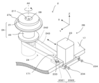
Access Memory)等を有するコンピュータにより構成されており、記憶部10Bに記憶されるプログラムにしたがって基板処理装置1の各部を以下のように制御し、ベベル処理を実行する。以下、図14を参照しつつ基板処理装置1によるベベル処理について説明する。
2A…基板保持部
2B…回転機構
5…処理機構
11…チャンバ
11a…底壁
11b~11e…側壁
11f…天井壁
12…内部空間
21…スピンチャック
23…モータ
24…動力伝達部
171…モータ取付部位(第1保持部位)
172…スピンチャック取付部位(第2保持部位)
231…回転シャフト
241…第1プーリ
242…第2プーリ
243…無端ベルト
AX…回転軸
SP…基板処理部
Z…鉛直方向
Claims (7)
- 底壁と、前記底壁の周囲から立設される側壁と、前記側壁の上端部を覆う天井壁とで内部空間を覆うように構成されたチャンバと、
前記内部空間内で、水平姿勢の基板を鉛直方向に延びる回転軸まわりに回転させながら前記基板に薬液を処理液として供給することで、前記基板に対して所定の基板処理を施す基板処理部と、
前記底壁から鉛直上方に立設された複数のベース支持部材と、
前記底壁よりも高い剛性を有し、前記基板処理部を載置可能に仕上げられた載置面を鉛直上方に向けた姿勢で、かつ前記底壁から上方に離間した離間位置で、前記複数のベース支持部材の上端部により支持されるベース部材と、
を備え、
前記基板処理部は、
前記基板から飛散する前記処理液の液滴を捕集する飛散防止機構と、
前記ベース部材の上面に取り付けられ、前記飛散防止機構の一部を鉛直方向に昇降可能に構成する昇降機構と、
を有する、基板処理装置。 - 請求項1に記載の基板処理装置であって、
前記飛散防止機構は、
上カップと下カップを有し、回転可能に構成された回転カップと、
前記回転カップを囲むように設けられる固定カップと、を有し、
前記昇降機構は、前記飛散防止機構のうち前記上カップを鉛直方向に昇降可能に構成する、基板処理装置。 - 請求項1に記載の基板処理装置であって、
前記ベース部材は金属プレートである、基板処理装置。 - 請求項3に記載の基板処理装置であって、
前記基板処理部は、
下方端部が前記底壁から上方に離間した姿勢で前記ベース部材に取り付けられるとともに、上方端部で前記基板を略水平に保持しながら鉛直方向に延びる回転軸まわりに回転可能に設けられる基板保持部と、
前記底壁から上方に離間した姿勢で前記ベース部材に取り付けられたモータと、前記モータで発生した回転駆動力を前記基板保持部の下方端部に伝達する動力伝達部と、を有し、前記回転駆動力によって前記基板保持部を前記回転軸まわりに回転させる回転機構と、
前記基板保持部の上方端部で保持された状態で前記回転軸まわりに回転される前記基板に前記処理液を供給する処理機構と、
を有する、基板処理装置。 - 底壁と、前記底壁の周囲から立設される側壁と、前記側壁の上端部を覆う天井壁とで内部空間を覆うように構成されたチャンバと、
前記内部空間内で、水平姿勢の基板を鉛直方向に延びる回転軸まわりに回転させながら前記基板に薬液を処理液として供給することで、前記基板に対して所定の基板処理を施す基板処理部と、
前記底壁から鉛直上方に立設された複数のベース支持部材と、
前記底壁よりも高い剛性を有し、前記基板処理部を載置可能に仕上げられた載置面を鉛直上方に向けた姿勢で、かつ前記底壁から上方に離間した離間位置で、前記複数のベース支持部材の上端部により支持されるベース部材と、
を備え、
前記基板処理部は、
下方端部が前記底壁から上方に離間した姿勢で前記ベース部材に取り付けられるとともに、上方端部で前記基板を略水平に保持しながら鉛直方向に延びる回転軸まわりに回転可能に設けられる基板保持部と、
前記底壁から上方に離間した姿勢で前記ベース部材に取り付けられたモータと、前記モータで発生した回転駆動力を前記基板保持部の下方端部に伝達する動力伝達部と、を有し、前記回転駆動力によって前記基板保持部を前記回転軸まわりに回転させる回転機構と、
前記基板保持部の上方端部で保持された状態で前記回転軸まわりに回転される前記基板に前記処理液を供給する処理機構と、
を有し、
前記ベース部材は、前記モータの回転シャフトを前記底壁に向けて前記ベース部材の下面から垂下させた姿勢で前記モータを保持する第1保持部位と、前記基板保持部の下方端部を前記底壁に向けて前記ベース部材の下面から垂下させた姿勢で前記基板保持部を保持する第2保持部位と、を有し、
前記動力伝達部は、前記回転シャフトの下端部に取り付けられる第1プーリと、前記基板保持部の下方端部に取り付けられる第2プーリと、前記ベース部材の下方で前記第1プーリおよび前記第2プーリの間に架け渡された無端ベルトと、を有する、基板処理装置。 - 請求項1ないし5のいずれか一項に記載の基板処理装置であって、
前記底壁は、前記処理液に対して耐薬品性を有する樹脂材料で構成されている、基板処理装置。 - 請求項1ないし5のいずれか一項に記載の基板処理装置であって、
鉛直方向において前記底壁と前記ベース部材との間に配置され、前記底壁に向かって流下してくる前記処理液を回収する回収部材を、さらに備える、基板処理装置。
Priority Applications (5)
| Application Number | Priority Date | Filing Date | Title |
|---|---|---|---|
| JP2022134815A JP7572998B2 (ja) | 2022-08-26 | 2022-08-26 | 基板処理装置 |
| US18/366,068 US20240066548A1 (en) | 2022-08-26 | 2023-08-07 | Substrate processing apparatus |
| TW112129787A TWI876463B (zh) | 2022-08-26 | 2023-08-08 | 基板處理裝置 |
| CN202311020752.XA CN117637526A (zh) | 2022-08-26 | 2023-08-14 | 衬底处理装置 |
| KR1020230107058A KR102754344B1 (ko) | 2022-08-26 | 2023-08-16 | 기판 처리 장치 |
Applications Claiming Priority (1)
| Application Number | Priority Date | Filing Date | Title |
|---|---|---|---|
| JP2022134815A JP7572998B2 (ja) | 2022-08-26 | 2022-08-26 | 基板処理装置 |
Publications (2)
| Publication Number | Publication Date |
|---|---|
| JP2024031325A JP2024031325A (ja) | 2024-03-07 |
| JP7572998B2 true JP7572998B2 (ja) | 2024-10-24 |
Family
ID=90000746
Family Applications (1)
| Application Number | Title | Priority Date | Filing Date |
|---|---|---|---|
| JP2022134815A Active JP7572998B2 (ja) | 2022-08-26 | 2022-08-26 | 基板処理装置 |
Country Status (5)
| Country | Link |
|---|---|
| US (1) | US20240066548A1 (ja) |
| JP (1) | JP7572998B2 (ja) |
| KR (1) | KR102754344B1 (ja) |
| CN (1) | CN117637526A (ja) |
| TW (1) | TWI876463B (ja) |
Families Citing this family (2)
| Publication number | Priority date | Publication date | Assignee | Title |
|---|---|---|---|---|
| JP7628434B2 (ja) * | 2021-02-15 | 2025-02-10 | 株式会社Screenホールディングス | 基板処理装置、および、筒状ガードの加工方法 |
| CN119133034B (zh) * | 2024-11-08 | 2025-03-21 | 宁波润华全芯微电子设备有限公司 | 一种排风系统 |
Citations (3)
| Publication number | Priority date | Publication date | Assignee | Title |
|---|---|---|---|---|
| JP2002177855A (ja) | 2000-12-15 | 2002-06-25 | Dainippon Screen Mfg Co Ltd | 基板処理装置 |
| JP2003163147A (ja) | 2001-11-27 | 2003-06-06 | Hitachi Electronics Eng Co Ltd | 基板液処理装置 |
| JP2007273510A (ja) | 2006-03-30 | 2007-10-18 | Dainippon Screen Mfg Co Ltd | 基板処理装置およびその製造方法 |
Family Cites Families (12)
| Publication number | Priority date | Publication date | Assignee | Title |
|---|---|---|---|---|
| US5591264A (en) * | 1994-03-22 | 1997-01-07 | Sony Corporation | Spin coating device |
| JPH11111665A (ja) * | 1997-10-03 | 1999-04-23 | Sumitomo Precision Prod Co Ltd | 回転式基板処理装置 |
| TWI261875B (en) * | 2002-01-30 | 2006-09-11 | Tokyo Electron Ltd | Processing apparatus and substrate processing method |
| KR100797079B1 (ko) | 2006-07-12 | 2008-01-22 | 세메스 주식회사 | 기판 처리 장치 및 방법 |
| JP5133855B2 (ja) * | 2008-11-25 | 2013-01-30 | 株式会社ディスコ | 保護膜の被覆方法 |
| JP5646354B2 (ja) * | 2011-01-25 | 2014-12-24 | 東京エレクトロン株式会社 | 液処理装置および液処理方法 |
| US10553421B2 (en) * | 2015-05-15 | 2020-02-04 | Tokyo Electron Limited | Substrate processing apparatus, substrate processing method and storage medium |
| WO2017018481A1 (ja) * | 2015-07-29 | 2017-02-02 | 東京エレクトロン株式会社 | 基板処理装置、基板処理方法および記憶媒体 |
| JP6706564B2 (ja) * | 2016-09-23 | 2020-06-10 | 株式会社Screenホールディングス | 基板処理装置および基板処理方法 |
| WO2019186578A1 (en) * | 2018-03-26 | 2019-10-03 | Navson Technologies Private Limited | Substrate holding chuck |
| JP7227757B2 (ja) * | 2018-05-31 | 2023-02-22 | 株式会社Screenホールディングス | 基板処理方法および基板処理装置 |
| JP7149118B2 (ja) * | 2018-07-03 | 2022-10-06 | 株式会社Screenホールディングス | 基板処理装置 |
-
2022
- 2022-08-26 JP JP2022134815A patent/JP7572998B2/ja active Active
-
2023
- 2023-08-07 US US18/366,068 patent/US20240066548A1/en active Pending
- 2023-08-08 TW TW112129787A patent/TWI876463B/zh active
- 2023-08-14 CN CN202311020752.XA patent/CN117637526A/zh active Pending
- 2023-08-16 KR KR1020230107058A patent/KR102754344B1/ko active Active
Patent Citations (3)
| Publication number | Priority date | Publication date | Assignee | Title |
|---|---|---|---|---|
| JP2002177855A (ja) | 2000-12-15 | 2002-06-25 | Dainippon Screen Mfg Co Ltd | 基板処理装置 |
| JP2003163147A (ja) | 2001-11-27 | 2003-06-06 | Hitachi Electronics Eng Co Ltd | 基板液処理装置 |
| JP2007273510A (ja) | 2006-03-30 | 2007-10-18 | Dainippon Screen Mfg Co Ltd | 基板処理装置およびその製造方法 |
Also Published As
| Publication number | Publication date |
|---|---|
| KR102754344B1 (ko) | 2025-01-14 |
| TWI876463B (zh) | 2025-03-11 |
| TW202427639A (zh) | 2024-07-01 |
| KR20240029514A (ko) | 2024-03-05 |
| JP2024031325A (ja) | 2024-03-07 |
| US20240066548A1 (en) | 2024-02-29 |
| CN117637526A (zh) | 2024-03-01 |
Similar Documents
| Publication | Publication Date | Title |
|---|---|---|
| JP7572998B2 (ja) | 基板処理装置 | |
| WO2024062760A1 (ja) | 基板処理装置 | |
| TWI864933B (zh) | 基板處理裝置 | |
| KR102836587B1 (ko) | 기판 처리 장치 | |
| KR102761215B1 (ko) | 기판 처리 장치 | |
| KR102836586B1 (ko) | 기판 처리 장치 및 기판 처리 방법 | |
| KR102934347B1 (ko) | 기판 처리 장치 | |
| US20260076129A1 (en) | Substrate processing apparatus, substrate processing method and substrate processing system | |
| KR102941874B1 (ko) | 기판 처리 장치, 기판 처리 방법 및 기판 처리 시스템 | |
| KR20250033259A (ko) | 기판 처리 장치 및 기판 처리 방법 | |
| JP2025033236A (ja) | 基板処理装置 | |
| JP2025000204A (ja) | 基板処理装置および基板処理方法 |
Legal Events
| Date | Code | Title | Description |
|---|---|---|---|
| A621 | Written request for application examination |
Free format text: JAPANESE INTERMEDIATE CODE: A621 Effective date: 20230411 |
|
| A131 | Notification of reasons for refusal |
Free format text: JAPANESE INTERMEDIATE CODE: A131 Effective date: 20240618 |
|
| A521 | Request for written amendment filed |
Free format text: JAPANESE INTERMEDIATE CODE: A523 Effective date: 20240725 |
|
| TRDD | Decision of grant or rejection written | ||
| A01 | Written decision to grant a patent or to grant a registration (utility model) |
Free format text: JAPANESE INTERMEDIATE CODE: A01 Effective date: 20241001 |
|
| A61 | First payment of annual fees (during grant procedure) |
Free format text: JAPANESE INTERMEDIATE CODE: A61 Effective date: 20241011 |
|
| R150 | Certificate of patent or registration of utility model |
Ref document number: 7572998 Country of ref document: JP Free format text: JAPANESE INTERMEDIATE CODE: R150 |