JP7561552B2 - Metal Wiring Formation Method - Google Patents

Metal Wiring Formation Method Download PDF

Info

Publication number
JP7561552B2
JP7561552B2 JP2020153710A JP2020153710A JP7561552B2 JP 7561552 B2 JP7561552 B2 JP 7561552B2 JP 2020153710 A JP2020153710 A JP 2020153710A JP 2020153710 A JP2020153710 A JP 2020153710A JP 7561552 B2 JP7561552 B2 JP 7561552B2
Authority
JP
Japan
Prior art keywords
semiconductor wafer
chamber
metal wiring
heat treatment
flash
Prior art date
Legal status (The legal status is an assumption and is not a legal conclusion. Google has not performed a legal analysis and makes no representation as to the accuracy of the status listed.)
Active
Application number
JP2020153710A
Other languages
Japanese (ja)
Other versions
JP2022047758A (en
Inventor
光 河原▲崎▼
英昭 谷村
翔伍 繁桝
Current Assignee (The listed assignees may be inaccurate. Google has not performed a legal analysis and makes no representation or warranty as to the accuracy of the list.)
Screen Holdings Co Ltd
Original Assignee
Screen Holdings Co Ltd
Priority date (The priority date is an assumption and is not a legal conclusion. Google has not performed a legal analysis and makes no representation as to the accuracy of the date listed.)
Filing date
Publication date
Application filed by Screen Holdings Co Ltd filed Critical Screen Holdings Co Ltd
Priority to JP2020153710A priority Critical patent/JP7561552B2/en
Publication of JP2022047758A publication Critical patent/JP2022047758A/en
Application granted granted Critical
Publication of JP7561552B2 publication Critical patent/JP7561552B2/en
Active legal-status Critical Current
Anticipated expiration legal-status Critical

Links

Images

Landscapes

  • Electrodes Of Semiconductors (AREA)
  • Internal Circuitry In Semiconductor Integrated Circuit Devices (AREA)

Description

特許法第30条第2項適用 第81回応用物理学会秋季学術講演会 講演予稿集、第143頁、応用物理学会Application of Article 30, Paragraph 2 of the Patent Law, 81st Autumn Meeting of the Japan Society of Applied Physics, Abstracts, p. 143, Japan Society of Applied Physics

本発明は、半導体ウェハー等の薄板状精密電子基板(以下、単に「基板」と称する)上にタングステン等の金属配線を形成する金属配線形成方法に関する。 The present invention relates to a method for forming metal wiring, such as tungsten wiring, on a thin precision electronic substrate (hereinafter simply referred to as "substrate") such as a semiconductor wafer.

近年の集積回路は、10億個を超える膨大な数のトランジスタによって構成されている。これら多数のトランジスタを同時に、高速で、かつ相補的に動作させることにより、ロジック機能やメモリ機能を創出している。 Recent integrated circuits are made up of a huge number of transistors, exceeding one billion. Logic and memory functions are created by operating these many transistors simultaneously, at high speed, and in a complementary manner.

メモリ機能等を実現するために、多数のトランジスタは金属配線によって相互に接続されている。金属配線に用いる金属材料としては段差被膜性に優れたタングステン(W)が採用されることが多い。特許文献1には、コンタクトホールにCVDによってタングステン膜を形成することが開示されている。また、特許文献2には、CVDによってタングステンのコンタクトプラグを形成することが開示されている。 To realize memory functions, etc., a large number of transistors are interconnected by metal wiring. Tungsten (W), which has excellent step coverage properties, is often used as the metal material for the metal wiring. Patent Document 1 discloses forming a tungsten film in a contact hole by CVD. Patent Document 2 discloses forming a tungsten contact plug by CVD.

特開2015-149354号公報JP 2015-149354 A 国際公開第2007/116433号International Publication No. 2007/116433

一般にCVDによってタングステンを堆積するときには原料ガスとしてフッ化タングステン(WF)が用いられる。このためCVDによってタングステンを堆積して形成された金属配線中にはフッ素(F)が混入している。 Generally, when depositing tungsten by CVD, tungsten fluoride (WF 6 ) is used as a source gas, and therefore fluorine (F) is mixed into the metal wiring formed by depositing tungsten by CVD.

また、典型的には、堆積後の金属配線には、堆積時不純物の脱離と高密度化の目的で熱処理が行われる。この熱処理時に金属配線中に混入していたフッ素が拡散して下層のチタン(Ti)やシリコン(Si)と反応してTiFxやSiFxを生成し、それらが堆積膨張して膜破壊を生じさせるボルケーノ現象が発生する。 Typically, the metal wiring after deposition is heat-treated to remove impurities and densify. During this heat treatment, fluorine that was mixed into the metal wiring diffuses and reacts with the titanium (Ti) or silicon (Si) in the underlying layer to generate TiFx or SiFx, which accumulate and expand, causing the volcano phenomenon that destroys the film.

このような現象を防ぐために、タングステンの金属配線と下層のチタンとの間にバリアメタル層として窒化チタン(TiN)の薄膜を成膜し、それによってフッ素の拡散を防ぐ技術が知られている。 To prevent this phenomenon, a technique is known in which a thin film of titanium nitride (TiN) is deposited as a barrier metal layer between the tungsten metal wiring and the underlying titanium, thereby preventing the diffusion of fluorine.

デバイスの微細化に伴って、タングステンの金属配線のアスペクト比が増大しているため、より深く狭い領域に窒化チタン膜を成膜する必要がある。このため、CVDよりも段差被膜性に優れたALDによって窒化チタン膜が成膜されることが多い。 As devices become more miniaturized, the aspect ratio of tungsten metal wiring increases, making it necessary to deposit titanium nitride films in deeper, narrower areas. For this reason, titanium nitride films are often deposited by ALD, which has better step coverage than CVD.

しかしながら、ALDによって成膜された窒化チタン膜は、膜質が良好ではなく、フッ素の拡散を抑制するという機能を十分には果たせていない。その結果、バリアメタル層としての窒化チタン膜を成膜したとしても、ボルケーノ現象を完全に防ぐことはできなかった。 However, the titanium nitride film formed by ALD does not have good film quality and does not fully suppress the diffusion of fluorine. As a result, even if a titanium nitride film is formed as a barrier metal layer, the volcano phenomenon cannot be completely prevented.

本発明は、上記課題に鑑みてなされたものであり、金属配線からのフッ素の拡散を十分に抑制することができる金属配線形成方法を提供することを目的とする。 The present invention was made in consideration of the above problems, and aims to provide a method for forming metal wiring that can sufficiently suppress the diffusion of fluorine from the metal wiring.

上記課題を解決するため、請求項1の発明は、基板上に金属配線を形成する金属配線形成方法において、基板上に窒化チタンをバリアメタル層として堆積させる第1堆積工程と、フラッシュランプから前記基板にフラッシュ光を照射して前記バリアメタル層を加熱する第1加熱工程と、前記バリアメタル層上にタングステンを金属配線として堆積させる第2堆積工程と、前記フラッシュランプから前記基板にフラッシュ光を照射して前記金属配線を加熱する第2加熱工程と、を備え、前記第2堆積工程では、フッ化タングステンを原料としてタングステンを堆積させることを特徴とする。 In order to solve the above problem, the invention of claim 1 provides a metal wiring formation method for forming metal wiring on a substrate, comprising a first deposition step of depositing titanium nitride on the substrate as a barrier metal layer, a first heating step of irradiating the substrate with a flash light from a flash lamp to heat the barrier metal layer, a second deposition step of depositing tungsten on the barrier metal layer as metal wiring, and a second heating step of irradiating the substrate with a flash light from the flash lamp to heat the metal wiring, wherein the second deposition step deposits tungsten using tungsten fluoride as a raw material .

また、請求項の発明は、請求項の発明に係る金属配線形成方法において、前記第1加熱工程および前記第2加熱工程は、大気圧未満の減圧下で実行されることを特徴とする。 The invention of claim 2 is the method of forming metal wiring according to the invention of claim 1 , characterized in that the first heating step and the second heating step are carried out under a reduced pressure lower than atmospheric pressure.

また、請求項の発明は、請求項または請求項の発明に係る金属配線形成方法において、前記第1加熱工程は、アンモニア雰囲気中にて実行され、前記第2加熱工程は、フォーミングガス雰囲気中にて実行されることを特徴とする。 The invention of claim 3 is characterized in that, in the metal wiring forming method of the invention of claim 1 or claim 2 , the first heating step is performed in an ammonia atmosphere, and the second heating step is performed in a forming gas atmosphere.

請求項1から請求項の発明によれば、フラッシュ光を照射して窒化チタンのバリアメタル層を加熱するため、バリアメタル層の膜質を改善して金属配線からのフッ素の拡散を十分に抑制することができる。また、フラッシュ光を照射してタングステンの金属配線を加熱するため、タングステンに混入しているフッ素の拡散をさらに抑制することができる。 According to the inventions of claims 1 to 3 , since the barrier metal layer of titanium nitride is heated by irradiating it with flash light, the film quality of the barrier metal layer can be improved and the diffusion of fluorine from the metal wiring can be sufficiently suppressed. Also, since the metal wiring of tungsten is heated by irradiating it with flash light, the diffusion of fluorine mixed in tungsten can be further suppressed.

特に、請求項の発明によれば、第1加熱工程および第2加熱工程は、大気圧未満の減圧下で実行されるため、バリアメタル層および金属配線の酸化を防止することができる。 In particular, according to the second aspect of the present invention, the first and second heating steps are carried out under a reduced pressure lower than atmospheric pressure, so that oxidation of the barrier metal layer and the metal wiring can be prevented.

特に、請求項の発明によれば、第1加熱工程は、アンモニア雰囲気中にて実行され、第2加熱工程は、フォーミングガス雰囲気中にて実行されるため、バリアメタル層の窒化を促進するとともに、金属配線に混入している不純物を還元することができる。
In particular, according to the invention of claim 3 , the first heating step is performed in an ammonia atmosphere, and the second heating step is performed in a forming gas atmosphere, thereby promoting nitridation of the barrier metal layer and reducing impurities that have become mixed in the metal wiring.

本発明に係る金属配線形成方法の熱処理工程を実行する熱処理装置の構成を示す縦断面図である。1 is a vertical cross-sectional view showing a configuration of a heat treatment apparatus for performing a heat treatment step of a metal wiring forming method according to the present invention; 保持部の全体外観を示す斜視図である。FIG. 2 is a perspective view showing the overall appearance of a holding portion. サセプタの平面図である。FIG. サセプタの断面図である。FIG. 2 is a cross-sectional view of a susceptor. 移載機構の平面図である。FIG. 移載機構の側面図である。FIG. 複数のハロゲンランプの配置を示す平面図である。FIG. 2 is a plan view showing an arrangement of a plurality of halogen lamps. 本発明に係る金属配線形成方法の処理手順を示すフローチャートである。2 is a flowchart showing a processing procedure of a metal wiring forming method according to the present invention. 半導体ウェハーに窒化チタンが堆積された状態の一例を示す図である。FIG. 1 illustrates an example of titanium nitride being deposited on a semiconductor wafer. 半導体ウェハーWに対する熱処理の手順を示すフローチャートである。4 is a flowchart showing a procedure for heat treatment of a semiconductor wafer W. チャンバー内の圧力変化を示す図である。FIG. 4 is a diagram showing pressure changes in a chamber. 半導体ウェハーの表面温度の変化を示す図である。FIG. 1 is a diagram showing changes in the surface temperature of a semiconductor wafer. 半導体ウェハーにタングステンが堆積された状態の一例を示す図である。FIG. 1 is a diagram showing an example of a state in which tungsten is deposited on a semiconductor wafer. 熱処理時のフッ素の拡散の程度を示す図である。FIG. 13 is a diagram showing the degree of fluorine diffusion during heat treatment.

以下、図面を参照しつつ本発明の実施の形態について詳細に説明する。 The following describes in detail the embodiment of the present invention with reference to the drawings.

図1は、本発明に係る金属配線形成方法の熱処理工程を実行する熱処理装置1の構成を示す縦断面図である。図1の熱処理装置1は、基板として円板形状の半導体ウェハーWに対してフラッシュ光照射を行うことによってその半導体ウェハーWを加熱するフラッシュランプアニール装置である。処理対象となる半導体ウェハーWのサイズは特に限定されるものではないが、例えばφ300mmやφ450mmである。なお、図1および以降の各図においては、理解容易のため、必要に応じて各部の寸法や数を誇張または簡略化して描いている。 Figure 1 is a vertical cross-sectional view showing the configuration of a heat treatment apparatus 1 that performs the heat treatment process of the metal wiring formation method according to the present invention. The heat treatment apparatus 1 in Figure 1 is a flash lamp annealing apparatus that heats a disk-shaped semiconductor wafer W as a substrate by irradiating the semiconductor wafer W with flash light. The size of the semiconductor wafer W to be treated is not particularly limited, but is, for example, φ300 mm or φ450 mm. Note that in Figure 1 and the subsequent figures, the dimensions and number of each part are exaggerated or simplified as necessary for ease of understanding.

熱処理装置1は、半導体ウェハーWを収容するチャンバー6と、複数のフラッシュランプFLを内蔵するフラッシュ加熱部5と、複数のハロゲンランプHLを内蔵するハロゲン加熱部4と、を備える。チャンバー6の上側にフラッシュ加熱部5が設けられるとともに、下側にハロゲン加熱部4が設けられている。また、熱処理装置1は、チャンバー6の内部に、半導体ウェハーWを水平姿勢に保持する保持部7と、保持部7と装置外部との間で半導体ウェハーWの受け渡しを行う移載機構10と、を備える。さらに、熱処理装置1は、ハロゲン加熱部4、フラッシュ加熱部5およびチャンバー6に設けられた各動作機構を制御して半導体ウェハーWの熱処理を実行させる制御部3を備える。 The heat treatment apparatus 1 includes a chamber 6 that houses a semiconductor wafer W, a flash heating section 5 that incorporates multiple flash lamps FL, and a halogen heating section 4 that incorporates multiple halogen lamps HL. The flash heating section 5 is provided on the upper side of the chamber 6, and the halogen heating section 4 is provided on the lower side. The heat treatment apparatus 1 also includes a holding section 7 inside the chamber 6 that holds the semiconductor wafer W in a horizontal position, and a transfer mechanism 10 that transfers the semiconductor wafer W between the holding section 7 and the outside of the apparatus. The heat treatment apparatus 1 also includes a control section 3 that controls the halogen heating section 4, the flash heating section 5, and each operating mechanism provided in the chamber 6 to perform heat treatment of the semiconductor wafer W.

チャンバー6は、筒状のチャンバー側部61の上下に石英製のチャンバー窓を装着して構成されている。チャンバー側部61は上下が開口された概略筒形状を有しており、上側開口には上側チャンバー窓63が装着されて閉塞され、下側開口には下側チャンバー窓64が装着されて閉塞されている。チャンバー6の天井部を構成する上側チャンバー窓63は、石英により形成された円板形状部材であり、フラッシュ加熱部5から出射されたフラッシュ光をチャンバー6内に透過する石英窓として機能する。また、チャンバー6の床部を構成する下側チャンバー窓64も、石英により形成された円板形状部材であり、ハロゲン加熱部4からの光をチャンバー6内に透過する石英窓として機能する。 The chamber 6 is constructed by attaching quartz chamber windows to the top and bottom of a cylindrical chamber side 61. The chamber side 61 has a roughly cylindrical shape with openings at the top and bottom, with an upper chamber window 63 attached and closed at the upper opening, and a lower chamber window 64 attached and closed at the lower opening. The upper chamber window 63, which constitutes the ceiling of the chamber 6, is a disk-shaped member made of quartz and functions as a quartz window that transmits the flash light emitted from the flash heating unit 5 into the chamber 6. The lower chamber window 64, which constitutes the floor of the chamber 6, is also a disk-shaped member made of quartz and functions as a quartz window that transmits the light from the halogen heating unit 4 into the chamber 6.

また、チャンバー側部61の内側の壁面の上部には反射リング68が装着され、下部には反射リング69が装着されている。反射リング68,69は、ともに円環状に形成されている。上側の反射リング68は、チャンバー側部61の上側から嵌め込むことによって装着される。一方、下側の反射リング69は、チャンバー側部61の下側から嵌め込んで図示省略のビスで留めることによって装着される。すなわち、反射リング68,69は、ともに着脱自在にチャンバー側部61に装着されるものである。チャンバー6の内側空間、すなわち上側チャンバー窓63、下側チャンバー窓64、チャンバー側部61および反射リング68,69によって囲まれる空間が熱処理空間65として規定される。 A reflective ring 68 is attached to the upper part of the inner wall surface of the chamber side 61, and a reflective ring 69 is attached to the lower part. Both reflective rings 68, 69 are formed in an annular shape. The upper reflective ring 68 is attached by fitting it from the upper side of the chamber side 61. On the other hand, the lower reflective ring 69 is attached by fitting it from the lower side of the chamber side 61 and fastening it with screws (not shown). In other words, both reflective rings 68, 69 are detachably attached to the chamber side 61. The inner space of the chamber 6, i.e., the space surrounded by the upper chamber window 63, the lower chamber window 64, the chamber side 61, and the reflective rings 68, 69, is defined as the heat treatment space 65.

チャンバー側部61に反射リング68,69が装着されることによって、チャンバー6の内壁面に凹部62が形成される。すなわち、チャンバー側部61の内壁面のうち反射リング68,69が装着されていない中央部分と、反射リング68の下端面と、反射リング69の上端面とで囲まれた凹部62が形成される。凹部62は、チャンバー6の内壁面に水平方向に沿って円環状に形成され、半導体ウェハーWを保持する保持部7を囲繞する。チャンバー側部61および反射リング68,69は、強度と耐熱性に優れた金属材料(例えば、ステンレススチール)にて形成されている。 By attaching the reflecting rings 68, 69 to the chamber side 61, a recess 62 is formed on the inner wall surface of the chamber 6. That is, the recess 62 is formed by the central portion of the inner wall surface of the chamber side 61 where the reflecting rings 68, 69 are not attached, the lower end surface of the reflecting ring 68, and the upper end surface of the reflecting ring 69. The recess 62 is formed in an annular shape along the horizontal direction on the inner wall surface of the chamber 6, and surrounds the holder 7 that holds the semiconductor wafer W. The chamber side 61 and the reflecting rings 68, 69 are formed from a metal material (e.g., stainless steel) that has excellent strength and heat resistance.

また、チャンバー側部61には、チャンバー6に対して半導体ウェハーWの搬入および搬出を行うための搬送開口部(炉口)66が形設されている。搬送開口部66は、ゲートバルブ185によって開閉可能とされている。搬送開口部66は凹部62の外周面に連通接続されている。このため、ゲートバルブ185が搬送開口部66を開放しているときには、搬送開口部66から凹部62を通過して熱処理空間65への半導体ウェハーWの搬入および熱処理空間65からの半導体ウェハーWの搬出を行うことができる。また、ゲートバルブ185が搬送開口部66を閉鎖するとチャンバー6内の熱処理空間65が密閉空間とされる。 In addition, a transport opening (furnace port) 66 is formed in the chamber side 61 to carry the semiconductor wafer W into and out of the chamber 6. The transport opening 66 can be opened and closed by a gate valve 185. The transport opening 66 is connected to the outer peripheral surface of the recess 62. Therefore, when the gate valve 185 opens the transport opening 66, the semiconductor wafer W can be carried into and out of the heat treatment space 65 through the transport opening 66 and the recess 62. In addition, when the gate valve 185 closes the transport opening 66, the heat treatment space 65 in the chamber 6 becomes an airtight space.

さらに、チャンバー側部61には、貫通孔61aが穿設されている。チャンバー側部61の外壁面の貫通孔61aが設けられている部位には放射温度計20が取り付けられている。貫通孔61aは、後述するサセプタ74に保持された半導体ウェハーWの下面から放射された赤外光を放射温度計20に導くための円筒状の孔である。貫通孔61aは、その貫通方向の軸がサセプタ74に保持された半導体ウェハーWの主面と交わるように、水平方向に対して傾斜して設けられている。よって、放射温度計20はサセプタ74の斜め下方に設けられることとなる。貫通孔61aの熱処理空間65に臨む側の端部には、放射温度計20が測定可能な波長領域の赤外光を透過させるフッ化バリウム材料からなる透明窓21が装着されている。 Furthermore, a through hole 61a is drilled in the chamber side 61. A radiation thermometer 20 is attached to the portion of the outer wall surface of the chamber side 61 where the through hole 61a is provided. The through hole 61a is a cylindrical hole for guiding infrared light radiated from the underside of the semiconductor wafer W held by the susceptor 74 described later to the radiation thermometer 20. The through hole 61a is provided at an angle to the horizontal direction so that the axis of the through hole 61a intersects with the main surface of the semiconductor wafer W held by the susceptor 74. Therefore, the radiation thermometer 20 is provided diagonally below the susceptor 74. A transparent window 21 made of barium fluoride material that transmits infrared light in a wavelength range that can be measured by the radiation thermometer 20 is attached to the end of the through hole 61a facing the heat treatment space 65.

また、チャンバー6の内壁上部には熱処理空間65に処理ガスを供給するガス供給孔81が形設されている。ガス供給孔81は、凹部62よりも上側位置に形設されており、反射リング68に設けられていても良い。ガス供給孔81はチャンバー6の側壁内部に円環状に形成された緩衝空間82を介してガス供給管83に連通接続されている。ガス供給管83は処理ガス供給源85に接続されている。また、ガス供給管83の経路途中にはバルブ84が介挿されている。バルブ84が開放されると、処理ガス供給源85から緩衝空間82に処理ガスが送給される。緩衝空間82に流入した処理ガスは、ガス供給孔81よりも流体抵抗の小さい緩衝空間82内を拡がるように流れてガス供給孔81から熱処理空間65内へと供給される。処理ガスとしては、例えば窒素(N)、アルゴン(Ar)、ヘリウム(He)等の不活性ガス、または、水素(H)、アンモニア(NH)等の反応性ガス、或いはそれらを混合した混合ガスを用いることができる。 Further, a gas supply hole 81 is formed in the upper part of the inner wall of the chamber 6 to supply a processing gas to the heat treatment space 65. The gas supply hole 81 is formed at a position above the recess 62, and may be provided in the reflecting ring 68. The gas supply hole 81 is connected to a gas supply pipe 83 through a buffer space 82 formed in an annular shape inside the side wall of the chamber 6. The gas supply pipe 83 is connected to a processing gas supply source 85. Further, a valve 84 is interposed in the middle of the gas supply pipe 83. When the valve 84 is opened, the processing gas is supplied from the processing gas supply source 85 to the buffer space 82. The processing gas that has flowed into the buffer space 82 flows in a manner to expand inside the buffer space 82, which has a smaller fluid resistance than the gas supply hole 81, and is supplied from the gas supply hole 81 to the heat treatment space 65. The processing gas may be, for example, an inert gas such as nitrogen ( N2 ), argon (Ar), or helium (He), or a reactive gas such as hydrogen ( H2 ), ammonia ( NH3 ), or a mixed gas of these.

一方、チャンバー6の内壁下部には熱処理空間65内の気体を排気するガス排気孔86が形設されている。ガス排気孔86は、凹部62よりも下側位置に形設されており、反射リング69に設けられていても良い。ガス排気孔86はチャンバー6の側壁内部に円環状に形成された緩衝空間87を介してガス排気管88に連通接続されている。ガス排気管88は排気部190に接続されている。また、ガス排気管88の経路途中にはバルブ89が介挿されている。バルブ89が開放されると、熱処理空間65の気体がガス排気孔86から緩衝空間87を経てガス排気管88へと排出される。なお、ガス供給孔81およびガス排気孔86は、チャンバー6の周方向に沿って複数設けられていても良いし、スリット状のものであっても良い。 On the other hand, a gas exhaust hole 86 is formed in the lower part of the inner wall of the chamber 6 to exhaust the gas in the heat treatment space 65. The gas exhaust hole 86 is formed at a position lower than the recess 62, and may be provided in the reflecting ring 69. The gas exhaust hole 86 is connected to a gas exhaust pipe 88 through a buffer space 87 formed in an annular shape inside the side wall of the chamber 6. The gas exhaust pipe 88 is connected to an exhaust section 190. A valve 89 is inserted in the middle of the path of the gas exhaust pipe 88. When the valve 89 is opened, the gas in the heat treatment space 65 is exhausted from the gas exhaust hole 86 through the buffer space 87 to the gas exhaust pipe 88. The gas supply holes 81 and the gas exhaust holes 86 may be provided in multiple numbers along the circumferential direction of the chamber 6, or may be slit-shaped.

排気部190は真空ポンプを備える。バルブ84を閉止してチャンバー6内にガス供給を行うこと無く、排気部190を作動させてチャンバー6内の気体を排気することにより、チャンバー6内を大気圧未満に減圧することができる。また、ガス排気管88と並列に管径の異なる複数のバイパス管(図示省略)を設け、それらを適宜開閉することによってチャンバー6からの排気速度を調整するようにしても良い。 The exhaust unit 190 is equipped with a vacuum pump. By operating the exhaust unit 190 to exhaust the gas in the chamber 6 without closing the valve 84 to supply gas into the chamber 6, the pressure inside the chamber 6 can be reduced to less than atmospheric pressure. In addition, multiple bypass pipes (not shown) with different pipe diameters may be provided in parallel with the gas exhaust pipe 88, and the exhaust speed from the chamber 6 may be adjusted by opening and closing them as appropriate.

図2は、保持部7の全体外観を示す斜視図である。保持部7は、基台リング71、連結部72およびサセプタ74を備えて構成される。基台リング71、連結部72およびサセプタ74はいずれも石英にて形成されている。すなわち、保持部7の全体が石英にて形成されている。 Figure 2 is a perspective view showing the overall appearance of the holding unit 7. The holding unit 7 is configured with a base ring 71, a connecting portion 72, and a susceptor 74. The base ring 71, the connecting portion 72, and the susceptor 74 are all made of quartz. In other words, the entire holding unit 7 is made of quartz.

基台リング71は円環形状から一部が欠落した円弧形状の石英部材である。この欠落部分は、後述する移載機構10の移載アーム11と基台リング71との干渉を防ぐために設けられている。基台リング71は凹部62の底面に載置されることによって、チャンバー6の壁面に支持されることとなる(図1参照)。基台リング71の上面に、その円環形状の周方向に沿って複数の連結部72(本実施形態では4個)が立設される。連結部72も石英の部材であり、溶接によって基台リング71に固着される。 The base ring 71 is an arc-shaped quartz member with a portion missing from the annular shape. This missing portion is provided to prevent interference between the base ring 71 and the transfer arm 11 of the transfer mechanism 10 (described later). The base ring 71 is placed on the bottom surface of the recess 62, and is supported by the wall surface of the chamber 6 (see FIG. 1). A number of connecting portions 72 (four in this embodiment) are erected on the upper surface of the base ring 71 along the circumferential direction of the annular shape. The connecting portions 72 are also made of quartz, and are fixed to the base ring 71 by welding.

サセプタ74は基台リング71に設けられた4個の連結部72によって支持される。図3は、サセプタ74の平面図である。また、図4は、サセプタ74の断面図である。サセプタ74は、保持プレート75、ガイドリング76および複数の基板支持ピン77を備える。保持プレート75は、石英にて形成された略円形の平板状部材である。保持プレート75の直径は半導体ウェハーWの直径よりも大きい。すなわち、保持プレート75は、半導体ウェハーWよりも大きな平面サイズを有する。 The susceptor 74 is supported by four connecting parts 72 provided on the base ring 71. FIG. 3 is a plan view of the susceptor 74. FIG. 4 is a cross-sectional view of the susceptor 74. The susceptor 74 includes a holding plate 75, a guide ring 76, and a plurality of substrate support pins 77. The holding plate 75 is a substantially circular flat member made of quartz. The diameter of the holding plate 75 is larger than the diameter of the semiconductor wafer W. In other words, the holding plate 75 has a planar size larger than that of the semiconductor wafer W.

保持プレート75の上面周縁部にガイドリング76が設置されている。ガイドリング76は、半導体ウェハーWの直径よりも大きな内径を有する円環形状の部材である。例えば、半導体ウェハーWの直径がφ300mmの場合、ガイドリング76の内径はφ320mmである。ガイドリング76の内周は、保持プレート75から上方に向けて広くなるようなテーパ面とされている。ガイドリング76は、保持プレート75と同様の石英にて形成される。ガイドリング76は、保持プレート75の上面に溶着するようにしても良いし、別途加工したピンなどによって保持プレート75に固定するようにしても良い。或いは、保持プレート75とガイドリング76とを一体の部材として加工するようにしても良い。 A guide ring 76 is installed on the periphery of the upper surface of the holding plate 75. The guide ring 76 is an annular member having an inner diameter larger than the diameter of the semiconductor wafer W. For example, when the diameter of the semiconductor wafer W is φ300 mm, the inner diameter of the guide ring 76 is φ320 mm. The inner circumference of the guide ring 76 is a tapered surface that widens from the holding plate 75 upward. The guide ring 76 is made of quartz, the same as the holding plate 75. The guide ring 76 may be welded to the upper surface of the holding plate 75, or may be fixed to the holding plate 75 by a separately processed pin or the like. Alternatively, the holding plate 75 and the guide ring 76 may be processed as an integrated member.

保持プレート75の上面のうちガイドリング76よりも内側の領域が半導体ウェハーWを保持する平面状の保持面75aとされる。保持プレート75の保持面75aには、複数の基板支持ピン77が立設されている。本実施形態においては、保持面75aの外周円(ガイドリング76の内周円)と同心円の周上に沿って30°毎に計12個の基板支持ピン77が立設されている。12個の基板支持ピン77を配置した円の径(対向する基板支持ピン77間の距離)は半導体ウェハーWの径よりも小さく、半導体ウェハーWの径がφ300mmであればφ270mm~φ280mm(本実施形態ではφ270mm)である。それぞれの基板支持ピン77は石英にて形成されている。複数の基板支持ピン77は、保持プレート75の上面に溶接によって設けるようにしても良いし、保持プレート75と一体に加工するようにしても良い。 The area of the upper surface of the holding plate 75 inside the guide ring 76 is a flat holding surface 75a that holds the semiconductor wafer W. A plurality of substrate support pins 77 are erected on the holding surface 75a of the holding plate 75. In this embodiment, a total of 12 substrate support pins 77 are erected every 30° along a circumference concentric with the outer circumferential circle of the holding surface 75a (the inner circumferential circle of the guide ring 76). The diameter of the circle on which the 12 substrate support pins 77 are arranged (the distance between opposing substrate support pins 77) is smaller than the diameter of the semiconductor wafer W, and is φ270 mm to φ280 mm (φ270 mm in this embodiment) if the diameter of the semiconductor wafer W is φ300 mm. Each substrate support pin 77 is made of quartz. The plurality of substrate support pins 77 may be provided on the upper surface of the holding plate 75 by welding, or may be machined integrally with the holding plate 75.

図2に戻り、基台リング71に立設された4個の連結部72とサセプタ74の保持プレート75の周縁部とが溶接によって固着される。すなわち、サセプタ74と基台リング71とは連結部72によって固定的に連結されている。このような保持部7の基台リング71がチャンバー6の壁面に支持されることによって、保持部7がチャンバー6に装着される。保持部7がチャンバー6に装着された状態においては、サセプタ74の保持プレート75は水平姿勢(法線が鉛直方向と一致する姿勢)となる。すなわち、保持プレート75の保持面75aは水平面となる。 Returning to FIG. 2, the four connecting parts 72 erected on the base ring 71 are fixed to the peripheral part of the holding plate 75 of the susceptor 74 by welding. That is, the susceptor 74 and the base ring 71 are fixedly connected by the connecting parts 72. The base ring 71 of the holding part 7 is supported on the wall surface of the chamber 6, and the holding part 7 is attached to the chamber 6. When the holding part 7 is attached to the chamber 6, the holding plate 75 of the susceptor 74 is in a horizontal position (a position in which the normal line coincides with the vertical direction). That is, the holding surface 75a of the holding plate 75 is a horizontal plane.

チャンバー6に搬入された半導体ウェハーWは、チャンバー6に装着された保持部7のサセプタ74の上に水平姿勢にて載置されて保持される。このとき、半導体ウェハーWは保持プレート75上に立設された12個の基板支持ピン77によって支持されてサセプタ74に保持される。より厳密には、12個の基板支持ピン77の上端部が半導体ウェハーWの下面に接触して当該半導体ウェハーWを支持する。12個の基板支持ピン77の高さ(基板支持ピン77の上端から保持プレート75の保持面75aまでの距離)は均一であるため、12個の基板支持ピン77によって半導体ウェハーWを水平姿勢に支持することができる。 The semiconductor wafer W that has been carried into the chamber 6 is placed and held in a horizontal position on the susceptor 74 of the holder 7 that is attached to the chamber 6. At this time, the semiconductor wafer W is supported by twelve substrate support pins 77 that are erected on the holding plate 75 and held on the susceptor 74. More precisely, the upper ends of the twelve substrate support pins 77 contact the underside of the semiconductor wafer W to support the semiconductor wafer W. The heights of the twelve substrate support pins 77 (the distance from the upper ends of the substrate support pins 77 to the holding surface 75a of the holding plate 75) are uniform, so the twelve substrate support pins 77 can support the semiconductor wafer W in a horizontal position.

また、半導体ウェハーWは複数の基板支持ピン77によって保持プレート75の保持面75aから所定の間隔を隔てて支持されることとなる。基板支持ピン77の高さよりもガイドリング76の厚さの方が大きい。従って、複数の基板支持ピン77によって支持された半導体ウェハーWの水平方向の位置ずれはガイドリング76によって防止される。 The semiconductor wafer W is supported by a plurality of substrate support pins 77 at a predetermined distance from the holding surface 75a of the holding plate 75. The thickness of the guide ring 76 is greater than the height of the substrate support pins 77. Therefore, the guide ring 76 prevents the semiconductor wafer W supported by the plurality of substrate support pins 77 from shifting in the horizontal direction.

また、図2および図3に示すように、サセプタ74の保持プレート75には、上下に貫通して開口部78が形成されている。開口部78は、放射温度計20が半導体ウェハーWの下面から放射される放射光(赤外光)を受光するために設けられている。すなわち、放射温度計20が開口部78およびチャンバー側部61の貫通孔61aに装着された透明窓21を介して半導体ウェハーWの下面から放射された光を受光して当該半導体ウェハーWの温度を測定する。さらに、サセプタ74の保持プレート75には、後述する移載機構10のリフトピン12が半導体ウェハーWの受け渡しのために貫通する4個の貫通孔79が穿設されている。 2 and 3, an opening 78 is formed in the holding plate 75 of the susceptor 74, penetrating vertically. The opening 78 is provided so that the radiation thermometer 20 can receive radiation (infrared light) emitted from the underside of the semiconductor wafer W. That is, the radiation thermometer 20 receives the light emitted from the underside of the semiconductor wafer W through the opening 78 and a transparent window 21 attached to the through hole 61a of the chamber side 61, and measures the temperature of the semiconductor wafer W. Furthermore, the holding plate 75 of the susceptor 74 has four through holes 79 through which the lift pins 12 of the transfer mechanism 10, described later, pass to transfer the semiconductor wafer W.

図5は、移載機構10の平面図である。また、図6は、移載機構10の側面図である。移載機構10は、2本の移載アーム11を備える。移載アーム11は、概ね円環状の凹部62に沿うような円弧形状とされている。それぞれの移載アーム11には2本のリフトピン12が立設されている。移載アーム11およびリフトピン12は石英にて形成されている。各移載アーム11は水平移動機構13によって回動可能とされている。水平移動機構13は、一対の移載アーム11を保持部7に対して半導体ウェハーWの移載を行う移載動作位置(図5の実線位置)と保持部7に保持された半導体ウェハーWと平面視で重ならない退避位置(図5の二点鎖線位置)との間で水平移動させる。水平移動機構13としては、個別のモータによって各移載アーム11をそれぞれ回動させるものであっても良いし、リンク機構を用いて1個のモータによって一対の移載アーム11を連動させて回動させるものであっても良い。 Figure 5 is a plan view of the transfer mechanism 10. Figure 6 is a side view of the transfer mechanism 10. The transfer mechanism 10 has two transfer arms 11. The transfer arms 11 are formed in an arc shape that roughly follows the annular recess 62. Two lift pins 12 are erected on each transfer arm 11. The transfer arms 11 and the lift pins 12 are made of quartz. Each transfer arm 11 is rotatable by a horizontal movement mechanism 13. The horizontal movement mechanism 13 horizontally moves the pair of transfer arms 11 between a transfer operation position (solid line position in Figure 5) where the semiconductor wafer W is transferred to the holding unit 7 and a retracted position (double-dashed line position in Figure 5) where the pair of transfer arms 11 do not overlap the semiconductor wafer W held by the holding unit 7 in a plan view. The horizontal movement mechanism 13 may be one that rotates each transfer arm 11 using an individual motor, or one that uses a link mechanism to rotate a pair of transfer arms 11 in unison using a single motor.

また、一対の移載アーム11は、昇降機構14によって水平移動機構13とともに昇降移動される。昇降機構14が一対の移載アーム11を移載動作位置にて上昇させると、計4本のリフトピン12がサセプタ74に穿設された貫通孔79(図2,3参照)を通過し、リフトピン12の上端がサセプタ74の上面から突き出る。一方、昇降機構14が一対の移載アーム11を移載動作位置にて下降させてリフトピン12を貫通孔79から抜き取り、水平移動機構13が一対の移載アーム11を開くように移動させると各移載アーム11が退避位置に移動する。一対の移載アーム11の退避位置は、保持部7の基台リング71の直上である。基台リング71は凹部62の底面に載置されているため、移載アーム11の退避位置は凹部62の内側となる。なお、移載機構10の駆動部(水平移動機構13および昇降機構14)が設けられている部位の近傍にも図示省略の排気機構が設けられており、移載機構10の駆動部周辺の雰囲気がチャンバー6の外部に排出されるように構成されている。 The pair of transfer arms 11 are raised and lowered together with the horizontal movement mechanism 13 by the lifting mechanism 14. When the lifting mechanism 14 raises the pair of transfer arms 11 to the transfer operation position, a total of four lift pins 12 pass through the through holes 79 (see Figures 2 and 3) drilled in the susceptor 74, and the upper ends of the lift pins 12 protrude from the upper surface of the susceptor 74. On the other hand, when the lifting mechanism 14 lowers the pair of transfer arms 11 to the transfer operation position to remove the lift pins 12 from the through holes 79, and the horizontal movement mechanism 13 moves the pair of transfer arms 11 to open them, each transfer arm 11 moves to a retracted position. The retracted position of the pair of transfer arms 11 is directly above the base ring 71 of the holding unit 7. Since the base ring 71 is placed on the bottom surface of the recess 62, the retracted position of the transfer arms 11 is inside the recess 62. In addition, an exhaust mechanism (not shown) is provided near the location where the drive parts (horizontal movement mechanism 13 and lifting mechanism 14) of the transfer mechanism 10 are provided, and is configured to exhaust the atmosphere around the drive parts of the transfer mechanism 10 to the outside of the chamber 6.

図1に戻り、チャンバー6の上方に設けられたフラッシュ加熱部5は、筐体51の内側に、複数本(本実施形態では30本)のキセノンフラッシュランプFLからなる光源と、その光源の上方を覆うように設けられたリフレクタ52と、を備えて構成される。また、フラッシュ加熱部5の筐体51の底部にはランプ光放射窓53が装着されている。フラッシュ加熱部5の床部を構成するランプ光放射窓53は、石英により形成された板状の石英窓である。フラッシュ加熱部5がチャンバー6の上方に設置されることにより、ランプ光放射窓53が上側チャンバー窓63と相対向することとなる。フラッシュランプFLはチャンバー6の上方からランプ光放射窓53および上側チャンバー窓63を介して熱処理空間65にフラッシュ光を照射する。 Returning to FIG. 1, the flash heating unit 5 provided above the chamber 6 is configured with a light source consisting of multiple (30 in this embodiment) xenon flash lamps FL inside a housing 51, and a reflector 52 provided to cover the light source from above. A lamp light emission window 53 is attached to the bottom of the housing 51 of the flash heating unit 5. The lamp light emission window 53, which constitutes the floor of the flash heating unit 5, is a plate-shaped quartz window made of quartz. By installing the flash heating unit 5 above the chamber 6, the lamp light emission window 53 faces the upper chamber window 63. The flash lamps FL irradiate flash light from above the chamber 6 through the lamp light emission window 53 and the upper chamber window 63 into the heat treatment space 65.

複数のフラッシュランプFLは、それぞれが長尺の円筒形状を有する棒状ランプであり、それぞれの長手方向が保持部7に保持される半導体ウェハーWの主面に沿って(つまり水平方向に沿って)互いに平行となるように平面状に配列されている。よって、フラッシュランプFLの配列によって形成される平面も水平面である。複数のフラッシュランプFLが配列される領域は半導体ウェハーWの平面サイズよりも大きい。 The multiple flash lamps FL are rod-shaped lamps each having a long cylindrical shape, and are arranged in a plane so that their longitudinal directions are parallel to each other along the main surface of the semiconductor wafer W held by the holder 7 (i.e., along the horizontal direction). Therefore, the plane formed by the arrangement of the flash lamps FL is also a horizontal plane. The area in which the multiple flash lamps FL are arranged is larger than the planar size of the semiconductor wafer W.

キセノンフラッシュランプFLは、その内部にキセノンガスが封入されその両端部にコンデンサーに接続された陽極および陰極が配設された円筒形状のガラス管(放電管)と、該ガラス管の外周面上に付設されたトリガー電極とを備える。キセノンガスは電気的には絶縁体であることから、コンデンサーに電荷が蓄積されていたとしても通常の状態ではガラス管内に電気は流れない。しかしながら、トリガー電極に高電圧を印加して絶縁を破壊した場合には、コンデンサーに蓄えられた電気がガラス管内に瞬時に流れ、そのときのキセノンの原子あるいは分子の励起によって光が放出される。このようなキセノンフラッシュランプFLにおいては、予めコンデンサーに蓄えられていた静電エネルギーが0.1ミリセカンドないし100ミリセカンドという極めて短い光パルスに変換されることから、ハロゲンランプHLの如き連続点灯の光源に比べて極めて強い光を照射し得るという特徴を有する。すなわち、フラッシュランプFLは、1秒未満の極めて短い時間で瞬間的に発光するパルス発光ランプである。なお、フラッシュランプFLの発光時間は、フラッシュランプFLに電力供給を行うランプ電源のコイル定数によって調整することができる。 The xenon flash lamp FL is equipped with a cylindrical glass tube (discharge tube) in which xenon gas is sealed and an anode and a cathode connected to a capacitor are arranged at both ends, and a trigger electrode attached to the outer surface of the glass tube. Since xenon gas is an electrical insulator, electricity does not flow in the glass tube under normal conditions even if an electric charge is stored in the capacitor. However, when a high voltage is applied to the trigger electrode to break down the insulation, the electricity stored in the capacitor flows instantly in the glass tube, and light is emitted by the excitation of the xenon atoms or molecules at that time. In such a xenon flash lamp FL, the electrostatic energy stored in the capacitor in advance is converted into an extremely short light pulse of 0.1 to 100 milliseconds, so that it has the characteristic of being able to irradiate extremely strong light compared to a light source that is continuously lit such as a halogen lamp HL. In other words, the flash lamp FL is a pulsed light-emitting lamp that emits light instantaneously for an extremely short time of less than one second. The light emission time of the flash lamp FL can be adjusted by the coil constant of the lamp power supply that supplies power to the flash lamp FL.

また、リフレクタ52は、複数のフラッシュランプFLの上方にそれら全体を覆うように設けられている。リフレクタ52の基本的な機能は、複数のフラッシュランプFLから出射されたフラッシュ光を熱処理空間65の側に反射するというものである。リフレクタ52はアルミニウム合金板にて形成されており、その表面(フラッシュランプFLに臨む側の面)はブラスト処理により粗面化加工が施されている。 The reflector 52 is provided above the multiple flash lamps FL so as to cover them entirely. The basic function of the reflector 52 is to reflect the flash light emitted from the multiple flash lamps FL towards the heat treatment space 65. The reflector 52 is made of an aluminum alloy plate, and its surface (the surface facing the flash lamps FL) is roughened by blasting.

チャンバー6の下方に設けられたハロゲン加熱部4は、筐体41の内側に複数本(本実施形態では40本)のハロゲンランプHLを内蔵している。ハロゲン加熱部4は、複数のハロゲンランプHLによってチャンバー6の下方から下側チャンバー窓64を介して熱処理空間65への光照射を行って半導体ウェハーWを加熱する。 The halogen heating unit 4, which is provided below the chamber 6, has multiple (40 in this embodiment) halogen lamps HL built into the inside of the housing 41. The halogen heating unit 4 heats the semiconductor wafer W by irradiating light from the multiple halogen lamps HL from below the chamber 6 through the lower chamber window 64 into the heat treatment space 65.

図7は、複数のハロゲンランプHLの配置を示す平面図である。40本のハロゲンランプHLは上下2段に分けて配置されている。保持部7に近い上段に20本のハロゲンランプHLが配設されるとともに、上段よりも保持部7から遠い下段にも20本のハロゲンランプHLが配設されている。各ハロゲンランプHLは、長尺の円筒形状を有する棒状ランプである。上段、下段ともに20本のハロゲンランプHLは、それぞれの長手方向が保持部7に保持される半導体ウェハーWの主面に沿って(つまり水平方向に沿って)互いに平行となるように配列されている。よって、上段、下段ともにハロゲンランプHLの配列によって形成される平面は水平面である。 Figure 7 is a plan view showing the arrangement of multiple halogen lamps HL. 40 halogen lamps HL are arranged in two tiers, upper and lower. 20 halogen lamps HL are arranged in the upper tier, which is closer to the holder 7, and 20 halogen lamps HL are also arranged in the lower tier, which is farther from the holder 7 than the upper tier. Each halogen lamp HL is a rod-shaped lamp having a long cylindrical shape. In both the upper and lower tiers, the 20 halogen lamps HL are arranged so that their longitudinal directions are parallel to each other along the main surface of the semiconductor wafer W held by the holder 7 (i.e., along the horizontal direction). Therefore, the plane formed by the arrangement of the halogen lamps HL in both the upper and lower tiers is a horizontal plane.

また、図7に示すように、上段、下段ともに保持部7に保持される半導体ウェハーWの中央部に対向する領域よりも周縁部に対向する領域におけるハロゲンランプHLの配設密度が高くなっている。すなわち、上下段ともに、ランプ配列の中央部よりも周縁部の方がハロゲンランプHLの配設ピッチが短い。このため、ハロゲン加熱部4からの光照射による加熱時に温度低下が生じやすい半導体ウェハーWの周縁部により多い光量の照射を行うことができる。 As shown in FIG. 7, the halogen lamps HL are arranged at a higher density in the area facing the periphery of the semiconductor wafer W held by the holder 7 in both the upper and lower tiers than in the area facing the center of the semiconductor wafer W. In other words, the arrangement pitch of the halogen lamps HL is shorter in the periphery of the lamp arrangement than in the center of the lamp arrangement in both the upper and lower tiers. This allows a greater amount of light to be irradiated to the periphery of the semiconductor wafer W, which is prone to temperature drops when heated by light irradiation from the halogen heating unit 4.

また、上段のハロゲンランプHLからなるランプ群と下段のハロゲンランプHLからなるランプ群とが格子状に交差するように配列されている。すなわち、上段に配置された20本のハロゲンランプHLの長手方向と下段に配置された20本のハロゲンランプHLの長手方向とが互いに直交するように計40本のハロゲンランプHLが配設されている。 The lamp group consisting of the halogen lamps HL in the upper row and the lamp group consisting of the halogen lamps HL in the lower row are arranged so that they intersect in a grid pattern. In other words, a total of 40 halogen lamps HL are arranged so that the longitudinal direction of the 20 halogen lamps HL arranged in the upper row and the longitudinal direction of the 20 halogen lamps HL arranged in the lower row are mutually perpendicular.

ハロゲンランプHLは、ガラス管内部に配設されたフィラメントに通電することでフィラメントを白熱化させて発光させるフィラメント方式の光源である。ガラス管の内部には、窒素やアルゴン等の不活性ガスにハロゲン元素(ヨウ素、臭素等)を微量導入した気体が封入されている。ハロゲン元素を導入することによって、フィラメントの折損を抑制しつつフィラメントの温度を高温に設定することが可能となる。したがって、ハロゲンランプHLは、通常の白熱電球に比べて寿命が長くかつ強い光を連続的に照射できるという特性を有する。すなわち、ハロゲンランプHLは少なくとも1秒以上連続して発光する連続点灯ランプである。また、ハロゲンランプHLは棒状ランプであるため長寿命であり、ハロゲンランプHLを水平方向に沿わせて配置することにより上方の半導体ウェハーWへの放射効率が優れたものとなる。 The halogen lamp HL is a filament type light source that emits light by passing electricity through a filament arranged inside a glass tube, which becomes incandescent and emits light. Inside the glass tube, a gas consisting of an inert gas such as nitrogen or argon with a small amount of halogen elements (iodine, bromine, etc.) is sealed. By introducing halogen elements, it is possible to set the temperature of the filament at a high temperature while suppressing filament breakage. Therefore, the halogen lamp HL has the characteristics of having a longer life than a normal incandescent light bulb and being able to continuously emit strong light. In other words, the halogen lamp HL is a continuous lighting lamp that emits light continuously for at least one second or more. In addition, since the halogen lamp HL is a rod-shaped lamp, it has a long life, and by arranging the halogen lamp HL along the horizontal direction, the radiation efficiency to the semiconductor wafer W above is excellent.

また、ハロゲン加熱部4の筐体41内にも、2段のハロゲンランプHLの下側にリフレクタ43が設けられている(図1)。リフレクタ43は、複数のハロゲンランプHLから出射された光を熱処理空間65の側に反射する。 In addition, a reflector 43 is provided below the two rows of halogen lamps HL inside the housing 41 of the halogen heating unit 4 (Figure 1). The reflector 43 reflects the light emitted from the multiple halogen lamps HL toward the heat treatment space 65.

制御部3は、熱処理装置1に設けられた上記の種々の動作機構を制御する。制御部3のハードウェアとしての構成は一般的なコンピュータと同様である。すなわち、制御部3は、各種演算処理を行う回路であるCPU、基本プログラムを記憶する読み出し専用のメモリであるROM、各種情報を記憶する読み書き自在のメモリであるRAMおよび制御用ソフトウェアやデータなどを記憶しておく磁気ディスクを備えている。制御部3のCPUが所定の処理プログラムを実行することによって熱処理装置1における処理が進行する。 The control unit 3 controls the various operating mechanisms provided in the heat treatment device 1. The hardware configuration of the control unit 3 is similar to that of a general computer. That is, the control unit 3 includes a CPU, which is a circuit that performs various arithmetic processing, a ROM, which is a read-only memory that stores basic programs, a RAM, which is a readable and writable memory that stores various information, and a magnetic disk that stores control software, data, etc. The processing in the heat treatment device 1 proceeds as the CPU of the control unit 3 executes a specified processing program.

上記の構成以外にも熱処理装置1は、半導体ウェハーWの熱処理時にハロゲンランプHLおよびフラッシュランプFLから発生する熱エネルギーによるハロゲン加熱部4、フラッシュ加熱部5およびチャンバー6の過剰な温度上昇を防止するため、様々な冷却用の構造を備えている。例えば、チャンバー6の壁体には水冷管(図示省略)が設けられている。また、ハロゲン加熱部4およびフラッシュ加熱部5は、内部に気体流を形成して排熱する空冷構造とされている。また、上側チャンバー窓63とランプ光放射窓53との間隙にも空気が供給され、フラッシュ加熱部5および上側チャンバー窓63を冷却する。 In addition to the above configuration, the heat treatment apparatus 1 is equipped with various cooling structures to prevent excessive temperature rise in the halogen heating section 4, the flash heating section 5, and the chamber 6 due to the thermal energy generated by the halogen lamps HL and the flash lamps FL during heat treatment of the semiconductor wafer W. For example, a water-cooled pipe (not shown) is provided in the wall of the chamber 6. In addition, the halogen heating section 4 and the flash heating section 5 have an air-cooled structure that forms a gas flow inside to remove heat. Air is also supplied to the gap between the upper chamber window 63 and the lamp light emission window 53 to cool the flash heating section 5 and the upper chamber window 63.

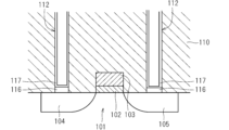
次に、本発明に係る金属配線形成方法の処理手順について説明する。図8は、本発明に係る金属配線形成方法の処理手順を示すフローチャートである。まず、半導体ウェハーWに窒化チタン(TiN)を堆積する(ステップS1)。図9は、半導体ウェハーWに窒化チタンが堆積された状態の一例を示す図である。 Next, the processing steps of the metal wiring forming method according to the present invention will be described. FIG. 8 is a flow chart showing the processing steps of the metal wiring forming method according to the present invention. First, titanium nitride (TiN) is deposited on the semiconductor wafer W (step S1). FIG. 9 is a diagram showing an example of the state in which titanium nitride has been deposited on the semiconductor wafer W.

シリコン(Si)の基材101の上にゲート絶縁膜102を挟んでゲート電極103が形成されている。ゲート絶縁膜102は、例えばシリコン酸化膜(SiO)である。また、ゲート電極103は例えばポリシリコンで形成されている。なお、ゲート絶縁膜102は、HfO等の高誘電率材料を用いた高誘電率膜(high-k膜)であっても良いし、ゲート電極103はTiN等を用いたメタルゲート電極であっても良い。シリコンの基材101には不純物が注入されたソース領域104およびドレイン領域105が形成されている。なお、ゲート電極103の側方にSiNのサイドウォールが形成されていても良い。 A gate electrode 103 is formed on a silicon (Si) substrate 101 with a gate insulating film 102 sandwiched therebetween. The gate insulating film 102 is, for example, a silicon oxide film (SiO 2 ). The gate electrode 103 is formed of, for example, polysilicon. The gate insulating film 102 may be a high dielectric constant film (high-k film) using a high dielectric constant material such as HfO 2 , and the gate electrode 103 may be a metal gate electrode using TiN or the like. A source region 104 and a drain region 105 into which impurities are implanted are formed in the silicon substrate 101. A SiN sidewall may be formed on the side of the gate electrode 103.

基材101の上面には、ソース領域104、ドレイン領域105およびゲート電極103等を備えた素子を覆うように二酸化ケイ素(SiO)の絶縁膜110が成膜されている。絶縁膜110にはソース領域104およびドレイン領域105の電極を絶縁膜110上に引き上げるためのコンタクトホール112が設けられる。このコンタクトホール112の底部にチタン(Ti)の下地層116が形成されている。その下地層116の上に窒化チタンが堆積されてバリアメタル層117が成膜される。バリアメタル層117は、コンタクトホール112内の深く狭い領域まで成膜されるため、ALD(Atomic Layer Deposition)によって窒化チタンを堆積させることにより成膜される。なお、図9の例では、ソース領域104およびドレイン領域105にコンタクトホール112が設けられているが、ゲート電極103についても同様に構成されていても良い。 An insulating film 110 made of silicon dioxide (SiO 2 ) is formed on the upper surface of the substrate 101 so as to cover the element including the source region 104, the drain region 105, the gate electrode 103, and the like. A contact hole 112 is provided in the insulating film 110 to pull up the electrodes of the source region 104 and the drain region 105 onto the insulating film 110. A base layer 116 made of titanium (Ti) is formed at the bottom of the contact hole 112. Titanium nitride is deposited on the base layer 116 to form a barrier metal layer 117. The barrier metal layer 117 is formed up to a deep and narrow region in the contact hole 112, so that it is formed by depositing titanium nitride by ALD (Atomic Layer Deposition). In the example of FIG. 9, the contact holes 112 are provided in the source region 104 and the drain region 105, but the gate electrode 103 may be similarly configured.

ALDによって成膜されたままの窒化チタンのバリアメタル層117は膜質が良好ではない。このため、次に、窒化チタンのバリアメタル層117が成膜された半導体ウェハーWに対する熱処理が行われる(ステップS2)。図10は、半導体ウェハーWに対する熱処理の手順を示すフローチャートである。半導体ウェハーWに対する熱処理は上記の熱処理装置1によって実行される。以下、熱処理装置1における処理手順について説明を続ける。熱処理装置1における処理は、制御部3が熱処理装置1の各動作機構を制御することにより進行する。 The titanium nitride barrier metal layer 117 formed by ALD does not have good film quality. For this reason, next, a heat treatment is performed on the semiconductor wafer W on which the titanium nitride barrier metal layer 117 has been formed (step S2). Figure 10 is a flow chart showing the procedure for heat treatment on the semiconductor wafer W. The heat treatment on the semiconductor wafer W is performed by the above-mentioned heat treatment apparatus 1. The processing procedure in the heat treatment apparatus 1 will be explained below. The processing in the heat treatment apparatus 1 proceeds as the control unit 3 controls each operating mechanism of the heat treatment apparatus 1.

図9に示したような窒化チタンのバリアメタル層117が形成された半導体ウェハーWが熱処理装置1のチャンバー6内に搬入される(ステップS11)。半導体ウェハーWの搬入時には、ゲートバルブ185が開いて搬送開口部66が開放され、装置外部の搬送ロボットにより搬送開口部66を介して処理対象となる半導体ウェハーWがチャンバー6内の熱処理空間65に搬入される。この際に、半導体ウェハーWの搬入にともなって装置外部の雰囲気をチャンバー6内に巻き込むおそれがある。そこで、バルブ84を開放して処理ガス供給源85からチャンバー6内に窒素ガスを供給し続けることによって搬送開口部66から窒素ガス流を流出させ、装置外部の雰囲気がチャンバー6内の流入するのを最小限に抑制するようにしても良い。 The semiconductor wafer W on which the titanium nitride barrier metal layer 117 as shown in FIG. 9 is formed is loaded into the chamber 6 of the heat treatment apparatus 1 (step S11). When the semiconductor wafer W is loaded, the gate valve 185 is opened to open the transport opening 66, and the semiconductor wafer W to be processed is loaded into the heat treatment space 65 in the chamber 6 through the transport opening 66 by a transport robot outside the apparatus. At this time, there is a risk that the atmosphere outside the apparatus may be drawn into the chamber 6 when the semiconductor wafer W is loaded. Therefore, the nitrogen gas flow may be discharged from the transport opening 66 by opening the valve 84 and continuing to supply nitrogen gas from the processing gas supply source 85 into the chamber 6, thereby minimizing the inflow of the atmosphere outside the apparatus into the chamber 6.

搬送ロボットによって搬入された半導体ウェハーWは保持部7の直上位置まで進出して停止する。そして、移載機構10の一対の移載アーム11が退避位置から移載動作位置に水平移動して上昇することにより、リフトピン12が貫通孔79を通ってサセプタ74の保持プレート75の上面から突き出て半導体ウェハーWを受け取る。このとき、リフトピン12は基板支持ピン77の上端よりも上方にまで上昇する。 The semiconductor wafer W carried in by the transport robot advances to a position directly above the holding part 7 and stops there. Then, the pair of transfer arms 11 of the transfer mechanism 10 move horizontally from the retracted position to the transfer operation position and rise, causing the lift pins 12 to pass through the through holes 79 and protrude from the upper surface of the holding plate 75 of the susceptor 74 to receive the semiconductor wafer W. At this time, the lift pins 12 rise above the upper ends of the substrate support pins 77.

半導体ウェハーWがリフトピン12に載置された後、搬送ロボットが熱処理空間65から退出し、ゲートバルブ185によって搬送開口部66が閉鎖される。そして、一対の移載アーム11が下降することにより、半導体ウェハーWは移載機構10から保持部7のサセプタ74に受け渡されて水平姿勢にて下方より保持される。半導体ウェハーWは、保持プレート75上に立設された複数の基板支持ピン77によって支持されてサセプタ74に保持される。また、半導体ウェハーWは、バリアメタル層117が形成された表面を上面として保持部7に保持される。複数の基板支持ピン77によって支持された半導体ウェハーWの裏面(表面とは反対側の主面)と保持プレート75の保持面75aとの間には所定の間隔が形成される。サセプタ74の下方にまで下降した一対の移載アーム11は水平移動機構13によって退避位置、すなわち凹部62の内側に退避する。 After the semiconductor wafer W is placed on the lift pins 12, the transport robot leaves the heat treatment space 65, and the transport opening 66 is closed by the gate valve 185. Then, the pair of transfer arms 11 descend, and the semiconductor wafer W is transferred from the transfer mechanism 10 to the susceptor 74 of the holding unit 7 and held from below in a horizontal position. The semiconductor wafer W is supported by a plurality of substrate support pins 77 erected on the holding plate 75 and held by the susceptor 74. The semiconductor wafer W is also held by the holding unit 7 with the surface on which the barrier metal layer 117 is formed as the upper surface. A predetermined gap is formed between the back surface (the main surface opposite to the front surface) of the semiconductor wafer W supported by the plurality of substrate support pins 77 and the holding surface 75a of the holding plate 75. The pair of transfer arms 11 that descend to below the susceptor 74 are retreated to a retreat position, that is, inside the recess 62, by the horizontal movement mechanism 13.

半導体ウェハーWがチャンバー6に収容され、ゲートバルブ185によって搬送開口部66が閉鎖された後、チャンバー6内を大気圧よりも低い気圧に減圧する(ステップS12)。具体的には、搬送開口部66が閉鎖されることによって、チャンバー6内の熱処理空間65が密閉空間となる。この状態にて、給気のためのバルブ84を閉止するとともに、排気部190を作動させつつ排気のためのバルブ89を開放する。これにより、チャンバー6内に対してはガス供給が行われることなく排気が行われることとなり、チャンバー6内の熱処理空間65が大気圧未満に減圧される。 After the semiconductor wafer W is placed in the chamber 6 and the transport opening 66 is closed by the gate valve 185, the pressure inside the chamber 6 is reduced to a pressure lower than atmospheric pressure (step S12). Specifically, the transport opening 66 is closed, and the heat treatment space 65 inside the chamber 6 becomes an airtight space. In this state, the valve 84 for supplying air is closed, and the exhaust valve 89 for exhaust is opened while the exhaust unit 190 is operated. As a result, exhaust is performed without supplying gas to the chamber 6, and the heat treatment space 65 inside the chamber 6 is reduced in pressure to below atmospheric pressure.

図11は、チャンバー6内の圧力変化を示す図である。同図の横軸には時刻を示し、縦軸にはチャンバー6内の圧力を示す。半導体ウェハーWがチャンバー6に収容されて搬送開口部66が閉鎖された時点では、チャンバー6内の圧力は大気圧Ps(=約101325Pa)である。そして、時刻t1にチャンバー6内の減圧が開始され、時刻t2にチャンバー6の圧力(真空度)が気圧P1に到達する。気圧P1は、例えば約100Paである。チャンバー6内を減圧する際に、排気流量を2段階に切り替えて排気速度を変化させるようにしても良い。例えば、減圧の初期段階では比較的遅い排気速度とした後に、排気速度を高めるようにしても良い。このようにすることより、チャンバー6内にパーティクルを巻き上げることなく、迅速にチャンバー6内を減圧することができる。 11 is a diagram showing the pressure change in the chamber 6. The horizontal axis of the figure shows time, and the vertical axis shows the pressure in the chamber 6. When the semiconductor wafer W is accommodated in the chamber 6 and the transport opening 66 is closed, the pressure in the chamber 6 is atmospheric pressure Ps (= about 101325 Pa). Then, depressurization of the chamber 6 begins at time t1, and the pressure (vacuum level) of the chamber 6 reaches atmospheric pressure P1 at time t2. The atmospheric pressure P1 is, for example, about 100 Pa. When depressurizing the chamber 6, the exhaust flow rate may be switched between two stages to change the exhaust speed. For example, the exhaust speed may be set to a relatively slow speed in the initial stage of depressurization, and then the exhaust speed may be increased. In this way, the chamber 6 can be depressurized quickly without stirring up particles in the chamber 6.

チャンバー6内の圧力が気圧P1に到達した時刻t2に、排気のためのバルブ89を閉止して給気のためのバルブ84を開放し、処理ガス供給源85からチャンバー6内の熱処理空間65にアンモニアを供給する(ステップS13)。アンモニアは窒素との混合ガスとして供給されても良い。チャンバー6内にアンモニアが供給されることによって、チャンバー6内の半導体ウェハーWの周辺にはアンモニア雰囲気が形成される。なお、チャンバー6にアンモニアを供給している間も、小流量(アンモニアの供給流量未満)にてチャンバー6からの排気を行うようにしても良い。 At time t2 when the pressure inside the chamber 6 reaches atmospheric pressure P1, the exhaust valve 89 is closed and the supply valve 84 is opened, and ammonia is supplied from the process gas supply source 85 to the heat treatment space 65 inside the chamber 6 (step S13). Ammonia may be supplied as a mixed gas with nitrogen. By supplying ammonia into the chamber 6, an ammonia atmosphere is formed around the semiconductor wafer W inside the chamber 6. Note that while ammonia is being supplied to the chamber 6, exhaust from the chamber 6 may be performed at a small flow rate (less than the supply flow rate of ammonia).

チャンバー6内にアンモニアが供給されることによって、チャンバー6内の圧力が気圧P1から上昇して時刻t3に気圧P2に復圧する。気圧P2は、気圧P1より高く、かつ、大気圧Psよりも低く、例えば約5000Paである。チャンバー6内を一旦気圧P1にまで減圧してから気圧P2に復圧しているため、気圧P2に復圧後のチャンバー6内のアンモニア雰囲気中における酸素濃度を約200ppb以下とすることができる。 By supplying ammonia into the chamber 6, the pressure inside the chamber 6 rises from atmospheric pressure P1 and returns to atmospheric pressure P2 at time t3. The atmospheric pressure P2 is higher than atmospheric pressure P1 and lower than atmospheric pressure Ps, for example, about 5000 Pa. Because the pressure inside the chamber 6 is first reduced to atmospheric pressure P1 and then returned to atmospheric pressure P2, the oxygen concentration in the ammonia atmosphere inside the chamber 6 after the pressure is returned to atmospheric pressure P2 can be made about 200 ppb or less.

チャンバー6内の圧力が気圧P2に復圧した時刻t3以降は、チャンバー6に対するアンモニアの供給流量とチャンバー6からの排気流量とを等しくしてチャンバー6内の圧力を気圧P2に維持する。 After time t3 when the pressure in chamber 6 returns to atmospheric pressure P2, the flow rate of ammonia supplied to chamber 6 and the flow rate of exhaust from chamber 6 are made equal to maintain the pressure in chamber 6 at atmospheric pressure P2.

図12は、半導体ウェハーWの表面温度の変化を示す図である。チャンバー6内の圧力が気圧P2に到達した時点以降の時刻t4に、ハロゲン加熱部4の40本のハロゲンランプHLが一斉に点灯して半導体ウェハーWの予備加熱(アシスト加熱)が開始される(ステップS14)。ハロゲンランプHLから出射されたハロゲン光は、石英にて形成された下側チャンバー窓64およびサセプタ74を透過して半導体ウェハーWの裏面から照射される。ハロゲンランプHLからの光照射を受けることによって半導体ウェハーWが予備加熱されて温度が上昇する。なお、移載機構10の移載アーム11は凹部62の内側に退避しているため、ハロゲンランプHLによる加熱の障害となることは無い。 Figure 12 shows the change in the surface temperature of the semiconductor wafer W. At time t4 after the pressure inside the chamber 6 reaches atmospheric pressure P2, the 40 halogen lamps HL of the halogen heating unit 4 are turned on all at once to start preheating (assisted heating) the semiconductor wafer W (step S14). The halogen light emitted from the halogen lamps HL passes through the lower chamber window 64 and the susceptor 74, both made of quartz, and is irradiated onto the backside of the semiconductor wafer W. The semiconductor wafer W is preheated by being irradiated with light from the halogen lamps HL, and its temperature rises. Note that the transfer arm 11 of the transfer mechanism 10 is retracted inside the recess 62, so it does not interfere with the heating by the halogen lamps HL.

ハロゲンランプHLからの光照射によって昇温する半導体ウェハーWの温度は放射温度計20によって測定される。測定された半導体ウェハーWの温度は制御部3に伝達される。制御部3は、ハロゲンランプHLからの光照射によって昇温する半導体ウェハーWの温度が所定の予備加熱温度T1に到達したか否かを監視しつつ、ハロゲンランプHLの出力を制御する。すなわち、制御部3は、放射温度計20による測定値に基づいて、半導体ウェハーWの温度が予備加熱温度T1となるようにハロゲンランプHLの出力をフィードバック制御する。予備加熱温度T1は500℃以上700℃以下であり、本実施形態では600℃である。 The temperature of the semiconductor wafer W, which is heated by the light irradiation from the halogen lamps HL, is measured by the radiation thermometer 20. The measured temperature of the semiconductor wafer W is transmitted to the control unit 3. The control unit 3 controls the output of the halogen lamps HL while monitoring whether the temperature of the semiconductor wafer W, which is heated by the light irradiation from the halogen lamps HL, has reached a predetermined preheating temperature T1. In other words, the control unit 3 feedback-controls the output of the halogen lamps HL based on the measurement value by the radiation thermometer 20 so that the temperature of the semiconductor wafer W becomes the preheating temperature T1. The preheating temperature T1 is 500°C or higher and 700°C or lower, and is 600°C in this embodiment.

半導体ウェハーWの温度が予備加熱温度T1に到達した後、制御部3は半導体ウェハーWをその予備加熱温度T1に暫時維持する。具体的には、放射温度計20によって測定される半導体ウェハーWの温度が予備加熱温度T1に到達した時刻t5に制御部3がハロゲンランプHLの出力を調整し、半導体ウェハーWの温度をほぼ予備加熱温度T1に維持している。 After the temperature of the semiconductor wafer W reaches the preheating temperature T1, the control unit 3 maintains the semiconductor wafer W at the preheating temperature T1 for a while. Specifically, at time t5 when the temperature of the semiconductor wafer W measured by the radiation thermometer 20 reaches the preheating temperature T1, the control unit 3 adjusts the output of the halogen lamps HL to maintain the temperature of the semiconductor wafer W at approximately the preheating temperature T1.

このようなハロゲンランプHLによる予備加熱を行うことによって、窒化チタンのバリアメタル層117を含む半導体ウェハーWの全体を予備加熱温度T1に均一に昇温している。ハロゲンランプHLによる予備加熱の段階においては、より放熱が生じやすい半導体ウェハーWの周縁部の温度が中央部よりも低下する傾向にあるが、ハロゲン加熱部4におけるハロゲンランプHLの配設密度は、半導体ウェハーWの中央部に対向する領域よりも周縁部に対向する領域の方が高くなっている。このため、放熱が生じやすい半導体ウェハーWの周縁部に照射される光量が多くなり、予備加熱段階における半導体ウェハーWの面内温度分布を均一なものとすることができる。 By performing such preheating using the halogen lamps HL, the entire semiconductor wafer W, including the titanium nitride barrier metal layer 117, is uniformly heated to the preheating temperature T1. During the preheating stage using the halogen lamps HL, the temperature of the peripheral portion of the semiconductor wafer W, where heat dissipation is more likely to occur, tends to be lower than that of the central portion, but the arrangement density of the halogen lamps HL in the halogen heating section 4 is higher in the area facing the peripheral portion than in the area facing the central portion of the semiconductor wafer W. As a result, more light is irradiated to the peripheral portion of the semiconductor wafer W, where heat dissipation is more likely to occur, and the in-plane temperature distribution of the semiconductor wafer W during the preheating stage can be made uniform.

半導体ウェハーWの温度が予備加熱温度T1に到達して所定時間が経過した時刻t6にフラッシュ加熱部5のフラッシュランプFLがサセプタ74に保持された半導体ウェハーWの表面にフラッシュ光照射を行う(ステップS15)。このとき、フラッシュランプFLから放射されるフラッシュ光の一部は直接にチャンバー6内へと向かい、他の一部は一旦リフレクタ52により反射されてからチャンバー6内へと向かい、これらのフラッシュ光の照射により半導体ウェハーWのフラッシュ加熱が行われる。 At time t6, when a predetermined time has elapsed since the temperature of the semiconductor wafer W reached the preheating temperature T1, the flash lamps FL of the flash heating unit 5 irradiate the surface of the semiconductor wafer W held on the susceptor 74 with flash light (step S15). At this time, part of the flash light emitted from the flash lamps FL heads directly into the chamber 6, and the other part heads into the chamber 6 after being reflected by the reflector 52, and the semiconductor wafer W is flash-heated by the irradiation of these flash lights.

フラッシュ加熱は、フラッシュランプFLからのフラッシュ光(閃光)照射により行われるため、半導体ウェハーWの表面温度を短時間で上昇することができる。すなわち、フラッシュランプFLから照射されるフラッシュ光は、予めコンデンサーに蓄えられていた静電エネルギーが極めて短い光パルスに変換された、照射時間が0.1ミリセカンド以上100ミリセカンド以下程度の極めて短く強い閃光である。窒化チタンのバリアメタル層117が成膜された半導体ウェハーWの表面にフラッシュランプFLからフラッシュ光を照射することによって、バリアメタル層117を含む半導体ウェハーWの表面は瞬間的に処理温度T2にまで昇温してバリアメタル層117の堆積後熱処理が実行される。フラッシュ光照射によって半導体ウェハーWの表面が到達する最高温度(ピーク温度)である処理温度T2は900℃以上1100℃以下である。半導体ウェハーWの表面温度はフラッシュランプFLからのフラッシュ光照射によって瞬間的に処理温度T2にまで上昇した後、急速に降温する。 Flash heating is performed by irradiating a flash light (light flash) from the flash lamp FL, so that the surface temperature of the semiconductor wafer W can be raised in a short time. That is, the flash light irradiated from the flash lamp FL is an extremely short and strong flash with an irradiation time of about 0.1 milliseconds to 100 milliseconds, in which electrostatic energy previously stored in a capacitor is converted into an extremely short light pulse. By irradiating the surface of the semiconductor wafer W on which the barrier metal layer 117 of titanium nitride is formed with a flash light from the flash lamp FL, the surface of the semiconductor wafer W including the barrier metal layer 117 is instantaneously heated to the processing temperature T2, and the heat treatment after deposition of the barrier metal layer 117 is performed. The processing temperature T2, which is the maximum temperature (peak temperature) that the surface of the semiconductor wafer W reaches by the flash light irradiation, is 900°C to 1100°C. The surface temperature of the semiconductor wafer W is instantaneously raised to the processing temperature T2 by the flash light irradiation from the flash lamp FL, and then rapidly drops.

アンモニア雰囲気中にて半導体ウェハーWにフラッシュランプFLからフラッシュ光を照射して窒化チタンのバリアメタル層117を瞬間的に処理温度T2にまで昇温することにより、ALDによって成膜された窒化チタンのバリアメタル層117が焼き締められてその膜質が改善される。また、アンモニア雰囲気中にてバリアメタル層117のフラッシュ加熱を行うことにより、バリアメタル層117の窒化が促進される。 By irradiating the semiconductor wafer W with flash light from the flash lamps FL in an ammonia atmosphere to instantly heat the titanium nitride barrier metal layer 117 to the processing temperature T2, the titanium nitride barrier metal layer 117 formed by ALD is baked and its film quality is improved. In addition, flash heating of the barrier metal layer 117 in an ammonia atmosphere promotes nitridation of the barrier metal layer 117.

また、減圧下で加熱処理が実行されるため、チャンバー6内に存在している酸素等の不純物元素の絶対量が少ない。このため、加熱処理時にチャンバー6内の雰囲気から不純物元素がバリアメタル層117に侵入することが防止され、バリアメタル層117の酸化を抑制して高抵抗化を防ぐことができる。さらに、減圧下でバリアメタル層117を加熱することにより、バリアメタル層117に含まれる不純物を外方拡散によって脱離させることができる。 In addition, because the heat treatment is performed under reduced pressure, the absolute amount of impurity elements such as oxygen present in the chamber 6 is small. This prevents impurity elements from entering the barrier metal layer 117 from the atmosphere in the chamber 6 during the heat treatment, suppressing oxidation of the barrier metal layer 117 and preventing it from becoming highly resistive. Furthermore, by heating the barrier metal layer 117 under reduced pressure, the impurities contained in the barrier metal layer 117 can be released by outward diffusion.

半導体ウェハーWにフラッシュ光を照射した後、給気のためのバルブ84を閉止してチャンバー6内を再び減圧する。チャンバー6内を再び気圧P1にまで減圧することによって、チャンバー6内の熱処理空間65からアンモニアを排出することができる。続いて、チャンバー6内の圧力が気圧P1にまで減圧された時刻t7に排気のためのバルブ89を閉止して給気のためのバルブ84を開放し、処理ガス供給源85からチャンバー6内に窒素ガスを供給して大気圧Psにまで復圧する。 After the semiconductor wafer W is irradiated with a flash light, the air supply valve 84 is closed and the pressure inside the chamber 6 is reduced again. By reducing the pressure inside the chamber 6 again to atmospheric pressure P1, ammonia can be exhausted from the heat treatment space 65 inside the chamber 6. Next, at time t7 when the pressure inside the chamber 6 has been reduced to atmospheric pressure P1, the exhaust valve 89 is closed and the air supply valve 84 is opened, and nitrogen gas is supplied from the process gas supply source 85 into the chamber 6 to restore the pressure to atmospheric pressure Ps.

また、フラッシュ光照射が終了した後、ハロゲンランプHLも消灯する。これにより、半導体ウェハーWが予備加熱温度T1からも急速に降温する。降温中の半導体ウェハーWの温度は放射温度計20によって測定され、その測定結果は制御部3に伝達される。制御部3は、放射温度計20の測定結果より半導体ウェハーWの温度が所定温度にまで降温したか否かを監視する。半導体ウェハーWの温度が所定温度以下にまで降温したことが制御部3によって確認された後、半導体ウェハーWがチャンバー6から搬出される(ステップS16)。半導体ウェハーWの搬出時には、移載機構10の一対の移載アーム11が再び退避位置から移載動作位置に水平移動して上昇することにより、リフトピン12がサセプタ74の上面から突き出て熱処理後の半導体ウェハーWをサセプタ74から受け取る。続いて、ゲートバルブ185により閉鎖されていた搬送開口部66が開放され、リフトピン12上に載置された半導体ウェハーWが装置外部の搬送ロボットによりチャンバー6から搬出される。これにより、熱処理装置1におけるバリアメタル層117の堆積後熱処理が完了する。 After the flash light irradiation is finished, the halogen lamp HL is also turned off. As a result, the temperature of the semiconductor wafer W is rapidly lowered from the preheating temperature T1. The temperature of the semiconductor wafer W during the temperature drop is measured by the radiation thermometer 20, and the measurement result is transmitted to the control unit 3. The control unit 3 monitors whether the temperature of the semiconductor wafer W has dropped to a predetermined temperature based on the measurement result of the radiation thermometer 20. After the control unit 3 confirms that the temperature of the semiconductor wafer W has dropped to a predetermined temperature or lower, the semiconductor wafer W is unloaded from the chamber 6 (step S16). When the semiconductor wafer W is unloaded, the pair of transfer arms 11 of the transfer mechanism 10 again move horizontally from the retreat position to the transfer operation position and rise, so that the lift pins 12 protrude from the upper surface of the susceptor 74 and receive the semiconductor wafer W after heat treatment from the susceptor 74. Next, the transfer opening 66 closed by the gate valve 185 is opened, and the semiconductor wafer W placed on the lift pins 12 is unloaded from the chamber 6 by a transfer robot outside the device. This completes the post-deposition heat treatment of the barrier metal layer 117 in the heat treatment device 1.

図8に戻り、次に半導体ウェハーWにタングステン(W)を堆積する(ステップS3)。図13は、半導体ウェハーWにタングステンが堆積された状態の一例を示す図である。コンタクトホール112内にてバリアメタル層117の上にタングステンが堆積されて埋め込まれ、タングステンの金属配線115が形設される。タングステンの金属配線115は、ソース領域104等の電極と上方の金属層(例えば、銅(Cu)やアルミニウム(Al)にて形成される)とを接続するためタングステンプラグである。タングステンは、抵抗率が低く、しかも段差被膜性(ステップカバレッジ)に優れているため、プラグ材料として好適である。 Returning to FIG. 8, next, tungsten (W) is deposited on the semiconductor wafer W (step S3). FIG. 13 is a diagram showing an example of a state in which tungsten has been deposited on the semiconductor wafer W. Tungsten is deposited and embedded on the barrier metal layer 117 in the contact hole 112, forming a tungsten metal wiring 115. The tungsten metal wiring 115 is a tungsten plug for connecting an electrode such as the source region 104 to an upper metal layer (formed, for example, of copper (Cu) or aluminum (Al)). Tungsten has low resistivity and excellent step coverage, making it suitable as a plug material.

タングステンは、ALD(Atomic Layer Deposition)およびCVD(Chemical Vapor Deposition)によって堆積される。具体的には、コンタクトホール112内にALDによって薄くタングステンを堆積させた後に、CVDによってタングステンを埋め込む。CVDによってタングステンを堆積するときには原料ガスとしてフッ化タングステン(WF)を用いている。このためCVDによってタングステンを堆積して形成された金属配線115中にはフッ素(F)が混入している。 Tungsten is deposited by ALD (Atomic Layer Deposition) and CVD (Chemical Vapor Deposition). Specifically, a thin layer of tungsten is deposited in the contact hole 112 by ALD, and then tungsten is filled in by CVD. When depositing tungsten by CVD, tungsten fluoride (WF 6 ) is used as a source gas. Therefore, fluorine (F) is mixed into the metal wiring 115 formed by depositing tungsten by CVD.

タングステンを堆積したままの金属配線115は密度が低くて脆い。従って、堆積したままの金属配線115をそのまま使用することはできず、金属配線115が形成された半導体ウェハーWに対する2度目の熱処理を実行することにより、金属配線115に堆積後熱処理を施す(ステップS4)。 The metal wiring 115 with the tungsten deposited has a low density and is brittle. Therefore, the metal wiring 115 cannot be used as it is, and a second heat treatment is performed on the semiconductor wafer W on which the metal wiring 115 is formed, thereby subjecting the metal wiring 115 to a post-deposition heat treatment (step S4).

半導体ウェハーWに対する2度目の熱処理も熱処理装置1によって実行される。半導体ウェハーWに対する2度目の熱処理の処理手順も概ね図10に示したのと同様である。但し、1度目の熱処理(第1熱処理)が窒化チタンのバリアメタル層117の堆積後熱処理であったのに対して、2度目の熱処理(第2熱処理)はタングステンの金属配線115の堆積後熱処理であるため、処理条件が異なる。 The second heat treatment of the semiconductor wafer W is also performed by the heat treatment apparatus 1. The procedure of the second heat treatment of the semiconductor wafer W is generally similar to that shown in FIG. 10. However, the processing conditions are different because the first heat treatment (first heat treatment) is a post-deposition heat treatment of the titanium nitride barrier metal layer 117, whereas the second heat treatment (second heat treatment) is a post-deposition heat treatment of the tungsten metal wiring 115.

具体的には、第1熱処理では処理ガスとしてアンモニアを供給していたのに対して、第2熱処理ではチャンバー6内にフォーミングガスを供給する。フォーミングガスとは、水素(H)と窒素(N)との混合ガスである。すなわち、フォーミングガスは、水素を含む還元性ガスである。チャンバー6内にフォーミングガスが供給されることによって、チャンバー6内の半導体ウェハーWの周辺には還元雰囲気が形成される。供給するフォーミングガス中における水素の濃度(つまり、水素と窒素との混合比)は、特に限定されるものではなく適宜の値とすることができるが、例えば4vol.%である。 Specifically, ammonia is supplied as the processing gas in the first heat treatment, whereas forming gas is supplied into the chamber 6 in the second heat treatment. The forming gas is a mixed gas of hydrogen ( H2 ) and nitrogen ( N2 ). That is, the forming gas is a reducing gas containing hydrogen. By supplying the forming gas into the chamber 6, a reducing atmosphere is formed around the semiconductor wafer W in the chamber 6. The concentration of hydrogen in the supplied forming gas (i.e., the mixture ratio of hydrogen and nitrogen) is not particularly limited and can be set to an appropriate value, for example, 4 vol.%.

また、第2熱処理におけるハロゲンランプHLによる予備加熱温度T1は450℃以上600℃以下である。さらに、第2熱処理におけるフラッシュ光照射による半導体ウェハーWの表面の処理温度T2は900℃である。 In addition, the preheating temperature T1 by the halogen lamps HL in the second heat treatment is 450°C or higher and 600°C or lower. Furthermore, the processing temperature T2 of the surface of the semiconductor wafer W by flash light irradiation in the second heat treatment is 900°C.

第2熱処理においては、半導体ウェハーWが予備加熱されてからさらにフラッシュ加熱されることにより、金属配線115が処理温度T2にまで加熱され、金属配線115を構成するタングステンの結晶粒が粒成長してその粒径が大きくなる。金属配線115中の結晶粒が粒成長して粗大化することにより、金属配線115の抵抗率が下がる。 In the second heat treatment, the semiconductor wafer W is preheated and then further flash heated, heating the metal wiring 115 to a treatment temperature T2, causing the crystal grains of the tungsten that constitutes the metal wiring 115 to grow and become larger in diameter. The crystal grains in the metal wiring 115 grow and become coarser, decreasing the resistivity of the metal wiring 115.

また、フラッシュ加熱は低熱履歴処理であるため、熱処理によるゲート絶縁膜102の劣化並びにソース領域104およびドレイン領域105におけるドーパントの不活性化を抑制することもできる。 Furthermore, because flash heating is a low thermal history process, it is also possible to suppress deterioration of the gate insulating film 102 due to heat treatment and inactivation of the dopants in the source region 104 and the drain region 105.

また、第1熱処理と同じく減圧下で加熱処理が実行されるため、チャンバー6内に存在している酸素等の不純物元素の絶対量が少ない。このため、加熱処理時にチャンバー6内の雰囲気から不純物元素が金属配線115に侵入することが効果的に防止され、金属配線115の抵抗率の上昇を抑制することができる。減圧下で金属配線115の加熱処理を行えば、金属配線115に含まれる不純物を外方拡散によって脱離させることもできる。 In addition, because the heat treatment is performed under reduced pressure, as in the first heat treatment, the absolute amount of impurity elements such as oxygen present in the chamber 6 is small. This effectively prevents impurity elements from entering the metal wiring 115 from the atmosphere in the chamber 6 during the heat treatment, and suppresses an increase in the resistivity of the metal wiring 115. By performing the heat treatment of the metal wiring 115 under reduced pressure, the impurities contained in the metal wiring 115 can also be released by outward diffusion.

さらに、還元雰囲気中にて金属配線115の加熱処理が実行されるため、堆積時に金属配線115中に混入した酸素等の不純物を還元することができる。これにより、金属配線115の抵抗率をより低下させることができる。 In addition, since the metal wiring 115 is heated in a reducing atmosphere, impurities such as oxygen that are mixed into the metal wiring 115 during deposition can be reduced. This can further reduce the resistivity of the metal wiring 115.

上述した通り、CVDによってタングステンを堆積して形成された金属配線115中にはフッ素が混入している。金属配線115を加熱したときには、混入しているフッ素が拡散する。本実施形態においては、照射時間が0.1ミリセカンド以上100ミリセカンド以下程度の極めて短いフラッシュ光を半導体ウェハーWに照射して金属配線115を瞬間的にフラッシュ加熱しているため、フッ素の拡散を抑制することができる。 As described above, fluorine is mixed into the metal wiring 115 formed by depositing tungsten by CVD. When the metal wiring 115 is heated, the mixed fluorine diffuses. In this embodiment, the semiconductor wafer W is irradiated with an extremely short flash of light with an irradiation time of about 0.1 milliseconds or more and 100 milliseconds or less to instantaneously flash heat the metal wiring 115, thereby suppressing the diffusion of fluorine.

図14は、熱処理時のフッ素の拡散の程度を示す図である。同図において、縦軸にはフッ素濃度を示し、横軸には深さ位置を示している。深さD1よりも浅い領域はタングステンの金属配線115であり、深さD1よりも深い領域は窒化チタンのバリアメタル層117、チタンの下地層116およびシリコンの基材101である。 Figure 14 shows the degree of fluorine diffusion during heat treatment. In this figure, the vertical axis shows the fluorine concentration, and the horizontal axis shows the depth position. The region shallower than the depth D1 is the tungsten metal wiring 115, and the region deeper than the depth D1 is the titanium nitride barrier metal layer 117, the titanium underlayer 116, and the silicon substrate 101.

図14において、実線で示すのは本実施形態のように半導体ウェハーWにフラッシュ加熱を行ったときのフッ素の濃度分布である。図14には、比較例として、いわゆるRTP(Rapid thermal processing)によって半導体ウェハーWの加熱処理を行った場合のフッ素の濃度分布を点線で示す。 In FIG. 14, the solid line shows the fluorine concentration distribution when flash heating is performed on the semiconductor wafer W as in this embodiment. As a comparative example, FIG. 14 also shows the fluorine concentration distribution when the semiconductor wafer W is subjected to heat treatment by so-called RTP (Rapid thermal processing) by dotted line.

RTPは、数秒程度をかけて半導体ウェハーWを加熱する処理であるため、フッ素が長距離を拡散する。その結果、フッ素はチタンの下地層116およびシリコンの基材101にまで拡散することとなる。フッ素が下地層116および基材101にまで拡散すると、TiFxやSiFxを生成し、それらが堆積膨張して膜破壊を生じさせるボルケーノ現象が発生する。 Since RTP is a process that heats the semiconductor wafer W over a period of several seconds, fluorine diffuses long distances. As a result, fluorine diffuses into the titanium underlayer 116 and the silicon substrate 101. When fluorine diffuses into the underlayer 116 and substrate 101, TiFx and SiFx are generated, which accumulate and expand, causing a volcano phenomenon that destroys the film.

本実施形態においては、加熱時間が1秒以下で低熱履歴処理であるフラッシュ加熱によって半導体ウェハーWを加熱しているため、フッ素が長距離を拡散することは抑制される。その結果、図14に示すように、フッ素が下地層116および基材101にまで拡散することはほとんどなく、ボルケーノ現象を防止することができる。 In this embodiment, the semiconductor wafer W is heated by flash heating, which is a low thermal history process with a heating time of 1 second or less, so fluorine is prevented from diffusing over long distances. As a result, as shown in FIG. 14, fluorine hardly diffuses to the underlayer 116 and the substrate 101, and the volcano phenomenon can be prevented.

また、第1熱処理によって、窒化チタンのバリアメタル層117の膜質を改善しているため、バリアメタル層117がその機能を十分に発揮する。これにより、金属配線115中のフッ素がバリアメタル層117を超えて下地層116および基材101にまで拡散することが防がれる。 In addition, the first heat treatment improves the film quality of the titanium nitride barrier metal layer 117, allowing the barrier metal layer 117 to fully function. This prevents fluorine in the metal wiring 115 from diffusing beyond the barrier metal layer 117 into the underlayer 116 and the substrate 101.

本実施形態においては、まず半導体ウェハーWに窒化チタンをバリアメタル層117として堆積し、その半導体ウェハーWにフラッシュ加熱を含む第1熱処理を施してバリアメタル層117を加熱している。続いて、バリアメタル層117の上にタングステンを金属配線115として堆積し、半導体ウェハーWにフラッシュ加熱を含む第2熱処理を施して金属配線115を加熱している。 In this embodiment, titanium nitride is first deposited on the semiconductor wafer W as a barrier metal layer 117, and the semiconductor wafer W is subjected to a first heat treatment including flash heating to heat the barrier metal layer 117. Next, tungsten is deposited on the barrier metal layer 117 as metal wiring 115, and the semiconductor wafer W is subjected to a second heat treatment including flash heating to heat the metal wiring 115.

タングステンの金属配線115を加熱する前に、窒化チタンのバリアメタル層117にフラッシュ加熱を施してその膜質を改善している。このため、金属配線115を加熱したときに、金属配線115からフッ素がバリアメタル層117を超えて拡散することを十分に抑制することができる。 Before heating the tungsten metal wiring 115, the titanium nitride barrier metal layer 117 is flash heated to improve its film quality. This makes it possible to sufficiently prevent fluorine from diffusing beyond the barrier metal layer 117 from the metal wiring 115 when the metal wiring 115 is heated.

また、第2熱処理では、照射時間が短く低熱履歴処理であるフラッシュ光照射によって金属配線115を瞬間的に加熱しているため、金属配線115からのフッ素の拡散を十分に抑制することができるとともに、ゲート絶縁膜102等の劣化を防止することもできる。 In addition, in the second heat treatment, the metal wiring 115 is instantaneously heated by flash light irradiation, which is a short-time, low-thermal history treatment, and therefore the diffusion of fluorine from the metal wiring 115 can be sufficiently suppressed and deterioration of the gate insulating film 102, etc. can also be prevented.

また、第1熱処理および第2熱処理ともに減圧下で実行しているため、バリアメタル層117および金属配線115の酸化を防止するとともに、それらに含まれる不純物を外方拡散によって脱離させやすくすることができる。 In addition, since both the first and second heat treatments are performed under reduced pressure, oxidation of the barrier metal layer 117 and the metal wiring 115 can be prevented, and impurities contained therein can be easily removed by outward diffusion.

また、アンモニア雰囲気中にて第1熱処理を実行しているため、窒化チタンのバリアメタル層117の窒化を促進することができる。さらに、フォーミングガスの還元雰囲気中にて第2熱処理を実行しているため、金属配線115中に混入している酸素等の不純物を還元して除去することができる。 In addition, since the first heat treatment is performed in an ammonia atmosphere, it is possible to promote nitridation of the titanium nitride barrier metal layer 117. Furthermore, since the second heat treatment is performed in a reducing atmosphere of forming gas, it is possible to reduce and remove impurities such as oxygen that are mixed in the metal wiring 115.

以上、本発明の実施の形態について説明したが、この発明はその趣旨を逸脱しない限りにおいて上述したもの以外に種々の変更を行うことが可能である。例えば、上記実施形態の第2熱処理においては、チャンバー6内にフォーミングガスを供給して還元雰囲気を形成していたが、これに限定されるものではなく、アルゴン(Ar)と水素との混合ガスまたはヘリウム(He)と水素との混合ガスを供給して還元雰囲気を形成するようにしても良い。双方ともに水素を含む還元性ガスである。アルゴンと水素との混合ガスまたはヘリウムと水素の混合ガスであれば、チャンバー6内雰囲気から金属配線115にガス元素が侵入するのをより効果的に防止することができる。特に、ヘリウムと水素との混合ガスを使用した場合には、ヘリウムの冷却効果によって加熱処理後の半導体ウェハーWを迅速に冷却することができる。 Although the embodiment of the present invention has been described above, this invention can be modified in various ways without departing from the spirit thereof. For example, in the second heat treatment of the above embodiment, forming gas is supplied into the chamber 6 to form a reducing atmosphere, but this is not limited to this, and a mixed gas of argon (Ar) and hydrogen or a mixed gas of helium (He) and hydrogen may be supplied to form a reducing atmosphere. Both are reducing gases containing hydrogen. A mixed gas of argon and hydrogen or a mixed gas of helium and hydrogen can more effectively prevent gas elements from entering the metal wiring 115 from the atmosphere in the chamber 6. In particular, when a mixed gas of helium and hydrogen is used, the semiconductor wafer W after heat treatment can be quickly cooled by the cooling effect of helium.

また、上記実施形態においては、大気圧未満の約5000Paの減圧下で第1熱処理および第2熱処理を実行していたが、圧力はこれに限定されるものではなく、大気圧未満であれば100Pa~100kPaで第1熱処理および第2熱処理を行うようにしても良い。 In addition, in the above embodiment, the first heat treatment and the second heat treatment are performed under a reduced pressure of about 5000 Pa, which is less than atmospheric pressure, but the pressure is not limited to this, and the first heat treatment and the second heat treatment may be performed at a pressure of 100 Pa to 100 kPa, which is less than atmospheric pressure.

また、上記実施形態においては、タングステンを堆積して金属配線115を形成していたが、これに限定されるものではなく、フッ化物を原料として堆積される金属によって金属配線115を形成する形態であれば、本発明に係る技術を適用することが可能である。 In addition, in the above embodiment, the metal wiring 115 is formed by depositing tungsten, but this is not limited to this, and the technology according to the present invention can be applied as long as the metal wiring 115 is formed from a metal deposited using fluoride as a raw material.

また、上記実施形態においては、フラッシュ加熱部5に30本のフラッシュランプFLを備えるようにしていたが、これに限定されるものではなく、フラッシュランプFLの本数は任意の数とすることができる。また、フラッシュランプFLはキセノンフラッシュランプに限定されるものではなく、クリプトンフラッシュランプであっても良い。また、ハロゲン加熱部4に備えるハロゲンランプHLの本数も40本に限定されるものではなく、任意の数とすることができる。 In addition, in the above embodiment, the flash heating unit 5 is provided with 30 flash lamps FL, but this is not limited to this and the number of flash lamps FL can be any number. Furthermore, the flash lamps FL are not limited to xenon flash lamps and may be krypton flash lamps. Furthermore, the number of halogen lamps HL provided in the halogen heating unit 4 is not limited to 40 and can be any number.

また、上記実施形態においては、1秒以上連続して発光する連続点灯ランプとしてフィラメント方式のハロゲンランプHLを用いて半導体ウェハーWの予備加熱を行っていたが、これに限定されるものではなく、ハロゲンランプHLに代えて放電型のアークランプ(例えば、キセノンアークランプ)を連続点灯ランプとして用いて予備加熱を行うようにしても良い。 In the above embodiment, the semiconductor wafer W is preheated using a filament-type halogen lamp HL as a continuously lit lamp that emits light continuously for one second or more, but this is not limited to this, and preheating may be performed using a discharge-type arc lamp (e.g., a xenon arc lamp) as a continuously lit lamp instead of the halogen lamp HL.

1 熱処理装置
3 制御部
4 ハロゲン加熱部
5 フラッシュ加熱部
6 チャンバー
7 保持部
10 移載機構
20 放射温度計
65 熱処理空間
74 サセプタ
101 基材
102 ゲート絶縁膜
103 ゲート電極
104 ソース領域
105 ドレイン領域
110 絶縁膜
112 コンタクトホール
115 金属配線
116 下地層
117 バリアメタル層
FL フラッシュランプ
HL ハロゲンランプ
W 半導体ウェハー
REFERENCE SIGNS LIST 1 Heat treatment apparatus 3 Control section 4 Halogen heating section 5 Flash heating section 6 Chamber 7 Holding section 10 Transfer mechanism 20 Radiation thermometer 65 Heat treatment space 74 Susceptor 101 Substrate 102 Gate insulating film 103 Gate electrode 104 Source region 105 Drain region 110 Insulating film 112 Contact hole 115 Metal wiring 116 Underlayer 117 Barrier metal layer FL Flash lamp HL Halogen lamp W Semiconductor wafer

Claims (3)

基板上に金属配線を形成する金属配線形成方法であって、
基板上に窒化チタンをバリアメタル層として堆積させる第1堆積工程と、
フラッシュランプから前記基板にフラッシュ光を照射して前記バリアメタル層を加熱する第1加熱工程と、
前記バリアメタル層上にタングステンを金属配線として堆積させる第2堆積工程と、
前記フラッシュランプから前記基板にフラッシュ光を照射して前記金属配線を加熱する第2加熱工程と、
を備え
前記第2堆積工程では、フッ化タングステンを原料としてタングステンを堆積させることを特徴とする金属配線形成方法。
A method for forming metal wiring on a substrate, comprising the steps of:
a first deposition step of depositing titanium nitride as a barrier metal layer on a substrate;
a first heating step of irradiating the substrate with a flash light from a flash lamp to heat the barrier metal layer;
a second deposition step of depositing tungsten as a metal wiring on the barrier metal layer;
a second heating step of irradiating the substrate with a flash of light from the flash lamp to heat the metal wiring;
Equipped with
The method for forming a metal wiring, wherein in the second deposition step, tungsten is deposited using tungsten fluoride as a raw material .
請求項記載の金属配線形成方法において、
前記第1加熱工程および前記第2加熱工程は、大気圧未満の減圧下で実行されることを特徴とする金属配線形成方法。
2. The method for forming metal wiring according to claim 1 ,
The method for forming a metal wiring, wherein the first heating step and the second heating step are carried out under a reduced pressure lower than atmospheric pressure.
請求項または請求項記載の金属配線形成方法において、
前記第1加熱工程は、アンモニア雰囲気中にて実行され、
前記第2加熱工程は、フォーミングガス雰囲気中にて実行されることを特徴とする金属配線形成方法。
3. The method for forming metal wiring according to claim 1 ,
The first heating step is carried out in an ammonia atmosphere;
The method for forming a metal wiring, wherein the second heating step is performed in a forming gas atmosphere.
JP2020153710A 2020-09-14 2020-09-14 Metal Wiring Formation Method Active JP7561552B2 (en)

Priority Applications (1)

Application Number Priority Date Filing Date Title
JP2020153710A JP7561552B2 (en) 2020-09-14 2020-09-14 Metal Wiring Formation Method

Applications Claiming Priority (1)

Application Number Priority Date Filing Date Title
JP2020153710A JP7561552B2 (en) 2020-09-14 2020-09-14 Metal Wiring Formation Method

Publications (2)

Publication Number Publication Date
JP2022047758A JP2022047758A (en) 2022-03-25
JP7561552B2 true JP7561552B2 (en) 2024-10-04

Family

ID=80781493

Family Applications (1)

Application Number Title Priority Date Filing Date
JP2020153710A Active JP7561552B2 (en) 2020-09-14 2020-09-14 Metal Wiring Formation Method

Country Status (1)

Country Link
JP (1) JP7561552B2 (en)

Citations (5)

* Cited by examiner, † Cited by third party
Publication number Priority date Publication date Assignee Title
JP2002118078A (en) 2000-10-12 2002-04-19 Toshiba Corp Semiconductor device manufacturing method and semiconductor device
JP2002543589A (en) 1999-04-27 2002-12-17 東京エレクトロン株式会社 Formation of CVD TiN plug from titanium halide precursor
JP2005136382A (en) 2003-10-09 2005-05-26 Toshiba Corp Manufacturing method of semiconductor device
WO2005098913A1 (en) 2004-04-09 2005-10-20 Tokyo Electron Limited METHOD FOR FORMING Ti FILM AND TiN FILM, CONTACT STRUCTURE, COMPUTER READABLE STORING MEDIUM AND COMPUTER PROGRAM
JP2018018847A (en) 2016-07-25 2018-02-01 株式会社Screenホールディングス Heat treatment method and heat treatment apparatus

Family Cites Families (2)

* Cited by examiner, † Cited by third party
Publication number Priority date Publication date Assignee Title
JPH0472733A (en) * 1990-07-13 1992-03-06 Sharp Corp Manufacture of semiconductor device
JP2643870B2 (en) * 1994-11-29 1997-08-20 日本電気株式会社 Method for manufacturing semiconductor memory device

Patent Citations (5)

* Cited by examiner, † Cited by third party
Publication number Priority date Publication date Assignee Title
JP2002543589A (en) 1999-04-27 2002-12-17 東京エレクトロン株式会社 Formation of CVD TiN plug from titanium halide precursor
JP2002118078A (en) 2000-10-12 2002-04-19 Toshiba Corp Semiconductor device manufacturing method and semiconductor device
JP2005136382A (en) 2003-10-09 2005-05-26 Toshiba Corp Manufacturing method of semiconductor device
WO2005098913A1 (en) 2004-04-09 2005-10-20 Tokyo Electron Limited METHOD FOR FORMING Ti FILM AND TiN FILM, CONTACT STRUCTURE, COMPUTER READABLE STORING MEDIUM AND COMPUTER PROGRAM
JP2018018847A (en) 2016-07-25 2018-02-01 株式会社Screenホールディングス Heat treatment method and heat treatment apparatus

Also Published As

Publication number Publication date
JP2022047758A (en) 2022-03-25

Similar Documents

Publication Publication Date Title
JP6665032B2 (en) Heat treatment method and heat treatment apparatus
JP7128944B2 (en) Heat treatment method and heat treatment apparatus
TWI698933B (en) Heat treatment method and heat treatment apparatus
JP6774800B2 (en) Manufacturing method of semiconductor devices
US10424483B2 (en) Light irradiation type heat treatment method and heat treatment apparatus
KR102720483B1 (en) Heat treatment method and heat treatment apparatus
CN110867370B (en) Heat treatment method
WO2018020742A1 (en) Heat treatment method and heat treatment device
JP2018152405A (en) Heat treatment method and heat treatment apparatus
JP7499160B2 (en) Heat Treatment Method
JP7561552B2 (en) Metal Wiring Formation Method
JP2022047759A (en) Metal wiring formation method

Legal Events

Date Code Title Description
A80 Written request to apply exceptions to lack of novelty of invention

Free format text: JAPANESE INTERMEDIATE CODE: A80

Effective date: 20201012

A621 Written request for application examination

Free format text: JAPANESE INTERMEDIATE CODE: A621

Effective date: 20230620

A131 Notification of reasons for refusal

Free format text: JAPANESE INTERMEDIATE CODE: A131

Effective date: 20240521

A977 Report on retrieval

Free format text: JAPANESE INTERMEDIATE CODE: A971007

Effective date: 20240523

A521 Request for written amendment filed

Free format text: JAPANESE INTERMEDIATE CODE: A523

Effective date: 20240718

TRDD Decision of grant or rejection written
A01 Written decision to grant a patent or to grant a registration (utility model)

Free format text: JAPANESE INTERMEDIATE CODE: A01

Effective date: 20240827

A61 First payment of annual fees (during grant procedure)

Free format text: JAPANESE INTERMEDIATE CODE: A61

Effective date: 20240924

R150 Certificate of patent or registration of utility model

Ref document number: 7561552

Country of ref document: JP

Free format text: JAPANESE INTERMEDIATE CODE: R150