JP7561545B2 - Etching composition, method for etching insulating film using same, and method for manufacturing semiconductor device - Google Patents
Etching composition, method for etching insulating film using same, and method for manufacturing semiconductor device Download PDFInfo
- Publication number
- JP7561545B2 JP7561545B2 JP2020148458A JP2020148458A JP7561545B2 JP 7561545 B2 JP7561545 B2 JP 7561545B2 JP 2020148458 A JP2020148458 A JP 2020148458A JP 2020148458 A JP2020148458 A JP 2020148458A JP 7561545 B2 JP7561545 B2 JP 7561545B2
- Authority
- JP
- Japan
- Prior art keywords
- etching
- etching composition
- nitride film
- silicon nitride
- film
- Prior art date
- Legal status (The legal status is an assumption and is not a legal conclusion. Google has not performed a legal analysis and makes no representation as to the accuracy of the status listed.)
- Active
Links
Classifications
-
- C—CHEMISTRY; METALLURGY
- C09—DYES; PAINTS; POLISHES; NATURAL RESINS; ADHESIVES; COMPOSITIONS NOT OTHERWISE PROVIDED FOR; APPLICATIONS OF MATERIALS NOT OTHERWISE PROVIDED FOR
- C09K—MATERIALS FOR MISCELLANEOUS APPLICATIONS, NOT PROVIDED FOR ELSEWHERE
- C09K13/00—Etching, surface-brightening or pickling compositions
- C09K13/04—Etching, surface-brightening or pickling compositions containing an inorganic acid
-
- C—CHEMISTRY; METALLURGY
- C09—DYES; PAINTS; POLISHES; NATURAL RESINS; ADHESIVES; COMPOSITIONS NOT OTHERWISE PROVIDED FOR; APPLICATIONS OF MATERIALS NOT OTHERWISE PROVIDED FOR
- C09G—POLISHING COMPOSITIONS; SKI WAXES
- C09G1/00—Polishing compositions
-
- C—CHEMISTRY; METALLURGY
- C09—DYES; PAINTS; POLISHES; NATURAL RESINS; ADHESIVES; COMPOSITIONS NOT OTHERWISE PROVIDED FOR; APPLICATIONS OF MATERIALS NOT OTHERWISE PROVIDED FOR
- C09G—POLISHING COMPOSITIONS; SKI WAXES
- C09G1/00—Polishing compositions
- C09G1/04—Aqueous dispersions
-
- C—CHEMISTRY; METALLURGY
- C09—DYES; PAINTS; POLISHES; NATURAL RESINS; ADHESIVES; COMPOSITIONS NOT OTHERWISE PROVIDED FOR; APPLICATIONS OF MATERIALS NOT OTHERWISE PROVIDED FOR
- C09G—POLISHING COMPOSITIONS; SKI WAXES
- C09G1/00—Polishing compositions
- C09G1/06—Other polishing compositions
-
- C—CHEMISTRY; METALLURGY
- C09—DYES; PAINTS; POLISHES; NATURAL RESINS; ADHESIVES; COMPOSITIONS NOT OTHERWISE PROVIDED FOR; APPLICATIONS OF MATERIALS NOT OTHERWISE PROVIDED FOR
- C09K—MATERIALS FOR MISCELLANEOUS APPLICATIONS, NOT PROVIDED FOR ELSEWHERE
- C09K13/00—Etching, surface-brightening or pickling compositions
- C09K13/04—Etching, surface-brightening or pickling compositions containing an inorganic acid
- C09K13/06—Etching, surface-brightening or pickling compositions containing an inorganic acid with organic material
-
- C—CHEMISTRY; METALLURGY
- C09—DYES; PAINTS; POLISHES; NATURAL RESINS; ADHESIVES; COMPOSITIONS NOT OTHERWISE PROVIDED FOR; APPLICATIONS OF MATERIALS NOT OTHERWISE PROVIDED FOR
- C09K—MATERIALS FOR MISCELLANEOUS APPLICATIONS, NOT PROVIDED FOR ELSEWHERE
- C09K13/00—Etching, surface-brightening or pickling compositions
- C09K13/04—Etching, surface-brightening or pickling compositions containing an inorganic acid
- C09K13/08—Etching, surface-brightening or pickling compositions containing an inorganic acid containing a fluorine compound
-
- C—CHEMISTRY; METALLURGY
- C09—DYES; PAINTS; POLISHES; NATURAL RESINS; ADHESIVES; COMPOSITIONS NOT OTHERWISE PROVIDED FOR; APPLICATIONS OF MATERIALS NOT OTHERWISE PROVIDED FOR
- C09K—MATERIALS FOR MISCELLANEOUS APPLICATIONS, NOT PROVIDED FOR ELSEWHERE
- C09K3/00—Materials not provided for elsewhere
- C09K3/14—Anti-slip materials; Abrasives
- C09K3/1454—Abrasive powders, suspensions and pastes for polishing
- C09K3/1463—Aqueous liquid suspensions
-
- C—CHEMISTRY; METALLURGY
- C09—DYES; PAINTS; POLISHES; NATURAL RESINS; ADHESIVES; COMPOSITIONS NOT OTHERWISE PROVIDED FOR; APPLICATIONS OF MATERIALS NOT OTHERWISE PROVIDED FOR
- C09K—MATERIALS FOR MISCELLANEOUS APPLICATIONS, NOT PROVIDED FOR ELSEWHERE
- C09K8/00—Compositions for drilling of boreholes or wells; Compositions for treating boreholes or wells, e.g. for completion or for remedial operations
- C09K8/52—Compositions for preventing, limiting or eliminating depositions, e.g. for cleaning
-
- C—CHEMISTRY; METALLURGY
- C23—COATING METALLIC MATERIAL; COATING MATERIAL WITH METALLIC MATERIAL; CHEMICAL SURFACE TREATMENT; DIFFUSION TREATMENT OF METALLIC MATERIAL; COATING BY VACUUM EVAPORATION, BY SPUTTERING, BY ION IMPLANTATION OR BY CHEMICAL VAPOUR DEPOSITION, IN GENERAL; INHIBITING CORROSION OF METALLIC MATERIAL OR INCRUSTATION IN GENERAL
- C23F—NON-MECHANICAL REMOVAL OF METALLIC MATERIAL FROM SURFACE; INHIBITING CORROSION OF METALLIC MATERIAL OR INCRUSTATION IN GENERAL; MULTI-STEP PROCESSES FOR SURFACE TREATMENT OF METALLIC MATERIAL INVOLVING AT LEAST ONE PROCESS PROVIDED FOR IN CLASS C23 AND AT LEAST ONE PROCESS COVERED BY SUBCLASS C21D OR C22F OR CLASS C25
- C23F3/00—Brightening metals by chemical means
- C23F3/04—Heavy metals
- C23F3/06—Heavy metals with acidic solutions
-
- H10P50/283—
-
- H10P50/642—
-
- H10P95/062—
-
- H10W10/014—
-
- H10W10/17—
Landscapes
- Chemical & Material Sciences (AREA)
- Organic Chemistry (AREA)
- Engineering & Computer Science (AREA)
- Materials Engineering (AREA)
- Inorganic Chemistry (AREA)
- General Chemical & Material Sciences (AREA)
- Chemical Kinetics & Catalysis (AREA)
- Life Sciences & Earth Sciences (AREA)
- Metallurgy (AREA)
- Dispersion Chemistry (AREA)
- General Life Sciences & Earth Sciences (AREA)
- Mechanical Engineering (AREA)
- Weting (AREA)
- Condensed Matter Physics & Semiconductors (AREA)
- Physics & Mathematics (AREA)
- General Physics & Mathematics (AREA)
- Manufacturing & Machinery (AREA)
- Computer Hardware Design (AREA)
- Microelectronics & Electronic Packaging (AREA)
- Power Engineering (AREA)
- Semiconductor Memories (AREA)
- Non-Volatile Memory (AREA)
- Element Separation (AREA)
Description
本発明は、エッチング組成物、特に酸化膜のエッチング率を最小限に抑えるとともに、窒化膜を選択的に除去することができる高選択比のエッチング組成物に関する。 The present invention relates to an etching composition, in particular an etching composition with a high selectivity that can minimize the etching rate of an oxide film and selectively remove a nitride film.
シリコン酸化膜(SiO2)などの酸化膜及びシリコン窒化膜(SiNx)などの窒化膜は、代表的な絶縁膜であり、これらのシリコン酸化膜又はシリコン窒化膜は半導体製造工程においてそれぞれ単独で、又は1層以上の膜が交互に積層されて用いられる。また、このような酸化膜及び窒化膜は、金属配線などの導電性パターンを形成するためのハードマスクとしても利用される。 Oxide films such as silicon oxide film (SiO 2 ) and nitride films such as silicon nitride film (SiNx) are typical insulating films, and these silicon oxide films and silicon nitride films are used alone or in a laminate of one or more layers in the semiconductor manufacturing process. Such oxide films and nitride films are also used as hard masks for forming conductive patterns such as metal wiring.
上記窒化膜を除去するためのウェットエッチング工程では、一般にリン酸(phosphoric acid)と脱イオン水(deionized water)との混合物が用いられている。上記脱イオン水は、エッチング率の減少及び酸化膜に対する窒化膜のエッチング選択性の変化を防止するために添加されるものであるが、供給される脱イオン水の量の微細な変化でも窒化膜エッチング除去工程において不良が発生するという問題がある。また、上記リン酸は強酸で腐食性を有しており、取り扱いに困難がある。 In the wet etching process for removing the nitride film, a mixture of phosphoric acid and deionized water is generally used. The deionized water is added to prevent a decrease in the etching rate and a change in the etching selectivity of the nitride film relative to the oxide film, but even a slight change in the amount of deionized water supplied can cause defects in the nitride film etching removal process. In addition, phosphoric acid is a strong acid and is corrosive, making it difficult to handle.
これを解決するために、従来はリン酸(H3PO4)にフッ酸(HF)又は硝酸(HNO3)などを含むエッチング組成物を利用して窒化膜を除去する技術が公知となっていたが、却って酸化膜に対する窒化膜のエッチング選択比を阻害させる結果をもたらした。また、リン酸とケイ酸、又はケイ酸塩を含むエッチング組成物を利用する技術も公知となっていたが、ケイ酸やケイ酸塩は基板に影響を及ぼす可能性があるパーティクルを発生させ、却って半導体製造工程に適さないという問題点がある。 To solve this problem, a technique for removing a nitride film using an etching composition containing phosphoric acid (H 3 PO 4 ), hydrofluoric acid (HF), or nitric acid (HNO 3 ), etc., has been known in the past, but this has resulted in a decrease in the etching selectivity of a nitride film to an oxide film. Also, a technique for using an etching composition containing phosphoric acid and silicic acid or a silicate has been known, but silicic acid and silicates generate particles that may affect the substrate, and are therefore unsuitable for semiconductor manufacturing processes.
しかし、このような窒化膜の除去のためのウェットエッチング工程でリン酸を利用する場合、酸化膜に対する窒化膜のエッチング選択比の低下によって窒化膜のみならず、SOD酸化膜までもエッチングされて有効酸化膜高さ(Effective Field Oxide Height、EFH)を調整することが困難となる。そのため、窒化膜の除去のための十分なウェットエッチング時間を確保することができなかったり、追加工程が必要となったりし、素子特性の変化を誘発して素子特性に悪影響を及ぼす。 However, when phosphoric acid is used in the wet etching process for removing such a nitride film, the etching selectivity of the nitride film to the oxide film decreases, and not only the nitride film but also the SOD oxide film is etched, making it difficult to adjust the effective field oxide height (EFH). As a result, it is not possible to ensure sufficient wet etching time for removing the nitride film, or an additional process is required, which induces changes in device characteristics and adversely affects the device characteristics.
したがって、半導体製造工程で酸化膜に対して窒化膜を選択的にエッチングしながらも、パーティクルの発生のような問題点を有しない高選択比のエッチング組成物が求められている。 Therefore, there is a demand for an etching composition with a high selectivity that can selectively etch nitride films relative to oxide films in the semiconductor manufacturing process without causing problems such as particle generation.
一方、従来のエッチング組成物に添加される添加剤であるシラン系添加剤は、溶解度が低く適正溶解度が確保されず、その結果、エッチング組成物内でパーティクルの析出及び基板の異常成長をもたらすという問題があった。このようなパーティクルは、シリコン基板に残留して基板上に実現される素子の不良をもたらしたり、エッチング又は洗浄工程に用いられる機器に残留して機器故障の原因となるという問題がある。 On the other hand, silane-based additives, which are additives added to conventional etching compositions, have low solubility and do not ensure proper solubility, which results in problems such as particle precipitation in the etching composition and abnormal growth on the substrate. Such particles can remain on the silicon substrate and cause defects in elements realized on the substrate, or remain in equipment used in the etching or cleaning process and cause equipment failure.
さらに、エッチング液の長期保管時に窒化膜及びシリコン酸化膜のエッチング速度が変化するようになって選択度が変化することもある。 Furthermore, when the etching solution is stored for a long period of time, the etching rate of the nitride film and silicon oxide film may change, resulting in a change in selectivity.
本発明の一目的は、酸化膜のエッチング率を最小限に抑えるとともに、窒化膜を選択的に除去することができ、素子特性に悪影響を及ぼすパーティクルの発生などの問題点を有しない高選択比のエッチング組成物を提供することである。 One objective of the present invention is to provide an etching composition with a high selectivity that can minimize the etching rate of an oxide film, selectively remove a nitride film, and does not have problems such as the generation of particles that adversely affect device characteristics.
また、本発明の他の目的は、保存安定性に優れたエッチング組成物を提供することである。 Another object of the present invention is to provide an etching composition having excellent storage stability.
尚、本発明のさらに他の目的は、上記エッチング組成物を用いた絶縁膜のエッチング方法及び半導体素子の製造方法を提供することである。 A further object of the present invention is to provide a method for etching an insulating film using the above etching composition and a method for manufacturing a semiconductor device.
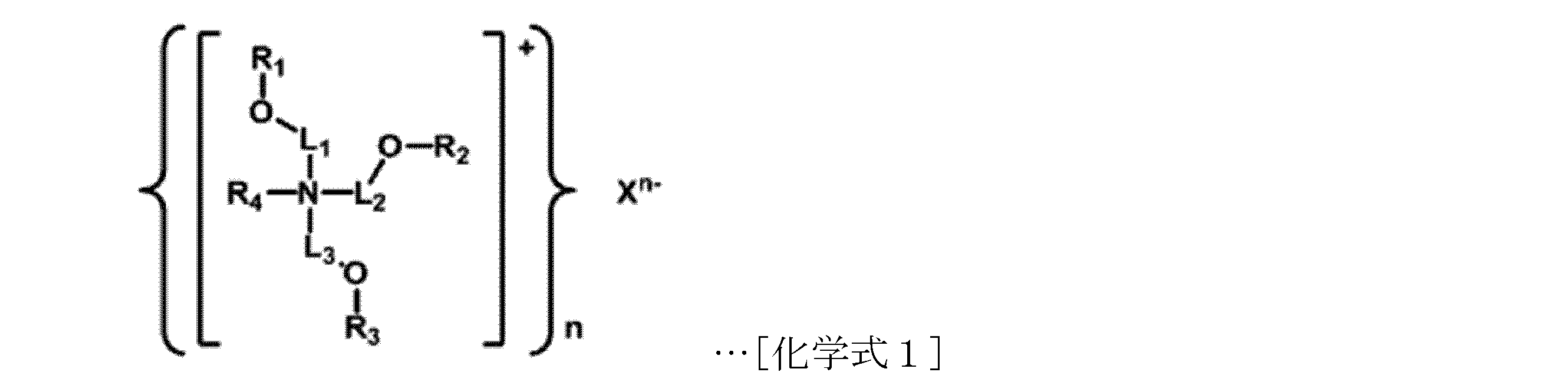
本発明は、エッチング組成物を提供しようとするものである。本発明の一実施例によると、リン酸、Si原子を1つ以上含むシラン化合物、及び下記化学式1で表されるアンモニウム塩を含むエッチング組成物を提供する。

上記Xは、ハロゲン、C1-C10のカルボキシレート、トシレート、硫酸塩、メシレート、重硫酸塩、炭酸塩、重炭酸塩、ホスフェート、ヒドロゲンホスフェート、ジヒドロゲンホスフェート、及び硝酸塩からなる群から選択される少なくとも一つであってもよい。 The X may be at least one selected from the group consisting of halogen, C 1 -C 10 carboxylate, tosylate, sulfate, mesylate, bisulfate, carbonate, bicarbonate, phosphate, hydrogen phosphate, dihydrogen phosphate, and nitrate.
上記L1~L3は独立して、置換又は非置換されたC1-C5のアルキルレンであってもよく、すべて同一であることがより好ましく、例えば、上記L1~L3は-CH2CH2-又は-CH2CH(CH3)-であってもよい。 The above L 1 to L 3 may be independently a substituted or unsubstituted C 1 -C 5 alkylene, and more preferably are all the same. For example, the above L 1 to L 3 may be -CH 2 CH 2 - or -CH 2 CH(CH 3 )-.
上記ヒドロカルビルは、置換又は非置換されたC1-C20のアルキル又は置換又は非置換されたC6-C20アリールであってもよい。 The hydrocarbyl may be a substituted or unsubstituted C 1 -C 20 alkyl or a substituted or unsubstituted C 6 -C 20 aryl.
例えば、上記R1~R3は水素であり、R4は水素又はC1-C20のアルキルであってもよく、より具体的には、上記R4は水素又は-CH3であってもよい。 For example, R 1 to R 3 are hydrogen, and R 4 is hydrogen or C 1 -C 20 alkyl, more specifically, R 4 is hydrogen or —CH 3 .
上記化学式1のアンモニウム塩は、下記式(1)~(14)の構造から選択されるものであってもよい。

上記シラン化合物は下記化学式2で表されるものであってもよい。

上記化学式2中、R51~R54は互いに独立して水素、置換又は非置換されたヒドロカルビル、置換又は非置換されたヘテロヒドロカルビルであり、R51~R54はそれぞれ存在するか、又は2つ以上がヘテロ元素を介して互いに連結されたリング状である。 In the above formula 2, R 51 to R 54 are each independently hydrogen, substituted or unsubstituted hydrocarbyl, or substituted or unsubstituted heterohydrocarbyl, and R 51 to R 54 are each present or two or more of them are connected to each other via a hetero atom to form a ring.
上記した各実施例のエッチング組成物は、リン酸70~95重量%、シラン化合物0.001~5重量%、化学式1で表されるアンモニウム塩0.001~10重量%を含んでもよい。 The etching composition of each of the above examples may contain 70 to 95% by weight of phosphoric acid, 0.001 to 5% by weight of a silane compound, and 0.001 to 10% by weight of an ammonium salt represented by chemical formula 1.
本発明は、上記したエッチング組成物を用いた絶縁膜のエッチング方法を提供し、上記絶縁膜のエッチング方法を含む半導体素子の製造方法を提供する。 The present invention provides a method for etching an insulating film using the above-mentioned etching composition, and a method for manufacturing a semiconductor device including the above-mentioned method for etching an insulating film.
本発明によるエッチング組成物は、酸化膜に対する窒化膜のエッチング選択比が高い。 The etching composition of the present invention has a high etching selectivity ratio of nitride films to oxide films.
また、本発明のエッチング組成物を用いると、窒化膜除去時に酸化膜の膜質の損傷や酸化膜のエッチングに起因する電気的特性の低下を防止するとともに、パーティクルの発生を防止して素子特性を向上させることができる。 In addition, the use of the etching composition of the present invention can prevent damage to the oxide film quality during nitride film removal and deterioration of electrical characteristics caused by etching the oxide film, as well as prevent particle generation and improve device characteristics.
本発明は、エッチング組成物、特に酸化膜のエッチング率を最小限に抑えるとともに、窒化膜を選択的に除去することができる高選択比を有し、保存安定性に優れたエッチング組成物を提供するためのものである。 The present invention aims to provide an etching composition, in particular an etching composition that minimizes the etching rate of an oxide film, has a high selectivity that can selectively remove a nitride film, and has excellent storage stability.
本発明のエッチング組成物はリン酸を含む。上記リン酸はシリコン窒化物と反応して窒化膜をエッチングするものであり、上記リン酸は下記反応式(1)のようにシリコン窒化物と反応してシリコン窒化物をエッチングする。
3Si3N4+27H2O+4H3PO4→4(NH4)3PO4+9SiO2H2O(1)
The etching composition of the present invention contains phosphoric acid, which reacts with silicon nitride to etch a nitride film, and the phosphoric acid reacts with silicon nitride to etch the silicon nitride as shown in the following reaction formula (1).
3Si 3 N 4 +27H 2 O + 4H 3 PO 4 →4(NH 4 ) 3 PO 4 +9SiO 2 H 2 O (1)
本発明のエッチング組成物は、下記化学式1で表されるアンモニウム塩を含む。

上記化学式1中、L1~L3は独立して、置換又は非置換されたヒドロカルビレンである。上記L1~L3は独立して、置換又は非置換されたC1-C5のアルキレン、例えば、-CH2CH2-、-CH2CH(CH3)-であってもよい。上記L1~L3は互いに異なってもよいことは言うまでもなく、すべて同一であってもよい。 In the above formula 1, L 1 to L 3 are independently substituted or unsubstituted hydrocarbylene. L 1 to L 3 may be independently substituted or unsubstituted C 1 -C 5 alkylene, for example, -CH 2 CH 2 -, -CH 2 CH(CH 3 )-. L 1 to L 3 may be different from each other, or may be the same.
上記化学式1中、R1~R4は独立して、水素、置換又は非置換されたヒドロカルビルである。上記ヒドロカルビルは置換又は非置換されたC1-C20のアルキル又は置換又は非置換されたC6-C20アリールであってもよい。上記R1~R4は互いに異なってもよいことは言うまでもなく、2以上が同一であってもよい。例えば、上記R1~R3は水素であり、R4は水素又は-CH3のような置換又は非置換されたC1-C20のアルキルであってもよい。 In the above formula 1, R 1 to R 4 are independently hydrogen, substituted or unsubstituted hydrocarbyl. The hydrocarbyl may be substituted or unsubstituted C 1 -C 20 alkyl or substituted or unsubstituted C 6 -C 20 aryl. It goes without saying that R 1 to R 4 may be different from each other, or two or more may be the same. For example, R 1 to R 3 may be hydrogen, and R 4 may be hydrogen or substituted or unsubstituted C 1 -C 20 alkyl, such as -CH 3 .
上記化学式1中、Xn-はn価の陰イオンであり、好ましくは、nが1~3のうちいずれか1つの整数である陰イオンであってもよい。例えば、上記Xは、F、Cl、Br、Iなどのハロゲン元素であってもよく、アセテートのようなC1-C10のカルボキシレート、トシレート、硫酸塩、メシレート、重硫酸塩、炭酸塩、重炭酸塩、ホスフェート、ヒドロゲンホスフェート、ジヒドロゲンホスフェート、及び硝酸塩で構成される群から選択されるものであってもよい。 In the above formula 1, X n- is an anion having a valency of n, preferably an anion in which n is an integer of 1 to 3. For example, X may be a halogen element such as F, Cl, Br, or I, or may be selected from the group consisting of C 1 -C 10 carboxylates such as acetate, tosylates, sulfates, mesylates, bisulfates, carbonates, bicarbonates, phosphates, hydrogen phosphates, dihydrogen phosphates, and nitrates.
本発明で提供される化学式1で表されるアンモニウム塩は、シラン化合物に対して構造的安定性を提供し、シラン化合物の分解又は異常成長のような現象の発生を抑制してエッチング組成物のパーティクルの生成を抑制し、シリコン酸化物に対するエッチング抑制の役割を維持するようにする。 The ammonium salt represented by Chemical Formula 1 provided in the present invention provides structural stability to the silane compound, inhibits the occurrence of phenomena such as decomposition or abnormal growth of the silane compound, inhibits the generation of particles in the etching composition, and maintains its role of inhibiting etching of silicon oxide.
本発明のエッチング組成物に含まれるアンモニウム塩は、上記化学式1で表されるものであればいずれか1つを単独で用いることができることは言うまでもなく、2以上を混合して用いることもできる。本発明で用いられる化学式1で表されるアンモニウム塩は、例えば、下記式(1)~(14)のアンモニウム塩であってもよい。

上記化学式1のアンモニウム塩は、エッチング組成物のパーティクル生成を防止することができ、全重量に対して0.001~10重量%の含有量で添加することができる。0.001重量%未満添加すると、パーティクルの生成抑制効果がわずかであり、10重量%を超えて添加すると、アンモニウム塩がパーティクルの生成を加速化させる可能性がある。 The ammonium salt of the above formula 1 can prevent particle generation in the etching composition and can be added in a content of 0.001 to 10 wt % based on the total weight. If less than 0.001 wt % is added, the effect of suppressing particle generation is slight, and if more than 10 wt % is added, the ammonium salt may accelerate particle generation.
上記化学式1のアンモニウム塩は、例えば、0.001~5重量%、0.001~3重量%、0.001~2重量%、0.001~1重量%、0.005~5重量%、0.005~3重量%、0.005~2重量%、0.005~1重量%、0.01~5重量%、0.01~3重量%、0.01~2重量%、0.01~1重量%、0.05~5重量%、0.05~3重量%、0.05~2重量%、0.05~1重量%、0.1~5重量%、0.1~3重量%、0.1~2重量%、0.1~1重量%、0.5~5重量%、0.5~3重量%、0.5~2重量%、0.5~1重量%の含有量であってもよい。 The ammonium salt of the above chemical formula 1 may have a content of, for example, 0.001-5 wt%, 0.001-3 wt%, 0.001-2 wt%, 0.001-1 wt%, 0.005-5 wt%, 0.005-3 wt%, 0.005-2 wt%, 0.005-1 wt%, 0.01-5 wt%, 0.01-3 wt%, 0.01-2 wt%, 0.01-1 wt%, 0.05-5 wt%, 0.05-3 wt%, 0.05-2 wt%, 0.05-1 wt%, 0.1-5 wt%, 0.1-3 wt%, 0.1-2 wt%, 0.1-1 wt%, 0.5-5 wt%, 0.5-3 wt%, 0.5-2 wt%, or 0.5-1 wt%.
本発明のエッチング組成物はシラン化合物を含む。本発明において、シラン化合物は、Si原子を1つ以上含むシラン化合物であれば適切に用いることができ、より好ましくは、下記式2で表されるシラン化合物であってもよい。

上記化学式2中、R51~R54は互いに独立して、水素、C1-C20のヒドロカルビルのような置換又は非置換されたヒドロカルビル又はC1-C20のヘテロヒドロカルビルのような置換又は非置換されたヘテロヒドロカルビルであってもよい。上記R51~R54はそれぞれ存在するか、又は2つ以上がヘテロ元素を介して互いに連結された環状であってもよい。例えば、水素、置換又は非置換されたC1-C20のアルキル、或いは置換又は非置換されたC1-C20のヘテロアルキルなどであってもよい。このとき、上記ヘテロ元素は特に限定しないが、例えば、N、S、O、Pなどであってもよい。 In the above formula 2, R 51 to R 54 may be each independently hydrogen, substituted or unsubstituted hydrocarbyl such as C 1 -C 20 hydrocarbyl, or substituted or unsubstituted heterohydrocarbyl such as C 1 -C 20 heterohydrocarbyl. Each of R 51 to R 54 may be present, or two or more may be connected to each other via a heteroatom to form a ring. For example, it may be hydrogen, substituted or unsubstituted C 1 -C 20 alkyl, or substituted or unsubstituted C 1 -C 20 heteroalkyl. In this case, the heteroatom is not particularly limited, and may be, for example, N, S, O, P, etc.
上記化学式2で表されるシラン化合物は、エッチング組成物の全重量に対して0.005~1重量%の含有量で含むことができる。 The silane compound represented by the above chemical formula 2 may be contained in an amount of 0.005 to 1 wt % based on the total weight of the etching composition.
さらに、本発明のエッチング組成物は、化学式1で表されるアンモニウム塩以外のアンモニウム塩をさらに含むことができる。 Furthermore, the etching composition of the present invention may further contain an ammonium salt other than the ammonium salt represented by Chemical Formula 1.
上記アンモニウム塩として、アンモニウムイオンを有する化合物であって、本発明が属する分野において通常用いられるものを、本発明でも好適に用いることができる。かかるアンモニウム塩として、これに限定するものではないが、例えば、アンモニア水、塩化アンモニウム、酢酸アンモニウム、リン酸アンモニウム、ペルオキソ二硫酸アンモニウム、硫酸アンモニウム、フッ酸アンモニウムなどを挙げることができ、これらのうちいずれか1つを単独で用いることができることは言うまでもなく、2以上を混合して用いることもできる。 As the ammonium salt, a compound having an ammonium ion that is commonly used in the field to which the present invention belongs can be suitably used in the present invention. Examples of such ammonium salts include, but are not limited to, ammonia water, ammonium chloride, ammonium acetate, ammonium phosphate, ammonium peroxodisulfate, ammonium sulfate, and ammonium hydrofluoride. Needless to say, any one of these can be used alone, and two or more can be used in combination.
さらに、本発明のエッチング組成物は、エッチング性能をさらに向上させるために、本技術分野において通常用いられる任意の添加剤をさらに含むことができる。添加剤としては、界面活性剤、金属イオン封鎖剤、腐食防止剤などを挙げることができる。 In addition, the etching composition of the present invention may further contain any additives commonly used in the art to further improve the etching performance. Examples of additives include surfactants, sequestering agents, corrosion inhibitors, etc.
本発明のエッチング組成物は、酸化膜と窒化膜を含む半導体素子から窒化膜を選択的にエッチング除去するために用いられるものであり、上記窒化膜は、シリコン窒化膜、例えば、SiN膜、SiON膜などを含むことができる。 The etching composition of the present invention is used to selectively etch away a nitride film from a semiconductor element that includes an oxide film and a nitride film, and the nitride film can include a silicon nitride film, such as a SiN film or a SiON film.
また、酸化膜は、シリコン酸化膜、例えば、SOD(Spin On Dielectric)膜、HDP(High Density Plasma)膜、熱酸化(thermal oxide)膜、BPSG(Borophosphate Silicate Glass)膜、PSG(Phospho Silicate Glass)膜、BSG(Boro Silicate Glass)膜、PSZ(Polysilazane)膜、FSG(Fluorinated Silicate Glass)膜、LPTEOS(Low Pressure Tetra Ethyl Ortho Silicate)膜、PETEOS(Plasma Enhanced Tetra Ethyl Ortho Silicate)膜、HTO(High Temperature Oxide)膜、MTO(Medium Temperature oxide)膜、USG(Undopped Silicate Glass)膜、SOG(Spin On Glass)膜、APL(Advanced Planarization Layer)膜、ALD(Atomic Layer Deposition)膜、PE-酸化(Plasma Enhanced oxide)膜、O3-TEOS(O3-Tetra Ethyl Ortho Silicate)膜、及びその組み合わせで構成される群から選択される少なくとも1以上の膜であってもよい。 The oxide film may be a silicon oxide film, for example, a SOD (Spin On Dielectric) film, a HDP (High Density Plasma) film, a thermal oxide film, a BPSG (Borophosphate Silicate Glass) film, a PSG (Phospho Silicate Glass) film, a BSG (Boro Silicate Glass) film, a PSZ (Polysilazane) film, a FSG (Fluorinated Silicate Glass) film, a LPTEOS (Low Pressure Tetra Ethyl Ortho Silicate) film, PETEOS (Plasma Enhanced Tetra Ethyl Ortho Silicate) film, HTO (High Temperature Oxide) film, MTO (Medium Temperature oxide) film , USG (Undopped Silicate Glass) film, SOG (Spin On Glass) film, APL (Advanced Planarization Layer) film, ALD (Atomic Deposition) film, PE-oxidation (P Lasma Enhanced The film may be at least one selected from the group consisting of an O3-TEOS (O3-Tetra Ethyl Ortho Silicate) film, an O3-TEOS (O3-Tetra Ethyl Ortho Silicate) film, and combinations thereof.
本発明のエッチング組成物を用いるエッチング工程は、ウェットエッチング方法、例えば、浸漬させる方法、噴射する方法などによって行われることができる。 The etching process using the etching composition of the present invention can be carried out by a wet etching method, such as an immersion method or a spraying method.
本発明のエッチング組成物を用いるエッチング工程の例を図1及び図2に概略的に示した。図1及び図2は、一例として、フラッシュメモリ素子の素子分離工程を示す工程断面図である。 An example of an etching process using the etching composition of the present invention is shown in schematic form in Figures 1 and 2. Figures 1 and 2 are cross-sectional views showing an example of an element isolation process for a flash memory element.
先ず、図1に示すように、基板10上にトンネル酸化膜11、ポリシリコン膜12、バッファ酸化膜13、及びパッド窒化膜14を順に形成した後、ポリシリコン膜12、バッファ酸化膜13、及びパッド窒化膜14を選択的にエッチングしてトレンチを形成する。続いて、トレンチをギャップフィルするまでSOD酸化膜15を形成した後、パッド窒化膜14を研磨停止膜としてSOD酸化膜15に対してCMP工程を行う。 First, as shown in FIG. 1, a tunnel oxide film 11, a polysilicon film 12, a buffer oxide film 13, and a pad nitride film 14 are sequentially formed on a substrate 10, and then the polysilicon film 12, the buffer oxide film 13, and the pad nitride film 14 are selectively etched to form a trench. Next, an SOD oxide film 15 is formed until the trench is gap-filled, and then a CMP process is performed on the SOD oxide film 15 using the pad nitride film 14 as a polishing stop film.
次に、図2に示すように、リン酸溶液を用いたウェットエッチングによってパッド窒化膜14を除去した後、洗浄工程を介してバッファ酸化膜13を除去する。これにより、フィールド領域に素子分離膜15Aが形成される。 Next, as shown in FIG. 2, the pad nitride film 14 is removed by wet etching using a phosphoric acid solution, and then the buffer oxide film 13 is removed through a cleaning process. This forms an element isolation film 15A in the field region.
エッチング工程におけるプロセス温度は、50~300℃の範囲、好ましくは100~200℃の範囲、より好ましくは156℃~163℃の範囲であってもよく、適正温度は、他の工程とその他の要因を考慮して必要に応じて変更されることができる。 The process temperature in the etching step may be in the range of 50 to 300°C, preferably in the range of 100 to 200°C, and more preferably in the range of 156°C to 163°C, and the appropriate temperature can be changed as necessary taking into account other steps and other factors.
このように、本発明のエッチング組成物を用いて行われるエッチング工程を含む半導体素子の製造方法によると、窒化膜と酸化膜が交互に積層されるか、又は混在する場合、酸化膜に対する窒化膜の選択的エッチングが可能である。また、従来のエッチング工程で問題となったパーティクルの発生を防止し、工程の安定性及び信頼性を確保することができる。 As described above, according to the method for manufacturing a semiconductor device including an etching process performed using the etching composition of the present invention, when nitride films and oxide films are alternately stacked or mixed, it is possible to selectively etch the nitride film relative to the oxide film. In addition, it is possible to prevent the generation of particles, which was a problem in the conventional etching process, and ensure the stability and reliability of the process.
したがって、このような方法は、半導体素子の製造工程において酸化膜に対する窒化膜の選択的エッチングが必要ないくつかの過程に効率的に適用されることができる。 Therefore, this method can be effectively applied to several processes in the manufacturing process of semiconductor devices that require selective etching of nitride films relative to oxide films.
以下、本発明を実施例を挙げてより詳細に説明する。以下の実施例は、本発明の一例を示すものであって、これにより本発明が限定されるものではない。 The present invention will be described in more detail below with reference to examples. The following examples are merely examples of the present invention, and are not intended to limit the present invention.
[合成例1]
100mLの丸底フラスコにトリエタノールアミン10gを投入し、エタノール30mlを投入した後、撹拌した。
[Synthesis Example 1]
10 g of triethanolamine was placed in a 100 mL round-bottom flask, and 30 ml of ethanol was added thereto, followed by stirring.
N2条件を維持しながら、0℃で冷却した後、酢酸4.1gを徐々に投入した。フラスコの外部温度が90℃になるまで昇温した後、24時間還流反応させた。 While maintaining N2 conditions, the mixture was cooled to 0°C, and 4.1 g of acetic acid was gradually added. The external temperature of the flask was raised to 90°C, and the mixture was refluxed for 24 hours.
外部温度が40℃になるように冷却し、減圧蒸留してエタノールをすべて削除した後、12時間追加真空乾燥して、下記式(1)のアンモニウム塩添加剤1を得た。

1H-NMR(DMSO-d6):5.00(broad、4H)、3.71(t、6H)、2.67(t、6H)、1.98(s、3H) 1 H-NMR (DMSO-d6): 5.00 (broad, 4H), 3.71 (t, 6H), 2.67 (t, 6H), 1.98 (s, 3H)
[合成例2]
100mlの丸底フラスコにトリエタノールアミン10gを投入し、アセトニトリル30mlを投入した後、撹拌した。
[Synthesis Example 2]
10 g of triethanolamine was placed in a 100 ml round-bottom flask, and 30 ml of acetonitrile was then added, followed by stirring.
N2条件を維持しながら、0℃で冷却した後、ジメチル硫酸4.3gを徐々に投入した。フラスコの外部温度が90℃になるまで昇温した後、60時間還流反応させた。 While maintaining N2 conditions, the flask was cooled to 0°C, and 4.3 g of dimethyl sulfate was gradually added. The external temperature of the flask was raised to 90°C, and the reaction was carried out under reflux for 60 hours.
外部温度が25℃となるように冷却し、アセトニトリル層を除去した後、アセトニトリル30mlを再びフラスコに投入し、洗浄除去した。 The flask was cooled to an external temperature of 25°C, the acetonitrile layer was removed, and 30 ml of acetonitrile was then added back into the flask and washed away.
12時間追加真空乾燥して、下記式(2)のアンモニウム塩添加剤2を得た。

1H-NMR(DMSO-d6):4.78(broad、3H)、3.81(m、6H)、3.49(t、6H)、3.12(s、3H) 1 H-NMR (DMSO-d6): 4.78 (broad, 3H), 3.81 (m, 6H), 3.49 (t, 6H), 3.12 (s, 3H)
[合成例3]
100mlの丸底フラスコにトリイソプロパノールアミン5gを投入し、エタノール30mlを投入した後、撹拌した。
[Synthesis Example 3]
5 g of triisopropanolamine was placed in a 100 ml round-bottom flask, and 30 ml of ethanol was then added, followed by stirring.
0℃で冷却した後、70%硝酸1.65mlを徐々に投入した。フラスコの外部温度が90℃になるまで昇温した後、20時間還流反応させた。 After cooling to 0°C, 1.65 ml of 70% nitric acid was gradually added. The external temperature of the flask was raised to 90°C, and the reaction was allowed to reflux for 20 hours.
外部温度が50℃になるように冷却し、減圧蒸留してエタノールを除去した。濃縮残渣にトルエン50mlを投入し、再び減圧蒸留した後、24時間追加真空乾燥して、下記式(3)のアンモニウム塩添加剤3を得た。

1H-NMR(DMSO-d6):4.94(broad、4H)、3.78(m、3H)、2.61(m、6H)、1.31(m、9H) 1 H-NMR (DMSO-d6): 4.94 (broad, 4H), 3.78 (m, 3H), 2.61 (m, 6H), 1.31 (m, 9H)
[合成例4]
100mlの丸底フラスコにトリイソプロパノールアミン10gを投入し、エタノール30mlを投入した後、撹拌した。
[Synthesis Example 4]
10 g of triisopropanolamine was placed in a 100 ml round-bottom flask, and 30 ml of ethanol was then added, followed by stirring.
0℃で冷却した後、メチルp-トルエンスルホネート9.7gを徐々に投入した。フラスコの外部温度が90℃になるまで昇温した後、24時間還流反応させた。 After cooling to 0°C, 9.7 g of methyl p-toluenesulfonate was gradually added. The external temperature of the flask was raised to 90°C, and the reaction was allowed to reflux for 24 hours.
外部温度が50℃になるように冷却し、減圧蒸留してエタノールを除去した。濃縮残渣にアセトン50mlを投入して洗浄した後、再び減圧蒸留し、24時間追加真空乾燥して、下記式(4)のアンモニウム塩添加剤4を得た。
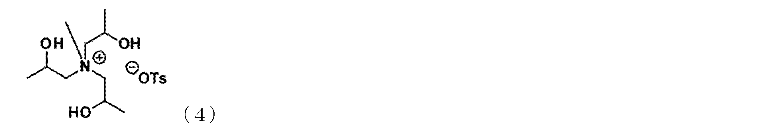
1H-NMR(DMSO-d6):7.48(d、2H)、7.12(d、2H)、5.05(broad、3H)、3.69(m、3H)、2.59(m、6H)、2.28(s、3H)、1.42(m、9H) 1 H-NMR (DMSO-d6): 7.48 (d, 2H), 7.12 (d, 2H), 5.05 (broad, 3H), 3.69 (m, 3H), 2.59 ( m, 6H), 2.28 (s, 3H), 1.42 (m, 9H)
実施例1
半導体ウェハ上に500Å(オングストローム)の厚さで蒸着されたシリコン酸化膜(SiOx)、及び5000Åの厚さのシリコン窒化膜(SiN)が形成された基板を設けた。
Example 1
A substrate was provided on which a silicon oxide film (SiOx) having a thickness of 500 Å (angstroms) and a silicon nitride film (SiN) having a thickness of 5000 Å were formed by vapor deposition on a semiconductor wafer.
表1に示すように、85%リン酸99.4重量%に3-アミノプロピルシラントリオール0.5重量%、アンモニウム塩添加剤10.1重量%を添加して100重量%になるように混合してエッチング組成物を製造した。 As shown in Table 1, an etching composition was prepared by adding 0.5% by weight of 3-aminopropylsilanetriol and 10.1% by weight of ammonium salt additive to 99.4% by weight of 85% phosphoric acid and mixing them to make 100% by weight.
実施例2~4
アンモニウム塩添加剤2~4を用いたことを除いては、実施例1と同様の方法でエッチング組成物をそれぞれ製造した。
Examples 2 to 4
The etching compositions were prepared in the same manner as in Example 1, except that ammonium salt additives 2 to 4 were used.
比較例1
アンモニウム塩添加剤を用いていないことを除いては、実施例1と同様の方法でエッチング組成物を製造した。
Comparative Example 1
An etching composition was prepared in the same manner as in Example 1, except that no ammonium salt additive was used.
比較例2
アンモニウム塩添加剤として、(NH4)OAc(アンモニウムアセテート)を用いたことを除いては、実施例1と同様の方法でエッチング組成物を製造した。
Comparative Example 2
An etching composition was prepared in the same manner as in Example 1, except that (NH 4 )OAc (ammonium acetate) was used as the ammonium salt additive.
<エッチング組成物の製造及び選択比の測定>
実施例1~4及び比較例1で得られたそれぞれのエッチング組成物を丸底フラスコに入れ、60分間加熱して158℃に上昇させた後、上記シリコンウェハを浸漬して、720秒、6000秒浸漬させてエッチング工程を行った。
<Preparation of Etching Composition and Measurement of Selectivity>
Each of the etching compositions obtained in Examples 1 to 4 and Comparative Example 1 was placed in a round-bottom flask and heated for 60 minutes to 158° C., after which the silicon wafer was immersed therein for 720 seconds and 6000 seconds to carry out an etching process.
パターンが形成されたシリコンウエハの表面を選択的にエッチングした後、シリコン酸化膜と窒化膜のエッチング前/後の膜質の厚さを薄膜厚さ測定装置(NANO VIEW、SEMG-1000)であるエリプソメトリを用いて測定し、そこからシリコン酸化膜のエッチング速度(SiO E/R、Å)、窒化膜のエッチング速度(SiN E/R、Å)、及び選択比を計算した。その結果を表1に示した。 After selectively etching the surface of the silicon wafer on which the pattern was formed, the thickness of the silicon oxide film and the nitride film before and after etching was measured using an ellipsometry thin film thickness measuring device (NANO VIEW, SEMG-1000), and the etching rate of the silicon oxide film (SiO E/R, Å), the etching rate of the nitride film (SiN E/R, Å), and the selectivity were calculated from the results. The results are shown in Table 1.
選択比は、酸化膜エッチング速度に対する窒化膜エッチング速度の比を表し、エッチング速度は初期値とエッチング処理後の膜厚の差をエッチング時間(分)で割って算出した値である。 The selectivity ratio represents the ratio of the nitride film etching rate to the oxide film etching rate, and the etching rate is calculated by dividing the difference between the initial film thickness and the film thickness after the etching process by the etching time (minutes).

表1から分かるように、エッチング組成物の添加剤として、アンモニウム塩添加剤1~4を添加したエッチング組成物を適用したとき、比較例1に比べてエッチング選択比が著しく高く示されることが分かる。また、シリコン窒化膜のエッチング速度(SiN E/R)の面からも、比較例1のエッチング組成物に比べて著しく優れた効果を示し、シリコン窒化膜のエッチング工程に最適化されたエッチング組成物を提供することができることを確認した。 As can be seen from Table 1, when the etching compositions containing ammonium salt additives 1 to 4 were used as additives to the etching composition, the etching selectivity was significantly higher than that of Comparative Example 1. In addition, in terms of the etching rate (SiN E/R) of the silicon nitride film, it was found that the etching compositions showed significantly superior effects compared to the etching composition of Comparative Example 1, and it was confirmed that an etching composition optimized for the silicon nitride film etching process could be provided.
かかる結果から、本発明で提供するアンモニウム塩を添加剤として用いる場合には、活性シリコン系構造安定性を向上させる結果が確認できる。これにより、シリコン窒化膜のエッチング速度、エッチング選択比、及びエッチングの安定性を向上させ、エッチング工程の効率を向上させることができるエッチング組成物を提供することができることが確認された。 From these results, it can be confirmed that when the ammonium salt provided by the present invention is used as an additive, the stability of the active silicon-based structure is improved. This confirms that it is possible to provide an etching composition that can improve the etching rate, etching selectivity, and etching stability of the silicon nitride film, and thus improve the efficiency of the etching process.
エッチング組成物の経時変化の確認
上記比較例1及び実施例1のエッチング組成物を約70℃で一定期間保管した後、上記エッチング組成物に対して7日毎に同一の条件で再びエッチングテストを行い、その結果を表2に示した。
The etching compositions of Comparative Example 1 and Example 1 were stored at about 70° C. for a certain period of time, and then an etching test was performed again under the same conditions every 7 days. The results are shown in Table 2.

上記表2から分かるように、21日後に、比較例1の上記エッチング組成物は、エッチング速度(SiN E/R)及び選択比が大幅に減少する結果を示した。これに対し、アンモニウム塩添加剤1を添加した実施例1の上記エッチング組成物は、エッチング速度(SiN E/R)及び選択比がほとんど変化しない結果を示すことが分かる。上記の結果から、本発明の一例によるエッチング組成物は、エッチング速度及び選択比に優れることは言うまでもなく、保管安定性に優れるため、長期保管時にも優れたエッチング特性を維持することができることが分かる。 As can be seen from Table 2 above, after 21 days, the etching composition of Comparative Example 1 showed a significant decrease in etching rate (SiN E/R) and selectivity. In contrast, the etching composition of Example 1 to which ammonium salt additive 1 was added showed results in which the etching rate (SiN E/R) and selectivity ratio remained almost unchanged. From the above results, it can be seen that the etching composition according to one example of the present invention not only has excellent etching rate and selectivity, but also has excellent storage stability, and therefore can maintain excellent etching properties even during long-term storage.
上記の結果は、アンモニウム塩添加剤1の構造的安定性の効果により、3-アミノプロピルシラントリオール間の分解又は異常成長のような現象の発生なしに、シリコン酸化膜に対するエッチング抑制の役割を維持することができることを示す。
The above results indicate that the effect of the structural stability of the ammonium salt additive 1 allows it to maintain its role in inhibiting etching of silicon oxide films without the occurrence of phenomena such as decomposition or abnormal growth between 3-aminopropylsilanetriols.
Claims (13)


前記ポリシリコン膜、前記バッファ酸化膜、及び前記パッド窒化膜を選択的にエッチングしてトレンチを形成する段階と、
SOD酸化膜を形成して前記トレンチをギャップフィル(gap-fill)する段階と、
前記パッド窒化膜を研磨停止膜として前記SOD酸化膜に対して化学機械研磨(CMP)工程を行う段階と、
請求項1から請求項11のいずれか一項のシリコン窒化膜のエッチング組成物を用いたウェットエッチングによって前記パッド窒化膜を除去する段階と、
前記バッファ酸化膜を除去する段階と、を含む、半導体素子の製造方法。 forming a tunnel oxide layer, a polysilicon layer, a buffer oxide layer, and a pad nitride layer on a substrate in sequence;
selectively etching the polysilicon layer, the buffer oxide layer, and the pad nitride layer to form a trench;
forming a SOD oxide layer to gap-fill the trench;
performing a chemical mechanical polishing (CMP) process on the SOD oxide film using the pad nitride film as a polishing stop;
removing the pad nitride film by wet etching using the silicon nitride film etching composition of any one of claims 1 to 11;
removing the buffer oxide film.
Applications Claiming Priority (2)
| Application Number | Priority Date | Filing Date | Title |
|---|---|---|---|
| KR10-2019-0109544 | 2019-09-04 | ||
| KR1020190109544A KR102803330B1 (en) | 2019-09-04 | 2019-09-04 | Etching composition, method for etching insulating layer of semiconductor devices using the same and method for preparing semiconductor devices |
Publications (2)
| Publication Number | Publication Date |
|---|---|
| JP2021040135A JP2021040135A (en) | 2021-03-11 |
| JP7561545B2 true JP7561545B2 (en) | 2024-10-04 |
Family
ID=74680735
Family Applications (1)
| Application Number | Title | Priority Date | Filing Date |
|---|---|---|---|
| JP2020148458A Active JP7561545B2 (en) | 2019-09-04 | 2020-09-03 | Etching composition, method for etching insulating film using same, and method for manufacturing semiconductor device |
Country Status (5)
| Country | Link |
|---|---|
| US (1) | US11186772B2 (en) |
| JP (1) | JP7561545B2 (en) |
| KR (1) | KR102803330B1 (en) |
| CN (1) | CN112442372B (en) |
| TW (1) | TWI837418B (en) |
Citations (5)
| Publication number | Priority date | Publication date | Assignee | Title |
|---|---|---|---|---|
| JP2009206462A (en) | 2008-02-29 | 2009-09-10 | Tosoh Corp | Composition for etching and etching method |
| JP2016538139A (en) | 2013-09-25 | 2016-12-08 | スリーエム イノベイティブ プロパティズ カンパニー | Multi-layer polishing pad |
| JP2017114966A (en) | 2015-12-22 | 2017-06-29 | Jsr株式会社 | Chemical mechanical polishing composition and chemical mechanical polishing method using the same |
| WO2017169602A1 (en) | 2016-03-30 | 2017-10-05 | 株式会社フジミインコーポレーテッド | Cationically modified silica raw material dispersion |
| JP2019501517A (en) | 2015-10-28 | 2019-01-17 | キャボット マイクロエレクトロニクス コーポレイション | Tungsten treatment slurry containing cationic surfactant |
Family Cites Families (13)
| Publication number | Priority date | Publication date | Assignee | Title |
|---|---|---|---|---|
| US20080210900A1 (en) | 2005-05-13 | 2008-09-04 | William Wojtczak | Selective Wet Etchings Of Oxides |
| US8859437B2 (en) * | 2012-12-31 | 2014-10-14 | The Penn State Research Foundation | Solution for etching a thin film transistor and method of manufacturing the same |
| KR102338550B1 (en) * | 2013-06-06 | 2021-12-14 | 엔테그리스, 아이엔씨. | Compositions and methods for selectively etching titanium nitride |
| KR20150108143A (en) * | 2014-03-17 | 2015-09-25 | 동우 화인켐 주식회사 | Texture etching solution composition and texture etching method of crystalline silicon wafers |
| KR20160010267A (en) * | 2014-07-17 | 2016-01-27 | 솔브레인 주식회사 | Composition for etching and manufacturing method of semiconductor device using the same |
| CN107573940A (en) * | 2016-07-04 | 2018-01-12 | Oci有限公司 | Silicon nitride film etching solution |
| KR102336865B1 (en) * | 2017-07-06 | 2021-12-09 | 오씨아이 주식회사 | Etching compositions and etching method using the same |
| US10651045B2 (en) | 2017-09-06 | 2020-05-12 | Entegris, Inc. | Compositions and methods for etching silicon nitride-containing substrates |
| US20190189631A1 (en) * | 2017-12-15 | 2019-06-20 | Soulbrain Co., Ltd. | Composition for etching and manufacturing method of semiconductor device using the same |
| KR102457243B1 (en) * | 2017-12-21 | 2022-10-21 | 주식회사 이엔에프테크놀로지 | Etching composition for silicon nitride layer |
| KR102484977B1 (en) * | 2017-12-28 | 2023-01-09 | 오씨아이 주식회사 | Etching compositions and etching method using the same |
| KR20190094927A (en) * | 2018-02-06 | 2019-08-14 | 동우 화인켐 주식회사 | Etching residue cleaning composition and method of forming conductive pattern using the same |
| KR102653096B1 (en) * | 2018-02-13 | 2024-04-01 | 동우 화인켐 주식회사 | Insulation layer etchant composition and method of forming pattern using the same |
-
2019
- 2019-09-04 KR KR1020190109544A patent/KR102803330B1/en active Active
-
2020
- 2020-09-02 US US17/009,852 patent/US11186772B2/en active Active
- 2020-09-02 TW TW109130000A patent/TWI837418B/en active
- 2020-09-02 CN CN202010908291.XA patent/CN112442372B/en active Active
- 2020-09-03 JP JP2020148458A patent/JP7561545B2/en active Active
Patent Citations (5)
| Publication number | Priority date | Publication date | Assignee | Title |
|---|---|---|---|---|
| JP2009206462A (en) | 2008-02-29 | 2009-09-10 | Tosoh Corp | Composition for etching and etching method |
| JP2016538139A (en) | 2013-09-25 | 2016-12-08 | スリーエム イノベイティブ プロパティズ カンパニー | Multi-layer polishing pad |
| JP2019501517A (en) | 2015-10-28 | 2019-01-17 | キャボット マイクロエレクトロニクス コーポレイション | Tungsten treatment slurry containing cationic surfactant |
| JP2017114966A (en) | 2015-12-22 | 2017-06-29 | Jsr株式会社 | Chemical mechanical polishing composition and chemical mechanical polishing method using the same |
| WO2017169602A1 (en) | 2016-03-30 | 2017-10-05 | 株式会社フジミインコーポレーテッド | Cationically modified silica raw material dispersion |
Also Published As
| Publication number | Publication date |
|---|---|
| KR102803330B1 (en) | 2025-05-07 |
| TW202111093A (en) | 2021-03-16 |
| CN112442372A (en) | 2021-03-05 |
| JP2021040135A (en) | 2021-03-11 |
| US11186772B2 (en) | 2021-11-30 |
| TWI837418B (en) | 2024-04-01 |
| US20210062089A1 (en) | 2021-03-04 |
| KR20210028447A (en) | 2021-03-12 |
| CN112442372B (en) | 2024-03-29 |
Similar Documents
| Publication | Publication Date | Title |
|---|---|---|
| JP7365139B2 (en) | Etching liquid composition and silane compound | |
| JP7365140B2 (en) | Etching solution composition, insulating film etching method, semiconductor element manufacturing method, and silane compound | |
| KR102484977B1 (en) | Etching compositions and etching method using the same | |
| JP2025131786A (en) | Etching composition, method for etching insulating film using same, and method for manufacturing semiconductor device | |
| CN111100640B (en) | Additive for etching composition, method for preparing same, and etching composition comprising same | |
| KR102576574B1 (en) | Etching composition, method for etching insulating layer of semiconductor devices using the same and method for preparing semiconductor devices | |
| JP7379060B2 (en) | Etching solution composition, insulating film etching method, and semiconductor device manufacturing method | |
| JP7561545B2 (en) | Etching composition, method for etching insulating film using same, and method for manufacturing semiconductor device | |
| JP7693285B2 (en) | Etching composition, insulating film etching method using the same, and semiconductor device manufacturing method, and novel compound | |
| KR102576575B1 (en) | Etching composition, method for etching insulating layer of semiconductor devices using the same and method for preparing semiconductor devices | |
| KR102719235B1 (en) | Etching composition, method for etching insulating layer of semiconductor devices and method for preparing semiconductor devices | |
| KR102576576B1 (en) | Etching composition, method for etching insulating layer of semiconductor devices using the same and method for preparing semiconductor devices |
Legal Events
| Date | Code | Title | Description |
|---|---|---|---|
| A711 | Notification of change in applicant |
Free format text: JAPANESE INTERMEDIATE CODE: A712 Effective date: 20220907 |
|
| RD03 | Notification of appointment of power of attorney |
Free format text: JAPANESE INTERMEDIATE CODE: A7423 Effective date: 20220929 |
|
| A621 | Written request for application examination |
Free format text: JAPANESE INTERMEDIATE CODE: A621 Effective date: 20230629 |
|
| A977 | Report on retrieval |
Free format text: JAPANESE INTERMEDIATE CODE: A971007 Effective date: 20240410 |
|
| A131 | Notification of reasons for refusal |
Free format text: JAPANESE INTERMEDIATE CODE: A131 Effective date: 20240416 |
|
| A521 | Request for written amendment filed |
Free format text: JAPANESE INTERMEDIATE CODE: A523 Effective date: 20240716 |
|
| TRDD | Decision of grant or rejection written | ||
| A01 | Written decision to grant a patent or to grant a registration (utility model) |
Free format text: JAPANESE INTERMEDIATE CODE: A01 Effective date: 20240903 |
|
| A61 | First payment of annual fees (during grant procedure) |
Free format text: JAPANESE INTERMEDIATE CODE: A61 Effective date: 20240924 |
|
| R150 | Certificate of patent or registration of utility model |
Ref document number: 7561545 Country of ref document: JP Free format text: JAPANESE INTERMEDIATE CODE: R150 |
|
| S111 | Request for change of ownership or part of ownership |
Free format text: JAPANESE INTERMEDIATE CODE: R313117 |