JP7463563B2 - Vapor Deposition Precursor Compounds and Processes of Use - Google Patents
Vapor Deposition Precursor Compounds and Processes of Use Download PDFInfo
- Publication number
- JP7463563B2 JP7463563B2 JP2022575943A JP2022575943A JP7463563B2 JP 7463563 B2 JP7463563 B2 JP 7463563B2 JP 2022575943 A JP2022575943 A JP 2022575943A JP 2022575943 A JP2022575943 A JP 2022575943A JP 7463563 B2 JP7463563 B2 JP 7463563B2
- Authority
- JP
- Japan
- Prior art keywords
- alkyl
- plasma
- independently selected
- purging
- hydrogen
- Prior art date
- Legal status (The legal status is an assumption and is not a legal conclusion. Google has not performed a legal analysis and makes no representation as to the accuracy of the status listed.)
- Active
Links
Images


Classifications
-
- C—CHEMISTRY; METALLURGY
- C23—COATING METALLIC MATERIAL; COATING MATERIAL WITH METALLIC MATERIAL; CHEMICAL SURFACE TREATMENT; DIFFUSION TREATMENT OF METALLIC MATERIAL; COATING BY VACUUM EVAPORATION, BY SPUTTERING, BY ION IMPLANTATION OR BY CHEMICAL VAPOUR DEPOSITION, IN GENERAL; INHIBITING CORROSION OF METALLIC MATERIAL OR INCRUSTATION IN GENERAL
- C23C—COATING METALLIC MATERIAL; COATING MATERIAL WITH METALLIC MATERIAL; SURFACE TREATMENT OF METALLIC MATERIAL BY DIFFUSION INTO THE SURFACE, BY CHEMICAL CONVERSION OR SUBSTITUTION; COATING BY VACUUM EVAPORATION, BY SPUTTERING, BY ION IMPLANTATION OR BY CHEMICAL VAPOUR DEPOSITION, IN GENERAL
- C23C16/00—Chemical coating by decomposition of gaseous compounds, without leaving reaction products of surface material in the coating, i.e. chemical vapour deposition [CVD] processes
- C23C16/22—Chemical coating by decomposition of gaseous compounds, without leaving reaction products of surface material in the coating, i.e. chemical vapour deposition [CVD] processes characterised by the deposition of inorganic material, other than metallic material
- C23C16/30—Deposition of compounds, mixtures or solid solutions, e.g. borides, carbides, nitrides
- C23C16/36—Carbonitrides
-
- C—CHEMISTRY; METALLURGY
- C07—ORGANIC CHEMISTRY
- C07F—ACYCLIC, CARBOCYCLIC OR HETEROCYCLIC COMPOUNDS CONTAINING ELEMENTS OTHER THAN CARBON, HYDROGEN, HALOGEN, OXYGEN, NITROGEN, SULFUR, SELENIUM OR TELLURIUM
- C07F7/00—Compounds containing elements of Groups 4 or 14 of the Periodic Table
- C07F7/02—Silicon compounds
- C07F7/08—Compounds having one or more C—Si linkages
- C07F7/10—Compounds having one or more C—Si linkages containing nitrogen having a Si-N linkage
-
- C—CHEMISTRY; METALLURGY
- C01—INORGANIC CHEMISTRY
- C01B—NON-METALLIC ELEMENTS; COMPOUNDS THEREOF; METALLOIDS OR COMPOUNDS THEREOF NOT COVERED BY SUBCLASS C01C
- C01B21/00—Nitrogen; Compounds thereof
- C01B21/082—Compounds containing nitrogen and non-metals and optionally metals
- C01B21/0828—Carbonitrides or oxycarbonitrides of metals, boron or silicon
-
- C—CHEMISTRY; METALLURGY
- C07—ORGANIC CHEMISTRY
- C07F—ACYCLIC, CARBOCYCLIC OR HETEROCYCLIC COMPOUNDS CONTAINING ELEMENTS OTHER THAN CARBON, HYDROGEN, HALOGEN, OXYGEN, NITROGEN, SULFUR, SELENIUM OR TELLURIUM
- C07F7/00—Compounds containing elements of Groups 4 or 14 of the Periodic Table
- C07F7/02—Silicon compounds
- C07F7/08—Compounds having one or more C—Si linkages
- C07F7/0803—Compounds with Si-C or Si-Si linkages
- C07F7/081—Compounds with Si-C or Si-Si linkages comprising at least one atom selected from the elements N, O, halogen, S, Se or Te
- C07F7/0812—Compounds with Si-C or Si-Si linkages comprising at least one atom selected from the elements N, O, halogen, S, Se or Te comprising a heterocyclic ring
- C07F7/0814—Compounds with Si-C or Si-Si linkages comprising at least one atom selected from the elements N, O, halogen, S, Se or Te comprising a heterocyclic ring said ring is substituted at a C ring atom by Si
-
- C—CHEMISTRY; METALLURGY
- C07—ORGANIC CHEMISTRY
- C07F—ACYCLIC, CARBOCYCLIC OR HETEROCYCLIC COMPOUNDS CONTAINING ELEMENTS OTHER THAN CARBON, HYDROGEN, HALOGEN, OXYGEN, NITROGEN, SULFUR, SELENIUM OR TELLURIUM
- C07F7/00—Compounds containing elements of Groups 4 or 14 of the Periodic Table
- C07F7/02—Silicon compounds
- C07F7/08—Compounds having one or more C—Si linkages
- C07F7/18—Compounds having one or more C—Si linkages as well as one or more C—O—Si linkages
- C07F7/1804—Compounds having Si-O-C linkages
-
- C—CHEMISTRY; METALLURGY
- C23—COATING METALLIC MATERIAL; COATING MATERIAL WITH METALLIC MATERIAL; CHEMICAL SURFACE TREATMENT; DIFFUSION TREATMENT OF METALLIC MATERIAL; COATING BY VACUUM EVAPORATION, BY SPUTTERING, BY ION IMPLANTATION OR BY CHEMICAL VAPOUR DEPOSITION, IN GENERAL; INHIBITING CORROSION OF METALLIC MATERIAL OR INCRUSTATION IN GENERAL
- C23C—COATING METALLIC MATERIAL; COATING MATERIAL WITH METALLIC MATERIAL; SURFACE TREATMENT OF METALLIC MATERIAL BY DIFFUSION INTO THE SURFACE, BY CHEMICAL CONVERSION OR SUBSTITUTION; COATING BY VACUUM EVAPORATION, BY SPUTTERING, BY ION IMPLANTATION OR BY CHEMICAL VAPOUR DEPOSITION, IN GENERAL
- C23C16/00—Chemical coating by decomposition of gaseous compounds, without leaving reaction products of surface material in the coating, i.e. chemical vapour deposition [CVD] processes
- C23C16/22—Chemical coating by decomposition of gaseous compounds, without leaving reaction products of surface material in the coating, i.e. chemical vapour deposition [CVD] processes characterised by the deposition of inorganic material, other than metallic material
- C23C16/30—Deposition of compounds, mixtures or solid solutions, e.g. borides, carbides, nitrides
- C23C16/308—Oxynitrides
-
- C—CHEMISTRY; METALLURGY
- C23—COATING METALLIC MATERIAL; COATING MATERIAL WITH METALLIC MATERIAL; CHEMICAL SURFACE TREATMENT; DIFFUSION TREATMENT OF METALLIC MATERIAL; COATING BY VACUUM EVAPORATION, BY SPUTTERING, BY ION IMPLANTATION OR BY CHEMICAL VAPOUR DEPOSITION, IN GENERAL; INHIBITING CORROSION OF METALLIC MATERIAL OR INCRUSTATION IN GENERAL
- C23C—COATING METALLIC MATERIAL; COATING MATERIAL WITH METALLIC MATERIAL; SURFACE TREATMENT OF METALLIC MATERIAL BY DIFFUSION INTO THE SURFACE, BY CHEMICAL CONVERSION OR SUBSTITUTION; COATING BY VACUUM EVAPORATION, BY SPUTTERING, BY ION IMPLANTATION OR BY CHEMICAL VAPOUR DEPOSITION, IN GENERAL
- C23C16/00—Chemical coating by decomposition of gaseous compounds, without leaving reaction products of surface material in the coating, i.e. chemical vapour deposition [CVD] processes
- C23C16/22—Chemical coating by decomposition of gaseous compounds, without leaving reaction products of surface material in the coating, i.e. chemical vapour deposition [CVD] processes characterised by the deposition of inorganic material, other than metallic material
- C23C16/30—Deposition of compounds, mixtures or solid solutions, e.g. borides, carbides, nitrides
- C23C16/40—Oxides
- C23C16/401—Oxides containing silicon
-
- C—CHEMISTRY; METALLURGY
- C23—COATING METALLIC MATERIAL; COATING MATERIAL WITH METALLIC MATERIAL; CHEMICAL SURFACE TREATMENT; DIFFUSION TREATMENT OF METALLIC MATERIAL; COATING BY VACUUM EVAPORATION, BY SPUTTERING, BY ION IMPLANTATION OR BY CHEMICAL VAPOUR DEPOSITION, IN GENERAL; INHIBITING CORROSION OF METALLIC MATERIAL OR INCRUSTATION IN GENERAL
- C23C—COATING METALLIC MATERIAL; COATING MATERIAL WITH METALLIC MATERIAL; SURFACE TREATMENT OF METALLIC MATERIAL BY DIFFUSION INTO THE SURFACE, BY CHEMICAL CONVERSION OR SUBSTITUTION; COATING BY VACUUM EVAPORATION, BY SPUTTERING, BY ION IMPLANTATION OR BY CHEMICAL VAPOUR DEPOSITION, IN GENERAL
- C23C16/00—Chemical coating by decomposition of gaseous compounds, without leaving reaction products of surface material in the coating, i.e. chemical vapour deposition [CVD] processes
- C23C16/44—Chemical coating by decomposition of gaseous compounds, without leaving reaction products of surface material in the coating, i.e. chemical vapour deposition [CVD] processes characterised by the method of coating
- C23C16/455—Chemical coating by decomposition of gaseous compounds, without leaving reaction products of surface material in the coating, i.e. chemical vapour deposition [CVD] processes characterised by the method of coating characterised by the method used for introducing gases into reaction chamber or for modifying gas flows in reaction chamber
- C23C16/45523—Pulsed gas flow or change of composition over time
- C23C16/45525—Atomic layer deposition [ALD]
- C23C16/45527—Atomic layer deposition [ALD] characterized by the ALD cycle, e.g. different flows or temperatures during half-reactions, unusual pulsing sequence, use of precursor mixtures or auxiliary reactants or activations
- C23C16/45536—Use of plasma, radiation or electromagnetic fields
- C23C16/45542—Plasma being used non-continuously during the ALD reactions
-
- C—CHEMISTRY; METALLURGY
- C23—COATING METALLIC MATERIAL; COATING MATERIAL WITH METALLIC MATERIAL; CHEMICAL SURFACE TREATMENT; DIFFUSION TREATMENT OF METALLIC MATERIAL; COATING BY VACUUM EVAPORATION, BY SPUTTERING, BY ION IMPLANTATION OR BY CHEMICAL VAPOUR DEPOSITION, IN GENERAL; INHIBITING CORROSION OF METALLIC MATERIAL OR INCRUSTATION IN GENERAL
- C23C—COATING METALLIC MATERIAL; COATING MATERIAL WITH METALLIC MATERIAL; SURFACE TREATMENT OF METALLIC MATERIAL BY DIFFUSION INTO THE SURFACE, BY CHEMICAL CONVERSION OR SUBSTITUTION; COATING BY VACUUM EVAPORATION, BY SPUTTERING, BY ION IMPLANTATION OR BY CHEMICAL VAPOUR DEPOSITION, IN GENERAL
- C23C16/00—Chemical coating by decomposition of gaseous compounds, without leaving reaction products of surface material in the coating, i.e. chemical vapour deposition [CVD] processes
- C23C16/44—Chemical coating by decomposition of gaseous compounds, without leaving reaction products of surface material in the coating, i.e. chemical vapour deposition [CVD] processes characterised by the method of coating
- C23C16/455—Chemical coating by decomposition of gaseous compounds, without leaving reaction products of surface material in the coating, i.e. chemical vapour deposition [CVD] processes characterised by the method of coating characterised by the method used for introducing gases into reaction chamber or for modifying gas flows in reaction chamber
- C23C16/45523—Pulsed gas flow or change of composition over time
- C23C16/45525—Atomic layer deposition [ALD]
- C23C16/45553—Atomic layer deposition [ALD] characterized by the use of precursors specially adapted for ALD
-
- H10P14/6336—
-
- H10P14/6339—
-
- H10P14/6682—
-
- H10P14/6922—
-
- H10P14/6927—
Landscapes
- Chemical & Material Sciences (AREA)
- Organic Chemistry (AREA)
- Engineering & Computer Science (AREA)
- Chemical Kinetics & Catalysis (AREA)
- General Chemical & Material Sciences (AREA)
- Materials Engineering (AREA)
- Mechanical Engineering (AREA)
- Metallurgy (AREA)
- Inorganic Chemistry (AREA)
- Physics & Mathematics (AREA)
- Plasma & Fusion (AREA)
- Electromagnetism (AREA)
- Condensed Matter Physics & Semiconductors (AREA)
- General Physics & Mathematics (AREA)
- Manufacturing & Machinery (AREA)
- Computer Hardware Design (AREA)
- Microelectronics & Electronic Packaging (AREA)
- Power Engineering (AREA)
- Formation Of Insulating Films (AREA)
- Chemical Vapour Deposition (AREA)
Description
一般に、本発明は、シリコンオキシ炭窒化物の薄膜をマイクロ電子デバイス表面上に堆積させるための材料及び方法に関する。これらの膜は、耐ウェットエッチング性及び耐ドライエッチング性に優れた低誘電率絶縁体として機能する。 In general, the present invention relates to materials and methods for depositing thin films of silicon oxycarbonitride onto microelectronic device surfaces. These films function as low-k insulators with excellent wet and dry etch resistance.
窒化ケイ素(SiN)は、その高い耐ウェットエッチング性と耐O2アッシング性により、FinFET及び全周ゲート型(GAA)構造のソース及びドレインスペーサ(S/Dスペーサ)に使用されてきた。しかしながら、SiNは誘電率(k)が約7.5と高い。誘電率を低減し、優れた耐エッチング性及び耐アッシング性を維持するために、炭素及び窒素ドープSiO2(SiCON)スペーサが開発されている。現在、最も優れた耐エッチング性及び耐アッシング性を有するSiCON誘電体は、約4.0のk値を有する。次世代デバイスには、3.5未満のk値を有する耐エッチング性及び耐アッシング性誘電体が必要である。 Silicon nitride (SiN) has been used for source and drain spacers (S/D spacers) in FinFETs and gate-all-around (GAA) structures due to its high wet etch and O2 ashing resistance. However, SiN has a high dielectric constant (k) of about 7.5. To reduce the dielectric constant and maintain good etch and ashing resistance, carbon and nitrogen doped SiO2 (SiCON) spacers have been developed. Currently, the best etch and ashing resistant SiCON dielectric has a k value of about 4.0. Next generation devices require etch and ashing resistant dielectrics with k values less than 3.5.
さらに、マイクロ電子デバイスの製造において、特に、シリコンオキシ炭窒化物(SiOCN)膜の形成に用いられる低温蒸着技術を用いる方法において、ケイ素含有膜を形成するための改善された有機ケイ素前駆体が依然として必要とされている。特に、良好な熱安定性、高い揮発性、及び基板表面との反応性を有する液体ケイ素前駆体が必要とされている。 Furthermore, there remains a need for improved organosilicon precursors for forming silicon-containing films in the manufacture of microelectronic devices, particularly in processes using low-temperature deposition techniques used to form silicon oxycarbonitride (SiOCN) films. In particular, there is a need for liquid silicon precursors that have good thermal stability, high volatility, and reactivity with substrate surfaces.
デバイス性能の向上には、トランジスタ及び相互接続回路の両方を分離する能力を高めるための新しい材料が必要である。これらの膜は、多くの場合、低い誘電率特性(すなわち、4未満)を必要とする一方で、耐ウェットエッチング性及び耐ドライエッチング性などのデバイス製造中の後続処理工程に耐えることも必要である。さらに、堆積した絶縁体は、堆積後の処理に曝露されたときに変化してはならない。これらの膜が基板工程で堆積される際、膜は、FinFETデバイスに見られるように、3D構造を共形的にコーティングし、構造全体にわたって均一な誘電特性を示すことが求められる。デバイス内に膜が残っているため、堆積後の処理で電気的性能を変化させることはできない。プラズマベースの堆積法は、不均一な電気特性を有する膜をもたらすことが多く、膜の上部はプラズマ衝撃の増強によって変化する。同時に、同じ膜でコーティングされた3D構造の側壁は、堆積中の電子衝撃の減少の結果、異なる特性を示し得る。それにもかかわらず、膜は、酸化又は還元環境でのウェットエッチング及び/又はプラズマ後処理に耐えなければならない。 Improved device performance requires new materials to enhance the ability to isolate both transistors and interconnect circuits. These films often require low dielectric constant properties (i.e., less than 4) while also surviving subsequent processing steps during device fabrication, such as wet and dry etch resistance. Additionally, the deposited insulator must not change when exposed to post-deposition processing. When these films are deposited at the substrate process, they are required to conformally coat the 3D structures, as found in FinFET devices, and exhibit uniform dielectric properties throughout the structure. Because the film remains within the device, post-deposition processing cannot change the electrical performance. Plasma-based deposition methods often result in films with non-uniform electrical properties, with the top of the film altered by enhanced plasma bombardment. At the same time, the sidewalls of a 3D structure coated with the same film may exhibit different properties as a result of reduced electron bombardment during deposition. Nevertheless, the film must survive wet etching and/or plasma post-processing in oxidizing or reducing environments.
本発明は、耐エッチング性SiOCN膜を堆積するためのプラズマ励起原子層堆積(PEALD)法を提供する。これらの膜は、改善された成長速度、改善されたステップカバレッジ、並びにO2及びNH3共反応剤を含有するウェットエッチング剤及び堆積後プラズマ処理に対する優れた耐エッチング性を備えている。このPEALD法は、プラズマ曝露と並行して反応してエッチング耐性SiOCN薄膜を堆積させる1つ以上の前駆体に依存する。膜は、堆積後及び堆積後プラズマ処理後の両方において、希釈HF水溶液によるウェットエッチングに対する優れた耐性を示す。したがって、これらの膜は、デバイスの製造及び構築中に用いられる堆積後の製造工程に対して優れた安定性を示すことが期待される。 The present invention provides a plasma-enhanced atomic layer deposition (PEALD) method for depositing etch-resistant SiOCN films. These films have improved growth rates, improved step coverage, and excellent etch resistance to wet etchants containing O2 and NH3 co-reactants and post-deposition plasma treatments. The PEALD method relies on one or more precursors that react in tandem with plasma exposure to deposit etch-resistant SiOCN thin films. The films exhibit excellent resistance to wet etching with dilute aqueous HF solutions both after deposition and after post-deposition plasma treatments. Thus, these films are expected to exhibit excellent stability to post-deposition manufacturing steps used during device fabrication and construction.
本開示は、添付の図面に関連して様々な例示的な実施形態の以下の説明を考慮してより完全に理解され得る。 The present disclosure may be more fully understood in consideration of the following description of various exemplary embodiments in conjunction with the accompanying drawings.
本開示は、様々な修正及び代替形態を受け入れることができるが、その詳細は、例として図面に示されており、詳細に説明される。しかしながら、本開示の態様を記載された特定の例示的な実施形態に限定することを意図するものではないことを理解されたい。それどころか、本開示の趣旨及び範囲内に入るすべての修正、等価物、及び代替物を網羅することを意図する。 While the present disclosure is susceptible to various modifications and alternative forms, details thereof have been shown by way of example in the drawings and will be described in detail. It should be understood, however, that it is not intended to limit aspects of the disclosure to the particular exemplary embodiments described. On the contrary, it is intended to cover all modifications, equivalents, and alternatives falling within the spirit and scope of the present disclosure.
本明細書及び添付の特許請求の範囲で使用される場合、単数形「a」、「an」、及び「the」は、内容が明らかにそうでないことを指示しない限り、複数の指示対象を含む。本明細書及び添付の特許請求の範囲で使用される場合、「又は」という用語は、一般に、その内容が明らかにそうでないことを指示しない限り、「及び/又は」を含む意味で使用される。 As used in this specification and the appended claims, the singular forms "a," "an," and "the" include plural referents unless the content clearly dictates otherwise. As used in this specification and the appended claims, the term "or" is generally used in its sense to include "and/or" unless the content clearly dictates otherwise.
用語「約」は、一般に、列挙された値(例えば、同じ機能又は結果を有する)と等価であると考えられる数の範囲を指す。多くの場合、「約」という用語は、最も近い有効数字に丸められた数字を含むことができる。 The term "about" generally refers to a range of numbers that are considered equivalent to the recited value (e.g., having the same function or result). In many cases, the term "about" may include numbers that are rounded to the nearest significant figure.
端点を使用して表される数値範囲は、その範囲内に包含されるすべての数を含む(例えば、1~5は、1、1.5、2、2.75、3、3.80、4、5を含む)。 Numerical ranges expressed using endpoints include all numbers subsumed within that range (e.g., 1 to 5 includes 1, 1.5, 2, 2.75, 3, 3.80, 4, and 5).
以下の詳細な説明は、図面を参照して読まれるべきであり、図面において、異なる図面における同様の要素には同じ番号が付されている。詳細な説明及び図面は、必ずしも縮尺通りではなく、例示的な実施形態を示しており、本発明の範囲を限定することを意図していない。図示された例示的な実施形態は、例示としてのみ意図されている。例示的な実施形態の選択された特徴は、明確に反対のことが述べられない限り、追加の実施形態に組み込まれてもよい。 The following detailed description should be read with reference to the drawings, in which like elements in different drawings are numbered the same. The detailed description and drawings, which are not necessarily to scale, depict example embodiments and are not intended to limit the scope of the invention. The example embodiments shown are intended as examples only. Selected features of the example embodiments may be incorporated into additional embodiments, unless expressly stated to the contrary.
第1の態様では、本発明は、反応領域内のマイクロ電子デバイス表面上にシリコンオキシ炭窒化物膜を蒸着するための方法を提供し、この方法は、(i)少なくとも1つのシリルアミン、(ii)少なくとも1つのオキシラニルシラン(ここで、(i)及び(ii)はいずれかの順序で導入される)、及び(iii)プラズマ形態の還元ガスから選択される反応物を前記反応領域内に順次導入することを含み、膜を次の反応物に曝露する前に各反応物をパージする。この態様では、このような反応物のパルス順序は、
a.シリルアミン;パージ;オキシラニルシラン;パージ;プラズマ形態の還元ガス;パージ;又は
b.オキシラニルシラン;パージ;シリルアミン;パージ;プラズマ形態の還元ガス;パージ;のいずれかであってもよい。1つの実施形態では、反応物はハロゲン原子を含まない。
In a first aspect, the present invention provides a method for depositing a silicon oxycarbonitride film on a microelectronic device surface in a reaction region, the method comprising sequentially introducing reactants into said reaction region selected from (i) at least one silylamine, (ii) at least one oxiranylsilane, where (i) and (ii) are introduced in any order, and (iii) a reducing gas in plasma form, and purging each reactant before exposing the film to the next reactant. In this aspect, the pulsing sequence of such reactants is:
a. silylamine; purge; oxiranylsilane; purge; reducing gas in plasma form; purge; or b. oxiranylsilane; purge; silylamine; purge; reducing gas in plasma form; purge; In one embodiment, the reactants do not include halogen atoms.
本明細書で使用される場合、「シリコンオキシ炭窒化物」膜という用語は、様々な割合でケイ素、酸素、炭素、及び窒素を含有する膜を指す。1つの実施形態では、本発明は、
(i)約30~50原子百分率のケイ素;
(ii)約5~30原子百分率の窒素;
(iii)約2~25原子百分率の炭素;及び
(iv)約20~40原子百分率の酸素、を有する膜を提供する。
As used herein, the term "silicon oxycarbonitride" films refers to films containing silicon, oxygen, carbon, and nitrogen in varying proportions. In one embodiment, the present invention provides a method for producing a silicon oxycarbonitride film comprising:
(i) about 30 to 50 atomic percent silicon;
(ii) about 5 to 30 atomic percent nitrogen;
(iii) about 2-25 atomic percent carbon; and (iv) about 20-40 atomic percent oxygen.
別の実施形態では、本発明は、
(i)約25~45原子百分率のケイ素;
(ii)約10~25原子百分率の窒素;
(iii)約5~20原子百分率の炭素;及び
(iv)約25~35原子百分率の酸素、を有する膜を提供する。
In another embodiment, the present invention provides
(i) about 25 to 45 atomic percent silicon;
(ii) about 10 to 25 atomic percent nitrogen;
(iii) about 5-20 atomic percent carbon; and (iv) about 25-35 atomic percent oxygen.
特定の実施形態では、本発明のシリコンオキシ炭窒化物(SiCON)膜は、約15~約25原子百分率の窒素を有し、他の実施形態では、約8~約12原子百分率の炭素を有する。 In certain embodiments, the silicon oxycarbonitride (SiCON) films of the present invention have about 15 to about 25 atomic percent nitrogen, and in other embodiments, about 8 to about 12 atomic percent carbon.
1つの実施形態では、「シリルアミン」という用語は、1つ又は2つのシリル基及び少なくとも1つの第2級アミン部分を有する化合物を指す。そのようなシリルアミンの例としては、

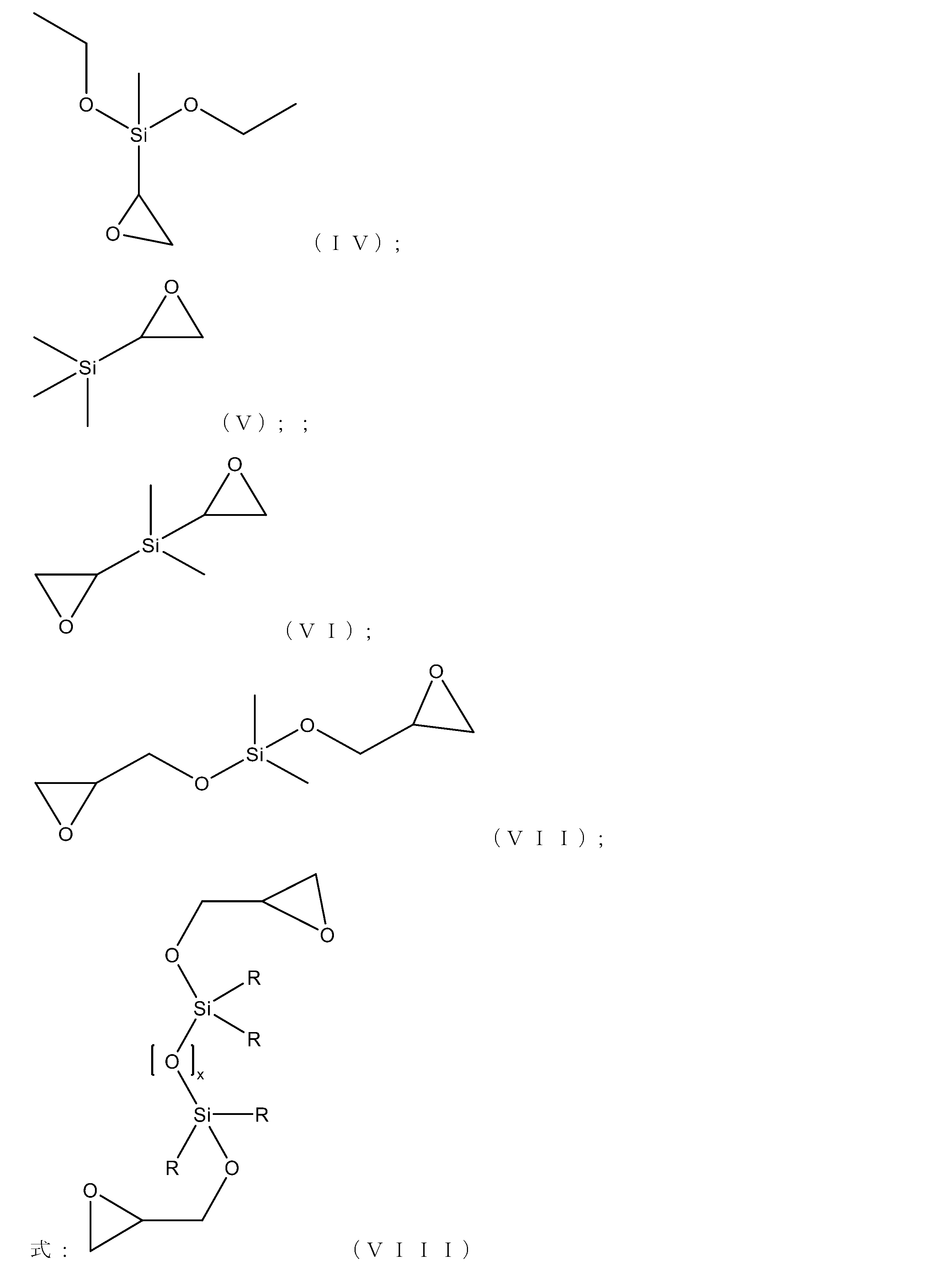
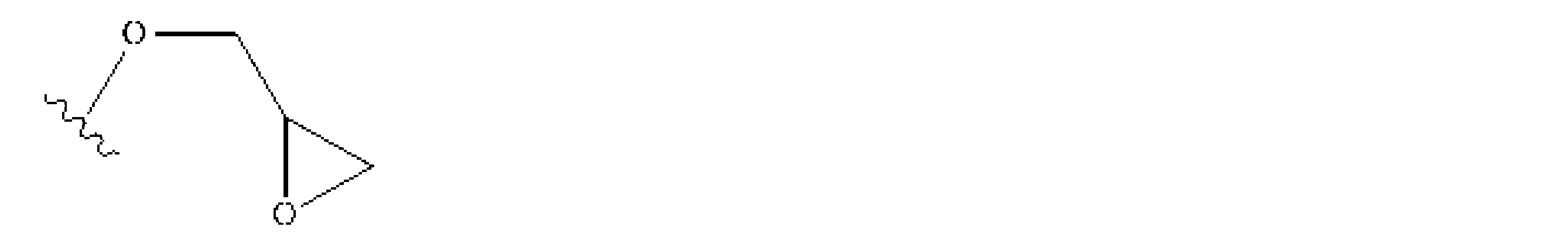
1つの実施形態では、「オキシラニルシラン」という用語は、少なくとも1つのエポキシ環が直接又はアルキル若しくはアルキルオキシ連結基を介して結合しているケイ素化合物を指す。このような化合物の例としては、以下

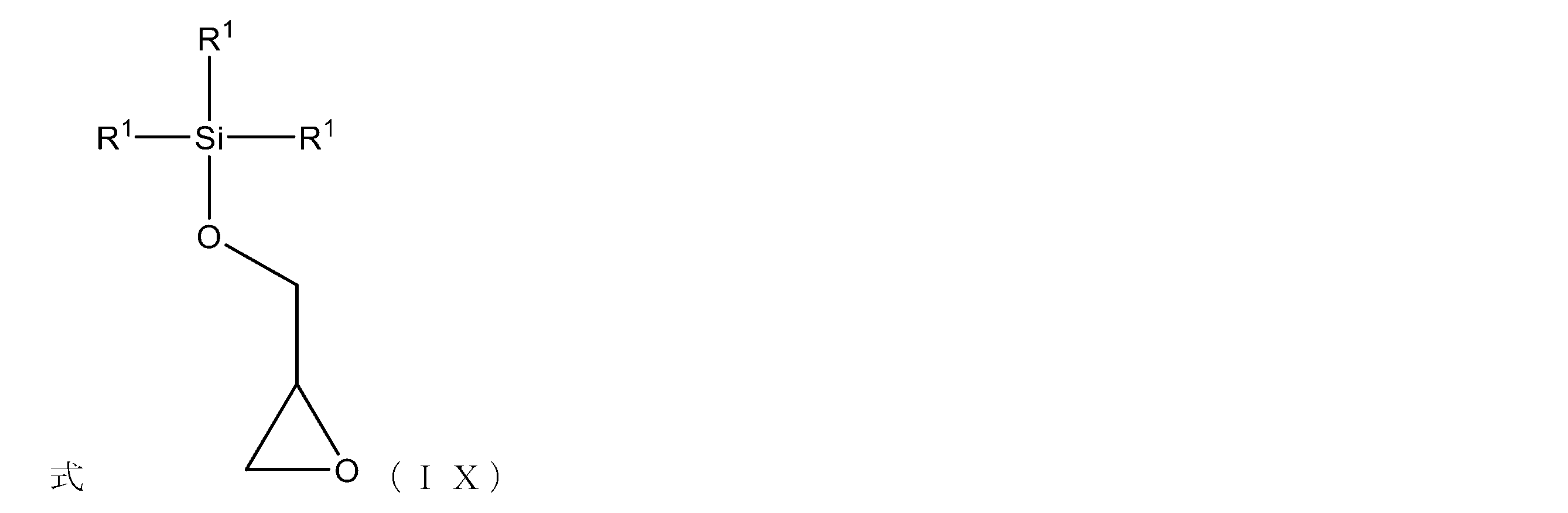
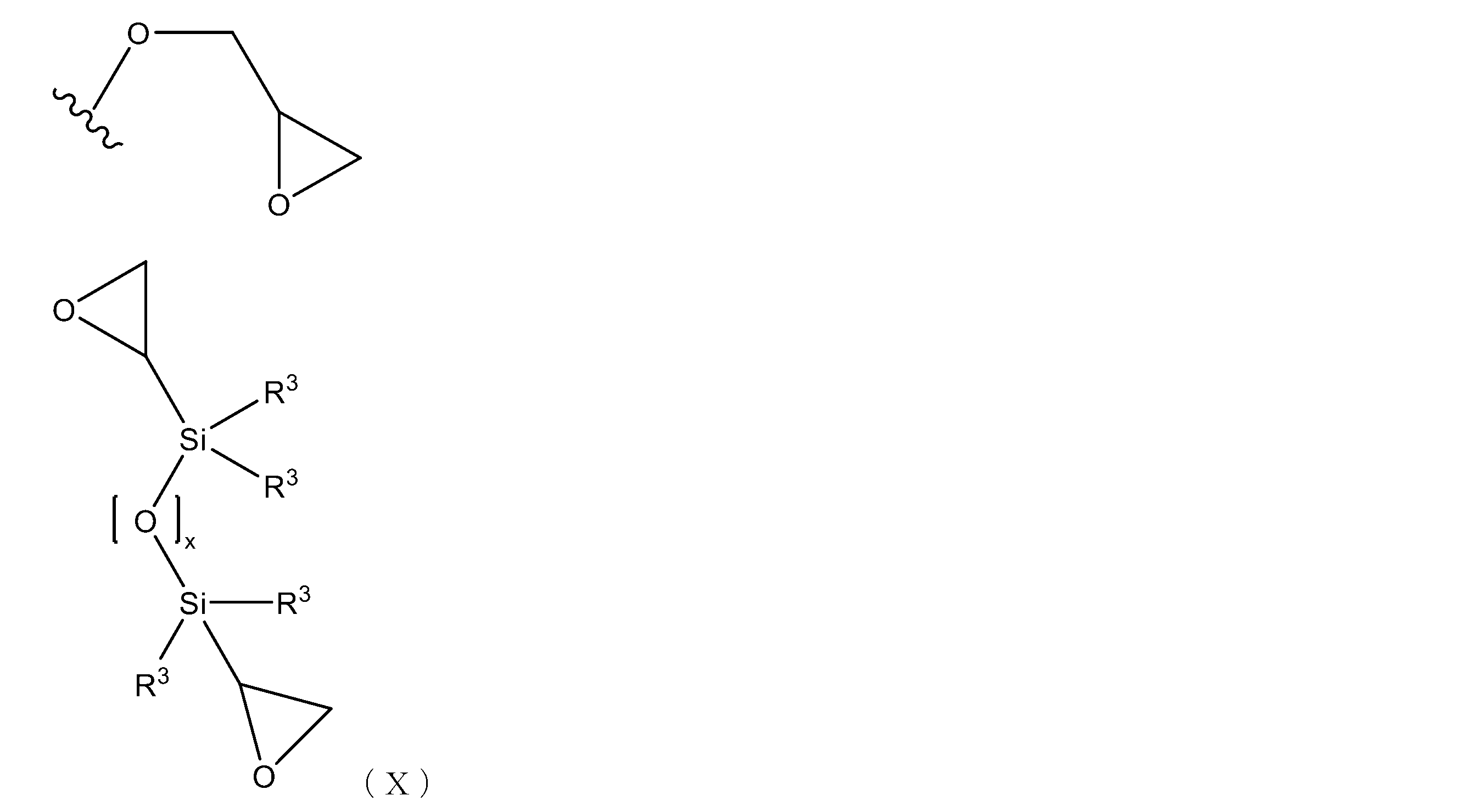

上記式(VIII)及び(X)において、xが0である場合、この構造は、二価の酸素原子が存在しないオキシラニルシラン化合物を示すと理解され、換言すれば、xが0である場合、構造はケイ素-ケイ素共有結合を示す。 In the above formulas (VIII) and (X), when x is 0, the structure is understood to represent an oxiranylsilane compound in which no divalent oxygen atom is present; in other words, when x is 0, the structure represents a silicon-silicon covalent bond.
さらに、C1~C4アルキルの例としては、メチル、エチル、プロピル、イソプロピル、n-ブチル、イソブチル、sec-ブチル、及びt-ブチルが挙げられる。1つの実施形態では、C1~C4アルキルはメチルである。 Further examples of C 1 -C 4 alkyl include methyl, ethyl, propyl, isopropyl, n-butyl, isobutyl, sec-butyl, and t-butyl, In one embodiment, C 1 -C 4 alkyl is methyl.
1つの実施形態では、上記式(VIII)において、各R1はメチルであり、別の実施形態では、各R1は、式

第2の態様では、本発明は、原子層堆積条件下で反応領域内のマイクロ電子デバイス表面上にシリコンオキシ炭窒化物膜を堆積させるための方法を提供し、この方法は:
a.以下から選択されるシリルアミン:

c.次に、前記反応領域内に以下から選択されるオキシラニルシラン


d.次に、前記反応領域を不活性ガスでパージすること;
e.次に、前記反応領域内にプラズマ形態の還元ガスを導入すること;
f.次に、前記反応領域を不活性ガスでパージすること;及び、所望の厚さの膜が堆積されるまで、工程a.~f.を繰り返すこと、を前記反応領域内に順次導入することを含む。
In a second aspect, the present invention provides a method for depositing a silicon oxycarbonitride film on a microelectronic device surface in a reaction region under atomic layer deposition conditions, the method comprising:
a. a silylamine selected from:
c. Then, in the reaction zone, an oxiranylsilane selected from the following:
d. then purging the reaction zone with an inert gas;
e. then introducing a reducing gas in the form of a plasma into said reaction region;
and repeating steps a.-f. sequentially into the reaction region until a film of a desired thickness is deposited.
第3の態様では、本発明は、原子層堆積条件下で反応領域内のマイクロ電子デバイス表面上にシリコンオキシ炭窒化物膜を堆積させるための方法を提供し、この方法は、以下:
a.以下から選択されるオキシラニルシラン:


b.次に、前記反応領域を不活性ガスでパージすること;
c.次に、前記反応領域内に以下から選択されるシリルアミン:

e.次に、前記反応領域内にプラズマ形態の還元ガスを導入すること;
f.次に、前記反応領域を不活性ガスでパージすること;及び、所望の厚さの膜が堆積されるまで、工程a.~f.を繰り返すこと、を前記反応領域内に順次導入すること含む。
In a third aspect, the present invention provides a method for depositing a silicon oxycarbonitride film on a microelectronic device surface in a reaction region under atomic layer deposition conditions, the method comprising:
a. an oxiranylsilane selected from:
b. then purging the reaction zone with an inert gas;
c. Then, in said reaction zone, a silylamine selected from:
e. then introducing a reducing gas in the form of a plasma into said reaction region;
and repeating steps a. through f. sequentially into the reaction region until a film of a desired thickness is deposited.
第4の態様では、本発明は、式

式中、各Rはメチルである。
In a fourth aspect, the present invention provides a compound of formula
wherein each R is methyl.
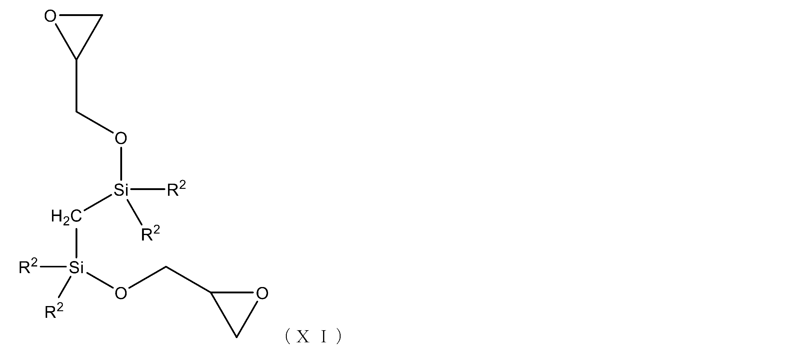
第5の態様では、本発明は、式

式中、
(i)各R2は、式
(ii)一方のR2は水素であり、他方のR2は式

In the formula,
(i) each R2 is a group of the formula
第4及び第5の態様の化合物は、ケイ素含有膜を形成するためのケイ素の蒸着における前駆体として有用である。 The compounds of the fourth and fifth aspects are useful as precursors in the deposition of silicon to form silicon-containing films.
一般に、本発明のシリルアミンは、対応するハロゲン化シリル化合物及び適切なアミンから調製することができる。例えば、参照により本明細書に組み込まれる米国特許第7,022,864号を参照されたい。 In general, the silyl amines of the present invention can be prepared from the corresponding silyl halide compound and an appropriate amine. See, for example, U.S. Pat. No. 7,022,864, which is incorporated herein by reference.
一般に、式(VIII)及び(X)の化合物は、式(VIII)の化合物の合成について示される以下の反応スキームに従って調製することができる:

一般に、xが0である式(VIII)の化合物は、クロロシランをトリエチルアミンの存在下で1,2-エポキシ-3-プロパノールと反応させて、対応するシリルエーテルを得ることによって調製することができる。 In general, compounds of formula (VIII) where x is 0 can be prepared by reacting a chlorosilane with 1,2-epoxy-3-propanol in the presence of triethylamine to give the corresponding silyl ether.
式IV、V、及びVIの化合物の合成は、Borovikらによる「Ethyleneoxide-Silane and Bridged Silane Precursors for Forming Low K Films(Borovik,A.;Xu,C.;Baum,T.;Bilodeau,S.;Roeder,J.;Ebbing,A.;Vestyck,D.)」に記載されている手順に従って調製できる。(参照により本明細書に組み込まれる米国特許第7,022,864号も参照されたい。)式VIの化合物及び式VIIIの他のグリシドキシシリルエステルの合成は、Martin,R.W.による「Epoxy-Substituted Esters of Silicon Acids and Their Preparation」に詳述されているように行うことができる。(参照により本明細書に組み込まれる米国特許第2,730,532号も参照されたい。)式(I)、(II)及び(III)の合成シリルアミン及びアミノジシランは、Wang,Z;Xu,C.;Hendrix,B.;Roeder,J.;Chen,T.;Baum,T.H.によって「Composition and Method for Low Temperature Chemical Vapor Deposition of Silicon-Containing Films including Silicon Carbonitride and Silicon Oxycarbonitride Films」、参照により本明細書に組み込まれる米国特許第9,102,693号に記載される方法によって調製することができる。 The synthesis of compounds of formula IV, V, and VI can be prepared according to the procedures described in "Ethyleneoxide-Silane and Bridged Silane Precursors for Forming Low K Films" by Borovik et al. (Borovik, A.; Xu, C.; Baum, T.; Bilodeau, S.; Roeder, J.; Ebbing, A.; Vestyck, D.). (See also U.S. Pat. No. 7,022,864, incorporated herein by reference.) The synthesis of compounds of formula VI and other glycidoxysilyl esters of formula VIII can be prepared according to the procedures described in Martin, R. W. The synthesis of silylamines and aminodisilanes of formulas (I), (II) and (III) can be carried out as detailed in "Epoxy-Substituted Esters of Silicon Acids and Their Preparation" by Wang, Z.; Xu, C.; Hendrix, B.; Roeder, J.; Chen, T.; Baum, T. H.; and the like. It can be prepared by the method described in "Composition and Method for Low Temperature Chemical Vapor Deposition of Silicon-Containing Films including Silicon Carbonitride and Silicon Oxycarbonite Films" by U.S. Pat. No. 9,102,693, which is incorporated herein by reference.
式(XI)の化合物は、以下のスキームに従って調製することができる:

1つの実施形態では、蒸着条件には、約250℃~約400℃の温度、及び約1~約20トール、又は約1~10トールの圧力が含まれる。別の実施形態では、蒸着条件には、約300°~約350℃の温度が含まれる。 In one embodiment, the deposition conditions include a temperature of about 250°C to about 400°C and a pressure of about 1 to about 20 Torr, or about 1 to about 10 Torr. In another embodiment, the deposition conditions include a temperature of about 300°C to about 350°C.
上記の化合物は、任意の好適なALD技術及びパルスプラズマ法によって高純度の薄いケイ素含有膜を形成するために使用することができる。そのような蒸着法を利用して、約350°~約550℃の堆積温度を用いてマイクロ電子デバイス上にケイ素含有膜を形成し、約20オングストローム~約200オングストロームの厚さを有する膜を形成することができる。 The above compounds can be used to form high purity thin silicon-containing films by any suitable ALD technique and pulsed plasma method. Such deposition methods can be used to form silicon-containing films on microelectronic devices using deposition temperatures of about 350° to about 550° C. to form films having thicknesses of about 20 Angstroms to about 200 Angstroms.
本発明の方法では、上記の化合物は、任意の好適な様式で、例えば、単一のウェハチャンバ内で、又は複数のウェハを含む炉内で、所望のマイクロ電子デバイス基板と反応させることができる。 In the methods of the present invention, the compounds described above can be reacted with the desired microelectronic device substrate in any suitable manner, for example, in a single wafer chamber or in a furnace containing multiple wafers.
あるいは、本発明の方法は、ALD様法として行うことができる。本明細書で使用される場合、「ALD又はALD様」という用語は、各反応物を単一ウェハALD反応器、セミバッチALD反応器、又はバッチ炉ALD反応器などの反応器に順次導入するか、又は各反応物を反応器の異なるセクションに基板を移動又は回転させることによって基板又はマイクロ電子デバイス表面に露出させ、各セクションを不活性ガスカーテン、すなわち空間ALD反応器又はロールツーロールALD反応器によって分離する方法を指す。 Alternatively, the method of the present invention can be carried out as an ALD-like method. As used herein, the term "ALD or ALD-like" refers to a method in which each reactant is exposed to the substrate or microelectronic device surface by sequentially introducing each reactant into a reactor, such as a single wafer ALD reactor, semi-batch ALD reactor, or batch furnace ALD reactor, or by moving or rotating the substrate to different sections of the reactor, and each section is separated by an inert gas curtain, i.e., a spatial ALD reactor or a roll-to-roll ALD reactor.
1つの実施形態では、本発明は、プラズマ形態の還元ガスと共に、本明細書に記載のシリルアミン及びオキシラニルシランを使用してシリコンオキシ炭窒化物膜を堆積させるためのプラズマ励起原子層堆積法(PEALD)に関する。窒素プラズマは、本明細書で教示されるように、シリルアミン及びオキシラニルシラン、並びにプラズマ形態の還元ガスを用いながら、より高い窒素原子百分率を有する膜を形成するのに有用であり得る。 In one embodiment, the present invention relates to a plasma-enhanced atomic layer deposition (PEALD) method for depositing silicon oxycarbonitride films using the silylamines and oxiranylsilanes described herein with a reducing gas in plasma form. Nitrogen plasma can be useful for forming films with a higher nitrogen atomic percentage while using silylamines and oxiranylsilanes and a reducing gas in plasma form as taught herein.
本明細書で使用する場合、用語「プラズマ形態の還元ガス」は、プラズマ形態の還元ガスが、水素(H2)、ヒドラジン(N2H4);メチルヒドラジン、t-ブチルヒドラジン、1,1-ジメチルヒドラジン及び1,2-ジメチルヒドラジンなどのC1~C4アルキルヒドラジンから選択されるガスで構成から構成され、N2、He又はArなどの不活性ガス単体又はH2と組み合わせて形成されるプラズマと組み合わせて用いられることを意味する。例えば、アルゴンなどの不活性ガスの連続流を用いながら、Rf磁場を開始し、その後水素を開始してプラズマH2を提供する。典型的には、用いられるプラズマ電力は、13.6Hzで約50~500ワットの範囲である。 As used herein, the term "reducing gas in plasma form" means that the reducing gas in plasma form consists of a gas selected from hydrogen ( H2 ), hydrazine ( N2H4 ); C1 - C4 alkyl hydrazines such as methylhydrazine, t-butylhydrazine, 1,1-dimethylhydrazine and 1,2-dimethylhydrazine , used in combination with a plasma formed with an inert gas such as N2 , He or Ar alone or in combination with H2 . For example, a continuous flow of an inert gas such as argon is used while an Rf magnetic field is initiated, followed by hydrogen to provide the plasma H2 . Typically, the plasma power used ranges from about 50 to 500 watts at 13.6 Hz.
特定の実施形態では、上記の反応物(すなわち、シリルアミン、オキシラニルシラン、及びプラズマ形態の還元ガス)のパルス時間(すなわち、基板への曝露の期間)は、約1~10秒の範囲である。パージ工程を用いる場合、持続時間は約1~10秒又は2~5秒である。他の実施形態では、各反応物のパルス時間は、約2~約5秒の範囲である。 In certain embodiments, the pulse times (i.e., duration of exposure to the substrate) of the above reactants (i.e., silylamine, oxiranylsilane, and reducing gas in plasma form) range from about 1 to 10 seconds. If a purge step is used, the duration is about 1 to 10 seconds or 2 to 5 seconds. In other embodiments, the pulse time of each reactant ranges from about 2 to about 5 seconds.
本明細書に開示される方法は、1つ以上のパージガスを含む。パージガスは、未消費の反応物及び/又は反応副生成物を除去するために使用され、前駆体と反応しない不活性ガスである。例示的なパージガスには、アルゴン、窒素、ヘリウム、ネオン、水素、及びそれらの混合物が含まれるが、これらに限定されない。特定の実施形態では、Arなどのパージガスは、約10~約2000sccmの範囲の流量で約0.1~1000秒間反応器に供給され、それによって反応器内に残留し得る未反応材料及び任意の副生成物がパージされる。 The methods disclosed herein include one or more purge gases. A purge gas is an inert gas that is used to remove unconsumed reactants and/or reaction by-products and does not react with the precursors. Exemplary purge gases include, but are not limited to, argon, nitrogen, helium, neon, hydrogen, and mixtures thereof. In certain embodiments, a purge gas, such as Ar, is supplied to the reactor at a flow rate ranging from about 10 to about 2000 sccm for about 0.1 to 1000 seconds, thereby purging unreacted materials and any by-products that may remain in the reactor.
シリルアミン及びオキシラニルシラン化合物、プラズマ形態の還元ガス、及び/又は他の前駆体、ソースガス、及び/又は試薬を供給するそれぞれの工程は、それらを供給するための順序を変更すること、及び/又は得られる誘電体膜の化学量論的組成を変更することによって実行され得る。 Each step of supplying the silylamine and oxiranylsilane compounds, the reducing gas in plasma form, and/or other precursors, source gases, and/or reagents may be performed by varying the order in which they are supplied and/or by varying the stoichiometric composition of the resulting dielectric film.
本発明の方法では、様々な反応物にエネルギーを印加して反応を誘発し、マイクロ電子デバイス基板上にシリコンオキシ炭窒化物膜を形成する。そのようなエネルギーは、熱、パルス熱、プラズマ、パルスプラズマ、高密度プラズマ、誘導結合プラズマ、リモートプラズマ法、及びそれらの組み合わせによって提供され得るが、これらに限定されない。特定の実施形態では、二次RF周波数源を使用して、基板表面のプラズマ特性を変更することができる。堆積がプラズマを伴う実施形態では、プラズマ生成法は、プラズマが反応器内で直接生成される直接プラズマ生成法、あるいは、プラズマが反応領域及び基板の「遠隔」で生成され、反応器内に供給される遠隔プラズマ生成法を含み得る。 In the method of the present invention, energy is applied to various reactants to induce reactions and form silicon oxycarbonitride films on microelectronic device substrates. Such energy may be provided by, but is not limited to, heat, pulsed heat, plasma, pulsed plasma, high density plasma, inductively coupled plasma, remote plasma techniques, and combinations thereof. In certain embodiments, a secondary RF frequency source may be used to modify the plasma characteristics at the substrate surface. In embodiments where deposition involves plasma, plasma generation techniques may include direct plasma generation techniques, where the plasma is generated directly in the reactor, or remote plasma generation techniques, where the plasma is generated "remote" to the reaction region and substrate and fed into the reactor.
本明細書で使用される場合、「マイクロ電子デバイス」という用語は、マイクロ電子、集積回路、又はコンピュータチップ用途で使用するために製造された、3D NAND構造、フラットパネルディスプレイ、及び微小電気機械システム(MEMS)などの半導体基板に対応する。「マイクロ電子デバイス」という用語は、いかなる意味でも限定するものではなく、負チャネル金属酸化膜半導体(nMOS)及び/又は正チャネル金属酸化膜半導体(pMOS)トランジスタを含み、最終的にマイクロ電子デバイス又はマイクロ電子アセンブリとなる任意の基板を含むことを理解されたい。そのようなマイクロ電子デバイスは、例えば、ケイ素、SiO2、Si3N4、OSG、FSG、炭化ケイ素、水素化炭化ケイ素、窒化ケイ素、水素化窒化ケイ素、炭窒化ケイ素、水素化炭窒化ケイ素、窒化ホウ素、反射防止コーティング、フォトレジスト、ゲルマニウム、ゲルマニウム含有、ホウ素含有、Ga/As、可撓性基板、多孔質無機材料、銅及びアルミニウムなどの金属、並びにTiN、Ti(C)N、TaN、Ta(C)N、Ta、W、又はWNなどであるがこれらに限定されない拡散バリア層から選択することができる少なくとも1つの基板を含む。膜は、例えば、化学機械平坦化(CMP)及び異方性エッチング法などの様々な後続の処理工程に適合する。 As used herein, the term "microelectronic device" corresponds to semiconductor substrates, such as 3D NAND structures, flat panel displays, and microelectromechanical systems (MEMS), that are fabricated for use in microelectronic, integrated circuit, or computer chip applications. It should be understood that the term "microelectronic device" is not intended to be limiting in any way and includes any substrate that contains negative channel metal oxide semiconductor (nMOS) and/or positive channel metal oxide semiconductor (pMOS) transistors and that ultimately becomes a microelectronic device or microelectronic assembly. Such microelectronic devices include at least one substrate that may be selected from , for example, silicon, SiO2 , Si3N4 , OSG, FSG, silicon carbide, hydrogenated silicon carbide, silicon nitride, hydrogenated silicon nitride, silicon carbonitride, hydrogenated silicon carbonitride, boron nitride, anti-reflective coatings, photoresists, germanium, germanium-containing, boron-containing, Ga/As, flexible substrates, porous inorganic materials, metals such as copper and aluminum, and diffusion barrier layers such as, but not limited to, TiN, Ti(C)N, TaN, Ta(C)N, Ta, W, or WN. The films are compatible with a variety of subsequent processing steps, such as, for example, chemical mechanical planarization (CMP) and anisotropic etching methods.
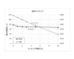
これらの膜は、ウェットエッチング剤及びO2プラズマに対して低い耐エッチング性を提供する。O2プラズマアッシング法は、340℃及び3トールの圧力で1分間、500sccmのO2流量及び100、250及び400Wのプラズマ出力で行った。これに関して、図3を参照すると、本発明は別の態様において、100ワットで60秒間酸素プラズマに曝露された際に窒化ケイ素基準試料に対してわずか約4オングストロームのアッシング損傷差を示すシリコンオキシ炭窒化物膜を提供する。別の実施形態では、本発明は、100ワットで60秒間酸素プラズマに曝露された際に、窒化ケイ素基準試料に対してわずか約4オングストロームのアッシング損傷差を示すシリコンオキシ炭窒化物膜を堆積させたマイクロ電子デバイスを提供する。 These films provide low etch resistance to wet etchants and O2 plasma. The O2 plasma ashing process was performed at 340° C. and 3 Torr pressure for 1 minute with an O2 flow rate of 500 sccm and plasma powers of 100, 250 and 400 W. In this regard, and with reference to FIG. 3, the present invention in another aspect provides a silicon oxycarbonitride film that exhibits an ashing damage difference of only about 4 Angstroms relative to a silicon nitride reference sample when exposed to an oxygen plasma at 100 watts for 60 seconds. In another embodiment, the present invention provides a microelectronic device having deposited thereon a silicon oxycarbonitride film that exhibits an ashing damage difference of only about 4 Angstroms relative to a silicon nitride reference sample when exposed to an oxygen plasma at 100 watts for 60 seconds.
上記のように、特定の実施形態では、本発明のシリコンオキシ炭窒化物(SiCON)膜は、約15~約25原子百分率の窒素及び約12原子百分率の炭素を有する。本発明の方法を用いて、約3.5未満の誘電率(k)を有するそのようなSiCON膜を調製することができる。他の実施形態では、そのようなSiCON膜の誘電率は、約2.5~約4.0である。 As noted above, in certain embodiments, silicon oxycarbonitride (SiCON) films of the present invention have about 15 to about 25 atomic percent nitrogen and about 12 atomic percent carbon. Using the methods of the present invention, such SiCON films can be prepared having a dielectric constant (k) of less than about 3.5. In other embodiments, the dielectric constant of such SiCON films is about 2.5 to about 4.0.
一般に、このようにして調製されたSiCON膜の所望の厚さは、約20Å~約200Åである。 Typically, the desired thickness of a SiCON film prepared in this manner is about 20 Å to about 200 Å.
シリルアミンとオキシラニルシラン前駆体との間の相互作用、及びその後のH2プラズマとの反応を介した窒素による低kSiCO膜のドーピングは、得られるSiCON膜の耐ウェットエッチング性及び耐O2プラズマアッシング性を劇的に改善する。 Doping of low-k SiCO films with nitrogen via the interaction between silylamine and oxiranylsilane precursors and subsequent reaction with H2 plasma dramatically improves the wet etch and O2 plasma ashing resistance of the resulting SiCON films.
本発明の方法において、オキシラニルシランの供給速度は、PEALDサイクル当たり約10~100mgであり、シリルアミンについてはPEALDサイクル当たり約5~50mgであり得る。 In the method of the present invention, the feed rate of oxiranylsilane can be about 10-100 mg per PEALD cycle, and for silylamine, about 5-50 mg per PEALD cycle.
本発明は、その特定の実施形態の以下の実施例によってさらに説明することができるが、これらの実施例は単に例示の目的で含まれ、特に明記しない限り本発明の範囲を限定することを意図しないことが理解されよう。 The present invention can be further illustrated by the following examples of specific embodiments thereof, although it will be understood that these examples are included for illustrative purposes only and are not intended to limit the scope of the invention unless specifically stated.
実施例1
ビス(グリシドキシ)テトラメチルジシラン(VIII、式中、x=0及びR=CH3)の合成
100mLの丸底フラスコに、トリエチルアミン(3.21g、31.8mmol)及び(オキシラン-2-イル)メタノール(1.62g、21.7mmol)を投入し、次いで、ヘキサン(20mL)で希釈した。容器にゴム隔壁を取り付け、グローブボックスから移した。PTFEコーティングされた熱電対を隔壁を通して挿入し、濁った溶液をブライン浴で-11℃に冷却した。1,2-ジクロロ-1,1,2,2-テトラメチルジシラン(2.00g、10.6mmol)の10mL無水ヘキサンの溶液を、シリンジを介して12分かけて滴下した。わずかな発熱が認められ、濃厚な白色沈殿物が形成された。反応混合物を0℃で2.5時間撹拌し、次いで常温まで加温した。反応混合物を10マイクロメートルのフィルターで濾過し、得られた溶液を40トール及び常温で溶媒を除去した。沈殿物を含む濃厚な無色の油状物が得られた。反応混合物を減圧下で3時間維持して、トリエチルアミンを完全に除去した。次いで、残留物を最小量のペンタン中に取り、0.4マイクロメートルのシリンジフィルターで濾過した。次いで、ペンタンを減圧下(40トール)で除去した。濁った無色の油状物を減圧下(0.100~0.200トール)で蒸留して、合計収率が44%である2つの画分を得た(1H NMRによるジアステレオマーの純度95%の混合物)。1H NMR(C6D6):δ3.87-3.71(ddd,2H)、3.61-3.45(ddd,2H)、3.02-2.96(m,2H)、2.67-2.64(dd,2H)、2.54-2.49(dd,2H)、0.15(s,12H)、0.06(s,12H)。
Example 1
Synthesis of bis(glycidoxy)tetramethyldisilane (VIII, where x=0 and R=CH 3 ). A 100 mL round bottom flask was charged with triethylamine (3.21 g, 31.8 mmol) and (oxiran-2-yl)methanol (1.62 g, 21.7 mmol) then diluted with hexanes (20 mL). The vessel was fitted with a rubber septum and removed from the glove box. A PTFE coated thermocouple was inserted through the septum and the cloudy solution was cooled to −11° C. in a brine bath. A solution of 1,2-dichloro-1,1,2,2-tetramethyldisilane (2.00 g, 10.6 mmol) in 10 mL anhydrous hexanes was added dropwise via syringe over 12 minutes. A slight exotherm was noted and a thick white precipitate formed. The reaction mixture was stirred at 0° C. for 2.5 hours and then allowed to warm to ambient temperature. The reaction mixture was filtered through a 10 micrometer filter and the resulting solution was stripped of solvent at 40 Torr and ambient temperature. A thick colorless oil with a precipitate was obtained. The reaction mixture was kept under reduced pressure for 3 hours to completely remove triethylamine. The residue was then taken up in a minimum amount of pentane and filtered through a 0.4 micrometer syringe filter. The pentane was then removed under reduced pressure (40 Torr). The cloudy colorless oil was distilled under reduced pressure (0.100-0.200 Torr) to give two fractions with a combined yield of 44% (mixture of diastereomeric purity 95% by 1 H NMR). 1H NMR (C6D6): δ 3.87-3.71 (ddd, 2H), 3.61-3.45 (ddd, 2H), 3.02-2.96 (m, 2H), 2.67-2.64 (dd, 2H), 2.54-2.49 (dd, 2H), 0.15 (s, 12H), 0.06 (s, 12H).
PEALD SiCON堆積は、改良されたASM(登録商標)PEALDシステムを使用して、サセプタ温度400℃、シャワーヘッド温度170℃、チャンバ圧力3トール、及び周囲不活性ガス流量500sccmで行われた。堆積中のクーポン温度は約340℃であった。 PEALD SiCON deposition was performed using a modified ASM® PEALD system with a susceptor temperature of 400°C, showerhead temperature of 170°C, chamber pressure of 3 Torr, and ambient inert gas flow rate of 500 sccm. The coupon temperature during deposition was approximately 340°C.
シャワーヘッドとサセプタ/ウェハとの間にプラズマを生成する直接プラズマシステムを使用して、水素プラズマ生成した。プラズマ出力は、150~500Wの範囲であった。プラズマパルス時間は、5~45秒の範囲であった。 Hydrogen plasma was generated using a direct plasma system that generates the plasma between the showerhead and the susceptor/wafer. Plasma power ranged from 150 to 500 W. Plasma pulse times ranged from 5 to 45 seconds.
SiCONのPEALDにおけるパルススキームは、以下からなる:
1.シリルアミンパルス(1~5秒)
2.不活性ガスパージ(10秒)
3.オキシラニルシラン又はビニルシランパルス(1~10秒)
4.不活性ガスパージ(10秒)
5.H2プラズマパルス(5~45秒)
6.不活性ガスパージ(5~10秒)
The pulse scheme for PEALD of SiCON consists of:
1. Silylamine pulse (1-5 seconds)
2. Inert gas purge (10 seconds)
3. Oxiranylsilane or vinylsilane pulse (1 to 10 seconds)
4. Inert gas purge (10 seconds)
5. H2 plasma pulse (5-45 seconds)
6. Inert gas purge (5 to 10 seconds)
以下のデータからわかるように、窒素をドープすることにより、SiCON膜の耐エッチング性及び耐アッシング性が飛躍的に向上し、SiCON膜の誘電率を3.5未満とすることが可能となった。 As can be seen from the data below, by doping with nitrogen, the etching resistance and ashing resistance of the SiCON film are dramatically improved, making it possible to reduce the dielectric constant of the SiCON film to less than 3.5.

注:HEADS前駆体は、約15~25原子百分率の窒素ドーピングをSiCON膜に提供する。

HEADS=ヘキサ(エチルアミノ)ジシラン
DMDORS=ジメチルジオキシラニルシラン
TMORS=トリメチルオキシラニルシラン
DEOMORS=ジエトキシメチルオキシラニルシラン
HEADS = hexa(ethylamino)disilane DMDORS = dimethyldioxiranylsilane TMORS = trimethyloxiranylsilane DEOMORS = diethoxymethyloxiranylsilane
このように本開示のいくつかの例示的な実施形態を説明してきたが、当業者は、添付の特許請求の範囲内でさらに他の実施形態を作成及び使用することができることを容易に理解するであろう。本文書が対象とする開示の数多くの利点は、前述の説明に記載されている。しかしながら、本開示は、多くの点で例示にすぎないことが理解されよう。本開示の範囲を超えることなく、変更を詳細に行うことができる。本開示の範囲は、当然のことながら、添付の特許請求の範囲が表現される言語で定義される。
Having thus described several exemplary embodiments of the present disclosure, those skilled in the art will readily appreciate that still other embodiments may be made and used within the scope of the appended claims. Numerous advantages of the disclosure to which this document is directed have been set forth in the foregoing description. It will be understood, however, that the disclosure is in many respects merely illustrative. Changes may be made in detail without departing from the scope of the present disclosure. The scope of the present disclosure is, of course, to be defined in the language in which the appended claims are expressed.
Claims (5)


の基から選択される。)の化合物;及び
and
a.以下から選択されるシリルアミン:

b.次に、前記反応領域を不活性ガスでパージすること;
c.次に、前記反応領域内に以下から選択されるオキシラニルシラン


d.次に、前記反応領域を不活性ガスでパージすること;
e.次に、前記反応領域内にプラズマ形態の還元ガスを導入すること;
f.次に、前記反応領域を不活性ガスでパージすること;及び、所望の厚さの膜が堆積されるまで、工程a.~f.を繰り返すこと、を含む方法。 1. A method for depositing a silicon oxycarbonitride film on a microelectronic device surface in a reaction region under atomic layer deposition conditions, comprising:
a. a silylamine selected from:
c. Then, in the reaction zone, an oxiranylsilane selected from the following:
d. then purging the reaction zone with an inert gas;
e. then introducing a reducing gas in the form of a plasma into said reaction region;
f. then purging the reaction region with an inert gas; and repeating steps a.-f. until a film of desired thickness is deposited.
a.以下から選択されるオキシラニルシラン


b.次に、前記反応領域を不活性ガスでパージすること;
c.次に、前記反応領域内に以下から選択されるシリルアミン:

d.次に、前記反応領域を不活性ガスでパージすること;
e.次に、前記反応領域内にプラズマ形態の還元ガスを導入すること;
f.次に、前記反応領域を不活性ガスでパージすること;及び、所望の厚さの膜が堆積されるまで、工程a.~f.を繰り返すこと、を含む、方法。 1. A method for depositing a silicon oxycarbonitride film on a microelectronic device surface in a reaction region under atomic layer deposition conditions, comprising:
a. an oxiranylsilane selected from the following:
b. then purging the reaction zone with an inert gas;
c. Then, in said reaction zone, a silylamine selected from:
d. then purging the reaction zone with an inert gas;
e. then introducing a reducing gas in the form of a plasma into said reaction region;
f. then purging the reaction region with an inert gas; and repeating steps a.-f. until a film of desired thickness is deposited.
Applications Claiming Priority (3)
| Application Number | Priority Date | Filing Date | Title |
|---|---|---|---|
| US16/899,060 | 2020-06-11 | ||
| US16/899,060 US11466038B2 (en) | 2020-06-11 | 2020-06-11 | Vapor deposition precursor compounds and process of use |
| PCT/US2021/036856 WO2021252788A1 (en) | 2020-06-11 | 2021-06-10 | Vapor deposition precursor compounds and process of use |
Publications (2)
| Publication Number | Publication Date |
|---|---|
| JP2023529205A JP2023529205A (en) | 2023-07-07 |
| JP7463563B2 true JP7463563B2 (en) | 2024-04-08 |
Family
ID=78824498
Family Applications (1)
| Application Number | Title | Priority Date | Filing Date |
|---|---|---|---|
| JP2022575943A Active JP7463563B2 (en) | 2020-06-11 | 2021-06-10 | Vapor Deposition Precursor Compounds and Processes of Use |
Country Status (7)
| Country | Link |
|---|---|
| US (2) | US11466038B2 (en) |
| EP (1) | EP4165226A4 (en) |
| JP (1) | JP7463563B2 (en) |
| KR (1) | KR102819030B1 (en) |
| CN (1) | CN115768919B (en) |
| TW (1) | TWI817139B (en) |
| WO (1) | WO2021252788A1 (en) |
Families Citing this family (3)
| Publication number | Priority date | Publication date | Assignee | Title |
|---|---|---|---|---|
| US11466038B2 (en) * | 2020-06-11 | 2022-10-11 | Entegris, Inc. | Vapor deposition precursor compounds and process of use |
| US12031205B2 (en) * | 2021-11-30 | 2024-07-09 | Asm Ip Holding B.V. | Method and system for forming a conformal silicon carbon nitride layer and structure formed using same |
| WO2024086199A1 (en) * | 2022-10-19 | 2024-04-25 | Entegris, Inc. | Silane precursors and related methods |
Citations (3)
| Publication number | Priority date | Publication date | Assignee | Title |
|---|---|---|---|---|
| US7022864B2 (en) | 2003-07-15 | 2006-04-04 | Advanced Technology Materials, Inc. | Ethyleneoxide-silane and bridged silane precursors for forming low k films |
| JP2011511881A (en) | 2007-06-28 | 2011-04-14 | アドバンスド テクノロジー マテリアルズ,インコーポレイテッド | Precursor for silicon dioxide gap filler |
| US20170186603A1 (en) | 2015-12-28 | 2017-06-29 | Samsung Electronics Co., Ltd. | METHOD OF FORMING SiOCN MATERIAL LAYER AND METHOD OF FABRICATING SEMICONDUCTOR DEVICE |
Family Cites Families (15)
| Publication number | Priority date | Publication date | Assignee | Title |
|---|---|---|---|---|
| US2730532A (en) | 1953-07-20 | 1956-01-10 | Shell Dev | Epoxy-substituted esters of silicon acids and their preparation |
| EP1436018A1 (en) * | 2001-09-26 | 2004-07-14 | THE GOVERNMENT OF THE UNITED STATES OF AMERICA, as represented by THE SECRETARY, DEPARTMENT OF HEALTH AND HUMAN SERVICES | Nitric oxide-releasing coated medical devices and method of preparing same |
| US7601860B2 (en) | 2003-10-10 | 2009-10-13 | Advanced Technology Materials, Inc. | Composition and method for low temperature chemical vapor deposition of silicon-containing films including silicon carbonitride and silicon oxycarbonitride films |
| US7345000B2 (en) * | 2003-10-10 | 2008-03-18 | Tokyo Electron Limited | Method and system for treating a dielectric film |
| CN101723963A (en) | 2009-11-27 | 2010-06-09 | 北京化工大学 | Organic silicon epoxy resin and preparation method thereof |
| US8703625B2 (en) * | 2010-02-04 | 2014-04-22 | Air Products And Chemicals, Inc. | Methods to prepare silicon-containing films |
| US20110206857A1 (en) | 2010-02-25 | 2011-08-25 | Applied Materials, Inc. | Ultra low dielectric materials using hybrid precursors containing silicon with organic functional groups by plasma-enhanced chemical vapor deposition |
| JP5699980B2 (en) | 2011-06-16 | 2015-04-15 | 東京エレクトロン株式会社 | Film forming method and film forming apparatus |
| KR101252063B1 (en) * | 2011-08-25 | 2013-04-12 | 한국생산기술연구원 | Epoxy Compound Having Alkoxysilyl Group, Preparing Method Thereof, Composition Comprising the Same and Cured Product and Use Thereof |
| US10804094B2 (en) | 2016-05-06 | 2020-10-13 | Applied Materials, Inc. | Methods of depositing SiCON with C, O and N compositional control |
| US9786492B2 (en) * | 2015-11-12 | 2017-10-10 | Asm Ip Holding B.V. | Formation of SiOCN thin films |
| EP3290457A1 (en) * | 2016-08-30 | 2018-03-07 | HILTI Aktiengesellschaft | Dual component mortar composition and its use |
| KR102312827B1 (en) | 2017-08-08 | 2021-10-13 | 어플라이드 머티어리얼스, 인코포레이티드 | Methods and apparatus for deposition of low-K films |
| SG10201903201XA (en) * | 2018-04-11 | 2019-11-28 | Versum Materials Us Llc | Organoamino-functionalized cyclic oligosiloxanes for deposition of silicon-containing films |
| US11466038B2 (en) * | 2020-06-11 | 2022-10-11 | Entegris, Inc. | Vapor deposition precursor compounds and process of use |
-
2020
- 2020-06-11 US US16/899,060 patent/US11466038B2/en active Active
-
2021
- 2021-06-10 JP JP2022575943A patent/JP7463563B2/en active Active
- 2021-06-10 KR KR1020237000668A patent/KR102819030B1/en active Active
- 2021-06-10 EP EP21823021.7A patent/EP4165226A4/en active Pending
- 2021-06-10 CN CN202180040494.4A patent/CN115768919B/en active Active
- 2021-06-10 WO PCT/US2021/036856 patent/WO2021252788A1/en not_active Ceased
- 2021-06-11 TW TW110121550A patent/TWI817139B/en active
-
2022
- 2022-09-01 US US17/901,569 patent/US12209105B2/en active Active
Patent Citations (3)
| Publication number | Priority date | Publication date | Assignee | Title |
|---|---|---|---|---|
| US7022864B2 (en) | 2003-07-15 | 2006-04-04 | Advanced Technology Materials, Inc. | Ethyleneoxide-silane and bridged silane precursors for forming low k films |
| JP2011511881A (en) | 2007-06-28 | 2011-04-14 | アドバンスド テクノロジー マテリアルズ,インコーポレイテッド | Precursor for silicon dioxide gap filler |
| US20170186603A1 (en) | 2015-12-28 | 2017-06-29 | Samsung Electronics Co., Ltd. | METHOD OF FORMING SiOCN MATERIAL LAYER AND METHOD OF FABRICATING SEMICONDUCTOR DEVICE |
Also Published As
| Publication number | Publication date |
|---|---|
| WO2021252788A1 (en) | 2021-12-16 |
| EP4165226A1 (en) | 2023-04-19 |
| JP2023529205A (en) | 2023-07-07 |
| KR102819030B1 (en) | 2025-06-12 |
| CN115768919A (en) | 2023-03-07 |
| CN115768919B (en) | 2025-04-18 |
| KR20230022971A (en) | 2023-02-16 |
| TW202205431A (en) | 2022-02-01 |
| US20230041086A1 (en) | 2023-02-09 |
| US12209105B2 (en) | 2025-01-28 |
| EP4165226A4 (en) | 2024-10-30 |
| US11466038B2 (en) | 2022-10-11 |
| US20210388008A1 (en) | 2021-12-16 |
| TWI817139B (en) | 2023-10-01 |
Similar Documents
| Publication | Publication Date | Title |
|---|---|---|
| TWI774299B (en) | Precursors and methods for preparing silicon-containing films | |
| JP7463563B2 (en) | Vapor Deposition Precursor Compounds and Processes of Use | |
| JP7661455B2 (en) | Silicon hydrazide precursor compounds | |
| TWI857271B (en) | High throughput deposition process | |
| TWI830206B (en) | Silicon precursor compounds and method for forming silicon-containing films |
Legal Events
| Date | Code | Title | Description |
|---|---|---|---|
| A521 | Request for written amendment filed |
Free format text: JAPANESE INTERMEDIATE CODE: A523 Effective date: 20230217 |
|
| A621 | Written request for application examination |
Free format text: JAPANESE INTERMEDIATE CODE: A621 Effective date: 20230217 |
|
| TRDD | Decision of grant or rejection written | ||
| A01 | Written decision to grant a patent or to grant a registration (utility model) |
Free format text: JAPANESE INTERMEDIATE CODE: A01 Effective date: 20240227 |
|
| A977 | Report on retrieval |
Free format text: JAPANESE INTERMEDIATE CODE: A971007 Effective date: 20240229 |
|
| A61 | First payment of annual fees (during grant procedure) |
Free format text: JAPANESE INTERMEDIATE CODE: A61 Effective date: 20240327 |
|
| R150 | Certificate of patent or registration of utility model |
Ref document number: 7463563 Country of ref document: JP Free format text: JAPANESE INTERMEDIATE CODE: R150 |