JP7449052B2 - Input devices, methods and processing systems - Google Patents
Input devices, methods and processing systems Download PDFInfo
- Publication number
- JP7449052B2 JP7449052B2 JP2019146047A JP2019146047A JP7449052B2 JP 7449052 B2 JP7449052 B2 JP 7449052B2 JP 2019146047 A JP2019146047 A JP 2019146047A JP 2019146047 A JP2019146047 A JP 2019146047A JP 7449052 B2 JP7449052 B2 JP 7449052B2
- Authority
- JP
- Japan
- Prior art keywords
- chip
- master
- slave
- signal
- sensing
- Prior art date
- Legal status (The legal status is an assumption and is not a legal conclusion. Google has not performed a legal analysis and makes no representation as to the accuracy of the status listed.)
- Active
Links
- 238000000034 method Methods 0.000 title claims description 28
- 238000012545 processing Methods 0.000 title description 52
- 230000003111 delayed effect Effects 0.000 claims description 9
- 230000001360 synchronised effect Effects 0.000 claims description 9
- 230000000737 periodic effect Effects 0.000 claims description 6
- 238000004891 communication Methods 0.000 claims description 3
- 230000005540 biological transmission Effects 0.000 claims 1
- 238000010586 diagram Methods 0.000 description 25
- 238000005259 measurement Methods 0.000 description 20
- 230000000630 rising effect Effects 0.000 description 20
- 230000008878 coupling Effects 0.000 description 17
- 238000010168 coupling process Methods 0.000 description 17
- 238000005859 coupling reaction Methods 0.000 description 17
- 239000000758 substrate Substances 0.000 description 15
- 230000008859 change Effects 0.000 description 9
- 239000011521 glass Substances 0.000 description 6
- 230000001934 delay Effects 0.000 description 5
- 230000005684 electric field Effects 0.000 description 5
- 230000006870 function Effects 0.000 description 5
- 230000007704 transition Effects 0.000 description 5
- 238000005516 engineering process Methods 0.000 description 4
- 230000008569 process Effects 0.000 description 4
- 230000003213 activating effect Effects 0.000 description 3
- 230000000694 effects Effects 0.000 description 3
- 230000002093 peripheral effect Effects 0.000 description 3
- 230000004044 response Effects 0.000 description 3
- 230000003247 decreasing effect Effects 0.000 description 2
- 238000005401 electroluminescence Methods 0.000 description 2
- 238000001914 filtration Methods 0.000 description 2
- 230000001939 inductive effect Effects 0.000 description 2
- 230000007246 mechanism Effects 0.000 description 2
- 230000003287 optical effect Effects 0.000 description 2
- 238000012546 transfer Methods 0.000 description 2
- WGCNASOHLSPBMP-UHFFFAOYSA-N Glycolaldehyde Chemical compound OCC=O WGCNASOHLSPBMP-UHFFFAOYSA-N 0.000 description 1
- 241000699670 Mus sp. Species 0.000 description 1
- 230000001133 acceleration Effects 0.000 description 1
- 230000004913 activation Effects 0.000 description 1
- 230000003750 conditioning effect Effects 0.000 description 1
- 238000001514 detection method Methods 0.000 description 1
- 230000007613 environmental effect Effects 0.000 description 1
- 239000012212 insulator Substances 0.000 description 1
- 230000010354 integration Effects 0.000 description 1
- 230000001788 irregular Effects 0.000 description 1
- 239000004973 liquid crystal related substance Substances 0.000 description 1
- 239000000463 material Substances 0.000 description 1
- 238000009877 rendering Methods 0.000 description 1
- 230000003252 repetitive effect Effects 0.000 description 1
- 125000006850 spacer group Chemical group 0.000 description 1
- 230000026676 system process Effects 0.000 description 1
- 239000012780 transparent material Substances 0.000 description 1
- 230000000007 visual effect Effects 0.000 description 1
Images


Classifications
-
- G—PHYSICS
- G06—COMPUTING; CALCULATING OR COUNTING
- G06F—ELECTRIC DIGITAL DATA PROCESSING
- G06F1/00—Details not covered by groups G06F3/00 - G06F13/00 and G06F21/00
- G06F1/04—Generating or distributing clock signals or signals derived directly therefrom
- G06F1/12—Synchronisation of different clock signals provided by a plurality of clock generators
-
- G—PHYSICS
- G06—COMPUTING; CALCULATING OR COUNTING
- G06F—ELECTRIC DIGITAL DATA PROCESSING
- G06F15/00—Digital computers in general; Data processing equipment in general
- G06F15/16—Combinations of two or more digital computers each having at least an arithmetic unit, a program unit and a register, e.g. for a simultaneous processing of several programs
- G06F15/163—Interprocessor communication
-
- G—PHYSICS
- G06—COMPUTING; CALCULATING OR COUNTING
- G06F—ELECTRIC DIGITAL DATA PROCESSING
- G06F3/00—Input arrangements for transferring data to be processed into a form capable of being handled by the computer; Output arrangements for transferring data from processing unit to output unit, e.g. interface arrangements
- G06F3/01—Input arrangements or combined input and output arrangements for interaction between user and computer
- G06F3/03—Arrangements for converting the position or the displacement of a member into a coded form
- G06F3/041—Digitisers, e.g. for touch screens or touch pads, characterised by the transducing means
- G06F3/0412—Digitisers structurally integrated in a display
Landscapes
- Engineering & Computer Science (AREA)
- Theoretical Computer Science (AREA)
- General Engineering & Computer Science (AREA)
- Physics & Mathematics (AREA)
- General Physics & Mathematics (AREA)
- Computer Hardware Design (AREA)
- Human Computer Interaction (AREA)
- Software Systems (AREA)
- Position Input By Displaying (AREA)
- Control Of Indicators Other Than Cathode Ray Tubes (AREA)
Description
ここで開示される実施形態は一般には電子機器に関し、より具体的には、複数の集積回路チップを同期させることに関する。 TECHNICAL FIELD Embodiments disclosed herein relate generally to electronic equipment, and more specifically to synchronizing multiple integrated circuit chips.
近接センサー装置を含む入力装置は様々な電子システムで使用される場合がある。近接センサー装置は表面で区切られたセンシング領域を含む場合がある。近接センサー装置はセンシング領域の中で1又は複数の入力物体の存在、及び/又は、位置、力、運動を決定する。近接センサー装置は電子システムのインターフェースを提供するために用いられる場合がある。近接センサー装置は、例えばノートブックやデスクトップのコンピューターに内蔵された又はその周辺機器のタッチパッドのように、より大規模なコンピューターシステムの入力装置として用いられる場合がある。近接センサー装置は、携帯電話や車両(例えば自動車)に組み込まれたタッチスクリーンといったように、より小さいコンピューターシステムでもしばしば用いられる場合がある。 Input devices including proximity sensor devices may be used in a variety of electronic systems. The proximity sensor device may include a sensing area delimited by a surface. A proximity sensor device determines the presence and/or position, force, and movement of one or more input objects within a sensing region. Proximity sensor devices may be used to provide an interface to electronic systems. Proximity sensor devices may be used as input devices in larger computer systems, such as touch pads built into or peripheral to notebook or desktop computers. Proximity sensor devices may also often be used in smaller computer systems, such as mobile phones and touch screens built into vehicles (eg, cars).
一実施形態では、入力装置は複数のセンサー電極と、マスター集積回路(IC)チップと、第1のスレーブICチップと、を備える。マスター集積回路(IC)チップは複数のセンサー電極と通信可能に接続され、垂直タイミング信号と、水平タイミング信号と、を生成し、1又は複数のセンシングバーストを含む第1のセンシング信号によって複数のセンサー電極を駆動することで、垂直タイミング信号と水平タイミング信号とのうち少なくとも一つに基づいて、第1の容量フレームの取得を開始する、ように構成されている。第1のスレーブICチップは、マスターICチップと、複数のセンサー電極と、に対して通信可能に接続され、垂直タイミング信号と水平タイミング信号とをマスターICチップから受信し、1又は複数のセンシングバーストを含む第2のセンシング信号によって複数のセンサー電極を駆動することで、垂直タイミング信号と水平タイミング信号とのうち少なくとも一つに基づいて、第2の容量フレームの取得を開始する、ように構成されている。 In one embodiment, the input device includes a plurality of sensor electrodes, a master integrated circuit (IC) chip, and a first slave IC chip. A master integrated circuit (IC) chip is communicatively connected to the plurality of sensor electrodes and generates a vertical timing signal and a horizontal timing signal, and a first sensing signal including one or more sensing bursts causes the plurality of sensors to be connected to each other. The device is configured to start acquiring a first capacitive frame based on at least one of a vertical timing signal and a horizontal timing signal by driving the electrodes. The first slave IC chip is communicatively connected to the master IC chip and the plurality of sensor electrodes, receives a vertical timing signal and a horizontal timing signal from the master IC chip, and receives one or more sensing bursts. is configured to start acquiring a second capacitance frame based on at least one of the vertical timing signal and the horizontal timing signal by driving the plurality of sensor electrodes with a second sensing signal including the vertical timing signal and the horizontal timing signal. ing.
一実施形態では、複数のICチップを同期させる方法は、マスターICチップによって、垂直タイミング信号と水平タイミング信号とを生成し、垂直タイミング信号と水平タイミング信号とをマスターICチップからスレーブICチップへと伝達し、マスターICチップによって、垂直タイミング信号と水平タイミング信号とのうち少なくとも一つに基づいて第1のセンシング測定結果の取得を開始し、スレーブICチップによって、垂直タイミング信号と水平タイミング信号とのうち少なくとも一つに基づいて第2のセンシング測定結果の取得を開始する、ことを含む。 In one embodiment, a method for synchronizing multiple IC chips includes generating vertical timing signals and horizontal timing signals by a master IC chip, and transmitting the vertical timing signals and horizontal timing signals from the master IC chip to a slave IC chip. the master IC chip starts obtaining a first sensing measurement result based on at least one of the vertical timing signal and the horizontal timing signal, and the slave IC chip starts obtaining a first sensing measurement result based on the vertical timing signal and the horizontal timing signal. The method includes starting acquisition of a second sensing measurement result based on at least one of the sensing results.
一実施形態では、組み込まれた容量センシングデバイスを持つ入力装置のためのプロセッシングシステムは、複数のセンサー電極と通信可能に接続されたマスターICチップと、スレーブICチップと、を備える。マスターICチップは、垂直タイミング信号と水平タイミング信号とを生成し、垂直タイミング信号と水平タイミング信号とのうち少なくとも一つに基づいて、1又は複数のセンシングバーストに対応する第1のセンシング信号によって複数のセンサー電極を駆動することで第1の容量フレームの取得を開始する、ように構成されている。スレーブICチップはマスターICチップと複数のセンサー電極とに対して通信可能に接続され、垂直タイミング信号と水平タイミング信号とをマスターICチップから受信し、垂直タイミング信号と水平タイミング信号とのうち少なくとも一つに基づいて、1又は複数のセンシングバーストに対応する第2のセンシング信号によって複数のセンサー電極を駆動することで第2の容量フレームの取得を開始する、ように構成されている。 In one embodiment, a processing system for an input device with an embedded capacitive sensing device includes a master IC chip communicatively connected to a plurality of sensor electrodes and a slave IC chip. The master IC chip generates a vertical timing signal and a horizontal timing signal, and based on at least one of the vertical timing signal and the horizontal timing signal, the first sensing signal corresponding to the one or more sensing bursts generates a plurality of sensing bursts. The configuration is such that acquisition of the first capacitance frame is started by driving the sensor electrode of. The slave IC chip is communicatively connected to the master IC chip and the plurality of sensor electrodes, receives a vertical timing signal and a horizontal timing signal from the master IC chip, and receives at least one of the vertical timing signal and the horizontal timing signal. Based on this, the plurality of sensor electrodes are driven by a second sensing signal corresponding to one or more sensing bursts, thereby starting acquisition of a second capacitive frame.
上記で簡単にまとめられているが、本開示の上記の特徴を詳しく理解するために、一部が添付された図面に示されている実施形態を参照することで、本開示はより具体的に説明される。しかし、添付された図面は例示的な実施形態を図示するにすぎず、それゆえに発明の範囲を限定するように解釈されず、本開示は同じ効果を有する他の実施形態を含み得ることに注意されたい。 Although briefly summarized above, for a detailed understanding of the above features of the present disclosure, reference may be made more specifically to the embodiments, some of which are illustrated in the accompanying drawings. explained. It is noted, however, that the attached drawings only illustrate exemplary embodiments and are therefore not to be construed as limiting the scope of the invention, and the present disclosure may include other embodiments having the same effect. I want to be
理解を容易にするために、可能な場合には、複数の図で共通する同一の要素は同一の参照番号を用いて示される。1つの実施形態で開示された要素は特別な言及なしに他の実施形態でも有効に適用される場合があり得ると解される。特段の言及がない場合、ここで参照される図面は正寸であると理解されるべきではない。さらに、提示や説明を明確にするため、図面はしばしば単純化され、細部や構成成分は省略される。図と論述は以下で議論される原理を説明するために供され、同様の記号は同様の要素を示す。 To facilitate understanding, where possible, identical elements common to several figures are designated using the same reference numerals. It is understood that elements disclosed in one embodiment may be effectively applied to other embodiments without specific reference. Unless specifically stated, the drawings referred to herein are not to be understood to scale. Moreover, for clarity of presentation and description, the drawings are often simplified and details and components are omitted. The figures and discussion serve to explain the principles discussed below, and like symbols indicate like elements.
後述の詳細な説明は実際単なる典型例に過ぎず、開示内容そのもの、又は、開示内容の適用及び利用法を限定する意図は無い。さらに、上述の背景やサマリー、あるいは後述の詳細な説明において明示又は暗示されたいかなる理論によっても拘束されることを意図してはいない。 The detailed description that follows is in fact exemplary only and is not intended to limit the disclosure itself or its application and uses. Furthermore, there is no intention to be bound by any theory expressed or implied in the preceding background or summary or the detailed description that follows.
1又は複数の実施形態では、入力装置は、表示の更新及び容量センシングを行うために構成された、複数のディスプレイドライバー集積回路チップを含む。ディスプレイドライバー集積回路チップはそれぞれ、センサー電極を駆動し、共通のディスプレイパネルのディスプレイ電極を更新するように構成されている。そして、もしディスプレイドライバー集積回路チップが互いに同期していないときには、センシングデータの中にアーティファクト及び/又はエラーが生じる場合がある。以下の記述では、ディスプレイドライバー集積回路チップを同期させるための様々なシステムと方法が説明されている。 In one or more embodiments, the input device includes a plurality of display driver integrated circuit chips configured for display updating and capacitive sensing. Each display driver integrated circuit chip is configured to drive a sensor electrode and update a display electrode of a common display panel. And if the display driver integrated circuit chips are not synchronized with each other, artifacts and/or errors may occur in the sensing data. In the following description, various systems and methods for synchronizing display driver integrated circuit chips are described.
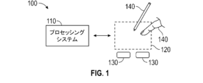
ここで図面に移って、図1は本開示の実施形態における例示的な入力装置100のブロック図である。入力装置100は電子システム(図示せず)に入力を提供するように構成される場合がある。この文書で使用される場合、「電子システム」は電子的に情報処理が可能なあらゆるシステムを広く意味する。電子システムの非限定例には、デスクトップコンピューター、ラップトップコンピューター、ノートブックコンピューター、タブレット、ウェブブラウザー、電子書籍リーダー、及び、パーソナルデジタルアシスタント(Personal Degital Assistants、PDAs)といった、あらゆる大きさや形態のパーソナルコンピュータが含まれる。追加の例示的な電子システムは、入力装置100と独立ジョイスティック又はキースイッチ装置とを含む物理キーボードといった複合入力装置を含む。さらなる例示的な電子システムとして、リモートコントローラーやマウスといったデータ入力装置と、ディスプレイスクリーン及びプリンタといったデータ出力装置と、といった周辺装置を含む。他の例にはリモート端末、キヨスク、ビデオゲームコンソールや携帯ゲーム装置といったビデオゲーム機、等が含まれる。他の例は、スマートフォンのような携帯電話といったコミュニケーションデバイスと、レコーダーやエディターといったメディア装置と、テレビやセットトップボックス、音楽プレーヤー、デジタルフォトフレームといったプレーヤーと、デジタルカメラと、等を含む。加えて、電子システムは入力装置のホストであってもスレーブであっても良い。電子システムは電子機器と呼ばれる場合もある。
Turning now to the drawings, FIG. 1 is a block diagram of an
入力装置100は電子システムの物理的な部分として実装されてもよいし、電子システムから物理的に分離されていてもよい。望ましくは、バスと、ネットワークと、他の有線又は無線のインターコネクションと、のうち1又は複数を用いて入力装置100は電子システムの一部と通信する場合がある。一例として、I2C、SPI、PS/2、ユニバーサルシリアルバス(Universal Serial Bus、USB)、ブルートゥース(登録商標)、RF、及び、IRDAが含まれる。
図1では、入力装置100は、1又は複数の入力物体140によってセンシング領域120に提供された入力を検出するように構成された近接センサー装置として示されている。例示的な入力物体140は、図1に示すように、指やスタイラスを含む。例示的な近接センサー装置は、タッチパッド、タッチスクリーン、タッチセンサー装置等である場合がある。
In FIG. 1 ,
ユーザー入力、例えば1又は複数の入力物体140により供給される入力、をその空間内で入力装置100が検出できるかぎり、センシング領域120は入力装置100の上部、周辺、内部、及び/又は、近傍といったいかなる空間を内包する。個々のセンシング領域の大きさ、形状、及び、位置は実施形態ごとに大きく異なる場合がある。いくつかの実施形態では、センシング領域120は、入力装置100の表面から、十分に正確な物体の検出を信号対雑音比が妨げるまで、空間にむかって一又は複数の方向へ広がる。センシング領域120が広がっている所定の方向の距離は、様々な実施形態で、ミリメートルよりも小さいオーダー、ミリメートルのオーダー、センチメートルのオーダー、あるいは、それ以上である場合がある。この距離は、使用されているセンシング技術の種類や必要な正確性によって大きく変動する場合がある。そのためいくつかの実施形態において検出される入力は、入力装置100のいかなる表面に非接触なものと、入力装置100の入力表面、例えばタッチ表面への接触と、ある量の力又は圧力の適用を伴う入力装置100の入力表面への接触と、及び/又は、これらの組み合わせと、を含む。様々な実施形態では入力表面は、中にセンサー電極(ここではセンシング電極ともいう)を備えるケーシング等の表面や、センサー電極上に置かれた表面シート、又は、何らかのケーシング等として提供される。いくつかの実施形態では、センシング領域120は入力装置100の入力表面に投影された場合には長方形の形状を有する。
入力装置100は、センシング領域120へのユーザー入力を検出するセンサー構成物とセンシング技術とのいかなる組み合わせを適用し得る。入力装置100はユーザー入力を検出するための1又は複数のセンシング要素を備える。いくつかの非限定的な例示として、入力装置100は容量方式、弾性方式、抵抗方式、インダクティブ方式、磁気方式、音響方式、超音波方式、及び/又は、光学方式の技術を用いる場合がある。
いくつかの実装では、一次、二次、三次、あるいは、より高次の次元空間に及ぶイメージ(複数)を供給するように構成される。いくつかの実装は、特定の軸又は平面への入力の投影を供給するように構成される。 Some implementations are configured to provide images spanning a first, second, third, or higher dimensional space. Some implementations are configured to provide a projection of the input onto a particular axis or plane.
入力装置100の抵抗方式の実装のいくつかでは、可撓性と電導性とを有する第1レイヤーが1又は複数のスペーサー要素によって電導性を有する第2レイヤーから分離される。運用中には、1又は複数の電圧勾配が複数のレイヤーにわたって生成される。可撓性の第1レイヤーを押すと、レイヤー間の電気的接触を生じるに十分な屈曲が起こる場合がある。その結果、レイヤー間が接触した1又は複数のポイントを反映した電圧が出力される。これらの電圧出力は位置情報を決定するために用いられる場合がある。
In some resistive implementations of
入力装置100の電気誘導方式の実装のいくつかでは、1又は複数のセンシング要素が共鳴コイル又はコイルのペアによって誘発されたループ電流をとらえる。電流の大きさと、周期と、周波数と、のうちいくつかの組み合わせが位置情報を決定するために用いられる場合がある。
In some electrically inductive implementations of
入力装置100の電気容量方式の実装のいくつかでは、電圧又は電流が電場を生成するために供給される。近隣の入力物体は電場の変化を引き起こし、容量結合に検出可能な変化を生じさせる。この変化は電圧又は電流等の変化として検出される場合がある。
In some capacitive implementations of
電気容量方式の実装のいくつかでは、容量性のセンシング要素の配列、又は、他の規則的あるいは非規則的なパターンを電場発生のために用いる。電気容量方式のいくつかの実装では、個々のセンシング要素が互いにオーム的に短絡され、より大きなセンサー電極が形成される場合がある。電気容量方式の実装のいくつかでは、抵抗シートが用いられる。抵抗シートは均一な電気抵抗を有している場合がある。 Some capacitive implementations use an array of capacitive sensing elements or other regular or irregular patterns to generate the electric field. In some capacitive implementations, individual sensing elements may be ohmically shorted together to form a larger sensor electrode. Some capacitive implementations use resistive sheets. A resistive sheet may have uniform electrical resistance.
電気容量方式の実装のいくつかでは、センサー電極と入力物質との間の容量結合の変化に基づく、「自己容量」(しばしば「絶対容量」とも言われる)センシング法が用いられる。様々な実施形態では、センサー電極の近くの入力物体がセンサー電極近傍の電場を改変し、これに伴い測定される容量結合が変化する。ある実装では、システムグラウンドといった基準電圧についてセンサー電極を変調し、センサー電極と入力物体の間の容量結合を検出することで、絶対容量センシング法を実行する。 Some capacitive implementations use a "self-capacitance" (often referred to as "absolute capacitance") sensing method that is based on changes in the capacitive coupling between the sensor electrode and the input material. In various embodiments, an input object near the sensor electrode modifies the electric field near the sensor electrode, resulting in a change in the measured capacitive coupling. One implementation performs an absolute capacitive sensing method by modulating the sensor electrode with respect to a reference voltage, such as system ground, and detecting capacitive coupling between the sensor electrode and the input object.
電気容量方式の実装のいくつかでは、センサー電極間の容量結合の変化に基づく「相互容量」(しばしば「トランス容量」とも言われる)センシング法を用いる。様々な実施形態では、センサー電極の近傍にある入力物体がセンサー電極間の電場を改変し、これに伴い測定される容量結合が変化する。ある実装では、1又は複数のトランスミッターセンサー電極(以下、「トランスミッター電極」又は「トランスミッター」とも言う)と1又は複数のレシーバーセンサー電極(以下、「レシーバー電極」又は「レシーバー」とも言う)との間の容量結合を検出することで、トランス容量のセンシング法を実行する。トランスミッターセンサー電極は、システムグラウンドといった基準電圧に対して変調されて、トランスミッター信号を送信する場合がある。レシーバーセンサー電極は、結果の信号を容易に受信するために、基準電圧に対して実質的に一定に保持される場合がある。結果の信号は、1又は複数のトランスミッター信号、及び/又は1又は複数の環境的な干渉源、例えば他の電磁信号に対応する影響を含む場合がある。センサー電極は専用のトランスミッター又はレシーバーであっても良いし、発信と受信の両方を行うように構成されても良い。 Some capacitive implementations use "mutual capacitance" (often referred to as "transcapacitance") sensing methods that are based on changes in capacitive coupling between sensor electrodes. In various embodiments, an input object in the vicinity of the sensor electrodes modifies the electric field between the sensor electrodes, resulting in a change in the measured capacitive coupling. In some implementations, between one or more transmitter sensor electrodes (hereinafter also referred to as "transmitter electrodes" or "transmitter") and one or more receiver sensor electrodes (hereinafter also referred to as "receiver electrodes" or "receiver"). The method of sensing the transformer capacitance is performed by detecting the capacitive coupling of the transformer. The transmitter sensor electrode may be modulated with respect to a reference voltage, such as system ground, to transmit the transmitter signal. The receiver sensor electrode may be held substantially constant relative to a reference voltage to facilitate receiving the resulting signal. The resulting signal may include effects corresponding to one or more transmitter signals and/or one or more environmental sources of interference, such as other electromagnetic signals. The sensor electrode may be a dedicated transmitter or receiver, or may be configured to both transmit and receive.
図1において、プロセッシングシステム110が入力装置100の一部として示されている。プロセッシングシステム110は、入力装置100のハードウェアを作動させて、センシング領域120への入力を検出するように構成されている。プロセッシングシステム110は、一部又はすべての、1又は複数の集積回路(Integrated Circuits、ICs)、及び/又は、他の回路構成要素を含む。例えば、相互容量センサー装置のためのプロセッシングシステムは、トランスミッターセンサー電極により信号を発信するトランスミッター回路を含む場合があり、及び/又は、レシーバーセンサー電極により信号を受信するレシーバー回路を含む場合がある。いくつかの実施形態では、プロセッシングシステム110は、例えばファームウェアのコード、及び/又は、ソフトウェアのコード等のような、電子的に読み込み可能な命令を更に含む。いくつかの実施形態では、プロセッシングシステム110を構成している複数のコンポーネントは、例えば入力装置100のセンシング要素の近傍のように、一か所に配置される。他の実施形態では、プロセッシングシステム110の構成要素は、1又は複数の構成要素が入力装置100のセンシング要素に近く、他の1又は複数の構成要素は他の場所に、物理的に別々に配置される。例えば、入力装置100は周辺装置としてデスクトップコンピューターに接続される場合がある。このとき、プロセッシングシステム110は、デスクトップコンピューターの中央演算装置と、中央演算装置から分離された1又は複数のICs(他の実施形態では、関連づけられたファームウェアと共に)と、によって実行されるように構成されたソフトウェアを含む場合がある。他の例として、入力装置100は電話と物理的に一体化し、プロセッシングシステム110は電話の主演算装置の一部をなす回路とファームウェアとを含む、として良い。いくつかの実施形態では、プロセッシングシステム110は入力装置100を実現するため専用のものである場合がある。他の実施形態では、プロセッシングシステム110は、例えばディスプレイスクリーンを作動させることや、触覚アクチュエーターを駆動させるといった、他の機能を実現しても良い。
In FIG. 1, a
プロセッシングシステム110は、プロセッシングシステム110の異なる機能を担うモジュールの一組として実装される場合がある。各モジュールは、プロセッシングシステム110の一部である回路、ファームウェア、ソフトウェア、又はこれらの組み合わせを含んでいる場合がある。様々な実施形態において、異なる組み合わせでモジュールが使用される場合がある。モジュールの例として、センサー電極やディスプレイスクリーンのようなハードウェアを作動させるためのハードウェア作動モジュールと、センサー信号や位置情報といったデータを処理するためのデータ処理モジュールと、情報を報知するための報知モジュールと、を含む。さらなるモジュールの例として、入力を検出するようにセンサー要素を作動させるように構成されたセンサー作動モジュールと、モード変更ジェスチャーのようなジェスチャーを識別する識別モジュールと、作動モードを変更するモード変更モジュールと、が含まれる。
いくつかの実施形態では、プロセッシングシステム110は、センシング領域120へのユーザーの入力(あるいはユーザ入力の欠如)に対して、1又は複数のアクションを起こすことで直接反応する。アクションの例には、カーソルの移動や選択、メニューの案内や他の機能といったGUIアクションはもちろん、作動モードの変更が含まれる。いくつかの実施例では、プロセッシングシステム110は電子システムの一部へ入力(あるいは入力の欠如)に関する情報を供給する。電子システムの一部とは、例えば、電子システムのプロセッシングシステム110とは別に電子システムの中央演算システムが存在する場合に、その中央演算装置を示す。いくつかの実施形態では、電子システムの一部は、プロセッシングシステム110から受信した情報を処理して、例えばモード変更アクションやGUIアクションを含む一連の全ての動作を促進するなど、ユーザー入力に基づく動作を行う。
In some embodiments,
例えばいくつかの実施形態において、センシング領域120に対する入力(あるいは入力の欠如)を示す電気信号を生成するように、プロセッシングシステム110は入力装置100のセンシング要素を作動させる。プロセッシングシステム110は、電子システムに供給される情報を生成するにあたり、いかなる適切な量の処理を電気信号に行っても良い。例えば、プロセッシングシステム110は、センサー電極から得られたアナログの電気信号をデジタル化する場合がある。他の例として、プロセッシングシステム110は、フィルタリングや他の信号調整を行う場合がある。さらに他の例として、プロセッシングシステム110は、情報が電気信号とベースラインの差異を反映するように、ベースラインを減算するか、別の計算を行う場合がある。さらなる他の例として、プロセッシングシステム110は、位置情報の決定や、入力のコマンド認識、手書き認識等を行う場合がある。
For example, in some embodiments,
ここでは「位置情報」を、絶対位置と、相対位置と、速度と、加速度と、他の空間性の情報と、を広く内包するように用いる。「0次元の」位置情報の例は、近/遠、又は、接触/非接触といった情報を含む。「一次元の」位置情報の例は、軸に沿った位置が含まれる。「二次元の」位置情報の例は、平面上の運動を含む。「三次元の」位置情報は空間上の瞬間的速度又は平均速度を含む。更なる例は、空間情報の他の表現を含む。例えば、位置、動き、あるいは、瞬間的速度を経時的に追跡した履歴情報を含む、1又は複数タイプの位置情報に関する履歴情報が検出及び/又は記憶される場合がある。 Here, "position information" is used to broadly include absolute position, relative position, velocity, acceleration, and other spatial information. Examples of "0-dimensional" position information include near/far or contact/non-contact information. Examples of "one-dimensional" position information include position along an axis. Examples of "two-dimensional" position information include movement in a plane. "Three-dimensional" position information includes instantaneous or average velocity over space. Further examples include other representations of spatial information. For example, historical information regarding one or more types of location information may be detected and/or stored, including historical information that tracks location, movement, or instantaneous velocity over time.
いくつかの実施形態では、入力装置100は、プロセッシングシステム110又は他のプロセッシングシステムによって作動される追加の入力構成要素と共に実装される。これらの追加の入力構成要素は、センシング領域120への入力や他の機能について重複する機能を提供する場合がある。図1では、センシング領域120の近くに(複数の)ボタン130が図示されている。ボタン130は、入力装置100を使用するアイテムを簡単に選択するために用いることができる。異なるタイプの追加入力構成要素として、スライダー、ボール、ホイール、及び、スイッチ等が含まれる。逆に、いくつかの実施形態では、入力装置100は他の入力構成要素を含まず実装される。
In some embodiments,
いくつかの実施形態では、入力装置100はタッチスクリーンインターフェースを含み、センシング領域120はディスプレイスクリーンの少なくとも一部と重複する。例えば、センシング領域120はディスプレイスクリーンのアクティブ領域の少なくとも一部と重複する場合がある。ディスプレイスクリーンのアクティブ領域は、ディスプレイスクリーンの画像が更新される部位と対応する場合がある。1又は複数の実施形態では、入力装置100は、ディスプレイスクリーンと重なり合う、実質的に透明なセンサー電極を含み、関連付けられた電子システムにタッチスクリーンインターフェースを提供する場合がある。ディスプレイスクリーンはユーザーにビジュアルインターフェースを表示できるいかなる種類の動的ディスプレイであってもよい。ディスプレイスクリーンは、いかなる種類の発光ダイオード(Light Emitting Diode、LED)、有機LED(Organic LED、OLED)、ブラウン管(Cathode Ray tube、CRT)、液晶ディスプレイ(Liqud Crystal Display、LCD)、プラズマ、エレクトロルミネンス(ElectroLuminescence、EL)、又は、他の表示技術を含む場合がある。入力装置100とディスプレイスクリーンは物理要素を共有する場合がある。例えば、いくつかの実施形態では、表示とセンシングのために同じ電子構成要素をいくつか利用する場合がある。他の例として、ディスプレイスクリーンは、一部又は全体がプロセッシングシステム110によって作動されてもよい。ディスプレイスクリーンはディスプレイパネルとも呼ばれる。
In some embodiments,
開示のいくつもの実施形態は完全に機能する装置の文脈で説明されたが、本開示のメカニズムは、例えばソフトウェアなど、さまざまな形態のプログラムの製品として配布されてもよいことが理解されるべきである。例えば本開示のメカニズムは、例えば、プロセッシングシステム110によって読取できる不揮発性のコンピューター読取可能な、かつ/又は、記録/書込可能な情報搬送メディアのように、電子プロセッサーにより読取り可能な情報搬送メディア上のソフトウェアプログラムとして実装され、配布される場合がある。さらに、本開示の実施形態では、配布を実現するために用いられるメディアを特定のメディアタイプにかかわらず同様に適用できる。電子的に読取可能な不揮発性メディアの例には、様々なディスク、メモリスティック、メモリカード、そしてメモリモジュール等が含まれる。電子的に読取可能なメディアは、フラッシュ、光学、磁気、ホログラフィー、又は他のストレージ技術に基づいてよい。
Although several embodiments of the disclosure have been described in the context of a fully functional device, it should be understood that the mechanisms of the disclosure may be distributed as a program product in various forms, e.g., software. be. For example, the mechanisms of the present disclosure may be implemented on an information-carrying medium readable by an electronic processor, such as, for example, a non-volatile computer-readable and/or recordable/writable information-carrying medium readable by
図2は、いくつかの実施形態に係る、パターンに関連づけられたセンシング領域120を感知するように構成された、(複数の)センサー電極205の例示的なパターンの一部を示す。図示と説明を明確にするため、図2では容量性のセンサー電極205の領域が単純な四角いパターンで示されている。しかし、他の実施形態では、センサー電極205は他のパターンで配置され、他の形状を持つ場合がある。例えば、1又は複数のセンサー電極205が第1の方向(例えば、X軸に沿った方向)に対しセンシング領域120の全体に広がり、他の1又は複数のセンサー電極が第1の方向とは異なる第2の方向(Y軸に沿った方向)に対しセンシング領域の全体に広がる場合がある。さらに、様々な実施形態では、センサー電極205は、重複する、又は、重複しないセンサー電極の行及び列に配列される場合がある。
FIG. 2 illustrates a portion of an exemplary pattern of sensor electrode(s) 205 configured to sense sensing
一実施形態では、センサー電極205は局所的な容量の領域を形成する。局所的な容量の領域は、第1の作動モードでは、個々のセンサー電極とグラウンドの間に形成され、第2の作動モードでは、トランスミッターとレシーバーの電極として用いられるセンサー電極の集合の間に形成される場合がある。容量結合はセンシング領域120の入力物体の近さと動きによって変動し、それゆえ入力装置のセンシング領域120における入力物体の存在の指標として用いられる場合がある。
In one embodiment,
例示的なパターンはセンサー電極205X,Yの配列を含む。なお、XとYは正の整数とし、センサー電極205X,Yは共通平面上のX列Y行に配列されている。XとYの一つはゼロである場合がある。センサー電極205のパターンは異なる配置を持つ複数の容量性ピクセル205を含む場合があると解される。異なる配置には、環状配列、繰り返しのパターン、非繰り返しのパターン、不均一な配列、単一の行又は列、あるいは、他の好適な配置が含まれる。さらに、下記でより詳細に議論されるが、センサー電極205は、円形、長方形、ダイヤモンド型、星形、正方形、非凸状、凸状、非凹状、凹状、といったどのような形状であってもよい。ここで示されているように、センサー電極205はプロセッシングシステム110と接続され、センシング領域120における入力の存在(あるいはその欠如)を決定するために利用される。
An exemplary pattern includes an array of sensor electrodes 205X,Y . Note that X and Y are positive integers, and the
第1の作動モードでは、少なくとも一つのセンサー電極が、絶対センシング技術を用いて、入力物体の存在を検出するために用いられる場合がある。プロセッシングシステム110のセンサーモジュール204は、各センサー電極205のトレース240を用いて、絶対容量センシング信号をセンサー電極に印加するように構成される。またセンサーモジュール204は、プロセッシングシステム110又は他のプロセッサーによって入力物体の位置を決定するために用いられる絶対容量センシング信号に基づき、センサー電極と入力物体の間の電気容量を測定するように構成される。絶対容量センシング信号は様々な電圧を含む変調信号であってよい。一実施形態では、絶対容量センシング信号は複数のパルス(例えば、複数の正及び負の電圧変移)を含む。さらに、正及び負の電圧変移はバーストと呼ばれる場合があり、絶対容量センシング信号は1又は複数のバーストを含む。
In a first mode of operation, at least one sensor electrode may be used to detect the presence of an input object using absolute sensing techniques. The
1又は複数のセンサー電極205は1又は複数の他のセンサー電極205からオーム的に絶縁されている場合がある。さらに、1又は複数の絶縁体がセンサー電極を分離し、互いに電気的にショートすることを防ぐ。
One or
第2の作動モードでは、センサー電極205は、トランス容量センシング技術を用いて、入力物体の存在を検知するために用いられる。すなわち、プロセッシングシステム110はセンサー電極205の少なくとも一つにトランスミッター信号を印加し、1又は複数の他のセンサー電極205を用いて結果信号を受信する場合がある。結果信号はトランスミッター信号に対応する影響を含む。結果信号はプロセッシングシステム110又は他のプロセッサーにより入力物体の位置を決定するために用いられる。トランスミッター信号を印加されたセンサー電極は、結果信号を受信するセンサー電極に関係のあるトランスミッター信号で変調される。一実施形態では、トランスミッター信号によって駆動されるセンサー電極と、結果信号を受信するセンサー電極と、の両方が変調される。一実施形態では、トランスミッター信号は複数のパルス(例えば、複数の正及び負の電圧変移)を含む。さらに、正及び負の電圧遷移はバーストと言われる場合があり、トランスミッター信号は1又は複数のバーストを含む。
In the second mode of operation, the
「センシング信号」という言葉は絶対容量センシング信号又はトランスミッター信号のいずれをも意味する場合がある。 The term "sensing signal" may mean either an absolute capacitive sensing signal or a transmitter signal.
入力装置100は上述されたモードのどれか一つで作動するように構成されている場合がある。入力装置100は上述された2つのモードを切り替えるように構成されてもよい。
いくつかの実施形態では、複数のセンサー電極205はこれらの容量結合を決定するために「スキャン」される。すなわち、一実施形態では、トランスミッター信号を発信するように、1又は複数のセンサー電極が駆動される。トランスミッターは、一度に一つのトランスミッター電極が発信するように、あるいは、同時に複数のトランスミッター電極が発信するように作動される場合がある。同時に複数のトランスミッター電極が発信する場合、複数のトランスミッター電極は、同じトランスミッター信号を発信して実質的により大きいトランスミッター電極を実質的に生じさせる場合がある。あるいは、複数のトランスミッター電極が異なるトランスミッター信号を発信してもよい。例えば、複数のトランスミッター電極は、(複数の)レシーバー電極の結果信号が併合された結果を独立に決定できる1又は複数のコーディングスキームに従って、異なるトランスミッター信号を発信する場合がある。
In some embodiments,
レシーバーセンサー電極として構成されたセンサー電極は、結果信号を取得するために単独で又は複合的に作動され得るように構成される。結果信号は容量性ピクセル205における容量結合の測定値を決定するために用いられる場合がある。
The sensor electrodes configured as receiver sensor electrodes are configured such that they can be actuated singly or in combination to obtain a result signal. The resulting signal may be used to determine a measurement of capacitive coupling at
他の実施形態では、センサー電極205の容量結合を決定するためのセンサー電極205への「スキャンニング」には、1又は複数のセンサー電極への、絶対容量センシング信号の印加と、絶対容量の測定と、を含む。その他の実施形態では、複数のセンサー電極は、センサー電極205に対し絶対容量センシング信号が同時に印加されるように作動される場合がある。そのような実施形態では、絶対容量の測定結果が1又は複数のセンサー電極205のそれぞれから同時に取得される場合がある。一実施形態では、入力装置100は複数のセンサー電極205のセンサー電極を同時に駆動し、各センサー電極の絶対容量の測定値を同じセンシングサイクルで測定する。様々な実施形態では、プロセッシングシステム110は複数のセンサー電極の一部により選択的に駆動と受信とを行わせるように構成される場合がある。例えば、センサー電極の選択は、ホストプロセッサーで実行されているアプリケーションと、入力装置のステータスと、センシング装置の作動モードと、及び、入力装置で決定された位置と、に基づいて(ただしこれに限定されない)行われる場合がある。ホストプロセッサーは電子装置の中央演算装置や他のプロセッサーであってもよい。
In other embodiments, "scanning" the
センサー電極205からの測定結果の組は、上述したように、センサー電極205の容量結合を示す容量イメージ又は容量フレームを形成する。複数の時間区間にわたって複数の容量イメージが取得される場合がある。そして、これらの間の差異がセンシング領域への入力についての情報を導くために用いられる。例えば、連続した時間区間にわたって取得された連続した容量イメージは、センシング領域に侵入、退出、及び、内在する1又は複数の入力物体の動作を追跡するために用いることができる。
The set of measurements from the
いくつかの実施形態では、1又は複数のセンサー電極205は、ディスプレイスクリーンの表示を更新するために用いられる1又は複数のディスプレイ電極を含む。1又は複数の実施形態ではディスプレイ電極は、1又は複数セグメントの共通電圧電極(Vcom電極ともいう)、ソースドライバー線(又はソース電極)、ゲート線(又はゲート電極)、アノード電極あるいはカソード電極、又は、他のいかなるディスプレイ要素を含む。これらのディスプレイ電極は、適切なディスプレイスクリーン基盤に配置される場合がある。例えば、インプレーンスイッチング方式(In Plane Swiching、IPS)やプレーントゥラインスイッチング方式(Plane to Line Switching、PLS)、有機発光ダイオード方式(Organic Light Emitting Diose、OLED)、といったようなディスプレイスクリーンでは、ガラス基板やTFTガラス又は他のいかなる透明な材質といった透明基盤の上にディスプレイ電極が配置される場合がある。他の実施形態では、パターン型の垂直配向方式(Patterned Vertical Aligment、PVA)やマルチドメイン型の垂直配向方式(Multi-domain Vertical Alignment、MVA)のようなディスプレイスクリーンにおいて、ディスプレイ電極はカラーフィルターガラスの底に配置される場合がある。1又は複数の実施形態では、ディスプレイ電極はOLEDディスプレイの発光層の上に配置される場合がある。そのような実施形態では、センサー電極とディスプレイ電極の両方として利用される電極は、複数の機能を担うため、コンビネーション電極と呼ばれる場合もある。一実施形態では、ディスプレイ電極は、ディスプレイの表示ラインにおいて更新するサブピクセルを選択するために用いられるゲート電極である場合がある。ソース電極は、更新するサブピクセル及び/又は1又は複数のVcom電極に対してデータ信号を印加するように構成されている。ソース電極はサブピクセルの列と接続されている場合があり、ゲート電極はサブピクセルの行と接続されている場合がある。
In some embodiments, one or
図2の参照を続け、様々な実施形態では、センシング電極と接続されたプロセッシングシステム110は、センサーモジュール204とディスプレイドライバーモジュール208とを含む、1又は複数の集積回路(Integrated Circuit、IC)チップを含む場合がある。一実施形態では、センサーモジュール204は、入力のセンシングが望まれる期間中、センシング電極に対してトランスミッター信号又は絶対容量センシング信号を印加し、センシング電極で結果信号を受信するように構成された回路を含む。さらに、プロセッシングシステムは複数のICチップを含み、各ICチップがセンサーモジュール204とディスプレイドライバーモジュール208とを含む場合がある。
Continuing to refer to FIG. 2, in various embodiments, the
1又は複数の実施形態では、センサーモジュール204は、入力センシングが望まれる期間中にトランスミッター信号をセンシング電極に印加するように構成された回路を含むトランスミッターモジュールを備える。1又は複数の実施形態では、入力センシングに割り当てられた時間期間にわたって、トランスミッター信号は変調され、さらに1又は複数のバーストを含む。トランスミッター信号の振幅、周波数、そして、電圧は、センシング領域120における入力物体についてよりロバスト性のある位置情報を取得するために変更される場合がある。絶対容量センシング信号は、トランス容量センシングに用いられるトランスミッター信号と同一である、又は、異なる場合がある。センサーモジュール204は、1又は複数のセンサー電極205と選択的に接続される場合がある。例えば、センサーモジュール204は、センサー電極のうち選択された一部と接続され、絶対容量センシング又はトランス容量センシングモードのいずれでも作動される場合がある。他の例では、センサーモジュール204は、絶対容量センシングモードで作動する場合と、トランス容量センシングモードで作動する場合と、で異なるセンサー電極に接続される場合がある。
In one or more embodiments,
様々な実施形態では、センサーモジュール204はセンサー回路(例えば、図3のセンサー回路206)を備える。また、センサーモジュールは、センシング電極により、入力センシングが望まれる期間中にトランスミッター信号に応じた影響を含む結果信号を受信するように構成される。1又は複数の実施形態では、センサーモジュール204は、絶対容量センシング信号を印加されたセンサー電極から結果信号を受信し、センサー電極と入力物体の間における絶対容量の変化を決定するように構成される。1又は複数の実施形態では、センサーモジュール204がセンシング領域120における入力物体の位置を決定する。1又は複数の実施形態では、センサーモジュール204は他のモジュール又はプロセッサーへ結果信号を示す情報を含む信号を供給する。他のモジュール又はプロセッサーは、センシング領域120における入力物体の位置を決定する、プロセッシングシステム110の決定モジュール、又は、電子装置のプロセッサー(例えばホストプロセッサー)といったようなものである。1又は複数の実施形態では、センサーモジュールのセンサー回路はレシーバー回路を複数備える。レシーバー回路は複数のアナログフロントエンド(Analog Front End,AFE)を備える場合がある。
In various embodiments,
1又は複数の実施形態では、容量センシングあるいは入力センシングと、ディスプレイの更新と、が少なくとも一部が重複する期間中に発生する場合がある。ディスプレイの更新は、表示フレーム中に各ディスプレイ電極の電圧を更新することを含む場合がある。各表示フレームの間に、表示装置の各表示ラインが更新される場合がある。一実施形態では、表示フレームは16ミリ秒ごとに更新される場合があり、あるいは表示のフレームレート60ヘルツで更新される場合がある。その他の実施形態では、他の表示のフレームレートが用いられる場合がある。例えば、表示のフレームレートとして48ヘルツ、120ヘルツ、及び/又は、240ヘルツが用いられる場合がある。例えば、コンビネーション電極が表示の更新のために駆動される上、コンビネーション電極はまた容量センシングのためにも駆動される場合がある。容量センシングと表示の更新とを重複させることは、センサー電極が容量センシングを行うように設定された期間と少なくとも一部において重複している時間期間中に、表示装置の1又は複数の参照電圧を変調すること、及び/又は、少なくとも一つの表示用ディスプレイ電極を変調すること、を含む場合がある。他の実施形態では、容量センシングと表示の更新とは重複しない期間に発生してもよい。この期間は非表示更新期間ともいう。さまざまな実施形態において、非表示更新期間は、表示フレームの2つの表示ラインにおいて、表示ラインを更新する期間どうしの間で発生する場合があり、時間の長さは少なくとも表示更新期間と同じである場合がある。このような実施形態では、非表示更新期間はロング水平帰線期間、ロングh-ブランキングピリオド、又は、分散ブランキング期間ともいう場合がある。他の実施形態においては、非表示更新期間は、水平帰線期間と垂直帰線期間とを含む場合がある。プロセッシングシステム110は容量センシングのために、どの1又は複数の異なる非ディスプレイ更新期間中に、又は、異なる非ディスプレイ更新期間のどの組み合わせの期間中に、センサー電極を駆動するように構成されてもよい。
In one or more embodiments, capacitive or input sensing and display updating may occur during at least partially overlapping periods. Updating the display may include updating the voltage of each display electrode during a display frame. During each display frame, each display line of the display may be updated. In one embodiment, the display frame may be updated every 16 milliseconds, or at a display frame rate of 60 Hertz. In other embodiments, other display frame rates may be used. For example, 48 Hz, 120 Hz, and/or 240 Hz may be used as the display frame rate. For example, in addition to being driven for display updating, the combination electrode may also be driven for capacitive sensing. Overlapping capacitive sensing and display updating includes changing one or more reference voltages of the display device during a period of time that at least partially overlaps the period during which the sensor electrodes are configured to perform capacitive sensing. and/or modulating at least one display electrode for display. In other embodiments, capacitive sensing and display updates may occur during non-overlapping time periods. This period is also referred to as a hidden update period. In various embodiments, a non-display update period may occur in two display lines of a display frame between periods of updating the display line, and is at least as long in time as the display update period. There are cases. In such embodiments, the non-display update period may also be referred to as a long horizontal blanking period, a long h-blanking period, or a distributed blanking period. In other embodiments, the non-display update period may include a horizontal blanking period and a vertical blanking period.
図3は、複数のICチップでディスプレイパネルを駆動するための解決策を示す。1又は複数の実施形態では、表示装置300は車両(例えば、自動車)用の入力装置(例えば、入力装置100)の一部である場合がある。図示されたように、図3は、基板320及びディスプレイ電極330を含むディスプレイパネルを有する表示装置300を含む。図示された実施形態では、3つのICチップ(例えば、マスターICチップ340と、右スレーブICチップ350と、左スレーブICチップ360)が、ディスプレイパネルの駆動と容量センシングとを実現するために用いられる。一実施形態では、1又は複数のICチップが第1の基板に配置され、他の1又は複数のICチップが第2の基板に配置される場合がある。
FIG. 3 shows a solution for driving a display panel with multiple IC chips. In one or more embodiments,
各ICチップは、センサーモジュール204及びディスプレイドライバーモジュール208の実例を含む場合がある。さらに、ICチップのそれぞれが、表示更新及び容量センシング用のタイミング信号を生成するように構成されたタイミングコントローラー(Tcon)209と、センサー電極205を用いて容量センシングを実行するように構成されたセンシング回路206と、含む場合がある。一実施形態では、Tcon209は、表示の更新と容量センシングとを同期するように構成された容量センシング回路と通信するように構成されている。
Each IC chip may include an instance of a
様々な実施形態において、ICチップ340、350、及び、360はそれぞれ複数の入力/出力ピンを含む。例えば、図3に示すように、ICチップ340、350、及び、360は、sense_sync_i/o_l、sense_sync_i/o_r、tsvd_i/o_l、tsvd_i/o_r、tshd_i/o_l、tshd_i/o_r、Hcal_pulse_i/o_l、Hcal_pulse_i/o_r、一般的用途の入力/出力(General Purpose input/output、GPIO)ピン、といった入力/出力ピンを含む。ICチップの入力/出力ピンは、基板320に設けられた配線を介して、あるいは1又は複数の実施形態における異なる基板に配置されたICチップの入力/出力ピン間に設けられた1又は複数の配線を介して、他のICチップの関連する入力/出力ピンと通信可能に接続される場合がある。例えば、マスターICチップ340のsense_sync_i/o_lは、左スレーブICチップ360のsense_sync_i/o_rと接続される場合があり、マスターICチップ340のsense_sync_i/o_rは、右スレーブICチップ350のsense_sync_i/o_lと接続される場合がある。同様に、例えば、マスターICチップ340のtsvd_i/o_lは、左スレーブICチップ360のtsvd_i/o_rと接続される場合があり、マスターICチップ340のtsvd_i/o_rは、右スレーブICチップ350のtsvd_i/o_lと接続される場合がある。さらに、マスターICチップ340のtshd_i/o_lは、左スレーブICチップ360のtshd_i/o_rと接続される場合があり、マスターICチップ340のtshd_i/o_rは、右スレーブICチップ350のtshd_i/o_lと接続される場合がある。マスターICチップ340のHcal_pulse_i/o_lは、左スレーブICチップ360のHcal_pulse_i/o_rと接続される場合があり、マスターICチップ340のHcal_pulse_i/o_rは、右スレーブICチップ350のHcal_pulse_i/o_lと接続される場合がある。
In various embodiments, IC chips 340, 350, and 360 each include multiple input/output pins. For example, as shown in FIG. 3, the IC chips 340, 350, and 360 include sense_sync_i/o_l, sense_sync_i/o_r, tsvd_i/o_l, tsvd_i/o_r, tshd_i/o_l, tshd_i/o_r, Hcal_pulse_i/o_l, Hc al_pulse_i/ o_r, general purpose input/output (GPIO) pins. The input/output pins of the IC chip may be connected to one or more wires provided on the
その他の実施形態では、各ICチップは他の入力/出力ピンを含む場合がある。例えば、ICチップのそれぞれが、容量センシングのためにセンサー電極205を駆動し、かつ、表示を更新するためにディスプレイ電極を駆動することに用いられる入力/出力ピンを備える場合がある。
In other embodiments, each IC chip may include other input/output pins. For example, each of the IC chips may include input/output pins used to drive
1又は複数の実施形態では、容量センシングと表示更新を共に行うように構成されたICチップ(例えば、マスターICチップ340、右スレーブICチップ350、及び、左スレーブICチップ360)はタッチ・ディスプレイドライバー集積(Touch and Display Driver Integration、TDDI)チップとも呼ばれる。例えばICチップは、トランス容量センシングと絶対容量センシングとのうち少なくとも一方のために、1又は複数のセンサー電極205を駆動するように構成される場合がある。
In one or more embodiments, IC chips configured to perform both capacitive sensing and display updates (e.g.,
図3の実施形態では3つのICチップが示されているが、他の実施形態では、異なる数のICチップが入力装置100内で用いられている場合がある。例えば、一実施形態では、少なくとも2つのICが、ディスプレイパネルを駆動とタッチセンシングの実行とのために利用される場合がある。各ICチップは、他のICチップから分離された別個のICを含む場合がある。さらにICチップはそれぞれ、ディスプレイパネルの異なる部分を更新し、容量センシングのためにセンサー電極205(例えば、センサー電極205a、205b、及び、205c)のうち異なる一部を作動させるように構成されている場合がある。1又は複数の実施形態では、2つまたはそれ以上のICチップが、容量センシングのために少なくとも一つの共通のセンサー電極205を駆動する場合がある。一実施形態では、各ICチップは、ソース電極のうち異なる一部、又は、ディスプレイパネルのラインのうち異なる一部と接続され、これを更新するように構成されている。さらに、ICチップは表示更新のためにVcom電極のうち異なる一部を駆動するように構成されている。Vcom電極が容量センシングと表示更新とに用いられている実施形態では、容量センシング及び表示更新のために、ICチップはそれぞれVcom電極のうち異なる一部を作動させるように構成されている。
Although three IC chips are shown in the embodiment of FIG. 3, different numbers of IC chips may be used within
一実施形態では、マスターICチップ340と右スレーブICチップ350と左スレーブICチップ360とはそれぞれディスプレイパネルの基板320と独立して接続されている。さらに、マスターICチップは、基板320に設けられた1又は複数のトレースにより各スレーブICチップと接続されている。一実施形態では、基板320はガラス基板であり、ICチップはこのガラス基板に設けられた1又は複数のトレースを介して通信可能に接続されている。
In one embodiment, the
2又はそれ以上のICチップを使用する実施形態では、一つのICチップは「マスター」(例えば、マスターICチップ340)として構成され、他のICチップ(例えば、スレーブチップ350及び/又は360)は「スレーブ」として構成される場合がある。「マスター」として構成されたICチップは、表示更新と容量センシングのうち少なくとも一つの機能をICチップ間で同期するために、「スレーブ」として構成されたICチップに1又は複数の同期信号を供給するように構成されている場合がある。3つのICチップを使用する実施形態では、マスターICチップは2つのスレーブICチップの間に配置される場合がある。他の実施形態では、マスターICチップは、各スレーブICチップがマスターICチップの同じ側にくるように配置される場合がある。
In embodiments using two or more IC chips, one IC chip is configured as a "master" (e.g., master IC chip 340) and the other IC chips (e.g.,
マスターICチップ340はディスプレイパネルを更新するためにホストプロセッサーから表示データを受信するように構成されている場合がある。例えば、マスターICチップ340は表示データを処理し、処理された表示データをスレーブICチップ350と360とに伝達する場合がある。さらに、マスターICチップ340はホストプロセッサーにセンサーデータを伝達するように構成されている場合がある。例えば、マスターICチップ340は、スレーブICチップ350と360とのそれぞれからセンサーデータを受信し、スレーブICチップからのセンサーデータをマスターICチップからのセンサーデータと結合し、結合したセンサーデータをホストプロセッサーに伝達するように構成されている場合がある。一実施形態ではICチップのそれぞれが、各ICチップで受信したセンサーデータをホストプロセッサーに送る前に処理するように構成されている場合がある。他の実施形態では、生のセンサーデータ(例えば、実質的に処理されていないセンサーデータ)がホストプロセッサーに伝達される場合がある。他の実施形態では、マスターICチップ340はスレーブICチップ350と360とのそれぞれから生のセンサーデータを受信し、このセンサーデータを処理し、そしてホストプロセッサーに処理されたセンサーデータを伝達するように構成されている。センサーデータを処理することは、センサーデータのベースライン処理と、センサーデータのフィルタリングと、1又は複数の入力物体の位置情報を決定することと、のうち少なくとも一つを含む場合がある。
1又は複数の実施形態では、マスターICチップ340とスレーブICチップ350、360は、各ICチップのデジタル回路が他のそれぞれのICチップに対して少なくとも50ナノ秒以内で作動するように同期される場合がある。他の実施形態では、各ICチップのデジタル回路のタイミングが50ナノ秒以上だがセンサーデータ間又は表示更新間でエラーが発生しない範囲で異なるように、ICチップが互いに同期される場合がある。一実施形態では、各ICチップのデジタル回路のタイミングが、ディスプレイパネルを更新するときに表示のアーティファクトが生じることが無いように、及び/又は、センサー電極から取得したセンサーデータにエラーが生じることがないように、ICチップが互いに同期される場合がある。さらに、ICチップの同期により、各ICチップによってそれぞれのセンサー電極205に印加されるセンシング信号のタイミングが同期される。
In one or more embodiments,
一実施形態では、マスターICチップ340とスレーブICチップ350と360とにわたるセンシング信号(例えば、センシング信号342、352、及び、362)どうしのいかなるタイミングのズレは、ディスプレイパネルの容量の不完全なガードにつながる場合があり、その結果各ICチップのレシーバー回路のAFEsに大量の電荷が流入し得る。このような実施形態では、ディスプレイパネルの1又は複数のディスプレイ電極又はセンサー電極は、容量センシングのために作動されるセンサー電極に対して電圧が異なる。電圧が不整合な電極間では、バックグラウンド容量と言われる容量結合が形成される。
In one embodiment, any timing misalignment between sensing signals (e.g., sensing signals 342, 352, and 362) across
センサー電極から取得したセンサーデータの中にバックグラウンド容量が存在すると、潜在的な干渉やセンサー電極の容量変化に対処するために用いることができるレシーバー回路のダイナミックレンジが減少する。一実施形態では、バックグラウンド容量の値は、センサー電極205間の容量結合、及び/又は、センサー電極205と入力物体の間の容量結合よりも大きい場合がある。そのため、センサー電極205間の容量結合、及び/又は、センサー電極205と入力物体の間の容量結合を検出、及び/又は、測定することが困難になる。さらに、バックグラウンド容量は、レシーバー回路のAFEに飽和又はクリップを発生させ、センサー電極205間の容量結合、及び/又は、センサー電極205と入力物体との間の容量結合を検出不可能、及び/又は、測定不可能にする場合がある。
The presence of background capacitance in the sensor data acquired from the sensor electrode reduces the dynamic range of the receiver circuitry that can be used to address potential interferences and capacitance changes in the sensor electrode. In one embodiment, the value of the background capacitance may be greater than the capacitive coupling between the
1又は複数の実施形態では、マスターICチップ340はスレーブICチップ350、360のそれぞれと、フレームの同期、センシングバーストの同期、センシングサイクルの同期、及び、高速発振器のクロック同期のうち1又は複数を実行するように構成されている。
In one or more embodiments, the
ICチップ340、350、360はそれぞれ、60ヘルツ又は120ヘルツのうち一方の容量フレームレートによる容量センシングのために、複数のセンサー電極205のうち異なる一部を作動させるように構成されている場合がある。他の実施形態では、他の容量フレームレートが使用される場合がある。一実施形態では、センサー電極がICチップ340、350及び360のうち一つとのみ接続されるように、各ICチップ340、350、360が複数のセンサー電極の重複しない一部とそれぞれ接続される。例えば、スレーブICチップ360がセンサー電極205a(複数)と通信可能に接続され、マスタースレーブICチップ340はセンサー電極205b(複数)と通信可能に接続され、スレーブICチップ350はセンサー電極205c(複数)と通信可能に接続される。ICチップは同じ数のセンサー電極と接続される場合がある。あるいは、1又は複数の実施形態では、少なくともICチップが他のICチップと異なる(例えば、多い又は少ない)数のセンサー電極と接続している場合がある。ICチップは、基板320に設けられた1又は複数の配線を介してそれぞれセンサー電極と接続されている場合がある。他の実施形態では複数のセンサー電極には、ICチップ340、350、360のうち1又は複数と接続された重複部分が存在する場合がある。
Each
各ICチップは、容量フレームごとに1回(又は2回)、それぞれのセンサー電極を作動させるように構成されている場合がある。一実施形態では、容量センシングのためにセンサー電極を作動させることには、センシング信号342、352、362のそれぞれ一つをそれぞれのセンサー電極に印加することを含む。容量フレームレートは、それぞれのICチップに接続されたセンサー電極からセンサーデータを受信する時間の周期に対応する。一実施形態では、容量イメージを取得するレートが容量フレームレート(又はセンシングレート)である。例えば、容量イメージが16ミリ秒ごとに一度取得される場合があり、このとき60ヘルツの容量フレームレートが生成される。他の実施形態では、容量フレームレートはおおよそ、120ヘルツ、240ヘルツ、又は、さらに大きい場合がある。さらに、1又は複数の実施形態では、容量フレームレートは60ヘルツより小さい場合がある。 Each IC chip may be configured to activate its respective sensor electrode once (or twice) per capacitive frame. In one embodiment, activating the sensor electrodes for capacitive sensing includes applying a respective one of sensing signals 342, 352, 362 to a respective sensor electrode. The capacitive frame rate corresponds to the period of time during which sensor data is received from sensor electrodes connected to each IC chip. In one embodiment, the rate at which capacitive images are acquired is the capacitive frame rate (or sensing rate). For example, a capacitive image may be acquired once every 16 milliseconds, producing a capacitive frame rate of 60 hertz. In other embodiments, the capacity frame rate may be approximately 120 Hertz, 240 Hertz, or even greater. Further, in one or more embodiments, the capacitive frame rate may be less than 60 Hertz.
マスターICチップ340は、各ICチップが新たな容量フレームを実質的に同時に始めるように、スレーブICチップ350、360のそれぞれとフレームの同期を行うように構成されている場合がある。一実施形態ではフレームの同期は、ICチップのスタートアップ時、1又は複数のICチップがリセットされた後、及び/又は、ある数の容量フレームが生じた後に起こる。
各ICチップ340、350、360のTcon209は、表示の更新と容量センシングを実行するためにICチップに用いられ得るタイミング制御信号を生成する場合がある。一実施形態では、1又は複数の容量センシングフレームと表示フレームの開始を示すために用いられるタイミング信号は、垂直方向へのタイミング信号(例えば、垂直タイミング信号)又はtsvd信号である。さらに、表示フレームの表示ラインの開始を示すように構成されたタイミング信号は、水平方向へのタイミングシグナル(例えば、水平タイミング信号)又はtshd信号である。tsvd信号とtshd信号は共にマスターICチップ340のTcon209によって生成され、スレーブICチップ350、360のそれぞれに伝達される場合がある。
The
図4は、トリガールックアップテーブル(Look Up Table、LUT)のロジック410の例示的な実施形態を示す。一実施形態では、ICチップ340、350、360のそれぞれがトリガーLUTのロジック410を含む。マスターICチップ340のTcon209によって生成されたtsvd信号は、マスターICチップ340とスレーブICチップ350、360の各トリガーLUTのロジックに伝送される場合がある。一実施形態では、tsvd信号はマスターICチップ340のtsvd_i/o_lとtsvd_i/o_rから左スレーブICチップ360のtsvd_i/o_rと右スレーブICチップ350のtsvd_i/o_lとに伝送される場合がある。さらに、マスターICチップ340のTcon209はスレーブICチップ350、360のそれぞれにtshd信号を伝送するように構成されている場合がある。例えば、tshd信号はマスターICチップ340のtshd_i/o_lとtshd_i/o_rから右スレーブICチップ360のtshd_i/o_rピンと左スレーブICチップ350のtshd_i/o_lとに伝送される場合がある。
FIG. 4 shows an exemplary embodiment of trigger look up table (LUT)
マスターICチップ340のTcon209はtsvd信号とtshd信号の両方を、スレーブICチップ350、360のそれぞれのトリガーLUTのロジック410へと同様に、マスターICチップ340のトリガーLUTのロジック410へも伝送する。スレーブICチップ350、360のそれぞれのトリガーLUTのロジック410は、マスターICチップ340から供給されたtsvd信号とtshd信号からローカルなsense_trig_eventパルス420を生成するように構成されている。さらに各ICチップ340、350、及び、360はそれぞれ、ローカルなsense_trig_eventパルス420に応答したセンサーデータの取得を可能にするバーストセンシング状態機械を始動する場合がある。各ICチップのバーストセンシング状態機械は、センシング信号のバーストに対応するセンサーデータを取得するために用いられるステップを開始する。
The
INT_TCON_TRIGレジスター432、434により、ICチップは、tshd信号とtsvd信号とをそれぞれ生成するために、ICチップのTCONを使用できる。SLAVE_SELECTレジスター436、438は、チップが単一IC構成か、マスターICチップとして構成されているか、左スレーブICチップとして構成されているか、又は、右スレーブICチップとして構成されているか、のいずれであるかを特定する。さらに、sense_trig_event信号420は、それぞれのICチップによってセンシングバーストを開始するために使用される場合がある。各センシングバーストは少なくとも一つの正と負の電圧遷移に対応する。各センシング信号は複数のバーストを含む。一実施形態では、SLAVE_SELECTレジスター436、438とINT_TCON_TRIGレジスター432、434とはマルチプレクサー462と464とに通信可能に接続され、マルチプレクサー462と463とによってトリガーLUT410に接続される信号を制御する場合がある。例えば、SLAVE_SELECTレジスター436とINT_TCON_TRIGレジスター432とは、マルチプレクサー462によってトリガーLUT410に接続される信号を、tshd_in_l_dest信号、tshd_in_r_dest信号、Tshd_Tcon信号から一つ選択するために用いられる。さらに、SLAVE_SELECTレジスター438とINT_TCON_TRIGレジスター434とは、マルチプレクサー464によってトリガーLUT410に接続される信号を、tsvd_in_l_dest信号、tsvd_in_r_dest信号、Tsvd_Tcon信号から一つ選択するために用いられる。
The INT_TCON_TRIG registers 432, 434 allow the IC chip to use the IC chip's TCON to generate the tshd and tsvd signals, respectively. SLAVE_SELECT registers 436, 438 indicate whether the chip is configured as a single IC, a master IC chip, a left slave IC chip, or a right slave IC chip. to identify. Additionally,
新たな容量フレームの開始にあたって、FW_SENSE_TRIGレジスター450はtsvd信号を受信したときにsense_trig_event信号420を生成するようにプログラムされる。さらに、tsvd信号が全てのICチップで実質的に同時に生成されるため、新たな容量フレームの始まりも全てのICチップで同時に始まる。
At the beginning of a new capacity frame, the
図5Aは上述の図で用いられた信号の発信源を示すダイアグラムである。要素510は、スレーブICチップ360の左側にある入力/出力ピンtsvd_in_lとtshd_in_lを示す。これらのピンはtsvd信号とtshd信号とをマスターICチップ340から受信する場合がある。tsvd_in_lピンとtsh_in_lピンは、スレーブICチップ360のマルチプレクサーの入力tsvd_in_l_destと入力tshd_in_l_destとに通信可能に接続されている場合がある。同様に、要素520は、スレーブICチップ350の右側にある入力/出力ピンtsvd_in_rとtshd_in_rを示す。これらはtsvd信号とtshd信号とをマスターICチップ340から受信する場合がある。tsvd_in_lピンとtsh_in_lピンは、スレーブICチップ360のマルチプレクサーのtsvd_in_r_destとtshd_in_r_destと通信可能に接続されている場合がある。さらに、マスターICチップ340のTcon209は、マスターICチップ340のトリガーLUT410に接続されたマルチプレクサーのtshd_Tconピンとtsvd_Tconピンとに、tshd信号とtsvd信号とを出力するように構成されている。
FIG. 5A is a diagram showing the sources of the signals used in the above figures.
1又は複数の実施形態では、マスターICチップ340は、スレーブICチップ350及び360とバースト同期を行うように構成されている場合がある。バースト同期は、バーストごとに、複数のバーストの後に、及び/又は、1又は複数の容量フレームごとに、行われる場合がある。各容量フレームは複数のバーストを含む場合がある。一実施形態では、マスターICチップ340のTcon(例えば、Tcon209)は、マスターICチップ340のトリガーLUTのロジック(例えば、トリガーLUTのロジック410)へマスターICチップのtshd信号を送る。さらに、ある容量フレームの最初のセンシングバーストの後、各ICチップは、それぞれのtshd信号に基づいてsense_trig_event信号を生成するようにプログラムされたFW_SENSE_TRIG信号を使用する。thsd信号が3つのICチップすべてに実質的に同時に到達するので、各ICチップはsense_trig_event信号をおおよそ同時に生成し、これによりバーストの同期が保持される。
In one or more embodiments,
図5Bは、1又は複数の実施形態に係る、sense_trig_event信号420を生成するように構成されたシステム500のブロック図である。図4で説明されたように、図5Bの実施形態では、sense_trig_event信号420はfw_sense_trig信号566によって開始される場合がある。一実施形態では、シンクロナイザー550とシンクロナイザー552とは、tshd信号とtsvd信号とをマスターICチップ340の対応する信号と同期させるために用いられる場合がある。図5Bで図示されているように、tshd信号はディレイ部540に入力され、tsvd信号はディレイ部542に入力される。1又は複数の実施形態では、tshd信号とディレイされたtshd信号の両方と、tsvd信号とディレイされたtsvd信号の両方と、がLUT544に供給される。sense_trig_LUTのレジスター548は、LUT544によるsense_trig信号の生成を制御するために用いられる場合がある。sense_trig信号546は、パルスジェネレーター560によって出力パルス562を生成するために用いられる。パルスジェネレーター560は、sense_trig信号546の検出された立ちあがりエッジ毎に、パルス562を出力する。パルスジェネレーター560の出力562は、ディレイされたfw_sense_trig_dlyd信号564と結合されて、sense_trig_eventパルス420が生成される場合がある。fw_sense_trig信号566がディレイ部568によってディレイされ、fw_sense_trig_dlyd信号564が生成される。一実施形態では、ディレイ部540、542、及び、568は、ICチップ340、350、360のそれぞれがsense_trig_eventパルス420を実質的に同時に生成することを保証する、プログラム可能なディレイである。プログラム可能なディレイは各ICチップで異なる場合がある。さらに、1又は複数の実施形態では、プログラム可能なディレイは後述されるような方法で決定される場合がある。
FIG. 5B is a block diagram of a
ICチップ(例えば、マスターICチップ340、スレーブICチップ350、360)のセンシング信号(例えば、Vguard信号)は、波形ジェネレーター(例えば、ダイレクトデジタルシンセサイズ(Direct Digital Synthesize、DDS)装置又は同様の装置)を用いて生成される場合がある。センシング信号波形は波形ジェネレーターによって生成される周期性の電圧波形である場合がある。一実施形態では、波形ジェネレーターはセンシング信号を一度に半周期ずつ生成する。一実施形態では、波形ジェネレーターは各センシングバーストの初めにリセットされる。さらに、1又は複数の実施形態では、各ICチップのバーストセンシング状態機械もまた各センシングバーストの初めにリセットされ起動される。一実施形態では、容量センシングを実行するために、センシング信号が1又は複数のセンサー電極に印加される場合があり、ディスプレイ電極をガードするガード信号として1又は複数のディスプレイ電極(例えば、ゲート電極、ソース電極、等)に印加される場合がある。
Sensing signals (e.g., Vguard signals) of the IC chips (e.g.,
マスターICチップ340は、スレーブICチップ350、360とのセンスサイクルの同期を実行するように構成されている場合がある。一実施形態では、センスサイクルを同期することにより、各ICチップの波形ジェネレーターがすべての半周期を実質的に同時に開始することが確保される。一実施形態では、3つのチップ間における各半周期の開始の遅れは50ナノ秒よりも大きくなることがない。他の実施形態では、各半周期の開始の遅れは表示のアーティファクトやセンサーデータのエラーが生じる時間期間よりも短い。
図6Aと図6Bは共に、1又は複数の実施形態に係る、マスターICチップのセンス同期信号のループバック経路の例を示す。各ループバック経路は、スレーブICチップとマスターICチップ間の通信可能な接続に対応する。図6AはマスターICチップの左スレーブICチップへの例示的な経路610を示している。図6BはマスターICチップの右スレーブICチップへの例示的な経路620を示している。さらに、図6Aと図6Bで示された実施形態では、マスターICチップはマスターICチップの波形ジェネレーター612からのsense_sync_out信号を送信する。「Start」のラベルは、波形ジェネレーター612によって供給されたsense_sync_out信号668の経路がどこから始まるかを示す。そしてsense_sync_out信号668はマスターICチップの外へ続く示された経路610を伝って流れる。
6A and 6B both illustrate example loopback paths for a master IC chip sense synchronization signal in accordance with one or more embodiments. Each loopback path corresponds to a communicable connection between a slave IC chip and a master IC chip. FIG. 6A shows an
図6Aの実施形態では、sense_sync_out信号668は、パルス伸長ブロック669を通り、ディレイブロック(又は、sense_sync_out_l_DLYブロック)617を通り、マスターICチップ340のsense_sync_out_lピン619を通って出力され、そしてsense_sync_in_lピン621を経由してマスターICチップ340に戻る。sense_sync_out_l_DLYブロック617はプログラム可能なディレイである場合がある。さらに、sense_sync_in_lピン621を通った信号は、これはsense_sync_in_l_dest信号622であるが、マルチプレクサー613を通って流れ、その後回路614を経由して「End」のラベルにおいて波形ジェネレーター612に入力される。回路614はsense_sync_in_l_dest信号622からsense_sync_in信号665を生成する。回路614はディレイブロック(又はSENSE_SYNC_IN_LP_DLYブロック)670とマルチプレクサー664とを含む場合がある。
In the embodiment of FIG. 6A, the
図6Bの実施形態では、sense_sync_out信号668は経路620を伝って、パルス伸長ブロック669を通り、ディレイブロック(又は、sense_sync_out_r_DLYブロック)671を通り、マスターICチップのsense_sync_out_rピン623から出力され、その後sense_sync_in_rピン624を経由してマスターICチップに戻る。sense_sync_out_r_DLYブロック671はプログラム可能なディレイである場合がある。さらに、sense_sync_in_rピン624を通る信号は、これはsense_sync_in_r_dest信号625であるが、マルチプレクサー613を通って流れ、その後回路614を経由して「End」のラベルにおいて波形ジェネレーター612に入力される。
In the embodiment of FIG. 6B, the
1又は複数の実施形態では、マスターICチップはsense_sync_out信号をマスターICチップと接続されたスレーブICチップ(例えば、右及び左スレーブチップ)へ同時に出力するように構成されている。また、各スレーブICチップに対してループバック経路が存在する場合がある。 In one or more embodiments, the master IC chip is configured to simultaneously output the sense_sync_out signal to slave IC chips (eg, right and left slave chips) connected to the master IC chip. Additionally, a loopback path may exist for each slave IC chip.
図6Cは、1又は複数の実施形態に係るマスターICチップの例示的なループバック経路回路660を示している。これは図6A及び図6Bの実施形態と併せて用いられる場合がある。図示されているように、sense_sync_short_lb信号667はsense_sync_out信号668から生成される場合がある。sense_sync_short_lb信号667は、sense_sync_out信号668を生成し、マスターICチップ340をスレーブICチップ350、360と同期させるためのトリガーとして、マスターICチップ340によって使用される場合がある。例えば、一実施形態では、sense_sync_short_lb信号667は入力/出力ピン619、621、623、及び、624を経由して伝達されることなく、マルチプレクサー666に入力される。このため、sense_sync_short_lb信号から生成されるタイミングは外部の干渉に影響されず、sense_sync_short_lb信号667はタイミングのジッターを軽減又は防止する場合がある。これはICチップ340とスレーブICチップ350、360間の同期を改善する。
FIG. 6C illustrates an example
図6A、6B、及び、6Cに戻って、1又は複数の実施形態では、マスターICチップは、例えば左側又は右側のように、マスターICチップ340の信号がルートバックされる側がいずれであるかを、マルチプレクサー613(図6a及び6b)、666(図6c)に接続されたSENSE_SYNC_IN_LR_SELレジスター615(図6A及び6B)とSENSE_SYNC_IN_SELレジスター616(図6C)のようなセレクターを介して制御するように構成されている。さらに、信号はSENSE_SYNC_IN_LP_DLYブロック670によりディレイされる場合がある。SENSE_SYNC_IN_LP_DLYブロック670はプログラム可能なディレイである場合がある。信号はその後マルチプレクサー664を通って伝達され、マスターICチップのsense_sync_in入力ポートで受信される。マルチプレクサー664はSLAVE_SELECTレジスター618を介して制御される場合がある。一実施形態では、マスターICチップ340がsense_sync_out信号を受信したときに、センシング信号(例えば、センシング信号342)の新たな半周期が開始される。
Returning to FIGS. 6A, 6B, and 6C, in one or more embodiments, the master IC chip determines which side of the
図7A及び7Bは、センスサイクルを同期するために、マスターICチップがsense_sync_out信号668をスレーブICチップに伝達する実施形態を示している。例えば図7Aの実施形態では、マスターICチップ340は、マスターICチップ340の右側に配置されたスレーブICチップ350と通信可能に接続されている。さらに、図7Bの実施形態ではマスターICチップ340は、マスターICチップ340の左側に配置されたスレーブICチップ360と通信可能に接続されている。一実施形態では、マスターICチップ340は、スレーブICチップがある位置に沿ったマスターICチップ340のその同じ側面から、sense_sync_out信号668を外に伝達する。例えば、スレーブICチップ350がマスターICチップ340の右側に位置し、sense_sync_out信号668はマスターICチップ340の右側面に沿って配置されたピンから出力される。他の実施形態では、スレーブICチップが位置するマスターICチップ340の側とは違うマスターICチップ340の側面に位置するピンから、sense_sync_out信号668が出力される場合がある。
7A and 7B illustrate an embodiment in which a master IC chip communicates a
一実施形態では、sense_sync_out信号668は、マスターICチップ340からスレーブICチップ350、360へ伝達される前にプログラム可能なディレイによって遅延される。sense_sync_out信号668はその後、マスターICチップ340のピンから出力され、スレーブICチップ350、360のsense_syne_i/oピンへ伝達される場合がある。一実施形態では、sense_sync_out信号668が伝達されるトレースはディスプレイパネルのガラス基板に配置されている。ディスプレイパネルは入力装置(例えば、入力装置100)の一部である場合がある。一実施形態では、スレーブICチップのsense_sync_i/oピンを経てsense_sync_out信号668が受信された後、sense_sync_out信号668はマルチプレクサーを経由して対応するスレーブICチップの波形ジェネレーターへ伝達される。
In one embodiment, the
1又は複数の実施形態では、スレーブICチップ350、360とのセンスサイクルの同期が実行される場合、マスターICチップ340は、マスターICチップ340のセンスサイクルをスレーブICチップ350、360のセンスサイクルと同期させるために、例えばsense_sync_out_r_dly712とsense_sync_out_l_dly722のような、プログラム可能なディレイを利用するように構成されている。マスターICチップ340内でプログラム可能なディレイをそれぞれ調整することで、マスターICチップ340とスレーブICチップ350、360とのセンスサイクルの同期が生じる場合がある。一実施形態では、プログラム可能なディレイの量は、ここで説明されるディレイをキャリブレーションする技術を1又は複数実行することで決定される場合がある。例えば、マスターICチップ340に生成されたsense_sync_out信号668がICチップ340、350、360の波形ジェネレーター612、612a、612bへ互いに約50ナノ秒の範囲内で到達するように、プログラム可能なディレイがキャリブレーションされる場合がある。他の実施形態では、ICチップ340、350、360の波形ジェネレーター612、612a、612bが、少なくとも、エラー、及び/又は、各ICチップによって取得されるセンサーデータの差を最小化するような互いに相対的な時間期間の範囲内にsense_sync_out信号668を受信するように、プログラム可能なディレイがキャリブレーションされる場合がある。
In one or more embodiments, when sense cycle synchronization with
他の実施形態では、ディレイのキャリブレーションを実行するために、マスターICチップ内のループバック経路を伝って、及び、スレーブICチップに行って戻ってくる往復経路を伝って、マスターICチップはタイミングパルスを伝達する。マスターICチップは、これらの経路を経由して伝達されるタイミングパルスの信号伝搬の時間を計時する。例えば、マスターICチップはマスターICチップのループバック経路を経由するタイミングパルスの信号伝搬と、マスターICチップからスレーブICチップへ伝達されマスターICチップに戻ってくる経路を経由して伝達されるタイミングパルスの信号伝搬と、を計時する。タイミングパルスはsense_sync_out信号668であってもよい。
In other embodiments, to perform delay calibration, the master IC chip uses a timing Transmit pulses. The master IC chip times the signal propagation of timing pulses transmitted via these paths. For example, the master IC chip transmits a timing pulse signal via a loopback path of the master IC chip, and a timing pulse that is transmitted via a path from the master IC chip to a slave IC chip and back to the master IC chip. signal propagation and timing. The timing pulse may be a
図8Aは、1または複数の実施形態に係る、二つのスレーブICチップ350、360と一つのマスターICチップ340を有する実施形態におけるディレイのキャリブレーションを実行するための信号経路のダイアグラムである。一つのスレーブICチップと、マスターICチップを有する実施形態では、信号経路が1又は複数省略される場合がある。例えば、右スレーブICチップが省略された実施形態では、対応する信号の経路もまた省略される。さらに、左スレーブICチップが省略された実施形態では、対応する信号の経路もまた省略される。
FIG. 8A is a diagram of signal paths for performing delay calibration in an embodiment with two
一実施形態ではマスターICチップ340は、ディレイキャリブレーションクロックを開始し、sense_sync_out信号を、信号経路812と813を経由してスレーブICチップ350、360に送り、信号経路810と811とを経由してマスターICチップ340のスレーブICチップ350、360が接続された両側上で局所的にも送る。経路810-813を伝ったsense_sync_out信号の伝搬が図8Aにそれぞれ示されている。例えば、sense_sync_out信号は、マスターICチップ340からスレーブICチップ350、360のそれぞれに伝達され、その後マスターICチップ340へ戻ってくるように伝達される場合がある。さらに、sense_sync_out信号はルックバック経路を経由して局所的にマスターICチップ340に伝達される場合がある。
In one embodiment,
マスターICチップ340のループバック経路810と811とに関連して、sense_sync_out信号は右側面(SSO_R)のパッドと左側面(SSO_L)のパッドのうち少なくとも一方から発信される場合がある。sense_sync_out信号は、パット上で、信号経路810、811を経由してマスターICチップ340の波形ジェネレーターに折り返される場合がある。一実施形態では、マスターICチップ340は一度には一つのループバック経路のみを測定して、測定された経路、右側の経路又は左側の経路のいずれか、を伝った場合のディレイを決定する場合がある。この実施形態では、例えば、マスターICチップ340のSENSE_SYNC_IN_LR_SELレジスター615の値がこの決定を行うために利用される場合がある。他の実施形態では、経路のそれぞれが同時に計測されてもよい。
In connection with the
一実施形態では、sense_sync_out信号はマスターICチップのSSO_Rパッドを経由して右スレーブICチップ350に伝達される。sense_sync_out信号は、例えば基板320のように、各ICチップが据え付けられた基板をわたって、マスターICチップ340から右スレーブICチップ350のSSI_Lパッドへ伝わる。右スレーブICチップ350はsense_sync_out信号を受信し、TSHDO_Lパッドを通って、基板をわたってマスターICチップ340のTSHDI_Rパッドにsense_sync_out信号を返信する。マスターICチップ340はこのsense_sync_out信号を受信し、タイマーを止め、経路を往復した伝搬時間に対応した記録を行う。
In one embodiment, the sense_sync_out signal is communicated to the right
一実施形態では、図7Aを参照して、例えばsense_sync_out信号668のようなタイミング信号は、マスターICチップ340の波形ジェネレーター612から伝達され、マスターICチップ340のsense_sync_out_rピン716から、スレーブICチップ350のsense_syc_in_lピン720へ発信され、そしてスレーブICチップ350の波形ジェネレーター612aへと伝達される。カウンターは、タイミング信号が波形ジェネレーター612によって伝達されたときに開始される。そしてタイミング信号は、波形ジェネレーター612aからスレーブICチップ350のsense_sync_out_lピン740を通って、マスターICチップ340のsense_sync_in_rピン742へ発信され、そして波形ジェネレーター612に伝送される。波形ジェネレーター612はタイミング信号が受信されたときにカウンターを停止する。カウンターの値は、マスターICチップ340とスレーブICチップ350間のディレイ量に対応する。
In one embodiment, with reference to FIG. 7A, a timing signal, such as a
他の実施形態では、sense_sync_out信号は、マスターICチップ340のSSO_Lパッドを経由して左スレーブICチップ360へ伝達される。sense_sync_out信号は、例えば基板320のように各ICチップが据え付けられた基板をわたって、マスターICチップ340から左スレーブICチップ360のSSI_Lパッドへ伝えられる。左スレーブICチップ360は、sense_sync_out信号を受信し、sense_sync_out信号をTSHDO_Rパッド経由で出力し、基板をわたってマスターICチップ340のTSHDI_Lパッドに返送する。マスターICチップ340はこのsense_sync_out信号を受信し、タイマーを止め、経路を往復して伝わった伝搬時間に対応した記録を行う。
In other embodiments, the sense_sync_out signal is communicated to the left
一実施形態では、図7Bを参照して、例えばsense_sync_out信号668のようなタイミング信号は、マスターICチップ340の波形ジェネレーター612からマスターICチップ340のsense_sync_out_lピン718を出てスレーブICチップ360のsense_syc_in_lピン756へ発信され、そしてスレーブICチップ360の波形ジェネレーター612bへと伝達される。カウンターは、タイミング信号が波形ジェネレーター612によって伝達されたときに開始される。そしてタイミング信号は、波形ジェネレーター612bからスレーブICチップ360のsense_sync_out_rピン752経由でマスターICチップ340のsense_sync_in_lピン754へ発信され、そして波形ジェネレーター612に伝送される。波形ジェネレーター612は信号タイミング信号が受信されたときにカウンターを停止する。カウンターの値は、マスターICチップ340とスレーブICチップ360の間のディレイ量に対応する。
In one embodiment, with reference to FIG. 7B, a timing signal, such as the
一実施形態では、例えば経路811のような、マスターICチップの右側のループバック経路における信号伝搬の測定結果はM2M_Rと呼ばれる場合があり、経路810のような左側ではM2M_Lと呼ばれる場合がある。さらに、例えば経路812のように、マスターICチップ340からスレーブICチップ350を往復して伝わった信号伝搬の測定結果はM_RS_Mと呼ばれる場合がある。例えば経路813のように、マスターICチップ340からスレーブICチップ360を往復して伝わった信号伝搬の測定値はM_LS_Mと呼ばれる場合がある。さらに、1又は複数の実施形態では、経路812と813は互いに実質的に対称である場合がある。
In one embodiment, measurements of signal propagation on the loopback path on the right side of the master IC chip, such as
一実施形態では、信号伝搬の測定値M2M_R及び/又は左側のM2M_Lは信号の伝搬測定値M_RS_MとM_LS_Mよりも小さい場合がある。例えば、信号伝搬の測定値M2M_R及び又は左側のM2M_Lはおおよそ10ナノ秒から30ナノ秒である場合があり、信号伝搬の測定値M_RS_MとM_LS_Mはおおよそ80ナノ秒から100ナノ秒である場合がある。 In one embodiment, the signal propagation measurements M2M_R and/or the left side M2M_L may be smaller than the signal propagation measurements M_RS_M and M_LS_M. For example, signal propagation measurements M2M_R and/or left M2M_L may be approximately 10 ns to 30 ns, and signal propagation measurements M_RS_M and M_LS_M may be approximately 80 ns to 100 ns. .
一実施形態では、マスターICチップ340から右スレーブICチップ350へのプログラム可能なディレイは次のように決定される場合がある。
In one embodiment, the programmable delay from

一実施形態では、マスターICチップ340から左スレーブICチップ360へのプログラム可能なディレイは次のように決定される場合がある。
In one embodiment, the programmable delay from

一実施形態では、マスターICチップ350のループバック経路におけるプログラム可能なディレイは次のように決定される。
In one embodiment, the programmable delay in the loopback path of

左のディレイ(LDLY)は右スレーブICチップ350と左スレーブICチップ360とにおける伝搬時間の差異に対応する場合がある。従って、マスターICチップ340は、マスターICチップ340とスレーブICチップ350、360とを経由した際のディレイに対応するディレイを生成するように構成されている場合がある。1又は複数の実施形態では、マスターICチップ340の異なる側面での伝搬時間が更なるプログラム可能なディレイを生成するために使用される場合がある。
The left delay ( LDLY ) may correspond to a difference in propagation time between the right
一実施形態では、マスターからマスターへのループバック経路(M2M_T)のディレイはおおよそタッチアナログ制御(Touch-Analog-Control、TAC)クロック2つ分のディレイである。TACクロックはセンサーモジュール204とセンサー回路206によって、センサー電極205からのセンサーデータ取得を制御するために用いられる場合がある。さらに、様々な実施形態では、M2M_T+LPDLYはM2LS+LDLYに等しい。さらに、M2M_Tはおおよそ2の固定されたディレイである場合があり、LDLYはおおよそ、0、.5*MLSM=M2LS、又は、TchipL+TglassL+TchipR+Tsync+2である場合がある。そのため、LDLYはTchipL+TglassL+TchipR+Tsyncと等しい場合がある。TglassLとTglassRはICチップ間のルーティング遅れに対応する。
In one embodiment, the master-to-master loopback path (M2M_T) delay is approximately two Touch-Analog-Control (TAC) clocks. The TAC clock may be used by
図8Bは、1又は複数の実施形態に係る、マスターICチップ340と各スレーブICチップ(例えば、左スレーブICチップ360と右スレーブICチップ350)との間の様々な信号経路を示す。例えばマスターICチップ340は、tshd信号、tsvd信号、sense_sync_out信号、及び、HSOキャリブレーションパルス出力(hpo)信号をスレーブICチップ350、360に、マスターICチップ340とスレーブICチップ350、360の対応する入力/出力ピンを経由して伝達する。一実施形態では、sense_sync_out信号は信号経路824、826、836、及び、838を経由して供給される。Tshd信号は信号経路820、822を経由して供給される場合がある。Tsvd信号は信号経路828、830を経由して供給される場合がある。hpo信号は信号経路832及び834を経由して供給される場合がある。
FIG. 8B illustrates various signal paths between
スレーブICチップ350、360のそれぞれと通信するため、マスターICチップ340の両側面にそれぞれ4セットの入力/出力ピンが用いられているが、他の実施形態では、入力/出力ピンの全てがマスターICチップ340の共通する一つの側面に沿って配置される場合がある。さらに、マスターICチップ340の一つの面に沿って入力/出力ピンのグループが一つ配置される代わりに、マスターICチップ340の1又は複数の側面が複数の入力/出力ピンのグループを含んでいてもよい。このような実施形態では、ピンのグループがそれぞれ、マスターICチップ340と接続され得る異なるスレーブICチップに対応する。
Although four sets of input/output pins are used on each side of
1又は複数の実施形態では、マスターICチップ340はスレーブICチップ350、360のハイスピード発振器(High-Speed-Oscillator、HSO)回路を同期するように構成されている場合がある。HSO回路はそれぞれのICチップのデジタル回路によって用いられるHSOクロック信号を生成する場合がある。一実施形態では、HSOクロックに基づいてTACクロック信号が生成される場合がある。ICチップのHSOクロックを同期させることにより、全てのICチップ(例えば、340、350、及び、360)にわたって容量センシングが同期される。一実施形態では、HSOクロックは実質的に同じ周波数にキャリブレーションされる場合がある。各HSOクロックは互いに周波数の許容誤差がおおよそ0.2%以内でキャリブレーションされる場合がある。他の実施形態では、各HSOクロックの周波数の許容誤差は、0.2%とは異なるが、センサー電極205から取得されたセンシングデータにエラーが導入されない範囲にキャリブレーションされる。
In one or more embodiments,
一実施形態では、HSOクロックを同期するために、マスターICチップ340は周波数がプログラム可能な周期的な矩形波信号910をスレーブICチップ350、360にそれぞれ、例えばHcal_pulse_i/oピン(図3)を経由して伝達する。スレーブICチップ350、360は、矩形波信号910をマスターICチップ340のクロックに対する正確な時間的基準として用いる場合がある。一実施形態では、各スレーブICチップ350、360が周期的な矩形波信号910の最初の立ち上がりエッジを受信したときに測定期間が始まる。測定期間は、最初の立ち上がりエッジの後に検出される立下りエッジまでに生じた、各スレーブICチップ350、360のnクロックのクロックパルスのクロック数に対応する。一実施形態では、各スレーブICチップ350、360がクロックパルスの数を数えるために用いられるレジスターを含む。一実施形態では、クロックパルスの数は約8である。他の実施形態では他のクロックパルスの数が用いられる。
In one embodiment, to synchronize the HSO clock, the
図9は周期的な矩形波910の例を示している。矩形波基準の半周期は、マスターICチップ340のHCAL_PULSE_DURレジスターによって制御される場合がある。一実施形態では、HCAL_PULSE_DURレジスターは10ビットのレジスターである。他の実施形態では、他のサイズを持つレジスターが使用される。矩形波パルスの周波数を決定するために式4が用いられる場合がある。

一実施形態では、矩形波の立ち上がりエッジにおいて、各スレーブICチップ350、360が、各スレーブICチップそれぞれのHSOクロックの立ち上がりエッジ数をカウントし始める。もしスレーブICチップのHSOクロックがマスターICチップのそれと完全に整合される場合、矩形波基準の一周期の間にスレーブICチップは自らのHSOの立ち上がりエッジを2*HALF_PULSE_DUR回測定することになる。スレーブICチップは自らのHSOの立ち上がりエッジ数を矩形波の複数の周期にわたってカウントするように構成されている場合がある。この測定を実行するために用いられる周期の数は、HSO_CALIB_TIMEによって制御される。測定ウインドウにわたって生じるスレーブICチップ350、360のHSOクロックの立ち上がりエッジの総数は、対応するスレーブICチップのHSO_CALIB_CNTと呼ばれるレジスターに保存される。HSO_CALIB_CNTの値は式5に従う。

各ICチップ350、360は、HSOキャリブレーションの間HSO_CALB_CNTを測定し、既知の期間で除算した後、スレーブICチップには(TmasterHSO/TslaveHSO)の測定結果が残される場合がある。このように、スレーブICチップは、各スレーブICチップそれぞれのHSOクロックと、マスターICチップのHSOと、の間のフラクショナル誤差を決定する。そのため各スレーブICチップは、スレーブICチップのHSOクロックを制御するレジスターを調整することで、HSO誤差を修正することができる。例えば、各スレーブICチップは、周波数変調(Frequency MODulation、FMOD)レジスターを調節して、HSOクロックを調節する場合がある。一実施形態では、FMODレジスターはHSOクロックの周波数をシフトするように構成されている。1又は複数の実施形態は、FMODレジスターは1又は複数ヘルツ、及び/又は、1又は複数キロヘルツの変更をHSOクロックに加えるように構成されている。
Each
一実施形態では、HSO_CALIB_CNTが0のとき、スレーブICチップがHSOの正確なキャリブレーションを実行するに十分なパルスをマスターICチップ340から受信していないことを示す標識子が生成される場合がある。一実施形態では、HSOのキャリブレーションは、ICチップがパワーオンの間、ICチップがリセットされた後、ICチップのパワーダウンの後、及び/又は、ある数のセンシングバーストが完了した後、に実行される。更にHSOのキャリブレーションは、マスター又はスレーブICチップのいずれのHSOクロックのドリフトを考慮して、ある時間期間の後に行われる場合がある。さらに、HSOのスレーブ又はマスターのクロックがドリフトしたか否かを検出し、HSOキャリブレーションを開始するために、トラッキングが用いられる場合がある。
In one embodiment, when HSO_CALIB_CNT is 0, an indicator may be generated indicating that the slave IC chip is not receiving sufficient pulses from the
図10は、マスターICチップ(例えば、マスターICチップ340)をスレーブICチップ(例えば、スレーブICチップ350、360)と同期させるための方法1000を示している。ステップ1010において、垂直タイミング信号(又は、tsvd)と水平タイミング信号(tshd)とが生成される。一実施形態では、マスターICチップ340は表示データをホストプロセッサーから受信し、表示データを処理し、垂直タイミング信号と水平タイミング信号とを生成する。垂直タイミング信号は表示フレームの開始に対応する場合があり、水平タイミング信号は表示ラインの開始に対応する場合がある。さらに、垂直タイミング信号と水平タイミング信号は1又は複数のパルスを含んでいる場合がある。1又は複数の実施形態では、垂直タイミング信号はマスターとスレーブICチップによって容量フレームを始動するために利用される場合がある。ステップ1020では、垂直タイミング信号と水平タイミング信号とがマスターICチップからスレーブICチップに伝達される。例えば、マスターICチップ340の入力/出力ピンからスレーブICチップ350及び/又は360の対応するピンに水平タイミング及び垂直タイミング信号が伝達される場合がある。
FIG. 10 illustrates a
ステップ1030において、マスターICチップは第1の容量フレームの取得を開始する。一実施形態ではマスターICチップ340は、少なくとも垂直タイミング信号と水平タイミング信号とのうち少なくとも一つに基づいて、第1の容量フレームの取得を開始する。例えば、マスターICチップ340は、垂直タイミング信号の立ち上がりエッジを検出することで第1の容量フレームの取得を開始する場合がある。マスターICチップは、絶対容量センシング及び/又はトランス容量センシングのためにセンサー電極205bを作動させるように構成されている場合がある。例えば、垂直タイミング信号の立ち上がりエッジの検出に応じ、マスターICチップ340はセンサー電極205bのそれぞれに絶対容量センシング信号を印加する。
At
ステップ1040において、スレーブICチップが第2の容量フレームの取得を開始する。一実施形態では、スレーブICチップ350、360は、マスターICチップ340から供給された垂直タイミング信号と水平タイミング信号とのうち少なくとも一つに基づいて、第2の容量フレームの取得を開始する。例えば、マスターICチップ340は垂直及び水平タイミング信号をスレーブICチップ350に伝達する場合がある。スレーブICチップは、垂直及び水平タイミング信号を受信して、垂直タイミング信号の立ち上がりエッジを検出し、絶対容量センシング及び/又はトランス容量センシングのために最初に1又は複数のセンサー電極205aにセンサー電極205aを作動させるためのセンシング信号352を印加することで、第2の容量フレームの取得を開始する。例えば、垂直タイミング信号の立ち上がりエッジに応じ、スレーブICチップ350はセンサー電極205aに絶対容量センシング信号を印加する。
At
図11の方法1100は、2つまたはそれ以上のICチップのセンシング信号を同期させるための複数のステップを示している。ステップ1110において、マスターICチップは第1のディレイと第2のディレイを生成する。第1のディレイはマスターICチップ内での信号伝搬の測定結果に対応し、第2のディレイはマスターICチップとスレーブICチップとの間における信号伝搬の測定結果に対応する。一実施形態では、マスターICチップは、マスターICチップ350にループバック経路を経由してフィードバックされマスターICチップの波形ジェネレーターに受信される第1のタイミング信号を伝達する。タイミング信号が伝達されるタイミングと、その後マスターICチップ340に受信されるタイミングとの差が、第1のディレイを決定するために用いられる。一実施形態では、マスターICチップ340はタイミング信号が伝達されたときにカウンターを始動させ、タイミング信号が受信されたときにカウンターを停止するように構成されている場合がある。カウンターの値は第1のディレイに対応する。
第2のディレイは、タイミング信号をマスターICチップ340からスレーブICチップ350へ伝達し、その後マスターICチップ340に戻るように伝達することにより、測定される場合がある。第2のディレイを決定するために、タイミング信号がマスターICチップ340から伝達されるときからマスターICチップによって受信されるまでの時間差が用いられる場合がある。一実施形態では、マスターICチップ340は、タイミング信号がスレーブICチップへ伝達されたときカウンターを始動させ、タイミング信号が受信されたときにカウンターを停止するように構成されている場合がある。
The second delay may be measured by communicating a timing signal from
ステップ1120において、マスターICチップからスレーブICチップへ第2のディレイが出力される。例えば、第2のディレイはマスターICチップ340からスレーブICチップ350へ伝達される。
In
ステップ1130において、少なくとも部分的には第1のディレイに基づいて、第1のセンシング信号がマスターICチップによって生成される。第1のディレイは、マスターICチップ340によって第1のセンシング信号342がセンサー電極205bへ出力されるときの遅延に用いられる場合がある。一実施形態では、第1のセンシング信号342の第1のパルスは第1のディレイにより遅延される。
At
ステップ1140において、少なくとも部分的には第2のディレイに基づいて、第2のセンシング信号がスレーブICチップによって生成される。第2のディレイは、第2のセンシング信号352がスレーブICチップ350によって出力されるときの遅延に用いられる場合がある。一実施形態では、センサー電極205aと205bとが実質的に同時に起動されるように、センシング信号352の第1のパルスが第2のディレイにより遅延される。例えば、センサー電極205aと205bとが駆動される時間差は約50ナノ秒以下である。
At
図12は、2つ又はそれ以上のICチップ間でセンシングバーストを同期するための方法1200を示している。ステップ1210においてマスターICチップは、水平タイミング信号に基づいて、第1のセンシング信号のセンシングバーストを開始する。例えば、マスターICチップ340は、水平タイミング信号の立ち上がりエッジを検出して、センシング信号342の第1のバーストを生成するように構成されている。マスターICチップ340は第1のセンシング信号を1又は複数のセンサー電極205bに出力する。
FIG. 12 shows a
ステップ1220において、スレーブICチップは、第2のセンシングバーストのセンシングバーストを開始する。例えばスレーブICチップ350は、水平タイミング信号の立ち上がりエッジを検出して、センシング信号352の第1のバーストを生成し、第1のセンシング信号を1又は複数のセンサー電極205aへ出力するように構成されている。第1のセンシング信号のバーストと第2のセンシング信号のバーストが共にマスターICチップ340の水平タイミング信号に基づいて開始されることにより、第1及び第2のセンシング信号は同期される。
In
図13の方法1300は、マスターICチップのクロック信号をスレーブICチップのクロック信号に同期させるための方法を示している。ステップ1310において、クロックタイミング信号がマスターICチップからスレーブICチップへ出力される。例えば、マスターICチップ340はマスターICチップのクロック信号をスレーブICチップ350へ出力する場合がある。ステップ1320において、スレーブICチップのクロック信号がクロックタイミング信号と比較される。例えばスレーブICチップ350は、クロックタイミング信号の最初の立ち上がりエッジを検出して、クロックタイミング信号の立ち下がりエッジが検出する前にスレーブICチップのクロック信号の立ち上がりエッジが幾つ生じるかを決定する、ように構成されている場合がある。
ステップ1330において、スレーブICチップのクロック信号は、スレーブICチップのクロック信号とクロックタイミング信号との比較結果に基づいて変化される。例えば、クロックタイミング信号の立ち上がりエッジと立下りエッジの間に生じるスレーブICチップのクロックの立ち上がりエッジの数が変化したと決定された場合に、スレーブICチップのクロック信号は、周波数をおのおの増加されるか、減少されるか、の場合がある。例えば、スレーブICチップ350、360のクロック信号の立ち上がりエッジの数が減少したと決定されたときに、スレーブICチップ350、360のクロック信号の周波数が増加される場合がある。あるいは、スレーブICチップ350、360のクロック信号の立ち上がりエッジの数が増加したと決定されたときに、スレーブICチップ350、360のクロック信号の周波数が減少される場合がある。
In
ここで明らかにされた実施形態と例は、現在の技術に応じた実施形態とその個々の応用を最良に説明し、結果として当業者がこの開示内容を生産および使用できるようにするために呈示されたものである。しかしながら、当業者は前述の記述と例は、例証と例示のみを目的とすることを理解するだろう。提示された説明は網羅的であること、又は本開示内容をここで明示に開示された形に限定することを意図したものではない。 The embodiments and examples disclosed herein are presented in order to best explain the embodiments and their respective applications according to the current state of the art and to enable any person skilled in the art to make and use the content of this disclosure. It is what was done. However, those skilled in the art will understand that the foregoing description and examples are for purposes of illustration and illustration only. The description presented is not intended to be exhaustive or to limit the disclosure to the form expressly disclosed herein.
前述の視点から、本開示の範囲は後述の請求項によって決定される。 In view of the foregoing, the scope of the disclosure is determined by the claims that follow.
Claims (8)
容量センシングのための複数のセンサー電極と、
表示フレームの表示ラインの開始を示す水平タイミング信号を生成し、前記表示パネルの第1の各自部分を駆動し、前記センサー電極の第1の各自部分に第1のセンシング信号を出力するように構成されたマスター集積回路(IC)チップと、
前記マスターICチップと通信するスレーブICチップであって、前記表示パネルの第2の各自部分を駆動し、前記センサー電極の第2の各自部分に第2のセンシング信号を出力するように構成されたスレーブICチップと、
を備え、
前記マスターICチップが、前記スレーブICチップに前記水平タイミング信号を提供するように更に構成され、
前記第1のセンシング信号のバーストと前記第2のセンシング信号のバーストとを前記水平タイミング信号に基づいて開始することにより、前記第1のセンシング信号と前記第2のセンシング信号とが同期される
入力装置。 a display panel;
multiple sensor electrodes for capacitive sensing ;
generating a horizontal timing signal indicative of the start of a display line of a display frame, driving a first respective portion of the display panel and outputting a first sensing signal to a first respective portion of the sensor electrode; a configured master integrated circuit (IC) chip;
a slave IC chip in communication with the master IC chip, the slave IC chip being configured to drive a second respective portion of the display panel and output a second sensing signal to a second respective portion of the sensor electrode; slave IC chip and
Equipped with
the master IC chip is further configured to provide the horizontal timing signal to the slave IC chip ;
The first sensing signal and the second sensing signal are synchronized by starting a burst of the first sensing signal and a burst of the second sensing signal based on the horizontal timing signal.
input device.
フレーム同期を行うことが、
容量センシングフレーム及び/又は表示フレームの開始を示す垂直タイミング信号を生成することと、
前記垂直タイミング信号を前記スレーブICチップに送信することと、
を含む
請求項1に記載の入力装置。 The master IC chip is configured to perform frame synchronization with the slave IC chip,
Performing frame synchronization
generating a vertical timing signal indicating the start of a capacitive sensing frame and/or display frame;
transmitting the vertical timing signal to the slave IC chip;
The input device according to claim 1.
容量センシングフレームの開始を示す垂直タイミング信号を生成し、
前記垂直タイミング信号を前記スレーブICチップに送信するように構成され、
前記マスターICチップと前記スレーブICチップの両方が、前記マスターICチップと前記スレーブICチップの間のバースト同期を維持するように前記垂直タイミング信号に基づいて、それぞれにセンシングトリガーイベント信号を生成するように構成された
請求項1に記載の入力装置。 The master IC chip further includes:
generating a vertical timing signal indicating the start of a capacitive sensing frame;
configured to send the vertical timing signal to the slave IC chip;
Both the master IC chip and the slave IC chip generate sensing trigger event signals respectively based on the vertical timing signal to maintain burst synchronization between the master IC chip and the slave IC chip. configured to
The input device according to claim 1.
前記センスサイクル同期が、
前記マスターICチップのプログラム可能な遅延を調節することと、
調節されたプログラム可能な遅延に基づいて前記スレーブICチップにセンシング同期信号を送信することと、
を含む
請求項1に記載の入力装置。 The master IC chip is configured to perform sense cycle synchronization with the slave IC chip,
The sense cycle synchronization is
adjusting a programmable delay of the master IC chip;
transmitting a sensing synchronization signal to the slave IC chip based on an adjusted programmable delay;
The input device according to claim 1.
遅延キャリブレーションが、前記マスターICチップにより、前記マスターICチップの内部のループバックパスを伝って、及び、前記スレーブICチップに行って戻ってくる往復経路を伝って、タイミングパルスを送信することを含む
請求項4に記載の入力装置。 adjusting the programmable delay includes performing delay calibration;
Delay calibration includes transmitting timing pulses by the master IC chip along a loopback path internal to the master IC chip and along a round trip path to and back from the slave IC chip. The input device according to claim 4 .
前記マスターICチップにより、前記タイミングパルスの送信に基づいてカウンターを開始することと、
前記マスターICチップにより、前記タイミングパルスの受信に基づいて前記カウンターを停止することと、
前記マスターICチップにより、前記カウンターに対応する往復伝搬時間を記録することと、
を含む
請求項5に記載の入力装置。 Further, performing delayed calibration,
Starting a counter by the master IC chip based on the transmission of the timing pulse;
stopping the counter based on reception of the timing pulse by the master IC chip;
recording, by the master IC chip, a round-trip propagation time corresponding to the counter;
The input device according to claim 5 .
HSO同期を行うことが、
前記マスターICチップにより、前記スレーブICチップに周期的な矩形波信号を送信することと、
前記スレーブICチップにより、前記周期的な矩形波信号の半周期にある前記スレーブICチップのHSOのクロックパルスの数を決定することと、
を含む
請求項1に記載の入力装置。 The master IC chip and the slave IC chip are configured to perform high speed oscillator (HSO) synchronization,
Performing HSO synchronization is
transmitting a periodic square wave signal to the slave IC chip by the master IC chip;
determining, by the slave IC chip, the number of clock pulses of the HSO of the slave IC chip in a half period of the periodic square wave signal;
The input device according to claim 1.
マスター集積回路(IC)チップによって、表示フレームの表示ラインの開始を示す水平タイミング信号を生成することと、
前記マスターICチップによって、前記表示パネルの第1の各自部分を駆動することと、
前記マスターICチップによって、前記センサー電極の第1の各自部分に第1のセンシング信号を出力することと、
前記マスターICチップによって、スレーブICチップに前記水平タイミング信号を提供することと、
前記スレーブICチップによって、前記表示パネルの第2の各自部分を駆動することと、
前記スレーブICチップによって、前記センサー電極の第2の各自部分に第2のセンシング信号を出力することと、
を含み、
前記第1のセンシング信号のバーストと前記第2のセンシング信号のバーストとを前記水平タイミング信号に基づいて開始することにより、前記第1のセンシング信号と前記第2のセンシング信号とが同期される
方法。 A method of operating an input device having a display panel and a plurality of sensor electrodes for capacitive sensing, the method comprising:
generating, by a master integrated circuit (IC) chip, a horizontal timing signal indicating the start of a display line of a display frame;
driving a first respective portion of the display panel by the master IC chip;
outputting a first sensing signal to a first respective portion of the sensor electrode by the master IC chip;
providing the horizontal timing signal by the master IC chip to a slave IC chip;
driving a second respective portion of the display panel by the slave IC chip;
outputting a second sensing signal to a second respective portion of the sensor electrode by the slave IC chip;
including;
The first sensing signal and the second sensing signal are synchronized by starting a burst of the first sensing signal and a burst of the second sensing signal based on the horizontal timing signal.
Method.
Applications Claiming Priority (4)
| Application Number | Priority Date | Filing Date | Title |
|---|---|---|---|
| US201862722794P | 2018-08-24 | 2018-08-24 | |
| US62/722,794 | 2018-08-24 | ||
| US16/178,202 | 2018-11-01 | ||
| US16/178,202 US10983553B2 (en) | 2018-08-24 | 2018-11-01 | System and method for synchronizing sensing signals of integrated circuit chips |
Publications (3)
| Publication Number | Publication Date |
|---|---|
| JP2020053024A JP2020053024A (en) | 2020-04-02 |
| JP2020053024A5 JP2020053024A5 (en) | 2022-08-04 |
| JP7449052B2 true JP7449052B2 (en) | 2024-03-13 |
Family
ID=69587234
Family Applications (1)
| Application Number | Title | Priority Date | Filing Date |
|---|---|---|---|
| JP2019146047A Active JP7449052B2 (en) | 2018-08-24 | 2019-08-08 | Input devices, methods and processing systems |
Country Status (3)
| Country | Link |
|---|---|
| US (2) | US10983553B2 (en) |
| JP (1) | JP7449052B2 (en) |
| CN (1) | CN110858186A (en) |
Families Citing this family (2)
| Publication number | Priority date | Publication date | Assignee | Title |
|---|---|---|---|---|
| KR20210076608A (en) * | 2019-12-16 | 2021-06-24 | 주식회사 실리콘웍스 | Method for writing firmware |
| US11334187B1 (en) * | 2021-03-30 | 2022-05-17 | Himax Technologies Limited | Display and touch driver system |
Citations (7)
| Publication number | Priority date | Publication date | Assignee | Title |
|---|---|---|---|---|
| JP2000187676A (en) | 1998-12-22 | 2000-07-04 | Mitsubishi Electric Corp | Logical synthesizing device and computer readable recording medium recording its program |
| US20060056560A1 (en) | 2004-09-13 | 2006-03-16 | Nortel Networks Limited | Method and apparatus for synchronizing internal state of frequency generators on a communications network |
| JP2015161752A (en) | 2014-02-27 | 2015-09-07 | シナプティクス・ディスプレイ・デバイス合同会社 | Display driving circuit, display device, and display driver ic |
| JP2016186676A (en) | 2015-03-27 | 2016-10-27 | セイコーエプソン株式会社 | Interactive projector, interactive projection system, and method for controlling interactive projector |
| JP2017045189A (en) | 2015-08-25 | 2017-03-02 | キヤノン株式会社 | Coordinate input device, information processing method, and program |
| JP2017198892A (en) | 2016-04-28 | 2017-11-02 | シナプティクス・ジャパン合同会社 | Drive control device and electronic apparatus |
| JP2018004886A (en) | 2016-06-30 | 2018-01-11 | シナプティクス・ジャパン合同会社 | Display control, touch control device, and display-touch detection panel unit |
Family Cites Families (24)
| Publication number | Priority date | Publication date | Assignee | Title |
|---|---|---|---|---|
| US7848825B2 (en) * | 2007-01-03 | 2010-12-07 | Apple Inc. | Master/slave mode for sensor processing devices |
| TWI421754B (en) * | 2008-04-02 | 2014-01-01 | Elan Microelectronics Corp | Capacitive touch device and its control method |
| TWI469017B (en) * | 2008-04-02 | 2015-01-11 | Elan Microelectronics Corp | Capacitive touch device and its method for saving power consumption |
| US8325309B2 (en) * | 2008-09-23 | 2012-12-04 | Apple Inc. | Display having a plurality of driver integrated circuits |
| JP4968227B2 (en) * | 2008-10-03 | 2012-07-04 | 三菱電機株式会社 | Image sensor and driving method thereof |
| US20100328237A1 (en) * | 2009-06-24 | 2010-12-30 | Yaw-Guang Chang | Touch control system for controlling touch panel |
| JP5439059B2 (en) * | 2009-06-30 | 2014-03-12 | 株式会社ジャパンディスプレイ | Display device and driving method thereof |
| CN102667692B (en) | 2009-12-18 | 2016-09-07 | 辛纳普蒂克斯公司 | Have ohmic seam across capacitive sensor means |
| US8890817B2 (en) * | 2010-09-07 | 2014-11-18 | Apple Inc. | Centralized processing of touch information |
| US8731002B2 (en) * | 2011-03-25 | 2014-05-20 | Invensense, Inc. | Synchronization, re-synchronization, addressing, and serialized signal processing for daisy-chained communication devices |
| US8947377B2 (en) * | 2011-04-06 | 2015-02-03 | Cypress Semiconductor Corporation | System and method for synchronization of touch panel devices |
| US8780065B2 (en) * | 2012-07-19 | 2014-07-15 | Cypress Semiconductor Corporation | Interface and synchronization method between touch controller and display driver for operation with touch integrated displays |
| US9268432B2 (en) * | 2012-10-19 | 2016-02-23 | Stmicroelectronics Asia Pacific Pte Ltd. | Touch panel having a master and slave controller and method for driving thereof |
| US9552089B2 (en) | 2013-08-07 | 2017-01-24 | Synaptics Incorporated | Capacitive sensing using a matrix electrode pattern |
| US9298325B2 (en) | 2013-09-30 | 2016-03-29 | Synaptics Incorporated | Processing system for a capacitive sensing device |
| US9405415B2 (en) | 2013-10-01 | 2016-08-02 | Synaptics Incorporated | Targeted transcapacitance sensing for a matrix sensor |
| CN104199577B (en) * | 2014-09-25 | 2017-02-15 | 深圳市华星光电技术有限公司 | Method and circuit of providing synchronous signals for touch panel by display panel |
| US9846665B2 (en) * | 2014-11-05 | 2017-12-19 | Stmicroelectronics Asia Pacific Pte Ltd | Chip synchronization by a master-slave circuit |
| KR102269893B1 (en) * | 2015-02-06 | 2021-06-29 | 삼성디스플레이 주식회사 | Display device and method for driving display device |
| US9882746B2 (en) | 2015-12-29 | 2018-01-30 | Synaptics Incorporated | Timing-controller-controlled power modes in touch-enabled source drivers |
| KR102565297B1 (en) * | 2016-10-17 | 2023-08-10 | 엘지디스플레이 주식회사 | Touch display device, touch system, touch master and communication method |
| KR102468731B1 (en) * | 2017-12-27 | 2022-11-18 | 엘지디스플레이 주식회사 | Touch driving circuit, touch display device and pen data recognition method |
| US10911171B2 (en) * | 2018-02-01 | 2021-02-02 | Anacapa Semiconductor, Inc. | High precision multi-chip clock synchronization |
| CN108806626B (en) * | 2018-05-31 | 2020-04-28 | 深圳市华星光电技术有限公司 | Display driving system |
-
2018
- 2018-11-01 US US16/178,202 patent/US10983553B2/en active Active
-
2019
- 2019-08-08 JP JP2019146047A patent/JP7449052B2/en active Active
- 2019-08-23 CN CN201910783841.7A patent/CN110858186A/en active Pending
-
2021
- 2021-03-12 US US17/199,786 patent/US11644862B2/en active Active
Patent Citations (7)
| Publication number | Priority date | Publication date | Assignee | Title |
|---|---|---|---|---|
| JP2000187676A (en) | 1998-12-22 | 2000-07-04 | Mitsubishi Electric Corp | Logical synthesizing device and computer readable recording medium recording its program |
| US20060056560A1 (en) | 2004-09-13 | 2006-03-16 | Nortel Networks Limited | Method and apparatus for synchronizing internal state of frequency generators on a communications network |
| JP2015161752A (en) | 2014-02-27 | 2015-09-07 | シナプティクス・ディスプレイ・デバイス合同会社 | Display driving circuit, display device, and display driver ic |
| JP2016186676A (en) | 2015-03-27 | 2016-10-27 | セイコーエプソン株式会社 | Interactive projector, interactive projection system, and method for controlling interactive projector |
| JP2017045189A (en) | 2015-08-25 | 2017-03-02 | キヤノン株式会社 | Coordinate input device, information processing method, and program |
| JP2017198892A (en) | 2016-04-28 | 2017-11-02 | シナプティクス・ジャパン合同会社 | Drive control device and electronic apparatus |
| JP2018004886A (en) | 2016-06-30 | 2018-01-11 | シナプティクス・ジャパン合同会社 | Display control, touch control device, and display-touch detection panel unit |
Also Published As
| Publication number | Publication date |
|---|---|
| US20210200259A1 (en) | 2021-07-01 |
| CN110858186A (en) | 2020-03-03 |
| US20200064880A1 (en) | 2020-02-27 |
| US11644862B2 (en) | 2023-05-09 |
| JP2020053024A (en) | 2020-04-02 |
| US10983553B2 (en) | 2021-04-20 |
Similar Documents
| Publication | Publication Date | Title |
|---|---|---|
| JP7113062B2 (en) | Matrix sensor with via routing | |
| US10564775B2 (en) | Method and apparatus for improved input sensing using a display processor reference signal | |
| CN107025013B (en) | Two-dimensional absolute capacitive sensing using electrode protection techniques | |
| US9678599B2 (en) | Acquiring multiple capacitive partial profiles for interleaved capacitive sensing | |
| CN105593799B (en) | Target transcapacitive sensing for matrix sensors | |
| US10534485B2 (en) | Display device having an integrated sensing device with improved proximity sensing | |
| JP6484227B2 (en) | Multi-sensor touch integrated display driver configuration for capacitive sensing devices | |
| US9465482B2 (en) | Display guarding techniques | |
| US9280231B2 (en) | Disabling display lines during input sensing periods | |
| US9971463B2 (en) | Row-based sensing on matrix pad sensors | |
| CN105005422B (en) | Interference detection using frequency modulation | |
| JP7046077B2 (en) | Reduction of capacitive baseline shift due to switching elements | |
| JP7449052B2 (en) | Input devices, methods and processing systems | |
| US9582099B2 (en) | Serrated input sensing intervals | |
| CN106933400B (en) | Single layer sensor pattern and sensing method | |
| US20170090611A1 (en) | Sensing an active device's transmission using timing interleaved with display updates | |
| US10126900B2 (en) | Reduced capacitive baseline shift using null time periods |
Legal Events
| Date | Code | Title | Description |
|---|---|---|---|
| A521 | Request for written amendment filed |
Free format text: JAPANESE INTERMEDIATE CODE: A523 Effective date: 20220727 |
|
| A621 | Written request for application examination |
Free format text: JAPANESE INTERMEDIATE CODE: A621 Effective date: 20220727 |
|
| A977 | Report on retrieval |
Free format text: JAPANESE INTERMEDIATE CODE: A971007 Effective date: 20230727 |
|
| A131 | Notification of reasons for refusal |
Free format text: JAPANESE INTERMEDIATE CODE: A131 Effective date: 20230823 |
|
| A521 | Request for written amendment filed |
Free format text: JAPANESE INTERMEDIATE CODE: A523 Effective date: 20231120 |
|
| TRDD | Decision of grant or rejection written | ||
| A01 | Written decision to grant a patent or to grant a registration (utility model) |
Free format text: JAPANESE INTERMEDIATE CODE: A01 Effective date: 20240207 |
|
| A61 | First payment of annual fees (during grant procedure) |
Free format text: JAPANESE INTERMEDIATE CODE: A61 Effective date: 20240301 |
|
| R150 | Certificate of patent or registration of utility model |
Ref document number: 7449052 Country of ref document: JP Free format text: JAPANESE INTERMEDIATE CODE: R150 |