JP7378920B2 - Optical device and imaging system equipped with the same - Google Patents
Optical device and imaging system equipped with the same Download PDFInfo
- Publication number
- JP7378920B2 JP7378920B2 JP2018195419A JP2018195419A JP7378920B2 JP 7378920 B2 JP7378920 B2 JP 7378920B2 JP 2018195419 A JP2018195419 A JP 2018195419A JP 2018195419 A JP2018195419 A JP 2018195419A JP 7378920 B2 JP7378920 B2 JP 7378920B2
- Authority
- JP
- Japan
- Prior art keywords
- lens
- imaging
- optical
- optical device
- filters
- Prior art date
- Legal status (The legal status is an assumption and is not a legal conclusion. Google has not performed a legal analysis and makes no representation as to the accuracy of the status listed.)
- Active
Links
- 238000003384 imaging method Methods 0.000 title claims description 208
- 230000003287 optical effect Effects 0.000 title claims description 173
- 238000012545 processing Methods 0.000 claims description 51
- 230000005540 biological transmission Effects 0.000 claims description 23
- 230000010287 polarization Effects 0.000 claims description 10
- 238000004891 communication Methods 0.000 claims description 8
- 238000000034 method Methods 0.000 claims description 6
- 230000008569 process Effects 0.000 claims description 6
- 230000007246 mechanism Effects 0.000 claims description 4
- 238000010586 diagram Methods 0.000 description 14
- 230000008859 change Effects 0.000 description 13
- 230000004075 alteration Effects 0.000 description 7
- 230000008878 coupling Effects 0.000 description 7
- 238000010168 coupling process Methods 0.000 description 7
- 238000005859 coupling reaction Methods 0.000 description 7
- 238000009792 diffusion process Methods 0.000 description 6
- 238000012937 correction Methods 0.000 description 3
- 238000004519 manufacturing process Methods 0.000 description 3
- 238000005259 measurement Methods 0.000 description 3
- 238000006243 chemical reaction Methods 0.000 description 2
- 230000003247 decreasing effect Effects 0.000 description 2
- 238000009826 distribution Methods 0.000 description 2
- 238000009434 installation Methods 0.000 description 2
- 238000012986 modification Methods 0.000 description 2
- 230000004048 modification Effects 0.000 description 2
- 230000007935 neutral effect Effects 0.000 description 2
- 239000003973 paint Substances 0.000 description 2
- 210000001747 pupil Anatomy 0.000 description 2
- 230000035945 sensitivity Effects 0.000 description 2
- 238000003860 storage Methods 0.000 description 2
- 229910000530 Gallium indium arsenide Inorganic materials 0.000 description 1
- 238000010521 absorption reaction Methods 0.000 description 1
- 238000013459 approach Methods 0.000 description 1
- 230000000903 blocking effect Effects 0.000 description 1
- 238000013461 design Methods 0.000 description 1
- 238000006073 displacement reaction Methods 0.000 description 1
- 230000000694 effects Effects 0.000 description 1
- 238000001914 filtration Methods 0.000 description 1
- 239000000463 material Substances 0.000 description 1
- 230000000717 retained effect Effects 0.000 description 1
- 239000002210 silicon-based material Substances 0.000 description 1
- 238000002834 transmittance Methods 0.000 description 1
Images


Classifications
-
- H—ELECTRICITY
- H04—ELECTRIC COMMUNICATION TECHNIQUE
- H04N—PICTORIAL COMMUNICATION, e.g. TELEVISION
- H04N23/00—Cameras or camera modules comprising electronic image sensors; Control thereof
- H04N23/50—Constructional details
- H04N23/55—Optical parts specially adapted for electronic image sensors; Mounting thereof
-
- G—PHYSICS
- G02—OPTICS
- G02B—OPTICAL ELEMENTS, SYSTEMS OR APPARATUS
- G02B13/00—Optical objectives specially designed for the purposes specified below
- G02B13/16—Optical objectives specially designed for the purposes specified below for use in conjunction with image converters or intensifiers, or for use with projectors, e.g. objectives for projection TV
-
- G—PHYSICS
- G02—OPTICS
- G02B—OPTICAL ELEMENTS, SYSTEMS OR APPARATUS
- G02B27/00—Optical systems or apparatus not provided for by any of the groups G02B1/00 - G02B26/00, G02B30/00
- G02B27/28—Optical systems or apparatus not provided for by any of the groups G02B1/00 - G02B26/00, G02B30/00 for polarising
- G02B27/288—Filters employing polarising elements, e.g. Lyot or Solc filters
-
- G—PHYSICS
- G02—OPTICS
- G02B—OPTICAL ELEMENTS, SYSTEMS OR APPARATUS
- G02B7/00—Mountings, adjusting means, or light-tight connections, for optical elements
- G02B7/02—Mountings, adjusting means, or light-tight connections, for optical elements for lenses
- G02B7/021—Mountings, adjusting means, or light-tight connections, for optical elements for lenses for more than one lens
-
- H—ELECTRICITY
- H04—ELECTRIC COMMUNICATION TECHNIQUE
- H04N—PICTORIAL COMMUNICATION, e.g. TELEVISION
- H04N23/00—Cameras or camera modules comprising electronic image sensors; Control thereof
- H04N23/45—Cameras or camera modules comprising electronic image sensors; Control thereof for generating image signals from two or more image sensors being of different type or operating in different modes, e.g. with a CMOS sensor for moving images in combination with a charge-coupled device [CCD] for still images
-
- H—ELECTRICITY
- H04—ELECTRIC COMMUNICATION TECHNIQUE
- H04N—PICTORIAL COMMUNICATION, e.g. TELEVISION
- H04N23/00—Cameras or camera modules comprising electronic image sensors; Control thereof
- H04N23/60—Control of cameras or camera modules
- H04N23/617—Upgrading or updating of programs or applications for camera control
-
- G—PHYSICS
- G02—OPTICS
- G02B—OPTICAL ELEMENTS, SYSTEMS OR APPARATUS
- G02B27/00—Optical systems or apparatus not provided for by any of the groups G02B1/00 - G02B26/00, G02B30/00
- G02B27/0075—Optical systems or apparatus not provided for by any of the groups G02B1/00 - G02B26/00, G02B30/00 with means for altering, e.g. increasing, the depth of field or depth of focus
-
- G—PHYSICS
- G02—OPTICS
- G02B—OPTICAL ELEMENTS, SYSTEMS OR APPARATUS
- G02B3/00—Simple or compound lenses
- G02B3/0006—Arrays
- G02B3/0037—Arrays characterized by the distribution or form of lenses
-
- G—PHYSICS
- G02—OPTICS
- G02B—OPTICAL ELEMENTS, SYSTEMS OR APPARATUS
- G02B5/00—Optical elements other than lenses
- G02B5/20—Filters
- G02B5/201—Filters in the form of arrays
-
- G—PHYSICS
- G02—OPTICS
- G02B—OPTICAL ELEMENTS, SYSTEMS OR APPARATUS
- G02B7/00—Mountings, adjusting means, or light-tight connections, for optical elements
- G02B7/006—Filter holders
Landscapes
- Physics & Mathematics (AREA)
- Optics & Photonics (AREA)
- General Physics & Mathematics (AREA)
- Engineering & Computer Science (AREA)
- Signal Processing (AREA)
- Multimedia (AREA)
- Software Systems (AREA)
- Human Computer Interaction (AREA)
- Structure And Mechanism Of Cameras (AREA)
- Studio Devices (AREA)
- Accessories Of Cameras (AREA)
- Spectrometry And Color Measurement (AREA)
- Blocking Light For Cameras (AREA)
Description
本発明は、夫々が物体の像を形成する複数のレンズ部を備える光学装置に関し、例えばデジタルスチルカメラやビデオカメラ等の撮像システムに好適なものである。 The present invention relates to an optical device including a plurality of lens sections each forming an image of an object, and is suitable for, for example, an imaging system such as a digital still camera or a video camera.
撮像装置に用いられる光学装置として、複数のレンズによって同一の物体(被写体)の複数の像を形成するものが知られている。このような光学装置において、複数のレンズの光軸上に互いに異なる透過特性を有する複数のフィルタを設けることで、互いに異なる複数の画像情報を一回の撮像で同時に取得することが可能になる。 2. Description of the Related Art Optical devices used in imaging devices are known that form multiple images of the same object (subject) using multiple lenses. In such an optical device, by providing a plurality of filters having mutually different transmission characteristics on the optical axes of a plurality of lenses, it becomes possible to simultaneously acquire a plurality of mutually different image information in one imaging.
特許文献1には、複数のレンズ及び複数のフィルタを備える撮像装置において、複数のフィルタを保持する保持部材を撮像装置に対して着脱可能とすることについて記載されている。この構成によれば、各フィルタを透過特性が異なるものに交換することで、取得できる画像情報を変更することが可能になる。
しかしながら、特許文献1に記載の構成において各フィルタを交換した場合、各レンズに入射する光の状態や波長が変化したり、各フィルタと各レンズとの相対位置が変化したりする可能性がある。この場合、各レンズの収差やピントが変化してしまい、良好な画像情報が得られなくなる可能性がある。
However, when each filter is replaced in the configuration described in
本発明は、複数の良好な画像情報を同時に取得することを可能にする光学装置及びそれを備える撮像システムを提供することを目的とする。 An object of the present invention is to provide an optical device that makes it possible to simultaneously acquire a plurality of pieces of good image information, and an imaging system equipped with the same.
上記目的を達成するための、本発明の一側面としての光学装置は、夫々が物体の像を形成する複数のレンズ部と、前記複数のレンズ部の光軸上に配置される複数のフィルタとを備える光学装置であって、前記物体からの光を前記複数のレンズ部に導光する、前記複数のレンズ部に対して共通の第1光学系と、前記複数のレンズ部、前記複数のフィルタ、及び前記第1光学系を一体的に保持する保持部材とを更に備え、前記複数のフィルタは、互いに異なる透過特性を有する第1及び第2のフィルタを含み、前記保持部材は第1及び第2のマウント部を有し、前記第1のマウント部を介して撮像装置に着脱可能であり、かつ前記第2のマウント部を介して前記光学装置とは異なるアクセサリ装置に着脱可能であり、前記アクセサリ装置は、前記撮像装置に対して着脱可能であることを特徴とする。 To achieve the above object, an optical device as an aspect of the present invention includes a plurality of lens sections each forming an image of an object, and a plurality of filters disposed on the optical axis of the plurality of lens sections. An optical device comprising: a first optical system common to the plurality of lens sections that guides light from the object to the plurality of lens sections; the plurality of lens sections; and the plurality of filters. , and a holding member that integrally holds the first optical system, the plurality of filters including first and second filters having different transmission characteristics, and the holding member holding the first and second optical systems. 2 mount portions, the optical device is removable from an imaging device via the first mount portion, and is removable from an accessory device different from the optical device via the second mount portion; The accessory device is characterized in that it is removable from the imaging device.
本発明によれば、複数の良好な画像情報を同時に取得することを可能にする光学装置及びそれを備える撮像システムを提供することができる。 According to the present invention, it is possible to provide an optical device that makes it possible to simultaneously acquire a plurality of pieces of good image information, and an imaging system equipped with the optical device.
以下、本発明の好ましい実施形態について図面を参照しながら説明する。なお、各図面は、便宜的に実際とは異なる縮尺で描かれている場合がある。また、各図面において、同一の部材については同一の参照番号を付し、重複する説明を省略する。 Hereinafter, preferred embodiments of the present invention will be described with reference to the drawings. Note that each drawing may be drawn on a scale different from the actual scale for convenience. Moreover, in each drawing, the same reference numerals are given to the same members, and overlapping explanations will be omitted.
[実施例1]
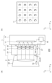
図1は、本発明の実施例1に係る撮像システム100の要部概略図(模式図)である。図1(a)は、後述する複数のレンズ部のうちの一部の光軸を含む断面(YZ断面)を示している。ここでの光軸とは、各レンズ部における各光学面(各レンズ面)の中心(頂点)を通る軸を指す。図1(a)においては、各レンズ部の軸上像高に集光される軸上光束のマージナル光線を示している。また、図1(b)は、撮像システム100における各部材の位置関係を示す図である。なお、撮像対象となる不図示の物体は、撮像システム100の-Z側(物体側)に配置されているものとする。
[Example 1]
FIG. 1 is a schematic diagram (schematic diagram) of main parts of an
撮像システム100は、撮像装置(カメラユニット)1と、それよりも物体側に配置された光学装置(アレイユニット)2とを有する。撮像装置1は、光学装置2の像面に配置される撮像面(受光面)を含む撮像素子(受光素子)11と、撮像素子11を保持する保持部材(筐体)12を備える。光学装置2は、夫々が物体の像を形成する複数のレンズ部で構成されるレンズアレイ21、各レンズ部の光軸上に配置される複数のフィルタで構成されるフィルタアレイ22、レンズアレイ21及びフィルタアレイ22を保持する保持部材(鏡筒)23を備える。
The
撮像素子11としては、CCDセンサやCMOSセンサなどの光電変換素子を採用することができる。また、撮像素子11は、可視光に限らず赤外光(近赤外光や遠赤外線光)などを光電変換できるように構成されていてもよい。例えば、使用波長帯域に応じて、Si、InGaAs、InAsSbなどの材料を用いた撮像素子を採用してもよい。また、撮像素子11の画素数は、撮像システム100において求められる分解能に基づいて決定することが望ましい。
As the
本実施例に係る複数のレンズ部の夫々は、1枚以上のレンズで構成されており、夫々が物体を撮像素子11の撮像面に結像する。言い換えると、レンズアレイ21の像面には、複数のレンズ部によって物体の複数の像(像アレイ)が形成される。すなわち、レンズアレイ21によれば、同一の物体の像を複製することができる。なお、複数のレンズ部は、製造や配置を容易にするために一体的に形成されていてもよく、あるいは個別の位置調整(フォーカス調整など)を可能にするために別体で形成されていてもよい。
Each of the plurality of lens units according to this embodiment is composed of one or more lenses, and each forms an image of an object on the imaging surface of the
本実施例に係る複数のフィルタ(光学フィルタ)は、互いに異なる透過特性を有する二つ以上のフィルタを含んでいる。ここでの透過特性とは、透過させる光の波長帯域(透過波長域)、透過させる偏光の方向や種類(偏光状態)、入射光の強度に対する透過光の強度(透過率)などの、入射光の状態を変化させる光学特性のことである。フィルタアレイ22を互いに異なる透過特性を有する複数のフィルタで構成することにより、同一の物体に対して互いに異なる複数の画像情報を同時に取得することが可能になる。
The plurality of filters (optical filters) according to this embodiment include two or more filters having mutually different transmission characteristics. The transmission characteristics here refer to the wavelength band of the light to be transmitted (transmission wavelength range), the direction and type of polarized light to be transmitted (polarization state), and the intensity of the transmitted light relative to the intensity of the incident light (transmittance). It is an optical property that changes the state of . By configuring the
フィルタアレイ22は、少なくとも透過特性が互いに異なる二つのフィルタ(第1及び第2のフィルタ)を含んでいればよい。言い換えると、透過特性が互いに同一である二つ以上のフィルタを含んでいてもよい。例えば、撮像システム100を測距装置(ステレオカメラ)として用いる場合、視差が互いに異なる二つの画像情報を用いて物体の距離情報を取得するため、各画像情報に対応する二つのフィルタの透過特性を略同等とすることが望ましい。ただし、互いに異なる複数の画像情報を一回の撮像でより多く取得するためには、複数フィルタの全ての透過特性を互いに異ならせることが望ましい。
The
例えば、互いに透過波長域の中心波長が異なる複数のフィルタ(バンドパスフィルタ)を用いることで、複数の波長帯域に対応する複数の画像情報を同時に取得することができる。このとき、撮像システム100を、一般的なカメラの波長帯域(RGB)よりも多い4種類以上の波長帯域に対応する画像情報を取得することができるマルチスペクトルカメラとして構成することが望ましい。さらに、撮像システム100を、100種類以上の波長帯域に対応する画像情報を取得することができるハイパースペクトルカメラとして構成することがより好ましい。なお、バンドパスフィルタの代わりに、入射光の波長を変換して射出する波長変換フィルタを用いてもよい。
For example, by using a plurality of filters (bandpass filters) whose transmission wavelength ranges have different center wavelengths, it is possible to simultaneously acquire a plurality of pieces of image information corresponding to a plurality of wavelength bands. At this time, it is desirable that the
あるいは、互いに種類が異なる複数の偏光フィルタを用いることで、複数の偏光状態に対応する複数の画像情報を同時に取得することができる。例えば、X方向(水平方向)、Y方向(垂直方向)、X方向及びY方向に対して45°の方向、の夫々に平行な方向の直線偏光を透過させる三つの直線偏光フィルタと、円偏光を透過させる円偏光フィルタを用いる場合が考えられる。このように、入射光の偏光状態を変化させる複数の種類の偏光フィルタを用いることで、物体の偏光特性(ストークスパラメータ)や、物体の偏光状態の2次元分布などの偏光情報を取得することができる。 Alternatively, by using a plurality of polarizing filters of different types, it is possible to simultaneously acquire a plurality of image information corresponding to a plurality of polarization states. For example, three linearly polarized filters transmit linearly polarized light in directions parallel to each of the X direction (horizontal direction), the Y direction (vertical direction), and the direction at 45 degrees to the X and Y directions, and circularly polarized light. A possible case is to use a circularly polarizing filter that transmits the light. In this way, by using multiple types of polarization filters that change the polarization state of incident light, it is possible to obtain polarization information such as the object's polarization characteristics (Stokes parameters) and the two-dimensional distribution of the object's polarization state. can.
なお、透過特性の種類が異なる複数のフィルタでフィルタアレイ22を構成することで、波長情報、偏光情報、輝度情報、視差情報などの異なる種類の情報を同時に取得できるようにしてもよい。このとき、互いに異なる種類の複数のフィルタの夫々を、互いに異なるレンズ部の光軸上に配置した構成に限らず、同一の光軸上に配置した構成を採ってもよい。後者の場合、取得した画像情報を不図示の画像処理部によってフィルタリングすることで、異なる種類の画像情報に分離することができる。
Note that by configuring the
また、一般的に可視波長帯域で使用されるシリコン材料で構成される撮像素子11は、短波長帯域(450nm以下)及び長波長帯域(750nm以上)よりも中心波長帯域(550nm近傍)に対する感度の方が高いという感度特性を有している。よって、これらの各波長帯域に対応する複数のバンドパスフィルタを用いる場合、中心波長帯域に対応するバンドパスフィルタが配置されている光軸上に減光フィルタを配置することが好ましい。このとき、偏光フィルタを減光フィルタとして用いることで、各画像情報の輝度のバランスを補正することだけでなく、波長情報及び偏光情報を同時に取得することが可能になる。
In addition, the
物体からの光を分光して所望の複数の画像情報を得るためには、各レンズ部及び各フィルタの夫々を互いに対となるように配置することが望ましい。言い換えると、一つのレンズ部を通過した光の全てが、その光軸上に配置された1種類のフィルタのみを透過することが望ましい。なお、ここでの1種類のフィルタとは、同一の光軸上に配置された複数のフィルタ素子で構成されたフィルタを含む。しかし、フィルタアレイ22のみが交換可能な構成、あるいはレンズアレイ21のみが交換可能な構成では、各レンズ部及び各フィルタの対応関係が崩れてしまい、良好な画像情報が得られなくなる可能性がある。例えば、レンズアレイ21を交換して各レンズ部のサイズ(有効径)や配置を変更する場合、それに合わせて各フィルタのサイズや配置を変更することが必要になる。
In order to obtain a plurality of desired image information by separating light from an object, it is desirable to arrange each lens section and each filter in pairs with each other. In other words, it is desirable that all of the light passing through one lens section pass through only one type of filter arranged on the optical axis. Note that one type of filter here includes a filter composed of a plurality of filter elements arranged on the same optical axis. However, in a configuration where only the
また、各レンズ部の像面における色収差は対応するバンドパスフィルタの透過特性によって変化し、それに応じて各レンズ部のピント位置(フォーカス位置)や歪曲収差も変化してしまう。バンドパスフィルタ以外のフィルタを用いた場合にも、各フィルタの異方性などに応じて光学性能の変化が生じてしまう可能性がある。よって、フィルタアレイ22を交換して各フィルタの透過特性を変更する場合、それに合わせて各レンズ部の位置や構成(設計)を変更することが必要になる。ただし、仮にレンズアレイ21及びフィルタアレイ22を個別に交換でき、夫々の適切な組み合わせを選択できる構成であったとしても、夫々の相対位置の誤差によって良好な光学性能が得られなくなる可能性がある。
Furthermore, the chromatic aberration at the image plane of each lens section changes depending on the transmission characteristics of the corresponding bandpass filter, and the focus position and distortion aberration of each lens section also change accordingly. Even when filters other than bandpass filters are used, optical performance may change depending on the anisotropy of each filter. Therefore, when replacing the
そこで、本実施例においては、レンズアレイ21及びフィルタアレイ22を保持部材23によって一体的に保持することで、夫々の相対位置のずれを抑制している。また、保持部材23は、撮像装置1と結合するための第1のマウント部(第1の結合部)24を有している。これにより、光学装置2をアクセサリ装置として、第1のマウント部24を介して撮像装置1に着脱可能とすることができる。すなわち、撮像装置1に対して、レンズアレイ21及びフィルタアレイ22を一体的に保持しつつ同時に交換することが可能になる。
Therefore, in this embodiment, the
この構成によれば、レンズアレイ21及びフィルタアレイ22の相対位置のずれを抑制しつつ、取得する画像情報の種類や解像度を変更することができる。具体的には、フィルタアレイ22を透過特性が異なるものに交換する際に、同時にレンズアレイ21を各フィルタアレイに対応する(最適化された)ものに交換することができる。これにより、各レンズの収差やピントの変化を抑制することができる。また、レンズアレイ21をレンズ部の数が異なるものに交換することで、撮像システム100の解像度を変更することができる。この場合にも、同時にフィルタアレイ22を各レンズアレイに対応するものに交換することができる。
According to this configuration, the type and resolution of image information to be acquired can be changed while suppressing deviations in the relative positions of the
このように、本実施例に係る撮像システム100によれば、取得したい画像情報に応じて光学装置2を交換することができる。特に、レンズアレイ21が交換可能であるため、レンズ部の数を増減させることで、画像情報の種類(バンド数など)や解像度を増減させることができる。そして、レンズアレイ21及びフィルタアレイ22を一体的に交換可能であるため、交換時の光学性能の変化を抑制することができる。これにより、光学装置2の構成によらず、共通の撮像装置1によって複数の良好な画像情報を同時に取得することが可能になる。
In this way, according to the
第1のマウント部24の形状は、撮像装置1に設けられたマウント部13に対応する形状とすればよい。例えば、光軸方向(Z方向)から見たときに撮像面を囲む円周上に設けられた結合部(凸部や凹部、磁石など)を第1のマウント部24として採用することができる。図1(a)においては、第1のマウント部24を凹部として示し、撮像装置1のマウント部13を凸部として示しているが、各マウント部の形状はこれに限られるものではない。また、第1のマウント部24に、撮像装置1と電気的に接続するための電気接点(端子)を設けることが好ましい。これにより、光学装置2は電気接点を介して撮像装置1と通信を行ったり撮像装置1から電力を受給したりすることが可能になる。
The shape of the first mount section 24 may be a shape corresponding to the mount section 13 provided in the
なお、図2に示すように、保持部材23は、像側に設けられる第1のマウント部24だけでなく、物体側に設けられる第2のマウント部(第2の結合部)25を有していてもよい。これにより、光学装置2に対して後述するレンズ装置やアダプタ装置などのアクセサリ装置を着脱可能とすることができる。図2においては、第2のマウント部25を凸部として示しているが、第2のマウント部25の形状はこれに限られず、装着されるアクセサリ装置におけるマウント部の形状に応じて設定すればよい。なお、第2のマウント部25についても、アクセサリ装置に対して通信や電力の受供給を行うための電気接点を設けることが好ましい。
Note that, as shown in FIG. 2, the holding
本実施例に係る光学装置2は、図1(b)に示したように、9個のレンズ部と、各レンズ部の光軸上に配置される9個のフィルタを備えている。すなわち、同一の光軸上に配置されたレンズ部及びフィルタをまとめて一つの結像部であるとすると、光学装置2は9個の結像部を備えていることになる。複数の結像部をまとめて結像部アレイとも呼ぶ。なお、結像部の数はこれに限られるものではなく、光学装置2は少なくとも二つの結像部を備えていればよい。ただし、一回の撮像でより多くの透過特性に対応する画像情報を取得するためには、結像部を四つ以上設けることが望ましく、本実施例のように結像部を九つ以上設けることがより好ましい。
The
物体からの光は、レンズアレイ21及びフィルタアレイ22を順に介して撮像素子11の撮像面に到達する。このとき、撮像面には、各結像部に応じた9個の像(複製像)が形成される。図1(b)では、仮に被写体としての物体が「C」の文字である場合に撮像面に形成される像を示している。本実施例に係る撮像システム100が備える結像光学系は、夫々が単レンズから成る複数のレンズ部で構成されたレンズアレイ21のみであるため、各像は倒立像となっている。
Light from the object reaches the imaging surface of the
なお、撮像装置1の小型化のためには、本実施例に係る撮像素子11のように、各レンズ部に対して共通の(単一の)撮像素子を設けることが望ましい。また、各レンズ部に対して共通の撮像素子を用いることで、光学装置2の交換によってレンズ部の数や配置が変化した場合にも、良好な画像情報を取得することができる。このとき、撮像素子11の利用効率を向上させるためには、撮像素子11を構成する複数の画素(フォトダイオード)をできるだけ隙間なく均一に配置することが望ましい。
Note that in order to downsize the
ただし、必要に応じて、各レンズ部に対して個別に撮像素子を設けてもよい。この場合、装置全体の小型化のためには、各撮像素子をできるだけ隙間なく均一に配置することが望ましい。また、光学装置2の小型化のためには、撮像素子11の撮像面の形状に合わせて各レンズ部を配置することが望ましい。具体的には、図1(b)に示すように、XY断面において各レンズ部を正方配置することが望ましい。なお、撮像素子11の撮像面が正方形でない場合は、各レンズ部の配置のアスペクト比などを変更してもよい。
However, if necessary, an image sensor may be provided individually for each lens section. In this case, in order to downsize the entire device, it is desirable to arrange the image sensors as uniformly as possible with as few gaps as possible. Furthermore, in order to downsize the
図1(b)では、撮像素子11の撮像面における複数の像(結像領域)の境界を破線で示している。ただし、この破線は便宜的に撮像面における各結像部に対応する区分を示したものであり、構造物ではない。実際に破線で示したように各像の境界を明確にする必要がある場合は、各結像部に対応する絞り部材(遮光部材)を設けることが望ましい。例えば、図2に示すように、各結像部の境界に遮光部材26を設けることで、ある結像部に対応する結像領域に、隣接する別の結像部からの不要光(迷光)が入射することを抑制することができる。
In FIG. 1(b), the boundaries between a plurality of images (imaging areas) on the imaging surface of the
上述したように、本実施例に係る光学装置2は撮像装置1に対して着脱可能に構成されているため、遮光部材26は光学装置2における保持部材23によって保持されていることが望ましい。これにより、レンズアレイ21及びフィルタアレイ22を交換する際に、同時に遮光部材26をレンズアレイ21及びフィルタアレイ22に対応するものに交換することができる。また、不要光を十分に遮光するためには、図2に示すように遮光部材26が撮像装置1の内部における撮像素子11の近傍まで延在した構成を採ることが好ましい。
As described above, since the
なお、図2では、図1(b)において破線で示した矩形の結像領域に対応するように遮光部材26が配置されているが、遮光部材26の配置はこれに限られるものではなく、各結像部の配置及び要求される各結像領域の形状に対応してさえいればよい。例えば、各結像領域の形状を矩形ではなく円形等の任意の形状としたり、各結像領域の大きさを異ならせたりしてもよい。ただし、撮像面の利用効率を向上させるためには、図1(b)に示すように各結像領域を同じ大きさの矩形とすることで撮像面を等分割した構成とすることが望ましい。あるいは、各結像部がハニカム配列されている場合は、これに合わせて遮光部材26をハニカム構造とすればよい。
In addition, in FIG. 2, the
レンズアレイ21及びフィルタアレイ22の光軸方向における配置の順番は、図1に示したものに限られない。例えば、干渉型のバンドパスフィルタを用いる場合は、その角度特性(角度依存性)を鑑みて、各フィルタに対する光の入射角が小さくなるように、フィルタアレイ22をレンズアレイ21よりも物体側に配置することが好ましい。ただし、レンズアレイ21における各レンズ部が十分なテレセントリック性を有している場合は、フィルタアレイ22がレンズアレイ21よりも像側(+Z側)に配置されていたとしても、各フィルタに対する光の入射角を小さくすることができる。
The order of arrangement of the
また、フィルタアレイ22がレンズアレイ21よりも物体側に配置されている場合、レンズアレイ21に入射する軸外光線の欠け(ヴィネッティング)が発生してしまう可能性がある。よって、例えば吸収型のバンドパスフィルタなどの角度依存性が小さいフィルタを用いる場合や、フィルタの角度依存性よりも光利用効率を優先する場合には、フィルタアレイ22をレンズアレイ21よりも像側に配置することが好ましい。
Furthermore, if the
本実施例に係る撮像システム100において、光学装置2を撮像装置1に装着する際に、夫々のマウント部の製造の精度によっては取り付け誤差が生じ、レンズアレイ21及びフィルタアレイ22と撮像素子11との位置関係に誤差が生じる可能性がある。このような誤差が生じた場合、撮像素子11の撮像面に対するレンズアレイ21のピントずれ(デフォーカス)が生じてしまう。そこで、レンズアレイ21を光軸方向に移動するための移動機構を設け、レンズアレイ21のピントを調整できるように構成することが望ましい。
In the
あるいは、レンズアレイ21の代わりに撮像素子11を光軸方向に移動するための移動機構を設け、撮像素子11の移動によるピント調整(センサフォーカス)ができるように構成してもよい。なお、光学装置2の取り付け誤差によりレンズアレイ21の像面が撮像面に対して傾き、像面湾曲やレンズ部ごとに異なるピントずれが生じてしまう可能性がある。よって、撮像素子11の光軸に対する傾き(チルト角)を変更することができるように構成することが好ましい。さらに、撮像素子11を光軸に垂直な方向の成分を含む方向に移動させることで、像ブレ補正(手振れ補正)を行うことができるようにしてもよい。
Alternatively, a moving mechanism for moving the
また、フィルタアレイ22を構成するフィルタの透過特性によっては、各レンズ部の夫々において生じるピントずれの向きやずれ量が互いに異なる場合がある。よって、レンズアレイ21を構成する複数のレンズ部の夫々の位置を個別に調整することができるように構成することがより好ましい。この場合、各レンズ部としてロッドレンズのような光軸方向に長いレンズを採用することで、各レンズ部を安定して保持することができるため、各レンズ部の調整時の光軸に対する傾き偏心の発生を抑制することが可能になる。
Furthermore, depending on the transmission characteristics of the filters constituting the
なお、色収差の補正などを目的として、各レンズ部を同一の光軸上に配置される複数のレンズによって構成した場合にも、各レンズ部を保持する鏡筒(小径鏡筒)が光軸方向に長い形状となるため、同様の効果を得ることができる。このとき、各鏡筒の内側の光軸に垂直な方向における端部(コバ部)に遮光塗料を塗布したり、隣接する鏡筒の間に遮光部材を設けたりすることにより、迷光が撮像面に到達することを抑制することができる。例えば、図2に示した遮光部材26を鏡筒として用いてもよい。
Note that even when each lens section is composed of multiple lenses arranged on the same optical axis for the purpose of correcting chromatic aberration, etc., the lens barrel (small diameter lens barrel) that holds each lens section is aligned in the optical axis direction. Since it has a long shape, the same effect can be obtained. At this time, by applying light-shielding paint to the inner end (edge part) of each lens barrel in the direction perpendicular to the optical axis, or by providing a light-shielding member between adjacent lens barrels, stray light can be prevented from forming on the imaging surface. can be suppressed from reaching . For example, the
次に、撮像システム100における処理系について説明する。上述したように、撮像素子11から出力される画像情報の特性は、撮像装置1に装着される光学装置2の構成によって変化する。よって、撮像装置1にどのような光学装置2が装着されたとしても、画像情報を適切に処理するためのシステムを実現することが望ましい。具体的に、光学装置2は、撮像装置1に対して情報を送受信するための通信部や、撮像装置1との接続を認識するための認識部を備えていることが好ましい。
Next, a processing system in the
図2では、撮像装置1が処理部14を有し、光学装置2が処理部27を有する場合を示している。処理部14は、少なくとも通信部及び認識部としての機能を備えている。処理部27は、少なくとも通信部(記憶部)としての機能を備えている。処理部14及び処理部27は、撮像装置1に光学装置2が装着された際に互いに電気的に接続され、相互に情報(信号)を送受信することができる。処理部14及び処理部27は、撮像装置1及び光学装置2の夫々のマウント部に設けられた電気接点を介して情報を送受信することができる。ただし、各マウント部に電気接点が設けられていない場合などは、例えば光通信などの無線通信を行ってもよい。
FIG. 2 shows a case where the
処理部27は光学装置2に関する固有情報を記憶しており、処理部14はその固有情報を受信することによって光学装置2が撮像装置1に装着されたことを認識する。光学装置2の固有情報は、例えばレンズアレイ21及びフィルタアレイ22の夫々に関する識別番号などの識別子(ID)又はレンズアレイ21及びフィルタアレイ22の組み合わせに関する識別子である。処理部14は、受信した固有情報に基づいて、光学装置2の種別や個体を認識することができる。
The
本実施例に係る撮像システム100においては、撮像装置1が電源を有しており、光学装置2は電源を有していないため、撮像装置1における処理部14によって光学装置2の装着を認識することが望ましい。この場合、処理部27は、固有情報を記憶する記憶部(通信部)としての機能だけを有することになる。ただし、処理部14及び処理部27が無線通信を行う場合は、撮像装置1及び光学装置2の夫々に電源を設け、夫々が個別に認識を行う構成を採ってもよい。
In the
処理部14は、画像処理部(プロセッサ)としての機能も備えており、受信した固有情報に応じて、撮像素子11から出力される画像情報を処理する。このとき、予め光学装置2におけるレンズアレイ21の情報(レンズ部の数や配置など)やフィルタアレイ22の情報(フィルタの透過特性や配置など)と固有情報を紐づけて、データテーブルとして処理部14又は外部装置に記録しておくことが望ましい。これにより、処理部14は、受信した固有情報をデータテーブルに照らし合わせることで、どのような構成(特性)の光学装置2が装着されたのかを認識することができる。
The
なお、必要に応じて、上述したようなレンズアレイ21やフィルタアレイ22の情報そのものを固有情報として処理部27に記録しておき、処理部14が処理部27からその情報を取得するように構成してもよい。ただし、光学装置2の簡素化及び小型化のためには、処理部27に記録しておく情報は、上述したように光学装置2の種別や個体を弁別するための識別番号などの最小限のものとすることが望ましい。
Note that, if necessary, the information on the
例えば、フィルタアレイ22がバンドパスフィルタで構成されている場合、処理部14はレンズアレイ21及びフィルタアレイ22の情報に基づいて、撮像素子11から出力される一つの画像情報を適切に分割及び再配列する。これにより、バンドパスフィルタに対応する波長帯域ごとの複数の画像情報(マルチスペクトル画像)を生成することができる。このとき、必要に応じて、複数の画像情報を重ね合わせる(再合成する)ことで、1枚のマルチスペクトル画像を生成してもよい。
For example, when the
なお、撮像素子11から出力される画像情報を外部装置に送信することで、処理部14ではなく外部装置によって上述したような画像処理を行うように構成してもよい。この場合、光学装置2の情報と画像情報との対応関係をわかりやすくするために、処理部27が記憶している情報を画像情報に付加してから外部装置に送信することが好ましい。あるいは、処理部27を外部装置として撮像装置1の外部に設けてもよい。
Note that by transmitting the image information output from the
以上、本実施例に係る撮像システム100によれば、レンズアレイ21及びフィルタアレイ22を一体的に保持しつつ撮像装置1に対して着脱可能に構成することで、複数の良好な画像情報を同時に取得することができる。特に、レンズアレイ21及びフィルタアレイ22を交換することで、バンド数や解像度が異なる様々な画像情報を取得することが可能になる。
As described above, according to the
[実施例2]
以下、本発明の実施例2に係る撮像システム200について説明する。本実施例に係る撮像システム200において、上述した実施例1に係る撮像システム100と同等の構成については説明を省略する。
[Example 2]
An
図3は、本実施例に係る撮像システム200の要部概略図(模式図)である。図3(a)は複数のレンズ部のうちの一部の光軸を含む断面を示し、図3(b)は撮像面を-Z方向から見たときの正面図を示している。撮像システム200の撮像システム100に対して異なる点は、光学装置2におけるレンズアレイ21及びフィルタアレイ22の構成と、光学装置2の物体側にレンズ装置(レンズユニット)3が装着されている点である。
FIG. 3 is a schematic diagram (schematic diagram) of main parts of the
本実施例に係る光学装置2において、レンズアレイ21は16個のレンズ部で構成され、フィルタアレイ22は各レンズ部に対応する16個のフィルタで構成されている。すなわち、光学装置2は16個の結像部を備えており、撮像素子11の撮像面には各結像部によって16個の像が形成される。このように、実施例1と実施例2とで結像部の数や配置が異なるが、各結像部に対して共通の撮像素子11を用いることで、撮像装置1の構成を変更せずに良好な画像情報を取得することができる。
In the
レンズ装置3は、光学装置2の各結像部に対して共通である1枚以上のレンズを有する光学系31と、光学系31を保持する保持部材(鏡筒)32を備えている。また、保持部材32は、光学装置2の第2のマウント部25と結合するためのマウント部33を有している。これにより、マウント部33を介してレンズ装置3を光学装置2に着脱可能とすることができる。ただし、レンズアレイ21及びフィルタアレイ22と光学系31との相対位置を決定できるのであれば、この構成に限られるものではない。例えば、光学装置2の保持部材23に開口(穴部)を設け、その開口を介してレンズ装置3を撮像装置1に直接装着できるようにしてもよい。
The
本実施例に係るレンズ装置3は、撮像システム200の画角(撮像画角)を変換する役割を果たしている。すなわち、レンズ装置3を光学系31の構成が異なるものに交換することで、様々な画角に対応する画像情報を取得することができる。なお、レンズ装置3を用いずに、各レンズ部を複数のレンズ群で構成し、隣接するレンズ群の間隔を変更可能とすることで、撮像システム1200の画角を変更することも可能である。しかし、その場合はレンズアレイ21の製造及び制御の難易度が高くなり、かつ光学装置2の構成が複雑化及び大型化してしまう。
The
よって、光学装置2の簡素化及び小型化のためには、本実施例のようにレンズ装置3の交換によって撮像システム100の画角を変更できるように構成すること望ましい。なお、レンズ装置3における光学系31を構成する少なくとも1枚のレンズを移動可能とすることで、ピント調整(フォーカシング)を行うようにしてもよい。また、光学系31を複数のレンズ群で構成して隣接するレンズ群の間隔を変更し、撮像システム1200の焦点距離を変更することで、画角や結像倍率を調整できるようにしてもよい。
Therefore, in order to simplify and downsize the
なお、レンズアレイ21における各レンズ部の焦点位置と撮像素子11の撮像面が一致している場合、無限遠に位置する物体から出射してレンズアレイ21に入射する光は平行光になる。よって、レンズ装置3における光学系31をコリメータ光学系として、光学系31が平行光をレンズアレイ21に導光するように構成することが望ましい。この構成によれば、各マウント部における取り付け誤差によりレンズ装置3が光軸に垂直な方向にずれた場合において、結像性能の変化を抑制することができる。
Note that when the focal position of each lens section in the
ただし、この構成においてレンズ装置3を取り外した場合、すなわち実施例1のように光学装置2のみを撮像装置1に装着して撮像を行う場合、近距離に位置する物体にピントが合わず、撮像画像においてボケが生じてしまう。よって、この構成においては、上述したようにレンズアレイ21と撮像素子11との相対位置を変化させるための機構を設けることで、フォーカシングを行うことができるようにすることが望ましい。
However, if the
また、レンズ装置3は、光学装置2における処理部27と同様の処理部34を備えていることが望ましい。処理部34は、レンズ装置3に関する固有情報を記憶しており、その固有情報を光学装置2における処理部27を介して、又は直接撮像装置1における処理部14に送信することができる。処理部14は、レンズ装置3の固有情報に基づいて、レンズ装置3の種別や個体を認識することができる。また、処理部14は、レンズ装置3の固有情報及び光学装置2の少なくとも一方の固有情報に応じて、撮像素子11から出力される画像情報を処理することができる。
Further, it is desirable that the
[実施例3]
以下、本発明の実施例3に係る撮像システム300について説明する。本実施例に係る撮像システム300において、上述した実施例2に係る撮像システム200と同等の構成については説明を省略する。
[Example 3]
An
図4は、本実施例に係る撮像システム300の要部概略図(模式図)である。図4(a)は複数のレンズ部のうちの一部の光軸を含む断面を示し、図4(b)はレンズアレイ21の正面図を示し、図4(c)は撮像面の正面図を示している。撮像システム300の撮像システム200に対して異なる点は、レンズアレイ21を構成するレンズ部の数と、一部のレンズ部のサイズ及び配置である。
FIG. 4 is a schematic diagram (schematic diagram) of main parts of the
本実施例に係る光学装置2において、レンズアレイ21は13個のレンズ部で構成され、フィルタアレイ22は各レンズ部に対応する13個のフィルタで構成されている。すなわち、光学装置2は13個の結像部を備えており、撮像素子11の撮像面には各結像部によって13個の像が形成される。そして、図4(b)に示すように、本実施例に係るレンズアレイ21におけるレンズ部21dのサイズは他のレンズ部よりも大きい。具体的に、本実施例に係るレンズ部21dは、実施例2に係るレンズアレイ21において四つのレンズ部が配置されていた領域を占めるように配置されている。
In the
本実施例では、各レンズ部が開口絞りの役割を兼ねており、各レンズ部のサイズ(有効径)によって各結像部の明るさ(F値)が決定されている。よって、レンズ部21dによって形成される像の光量は、他のレンズ部によって形成される像の光量よりも多い。このように、レンズアレイ21における一部のレンズ部のサイズを変更することで、複数の異なる光量情報を含む撮像情報を一度の撮像で取得することができる。なお、レンズ部21d以外にも、有効径のサイズが異なるレンズ部を設けてもよい。
In this embodiment, each lens section also serves as an aperture stop, and the brightness (F number) of each imaging section is determined by the size (effective diameter) of each lens section. Therefore, the amount of light of the image formed by the
また、本実施例では、レンズ部21dのサイズを他のレンズ部よりも大きくしたことに伴い、レンズ部21dの焦点距離を他のレンズ部よりも大きくし、かつ図4(a)に示すようにレンズ部21dを他のレンズ部よりも物体側に配置している。そのため、図4(c)に示すように、レンズ部21dによって形成される像11dが、他のレンズ部によって形成される像よりも大きくなっている。よって、撮像素子11における画素密度が一定である場合、像11dの解像度は他の像の解像度よりも高くなる。したがって、この構成によれば、複数の異なる解像度の撮像情報を一度の撮像で取得することができる。
In addition, in this embodiment, as the size of the
例えば、フィルタアレイ22をバンド幅が互いに異なる複数のバンドパスフィルタで構成した場合、収差補正が比較的難しい長波長帯域に対応するバンドパスフィルタをレンズ部21dの光軸上に配置することで、十分な解像度を確保することができる。あるいは、レンズ部21dの光軸上にフィルタを配置せずに、レンズ部21dを輝度情報(輝度分布)の取得に特化させてもよい。この場合、像11dより取得した輝度情報に基づいて、他の像より取得した画像情報のダイナミックレンジの補正や、サブピクセル情報を利用した超解像処理などを行うことができる。
For example, when the
[実施例4]
以下、本発明の実施例4に係る撮像システム400について説明する。本実施例に係る撮像システム400において、上述した実施例1に係る撮像システム100と同等の構成については説明を省略する。
[Example 4]
An
図5は、本実施例に係る撮像システム400の要部概略図(模式図)である。図5(a)は複数のレンズ部のうちの一部の光軸を含む断面を示し、図5(b)は撮像面の正面図を示している。撮像システム400の撮像システム100に対して異なる点は、光学装置2の物体側にレンズ装置3及びアダプタ装置(アダプタユニット)4が装着されている点である。
FIG. 5 is a schematic diagram (schematic diagram) of main parts of an
本実施例に係るレンズ装置3は、実施例2及び3に係るレンズ装置3と同様に、1枚以上のレンズを有する光学系31と、光学系31を保持する保持部材32を備えている。しかし、実施例2及び3に係る光学系31とは異なり、本実施例に係る光学系31は、物体からの光を集光することで物体の中間像を形成している。
The
本実施例に係るアダプタ装置4は、光を拡散させる拡散素子41と、1枚以上のレンズを有する光学系42と、拡散素子41及び光学系42を保持する保持部材43を備えている。拡散素子41は、レンズ装置3により形成される中間像面(1次結像面)の位置に配置されており、スクリーンとしての役割を果たしている。拡散素子41としては、拡散面(粗面)を有する拡散部材(拡散板)や、複数の微細なレンズで構成されるマイクロレンズアレイなどを採用することができる。光学系42は、拡散素子41からの光を平行光に変換するコリメータ光学系としての機能を有する。
The
そして、アダプタ装置4における保持部材43は、光学装置2の第2のマウント部25と結合するためのマウント部44と、レンズ装置3のマウント部33と結合するためのマウント部45とを有している。これにより、各マウント部を介してアダプタ装置4を光学装置2及びレンズ装置3に着脱可能とすることができる。このとき、レンズ装置3が撮像装置1及び光学装置2に直接着脱することができない場合であっても、アダプタ装置4を介することで間接的に着脱することが可能になる。
The holding
ただし、光学装置2の第1のマウント部24とレンズ装置3のマウント部33とを同じ形状とし、撮像装置1のマウント部13とアダプタ装置4のマウント部45とを同じ形状とすることが望ましい。言い換えると、撮像装置1に対して着脱可能なレンズ装置3が、アダプタ装置4にも着脱可能である構成とすることが望ましい。これにより、一般的なカメラとしての撮像装置1及び一般的な交換レンズとしてのレンズ装置3を用いて、複数の画像情報を一回の撮像で同時に取得できる撮像システムを構成することが可能になる。
However, it is desirable that the first mount section 24 of the
また、本実施例に係る撮像システム400は、アダプタ装置4を用いることで、実施例2及び3に係る撮像システム200,300と同様に光学装置2に平行光が入射する構成を採っている。これにより、本実施例に係る光学装置2を、実施例2及び3に示したような物体の中間像を形成しないレンズ装置に対しても適用することが可能になる。よって、光学装置2、レンズ装置3、及びアダプタ装置4の夫々の互換性を確保するために、各装置のマウント部の形状は、夫々の光学系の構成にかかわらず同一の形状とすることが望ましい。
Further, the
なお、本実施例のレンズ装置3のように物体の中間像を形成するレンズ装置を用いる場合は、その中間像面の位置に視野絞りを配置することが望ましい。これにより、撮像素子11の撮像面に形成される各像の境界の形状やサイズを適切に設定することができる。例えば、各結像部からの光が撮像面において互いに干渉する場合は、視野絞りに設けられる開口のサイズ(開口径)を小さくすればよい。このとき、撮像素子11の利用効率を向上させるためには、視野絞りの開口の形状を、撮像面を等分割することができる矩形などの形状とすることが望ましい。
Note that when using a lens device that forms an intermediate image of an object like the
また、撮像面における各像の境界は、視野絞りを中間像面の位置に近づける程明確になるため、本実施例のように中間像面の位置に拡散素子41を配置する場合は、視野絞りを拡散素子41に密着するように配置することが好ましい。このとき、拡散素子41が厚みを持つ場合は、拡散素子41の内部での散乱の影響を低減するために、視野絞りを拡散素子41の像側に配置することがより好ましい。本実施例においては、図5に示すように、拡散素子41の中央部(矩形部)以外に遮光部材(遮光塗料)を設けることで、拡散素子41に視野絞りとしての機能を持たせることができる。あるいは、視野絞りを構成する遮光部材に設けられる開口部に拡散素子41を配置することで、視野絞りと拡散素子41とを一体的に構成してもよい。
In addition, the boundary between each image on the imaging plane becomes clearer as the field diaphragm approaches the position of the intermediate image plane. It is preferable to arrange the
中間像面の位置に拡散素子41を配置した場合、レンズ装置3からの光は拡散素子41によって拡散されるため、レンズ装置3からの光の入射角に関する情報が失われ、各像における視差の発生を抑制することができる。ただし、本実施例に係る撮像システム400を後述するような測距装置として用いる場合、各像の視差を用いて物体までの距離に関する情報を取得するため、レンズ装置3からの光の入射角に関する情報を残しておく必要がある。その場合は、視野絞りの直前に拡散素子41の代わりにフィールドレンズとしての正レンズを配置することで、入射角に関する情報を残しつつ本実施例と同様の機能を実現することができる。
When the diffusing
図5(a)に示すように、アダプタ装置4は、光学装置2における処理部27と同様の処理部46を備えていることが望ましい。処理部46は、アダプタ装置4に関する固有情報を記憶しており、その固有情報を光学装置2における処理部27を介して、又は直接撮像装置1における処理部14に送信することができる。処理部14は、アダプタ装置4の固有情報に基づいて、アダプタ装置4の種別や個体を認識することができる。また、処理部14は、レンズ装置3、アダプタ装置4、及び光学装置2の少なくとも一つの固有情報に応じて、撮像素子11から出力される画像情報を処理することができる。このとき、レンズ装置3の固有情報を用いて、レンズ装置3で生じる収差による画像情報への影響を補正してもよい。
As shown in FIG. 5A, the
ここで、本実施例に係る撮像システム400は、レンズ装置3によって結像した物体を光学装置2によって再結像する構成を採っているため、図5(b)に示すように、本実施例における撮像面には正立像が形成される。したがって、撮像装置1における処理部14によって画像情報を適切に処理するためには、撮像面に形成される像が倒立像なのか正立像なのかを判別するための情報が必要になる。
Here, since the
よって、アダプタ装置4の処理部46には、像の反転の有無を識別するための情報を記憶させておくことが好ましい。例えば、アダプタ装置4には物体の中間像を形成するレンズ装置のみが装着されるということを前提とする場合、処理部46には物体の像が1回結像された(反転した)ということを識別するための情報を記憶させておけばよい。なお、仮に光学装置2における各結像部が物体を複数回結像する構成を採っている場合は、処理部27にも像の反転に関する情報を記憶させておけばよい。
Therefore, it is preferable that the
[測距装置]
以下、上述した各実施例に係る撮像システムを車載カメラや監視カメラなどの測距装置として用いる場合について説明する。
[Distance measuring device]
Hereinafter, a case will be described in which the imaging system according to each of the embodiments described above is used as a distance measuring device such as a vehicle-mounted camera or a surveillance camera.
光学装置2におけるレンズアレイ21を構成する各レンズ部の光軸は、X方向及びY方向の少なくとも一方において互いに離間しているため、各レンズ部により形成される像には視差が生じている。よって、この視差に関する情報(視差情報)に基づいて、撮像装置1の処理部14や外部装置により物体までの距離に関する情報(距離情報)を取得することができる。なお、ここでの距離情報とは、物体との間隔、デフォーカス量、像ズレ量、などの物体との相対位置に関する情報のことであり、画像情報における物体の距離値を直接的に表すものでも、距離値に対応する情報を間接的に表すものでもよい。
Since the optical axes of the respective lens sections constituting the
例えば、図1(b)に示したフィルタアレイ22における何れか二つのフィルタを、互いに同じ透過波長域のバンドパスフィルタとすることにより、このバンドパスフィルタを含む結像部のペアがステレオ光学系(測距光学系)として機能する。すなわち、図1(a)に示した撮像システム100がステレオカメラ(測距装置)として機能することになる。よって、この結像部のペアにより形成されるステレオ像の視差情報に基づいて、物体の距離情報を取得することができる。
For example, by making any two filters in the
なお、ステレオ光学系として用いる結像部のペアは、水平方向(X方向)に配列されたものであっても、鉛直方向(Y方向)に配列されたものであっても、斜め方向に配列されたものであってもよい。ただし、ステレオ像の視差が大きいほど測距精度が向上するため、複数の結像部の中で最も離間したペアをステレオ光学系として用いることが好ましい。また、一対の結像部だけでなく、他の結像部のペアを測距に用いてもよい。奥行方向(Z方向)に配置される複数の物体を測距対象とする場合、手前の物体の背後にある物体の情報が不足するオクルージョンという問題が生じるため、三つ以上の結像部をセットとして測距に用いることがより好ましい。 Note that the pair of imaging units used as a stereo optical system may be arranged horizontally (X direction), vertically (Y direction), or diagonally. It may be something that has been done. However, since the distance measurement accuracy improves as the parallax of the stereo images increases, it is preferable to use the pair that is most distant among the plurality of imaging units as the stereo optical system. Furthermore, in addition to the pair of imaging sections, other pairs of imaging sections may be used for distance measurement. When measuring multiple objects arranged in the depth direction (Z direction), there is a problem of occlusion, where information about objects behind the foreground object is insufficient, so three or more imaging units are set. It is more preferable to use it for distance measurement.
[変形例]
以上、本発明の好ましい実施形態及び実施例について説明したが、本発明はこれらの実施形態及び実施例に限定されず、その要旨の範囲内で種々の組合せ、変形及び変更が可能である。
[Modified example]
Although preferred embodiments and examples of the present invention have been described above, the present invention is not limited to these embodiments and examples, and various combinations, modifications, and changes can be made within the scope of the gist.
上述した各実施例では、レンズ部が開口絞りの役割を兼ねている場合、すなわちレンズ部の有効径がレンズ部自身によって定まる場合について説明したが、開口絞りを別部材として設けてもよい。また、一つの結像部において、レンズ部が複数のレンズを含む場合や、フィルタが複数のフィルタ素子を含む場合は、レンズ及びフィルタ素子を光軸方向において交互に配置してもよい。 In each of the embodiments described above, a case has been described in which the lens portion also serves as an aperture stop, that is, a case in which the effective diameter of the lens portion is determined by the lens portion itself, but the aperture stop may be provided as a separate member. Further, in one imaging section, when the lens section includes a plurality of lenses or when the filter includes a plurality of filter elements, the lenses and the filter elements may be arranged alternately in the optical axis direction.
さらに、レンズ部の瞳をXY断面において分割するように配置される複数のフィルタを備える結像部を採用してもよい。このとき、撮像面におけるその結像部に対応する領域に微小なレンズアレイを設けることで、撮像システムをプレノプティックカメラとして用いることができる。この構成によれば、一つのレンズ部の瞳を通過する光が分離されて、撮像面における互いに異なる画素に入射するため、より多くの画像情報を取得することが可能になる。 Furthermore, an imaging section including a plurality of filters arranged to divide the pupil of the lens section in the XY cross section may be employed. At this time, the imaging system can be used as a plenoptic camera by providing a minute lens array in a region corresponding to the imaging section on the imaging surface. According to this configuration, the light passing through the pupil of one lens section is separated and enters different pixels on the imaging surface, making it possible to acquire more image information.
上述した実施例2乃至4に係る撮像システムにおいては、光学装置2とレンズ装置3又はアダプタ装置4とが互いに着脱可能となっているが、必要に応じて夫々を一体化することで、互いの取り付け誤差の発生を抑制してもよい。例えば、光学装置2とレンズ装置3とを一体的に構成したり、光学装置2とレンズ装置3とアダプタ装置4とを一体的に構成したりすることで、撮像装置1に対して着脱可能な一つのレンズ装置(アクセサリ装置)としてもよい。あるいは、光学装置2とアダプタ装置4とを一体的に構成することで、撮像装置1及びレンズ装置3に対して着脱可能な一つのアダプタ装置(アクセサリ装置)としてもよい。
In the imaging systems according to the second to fourth embodiments described above, the
1 撮像装置
2 光学装置
21 複数のレンズ部(レンズアレイ)
22 複数のフィルタ(フィルタアレイ)
23 保持部材
24 第1のマウント部
1
22 Multiple filters (filter array)
23 Holding member 24 First mount part
Claims (17)
前記複数のレンズ部の光軸上に配置される複数のフィルタとを備える光学装置であって、
前記物体からの光を前記複数のレンズ部に導光する、前記複数のレンズ部に対して共通の第1光学系と、
前記複数のレンズ部、前記複数のフィルタ、及び前記第1光学系を一体的に保持する保持部材とを更に備え、
前記複数のフィルタは、互いに異なる透過特性を有する第1及び第2のフィルタを含み、
前記保持部材は第1及び第2のマウント部を有し、
前記第1のマウント部を介して撮像装置に着脱可能であり、かつ前記第2のマウント部を介して前記光学装置とは異なるアクセサリ装置に着脱可能であり、
前記アクセサリ装置は、前記撮像装置に対して着脱可能であることを特徴とする光学装置。 a plurality of lens units each forming an image of an object;
An optical device comprising a plurality of filters arranged on the optical axis of the plurality of lens parts,
a first optical system common to the plurality of lens units that guides light from the object to the plurality of lens units;
further comprising a holding member that integrally holds the plurality of lens parts, the plurality of filters, and the first optical system,
The plurality of filters include first and second filters having mutually different transmission characteristics,
The holding member has first and second mount parts,
is removable from an imaging device via the first mount portion, and removable from an accessory device different from the optical device via the second mount portion;
The optical device is characterized in that the accessory device is removably attached to the imaging device.
Priority Applications (3)
| Application Number | Priority Date | Filing Date | Title |
|---|---|---|---|
| JP2018195419A JP7378920B2 (en) | 2018-10-16 | 2018-10-16 | Optical device and imaging system equipped with the same |
| US16/594,968 US20200120245A1 (en) | 2018-10-16 | 2019-10-07 | Optical apparatus and image pickup system including the same |
| US17/745,720 US11917279B2 (en) | 2018-10-16 | 2022-05-16 | Optical apparatus including lens portions and filters, and image pickup system including the same |
Applications Claiming Priority (1)
| Application Number | Priority Date | Filing Date | Title |
|---|---|---|---|
| JP2018195419A JP7378920B2 (en) | 2018-10-16 | 2018-10-16 | Optical device and imaging system equipped with the same |
Publications (3)
| Publication Number | Publication Date |
|---|---|
| JP2020064161A JP2020064161A (en) | 2020-04-23 |
| JP2020064161A5 JP2020064161A5 (en) | 2021-11-18 |
| JP7378920B2 true JP7378920B2 (en) | 2023-11-14 |
Family
ID=70160635
Family Applications (1)
| Application Number | Title | Priority Date | Filing Date |
|---|---|---|---|
| JP2018195419A Active JP7378920B2 (en) | 2018-10-16 | 2018-10-16 | Optical device and imaging system equipped with the same |
Country Status (2)
| Country | Link |
|---|---|
| US (2) | US20200120245A1 (en) |
| JP (1) | JP7378920B2 (en) |
Families Citing this family (4)
| Publication number | Priority date | Publication date | Assignee | Title |
|---|---|---|---|---|
| JP7542999B2 (en) | 2020-06-04 | 2024-09-02 | キヤノン株式会社 | Processing device, imaging device, imaging system, and processing method |
| JP7543012B2 (en) | 2020-07-13 | 2024-09-02 | キヤノン株式会社 | Apparatus and system |
| KR20220030515A (en) * | 2020-09-02 | 2022-03-11 | 삼성디스플레이 주식회사 | Apparatus for measuring resolution and method for measuring resolution using the same |
| WO2022208571A1 (en) * | 2021-03-29 | 2022-10-06 | 株式会社ニコン | Imaging device and imaging system |
Citations (11)
| Publication number | Priority date | Publication date | Assignee | Title |
|---|---|---|---|---|
| JP2004198439A (en) | 2004-02-16 | 2004-07-15 | Olympus Corp | Spectral apparatus and spectral image recording apparatus |
| JP2013076719A (en) | 2011-09-16 | 2013-04-25 | Nikon Corp | Camera body and camera system |
| WO2013179620A1 (en) | 2012-05-28 | 2013-12-05 | 株式会社ニコン | Imaging device |
| JP2014075669A (en) | 2012-10-03 | 2014-04-24 | Nikon Corp | Multi-band camera |
| WO2014203844A1 (en) | 2013-06-17 | 2014-12-24 | コニカミノルタ株式会社 | Image input apparatus |
| JP2015104058A (en) | 2013-11-27 | 2015-06-04 | 株式会社ニコン | Imaging apparatus |
| JP2015130557A (en) | 2014-01-06 | 2015-07-16 | キヤノン株式会社 | Imaging device and interchangeable lens |
| CN104935793A (en) | 2014-03-20 | 2015-09-23 | 株式会社东芝 | Filter-array-equipped microlens and solid-state imaging device |
| WO2017120640A1 (en) | 2016-01-13 | 2017-07-20 | National Ict Australia Limited | Image sensor |
| JP2018526664A (en) | 2015-06-15 | 2018-09-13 | アグローウィング エルティーディー | Multispectral imaging device |
| WO2019065260A1 (en) | 2017-09-27 | 2019-04-04 | ソニー株式会社 | Information processing device, information processing method, and program, and interchangeable lens |
Family Cites Families (6)
| Publication number | Priority date | Publication date | Assignee | Title |
|---|---|---|---|---|
| JP2007243928A (en) | 2006-02-09 | 2007-09-20 | Nippon Hoso Kyokai <Nhk> | Gradation nd filter unit for television camera, nd adapter, and television camera |
| US8014666B2 (en) * | 2009-01-20 | 2011-09-06 | David Neiman | Apparatus and method for removably mounting filters to a photographic lens |
| JP5836821B2 (en) * | 2012-01-30 | 2015-12-24 | オリンパス株式会社 | Imaging device |
| WO2015170745A1 (en) * | 2014-05-09 | 2015-11-12 | 株式会社ニコン | Erecting unit magnification relay lens and camera system |
| KR102195407B1 (en) * | 2015-03-16 | 2020-12-29 | 삼성전자주식회사 | Image signal processor and devices having the same |
| JP2017005111A (en) * | 2015-06-10 | 2017-01-05 | ソニー株式会社 | Solid state imaging device and electronic apparatus |
-
2018
- 2018-10-16 JP JP2018195419A patent/JP7378920B2/en active Active
-
2019
- 2019-10-07 US US16/594,968 patent/US20200120245A1/en not_active Abandoned
-
2022
- 2022-05-16 US US17/745,720 patent/US11917279B2/en active Active
Patent Citations (11)
| Publication number | Priority date | Publication date | Assignee | Title |
|---|---|---|---|---|
| JP2004198439A (en) | 2004-02-16 | 2004-07-15 | Olympus Corp | Spectral apparatus and spectral image recording apparatus |
| JP2013076719A (en) | 2011-09-16 | 2013-04-25 | Nikon Corp | Camera body and camera system |
| WO2013179620A1 (en) | 2012-05-28 | 2013-12-05 | 株式会社ニコン | Imaging device |
| JP2014075669A (en) | 2012-10-03 | 2014-04-24 | Nikon Corp | Multi-band camera |
| WO2014203844A1 (en) | 2013-06-17 | 2014-12-24 | コニカミノルタ株式会社 | Image input apparatus |
| JP2015104058A (en) | 2013-11-27 | 2015-06-04 | 株式会社ニコン | Imaging apparatus |
| JP2015130557A (en) | 2014-01-06 | 2015-07-16 | キヤノン株式会社 | Imaging device and interchangeable lens |
| CN104935793A (en) | 2014-03-20 | 2015-09-23 | 株式会社东芝 | Filter-array-equipped microlens and solid-state imaging device |
| JP2018526664A (en) | 2015-06-15 | 2018-09-13 | アグローウィング エルティーディー | Multispectral imaging device |
| WO2017120640A1 (en) | 2016-01-13 | 2017-07-20 | National Ict Australia Limited | Image sensor |
| WO2019065260A1 (en) | 2017-09-27 | 2019-04-04 | ソニー株式会社 | Information processing device, information processing method, and program, and interchangeable lens |
Also Published As
| Publication number | Publication date |
|---|---|
| US20220279098A1 (en) | 2022-09-01 |
| US11917279B2 (en) | 2024-02-27 |
| US20200120245A1 (en) | 2020-04-16 |
| JP2020064161A (en) | 2020-04-23 |
Similar Documents
| Publication | Publication Date | Title |
|---|---|---|
| JP7378920B2 (en) | Optical device and imaging system equipped with the same | |
| US8953084B2 (en) | Plural focal-plane imaging | |
| US9482850B2 (en) | Monocentric imaging | |
| JP5910739B2 (en) | Imaging device | |
| JP2022539553A (en) | Lens design for low-parallax panoramic camera system | |
| JP5144841B1 (en) | Imaging device | |
| US20160120397A1 (en) | Endoscope image-acquisition device | |
| US11402727B2 (en) | Optical apparatus and imaging system including the same | |
| US11930256B2 (en) | Imaging device, imaging optical system, and imaging method | |
| JP6123213B2 (en) | Multiband camera | |
| US11520120B2 (en) | Optical system, and imaging apparatus and accessory apparatus including the same | |
| US11428927B2 (en) | Optical system, and accessory apparatus and imaging apparatus including the same | |
| JP2020064162A (en) | Optical system and accessory device and imaging device equipped with the same | |
| JP6237161B2 (en) | Imaging device | |
| JP7532088B2 (en) | Optical unit, optical device, and imaging device | |
| US11829053B2 (en) | Optical unit, optical apparatus, imaging apparatus, and imaging system | |
| JP2011182041A (en) | Imaging apparatus | |
| JP2015166723A (en) | Imaging device and imaging system | |
| JP2020064163A (en) | Optical system and accessory device and imaging device equipped with the same | |
| JP2017026814A (en) | Imaging optical system and imaging system | |
| WO2015119007A1 (en) | Wide-angle array optical system |
Legal Events
| Date | Code | Title | Description |
|---|---|---|---|
| A521 | Request for written amendment filed |
Free format text: JAPANESE INTERMEDIATE CODE: A523 Effective date: 20211008 |
|
| A621 | Written request for application examination |
Free format text: JAPANESE INTERMEDIATE CODE: A621 Effective date: 20211008 |
|
| A977 | Report on retrieval |
Free format text: JAPANESE INTERMEDIATE CODE: A971007 Effective date: 20220831 |
|
| A131 | Notification of reasons for refusal |
Free format text: JAPANESE INTERMEDIATE CODE: A131 Effective date: 20221004 |
|
| A521 | Request for written amendment filed |
Free format text: JAPANESE INTERMEDIATE CODE: A523 Effective date: 20221130 |
|
| A131 | Notification of reasons for refusal |
Free format text: JAPANESE INTERMEDIATE CODE: A131 Effective date: 20230322 |
|
| A521 | Request for written amendment filed |
Free format text: JAPANESE INTERMEDIATE CODE: A523 Effective date: 20230517 |
|
| A131 | Notification of reasons for refusal |
Free format text: JAPANESE INTERMEDIATE CODE: A131 Effective date: 20230801 |
|
| A521 | Request for written amendment filed |
Free format text: JAPANESE INTERMEDIATE CODE: A523 Effective date: 20230925 |
|
| TRDD | Decision of grant or rejection written | ||
| A01 | Written decision to grant a patent or to grant a registration (utility model) |
Free format text: JAPANESE INTERMEDIATE CODE: A01 Effective date: 20231003 |
|
| A61 | First payment of annual fees (during grant procedure) |
Free format text: JAPANESE INTERMEDIATE CODE: A61 Effective date: 20231101 |
|
| R151 | Written notification of patent or utility model registration |
Ref document number: 7378920 Country of ref document: JP Free format text: JAPANESE INTERMEDIATE CODE: R151 |