JP7362488B2 - Touch display board and display device - Google Patents
Touch display board and display device Download PDFInfo
- Publication number
- JP7362488B2 JP7362488B2 JP2019565376A JP2019565376A JP7362488B2 JP 7362488 B2 JP7362488 B2 JP 7362488B2 JP 2019565376 A JP2019565376 A JP 2019565376A JP 2019565376 A JP2019565376 A JP 2019565376A JP 7362488 B2 JP7362488 B2 JP 7362488B2
- Authority
- JP
- Japan
- Prior art keywords
- sub
- pixel unit
- touch
- signal line
- pixel units
- Prior art date
- Legal status (The legal status is an assumption and is not a legal conclusion. Google has not performed a legal analysis and makes no representation as to the accuracy of the status listed.)
- Active
Links
Images


Classifications
-
- G—PHYSICS
- G06—COMPUTING; CALCULATING OR COUNTING
- G06F—ELECTRIC DIGITAL DATA PROCESSING
- G06F3/00—Input arrangements for transferring data to be processed into a form capable of being handled by the computer; Output arrangements for transferring data from processing unit to output unit, e.g. interface arrangements
- G06F3/01—Input arrangements or combined input and output arrangements for interaction between user and computer
- G06F3/03—Arrangements for converting the position or the displacement of a member into a coded form
- G06F3/041—Digitisers, e.g. for touch screens or touch pads, characterised by the transducing means
- G06F3/0416—Control or interface arrangements specially adapted for digitisers
- G06F3/04164—Connections between sensors and controllers, e.g. routing lines between electrodes and connection pads
-
- G—PHYSICS
- G06—COMPUTING; CALCULATING OR COUNTING
- G06F—ELECTRIC DIGITAL DATA PROCESSING
- G06F3/00—Input arrangements for transferring data to be processed into a form capable of being handled by the computer; Output arrangements for transferring data from processing unit to output unit, e.g. interface arrangements
- G06F3/01—Input arrangements or combined input and output arrangements for interaction between user and computer
- G06F3/03—Arrangements for converting the position or the displacement of a member into a coded form
- G06F3/041—Digitisers, e.g. for touch screens or touch pads, characterised by the transducing means
- G06F3/0412—Digitisers structurally integrated in a display
-
- G—PHYSICS
- G06—COMPUTING; CALCULATING OR COUNTING
- G06F—ELECTRIC DIGITAL DATA PROCESSING
- G06F2203/00—Indexing scheme relating to G06F3/00 - G06F3/048
- G06F2203/041—Indexing scheme relating to G06F3/041 - G06F3/045
- G06F2203/04103—Manufacturing, i.e. details related to manufacturing processes specially suited for touch sensitive devices
Landscapes
- Engineering & Computer Science (AREA)
- General Engineering & Computer Science (AREA)
- Theoretical Computer Science (AREA)
- Human Computer Interaction (AREA)
- Physics & Mathematics (AREA)
- General Physics & Mathematics (AREA)
- Computer Networks & Wireless Communication (AREA)
- Devices For Indicating Variable Information By Combining Individual Elements (AREA)
- Liquid Crystal (AREA)
- Position Input By Displaying (AREA)
Description
(関連出願の相互参照)
本出願は、2017年8月10日に提出された、第201710681837.0号の中国特許出願の優先権を主張し、本出願の一部として、上記中国特許出願の開示内容全文を引用する。
(Cross reference to related applications)
This application claims priority to the Chinese patent application No. 201710681837.0, filed on August 10, 2017, and cites the entire disclosure of the above Chinese patent application as part of this application.
本開示の実施例は、タッチ表示基板および表示装置に関するものである。 Embodiments of the present disclosure relate to touch display substrates and display devices.
タッチ表示パネルは、表示と指示入力機能とを兼ね備えた表示デバイスである。ユーザは、タッチ領域を検出することができるタッチ表示パネルに手または物体を接触させ、検出されるタッチ領域に応じて対応する応答を行うことができる。多くの種類のタッチ表示パネルのうち、インセルタイプのタッチ表示パネルは、表示パネル内部にタッチ電極が埋め込まれているため、薄型で低コストであるという特徴を有し、各パネルの大手メーカーに好まれている。 A touch display panel is a display device that has both display and instruction input functions. A user can touch a touch display panel capable of detecting a touch area with a hand or an object and make a corresponding response depending on the detected touch area. Among the many types of touch display panels, in-cell type touch display panels have touch electrodes embedded inside the display panel, so they are thin and low cost, and are preferred by major panel manufacturers. It is rare.
インセルタッチ方式の表示パネルは、タッチ精度を満たすために、表示パネルの内部に複数のタッチ電極を設けるのが一般的であり、各タッチ電極には、対応するタッチ信号線を設ける必要があるが、タッチ信号線の配置方式は複雑であり依然として改善の余地がある。 In-cell touch type display panels generally have multiple touch electrodes inside the display panel in order to meet touch accuracy, and each touch electrode needs to be provided with a corresponding touch signal line. However, the touch signal line arrangement method is complicated and there is still room for improvement.
本開示の実施例ではタッチ表示基板を提供する。当該タッチ表示基板は、アレイ形式で配列された複数のサブ画素ユニットであって、隣接する2行のサブ画素ユニット毎に、1行のサブ画素ユニット内におけるサブ画素ユニットと、これに隣接し、かつ他の1行のサブ画素ユニット内に位置するサブ画素ユニットとの間で、X個のサブ画素ユニットの位置が行方向にずれており、0<X<1であり、1行のサブ画素ユニット内におけるサブ画素ユニットと、これに隣接し、かつ他の1行のサブ画素ユニット内に位置するサブ画素ユニットが異なる色を有し、各前記サブ画素ユニットがいずれも画素ユニットスイッチを備えるアレイ形式で配列された複数のサブ画素ユニットと、前記サブ画素ユニットの間の、列方向に延伸する隙間に配置されたデータ線と、前記サブ画素ユニットの間の、列方向に延伸する隙間に配置されたタッチ信号線と、を備え、前記タッチ信号線は前記データ線と同じ層に配置されて、前記データ線と絶縁される。 Embodiments of the present disclosure provide a touch display substrate. The touch display substrate has a plurality of sub-pixel units arranged in an array format, and for every two adjacent rows of sub-pixel units, a sub-pixel unit in one row of sub-pixel units, and a sub-pixel unit adjacent thereto, And the positions of X sub-pixel units are shifted in the row direction from the sub-pixel units located within the sub-pixel units of another row, 0<X<1, and the sub-pixel units of one row An array in which a sub-pixel unit in a unit and a sub-pixel unit adjacent to the sub-pixel unit located in another row of sub-pixel units have different colors, and each of the sub-pixel units includes a pixel unit switch. a plurality of sub-pixel units arranged in a format, a data line arranged in a gap extending in the column direction between the sub-pixel units, and a data line arranged in the gap extending in the column direction between the sub-pixel units. a touch signal line, the touch signal line being disposed on the same layer as the data line and insulated from the data line.
例えば、前記画素ユニットスイッチは、ソース領域と、ドレイン領域と、ソース領域とドレイン領域との間に位置するチャネル領域とを有する活性層を備え、前記活性層は、前記データ線と前記タッチ信号線とは異なる層に位置し、前記ソース領域は、ビアを介して前記データ線に電気的に接続され、前記データ線は第1のデータ線を含み、前記第1のデータ線部分の、列方向に延伸する隙間に前記タッチ信号線が配置され、前記画素ユニットスイッチは、前記第1のデータ線の第1端に接続された第1の画素ユニットスイッチを含み、前記タッチ信号線は、前記タッチ表示基板に垂直な方向での投射が前記第1の画素ユニットスイッチのソース領域とドレイン領域との間に位置する。 For example, the pixel unit switch includes an active layer having a source region, a drain region, and a channel region located between the source region and the drain region, and the active layer includes the data line and the touch signal line. , the source region is electrically connected to the data line via a via, the data line includes a first data line, and the source region is located in a different layer from the first data line portion in the column direction. The touch signal line is disposed in a gap extending from the touch to the touch signal line, the pixel unit switch includes a first pixel unit switch connected to a first end of the first data line, and the touch signal line A projection in a direction perpendicular to the display substrate is located between a source region and a drain region of the first pixel unit switch.
例えば、前記画素ユニットスイッチは、前記第1のデータ線の第2端に接続された第2の画素ユニットスイッチを含み、第1端と第2端は前記第1のデータ線の相反する両側であり、前記第1の画素ユニットスイッチのソース領域とドレイン領域との行方向での間隔は、前記第2画素ユニットスイッチのソース領域とドレイン領域との行方向での間隔より大きい。 For example, the pixel unit switch includes a second pixel unit switch connected to a second end of the first data line, the first end and the second end being on opposite sides of the first data line. The distance between the source region and the drain region of the first pixel unit switch in the row direction is larger than the distance between the source region and the drain region of the second pixel unit switch in the row direction.
例えば、第1の間隔は第2の間隔より大きく、前記第1の間隔は1本の前記タッチ信号線に最も近接する2本のデータ線の間の行方向での間隔であり、前記第2の間隔は隣接する2本のタッチ信号線の間の任意の隣接する2本のデータ線の間の行方向での間隔である。 For example, the first spacing is larger than the second spacing, the first spacing is the spacing in the row direction between two data lines closest to one of the touch signal lines, and the second spacing is The interval is the interval in the row direction between any two adjacent data lines between two adjacent touch signal lines.
例えば、前記データ線は第2のデータ線をさらに含み、前記第2のデータ線部分の、列方向に延伸する隙間に前記タッチ信号線が設けられておらず、1本の前記タッチ信号線に最も近接する2本のデータ線は、1本の前記第1のデータ線と1本の前記第2のデータ線とを含み、1本の前記タッチ信号線に最も近接する2本のデータ線のうちの前記第2のデータ線と前記タッチ信号線との間の行方向での間隔が、前記第2の間隔と等しい。 For example, the data line further includes a second data line, and the touch signal line is not provided in a gap extending in the column direction in the second data line portion, and one of the touch signal lines The two data lines closest to each other include one of the first data lines and one of the second data lines, and the two data lines closest to one of the touch signal lines include one of the first data lines and one of the second data lines. An interval in the row direction between the second data line and the touch signal line is equal to the second interval.
例えば、各前記サブ画素ユニットがいずれも画素ユニット電極を備え、前記ドレイン領域が前記画素ユニット電極に電気的に接続され、1本の前記第1のデータ線に最も近接する2列のサブ画素ユニット内において、前記第1のデータ線と、その第1端のサブ画素ユニットに位置する画素ユニット電極との行方向での間隔が、前記第1のデータ線と、その第2端のサブ画素ユニットに位置する画素ユニット電極との行方向での間隔より大きく、第1端と第2端は前記第1のデータ線の相反する両側であり、前記第1の画素ユニットスイッチが、前記第1のデータ線の第1端に位置するサブ画素ユニット内に配置される。 For example, each of the sub-pixel units includes a pixel unit electrode, the drain region is electrically connected to the pixel unit electrode, and two columns of sub-pixel units are closest to one of the first data lines. The distance in the row direction between the first data line and the pixel unit electrode located in the sub-pixel unit at the first end thereof is the same as that between the first data line and the sub-pixel unit at the second end thereof. , the first end and the second end are opposite sides of the first data line, and the first pixel unit switch is connected to the first pixel unit electrode. The sub-pixel unit is located at the first end of the data line.
例えば、前記活性層が、行方向に延伸する水平部分を有し、前記タッチ表示基板が、前記サブ画素ユニットの間の、行方向に延伸する隙間に設けられたゲート線をさらに有し、前記タッチ表示基板に垂直な方向での前記水平部分の投射が、前記タッチ表示基板に垂直な方向での前記ゲート線の投射に一部重なる。 For example, the active layer has a horizontal portion extending in the row direction, the touch display substrate further includes a gate line provided in a gap extending in the row direction between the sub-pixel units, and the touch display substrate further includes a gate line extending in the row direction. A projection of the horizontal portion in a direction perpendicular to the touch display substrate partially overlaps a projection of the gate line in a direction perpendicular to the touch display substrate.
例えば、前記活性層が、列方向に延伸する鉛直部分を有し、前記タッチ表示基板に垂直な方向での前記第1の画素ユニットスイッチの活性層の鉛直部分の投射が、前記タッチ表示基板に垂直な方向での前記タッチ信号線の投射内に位置する。 For example, the active layer has a vertical portion extending in a column direction, and the projection of the vertical portion of the active layer of the first pixel unit switch in a direction perpendicular to the touch display substrate is directed to the touch display substrate. Located within the projection of the touch signal line in the vertical direction.
例えば、前記活性層が、列方向に延伸する鉛直部分を有し、前記タッチ表示基板に垂直な方向での前記第1の画素ユニットスイッチの活性層の鉛直部分の投射が、前記タッチ表示基板に垂直な方向での前記第1のデータ線の投射内に位置する。 For example, the active layer has a vertical portion extending in a column direction, and the projection of the vertical portion of the active layer of the first pixel unit switch in a direction perpendicular to the touch display substrate is directed to the touch display substrate. located within the projection of said first data line in a vertical direction.
例えば、前記第1のデータ線の延伸方向と前記タッチ信号線の延伸方向が一致し、前記第1のデータ線と前記タッチ信号線との間の間隔がどの箇所においても等しい。 For example, the extending direction of the first data line and the extending direction of the touch signal line are the same, and the distance between the first data line and the touch signal line is equal at all locations.
例えば、前記列方向に延伸する隙間に配置された前記タッチ信号線の前記データ線が、バス線と、いずれも前記バス線に接続された2本の分岐線とを備え、前記タッチ信号線は前記2本の分岐線の間に位置し、前記2本の分岐線のうちの1本は前記タッチ信号線の第1端に位置する前記画素ユニットスイッチに接続され、前記2本の分岐線のうちの他の1本は前記タッチ信号線の第2端に位置する前記画素ユニットスイッチに接続され、第1端と第2端は前記タッチ信号線の相反する両側である。 For example, the data line of the touch signal line arranged in the gap extending in the column direction includes a bus line and two branch lines both connected to the bus line, and the touch signal line one of the two branch lines is connected to the pixel unit switch located at the first end of the touch signal line; The other one of them is connected to the pixel unit switch located at the second end of the touch signal line, and the first and second ends are opposite sides of the touch signal line.
例えば、前記2本の分岐線の両端がそれぞれ接続されて、閉じた枠型構造を構成し、前記タッチ信号線は前記枠型構造の内部に位置し、前記バス線が前記枠型構造に接続される。 For example, both ends of the two branch lines are respectively connected to form a closed frame structure, the touch signal line is located inside the frame structure, and the bus line is connected to the frame structure. be done.
例えば、前記画素ユニットスイッチは低温ポリシリコン型薄膜トランジスタである。 For example, the pixel unit switch is a low temperature polysilicon thin film transistor.
例えば、前記データ線は、行方向にその両側に位置しかつ異なる行のサブ画素ユニットに位置する画素ユニットスイッチに接続される。 For example, the data line is connected to pixel unit switches located on both sides of the data line in the row direction and located in sub-pixel units of different rows.
例えば、前記データ線は、同一色の前記サブ画素ユニットの画素ユニットスイッチに接続される。 For example, the data line is connected to pixel unit switches of the sub-pixel units of the same color.
例えば、任意の隣接する2本の前記データ線の間に、二種類の異なる色の前記サブ画素ユニットのみが配置される。 For example, only the sub-pixel units of two different colors are arranged between any two adjacent data lines.
例えば、1行のサブ画素ユニットを離隔する2行のサブ画素ユニット内における各サブ画素ユニットは列方向に整列して配置される。 For example, sub-pixel units in two rows of sub-pixel units separated from one row of sub-pixel units are arranged in alignment in the column direction.
例えば、本開示の実施例のタッチ表示基板はタッチ検出電極をさらに備え、前記タッチ検出電極は前記タッチ信号線に接続される。 For example, the touch display substrate of the embodiment of the present disclosure further includes a touch detection electrode, and the touch detection electrode is connected to the touch signal line.
例えば、前記タッチ検出電極は前記サブ画素ユニットのコモン電極層としてさらに機能する。 For example, the touch detection electrode further functions as a common electrode layer of the sub-pixel unit.
本開示の実施例では表示装置をさらに提供する。当該表示装置は上記に記載のタッチ表示基板をさらに備える。 Embodiments of the present disclosure further provide a display device. The display device further includes the touch display substrate described above.
本開示の実施例の技術案をより明確に説明するために、以下では本開示の実施例の図面について簡単に説明する。以下で説明する図面は本開示の一部の実施例に関するものにすぎず、本開示を限定するものでないことは明らかである。 In order to more clearly explain the technical solution of the embodiment of the present disclosure, the drawings of the embodiment of the present disclosure will be briefly described below. It is clear that the drawings described below relate only to some embodiments of the disclosure and are not intended to limit the disclosure.
本開示の実施例の目的、技術案、利点をより明確にするために、以下では本開示の実施例の技術案について図面を組み合わせて明確かつ完全に説明する。説明する実施例は本開示の一部の実施例であり、すべての実施例でないことは明らかである。説明する本開示の実施例に基づき、当業者が創造力を働かせることなく得られるすべてのその他の実施例はみな本開示の請求範囲に属する。 In order to make the objectives, technical solutions, and advantages of the embodiments of the present disclosure more clear, the technical solutions of the embodiments of the present disclosure will be clearly and completely explained in conjunction with the drawings below. Obviously, the described embodiments are some but not all embodiments of the present disclosure. Based on the described embodiments of the present disclosure, all other embodiments that a person skilled in the art can derive without any creativity are within the scope of the claims of the present disclosure.
図1は本開示の実施例が提供するタッチ表示基板の部分的な平面模式図である。図1に示すように、当該タッチ表示基板は、アレイ形式で配列された複数のサブ画素ユニット10と、複数のデータ線20と、複数のタッチ信号線30(図1ではそのうちの1本のみを示す)と、複数のタッチ検出電極(図1では図示していない)とを備える。
FIG. 1 is a partial schematic plan view of a touch display substrate provided by an embodiment of the present disclosure. As shown in FIG. 1, the touch display substrate includes a plurality of
例えば、図1に示すように、各行のサブ画素ユニット内における各サブ画素ユニット10は整列して配置され、隣接する2行のサブ画素ユニット毎に、1行のサブ画素ユニット内におけるサブ画素ユニット10と、これに隣接し、かつ他の1行のサブ画素ユニット内に位置するサブ画素ユニット10との間で、X個のサブ画素ユニット10の位置が行方向にずれており、0<X<1であり、例えばXは0.5であってよい。隣接する2行のサブ画素ユニット毎に、1行のサブ画素ユニット内におけるサブ画素ユニット10と、これに隣接し、かつ他の1行のサブ画素ユニット内に位置するサブ画素ユニット10が異なる色を有し、各サブ画素ユニット10がいずれも画素ユニットスイッチ11と画素ユニット電極12とを備える。各データ線20はいずれもサブ画素ユニット10の間の、列方向に延伸する隙間に配置される。例えば、各データ線20は異なる行のサブ画素ユニット10に位置する画素ユニットスイッチ11に接続される。例えば、各データ線20は、行方向にその両側に位置しかつ異なる行のサブ画素ユニット10に位置する画素ユニットスイッチ11に接続される。各タッチ信号線30はいずれもサブ画素ユニット10の間の、列方向に延伸する隙間に配置される。タッチ信号線30の数はデータ線20の数よりも少ないため、各データ線20部分の、列方向に延伸する隙間すべてに1本のタッチ信号線30が配置されているのではなく、このような場合、データ線20は第1のデータ線21と第2のデータ線22とを含んでよく、第1のデータ線21部分の、列方向に延伸する隙間にタッチ信号線30が配置され、第2のデータ線22部分の、列方向に延伸する隙間にはタッチ信号線30が配置されない。タッチ信号線30はデータ線20と同じ層に配置されて、データ線20と絶縁される。
For example, as shown in FIG. 1, the
例えば、図1に示すように、タッチ表示基板は複数のゲート線G1、G2・・・Gnを有し、当該複数のゲート線は複数のデータ線20と交差して、上記のような複数のサブ画素ユニット10を規定する。例えば、各データ線はいずれもサブ画素ユニットの間の、行方向に延伸する隙間に配置され、同一行に位置するサブ画素ユニット10に接続される。
For example, as shown in FIG. 1, the touch display substrate has a plurality of gate lines G1, G2...Gn, and the plurality of gate lines intersect with the plurality of
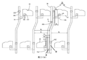
例えば、画素ユニットスイッチ11はTFT(英語名:Thin Film Transistor、日本語名:薄膜トランジスタ)である。例えば、TFTはゲート113と活性層とを有してよく、活性層はソース領域112と、ドレイン領域111と、ソース領域112とドレイン領域111との間に位置するチャネル領域114とを有し、ソース領域112とドレイン領域111は、それぞれデータ線20、画素ユニット電極12に電気的に接続される領域であってよく、例えば、チャネル領域114よりも導電率が高くなるようにドープされた領域である。図2(a)は図1の部分拡大模式図であり(説明の便宜上、データ線、タッチ信号線、活性層、画素ユニット電極などの部分のみを示し、タッチ電極、膜層間の絶縁層などのその他の部分については図示していない)、図1と図2(a)に示すように、活性層は、データ線20とタッチ信号線30とは異なる層に位置し、ソース領域112は、ビア101を介してデータ線20に電気的に接続され、ドレイン領域111はビア102を介して画素ユニット電極12に電気的に接続される。例えばTFTはトップゲート型TFTでもボトムゲート型TFTであってもよく、本開示ではこれについて限定しない。
For example, the
画素ユニットスイッチ10は、第1のデータ線21の第1端(図2(a)に示すような第1のデータ線21の左側)に接続される第1の画素ユニットスイッチ11aと、第1のデータ線21の第2端(図2(a)に示すような第1のデータ線21の右側)に接続される第2の画素ユニットスイッチ11bとを含み、第1端と第2端は第1のデータ線21の相反する両側であり、タッチ信号線30は、タッチ表示基板に垂直な方向での投射が第1の画素ユニットスイッチ11aのソース領域とドレイン領域との間に位置する。つまり、ベース基板1でのタッチ信号線30の投射は、ベース基板1での第1の画素ユニットスイッチ11aのソース領域の投射と、ベース基板での第1の画素ユニットスイッチ11aのドレイン領域の投射との間に位置する。
The
例えば、第1の画素ユニットスイッチ11aのソース領域112とドレイン領域111との行方向での間隔d1は、第2画素ユニットスイッチ11bのソース領域112とドレイン領域111との行方向での間隔d2より大きい。よって、タッチ信号線30を便利に配置することができる。
For example, the distance d 1 in the row direction between the
例えば、TFTは低温ポリシリコン型TFTであってよく、アモルファスシリコン型TFTと比べてより多くの利点を有する。図3は図2(a)における線A-Aに沿った断面模式図であり、図2と図3を組み合わせると、TFTはベース基板1に設けられたゲート113と、ゲート113に設けられたゲート絶縁層2と、ゲート絶縁層2に設けられた活性層とを備える。ゲート絶縁層2には酸化シリコンもしくは窒化シリコン材料を用いてよく、厚さは80~120nmであってよい。活性層は、離隔されたドレイン領域111およびソース領域112と、ソース領域111とドレイン領域112との間に位置するチャネル領域114とを有し、ベース基板1でのドレイン領域111とソース領域112の正投射は、ベース基板1でのゲート113の正投射の外に位置し、ベース基板1でのチャネル領域114の正投射は、ベース基板1でのゲート113の正投射と一致する。低温ポリシリコンの電子移動率はアモルファスシリコンよりはるかに大きいため、低温ポリシリコンTFTにおいては、活性層をより細長くすることができ、第1の画素ユニットスイッチ11aのドレイン領域111とソース領域112との間隔を延ばすことができ、タッチ信号線30の配置に便利である。
For example, the TFT may be a low temperature polysilicon type TFT, which has more advantages than an amorphous silicon type TFT. FIG. 3 is a schematic cross-sectional view taken along the line AA in FIG. 2(a), and when FIG. 2 and FIG. It includes a
図3に示すように、複数のタッチ信号線30は複数の信号線20と同じ層に配置されて、各データ線20と絶縁される。
As shown in FIG. 3, the plurality of
例えば、TFTのある膜層に第1の絶縁層3が設けられ、第1の絶縁層3の材料は窒化物、非金属酸化物を含んでよく、窒化物にはSiNxを含むがこれに限らず、非金属酸化物にはSiOxを含むがこれに限らない。第1の絶縁層3はTFTのある膜層と、複数のタッチ信号線30および複数のデータ線20のある膜層との間に設けられる。例えば、図3に示すように、ビア101は前記第1の絶縁層3を貫通する。
For example, the first insulating
複数のタッチ検出電極31はそれぞれが対応するタッチ信号線30に接続される。例えば、ビア103を介して、対応するタッチ信号線30にタッチ検出電極31を電気的に接続することができる。タッチ信号線30のある膜層と、タッチ検出電極31のある膜層との間に第2の絶縁層4を設けることができ、膜層の表面を平坦にする。例えば、第2の絶縁層4の材料は樹脂であってよい。例えば、図3に示すように、ビア103は第2の絶縁層4を貫通する。
Each of the plurality of
例えば、タッチ検出電極31のある膜層と、画素ユニット電極12のある膜層との間に第3の絶縁層5を設けることができ、第3の絶縁層5の材料は窒化シリコンであってよく、第3の絶縁層5の厚さは100nm~200nmであってよい。例えば、図3に示すように、ビア102は第1の絶縁層3と、第4の絶縁層4と、第5の絶縁層5とを貫通する。
For example, the third insulating
再び図2(a)を参照すると、任意のタッチ信号線30はタッチ表示基板に垂直な方向での投射が、第1の画素ユニットスイッチ11aのソース領域112とドレイン領域111との間に位置する。つまり、タッチ信号線30とデータ線20に短絡が発生しないように、タッチ信号線30は第1の画素ユニットスイッチ11aの直上を跨ぐ。
Referring again to FIG. 2(a), the arbitrary
図2(a)に示すように、第1の間隔d3は第2の間隔d4より大きく、第1の間隔d3は1本のタッチ信号線30に最も近接する2本のデータ線20の間の行方向での間隔であり、第2の間隔d4は隣接する2本のタッチ信号線30の間の任意の隣接する2本のデータ線20の間の行方向での間隔である。タッチ信号線30と第1のデータ線21との間の領域は発光しないため、第1の間隔d3を第2の間隔d4より大きく設け、タッチ信号線30と第1のデータ線21との間の領域面積が一定である限り、発光する領域面積を増やすことができる。
As shown in FIG. 2A, the first distance d3 is larger than the second distance d4 , and the first distance d3 is the distance between two
例えば、1本の第1のデータ線21に最も近接する2列のサブ画素ユニット10内において、第1のデータ線21と、その第1端のサブ画素ユニット10に位置する画素ユニット電極12との間隔d5が、第1のデータ線21と、その第2端のサブ画素ユニット10に位置する画素ユニット電極12との間隔d6より大きく、第1端と第2端は第1のデータ線21の相反する両側である。例えば、前記第1の画素ユニットスイッチ11aが、第1のデータ線121の第1端に位置するサブ画素ユニット10内に配置される。第1のデータ線21と、その両側のサブ画素ユニット10に位置する画素ユニット電極12との間の間隔は異なるため、そのうちの間隔が大きい側にタッチ信号線30を設けるのに便利である。なお、第1のデータ線21と画素ユニット電極12との間の間隔とは、行方向での第1のデータ線21と画素ユニット電極12の縁との最小距離を指す。
For example, in two columns of
例えば、1本のタッチ信号線30に最も近接する2本のデータ線20は、1本の第1のデータ線21と1本の第2のデータ線22とを含み、1本のタッチ信号線30に最も近接する2本のデータ線20において、第2のデータ線22とタッチ信号線30との間の行方向での間隔d7は、第2の間隔d4と等しいため、各サブ画素ユニットの発光面積を等しくすることができる。最も近接するとは、両者間にタッチ信号線もしくはデータ線がないということを指す。例えば、図2(a)において、1本のタッチ信号線30に最も近接する2本のデータ線20とは、タッチ信号線30の右側の第1本目の第1のデータ線21と、タッチ信号線30の左側の第1本目の第2のデータ線22であり、これは実際の距離とは関係がない。
For example, the two
例えば、図2(a)に示すように、活性層は、行方向に延伸する水平部分aと列方向に延伸する鉛直部分bとを有する。例えば、タッチ表示基板に垂直な方向での水平部分aの投射が、タッチ表示基板に垂直な方向でのゲート線の投射に一部重なり、つまり、水平部分aのベース基板1での正投射はゲート線のベース基板1での正投射に一部重なる。このように、ゲート線の一部はゲートとして直接兼用できる。例えば、図2(a)に示すように、タッチ表示基板に垂直な方向での、第1のデータ線21に接続される第1の画素ユニットスイッチ11aの活性層の鉛直部分bの投射は、タッチ表示基板に垂直な方向でのタッチ信号線30の投射内にあり、その行方向の幅は、タッチ表示基板に垂直な方向でのタッチ信号線30の投射の行方向の幅と等しい。つまり、第1のデータ線21に接続される第1の画素ユニットスイッチ11aは、ベース基板1でのその活性層の鉛直部分bの正投射が、ベース基板1でのタッチ信号線30の正投射内にあり、ベース基板1での鉛直部分bの正投射の行方向の幅は、ベース基板1でのタッチ信号線30の正投射の行方向の幅と等しい。図2(b)は図1の部分拡大模式図2である。図2(a)と異なるのは、図2(b)において、タッチ表示基板に垂直な方向での、第1のデータ線21に接続される第1画素ユニットスイッチ11aの活性層の鉛直部分bの投射は、タッチ表示基板に垂直な方向での第1のデータ線21の投射内にあり、その行方向の幅は、タッチ表示基板に垂直な方向での第1のデータ線21の投射の行方向の幅と等しい。つまり、第1のデータ線21に接続される第1の画素ユニットスイッチ11aは、ベース基板1でのその活性層の鉛直部分bの正投射が、ベース基板1での第1のデータ線21の正投射内にあり、ベース基板1での鉛直部分bの正投射の行方向の幅は、ベース基板1での1本の第1のデータ線21の正投射の行方向の幅と等しい。図2(a)に示す構造について、すべての画素ユニットスイッチ11の活性層の鉛直部分bの間の間隔は同一の距離であるため、パターニングに便利である。図2(b)に示す構造について、すべての画素ユニットスイッチ11の活性層の鉛直部分bはいずれもデータ線20と重なるため、タッチ表示基板の電気学的均一性を向上させることができる。本開示の実施例において、ゲート線と活性層との間の位置関係は、図2(a)と図2(b)に示す状況に限定されない。例えば、ゲート線は活性層の鉛直部分bと重なる箇所が二箇所あるが、水平部分aとは重ならないことから、デュアルゲートTFTを形成する。
For example, as shown in FIG. 2(a), the active layer has a horizontal portion a extending in the row direction and a vertical portion b extending in the column direction. For example, the projection of the horizontal portion a in the direction perpendicular to the touch display substrate partially overlaps the projection of the gate line in the direction perpendicular to the touch display substrate, that is, the orthogonal projection of the horizontal portion a on the
例えば、複数のタッチ検出電極31は各サブ画素ユニットのコモン電極層を構成する。この場合、タッチ検出電極31はサブ画素ユニット10のコモン電極層としてさらに機能し、表示基板の厚さの低減に有利である。
For example, the plurality of
例えば、図3に示すように、データ線20とタッチ信号線30は、活性層14のある膜層とコモン電極層との間に位置する。
For example, as shown in FIG. 3, the
図4は本開示の実施例が提供する他のタッチ表示基板の部分断面模式図であり、図4に示すタッチ表示基板と図3に示すタッチ表示基板の構造は基本的に同一で、相違点は、図4におけるタッチ表示基板の画素ユニット電極12はタッチ検出電極31の下方に位置するという点である。
FIG. 4 is a schematic partial cross-sectional view of another touch display substrate provided by the embodiment of the present disclosure, and the structures of the touch display substrate shown in FIG. 4 and the touch display substrate shown in FIG. 3 are basically the same, and there are differences. The point is that the
図5は本開示の実施例が提供する他のタッチ表示基板の部分断面模式図であり、図5に示すタッチ表示基板と図3に示すタッチ表示基板の構造は基本的に同一で、相違点は、図5に示すタッチ表示基板において、画素ユニットスイッチはトップゲート型のTFTであるという点である。 FIG. 5 is a schematic partial cross-sectional view of another touch display substrate provided by the embodiment of the present disclosure, and the structures of the touch display substrate shown in FIG. 5 and the touch display substrate shown in FIG. 3 are basically the same, and there are differences. The point is that in the touch display substrate shown in FIG. 5, the pixel unit switch is a top gate type TFT.
なお、トップゲート型のTFTの製造過程において、ベース基板1と活性層114との間には光リーク電流を防止するためにチャネル領域114に対向する遮光層が設けられるが、図5では当該遮光層を省略している。
Note that in the manufacturing process of a top-gate TFT, a light-shielding layer facing the
同じ層に設けられたタッチ信号線とデータ線によって、データ線とタッチ信号線との寄生容量を低減することができるうえ、これらの間に絶縁層を設けることを省き、工程を簡素化することができる。また、タッチ信号線とデータ線に短絡が発生しないように、タッチ信号線とデータ線との間を絶縁する。 Parasitic capacitance between the data line and touch signal line can be reduced by providing the touch signal line and the data line on the same layer, and the process can be simplified by omitting the provision of an insulating layer between them. I can do it. Further, the touch signal line and the data line are insulated to prevent a short circuit from occurring between the touch signal line and the data line.
図1に示すように、1行のサブ画素ユニットを離隔する2行のサブ画素ユニット10内における各サブ画素ユニット10は列方向に整列して配置され、これにより、サブ画素ユニット10の配置をより整然とさせることができ、製造に便利である。
As shown in FIG. 1, the
その他の実施例において、1行のサブ画素ユニットを離隔する2行のサブ画素ユニット10内における各サブ画素ユニット10は列方向に整列せずに配置してもよいということは、異なる要求に適応させるために容易に想到できることである。例えば、三角形のタッチ表示基板内において、1行のサブ画素ユニットを離隔する2行のサブ画素ユニット10内における各サブ画素ユニット10は、列方向において複数のサブ画素ユニット10の距離を徐々に縮小してよい。例えば、円形、菱形、楕円形、台形を含むがこれに限らないその他の可能な形状のタッチ表示基板内においては、1行のサブ画素ユニットを離隔する2行のサブ画素ユニット10内における各サブ画素ユニット10は、列方向において縮小あるいは複数のサブ画素ユニット10の距離を越えてもよく、画素ユニットを表示基板の形状に応じて配置させる。
In other embodiments, the
本開示の実施例では、例えば、どの行のサブ画素ユニット10も三種類の異なる色のサブ画素ユニット10を有し、隣接し順に配列された三種類の異なる色のサブ画素ユニット10は重複ユニットとなり、どの行のサブ画素ユニット10においても当該重複ユニットが行方向に重複配列される。矩形ではないタッチ表示基板において、複数のサブ画素ユニット10の距離を縮小する必要がある場合、サブ画素ユニット10の距離を3の整数倍縮小することができる。同一行内に二種類の異なる色のサブ画素ユニット10のみを含む表示基板については、サブ画素ユニット10の距離を2の整数倍縮小することができる。
In the embodiment of the present disclosure, for example, each row of
例えば、各サブ画素ユニット10と、隣接する各サブ画素ユニット10の色はいずれも異なるため、同一行において三種類の異なる色のサブ画素ユニット10を含む場合に、サブ画素ユニット10の配置を便利にできる。
For example, since each
例えば、任意の隣接する2本のデータ線20の間に、二種類の異なる色のサブ画素ユニットのみが配置される。 For example, only two types of sub-pixel units of different colors are arranged between any two adjacent data lines 20.
例えば、1つの画素ユニットは、6つのサブ画素ユニットを含んでよく(図1における破線枠内の6つのサブ画素ユニット)、UHD(英語名:Ultra High Definition、日本語名:超高精細)表示装置の製造に適している。隣接するデータ線20の間の間隔がより小さくなれば単位面積内の画素ユニットの個数はより多くなり、隣接するデータ線20の間の間隔を縮小することでタッチ表示基板のPPI(英語名:Pixels Per Inch、日本語名:画素密度)を高めることができる。
For example, one pixel unit may include six sub-pixel units (six sub-pixel units within the dashed line frame in FIG. 1), and UHD (English name: Ultra High Definition, Japanese name: Ultra High Definition) display Suitable for manufacturing equipment. As the distance between
例えば、各データ線20は同一の色のサブ画素ユニット10の画素ユニットスイッチ11に接続され、これにより、単色画面表示の際にカラム反転(Column-inversion)を便利に行うことができる。
For example, each
図1に示すように、各データ線20は、同一色でかつ当該データ線20の両側にそれぞれ位置するサブ画素ユニット10の画素ユニットスイッチ11のみに接続される。したがって、単色画面表示の際に、表示しようとする色に対応するサブ画素ユニット10に接続されたデータ線20をオンにするだけでよく、例えば、赤色画面を表示させようとする時、S1とS4の2本のデータ線20をオンにするだけでよく、実現が簡単で操作が便利である。
As shown in FIG. 1, each
図6は本開示の実施例が提供するタッチ表示基板の別の部分的な構造模式図であり、図7は図6における線B-Bに沿った断面模式図である。図6と図7に示すように、当該タッチ表示基板において、第1データ線21はバス線212と、いずれもバス線212に接続された2本の分岐線211とを備え、タッチ信号線30は2本の分岐線211の間に位置し、2本の分岐線211のうちの1本はタッチ信号線30の第1端に位置する画素ユニットスイッチ11に接続され、2本の分岐線211のうちの他の1本はタッチ信号線30の第2端に位置する画素ユニットスイッチ11に接続され、第1端と第2端はタッチ信号線30の相反する両側である。2本の分岐線211を備える第1のデータ線21を設けることで、2本の分岐線211のうちの各1本の分岐線はタッチ信号線30の一端の画素ユニットスイッチ11のみに接続し、これにより、タッチ信号線30と画素ユニットスイッチ11の交差を避けることができる。
FIG. 6 is another partial structural schematic diagram of a touch display substrate provided by an embodiment of the present disclosure, and FIG. 7 is a cross-sectional schematic diagram taken along line BB in FIG. 6. As shown in FIGS. 6 and 7, in the touch display board, the
図6に示すように、2本の分岐線211の延伸方向は同じであり、2本の分岐線211の両端がそれぞれ接続されて、閉じた枠型構造を構成し、タッチ信号線30は枠型構造の内部に位置する。2本のバス線212はいずれも枠型構造に接続される。タッチ信号線30は枠型内部に位置するため、ビアを開けてタッチ信号線30を引き出す必要がある。
As shown in FIG. 6, the two
図2に示すタッチ表示基板において、各タッチ信号線30と各データ線の延伸方向が一致し、タッチ信号線30に最も距離が近いデータ線20とタッチ信号線30との間の間隔がどの箇所においても等しく、これにより、データ線20とタッチ信号線30の設置を便利にできるとともに、データ線20とタッチ信号線30の一部分との間隔が小さいことで電荷が一部に蓄積するという状況の発生を回避できる。例えば、第1のデータ線21の延伸方向とタッチ信号線30の延伸方向が一致し、第1のデータ線21とタッチ信号線30との間の間隔がどの箇所においても等しい。このほか、図2に示すタッチ表示基板において、データ線20は分岐線を持たず、ベース基板1でのその正投射の面積はより小さく、画素ユニットの開口率を高めるのに有利であり、表示基板の輝度が同一であるという状況において表示基板のエネルギー消費低減に有利である。図2に示すタッチ表示基板は、図4に示すタッチ表示基板との比較においてその開口率が20%向上しており、実験、テストしたところ、同一の単色画面を表示する際に、輝度が同一であるという状況において、図2に示すタッチ表示基板のエネルギー消費は図4に示すタッチ表示基板のエネルギー消費よりも20%ほど低いものである。
In the touch display board shown in FIG. 2, the extending direction of each
本開示の実施例では、図1~図7に示すいずれかのタッチ表示基板を備える表示装置をさらに提供する。例えば、当該表示装置は携帯電話、タブレット型コンピュータ、テレビ、モニタ、ノート型パソコン、デジタルフォトフレーム、ナビゲーションなどの、表示機能を有するあらゆる製品もしくは部品であってよい。 Embodiments of the present disclosure further provide a display device including any of the touch display substrates shown in FIGS. 1 to 7. For example, the display device may be any product or component that has a display function, such as a mobile phone, tablet computer, television, monitor, laptop, digital photo frame, navigation, etc.
同じ層に設けられたタッチ信号線とデータ線によって、データ線とタッチ信号線との寄生容量を低減することができるうえ、これらの間に絶縁層を設けることを省き、工程を簡素化することができる。また、タッチ信号線とデータ線に短絡が発生しないように、タッチ信号線とデータ線との間を絶縁する。 Parasitic capacitance between the data line and touch signal line can be reduced by providing the touch signal line and the data line on the same layer, and the process can be simplified by omitting the provision of an insulating layer between them. I can do it. Further, the touch signal line and the data line are insulated to prevent a short circuit from occurring between the touch signal line and the data line.
図8は本開示の実施例が提供するタッチ表示基板の製造方法のフロー図であり、当該方法は図1~図7に示すタッチ表示基板の製造に適用される。図8に示すように、当該製造方法は以下のステップを含んでよい。 FIG. 8 is a flow diagram of a method for manufacturing a touch display substrate provided by an embodiment of the present disclosure, and the method is applied to manufacturing the touch display substrates shown in FIGS. 1 to 7. As shown in FIG. 8, the manufacturing method may include the following steps.
S11、ベース基板に複数の画素ユニットスイッチを形成する。 S11: forming a plurality of pixel unit switches on the base substrate;
各画素ユニットスイッチは異なる画素ユニットにそれぞれ属する。各行のサブ画素ユニットにおける各画素ユニットは整列して配置され、隣接する2行のサブ画素ユニット毎に、1行のサブ画素ユニット内におけるサブ画素ユニットと、これに隣接し、かつ他の1行のサブ画素ユニット内に位置するサブ画素ユニットとの間で、X個のサブ画素ユニットの位置が行方向にずれており、0<X<1であり、例えばXは0.5であってよい。隣接する2行のサブ画素ユニット毎に、1行のサブ画素ユニット内におけるサブ画素ユニットと、これに隣接し、かつ他の1行のサブ画素ユニット内に位置するサブ画素ユニットが異なる色を有する。 Each pixel unit switch belongs to a different pixel unit. Each pixel unit in the sub-pixel unit of each row is arranged in alignment, and for every sub-pixel unit of two adjacent rows, the sub-pixel unit in the sub-pixel unit of one row, and the sub-pixel unit in the sub-pixel unit of one row adjacent to this and another one row. The positions of X sub-pixel units are shifted in the row direction between the sub-pixel units located within the sub-pixel unit, and 0<X<1, for example, X may be 0.5. . For every two adjacent rows of sub-pixel units, the sub-pixel units in one row of sub-pixel units and the sub-pixel units adjacent to this and located in the other one row of sub-pixel units have different colors. .
S12、複数の画素ユニットスイッチが形成されたベース基板に第1の絶縁層を形成する。 S12: forming a first insulating layer on a base substrate on which a plurality of pixel unit switches are formed;
S13、第1の絶縁層に第1のパターニング層を形成する。 S13: forming a first patterning layer on the first insulating layer;
第1のパターニング層は、互いに離隔したデータ線とタッチ信号線とを有する。例えば、データ線は、異なる行のサブ画素ユニットに位置する画素ユニットスイッチに接続される。例えば、データ線は、行方向にその両側に位置しかつ異なる行のサブ画素ユニットに位置する画素ユニットスイッチに接続される。 The first patterning layer has data lines and touch signal lines spaced apart from each other. For example, the data lines are connected to pixel unit switches located in sub-pixel units of different rows. For example, the data line is connected to pixel unit switches located on both sides thereof in the row direction and located in sub-pixel units of different rows.
S14、第1のパターニング層に第2の絶縁層を形成する。 S14: forming a second insulating layer on the first patterning layer;
S15、第2の絶縁層に画素ユニット電極を形成する。 S15: forming a pixel unit electrode on the second insulating layer;
画素ユニット電極はいずれも画素ユニットスイッチに接続される。 Both pixel unit electrodes are connected to a pixel unit switch.
同じ層に設けられたタッチ信号線とデータ線によって、データ線とタッチ信号線との寄生容量を低減することができるうえ、これらの間に絶縁層を設けることを省き、工程を簡素化することができる。また、タッチ信号線とデータ線に短絡が発生しないように、タッチ信号線とデータ線との間を絶縁する。 Parasitic capacitance between the data line and touch signal line can be reduced by providing the touch signal line and the data line on the same layer, and the process can be simplified by omitting the provision of an insulating layer between them. Can be done. Further, the touch signal line and the data line are insulated to prevent a short circuit from occurring between the touch signal line and the data line.
図9は本開示の実施例が提供するタッチ表示基板の製造方法の別のフロー図であり、当該方法は図1~図3に示すタッチ表示基板の製造に同じく適用される。以下では図10~図16を組み合わせて本製造方法について詳しく説明する。図9に示すように、当該製造方法は以下のステップを含んでよい。 FIG. 9 is another flow diagram of a method for manufacturing a touch display substrate provided by an embodiment of the present disclosure, and the method is similarly applied to manufacturing the touch display substrate shown in FIGS. 1-3. The present manufacturing method will be explained in detail below by combining FIGS. 10 to 16. As shown in FIG. 9, the manufacturing method may include the following steps.
S21、ベース基板にTFTを形成する。 S21: Form a TFT on the base substrate.
例えば、ベース基板にトップゲート型のTFTを形成してよく、ボトムゲート型のTFTを形成してもよい。図10に示すように、ベース基板8000にボトムゲート型のTFTを製作し、当該TFTはベース基板8000に配置されたゲート8113と、ゲート8113に配置されたゲート絶縁層8002と、ゲート絶縁層8002に配置された活性層とを備え、活性層は、離隔されたドレイン領域8111およびソース領域8112と、ドレイン領域8111とソース領域8112との間に位置するチャネル領域8114とを有し、ベース基板8000でのドレイン領域8111とソース領域8112の正投射は、ベース基板8000でのゲート8113の正投射の外に位置する。
For example, a top gate type TFT or a bottom gate type TFT may be formed on the base substrate. As shown in FIG. 10, a bottom gate TFT is fabricated on a
複数のTFTは、製作するタッチ表示基板のサブ画素ユニットの配置方式を満たすために、ベース基板8000にアレイ配置される。
A plurality of TFTs are arranged in an array on the
例えば、低温ポリシリコン型TFTを用いてよい。 For example, a low temperature polysilicon TFT may be used.
S22、TFTが形成されたベース基板に第1の絶縁層を形成する。 S22: A first insulating layer is formed on the base substrate on which the TFT is formed.
例えば、第1の絶縁層8010の材料は窒化物、非金属酸化物を含んでよく、窒化物にはSiNxを含むがこれに限らず、非金属酸化物にはSiOxを含むがこれに限らない。
For example, the material of the first insulating
S23、第1の絶縁層内に第1のビアを製作する。 S23, fabricating a first via in the first insulating layer.
図11に示すように、後続ステップにて製作するデータ線が第1のビア8011を介してソース領域8112に電気的に接続されるように、第1のビア8011は第1の絶縁層8010を貫通して、TFTのソース領域8112の直上に位置する。
As shown in FIG. 11, the first via 8011 extends through the first insulating
例えば、第1のビア8011は、第1の絶縁層8010を介してパターニング工程を行って製作してよい。
For example, the first via 8011 may be manufactured by performing a patterning process through the first insulating
S24、第1の絶縁層に第1のパターニング層を形成する。 S24: forming a first patterning layer on the first insulating layer;
例えば、第1のパターニング層もパターニング工程によって製作してよい。 For example, the first patterned layer may also be fabricated by a patterning process.
例えば、図12に示すように、第1のパターニング層は複数のデータ線8200と複数のタッチ信号線8300とを有し、タッチ信号線8300とデータ線8200は互いに離隔する。データ線8200は、第1のビア8011を貫通してTFTのソース領域8112に電気的に接続するために第1のビアの直上に位置する。
For example, as shown in FIG. 12, the first patterning layer has a plurality of
例えば、データ線8200とタッチ信号線8300は金属Alなどの金属材料で製作してよく、ITO(英語名:Indium tin oxide、日本語名:酸化インジウムスズ)などの透明導電材料で製作してもよい。
For example, the
図6に示すタッチ表示基板を製作するとき、第1のデータ線は、バス線と、いずれもバス線に接続された2本の分岐線とを備え、タッチ信号線は2本の分岐線の間に位置し、2本の分岐線のうちの1本は第1のビアを介してタッチ信号線の第1端に位置するTFTのソース領域に接続され、2本の分岐線のうちの他の1本は第1のビアを介してタッチ信号線の第2端に位置するTFTのソース領域に接続され、第1端と第2端はタッチ信号線の相反する両側である。 When manufacturing the touch display board shown in FIG. 6, the first data line includes a bus line and two branch lines, both of which are connected to the bus line, and the touch signal line is one of the two branch lines. One of the two branch lines is connected to the source region of the TFT located at the first end of the touch signal line via the first via, and the other of the two branch lines is connected to the source region of the TFT located at the first end of the touch signal line. One of the TFTs is connected to the source region of the TFT located at the second end of the touch signal line through the first via, and the first end and the second end are opposite sides of the touch signal line.
S25、第1のパターニング層に第2の絶縁層を形成する。 S25: forming a second insulating layer on the first patterning layer;
例えば、第2の絶縁層8020の材料は樹脂であってよいがこれに限らない。
For example, the material of the second insulating
S26、第2の絶縁層内に第2のビアを製作する。 S26, fabricating a second via in the second insulating layer.
第2のビアの制作方法は第1のビアの制作方法を同じであってよい。 The method for producing the second via may be the same as the method for producing the first via.
図13に示すように、後続ステップにて製作するタッチ検出電極が第2のビア8021を介してタッチ信号線8300に接続されるように、第2のビア8021は第2の絶縁層8020を貫通して、タッチ信号線8300の直上の位置に位置する。
As shown in FIG. 13, the second via 8021 penetrates the second insulating
S27、第2の絶縁層にタッチ検出電極を形成する。 S27: forming touch detection electrodes on the second insulating layer;
例えば、タッチ検出電極はパターニング工程によって製作してよい。 For example, the touch sensing electrode may be fabricated by a patterning process.
図14に示すように、タッチ検出電極8310は第2のビア8021を介してタッチ信号線8300に電気的に接続される。
As shown in FIG. 14,
例えば、タッチ検出電極8310は、光透過率を高めるために、ITOのような透明導電材料で製作してよい。
For example,
S28、タッチ検出電極が形成されたベース基板に第3の絶縁層を形成する。 S28: forming a third insulating layer on the base substrate on which the touch detection electrode is formed;
例えば、第3の絶縁層8030の材料は窒化シリコンであってよく、第3の絶縁層8030の厚さは100nm~200nmであってよい。
For example, the material of the third insulating
S29、第3のビアを製作する。 S29: Manufacture the third via.
図15に示すように、後続ステップにて製作する画素ユニット電極がドレイン領域8111に電気的に接続されるように、第3のビア8031はTFTのドレイン領域8111の直上に位置し、第3の絶縁層8030と、第2の絶縁層8020と、第1の絶縁層8010とを貫通する。
As shown in FIG. 15, the third via 8031 is located directly above the
S30、第3の絶縁層に画素ユニット電極を製作する。 S30: Fabricate pixel unit electrodes on the third insulating layer.
例えば、画素ユニット電極8120はパターニング工程によって製作してよい。
For example, the
図16に示すように、画素ユニット電極8120は第3のビア8031を介してドレイン領域8111に電気的に接続される。
As shown in FIG. 16, the
例えば、画素ユニット電極8120は、光透過率を向上させるために、ITOのような透明の導電材料で製作してよい。
For example, the
例えば、ステップS23を実行するとき、第1の絶縁層8010の、ドレイン領域8111の直上に位置する箇所にもビアを製作してよく、これにより、ステップS24の実行時に、データ線8200とタッチ信号線8300を製作する際に、第1の絶縁層8010にトランスファ電極をさらに製作でき、トランスファ電極は第1の絶縁層8010におけるドレイン領域8111直上に位置するビアを介してドレイン領域8111に電気的に接続される。図17に示すように、ステップS23においてビア8031aを同時に製作し、ステップS24においてトランスファ電極8031bを同時に製作することで、S29において加工を必要とする第3のビア8031が、第3の絶縁層8030と第2の絶縁層8020のみを貫通するようにすることができ、第3のビア8031の深さを低減して、加工難度を低減し、画素ユニット電極8120がドレイン領域8111と安定した電気接続を形成することを確保し、断線および接触不良が生じる可能性を低減する。また、ビア8031aは第1のビア8011と同時に製作することができるため、トランスファ電極8131bはタッチ信号線8300、データ線8200と同時に製作することができ、別途工程ステップを追加する必要はない。
For example, when performing step S23, a via may also be fabricated at a location of the first insulating
図18は本開示の実施例が提供するタッチ表示基板の製造方法のさらなるフロー図であり、当該方法は図4に示すタッチ表示基板の製造に用いられ、当該製造方法はS41~S50を含み、そのうちのステップS41~S45は前述のステップS21~S25とそれぞれ同一であるため、ここでは改めて説明しない。以下、図19~21を組み合わせて当該方法のステップS46~S50について説明する。 FIG. 18 is a further flow diagram of a method for manufacturing a touch display substrate provided by an embodiment of the present disclosure, the method is used to manufacture the touch display substrate shown in FIG. 4, and the manufacturing method includes S41 to S50; Since steps S41 to S45 are the same as steps S21 to S25 described above, they will not be explained again here. Steps S46 to S50 of the method will be described below by combining FIGS. 19 to 21.
S46、第2の絶縁層内に第4のビアを製作する。 S46, fabricating a fourth via in the second insulating layer.
第4のビア9021の製作方法は前述の第2のビア8021の製作方法と同一である。 The method for manufacturing the fourth via 9021 is the same as the method for manufacturing the second via 8021 described above.
図19に示すように、後続にて製作する画素ユニット電極がドレイン領域9111に電気的に接続されるように、第4のビア9021はTFTのドレイン領域9111の直上に位置し、第2の絶縁層9020と、第1の絶縁層8010とを貫通する。
As shown in FIG. 19, the fourth via 9021 is located directly above the
S47、第2の絶縁層に画素ユニット電極を形成する。 S47: forming a pixel unit electrode on the second insulating layer;
例えば、画素ユニット電極9120はパターニング工程によって製作してよい。
For example, the
図20に示すように、画素ユニット電極9120は第4のビア9021を介してドレイン領域9111と電気的に接続される。
As shown in FIG. 20, the
S48、画素ユニット電極が形成されたベース基板に第3の絶縁層を形成する。 S48: A third insulating layer is formed on the base substrate on which the pixel unit electrodes are formed.
例えば、第3の絶縁層9030の製作は前述の第3の絶縁層8030の製作を参照することができるため、ここでは改めて説明しない。
For example, the fabrication of the third insulating
S49、第5のビアを製作する。 S49: Manufacture the fifth via.
図21に示すように、後続ステップにて製作するタッチ検出電極が第5のビア9031を介してタッチ信号線9300に接続できるように、第5のビア9031はタッチ信号線9300の直上の位置に製作され、第3の絶縁層9030と、第2の絶縁層9020とを貫通する。
As shown in FIG. 21, the fifth via 9031 is positioned directly above the
S50、第3の絶縁層にタッチ検出電極を製作する。 S50: fabricating touch detection electrodes on the third insulating layer;
例えば、タッチ検出電極9030はパターニング技術によって作成してよい。
For example,
図22に示すように、タッチ検出電極9030は第5のビア9031を介してタッチ信号線9300に接続される。
As shown in FIG. 22,
図4に示すタッチ表示基板を製造するとき、トランスファ電極を追加する前述の方法を同様に用いて、断線や接触不良が生じる可能性を低減することができるが、ここでは改めて説明しない。 When manufacturing the touch display substrate shown in FIG. 4, the above-described method of adding transfer electrodes can be similarly used to reduce the possibility of disconnection or poor contact, but will not be described again here.
上記内容は本開示の例示的な実施の形態にすぎず、本開示の請求範囲を限定するものではなく、本開示の請求範囲は添付の請求項によって決められる。 The above content is merely exemplary embodiments of the disclosure and does not limit the scope of the disclosure, which is defined by the appended claims.
10 サブ画素ユニット
11 画素ユニットスイッチ
20 データ線
30 タッチ信号線
10
Claims (10)
前記サブ画素ユニットの間の、列方向に延伸する隙間に配置されたデータ線と、
前記サブ画素ユニットの間の、列方向に延伸する隙間に配置されたタッチ信号線と、を備え、
前記タッチ信号線は前記データ線と同じ層に配置されて、前記データ線と絶縁され、
前記列方向に延伸する隙間に配置された前記タッチ信号線の前記データ線が、バス線と、いずれも前記バス線に接続された2本の分岐線とを備え、前記タッチ信号線は前記2本の分岐線の間に位置し、前記2本の分岐線のうちの1本は前記タッチ信号線の第1端に位置する前記画素ユニットスイッチに接続され、前記2本の分岐線のうちの他の1本は前記タッチ信号線の第2端に位置する前記画素ユニットスイッチに接続され、第1端と第2端は前記タッチ信号線の相反する両側である、タッチ表示基板。 A plurality of sub-pixel units arranged in an array format, wherein for each two adjacent rows of sub-pixel units, a plurality of sub-pixel units in one of the two adjacent rows and a plurality of sub-pixel units in one of the two adjacent rows; The position of the sub-pixel unit by X is shifted in the row direction from the plurality of sub-pixel units in the other one row, and 0<X<1, and each sub-pixel unit in the one row a plurality of sub-pixel units arranged in an array format, each sub-pixel unit having a different color and each sub-pixel unit having a pixel unit switch; pixel unit,
a data line arranged in a gap extending in the column direction between the sub-pixel units;
a touch signal line arranged in a gap extending in the column direction between the sub-pixel units,
the touch signal line is disposed on the same layer as the data line and is insulated from the data line;
The data line of the touch signal line arranged in the gap extending in the column direction includes a bus line and two branch lines both connected to the bus line, and the touch signal line is connected to the two branch lines. one of the two branch lines is connected to the pixel unit switch located at the first end of the touch signal line; one of the two branch lines is connected to the pixel unit switch located at the first end of the touch signal line; The other one is connected to the pixel unit switch located at the second end of the touch signal line, and the first end and the second end are opposite sides of the touch signal line.
Priority Applications (1)
| Application Number | Priority Date | Filing Date | Title |
|---|---|---|---|
| JP2023172890A JP2023178337A (en) | 2017-08-10 | 2023-10-04 | Touch display substrate and display device |
Applications Claiming Priority (3)
| Application Number | Priority Date | Filing Date | Title |
|---|---|---|---|
| CN201710681837.0A CN107506076B (en) | 2017-08-10 | 2017-08-10 | A kind of touch display substrate, manufacturing method and display device |
| CN201710681837.0 | 2017-08-10 | ||
| PCT/CN2018/098988 WO2019029484A1 (en) | 2017-08-10 | 2018-08-06 | Touch display substrate and display device |
Related Child Applications (1)
| Application Number | Title | Priority Date | Filing Date |
|---|---|---|---|
| JP2023172890A Division JP2023178337A (en) | 2017-08-10 | 2023-10-04 | Touch display substrate and display device |
Publications (2)
| Publication Number | Publication Date |
|---|---|
| JP2020529642A JP2020529642A (en) | 2020-10-08 |
| JP7362488B2 true JP7362488B2 (en) | 2023-10-17 |
Family
ID=60688887
Family Applications (2)
| Application Number | Title | Priority Date | Filing Date |
|---|---|---|---|
| JP2019565376A Active JP7362488B2 (en) | 2017-08-10 | 2018-08-06 | Touch display board and display device |
| JP2023172890A Pending JP2023178337A (en) | 2017-08-10 | 2023-10-04 | Touch display substrate and display device |
Family Applications After (1)
| Application Number | Title | Priority Date | Filing Date |
|---|---|---|---|
| JP2023172890A Pending JP2023178337A (en) | 2017-08-10 | 2023-10-04 | Touch display substrate and display device |
Country Status (5)
| Country | Link |
|---|---|
| US (3) | US11163389B2 (en) |
| EP (1) | EP3667467A4 (en) |
| JP (2) | JP7362488B2 (en) |
| CN (1) | CN107506076B (en) |
| WO (1) | WO2019029484A1 (en) |
Families Citing this family (5)
| Publication number | Priority date | Publication date | Assignee | Title |
|---|---|---|---|---|
| CN107506076B (en) | 2017-08-10 | 2019-05-14 | 京东方科技集团股份有限公司 | A kind of touch display substrate, manufacturing method and display device |
| CN112234092B (en) * | 2020-10-30 | 2023-03-24 | 云谷(固安)科技有限公司 | Display panel and display device |
| CN112882596B (en) * | 2021-01-26 | 2022-06-10 | 武汉华星光电半导体显示技术有限公司 | Display panel and touch display device |
| CN113470532B (en) * | 2021-07-09 | 2023-04-14 | 昆山国显光电有限公司 | Display panel and display device |
| CN114385044B (en) * | 2022-01-13 | 2023-07-25 | 武汉华星光电半导体显示技术有限公司 | Touch display panel |
Citations (5)
| Publication number | Priority date | Publication date | Assignee | Title |
|---|---|---|---|---|
| JP2008096553A (en) | 2006-10-10 | 2008-04-24 | Sony Corp | Display apparatus, light receiving method, and information processor |
| CN105788466A (en) | 2016-05-13 | 2016-07-20 | 京东方科技集团股份有限公司 | Display panel, manufacturing method thereof and display device |
| US20160370919A1 (en) | 2015-01-26 | 2016-12-22 | Boe Technology Group Co., Ltd. | In-cell touch panel and display apparatus |
| CN106502474A (en) | 2017-01-12 | 2017-03-15 | 京东方科技集团股份有限公司 | A kind of array base palte and display floater |
| CN106773421A (en) | 2017-02-13 | 2017-05-31 | 上海天马微电子有限公司 | Liquid crystal display device |
Family Cites Families (16)
| Publication number | Priority date | Publication date | Assignee | Title |
|---|---|---|---|---|
| TWI267057B (en) * | 2004-08-31 | 2006-11-21 | Au Optronics Corp | Flat panel display with built-in DC-DC converters |
| KR102021908B1 (en) | 2011-05-03 | 2019-09-18 | 삼성전자주식회사 | Optical touch screen apparatus and method of driving the optical touch screen apparatus |
| US9030438B2 (en) | 2012-08-16 | 2015-05-12 | Eastman Kodak Company | Pixel-aligned micro-wire electrode device |
| CN104461191A (en) | 2013-08-30 | 2015-03-25 | 新益先创科技股份有限公司 | Touch screen structure |
| CN104614909B (en) * | 2015-02-06 | 2017-07-21 | 京东方科技集团股份有限公司 | Display panel and display device |
| CN104698709A (en) * | 2015-04-01 | 2015-06-10 | 上海天马微电子有限公司 | Array substrate and liquid crystal display panel |
| CN104808403B (en) * | 2015-05-08 | 2018-05-15 | 厦门天马微电子有限公司 | Array base palte, display panel and display device |
| CN104951143B (en) | 2015-07-27 | 2020-05-08 | 京东方科技集团股份有限公司 | Array substrate, touch panel and display device |
| CN105047123B (en) * | 2015-09-10 | 2017-10-17 | 京东方科技集团股份有限公司 | Display drive method, display drive apparatus and display device |
| CN205507719U (en) * | 2016-01-28 | 2016-08-24 | 成都京东方光电科技有限公司 | Touch display substrate, touch display panel and touch display device |
| CN105652498A (en) * | 2016-03-22 | 2016-06-08 | 上海中航光电子有限公司 | Array substrate, touch display panel and touch display device |
| CN205680370U (en) | 2016-05-13 | 2016-11-09 | 京东方科技集团股份有限公司 | A kind of display floater and display device |
| CN105845033A (en) * | 2016-05-13 | 2016-08-10 | 京东方科技集团股份有限公司 | Display panel, manufacturing method and display device thereof |
| CN106909249B (en) * | 2017-02-24 | 2020-06-09 | 厦门天马微电子有限公司 | Touch display substrate and touch display device |
| CN106908980B (en) * | 2017-05-09 | 2020-10-16 | 上海中航光电子有限公司 | Array substrate, touch display panel and display device |
| CN107506076B (en) * | 2017-08-10 | 2019-05-14 | 京东方科技集团股份有限公司 | A kind of touch display substrate, manufacturing method and display device |
-
2017
- 2017-08-10 CN CN201710681837.0A patent/CN107506076B/en active Active
-
2018
- 2018-08-06 US US16/621,401 patent/US11163389B2/en active Active
- 2018-08-06 WO PCT/CN2018/098988 patent/WO2019029484A1/en unknown
- 2018-08-06 JP JP2019565376A patent/JP7362488B2/en active Active
- 2018-08-06 EP EP18842965.8A patent/EP3667467A4/en active Pending
-
2021
- 2021-10-01 US US17/492,179 patent/US11669180B2/en active Active
-
2023
- 2023-04-05 US US18/296,102 patent/US20230236691A1/en active Pending
- 2023-10-04 JP JP2023172890A patent/JP2023178337A/en active Pending
Patent Citations (5)
| Publication number | Priority date | Publication date | Assignee | Title |
|---|---|---|---|---|
| JP2008096553A (en) | 2006-10-10 | 2008-04-24 | Sony Corp | Display apparatus, light receiving method, and information processor |
| US20160370919A1 (en) | 2015-01-26 | 2016-12-22 | Boe Technology Group Co., Ltd. | In-cell touch panel and display apparatus |
| CN105788466A (en) | 2016-05-13 | 2016-07-20 | 京东方科技集团股份有限公司 | Display panel, manufacturing method thereof and display device |
| CN106502474A (en) | 2017-01-12 | 2017-03-15 | 京东方科技集团股份有限公司 | A kind of array base palte and display floater |
| CN106773421A (en) | 2017-02-13 | 2017-05-31 | 上海天马微电子有限公司 | Liquid crystal display device |
Also Published As
| Publication number | Publication date |
|---|---|
| US11669180B2 (en) | 2023-06-06 |
| WO2019029484A1 (en) | 2019-02-14 |
| EP3667467A1 (en) | 2020-06-17 |
| EP3667467A4 (en) | 2021-04-28 |
| US20200104000A1 (en) | 2020-04-02 |
| US20220019308A1 (en) | 2022-01-20 |
| JP2023178337A (en) | 2023-12-14 |
| CN107506076A (en) | 2017-12-22 |
| US20230236691A1 (en) | 2023-07-27 |
| US11163389B2 (en) | 2021-11-02 |
| CN107506076B (en) | 2019-05-14 |
| JP2020529642A (en) | 2020-10-08 |
Similar Documents
| Publication | Publication Date | Title |
|---|---|---|
| JP7362488B2 (en) | Touch display board and display device | |
| US11592699B2 (en) | Backplane substrate including in-cell type touch panel, liquid crystal display device using the same, and method of manufacturing the same | |
| US10705367B2 (en) | Touch display panel having touch line formed on the same layer as the gate line | |
| KR101790977B1 (en) | Liquid crystal display device | |
| KR101891985B1 (en) | Liquid crystal display device | |
| US8743301B2 (en) | Liquid crystal display device provided with an electrode for sensing a touch of a user | |
| US10599278B2 (en) | Touch structure, array substrate and display device | |
| US9977276B2 (en) | Array substrate, display panel and display device | |
| CN109857279B (en) | Display panel and display device | |
| US9627416B2 (en) | Array substrate and method for manufacturing the same, display device | |
| US10606388B2 (en) | Array substrate, manufacturing method thereof and touch display panel | |
| US10884533B2 (en) | Touch display device | |
| KR20130101330A (en) | Thin film transistor display panel and manufacturing method thereof | |
| CN111708237B (en) | Array substrate, display panel and display device | |
| WO2022062879A9 (en) | Touch substrate and display panel | |
| KR102080281B1 (en) | Liquid crystal display device | |
| US20240012525A1 (en) | Touch Control Substrate, Display Panel, and Electronic Device | |
| TW201721263A (en) | Display panel | |
| CN116267019A (en) | Array substrate and display panel |
Legal Events
| Date | Code | Title | Description |
|---|---|---|---|
| A621 | Written request for application examination |
Free format text: JAPANESE INTERMEDIATE CODE: A621 Effective date: 20210802 |
|
| A977 | Report on retrieval |
Free format text: JAPANESE INTERMEDIATE CODE: A971007 Effective date: 20220708 |
|
| A131 | Notification of reasons for refusal |
Free format text: JAPANESE INTERMEDIATE CODE: A131 Effective date: 20220719 |
|
| A521 | Request for written amendment filed |
Free format text: JAPANESE INTERMEDIATE CODE: A523 Effective date: 20221019 |
|
| A131 | Notification of reasons for refusal |
Free format text: JAPANESE INTERMEDIATE CODE: A131 Effective date: 20230220 |
|
| A521 | Request for written amendment filed |
Free format text: JAPANESE INTERMEDIATE CODE: A523 Effective date: 20230519 |
|
| TRDD | Decision of grant or rejection written | ||
| A01 | Written decision to grant a patent or to grant a registration (utility model) |
Free format text: JAPANESE INTERMEDIATE CODE: A01 Effective date: 20230904 |
|
| A61 | First payment of annual fees (during grant procedure) |
Free format text: JAPANESE INTERMEDIATE CODE: A61 Effective date: 20231004 |
|
| R150 | Certificate of patent or registration of utility model |
Ref document number: 7362488 Country of ref document: JP Free format text: JAPANESE INTERMEDIATE CODE: R150 |