JP7362293B2 - Real-time monitoring using closed-loop chucking force control - Google Patents
Real-time monitoring using closed-loop chucking force control Download PDFInfo
- Publication number
- JP7362293B2 JP7362293B2 JP2019091811A JP2019091811A JP7362293B2 JP 7362293 B2 JP7362293 B2 JP 7362293B2 JP 2019091811 A JP2019091811 A JP 2019091811A JP 2019091811 A JP2019091811 A JP 2019091811A JP 7362293 B2 JP7362293 B2 JP 7362293B2
- Authority
- JP
- Japan
- Prior art keywords
- workpiece
- chucking
- force
- backside gas
- sensor
- Prior art date
- Legal status (The legal status is an assumption and is not a legal conclusion. Google has not performed a legal analysis and makes no representation as to the accuracy of the status listed.)
- Active
Links
Images


Classifications
-
- H—ELECTRICITY
- H01—ELECTRIC ELEMENTS
- H01L—SEMICONDUCTOR DEVICES NOT COVERED BY CLASS H10
- H01L21/00—Processes or apparatus adapted for the manufacture or treatment of semiconductor or solid state devices or of parts thereof
- H01L21/67—Apparatus specially adapted for handling semiconductor or electric solid state devices during manufacture or treatment thereof; Apparatus specially adapted for handling wafers during manufacture or treatment of semiconductor or electric solid state devices or components ; Apparatus not specifically provided for elsewhere
- H01L21/67005—Apparatus not specifically provided for elsewhere
- H01L21/67242—Apparatus for monitoring, sorting or marking
- H01L21/67248—Temperature monitoring
-
- H—ELECTRICITY
- H01—ELECTRIC ELEMENTS
- H01J—ELECTRIC DISCHARGE TUBES OR DISCHARGE LAMPS
- H01J37/00—Discharge tubes with provision for introducing objects or material to be exposed to the discharge, e.g. for the purpose of examination or processing thereof
- H01J37/32—Gas-filled discharge tubes
- H01J37/32431—Constructional details of the reactor
- H01J37/32697—Electrostatic control
-
- H—ELECTRICITY
- H01—ELECTRIC ELEMENTS
- H01L—SEMICONDUCTOR DEVICES NOT COVERED BY CLASS H10
- H01L21/00—Processes or apparatus adapted for the manufacture or treatment of semiconductor or solid state devices or of parts thereof
- H01L21/67—Apparatus specially adapted for handling semiconductor or electric solid state devices during manufacture or treatment thereof; Apparatus specially adapted for handling wafers during manufacture or treatment of semiconductor or electric solid state devices or components ; Apparatus not specifically provided for elsewhere
- H01L21/67005—Apparatus not specifically provided for elsewhere
- H01L21/67242—Apparatus for monitoring, sorting or marking
-
- H—ELECTRICITY
- H01—ELECTRIC ELEMENTS
- H01J—ELECTRIC DISCHARGE TUBES OR DISCHARGE LAMPS
- H01J37/00—Discharge tubes with provision for introducing objects or material to be exposed to the discharge, e.g. for the purpose of examination or processing thereof
- H01J37/32—Gas-filled discharge tubes
- H01J37/32009—Arrangements for generation of plasma specially adapted for examination or treatment of objects, e.g. plasma sources
-
- H—ELECTRICITY
- H01—ELECTRIC ELEMENTS
- H01J—ELECTRIC DISCHARGE TUBES OR DISCHARGE LAMPS
- H01J37/00—Discharge tubes with provision for introducing objects or material to be exposed to the discharge, e.g. for the purpose of examination or processing thereof
- H01J37/32—Gas-filled discharge tubes
- H01J37/32431—Constructional details of the reactor
- H01J37/32715—Workpiece holder
-
- H—ELECTRICITY
- H01—ELECTRIC ELEMENTS
- H01L—SEMICONDUCTOR DEVICES NOT COVERED BY CLASS H10
- H01L21/00—Processes or apparatus adapted for the manufacture or treatment of semiconductor or solid state devices or of parts thereof
- H01L21/67—Apparatus specially adapted for handling semiconductor or electric solid state devices during manufacture or treatment thereof; Apparatus specially adapted for handling wafers during manufacture or treatment of semiconductor or electric solid state devices or components ; Apparatus not specifically provided for elsewhere
- H01L21/67005—Apparatus not specifically provided for elsewhere
- H01L21/67011—Apparatus for manufacture or treatment
- H01L21/67017—Apparatus for fluid treatment
-
- H—ELECTRICITY
- H01—ELECTRIC ELEMENTS
- H01L—SEMICONDUCTOR DEVICES NOT COVERED BY CLASS H10
- H01L21/00—Processes or apparatus adapted for the manufacture or treatment of semiconductor or solid state devices or of parts thereof
- H01L21/67—Apparatus specially adapted for handling semiconductor or electric solid state devices during manufacture or treatment thereof; Apparatus specially adapted for handling wafers during manufacture or treatment of semiconductor or electric solid state devices or components ; Apparatus not specifically provided for elsewhere
- H01L21/67005—Apparatus not specifically provided for elsewhere
- H01L21/67242—Apparatus for monitoring, sorting or marking
- H01L21/67253—Process monitoring, e.g. flow or thickness monitoring
-
- H—ELECTRICITY
- H01—ELECTRIC ELEMENTS
- H01L—SEMICONDUCTOR DEVICES NOT COVERED BY CLASS H10
- H01L21/00—Processes or apparatus adapted for the manufacture or treatment of semiconductor or solid state devices or of parts thereof
- H01L21/67—Apparatus specially adapted for handling semiconductor or electric solid state devices during manufacture or treatment thereof; Apparatus specially adapted for handling wafers during manufacture or treatment of semiconductor or electric solid state devices or components ; Apparatus not specifically provided for elsewhere
- H01L21/67005—Apparatus not specifically provided for elsewhere
- H01L21/67242—Apparatus for monitoring, sorting or marking
- H01L21/67259—Position monitoring, e.g. misposition detection or presence detection
-
- H—ELECTRICITY
- H01—ELECTRIC ELEMENTS
- H01L—SEMICONDUCTOR DEVICES NOT COVERED BY CLASS H10
- H01L21/00—Processes or apparatus adapted for the manufacture or treatment of semiconductor or solid state devices or of parts thereof
- H01L21/67—Apparatus specially adapted for handling semiconductor or electric solid state devices during manufacture or treatment thereof; Apparatus specially adapted for handling wafers during manufacture or treatment of semiconductor or electric solid state devices or components ; Apparatus not specifically provided for elsewhere
- H01L21/683—Apparatus specially adapted for handling semiconductor or electric solid state devices during manufacture or treatment thereof; Apparatus specially adapted for handling wafers during manufacture or treatment of semiconductor or electric solid state devices or components ; Apparatus not specifically provided for elsewhere for supporting or gripping
- H01L21/6831—Apparatus specially adapted for handling semiconductor or electric solid state devices during manufacture or treatment thereof; Apparatus specially adapted for handling wafers during manufacture or treatment of semiconductor or electric solid state devices or components ; Apparatus not specifically provided for elsewhere for supporting or gripping using electrostatic chucks
- H01L21/6833—Details of electrostatic chucks
-
- H—ELECTRICITY
- H01—ELECTRIC ELEMENTS
- H01L—SEMICONDUCTOR DEVICES NOT COVERED BY CLASS H10
- H01L22/00—Testing or measuring during manufacture or treatment; Reliability measurements, i.e. testing of parts without further processing to modify the parts as such; Structural arrangements therefor
- H01L22/20—Sequence of activities consisting of a plurality of measurements, corrections, marking or sorting steps
-
- H—ELECTRICITY
- H05—ELECTRIC TECHNIQUES NOT OTHERWISE PROVIDED FOR
- H05H—PLASMA TECHNIQUE; PRODUCTION OF ACCELERATED ELECTRICALLY-CHARGED PARTICLES OR OF NEUTRONS; PRODUCTION OR ACCELERATION OF NEUTRAL MOLECULAR OR ATOMIC BEAMS
- H05H1/00—Generating plasma; Handling plasma
- H05H1/24—Generating plasma
- H05H1/46—Generating plasma using applied electromagnetic fields, e.g. high frequency or microwave energy
-
- H—ELECTRICITY
- H01—ELECTRIC ELEMENTS
- H01J—ELECTRIC DISCHARGE TUBES OR DISCHARGE LAMPS
- H01J2237/00—Discharge tubes exposing object to beam, e.g. for analysis treatment, etching, imaging
- H01J2237/002—Cooling arrangements
-
- H—ELECTRICITY
- H01—ELECTRIC ELEMENTS
- H01J—ELECTRIC DISCHARGE TUBES OR DISCHARGE LAMPS
- H01J2237/00—Discharge tubes exposing object to beam, e.g. for analysis treatment, etching, imaging
- H01J2237/20—Positioning, supporting, modifying or maintaining the physical state of objects being observed or treated
- H01J2237/2007—Holding mechanisms
-
- H—ELECTRICITY
- H01—ELECTRIC ELEMENTS
- H01J—ELECTRIC DISCHARGE TUBES OR DISCHARGE LAMPS
- H01J2237/00—Discharge tubes exposing object to beam, e.g. for analysis treatment, etching, imaging
- H01J2237/245—Detection characterised by the variable being measured
- H01J2237/24571—Measurements of non-electric or non-magnetic variables
- H01J2237/24585—Other variables, e.g. energy, mass, velocity, time, temperature
-
- H—ELECTRICITY
- H01—ELECTRIC ELEMENTS
- H01J—ELECTRIC DISCHARGE TUBES OR DISCHARGE LAMPS
- H01J2237/00—Discharge tubes exposing object to beam, e.g. for analysis treatment, etching, imaging
- H01J2237/32—Processing objects by plasma generation
- H01J2237/33—Processing objects by plasma generation characterised by the type of processing
- H01J2237/332—Coating
-
- H—ELECTRICITY
- H01—ELECTRIC ELEMENTS
- H01J—ELECTRIC DISCHARGE TUBES OR DISCHARGE LAMPS
- H01J2237/00—Discharge tubes exposing object to beam, e.g. for analysis treatment, etching, imaging
- H01J2237/32—Processing objects by plasma generation
- H01J2237/33—Processing objects by plasma generation characterised by the type of processing
- H01J2237/334—Etching
-
- H—ELECTRICITY
- H01—ELECTRIC ELEMENTS
- H01J—ELECTRIC DISCHARGE TUBES OR DISCHARGE LAMPS
- H01J37/00—Discharge tubes with provision for introducing objects or material to be exposed to the discharge, e.g. for the purpose of examination or processing thereof
- H01J37/32—Gas-filled discharge tubes
- H01J37/32431—Constructional details of the reactor
- H01J37/32715—Workpiece holder
- H01J37/32724—Temperature
-
- H—ELECTRICITY
- H01—ELECTRIC ELEMENTS
- H01L—SEMICONDUCTOR DEVICES NOT COVERED BY CLASS H10
- H01L21/00—Processes or apparatus adapted for the manufacture or treatment of semiconductor or solid state devices or of parts thereof
- H01L21/67—Apparatus specially adapted for handling semiconductor or electric solid state devices during manufacture or treatment thereof; Apparatus specially adapted for handling wafers during manufacture or treatment of semiconductor or electric solid state devices or components ; Apparatus not specifically provided for elsewhere
- H01L21/67005—Apparatus not specifically provided for elsewhere
- H01L21/67011—Apparatus for manufacture or treatment
- H01L21/67017—Apparatus for fluid treatment
- H01L21/67063—Apparatus for fluid treatment for etching
- H01L21/67069—Apparatus for fluid treatment for etching for drying etching
-
- H—ELECTRICITY
- H01—ELECTRIC ELEMENTS
- H01L—SEMICONDUCTOR DEVICES NOT COVERED BY CLASS H10
- H01L21/00—Processes or apparatus adapted for the manufacture or treatment of semiconductor or solid state devices or of parts thereof
- H01L21/67—Apparatus specially adapted for handling semiconductor or electric solid state devices during manufacture or treatment thereof; Apparatus specially adapted for handling wafers during manufacture or treatment of semiconductor or electric solid state devices or components ; Apparatus not specifically provided for elsewhere
- H01L21/683—Apparatus specially adapted for handling semiconductor or electric solid state devices during manufacture or treatment thereof; Apparatus specially adapted for handling wafers during manufacture or treatment of semiconductor or electric solid state devices or components ; Apparatus not specifically provided for elsewhere for supporting or gripping
- H01L21/687—Apparatus specially adapted for handling semiconductor or electric solid state devices during manufacture or treatment thereof; Apparatus specially adapted for handling wafers during manufacture or treatment of semiconductor or electric solid state devices or components ; Apparatus not specifically provided for elsewhere for supporting or gripping using mechanical means, e.g. chucks, clamps or pinches
- H01L21/68714—Apparatus specially adapted for handling semiconductor or electric solid state devices during manufacture or treatment thereof; Apparatus specially adapted for handling wafers during manufacture or treatment of semiconductor or electric solid state devices or components ; Apparatus not specifically provided for elsewhere for supporting or gripping using mechanical means, e.g. chucks, clamps or pinches the wafers being placed on a susceptor, stage or support
- H01L21/68742—Apparatus specially adapted for handling semiconductor or electric solid state devices during manufacture or treatment thereof; Apparatus specially adapted for handling wafers during manufacture or treatment of semiconductor or electric solid state devices or components ; Apparatus not specifically provided for elsewhere for supporting or gripping using mechanical means, e.g. chucks, clamps or pinches the wafers being placed on a susceptor, stage or support characterised by a lifting arrangement, e.g. lift pins
Description
本発明の実施形態は一般に、超小型電子デバイスを製作するための処理チャンバ内で使用される基板支持体に関する。 Embodiments of the present invention generally relate to substrate supports used in processing chambers for fabricating microelectronic devices.
高精度の製造、たとえば半導体製造においては、均一品質を向上し欠陥を減らすために、製造作業中に加工品が固定具によって正確に保持される必要がある。一部の製造作業においては、加工品を支持構造体に押し当てて保持するための固定具として基板支持体が使用されることがある。静電力もしくは他の力(クランプ力)がしばしば、1つまたは複数の製造作業中に加工品を基板支持体の加工品支持面に正確に保持するために使用される。これらのタイプの基板支持体は静電チャック(ESC)と呼ばれる。 In high-precision manufacturing, such as semiconductor manufacturing, workpieces need to be precisely held by fixtures during manufacturing operations to improve uniform quality and reduce defects. In some manufacturing operations, substrate supports may be used as fixtures to hold workpieces against support structures. Electrostatic or other forces (clamping forces) are often used to precisely hold a workpiece to a workpiece support surface of a substrate support during one or more manufacturing operations. These types of substrate supports are called electrostatic chucks (ESCs).
これらの製造作業中に加工品は、欠陥を減らすために、可能な限り小さいクランプ力によって保持され、加工品支持面との接触が最小限でなければならない。しかし、加工品に施される、チャッキング力を変えることのある表面処理、基板支持体の支持面の摩耗および汚染などの製造変動性の故に、また他の環境的影響の故に、製造要員はしばしば、上述の変動性、およびこれらの変動性のチャッキング力に対する影響を阻止するために、ある安全係数を得るための目標クランプ力を増加させて十分なクランプ力が加わることを確保することになる。 During these manufacturing operations the workpiece must be held with the lowest possible clamping force and contact with the workpiece support surface must be minimized to reduce defects. However, because of manufacturing variables such as surface treatments applied to the workpiece that can alter the chucking force, wear and contamination of the support surface of the substrate support, and other environmental influences, manufacturing personnel Often, in order to counteract the above-mentioned variabilities and the effect of these variabilities on the chucking force, it is necessary to increase the target clamping force to obtain a certain safety factor to ensure that sufficient clamping force is applied. Become.
半導体製造業界で使用される大多数の基板支持体では、必要とされるよりも大きいクランプ力をかけること、すなわちオーバチャッキングが多い。オーバチャッキングにより、たとえば、加工品の裏側に穴が生じる、基板支持体の部品が加工品にめり込む、加工品における膜応力が増加する、かつ/または加工品の処理面の品質問題を引き起こすおそれのある微粒子が生じることによって、加工品が損傷することになる。たとえば、大量生産操業では、平均の表側総欠陥は、25nm以上のサイズの微粒子がウエハ当たり約3~4個の間で変動した。分析では、これらの欠陥の80~90%が、ESCによるSi、Al、またはOを含む微粒子であることが示された。加工品裏側の微粒子試験結果は、標準の1800Vチャッキング/チャッキング解除1サイクルで、加工品の裏側にサイズが0.5μm以上の約8000~24000個の欠陥が生じ得ることを示す。これらの欠陥の中で、約35%が引っ掻き傷、約50%が引っ掻きにより発生した埋込みシリコン微粒子、また約15%がESCおよび/または加工品からのSi、Si-O、Al-Si-O遊離微粒子である。これらの遊離欠陥の一部は、大きいチャッキング力によるチャッキング中およびチャッキング解除中の加工品の上昇/下降の動きにより、加工品の表面に落ちる可能性がある。 The majority of substrate supports used in the semiconductor manufacturing industry are prone to applying greater clamping force than necessary, ie, overchucking. Overchucking can, for example, create holes on the back side of the workpiece, cause parts of the substrate support to sink into the workpiece, increase membrane stresses in the workpiece, and/or cause quality problems with the processing side of the workpiece. The formation of certain particulates will result in damage to the workpiece. For example, in high volume production operations, the average front side total defects varied between about 3 to 4 particles per wafer with a size of 25 nm or larger. Analysis showed that 80-90% of these defects were particulates containing Si, Al, or O by ESC. Workpiece backside particulate test results indicate that one standard 1800V chucking/unchucking cycle can produce approximately 8,000 to 24,000 defects on the backside of a workpiece with a size of 0.5 μm or greater. Among these defects, approximately 35% are scratches, approximately 50% are embedded silicon particles generated by scratching, and approximately 15% are Si, Si-O, Al-Si-O from ESC and/or processed products. Free particles. Some of these loose defects may fall onto the surface of the workpiece due to the upward/downward movement of the workpiece during chucking and unchucking with large chucking forces.
製造許容値がますます厳しくなり、コストを低減する必要性がより重要になるにつれて、より広い範囲の製造変動性に対処し、上で論じた製造欠陥を低減するためのより一定の、予測可能なクランプ力が得られる新規の手法が必要とされている。 As manufacturing tolerances become increasingly tight and the need to reduce costs becomes more important, more constant, predictable to address a wider range of manufacturing variability and reduce the manufacturing defects discussed above. There is a need for a new method that can provide high clamping forces.
したがって、処理中に加工品を支持するための装置および方法の改善が必要とされている。 Therefore, there is a need for improved apparatus and methods for supporting workpieces during processing.
本明細書で開示される実施形態は、プラズマ処理チャンバ内の静電チャックに配置された加工品にかかるチャッキング力を最小限にする方法を含む。この方法は、加工品を処理チャンバ内の静電チャックに配置することから開始する。プラズマが処理チャンバの中に与えられる。加工品にかかる撓み力が監視される。最小値のチャッキング電圧が加えられる。最小圧の裏側ガス圧が加えられる。チャッキング電圧および/または裏側ガス圧力は、撓み力が閾値未満になるように調整される。また、チャッキング電圧および裏側ガス圧は同時に引き上げられる。 Embodiments disclosed herein include a method of minimizing chucking forces on a workpiece placed on an electrostatic chuck within a plasma processing chamber. The method begins by placing a workpiece on an electrostatic chuck within a processing chamber. A plasma is provided within the processing chamber. The deflection force on the workpiece is monitored. A minimum chucking voltage is applied. A minimum backside gas pressure is applied. The chucking voltage and/or backside gas pressure is adjusted such that the deflection force is below a threshold. Also, the chucking voltage and backside gas pressure are raised simultaneously.
本発明の実施形態の上記に列挙された特徴が細部にわたり理解できるように、上で簡潔に要約された本発明の実施形態について、添付の図面にその一部が示されている実施形態を参照することによって、より具体的な説明が得られよう。しかし、本発明の実施形態では、その他の同様に効果的な実施形態も認めることができるので、添付の図面は、本発明の典型的な実施形態を示すにすぎず、したがって、本発明の範囲を限定するものとみなされるべきでないことに留意されたい。 In order that the above-listed features of embodiments of the invention may be understood in more detail, reference is made to the embodiments of the invention briefly summarized above with reference to embodiments, some of which are illustrated in the accompanying drawings. This will give you a more concrete explanation. However, since the embodiments of the invention may also recognize other equally advantageous embodiments, the attached drawings depict only typical embodiments of the invention and therefore do not limit the scope of the invention. Please note that this should not be considered as limiting.
さらなる特徴および利点が、以下の「発明を実施するための形態」で論述され、一部は、その説明により当業者には容易に明らかになり、あるいは、以下の「発明を実施するための形態」、特許請求の範囲、および添付の図面を含めて、本明細書に記載の実施形態を実践することによって理解されよう。 Additional features and advantages are discussed in the Detailed Description below, and some will be readily apparent to those skilled in the art from the description thereof, or may be readily apparent to those skilled in the art from the description thereof, or may be found in the Detailed Description below. ”, the claims, and the accompanying drawings, may be understood by practicing the embodiments described herein.
上記の一般的な説明も以下の詳細な説明も、例示的なものにすぎず、特許請求の範囲の性質および特性を理解するための概要または枠組みを与えるものであることを理解されたい。添付の図面は、さらなる理解が得られるように含まれており、また本明細書に組み込まれ、その一部を構成している。図面は1つまたは複数の実施形態を示し、明細書と共に様々な実施形態の原理および動作を説明する役割を果たす。 It is to be understood that both the foregoing general description and the following detailed description are exemplary only and are intended to provide an overview or framework for understanding the nature and characteristics of the claims. The accompanying drawings are included to provide a further understanding and are incorporated into and constitute a part of this specification. The drawings illustrate one or more embodiments and, together with the specification, serve to explain the principles and operation of the various embodiments.
次に、添付の図面にその例が図示されている実施形態を詳細に参照する。図面には、実施形態の全部ではなく一部が示されている。実のところ、その概念は多くの異なる形で具現化することができ、本明細書において限定するものと解釈されるべきではなく、むしろ、これらの実施形態は、本開示が当該の法的要件を満たすように提示されている。可能なときにはいつも、同様の参照番号が同様の構成要素または部品を指示するのに使用される。 Reference will now be made in detail to the embodiments, examples of which are illustrated in the accompanying drawings. The drawings depict some, but not all, embodiments. Indeed, the concept may be embodied in many different forms and should not be construed as limiting herein; rather, these embodiments are intended to ensure that this disclosure does not comply with applicable legal requirements. It is presented to meet the requirements. Whenever possible, like reference numbers are used to designate like components or parts.
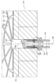
本明細書で開示される実施形態には、1つまたは複数のセンサハウジングおよび撓みセンサを含むセンサアセンブリが含まれる。このセンサアセンブリは、裏側ガスを用いて構成される静電チャック、または他の、処理中に加工品を処理チャンバ内で保持するのに適しているアセンブリなどの基板支持アセンブリ内に配置されるように構成される。たとえば、センサアセンブリは、既存の裏側ガス送出孔、または静電チャックの他の孔の中に配置することができる。撓みセンサは、静電チャック上に配置された加工品にかかる力のバランスを決定するための、加工品の撓みのリアルタイム測定値を与えることができる。撓みセンサを使用してチャッキング力を決定することによって、加工品チャッキング/チャッキング解除プロセスは、裏側加工品欠陥、およびこれにより発生する微粒子を低減/除去するチャッキング力を最小限にするように最適化することができる。たとえば、チャッキング/チャッキング解除中にチャッキング電圧を裏側のHeの流れ圧力と共に同時に引き上げ、引き下げることによって、プロセスは、加工品を保持するのに適切なチャッキング力を最小限にし、これにより、裏側加工品引っ掻き傷、およびそれによる微粒子発生が最小限になる。 Embodiments disclosed herein include a sensor assembly that includes one or more sensor housings and a deflection sensor. The sensor assembly may be placed within a substrate support assembly, such as an electrostatic chuck configured with a backside gas, or other assembly suitable for holding the workpiece within the processing chamber during processing. It is composed of For example, the sensor assembly can be placed within an existing backside gas delivery hole or other hole in the electrostatic chuck. The deflection sensor can provide real-time measurements of workpiece deflection to determine the balance of forces on the workpiece placed on the electrostatic chuck. By using deflection sensors to determine the chucking force, the workpiece chucking/unchucking process minimizes chucking forces to reduce/eliminate backside workpiece defects and the resulting particulate matter. It can be optimized as follows. For example, by simultaneously raising and lowering the chucking voltage along with the backside He flow pressure during chucking/unchucking, the process minimizes the chucking force adequate to hold the workpiece, thereby , backside workpiece scratches and resulting particulate generation are minimized.
図1は、センサアセンブリ190の一実施形態を示す。図1は、基板支持アセンブリ170が組み込まれている例示的なプラズマ処理チャンバ100の概略図を示す。基板支持アセンブリ170は、その中にセンサアセンブリ190が配置されている。一実施形態では、プラズマ処理チャンバ100は、スパッタエッチ処理チャンバまたはプラズマエッチシステムである。しかし、物理的気相成長(すなわち、スパッタリング)チャンバ、化学的気相成長チャンバ、エッチングチャンバ、選択的除去処理チャンバ(SRP)、または他の真空処理チャンバなど、他のタイプの処理チャンバもまた、本明細書に記載の実施形態を実践するのに使用されてよい。
FIG. 1 illustrates one embodiment of a
プラズマ処理チャンバ100は、たとえばシリコンウエハである基板などの加工品101の処理中に、チャンバ内部容積120内の減圧を維持するように適切に適合させることができる真空チャンバである。プラズマ処理チャンバ100は、底面126を有するチャンバ本体106を含み、チャンバ内部容積120を密閉する蓋104によって覆われる。チャンバ本体106および蓋104は、アルミニウムなどの金属、または他の適切な材料で作ることができる。
プラズマ処理チャンバ100は、プラズマ処理チャンバ100をポンプダウンし排気するために使用されるスロットルバルブ(図示せず)、および真空ポンプ(図示せず)を含む真空システム114と結合され、流体連結している。プラズマ処理チャンバ100の内部の圧力は、スロットルバルブおよび/または真空ポンプを調整することによって調節することができる。プラズマ処理チャンバ100はまた、アルゴン、酸素、塩素、フッ素、または他の、加工品101を処理するのに適切なガスなど、1つまたは複数の処理ガスをプラズマ処理チャンバ100へ供給できる処理ガス供給源118と結合され、流体連結している。
RFプラズマ電源117は、プロセスガスにエネルギーを与えて、加工品101を処理するためのプラズマ102を維持することができる。基板支持アセンブリ170は、加工品101を偏らせて、そこにイオンをプラズマ102から引き寄せてもよい。塩素などの処理ガスは、処理ガス供給源118からプラズマ処理チャンバ100の中に導入され、ガス圧は、プラズマ点火に調整される。プラズマ102は、RF電力が送出されると容量性結合によってチャンバ内部容積120内で点火される。RF整合部(図示せず)を調整またはプリセットして、RFプラズマ電源117からプラズマ102への電力伝達の効率を改善することができる。
RF
基板支持アセンブリ170はチャンバ内部容積120内に配置される。基板支持アセンブリ170は加工品支持面172を有し、その上には加工品101が処理の間中載っている。基板支持アセンブリ170は、真空チャック、静電チャック、サセプタ、ヒータ、または他の、処理中に加工品101をプラズマ処理チャンバ100内に支持するのに適している、基板支持体を含むことができる。
A
一実施形態では、基板支持アセンブリ170は静電チャック122を含む。基板支持アセンブリ170はさらに、冷却プレート151および支持ベース152を含むことができる。支持ベース152は、支持体ハウジング149、ベローズアセンブリ110、および支持軸112を含むことができる。支持軸112は、図示の上方の処理位置と下方の加工品移送位置(図示せず)の間で基板支持アセンブリ170の垂直移動を行うことができるリフト機構113と結合することができる。ベローズアセンブリ110は、支持軸112のまわりに配置することができ、支持ベース152とプラズマ処理チャンバ100の底面126との間に結合されて、プラズマ処理チャンバ100の内部から真空が失われることを防止しながら基板支持アセンブリ170の垂直の動きを可能にする可撓性シールを提供することができる。
In one embodiment,
基板支持アセンブリ170上に配置された加工品101の温度調節が、冷却プレート151内に配置されている複数の冷却チャネル160によって容易になり得る。冷却チャネル160は流体供給源142と結合され、流体連結しており、この流体供給源は、水などの冷媒流体を供給するが、任意の適切な、ガスまたは液体である冷媒流体が使用されてよい。
Temperature regulation of
基板支持アセンブリ170は、ロボット(図示せず)によりプラズマ処理チャンバ100に出し入れする移送の間中、加工品101を加工品支持面172の上に間隔をあけて支持するための基板リフト130を含むことができる。基板リフト130は、軸111に連結されたプラットフォーム108と整合されたリフトピン109を含むことができる。基板支持アセンブリ170は、リフトピン109が持ち上げられた位置にあるときに、たとえば加工品101を支持しているときに、リフトピン109を受け入れて通すための貫通孔(図示せず)を含むことができる。基板リフト130は、加工品101のロボット移送を容易にするためにリフトピン109を貫通孔から延ばして加工品支持面172の上方の位置に加工品101を支持する、第2のリフト機構132に結合される。基板リフト130はさらに、リフトピン109を加工品支持面172の下に降下させて、加工品101を加工品支持面172に置く。
静電チャック122はパック150を含む。パック150は、加熱素子を含むことができる。パック150、冷却プレート151、および/または静電チャック122の他の構成要素の温度は、1つまたは複数の温度監視装置に結合された熱電対などの1つまたは複数の温度センサ(図示せず)を使用して監視することができる。一例では、パック150は、温度監視用の少なくとも1つの熱電対に結合される。
パック150は、加工品101を支持しチャッキングする、すなわちクランプ力(Fc)を加工品101にかける。パック150は、クランプ力(Fc)を発生させるために電極134が中に埋め込まれている、電気絶縁用パックベース162を含むことができる。
The
電極134は、DC電源などのチャック電源140に電気的に接続される。電極134は、加工品101をパック150の加工品支持面172にチャッキングするためのクランプ力(Fc)を提供する。電極134は、金属または金属合金などの任意の適切な導電性材料で作ることができる。電極134への電力は、チャック電源140に結合された制御システム194によって制御することができる。一例では、パック150は、加工品101をチャッキングするための1つの電極134を含む。電極134は、パックベース162の中に配置された薄い円板または細い線でよい。別の例では、パック150は、加工品101をチャッキングするための2つ以上の電極134を含む。電極134はそれぞれ、互いに独立して動作できる薄い半円形または「D」形のプレートでよい。しかし、1つまたは複数の電極134は、環、くさび、細片などを含んでよい、任意の適切な形状を有することができる。
メサ168および凹部164が、パックベース162の加工品支持面172に配置される。加工品支持面172はさらに、1つまたは複数の溝およびチャネル、または他の幾何形状を含むことができる。加工品101は、メサ168の上に支持し、凹部164の上方に持ち上げることができる。凹部164は、ガス供給源141と流体連結して、ヘリウム、アルゴン、または他の適切な裏側ガスなどの流体を各メサ168の間に供給することができる。裏側ガスは、ガス供給源141から凹部164まで、パック150に形成された1つまたは複数の裏側ガス送出孔198を通して送出することができる。裏側ガスは、パック150と加工品101の間の熱伝達速度を調節する助けとするために、加工品101とパック150の間に流れることができる。一例では、裏側ガスは、アルゴンなどの不活性ガスを含むことができる。ガス供給源は、約4トル以上など、約10トル以上の裏側ガス圧力(図5にFpとして示す)を供給することができる。裏側ガスは加工品101に圧力Fpを作用させるが、詳細には以下で論じる。
A
センサアセンブリ190は、裏側ガス送出孔198もしくは他の適切な貫通孔などの、パック150に形成された貫通孔の中、またはリフトピンの空洞の中に配置されてよい。センサアセンブリ190は、多孔性であり、裏側ガスなどの流体が流れて通り抜けることができる。たとえば、センサアセンブリ190は、流体がセンサアセンブリ190を通過できるようにする通路を有することができる。別の実施形態では、センサアセンブリ190は凹部164の中、または他の適切な場所に取り付けられてよい。
センサアセンブリ190は、制御システム194と通信することができる。センサアセンブリ190は、加工品支持面172上の加工品101の撓みを測定する。コントローラ192は、センサアセンブリ190によって測定された撓みに基づいて、加工品101にかかっているクランプ力Fcを決定する。こうして、コントローラ192は、チャック電源140から電極134に供給されるクランプ電圧Vcを調整することによって、所望のクランプ力Fcを維持するようにクランプ力Fcを調整することができる。実際のクランプ力の(センサアセンブリ190を介した)リアルタイム監視、および電極134に供給される電力のリアルタイム調整により所望のクランプ力Fcを維持することによって、静電チャック122から受ける加工品101の損傷を従来のチャッキング技法と比較して減らすことができる。
有利なことに、パック150の動作パラメータは、センサアセンブリ190から供給されるデータに依拠するフィードバックループを用いて制御することができる。センサアセンブリ190による撓みの測定は、加工品101に作用するチャッキング力を最小限にして欠陥および粒子発生を低減するために、加工品101にかかるリアルタイムの力を計算するように拡張することができる。
Advantageously, the operating parameters of
図2は、センサアセンブリ190が裏側ガス送出孔198の中に取り付けられている図1に示された静電チャック122の部分断面図である。当業者には、センサアセンブリ190が静電チャック122の孔または凹部の中に取り付けられてよいことが理解されよう。1つまたは複数のシナリオでは、静電チャック122は、加工品撓みと、静電チャックによって加工品にかかる力とを検出する複数のセンサアセンブリ190を有する。センサアセンブリ190についてのさらなる説明は、裏側ガス送出孔198のうちの1つに配置されているセンサアセンブリ190に関するものになる。パック150内でセンサアセンブリが中に取り付けられる孔の形状は、円形孔に限定されない。孔は、レーザドリルであける、放電加工(EDM)をする、または他の適切な任意の方法で形成することができる。
FIG. 2 is a partial cross-sectional view of the
裏側ガス通路218は、裏側ガス送出孔198と、裏側ガスをパック150の加工品支持面172へ供給するために裏側ガス送出孔に連結された移行導管210とを含むことができる。センサアセンブリ190が裏側ガス送出孔198内に配置され、制御システム194に配線される実施形態では、センサアセンブリ190と制御システム194の間の通信結線284が、裏側ガス通路218を少なくとも一部は通って横切っていくことができる。図3に示される、センサアセンブリ396がリフトピンの空洞320内に配置され、制御システム194に配線される実施形態では、センサアセンブリ396と制御システム194の間の通信結線284が、静電チャック122内のリフトピン孔を少なくとも一部は通って横切っていくことができる。センサアセンブリが静電チャック122の加工品支持面172の孔または凹部の中に配置されているさらに別の実施形態では、センサアセンブリ190と制御システム194の間の通信結線284間の通信結線は、無線でも、基板支持アセンブリ170の中を通して配線されてもよい。
センサアセンブリ190はセンサ280およびセンサハウジング220を含む。センサ280は、ファブリペローセンサ(FPS)または干渉計、または他の、小さい撓みを測定するのに適しているセンサなど、光ファイバベースのセンサでよい。一実施形態では、センサ280はFPSである。センサ280は、制御システム194と通信する。一実施形態では、センサ280は、制御システム194内のコントローラ192に配線された通信接続部284を有することができる。別の実施形態では、センサアセンブリ190は、制御システム194と無線で通信することができる。センサ280は、パック150上に配置された加工品(図示せず)までの距離を示すメトリックを測定し、そのメトリックを制御システム194に、制御システム194または他の適切なデバイスによる分析のために、リアルタイムで提供することができる。
センサ280は、センサヘッド282を有することができる。センサヘッド282は、距離測定を行うための信号を放出および受信することができる。センサ280は、センサヘッド282と加工品(図示せず)などの任意の対象物との間の距離をリアルタイムで測定して相対変位をナノメートル精度で決定できるように、パック150内に精密取り付けすることができる。加工品支持面172に垂直な垂直線298が与えられている。垂直線298は説明的なものにすぎず、裏側ガス送出孔198、またはパック150内の他の孔には必ずしも存在しない。センサ280は、センサハウジング220が、垂直線298の±3度以内で、言い換えれば、加工品支持面172の垂線から±3度以内に位置合わせされたセンサヘッド282を保持するように、正確に取り付けることができる。センサヘッド282の距離は、パック150の中のセンサハウジング220の位置を調整することによって、メサ168の上部より概ね5mm未満からメサ168の上部より約300mmまで精密に調整することができる。
センサ280は、放射を放出する放射放出器と、加工品101によって反射された放射の一部を測定する放射検出器とを含むことができる。放射または信号は、たとえば、波長が約600ナノメートルから約1700ナノメートルの間の電磁放射でよい。センサ280内の放射検出器は、放出された放射信号の復路を測定する。したがって、センサ280の角度および位置は、測定に影響を及ぼす可能性がある。センサハウジング220は、正確な測定を容易にするために、センサ280を精密な位置および配向に保持する。センサハウジング220は、センサ280の自己位置合わせを可能にすることができる。有利には、センサヘッド282は、加工品支持面172の上方に向けてまたはそこから下方に、加工品支持面172の最上部より概ね5mm未満から約30mmまで精密に調整することができる。
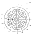
図4は、静電チャック122などの基板支持体の上面図であり、センサアセンブリ190の様々な位置を示す。上で論じたように、センサアセンブリ190は、裏側ガス送出孔198などの、静電チャック122に設けられた既存の孔の中、リフトピン109の空洞の中、または静電チャック122に形成された孔の中に設置することができる。センサアセンブリ190の位置は、静電チャック122のパック150の既存の構成に基づいて決定することができる。1つまたは複数のセンサアセンブリ421~428、190は、裏側ガスを有するパック150の加工品支持面172の全体にわたって設置することができる。センサアセンブリ421~428、190は、同心の列に、および/またはチャック電極の配置に対応するパック150の領域に、置くことができる。たとえば、静電チャック122は、同心に配置された複数の個別チャック電極を有することができる。センサアセンブリ421~428は、内環群430および外環群440として配置することができる。センサアセンブリ421~428は、ローカライズされたチャッキング力の小さいばらつきをパック150に沿って検出することができる。いくつかの実施形態では、多数のセンサアセンブリ421~428は、中心位置のセンサアセンブリ190をさらに含むことができる。有利なことに、このセンサアセンブリ421~428の配置により、過度のチャッキングによる加工品101の損傷からの保護の強化のための、加工品101の全体についての個別撓み測定値を得ることができる。
FIG. 4 is a top view of a substrate support, such as
図5は、加工品101が上に配置されている静電チャック122の部分断面図である。パック150と、センサアセンブリ190に近接している静電チャック122のメサ168とが図示されている。メサ168は、隣り合う1つまたは複数の凹部164の間に配置されている。メサ168は、加工品101を支持するためにパック150から上に延びる、様々なサイズの正方形もしくは長方形ブロック、円錐、くさび、ピラミッド、柱、円筒形隆起、もしくは他の突起、またはこれらの組合せを含むことができる。加工品101は、上で論じたように、クランプ力Fcで静電チャック122に固定することができる。1つの実施形態では、メサ168は、加工品101に最小限の力を作用させて、加工品101の裏側に引っ掻き傷をつけない、または損傷させないように構成される。
FIG. 5 is a partial cross-sectional view of
隣り合うメサ168は、各中心の間隔を距離560とすることができる。一実施形態では、距離560は約0.3インチから約0.5インチの範囲とすることができる。隣り合うメサ168はそれぞれ、約3マイクロメートルから約700マイクロメートルの高さを有することができる。隣り合うメサ168はそれぞれ、約500マイクロメートルから約5000マイクロメートルの範囲の幅を有することができる。凹部164は、約2ミリメートルから約10ミリメートルの幅を有することができる。メサ168および凹部164は、静電チャック122が加工品101を支持することを、加工品101の熱管理も行いながら可能にする。
メサ168は、加工品101を支持する上面542を有する。上面542は一般に、静電チャック122からのクランプ力Fcがかかっていないときに加工品101が載っている基準面520を規定する。基準面520は、加工品101の撓みをセンサ280によってそこから測定できる参照点として機能することができる。1つの実施形態では、チャッキング力が加工品101に加えられると、正反対の接触圧力がメサ168によって加工品101に加えられる。
加工品101は、クランプ力Fcがかかると静電チャック122に固定され得る。クランプ力Fcは、加工品101をメサ168に向けて引き寄せ、メサ168との接触と相俟って、加工品101が静電チャック122に対して動かないようにする。クランプ力Fcは、静電チャック122の加工品支持面172の全体にわたって同じではなく、実質的に類似もしていないことさえあり得る。クランプ力Fcのばらつきは、特に、材料の堆積によるパック150の変化、洗浄およびエッチングによる腐食、ならびに摩耗に原因があると考えられる。加えて、クランプ力Fcは、区域に分けられた静電チャック構成などにおいて、加工品支持面172の全体にわたって意図的に差異化することもできる。
センサ280は、基準面520に対する加工品101の撓みを測定する。クランプ力Fcを制御するために、クランプ電圧が静電チャック内の電極134に印加される。クランプ電圧は、センサ280によって測定された加工品101の撓みに応じて変えることができる。クランプ力Fcをかけると、加工品101は、凹部164の幾何学的平面510と整合することができる。撓みは、クランプ力Fcと実質的に一致する合力を表し得る。測定された撓みとクランプ電圧は、測定された撓みが所定の範囲に入るまで調整することができる。たとえば、許容可能な撓みの所定の範囲は、500ナノメートルから約2μmの間とすることができる。測定された撓みが約2μmよりも大きい場合、クランプ電圧は、撓みが500ナノメートルから約2μmの間にあるとセンサがリアルタイムで決定するまで、低減させることができる。撓みは、2つ以上の位置に配置されたセンサアセンブリ190を用いて測定することができ、それによって、ガス圧と接触圧などの正反対の力とを一致させるためのクランプ電圧の精密な調整が可能になる。
センサ280は、加工品101の撓みの変化を短い時間間隔で測定することができる。
多数のセンサ280が加工品101の撓みを監視し、静電チャック122に多数のクランプゾーンが備えられる実施形態では、制御システム194は、別々のクランプゾーンに設置された個々のセンサ280からのデータを使用して、その特定のクランプゾーンにおけるクランプを、正反対の各力を一致させ、クランプ電圧を最小限にするように制御することができる。チャッキング電圧/力が増大すると、ESC上およびチャンパ処理環境中により多くの微粒子が発生する。たとえば、1μmよりも大きい微粒子による欠陥では、800Vのチャッキング電圧でおよそ1392個の埋込み微粒子が加工品101の裏側面に生じたことが観察された。これらの埋込み微粒子のうち、約21個の微粒子が10μmよりも大きいサイズであった。1000Vのチャッキング電圧では、およそ2264個の埋込み微粒子が加工品101の裏側面に生じた。1200Vのチャッキング電圧では、およそ3546個の埋込み微粒子が加工品101の裏側面に生じた。また1800Vのチャッキング電圧では、およそ5532個の埋込み微粒子が加工品101の表側面に生じた。さらに1800Vでは、10μmよりも大きい埋込み微粒子の数がおよそ140個にまで増加した。すなわち、埋込み微粒子の数は電圧に対して直線的な関係ではなく、電圧のそれぞれの小さな増加でますます多くの埋込み微粒子が発生する。しかし、さらに著しいのは10μmよりも大きい微粒子の数であり、チャッキング電圧の2倍の増加に対し、10μmよりも大きい微粒子の数は7倍超に増加した。これらの裏側微粒子/欠陥は、ウエハ処理中またはウエハカセット(すなわち、FOUP)内での裏側ガス漏洩によって、または加工品101の上への落下によって、加工品101の表側に移転し得る。裏側欠陥はまた、他の半導体プロセスステップで移転することもある。この移転は、ダイおよびフィーチャサイズが縮小するにつれて顕著になり、より大きいサイズの微粒子がフィーチャ間の間隙を橋絡し、場合によってはダイが使用不可になる。
In embodiments where
したがって、ESCからの微粒子を低減/除去するために、ウエハチャッキング/チャッキング解除プロセスでは、加工品101にかかるチャッキング力を最小限にする。加工品101を過度にチャッキングすることによるシリコン引っ掻き傷が微粒子を発生させるが、この場合チャッキングを最小限にして、遊離微粒子が加工品101の表側フィーチャに導入されること、およびそこに欠陥が形成されることを防止することができる。裏側ガスの導入による力を引き上げ、同時にチャッキング電圧による正反対の力を引き上げることによって、加工品101にかかるこれらの力のバランスを取ることができ、それにより、加工品101は、裏側に引っ掻き傷を生じさせる、または微粒子を表側に導入することなく、ESCに保持することができる。1つの実施形態では、チャッキング/チャッキング解除ステップ中にHe圧が、ウエハにかかるチャッキング力を最小限にするように、同時に調整される。
Therefore, to reduce/remove particulates from the ESC, the wafer chucking/unchucking process minimizes chucking forces on the
静電チャック122は、多数のクランプゾーンを備えることができ、センサ280を有する多数のセンサアセンブリ190を使用して各クランプゾーンを監視することができる。あるいは、静電チャック122は、チャッキング力測定デバイスを有してもよい。チャッキング力測定デバイスは、チャッキング電圧と、最終的には加工品101に加えられる力の大きさとを制御するために、フィードバックを行うことができる。当業者には、加工品に加えられるリアルタイムの力を供給または定量化するのに適切な任意のデバイスまたはセンサが、加工品の過度のチャッキング、および過度のチャッキングによって生じる欠陥を低減するための、図6に関して以下で説明する方法を実施するのに適していることが理解されよう。
次に、図6および図7について一緒に論じる。図6は、基板支持体上に配置された加工品にかかる力を最小限にするための方法600である。図7は、図6の方法を示す図である。加工品は、ESCに向けて加工品を押す1つまたは複数の静電力と、メサに沿った接触圧および加工品をESCから押し離すガス圧の両方とを受けることができる。方法600は、これらの力を最小限でバランスさせて、加工品101を処理チャンバ内のESCに保持する。
Next, FIGS. 6 and 7 will be discussed together. FIG. 6 is a
ウエハを静電チャックによってチャッキングすることは、静的プロセスである(動的なウエハの動きが生じない)。チャッキング力は、2つの正反対の力による抵抗を受ける。第1は、裏側ガス圧の、このガスにさらされるウエハの裏側領域に対する力である。第2の力は、ウエハがeチャックと接触する領域に対する接触圧である。図7は、加工品にかかるそれぞれの力を示す。y軸754は、加工品に加えられる力を示す。x軸752は、加工品にかかるこれらの力のタイミングを示す。
Chucking a wafer with an electrostatic chuck is a static process (no dynamic wafer movement occurs). The chucking force is resisted by two opposing forces. The first is the force of the backside gas pressure on the backside area of the wafer exposed to this gas. The second force is the contact pressure on the area where the wafer contacts the e-chuck. Figure 7 shows the respective forces applied to the workpiece. The y-
方法600のブロック610で、加工品がプラズマ処理チャンバ内の静電チャック上に配置される。図7の第1の時間ブロック701は、チャッキング電圧740がチャッキング最小電圧742に設定され、裏側ガス圧760がガス最小圧762にあることを示す。加工品は、第2の時間ブロック702においてESCの上に移される。これはまた、最小チャッキング電圧742を設定する代わりに、最小力までチャッキング電圧740に傾斜をつけることによって実現することもできる。次に裏側ガス圧760が、最小ガス圧762になる。この最後の手法によって、最小力が加工品に加えられる。
At
方法600のブロック620で、プラズマが処理チャンバ内に与えられる。これは、図7の第3の時間ブロック703に対応する。プラズマは、加工品をチャッキングするときにESCにグランドを提供する。ここで、DCバイアス補償は、プラズマを与えるときにESC上で不能にされてよい。
At
方法600のブロック630で、加工品にかかる撓み力が監視される。力は、加工品に加わる力を決定するコントローラに応力情報、撓み情報、または他の適切な情報を供給するセンサによって監視することができる。
At
方法600のブロック640で、チャッキング電圧740が最小値741にされる。これはまた、最小チャッキング電圧741を設定する代わりに、最小力までチャッキング電圧740に傾斜をつけることによって実現することもできる。ブロック650で、裏側ガス圧760が裏側ガス最小圧763にされる。ここで、裏側ガス最小圧763は、ガス最小圧762から増大されていてもいなくてもよい。これは、一部のESCには最小の裏側ガスの流れが常にあるからである。コントローラは、裏側ガス圧760とチャッキング電圧740の間の撓み力780を監視および維持する。撓み力780(裏側ガス圧760とチャッキング電圧740の間の力の差)は、まだ処理前の加工品をESC上に維持するのに適切な、処理に適している撓み力780の閾値未満のものでよい。
At
方法600のブロック660で、チャッキング電圧740および/または裏側ガス圧760は、撓み力780が閾値未満になるように調整される。撓み力780は、加工品に下向きにかかる合力である。すなわち、ESCによって保持される加工品に対して、チャッキング電圧740によって供給される力は、裏側ガス圧760によって供給される力よりも大きい。1つの実施形態では、撓み力は、ウエハのまわりで撓みが10ナノメートル~5μmなどの、約50ミリトルから約50トルの間である。
At
方法600のブロック670で、チャッキング電圧および裏側ガスは同時に引き上げられる。これは、図7の第4の時間ブロック704に対応する。プラズマを与えることと加工品をチャッキングすることの間で、小さな時間遅延が力の引き上げに導入されてもよい。1つの実施形態では、約200ミリ秒から約10秒の間の時間遅延が、プラズマを与えることと加工品をチャッキングすることの間に設けられる。
At
加工品は、図7に示された第5の時間ブロック705の間にチャッキングされ処理される。ここでチャッキング電圧740は、プラズマにバイアスをかける、加工品を処理する、および/または加工品をESCに静電的に保持するのに適切なレベル749にある。裏側ガス圧760は、チャッキング電圧740の力と釣り合わせる、かつ撓み力780を閾値未満に維持するために、高い圧力769に維持される。
The workpiece is chucked and processed during the fifth time block 705 shown in FIG. The chucking
したがって、加工品を固定するために用いられるチャッキング力は、常に最小限にされる。低いチャッキング電圧により、引っ掻き傷および引っ掻き傷で発生する微粒子が低減する。方法600では、裏側ガスが供給された状態で加工品を保持するのにちょうど十分である小さい力で加工品をチャッキングする。ずっと小さい追加チャッキング力の安全マージンがまた、加工品が処理中にESCによって堅固に保持されることを確実にするために加えられてもよい。裏側冷却ガスが加えられ安定にする。次に、チャックのスキャン中にチャック上の所定の位置に加工品を保持するためだけに十分な追加の力が加えられる。これによりウエハにかかる力が最小限にされて、ウエハの静電クランプによって生じるシリコン損傷が低減する。
Therefore, the chucking force used to secure the workpiece is always minimized. The lower chucking voltage reduces scratches and scratch-generated particulates. The
チャッキング力および裏側ガス圧の閉ループ制御を設けてチャッキング力を最小限にすることができ、これにより、ウエハ引っ掻き傷および引っ掻き傷で発生する微粒子が著しく低減する。1つまたは複数の撓みセンサ、または他の適切な力センサを含む制御システムは、静電チャックによって加えられるクランプ力を測定および制御する。制御システムは、センサによって測定される撓みを用いて、加工品にかかる力を計算し、静電チャックによって加工品に加えられるクランプ力を調整することができる。制御システムは、クランプ力が、加工品に加えられる目標合計クランプ力に到達し、これを維持するように、静電チャックへのクランプ電圧を調整する。有利なことに、クランプ力は、シリコンウエハを静電チャックに固定するように、かつ実施されるべき製造作業を、加工品にかかる不要な高いクランプ力の結果として生じる加工品損傷を最小限にしながら、可能にするように供給することができる。 Closed-loop control of chucking force and backside gas pressure can be provided to minimize chucking force, which significantly reduces wafer scratches and scratch-generated particulates. A control system including one or more deflection sensors, or other suitable force sensors, measures and controls the clamping force exerted by the electrostatic chuck. The control system can use the deflection measured by the sensor to calculate the force on the workpiece and adjust the clamping force applied to the workpiece by the electrostatic chuck. The control system adjusts the clamping voltage to the electrostatic chuck such that the clamping force reaches and maintains a target total clamping force applied to the workpiece. Advantageously, the clamping force is such that the silicon wafer is secured to the electrostatic chuck and the manufacturing operations to be performed minimize workpiece damage resulting from unnecessary high clamping forces applied to the workpiece. However, it can be supplied as possible.
この方法は、加工品をチャッキング解除するために拡張される。第6の時間ブロック706の間、チャッキング電圧740および裏側ガス圧760は低減すなわち引き下げられる。裏側ガス圧がガス最小圧762まで低減されると、チャッキング電圧740の除去の前に小さな遅延が設けられる。第7の時間ブロック707において、プラズマはオフにされ、加工品はチャッキング解除される。センサはまた、チャッキング解除ステップで、いつ加工品を取り外すのが、またはリフトピンを上げるのが安全かのリアルタイムフィードバックを与える助けにもなり得る。第8の時間ブロック708で、加工品はESCから取り外され、プラズマ処理チャンバから取り出される。チャッキング作業とチャッキング解除作業は実質的に類似しているが、逆の順序で行われることを理解されたい。
This method is extended to unchucking workpieces. During the
本明細書に論述されていない多くの修正および他の実施形態が、上記の説明および添付の図面において提示された教示の利益を受けてその実施形態に関係する当業者には想起されよう。したがって、本明細書および特許請求の範囲が、開示された特定の実施形態に限定されないこと、ならびに修正および他の実施形態が添付の特許請求の範囲内に含まれるものであることを理解されたい。諸実施形態は、その実施形態の修正形態および変形形態を、これらが添付の特許請求の範囲およびその等価物の範囲に入るのであれば、包含するものである。特定の用語が本明細書に使用されているが、これらは一般的および説明的な意味で使用されているにすぎず、限定を目的とするものではない。 Many modifications and other embodiments not discussed herein will occur to those skilled in the art having the benefit of the teachings presented in the foregoing description and accompanying drawings. Therefore, it is to be understood that the specification and claims are not limited to the particular embodiments disclosed, and that modifications and other embodiments are intended to be included within the scope of the appended claims. . The embodiments are intended to cover modifications and variations of the embodiments provided they come within the scope of the appended claims and their equivalents. Although specific terms are used herein, they are used in a generic and descriptive sense only and not for purposes of limitation.
上記は本開示の諸実施形態を対象としているが、本発明のその他のさらなる実施形態を本発明の基本的な範囲から逸脱することなく考案することができ、その範囲は添付の特許請求の範囲によって決まる。 Although the above is directed to embodiments of the present disclosure, other further embodiments of the invention may be devised without departing from the essential scope of the invention, which scope is within the scope of the appended claims. Determined by
701 第1の時間ブロック
702 第2の時間ブロック
703 第3の時間ブロック
704 第4の時間ブロック
705 第5の時間ブロック
706 第6の時間ブロック
707 第7の時間ブロック
708 第8の時間ブロック
740 チャッキング電圧
741 最小チャッキング電圧
742 チャッキング最小電圧
749 加工品を処理する、および/または加工品をESCに静電的に保持するのに適切なレベル
760 裏側ガス圧
762 最小ガス圧
763 裏側ガス最小圧
769 高い圧力
780 撓み力
701 First time block 702 Second time block 703 Third time block 704 Fourth time block 705
Claims (11)
処理チャンバ内の静電チャック上に加工品を配置するステップと、
前記処理チャンバの中にプラズマを与えるステップと、
前記加工品にかかる撓み力を監視するステップと、
最小値のチャッキング電圧を加えるステップと、
最小圧の裏側ガス圧を加えるステップと、
前記撓み力が閾値未満になるように前記チャッキング電圧および/または裏側ガス圧を調整するステップと、
前記チャッキング電圧および前記裏側ガス圧を同時に引き上げるステップとを含む、方法。 A method of minimizing chucking forces on a workpiece placed on an electrostatic chuck in a plasma processing chamber, the method comprising:
placing the workpiece on an electrostatic chuck within the processing chamber;
providing a plasma within the processing chamber;
monitoring the deflection force applied to the workpiece;
applying a minimum chucking voltage;
applying a minimum backside gas pressure;
adjusting the chucking voltage and/or backside gas pressure such that the deflection force is below a threshold;
and simultaneously increasing the chucking voltage and the backside gas pressure.
前記閉ループ制御に応じて前記チャッキング力を最小限にするステップとをさらに含む、請求項1に記載の方法。 providing closed-loop control of the chucking force and backside gas pressure;
and minimizing the chucking force in response to the closed-loop control.
最小力を得るように前記チャッキング電圧を選択するステップを含む、請求項1に記載の方法。 Applying the chucking voltage at the minimum value further comprises:
2. The method of claim 1, comprising selecting the chucking voltage to obtain a minimum force.
Applications Claiming Priority (3)
| Application Number | Priority Date | Filing Date | Title |
|---|---|---|---|
| US201762506313P | 2017-05-15 | 2017-05-15 | |
| US15/979,787 US10460916B2 (en) | 2017-05-15 | 2018-05-15 | Real time monitoring with closed loop chucking force control |
| US15/979,787 | 2018-05-15 |
Publications (2)
| Publication Number | Publication Date |
|---|---|
| JP2019201207A JP2019201207A (en) | 2019-11-21 |
| JP7362293B2 true JP7362293B2 (en) | 2023-10-17 |
Family
ID=64096762
Family Applications (1)
| Application Number | Title | Priority Date | Filing Date |
|---|---|---|---|
| JP2019091811A Active JP7362293B2 (en) | 2017-05-15 | 2019-05-15 | Real-time monitoring using closed-loop chucking force control |
Country Status (5)
| Country | Link |
|---|---|
| US (1) | US10460916B2 (en) |
| JP (1) | JP7362293B2 (en) |
| KR (1) | KR20190130971A (en) |
| CN (1) | CN110491756B (en) |
| TW (1) | TWI815889B (en) |
Families Citing this family (27)
| Publication number | Priority date | Publication date | Assignee | Title |
|---|---|---|---|---|
| WO2017209901A2 (en) * | 2016-06-03 | 2017-12-07 | Applied Materials, Inc. | Substrate distance monitoring |
| US10732615B2 (en) * | 2017-10-30 | 2020-08-04 | Varian Semiconductor Equipment Associates, Inc. | System and method for minimizing backside workpiece damage |
| US10555412B2 (en) | 2018-05-10 | 2020-02-04 | Applied Materials, Inc. | Method of controlling ion energy distribution using a pulse generator with a current-return output stage |
| US11054317B2 (en) * | 2018-09-28 | 2021-07-06 | Applied Materials, Inc. | Method and apparatus for direct measurement of chucking force on an electrostatic chuck |
| US11476145B2 (en) | 2018-11-20 | 2022-10-18 | Applied Materials, Inc. | Automatic ESC bias compensation when using pulsed DC bias |
| US11373890B2 (en) * | 2018-12-17 | 2022-06-28 | Applied Materials, Inc. | Wireless in-situ real-time measurement of electrostatic chucking force in semiconductor wafer processing |
| JP7451540B2 (en) | 2019-01-22 | 2024-03-18 | アプライド マテリアルズ インコーポレイテッド | Feedback loop for controlling pulsed voltage waveforms |
| US11508554B2 (en) | 2019-01-24 | 2022-11-22 | Applied Materials, Inc. | High voltage filter assembly |
| US11488811B2 (en) | 2019-03-08 | 2022-11-01 | Applied Materials, Inc. | Chucking process and system for substrate processing chambers |
| CN113035682B (en) * | 2019-12-25 | 2023-03-31 | 中微半导体设备(上海)股份有限公司 | Lower electrode assembly and plasma processing device thereof |
| WO2021148195A1 (en) * | 2020-01-24 | 2021-07-29 | Evatec Ag | Phase shift controlled sputter system and process |
| WO2021185939A1 (en) * | 2020-03-20 | 2021-09-23 | Asml Netherlands B.V. | Method, apparatus, and system for dynamically controlling an electrostatic chuck during an inspection of wafer |
| US11462389B2 (en) | 2020-07-31 | 2022-10-04 | Applied Materials, Inc. | Pulsed-voltage hardware assembly for use in a plasma processing system |
| US11508608B2 (en) * | 2020-08-20 | 2022-11-22 | Taiwan Semiconductor Manufacturing Co., Ltd. | Vacuum wafer chuck for manufacturing semiconductor devices |
| US11901157B2 (en) | 2020-11-16 | 2024-02-13 | Applied Materials, Inc. | Apparatus and methods for controlling ion energy distribution |
| US11798790B2 (en) | 2020-11-16 | 2023-10-24 | Applied Materials, Inc. | Apparatus and methods for controlling ion energy distribution |
| US11854911B2 (en) * | 2021-02-25 | 2023-12-26 | Applied Materials, Inc. | Methods, systems, and apparatus for conducting chucking operations using an adjusted chucking voltage if a process shift occurs |
| US11495470B1 (en) | 2021-04-16 | 2022-11-08 | Applied Materials, Inc. | Method of enhancing etching selectivity using a pulsed plasma |
| US11948780B2 (en) | 2021-05-12 | 2024-04-02 | Applied Materials, Inc. | Automatic electrostatic chuck bias compensation during plasma processing |
| US11791138B2 (en) | 2021-05-12 | 2023-10-17 | Applied Materials, Inc. | Automatic electrostatic chuck bias compensation during plasma processing |
| US11967483B2 (en) | 2021-06-02 | 2024-04-23 | Applied Materials, Inc. | Plasma excitation with ion energy control |
| US11810760B2 (en) | 2021-06-16 | 2023-11-07 | Applied Materials, Inc. | Apparatus and method of ion current compensation |
| US11569066B2 (en) | 2021-06-23 | 2023-01-31 | Applied Materials, Inc. | Pulsed voltage source for plasma processing applications |
| US11476090B1 (en) | 2021-08-24 | 2022-10-18 | Applied Materials, Inc. | Voltage pulse time-domain multiplexing |
| US20230114751A1 (en) * | 2021-10-08 | 2023-04-13 | Applied Materials, Inc. | Substrate support |
| US11694876B2 (en) | 2021-12-08 | 2023-07-04 | Applied Materials, Inc. | Apparatus and method for delivering a plurality of waveform signals during plasma processing |
| CN114582780B (en) * | 2022-03-01 | 2022-12-23 | 江苏京创先进电子科技有限公司 | Method and device for removing ring of Taiko wafer |
Citations (4)
| Publication number | Priority date | Publication date | Assignee | Title |
|---|---|---|---|---|
| JP2001351968A (en) | 2000-06-07 | 2001-12-21 | Mitsubishi Electric Corp | Apparatus and method for plasma processing |
| US20150138687A1 (en) | 2013-11-19 | 2015-05-21 | Applied Materials, Inc. | Control systems employing deflection sensors to control clamping forces applied by electrostatic chucks, and related methods |
| JP2016139649A (en) | 2015-01-26 | 2016-08-04 | 住友大阪セメント株式会社 | Electrostatic chuck device |
| JP2018530150A (en) | 2015-09-11 | 2018-10-11 | アプライド マテリアルズ インコーポレイテッドApplied Materials,Incorporated | Substrate support with real-time force and membrane stress control |
Family Cites Families (4)
| Publication number | Priority date | Publication date | Assignee | Title |
|---|---|---|---|---|
| JPH04206546A (en) * | 1990-11-30 | 1992-07-28 | Hitachi Ltd | Method and device for plasma treatment |
| US8422193B2 (en) * | 2006-12-19 | 2013-04-16 | Axcelis Technologies, Inc. | Annulus clamping and backside gas cooled electrostatic chuck |
| US8313612B2 (en) * | 2009-03-24 | 2012-11-20 | Lam Research Corporation | Method and apparatus for reduction of voltage potential spike during dechucking |
| US9287092B2 (en) * | 2009-05-01 | 2016-03-15 | Advanced Energy Industries, Inc. | Method and apparatus for controlling ion energy distribution |
-
2018
- 2018-05-15 US US15/979,787 patent/US10460916B2/en active Active
-
2019
- 2019-05-13 KR KR1020190055863A patent/KR20190130971A/en not_active Application Discontinuation
- 2019-05-15 CN CN201910406928.2A patent/CN110491756B/en active Active
- 2019-05-15 JP JP2019091811A patent/JP7362293B2/en active Active
- 2019-05-15 TW TW108116655A patent/TWI815889B/en active
Patent Citations (4)
| Publication number | Priority date | Publication date | Assignee | Title |
|---|---|---|---|---|
| JP2001351968A (en) | 2000-06-07 | 2001-12-21 | Mitsubishi Electric Corp | Apparatus and method for plasma processing |
| US20150138687A1 (en) | 2013-11-19 | 2015-05-21 | Applied Materials, Inc. | Control systems employing deflection sensors to control clamping forces applied by electrostatic chucks, and related methods |
| JP2016139649A (en) | 2015-01-26 | 2016-08-04 | 住友大阪セメント株式会社 | Electrostatic chuck device |
| JP2018530150A (en) | 2015-09-11 | 2018-10-11 | アプライド マテリアルズ インコーポレイテッドApplied Materials,Incorporated | Substrate support with real-time force and membrane stress control |
Also Published As
| Publication number | Publication date |
|---|---|
| JP2019201207A (en) | 2019-11-21 |
| US10460916B2 (en) | 2019-10-29 |
| TW201947702A (en) | 2019-12-16 |
| CN110491756B (en) | 2024-03-29 |
| CN110491756A (en) | 2019-11-22 |
| KR20190130971A (en) | 2019-11-25 |
| US20180330926A1 (en) | 2018-11-15 |
| TWI815889B (en) | 2023-09-21 |
Similar Documents
| Publication | Publication Date | Title |
|---|---|---|
| JP7362293B2 (en) | Real-time monitoring using closed-loop chucking force control | |
| JP7443430B2 (en) | Substrate support with real-time force and membrane stress control | |
| TWI774652B (en) | Systems and methods for performing edge ring characterization | |
| TWI404163B (en) | Heat transfer system for improved semiconductor processing uniformity, plasma processing system for processing a substrate, and method of processing a substrate in a process chamber | |
| US7869184B2 (en) | Method of determining a target mesa configuration of an electrostatic chuck | |
| TW201737290A (en) | Wafer edge ring lifting solution | |
| TWI748437B (en) | Process kit and apparatus for processing substrate and lifting solution for substrate edge ring of the apparatus | |
| TW202107610A (en) | Plasma processing apparatus andtemperature control method | |
| KR102223759B1 (en) | Substrate treating method and substrate treating apparatus | |
| TWI816890B (en) | Plasma processing apparatus and method for measuring thickness of ring member | |
| KR100799781B1 (en) | Focus-ring, substrate processing device and substrate processing method | |
| JP2022174626A (en) | Substrate processing system and method for estimating height of annular member | |
| CN117976601A (en) | Substrate support with instant force and film stress control | |
| TW202314778A (en) | Method and apparatus for determining a position of a ring within a process kit |
Legal Events
| Date | Code | Title | Description |
|---|---|---|---|
| A621 | Written request for application examination |
Free format text: JAPANESE INTERMEDIATE CODE: A621 Effective date: 20220218 |
|
| A977 | Report on retrieval |
Free format text: JAPANESE INTERMEDIATE CODE: A971007 Effective date: 20230209 |
|
| A131 | Notification of reasons for refusal |
Free format text: JAPANESE INTERMEDIATE CODE: A131 Effective date: 20230227 |
|
| A521 | Request for written amendment filed |
Free format text: JAPANESE INTERMEDIATE CODE: A523 Effective date: 20230526 |
|
| TRDD | Decision of grant or rejection written | ||
| A01 | Written decision to grant a patent or to grant a registration (utility model) |
Free format text: JAPANESE INTERMEDIATE CODE: A01 Effective date: 20230904 |
|
| A61 | First payment of annual fees (during grant procedure) |
Free format text: JAPANESE INTERMEDIATE CODE: A61 Effective date: 20231004 |
|
| R150 | Certificate of patent or registration of utility model |
Ref document number: 7362293 Country of ref document: JP Free format text: JAPANESE INTERMEDIATE CODE: R150 |