JP7356982B2 - Methods of forming semiconductor structures for vertical transport field effect transistors, semiconductor structures, and integrated circuits - Google Patents
Methods of forming semiconductor structures for vertical transport field effect transistors, semiconductor structures, and integrated circuits Download PDFInfo
- Publication number
- JP7356982B2 JP7356982B2 JP2020534980A JP2020534980A JP7356982B2 JP 7356982 B2 JP7356982 B2 JP 7356982B2 JP 2020534980 A JP2020534980 A JP 2020534980A JP 2020534980 A JP2020534980 A JP 2020534980A JP 7356982 B2 JP7356982 B2 JP 7356982B2
- Authority
- JP
- Japan
- Prior art keywords
- forming
- gate
- source
- drain
- fins
- Prior art date
- Legal status (The legal status is an assumption and is not a legal conclusion. Google has not performed a legal analysis and makes no representation as to the accuracy of the status listed.)
- Active
Links
- 239000004065 semiconductor Substances 0.000 title claims description 115
- 238000000034 method Methods 0.000 title claims description 106
- 230000005669 field effect Effects 0.000 title claims description 9
- 239000010410 layer Substances 0.000 claims description 237
- 229910052751 metal Inorganic materials 0.000 claims description 112
- 239000002184 metal Substances 0.000 claims description 112
- 230000008569 process Effects 0.000 claims description 70
- 125000006850 spacer group Chemical group 0.000 claims description 57
- 239000000758 substrate Substances 0.000 claims description 33
- 239000004020 conductor Substances 0.000 claims description 30
- 239000011229 interlayer Substances 0.000 claims description 22
- 238000011049 filling Methods 0.000 claims description 18
- 238000000151 deposition Methods 0.000 claims description 12
- 238000005530 etching Methods 0.000 claims description 9
- 238000002955 isolation Methods 0.000 claims description 5
- 238000006073 displacement reaction Methods 0.000 claims description 4
- 230000015572 biosynthetic process Effects 0.000 description 65
- 239000000463 material Substances 0.000 description 56
- 239000002019 doping agent Substances 0.000 description 16
- 238000005229 chemical vapour deposition Methods 0.000 description 13
- 238000012545 processing Methods 0.000 description 13
- 229910052581 Si3N4 Inorganic materials 0.000 description 11
- 238000000231 atomic layer deposition Methods 0.000 description 11
- 238000000059 patterning Methods 0.000 description 11
- VYPSYNLAJGMNEJ-UHFFFAOYSA-N Silicium dioxide Chemical compound O=[Si]=O VYPSYNLAJGMNEJ-UHFFFAOYSA-N 0.000 description 8
- 230000008021 deposition Effects 0.000 description 8
- NFFIWVVINABMKP-UHFFFAOYSA-N methylidynetantalum Chemical compound [Ta]#C NFFIWVVINABMKP-UHFFFAOYSA-N 0.000 description 8
- 238000001020 plasma etching Methods 0.000 description 8
- 229910003468 tantalcarbide Inorganic materials 0.000 description 8
- MTPVUVINMAGMJL-UHFFFAOYSA-N trimethyl(1,1,2,2,2-pentafluoroethyl)silane Chemical compound C[Si](C)(C)C(F)(F)C(F)(F)F MTPVUVINMAGMJL-UHFFFAOYSA-N 0.000 description 8
- 229910004298 SiO 2 Inorganic materials 0.000 description 7
- UQZIWOQVLUASCR-UHFFFAOYSA-N alumane;titanium Chemical compound [AlH3].[Ti] UQZIWOQVLUASCR-UHFFFAOYSA-N 0.000 description 7
- 238000005137 deposition process Methods 0.000 description 7
- HQVNEWCFYHHQES-UHFFFAOYSA-N silicon nitride Chemical compound N12[Si]34N5[Si]62N3[Si]51N64 HQVNEWCFYHHQES-UHFFFAOYSA-N 0.000 description 7
- XUIMIQQOPSSXEZ-UHFFFAOYSA-N Silicon Chemical compound [Si] XUIMIQQOPSSXEZ-UHFFFAOYSA-N 0.000 description 6
- 229910000577 Silicon-germanium Inorganic materials 0.000 description 6
- 230000000873 masking effect Effects 0.000 description 6
- 229910052710 silicon Inorganic materials 0.000 description 6
- 239000010703 silicon Substances 0.000 description 6
- ZOXJGFHDIHLPTG-UHFFFAOYSA-N Boron Chemical compound [B] ZOXJGFHDIHLPTG-UHFFFAOYSA-N 0.000 description 4
- GYHNNYVSQQEPJS-UHFFFAOYSA-N Gallium Chemical compound [Ga] GYHNNYVSQQEPJS-UHFFFAOYSA-N 0.000 description 4
- NRTOMJZYCJJWKI-UHFFFAOYSA-N Titanium nitride Chemical compound [Ti]#N NRTOMJZYCJJWKI-UHFFFAOYSA-N 0.000 description 4
- LEVVHYCKPQWKOP-UHFFFAOYSA-N [Si].[Ge] Chemical compound [Si].[Ge] LEVVHYCKPQWKOP-UHFFFAOYSA-N 0.000 description 4
- 229910052796 boron Inorganic materials 0.000 description 4
- 238000000407 epitaxy Methods 0.000 description 4
- 229910052733 gallium Inorganic materials 0.000 description 4
- MZLGASXMSKOWSE-UHFFFAOYSA-N tantalum nitride Chemical compound [Ta]#N MZLGASXMSKOWSE-UHFFFAOYSA-N 0.000 description 4
- 239000010936 titanium Substances 0.000 description 4
- GWEVSGVZZGPLCZ-UHFFFAOYSA-N Titan oxide Chemical compound O=[Ti]=O GWEVSGVZZGPLCZ-UHFFFAOYSA-N 0.000 description 3
- 230000004913 activation Effects 0.000 description 3
- 229910021417 amorphous silicon Inorganic materials 0.000 description 3
- 229910052785 arsenic Inorganic materials 0.000 description 3
- RQNWIZPPADIBDY-UHFFFAOYSA-N arsenic atom Chemical compound [As] RQNWIZPPADIBDY-UHFFFAOYSA-N 0.000 description 3
- 230000000903 blocking effect Effects 0.000 description 3
- 229910017052 cobalt Inorganic materials 0.000 description 3
- 239000010941 cobalt Substances 0.000 description 3
- GUTLYIVDDKVIGB-UHFFFAOYSA-N cobalt atom Chemical compound [Co] GUTLYIVDDKVIGB-UHFFFAOYSA-N 0.000 description 3
- 230000007423 decrease Effects 0.000 description 3
- 239000003989 dielectric material Substances 0.000 description 3
- 238000005516 engineering process Methods 0.000 description 3
- 238000005468 ion implantation Methods 0.000 description 3
- 238000001459 lithography Methods 0.000 description 3
- 150000001247 metal acetylides Chemical class 0.000 description 3
- 150000004706 metal oxides Chemical class 0.000 description 3
- 150000004767 nitrides Chemical class 0.000 description 3
- 229920000620 organic polymer Polymers 0.000 description 3
- 238000005240 physical vapour deposition Methods 0.000 description 3
- BASFCYQUMIYNBI-UHFFFAOYSA-N platinum Chemical compound [Pt] BASFCYQUMIYNBI-UHFFFAOYSA-N 0.000 description 3
- 239000000047 product Substances 0.000 description 3
- HBMJWWWQQXIZIP-UHFFFAOYSA-N silicon carbide Chemical compound [Si+]#[C-] HBMJWWWQQXIZIP-UHFFFAOYSA-N 0.000 description 3
- 235000012239 silicon dioxide Nutrition 0.000 description 3
- 239000000377 silicon dioxide Substances 0.000 description 3
- HWEYZGSCHQNNEH-UHFFFAOYSA-N silicon tantalum Chemical compound [Si].[Ta] HWEYZGSCHQNNEH-UHFFFAOYSA-N 0.000 description 3
- 238000001039 wet etching Methods 0.000 description 3
- PFNQVRZLDWYSCW-UHFFFAOYSA-N (fluoren-9-ylideneamino) n-naphthalen-1-ylcarbamate Chemical compound C12=CC=CC=C2C2=CC=CC=C2C1=NOC(=O)NC1=CC=CC2=CC=CC=C12 PFNQVRZLDWYSCW-UHFFFAOYSA-N 0.000 description 2
- MARUHZGHZWCEQU-UHFFFAOYSA-N 5-phenyl-2h-tetrazole Chemical compound C1=CC=CC=C1C1=NNN=N1 MARUHZGHZWCEQU-UHFFFAOYSA-N 0.000 description 2
- 229910015900 BF3 Inorganic materials 0.000 description 2
- OAICVXFJPJFONN-UHFFFAOYSA-N Phosphorus Chemical compound [P] OAICVXFJPJFONN-UHFFFAOYSA-N 0.000 description 2
- RTAQQCXQSZGOHL-UHFFFAOYSA-N Titanium Chemical compound [Ti] RTAQQCXQSZGOHL-UHFFFAOYSA-N 0.000 description 2
- CEPICIBPGDWCRU-UHFFFAOYSA-N [Si].[Hf] Chemical compound [Si].[Hf] CEPICIBPGDWCRU-UHFFFAOYSA-N 0.000 description 2
- 229910052782 aluminium Inorganic materials 0.000 description 2
- XAGFODPZIPBFFR-UHFFFAOYSA-N aluminium Chemical compound [Al] XAGFODPZIPBFFR-UHFFFAOYSA-N 0.000 description 2
- 229910052787 antimony Inorganic materials 0.000 description 2
- WATWJIUSRGPENY-UHFFFAOYSA-N antimony atom Chemical compound [Sb] WATWJIUSRGPENY-UHFFFAOYSA-N 0.000 description 2
- IVHJCRXBQPGLOV-UHFFFAOYSA-N azanylidynetungsten Chemical compound [W]#N IVHJCRXBQPGLOV-UHFFFAOYSA-N 0.000 description 2
- WTEOIRVLGSZEPR-UHFFFAOYSA-N boron trifluoride Chemical compound FB(F)F WTEOIRVLGSZEPR-UHFFFAOYSA-N 0.000 description 2
- 229910052681 coesite Inorganic materials 0.000 description 2
- 238000004891 communication Methods 0.000 description 2
- 239000010949 copper Substances 0.000 description 2
- 229910052906 cristobalite Inorganic materials 0.000 description 2
- 238000001312 dry etching Methods 0.000 description 2
- 230000005684 electric field Effects 0.000 description 2
- 229910052732 germanium Inorganic materials 0.000 description 2
- GNPVGFCGXDBREM-UHFFFAOYSA-N germanium atom Chemical compound [Ge] GNPVGFCGXDBREM-UHFFFAOYSA-N 0.000 description 2
- 239000010931 gold Substances 0.000 description 2
- WHJFNYXPKGDKBB-UHFFFAOYSA-N hafnium;methane Chemical compound C.[Hf] WHJFNYXPKGDKBB-UHFFFAOYSA-N 0.000 description 2
- 230000006872 improvement Effects 0.000 description 2
- 238000011065 in-situ storage Methods 0.000 description 2
- 229910052738 indium Inorganic materials 0.000 description 2
- APFVFJFRJDLVQX-UHFFFAOYSA-N indium atom Chemical compound [In] APFVFJFRJDLVQX-UHFFFAOYSA-N 0.000 description 2
- 239000011810 insulating material Substances 0.000 description 2
- 238000004943 liquid phase epitaxy Methods 0.000 description 2
- 238000004518 low pressure chemical vapour deposition Methods 0.000 description 2
- 239000011777 magnesium Substances 0.000 description 2
- 238000004519 manufacturing process Methods 0.000 description 2
- 229910044991 metal oxide Inorganic materials 0.000 description 2
- 229910052698 phosphorus Inorganic materials 0.000 description 2
- 239000011574 phosphorus Substances 0.000 description 2
- 238000000623 plasma-assisted chemical vapour deposition Methods 0.000 description 2
- 238000003672 processing method Methods 0.000 description 2
- 238000001289 rapid thermal chemical vapour deposition Methods 0.000 description 2
- 229910010271 silicon carbide Inorganic materials 0.000 description 2
- 229910052814 silicon oxide Inorganic materials 0.000 description 2
- 229910052682 stishovite Inorganic materials 0.000 description 2
- 239000000126 substance Substances 0.000 description 2
- 229910052716 thallium Inorganic materials 0.000 description 2
- BKVIYDNLLOSFOA-UHFFFAOYSA-N thallium Chemical compound [Tl] BKVIYDNLLOSFOA-UHFFFAOYSA-N 0.000 description 2
- 229910052719 titanium Inorganic materials 0.000 description 2
- OGIDPMRJRNCKJF-UHFFFAOYSA-N titanium oxide Inorganic materials [Ti]=O OGIDPMRJRNCKJF-UHFFFAOYSA-N 0.000 description 2
- 229910052905 tridymite Inorganic materials 0.000 description 2
- WFKWXMTUELFFGS-UHFFFAOYSA-N tungsten Chemical compound [W] WFKWXMTUELFFGS-UHFFFAOYSA-N 0.000 description 2
- 229910052721 tungsten Inorganic materials 0.000 description 2
- 239000010937 tungsten Substances 0.000 description 2
- 238000000038 ultrahigh vacuum chemical vapour deposition Methods 0.000 description 2
- 239000012808 vapor phase Substances 0.000 description 2
- 238000000927 vapour-phase epitaxy Methods 0.000 description 2
- 229910018072 Al 2 O 3 Inorganic materials 0.000 description 1
- JBRZTFJDHDCESZ-UHFFFAOYSA-N AsGa Chemical compound [As]#[Ga] JBRZTFJDHDCESZ-UHFFFAOYSA-N 0.000 description 1
- 229910052582 BN Inorganic materials 0.000 description 1
- PZNSFCLAULLKQX-UHFFFAOYSA-N Boron nitride Chemical compound N#B PZNSFCLAULLKQX-UHFFFAOYSA-N 0.000 description 1
- RYGMFSIKBFXOCR-UHFFFAOYSA-N Copper Chemical compound [Cu] RYGMFSIKBFXOCR-UHFFFAOYSA-N 0.000 description 1
- JMASRVWKEDWRBT-UHFFFAOYSA-N Gallium nitride Chemical compound [Ga]#N JMASRVWKEDWRBT-UHFFFAOYSA-N 0.000 description 1
- FYYHWMGAXLPEAU-UHFFFAOYSA-N Magnesium Chemical compound [Mg] FYYHWMGAXLPEAU-UHFFFAOYSA-N 0.000 description 1
- KJTLSVCANCCWHF-UHFFFAOYSA-N Ruthenium Chemical compound [Ru] KJTLSVCANCCWHF-UHFFFAOYSA-N 0.000 description 1
- BQCADISMDOOEFD-UHFFFAOYSA-N Silver Chemical compound [Ag] BQCADISMDOOEFD-UHFFFAOYSA-N 0.000 description 1
- ATJFFYVFTNAWJD-UHFFFAOYSA-N Tin Chemical compound [Sn] ATJFFYVFTNAWJD-UHFFFAOYSA-N 0.000 description 1
- XWCMFHPRATWWFO-UHFFFAOYSA-N [O-2].[Ta+5].[Sc+3].[O-2].[O-2].[O-2] Chemical compound [O-2].[Ta+5].[Sc+3].[O-2].[O-2].[O-2] XWCMFHPRATWWFO-UHFFFAOYSA-N 0.000 description 1
- ILCYGSITMBHYNK-UHFFFAOYSA-N [Si]=O.[Hf] Chemical compound [Si]=O.[Hf] ILCYGSITMBHYNK-UHFFFAOYSA-N 0.000 description 1
- 238000002679 ablation Methods 0.000 description 1
- 230000003321 amplification Effects 0.000 description 1
- 238000000137 annealing Methods 0.000 description 1
- 238000013459 approach Methods 0.000 description 1
- 238000004380 ashing Methods 0.000 description 1
- QVGXLLKOCUKJST-UHFFFAOYSA-N atomic oxygen Chemical compound [O] QVGXLLKOCUKJST-UHFFFAOYSA-N 0.000 description 1
- GPBUGPUPKAGMDK-UHFFFAOYSA-N azanylidynemolybdenum Chemical compound [Mo]#N GPBUGPUPKAGMDK-UHFFFAOYSA-N 0.000 description 1
- CFJRGWXELQQLSA-UHFFFAOYSA-N azanylidyneniobium Chemical compound [Nb]#N CFJRGWXELQQLSA-UHFFFAOYSA-N 0.000 description 1
- VKJLWXGJGDEGSO-UHFFFAOYSA-N barium(2+);oxygen(2-);titanium(4+) Chemical compound [O-2].[O-2].[O-2].[Ti+4].[Ba+2] VKJLWXGJGDEGSO-UHFFFAOYSA-N 0.000 description 1
- 239000003990 capacitor Substances 0.000 description 1
- 239000000969 carrier Substances 0.000 description 1
- 239000000919 ceramic Substances 0.000 description 1
- 238000006243 chemical reaction Methods 0.000 description 1
- 239000007795 chemical reaction product Substances 0.000 description 1
- 238000000224 chemical solution deposition Methods 0.000 description 1
- 230000000295 complement effect Effects 0.000 description 1
- 229910052802 copper Inorganic materials 0.000 description 1
- 230000001419 dependent effect Effects 0.000 description 1
- 238000013461 design Methods 0.000 description 1
- 238000011161 development Methods 0.000 description 1
- 238000009792 diffusion process Methods 0.000 description 1
- 238000011143 downstream manufacturing Methods 0.000 description 1
- 238000001704 evaporation Methods 0.000 description 1
- 230000008020 evaporation Effects 0.000 description 1
- 238000001914 filtration Methods 0.000 description 1
- 239000012467 final product Substances 0.000 description 1
- PCHJSUWPFVWCPO-UHFFFAOYSA-N gold Chemical compound [Au] PCHJSUWPFVWCPO-UHFFFAOYSA-N 0.000 description 1
- 229910052737 gold Inorganic materials 0.000 description 1
- 229910052735 hafnium Inorganic materials 0.000 description 1
- -1 hafnium nitride Chemical class 0.000 description 1
- CJNBYAVZURUTKZ-UHFFFAOYSA-N hafnium(iv) oxide Chemical compound O=[Hf]=O CJNBYAVZURUTKZ-UHFFFAOYSA-N 0.000 description 1
- BHEPBYXIRTUNPN-UHFFFAOYSA-N hydridophosphorus(.) (triplet) Chemical compound [PH] BHEPBYXIRTUNPN-UHFFFAOYSA-N 0.000 description 1
- 238000007654 immersion Methods 0.000 description 1
- 238000001802 infusion Methods 0.000 description 1
- 239000013067 intermediate product Substances 0.000 description 1
- 229910052746 lanthanum Inorganic materials 0.000 description 1
- FZLIPJUXYLNCLC-UHFFFAOYSA-N lanthanum atom Chemical compound [La] FZLIPJUXYLNCLC-UHFFFAOYSA-N 0.000 description 1
- MRELNEQAGSRDBK-UHFFFAOYSA-N lanthanum(3+);oxygen(2-) Chemical compound [O-2].[O-2].[O-2].[La+3].[La+3] MRELNEQAGSRDBK-UHFFFAOYSA-N 0.000 description 1
- JQJCSZOEVBFDKO-UHFFFAOYSA-N lead zinc Chemical compound [Zn].[Pb] JQJCSZOEVBFDKO-UHFFFAOYSA-N 0.000 description 1
- 239000007791 liquid phase Substances 0.000 description 1
- 239000012705 liquid precursor Substances 0.000 description 1
- 229910052749 magnesium Inorganic materials 0.000 description 1
- 150000002736 metal compounds Chemical class 0.000 description 1
- 239000007769 metal material Substances 0.000 description 1
- 238000012986 modification Methods 0.000 description 1
- 230000004048 modification Effects 0.000 description 1
- 238000001451 molecular beam epitaxy Methods 0.000 description 1
- 229910021334 nickel silicide Inorganic materials 0.000 description 1
- RUFLMLWJRZAWLJ-UHFFFAOYSA-N nickel silicide Chemical compound [Ni]=[Si]=[Ni] RUFLMLWJRZAWLJ-UHFFFAOYSA-N 0.000 description 1
- 238000003199 nucleic acid amplification method Methods 0.000 description 1
- 239000011368 organic material Substances 0.000 description 1
- TWNQGVIAIRXVLR-UHFFFAOYSA-N oxo(oxoalumanyloxy)alumane Chemical compound O=[Al]O[Al]=O TWNQGVIAIRXVLR-UHFFFAOYSA-N 0.000 description 1
- KJXBRHIPHIVJCS-UHFFFAOYSA-N oxo(oxoalumanyloxy)lanthanum Chemical compound O=[Al]O[La]=O KJXBRHIPHIVJCS-UHFFFAOYSA-N 0.000 description 1
- SIWVEOZUMHYXCS-UHFFFAOYSA-N oxo(oxoyttriooxy)yttrium Chemical compound O=[Y]O[Y]=O SIWVEOZUMHYXCS-UHFFFAOYSA-N 0.000 description 1
- 229910052760 oxygen Inorganic materials 0.000 description 1
- 239000001301 oxygen Substances 0.000 description 1
- BPUBBGLMJRNUCC-UHFFFAOYSA-N oxygen(2-);tantalum(5+) Chemical compound [O-2].[O-2].[O-2].[O-2].[O-2].[Ta+5].[Ta+5] BPUBBGLMJRNUCC-UHFFFAOYSA-N 0.000 description 1
- RVTZCBVAJQQJTK-UHFFFAOYSA-N oxygen(2-);zirconium(4+) Chemical compound [O-2].[O-2].[Zr+4] RVTZCBVAJQQJTK-UHFFFAOYSA-N 0.000 description 1
- 239000012071 phase Substances 0.000 description 1
- 229910052697 platinum Inorganic materials 0.000 description 1
- 238000005498 polishing Methods 0.000 description 1
- 229920000642 polymer Polymers 0.000 description 1
- 230000009467 reduction Effects 0.000 description 1
- 229910052707 ruthenium Inorganic materials 0.000 description 1
- WOCIAKWEIIZHES-UHFFFAOYSA-N ruthenium(iv) oxide Chemical compound O=[Ru]=O WOCIAKWEIIZHES-UHFFFAOYSA-N 0.000 description 1
- VSZWPYCFIRKVQL-UHFFFAOYSA-N selanylidenegallium;selenium Chemical compound [Se].[Se]=[Ga].[Se]=[Ga] VSZWPYCFIRKVQL-UHFFFAOYSA-N 0.000 description 1
- 229910021332 silicide Inorganic materials 0.000 description 1
- FVBUAEGBCNSCDD-UHFFFAOYSA-N silicide(4-) Chemical compound [Si-4] FVBUAEGBCNSCDD-UHFFFAOYSA-N 0.000 description 1
- UVGLBOPDEUYYCS-UHFFFAOYSA-N silicon zirconium Chemical compound [Si].[Zr] UVGLBOPDEUYYCS-UHFFFAOYSA-N 0.000 description 1
- 229910052709 silver Inorganic materials 0.000 description 1
- 239000004332 silver Substances 0.000 description 1
- 238000005549 size reduction Methods 0.000 description 1
- 239000007787 solid Substances 0.000 description 1
- 239000007790 solid phase Substances 0.000 description 1
- 238000003860 storage Methods 0.000 description 1
- VEALVRVVWBQVSL-UHFFFAOYSA-N strontium titanate Chemical compound [Sr+2].[O-][Ti]([O-])=O VEALVRVVWBQVSL-UHFFFAOYSA-N 0.000 description 1
- CZXRMHUWVGPWRM-UHFFFAOYSA-N strontium;barium(2+);oxygen(2-);titanium(4+) Chemical compound [O-2].[O-2].[O-2].[O-2].[Ti+4].[Sr+2].[Ba+2] CZXRMHUWVGPWRM-UHFFFAOYSA-N 0.000 description 1
- 229910052715 tantalum Inorganic materials 0.000 description 1
- GUVRBAGPIYLISA-UHFFFAOYSA-N tantalum atom Chemical compound [Ta] GUVRBAGPIYLISA-UHFFFAOYSA-N 0.000 description 1
- 238000012546 transfer Methods 0.000 description 1
- WQJQOUPTWCFRMM-UHFFFAOYSA-N tungsten disilicide Chemical compound [Si]#[W]#[Si] WQJQOUPTWCFRMM-UHFFFAOYSA-N 0.000 description 1
- 229910021342 tungsten silicide Inorganic materials 0.000 description 1
- 229910001928 zirconium oxide Inorganic materials 0.000 description 1
- GFQYVLUOOAAOGM-UHFFFAOYSA-N zirconium(iv) silicate Chemical compound [Zr+4].[O-][Si]([O-])([O-])[O-] GFQYVLUOOAAOGM-UHFFFAOYSA-N 0.000 description 1
Images


Classifications
-
- H—ELECTRICITY
- H01—ELECTRIC ELEMENTS
- H01L—SEMICONDUCTOR DEVICES NOT COVERED BY CLASS H10
- H01L21/00—Processes or apparatus adapted for the manufacture or treatment of semiconductor or solid state devices or of parts thereof
- H01L21/70—Manufacture or treatment of devices consisting of a plurality of solid state components formed in or on a common substrate or of parts thereof; Manufacture of integrated circuit devices or of parts thereof
- H01L21/77—Manufacture or treatment of devices consisting of a plurality of solid state components or integrated circuits formed in, or on, a common substrate
- H01L21/78—Manufacture or treatment of devices consisting of a plurality of solid state components or integrated circuits formed in, or on, a common substrate with subsequent division of the substrate into plural individual devices
- H01L21/82—Manufacture or treatment of devices consisting of a plurality of solid state components or integrated circuits formed in, or on, a common substrate with subsequent division of the substrate into plural individual devices to produce devices, e.g. integrated circuits, each consisting of a plurality of components
- H01L21/822—Manufacture or treatment of devices consisting of a plurality of solid state components or integrated circuits formed in, or on, a common substrate with subsequent division of the substrate into plural individual devices to produce devices, e.g. integrated circuits, each consisting of a plurality of components the substrate being a semiconductor, using silicon technology
- H01L21/8232—Field-effect technology
- H01L21/8234—MIS technology, i.e. integration processes of field effect transistors of the conductor-insulator-semiconductor type
- H01L21/8238—Complementary field-effect transistors, e.g. CMOS
- H01L21/823885—Complementary field-effect transistors, e.g. CMOS with a particular manufacturing method of vertical transistor structures, i.e. with channel vertical to the substrate surface
-
- H—ELECTRICITY
- H01—ELECTRIC ELEMENTS
- H01L—SEMICONDUCTOR DEVICES NOT COVERED BY CLASS H10
- H01L23/00—Details of semiconductor or other solid state devices
- H01L23/52—Arrangements for conducting electric current within the device in operation from one component to another, i.e. interconnections, e.g. wires, lead frames
- H01L23/535—Arrangements for conducting electric current within the device in operation from one component to another, i.e. interconnections, e.g. wires, lead frames including internal interconnections, e.g. cross-under constructions
-
- H—ELECTRICITY
- H01—ELECTRIC ELEMENTS
- H01L—SEMICONDUCTOR DEVICES NOT COVERED BY CLASS H10
- H01L21/00—Processes or apparatus adapted for the manufacture or treatment of semiconductor or solid state devices or of parts thereof
- H01L21/70—Manufacture or treatment of devices consisting of a plurality of solid state components formed in or on a common substrate or of parts thereof; Manufacture of integrated circuit devices or of parts thereof
- H01L21/77—Manufacture or treatment of devices consisting of a plurality of solid state components or integrated circuits formed in, or on, a common substrate
- H01L21/78—Manufacture or treatment of devices consisting of a plurality of solid state components or integrated circuits formed in, or on, a common substrate with subsequent division of the substrate into plural individual devices
- H01L21/82—Manufacture or treatment of devices consisting of a plurality of solid state components or integrated circuits formed in, or on, a common substrate with subsequent division of the substrate into plural individual devices to produce devices, e.g. integrated circuits, each consisting of a plurality of components
- H01L21/822—Manufacture or treatment of devices consisting of a plurality of solid state components or integrated circuits formed in, or on, a common substrate with subsequent division of the substrate into plural individual devices to produce devices, e.g. integrated circuits, each consisting of a plurality of components the substrate being a semiconductor, using silicon technology
- H01L21/8232—Field-effect technology
- H01L21/8234—MIS technology, i.e. integration processes of field effect transistors of the conductor-insulator-semiconductor type
- H01L21/823437—MIS technology, i.e. integration processes of field effect transistors of the conductor-insulator-semiconductor type with a particular manufacturing method of the gate conductors, e.g. particular materials, shapes
- H01L21/823456—MIS technology, i.e. integration processes of field effect transistors of the conductor-insulator-semiconductor type with a particular manufacturing method of the gate conductors, e.g. particular materials, shapes gate conductors with different shapes, lengths or dimensions
-
- H—ELECTRICITY
- H01—ELECTRIC ELEMENTS
- H01L—SEMICONDUCTOR DEVICES NOT COVERED BY CLASS H10
- H01L21/00—Processes or apparatus adapted for the manufacture or treatment of semiconductor or solid state devices or of parts thereof
- H01L21/70—Manufacture or treatment of devices consisting of a plurality of solid state components formed in or on a common substrate or of parts thereof; Manufacture of integrated circuit devices or of parts thereof
- H01L21/77—Manufacture or treatment of devices consisting of a plurality of solid state components or integrated circuits formed in, or on, a common substrate
- H01L21/78—Manufacture or treatment of devices consisting of a plurality of solid state components or integrated circuits formed in, or on, a common substrate with subsequent division of the substrate into plural individual devices
- H01L21/82—Manufacture or treatment of devices consisting of a plurality of solid state components or integrated circuits formed in, or on, a common substrate with subsequent division of the substrate into plural individual devices to produce devices, e.g. integrated circuits, each consisting of a plurality of components
- H01L21/822—Manufacture or treatment of devices consisting of a plurality of solid state components or integrated circuits formed in, or on, a common substrate with subsequent division of the substrate into plural individual devices to produce devices, e.g. integrated circuits, each consisting of a plurality of components the substrate being a semiconductor, using silicon technology
- H01L21/8232—Field-effect technology
- H01L21/8234—MIS technology, i.e. integration processes of field effect transistors of the conductor-insulator-semiconductor type
- H01L21/823481—MIS technology, i.e. integration processes of field effect transistors of the conductor-insulator-semiconductor type isolation region manufacturing related aspects, e.g. to avoid interaction of isolation region with adjacent structure
-
- H—ELECTRICITY
- H01—ELECTRIC ELEMENTS
- H01L—SEMICONDUCTOR DEVICES NOT COVERED BY CLASS H10
- H01L21/00—Processes or apparatus adapted for the manufacture or treatment of semiconductor or solid state devices or of parts thereof
- H01L21/70—Manufacture or treatment of devices consisting of a plurality of solid state components formed in or on a common substrate or of parts thereof; Manufacture of integrated circuit devices or of parts thereof
- H01L21/77—Manufacture or treatment of devices consisting of a plurality of solid state components or integrated circuits formed in, or on, a common substrate
- H01L21/78—Manufacture or treatment of devices consisting of a plurality of solid state components or integrated circuits formed in, or on, a common substrate with subsequent division of the substrate into plural individual devices
- H01L21/82—Manufacture or treatment of devices consisting of a plurality of solid state components or integrated circuits formed in, or on, a common substrate with subsequent division of the substrate into plural individual devices to produce devices, e.g. integrated circuits, each consisting of a plurality of components
- H01L21/822—Manufacture or treatment of devices consisting of a plurality of solid state components or integrated circuits formed in, or on, a common substrate with subsequent division of the substrate into plural individual devices to produce devices, e.g. integrated circuits, each consisting of a plurality of components the substrate being a semiconductor, using silicon technology
- H01L21/8232—Field-effect technology
- H01L21/8234—MIS technology, i.e. integration processes of field effect transistors of the conductor-insulator-semiconductor type
- H01L21/823487—MIS technology, i.e. integration processes of field effect transistors of the conductor-insulator-semiconductor type with a particular manufacturing method of vertical transistor structures, i.e. with channel vertical to the substrate surface
-
- H—ELECTRICITY
- H01—ELECTRIC ELEMENTS
- H01L—SEMICONDUCTOR DEVICES NOT COVERED BY CLASS H10
- H01L21/00—Processes or apparatus adapted for the manufacture or treatment of semiconductor or solid state devices or of parts thereof
- H01L21/70—Manufacture or treatment of devices consisting of a plurality of solid state components formed in or on a common substrate or of parts thereof; Manufacture of integrated circuit devices or of parts thereof
- H01L21/77—Manufacture or treatment of devices consisting of a plurality of solid state components or integrated circuits formed in, or on, a common substrate
- H01L21/78—Manufacture or treatment of devices consisting of a plurality of solid state components or integrated circuits formed in, or on, a common substrate with subsequent division of the substrate into plural individual devices
- H01L21/82—Manufacture or treatment of devices consisting of a plurality of solid state components or integrated circuits formed in, or on, a common substrate with subsequent division of the substrate into plural individual devices to produce devices, e.g. integrated circuits, each consisting of a plurality of components
- H01L21/822—Manufacture or treatment of devices consisting of a plurality of solid state components or integrated circuits formed in, or on, a common substrate with subsequent division of the substrate into plural individual devices to produce devices, e.g. integrated circuits, each consisting of a plurality of components the substrate being a semiconductor, using silicon technology
- H01L21/8232—Field-effect technology
- H01L21/8234—MIS technology, i.e. integration processes of field effect transistors of the conductor-insulator-semiconductor type
- H01L21/8238—Complementary field-effect transistors, e.g. CMOS
- H01L21/823807—Complementary field-effect transistors, e.g. CMOS with a particular manufacturing method of the channel structures, e.g. channel implants, halo or pocket implants, or channel materials
-
- H—ELECTRICITY
- H01—ELECTRIC ELEMENTS
- H01L—SEMICONDUCTOR DEVICES NOT COVERED BY CLASS H10
- H01L21/00—Processes or apparatus adapted for the manufacture or treatment of semiconductor or solid state devices or of parts thereof
- H01L21/70—Manufacture or treatment of devices consisting of a plurality of solid state components formed in or on a common substrate or of parts thereof; Manufacture of integrated circuit devices or of parts thereof
- H01L21/77—Manufacture or treatment of devices consisting of a plurality of solid state components or integrated circuits formed in, or on, a common substrate
- H01L21/78—Manufacture or treatment of devices consisting of a plurality of solid state components or integrated circuits formed in, or on, a common substrate with subsequent division of the substrate into plural individual devices
- H01L21/82—Manufacture or treatment of devices consisting of a plurality of solid state components or integrated circuits formed in, or on, a common substrate with subsequent division of the substrate into plural individual devices to produce devices, e.g. integrated circuits, each consisting of a plurality of components
- H01L21/822—Manufacture or treatment of devices consisting of a plurality of solid state components or integrated circuits formed in, or on, a common substrate with subsequent division of the substrate into plural individual devices to produce devices, e.g. integrated circuits, each consisting of a plurality of components the substrate being a semiconductor, using silicon technology
- H01L21/8232—Field-effect technology
- H01L21/8234—MIS technology, i.e. integration processes of field effect transistors of the conductor-insulator-semiconductor type
- H01L21/8238—Complementary field-effect transistors, e.g. CMOS
- H01L21/823828—Complementary field-effect transistors, e.g. CMOS with a particular manufacturing method of the gate conductors, e.g. particular materials, shapes
- H01L21/823842—Complementary field-effect transistors, e.g. CMOS with a particular manufacturing method of the gate conductors, e.g. particular materials, shapes gate conductors with different gate conductor materials or different gate conductor implants, e.g. dual gate structures
-
- H—ELECTRICITY
- H01—ELECTRIC ELEMENTS
- H01L—SEMICONDUCTOR DEVICES NOT COVERED BY CLASS H10
- H01L21/00—Processes or apparatus adapted for the manufacture or treatment of semiconductor or solid state devices or of parts thereof
- H01L21/70—Manufacture or treatment of devices consisting of a plurality of solid state components formed in or on a common substrate or of parts thereof; Manufacture of integrated circuit devices or of parts thereof
- H01L21/77—Manufacture or treatment of devices consisting of a plurality of solid state components or integrated circuits formed in, or on, a common substrate
- H01L21/78—Manufacture or treatment of devices consisting of a plurality of solid state components or integrated circuits formed in, or on, a common substrate with subsequent division of the substrate into plural individual devices
- H01L21/82—Manufacture or treatment of devices consisting of a plurality of solid state components or integrated circuits formed in, or on, a common substrate with subsequent division of the substrate into plural individual devices to produce devices, e.g. integrated circuits, each consisting of a plurality of components
- H01L21/822—Manufacture or treatment of devices consisting of a plurality of solid state components or integrated circuits formed in, or on, a common substrate with subsequent division of the substrate into plural individual devices to produce devices, e.g. integrated circuits, each consisting of a plurality of components the substrate being a semiconductor, using silicon technology
- H01L21/8232—Field-effect technology
- H01L21/8234—MIS technology, i.e. integration processes of field effect transistors of the conductor-insulator-semiconductor type
- H01L21/8238—Complementary field-effect transistors, e.g. CMOS
- H01L21/823828—Complementary field-effect transistors, e.g. CMOS with a particular manufacturing method of the gate conductors, e.g. particular materials, shapes
- H01L21/82385—Complementary field-effect transistors, e.g. CMOS with a particular manufacturing method of the gate conductors, e.g. particular materials, shapes gate conductors with different shapes, lengths or dimensions
-
- H—ELECTRICITY
- H01—ELECTRIC ELEMENTS
- H01L—SEMICONDUCTOR DEVICES NOT COVERED BY CLASS H10
- H01L21/00—Processes or apparatus adapted for the manufacture or treatment of semiconductor or solid state devices or of parts thereof
- H01L21/70—Manufacture or treatment of devices consisting of a plurality of solid state components formed in or on a common substrate or of parts thereof; Manufacture of integrated circuit devices or of parts thereof
- H01L21/77—Manufacture or treatment of devices consisting of a plurality of solid state components or integrated circuits formed in, or on, a common substrate
- H01L21/78—Manufacture or treatment of devices consisting of a plurality of solid state components or integrated circuits formed in, or on, a common substrate with subsequent division of the substrate into plural individual devices
- H01L21/82—Manufacture or treatment of devices consisting of a plurality of solid state components or integrated circuits formed in, or on, a common substrate with subsequent division of the substrate into plural individual devices to produce devices, e.g. integrated circuits, each consisting of a plurality of components
- H01L21/822—Manufacture or treatment of devices consisting of a plurality of solid state components or integrated circuits formed in, or on, a common substrate with subsequent division of the substrate into plural individual devices to produce devices, e.g. integrated circuits, each consisting of a plurality of components the substrate being a semiconductor, using silicon technology
- H01L21/8232—Field-effect technology
- H01L21/8234—MIS technology, i.e. integration processes of field effect transistors of the conductor-insulator-semiconductor type
- H01L21/8238—Complementary field-effect transistors, e.g. CMOS
- H01L21/823878—Complementary field-effect transistors, e.g. CMOS isolation region manufacturing related aspects, e.g. to avoid interaction of isolation region with adjacent structure
-
- H—ELECTRICITY
- H01—ELECTRIC ELEMENTS
- H01L—SEMICONDUCTOR DEVICES NOT COVERED BY CLASS H10
- H01L27/00—Devices consisting of a plurality of semiconductor or other solid-state components formed in or on a common substrate
- H01L27/02—Devices consisting of a plurality of semiconductor or other solid-state components formed in or on a common substrate including semiconductor components specially adapted for rectifying, oscillating, amplifying or switching and having at least one potential-jump barrier or surface barrier; including integrated passive circuit elements with at least one potential-jump barrier or surface barrier
- H01L27/04—Devices consisting of a plurality of semiconductor or other solid-state components formed in or on a common substrate including semiconductor components specially adapted for rectifying, oscillating, amplifying or switching and having at least one potential-jump barrier or surface barrier; including integrated passive circuit elements with at least one potential-jump barrier or surface barrier the substrate being a semiconductor body
- H01L27/08—Devices consisting of a plurality of semiconductor or other solid-state components formed in or on a common substrate including semiconductor components specially adapted for rectifying, oscillating, amplifying or switching and having at least one potential-jump barrier or surface barrier; including integrated passive circuit elements with at least one potential-jump barrier or surface barrier the substrate being a semiconductor body including only semiconductor components of a single kind
- H01L27/085—Devices consisting of a plurality of semiconductor or other solid-state components formed in or on a common substrate including semiconductor components specially adapted for rectifying, oscillating, amplifying or switching and having at least one potential-jump barrier or surface barrier; including integrated passive circuit elements with at least one potential-jump barrier or surface barrier the substrate being a semiconductor body including only semiconductor components of a single kind including field-effect components only
- H01L27/088—Devices consisting of a plurality of semiconductor or other solid-state components formed in or on a common substrate including semiconductor components specially adapted for rectifying, oscillating, amplifying or switching and having at least one potential-jump barrier or surface barrier; including integrated passive circuit elements with at least one potential-jump barrier or surface barrier the substrate being a semiconductor body including only semiconductor components of a single kind including field-effect components only the components being field-effect transistors with insulated gate
- H01L27/092—Devices consisting of a plurality of semiconductor or other solid-state components formed in or on a common substrate including semiconductor components specially adapted for rectifying, oscillating, amplifying or switching and having at least one potential-jump barrier or surface barrier; including integrated passive circuit elements with at least one potential-jump barrier or surface barrier the substrate being a semiconductor body including only semiconductor components of a single kind including field-effect components only the components being field-effect transistors with insulated gate complementary MIS field-effect transistors
-
- H—ELECTRICITY
- H01—ELECTRIC ELEMENTS
- H01L—SEMICONDUCTOR DEVICES NOT COVERED BY CLASS H10
- H01L29/00—Semiconductor devices adapted for rectifying, amplifying, oscillating or switching, or capacitors or resistors with at least one potential-jump barrier or surface barrier, e.g. PN junction depletion layer or carrier concentration layer; Details of semiconductor bodies or of electrodes thereof ; Multistep manufacturing processes therefor
- H01L29/40—Electrodes ; Multistep manufacturing processes therefor
- H01L29/41—Electrodes ; Multistep manufacturing processes therefor characterised by their shape, relative sizes or dispositions
- H01L29/423—Electrodes ; Multistep manufacturing processes therefor characterised by their shape, relative sizes or dispositions not carrying the current to be rectified, amplified or switched
- H01L29/42312—Gate electrodes for field effect devices
- H01L29/42316—Gate electrodes for field effect devices for field-effect transistors
- H01L29/4232—Gate electrodes for field effect devices for field-effect transistors with insulated gate
- H01L29/42384—Gate electrodes for field effect devices for field-effect transistors with insulated gate for thin film field effect transistors, e.g. characterised by the thickness or the shape of the insulator or the dimensions, the shape or the lay-out of the conductor
- H01L29/42392—Gate electrodes for field effect devices for field-effect transistors with insulated gate for thin film field effect transistors, e.g. characterised by the thickness or the shape of the insulator or the dimensions, the shape or the lay-out of the conductor fully surrounding the channel, e.g. gate-all-around
-
- H—ELECTRICITY
- H01—ELECTRIC ELEMENTS
- H01L—SEMICONDUCTOR DEVICES NOT COVERED BY CLASS H10
- H01L29/00—Semiconductor devices adapted for rectifying, amplifying, oscillating or switching, or capacitors or resistors with at least one potential-jump barrier or surface barrier, e.g. PN junction depletion layer or carrier concentration layer; Details of semiconductor bodies or of electrodes thereof ; Multistep manufacturing processes therefor
- H01L29/66—Types of semiconductor device ; Multistep manufacturing processes therefor
- H01L29/66007—Multistep manufacturing processes
- H01L29/66075—Multistep manufacturing processes of devices having semiconductor bodies comprising group 14 or group 13/15 materials
- H01L29/66227—Multistep manufacturing processes of devices having semiconductor bodies comprising group 14 or group 13/15 materials the devices being controllable only by the electric current supplied or the electric potential applied, to an electrode which does not carry the current to be rectified, amplified or switched, e.g. three-terminal devices
- H01L29/66409—Unipolar field-effect transistors
- H01L29/66477—Unipolar field-effect transistors with an insulated gate, i.e. MISFET
- H01L29/66545—Unipolar field-effect transistors with an insulated gate, i.e. MISFET using a dummy, i.e. replacement gate in a process wherein at least a part of the final gate is self aligned to the dummy gate
-
- H—ELECTRICITY
- H01—ELECTRIC ELEMENTS
- H01L—SEMICONDUCTOR DEVICES NOT COVERED BY CLASS H10
- H01L29/00—Semiconductor devices adapted for rectifying, amplifying, oscillating or switching, or capacitors or resistors with at least one potential-jump barrier or surface barrier, e.g. PN junction depletion layer or carrier concentration layer; Details of semiconductor bodies or of electrodes thereof ; Multistep manufacturing processes therefor
- H01L29/66—Types of semiconductor device ; Multistep manufacturing processes therefor
- H01L29/66007—Multistep manufacturing processes
- H01L29/66075—Multistep manufacturing processes of devices having semiconductor bodies comprising group 14 or group 13/15 materials
- H01L29/66227—Multistep manufacturing processes of devices having semiconductor bodies comprising group 14 or group 13/15 materials the devices being controllable only by the electric current supplied or the electric potential applied, to an electrode which does not carry the current to be rectified, amplified or switched, e.g. three-terminal devices
- H01L29/66409—Unipolar field-effect transistors
- H01L29/66477—Unipolar field-effect transistors with an insulated gate, i.e. MISFET
- H01L29/6656—Unipolar field-effect transistors with an insulated gate, i.e. MISFET using multiple spacer layers, e.g. multiple sidewall spacers
-
- H—ELECTRICITY
- H01—ELECTRIC ELEMENTS
- H01L—SEMICONDUCTOR DEVICES NOT COVERED BY CLASS H10
- H01L29/00—Semiconductor devices adapted for rectifying, amplifying, oscillating or switching, or capacitors or resistors with at least one potential-jump barrier or surface barrier, e.g. PN junction depletion layer or carrier concentration layer; Details of semiconductor bodies or of electrodes thereof ; Multistep manufacturing processes therefor
- H01L29/66—Types of semiconductor device ; Multistep manufacturing processes therefor
- H01L29/66007—Multistep manufacturing processes
- H01L29/66075—Multistep manufacturing processes of devices having semiconductor bodies comprising group 14 or group 13/15 materials
- H01L29/66227—Multistep manufacturing processes of devices having semiconductor bodies comprising group 14 or group 13/15 materials the devices being controllable only by the electric current supplied or the electric potential applied, to an electrode which does not carry the current to be rectified, amplified or switched, e.g. three-terminal devices
- H01L29/66409—Unipolar field-effect transistors
- H01L29/66477—Unipolar field-effect transistors with an insulated gate, i.e. MISFET
- H01L29/66666—Vertical transistors
-
- H—ELECTRICITY
- H01—ELECTRIC ELEMENTS
- H01L—SEMICONDUCTOR DEVICES NOT COVERED BY CLASS H10
- H01L29/00—Semiconductor devices adapted for rectifying, amplifying, oscillating or switching, or capacitors or resistors with at least one potential-jump barrier or surface barrier, e.g. PN junction depletion layer or carrier concentration layer; Details of semiconductor bodies or of electrodes thereof ; Multistep manufacturing processes therefor
- H01L29/66—Types of semiconductor device ; Multistep manufacturing processes therefor
- H01L29/68—Types of semiconductor device ; Multistep manufacturing processes therefor controllable by only the electric current supplied, or only the electric potential applied, to an electrode which does not carry the current to be rectified, amplified or switched
- H01L29/76—Unipolar devices, e.g. field effect transistors
- H01L29/772—Field effect transistors
- H01L29/78—Field effect transistors with field effect produced by an insulated gate
- H01L29/7827—Vertical transistors
-
- H—ELECTRICITY
- H01—ELECTRIC ELEMENTS
- H01L—SEMICONDUCTOR DEVICES NOT COVERED BY CLASS H10
- H01L29/00—Semiconductor devices adapted for rectifying, amplifying, oscillating or switching, or capacitors or resistors with at least one potential-jump barrier or surface barrier, e.g. PN junction depletion layer or carrier concentration layer; Details of semiconductor bodies or of electrodes thereof ; Multistep manufacturing processes therefor
- H01L29/66—Types of semiconductor device ; Multistep manufacturing processes therefor
- H01L29/68—Types of semiconductor device ; Multistep manufacturing processes therefor controllable by only the electric current supplied, or only the electric potential applied, to an electrode which does not carry the current to be rectified, amplified or switched
- H01L29/76—Unipolar devices, e.g. field effect transistors
- H01L29/772—Field effect transistors
- H01L29/78—Field effect transistors with field effect produced by an insulated gate
- H01L29/786—Thin film transistors, i.e. transistors with a channel being at least partly a thin film
- H01L29/78642—Vertical transistors
-
- H—ELECTRICITY
- H01—ELECTRIC ELEMENTS
- H01L—SEMICONDUCTOR DEVICES NOT COVERED BY CLASS H10
- H01L21/00—Processes or apparatus adapted for the manufacture or treatment of semiconductor or solid state devices or of parts thereof
- H01L21/70—Manufacture or treatment of devices consisting of a plurality of solid state components formed in or on a common substrate or of parts thereof; Manufacture of integrated circuit devices or of parts thereof
- H01L21/77—Manufacture or treatment of devices consisting of a plurality of solid state components or integrated circuits formed in, or on, a common substrate
- H01L21/78—Manufacture or treatment of devices consisting of a plurality of solid state components or integrated circuits formed in, or on, a common substrate with subsequent division of the substrate into plural individual devices
- H01L21/82—Manufacture or treatment of devices consisting of a plurality of solid state components or integrated circuits formed in, or on, a common substrate with subsequent division of the substrate into plural individual devices to produce devices, e.g. integrated circuits, each consisting of a plurality of components
- H01L21/822—Manufacture or treatment of devices consisting of a plurality of solid state components or integrated circuits formed in, or on, a common substrate with subsequent division of the substrate into plural individual devices to produce devices, e.g. integrated circuits, each consisting of a plurality of components the substrate being a semiconductor, using silicon technology
- H01L21/8232—Field-effect technology
- H01L21/8234—MIS technology, i.e. integration processes of field effect transistors of the conductor-insulator-semiconductor type
- H01L21/823412—MIS technology, i.e. integration processes of field effect transistors of the conductor-insulator-semiconductor type with a particular manufacturing method of the channel structures, e.g. channel implants, halo or pocket implants, or channel materials
Description
本発明は、半導体構造を形成するための技法に関する。より詳細には、本発明は、縦型輸送電界効果トランジスタ(VTFET)のための置換金属ゲート(RMG)・プロセスの技法に関する。 TECHNICAL FIELD This invention relates to techniques for forming semiconductor structures. More particularly, the present invention relates to replacement metal gate (RMG) process techniques for vertical transport field effect transistors (VTFETs).
半導体および集積回路チップは、特にそのコストおよびサイズが減少し続けるにつれて、多くの製品において広く使用されるようになっている。構造的特徴のサイズを減少させること、または所与のチップ・サイズに合わせたより多くの構造的特徴を提供すること、あるいはその両方が引き続き求められている。一般的に、小型化により、低電力レベルかつ低コストで性能を高めることができる。現在の技術は、論理ゲート、電界効果トランジスタ(FET)、およびキャパシタなどのあるマイクロデバイスの原子レベルのスケーリングであるか、またはこれに近づいている。 Semiconductor and integrated circuit chips are becoming widely used in many products, especially as their cost and size continue to decrease. There continues to be a need to reduce the size of structural features and/or provide more structural features for a given chip size. Miniaturization generally allows for increased performance at lower power levels and lower cost. Current technology is at or approaching atomic level scaling of certain microdevices such as logic gates, field effect transistors (FETs), and capacitors.
本発明は、縦型輸送電界効果トランジスタのための置換金属ゲート・プロセスによる、半導体構造を形成する方法、半導体構造、および集積回路を提供する。 The present invention provides methods of forming semiconductor structures, semiconductor structures, and integrated circuits by displacement metal gate processes for vertical transport field effect transistors.
本発明の一実施形態において、半導体構造を形成する方法が、基板の上面に配置された複数のフィンを形成することと、RMGプロセスを使用して複数のフィンから1つまたは複数のVTFETを形成することとを含む。VTFETのうちの所与の1つの少なくとも1つのフィンを囲むゲートが、ゲート・コンタクト金属層に配置されたゲート自己整合コンタクト(SAC)・キャッピング層を含み、ゲート・コンタクト金属層が、少なくとも1つのフィンの端部に隣接して配置される。 In one embodiment of the invention, a method of forming a semiconductor structure includes forming a plurality of fins disposed on a top surface of a substrate and forming one or more VTFETs from the plurality of fins using an RMG process. including doing. The gate surrounding at least one fin of a given one of the VTFETs includes a gate self-aligned contact (SAC) capping layer disposed on the gate contact metal layer, the gate contact metal layer comprising at least one fin. located adjacent to the ends of the fins.
本発明の別の実施形態において、半導体構造が、基板と、基板の上面に配置された複数のフィンとを含み、複数のフィンが、RMGプロセスを使用して形成された1つまたは複数のVTFETのチャネルを含む。VTFETのうちの所与の1つが、複数のフィンのうちの少なくとも1つを囲むゲートを含み、所与のVTFETのゲートが、ゲート・コンタクト金属層に配置されたゲートSACキャッピング層を含み、ゲート・コンタクト金属層が、少なくとも1つのフィンの端部に隣接して配置される。 In another embodiment of the invention, a semiconductor structure includes a substrate and a plurality of fins disposed on a top surface of the substrate, the plurality of fins forming one or more VTFETs formed using an RMG process. Including channels. a given one of the VTFETs includes a gate surrounding at least one of the plurality of fins, the gate of the given VTFET includes a gate SAC capping layer disposed on the gate contact metal layer; - A contact metal layer is disposed adjacent an end of the at least one fin.
本発明の別の実施形態において、集積回路が、基板と基板の上面に配置された複数のフィンとを含む1つまたは複数のVTFETを含み、複数のフィンが、RMGプロセスを使用して形成された1つまたは複数のVTFETのチャネルを含む。VTFETのうちの所与の1つが、複数のフィンのうちの少なくとも1つを囲むゲートを含み、所与のVTFETのゲートが、ゲート・コンタクト金属層に配置されたゲートSACキャッピング層を含み、ゲート・コンタクト金属層が、少なくとも1つのフィンの端部に隣接して配置される。 In another embodiment of the invention, an integrated circuit includes one or more VTFETs that include a substrate and a plurality of fins disposed on a top surface of the substrate, the plurality of fins being formed using an RMG process. one or more channels of VTFETs. a given one of the VTFETs includes a gate surrounding at least one of the plurality of fins, the gate of the given VTFET includes a gate SAC capping layer disposed on the gate contact metal layer; - A contact metal layer is disposed adjacent an end of the at least one fin.
本明細書で、本発明の例示的な実施形態について、縦型輸送電界効果トランジスタのための置換金属ゲート・プロセスの例示的な方法、ならびにそのような方法を使用して形成された例示的な装置、システム、およびデバイスの文脈で説明する。しかしながら、本発明の実施形態は例示的な方法、装置、システム、およびデバイスに限定されるものではなく、他の適切な方法、装置、システム、およびデバイスにより広く適用可能であることを理解されたい。 Described herein for exemplary embodiments of the invention are exemplary methods of displacement metal gate processing for vertical transport field effect transistors, as well as exemplary methods formed using such methods. Described in the context of apparatus, systems, and devices. However, it is to be understood that embodiments of the invention are not limited to the exemplary methods, apparatus, systems, and devices, but are more broadly applicable to other suitable methods, apparatus, systems, and devices. .
電界効果トランジスタ(FET)は、ソース、ゲート、およびドレインを有し、ソースおよびドレイン間に延びるチャネルに沿ったキャリア(電子または正孔)の流れに応じた動作を有するトランジスタである。ソースおよびドレイン間のチャネルを流れる電流は、ゲート下の横電界によって制御され得る。 A field effect transistor (FET) is a transistor that has a source, a gate, and a drain, and whose operation depends on the flow of carriers (electrons or holes) along a channel extending between the source and the drain. The current flowing through the channel between the source and drain can be controlled by the transverse electric field under the gate.
FETは、スイッチング、増幅、フィルタリング、および他のタスクに広く使用されている。FETは、金属酸化膜(MOS)半導体FET(MOSFET)を含む。n型トランジスタ(NFET)およびp型トランジスタ(PFET)の両方を使用して論理回路および他の回路を作製する、相補型MOS(CMOS)デバイスが広く使用されている。FETのソースおよびドレイン領域は、通常、ゲートがチャネル上方に形成されている状態で、チャネルの両側における半導体本体の目標領域にドーパントを添加することによって形成される。ゲートは、チャネル上のゲート誘電体とゲート誘電体上のゲート導体とを含む。ゲート誘電体は絶縁体材料であり、ゲート導体に電圧が加えられたときに大きい漏れ電流がチャネルに流入することを防ぐとともに、加えられたゲート電圧がチャネルに横電界を生じさせることができるようにする。 FETs are widely used for switching, amplification, filtering, and other tasks. FETs include metal oxide (MOS) semiconductor FETs (MOSFETs). Complementary MOS (CMOS) devices, which use both n-type transistors (NFETs) and p-type transistors (PFETs) to create logic and other circuits, are widely used. The source and drain regions of a FET are typically formed by adding dopants to target regions of the semiconductor body on either side of the channel, with the gate formed above the channel. The gate includes a gate dielectric over the channel and a gate conductor over the gate dielectric. The gate dielectric is an insulating material that prevents large leakage currents from flowing into the channel when a voltage is applied to the gate conductor, and also allows the applied gate voltage to create a transverse electric field in the channel. Make it.
集積回路デバイスの高い密度および高い性能の需要が増すにつれて、ゲート長さの縮小およびデバイスの他のサイズ減少またはスケーリングを含む、新しい構造的特徴および設計的特徴の開発が必要になる。しかしながら、継続されているスケーリングは、従来の作製技法の限界に達している。 As the demands for higher density and higher performance of integrated circuit devices increase, the development of new structural and design features, including reduction in gate length and other size reductions or scaling of devices, is required. However, continued scaling is reaching the limits of traditional fabrication techniques.
縦型FETプロセス・フローは、処理時にhigh-k金属ゲート(HKMG)モジュールが先に形成されるため、上部ソース/ドレインのエピタキシャル成長およびドーパント活性化アニール・プロセスなどの下流処理ステップのためのサーマル・バジェットに厳しい制約を有する。チャネル長さ(Lgate)が金属ゲートの凹部形成処理に大きく依存するため、Lgateのチップ変動が大きくなる。上部ソース/ドレイン・モジュールの高温プロセス(例えば、550℃超)により、閾値電圧(Vt)変化、反転厚さ(Tinv)の増加、およびチャネル内への酸素および金属の拡散による漏れ電流メトリック(Toxgl)の低下が生じる。したがって、縦型輸送FET(VTFET)のための置換金属ゲート(RMG)・プロセス・フローが必要である。 The vertical FET process flow is characterized by the fact that the high-k metal gate (HKMG) module is formed first during processing, thereby providing thermal clearance for downstream processing steps such as top source/drain epitaxial growth and dopant activation annealing processes. Have strict budget constraints. Since the channel length (Lgate) is highly dependent on the metal gate recess formation process, the chip variation of Lgate is large. High temperature processing (e.g., above 550°C) of the top source/drain module results in threshold voltage (Vt) changes, increased inversion thickness (Tinv), and leakage current metrics (Toxgl) due to oxygen and metal diffusion into the channel. ) occurs. Therefore, a replacement metal gate (RMG) process flow for vertical transport FETs (VTFETs) is needed.
本発明の実施形態は、RMGプロセスを使用してVTFETデバイスを形成し、ゲート・スタックについてのサーマル・バジェットの制約を取り除くための技法を提供する。本明細書に開示のRMGプロセスは、正確なLgateの定義および自己整合上部接合部を提供する。RMGプロセスを使用してVTFETを形成する技法を提供することに加えて、実施形態により、複数のチャネル長さを有するVTFETの形成、ゲートおよびソース/ドレイン領域間の短絡を避けるための自己整合ゲート・キャップの形成、および無視できるほど小さいn/p境界ずれを有するCMOSパターニングも可能になる。 Embodiments of the present invention provide techniques for forming VTFET devices using the RMG process and removing thermal budget constraints on the gate stack. The RMG process disclosed herein provides accurate Lgate definition and self-aligned top junction. In addition to providing a technique for forming a VTFET using an RMG process, embodiments provide a method for forming VTFETs with multiple channel lengths, self-aligned gates to avoid shorting between gate and source/drain regions. - Formation of caps and CMOS patterning with negligible n/p boundary shift is also possible.
以下で、図1~図45に関して、RMGプロセスを使用して、複数のチャネル長さを有するVTFETおよびCMOS VTFETデバイスを含むVTFETを形成するための例示的なプロセスについて説明する。 Exemplary processes for forming VTFETs, including VTFETs with multiple channel lengths and CMOS VTFET devices, using the RMG process are described below with respect to FIGS. 1-45.
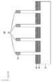
図1は、複数のフィン101が形成された基板102を含む、半導体構造の側断面図100である。図示したように、各フィン101の上部がハード・マスク104で覆われている。フィン101は、側壁画像転写(SIT)、またはリソグラフィおよび反応性イオン・エッチング(RIE)などを含むエッチングなどの他の適切な技法を使用して形成することができる。各フィン101は、5~10ナノメートル(nm)の幅または水平方向厚さ(方向X-X’)を有することができるが、特定の適用の要求に応じて、この範囲より大きいまたは小さい他の幅を使用してもよい。各フィン101は、30nm~150nmの高さまたは垂直方向厚さ(方向Y-Y’)を有することができるが、特定の適用の要求に応じて、この範囲より大きいまたは小さい他の高さを使用してもよい。隣接するフィン101同士の間隔は、20nm~100nmであってよいが、特定の適用の要求に応じて、他の間隔を有していてもよい。
FIG. 1 is a side
本発明の一部の実施形態において、基板102はシリコン(Si)から形成された半導体基板を含むが、他の適切な材料を使用してもよい。例えば、基板102は任意の適切な基板構造、例えば、バルク半導体を含むことができる。基板102はシリコン含有材料を含むことができる。基板102に適したSi含有材料の例として、Si、シリコンゲルマニウム(SiGe)、シリコンゲルマニウム炭化物(SiGeC)、炭化ケイ素(SiC)、およびそれらの多層が挙げられるが、これらに限定されない。シリコンは、ウエハの作製において主に使用される半導体材料であるが、ゲルマニウム(Ge)、ヒ化ガリウム(GaAs)、窒化ガリウム(GaN)、SiGe、テルル化カドミウム(CdTe)、セレン化亜鉛(ZnSe)など(ただし、これらに限定されない)の代替の半導体材料を追加の層として使用してもよい。フィン101は、上記のように基板102をパターニングすることによって形成されるため、基板102と同一の材料から形成することができる。
In some embodiments of the invention,
基板102は、いくつかのフィン101またはフィン101の上に形成される他の特徴に基づいて、要求に応じて選択された幅または水平方向厚さ(X-X’)を有することができる。基板102は、20nm~500nmの高さまたは垂直方向厚さ(方向Y-Y’)を有することができるが、特定の適用の要求に応じて、この範囲より大きいまたは小さい他の高さを使用してもよい。
The
最初にハード・マスク104を基板全体の上面に形成することができ、次にSITまたは他の適切な技法を使用してパターニングを行い、フィン101が、パターンニングされたハード・マスク104により露出された基板のエッチング部分によって形成される。ハード・マスク104を窒化ケイ素(SiN)から形成することができるが、酸化ケイ素(SiOX)、二酸化ケイ素(SiO2)、および酸窒化ケイ素(SiON)などの他の適切な材料を使用してもよい。ハード・マスク104は、20nm~100nmの高さまたは垂直方向厚さ(方向Y-Y’)を有することができるが、特定の適用の要求に応じて、この範囲より大きいまたは小さい他の高さを使用してもよい。
A
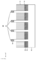
図2は、フィン101を囲む基板102の上面に下部ソース/ドレイン領域106を形成し、フィン101を囲む下部ソース/ドレイン領域106上に下部スペーサ108を形成した後の、図1の半導体構造の側断面図200である。
FIG. 2 illustrates the semiconductor structure of FIG. 1 after forming a lower source/
下部ソース/ドレイン領域106は、イオン注入、気相ドーピング、プラズマ・ドーピング、プラズマ浸漬イオン注入、クラスタ・ドーピング、インフュージョン・ドーピング、液相ドーピング、固相ドーピングなどを使用して、適切にドープすることができる。n型ドーパントは、リン(P)、ヒ素(As)、およびアンチモン(Sb)の群から選択することができ、p型ドーパントは、ホウ素(B)、フッ化ホウ素(BF2)、ガリウム(Ga)、インジウム(In)、およびタリウム(Tl)の群から選択することができる。下部ソース/ドレイン領域106は、エピタキシャル成長プロセスによって形成することができる。一部の実施形態において、エピタキシ・プロセスは、現場ドーピング(エピタキシ中にドーパントがエピタキシ材料に取り込まれる)を含む。エピタキシャル材料は、気体前駆体または液体前駆体から成長させることができる。エピタキシャル材料は、気相エピタキシ(VPE)、分子線エピタキシ(MBE)、液相エピタキシ(LPE)、急速熱化学気相成長(RTCVD)、有機金属化学気相成長(MOCVD)、超高真空化学気相成長(UHVCVD)、低圧化学気相成長(LPCVD)、制限反応処理CVD(LRPCVD)、または他の適切なプロセスを使用して成長させることができる。エピタキシャルシリコン、シリコンゲルマニウム(SiGe)、ゲルマニウム(Ge)、または炭素ドープシリコン(Si:C)、あるいはそれらの組合せは、トランジスタの型に応じてn型ドーパント(例えば、リンもしくはヒ素)またはp型ドーパント(例えば、ホウ素もしくはガリウム)などのドーパントを添加することによって、堆積中にドープ(現場ドープ)することができる。ソース/ドレイン中のドーパント濃度は、1×1019cm-3~3×1021cm-3、または好ましくは2×1020cm-3~3×1021cm-3であってよい。
The lower source/
下部ソース/ドレイン領域106は、10nm~50nmの高さまたは垂直方向厚さ(方向Y-Y’)を有することができるが、特定の適用の要求に応じて、この範囲より大きいまたは小さい他の高さを使用してもよい。
The lower source/
下部スペーサ108は、非コンフォーマル堆積およびエッチバック処理(例えば、物理気相成長(PVD)、高密度プラズマ(HDP)堆積など)を使用して下部ソース/ドレイン領域106上に形成される。下部スペーサ108は、SiO2、SiN、炭化ケイ素酸化物(SiCO)、炭化ケイ素ホウ素窒化物(SiBCN)などから形成することができるが、他の適切な材料を使用してもよい。下部スペーサ108は、3nm~10nmの高さまたは垂直方向厚さ(方向Y-Y’)を有することができるが、特定の適用の要求に応じて、この範囲より大きいまたは小さい他の高さを使用してもよい。
A
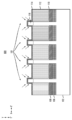
図3は、ダミー・ゲートの形成後の、図2の半導体構造の側断面図300である。ダミー・ゲートの形成は、下部スペーサ108の上面ならびにフィン101およびハード・マスク104の側壁に酸化物110を形成することを含む。酸化物110は、原子層堆積(ALD)または化学気相成長(CVD)などのコンフォーマル堆積プロセスによって形成することができる。酸化物110はSiO2、SiONなどから形成することができるが、他の適切な材料を使用してもよい。酸化物110は2nm~6nmの均一な厚さを有することができるが、特定の適用の要求に応じて、この範囲より大きいまたは小さい他の厚さを使用してもよい。
FIG. 3 is a side
ダミー・ゲート112は、CVDまたはALDなどの処理を使用して酸化物110上に形成される。ダミー・ゲート112は、アモルファスシリコン(a-Si)、アモルファスシリコンゲルマニウム(a-SiGe)、SiO2、酸化チタン(TiO2)、または別の適切な材料から形成することができる。
図4は、ダミー・ゲート112に凹部形成し、フィン101およびフィン101に配置されたハード・マスク104の側壁における酸化物110の露出部分を除去した後の、図3の半導体構造の側断面図400である。ダミー・ゲート112および酸化物110には、ウェット・エッチング、RIEなどの処理を使用して凹部形成することができる。ダミー・ゲート112および酸化物110には、5nm~20nmの深さ(方向Y-Y’)に凹部形成することができるが、ハード・マスク104下方のフィン101の側壁の少なくとも一部が露出していれば、他の深さを使用してもよい。
FIG. 4 is a side cross-sectional view of the semiconductor structure of FIG. 3 after recessing
図5は、ハード・マスク104の除去および上部スペーサ114の形成後の、図4の半導体構造の側断面図500である。ハード・マスク104は、ドライ・エッチング処理またはウェット・エッチング処理を選択的に使用して除去することができる。上部スペーサ114は、ALD処理またはCVD処理などのコンフォーマル堆積を使用して形成することができる。上部スペーサ114は、SiN、SiO2またはSiON、SiOC、SiBCNなどの別の適切な材料から形成することができる。上部スペーサ114は、3nm~10nmの均一な厚さを有することができるが、特定の適用の要求に応じて、この範囲より大きいまたは小さい他の厚さを使用してもよい。
FIG. 5 is a side
図6は、上部接合部116の形成および活性化後の、図5の半導体構造の側断面図600である。イオン注入、プラズマ・ドーピング、または別の適切なプロセスを使用して、フィン101の上部に上部接合部116(例えば、高濃度ドープ領域)を形成する。上部接合部116は、リン(P)、ヒ素(As)、およびアンチモン(Sb)の群から選択されたn型ドーパントと、ホウ素(B)、フッ化ホウ素(BF2)、ガリウム(Ga)、インジウム(In)、およびタリウム(Tl)の群から選択されたp型ドーパントとを含むドーパントを使用することができる。上部接合部116の高さは、上部スペーサ114の下面より下方のフィンの領域に延びる。上部接合部116は、5nm~20nmの高さまたは垂直方向厚さ(方向Y-Y’)を有することができるが、特定の適用の要求に応じて、この範囲より大きいまたは小さい他の高さを使用してもよい。
FIG. 6 is a side
図7は、絶縁層または層間誘電体(ILD)層118の充填後の、図6の半導体構造の側断面図700である。絶縁層118は、SiO2、またはSiOC、SiONなどの別の適切な材料から形成することができる。絶縁層118は、絶縁材料を充填した後に、化学機械研磨または平坦化(CMP)を使用して上部スペーサ114の上面まで平坦化することによって形成することができる。
7 is a side cross-sectional view 700 of the semiconductor structure of FIG. 6 after filling an insulating or interlevel dielectric (ILD) layer 118. Insulating layer 118 may be formed from SiO 2 or another suitable material such as SiOC, SiON, etc. Insulating layer 118 may be formed by filling with an insulating material and then planarizing to the top surface of
図8は、スペーサ120およびILD層122の形成後の、図7の半導体構造の側断面図800である。スペーサ120はSiNから形成することができるが、SiO2、SiON、SiBCN、SiCOなどの他の適切な材料を使用してもよい。スペーサ120は、5nm~15nmの高さまたは垂直方向厚さ(方向Y-Y’)を有することができるが、特定の適用の要求に応じて、この範囲より大きいまたは小さい他の高さを使用してもよい。スペーサ120は、ALDまたはCVDなどのコンフォーマル堆積処理を使用して形成することができる。 FIG. 8 is a side cross-sectional view 800 of the semiconductor structure of FIG. 7 after formation of spacers 120 and ILD layer 122. Spacer 120 may be formed from SiN, but other suitable materials may be used, such as SiO 2 , SiON, SiBCN, SiCO, etc. The spacer 120 can have a height or vertical thickness (direction Y-Y') of 5 nm to 15 nm, although other heights greater or less than this range may be used depending on the requirements of the particular application. You may. Spacer 120 may be formed using a conformal deposition process such as ALD or CVD.
ILD122はSiO2から形成することができるが、SiON、SiCOなどの他の適切な材料を使用してもよい。ILD122は、CVD処理またはALD処理を使用して形成することができる。ILD122は、30nm~150nmの高さまたは垂直方向厚さ(方向Y-Y’)を有することができるが、特定の適用の要求に応じて、この範囲より大きいまたは小さい他の高さを使用してもよい。 ILD 122 can be formed from SiO2 , but other suitable materials such as SiON, SiCO, etc. may be used. ILD 122 can be formed using CVD or ALD processes. The ILD 122 can have a height or vertical thickness (direction Y-Y') from 30 nm to 150 nm, although other heights greater or less than this range may be used depending on the demands of the particular application. You can.
図9は、上部ソース/ドレイン・コンタクトの形成のために接合部116の上部を露出させるように開口した後の、図8の半導体構造の側断面図900である。マスク層124が、リソグラフィおよびエッチングまたは他の適切な技法を使用して、ILD122の上面にパターニングされる。マスク層124は、有機材料、SiO2、酸化チタン(TiOx)の適切な組合せから形成することができるが、他の適切な材料を使用してもよい。マスク層124は、30nm~150nmの高さまたは垂直方向厚さ(方向Y-Y’)を有することができるが、特定の適用の要求に応じて、この範囲より大きいまたは小さい他の高さを使用してもよい。
FIG. 9 is a side cross-sectional view 900 of the semiconductor structure of FIG. 8 after opening to expose the top of
マスク層124は、フィン101の上部より上方に開口部を設けるようにパターニングされる。フィン101上方の開口部の上部は、フィン101よりも幅広で、例えば20nm~80nmの幅901を有する。この幅は、フィン101の上面からの距離が短くなるにつれて、フィン101の幅に略一致する幅まで減少する。ILD122の開口部は、方向性RIEまたは他の適切な処理によって形成することができる。
The mask layer 124 is patterned to provide an opening above the top of the
図10は、上部ソース/ドレインの形成後の、図9の半導体構造の側断面図1000である。マスク層124は、プラズマ灰化/除去などの処理を使用して除去される。エピタキシャル成長を助けるために、場合により、スペーサ114、120の材料の横方向エッチングを行ってもよい。任意選択の横方向エッチング後、上部ソース/ドレイン領域126を、接合部116(および、スペーサ114、120の任意選択の横方向エッチングによって露出した領域)上でエピタキシャル成長させる。上部ソース/ドレイン領域126は、10nm~50nmの高さまたは垂直方向厚さ(方向Y-Y’)を有することができるが、特定の適用の要求に応じて、この範囲より大きいまたは小さい他の高さを使用してもよい。上部ソース/ドレイン領域126は、下部ソース/ドレイン領域106と同様の材料から形成することができる。
FIG. 10 is a side cross-sectional view 1000 of the semiconductor structure of FIG. 9 after formation of the top source/drain. Mask layer 124 is removed using a process such as plasma ashing/ablation. Lateral etching of the material of the
図11は、金属を充填して、上部ソース/ドレイン領域126上に金属層128を形成した後の、図10の半導体構造の側断面図1100である。上部ソース/ドレイン・コンタクト金属層とも呼ばれる金属層128は、タングステン(W)から形成することができるが、チタン(Ti)、コバルト(Co)などの他の適切な材料を使用してもよい。金属層128は、金属材料を充填した後に、CMPまたは別の適切な技法を使用して、金属層128の上面がILD122の上面と略同一平面になるように平坦化することによって形成することができる。 FIG. 11 is a side cross-sectional view 1100 of the semiconductor structure of FIG. 10 after metal filling and formation of a metal layer 128 over the top source/drain region 126. Metal layer 128, also referred to as the top source/drain contact metal layer, may be formed from tungsten (W), but other suitable materials such as titanium (Ti), cobalt (Co), etc. may be used. Metal layer 128 may be formed by filling with a metal material and then planarizing using CMP or another suitable technique such that the top surface of metal layer 128 is substantially coplanar with the top surface of ILD 122. can.
図12は、金属層128に凹部形成し、上部ソース/ドレインSACキャッピング層とも呼ばれる自己整合コンタクト(SAC)・キャッピング層130を金属層128の上面に形成した後の、図11の半導体構造の側断面図1200である。金属層128には、ウェット・エッチング・プロセスまたはドライ・エッチング・プロセスを使用して凹部形成することができる。SACキャッピング層130は、ALD処理またはCVD処理を使用して形成することができる。金属層128には、5nm~20nmの深さまで凹部形成することができるが、特定の適用の要求に応じて、この範囲外の他の深さを使用してもよい。SACキャッピング層130は、SACキャッピング層130の上面がILD122の上面に一致するように、金属層128に凹部形成する深さに一致する高さまたは厚さ(方向Y-Y’)を有することができる。 12 shows a side of the semiconductor structure of FIG. 11 after recessing metal layer 128 and forming a self-aligned contact (SAC) capping layer 130, also referred to as a top source/drain SAC capping layer, on the top surface of metal layer 128. 1200 is a cross-sectional view. Metal layer 128 may be recessed using a wet or dry etching process. SAC capping layer 130 can be formed using ALD or CVD processes. Metal layer 128 can be recessed to a depth of 5 nm to 20 nm, although other depths outside this range may be used depending on the needs of a particular application. The SAC capping layer 130 may have a height or thickness (in direction Y-Y') that corresponds to a depth recessed in the metal layer 128 such that the top surface of the SAC capping layer 130 corresponds to the top surface of the ILD 122. can.
図13は、SACキャッピング層130の形成後の、図11の半導体構造の別の側断面図1300である。図12の側断面図1200(および図1~図11の側断面図)はフィン101に垂直に取っているが、側断面図1300はフィン101に平行に取っている。フィン101のうちの1つが側断面図1300に破線の輪郭で示され、この図でフィン101がダミー・ゲート112の「後方」にあることを示している。側断面図1300は、シャロー・トレンチ絶縁(STI)領域103が図示したように形成されている様子をさらに示す。STI領域103は、絶縁層118およびILD122と同様の材料から形成することができる。
FIG. 13 is another side cross-sectional view 1300 of the semiconductor structure of FIG. 11 after formation of the SAC capping layer 130. The side cross-sectional view 1200 of FIG. 12 (and the side cross-sectional views of FIGS. 1-11) is taken perpendicular to the
図14は、ダミー・ゲート112を開口するようにマスキングした後の、図12および図13の半導体構造の側断面図1400である。側断面図1400は、側断面図1300と同様に、フィン101に平行に取っている。マスク層132が、ILD122およびSACキャッピング層130の上面にパターニングされる。マスク層132は、マスク層124と同様の材料および同様のサイズを使用して形成することができる。SACキャッピング層130により、上部ソース/ドレイン領域126およびゲート間の短絡が確実になくなる。上部ソース/ドレイン領域126上のSACキャッピング層130は、エピタキシャル層が閉じ込められていることによって同化しないため、マスク層132は、図示したように、ダミー・ゲート112を開口するようにパターニングすることができる。ダミー・ゲート112を露出させるための開口部は、75nm、より一般的には30nm~100nmの幅1401を有することができるが、特定の適用の要求に応じて、この範囲外の他の幅を使用してもよい。
FIG. 14 is a side cross-sectional view 1400 of the semiconductor structure of FIGS. 12 and 13 after masking the
図15は、ゲート開口部の側壁にライナ134を堆積させ、ゲート開口部においてダミー・ゲート112の上面を露出させるように方向性エッチングした後の、図14の半導体構造の側断面図1500である。ライナ134は、下部スペーサ108および上部スペーサ114と同様の材料(例えば、SiN)から形成することができるが、他の適切な材料を使用してもよい。ライナ134は、3nm~10nmの厚さを有することができるが、特定の適用の要求に応じて、この範囲外の他の厚さを使用してもよい。ダミー・ゲート112の上面を露出させる方向性エッチングは、方向性RIEであってよい。
FIG. 15 is a side cross-sectional view 1500 of the semiconductor structure of FIG. 14 after depositing liner 134 on the sidewalls of the gate opening and directional etching to expose the top surface of
図16は、ダミー・ゲート112の除去後の、図15の半導体構造の側断面図1600である。マスク層132は、ダミー・ゲート112の除去より前に除去される。ダミー・ゲート112は、気相エッチング、ウェット・エッチング、または他の適切な処理を使用して酸化物層110上のダミー・ゲート112を選択的に除去することによって除去することができる。酸化物層110は、ダミー・ゲート112の除去中にフィン101を保護する。フィン101を覆う酸化物層110は、さらに詳細に後述する置換金属ゲート(RMG)・プロセスより前に希釈HFエッチングなどを使用して除去される。ダミー・ゲート112とフィン101を覆う酸化物層110とを除去した後、ダミー・ゲート112後方のフィン101が図示したように見られる。
FIG. 16 is a side cross-sectional view 1600 of the semiconductor structure of FIG. 15 after removal of
図17は、RMGプロセス後の、図16の半導体構造の側断面図1700である。RMGプロセスでは、フィン101を囲むゲート誘電体(図示せず)が形成された後に、ゲート導体136が形成される。
FIG. 17 is a side cross-sectional view 1700 of the semiconductor structure of FIG. 16 after an RMG process. In the RMG process, gate conductor 136 is formed after a gate dielectric (not shown) surrounding
ゲート誘電体は、high-k誘電材料から形成することができるが、他の適切な材料を使用してもよい。high-k材料の例としては、酸化ハフニウム(HfO2)、ハフニウムシリコン酸化物(Hf-Si-O)、ハフニウムシリコン酸窒化物(HfSiON)、酸化ランタン(La2O3)、ランタンアルミニウム酸化物(LaAlO3)、酸化ジルコニウム(ZrO2)、ジルコニウムシリコン酸化物、ジルコニウムシリコン酸窒化物、酸化タンタル(Ta2O5)、酸化チタン(TiO2)、バリウムストロンチウムチタン酸化物、バリウムチタン酸化物、ストロンチウムチタン酸化物、酸化イットリウム(Y2O3)、酸化アルミニウム(Al2O3)、鉛スカンジウムタンタル酸化物、および鉛亜鉛ニオブ酸塩などの金属酸化物を含むが、これらに限定されない。high-k材料は、ランタン(La)、アルミニウム(Al)、およびマグネシウム(Mg)などのドーパントをさらに含むことができる。ゲート誘電体は、2nm~5nmの均一な厚さを有することができるが、特定の適用の要求に応じて、この範囲より大きいまたは小さい他の厚さを使用してもよい。 The gate dielectric can be formed from a high-k dielectric material, although other suitable materials may be used. Examples of high-k materials include hafnium oxide (HfO 2 ), hafnium silicon oxide (Hf-Si-O), hafnium silicon oxynitride (HfSiON), lanthanum oxide (La 2 O 3 ), and lanthanum aluminum oxide. (LaAlO 3 ), zirconium oxide (ZrO 2 ), zirconium silicon oxide, zirconium silicon oxynitride, tantalum oxide (Ta 2 O 5 ), titanium oxide (TiO 2 ), barium strontium titanium oxide, barium titanium oxide, Metal oxides include, but are not limited to, strontium titanium oxide, yttrium oxide (Y 2 O 3 ), aluminum oxide (Al 2 O 3 ), lead scandium tantalum oxide, and lead zinc niobate. High-k materials can further include dopants such as lanthanum (La), aluminum (Al), and magnesium (Mg). The gate dielectric can have a uniform thickness of 2 nm to 5 nm, although other thicknesses larger or smaller than this range may be used depending on the needs of the particular application.
ゲート導体136は、金属(例えば、タングステン(W)、チタン(Ti)、タンタル(Ta)、ルテニウム(Ru)、ジルコニウム(Zr)、コバルト(Co)、銅(Cu)、アルミニウム(Al)、鉛(Pb)、白金(Pt)、スズ(Sn)、銀(Ag)、金(Au)など)、導電性金属化合物材料(例えば、窒化タンタル(TaN)、窒化チタン(TiN)、炭化タンタル(TaCX)、炭化チタン(TiC)、チタンアルミニウム炭化物、ケイ化タングステン(WSi2)、窒化タングステン(WN)、酸化ルテニウム(RuO2)、ケイ化コバルト、ケイ化ニッケルなど)、またはこれらおよび他の適切な材料の任意の適切な組合せを含む、任意の適切な導電性材料から形成することができるが、これらに限定されない。導電性材料は、堆積中または堆積後に取り込まれるドーパントをさらに含むことができる。一部の実施形態において、ゲート導体は、縦型トランジスタの閾値電圧を所望の値に設定するための仕事関数金属(WFM)層を含む。WFMは、窒化チタン(TiN)、チタンアルミニウム窒化物(TiAlN)、窒化ハフニウム(HfN)、ハフニウムシリコン窒化物(HfSiN)、窒化タンタル(TaN)、タンタルシリコン窒化物(TaSiN)、窒化タングステン(WN)、窒化モリブデン(MoN)、窒化ニオブ(NbN)を含むがこれらに限定されない窒化物、炭化チタン(TiC)、チタンアルミニウム炭化物(TiAlC)、炭化タンタル(TaC)、炭化ハフニウム(HfC)を含むがこれらに限定されない炭化物、およびこれらの組合せであってよい。 The gate conductor 136 is made of metal (for example, tungsten (W), titanium (Ti), tantalum (Ta), ruthenium (Ru), zirconium (Zr), cobalt (Co), copper (Cu), aluminum (Al), lead). (Pb), platinum (Pt), tin (Sn), silver (Ag), gold (Au), etc.), conductive metal compound materials (e.g. tantalum nitride (TaN), titanium nitride (TiN), tantalum carbide (TaC) X ), titanium carbide (TiC), titanium aluminum carbide, tungsten silicide (WSi 2 ), tungsten nitride (WN), ruthenium oxide (RuO 2 ), cobalt silicide, nickel silicide, etc.), or these and other suitable The conductive material may be formed from any suitable electrically conductive material, including, but not limited to, any suitable combination of materials. The conductive material can further include dopants that are incorporated during or after deposition. In some embodiments, the gate conductor includes a work function metal (WFM) layer to set the threshold voltage of the vertical transistor to a desired value. WFM includes titanium nitride (TiN), titanium aluminum nitride (TiAlN), hafnium nitride (HfN), hafnium silicon nitride (HfSiN), tantalum nitride (TaN), tantalum silicon nitride (TaSiN), and tungsten nitride (WN). , nitrides including but not limited to molybdenum nitride (MoN), niobium nitride (NbN), titanium carbide (TiC), titanium aluminum carbide (TiAlC), tantalum carbide (TaC), hafnium carbide (HfC). carbides, and combinations thereof.
ゲート導体136は、図示したように、フィン101の周囲の領域に充填され、スペーサの側壁およびゲート開口部を囲む側壁に3nm~10nmの厚さを有するが、特定の適用の要求に応じて、この範囲外の他の厚さを使用してもよい。
The gate conductor 136 fills the area around the
前述したように、ゲート誘電体およびゲート導体136は、RMGプロセスを使用して形成される。ゲート誘電体膜およびゲート導体136は、CVD、プラズマ化学気相成長(PECVD)、ALD、蒸着、PVD、化学溶液堆積、または他の同様のプロセスなどの適切な堆積プロセスによって形成することができる。ゲート誘電体およびゲート導体136の厚さは、堆積プロセスならびに使用するゲート誘電体材料の組成および数に応じて変化し得る。 As previously discussed, the gate dielectric and gate conductor 136 are formed using an RMG process. The gate dielectric film and gate conductor 136 may be formed by a suitable deposition process, such as CVD, plasma enhanced chemical vapor deposition (PECVD), ALD, evaporation, PVD, chemical solution deposition, or other similar process. The thickness of the gate dielectric and gate conductor 136 may vary depending on the deposition process and the composition and number of gate dielectric materials used.
図18は、ゲート・コンタクト金属層とも呼ばれる金属層138を、図示したようにゲート開口部に充填した後の、図17の半導体構造の側断面図1800である。金属層138は、CMPまたは他の適切な処理を使用して、ILD122の上面と略同一平面の表面を有するように平坦化することができる。金属層138は、金属層128と同様の材料から形成することができる。 FIG. 18 is a side cross-sectional view 1800 of the semiconductor structure of FIG. 17 after a metal layer 138, also referred to as a gate contact metal layer, fills the gate opening as shown. Metal layer 138 may be planarized using CMP or other suitable processing to have a surface that is approximately coplanar with the top surface of ILD 122. Metal layer 138 can be formed from a similar material as metal layer 128.
図19は、金属層138の凹部形成、およびゲートSACキャッピング層とも呼ばれるSACキャッピング層140の形成後の、図18の半導体構造の側断面図1900である。SACキャッピング層140は、SACキャッピング層130と同様の材料から同様の厚さで形成することができる。金属層138には、金属層128の凹部形成に使用したものと同様の処理を使用して凹部形成することができる。 FIG. 19 is a side cross-sectional view 1900 of the semiconductor structure of FIG. 18 after recess formation of metal layer 138 and formation of SAC capping layer 140, also referred to as gate SAC capping layer. SAC capping layer 140 may be formed from a similar material and to a similar thickness as SAC capping layer 130. Metal layer 138 may be recessed using a process similar to that used to recess metal layer 128.
図20は、マスク層142をパターニングし、下部ソース/ドレイン領域106の開口部を形成した後の、図19の半導体構造の側断面図2000である。マスク層142は、マスク層124に関して前述したものと同様の材料および同様のサイズを使用して形成することができる。下部ソース/ドレイン領域106の開口部は、方向性RIEまたは他の適切な処理によって形成することができる。
FIG. 20 is a side cross-sectional view 2000 of the semiconductor structure of FIG. 19 after patterning mask layer 142 and forming openings for bottom source/
図21は、下部ソース/ドレイン・コンタクト金属層とも呼ばれる金属層144を下部ソース/ドレイン領域106の開口部に充填した後の、図20の半導体構造の側断面図2100である。図21は、金属層144の凹部形成、および下部ソース/ドレイン・キャッピング層とも呼ばれるSACキャッピング層146の形成も示す。金属層144は、金属層128、138と同様の材料から同様の処理によって形成することができる。SACキャッピング層146は、SACキャッピング層130、140の形成に関して説明したものと同様の材料から同様の大きさで、同様の処理を使用して形成することができる。
21 is a side cross-sectional view 2100 of the semiconductor structure of FIG. 20 after filling the opening of the lower source/
図22は、ライナ148およびILD150の形成後の、図21の半導体構造の側断面図2200である。ライナ148は、上部スペーサ114およびSACキャッピング層130、140、146と同様の材料から形成することができる。ライナ148は、5nm~20nmの高さまたは垂直方向厚さ(方向Y-Y’)を有することができるが、特定の適用の要求に応じて、この範囲外の他の厚さを使用してもよい。ILD150は、ILD122と同様の材料から形成することができる。ILD150は、30nm~150nmの高さまたは垂直方向厚さ(方向Y-Y’)を有するが、特定の適用の要求に応じて、この範囲外の他の厚さを使用してもよい。
22 is a side cross-sectional view 2200 of the semiconductor structure of FIG. 21 after formation of liner 148 and ILD 150. Liner 148 may be formed from a similar material as
図23は、下部ソース/ドレイン領域106、上部ソース/ドレイン領域126、およびゲート導体136のそれぞれのコンタクトに(金属層128、138、144のそれぞれを介して)アクセスするためのビア152、154、156を形成した後の、図22の半導体構造の側断面図2300である。ビア152、154、156は、CVDまたはALDなどのコンフォーマル堆積処理を使用して形成することができ、各々、上面に20nm~100nmの幅または水平方向厚さ(方向X-X’)を有することができるが、特定の適用の要求に応じて、この範囲外の他の幅を使用してもよい。ビア152、154、156が異なる幅を有してもよいことも理解されたい。
FIG. 23 shows vias 152, 154 for accessing (through metal layers 128, 138, 144, respectively) the respective contacts of bottom source/
図24は、図23の半導体構造の上面図2400である。上面図2400は、フィン101に対するビア152、154、156の位置を示すように提示されており、したがって、図示を明瞭にするために、下にある層の様々な詳細が省略されていることに留意されたい。下部ソース/ドレイン・コンタクトのビア152は、30nm、またはより一般的には20nm~100nmの厚さ(方向Y-Y’)を有することができるが、特定の適用の要求に応じて、他の適切な厚さを使用してもよい。各フィン101は、45nm、またはより一般的には10nm~200nmの長さ(方向Y-Y’)を有することができるが、特定の適用の要求に応じて、他の適切な長さを使用してもよい。上部ソース/ドレイン・コンタクトのビア154は、図示したように、フィン101の長さに一致する長さを有することができるが、これは必要条件ではない。ゲート・コンタクトのビア156は、20nm、またはより一般的には15nm~100nmの厚さ(方向Y-Y’)を有することができるが、特定の適用の要求に応じて、他の適切な厚さを使用してもよい。
FIG. 24 is a
上面図2400は、半導体構造のマスク領域2401、2403、2405を示す。マスク領域2401は、下部ソース/ドレイン106が形成される場所を示す。マスク領域2403は、ゲートが形成される場所を示す。マスク領域2405は、ダミー・ゲート112を露出させるための開口部が形成される場所を示す。
縦型トランジスタのRMG方式では、ゲート・コンタクトの開口部156を通して、ダミー・ゲートを除去し、ゲート誘電体およびゲート導体を堆積させることが必要である。リソグラフィおよびエッチングのプロセスの変動により、ゲートおよびソース/ドレイン領域間の短絡の危険が大きくなるため、ゲート・コンタクトの開口部を上部ソース/ドレイン領域から離して配置すべきである。フィン101とゲート・コンタクトの開口部156との距離は、一般的に20nm~100nmであるため、ダミー・ゲートを除去し、ゲート誘電体およびゲート導体を堆積させることが困難である。しかしながら、例示的な実施形態において、上部ソース/ドレイン領域および下部ソース/ドレイン領域の開口部の上部にSACキャッピング層が形成されることによって、寸法の制約ならびにゲートおよび上部ソース/ドレイン間の短絡のないRMGプロセスが可能になり、有利である。
The vertical transistor RMG approach requires removing the dummy gate and depositing the gate dielectric and gate conductor through the
前述したように、図1~図12の側断面図は、例えば、図24の上面図2400のA-A線に沿って、フィン101の長さに垂直に取っている。図13~図23の側断面図は、例えば、図24の上面図2400のB-B線に沿って、フィン101の長さに平行に取っている。
As mentioned above, the side cross-sectional views of FIGS. 1-12 are taken perpendicular to the length of
一部の実施形態において、RMGプロセスを使用して、共通の基板に形成されたVTFETについて複数の異なるチャネル長さを形成することができる。図25~図34は、複数の異なるチャネル長さを形成するためのそのような処理の例を示す。 In some embodiments, the RMG process can be used to form multiple different channel lengths for VTFETs formed on a common substrate. Figures 25-34 illustrate examples of such processing to form multiple different channel lengths.
図25は、図3に示す半導体構造と同様の半導体構造の側断面図2500であり、同様の符号を付した要素は同様の材料から同様のサイズで、同様の処理によって形成される。しかしながら、図25に示す半導体構造では、フィンが異なる領域2501-1、2501-2に配置され、STI領域2503(STI領域103と同様の材料から形成される)が異なる領域2501-1、2501-2のフィン間に形成されている。STI領域2503は、下部ソース/ドレイン領域106の形成後に形成することができる。図25~図34に関して後述するプロセスの例において、領域2501-1のフィンを使用して「長」チャネル・デバイスを形成し、領域2501-2のフィンを使用して「短」チャネル・デバイスを形成する。
FIG. 25 is a side cross-sectional view 2500 of a semiconductor structure similar to the semiconductor structure shown in FIG. 3, with like-numbered elements formed from like materials, of like size, and by similar processes. However, in the semiconductor structure shown in FIG. 25, the fins are located in different regions 2501-1, 2501-2, and the STI regions 2503 (formed from the same material as STI region 103) are located in different regions 2501-1, 2501-2. It is formed between two fins. STI region 2503 may be formed after formation of lower source/
図26は、上面にマスク層2505をパターニングし、マスク層2505により露出されたダミー・ゲート112の部分をパターニングまたは除去するようにエッチングした後の、図25の半導体構造の側断面図2600である。マスク層2505は、マスク層124に関して前述したものと同様の材料から同様のサイズで形成することができる。開口部2601は、20nm~150nmの幅を有することができるが、ダミー・ゲート112の材料の十分な部分が領域2501-1、2501-2の開口部2601に最も近いフィンを囲んだままであれば、この範囲より大きいまたは小さい他の適切な幅を使用してもよい。マスク層2505により露出されたダミー・ゲート112は、方向性RIEまたは他の適切な処理を使用して除去することができる。
26 is a side cross-sectional view 2600 of the semiconductor structure of FIG. 25 after patterning a mask layer 2505 on top and etching to pattern or remove the portions of
図27は、ライナ2507の形成後の、図26の半導体構造の側断面図2700である。ライナ2507は、下部スペーサ108と同様の材料(例えば、SiN)から形成することができる。ライナ2507は、5nm~20nmの幅または厚さ(方向X-X’)を有することができるが、特定の適用の要求に応じて、この範囲より大きいまたは小さい他の適切な幅を使用してもよい。ライナ2508は、任意の適切な堆積およびその後のRIEによって形成することができる。 27 is a side cross-sectional view 2700 of the semiconductor structure of FIG. 26 after formation of liner 2507. Liner 2507 can be formed from a similar material as bottom spacer 108 (eg, SiN). The liner 2507 can have a width or thickness (in direction XX') of 5 nm to 20 nm, although other suitable widths larger or smaller than this range can be used depending on the demands of the particular application. Good too. Liner 2508 can be formed by any suitable deposition followed by RIE.
図28は、ダミー・ゲート112の凹部形成後の、図27の半導体構造の側断面図2800である。ダミー・ゲート112の凹部形成は、図4に関して前述したものと同様の処理を使用することができるが、図28の例では、長チャネル領域(例えば2501-1)のダミー・ゲート112に第1の深さ2801で凹部形成され、他方で短チャネル領域(例えば2501-2)のダミー・ゲート112に第2の深さ2803で凹部形成され、第2の深さ2803が第1の深さ2801より大きい。一部の実施形態において、第1の深さ2801は15nm~100nmであってよく、他方で第2の深さ2803は25nm~110nmであるが、要求に応じて、この範囲外の他の深さを使用して異なるチャネル長さを形成してもよい。図25~図34は2つの異なるチャネル長さが形成される例を示すが、実施形態はこれに限定されないことを理解されたい。それどころか、図25~図34に関して説明するものと同様の技法を使用して、要求に応じて任意の数の異なるチャネル長さを形成することができる。
FIG. 28 is a side cross-sectional view 2800 of the semiconductor structure of FIG. 27 after recess formation of
ダミー・ゲート112に異なる深さ2801、2803まで凹部形成することは、最初に長チャネル領域および短チャネル領域の両方のダミー・ゲート112に深さ2801まで凹部形成し、次に長チャネル領域のダミー・ゲート112をマスキングまたは保護し、その後、短チャネル領域のダミー・ゲート112にさらに凹部形成することを含むことができる。あるいは、短チャネル領域のダミー・ゲート112を保護しながら長チャネル領域のダミー・ゲート112に凹部形成し、その後、長チャネル領域のダミー・ゲート112を保護しながら短チャネル領域のダミー・ゲート112に凹部形成してもよい(または、この逆も可能である)。
Forming recesses to different depths 2801 and 2803 in the
図29は、上部スペーサ2514の形成後の、図28の半導体構造の側断面図2900であり、上部スペーサ2514は、上部スペーサ114と同様の材料、同様の大きさを使用して、同様の処理によって形成することができる。上部スペーサ2514の形成前に、各フィン上のハード・マスク104が除去され、酸化物110は、上面が周囲のダミー・ゲート112と略同一平面になるように凹部形成される。上部スペーサ2514の形成前にライナ2507も除去される。
29 is a side cross-sectional view 2900 of the semiconductor structure of FIG. 28 after formation of a top spacer 2514, which uses similar materials, similar dimensions, and undergoes similar processing as
図30は、上部接合部2516の形成後の、図29の半導体構造の側断面図3000である。上部接合部2516の形成は、上部接合部116の形成に関して前述したものと同様の処理を使用することができる。図30に示すように、短チャネル領域の上部接合部2516は、長チャネル領域の上部接合部2516に対して「より長い」、またはより大きい垂直方向厚さを有する。長チャネル領域および短チャネル領域の両方の上部接合部2516は、周囲のダミー・ゲート112の表面より下方に2nm~10nmの深さまで延びるが、特定の適用の要求に応じて、この範囲外の他の適切な深さを使用してもよい。しかしながら、トランジスタ性能が非ドープ領域により低下するおそれがない限り、上部接合部2516はゲート導体と重なるべきである。
30 is a side cross-sectional view 3000 of the semiconductor structure of FIG. 29 after formation of top junction 2516. Formation of top bond 2516 may use processes similar to those described above with respect to formation of
図31は、絶縁層2518、スペーサ2520、およびILD2522の形成後の、図30の半導体構造の側断面図3100である。絶縁層2518、スペーサ2520、およびILD2522は、絶縁層118、スペーサ120、およびILD122のそれぞれに関して前述したものと同様の材料から同様の大きさで、同様の処理を使用して形成することができる。 31 is a side cross-sectional view 3100 of the semiconductor structure of FIG. 30 after formation of insulating layer 2518, spacer 2520, and ILD 2522. Insulating layer 2518, spacer 2520, and ILD 2522 may be formed from similar materials, to similar dimensions, and using similar processes as described above for insulating layer 118, spacer 120, and ILD 122, respectively.
図32は、パターニングされたマスク層2524を使用して上部接合部2516を露出させるように開口した後の、図31の半導体構造の側断面図3200である。マスク層2524は、マスク層124に関して前述したものと同様の方法でパターニングすることができる。上部接合部2516を露出させるための開口部は、図9に関して前述したものと同様の処理を使用して形成することができる。 FIG. 32 is a side cross-sectional view 3200 of the semiconductor structure of FIG. 31 after opening to expose top junction 2516 using patterned mask layer 2524. Mask layer 2524 can be patterned in a manner similar to that described above with respect to mask layer 124. The opening to expose the top joint 2516 can be formed using a process similar to that described above with respect to FIG.
図33は、上部ソース/ドレイン領域2526の形成および上部ソース/ドレイン領域2526上への金属層2528の形成後の、図32の半導体構造の側断面図3300である。上部ソース/ドレイン領域2526は、上部ソース/ドレイン領域126に関して前述したものと同様の材料から同様の大きさで、同様の処理を使用して形成することができる。しかしながら、図33は、図10の任意選択の横方向エッチングを行わない一実施形態を示す。しかしながら、他の実施形態においては、図10に関して前述した任意選択の横方向エッチングを使用して上部ソース/ドレイン領域2526を形成してもよい。金属層2528は、金属層128に関して前述したものと同様の材料から同様の大きさで、同様の処理を使用して形成することができる。 FIG. 33 is a side cross-sectional view 3300 of the semiconductor structure of FIG. 32 after formation of top source/drain regions 2526 and formation of metal layer 2528 over top source/drain regions 2526. Upper source/drain region 2526 may be formed from similar materials, of similar dimensions, and using similar processing as described above for upper source/drain region 126. However, FIG. 33 shows an embodiment without the optional lateral etch of FIG. However, in other embodiments, the optional lateral etch described above with respect to FIG. 10 may be used to form the upper source/drain region 2526. Metal layer 2528 may be formed from similar materials, with similar dimensions, and using similar processes as described above with respect to metal layer 128.
図34は、金属層2528の凹部形成、および本明細書で上部ソース/ドレインSACキャッピング層とも呼ばれるSACキャッピング層2530の形成後の、図33の半導体構造の側断面図3400である。金属層2528の凹部形成およびSACキャッピング層2530の形成は、図12に関して前述したものと同様の処理を使用することができる。SACキャッピング層2530は、SACキャッピング層130と同様の材料から同様の大きさで形成することができる。 34 is a side cross-sectional view 3400 of the semiconductor structure of FIG. 33 after recess formation of metal layer 2528 and formation of SAC capping layer 2530, also referred to herein as a top source/drain SAC capping layer. The recess formation of the metal layer 2528 and the formation of the SAC capping layer 2530 can use processes similar to those described above with respect to FIG. SAC capping layer 2530 may be formed from similar materials and of similar dimensions as SAC capping layer 130.
図25~図34は、図1~図12と同様に、フィンに垂直に(例えば、図24の上面図2400のA-A線に沿って)取った断面図である。図34の半導体構造は、図13~図23に関して前述したものと同様のRMGについてのさらなる処理を受けることができる。
25-34, like FIGS. 1-12, are cross-sectional views taken perpendicular to the fins (eg, along line AA of
本明細書に記載のRMG技法を、CMOSデバイスの形成またはCMOSのパターニングに使用することもできる。以下で、図35~図45に関して、CMOSのパターニングのためのRMGプロセスについて説明する。 The RMG techniques described herein can also be used to form CMOS devices or pattern CMOS. The RMG process for CMOS patterning is described below with respect to FIGS. 35-45.
図35は、共有ダミー・ゲート3512を含む半導体構造の側断面図3500である。図35の半導体構造は、基板3502、STI領域3503、下部ソース/ドレイン領域3506-1、3506-2(まとめて下部ソース/ドレイン領域3506)、下部スペーサ3508、上部スペーサ3510、ILD3522、上部ソース/ドレイン領域3526-1、3526-2(まとめて上部ソース/ドレイン領域3526)、金属層3528、およびSACキャッピング層3530を含み、これらは、基板102、STI領域103、下部ソース/ドレイン領域106、下部スペーサ108、上部スペーサ114、ILD122、上部ソース/ドレイン領域126、金属層128、およびSACキャッピング層130のそれぞれに関して前述したものと同様の材料から同様の大きさで、同様の処理を使用して形成することができる。しかしながら、図35は、NFETを形成する第1のフィン3501-1とPFETを形成する第2のフィン3502-2とを含むCMOS配置を示す。フィン3501-1、3501-2(まとめてフィン3501)は、側断面図3500において共有ダミー・ゲート3512の「後方」にあるため、破線の輪郭で示されている。
FIG. 35 is a side cross-sectional view 3500 of a semiconductor structure including a shared dummy gate 3512. The semiconductor structure of FIG. 35 includes a substrate 3502, an STI region 3503, lower source/drain regions 3506-1, 3506-2 (collectively lower source/drain regions 3506), a lower spacer 3508, an upper spacer 3510, an ILD 3522, an upper source/drain Includes drain regions 3526-1, 3526-2 (collectively top source/drain region 3526), metal layer 3528, and SAC capping layer 3530, which are connected to
NFETの下部ソース/ドレイン領域3506-1および上部ソース/ドレイン領域3526-1はn型ドーパントでドープすることができ、下部ソース/ドレイン領域3506-2および上部ソース/ドレイン領域3526-2はp型ドーパントでドープすることができる。フィン3501-1、3501-2間の距離3505は、75nm、またはより一般的には30nm~100nmであってよいが、後述する処理を使用する共有ゲート・コンタクトの形成のための十分な空間があれば、要求に応じてこの範囲外の他の距離を使用してもよい。 The bottom source/drain region 3506-1 and top source/drain region 3526-1 of the NFET can be doped with n-type dopants, and the bottom source/drain region 3506-2 and top source/drain region 3526-2 can be doped with p-type. Can be doped with a dopant. The distance 3505 between fins 3501-1, 3501-2 may be 75 nm, or more generally 30 nm to 100 nm, provided there is sufficient space for the formation of a shared gate contact using the process described below. Other distances outside this range may be used if desired.
図36は、パターニングされたマスク層3532を使用して共有ダミー・ゲート3512を開口した後の、図35の半導体構造の側断面図3600である。共有ダミー・ゲート3512の開口部は、図14に関して前述したものと同様の処理を使用して形成することができる。マスク層3532は、マスク層132と同様の材料を使用して同様のサイズで形成することができる。 FIG. 36 is a side cross-sectional view 3600 of the semiconductor structure of FIG. 35 after opening a shared dummy gate 3512 using a patterned mask layer 3532. The shared dummy gate 3512 opening may be formed using a process similar to that described above with respect to FIG. Mask layer 3532 can be formed using similar materials and of similar size as mask layer 132.
図37は、図15に関して前述したものと同様の処理を使用してライナ3534を形成した後の、図36の半導体構造の側断面図3700である。ライナ3534は、ライナ134と同様の材料を使用して同様のサイズで形成することができる。 37 is a side cross-sectional view 3700 of the semiconductor structure of FIG. 36 after forming a liner 3534 using a process similar to that described above with respect to FIG. Liner 3534 may be formed using similar materials and of similar size as liner 134.
図38は、共有ダミー・ゲート3512の除去後の、図37の半導体構造の側断面図3800である。共有ダミー・ゲート3512は、ダミー・ゲート112の除去に関して前述したものと同様の処理を使用して除去することができる。
FIG. 38 is a side cross-sectional view 3800 of the semiconductor structure of FIG. 37 after removal of shared dummy gate 3512. Shared dummy gate 3512 may be removed using a process similar to that described above for removing
図39は、ゲート誘電体(図示せず)およびPFET WFM3536-2(より一般的には、PFETゲート導体3536-2)の堆積後の、図38の半導体構造の側断面図3900である。最初に、図示したように、NFETデバイスのフィン3501-1を囲むPFET WFM3536-2が形成されるが、これは後述する後の処理中に除去される。PFET WFM3536-2は、窒化チタン(TiN)、チタンアルミニウム窒化物(TiAlN)、窒化タンタル(TaN)、タンタルシリコン窒化物(TaSiN)などの窒化物、または炭化チタン(TiC)、チタンアルミニウム炭化物(TiAlC)、炭化タンタル(TaC)を含むがこれらに限定されない炭化物から形成することができるが、他の適切な材料を使用してもよい。PFET WFM3536-2は、ALDまたはCVDなどのコンフォーマル堆積処理を使用して形成することができる。 FIG. 39 is a side cross-sectional view 3900 of the semiconductor structure of FIG. 38 after deposition of a gate dielectric (not shown) and PFET WFM 3536-2 (more generally, PFET gate conductor 3536-2). First, as shown, a PFET WFM 3536-2 is formed surrounding the NFET device fin 3501-1, which is removed during later processing as described below. The PFET WFM3536-2 is made of nitrides such as titanium nitride (TiN), titanium aluminum nitride (TiAlN), tantalum nitride (TaN), tantalum silicon nitride (TaSiN), or titanium carbide (TiC), titanium aluminum carbide (TiAlC). ), carbides, including but not limited to tantalum carbide (TaC), although other suitable materials may be used. PFET WFM3536-2 can be formed using conformal deposition processes such as ALD or CVD.
図40は、PFET WFM3536-2のパターニング後の、図39の半導体構造の側断面図4000である。PFET WFM3536-2は、PFET領域(例えば、フィン3501-2を囲むPFET WFM3536-2)をブロックすることによりパターニングされるが、NFET領域のPFET WFM3536-2(例えば、フィン3501-1を囲むPFET WFM3536-2の部分)が、ウェット化学エッチング(例えば、SC1)または他の適切な処理を使用して除去される。PFET WFM3536-2は、有機ポリマー層(OPL)3537を使用してPFET領域でブロックすることができる。PFET WFM3536-2がNFET領域で除去されると、フィン3501-1を囲むゲート誘電体3534が見える(ゲート誘電体3534はフィン3501-2を同様に囲むが、側断面図4000では見えない)。PFET WFM3536-2をNFET領域から除去する間にPFET領域がOPL3537によりブロックされるが、図示したように、PFET領域のPFET WFM3536-2から一部の横方向アンダカット4001が取り除かれる。しかしながら、横方向アンダカット4001は小さく、そしてそのことはゲート金属のパターニング中の非常に小さいnp境界ずれに対応し、有利である。 FIG. 40 is a side cross-sectional view 4000 of the semiconductor structure of FIG. 39 after patterning of PFET WFM3536-2. PFET WFM3536-2 is patterned by blocking the PFET area (e.g., PFET WFM3536-2 surrounding fin 3501-2), but blocking the PFET WFM3536-2 (e.g., PFET WFM3536 surrounding fin 3501-1) in the NFET area. -2 portion) is removed using a wet chemical etch (eg, SC1) or other suitable process. PFET WFM 3536-2 can be blocked in the PFET region using an organic polymer layer (OPL) 3537. When PFET WFM 3536-2 is removed in the NFET region, gate dielectric 3534 surrounding fin 3501-1 is visible (gate dielectric 3534 also surrounds fin 3501-2, but is not visible in side cross-sectional view 4000). While the PFET region is blocked by OPL 3537 while removing PFET WFM 3536-2 from the NFET region, some lateral undercut 4001 is removed from PFET WFM 3536-2 in the PFET region as shown. However, the lateral undercut 4001 is small, which corresponds advantageously to very small np boundary shift during patterning of the gate metal.
図41は、NFET WFM3536-1(より一般的には、NFETゲート導体3536-1)の形成後の、図40の半導体構造の側断面図4100である。NFET WFM3536-1は、ALDまたはCVDなどのコンフォーマル堆積処理を使用して形成することができる。NFET WFM3536-1は、窒化チタン(TiN)、チタンアルミニウム窒化物(TiAlN)、窒化タンタル(TaN)、タンタルシリコン窒化物(TaSiN)などの窒化物、炭化チタン(TiC)、チタンアルミニウム炭化物(TiAlC)、炭化タンタル(TaC)を含むがこれらに限定されない炭化物、およびこれらの組合せから形成することができるが、他の適切な材料を使用してもよい。図39~図41は、PFET WFM3536-2の形成およびその後のNFET WFM3536-1の形成を示すが、他の実施形態において、NFET WFM3536-1は、同様の処理を使用するPFET WFM3536-2の形成前に形成してもよい(例えば、最初にNFET WFM3536-1を形成し、次にNFET WFM3536-1をPFET領域から除去しながらNFET領域をブロックしてもよい)ことを理解されたい。 FIG. 41 is a side cross-sectional view 4100 of the semiconductor structure of FIG. 40 after formation of NFET WFM 3536-1 (more generally, NFET gate conductor 3536-1). NFET WFM3536-1 can be formed using conformal deposition processes such as ALD or CVD. NFET WFM3536-1 is compatible with nitrides such as titanium nitride (TiN), titanium aluminum nitride (TiAlN), tantalum nitride (TaN), and tantalum silicon nitride (TaSiN), titanium carbide (TiC), and titanium aluminum carbide (TiAlC). , carbides, including but not limited to tantalum carbide (TaC), and combinations thereof, although other suitable materials may be used. Although FIGS. 39-41 illustrate the formation of PFET WFM3536-2 and subsequent formation of NFET WFM3536-1, in other embodiments, NFET WFM3536-1 is formed using similar processes to form PFET WFM3536-2. It should be appreciated that the NFET region may be formed before (eg, NFET WFM3536-1 may be formed first and then the NFET region may be blocked while NFET WFM3536-1 is removed from the PFET region).
図42は、金属層138と同様の材料を使用して同様の処理によって形成することのできる金属層3538を充填した後の、図41の半導体構造の側断面図4200である。 42 is a side cross-sectional view 4200 of the semiconductor structure of FIG. 41 after filling with a metal layer 3538, which can be formed using a similar material and by a similar process as metal layer 138.
図43は、金属層3538の凹部形成(ならびにNFET WFM3536-1およびPFET WFM3536-2の凹部形成)、ならびにゲートSACキャッピング層または共有ゲートSACキャッピング層とも呼ばれるSACキャッピング層3540の形成後の、図42の半導体構造の側断面図4300である。金属層3538の凹部形成(ならびにNFET WFM3536-1およびPFET WFM3536-2の凹部形成)、ならびにSACキャッピング層3540の形成は、金属層138の凹部形成およびSACキャッピング層140の形成に関して前述したものと同様の処理を使用することができる。SACキャッピング層3540は、SACキャッピング層140と同様の材料および同様のサイズを使用して形成することができる。 FIG. 43 shows FIG. 42 after recessing of metal layer 3538 (as well as recessing of NFET WFM3536-1 and PFET WFM3536-2) and formation of SAC capping layer 3540, also referred to as gate SAC capping layer or shared gate SAC capping layer. 4300 is a side cross-sectional view of a semiconductor structure of FIG. The recessing of metal layer 3538 (as well as the recessing of NFET WFM3536-1 and PFET WFM3536-2) and the formation of SAC capping layer 3540 are similar to those described above with respect to recessing of metal layer 138 and formation of SAC capping layer 140. processing can be used. SAC capping layer 3540 may be formed using similar materials and similar sizes as SAC capping layer 140.
図44は、上部ソース/ドレイン領域3526-1、3526-2のそれぞれのコンタクトにアクセスするためのビア3554-1、3554-2の形成、および共有ゲートのコンタクトにアクセスするためのビア3556の形成後の、図43の半導体構造の側断面図4400である。ビア3554-1、3554-2(まとめてビア3554)およびビア3556は、ビア154、156の形成に関して前述したものと同様の材料から同様のサイズで、同様の処理を使用して形成することができる。図44には示さないが、下部ソース/ドレイン領域3506-1、3506-2のビア3552-1、3552-2も形成される(図45に示すように、ビア152の形成に関して説明したものと同様の処理によって形成される)。
FIG. 44 shows the formation of vias 3554-1, 3554-2 to access the contacts of the upper source/drain regions 3526-1, 3526-2, respectively, and the formation of via 3556 to access the contacts of the shared gate. 4400 is a later cross-sectional side view 4400 of the semiconductor structure of FIG. 43. Vias 3554-1, 3554-2 (collectively vias 3554) and via 3556 may be formed from similar materials, similar sizes, and using similar processes as described above for forming
図45は、図44の半導体構造の上面図4500である。上面図4500は、フィン3501-1、3501-2に対するビア3552-1、3552-2、3554-1、3554-2、3556の位置を示すように提示されており、したがって、図示を明瞭にするために、下にある層の様々な詳細が省略されていることに留意されたい。下部ソース/ドレイン・コンタクトのビア3552-1、3552-2は、下部ソース/ドレイン・コンタクトのビア152と同様のサイズを有することができる。各フィン3501は、フィン101と同様の長さ(方向Y-Y’)を有することができる。上部ソース/ドレイン・コンタクトのビア3554-1、3554-2は、図示したようにフィン3501の長さに一致する長さを有することができるが、これは必要条件ではない。ゲート・コンタクトのビア3556は、ゲート・コンタクトのビア156と同様の厚さを有することができる。
FIG. 45 is a
上面図4500は、マスク領域2401、2403、2405と同様のマスク領域4501、4503、4505を示す。図35~図44の側断面図は、対のフィン3501-1、3501-2に平行に、例えば、図45の上面図4500のB-B線に沿って取っている。
本発明の一部の実施形態において、半導体構造を形成する方法は、基板の上面に配置された複数のフィンを形成することと、RMGプロセスを使用して複数のフィンから1つまたは複数のVTFETを形成することとを含む。VTFETのうちの所与の1つの少なくとも1つのフィンを囲むゲートが、ゲート・コンタクト金属層に配置されたゲートSACキャッピング層を含み、ゲート・コンタクト金属層が、少なくとも1つのフィンの端部に隣接して配置される。 In some embodiments of the invention, a method of forming a semiconductor structure includes forming a plurality of fins disposed on a top surface of a substrate and forming one or more VTFETs from the plurality of fins using an RMG process. including forming. a gate surrounding at least one fin of a given one of the VTFETs includes a gate SAC capping layer disposed on a gate contact metal layer, the gate contact metal layer adjacent an end of the at least one fin; will be placed.
1つまたは複数のVTFETを形成することが、複数のフィンを囲む基板の上面に配置された下部ソース/ドレイン領域を形成することと、下部ソース/ドレイン領域に配置された下部スペーサを形成することとを含むことができる。 Forming the one or more VTFETs includes forming a bottom source/drain region disposed on a top surface of the substrate surrounding the plurality of fins and forming a bottom spacer disposed in the bottom source/drain region. and can include.
1つまたは複数のVTFETを形成することが、下部スペーサおよび複数のフィンの側壁に配置された酸化物層を形成することと、酸化物層に配置されたダミー・ゲートを形成することと、複数のフィンの上面より下方でダミー・ゲートに凹部形成することと、酸化物層の露出部分を除去することと、ダミー・ゲートおよび複数のフィンに配置された上部スペーサを形成することとをさらに含むことができる。 Forming the one or more VTFETs includes: forming an oxide layer disposed on the sidewalls of the bottom spacer and the plurality of fins; forming a dummy gate disposed on the oxide layer; further comprising: recessing the dummy gate below a top surface of the fin; removing exposed portions of the oxide layer; and forming a top spacer disposed on the dummy gate and the plurality of fins. be able to.
1つまたは複数のVTFETを形成することが、複数のフィンの上部に上部接合部を形成することと、上部スペーサに配置された酸化物層を形成することと、酸化物層に配置されたライナを形成することと、ライナに配置された層間誘電体層を形成することとをさらに含むことができる。 Forming the one or more VTFETs includes forming a top junction on top of the plurality of fins, forming an oxide layer disposed on the top spacer, and forming a liner disposed on the oxide layer. and forming an interlevel dielectric layer disposed on the liner.
1つまたは複数のVTFETを形成することが、複数のフィンの各々の上部接合部の上面を露出させるように層間誘電体層に上部ソース/ドレイン開口部を形成することと、上部接合部に配置された上部ソース/ドレイン領域を形成することと、上部ソース/ドレイン領域に配置された上部ソース/ドレイン・コンタクト金属層を形成することと、層間誘電体の上面より下方で上部ソース/ドレイン・コンタクト金属層に凹部形成することと、凹部形成された上部ソース/ドレイン・コンタクト金属層に配置された上部ソース/ドレインSACキャッピング層を形成することとをさらに含むことができる。 Forming one or more VTFETs includes forming a top source/drain opening in the interlayer dielectric layer to expose a top surface of a top junction of each of the plurality of fins; and disposing in the top junction. forming a top source/drain contact metal layer disposed in the top source/drain region; and forming a top source/drain contact below a top surface of the interlayer dielectric. The method may further include recessing the metal layer and forming a top source/drain SAC capping layer disposed on the recessed top source/drain contact metal layer.
1つまたは複数のVTFETを形成することが、ダミー・ゲートに配置された上部スペーサの一部を露出させるように層間誘電体層にゲート開口部を形成することと、層間誘電体層の開口部の側壁にライナを堆積させることと、ダミー・ゲートの一部を露出させるように上部スペーサの露出部分をエッチングすることと、ダミー・ゲートを除去することと、1つまたは複数のフィンを囲むゲート誘電体を形成し、かつゲート誘電体を囲む金属ゲート導体を形成するように置換金属ゲート・プロセスを行うことと、層間誘電体層のゲート開口部の残りの部分にゲート・コンタクト金属層を充填することと、層間誘電体層の上面より下方でゲート・コンタクト金属層に凹部形成することと、凹部形成されたゲート・コンタクト金属層に配置されたゲートSACキャッピング層を形成することとをさらに含むことができる。 Forming the one or more VTFETs includes forming a gate opening in the interlayer dielectric layer to expose a portion of the top spacer disposed in the dummy gate; and forming the opening in the interlayer dielectric layer. depositing a liner on the sidewalls of the fin, etching the exposed portion of the top spacer to expose a portion of the dummy gate, and removing the dummy gate; performing a displacement metal gate process to form a dielectric and a metal gate conductor surrounding the gate dielectric and filling the remaining portion of the gate opening in the interlevel dielectric layer with a gate contact metal layer; recessing the gate contact metal layer below a top surface of the interlevel dielectric layer; and forming a gate SAC capping layer disposed in the recessed gate contact metal layer. be able to.
1つまたは複数のVTFETを形成することが、下部ソース/ドレイン領域の上面の一部を露出させるように層間誘電体層に下部ソース/ドレイン開口部を形成することと、下部ソース/ドレイン領域の上面の露出部分に配置された下部ソース/ドレイン開口部に下部ソース/ドレイン・コンタクト金属層を充填することと、層間誘電体層の上面より下方で下部ソース/ドレイン・コンタクト金属層に凹部形成することと、凹部形成された下部ソース/ドレイン・コンタクト層に配置された下部ソース/ドレインSACキャッピング層を形成することとをさらに含むことができる。 Forming the one or more VTFETs includes forming a bottom source/drain opening in the interlevel dielectric layer to expose a portion of the top surface of the bottom source/drain region; filling a lower source/drain contact metal layer in a lower source/drain opening disposed in the exposed portion of the top surface and recessing the lower source/drain contact metal layer below the top surface of the interlevel dielectric layer; and forming a lower source/drain SAC capping layer disposed on the recessed lower source/drain contact layer.
1つまたは複数のVTFETを形成することが、層間誘電体、上部ソース/ドレインSACキャッピング層、ゲートSACキャッピング層、および下部ソース/ドレインSACキャッピング層に配置された追加のライナを形成することと、追加のライナに配置された追加の層間誘電体を形成することと、上部ソース/ドレイン・コンタクト金属層、ゲート・コンタクト金属層、および下部ソース/ドレイン・コンタクト金属層の上面の一部を露出させるように、追加のライナ、追加の層間誘電体、上部ソース/ドレインSACキャッピング層、ゲートSACキャッピング層、および下部ソース/ドレインSACキャッピング層にビアを形成することと、ビアに上部ソース/ドレイン・コンタクト、ゲート・コンタクト、および下部ソース/ドレイン・コンタクトを形成することとをさらに含むことができる。 Forming the one or more VTFETs includes forming an additional liner disposed on the interlayer dielectric, the top source/drain SAC capping layer, the gate SAC capping layer, and the bottom source/drain SAC capping layer; forming additional interlayer dielectrics disposed on additional liners and exposing portions of the top surfaces of the upper source/drain contact metal layer, the gate contact metal layer, and the lower source/drain contact metal layer; Forming vias in the additional liner, additional interlayer dielectric, top source/drain SAC capping layer, gate SAC capping layer, and bottom source/drain SAC capping layer, and connecting the vias to the top source/drain contacts. , forming a gate contact, and a bottom source/drain contact.
1つまたは複数のVTFETを形成することが、少なくとも1つのシャロー・トレンチ絶縁領域を、複数のフィンの第1のサブセットと複数のフィンの少なくとも第2のサブセットとの間で基板および下部ソース/ドレイン領域に形成することをさらに含むことができ、ダミー・ゲートに凹部形成することが、複数のフィンの第1のサブセットを囲むダミー・ゲートの第1の部分に第1の深さまで凹部形成することと、複数のフィンの第2のサブセットを囲むダミー・ゲートの第2の部分に第1の深さより大きい第2の深さまで凹部形成することとを含む。複数のフィンの第1のサブセットが、第1のチャネル長さを有するVTFETを形成し、複数のフィンの第2のサブセットが、第1のチャネル長さより短い第2のチャネル長さを有するVTFETを形成する。 Forming the one or more VTFETs includes forming at least one shallow trench isolation region between a first subset of the plurality of fins and at least a second subset of the plurality of fins. recessing the dummy gate to a first depth in the first portion of the dummy gate surrounding the first subset of the plurality of fins; and recessing a second portion of the dummy gate surrounding a second subset of the plurality of fins to a second depth that is greater than the first depth. A first subset of the plurality of fins forms a VTFET with a first channel length, and a second subset of the plurality of fins forms a VTFET with a second channel length that is less than the first channel length. Form.
ダミー・ゲートの第1の部分に凹部形成することと、ダミー・ゲートの第2の部分に凹部形成することとが、少なくとも1つのシャロー・トレンチ絶縁領域に配置されたダミー・ゲートの上面を露出させるようにダミー・ゲート上のマスク層をパターニングすることと、少なくとも1つのシャロー・トレンチ絶縁領域に配置された下部スペーサの一部を露出させるようにダミー・ゲートの露出部分を除去することと、ダミー・ゲートの露出した側壁にライナを形成することとを含むことができる。 recessing the first portion of the dummy gate and recessing the second portion of the dummy gate exposing a top surface of the dummy gate disposed in the at least one shallow trench isolation region; patterning a mask layer on the dummy gate to expose a portion of the bottom spacer disposed in the at least one shallow trench isolation region; forming a liner on the exposed sidewalls of the dummy gate.
ダミー・ゲートが、複数のフィンの対を囲む共有ダミー・ゲートを含むことができ、複数のフィンの各対が、所与のCMOSデバイスのPFETおよび所与のCMOSデバイスのNFETの一方のチャネルを形成する第1のフィンと、所与のCMOSデバイスのPFETおよびNFETの他方のチャネルを形成する第2のフィンとを含むことができる。 The dummy gate may include a shared dummy gate surrounding a plurality of pairs of fins, each pair of fins connecting one channel of a PFET of a given CMOS device and an NFET of a given CMOS device. The method may include a first fin that forms a PFET and a second fin that forms a channel of the other of the NFETs of a given CMOS device.
1つまたは複数のVTFETを形成することが、共有ダミー・ゲートに配置された上部スペーサに配置された層間誘電体層にゲート開口部をパターニングすることと、上部スペーサの上面の一部を露出させるように層間誘電体層の一部を除去することと、ゲート開口部の層間誘電体層の露出した側壁にライナを形成することと、共有ダミー・ゲートを除去することとをさらに含むことができる。 Forming one or more VTFETs includes patterning a gate opening in an interlayer dielectric layer disposed on a top spacer disposed on a shared dummy gate and exposing a portion of a top surface of the top spacer. forming a liner on the exposed sidewalls of the interlayer dielectric layer in the gate opening; and removing the shared dummy gate. .
1つまたは複数のVTFETを形成することが、第1のフィンおよび第2のフィンを囲むゲート誘電体を形成することと、ゲート誘電体、基板の上面、および層間誘電体層の露出した側壁に配置されたライナを囲む第1のゲート導体層を形成することと、ゲート開口部の第1の部分および第1のフィンを囲む第1のゲート導体層を有機ポリマー層でブロックすることと、有機ポリマー層により露出された第2のフィンを囲む第1のゲート導体層を除去することと、有機ポリマー層を除去することと、第2のフィンを囲むゲート誘電体を囲む第2のゲート導体層を形成することとをさらに含むことができる。 Forming one or more VTFETs includes forming a gate dielectric surrounding the first fin and the second fin; forming a first gate conductor layer surrounding the disposed liner; blocking the first gate conductor layer surrounding the first portion of the gate opening and the first fin with an organic polymer layer; removing a first gate conductor layer surrounding the second fin exposed by the polymer layer; removing the organic polymer layer; and a second gate conductor layer surrounding the gate dielectric surrounding the second fin. The method may further include forming a .
本方法は、第1のゲート導体層および第2のゲート導体層に接触するゲート開口部にゲート・コンタクト金属層を充填することと、層間誘電体の上面より下方でゲート・コンタクト金属層に凹部形成することと、凹部形成されたゲート・コンタクト金属層に配置されたゲートSACキャッピング層を形成することとをさらに含むことができる。 The method includes filling a gate contact metal layer into a gate opening in contact with a first gate conductor layer and a second gate conductor layer, and recessing the gate contact metal layer below a top surface of an interlevel dielectric. and forming a gate SAC capping layer disposed on the recessed gate contact metal layer.
本発明の一部の実施形態において、半導体構造は、基板と、基板の上面に配置された複数のフィンとを含み、複数のフィンが、RMGプロセスを使用して形成された1つまたは複数のVTFETのチャネルを含む。VTFETのうちの所与の1つが、複数のフィンのうちの少なくとも1つを囲むゲートを含み、所与のVTFETのゲートが、ゲート・コンタクト金属層に配置されたゲートSACキャッピング層を含み、ゲート・コンタクト金属層が、少なくとも1つのフィンの端部に隣接して配置される。 In some embodiments of the invention, a semiconductor structure includes a substrate and a plurality of fins disposed on a top surface of the substrate, the plurality of fins having one or more fins formed using an RMG process. Contains VTFET channels. a given one of the VTFETs includes a gate surrounding at least one of the plurality of fins, the gate of the given VTFET includes a gate SAC capping layer disposed on the gate contact metal layer; - A contact metal layer is disposed adjacent an end of the at least one fin.
本半導体構造は、複数のフィンを囲む基板の上面に配置された下部ソース/ドレイン領域と、下部ソース/ドレイン領域に配置された下部スペーサと、複数のフィンを囲むゲートと、ゲートに配置された上部スペーサと、複数のフィンの各々に配置された上部スペーサの一部に配置された上部ソース/ドレイン領域と、上部ソース/ドレイン領域に配置された上部ソース/ドレイン・コンタクト金属層と、上部ソース/ドレイン金属コンタクト層に配置された上部ソース/ドレインSACキャッピング層と、下部ソース/ドレイン領域の一部に配置された下部ソース/ドレイン・コンタクト金属層と、下部ソース/ドレイン金属コンタクト層に配置された下部ソース/ドレインSACキャッピング層とをさらに含むことができる。 The present semiconductor structure includes a lower source/drain region disposed on the upper surface of the substrate surrounding the plurality of fins, a lower spacer disposed in the lower source/drain region, a gate surrounding the plurality of fins, and a lower spacer disposed in the gate. a top spacer, a top source/drain region disposed on a portion of the top spacer disposed in each of the plurality of fins, a top source/drain contact metal layer disposed in the top source/drain region, and a top source. a top source/drain SAC capping layer disposed on the /drain metal contact layer; a bottom source/drain contact metal layer disposed on a portion of the bottom source/drain region; and a bottom source/drain contact metal layer disposed on the bottom source/drain metal contact layer. and a lower source/drain SAC capping layer.
一部の実施形態において、複数のフィンのうちの少なくとも2つが異なる高さを有する。 In some embodiments, at least two of the plurality of fins have different heights.
一部の実施形態において、所与のVTFETのゲートが、複数のフィンの対を囲む共有ゲートを含み、複数のフィンの各対が、所与のCMOSデバイスのPFETおよび所与のCMOSデバイスのNFETの一方のチャネルを形成する第1のフィンと、所与のCMOSデバイスのPFETおよびNFETの他方のチャネルを形成する第2のフィンとを含む。 In some embodiments, the gate of a given VTFET includes a shared gate surrounding a plurality of pairs of fins, each pair of the plurality of fins including a PFET of a given CMOS device and a NFET of a given CMOS device. a first fin that forms one channel of the PFET and a second fin that forms the other channel of the PFET and NFET of a given CMOS device.
本発明の一部の実施形態において、共有ゲートが、第1のフィンを囲む第1のゲート導体と、第2のフィンを囲む第2のゲート導体とを含み、ゲート・コンタクト金属層が第1のゲート導体および第2のゲート導体に接触する。 In some embodiments of the invention, the shared gate includes a first gate conductor surrounding the first fin and a second gate conductor surrounding the second fin, and the gate contact metal layer is connected to the first gate conductor. and a second gate conductor.
本発明の一部の実施形態において、集積回路が、基板と基板の上面に配置された複数のフィンとを含む1つまたは複数のVTFETを含み、複数のフィンが、RMGプロセスを使用して形成された1つまたは複数のVTFETのチャネルを含む。VTFETのうちの所与の1つが、複数のフィンのうちの少なくとも1つを囲むゲートを含み、所与のVTFETのゲートが、ゲート・コンタクト金属層に配置されたゲートSACキャッピング層を含み、ゲート・コンタクト金属層が、少なくとも1つのフィンの端部に隣接して配置される。 In some embodiments of the invention, an integrated circuit includes one or more VTFETs including a substrate and a plurality of fins disposed on a top surface of the substrate, the plurality of fins being formed using an RMG process. one or more channels of VTFETs. a given one of the VTFETs includes a gate surrounding at least one of the plurality of fins, the gate of the given VTFET includes a gate SAC capping layer disposed on the gate contact metal layer; - A contact metal layer is disposed adjacent an end of the at least one fin.
上記の説明で示した様々な材料、処理方法(例えば、エッチングのタイプ、堆積のタイプなど)、および寸法は、単に例示のために提示されたものであることを理解されたい。要求に応じて、様々な他の適切な材料、処理方法、および寸法を使用してもよい。 It is to be understood that the various materials, processing methods (eg, etching types, deposition types, etc.), and dimensions set forth in the above description are presented for illustrative purposes only. Various other suitable materials, processing methods, and dimensions may be used as desired.
上記の技法による半導体デバイスおよび半導体デバイスを形成するための方法を、様々な適用、ハードウェア、または電子システム、あるいはそれらの組合せで採用することができる。本発明の実施形態を実施するための適切なハードウェアおよびシステムとしては、センサおよび感知デバイス、パーソナル・コンピュータ、通信ネットワーク、電子商取引システム、携帯型通信デバイス(例えば、携帯電話およびスマート・フォン)、ソリッドステート媒体記憶デバイス、機能回路などが挙げられ得るが、これらに限定されない。半導体デバイスを組み込んだシステムおよびハードウェアが、本発明の実施形態によって考えられる。本明細書の教示を前提として、当業者は、本発明の実施形態の他の実施および適用を考えることができるだろう。 Semiconductor devices and methods for forming semiconductor devices according to the techniques described above can be employed in a variety of applications, hardware, and/or electronic systems. Suitable hardware and systems for implementing embodiments of the invention include sensors and sensing devices, personal computers, communication networks, electronic commerce systems, portable communication devices (e.g., mobile phones and smart phones), May include, but are not limited to, solid state media storage devices, functional circuits, and the like. Systems and hardware incorporating semiconductor devices are contemplated by embodiments of the present invention. Other implementations and applications of embodiments of the invention will occur to those skilled in the art, given the teachings herein.
前述した様々な構造を集積回路で実施することができる。これによって得られる集積回路チップは、作製者により、生ウエハの形で(すなわち、複数のパッケージされていないチップを有する単一ウエハとして)、ベア・ダイとして、またはパッケージされた形で流通させることができる。パッケージされた形の場合、チップは、単一チップ・パッケージ(マザーボードまたは他の高レベル・キャリアに付加されるリードを含むプラスチック・キャリアなど)、またはマルチチップ・パッケージ(片面もしくは両面相互接続または埋設相互接続を有するセラミック・キャリアなど)に装着される。いずれにしても、チップはその後、他のチップ、ディスクリート回路素子、または(a)マザーボードなどの中間製品もしくは(b)最終製品の一部としての他の信号処理デバイス、あるいはそれらの組合せに集積される。最終製品は、玩具および他の低性能の適用からディスプレイ、キーボード、または他の入力デバイス、および中央処理装置を有する高機能のコンピュータ製品まで、集積回路チップを含む任意の製品であってよい。 The various structures described above can be implemented in integrated circuits. The resulting integrated circuit chips may be distributed by the manufacturer in raw wafer form (i.e., as a single wafer with multiple unpackaged chips), as bare die, or in packaged form. I can do it. In packaged form, the chips can be placed in a single-chip package (such as a plastic carrier with leads attached to a motherboard or other high-level carrier) or in a multi-chip package (with single- or double-sided interconnects or embedded (e.g., a ceramic carrier with interconnects). In either case, the chip is then integrated into other chips, discrete circuit elements, or other signal processing devices, either as part of (a) an intermediate product such as a motherboard, or (b) a final product, or a combination thereof. Ru. The end product can be any product containing integrated circuit chips, from toys and other low-performance applications to high-performance computer products with displays, keyboards, or other input devices, and central processing units.
例示の目的で本発明の様々な実施形態について説明したが、これらの説明は、網羅的なもの、または開示された実施形態に限定されるものではない。本発明の範囲から逸脱することなく、多くの修正および変更が当業者に明らかであろう。本明細書で使用した用語は、本発明の実施形態の原理、実際の適用、もしくは市場で見られる技術への技術的改良を最もよく説明するため、または本明細書に開示された本発明の実施形態を他の当業者が理解できるようにするために選択されたものである。 Although various embodiments of the invention have been described for purposes of illustration, these descriptions are not exhaustive or limited to the disclosed embodiments. Many modifications and changes will be apparent to those skilled in the art without departing from the scope of the invention. The terminology used herein is used to best explain the principle, practical application, or technical improvement to the technology of embodiments of the invention disclosed herein, or to explain the principles, practical application, or technical improvements to the technology of the invention disclosed herein. They were chosen to make the embodiments understandable to others skilled in the art.
Claims (9)
基板の上面に配置された複数のフィンを形成することと、
置換金属ゲート(RMG)・プロセスを使用して前記複数のフィンから1つまたは複数の縦型輸送電界効果トランジスタ(VTFET)を形成することとを含み、
前記VTFETのうちの所与の1つの少なくとも1つのフィンを囲むゲートが、ゲート・コンタクト金属層に配置されたゲート自己整合コンタクト(SAC)・キャッピング層を含み、前記ゲート・コンタクト金属層が、前記少なくとも1つのフィンの端部に隣接して配置される方法。 A method of forming a semiconductor structure, the method comprising:
forming a plurality of fins disposed on the top surface of the substrate;
forming one or more vertical transport field effect transistors (VTFETs) from the plurality of fins using a replacement metal gate (RMG) process;
a gate surrounding at least one fin of a given one of the VTFETs includes a gate self-aligned contact (SAC) capping layer disposed on a gate contact metal layer; A method disposed adjacent an end of at least one fin.
前記複数のフィンを囲む前記基板の前記上面に配置された下部ソース/ドレイン領域を形成することと、
前記下部ソース/ドレイン領域に配置された下部スペーサを形成することとを含む、請求項1に記載の方法。 forming the one or more VTFETs,
forming a lower source/drain region disposed on the top surface of the substrate surrounding the plurality of fins;
and forming a lower spacer disposed in the lower source/drain region.
前記下部スペーサおよび前記複数のフィンの側壁に配置された酸化物層を形成することと、
前記酸化物層に配置されたダミー・ゲートを形成することと、
前記複数のフィンの上面より下方で前記ダミー・ゲートに凹部形成することと、
前記酸化物層の露出部分を除去することと、
前記ダミー・ゲートおよび前記複数のフィンに配置された上部スペーサを形成することとをさらに含む、請求項2に記載の方法。 forming the one or more VTFETs,
forming an oxide layer disposed on sidewalls of the lower spacer and the plurality of fins;
forming a dummy gate disposed in the oxide layer;
forming a recess in the dummy gate below the upper surface of the plurality of fins;
removing exposed portions of the oxide layer;
3. The method of claim 2, further comprising forming a top spacer disposed on the dummy gate and the plurality of fins.
前記複数のフィンの上部に上部接合部を形成することと、
前記上部スペーサに配置された酸化物層を形成することと、
前記酸化物層に配置されたライナを形成することと、
前記ライナに配置された層間誘電体層を形成することとをさらに含む、請求項3に記載の方法。 forming the one or more VTFETs,
forming an upper joint at the top of the plurality of fins;
forming an oxide layer disposed on the top spacer;
forming a liner disposed on the oxide layer;
4. The method of claim 3, further comprising forming an interlayer dielectric layer disposed on the liner.
前記複数のフィンの各々の前記上部接合部の上面を露出させるように前記層間誘電体層に上部ソース/ドレイン開口部を形成することと、
前記上部接合部に配置された上部ソース/ドレイン領域を形成することと、
前記上部ソース/ドレイン領域に配置された上部ソース/ドレイン・コンタクト金属層を形成することと、
前記層間誘電体層の上面より下方で前記上部ソース/ドレイン・コンタクト金属層に凹部形成することと、
前記凹部形成された上部ソース/ドレイン・コンタクト金属層に配置された上部ソース/ドレインSACキャッピング層を形成することとを含む、請求項4に記載の方法。 forming the one or more VTFETs,
forming an upper source/drain opening in the interlayer dielectric layer to expose a top surface of the upper junction of each of the plurality of fins;
forming an upper source/drain region disposed at the upper junction;
forming an upper source/drain contact metal layer disposed in the upper source/drain region;
recessing the upper source/drain contact metal layer below a top surface of the interlayer dielectric layer;
and forming a top source/drain SAC capping layer disposed on the recessed top source/drain contact metal layer.
前記ダミー・ゲートに配置された前記上部スペーサの一部を露出させるように前記層間誘電体層にゲート開口部を形成することと、
前記層間誘電体層の前記ゲート開口部の側壁にライナを堆積させることと、
前記ダミー・ゲートの一部を露出させるように前記上部スペーサの前記露出部分をエッチングすることと、
前記ダミー・ゲートを除去することと、
前記1つまたは複数のフィンを囲むゲート誘電体を形成し、かつ前記ゲート誘電体を囲む金属ゲート導体を形成するように前記置換金属ゲート・プロセスを行うことと、
前記層間誘電体層の前記ゲート開口部の残りの部分に前記ゲート・コンタクト金属層を充填することと、
前記層間誘電体層の前記上面より下方で前記ゲート・コンタクト金属層に凹部形成することと、
前記凹部形成されたゲート・コンタクト金属層に配置された前記ゲートSACキャッピング層を形成することとをさらに含む、請求項5に記載の方法。 forming the one or more VTFETs,
forming a gate opening in the interlayer dielectric layer to expose a portion of the upper spacer disposed in the dummy gate;
depositing a liner on sidewalls of the gate opening in the interlevel dielectric layer;
etching the exposed portion of the top spacer to expose a portion of the dummy gate;
removing the dummy gate;
performing the displacement metal gate process to form a gate dielectric surrounding the one or more fins and forming a metal gate conductor surrounding the gate dielectric;
filling a remaining portion of the gate opening in the interlayer dielectric layer with the gate contact metal layer;
forming a recess in the gate contact metal layer below the top surface of the interlayer dielectric layer;
6. The method of claim 5, further comprising forming the gate SAC capping layer disposed on the recessed gate contact metal layer.
前記下部ソース/ドレイン領域の上面の一部を露出させるように前記層間誘電体層に下部ソース/ドレイン開口部を形成することと、
前記下部ソース/ドレイン領域の前記上面の前記露出部分に配置された前記下部ソース/ドレイン開口部に下部ソース/ドレイン・コンタクト金属層を充填することと、
前記層間誘電体層の前記上面より下方で前記下部ソース/ドレイン・コンタクト金属層に凹部形成することと、
前記凹部形成された下部ソース/ドレイン・コンタクト金属層に配置された下部ソース/ドレインSACキャッピング層を形成することとをさらに含む、請求項6に記載の方法。 forming the one or more VTFETs,
forming a lower source/drain opening in the interlayer dielectric layer to expose a portion of the upper surface of the lower source/drain region;
filling the lower source/drain opening located in the exposed portion of the upper surface of the lower source/drain region with a lower source/drain contact metal layer;
recessing the lower source/drain contact metal layer below the top surface of the interlayer dielectric layer;
7. The method of claim 6, further comprising forming a lower source/drain SAC capping layer disposed on the recessed lower source/drain contact metal layer.
前記層間誘電体層、前記上部ソース/ドレインSACキャッピング層、前記ゲートSACキャッピング層、および前記下部ソース/ドレインSACキャッピング層に配置された追加のライナを形成することと、
前記追加のライナに配置された追加の層間誘電体を形成することと、
前記上部ソース/ドレイン・コンタクト金属層、前記ゲート・コンタクト金属層、および前記下部ソース/ドレイン・コンタクト金属層の上面の一部を露出させるように、前記追加のライナ、前記追加の層間誘電体、前記上部ソース/ドレインSACキャッピング層、前記ゲートSACキャッピング層、および前記下部ソース/ドレインSACキャッピング層にビアを形成することと、
前記ビアに上部ソース/ドレイン・コンタクト、ゲート・コンタクト、および下部ソース/ドレイン・コンタクトを形成することとをさらに含む、請求項7に記載の方法。 forming the one or more VTFETs,
forming an additional liner disposed on the interlevel dielectric layer, the top source/drain SAC capping layer, the gate SAC capping layer, and the bottom source/drain SAC capping layer;
forming an additional interlayer dielectric disposed on the additional liner;
the additional liner, the additional interlayer dielectric to expose a portion of the top surface of the upper source/drain contact metal layer, the gate contact metal layer, and the lower source/drain contact metal layer; forming vias in the upper source/drain SAC capping layer, the gate SAC capping layer, and the lower source/drain SAC capping layer;
8. The method of claim 7, further comprising forming a top source/drain contact, a gate contact, and a bottom source/drain contact in the via.
少なくとも1つのシャロー・トレンチ絶縁領域を、前記複数のフィンの第1のサブセットと前記複数のフィンの少なくとも第2のサブセットとの間で前記基板および前記下部ソース/ドレイン領域に形成することをさらに含み、
前記ダミー・ゲートに凹部形成することが、
前記複数のフィンの前記第1のサブセットを囲む前記ダミー・ゲートの第1の部分に第1の深さまで凹部形成することと、
前記複数のフィンの前記第2のサブセットを囲む前記ダミー・ゲートの第2の部分に前記第1の深さより大きい第2の深さまで凹部形成することとを含み、
前記複数のフィンの前記第1のサブセットが、第1のチャネル長さを有するVTFETを形成し、
前記複数のフィンの前記第2のサブセットが、前記第1のチャネル長さより短い第2のチャネル長さを有するVTFETを形成する、請求項3に記載の方法。 forming the one or more VTFETs,
further comprising forming at least one shallow trench isolation region in the substrate and the lower source/drain region between a first subset of the plurality of fins and at least a second subset of the plurality of fins. ,
forming a recess in the dummy gate;
recessing a first portion of the dummy gate to a first depth surrounding the first subset of the plurality of fins;
recessing a second portion of the dummy gate surrounding the second subset of the plurality of fins to a second depth greater than the first depth;
the first subset of the plurality of fins forms a VTFET having a first channel length;
4. The method of claim 3, wherein the second subset of the plurality of fins forms a VTFET having a second channel length that is less than the first channel length.
Applications Claiming Priority (3)
| Application Number | Priority Date | Filing Date | Title |
|---|---|---|---|
| US15/862,930 US10373912B2 (en) | 2018-01-05 | 2018-01-05 | Replacement metal gate processes for vertical transport field-effect transistor |
| US15/862,930 | 2018-01-05 | ||
| PCT/IB2018/060735 WO2019135154A1 (en) | 2018-01-05 | 2018-12-31 | Replacement metal gate processes for vertical transport field-effect transistor |
Publications (3)
| Publication Number | Publication Date |
|---|---|
| JP2021509536A JP2021509536A (en) | 2021-03-25 |
| JP2021509536A5 JP2021509536A5 (en) | 2021-05-06 |
| JP7356982B2 true JP7356982B2 (en) | 2023-10-05 |
Family
ID=67141082
Family Applications (1)
| Application Number | Title | Priority Date | Filing Date |
|---|---|---|---|
| JP2020534980A Active JP7356982B2 (en) | 2018-01-05 | 2018-12-31 | Methods of forming semiconductor structures for vertical transport field effect transistors, semiconductor structures, and integrated circuits |
Country Status (5)
| Country | Link |
|---|---|
| US (2) | US10373912B2 (en) |
| EP (1) | EP3711098B1 (en) |
| JP (1) | JP7356982B2 (en) |
| CN (1) | CN111566820B (en) |
| WO (1) | WO2019135154A1 (en) |
Families Citing this family (17)
| Publication number | Priority date | Publication date | Assignee | Title |
|---|---|---|---|---|
| US10276572B2 (en) | 2015-11-05 | 2019-04-30 | Taiwan Semiconductor Manufacturing Co., Ltd. | Semiconductor device and manufacturing method thereof |
| US10529624B2 (en) * | 2017-11-21 | 2020-01-07 | International Business Machines Corporation | Simple contact over gate on active area |
| US10559686B2 (en) * | 2018-06-26 | 2020-02-11 | Globalfoundries Inc. | Methods of forming gate contact over active region for vertical FinFET, and structures formed thereby |
| US10483375B1 (en) * | 2018-07-17 | 2019-11-19 | International Business Machines Coporation | Fin cut etch process for vertical transistor devices |
| US10916638B2 (en) * | 2018-09-18 | 2021-02-09 | International Business Machines Corporation | Vertical fin field effect transistor devices with reduced top source/drain variability and lower resistance |
| US20200135585A1 (en) | 2018-10-29 | 2020-04-30 | International Business Machines Corporation | Maskless top source/drain epitaxial growth on vertical transport field effect transistor |
| US11908911B2 (en) * | 2019-05-16 | 2024-02-20 | Intel Corporation | Thin film transistors with raised source and drain contacts and process for forming such |
| US11322602B2 (en) | 2019-10-11 | 2022-05-03 | Samsung Electronics Co., Ltd. | Vertical field-effect transistor (VFET) devices and methods of forming the same |
| US11164787B2 (en) | 2019-12-19 | 2021-11-02 | International Business Machines Corporation | Two-stage top source drain epitaxy formation for vertical field effect transistors enabling gate last formation |
| KR20210090416A (en) | 2020-01-10 | 2021-07-20 | 삼성전자주식회사 | Semiconductor device including self-aligned contact and manufacturing method thereof |
| US11257710B2 (en) * | 2020-01-10 | 2022-02-22 | Xia Tai Xin Semiconductor (Qing Dao) Ltd. | Method of fabricating semiconductor device |
| US11145550B2 (en) * | 2020-03-05 | 2021-10-12 | International Business Machines Corporation | Dummy fin template to form a self-aligned metal contact for output of vertical transport field effect transistor |
| US11476346B2 (en) | 2020-06-24 | 2022-10-18 | International Business Machines Corporation | Vertical transistor having an oxygen-blocking top spacer |
| US20220320335A1 (en) * | 2021-04-02 | 2022-10-06 | Samsung Electronics Co., Ltd. | Semiconductor device and method for fabricating the same |
| US20230063973A1 (en) * | 2021-09-01 | 2023-03-02 | International Business Machines Corporation | Fet with reduced parasitic capacitance |
| US11855191B2 (en) * | 2021-10-06 | 2023-12-26 | International Business Machines Corporation | Vertical FET with contact to gate above active fin |
| US20240105841A1 (en) * | 2022-09-28 | 2024-03-28 | International Business Machines Corporation | Vertical-transport field-effect transistors with high performance output |
Citations (3)
| Publication number | Priority date | Publication date | Assignee | Title |
|---|---|---|---|---|
| US20170278951A1 (en) | 2016-03-28 | 2017-09-28 | International Business Machines Corporation | Vertical transistors with reduced bottom electrode series resistance |
| US20170278943A1 (en) | 2016-03-28 | 2017-09-28 | International Business Machines Corporation | Vertical transistor structure with reduced parasitic gate capacitance |
| JP2017208567A (en) | 2017-07-27 | 2017-11-24 | ユニサンティス エレクトロニクス シンガポール プライベート リミテッドUnisantis Electronics Singapore Pte Ltd. | Method of manufacturing semiconductor device, and semiconductor device |
Family Cites Families (49)
| Publication number | Priority date | Publication date | Assignee | Title |
|---|---|---|---|---|
| KR100401130B1 (en) | 2001-03-28 | 2003-10-10 | 한국전자통신연구원 | Ultra small size vertical MOSFET device and fabrication method of the MOSFET device |
| US6690040B2 (en) | 2001-09-10 | 2004-02-10 | Agere Systems Inc. | Vertical replacement-gate junction field-effect transistor |
| US6773994B2 (en) | 2001-12-26 | 2004-08-10 | Agere Systems Inc. | CMOS vertical replacement gate (VRG) transistors |
| US7683428B2 (en) | 2004-01-22 | 2010-03-23 | International Business Machines Corporation | Vertical Fin-FET MOS devices |
| US20060261406A1 (en) | 2005-05-18 | 2006-11-23 | Yijian Chen | Vertical integrated-gate CMOS device and its fabrication process |
| JP2009141110A (en) * | 2007-12-06 | 2009-06-25 | Elpida Memory Inc | Semiconductor device and method of manufacturing the same |
| US8274110B2 (en) | 2009-05-20 | 2012-09-25 | Micron Technology, Inc. | Vertically-oriented semiconductor selection device providing high drive current in cross-point array memory |
| US9048254B2 (en) * | 2009-12-02 | 2015-06-02 | United Microelectronics Corp. | Semiconductor structure having a metal gate with side wall spacers |
| US8677575B1 (en) | 2010-10-29 | 2014-03-25 | Jenny Bergstrom | Jewelry clasp |
| US8455932B2 (en) | 2011-05-06 | 2013-06-04 | International Business Machines Corporation | Local interconnect structure self-aligned to gate structure |
| US8685825B2 (en) | 2011-07-27 | 2014-04-01 | Advanced Ion Beam Technology, Inc. | Replacement source/drain finFET fabrication |
| CN103187310B (en) | 2011-12-31 | 2017-03-15 | 中芯国际集成电路制造(北京)有限公司 | A kind of complementary junction field effect transistor c JFET devices and its manufacture method of post tensioned unbonded prestressed concrete |
| CN102646599B (en) | 2012-04-09 | 2014-11-26 | 北京大学 | Preparation method of FinFET (Fin Field Effect Transistor) in large-scale integration circuit |
| US8865581B2 (en) | 2012-10-19 | 2014-10-21 | Tokyo Electron Limited | Hybrid gate last integration scheme for multi-layer high-k gate stacks |
| JP5596245B1 (en) * | 2012-11-12 | 2014-09-24 | ユニサンティス エレクトロニクス シンガポール プライベート リミテッド | Semiconductor device manufacturing method and semiconductor device |
| US8946793B2 (en) * | 2013-02-05 | 2015-02-03 | GlobalFoundries, Inc. | Integrated circuits having replacement gate structures and methods for fabricating the same |
| FR3011119B1 (en) | 2013-09-23 | 2017-09-29 | Commissariat Energie Atomique | METHOD FOR PRODUCING A TRANSISTOR |
| US9520494B2 (en) * | 2013-09-26 | 2016-12-13 | Intel Corporation | Vertical non-planar semiconductor device for system-on-chip (SoC) applications |
| US9087897B1 (en) | 2014-01-31 | 2015-07-21 | International Business Machines Corporation | Semiconductor structures with pair(s) of vertical field effect transistors, each pair having a shared source/drain region and methods of forming the structures |
| US10043797B2 (en) | 2014-06-23 | 2018-08-07 | Intel Corporation | Techniques for forming vertical transistor architectures |
| CN105261645B (en) * | 2014-07-16 | 2020-02-21 | 联华电子股份有限公司 | Semiconductor device and method for fabricating the same |
| CN105470132B (en) | 2014-09-03 | 2018-08-10 | 中芯国际集成电路制造(上海)有限公司 | The forming method of fin field effect pipe |
| US9620643B2 (en) * | 2015-01-27 | 2017-04-11 | International Business Machines Corporation | Reducing parasitic capacitance and resistance in finFET |
| US9899489B2 (en) | 2015-02-13 | 2018-02-20 | Taiwan Semiconductor Manufacturing Company, Ltd. | Vertical gate all around (VGAA) devices and methods of manufacturing the same |
| KR102292812B1 (en) | 2015-08-18 | 2021-08-23 | 삼성전자주식회사 | Semiconductor device |
| US9570356B1 (en) | 2015-12-07 | 2017-02-14 | International Business Machines Corporation | Multiple gate length vertical field-effect-transistors |
| US9525064B1 (en) | 2015-12-16 | 2016-12-20 | International Business Machines Corporation | Channel-last replacement metal-gate vertical field effect transistor |
| US9437503B1 (en) | 2015-12-22 | 2016-09-06 | International Business Machines Corporation | Vertical FETs with variable bottom spacer recess |
| US9805935B2 (en) | 2015-12-31 | 2017-10-31 | International Business Machines Corporation | Bottom source/drain silicidation for vertical field-effect transistor (FET) |
| US9935199B2 (en) | 2016-01-15 | 2018-04-03 | Taiwan Semiconductor Manufacturing Company, Ltd. | FinFET with source/drain structure |
| US9882047B2 (en) | 2016-02-01 | 2018-01-30 | International Business Machines Corporation | Self-aligned replacement metal gate spacerless vertical field effect transistor |
| US11018254B2 (en) | 2016-03-31 | 2021-05-25 | International Business Machines Corporation | Fabrication of vertical fin transistor with multiple threshold voltages |
| US9530863B1 (en) | 2016-04-13 | 2016-12-27 | Globalfoundries Inc. | Methods of forming vertical transistor devices with self-aligned replacement gate structures |
| US9530866B1 (en) | 2016-04-13 | 2016-12-27 | Globalfoundries Inc. | Methods of forming vertical transistor devices with self-aligned top source/drain conductive contacts |
| US9799751B1 (en) * | 2016-04-19 | 2017-10-24 | Globalfoundries Inc. | Methods of forming a gate structure on a vertical transistor device |
| US9536793B1 (en) | 2016-04-22 | 2017-01-03 | Globalfoundries Inc. | Self-aligned gate-first VFETs using a gate spacer recess |
| US9773913B1 (en) * | 2016-05-06 | 2017-09-26 | International Business Machines Corporation | Vertical field effect transistor with wrap around metallic bottom contact to improve contact resistance |
| US9640636B1 (en) * | 2016-06-02 | 2017-05-02 | Globalfoundries Inc. | Methods of forming replacement gate structures and bottom and top source/drain regions on a vertical transistor device |
| US10217863B2 (en) * | 2016-06-28 | 2019-02-26 | International Business Machines Corporation | Fabrication of a vertical fin field effect transistor with an asymmetric gate structure |
| US11056391B2 (en) | 2016-06-30 | 2021-07-06 | International Business Machines Corporation | Subtractive vFET process flow with replacement metal gate and metallic source/drain |
| US9786788B1 (en) | 2016-07-07 | 2017-10-10 | Globalfoundries Inc. | Vertical-transport FinFET device with variable Fin pitch |
| US9780208B1 (en) | 2016-07-18 | 2017-10-03 | Globalfoundries Inc. | Method and structure of forming self-aligned RMG gate for VFET |
| US9799647B1 (en) * | 2016-08-22 | 2017-10-24 | International Business Machines Corporation | Integrated device with P-I-N diodes and vertical field effect transistors |
| US9773708B1 (en) | 2016-08-24 | 2017-09-26 | Globalfoundries Inc. | Devices and methods of forming VFET with self-aligned replacement metal gates aligned to top spacer post top source drain EPI |
| US9653465B1 (en) * | 2016-09-12 | 2017-05-16 | International Business Machines Corporation | Vertical transistors having different gate lengths |
| US9859421B1 (en) | 2016-09-21 | 2018-01-02 | International Business Machines Corporation | Vertical field effect transistor with subway etch replacement metal gate |
| US10014370B1 (en) * | 2017-04-19 | 2018-07-03 | Globalfoundries Inc. | Air gap adjacent a bottom source/drain region of vertical transistor device |
| US9911738B1 (en) | 2017-05-04 | 2018-03-06 | Globalfoundries Inc. | Vertical-transport field-effect transistors with a damascene gate strap |
| US10453844B2 (en) | 2017-12-06 | 2019-10-22 | International Business Machines Corporation | Techniques for enhancing vertical gate-all-around FET performance |
-
2018
- 2018-01-05 US US15/862,930 patent/US10373912B2/en active Active
- 2018-12-31 JP JP2020534980A patent/JP7356982B2/en active Active
- 2018-12-31 CN CN201880085472.8A patent/CN111566820B/en active Active
- 2018-12-31 EP EP18898726.7A patent/EP3711098B1/en active Active
- 2018-12-31 WO PCT/IB2018/060735 patent/WO2019135154A1/en unknown
-
2019
- 2019-05-15 US US16/412,569 patent/US10658299B2/en active Active
Patent Citations (3)
| Publication number | Priority date | Publication date | Assignee | Title |
|---|---|---|---|---|
| US20170278951A1 (en) | 2016-03-28 | 2017-09-28 | International Business Machines Corporation | Vertical transistors with reduced bottom electrode series resistance |
| US20170278943A1 (en) | 2016-03-28 | 2017-09-28 | International Business Machines Corporation | Vertical transistor structure with reduced parasitic gate capacitance |
| JP2017208567A (en) | 2017-07-27 | 2017-11-24 | ユニサンティス エレクトロニクス シンガポール プライベート リミテッドUnisantis Electronics Singapore Pte Ltd. | Method of manufacturing semiconductor device, and semiconductor device |
Also Published As
| Publication number | Publication date |
|---|---|
| WO2019135154A1 (en) | 2019-07-11 |
| EP3711098A1 (en) | 2020-09-23 |
| US10373912B2 (en) | 2019-08-06 |
| EP3711098A4 (en) | 2020-12-23 |
| US10658299B2 (en) | 2020-05-19 |
| CN111566820A (en) | 2020-08-21 |
| US20190267325A1 (en) | 2019-08-29 |
| EP3711098B1 (en) | 2024-02-14 |
| CN111566820B (en) | 2024-02-13 |
| JP2021509536A (en) | 2021-03-25 |
| US20190214343A1 (en) | 2019-07-11 |
Similar Documents
| Publication | Publication Date | Title |
|---|---|---|
| JP7356982B2 (en) | Methods of forming semiconductor structures for vertical transport field effect transistors, semiconductor structures, and integrated circuits | |
| US11164791B2 (en) | Contact formation for stacked vertical transport field-effect transistors | |
| US10236355B2 (en) | Fabrication of a vertical fin field effect transistor with a reduced contact resistance | |
| JP7438237B2 (en) | Hybrid gate stack integration for stacked vertical transport field effect transistors | |
| US11271106B2 (en) | Replacement metal gate process for vertical transport field-effect transistor with self-aligned shared contacts | |
| US11195745B2 (en) | Forming single and double diffusion breaks for fin field-effect transistor structures | |
| US10777468B1 (en) | Stacked vertical field-effect transistors with sacrificial layer patterning | |
| US11127825B2 (en) | Middle-of-line contacts with varying contact area providing reduced contact resistance | |
| US11145555B2 (en) | Gate-last process for vertical transport field-effect transistor | |
| US9887100B2 (en) | Methods of forming semiconductor devices and structures thereof | |
| US11257721B2 (en) | Replacement metal gate process for vertical transport field-effect transistors with multiple threshold voltages | |
| US10720364B2 (en) | Forming vertical transistor devices with greater layout flexibility and packing density | |
| US20240128334A1 (en) | Semiconductor structure with wrapped-around backside contact | |
| US20240079462A1 (en) | Vertical transport transistor devices with back side interconnects | |
| US20240128318A1 (en) | Semiconductor structure with fully wrapped-around backside contact | |
| US20240079327A1 (en) | Backside power element connection to source/drain region | |
| US10388570B2 (en) | Substrate with a fin region comprising a stepped height structure |
Legal Events
| Date | Code | Title | Description |
|---|---|---|---|
| A521 | Request for written amendment filed |
Free format text: JAPANESE INTERMEDIATE CODE: A523 Effective date: 20210219 |
|
| A621 | Written request for application examination |
Free format text: JAPANESE INTERMEDIATE CODE: A621 Effective date: 20210525 |
|
| RD04 | Notification of resignation of power of attorney |
Free format text: JAPANESE INTERMEDIATE CODE: A7424 Effective date: 20220502 |
|
| A131 | Notification of reasons for refusal |
Free format text: JAPANESE INTERMEDIATE CODE: A131 Effective date: 20220802 |
|
| A521 | Request for written amendment filed |
Free format text: JAPANESE INTERMEDIATE CODE: A523 Effective date: 20221026 |
|
| A131 | Notification of reasons for refusal |
Free format text: JAPANESE INTERMEDIATE CODE: A131 Effective date: 20230221 |
|
| A521 | Request for written amendment filed |
Free format text: JAPANESE INTERMEDIATE CODE: A523 Effective date: 20230518 |
|
| TRDD | Decision of grant or rejection written | ||
| A01 | Written decision to grant a patent or to grant a registration (utility model) |
Free format text: JAPANESE INTERMEDIATE CODE: A01 Effective date: 20230905 |
|
| A61 | First payment of annual fees (during grant procedure) |
Free format text: JAPANESE INTERMEDIATE CODE: A61 Effective date: 20230925 |
|
| R150 | Certificate of patent or registration of utility model |
Ref document number: 7356982 Country of ref document: JP Free format text: JAPANESE INTERMEDIATE CODE: R150 |