JP7328257B2 - Improved light distribution element - Google Patents
Improved light distribution element Download PDFInfo
- Publication number
- JP7328257B2 JP7328257B2 JP2020564334A JP2020564334A JP7328257B2 JP 7328257 B2 JP7328257 B2 JP 7328257B2 JP 2020564334 A JP2020564334 A JP 2020564334A JP 2020564334 A JP2020564334 A JP 2020564334A JP 7328257 B2 JP7328257 B2 JP 7328257B2
- Authority
- JP
- Japan
- Prior art keywords
- functional layer
- light
- optical
- light distribution
- distribution element
- Prior art date
- Legal status (The legal status is an assumption and is not a legal conclusion. Google has not performed a legal analysis and makes no representation as to the accuracy of the status listed.)
- Active
Links
Images


Classifications
-
- G—PHYSICS
- G02—OPTICS
- G02B—OPTICAL ELEMENTS, SYSTEMS OR APPARATUS
- G02B6/00—Light guides; Structural details of arrangements comprising light guides and other optical elements, e.g. couplings
- G02B6/0001—Light guides; Structural details of arrangements comprising light guides and other optical elements, e.g. couplings specially adapted for lighting devices or systems
- G02B6/0011—Light guides; Structural details of arrangements comprising light guides and other optical elements, e.g. couplings specially adapted for lighting devices or systems the light guides being planar or of plate-like form
- G02B6/0033—Means for improving the coupling-out of light from the light guide
- G02B6/005—Means for improving the coupling-out of light from the light guide provided by one optical element, or plurality thereof, placed on the light output side of the light guide
-
- G—PHYSICS
- G02—OPTICS
- G02B—OPTICAL ELEMENTS, SYSTEMS OR APPARATUS
- G02B6/00—Light guides; Structural details of arrangements comprising light guides and other optical elements, e.g. couplings
- G02B6/0001—Light guides; Structural details of arrangements comprising light guides and other optical elements, e.g. couplings specially adapted for lighting devices or systems
- G02B6/0011—Light guides; Structural details of arrangements comprising light guides and other optical elements, e.g. couplings specially adapted for lighting devices or systems the light guides being planar or of plate-like form
- G02B6/0033—Means for improving the coupling-out of light from the light guide
- G02B6/0035—Means for improving the coupling-out of light from the light guide provided on the surface of the light guide or in the bulk of it
- G02B6/0038—Linear indentations or grooves, e.g. arc-shaped grooves or meandering grooves, extending over the full length or width of the light guide
-
- G—PHYSICS
- G02—OPTICS
- G02B—OPTICAL ELEMENTS, SYSTEMS OR APPARATUS
- G02B6/00—Light guides; Structural details of arrangements comprising light guides and other optical elements, e.g. couplings
- G02B6/0001—Light guides; Structural details of arrangements comprising light guides and other optical elements, e.g. couplings specially adapted for lighting devices or systems
- G02B6/0011—Light guides; Structural details of arrangements comprising light guides and other optical elements, e.g. couplings specially adapted for lighting devices or systems the light guides being planar or of plate-like form
- G02B6/0033—Means for improving the coupling-out of light from the light guide
- G02B6/0035—Means for improving the coupling-out of light from the light guide provided on the surface of the light guide or in the bulk of it
- G02B6/0036—2-D arrangement of prisms, protrusions, indentations or roughened surfaces
-
- G—PHYSICS
- G02—OPTICS
- G02B—OPTICAL ELEMENTS, SYSTEMS OR APPARATUS
- G02B6/00—Light guides; Structural details of arrangements comprising light guides and other optical elements, e.g. couplings
- G02B6/0001—Light guides; Structural details of arrangements comprising light guides and other optical elements, e.g. couplings specially adapted for lighting devices or systems
- G02B6/0011—Light guides; Structural details of arrangements comprising light guides and other optical elements, e.g. couplings specially adapted for lighting devices or systems the light guides being planar or of plate-like form
- G02B6/0033—Means for improving the coupling-out of light from the light guide
- G02B6/0058—Means for improving the coupling-out of light from the light guide varying in density, size, shape or depth along the light guide
- G02B6/006—Means for improving the coupling-out of light from the light guide varying in density, size, shape or depth along the light guide to produce indicia, symbols, texts or the like
-
- G—PHYSICS
- G02—OPTICS
- G02B—OPTICAL ELEMENTS, SYSTEMS OR APPARATUS
- G02B6/00—Light guides; Structural details of arrangements comprising light guides and other optical elements, e.g. couplings
- G02B6/0001—Light guides; Structural details of arrangements comprising light guides and other optical elements, e.g. couplings specially adapted for lighting devices or systems
- G02B6/0011—Light guides; Structural details of arrangements comprising light guides and other optical elements, e.g. couplings specially adapted for lighting devices or systems the light guides being planar or of plate-like form
- G02B6/0065—Manufacturing aspects; Material aspects
-
- G—PHYSICS
- G02—OPTICS
- G02B—OPTICAL ELEMENTS, SYSTEMS OR APPARATUS
- G02B6/00—Light guides; Structural details of arrangements comprising light guides and other optical elements, e.g. couplings
- G02B6/0001—Light guides; Structural details of arrangements comprising light guides and other optical elements, e.g. couplings specially adapted for lighting devices or systems
- G02B6/0011—Light guides; Structural details of arrangements comprising light guides and other optical elements, e.g. couplings specially adapted for lighting devices or systems the light guides being planar or of plate-like form
- G02B6/0033—Means for improving the coupling-out of light from the light guide
- G02B6/0058—Means for improving the coupling-out of light from the light guide varying in density, size, shape or depth along the light guide
- G02B6/0061—Means for improving the coupling-out of light from the light guide varying in density, size, shape or depth along the light guide to provide homogeneous light output intensity
-
- G—PHYSICS
- G02—OPTICS
- G02B—OPTICAL ELEMENTS, SYSTEMS OR APPARATUS
- G02B6/00—Light guides; Structural details of arrangements comprising light guides and other optical elements, e.g. couplings
- G02B6/0001—Light guides; Structural details of arrangements comprising light guides and other optical elements, e.g. couplings specially adapted for lighting devices or systems
- G02B6/0011—Light guides; Structural details of arrangements comprising light guides and other optical elements, e.g. couplings specially adapted for lighting devices or systems the light guides being planar or of plate-like form
- G02B6/0066—Light guides; Structural details of arrangements comprising light guides and other optical elements, e.g. couplings specially adapted for lighting devices or systems the light guides being planar or of plate-like form characterised by the light source being coupled to the light guide
- G02B6/0068—Arrangements of plural sources, e.g. multi-colour light sources
Landscapes
- Physics & Mathematics (AREA)
- General Physics & Mathematics (AREA)
- Optics & Photonics (AREA)
- Engineering & Computer Science (AREA)
- Manufacturing & Machinery (AREA)
- Planar Illumination Modules (AREA)
- Optical Integrated Circuits (AREA)
- Optical Elements Other Than Lenses (AREA)
Description
発明の分野
本発明は、透光性基材光学系全般に関する。特に、本発明は、例えばライトガイドなどの、照明の均一性が改善された配光素子に関する。
FIELD OF THE INVENTION The present invention relates generally to translucent substrate optical systems. In particular, the present invention relates to a light distribution element, such as a light guide, with improved illumination uniformity.
背景
典型的な配光素子(例えばライトガイド素子)は、光取り出し、アウトカップリングおよび均一性分布を制御する光学パターンを設けることに基づいている。さらに、ほとんどすべてのライトガイド素子は、個別の光学層として設けられた輝度上昇フィルムを利用しており、それらのフィルム/層は、配光角度を制御するために、すでにアウトカップリングされた光および/または臨界角を超える入射角を持つ入射光で動作する。別々の層を設けているため、最終設計での光学的管理は常に困難であり、所望の性能を達成するためには複数の設計を完成させる必要がある。
BACKGROUND Typical light distribution elements (eg, light guide elements) are based on providing optical patterns that control light extraction, outcoupling and uniformity distribution. Furthermore, almost all light guide elements utilize brightness enhancement films provided as separate optical layers, and those films/layers are used to control the angle of light distribution of already outcoupled light. and/or operate with incident light having an angle of incidence exceeding the critical angle. Due to the separate layers, optical control in the final design is always difficult, requiring multiple designs to be completed to achieve the desired performance.
照明システムは、透過型、導光型、反射型の各素子について定義することができる。基本的な照明分布および均一性は、光学構造体を用いて制御することができる。別の選択肢は、層を通過する光の局所的な制御を提供する光反射層を利用することである。いくつかの先行技術のソリューションは、周囲の媒体よりも低い屈折率(Ri)値を有する、低屈折率コーティングまたはクラッドに基づいている。表面法線に対する臨界角よりも大きい入射角で到達した入射光は、内部全反射し、そのような低Ri層を透過しない。先行技術はまた、基材層またはクラッドに空隙または開口部を有するソリューションであって、屈折率がライトガイド媒体のような周囲の媒体と同じかそれよりも高くされたソリューションを教示している。それらの空隙または開口部は、光線がコーティングまたはクラッド層を通過することを可能にする。このようなタイプの層は、特定の低Ri材料に基づいており、より多くのノウハウおよび高度な加工・生産技術を必要とする。ほとんどの場合、これらの材料のコストは重要な要因であり、大量生産でのその利用が制限されてしまう。 Illumination systems can be defined in terms of transmissive, light guiding, and reflective elements. Basic illumination distribution and uniformity can be controlled using optical structures. Another option is to utilize a light reflective layer that provides localized control of light passing through the layer. Some prior art solutions are based on low refractive index coatings or claddings that have lower refractive index (Ri) values than the surrounding medium. Incident light arriving at angles of incidence greater than the critical angle to the surface normal undergoes total internal reflection and is not transmitted through such a low Ri layer. The prior art also teaches solutions with voids or openings in the substrate layer or cladding that have an index of refraction that is the same as or higher than the surrounding medium, such as a light guide medium. These voids or openings allow light rays to pass through the coating or cladding layer. Such types of layers are based on specific low Ri materials and require more know-how and advanced processing and production techniques. In most cases, the cost of these materials is a significant factor limiting their use in mass production.
米国特許No.US10,139,550号(Thompson et al)には、離散的な空隙を有する非連続的なクラッド層が開示されており、第2の媒体への光の通路を達成するために、別の材料を用いてそれらの空隙を充填している。また、US2009/0086466(Sugitaら)の文献には、充填された空隙を有する非連続的なクラッド層が教示されている。 U.S. Patent No. US 10,139,550 (Thompson et al) discloses a non-continuous cladding layer with discrete voids in which another material is used to achieve passage of light to a second medium. is used to fill those voids. US 2009/0086466 (Sugita et al.) also teaches a discontinuous cladding layer with filled voids.
文献WO2019/026865(Suginoら)は、低Riパターンを形成する、離散的で非連続的なクラッド層を開示しており、ここでは、第1の媒体から第2の媒体への光の通路を形成するように屈折率が変更され管理されている。言及した文献は全て、内部全反射(TIR)を生む低Riコーティングまたはクラッド層を教示している。 Document WO2019/026865 (Sugino et al.) discloses a discrete, non-continuous cladding layer forming a low Ri pattern, where the passage of light from a first medium to a second medium is The refractive index is modified and controlled to form. All of the references mentioned teach low Ri coatings or cladding layers that produce total internal reflection (TIR).
本発明の目的は、少なくとも関連技術の制限および欠点から生じる各問題を緩和することである。この目的は、独立請求項1に定義される内容に従って、配光素子の様々な実施形態により達成される。
SUMMARY OF THE INVENTION It is an object of the present invention to alleviate at least each of the problems arising from the limitations and shortcomings of the related art. This object is achieved according to what is defined in
実施形態において、
光伝搬のために構成されたライトガイド媒体と、
光学フィルタ層として構成され、前記ライトガイド媒体の少なくとも1つの表面上に設けられた第1の機能層と、
少なくとも1つの光学機能特徴部パターンを有する第2の機能層と、を備える配光素子であって、
前記第1の機能層および前記第2の機能層には、入射光、特に臨界角に等しいおよび/またはそれ以下の角度で入射する光に関する少なくとも1つの光学機能が付与されており、
前記第1の機能層はさらに光均一性制御機能を有する内部層として構成され、前記層は、任意に前記第2の機能層へおよび前記第2の機能層から、光線を透過させるように構成された、いくつかの光学コンタクトエリア(optical contact area)を有する、
配光素子が提供される。
In an embodiment,
a light guide medium configured for light propagation;
a first functional layer configured as an optical filter layer and provided on at least one surface of the light guide medium;
a second functional layer having at least one optical functional feature pattern,
said first functional layer and said second functional layer are endowed with at least one optical function for incident light, in particular for light incident at angles equal to and/or less than the critical angle,
Said first functional layer is further configured as an inner layer having a light uniformity control function, said layer optionally being configured to transmit light rays to and from said second functional layer. having several optical contact areas,
A light distribution element is provided.
前記第1の機能層(1)は前記第2の機能層(10)と前記ライトガイド媒体(101)との間に一体化されている、請求項1に記載の配光素子(100)。
The light distribution element (100) according to
前記配光素子において、前記第1の機能層はクラッド、コーティング、またはフィルムとして構成され得る。 In the light distribution element, the first functional layer can be configured as a clad, coating, or film.
前記配光素子において、前記第1の機能層には少なくとも光透過機能が付与されてもよい。 In the light distribution element, at least a light transmitting function may be imparted to the first functional layer.
実施形態において、前記第1の機能層は、少なくとも部分的に、前記ライトガイド媒体を構成する材料の屈折率、そして任意に前記第2の機能層を構成する材料の屈折率と、実質的に等しいかまたはそれ以上の屈折率を有する基材材料から形成される。 In embodiments, the first functional layer comprises, at least in part, the refractive index of the material making up the light guide medium, and optionally the refractive index of the material making up the second functional layer, and substantially It is formed from a substrate material having an index of refraction equal to or greater than.
代替的な実施形態において、前記第1の機能層は、少なくとも部分的に、前記第2の機能層を構成する材料の屈折率よりも低い屈折率、そして任意に、前記ライトガイド媒体を構成する材料の屈折率よりも低い屈折率を有する基材材料で形成されている。 In an alternative embodiment, said first functional layer, at least in part, has a lower refractive index than the material constituting said second functional layer and optionally constitutes said light guide medium. It is formed of a substrate material having a refractive index lower than that of the material.
実施形態において、前記第1の機能層は、内部全反射(TIR)層構造として構成される。 In embodiments, said first functional layer is configured as a total internal reflection (TIR) layer structure.
実施形態において、前記光学コンタクトエリアは、基材材料に形成されたいくつかの開口部によって、前記第1の機能層中に確立される。実施形態において、前記基材材料に形成された開口部は貫通孔である。 In embodiments, said optical contact areas are established in said first functional layer by a number of openings formed in a substrate material. In embodiments, the openings formed in the base material are through holes.
実施形態において、前記開口部は前記配光素子と一体化されたとき、封入された空隙を形成する。実施形態において、前記封入された空隙は、空気などの気体媒体または真空で満たされている。 In embodiments, the aperture forms an enclosed void when integrated with the light distribution element. In embodiments, the enclosed void is filled with a gaseous medium such as air or a vacuum.
実施形態において、前記第1の機能要素は、いくつかの開口部を有する基材材料が基本的に光学的に透明な材料の層に一体化したものとして構成される。実施形態において、前記基本的に光学的に透明な材料は接着剤材料である。 In an embodiment, said first functional element is constructed as a substrate material with several openings integrated into a layer of essentially optically transparent material. In embodiments, said essentially optically transparent material is an adhesive material.
いくつかの実施形態において、前記光学コンタクトエリアは、前記基材材料によって前記開口部間に形成された離散的パターン(単数または複数)により、前記第1の機能層中に確立されている。 In some embodiments, the optical contact areas are established in the first functional layer by discrete pattern(s) formed between the openings by the substrate material.
実施形態において、前記光学コンタクトエリアは、線、ドット、幾何学形状、十字、グリッド、またはそれらの任意の組み合わせからなるパターンのうちの任意の1つとして設けられている。 In embodiments, the optical contact areas are provided as any one of patterns consisting of lines, dots, geometric shapes, crosses, grids, or any combination thereof.
実施形態において、前記光学コンタクトエリアは、前記第1の機能層における少なくとも1つの所定の位置内の少なくとも1つのアレイとして配置されていているか、あるいは前記第1の機能層の表面全体に沿っておよび/または横切って延びる少なくとも1つのアレイとして配置されている。 In embodiments, the optical contact areas are arranged as at least one array within at least one predetermined location in the first functional layer, or along the entire surface of the first functional layer and /or arranged in at least one array extending across.
実施形態において、前記第1の機能層は少なくとも2つのサブ層を有する。実施形態において、各サブ層は、光線を透過させるように構成されたいくつかの光学コンタクトを有し、前記光学コンタクトは、複数の開口部および/または前記基材材料によって前記開口部間に形成された離散的パターン(単数または複数)により形成される。 In embodiments, said first functional layer comprises at least two sub-layers. In embodiments, each sub-layer has a number of optical contacts configured to transmit light, said optical contacts being formed between said openings by a plurality of openings and/or said substrate material. formed by discrete pattern(s).
一局面において、独立請求項19の記載にしたがって、配光素子がさらに提供される。 In one aspect, according to independent claim 19, there is further provided a light distribution element.
実施形態において、前記配光素子は、
光伝搬のために構成されたライトガイド媒体と、
光学フィルタ層として構成され、前記ライトガイド媒体の少なくとも1つの表面上に設けられた第1の機能層と、
少なくとも1つの光学機能特徴部パターンを有する第2の機能層と、を備える配光素子であって、
前記第1の機能層および前記第2の機能層には、入射光、特に臨界角に等しいおよび/またはそれ以下の角度で入射する光に関する少なくとも1つの光学機能が付与されており、
前記第1の機能層はさらに光均一性制御機能を有する内部層として構成され、前記層は任意に、前記第1の機能層が前記配光素子内に一体化されるとともに形成されるいくつかの封入された空隙であって、気体媒体または真空で満たされている、前記空隙を有する。
In an embodiment, the light distribution element
a light guide medium configured for light propagation;
a first functional layer configured as an optical filter layer and provided on at least one surface of the light guide medium;
a second functional layer having at least one optical functional feature pattern,
said first functional layer and said second functional layer are endowed with at least one optical function for incident light, in particular for light incident at angles equal to and/or less than the critical angle,
The first functional layer is further configured as an inner layer having a light uniformity control function, and the layer is optionally formed with the first functional layer being integrated within the light distribution element. wherein the void is filled with a gaseous medium or a vacuum.
実施形態において、前記空隙は空気で満たされている。 In embodiments, the void is filled with air.
実施形態において、前記第1の機能層は前記第2の機能層と前記ライトガイド媒体との間に一体化されている。 In embodiments, the first functional layer is integrated between the second functional layer and the light guide medium.
実施形態において、前記封入された空隙は、基材に設けられたいくつかの開口部によって、前記開口部を有する前記基材が前記配光素子に一体化されるとともに確立される。 In embodiments, the enclosed air gap is established by a number of openings provided in the substrate as the substrate with the openings is integrated into the light distributing element.
実施形態において、前記第1の機能層は、任意に前記第2の機能層へおよび前記第2の機能層から、光線を透過させるように構成された、複数の光学コンタクトを有する。実施形態において、前記光学コンタクトは、前記基材材料によって前記開口部間に形成された離散的パターン(単数または複数)により、前記第1の機能層中に形成される。 In embodiments, said first functional layer optionally comprises a plurality of optical contacts configured to transmit light to and from said second functional layer. In embodiments, the optical contacts are formed in the first functional layer by discrete pattern(s) formed between the openings by the substrate material.
一局面において、独立請求項32の記載にしたがって配光素子が提供される。 In one aspect, a light distribution element is provided according to independent claim 32.
実施形態において、前記配光素子は、
光伝搬のために構成されたライトガイド媒体と、
光学フィルタ層として構成され、前記ライトガイド媒体の少なくとも1つの表面上に設けられた第1の機能層と、
少なくとも1つの光学機能特徴部パターンを有する第2の機能層と、を備える配光素子であって、
前記第1の機能層および前記第2の機能層には、入射光、特に臨界角に等しいおよび/またはそれ以下の角度で入射する光に関する少なくとも1つの光学機能が付与されており、
前記第1の機能層はさらに光均一性制御機能を有する内部層として構成される。
In an embodiment, the light distribution element
a light guide medium configured for light propagation;
a first functional layer configured as an optical filter layer and provided on at least one surface of the light guide medium;
a second functional layer having at least one optical functional feature pattern,
said first functional layer and said second functional layer are endowed with at least one optical function for incident light, in particular for light incident at angles equal to and/or less than the critical angle,
The first functional layer is further configured as an inner layer having a light uniformity control function.
実施形態において、前記第1の機能層は連続的で均一な層として設けられる。 In embodiments, said first functional layer is provided as a continuous and uniform layer.
実施形態において、前記第1の機能層は、少なくとも部分的に、基材材料によって形成される。 In embodiments, said first functional layer is at least partially formed by a substrate material.
実施形態において、前記第1の機能層は、好ましくは光学透明接着剤材料である接着剤材料からなるか、または接着剤材料を含む。 In embodiments, said first functional layer consists of or comprises an adhesive material, preferably an optically transparent adhesive material.
実施形態において、前記第1の機能層は接着剤材料なしに形成されている。 In embodiments, the first functional layer is formed without adhesive material.
実施形態において、前記第1の機能層は少なくとも2つのサブ層を有し、前記第1のサブ層は前記基材材料から形成され、前記第2のサブ層は前記接着剤材料から形成される。 In embodiments, said first functional layer has at least two sub-layers, said first sub-layer being formed from said substrate material and said second sub-layer being formed from said adhesive material. .
実施形態において、前記ライトガイド媒体はさらに、任意に前記接着剤材料と一体化された、いくつかの突出した光学機能レリーフプロファイルを有する、前記請求項のいずれかに記載の配光素子。 A light distribution element according to any preceding claim, wherein, in embodiments, the light guide medium further comprises a number of protruding optical function relief profiles, optionally integrated with the adhesive material.
実施形態において、前記第2の機能層は、少なくとも光取り出し機能および光アウトカップリング機能を付与された光学機能層として構成されている。 In an embodiment, the second functional layer is configured as an optical functional layer provided with at least a light extraction function and a light outcoupling function.
実施形態において、前記第2の機能層の前記少なくとも1つの光学機能特徴部パターンは、光学機能キャビティとして設けられた複数の特徴部によって、透光性キャリア媒体中に形成されている。実施形態において、前記少なくとも1つの光学機能特徴部パターンにおいて、前記光学機能キャビティはオープントップの特徴部である。 In embodiments, said at least one optically functional feature pattern of said second functional layer is formed in a translucent carrier medium by means of a plurality of features provided as optically functional cavities. In embodiments, in said at least one optically functional feature pattern, said optically functional cavity is an open top feature.
実施形態において、前記第2の機能層の少なくとも1つの光学機能特徴部パターンは、前記透光性キャリア媒体内に完全に一体化され、かつ/または埋め込まれていることにより、埋め込み特徴部パターンが、前記キャリア媒体のパターン化層に対して配置された前記キャリア媒体の完全に平坦で平面的な層によって形成されたラミネート構造により透光性キャリア媒体内に確立され、複数の光学機能内部キャビティが前記層界面に形成されている。 In embodiments, at least one optical functional feature pattern of said second functional layer is fully integrated and/or embedded within said translucent carrier medium such that an embedded feature pattern is , a plurality of optically functional internal cavities established within a light transmissive carrier medium by a laminate structure formed by a completely flat planar layer of said carrier medium positioned against a patterned layer of said carrier medium; It is formed at the layer interface.
実施形態において、第2の機能層の光学機能(単数または複数)は、前記少なくとも1つの光学機能特徴部パターンにおける前記キャビティの寸法、形状、周期性および配置のうち少なくとも1つによって確立される。 In embodiments, the optical function(s) of the second functional layer is established by at least one of size, shape, periodicity and arrangement of said cavities in said at least one optically functional feature pattern.
実施形態において、前記キャビティは、空気などの気体媒体によって満たされている。 In embodiments, the cavity is filled with a gaseous medium, such as air.
実施形態において、前記少なくとも1つの光学機能特徴部パターンは、複数の離散的な特徴部プロファイルを有している。 In embodiments, the at least one optically functional feature pattern comprises a plurality of discrete feature profiles.
実施形態において、前記少なくとも1つの光学機能特徴部パターン、対称パターン構造または非対称パターン構造として設けられた、複数の少なくとも部分的に連続的な特徴部プロファイルを有する。 In embodiments, said at least one optically functional feature pattern has a plurality of at least partially continuous feature profiles provided as a symmetric pattern structure or an asymmetric pattern structure.
実施形態において、前記少なくとも1つの光学機能特徴部パターンは、複数の離散的な特徴部プロファイルまたは複数の少なくとも部分的に連続的な特徴部プロファイルを含むハイブリッドパターンである。 In embodiments, the at least one optically functional feature pattern is a hybrid pattern comprising a plurality of discrete feature profiles or a plurality of at least partially continuous feature profiles.
実施形態において、前記光学キャビティ特徴部は、溝、凹部、ドット、およびピクセルからなる群より選択され、前記キャビティ特徴部はバイナリ、ブレーズ、傾斜、プリズム、台形、半球形プロファイルなどから選択される横断方向のプロファイルを有し、前記キャビティ特徴部は、直線状、曲線状、波状、正弦波状などから選択される長さ方向の形状を有している。 In embodiments, said optical cavity features are selected from the group consisting of grooves, recesses, dots, and pixels, and said cavity features are transversely selected from binary, blazed, tilted, prismatic, trapezoidal, hemispherical profiles, etc. Having a directional profile, the cavity feature has a longitudinal shape selected from linear, curvilinear, wavy, sinusoidal, and the like.
実施形態において、前記ライトガイド媒体および前記第2の機能層(10)は光学ポリマーおよび/またはガラスである。 In embodiments, said light guide medium and said second functional layer (10) are optical polymers and/or glass.
実施形態において、前記第2の機能層は、一体化されたキャビティ特徴部を有する少なくとも1つの層および/または第3の機能層を含むラミネートされた多層構造として設けられており、任意にオープンプロフィール層として構成されている。 In embodiments, said second functional layer is provided as a laminated multilayer structure comprising at least one layer with integrated cavity features and/or a third functional layer, optionally with an open profile structured in layers.
実施形態において、前記配光素子は、発光ダイオード(LED)、有機発光ダイオード(OLED)、レーザダイオード、LEDバー、OLEDストリップ、マイクロチップLEDストリップ、および冷陰極管から選択される少なくとも1つの光源をさらに備える。 In embodiments, the light distribution element comprises at least one light source selected from light emitting diodes (LEDs), organic light emitting diodes (OLEDs), laser diodes, LED bars, OLED strips, microchip LED strips, and cold cathode tubes. Prepare more.
実施形態において、前記配光素子は、ライトガイド、ライトパイプ、ライトガイドフィルムまたはライトガイドプレートとして構成されている。 In embodiments, the light distribution element is configured as a light guide, light pipe, light guide film or light guide plate.
別の局面において、独立請求項58の記載にしたがって、配光素子を製造するプロセスが提供される。 In another aspect, according to independent claim 58, there is provided a process for manufacturing a light distribution element.
実施形態において、前記配光素子を製造するプロセスが提供され、前記配光素子は、光伝搬のために構成されたライトガイド媒体と、基材材料に形成された複数の離散的な開口部を有する光学フィルタ層として構成された第1の機能層であって、前記ライトガイド媒体の少なくとも1つの表面に設けられた前記第1の機能層と、第2の機能層とを備え、前記方法において、前記開口部は、レーザパターニング、直接レーザイメージング、レーザ穿孔、マスクおよびマスクレスレーザまたは電子ビーム露光、印刷、機械加工、モールディング、インプリント、エンボス加工、マイクロおよびナノディスペンシング、ドージング、直接書き込み、ディスクリートレーザ焼結、およびマイクロ放電加工(マイクロEDM)からなる群より選択される少なくとも1つの方法により作製される。 In embodiments, a process is provided for manufacturing the light distribution element, the light distribution element comprising a light guide medium configured for light propagation and a plurality of discrete apertures formed in a substrate material. a first functional layer configured as an optical filter layer comprising: the first functional layer provided on at least one surface of the light guide medium; and a second functional layer, the method comprising: , said apertures are formed by laser patterning, direct laser imaging, laser drilling, mask and maskless laser or electron beam exposure, printing, machining, molding, imprinting, embossing, micro- and nano-dispensing, dosing, direct writing, It is produced by at least one method selected from the group consisting of discrete laser sintering and micro electric discharge machining (micro EDM).
実施形態において、前記第1の機能層および/または前記第2の機能層はロール・ツー・ロール法またはロール・ツー・シート法により作製される。 In embodiments, said first functional layer and/or said second functional layer is produced by a roll-to-roll method or a roll-to-sheet method.
実施形態において、前記第1の機能層は、前記第2の機能層の塗布よりも前にライトガイド媒体上に作製される。 In embodiments, the first functional layer is fabricated on the light guide medium prior to the application of the second functional layer.
別の局面において、独立請求項61の記載にしたがって、光学デバイスが提供される。実施形態において、前記光学デバイスは、フロントライト照明装置またはバックライト照明装置として構成される。 In another aspect, according to independent claim 61, an optical device is provided. In embodiments, the optical device is configured as a frontlit illuminator or a backlight illuminator.
さらなる局面において、前記局面にしたがい、独立請求項63の記載にしたがって、光学デバイスの使用が提供される。 In a further aspect, according to said aspect and according to independent claim 63, there is provided use of an optical device.
加えてさらなる局面において、独立請求項64の記載にしたがって、配光素子のロールが提供される。 Additionally, in a further aspect, according to independent claim 64, there is provided a roll of light distribution elements.
実施形態において、前記配光素子のロールは、
光学フィルタ層として構成された第1の機能層と、
少なくとも1つの光学機能パターンを有する第2の機能層とを備える配光素子のロールであって、
前記第1の機能層には光均一性制御機能が付与されている。
In an embodiment, the roll of the light distribution element comprises:
a first functional layer configured as an optical filter layer;
a second functional layer having at least one optical functional pattern, the roll of light distribution elements comprising:
A light uniformity control function is provided to the first functional layer.
多くの実施形態において、前記配光素子のロールは、独立請求項1、19および32、ならびに関連する実施形態にしたがった局面に応じて構成される。
In many embodiments, the roll of light-distributing elements is configured according to aspects according to
本発明の有用性は、その各特定の実施形態に依存する様々な理由から生じる。まず、本明細書において提供される配光素子は、均一性制御や制御された配光分布での光取り出しなど、すべての光管理要素を一つの素子に一体化している。このようにして二段階の光学的管理が達成され、第一の機能は光フィルタリングによる照明の均一性制御である。第二の機能は、好ましい角度での光取り出しとアウトカップリングである。 The usefulness of the present invention arises for various reasons depending on each particular embodiment thereof. First, the light distribution element provided herein integrates all light management elements into one element, such as uniformity control and light extraction with controlled light distribution. A two-level optical management is thus achieved, the primary function being illumination uniformity control by light filtering. The second function is light extraction and outcoupling at preferred angles.
本発明のコンセプトは、ライトガイドなどの配光素子のための光学フィルタ構造体に基づいており、この光学フィルタにおいて、臨界角を超える角度でそこに入射した光が内部全反射(TIR)によって反射される。ここで、TIR現象は、(低Riクラッドによって生じるのではなく)主に気体界面で生じる。 The concept of the present invention is based on an optical filter structure for a light distribution element, such as a light guide, in which light incident thereon at an angle exceeding the critical angle is reflected by total internal reflection (TIR). be done. Here the TIR phenomenon occurs mainly at the gas interface (rather than caused by the low Ri cladding).
この構造は、別々の層構成要素を備えず、本開示に記載されているすべての「層」は、1つの素子に一体化されている。 This structure does not have separate layer components, all the "layers" described in this disclosure are integrated into one element.
好適な実施形態において, 本明細書において提供される配光素子では、第1および第2の機能は、臨界角に等しいおよび/またはそれ以下の角度で入射する光を利用する。 In preferred embodiments, in the light distribution elements provided herein, the first and second functions utilize light incident at angles equal to and/or less than the critical angle.
これは光学パターン設計に大きなインパクトをもたらすものであり、通常の輝度上昇フィルムとは異なる。 This has a great impact on optical pattern design and is different from ordinary brightness enhancement films.
新規なライトガイド素子はさらに、照明側に光取り出し層を有する直接アウトカップリング積層体、またはバックシートリフレクタを有し底部に光取り出し層を有する間接アウトカップリングの機能を利用することができる。 The novel light guide element can further utilize the functionality of a direct outcoupling laminate with an outcoupling layer on the illumination side, or an indirect outcoupling stack with a backsheet reflector and an outcoupling layer on the bottom.
その最も広い意味において、用語「光フィルタ(light filter)」または「光学フィルタ(optical filter)」は、そこに入射する電磁放射のスペクトル強度分布または偏光の状態を変化させるために使用されるデバイスまたは材料を指す。フィルタは、透過、反射、吸収、屈折、干渉、回折、散乱および偏光から選択される様々な光学機能の実行に関与し得る。 In its broadest sense, the term "light filter" or "optical filter" means a device or filter used to change the spectral intensity distribution or state of polarization of electromagnetic radiation incident thereon. point to the material. Filters may be responsible for performing various optical functions selected from transmission, reflection, absorption, refraction, interference, diffraction, scattering and polarization.
用語「光学的(optical)」および「光(light)」は、特に明示しない限り、概ね同義語として利用され、電磁スペクトルの特定の部分中の電磁放射、好ましくは、可視光を指すが、これに限定されない。 The terms "optical" and "light", unless otherwise specified, are used generally synonymously and refer to electromagnetic radiation in a particular portion of the electromagnetic spectrum, preferably visible light; is not limited to
その最も広い意味において、用語「光学フィルタ(optical filter)」または「光フィルタ(light filter)」は、本開示では、そこに入射する電磁放射のスペクトル強度分布または偏光の状態を変化させるために使用されるデバイスまたは材料を指す。フィルタは、透過、反射、吸収、屈折、干渉、回折、散乱および偏光から選択される様々な光学機能の実行に関与し得る。 In its broadest sense, the term "optical filter" or "light filter" is used in this disclosure to change the spectral intensity distribution or state of polarization of electromagnetic radiation incident thereon. refers to a device or material that is Filters may be responsible for performing various optical functions selected from transmission, reflection, absorption, refraction, interference, diffraction, scattering and polarization.
その最も広い意味において、「ライトガイド」または「導波路」という用語は、本開示では、(例えば、光源から光取り出し面へ)光を透過させるように構成されたデバイスまたは構造を指す。この定義には、ライトパイプタイプの部品、ライトガイドプレート、ライトガイドパネルなどを含むが、これらに限定されない、任意のタイプのライトガイドが含まれる。 In its broadest sense, the term "light guide" or "waveguide" as used in this disclosure refers to a device or structure configured to transmit light (eg, from a light source to an extraction surface). This definition includes any type of light guide including, but not limited to, light pipe type components, light guide plates, light guide panels, and the like.
「キャリア」または「キャリア媒体」という用語は、概して、光伝搬のために構成され、オプションとして層状構造を構成してもよい基材材料からなる、平坦で平面的な部材を指す。 The term "carrier" or "carrier medium" generally refers to a flat, planar member of substrate material configured for light propagation and optionally in a layered structure.
「素子」という用語は、本開示において、実体の一部を示すために使用される。 The term "element" is used in this disclosure to denote a part of an entity.
「いくつかの(a number of)」という表現は、本明細書では、例えば1、2または3などの、1から始まる正の整数を意味し、「複数の」という表現は、本明細書では、2から始まる正の整数、例えば、2、3または4を意味する。 The expression "a number of" means herein a positive integer starting with 1, such as 1, 2 or 3, and the expression "plurality" herein means , means a positive integer starting with 2, for example 2, 3 or 4.
用語「第1」および「第2」は、いかなる順序、量、または重要性を示すことをも意図したものではなく、むしろ、単に1つの要素を別の要素から区別するために使用される。 The terms "first" and "second" are not intended to indicate any order, quantity, or importance, but rather are used merely to distinguish one element from another.
本発明の異なる実施形態は、詳細な説明と添付の図面を考慮することで明らかになるであろう。 Different embodiments of the invention will become apparent from consideration of the detailed description and accompanying drawings.
本発明の詳細な実施形態が、添付図面を参照して本明細書に開示される。図面全体を通して、同じ部材を参照するために、同じ参照文字が使用されている。以下の引用が部材について使用される。
100-配光素子;
101-光学的に透明な基材(光伝搬のために構成されたライトガイド媒体 );
1-第1の機能層(光学フィルタ);
1-1、1-2-サブ層(前記光学フィルタ);
2-第1の機能層の開口部;
2A-封入された空隙;
3-基材;
4-光学的に透明な材料(an adhesive);
5-保護カバー;
10-第2の機能層;
11-光学的特徴部パターン;
12-光学(パターン化)特徴部;
13-光通路;
20-第3の機能層;
21、31- 光学コンタクト;
51-リフレクタシート;
7-光源;
71-入射光;
72-取り出された(アウトカップリングされた)光;
111、111A、111B-透光性キャリア媒体;
121-ライトガイド媒体101上のパターン;
200-光学デバイス。
Detailed embodiments of the present invention are disclosed herein with reference to the accompanying drawings. The same reference characters are used throughout the drawings to refer to the same parts. The following citations are used for the components.
100—light distribution element;
101—optically transparent substrate (light guide medium configured for light propagation);
1 - first functional layer (optical filter);
1-1, 1-2-sublayers (said optical filters);
2 - openings in the first functional layer;
2A—enclosed void;
3 - substrate;
4 - an optically transparent material (an adhesive);
5 - protective cover;
10 - second functional layer;
11 - optical feature pattern;
12 - optical (patterned) features;
13 - light passage;
20—third functional layer;
21, 31—optical contacts;
51—reflector sheet;
7 - light source;
71—incident light;
72—light extracted (outcoupled);
111, 111A, 111B—light transmissive carrier medium;
121—pattern on
200—optical device;
図1Aおよび1Bは、配光フィルタ(LDF)を有する新規な配光素子またはライトガイドの根底にあるコンセプトを、100において図示している。いくつかの例において、配光素子100は、「ライトガイド」と呼ばれる。
1A and 1B illustrate at 100 the concept underlying a novel light distributing element or light guide with a light distributing filter (LDF). In some examples,
配光素子100は、光源7より出射されたインカップリング光71の伝搬などの光伝搬のために構成された透光性キャリア媒体101を備える。
The
ライトガイド媒体101は、好ましくは光学的に透明なポリマーまたはガラスである。いくつかの例において、ライトガイド媒体は、ポリメチルメタクリレート(PMMA)またはポリカーボネート(PC)材料で作られる。ライトガイド媒体は、例えばシート、平板、またはフィルムなどの実質的に平面的な媒体として設けることができ、オプションとして、その少なくとも1つの表面にいくつかの突出したレリーフプロファイルを有している。 Light guide medium 101 is preferably an optically transparent polymer or glass. In some examples, the light guide medium is made of polymethylmethacrylate (PMMA) or polycarbonate (PC) materials. The light guide medium may be provided as a substantially planar medium, such as a sheet, slab or film, optionally having a number of raised relief profiles on at least one surface thereof.
素子100はさらに、少なくとも第1の光学機能層1と第2の光学機能層10とを含む。これらは以下、第1の機能層および第2の機能層、または第1の層および第2の層と呼ばれる。前記の層1および10は、それぞれ、入射光に関連する少なくとも1つの光学機能を付与されている。
The
第1の機能層1は、光均一性制御機能を付与された光学フィルタ層(配光フィルタ)として構成される。この点で、第1の機能層は、いくつかの例において「光フィルタ」または「光学フィルタ」とさらに称される。
The first
第1の機能層1は、ライトガイド媒体101の少なくとも1つの表面に配置されている。光学フィルタ層1は、素子100内に一体化された内部層であることが好ましい。いくつかの構成において、光学フィルタ層1は、第2の機能層10とライトガイド媒体101との間に一体化されている(図1A、1B)。
A first
光学フィルタ層1の厚さは、1~10マイクロメートル(pm)の範囲内で設けられる。
The thickness of the
いくつかの代替的な構成において、光学フィルタ1と第2の機能層10との間および/または光学フィルタ1とライトガイド媒体101との間に追加の層(単数または複数)を設けることは、除外されない。
In some alternative arrangements, providing an additional layer(s) between the
第2の機能層10は、好ましくは、光取り出し機能および/または光アウトカップリング機能を付与されている。
The second
いくつかの構成において、第2の機能層10は、以下でさらに詳細に説明するように、少なくとも1つの光学機能特徴部パターン11を有する。第2の層10内に前記パターンを設けることにより、および/または前記層10が作られている材料に起因して、第2の機能層10には、上述の光学機能(単数または複数)、すなわち、ライトガイド素子100内および/またはライトガイド素子100を通過して伝搬する光の取り出しおよび/またはアウトカップリングが付与されている。
In some configurations, second
多くの構成において、両機能層1、10には、表面法線に対する臨界角に等しい角度および/またはそれ以下の角度でそこに入射する光に関連する、所定の光学機能(単数または複数)が付与される。
In many configurations, both
臨界角とは、表面法線に対する光の入射角で、内部全反射(TIR)の現象が起こる角度のことである。屈折角が表面法線に対して90度になると、入射角は臨界角になる(=臨界角に等しくなる)。典型的には、光が(より)高い屈折率(Ri)を持つ媒体から(より)低い屈折率(Ri)を持つ媒体、例えばプラスチック(Ri 1.4~1.6)またはガラス(Ri 1.5)から空気(Ri 1)または基本的に低い屈折率を持つその他の媒体へと通過するときに、TIRが発生する。高Ri媒体から低Ri媒体へ移動する光線については、入射角(例えば、ガラス-空気界面での)が臨界角よりも大きい場合、媒体境界は非常に良好なミラーとして機能し、光は(ガラスなどの高Ri媒体に戻って)反射される。TIRが発生した場合、境界を介したエネルギーの伝達は無い。一方、臨界角未満の角度(単数または複数)で入射した光は、部分的に高Ri媒体から出るように屈折し、また部分的に反射する。反射光対屈折光の比率は、主に入射角および媒体の屈折率に依存する。 The critical angle is the angle of incidence of light relative to the surface normal at which the phenomenon of total internal reflection (TIR) occurs. When the refraction angle is 90 degrees to the surface normal, the incident angle becomes the critical angle (=equal to the critical angle). Typically, light passes from a medium with a (higher) refractive index (Ri) to a medium with a (lower) refractive index (Ri), such as plastic (Ri 1.4-1.6) or glass (Ri 1.6). .5) to air (Ri 1) or other medium with an essentially low index of refraction, TIR occurs. For light rays traveling from a high-Ri medium to a low-Ri medium, if the angle of incidence (e.g. at the glass-air interface) is larger than the critical angle, the medium boundary acts as a very good mirror and the light is reflected (into the glass (back to a high Ri medium such as ). When TIR occurs, there is no transfer of energy across the boundary. On the other hand, light incident at angle(s) below the critical angle is partially refracted out of the high Ri medium and partially reflected. The ratio of reflected to refracted light depends primarily on the angle of incidence and the refractive index of the medium.
臨界角は式(1)に従って計算する。
臨界角は、基材-空気界面(例えば、プラスチック-空気、ガラス-空気など)によって変化することに注意する必要がある。例えば、ほとんどのプラスチックとガラスとの臨界角は、約42度をなす。したがって、例示的な導波路では、PMMAシートなどの透光性媒体と空気との間の境界に入射した光は、45度の角度(表面法線に対して)で、おそらく反射してライトガイド媒体に戻され、光アウトカップリングが発生しないことになる。
The critical angle is calculated according to equation (1).
It should be noted that the critical angle varies with the substrate-air interface (eg plastic-air, glass-air, etc.). For example, the critical angle between most plastics and glass is about 42 degrees. Thus, in an exemplary waveguide, light incident on the boundary between a translucent medium, such as a PMMA sheet, and air is likely reflected at an angle of 45 degrees (relative to the surface normal) into the light guide. It will be returned to the medium and no light outcoupling will occur.
このように、実施形態において第1の機能層1は、以下にさらに記載されるように、様々な技術および構造を用いてTIR現象が確立された内部全反射(TIR)層構造として構成されている。
Thus, in embodiments the first
第1の機能層1は、基材材料3(図2A、2G、2H参照)を含むか、または基材材料3よりなる。第1の層1は、有利には、クラッド、コーティング、フィルムまたはシートによって形成された実質的に平面的な基材として構成される。以下にさらに説明するように、前記基材3は好ましくは、印刷、パターニング、エンボス加工などによって得られるような、固体または固体化された状態で設けられている。構成に依存して、基材3は、透光性または光反射機能を付与される。
The first
追加的または代替的に、第1の機能層1は、接着剤材料4を含むことができる(図2B~2F参照)。接着剤4は、好ましくは、光学透明接着剤(OCA)または液体の光学透明接着剤(LOCA)である。接着剤は、低粘度で基本的に液体の接着剤、または基本的にゲル状またはそれ以上の硬さなどの高粘度接着剤であってもよい。
Additionally or alternatively, the first
したがって、基材材料3が少なくとも部分的に接着剤材料4に一体化されている(図2B~2D参照);基材材料3と接着剤4が層状構造または積層体を形成している(図2D、2F参照);そして光フィルタ層1が(接着剤)材料4(図2E参照)によって少なくとも部分的に確立されているような、多くの実施形態が確立され得る。後者の場合、接着剤材料4が基材材料3に取って代わると考えてもよい。
The
それが作られている材料に起因して、周囲の層の屈折率(すなわち、ライトガイド媒体101および/または第2の機能層10の屈折率)と実質的に等しいかまたはそれ以上の屈折率値、あるいはそれよりも低い屈折率値を、基材3に付与することができる。
Due to the material from which it is made, a refractive index substantially equal to or greater than the refractive index of the surrounding layers (i.e. the refractive index of the
したがって、いくつかの構成において、第1の機能層1は、ライトガイド媒体101を構成する材料の屈折率、そして任意に第2の機能層10を構成する材料の屈折率と、実質的に等しいかまたはそれ以上の屈折率を有する基材材料3から少なくとも部分的に形成されている。
Thus, in some configurations, the first
いくつかの代替的な構成において、第1の機能層1は、少なくとも部分的に、第2の機能層10を構成する材料の屈折率よりも低い屈折率、そして任意に、ライトガイド媒体101を構成する材料の屈折率よりも低い屈折率を有する基材材料3で形成されている(図2Fの説明を参照)。
In some alternative arrangements, the first
一般的に「低屈折率」と呼ばれているものは、1~1.4の範囲内で与えられる屈折率値である。 What is commonly referred to as "low refractive index" is a refractive index value given in the range of 1 to 1.4.
多くの構成において、前記第1の機能層1は、実質的に平面的で連続的な均一層として設けられる(例えば、図2Hを参照のこと)。いくつかの追加的または代替的な構成において、前記第1の機能層1は、基材材料3に形成された複数の離散的な開口部2を有することが好ましい。
In many configurations, said first
一般的な態様として、配光素子100は、光透過媒体を介した制御された光伝搬を可能にするために、素子100中に確立されたいくつかのいわゆる光学チャネルを設けることを採用する。一般的に、光学チャネルに関連するコンセプトの文脈では、「光透過媒体」という表現は、自身に光を通らせて伝搬することが可能な(すなわち、自身を通って光が伝搬することを妨げない)任意の媒体を指す。図1Aおよび1Bに示すように、光学チャネル、すなわち光源7によって放出された光線(光線71)を例えば表示面に効果的かつ制御された伝搬させる(光線72)ための経路は、素子100において、素子100を形成する構成要素内(すなわち機能層1および10内、および基本ライトガイド媒体101内)に設けられた光透過媒体、および/または光透過媒体を包含する光透過性光学構造体によって、確立される。
In a general aspect,
上述した光学チャネルのコンセプトを実施するために、第1の機能層1は、このように、以下「光学コンタクト」と呼ばれ、光線を透過させるように構成されている、多数の光学コンタクトエリア31、41(図2A~2H)を有している。
In order to implement the optical channel concept described above, the first
いくつかの構成において、光学コンタクトエリアは、第1の機能層1が敷設された表面全体にわたって確立され、基材3(図2F、2Hを参照)および/または接着剤4(図2E、2Fを参照)によって表され得る。いくつかの構成において、図2A~2Dおよび2Gを参照して説明したように、光学コンタクトは、確立された実質的に離散的な領域として得られる。
In some configurations, an optical contact area is established over the entire surface on which the first
光学コンタクト21、31の実装は、第2の機能層10への光線そして前記第2の機能層10からの光線の制御された伝搬を可能にするようなものであり得る。
The implementation of the
パターン化された(11)第2の機能層10とライトガイド基材101との間に配置された光学フィルタ層1によって、そこを通過する光の均一性が高められる。均一性の向上は、光学フィルタ層が形成されている材料の徹底した選択および、任意に、開口部2および/またはこれらの開口部2のための充填材料を設けることによって達成される。
The
光学フィルタ層1が作製されている材料により、および/またはそこに開口部2を設けることにより、前記光学フィルタ層1は、表面法線に対する臨界角に等しい角度および/またはそれ以下の入射角(媒体間の界面において)で自身に入射する光を制御するように構成されている。いくつかの例において「エアキャビティ光取り出し層」と呼ばれる第2の機能層10については、この機能は、以下でさらに説明するように、光学機能パターン構造を設けることによって可能になる。
Due to the material from which the
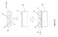
配光素子100のためのいくつかの構成および層状構造を組み立てるための方法を、図2A~2Hを参照して次に説明する。光の伝搬の方向は、破線で示される。免責事項として、これらの表示は、ここに開示された光学コンタクトおよび光学チャネルのコンセプト内において、素子100を通る光の伝搬の仕方を単に例示することを意図しており、したがって、物理学の法則を厳密に遵守するという意味で解釈されるべきではないことを、留意されたい。
Several configurations and methods for assembling layered structures for the
図2Aおよび2Bをさらに参照して、本発明のコンセプト内において、第1の機能層1における光学コンタクトの形成のための2つの基本的な構成を記載している。
With further reference to FIGS. 2A and 2B, two basic configurations for the formation of optical contacts in the first
上述したように、前記第1の機能層1を形成する基材3には、開口部2が設けられ得る。いくつかの構成において、開口部2は、その幅全体を通って、つまり上側層(ここでは、第2の機能層10)から下側層(ここでは、ライトガイド媒体101)まで延びる貫通孔である。
As described above, the
前記第1の機能1層1が配光素子100(図1A)内に一体化されると、前記開口部2によって、いくつかの封入された空隙2Aが形成される。いくつかの構成において、前記封入された空隙2Aは、空気、窒素、酸素、アルゴンなどの気体媒体、または真空で満たされている。
When said first functional 1
本願により形成されたエアボイド(「エアトラップ」)として構成された封入された空隙2Aは、光がそこを通過することをTIR現象により防ぐ。光学コンタクト31は、自身を通しての光の伝搬を可能にする材料から作製された基材3(3Aとして具現化している)によって確立される。図2Aに示す例示的な構成では、基材3は、印刷されたボンディングドットなどの複数のボンディングドット3Aによって表わされ、そのドットは、光取り出し層10への光の透過を可能にし、前記層10との光学的な接合強度を得るための光学コンタクト31として機能する。
これに関して、図2Aに示された配光素子100は、光の伝搬の観点について完全にラミネートされ一体化された素子であり、以下を含む。すなわち、1)例えば、光取り出しパターンを有さない基本的なPMMAライトガイドその他の光透明材料として構成されたライトガイド媒体101と;2)エアボイドなどの封入された空隙2Aを、透光性基材3A(例えば、印刷ドットとして設けられる)によって形成された光学コンタクト31と交互に有する(1Aとして具現化された)第1の機能層1と;3)効率的かつ制御された配光分布のためのエアキャビティパターンを有する光取り出し層10として構成された第2の機能層2と。
In this regard, the
封入された空隙2Aを充填する空気の屈折率は、一般に、ライトガイド媒体101を構成する材料の屈折率よりも低く、任意に、層構成要素1および10の媒体を構成する屈折率よりも低いことに留意すべきである。
The refractive index of the air filling the
したがって、図2Aは、光学コンタクト31が基材材料3(ここでは3A)によって形成されている基本的な構成を説明する。
FIG. 2A thus illustrates a basic configuration in which the
本明細書に開示されたライトガイド素子100において、光均一性制御は、特に、特定の入射角を有する光に関して、上述の光学チャネルまたは光学コンタクトのコンセプトに基づいて、内部の一体化された光学フィルタ1を利用して実施される。前記光学コンタクトは、開口部および光フィルタリング、エアボイドを設けること、低Ri層を設けること、および/または所望の色のリフレクタ層(拡散、ランバート、または鏡面反射を達成するように構成されている)を設けることを含むがこれらに限定されない、複数の方法によって実現される。
In the
図2Aそして図2Gにも示されているような印刷ドットは、均一性を制御し、光取り出し層10に所望の範囲(例えば、入射角に関して)の光を透過させるための最も単純な手法を表している。印刷ドットは、そこを通過する光が(屈折、反射、コリメーションなどを介しての)取り出しを受けないため、いかなる光学機能性をも担わない。むしろ、前記印刷ドットは、第1の機能層1および/または下層のライトガイド媒体101からセクション機能層(光取り出し層)10へと伝搬する光線のための光学的通路(光学コンタクト)を形成する。
Printed dots, such as those also shown in FIGS. 2A and 2G, provide the simplest approach to controlling uniformity and transmitting a desired range of light (e.g., with respect to angle of incidence) to the
サイズに関して、印刷ドットは、素子100の特定の用途および設計に応じて、例えば5マイクロメートルから数百マイクロメートルまでの範囲内で設けることができる。ドットの高さは、光学フィルタ層1の厚さによって定義され、光学的取り出しを避けるためには、好ましくは高すぎない(例えば、1~10マイクロメートルの範囲内)。典型的には、ドットは、インクジェット、フレキソ、グラビア、インプリント、マスクまたは孔版印刷、シルク印刷などによって印刷することができる。
In terms of size, printed dots can be provided, for example, in the range of 5 micrometers to hundreds of micrometers, depending on the particular application and design of
図2Aに示すように、光フィルタ層1内の、光学ドットおよびチャネルのない領域は、薄いエアギャップ(エアボイド2A)を有している。これはリフレクタとして機能し、望ましくない光がそこを通って伝搬するのを防止する。これは、例えば低Riコーティングのような特殊なコーティング材を塗布する場合と比較して、簡単で費用対効果の高い代替手段である。
As shown in FIG. 2A, regions within the
上述したソリューションの典型的な応用領域は、ディスプレイのバックライトおよび/または照明パネルである。エアギャップを設けているため、図2Aのソリューションは、完全な透明性を必要としない用途に最も適している。 Typical application areas for the solutions described above are display backlights and/or lighting panels. Due to the air gap, the solution of Figure 2A is best suited for applications that do not require full transparency.
図2Bに、光学コンタクト21が、基材材料3に形成されたいくつかの開口部2によって第1の機能層1に確立されていると見ることができる、別の基本的な実施形態を説明する。図3Bに示されている基材3(3Bとして具現化されている)は、開口部2を有する反射性フィルムである。反射性フィルムは、鏡面または拡散反射を得るように構成されることができ、当然のことながら、基材3Bは、そこに到達する光を反射する。このような反射性フィルムのための開口部は、例えば、高速レーザ穿孔プロセスによって製造することができる。
FIG. 2B describes another basic embodiment in which optical contacts 21 can be seen to be established to the first
光学コンタクト21を形成するために、反射性フィルム3Bは、光学的に透明な接着剤4(OCA、LOCA等)に一体化されている。接着剤4は、液状、低粘度の接着剤であってもよいし、ゲル状の接着剤材料であってもよい。従って、第1の機能層1(1Bとして具現化)は、光学的に透明な接着剤4に一体化された反射性基材3、3Bを含んでなる。接着剤4に一体化されると、基材3Bの開口部2は、光学的にクリアな材料で「充填」された状態となり、それによって光学コンタクト21が形成される。図2Bに示す構成では、空隙2Aは形成されず、代わりに、接着剤4によって光学フィルタ層1がラミネートされている。
To form an optical contact 21, the reflective film 3B is integrated with an optically transparent adhesive 4 (OCA, LOCA, etc.). The adhesive 4 may be a liquid, low-viscosity adhesive or a gel adhesive material. Thus, the first functional layer 1 (embodied as 1B) comprises a
図2Bは、第1の機能層1の形成時に、反射性フィルム3Bが、接着剤4と構造体101および10との間に界面が形成されるように、接着剤4の中に封入されることを示している。代替的な構成において、接着剤4は、基材3、3Bの中の空隙(開口部2)を埋めることにより、反射面3Bが構造体101および10間の界面に堆積するように塗布することができる。
FIG. 2B shows that during the formation of the first
いずれにしても、第1の機能層1(1Bとして具現化)は、制御された均一な光が得られるように、そのような2つの主層101、10間に完全にラミネートされている。光学接着剤は、好ましくは、ライトガイド材料101の屈折率と等しいかまたはそれ以上の屈折率を有し、任意に、光取り出し層10の屈折率と等しいかまたはそれ以上の屈折率を有する。
In any event, the first functional layer 1 (embodied as 1B) is fully laminated between two such
図2Bに示した配光素子100は、完全にラミネートされた一体型の要素であり、以下を含む。すなわち、1)例えば、光取り出しパターンを有しない基本的なPMMAライトガイドその他の光透明材料として構成されたライトガイド媒体101と、2)低粘度またはゲル状の光学接着剤材料4によって一体化または充填されて光学コンタクト21を形成する、開口部2を有する反射性基材3Bを含んでなる、1Bとして具現化された第1の機能層1と、3)効率的かつ制御された配光分布のためのエアキャビティパターンを有する光取り出し層10として構成された第2の機能層2と。
The
実施形態において、光学コンタクト21、31は、線、ドット、幾何学形状、十字、グリッド、またはそれらの任意の組み合わせからなるパターンのうちの任意の1つとして設けられ得る。
In embodiments, the
光学コンタクト21、31は、前記第1の機能層1における少なくとも1つの所定の位置内の少なくとも1つのアレイとして配置されていてもよいし、あるいは前記第1の機能層1の表面全体に沿っておよび/または横切って延びる少なくとも1つのアレイとして配置されていてもよい。
The
図6は、光学コンタクト21、31の例示的な構成を示す。光学コンタクトは、図2Aおよび2Bについて説明した任意の基本的な実施形態に従って、基材材料2(光学コンタクト31)によって、または開口部2(光学コンタクト21)内の光学透明接着剤材料によって確立された光学コンタクトとして、実施することができる。
FIG. 6 shows an exemplary configuration of
光学コンタクトが、31において光透過印刷パターン3A(図2Aによる)として実施されているか、または反射構造体3B(図2Bによる)の間に設けられた光学透明接着剤パターン21として実施されているかどうかによらず、各前記光学コンタクトパターン21、31の密度、サイズ、および被覆率は、所望の光伝搬のモードを達成するため、および前記光伝搬に対する強化された制御を達成するため、変化することができる。
Whether the optical contact is embodied at 31 as a light-transmissive printed
図2Cは、第1の機能要素1が、接着剤材料4中に形成された例えばエアボイドなどのいくつかの封入された空隙2Aを有している構成を示している。この構成は、以下のようにして組み立てられる。図2Bを参照して先に論じた様態で、基本的に(光学的に)透明なフィルムとして構成された、基材フィルム3(3Cとして具現化)が得られ、接着剤4中に一体化される。基材3Cは、好ましくは、下層のライトガイド媒体101および接着剤材料4の屈折率と同じか同等の屈折率を有する。図3Bに示された態様、また液状、低粘度の接着剤またはゲル状の接着剤を利用することとは別に、図2Cの接着剤4は、好ましくは高粘度接着剤である。接着剤4は、開口部2(例えばレーザ穿孔された開口部)を貫通し、光取り出し層10(および下層のライトガイド媒体101)との光学的接合(optical bonding)を形成する。高粘度接着剤4は、任意の適切な方法でさらにパターン化されることにより、エアトラップ2Aを形成することができる。高粘度接着剤4に一体化された開口部2を設けることにより、光学コンタクト21が形成される。
FIG. 2C shows a configuration in which the first
図2Cに示された配光素子100は、完全にラミネートされ一体化された素子であり、以下を含む。すなわち、1)ライトガイド媒体101と、2)ライトガイド媒体101と取り出しフィルム10との間に、高粘度またはゲル状の光学接着剤材料を用いてラミネートされ、光学的均一性制御のためのエアトラップ2Aを形成する開口部設計を有する光学的に透明なフィルムとして構成された、第1の機能要素1を備える、1Cとして具現化された第1の機能層1と、3)効率的かつ制御された配光分布のためのエアキャビティパターンを有する光取り出し層10と。
The
基材層3に一般的に形成された開口部2は、いくつかの実施形態においては光学コンタクト21(例えば図2B)として、また、いくつかの代替的な実施形態ではTIR機能部品として作用することができることを、さらに指定する。開口部がTIR機能部品を形成する構成は、図2Aおよび図2Cによって例示される。
実施形態において、第1の機能層1は、少なくとも2つのサブ層1-1、1-2を有するように構成することができる。そのような基本的に多層構造を設けることは、図2Dおよび2Fに示す構成によって例示される。
In embodiments, the first
図2Dは、光学フィルタ層が、開口部2を有する多層構造(積層体)として設けられた構成を示している。前記積層体は、前記全サブ層を貫通する開口部2を有する少なくとも2つのサブ層1-1、1-2を有する。図2Dに示す構成において、前記積層体構造は、少なくとも片側に低Ri膜(3D、サブ層1-1)がラミネートされた、PMMAシート(3E、サブ層1-2)などのプラスチックシートによって形成されている。図2Bの構成と同様に、図2Dに示す開口部を有する層状構造は、液状、低粘度またはゲル状の接着剤として設けられる接着剤4に一体化されて、第1の機能層1(1Dとして具現化)を形成する。
FIG. 2D shows a configuration in which the optical filter layer is provided as a multilayer structure (laminate) having
したがって、第1の機能層1は、ライトガイド媒体101を構成する材料の屈折率よりも低い屈折率、そして任意に、第2の機能層10を形成する材料の屈折率よりも低い屈折率を有する材料によって形成されたサブ層3D(図2D)を有していてもよい。
The first
いくつかの例において、サブ層3Eを設けることを省略することができ、第1の機能層構造1Dは、開口部(図示せず)を有する低Ri膜として設けられる単一の(サブ)層3Dから形成することができる。
In some examples, providing the sub-layer 3E can be omitted and the first
全体的に、図2Dのソリューションは、図2Bに示したものと同様であるが、光学フィルタ膜Lは、その少なくとも一部が透明かつ低Riの材料で作られている。 Overall, the solution of Figure 2D is similar to that shown in Figure 2B, but the optical filter film L is at least partially made of a transparent and low Ri material.
図2Dに示された配光素子100は、完全にラミネートされ一体化された素子であり、以下を含む。すなわち、1)ライトガイド媒体101と、2)ライトガイド媒体と光取り出しフィルムとの間に、オプションとしてサブ層3E(PMMAフィルム)上に設けられ、低粘度またはゲル状の光学接着剤4を用いてラミネートされた、開口部設計を有する低Riフィルム3Dを有する、1Dとして具現化された第1の機能層1と、3)効率的かつ制御された配光分布のためのエアキャビティパターンを有する光取り出し層10と。
The
図2Eは、第1の機能層1(1Eとして具現化)が、好ましくはライトガイド媒体101よりも低い屈折率Riを有する接着剤4の層として表される構成を示している。さらに、ライトガイド媒体101には、前記接着剤材料4とさらに一体化され得る、いくつかの突出した光学機能レリーフプロファイル121を設けることができる。パターン(単数または複数)121は、好ましくは、光屈折機能性を付与されている。ただし光アウトカップリング(取り出し)無しにである。図2Eに示す構成では、光学フィルタ層1は、このように、実質的に低Riの接着剤材料4によって確立され、任意に、いくつかのレリーフパターンプロファイル121と組み合わされる。
FIG. 2E shows a configuration in which the first functional layer 1 (embodied as 1E) is represented as a layer of
ライトガイド媒体101に設けられたパターン(単数または複数)121は、ラミネートされたときに配光素子100から光を取り出さない単純なフォーメーションである。このパターンは、次の取り出し層10のために入射光を屈折させて均一性を制御するだけである。図2Eに示す構成では、光取り出し層19と完全にラミネートされた、従来のパターン化されたライトガイドを利用してもよい。このコンセプトもまた、臨界角と等しいかそれ以下の入射光を利用している。
The pattern(s) 121 provided on the
図2Eに示す配光素子100は、完全にラミネートされ一体化された素子であり、以下を含む。すなわち、1)なんらかの光屈折パターンを有する(光アウトカップリング無し)基本的なPCライトガイドその他の光透明材料として設けられた、ライトガイド媒体101と、2)ライトガイド媒体材料よりもわずかに低いRi値を有する積層接着剤(ライトガイド媒体と取り出しフィルムとをラミネートする)を有する光学フィルタと、3)効率的かつ制御された配光分布のためのエアキャビティパターンを有する光取り出し層と。
The
図2Fは、図2Eに示したものと同様の配光素子100を例示する。図2Eに示された光学フィルタ構造体と比較して、図2Fの光学フィルタ構造体(第1の機能層1)は、さらに、低屈折率の材料で作られた基材3を有する。この基材3は、例えば、光取り出し層10に隣接して配置された低Riコーティングの形態で設けることができる。低Ri値は、どの光が取り出されるかを制御するために、前記光取り出し層10のパターンソリューション用に最適化され得る。
FIG. 2F illustrates a
図2Dに示す光学フィルタ構造体1と同様に、図2Fの光学フィルタ構造体は、第1のサブ層1-1が低Riコーティングであり、接着剤および任意にライトガイドパターン121が第2のサブ層1-2を構成しているような、積層体ソリューションとみなすことができる。図2Fの基材3は、例えば、サブ層3D(図2D)と同じか同等の低Ri材料で構成することができる。
Similar to the
図2Gは、図2Aに示した構成と同様の構成を示しているが、第2の機能層10がオープントップのパターン化特徴部を有するように実装されている。第1Gとして実装された第1の機能層1は、複数の印刷ドットとして実装された基材3を含んでなる。ライトガイド媒体101と光取り出し層10との間の光学コンタクト31は、前記印刷ドット3によって確立されている。基材(印刷ドット)3は、好ましくは、ライトガイド媒体101と等しい屈折率を有する。印刷ドット3は、光学チャネルを形成することに加えて、第1の機能層1を第2の機能層10に対してオープントップの光取り出しパターンでラミネートする役割を果たす。さらに、光学チャネルを形成する基材3を介して、光は、最終的な光取り出しのための(上側)層10にさらに導かれる。さらに、基材3によって確立された印刷ドットの間に(第1の機能層1G内に)いくつかの開口部が形成される。
FIG. 2G shows a configuration similar to that shown in FIG. 2A, but implemented such that the second
図2Gに示す配光素子100は、完全にラミネートされ一体化された素子であり、以下を含む。すなわち、1)光取り出しパターンを有しない基本的なPMMAライトガイドその他の光透明材料として設けられた、ライトガイド媒体101と、2)ライトガイド媒体と光取り出しフィルム10との間の複数の印刷ドットであって、物理的な接合を形成し、さらに追加的に、光均一性制御のための光学チャネルを形成する、ドットと、3)効率的かつ制御された配光分布のためのオープン光学パターンを有する光取り出し層10と。
The
基材3(図2G)から形成された光学ドットは、第2の機能層10のオープン取り出しパターンの内部には侵入しない。光学ドットは、単に光学コンタクトを形成し、ライトガイド101と光取り出し層10との間の接合強度を提供するだけである。
The optical dots formed from the substrate 3 (FIG. 2G) do not penetrate inside the open extraction pattern of the second
図2Aに示された構成とは反対に、例えば図2Gの構成は、封入された空隙(エアトラップ)の形成を伴わないことに留意すべきである。したがって、基材層3(第1の機能層1Gの)に形成された開口部は、オープン光学パターンを有する第2の機能層10に定義された、いくつかの光学機能キャビティ12(例えばエアキャビティ)と接続する。第1の機能層1Gのための光学コンタクトを形成する印刷ドット3自体は、第2の機能層10が作られている実質的に透光性の材料と接続し、配光素子100の高さ全体、そして任意に幅全体にわたって、「光学チャネル」を確立する。図2Gの実施形態では、第1の機能層1Gに形成された開口部は、前記開口部が層10および101の間で一体化されたときに、「封入されていない空隙」(エアキャビティ12に接続可能であるものとして)と称することができる。
It should be noted that, contrary to the configuration shown in Figure 2A, the configuration of Figure 2G, for example, does not involve the formation of enclosed voids (air traps). Thus, the openings formed in the substrate layer 3 (of the first
図2Hは、第1の機能層1が、図2Gに示されているのと同様に具現化されているが、開口部2が存在しない、配光素子100のさらなる構成を示している。基材3の配置は、ライトガイド媒体101を横切る領域全体を覆い、前記ライトガイド101と光取り出し層10との間に光学的接合を形成するようにされる。図2Hに示された基材3は、ライトガイド媒体101の表面全体を横切って配置された光学コンタクトとみなすことができる。
FIG. 2H shows a further configuration of the
光学フィルタ層1は、透明な低屈折率フィルタ層として、または光学的に透明な(ライトガイド)基材101の少なくとも片面に形成された反射性TIR層(例えば拡散または鏡面TIR層)として構成することができる。前記光学フィルタは、a)平坦面上に直接塗布されたもの、b)接着剤層によってラミネートされたもの、またはc)VUV(真空紫外線)、大気プラズマ処理、マイクロ波アシストボンディングなどの化学的表面処理によって接合されたものであってもよい。
The
いくつかの例において、光フィルタ層1は、開口部がない場合でも好ましい配光分布を得るために、徐々に変化する低Ri値を有する。
In some examples, the
光フィルタ層1内の開口部は、光学的に変調されてもよく、それにより、均一、対称、離散的、または非対称の配光分布パターンを含むがこれらに限定されない、光フィルタ層によって生成される様々な配光分布パターンを達成することができる。
The apertures in the
ディスプレイ、サイネージ、ポスター(図4参照)など上における所定の図柄(画像)や信号を形成する、光学開口部による配光分布は、均一、不均一、または離散的であることができる。これにより、均一、不均一、または離散的な図柄(画像)または信号を形成することができる。開口部は、光学フィルタ層の両側に設けられて、均一/連続的または離散的な領域を形成することができる。開口部は、光学フィルタ層の表面全体に、またはその所定の領域に設けることができる。 Light distribution by optical apertures that form a predetermined pattern (image) or signal on a display, signage, poster (see FIG. 4), etc., can be uniform, non-uniform, or discrete. This allows formation of uniform, non-uniform, or discrete patterns (images) or signals. Apertures can be provided on both sides of the optical filter layer to form uniform/continuous or discrete regions. Apertures can be provided over the entire surface of the optical filter layer or in predetermined regions thereof.
開口部の主要な機能は、光アウトカップリングなしに、第1の媒体から第2の媒体に伝搬する入射光の量を制御すること、すなわち、すべての入射光角が媒体内の臨界角以上であることを意味する。特に、光均一性制御は、このようにして、光学パターンなしで実現することができる。 The main function of the aperture is to control the amount of incident light that propagates from the first medium to the second medium without light outcoupling, i.e. all incident light angles are above the critical angle in the medium. means that In particular, light uniformity control can be achieved in this way without optical patterns.
開口部は、第1の媒体から第2の媒体への光を透過させる(これが所望の配光分布および/または均一性を決定する)などの、いくつかの主要な機能を有する、光学開口部(光学コンタクト)として設けることができる。第1および第2の媒体における配光分布は、空気または低Riフィルタ/クラッドが界面を形成している場合、典型的には、媒体界面に関する臨界角(これを超えるとTIRが発生する入射角)未満の入射光角を有する。その結果、光は媒体からアウトカップリングされない。 The aperture has several primary functions, such as transmitting light from the first medium to the second medium (which determines the desired light distribution and/or uniformity). (optical contact). The light distribution in the first and second media, if air or a low-Ri filter/cladding forms the interface, is typically at the critical angle (incident angle above which TIR occurs ). As a result, no light is outcoupled from the medium.
光学開口部(光学コンタクト)として設けられることに加えて、前記開口部は、いくつかの実施形態において、TIR機能部品(図2A、2Cに示すように)を確立することができる。 In addition to being provided as optical apertures (optical contacts), said apertures can establish TIR functional components (as shown in FIGS. 2A, 2C) in some embodiments.
開口部は、レーザアブレーション、短パルスシステム、プラズマエッチング、マスクアシストエキシマ露光、マイクロプリンティングおよび/または他の任意の好適な方法を用いて製造することができる。例えば、レーザアブレーションは、ロールツーロール装置および方法を利用して行うことができ、ここで、製造プロセスは、毎分40メートルまで速度を上げることができる。 Apertures can be manufactured using laser ablation, short pulse systems, plasma etching, mask-assisted excimer exposure, microprinting and/or any other suitable method. For example, laser ablation can be performed using roll-to-roll equipment and methods, where the manufacturing process can speed up to 40 meters per minute.
光学開口部は、以下を含むが、これらに限定されない様々な方法によって製造することができる。すなわち、レーザパターニング、直接レーザイメージング、レーザ穿孔、マスクおよび/またはマスクレスレーザまたは電子ビーム露光であったり、印刷、インクジェット印刷、スクリーン印刷、マイクロ/ナノディスペンシング、ドージング、直接「書き込み」、ディスクリートレーザ焼結、マイクロ放電加工(マイクロEDM)、マイクロ機械加工、マイクロモールディング、インプリント、エンボス加工などにより離散的特性を付与することで光学材料/Ri値を変更したりすることである。光学開口部の形成は、低Riクラッドまたは反射性TIRクラッドとの直接接触によって完了することができる。光学開口部の形成は、低Riクラッドまたは反射性TIRクラッドとの直接接触によって完了することができる。 Optical apertures can be manufactured by a variety of methods including, but not limited to: laser patterning, direct laser imaging, laser drilling, mask and/or maskless laser or electron beam exposure, printing, inkjet printing, screen printing, micro/nano dispensing, dosing, direct "writing", discrete lasers. sintering, micro-electric discharge machining (micro-EDM), micro-machining, micro-molding, imprinting, embossing, etc. to impart discrete characteristics to change the optical material/Ri value. Formation of the optical aperture can be completed by direct contact with the low Ri cladding or the reflective TIR cladding. Formation of the optical aperture can be completed by direct contact with the low Ri cladding or the reflective TIR cladding.
配光素子100において、第1の光学フィルタ層1(第1の機能要素)および光取り出し層10(第2の機能要素)は、ロール・ツー・ロール法またはロール・ツー・シート法により製造することができる。
In the
第1の機能要素1は、第2の機能要素10よりも先にライトガイド媒体101上に作製されることが好ましい。
The first
さらに、開口部の形成は、キャリア基板またはライトガイド素子(媒体)を介して操作するような間接的な接触、例えばレーザアブレーションによって完了することができ、それによってクラッドはアブレーションにより除去され、結果として、直接接触法による場合と同様に、サイズおよび形状について所望の開口特徴部を形成することができる。レーザビームスポットプロファイルは、好ましくは、過度の熱を発生しないためキャリア基板またはライトガイド媒体素子を損傷しない、平坦なトップハットの形状である。レーザの波長は、クラッド吸収曲線、ホールエッジ品質、ビームシェーパー光学系、厚さ/高さ、動作コストなどの観点から選択することができる。 Furthermore, the formation of the openings can be completed by indirect contact, such as laser ablation, such as operating through the carrier substrate or light guide element (medium), whereby the cladding is removed by ablation, resulting in , the desired aperture feature in size and shape can be formed as by direct contact methods. The laser beam spot profile is preferably a flat top hat shape that does not generate excessive heat and thus damage the carrier substrate or light guide media element. The wavelength of the laser can be selected in terms of cladding absorption curve, hole edge quality, beam shaper optics, thickness/height, cost of operation, and the like.
配光素子100はさらに第2の機能層10を備え、好ましくは、光取り出し機能および光アウトカップリング機能を付与される。
The
第2の機能層10は、光学機能キャビティ12として設けられる複数の特徴によって透光性キャリア媒体111に形成された少なくとも1つの光学機能特徴部パターン11を備える。
The second
いくつかの構成において(図2G、2H)、前記少なくとも1つの光学機能特徴部パターン11は、オープントップの特徴部として構成された光学機能キャビティ12を有する。
In some configurations (FIGS. 2G, 2H), the at least one optically
いくつかの構成において(図2A~2F)、少なくとも1つの光学機能特徴部パターン11は、透光性キャリア媒体111内に完全に一体化され、かつ/または埋め込まれており、それにより、埋め込み特徴部パターンが、キャリア媒体111のパターン化層111Bに対して配置されたキャリア媒体111の完全に平坦で平面的な層111Aによって形成されたラミネート構造により透光性キャリア媒体内に確立され、複数の光学機能内部キャビティ12が層111A、111Bの間の界面に形成されている。
In some configurations (FIGS. 2A-2F), at least one optical
光学キャビティ特徴部12は、溝、凹部、ドット、およびピクセルからなる群から選択されることができ、前記キャビティ特徴部12は、バイナリ、ブレーズ、傾斜、プリズム、台形、半球形プロファイルなどから選択される横断方向のプロファイルを有し、前記キャビティ特徴部は、直線状、曲線状、波状、正弦波状などから選択される長さ方向の形状を有している。 Optical cavity features 12 may be selected from the group consisting of grooves, recesses, dots, and pixels, said cavity features 12 being selected from binary, blazed, tilted, prismatic, trapezoidal, hemispherical profiles, etc. The cavity feature has a longitudinal profile selected from straight, curved, wavy, sinusoidal, and the like.
好適な実施形態において、キャビティ12は空気で満たされている。他のいくつかの実施形態では、エアキャビティは、別の気体、流体、液体、ゲル、または固体媒体で充填され得る。
In a preferred embodiment,
光学機能パターン11は、複数の離散的プロファイル、または対称パターン構造として、または非対称パターン構造として設けられる複数の少なくとも部分的に連続的なプロファイルの複数のプロファイルを有し得る。
The
いくつかの例において、光学機能パターンは、複数の離散的プロファイルまたは複数の少なくとも部分的に連続的なプロファイルからなるハイブリッドパターンとして設けられ得る。 In some examples, the optical feature pattern may be provided as a hybrid pattern consisting of a plurality of discrete profiles or a plurality of at least partially continuous profiles.
前記少なくとも1つの光学機能パターンは、溝、凹部、ドット、およびピクセルからなる群から選択されるレリーフ形状によって確立することができ、前記レリーフ形状は、バイナリ、ブレーズ、傾斜、プリズム、台形、半球形などから選択される横断方向の凹状または凸状のプロファイルを有し、前記レリーフ形状は、直線状、曲線状、波状、正弦波状などから選択される長さ方向の形状を有している。 Said at least one optical feature pattern may be established by a relief shape selected from the group consisting of grooves, recesses, dots and pixels, said relief shape being binary, blazed, oblique, prismatic, trapezoidal, hemispherical. and the relief shape has a longitudinal shape selected from linear, curvilinear, wavy, sinusoidal and the like.
好適な実施形態において、前記少なくとも1つの光学機能パターンは、前記配光素子内に完全に一体化されており、かつ/または埋め込まれている。 In a preferred embodiment, said at least one optical function pattern is fully integrated and/or embedded within said light distribution element.
図3を参照して、配光素子100は、第3の機能層20をさらに備えることができる。このような場合、取り出しおよび光アウトカップリング層として設けられた第2の機能層10によって得られる機能性と、前記第3の機能層によって得られる機能性とを組み合わせることができる。第3の機能層20は、従来のプリズム層構造、硬質保護コーティング、反射防止・防眩コーティング、セルフクリーニングコーティングなどとして設けられ得る。
Referring to FIG. 3 ,
これにより、エアキャビティパターン(層10)とオープントップパターン(層20)の二重構造が可能となる。これにより、光アウトカップリング分布などの性能を制御する可能性が広がる。例えば、第3の機能層20をプリズム型の層として構成したり、オープンパターンを有するレンティキュラ層をトップ層として利用したりする場合、このようなソリューションは双方向の配光分布を得ることができる。
This allows for a dual structure of the air cavity pattern (layer 10) and the open top pattern (layer 20). This opens up the possibility of controlling performance such as light outcoupling distribution. For example, if the third
このように、配光素子100は、(光取り出し/第2の機能層10内の)エアキャビティパターンとオープントップパターン(例えば、第3の機能層20内のプリズムパターン)との両方を利用する多層フィルムとして構成することができる。さらに、ディフューザーを、任意に、前述の光学パターン層の間に一体化することができる。
Thus, the
配光素子はさらに、発光ダイオード(LED)、有機発光ダイオード(OLED)、レーザダイオード、LEDバー、OLEDストリップ、マイクロチップLEDストリップ、および冷陰極管から選択される光源7を備えている。
The light distribution element further comprises a
別の局面において、本明細書に記載されたいずれかの実施形態による配光素子からなる光学デバイス200が提供される。
In another aspect, an
光学デバイスは、フロントライト照明装置として構成してもよいし、バックライト照明装置として構成してもよい。 The optical device may be configured as a frontlight illumination device or as a backlight illumination device.
したがって、図4は、ある局面に従って、夜間照明器具のためのサイネージおよび/または広告照明コンセプトに一体化された配光素子を示す。図4に示されている広告フィルムは、例えば、任意の形状を採用するために切断することによって得ることができ、それは、ウィンドウまたはスクリーンに接着させることができる。このソリューションは、光学デバイス200の縁部に配置された光源7(LED)を備えている。図4に示すソリューションは、さらに、所定の色のリフレクタシート51を備えることができる。
FIG. 4 thus shows a light distribution element integrated into a signage and/or advertising lighting concept for nighttime lighting fixtures, according to one aspect. The advertising film shown in Figure 4 can be obtained, for example, by cutting to adopt any shape, which can be glued to the window or screen. This solution comprises a light source 7 (LED) placed at the edge of the
光学デバイス200は、ウィンドウ、ファサード照明および/または表示素子、天井照明および/または表示素子、サイネージ、看板、ポスター、マーケティングボード、広告ボード照明および/または表示素子、および太陽光アプリケーション用に構成された照明素子として構成することができる。
The
したがって、ある局面において、前出の局面の1つに従った光学デバイス200の使用は、以下からなる群から選択される照明および表示においてさらに得られる。すなわち、装飾照明、ライトシールドおよびマスク、ウィンドウ、ファサードおよび天井照明を含む公共および一般照明、サイネージ、看板、ポスター、および/または広告ボード照明および表示、および太陽光アプリケーションにおける照明および表示である。
Thus, in certain aspects, use of the
図5は、配光素子100のための層状構造を組み立てるための一般的なコンセプトをさらに示している。したがって、図5に示す素子100は、上側媒体101-1(例えば、キャビティ光学系などの光学的取り出しパターンを有する層10からなるか、または含む)と、光学フィルタ1を重ね合わせた下側媒体101-2(光学接着剤パターンを有する、密度変化を有する連続的な線)とから構成される。上側媒体と下側媒体とはラミネートされている。このようにして、埋め込み型光フィルタリング/下側媒体から上側媒体への制御された光通過を備えた、ラミネートされたライトガイドを確立することができる。
FIG. 5 further illustrates the general concept for assembling the layered structure for the
図7Aおよび7Bは、第2の媒体の厚さ(a)が、光学的接着コンタクト(b)のサイズおよびフォーマットとともに、光の伝搬および局所的照明領域(c)の最大サイズを制御する方法をさらに例示している。均一性などの光制御は、複数の接着コンタクト(b)の比率および第2の媒体(a)の高さによって定義することができる。したがって、図7Aおよび図7Bは、照明領域(c)に対する媒体厚さ(b)の影響を示しており、媒体厚さが大きくなるにつれて増加している。 Figures 7A and 7B illustrate how the thickness of the second medium (a), along with the size and format of the optical adhesive contact (b), controls the propagation of light and the maximum size of the localized illumination region (c). further exemplified. Light control such as uniformity can be defined by the ratio of the plurality of adhesive contacts (b) and the height of the second medium (a). Accordingly, Figures 7A and 7B show the effect of media thickness (b) on the illumination area (c), increasing with increasing media thickness.
図7Aおよび図7Bは、照明領域に関する光学コンタクト31の基本的な機能を説明するための図である。光学コンタクトの横方向サイズ(b)と横方向の照明の射影(c)との間の関係は、第2の媒体(層10)の厚さに直接関係している。光学コンタクトの最終的なサイズは、式(2)に従って、好ましい照明ターゲットについて定義することができる。
7A and 7B are diagrams for explaining the basic function of the
これはいかなるRi値やスネルの法則を考慮しない簡略化されたソリューションであり、所望の照明領域、全体の均一性、離散的な照明(画像、マーキングなど)その他の設計に迅速に活用できる。 This is a simplified solution that does not take into account any Ri values or Snell's Law, and can be quickly leveraged for desired illumination area, global uniformity, discrete illumination (images, markings, etc.) and other designs.
上述のように、光学コンタクト(21、31の両方として実装)は、光を管理したり、光の方向を制御したりするように構成された実際の光学構造体を形成するものではない。光学コンタクト(単数または複数)21、31は、第1の媒体(例えばライトガイド媒体101)から第2の媒体(例えば光取り出し層10)への光の伝搬を可能にする接触領域に過ぎない。 As noted above, the optical contacts (implemented as both 21 and 31) do not form actual optical structures configured to manage or control the direction of light. The optical contact(s) 21, 31 are merely contact areas that allow light to propagate from a first medium (eg light guide medium 101) to a second medium (eg light extraction layer 10).
縦方向の値と横方向の値の間の比率は、最小比率1/4(縦方向/横方向)を達成するように制御されなければならない。前述の比率の横方向の値は無制限であり(理論的には、この値は無限大に達することができる)、したがって、1/8、1/20、1/100などの比率が可能である。典型的な縦方向の寸法(厚さ)は、0.5~100μmの範囲で設けられる。 The ratio between the vertical and horizontal values should be controlled to achieve a minimum ratio of 1/4 (vertical/horizontal). The lateral value of the aforementioned ratio is unlimited (theoretically, this value can reach infinity), so ratios of 1/8, 1/20, 1/100, etc. are possible. . A typical longitudinal dimension (thickness) is provided in the range 0.5-100 μm.
一局面において、光学フィルタ層として構成された第1の機能層1と、少なくとも1つの光学機能パターン11を有する第2の機能層10とからなる配光素子のロールがさらに提供され、ここで、第1の機能層1には、光均一性制御機能を付与されている。
In one aspect, there is further provided a roll of light distribution elements consisting of a first
前記配光素子の前記ロールにおいて、前記第1の機能層1は、本明細書で説明した任意の構成に従って実施される構造によって確立することができる。
In the roll of light distribution elements, the first
技術の進歩に伴い、本発明の基本的概念は、その様々な改変をカバーすることが意図されていることは、当業者には明らかである。したがって、本発明およびその実施形態は、上記の例に限定されるものではなく、添付の特許請求の範囲の範囲内で概して変化し得る。 It will be apparent to those skilled in the art that as technology advances, the basic concept of the invention is intended to cover various modifications thereof. The invention and its embodiments are therefore not limited to the examples described above, but may generally vary within the scope of the appended claims.
Claims (45)
光学フィルタ層として構成され、前記ライトガイド媒体の少なくとも1つの表面上に設けられた第1の機能層と、
少なくとも1つの光学機能特徴部パターンを有する第2の機能層と、を備える配光素子であって、
前記第1の機能層および前記第2の機能層には、臨界角に等しいおよび/またはそれ以下の角度で入射する光に関する少なくとも1つの光学機能が付与されており、前記第1の機能層はさらに光均一性制御機能を有する内部層として構成され、前記内部層は、前記第2の機能層へおよび前記第2の機能層から、光線を透過させるように構成された、いくつかの光学コンタクトエリアを有し、
前記少なくとも1つの光学機能特徴部パターンは、光学機能キャビティの一部が開放されたオープントップの特徴部であり、
前記第1の機能層は、封入されていない空隙を備え、前記封入されていない空隙は、前記オープントップの特徴部に直接接続する、
配光素子。 a light guide medium configured for light propagation;
a first functional layer configured as an optical filter layer and provided on at least one surface of the light guide medium;
a second functional layer having at least one optical functional feature pattern,
The first functional layer and the second functional layer are endowed with at least one optical function for light incident at an angle equal to and/or less than the critical angle, and the first functional layer is A number of optical contacts further configured as an inner layer having a light uniformity control function, said inner layer configured to transmit light rays to and from said second functional layer. has an area
wherein the at least one optically functional feature pattern is an open top feature in which a portion of the optically functional cavity is open;
wherein the first functional layer comprises an unencapsulated void, the unencapsulated void directly connecting to the open-top feature;
Light distribution element.
光学フィルタ層として構成され、前記ライトガイド媒体の少なくとも1つの表面上に設けられた第1の機能層と、
少なくとも1つの光学機能特徴部パターンを有する第2の機能層と、を備える配光素子であって、
前記第1の機能層および前記第2の機能層には、臨界角に等しいおよび/またはそれ以下の角度で入射する光に関する少なくとも1つの光学機能が付与されており、前記第1の機能層はさらに光均一性制御機能を有する内部層として構成され、
前記少なくとも1つの光学機能特徴部パターンは、光学機能キャビティの一部が開放されたオープントップの特徴部であり、
前記第1の機能層は、封入されていない空隙を備え、前記封入されていない空隙は、前記オープントップの特徴部に直接接続する、
配光素子。 a light guide medium configured for light propagation;
a first functional layer configured as an optical filter layer and provided on at least one surface of the light guide medium;
a second functional layer having at least one optical functional feature pattern,
The first functional layer and the second functional layer are endowed with at least one optical function for light incident at an angle equal to and/or less than the critical angle, and the first functional layer is Furthermore, it is configured as an internal layer having a light uniformity control function,
wherein the at least one optically functional feature pattern is an open top feature in which a portion of the optically functional cavity is open;
wherein the first functional layer comprises an unencapsulated void, the unencapsulated void directly connecting to the open-top feature;
Light distribution element.
前記少なくとも1つの光学機能特徴部パターンは、光学機能キャビティの一部が開放されたオープントップの特徴部であり、
前記第1の機能層は、封入されていない空隙を備え、前記封入されていない空隙は、前記オープントップの特徴部に直接接続し、
前記開口部は、レーザパターニング、直接レーザイメージング、レーザ穿孔、マスクおよびマスクレスレーザまたは電子ビーム露光、印刷、機械加工、モールディング、インプリント、エンボス加工、マイクロおよびナノディスペンシング、ドージング、直接書き込み、ディスクリートレーザ焼結、およびマイクロ放電加工(マイクロEDM)からなる群より選択される少なくとも1つの方法により作製される、プロセス。 a light guide medium configured for light propagation; and a first functional layer configured as an optical filter layer having a plurality of discrete apertures formed in a substrate material, the light guide medium comprising: A process for manufacturing a light distribution element comprising the first functional layer provided on at least one surface and a second functional layer having at least one optical functional feature pattern, comprising:
wherein the at least one optically functional feature pattern is an open top feature in which a portion of the optically functional cavity is open;
wherein the first functional layer comprises an unencapsulated void, the unencapsulated void directly connecting to the open top feature;
Said apertures are laser patterning, direct laser imaging, laser drilling, mask and maskless laser or e-beam exposure, printing, machining, molding, imprinting, embossing, micro- and nano-dispensing, dosing, direct writing, discrete A process made by at least one method selected from the group consisting of laser sintering and micro electrical discharge machining (micro EDM).
少なくとも1つの光学機能特徴部パターンを有する第2の機能層とを備える配光素子のロールであって、
前記第1の機能層には光均一性制御機能が付与されており、
前記少なくとも1つの光学機能特徴部パターンは、光学機能キャビティの一部が開放されたオープントップの特徴部であり、
前記第1の機能層は、封入されていない空隙を備え、前記封入されていない空隙は、前記オープントップの特徴部に直接接続する、
配光素子のロール。 a first functional layer configured as an optical filter layer for placement on at least one surface of a light guide medium configured for light propagation;
a second functional layer having at least one optical functional feature pattern, the roll of light distribution elements comprising:
The first functional layer is provided with a light uniformity control function,
wherein the at least one optically functional feature pattern is an open top feature in which a portion of the optically functional cavity is open;
wherein the first functional layer comprises an unencapsulated void, the unencapsulated void directly connecting to the open-top feature;
A roll of light distribution elements.
請求項44に記載の配光素子のロール。 The first functional layer is further configured as an inner layer having a light uniformity control function, the inner layer being configured to transmit light rays to and from the second functional layer. and has several optical contact areas,
45. A roll of light distribution elements according to claim 44.
Applications Claiming Priority (3)
| Application Number | Priority Date | Filing Date | Title |
|---|---|---|---|
| US201862674260P | 2018-05-21 | 2018-05-21 | |
| US62/674,260 | 2018-05-21 | ||
| PCT/IB2019/054173 WO2019224705A1 (en) | 2018-05-21 | 2019-05-21 | Improved light distribution element |
Publications (3)
| Publication Number | Publication Date |
|---|---|
| JP2021524939A JP2021524939A (en) | 2021-09-16 |
| JPWO2019224705A5 JPWO2019224705A5 (en) | 2022-05-27 |
| JP7328257B2 true JP7328257B2 (en) | 2023-08-16 |
Family
ID=68616610
Family Applications (1)
| Application Number | Title | Priority Date | Filing Date |
|---|---|---|---|
| JP2020564334A Active JP7328257B2 (en) | 2018-05-21 | 2019-05-21 | Improved light distribution element |
Country Status (8)
| Country | Link |
|---|---|
| US (1) | US11650364B2 (en) |
| EP (1) | EP3797322A4 (en) |
| JP (1) | JP7328257B2 (en) |
| KR (1) | KR20210013064A (en) |
| CN (1) | CN112189152B (en) |
| SG (1) | SG11202011569QA (en) |
| TW (1) | TW202012834A (en) |
| WO (1) | WO2019224705A1 (en) |
Families Citing this family (7)
| Publication number | Priority date | Publication date | Assignee | Title |
|---|---|---|---|---|
| WO2019087118A1 (en) * | 2017-11-01 | 2019-05-09 | Nitto Denko Corporation | Light distribution structure and element, related method and uses |
| CN111239887B (en) * | 2020-03-24 | 2024-06-14 | 杭州矽能新材料有限公司 | Light guide film, production method thereof and light guide device |
| KR20230047084A (en) * | 2020-07-28 | 2023-04-06 | 닛토덴코 가부시키가이샤 | lighting device |
| CN116157618A (en) * | 2020-07-28 | 2023-05-23 | 日东电工株式会社 | Table top lighting device |
| WO2022104604A1 (en) * | 2020-11-18 | 2022-05-27 | 京东方科技集团股份有限公司 | Light source module and preparation method therefor, and display module |
| CN112764152B (en) * | 2021-02-08 | 2022-09-02 | 捷开通讯(深圳)有限公司 | Display assembly and display device |
| KR20240026886A (en) * | 2021-06-29 | 2024-02-29 | 닛토덴코 가부시키가이샤 | Light guiding member and light emitting device for light emitting device |
Citations (3)
| Publication number | Priority date | Publication date | Assignee | Title |
|---|---|---|---|---|
| JP2002222604A (en) | 2000-09-25 | 2002-08-09 | Mitsubishi Rayon Co Ltd | Light source device having leakage light modulator |
| JP2011210595A (en) | 2010-03-30 | 2011-10-20 | Mitsubishi Rayon Co Ltd | Lighting device |
| JP2013159099A (en) | 2012-02-08 | 2013-08-19 | Kuraray Co Ltd | Method of manufacturing optical member |
Family Cites Families (14)
| Publication number | Priority date | Publication date | Assignee | Title |
|---|---|---|---|---|
| JPH0862428A (en) * | 1994-08-18 | 1996-03-08 | Dainippon Printing Co Ltd | Edge light type surface light source |
| KR100867066B1 (en) | 2000-09-25 | 2008-11-04 | 미츠비시 레이온 가부시키가이샤 | Surface light source device |
| JP2002358811A (en) * | 2001-05-31 | 2002-12-13 | Harison Toshiba Lighting Corp | Light transmission device, backlight unit, and liquid crystal displaying device |
| JP4384214B2 (en) | 2007-09-27 | 2009-12-16 | 株式会社 日立ディスプレイズ | Surface light emitting device, image display device, and image display device using the same |
| US8070341B2 (en) * | 2008-12-18 | 2011-12-06 | Visteon Global Technologies, Inc. | Light pipe with uniformly lit appearance |
| US20110244187A1 (en) * | 2010-04-06 | 2011-10-06 | Modilis Holdings Llc | Internal Cavity Optics |
| JP2013524282A (en) * | 2010-04-06 | 2013-06-17 | オーワイ アイシーエス インテリジェント コントロール システムズ リミテッド | Laminated structure with embedded cavities used in solar cells and related manufacturing methods |
| KR101808185B1 (en) * | 2010-12-27 | 2018-01-19 | 삼성전자 주식회사 | Light guide plate, backlight unit and display apparatus including the same and manufacturing method thereof |
| US20140140091A1 (en) | 2012-11-20 | 2014-05-22 | Sergiy Victorovich Vasylyev | Waveguide illumination system |
| US8971680B2 (en) * | 2012-05-22 | 2015-03-03 | Sharp Laboratories Of America, Inc. | Waveguide with Controlled Light Collimation |
| US8630518B2 (en) | 2012-05-22 | 2014-01-14 | Sharp Laboratories Of America, Inc. | Ultra-thin waveguide with controlled light extraction |
| EP2888524A1 (en) * | 2012-08-24 | 2015-07-01 | 3M Innovative Properties Company | Variable index light extraction layer and method of making the same |
| CN106662293B (en) * | 2014-10-03 | 2018-08-10 | 飞利浦照明控股有限公司 | Concentrator for using in the illumination device |
| WO2019026865A1 (en) | 2017-08-04 | 2019-02-07 | 日東電工株式会社 | Light extraction member |
-
2019
- 2019-05-21 TW TW108117528A patent/TW202012834A/en unknown
- 2019-05-21 US US17/056,934 patent/US11650364B2/en active Active
- 2019-05-21 WO PCT/IB2019/054173 patent/WO2019224705A1/en unknown
- 2019-05-21 EP EP19807799.2A patent/EP3797322A4/en active Pending
- 2019-05-21 JP JP2020564334A patent/JP7328257B2/en active Active
- 2019-05-21 KR KR1020207033945A patent/KR20210013064A/en not_active Application Discontinuation
- 2019-05-21 SG SG11202011569QA patent/SG11202011569QA/en unknown
- 2019-05-21 CN CN201980034041.3A patent/CN112189152B/en active Active
Patent Citations (3)
| Publication number | Priority date | Publication date | Assignee | Title |
|---|---|---|---|---|
| JP2002222604A (en) | 2000-09-25 | 2002-08-09 | Mitsubishi Rayon Co Ltd | Light source device having leakage light modulator |
| JP2011210595A (en) | 2010-03-30 | 2011-10-20 | Mitsubishi Rayon Co Ltd | Lighting device |
| JP2013159099A (en) | 2012-02-08 | 2013-08-19 | Kuraray Co Ltd | Method of manufacturing optical member |
Also Published As
| Publication number | Publication date |
|---|---|
| US11650364B2 (en) | 2023-05-16 |
| JP2021524939A (en) | 2021-09-16 |
| EP3797322A1 (en) | 2021-03-31 |
| TW202012834A (en) | 2020-04-01 |
| US20210181399A1 (en) | 2021-06-17 |
| KR20210013064A (en) | 2021-02-03 |
| EP3797322A4 (en) | 2022-01-12 |
| CN112189152A (en) | 2021-01-05 |
| SG11202011569QA (en) | 2020-12-30 |
| CN112189152B (en) | 2024-06-18 |
| WO2019224705A1 (en) | 2019-11-28 |
Similar Documents
| Publication | Publication Date | Title |
|---|---|---|
| JP7328257B2 (en) | Improved light distribution element | |
| JP7317800B2 (en) | optical device | |
| CN111295606B (en) | Light distribution structures and elements, related methods and uses | |
| KR20230043875A (en) | Optical Incoupling Tapes, Related Methods and Applications | |
| JP2023538261A (en) | Light deflection tape, related methods and uses |
Legal Events
| Date | Code | Title | Description |
|---|---|---|---|
| A521 | Request for written amendment filed |
Free format text: JAPANESE INTERMEDIATE CODE: A523 Effective date: 20220519 |
|
| A621 | Written request for application examination |
Free format text: JAPANESE INTERMEDIATE CODE: A621 Effective date: 20220519 |
|
| A131 | Notification of reasons for refusal |
Free format text: JAPANESE INTERMEDIATE CODE: A131 Effective date: 20230117 |
|
| A521 | Request for written amendment filed |
Free format text: JAPANESE INTERMEDIATE CODE: A523 Effective date: 20230315 |
|
| A131 | Notification of reasons for refusal |
Free format text: JAPANESE INTERMEDIATE CODE: A131 Effective date: 20230328 |
|
| A521 | Request for written amendment filed |
Free format text: JAPANESE INTERMEDIATE CODE: A523 Effective date: 20230523 |
|
| A131 | Notification of reasons for refusal |
Free format text: JAPANESE INTERMEDIATE CODE: A131 Effective date: 20230613 |
|
| A521 | Request for written amendment filed |
Free format text: JAPANESE INTERMEDIATE CODE: A523 Effective date: 20230703 |
|
| TRDD | Decision of grant or rejection written | ||
| A01 | Written decision to grant a patent or to grant a registration (utility model) |
Free format text: JAPANESE INTERMEDIATE CODE: A01 Effective date: 20230711 |
|
| A61 | First payment of annual fees (during grant procedure) |
Free format text: JAPANESE INTERMEDIATE CODE: A61 Effective date: 20230803 |
|
| R150 | Certificate of patent or registration of utility model |
Ref document number: 7328257 Country of ref document: JP Free format text: JAPANESE INTERMEDIATE CODE: R150 |