JP7323574B2 - Charged particle beam device and image acquisition method - Google Patents
Charged particle beam device and image acquisition method Download PDFInfo
- Publication number
- JP7323574B2 JP7323574B2 JP2021093570A JP2021093570A JP7323574B2 JP 7323574 B2 JP7323574 B2 JP 7323574B2 JP 2021093570 A JP2021093570 A JP 2021093570A JP 2021093570 A JP2021093570 A JP 2021093570A JP 7323574 B2 JP7323574 B2 JP 7323574B2
- Authority
- JP
- Japan
- Prior art keywords
- sample surface
- sample
- image
- height
- particle beam
- Prior art date
- Legal status (The legal status is an assumption and is not a legal conclusion. Google has not performed a legal analysis and makes no representation as to the accuracy of the status listed.)
- Active
Links
Images


Classifications
-
- H—ELECTRICITY
- H01—ELECTRIC ELEMENTS
- H01J—ELECTRIC DISCHARGE TUBES OR DISCHARGE LAMPS
- H01J37/00—Discharge tubes with provision for introducing objects or material to be exposed to the discharge, e.g. for the purpose of examination or processing thereof
- H01J37/02—Details
- H01J37/22—Optical or photographic arrangements associated with the tube
- H01J37/222—Image processing arrangements associated with the tube
-
- H—ELECTRICITY
- H01—ELECTRIC ELEMENTS
- H01J—ELECTRIC DISCHARGE TUBES OR DISCHARGE LAMPS
- H01J37/00—Discharge tubes with provision for introducing objects or material to be exposed to the discharge, e.g. for the purpose of examination or processing thereof
- H01J37/26—Electron or ion microscopes; Electron or ion diffraction tubes
- H01J37/28—Electron or ion microscopes; Electron or ion diffraction tubes with scanning beams
-
- H—ELECTRICITY
- H01—ELECTRIC ELEMENTS
- H01J—ELECTRIC DISCHARGE TUBES OR DISCHARGE LAMPS
- H01J37/00—Discharge tubes with provision for introducing objects or material to be exposed to the discharge, e.g. for the purpose of examination or processing thereof
- H01J37/02—Details
- H01J37/244—Detectors; Associated components or circuits therefor
-
- H—ELECTRICITY
- H01—ELECTRIC ELEMENTS
- H01J—ELECTRIC DISCHARGE TUBES OR DISCHARGE LAMPS
- H01J2237/00—Discharge tubes exposing object to beam, e.g. for analysis treatment, etching, imaging
- H01J2237/22—Treatment of data
- H01J2237/226—Image reconstruction
-
- H—ELECTRICITY
- H01—ELECTRIC ELEMENTS
- H01J—ELECTRIC DISCHARGE TUBES OR DISCHARGE LAMPS
- H01J2237/00—Discharge tubes exposing object to beam, e.g. for analysis treatment, etching, imaging
- H01J2237/244—Detection characterized by the detecting means
- H01J2237/2446—Position sensitive detectors
- H01J2237/24465—Sectored detectors, e.g. quadrants
-
- H—ELECTRICITY
- H01—ELECTRIC ELEMENTS
- H01J—ELECTRIC DISCHARGE TUBES OR DISCHARGE LAMPS
- H01J2237/00—Discharge tubes exposing object to beam, e.g. for analysis treatment, etching, imaging
- H01J2237/244—Detection characterized by the detecting means
- H01J2237/2448—Secondary particle detectors
-
- H—ELECTRICITY
- H01—ELECTRIC ELEMENTS
- H01J—ELECTRIC DISCHARGE TUBES OR DISCHARGE LAMPS
- H01J2237/00—Discharge tubes exposing object to beam, e.g. for analysis treatment, etching, imaging
- H01J2237/245—Detection characterised by the variable being measured
- H01J2237/24571—Measurements of non-electric or non-magnetic variables
- H01J2237/24578—Spatial variables, e.g. position, distance
-
- H—ELECTRICITY
- H01—ELECTRIC ELEMENTS
- H01J—ELECTRIC DISCHARGE TUBES OR DISCHARGE LAMPS
- H01J2237/00—Discharge tubes exposing object to beam, e.g. for analysis treatment, etching, imaging
- H01J2237/26—Electron or ion microscopes
- H01J2237/28—Scanning microscopes
- H01J2237/2803—Scanning microscopes characterised by the imaging method
- H01J2237/2806—Secondary charged particle
-
- H—ELECTRICITY
- H01—ELECTRIC ELEMENTS
- H01J—ELECTRIC DISCHARGE TUBES OR DISCHARGE LAMPS
- H01J2237/00—Discharge tubes exposing object to beam, e.g. for analysis treatment, etching, imaging
- H01J2237/26—Electron or ion microscopes
- H01J2237/28—Scanning microscopes
- H01J2237/2813—Scanning microscopes characterised by the application
- H01J2237/2814—Measurement of surface topography
Description
本発明は、荷電粒子線装置および画像取得方法に関する。 The present invention relates to a charged particle beam device and an image acquisition method.
走査電子顕微鏡では、細く絞った電子線を試料上で走査し、電子の照射によって試料から放出された電子を検出して、SEM像を取得することができる。 A scanning electron microscope scans a sample with a narrowly focused electron beam, detects electrons emitted from the sample by electron irradiation, and acquires an SEM image.
このような走査電子顕微鏡では、例えば、複数の検出領域を備えた分割型検出器を用いて、試料表面の傾斜角度の情報を得ることができる。例えば、特許文献1には、光軸に関して対称に配置された4つの検出領域を有する分割型検出器を用いて、試料の3次元構造を再構築する手法が開示されている。
In such a scanning electron microscope, for example, a segmented detector provided with a plurality of detection areas can be used to obtain information on the tilt angle of the sample surface. For example,
例えば、4つの検出領域でそれぞれ独立して電子を検出することによって4つのSEM像を取得し、4つのSEM像の同一座標におけるコントラストの差を計算することによって、試料表面の傾斜角度を求めることができる。また、各座標の傾斜角度を積分することで、試料表面の形状を再構築できる。 For example, obtaining the tilt angle of the sample surface by acquiring four SEM images by independently detecting electrons in four detection regions and calculating the difference in contrast at the same coordinates of the four SEM images. can be done. In addition, the shape of the sample surface can be reconstructed by integrating the tilt angle of each coordinate.
しかしながら、上述した試料表面の傾斜角度を求める手法では、試料表面の傾斜角度が大きくなると、傾斜角度を正確に求めることができない。これは、試料表面の傾斜角度が大きくなると、傾斜角度の変化に対して各検出領域で検出される信号量の変化が小さくなるためのである。このように、試料表面に傾斜角度が大きい部分があると、試料表面の形状を正確に再構築できない場合がある。 However, with the method of obtaining the tilt angle of the sample surface described above, the tilt angle cannot be obtained accurately when the tilt angle of the sample surface increases. This is because when the tilt angle of the sample surface increases, the change in the amount of signal detected in each detection area decreases with respect to the change in tilt angle. Thus, if the sample surface has a portion with a large inclination angle, it may not be possible to reconstruct the shape of the sample surface accurately.
本発明に係る荷電粒子線装置の一態様は、
荷電粒子線で試料上を走査し、前記試料から放出される荷電粒子を検出して走査像を取得する荷電粒子線装置であって、
前記荷電粒子線を放出する荷電粒子線源と、
前記荷電粒子線で前記試料を走査する照射光学系と、
前記試料から放出された荷電粒子を検出する複数の検出部と、
前記複数の検出部から出力される複数の検出信号に基づいて、試料表面の形状を再構築する画像処理部と、
を含み、
前記画像処理部は、
前記複数の検出信号に基づいて、前記試料表面の傾斜角度を求める処理と、
前記走査像に基づいて、前記試料表面の高さを求める処理と、
前記試料表面の傾斜角度および前記試料表面の高さに基づいて、前記試料表面の形状を再構築する処理と、
を行い、
前記画像処理部は、
前記試料表面の高さを求める処理において、
前記走査像に基づいて、前記試料の第1領域の前記試料表面の高さを求め、
前記試料表面の形状を再構築する処理において、
前記第1領域の前記試料表面の高さおよび前記試料表面の傾斜角度に基づいて、前記第1領域と隣り合う第2領域の前記試料表面の高さを求める。
One aspect of the charged particle beam device according to the present invention is
A charged particle beam device that scans a sample with a charged particle beam and detects charged particles emitted from the sample to obtain a scanned image,
a charged particle beam source that emits the charged particle beam;
an irradiation optical system that scans the sample with the charged particle beam;
a plurality of detection units that detect charged particles emitted from the sample;
an image processing unit that reconstructs the shape of the sample surface based on the plurality of detection signals output from the plurality of detection units;
including
The image processing unit
a process of determining the tilt angle of the sample surface based on the plurality of detection signals;
a process of obtaining the height of the sample surface based on the scanned image;
a process of reconstructing the shape of the sample surface based on the tilt angle of the sample surface and the height of the sample surface;
and
The image processing unit
In the process of obtaining the height of the sample surface,
Obtaining the height of the sample surface in the first region of the sample based on the scanned image;
In the process of reconstructing the shape of the sample surface,
Based on the height of the sample surface of the first region and the tilt angle of the sample surface, the height of the sample surface of the second region adjacent to the first region is obtained.
このような荷電粒子線装置では、例えば、試料表面の傾斜角度のみから試料表面の形状
を再構築する場合と比べて、より正確に試料表面の形状を再構築できる。
In such a charged particle beam device, for example, the shape of the sample surface can be reconstructed more accurately than when the shape of the sample surface is reconstructed only from the tilt angle of the sample surface.
本発明に係る画像取得方法の一態様は、
荷電粒子線を放出する荷電粒子線源と、
前記荷電粒子線で試料を走査する照射光学系と、
前記試料から放出された荷電粒子を検出する複数の検出部と、
を含む荷電粒子線装置における画像取得方法であって、
前記複数の検出部から出力される複数の検出信号に基づいて、試料表面の傾斜角度を求める工程と、
前記荷電粒子線で前記試料上を走査し、前記試料から放出される荷電粒子を検出して走査像を取得する工程と、
前記走査像に基づいて、前記試料表面の高さを求める工程と、
前記試料表面の傾斜角度および前記試料表面の高さに基づいて、前記試料表面の形状を再構築する工程と、
を含み、
前記試料表面の高さを求める工程において、
前記走査像に基づいて、前記試料の第1領域の前記試料表面の高さを求め、
前記試料表面の形状を再構築する工程において、
前記第1領域の前記試料表面の高さおよび前記試料表面の傾斜角度に基づいて、前記第1領域と隣り合う第2領域の前記試料表面の高さを求める。
One aspect of the image acquisition method according to the present invention includes:
a charged particle beam source that emits a charged particle beam;
an irradiation optical system for scanning a sample with the charged particle beam;
a plurality of detection units that detect charged particles emitted from the sample;
An image acquisition method in a charged particle beam device comprising
determining the tilt angle of the sample surface based on the plurality of detection signals output from the plurality of detection units ;
a step of scanning the sample with the charged particle beam and detecting charged particles emitted from the sample to obtain a scanned image;
determining the height of the sample surface based on the scanned image;
reconstructing the shape of the sample surface based on the tilt angle of the sample surface and the height of the sample surface;
including
In the step of obtaining the height of the sample surface,
Obtaining the height of the sample surface in the first region of the sample based on the scanned image;
In the step of reconstructing the shape of the sample surface,
Based on the height of the sample surface of the first region and the tilt angle of the sample surface, the height of the sample surface of the second region adjacent to the first region is obtained.
このような画像取得方法では、例えば、試料表面の傾斜角度のみから試料表面の形状を再構築する場合と比べて、より正確に試料表面の形状を再構築できる。 With such an image acquisition method, the shape of the sample surface can be reconstructed more accurately than, for example, when the shape of the sample surface is reconstructed from only the tilt angle of the sample surface.
以下、本発明の好適な実施形態について図面を用いて詳細に説明する。なお、以下に説明する実施形態は、特許請求の範囲に記載された本発明の内容を不当に限定するものではない。また、以下で説明される構成の全てが本発明の必須構成要件であるとは限らない。 Preferred embodiments of the present invention will be described in detail below with reference to the drawings. It should be noted that the embodiments described below do not unduly limit the scope of the invention described in the claims. Moreover, not all the configurations described below are essential constituent elements of the present invention.
また、以下では、本発明に係る荷電粒子線装置として、電子線を照射して試料から放出
される電子を検出して走査像を取得する走査電子顕微鏡を例に挙げて説明する。なお、本発明に係る荷電粒子線装置は電子線以外の荷電粒子線(イオンビーム等)を照射して試料から放出される荷電粒子を検出して走査像を取得する装置であってもよい。
In the following description, as a charged particle beam device according to the present invention, a scanning electron microscope that acquires a scanning image by detecting electrons emitted from a sample by irradiation with an electron beam will be described as an example. The charged particle beam apparatus according to the present invention may be an apparatus that acquires a scanning image by detecting charged particles emitted from a sample by irradiating a charged particle beam (such as an ion beam) other than an electron beam.
1. 走査電子顕微鏡の構成
まず、本発明の一実施形態に係る走査電子顕微鏡について図面を参照しながら説明する。図1は、本発明の一実施形態に係る走査電子顕微鏡100の構成を示す図である。
1. Configuration of Scanning Electron Microscope First, a scanning electron microscope according to an embodiment of the present invention will be described with reference to the drawings. FIG. 1 is a diagram showing the configuration of a
走査電子顕微鏡100は、電子線で試料101上を走査し、試料101から放出される電子を検出して、走査像を取得する。走査像は、電子線などのプローブで試料101を走査し、試料101から発生した信号を検出して得られる像である。
A
走査電子顕微鏡100は、図1に示すように、電子源(荷電粒子線源の一例)10と、照射光学系20と、試料ステージ30と、二次電子検出器40と、分割型検出器50と、走査信号発生器60と、増幅器61,62,63,64,65と、信号調整器66と、信号取得部70と、信号変換器72と、操作部80と、表示部82と、記憶部84と、画像処理部90と、を含む。
The
電子源10は、電子を発生させる。電子源10は、例えば、陰極から放出された電子を陽極で加速し電子線を放出する電子銃である。
照射光学系20は、電子源10から放出された電子線を集束し、集束された電子線で試料101を走査する。照射光学系20は、収束レンズ22と、対物レンズ24と、走査偏向器26と、を含む。
The irradiation
収束レンズ22は、対物レンズ24とともに、電子源10から放出された電子線を収束させて電子プローブを形成する。収束レンズ22によって、電子プローブの径やプローブ電流(照射電流量)を制御することができる。
The converging
対物レンズ24は、試料101の直前に配置された電子プローブを形成するためのレンズである。対物レンズ24は、例えば、コイルと、ヨークと、を含む。対物レンズ24では、コイルで作られた磁力線を、透磁率の高い材料で作られたヨークに閉じ込め、ヨークの一部に切欠きを作ることで、高密度に分布した磁力線を光軸OA上に漏洩させる。
The
走査偏向器26は、収束レンズ22と対物レンズ24とによって形成された電子プローブを偏向させる。走査偏向器26は、電子プローブで試料101上を走査するために用いられる。走査偏向器26は、走査信号発生器60が発生させた走査信号に応じて駆動し、電子線を偏向させる。この結果、電子プローブで試料101上を走査できる。
試料ステージ30には、試料101が載置される。試料ステージ30は、試料101を支持している。試料ステージ30は、試料101を移動させるための駆動機構を有している。
A
二次電子検出器40は、試料101に電子線が照射されることによって試料101から放出された二次電子を検出する。二次電子検出器40は、検出された電子の量に応じた信号量の検出信号を出力する。二次電子検出器40は、例えば、シンチレーター(蛍光物質)と、光電子増倍管と、を含む。二次電子検出器40では、入射した電子はシンチレーターによって光に変換され、光電子増倍管によって電子に変換され増幅されて電流として検出される。
The
分割型検出器50は、試料101に電子線が照射されることによって試料101から放出された電子(例えば、反射電子)を検出する。分割型検出器50は、例えば、半導体検出器である。分割型検出器50は、対物レンズ24と試料ステージ30との間に配置されている。
The
図2は、分割型検出器50を模式的に示す平面図である。分割型検出器50は、図2に示すように、4つの検出領域(第1検出領域52、第2検出領域54、第3検出領域56、第4検出領域58)を有している。4つの検出領域52,54,56,58は、それぞれ独立して電子を検出可能である。すなわち、4つの検出領域52,54,56,58の各々が、検出された電子の量に応じた信号量の検出信号を出力する検出部として機能する。分割型検出器50では、第1検出領域52から第1検出信号が出力され、第2検出領域54から第2検出信号が出力され、第3検出領域56から第3検出信号が出力され、第4検出領域58から第4検出信号が出力される。
FIG. 2 is a plan view schematically showing the
図2に示す例では、円環状の検出面を円周方向に分割することで、4つの検出領域52,54,56,58が形成されている。分割型検出器50には、電子線を通過させる孔が設けられている。分割型検出器50では、4つの検出領域52,54,56,58が光軸OAに関して対称に配置されている。4つの検出領域52,54,56,58は、光軸OAに垂直な面内に配置されている。すなわち、4つの検出領域52,54,56,58は、光軸OAに垂直な面内において、光軸OAに関して対称に配置されている。4つの検出領域52,54,56,58の面積は、例えば、互いに等しい。
In the example shown in FIG. 2, four
なお、検出領域の形状や、分割数は、図2に示す例に限定されない。例えば、検出領域の数は2以上であればよい。また、分割型検出器50のかわりに、検出領域が1つの電子検出器を複数配置してもよい。この場合、1つの電子検出器が1つの検出部を構成する。
Note that the shape of the detection area and the number of divisions are not limited to the example shown in FIG. For example, the number of detection areas may be two or more. Further, instead of the split-
また、図1に示す例では、分割型検出器50が対物レンズ24の直下に配置されているが、分割型検出器50は、試料101から放出された反射電子を検出することができればその位置は特に限定されない。
In the example shown in FIG. 1, the
例えば、図示はしないが、走査電子顕微鏡100において、対物レンズ24として、レンズの磁場を積極的に試料101付近まで発生させることで低加速電圧での分解能を向上させたレンズ(いわゆるシュノーケルレンズ)を用いた場合、分割型検出器50を対物レンズ24内に配置してもよい。この場合、試料101から放出された電子は対物レンズ24の中心穴を通過して対物レンズ24内に到達しやすいためである。
For example, although not shown, in the
走査電子顕微鏡100では、電子源10から放出された電子線を収束レンズ22および対物レンズ24によって収束して電子プローブを形成し、走査偏向器26で電子線を偏向させることによって、電子プローブで試料101上を走査する。これにより、試料101から電子(二次電子や反射電子)が放出される。試料101から放出された二次電子は、二次電子検出器40で検出され、試料101から放出された反射電子は、分割型検出器50で検出される。
In the
二次電子検出器40から出力された二次電子検出信号は、増幅器65で増幅される。第1検出領域52から出力された第1検出信号は、増幅器61で増幅される。第2検出領域54から出力された第2検出信号は、増幅器62で増幅される。第3検出領域56から出力された第3検出信号は、増幅器63で増幅される。第4検出領域58から出力された第4検出信号は、増幅器64で増幅される。増幅器61,62,63,64,65における検出信号の増幅率およびオフセット量等は、信号調整器66により調整される。
A secondary electron detection signal output from the
信号取得部70は、増幅器65で増幅された二次電子検出信号を取得する。信号取得部70は、増幅器61,62,63,64で増幅された第1~第4検出信号を取得する。また、信号取得部70は、走査信号発生器60からの走査信号を受け付けて、試料101における電子線の照射位置の情報を取得する。信号取得部70では、二次電子検出信号が電子線の照射位置の情報に関連づけられる。信号取得部70では、第1~第4検出信号が電子線の照射位置の情報に関連づけられる。信号取得部70は、例えば、専用回路により実現できる。
The
信号取得部70から出力された検出信号は、信号変換器72において画像処理部90で読み取り可能な信号に変換される。画像処理部90では、信号変換器72で変換された検出信号に基づいてSEM像が生成される。例えば、画像処理部90は、二次電子検出信号から二次電子像を生成し、第1~第4検出信号から反射電子像を生成する。画像処理部90は、電子線の照射位置を座標(X,Y)、その照射位置で検出された信号量を輝度(明るさ)で表しSEM像を生成する。例えば、画像処理部90は、照射位置ごとに第1~第4検出信号の信号量の総和を計算し、信号量の総和を輝度で表すことで反射電子像を生成する。SEM像は、二次電子像および反射電子像を含む。
The detection signal output from the
操作部80は、ユーザーからの指示を信号に変換して画像処理部90に送る処理を行う。操作部80は、例えば、ボタン、キー、タッチパネル型ディスプレイ、マイクなどの入力機器により実現できる。
The
表示部82は、画像処理部90で生成された画像を出力する。表示部82は、例えば、LCD(liquid crystal display)などのディスプレイにより実現できる。
The
記憶部84は、画像処理部90が各種の計算処理を行うためのプログラムやデータ等を記憶している。また、記憶部84は、画像処理部90のワーク領域として用いられる。記憶部84は、例えば、RAM(Random Access Memory)、ROM(Read Only Memory)、およびハードディスクなどにより実現できる。
The
画像処理部90は、上述したように、二次電子像および反射電子像を含むSEM像を生成する。また、画像処理部90は、第1~第4検出信号に基づいて、試料表面の傾斜角度を求める。また、画像処理部90は、SEM像に基づいて、試料表面の高さを求める。画像処理部90は、試料表面の傾斜角度および試料表面の高さに基づいて、試料表面の形状を再構築する。画像処理部90の処理の詳細については後述する。
The
画像処理部90の機能は、各種プロセッサー(CPU(Central Processing Unit)など)でプログラムを実行することにより実現できる。なお、画像処理部90の機能の少なくとも一部を、ASIC(ゲートアレイ等)などの専用回路により実現してもよい。
The functions of the
2. 画像取得方法
2.1. 原理
走査電子顕微鏡100では、分割型検出器50を用いることによって、試料101の3次元形状を再構築できる。具体的には、分割型検出器50の4つの検出領域52,54,56,58で4つのSEM像を取得する。4つのSEM像のコントラストの差は、試料表面102の傾斜角度を反映しているため、同一座標の4つの信号量の差(コントラストの差)を計算して試料表面102の傾斜角度を求めることができる。したがって、4つのSEM像から傾斜マップを作成できる。傾斜マップにおいて試料表面の傾斜角度を積分すると、傾斜マップの各位置(座標)の高さを求めることができる。これにより、試料表面の3次元形状を再構築できる。
2. Image Acquisition Method 2.1. Principle The
ここで、上述した分割型検出器50を用いて試料表面の傾斜角度を求める手法では、傾斜角度が大きくなると、傾斜角度の誤差が大きくなってしまう。例えば、傾斜角度が70°以上になると、この手法では誤差が大きくなってしまう。
Here, in the above-described method of obtaining the tilt angle of the sample surface using the segmented
そのため、本実施形態における画像取得方法では、試料表面102の高さの情報を用いて傾斜角度の誤差を補正し、試料表面の形状を再構築する。以下、本実施形態における画像取得方法の原理をより詳細に説明する。
Therefore, in the image acquisition method of the present embodiment, the height information of the
2.1.1. 試料表面の傾斜角度を求める
図3は、試料表面の傾斜角度と検出領域で検出される信号量の関係を説明するための図である。ここでは、対称な位置に配置された2つの検出領域(第1検出領域52と第3検出領域56)で検出される信号量の関係について説明する。図3では、試料101から放出される電子の量を矢印の大きさで示している。
2.1.1. Determining the Tilt Angle of the Sample Surface FIG. 3 is a diagram for explaining the relationship between the tilt angle of the sample surface and the amount of signal detected in the detection area. Here, the relationship between the signal amounts detected by the two detection areas (the
図3に示すように、試料表面102が傾斜している場合、試料101から放出された電子(散乱電子)は、試料表面102が傾斜している方向に多く放出される。そのため、図3に示す例では、試料表面102が傾斜している方向に位置している第1検出領域52から出力される第1検出信号の信号量が第3検出領域56から出力される第3検出信号の信号量よりも大きくなる。第1検出信号と第3検出信号の信号量の差は、試料表面102の傾斜角度が大きくなるほど大きくなる。そのため、当該信号量の差に基づいて、試料表面102の傾斜角度を求めることができる。
As shown in FIG. 3, when the
図4は、傾斜マップM2を説明するための図である。図4では、試料表面102の傾斜角度を矢印の傾きで表している。
FIG. 4 is a diagram for explaining the tilt map M2. In FIG. 4, the tilt angle of the
電子線で試料表面102を走査しながら、各照射位置において分割型検出器50を用いて電子線を検出し、第1検出信号と第3検出信号の信号量の差から試料表面102の傾斜角度を計算する。これにより、各照射位置における試料表面102の傾斜角度を得ることができる。この結果、図4に示す傾斜マップM2を作成できる。傾斜マップM2は、試料表面102の傾斜角度のマップである。傾斜マップM2では、試料表面102の位置(座標)と、試料表面102の傾斜角度が対応付けられている。
While scanning the
図5は、傾斜マップM2から求めた、試料表面102の形状を示す図である。
FIG. 5 is a diagram showing the shape of the
図5に示すように、傾斜マップM2において試料表面102の傾斜角度を積分することによって、試料表面102の形状を求めることができる。
As shown in FIG. 5, the shape of the
なお、上記では、2つの検出領域を用いて試料表面102の一方向(X方向)の傾斜角度のデータを取得したが、同様の手法により、4つの検出領域を用いて試料表面102の二方向(X方向およびY方向)の傾斜角度のデータを取得してもよい。これにより、試料表面102の3次元形状を再構築できる。
In the above description, two detection regions were used to acquire data on the tilt angle of the
2.1.2. 試料表面の高さを求める
試料表面の高さを求める際には、まず、電子線の焦点位置を変えて撮影した複数のSEM像を解析し、それぞれのSEM像において合焦点している位置(合焦点位置)を求める。例えば、SEM像中において像の鮮明さを評価し、SEM像中において鮮明な像が得られた領域、すなわち、焦点があった像である合焦点像が得られた領域を合焦点位置とする。
2.1.2. Determining the height of the sample surface To determine the height of the sample surface, first, analyze multiple SEM images taken by changing the focal position of the electron beam, and determine the focused position ( in-focus position). For example, the sharpness of the image in the SEM image is evaluated, and the area where a clear image is obtained in the SEM image, that is, the area where the in-focus image, which is the focused image, is obtained is defined as the in-focus position. .
合焦点位置において、対物レンズ24の焦点距離(以下、単に「焦点距離」ともいう)
を求めることで、試料表面の高さを求めることができる。焦点距離は、対物レンズ24の主面と電子線の焦点位置との間の距離である。焦点距離は、電子線の照射条件から計算できる。電子線の照射条件は、電子線のエネルギー(すなわち加速電圧)および照射光学系20の条件を含む。
At the in-focus position, the focal length of the objective lens 24 (hereinafter also simply referred to as “focal length”)
By obtaining , the height of the sample surface can be obtained. The focal length is the distance between the principal plane of the
例えば、電子線の焦点位置を変えた複数のSEM像を取得し、それぞれのSEM像を撮影したときの電子線の照射条件から焦点距離を計算し、各SEM像において合焦点位置を求めることで、試料表面の複数の領域で試料表面の高さを求めることができる。 For example, by acquiring a plurality of SEM images with different focal positions of the electron beam, calculating the focal length from the irradiation conditions of the electron beam when each SEM image was taken, and obtaining the in-focus position in each SEM image. , the sample surface height can be determined at multiple regions of the sample surface.
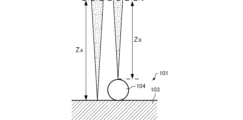
図6は、試料表面の高さを求める手法を説明するための図である。図6では、試料101が基板103上に球状の粒子104が配置されたものである例を示している。
FIG. 6 is a diagram for explaining a technique for obtaining the height of the sample surface. FIG. 6 shows an example in which the
照射条件CAの電子線でSEM像を撮影した場合、得られるSEM像では、基板103の表面が鮮明に観察できる。すなわち、このSEM像では、基板103の表面に焦点があっている。照射条件CAに基づいて焦点距離ZAを計算することで、基板103の表面の高さを求めることができる。
When an SEM image is taken with an electron beam under the irradiation condition CA , the surface of the
照射条件CBの電子線でSEM像を取得した場合、得られるSEM像では、粒子104の頂点が鮮明に観察できる。すなわち、このSEM像では、粒子104の頂点に焦点があっている。照射条件CBに基づいて焦点距離ZBを計算することで、粒子104の頂点の高さを求めることができる。
When an SEM image is obtained with the electron beam under the irradiation condition CB , the vertexes of the
また、焦点距離ZAと焦点距離ZBの差ZA-ZBを計算することによって、基板103の表面と粒子104の頂点との間の距離、すなわち、粒子104の高さを求めることができる。
Also, by calculating the difference ZA - ZB between the focal length ZA and the focal length ZB , the distance between the surface of the
2.1.3. 試料表面の形状の再構築
図7は、図6に示す試料101の傾斜マップM2を示す図である。
2.1.3. Reconstruction of Sample Surface Shape FIG. 7 is a diagram showing a gradient map M2 of the
図7に示す傾斜マップM2では、位置P1における試料表面の傾斜角度は、0°であり、位置P2における試料表面の傾斜角度は、+90°であり、位置P3における試料表面の傾斜角度は、+45°であり、位置P4における試料表面の傾斜角度は、0°であり、位置P5における試料表面の傾斜角度は、-45°であり、位置P6における試料表面の傾斜角度は、-90°であり、位置P7における試料表面の傾斜角度は、0°である。なお、位置P1および位置P7は、基板103上に位置し、位置P2および位置P6は、粒子104の側面に位置し、位置P4は粒子104の頂点に位置している。また、位置P3は、位置P2と位置P4の間に位置し、位置P5は、位置P4と位置P6の間に位置している。
In the tilt map M2 shown in FIG. 7, the tilt angle of the sample surface at position P1 is 0°, the tilt angle of the sample surface at position P2 is +90°, and the tilt angle of the sample surface at position P3 is +45°. , the tilt angle of the sample surface at position P4 is 0°, the tilt angle of the sample surface at position P5 is -45°, and the tilt angle of the sample surface at position P6 is -90°. , the tilt angle of the sample surface at position P7 is 0°. Positions P1 and P7 are positioned on the
このように、球状の粒子104の側面では、傾斜角度が+90°、-90°になる。
Thus, the side surfaces of the
図8は、傾斜マップM2から試料表面の形状を求めた結果の一例を示す図である。 FIG. 8 is a diagram showing an example of the result of determining the shape of the sample surface from the tilt map M2.
図3に示すように、2つの検出領域52,56の信号量の差に基づいて試料表面102の傾斜角度を求める場合、試料表面の傾斜角度が大きくなると、傾斜角度の変化に対して検出信号の信号量の変化が小さくなる。そのため、試料表面の傾斜角度が大きい箇所では誤差が大きくなり、図8に示すように、基板103の高さが粒子104の左右で異なったり、粒子104の形状が歪んだりしてしまう。
As shown in FIG. 3, when the tilt angle of the
このような問題に対して、傾斜マップM2から試料表面の形状を求める際に、図6で求
めた試料表面の高さで補正することによって、より正確に試料表面の形状を求めることができる。
To address such a problem, when obtaining the shape of the sample surface from the tilt map M2, it is possible to more accurately obtain the shape of the sample surface by correcting the height of the sample surface obtained in FIG.
図9は、焦点距離ZA、焦点距離ZB、および傾斜マップM2から試料表面の形状を求めた結果の一例を示す図である。 FIG. 9 is a diagram showing an example of the result of obtaining the shape of the sample surface from the focal length Z A , the focal length Z B , and the tilt map M2.
位置P1および位置P7における焦点距離ZAおよび位置P4における焦点距離ZBが求められているとする。このとき、位置P1および位置P7の値を焦点距離ZAとし、位置P4の値を焦点距離ZBとして、位置P1、位置P7、および位置P4を積分の計算の始点として、積分を行う。これにより、図9に示すように、より正確に試料表面の形状を求めることができる。 Suppose the focal length ZA at positions P1 and P7 and the focal length ZB at position P4 are desired. At this time, the values of the positions P1 and P7 are taken as the focal length ZA , the value of the position P4 is taken as the focal length ZB , and the positions P1, P7, and P4 are used as starting points for the calculation of integration, and integration is performed. Thereby, as shown in FIG. 9, the shape of the sample surface can be obtained more accurately.
2.2. 画像処理部の処理
2.2.1. 画像処理部の処理の流れ
図10は、画像処理部90の処理の一例を示すフローチャートである。
2.2. Processing of image processing unit 2.2.1. Flow of Processing by Image Processing Unit FIG. 10 is a flowchart showing an example of processing by the
画像処理部90は、図10に示すように、複数の検出領域52,54,56,58から出力される複数の検出信号に基づいて試料表面の傾斜角度を求める処理S10と、SEM像に基づいて試料表面の高さを求める処理S20と、試料表面の傾斜角度および試料表面の高さに基づいて試料表面の形状を再構築する処理S30と、を行う。なお、図10に示す例では、試料表面の傾斜角度を求める処理S10の後に、試料表面の高さを求める処理S20を行っているが、処理S20の後に、処理S10を行ってもよい。以下、各処理について詳細に説明する。
As shown in FIG. 10, the
2.2.2. 試料表面の傾斜角度を求める処理S10
画像処理部90は、複数の検出領域52,54,56,58から出力される複数の検出信号に基づいて試料表面の傾斜角度を求める。上述したように、走査電子顕微鏡100では、電子線で試料表面102を走査しながら、各照射位置において分割型検出器50を用いて反射電子を検出して、第1~第4検出信号を得ることができる。画像処理部90は、照射位置ごとに、第1~第4検出信号の信号量の差に基づいて試料表面の傾斜角度を計算する。これにより、傾斜マップM2を得ることができる。
2.2.2. Processing S10 for determining the tilt angle of the sample surface
The
2.2.3. 試料表面の高さを求める処理
画像処理部90は、異なる焦点位置で撮影された複数のSEM像に基づいて、試料表面の高さを計算する。
2.2.3. Processing for Obtaining Height of Sample Surface The
試料表面の高さは、互いに異なる焦点位置で撮影された複数のSEM像から求める。そのため、まず、視野中の任意の領域で像が鮮明に見えるように焦点位置を合わせる。このとき、焦点合わせは、既知のオートフォーカス技術を用いてもよいし、ユーザーが手動でフォーカスを合わせてもよい。視野中の任意の領域で焦点があったら、すなわち、視野中の任意の領域で像が鮮明に見えたら、SEM像を撮影する。そして、このときの電子線の照射条件から焦点距離を計算する。画像処理部90は、SEM像および焦点距離を記憶部84に記憶する。
The height of the sample surface is obtained from a plurality of SEM images taken at different focal positions. Therefore, first, the focal position is adjusted so that the image can be seen clearly in any region in the field of view. At this time, a known autofocus technique may be used for focusing, or the user may manually focus. A SEM image is taken when an arbitrary area in the field of view is in focus, that is, when an arbitrary area in the field of view is clearly visible. Then, the focal length is calculated from the irradiation conditions of the electron beam at this time. The
次に、画像処理部90は、焦点位置を変えて、同様にSEM像を撮影し焦点距離を求めて、SEM像および焦点距離を記憶部84に記憶する。焦点位置の変更は、例えば、対物レンズ24の励磁電流を変化させることで行う。焦点位置の変更は、対物レンズ24の励磁電流をあらかじめ設定された量だけ変化させることで行ってもよいし、先に撮影でフォーカスを合わせた領域とは異なる領域でフォーカスを合わせることで行ってもよい。
Next, the
このようにして、画像処理部90は、SEM像の撮影、焦点距離の計算、および焦点位置の変更を繰り返すことで、SEM像および焦点距離のデータを複数取得する。
In this manner, the
画像処理部90は、このようにして取得された、異なる焦点位置で撮影された複数のSEM像および各SEM像を撮影したときの焦点距離からZマップを作成する。
The
Zマップは、試料表面102の高さのマップである。Zマップでは、試料表面102の位置(座標)と、試料表面102の高さが対応付けられている。試料表面102の高さは、例えば、焦点距離に基づく値であり、焦点距離の値を試料表面102の高さとして用いてもよい。Zマップは、試料表面の全部の領域の高さを示しておらず、試料表面の一部の領域の高さを示している。
A Z map is a map of the height of the
ここで、試料の最も低い位置から試料の最も高い位置まで焦点位置を変化させてSEM像を取得すれば、視野中の全領域の焦点距離を求めることができる。しかしながら、高さが大きい試料では、多数のSEM像を撮影する必要があるため、時間がかかってしまう。また、組成が均一で平坦な領域では、合焦点しているか否かの判断が難しい。そのため、視野中に組成が均一で平坦な領域があると、焦点距離を求めることができない。よって、視野中のすべての領域で試料表面の高さを求めることは困難である。そのため、Zマップでは、試料表面の全部の領域の高さを示しておらず、試料表面の一部の領域の高さを示している。以下、Zマップの作成方法について具体的に説明する。 Here, if the focal position is changed from the lowest position of the sample to the highest position of the sample and an SEM image is acquired, the focal length of the entire area in the field of view can be obtained. However, for a sample with a large height, many SEM images need to be taken, which takes time. In addition, it is difficult to determine whether or not the focal point is achieved in a flat area having a uniform composition. Therefore, if there is a flat region with a uniform composition in the field of view, the focal length cannot be determined. Therefore, it is difficult to obtain the height of the sample surface over the entire field of view. Therefore, the Z map does not show the height of the entire region of the sample surface, but shows the height of a partial region of the sample surface. A method for creating a Z map will be specifically described below.
図11は、異なる焦点位置で撮影された3つのSEM像を示している。SEM像S1は、焦点距離Z=9.95で撮影されたSEM像であり、SEM像S2は焦点距離Z=10で撮影されたSEM像であり、SEM像S3は焦点距離Z=10.05で撮影されたSEM像である。 FIG. 11 shows three SEM images taken at different focal positions. The SEM image S1 is an SEM image taken at a focal length Z=9.95, the SEM image S2 is an SEM image taken at a focal length Z=10, and the SEM image S3 is an SEM image taken at a focal length Z=10.05. It is an SEM image taken at .
図12は、合焦点位置を求める手法を説明するための図である。 12A and 12B are diagrams for explaining a method of obtaining the in-focus position. FIG.
図12に示すように、SEM像を複数の小領域に分割し、各小領域内で焦点があった像(合焦点像)が得られているか否かを判断する。各小領域の大きさは、任意に設定可能である。各小領域内で合焦点像が得られているか否かは、例えば、小領域内の輝度のヒストグラムから判断できる。 As shown in FIG. 12, the SEM image is divided into a plurality of small regions, and it is determined whether or not an image (in-focus image) is obtained in each small region. The size of each small area can be set arbitrarily. Whether or not an in-focus image is obtained in each small area can be determined, for example, from a luminance histogram in the small area.
図13および図14は、小領域のヒストグラムの一例を示す図である。図13には、合焦点像が得られた小領域のヒストグラムを示し、図14には、合焦点像が得られていない小領域のヒストグラムを示している。 13 and 14 are diagrams showing examples of histograms of small regions. FIG. 13 shows the histogram of the small area from which the focused image was obtained, and FIG. 14 shows the histogram of the small area from which the focused image was not obtained.
図13に示すように、小領域内に合焦点像が得られている場合には、ヒストグラムにピークが現れる。これに対して、図14に示すように、小領域内に合焦点像が得られていない場合には、ヒストグラムには明瞭なピークが現れない。このように、小領域内の輝度のヒストグラムを取得し、当該ヒストグラムにピークがあるか否かで、小領域内に合焦点像が得られているか否かを判断できる。 As shown in FIG. 13, when a focused image is obtained within a small area, a peak appears in the histogram. On the other hand, as shown in FIG. 14, when the in-focus image is not obtained within the small area, the histogram does not show a clear peak. In this manner, it is possible to obtain a histogram of brightness within a small area and determine whether or not a focused image is obtained within the small area based on whether or not the histogram has a peak.
なお、小領域内に合焦点像が得られているか否かの判断の手法はこれに限定されない。例えば、小領域ごとにフーリエ変換を行って周波数成分に分解することによって、合焦点像が得られているか否かを判断してもよい。 Note that the method for determining whether or not a focused image is obtained within a small area is not limited to this. For example, it may be determined whether or not an in-focus image is obtained by performing Fourier transform for each small area and decomposing it into frequency components.
図12に示すSEM像S1の小領域A1では、図13に示すヒストグラムのように、ヒストグラムにピークが現れた。そのため、小領域A1において合焦点像が得られたと判断できる。これにより、小領域A1は、焦点距離Z=9.95で焦点があったと判断できる
。
In the small region A1 of the SEM image S1 shown in FIG. 12, a peak appeared in the histogram like the histogram shown in FIG. Therefore, it can be determined that a focused image is obtained in the small area A1. Thus, it can be determined that the small area A1 was in focus at the focal length Z=9.95.
図15は、ZマップM4の一例を示す図である。 FIG. 15 is a diagram showing an example of the Z map M4.
SEM像S1、SEM像S2、およびSEM像S3の各々について、小領域の分割、小領域内に合焦点像が得られているか否かの判定、および焦点距離の計算を繰り返すことで、図15に示すZマップM4を作成できる。ZマップM4では、合焦点像が得られたと判断された小領域に、焦点距離Zの情報が対応づけられている。ZマップM4では、すべてのSEM像において合焦点像が得られていないと判断された小領域には、焦点距離の情報がない。 For each of the SEM image S1, the SEM image S2, and the SEM image S3, division into small regions, determination of whether or not an in-focus image is obtained in the small region, and calculation of the focal length are repeated to obtain the image shown in FIG. can create a Z map M4 shown in . In the Z map M4, information on the focal length Z is associated with the small area where it is determined that the in-focus image has been obtained. In the Z map M4, there is no focal length information in a small area determined to have no in-focus image in all SEM images.
2.2.4. 試料表面の形状の再構築
画像処理部90は、処理S10で得られた試料表面の傾斜角度および処理S20で得られた試料表面の高さに基づいて、試料表面の形状を再構築する。
2.2.4. Reconstruction of Sample Surface Shape The
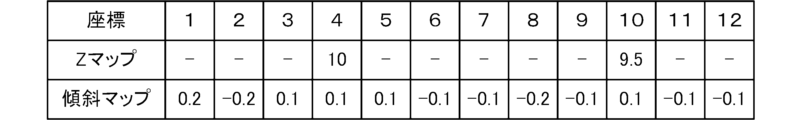
図16は、ZマップM4と傾斜マップM2を示す表である。図16では、便宜上、ZマップM4および傾斜マップM2を一次元のデータとして表している。図16に示す表において、座標は、SEM像の座標を表している。 FIG. 16 is a table showing the Z map M4 and the tilt map M2. In FIG. 16, the Z map M4 and the tilt map M2 are represented as one-dimensional data for convenience. In the table shown in FIG. 16, the coordinates represent the coordinates of the SEM image.
図16に示すZマップM4では、座標X=4で焦点距離Z=10、座標X=10で焦点距離Z=9.5が得られている。ZマップM4では、焦点距離Zが得られた座標のみ、その値が入力されており、焦点距離Zが得られていない座標には値が入力されていない。なお、焦点距離Zが得られていない座標に、焦点距離Zが得られていないことを示す値(例えば、「-1」)などが入力されていてもよい。 In the Z map M4 shown in FIG. 16, the focal length Z=10 is obtained at the coordinate X=4, and the focal length Z=9.5 is obtained at the coordinate X=10. In the Z map M4, only the coordinates for which the focal length Z has been obtained have their values entered, and the coordinates for which the focal length Z has not been obtained have no values entered. A value (eg, "-1") indicating that the focal length Z has not been obtained may be input to the coordinates for which the focal length Z has not been obtained.
図16に示す傾斜マップM2には、便宜上、試料表面の傾斜角度から求められた、右隣の座標で示す領域との高低差が入力されている。 In the tilt map M2 shown in FIG. 16, for the sake of convenience, the height difference with respect to the area indicated by the coordinates on the right, which is obtained from the tilt angle of the sample surface, is input.
図17~図19は、ZマップM4および傾斜マップM2から試料表面の形状を再構築する手法を説明するための表である。 17 to 19 are tables for explaining a method of reconstructing the shape of the sample surface from the Z map M4 and the tilt map M2.
まず、図17に示すように、焦点距離が得られている座標X=4および座標X=10において、表面形状の値R(すなわち、試料表面の高さを表す値)として、ZマップM4の焦点距離を採用する。ZマップM4で得られた値は、傾斜マップM2の値に比べて、信頼性が高いためである。 First, as shown in FIG. 17, at the coordinates X=4 and X=10 where the focal length is obtained, the surface shape value R (that is, the value representing the height of the sample surface) of the Z map M4 is Adopt focal length. This is because the values obtained from the Z map M4 are more reliable than the values from the tilt map M2.
次に、図18に示すように、座標X=4の隣の座標である座標X=3および座標X=5において、座標X=4における表面形状の値Rおよび傾斜マップM2の傾斜角度の値に基づいて、表面形状の値Rを求める。具体的には、座標X=3では、座標X=4における表面形状の値R=10から、座標X=3の傾斜マップM2の値を引いて、表面形状の値R=9.9とする。同様に、座標X=5では、座標X=4における表面形状の値R=10に、座標X=5の傾斜マップM2の値を足して、表面形状の値R=10.1とする。 Next, as shown in FIG. 18, at the coordinate X=3 and the coordinate X=5, which are the coordinates next to the coordinate X=4, the surface shape value R at the coordinate X=4 and the tilt angle value of the tilt map M2 Based on, the value R of the surface shape is obtained. Specifically, at the coordinate X=3, the surface shape value R=9.9 is obtained by subtracting the value of the gradient map M2 at the coordinate X=3 from the surface shape value R=10 at the coordinate X=4. . Similarly, at the coordinate X=5, the surface shape value R=10 at the coordinate X=4 is added to the surface shape value R=10.1 at the coordinate X=5 in the gradient map M2.
座標X=10の隣の座標である座標X=9および座標X=11についても、同様に、表面形状の値Rを求める。 For the coordinates X=9 and X=11, which are the coordinates next to the coordinate X=10, the surface shape value R is similarly obtained.
上記の処理を繰り返して、SEM像の全部の座標(画素)について表面形状の値を求めることで、図19に示すように、試料表面の形状を再構築できる。 By repeating the above process to find the surface shape values for all the coordinates (pixels) of the SEM image, the shape of the sample surface can be reconstructed as shown in FIG.
なお、ここでは、ZマップM4および傾斜マップM2が一次元のデータである場合につ
いて説明したが、ZマップM4および傾斜マップM2が二次元のデータである場合も同様の手法で、表面形状を再構築できる。
Although the case where the Z map M4 and the tilt map M2 are one-dimensional data has been described here, the same method can be used to reproduce the surface shape when the Z map M4 and the tilt map M2 are two-dimensional data. can build.
以上の処理により、画像処理部90は、試料101の試料表面の形状を再構築できる。
Through the above processing, the
画像処理部90は、処理S30の後、試料101の試料表面の形状を再構築した画像を、表示部82に表示する。
After processing S30, the
3. 効果
走査電子顕微鏡100では、画像処理部90は、複数の検出信号に基づいて試料表面の傾斜角度を求める処理と、SEM像に基づいて試料表面の高さを求める処理と、試料表面の傾斜角度および試料表面の高さに基づいて試料表面の形状を再構築する処理と、を行う。そのため、走査電子顕微鏡100では、例えば、試料表面の傾斜角度のみから試料表面の形状を再構築する場合と比べて、より正確に試料表面の構造を再構築できる。
3. Effect In the
上述したように、傾斜マップM2では、試料表面の傾斜角度が大きくなると、誤差が大きくなる。走査電子顕微鏡100では、この誤差を試料表面の高さで補正できる。そのため、より正確に試料表面の形状を再構築できる。さらに、走査電子顕微鏡100では、試料表面の高さの情報を用いることによって、試料表面の高低差を正確に求めることができる。
As described above, in the tilt map M2, the error increases as the tilt angle of the sample surface increases. In the
走査電子顕微鏡100では、画像処理部90は、試料表面の高さを求める処理において、SEM像に基づいて、試料101の第1領域の試料表面の高さを求め、試料表面の形状を再構築する処理において、第1領域の試料表面の高さおよび試料表面の傾斜角度に基づいて、第1領域と隣り合う第2領域の試料表面の高さを求める。そのため、走査電子顕微鏡100では、すべての領域の試料表面の高さを求めなくても、正確に試料表面の形状を再構築できる。
In the
走査電子顕微鏡100では、画像処理部90は、試料表面の高さを求める処理において、SEM像を複数の小領域に分割し、複数の小領域の各々において焦点があった像である合焦点像が得られた否かを判定し、電子線の照射条件に基づいてSEM像を撮影したときの焦点距離を計算し、計算された焦点距離に基づいて合焦点像が得られた小領域における試料表面の高さを求める。このように、走査電子顕微鏡100では、SEM像から試料表面の高さを求めることができる。
In the
走査電子顕微鏡100では、画像処理部90は、第1走査像を取得する処理と、第1走査像とは異なる電子線の焦点位置で撮影された第2走査像を取得する処理と、を行い、試料表面の高さを求める処理において、第1走査像および第2走査像に基づいて試料表面の高さを計算する。そのため、走査電子顕微鏡100では、試料表面の高さを正確に求めることができる。
In the
走査電子顕微鏡100では、第1走査像および第2走査像は二次電子像である。ここで、二次電子像を検出する二次電子検出器40は、例えば、シンチレーターと、光電子増倍管と、を含む検出器である。このような検出器は、例えば、半導体検出器と比べて、応答が速く短時間で像を取得できる。そのため、異なる焦点位置で撮影されたSEM像を複数取得する場合でも、測定時間を短くできる。
In
走査電子顕微鏡100における画像処理方法は、複数の検出信号に基づいて試料表面の傾斜角度を求める工程と、SEM像に基づいて試料表面の高さを求める工程と、試料表面の傾斜角度および試料表面の高さに基づいて試料表面の形状を再構築する工程と、を含む
。そのため、例えば、試料表面の傾斜角度から試料表面の形状を再構築する場合と比べて、より正確に試料表面の形状を再構築できる。
The image processing method in the
4. 変形例
なお、本発明は上述した実施形態に限定されず、本発明の要旨の範囲内で種々の変形実施が可能である。
4. Modifications The present invention is not limited to the above-described embodiments, and various modifications can be made within the scope of the gist of the present invention.
4.1. 第1変形例
上述した実施形態では、各小領域内で合焦点像が得られているか否かは、小領域内の輝度のヒストグラムから判断したが、合焦点像が得られているか否かを判断する手法はこれに限定されない。
4.1. First Modification In the above-described embodiment, whether or not an in-focus image is obtained in each small area is determined from the luminance histogram in the small area. The judging method is not limited to this.
例えば、焦点位置を等間隔で変化させて取得した複数のSEM像において、SEM像の座標(X,Y)と、その座標における焦点距離Zが対応付けられているデータであるXYZデータを取得する。次に、このXYZデータからX-Z画像を生成する。 For example, in a plurality of SEM images obtained by changing the focal position at equal intervals, XYZ data, which is data in which the coordinates (X, Y) of the SEM images are associated with the focal length Z at the coordinates, is obtained. . Next, an XZ image is generated from this XYZ data.
図20は、X-Z画像を示す図である。図20に示すX-Z画像において、横方向はXデータを表し、縦方向はZデータを表している。 FIG. 20 is a diagram showing an XZ image. In the XZ image shown in FIG. 20, the horizontal direction represents X data, and the vertical direction represents Z data.
図20に示すように、X-Z画像では、合焦点位置を頂点とした円錐形を上下につなげた形状が確認できる。これは、電子線の焦点付近の形状と試料形状が重畳されたものである。そのため、この電子線の焦点付近の形状と取得したXYZデータを逆畳み込み計算することによって、焦点位置を求めることができる。 As shown in FIG. 20, in the XZ image, a conical shape with the in-focus position as the apex connected vertically can be confirmed. This is a superposition of the shape near the focal point of the electron beam and the sample shape. Therefore, the focal position can be obtained by deconvolving the shape near the focal point of the electron beam and the obtained XYZ data.
この手法では、焦点距離を求めることができる領域は、SEM像でコントラストがつく構造がある領域のみである。 In this method, the only area where the focal length can be obtained is the area where there is a structure with contrast in the SEM image.
図21は、逆畳み込み計算で求められたZマップM4を示す図である。 FIG. 21 is a diagram showing a Z map M4 obtained by deconvolution calculation.
図21に示すように、逆畳み込み計算で焦点位置を求めることが可能な領域は、ヒストグラムから求めた場合と同様に、SEM像の一部の領域である。 As shown in FIG. 21, the area where the focal position can be obtained by the deconvolution calculation is a partial area of the SEM image, as in the case of obtaining it from the histogram.
4.2. 第2変形例
上述した実施形態では、図17~図19に示すように、ZマップM4で焦点距離Zが得られた座標を始点として、傾斜マップM2を用いて表面形状の値を求めた。
4.2. Second Modification In the above-described embodiment, as shown in FIGS. 17 to 19, the surface shape values are obtained using the tilt map M2, starting from the coordinates where the focal length Z is obtained in the Z map M4.
ここで、ZマップM4において複数の座標で焦点距離Zが求められている場合、焦点距離Zが求められた各座標を始点として表面形状の値を求めていくと、始点ごとに表面形状の値が異なる場合がある。 Here, when the focal length Z is obtained at a plurality of coordinates in the Z map M4, if the surface shape value is obtained with each coordinate at which the focal length Z was obtained as the starting point, the surface shape value may differ.
図22は、ZマップM4および傾斜マップM2から試料の表面形状を再構築する手法の一例を説明するための表である。 FIG. 22 is a table for explaining an example of a method of reconstructing the surface shape of the sample from the Z map M4 and the tilt map M2.
図22に示すように、座標X=4を始点として表面形状の値を求めた表面形状Aと、座標X=10を始点として表面形状の値を求めた表面形状Bでは、同じ座標であっても表面形状の値が異なっている。 As shown in FIG. 22, the surface shape A whose starting point is the coordinate X=4 and the surface shape B whose starting point is the coordinate X=10 have the same coordinates. also have different surface morphology values.
ここで、上述したように、傾斜マップM2では、試料表面の傾斜角度が大きいほど値の信頼性が低い。このことを利用して、図22に示す表から表面形状を求める。 Here, as described above, in the tilt map M2, the greater the tilt angle of the sample surface, the lower the reliability of the value. Using this fact, the surface shape is obtained from the table shown in FIG.
具体的には、まず、図22に示すように、座標X=4を始点として表面形状の値を求めて表面形状Aを算出し、座標X=10を始点として表面形状の値を求めて表面形状Bを算出する。次に、表面形状Aの信頼性、および表面形状Bの信頼性を評価する。 Specifically, first, as shown in FIG. 22, the surface shape value is calculated with the coordinate X=4 as the starting point, and the surface shape A is calculated. A shape B is calculated. Next, the reliability of surface shape A and the reliability of surface shape B are evaluated.
信頼性の評価は、傾斜角度の大きさに応じて誤差の大きさを設定し、表面形状を求める際の積分過程で蓄積される誤差(以下、「累積誤差」ともいう)の大きさを計算することで行う。上述したように傾斜角度が大きくなるほど誤差が大きくなることから、傾斜角度に対する誤差の大きさは、傾斜マップM2の値の絶対値とする。 To evaluate reliability, set the size of the error according to the size of the tilt angle, and calculate the size of the error (hereinafter also referred to as "accumulated error") accumulated in the integration process when obtaining the surface shape. Do it by doing Since the error increases as the tilt angle increases as described above, the magnitude of the error with respect to the tilt angle is the absolute value of the tilt map M2.
図22に示す例では、座標X=4では、ZマップM4の値がそのまま表面形状の値として用いられるため、累積誤差は「0」となる。座標X=3では、傾斜マップM2の値の絶対値を、座標X=4の累積誤差に足して、累積誤差は「0.1」となる。また、座標X=2では、傾斜マップM2の値の絶対値を座標X=3の累積誤差に足して累積誤差は「0.3」となる。これを繰り返して、各座標の累積誤差を求める。 In the example shown in FIG. 22, at the coordinate X=4, the value of the Z map M4 is used as it is as the value of the surface shape, so the cumulative error is "0". At coordinate X=3, the absolute value of the value of the gradient map M2 is added to the accumulated error at coordinate X=4, resulting in an accumulated error of "0.1". At the coordinate X=2, the absolute value of the value of the gradient map M2 is added to the accumulated error at the coordinate X=3, resulting in a cumulative error of "0.3". This is repeated to obtain the cumulative error of each coordinate.
同様に、座標X=10を始点として求めた表面形状Bについても、各座標の累積誤差を求める。 Similarly, for the surface shape B determined with the coordinate X=10 as the starting point, the cumulative error of each coordinate is determined.
ここで、各座標において、累積誤差が小さいほど、実際の表面形状を反映しているといえる。そのため、座標ごとに累積誤差を比較し、累積誤差の小さい方の表面形状の値を、最終的な表面形状の値とする。図22に示す例では、座標1~8は表面形状Aの値を採用し、座標9~12は表面形状Bの値を採用している。
Here, at each coordinate, it can be said that the smaller the cumulative error, the more the actual surface shape is reflected. Therefore, the accumulated errors are compared for each coordinate, and the surface shape value with the smaller accumulated error is used as the final surface shape value. In the example shown in FIG. 22, the
なお、試料表面の形状を再構築する手法は、上記の例に限定されない。上記では、表面形状の値として累積誤差の小さい方の値を採用したが、例えば、加重平均を用いて信頼性に応じて重みをつけて、表面形状Aの値と表面形状Bの値の平均値を、表面形状の値として採用してもよい。また、傾斜マップM2だけでなくZマップM4に関しても信頼性を評価し、ZマップM4の値と傾斜マップM2の値のどちらを採用するかを決定してもよい。 Note that the method of reconstructing the shape of the sample surface is not limited to the above example. In the above, the value of the surface shape with the smaller accumulated error is adopted as the value of the surface shape. value may be taken as the surface figure value. Further, the reliability of not only the tilt map M2 but also the Z map M4 may be evaluated, and it may be determined which of the values of the Z map M4 and the values of the tilt map M2 should be adopted.
4.3. 第3変形例
上述した実施形態では、本発明に係る荷電粒子線装置が走査電子顕微鏡である場合について説明したが、本発明に係る荷電粒子線装置は、走査電子顕微鏡に限定されない。本発明に係る荷電粒子線装置は、例えば、試料にイオンビームを照射して、試料から放出される電子を検出して走査像を取得する集束イオンビーム装置であってもよい。
4.3. Third Modification In the above-described embodiments, the charged particle beam device according to the present invention is a scanning electron microscope, but the charged particle beam device according to the present invention is not limited to a scanning electron microscope. The charged particle beam device according to the present invention may be, for example, a focused ion beam device that irradiates a sample with an ion beam and detects electrons emitted from the sample to acquire a scanning image.
なお、上述した実施形態及び変形例は一例であって、これらに限定されるわけではない。例えば各実施形態及び各変形例は、適宜組み合わせることが可能である。 It should be noted that the above-described embodiments and modifications are examples, and the present invention is not limited to these. For example, each embodiment and each modification can be combined as appropriate.
本発明は、上述した実施形態に限定されるものではなく、さらに種々の変形が可能である。例えば、本発明は、実施形態で説明した構成と実質的に同一の構成を含む。実質的に同一の構成とは、例えば、機能、方法、及び結果が同一の構成、あるいは目的及び効果が同一の構成である。また、本発明は、実施形態で説明した構成の本質的でない部分を置き換えた構成を含む。また、本発明は、実施形態で説明した構成と同一の作用効果を奏する構成又は同一の目的を達成することができる構成を含む。また、本発明は、実施形態で説明した構成に公知技術を付加した構成を含む。 The present invention is not limited to the above-described embodiments, and various modifications are possible. For example, the present invention includes configurations that are substantially the same as the configurations described in the embodiments. "Substantially the same configuration" means, for example, a configuration having the same function, method, and result, or a configuration having the same purpose and effect. Moreover, the present invention includes configurations in which non-essential portions of the configurations described in the embodiments are replaced. In addition, the present invention includes a configuration that achieves the same effects as the configurations described in the embodiments or a configuration that can achieve the same purpose. In addition, the present invention includes configurations obtained by adding known techniques to the configurations described in the embodiments.
10…電子源、20…照射光学系、22…収束レンズ、24…対物レンズ、26…走査偏向器、30…試料ステージ、40…二次電子検出器、50…分割型検出器、52…第1検出領域、54…第2検出領域、56…第3検出領域、58…第4検出領域、60…走査信
号発生器、61…増幅器、62…増幅器、63…増幅器、64…増幅器、65…増幅器、66…信号調整器、70…信号取得部、72…信号変換器、80…操作部、82…表示部、84…記憶部、90…画像処理部、100…走査電子顕微鏡
DESCRIPTION OF
Claims (6)
前記荷電粒子線を放出する荷電粒子線源と、
前記荷電粒子線で前記試料を走査する照射光学系と、
前記試料から放出された荷電粒子を検出する複数の検出部と、
前記複数の検出部から出力される複数の検出信号に基づいて、試料表面の形状を再構築する画像処理部と、
を含み、
前記画像処理部は、
前記複数の検出信号に基づいて、前記試料表面の傾斜角度を求める処理と、
前記走査像に基づいて、前記試料表面の高さを求める処理と、
前記試料表面の傾斜角度および前記試料表面の高さに基づいて、前記試料表面の形状を再構築する処理と、
を行い、
前記画像処理部は、
前記試料表面の高さを求める処理において、
前記走査像に基づいて、前記試料の第1領域の前記試料表面の高さを求め、
前記試料表面の形状を再構築する処理において、
前記第1領域の前記試料表面の高さおよび前記試料表面の傾斜角度に基づいて、前記第1領域と隣り合う第2領域の前記試料表面の高さを求める、荷電粒子線装置。 A charged particle beam device that scans a sample with a charged particle beam and detects charged particles emitted from the sample to obtain a scanned image,
a charged particle beam source that emits the charged particle beam;
an irradiation optical system that scans the sample with the charged particle beam;
a plurality of detection units that detect charged particles emitted from the sample;
an image processing unit that reconstructs the shape of the sample surface based on the plurality of detection signals output from the plurality of detection units;
including
The image processing unit
a process of determining the tilt angle of the sample surface based on the plurality of detection signals;
a process of obtaining the height of the sample surface based on the scanned image;
a process of reconstructing the shape of the sample surface based on the tilt angle of the sample surface and the height of the sample surface;
and
The image processing unit
In the process of obtaining the height of the sample surface,
Obtaining the height of the sample surface in the first region of the sample based on the scanned image;
In the process of reconstructing the shape of the sample surface,
A charged particle beam apparatus, wherein the height of the sample surface in a second region adjacent to the first region is determined based on the height of the sample surface in the first region and the tilt angle of the sample surface.
前記画像処理部は、
前記試料表面の高さを求める処理において、
前記走査像を複数の小領域に分割し、
前記複数の小領域の各々において、焦点があった像である合焦点像が得られた否かを判定し、
前記荷電粒子線の照射条件に基づいて前記走査像を撮影したときの焦点距離を計算し、
計算された前記焦点距離に基づいて前記合焦点像が得られた小領域における前記試料表面の高さを求める、荷電粒子線装置。 In claim 1 ,
The image processing unit
In the process of obtaining the height of the sample surface,
dividing the scanned image into a plurality of small regions;
Determining whether an in-focus image, which is an image in focus, is obtained in each of the plurality of small regions;
calculating a focal length when the scanning image is captured based on the irradiation conditions of the charged particle beam;
A charged particle beam apparatus for determining the height of the sample surface in the small area where the focused image was obtained based on the calculated focal length.
前記画像処理部は、
前記荷電粒子線で前記試料を走査して得られた、第1走査像を取得する処理と、
前記荷電粒子線で前記試料を走査して得られた、前記第1走査像とは異なる前記荷電粒子線の焦点位置で撮影された第2走査像を取得する処理と、
を行い、
前記試料表面の高さを求める処理において、前記第1走査像および前記第2走査像に基づいて、前記試料表面の高さを求める、荷電粒子線装置。 In claim 1 or 2 ,
The image processing unit
a process of acquiring a first scanned image obtained by scanning the sample with the charged particle beam;
a process of acquiring a second scanned image captured at a focal position of the charged particle beam different from the first scanned image obtained by scanning the sample with the charged particle beam;
and
A charged particle beam apparatus, wherein in the process of obtaining the height of the sample surface, the height of the sample surface is obtained based on the first scanned image and the second scanned image.
前記試料から放出された二次電子を検出する二次電子検出器を含み、
前記走査像は、二次電子像である、荷電粒子線装置。 In any one of claims 1 to 3 ,
a secondary electron detector that detects secondary electrons emitted from the sample;
A charged particle beam apparatus, wherein the scanned image is a secondary electron image.
前記複数の検出部は、光軸に関して対称に配置されている、荷電粒子線装置。 In any one of claims 1 to 4 ,
The charged particle beam device, wherein the plurality of detection units are arranged symmetrically with respect to the optical axis.
前記荷電粒子線で試料を走査する照射光学系と、
前記試料から放出された荷電粒子を検出する複数の検出部と、
を含む荷電粒子線装置における画像取得方法であって、
前記複数の検出部から出力される複数の検出信号に基づいて、試料表面の傾斜角度を求める工程と、
前記荷電粒子線で前記試料上を走査し、前記試料から放出される荷電粒子を検出して走査像を取得する工程と、
前記走査像に基づいて、前記試料表面の高さを求める工程と、
前記試料表面の傾斜角度および前記試料表面の高さに基づいて、前記試料表面の形状を再構築する工程と、
を含み、
前記試料表面の高さを求める工程において、
前記走査像に基づいて、前記試料の第1領域の前記試料表面の高さを求め、
前記試料表面の形状を再構築する工程において、
前記第1領域の前記試料表面の高さおよび前記試料表面の傾斜角度に基づいて、前記第1領域と隣り合う第2領域の前記試料表面の高さを求める、画像取得方法。 a charged particle beam source that emits a charged particle beam;
an irradiation optical system for scanning a sample with the charged particle beam;
a plurality of detection units that detect charged particles emitted from the sample;
An image acquisition method in a charged particle beam device comprising
determining the tilt angle of the sample surface based on the plurality of detection signals output from the plurality of detection units ;
a step of scanning the sample with the charged particle beam and detecting charged particles emitted from the sample to obtain a scanned image;
determining the height of the sample surface based on the scanned image;
reconstructing the shape of the sample surface based on the tilt angle of the sample surface and the height of the sample surface;
including
In the step of obtaining the height of the sample surface,
Obtaining the height of the sample surface in the first region of the sample based on the scanned image;
In the step of reconstructing the shape of the sample surface,
An image acquisition method, wherein the height of the sample surface in a second region adjacent to the first region is obtained based on the height of the sample surface in the first region and the tilt angle of the sample surface.
Priority Applications (3)
| Application Number | Priority Date | Filing Date | Title |
|---|---|---|---|
| JP2021093570A JP7323574B2 (en) | 2021-06-03 | 2021-06-03 | Charged particle beam device and image acquisition method |
| EP22175923.6A EP4099359A1 (en) | 2021-06-03 | 2022-05-27 | Charged particle beam apparatus and image acquiring method |
| US17/831,144 US20220392738A1 (en) | 2021-06-03 | 2022-06-02 | Charged Particle Beam Apparatus and Image Acquiring Method |
Applications Claiming Priority (1)
| Application Number | Priority Date | Filing Date | Title |
|---|---|---|---|
| JP2021093570A JP7323574B2 (en) | 2021-06-03 | 2021-06-03 | Charged particle beam device and image acquisition method |
Publications (2)
| Publication Number | Publication Date |
|---|---|
| JP2022185757A JP2022185757A (en) | 2022-12-15 |
| JP7323574B2 true JP7323574B2 (en) | 2023-08-08 |
Family
ID=81851299
Family Applications (1)
| Application Number | Title | Priority Date | Filing Date |
|---|---|---|---|
| JP2021093570A Active JP7323574B2 (en) | 2021-06-03 | 2021-06-03 | Charged particle beam device and image acquisition method |
Country Status (3)
| Country | Link |
|---|---|
| US (1) | US20220392738A1 (en) |
| EP (1) | EP4099359A1 (en) |
| JP (1) | JP7323574B2 (en) |
Citations (5)
| Publication number | Priority date | Publication date | Assignee | Title |
|---|---|---|---|---|
| JP2002203507A (en) | 2000-12-28 | 2002-07-19 | Shimadzu Corp | Concavoconvex image forming device and electron beam analyzer |
| JP2005005055A (en) | 2003-06-10 | 2005-01-06 | Hitachi High-Technologies Corp | Information acquisition method for height of test piece |
| US20080283766A1 (en) | 2007-05-15 | 2008-11-20 | Jeol Ltd. | Autofocus Method for Scanning Charged-Particle Beam Instrument |
| JP2013114893A (en) | 2011-11-29 | 2013-06-10 | Hitachi High-Technologies Corp | Scanning electron microscope, and automatic focusing method for the same |
| JP2013161795A (en) | 2012-02-02 | 2013-08-19 | Applied Materials Israel Ltd | Three-dimensional mapping using scanning electron microscope images |
Family Cites Families (5)
| Publication number | Priority date | Publication date | Assignee | Title |
|---|---|---|---|---|
| JPS63215910A (en) * | 1987-03-04 | 1988-09-08 | Erionikusu:Kk | Section measurement |
| JPS6473209A (en) * | 1987-09-16 | 1989-03-17 | Erionikusu Kk | Method for measuring cross-sectional profile |
| JP4231831B2 (en) * | 2004-08-30 | 2009-03-04 | 株式会社日立ハイテクノロジーズ | Scanning electron microscope |
| JP5371928B2 (en) * | 2010-10-28 | 2013-12-18 | 株式会社日立ハイテクノロジーズ | Defect inspection method and apparatus |
| JP6851345B2 (en) | 2018-05-24 | 2021-03-31 | 日本電子株式会社 | Charged particle beam device and image acquisition method |
-
2021
- 2021-06-03 JP JP2021093570A patent/JP7323574B2/en active Active
-
2022
- 2022-05-27 EP EP22175923.6A patent/EP4099359A1/en active Pending
- 2022-06-02 US US17/831,144 patent/US20220392738A1/en active Pending
Patent Citations (6)
| Publication number | Priority date | Publication date | Assignee | Title |
|---|---|---|---|---|
| JP2002203507A (en) | 2000-12-28 | 2002-07-19 | Shimadzu Corp | Concavoconvex image forming device and electron beam analyzer |
| JP2005005055A (en) | 2003-06-10 | 2005-01-06 | Hitachi High-Technologies Corp | Information acquisition method for height of test piece |
| US20080283766A1 (en) | 2007-05-15 | 2008-11-20 | Jeol Ltd. | Autofocus Method for Scanning Charged-Particle Beam Instrument |
| JP2008311216A (en) | 2007-05-15 | 2008-12-25 | Jeol Ltd | Autofocus method of scanning charged-particle beam device |
| JP2013114893A (en) | 2011-11-29 | 2013-06-10 | Hitachi High-Technologies Corp | Scanning electron microscope, and automatic focusing method for the same |
| JP2013161795A (en) | 2012-02-02 | 2013-08-19 | Applied Materials Israel Ltd | Three-dimensional mapping using scanning electron microscope images |
Also Published As
| Publication number | Publication date |
|---|---|
| US20220392738A1 (en) | 2022-12-08 |
| EP4099359A1 (en) | 2022-12-07 |
| JP2022185757A (en) | 2022-12-15 |
Similar Documents
| Publication | Publication Date | Title |
|---|---|---|
| WO2016121265A1 (en) | Sample observation method and sample observation device | |
| JP2010062106A (en) | Scanning charged particle microscope device, and method of processing image acquired by the same | |
| TWI776085B (en) | Method and apparatus for monitoring beam profile and power | |
| US10340118B2 (en) | Scanning transmission electron microscope and method of image generation | |
| US10720304B2 (en) | Charged particle beam apparatus and image acquisition method | |
| KR20210060644A (en) | Multi-beam electronic characterization tool with telecentric illumination | |
| JP7323574B2 (en) | Charged particle beam device and image acquisition method | |
| JP6770482B2 (en) | Charged particle beam device and scanning image distortion correction method | |
| EP4067886A1 (en) | Method and system to determine crystal structure | |
| JP2012204041A (en) | Electron microscope and three-dimensional image construction method | |
| CN111146062B (en) | Electron microscope and image processing method | |
| JP6851345B2 (en) | Charged particle beam device and image acquisition method | |
| US9035247B2 (en) | Method for operating a particle beam device and/or for analyzing an object in a particle beam device | |
| JP6595856B2 (en) | Charged particle apparatus and measurement method | |
| JP2006172919A (en) | Scanning electron microscope having three-dimensional shape analysis function | |
| JP2019129072A (en) | Scan electronic microscope and method for measuring the same | |
| TWI836541B (en) | Non-transitory computer-readable medium and system for monitoring a beam in an inspection system | |
| JP2007324467A (en) | Pattern inspection method and its device | |
| JP2007287561A (en) | Charged particle beam device | |
| JP5500868B2 (en) | Scanning electron microscope and image display method in scanning electron microscope | |
| JP2023007094A (en) | scanning electron microscope | |
| JP2021176143A (en) | Scanning transmission electron microscope and adjustment method of optical system | |
| JP2019121588A (en) | Charged particle beam apparatus and analysis method | |
| JP2022055463A (en) | Charged particle beam device and sample observation method using the same | |
| JP2019039765A (en) | Charged particle beam device |
Legal Events
| Date | Code | Title | Description |
|---|---|---|---|
| A621 | Written request for application examination |
Free format text: JAPANESE INTERMEDIATE CODE: A621 Effective date: 20220908 |
|
| A977 | Report on retrieval |
Free format text: JAPANESE INTERMEDIATE CODE: A971007 Effective date: 20230424 |
|
| A131 | Notification of reasons for refusal |
Free format text: JAPANESE INTERMEDIATE CODE: A131 Effective date: 20230502 |
|
| A521 | Request for written amendment filed |
Free format text: JAPANESE INTERMEDIATE CODE: A523 Effective date: 20230628 |
|
| TRDD | Decision of grant or rejection written | ||
| A01 | Written decision to grant a patent or to grant a registration (utility model) |
Free format text: JAPANESE INTERMEDIATE CODE: A01 Effective date: 20230711 |
|
| A61 | First payment of annual fees (during grant procedure) |
Free format text: JAPANESE INTERMEDIATE CODE: A61 Effective date: 20230727 |
|
| R150 | Certificate of patent or registration of utility model |
Ref document number: 7323574 Country of ref document: JP Free format text: JAPANESE INTERMEDIATE CODE: R150 |