JP7323330B2 - Substrate processing method and substrate processing apparatus - Google Patents
Substrate processing method and substrate processing apparatus Download PDFInfo
- Publication number
- JP7323330B2 JP7323330B2 JP2019090801A JP2019090801A JP7323330B2 JP 7323330 B2 JP7323330 B2 JP 7323330B2 JP 2019090801 A JP2019090801 A JP 2019090801A JP 2019090801 A JP2019090801 A JP 2019090801A JP 7323330 B2 JP7323330 B2 JP 7323330B2
- Authority
- JP
- Japan
- Prior art keywords
- substrate
- chamber
- film
- processing apparatus
- plasma
- Prior art date
- Legal status (The legal status is an assumption and is not a legal conclusion. Google has not performed a legal analysis and makes no representation as to the accuracy of the status listed.)
- Active
Links
Images


Classifications
-
- H—ELECTRICITY
- H01—ELECTRIC ELEMENTS
- H01L—SEMICONDUCTOR DEVICES NOT COVERED BY CLASS H10
- H01L21/00—Processes or apparatus adapted for the manufacture or treatment of semiconductor or solid state devices or of parts thereof
- H01L21/02—Manufacture or treatment of semiconductor devices or of parts thereof
- H01L21/02104—Forming layers
- H01L21/02107—Forming insulating materials on a substrate
- H01L21/02225—Forming insulating materials on a substrate characterised by the process for the formation of the insulating layer
- H01L21/0226—Forming insulating materials on a substrate characterised by the process for the formation of the insulating layer formation by a deposition process
- H01L21/02263—Forming insulating materials on a substrate characterised by the process for the formation of the insulating layer formation by a deposition process deposition from the gas or vapour phase
- H01L21/02271—Forming insulating materials on a substrate characterised by the process for the formation of the insulating layer formation by a deposition process deposition from the gas or vapour phase deposition by decomposition or reaction of gaseous or vapour phase compounds, i.e. chemical vapour deposition
- H01L21/02274—Forming insulating materials on a substrate characterised by the process for the formation of the insulating layer formation by a deposition process deposition from the gas or vapour phase deposition by decomposition or reaction of gaseous or vapour phase compounds, i.e. chemical vapour deposition in the presence of a plasma [PECVD]
-
- C—CHEMISTRY; METALLURGY
- C23—COATING METALLIC MATERIAL; COATING MATERIAL WITH METALLIC MATERIAL; CHEMICAL SURFACE TREATMENT; DIFFUSION TREATMENT OF METALLIC MATERIAL; COATING BY VACUUM EVAPORATION, BY SPUTTERING, BY ION IMPLANTATION OR BY CHEMICAL VAPOUR DEPOSITION, IN GENERAL; INHIBITING CORROSION OF METALLIC MATERIAL OR INCRUSTATION IN GENERAL
- C23C—COATING METALLIC MATERIAL; COATING MATERIAL WITH METALLIC MATERIAL; SURFACE TREATMENT OF METALLIC MATERIAL BY DIFFUSION INTO THE SURFACE, BY CHEMICAL CONVERSION OR SUBSTITUTION; COATING BY VACUUM EVAPORATION, BY SPUTTERING, BY ION IMPLANTATION OR BY CHEMICAL VAPOUR DEPOSITION, IN GENERAL
- C23C16/00—Chemical coating by decomposition of gaseous compounds, without leaving reaction products of surface material in the coating, i.e. chemical vapour deposition [CVD] processes
- C23C16/44—Chemical coating by decomposition of gaseous compounds, without leaving reaction products of surface material in the coating, i.e. chemical vapour deposition [CVD] processes characterised by the method of coating
- C23C16/52—Controlling or regulating the coating process
-
- H—ELECTRICITY
- H01—ELECTRIC ELEMENTS
- H01L—SEMICONDUCTOR DEVICES NOT COVERED BY CLASS H10
- H01L21/00—Processes or apparatus adapted for the manufacture or treatment of semiconductor or solid state devices or of parts thereof
- H01L21/02—Manufacture or treatment of semiconductor devices or of parts thereof
- H01L21/02104—Forming layers
- H01L21/02107—Forming insulating materials on a substrate
- H01L21/02225—Forming insulating materials on a substrate characterised by the process for the formation of the insulating layer
- H01L21/0226—Forming insulating materials on a substrate characterised by the process for the formation of the insulating layer formation by a deposition process
- H01L21/02263—Forming insulating materials on a substrate characterised by the process for the formation of the insulating layer formation by a deposition process deposition from the gas or vapour phase
- H01L21/02271—Forming insulating materials on a substrate characterised by the process for the formation of the insulating layer formation by a deposition process deposition from the gas or vapour phase deposition by decomposition or reaction of gaseous or vapour phase compounds, i.e. chemical vapour deposition
- H01L21/0228—Forming insulating materials on a substrate characterised by the process for the formation of the insulating layer formation by a deposition process deposition from the gas or vapour phase deposition by decomposition or reaction of gaseous or vapour phase compounds, i.e. chemical vapour deposition deposition by cyclic CVD, e.g. ALD, ALE, pulsed CVD
-
- C—CHEMISTRY; METALLURGY
- C23—COATING METALLIC MATERIAL; COATING MATERIAL WITH METALLIC MATERIAL; CHEMICAL SURFACE TREATMENT; DIFFUSION TREATMENT OF METALLIC MATERIAL; COATING BY VACUUM EVAPORATION, BY SPUTTERING, BY ION IMPLANTATION OR BY CHEMICAL VAPOUR DEPOSITION, IN GENERAL; INHIBITING CORROSION OF METALLIC MATERIAL OR INCRUSTATION IN GENERAL
- C23C—COATING METALLIC MATERIAL; COATING MATERIAL WITH METALLIC MATERIAL; SURFACE TREATMENT OF METALLIC MATERIAL BY DIFFUSION INTO THE SURFACE, BY CHEMICAL CONVERSION OR SUBSTITUTION; COATING BY VACUUM EVAPORATION, BY SPUTTERING, BY ION IMPLANTATION OR BY CHEMICAL VAPOUR DEPOSITION, IN GENERAL
- C23C16/00—Chemical coating by decomposition of gaseous compounds, without leaving reaction products of surface material in the coating, i.e. chemical vapour deposition [CVD] processes
- C23C16/02—Pretreatment of the material to be coated
- C23C16/0272—Deposition of sub-layers, e.g. to promote the adhesion of the main coating
-
- C—CHEMISTRY; METALLURGY
- C23—COATING METALLIC MATERIAL; COATING MATERIAL WITH METALLIC MATERIAL; CHEMICAL SURFACE TREATMENT; DIFFUSION TREATMENT OF METALLIC MATERIAL; COATING BY VACUUM EVAPORATION, BY SPUTTERING, BY ION IMPLANTATION OR BY CHEMICAL VAPOUR DEPOSITION, IN GENERAL; INHIBITING CORROSION OF METALLIC MATERIAL OR INCRUSTATION IN GENERAL
- C23C—COATING METALLIC MATERIAL; COATING MATERIAL WITH METALLIC MATERIAL; SURFACE TREATMENT OF METALLIC MATERIAL BY DIFFUSION INTO THE SURFACE, BY CHEMICAL CONVERSION OR SUBSTITUTION; COATING BY VACUUM EVAPORATION, BY SPUTTERING, BY ION IMPLANTATION OR BY CHEMICAL VAPOUR DEPOSITION, IN GENERAL
- C23C16/00—Chemical coating by decomposition of gaseous compounds, without leaving reaction products of surface material in the coating, i.e. chemical vapour deposition [CVD] processes
- C23C16/04—Coating on selected surface areas, e.g. using masks
- C23C16/045—Coating cavities or hollow spaces, e.g. interior of tubes; Infiltration of porous substrates
-
- C—CHEMISTRY; METALLURGY
- C23—COATING METALLIC MATERIAL; COATING MATERIAL WITH METALLIC MATERIAL; CHEMICAL SURFACE TREATMENT; DIFFUSION TREATMENT OF METALLIC MATERIAL; COATING BY VACUUM EVAPORATION, BY SPUTTERING, BY ION IMPLANTATION OR BY CHEMICAL VAPOUR DEPOSITION, IN GENERAL; INHIBITING CORROSION OF METALLIC MATERIAL OR INCRUSTATION IN GENERAL
- C23C—COATING METALLIC MATERIAL; COATING MATERIAL WITH METALLIC MATERIAL; SURFACE TREATMENT OF METALLIC MATERIAL BY DIFFUSION INTO THE SURFACE, BY CHEMICAL CONVERSION OR SUBSTITUTION; COATING BY VACUUM EVAPORATION, BY SPUTTERING, BY ION IMPLANTATION OR BY CHEMICAL VAPOUR DEPOSITION, IN GENERAL
- C23C16/00—Chemical coating by decomposition of gaseous compounds, without leaving reaction products of surface material in the coating, i.e. chemical vapour deposition [CVD] processes
- C23C16/22—Chemical coating by decomposition of gaseous compounds, without leaving reaction products of surface material in the coating, i.e. chemical vapour deposition [CVD] processes characterised by the deposition of inorganic material, other than metallic material
- C23C16/24—Deposition of silicon only
-
- C—CHEMISTRY; METALLURGY
- C23—COATING METALLIC MATERIAL; COATING MATERIAL WITH METALLIC MATERIAL; CHEMICAL SURFACE TREATMENT; DIFFUSION TREATMENT OF METALLIC MATERIAL; COATING BY VACUUM EVAPORATION, BY SPUTTERING, BY ION IMPLANTATION OR BY CHEMICAL VAPOUR DEPOSITION, IN GENERAL; INHIBITING CORROSION OF METALLIC MATERIAL OR INCRUSTATION IN GENERAL
- C23C—COATING METALLIC MATERIAL; COATING MATERIAL WITH METALLIC MATERIAL; SURFACE TREATMENT OF METALLIC MATERIAL BY DIFFUSION INTO THE SURFACE, BY CHEMICAL CONVERSION OR SUBSTITUTION; COATING BY VACUUM EVAPORATION, BY SPUTTERING, BY ION IMPLANTATION OR BY CHEMICAL VAPOUR DEPOSITION, IN GENERAL
- C23C16/00—Chemical coating by decomposition of gaseous compounds, without leaving reaction products of surface material in the coating, i.e. chemical vapour deposition [CVD] processes
- C23C16/22—Chemical coating by decomposition of gaseous compounds, without leaving reaction products of surface material in the coating, i.e. chemical vapour deposition [CVD] processes characterised by the deposition of inorganic material, other than metallic material
- C23C16/26—Deposition of carbon only
-
- C—CHEMISTRY; METALLURGY
- C23—COATING METALLIC MATERIAL; COATING MATERIAL WITH METALLIC MATERIAL; CHEMICAL SURFACE TREATMENT; DIFFUSION TREATMENT OF METALLIC MATERIAL; COATING BY VACUUM EVAPORATION, BY SPUTTERING, BY ION IMPLANTATION OR BY CHEMICAL VAPOUR DEPOSITION, IN GENERAL; INHIBITING CORROSION OF METALLIC MATERIAL OR INCRUSTATION IN GENERAL
- C23C—COATING METALLIC MATERIAL; COATING MATERIAL WITH METALLIC MATERIAL; SURFACE TREATMENT OF METALLIC MATERIAL BY DIFFUSION INTO THE SURFACE, BY CHEMICAL CONVERSION OR SUBSTITUTION; COATING BY VACUUM EVAPORATION, BY SPUTTERING, BY ION IMPLANTATION OR BY CHEMICAL VAPOUR DEPOSITION, IN GENERAL
- C23C16/00—Chemical coating by decomposition of gaseous compounds, without leaving reaction products of surface material in the coating, i.e. chemical vapour deposition [CVD] processes
- C23C16/44—Chemical coating by decomposition of gaseous compounds, without leaving reaction products of surface material in the coating, i.e. chemical vapour deposition [CVD] processes characterised by the method of coating
- C23C16/455—Chemical coating by decomposition of gaseous compounds, without leaving reaction products of surface material in the coating, i.e. chemical vapour deposition [CVD] processes characterised by the method of coating characterised by the method used for introducing gases into reaction chamber or for modifying gas flows in reaction chamber
- C23C16/45523—Pulsed gas flow or change of composition over time
- C23C16/45525—Atomic layer deposition [ALD]
- C23C16/45527—Atomic layer deposition [ALD] characterized by the ALD cycle, e.g. different flows or temperatures during half-reactions, unusual pulsing sequence, use of precursor mixtures or auxiliary reactants or activations
- C23C16/45534—Use of auxiliary reactants other than used for contributing to the composition of the main film, e.g. catalysts, activators or scavengers
-
- C—CHEMISTRY; METALLURGY
- C23—COATING METALLIC MATERIAL; COATING MATERIAL WITH METALLIC MATERIAL; CHEMICAL SURFACE TREATMENT; DIFFUSION TREATMENT OF METALLIC MATERIAL; COATING BY VACUUM EVAPORATION, BY SPUTTERING, BY ION IMPLANTATION OR BY CHEMICAL VAPOUR DEPOSITION, IN GENERAL; INHIBITING CORROSION OF METALLIC MATERIAL OR INCRUSTATION IN GENERAL
- C23C—COATING METALLIC MATERIAL; COATING MATERIAL WITH METALLIC MATERIAL; SURFACE TREATMENT OF METALLIC MATERIAL BY DIFFUSION INTO THE SURFACE, BY CHEMICAL CONVERSION OR SUBSTITUTION; COATING BY VACUUM EVAPORATION, BY SPUTTERING, BY ION IMPLANTATION OR BY CHEMICAL VAPOUR DEPOSITION, IN GENERAL
- C23C16/00—Chemical coating by decomposition of gaseous compounds, without leaving reaction products of surface material in the coating, i.e. chemical vapour deposition [CVD] processes
- C23C16/44—Chemical coating by decomposition of gaseous compounds, without leaving reaction products of surface material in the coating, i.e. chemical vapour deposition [CVD] processes characterised by the method of coating
- C23C16/455—Chemical coating by decomposition of gaseous compounds, without leaving reaction products of surface material in the coating, i.e. chemical vapour deposition [CVD] processes characterised by the method of coating characterised by the method used for introducing gases into reaction chamber or for modifying gas flows in reaction chamber
- C23C16/45523—Pulsed gas flow or change of composition over time
- C23C16/45525—Atomic layer deposition [ALD]
- C23C16/45527—Atomic layer deposition [ALD] characterized by the ALD cycle, e.g. different flows or temperatures during half-reactions, unusual pulsing sequence, use of precursor mixtures or auxiliary reactants or activations
- C23C16/45536—Use of plasma, radiation or electromagnetic fields
-
- C—CHEMISTRY; METALLURGY
- C23—COATING METALLIC MATERIAL; COATING MATERIAL WITH METALLIC MATERIAL; CHEMICAL SURFACE TREATMENT; DIFFUSION TREATMENT OF METALLIC MATERIAL; COATING BY VACUUM EVAPORATION, BY SPUTTERING, BY ION IMPLANTATION OR BY CHEMICAL VAPOUR DEPOSITION, IN GENERAL; INHIBITING CORROSION OF METALLIC MATERIAL OR INCRUSTATION IN GENERAL
- C23C—COATING METALLIC MATERIAL; COATING MATERIAL WITH METALLIC MATERIAL; SURFACE TREATMENT OF METALLIC MATERIAL BY DIFFUSION INTO THE SURFACE, BY CHEMICAL CONVERSION OR SUBSTITUTION; COATING BY VACUUM EVAPORATION, BY SPUTTERING, BY ION IMPLANTATION OR BY CHEMICAL VAPOUR DEPOSITION, IN GENERAL
- C23C16/00—Chemical coating by decomposition of gaseous compounds, without leaving reaction products of surface material in the coating, i.e. chemical vapour deposition [CVD] processes
- C23C16/44—Chemical coating by decomposition of gaseous compounds, without leaving reaction products of surface material in the coating, i.e. chemical vapour deposition [CVD] processes characterised by the method of coating
- C23C16/50—Chemical coating by decomposition of gaseous compounds, without leaving reaction products of surface material in the coating, i.e. chemical vapour deposition [CVD] processes characterised by the method of coating using electric discharges
- C23C16/505—Chemical coating by decomposition of gaseous compounds, without leaving reaction products of surface material in the coating, i.e. chemical vapour deposition [CVD] processes characterised by the method of coating using electric discharges using radio frequency discharges
- C23C16/507—Chemical coating by decomposition of gaseous compounds, without leaving reaction products of surface material in the coating, i.e. chemical vapour deposition [CVD] processes characterised by the method of coating using electric discharges using radio frequency discharges using external electrodes, e.g. in tunnel type reactors
-
- C—CHEMISTRY; METALLURGY
- C23—COATING METALLIC MATERIAL; COATING MATERIAL WITH METALLIC MATERIAL; CHEMICAL SURFACE TREATMENT; DIFFUSION TREATMENT OF METALLIC MATERIAL; COATING BY VACUUM EVAPORATION, BY SPUTTERING, BY ION IMPLANTATION OR BY CHEMICAL VAPOUR DEPOSITION, IN GENERAL; INHIBITING CORROSION OF METALLIC MATERIAL OR INCRUSTATION IN GENERAL
- C23C—COATING METALLIC MATERIAL; COATING MATERIAL WITH METALLIC MATERIAL; SURFACE TREATMENT OF METALLIC MATERIAL BY DIFFUSION INTO THE SURFACE, BY CHEMICAL CONVERSION OR SUBSTITUTION; COATING BY VACUUM EVAPORATION, BY SPUTTERING, BY ION IMPLANTATION OR BY CHEMICAL VAPOUR DEPOSITION, IN GENERAL
- C23C16/00—Chemical coating by decomposition of gaseous compounds, without leaving reaction products of surface material in the coating, i.e. chemical vapour deposition [CVD] processes
- C23C16/44—Chemical coating by decomposition of gaseous compounds, without leaving reaction products of surface material in the coating, i.e. chemical vapour deposition [CVD] processes characterised by the method of coating
- C23C16/50—Chemical coating by decomposition of gaseous compounds, without leaving reaction products of surface material in the coating, i.e. chemical vapour deposition [CVD] processes characterised by the method of coating using electric discharges
- C23C16/515—Chemical coating by decomposition of gaseous compounds, without leaving reaction products of surface material in the coating, i.e. chemical vapour deposition [CVD] processes characterised by the method of coating using electric discharges using pulsed discharges
-
- C—CHEMISTRY; METALLURGY
- C23—COATING METALLIC MATERIAL; COATING MATERIAL WITH METALLIC MATERIAL; CHEMICAL SURFACE TREATMENT; DIFFUSION TREATMENT OF METALLIC MATERIAL; COATING BY VACUUM EVAPORATION, BY SPUTTERING, BY ION IMPLANTATION OR BY CHEMICAL VAPOUR DEPOSITION, IN GENERAL; INHIBITING CORROSION OF METALLIC MATERIAL OR INCRUSTATION IN GENERAL
- C23C—COATING METALLIC MATERIAL; COATING MATERIAL WITH METALLIC MATERIAL; SURFACE TREATMENT OF METALLIC MATERIAL BY DIFFUSION INTO THE SURFACE, BY CHEMICAL CONVERSION OR SUBSTITUTION; COATING BY VACUUM EVAPORATION, BY SPUTTERING, BY ION IMPLANTATION OR BY CHEMICAL VAPOUR DEPOSITION, IN GENERAL
- C23C16/00—Chemical coating by decomposition of gaseous compounds, without leaving reaction products of surface material in the coating, i.e. chemical vapour deposition [CVD] processes
- C23C16/56—After-treatment
-
- H—ELECTRICITY
- H01—ELECTRIC ELEMENTS
- H01J—ELECTRIC DISCHARGE TUBES OR DISCHARGE LAMPS
- H01J37/00—Discharge tubes with provision for introducing objects or material to be exposed to the discharge, e.g. for the purpose of examination or processing thereof
- H01J37/32—Gas-filled discharge tubes
- H01J37/32009—Arrangements for generation of plasma specially adapted for examination or treatment of objects, e.g. plasma sources
- H01J37/32082—Radio frequency generated discharge
-
- H—ELECTRICITY
- H01—ELECTRIC ELEMENTS
- H01J—ELECTRIC DISCHARGE TUBES OR DISCHARGE LAMPS
- H01J37/00—Discharge tubes with provision for introducing objects or material to be exposed to the discharge, e.g. for the purpose of examination or processing thereof
- H01J37/32—Gas-filled discharge tubes
- H01J37/32431—Constructional details of the reactor
- H01J37/3244—Gas supply means
-
- H—ELECTRICITY
- H01—ELECTRIC ELEMENTS
- H01J—ELECTRIC DISCHARGE TUBES OR DISCHARGE LAMPS
- H01J37/00—Discharge tubes with provision for introducing objects or material to be exposed to the discharge, e.g. for the purpose of examination or processing thereof
- H01J37/32—Gas-filled discharge tubes
- H01J37/32431—Constructional details of the reactor
- H01J37/32715—Workpiece holder
-
- H—ELECTRICITY
- H01—ELECTRIC ELEMENTS
- H01J—ELECTRIC DISCHARGE TUBES OR DISCHARGE LAMPS
- H01J37/00—Discharge tubes with provision for introducing objects or material to be exposed to the discharge, e.g. for the purpose of examination or processing thereof
- H01J37/32—Gas-filled discharge tubes
- H01J37/32431—Constructional details of the reactor
- H01J37/32798—Further details of plasma apparatus not provided for in groups H01J37/3244 - H01J37/32788; special provisions for cleaning or maintenance of the apparatus
- H01J37/32899—Multiple chambers, e.g. cluster tools
-
- H—ELECTRICITY
- H01—ELECTRIC ELEMENTS
- H01L—SEMICONDUCTOR DEVICES NOT COVERED BY CLASS H10
- H01L21/00—Processes or apparatus adapted for the manufacture or treatment of semiconductor or solid state devices or of parts thereof
- H01L21/02—Manufacture or treatment of semiconductor devices or of parts thereof
- H01L21/02104—Forming layers
- H01L21/02107—Forming insulating materials on a substrate
- H01L21/02109—Forming insulating materials on a substrate characterised by the type of layer, e.g. type of material, porous/non-porous, pre-cursors, mixtures or laminates
- H01L21/02112—Forming insulating materials on a substrate characterised by the type of layer, e.g. type of material, porous/non-porous, pre-cursors, mixtures or laminates characterised by the material of the layer
- H01L21/02123—Forming insulating materials on a substrate characterised by the type of layer, e.g. type of material, porous/non-porous, pre-cursors, mixtures or laminates characterised by the material of the layer the material containing silicon
-
- H—ELECTRICITY
- H01—ELECTRIC ELEMENTS
- H01L—SEMICONDUCTOR DEVICES NOT COVERED BY CLASS H10
- H01L21/00—Processes or apparatus adapted for the manufacture or treatment of semiconductor or solid state devices or of parts thereof
- H01L21/02—Manufacture or treatment of semiconductor devices or of parts thereof
- H01L21/02104—Forming layers
- H01L21/02107—Forming insulating materials on a substrate
- H01L21/02109—Forming insulating materials on a substrate characterised by the type of layer, e.g. type of material, porous/non-porous, pre-cursors, mixtures or laminates
- H01L21/02205—Forming insulating materials on a substrate characterised by the type of layer, e.g. type of material, porous/non-porous, pre-cursors, mixtures or laminates the layer being characterised by the precursor material for deposition
-
- H—ELECTRICITY
- H01—ELECTRIC ELEMENTS
- H01L—SEMICONDUCTOR DEVICES NOT COVERED BY CLASS H10
- H01L21/00—Processes or apparatus adapted for the manufacture or treatment of semiconductor or solid state devices or of parts thereof
- H01L21/02—Manufacture or treatment of semiconductor devices or of parts thereof
- H01L21/02104—Forming layers
- H01L21/02107—Forming insulating materials on a substrate
- H01L21/02225—Forming insulating materials on a substrate characterised by the process for the formation of the insulating layer
- H01L21/02227—Forming insulating materials on a substrate characterised by the process for the formation of the insulating layer formation by a process other than a deposition process
- H01L21/02249—Forming insulating materials on a substrate characterised by the process for the formation of the insulating layer formation by a process other than a deposition process formation by combined oxidation and nitridation performed simultaneously
-
- H—ELECTRICITY
- H01—ELECTRIC ELEMENTS
- H01L—SEMICONDUCTOR DEVICES NOT COVERED BY CLASS H10
- H01L21/00—Processes or apparatus adapted for the manufacture or treatment of semiconductor or solid state devices or of parts thereof
- H01L21/02—Manufacture or treatment of semiconductor devices or of parts thereof
- H01L21/04—Manufacture or treatment of semiconductor devices or of parts thereof the devices having at least one potential-jump barrier or surface barrier, e.g. PN junction, depletion layer or carrier concentration layer
- H01L21/18—Manufacture or treatment of semiconductor devices or of parts thereof the devices having at least one potential-jump barrier or surface barrier, e.g. PN junction, depletion layer or carrier concentration layer the devices having semiconductor bodies comprising elements of Group IV of the Periodic System or AIIIBV compounds with or without impurities, e.g. doping materials
- H01L21/30—Treatment of semiconductor bodies using processes or apparatus not provided for in groups H01L21/20 - H01L21/26
- H01L21/302—Treatment of semiconductor bodies using processes or apparatus not provided for in groups H01L21/20 - H01L21/26 to change their surface-physical characteristics or shape, e.g. etching, polishing, cutting
- H01L21/306—Chemical or electrical treatment, e.g. electrolytic etching
- H01L21/3065—Plasma etching; Reactive-ion etching
-
- H—ELECTRICITY
- H01—ELECTRIC ELEMENTS
- H01L—SEMICONDUCTOR DEVICES NOT COVERED BY CLASS H10
- H01L21/00—Processes or apparatus adapted for the manufacture or treatment of semiconductor or solid state devices or of parts thereof
- H01L21/67—Apparatus specially adapted for handling semiconductor or electric solid state devices during manufacture or treatment thereof; Apparatus specially adapted for handling wafers during manufacture or treatment of semiconductor or electric solid state devices or components ; Apparatus not specifically provided for elsewhere
- H01L21/67005—Apparatus not specifically provided for elsewhere
- H01L21/67011—Apparatus for manufacture or treatment
- H01L21/67017—Apparatus for fluid treatment
-
- H—ELECTRICITY
- H01—ELECTRIC ELEMENTS
- H01L—SEMICONDUCTOR DEVICES NOT COVERED BY CLASS H10
- H01L21/00—Processes or apparatus adapted for the manufacture or treatment of semiconductor or solid state devices or of parts thereof
- H01L21/67—Apparatus specially adapted for handling semiconductor or electric solid state devices during manufacture or treatment thereof; Apparatus specially adapted for handling wafers during manufacture or treatment of semiconductor or electric solid state devices or components ; Apparatus not specifically provided for elsewhere
- H01L21/67005—Apparatus not specifically provided for elsewhere
- H01L21/67242—Apparatus for monitoring, sorting or marking
- H01L21/67276—Production flow monitoring, e.g. for increasing throughput
-
- H—ELECTRICITY
- H05—ELECTRIC TECHNIQUES NOT OTHERWISE PROVIDED FOR
- H05H—PLASMA TECHNIQUE; PRODUCTION OF ACCELERATED ELECTRICALLY-CHARGED PARTICLES OR OF NEUTRONS; PRODUCTION OR ACCELERATION OF NEUTRAL MOLECULAR OR ATOMIC BEAMS
- H05H1/00—Generating plasma; Handling plasma
- H05H1/24—Generating plasma
- H05H1/46—Generating plasma using applied electromagnetic fields, e.g. high frequency or microwave energy
-
- H—ELECTRICITY
- H01—ELECTRIC ELEMENTS
- H01J—ELECTRIC DISCHARGE TUBES OR DISCHARGE LAMPS
- H01J2237/00—Discharge tubes exposing object to beam, e.g. for analysis treatment, etching, imaging
- H01J2237/32—Processing objects by plasma generation
- H01J2237/33—Processing objects by plasma generation characterised by the type of processing
- H01J2237/332—Coating
- H01J2237/3321—CVD [Chemical Vapor Deposition]
-
- H—ELECTRICITY
- H01—ELECTRIC ELEMENTS
- H01J—ELECTRIC DISCHARGE TUBES OR DISCHARGE LAMPS
- H01J2237/00—Discharge tubes exposing object to beam, e.g. for analysis treatment, etching, imaging
- H01J2237/32—Processing objects by plasma generation
- H01J2237/33—Processing objects by plasma generation characterised by the type of processing
- H01J2237/334—Etching
-
- H—ELECTRICITY
- H01—ELECTRIC ELEMENTS
- H01L—SEMICONDUCTOR DEVICES NOT COVERED BY CLASS H10
- H01L21/00—Processes or apparatus adapted for the manufacture or treatment of semiconductor or solid state devices or of parts thereof
- H01L21/02—Manufacture or treatment of semiconductor devices or of parts thereof
- H01L21/02104—Forming layers
- H01L21/02107—Forming insulating materials on a substrate
- H01L21/02109—Forming insulating materials on a substrate characterised by the type of layer, e.g. type of material, porous/non-porous, pre-cursors, mixtures or laminates
- H01L21/02112—Forming insulating materials on a substrate characterised by the type of layer, e.g. type of material, porous/non-porous, pre-cursors, mixtures or laminates characterised by the material of the layer
- H01L21/02118—Forming insulating materials on a substrate characterised by the type of layer, e.g. type of material, porous/non-porous, pre-cursors, mixtures or laminates characterised by the material of the layer carbon based polymeric organic or inorganic material, e.g. polyimides, poly cyclobutene or PVC
- H01L21/0212—Forming insulating materials on a substrate characterised by the type of layer, e.g. type of material, porous/non-porous, pre-cursors, mixtures or laminates characterised by the material of the layer carbon based polymeric organic or inorganic material, e.g. polyimides, poly cyclobutene or PVC the material being fluoro carbon compounds, e.g.(CFx) n, (CHxFy) n or polytetrafluoroethylene
-
- H—ELECTRICITY
- H01—ELECTRIC ELEMENTS
- H01L—SEMICONDUCTOR DEVICES NOT COVERED BY CLASS H10
- H01L21/00—Processes or apparatus adapted for the manufacture or treatment of semiconductor or solid state devices or of parts thereof
- H01L21/02—Manufacture or treatment of semiconductor devices or of parts thereof
- H01L21/04—Manufacture or treatment of semiconductor devices or of parts thereof the devices having at least one potential-jump barrier or surface barrier, e.g. PN junction, depletion layer or carrier concentration layer
- H01L21/18—Manufacture or treatment of semiconductor devices or of parts thereof the devices having at least one potential-jump barrier or surface barrier, e.g. PN junction, depletion layer or carrier concentration layer the devices having semiconductor bodies comprising elements of Group IV of the Periodic System or AIIIBV compounds with or without impurities, e.g. doping materials
- H01L21/30—Treatment of semiconductor bodies using processes or apparatus not provided for in groups H01L21/20 - H01L21/26
- H01L21/31—Treatment of semiconductor bodies using processes or apparatus not provided for in groups H01L21/20 - H01L21/26 to form insulating layers thereon, e.g. for masking or by using photolithographic techniques; After treatment of these layers; Selection of materials for these layers
- H01L21/3105—After-treatment
- H01L21/311—Etching the insulating layers by chemical or physical means
- H01L21/31105—Etching inorganic layers
- H01L21/31111—Etching inorganic layers by chemical means
- H01L21/31116—Etching inorganic layers by chemical means by dry-etching
Description
以下に開示する実施形態は、基板処理方法および基板処理装置に関する。 Embodiments disclosed below relate to a substrate processing method and a substrate processing apparatus.
種々の成膜手法が知られている。たとえば、化学蒸着(CVD)はガス種の反応または分解を利用して基板表面に固体膜を形成する。また原子層堆積(ALD)は、CVDの一種といえるが、本質的にコンフォーマルな膜を形成するという特徴がある。 Various film formation techniques are known. For example, chemical vapor deposition (CVD) utilizes the reaction or decomposition of gaseous species to form solid films on substrate surfaces. Atomic layer deposition (ALD), a type of CVD, is characterized by the formation of essentially conformal films.
半導体デバイスの集積度を上げ微細化を進めるため種々の手法が開発されてきたが、さらなる高集積度および微細化の要求に伴い、さらに精密にパターンを制御することが求められている。 Various methods have been developed to increase the degree of integration and miniaturization of semiconductor devices. However, with the demand for higher degree of integration and miniaturization, there is a demand for more precise pattern control.
本開示は、半導体基板のパターンを精密に制御することができる技術を提供する。 The present disclosure provides techniques that can precisely control the pattern of a semiconductor substrate.
本開示の一態様による基板処理装置は処理装置とコントローラとを備える。処理装置はチャンバを備える。コントローラは、メモリと、当該メモリに接続されたプロセッサとを備える。メモリは、はプロセッサを制御して処理装置による処理を制御するための、コンピュータによって実行可能な命令を記憶する。処理装置による処理は、化学蒸着(CVD)により、前記チャンバ内の基板の第1領域内に第1膜を形成する第1処理を含む。また、処理装置による処理は、原子層堆積(ALD)により、チャンバ内の基板の第2領域内に第2膜を形成する第2処理を含む。また、処理装置は、第1処理および第2処理を、基板をチャンバから外に移動させることなく実行する。 A substrate processing apparatus according to one aspect of the present disclosure includes a processing apparatus and a controller. The processing device includes a chamber. The controller includes memory and a processor coupled to the memory. The memory stores computer-executable instructions for controlling the processor and controlling the processing by the processing unit. Processing by the processing apparatus includes a first process of forming a first film within a first region of a substrate within the chamber by chemical vapor deposition (CVD). Also, processing by the processing apparatus includes a second process of forming a second film within a second region of the substrate within the chamber by atomic layer deposition (ALD). Also, the processing apparatus performs the first processing and the second processing without moving the substrate out of the chamber.
本開示によれば、半導体基板のパターンを精密に制御することができる。 According to the present disclosure, the pattern of the semiconductor substrate can be precisely controlled.
以下に、開示する基板処理方法および基板処理装置の一実施形態について、図面に基づいて詳細に説明する。なお、以下に開示する例示としての実施形態はいかなる点でも限定的なものではない。 An embodiment of the disclosed substrate processing method and substrate processing apparatus will be described in detail below with reference to the drawings. It should be noted that the illustrative embodiments disclosed below are not limiting in any respect.
(基板処理装置の一例)
図1は、一実施形態に係る処理装置10の概略構成を示す図である。処理装置10は、一実施形態に係る基板処理装置の一例である。図1に示す処理装置10は、一実施形態に係る方法を実現するために使用できる。図1に示す処理装置10は、いわゆる誘導結合型プラズマ(Inductively-coupled plasma:ICP)装置であり、誘導結合型プラズマを生成するためのプラズマ源を有する。ただし、一実施形態に係る基板処理装置は、他の手法で生成されるプラズマを利用してもよい。たとえば、一実施形態に係る基板処理装置は、容量結合型プラズマ(CCP)、ECRプラズマ(electron-cyclotron-resonance plasma)、ヘリコン波励起プラズマ(HWP)、または、表面波プラズマ(SWP)等を利用する装置であってもよい。
(Example of substrate processing apparatus)
FIG. 1 is a diagram showing a schematic configuration of a
処理装置10はチャンバ12を備える。チャンバ12は、アルミニウム等の金属で形成される。チャンバ12はたとえば、略円筒形状である。チャンバ12内には、処理が実行される空間12cが設けられている。
空間12cの下方にはステージ14が配置されている。ステージ14は、上に載置されるワークピースWを保持するよう構成されている。ワークピースWはたとえば、一実施形態の方法により処理される基板である。
A
ステージ14は、支持機構13により支持可能である。支持機構13は、空間12c内でチャンバ12の底部から上方に向けて延在する。支持機構13は、略円筒形であってよい。支持機構13は石英等の絶縁材料で構成できる。
The
ステージ14は、静電チャック16と下部電極18とを備える。下部電極18は第1プレート18aと第2プレート18bとを含む。第1プレート18aおよび第2プレート18bは、アルミニウム等の金属で構成される。第1プレート18aおよび第2プレート18bはたとえば略円筒形である。第2プレート18bは、第1プレート18a上に配置される。第2プレート18bは第1プレート18aと電気的に接続されている。
The
静電チャック16は、第2プレート18b上に配置される。静電チャック16は、絶縁層と当該絶縁層内に配置される薄膜電極とを備える。静電チャック16の薄膜電極には、スイッチ23を介して直流電源22が電気的に接続されている。静電チャック16は、直流電源22の直流電圧から静電力を生成する。静電チャック16は生成した静電力によりワークピースWを吸着保持する。
The
処理装置10の動作時、ワークピースWと静電チャック16の外周を囲むように、フォーカスリングFRが第2プレート18bの上かつ第2プレート18bの周囲に配置される。フォーカスリングFRはプロセスの均一性を高める役割を有する。フォーカスリングFRは、たとえば石英で形成される。
During operation of the
第2プレート18b内には流路24が形成されている。流路24には、チャンバ12外部に配置される温度調節部(たとえばチラーユニット)から温度制御のため冷媒等の熱交換媒体が供給される。温度調節部は、熱交換媒体の温度を調節する。熱交換媒体は温度調節部からパイプ26aを通って流路24に供給される。温度調節部からパイプ26aを通り流路24に供給された熱交換媒体は、その後、パイプ26bを通って温度調節部に送り返される。熱交換媒体は、温度調節部による温度調節の後、ステージ14内の流路24に戻される。このようにして、ステージ14の温度すなわちワークピースWの温度を調節することができる。
A
処理装置10はさらに、ステージ14の中を通って静電チャック16の上表面まで延びる気体供給ライン28を備える。静電チャック16の上表面とワークピースWの下表面との間の空間には、熱交換ガス供給機構から気体供給ライン28を通って、ヘリウム(He)ガス等の熱交換ガスが供給される。こうして、ステージ14とワークピースWとの間での熱交換が促進される。
また、ヒータHTがステージ14内に配置されてもよい。ヒータHTは、加熱装置である。ヒータHTはたとえば第2プレート18bまたは静電チャック16内に埋め込まれている。ヒータHTはヒータ電源HPに接続される。ヒータ電源HPがヒータHTに電力を供給することで、ステージ14の温度ひいてはワークピースWの温度が調整される。
Also, a heater HT may be arranged in the
ステージ14の下部電極18には、整合器32を介して高周波(RF)電源30が接続されている。RF電源30から下部電極18にRF電流を供給することができる。RF電源30はRF電力を生成し、ステージ14上に載置されるワークピースWにイオンを引き込む。つまり、RF電源30はバイアス電圧となるRF電流を生成する。RF電源30が生成するRF電流の周波数は、たとえば、400キロヘルツから40.68メガヘルツの範囲内である。一例では、RF電流の周波数は13.56メガヘルツである。
A radio frequency (RF)
整合器32は、RF電源30からの出力インピーダンスと負荷側すなわち下部電極18側のインピーダンスとの間のマッチングを行う回路を含む。処理装置10は、プラズマ生成用のRF電流を生成するための付加的なプラズマ源を使用せずに、下部電極18にRF電圧を供給することでプラズマを生成することができる。
The
処理装置10はさらに、チャンバ12の内壁に着脱可能に取り付けられたシールド34を備える。シールド34はまた、支持機構13の外周を囲むように配置される。シールド34は、処理によって生成される副生成物のチャンバ12への付着を防止する。シールド34は、Y2O3等のセラミックスでコーティングされたアルミニウム部材であってもよい。
ステージ14とチャンバ12の側壁との間には排気路が形成されている。排気路は、チャンバ12の底部に形成された排気口12eに接続されている。排気口12eは、パイプ36を介して排気装置38に接続されている。排気装置38は、圧力調整部と、ターボ分子ポンプ(TMP)等の真空ポンプと、を含む。バッフル板40は、排気路内、すなわち、ステージ14とチャンバ12の側壁との間に配置される。バッフル板40は厚さ方向にバッフル板40を貫通する複数の貫通穴を有する。バッフル板40は、Y2O3等のセラミックスで表面がコーティングされたアルミニウム部材であってもよい。
An exhaust path is formed between the
チャンバ12の上側には開口が形成されている。開口はウィンドウ42によって閉鎖される。ウィンドウ42は石英等の誘電体で形成される。ウィンドウ42はたとえば平らな板である。
An opening is formed in the upper side of the
チャンバ12の側壁には吸気口12iが形成されている。吸気口12iはパイプ46を介して気体供給部44に接続されている。気体供給部44は処理に使用される種々のガスを空間12cに供給する。気体供給部44は、複数のガス源44a、複数のフローコントローラ44b、および複数のバルブ44cを備える。図1には明示していないが、供給するガス毎に異なる複数の吸気口を設けて、ガスが混じり合わないようにしてもよい。
A side wall of the
複数のガス源44aは、後述する種々のガスのガス源を含む。1のガス源が1以上のガスを供給してもよい。複数のフローコントローラ44bは、マスフローコントローラ(MFC)であってもよく、フローコントローラ44bは圧力制御により流量制御を実現する。複数のガス源44aに含まれる各ガス源は、複数のフローコントローラ44bのうち対応する一つのフローコントローラおよび複数のバルブ44cのうち対応する一つのバルブを介して吸気口12iに接続されている。吸気口12iの位置は特に限定されない。たとえば、吸気口12iはチャンバ12の側壁ではなくウィンドウ42内に形成されてもよい。
The plurality of
チャンバ12の側壁内には、開口12pが形成されている。開口12pは、外部からチャンバ12の空間12cに搬入され、空間12c内からチャンバ12の外へと搬出されるワークピースWの搬入出経路となる。チャンバ12の側壁上にはゲートバルブ48が設けられ、開口12pを開放および閉塞可能となっている。
An
チャンバ12およびウィンドウ42上には、アンテナ50とシールド60が配置されている。アンテナ50およびシールド60は、チャンバ12の外側に配置される。一実施形態においては、アンテナ50は、内側アンテナ素子52Aと外側アンテナ素子52Bとを含む。内側アンテナ素子52Aは、ウィンドウ42の中央に配置されるスパイラルコイルである。外側アンテナ素子52Bは、ウィンドウ42上かつ内側アンテナ素子52Aの外周側に配置されるスパイラルコイルである。内側アンテナ素子52Aおよび外側アンテナ素子52Bは各々、銅、アルミニウム、ステンレススチール等の導電性材料で構成される。
内側アンテナ素子52Aおよび外側アンテナ素子52Bは、複数のクランプ54により把持され、まとめて保持されている。複数のクランプ54は各々棒状である。複数のクランプ54は、内側アンテナ素子52Aの略中央から外側アンテナ素子52Bの外周側へ径方向に延びている。
The
アンテナ50はシールド60で覆われている。シールド60は、内側シールド壁62Aと外側シールド壁62Bとを備える。内側シールド壁62Aは円筒形状である。内側シールド壁62Aは、内側アンテナ素子52Aと外側アンテナ素子52Bとの間に配置され、内側アンテナ素子52Aを包囲する。外側シールド壁62Bは円筒形状である。外側シールド壁62Bは外側アンテナ素子52Bの外側に配置され、外側アンテナ素子52Bを包囲する。
内側アンテナ素子52A上には円盤状の内側シールド板64Aが配置され、内側シールド壁62Aの開口を覆っている。外側アンテナ素子52Bの上には平らなリング形状の外側シールド板64Bが配置され、内側シールド壁62Aと外側シールド壁62Bとの間の開口を覆っている。
A disk-shaped
シールド60に含まれるシールド壁およびシールド板の形状は上に記載したものに限定されない。たとえば、シールド60のシールド壁は断面4角形の角柱状であってもよい。
The shapes of the shield walls and shield plates included in
内側アンテナ素子52Aおよび外側アンテナ素子52BはRF電源70AおよびRF電源70Bにそれぞれ接続されている。内側アンテナ素子52Aおよび外側アンテナ素子52Bは、RF電源70AおよびRF電源70Bからそれぞれ、同一または異なる周波数の電力供給を受ける。RF電力がRF電源70Aから内側アンテナ素子52Aに供給されると、誘導磁界が空間12c内に発生し、空間12c内の気体を励起してワークピースWの中心上方にプラズマを発生させる。他方、RF電力がRF電源70Bから外側アンテナ素子52Bに供給されると、空間12c内に誘導磁界が発生して空間12c内の気体を励起してワークピースWの外周部上方にリング状にプラズマを発生させる。
内側アンテナ素子52Aおよび外側アンテナ素子52B各々の電気長は、RF電源70AおよびRF電源70Bから出力される周波数に応じて調整される。このため、内側シールド板64Aおよび外側シールド板64Bのz軸方向の位置は、アクチュエータ68Aおよび68Bにより各々独立して調整される。
The electrical length of each of
処理装置10はさらにコントローラ80を備える。コントローラ80は、プロセッサ、メモリ等の記憶部、入力部、ディスプレイ等を備える計算装置であってもよい。コントローラ80は、記憶部に記憶された制御プログラムやレシピデータに基づき動作し、処理装置10の各部を制御する。たとえば、コントローラ80は、複数のフローコントローラ44b、複数のバルブ44c、排気装置38、RF電源70A,70B、RF電源30、整合器32、ヒータ電源HP等を制御する。コントローラ80は、一実施形態に係る方法を実現するとき、かかる制御プログラムやレシピデータに基づき処理装置10の各部を制御してもよい。
(一実施形態に係る処理の流れの一例)
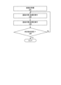
図2は、一実施形態に係る処理方法の一例を示すフローチャートである。一実施形態に係る処理装置10は、半導体基板等のワークピースWを処理する。
(Example of flow of processing according to one embodiment)
FIG. 2 is a flow chart illustrating an example of a processing method according to one embodiment. A
ステップ101においてまず、一実施形態に係る処理のため基板が準備される。一実施形態において、基板はチャンバ12内へ搬入され、静電チャック16上に載置され保持されてもよい。さらに、基板に対して前処理が施されてもよい。たとえば、基板表面の特性が均一でない場合には、均一化のための処理を施してもよい。処理対象基板は、二酸化シリコン(SiO2)、窒化シリコン(SiN)またはゲルマニウム(Ge)等で形成されてもよい。ただし、基板の表面が親水性であるか、または、基板が親水化処理を施された表面を有している限り、基板は他の材料を含有してもよい。基板はビア、トレンチ、コンタクトホール等の凹凸を有してもよい。基板の凹凸は、エッチングにより形成されたものであってもよい。基板はシリコン基板であってもよい。エッチングにおいては、HBr等のハロゲンガスを使用することができる。エッチングは、エッチング後の処理たとえば後述する第1処理および第2処理が実行されるチャンバと同じチャンバ内で実行してもよい。ただし、エッチングを第1処理および第2処理が実行されるチャンバとは異なるチャンバ内で実行してもよい。
First, in
ステップ102において、コントローラ80は処理装置10を制御して第1処理を実行させる。第1処理は、基板上の第1領域に第1膜を形成する。一実施形態において、第1処理は、化学蒸着(CVD)処理である。第1処理は、プラズマCVDであってもよい。ただし、第1処理は、プラズマを使用せずに実行してもよい。
At
第1処理においては、気体供給部44を介してチャンバ12に第1ガスが導入される。コントローラ80は、RF電源30を制御してRF電力を下部電極18に供給させる。これにより第1ガスがプラズマ化して基板表面上に第1膜が形成される。
In the first process, a first gas is introduced into the
第1ガスは炭素を含むガスであってもよい。第1ガスは、たとえば、フルオロカーボンガス、ハイドロフルオロカーボンガス、ハイドロカーボンガスであってもよい。たとえば、CF4、C4F6、C4F8、CH2F2、CHF3、CH4等のガスを使用できる。たとえば、PPFC(Plasma Polymerized Fluorocarbon)膜は疎水性であり、一実施形態の第1膜として適当である。ただし、基板の親水性表面上に疎水性の膜を形成できるものであれば、第1ガスとして任意のガスを利用できる。さらに、第1ガスにより形成される疎水膜は、後述する第2処理において除去されることが望ましい。第1処理においては、第1ガスは、窒素(N2)、アルゴン(Ar)等の不活性ガスをキャリアガスとして含んでもよい。 The first gas may be a carbon-containing gas. The first gas may be, for example, a fluorocarbon gas, a hydrofluorocarbon gas, or a hydrocarbon gas. For example, gases such as CF4 , C4F6 , C4F8 , CH2F2 , CHF3 , CH4 can be used. For example, a PPFC (Plasma Polymerized Fluorocarbon) membrane is hydrophobic and suitable as the first membrane in one embodiment. However, any gas can be used as the first gas as long as it can form a hydrophobic film on the hydrophilic surface of the substrate. Furthermore, it is desirable that the hydrophobic film formed by the first gas be removed in the second process, which will be described later. In the first process, the first gas may contain an inert gas such as nitrogen (N 2 ) or argon (Ar) as a carrier gas.
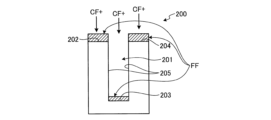
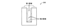
第1膜は、基板の第1領域内に形成されてもよい。第1領域の位置は、基板上の凹凸に応じて決定してもよい。また、第1領域の位置は、第1処理の種類に応じて決定してもよい。たとえば、第1処理が異方性CVDであるか等方性CVDであるかに応じて、第1領域の位置を決定してもよい。図3Aは、一実施形態に係る処理の対象となる基板の概略図である。図3A中、基板200はトレンチ201を有する。トレンチ201の開口は頂部と底部とで略同一の大きさである。かかる基板200に異方性CVDを施すときは、図3Aに示すように、CFx等の第1膜FFを領域202,203,204に堆積する。たとえば、図3Aの第1膜FFは、頂部202,204と底部203とに形成されているが、側壁205上には形成されていない。異方性CVDの場合には、成膜材料は主として一方向に堆積する。図3Aの例では、CFxは、垂直方向に堆積しているが、水平方向には堆積しない。なお、垂直方向とは、基板200の表面に直交する方向を指し、水平方向とは、基板200の表面と並行な方向を指す。このため、第1膜FFは側壁205上には形成されていない。しかし、第1膜FFは、頂部202,204および底部203上よりも少量、側壁205上に堆積していてもよい。また、第1膜FFは、底部203上においては頂部202,204上よりも膜厚が薄くてもよい。
A first membrane may be formed in the first region of the substrate. The position of the first region may be determined according to unevenness on the substrate. Also, the position of the first area may be determined according to the type of the first process. For example, the location of the first region may be determined depending on whether the first process is anisotropic CVD or isotropic CVD. FIG. 3A is a schematic diagram of a substrate to be processed according to one embodiment. In FIG. 3A,
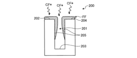
他方、等方性CVDの場合は、図4Aに示すように第1膜FFが形成されてもよい。図4Aにおいては、第1膜FFは、頂部202,204および側壁205の上部に形成されているが、底部203および側壁205の下部には形成されていない。第1膜FFの膜厚は概ね均一ではなく、トレンチ201の上端において膨らむように堆積している。このように、第1領域の位置は、基板の凹凸によって変化してもよい。
On the other hand, for isotropic CVD, the first film FF may be formed as shown in FIG. 4A. In FIG. 4A, the first film FF is formed on the tops 202 and 204 and the
ステップ103において、コントローラ80は処理装置10を制御して第2処理を実行させる。第2処理は基板上の第2領域に第2膜を形成する。一実施形態において、第2処理は、原子層堆積(ALD)処理であってもよい。ステップ103において、第2膜SFの膜厚が所定値に達するまで、1回以上のALD処理を繰り返し実行してもよい。なお、ここでは、1回のALD処理により1原子層が形成されるものとする。第1処理が行われる毎に、1以上のALD処理が第2処理において実行されることが望ましい。第2処理の間に第1膜FFが完全にまたは部分的に除去されたとき、第1処理すなわちステップ102を再度実行してもよい。第1膜FFが完全に除去される前に第1処理を繰り返し実行することが望ましい。
At
ALD処理は吸着ステップと活性化ステップすなわち改質ステップとを含む。吸着ステップにおいては、基板200に吸着する物質の前駆体がチャンバ12内に導入される。次に活性化ステップにおいて、チャンバ12内に改質ガスのプラズマが生成され、基板表面上の吸着層を改質し、表面に吸着していた前駆体から第2膜が形成される。
ALD processing includes an adsorption step and an activation or modification step. In the adsorption step, a precursor of a substance that adsorbs to
一実施形態においては、前駆体はヒドロキシ基に吸着する材料から選択する。たとえば、前駆体はシリコン含有前駆体であり、改質ガスはO2,CO,CO2,NO,NO2等の酸素含有ガスであってもよい。 In one embodiment, the precursor is selected from materials that adsorb to hydroxy groups. For example, the precursor may be a silicon containing precursor and the reforming gas may be an oxygen containing gas such as O2 , CO, CO2 , NO, NO2 .
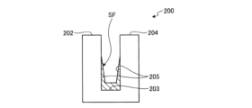
第1処理において、第1膜は基板の第1領域上に堆積する。第1膜は疎水性表面を有するため、第2処理において導入される前駆体は第1領域には吸着しない。そして、前駆体は基板200上の第1領域以外の領域に吸着する。続く改質ステップにおいて、吸着していた前駆体が改質されて第1領域以外の領域に第2膜を形成する。第1領域以外の領域を、第2領域とも呼ぶ。
In a first process, a first film is deposited on a first region of the substrate. Since the first membrane has a hydrophobic surface, precursors introduced in the second treatment do not adsorb to the first region. Then, the precursor is adsorbed to regions other than the first region on the
図3Bの例に示すように、図3Aの基板200に対して第2処理を施すと、図3Bおよび図4Bに示す第2膜SFは側壁205上に形成される。同時に、頂部202,204および底部203上の第1膜FFが第2処理中にプラズマの影響によって除去される。このため、第2膜SFは基板200の側壁205上のみに形成される。第1膜FFが第2処理後も頂部202,204および底部203上に残存している場合、第1膜FFを除去するための別個の処理を実行してもよい。たとえば、第2処理の後、基板200をアルゴンガスや酸素ガスのプラズマに曝露してもよい。
As shown in the example of FIG. 3B, when the
図4Aに示すように基板200に対して第2処理を実行すると、図4Bに示すように、第2膜SFが底部203と側壁205の下部とに形成される。このように、基板の凹凸と第1処理の種類(すなわち異方性CVDか等方性CVDか)に応じて、処理の結果として得られる第2膜SFの形状および位置が変化する。図3Cに示すように、第1処理において異方性CVDを実行した場合、第1領域は頂部202,204および底部203であり、第2領域は側壁205である。つまり、第1処理が異方性CVDである場合、第1領域は水平領域であり、第2領域は垂直領域である。また、第1処理が異方性CVDである場合、第1領域は第1方向に延在する表面であり、第2領域は第1方向とは異なる第2方向に延在する表面である。第1方向と第2方向とがなす角度は略90度であってもよい。また、第1方向は膜の堆積方向に直交する方向であり、第2方向は、堆積方向と並行な方向であってもよい。他方、図4Cに示すように、第1処理が等方性CVDである場合、第1領域は頂部202,204および側壁205の上部であり、第2領域は底部203および側壁205の下部である。たとえば、第1処理が等方性CVDである場合、第1領域は、第2領域よりも頂部に近い領域であり、第2領域は第1領域よりも底部に近い領域である。第1領域は第1処理によって膜が形成される領域であり、第2領域は第2処理によって膜が形成される領域である。第1領域および第2領域は部分的に重なりあっていてもよい。
When the second process is performed on the
図2に示すように、ステップ102および103の後、ステップ104において所定の条件が満足されたか否かを判定する。所定の条件とは、同一基板に対して実行済みの第1処理および第2処理の回数、または、基板上に堆積された第2膜SFの膜厚である。また、所定の条件は、基板200の表面上に残存している第1膜FFの膜厚であってもよい。
As shown in FIG. 2, after
たとえば、第2処理において実行するALD処理の回数を予め設定し、記憶部内に制御プログラムとして記憶しておいてもよい。たとえば、1回の第2処理によって形成される第2膜の膜厚を算出し、第2膜の膜厚を所望の値にするために必要なALD処理の回数を設定してもよい。そして、ステップ104において、同一基板に対して所定数の第2処理が実行済みか否かを判定してもよい。
For example, the number of times of ALD processing to be executed in the second processing may be set in advance and stored as a control program in the storage unit. For example, the film thickness of the second film formed by one second process may be calculated, and the number of ALD processes necessary for setting the film thickness of the second film to a desired value may be set. Then, in
上記の処理に代えて、または上記の処理に加えて、ステップ104において、基板上に残存している第1膜の膜厚が所定値たとえばゼロとなったか否かを判定してもよい。第2膜の膜厚が所定値に達していないうちに第1膜が基板上から完全に除去された場合、ステップ102および103を再度実行する。また、この他に所定の条件が達成されたか否かを判定する追加ステップをステップ102の後に実行して、第1膜の膜厚が所定値になったか否かを判定してもよい。
Instead of the above process, or in addition to the above process, in
ステップ104は、記憶部に記憶された制御プログラムに基づきコントローラ80が実行してもよい。ステップ104において所定の条件が満足されたと判定した場合(ステップS104、Yes)、処理は終了する。他方、ステップ104において所定の条件が満足されていないと判定した場合(ステップS104、No)、処理はステップ102に戻る。たとえば、コントローラ80は、所定の条件が満足されるまで、ステップ102および103を繰り返し実行させる。ステップ104において所定の条件が満足されていないと判定された場合、ステップ102とステップ103のいずれか一方のみを実行するように制御プログラムを設定してもよい。
Step 104 may be executed by the
(In Situでの動作)
ステップ102およびステップ103は、基板をチャンバ12から取り出すことなく実行する。つまり、第1処理および第2処理はチャンバ12内の真空状態を壊すことなく、in situで実行する。一実施形態に係る装置たとえば処理装置10は、気体供給部44を備え、気体供給部44はチャンバ12内に種々のガスを供給できる。また、一実施形態に係る装置は、第1処理および第2処理をチャンバ12内の真空状態を壊すことなく実行できる。また、一実施形態に係る装置は、排気路、排気口12e、排気装置3等の排気機構を備え、異なる種類のガスがチャンバ12内で混ざりあわないよう、パージ処理を実行できる。このため、一実施形態の装置は、ステップ102およびステップ103をin situで、または真空状態を壊すことなく実行できる。
(Operation in Situ)
(第1処理および第2処理中の電力制御)
また、一実施形態に係る装置は、プロセスごとにプラズマ生成の態様を変更してもよい。たとえば、コントローラ80は、アンテナ50と下部電極18とを制御して、第1処理の間は下部電極18のみに電圧が印加され、第2処理の間はアンテナ50のみに電圧が印加されるようにしてもよい。
(Power control during the first process and the second process)
Also, the apparatus according to one embodiment may change the aspect of plasma generation for each process. For example,
コントローラ80が第1処理中にアンテナ50および下部電極18の両方を動作させる場合、第1ガスが過度に解離する可能性がある。この場合、第1ガスから生じるラジカルによって基板にダメージが加えられる可能性がある。このため、第1処理中は、コントローラ80は処理装置10を制御して、下部電極18には電力が供給されるがアンテナ50には供給されないようにしてもよい。また、第1処理中、コントローラ80は処理装置10を制御して、下部電極18とアンテナ50の双方に電力が供給されるようにしてもよい。この場合、コントローラ80は、アンテナ50に供給される電力レベルを基板にダメージが加わらない程度に抑制する。他方、第2処理中は、高品質の第2膜を形成することが望ましい。そこで、第2処理中は、高電子密度かつ低イオンエネルギーのプラズマを生成することが望ましい。このため、第2処理中は、コントローラ80は処理装置10を制御して、アンテナ50には電力が供給されるが下部電極18には供給されないようにしてもよい。また、第2処理中は、コントローラ80は処理装置10を制御して、下部電極18およびアンテナ50の双方に電力が供給されるようにしてもよい。この場合、コントローラ80は、下部電極18に供給される電力レベルを、低イオンエネルギーのプラズマが生成されるように低いレベルに抑制する。
If
たとえば、コントローラ80は、図5に示すタイムシーケンスに基づき、処理装置10の各部を制御してもよい。図5に示すように、第1処理(CVD処理)中、コントローラ80は、気体供給部44を制御して、第1ガスたとえばCFxガスおよびアルゴンガスをチャンバ12に供給させてもよい。同時に、コントローラ80は、RF電源30を制御して、下部電極18に電力を供給させてもよい。第1処理中、コントローラ80は、(図5中ICPアンテナとして示す)アンテナ50を動作させない。
For example, the
そして、第1処理後、第2処理の吸着ステップが開始する。コントローラ80は、気体供給部44を制御してシリコン含有前駆体(図5中「Si-Precursor」と表示する)等の前駆体をチャンバ12内に供給させる。この期間中、コントローラ80は、アルゴンガス等のキャリアガスをチャンバ12内に供給させてもよい。コントローラ80は、気体供給部44を制御して、基板処理の間一貫して所定の流量のキャリアガスがチャンバ12内に供給されるようにしてもよい。この期間中は、アンテナ50および下部電極18は動作しない。シリコン含有前駆体が導入され基板に吸着した後、コントローラ80は、チャンバ12をパージして不所望のガス種をチャンバ12から排出する。
After the first process, the adsorption step of the second process starts. The
次に、コントローラ80は活性化ステップすなわち改質ステップを開始して吸着した前駆体を改質する。活性化ステップでは、コントローラ80は、気体供給部44を制御して、酸素等の改質ガスをチャンバ12内に供給させる。同時に、コントローラ80は、RF電源70Aおよび70Bを制御して、アンテナ50に電力を供給する。この期間中、コントローラ80は下部電極18を動作させない。その後、コントローラ80は、再びパージ処理を実行する。吸着ステップおよび活性化ステップ後のパージ処理は省略してもよい。そして、コントローラ80は、所定の条件が満足されたか否かに応じて、第1処理および第2処理を繰り返す。さらに、コントローラ80は、第1処理および第2処理のいずれか一方を個別に繰り返し実行してもよい。
(エッチング処理)
一実施形態に係る装置においては、第1処理および第2処理に加えて、他の処理を第3処理としてin situで実行してもよい。たとえば、一実施形態に係る装置はさらにエッチング処理を実行することで、スループットをさらに向上させることができる。エッチング処理は原子層エッチング(ALE)処理であってもよい。
(etching process)
In an apparatus according to one embodiment, in addition to the first process and the second process, another process may be executed in situ as the third process. For example, the apparatus according to one embodiment can perform an additional etching process to further improve throughput. The etch process may be an atomic layer etch (ALE) process.
なお、ALE処理は、反応層を形成する改質ステップと、改質した反応層を除去する除去ステップとを含んでもよい。ALE処理は、改質ステップおよび除去ステップ各々の後にパージステップを含んでもよい。改質ステップは、NプラズマまたはHプラズマを用いて実行してもよい。除去ステップは、F等のハロゲンプラズマ(種)を用いて実行してもよい。 Note that the ALE process may include a modification step of forming a reaction layer and a removal step of removing the modified reaction layer. The ALE process may include a purge step after each of the reforming and stripping steps. The modification step may be performed using N plasma or H plasma. The removal step may be performed using a halogen plasma (seed) such as F.
一実施形態においては、第1処理、第2処理および第3処理は、この順番に繰り返し実行してもよい。各処理を繰り返す回数は、それぞれ異なっていてもよい。たとえば、第1処理を1回実行した後に第2処理を10回実行してもよい。また、第1処理、第2処理、第3処理の実行順序を変更してもよい。 In one embodiment, the first process, second process and third process may be repeatedly performed in this order. The number of times each process is repeated may be different. For example, the second process may be performed ten times after the first process is performed once. Also, the execution order of the first process, the second process, and the third process may be changed.
これまで、完全かつ明確な開示のために具体的な実施形態につき説明した。ただし、添付の特許請求の範囲に記載の請求項はかかる開示に基づき限定的に解釈されるべきではなく、当業者が想到可能であり、かつ、ここに示した基本的な教示の範囲に該当する、全ての変形例および代替的な構成例を包含するものと解釈されるべきである。 Thus far, specific embodiments have been described for the purpose of complete and clear disclosure. However, the claims set forth in the appended claims should not be construed as limiting based on such disclosure, but rather within the scope of the basic teachings within the reach of those skilled in the art and the basic teachings presented herein. should be construed to include all modifications and alternative constructions.
10 処理装置
12 チャンバ
12c 空間
12e 排気口
12i 吸気口
12p 開口
13 支持機構
14 ステージ
16 静電チャック
18 下部電極
18a 第1プレート
18b 第2プレート
22 直流電源
23 スイッチ
24 流路
26a,26b パイプ
28 気体供給ライン
30 RF電源
32 整合器
34 シールド
36 パイプ
38 排気装置
40 バッフル板
42 ウィンドウ
44 気体供給部
44a ガス源
44b フローコントローラ
44c バルブ
46 パイプ
48 ゲートバルブ
50 アンテナ
52A 内側アンテナ素子
52B 外側アンテナ素子
54 クランプ
60 シールド
62A 内側シールド壁
62B 外側シールド壁
64A 内側シールド板
64B 外側シールド板
68A,68B アクチュエータ
70A,70B RF電源
80 コントローラ
FR フォーカスリング
HT ヒータ
HP ヒータ電源
W ワークピース
10
Claims (19)
メモリと、当該メモリに接続されたプロセッサとを備えるコントローラと、
を備える基板処理装置であって、
前記メモリは前記プロセッサを制御して前記処理装置による処理を制御するための、コンピュータによって実行可能な命令を記憶し、当該処理は、
前記チャンバ内の基板の第1領域上に第1膜を形成する第1処理と、
前記チャンバ内に前記基板に吸着する前駆体を供給した後、前記チャンバ内に供給した改質ガスからプラズマを生成することにより、前記チャンバ内の前記基板の第2領域上に第2膜を形成する第2処理と、
前記基板をエッチングするエッチング処理と、
を含み、
前記第1処理および前記第2処理を、前記基板を前記チャンバから外に移動させることなく実行する、基板処理装置。 a processing apparatus comprising a chamber;
a controller comprising a memory and a processor coupled to the memory;
A substrate processing apparatus comprising
The memory stores computer-executable instructions for controlling the processor to control processing by the processing unit, the processing comprising:
a first process of forming a first film on a first region of a substrate within the chamber;
A second film is formed on a second region of the substrate in the chamber by generating a plasma from the reforming gas supplied in the chamber after supplying a precursor that is adsorbed to the substrate into the chamber. a second process to
an etching process for etching the substrate;
including
A substrate processing apparatus that performs the first process and the second process without moving the substrate out of the chamber.
前記第2処理は、前記第2領域上に、ヒドロキシ基と反応する前駆体を吸着させることにより前記第2膜を形成する、請求項1に記載の基板処理装置。 The first process forms the first film as a hydrophobic surface on a first region of the hydrophilic surface of the substrate,
2. The substrate processing apparatus according to claim 1, wherein said second treatment forms said second film on said second region by adsorbing a precursor that reacts with a hydroxyl group.
前記第2処理は、前記基板の凹凸の側壁に前記第2膜を形成する、請求項1~4のいずれか1項に記載の基板処理装置。 The first process forms the first film on the top and bottom of the unevenness of the substrate,
5. The substrate processing apparatus according to claim 1, wherein said second process forms said second film on uneven sidewalls of said substrate.
前記第2処理は、前記第2膜としてシリコン含有膜を形成する、請求項1~5のいずれか1項に記載の基板処理装置。 the substrate contains at least one of SiO2, SiN, Si and Ge;
6. The substrate processing apparatus according to claim 1, wherein said second process forms a silicon-containing film as said second film.
前記アンテナに対向して配置され、前記基板を上に保持するよう構成され、前記コントローラにより制御される下部電極と、
をさらに備え、前記処理装置による処理はさらに、
前記第1処理において前記下部電極に電力を供給し、
前記第2処理において前記改質ガスを前記チャンバ内に供給する際に前記アンテナに電力を供給することを含む、請求項1~7のいずれか1項に記載の基板処理装置。 an antenna controlled by the controller;
a lower electrode positioned opposite the antenna and configured to hold the substrate thereon and controlled by the controller;
wherein the processing by the processing device further comprises:
supplying power to the lower electrode in the first process;
8. The substrate processing apparatus according to claim 1, further comprising supplying power to said antenna when said modifying gas is supplied into said chamber in said second processing.
前記アンテナに対向して配置され、前記基板を上に保持するよう構成され、前記コントローラにより制御される下部電極と、
をさらに備え、前記処理装置による処理はさらに、
前記第1処理において前記アンテナに電力を供給せずに、前記下部電極に電力を供給し、
前記第2処理において前記改質ガスを前記チャンバ内に供給する際に前記下部電極に電力を供給せず、前記アンテナに電力を供給することを含む、請求項1~7のいずれか1項に記載の基板処理装置。 an antenna positioned over the chamber and controlled by the controller;
a lower electrode positioned opposite the antenna and configured to hold the substrate thereon and controlled by the controller;
wherein the processing by the processing device further comprises:
supplying power to the lower electrode without supplying power to the antenna in the first process;
8. The method according to any one of claims 1 to 7, comprising supplying power to the antenna without supplying power to the lower electrode when supplying the reformed gas into the chamber in the second process. A substrate processing apparatus as described.
前記基板上に前記第1膜が残っている間に前記第1処理が実行される、請求項1~12のいずれか1項に記載の基板処理装置。 stopping the second treatment before the first film is completely removed in the second treatment;
13. The substrate processing apparatus according to claim 1, wherein said first process is performed while said first film remains on said substrate.
メモリと、当該メモリに接続されるプロセッサと、を有するコントローラと、を備え、前記メモリは前記プロセッサを制御して処理を制御させるためのコンピュータにより実行可能な命令を記憶し、当該処理は、
前記チャンバ内の基板の第1領域上に第1膜を形成する第1処理と、
前記チャンバ内に前記基板に吸着する前駆体を供給した後、前記チャンバ内に供給した改質ガスからプラズマを生成することにより、前記チャンバ内の前記基板の第2領域上に第2膜を形成する第2処理と、
前記基板をエッチングする第3処理と、
を含み、
前記第1処理、前記第2処理および前記第3処理を、前記チャンバの外に前記基板を移動させずに実行する、基板処理装置。 a processing apparatus having a chamber;
a controller having a memory and a processor coupled to the memory, the memory storing computer-executable instructions for controlling the processor to control a process, the process comprising:
a first process of forming a first film on a first region of a substrate within the chamber;
A second film is formed on a second region of the substrate in the chamber by generating a plasma from the reforming gas supplied in the chamber after supplying a precursor that is adsorbed to the substrate into the chamber. a second process to
a third process of etching the substrate;
including
A substrate processing apparatus that performs the first process, the second process, and the third process without moving the substrate out of the chamber.
メモリと、当該メモリに接続されるプロセッサと、を有するコントローラと、を備え、前記メモリは前記プロセッサを制御して処理を制御させるためのコンピュータにより実行可能な命令を記憶し、当該処理は、
前記チャンバ内の基板の第1領域内に第1膜を形成する第1処理と、
前記チャンバ内に前記基板に吸着する前駆体を供給した後、前記チャンバ内に供給した改質ガスからプラズマを生成することにより、前記チャンバ内の前記基板の第2領域内に第2膜を形成する第2処理と、
前記基板をエッチングする第3処理と、
を含み、
前記第1処理、前記第2処理および前記第3処理を、前記チャンバの外に前記基板を移動させずに実行し、
前記第3処理は、
NプラズマおよびHプラズマの一方により前記基板の表面を改質し、
前記NプラズマおよびHプラズマの一方により改質された前記表面を、ハロゲンガスにより除去する、ことを含む、基板処理装置。 a processing apparatus having a chamber;
a controller having a memory and a processor coupled to the memory, the memory storing computer-executable instructions for controlling the processor to control a process, the process comprising:
a first process of forming a first film within a first region of a substrate within the chamber;
A second film is formed in a second region of the substrate in the chamber by generating a plasma from the reforming gas supplied in the chamber after supplying a precursor that is adsorbed to the substrate into the chamber. a second process to
a third process of etching the substrate;
including
performing the first process, the second process, and the third process without moving the substrate out of the chamber;
The third process is
modifying the surface of the substrate with one of N plasma and H plasma;
and removing the surface modified by one of the N plasma and the H plasma with a halogen gas.
前記チャンバ内に前記基板に吸着する前駆体を供給した後、前記チャンバ内に供給した改質ガスからプラズマを生成することにより、前記チャンバ内の前記基板の第2領域上に第2膜を形成する第2処理と、
前記基板をエッチングする第3処理と、
を含み、
前記第1処理および前記第2処理は、前記チャンバの外に前記基板を移動させずに実行する、基板処理方法。 a first process of forming a first film on a first region of a substrate in a chamber of a processing apparatus;
A second film is formed on a second region of the substrate in the chamber by generating a plasma from the reforming gas supplied in the chamber after supplying a precursor that is adsorbed to the substrate into the chamber. a second process to
a third process of etching the substrate;
including
The substrate processing method, wherein the first processing and the second processing are performed without moving the substrate out of the chamber.
前記チャンバ内に前記基板に吸着する前駆体を供給した後、前記チャンバ内に供給した改質ガスからプラズマを生成することにより、前記チャンバ内の前記基板の第2領域内に第2膜を形成する第2処理と、
前記基板をエッチングする第3処理と、
を含み、
前記第1処理、前記第2処理および前記第3処理は、前記チャンバの外に前記基板を移動させずに実行し、
前記第3処理は、
NプラズマおよびHプラズマの一方により、前記基板の表面を改質し、
前記NプラズマおよびHプラズマの一方により改質された前記表面を、ハロゲンガスにより除去することを含む、基板処理方法。 a first process of forming a first film within a first region of a substrate within a chamber of a processing apparatus;
A second film is formed in a second region of the substrate in the chamber by generating a plasma from the reforming gas supplied in the chamber after supplying a precursor that is adsorbed to the substrate into the chamber. a second process to
a third process of etching the substrate;
including
performing the first process, the second process, and the third process without moving the substrate out of the chamber;
The third process is
modifying the surface of the substrate with one of N plasma and H plasma;
A substrate processing method, comprising removing the surface modified by one of the N plasma and the H plasma with a halogen gas.
Applications Claiming Priority (2)
| Application Number | Priority Date | Filing Date | Title |
|---|---|---|---|
| US16/010,800 | 2018-06-18 | ||
| US16/010,800 US10781519B2 (en) | 2018-06-18 | 2018-06-18 | Method and apparatus for processing substrate |
Publications (3)
| Publication Number | Publication Date |
|---|---|
| JP2019220681A JP2019220681A (en) | 2019-12-26 |
| JP2019220681A5 JP2019220681A5 (en) | 2022-05-25 |
| JP7323330B2 true JP7323330B2 (en) | 2023-08-08 |
Family
ID=68839187
Family Applications (1)
| Application Number | Title | Priority Date | Filing Date |
|---|---|---|---|
| JP2019090801A Active JP7323330B2 (en) | 2018-06-18 | 2019-05-13 | Substrate processing method and substrate processing apparatus |
Country Status (5)
| Country | Link |
|---|---|
| US (2) | US10781519B2 (en) |
| JP (1) | JP7323330B2 (en) |
| KR (1) | KR20190142741A (en) |
| CN (1) | CN110616416A (en) |
| TW (1) | TWI807049B (en) |
Families Citing this family (3)
| Publication number | Priority date | Publication date | Assignee | Title |
|---|---|---|---|---|
| JP7205929B2 (en) | 2018-04-09 | 2023-01-17 | 東京エレクトロン株式会社 | Method of forming semiconductor devices with air gaps for low capacitance interconnects |
| US10896823B2 (en) * | 2018-11-21 | 2021-01-19 | Thomas E. Seidel | Limited dose atomic layer processes for localizing coatings on non-planar surfaces |
| JP7285152B2 (en) * | 2019-07-08 | 2023-06-01 | 東京エレクトロン株式会社 | Plasma processing equipment |
Citations (1)
| Publication number | Priority date | Publication date | Assignee | Title |
|---|---|---|---|---|
| US20180166270A1 (en) | 2016-12-09 | 2018-06-14 | Wonik Ips Co., Ltd. | Method of depositing a thin film |
Family Cites Families (26)
| Publication number | Priority date | Publication date | Assignee | Title |
|---|---|---|---|---|
| US20020004309A1 (en) * | 1990-07-31 | 2002-01-10 | Kenneth S. Collins | Processes used in an inductively coupled plasma reactor |
| DE19651029C2 (en) * | 1996-12-09 | 1999-12-02 | Ibm | Calibration standard for profilometers and manufacturing processes |
| US6794290B1 (en) * | 2001-12-03 | 2004-09-21 | Novellus Systems, Inc. | Method of chemical modification of structure topography |
| US6852996B2 (en) * | 2002-09-25 | 2005-02-08 | Stmicroelectronics, Inc. | Organic semiconductor sensor device |
| US7323231B2 (en) * | 2003-10-09 | 2008-01-29 | Micron Technology, Inc. | Apparatus and methods for plasma vapor deposition processes |
| US7476621B1 (en) * | 2003-12-10 | 2009-01-13 | Novellus Systems, Inc. | Halogen-free noble gas assisted H2 plasma etch process in deposition-etch-deposition gap fill |
| US8974868B2 (en) * | 2005-03-21 | 2015-03-10 | Tokyo Electron Limited | Post deposition plasma cleaning system and method |
| US7341959B2 (en) * | 2005-03-21 | 2008-03-11 | Tokyo Electron Limited | Plasma enhanced atomic layer deposition system and method |
| US8815014B2 (en) * | 2005-11-18 | 2014-08-26 | Tokyo Electron Limited | Method and system for performing different deposition processes within a single chamber |
| US7649239B2 (en) * | 2006-05-04 | 2010-01-19 | Intel Corporation | Dielectric spacers for metal interconnects and method to form the same |
| US20070298583A1 (en) * | 2006-06-27 | 2007-12-27 | Macronix International Co., Ltd. | Method for forming a shallow trench isolation region |
| JP4916257B2 (en) * | 2006-09-06 | 2012-04-11 | 東京エレクトロン株式会社 | Oxide film forming method, oxide film forming apparatus and program |
| WO2008153674A1 (en) * | 2007-06-09 | 2008-12-18 | Boris Kobrin | Method and apparatus for anisotropic etching |
| US8129288B2 (en) * | 2008-05-02 | 2012-03-06 | Intermolecular, Inc. | Combinatorial plasma enhanced deposition techniques |
| US7816278B2 (en) * | 2008-03-28 | 2010-10-19 | Tokyo Electron Limited | In-situ hybrid deposition of high dielectric constant films using atomic layer deposition and chemical vapor deposition |
| JP5439771B2 (en) * | 2008-09-05 | 2014-03-12 | 東京エレクトロン株式会社 | Deposition equipment |
| US8039966B2 (en) * | 2009-09-03 | 2011-10-18 | International Business Machines Corporation | Structures of and methods and tools for forming in-situ metallic/dielectric caps for interconnects |
| US9257274B2 (en) * | 2010-04-15 | 2016-02-09 | Lam Research Corporation | Gapfill of variable aspect ratio features with a composite PEALD and PECVD method |
| US9564312B2 (en) * | 2014-11-24 | 2017-02-07 | Lam Research Corporation | Selective inhibition in atomic layer deposition of silicon-containing films |
| CN106148918B (en) * | 2015-03-26 | 2018-08-07 | 理想晶延半导体设备(上海)有限公司 | Semiconductor processing equipment |
| US9716005B1 (en) | 2016-03-18 | 2017-07-25 | Applied Materials, Inc. | Plasma poisoning to enable selective deposition |
| US10037884B2 (en) * | 2016-08-31 | 2018-07-31 | Lam Research Corporation | Selective atomic layer deposition for gapfill using sacrificial underlayer |
| JP6559107B2 (en) * | 2016-09-09 | 2019-08-14 | 東京エレクトロン株式会社 | Film forming method and film forming system |
| TWI754041B (en) * | 2017-04-18 | 2022-02-01 | 日商東京威力科創股份有限公司 | Method of processing target object |
| US10892186B2 (en) * | 2017-10-14 | 2021-01-12 | Applied Materials, Inc. | Integration of ALD copper with high temperature PVD copper deposition for BEOL interconnect |
| US10515815B2 (en) * | 2017-11-21 | 2019-12-24 | Lam Research Corporation | Atomic layer deposition and etch in a single plasma chamber for fin field effect transistor formation |
-
2018
- 2018-06-18 US US16/010,800 patent/US10781519B2/en active Active
-
2019
- 2019-05-13 JP JP2019090801A patent/JP7323330B2/en active Active
- 2019-06-17 KR KR1020190071720A patent/KR20190142741A/en not_active Application Discontinuation
- 2019-06-18 CN CN201910525969.3A patent/CN110616416A/en active Pending
- 2019-06-18 TW TW108121136A patent/TWI807049B/en active
-
2020
- 2020-08-21 US US17/000,090 patent/US20210025060A1/en active Pending
Patent Citations (1)
| Publication number | Priority date | Publication date | Assignee | Title |
|---|---|---|---|---|
| US20180166270A1 (en) | 2016-12-09 | 2018-06-14 | Wonik Ips Co., Ltd. | Method of depositing a thin film |
Also Published As
| Publication number | Publication date |
|---|---|
| JP2019220681A (en) | 2019-12-26 |
| US10781519B2 (en) | 2020-09-22 |
| KR20190142741A (en) | 2019-12-27 |
| US20210025060A1 (en) | 2021-01-28 |
| TW202002014A (en) | 2020-01-01 |
| US20190382897A1 (en) | 2019-12-19 |
| CN110616416A (en) | 2019-12-27 |
| TWI807049B (en) | 2023-07-01 |
Similar Documents
| Publication | Publication Date | Title |
|---|---|---|
| US10566209B2 (en) | Etching method and workpiece processing method | |
| US11380551B2 (en) | Method of processing target object | |
| CN108878285B (en) | Etching method | |
| JP7323330B2 (en) | Substrate processing method and substrate processing apparatus | |
| KR102617192B1 (en) | Method of selectively etching first region made of silicon nitride against second region made of silicon oxide | |
| US20210202233A1 (en) | Substrate processing method and substrate processing apparatus | |
| KR20180018416A (en) | Method of processing target object | |
| KR20230129345A (en) | Plasma processing apparatus and etching method | |
| US20210327719A1 (en) | Method for processing workpiece | |
| US10755944B2 (en) | Etching method and plasma processing apparatus | |
| US20220246440A1 (en) | Substrate processing method and substrate processing apparatus | |
| JP7236315B2 (en) | Processing method and plasma processing apparatus | |
| WO2022196369A1 (en) | Substrate processing method and substrate processing device | |
| US20070218691A1 (en) | Plasma etching method, plasma etching apparatus and computer-readable storage medium |
Legal Events
| Date | Code | Title | Description |
|---|---|---|---|
| A521 | Request for written amendment filed |
Free format text: JAPANESE INTERMEDIATE CODE: A523 Effective date: 20220513 |
|
| A621 | Written request for application examination |
Free format text: JAPANESE INTERMEDIATE CODE: A621 Effective date: 20220513 |
|
| A977 | Report on retrieval |
Free format text: JAPANESE INTERMEDIATE CODE: A971007 Effective date: 20230222 |
|
| A131 | Notification of reasons for refusal |
Free format text: JAPANESE INTERMEDIATE CODE: A131 Effective date: 20230228 |
|
| A521 | Request for written amendment filed |
Free format text: JAPANESE INTERMEDIATE CODE: A523 Effective date: 20230426 |
|
| TRDD | Decision of grant or rejection written | ||
| A01 | Written decision to grant a patent or to grant a registration (utility model) |
Free format text: JAPANESE INTERMEDIATE CODE: A01 Effective date: 20230627 |
|
| A61 | First payment of annual fees (during grant procedure) |
Free format text: JAPANESE INTERMEDIATE CODE: A61 Effective date: 20230727 |
|
| R150 | Certificate of patent or registration of utility model |
Ref document number: 7323330 Country of ref document: JP Free format text: JAPANESE INTERMEDIATE CODE: R150 |