JP7304534B2 - Photodetector, structure manufacturing method, and photodetector manufacturing method - Google Patents
Photodetector, structure manufacturing method, and photodetector manufacturing method Download PDFInfo
- Publication number
- JP7304534B2 JP7304534B2 JP2022552280A JP2022552280A JP7304534B2 JP 7304534 B2 JP7304534 B2 JP 7304534B2 JP 2022552280 A JP2022552280 A JP 2022552280A JP 2022552280 A JP2022552280 A JP 2022552280A JP 7304534 B2 JP7304534 B2 JP 7304534B2
- Authority
- JP
- Japan
- Prior art keywords
- filters
- light
- image sensor
- filter array
- photodetection
- Prior art date
- Legal status (The legal status is an assumption and is not a legal conclusion. Google has not performed a legal analysis and makes no representation as to the accuracy of the status listed.)
- Active
Links
- 238000004519 manufacturing process Methods 0.000 title claims description 23
- 125000006850 spacer group Chemical group 0.000 claims description 89
- 238000000411 transmission spectrum Methods 0.000 claims description 82
- 239000000853 adhesive Substances 0.000 claims description 70
- 230000001070 adhesive effect Effects 0.000 claims description 70
- 238000001514 detection method Methods 0.000 claims description 69
- 238000002834 transmittance Methods 0.000 claims description 62
- 239000000758 substrate Substances 0.000 claims description 49
- 230000002093 peripheral effect Effects 0.000 claims description 46
- 238000000034 method Methods 0.000 claims description 40
- 238000012545 processing Methods 0.000 claims description 21
- 230000003595 spectral effect Effects 0.000 claims description 14
- 229920002120 photoresistant polymer Polymers 0.000 claims description 11
- 238000003825 pressing Methods 0.000 claims description 4
- 238000004528 spin coating Methods 0.000 claims description 3
- 238000000059 patterning Methods 0.000 claims description 2
- 239000013598 vector Substances 0.000 description 48
- 238000010586 diagram Methods 0.000 description 35
- 238000003384 imaging method Methods 0.000 description 27
- 238000009826 distribution Methods 0.000 description 22
- 239000010408 film Substances 0.000 description 21
- 230000003287 optical effect Effects 0.000 description 20
- 239000011295 pitch Substances 0.000 description 19
- 229920005989 resin Polymers 0.000 description 15
- 239000011347 resin Substances 0.000 description 15
- 238000001228 spectrum Methods 0.000 description 11
- 239000000463 material Substances 0.000 description 10
- 238000012986 modification Methods 0.000 description 10
- 230000004048 modification Effects 0.000 description 10
- VYPSYNLAJGMNEJ-UHFFFAOYSA-N Silicium dioxide Chemical compound O=[Si]=O VYPSYNLAJGMNEJ-UHFFFAOYSA-N 0.000 description 8
- 230000008569 process Effects 0.000 description 8
- 230000005540 biological transmission Effects 0.000 description 7
- 230000006870 function Effects 0.000 description 6
- 238000003491 array Methods 0.000 description 5
- GWEVSGVZZGPLCZ-UHFFFAOYSA-N Titan oxide Chemical compound O=[Ti]=O GWEVSGVZZGPLCZ-UHFFFAOYSA-N 0.000 description 4
- 230000015572 biosynthetic process Effects 0.000 description 4
- 229910052681 coesite Inorganic materials 0.000 description 4
- 229910052906 cristobalite Inorganic materials 0.000 description 4
- 238000001723 curing Methods 0.000 description 4
- 230000000694 effects Effects 0.000 description 4
- 230000010354 integration Effects 0.000 description 4
- 230000001788 irregular Effects 0.000 description 4
- 239000011159 matrix material Substances 0.000 description 4
- 229910052751 metal Inorganic materials 0.000 description 4
- 239000002184 metal Substances 0.000 description 4
- 239000000377 silicon dioxide Substances 0.000 description 4
- 235000012239 silicon dioxide Nutrition 0.000 description 4
- 229910052682 stishovite Inorganic materials 0.000 description 4
- 238000003860 storage Methods 0.000 description 4
- 229920001187 thermosetting polymer Polymers 0.000 description 4
- 229910052905 tridymite Inorganic materials 0.000 description 4
- PNEYBMLMFCGWSK-UHFFFAOYSA-N aluminium oxide Inorganic materials [O-2].[O-2].[O-2].[Al+3].[Al+3] PNEYBMLMFCGWSK-UHFFFAOYSA-N 0.000 description 3
- 238000004364 calculation method Methods 0.000 description 3
- 230000000295 complement effect Effects 0.000 description 3
- 239000000470 constituent Substances 0.000 description 3
- 229910052593 corundum Inorganic materials 0.000 description 3
- 238000010438 heat treatment Methods 0.000 description 3
- 239000004065 semiconductor Substances 0.000 description 3
- 230000035945 sensitivity Effects 0.000 description 3
- PBCFLUZVCVVTBY-UHFFFAOYSA-N tantalum pentoxide Inorganic materials O=[Ta](=O)O[Ta](=O)=O PBCFLUZVCVVTBY-UHFFFAOYSA-N 0.000 description 3
- 229910001845 yogo sapphire Inorganic materials 0.000 description 3
- 238000012935 Averaging Methods 0.000 description 2
- -1 ITO Inorganic materials 0.000 description 2
- 229910052581 Si3N4 Inorganic materials 0.000 description 2
- 229910020286 SiOxNy Inorganic materials 0.000 description 2
- 229910021417 amorphous silicon Inorganic materials 0.000 description 2
- 230000008859 change Effects 0.000 description 2
- 239000011248 coating agent Substances 0.000 description 2
- 238000000576 coating method Methods 0.000 description 2
- 239000003086 colorant Substances 0.000 description 2
- 230000006835 compression Effects 0.000 description 2
- 238000007906 compression Methods 0.000 description 2
- 238000004590 computer program Methods 0.000 description 2
- 230000006866 deterioration Effects 0.000 description 2
- 239000000428 dust Substances 0.000 description 2
- 238000007689 inspection Methods 0.000 description 2
- 239000004973 liquid crystal related substance Substances 0.000 description 2
- 238000005259 measurement Methods 0.000 description 2
- 229910021421 monocrystalline silicon Inorganic materials 0.000 description 2
- ZKATWMILCYLAPD-UHFFFAOYSA-N niobium pentoxide Chemical compound O=[Nb](=O)O[Nb](=O)=O ZKATWMILCYLAPD-UHFFFAOYSA-N 0.000 description 2
- 239000011368 organic material Substances 0.000 description 2
- 238000000016 photochemical curing Methods 0.000 description 2
- 229910021420 polycrystalline silicon Inorganic materials 0.000 description 2
- 238000007789 sealing Methods 0.000 description 2
- 238000000926 separation method Methods 0.000 description 2
- 229910018072 Al 2 O 3 Inorganic materials 0.000 description 1
- 229910002601 GaN Inorganic materials 0.000 description 1
- 238000007476 Maximum Likelihood Methods 0.000 description 1
- 229910004298 SiO 2 Inorganic materials 0.000 description 1
- 238000010521 absorption reaction Methods 0.000 description 1
- 238000004458 analytical method Methods 0.000 description 1
- 238000013459 approach Methods 0.000 description 1
- 238000001574 biopsy Methods 0.000 description 1
- 238000005219 brazing Methods 0.000 description 1
- 230000008878 coupling Effects 0.000 description 1
- 238000010168 coupling process Methods 0.000 description 1
- 238000005859 coupling reaction Methods 0.000 description 1
- 238000013461 design Methods 0.000 description 1
- 238000005538 encapsulation Methods 0.000 description 1
- 238000005516 engineering process Methods 0.000 description 1
- 239000011521 glass Substances 0.000 description 1
- 238000009499 grossing Methods 0.000 description 1
- 229910052500 inorganic mineral Inorganic materials 0.000 description 1
- 238000005304 joining Methods 0.000 description 1
- 238000010030 laminating Methods 0.000 description 1
- 238000003475 lamination Methods 0.000 description 1
- 239000007788 liquid Substances 0.000 description 1
- 229910044991 metal oxide Inorganic materials 0.000 description 1
- 150000004706 metal oxides Chemical class 0.000 description 1
- 150000002739 metals Chemical class 0.000 description 1
- 239000011707 mineral Substances 0.000 description 1
- 238000002156 mixing Methods 0.000 description 1
- 239000000203 mixture Substances 0.000 description 1
- 229910003465 moissanite Inorganic materials 0.000 description 1
- 230000007935 neutral effect Effects 0.000 description 1
- 238000010606 normalization Methods 0.000 description 1
- 238000005192 partition Methods 0.000 description 1
- 230000000149 penetrating effect Effects 0.000 description 1
- 230000000737 periodic effect Effects 0.000 description 1
- 239000000575 pesticide Substances 0.000 description 1
- 238000011170 pharmaceutical development Methods 0.000 description 1
- 230000000704 physical effect Effects 0.000 description 1
- 239000000049 pigment Substances 0.000 description 1
- 239000004033 plastic Substances 0.000 description 1
- 238000003672 processing method Methods 0.000 description 1
- 230000009467 reduction Effects 0.000 description 1
- 238000002310 reflectometry Methods 0.000 description 1
- 229910010271 silicon carbide Inorganic materials 0.000 description 1
- 238000005476 soldering Methods 0.000 description 1
- 238000004611 spectroscopical analysis Methods 0.000 description 1
- 230000006641 stabilisation Effects 0.000 description 1
- 238000011105 stabilization Methods 0.000 description 1
- 230000000087 stabilizing effect Effects 0.000 description 1
- 238000007619 statistical method Methods 0.000 description 1
- 239000010409 thin film Substances 0.000 description 1
Images


Classifications
-
- H—ELECTRICITY
- H01—ELECTRIC ELEMENTS
- H01L—SEMICONDUCTOR DEVICES NOT COVERED BY CLASS H10
- H01L27/00—Devices consisting of a plurality of semiconductor or other solid-state components formed in or on a common substrate
- H01L27/14—Devices consisting of a plurality of semiconductor or other solid-state components formed in or on a common substrate including semiconductor components sensitive to infrared radiation, light, electromagnetic radiation of shorter wavelength or corpuscular radiation and specially adapted either for the conversion of the energy of such radiation into electrical energy or for the control of electrical energy by such radiation
- H01L27/144—Devices controlled by radiation
- H01L27/146—Imager structures
- H01L27/14601—Structural or functional details thereof
- H01L27/14625—Optical elements or arrangements associated with the device
-
- G—PHYSICS
- G01—MEASURING; TESTING
- G01J—MEASUREMENT OF INTENSITY, VELOCITY, SPECTRAL CONTENT, POLARISATION, PHASE OR PULSE CHARACTERISTICS OF INFRARED, VISIBLE OR ULTRAVIOLET LIGHT; COLORIMETRY; RADIATION PYROMETRY
- G01J3/00—Spectrometry; Spectrophotometry; Monochromators; Measuring colours
- G01J3/28—Investigating the spectrum
- G01J3/2823—Imaging spectrometer
-
- G—PHYSICS
- G01—MEASURING; TESTING
- G01J—MEASUREMENT OF INTENSITY, VELOCITY, SPECTRAL CONTENT, POLARISATION, PHASE OR PULSE CHARACTERISTICS OF INFRARED, VISIBLE OR ULTRAVIOLET LIGHT; COLORIMETRY; RADIATION PYROMETRY
- G01J3/00—Spectrometry; Spectrophotometry; Monochromators; Measuring colours
- G01J3/46—Measurement of colour; Colour measuring devices, e.g. colorimeters
- G01J3/50—Measurement of colour; Colour measuring devices, e.g. colorimeters using electric radiation detectors
- G01J3/51—Measurement of colour; Colour measuring devices, e.g. colorimeters using electric radiation detectors using colour filters
- G01J3/513—Measurement of colour; Colour measuring devices, e.g. colorimeters using electric radiation detectors using colour filters having fixed filter-detector pairs
-
- G—PHYSICS
- G02—OPTICS
- G02B—OPTICAL ELEMENTS, SYSTEMS OR APPARATUS
- G02B5/00—Optical elements other than lenses
- G02B5/20—Filters
-
- G—PHYSICS
- G02—OPTICS
- G02B—OPTICAL ELEMENTS, SYSTEMS OR APPARATUS
- G02B5/00—Optical elements other than lenses
- G02B5/20—Filters
- G02B5/201—Filters in the form of arrays
-
- H—ELECTRICITY
- H01—ELECTRIC ELEMENTS
- H01L—SEMICONDUCTOR DEVICES NOT COVERED BY CLASS H10
- H01L27/00—Devices consisting of a plurality of semiconductor or other solid-state components formed in or on a common substrate
- H01L27/14—Devices consisting of a plurality of semiconductor or other solid-state components formed in or on a common substrate including semiconductor components sensitive to infrared radiation, light, electromagnetic radiation of shorter wavelength or corpuscular radiation and specially adapted either for the conversion of the energy of such radiation into electrical energy or for the control of electrical energy by such radiation
- H01L27/144—Devices controlled by radiation
- H01L27/146—Imager structures
- H01L27/14601—Structural or functional details thereof
- H01L27/14618—Containers
-
- H—ELECTRICITY
- H01—ELECTRIC ELEMENTS
- H01L—SEMICONDUCTOR DEVICES NOT COVERED BY CLASS H10
- H01L27/00—Devices consisting of a plurality of semiconductor or other solid-state components formed in or on a common substrate
- H01L27/14—Devices consisting of a plurality of semiconductor or other solid-state components formed in or on a common substrate including semiconductor components sensitive to infrared radiation, light, electromagnetic radiation of shorter wavelength or corpuscular radiation and specially adapted either for the conversion of the energy of such radiation into electrical energy or for the control of electrical energy by such radiation
- H01L27/144—Devices controlled by radiation
- H01L27/146—Imager structures
- H01L27/14601—Structural or functional details thereof
- H01L27/1462—Coatings
- H01L27/14621—Colour filter arrangements
-
- H—ELECTRICITY
- H01—ELECTRIC ELEMENTS
- H01L—SEMICONDUCTOR DEVICES NOT COVERED BY CLASS H10
- H01L27/00—Devices consisting of a plurality of semiconductor or other solid-state components formed in or on a common substrate
- H01L27/14—Devices consisting of a plurality of semiconductor or other solid-state components formed in or on a common substrate including semiconductor components sensitive to infrared radiation, light, electromagnetic radiation of shorter wavelength or corpuscular radiation and specially adapted either for the conversion of the energy of such radiation into electrical energy or for the control of electrical energy by such radiation
- H01L27/144—Devices controlled by radiation
- H01L27/146—Imager structures
- H01L27/14601—Structural or functional details thereof
- H01L27/14625—Optical elements or arrangements associated with the device
- H01L27/14627—Microlenses
-
- H—ELECTRICITY
- H01—ELECTRIC ELEMENTS
- H01L—SEMICONDUCTOR DEVICES NOT COVERED BY CLASS H10
- H01L27/00—Devices consisting of a plurality of semiconductor or other solid-state components formed in or on a common substrate
- H01L27/14—Devices consisting of a plurality of semiconductor or other solid-state components formed in or on a common substrate including semiconductor components sensitive to infrared radiation, light, electromagnetic radiation of shorter wavelength or corpuscular radiation and specially adapted either for the conversion of the energy of such radiation into electrical energy or for the control of electrical energy by such radiation
- H01L27/144—Devices controlled by radiation
- H01L27/146—Imager structures
- H01L27/14643—Photodiode arrays; MOS imagers
- H01L27/14645—Colour imagers
-
- H—ELECTRICITY
- H01—ELECTRIC ELEMENTS
- H01L—SEMICONDUCTOR DEVICES NOT COVERED BY CLASS H10
- H01L27/00—Devices consisting of a plurality of semiconductor or other solid-state components formed in or on a common substrate
- H01L27/14—Devices consisting of a plurality of semiconductor or other solid-state components formed in or on a common substrate including semiconductor components sensitive to infrared radiation, light, electromagnetic radiation of shorter wavelength or corpuscular radiation and specially adapted either for the conversion of the energy of such radiation into electrical energy or for the control of electrical energy by such radiation
- H01L27/144—Devices controlled by radiation
- H01L27/146—Imager structures
- H01L27/14683—Processes or apparatus peculiar to the manufacture or treatment of these devices or parts thereof
- H01L27/14685—Process for coatings or optical elements
-
- H—ELECTRICITY
- H04—ELECTRIC COMMUNICATION TECHNIQUE
- H04N—PICTORIAL COMMUNICATION, e.g. TELEVISION
- H04N25/00—Circuitry of solid-state image sensors [SSIS]; Control thereof
- H04N25/10—Circuitry of solid-state image sensors [SSIS]; Control thereof for transforming different wavelengths into image signals
- H04N25/11—Arrangement of colour filter arrays [CFA]; Filter mosaics
- H04N25/13—Arrangement of colour filter arrays [CFA]; Filter mosaics characterised by the spectral characteristics of the filter elements
- H04N25/135—Arrangement of colour filter arrays [CFA]; Filter mosaics characterised by the spectral characteristics of the filter elements based on four or more different wavelength filter elements
-
- G—PHYSICS
- G01—MEASURING; TESTING
- G01J—MEASUREMENT OF INTENSITY, VELOCITY, SPECTRAL CONTENT, POLARISATION, PHASE OR PULSE CHARACTERISTICS OF INFRARED, VISIBLE OR ULTRAVIOLET LIGHT; COLORIMETRY; RADIATION PYROMETRY
- G01J3/00—Spectrometry; Spectrophotometry; Monochromators; Measuring colours
- G01J3/28—Investigating the spectrum
- G01J3/2823—Imaging spectrometer
- G01J2003/2826—Multispectral imaging, e.g. filter imaging
-
- G—PHYSICS
- G02—OPTICS
- G02B—OPTICAL ELEMENTS, SYSTEMS OR APPARATUS
- G02B1/00—Optical elements characterised by the material of which they are made; Optical coatings for optical elements
- G02B1/10—Optical coatings produced by application to, or surface treatment of, optical elements
- G02B1/11—Anti-reflection coatings
-
- G—PHYSICS
- G02—OPTICS
- G02B—OPTICAL ELEMENTS, SYSTEMS OR APPARATUS
- G02B3/00—Simple or compound lenses
- G02B3/0006—Arrays
- G02B3/0037—Arrays characterized by the distribution or form of lenses
- G02B3/0056—Arrays characterized by the distribution or form of lenses arranged along two different directions in a plane, e.g. honeycomb arrangement of lenses
-
- G—PHYSICS
- G02—OPTICS
- G02B—OPTICAL ELEMENTS, SYSTEMS OR APPARATUS
- G02B5/00—Optical elements other than lenses
- G02B5/20—Filters
- G02B5/28—Interference filters
Description
本開示は、光検出装置、構造体の製造方法、および光検出装置の製造方法に関する。 TECHNICAL FIELD The present disclosure relates to a photodetector, a method of manufacturing a structure, and a method of manufacturing a photodetector.
各々が狭帯域である多数のバンド、例えば数十バンドのスペクトル情報を活用することにより、従来のRGB画像では不可能であった対象物の詳細な物性を把握することができる。このような多波長の情報を取得するカメラは、「ハイパースペクトルカメラ」と呼ばれる。ハイパースペクトルカメラは、食品検査、生体検査、医薬品開発、および鉱物の成分分析などの様々な分野で利用されている。 By utilizing spectral information of a large number of narrow bands, for example, several tens of bands, it is possible to grasp detailed physical properties of an object, which is impossible with conventional RGB images. A camera that acquires such multi-wavelength information is called a “hyperspectral camera”. Hyperspectral cameras are used in various fields such as food inspection, biopsy, pharmaceutical development, and mineral composition analysis.
特許文献1は、圧縮センシングを利用したハイパースペクトル撮像装置の例を開示している。当該撮像装置は、光透過率の波長依存性が互いに異なる複数の光学フィルタのアレイである符号化素子と、符号化素子を透過した光を検出するイメージセンサと、信号処理回路とを備える。被写体とイメージセンサとを結ぶ光路上に、符号化素子が配置される。イメージセンサは、画素ごとに、複数の波長域の成分が重畳された光を同時に検出することにより、1つの波長多重画像を取得する。信号処理回路は、符号化素子の分光透過率(spectral transmittance)の空間分布の情報を利用して、取得された波長多重画像に圧縮センシングを適用することにより、複数の波長域のそれぞれについての画像データを生成する。特許文献1に開示された撮像装置においては、符号化素子として、対象波長域内で2つ以上の透過率のピーク(すなわち極大値)をもつ光学フィルタアレイが用いられる。
US Pat. No. 6,200,000 discloses an example of a hyperspectral imager that utilizes compressed sensing. The imaging device includes an encoding element that is an array of a plurality of optical filters having different wavelength dependencies of light transmittance, an image sensor that detects light transmitted through the encoding element, and a signal processing circuit. An encoding element is arranged on an optical path connecting an object and an image sensor. The image sensor acquires one wavelength-multiplexed image by simultaneously detecting light in which components of a plurality of wavelength bands are superimposed for each pixel. The signal processing circuit applies compression sensing to the acquired wavelength-multiplexed image using information on the spatial distribution of the spectral transmittance of the encoding element, thereby obtaining an image for each of a plurality of wavelength bands. Generate data. In the imaging apparatus disclosed in
特許文献2は、誘電体多層膜を反射層に用いたファブリ・ペロー共振器を備えるフィルタアレイの例を開示している。特許文献3から5は、フィルタアレイとイメージセンサとの配置の例を開示している。
本開示は、撮像特性を向上させることができる光検出装置を提供する。 The present disclosure provides a photodetector that can improve imaging characteristics.
本開示の一態様に係る光検出装置は、各々が光入射面および光出射面を有し、2次元的に配列された複数のフィルタを含むフィルタアレイであって、前記複数のフィルタは互いに異なる透過スペクトルを有する複数種類のフィルタを含む、フィルタアレイと、前記光出射面に対向する光検出面を有するイメージセンサであって、前記光検出面に沿って2次元的に配列された複数の光検出素子を備えるイメージセンサと、を備え、前記光出射面と前記光検出面との距離が、前記フィルタごとに異なっている。 A photodetector according to an aspect of the present disclosure is a filter array including a plurality of filters each having a light incident surface and a light emitting surface and arranged two-dimensionally, wherein the plurality of filters are different from each other A filter array including a plurality of types of filters having transmission spectra, and an image sensor having a photodetection surface facing the light exit surface, wherein a plurality of lights are arranged two-dimensionally along the photodetection surface. and an image sensor comprising a detection element, wherein the distance between the light exit surface and the light detection surface is different for each of the filters.
本開示の包括的または具体的な態様は、システム、装置、方法、集積回路、コンピュータプログラムまたはコンピュータ読み取り可能な記録媒体で実現されてもよく、システム、装置、方法、集積回路、コンピュータプログラムおよびコンピュータ読み取り可能な記録媒体の任意の組み合わせで実現されてもよい。コンピュータ読み取り可能な記録媒体は、例えばCD-ROM(Compact Disc‐Read Only Memory)等の不揮発性の記録媒体を含む。装置は、1つ以上の装置で構成されてもよい。装置が2つ以上の装置で構成される場合、当該2つ以上の装置は、1つの機器内に配置されてもよく、分離した2つ以上の機器内に分かれて配置されてもよい。本明細書および特許請求の範囲では、「装置」とは、1つの装置を意味し得るだけでなく、複数の装置からなるシステムも意味し得る。 General or specific aspects of the present disclosure may be embodied in systems, devices, methods, integrated circuits, computer programs or computer-readable recording media, and may be implemented in systems, devices, methods, integrated circuits, computer programs and computers. Any combination of readable recording media may be implemented. Computer-readable recording media include non-volatile recording media such as CD-ROMs (Compact Disc-Read Only Memory). A device may consist of one or more devices. When the device is composed of two or more devices, the two or more devices may be arranged in one device, or may be divided and arranged in two or more separate devices. As used herein and in the claims, a "device" can mean not only one device, but also a system of multiple devices.
本開示の技術によれば、例えばハイパースペクトルカメラなどの光検出装置の撮像特性を向上させることができる。 According to the technique of the present disclosure, it is possible to improve the imaging characteristics of a photodetector such as a hyperspectral camera.
以下、本開示の例示的な実施形態を説明する。なお、以下で説明する実施形態は、いずれも包括的又は具体的な例を示すものである。以下の実施形態で示される数値、形状、構成要素、構成要素の配置位置及び接続形態、ステップ、ステップの順序などは、一例であり、本開示を限定する主旨ではない。また、以下の実施形態における構成要素のうち、最上位概念を示す独立請求項に記載されていない構成要素については、任意の構成要素として説明される。また、各図は模式図であり、必ずしも厳密に図示されたものではない。さらに、各図において、実質的に同一の構成要素に対しては同一の符号を付しており、重複する説明は省略又は簡略化される場合がある。 Illustrative embodiments of the present disclosure are described below. It should be noted that the embodiments described below are all comprehensive or specific examples. Numerical values, shapes, components, arrangement positions and connection forms of components, steps, order of steps, and the like shown in the following embodiments are examples, and are not intended to limit the present disclosure. In addition, among the constituent elements in the following embodiments, constituent elements that are not described in independent claims representing the highest concept will be described as optional constituent elements. Each figure is a schematic diagram and is not necessarily strictly illustrated. Furthermore, in each drawing, substantially the same components are denoted by the same reference numerals, and redundant description may be omitted or simplified.
本開示の実施形態を説明する前に、本開示の基礎となった知見を説明する。 Prior to describing the embodiments of the present disclosure, knowledge on which the present disclosure is based will be described.
特許文献1は、高い解像度の多波長画像すなわち複数の波長域のそれぞれについての画像を生成することが可能な撮像装置を開示している。当該撮像装置では、対象物からの光の像が、「符号化素子」と称される光学素子によって符号化されて撮像される。符号化素子は、例えば、2次元的に配列された複数の領域を有する。当該複数の領域のうちの少なくとも2つの領域の各々の透過スペクトルは、撮像対象の波長域内の複数の波長域において、それぞれ透過率の極大値を有する。複数の領域は、例えばイメージセンサの複数の画素にそれぞれ対応して配置され得る。当該符号化素子を用いた撮像において、各画素のデータは、複数の波長域の情報を含む。すなわち、撮像によって取得される画像データは、波長情報が圧縮された圧縮画像データである。したがって、2次元データを保有するだけで済み、データ量を抑えることができる。例えば、記録媒体の容量に制約がある場合であっても、長時間の動画像のデータを取得することが可能である。多波長画像は、撮像によって取得された画像から、複数の波長域にそれぞれ対応する複数の画像を再構成することによって生成される。
符号化素子は、例えば、2次元的に配列された複数のフィルタを含むフィルタアレイによって実現され得る。複数のフィルタの各々は、例えば、干渉層を含むいわゆるファブリ・ペロー共振器の構造を備え得る。ファブリ・ペロー共振器として、例えば特許文献2に開示された構造を採用することができる。複数のフィルタは、各フィルタの透過スペクトルが、撮像対象の波長域において複数のピークを有するように設計され得る。干渉層の厚さが異なる複数のフィルタは、互いに異なる透過スペクトルを有する。
A coding element can be realized, for example, by a filter array including a plurality of filters arranged two-dimensionally. Each of the plurality of filters may, for example, comprise a so-called Fabry-Perot cavity structure including an interference layer. As the Fabry-Perot resonator, for example, the structure disclosed in
フィルタアレイを透過した光はイメージセンサによって検出される。特許文献3から5は、フィルタアレイおよびイメージセンサの配置の例を開示している。特許文献3に開示されている配置では、イメージセンサ上にフィルタアレイが集積されている。このような構成では、フィルタアレイの構成を変更すると製造工程も変更するので結果的にコストが高くなってしまう。特許文献4に開示されている配置では、フィルタアレイおよびイメージセンサが、それらの間に隙間がある状態で接着されている。このような構成では、フィルタアレイとイメージセンサとの間で生じる光の干渉によって撮像画像にニュートンリングなどの干渉縞が現れる。その結果、撮像特性が低下する。特許文献5に開示されている配置では、フィルタアレイおよびイメージセンサが、それらの間に隙間がない状態で接着されている。しかし、フィルタアレイおよび/またはイメージセンサが反りを有する場合、隙間がない状態で接着しようとしても隙間ができてしまう可能性がある。 Light transmitted through the filter array is detected by an image sensor. Patent Documents 3 to 5 disclose examples of filter array and image sensor arrangements. In the arrangement disclosed in US Pat. No. 5,400,000, a filter array is integrated on the image sensor. With such a configuration, if the configuration of the filter array is changed, the manufacturing process is also changed, resulting in an increase in cost. In the arrangement disclosed in U.S. Pat. No. 6,300,000, the filter array and image sensor are glued together with a gap between them. In such a configuration, interference fringes such as Newton's rings appear in the captured image due to light interference occurring between the filter array and the image sensor. As a result, imaging characteristics deteriorate. In the arrangement disclosed in US Pat. No. 5,400,000, the filter array and image sensor are glued together with no gap between them. However, if the filter array and/or the image sensor have a warp, there is a possibility that a gap will be created even if an attempt is made to adhere without a gap.
以上の検討から、本発明者らは、光の干渉による撮像特性の低下を低コストで抑制できるフィルタアレイおよびイメージセンサの配置に想到した。本開示の実施形態による光検出装置は、光入射面およびその反対側の光出射面を有するフィルタアレイと、当該光出射面に対向する光検出面を有するイメージセンサとを備える。フィルタアレイは、特定の波長域内で互いに透過スペクトルが異なる複数種類のフィルタを備える。光出射面と光検出面との距離は、フィルタの透過スペクトルに応じて異なっている。光出射面と光検出面との距離が不均一であることにより、撮像画像に干渉縞の影響が現れることを抑制できる。その結果、撮像特性を向上させることができる。さらに、イメージセンサ上にフィルタアレイを集積する必要がないので、低コストで光検出装置を製造することができる。本開示の実施形態による光検出装置は、ハイパースペクトルカメラだけでなく、例えば3原色の画像を取得する一般的なカラーカメラにも適用することができる。以下に、本開示の実施形態による光検出装置を簡単に説明する。 Based on the above studies, the present inventors have come up with an arrangement of a filter array and an image sensor that can suppress deterioration of imaging characteristics due to light interference at low cost. A photodetection device according to an embodiment of the present disclosure includes a filter array having a light incident surface and an opposite light exit surface, and an image sensor having a photodetection surface facing the light exit surface. The filter array includes multiple types of filters having different transmission spectra within a specific wavelength range. The distance between the light exit surface and the light detection surface varies according to the transmission spectrum of the filter. Due to the non-uniform distance between the light emitting surface and the light detecting surface, it is possible to suppress the influence of interference fringes from appearing on the captured image. As a result, imaging characteristics can be improved. Furthermore, since there is no need to integrate the filter array on the image sensor, the photodetector can be manufactured at low cost. The photodetector according to the embodiments of the present disclosure can be applied not only to hyperspectral cameras, but also to general color cameras that acquire images of three primary colors, for example. A photodetection device according to an embodiment of the present disclosure will be briefly described below.
第1の項目に係る光検出装置は、各々が光入射面および光出射面を有し、2次元的に配列された複数のフィルタを含むフィルタアレイであって、前記複数のフィルタは互いに異なる透過スペクトルを有する複数種類のフィルタを含む、フィルタアレイと、前記光出射面に対向する光検出面を有するイメージセンサであって、前記光検出面に沿って2次元的に配列された複数の光検出素子を備えるメージセンサと、を備える。前記光出射面と前記光検出面との距離が前記フィルタごとに異なっている。 The photodetector according to the first item is a filter array including a plurality of filters arranged two-dimensionally, each having a light incident surface and a light emitting surface, wherein the plurality of filters transmit different light from each other. A filter array including a plurality of types of filters having spectra, and an image sensor having a photodetection surface facing the light exit surface, wherein a plurality of photodetectors are arranged two-dimensionally along the photodetection surface. a image sensor comprising an element. A distance between the light emitting surface and the light detecting surface is different for each filter.
この光検出装置では、撮像画像に干渉縞が現れることを抑制できる。 This photodetector can suppress the appearance of interference fringes in the captured image.
第2の項目に係る光検出装置は、第1の項目に係る光検出装置において、前記複数種類のフィルタの各々が、互いに反対側に位置する第1表面および第2表面を有する干渉層と、前記第1表面に設けられた反射層とを含む共振構造を備える。前記干渉層の厚さは、前記フィルタの透過スペクトルに応じて異なっている。前記複数種類のフィルタの各々の透過スペクトルは、特定の波長域に含まれる2つ以上の波長の各々において透過率の極大値を有する。前記イメージセンサは、前記特定の波長域に感度を有する。 The photodetector according to the second item is the photodetector according to the first item, wherein each of the plurality of types of filters has an interference layer having a first surface and a second surface located opposite to each other; and a reflective layer on the first surface. The thickness of the interference layer varies according to the transmission spectrum of the filter. Each transmission spectrum of the plurality of types of filters has a maximum value of transmittance at each of two or more wavelengths included in a specific wavelength band. The image sensor is sensitive to the specific wavelength range.
この光検出装置では、多波長画像を取得することができる。 This photodetector can acquire a multi-wavelength image.
第3の項目に係る光検出装置は、第1の項目に係る光検出装置において、前記複数種類のフィルタが、2種類以上のカラーフィルタを含む。 A photodetector according to a third item is the photodetector according to the first item, wherein the plurality of types of filters include two or more types of color filters.
この光検出装置では、多波長画像を取得することができる。 This photodetector can acquire a multi-wavelength image.
第4の項目に係る光検出装置は、第3の項目に係る光検出装置において、前記複数種類のカラーフィルタの少なくとも1つが、前記光出射面に反射防止膜を備える。 A photodetector according to a fourth item is the photodetector according to the third item, wherein at least one of the plurality of types of color filters has an antireflection film on the light exit surface.
この光検出装置では、撮像画像に干渉縞が現れることをさらに抑制できる。 With this photodetector, it is possible to further suppress the appearance of interference fringes in the captured image.
第5の項目に係る光検出装置は、第1から第4の項目のいずれかに係る光検出装置において、前記複数種類のフィルタが不規則に配置されている。 A photodetector according to a fifth item is the photodetector according to any one of the first to fourth items, wherein the plurality of types of filters are arranged irregularly.
この光検出装置では、撮像画像に干渉縞が現れることをさらに抑制できる。さらに、多波長画像を取得する場合、多波長画像の復元誤差を低減することができる。 With this photodetector, it is possible to further suppress the appearance of interference fringes in the captured image. Furthermore, when acquiring a multi-wavelength image, it is possible to reduce the restoration error of the multi-wavelength image.
第6の項目に係る光検出装置は、第1から第5の項目のいずれかに係る光検出装置において、前記光出射面と前記光検出面との最小距離が、0.1μm以上200μm以下である。 A photodetector according to a sixth item is the photodetector according to any one of the first to fifth items, wherein the minimum distance between the light exit surface and the light detection surface is 0.1 μm or more and 200 μm or less. be.
この光検出装置では、各フィルタを通過した光の大部分を、光検出面内の各フィルタの直下に位置する領域に入射させることができる。 In this photodetector, most of the light that has passed through each filter can be made incident on the region located directly below each filter in the photodetection plane.
第7の項目に係る光検出装置は、第1から第6の項目のいずれかに係る光検出装置において、前記複数のフィルタが、前記複数の光検出素子にそれぞれ対向している。 A photodetector according to a seventh item is the photodetector according to any one of the first to sixth items, wherein the plurality of filters face the plurality of photodetectors, respectively.
この光検出装置では、各フィルタを通過した光を、1つの光検出素子に入射させることができる。 In this photodetector, light that has passed through each filter can be made incident on one photodetector.
第8の項目に係る光検出装置は、第1から第6の項目のいずれかに係る光検出装置において、前記複数のフィルタの少なくとも1つが、前記複数の光検出素子のうち、2つの隣り合う光検出素子の各々の一部に対向する部分を有する。 The photodetector according to the eighth item is the photodetector according to any one of the first to sixth items, wherein at least one of the plurality of filters is two adjacent photodetectors among the plurality of photodetectors. It has a portion facing a portion of each of the photodetectors.
この光検出装置では、複数の光検出素子が検出する光のスペクトルのランダム性を向上させることができる。 In this photodetector, the randomness of the spectrum of light detected by the plurality of photodetectors can be improved.
第9の項目に係る光検出装置は、第1から第8の項目のいずれかに係る光検出装置において、前記複数のフィルタにおける前記光入射面および前記光検出面が互いに平行である。 A photodetector according to a ninth item is the photodetector according to any one of the first to eighth items, wherein the light incident surface and the photodetection surface of the plurality of filters are parallel to each other.
この光検出装置では、フィルタアレイとイメージセンサとの間隔を、互いに接触させることなく小さくすることができる。 In this photodetector, the distance between the filter array and the image sensor can be reduced without contacting each other.
第10の項目に係る光検出装置は、第1から第8の項目のいずれかに係る光検出装置において、前記複数のフィルタにおける前記光入射面および前記光検出面が互いに平行ではない。 A photodetector according to a tenth item is the photodetector according to any one of the first to eighth items, wherein the light incident surface and the photodetection surface of the plurality of filters are not parallel to each other.
この光検出装置では、撮像画像に干渉縞が現れることをさらに抑制できる。 With this photodetector, it is possible to further suppress the appearance of interference fringes in the captured image.
第11の項目に係る光検出装置は、第1から第10の項目のいずれかに係る光検出装置において、前記光入射面の側から見て、前記複数のフィルタが、第1方向および前記第1方向から反時計回りに所定の角度だけ回転した第2方向に沿って2次元的に配列されており、前記複数の光検出素子が、第3方向および前記第3方向から反時計回りに前記所定の角度だけ回転した第4方向に沿って2次元的に配列されている。前記第1方向と前記第3方向とがなす角度は、前記所定の角度の1/4以上1/2以下である。 The photodetector according to the eleventh item is the photodetector according to any one of the first to tenth items, wherein the plurality of filters are aligned in the first direction and the first direction when viewed from the light incident surface side. are two-dimensionally arranged along a second direction rotated by a predetermined angle counterclockwise from one direction, and the plurality of photodetectors are arranged in a third direction and counterclockwise from the third direction; They are two-dimensionally arranged along a fourth direction rotated by a predetermined angle. The angle formed by the first direction and the third direction is 1/4 or more and 1/2 or less of the predetermined angle.
この光検出装置では、モアレを抑制して撮像特性を向上させることができる。 In this photodetector, it is possible to suppress moiré and improve imaging characteristics.
第12の項目に係る光検出装置は、第11の項目に係る光検出装置において、前記所定の角度は90度である。 A photodetector according to the twelfth item is the photodetector according to the eleventh item, wherein the predetermined angle is 90 degrees.
この光検出装置では、モアレを抑制できる角度の範囲が大きくなる。 In this photodetector, the range of angles in which moire can be suppressed is widened.
第13の項目に係る光検出装置は、第1から第12の項目のいずれかに係る光検出装置において、前記フィルタアレイおよび前記イメージセンサが、同一傾向の反りを有する。 A photodetector according to a thirteenth item is the photodetector according to any one of the first to twelfth items, wherein the filter array and the image sensor have the same tendency of warping.
この光検出装置では、フィルタアレイとイメージセンサとの間隔を、互いに接触させることなく小さくすることができる。 In this photodetector, the distance between the filter array and the image sensor can be reduced without contacting each other.
第14の項目に係る光検出装置は、第1から第12の項目のいずれかに係る光検出装置において、前記フィルタアレイおよび前記イメージセンサが、反対傾向の反りを有する。 A photodetector according to a fourteenth item is the photodetector according to any one of the first to twelfth items, wherein the filter array and the image sensor have opposite tendencies of warp.
この光検出装置では、撮像画像に干渉縞が現れることをさらに抑制できる。 With this photodetector, it is possible to further suppress the appearance of interference fringes in the captured image.
第15の項目に係る光検出装置は、第1から第14の項目のいずれかに係る光検出装置において、前記複数のフィルタの前記光入射面に基板を備える。 A photodetector according to a fifteenth item is the photodetector according to any one of the first to fourteenth items, wherein a substrate is provided on the light incident surface of the plurality of filters.
この光検出装置では、フィルタアレイが設けられた基板を構成要素とすることにより、基板を除去する工程を省略できる。 In this photodetector, the step of removing the substrate can be omitted by using the substrate provided with the filter array as a component.
第16の項目に係る光検出装置は、第15の項目に係る光検出装置において、前記基板が、前記フィルタアレイの側の面とは反対側の面に反射防止膜を備える。 A photodetector according to a sixteenth item is the photodetector according to the fifteenth item, wherein the substrate has an antireflection film on the surface opposite to the surface facing the filter array.
この光検出装置では、光検出効率を向上させることができる。 This photodetector can improve the photodetection efficiency.
第17の項目に係る光検出装置は、第1から第16の項目のいずれかに係る光検出装置において、前記複数のフィルタの前記光出射面の周囲に位置する周縁領域の少なくとも一部と、前記イメージセンサの前記光検出面の周囲に位置する周縁領域の少なくとも一部とを貼り合わせる両面テープを備える。 A photodetector according to a seventeenth item is the photodetector according to any one of the first to sixteenth items, wherein at least part of a peripheral region located around the light exit surface of the plurality of filters; A double-faced tape is provided for adhering at least a portion of a peripheral area around the photodetection surface of the image sensor.
この光検出装置では、フィルタアレイおよびイメージセンサの配置を固定することができる。 In this photodetector, the arrangement of the filter array and the image sensor can be fixed.
第18の項目に係る光検出装置は、第1から第16の項目のいずれかに係る光検出装置において、前記フィルタアレイと前記イメージセンサとによって挟まれ、各フィルタの前記光出射面と前記光検出面との前記距離を規定する複数のスペーサを備える。前記複数のフィルタの前記光出射面の少なくとも一部と前記光検出面の少なくとも一部とが、透明接着剤で接着されている。 The photodetector according to the eighteenth item is the photodetector according to any one of the first to sixteenth items, wherein the filter array and the image sensor sandwich the light emitting surface of each filter and the light. A plurality of spacers are provided to define the distance from the sensing surface. At least part of the light exit surface and at least part of the light detection surface of the plurality of filters are adhered with a transparent adhesive.
この光検出装置では、フィルタアレイおよびイメージセンサの配置を固定することができる。 In this photodetector, the arrangement of the filter array and the image sensor can be fixed.
第19の項目に係る光検出装置は、第18の項目に係る光検出装置において、平面視において、前記複数のスペーサの少なくとも1つが、前記複数の光検出素子の少なくとも1つと重なる位置に配置される。
The photodetector according to
この光検出装置では、複数の光検出素子が検出する光のスペクトルのランダム性を向上させることができる。 In this photodetector, the randomness of the spectrum of light detected by the plurality of photodetectors can be improved.
第20の項目に係る光検出装置は、第1から第19の項目のいずれかに係る光検出装置において、前記イメージセンサが、前記複数の光検出素子にそれぞれ配置された複数の第1マイクロレンズを備える。 A photodetector according to a twentieth item is the photodetector according to any one of the first to nineteenth items, wherein the image sensor comprises a plurality of first microlenses respectively arranged on the plurality of photodetectors. Prepare.
この光検出装置では、フィルタを透過した光を第1マイクロレンズによって光検出素子に効率的に入射させることができる。 In this photodetector, light transmitted through the filter can be efficiently incident on the photodetector by the first microlens.
第21の項目に係る光検出装置は、第1から第20の項目のいずれかに係る光検出装置において、前記フィルタアレイが、前記複数のフィルタの光出射面にそれぞれ配置された複数の第2マイクロレンズを備える。 A photodetector according to a twenty-first item is the photodetector according to any one of the first to twentieth items, wherein the filter array is a plurality of second filters arranged on light exit surfaces of the plurality of filters, respectively. Equipped with a microlens.
この光検出装置では、フィルタを透過した光を第2マイクロレンズによって光検出素子に効率的に入射させることができる。 In this photodetector, light transmitted through the filter can be efficiently incident on the photodetector by the second microlens.
第22の項目に係る光検出装置は、第1から第21の項目のいずれかに係る光検出装置において、前記光出射面と前記光検出面との最小距離が、0.1μmよりも大きい。 A photodetector according to a twenty-second item is the photodetector according to any one of the first to twenty-first items, wherein the minimum distance between the light exit surface and the photodetection surface is greater than 0.1 μm.
この光検出装置では、対象波長域において、波長400nm付近での干渉の影響を低減することができる。 This photodetector can reduce the influence of interference near a wavelength of 400 nm in the target wavelength range.
第23の項目に係る光検出装置は、第1から第21の項目のいずれかに係る光検出装置において、対象波長域がλ1以上λ2以下であるとき、前記光出射面と前記光検出面との最小距離が、λ1/4よりも大きい。The photodetector according to item 23 is the photodetector according to any one of
この光検出装置では、対象波長域における撮像特性を向上させることができる。 This photodetector can improve imaging characteristics in the target wavelength range.
第24の項目に係る光検出装置は、第1から第21の項目のいずれかに係る光検出装置において、対象波長域がλ1以上λ2以下であるとき、前記光出射面と前記光検出面との最小距離が、λ2/4よりも大きい。A photodetector according to a twenty-fourth item is the photodetector according to any one of the first to twenty-first items, wherein when the target wavelength range is λ 1 or more and λ 2 or less, the light exit surface and the photodetector The minimum distance to the surface is greater than λ 2 /4.
この光検出装置では、対象波長域における撮像特性をさらに向上させることができる。 With this photodetector, the imaging characteristics in the target wavelength range can be further improved.
第25の項目に係る光検出装置は、第1から第24の項目のいずれかに係る光検出装置において、前記フィルタアレイを支持する透明カバーと、前記イメージセンサが設けられる第1領域を有する底部、および前記底部のうち、前記第1領域の周囲に位置する第2領域から延び、前記イメージセンサを囲む側壁を備えるパッケージと、を備える。前記透明カバーおよび前記パッケージは、前記フィルタアレイおよび前記イメージセンサを封止する。
The photodetector according to item 25 is the photodetector according to any one of
この光検出装置では、塵、ほこり、または水分が光検出装置の内部に混入することを抑制できる。 With this photodetector, it is possible to prevent dust, dirt, or moisture from entering the interior of the photodetector.
第26の項目に係る光検出装置は、第1から第25の項目のいずれかに係る光検出装置において、信号処理回路をさらに備える。前記信号処理回路は、前記フィルタアレイにより符号化された圧縮画像から、4つ以上の波長域ごとの複数の分光画像を復元する。 A photodetector according to a twenty-sixth item is the photodetector according to any one of the first to twenty-fifth items, further comprising a signal processing circuit. The signal processing circuit restores a plurality of spectral images for four or more wavelength bands from the compressed image encoded by the filter array.
この光検出装置では、RGBのカラー画像よりも多くの波長情報を含む画像を得ることができる。 With this photodetector, an image containing more wavelength information than an RGB color image can be obtained.
第27の項目に係る構造体の製造方法は、2次元的に配列された複数のフィルタを含み、かつ凹凸面を有するフィルタアレイであって、前記複数のフィルタは互いに異なる透過スペクトルを有する、フィルタアレイを用意する工程と、前記フィルタアレイの前記凹凸面に、スピンコートによってフォトレジストを形成する工程と、前記フォトレジストをパターニングすることにより、前記フィルタアレイの前記凹凸面に複数のスペーサを形成する工程と、を含む。 A method for manufacturing a structure according to the twenty-seventh item is a filter array including a plurality of filters arranged two-dimensionally and having an uneven surface, wherein the plurality of filters have transmission spectra different from each other. forming a photoresist on the uneven surface of the filter array by spin coating; and patterning the photoresist to form a plurality of spacers on the uneven surface of the filter array. and
このフィルタアレイの製造方法では、フィルタアレイの凹凸面に高さが揃った複数のスペーサを形成することができる。 In this filter array manufacturing method, a plurality of spacers having the same height can be formed on the uneven surface of the filter array.
第28の項目に係る光検出装置の製造方法は、第27の項目に係る構造体の製造方法によって製造される構造体、および光検出面を有するイメージセンサを用意する工程と、前記フィルタアレイの前記凹凸面と、前記イメージセンサの前記光検出面を互いに対向させた状態で、前記複数のスペーサを介して前記フィルタアレイと前記イメージセンサとを貼り合わせる工程と、を含む。 A method for manufacturing a photodetector according to the twenty-eighth item includes steps of preparing a structure manufactured by the method for manufacturing a structure according to the twenty-seventh item, and an image sensor having a photodetection surface; bonding the filter array and the image sensor via the plurality of spacers in a state in which the uneven surface and the light detection surface of the image sensor are opposed to each other.
この光検出装置の製造方法では、フィルタアレイとイメージセンサとを互いにほぼ平行な状態で貼り合わせることができる。 In this method of manufacturing a photodetector, the filter array and the image sensor can be bonded together in a substantially parallel state.
第29の項目に係る光検出装置の製造方法は、第28の項目に係る光検出装置の製造方法において、前記イメージセンサの前記光検出面および/または前記光検出面の周囲に位置する周縁領域には、複数の接着剤が配置されており、前記フィルタアレイと前記イメージセンサとを貼り合わせる工程は、前記フィルタアレイを、前記複数のスペーサおよび前記複数の接着剤を介して前記イメージセンサに押し当てることを含む。 The method for manufacturing a photodetector according to the twenty-ninth item is the method for manufacturing a photodetector according to the twenty-eighth item, wherein the photodetection surface of the image sensor and/or a peripheral edge region located around the photodetection surface a plurality of adhesives are arranged in the, and the step of bonding the filter array and the image sensor includes pressing the filter array against the image sensor via the plurality of spacers and the plurality of adhesives. Including guessing.
この光検出装置の製造方法では、複数の接着剤を硬化させてフィルタアレイとイメージセンサとを貼り合わせることができる。 In this photodetector manufacturing method, the filter array and the image sensor can be bonded together by curing a plurality of adhesives.
本開示において、回路、ユニット、装置、部材または部の全部または一部、またはブロック図における機能ブロックの全部または一部は、例えば、半導体装置、半導体集積回路(IC)、またはLSI(large scale integration)を含む1つまたは複数の電子回路によって実行され得る。LSIまたはICは、1つのチップに集積されてもよいし、複数のチップを組み合わせて構成されてもよい。例えば、記憶素子以外の機能ブロックは、1つのチップに集積されてもよい。ここでは、LSIまたはICと呼んでいるが、集積の度合いによって呼び方が変わり、システムLSI、VLSI(very large scale integration)、もしくはULSI(ultra large scale integration)と呼ばれるものであってもよい。LSIの製造後にプログラムされる、Field Programmable Gate Array(FPGA)、またはLSI内部の接合関係の再構成またはLSI内部の回路区画のセットアップができるreconfigurable logic deviceも同じ目的で使うことができる。 In the present disclosure, all or part of a circuit, unit, device, member or section, or all or part of a functional block in a block diagram is, for example, a semiconductor device, a semiconductor integrated circuit (IC), or an LSI (large scale integration). ) may be performed by one or more electronic circuits. An LSI or IC may be integrated on one chip, or may be configured by combining a plurality of chips. For example, functional blocks other than memory elements may be integrated on one chip. Although they are called LSIs or ICs here, they may be called system LSIs, VLSIs (very large scale integration), or ULSIs (ultra large scale integration) depending on the degree of integration. A Field Programmable Gate Array (FPGA), which is programmed after the LSI is manufactured, or a reconfigurable logic device capable of reconfiguring connection relationships inside the LSI or setting up circuit partitions inside the LSI can also be used for the same purpose.
さらに、回路、ユニット、装置、部材または部の全部または一部の機能または操作は、ソフトウェア処理によって実行することが可能である。この場合、ソフトウェアは1つまたは複数のROM、光学ディスク、ハードディスクドライブなどの非一時的記録媒体に記録され、ソフトウェアが処理装置(processor)によって実行されたときに、そのソフトウェアで特定された機能が処理装置(processor)および周辺装置によって実行される。システムまたは装置は、ソフトウェアが記録されている1つまたは複数の非一時的記録媒体、処理装置(processor)、および必要とされるハードウェアデバイス、例えばインターフェースを備えていてもよい。 Furthermore, all or part of the functions or operations of circuits, units, devices, members or sections can be performed by software processing. In this case, the software is recorded on one or more non-transitory storage media, such as ROMs, optical discs, hard disk drives, etc., such that when the software is executed by a processor, the functions specified in the software are performed. It is executed by processors and peripherals. A system or apparatus may include one or more non-transitory storage media on which software is recorded, a processor, and required hardware devices such as interfaces.
(実施形態)
<光検出システム>
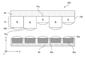
図1は、本開示の例示的な実施形態による光検出システム400を模式的に示す図である。光検出システム400は、光学系40と、フィルタアレイ10と、イメージセンサ60と、信号処理回路200とを備える。フィルタアレイ10は、特許文献1に開示されている「符号化素子」と同様の機能を有する。このため、フィルタアレイ10を、「符号化素子」と称することもできる。光学系40およびフィルタアレイ10は、対象物70から入射する光の光路に配置されている。図1に示す例では、フィルタアレイ10は、光学系40とイメージセンサ160との間に配置されている。(embodiment)
<Photodetection system>
FIG. 1 is a schematic diagram of an
図1には、対象物70の一例として、リンゴが例示されている。対象物70は、リンゴに限らず、任意の物体であり得る。信号処理回路200は、イメージセンサ60が生成した画像データに基づいて、特定の波長域(以下、「対象波長域」とも称する。)に含まれる複数の波長域のそれぞれについて画像データを生成する。この画像データを、本明細書において「分光画像データ」と称する。ここで、対象波長域に含まれる波長域の数をN(Nは4以上の整数)とする。以下の説明において、生成される複数の波長域の分光画像データを、分離画像220W1、220W2、・・・、220WNと称し、これらを分離画像220と総称する。本明細書において、画像を示す信号、すなわち、画像を構成する複数の画素の画素値を表す信号の集合を、単に「画像」とも称する。An apple is illustrated in FIG. 1 as an example of the object 70 . Object 70 is not limited to an apple, and may be any object. Based on the image data generated by the
フィルタアレイ10は、行および列状に配列された透光性の複数のフィルタを備える。フィルタアレイ10は、光の透過スペクトル、すなわち光透過率の波長依存性がフィルタによって異なる光学素子である。フィルタアレイ10は、入射した光の強度を波長域ごとに変調させて通過させる。
The
図1に示す例において、フィルタアレイ10は、イメージセンサ60の近傍に配置されている。ここで「近傍」とは、光学系40からの光の像がある程度鮮明な状態でフィルタアレイ10の面上に形成される程度に近接していることを意味する。本明細書において、フィルタアレイ10およびイメージセンサ60を備える装置を、「光検出装置300」と称する。
In the example shown in FIG. 1, the
光学系40は、少なくとも1つのレンズを含む。図1では、1つのレンズとして示されているが、光学系40は複数のレンズの組み合わせによって構成されていてもよい。光学系40は、フィルタアレイ10を介して、イメージセンサ60の撮像面上に像を形成する。
イメージセンサ60は、2次元的に配列された複数の光検出素子を備える。イメージセンサ60は、例えばCCD(Charge-Coupled Device)センサ、CMOS(Complementary Metal Oxide Semiconductor)センサ、または赤外線アレイセンサであり得る。光検出素子は、例えばフォトダイオードを含み得る。イメージセンサ60は、例えばモノクロタイプのセンサ、またはカラータイプのセンサであり得る。対象波長域は任意に決定してよい。対象波長域は、可視の波長域に限らず、紫外、近赤外、中赤外、遠赤外、またはマイクロ波の波長範囲であってもよい。
The
図1に示す例において、複数の光検出素子の各々は、複数のフィルタの1つに対向して配置されている。複数の光検出素子の各々は、撮像対象の波長域の光に対して感度を有する。具体的には、複数の光検出素子の各々は、撮像対象の波長域の光を検出するのに必要な実質的な感度を有する。例えば、当該波長域における光検出素子の外部量子効率は1%以上であり得る。光検出素子の外部量子効率は10%以上であってもよい。光検出素子の外部量子効率は20%以上であってもよい。以下の説明において、光検出素子を「画素」とも称する。 In the example shown in FIG. 1, each of the plurality of photodetector elements is positioned opposite one of the plurality of filters. Each of the plurality of photodetector elements has sensitivity to light in the wavelength range of the imaging target. Specifically, each of the plurality of photodetector elements has the substantial sensitivity required to detect light in the wavelength range to be imaged. For example, the external quantum efficiency of the photodetector in that wavelength range can be 1% or greater. The photodetector may have an external quantum efficiency of 10% or more. The external quantum efficiency of the photodetector may be 20% or more. In the following description, the photodetector is also called "pixel".
信号処理回路200は、例えばプロセッサとメモリ等の記憶媒体とを備える集積回路であり得る。信号処理回路200は、イメージセンサ60によって取得された画像120に基づいて、複数の波長域の情報をそれぞれ含む複数の分離画像220のデータを生成する。複数の分離画像220、および信号処理回路200の画像信号の処理方法の詳細については、後述する。なお、信号処理回路200は、光検出装置300に組み込まれていてもよいし、光検出装置300に有線または無線によって電気的に接続された信号処理装置の構成要素であってもよい。
<フィルタアレイ>
以下に、本実施形態によるフィルタアレイ10を説明する。フィルタアレイ10は、対象物から入射する光の光路に配置され、入射光の強度を波長ごとに変調して出力する。フィルタアレイすなわち符号化素子によるこの過程を、本明細書では「符号化」と称する。<Filter array>
The
図2Aは、フィルタアレイ10の例を模式的に示す図である。フィルタアレイ10は、2次元的に配列された複数のフィルタを含む。各フィルタは、個別に設定された透過スペクトルを有する。透過スペクトルは、入射光の波長をλとして、関数T(λ)で表される。透過スペクトルT(λ)は、0以上1以下の値を取り得る。
FIG. 2A is a diagram schematically showing an example of the
図2Aに示す例では、フィルタアレイ10は、6行8列に配列された48個の矩形状のフィルタを有している。これはあくまで例示であり、実際の用途では、これよりも多くのフィルタが設けられ得る。その数は、例えばイメージセンサ60の画素数と同程度であってもよい。フィルタアレイ10に含まれるフィルタの数は、例えば数十から数千万の範囲で用途に応じて決定される。
In the example shown in FIG. 2A, the
図2Bは、対象波長域に含まれる複数の波長域W1、W2、・・・、Wiのそれぞれの光の透過率の空間分布の一例を示す図である。図2Bに示す例では、各フィルタの濃淡の違いは、透過率の違いを表している。淡いフィルタほど透過率が高く、濃いフィルタほど透過率が低い。図2Bに示すように、波長域によって光透過率の空間分布が異なっている。FIG. 2B is a diagram showing an example of spatial distribution of transmittance of light in each of a plurality of wavelength bands W 1 , W 2 , . . . , W i included in the target wavelength band. In the example shown in FIG. 2B, the difference in shade of each filter represents the difference in transmittance. A lighter filter has a higher transmittance, and a darker filter has a lower transmittance. As shown in FIG. 2B, the spatial distribution of light transmittance differs depending on the wavelength range.
図2Cおよび図2Dは、それぞれ、図2Aのフィルタアレイ10の複数のフィルタに含まれるフィルタA1およびフィルタA2の透過スペクトルの例を示す図である。フィルタA1の透過スペクトルとフィルタA2の透過スペクトルとは、互いに異なっている。このように、フィルタアレイ10の透過スペクトルは、フィルタによって異なる。ただし、必ずしもすべてのフィルタの透過スペクトルが異なっている必要はない。フィルタアレイ10において、複数のフィルタのうちの少なくとも2つ以上のフィルタの透過スペクトルが互いに異なっている。すなわち、フィルタアレイ10は、透過スペクトルが互いに異なる2つ以上のフィルタを含む。ある例では、フィルタアレイ10に含まれる複数のフィルタの透過スペクトルのパターンの数は、対象波長域に含まれる波長域の数iと同じか、それ以上であり得る。フィルタアレイ10は、半数以上のフィルタの透過スペクトルが異なるように設計されていてもよい。
2C and 2D are diagrams showing examples of transmission spectra of filters A1 and A2 included in the plurality of filters of
図3Aおよび図3Bは、対象波長域Wと、それに含まれる複数の波長域W1、W2、・・・、Wiとの関係を説明するための図である。対象波長域Wは、用途によって様々な範囲に設定され得る。対象波長域Wは、例えば、約400nmから約700nmの可視光の波長域、約700nmから約2500nmの近赤外線の波長域、または約10nmから約400nmの近紫外線の波長域であり得る。あるいは、対象波長域Wは、中赤外、遠赤外、テラヘルツ波、またはミリ波などの電波域であってもよい。このように、使用される波長域は可視光域とは限らない。本明細書では、可視光に限らず、近紫外線、近赤外線、および電波などの非可視光も便宜上「光」と称する。3A and 3B are diagrams for explaining the relationship between a target wavelength band W and a plurality of wavelength bands W 1 , W 2 , . . . , W i included therein. The target wavelength band W can be set in various ranges depending on the application. The target wavelength range W can be, for example, a visible light wavelength range from about 400 nm to about 700 nm, a near-infrared wavelength range from about 700 nm to about 2500 nm, or a near-ultraviolet wavelength range from about 10 nm to about 400 nm. Alternatively, the target wavelength range W may be a radio wave range such as mid-infrared, far-infrared, terahertz waves, or millimeter waves. Thus, the wavelength range used is not limited to the visible light range. In this specification, not only visible light but also non-visible light such as near-ultraviolet light, near-infrared light, and radio waves are referred to as "light" for the sake of convenience.
図3Aに示す例では、iを4以上の任意の整数として、対象波長域Wをi等分したそれぞれを波長域W1、波長域W2、・・・、波長域Wiとしている。ただしこのような例に限定されない。対象波長域Wに含まれる複数の波長域は任意に設定してもよい。例えば、波長域によって帯域幅を不均一にしてもよい。隣接する波長域の間にギャップがあってもよい。図3Bに示す例では、波長域によって帯域幅が異なり、かつ、隣接する2つの波長域の間にギャップがある。このように、複数の波長域は、互いに異なっていればよく、その決め方は任意である。波長の分割数iは3以下でもよい。In the example shown in FIG. 3A, i is an arbitrary integer equal to or greater than 4, and the target wavelength range W is equally divided into i equal wavelength ranges W 1 , W 2 , . . . , and W i . However, it is not limited to such an example. A plurality of wavelength ranges included in the target wavelength range W may be set arbitrarily. For example, the bandwidth may be non-uniform depending on the wavelength band. There may be gaps between adjacent wavelength bands. In the example shown in FIG. 3B, the wavelength bands have different bandwidths and there is a gap between two adjacent wavelength bands. In this way, the plurality of wavelength ranges may be different from each other, and the method of determining them is arbitrary. The wavelength division number i may be 3 or less.
図4Aは、フィルタアレイ10におけるあるフィルタの透過スペクトルの特性を説明するための図である。図4Aに示す例では、透過スペクトルは、対象波長域W内の波長に関して、複数の極大値P1から極大値P5、および複数の極小値を有する。図4Aに示す例では、対象波長域W内での光透過率の最大値が1、最小値が0となるように正規化されている。図4Aに示す例では、波長域W2、および波長域Wi-1などの波長域において、透過スペクトルが極大値を有している。このように、本実施形態では、各フィルタの透過スペクトルは、複数の波長域W1から波長域Wiのうち、少なくとも2つの複数の波長域において極大値を有する。図4Aからわかるように、極大値P1、極大値P3、極大値P4、および極大値P5は0.5以上である。FIG. 4A is a diagram for explaining transmission spectrum characteristics of a certain filter in the
以上のように、各フィルタの光透過率は、波長によって異なる。したがって、フィルタアレイ10は、入射する光のうち、ある波長域の成分を多く透過させ、他の波長域の成分をそれほど透過させない。例えば、i個の波長域のうちのk個の波長域の光については、透過率が0.5よりも大きく、残りのi-k個の波長域の光については、透過率が0.5未満であり得る。kは、2≦k<iを満たす整数である。仮に入射光が、すべての可視光の波長成分を均等に含む白色光であった場合には、フィルタアレイ10は、入射光をフィルタごとに、波長に関して離散的な複数の強度のピークを有する光に変調し、これらの多波長の光を重畳して出力する。
As described above, the light transmittance of each filter differs depending on the wavelength. Therefore, the
図4Bは、一例として、図4Aに示す透過スペクトルを、波長域W1、波長域W2、・・・、波長域Wiごとに平均化した結果を示す図である。平均化された透過率は、透過スペクトルT(λ)を波長域ごとに積分してその波長域の帯域幅で除算することによって得られる。本明細書では、このように波長域ごとに平均化した透過率の値を、その波長域における透過率と称する。この例では、極大値P1、極大値P3、および極大値P5をとる3つの波長域において、透過率が突出して高くなっている。特に、極大値P3、および極大値P5をとる2つの波長域において、透過率が0.8を超えている。FIG. 4B is a diagram showing, as an example, the result of averaging the transmission spectrum shown in FIG. 4A for each wavelength region W 1 , wavelength region W 2 , . . . , wavelength region Wi . The averaged transmission is obtained by integrating the transmission spectrum T(λ) for each wavelength band and dividing by the bandwidth of that wavelength band. In this specification, the transmittance value averaged for each wavelength band is referred to as the transmittance in that wavelength band. In this example, the transmittance is remarkably high in three wavelength regions having the maximum value P1, the maximum value P3, and the maximum value P5. In particular, the transmittance exceeds 0.8 in the two wavelength regions having the maximum value P3 and the maximum value P5.
各フィルタの透過スペクトルの波長方向の分解能は、所望の波長域の帯域幅程度に設定され得る。言い換えれば、透過スペクトル曲線における1つの極大値を含む波長範囲のうち、当該極大値に最も近接する極小値と当該極大値との平均値以上の値をとる範囲の幅は、所望の波長域の帯域幅程度に設定され得る。この場合、透過スペクトルを、例えばフーリエ変換によって周波数成分に分解すれば、その波長域に相当する周波数成分の値が相対的に大きくなる。 The resolution in the wavelength direction of the transmission spectrum of each filter can be set to approximately the bandwidth of the desired wavelength band. In other words, in the wavelength range including one maximum value in the transmission spectrum curve, the width of the range having a value equal to or greater than the average value of the maximum value and the minimum value closest to the maximum value is the desired wavelength range. It can be set on the order of bandwidth. In this case, if the transmission spectrum is decomposed into frequency components by, for example, Fourier transform, the values of the frequency components corresponding to that wavelength range become relatively large.
フィルタアレイ10は、典型的には、図2Aに示すように、格子状に区分けされた複数のフィルタを有する。これらのフィルタの一部または全部が、互いに異なる透過スペクトルを有する。フィルタアレイ10に含まれる複数のフィルタの光透過率の波長分布および空間分布は、例えばランダム分布または準ランダム分布であり得る。
The
ランダム分布および準ランダム分布の考え方は次の通りである。まず、フィルタアレイ10における各フィルタは、光透過率に応じて、例えば0から1の値を有するベクトル要素と考えることができる。ここで、透過率が0の場合、ベクトル要素の値は0であり、透過率が1の場合、ベクトル要素の値は1である。言い換えると、行方向または列方向に一列に並んだフィルタの集合を0から1の値を有する多次元のベクトルと考えることができる。したがって、フィルタアレイ10は、多次元ベクトルを列方向または行方向に複数備えていると言える。このとき、ランダム分布とは、任意の2つの多次元ベクトルが独立である、すなわち平行でないことを意味する。また、準ランダム分布とは、一部の多次元ベクトル間で独立でない構成が含まれることを意味する。したがって、ランダム分布および準ランダム分布においては、複数のフィルタに含まれる1つの行または列に並んだフィルタの集合に属する各フィルタでの第1の波長域の光の透過率の値を要素とするベクトルと、他の行または列に並んだフィルタの集合に属する各フィルタにおける第1の波長域の光の透過率の値を要素とするベクトルとは、互いに独立である。第1の波長域とは異なる第2の波長域についても同様に、複数のフィルタに含まれる1つの行または列に並んだフィルタの集合に属する各フィルタにおける第2の波長域の光の透過率の値を要素とするベクトルと、他の行または列に並んだフィルタの集合に属する各フィルタにおける第2の波長域の光の透過率の値を要素とするベクトルとは、互いに独立である。
The concept of random distribution and quasi-random distribution is as follows. First, each filter in
フィルタアレイ10をイメージセンサ60の近傍に配置する場合、フィルタアレイ10に含まれる複数のフィルタの相互の間隔は、イメージセンサ60の画素ピッチと略一致させてもよい。このようにすれば、フィルタアレイ10から出射した符号化された光の像の解像度が画素の解像度と略一致する。各セルを透過した光が対応する1つの画素に入射するようにすることにより、後述する演算を容易にすることができる。フィルタアレイ10をイメージセンサ60から離して配置する場合には、その距離に応じてセルピッチを細かくしてもよい。
When the
図2Aから図2Dに示す例では、フィルタアレイ10は、各フィルタの透過率が0以上1以下の任意の値をとり得るグレースケールの透過率分布を有する。しかし、必ずしもグレースケールの透過率分布にする必要はない。例えば、各フィルタの透過率がほぼ0またはほぼ1のいずれかの値を取り得るバイナリスケールの透過率分布を採用してもよい。バイナリスケールの透過率分布において、各フィルタは、対象波長域に含まれる複数の波長域のうちの少なくとも2つの波長域の光の大部分を透過させ、残りの波長域の光の大部分を透過させない。ここで「大部分」とは、概ね80%以上を指す。
In the example shown in FIGS. 2A to 2D, the
すべてのフィルタのうちの一部、例えば半分のフィルタを、透明フィルタに置き換えてもよい。そのような透明フィルタは、対象波長域に含まれるすべての波長域W1から波長域Wiの光を高い透過率で透過させる。当該高い透過率は、例えば0.8以上である。そのような構成では、複数の透明フィルタは、例えば市松(checkerboard)状に配置され得る。すなわち、フィルタアレイ10における複数のフィルタの2つの配列方向において、光透過率が波長によって異なるフィルタと、透明フィルタとが交互に配列され得る。図2Aに示す例において、2つの配列方向は、横方向および縦方向である。
Part of all filters, for example half of the filters, may be replaced by transparent filters. Such a transparent filter transmits light in all wavelength ranges W1 to Wi included in the target wavelength range with high transmittance. The high transmittance is, for example, 0.8 or higher. In such a configuration, multiple transparent filters may be arranged in a checkerboard, for example. That is, in the two arrangement directions of the plurality of filters in the
このようなフィルタアレイ10の分光透過率の空間分布を示すデータは、設計データまたは実測キャリブレーションに基づいて事前に取得され、信号処理回路200が備える記憶媒体に格納される。このデータは、後述する演算処理に利用される。
Such data indicating the spatial distribution of the spectral transmittance of the
フィルタアレイ10は、例えば、多層膜、有機材料、回折格子構造、または金属を含む微細構造を用いて構成され得る。多層膜を用いて構成される場合、例えば、誘電体多層膜または金属層を含む多層膜が用いられ得る。この場合、セルごとに各多層膜の厚さ、材料、および積層順序の少なくとも1つが異なるように形成され得る。これにより、セルによって異なる分光特性を実現できる。多層膜を用いることにより、分光透過率におけるシャープな立ち上がりおよび立下りを実現できる。有機材料を用いた構成は、セルによって含有する顔料または染料が異なるようにしたり、異種の材料を積層させたりすることによって実現され得る。回折格子構造を用いた構成は、セルごとに異なる回折ピッチまたは深さの回折構造を設けることによって実現され得る。金属を含む微細構造を用いる場合は、プラズモン効果による分光を利用して作製され得る。
The
<信号処理回路>
次に、信号処理回路200によって多波長の分離画像220を再構成する方法を説明する。ここで多波長とは、例えば通常のカラーカメラで取得されるRGBの3色の波長域よりも多くの波長域、すなわち4つ以上の波長域を意味する。この波長域の数は、例えば4から100程度の数であり得る。この波長域の数を、「分光帯域数」とも称する。用途によっては、分光帯域数は100を超えていてもよい。<Signal processing circuit>
Next, a method for reconstructing a multi-wavelength
求めたいデータは分離画像220であり、そのデータは、fとして表される。分光帯域数をwとすると、fは、各帯域の画像データf1、f2、・・・、fwを統合したデータである。ここで、図1に示すように、画像の横方向をx方向、画像の縦方向をy方向とする。求めるべき画像データのx方向の画素数をnとし、y方向の画素数をmとすると、画像データf1、f2、・・・、fwの各々は、n×m画素の2次元データである。したがって、データfは要素数n×m×wの3次元データである。一方、フィルタアレイ10によって符号化および多重化されて取得される画像120のデータgの要素数はn×mである。データgは、以下の式(1)によって表すことができる。The data we want to obtain is the

ここで、f1、f2、・・・、fwは、n×m個の要素を有するデータである。したがって、右辺のベクトルは、厳密にはn×m×w行1列の1次元ベクトルである。ベクトルgは、n×m行1列の1次元ベクトルに変換して表され、計算される。行列Hは、ベクトルfの各成分f1、f2、・・・、fwを波長域ごとに異なる符号化情報で符号化および強度変調し、それらを加算する変換を表す。したがって、Hは、n×m行n×m×w列の行列である。Here, f 1 , f 2 , . . . , f w are data having n×m elements. Therefore, the vector on the right side is strictly a one-dimensional vector of n×m×w rows and 1 column. The vector g is converted into a one-dimensional vector of n×m rows and 1 column and calculated. Matrix H represents a transform that encodes and intensity-modulates each component f 1 , f 2 , . Therefore, H is a matrix with n×m rows and n×m×w columns.
ベクトルgと行列Hが与えられれば、式(1)の逆問題を解くことにより、fを算出することができそうである。しかし、求めるデータfの要素数n×m×wが取得データgの要素数n×mよりも多いため、この問題は不良設定問題であり、このままでは解くことができない。そこで、信号処理回路200は、データfに含まれる画像の冗長性を利用し、圧縮センシングの手法を用いて解を求める。具体的には、以下の式(2)を解くことにより、求めるデータfが推定される。
Given a vector g and a matrix H, it is likely that f can be calculated by solving the inverse problem of equation (1). However, since the number of elements n×m×w of the desired data f is larger than the number of elements n×m of the acquired data g, this problem is an ill-posed problem and cannot be solved as it is. Therefore, the

ここで、f’は、推定されたfのデータを表す。上式の括弧内の第1項は、推定結果Hfと取得データgとのずれ量、いわゆる残差項を表す。ここでは2乗和を残差項としているが、絶対値あるいは二乗和平方根等を残差項としてもよい。括弧内の第2項は、後述する正則化項または安定化項である。式(2)は、第1項と第2項との和を最小化するfを求めることを意味する。信号処理回路200は、再帰的な反復演算によって解を収束させ、最終的な解f’を算出することができる。
where f' represents the estimated data of f. The first term in parentheses in the above formula represents the amount of deviation between the estimation result Hf and the acquired data g, ie, the so-called residual term. Although the sum of squares is used as the residual term here, the absolute value or the square root of the sum of squares may be used as the residual term. The second term in parentheses is a regularization term or a stabilization term, which will be described later. Equation (2) means finding f that minimizes the sum of the first and second terms. The
式(2)の括弧内の第1項は、取得データgと、推定過程のfを行列Hによってシステム変換したHfとの差分の二乗和を求める演算を意味する。第2項のΦ(f)は、fの正則化における制約条件であり、推定データのスパース情報を反映した関数である。働きとしては、推定データを滑らかまたは安定にする効果がある。正則化項は、例えば、fの離散的コサイン変換(DCT)、ウェーブレット変換、フーリエ変換、またはトータルバリエーション(TV)などによって表され得る。例えば、トータルバリエーションを使用した場合、観測データgのノイズの影響を抑えた安定した推測データを取得できる。それぞれの正則化項の空間における対象物70のスパース性は、対象物70のテキスチャによって異なる。対象物70のテキスチャが正則化項の空間においてよりスパースになる正則化項を選んでもよい。あるいは、複数の正則化項を演算に含んでもよい。τは、重み係数である。重み係数τが大きいほど冗長的なデータの削減量が多くなり、圧縮する割合が高まる。重み係数τが小さいほど解への収束性が弱くなる。重み係数τは、fがある程度収束し、かつ、過圧縮にならない適度な値に設定される。 The first term in the parenthesis of Equation (2) means an operation for obtaining the sum of squares of differences between the obtained data g and Hf obtained by system-transforming f in the estimation process using the matrix H. The second term, Φ(f), is a constraint on the regularization of f, and is a function that reflects the sparse information of the estimated data. As a function, it has the effect of smoothing or stabilizing the estimated data. The regularization term may be represented by, for example, the Discrete Cosine Transform (DCT), Wavelet Transform, Fourier Transform, or Total Variation (TV) of f. For example, when the total variation is used, it is possible to acquire stable estimated data that suppresses the influence of noise in the observed data g. The sparsity of the object 70 in the space of each regularization term depends on the texture of the object 70 . A regularization term may be chosen that makes the texture of the object 70 more spars in the space of regularization terms. Alternatively, multiple regularization terms may be included in the operation. τ is a weighting factor. The larger the weighting factor τ, the larger the reduction amount of redundant data and the higher the compression rate. The smaller the weighting factor τ, the weaker the convergence to the solution. The weighting factor τ is set to an appropriate value with which f converges to some extent and does not become over-compressed.
なお、ここでは式(2)に示す圧縮センシングを用いた演算例を示したが、その他の方法を用いて解いてもよい。例えば、最尤推定法またはベイズ推定法などの他の統計的方法を用いることができる。また、分離画像220の数は任意であり、各波長域も任意に設定してよい。再構成の方法の詳細は、特許文献1に開示されている。特許文献1の開示内容の全体を本明細書に援用する。
Although an example of calculation using compressed sensing shown in Equation (2) has been shown here, other methods may be used for solving. For example, other statistical methods such as maximum likelihood or Bayesian estimation can be used. Moreover, the number of separated
<ファブリ・ペローフィルタを含むフィルタアレイ>
次に、図5Aから図5Cを参照して、本開示の実施形態によるフィルタアレイ10の具体的な構造の例を説明する。図5Aから図5Cは、それぞれ本開示の実施形態によるフィルタアレイ10の第1から第3の例を模式的に示す断面図である。これらの断面図では、簡単のために、1つの行に含まれる5つのフィルタ100が示されている。図5Aから図5Cに示す例において、フィルタアレイ10は基板20によって支持されている。フィルタアレイ10は、図2Aに示すように、正方格子状に2次元的に配列された複数のフィルタ100を含む。図5Aに示す第1の例から図5Cに第3の例において、フィルタアレイ10に含まれるすべてのフィルタ100は共振構造を備える。共振構造とは、ある波長の光が内部で定在波を形成して安定に存在する構造を意味する。<Filter array including Fabry-Perot filter>
Next, with reference to FIGS. 5A to 5C, examples of specific structures of the
図5Aに示す第1の例において、基板20上に、第1反射層14a、干渉層12、および第2反射層14bがこの順に積層されている。図5Aに示す各共振構造は、互いに反対側に位置する第1表面12s1および第2表面12s2を有する干渉層12と、第1表面12s1に設けられた第1反射層14aと、第2表面12s2に設けられた第2反射層14bとを含む。第1表面12s1および第2表面12s2の各々の対象波長域Wの光についての反射率は、例えば80%以上であり得る。当該反射率は、80%よりも低くてもよいが40%以上に設計され得る。第1反射層14aの厚さおよび第2反射層14bの厚さは等しくなるように設計され得る。干渉層12の厚さが互いに異なる複数のフィルタ100は、対象波長域W内で互いに異なる透過スペクトルを有する。図5Aに示す各共振構造の透過スペクトルは、後述するように対象波長域W内に2つ以上の鋭いピークを有する。In the first example shown in FIG. 5A, a first
図5Aに示す第1の例において、第1反射層14aおよび第2反射層14bの各々は、複数の高屈折率層および複数の低屈折率層が交互に積層された分布ブラッグ反射器(Distributed Bragg Reflector:DBR)から形成されている。第1反射層14aおよび第2反射層14bの各々は金属薄膜から形成されていてもよい。
In the first example shown in FIG. 5A, each of the first
DBRは、屈折率が異なる高屈折率層および低屈折率層のペア層を1組以上含む。高屈折率層の屈折率は、低屈折率層の屈折率よりも高い。DBRは、周期的な積層構造に起因するブラッグ反射により、反射率が高い波長域を有する。当該波長域はストップバンドと呼ばれる。上記のペア層の数を増加させると、ストップバンドの反射率は100%に近づく。 A DBR includes at least one set of pair layers of a high refractive index layer and a low refractive index layer having different refractive indices. The refractive index of the high refractive index layer is higher than that of the low refractive index layer. A DBR has a wavelength region with high reflectance due to Bragg reflection caused by a periodic lamination structure. This wavelength range is called a stop band. As the number of pair layers is increased, the stopband reflectivity approaches 100%.
対象波長域W内の波長をλ、高屈折率層の屈折率をnH、低屈折率層の屈折率をnLとする。厚さがλ/(4nH)である高屈折率層、および厚さがλ/(4nL)である低屈折率層のペア層を1組以上含むDBRは、波長λの光を効率的に反射させる。対象波長域Wが波長λi以上波長λf以下の範囲である場合、複数の高屈折率層および複数の低屈折率層の厚さを段階的に変化させることにより、DBRは、波長λiに対応するペア層から波長λfに対応するペア層を含むことができる。その結果、当該DBRは、対象波長域W内のすべての光を効率的に反射させることができる。Let λ be the wavelength in the target wavelength range W, n H be the refractive index of the high refractive index layer, and n L be the refractive index of the low refractive index layer. A DBR that includes one or more paired layers of a high refractive index layer with a thickness of λ/(4n H ) and a low refractive index layer with a thickness of λ/(4n L ) efficiently emits light with a wavelength of λ. reflect to When the target wavelength range W is in the range of wavelength λ i or more and wavelength λ f or less, the DBR can be obtained by changing the thicknesses of the plurality of high refractive index layers and the plurality of low refractive index layers stepwise, so that the wavelength λ i to the paired layers corresponding to the wavelength λ f . As a result, the DBR can efficiently reflect all light within the wavelength range W of interest.
第1反射層14aおよび第2反射層14bの各々に含まれる高屈折率層および低屈折率層、ならびに干渉層12は、例えば、対象波長域W内の光について吸収率の低い材料から形成され得る。対象波長域Wが可視光領域内にある場合、そのような材料は、例えば、SiO2、Al2O3、SiOxNy、Si3N4、Ta2O5、およびTiO2からなる群から選択される少なくとも1つであり得る。対象波長域Wが赤外領域内にある場合、そのような材料は、例えば、上記のSiO2、Al2O3、SiOxNy、Si3N4、Ta2O5、およびTiO2に加えて、単結晶Si、多結晶Si、およびアモルファスSiからなる群から選択される少なくとも1つであり得る。同様に、基板20は、例えば、対象波長域W内の光について吸収率の低い材料から形成され得る。対象波長域Wが可視光領域内にある場合、そのような材料は、SiO2、ITO、Al2O3、GaN、Nb2O5、Ta2O5、およびSiCからなる群から選択される少なくとも1つであり得る。対象波長域Wが赤外領域内にある場合、そのような材料は、例えば、上記のSiO2、ITO、Al2O3、GaN、Nb2O5、Ta2O5、およびSiCに加えて、単結晶Si、多結晶Si、アモルファスSi、およびInPからなる群から選択される少なくとも1つであり得る。第1反射層14aおよび第2反射層14bの各々の厚さは、例えば100nm以上900nm以下であり得る。干渉層12の厚さは、例えば10nm以上500nm以下であり得る。基板20の厚さは、例えば0.1mm以上1mm以下であり得る。The high refractive index layer and the low refractive index layer included in each of the first
図5Bに示す第2の例において、基板20上に、第1反射層14aおよび干渉層12がこの順に積層されている。図5Bに示す各共振構造は、干渉層12と、第1表面12s1に設けられた第1反射層14aと含む。図5Bに示す第2の例が図5Aに示す第1の例と異なる点は、第2表面12s2に第2反射層14bが設けられていないことである。図5Bに示す各共振構造の透過スペクトルは、後述するように対象波長域W内に2つ以上の幅広いピークを有する。In the second example shown in FIG. 5B, the first
図5Bに示す例において、第2表面12s2は外部に露出し、空気に接している。干渉層12の第2表面12s2上に、透明層をさらに積層してもよい。第1表面12s1における対象波長域Wの光についての反射率(以下、「第1反射率」と称する。)は、例えば80%以上であり得る。第1反射率は、80%よりも低くてもよいが40%以上に設計され得る。第2表面12s2における対象波長域Wの光についての反射率(「第2反射率」と称する。)は、第1反射率よりも低く、例えば1%以上30%未満であり得る。第1反射率と第2反射率との間には10%以上の一定の差異がある。In the example shown in FIG. 5B, the second surface 12s2 is exposed to the outside and is in contact with air. A transparent layer may be further laminated on the second surface 12s2 of the
本明細書では、図5Aに示す共振構造を「両側DBR構造」と称し、図5Bに示す共振構造を「片側DBR構造」と称する。本明細書では、両側DBR構造および片側DBR構造において、光を反射する面の正確な位置が問題にならない限り、干渉層12内の光は、第1表面12s1および第2表面12s2で反射されるものとする。本実施形態において、干渉層12から第1反射層14aまたは第2反射層14bに入射する光の一部は、実際には、第1反射層14aまたは第2反射層14b内に浸入し、複数の高屈折率層および複数の低屈折率層の界面で反射される。光が反射される界面は、波長によって異なる。しかし、説明の便宜上、これらの光は、第1表面12s1および第2表面12s2で反射されるものとして取り扱う。In this specification, the resonant structure shown in FIG. 5A is referred to as a "double-sided DBR structure," and the resonant structure illustrated in FIG. 5B is referred to as a "single-sided DBR structure." Herein, in double-sided DBR structures and single-sided DBR structures, light in
図5Cに示す第3の例において、一部のフィルタ100は両側DBR構造を有し、他の一部のフィルタ100は片側DBR構造を有する。フィルタアレイ10に含まれるすべてのDBR構造に対する片側DBR構造の割合は、例えば10%以上90%以下であり得る。片側DBR構造の割合は、両側DBR構造の割合よりも小さくてもよいし、両側DBR構造の割合に等しくてもよいし、両側DBR構造の割合よりも大きくてもよい。両側DBR構造および片側DBR構造の配置は、規則的であってもよいし不規則であってもよい。両側DBR構造および片側DBR構造が混在することにより、フィルタアレイ10に含まれる複数のフィルタ100の透過スペクトルのランダム性を向上させることができる。その結果、より正確な複数の分離画像220を得ることができる。
In a third example shown in FIG. 5C, some
次に、図6を参照して、フィルタ100の透過スペクトルの例を説明する。図6は、光が垂直に入射する場合における両側DBR構造および片側DBR構造の光の透過スペクトルの例を示す図である。図6に示す例において、対象波長域Wは450nm以上850nm以下である。図6に示す実線は両側DBR構造の透過スペクトルを表し、図6に示す破線は片側DBR構造の透過スペクトルを表す。図6に示すように、両側DBR構造および片側DBR構造の透過スペクトルは、対象波長域W内に2つ以上の波長の各々で透過率の極大値を有する。本明細書では、このような透過スペクトルを有するフィルタを「多モードフィルタ」と称する。透過率が極大値を示す波長は、干渉層12を薄くすると短波長側にシフトし、干渉層12を厚くすると長波長側にシフトする。
Next, an example of the transmission spectrum of
両側DBR構造および片側DBR構造の特性は以下の点において異なる。両側DBR構造の透過スペクトルにおいて、各ピークは鋭く、かつ、最大の透過率が1.0程度であり、最小の透過率が0.02程度である。これに対して、片側DBR構造の透過スペクトルにおいて、各ピークは幅広く、かつ、最大の透過率が0.5程度であり、最小の透過率が0.1程度である。片側DBR構造では、両側DBR構造と比較して、透過率のベースラインが上昇する。図6に示す例において、片側DBR構造の対象波長域W内の平均透過率は約26%であり、両側DBR構造の対象波長域W内の平均透過率は約14%である。片側DBR構造では、両側DBR構造と比較して、平均透過率が約2倍である。このように、片側DBR構造は、撮像時の光量損失を抑制することができる。 The properties of the double-sided DBR structure and the single-sided DBR structure differ in the following points. In the transmission spectrum of the double-sided DBR structure, each peak is sharp and the maximum transmittance is about 1.0 and the minimum transmittance is about 0.02. On the other hand, in the transmission spectrum of the single-sided DBR structure, each peak is broad and has a maximum transmittance of about 0.5 and a minimum transmittance of about 0.1. The single-sided DBR structure increases the baseline transmission compared to the double-sided DBR structure. In the example shown in FIG. 6, the average transmittance within the wavelength range W of interest for the single-sided DBR structure is approximately 26%, and the average transmittance within the wavelength range W of interest for the double-sided DBR structure is approximately 14%. The single-sided DBR structure has about twice the average transmittance as compared to the double-sided DBR structure. In this way, the single-sided DBR structure can suppress loss of light quantity during imaging.
本実施形態によるフィルタアレイ10では、対象波長域W内で互いに透過スペクトルが異なる複数種類の多モードフィルタが不規則に配置され得る。不規則な配置とは、明確な規則性または周期性を示さない配置であり、非周期的な配置でもある。不規則な配置は、例えば前述のランダム分布または準ランダム分布の考え方に従った配置であり得る。ある例において、フィルタアレイ10は2次元的に配列された数百万個のフィルタ100を含み、当該数百万個のフィルタ100は不規則に配置された9種類の多モードフィルタを含む。9種類の多モードフィルタが、高いランダム性をもって配列され得る。そのようなランダム性の高いフィルタ配列を有するフィルタアレイ10により、分離画像220の復元誤差を低減することができる。不規則な配置であることから、隣り合うフィルタが同種類のフィルタである場合もある。しかし、そのような場合はまれであると考えられるので、大きな問題にはならない。
In the
なお、本実施形態によるフィルタアレイ10は、上記の共振構造を有しないフィルタを含んでいてもよい。本実施形態によるフィルタアレイ10は、例えば、透明フィルタまたはNDフィルタ(Neutral Density Filter)などの、光透過率の波長依存性を有しないフィルタを含んでいてもよい。
Note that the
本明細書では、両側DBR構造および/または片側DBR構造を備えるフィルタ100を、「ファブリ・ペローフィルタ」とも称する。ファブリ・ペローフィルタは干渉フィルタの一種である。ファブリ・ペローフィルタに代えて、例えば回折格子などから構成される色分離フィルタなど、他の種類の干渉フィルタを用いることができる。
A
<フィルタアレイおよびイメージセンサの配置関係>
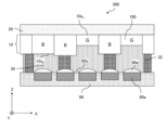
次に、図7から図14を参照して、フィルタアレイ10およびイメージセンサ60の配置関係の例を説明する。図7および以降の図に示す例においては、簡単のために、フィルタアレイ10およびイメージセンサ60の各々が2次元的に配列された5×5のユニットセルを含むものとして説明されている。しかし、実際には、フィルタアレイ10およびイメージセンサ60の各々は、例えば2次元的に配列された数百万個のユニットセルを含み得る。図示されている構造は例示にすぎず、ユニットセルの数および配置は任意に決定され得る。<Arrangement Relationship between Filter Array and Image Sensor>
Next, with reference to FIGS. 7 to 14, examples of the arrangement relationship between the
図7は、本開示の実施形態による光検出装置300の第1の例を模式的に示す断面図である。当該断面図は、ある1つの行についてのフィルタアレイ10およびイメージセンサ60の断面図である。図7に示す構造は、光検出装置300の部分構造である。説明の便宜上、図7には、互いに直交するX軸、Y軸、およびZ軸が示されている。X軸の矢印の方向を+X方向と称し、その反対の方向を-X方向と称する。Y軸およびZ軸の矢印の方向およびその反対の方向についても同様である。+Z方向側を「上」とも称し、-Z方向側を「下」とも称する。これらの軸は、光検出装置300の配置および姿勢を限定するものではなく、実際の光検出装置300の配置および姿勢は任意である。本実施形態による光検出装置300は、フィルタアレイ10と、フィルタアレイ10を支持する基板20と、イメージセンサ60とを備える。
FIG. 7 is a cross-sectional view schematically showing a first example of the
図7に示すフィルタアレイ10および基板20の構成は、上下を反転させた点を除き、図5Cに示すフィルタアレイ10および基板20の構成と同じである。図5Cに示す構成の代わりに、図5Aまたは図5Bに示す構成を採用してもよい。基板20は、光検出装置300を製造する工程において用いられる。基板20は必ずしも必要ではないが、光検出装置300の製造において基板20を除去しない場合には、基板20が光検出装置300に含まれる。
The configuration of the
フィルタアレイ10は、XY平面に沿って正方格子状に2次元的に配列された複数のフィルタ100を含む。複数のフィルタ100は、対象波長域W内で透過スペクトルが互いに異なる複数種類の多モードフィルタを含む。干渉層12の厚さは、多モードフィルタの透過スペクトルに応じて異なっている。複数のフィルタ100のX方向およびY方向における配列ピッチはすべて等しい。複数種類の多モードフィルタは、例えば前述のランダム分布または準ランダム分布の考え方に従って不規則に配置されている。
The
フィルタアレイ10は、光入射面10s1およびその反対側の光出射面10s2を有する。光入射面10s1は、複数のフィルタ100の光入射面の集まりによって形成される。光出射面10s2は、複数のフィルタ100の光出射面の集まりによって形成される。図7に示す例において、光入射面10s1は平坦である。言い換えれば、複数のフィルタ100における光入射面は段差のない平坦面を形成する。これに対して、光出射面10s2は凹凸すなわち段差を有する。言い換えれば、複数のフィルタ100における光出射面は凹凸面を形成する。この凹凸は、フィルタ100によって厚さが異なることに起因して生じる。フィルタ100ごとの厚さの違いは、干渉層の厚さが異なること、あるいは第2反射層14bの有無に起因して生じる。基板20は、フィルタアレイ10の光入射面10s1に設けられている。The
イメージセンサ60は、光出射面10s2に対向する光検出面60sを有し、光検出面60sに沿って正方格子状に2次元的に配列された複数の光検出素子60aを含む。光検出面60sは平坦である。複数の光検出素子60aは対象波長域Wに感度を有する。複数の光検出素子60aは、複数のフィルタ100にそれぞれ対向している。図7に示す第1の例において、複数の光検出素子60aのX方向およびY方向における配列ピッチはすべて等しい。光検出素子60aのX方向およびY方向における配列ピッチは異なっていてもよい。光検出素子60aの配列ピッチは、例えば1μm以上10μm以下であり得る。図7に示す第1の例において、フィルタ100の配列ピッチは、光検出素子60aの配列ピッチに等しくなるように設計されている。複数の光検出素子60aは、それぞれ、直上に複数のマイクロレンズ40aを備える。マイクロレンズ40aは、フィルタ100を透過した光を光検出素子60aに効率的に入射させる。光入射面10s1および光検出面60sは互いに平行である。「光入射面10s1および光検出面60sが互いに平行である」とは、厳密に平行であることを意味するのではなく、光入射面10s1の法線方向と光検出面60sの法線方向とがなす角度が10°以下であることを意味する。光入射面10s1の法線方向は、光入射面10s1に垂直であり、かつ、フィルタアレイ10から遠ざかる方向である。光検出面60sの法線方向は、光検出面60sに垂直であり、かつ、イメージセンサ60から遠ざかる方向である。The
対象物70で反射された光は、主に-Z方向に沿って基板20を介してフィルタアレイ10の光入射面10s1に入射し、フィルタアレイ10を通り、フィルタアレイ10の光出射面10s2から出射する。フィルタアレイ10の光出射面10s2から出射した光は、イメージセンサ60の光検出面60sに入射する。Light reflected by the object 70 enters the light incident surface 10s1 of the
光出射面10s2と光検出面60sとの距離は、多モードフィルタごとに異なっている。本実施形態の光検出装置300は、図5Cに示す構造物およびイメージセンサ60を、フィルタアレイ10の凹凸面が光検出面60sに対向するように固定することによって製造される。光出射面10s2と光検出面60sとの距離が不均一になるので、光出射面10s2と光検出面60sとの間で光の多重反射が生じても、撮像画像に光の干渉による干渉縞が現れることを抑制できる。したがって、光検出装置300の撮像特性を向上させることができる。複数種類の多モードフィルタの不規則な配置により、複数の分離画像220の復元誤差を低減できるだけでなく、撮像画像に干渉縞が現れることをさらに抑制できる。The distance between the light exit surface 10s2 and the
さらに、本実施形態では、基板20ではなく第2反射層14bがイメージセンサ60の光検出面60sに対向するように配置することにより、フィルタアレイ10とイメージセンサ60とを近づけることができる。光出射面10s2のうち、最も光検出面60sに近い部分と光検出面60sとの距離(以下、「最小距離dm」と称することがある。)は、例えば0.1μm以上200μm以下であり得る。本実施形態において、図1に示す光学系40のF値は16以下であり、光検出素子60aの配列ピッチは6μm程度であり得る。この場合、焦点深度が約200μm程度となるので、光出射面10s2と光検出面60sとの最小距離が上記の範囲内であれば、各フィルタ100を通過した光の大部分を、光検出面60s内の各フィルタ100の直下に位置する領域に入射させることができる。図7に示す第1の例では、当該領域に1つの光検出素子60aが位置する。Furthermore, in this embodiment, the
光出射面10s2と光検出面60sとの距離によっては、両者の間に光の干渉が発生し得る。この干渉の影響により、光検出素子60aによって検出される光のスペクトルと、多モードフィルタの透過スペクトルとがずれる可能性がある。ここで発生し得る干渉は、光出射面10s2と光検出面60sとの間の距離dに依存する。光出射面10s2と光検出面60sと往復距離2dが波長λの整数倍である場合、すなわち距離d=m1λ/2の場合、光は干渉によって強め合い、その結果、波長λ=2d/m1で透過率が極大になる。m1は1以上の整数である。これに対して、光出射面10s2と光検出面60sと往復距離2dが波長λの半整数倍である場合、すなわち距離d=(m2+1/2)λ/2の場合、光は干渉によって弱め合い、その結果、波長λ=2d/(m2+1/2)で透過率が極小になる。m2は0以上の整数である。干渉によって透過率が極小になる最大波長はm2=0の場合、すなわちλ=4dである。本明細書では、距離d=λ/4で生じる干渉を「基本モードの干渉」と称する。Depending on the distance between the light emitting surface 10s2 and the
図8は、屈折率が同じ2つの媒質およびその間に位置する空気のギャップ層を備える構成における透過スペクトルを示すグラフである。図8に示す実線、点線、および破線は、それぞれ、ギャップ層の厚さdが100nm、125nm、および150nmである場合を表す。2つの媒質はSiO2であり、それぞれの屈折率はn=1.5である。図8に示すように、距離d=100nmでは波長λ=400nmの光について基本モードの干渉が発生し、波長λ=400nm付近で透過率が極小になる。同様に、距離d=125nmでは波長λ=500nm付近で透過率が極小になり、距離d=150nmでは波長λ=600nm付近で透過率が極小になる。図8に示すように、基本モードの干渉が生じる波長よりも波長が長くなると、透過率は緩やかに増加し、基本モードの干渉が生じる波長よりも波長が短くなると、透過率は極大値に向けて急峻に増加する。FIG. 8 is a graph showing transmission spectra in a configuration comprising two media with the same index of refraction and a gap layer of air between them. The solid line, dotted line, and dashed line shown in FIG. 8 represent the cases where the thickness d of the gap layer is 100 nm, 125 nm, and 150 nm, respectively. The two media are SiO2 and their respective refractive indices are n=1.5. As shown in FIG. 8, at the distance d=100 nm, interference of the fundamental mode occurs with respect to light with a wavelength λ=400 nm, and the transmittance becomes minimum near the wavelength λ=400 nm. Similarly, when the distance d=125 nm, the transmittance becomes minimum near the wavelength λ=500 nm, and when the distance d=150 nm, the transmittance becomes minimum near the wavelength λ=600 nm. As shown in FIG. 8, the transmission increases slowly at wavelengths longer than the wavelength at which the fundamental mode interference occurs, and the transmission tends to a maximum value at wavelengths shorter than the wavelength at which the fundamental mode interference occurs. increases steeply.
各画素の光検出素子は、多モードフィルタの透過スペクトルに上記の干渉の影響が加味された光を検出することになる。すなわち、各画素において検出される光のスペクトルと、多モードフィルタの透過スペクトルとが大きく異なる可能性がある。その結果、分離画像220の復元誤差が増加するといった撮像特性の低下を招く可能性がある。
The photodetector element of each pixel detects light in which the transmission spectrum of the multimode filter is affected by the interference described above. That is, the spectrum of light detected at each pixel and the transmission spectrum of the multimode filter may differ significantly. As a result, there is a possibility that deterioration of imaging characteristics such as an increase in restoration error of the separated
対象波長域が可視光の波長域、すなわち約400nm以上約700m以下であるとする。最小距離dmが0.1μm以下である場合、対象波長域の全体にわたって、透過率は干渉の影響を受けて低くなる可能性がある。最小距離dmが0.1μmよりも大きい場合、すなわち距離dmが0.1μm以下となる画素が存在しない場合であれば、対象波長域において、波長400nm付近での干渉の影響を低減することができる。したがって、最小距離dmが0.1μm以下である場合よりも、撮像特性を向上させることができる。Assume that the target wavelength range is the wavelength range of visible light, that is, approximately 400 nm or more and approximately 700 nm or less. If the minimum distance dm is less than or equal to 0.1 μm, the transmission can be low due to interference over the entire wavelength range of interest. If the minimum distance dm is greater than 0.1 μm, that is, if there are no pixels with a distance dm of 0.1 μm or less, the effect of interference near a wavelength of 400 nm is reduced in the target wavelength range. can be done. Therefore, imaging characteristics can be improved more than when the minimum distance dm is 0.1 μm or less.
同様に、最小距離dmが0.125μmよりも大きい場合、対象波長域のうち、400nm以上500nm以下の波長域における干渉の影響を低減することができ、撮像特性をより向上させることが可能になる。同様に、最小距離dmが0.150μmよりも大きい場合、対象波長域のうち、400nm以上600nm以下の波長域における干渉の影響を低減することができ、撮像特性をさらに向上させることが可能になる。Similarly, when the minimum distance d m is greater than 0.125 μm, it is possible to reduce the influence of interference in the wavelength range of 400 nm or more and 500 nm or less in the target wavelength range, and it is possible to further improve the imaging characteristics. Become. Similarly, when the minimum distance dm is greater than 0.150 μm, it is possible to reduce the influence of interference in the wavelength range of 400 nm or more and 600 nm or less in the target wavelength range, and it is possible to further improve the imaging characteristics. Become.
一般化すると、対象波長域がλ1≦λ≦λ2である場合、最小距離dmをλ1/4よりも大きくすることにより、撮像特性を向上させることができる。最小距離dmをλ2/4よりも大きくすることにより、撮像特性をさらに向上させることができる。Generally speaking, when the target wavelength range is λ 1 ≤ λ ≤ λ 2 , imaging characteristics can be improved by making the minimum distance d m larger than λ 1 /4. Imaging characteristics can be further improved by making the minimum distance d m greater than λ 2 /4.
最小距離dmを大きくするほど、干渉の影響により、図8に示す透過率は、対象波長域において波長の変化に伴ってより短い周期で振動する。この振動幅が、例えば図3Aに示す対象波長域に含まれる各波長域Wiよりも十分に小さい場合、短い周期の振動が各波長域Wiにおいて平均化されて打ち消されるので、複数の分離画像220は、干渉の影響をほとんど受けず、撮像特性をさらに向上させることができる。As the minimum distance dm is increased, the transmittance shown in FIG. 8 oscillates at a shorter period as the wavelength changes in the wavelength range of interest due to the influence of interference. If this amplitude is sufficiently smaller than, for example, each wavelength band W i included in the target wavelength band shown in FIG. The
対象波長域の下限波長λ1および上限波長λ2は、それぞれ、分離画像220に含まれる波長成分の下限波長および上限波長としてもよい。あるいは、対象波長域の下限波長λ1および上限波長λ2は、それぞれ、光検出装置300におけるイメージセンサ60が検出可能な光の下限波長および上限波長としてもよい。あるいは、対象波長域の下限波長λ1および上限波長λ2は、それぞれ、光検出装置300におけるイメージセンサ60に入射する光の下限波長および上限波長としてもよい。The lower limit wavelength λ 1 and the upper limit wavelength λ 2 of the target wavelength range may be the lower limit wavelength and the upper limit wavelength of the wavelength components included in the separated
フィルタアレイ10およびイメージセンサ60は反りを有することがある。フィルタアレイ10を支持する基板20も、フィルタアレイ10と同じ方向に反りを有することがある。例えば、フィルタアレイ10またはイメージセンサ60の一辺が10mmである場合、反りによってその中央部と端部とでZ方向に1μm程度の差異が生じ得る。フィルタアレイ10およびイメージセンサ60は、互いに同じ傾向の反りを有し得る。すなわち、フィルタアレイ10およびイメージセンサ60は、ともに上に凸または下に凸の反りを有し得る。あるいは、フィルタアレイ10およびイメージセンサ60は互いに反対の傾向の反りを有することもある。すなわち、フィルタアレイ10およびイメージセンサ60のうち、一方は上に凸の反りを有し、他方は下に凸の反りを有することがある。特に、フィルタアレイ10およびイメージセンサ60が互いに反対の傾向の反りを有する場合、光出射面10s2と光検出面60sとの距離がより不均一になるので、撮像画像に干渉縞が現れることをさらに抑制することができる。なお、本明細書において「光入射面10s1および光検出面60sは平坦である」と言うときは、フィルタアレイ10およびイメージセンサ60の反りは無視される。
図7に示す光検出装置300の変形例として、フィルタアレイ10における複数のフィルタ100の光出射面に複数のマイクロレンズがそれぞれ配置されていてもよい。図9Aは、図7に示す光検出装置300の変形例を模式的に示す図である。図9Aに示す光検出装置300が図7に示す光検出装置300とは異なる点は、フィルタアレイ10が、複数のフィルタ100の光出射面にそれぞれ配置された複数のマイクロレンズ40bを備えることである。光出射面10s2に配置された複数のマイクロレンズ40bは、光検出面60sに配置された複数のマイクロレンズ40aにそれぞれ対向する。そのような構成により、各フィルタ100を通過した光の大部分をマイクロレンズ40bによって集光またはコリメートさせて、その下にあるマイクロレンズ40aを介して光検出素子60aに入射させることができる。マイクロレンズ40aおよび40bを併用することにより、各フィルタ100aを通過する光を、対応する光検出素子60aにより効率的に入射させることができる。As a modification of the
図9Bは、図7に示す光検出装置300の他の変形例を模式的に示す図である。図9Bに示す光検出装置300が図9Aに示す光検出装置300とは異なる点は、光検出面60sに複数のマイクロレンズ40aが配置されていないことである。本変形例のように、複数のマイクロレンズ40aを配置せず、光出射面10s2に配置された複数のマイクロレンズ40bを用いることによって、光検出素子60aに光を効率的に入射させてもよい。FIG. 9B is a diagram schematically showing another modification of the
本明細書では、光検出面60sに配置される複数のマイクロレンズ40aを「複数の第1マイクロレンズ」とも称し、光出射面10s2に設けられる複数のマイクロレンズ40bを「複数の第2マイクロレンズ」とも称する。In this specification, the plurality of
図7に示す構造に、他の構成要素を追加してもよい。図10は、光検出装置300の第2の例を模式的に示す断面図である。図10に示す構造が図7に示す構造とは異なる点は、基板20が、フィルタアレイ10を支持する面とは反対側の面に反射防止膜22を備えることである。反射防止膜22は、図7に示す第1の例における基板20と空気との界面で生じる光の反射を抑制することができる。したがって、光検出装置300の光検出効率を向上させることができる。さらに、反射防止膜22により、フィルタアレイ10および基板20の反りを緩やかにしたり、その反りの方向を反転させたりすることができる。反射防止膜22によってフィルタアレイ10および基板20の反りを調整することにより、撮像画像に干渉縞が現れることをさらに抑制できる。
Other components may be added to the structure shown in FIG. FIG. 10 is a cross-sectional view schematically showing a second example of the
図7に示す構成の配置を変更してもよい。図11は、光検出装置300の第3の例を模式的に示す断面図である。図11に示す構造が図7に示す構造とは異なる点は、フィルタアレイ10とイメージセンサ60との配置関係が、光検出面60sに平行な一方向に沿ってずれていることである。図11に示す第3の例において、当該方向はX方向である。ずれの大きさはフィルタ100の配列ピッチまたは光検出素子60aの配列ピッチよりも小さい。図11に示す第3の例において、複数のフィルタ100および複数の光検出素子60aは1対1で対向していない。端に位置するフィルタ100を除き、複数のフィルタ100の各々は、Z方向から見た場合に、2つの隣り合う光検出素子60aに重なる。言い換えれば、それらのフィルタ100の各々は、2つの隣り合う光検出素子60aの各々の一部に対向する部分を有する。この場合、各フィルタ100を透過した光のうち、一部はある光検出素子60aに入射し、他の一部はその隣の他の光検出素子60aに入射する。したがって、複数の光検出素子60aが検出する光のスペクトルのランダム性を向上させることができる。その結果、複数の分離画像220をより正確に復元することができる。
The arrangement of the configuration shown in FIG. 7 may be changed. FIG. 11 is a cross-sectional view schematically showing a third example of the
図11に示す例において、フィルタ100の配列ピッチと光検出素子60aの配列ピッチとが等しいが、これらの配列ピッチが異なっていてもよい。あるいは、複数のフィルタ100の配列ピッチおよび/または複数の光検出素子60aの配列ピッチが不均一であってもよい。そのような配列により、フィルタアレイ10の光出射面0s2とイメージセンサ60の光検出面60sとを対向させると、複数のフィルタ100および複数の光検出素子60aが1対1で対向していない構成を得ることができる。そのような構成において、一部のフィルタ100および一部の光検出素子60aが1対1で対向していてもよい。本実施形態において、複数のフィルタ100の少なくとも1つは、2つの隣り合う光検出素子60aの各々の一部に対向する部分を有し得る。In the example shown in FIG. 11, the arrangement pitch of the
図12は、光検出装置300の第4の例を模式的に示す断面図である。図12に示す第4の例が図7に示す第1の例とは異なる点は、フィルタアレイ10の光入射面10s1とイメージセンサ60の光検出面60sとが互いに平行ではないことである。光入射面10s1の法線方向および光検出面60sの法線方向は交差している。これらの法線方向が交差する角度は、例えば30°以上45°以下であり得る。本実施形態のように光入射面10s1と光検出面60sとが平行ではない構成では、光出射面10s2と光検出面60sとの距離がより不均一になる。その結果、撮像画像に干渉縞が現れることをさらに抑制することができる。FIG. 12 is a cross-sectional view schematically showing a fourth example of the
図13は、光検出装置300の第5の例を模式的に示す平面図である。当該平面図は、フィルタアレイ10の光入射面10s1の側から光検出装置300を見た図である。当該平面図には、基板20の図示が省略されている。図13に示す第5の例において、太い線は、5×5のフィルタ100を含むフィルタアレイ10を表し、細い線は5×5の光検出素子60aを含むイメージセンサ60を表す。図13に示す第5の例が図7に示す第1の例とは異なる点は、XY平面内において、フィルタアレイ10がイメージセンサ60に対してある角度だけ回転していることである。フィルタアレイ10に含まれる複数のフィルタ100は、第1ベクトルD1と第1ベクトルD1を反時計回りに90°だけ回転させた第2ベクトルD2とを基本ベクトルとして、これらの基本ベクトルの方向に沿って2次元的に配列されている。イメージセンサ60における複数の光検出素子60aは、第3ベクトルD3と第3ベクトルD3を反時計回りに90°だけ回転させた第4ベクトルD4とを基本ベクトルとして、これらの基本ベクトルの方向に沿って2次元的に配列されている。第1および第2ベクトルD1、D2の大きさは、それぞれ第1および第2ベクトルD1、D2の方向におけるフィルタ100の配列ピッチに等しい。第3および第4ベクトルD3、D4の大きさは、それぞれ第3および第4ベクトルD3、D4の方向における光検出素子60aの配列ピッチに等しい。第1ベクトルD1から第4ベクトルD4の大きさはすべて等しい。図7に示す第1の例では、第1ベクトルD1および第3ベクトルD3は互いに平行であり、第2ベクトルD2および第4ベクトルD4は互いに平行である。これに対して、図13に示す第5の例において、第3ベクトルD3は第1ベクトルD1に交差しており、第4ベクトルD4は第2ベクトルD2に交差している。FIG. 13 is a plan view schematically showing a fifth example of the
図14は、XY平面においてフィルタアレイ10をイメージセンサ60に対して0°から45°まで5°刻みの角度で回転させた構成を模式的に示す平面図である。45°から90°までの回転角の構成は、図14に示す45°から0°の回転角の構成に等しい。例えば、55°の回転角の構成は35°の回転角の構成に等しく、80°の回転角の構成は10°の回転角の構成に等しい。図14に示すように、0°以外の回転角では、フィルタアレイ10およびイメージセンサ60が重なる部分に、モアレ、すなわち規則的な明暗が現れる。回転角が増加するほど、モアレの模様が細かくなる。回転角が25°以上45°以下の範囲ではモアレは視認されにくい。
FIG. 14 is a plan view schematically showing a configuration in which the
より高品質なハイパースペクトル画像を得るために、モアレは可能な限り抑制してもよい。フィルタアレイ10およびイメージセンサ60を回転させずに配置しようとしても、実際には数度の回転角の誤差が生じ得る。図14に示すように5°の回転角でさえ顕著なモアレが現れる。これに対して、25°以上45°以下の回転角でフィルタアレイ10およびイメージセンサ60を配置する場合、数度の回転角の誤差が生じても、図14に示すようにモアレはほとんど変化せず、かつ視認されにくい。したがって、配置誤差に起因するモアレの増加を抑制することができる。
Moire may be suppressed as much as possible to obtain a hyperspectral image of higher quality. Even attempting to place the
さらに、図13に示す第5の例では、図11に示す第3の例と同様に、複数のフィルタ100および複数の光検出素子60aが1対1で対向していない。したがって、複数の光検出素子60aが検出する光のスペクトルのランダム性を向上させることができる。その結果、複数の分離画像220をより正確に復元することができる。
Furthermore, in the fifth example shown in FIG. 13, like the third example shown in FIG. 11, the plurality of
図13に示す例において、第1ベクトルD1と第2ベクトルD2とがなす角度、および第3ベクトルD3と第4ベクトルとがなす角度は90°である。当該角度は正方格子の配列に対応する。第1ベクトルD1と第2ベクトルD2とがなす角度、および第3ベクトルD3と第4ベクトルとがなす角度は90°以外の所定の角度であってもよい。例えば、60°の角度は三角格子の配列に対応する。モアレが視認されにくい回転角は、当該所定の角度の1/4以上1/2以下である。In the example shown in FIG. 13, the angle between the first vector D1 and the second vector D2 and the angle between the third vector D3 and the fourth vector are 90°. The angles correspond to a square grid arrangement. The angle formed by the first vector D1 and the second vector D2 and the angle formed by the third vector D3 and the fourth vector may be predetermined angles other than 90°. For example, an angle of 60° corresponds to a triangular grid arrangement. The rotation angle at which moiré is less visible is 1/4 or more and 1/2 or less of the predetermined angle.
<フィルタアレイおよびイメージセンサの配置の固定>
次に、図15Aから図16Eを参照して、フィルタアレイ10とイメージセンサ60とを互いに固定する構造の例を説明する。<Fixation of Arrangement of Filter Array and Image Sensor>
Next, with reference to FIGS. 15A to 16E, examples of structures for securing the
図15Aは、光検出装置300の第6の例を模式的に示す断面図である。図15Bは、図15Aに示す光検出装置300からフィルタアレイ10および基板20を除いた状態を示す平面図である。図15Aに示す第6の例において、フィルタアレイ10は、光出射面10s2の周囲に位置する周縁領域10pを有し、イメージセンサ60は、光検出面60sの周囲に位置する周縁領域60pを有する。フィルタアレイ10の周縁領域10pおよびイメージセンサ60の周縁領域60pは平坦である。図15Aに示す第6の例において、光検出装置300は、フィルタアレイ10の周縁領域10pと、イメージセンサ60の周縁領域60pとを貼り合わせる両面テープ30を備える。両面テープ30は、図15Aに示すように、光検出面60sに対して垂直な方向に沿って延びる形状を有し、かつ、図15Bに示すように、光出射面10s2と光検出面60sとの間の空間を囲む形状を有する。両面テープ30は、各フィルタ100の光出射面と光検出面60sとの距離を規定する。両面テープ30の高さは、光出射面10s2と光検出面60sとの距離が前述した最小距離を満足するように設計され得る。両面テープ30によってフィルタアレイ10およびイメージセンサ60の配置を固定することにより、低コストで簡素な工程によって光検出装置300を製造することができる。FIG. 15A is a cross-sectional view schematically showing a sixth example of the
図15Cは、図15Bに示す両面テープ30の配置の他の例を模式的に示す平面図である。図15Cに示す例では、フィルタアレイ10の周縁領域10pの四隅と、イメージセンサ60の周縁領域60pの四隅とが、両面テープ30で貼り合わせられている。本実施形態では、フィルタアレイ10の周縁領域10pの少なくとも一部と、イメージセンサ60の周縁領域60pの少なくとも一部とが両面テープ30で貼り合わせられる。その結果、フィルタアレイ10およびイメージセンサ60の配置を固定することができる。
FIG. 15C is a plan view schematically showing another example of arrangement of the double-
図16Aは、光検出装置300の第7の例を模式的に示す断面図である。図16Bは、図16Aに示す光検出装置300からフィルタアレイ10および基板20を除いた状態を示す平面図である。図16Aに示す第7の例において、光検出装置300は、フィルタアレイ10とイメージセンサ60とによって挟まれた複数のスペーサ32を備える。光出射面10s2と光検出面60sとが透明接着剤34で接着されている。透明接着剤34は、対象波長域に含まれるすべての波長域W1から波長域Wiの光を高い透過率で透過させる。当該高い透過率は、例えば0.8以上である。複数のスペーサ32は剛性を有し、各フィルタ100の光出射面と光検出面60sとの距離をより正確に規定する。スペーサ32は、例えば液晶ディスプレイにおける液晶材料が注入される空間の高さを規定するフォトスペーサであり得る。フォトスペーサは、例えばネガ型フォトレジストSU8(日本化薬社製)から形成され得る。透明接着剤34は、例えば光路結合用接着剤GA700L(NTTアドバンストテクノロジ社製)から形成され得る。スペーサ32の形成方法については後述する。FIG. 16A is a cross-sectional view schematically showing a seventh example of the
各スペーサ32のXY平面における断面のサイズが光検出素子60aのサイズよりも大きい場合、各スペーサ32は、フィルタ100の光出射面とマイクロレンズ40aの頂部とによって支持される。各スペーサ32の断面のサイズが光検出素子60aのサイズと同程度である場合でも、一部のスペーサ32が、フィルタ100の光出射面とマイクロレンズ40aの頂部とによって支持される。いずれの場合でも、スペーサ32によって各フィルタ100の光出射面と光検出面60sとの距離をより正確に規定することができる。
When the cross-sectional size of each spacer 32 in the XY plane is larger than the size of the
図16Bに示す例において、複数のスペーサ32は不規則に配置されている。スペーサ32の分布密度は、所定の大きさの領域(例えば3×3のユニットセルに相当する領域等)ごとに均一になるように設計され得る。複数のスペーサ32の断面のサイズは均一であってもよいし、不均一であってもよい。スペーサ32の断面のサイズは、例えば光検出素子60aのサイズよりも大きくてもよいし、同程度であってもよい。一部のスペーサ32の断面のサイズは、光検出素子60aのサイズよりも小さくてもよい。スペーサ32は透光性を有してもよいし、透光性を有していなくてもよい。平面視において、複数のスペーサ32の少なくとも1つは、マイクロレンズ40aに重なる位置に配置され得る。
In the example shown in FIG. 16B, the plurality of
複数のスペーサ32は、それらがイメージセンサ60の周縁領域60p付近および光検出面60sのいずれに設けられているかに関係なく、各フィルタ100の光出射面と光検出面60sとの距離をより正確に規定することに役立つ。光検出面60sに設けられ、マイクロレンズ40aに重なるスペーサ32は、光検出素子60aが検出する光のスペクトルのランダム性を向上させることにも役立つ。スペーサ32の屈折率が透明接着剤34の屈折率と異なっていれば、光検出素子60aに入射する光の一部が、スペーサ32によって変調されるからである。
The plurality of
図16Aおよび図16Bに示す例において、光出射面10s2と光検出面60sとの間の空間は、透明接着剤34で充填されている。したがって、光検出装置300の機械的強度を向上させることができる。その結果、光検出装置300の信頼性を向上させることができる。さらに、イメージセンサ60から発せられた熱が、透明接着剤34を介してフィルタアレイ10および基板20に伝わるので、当該熱を効率的に外部に放出することができる。本実施形態では、光出射面10s2の少なくとも一部と光検出面60sの少なくとも一部とが透明接着剤34で接着されている。あるいは、図15Aから図15Cに示すように、フィルタアレイ10の周縁領域10pの少なくとも一部とイメージセンサ60の周縁領域60pの少なくとも一部とを接着剤で貼り合わせてもよい。この場合、当該接着剤は透明である必要はない。In the example shown in FIGS. 16A and 16B, the space between the light exit surface 10s2 and the
図16Cは、図16Bに示す複数のスペーサ32の配置の他の例を模式的に示す平面図である。図16Cに示す例では、複数のスペーサ32が、イメージセンサ60の周縁領域60pではなくイメージセンサ60の光検出面60sに設けられている。光検出素子60aが検出する光のスペクトルのランダム性をさらに向上させる必要がある場合、図16Cに示す複数のスペーサ32の配置が有効である。
FIG. 16C is a plan view schematically showing another example of arrangement of the plurality of
図16Dは、図16Bに示す複数のスペーサ32の配置のさらに他の例を模式的に示す平面図である。図16Dに示す例では、複数のスペーサ32が、イメージセンサ60の光検出面60sよりもむしろイメージセンサ60の周縁領域60p付近に設けられている。光検出素子60aが検出する光のスペクトルのランダム性を向上させる必要がなく、各フィルタ100の光出射面と光検出面60sとの距離をより正確に規定する必要がある場合、図16Dに示す複数のスペーサ32の配置が有効である。
FIG. 16D is a plan view schematically showing still another example of the arrangement of the plurality of
図16Eは、図16Bに示す複数のスペーサ32の配置のさらに他の例を模式的に示す平面図である。図16Eに示す例では、複数のスペーサ32および複数の接着剤35が、イメージセンサ60の周縁領域60pに配置されている。接着剤35は、スペーサ32と同様に柱状形状を有する。周縁領域60pに配置される接着剤35は透明でなくてもよい。周縁領域60pは光検出に寄与しないからである。光入射面10s1の法線方向から見たとき、接着剤35およびスペーサ32は、互いに重ならない。したがって、フィルタアレイ10の光出射面10s2と、イメージセンサ60の光検出面60sとの距離を正確に規定することができ、フィルタアレイ10とイメージセンサ60とをより平行に近い状態で貼り合わせることが可能になる。さらに、光検出面60sにスペーサ32および透明接着剤34が配置されていないので、スペーサ32および透明接着剤34による光の減衰はない。光検出素子60aが検出する光のスペクトルのランダム性を向上させる必要がなく、透明接着剤34によって機械的強度を向上させる必要がなく、光出射面10s2と光検出面60sとの距離をより正確に規定する必要がある場合、図16Eに示す複数のスペーサ32の配置が有効である。FIG. 16E is a plan view schematically showing still another example of the arrangement of the plurality of
図16Eに示す例では、複数のスペーサ32および複数の接着剤35が、イメージセンサ60の周縁領域60pに交互に配置されている。複数のスペーサ32および複数の接着剤35は交互に配置される必要はなく、2つ以上のスペーサ32が連続して配置されていてもよいし、2つ以上の接着剤35が連続して配置されていてもよい。あるいは、イメージセンサ60の周縁領域60pのうち、四隅に4つのスペーサ32がそれぞれ配置されており、それ以外の部分に、複数の接着剤35が配置されていてもよい。図16Eに示す例において、スペーサ32は、矩形の断面形状を有しているが、円形の断面形状を有していてもよい。接着剤35は、円形を有しているが、楕円形であってもよい。光出射面10s2と光検出面60sとの距離を正確に規定する必要がない場合、光入射面10s1の法線方向から見たとき、接着剤35およびスペーサ32は、互いに重なっていてもよい。In the example shown in FIG. 16E ,
<スペーサの形成方法>
スペーサ32の形成方法として、例えば、イメージセンサ60の光検出面60sに複数のスペーサ32を形成する方法が考えられる。しかし、当該方法では、以下の課題が生じ得る。光検出面60sに複数のスペーサ32を形成したイメージセンサ60と、凹凸面である光出射面10s2を有するフィルタアレイ10とを貼り合わせる場合を想定する。この場合、イメージセンサ60の光検出面60sとフィルタアレイ10の光出射面10s2との距離が画素ごとに異なること、または、フィルタアレイ10の周縁領域10pとイメージセンサ60の周縁領域60pとの距離が場所ごとに異なることから、一部のスペーサ32が、フィルタアレイ10の光出射面10s2に接触しない可能性がある。そのような構成では、貼り合わされたフィルタアレイ10およびイメージセンサ60の機械的強度が低下したり、光出射面10s2と光検出面60sとの間の距離を規定する精度が低下したりする課題が生じ得る。当該課題を解決するため、本発明者らは、フィルタアレイ10の光出射面10s2に複数のスペーサ32を形成する方法に想到した。<Method of Forming Spacers>
As a method of forming the
以下に、図17Aから図17Dを参照して、フィルタアレイ10の光出射面10s2に複数のスペーサ32を形成する方法を説明する。図17Aから図17Dは、スペーサの形成方法における工程の例を説明するための図である。A method of forming a plurality of
最初の工程において、図17Aに示すように、凹凸面を有するフィルタアレイ10が用意される。図17Aに示す例において、フィルタアレイ10は基板20によって支持されているが、基板20はなくてもよい。
In the first step, as shown in FIG. 17A, a
次の工程において、図17Bに示すように、フィルタアレイ10の光出射面10s2に、例えばスピンコートによって液体状のフォトレジスト32Aが塗布される。スピンコートされたフォトレジスト32Aは、光出射面10s2の不規則な凹凸を吸収する、または埋めるので、フォトレジスト32Aの最表面は平坦になる。図17Bを参照して説明する工程により、フィルタアレイ10の凹凸面にフォトレジストを形成することができる。In the next step, as shown in FIG. 17B, the light exit surface 10s2 of the
次の工程において、図17Cまたは図17Dに示すように、フォトレジストをパターニングすることにより、フィルタアレイ10の光出射面10s2に高さが揃った複数のスペーサ32が形成される。ここで、高さが揃うとは、複数のスペーサ32の端部が、鉛直方向において、ほぼ同一の高さに位置することを意味する。図17Cに示すように、各スペーサ32の断面のサイズが、1つの画素のサイズ以下である場合、画素ごとにスペーサの鉛直方向の長さは異なる一方、フィルタアレイ10内で複数のスペーサ32の高さは揃う。図17Dに示すように、各スペーサ32の断面のサイズが、1つの画素のサイズよりも大きい場合であっても、フィルタアレイ10内で複数のスペーサ32の高さは揃う。図17Cまたは図17Dを参照して説明する工程により、フィルタアレイ10の凹凸面に複数のスペーサを形成することができる。In the next step, as shown in FIG. 17C or 17D, the photoresist is patterned to form a plurality of
図17Aから図17Dに示す例では、フィルタアレイ10の光出射面10s2に複数のスペーサ32が形成されている。この例に限定されず、フィルタアレイ10の光出射面10s2および/または周縁領域10pに複数のスペーサ32が形成されてもよい。本明細書では、複数のスペーサ32が形成されたフィルタアレイ10を、「構造体」とも称する。17A to 17D, a plurality of
<フィルタアレイ10とイメージセンサ60との貼り合わせ>
次に、図18Aから図18Cを参照して、フィルタアレイ10とイメージセンサ60とを貼り合わる方法を説明する。図18Aから図18Cは、フィルタアレイ10とイメージセンサ60とを貼り合わる方法における工程の例を説明するための図である。<Bonding of
Next, a method of bonding the
最初の工程において、図18Aに示すように、光出射面10s2に複数のスペーサ32が形成されたフィルタアレイ10と、光検出面60sに複数の接着剤35が点状に配置されたイメージセンサ60とが用意される。接着剤35は、例えば光硬化樹脂または熱硬化性樹脂から形成され得る。光硬化樹脂は、紫外線硬化樹脂または可視光硬化性樹脂であり得る。図18Aに示す例において、接着剤35は、概略的に半楕円球状の形状を有する。接着剤35の形状は任意である。In the first step, as shown in FIG. 18A, the
次の工程において、図18Bに示すように、フィルタアレイ10の光出射面10sとイメージセンサ60の光検出面60sとを互いに対向させた状態で、フィルタアレイ10が、複数のスペーサ32および複数の接着剤35を介してイメージセンサ60に押し当てられる。図18Bに示すように、光入射面10s1に対して垂直な方向から見たとき、スペーサ32と接着剤35とが互いに重ならないように配置されていてもよい。この工程において、接着剤35は、フィルタアレイ10によって押さえつけられて概略的に円柱形状を有するようになる。押さえつけにより、図18Bに示す接着剤35の径は、図18Aに示す接着剤35の径よりも大きくなる。In the next step, as shown in FIG. 18B, the
次の工程において、接着剤35が光硬化樹脂から形成される場合、図18Cに示すように、フィルタアレイ10および基板20を介して複数の接着剤35が光で照射される。図18Cに示す矢印は、光照射の様子を表す。光硬化樹脂が紫外線硬化樹脂である場合、照射光は紫外線であり、光硬化樹脂が可視光硬化性樹脂である場合、照射光は可視光である。光照射によって複数の接着剤35が硬化されて、フィルタアレイ10とイメージセンサ60とが互いにほぼ平行な状態で貼り合わせられる。この貼り合わせにより、各フィルタ100の光出射面と、対応する光検出素子60aの光検出面との距離を正確に規定することができる。接着剤35が熱硬化性樹脂から形成される場合、複数の接着剤35が加熱によって硬化されて、フィルタアレイ10とイメージセンサ60とが互いにほぼ平行な状態で貼り合わせられる。
In the next step, when the adhesive 35 is formed from a photocurable resin, the plurality of
図18Aから図18Cに示す例では、光出射面10s2に複数のスペーサ32が形成されたフィルタアレイ10と、光検出面60sに複数の接着剤35が配置されたイメージセンサ60とが貼り合わせられる。この例に限定されず、光出射面10s2および/または周縁領域10pに複数のスペーサ32が形成されたフィルタアレイ10と、光検出面60sおよび/または周縁領域60pに複数の接着剤35が配置されたイメージセンサ60とが貼り合わせられてもよい。図18Aから図18Cでは示していないが、フィルタアレイ10の周縁領域10pとイメージセンサ60の周縁領域60pとは互いに対向している。In the example shown in FIGS. 18A to 18C, the
<フィルタアレイおよびイメージセンサの封止>
次に、図19および図20を参照して、フィルタアレイ10およびイメージセンサ60をパッケージ内に封止する例を説明する。<Encapsulation of filter array and image sensor>
Next, an example of sealing the
図19は、光検出装置300の第8の例を模式的に示す断面図である。図19に示す第8の例が図16Aに示す第7の例とは異なる点は、光検出装置300が透明カバー50とパッケージ80とを備え、光出射面10s2と光検出面60sとの間の透明接着剤34を備えないことである。透明カバー50は、対象波長域に含まれるすべての波長域W1から波長域Wiの光を高い透過率で透過させる。当該高い透過率は、例えば0.8以上である。透明カバー50は凸部50pを有する。透明カバー50の凸部50pは、透明接着剤36を介してフィルタアレイ10および基板20を支持する。透明カバー50は、例えばガラスまたはプラスチックから形成され得る。透明接着剤36の屈折率が透明カバー50の屈折率に近ければ、透明カバー50と透明接着剤36との界面での光の反射を抑制することができる。パッケージ80は、底部82と、側壁84と、底部82を貫通する複数対のリード電極80aとを備える。底部82は、イメージセンサ60が設けられる第1領域82aを有する。側壁84は、底部82のうち、第1領域82aの周囲に位置する第2領域82bから底部82に垂直な方向に延び、イメージセンサ60を囲む形状を有する。複数対のリード電極80aは、それぞれイメージセンサ60に含まれる複数の光検出素子60aに電気的に接続されている。各光検出素子60aで発生した光電流を、一対のリード電極80aから取り出すことができる。FIG. 19 is a cross-sectional view schematically showing an eighth example of the
パッケージ80の側壁84の上面と、透明カバー50のうち、当該上面に対向する周縁領域とが接合される。この接合には、例えば、はんだ付け材料もしくはろう付け材料、または光硬化性樹脂もしくは熱硬化性樹脂が用いられ得る。図19に示すように、透明カバー50およびパッケージ80は、フィルタアレイ10およびイメージセンサ60を封止する。この封止により、塵、ほこり、または水分が光検出装置300の内部に混入することを抑制できる。その結果、光検出装置300の信頼性を向上させることができる。
The upper surface of the
図19に示す光検出装置300は、イメージセンサ60および複数対のリード電極80aを含むパッケージ80を、透明接着剤36を介してフィルタアレイ10および基板20を支持する透明カバー50で覆うことによって製造することができる。パッケージ80を透明カバー50で覆うので、低コストで簡素な工程によって光検出装置300を製造することができる。複数のスペーサ32は、パッケージ80を透明カバー50で覆う前に、光出射面10s2に設けられている。透明カバー50の凸部50pの厚さおよび透明接着剤36の厚さは、パッケージ80を透明カバー50で覆うときに、複数のスペーサ32が光検出面60sに接触するように設計されている。パッケージ80を透明カバー50で覆うと、硬化前の透明接着剤36が圧縮されて透明接着剤36の厚さが減少する。その結果、各フィルタ100の光出射面と光検出面60sとの距離は、複数のスペーサ32によってより正確に規定される。パッケージ80の側壁84の高さに製造誤差がある場合、基板20と透明カバー50との隙間の大きさはパッケージ80ごとに異なり得る。当該製造誤差は、例えば100μmから300μmになることもある。透明接着剤36が光硬化性樹脂から形成されている場合、基板20と透明カバー50との隙間の大きさがパッケージ80ごとに異なっていても、当該隙間を硬化前の伸縮する透明接着剤36で埋めることができる。透明接着剤36は、その後光で照射されて、または加熱されて硬化される。図19に示す形態とは異なり、フィルタアレイ10の上に位置する基板20と透明カバー50とを透明接着剤36によって互いに接合しなくてもよい。この場合、基板20と透明カバー50との間には隙間があるので、両者は互いに接触しない。フィルタアレイ10は接着剤35によってイメージセンサ60に固定される。The
図20は、光検出装置300の第9の例を模式的に示す断面図である。図20に示す第9の例が図19に示す第8の例とは異なる点は以下の3点である。透明カバー50の凸部50pが基板20を介さずにフィルタアレイ10を直接支持する。パッケージ80の側壁84が、基板20がない分だけより低くなっている。パッケージ80の側壁84の上面と、透明カバー50のうち、当該上面に対向する周縁領域とが、光硬化性樹脂または熱硬化性樹脂から形成された接着剤38で接合される。
FIG. 20 is a cross-sectional view schematically showing a ninth example of the
図20に示すように、フィルタアレイ10を透明カバー50の凸部50p上に直接積層してもよい。図19に示す第8の例と比較して、基板20がない分だけ、部品の数を減らすことができる。パッケージ80の側壁84の高さに製造誤差があっても、パッケージ80の側壁84の上面と、透明カバー50の周縁領域との隙間を、硬化前の伸縮する接着剤38で埋めることができる。接着剤38は、その後光で照射されて、または加熱されて硬化される。その結果、透明カバー50がパッケージ80に接合される。接着剤38は透明である必要はない。
As shown in FIG. 20, the
<カラーフィルタを含むフィルタアレイおよびイメージセンサの配置関係>
前述した例において、フィルタアレイ10はファブリ・ペローフィルタを含む。そのようなフィルタアレイ10は、ハイパースペクトルカメラに使用され得る。本開示のフィルタアレイは、ハイパースペクトルカメラに限らず、例えば3原色(赤、緑、青)のカラー画像を取得する一般的なカメラ(すなわち撮像装置)にも用いることができる。その場合、フィルタアレイ10は、ファブリ・ペローフィルタではなくカラーフィルタを含み得る。前述の干渉縞の影響を低減する効果は、ファブリ・ペローフィルタに限らず、カラーィルタによるフィルタアレイにおいても得られる。カラーフィルタを含むフィルタアレイは、ハイパースペクトルカメラにも使用され得る。以下、そのようなフィルタアレイを用いてハイパースペクトル画像、すなわち前述の分離画像220を取得する構成の例を説明する。<Arrangement Relationship Between Filter Array Including Color Filters and Image Sensor>
In the example described above,
図21は、赤色フィルタ、緑色フィルタ、および青色フィルタの透過スペクトルを模式的に示す図である。図21に示す「R」、「G」、および「B」は、それぞれ赤色、緑色、および青色を表す。本明細書において、赤色、緑色、および青色のカラーフィルタをそれぞれ「Rフィルタ」、「Gフィルタ」、および「Bフィルタ」と称する。Rフィルタの透過スペクトルは、600nm以上700nm以下の範囲の波長で極大値を有し、この範囲と同程度のピーク幅を有する。Gフィルタの透過スペクトルは、500nm以上600nm以下の範囲の波長で極大値を有し、この範囲と同程度のピーク幅を有する。Bフィルタの透過スペクトルは、400nm以上500nm以下の範囲の波長で極大値を有し、この範囲と同程度のピーク幅を有する。各カラーフィルタの透過スペクトルは、対象波長域W内で単一の幅広いピークを有する。このピーク幅は、対象波長域Wに含まれる複数の波長域W1、W2、・・・、Wiのうち、2つ以上の波長域を含むほど広い。各カラーフィルタの透過スペクトルがこのような幅広いピークを有していれば、いずれかのカラーフィルタが対象波長域W内の隣り合う波長域Wiと波長域Wi+1との間で透過率の差を有し得る。この場合、各カラーフィルタの透過スペクトルが対象波長域W内で2つ以上のピークを有さなくても、複数の分離画像220を得ることができる。FIG. 21 is a diagram schematically showing transmission spectra of a red filter, a green filter, and a blue filter. “R”, “G”, and “B” shown in FIG. 21 represent red, green, and blue, respectively. The red, green, and blue color filters are referred to herein as "R filters,""Gfilters," and "B filters," respectively. The transmission spectrum of the R filter has a maximum value in the wavelength range of 600 nm or more and 700 nm or less, and has a peak width comparable to this range. The transmission spectrum of the G filter has a maximum value in the wavelength range of 500 nm or more and 600 nm or less, and has a peak width comparable to this range. The transmission spectrum of the B filter has a maximum value in the wavelength range of 400 nm or more and 500 nm or less, and has a peak width comparable to this range. The transmission spectrum of each color filter has a single broad peak within the wavelength band W of interest. This peak width is so wide that it includes two or more wavelength ranges W 1 , W 2 , . . . , W i included in the target wavelength range W. If the transmission spectrum of each color filter has such a wide peak, any one of the color filters will have a transmittance between adjacent wavelength regions W i and W i+1 within the target wavelength region W can have a difference of In this case, a plurality of separated
したがって、図7に示す第1の例から図20に示す第9の例におけるファブリ・ペローフィルタを含むフィルタアレイ10を、カラーフィルタを含むフィルタアレイ10に置き換えてもよい。カラーフィルタを用いることにより、低コストでフィルタアレイ10を製造することができる。
Therefore, the
次に、図22から図31を参照して、カラーフィルタを含むフィルタアレイ10およびイメージセンサ60の配置関係の例を説明する。前述した説明と重複する説明については省略する。
Next, with reference to FIGS. 22 to 31, examples of the arrangement relationship between the
図22は、本開示の実施形態による光検出装置300の第10の例を模式的に示す断面図である。図22に示す第10の例が図7に示す第1の例とは異なる点は、フィルタアレイ10が、カラーフィルタであるフィルタ100を含むことである。カラーフィルタは、例えばカラーレジストから形成され得る。フィルタアレイ10は、基板20上に、ランダム分布または準ランダム分布のように不規則に配列された複数のRフィルタ、複数のGフィルタ、および複数のBフィルタを含む。Rフィルタ、Gフィルタ、およびBフィルタの厚さは互いに異なっている。各フィルタの厚さは、例えば100nm以上5μm以下であり得る。光出射面10s2と光検出面60sとの距離は、Rフィルタ、Gフィルタ、およびBフィルタごとに異なっている。光出射面10s2と光検出面60sとの距離が不均一になるので、光出射面10s2と光検出面60sとの間で光の多重反射が生じても、撮像画像に干渉縞が現れることを抑制できる。光出射面10s2と光検出面60sとの距離が不均一であれば、フィルタアレイ10が通常のベイヤー配列のカラーフィルタを含んでいても、撮像画像に干渉縞が現れることを抑制できる。ファブリ・ペローフィルタを含むフィルタアレイ10とは異なり、カラーフィルタを含むフィルタアレイ10は実質的な反りを有しない。したがって、フィルタアレイ10が基板20の反りに及ぼす影響は十分に小さい。FIG. 22 is a cross-sectional view schematically showing a tenth example of the
本実施形態によるフィルタアレイ10は、対象波長域W内で透過スペクトルが互いに異なる2種類以上のカラーフィルタを備える。光出射面10s2と光検出面60sとの距離は、当該2種類以上のカラーフィルタごとに異なっている。カラーフィルタは、Rフィルタ、Gフィルタ、およびBフィルタのような原色系フィルタであってもよい。あるいは、カラーフィルタは、シアン色のフィルタ、マゼンタ色のフィルタ、および黄色のフィルタのような補色系フィルタであってもよい。あるいは、カラーフィルタは、原色系フィルタおよび補色系フィルタが混合したフィルタであってもよい。なお、本実施形態によるフィルタアレイ10は、透明フィルタまたはNDフィルタなどの、光透過率の波長依存性を有しないフィルタを含んでいてもよい。The
図23Aおよびお図23Bは、図22に示す光検出装置の変形例を模式的に示す断面図である。図23Aおよび図23Bに示す変形例は、それぞれ、図9Aおよび図9Bに示す変形例に相当する。 23A and 23B are cross-sectional views schematically showing modifications of the photodetector shown in FIG. 22. FIG. The modifications shown in FIGS. 23A and 23B correspond to the modifications shown in FIGS. 9A and 9B, respectively.
図24Aから図24Cは、それぞれ本開示の実施形態による光検出装置300の第11から第13の例を模式的に示す断面図である。図24Aに示す第11の例は、図10に示す第2の例に相当する。図24Bに示す第12の例および図24Cに示す第13の例は、カラーフィルタを含むフィルタアレイ10に特有の構成である。
24A to 24C are cross-sectional views schematically showing eleventh to thirteenth examples of the
図24Bに示す第12の例が図22に示す第10の例とは異なる点は、複数のフィルタ100の各々が、光出射面に反射防止膜22を備えることである。すべてのフィルタ100ではなく、少なくとも1つのフィルタ100が反射防止膜22を備えていてもよい。ファブリ・ペローフィルタに反射防止膜22を直接設けると、ファブリ・ペローフィルタの透過スペクトルが変化する可能性がある。これに対して、カラーフィルタに反射防止膜22を直接設けても、カラーフィルタの透過スペクトルは変化しない。したがって、カラーフィルタを含むフィルタアレイ10では、光出射面10s2に反射防止膜22を設けることができる。反射防止膜22は、図22に示す第10の例におけるフィルタアレイ10と空気との界面で生じる光の反射を抑制することができる。したがって、光出射面10s2と光検出面60sとの間で生じる光の多重反射を抑制することができる。その結果、撮像画像に干渉縞が現れることをさらに抑制することができる。図24Cに示す第13の例が図24Bに示す第12の例とは異なる点は、基板20が、フィルタアレイ10を支持する面とは反対側の面に反射防止膜22をさらに備えることである。2つの反射防止膜22により、光検出装置300の光検出効率をさらに向上させることができる。The twelfth example shown in FIG. 24B differs from the tenth example shown in FIG. 22 in that each of the plurality of
図25および図26は、それぞれ本開示の実施形態による光検出装置300の第14および第15の例を模式的に示す断面図である。図25に示す第14の例は、図11に示す第3の例に相当する。図26に示す第15の例は、図12に示す第4の例に相当する。
25 and 26 are cross-sectional views schematically showing fourteenth and fifteenth examples of the
図27は、本開示の実施形態による光検出装置300の第16の例を模式的に示す平面図である。図27に示す第16の例は、図13に示す第5の例に相当する。
FIG. 27 is a plan view schematically showing a sixteenth example of the
図28は、本開示の実施形態による光検出装置300の第17の例を模式的に示す断面図である。図28に示す第17の例は、図15Aに示す第6の例に相当する。図28に示すフィルタアレイ10の周縁領域10pは、例えば、Rフィルタ、Gフィルタ、およびBフィルタのいずれかのフィルタの表面であり得る。
FIG. 28 is a cross-sectional view schematically showing a seventeenth example of the
図29から図31は、それぞれ本開示の実施形態による光検出装置300の第18から20の例を模式的に示す断面図である。図29に示す第18の例は、図16Aに示す第7の例に相当する。図30に示す第19に示す例は、図19に示す第8の例に相当する。図31に示す第20の例は、図20に示す第9の例に相当する。
29 to 31 are cross-sectional views schematically showing eighteenth to twentieth examples of the
なお、上記の光検出装置300の複数の例の一部または全部を、目的または用途に応じて任意に組み合わせてもよい。例えば、図10に示す第2の例における反射防止膜22を、図11に示す第3の例から図20に示す第9の例のいずれかに適用してもよい。あるいは、図13に示す第5の例におけるフィルタアレイ10およびイメージセンサ60を、図19に示す第8の例または図20に示す第9の例における透明カバー50およびパッケージ80によって封止してもよい。
Some or all of the multiple examples of the
本開示における光検出装置、およびフィルタアレイは、例えば、多波長の2次元画像を取得するカメラおよび測定機器に有用である。本開示における光検出装置、およびフィルタアレイは、生体・医療・美容向けセンシング、食品の異物・残留農薬検査システム、リモートセンシングシステムおよび車載センシングシステム等にも応用できる。 The photodetectors and filter arrays of the present disclosure are useful, for example, in cameras and measurement instruments that acquire multi-wavelength two-dimensional images. The photodetector and filter array according to the present disclosure can also be applied to bio-, medical-, and beauty-use sensing, food foreign matter/residual pesticide inspection systems, remote sensing systems, vehicle-mounted sensing systems, and the like.
10 フィルタアレイ
10s1 光入射面
10s2 光出射面
10p フィルタアレイの周縁領域
12 干渉層
14a 第1反射層
14b 第2反射層
20 基板
22 反射防止膜
30 両面テープ
32 スペーサ
32A フォトレジスト
34、36 透明接着剤
35 接着剤
38 接着剤
40 光学系
40a マイクロレンズ
50 透明カバー
50p 透明カバーの凸部
60 イメージセンサ
60s 光検出面
60a 光検出素子
60p イメージセンサの周縁領域
70 対象物
80 パッケージ
82 底部
82a 底部の第1領域
82b 底部の第2領域
84 側壁
100 フィルタ
120 画像
200 信号処理回路
220 分離画像
300 光検出装置
400 光検出システムREFERENCE SIGNS
Claims (43)
前記光出射面に対向する光検出面を有するイメージセンサであって、前記光検出面に沿って2次元平面内に配置された複数の光検出素子を備えるイメージセンサと、
基板と、
を備え、
前記光出射面と前記光検出面との距離が、前記フィルタごとに異なっており、
前記基板と前記イメージセンサとの間に前記フィルタアレイが配置されるように、前記基板は前記光入射面の側に備えられている、光検出装置。 a filter array including a plurality of filters each having a light entrance surface and a light exit surface and arranged in a two-dimensional plane , the plurality of filters having transmission spectra different from each other;
an image sensor having a photodetection surface facing the light exit surface, the image sensor comprising a plurality of photodetection elements arranged in a two-dimensional plane along the photodetection surface;
a substrate;
with
the distance between the light exit surface and the light detection surface is different for each of the filters,
The light detection device, wherein the substrate is provided on the side of the light incident surface such that the filter array is arranged between the substrate and the image sensor .
前記干渉層の厚さは、前記フィルタの透過スペクトルに応じて異なっており、
前記複数のフィルタの各々の透過スペクトルは、特定の波長域に含まれる2つ以上の波長の各々において透過率の極大値を有し、
前記イメージセンサは、前記特定の波長域に感度を有する、請求項1に記載の光検出装置。 each of the plurality of filters comprises a resonant structure including an interference layer having first and second opposite surfaces and a reflective layer disposed on the first surface;
the thickness of the interference layer varies depending on the transmission spectrum of the filter;
Each transmission spectrum of the plurality of filters has a maximum value of transmittance at each of two or more wavelengths included in a specific wavelength range;
2. The photodetector according to claim 1, wherein said image sensor is sensitive to said specific wavelength range.
前記第1方向と前記第3方向とがなす角度は、前記所定の角度の1/4以上1/2以下である、請求項1に記載の光検出装置。 When viewed from the light incident surface side, the plurality of filters are arranged in a two-dimensional plane along a first direction and a second direction rotated counterclockwise from the first direction by a predetermined angle. wherein the plurality of photodetecting elements are arranged in a two-dimensional plane along a third direction and a fourth direction rotated counterclockwise from the third direction by the predetermined angle ;
2. The photodetector according to claim 1, wherein an angle formed by said first direction and said third direction is 1/4 or more and 1/2 or less of said predetermined angle.
前記光出射面の少なくとも一部と前記光検出面の少なくとも一部とが、透明接着剤で接着されている、請求項1に記載の光検出装置。 a plurality of spacers sandwiched between the filter array and the image sensor and defining the distance between the light emitting surface and the light detecting surface of each filter;
2. The photodetector according to claim 1, wherein at least a portion of said light exit surface and at least a portion of said photodetection surface are adhered with a transparent adhesive.
前記複数のフィルタの前記光出射面の周囲に位置する周縁領域の少なくとも一部と、前記光検出面の周囲に位置する周縁領域の少なくとも一部とが、接着剤で接着されている、請求項1に記載の光検出装置。3. At least a portion of peripheral edge regions located around said light emitting surfaces of said plurality of filters and at least a portion of peripheral edge regions located around said light detection surfaces of said plurality of filters are adhered with an adhesive. 2. The photodetector according to 1.
前記光出射面と前記光検出面との最小距離は、λ1/4よりも大きい、請求項1に記載の光検出装置。 When the wavelength range of light to be detected by the image sensor is λ 1 or more and λ 2 or less,
2. The photodetector of claim 1, wherein the minimum distance between the light exit surface and the photodetection surface is greater than λ1 /4.
前記光出射面と前記光検出面との最小距離は、λ2/4よりも大きい、請求項1に記載の光検出装置。 When the wavelength range of light to be detected by the image sensor is λ 1 or more and λ 2 or less,
2. The photodetector of claim 1, wherein the minimum distance between the light exit surface and the photodetection surface is greater than λ2 /4.
前記イメージセンサが設けられる第1領域を有する底部、および前記底部のうち、前記第1領域の周囲に位置する第2領域から延び、前記イメージセンサを囲む側壁を備えるパッケージと、を備え、
前記透明カバーおよび前記パッケージは、前記フィルタアレイおよび前記イメージセンサを封止する、請求項1に記載の光検出装置。 a transparent cover supporting the filter array;
a package comprising a bottom having a first region where the image sensor is provided, and a sidewall extending from a second region of the bottom located around the first region and surrounding the image sensor;
2. The photodetector device of claim 1, wherein the transparent cover and the package enclose the filter array and the image sensor.
前記信号処理回路は、前記フィルタアレイにより符号化された圧縮画像から、4つ以上の波長域ごとの複数の分光画像を復元する、請求項1に記載の光検出装置。 further equipped with a signal processing circuit,
2. The photodetector according to claim 1, wherein said signal processing circuit restores a plurality of spectral images for each of four or more wavelength bands from the compressed image encoded by said filter array.
前記光出射面に対向する光検出面を有するイメージセンサであって、前記光検出面に沿って2次元平面内に配置された複数の光検出素子を備えるイメージセンサと、を備え、
前記光出射面と前記光検出面との距離が、前記フィルタごとに異なっており、
前記複数のフィルタは、2種類以上のカラーフィルタを含み、
前記2種類以上のカラーフィルタの少なくとも1つは、前記光出射面に反射防止膜を備える、光検出装置。 a filter array including a plurality of filters each having a light entrance surface and a light exit surface and arranged in a two-dimensional plane , the plurality of filters having transmission spectra different from each other;
an image sensor having a photodetection surface facing the light exit surface, the image sensor comprising a plurality of photodetection elements arranged in a two-dimensional plane along the photodetection surface;
the distance between the light exit surface and the light detection surface is different for each of the filters,
The plurality of filters includes two or more types of color filters,
The photodetector, wherein at least one of the two or more types of color filters has an antireflection film on the light exit surface.
前記光出射面に対向する光検出面を有するイメージセンサであって、前記光検出面に沿って2次元平面内に配置された複数の光検出素子を備えるイメージセンサと、を備え、
前記光出射面と前記光検出面との距離が、前記フィルタごとに異なっており、
前記複数のフィルタは、不規則に配置されている、光検出装置。 a filter array including a plurality of filters each having a light entrance surface and a light exit surface and arranged in a two-dimensional plane , the plurality of filters having transmission spectra different from each other;
an image sensor having a photodetection surface facing the light exit surface, the image sensor comprising a plurality of photodetection elements arranged in a two-dimensional plane along the photodetection surface;
the distance between the light exit surface and the light detection surface is different for each of the filters,
The photodetector, wherein the plurality of filters are arranged irregularly.
前記光出射面に対向する光検出面を有するイメージセンサであって、前記光検出面に沿って2次元平面内に配置された複数の光検出素子を備えるイメージセンサと、を備え、
前記光出射面と前記光検出面との距離が、前記フィルタごとに異なっており、
前記複数のフィルタの少なくとも1つは、前記複数の光検出素子のうち、2つの隣り合う光検出素子の各々の一部に対向する部分を有する、光検出装置。 a filter array including a plurality of filters each having a light entrance surface and a light exit surface and arranged in a two-dimensional plane , the plurality of filters having transmission spectra different from each other;
an image sensor having a photodetection surface facing the light exit surface, the image sensor comprising a plurality of photodetection elements arranged in a two-dimensional plane along the photodetection surface;
the distance between the light exit surface and the light detection surface is different for each of the filters,
The photodetection device, wherein at least one of the plurality of filters has a portion that faces a portion of each of two adjacent photodetection elements of the plurality of photodetection elements.
前記光出射面に対向する光検出面を有するイメージセンサであって、前記光検出面に沿って2次元平面内に配置された複数の光検出素子を備えるイメージセンサと、を備え、
前記光出射面と前記光検出面との距離が、前記フィルタごとに異なっており、
前記複数のフィルタにおける前記光入射面および前記光検出面は互いに平行ではない、光検出装置。 a filter array including a plurality of filters each having a light entrance surface and a light exit surface and arranged in a two-dimensional plane , the plurality of filters having transmission spectra different from each other;
an image sensor having a photodetection surface facing the light exit surface, the image sensor comprising a plurality of photodetection elements arranged in a two-dimensional plane along the photodetection surface;
the distance between the light exit surface and the light detection surface is different for each of the filters,
The light detection device, wherein the light incident surface and the light detection surface of the plurality of filters are not parallel to each other.
前記光出射面に対向する光検出面を有するイメージセンサであって、前記光検出面に沿って2次元平面内に配置された複数の光検出素子を備えるイメージセンサと、を備え、
前記光出射面と前記光検出面との距離が、前記フィルタごとに異なっており、
前記光入射面の側から見て、前記複数のフィルタは、第1方向および前記第1方向から反時計回りに所定の角度だけ回転した第2方向に沿って2次元平面内に配置されており、前記複数の光検出素子は、第3方向および前記第3方向から反時計回りに前記所定の角度だけ回転した第4方向に沿って2次元平面内に配置されており、
前記第1方向と前記第3方向とがなす角度は、前記所定の角度の1/4以上1/2以下である、光検出装置。 a filter array including a plurality of filters each having a light entrance surface and a light exit surface and arranged in a two-dimensional plane , the plurality of filters having transmission spectra different from each other;
an image sensor having a photodetection surface facing the light exit surface, the image sensor comprising a plurality of photodetection elements arranged in a two-dimensional plane along the photodetection surface;
the distance between the light exit surface and the light detection surface is different for each of the filters,
When viewed from the light incident surface side, the plurality of filters are arranged in a two-dimensional plane along a first direction and a second direction rotated counterclockwise from the first direction by a predetermined angle. wherein the plurality of photodetecting elements are arranged in a two-dimensional plane along a third direction and a fourth direction rotated counterclockwise from the third direction by the predetermined angle ;
The photodetector, wherein an angle between the first direction and the third direction is 1/4 or more and 1/2 or less of the predetermined angle.
前記光出射面に対向する光検出面を有するイメージセンサであって、前記光検出面に沿って2次元平面内に配置された複数の光検出素子を備えるイメージセンサと、を備え、
前記光出射面と前記光検出面との距離が、前記フィルタごとに異なっており、
前記フィルタアレイおよび前記イメージセンサは、同一傾向の反りを有する、光検出装置。 a filter array including a plurality of filters each having a light entrance surface and a light exit surface and arranged in a two-dimensional plane , the plurality of filters having transmission spectra different from each other;
an image sensor having a photodetection surface facing the light exit surface, the image sensor comprising a plurality of photodetection elements arranged in a two-dimensional plane along the photodetection surface;
the distance between the light exit surface and the light detection surface is different for each of the filters,
The photodetector, wherein the filter array and the image sensor have the same tendency of warp.
前記光出射面に対向する光検出面を有するイメージセンサであって、前記光検出面に沿って2次元平面内に配置された複数の光検出素子を備えるイメージセンサと、を備え、
前記光出射面と前記光検出面との距離が、前記フィルタごとに異なっており、
前記フィルタアレイおよび前記イメージセンサは、反対傾向の反りを有する、光検出装置。 a filter array including a plurality of filters each having a light entrance surface and a light exit surface and arranged in a two-dimensional plane , the plurality of filters having transmission spectra different from each other;
an image sensor having a photodetection surface facing the light exit surface, the image sensor comprising a plurality of photodetection elements arranged in a two-dimensional plane along the photodetection surface;
the distance between the light exit surface and the light detection surface is different for each of the filters,
The photodetector device, wherein the filter array and the image sensor have opposite tendencies of bow.
前記光出射面に対向する光検出面を有するイメージセンサであって、前記光検出面に沿って2次元平面内に配置された複数の光検出素子を備えるイメージセンサと、
前記複数のフィルタの前記光出射面の周囲に位置する周縁領域の少なくとも一部と、前記イメージセンサの前記光検出面の周囲に位置する周縁領域の少なくとも一部とを貼り合わせる両面テープと、を備え、
前記光出射面と前記光検出面との距離が、前記フィルタごとに異なっている、光検出装置。 a filter array including a plurality of filters each having a light entrance surface and a light exit surface and arranged in a two-dimensional plane , the plurality of filters having transmission spectra different from each other;
an image sensor having a photodetection surface facing the light exit surface, the image sensor comprising a plurality of photodetection elements arranged in a two-dimensional plane along the photodetection surface;
a double-faced tape that bonds at least a portion of a peripheral edge region located around the light emitting surface of the plurality of filters and at least a portion of a peripheral edge region located around the light detection surface of the image sensor; prepared,
The photodetector, wherein the distance between the light exit surface and the photodetection surface is different for each of the filters.
前記光出射面に対向する光検出面を有するイメージセンサであって、前記光検出面に沿って2次元平面内に配置された複数の光検出素子を備えるイメージセンサと、
前記フィルタアレイと前記イメージセンサとによって挟まれ、各フィルタの前記光出射面と前記光検出面との距離を規定する複数のスペーサと、を備え、
前記光出射面と前記光検出面との前記距離が、前記フィルタごとに異なっており、
前記光出射面の少なくとも一部と前記光検出面の少なくとも一部とが、透明接着剤で接着されている、光検出装置。 a filter array including a plurality of filters each having a light entrance surface and a light exit surface and arranged in a two-dimensional plane , the plurality of filters having transmission spectra different from each other;
an image sensor having a photodetection surface facing the light exit surface, the image sensor comprising a plurality of photodetection elements arranged in a two-dimensional plane along the photodetection surface;
a plurality of spacers sandwiched between the filter array and the image sensor and defining a distance between the light emitting surface and the light detecting surface of each filter;
the distance between the light exit surface and the light detection surface is different for each filter,
A photodetector, wherein at least a portion of the light exit surface and at least a portion of the photodetection surface are adhered with a transparent adhesive.
前記光出射面に対向する光検出面を有するイメージセンサであって、前記光検出面に沿って2次元平面内に配置された複数の光検出素子を備えるイメージセンサと、an image sensor having a photodetection surface facing the light exit surface, the image sensor comprising a plurality of photodetection elements arranged in a two-dimensional plane along the photodetection surface;
前記フィルタアレイと前記イメージセンサとによって挟まれ、各フィルタの前記光出射面と前記光検出面との距離を規定する複数のスペーサと、を備え、a plurality of spacers sandwiched between the filter array and the image sensor and defining a distance between the light emitting surface and the light detecting surface of each filter;
前記光出射面と前記光検出面との前記距離が、前記フィルタごとに異なっており、the distance between the light exit surface and the light detection surface is different for each filter,
前記複数のフィルタの前記光出射面の周囲に位置する周縁領域の少なくとも一部と、前記光検出面の周囲に位置する周縁領域の少なくとも一部とが、接着剤で接着されている、光検出装置。At least a portion of a peripheral edge region located around the light exit surface of the plurality of filters and at least a portion of a peripheral edge region located around the photodetection surface of the plurality of filters are adhered with an adhesive. Device.
前記光出射面に対向する光検出面を有するイメージセンサであって、前記光検出面に沿って2次元平面内に配置された複数の光検出素子を備えるイメージセンサと、
前記フィルタアレイを支持する透明カバーと、
前記イメージセンサが設けられる第1領域を有する底部、および前記底部のうち、前記第1領域の周囲に位置する第2領域から延び、前記イメージセンサを囲む側壁を備えるパッケージと、を備え、
前記光出射面と前記光検出面との距離が、前記フィルタごとに異なっており、
前記透明カバーおよび前記パッケージは、前記フィルタアレイおよび前記イメージセンサを封止する、光検出装置。 a filter array including a plurality of filters each having a light entrance surface and a light exit surface and arranged in a two-dimensional plane , the plurality of filters having transmission spectra different from each other;
an image sensor having a photodetection surface facing the light exit surface, the image sensor comprising a plurality of photodetection elements arranged in a two-dimensional plane along the photodetection surface;
a transparent cover supporting the filter array;
a package comprising a bottom having a first region where the image sensor is provided, and a sidewall extending from a second region of the bottom located around the first region and surrounding the image sensor;
the distance between the light exit surface and the light detection surface is different for each of the filters,
The light detection device, wherein the transparent cover and the package enclose the filter array and the image sensor.
前記光出射面に対向する光検出面を有するイメージセンサであって、前記光検出面に沿って2次元平面内に配置された複数の光検出素子を備えるイメージセンサと、
信号処理回路と、を備え、
前記光出射面と前記光検出面との距離が、前記フィルタごとに異なっており、
前記信号処理回路は、前記フィルタアレイにより符号化された圧縮画像から、4つ以上の波長域ごとの複数の分光画像を復元する、光検出装置。 a filter array including a plurality of filters each having a light entrance surface and a light exit surface and arranged in a two-dimensional plane , the plurality of filters having transmission spectra different from each other;
an image sensor having a photodetection surface facing the light exit surface, the image sensor comprising a plurality of photodetection elements arranged in a two-dimensional plane along the photodetection surface;
a signal processing circuit,
the distance between the light exit surface and the light detection surface is different for each of the filters,
The photodetector, wherein the signal processing circuit restores a plurality of spectral images for each of four or more wavelength ranges from the compressed image encoded by the filter array.
前記フィルタアレイの前記凹凸面に、スピンコートによってフォトレジストを形成する工程と、
前記フォトレジストをパターニングすることにより、前記フィルタアレイの前記凹凸面に複数のスペーサを形成する工程と、
を含む、構造体の製造方法。 preparing a filter array including a plurality of filters arranged in a two-dimensional plane and having an uneven surface;
forming a photoresist on the uneven surface of the filter array by spin coating;
forming a plurality of spacers on the uneven surface of the filter array by patterning the photoresist;
A method of manufacturing a structure, comprising:
前記フィルタアレイの前記凹凸面と、前記イメージセンサの前記光検出面を互いに対向させた状態で、前記複数のスペーサを介して前記フィルタアレイと前記イメージセンサとを貼り合わせる工程と、を含む、光検出装置の製造方法。 providing a structure manufactured by the structure manufacturing method according to claim 40 and an image sensor having a light detection surface;
bonding the filter array and the image sensor via the plurality of spacers in a state in which the uneven surface of the filter array and the light detection surface of the image sensor are opposed to each other. A method for manufacturing a detection device.
前記フィルタアレイと前記イメージセンサとを貼り合わせる工程は、前記フィルタアレイを、前記複数のスペーサおよび前記複数の透明接着剤を介して前記イメージセンサに押し当てることを含む、請求項41に記載の光検出装置の製造方法。 a plurality of transparent adhesives are disposed on at least a portion of the photodetection surface of the image sensor;
42. The light according to claim 41 , wherein the step of bonding the filter array and the image sensor includes pressing the filter array against the image sensor via the plurality of spacers and the plurality of transparent adhesives. A method for manufacturing a detection device.
前記フィルタアレイと前記イメージセンサとを貼り合わせる工程は、前記フィルタアレイを、前記複数のスペーサおよび前記複数の接着剤を介して前記イメージセンサに押し当てることを含む、請求項41に記載の光検出装置の製造方法。 42. The photodetector according to claim 41, wherein the step of attaching the filter array and the image sensor includes pressing the filter array against the image sensor via the plurality of spacers and the plurality of adhesives. Method of manufacturing the device.
Priority Applications (1)
| Application Number | Priority Date | Filing Date | Title |
|---|---|---|---|
| JP2023097873A JP2023121766A (en) | 2020-10-30 | 2023-06-14 | Light detector |
Applications Claiming Priority (5)
| Application Number | Priority Date | Filing Date | Title |
|---|---|---|---|
| JP2020182110 | 2020-10-30 | ||
| JP2020182110 | 2020-10-30 | ||
| JP2021155972 | 2021-09-24 | ||
| JP2021155972 | 2021-09-24 | ||
| PCT/JP2021/037711 WO2022091769A1 (en) | 2020-10-30 | 2021-10-12 | Photodetector device, method for manufacturing structure, and method for manufacturing photodetector device |
Related Child Applications (1)
| Application Number | Title | Priority Date | Filing Date |
|---|---|---|---|
| JP2023097873A Division JP2023121766A (en) | 2020-10-30 | 2023-06-14 | Light detector |
Publications (3)
| Publication Number | Publication Date |
|---|---|
| JPWO2022091769A1 JPWO2022091769A1 (en) | 2022-05-05 |
| JPWO2022091769A5 JPWO2022091769A5 (en) | 2022-11-24 |
| JP7304534B2 true JP7304534B2 (en) | 2023-07-07 |
Family
ID=81383742
Family Applications (2)
| Application Number | Title | Priority Date | Filing Date |
|---|---|---|---|
| JP2022552280A Active JP7304534B2 (en) | 2020-10-30 | 2021-10-12 | Photodetector, structure manufacturing method, and photodetector manufacturing method |
| JP2023097873A Pending JP2023121766A (en) | 2020-10-30 | 2023-06-14 | Light detector |
Family Applications After (1)
| Application Number | Title | Priority Date | Filing Date |
|---|---|---|---|
| JP2023097873A Pending JP2023121766A (en) | 2020-10-30 | 2023-06-14 | Light detector |
Country Status (5)
| Country | Link |
|---|---|
| US (1) | US20230238413A1 (en) |
| EP (1) | EP4239682A1 (en) |
| JP (2) | JP7304534B2 (en) |
| CN (1) | CN116324351A (en) |
| WO (1) | WO2022091769A1 (en) |
Families Citing this family (4)
| Publication number | Priority date | Publication date | Assignee | Title |
|---|---|---|---|---|
| CN113167649A (en) * | 2019-01-16 | 2021-07-23 | 松下知识产权经营株式会社 | Optical detection device, optical detection system, and optical filter array |
| CN115461657A (en) * | 2020-05-29 | 2022-12-09 | 松下知识产权经营株式会社 | Filter array and optical detection system |
| US20230197866A1 (en) * | 2021-12-16 | 2023-06-22 | Attollo Engineering, LLC | Electron-photon barrier in photodetectors |
| WO2024057950A1 (en) * | 2022-09-16 | 2024-03-21 | ソニーセミコンダクタソリューションズ株式会社 | Photodetector and electronic appliance |
Citations (20)
| Publication number | Priority date | Publication date | Assignee | Title |
|---|---|---|---|---|
| JP2008035047A (en) | 2006-07-27 | 2008-02-14 | Matsushita Electric Ind Co Ltd | Camera parts and camera, and manufacturing method the camera parts |
| JP2008070437A (en) | 2006-09-12 | 2008-03-27 | Matsushita Electric Ind Co Ltd | Interference filter, liquid crystal display, electroluminescence display, and projection display device |
| JP2008170979A (en) | 2006-12-13 | 2008-07-24 | Matsushita Electric Ind Co Ltd | Solid-state imaging apparatus, manufacturing method therefor and camera |
| JP2008177362A (en) | 2007-01-18 | 2008-07-31 | Matsushita Electric Ind Co Ltd | Solid-state imaging apparatus and camera |
| JP2009004680A (en) | 2007-06-25 | 2009-01-08 | Panasonic Corp | Solid-state imaging device and camera |
| US20100053755A1 (en) | 2006-12-29 | 2010-03-04 | Nanolambda, Inc. | Plasmonic fabry-perot filter |
| JP2014533355A (en) | 2011-11-04 | 2014-12-11 | アイメックImec | Spectral camera with a mirror for projecting multiple adjacent image copies onto a sensor array |
| US20150229851A1 (en) | 2014-02-12 | 2015-08-13 | Xerox Corporation | Hyperspectral single pixel imager with fabry perot filter |
| US20160148963A1 (en) | 2014-11-21 | 2016-05-26 | Lumilant, Inc. | Multi-layer extraordinary optical transmission filter systems, devices, and methods |
| JP2016114683A (en) | 2014-12-12 | 2016-06-23 | 日本放送協会 | Filter and imaging apparatus |
| JP2016513240A5 (en) | 2014-01-28 | 2017-04-06 | ||
| WO2018070431A1 (en) | 2016-10-11 | 2018-04-19 | 凸版印刷株式会社 | Optical device, display body, color filter, and optical device manufacturing method |
| JP2018511822A (en) | 2015-03-09 | 2018-04-26 | テクノロギアン トゥトキムスケスクス ヴェーテーテー オイ | Mirror plate for Fabry-Perot interferometer and Fabry-Perot interferometer |
| JP2018137284A (en) | 2017-02-20 | 2018-08-30 | ソニーセミコンダクタソリューションズ株式会社 | Sensor, solid-state imaging apparatus and electronic apparatus |
| WO2018193986A1 (en) | 2017-04-17 | 2018-10-25 | 凸版印刷株式会社 | Solid-state imaging element and method for manufacturing same |
| US20190377109A1 (en) | 2018-06-08 | 2019-12-12 | Commissariat à l'énergie atomique et aux énergies alternatives | Image sensor comprising an array of interference filters |
| CN111141385A (en) | 2020-01-02 | 2020-05-12 | 暨南大学 | Narrow-band transmission filter and on-chip spectral analysis and imaging system |
| WO2020149056A1 (en) | 2019-01-16 | 2020-07-23 | パナソニックIpマネジメント株式会社 | Optical filter, photodetection device, and photodetection system |
| WO2020149055A1 (en) | 2019-01-16 | 2020-07-23 | パナソニックIpマネジメント株式会社 | Light detection device, light detection system, and filter array |
| WO2020179282A1 (en) | 2019-03-06 | 2020-09-10 | パナソニックIpマネジメント株式会社 | Light detection device, light detection system, and filter array |
Family Cites Families (6)
| Publication number | Priority date | Publication date | Assignee | Title |
|---|---|---|---|---|
| JPS59218770A (en) | 1983-05-26 | 1984-12-10 | Toppan Printing Co Ltd | Bonding method of color separation filter |
| JPS63151076A (en) | 1986-12-16 | 1988-06-23 | Sony Corp | Solid-state image sensing device |
| US6031653A (en) * | 1997-08-28 | 2000-02-29 | California Institute Of Technology | Low-cost thin-metal-film interference filters |
| US9466628B2 (en) | 2012-12-21 | 2016-10-11 | Imec | Spectral imaging device and method to calibrate the same |
| TWI662260B (en) | 2013-01-29 | 2019-06-11 | 美商唯亞威方案公司 | Optical filters |
| CN109163805B (en) | 2014-11-19 | 2022-03-22 | 松下知识产权经营株式会社 | Light splitting system |
-
2021
- 2021-10-12 CN CN202180069200.0A patent/CN116324351A/en active Pending
- 2021-10-12 EP EP21885888.4A patent/EP4239682A1/en active Pending
- 2021-10-12 WO PCT/JP2021/037711 patent/WO2022091769A1/en unknown
- 2021-10-12 JP JP2022552280A patent/JP7304534B2/en active Active
-
2023
- 2023-04-03 US US18/194,669 patent/US20230238413A1/en active Pending
- 2023-06-14 JP JP2023097873A patent/JP2023121766A/en active Pending
Patent Citations (20)
| Publication number | Priority date | Publication date | Assignee | Title |
|---|---|---|---|---|
| JP2008035047A (en) | 2006-07-27 | 2008-02-14 | Matsushita Electric Ind Co Ltd | Camera parts and camera, and manufacturing method the camera parts |
| JP2008070437A (en) | 2006-09-12 | 2008-03-27 | Matsushita Electric Ind Co Ltd | Interference filter, liquid crystal display, electroluminescence display, and projection display device |
| JP2008170979A (en) | 2006-12-13 | 2008-07-24 | Matsushita Electric Ind Co Ltd | Solid-state imaging apparatus, manufacturing method therefor and camera |
| US20100053755A1 (en) | 2006-12-29 | 2010-03-04 | Nanolambda, Inc. | Plasmonic fabry-perot filter |
| JP2008177362A (en) | 2007-01-18 | 2008-07-31 | Matsushita Electric Ind Co Ltd | Solid-state imaging apparatus and camera |
| JP2009004680A (en) | 2007-06-25 | 2009-01-08 | Panasonic Corp | Solid-state imaging device and camera |
| JP2014533355A (en) | 2011-11-04 | 2014-12-11 | アイメックImec | Spectral camera with a mirror for projecting multiple adjacent image copies onto a sensor array |
| JP2016513240A5 (en) | 2014-01-28 | 2017-04-06 | ||
| US20150229851A1 (en) | 2014-02-12 | 2015-08-13 | Xerox Corporation | Hyperspectral single pixel imager with fabry perot filter |
| US20160148963A1 (en) | 2014-11-21 | 2016-05-26 | Lumilant, Inc. | Multi-layer extraordinary optical transmission filter systems, devices, and methods |
| JP2016114683A (en) | 2014-12-12 | 2016-06-23 | 日本放送協会 | Filter and imaging apparatus |
| JP2018511822A (en) | 2015-03-09 | 2018-04-26 | テクノロギアン トゥトキムスケスクス ヴェーテーテー オイ | Mirror plate for Fabry-Perot interferometer and Fabry-Perot interferometer |
| WO2018070431A1 (en) | 2016-10-11 | 2018-04-19 | 凸版印刷株式会社 | Optical device, display body, color filter, and optical device manufacturing method |
| JP2018137284A (en) | 2017-02-20 | 2018-08-30 | ソニーセミコンダクタソリューションズ株式会社 | Sensor, solid-state imaging apparatus and electronic apparatus |
| WO2018193986A1 (en) | 2017-04-17 | 2018-10-25 | 凸版印刷株式会社 | Solid-state imaging element and method for manufacturing same |
| US20190377109A1 (en) | 2018-06-08 | 2019-12-12 | Commissariat à l'énergie atomique et aux énergies alternatives | Image sensor comprising an array of interference filters |
| WO2020149056A1 (en) | 2019-01-16 | 2020-07-23 | パナソニックIpマネジメント株式会社 | Optical filter, photodetection device, and photodetection system |
| WO2020149055A1 (en) | 2019-01-16 | 2020-07-23 | パナソニックIpマネジメント株式会社 | Light detection device, light detection system, and filter array |
| WO2020179282A1 (en) | 2019-03-06 | 2020-09-10 | パナソニックIpマネジメント株式会社 | Light detection device, light detection system, and filter array |
| CN111141385A (en) | 2020-01-02 | 2020-05-12 | 暨南大学 | Narrow-band transmission filter and on-chip spectral analysis and imaging system |
Also Published As
| Publication number | Publication date |
|---|---|
| US20230238413A1 (en) | 2023-07-27 |
| JPWO2022091769A1 (en) | 2022-05-05 |
| JP2023121766A (en) | 2023-08-31 |
| WO2022091769A1 (en) | 2022-05-05 |
| CN116324351A (en) | 2023-06-23 |
| EP4239682A1 (en) | 2023-09-06 |
Similar Documents
| Publication | Publication Date | Title |
|---|---|---|
| JP7304534B2 (en) | Photodetector, structure manufacturing method, and photodetector manufacturing method | |
| US9683894B2 (en) | Spectroscopic sensor and electronic apparatus | |
| US9601532B2 (en) | Optical filter with Fabry-Perot resonator comprising a plate-shaped wire grid polarizer | |
| JP6945195B2 (en) | Optical filters, photodetectors, and photodetectors | |
| US11828650B2 (en) | Light filter and spectrometer including the same | |
| JP2020053910A (en) | Optical device and imaging device | |
| WO2021085014A1 (en) | Filter array and optical detection system | |
| JP7257644B2 (en) | Photodetector, photodetector system, and filter array | |
| JP7142251B2 (en) | Filter array and photodetection system | |
| CN117280186A (en) | Spectrum chip, preparation method thereof and spectrum analysis device | |
| WO2020179282A1 (en) | Light detection device, light detection system, and filter array | |
| US11768108B2 (en) | Optical filter and spectrometer including the optical filter | |
| WO2021145054A1 (en) | Optical filter array, optical detection device, and optical detection system | |
| US20230168126A1 (en) | Filter array and imaging system | |
| WO2023171470A1 (en) | Light detection device, light detection system, and filter array | |
| JP7122636B2 (en) | Filter array and photodetection system | |
| JP7209273B2 (en) | Filter array and photodetection system | |
| CN113227729B (en) | Light detection device, light detection system, and filter array | |
| JP2021110869A (en) | Optical filter and light detector | |
| CN117546061A (en) | Filter array, light detection device and light detection system |
Legal Events
| Date | Code | Title | Description |
|---|---|---|---|
| A521 | Request for written amendment filed |
Free format text: JAPANESE INTERMEDIATE CODE: A523 Effective date: 20220829 |
|
| A621 | Written request for application examination |
Free format text: JAPANESE INTERMEDIATE CODE: A621 Effective date: 20220829 |
|
| A871 | Explanation of circumstances concerning accelerated examination |
Free format text: JAPANESE INTERMEDIATE CODE: A871 Effective date: 20220829 |
|
| A131 | Notification of reasons for refusal |
Free format text: JAPANESE INTERMEDIATE CODE: A131 Effective date: 20221213 |
|
| A521 | Request for written amendment filed |
Free format text: JAPANESE INTERMEDIATE CODE: A523 Effective date: 20230210 |
|
| TRDD | Decision of grant or rejection written | ||
| A01 | Written decision to grant a patent or to grant a registration (utility model) |
Free format text: JAPANESE INTERMEDIATE CODE: A01 Effective date: 20230516 |
|
| A61 | First payment of annual fees (during grant procedure) |
Free format text: JAPANESE INTERMEDIATE CODE: A61 Effective date: 20230614 |
|
| R151 | Written notification of patent or utility model registration |
Ref document number: 7304534 Country of ref document: JP Free format text: JAPANESE INTERMEDIATE CODE: R151 |