JP7290188B2 - Method performed by base station, method performed by UE, base station and UE - Google Patents
Method performed by base station, method performed by UE, base station and UE Download PDFInfo
- Publication number
- JP7290188B2 JP7290188B2 JP2022092617A JP2022092617A JP7290188B2 JP 7290188 B2 JP7290188 B2 JP 7290188B2 JP 2022092617 A JP2022092617 A JP 2022092617A JP 2022092617 A JP2022092617 A JP 2022092617A JP 7290188 B2 JP7290188 B2 JP 7290188B2
- Authority
- JP
- Japan
- Prior art keywords
- sequence
- value
- pucch
- base station
- sets
- Prior art date
- Legal status (The legal status is an assumption and is not a legal conclusion. Google has not performed a legal analysis and makes no representation as to the accuracy of the status listed.)
- Active
Links
Images


Description
本開示の実施形態は、一般に無線通信技術に関し、より詳細には、アップリンク(UL)情報を送信する方法および装置、ならびにUL情報を受信する方法および装置に関する。 TECHNICAL FIELD Embodiments of the present disclosure relate generally to wireless communication technologies, and more particularly to methods and apparatus for transmitting uplink (UL) information and methods and apparatus for receiving UL information.
既存の無線通信において、サブフレームは、それぞれが7つのシンボルを含む2つのスロットを備える。図1に示すように、スロット内の全ての7つのシンボルは、物理アップリンク制御チャネル(PUCCH)送信、復調基準信号(DMRS)送信などのためのULシンボルとして使用することができる。PUCCHは、例えば、ACK/NACK、チャネル品質インジケータ(CQI)、プレコーディング行列インジケータ(PMI)、(ランクインジケータ)RIなどのような、アップリンク制御情報を運ぶULチャネルである。図1に示すように、3つの中間シンボルは、DMRSを送信するために使用され、他のシンボルは、PUCCHシンボルを送信するために使用される。 In existing wireless communications, a subframe comprises two slots each containing seven symbols. As shown in FIG. 1, all seven symbols in a slot can be used as UL symbols for physical uplink control channel (PUCCH) transmission, demodulation reference signal (DMRS) transmission, and so on. PUCCH is a UL channel that carries uplink control information, eg, ACK/NACK, channel quality indicator (CQI), precoding matrix indicator (PMI), (rank indicator) RI, and so on. As shown in FIG. 1, three intermediate symbols are used to transmit DMRS and the other symbols are used to transmit PUCCH symbols.
通常、シンボルが送信された後、さらに4つのシンボルが送信される前にPUCCH上でACK/NACKが受信され、これは実質的な待ち時間を意味する。待ち時間を低減するために、ULシンボルの数を減らすことが提案されている。将来の5世代(5G)通信では、1つまたは複数のシンボルのみのフレーム構成が待ち時間低減のために提案されており、これは、UL送信のために1つのシンボルまたは複数のシンボルが存在することを意味する。説明のために、図2は、可能な新しいサブフレーム構成のうちの1つを示しており、UL送信のためのシンボルは1つだけである。しかし、別の可能性のある新しいサブフレーム構成では、シンボルは、別の位置に配置されてもよく、および/または複数のULシンボルを備えてもよいことを理解されたい。 Usually, after a symbol is transmitted, ACK/NACK is received on PUCCH before 4 more symbols are transmitted, which means substantial latency. To reduce latency, it is proposed to reduce the number of UL symbols. For future fifth generation (5G) communications, frame structures with only one or more symbols have been proposed for latency reduction, which means that for UL transmission there are either one symbol or multiple symbols. means that For illustration purposes, FIG. 2 shows one of the possible new subframe configurations, with only one symbol for UL transmission. However, it should be appreciated that in other possible new subframe configurations, the symbols may be placed in different positions and/or may comprise multiple UL symbols.
したがって、減少したULシンボルを伴うフレーム構成に適応するために、新しいPUCCHチャネル構成および新しいUL情報伝送ソリューションが要求される。 Therefore, new PUCCH channel configurations and new UL information transmission solutions are required to accommodate frame structures with reduced UL symbols.
本開示では、従来技術の問題の少なくとも一部を緩和または少なくとも軽減するUL情報送信および受信のための新しい解決法が提供される。 In the present disclosure, new solutions for UL information transmission and reception are provided that alleviate or at least mitigate some of the problems of the prior art.
本開示の第1の態様によれば、UL情報を送信する方法が提供される。前記方法は、第1のシーケンスを使用して基準信号を送信することと、第2のシーケンスを使用してUL制御情報を送信することと、を備え、前記基準信号と前記UL制御情報とは、周波数領域で互い違いにずらして多重化される。 According to a first aspect of the present disclosure, a method of transmitting UL information is provided. The method comprises transmitting a reference signal using a first sequence and transmitting UL control information using a second sequence, wherein the reference signal and the UL control information are: , are staggered and multiplexed in the frequency domain.
本開示の第2の態様では、UL情報を受信する方法が提供される。前記方法は、第1のシーケンスを使用して送信された基準信号を受信することと、第2のシーケンスを使用して送信された制御情報を受信することと、前記基準信号を使用して前記制御情報を復調することと、を備え、前記基準信号と前記UL制御情報とは、周波数領域で互い違いにずらして多重化される。 In a second aspect of the present disclosure, a method of receiving UL information is provided. The method comprises: receiving a reference signal transmitted using a first sequence; receiving control information transmitted using a second sequence; and demodulating control information, wherein the reference signal and the UL control information are multiplexed in a staggered manner in the frequency domain.
本開示の第3の態様では、UL情報を送信するための装置も提供される。前記装置は、第1のシーケンスを使用して基準信号を送信するように構成された基準信号送信部と、第2のシーケンスを用いてUL制御情報を送信するように構成された制御情報送信部と、を備え、前記基準信号と前記UL制御情報とは、周波数領域で互い違いにずらして多重化される。 A third aspect of the present disclosure also provides an apparatus for transmitting UL information. The apparatus comprises a reference signal transmitter configured to transmit a reference signal using a first sequence and a control information transmitter configured to transmit UL control information using a second sequence. and , wherein the reference signal and the UL control information are alternately shifted in the frequency domain and multiplexed.
本開示の第4の態様では、UL情報を受信する装置が提供される。前記装置は、第1のシーケンスを使用して送信された基準信号を受信するように構成された基準信号受信部と、第2のシーケンスを使用して送信された制御情報を受信するように構成された制御情報受信部と、前記基準信号を使用して前記制御情報を復調するように構成された復調部と、を備え、前記基準信号と前記UL制御情報とは、周波数領域で互い違いにずらして多重化される。 In a fourth aspect of the disclosure, an apparatus for receiving UL information is provided. The apparatus is configured to receive a reference signal receiver configured to receive a reference signal transmitted using a first sequence and a control information transmitted using a second sequence. and a demodulator configured to demodulate the control information using the reference signal, wherein the reference signal and the UL control information are staggered in the frequency domain. are multiplexed.
本開示の第5の態様によれば、コンピュータプログラムコードが具現化され、提供されるコンピュータ可読記憶媒体であって、前記コンピュータプログラムコードは、実行されると、前記第1の態様のいずれかの実施形態に係る前記方法において、装置に動作を実行させるように構成される。 According to a fifth aspect of the present disclosure, there is provided a computer readable storage medium embodied with computer program code, the computer program code, when executed, performing the steps of any of the first aspects. In the above method according to an embodiment, the device is configured to cause an action to be performed.
本開示の第6の態様によれば、コンピュータプログラムコードが具現化され、さらに提供されるコンピュータ可読記憶媒体であって、前記コンピュータプログラムコードは、実行されると、前記第2の態様のいずれかの実施形態に係る前記方法において、装置に動作を実行させるように構成される。 According to a sixth aspect of the present disclosure, there is provided a computer readable storage medium embodied with computer program code, wherein the computer program code, when executed, The method according to the embodiment of , configured to cause an apparatus to perform an action.
本開示の第7の態様によれば、前記第5の態様によるコンピュータ可読記憶媒体を備えるコンピュータプログラム製品が提供される。 According to a seventh aspect of the present disclosure there is provided a computer program product comprising a computer readable storage medium according to the fifth aspect.
本開示の第8の態様によれば、前記第6の態様によるコンピュータ可読記憶媒体を備えるコンピュータプログラム製品が提供される。 According to an eighth aspect of the present disclosure there is provided a computer program product comprising a computer readable storage medium according to the sixth aspect.
本開示の実施形態では、UL送信および受信のための新しい解決策を提供し、その中では、前記アップリンク情報は、減少したアップリンクシンボルのサブフレーム構成に適応するように、減少したアップリンクシンボルで送信することができ、したがって、前記送信待ち時間を大幅に減少することができる。 Embodiments of the present disclosure provide a new solution for UL transmission and reception, in which the uplink information is adapted to a subframe configuration of reduced uplink symbols, reduced uplink It can be transmitted in symbols, thus significantly reducing the transmission latency.
本開示の上記およびその他の特徴は、添付の図面を参照して実施形態に示される実施形態の詳細な説明を通してより明らかとなり、その全体を通じて、同じ参照番号は、同じまたは同様の構成要素を示す。 The above and other features of the present disclosure will become more apparent through the detailed description of embodiments shown in the embodiments with reference to the accompanying drawings, throughout which like reference numerals refer to like or similar components. .
以下、添付図面を参照しながら、本開示の実施形態を詳細に説明する。これらの実施形態は、当業者が本開示をより良く理解し実施できるようにするためにのみ提示されており、本開示の範囲を限定することを意図するものではないことを理解されたい。 Hereinafter, embodiments of the present disclosure will be described in detail with reference to the accompanying drawings. It should be understood that these embodiments are presented only to enable those skilled in the art to better understand and practice the present disclosure and are not intended to limit the scope of the present disclosure.
添付の図面では、本開示の様々な実施形態が、ブロック図、フローチャートおよび他の図に示されている。フローチャートまたはブロック内の各ブロックは、指定された論理機能を実行するための1つまたは複数の実行可能命令を含むモジュール、プログラム、またはコードの一部を表すことができ、本開示では、ディスペンス可能ブロックを点線で示す。さらに、これらのブロックは、本方法のステップを実行するための特定のシーケンスで示されているが、実際には、図示されたシーケンスに従って厳密に実行される必要はない。例えば、それらは、それぞれの操作の性質に依存する逆の順序または同時に実行されてもよい。フローチャートのブロック図および/または各ブロックおよびそれらの組み合わせは、特定の機能/動作を実行するための専用のハードウェアベースのシステムによって、または専用のハードウェアとコンピュータ命令の組み合わせによって実現されてもよいことにも留意されたい。 In the accompanying drawings, various embodiments of the disclosure are illustrated in block diagrams, flowcharts, and other figures. Each block within the flowchart or blocks may represent a module, program, or portion of code that includes one or more executable instructions for performing the specified logical function, and is referred to in this disclosure as dispensable Blocks are indicated by dotted lines. Moreover, although these blocks are shown in a particular sequence for performing the steps of the method, in practice they need not be performed strictly according to the illustrated sequence. For example, they may be performed in reverse order or concurrently depending on the nature of their respective operations. The block diagrams of the flowcharts and/or each block and combinations thereof may be implemented by dedicated hardware-based systems, or by a combination of dedicated hardware and computer instructions, to perform the specified functions/acts. Also note that
一般に、特許請求の範囲で使用される用語は、本明細書において明示的に定義されない限り、技術分野における通常の意味に従って解釈される。“a/an/the/said「要素、デバイス、コンポーネント、手段、ステップ等」”への言及は、そうでないと明示的に宣言されていない限り、複数のそのようなデバイス、コンポーネント、手段、ユニット、ステップなどを排除することなく、少なくとも1つの要素、デバイス、コンポーネント、手段、ユニットステップ等のインスタンスへの言及としてオープンに解釈される。また、本明細書において用いられる不定冠詞“a/an”は、複数のそのようなステップ、ユニット、モジュール、デバイス、およびオブジェクトなどを排除するものではない。 Generally, terms used in the claims are to be interpreted according to their ordinary meaning in the technical field, unless explicitly defined otherwise herein. References to "a/an/the/said 'element, device, component, means, step, etc.'" refer to a plurality of such devices, components, means, units, unless expressly stated otherwise. shall be construed openly as any reference to an instance of at least one element, device, component, means, unit step, etc., without excluding steps, etc. Also, as used herein, the indefinite article "a/an" does not exclude a plurality of such steps, units, modules, devices, objects, and the like.
加えて、本開示の文脈において、ユーザ機器(UE:User Equipment)は、端末、モバイル端末(MT:Mobile Terminal)、加入者局(SS:Subscriber Station)、携帯加入者局(PSS:Portable Subscriber Station)、モバイル局(MS:Mobile Station)、又はアクセス端末(AT:Access Terminal)を参照することがあり、UE、端末、MT、SS、PSS、MS、またはATのいくつかの又は全ての機能が含まれ得る。更に、本開示の文脈において、用語“BS”は、例えばノードB(NodeB又はNB)、エボルブドノードB(eNodeB又はeNB)、ラジオヘッダ(RH:Radio Header)、リモートラジオヘッド(RRH:Remote Radio Head)、リレー、またはフェムト、ピコなどの低電力ノード、などを表し得る。 Additionally, in the context of this disclosure, User Equipment (UE) refers to terminals, mobile terminals (MT), subscriber stations (SS), portable subscriber stations (PSS). ), Mobile Station (MS), or Access Terminal (AT), where some or all functions of a UE, terminal, MT, SS, PSS, MS, or AT can be included. Further, in the context of this disclosure, the term "BS" may be used to refer to, for example, Node B (NodeB or NB), Evolved Node B (eNodeB or eNB), Radio Header (RH), Remote Radio Head (RRH) Head), relays, or low power nodes such as femto, pico, etc.
上述したように、既存のサブフレームでは、スロット内の7つのシンボル全てをULシンボルとして使用することができる。以下、既存の通信におけるPUCCHのパターンについて、本開示をより良く理解するために、図3乃至図7を参照して説明する。 As mentioned above, in existing subframes, all seven symbols in a slot can be used as UL symbols. In the following, PUCCH patterns in existing communications will be described with reference to FIGS. 3 to 7 for a better understanding of the present disclosure.
最初に、既存の通信システムにおけるPUCCHパターンをより詳細に示す図3を参照する。図3には、ULサブフレームkおよびULサブフレームk+8が示されており、特に各サブフレームにおいて、PUCCHはシステム帯域幅のエッジで送信され、2つのスロットでホッピングされる。 Reference is first made to FIG. 3 which shows in more detail the PUCCH pattern in an existing communication system. FIG. 3 shows UL subframe k and UL subframe k+8, specifically in each subframe, the PUCCH is transmitted at the edge of the system bandwidth and hops in two slots.
既存の通信では、PUCCHのためのフォーマットは、フォーマット1a/1bと、フォーマット2a/2bと、を備え、フォーマット1a/1bは1ビットまたは2ビットのACK/NACKを送信するために使用され、フォーマット2a/2bはアップリンクCQIと1ビットまたは2ビットのACK/NACKを送信するために使用される。通常、ACK/NACKビットのようなPUCCHビットは、コンスタレーションマッピングを通じてACK/NACKシンボルに変調される。異なる変調技術のために、異なるコンスタレーションマッピングが使用される。図4は、HARQ ACK/NACKのための異なるコンスタレーションマッピングを概略的に示す。図4及び図5に示すように、BPSK(Binary Phase Shift Keying)の場合、ACK=1及びDTX/NACK=0は、それぞれ-1及び+1にマッピングされ、QPSK(Quadrature Phase Shift Key )の場合、(ACK/NACK)=11、(ACK/NACK)=00、(ACK/NACK)=10、(ACK/NACK)=01が、それぞれ+1、-1、+j、-jにマッピングされる。 In existing communication, formats for PUCCH comprise format 1a/1b and format 2a/2b, where format 1a/1b is used to transmit 1-bit or 2-bit ACK/NACK, format 2a/2b are used to transmit uplink CQI and 1-bit or 2-bit ACK/NACK. Generally, PUCCH bits, such as ACK/NACK bits, are modulated into ACK/NACK symbols through constellation mapping. Different constellation mappings are used for different modulation techniques. FIG. 4 schematically shows different constellation mappings for HARQ ACK/NACK. As shown in FIGS. 4 and 5, in the case of BPSK (Binary Phase Shift Keying), ACK=1 and DTX/NACK=0 are mapped to -1 and +1, respectively, and in the case of QPSK (Quadrature Phase Shift Key), (ACK/NACK)=11, (ACK/NACK)=00, (ACK/NACK)=10, (ACK/NACK)=01 are mapped to +1, −1, +j, −j, respectively.
図5は、既存のPUCCHフォーマット1a/1bにおけるUL情報伝送を概略的に示す。図5に示すように、コンスタレーションマッピングを通じてACK/NACKシンボルに変調された後、ACK/NACKシンボルは、長さ12の基本シーケンスと乗算される。基本シーケンスを図6に示す。基本シーケンスは、異なるサイクルシフトを使用することによってシフトされ、さらに、図5に示されるように、OCCシーケンスと乗算される。得られた信号は、シングルキャリア周波数分割多元接続(SC-FDMA)のシンボル#0、#1、#5および#6を形成するように、逆高速フーリエ変換(IFFT)を通じてさらに処理される。一方、異なるサイクルシフトを使用してシフトされた基本シーケンスは、OCCシーケンスと乗算され、得られた信号は、IFFTによって処理され、それによってDM-RSシンボルを形成する。言い換えれば、DMRSおよびPUCCHの形成は、NACKシンボルのd0がDM-RSシンボルに乗算されないことを除いて、実質的に同様である。
FIG. 5 schematically illustrates UL information transmission in existing PUCCH format 1a/1b. As shown in FIG. 5, after being modulated into ACK/NACK symbols through constellation mapping, the ACK/NACK symbols are multiplied with a length-12 base sequence. A basic sequence is shown in FIG. The base sequence is shifted by using different cycle shifts and then multiplied with the OCC sequence as shown in FIG. The resulting signals are further processed through an inverse fast Fourier transform (IFFT) to form single carrier frequency division multiple access (SC-FDMA)
図7は、既存のPUCCHフォーマット2a/2bにおけるPUCCHパターンを概略的に示す。図7のPUCCHパターンは、OCCシーケンスが使用されない、QPSK変調後に符号化されたCSIビット(10ビット)がシリアルパラレル処理を通じて5つのデータd0からd5に変換される、及び、PUCCHシンボルとDMRSシンボルとが異なる位置を持つ、を除いて、図5に示されたものと同様である。 FIG. 7 schematically shows a PUCCH pattern in existing PUCCH format 2a/2b. The PUCCH pattern in FIG. 7 does not use the OCC sequence, the coded CSI bits (10 bits) after QPSK modulation are converted into five data d0 to d5 through serial-parallel processing, and the PUCCH symbol and the DMRS symbol. is similar to that shown in FIG. 5, except that has different positions.
前述したように、減少したULシンボルを使用する場合、既存のPUCCHパターンを使用することができないので、本発明では新たなPUCCH設計及び新たなUL制御情報の送受信ソリューションを提供し、それは、図8乃至図32を参照して説明する。 As mentioned above, when using reduced UL symbols, the existing PUCCH pattern cannot be used, so the present invention provides a new PUCCH design and a new UL control information transmission and reception solution, which is shown in FIG. Description will be made with reference to FIGS.
図8は、本開示の一実施形態によるUL情報を送信する方法のフローチャートを概略的に示す。図8に示すように、まず、ステップ810で、第1のシーケンスを使用して基準信号を送信し、ステップ820で第2のシーケンスを使用してUL制御情報を送信し、特に基準信号とUL制御情報とを周波数領域で互い違いにずらして多重化する。
FIG. 8 schematically shows a flowchart of a method for transmitting UL information according to one embodiment of the disclosure. As shown in FIG. 8, first, in
本開示をよりよく理解するために、図9は、本開示の一実施形態によるDMRSおよびPUCCH情報送信の図をさらに示す。図9に示すように、DMRSの場合、Nの長を有する基本シーケンス1は、まず、巡回シフトまたは位相回転のような変換を通じてR’1に変換され、次に、物理リソースにマッピングされる。同時に、PUCCH情報ビットは、図4に示すようなコンスタレーションマッピングのいずれかを介して情報シンボルに最初にマッピングされる。次に、情報シンボルdiは、Mの長さを有する基本シーケンス2から、例えば巡回シフトされた系列R’2とさらに乗算される。その後、結果のYは、物理リソースにマッピングされる。
To better understand the present disclosure, FIG. 9 further shows a diagram of DMRS and PUCCH information transmission according to one embodiment of the present disclosure. As shown in FIG. 9, for DMRS, a
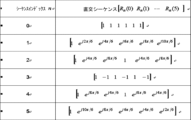
PUCCH情報はDMRSと共に送信される。リソースにマッピングするとき、基準信号およびUL制御情報は、本開示の一実施形態による例示的な新しいPUCCH構成を示す図10に示されるように、周波数領域で互い違いにずらして多重化される。図10に示すように、PUCCHとDMRSは、例えば図6に示すように、長さが12の同じ基本シーケンスを共有する。PUCCHシンボルd0を得るために、PUCCH(例えば、ACK/NACK)ビット{0,1}がコンスタレーションマッピングの後に、最初にPUCCHシンボルに変調される。コンスタレーションマッピングは、図4に示すものに従って実行されてもよい。PUCCHシンボルは、それから、DMRSにも使用される基本シーケンス上で変調される。基本シーケンス上で変調されたPUCCHシンボルYnは、以下のように表現できる。
Yn=d0・Rn, n=0,1,...,11
PUCCH information is transmitted with DMRS. When mapping to resources, the reference signal and UL control information are staggered and multiplexed in the frequency domain as shown in FIG. 10, which shows an exemplary new PUCCH configuration according to one embodiment of the present disclosure. As shown in FIG. 10, PUCCH and DMRS share the same basic sequence of length 12, eg, as shown in FIG. To obtain PUCCH symbol d0 , the PUCCH (eg, ACK/NACK) bits {0,1} are first modulated onto the PUCCH symbol after constellation mapping. Constellation mapping may be performed according to what is shown in FIG. The PUCCH symbols are then modulated on the base sequence that is also used for DMRS. A PUCCH symbol Y n modulated on the base sequence can be expressed as follows.
Yn = d0.Rn , n =0, 1, . . . , 11
ここで、Ynは変調後の結果のシンボルを示し、d0はコンスタレーションマッピング後のPUCCHシンボルを示し、Rnは基本シーケンスを示す。従って、PUCCHの場合、リソースエレメントの総数は24である。 where Yn denotes the resulting symbol after modulation, d0 denotes the PUCCH symbol after constellation mapping, and Rn denotes the base sequence. Therefore, for PUCCH, the total number of resource elements is 24.
図11は、本開示の一実施形態によるDMRSおよびPUCCH情報のために使用され得る別の基本シーケンスを概略的に示す。直交シーケンスRn(i)は、OCC/DFTシーケンスに基づくことができ、それは、6の長さを有し、0から5の範囲のインデックスを有する6つの直交シーケンスが存在する。従って、DMRSとPUCCHとのシーケンスは、図6または図11に示されたものに限定されないことは明らかであり、実際には、周波数の直交性が保証される限り、任意の適切なシーケンスを使用することができる。 FIG. 11 schematically shows another base sequence that may be used for DMRS and PUCCH information according to one embodiment of the present disclosure. The orthogonal sequence R n (i) can be based on the OCC/DFT sequence, which has a length of 6 and there are 6 orthogonal sequences with indices ranging from 0 to 5. Therefore, it is clear that the sequences of DMRS and PUCCH are not limited to those shown in FIG. 6 or FIG. 11, and in practice any suitable sequence can be used as long as frequency orthogonality is guaranteed. can do.
図12は、本開示の別の実施形態による別の新しいPUCCH構造を示し、図11に示されるような基本シーケンスとともに使用される。図12に示すように、PUCCHとDMRSも同じ基本シーケンスを共有しているが、例えば図11に示すように、基本シーケンスの長さは6である。同様に、PUCCHシンボルd0を得るために、PUCCH(例えばACK/NACK)ビット{0,1}がコンスタレーションマッピングの後にPUCCHシンボルに最初に変調される。コンスタレーションマッピングは、図4に示すものに従って実行することもできる。PUCCHシンボルは、それから、長さ6の基本シーケンス上で変調される。基本シーケンス上で変調されたPUCCHシンボルYnは、以下のように表現できる。
Yn=d0・Rn(i), i=0,1,...,5
ここで、Ynは変調後の結果のシンボルを示し、d0はコンスタレーションマッピング後のPUCCHシンボルを示し、図11に示すように、Rn(i)はインデックスがiのシーケンスを示す。
FIG. 12 shows another new PUCCH structure according to another embodiment of the present disclosure, used with the base sequence as shown in FIG. As shown in FIG. 12, PUCCH and DMRS also share the same basic sequence, but the length of the basic sequence is 6, for example, as shown in FIG. Similarly, to obtain PUCCH symbol d0 , the PUCCH (eg, ACK/NACK) bits {0,1} are first modulated onto the PUCCH symbol after constellation mapping. Constellation mapping can also be performed according to what is shown in FIG. The PUCCH symbols are then modulated over the length-6 base sequence. A PUCCH symbol Y n modulated on the base sequence can be expressed as follows.
Yn = d0.Rn (i), i=0 , 1, . . . , 5
where Y n denotes the resulting symbol after modulation, d 0 denotes the PUCCH symbol after constellation mapping, and R n (i) denotes the sequence with index i, as shown in FIG.
PUCCHシンボルは、図12に示すように、DMRSとともに送信され、周波数領域で互い違いにずらして多重化される。従って、そのようなPUCCHの場合、リソースエレメントの総数は12である。 PUCCH symbols are transmitted together with DMRS and multiplexed in a staggered manner in the frequency domain, as shown in FIG. Therefore, for such PUCCH, the total number of resource elements is twelve.
本開示のさらなる実施形態では、DMRSは、例えば図6に示す長さが12の基本シーケンスを使用する。一方で、PUCCHは、例えば図11に示すような異なるシーケンスを使用する。図13は、本開示のさらなる実施形態によるさらなる新しいPUCCH構成を概略的に示し、それは、異なる長さのシーケンスが使用される本実施形態で使用することができる。このような場合、基本シーケンス上で変調されたPUCCHシンボルYnは、以下のように表現できる。
Yn=d0・S(i), i=0,1,...,5
ここで、Ynは変調後の結果のシンボルを示し、d0はコンスタレーションマッピング後のPUCCHシンボルを示し、図11に示すように、S(i)はPUCCHのインデックスがiの基本シーケンスを示す。このようなPUCCHの場合、2つのPUCCHシンボルがDMRSと共に送信され、それによって互い違いにずらして多重化され、リソースエレメントの総数は24である。
In a further embodiment of the present disclosure, DMRS uses base sequences of length 12, eg, as shown in FIG. PUCCH, on the other hand, uses a different sequence, eg as shown in FIG. Figure 13 schematically shows a further new PUCCH configuration according to a further embodiment of the present disclosure, which can be used in this embodiment where different length sequences are used. In such a case, the PUCCH symbol Yn modulated on the base sequence can be expressed as follows.
Y n =d 0 ·S(i), i=0,1, . . . , 5
where Y n denotes the resulting symbol after modulation, d 0 denotes the PUCCH symbol after constellation mapping, and S(i) denotes the base sequence of PUCCH with index i, as shown in FIG. . For such PUCCH, two PUCCH symbols are transmitted with DMRS and thereby staggered and multiplexed, the total number of resource elements being 24.
従って、図9では、図に示された2つの基本シーケンスR1およびR2は、同じシーケンスであってもよい。例えば、PUCCHは、図6および図11に示すように、DMRSのための基本シーケンスを使用することができる。また、基本シーケンスR1と基本シーケンスR2とは、基本シーケンスを共有することができる。別の選択肢として、2つの基本シーケンスは異なるものであってもよい。例えば、基本シーケンスR2は、基本シーケンスR1の異なるルートシーケンスであってもよい。また、2つの基本シーケンスR1およびR2は、同じ長さ、すなわちM=Nを有することができ、または、異なる長さ、すなわちM≠Nを有することもできる。DMRSのためのシーケンスR’1(第1のシーケンス)は、基本シーケンスR1と同じである、または、シーケンスR’1は、巡回シフトまたは位相回転を通じて基本シーケンスR1から変換することができる。PUCCHシンボルを変調するためのシーケンスR’2(第2のシーケンス)は、基本シーケンスR2と同じである、または、シーケンスR’1は、巡回シフトまたは位相回転を通じて基本シーケンスR1から変換することができる。 Thus, in FIG. 9, the two basic sequences R 1 and R 2 shown in the figure may be the same sequence. For example, PUCCH may use base sequences for DMRS, as shown in FIG. 6 and FIG. Also, base sequence R1 and base sequence R2 can share a base sequence. Alternatively, the two base sequences may be different. For example, base sequence R2 may be a different root sequence of base sequence R1 . Also, the two base sequences R 1 and R 2 can have the same length, ie M=N, or they can have different lengths, ie M≠N. The sequence R′ 1 (first sequence) for DMRS is the same as the base sequence R 1 , or the sequence R′ 1 can be transformed from the base sequence R 1 through cyclic shift or phase rotation. The sequence R'2 (second sequence) for modulating the PUCCH symbols is the same as the base sequence R2 , or the sequence R'1 is transformed from the base sequence R1 through cyclic shift or phase rotation. can be done.
本開示の実施形態では、PUCCHおよびRSは、多くの異なる方法でずらして多重化され得る。説明のために、図14A乃至14Eは、周波数領域におけるいくつかの例示的な多重化方式を示す。図14Aに示すように、RS及びPUCCHは、RE毎に互い違いにずらして多重化することができ、すなわち1つのRSは1つのPUCCHに対してである。図14Bにおいて、RSおよびPUCCHは、k個のRE毎に互い違いにずらして多重化することができ、すなわち、1つのRSはk個のPUCCHに対してであり、ciおよびdmは同じUEまたは異なるUEから来ることができる変調シンボルである。図14Cは、図14Bの場合と同様の多重化方法の別の例を示すが、図14Cでは、PUCCHは周波数において連続的ではなくDMRSによって分離されている。図14Dはさらに、さらなる例示的な多重化方法を示し、その中では、RSおよびPUCCHは異なる長さのシーケンスを使用し、1つのPUCCHが1つのRSを使用する。図14Eは、本開示のさらなる実施形態による、さらなる例示的な多重化方式を示す。図14Eでは、PUCCHはDMRSによって分離されておらず、周波数において連続的であり、それは、DMRSも周波数において連続的であることを意味する。 In embodiments of the present disclosure, PUCCH and RS may be staggered multiplexed in many different ways. For illustration purposes, FIGS. 14A-14E show some exemplary multiplexing schemes in the frequency domain. As shown in FIG. 14A, RS and PUCCH can be staggered and multiplexed per RE, ie one RS to one PUCCH. In FIG. 14B, RS and PUCCH can be staggered and multiplexed every k REs, i.e. one RS is for k PUCCHs and c i and d m are the same UE or modulation symbols that can come from different UEs. Figure 14C shows another example of a multiplexing method similar to Figure 14B, but in Figure 14C the PUCCH is separated by DMRS instead of being continuous in frequency. FIG. 14D further shows a further exemplary multiplexing method, in which RS and PUCCH use different length sequences, and one PUCCH uses one RS. FIG. 14E shows further exemplary multiplexing schemes according to further embodiments of the present disclosure. In FIG. 14E, PUCCH is not separated by DMRS and is continuous in frequency, which means DMRS is also continuous in frequency.
以下では、説明のために、1つのULシンボル送信の共通の表現を示し、そこでは、dmn(m>=0、n>=0)は情報ビットの変調シンボルを示す。与えられたmまたはnに対して、シンボルは同じであることができ、言い換えれば以下となる。
dmi=dmj 、または、din=djn
さらに、シンボルは、例えば、異なる位相回転を有することができる。
dmi=ejkθ*dmj 、または、din=ejkθ*djn
シンボルは異なる順序を持つことができる。例えば、以下に示すように、1つは昇順を有し、もう1つは降順を有する。
d00=d1n, d01=d1n-1, ...d0n=d10
また、シンボルは完全に異なっていてもよい。
In the following, for illustration purposes, a common representation of one UL symbol transmission is given, where d mn (m>=0, n>=0) denote the modulation symbols of the information bits. For a given m or n, the symbols can be the same, in other words:
d mi =d mj or d in =d jn
Furthermore, the symbols can have different phase rotations, for example.
d mi =e jkθ *d mj or d in =e jkθ *d jn
Symbols can have different orders. For example, one has ascending order and the other has descending order, as shown below.
d 00 =d 1n , d 01 =d 1n−1 , . . . d0n = d10
Also, the symbols may be completely different.
RSシーケンスRmn(m>=0、n>=0)の場合、シーケンスはまた、与えられたmまたはnについて同じである。本開示の別の実施形態では、RSシーケンスRmnは、与えられたmまたはnについて異なることができる。さらに、シンボルは、同じ基本シーケンスに基づいてもよく、異なる位相回転値またはサイクルシフト値を有してもよい。 For RS sequences R mn (m>=0, n>=0), the sequences are also the same for a given m or n. In another embodiment of the present disclosure, the RS sequences Rmn can differ for a given m or n. Furthermore, the symbols may be based on the same base sequence and may have different phase rotation or cycle shift values.
図15A乃至図15Fは、本開示の実施形態による例示的なリソースマッピング方法を概略的に示す。図15Aに示すように、シーケンスに基づくDMRSシーケンスおよび変調されたPUCCHの両方が、例えば、順番にマッピングされる。変調されたPUCCHシンボルは、d00,d01...d0n,d10,d11,...d1n,...dm0,dm1,...dmnの順にマッピングされ、DMRSシーケンスはR00,R01...R0n,R10,R11,...R1n,...dm0,dm1,...dmnの順番にマッピングされる。一方、図15Bでは、シーケンスに基づくDMRSシーケンスおよび変調されたPUCCHは、帯域のエッジからマッピングされる。 15A-15F schematically illustrate exemplary resource mapping methods according to embodiments of the present disclosure. As shown in FIG. 15A, both the DMRS sequence based sequence and the modulated PUCCH are mapped in order, for example. The modulated PUCCH symbols are d 00 , d 01 . . . d 0n , d 10 , d 11 , . . . d 1n , . . . d m0 , d m1 , . . . d mn and the DMRS sequences are R 00 , R 01 . . . R 0n , R 10 , R 11 , . . . R 1n , . . . d m0 , d m1 , . . . d mn order. On the other hand, in FIG. 15B, the sequence-based DMRS sequence and modulated PUCCH are mapped from the edge of the band.
本開示の実施形態では、DMRSを伴うPUCCHは、予め定義されたRB内に所定の順序で物理リソースブロック(PRB)上に配置することができる。例えば、図15Cに示すように、異なるPUCCHシンボルを異なるPRBに配置することができる。図15Dに示すように、周波数ダイバーシティのために、システム帯域の両方のエッジにPUCCHシンボルをマッピングすることができる。図15Dにおいて、DMRS R0およびPUCCH d0*R’1は、システム帯域の第1のエッジにマッピングされる。DMRS R1およびPUCCH d1*R’1は、システム帯域の第2のエッジにマッピングされ、DMRS R2およびPUCCH d2*R’2は、残りのシステム帯域の第1のエッジにマッピングされ、DMRS R3およびPUCCH d3*R’3は、残りのシステムの第2のエッジにマッピングされ、以下同様である。 In embodiments of the present disclosure, PUCCH with DMRS may be placed on physical resource blocks (PRBs) in a predetermined order within predefined RBs. For example, different PUCCH symbols can be placed in different PRBs, as shown in FIG. 15C. PUCCH symbols can be mapped to both edges of the system band for frequency diversity, as shown in FIG. 15D. In FIG. 15D, DMRS R 0 and PUCCH d 0 *R′ 1 are mapped to the first edge of the system band. DMRS R 1 and PUCCH d 1 *R' 1 are mapped to the second edge of the system band, DMRS R 2 and PUCCH d 2 *R' 2 are mapped to the first edge of the remaining system band, DMRS R 3 and PUCCH d 3 *R' 3 are mapped to the second edge of the rest of the system, and so on.
本開示の別の実施形態では、PUCCHとDMRSとの複製をPRB上に配置することができる。例えば、図15Eに示すように、DMRS R00,R10,乃至Rm0およびPUCCH d0*R’00,d1*R’10乃至dm*R’m0が最初にシステム帯域の第1のエッジ上にマッピングされ、DMRS R01,R11乃至Rm1およびPUCCH d0*R’01,d1*R’11乃至dm*R’m1がそれからシステム帯域の第2の反対側のエッジからマッピングされ、以下同様である。さらに、図15Fは、別のリソースマッピング方式も示し、DMRS R00,R10乃至Rm0およびPUCCH d0*R’00,d1*R’10乃至dm*R’m0が図15Eと同様に、システム帯域の第1のエッジ上から最初にマッピングされ、DMRS Rm1,Rm-11乃至R01およびPUCCH d0*R’01,d1*R’m-1乃至dm*R’01がそれからシステム帯域の第2の反対側のエッジから、図15Eとは異なる順序でマッピングされ、以下同様である。さらに、異なるPRBSにおけるPUCCHの複製は、図15Aまたは図15Bに示すように、PRB上に配置することもできる。 In another embodiment of the present disclosure, PUCCH and DMRS duplicates may be placed on the PRB. For example, as shown in FIG. 15E, DMRS R 00 , R 10 , to R m0 and PUCCH d 0 *R′ 00 , d 1 *R′ 10 to d m *R′ m0 are first in the first band of the system band. DMRS R 01 , R 11 to R m1 and PUCCH d 0 *R′ 01 , d 1 *R′ 11 to d m *R′ m1 are then mapped onto the edge from the second opposite edge of the system band. mapped, and so on. Moreover, FIG. 15F also shows another resource mapping scheme, DMRS R 00 , R 10 to R m0 and PUCCH d 0 *R′ 00 , d 1 *R′ 10 to d m *R′ m0 are similar to FIG. 15E , are mapped first from the first edge of the system band, DMRS R m1 , R m−11 to R 01 and PUCCH d 0 *R′ 01 , d 1 *R′ m−1 to d m *R′ 01 are then mapped from the second opposite edge of the system band, in a different order than in FIG. 15E, and so on. In addition, PUCCH duplicates in different PRBSs can also be placed on PRBs, as shown in FIG. 15A or FIG. 15B.
マッピング順序(例えば、ホッピング)は、異なるシンボル/サブフレーム/PRBにおいて予め定義された順序で変更可能であることにも留意されたい。 It should also be noted that the mapping order (eg, hopping) can change in a predefined order in different symbols/subframes/PRBs.
以上、本開示は主に1つのULシンボルデサインを参照して説明される。実際には、L個のULシンボルのフレームデザインで使用することもできる。これは、サブフレームが、減少したULシンボルを有することができるが、ULシンボルの数は1より大きいことを意味する。 Above, the present disclosure is primarily described with reference to one UL symbol design. In fact, it can also be used in a frame design of L UL symbols. This means that a subframe can have reduced UL symbols, but the number of UL symbols is greater than one.
L個のULシンボルのそれぞれについて、PUCCHおよびDMRSは、例えば図16Aに示すように、同じ方法で互い違いにずらして多重化することができる。あるいは、図16Bに示すように、2つのシンボルにホッピングがあってもよい。さらに、L個のシンボル内のM(1=<M<=L)個のシンボルに対して、PUCCHおよびRSのシーケンスは、周波数が1つ以上RE毎に互い違いにずらして多重化されることができ、図16Cに示すように、他の(L-K)シンボルをPUCCHのために使用することができる。 For each of the L UL symbols, the PUCCH and DMRS can be staggered and multiplexed in the same manner, eg, as shown in FIG. 16A. Alternatively, there may be hopping between two symbols, as shown in FIG. 16B. Furthermore, for M (1=<M<=L) symbols in L symbols, the PUCCH and RS sequences may be multiplexed with the frequency staggered for each RE by one or more. Yes, and other (LK) symbols can be used for PUCCH, as shown in FIG. 16C.
本開示の別の実施形態では、PUCCHおよびRSのシーケンスは、時間的に互い違いにずらして多重化することができる。言い換えると、M(1<=M<=L)個のシンボルは、RSに使用することができ(連続していても、互い違いにずらしてもよい)、他は、図16Dに示すようにPUCCHに使用することができる。 In another embodiment of the present disclosure, the PUCCH and RS sequences may be multiplexed staggered in time. In other words, M (1<=M<=L) symbols can be used for RS (which can be consecutive or staggered) and the rest for PUCCH as shown in FIG. 16D. can be used for
図17Aおよび図17Bは、シーケンス内のPUCCHおよびRSのマッピングを示し、図17Cおよび17Dは、システム帯域のエッジからのPUCCHおよびDMRSのマッピングを示す。図17Aおよび図17Bから、L個のULシンボルの場合、PUCCHおよびDMRSは時間的に多重化され、所定の順序でPRB上に配置されることが分かる。例えば、DMRSを有するPUCCHは、図17Aに示すように順番にマッピングすることができ、または、図17Cに示すようにシステム帯域の両エッジからマッピングすることができる。さらに、DMRSを有するPUCCHの重複をPRBに配置することもできる。別の代替案として、PUCCHおよびDMRSは、図17Bおよび図17Dに示すようにシンボル内でホッピングすることができる。加えて、説明の目的のためにのみ、図18A乃至図18Dは、シーケンス内のPUCCHおよびDMRSのマッピングを示し、共通の表現のためのシステム帯域のエッジからのマッピングを示す。 Figures 17A and 17B show the mapping of PUCCH and RS in sequence, and Figures 17C and 17D show the mapping of PUCCH and DMRS from the edge of the system band. From Figures 17A and 17B, it can be seen that for L UL symbols, the PUCCH and DMRS are time multiplexed and placed on the PRBs in a predetermined order. For example, PUCCH with DMRS can be mapped sequentially as shown in FIG. 17A or mapped from both edges of the system band as shown in FIG. 17C. In addition, duplication of PUCCH with DMRS can also be placed in PRBs. As another alternative, the PUCCH and DMRS can hop within symbols as shown in FIGS. 17B and 17D. Additionally, for illustrative purposes only, FIGS. 18A-18D show the mapping of PUCCH and DMRS in sequence and from the edge of the system band for common representation.
図19は、本開示の別の実施形態によるDMRSおよびPUCCH情報送信のブロック図を概略的に示す。本開示の実施形態では、PUCCH情報シンボルは、第2のシーケンスに基づいて変調されず、送信されるべき第1のシーケンスと第2のシーケンスとの間の関係によって示される。図19に示すように、DMRSの場合、N長の基本シーケンス1は、先ず、巡回シフトまたは位相回転のような変換を通じてR’1に変換され、それから、物理リソースにマッピングされる。同時に、PUCCH情報ビットは、図4に示すようなコンスタレーションマッピングのいずれかを通じて情報シンボルに最初にマッピングされる。シーケンスR’2は、M長の基本シーケンス2から変換され、例えば、基本シーケンス2から巡回シフトまたは位相回転される。次に、結果のシーケンスR’2は、物理リソースにマッピングされる。この解法では、情報シンボルdiは、図9と同様のシーケンスR’2にさらに乗算されない。代わりに、情報シンボルdiは、シーケンスR’1とシーケンスR’2との間の関係によって暗黙的に示される。次に、R’2は、DMRSシーケンスR’1と共に送信される。
FIG. 19 schematically shows a block diagram of DMRS and PUCCH information transmission according to another embodiment of the disclosure. In embodiments of the present disclosure, the PUCCH information symbols are not modulated based on the second sequence, indicated by the relationship between the first and second sequences to be transmitted. As shown in FIG. 19, for DMRS, an N-
図20は、本開示の一実施形態による新しいPUCCH構成を概略的に示し、情報シンボルdiは、シーケンスR’1とシーケンスR’2との間の関係により暗黙的に示され、基準信号とACK/NACKのようなUL制御情報とは、周波数領域で互い違いにずらして多重化される。 FIG. 20 schematically illustrates a new PUCCH configuration according to one embodiment of the present disclosure, where information symbols d i are implicitly indicated by the relationship between sequence R′1 and sequence R′2 , and reference signal and UL control information such as ACK/NACK is alternately shifted and multiplexed in the frequency domain.
図20に示すように、本開示のこの実施形態では、基本シーケンス1および2は、同じ長さNを有する。2つのシーケンスR1およびR2は、同じベースシーケンスから、異なるものであっても、または変換されても、巡回シフトされても、位相回転されてもよい。基本シーケンス1および2は、例えば、図6に示すような基本シーケンスであってもよい。しかしながら、他の基本シーケンスも可能であることを理解されたい。PUCCH(例えば、ACK/NACK)ビット{0,1}は、コンスタレーションマッピングの後に、例えばBPSK{+1、-1}のように、最初にPUCCHシンボルに変調される。次に、変調されたシンボルは、シーケンスR’1とR’2との関係によって暗黙的に示される。この関係は、例えば、以下のように表すことができる巡回シフトに反映されてもよい。
R’n=ejαnRn,0≦n≦11 α=2πk/12,0≦k≦11
シーケンスR’1およびR’2の場合、それらは異なるサイクルシフトを使用することができ、これは以下の式で表すことができる。
ej2πk1/12Rn’ ej2πk1/12Rn
ここにおいて、k1およびk2はRnのCS指数である。k1-k2=6の場合、情報シンボルは+1であることを示し、k1-k2=-6の場合、情報シンボルは-1であることを示す。このようにして、PUCCH情報シンボルは、シーケンスR’1とR’2との間の関係によって暗黙的に示すことができる。そのような場合、送信するPUCCHを暗示するためのREの総数は、24(2N)である。
As shown in FIG. 20, in this embodiment of the disclosure,
R′ n =e jαn R n , 0≦n≦11 α=2πk/12, 0≦k≦11
For sequences R'1 and R'2 , they can use different cycle shifts, which can be represented by the following equations.
e j2πk1/12 R n′ e j2πk1/12 R n
where k1 and k2 are the CS indices of Rn . The case of k1-k2=6 indicates that the information symbol is +1, and the case of k1-k2=-6 indicates that the information symbol is -1. In this way, the PUCCH information symbols can be implicitly indicated by the relationship between the sequences R'1 and R'2 . In such case, the total number of REs to imply PUCCH to transmit is 24 (2N).
PUCCHマッピングおよび多重化は、図9に示すような実施形態と同様であり、したがって詳細については、図10乃至図18を参照することができる。 PUCCH mapping and multiplexing are similar to the embodiment as shown in FIG. 9, so reference can be made to FIGS. 10-18 for details.
図21から図22は、本開示のさらなる実施形態による、DMRSおよびPUCCH情報送信のさらなる可能な解決策をさらに示し、シーケンスはk個の異なるグループに分割され、変調されたPUCCHシンボルは、予め定義されたグループによって示される。 Figures 21-22 further illustrate further possible solutions for DMRS and PUCCH information transmission, according to further embodiments of the present disclosure, where the sequence is divided into k different groups and the modulated PUCCH symbols are predefined indicated by the marked group.
PUCCH情報ビットは、コンスタレーションマッピングの後に得られるdiによって示される。変調次数がMであれば、それは完全に2M個のシンボルになる。使用できるQシーケンスがある。このQシーケンスは、K個のグループ(K=Q/M)にグループ化され、各グループkjは、図21に示されるように、1つの変調シンボルに対応する。従って、異なる変調シンボルに対して異なるシーケンスグループが使用される。 The PUCCH information bits are denoted by d i obtained after constellation mapping. If the modulation order is M, it will be completely 2 M symbols. There are Q-sequences that can be used. The Q-sequences are grouped into K groups (K=Q/M), with each group kj corresponding to one modulation symbol, as shown in FIG. Therefore, different sequence groups are used for different modulation symbols.
図22は、本開示の一実施形態による、QPSKのコンスタレーションマッピングをさらに概略的に示す。図22に示すように、4つのシーケンスグループk1乃至k4は、4つのNACK/ACKシンボルにマッピングされる。 FIG. 22 further schematically illustrates constellation mapping for QPSK, according to one embodiment of the present disclosure. As shown in FIG. 22, four sequence groups k1 to k4 are mapped to four NACK/ACK symbols.
Qシーケンスは、異なる基本シーケンス、1つまたは複数の基本シーケンスの異なる巡回シフト、または、1つまたは複数の基本シーケンスの異なる変換、例えば位相回転(R1=ejθ*R2)を通じたものでよい。これらのシーケンスは、周波数または時間領域でずらすか、または連続的にマッピングすることができる。暗黙的にPUCCH情報を送信するためのREの総数は、N個である。 The Q-sequences are through different base sequences, different cyclic shifts of one or more base sequences, or different transformations of one or more base sequences, such as phase rotations (R 1 =e jθ *R 2 ). good. These sequences can be staggered or continuously mapped in the frequency or time domain. The total number of REs for implicitly transmitting PUCCH information is N.
図23乃至図24は、本開示の一実施形態による巡回シフトグルーピングの特定の実施形態を示す。図23には、2つの異なる巡回シフトグループが示される。図23に示すように、12個の巡回シフトは、異なるパターンによって示された4つのグループに分割される。12個の巡回シフトは、以下のように表すことができる。
R’n=ejαnRn,0≦n≦11 α=2πk/12,0≦k≦11
23-24 illustrate a specific embodiment of cyclic shift grouping according to one embodiment of the present disclosure. Two different cyclic shift groups are shown in FIG. As shown in FIG. 23, the 12 cyclic shifts are divided into 4 groups indicated by different patterns. The 12 cyclic shifts can be expressed as follows.
R′ n =e jαn R n , 0≦n≦11 α=2πk/12, 0≦k≦11
1つの可能なグループ化では、巡回シフト0乃至2が第1グループに、巡回シフト3乃至5が第2グループに、巡回シフト6乃至8が第3グループに、巡回シフト9乃至11が第4のグループに分けられる。図24は、本開示の一実施形態による図21に例示されるような巡回シフトグルーピングに対応するACK/NACKコンスタレーションマッピングを概略的に示す。図24に示すように、4つの巡回シフトグループは、それぞれQPSK{+1、-1、+j、-j}にマッピングされる。 In one possible grouping, cyclic shifts 0-2 are in the first group, cyclic shifts 3-5 are in the second group, cyclic shifts 6-8 are in the third group, and cyclic shifts 9-11 are in the fourth group. divided into groups. FIG. 24 schematically shows ACK/NACK constellation mapping corresponding to cyclic shift grouping as illustrated in FIG. 21 according to one embodiment of the present disclosure. As shown in FIG. 24, four cyclic shift groups are mapped to QPSK {+1, -1, +j, -j} respectively.
さらに、図23は、巡回シフト0、4、8が第1のグループに分割され、巡回シフト1、5、9が第2のグループに分割され、巡回シフト2、6、10が第3のグループに分割され、巡回シフト3、7乃至11が第4のグループに分割される他の可能なグループ化を示す。可能なグループ化の例に加えて、巡回シフトは他の適切な方法で分割することができることを理解されたい。このようにして、異なる巡回シフトグループを使用して、異なるPUCCHシンボルを示すことができる。さらに、異なるUEは、自身のPUCCHシンボルを示すために巡回シフトグループ内の異なる巡回シフトを使用してもよい。基本シーケンスが12である場合、暗黙的にPUCCHを送信するためのREの総数は12個である。
Further, FIG. 23 shows that
図25は、本開示の一実施形態による新しいPUCCH構成を概略的に示す。図示されるように、PUCCH情報シンボルは、位相回転(PR)または巡回シフト(CS)のような所定の変換を伴うR’nによって暗黙的に示される。R’nは、物理リソースにマッピングされ、ULシンボルで送信される。 Figure 25 schematically illustrates a new PUCCH configuration according to one embodiment of the present disclosure. As shown, the PUCCH information symbols are implicit by R'n with a predetermined transformation such as phase rotation (PR) or cyclic shift (CS). R'n are mapped to physical resources and transmitted in UL symbols.
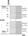
PUCCH情報はL個のシンボル(L>=1)にマッピングすることができ、ここで、Lは予め定義された値であることができることを理解されたい。Lは、eNBなどの基地局によって動的または半静的に通知することができ、そのような場合、動的制御領域またはRRCメッセージ内にビットを提供することができる。さらに、PUCCHリソースインデックスは、eNBによって予め定義されるか、または、動的にまたは半静的に通知されることもできる。シーケンスおよび/またはマッピング順序は、PRBまたはシンボルにおいて異なるものであってもよいし、または同じであってもよいことに留意されたい。OCC、位相回転などは、PRBまたはシンボルで使用することができる。 It should be appreciated that the PUCCH information can be mapped to L symbols (L>=1), where L can be a predefined value. L may be signaled dynamically or semi-statically by a base station such as an eNB, and in such cases a bit may be provided in the dynamic control region or RRC message. Additionally, the PUCCH resource index may be predefined by the eNB or signaled dynamically or semi-statically. Note that the sequence and/or mapping order may be different or the same in PRBs or symbols. OCC, phase rotation, etc. can be used with PRBs or symbols.
さらに、PUCCHのサブキャリア間隔は、他のシンボルと異なることができる。新しい変調を使用することもできる。1つまたは複数のシンボルで低いPAPRを維持するために、例えば8PSKのような一定の係数を使用することができる。さらに、PUCCHのシーケンス長は、異なるペイロードに適合させることができる。
本開示の一実施形態では、PUCCHはグループに分類され、いくつかはZC/PNシーケンスで変調されるか、または巡回シフトで表され、他は異なるシーケンスで表現されるか、または、図26Aおよび26Bに示すように、シーケンス上で変調されない。通常、重要なPUCCH情報は、正確な結果を得るために、DMRSシーケンスで変調される。例えば、ACK/NACKはCSIよりも重要であり、従って、それは、ZC/PNシーケンス上で変調されてもよいし、または巡回シフトで表現されてもよい。対照的に、CSIはあまり重要ではないので、CSIは、ZC/PNシーケンスで変調されない。ACK/NACKのためのZC/PNシーケンスは、CSIのための復調RSとして使用することができ、それは、利用可能な基準信号なしでいくつかのPUCCHの追加の利点を得ることができる。場合によっては、UL制御情報と基準信号とが異なる時間間隔で送信されてもよく、別の場合、すべてのUL制御情報が基準信号と共に送信されなくてもよい。しかしながら、2つの場合のいずれにおいても、利用可能な基準信号を伴わないPUCCHが存在する可能性がある。そのような場合、以前の基準信号、例えばそれに最も近い基準信号を使用することが可能である。代替的な選択肢として、受信されたシーケンスそれ自体は、他のPUCCHのためのRSとして使用され得るチャネル情報を運ぶので、前の制御情報のためのシーケンスを使用することもできる。本開示の特定の実施形態では、利用可能な基準信号を伴わないUL制御情報のための基準信号を、利用可能な基準信号なしで、以前の基準信号および以前の制御情報からUL制御情報までの時間間隔に依存して決定することができる。すなわち、PUCCHが、以前のRSからよりも、以前のPUCCHから方がより短い時間間隔を有する場合、以前のPUCCHのためのシーケンスをPUCCHの基準信号として使用することができる。これにより、精度の高いPUCCH情報を得ることができる。この解決策は、より高い精度を達成するために、上述したようなPUCCH送信ソリューションのいずれかと共に使用することができる。
Furthermore, the subcarrier spacing of PUCCH can be different from other symbols. New modulations can also be used. A constant factor, such as 8PSK, can be used to maintain a low PAPR on one or more symbols. Furthermore, the PUCCH sequence length can be adapted to different payloads.
In one embodiment of the present disclosure, the PUCCH is grouped into groups, some modulated with ZC/PN sequences or represented by cyclic shifts, others represented by different sequences, or 26B is not modulated on the sequence. Important PUCCH information is usually modulated with a DMRS sequence to obtain accurate results. For example, ACK/NACK is more important than CSI, so it may be modulated on a ZC/PN sequence or represented with a cyclic shift. In contrast, CSI is not modulated with the ZC/PN sequence, as it is of lesser importance. The ZC/PN sequences for ACK/NACK can be used as demodulation RSs for CSI, which can obtain some additional benefits of PUCCH without reference signals available. In some cases, the UL control information and the reference signal may be transmitted at different time intervals, and in other cases not all UL control information may be transmitted with the reference signal. However, in either of the two cases there may be a PUCCH without an available reference signal. In such cases, it is possible to use the previous reference signal, eg the closest reference signal to it. Alternatively, the received sequence itself carries channel information that can be used as RSs for other PUCCHs, so the sequence for the previous control information can be used. In certain embodiments of the present disclosure, the reference signal for UL control information without available reference signal is changed from previous reference signal and previous control information to UL control information without available reference signal. It can be determined depending on the time interval. That is, if the PUCCH has a shorter time interval from the previous PUCCH than from the previous RS, the sequence for the previous PUCCH can be used as the reference signal for the PUCCH. This makes it possible to obtain highly accurate PUCCH information. This solution can be used with any of the PUCCH transmission solutions as described above to achieve higher accuracy.
図27Aは、本開示の実施形態による1つの可能なUL領域設計を示す。ULのためのN個のシンボルと、UL制御のためのM個のシンボル(PUCCH)と、DMRSのためのL個のシンボル(L>=0)とがあると仮定する。本開示の一実施形態では、1つまたは複数のシンボル/PRBを、ZC/PNシーケンスで変調することができ、またはZC/PNシーケンスの巡回シフトで変調することができる。図27Aに示すように、M個のシンボルPUCCHの場合、K個のシンボルは、ZC/PNシーケンス上で変調されるか、または、ZC/PNシーケンス(K>=0)の巡回シフトで変調される。他のM-Kシンボルは、任意の種類の制御情報であってもよい。図27Bはまた、本開示の実施形態による別の可能なUL領域設計を示し、DMRSのための1つのシンボルと、変調されたPUCCHのための1つのシンボルとが存在する。DMRSおよび/またはPUCCHシンボルは、連続的または互い違いにすることができる。DMRS、PUCCHおよびデータの位置は、図27Aおよび図27Bに示したものとは異なることがあることに留意されたい。 FIG. 27A shows one possible UL region design according to embodiments of the present disclosure. Assume that there are N symbols for UL, M symbols for UL control (PUCCH), and L symbols for DMRS (L>=0). In one embodiment of the present disclosure, one or more symbols/PRBs may be modulated with a ZC/PN sequence or modulated with a cyclic shift of a ZC/PN sequence. As shown in FIG. 27A, for M-symbol PUCCH, K symbols are modulated on a ZC/PN sequence or modulated with a cyclic shift of a ZC/PN sequence (K>=0). be. Other MK symbols may be any kind of control information. FIG. 27B also shows another possible UL region design according to embodiments of the present disclosure, where there is one symbol for DMRS and one symbol for modulated PUCCH. DMRS and/or PUCCH symbols can be contiguous or staggered. Note that the DMRS, PUCCH and data locations may differ from those shown in FIGS. 27A and 27B.
さらに、本開示の実施形態では、図28A乃至図28Cに示されるように、復調のためのウィンドウ時間内に1つまたは複数のDMRSを提供することができる。本開示の一実施形態では、ウィンドウ時間において、図28Aに示されるような複数のサブフレーム、または、図28Bに示されるような複数のシンボルが存在し得る、または図28Cに示されるような以前の解決策との合成でもよい。ウィンドウ時間値は、予め定義されても、または動的に/半静的に通知されてもよい。 Additionally, embodiments of the present disclosure may provide one or more DMRSs within a window time for demodulation, as shown in FIGS. 28A-28C. In one embodiment of the present disclosure, in a window time there may be multiple subframes as shown in FIG. 28A or multiple symbols as shown in FIG. may be combined with the solution of The window time value may be predefined or dynamically/semi-statically signaled.
以上、UL情報送信の解決方法について主に説明した。本開示では、図29を参照して説明するUL情報を受信する方法も提供される。 So far, the solution to the UL information transmission has been mainly described. This disclosure also provides a method of receiving UL information, which is described with reference to FIG.
図29に示すように、方法2900は、第1のシーケンスを使用して送信された基準信号を最初に受信するステップ2910から開始することができる。基準信号の第1のシーケンスは、図6に示すような基本シーケンスを有することができ、図11に示すシーケンスのうちの1つであってもよく、または周波数領域の直交性を有する他のシーケンスであってもよい。第1の基準信号は、基本シーケンスから巡回シフト、位相回転または任意の他の変換によって変換されたシーケンスであってもよい。さらに、基準信号は、例えばDMRS信号または他の基準信号であってもよい。
As shown in FIG. 29,
ステップ2920において、第2のシーケンスを使用して送信された制御情報を受信する。同様に、制御情報の第2のシーケンスは、図6に示すような基本シーケンスを有することができ、図11のシーケンスのうちの1つであってもよく、または周波数領域の直交性を有する他のシーケンスであってもよい。第2の基準信号は、基本シーケンスから巡回シフト、位相回転または他の変換によって変換されたシーケンスであってもよい。第1のシーケンスおよび第2のシーケンスは同一であってもよく、または同じ基本シーケンスを共有してもよい。あるいは、第1のシーケンスおよび第2のシーケンスは、同じまたは異なる長さを有する異なる基本シーケンスを有する。例えば、第1のシーケンスは、図6に示すような基本シーケンスを有することができ、一方、第2のシーケンスは、図11に示すようなシーケンスのうちの1つであり得る。制御情報は、NACK/ACK、CQI、PMI、RIなどのPUCCH情報であってもよい。
In
次に、ステップS2930では、基準信号を使用して制御情報を復調する。特に、基準信号とUL制御情報とは、周波数領域で互い違いにずらして多重化される。本開示の一実施形態では、制御情報を復調することは、第2のシーケンスとともにチャネル情報を使用してUL制御情報を取得することをさらに備え、チャネル情報は、第1のシーケンスを使用することによって基準信号から取得される。すなわち、まず、第1のシーケンスに基づいて基準信号からチャネル情報を取得し、その後、チャネル情報と第2のシーケンスに基づいて受信した制御情報を復調することにより制御情報ビットを取得することができる。 Next, in step S2930, the control information is demodulated using the reference signal. In particular, the reference signal and the UL control information are alternately shifted and multiplexed in the frequency domain. In one embodiment of the present disclosure, demodulating the control information further comprises obtaining UL control information using the channel information with the second sequence, the channel information using the first sequence obtained from the reference signal by That is, first, the channel information is obtained from the reference signal based on the first sequence, and then the control information bits can be obtained by demodulating the received control information based on the channel information and the second sequence. .
本開示の別の実施形態では、制御情報を復調することは、チャネル情報を使用して第2のシーケンスを取得することを備え、チャネル情報は、第1のシーケンスを使用して基準信号から得られ、第1のシーケンスと第2のシーケンスとの間の関係に基づいて制御情報を取得することを、備える。このような場合、基準信号に基づいてチャネル情報を取得した後、チャネル情報に基づいて第2のシーケンスをさらに取得し、それから、第1のシーケンスと第2のシーケンスとの関係であって制御情報を暗黙的に示す関係をさらに決定する。従って、この実施形態では、情報ビットは暗黙的に送信される。言い換えれば、情報ビット自体は、第2のシーケンスとは多重化されず、第1のシーケンスと第2のシーケンスとによって暗黙的に示される。 In another embodiment of the disclosure, demodulating the control information comprises obtaining the second sequence using the channel information, the channel information obtained from the reference signal using the first sequence. and obtaining control information based on a relationship between the first sequence and the second sequence. In such a case, after obtaining channel information based on the reference signal, further obtaining a second sequence based on the channel information, and then determining the relationship between the first sequence and the second sequence as control information. further determine the relationship that implies . Therefore, in this embodiment, information bits are implicitly transmitted. In other words, the information bits themselves are not multiplexed with the second sequence and are implied by the first and second sequences.
本開示の実施形態では、基準信号およびUL制御情報は、多くの異なる方法で互い違いにずらして多重化される。例えば、基準信号とUL制御情報は、1つのUL制御情報に対して1つの基準信号を用いて1リソースエレメント毎に互い違いにずらして多重化することができる。他の選択肢として、基準信号とUL制御情報は、2つ以上のリソースエレメント毎に、UL制御情報の2つ以上の部分によって共有される1つの基準信号を用いて互い違いにずらして多重化することができる。 In embodiments of the present disclosure, the reference signal and UL control information are staggered and multiplexed in a number of different ways. For example, the reference signal and the UL control information can be multiplexed by staggering by one resource element using one reference signal for one UL control information. Alternatively, the reference signal and UL control information are staggered and multiplexed with one reference signal shared by two or more portions of the UL control information for every two or more resource elements. can be done.
本開示の実施形態では、UL制御情報および基準信号は、任意の適切な方法でマッピングされる。例えば、UL制御情報および基準信号は、システム帯域幅の両エッジにマッピングすることができる。それに加えて、またはこれに代えて、UL制御情報および基準信号は、2つのシンボルにおいてホッピングすることができる。 In embodiments of the present disclosure, UL control information and reference signals are mapped in any suitable manner. For example, UL control information and reference signals can be mapped to both edges of the system bandwidth. Additionally or alternatively, the UL control information and reference signal may hop in two symbols.
UL制御情報および基準信号が異なる時間間隔で送信されるか、またはすべてのUL制御情報が基準信号と共に送信されない実施形態では、以前の基準信号および以前の制御情報のシーケンスのうちの1つは、利用可能な基準信号なしでUL制御情報を復調するための基準信号として使用される。そのような場合、本方法は、利用可能な基準信号なしで、前の基準信号および前の制御情報からUL制御情報までの時間間隔に依存する利用可能な基準信号なしに、UL制御情報の基準信号を決定することをさらに備えることができる。 In embodiments in which the UL control information and the reference signal are transmitted at different time intervals or not all the UL control information is transmitted with the reference signal, one of the sequences of previous reference signals and previous control information is: Used as a reference signal to demodulate the UL control information without a reference signal available. In such a case, the method provides a reference for the UL control information without an available reference signal and without an available reference signal that depends on the time interval from the previous reference signal and the previous control information to the UL control information. It can further comprise determining a signal.
PUCCH設計、第1のシーケンス、第2のシーケンス、互い違いの多重化、リソースマッピングなどについてのいくつかの詳細は、既に図8乃至図28を参照して詳細に説明されているので、これらの詳細はここでは詳述しない。簡略化目的のためおよびそれらの詳細については、図8乃至図28を参照して説明を参照されたい。 Some details about PUCCH design, first sequence, second sequence, staggered multiplexing, resource mapping, etc. have already been described in detail with reference to FIGS. are not detailed here. For simplification purposes and for details thereof, refer to the description with reference to FIGS.
本開示の実施形態では、アップリンク情報は、減少したアップリンクシンボルで送信されて、アップリンクシンボルが減少したサブフレーム構成に適応することができるUL送信および受信のための新しい解決を提供し、従って、送信待ち時間を大幅に削減することができる。 In embodiments of the present disclosure, uplink information is transmitted in reduced uplink symbols to provide a new solution for UL transmission and reception that can adapt to subframe configurations with reduced uplink symbols; Therefore, the transmission waiting time can be greatly reduced.
図30は、本開示の一実施形態によるUL情報を送信するための装置のブロック図を概略的に示す。図30に示すように、装置3000は、基準信号送信部3010と、制御情報送信部3020と、を備える。基準信号送信部3010は、第1のシーケンスを使用して基準信号を送信するように構成することができる。制御情報送信部3020は、第2のシーケンスを使用してUL制御情報を送信するように構成することができる。特に、基準信号とUL制御情報とは、周波数領域で互い違いにずらして多重化される。
FIG. 30 schematically shows a block diagram of an apparatus for transmitting UL information according to one embodiment of the disclosure. As shown in FIG. 30 , device 3000 includes
本開示の一実施形態では、UL制御情報は、第2のシーケンスに基づいて変調され、UL制御情報のビットが暗黙的に送信されることを意味する。本開示の別の実施形態では、第1のシーケンスおよび第2のシーケンスは、UL制御情報を暗黙的に示すために使用される予め決定された関係を有することができる。 In one embodiment of the present disclosure, the UL control information is modulated based on the second sequence, meaning that bits of UL control information are implicitly transmitted. In another embodiment of the present disclosure, the first sequence and the second sequence may have a pre-determined relationship used to implicitly indicate UL control information.
本開示の実施形態において、第1のシーケンスと第2のシーケンスとは、同一または同じ基本シーケンスを共有する。あるいは、第1のシーケンスと第2のシーケンスとは、異なる基本シーケンスを有することができる。 In embodiments of the present disclosure, the first sequence and the second sequence share the same or the same base sequence. Alternatively, the first sequence and the second sequence can have different base sequences.
本開示の実施形態では、基準信号およびUL制御情報は、任意の適切な方法で互い違いにずらして多重化することができる。例えば、1つのUL制御情報に対して1つの基準信号を使用して基準信号とUL制御情報とを1リソースエレメント毎に互い違いにずらして多重化してもよいし、または、基準信号とUL制御情報とは、UL制御情報の1つよりも多い部分によって共有された1つの基準信号を使用して、1つよりも多くのリソースエレメント毎に互い違いにずらして多重化することができる。 In embodiments of the present disclosure, the reference signal and UL control information may be staggered and multiplexed in any suitable manner. For example, one reference signal may be used for one UL control information, and the reference signal and the UL control information may be alternately shifted and multiplexed for each resource element, or the reference signal and the UL control information may be multiplexed. can be staggered and multiplexed by more than one resource element using one reference signal shared by more than one portion of UL control information.
本開示の実施形態では、基準信号およびUL制御情報は、任意の適切な方法でマッピングすることができる。本開示の一実施形態では、UL制御情報および基準信号は、システム帯域幅の両端にマッピングされる。本開示の別の実施形態では、UL制御情報および基準信号は、2つのシンボルでホッピングする。 In embodiments of the present disclosure, reference signals and UL control information may be mapped in any suitable manner. In one embodiment of the present disclosure, UL control information and reference signals are mapped to both ends of the system bandwidth. In another embodiment of the present disclosure, the UL control information and reference signal hop in two symbols.
本開示の一実施形態では、UL制御情報および基準信号は、異なる時間周期で送信することができる。本開示の別の実施形態では、すべてのUL制御情報が基準信号とともに送信されるわけではない。どちらの場合も、利用可能な基準信号なしのいくつかのUL制御情報があることを意味する。そのような場合、以前の制御信号の1つと、以前の制御情報の1つの制御信号とを、利用可能な基準信号なしのUL制御情報のための基準信号として使用することができる。本開示の一実施形態では、利用可能な基準信号を伴わないUL制御情報のための基準信号は、以前の基準信号および以前の制御情報から、利用可能な基準信号を伴わないUL制御情報までの時間間隔に依存する。 In one embodiment of the present disclosure, UL control information and reference signals may be transmitted in different time periods. In another embodiment of the present disclosure, not all UL control information is transmitted with the reference signal. In both cases it means that there is some UL control information without reference signals available. In such cases, one of the previous control signals and one of the previous control information can be used as reference signals for the UL control information without available reference signals. In one embodiment of the present disclosure, the reference signal for UL control information without available reference signal is from previous reference signal and previous control information to UL control information without available reference signal. Time interval dependent.
図31は、UL情報を受信するための装置をさらに示す。図31に示すように、装置3100は、基準信号受信部3110と、制御情報受信部3120と、復調部3130と、を備える。基準信号受信部3110は、第1のシーケンスを使用して送信された基準信号を受信するように構成してもよい。制御情報受信部3120は、第2のシーケンスを使用して送信された制御情報を受信するように構成してもよい。復調部3130は、基準信号を使用して制御情報を復調するように構成してもよい。特に、基準信号とUL制御情報は、周波数領域で互い違いにずらして多重化される。
FIG. 31 further shows an apparatus for receiving UL information. As shown in FIG. 31,
本開示の一実施形態では、復調部3130は、第2のシーケンスとともにチャネル情報を使用してUL制御情報を取得するようにさらに構成され、チャネル情報は、第1のシーケンスを使用することによって基準信号から取得される。
In one embodiment of the present disclosure, the
本開示の別の実施形態では、復調部3130は、第1のシーケンスを使用して基準信号から得られるチャネル情報を使用して第2のシーケンスを取得し、第1のシーケンスと第2のシーケンスとの間の関係に基づいて制御情報を取得するようにさらに構成される。
In another embodiment of the present disclosure, the
本開示の一実施形態では、第1のシーケンスおよび第2のシーケンスは同一であってもよく、または同じ基本シーケンスを共有してもよい。本開示の別の実施形態では、第1のシーケンスおよび第2のシーケンスは、異なる基本シーケンスを有することができる。 In one embodiment of the present disclosure, the first sequence and the second sequence may be identical or share the same base sequence. In another embodiment of the disclosure, the first sequence and the second sequence may have different base sequences.
本開示の一実施形態では、基準信号およびUL制御情報は、1つのUL制御情報に対して1つの基準信号を有する1つのリソースエレメント毎に互い違いにずらして多重化される。本開示の別の実施形態では、基準信号およびUL制御情報は、2つ以上のリソースエレメント毎に、UL制御情報の2つ以上の部分によって共有される1つの基準信号を用いて互い違いにずらして多重化される。 In one embodiment of the present disclosure, the reference signal and UL control information are staggered and multiplexed for each resource element with one reference signal for one UL control information. In another embodiment of the present disclosure, the reference signal and UL control information are staggered with one reference signal shared by two or more portions of UL control information for every two or more resource elements. Multiplexed.
本開示の一実施形態では、UL制御情報および基準信号は、システム帯域幅の両方のエッジにマッピングされる。本開示の別の実施形態では、UL制御情報および基準信号は、2つのシンボルでホッピングすることができる。 In one embodiment of the present disclosure, UL control information and reference signals are mapped to both edges of the system bandwidth. In another embodiment of the disclosure, the UL control information and reference signal may hop in two symbols.
本開示の一実施形態では、以前の基準信号および続く以前の制御情報のシーケンスのうちの1つは、利用可能な基準信号なしでUL制御情報を復調するための基準信号として使用することができる。そのような場合、装置3100は、前の基準信号から前の制御情報までの時間間隔に依存する利用可能な基準信号なしで、UL制御情報のための基準信号を決定するように構成された基準信号決定部3140をさらに備える。時間間隔は、利用可能な基準信号なしのUL制御情報のための時間間隔である。
In one embodiment of the present disclosure, one of the previous reference signal and subsequent previous control information sequence may be used as the reference signal for demodulating the UL control information without an available reference signal. . In such a case, the
以上、装置3000および装置3100について、図30および図31を参照して簡単に説明した。装置3000および3100は、図8乃至29を参照して説明したような機能を実装するように構成されてもよいことに留意されたい。従って、これらの装置におけるモジュールの動作についての詳細は、図8乃至29を参照して説明した方法の各ステップに関する記述を参照することができる。
The
さらに、装置3000および3100の構成要素は、ハードウェア、ソフトウェア、ファームウェア、および/またはそれらの任意の組み合わせで具体化されてもよいことに留意されたい。例えば、装置3000および3100の構成要素は、回路、プロセッサまたは任意の他の適切な選択装置によってそれぞれ実現されてもよい。当業者であれば、上記の例は限定ではなく例示のためのものであることを理解するであろう。
Further, it should be noted that components of
本開示のいくつかの実施形態では、装置3000および3100は、少なくとも1つのプロセッサを備えることができる。本開示の実施形態での使用に適した少なくとも1つのプロセッサは、例えば、将来知られている、または将来開発される汎用プロセッサおよび専用プロセッサの両方を含むことができる。装置3000および3100は、少なくとも1つのメモリをさらに備えることができる。少なくとも1つのメモリは、例えば、RAM、ROM、EPROM、EEPROM、フラッシュメモリデバイスなどの半導体メモリデバイスを含むことができる。少なくとも1つのメモリは、コンピュータ実行可能命令のプログラムを格納するために使用されてもよい。このプログラムは、任意の高水準および/または低水準の適合可能または解釈可能なプログラミング言語で記述することができる。実施形態によれば、コンピュータ実行可能命令は、少なくとも1つのプロセッサを用いて、装置3000および3100に少なくとも図8乃至29のそれぞれを参照して説明した方法による動作を実行させるように構成することができる。
In some embodiments of the present disclosure,
図32はさらに、無線ネットワーク内の無線ネットワークのためのUEのような端末装置として具現化されるか、またはその中に含まれ得る装置3210の簡略化したブロック図を示し、装置3220は、本明細書で説明するNBまたはeNBのような基地局である。
FIG. 32 also shows a simplified block diagram of
装置3210は、データプロセッサ(DP)およびプロセッサ3211に結合された少なくとも1つのメモリ(MEM)3212のような少なくとも1つのプロセッサ3211を備える。装置3210は、プロセッサ3211に結合された送信機TXおよび受信機RX3213をさらに備えてもよく、プロセッサ3211は、装置3220に通信可能に接続して動作するようにしてもよい。MEM3212は、プログラム(PROG)3214を格納する。PROG3214は、関連するプロセッサ3211上で実行された時、例えば、方法800を実行するために、本開示の実施形態に従って装置3210が動作することを可能にする命令を含むことができる。少なくとも1つのプロセッサ3211と少なくとも1つのMEM3212との組み合わせは、本開示の様々な実施形態を実装するように適合された処理手段3215を形成することができる。
装置3220は、DPなどの少なくとも1つのプロセッサ3221と、プロセッサ3221に結合された少なくとも1つのMEM3222とを備える。装置3220は、プロセッサ3221に結合された適当なTX/RX3223をさらに備えることができ、TX/RX3223は、装置3210と無線通信をするように動作することができる。MEM3222は、PROG3224を記憶する。PROG3224は、関連するプロセッサ3221上で実行された時、本開示の実施形態に従って装置3220が動作することを可能にする命令、例えば、方法2900を実行するための命令を含むことができる。少なくとも1つのプロセッサ3221と少なくとも1つのMEM3222の組み合わせは、本開示の様々な実施形態を実装するように適合された処理手段3225を形成することができる。
本開示の様々な実施形態は、プロセッサ3211、3221、ソフトウェア、ファームウェア、ハードウェアの1つまたは複数による実行可能なコンピュータプログラムによって、またはそれらの組み合わせによって実行されてもよい。
Various embodiments of the present disclosure may be performed by a computer program executable by one or more of
MEM3212および3222は、ローカル技術環境に適した任意のタイプのものでよく、半導体ベースのメモリデバイス、磁気メモリデバイスおよびシステム、光メモリデバイスおよびシステムなどの任意の適切なデータ記憶技術を使用して実装することができ、メモリ、およびリムーバブルメモリを含むが、これらに限定されない。
The
プロセッサ3211および3321は、ローカル技術環境に適した任意のタイプのものでよく、汎用コンピュータ、専用コンピュータ、マイクロプロセッサ、デジタル信号プロセッサDSPおよびマルチコアプロセッサアーキテクチャに基づくプロセッサのうちの1つまたは複数を含むことができ、非限定的な例である。
さらに、本開示は、キャリアが電子信号、光信号、無線信号、またはコンピュータ可読記憶媒体のうちの1つである、上記のようなコンピュータプログラムを含むキャリアを提供することもできる。コンピュータ読み取り可能な記憶媒体は、例えば、光コンパクトディスクまたはRAM(ランダムアクセスメモリ)、ROM(読み出し専用メモリ)、フラッシュメモリ、磁気テープ、CD-ROM、DVD、ブルーレイディスクなどの電子メモリデバイスを含む。 Further, the present disclosure may also provide a carrier containing a computer program as described above, wherein the carrier is one of an electronic signal, optical signal, radio signal, or computer readable storage medium. Computer readable storage media include, for example, optical compact discs or electronic memory devices such as RAM (random access memory), ROM (read only memory), flash memory, magnetic tapes, CD-ROMs, DVDs, Blu-ray discs, and the like.
本明細書で説明される技術は、一実施形態で説明された対応する装置の1つまたは複数の機能を実装する装置が従来技術の手段だけでなく対応する1つまたは複数の機能を実装するための手段であり、装置は、それぞれの別個の機能のための別個の手段、または2つ以上の機能を実行するように構成され得る手段を備え得る。例えば、これらの技術は、ハードウェア(1つまたは複数の装置)、ファームウェア(1つまたは複数の装置)、ソフトウェア(1つまたは複数のモジュール)、またはそれらの組み合わせで実施されてもよい。ファームウェアまたはソフトウェアの場合、本明細書に記載の機能を実行するモジュール(例えば、プロシージャ、ファンクションなど)を介して実装を行うことができる。 The technology described herein is such that a device that implements one or more functions of the corresponding device described in one embodiment implements the corresponding one or more functions as well as prior art means. The apparatus may comprise separate means for each separate function, or means that may be configured to perform more than one function. For example, these techniques may be implemented in hardware (one or more devices), firmware (one or more devices), software (one or more modules), or a combination thereof. In the case of firmware or software, implementation can be through modules (eg, procedures, functions, and so on) that perform the functions described herein.
本明細書の例示的な実施形態は、方法および装置のブロック図およびフローチャート図を参照して上述されている。ブロック図およびフローチャート図の各ブロック、ならびにブロック図およびフローチャート図におけるブロックの組み合わせは、それぞれ、コンピュータプログラム命令を含む様々な手段によって実施できることが理解されよう。これらのコンピュータプログラム命令は、コンピュータまたは他のプログラマブルデータ処理装置上で実行される命令が、指定された機能を実行するための手段を作成するように、汎用コンピュータ、専用コンピュータ、または他のプログラム可能データ処理装置にロードされて、フローチャートの1つまたは複数のブロック内にある。 Exemplary embodiments herein are described above with reference to block diagrams and flowchart illustrations of methods and apparatus. It will be understood that each block of the block diagrams and flowchart illustrations, and combinations of blocks in the block diagrams and flowchart illustrations, respectively, can be implemented by various means including computer program instructions. These computer program instructions may be used on a general purpose computer, special purpose computer, or other programmable computer, such that the instructions, executed on a computer or other programmable data processing apparatus, create the means for performing the specified functions. loaded into the data processing apparatus and within one or more blocks of the flowchart.
本明細書は、多くの具体的な実装の詳細を含むが、これらは、実装の範囲または請求可能な範囲の限定として解釈されるべきではなく、特定の実装の特定の実施形態に特有の機能の記述として解釈されるべきである。別個の実施形態の文脈において本明細書で説明される特定の特徴は、単一の実施形態において組み合わせて実施されてもよい。逆に、単一の実施形態の文脈で記載されている様々な特徴は、複数の実施形態で別々にまたは任意の適切なサブコンビネーションで実施することもできる。さらに、特徴は、特定の組み合わせで作用するものとして上述されており、当初はそのように主張されているものであっても、ある場合には、請求された組み合わせからの1つまたは複数の特徴を組み合わせから切り出すことができ、またはサブコンビネーションのバリエーションを含むことができる。 Although this specification contains many specific implementation details, these should not be construed as limitations on the scope of implementation or the scope of claims, but rather features specific to particular embodiments of particular implementations. should be interpreted as a description of Certain features that are described in this specification in the context of separate embodiments can also be implemented in combination in a single embodiment. Conversely, various features that are described in the context of a single embodiment can also be implemented in multiple embodiments separately or in any suitable subcombination. Further, features are described above as working in particular combinations, and even if originally claimed as such, in some cases one or more features from the claimed combination can be cut out of combinations, or can include variations of subcombinations.
技術が進歩するにつれて、本発明の概念が様々な方法で実施できることは、当業者には明らかであろう。上述の実施形態は、本開示を限定するものではなく説明するために与えられており、当業者が容易に理解するように、本開示の精神および範囲から逸脱することなく改変および変形が可能であることを理解されたい。そのような改変および変形は、開示および添付の請求項の範囲内にあると考えられる。本開示の保護範囲は、添付の特許請求の範囲によって規定される。 It will be apparent to those skilled in the art that as technology advances, the inventive concept can be implemented in various ways. The above-described embodiments are provided to illustrate rather than limit the disclosure, and modifications and variations are possible without departing from the spirit and scope of the disclosure, as those skilled in the art will readily appreciate. It should be understood that there is Such modifications and variations are considered to fall within the scope of the disclosure and appended claims. The protection scope of the present disclosure is defined by the attached claims.
Claims (23)
UE(User Equipment)へ、RRC(Radio Resource Control)シグナリングによって、第1タイプのPUCCH(Physical Uplink Control Channel)に対応するパラメータを送信する手段と、
前記UEから、前記第1タイプのPUCCHのための第1のシーケンスを受信する手段と、を有し、
前記第1のシーケンスは、ejαnR(n) (ただし、0≦n≦11)で定義され、
R(n)はベースシーケンスであり、
αはα=2πk/12 (ただし、0≦k≦11)で定義され、
kの値は、HARQ-ACK(Hybrid Automatic Repeat Request Acknowledgement)情報ビットの2ビットのペアの値の4つのセットのうち1つに基づき、
時間ドメインの1つのシンボルにおけるkの値のそれぞれは、前記4つのセットのそれぞれに対して異なり、
前記HARQ-ACK情報ビットのそれぞれは、NACKを示す0、又はACKを示す1のいずれかである、
基地局。 a base station,
means for transmitting parameters corresponding to a first type PUCCH (Physical Uplink Control Channel) to a UE (User Equipment) by RRC (Radio Resource Control) signaling;
means for receiving from the UE a first sequence for the first type PUCCH;
The first sequence is defined by e jαn R(n) (where 0≦n≦11),
R(n) is the base sequence,
α is defined as α=2πk/12 (where 0≦k≦11),
The value of k is based on one of four sets of two-bit pair values of Hybrid Automatic Repeat Request Acknowledgment (HARQ-ACK) information bits;
each value of k in one symbol in the time domain is different for each of the four sets;
each of the HARQ-ACK information bits is either 0 to indicate NACK or 1 to indicate ACK;
base station.
請求項1に記載の基地局。 means for interpreting at least one of said NACKs or said ACKs from said first sequence from said four sets;
A base station according to claim 1.
φ(n)の値は、nの値によって-1、1、-3、又は3の間で変動する、
請求項1に記載の基地局。 the base sequence is defined by R(n)=e jφ(n)π/4 ;
the value of φ(n) varies between −1, 1, −3, or 3 depending on the value of n;
A base station according to claim 1.
請求項1に記載の基地局。 the first sequence is mapped to resource elements without being multiplied with symbols modulated from the HARQ-ACK information bits;
A base station according to claim 1.
請求項1に記載の基地局。 The first type PUCCH is received without frequency division multiplexing with DMRS (Demodulation Reference Signal),
A base station according to claim 1.
請求項5に記載の基地局。 The first type PUCCH is received without time division multiplexing with the DMRS,
A base station according to claim 5 .
{3、4、5}のうちいずれかのkの値は、前記4つのセットのうち第2セットに基づき、
{6、7、8}のうちいずれかのkの値は、前記4つのセットのうち第3セットに基づき、
{9、10、11}のうちいずれかのkの値は、前記4つのセットのうち第4セットに基づく、
請求項1に記載の基地局。 a value of k any of {0, 1, 2} based on the first of the four sets;
any value of k among {3, 4, 5} based on the second set of the four sets;
any value of k among {6, 7, 8} based on the third set of the four sets,
any of {9, 10, 11} values of k based on the fourth set of the four sets;
A base station according to claim 1.
00とは異なる2ビットで示される前記HARQ-ACK情報ビットの2ビットのペアの値に基づくkの第2の値との差は、
3の倍数である、
請求項1に記載の基地局。 a first value of k based on a 2-bit pair value of the HARQ-ACK information bits indicated by 2 bits 00;
a second value of k based on the value of the 2-bit pair of said HARQ-ACK information bits indicated by 2 bits different from 00,
is a multiple of 3,
A base station according to claim 1.
請求項1乃至8のいずれか1つに記載の基地局。 the value of k based on the 2-bit pair values of the HARQ-ACK information bits is UE-specific in one symbol in the time domain;
A base station according to any one of claims 1-8.
請求項1乃至9のいずれか1つに記載の基地局。 The first type PUCCH is received with a time length of 1 symbol,
A base station according to any one of claims 1-9.
請求項1に記載の基地局。 The α is a cyclic shift,
A base station according to claim 1.
基地局から、RRC(Radio Resource Control)シグナリングによって、第1タイプのPUCCH(Physical Uplink Control Channel)に対応するパラメータを受信する手段と、
前記基地局へ、前記第1タイプのPUCCHのための第1のシーケンスを送信する手段と、を有し、
前記第1のシーケンスは、ejαnR(n) (ただし、0≦n≦11)で定義され、
R(n)はベースシーケンスであり、
αはα=2πk/12 (ただし、0≦k≦11)で定義され、
kの値は、HARQ-ACK(Hybrid Automatic Repeat Request Acknowledgement)情報ビットの2ビットのペアの値の4つのセットのうち1つに基づき、
時間ドメインの1つのシンボルにおけるkの値のそれぞれは、前記4つのセットのそれぞれに対して異なり、
前記HARQ-ACK情報ビットのそれぞれは、NACKを示す0、又はACKを示す1のいずれかである、
UE。 UE (User Equipment),
means for receiving parameters corresponding to a first type PUCCH (Physical Uplink Control Channel) from a base station by RRC (Radio Resource Control) signaling;
means for transmitting a first sequence for the first type PUCCH to the base station;
The first sequence is defined by e jαn R(n) (where 0≦n≦11),
R(n) is the base sequence,
α is defined as α=2πk/12 (where 0≦k≦11),
The value of k is based on one of four sets of two-bit pair values of Hybrid Automatic Repeat Request Acknowledgment (HARQ-ACK) information bits;
each value of k in one symbol in the time domain is different for each of the four sets;
each of the HARQ-ACK information bits is either 0 to indicate NACK or 1 to indicate ACK;
U.E.
φ(n)の値は、nの値によって-1、1、-3、又は3の間で変動する、
請求項12に記載のUE。 the base sequence is defined by R(n)=e jφ(n)π/4 ;
the value of φ(n) varies between −1, 1, −3, or 3 depending on the value of n;
13. The UE of claim 12.
請求項12に記載のUE。 the first sequence is mapped to resource elements without being multiplied with symbols modulated from the HARQ-ACK information bits;
13. The UE of claim 12.
請求項12に記載のUE。 The first type of PUCCH is transmitted without frequency division multiplexing with DMRS (Demodulation Reference Signal),
13. The UE of claim 12.
請求項15に記載のUE。 The first type PUCCH is transmitted without being time division multiplexed with the DMRS,
16. The UE of claim 15.
{3、4、5}のうちいずれかのkの値は、前記4つのセットのうち第2セットに基づき、
{6、7、8}のうちいずれかのkの値は、前記4つのセットのうち第3セットに基づき、
{9、10、11}のうちいずれかのkの値は、前記4つのセットのうち第4セットに基づく、
請求項12に記載のUE。 a value of k any of {0, 1, 2} based on the first of the four sets;
any value of k among {3, 4, 5} based on the second set of the four sets;
any value of k among {6, 7, 8} based on the third set of the four sets,
any of {9, 10, 11} values of k based on the fourth set of the four sets;
13. The UE of claim 12.
00とは異なる2ビットで示される前記HARQ-ACK情報ビットの値の2ビットのペアの値に基づくkの第2の値との差は、
3の倍数である、
請求項12に記載のUE。 a first value of k based on a 2-bit pair value of the HARQ-ACK information bits indicated by 2 bits 00;
The difference between the value of the HARQ-ACK information bits indicated by two bits different from 00 and a second value of k based on the value of the two-bit pair is
is a multiple of 3,
13. The UE of claim 12.
請求項12に記載のUE。 the value of k based on the 2-bit pair values of the HARQ-ACK information bits is UE-specific in one symbol in the time domain;
13. The UE of claim 12.
請求項12に記載のUE。 The first type PUCCH is transmitted with a time length of 1 symbol,
13. The UE of claim 12.
請求項12に記載のUE。 The α is a cyclic shift,
13. The UE of claim 12.
UE(User Equipment)へ、RRC(Radio Resource Control)シグナリングによって、第1タイプのPUCCH(Physical Uplink Control Channel)に対応するパラメータを送信し、
前記UEから、前記第1タイプのPUCCHのための第1のシーケンスを受信し、
前記第1のシーケンスは、ejαnR(n) (ただし、0≦n≦11)で定義され、
R(n)はベースシーケンスであり、
αはα=2πk/12 (ただし、0≦k≦11)で定義され、
kの値は、HARQ-ACK(Hybrid Automatic Repeat Request Acknowledgement)情報ビットの2ビットのペアの値の4つのセットのうち1つに基づき、
時間ドメインの1つのシンボルにおけるkの値のそれぞれは、前記4つのセットのそれぞれに対して異なり、
前記HARQ-ACK情報ビットのそれぞれは、NACKを示す0、又はACKを示す1のいずれかである、
方法。 A method performed by a base station, comprising:
To the UE (User Equipment), RRC (Radio Resource Control) signaling, by transmitting the parameters corresponding to the first type PUCCH (Physical Uplink Control Channel),
receive a first sequence for the first type of PUCCH from the UE;
The first sequence is defined by e jαn R(n) (where 0≦n≦11),
R(n) is the base sequence,
α is defined as α=2πk/12 (where 0≦k≦11),
The value of k is based on one of four sets of two-bit pair values of Hybrid Automatic Repeat Request Acknowledgment (HARQ-ACK) information bits;
each value of k in one symbol in the time domain is different for each of the four sets;
each of the HARQ-ACK information bits is either 0 to indicate NACK or 1 to indicate ACK;
Method.
基地局から、RRC(Radio Resource Control)シグナリングによって、第1タイプのPUCCH(Physical Uplink Control Channel)に対応するパラメータを受信し、
前記基地局へ、前記第1タイプのPUCCHのための第1のシーケンスを送信し、
前記第1のシーケンスは、ejαnR(n) (ただし、0≦n≦11)で定義され、
R(n)はベースシーケンスであり、
αはα=2πk/12 (ただし、0≦k≦11)で定義され、
kの値は、HARQ-ACK(Hybrid Automatic Repeat Request Acknowledgement)情報ビットの2ビットのペアの値の4つのセットのうち1つに基づき、
時間ドメインの1つのシンボルにおけるkの値のそれぞれは、前記4つのセットのそれぞれに対して異なり、
前記HARQ-ACK情報ビットのそれぞれは、NACKを示す0、又はACKを示す1のいずれかである、
方法。 A method performed by a UE (User Equipment),
From the base station, receive parameters corresponding to the first type PUCCH (Physical Uplink Control Channel) by RRC (Radio Resource Control) signaling,
transmitting a first sequence for the first type PUCCH to the base station;
The first sequence is defined by e jαn R(n) (where 0≦n≦11),
R(n) is the base sequence,
α is defined as α=2πk/12 (where 0≦k≦11),
The value of k is based on one of four sets of two-bit pair values of HARQ-ACK (Hybrid Automatic Repeat Request Acknowledgment) information bits;
each value of k in one symbol in the time domain is different for each of the four sets;
each of the HARQ-ACK information bits is either 0 to indicate NACK or 1 to indicate ACK;
Method.
Priority Applications (2)
| Application Number | Priority Date | Filing Date | Title |
|---|---|---|---|
| JP2022092617A JP7290188B2 (en) | 2020-02-07 | 2022-06-08 | Method performed by base station, method performed by UE, base station and UE |
| JP2023090783A JP2023116569A (en) | 2022-06-08 | 2023-06-01 | Method implemented by base station, method implemented by ue, and base station and ue |
Applications Claiming Priority (3)
| Application Number | Priority Date | Filing Date | Title |
|---|---|---|---|
| JP2020019845A JP6897815B2 (en) | 2015-12-31 | 2020-02-07 | UE and how it is done by UE |
| JP2021095066A JP7088377B2 (en) | 2020-02-07 | 2021-06-07 | How it is done by the base station and how it is done by the UE |
| JP2022092617A JP7290188B2 (en) | 2020-02-07 | 2022-06-08 | Method performed by base station, method performed by UE, base station and UE |
Related Parent Applications (1)
| Application Number | Title | Priority Date | Filing Date |
|---|---|---|---|
| JP2021095066A Division JP7088377B2 (en) | 2020-02-07 | 2021-06-07 | How it is done by the base station and how it is done by the UE |
Related Child Applications (1)
| Application Number | Title | Priority Date | Filing Date |
|---|---|---|---|
| JP2023090783A Division JP2023116569A (en) | 2022-06-08 | 2023-06-01 | Method implemented by base station, method implemented by ue, and base station and ue |
Publications (3)
| Publication Number | Publication Date |
|---|---|
| JP2022122996A JP2022122996A (en) | 2022-08-23 |
| JP2022122996A5 JP2022122996A5 (en) | 2023-01-30 |
| JP7290188B2 true JP7290188B2 (en) | 2023-06-13 |
Family
ID=87761013
Family Applications (1)
| Application Number | Title | Priority Date | Filing Date |
|---|---|---|---|
| JP2022092617A Active JP7290188B2 (en) | 2020-02-07 | 2022-06-08 | Method performed by base station, method performed by UE, base station and UE |
Country Status (1)
| Country | Link |
|---|---|
| JP (1) | JP7290188B2 (en) |
Citations (6)
| Publication number | Priority date | Publication date | Assignee | Title |
|---|---|---|---|---|
| JP2011523248A (en) | 2008-04-21 | 2011-08-04 | エルジー エレクトロニクス インコーポレイティド | Control signal transmission method in wireless communication system |
| JP2011530941A (en) | 2008-08-11 | 2011-12-22 | エルジー エレクトロニクス インコーポレイティド | Information transmission method and apparatus in wireless communication system |
| JP2013509830A (en) | 2009-10-30 | 2013-03-14 | クゥアルコム・インコーポレイテッド | Method and apparatus for multiplexing reference signals and data in a wireless communication system |
| JP2013540394A (en) | 2010-09-28 | 2013-10-31 | エルジー エレクトロニクス インコーポレイティド | Reception confirmation transmission method and apparatus in wireless communication system |
| WO2014113546A1 (en) | 2013-01-16 | 2014-07-24 | Interdigital Patent Holdings, Inc. | Improved uplink spectrum efficiency |
| JP2015527845A (en) | 2012-08-03 | 2015-09-17 | 日本テキサス・インスツルメンツ株式会社 | Uplink signaling for coordinated multipoint communications |
-
2022
- 2022-06-08 JP JP2022092617A patent/JP7290188B2/en active Active
Patent Citations (6)
| Publication number | Priority date | Publication date | Assignee | Title |
|---|---|---|---|---|
| JP2011523248A (en) | 2008-04-21 | 2011-08-04 | エルジー エレクトロニクス インコーポレイティド | Control signal transmission method in wireless communication system |
| JP2011530941A (en) | 2008-08-11 | 2011-12-22 | エルジー エレクトロニクス インコーポレイティド | Information transmission method and apparatus in wireless communication system |
| JP2013509830A (en) | 2009-10-30 | 2013-03-14 | クゥアルコム・インコーポレイテッド | Method and apparatus for multiplexing reference signals and data in a wireless communication system |
| JP2013540394A (en) | 2010-09-28 | 2013-10-31 | エルジー エレクトロニクス インコーポレイティド | Reception confirmation transmission method and apparatus in wireless communication system |
| JP2015527845A (en) | 2012-08-03 | 2015-09-17 | 日本テキサス・インスツルメンツ株式会社 | Uplink signaling for coordinated multipoint communications |
| WO2014113546A1 (en) | 2013-01-16 | 2014-07-24 | Interdigital Patent Holdings, Inc. | Improved uplink spectrum efficiency |
Also Published As
| Publication number | Publication date |
|---|---|
| JP2022122996A (en) | 2022-08-23 |
Similar Documents
| Publication | Publication Date | Title |
|---|---|---|
| US11791941B2 (en) | Methods and apparatuses for transmitting and receiving uplink information | |
| KR102201284B1 (en) | Method and user equipment for transmitting pucch when more than five cells are used according to carrier aggregation | |
| US8861467B2 (en) | Method and device for transmitting sounding reference signal and extended uplink control information in wireless communication system | |
| KR102588473B1 (en) | Apparatus and method for dynamic resource allocation for uplink control channel | |
| JP2019506023A (en) | Method and device for uplink control information transmission | |
| CN105187172A (en) | Method And Apparatus For Transmitting Control Information In A Wireless Communication System | |
| CN107370585B (en) | Channel state information feedback method and device | |
| KR20110038592A (en) | Method and apparatus of transmitting uplink control signal in wireless communication system | |
| JP7290188B2 (en) | Method performed by base station, method performed by UE, base station and UE | |
| JP7088377B2 (en) | How it is done by the base station and how it is done by the UE | |
| JP2023116569A (en) | Method implemented by base station, method implemented by ue, and base station and ue | |
| WO2017121416A1 (en) | Uplink control information sending method and device |
Legal Events
| Date | Code | Title | Description |
|---|---|---|---|
| A621 | Written request for application examination |
Free format text: JAPANESE INTERMEDIATE CODE: A621 Effective date: 20220608 |
|
| A521 | Request for written amendment filed |
Free format text: JAPANESE INTERMEDIATE CODE: A523 Effective date: 20230120 |
|
| A871 | Explanation of circumstances concerning accelerated examination |
Free format text: JAPANESE INTERMEDIATE CODE: A871 Effective date: 20230120 |
|
| A131 | Notification of reasons for refusal |
Free format text: JAPANESE INTERMEDIATE CODE: A131 Effective date: 20230228 |
|
| A521 | Request for written amendment filed |
Free format text: JAPANESE INTERMEDIATE CODE: A523 Effective date: 20230417 |
|
| TRDD | Decision of grant or rejection written | ||
| A01 | Written decision to grant a patent or to grant a registration (utility model) |
Free format text: JAPANESE INTERMEDIATE CODE: A01 Effective date: 20230502 |
|
| A61 | First payment of annual fees (during grant procedure) |
Free format text: JAPANESE INTERMEDIATE CODE: A61 Effective date: 20230515 |
|
| R151 | Written notification of patent or utility model registration |
Ref document number: 7290188 Country of ref document: JP Free format text: JAPANESE INTERMEDIATE CODE: R151 |