JP7284639B2 - Molding apparatus and article manufacturing method - Google Patents
Molding apparatus and article manufacturing method Download PDFInfo
- Publication number
- JP7284639B2 JP7284639B2 JP2019107449A JP2019107449A JP7284639B2 JP 7284639 B2 JP7284639 B2 JP 7284639B2 JP 2019107449 A JP2019107449 A JP 2019107449A JP 2019107449 A JP2019107449 A JP 2019107449A JP 7284639 B2 JP7284639 B2 JP 7284639B2
- Authority
- JP
- Japan
- Prior art keywords
- adsorption
- mold
- substrate
- pattern
- condition
- Prior art date
- Legal status (The legal status is an assumption and is not a legal conclusion. Google has not performed a legal analysis and makes no representation as to the accuracy of the status listed.)
- Active
Links
- 238000000465 moulding Methods 0.000 title claims description 35
- 238000004519 manufacturing process Methods 0.000 title claims description 9
- 238000001179 sorption measurement Methods 0.000 claims description 200
- 239000000758 substrate Substances 0.000 claims description 146
- 239000000463 material Substances 0.000 claims description 88
- 238000000034 method Methods 0.000 claims description 63
- 239000000203 mixture Substances 0.000 claims description 44
- 230000008569 process Effects 0.000 claims description 39
- 238000012545 processing Methods 0.000 claims description 21
- 230000007547 defect Effects 0.000 claims description 11
- 230000002093 peripheral effect Effects 0.000 claims description 10
- 238000000926 separation method Methods 0.000 claims description 6
- 238000003384 imaging method Methods 0.000 claims description 5
- 230000006378 damage Effects 0.000 description 16
- 238000001723 curing Methods 0.000 description 14
- 238000010586 diagram Methods 0.000 description 8
- 239000004065 semiconductor Substances 0.000 description 7
- 230000008859 change Effects 0.000 description 6
- 238000006073 displacement reaction Methods 0.000 description 5
- 230000006870 function Effects 0.000 description 5
- 150000001875 compounds Chemical class 0.000 description 4
- 239000010410 layer Substances 0.000 description 4
- 230000015654 memory Effects 0.000 description 4
- VYPSYNLAJGMNEJ-UHFFFAOYSA-N Silicium dioxide Chemical compound O=[Si]=O VYPSYNLAJGMNEJ-UHFFFAOYSA-N 0.000 description 3
- XUIMIQQOPSSXEZ-UHFFFAOYSA-N Silicon Chemical compound [Si] XUIMIQQOPSSXEZ-UHFFFAOYSA-N 0.000 description 3
- 238000005530 etching Methods 0.000 description 3
- 238000005259 measurement Methods 0.000 description 3
- 230000003287 optical effect Effects 0.000 description 3
- 229910052710 silicon Inorganic materials 0.000 description 3
- 239000010703 silicon Substances 0.000 description 3
- 238000005516 engineering process Methods 0.000 description 2
- 238000012423 maintenance Methods 0.000 description 2
- 230000004048 modification Effects 0.000 description 2
- 238000012986 modification Methods 0.000 description 2
- 230000002265 prevention Effects 0.000 description 2
- 230000009467 reduction Effects 0.000 description 2
- 239000011347 resin Substances 0.000 description 2
- 229920005989 resin Polymers 0.000 description 2
- OKTJSMMVPCPJKN-UHFFFAOYSA-N Carbon Chemical compound [C] OKTJSMMVPCPJKN-UHFFFAOYSA-N 0.000 description 1
- 239000003963 antioxidant agent Substances 0.000 description 1
- 238000004364 calculation method Methods 0.000 description 1
- 229910052799 carbon Inorganic materials 0.000 description 1
- 239000000919 ceramic Substances 0.000 description 1
- 239000003795 chemical substances by application Substances 0.000 description 1
- 239000000470 constituent Substances 0.000 description 1
- 230000007423 decrease Effects 0.000 description 1
- 238000001514 detection method Methods 0.000 description 1
- 238000007667 floating Methods 0.000 description 1
- -1 for example Substances 0.000 description 1
- 239000011521 glass Substances 0.000 description 1
- 238000009499 grossing Methods 0.000 description 1
- 238000010438 heat treatment Methods 0.000 description 1
- 239000000852 hydrogen donor Substances 0.000 description 1
- 239000003999 initiator Substances 0.000 description 1
- 239000012212 insulator Substances 0.000 description 1
- 239000011229 interlayer Substances 0.000 description 1
- 238000005468 ion implantation Methods 0.000 description 1
- 239000011159 matrix material Substances 0.000 description 1
- 239000002184 metal Substances 0.000 description 1
- 238000000016 photochemical curing Methods 0.000 description 1
- 238000005498 polishing Methods 0.000 description 1
- 229920000642 polymer Polymers 0.000 description 1
- 239000010453 quartz Substances 0.000 description 1
- 230000007261 regionalization Effects 0.000 description 1
- 238000004088 simulation Methods 0.000 description 1
- 239000002904 solvent Substances 0.000 description 1
- 239000000126 substance Substances 0.000 description 1
- 239000004094 surface-active agent Substances 0.000 description 1
- 230000009466 transformation Effects 0.000 description 1
- 230000007704 transition Effects 0.000 description 1
Images


Classifications
-
- G—PHYSICS
- G03—PHOTOGRAPHY; CINEMATOGRAPHY; ANALOGOUS TECHNIQUES USING WAVES OTHER THAN OPTICAL WAVES; ELECTROGRAPHY; HOLOGRAPHY
- G03F—PHOTOMECHANICAL PRODUCTION OF TEXTURED OR PATTERNED SURFACES, e.g. FOR PRINTING, FOR PROCESSING OF SEMICONDUCTOR DEVICES; MATERIALS THEREFOR; ORIGINALS THEREFOR; APPARATUS SPECIALLY ADAPTED THEREFOR
- G03F7/00—Photomechanical, e.g. photolithographic, production of textured or patterned surfaces, e.g. printing surfaces; Materials therefor, e.g. comprising photoresists; Apparatus specially adapted therefor
- G03F7/0002—Lithographic processes using patterning methods other than those involving the exposure to radiation, e.g. by stamping
-
- B—PERFORMING OPERATIONS; TRANSPORTING
- B29—WORKING OF PLASTICS; WORKING OF SUBSTANCES IN A PLASTIC STATE IN GENERAL
- B29C—SHAPING OR JOINING OF PLASTICS; SHAPING OF MATERIAL IN A PLASTIC STATE, NOT OTHERWISE PROVIDED FOR; AFTER-TREATMENT OF THE SHAPED PRODUCTS, e.g. REPAIRING
- B29C59/00—Surface shaping of articles, e.g. embossing; Apparatus therefor
- B29C59/002—Component parts, details or accessories; Auxiliary operations
-
- B—PERFORMING OPERATIONS; TRANSPORTING
- B29—WORKING OF PLASTICS; WORKING OF SUBSTANCES IN A PLASTIC STATE IN GENERAL
- B29C—SHAPING OR JOINING OF PLASTICS; SHAPING OF MATERIAL IN A PLASTIC STATE, NOT OTHERWISE PROVIDED FOR; AFTER-TREATMENT OF THE SHAPED PRODUCTS, e.g. REPAIRING
- B29C59/00—Surface shaping of articles, e.g. embossing; Apparatus therefor
- B29C59/02—Surface shaping of articles, e.g. embossing; Apparatus therefor by mechanical means, e.g. pressing
- B29C59/022—Surface shaping of articles, e.g. embossing; Apparatus therefor by mechanical means, e.g. pressing characterised by the disposition or the configuration, e.g. dimensions, of the embossments or the shaping tools therefor
-
- B—PERFORMING OPERATIONS; TRANSPORTING
- B29—WORKING OF PLASTICS; WORKING OF SUBSTANCES IN A PLASTIC STATE IN GENERAL
- B29C—SHAPING OR JOINING OF PLASTICS; SHAPING OF MATERIAL IN A PLASTIC STATE, NOT OTHERWISE PROVIDED FOR; AFTER-TREATMENT OF THE SHAPED PRODUCTS, e.g. REPAIRING
- B29C59/00—Surface shaping of articles, e.g. embossing; Apparatus therefor
- B29C59/02—Surface shaping of articles, e.g. embossing; Apparatus therefor by mechanical means, e.g. pressing
- B29C59/026—Surface shaping of articles, e.g. embossing; Apparatus therefor by mechanical means, e.g. pressing of layered or coated substantially flat surfaces
-
- G—PHYSICS
- G03—PHOTOGRAPHY; CINEMATOGRAPHY; ANALOGOUS TECHNIQUES USING WAVES OTHER THAN OPTICAL WAVES; ELECTROGRAPHY; HOLOGRAPHY
- G03F—PHOTOMECHANICAL PRODUCTION OF TEXTURED OR PATTERNED SURFACES, e.g. FOR PRINTING, FOR PROCESSING OF SEMICONDUCTOR DEVICES; MATERIALS THEREFOR; ORIGINALS THEREFOR; APPARATUS SPECIALLY ADAPTED THEREFOR
- G03F7/00—Photomechanical, e.g. photolithographic, production of textured or patterned surfaces, e.g. printing surfaces; Materials therefor, e.g. comprising photoresists; Apparatus specially adapted therefor
- G03F7/70—Microphotolithographic exposure; Apparatus therefor
- G03F7/70691—Handling of masks or workpieces
- G03F7/707—Chucks, e.g. chucking or un-chucking operations or structural details
-
- H—ELECTRICITY
- H01—ELECTRIC ELEMENTS
- H01L—SEMICONDUCTOR DEVICES NOT COVERED BY CLASS H10
- H01L21/00—Processes or apparatus adapted for the manufacture or treatment of semiconductor or solid state devices or of parts thereof
- H01L21/02—Manufacture or treatment of semiconductor devices or of parts thereof
- H01L21/04—Manufacture or treatment of semiconductor devices or of parts thereof the devices having potential barriers, e.g. a PN junction, depletion layer or carrier concentration layer
- H01L21/18—Manufacture or treatment of semiconductor devices or of parts thereof the devices having potential barriers, e.g. a PN junction, depletion layer or carrier concentration layer the devices having semiconductor bodies comprising elements of Group IV of the Periodic Table or AIIIBV compounds with or without impurities, e.g. doping materials
- H01L21/30—Treatment of semiconductor bodies using processes or apparatus not provided for in groups H01L21/20 - H01L21/26
-
- H—ELECTRICITY
- H01—ELECTRIC ELEMENTS
- H01L—SEMICONDUCTOR DEVICES NOT COVERED BY CLASS H10
- H01L21/00—Processes or apparatus adapted for the manufacture or treatment of semiconductor or solid state devices or of parts thereof
- H01L21/67—Apparatus specially adapted for handling semiconductor or electric solid state devices during manufacture or treatment thereof; Apparatus specially adapted for handling wafers during manufacture or treatment of semiconductor or electric solid state devices or components ; Apparatus not specifically provided for elsewhere
- H01L21/683—Apparatus specially adapted for handling semiconductor or electric solid state devices during manufacture or treatment thereof; Apparatus specially adapted for handling wafers during manufacture or treatment of semiconductor or electric solid state devices or components ; Apparatus not specifically provided for elsewhere for supporting or gripping
- H01L21/687—Apparatus specially adapted for handling semiconductor or electric solid state devices during manufacture or treatment thereof; Apparatus specially adapted for handling wafers during manufacture or treatment of semiconductor or electric solid state devices or components ; Apparatus not specifically provided for elsewhere for supporting or gripping using mechanical means, e.g. chucks, clamps or pinches
-
- B—PERFORMING OPERATIONS; TRANSPORTING
- B29—WORKING OF PLASTICS; WORKING OF SUBSTANCES IN A PLASTIC STATE IN GENERAL
- B29L—INDEXING SCHEME ASSOCIATED WITH SUBCLASS B29C, RELATING TO PARTICULAR ARTICLES
- B29L2031/00—Other particular articles
- B29L2031/34—Electrical apparatus, e.g. sparking plugs or parts thereof
- B29L2031/3425—Printed circuits
-
- B—PERFORMING OPERATIONS; TRANSPORTING
- B82—NANOTECHNOLOGY
- B82Y—SPECIFIC USES OR APPLICATIONS OF NANOSTRUCTURES; MEASUREMENT OR ANALYSIS OF NANOSTRUCTURES; MANUFACTURE OR TREATMENT OF NANOSTRUCTURES
- B82Y40/00—Manufacture or treatment of nanostructures
Landscapes
- Engineering & Computer Science (AREA)
- Physics & Mathematics (AREA)
- General Physics & Mathematics (AREA)
- Mechanical Engineering (AREA)
- Condensed Matter Physics & Semiconductors (AREA)
- Manufacturing & Machinery (AREA)
- Computer Hardware Design (AREA)
- Microelectronics & Electronic Packaging (AREA)
- Power Engineering (AREA)
- Shaping Of Tube Ends By Bending Or Straightening (AREA)
- Exposure Of Semiconductors, Excluding Electron Or Ion Beam Exposure (AREA)
Description
本発明は、成形装置、および物品製造方法に関する。 The present invention relates to a molding apparatus and an article manufacturing method.
基板の上に配置された硬化性組成物を成形処理によって成形する成形装置がある。成形処理は、基板の上の組成物と型とを接触させる接触工程と、組成物と型とが接触した状態で組成物を硬化させる硬化工程と、硬化後の組成物と型とを分離する分離工程とを含みうる。 There are molding apparatuses that shape a curable composition disposed on a substrate by a molding process. The molding process includes a contacting step of bringing the composition on the substrate into contact with the mold, a curing step of curing the composition while the composition and the mold are in contact, and separating the cured composition from the mold. and a separation step.
成形装置の典型例として、半導体デバイス等の物品の製造用途のインプリント装置が注目されている。例えば、光硬化法を採用したインプリント装置では、まず、基板上のインプリント領域であるショット領域に光硬化性の組成物であるインプリント材を供給する。次に、型のパターン部とショット領域の位置合わせを行いながら、型と基板に供給されたインプリント材とを接触させ、インプリント材を型に充填させる。そして、光を照射することによりインプリント材を硬化させ、その後、型とインプリント材とを引き離す(離型)。こうして、基板のショット領域上にインプリント材のパターンが形成される。 As a typical example of a molding apparatus, attention has been paid to an imprint apparatus for use in manufacturing articles such as semiconductor devices. For example, in an imprint apparatus that employs a photo-curing method, first, an imprint material that is a photo-curable composition is supplied to a shot region that is an imprint region on a substrate. Next, while aligning the pattern portion of the mold and the shot area, the mold and the imprint material supplied to the substrate are brought into contact with each other to fill the mold with the imprint material. Then, the imprint material is cured by irradiation with light, and then the mold and the imprint material are separated (mold release). Thus, a pattern of the imprint material is formed on the shot area of the substrate.
インプリント装置では、離形が適切な制御の下で行われないと、型の型保持部からの脱落や、形成したパターンの破壊といった問題が生じる。特許文献1には、形成されたパターンの破壊を防ぐため、基板を保持する複数の吸着領域の基板吸着力を制御することで、硬化したインプリント材から型を引き離すのに必要な力である離形力を低減させることが記載されている。特許文献2には、離形の際にインプリント材と型と接触領域の図心がショット領域(パターン形成領域)の中心に向かうように駆動部を制御することが記載されている。
In the imprint apparatus, problems such as the mold falling off from the mold holding portion and the destruction of the formed pattern occur unless mold release is performed under appropriate control. In
しかし、特許文献1に記載の複数の吸着領域、パターン部の大きさ、インプリントする基板上の位置関係によって、最終離形点が離形前のインプリント材と型の接触領域の図心から外れ、偏心してしまう場合がある。偏心が起こると、型に大きな応力が発生し型の破壊の原因になり得る。型が破壊されると型は寿命を迎えることになる。
However, the final release point deviates from the centroid of the contact area between the imprint material and the mold before release due to the plurality of adsorption areas described in
また、特許文献2に記載の方法では、ライン/スペース(Line/Space)のような平面方向のパターン変位に弱いとされるパターンにおいては、パターン倒れ等のパターン欠陥が発生するおそれがある。
Further, in the method described in
本発明は、例えば、パターン欠陥の低減と型の長寿命化の両立に有利な技術を提供することを目的とする。 SUMMARY OF THE INVENTION An object of the present invention is, for example, to provide a technique that is advantageous in achieving both reduction of pattern defects and extension of mold life.
本発明の一側面によれば、基板の上の組成物と型とを接触させる接触工程と、前記組成物と前記型とが接触した状態で前記組成物を硬化させる硬化工程と、前記硬化した組成物と前記型とを分離する離型工程と、を含む成形処理を行う成形装置であって、前記基板の下面を吸着する複数の吸着領域を有し、該複数の吸着領域で前記基板を吸着することによって前記基板を保持する基板保持部と、前記成形処理の実行を制御するとともに、前記複数の吸着領域のそれぞれにおける吸着力を独立に制御する制御部と、を有し、前記制御部は、前記離型工程において、前記型が前記組成物から最後に分離する点である最終離型点が前記型のパターン面の中心になるように、前記複数の吸着領域それぞれの吸着力を制御するように構成され、前記制御部は、離型時に前記パターン面と対向する前記基板のショット領域が前記パターン面に対して凸形状に変形することを許容するように、当該ショット領域の下にある吸着領域のうち最も基板外周側の吸着領域以外の吸着領域の吸着力を弱める第1吸着条件で前記離型工程を開始し、前記離型工程の途中で、前記第1吸着条件から、前記ショット領域の下にある各吸着領域の吸着力の差をなくした第2吸着条件に変更する、ことを特徴とする成形装置が提供される。 According to one aspect of the present invention, a contact step of contacting a composition on a substrate with a mold; a curing step of curing the composition while the composition and the mold are in contact; and a mold release step of separating the composition from the mold, the molding apparatus having a plurality of adsorption areas for adsorbing the lower surface of the substrate, wherein the substrate is held by the plurality of adsorption areas. a substrate holding unit that holds the substrate by suction; and a control unit that controls the execution of the molding process and independently controls the suction force in each of the plurality of suction areas, wherein the control unit controls the adsorption force of each of the plurality of adsorption regions so that the final release point, which is the point at which the mold is finally separated from the composition, is the center of the pattern surface of the mold in the mold release step. and the controller controls the shot area below the shot area so as to allow the shot area of the substrate facing the pattern surface to be deformed into a convex shape with respect to the pattern surface when the mold is released. The releasing step is started under a first adsorption condition that weakens the adsorption force of the adsorption regions other than the adsorption region closest to the outer circumference of the substrate among certain adsorption regions. There is provided a molding apparatus characterized by changing to a second adsorption condition that eliminates the difference in the adsorption force of each adsorption region under the shot region .
本発明によれば、例えば、パターン欠陥の低減と型の長寿命化の両立に有利な技術を提供することができる。 According to the present invention, for example, it is possible to provide a technique that is advantageous in achieving both reduction of pattern defects and extension of mold life.
以下、添付図面を参照して実施形態を詳しく説明する。以下、添付図面を参照して実施形態を詳しく説明する。なお、以下の実施形態は特許請求の範囲に係る発明を限定するものではない。実施形態には複数の特徴が記載されているが、これらの複数の特徴の全てが発明に必須のものとは限らず、また、複数の特徴は任意に組み合わせられてもよい。さらに、添付図面においては、同一若しくは同様の構成に同一の参照番号を付し、重複した説明は省略する。 Hereinafter, embodiments will be described in detail with reference to the accompanying drawings. Hereinafter, embodiments will be described in detail with reference to the accompanying drawings. In addition, the following embodiments do not limit the invention according to the scope of claims. Although multiple features are described in the embodiments, not all of these multiple features are essential to the invention, and multiple features may be combined arbitrarily. Furthermore, in the accompanying drawings, the same or similar configurations are denoted by the same reference numerals, and redundant description is omitted.
<第1実施形態>
本発明は、基板の上に硬化性組成物(以下、単に「組成物」ともいう。)を成形する成形処理を行う成形装置に関するものである。成形処理は、基板の上に組成物の液滴を離散的に供給する供給工程と、基板の上に供給された組成物と部材としての型(原版、テンプレート)とを接触させる接触工程とを含みうる。成形処理は更に、組成物と型とが接触した状態で組成物を硬化させる硬化工程と、硬化後の組成物と型とを分離する離型工程とを含みうる。
<First Embodiment>
The present invention relates to a molding apparatus for molding a curable composition (hereinafter also simply referred to as "composition") on a substrate. The molding process includes a supply step of discretely supplying droplets of the composition onto the substrate, and a contacting step of bringing the composition supplied onto the substrate into contact with a mold (original plate, template) as a member. can contain The molding process can further include a curing step of curing the composition while the composition and mold are in contact, and a demolding step of separating the cured composition from the mold.
本実施形態では、成形装置の具体例であるインプリント装置について述べる。インプリント装置は、基板上に供給されたインプリント材を型と接触させ、インプリント材に硬化用のエネルギーを与えることにより、型の凹凸パターンが転写された硬化物のパターンを形成する装置である。 In this embodiment, an imprinting apparatus, which is a specific example of a molding apparatus, will be described. An imprinting apparatus is a device that forms a hardened pattern in which the uneven pattern of the mold is transferred by bringing the imprinting material supplied onto the substrate into contact with the mold and applying energy for curing to the imprinting material. be.
インプリント材としては、硬化用のエネルギーが与えられることにより硬化する硬化性組成物(未硬化状態の樹脂と呼ぶこともある)が用いられる。硬化用のエネルギーとしては、電磁波、熱等が用いられうる。電磁波は、例えば、その波長が10nm以上1mm以下の範囲から選択される光、例えば、赤外線、可視光線、紫外線などでありうる。硬化性組成物は、光の照射により、あるいは、加熱により硬化する組成物でありうる。これらのうち、光の照射により硬化する光硬化性組成物は、少なくとも重合性化合物と光重合開始剤とを含有し、必要に応じて非重合性化合物または溶剤を更に含有してもよい。非重合性化合物は、増感剤、水素供与体、内添型離型剤、界面活性剤、酸化防止剤、ポリマー成分などの群から選択される少なくとも一種である。インプリント材は、インプリント材供給部により、液滴状、或いは複数の液滴が繋がってできた島状又は膜状となって基板上に配置されうる。インプリント材の粘度(25℃における粘度)は、例えば、1mPa・s以上100mPa・s以下でありうる。基板の材料としては、例えば、ガラス、セラミックス、金属、半導体、樹脂等が用いられうる。必要に応じて、基板の表面に、基板とは別の材料からなる部材が設けられてもよい。基板は、例えば、シリコンウエハ、化合物半導体ウエハ、石英ガラスである。 As the imprint material, a curable composition (also referred to as an uncured resin) that cures when energy for curing is applied is used. Electromagnetic waves, heat, and the like can be used as energy for curing. The electromagnetic wave can be light having a wavelength selected from the range of 10 nm or more and 1 mm or less, such as infrared rays, visible rays, and ultraviolet rays. The curable composition can be a composition that is cured by irradiation with light or by heating. Among these, the photocurable composition that is cured by irradiation with light contains at least a polymerizable compound and a photopolymerization initiator, and may further contain a non-polymerizable compound or a solvent if necessary. The non-polymerizable compound is at least one selected from the group consisting of sensitizers, hydrogen donors, internal release agents, surfactants, antioxidants, polymer components and the like. The imprinting material can be arranged on the substrate in the form of droplets, or in the form of islands or films formed by connecting a plurality of droplets, by the imprinting material supply unit. The viscosity of the imprint material (viscosity at 25° C.) can be, for example, 1 mPa·s or more and 100 mPa·s or less. As the material of the substrate, for example, glass, ceramics, metal, semiconductor, resin, or the like can be used. If necessary, a member made of a material different from that of the substrate may be provided on the surface of the substrate. The substrate is, for example, a silicon wafer, a compound semiconductor wafer, quartz glass.
本明細書および添付図面では、基板の表面に平行な方向をXY平面とするXYZ座標系において方向を示す。XYZ座標系におけるX軸、Y軸、Z軸にそれぞれ平行な方向をX方向、Y方向、Z方向とする。X軸、Y軸、Z軸に関する制御または駆動は、それぞれX軸に平行な方向、Y軸に平行な方向、Z軸に平行な方向に関する制御または駆動を意味する。 In this specification and the accompanying drawings, directions are shown in an XYZ coordinate system in which the XY plane is the direction parallel to the surface of the substrate. The directions parallel to the X axis, Y axis, and Z axis in the XYZ coordinate system are defined as the X direction, Y direction, and Z direction, respectively. Controlling or driving with respect to the X-axis, Y-axis, and Z-axis means controlling or driving with respect to directions parallel to the X-axis, directions parallel to the Y-axis, and directions parallel to the Z-axis, respectively.
図1は、実施形態におけるインプリント装置100の構成を示す図である。インプリント装置100は、ステージ101と、型駆動部109と、照射部111と、インプリント材供給部105と、画像取得部114と、吸着力制御部103と、制御部113とを含みうる。制御部113は、例えばCPUやメモリなどを有するコンピュータによって構成され、インプリント装置100の各部を制御し、とりわけ本実施形態ではインプリント処理を制御する。なお、吸着力制御部103と制御部113は、成形処理の実行を制御するとともに、前記複数の吸着領域のそれぞれにおける吸着力を独立に制御する、1つの制御部で構成されていてもよい。型107は、パターンが形成されているパターン部115(メサ部とも呼ばれる)を有する(詳細は後述)。インプリント処理は、例えば、接触工程において、パターン部115(パターン面)と基板104上のインプリント材106との接触を開始し、パターン部115とインプリント材106との接触領域を徐々に拡げる処理(接液)を含みうる。インプリント処理はまた、硬化工程でインプリント材106を硬化させた後、離型工程で型107をインプリント材106から引き離す処理を含みうる。
FIG. 1 is a diagram showing the configuration of an
ステージ101は、例えば基板保持部102を含み、基板104を保持して移動可能に構成される。基板保持部102は、例えば真空吸着力や静電力などにより基板104を保持する。ステージ101は、基板保持部102を機械的に保持するとともに、基板保持部102(すなわち基板104)をXY方向に駆動する。また、ステージ101は、基板104のZ方向の位置や、基板104のXY面に対する傾き、XY面の回転を変更することができるように構成されてもよい。基板104は、上記したとおり、シリコンウエハ、石英ガラス等で構成されうるが、インプリント材の付与前に、必要に応じて、インプリント材と基板との密着性を向上させるための密着層を設けてもよい。
The
型駆動部109は、例えば真空吸引力や静電力などにより型107を保持する型保持部108と、型107のZ方向の位置や傾きを変更可能に構成されている。また、型駆動部109は、型107のXY方向の位置を調整することができるように構成されてもよい。
The
ここで、型駆動部109の構成について説明する。型駆動部109は、例えば複数のアクチュエータを含み、複数のアクチュエータの各々を制御することにより、型107と基板104との相対的な位置および/または傾きを変更することができる。また、複数のアクチュエータには、変位センサおよび力センサが設けられうる。変位センサは、各アクチュエータにおける両端間の変位量(各アクチュエータが型を変位させた量)を検出し、力センサは、各アクチュエータで発生した力を検出する。このアクチュエータにより、離形の際に発生する離形力も測定することができる。
Here, the configuration of the
本実施形態では、型駆動部109を、型107と基板104上のインプリント材106とを接触させるように型107を駆動する駆動部として機能させているが、それに限られるものではない。例えば、ステージ101を当該駆動部として機能させてもよいし、型駆動部109およびステージ101の双方を当該駆動部として機能させてもよい。
In this embodiment, the
型駆動部109により保持される型107は、通常、石英など紫外線を透過することが可能な材料で作製されており、基板側の面(パターン面)には、デバイスパターンとして基板104に転写すべき凹凸パターンが形成されたパターン部115を有する。パターン部115は、例えば数十μm程度の段差で構成されたメサ形状を有しており、パターン部115のサイズは、基板上に転写すべきデバイスパターンにより異なるが、33mm×26mmが一般的である。また、型107には、パターン部115を変形しやすくするため、パターン部115とその周辺の厚みが薄くなるように、パターン面と反対側の面にキャビティ(凹部)が形成される。このキャビティは、型駆動部109(型保持部108)によって型107が保持されることで、略密封された空間Cとなる。キャビティは、配管を介して圧空系に接続されている。
The
照射部111は、基板104上のインプリント材106を硬化させる処理において、インプリント材106を硬化させる光(紫外線)を、型107を介して基板104に照射する。本実施形態では、照射部111から射出された光が、ビームスプリッタ112(バンドフィルタ)で反射され、リレー光学系110および型107を介して基板104に照射される。また、インプリント材供給部105は、基板上にインプリント材106を供給(塗布)する。上述したように、本実施形態のインプリント装置100では、光(例えば紫外線)の照射によって硬化する性質を有する光硬化性組成物がインプリント材106として用いられうる。
In the process of curing the
画像取得部114は、ビームスプリッタ112およびリレー光学系110を介して型107のパターン部115を撮像する撮像部である。例えば、画像取得部114は、離型工程において、型107のパターン部115と基板104上のインプリント材106との接触領域を複数のタイミングのそれぞれで撮像することができる。接触工程では、画像取得部114により得られた各画像には、型107と基板104との接触によって生じる干渉縞が形成されるため、各画像に基づいて、パターン部115とインプリント材106との接触領域の拡がり方を観察することができる。また、本実施形態では、画像取得部114は、離型工程においても、型107のパターン部115とショット領域上のインプリント材106との接触領域を複数のタイミングのそれぞれで撮像を行う。なお、型107と基板104に形成されたアライメントマークを検出するために、アライメントスコープ(検出系)を備えていてもよい。
The image acquisition unit 114 is an imaging unit that images the
次に図2を参照して、本実施形態における基板保持部102の説明を行う。図2(a)は、型107側から見た基板保持部102の平面図、図2(b)は、この基板保持部102のA-A’線に沿う断面図である。基板保持部102の、基板104の下面と接する面には、第1吸着領域1021、第2吸着領域1022、第3吸着領域1023、第4吸着領域1024、第5吸着領域1025を含む複数の吸着領域が同心円状に形成されている。なお、吸着領域の数は5つに限定されず、これよりも少なくてもよいし多くてもよい。複数の吸着領域はそれぞれ、配管を介して吸着力制御部103に接続されている。吸着力制御部103は、例えば、各吸着領域の内部を不図示の圧力調整装置によって負圧に調整することでその上の基板を吸着固定する。本実施形態では、吸着領域ごとに圧力調整装置が設けられ、吸着力制御部103は各圧力調整装置を独立に制御することができる。
Next, referring to FIG. 2, the
基板保持部102の他の構成例を、図18に示す。図18(a)は、型107側から見た基板保持部102の平面図、図18(b)は、この基板保持部102のA-A’線に沿う断面図である。基板保持部102の、基板104の下面と接する面には、複数の吸着領域が行列状に形成されている。複数の吸着領域はそれぞれ、吸着力制御部103に接続されており、これにより各吸着領域の吸着力が独立に制御されうる。以下では、図2の構成に基づいて説明する。
Another configuration example of the
図3は、基板104の上の複数のショット領域のレイアウトであるショットレイアウト200の例を、図2に示した基板保持部102の複数の吸着領域の上に重ねて表示したものである。ショットレイアウト200において、それぞれの矩形が1つのショット領域を表している。1つのショット領域は型107を用いて1回のインプリント処理が行われる領域であり、例えば1個の半導体チップの領域に相当する。図3から分かるように、複数のショット領域は、1つの吸着領域のみによって基板保持部102に吸着されるショット領域201と、複数の吸着領域を跨いでおりそれら複数の吸着領域によって基板保持部102に吸着されるショット領域202とを含む。
以下ではまず、複数の吸着領域を跨ぐショット領域202における離形時の課題を明らかにしておく。
FIG. 3 shows an example of a
In the following, first, the problem at the time of release in the
図4は、離形時に起こりうるインプリント材106のパターン破壊を例示したものである。上記したように、型107には、パターン面と反対側の面にキャビティ(凹部)が形成されている。したがって、基板104が基板保持部102と平行に保持されているのであれば、インプリント材106とパターン部115との接触領域は、離型の進行に伴ってパターン部115の端部より同心円状に小さくなっていく。しかし、この場合、離形が進むにつれて、基板104の硬化されたインプリント材106とパターン部115との接触点がX-Y方向にズレてしまう。形成されるパターンの高さやインプリント材106の成分にもよるが、このX-Y方向のズレがパターン倒れ等のパターン欠陥になりうる。
FIG. 4 illustrates pattern destruction of the
これに対して、図5に示すように、インプリント材106とパターン部115との接触領域における基板104の吸着力をその周辺の吸着力よりも小さくすることで、離型力に応じて接触領域における基板104を浮かせて基板をZ方向に変形させる。これによりインプリント材106とパターン部115との接触点のX-Y方向へのズレを低減することができる。このように、インプリント材106とパターン部115との接触領域とその周辺領域とで吸着力の差をつけることは、パターン破壊を防ぐための手法として従来から行われている。
On the other hand, as shown in FIG. 5, by making the attraction force of the
次に、図6を参照して、本件の課題を詳しく説明する。
まず、図6(a)において、ショット領域201(図3参照)は、第1吸着領域1021の領域内にある。このショット領域201に対して、吸着力制御部103は、インプリント材106とパターン部115との接触領域である第1吸着領域1021の吸着力よりも、その周辺領域である第2吸着領域1022~第5吸着領域1025のいずれかの吸着力を大きくする。それにより、離形の際に基板104のZ方向への変形を発生させることができる。
Next, with reference to FIG. 6, the subject of this case will be described in detail.
First, in FIG. 6A, the shot area 201 (see FIG. 3) is within the area of the
図6(b)は、そのような基板104のZ方向の変形が発生する吸着条件下で離形を開始した時の、インプリント材106とパターン部115との接触領域を示している。このような接触領域の画像は、画像取得部114による撮像によって得ることができる。図6(b)の状態では、パターン部115の中心と接触領域の図心とは一致している。図6(c)は、離形完了直前の時点におけるインプリント材106とパターン部115との接触領域、すなわち、型がインプリント材から最後に分離する点(最終離形点)を示している。図6(b)の状態と同じく、パターン部115の中心と接触領域の図心とは一致している。
FIG. 6(b) shows the contact area between the
一方、図6(d)において、ショット領域202(図3参照)は、第2吸着領域1022、第3吸着領域1023、第4吸着領域1024、第5吸着領域1025を跨ぐ場所に位置している。このショット領域202に対して、吸着力制御部103は、次のような制御を行う。まず、基板104の端部が浮いて基板104が基板保持部102から離脱してしまうのを防止するため、第5吸着領域1025の吸着力は、少なくとも接触領域より大きな吸着力に設定される。また、ショット領域202とは重複していない第1吸着領域1021の吸着力も、少なくとも接触領域より大きな吸着力とする。一方、ショット領域202と重複している第2吸着領域1022、第3吸着領域1023、第4吸着領域1024の吸着力は、第1吸着領域1021および第5吸着領域1025の吸着力よりも小さな吸着力にすべきである。ただし、第2吸着領域1022、第3吸着領域1023、第4吸着領域1024の吸着力を全て同じにする必要はない。例えば、接触領域において面積が支配的な吸着領域のみを弱くしたり、パターン部115の平面座標の中心部に最も近い吸着領域を弱くしたりしてもよい。
On the other hand, in FIG. 6D, the shot area 202 (see FIG. 3) is positioned across the
図6(e)は、基板104のZ方向の変形が発生する吸着条件下で離形を開始した時の、インプリント材106とパターン部115との接触領域を示している。接触領域内にある第5吸着領域1025の吸着力が第2吸着領域1022~第4吸着領域1024の吸着力よりも大きいため、基板104のZ方向への変形度合いに偏りが生じ、パターン部115の中心と接触領域の図心とが一致しない。図6(f)は、離形完了直前の時点におけるインプリント材106とパターン部115との接触領域(最終離形点)を示している。図6(e)の時よりも接触領域が更に偏心している。すなわち、パターン部115の中心と接触領域の図心の距離が更に大きくなっている。
FIG. 6E shows the contact area between the
図7は、図6(f)の状態を、ステージ101の駆動方向(X-Y平面と平行な方向)から見た図である。接触領域内にある吸着領域で吸着力に差が生じているので、パターン部115の最終離型点がパターン部115の中心からずれている。このときの型107の歪み形状は基板104の中心側に偏って湾曲が大きくなっている。そのため、型107に応力が発生する領域116には、ショット領域201のような吸着領域を跨がない通常のショット領域の場合よりも大きな応力が発生している。この際に発生した応力が型107、特にパターン部115、の破壊を引き起こす場合がある。
以上が既存技術における複数の吸着領域を跨ぐショット領域202において発生する課題である。
FIG. 7 is a view of the state of FIG. 6(f) viewed from the driving direction of the stage 101 (direction parallel to the XY plane). Since there is a difference in attraction force between the attraction areas within the contact area, the final release point of the
The above is the problem that occurs in the
図8は、図7に対して型107にかかる応力を最小限に抑えた場合の型107の変形と、それを可能にするための基板104の変形の一例である。図8において、基板104は基板保持部102に倣った形状をしている。これは、例えばインプリント材106とパターン部115との接触領域内の第2吸着領域1022~第5吸着領域1025の各吸着領域の吸着力の差をなくすことによって実現される。これにより、型107がパターン部115の中心に対して対称に変形するようになり、型107、特にパターン部115、の破壊を防止することができる。
FIG. 8 shows an example of deformation of the
以上、インプリント材106とパターン部115で形成したパターンが破壊される要因と、既存技術によるその対策を説明し、更に、その対策により離形の際の応力で型107の破壊が起きる要因を説明した。本発明は、このようなパターン破壊の防止と型破壊の防止を両立させるための技術である。
In the above, the cause of destruction of the pattern formed by the
以下では、離形工程開始時の基板保持部102における複数の吸着領域の吸着力の条件を第1吸着条件といい、離形工程の途中で切り替える、複数の吸着領域の吸着力の条件を第2吸着条件という。実施形態において、第1吸着条件は、パターン破壊を防ぐため、パターン部115と対向する基板104の対象ショット領域がパターン部115に対して凸形状に変形することを許容する吸着条件にする。一方、第2吸着条件は、型破壊を防ぐために最終離形点がパターン部115の中心になるように、対象ショット領域の下にある各吸着領域の吸着力の差をなくした吸着条件にする。
Hereinafter, the condition of the attraction forces of the plurality of attraction areas in the
図9は、第1吸着条件と第2吸着条件の変更パターンの例を示している。第1吸着条件および第2吸着条件はそれぞれ、インプリント材106とパターン部115との接触領域内の少なくとも1つの吸着領域の吸着力と、その周辺領域における少なくとも1つの吸着領域の吸着力を含む。
図9(a)において、第1吸着条件では、接触領域内の少なくとも一部の吸着力を、周辺領域の少なくとも一部の吸着力よりも小さいものとし、これによりパターン破壊を防ぐために基板104の変形を促進させている。一方、第2吸着条件では、第1吸着条件で小さくしていた接触領域の少なくとも一部の吸着力を周辺領域の少なくとも一部の吸着力に近づけている。
図9(b)においては、第2吸着条件で第1吸着条件の大小関係を逆転させている。
図9(c)においては、第2吸着条件で互いに吸着力を近づけている。
図9(d)においては、周辺領域の少なくとも一部の吸着力は接触領域の少なくとも一部の吸着力より小さいままとし、接触領域の少なくとも一部の吸着力を第2吸着条件で第1吸着条件よりも大きくしている。
FIG. 9 shows an example of change patterns of the first adsorption condition and the second adsorption condition. The first adsorption condition and the second adsorption condition each include the adsorption force of at least one adsorption region within the contact region between the
In FIG. 9A, under the first attraction condition, the attraction force of at least part of the contact area is set to be smaller than the attraction force of at least part of the peripheral area. promotes transformation. On the other hand, under the second adsorption condition, the adsorption force of at least part of the contact area, which was reduced under the first adsorption condition, is brought closer to the adsorption force of at least part of the peripheral area.
In FIG. 9B, the magnitude relationship of the first adsorption condition is reversed in the second adsorption condition.
In FIG. 9(c), the attraction forces are brought closer to each other under the second attraction condition.
In FIG. 9D, the adsorption force of at least a portion of the peripheral region remains smaller than the adsorption force of at least a portion of the contact region, and the adsorption force of at least a portion of the contact region is reduced to the first adsorption force under the second adsorption condition. greater than the conditions.
図10に、離型時に図9に示したような吸着条件の制御をした場合の接触領域の推移の例を示す。図10(a)は、第2吸着領域1022、第3吸着領域1023、第4吸着領域1024、第5吸着領域1025を跨ぐ場所に位置しているショット領域202を示しており、図6(d)と同じである。制御部113は、離型時にパターン面と対向する対象ショット領域がパターン部115(パターン面)に対して凸形状に変形することを許容するような吸着条件を第1吸着条件として設定する。具体的には、そのような吸着条件は、当該対象ショット領域の下にある吸着領域のうち最も基板外周側の吸着領域以外の吸着領域の吸着力を弱める吸着条件である。図10(b)は、第1吸着条件、すなわち、離型時に基板104の対象ショット領域がパターン部115に対して凸形状に変形するのを許容する吸着条件、の下で離型工程を開始した後の、インプリント材106とパターン部115との接触領域を示している。この時点では、図6(e)と同様、基板104の変形度合いに偏りが生じ、パターン部115の中心と接触領域の図心とは一致しないかもしれない。しかし、実施形態では、離型工程の途中で第1吸着条件から第2吸着条件に変更する。そのため、図10(c)では、最終離型点がパターン部115の中心と一致している。
FIG. 10 shows an example of transition of the contact area when the adsorption conditions are controlled as shown in FIG. 9 during release. FIG. 10(a) shows the
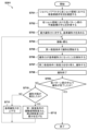
図11は、本実施形態における、第1吸着条件、第2吸着条件を用いた離形を行うことを含むインプリント処理のフローチャートである。S301で、制御部113は、ショットレイアウトに基づいて、各ショット領域の第1吸着条件および第2吸着条件ならびにその切替タイミングを設定する。S302で、制御部113は、インプリント材供給部105を制御して基板上にインプリント材を供給し、型駆動部109を制御して型107と基板104上のインプリント材106とを接触させ、照射部111を制御してインプリント材を硬化させる。
FIG. 11 is a flowchart of imprint processing including release using the first adsorption condition and the second adsorption condition in this embodiment. In S301, the
S303で、制御部113は、型駆動部109を制御して第1吸着条件で離型を開始する。S304で、制御部113は、離型中に切替タイミングになったことを検知する。S305で、制御部113は、吸着力を第2吸着条件に切り替えて離型を進行させる。S306で離型が完了する。S307で、制御部113は、処理すべき次のショット領域があるかを判定し、次のショット領域がある場合はS302に戻って次のショット領域のインプリント処理を実行する。次のショット領域がない場合は、本処理を終了する。
このフローでは、第1吸着条件、第2吸着条件、およびその切替タイミングの適正値が決まっており、その設定が事前に(例えばS301で)各ショット領域に割り当てられるようになっている。
In S303, the
In this flow, the first adsorption condition, the second adsorption condition, and appropriate values for the switching timing thereof are determined, and the settings are assigned to each shot area in advance (for example, in S301).
なお、複数の吸着領域を跨ぐショット領域202に限らず、吸着領域を跨がないショット領域201の場合も、同様の概念で、第1吸着条件、第2吸着条件、およびその切替タイミングが決定されうるものである。
Note that not only the
<第2実施形態>
ここでは、図11のS301における、第1吸着条件、第2吸着条件、およびその切替タイミングの具体的な決定方法を説明する。図12は、S301における、第1吸着条件、第2吸着条件、および第1吸着条件から第2吸着条件に変更するタイミング(以下「切替タイミング」)の具体的な決定方法のフローチャートである。
S501で、制御部113は、基板104のショットレイアウトから、各ショット領域内に、基板保持部102の第1吸着領域1021~第5吸着領域1025のうちどの吸着領域が存在するかを確認する。そして、制御部113は、各吸着領域のショット領域内で占める面積に基づいて、または、パターン部115の中心に最も近い吸着領域はどの吸着領域であるかに基づいて、第1吸着条件と第2吸着条件を決める。切替タイミングについては、切替タイミングが早すぎると、離型工程の早期から基板のZ方向の動きが拘束されてしまいパターン破壊のリスクが高まる。一方、切替タイミングが遅すぎると、離型完了時までに最終離型点をパターン部115の中心に精度良く近づけることが間に合わない。よって、以下の処理で、切替タイミングは、パターン破壊が起きない範囲でなるべく早いタイミングに決定されるとよい。
<Second embodiment>
Here, a specific method of determining the first adsorption condition, the second adsorption condition, and the switching timing thereof in S301 of FIG. 11 will be described. FIG. 12 is a flowchart of a specific method of determining the first adsorption condition, the second adsorption condition, and the timing of changing from the first adsorption condition to the second adsorption condition (hereinafter referred to as "switching timing") in S301.
In S501, from the shot layout of the
S502で、制御部113は、各ショット領域における、パターン部115の中心座標を求め、最終離形点となるべき座標を設定する。図13は、離型工程中のショット領域上のインプリント材と型107のパターン部115との接触状態を示している。ここで、図13(a)に、パターン部115における、第1パターン領域601と第2パターン領域602の区分けの一例を示す。本実施形態では、離形開始時は接触領域がパターン部115の外周部を含む領域で始まり、離型終了時は該接触領域がパターン部115の中心で消えてなくなることを目標とする。そのたため、第1パターン領域601の図心とパターン部115の中心とが一致するように、基準領域を定義する。S503で、制御部113は、第1吸着条件と第2吸着条件を切り替える判断をするために、パターン部115内における、第1パターン領域601と第2パターン領域602を決定する。例えば、第1パターン領域601(基準領域)は、パターン面の中心を含みパターン面より小さい領域に決定する。第2パターン領域602は、パターン面のうちの第1パターン領域601以外の領域である。
In S502, the
S504で、制御部113は、インプリント材供給部105を制御して基板上にインプリント材を供給し、型駆動部109を制御して型107と基板104上のインプリント材106とを接触させ、照射部111を制御してインプリント材を硬化させる。S505で、制御部113は、型駆動部109を制御して、S501で決めた第1吸着条件で離形を開始する。S506で、制御部113は、画像取得部114で得られた画像が、S503で決定した第1パターン領域601内に入ったことを検知する。図13(b)は、S506で接触領域の外縁の少なくとも一部が第1パターン領域601に入ったことを検知したときの画像の一例を示している。S506で接触領域の外縁の少なくとも一部が第1パターン領域601に入ったことが検知されたタイミングが、切替タイミングとして決定される。
In S504, the
S507で、制御部113は、吸着力をS501で決定した第2吸着条件に切り替えて離型を進行させる。S508で離形が完了する。なお、S505~S508の期間中は離形は継続しているが、S505、S506、S507、S508の各ステップで離形を一旦停止させることもありうる。S509で、制御部113は、離型完了直前に画像取得部114で得られた画像に基づいて、最終離形点がS502で決定された座標、すなわちパターン部115の中心、であったかを判定する。YESであれば、ショット領域の第1吸着条件、第2吸着条件、およびその切替タイミングは定まったこととなる。NOであればS510へ進み、制御部113は、画像取得部114の画像または外部計測器を用いて、形成されたパターンの離型による破壊(離型欠陥)があるか否かを確認する。パターン破壊がある場合は、S512で、第1吸着条件を、パターン破壊を防止するため離型中の基板変形量が大きくなるよう接触領域の吸着力と周辺領域の吸着力との差を大きくした吸着条件に変更する。その後、処理はS504へ戻る。パターン破壊がなければ、S511に進む。この状況は、パターン破壊は起きないものの、最終離形点がパターン部115の中心からずれており(S509でNO)、型破壊のリスクが高いという状況である。そこでS511では、第1パターン領域601の面積を大きくして再度S504へ戻る。第1パターン領域601の面積を大きくすることにより、第1吸着条件から第2吸着条件への切替タイミング(S507の実行タイミング)を早めることができ、これにより、最終離形点をパターン部115の中心に近づけることができる。図13(c)は、以上の処理を経て、S509で最終離形点がパターン部115の中心になったときの画像の一例を示している。
In S507, the
このように、制御部113は、離型完了直前に画像取得部114による撮像によって得られた画像に基づき、形成されたパターンの欠陥が発生せず、かつ、最終離型点がパターン部115の中心になるように、第1パターン領域(基準領域)を設定する。
S301では、このようなフローによって、各ショット領域の第1吸着条件、第2吸着条件、およびその切替タイミングを適切に決定することができる。なお、図12の決定フローをそのままインプリント処理に用いてもよい。図13(d)は、第2吸着領域1022、第3吸着領域1023、第4吸着領域1024、第5吸着領域1025を跨ぐ場所に位置しているショット領域202を示しており、これは図6(d)と同じである。図13(e)は、図12のフローに従い決定された第1吸着条件の下で離型を開始した後の、インプリント材106とパターン部115との接触領域を示している。この時点では、図6(e)と同様、基板104の変形度合いに偏りが生じ、パターン部115の中心と接触領域の図心とが一致しないかもしれない。しかし、図13(f)では、図12のフローに従い適切に設定されたタイミングで第2吸着条件に切り替えたため、最終離型点がパターン部115の中心と一致している。
In this way, based on the image obtained by the image acquisition unit 114 immediately before the mold release is completed, the
In S301, such a flow makes it possible to appropriately determine the first suction condition, the second suction condition, and the switching timing for each shot area. Note that the determination flow of FIG. 12 may be used as it is for imprint processing. FIG. 13(d) shows the
なお、複数の吸着領域を跨ぐショット領域202に限らず、吸着領域を跨がないショット領域201の場合も、同様の概念で、第1吸着条件、第2吸着条件、およびその切替タイミングが決定されうる。
Note that not only the
<第3実施形態>
ここでは、図11のS301における、第1吸着条件、第2吸着条件、およびその切替タイミングの決定方法について、他の例を説明する。
本実施形態におけるインプリント装置100は、図1に示すように、型保持部108付近に配置された測定部150を有する。測定部150は、離型工程において、硬化したインプリント材106と型107との分離に要する力である離型力に関する物理量を測定する。測定部150は、例えば、力に比例して変形する起歪体とその変形量を測定する歪みゲージを有するロードセルでありうる。
<Third Embodiment>
Here, another example of the method for determining the first adsorption condition, the second adsorption condition, and the switching timing thereof in S301 of FIG. 11 will be described.
The
図14は、本実施形態による、S301における、第1吸着条件、第2吸着条件、およびその切替タイミングの具体的な決定方法のフローチャートである。
S701で、制御部113は、基板104のショットレイアウトから、各ショット領域内に、基板保持部102の第1吸着領域1021~第5吸着領域1025のうちどの吸着領域が存在するかを確認する。そして、制御部113は、各吸着領域のショット領域内で占める面積に基づいて、または、パターン部115の中心に最も近い吸着領域はどの吸着領域あるかに基づいて、第1吸着条件と第2吸着条件を決める。
FIG. 14 is a flowchart of a specific method for determining the first adsorption condition, the second adsorption condition, and the switching timing thereof in S301 according to the present embodiment.
In S701, from the shot layout of the
S702で、制御部113は、各ショット領域における、パターン部115の中心座標を求め、最終離形点となるべき座標を設定する。S703で、制御部113は、測定部150を用いて第1吸着条件と第2吸着条件とを切り替える判断を行うために、離形の際に発生する最大離形力に対する基準離形力を決定する。この基準離形力は、絶対値であっても、最大離形力に対する相対変化量または相対比率であってもよい。図15(a)に、離形開始から離形力が大きくなり最初に小さくなる点を最大離形力としたときの、基準離形力を決める一例を示している。本実施形態では、離形力が一度しかピークを迎えないが、型駆動部109の制御によっては複数のピークを持つことがあり、ピーク同士の関係等に基づいて基準離形力を決めてもよい。
In S702, the
S704で、制御部113は、インプリント材供給部105を制御して基板上にインプリント材を供給し、型駆動部109を制御して型107と基板104上のインプリント材106とを接触させ、照射部111を制御してインプリント材を硬化させる。S705で、制御部113は、型駆動部109を制御して、S701で決めた第1吸着条件で離形を開始する。S706で、制御部113は、測定部150により測定された離形力が基準離形力に到達したことを検知する。この検知されたタイミングが、切替タイミングとして決定される。
In S704, the
S707で、制御部113は、吸着力をS701で決定した第2吸着条件に切り替えて離型を進行させる。S708で離形が完了する。図15(b)および図15(c)は、S705~S708の期間における、接触領域の少なくとも一部の吸着力と周辺領域の少なくとも一部の吸着力の、切り替えの一例を示している。なお、S705~S708の期間中は離形は継続しているが、S705、S706、S707、S708の各ステップで離形を一旦停止させることもありうる。S709で、制御部113は、画像取得部114で得られた画像に基づいて、最終離形点がS702で決定された座標、すなわちパターン部115の中心、であったかを判定する。YESであれば、ショット領域の第1吸着条件、第2吸着条件、およびその切替タイミングは定まったこととなる。NOであればS710へ進み、制御部113は、画像取得部114の画像または外部計測器を用いて、形成パターンの破壊がないことを確認する。YESであればS712で、第1吸着条件の接触領域の吸着力と周辺領域の吸着力との差を大きくして再度S704へ戻る。NOであればS711で、基準離形力を大きくして再度S704へ戻る。
In S707, the
このように、制御部113は、離型完了直前に画像取得部114による撮像によって得られた画像に基づき、形成されたパターンの欠陥が発生せず、かつ、最終離型点がパターン部115の中心になるように、基準離型力を設定する。
S301では、このようなフローで、各ショット領域の第1吸着条件、第2吸着条件、およびその切替タイミングを決定することができる。なお、図14の決定フローをそのままインプリント処理に用いてもよい。
In this way, based on the image obtained by the image acquisition unit 114 immediately before the mold release is completed, the
In S301, it is possible to determine the first adsorption condition, the second adsorption condition, and the switching timing for each shot area in such a flow. Note that the determination flow of FIG. 14 may be used as it is for imprint processing.
なお、複数の吸着領域を跨ぐショット領域202に限らず、吸着領域を跨がないショット領域201の場合も、同様の概念で、第1吸着条件、第2吸着条件、およびその切替タイミングが決定されうる。
Note that not only the
<第4実施形態>
ここでは、図11のS301における、第1吸着条件、第2吸着条件、およびその切替タイミングの決定方法について、更に他の例を説明する。図16は、本実施形態よる、S301での、第1吸着条件、第2吸着条件、およびその切替タイミングの具体的な決定方法のフローチャートである。
S901で、制御部113は、基板104のショットレイアウトから、各ショット領域内に、基板保持部102の第1吸着領域1021~第5吸着領域1025のうちどの吸着領域が存在するかを確認する。そして、制御部113は、各吸着領域のショット領域内で占める面積に基づいて、または、パターン部115の中心に最も近い吸着領域はどの吸着領域であるかに基づいて、第1吸着条件と第2吸着条件を決める。
<Fourth Embodiment>
Here, still another example of the method for determining the first adsorption condition, the second adsorption condition, and the switching timing thereof in S301 of FIG. 11 will be described. FIG. 16 is a flowchart of a specific method for determining the first adsorption condition, the second adsorption condition, and the switching timing thereof in S301 according to the present embodiment.
In S901, the
S902で、制御部113は、各ショット領域における、パターン部115の中心座標を求め、最終離形点となるべき座標を設定する。S903で、制御部113は、第1吸着条件から第2吸着条件に切り替える、離形開始からの基準時間を決定する。
In S902, the
S904で、制御部113は、インプリント材供給部105を制御して基板上にインプリント材を供給し、型駆動部109を制御して型107と基板104上のインプリント材106とを接触させ、照射部111を制御してインプリント材を硬化させる。S905で、制御部113は、型駆動部109を制御して、S901で決めた第1吸着条件で離形工程を開始する。S906で、制御部113は、離形工程の開始から基準時間が経過したことを検知する。この検知されたタイミングが、切替タイミングとして決定される。
In S904, the
S907で、制御部113は、吸着力をS901で決定した第2吸着条件に切り替えて離型を進行させる。S908で離形が完了する。なお、S905~S908の期間中は離形は継続しているが、S905、S906、S907、S908の各ステップで離形を一旦停止させることもありうる。S909で、制御部113は、画像取得部114で得られた画像に基づいて、最終離形点がS902で決定された座標、すなわちパターン部115の中心、であったかを判定する。YESであれば、ショット領域の第1吸着条件、第2吸着条件、およびその切替タイミングは定まったこととなる。NOであればS910へ進み、制御部113は、画像取得部114の画像または外部計測器を用いて、形成パターンの破壊がないことを確認する。YESであればS912で、第1吸着条件の接触領域の吸着力と周辺領域の吸着力との差を大きくして再度S904へ戻る。NOであればS911で、基準時間を短くして再度S904へ戻る。
In S907, the
このように、制御部113は、離型完了直前に画像取得部114による撮像によって得られた画像に基づき、形成されたパターンの欠陥が発生せず、かつ、最終離型点がパターン部115の中心になるように、基準時間を設定する。
S301では、このようなフローで、各ショット領域の第1吸着条件、第2吸着条件、およびその切替タイミングを決定することができる。なお、図16の決定フローをそのままインプリント処理に用いてもよい。
In this way, based on the image obtained by the image acquisition unit 114 immediately before the mold release is completed, the
In S301, it is possible to determine the first adsorption condition, the second adsorption condition, and the switching timing for each shot area in such a flow. Note that the determination flow of FIG. 16 may be used as it is for imprint processing.
なお、複数の吸着領域を跨ぐショット領域202に限らず、吸着領域を跨がないショット領域201の場合も、同様の概念で、第1吸着条件、第2吸着条件、およびその切替タイミングが決定されうる。
Note that not only the
<第5実施形態>
本実施形態は、第1実施形態における図11のインプリント処理の変形例に関する。図17に、本実施形態におけるインプリント処理のフローチャートを示す。
S1001で、制御部113は、基板104のショットレイアウトから、各ショット領域内に、基板保持部102の第1吸着領域1021~第5吸着領域1025のうちどの吸着領域が存在するかを確認する。そして、制御部113は、各吸着領域のショット領域内で占める面積に基づいて、または、パターン部115の中心に最も近い吸着領域はどの吸着領域であるかに基づいて、第1吸着条件と第2吸着条件を決める。
<Fifth Embodiment>
This embodiment relates to a modification of the imprint processing of FIG. 11 in the first embodiment. FIG. 17 shows a flowchart of imprint processing in this embodiment.
In S1001, the
S1002で、制御部113は、S1001で決めた第1吸着条件、第2吸着条件、およびその切替タイミングが妥当であるかを、計算もしくはシミュレーションで判断し、修正する。また、その判断には過去の実績情報などによる学習機能などが含まれていてもよい。S1003で、制御部113は、第1吸着条件、第2吸着条件、およびその切替タイミングを決定する。
In S1002, the
S1004で、制御部113は、インプリント材供給部105を制御して基板上にインプリント材を供給し、型駆動部109を制御して型107と基板104上のインプリント材106とを接触させ、照射部111を制御してインプリント材を硬化させる。S1005で、制御部113は、型駆動部109を制御してS1003で決めた第1吸着条件で離形を開始する。
In S1004, the
S1006で、制御部113は、S1003で決めたタイミングになったことを検知する。S1007で、制御部113は、吸着力をS1003で決めた第2吸着条件に切り替えて離型を進行させる。S1008で離形が完了する。なお、S1005~S1008の期間中は離形は継続しているが、S1005、S1006、S1007、S1008の各ステップで離形を一旦停止させることもありうる。S1009で、制御部113は、処理すべき次のショット領域があるかを判定し、次のショット領域がある場合はS1004へ戻って次のショット領域のインプリント処理を実行する。次のショット領域がない場合は、本処理を終了する。
In S1006, the
<第6実施形態>
上述の各実施形態においては、成形装置の一態様として、インプリント材と前記型とを接触させることによって前記型のパターンを前記インプリント材に転写するインプリント装置について説明した。しかし、本発明は、成形装置の別態様として、基板の上の組成物と平坦面を有する部材(型)を接触させることによって基板の上に組成物による平坦化膜を形成する平坦化装置にも適用することができる。
<Sixth embodiment>
In each of the above-described embodiments, as one aspect of the molding apparatus, the imprint apparatus that transfers the pattern of the mold to the imprint material by bringing the imprint material and the mold into contact has been described. However, the present invention provides, as another aspect of the molding apparatus, a flattening apparatus that forms a flattening film of a composition on a substrate by bringing the composition on the substrate into contact with a member (mold) having a flat surface. can also be applied.
基板上の下地パターンは、前の工程で形成されたパターンに起因する凹凸プロファイルを有しており、特に近年のメモリ素子の多層構造化に伴いプロセス基板は100nm前後の段差を持つものも出てきている。基板全体の緩やかなうねりに起因する段差は、フォト工程で使われているスキャン露光装置のフォーカス追従機能によって補正可能である。しかし、露光装置の露光スリット面積内に収まってしまうピッチの細かい凹凸は、露光装置のDOF(Depth Of Focus)から外れるおそれがある。従来、基板の下地パターンを平滑化する手法として、SOC(Spin On Carbon)、CMP(Chemical Mechanical Polishing)のような平坦化層を形成する手法が用いられている。しかし、従来技術では十分な平坦化性能が得られない問題があり、今後多層化による下地の凹凸差は更に増加する傾向にある。 The underlying pattern on the substrate has an uneven profile resulting from the pattern formed in the previous process. In particular, with the recent multi-layered structure of memory elements, some process substrates have steps of about 100 nm. ing. A step caused by a gentle undulation of the entire substrate can be corrected by a focus tracking function of a scanning exposure device used in the photo process. However, fine-pitch irregularities that fit within the exposure slit area of the exposure apparatus may be out of the DOF (Depth Of Focus) of the exposure apparatus. Conventionally, methods for forming a planarization layer such as SOC (Spin On Carbon) and CMP (Chemical Mechanical Polishing) have been used as methods for smoothing an underlying pattern of a substrate. However, the prior art has a problem that sufficient flattening performance cannot be obtained, and there is a tendency that the unevenness difference of the substrate will further increase due to the increase in the number of layers in the future.
この問題を解決するために、上記したようなインプリント技術を用いて基板の平坦化を行う平坦化装置が検討されている。平坦化装置は、基板に予め供給された未硬化状態の組成物(平坦化材)に、部材の平坦面、あるいは、パターンが形成されていない部材(平面テンプレート)を接触させて基板面内の局所的な平面化を行う。その後、組成物と平面テンプレートとが接触した状態で組成物を硬化させ、硬化した組成物から平面テンプレートを分離させる。これにより基板上に平坦化層が形成される。インプリント技術を用いた平坦化装置は、基板の段差に応じた量の組成物を滴下するため、既存の方法よりも平坦化の精度が向上することが期待される。 In order to solve this problem, a planarization apparatus that planarizes a substrate using the imprint technique as described above has been studied. The planarization apparatus contacts an uncured composition (planarization material) previously supplied to the substrate with a flat surface of a member or a member (planar template) on which no pattern is formed, thereby planarizing the substrate surface. Perform local planarization. The composition is then cured while the composition and planar template are in contact, separating the planar template from the cured composition. This forms a planarization layer on the substrate. A planarization apparatus using an imprint technique drops a composition in an amount corresponding to the steps of a substrate, and is therefore expected to have higher planarization accuracy than existing methods.
<物品製造方法の実施形態>
インプリント装置を用いて形成した硬化物のパターンは、各種物品の少なくとも一部に恒久的に、或いは各種物品を製造する際に一時的に、用いられる。物品とは、電気回路素子、光学素子、MEMS、記録素子、センサ、或いは、型等である。電気回路素子としては、DRAM、SRAM、フラッシュメモリ、MRAMのような、揮発性或いは不揮発性の半導体メモリや、LSI、CCD、イメージセンサ、FPGAのような半導体素子等が挙げられる。型としては、インプリント用のモールド等が挙げられる。
<Embodiment of article manufacturing method>
A pattern of a cured product formed using an imprint apparatus is used permanently on at least a part of various articles, or temporarily used when manufacturing various articles. Articles are electric circuit elements, optical elements, MEMS, recording elements, sensors, molds, or the like. Examples of electric circuit elements include volatile or nonvolatile semiconductor memories such as DRAM, SRAM, flash memory, and MRAM, and semiconductor elements such as LSI, CCD, image sensors, and FPGA. Examples of the mold include imprint molds and the like.
硬化物のパターンは、上記物品の少なくとも一部の構成部材として、そのまま用いられるか、或いは、レジストマスクとして一時的に用いられる。基板の加工工程においてエッチング又はイオン注入等が行われた後、レジストマスクは除去される。 The pattern of the cured product is used as it is or temporarily used as a resist mask as at least a part of the article. After etching, ion implantation, or the like in the substrate processing step, the resist mask is removed.
次に、物品製造方法について説明する。図19の工程SAでは、絶縁体等の被加工材2zが表面に形成されたシリコン基板等の基板1zを用意し、続いて、インクジェット法等により、被加工材2zの表面にインプリント材3zを付与する。ここでは、複数の液滴状になったインプリント材3zが基板上に付与された様子を示している。
Next, an article manufacturing method will be described. In step SA of FIG. 19, a
図19の工程SBでは、インプリント用の型4zを、その凹凸パターンが形成された側を基板上のインプリント材3zに向け、対向させる。図19の工程SCでは、インプリント材3zが付与された基板1zと型4zとを接触させ、圧力を加える。インプリント材3zは型4zと被加工材2zとの隙間に充填される。この状態で硬化用のエネルギーとして光を型4zを介して照射すると、インプリント材3zは硬化する。
In step SB of FIG. 19, the
図19の工程SDでは、インプリント材3zを硬化させた後、型4zと基板1zを引き離すと、基板1z上にインプリント材3zの硬化物のパターンが形成される。この硬化物のパターンは、型の凹部が硬化物の凸部に、型の凸部が硬化物の凹部に対応した形状になっており、即ち、インプリント材3zに型4zの凹凸パターンが転写されたことになる。
In step SD of FIG. 19, after the
図19の工程SEでは、硬化物のパターンを耐エッチングマスクとしてエッチングを行うと、被加工材2zの表面のうち、硬化物が無いか或いは薄く残存した部分が除去され、溝5zとなる。図19の工程SFでは、硬化物のパターンを除去すると、被加工材2zの表面に溝5zが形成された物品を得ることができる。ここでは硬化物のパターンを除去したが、加工後も除去せずに、例えば、半導体素子等に含まれる層間絶縁用の膜、つまり、物品の構成部材として利用してもよい。
In step SE of FIG. 19, when etching is performed using the pattern of the cured product as an anti-etching mask, the portion of the surface of the
発明は上記実施形態に制限されるものではなく、発明の精神及び範囲から離脱することなく、様々な変更及び変形が可能である。従って、発明の範囲を公にするために請求項を添付する。 The invention is not limited to the embodiments described above, and various modifications and variations are possible without departing from the spirit and scope of the invention. Accordingly, the claims are appended to make public the scope of the invention.
100:インプリント装置、101:ステージ、102:基板保持部、103:吸着力制御部、104:基板、105:インプリント材供給部、106:インプリント材、107:型、108:型保持部、109:型駆動部、113:制御部、114:画像取得部、115:パターン部 100: imprint apparatus, 101: stage, 102: substrate holder, 103: adsorption force controller, 104: substrate, 105: imprint material supply unit, 106: imprint material, 107: mold, 108: mold holder , 109: mold driving unit, 113: control unit, 114: image acquisition unit, 115: pattern unit
Claims (12)
前記基板の下面を吸着する複数の吸着領域を有し、該複数の吸着領域で前記基板を吸着することによって前記基板を保持する基板保持部と、
前記成形処理の実行を制御するとともに、前記複数の吸着領域のそれぞれにおける吸着力を独立に制御する制御部と、を有し、
前記制御部は、前記離型工程において、前記型が前記組成物から最後に分離する点である最終離型点が前記型のパターン面の中心になるように、前記複数の吸着領域それぞれの吸着力を制御するように構成され、
前記制御部は、離型時に前記パターン面と対向する前記基板のショット領域が前記パターン面に対して凸形状に変形することを許容するように、当該ショット領域の下にある吸着領域のうち最も基板外周側の吸着領域以外の吸着領域の吸着力を弱める第1吸着条件で前記離型工程を開始し、前記離型工程の途中で、前記第1吸着条件から、前記ショット領域の下にある各吸着領域の吸着力の差をなくした第2吸着条件に変更する、ことを特徴とする成形装置。 A contact step of contacting the composition on the substrate with the mold, a curing step of curing the composition while the composition and the mold are in contact, and separating the cured composition and the mold. A molding device that performs a molding process including a mold release step,
a substrate holding part having a plurality of adsorption areas for adsorbing the lower surface of the substrate, and holding the substrate by adsorbing the substrate in the plurality of adsorption areas;
a control unit that controls the execution of the molding process and independently controls the adsorption force in each of the plurality of adsorption areas;
In the mold release step, the control unit controls the adsorption of each of the plurality of adsorption regions so that the final release point, which is the point at which the mold is finally separated from the composition, is the center of the pattern surface of the mold. configured to control the force,
The control unit is configured to allow the shot area of the substrate facing the pattern surface to be deformed into a convex shape with respect to the pattern surface when the mold is released. The mold release step is started under a first adsorption condition that weakens the adsorption force of the adsorption regions other than the adsorption region on the outer peripheral side of the substrate. A molding apparatus characterized by changing to a second adsorption condition that eliminates the difference in the adsorption force of each adsorption area.
前記制御部は、前記離型工程において前記撮像部により得られた前記接触領域の画像に基づいて、前記第1吸着条件から前記第2吸着条件に変更するタイミングを決定する、ことを特徴とする請求項1に記載の成形装置。 further comprising an imaging unit for imaging a contact area between the composition and the pattern surface;
The control unit determines timing for changing the first adsorption condition to the second adsorption condition based on the image of the contact area obtained by the imaging unit in the releasing step. A molding apparatus according to claim 1 .
前記制御部は、前記測定部により測定された離型力が基準離型力になったタイミングを前記第1吸着条件から前記第2吸着条件に変更するタイミングとして決定する、ことを特徴とする請求項2に記載の成形装置。 further comprising a measuring unit for measuring a release force, which is the force required to separate the cured composition from the mold;
The control unit determines a timing at which the releasing force measured by the measuring unit becomes a reference releasing force as a timing for changing the first adsorption condition to the second adsorption condition. Item 2. The molding apparatus according to item 2 .
前記形成工程で前記パターンが形成された前記基板を処理する処理工程と、
を有し、前記処理工程で処理された前記基板から物品を製造することを特徴とする物品製造方法。 a forming step of forming a pattern on a substrate using the imprinting device, which is the molding device according to claim 9 ;
a processing step of processing the substrate on which the pattern is formed in the forming step;
and manufacturing an article from the substrate treated in the treatment step.
前記形成工程で形成された前記膜を処理する処理工程と、
を有し、前記処理工程で処理された前記基板から物品を製造することを特徴とする物品製造方法。 a forming step of forming a composition film on a substrate by the flattening device, which is the molding device according to claim 10 ;
a processing step of processing the film formed in the forming step;
and manufacturing an article from the substrate treated in the treatment step.
Priority Applications (3)
| Application Number | Priority Date | Filing Date | Title |
|---|---|---|---|
| JP2019107449A JP7284639B2 (en) | 2019-06-07 | 2019-06-07 | Molding apparatus and article manufacturing method |
| KR1020200064679A KR102559861B1 (en) | 2019-06-07 | 2020-05-29 | Forming apparatus and method of manufacturing article |
| US16/892,389 US11422462B2 (en) | 2019-06-07 | 2020-06-04 | Forming apparatus that controls chucking force |
Applications Claiming Priority (1)
| Application Number | Priority Date | Filing Date | Title |
|---|---|---|---|
| JP2019107449A JP7284639B2 (en) | 2019-06-07 | 2019-06-07 | Molding apparatus and article manufacturing method |
Publications (3)
| Publication Number | Publication Date |
|---|---|
| JP2020202269A JP2020202269A (en) | 2020-12-17 |
| JP2020202269A5 JP2020202269A5 (en) | 2022-06-07 |
| JP7284639B2 true JP7284639B2 (en) | 2023-05-31 |
Family
ID=73651465
Family Applications (1)
| Application Number | Title | Priority Date | Filing Date |
|---|---|---|---|
| JP2019107449A Active JP7284639B2 (en) | 2019-06-07 | 2019-06-07 | Molding apparatus and article manufacturing method |
Country Status (3)
| Country | Link |
|---|---|
| US (1) | US11422462B2 (en) |
| JP (1) | JP7284639B2 (en) |
| KR (1) | KR102559861B1 (en) |
Families Citing this family (2)
| Publication number | Priority date | Publication date | Assignee | Title |
|---|---|---|---|---|
| JP6762853B2 (en) * | 2016-11-11 | 2020-09-30 | キヤノン株式会社 | Equipment, methods, and article manufacturing methods |
| JP7327973B2 (en) * | 2019-03-29 | 2023-08-16 | キヤノン株式会社 | IMPRINT APPARATUS, IMPRINT METHOD, AND ARTICLE MANUFACTURING METHOD |
Citations (4)
| Publication number | Priority date | Publication date | Assignee | Title |
|---|---|---|---|---|
| JP2012507141A (en) | 2008-10-24 | 2012-03-22 | モレキュラー・インプリンツ・インコーポレーテッド | Control of strain and dynamics during the separation stage of the imprint process |
| JP2016096327A (en) | 2014-11-11 | 2016-05-26 | キヤノン株式会社 | Imprint method, imprint device, mold, and manufacturing method of article |
| JP2017092396A (en) | 2015-11-16 | 2017-05-25 | キヤノン株式会社 | Imprinting device and article manufacturing method |
| JP2019021911A (en) | 2017-07-14 | 2019-02-07 | キヤノン株式会社 | Imprint device, article manufacturing method, and molding device |
Family Cites Families (7)
| Publication number | Priority date | Publication date | Assignee | Title |
|---|---|---|---|---|
| US20050276919A1 (en) * | 2004-06-01 | 2005-12-15 | Molecular Imprints, Inc. | Method for dispensing a fluid on a substrate |
| US7635263B2 (en) * | 2005-01-31 | 2009-12-22 | Molecular Imprints, Inc. | Chucking system comprising an array of fluid chambers |
| US7636999B2 (en) | 2005-01-31 | 2009-12-29 | Molecular Imprints, Inc. | Method of retaining a substrate to a wafer chuck |
| WO2006083518A2 (en) | 2005-01-31 | 2006-08-10 | Molecular Imprints, Inc. | Chucking system for nano-manufacturing |
| JP5875250B2 (en) * | 2011-04-28 | 2016-03-02 | キヤノン株式会社 | Imprint apparatus, imprint method, and device manufacturing method |
| JP6004738B2 (en) | 2011-09-07 | 2016-10-12 | キヤノン株式会社 | Imprint apparatus and article manufacturing method using the same |
| US10627715B2 (en) * | 2016-10-31 | 2020-04-21 | Canon Kabushiki Kaisha | Method for separating a nanoimprint template from a substrate |
-
2019
- 2019-06-07 JP JP2019107449A patent/JP7284639B2/en active Active
-
2020
- 2020-05-29 KR KR1020200064679A patent/KR102559861B1/en active IP Right Grant
- 2020-06-04 US US16/892,389 patent/US11422462B2/en active Active
Patent Citations (4)
| Publication number | Priority date | Publication date | Assignee | Title |
|---|---|---|---|---|
| JP2012507141A (en) | 2008-10-24 | 2012-03-22 | モレキュラー・インプリンツ・インコーポレーテッド | Control of strain and dynamics during the separation stage of the imprint process |
| JP2016096327A (en) | 2014-11-11 | 2016-05-26 | キヤノン株式会社 | Imprint method, imprint device, mold, and manufacturing method of article |
| JP2017092396A (en) | 2015-11-16 | 2017-05-25 | キヤノン株式会社 | Imprinting device and article manufacturing method |
| JP2019021911A (en) | 2017-07-14 | 2019-02-07 | キヤノン株式会社 | Imprint device, article manufacturing method, and molding device |
Also Published As
| Publication number | Publication date |
|---|---|
| KR20200140717A (en) | 2020-12-16 |
| US11422462B2 (en) | 2022-08-23 |
| JP2020202269A (en) | 2020-12-17 |
| KR102559861B1 (en) | 2023-07-27 |
| US20200387067A1 (en) | 2020-12-10 |
Similar Documents
| Publication | Publication Date | Title |
|---|---|---|
| TWI718288B (en) | Imprint apparatus, imprint method, and method of manufacturing article | |
| JP7284639B2 (en) | Molding apparatus and article manufacturing method | |
| JP7134717B2 (en) | Imprinting apparatus, imprinting method and article manufacturing method | |
| JP2019145786A (en) | Imprint apparatus, planarization layer forming apparatus, forming apparatus, control method, and article manufacturing method | |
| JP6423641B2 (en) | Imprint apparatus, article manufacturing method, and imprint method | |
| US11194249B2 (en) | Molding apparatus for molding composition on substrate with mold, and article manufacturing method | |
| KR20190003391A (en) | Imprint apparatus and method of manufacturing article | |
| JP6887279B2 (en) | Imprint equipment and article manufacturing method | |
| JP6317620B2 (en) | Imprint method, imprint apparatus, and article manufacturing method | |
| KR20220027034A (en) | Imprint apparatus and method of manufacturing article | |
| JP2019201184A (en) | Imprint device and article manufacturing method | |
| JP7148284B2 (en) | IMPRINT APPARATUS AND ARTICLE MANUFACTURING METHOD | |
| JP6983091B2 (en) | Imprint device and manufacturing method of goods | |
| KR20210065854A (en) | Imprinting apparatus, imprinting method, method for producing article, substrate, and mold | |
| JP7194068B2 (en) | Mold making method and article manufacturing method | |
| JP2019145591A (en) | Imprint apparatus, article manufacturing method, and mold | |
| JP2023125837A (en) | Molding method, molding device, and manufacturing method of article | |
| JP7414627B2 (en) | Imprint device, imprint method, and article manufacturing method | |
| KR102689957B1 (en) | Imprint system, replica mold manufacturing apparatus, and article manufacturing method | |
| JP7437928B2 (en) | Imprint equipment, imprint method, and article manufacturing method | |
| JP7555756B2 (en) | Imprint system, imprint method, and article manufacturing method | |
| JP7254564B2 (en) | IMPRINT APPARATUS, IMPRINT METHOD, AND ARTICLE MANUFACTURING METHOD | |
| JP2022172906A (en) | Molding device and article manufacturing method | |
| JP2023058321A (en) | Imprint apparatus and article manufacturing method | |
| JP2024042462A (en) | Imprint device, imprint method, determination method, and method for manufacturing article |
Legal Events
| Date | Code | Title | Description |
|---|---|---|---|
| RD01 | Notification of change of attorney |
Free format text: JAPANESE INTERMEDIATE CODE: A7421 Effective date: 20210103 |
|
| A521 | Request for written amendment filed |
Free format text: JAPANESE INTERMEDIATE CODE: A523 Effective date: 20210113 |
|
| A521 | Request for written amendment filed |
Free format text: JAPANESE INTERMEDIATE CODE: A523 Effective date: 20220530 |
|
| A621 | Written request for application examination |
Free format text: JAPANESE INTERMEDIATE CODE: A621 Effective date: 20220530 |
|
| A977 | Report on retrieval |
Free format text: JAPANESE INTERMEDIATE CODE: A971007 Effective date: 20230126 |
|
| A131 | Notification of reasons for refusal |
Free format text: JAPANESE INTERMEDIATE CODE: A131 Effective date: 20230203 |
|
| A521 | Request for written amendment filed |
Free format text: JAPANESE INTERMEDIATE CODE: A523 Effective date: 20230330 |
|
| TRDD | Decision of grant or rejection written | ||
| A01 | Written decision to grant a patent or to grant a registration (utility model) |
Free format text: JAPANESE INTERMEDIATE CODE: A01 Effective date: 20230421 |
|
| A61 | First payment of annual fees (during grant procedure) |
Free format text: JAPANESE INTERMEDIATE CODE: A61 Effective date: 20230519 |
|
| R151 | Written notification of patent or utility model registration |
Ref document number: 7284639 Country of ref document: JP Free format text: JAPANESE INTERMEDIATE CODE: R151 |