JP7272937B2 - Deep solid-state devices and neural network-based persistent data storage - Google Patents
Deep solid-state devices and neural network-based persistent data storage Download PDFInfo
- Publication number
- JP7272937B2 JP7272937B2 JP2019209473A JP2019209473A JP7272937B2 JP 7272937 B2 JP7272937 B2 JP 7272937B2 JP 2019209473 A JP2019209473 A JP 2019209473A JP 2019209473 A JP2019209473 A JP 2019209473A JP 7272937 B2 JP7272937 B2 JP 7272937B2
- Authority
- JP
- Japan
- Prior art keywords
- dataset
- circuit
- machine learning
- data set
- transformed
- Prior art date
- Legal status (The legal status is an assumption and is not a legal conclusion. Google has not performed a legal analysis and makes no representation as to the accuracy of the status listed.)
- Active
Links
Images


Classifications
-
- G—PHYSICS
- G06—COMPUTING; CALCULATING OR COUNTING
- G06F—ELECTRIC DIGITAL DATA PROCESSING
- G06F12/00—Accessing, addressing or allocating within memory systems or architectures
- G06F12/02—Addressing or allocation; Relocation
- G06F12/0223—User address space allocation, e.g. contiguous or non contiguous base addressing
- G06F12/023—Free address space management
- G06F12/0238—Memory management in non-volatile memory, e.g. resistive RAM or ferroelectric memory
-
- G—PHYSICS
- G06—COMPUTING; CALCULATING OR COUNTING
- G06F—ELECTRIC DIGITAL DATA PROCESSING
- G06F3/00—Input arrangements for transferring data to be processed into a form capable of being handled by the computer; Output arrangements for transferring data from processing unit to output unit, e.g. interface arrangements
- G06F3/06—Digital input from, or digital output to, record carriers, e.g. RAID, emulated record carriers or networked record carriers
- G06F3/0601—Interfaces specially adapted for storage systems
- G06F3/0628—Interfaces specially adapted for storage systems making use of a particular technique
- G06F3/0655—Vertical data movement, i.e. input-output transfer; data movement between one or more hosts and one or more storage devices
-
- G—PHYSICS
- G06—COMPUTING; CALCULATING OR COUNTING
- G06F—ELECTRIC DIGITAL DATA PROCESSING
- G06F3/00—Input arrangements for transferring data to be processed into a form capable of being handled by the computer; Output arrangements for transferring data from processing unit to output unit, e.g. interface arrangements
- G06F3/06—Digital input from, or digital output to, record carriers, e.g. RAID, emulated record carriers or networked record carriers
- G06F3/0601—Interfaces specially adapted for storage systems
- G06F3/0668—Interfaces specially adapted for storage systems adopting a particular infrastructure
- G06F3/0671—In-line storage system
- G06F3/0673—Single storage device
- G06F3/0679—Non-volatile semiconductor memory device, e.g. flash memory, one time programmable memory [OTP]
-
- G—PHYSICS
- G06—COMPUTING; CALCULATING OR COUNTING
- G06F—ELECTRIC DIGITAL DATA PROCESSING
- G06F3/00—Input arrangements for transferring data to be processed into a form capable of being handled by the computer; Output arrangements for transferring data from processing unit to output unit, e.g. interface arrangements
- G06F3/06—Digital input from, or digital output to, record carriers, e.g. RAID, emulated record carriers or networked record carriers
- G06F3/0601—Interfaces specially adapted for storage systems
- G06F3/0602—Interfaces specially adapted for storage systems specifically adapted to achieve a particular effect
- G06F3/0604—Improving or facilitating administration, e.g. storage management
-
- G—PHYSICS
- G06—COMPUTING; CALCULATING OR COUNTING
- G06F—ELECTRIC DIGITAL DATA PROCESSING
- G06F3/00—Input arrangements for transferring data to be processed into a form capable of being handled by the computer; Output arrangements for transferring data from processing unit to output unit, e.g. interface arrangements
- G06F3/06—Digital input from, or digital output to, record carriers, e.g. RAID, emulated record carriers or networked record carriers
- G06F3/0601—Interfaces specially adapted for storage systems
- G06F3/0628—Interfaces specially adapted for storage systems making use of a particular technique
- G06F3/0638—Organizing or formatting or addressing of data
-
- G—PHYSICS
- G06—COMPUTING; CALCULATING OR COUNTING
- G06N—COMPUTING ARRANGEMENTS BASED ON SPECIFIC COMPUTATIONAL MODELS
- G06N3/00—Computing arrangements based on biological models
- G06N3/02—Neural networks
- G06N3/06—Physical realisation, i.e. hardware implementation of neural networks, neurons or parts of neurons
- G06N3/063—Physical realisation, i.e. hardware implementation of neural networks, neurons or parts of neurons using electronic means
-
- G—PHYSICS
- G06—COMPUTING; CALCULATING OR COUNTING
- G06N—COMPUTING ARRANGEMENTS BASED ON SPECIFIC COMPUTATIONAL MODELS
- G06N3/00—Computing arrangements based on biological models
- G06N3/02—Neural networks
- G06N3/08—Learning methods
-
- G—PHYSICS
- G06—COMPUTING; CALCULATING OR COUNTING
- G06N—COMPUTING ARRANGEMENTS BASED ON SPECIFIC COMPUTATIONAL MODELS
- G06N3/00—Computing arrangements based on biological models
- G06N3/02—Neural networks
- G06N3/08—Learning methods
- G06N3/082—Learning methods modifying the architecture, e.g. adding, deleting or silencing nodes or connections
Description
本発明は、データの格納に関し、より詳細には、ニューラルネットワークベースの永続的データストレージに関する。 The present invention relates to data storage, and more particularly to neural network-based persistent data storage.
最新の情報処理(IT:Information Technology)産業では、非常に大量のデータが多様な装置やプロセスによって生成されている。このようなデータジェネレータのいくつかの例は、スマートマシン、自動車、ソーシャルネットワーク、及びモノのインターネット(IoT:Internet-of-Things)装置である。新しい人工知能(AI:artificial intelligence)及びマシンラーニング(ML:machine learning)技法は、収集されたデータを効率的に分析し、それを使用して、アプリケーションのより良い効用と生産性を達成するために開発されている。これらの膨大な量のデータは、ソリッドステート装置(SSD:solid-state device)、ハードディスク装置(HDD:hard disk device)、ストレージノード、及びストレージの連結で構成される、高性能及び高信頼性のストレージシステム(high performance、reliable storage system)に格納される。 In the modern information technology (IT) industry, very large amounts of data are generated by a wide variety of devices and processes. Some examples of such data generators are smart machines, automobiles, social networks, and Internet-of-Things (IoT) devices. New artificial intelligence (AI) and machine learning (ML) techniques are being used to efficiently analyze the collected data and use it to achieve better application utility and productivity. has been developed. These vast amounts of data are stored in high-performance and high-reliability storage systems consisting of solid-state devices (SSDs), hard disk devices (HDDs), storage nodes, and storage concatenations. It is stored in a storage system (high performance, reliable storage system).
人工ニューラルネットワーク(NN:neural network)、又はコネクショニストシステム(connectionist system)は、動物の脳(animal brain)を構成する生物学的ニューラルネットワークによって若干影響を受けたコンピューティングシステムである。ニューラルネットワークは、多数の他のマシンラーニング技法とともに動作し、複雑なデータ入力を処理するフレームワーク(framework)である。このようなシステムは、一般的に、タスク特有の規則でプログラムされることなく、例を考慮することにより、タスク(task)を遂行するように「学習(learn)」する。例えば、画像認識(image recognition)において、「猫(cat)」又は「猫ではない(no cat)」と手動でラベル付された画像例を分析し、他の画像の猫を識別するために、その結果を使用することで、猫が含まれている画像を識別するように学習する。それらは、例えば、毛皮(fur)、尾(tail)、ひげ、及び猫のような顔を有することのような、猫に対する事前知識なしにこれを行う。代わりに、このようなシステムは、それらが処理した学習内容から特徴(characteristic)を識別することを自動的に生成する。 An artificial neural network (NN), or connectionist system, is a computing system inspired somewhat by the biological neural networks that make up the animal brain. Neural networks are frameworks that work with many other machine learning techniques to process complex data inputs. Such systems generally "learn" to perform a task by considering examples without being programmed with task-specific rules. For example, in image recognition, to analyze example images manually labeled as "cat" or "no cat" and identify cats in other images: Using the results, it learns to identify images that contain cats. They do this without prior knowledge of cats, such as having fur, tails, whiskers, and cat-like faces. Instead, such systems automatically generate identifying characteristics from the learning content they process.
ニューラルネットワーク(NN)は、人工ニューロン(artificial neuron)と呼ばれる連結されたユニット又はノードの収集に基づいている。人工ニューロンは、生物学的脳のニューロンを大略的にモデリングする。生物学的脳のシナプス(synapse)のような各連結は、一つの人工ニューロンから他の人工ニューロンに信号を伝送する。信号を受信した人工ニューロンは、それを処理し、その後、それに連結された他の人工ニューロンに信号を伝送し得る。一般的なニューラルネットワークの具現において、人工ニューロン間の連結での信号は、実数(real number)であり、各人工ニューロンの出力は、その入力の合計の、ある非線形関数(non-linear function)によって演算される。人工ニューロン間の連結は、「エッジ(edge)」と呼ばれる。人工ニューロンとエッジとは、一般的に、学習が進行するにつれて調節される重みを含む。重みは、連結における信号の強度を増加又は減少させる。人工ニューロンは、合算信号がしきい値を超える場合にのみ、信号が伝送されるようにする、しきい値(threshold)を有し得る。一般的に、人工ニューロンは、レイヤを介して合算される。他のレイヤは、それらの入力に対して、他の種類の変換を行い得る。信号は、レイヤを複数回通過した後に、最初のレイヤ(入力層)から最後のレイヤ(出力層)に移動する。 A neural network (NN) is based on a collection of connected units or nodes called artificial neurons. Artificial neurons roughly model the neurons of the biological brain. Each connection, like a synapse in the biological brain, carries a signal from one artificial neuron to another. An artificial neuron that receives a signal may process it and then transmit the signal to other artificial neurons linked to it. In a typical neural network implementation, the signals at the connections between artificial neurons are real numbers, and the output of each artificial neuron is determined by some non-linear function of the sum of its inputs. calculated. The connections between artificial neurons are called "edges." Artificial neurons and edges generally contain weights that are adjusted as learning progresses. Weights increase or decrease the strength of the signal at the link. An artificial neuron may have a threshold that causes a signal to be transmitted only if the summed signal exceeds the threshold. In general, artificial neurons are summed up through layers. Other layers may perform other types of transformations on their inputs. The signal moves from the first layer (input layer) to the last layer (output layer) after multiple passes through the layers.
本発明は、上記従来技術に鑑みてなされたものであって、本発明の目的は、減少された費用及び向上された性能を有するニューラルネットワークベースの永続性データストレージを提供することにある。 SUMMARY OF THE INVENTION It is an object of the present invention to provide neural network-based persistent data storage with reduced cost and improved performance.
上記目的を達成するためになされた本発明の一態様による装置は、データセットに関連付けられたメモリアクセス要請を受信するように構成されたホストインターフェース回路と、変換されたデータセットを格納するように構成されたメモリ回路と、少なくとも1つのマシンラーニング回路を含み、書き込みメモリアクセス要請に応答して、前記データセットの元のバージョンを前記変換されたデータセットに変換し、読み取りメモリアクセス要請に応答して、前記変換されたデータセットを復元されたデータセットに変換するように構成された変換回路と、を備えることを特徴とする。 An apparatus according to one aspect of the present invention made to achieve the above objects includes a host interface circuit configured to receive a memory access request associated with a data set; a configured memory circuit and at least one machine learning circuit for converting the original version of the data set into the transformed data set in response to write memory access requests; and in response to read memory access requests. and a transformation circuit configured to transform the transformed dataset into a reconstructed dataset.
上記目的を達成するためになされた本発明の一態様によるシステムは、ストレージ装置と、前記ストレージ装置にデータセットと関連付けられたメモリアクセスを遂行するように構成されたホストコンピューティング装置と、を備え、前記ストレージ装置は、変換されたデータセットを格納するように構成されたメモリ回路と、少なくとも1つのマシンラーニング回路を含み、前記メモリアクセスに応答して、前記データセットの元のバージョンを前記変換されたデータセットに変換する動作、前記変換されたデータセットを復元されたデータセットに変換する動作、又は前記変換されたデータを返還する動作のうちのいずれか1つを遂行するように構成された変換回路と、を含むことを特徴とする。 A system according to one aspect of the present invention made to achieve the above object comprises a storage device and a host computing device configured to perform memory access associated with a data set in the storage device. , the storage device includes a memory circuit configured to store a transformed data set and at least one machine learning circuit, and in response to the memory access, converts an original version of the data set to the transformed data set. converting the converted data set to a restored data set; converting the converted data set to a restored data set; or returning the converted data. and a conversion circuit.
上記目的を達成するためになされた本発明の一態様による方法は、元のデータセットを受信してメモリ回路に格納する段階と、マシンラーニングの技法を介して前記元のデータセットを前記元のデータセットよりも小さい変換されたデータセットに変換する段階と、前記元のデータセットの代わりに、前記変換されたデータセットを格納する段階と、を有することを特徴とする。 A method according to one aspect of the present invention, which has been made to achieve the above object, includes steps of receiving an original data set and storing it in a memory circuit; transforming to a transformed data set that is smaller than the data set; and storing the transformed data set in place of the original data set.
本発明によれば、減少された費用及び向上された性能を有するニューラルネットワークベースの永続的データストレージが提供される。 According to the present invention, neural network-based persistent data storage is provided with reduced cost and improved performance.
以下では、いくつかの例としての実施形態を示す図面を参照して、多様な例としての実施形態が、より詳細に説明される。しかし、本明細書の詳細な説明に記載された内容は、他の多様な形態で具現されることができ、本明細書に記載された、例としての実施形態に限定されない。代わりに、これら例としての実施形態は、詳細な説明が完全であり、当業者に、本発明の技術的思想が完全に伝達されるように提供される。図面で、階層及び領域のサイズ及び相対的なサイズは、明確さのために、誇張される。また、類似の参照番号は、多様な図面において類似のエレメントを指す。 Various example embodiments are described in more detail below with reference to drawings that illustrate some example embodiments. The subject matter described in this detailed description, however, may be embodied in many different forms and is not limited to the example embodiments set forth herein. Rather, these example embodiments are provided so that the detailed description will be thorough and fully convey the spirit of the invention to those skilled in the art. In the drawings, the sizes and relative sizes of layers and regions are exaggerated for clarity. Also, like reference numbers refer to like elements in the various drawings.
エレメントや階層が、他のエレメントや階層に「連結された」と記載される場合、これは直接的に他のエレメントや階層と連結されるか、又は1つ以上の中間のエレメントや階層が存在する。対照的に、エレメントが他のエレメントや階層と「直接連結された」と記載される場合には、中間のエレメント又は階層が存在していない。類似の参照番号は、全体的に類似のエレメントを指す。本明細書で使用される「及び/又は(and/or)」は、関連してリストされたアイテム中のいずれか一つ又はそれ以上の組み合わせの一部及びすべてを含む。 When an element or hierarchy is said to be "connected" to another element or hierarchy, it is either directly connected to the other element or hierarchy or there are one or more intermediate elements or hierarchies. do. In contrast, when an element is referred to as being "directly linked" to another element or hierarchy, there are no intermediate elements or hierarchies present. Like reference numbers refer to like elements throughout. As used herein, "and/or" includes any and all combinations of any one or more of the associated listed items.
「第1」、「第2」、「第3」などの用語は、多様なエレメント、構成要素、領域、階層、及び/又はセクションを説明するために本明細書で使用されるが、これらのエレメント、構成要素、領域、階層、及び/又はセクションはこれらの用語に限定されない。これらの用語は、一つのエレメント、構成要素、領域、階層、又はセクションを他の一つのエレメント、構成要素、領域、階層、又はセクションから区別するためにだけ使用される。つまり、以下に記載されている第1のエレメント、構成要素、領域、階層、又はセクションは、本発明の思想及び技術範囲から逸脱せずに、第2のエレメント、構成要素、領域、階層、又はセクションと呼ばれ得る。 The terms “first,” “second,” “third,” etc. are used herein to describe various elements, components, regions, hierarchies, and/or sections, which Elements, components, regions, hierarchies, and/or sections are not limited to these terms. These terms are only used to distinguish one element, component, region, hierarchy or section from another element, component, region, hierarchy or section. That is, a first element, component, region, hierarchy, or section described below could be separated from a second element, component, region, hierarchy, or section without departing from the spirit and scope of the present invention. can be called a section.
「~の下」、「~の上」などのような空間的に相対的な用語は、図面に示された他の一つの要素又は特徴と、一つの要素又は特徴との関連性を容易に説明するために本明細書で使用される。空間的に相対的な用語は、図面に示された指向性に加え、動作又は使用において装置の他の指向性(orientation)を含むと意図される。例えば、図面で、装置が裏返される場合、他の要素又は特徴の「下」に、と説明されたエレメントは、他のエレメント又は特徴の「上部」に向く。つまり、「下」の例としての用語は、上と下の方向をすべて含む。装置は別の方向(例えば、90度回転するか、又は他の方向)に指向され、本明細書で使用される空間的に相対的な説明は、これに応じて解釈される。 Spatially-relative terms such as "below", "above", etc., facilitate the association of one element or feature with one other element or feature shown in the drawings. Used herein for description. Spatially-relative terms are intended to include the orientation shown in the drawings, as well as other orientations of the device in operation or use. For example, in a drawing, an element described as being "below" other elements or features would face "above" other elements or features when the device is turned over. Thus, the exemplary term "below" includes all directions above and below. The device may be oriented in other directions (eg, rotated 90 degrees or in other directions) and the spatially relative descriptions used herein interpreted accordingly.
本発明の詳細な説明で使用される用語は、ただ特定の実施形態に対する説明目的のためのものであり、本発明の限定を意図するものではない。単数形は、明らかに別のものを示すと定義されない限り、複数形を含む。「含む」という用語は、明記された特徴、段階、動作、エレメント、及び/又は構成の存在を特定するが、一つ以上の他の特徴、段階、動作、エレメント、構成要素、及び/又はそれらのグループの追加又は存在を排除しない。 The terminology used in the detailed description of the invention is for the purpose of description of particular embodiments only and is not intended to be limiting of the invention. The singular includes the plural unless the definition clearly indicates otherwise. The term "comprising" specifies the presence of the specified features, steps, acts, elements and/or configurations, but not one or more other features, steps, acts, elements, components and/or thereof. does not preclude the addition or existence of groups of
例としての実施形態は、理想的な実施形態(及び中間構造)の例としての図面である断面図を参照して、詳細な説明で説明される。このように、例えば、製造技術及び/又は許容誤差のような結果としての図面の形状からの変形が予想され得る。つまり、例としての実施形態は、詳細な説明に図示された特定の形状の領域に限定されるものではなく、例えば、製造からもたらされる形状の偏差を含み得る。例えば、長方形で示された注入された領域は、一般的には、注入された領域から注入されていない領域へのバイナリ変化というよりは、円形又は曲線のフィーチャー及び/又はエッジでの注入濃度の勾配を有する。同様に、注入によって形成された埋め込み領域は、埋め込み領域と注入が生じる表面との間の領域に若干の注入をもたらす。したがって、図面に示された領域は、本質的に概略であり、その形状は装置の領域の実際の形状を説明するためのものではなく、本発明の技術範囲を限定するものではない。 Example embodiments are described in the detailed description with reference to cross-section illustrations that are example drawings of idealized embodiments (and intermediate structures). As such, variations from the geometry of the resulting drawings, such as, for example, manufacturing techniques and/or tolerances, may be expected. Thus, example embodiments are not limited to the specific shaped regions illustrated in the detailed description, but may include deviations in shape resulting from manufacturing, for example. For example, the implanted regions shown as rectangles generally represent the concentration of implants at circular or curvilinear features and/or edges, rather than a binary change from implanted to non-implanted regions. have a gradient. Similarly, a buried region formed by an implant results in some implant in the region between the buried region and the surface from which the implant occurs. Accordingly, the areas shown in the drawings are schematic in nature and their shapes are not intended to illustrate the actual shape of the areas of the device and are not intended to limit the scope of the invention.
明らかに別のものを示すと定義されない限り、本明細書で使用されるすべての用語(技術的及び科学的用語を含む)は、当業者によって共通に理解される意味を有する。また、一般的に使用される辞典に定義された用語は、関連技術及び/又は本明細書に関連して、その意味と一致する意味を有するものと解釈され、本明細書で定義されていない限り、理想的又は過度に形式的な意味として解釈されない。 Unless clearly defined otherwise, all terms (including technical and scientific terms) used herein have the meanings commonly understood by those of ordinary skill in the art. Also, terms defined in commonly used dictionaries are to be construed to have a meaning consistent with that meaning in the context of the relevant art and/or herein, and are not defined herein. not be construed in an ideal or overly formal sense.
以下、本発明を実施するための形態の具体例を、図面を参照しながら、詳細に説明する。 Hereinafter, specific examples of embodiments for carrying out the present invention will be described in detail with reference to the drawings.
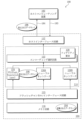
図1は、本発明の一実施形態によるシステムの一例を示すブロック図である。多様な実施形態で、システム100は、上述したように、大量のデータを格納するために使用される。図1に示す実施形態では、書き込みメモリアクセスが示されている。
FIG. 1 is a block diagram illustrating an example of a system according to one embodiment of the invention. In various embodiments,
図1に示す実施形態で、システム100は、ホストコンピューティング装置102を含む。いくつかの実施形態で、ホストコンピューティング装置102は、例えば、ラップトップ、デスクトップ、ワークステーション、PDA(personal digital assistant)、スマートフォン、タブレット、及び他の適切なコンピュータのような多様なコンピューティング装置又は仮想マシン若しくはそれらの仮想コンピューティング装置を含み得る。多様な実施形態で、ホストコンピューティング装置102は、ユーザー(図示せず)によって使用される。いくつかの実施形態で、ホストコンピューティング装置102は、複数の装置を含み、複数の装置のそれぞれは、ストレージ装置104からデータを読み書きすることができる。
In the embodiment shown in FIG. 1,
図1に示す実施形態で、システム100は、ストレージ装置104を含む。多様な実施形態で、ストレージ装置104は、データを格納するように構成される。多様な実施形態で、図1には1つのストレージ装置のみが示されているが、システム100は、複数のストレージ装置104を含み得る。多様な実施形態で、ストレージ装置104は、揮発性又は不揮発性のSSD(solid-state device)、強磁性ハードディスクドライブ(HDD:ferromagnetic hard disk drive)、又は他のストレージ技術を含む。
In the embodiment shown in FIG. 1,
一般的に、ストレージ装置は、書き込まれたデータを正確に格納するように構成される。ユーザーがデータをストレージ装置に書き込むとき、ユーザーは全く同じデータが後に抽出されることを期待する。図1に示す実施形態で、ストレージ装置104は、これを行うように構成されない可能性がある。代わりに、ストレージ装置104は、元のデータの表現(representation of original data)を格納し、後で生成するように構成され得る。多様な実施形態で、この表現は、元のデータ(original data)であるか、又は元のデータと同一であり得る。また、この表現は、元のデータと同じでない可能性がある。このような実施形態で、システム100は、無損失(lossless)及び損失(lossy)ストレージの中の1つ又は両方を提供するように構成される。
In general, storage devices are configured to store written data exactly. When a user writes data to a storage device, the user expects the exact same data to be retrieved later. In the embodiment shown in FIG. 1,
図1に示す実施形態において、ホストコンピューティング装置102は、書き込みメモリアクセス要請182を発行し得る。書き込みメモリアクセス要請182は、ストレージ装置104によって格納される元のデータセット192を含む。
In the embodiment shown in FIG. 1,
図1に示す実施形態において、ストレージ装置104は、ホストインターフェース回路112を含み得る。このような実施形態で、ホストインターフェース回路112は、メモリアクセス要請(例えば、書き込みメモリアクセス要請182)を受信するように構成される。いくつかの実施形態で、ホストインターフェース回路112又はレイヤ(HIL:host interface layer)は、ストレージ装置104の論理的視点(logical view)を管理する。このような実施形態で、ホストコンピューティング装置102は、論理的アドレス範囲(logical address range)を使用してストレージ装置104のストレージ容量(storage capacity)の空間にアクセスする。多様な実施形態で、ホストインターフェース回路112は、ホストコンピューティング装置102によって使用される論理プロトコルと、ストレージ装置104によって使用される内部の実際の物理的プロトコル又はメカニズムとの間を変換するように構成される。多様な実施形態で、フラッシュチャネル又はインターフェース回路115は、論理アドレスから物理アドレスへの変換を遂行する。いくつかの実施形態で、ストレージ装置104は、以下で説明するように、従来の物理的なアドレス指定方式を使用しない。
In the embodiment shown in FIG. 1,
図1に示す実施形態で、ストレージ装置104は、変換回路114を含む。多様な実施形態で、変換回路114は、元のデータセット192を変換されたデータセット194に変換するように構成される。多様な実施形態で、変換されたデータセット194は、元のデータセット192よりも小さい可能性がある。このような実施形態で、ストレージ装置104は、オリジナル(元のバージョン)そのものの代わりに、元のデータセット192の減少された表現を格納するように構成される。
In the embodiment shown in FIG. 1,
多様な実施形態で、ニューラルネットワーク(NN)の状態(state of neural network)とともに減少された表現は、必要な場合、元のデータを再生成(recreate)又は復元(reconstruct)するために使用される。データの再生成(recreation)又は復元(reconstruction)は、元のデータのサイズ及び/又は元のデータの値という点では、元のデータと完全に一致していないか、又は一致し得る。このような実施形態で、データを格納するのに必要な空間のサイズが減少される。上述したように、多様な実施形態で、変換されたデータセット194は、無損失又は損失の減少方法(lossless or lossy reduction scheme)を使用して生成される。フィデリティ(fidelity)と呼ばれる復元精度(reconstruction accuracy)が、100%よりも小さい場合、永続的ストレージ(persistent storage)は、損失(lossy)であると呼ばれる。復元精度が100%である場合には、ストレージ装置は、無損失(lossless)である。
In various embodiments, the reduced representation along with the state of neural network (NN) are used to recreate or reconstruct the original data if necessary. . Recreation or reconstruction of data may not exactly match or match the original data in terms of the size of the original data and/or the value of the original data. In such embodiments, the size of space required to store data is reduced. As noted above, in various embodiments, transformed
使用されるNAND型フラッシュのような実際の永続的ストレージ媒体のサイズは、減少された表現のサイズと、使用されるニューラルネットワークの状態を格納するのに必要なストレージ媒体のサイズである。ニューラルネットワークのために必要なストレージのサイズは、各ネットワークでのレイヤの数及びノードの数に従う。例えば、各レイヤで128個のノードを有する、2つのレイヤの全結合ニューラルネットワーク(a two layer fully-connected neural network)に対し、このニューラルネットワークのために格納する必要があるパラメータの数は、128×128と、各レイヤのバイアスパラメータである。この例では、簡単にするために、バイアスパラメータを格納していないと仮定する。各パラメータが64ビットを要求すると仮定すると、この2つのレイヤのニューラルネットワークのための全体のストレージは、「(128×128×8)/1024=128KB」である。2つのネットワークがストレージ装置で使用されていると仮定すると、ネットワークの状態を格納するのに必要なNAND型フラッシュの容量は256KBである。このストレージは、ストレージ装置に格納されたすべてのユーザーデータにわたって分割される。つまり、このストレージのサイズは固定され、実際のユーザーデータとは独立している。なお、4KB毎の元のデータが格納のために8バイトに減少できると仮定すると、必要なストレージ容量の空間が512倍減少するはずである。言い換えると、提案されたストレージ装置は、「1MB(1024KB)」のNAND型フラッシュの空間を含むものと仮定する。上述したように、2つのニューラルネットワークのために必要な空間(256KB)を除いた後に、残りのサイズ(1024KB-256KB=768KB)がユーザーデータを永続的に格納するために使用される。4KBのデータの、8Bの減少された表現を仮定すると、768KBの空間は、「(768KB/8B)=96K」のデータセット(各4KBのデータ)を格納するために使用される。言い換えると、1MBの実際のNAND型フラッシュ媒体を有するストレージ装置は、「(96K×4KB)=384MB」のユーザーデータを格納できる。 The size of the actual persistent storage medium, such as NAND flash, used is the size of the reduced representation and the size of the storage medium required to store the state of the neural network used. The size of storage required for a neural network depends on the number of layers and the number of nodes in each network. For example, for a two layer fully-connected neural network with 128 nodes in each layer, the number of parameters that need to be stored for this neural network is 128 ×128 and the bias parameter for each layer. In this example, for simplicity, we assume that we have not stored the bias parameter. Assuming that each parameter requires 64 bits, the total storage for this two-layer neural network is (128×128×8)/1024=128 KB. Assuming that two networks are used in the storage device, the NAND flash capacity required to store the state of the networks is 256 KB. This storage is divided across all user data stored on the storage device. That is, the size of this storage is fixed and independent of the actual user data. Note that assuming that every 4 KB of original data can be reduced to 8 bytes for storage, the required storage capacity space should be reduced by a factor of 512. In other words, it is assumed that the proposed storage device contains "1 MB (1024 KB)" of NAND flash space. After removing the space required for the two neural networks (256 KB) as described above, the remaining size (1024 KB - 256 KB = 768 KB) is used to permanently store user data. Assuming an 8B reduced representation of 4KB of data, 768KB of space is used to store "(768KB/8B)=96K" data sets (each 4KB of data). In other words, a storage device having a 1MB actual NAND flash medium can store "(96K×4KB)=384MB" of user data.
多様な実施形態で、変換回路114は、1つ以上のマシンラーニング(ML:machine learning)回路126を含む。これらのML回路126は、元のデータセット192のサイズを減少させ、元のデータセット192を変換されたデータセット194に変換(convert or translate)するように構成される。一実施形態で、ベイジアンネットワーク(Bayesian network)、遺伝子技法(genetic technique)、主成分分析(principal component analysis)、及び/又はサポートベクトルマシン(support vector machine)が考慮されるが、ML回路126は、ニューラルネットワーク(NN:neural network)を実装する。上述した内容は、いくつかの例としての実施形態であり、本発明はこれに限定されない。
In various embodiments,
図1に示す実施形態で、変換回路114は、1つだけではなく、複数のML回路(例えば、ニューラルネットワーク126A、126N)を含み得る。多様な実施形態で、変換回路114は、エンコーディング選択回路122を介して、ML回路126の中から1つを選択して、1つ以上の因子(factor)に基づいて変換(transformation)を遂行するように構成される。このような実施形態で、複数のML回路126の使用は、変換回路114が(どのような条件が意図されるか、例えば、復元フィデリティ(reconstruction fidelity)に基づいて)、元のデータセット192を変換するために最適なML回路126を動的に選択できるようにする。エンコーディング選択回路122は、FTL(flash translation layer)124を選択して、元のデータにどのような変換も遂行せずに、100%の精度で、データをそのまま格納し得る。
In the embodiment shown in FIG. 1, transform
図1に示す実施形態で、フィデリティ要求(fidelity requirement)128は、元のデータセット192と、変換されたデータセット194から復元されたデータセットとの間の変換損失がどの程度なのかを示すものとして設定される。このような実施形態で、変換回路114は、データタイプ及び他の因子をベースに、意図されたフィデリティ(又はより良いフィデリティ)を生成する特定のML回路126を選択する。フィデリティ要求128は、各データの書き込み動作に対して、ホストコンピューティング装置102によって提供される。他の実施形態で、フィデリティ要求128は、名前空間識別子(Namespace identifier)、ホスト識別子(host identifier)、論理ブロックアドレス範囲(logical block address range)、NVMセット識別子(nonvolatile memory set identifier)、NVMeサブミッションキュー識別子(NVMe submission queue identifier)、ストリーム識別子(Stream Identifier)、イーサネット(登録商標)MAC識別子(Ethernet MAC Identifier)、TCP/IPアドレス及び他の伝送/ネットワークパラメータ(TCP/IP addresses and other transport/network parameter)、又はデータと時間のような汎用パラメータなどの多様なストレージパラメータに対して、ホストによって固定された値として提供されるように構成される。
In the embodiment shown in FIG. 1, the
他の実施形態で、どのML回路126又は技法を使用するかの選択は、1つ以上の他の因子をベースに選択される。このような実施形態で、これらの因子は、データ又はファイルタイプ、ソースホスト(たとえば、ホストコンピューティング装置102)、元のデータセット192のサイズ、メモリ回路116の自由空間のサイズなどを含む。上述した内容は、単にいくつかの例としての実施形態であり、本発明はこれに限定されない。
In other embodiments, the selection of which ML circuit 126 or technique to use is selected based on one or more other factors. In such embodiments, these factors include data or file type, source host (eg, host computing device 102), size of
多様な実施形態で、これらのフィデリティ要求128は、書き込みメモリアクセス要請182に含まれる。他の実施形態で、これらのフィデリティ要求128は、ホストインターフェース回路112又は他のインターフェース回路(図示せず)を介して受信された別途のコマンドを使用して設定される。別の実施形態で、フィデリティ要求128(fidelity requirement)は、名前空間識別子(Namespace identifier)、ホスト識別子(host identifier)、論理ブロックアドレス範囲(logical block address range)、NVMセット識別子(nonvolatile memory set identifier)、NVMeサブミッションキュー識別子(NVMe submission queue identifier)、ストリーム識別子(Stream identifier)、イーサネット(登録商標)MAC識別子(Ethernet MAC identifier)、TCP/IPアドレス及び他の伝送/ネットワークパラメータ(TCP/IP addresses and other transport/network parameters)、又はデータと時間のような汎用パラメータなどのような多様なストレージパラメータをベースに、ストレージ装置そのものによって決定される。
In various embodiments, these
多様な実施形態で、図1を参照して、以下で説明するように、変換回路114は、ML回路126又は技法の動作を動的に変更して出力特性(例えば、フィデリティ(fidelity))を調整するように集められる。このような実施形態で、特定のML回路126の出力特性が調整される。
In various embodiments, transform
いくつかの実施形態で、変換回路114は、無損失のML回路126(lossless ML circuit)を含む。このような実施形態で、変換されたデータセット194は、元のデータセット192と同じサイズであるか又は小さい。
In some embodiments, transform
図1に示す実施形態で、変換回路114は、元のデータセット192と同じか又は等しい変換されたデータセット194のバージョンを生成する従来の非ニューラルネットワークベースの直接変換回路124を含み得る。図1に示す実施形態で、変換回路114は、フラッシュ変換レイヤ(FTL:flash translation layer)124を含むか、又はそれを使用し得る。このような実施形態で、FTL124の回路は、論理アドレスを物理アドレスに変換し、元のデータセット192を(変換されたデータセット194として)直接にメモリ回路116に書き込む。このような実施形態で、変換回路114は、FTL124とML回路126のうちの1つ以上のオプションを使用する。
In the embodiment shown in FIG. 1, transform
図1に示す実施形態で、ストレージ装置104は、メモリ回路116を含む。このような実施形態で、メモリ回路116は、変換されたデータセット194を格納するように構成される。このような実施形態で、変換されたデータセット194が生成されると、それはメモリ回路116に格納される。元のデータセット192は、全体又は部分的に除去(discard)される。例えば、書き込みメモリアクセス要請182が論理ブロックアドレス(LBA:logical block addressing)を使用している場合、元のデータセット192の全体が削除され、ストレージ装置104は、変換されたデータセット194からデータセット196を復元する能力に依存し得る。他の実施形態で、書き込みメモリアクセス要請182がキー値(KV:key-value)のペアを使用する場合、元のデータセット192の値部分(value portion)は除去されるが、キー部分は維持される。このような実施形態で、キー部分(一般的には値部分よりもはるかに小さい)は、変換されたデータセット194(現在、値部分として使用される)のインデックスとして維持される。
In the embodiment shown in FIG. 1,
多様な実施形態で、損失の側面にも拘わらず、変換されたデータセットの使用が十分な場合がある。たとえば、センサーデータ、IoTデータ、及び画像などのアプリケーションでは、フィデリティと応答時間とがいずれも重要でない。他の例で、フィデリティは重要ではないが、応答時間が重要なアプリケーションは、例えば、システムから迅速な応答を要求するWebアプリケーションを含む。他の実施形態で、データストレージの調節機能(tunability)が要求される。例えば、フィデリティは重要であるが、応答時間が重要ではないアプリケーションとして、例えば、動物園で動物の行動を定期的に監視するアプリケーションがある。又は、他の実施形態で、フィデリティと応答時間の両方が重要である、例えば、金融分野などのようなアプリケーションがある。変換回路114を使用して、元のデータセット192を減少された表現のデータセット(例えば、変換されたデータセット194)に変換し、データセット(例えば、変換されたデータセット194)からデータセット(例えば、復元されたデータセット196)を復元するようにする本発明によるストレージ装置は、ディープソリッドステート装置(Deep-SSD:Deep Solid State Device)と呼ばれる。このコンテキストで、ディープSSDは、元のデータを、減少されたサイズの表現(a reduced size representation)に変換し、必要なときに減少されたサイズの表現から元のデータの近似値又は元のデータを復元するニューラルネットワーク又は類似の技法を使用して、1つ以上の「機能(function)」を具現する永続的なデータストレージ装置のタイプを含み得る。「機能(function)」は、基本的に、装置内部に維持される元のデータの減少された表現であるディープキー(Deep-Key)と呼ばれる入力値を必須に使用して、元のデータとある所定の程度で一致する出力を生成できる。ディープSSDは、データを「そのまま(as-is)」格納することで、一般的なSSDのような機能を使用できる。上述した内容は、いくつかの例としての実施形態であり、本発明はこれに限定されない。
In various embodiments, using a transformed dataset may be sufficient, despite the lossy aspect. For example, in applications such as sensor data, IoT data, and images, neither fidelity nor response time are important. In other examples, applications where fidelity is not critical, but response time is critical include, for example, web applications that require a quick response from the system. In other embodiments, data storage tunability is required. For example, an application in which fidelity is important but response time is not is, for example, the routine monitoring of animal behavior in a zoo. Or, in other embodiments, there are applications where both fidelity and response time are important, such as in the financial sector.
図2は、本発明の一実施形態によるシステムの他の例を示すブロック図である。多様な実施形態で、システム100は、上述したように大規模なデータを格納するために使用される。図2に示す実施形態では、読み取りメモリアクセスが説明される。
FIG. 2 is a block diagram illustrating another example of a system according to one embodiment of the invention. In various embodiments,
図2に示す実施形態で、システム100は、ホストコンピューティング装置102及びストレージ装置104を含む。このような実施形態で、ストレージ装置104は、ホストインターフェース回路112、変換回路114、及びメモリ回路116を含む。
In the embodiment shown in FIG. 2,
図2に示す実施形態で、変換回路114は、復元されたデータセット196として知られた、元のデータセット(又はその複製若しくは類似物(facsimile or likeness thereof))をデコーディングするか又は再生成するように構成された1つ以上のML回路126を含む。多様な実施形態で、複数のML回路126(例えば、NN(126A、126N)及び/又はFTL124)が含まれている変換回路114は、エンコーディング(又はデコーディング)選択回路122を含む。
In the embodiment shown in FIG. 2, transform
図2に示す実施形態で、ホストコンピューティング装置102は、読み取りメモリアクセス要請183を発行する。読み取りメモリアクセス要請183は、元のデータセット(図1に示す)に関連付けられる。このような実施形態で、読み取りメモリアクセス要請183は、どのようなデータが要請されるかを示す論理アドレス又はキー(キー値ペアのキー)を含む。
In the embodiment shown in FIG. 2,
図2に示す実施形態で、ストレージ装置104は、読み取りメモリアクセス要請183を遂行するように試みるが、要請された元のデータセットが含まれていない可能性がある。代わりに、ストレージ装置104は、変換されたデータセット194を含み得る。このような実施形態で、変換回路114は、最初の段階で変換されたデータセット194を生成するために使用されたML回路126(又は関連したデコーディングML回路)を介して、変換されたデータセット194を駆動する。このような実施形態で、ML回路126は、変換されたデータセット194から復元されたデータセット196を生成し得る。このような復元されたデータセット196は、元のデータセットを再生成する際のストレージ装置104の最良の又は選択された試みであり得る。
In the embodiment shown in FIG. 2,
一実施形態で、変換されたデータセット194が無損失エンコーディング(又はFTL124を介した直接コピー)である場合、復元されたデータセット196のバージョンは、元のデータセットと同じである。他の実施形態で、変換されたデータセット194が損失エンコーディングを使用して構成された場合、復元されたデータセット196は、元のデータセットと同じでないか又は等しくない可能性がある。このような実施形態で、システム100は、復元されたデータセット196が部分的にしか正確(例えば、90%の精度、80%の精度など)ではないと、フィデリティ要求128を設定できる。
In one embodiment, if transformed
このような実施形態で、復元されたデータセット196が生成されると、復元されたデータセット196は、ホストコンピューティング装置102に(読み取り応答184として)伝送される。多様な実施形態で、ホストインターフェース回路112は、この読み取り応答184を伝送するように構成される。多様な実施形態で、復元されたデータセット196が損失である場合、復元されたデータセット196は、元のデータセットよりも小さい可能性があり、これにより、読み取りメモリアクセス要請183を処理するために、より小さな帯域幅又はより小さな他のシステムリソースを使用する。他の実施形態では、復元されたデータは、元のデータのサイズと正確に一致するが、復元されたコンテンツ又は値は、正確に一致しない可能性がある。
In such an embodiment, once reconstructed
図3は、本発明の一実施形態によるシステムのさらに他の例を示すブロック図である。多様な実施形態で、システム100は、上述したように、大規模なデータを格納するために使用される。図3に示す実施形態では、読み取りメモリアクセスが説明される。
FIG. 3 is a block diagram illustrating yet another example of a system according to one embodiment of the invention. In various embodiments,
図3に示す実施形態では、システム100は、ホストコンピューティング装置102及びストレージ装置104を含む。このような実施形態で、ストレージ装置104は、ホストインターフェース回路112、変換回路114、及びメモリ回路116を含む。
In the embodiment shown in FIG. 3,
図3に示す実施形態で、変換回路114は、復元されたデータセット196として知られる元のデータセット(又はその複製若しくは類似物(facsimile or likeness thereof))をデコーディングするか又は再生成するように構成された1つ以上のML回路126を含む。多様な実施形態で、複数のML回路126(例えば、NN(126A、126N))及び/又はFTL124が含まれている変換回路114は、エンコーディング(又はデコーディング)選択回路122を含む。
In the embodiment shown in FIG. 3, transform
図3に示す実施形態で、ホストコンピューティング装置102は、読み取りメモリアクセス要請185を発行し得る。読み取りメモリアクセス要請185は、元のデータセット(図1に示す)に関連付けられる。このような実施形態で、読み取りメモリアクセス要請185は、どのようなデータセットが要請されるかを示す論理アドレス又はキー(キー値ペアのキー)を含む。
In the embodiment shown in FIG. 3,
しかしながら、図3に示す実施形態で、読み取りメモリアクセス要請185が復元されたデータセットを返還することを予想しないか、又は要請しない可能性がある。代わりに、読み取りメモリアクセス要請185は、変換されたデータセット194そのものを要請し得る。
However, in the embodiment shown in FIG. 3, the read
このような実施形態で、ストレージ装置104は、変換回路114又は少なくともML回路126をバイパス(bypass)する経路170を含む。多様な実施形態で、経路170は、図3に示されたものの代わりに、FTL124を活用できる。上述した内容は、単に例としての実施形態であり、本発明はこれに限定されない。
In such embodiments, the
このような実施形態で、ストレージ装置104は、どのような変換されたデータセット194が要請されたかを判定でき、変換されたデータセット194をホストコンピューティング装置102に(読み取り応答186を介して)直接提供する。このような実施形態で、ストレージ装置104とホストコンピューティング装置102との間で伝送されるデータのサイズは劇的に減少される。
In such an embodiment,
一実施形態で、ホストコンピューティング装置102は、変換されたデータセット194をエンコーディングするML回路126と類似したML回路を含む。このような実施形態で、ホストコンピューティング装置102は、復元されたデータセットをローカルに(locally)(ホストコンピューティング装置102へ)生成する。このような実施形態で、ストレージ装置104及びホストコンピューティング装置102は、ML回路が同期状態を維持できるように、ML回路126の重み又は設定を変換する。
In one embodiment,
図4は、本発明の他の実施形態によるシステムの一例を示すブロック図である。図4に示す実施形態で、システム200は、図1のストレージ装置を含む。
FIG. 4 is a block diagram illustrating an example system according to another embodiment of the invention. In the embodiment shown in FIG. 4,
図4に示す実施形態で、システム200は、上述したように、ホストインターフェース回路112を含む。このような実施形態で、ホストインターフェース回路112は、外部コンピューティング装置(図示せず)とデータを送受信するように構成される。
In the embodiment shown in FIG. 4,
図4に示す実施形態で、システム200は、上述したように、変換回路114を含む。このような実施形態で、変換回路114は、1つ以上のマシンラーニング(ML:machine learning)回路を含む。
In the embodiment shown in FIG. 4,
図4に示す実施形態で、各ML回路は、エンコーディング回路222(例えば、エンコーディング回路222A、222B、222C)を含む。エンコーディング回路222は、上述したように、元のデータセットを変換されたデータセットに変換するように構成される。 In the embodiment shown in FIG. 4, each ML circuit includes an encoding circuit 222 (eg, encoding circuits 222A, 222B, 222C). Encoding circuitry 222 is configured to transform the original data set into a transformed data set, as described above.
図4に示す実施形態で、各ML回路は、デコーディング回路224(例えば、デコーディング回路224A、224B、224C)を含む。デコーディング回路224は、上述したように、変換されたデータセットを復元されたデータセットに変換するように構成される。 In the embodiment shown in FIG. 4, each ML circuit includes a decoding circuit 224 (eg, decoding circuits 224A, 224B, 224C). Decoding circuitry 224 is configured to transform the transformed data set into a recovered data set, as described above.
多様な実施形態で、変換回路114は、シングルエンコーディング回路222及びマルチデコーディング回路224を含む。このような実施形態で、変換回路114は、どのデコーディング回路224が最も小さな差異や、最高のフィデリティを生成するかを選択する。上述した内容は、単にいくつかの例としての実施形態であり、本発明はこれに限定されない。
In various embodiments, transform
図4に示す実施形態で、各ML回路は差分又はデルタ(差異量)回路(difference or delta circuit)226(例えば、差分回路226A、226B、226C)を含む。多様な実施形態で、変換回路114は、1つの差分又はデルタ回路226を含むか、複数のML回路は、差分又はデルタ回路226を共有し得る。このような実施形態で、差分回路226は、元のデータセットを復元されたデータセットと比較するように構成される。このような実施形態で、差分回路226は、各ML回路のために提供されたフィデリティのサイズ又はレベルを計算するか又は表し得る。上述したように、変換回路114は、元のデータセットをエンコーディングするのにどのようなML回路が使用されるかを決定するとき、このフィデリティのレベルを使用する。他の実施形態で、観測されたデルタ(observed delta)は、所望の復元フィデリティ(reconstruction fidelity)を達成するために、エンコーダ及び/又はデコーダで使用されるニューラルネットワークの重み及び他のパラメータをアップデートするのに使用される。データの書き込み動作の間に、観測された復元されたデルタ(observed reconstruction delta)は、入力データが正確度に対する所望のレベルに後で復元できるようにニューラルネットワークをトレーニングするために使用される。いくつかの実施形態で、ニューラルネットワークは、事前トレーニング(pre-trained)され、所望の復元フィデリティを達成するためにネットワークのレイヤの数だけが変更される。
In the embodiment shown in FIG. 4, each ML circuit includes a difference or delta circuit 226 (eg,
多様な実施形態で、システム200は、書き込みキャッシュ217を含む。書き込みキャッシュ217は、一時的なストレージを提供するように構成される。多様な実施形態で、一時的ストレージはML回路のエンコーディング/デコーディング手順の間の中間値及び/又は元のデータセットのためのものであり得る。
In various embodiments,
多様な実施形態で、システム200は、上述したように、メモリ回路216を含む。多様な実施形態で、メモリ回路216は、変換されたデータセットを格納する。メモリ回路216は、データの復元中に使用される所望のフィデリティのレベルをさらに格納する。
In various embodiments,
図4に示す実施形態で、メモリ回路216は、ルックアップテーブル(look-up table)、インデックスアレイ(indexed array)、又は一連のフィールド(series of fields)のようなデータ構造に組織化される。図2に示す実施形態で、メモリ回路216は、システム200が変換されたデータセットを検索できるようにする、インデックスフィールド252を含む。多様な実施形態で、インデックスフィールド252は、キー値(KV:key-value)ペアのキー又は論理ブロックアドレス(LBA:logical block address)を含む。
In the embodiment shown in FIG. 4,
メモリ回路216は、変換されたデータセット、又は変換されたデータセットへのポインタを格納するデータフィールド254を含む。このような実施形態で、元のデータセットの同じインスタンスが同じ変換されたデータセットをもたらすため、システム200は、データの重複排除(data de-duplication)を行うことができ、これにより、追加の空間を確保できる。
一実施形態で、メモリ回路216は、変換されたデータセット194をデータフィールド254に格納する。データフィールド254に格納された、変換されたデータセット194は、ディープキー(Deep-Key)と称する。このような実施形態で、変換されたデータセット194、すなわち、ディープキー(Deep-Key)は、第2のメモリ回路218に別個に格納されるか、又は格納されない。第1のメモリ回路216に含まれているディープキー(Deep-Key)は、第2のメモリ回路218に永続的に(persistently)格納される。
In one embodiment,
メモリ回路216は、エンコーディングフィールド256を含む。エンコーディングフィールド256は、どのML回路がエンコーディングされるか、及び/又は変換されたデータセットをデコーディングするのに使用されるかを格納して識別する。このような実施形態で、変換回路114は、どのML回路が決定プロセス(deciding process)に使用されなければならないかを迅速に決定できる。
図4に示す実施形態で、システム200は、第2のメモリ回路218、及びフラッシュチャネル又はインターフェース回路215をさらに含む。多様な実施形態で、第1のメモリ回路216及び第2のメモリ回路218は、同一のメモリ回路に含まれ得るが、別個のパーティション又は領域内に含まれ得る。
In the embodiment shown in FIG. 4,
多様な実施形態で、第2のメモリ回路218は、多様なML回路の状態又は重み値(例えば、NN状態228A、228B、228C)を格納するように構成される。このような実施形態で、変換回路114は、ML回路又はML回路の構成間を迅速にかつ動的に切り替えることができる。多様な実施形態で、変換回路114は、他のML状態228又は設定をロードすることにより、ML回路間を切り替えるように構成された、装置プロセッサ又はコントローラを含み得る。
In various embodiments, the
上述したように、システム200は、以下の態様又は利点を含む。図4に示す実施形態で、システム200は、メモリ回路にデータを「そのまま(as-is)」格納する代わりに、ストレージ媒体としてニューラルネットワークを使用する。システム200は、従来のストレージ装置と比較して、ストレージ容量を大幅に増加させることができる。多様な実施形態で、特定の動作(例えば、検索(search))は、全体のデータに対する動作の代わりにニューラルネットワーク及び/又はマシンラーニング回路によって遂行され、これにより、データの動作がより速くなる。たとえば、マシンラーニング回路は、データを第1のフォーマットから第2のフォーマットに変換し得る。以後、マシンラーニング回路は、データを第1のフォーマットに変換することなしに、第2のフォーマットのデータに対する1つ以上の検索を行うことができる。
As noted above,
多様な実施形態で、システム200は、格納されたデータを自動的に重複削除(de-duplicate)することができる。このような実施形態で、重複排除(de-duplication)は、ブロックレベル又はデータチャンクの一部の粒度であり、これは、データのより多くの重複排除を可能にする。
In various embodiments,
いくつかの実施形態では、ホストコンピューティング装置は、データを格納するためのフィデリティの程度を変更することを特定できる。もしフィデリティが100%である場合、(無損失に又は直接格納された)データは、ホストコンピューティング装置に「そのまま(as-is)」返還される。もしフィデリティが100%よりも小さい場合には、ホストコンピューティング装置に返還されるデータは、元のデータのサイズと同じか、又は同じではない、元のデータの近似値である。いくつかの実施形態では、返還されたデータは、元のデータとまったく同じサイズを有し得るが、返還されたデータ値は、元のデータ値と正確に一致しない可能性がある。 In some embodiments, the host computing device can specify varying degrees of fidelity for storing data. If the fidelity is 100%, the data (stored losslessly or directly) is returned "as-is" to the host computing device. If the fidelity is less than 100%, the data returned to the host computing device is an approximation of the original data, which may or may not be the same size as the original data. In some embodiments, the returned data may have exactly the same size as the original data, but the returned data values may not exactly match the original data values.
このような実施形態で、システム200は、マシンラーニングアプリケーションを補完し得る。多様な実施形態で、マシンラーニングアプリケーションは、復元されたデータを必要とせず、代わりに、減少された特徴の表現(reduced feature representation)を使用し得る。例えば、変換されたデータセットが直接使用されてMLアプリケーションの速度を向上させることができる。
In such embodiments,
図5は、本発明のさらに他の実施形態によるシステムの一例を示すブロック図である。多様な実施形態で、システム300は、マシンラーニング(ML:machine learning)回路やソフトウェア構成を含む。特定の実施形態で、システム300は、ニューラルネットワーク(neural network)を含む。 FIG. 5 is a block diagram illustrating an example system according to yet another embodiment of the invention. In various embodiments, system 300 includes machine learning (ML) circuitry and software constructs. In certain embodiments, system 300 includes a neural network.
図5に示す実施形態で、システム300は、エンコーダニューラルネットワーク302(encoder neural network)及びデコーダニューラルネットワーク304(decoder neural network)を含む。多様な実施形態で、これらのニューラルネットワーク(302、304)は、それぞれ複数のレイヤ(例えば、レイヤ312A、312B、312C、312D、及び314A、314B、314C、314D)を含む。各レイヤ(312、314)は、レイヤの入力を処理して出力を生成する多様な重み値及び多数のニューロンを含む。ニューラルネットワークの各レイヤは、異なるタイプの可能性があり、コンボリューション(convolution)、2つのレイヤの間の密な結合(dense connections between two layers)、回帰型ニューラルネットワークユニット(recurrent neural network unit)、ロングショートタームメモリユニット(long short term memory unit)、ゲート付き回帰型ユニット(gated recurrent unit)、GAN(generative adversarial network)、sigmoid、ソフトマックス(softmax)などのようなレイヤ、動作、及び他のニューラルネットワークのノードを含む。これらは、単に例としての実施形態であり、本発明はこれに限定されない。その後、ニューラルネットワークの最終的な出力レイヤ(例えば、312D、314D)に到達するまで、出力は他のレイヤの入力として使用される。
In the embodiment shown in FIG. 5, system 300 includes encoder
図5に示す実施形態で、元のデータセット192は、エンコーダニューラルネットワーク302に入力されて、変換されたデータセット194を生成する。同様に、変換されたデータセット194は、デコーダニューラルネットワーク304に入力されて、復元されたデータセット196を生成する。
In the embodiment shown in FIG. 5,
このような実施形態で、システム300は、差分回路又はデルタ回路306を含む。デルタ回路306は、元のデータセット192を復元されたデータセット196と比較して、ニューラルネットワーク(302、304)が、元のデータセット192をどのくらい正確に復元するかを判定できる。多様な実施形態で、上述したように、この正確度は、フィデリティ要請と比較される。
In such an embodiment, system 300 includes difference or
多様な実施形態で、システム300は、ニューラルネットワーク(302、304)内の多様なレイヤをスキップ(skip)又はバイパス(bypass)することで、システム300の正確度を動的に調整するように構成される。例えば、一実施形態で、フィデリティが要求されたよりも高い場合には、システム300は、レイヤ312Bをバイパスする。フィデリティが要請されたよりもまだ高い場合には、システム300は、レイヤ(312B、312C)の両方をバイパスする。同様に、デコーダニューラルネットワーク304は、例えば、レイヤ314をスキップできる。逆に、達成されたフィデリティが要求されたレベルよりも低い場合には、以前にバイパスされたレイヤが演算に再び追加され、フィデリティのレベルを増加させる。
In various embodiments, the system 300 is configured to dynamically adjust the accuracy of the system 300 by skipping or bypassing various layers within the neural networks (302, 304). be done. For example, in one embodiment, system 300 bypasses
多様な実施形態で、レイヤは、エンコーダ及びデコーダニューラルネットワーク(302、304)内に同時に追加/バイパスされる。他の実施形態で、レイヤは、独立して追加/バイパスされる。 In various embodiments, layers are added/bypassed simultaneously in the encoder and decoder neural networks (302, 304). In other embodiments, layers are added/bypassed independently.
多様な実施形態で、システム300は、多様な設定を含むか、又は多様な設定によって制限される。例えば、システム300は、スキップ又はバイパスできるレイヤの最大の個数によって制限される。他の実施形態で、システム300は、所望のフィデリティ要求(又は演算時間などのような他の要求)を達成できる試行、又は最大の回数によって制限される。上述された内容は、本発明がいくつかの例としての実施形態に限定されない。 In various embodiments, system 300 includes or is limited by various settings. For example, system 300 is limited by the maximum number of layers that can be skipped or bypassed. In other embodiments, the system 300 is limited by the number of attempts, or maximum number of attempts, that can achieve the desired fidelity request (or other request such as computation time, etc.). What has been described above does not limit the invention to a few example embodiments.
多様な実施形態で、システム300は、データストレージの動作の一部として、このフィデリティの演算を遂行する。このような実施形態で、システム300は、所望のフィデリティ又は他のリソースの要求を達成するためにどのようなニューラルネットワーク設定が使用されるかを判定する。このような実施形態で、ニューラルネットワークに対する設定は、データをエンコーディングするのにどのようなニューラルネットワークが使用されるかとともに格納される。 In various embodiments, the system 300 performs this fidelity calculation as part of its data storage operations. In such embodiments, the system 300 determines what neural network settings to use to achieve the desired fidelity or other resource requirements. In such embodiments, the settings for the neural network are stored along with what neural network is used to encode the data.
多様な実施形態で、システム300が設定された試行回数又は全体で所望のフィデリティを達成できない場合は、システム300は、フィデリティ要求に可能な限り近いフィデリティレベルを達成する設定を使用する。他の実施形態で、システム300が所望のフィデリティを達成できない場合、システム300は、元のデータセット192を「そのまま(as-is)」又はそれの元のデータの状態に(例えば、FTLを介して)格納する。他の実施形態で、システム300が所望のフィデリティを正確に達成できない場合、システム300は、所望のフィデリティのレベルよりも高いが、100%のフィデリティのレベルよりも低いフィデリティのレベルで、元のデータを格納し得る。別の実施形態で、システム300が所望のレベル(又は他の要求)を達成できない場合、システム300は、複数のML回路のうちの他の1つに切り替えて再び試行する。上述した内容は、単にいくつかの例としての実施形態であり、本発明はこれに限定されない。
In various embodiments, if the system 300 fails to achieve the desired fidelity in a set number of attempts or overall, the system 300 uses settings that achieve a fidelity level as close as possible to the fidelity requirement. In other embodiments, if the system 300 fails to achieve the desired fidelity, the system 300 returns the
図6は、本発明の原理に基づいて形成された半導体装置を含む情報処理システムの一例を示すブロック図である。 FIG. 6 is a block diagram showing an example of an information processing system including a semiconductor device formed according to the principles of the present invention.
図6を参照すると、情報処理システム400は、本発明の原理に基づいて構成された1つ以上の装置を含む。他の実施形態で、情報処理システム400は、本発明の原理による1つ以上の手法を使用するか実行し得る。
Referring to FIG. 6,
多様な実施形態で、情報処理システム400は、例えば、ラップトップ、デスクトップ、ワークステーション、サーバ、ブレードサーバ、PDA(personal digital assistant)、スマートフォン、タブレット、及び他の適切なコンピュータのようなコンピューティング装置、仮想マシン、又はそれらの仮想コンピューティング装置を含む。多様な実施形態で、情報処理システム400は、ユーザー(図示せず)によって使用される。
In various embodiments,
本発明の一実施形態による情報処理システム400は、中央処理ユニット(CPU:central processing unit)、ロジック、又はプロセッサ410をさらに含む。いくつかの実施形態で、プロセッサ410は、1つ以上の機能ユニットブロック(FUB:functional unit block)又は組み合わせ論理ブロック(CLB:combinational logic block)415を含む。このような実施形態で、組み合わせ論理ブロックは、多様なブールロジック演算(Boolean logic operation)(例えば、NAND、NOR、NOT、XOR)、安定化ロジック装置(stabilizing logic device)(例えば、フリップ・フロップ、ラッチ)、他のロジック装置、又はそれらの組み合わせを含む。このような組み合わせ論理演算は、単純な又は複雑な方法で入力信号を処理して、所望の結果を達成し得る。同期式組み合わせ論理演算の一部の例としての実施形態が説明されたが、本発明はこれに限定されず、非同期式演算又はそれらの組み合わせを含み得る。一実施形態で、組み合わせ論理演算(回路)は、複数のCMOS(complementary metal oxide semiconductor)トランジスタを含む。多様な実施形態で、これらのCMOSトランジスタは、論理演算を遂行するゲートにアレンジされる。本発明の技術範囲内で、他の技術が使用され得る。
The
本発明の一実施形態による情報処理システム400は、揮発性メモリ420(例えば、RAM(Random Access Memory))をさらに含む。本発明の一実施形態による情報処理システム400は、不揮発性メモリ430(例えば、ハードドライブ、光メモリ、NAND型フラッシュメモリ)をさらに含む。いくつかの実施形態で、揮発性メモリ420、不揮発性メモリ430、又はそれらの一部若しくは組み合わせの中の1つは、「ストレージ媒体(storage medium)」と呼ばれる。多様な実施形態で、揮発性メモリ420及び/又は不揮発性メモリ430は、半永続的又は実質的に永続的な形でデータを格納する。
多様な実施形態で、情報処理システム400は、情報処理システム400が通信ネットワークを介して、一部と通信するように構成された1つ以上のネットワークインターフェース440を含む。Wi-Fi(登録商標)プロトコルの例は、IEEE(Institute of Electrical and Electronics Engineers)802.11g、IEEE 802.11nを含むが、これに限定されない。セルラーのプロトコルの例は、IEEE 802.16m(別名、Wireless-MAN(Metropolitan Area Network)アドバンスド、LTE(Long Term Evolution)(登録商標)アドバンスド、EDGE((Enhanced Data rates for Global System for Mobile Communications)エボリューション(Evolution))、HSPA+(Evolved High- Speed Packet Access))を包含できるが、これに限定されない。有線プロトコルの例は、IEEE 802.3(別名、Ethernet(登録商標))、ファイバチャネル(Fibre Channel)、電力線通信(Power Line communication)(例えば、ホームプラグ(HomePlug)、IEEE 1901)を含み得るが、これに限定されない。上述した内容は、いくつかの例としての実施形態であり、本発明はこれに限定されない。
In various embodiments,
本発明の一実施形態による情報処理システム400は、ユーザーインターフェースユニット450(例えば、ディスプレイアダプタ、ハプティックインターフェース、ヒューマンインターフェース装置)をさらに含む。多様な実施形態で、このようなユーザーインターフェースユニット450は、ユーザーからの入力を受信したり、ユーザーに出力を提供したりする。他の種類の装置がユーザーとの相互作用(interaction)を提供するために使用されるだけではなく、例えば、ユーザーに提供されるフィードバックは、視覚フィードバック、聴覚フィードバック、又は触覚フィードバックのような感覚フィードバックの形態であり、ユーザーからの入力は、音、音声、又は触覚入力を含む形で受信される。
The
多様な実施形態で、情報処理システム400は、1つ以上の他の装置又はハードウェア構成要素460(例えば、ディスプレイ、モニター、キーボード、マウス、カメラ、指紋リーダー、ビデオプロセッサなど)を含む。上述した内容は、いくつかの例としての実施形態であり、本発明はこれに限定されない。
In various embodiments,
本発明の一実施形態による情報処理システム400は、1つ以上のシステムバス405をさらに含む。このような実施形態で、システムバス405は、プロセッサ410、揮発性メモリ420、不揮発性メモリ430、ネットワークインターフェース440、ユーザーインターフェースユニット450、及び1つ以上のハードウェア構成要素460と通信的に連結されるように構成される。プロセッサ410によって処理されたデータ、又は不揮発性メモリ430に外部から入力されたデータは、不揮発性メモリ430又は揮発性メモリ420のいずれか1つに格納される。
多様な実施形態で、情報処理システム400は、1つ以上のソフトウェア構成要素470を含むか実行し得る。いくつかの実施形態で、ソフトウェア構成要素470は、オペレーティングシステム(OS:operating system)、及び/又はアプリケーションを含む。いくつかの実施形態で、OSは、1つ以上のサービスをアプリケーションに提供し、情報処理システム400のアプリケーションと、多様なハードウェア構成要素(例えば、プロセッサ410、ネットワークインターフェース440)との間の媒介として動作するか、又は管理する。このような実施形態で、情報処理システム400は、ローカルに(例えば、不揮発性メモリ430内に)設置され、プロセッサ410によって直接実行され、OSと直接相互作用するように構成された1つ以上のネイティブアプリケーションを含む。このような実施形態で、ネイティブアプリケーションは、事前にコンパイルされたマシン実行可能なコード(pre-compiled machine executable code)を含む。いくつかの実施形態で、ネイティブアプリケーションは、ソース又はオブジェクトコードをプロセッサ410によって実行される実行可能なコードに変換するように構成されたスクリプトインタープリタ(script interpreter)(例えば、csh(C shell)、AppleSrcript(登録商標)、AutoHotkey)又は仮想実行マシン(VM)(例えば、Java(登録商標)Virtual Machine、the Microsoft(登録商標)Common Language Runtime)を含む。
In various embodiments,
上述した半導体装置は、多様なパッケージング技法を使用してカプセル化され得る。例えば、本発明の原理による半導体装置は、POP(package on package)技法、BGA(a ball grid array)技法、CSP(a chip scale package)技法、PLCC(a plastic leaded chip carrier)技法、PDIP(a plastic dual in-line package)技法、ダイインワッフルパック(a die in waffle pack)技法、ダイインウェハフォーム(a die in wafer form)技法、COB(a chip on board)技法、CERDIP(a ceramic dual in-line package)技法、PMQFP(a plastic metric quad flat package)技法、PQFP(a plastic quad flat package)技法、SOIC(a small outline package)技法、SSOP(a shrink small outline package)技法、TSOP(a thin small outline package)技法、TQFP(a thin quad flat package)技法、SIP(a system in package)技法、MCP(a multi-chip package)技法、WFP(a wafer-level fabricated package)技法、WSP(a wafer-level processed stack package)技法、又は本発明が属する技術分野でよく知られている他の技法の中のいずれか1つを使用してカプセル化される。 The semiconductor devices described above can be encapsulated using a variety of packaging techniques. For example, a semiconductor device according to the principles of the present invention may be manufactured using a POP (package on package) technique, a BGA (a ball grid array) technique, a CSP (a chip scale package) technique, a PLCC (a plastic leaded chip carrier) technique, a PDIP (a plastic dual in-line package technology, a die in waffle pack technology, a die in wafer form technology, COB (a chip on board) technology, CERDIP (a ceramic dual in-line) technology package) technique, PMQFP (a plastic quad flat package) technique, PQFP (a plastic quad flat package) technique, SOIC (a small outline package) technique, SSOP (a shrink small outline package) technique, TSOP (a thin small outline) package) technique, TQFP (a thin quad flat package) technique, SIP (a system in package) technique, MCP (a multi-chip package) technique, WFP (wafer-level fabricated package) technique, WSP ( a wafer-level process stack package) technique, or any one of the other techniques well known in the art to which this invention pertains.
本発明による方法の段階は、コンピュータプログラムを実行して、入力データに対する演算及び出力を生成することにより、機能を遂行する1つ以上のプログラム可能なプロセッサによって遂行される。方法の段階は、FPGA(field programmable gate array)又はASIC(application-specific integrated circuit)のような専用ロジック回路(special purpose logic circuitry)として具現され得る装置によって遂行される。 The steps of the method according to the invention are performed by one or more programmable processors performing functions by executing a computer program to operate on input data and generate output. The steps of the method are performed by a device that may be embodied as a special purpose logic circuit such as a field programmable gate array (FPGA) or an application-specific integrated circuit (ASIC).
多様な実施形態で、コンピュータ読み取り可能な媒体は、コマンドを含み、コマンドが実行されるとき、装置は、方法の段階の少なくとも一部を遂行し得る。いくつかの実施形態で、コンピュータ読み取り可能な媒体は、磁気媒体、光媒体、他の媒体又はそれらの組み合わせ(例えば、CD-ROM、ハードドライブ、読み取り専用メモリ、フラッシュメモリ)に含まれる。このような実施形態で、コンピュータ読み取り可能な媒体は、有形で非一時的に具現された製品であり得る。 In various embodiments, the computer-readable medium may contain commands, and when the commands are executed, the apparatus may perform at least some of the steps of the method. In some embodiments, the computer-readable medium includes magnetic media, optical media, other media, or combinations thereof (eg, CD-ROM, hard drive, read-only memory, flash memory). In such embodiments, the computer-readable medium may be a tangible, non-transitory embodied product.
以上、本発明の原理を、例としての実施形態を参照して説明したが、当業者は、本発明の思想及び技術範囲から逸脱しない範囲内で多様に変更実施することができる。したがって、上述した実施形態は限定ではなく、単純な例として提示したものである。すなわち、本発明の技術的思想は、特許請求の範囲及びその均等物の最も広い範囲の解釈によって決定されるべきで、上述の詳細な説明によって限定されない。 Although the principles of the present invention have been described with reference to exemplary embodiments, various modifications can be made by those skilled in the art without departing from the spirit and scope of the invention. Accordingly, the above-described embodiments are presented as simple examples and not as limitations. That is, the technical idea of the present invention should be determined by the broadest interpretation of the claims and their equivalents, and not limited by the above detailed description.
100、200、300 システム
102 ホストコンピューティング装置
104 ストレージ装置
112 ホストインターフェース回路
114 変換回路
115、215 フラッシュチャネル/インターフェース回路
116 メモリ回路
122 エンコーディング選択回路
124 FTL(フラッシュ変換レイヤ)/直接変換回路
126 マシンラーニング(ML)回路
126A、126N ニューラルネットワーク
128 フィデリティ要求
170 経路
182 書き込みメモリアクセス要請
183、185 読み取りメモリアクセス要請
184、186 読み取り応答
192 元のデータセット
194 変換されたデータセット
196 (復元された)データセット
216 (第1の)メモリ回路
217 書き込みキャッシュ
218 第2のメモリ回路
222 (シングル)エンコーディング回路
222A、222B、222C エンコーディング回路
224 (マルチ)デコーディング回路
224A、224B、224C デコーディング回路
226、306 差分回路(デルタ回路)
226A、226B、226C 差分回路
228、228A、228B、228C NN状態
252 インデックスフィールド
254 データフィールド
256 エンコーディングフィールド
302 エンコーダニューラルネットワーク
304 デコーダニューラルネットワーク
312、312A、312B、312C、312D レイヤ
314、314A、314B、314C、314D レイヤ
400 情報処理システム
405 システムバス
410 プロセッサ(及び/又はロジック)
415 組み合わせ論理ブロック
420 揮発性メモリ
430 不揮発性メモリ
440 ネットワークインターフェース
450 ユーザーインターフェースユニット
460 ハードウェア(構成要素)
470 ソフトウェア(構成要素)
100, 200, 300
226A, 226B,
415
470 software (components)
Claims (19)
データセットに関連付けられたメモリアクセス要請を受信するように構成されたホストインターフェース回路と、
変換されたデータセットを格納するように構成された少なくとも1つの不揮発性メモリストレージ回路と、
マシンラーニング回路を含み、書き込みメモリアクセスに基づいて、前記データセットの元のバージョンを前記変換されたデータセットに変換し、読み取りメモリアクセスに基づいて、前記変換されたデータセットを前記データセットとは異なる前記データセットの近似値を含む復元されたデータセットに変換するように構成された変換回路と、を備え、
前記少なくとも1つの不揮発性メモリストレージ回路は、前記データセットの前記元のバージョンを前記変換されたデータセットに変換するために使用される前記マシンラーニング回路の永続的状態(persistent state)を格納するように構成され、
前記マシンラーニング回路の永続的状態は、前記変換されたデータセットを前記復元されたデータセットに変換するための構成を含み、
前記マシンラーニング回路は、第1のマシンラーニング回路を含み、
前記変換回路は、第2のマシンラーニング回路を含み、
前記変換回路は、少なくとも部分的に、ホストによって特定されたフィデリティ(fidelity)のサイズ及び前記マシンラーニング回路によって提供された前記フィデリティのサイズに基づいて、前記第1又は第2のマシンラーニング回路の中の1つを選択して、前記データセットを変換するように構成されたことを特徴とする装置。 a device,
a host interface circuit configured to receive a memory access request associated with the data set;
at least one non-volatile memory storage circuit configured to store the transformed data set;
machine learning circuitry for converting an original version of the dataset into the transformed dataset based on write memory accesses, and converting the transformed dataset to the dataset based on read memory accesses; a conversion circuit configured to convert to a recovered data set containing approximations of different said data sets;
The at least one non-volatile memory storage circuit stores a persistent state of the machine learning circuit used to transform the original version of the dataset into the transformed dataset. configured to
the persistent state of the machine learning circuit includes configuration for transforming the transformed dataset into the reconstructed dataset;
the machine learning circuit includes a first machine learning circuit;
the conversion circuit includes a second machine learning circuit;
The conversion circuit is configured to convert the first or second machine learning circuit based, at least in part, on a fidelity size specified by a host and the fidelity size provided by the machine learning circuit. , to transform the data set .
前記復元されたデータセットは、前記データセットの前記元のバージョンと異なることを特徴とする請求項1に記載の装置。 the transformed dataset has a size that is the same as or smaller than the original version of the dataset;
2. The apparatus of claim 1, wherein the reconstructed data set differs from the original version of the data set.
前記データセットの重複排除は、ブロックレベルで遂行されることを特徴とする請求項1に記載の装置。 the conversion circuit is configured to de-duplicate the data set;
2. The apparatus of claim 1, wherein deduplication of the data set is performed at block level.
前記変換されたデータセットは、前記データセットの前記元のバージョンと同じサイズか、又はより小さいサイズを有し、前記変換されたデータセットは、前記データセットの前記元のバージョンの近似値であることを特徴とする請求項1に記載の装置。 based on the read memory access, the host interface circuit is configured to return the transformed data set;
The transformed dataset has the same size or a smaller size than the original version of the dataset, and the transformed dataset is an approximation of the original version of the dataset. 2. A device according to claim 1, characterized in that:
前記変換されたデータセットに対する前記メモリアクセス要請に含まれるアドレッシング値に関連付けられた第1のフィールドと、
前記変換されたデータセットを生成するために使用される前記マシンラーニング回路を示す第2のフィールドと、を含むことを特徴とする請求項1に記載の装置。 The at least one non-volatile memory storage circuit comprises:
a first field associated with an addressing value included in the memory access request for the transformed data set;
and a second field indicating the machine learning circuitry used to generate the transformed data set.
前記データセットの前記元のバージョンと同じ前記変換されたデータセットのバージョンを生成し、前記データセットの前記元のバージョンと同じ復元されたデータセットを生成するように構成されたフラッシュ変換レイヤ回路を含み、
前記変換回路は、フィデリティ要求に基づいて、前記変換されたデータセットを処理するために、前記マシンラーニング回路を使用するように構成されたことを特徴とする請求項1に記載の装置。 The conversion circuit is
a flash conversion layer circuit configured to produce a version of the transformed dataset that is the same as the original version of the dataset and to produce a reconstructed dataset that is the same as the original version of the dataset; including
2. The apparatus of claim 1, wherein the transformation circuitry is configured to use the machine learning circuitry to process the transformed data set based on fidelity requirements.
前記変換回路は、少なくとも部分的に、フィデリティ要求に基づいて、前記ニューラルネットワークのレイヤの数を調整するように構成されたことを特徴とする請求項1に記載の装置。 the machine learning circuit includes a neural network;
2. The apparatus of claim 1, wherein the transform circuitry is configured to adjust the number of layers of the neural network based, at least in part, on fidelity requirements.
前記変換回路は、
観測された復元デルタ(observed reconstruction delta)を使用して、前記第1のマシンラーニング回路をトレーニングし、
前記観測された復元デルタ(差分量)を使用して、前記第1のマシンラーニング回路の使用に基づいて、フィデリティを判定するように構成され、
前記フィデリティに基づいて、前記第1のマシンラーニング回路を選択するように構成されたことを特徴とする請求項1に記載の装置。 the machine learning circuit comprises a first machine learning circuit, the conversion circuit comprises a second machine learning circuit;
The conversion circuit is
training the first machine learning circuit using the observed reconstruction delta;
configured to use the observed reconstructed delta (difference amount) to determine fidelity based on the use of the first machine learning circuit;
2. The apparatus of claim 1, configured to select the first machine learning circuit based on the fidelity.
前記変換回路は、少なくとも部分的に、フィデリティターゲットに基づいて、損失のサイズを調整するように構成されたことを特徴とする請求項1に記載の装置。 the transform circuitry is configured to determine, at least in part, to perform a lossy transform of the original version of the dataset to the transformed dataset based on a fidelity target;
2. The apparatus of claim 1, wherein the transform circuitry is configured to adjust loss size based, at least in part, on a fidelity target.
ストレージ装置に書き込みメモリアクセス及び読み取りメモリアクセスを遂行するように構成されたホストコンピューティング装置を備え、
書き込みメモリアクセス及び読み取りメモリアクセスは、データセットに関連付けられ、
前記ストレージ装置は、
変換されたデータセットを格納するように構成された少なくとも1つのメモリストレージ回路と、
マシンラーニング回路を含み、前記書き込みメモリアクセスに基づいて、前記データセットの元のバージョンを前記変換されたデータセットに変換し、前記読み取りメモリアクセスに基づいて、前記変換されたデータセットを前記データセットとは異なる前記データセットの近似値を含む復元されたデータセットに変換するように構成された変換回路と、を含み、
前記少なくとも1つのメモリストレージ回路は、前記データセットの元のバージョンを前記変換されたデータセットに変換するために使用される前記マシンラーニング回路の永続的状態を格納するように構成され、
前記マシンラーニング回路の前記永続的状態は、前記変換されたデータセットを前記復元されたデータセットに変換するための構成を含み、
前記マシンラーニング回路は第1のマシンラーニング回路を含み、前記変換回路は第2のマシンラーニング回路を含み、
前記変換回路は、少なくとも部分的に、選択されたマシンラーニング回路によって提供されたフィデリティ(fidelity)のサイズに基づいて前記データセットを変換するために、前記第1又は第2のマシンラーニング回路の中の1つを選択するように構成されたことを特徴とするシステム。 a system,
a host computing device configured to perform write memory accesses and read memory accesses to a storage device;
Write memory accesses and read memory accesses are associated with datasets,
The storage device is
at least one memory storage circuit configured to store the transformed data set;
machine learning circuitry for converting an original version of the dataset into the transformed dataset based on the write memory access and transforming the transformed dataset into the dataset based on the read memory access; a transform circuit configured to transform a recovered data set comprising an approximation of the data set different from
the at least one memory storage circuit configured to store a persistent state of the machine learning circuit used to transform the original version of the dataset into the transformed dataset;
the persistent state of the machine learning circuit includes configuration for transforming the transformed dataset into the reconstructed dataset;
the machine learning circuit comprises a first machine learning circuit, the conversion circuit comprises a second machine learning circuit;
the transform circuitry in the first or second machine learning circuitry to transform the data set based, at least in part, on the size of fidelity provided by the selected machine learning circuitry; A system configured to select one of
前記変換されたデータセットは、前記データセットの前記元のバージョンよりも小さいサイズを有し、
前記変換回路は、前記データセットの前記元のバージョンと同じ前記変換されたデータセットのバージョンを生成し、前記データセットの前記元のバージョンと同じ復元されたデータセットのバージョンを生成するように構成された直接ストレージ回路を含み、
前記変換回路は、フィデリティ要求に基づいて、前記変換されたデータセットを処理するために前記第1又は第2のマシンラーニング回路の中の1つを選択するように構成されたことを特徴とする請求項13に記載のシステム。 Upon read memory access, the storage device is configured to return the transformed data set to the host computing device;
the transformed dataset has a smaller size than the original version of the dataset;
The transformation circuitry is configured to generate a version of the transformed data set that is the same as the original version of the data set and to generate a reconstructed version of the data set that is the same as the original version of the data set. includes a direct storage circuit that
The transform circuit is configured to select one of the first or second machine learning circuits to process the transformed data set based on a fidelity requirement. 14. The system of claim 13 .
前記変換されたデータセットに前記メモリアクセスに含まれるアドレッシング値を関連付けるフィールドと、
前記変換されたデータセットを生成するために使用される前記マシンラーニング回路を示すフィールドと、を含むことを特徴とする請求項13に記載のシステム。 The at least one memory storage circuit comprises:
a field associating an addressing value included in the memory access with the transformed data set;
and a field indicating the machine learning circuitry used to generate the transformed data set.
前記変換回路は、少なくとも部分的に、フィデリティ要求に基づいて、前記ニューラルネットワーク内のレイヤの数を調整するように構成されたことを特徴とする請求項13に記載のシステム。 the machine learning circuit includes one or more neural networks;
14. The system of claim 13 , wherein the transform circuitry is configured to adjust the number of layers in the neural network based, at least in part, on fidelity requirements.
ホスト装置からの要請に基づいて、前記ストレージ装置にデータを格納する方法であって、
前記ストレージ装置が、元のデータセットを前記ホスト装置から受信して少なくとも1つのメモリ回路に格納する段階と、
前記ストレージ装置が、マシンラーニング技法を介して前記元のデータセットを変換されたデータセットに変換する段階と、
前記ストレージ装置が、前記変換されたデータセットを前記少なくとも1つのメモリ回路に格納する段階と、
前記ストレージ装置が、前記元のデータセットを前記変換されたデータセットに変換するために使用される前記マシンラーニング技法の永続的状態を前記少なくとも1つのメモリ回路に格納する段階と、を有し、
前記変換されたデータセットは前記元のデータセットよりも小さく、前記変換されたデータセットから生成された復元されたデータセットは、前記データセットとは異なる前記データセットの近似値を含み、
前記マシンラーニング技法の永続的状態は、前記変換されたデータセットから前記復元されたデータセットを生成するための構成を含み、
前記変換する段階は、少なくとも部分的に、前記ホスト装置によって特定されたフィデリティ(fidelity)のサイズ及び前記複数のマシンラーニング回路によって提供された前記フィデリティのサイズに基づいて、前記複数のマシンラーニング回路の中のいずれか1つを選択して、前記データセットを変換することを特徴とする方法。 In a storage device comprising a conversion circuit including a host interface circuit, a non-volatile memory storage circuit, and a plurality of machine learning circuits,
A method for storing data in the storage device based on a request from a host device, comprising :
the storage device receiving an original data set from the host device and storing it in at least one memory circuit;
the storage device transforming the original dataset into a transformed dataset via machine learning techniques;
said storage device storing said transformed data set in said at least one memory circuit;
said storage device storing in said at least one memory circuit a persistent state of said machine learning technique used to transform said original dataset into said transformed dataset;
wherein the transformed dataset is smaller than the original dataset and a reconstructed dataset generated from the transformed dataset comprises an approximation of the dataset that differs from the dataset;
the persistent state of the machine learning technique includes configuration for generating the reconstructed dataset from the transformed dataset;
The transforming step includes determining, at least in part, the plurality of machine learning circuits based on a fidelity size specified by the host device and the fidelity size provided by the plurality of machine learning circuits. transforming the data set by selecting any one of
前記ストレージ装置が、前記少なくとも1つのメモリ回路から前記変換されたデータセットを取得する段階と、
前記ストレージ装置が、前記少なくとも1つのメモリ回路から前記マシンラーニング技法の永続的状態を取得する段階と、
前記ストレージ装置が、前記マシンラーニング技法を介して、前記変換されたデータセットを前記復元されたデータセットに変換する段階と、
前記ストレージ装置が、前記ホスト装置に、前記復元されたデータセットを返還する段階と、をさらに含むことを特徴とする請求項18に記載の方法。
the storage device receiving a request from the host device to retrieve the original data set from the at least one memory circuit;
the storage device retrieving the transformed data set from the at least one memory circuit;
the storage device obtaining the persistent state of the machine learning technique from the at least one memory circuit;
the storage device transforming the transformed dataset into the restored dataset via the machine learning technique;
19. The method of claim 18 , further comprising returning the restored data set to the host device by the storage device.
Applications Claiming Priority (4)
| Application Number | Priority Date | Filing Date | Title |
|---|---|---|---|
| US201862770151P | 2018-11-20 | 2018-11-20 | |
| US62/770,151 | 2018-11-20 | ||
| US16/430,408 US11449268B2 (en) | 2018-11-20 | 2019-06-03 | Deep solid state device (deep-SSD): a neural network based persistent data storage |
| US16/430,408 | 2019-06-03 |
Publications (3)
| Publication Number | Publication Date |
|---|---|
| JP2020087468A JP2020087468A (en) | 2020-06-04 |
| JP2020087468A5 JP2020087468A5 (en) | 2022-11-29 |
| JP7272937B2 true JP7272937B2 (en) | 2023-05-12 |
Family
ID=70727596
Family Applications (1)
| Application Number | Title | Priority Date | Filing Date |
|---|---|---|---|
| JP2019209473A Active JP7272937B2 (en) | 2018-11-20 | 2019-11-20 | Deep solid-state devices and neural network-based persistent data storage |
Country Status (5)
| Country | Link |
|---|---|
| US (1) | US11449268B2 (en) |
| JP (1) | JP7272937B2 (en) |
| KR (1) | KR102592979B1 (en) |
| CN (1) | CN111198826A (en) |
| TW (1) | TWI789546B (en) |
Families Citing this family (5)
| Publication number | Priority date | Publication date | Assignee | Title |
|---|---|---|---|---|
| US20210049480A1 (en) * | 2019-08-12 | 2021-02-18 | Micron Technology, Inc. | Predictive maintenance of automotive battery |
| TWI769466B (en) * | 2020-06-17 | 2022-07-01 | 台達電子工業股份有限公司 | Neural network system and method of operating the same |
| US11429279B2 (en) | 2020-09-16 | 2022-08-30 | Samsung Electronics Co., Ltd. | Automatic data separation and placement for compressed data in a storage device |
| US11755208B2 (en) * | 2021-10-12 | 2023-09-12 | Western Digital Technologies, Inc. | Hybrid memory management of non-volatile memory (NVM) devices for use with recurrent neural networks |
| US11893244B2 (en) | 2021-10-12 | 2024-02-06 | Western Digital Technologies, Inc. | Hybrid memory management of non-volatile memory (NVM) devices for use with recurrent neural networks |
Citations (3)
| Publication number | Priority date | Publication date | Assignee | Title |
|---|---|---|---|---|
| US20170324983A1 (en) | 2016-05-03 | 2017-11-09 | Imagination Technologies Limited | Compressing and Decompressing Image Data Using Compacted Region Transforms |
| WO2018051696A1 (en) | 2016-09-14 | 2018-03-22 | 株式会社ターボデータラボラトリー | Data compression method, data compression device, computer program, and database system |
| JP2019061512A (en) | 2017-09-27 | 2019-04-18 | 株式会社Abeja | Data processing system using data feature |
Family Cites Families (44)
| Publication number | Priority date | Publication date | Assignee | Title |
|---|---|---|---|---|
| JPH0765021A (en) | 1992-02-21 | 1995-03-10 | Mitsubishi Electric Corp | Information retrieving device |
| US6879266B1 (en) * | 1997-08-08 | 2005-04-12 | Quickshift, Inc. | Memory module including scalable embedded parallel data compression and decompression engines |
| US8391070B2 (en) * | 2008-12-02 | 2013-03-05 | Spansion Llc | Moving program verify level for programming of memory |
| JP2005333393A (en) * | 2004-05-19 | 2005-12-02 | Sharp Corp | Image compressing device, image output device, image expanding device, printer, image processor, copying machine, image compression method, image expansion method, image processing program, and recording medium with image processing program recorded thereon |
| US8363837B2 (en) * | 2005-02-28 | 2013-01-29 | HGST Netherlands B.V. | Data storage device with data transformation capability |
| US20130254787A1 (en) * | 2006-05-02 | 2013-09-26 | Invidi Technologies Corporation | Method and apparatus to perform real-time audience estimation and commercial selection suitable for targeted advertising |
| US8694776B2 (en) * | 2007-12-21 | 2014-04-08 | Spansion Llc | Authenticated memory and controller slave |
| JP2010081182A (en) * | 2008-09-25 | 2010-04-08 | Renesas Technology Corp | Image processing apparatus |
| US7995386B2 (en) * | 2008-11-21 | 2011-08-09 | Spansion Llc | Applying negative gate voltage to wordlines adjacent to wordline associated with read or verify to reduce adjacent wordline disturb |
| US7872916B2 (en) * | 2008-12-09 | 2011-01-18 | Spansion Llc | Deterministic-based programming in memory |
| US8407378B2 (en) * | 2009-04-22 | 2013-03-26 | Lsi Corporation | High-speed inline data compression inline with an eight byte data path |
| US9123409B2 (en) * | 2009-06-11 | 2015-09-01 | Micron Technology, Inc. | Memory device for a hierarchical memory architecture |
| JP5052569B2 (en) * | 2009-06-25 | 2012-10-17 | シャープ株式会社 | Image compression apparatus, image compression method, image expansion apparatus, image expansion method, image forming apparatus, computer program, and recording medium |
| US8965819B2 (en) | 2010-08-16 | 2015-02-24 | Oracle International Corporation | System and method for effective caching using neural networks |
| US8937644B2 (en) * | 2012-03-21 | 2015-01-20 | Canon Kabushiki Kaisha | Stereoscopic image capture |
| WO2014076743A1 (en) | 2012-11-19 | 2014-05-22 | Hitachi, Ltd. | Storage system |
| US20150104152A1 (en) * | 2013-03-14 | 2015-04-16 | In Hand Guides Ltd. | Wirelessly triggered smart media guides |
| US9461972B1 (en) * | 2014-03-19 | 2016-10-04 | NetSuite Inc. | Intelligently designed user interface based on user behavior |
| US8837066B1 (en) * | 2014-04-17 | 2014-09-16 | Lsi Corporation | Adaptive baseline correction involving estimation of filter parameter using a least mean squares algorithm |
| US9727459B2 (en) | 2014-08-22 | 2017-08-08 | Seagate Technology Llc | Non-volatile, solid-state memory configured to perform logical combination of two or more blocks sharing series-connected bit lines |
| US10229356B1 (en) * | 2014-12-23 | 2019-03-12 | Amazon Technologies, Inc. | Error tolerant neural network model compression |
| US10021837B2 (en) * | 2015-01-30 | 2018-07-17 | iUNU, LLC | Radio-controlled luminaire with integrated sensors |
| US11080587B2 (en) * | 2015-02-06 | 2021-08-03 | Deepmind Technologies Limited | Recurrent neural networks for data item generation |
| US11295202B2 (en) | 2015-02-19 | 2022-04-05 | Seagate Technology Llc | Storage device with configurable neural networks |
| US10671703B1 (en) * | 2015-03-26 | 2020-06-02 | Cerner Innovation, Inc. | Maintaining stability of health services entities treating influenza |
| US10614038B1 (en) * | 2015-12-28 | 2020-04-07 | EMC IP Holding Company LLC | Inline deduplication of compressed data |
| KR102182583B1 (en) * | 2016-05-17 | 2020-11-24 | 실리콘 스토리지 테크놀로지 인크 | Deep learning neural network classifier using nonvolatile memory array |
| US10169387B1 (en) * | 2016-07-28 | 2019-01-01 | EMC IP Holding Company LLC | Self-balancing tree data structure compression |
| US10503443B2 (en) * | 2016-09-13 | 2019-12-10 | Netapp, Inc. | Systems and methods for allocating data compression activities in a storage system |
| KR102656190B1 (en) * | 2016-11-24 | 2024-04-11 | 삼성전자주식회사 | Storage device including nonvolatile memory device and access method for nonvolatile memory device |
| US10203897B1 (en) * | 2016-12-02 | 2019-02-12 | Nutanix, Inc. | Dynamic data compression |
| KR102061615B1 (en) * | 2016-12-26 | 2020-01-02 | 한국과학기술원 | Dropout method for improving training speed and memory efficiency on artificial neural network and learning method based on the same |
| US10235064B1 (en) * | 2016-12-27 | 2019-03-19 | EMC IP Holding Company LLC | Optimized data replication using special NVME protocol and running in a friendly zone of storage array |
| JP2018110300A (en) * | 2016-12-28 | 2018-07-12 | キヤノン株式会社 | Imaging device, control method therefor, program, and recording medium |
| US10366595B2 (en) * | 2017-03-10 | 2019-07-30 | Turing Video, Inc. | Surveillance method and system based on human behavior recognition |
| US10643153B2 (en) * | 2017-04-24 | 2020-05-05 | Virginia Tech Intellectual Properties, Inc. | Radio signal identification, identification system learning, and identifier deployment |
| US10474458B2 (en) * | 2017-04-28 | 2019-11-12 | Intel Corporation | Instructions and logic to perform floating-point and integer operations for machine learning |
| US11074601B2 (en) * | 2018-02-06 | 2021-07-27 | International Business Machines Corporation | Real time personalized pricing for limited inventory assortments in a high-volume business environment |
| US20190392300A1 (en) * | 2018-06-20 | 2019-12-26 | NEC Laboratories Europe GmbH | Systems and methods for data compression in neural networks |
| WO2020064988A1 (en) * | 2018-09-27 | 2020-04-02 | Deepmind Technologies Limited | Scalable and compressive neural network data storage system |
| US11307977B2 (en) * | 2018-09-27 | 2022-04-19 | Intel Corporation | Technologies for direct matrix read and write operations |
| US10691537B2 (en) * | 2018-10-12 | 2020-06-23 | Western Digital Technologies, Inc. | Storing deep neural network weights in non-volatile storage systems using vertical error correction codes |
| US11625586B2 (en) * | 2019-10-15 | 2023-04-11 | Sandisk Technologies Llc | Realization of neural networks with ternary inputs and ternary weights in NAND memory arrays |
| US11568228B2 (en) * | 2020-06-23 | 2023-01-31 | Sandisk Technologies Llc | Recurrent neural network inference engine with gated recurrent unit cell and non-volatile memory arrays |
-
2019
- 2019-06-03 US US16/430,408 patent/US11449268B2/en active Active
- 2019-09-09 TW TW108132448A patent/TWI789546B/en active
- 2019-11-13 CN CN201911109232.XA patent/CN111198826A/en active Pending
- 2019-11-14 KR KR1020190145558A patent/KR102592979B1/en active IP Right Grant
- 2019-11-20 JP JP2019209473A patent/JP7272937B2/en active Active
Patent Citations (3)
| Publication number | Priority date | Publication date | Assignee | Title |
|---|---|---|---|---|
| US20170324983A1 (en) | 2016-05-03 | 2017-11-09 | Imagination Technologies Limited | Compressing and Decompressing Image Data Using Compacted Region Transforms |
| WO2018051696A1 (en) | 2016-09-14 | 2018-03-22 | 株式会社ターボデータラボラトリー | Data compression method, data compression device, computer program, and database system |
| JP2019061512A (en) | 2017-09-27 | 2019-04-18 | 株式会社Abeja | Data processing system using data feature |
Also Published As
| Publication number | Publication date |
|---|---|
| JP2020087468A (en) | 2020-06-04 |
| CN111198826A (en) | 2020-05-26 |
| US11449268B2 (en) | 2022-09-20 |
| TW202026885A (en) | 2020-07-16 |
| KR20200059151A (en) | 2020-05-28 |
| KR102592979B1 (en) | 2023-10-23 |
| TWI789546B (en) | 2023-01-11 |
| US20200159445A1 (en) | 2020-05-21 |
Similar Documents
| Publication | Publication Date | Title |
|---|---|---|
| JP7272937B2 (en) | Deep solid-state devices and neural network-based persistent data storage | |
| CN110520856B (en) | Processing non-contiguous memory as contiguous memory to improve performance of neural networks | |
| US20190190538A1 (en) | Accelerator hardware for compression and decompression | |
| US11314441B2 (en) | Block cleanup: page reclamation process to reduce garbage collection overhead in dual-programmable NAND flash devices | |
| JP7372347B2 (en) | Data compression methods and computing devices | |
| CN115066692A (en) | Apparatus and method for representing sparse matrices in neural networks | |
| CN111324479B (en) | Apparatus and system for acceleration of error correction code | |
| CN114127788A (en) | Systems and methods for lossy image and video compression and/or transmission using a meta-network or a neural network | |
| CN111324777A (en) | Apparatus and system for shard creation | |
| Wang et al. | Lightweight run-time working memory compression for deployment of deep neural networks on resource-constrained MCUs | |
| CN114529741A (en) | Picture duplicate removal method and device and electronic equipment | |
| US10387302B2 (en) | Managing database index by leveraging key-value solid state device | |
| JP7108784B2 (en) | DATA STORAGE METHOD, DATA ACQUISITION METHOD, AND DEVICE | |
| US10445012B2 (en) | System and methods for in-storage on-demand data decompression | |
| Park et al. | {DeepSketch}: A new machine {Learning-Based} reference search technique for {Post-Deduplication} delta compression | |
| WO2022047802A1 (en) | Processing-in-memory device and data processing method thereof | |
| US20180165034A1 (en) | Efficient migration to distributed storage | |
| US20210157485A1 (en) | Pattern-based cache block compression | |
| CN115499635A (en) | Data compression processing method and device | |
| Wang et al. | A dynamic routing CapsNet based on increment prototype clustering for overcoming catastrophic forgetting | |
| US10474567B2 (en) | Multi-bit data representation framework to enable dual program operation on solid-state flash devices | |
| JP2022045615A (en) | Arithmetic device and arithmetic method | |
| Fuzong et al. | Dynamic data compression algorithm selection for big data processing on local file system | |
| Shafiq et al. | Automated flow for compressing convolution neural networks for efficient edge-computation with FPGA | |
| US20230325240A1 (en) | Data processing using a heterogeneous memory pool |
Legal Events
| Date | Code | Title | Description |
|---|---|---|---|
| A521 | Request for written amendment filed |
Free format text: JAPANESE INTERMEDIATE CODE: A523 Effective date: 20221118 |
|
| A621 | Written request for application examination |
Free format text: JAPANESE INTERMEDIATE CODE: A621 Effective date: 20221118 |
|
| A871 | Explanation of circumstances concerning accelerated examination |
Free format text: JAPANESE INTERMEDIATE CODE: A871 Effective date: 20221118 |
|
| A131 | Notification of reasons for refusal |
Free format text: JAPANESE INTERMEDIATE CODE: A131 Effective date: 20230221 |
|
| A521 | Request for written amendment filed |
Free format text: JAPANESE INTERMEDIATE CODE: A523 Effective date: 20230403 |
|
| TRDD | Decision of grant or rejection written | ||
| A01 | Written decision to grant a patent or to grant a registration (utility model) |
Free format text: JAPANESE INTERMEDIATE CODE: A01 Effective date: 20230418 |
|
| A61 | First payment of annual fees (during grant procedure) |
Free format text: JAPANESE INTERMEDIATE CODE: A61 Effective date: 20230427 |
|
| R150 | Certificate of patent or registration of utility model |
Ref document number: 7272937 Country of ref document: JP Free format text: JAPANESE INTERMEDIATE CODE: R150 |