[1.パチンコ機の全体構造]
本発明の一実施形態であるパチンコ機1について、図面を参照して詳細に説明する。まず、図1乃至図12を参照して本実施形態のパチンコ機1の全体構成について説明する。図1は本発明の一実施形態であるパチンコ機の正面図である。図2はパチンコ機の右側面図であり、図3はパチンコ機の左側面図であり、図4はパチンコ機の背面図である。図5はパチンコ機を右前から見た斜視図であり、図6はパチンコ機を左前から見た斜視図であり、図7はパチンコ機を後ろから見た斜視図である。図8は演出操作ユニットの押圧操作部が上昇位置の時のパチンコ機の正面図であり、図9は演出操作ユニットの押圧操作部が上昇位置の時のパチンコ機を右前から見た斜視図である。また、図10は、本体枠から扉枠を開放させると共に、外枠から本体枠を開放させた状態で前から見たパチンコ機の斜視図である。図11はパチンコ機を扉枠、遊技盤、本体枠、及び外枠に分解して前から見た分解斜視図であり、図12はパチンコ機を扉枠、遊技盤、本体枠、及び外枠に分解して後ろから見た分解斜視図である。
[1. Overall Structure of Pachinko Machine]
A pachinko machine 1 that is an embodiment of the present invention will be described in detail with reference to the drawings. First, the overall configuration of a pachinko machine 1 of this embodiment will be described with reference to FIGS. 1 to 12. FIG. FIG. 1 is a front view of a pachinko machine which is one embodiment of the present invention. 2 is a right side view of the pachinko machine, FIG. 3 is a left side view of the pachinko machine, and FIG. 4 is a rear view of the pachinko machine. 5 is a perspective view of the pachinko machine seen from the front right, FIG. 6 is a perspective view of the pachinko machine seen from the front left, and FIG. 7 is a perspective view of the pachinko machine seen from the rear. FIG. 8 is a front view of the pachinko machine when the pressing operation portion of the effect operation unit is in the raised position, and FIG. 9 is a perspective view of the pachinko machine seen from the front right when the pressing operation portion of the effect operation unit is in the raised position. be. FIG. 10 is a perspective view of the pachinko machine seen from the front with the door frame opened from the body frame and the body frame opened from the outer frame. FIG. 11 is an exploded perspective view of the pachinko machine disassembled into the door frame, game board, main body frame and outer frame and viewed from the front. FIG. 12 shows the pachinko machine with the door frame, game board, main frame and outer frame 1 is an exploded perspective view viewed from the rear after being disassembled into two parts; FIG.
本実施形態のパチンコ機1は、遊技ホールの島設備(図示しない)に設置される枠状の外枠2と、外枠2の前面を開閉可能に閉鎖する扉枠3と、扉枠3を開閉可能に支持していると共に外枠2に開閉可能に取付けられている本体枠4と、本体枠4に前側から着脱可能に取付けられると共に扉枠3を通して遊技者側から視認可能とされ遊技者によって遊技球B(図90を参照)が打込まれる遊技領域5aを有した遊技盤5と、を備えている。
The pachinko machine 1 of this embodiment comprises a frame-shaped outer frame 2 installed on an island facility (not shown) of a game hall, a door frame 3 for closing the front surface of the outer frame 2 so that it can be opened and closed, and a door frame 3. A body frame 4 which is supported so as to be openable and closable and which is attached to the outer frame 2 so as to be openable and closable; and a game board 5 having a game area 5a into which game balls B (see FIG. 90) are driven by.
外枠2は、正面視の形状が上下に延びた四角形の枠に形成されている。外枠2は、左右に離間しており上下に延びている外枠左組立体10及び外枠右組立体20と、外枠左組立体10及び外枠右組立体20の上端同士を連結している外枠上部材30と、外枠左組立体10及び外枠右組立体20の下端同士を連結している外枠下組立体40と、外枠上部材30の上面左端に取付けられている外枠上ヒンジ組立体50と、外枠左組立体10の右側面下部と外枠下組立体40の上面左端に取付けられている外枠下ヒンジ部材60と、を備えている。
The outer frame 2 is formed in a rectangular frame extending vertically when viewed from the front. The outer frame 2 connects the upper ends of the outer frame left assembly 10 and the outer frame right assembly 20, which are spaced apart in the left and right direction and extend vertically, and the outer frame left assembly 10 and the outer frame right assembly 20. a lower outer frame assembly 40 connecting the lower ends of the left outer frame assembly 10 and the right outer frame assembly 20; and a lower outer frame hinge member 60 attached to the lower right side surface of the left outer frame assembly 10 and the left end of the upper surface of the lower outer frame assembly 40 .
外枠2は、パチンコ機1が設置される遊技ホールの島設備に取付けられ、外枠上ヒンジ組立体50と外枠下ヒンジ部材60とによって、本体枠4の本体枠上ヒンジ部材510と本体枠下ヒンジ組立体520とを同軸上で回転可能に支持して、本体枠4を正面視左側を中心にして前方へ開閉可能に取付けるためのものである。
The outer frame 2 is attached to the island facility of the game hall in which the pachinko machine 1 is installed, and the outer frame upper hinge assembly 50 and the outer frame lower hinge member 60 are connected to the main body frame 4 and the main body. It is for coaxially supporting the lower frame hinge assembly 520 so as to be rotatable, and attaching the body frame 4 so as to be openable and closable forward about the left side in front view.
また、扉枠3は、本体枠4を閉じた時に、外枠下組立体40が、本体枠4における基板ユニット620のスピーカユニット620aと協働して、本体枠スピーカ622のエンクロージャ624の一部を形成し、本体枠スピーカ622の後方へ出力されたサウンドを、位相反転させて前方へ放射することで、より重低音のサウンドを遊技者に聴かせることができるものである。
In addition, when the main body frame 4 is closed, the door frame 3 cooperates with the speaker unit 620a of the board unit 620 in the main body frame 4 so that the lower outer frame assembly 40 is part of the enclosure 624 of the main body frame speaker 622. By inverting the phase of the sound output to the rear of the main body frame speaker 622 and radiating it forward, the player can hear a deeper bass sound.
扉枠3は、遊技球Bが打込まれる遊技盤5の遊技領域5aを前側から視認可能に閉鎖し、遊技領域5a内に打込むための遊技球Bを貯留すると共に、貯留している遊技球Bを遊技領域5a内へ打込むために遊技者が操作するハンドル182を備えているものである。また、扉枠3は、パチンコ機1の前面全体を装飾するものである。
The door frame 3 closes the game area 5a of the game board 5 into which the game ball B is hit so as to be visible from the front side, stores the game ball B to be hit in the game area 5a, and stores the game ball B. It has a handle 182 operated by the player to hit the ball B into the game area 5a. Further, the door frame 3 decorates the entire front surface of the pachinko machine 1. - 特許庁
また、扉枠3は、ハンドル182とは別に遊技者が操作可能な演出操作部301を備えており、遊技者参加型演出が実行された際に、遊技者が演出操作部301を操作することで遊技者が演出に参加できるようになり、遊技球Bによる遊技に加えて、演出操作部301の操作によっても遊技者を楽しませることができるようにしている。
In addition, the door frame 3 is provided with a performance operating section 301 that can be operated by the player separately from the handle 182, and the player can operate the performance operating section 301 when the player participation type performance is executed. , the player can participate in the performance, and in addition to the game with the game ball B, the player can also be entertained by the operation of the performance operation unit 301.例文帳に追加
本体枠4は、後部が外枠2の枠内に挿入可能とされると共に遊技盤5の外周を支持可能とされた枠状の本体枠ベースユニット500と、本体枠4を外枠2に対して開閉可能に取付けると共に扉枠3を開閉可能に取付けるための本体枠上ヒンジ部材510及び本体枠下ヒンジ組立体520と、本体枠ベースユニット500を補強している本体枠補強フレーム530と、遊技盤5の遊技領域5a内に遊技球Bを打込むための球発射装置540と、遊技ホールの島設備から供給される遊技球Bを受取る払出ベースユニット550と、払出ベースユニット550で受取った遊技球Bを遊技者側へ払出すための払出ユニット560と、電源基板630や払出制御基板633を有している基板ユニット620と、本体枠ベース501に取付けられた遊技盤5の後側を覆う裏カバー640と、外枠2と本体枠4、及び扉枠3と本体枠4の間を施錠する施錠ユニット650と、を備えている。
The body frame 4 has a frame-like body frame base unit 500 whose rear part can be inserted into the frame of the outer frame 2 and can support the outer periphery of the game board 5, and the body frame 4 is attached to the outer frame 2. a main body frame upper hinge member 510 and a main body frame lower hinge assembly 520 for mounting the door frame 3 so that it can be opened and closed, a main body frame reinforcing frame 530 that reinforces the main body frame base unit 500; A ball launching device 540 for hitting a game ball B into the game area 5a of the board 5, a payout base unit 550 for receiving the game ball B supplied from the island facility of the game hall, and a game received by the payout base unit 550. A payout unit 560 for putting out the ball B to the player side, a board unit 620 having a power supply board 630 and a payout control board 633, and the rear side of the game board 5 attached to the body frame base 501 are covered. A back cover 640 and a locking unit 650 for locking between the outer frame 2 and the body frame 4 and between the door frame 3 and the body frame 4 are provided.
本体枠4は、遊技球Bを打込むことで遊技が行われる遊技領域5aを有した遊技盤5を保持すると共に、遊技球Bを遊技者側へ払出したり、遊技に使用された遊技球Bをパチンコ機1の後方(遊技ホールの島設備側)へ排出したり、するためのものである。本体枠4は、前方が開放された箱状に形成されており、内部に前方から遊技盤5が着脱可能に収容される。また、本体枠4は、正面左辺側前端の上下において、遊技ホールの島設備に取付けられる枠状の外枠2に開閉可能に取付けられると共に、開放された前面側が閉鎖されるように扉枠3が開閉可能に取付けられる。
The main body frame 4 holds a game board 5 having a game area 5a where a game is played by hitting a game ball B, and also discharges the game ball B to the player side and stores the game ball B used in the game. is discharged to the rear of the pachinko machine 1 (on the island facility side of the game hall). The body frame 4 is formed in a box shape with an open front, and the game board 5 is detachably accommodated therein from the front. The body frame 4 is attached to a frame-shaped outer frame 2 attached to the island facility of the game hall at the top and bottom of the front left side of the front so that it can be opened and closed. is attached so that it can be opened and closed.
遊技盤5は、遊技者の操作によって遊技球Bが行われる遊技領域5aと、遊技領域5aの外周を区画し外形が正面視略四角形状とされた前構成部材1000と、前構成部材1000の後側に取付けられており遊技領域5aの後端を区画する板状の遊技パネル1100と、遊技パネル1100の後側下部に取付けられている基板ホルダ1200と、基板ホルダ1200の後面に取付けられており主制御基板1310を有している主制御ユニット1300と、主制御基板1310からの制御信号に基づいて遊技状況を表示する機能表示ユニット1400と、遊技パネル1100の後側に配置されている周辺制御ユニット1500(図12を参照)と、正面視において遊技領域5aの中央に配置されており所定の演出画像を表示可能な演出表示装置1600と、遊技パネル1100の前面に取付けられる表ユニット2000と、遊技パネル1100の後面に取付けられる裏ユニット3000と、を備えている。裏ユニット3000には、遊技状態に応じて可動演出や発光演出を行うことが可能な各種の演出ユニットを備えている。
The game board 5 includes a game area 5a in which a game ball B is played by a player's operation, a front constituent member 1000 which defines the outer periphery of the game area 5a and has a substantially rectangular outer shape when viewed from the front, and a front constituent member 1000. A plate-shaped game panel 1100 attached to the rear side and defining the rear end of the game area 5a, a substrate holder 1200 attached to the lower rear side of the game panel 1100, and a board holder 1200 attached to the rear surface of the substrate holder 1200. A main control unit 1300 having a cage main control board 1310, a function display unit 1400 for displaying the game status based on control signals from the main control board 1310, and peripherals arranged behind the game panel 1100. A control unit 1500 (see FIG. 12), an effect display device 1600 arranged in the center of the game area 5a in a front view and capable of displaying a predetermined effect image, and a front unit 2000 attached to the front of the game panel 1100. , and a back unit 3000 attached to the rear surface of the game panel 1100. - 特許庁The back unit 3000 is provided with various effect units capable of performing movable effects and light emitting effects according to the game state.
遊技盤5の遊技領域5a内には、遊技球Bと当接し所定のゲージ配列で植設されている金色を有する複数の障害釘N(本実施形態では、真ちゅうを使用している。)と、遊技球Bの受入れ又は通過により遊技者に対して所定の特典(例えば、所定数の遊技球Bの払出し)を付与する一般入賞口2001、第一始動口2002、ゲート部2003、第二始動口2004、第一大入賞口2005、及び第二大入賞口2006と、を備えている。金色を有する障害釘Nは、遊技パネル1100の前面に植設されている。一般入賞口2001、第一始動口2002、ゲート部2003、第二始動口2004、第一大入賞口2005、及び第二大入賞口2006は、表ユニット2000に備えられている。
In the game area 5a of the game board 5, there are a plurality of golden obstacle nails N (brass is used in the present embodiment) which are in contact with the game balls B and planted in a predetermined gauge arrangement. , a general prize winning port 2001, a first start port 2002, a gate part 2003, and a second start that give a predetermined privilege (for example, a predetermined number of game balls B payout) to the player by receiving or passing the game ball B An opening 2004, a first big winning opening 2005, and a second big winning opening 2006 are provided. A golden obstacle nail N is planted on the front surface of the game panel 1100 . A general winning opening 2001 , a first starting opening 2002 , a gate section 2003 , a second starting opening 2004 , a first big winning opening 2005 and a second big winning opening 2006 are provided in the table unit 2000 .
遊技盤5の遊技領域5a内には、遊技者がハンドルユニット180のハンドル182を操作することで、遊技球Bを打込むことができる。これにより、遊技球Bが、遊技領域5a内の一般入賞口2001、第一始動口2002、ゲート部2003、第二始動口2004、第一大入賞口2005、及び第二大入賞口2006等に、受入れられたり通過したりするように、遊技者に対してハンドル182の打込操作を楽しませることができる。
A game ball B can be hit into the game area 5a of the game board 5 by operating the handle 182 of the handle unit 180 by the player. As a result, the game ball B enters the general winning opening 2001, the first starting opening 2002, the gate part 2003, the second starting opening 2004, the first big winning opening 2005, the second big winning opening 2006, etc. in the game area 5a. , the player can be entertained with the driving operation of the handle 182 so as to be received or passed.
また、遊技盤5は、遊技領域5a内に遊技球Bを打込むことで変化する遊技状態に応じて、演出表示装置1600に所定の演出画像を表示させたり、裏後演出ユニット3100、裏下左演出ユニット3200、裏下右演出ユニット3250、裏下中演出ユニット3300、裏上演出ユニット3400、裏後左演出ユニット3500、裏後右演出ユニット3600、裏前左演出ユニット3700、裏前右演出ユニット3800、等により発光演出や可動演出等を行わせたりして、遊技者を楽しませることができる。
In addition, the game board 5 displays a predetermined effect image on the effect display device 1600, or displays a predetermined effect image on the effect display device 1600, or displays a reverse effect unit 3100, a reverse effect unit 3100, or a Left effect unit 3200, back bottom right effect unit 3250, back bottom middle effect unit 3300, back top effect unit 3400, back rear left effect unit 3500, back rear right effect unit 3600, back front left effect unit 3700, back front right effect The unit 3800 or the like can be used to entertain the player by performing a lighting effect, a movable effect, or the like.
[2.外枠の全体構成]
パチンコ機1の外枠2について、図13乃至図18を参照して説明する。図13はパチンコ機における外枠の正面図であり、図14は外枠の背面図であり、図15は外枠の右側面図である。また、図16は外枠を前から見た斜視図であり、図17は外枠を後ろから見た斜視図である。図18は、外枠を主な部材毎に分解して前から見た分解斜視図である。外枠2は、遊技ホール等のパチンコ機1が設置される島設備(図示は省略)に取付けられるものである。外枠2は、正面視の形状が上下に延びた四角形の枠に形成されている。
[2. Overall configuration of the outer frame]
The outer frame 2 of the pachinko machine 1 will be described with reference to FIGS. 13 to 18. FIG. 13 is a front view of the outer frame of the pachinko machine, FIG. 14 is a rear view of the outer frame, and FIG. 15 is a right side view of the outer frame. 16 is a front perspective view of the outer frame, and FIG. 17 is a rear perspective view of the outer frame. FIG. 18 is an exploded perspective view of the outer frame disassembled into main members and viewed from the front. The outer frame 2 is attached to an island facility (not shown) such as a game hall where the pachinko machine 1 is installed. The outer frame 2 is formed in a rectangular frame extending vertically when viewed from the front.
外枠2は、図示するように、左右に離間しており上下に延びている外枠左組立体10及び外枠右組立体20と、外枠左組立体10及び外枠右組立体20の上端同士を連結している外枠上部材30と、外枠左組立体10及び外枠右組立体20の下端同士を連結している外枠下組立体40と、外枠上部材30の上面左端に取付けられている外枠上ヒンジ組立体50と、外枠左組立体10の右側面下部と外枠下組立体40の上面左端に取付けられている外枠下ヒンジ部材60と、を備えている。
As shown in the figure, the outer frame 2 includes a left outer frame assembly 10 and a right outer frame assembly 20 which are spaced apart from each other and extend vertically, and a left outer frame assembly 10 and a right outer frame assembly 20. An outer frame upper member 30 connecting the upper ends thereof, an outer frame lower assembly 40 connecting the lower ends of the outer frame left assembly 10 and the outer frame right assembly 20 together, and the upper surface of the outer frame upper member 30 An outer frame upper hinge assembly 50 attached to the left end, and an outer frame lower hinge member 60 attached to the lower right side surface of the outer frame left assembly 10 and the upper left end of the outer frame lower assembly 40. ing.
外枠2は、本体枠4を閉じた時に、外枠下組立体40が、本体枠4における基板ユニット620のスピーカユニット620aと協働して、本体枠スピーカ622のエンクロージャ624の一部を形成していると共に、本体枠スピーカ622の後方へ出力されたサウンドを、位相反転させて前方へ放射することができるものである。
The outer frame 2 forms part of the enclosure 624 of the main body frame speaker 622 when the main body frame 4 is closed. In addition, the sound output to the rear of the main body frame speaker 622 can be phase-inverted and radiated forward.
外枠2は、外枠上ヒンジ組立体50が、本体枠4の本体枠上ヒンジ部材510を着脱可能に支持することができる。外枠2は、外枠上ヒンジ組立体50と外枠下ヒンジ部材60とによって、本体枠4の本体枠上ヒンジ部材510と本体枠下ヒンジ組立体520とを同軸上で回転可能に支持することができ、本体枠4を正面視左側を中心にして前方へ開閉可能に取付けることができる。
In the outer frame 2 , the outer frame upper hinge assembly 50 can detachably support the main body frame upper hinge member 510 of the main body frame 4 . The outer frame 2 coaxially and rotatably supports the main body frame upper hinge member 510 and the main body frame lower hinge assembly 520 of the main body frame 4 by the outer frame upper hinge assembly 50 and the outer frame lower hinge member 60. The body frame 4 can be attached so as to be openable and closable forward with the left side as the center in the front view.
[2-1.外枠左組立体及び外枠右組立体]
外枠2の外枠左組立体10及び外枠右組立体20について、主に図19を参照して詳細に説明する。図19は、外枠の外枠左組立体及び外枠右組立体を夫々分解して前から見た分解斜視図である。外枠2の外枠左組立体10及び外枠右組立体20は、夫々が上下に延びており、互いに左右に離間して配置されている。外枠左組立体10及び外枠右組立体20は、本体枠4の本体枠上ヒンジ部材510及び本体枠下ヒンジ組立体520を同軸上で回転可能に支持して、外枠2に対して本体枠4を開閉可能に取付けるためのものである。
[2-1. Outer frame left assembly and outer frame right assembly]
The outer frame left assembly 10 and the outer frame right assembly 20 of the outer frame 2 will be described in detail mainly with reference to FIG. FIG. 19 is an exploded perspective view of the left outer frame assembly and the right outer frame assembly of the outer frame, viewed from the front. A left outer frame assembly 10 and a right outer frame assembly 20 of the outer frame 2 each extend vertically and are spaced apart from each other in the left and right direction. The outer frame left assembly 10 and the outer frame right assembly 20 coaxially support a main body frame upper hinge member 510 and a main body frame lower hinge assembly 520 of the main body frame 4 so as to be rotatable with respect to the outer frame 2 . It is for attaching the body frame 4 so that it can be opened and closed.
まず、外枠左組立体10は、前後方向が一定の幅(奥行)で上下に延びている外枠左部材11と、外枠左部材11の右側面上端に取付けられている左上連結部材12と、外枠左部材11の右側面下端に取付けられている左下連結部材13と、を備えている。
First, the left outer frame assembly 10 includes a left outer frame member 11 extending vertically with a constant width (depth) in the front-rear direction, and an upper left connecting member 12 attached to the upper end of the right side surface of the left outer frame member 11 . and a lower left connecting member 13 attached to the lower end of the right side surface of the outer frame left member 11 .
外枠左部材11は、一定の断面形状で上下に延びており、アルミ合金の押出型材によって形成されている。外枠左部材11は、左側面における前後方向を三等分したうちの後側の部位において平坦状に右方へ窪んでいる凹部11aと、右側面における凹部11aとは反対側の部位から右方へ膨出している膨出部11bと、膨出部11bを上下に貫通している空洞部11cと、を備えている。外枠左部材11は、凹部11aや膨出部11bによって、強度・剛性が高められていると共に、空洞部11cによって、重量が軽減されている。
The outer frame left member 11 extends vertically with a constant cross-sectional shape, and is formed of an extruded aluminum alloy. The outer frame left member 11 includes a concave portion 11a that is flat and concave to the right in the rear portion of the left side surface that is trisected in the front-rear direction, and a portion that is opposite to the concave portion 11a on the right side surface. It has a bulging portion 11b that bulges in the direction and a hollow portion 11c that vertically penetrates the bulging portion 11b. The left outer frame member 11 has increased strength and rigidity due to the concave portion 11a and the bulging portion 11b, and has a reduced weight due to the hollow portion 11c.
また、外枠左部材11は、左右両側面において、上下に延びた複数の溝が形成されている。左側面の複数の溝は、V字状に形成されており、右側面の複数の溝は、半円形状に形成されている。外枠左部材11は、後述する外枠右組立体20の外枠右部材21と左右対称形状に形成されている。
Further, the outer frame left member 11 is formed with a plurality of vertically extending grooves on both left and right side surfaces. The plurality of grooves on the left side are formed in a V shape, and the plurality of grooves on the right side are formed in a semicircular shape. The outer frame left member 11 is formed in a bilaterally symmetrical shape with the outer frame right member 21 of the outer frame right assembly 20 to be described later.
左上連結部材12は、外枠左部材11の上端と外枠上部材30の左端とを連結するためのものである。左上連結部材12は、水平に延びた平板状の水平固定部12aと、水平固定部12aの左辺における前後方向の中間から上方へ延出している平板状の上横固定部12bと、水平固定部12aの左辺における上横固定部12bの前後両側から下方へ延出している平板状の一対の下横固定部12cと、を備えている。左上連結部材12は、平板状の金属板を屈曲させて形成されている。
The upper left connecting member 12 connects the upper end of the outer frame left member 11 and the left end of the outer frame upper member 30 . The upper left connecting member 12 includes a flat plate-like horizontal fixing portion 12a extending horizontally, a flat plate-like upper horizontal fixing portion 12b extending upward from the middle of the left side of the horizontal fixing portion 12a in the front-rear direction, and a horizontal fixing portion. A pair of flat plate-like lower lateral fixing portions 12c extending downward from both front and rear sides of the upper lateral fixing portion 12b on the left side of the portion 12a are provided. The upper left connecting member 12 is formed by bending a flat metal plate.
左上連結部材12は、後側の下横固定部12cを外枠左部材11の空洞部11c内に挿入させると共に、水平固定部12aを外枠左部材11の上端に当接させ、更に、前側及び後側の下横固定部12cを外枠左部材11の右側面に当接させた状態で、外枠左部材11の左側面の外側から下横固定部12cにビスを捩じ込むことで、外枠左部材11に取付けられる。また、左上連結部材12は、水平固定部12aを外枠上部材30の左端側の下面に当接させると共に、上横固定部12bを外枠上部材30の左側面の切欠部30a内に挿入させた状態で、水平固定部12a及び上横固定部12bを通して外枠上部材30にビスを捩じ込むことで、外枠上部材30に取付けられる。
The upper left connecting member 12 inserts the lower horizontal fixing portion 12c on the rear side into the hollow portion 11c of the left outer frame member 11, and the horizontal fixing portion 12a is brought into contact with the upper end of the left outer frame member 11. By screwing a screw into the lower horizontal fixing portion 12c from the outside of the left side surface of the outer frame left member 11 while the rear lower horizontal fixing portion 12c is in contact with the right side surface of the outer frame left member 11. , is attached to the outer frame left member 11 . The upper left connecting member 12 has the horizontal fixing portion 12a in contact with the lower surface of the outer frame upper member 30 on the left end side, and the upper horizontal fixing portion 12b is inserted into the left side cutout portion 30a of the outer frame upper member 30. In this state, it is attached to the outer frame upper member 30 by screwing screws into the outer frame upper member 30 through the horizontal fixing portion 12a and the upper horizontal fixing portion 12b.
左下連結部材13は、外枠左部材11の下端と外枠下組立体40(外枠下部材41)の左端とを連結するためのものである。左下連結部材13は、水平に延びた平板状の水平固定部13aと、水平固定部13aの左辺から上方へ延出していると共に水平固定部13aよりも後方へ延出している平板状の上横固定部13bと、上横固定部13bの下辺における水平固定部よりも後側の部位から下方へ延出している平板状の下横固定部13cと、上横固定部13bの後辺から右方へ短く延出している平板状の当接部13dと、を備えている。左下連結部材13は、平板状の金属板を屈曲させて形成されている。
The lower left connecting member 13 is for connecting the lower end of the outer frame left member 11 and the left end of the outer frame lower assembly 40 (outer frame lower member 41). The lower left connecting member 13 includes a horizontally extending flat plate-like horizontal fixing portion 13a, and a flat plate-like upper horizontal fixing portion 13a extending upward from the left side of the horizontal fixing portion 13a and extending rearward from the horizontal fixing portion 13a. A fixing portion 13b, a flat plate-like lower horizontal fixing portion 13c extending downward from a portion of the lower side of the upper horizontal fixing portion 13b on the rear side of the horizontal fixing portion, and rightward from the rear side of the upper horizontal fixing portion 13b. and a flat plate-like abutting portion 13d that extends short. The lower left connecting member 13 is formed by bending a flat metal plate.
左下連結部材13は、当接部13dの後面を外枠左部材11の膨出部11bの前面に当接させると共に、上横固定部13bの左側面を外枠左部材11の右側面に当接させ、水平固定部13aの下面を外枠左部材11の下端と一致させた状態で、外枠左部材11の左側面の外側から上横固定部13bにビスを捩じ込むことで、外枠左部材11に取付けられる。また、左下連結部材13は、水平固定部13aを外枠下部材41の左端側の上面に当接させると共に、下横固定部13cを外枠下部材41の左側面の切欠部41aに挿入させた状態で、水平固定部13a及び下横固定部13cを通して外枠下部材にビスを捩じ込むことで、外枠下部材41に取付けられる。
The lower left connecting member 13 abuts the rear surface of the contact portion 13 d against the front surface of the bulging portion 11 b of the left outer frame member 11 and the left side surface of the upper horizontal fixing portion 13 b against the right side surface of the left outer frame member 11 . With the lower surface of the horizontal fixing portion 13a aligned with the lower end of the outer frame left member 11, a screw is screwed into the upper horizontal fixing portion 13b from the outside of the left side surface of the outer frame left member 11, thereby It is attached to the left frame member 11 . The left lower connecting member 13 has the horizontal fixing portion 13a in contact with the upper surface of the left end side of the outer frame lower member 41, and the lower horizontal fixing portion 13c is inserted into the left side cutout portion 41a of the outer frame lower member 41. In this state, it is attached to the outer frame lower member 41 by screwing screws into the outer frame lower member through the horizontal fixing portion 13a and the lower horizontal fixing portion 13c.
次に、外枠右組立体20は、前後方向が一定の幅(奥行)で上下に延びている外枠右部材21と、外枠右部材21の左側面上端に取付けられている右上連結部材22と、外枠右部材21の左側面下端に取付けられている右下連結部材23と、外枠右部材21の左側面上部に取付けられている上鉤掛部材24と、外枠右部材21の左側面下部に取付けられている下鉤掛部材25と、を備えている。
Next, the right outer frame assembly 20 includes a right outer frame member 21 extending vertically with a constant width (depth) in the front-rear direction, and an upper right connecting member attached to the upper end of the left side surface of the right outer frame member 21. 22, a lower right connecting member 23 attached to the lower end of the left side surface of the right outer frame member 21, an upper hooking member 24 attached to the upper left side surface of the right outer frame member 21, and the right outer frame member 21. and a lower hooking member 25 attached to the lower left side surface.
外枠右部材21は、一定の断面形状で上下に延びており、アルミ合金の押出型材によって形成されている。外枠右部材21は、右側面における前後方向を三等分したうちの後側の部位において平坦状に左方へ窪んでいる凹部21aと、左側面における凹部21aとは反対側の部位から左方へ膨出している膨出部21bと、膨出部21bを上下に貫通している空洞部21cと、を備えている。外枠右部材21は、凹部21aや膨出部21bによって、強度・剛性が高められていると共に、空洞部21cによって、重量が軽減されている。
The right outer frame member 21 extends vertically with a constant cross-sectional shape, and is formed of an extruded aluminum alloy. The right outer frame member 21 has a recess 21a that is flat and recessed leftward at the rear portion of the right side surface that is trisected in the front-rear direction, and a recess portion 21a that is flat and recessed leftward from the portion opposite to the recessed portion 21a on the left side surface. It has a bulging portion 21b that bulges in the direction, and a hollow portion 21c that vertically penetrates the bulging portion 21b. The right outer frame member 21 has increased strength and rigidity due to the concave portion 21a and the bulging portion 21b, and has a reduced weight due to the hollow portion 21c.
また、外枠右部材21は、左右両側面において、上下に延びた複数の溝が形成されている。右側面の複数の溝は、V字状に形成されており、左側面の複数の溝は、半円形状に形成されている。外枠右部材21は、外枠左組立体10の外枠左部材11と左右対称形状に形成されている。
Further, the right outer frame member 21 has a plurality of vertically extending grooves formed on both left and right side surfaces thereof. The plurality of grooves on the right side are formed in a V shape, and the plurality of grooves on the left side are formed in a semicircular shape. The outer frame right member 21 is formed in a bilaterally symmetrical shape with the outer frame left member 11 of the outer frame left assembly 10 .
右上連結部材22は、外枠右部材21の上端と外枠上部材30の右端とを連結するためのものである。右上連結部材22は、水平に延びた平板状の水平固定部22aと、水平固定部22aの右辺における前後方向の中間から上方へ延出している平板状の上横固定部22bと、水平固定部22aの右辺における上横固定部22bの前後両側から下方へ延出している平板状の一対の下横固定部22cと、を備えている。右上連結部材22は、平板状の金属板を屈曲させて形成されている。
The upper right connecting member 22 connects the upper end of the outer frame right member 21 and the right end of the outer frame upper member 30 . The upper right connecting member 22 includes a horizontally extending flat plate-like horizontal fixing portion 22a, a flat plate-like upper horizontal fixing portion 22b extending upward from the middle of the right side of the horizontal fixing portion 22a in the front-rear direction, and a horizontal fixing portion. A pair of flat plate-like lower lateral fixing portions 22c extending downward from both front and rear sides of the upper lateral fixing portion 22b on the right side of the portion 22a are provided. The upper right connecting member 22 is formed by bending a flat metal plate.
右上連結部材22は、後側の下横固定部22cを外枠右部材21の空洞部21c内に挿入させると共に、水平固定部22aを外枠右部材21の上端に当接させ、更に、前側及び後側の下横固定部22cを外枠右部材21の左側面に当接させた状態で、外枠右部材21の右側面の外側から下横固定部22cにビスを捩じ込むことで、外枠右部材21に取付けられる。また、右上連結部材22は、水平固定部22aを外枠上部材30の右端側の下面に当接させると共に、上横固定部22bを外枠上部材30の右側面の切欠部30a内に挿入させた状態で、水平固定部22a及び上横固定部22bを通して外枠上部材30にビスを捩じ込むことで、外枠上部材30に取付けられる。
The upper right connecting member 22 inserts the lower horizontal fixing portion 22c on the rear side into the hollow portion 21c of the right outer frame member 21, and the horizontal fixing portion 22a is brought into contact with the upper end of the right outer frame member 21. By screwing a screw into the lower horizontal fixing portion 22c from the outside of the right side surface of the right outer frame member 21 while the lower horizontal fixing portion 22c on the rear side is in contact with the left side surface of the right outer frame member 21. , is attached to the outer frame right member 21 . The upper right connecting member 22 has the horizontal fixing portion 22a in contact with the lower surface of the right end side of the outer frame upper member 30, and the upper horizontal fixing portion 22b is inserted into the notch portion 30a in the right side surface of the outer frame upper member 30. In this state, it is attached to the outer frame upper member 30 by screwing screws into the outer frame upper member 30 through the horizontal fixing portion 22a and the upper horizontal fixing portion 22b.
右下連結部材23は、外枠右部材21の下端と外枠下組立体40(外枠下部材41)の右端とを連結するためのものである。右下連結部材23は、水平に延びた平板状の水平固定部23aと、水平固定部23aの右辺から上方へ延出していると共に水平固定部23aよりも後方へ延出している平板状の上横固定部23bと、上横固定部23bの下辺における水平固定部よりも後側の部位から下方へ延出している平板状の下横固定部23cと、上横固定部23bの後辺から左方へ短く延出している平板状の当接部23dと、を備えている。右下連結部材23は、平板状の金属板を屈曲させて形成されている。
The lower right connecting member 23 is for connecting the lower end of the outer frame right member 21 and the right end of the outer frame lower assembly 40 (outer frame lower member 41). The lower right connecting member 23 includes a horizontally extending flat plate-like horizontal fixing portion 23a and a flat plate-like upper portion extending upward from the right side of the horizontal fixing portion 23a and extending rearward from the horizontal fixing portion 23a. A horizontal fixing portion 23b, a flat lower horizontal fixing portion 23c extending downward from a portion of the lower side of the upper horizontal fixing portion 23b on the rear side of the horizontal fixing portion, and left from the rear side of the upper horizontal fixing portion 23b. and a flat plate-like contact portion 23d that extends short in the direction. The lower right connecting member 23 is formed by bending a flat metal plate.
右下連結部材23は、当接部23dの後面を外枠右部材21の膨出部21bの前面に当接させると共に、上横固定部23bの右側面を外枠右部材21の左側面に当接させ、水平固定部23aの下面を外枠右部材21の下端と一致させた状態で、外枠右部材21の右側面の外側から上横固定部23bにビスを捩じ込むことで、外枠右部材21に取付けられる。また、右下連結部材23は、水平固定部23aを外枠下部材41の右端側の上面に当接させると共に、下横固定部23cを外枠下部材41の右側面の切欠部41aに挿入させた状態で、水平固定部23a及び下横固定部23cを通して外枠下部材にビスを捩じ込むことで、外枠下部材41に取付けられる。
The lower right connecting member 23 has the rear surface of the abutting portion 23 d in contact with the front surface of the bulging portion 21 b of the right outer frame member 21 and the right side surface of the upper horizontal fixing portion 23 b on the left side surface of the right outer frame member 21 . With the lower surface of the horizontal fixing portion 23a aligned with the lower end of the right outer frame member 21, a screw is screwed into the upper horizontal fixing portion 23b from the outside of the right side surface of the right outer frame member 21. It is attached to the outer frame right member 21 . The lower right connecting member 23 has the horizontal fixing portion 23a in contact with the upper surface of the right end side of the lower outer frame member 41, and the lower lateral fixing portion 23c is inserted into the notch portion 41a in the right side surface of the lower outer frame member 41. In this state, it is attached to the outer frame lower member 41 by screwing screws into the outer frame lower member through the horizontal fixing portion 23a and the lower horizontal fixing portion 23c.
上鉤掛部材24及び下鉤掛部材25は、後述する本体枠4における施錠ユニット650の外枠用鉤653が掛止されるものである。上鉤掛部材24は、前後方向に一定の幅で上下に延びており外枠右部材21の左側面に取付けられる平板状の取付部24aと、取付部24aの前辺から左方へ延出しており上側の外枠用鉤653が掛止される平板状の掛止片部24bと、を備えている。
An outer frame hook 653 of a locking unit 650 in the body frame 4 to be described later is hooked to the upper hooking member 24 and the lower hooking member 25 . The upper hooking member 24 has a flat mounting portion 24a that extends vertically with a constant width in the front-rear direction and is attached to the left side surface of the outer frame right member 21. The upper hooking member 24 extends leftward from the front side of the mounting portion 24a. A flat plate-like hooking piece 24b to which the outer frame hook 653 on the upper side of the cage is hooked is provided.
下鉤掛部材25は、前後方向に一定の幅で上下に延びており外枠右部材21の左側面に取付けられる平板状の取付部25aと、取付部25aの前辺から左方へ延出しており下側の外枠用鉤653が掛止される平板状の掛止片部25bと、掛止片部25bを前後に貫通しており下側の外枠用鉤653が挿通可能な挿通口25cと、を備えている。
The lower hooking member 25 has a flat mounting portion 25a that extends vertically with a constant width in the front-rear direction and is attached to the left side surface of the outer frame right member 21, and extends leftward from the front side of the mounting portion 25a. A flat plate-like hooking piece 25b to which the lower outer frame hook 653 is hooked, and an insertion through which the lower outer frame hook 653 can be inserted through the hooking piece 25b in the front-rear direction. and a mouth 25c.
[2-2.外枠上部材]
外枠2の外枠上部材30について、主に図18を参照して詳細に説明する。外枠上部材30は、左右に離間している外枠左組立体10及び外枠右組立体20の上端同士を連結するためのものである。外枠上部材30は、前後方向の幅が、外枠左部材11及び外枠右部材21の前後方向と略同じ幅で、上下方向の厚さが一定で、左右方向に延びており、木材によって形成されている。外枠上部材30は、左右方向の長さが、後述する外枠下組立体40の外枠下部材41の左右方向の長さと同じに形成されている。
[2-2. Outer frame upper member]
The outer frame upper member 30 of the outer frame 2 will be described in detail mainly with reference to FIG. The outer frame upper member 30 is for connecting the upper ends of the outer frame left assembly 10 and the outer frame right assembly 20 which are separated from each other to the left and right. The outer frame upper member 30 has a width in the front-rear direction substantially the same as the width in the front-rear direction of the outer frame left member 11 and the outer frame right member 21, has a constant vertical thickness, and extends in the left-right direction. formed by The outer frame upper member 30 is formed to have the same lateral length as the lateral length of the outer frame lower member 41 of the outer frame lower assembly 40 described later.
外枠上部材30は、左右両側面における前後方向の中央において、上下に貫通した状態で左右方向中央側へ夫々窪んでいる切欠部30aを備えている。これら左右両端の切欠部30aには、左上連結部材12の上横固定部12b及び右上連結部材22の上横固定部22bが夫々挿入された状態で取付けられる。
The outer frame upper member 30 has cutout portions 30a that penetrate vertically and are recessed toward the center in the left and right direction at the center in the front-rear direction on both left and right side surfaces. The upper lateral fixing portion 12b and the upper lateral fixing portion 22b of the upper left connecting member 12 and the upper lateral fixing portion 22b of the upper right connecting member 22 are respectively inserted into the cutout portions 30a on the left and right ends and attached.
また、外枠上部材30は、左側端部において、上面と前面が一般面よりも窪んだ取付段部30bを備えている。この取付段部30bには、後述する外枠上ヒンジ組立体50が取付けられる。
In addition, the outer frame upper member 30 has a mounting stepped portion 30b at the left end portion, the upper surface and the front surface of which are recessed from the general surface. An outer frame upper hinge assembly 50, which will be described later, is attached to the attachment stepped portion 30b.
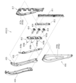
[2-3.外枠下組立体]
外枠2の外枠下組立体40について、主に図20を参照して詳細に説明する。図20は、外枠の外枠下組立体を分解して前から見た分解斜視図である。外枠下組立体40は、左右に離間している外枠左組立体10及び外枠右組立体20の下端同士を連結すると共に、パチンコ機1において扉枠3よりも下側を閉鎖して装飾するためのものである。
[2-3. Outer frame lower assembly]
The outer frame lower assembly 40 of the outer frame 2 will be described in detail mainly with reference to FIG. FIG. 20 is an exploded front perspective view of the outer frame lower assembly of the outer frame. The outer frame lower assembly 40 connects the lower ends of the outer frame left assembly 10 and the outer frame right assembly 20 which are separated from each other to the left and right, and closes the lower side of the door frame 3 in the pachinko machine 1. It is for decoration.
外枠下組立体40は、左右に離間している外枠左組立体10及び外枠右組立体20の下端同士を連結しており左右に延びている外枠下部材41と、外枠下部材41の前方に配置されており外枠下部材41に沿って左右に延びていると共に後方が開放されている箱状の幕板前部材42と、幕板前部材42の後側に取付けられていると共に外枠下部材41の上面に取付けられており前方が開放されている左右に延びた箱状の幕板後部材43と、幕板後部材43の上面における左端に形成されている球噛防止機構44と、を備えている。
The outer frame lower assembly 40 connects the lower ends of the outer frame left assembly 10 and the outer frame right assembly 20, which are spaced apart in the left and right direction, and extends left and right. A box-shaped curtain plate front member 42 which is arranged in front of the member 41 and extends left and right along the outer frame lower member 41 and whose rear is open is attached to the rear side of the curtain plate front member 42. A box-shaped rear panel member 43 extending to the left and right, which is attached to the upper surface of the outer frame lower member 41 and has an open front, and a ball bite prevention formed at the left end on the upper surface of the rear panel member 43 a mechanism 44;
外枠下部材41は、前後方向の幅が、外枠左部材11及び外枠右部材21の前後方向と略同じ幅で、上下方向の厚さが一定で、左右方向に延びており、木材によって形成されている。外枠下部材41は、左右方向の長さが、外枠上部材30の左右方向の長さと同じに形成されている。
The outer frame lower member 41 has a width in the front-rear direction substantially the same as the width in the front-rear direction of the outer frame left member 11 and the outer frame right member 21, has a constant vertical thickness, and extends in the left-right direction. formed by The outer frame lower member 41 is formed to have the same length in the left-right direction as the outer frame upper member 30 in the left-right direction.
外枠下部材41は、左右両側面における前後方向の中央において、上下に貫通した状態で左右方向中央側へ夫々窪んでいる切欠部41aを備えている。これら左右両端の切欠部41aには、左下連結部材13の下横固定部13c及び右下連結部材23の下横固定部23cが夫々挿入された状態で取付けられる。これにより、外枠左部材11及び外枠右部材21の下端同士を連結することができる。
The outer frame lower member 41 has cutout portions 41a that penetrate vertically and are recessed toward the center in the left-right direction at the center in the front-rear direction on both left and right side surfaces. The lower lateral fixing portion 13c of the lower left connecting member 13 and the lower lateral fixing portion 23c of the lower right connecting member 23 are inserted into the cutout portions 41a on both the left and right ends, respectively. Thereby, the lower ends of the outer frame left member 11 and the outer frame right member 21 can be connected.
また、外枠下部材41は、上面から凹んでおり、幕板後部材43の下部が挿入される凹部41bを備えている。凹部41bは、左右に延びていると共に、前後方向中央の後ろ寄りの位置から前端側へ抜けている。この凹部41bにより、幕板前部材42及び幕板後部材43により形成される幕板内部空間40aの容積を可及的に広くしている。
Further, the outer frame lower member 41 is recessed from the upper surface and has a recess 41b into which the lower part of the panel rear member 43 is inserted. The concave portion 41b extends left and right, and extends from a position near the rear in the center in the front-rear direction to the front end side. The concave portion 41b maximizes the volume of the inner space 40a formed by the front panel member 42 and the rear panel member 43. As shown in FIG.
幕板前部材42は、左右方向の長さが外枠下部材41と同じ長さに延びており、高さに対して前後方向の奥行が短い横長の直方体状の箱状に形成されており、後側の全面が開放されている。幕板前部材42は、開放されている後側を、幕板後部材43によって閉鎖することで、幕板後部材43と協働して本体枠スピーカ622のエンクロージャ624の一部となる幕板内部空間40aを形成する。幕板前部材42は、右端付近の前面において、前後に貫通していると共に左右に延びている長孔状の開口部42aを備えている。
The front panel member 42 extends in the left-right direction to the same length as the outer frame lower member 41, and is formed in a horizontally long rectangular parallelepiped box shape with a short depth in the front-rear direction relative to the height. The entire rear side is open. By closing the open rear side of the panel front member 42 with the panel rear member 43, the panel interior becomes a part of the enclosure 624 of the main body frame speaker 622 in cooperation with the panel rear member 43. A space 40a is formed. The curtain plate front member 42 has an elongated opening 42a penetrating in the front-rear direction and extending in the left-right direction on the front surface near the right end.
幕板後部材43は、左右方向の長さが外枠下部材41よりも若干短く延びており、前方が開放された箱状に形成されている。幕板後部材43は、前面に幕板前部材42を取付けることで、幕板前部材42と協働して本体枠スピーカ622のエンクロージャ624の一部となる幕板内部空間40aを形成する。幕板後部材43は、上面における左右方向中央部において、左右に延びていると共に上方へ突出しており幕板内部空間40aと連通している筒状の接続筒部43aを有している。接続筒部43aは、上端が、幕板後部材43の一般的な上面と一致している前端側から後方へ向かうほど上方へ位置するように傾斜している。本実施形態では、接続筒部43aの上端は、45度の角度で傾斜している。
The rear panel member 43 extends in the left-right direction slightly shorter than the outer frame lower member 41, and is formed in a box shape with an open front. By attaching the front panel member 42 to the front surface of the panel rear member 43 , the panel internal space 40 a that forms a part of the enclosure 624 of the main frame speaker 622 is formed in cooperation with the panel front member 42 . The rear panel member 43 has a cylindrical connection tube portion 43a extending in the left-right direction, projecting upward, and communicating with the inner space 40a of the panel at the central portion in the left-right direction of the upper surface. The connecting tube portion 43a is inclined such that the upper end of the connecting tube portion 43a is positioned upward as it goes rearward from the front end side that coincides with the general upper surface of the rear panel member 43 . In this embodiment, the upper end of the connecting tube portion 43a is inclined at an angle of 45 degrees.
この接続筒部43aは、左右方向の長さが、幕板後部材43全体の約1/3の長さに形成されていると共に、前後方向の奥行が、幕板後部材43全体の奥行よりも若干短く形成されている。接続筒部43a内には、前端側と後端側とを結ぶ複数のリブ43bが備えられている。この接続筒部43aの上端には、外枠2に対して本体枠4を閉じた時に、本体枠4における基板ユニット620のスピーカユニット620aにおけるスピーカカバー621の接続部621cが接続されて、スピーカユニット620aの内部空間と連通した状態となり、エンクロージャ624を形成する。
The connecting tube portion 43a is formed so that the length in the left-right direction is approximately 1/3 the length of the entire rear panel member 43, and the depth in the front-rear direction is greater than the depth of the rear panel member 43 as a whole. is also slightly shorter. A plurality of ribs 43b connecting the front end side and the rear end side are provided in the connecting tube portion 43a. When the body frame 4 is closed with respect to the outer frame 2, the connection part 621c of the speaker cover 621 of the speaker unit 620a of the board unit 620 of the body frame 4 is connected to the upper end of the connection tube part 43a, thereby connecting the speaker unit. It communicates with the internal space of 620a to form an enclosure 624. FIG.
球噛防止機構44は、幕板後部材43の上面における左端において、外枠下ヒンジ部材60の部位に遊技球Bが滞留することで、外枠2と本体枠4との間に遊技球Bが挟まれるのを防止するためのものである。
The ball bite prevention mechanism 44 is arranged such that the game ball B stays at the portion of the outer frame lower hinge member 60 at the left end of the upper surface of the rear panel member 43, thereby preventing the game ball B from being held between the outer frame 2 and the main body frame 4. to prevent it from being caught.
球噛防止機構44は、幕板後部材43の上面における左端に形成されており、後述する外枠下ヒンジ部材60が際されるように平坦に形成された載置部44aと、載置部44aの左端において上方へ向かって開口している第一排出口44bと、載置部44aにおける第一排出口44bよりも右方で上方へ向かって開口している第二排出口44cと、載置部44aの後辺及び右辺から上方へ延出している立壁部44dと、立壁部44dの上端から前方へ突出していると共に上面が後方へ向かうに従って上方に位置するように傾斜している上端突出部44eと、を備えている。
The ball bite prevention mechanism 44 is formed at the left end of the upper surface of the rear panel member 43, and includes a mounting portion 44a formed flat so as to face the outer frame lower hinge member 60 described later, and a mounting portion. A first discharge port 44b that opens upward at the left end of the mounting portion 44a, a second discharge port 44c that opens upward to the right of the first discharge port 44b in the placement portion 44a, An upright wall portion 44d extending upward from the rear and right sides of the placing portion 44a, and an upper end protrusion projecting forward from the upper end of the upright wall portion 44d and having an upper surface inclined upward toward the rear. and a portion 44e.
第一排出口44bは、後述する外枠下ヒンジ部材60の排出孔60dと一致する位置に形成されている。第一排出口44b及び第二排出口44cは、遊技球Bが通過可能な大きさに形成されている。第一排出口44b及び第二排出口44cは、幕板内部空間40aとは連通しておらず、幕板後部材43の後面に開口している。従って、第一排出口44b及び第二排出口44cに進入した遊技球Bを、幕板後部材43の後方へ排出することができる。
The first discharge port 44b is formed at a position coinciding with a discharge hole 60d of the outer frame lower hinge member 60, which will be described later. The first discharge port 44b and the second discharge port 44c are formed in a size through which the game ball B can pass. The first discharge port 44 b and the second discharge port 44 c do not communicate with the inner space 40 a of the curtain plate, and open to the rear surface of the rear panel member 43 . Therefore, the game ball B that has entered the first discharge port 44b and the second discharge port 44c can be discharged behind the curtain plate rear member 43. As shown in FIG.
この球噛防止機構44は、球噛防止機構44は、外枠下ヒンジ部材60と後述する本体枠下ヒンジ組立体520との間の隙間を通して、ピアノ線等の不正な工具が挿入された場合、載置部44aの後端から立上っている立壁部44dにより、不正な工具の侵入を阻止することができる。仮に、不正な工具の先端が立壁部44dに当接することで、上方へ曲がったとしても、立壁部44dの上端に備えられている前方へ突出した上端突出部44eに当接し、これ以上の侵入を阻止することができる。従って、外枠下ヒンジ部材60の部位を介して、不正行為が行われるのを防止することができる。
The ball biting prevention mechanism 44 is designed to prevent an illegal tool such as piano wire from being inserted through a gap between the outer frame lower hinge member 60 and the main body frame lower hinge assembly 520, which will be described later. A standing wall portion 44d rising from the rear end of the mounting portion 44a can prevent an unauthorized tool from entering. Even if the tip of the unauthorized tool abuts against the vertical wall portion 44d and bends upward, it will abut against the upper end projecting portion 44e that protrudes forward provided at the upper end of the vertical wall portion 44d, preventing further intrusion. can be prevented. Therefore, it is possible to prevent fraudulent activity through the portion of the lower outer frame hinge member 60 .
ところで、載置部44aの後端に立壁部44dを備えた場合、外枠2に対して本体枠4を開けた時に、何らかの理由により載置部44a上に落下した遊技球Bが、立壁部44dによって外枠2の後方への移動が阻止されるため、載置部44a上に遊技球Bが滞留し易くなる。そして、載置部44a上に遊技球Bが滞留していると、外枠2に対して本体枠4を閉じる際に、外枠2と本体枠4との間に遊技球Bが挟み込まれてしまい、本体枠4を閉じることができなくなる問題が発生する。
By the way, in the case where the standing wall portion 44d is provided at the rear end of the placing portion 44a, when the main body frame 4 is opened with respect to the outer frame 2, the game ball B that has fallen onto the placing portion 44a for some reason is Since the rearward movement of the outer frame 2 is prevented by 44d, the game ball B tends to stay on the placing portion 44a. When the game ball B remains on the mounting portion 44a, the game ball B is caught between the outer frame 2 and the main body frame 4 when the main body frame 4 is closed with respect to the outer frame 2. As a result, there arises a problem that the body frame 4 cannot be closed.
これに対して、本実施形態の球噛防止機構44では、外枠下ヒンジ部材60上や載置部44a上に落下した遊技球Bを、外枠下ヒンジ部材60の排出孔60dと第一排出口44bを通して、又は、第二排出口44cを通して、遊技球Bを幕板後部材43の後方(外枠2の後方)へ排出することができ、外枠2と本体枠4との間に遊技球Bが挟まれるのを防止することができる。
On the other hand, in the ball biting prevention mechanism 44 of the present embodiment, the game ball B that has fallen onto the outer frame lower hinge member 60 or the placing portion 44a is discharged from the discharge hole 60d of the outer frame lower hinge member 60 and the first Through the discharge port 44b or through the second discharge port 44c, the game ball B can be discharged behind the curtain board rear member 43 (behind the outer frame 2), and between the outer frame 2 and the main body frame 4 It is possible to prevent the game ball B from being caught.
外枠下組立体40は、幕板前部材42及び幕板後部材43の上面に左右に離間して配置されている一対の案内部材45と、幕板前部材42の開口部42aを後側から閉鎖している平板状のグリル部材46と、グリル部材46を挟んで開口部42aを閉鎖するように幕板前部材42の内部に取付けられており前後に延びた二つの円筒を有したポート部材47と、幕板後部材43の接続筒部43aの上端に配置される枠状のシール部材48と、を備えている。
The lower outer frame assembly 40 includes a pair of guide members 45 arranged on the upper surfaces of the front panel member 42 and the rear panel member 43 with a left-right spacing, and closes the opening 42a of the front panel member 42 from the rear side. and a port member 47 having two cylinders extending back and forth, which is mounted inside the front panel member 42 so as to close the opening 42a with the grill member 46 interposed therebetween. , and a frame-shaped sealing member 48 arranged at the upper end of the connecting tube portion 43 a of the rear panel member 43 .
一対の案内部材45は、外枠2に対して本体枠4を閉じた時に、扉枠3の下端が当接するものである。案内部材45は、摩擦抵抗の低い低摩擦材料によって形成されており、本体枠4の下端を滑り易くして、開閉を容易にしている。
The pair of guide members 45 are in contact with the lower end of the door frame 3 when the body frame 4 is closed with respect to the outer frame 2 . The guide member 45 is made of a low-friction material with low frictional resistance, and makes the lower end of the body frame 4 slippery to facilitate opening and closing.
グリル部材46は、無数の小穴を有したパンチングメタルにより形成されている。ポート部材47は、二つの円筒により、グリル部材46を介して幕板内部空間40a(エンクロージャ624)と外枠2の前方とを連通させている。ポート部材47は、二つの円筒が、所定の内径で所定の長さに形成されており、ヘルムホルツ共鳴の原理により本体枠スピーカ622から後方(エンクロージャ624内)へ発せられた低音を共振・増幅させて、豊かな低音を外枠2の前方(遊技者側)へ放射することができる。つまり、本実施形態では、本体枠スピーカ622のエンクロージャ624がバスレフ型とされており、遊技者に対して重低音を聞かせることができる。
The grill member 46 is made of punching metal with numerous small holes. The port member 47 communicates the inner space 40a (enclosure 624) of the curtain board and the front of the outer frame 2 via the grill member 46 with two cylinders. The port member 47 is formed of two cylinders having a predetermined inner diameter and a predetermined length, and resonates and amplifies the low-pitched sound emitted from the main body frame speaker 622 to the rear (within the enclosure 624) according to the principle of Helmholtz resonance. , a rich low-pitched sound can be radiated forward of the outer frame 2 (toward the player). In other words, in this embodiment, the enclosure 624 of the main body frame speaker 622 is of a bass reflex type, so that the player can hear deep bass sounds.
シール部材48は、外枠2に対して本体枠4を閉じた時に、接続筒部43aの上端と本体枠4におけるスピーカカバー621の接続部621cの下端との間に挟まれて圧縮されるものであり、接続筒部43aと接続部621cとの間から本体枠スピーカ622のエンクロージャ624内の音が漏れるのを防止するものである。
The seal member 48 is sandwiched and compressed between the upper end of the connection tube portion 43a and the lower end of the connection portion 621c of the speaker cover 621 in the main body frame 4 when the main body frame 4 is closed with respect to the outer frame 2. and prevents the sound in the enclosure 624 of the main frame speaker 622 from leaking from between the connecting tube portion 43a and the connecting portion 621c.
[2-4.外枠上ヒンジ組立体]
外枠2の外枠上ヒンジ組立体50について、主に図21を参照して詳細に説明する。図21(a)は外枠の外枠上ヒンジ組立体を分解して前上から見た分解斜視図であり、(b)は(a)を前下から見た分解斜視図である。外枠上ヒンジ組立体50は、外枠左組立体10の上端と外枠上部材30の左端に取付けられるものであり、外枠2に対して本体枠4をヒンジ回転可能に取付けるためのものである。外枠上ヒンジ組立体50は、外枠左部材11の凹部11aの上端と外枠上部材30の取付段部30bとに取付けられる外枠上ヒンジ部材51と、外枠上ヒンジ部材51に取付けられているロック部材52と、ロック部材52を外枠上ヒンジ部材51に取付けている取付ビス53と、を備えている。
[2-4. Outer frame upper hinge assembly]
The outer frame upper hinge assembly 50 of the outer frame 2 will be described in detail mainly with reference to FIG. FIG. 21(a) is an exploded perspective view of the outer frame upper hinge assembly of the outer frame and viewed from above, and FIG. 21(b) is an exploded perspective view of (a) viewed from below. The outer frame upper hinge assembly 50 is attached to the upper end of the outer frame left assembly 10 and the left end of the outer frame upper member 30, and is used to attach the main body frame 4 to the outer frame 2 so as to be hinge-rotatable. is. The outer frame upper hinge assembly 50 is attached to the outer frame upper hinge member 51 attached to the upper end of the recess 11a of the outer frame left member 11 and the mounting step portion 30b of the outer frame upper member 30. and a mounting screw 53 for mounting the locking member 52 to the outer frame upper hinge member 51 .
外枠上ヒンジ部材51は、水平に延びた平板状で外枠上部材30の取付段部30bの上面に取付けられる上固定部51aと、上固定部51aの前辺から前方へ延出している平板状の前方延出部51bと、前方延出部51bの右辺の途中から前方へ向かうに従って前方延出部51bの左右中央へ延びており上下に貫通している軸受溝51cと、上固定部51aの左辺から下方へ延びている平板状の横固定部51dと、前方延出部51bの左辺から前辺を周って軸受溝51cが開口している部位までの端縁から下方へ延びており横固定部51dと連続している平板状の端縁壁部51eと、を備えている。外枠上ヒンジ部材51は、金属板をプレス成型により打抜き・屈曲させて形成されている。外枠上ヒンジ部材51は、軸受溝51c内において、本体枠上ヒンジ部材510の後述する本体枠上ヒンジピン512を回転可能に支持することができる。
The outer frame upper hinge member 51 is in the form of a horizontally extending flat plate and extends forward from an upper fixing portion 51a attached to the upper surface of the mounting step portion 30b of the outer frame upper member 30 and the front side of the upper fixing portion 51a. A flat plate-like forward extending portion 51b, a bearing groove 51c that extends from the middle of the right side of the forward extending portion 51b to the center of the forward extending portion 51b toward the front and penetrates vertically, and an upper fixing portion. A flat plate-like lateral fixing portion 51d extending downward from the left side of 51a, and an end edge extending downward from the left side of the forward extending portion 51b to the portion where the bearing groove 51c opens around the front side. A flat edge wall portion 51e that is continuous with the cage horizontal fixing portion 51d is provided. The outer frame upper hinge member 51 is formed by punching and bending a metal plate by press molding. The outer frame upper hinge member 51 can rotatably support a later-described main body frame upper hinge pin 512 of the main body frame upper hinge member 510 in the bearing groove 51c.
ロック部材52は、前後に延びている帯板状のロック本体52aと、ロック本体52aの後端から右方へ突出している操作片52bと、ロック本体52aの後端から左方へ延びた後に斜め左前方へ延びている弾性変形可能な棒状の弾性部52cと、ロック本体52aの後端付近で上下に貫通している取付孔52dと、を備えている。ロック部材52は、合成樹脂によって形成されている。ロック部材52は、取付ビス53によって、外枠上ヒンジ部材51における前方延出部51bの下面で、軸受溝51cよりも後側の部位に回動可能に取付けられる。
The lock member 52 includes a band plate-like lock body 52a extending back and forth, an operation piece 52b projecting rightward from the rear end of the lock body 52a, and an operation piece 52b extending leftward from the rear end of the lock body 52a. It has an elastically deformable rod-shaped elastic portion 52c extending obliquely forward left, and a mounting hole 52d penetrating vertically near the rear end of the lock body 52a. The lock member 52 is made of synthetic resin. The locking member 52 is rotatably attached to the lower surface of the forward extending portion 51b of the outer frame upper hinge member 51 by an attaching screw 53, at a portion rearward of the bearing groove 51c.
ロック部材52は、外枠上ヒンジ部材51に取付けた状態で、ロック本体52aが、平面視で軸受溝51cを遮ることができると共に、前端付近の右側面が、外枠上ヒンジ部材51の端縁壁部51eにおける軸受溝51cの開口まで延びている部位と当接可能となるように前方へ延びている。また、ロック本体52aの後端から左方へ延びている弾性部52cの先端は、外枠上ヒンジ部材51における端縁壁部51eの内周面に当接している。このロック部材52は、弾性部52cの付勢力によって取付孔52dを中心に、前端が左方へ回動する方向に付勢されている。従って、通常の状態では、ロック部材52のロック本体52aの前端付近の右側面が、端縁壁部51eに当接している。この状態では、軸受溝51cにおけるロック本体52aよりも前側の部位に、本体枠上ヒンジ部材510の本体枠上ヒンジピン512を収容可能な空間が形成される。
When the lock member 52 is attached to the outer frame upper hinge member 51 , the lock body 52 a can block the bearing groove 51 c in a plan view, and the right side surface near the front end is the edge of the outer frame upper hinge member 51 . It extends forward so as to come into contact with a portion of the edge wall portion 51e extending to the opening of the bearing groove 51c. The tip of the elastic portion 52c extending leftward from the rear end of the lock body 52a abuts the inner peripheral surface of the edge wall portion 51e of the outer frame upper hinge member 51. As shown in FIG. The locking member 52 is biased in a direction in which the front end thereof rotates leftward about the mounting hole 52d by the biasing force of the elastic portion 52c. Therefore, in a normal state, the right side surface of the lock body 52a of the lock member 52 in the vicinity of the front end is in contact with the edge wall portion 51e. In this state, a space capable of accommodating the main body frame upper hinge pin 512 of the main body frame upper hinge member 510 is formed in a portion of the bearing groove 51c on the front side of the lock body 52a.
このロック部材52は、操作片52bを操作することで、弾性部52cの付勢力に抗してロック本体52aを回動させることができる。そして、操作片52bの操作によって、ロック本体52aを、その前端が左方へ移動する方向へ回動させることで、平面視において軸受溝51cからロック本体52aを後退させることができ、軸受溝51cが全通している状態とすることができる。これにより、軸受溝51c内に本体枠上ヒンジピン512を挿入したり、軸受溝51c内から本体枠上ヒンジピン512を外したりすることができる。
By operating the operation piece 52b, the lock member 52 can rotate the lock body 52a against the biasing force of the elastic portion 52c. By operating the operation piece 52b to rotate the lock body 52a in a direction in which the front end thereof moves leftward, the lock body 52a can be retracted from the bearing groove 51c in a plan view. can be in a state in which the As a result, the body frame upper hinge pin 512 can be inserted into the bearing groove 51c, or the body frame upper hinge pin 512 can be removed from the bearing groove 51c.
[2-5.外枠下ヒンジ部材]
外枠2の外枠下ヒンジ部材60について、主に図18を参照して詳細に説明する。外枠下ヒンジ部材60は、水平に延びた平板状の水平部60aと、水平部60aの左辺において前後方向中央よりも後側の部位から上方へ立上っている平板状の立上部60bと、水平部60aの前端付近から上方へ突出している外枠下ヒンジピン60cと、水平部60aを上下に貫通しており遊技球Bが一つのみ通過可能な大きさの排出孔60dと、を備えている。この外枠下ヒンジ部材60は、金属板をプレス成型により打抜き・屈曲させて形成されている。
[2-5. Outer frame lower hinge member]
The lower outer frame hinge member 60 of the outer frame 2 will be described in detail mainly with reference to FIG. The outer frame lower hinge member 60 has a flat plate-like horizontal portion 60a that extends horizontally, and a flat plate-like raised portion 60b that rises upward from a portion on the left side of the horizontal portion 60a on the rear side of the center in the front-rear direction. , an outer frame lower hinge pin 60c protruding upward from near the front end of the horizontal portion 60a, and a discharge hole 60d penetrating vertically through the horizontal portion 60a and having a size through which only one game ball B can pass. ing. The outer frame lower hinge member 60 is formed by punching and bending a metal plate by press molding.
外枠下ヒンジ部材60の水平部60aは、平面視において、左辺を底辺とした台形に形成されている。外枠下ヒンジピン60cは、円柱状で、上下方向中央よりも上部が、上端が窄まった円錐台状に形成されている。この外枠下ヒンジピン60cは、水平部60aの前端付近における左寄りの位置に取付けられている。排出孔60dは、水平部60aにおいて、立上部60bの前後方向中央の部位と接し、水平部60aの左辺から右方へ逆U字状に延びるように形成されている。この排出孔60dは、外枠下組立体40における球噛防止機構44の第一排出口44bと、略同じ大きさに形成されている。
The horizontal portion 60a of the lower outer frame hinge member 60 is formed in a trapezoidal shape with the left side as the base in plan view. The outer frame lower hinge pin 60c has a columnar shape, and is formed in a truncated cone shape with a narrower upper end than the center in the vertical direction. The outer frame lower hinge pin 60c is attached to a leftward position near the front end of the horizontal portion 60a. 60 d of discharge holes are formed in the horizontal part 60a so that it may contact|connect the center part of the front-back direction of the rising part 60b, and may extend rightward from the left side of the horizontal part 60a in an inverted U shape. The discharge hole 60 d is formed to have substantially the same size as the first discharge port 44 b of the ball jam prevention mechanism 44 in the outer frame lower assembly 40 .
外枠下ヒンジ部材60は、外枠2に組立てた状態で、水平部60aの後部が、外枠下組立体40における幕板後部材43の載置部44a上に載置され、図示しないビスによって幕板後部材43に固定されている。また、立上部60bが、外枠左部材11の右側面における膨出部11bよりも前側の部位に、図示しないビスによって取付けられている。この外枠下ヒンジ部材60は、外枠下ヒンジピン60cを、本体枠4の本体枠下ヒンジ組立体520における外枠用下ヒンジ孔521aに挿通させることで、外枠上ヒンジ部材51と協働して本体枠4を開閉可能に取付けることができる。
In the outer frame lower hinge member 60 assembled to the outer frame 2, the rear portion of the horizontal portion 60a is placed on the mounting portion 44a of the curtain plate rear member 43 in the outer frame lower assembly 40, and screwed (not shown). It is fixed to the rear panel member 43 by . The raised portion 60b is attached to the right side surface of the outer frame left member 11 on the front side of the bulging portion 11b with a screw (not shown). The outer frame lower hinge member 60 cooperates with the outer frame upper hinge member 51 by inserting the outer frame lower hinge pin 60c into the outer frame lower hinge hole 521a in the main body frame lower hinge assembly 520 of the main body frame 4. Then, the body frame 4 can be attached so that it can be opened and closed.
また、外枠2を組立てた状態では、排出孔60dが、外枠下組立体40における球噛防止機構44の第一排出口44bと一致している。これにより、水平部60a上の遊技球Bを、排出孔60d及び第一排出口44bを通して、外枠2の後方へ落下(排出)させることができる。詳述すると、外枠2に対して本体枠4を閉じる時に、外枠2と本体枠4との間に落下した遊技球Bが、本体枠4が閉じられるのに従って、外枠2と本体枠4との間が徐々に狭くなることから、間隔が広い後方側へ転動とすることとなり、排出孔60dから排出させることができる。この際に、排出孔60dが、パチンコ機1に組立てた状態で、外枠2に対して本体枠4を閉じた時に、本体枠4の後端と略同じとなる位置に形成されているため、外枠2と本体枠4との間に落下した遊技球Bを、排出孔60dから排出させることで本体枠4よりも後側へ転動するのを阻止し易くすることができ、外枠下ヒンジ部材60の部位に遊技球Bが留まり難くすることができる。
Further, in the assembled state of the outer frame 2, the discharge hole 60d coincides with the first discharge port 44b of the ball bite prevention mechanism 44 in the lower outer frame assembly 40. As shown in FIG. Thereby, the game ball B on the horizontal portion 60a can be dropped (discharged) behind the outer frame 2 through the discharge hole 60d and the first discharge port 44b. More specifically, when the main body frame 4 is closed with respect to the outer frame 2, the game ball B that has fallen between the outer frame 2 and the main body frame 4 is separated from the outer frame 2 and the main body frame as the main body frame 4 is closed. 4 gradually narrows, the ball rolls to the rear side where the gap is wide, and can be discharged from the discharge hole 60d. At this time, the discharge hole 60d is formed at a position that is substantially the same as the rear end of the body frame 4 when the body frame 4 is closed with respect to the outer frame 2 in the state assembled to the pachinko machine 1. By ejecting the game ball B dropped between the outer frame 2 and the main body frame 4 from the ejection hole 60d, it is possible to easily prevent the game ball B from rolling to the rear side of the main body frame 4, and the outer frame It is possible to make it difficult for the game ball B to stay at the part of the lower hinge member 60.例文帳に追加
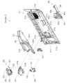
[3.扉枠の全体構成]
パチンコ機1の扉枠3について、主に図22乃至図30を参照して詳細に説明する。図22はパチンコ機における扉枠の表面図であり、図23は扉枠の背面図であり、図24は扉枠の左側面図であり、図25は扉枠の右側面図である。図26は扉枠を右前から見た斜視図であり、図27は扉枠を左前から見た斜視図であり、図28は扉枠を後ろから見た斜視図である。図29は扉枠を主な部材毎に分解して前から見た分解斜視図であり、図30は扉枠を主な部材毎に分解して後ろから見た分解斜視図である。
[3. Overall configuration of door frame]
The door frame 3 of the pachinko machine 1 will be described in detail mainly with reference to FIGS. 22 to 30. FIG. 22 is a front view of a door frame in a pachinko machine, FIG. 23 is a rear view of the door frame, FIG. 24 is a left side view of the door frame, and FIG. 25 is a right side view of the door frame. 26 is a perspective view of the door frame viewed from the front right, FIG. 27 is a perspective view of the door frame viewed from the front left, and FIG. 28 is a perspective view of the door frame viewed from the back. FIG. 29 is an exploded perspective view of the door frame disassembled into main members and viewed from the front, and FIG. 30 is an exploded perspective view of the door frame disassembled into the main members and viewed from the back.
扉枠3は、外枠2の枠内と略同じ大きさで正面視において上下に延びた四角形に形成されており、本体枠4を介して外枠2の枠内を前側から開閉可能に取付けられている。扉枠3は、遊技球Bが打込まれる遊技盤5の遊技領域5aを前側から視認可能に閉鎖し、遊技領域5a内に打込むための遊技球Bを貯留すると共に、貯留している遊技球Bを遊技領域5a内へ打込むために遊技者が操作するハンドル182を備えているものである。また、扉枠3は、パチンコ機1の前面全体を装飾するものである。
The door frame 3 has substantially the same size as the inside of the outer frame 2 and is formed in a rectangular shape extending vertically when viewed from the front. It is The door frame 3 closes the game area 5a of the game board 5 into which the game ball B is hit so as to be visible from the front side, stores the game ball B to be hit in the game area 5a, and stores the game ball B. It has a handle 182 operated by the player to hit the ball B into the game area 5a. Further, the door frame 3 decorates the entire front surface of the pachinko machine 1. - 特許庁
扉枠3は、正面視の外形が上下に延びた四角形で枠状の扉枠ベースユニット100と、扉枠ベースユニット100に着脱可能に取付けられており本体枠4に取付けられた遊技盤5の遊技領域5aを前方から視認可能に閉鎖しているガラスユニット160と、ガラスユニット160の下部を後側から覆うように扉枠ベースユニット100に取付けられている防犯カバー170と、扉枠ベースユニット100の前面右下隅に取付けられているハンドルユニット180と、扉枠ベースユニット100の前面下部に取付けられている皿ユニット200と、皿ユニット200の上側で扉枠ベースユニット100の前面左部に取付けられている扉枠左サイドユニット400と、皿ユニットの上側で扉枠ベースユニット100の前面右部に取付けられている扉枠右サイドユニット410と、扉枠左サイドユニット400及び扉枠右サイドユニット410の上側で扉枠ベースユニット100の前面上部に取付けられている扉枠トップユニット450と、を備えている。
The door frame 3 includes a door frame base unit 100 having a rectangular frame shape extending vertically when viewed from the front, and a game board 5 detachably attached to the door frame base unit 100 and attached to the main body frame 4. A glass unit 160 closing the game area 5a so as to be visible from the front, a security cover 170 attached to the door frame base unit 100 so as to cover the lower part of the glass unit 160 from the rear side, and the door frame base unit 100. a handle unit 180 attached to the front lower right corner of the door frame base unit 100; a door frame left side unit 400 attached to the tray unit, a door frame right side unit 410 attached to the front right portion of the door frame base unit 100 above the tray unit, the door frame left side unit 400 and the door frame right side unit 410 and a door frame top unit 450 attached to the front upper portion of the door frame base unit 100 on the upper side of the door frame base unit 100 .
扉枠ベースユニット100は、正面視の外形が上下に延びた四角形(長方形)に形成されており前後に貫通している扉窓101aを有した扉枠ベース101と、扉枠ベース101の前面右下に取付けられているハンドル取付部材102と、扉枠ベース101の後側で背面視右下隅に取付けられているスピーカダクト103と、扉枠ベース101の後側の下部における背面視右端付近に取付けられている扉枠主中継基板104と、扉枠主中継基板104の背面視左方に取付けられている扉枠副中継基板105と、扉枠副中継基板105の背面視左方に取付けられているハンドル後中継基板106と、扉枠主中継基板104と扉枠副中継基板105の一部とを後側から被覆する扉枠中継基板カバー107と、ハンドル後中継基板106を後側から被覆するハンドル後中継基板カバー108と、配線ケーブルを被覆するケーブルカバー109と、を備えている。
The door frame base unit 100 includes a door frame base 101 having a vertically extending quadrangular (rectangular) outer shape when viewed from the front, and having a door window 101a penetrating in the front and rear directions. A handle mounting member 102 mounted below, a speaker duct 103 mounted on the rear side of the door frame base 101 at the lower right corner when viewed from the rear, and mounted near the right end on the rear side of the door frame base 101 on the rear side. a door frame main relay board 104 attached to the door frame main relay board 104; The door frame relay board cover 107 covers the rear handle relay board 106, the door frame main relay board 104 and a part of the door frame sub relay board 105 from the rear side, and the handle rear relay board 106 is covered from the rear side. It has a post-handle relay board cover 108 and a cable cover 109 that covers the wiring cable.
また、扉枠ベースユニット100は、扉枠ベース101の後側に取付けられている枠状の扉枠補強ユニット110と、扉枠補強ユニット110に取付けられている扉枠上ヒンジ組立体120及び扉枠下ヒンジ部材125と、扉枠補強ユニット110に取付けられている開閉用のシリンダ錠130と、扉枠ベース101の後側でハンドル後中継基板106の上方に取付けられている球送給ユニット140と、扉枠ベース101の後側の下部における背面視右側に取付けられているファールカバーユニット150と、を備えている。
Further, the door frame base unit 100 includes a frame-shaped door frame reinforcing unit 110 attached to the rear side of the door frame base 101, a door frame upper hinge assembly 120 attached to the door frame reinforcing unit 110, and a door. A frame lower hinge member 125, an opening/closing cylinder lock 130 attached to the door frame reinforcing unit 110, and a ball feeding unit 140 attached above the handle rear relay board 106 on the rear side of the door frame base 101. and a foul cover unit 150 attached to the right side of the lower rear side of the door frame base 101 when viewed from the rear.
扉枠補強ユニット110は、扉枠ベース101の後側に取付けられることで、扉枠ベース101を補強して剛性を付与するものである。扉枠上ヒンジ組立体120及び扉枠下ヒンジ部材125は、扉枠3を本体枠4に対して開閉可能に取付けるためのものである。シリンダ錠130は、本体枠4の施錠ユニット650と協働して、扉枠3と本体枠4との開閉、及び、外枠2と本体枠4との開閉施錠に使用されるものである。なお、以下、扉枠3と本体枠4とから構成される枠体を「前面枠」と記載する場合がある。
The door frame reinforcing unit 110 is attached to the rear side of the door frame base 101 to reinforce the door frame base 101 and impart rigidity to it. The door frame upper hinge assembly 120 and the door frame lower hinge member 125 are for attaching the door frame 3 to the body frame 4 so as to be openable and closable. The cylinder lock 130 cooperates with the locking unit 650 of the body frame 4 to open and close the door frame 3 and the body frame 4 and to open and close the outer frame 2 and the body frame 4 . In addition, hereinafter, the frame formed by the door frame 3 and the body frame 4 may be referred to as a "front frame".
また、球送給ユニット140は、上皿201内の遊技球Bを一つずつ本体枠4の球発射装置540へ供給するためのものである。ファールカバーユニット150は、球発射装置540により発射されて遊技盤5の遊技領域5a内に到達しなかった遊技球B(ファール球)を、下皿202に誘導すると共に、払出装置580から払出された遊技球Bを、上皿201又は下皿202に誘導するためのものである。
Also, the ball feeding unit 140 is for feeding the game balls B in the upper tray 201 to the ball launching device 540 of the body frame 4 one by one. The foul cover unit 150 guides the game ball B (foul ball) that has been shot by the ball launcher 540 and has not reached the game area 5a of the game board 5 to the lower tray 202 and is paid out from the payout device 580. It is for guiding the game ball B to the upper tray 201 or the lower tray 202.例文帳に追加
ガラスユニット160は、透明なガラス板162を有しており扉枠ベース101の扉窓101aを閉鎖している。防犯カバー170は、ガラスユニット160の下部を後方から覆うように扉枠ベース101に取付けられている。ハンドルユニット180は、遊技者が回転操作可能なハンドル182を備えており、ハンドル182を操作することで、上皿201内の遊技球Bを、球発射装置540によって遊技盤5の遊技領域5a内に打込む遊技を行うためのものである。
The glass unit 160 has a transparent glass plate 162 and closes the door window 101 a of the door frame base 101 . The security cover 170 is attached to the door frame base 101 so as to cover the lower portion of the glass unit 160 from behind. The handle unit 180 includes a handle 182 that can be rotated by the player. By operating the handle 182, the game ball B in the upper tray 201 is ejected into the game area 5a of the game board 5 by the ball launcher 540. It is for playing a game to hit into.
[3-1.扉枠ベースユニットの全体構成]
扉枠3の扉枠ベースユニット100について、主に図31乃至図33を参照して詳細に説明する。図31(a)は扉枠の扉枠ベースユニットを前から見た斜視図であり、(b)は扉枠ベースユニットを後ろから見た斜視図である。図32は扉枠ベースユニットを主な部材毎に分解して前から見た分解斜視図であり、図33は扉枠ベースユニットを主な部材毎に分解して後ろから見た分解斜視図である。
[3-1. Overall configuration of door frame base unit]
The door frame base unit 100 of the door frame 3 will be described in detail mainly with reference to FIGS. 31 to 33. FIG. FIG. 31(a) is a front perspective view of the door frame base unit of the door frame, and FIG. 31(b) is a rear perspective view of the door frame base unit. FIG. 32 is an exploded perspective view of the door frame base unit disassembled for each main member and viewed from the front, and FIG. 33 is an exploded perspective view of the door frame base unit disassembled for each main member and viewed from the back. be.
扉枠ベースユニット100は、正面視左辺側が本体枠4に対してヒンジ回転可能に取付けられ、本体枠4の前面を開閉可能に閉鎖していると共に、本体枠4に取付けられている遊技盤の遊技領域を前方から視認可能としている。扉枠ベースユニット100は、外形が上下に延びた四角形で平板状の扉枠ベース101と、扉枠ベース101の前面右下に取付けられておりハンドルユニット180を取付けるためのハンドル取付部材102と、扉枠ベース101の後側で背面視右下隅に取付けられているスピーカダクト103と、を備えている。
The door frame base unit 100 is hinge-rotatably attached to the main body frame 4 at the left side in front view, and closes the front surface of the main body frame 4 so as to be opened and closed. The game area is visible from the front. The door frame base unit 100 includes a rectangular and flat plate-shaped door frame base 101 with an outer shape extending vertically, a handle mounting member 102 mounted on the lower right front surface of the door frame base 101 for mounting a handle unit 180, and a speaker duct 103 attached to the rear side of the door frame base 101 at the lower right corner in rear view.
また、扉枠ベースユニット100は、扉枠ベース101の後側の下部における背面視右端付近に取付けられている扉枠主中継基板104と、扉枠ベース101の後側の下部における扉枠主中継基板104の背面視左方に取付けられている扉枠副中継基板105と、扉枠ベース101の後側の下部における扉枠副中継基板105の背面視左方に取付けられているハンドル後中継基板106と、扉枠ベース101の後側に取付けられており扉枠主中継基板104と扉枠副中継基板105の一部とを後側から被覆する扉枠中継基板カバー107と、扉枠ベース101の後側に取付けられておりハンドル後中継基板106を後側から被覆するハンドル後中継基板カバー108と、扉枠ベース101の後側に取付けられており配線ケーブルを被覆するケーブルカバー109と、を備えている。
The door-frame base unit 100 also includes a door-frame main relay board 104 attached near the right end in the rear view of the lower rear side of the door-frame base 101, and a door-frame main relay board 104 attached to the lower rear side of the door-frame base 101. A door frame secondary relay board 105 attached to the left side of the board 104 in rear view, and a handle rear relay board mounted to the left side of the door frame secondary relay board 105 in the lower rear side of the door frame base 101 in rear view. 106, a door frame relay board cover 107 attached to the rear side of the door frame base 101 and covering the door frame main relay board 104 and part of the door frame sub relay board 105 from the rear side, and the door frame base 101. A rear handle relay board cover 108 attached to the rear side and covering the rear handle relay board 106 from the rear side, and a cable cover 109 attached to the rear side of the door frame base 101 and covering the wiring cable are provided. I have it.
更に、扉枠ベースユニット100は、扉枠ベース101の後側に取付けられている枠状の扉枠補強ユニット110と、扉枠補強ユニット110に取付けられている扉枠上ヒンジ組立体120及び扉枠下ヒンジ部材125と、扉枠補強ユニット110に取付けられている開閉用のシリンダ錠130と、扉枠ベース101の後側でハンドル後中継基板106の上方に取付けられている球送給ユニット140と、扉枠ベース101の後側の下部における背面視右側に取付けられているファールカバーユニット150と、を備えている。
Further, the door frame base unit 100 includes a frame-shaped door frame reinforcement unit 110 attached to the rear side of the door frame base 101, a door frame top hinge assembly 120 attached to the door frame reinforcement unit 110, and a door. A frame lower hinge member 125, an opening/closing cylinder lock 130 attached to the door frame reinforcing unit 110, and a ball feeding unit 140 attached above the handle rear relay board 106 on the rear side of the door frame base 101. and a foul cover unit 150 attached to the right side of the lower rear side of the door frame base 101 when viewed from the rear.
この扉枠ベースユニット100には、前面下隅にハンドルユニット180が、扉窓101aの下側前面に皿ユニット200が、扉窓101aの左外側前面に扉枠左サイドユニット400が、扉窓101aの右外側前面に扉枠右サイドユニット410が、扉窓101aの上外側前面に扉枠トップユニット450が、夫々取付けられるものである。
This door frame base unit 100 has a handle unit 180 at the bottom corner of the front surface, a plate unit 200 at the lower front surface of the door window 101a, a door frame left side unit 400 at the left outer front surface of the door window 101a, and a door frame left side unit 400 at the front surface of the door window 101a. A door frame right side unit 410 is attached to the right outer front surface, and a door frame top unit 450 is attached to the upper outer front surface of the door window 101a.
また、扉枠ベースユニット100には、扉窓101aを後方から閉鎖するようにガラスユニット160が取付けられると共に、ガラスユニット160の下部を後方から覆うように透明な防犯カバー170が取付けられるものである。
A glass unit 160 is attached to the door frame base unit 100 so as to close the door window 101a from behind, and a transparent security cover 170 is attached to cover the lower part of the glass unit 160 from behind. .
[3-1a.扉枠ベース]
扉枠3における扉枠ベースユニット100の扉枠ベース101について、主に図31乃至図33を参照して詳細に説明する。扉枠ベース101は、正面視の外形が上下に延びた四角形(長方形)に形成されている。扉枠ベース101は、前後に貫通しており、正面視における内周形状が上下に延びた略四角形に形成された扉窓101aを備えている。扉窓101aは、内周を形成している上辺及び左右両辺が、扉枠ベース101の外周辺に夫々接近しており、内周を形成している下辺が、扉枠ベース101の下端から上下方向の約1/3の高さに位置している。このように、扉枠ベース101は、前後に貫通している扉窓101aにより全体が枠状に形成されている。この扉枠ベース101は、合成樹脂により一体成形されている。
[3-1a. door frame base]
The door frame base 101 of the door frame base unit 100 in the door frame 3 will be described in detail mainly with reference to FIGS. 31 to 33. FIG. The door frame base 101 has a quadrangular (rectangular) shape extending vertically when viewed from the front. The door frame base 101 penetrates in the front-rear direction and has a door window 101a formed in a substantially quadrangular shape with an inner peripheral shape extending vertically when viewed from the front. The door window 101a has an upper side and both left and right sides forming the inner periphery thereof, and the lower side forming the inner periphery extends vertically from the lower end of the door frame base 101. It is located at about 1/3 of the height of the direction. Thus, the door frame base 101 is formed in a frame shape as a whole by the door window 101a penetrating in the front and rear directions. The door frame base 101 is integrally molded of synthetic resin.
扉枠ベース101は、前面における正面視右下隅に形成されており左端側が右端側よりも前方へやや突出するように傾斜しているハンドル取付座面101bと、ハンドル取付座面101bと扉窓101aとの間で正面視右端付近に後面から前方へ向かって窪み、扉枠補強ユニット110のシリンダ取付フレーム115が挿入される挿入凹部101cと、挿入凹部101cにおいて前後に貫通しておりシリンダ錠130のシリンダ本体131が挿通されるシリンダ挿通孔101dと、シリンダ挿通孔101d及びハンドル取付座面101bの正面視左側で前後に貫通しており球送給ユニット140の進入口141a及び球抜口141bを前方に臨ませるための球送給開口101eと、を備えている。
The door frame base 101 has a handle mounting seat surface 101b, which is formed at the lower right corner of the front surface when viewed from the front and is inclined so that the left end side projects slightly forward from the right end side, the handle mounting seat surface 101b, and the door window 101a. The insertion recess 101c into which the cylinder mounting frame 115 of the door frame reinforcing unit 110 is inserted is recessed near the right end in the front view from the front to the front and the insertion recess 101c. The cylinder insertion hole 101d through which the cylinder main body 131 is inserted, the cylinder insertion hole 101d, and the handle mounting seat surface 101b are penetrated in the front-rear direction on the left side of the front view. and a ball feed opening 101e for facing the ball.
また、扉枠ベース101は、左右方向中央より左寄りで且つハンドル取付座面101bと略同じ高さで前後に貫通しておりファールカバーユニット150の球放出口150dを前方に臨ませる下皿用球通過口101fと、正面視左端付近で扉窓101aの下辺に隣接するように前後に貫通しておりファールカバーユニット150の貫通球通路150aを前方に臨ませる上皿用球通過口101gと、扉窓101aの内周に沿って後面から前方へ向かって窪み、ガラスユニット160のガラス枠161が挿入されるガラスユニット取付部101hと、を備えている。
In addition, the door frame base 101 penetrates in the front and back at a position near the center in the left-right direction and at substantially the same height as the handle mounting seat surface 101b. a passage opening 101f, a ball passage opening 101g for an upper tray that penetrates in the front-rear direction so as to be adjacent to the lower side of the door window 101a in the vicinity of the left end in a front view and faces the through ball passage 150a of the foul cover unit 150 forward, and a door. A glass unit mounting portion 101h recessed forward from the rear surface along the inner circumference of the window 101a and into which the glass frame 161 of the glass unit 160 is inserted is provided.
また、扉枠ベース101は、正面視左下隅(上皿用球通過口101gの下方)に形成されており前後に貫通した縦長の複数のスリット101iを、備えている。複数のスリット101iの後側にスピーカダクト103が取付けられる。また、複数のスリット101iは、パチンコ機1を組立てた状態で、前方に皿ユニット200における皿ユニットベース211のスピーカ口211bが位置していると共に、後方に本体枠4のスピーカユニット620aにおける本体枠スピーカ622が位置しており、本体枠スピーカ622からの音を前方へ放射することができる。
Further, the door frame base 101 is provided with a plurality of longitudinally long slits 101i that are formed in the lower left corner (below the upper tray ball passage opening 101g) when viewed from the front and penetrate therethrough in the front-rear direction. A speaker duct 103 is attached to the rear side of the plurality of slits 101i. In addition, in the assembled state of the pachinko machine 1, the plurality of slits 101i are such that the speaker opening 211b of the dish unit base 211 of the dish unit 200 is positioned in front, and the main body frame of the speaker unit 620a of the main body frame 4 is positioned behind. A speaker 622 is located, and the sound from the main body frame speaker 622 can be radiated forward.
更に、扉枠ベース101は、扉窓101aの下方でハンドル取付座面101bの上方において、前後に貫通している貫通孔101jを備えている。この貫通孔101jは、扉枠ベースユニット100側と皿ユニット200側とを接続する配線ケーブル(図示は省略)が挿通されるものであり、後述する扉枠補強ユニット110における中間補強フレーム114の貫通部114bと一致するように形成されている。
Further, the door frame base 101 is provided with a through hole 101j penetrating back and forth below the door window 101a and above the handle mounting seat surface 101b. A wiring cable (not shown) connecting the door frame base unit 100 side and the tray unit 200 side is inserted through the through hole 101j. It is formed to match the portion 114b.
[3-1b.ハンドル取付部材]
扉枠ベースユニット100のハンドル取付部材102について、主に図31乃至図33を参照して詳細に説明する。ハンドル取付部材102は、扉枠ベース101の前面にハンドルユニットを取付けるためのものであり、扉枠ベース101の前面のハンドル取付座面101bに取付けられる。
[3-1b. Handle mounting member]
The handle mounting member 102 of the door frame base unit 100 will be described in detail mainly with reference to FIGS. 31-33. The handle mounting member 102 is for mounting the handle unit on the front surface of the door frame base 101, and is mounted on the handle mounting seat surface 101b on the front surface of the door frame base 101. As shown in FIG.
ハンドル取付部材102は、前後方向へ延びた円筒状の筒部102aと、筒部102aの後端から筒部102aの軸に対して直角方向外方へ延びた円環状のフランジ部102bと、筒部102a内に突出していると共に筒部102aの軸方向全長に亘って延びており筒部102aの周方向に対して不等間隔に配置された複数(本実施形態では三つ)の突条102cと、筒部102aの外周面とフランジ部102bの前面とを繋ぎ、筒部102aの周方向に対して複数配置された補強リブ102dと、を備えている。
The handlebar mounting member 102 includes a cylindrical tubular portion 102a extending in the front-rear direction, an annular flange portion 102b extending outward in a direction perpendicular to the axis of the tubular portion 102a from the rear end of the tubular portion 102a, and a tubular portion 102a. A plurality of (three in this embodiment) protrusions 102c protrude into the portion 102a and extend over the entire axial length of the cylindrical portion 102a and are arranged at uneven intervals in the circumferential direction of the cylindrical portion 102a. and a plurality of reinforcing ribs 102d that connect the outer peripheral surface of the cylindrical portion 102a and the front surface of the flange portion 102b and are arranged in the circumferential direction of the cylindrical portion 102a.
ハンドル取付部材102は、フランジ部102bの後面を、扉枠ベース101におけるハンドル取付座面101bの前面に当接させた状態で、ビスによってハンドル取付座面101bに取付けられる。
The handle mounting member 102 is attached to the handle mounting seat surface 101b with a screw while the rear surface of the flange portion 102b is in contact with the front surface of the handle mounting seat surface 101b of the door frame base 101. As shown in FIG.
筒部102aは、内径がハンドルユニット180におけるハンドルベース181の基部181aの外径よりも若干大きく形成されている。三つの突条102cは、一つが筒部102aの上部に備えられており、残り二つが筒部102aの下部に備えられている。これら三つの突条102cは、ハンドルベース181における三つの溝部181cと対応する位置に形成されている。従って、ハンドル取付部材102は、三つの突条102cと、ハンドルベース181の三つの溝部181cとを一致させた状態でのみ、筒部102a内にハンドルベース181の基部181aを挿入させることができ、扉枠ベース101に対してハンドルベース181(ハンドルユニット180)の回転位置を規制することができる。
The cylindrical portion 102 a has an inner diameter slightly larger than the outer diameter of the base portion 181 a of the handle base 181 of the handle unit 180 . One of the three protrusions 102c is provided on the upper portion of the cylindrical portion 102a, and the remaining two are provided on the lower portion of the cylindrical portion 102a. These three ridges 102c are formed in the handle base 181 at positions corresponding to the three grooves 181c. Therefore, in the handle mounting member 102, the base portion 181a of the handle base 181 can be inserted into the cylindrical portion 102a only when the three ridges 102c and the three groove portions 181c of the handle base 181 are aligned. The rotational position of the handle base 181 (handle unit 180) with respect to the door frame base 101 can be regulated.
なお、ハンドル取付部材102は、フランジ部102bの後面に対して、筒部102aの軸線が垂直に延びていることから、扉枠ベース101の傾斜しているハンドル取付座面101bに取付けることで、筒部102aの軸線が右前方へ延びるように傾いた状態となり、ハンドルユニット180を同様に傾いた状態で扉枠ベース101に取付けることができる。
Since the axis of the cylindrical portion 102a extends perpendicularly to the rear surface of the flange portion 102b, the handle mounting member 102 can be attached to the inclined handle mounting seat surface 101b of the door frame base 101. The axis of the cylindrical portion 102a is inclined so as to extend forward right, and the handle unit 180 can be attached to the door frame base 101 in a similarly inclined state.
[3-1c.スピーカダクト]
扉枠ベースユニット100のスピーカダクト103について、主に図31乃至図33を参照して詳細に説明する。このスピーカダクト103は、筒状に形成されており、扉枠ベース101の後側において複数のスリット101iが形成されている部位に取付けられる。スピーカダクト103は、パチンコ機1を組立てた状態で、筒状の部位の後端が、本体枠4の本体枠スピーカ622の前方に位置している。これにより、本体枠4の本体枠スピーカ622から放射(出力)された音(サウンド)を、拡散させることなく前方へ誘導することができ、扉枠ベース101の複数のスリット101i及び皿ユニット200の皿ユニットベース211におけるスピーカ口211bを通して、パチンコ機1の前方(遊技者側)へ良好に誘導することができる。
[3-1c. speaker duct]
The speaker duct 103 of the door frame base unit 100 will be described in detail mainly with reference to FIGS. 31 to 33. FIG. This speaker duct 103 is formed in a cylindrical shape and is attached to a portion on the rear side of the door frame base 101 where a plurality of slits 101i are formed. The rear end of the tubular portion of the speaker duct 103 is located in front of the body frame speaker 622 of the body frame 4 when the pachinko machine 1 is assembled. As a result, the sound radiated (output) from the main body frame speaker 622 of the main body frame 4 can be guided forward without being diffused, and the plurality of slits 101i of the door frame base 101 and the plate unit 200 can be guided forward. Through the speaker opening 211b in the plate unit base 211, the pachinko machine 1 can be favorably guided forward (toward the player).
また、スピーカダクト103は、筒状の部位の下方の後面に、接続ケーブル503を保持するケーブルホルダ103aを備えている。ケーブルホルダ103aは、扉枠中継基板カバー107よりも正面視左方に配置されており、扉枠主中継基板104及び扉枠副中継基板105に接続されている接続ケーブル503を、扉枠3の左端側へ延びるように保持している。
Moreover, the speaker duct 103 has a cable holder 103a for holding the connection cable 503 on the rear surface below the tubular portion. The cable holder 103a is arranged to the left of the door frame relay board cover 107 in front view, and connects the connection cable 503 connected to the door frame main relay board 104 and the door frame sub relay board 105 to the door frame 3. It is held so as to extend to the left end side.
[3-1d.扉枠主中継基板・扉枠副中継基板・ハンドル後中継基板]
扉枠ベースユニット100の扉枠主中継基板104、扉枠副中継基板105、ハンドル後中継基板106について、主に図32及び図33等を参照して説明する。扉枠主中継基板104は、外形が上下に延びた四角形に形成されており、扉枠ベース101の後側の下部における背面視右下隅に取付けられる。扉枠主中継基板104は、ハンドル後中継基板106と本体枠4の基板ユニット620におけるインターフェイス基板635との接続を中継するためのものであり、本体枠4から延びている接続ケーブル503(図83及び図84を参照)の一部が接続される。
[3-1d. Door frame main relay board/Door frame secondary relay board/Handle rear relay board]
The door frame main relay board 104, the door frame sub relay board 105, and the rear handle relay board 106 of the door frame base unit 100 will be described mainly with reference to FIGS. The door frame main relay board 104 has a rectangular outer shape extending vertically, and is attached to the lower right corner of the rear side of the door frame base 101 when viewed from the rear. The door frame main relay board 104 is for relaying the connection between the handle rear relay board 106 and the interface board 635 in the board unit 620 of the body frame 4, and the connection cable 503 extending from the body frame 4 (see FIG. 83). and FIG. 84) are connected.
扉枠副中継基板105は、外形が、上下に延びた四角形の上部の正面視右側に左右に延びた四角形が組み合された逆L字状に形成されており、上下に延びているが扉枠主中継基板104の背面視左方に隣接するように、扉枠ベース101の後側に取付けられている。扉枠副中継基板105は、ハンドルユニット180のハンドル装飾基板184、皿ユニット200の皿ユニット中継基板214、扉枠左サイドユニット400の扉枠左サイド装飾基板402、扉枠右サイドユニット410のサイド窓内装飾部装飾基板413及び扉枠右サイド装飾基板418、扉枠トップユニット450の扉枠トップ中継基板467等と、本体枠4の各種基板との接続を中継するためのものであり、本体枠4から延びている接続ケーブル503の残りが接続される。
The door frame sub-relay board 105 is formed in an inverted L shape by combining a square extending left and right on the right side of the upper part of the square extending vertically when viewed from the front. It is attached to the rear side of the door frame base 101 so as to be adjacent to the left side of the frame main relay board 104 in rear view. The door frame secondary relay board 105 includes the handle decoration board 184 of the handle unit 180, the plate unit relay board 214 of the plate unit 200, the door frame left side decoration board 402 of the door frame left side unit 400, and the door frame right side unit 410 side. It is for relaying connection between the window interior decoration part decoration board 413, the door frame right side decoration board 418, the door frame top relay board 467 of the door frame top unit 450, etc., and various boards of the body frame 4. The remainder of the connecting cable 503 extending from the frame 4 is connected.
扉枠主中継基板104及び扉枠副中継基板105は、接続端子が後方へ向かって突出するように、扉枠ベース101に取付けられる。扉枠主中継基板104及び扉枠副中継基板105は、扉枠ベースユニット100を組立てた状態で、扉枠主中継基板104と扉枠副中継基板105の上下に延びている部位とが、扉枠中継基板カバー107によって後側が被覆された状態となり、扉枠副中継基板105の残りの部位が、ファールカバーユニット150によって後側が被覆された状態となる。
The door frame main relay board 104 and the door frame sub relay board 105 are attached to the door frame base 101 so that the connection terminals protrude rearward. When the door-frame base unit 100 is assembled, the door-frame main relay board 104 and the door-frame sub-relay board 105 are arranged so that the vertically extending parts of the door-frame main relay board 104 and the door-frame sub-relay board 105 are connected to the door. The rear side is covered with the frame relay board cover 107 , and the rear side of the remaining part of the door frame sub-relay board 105 is covered with the foul cover unit 150 .
ハンドル後中継基板106は、外形が左右に延びた四角形に形成されており、扉枠ベース101の後側における球送給開口101eの下方でハンドル取付座面101bの後側に取付けられる。ハンドル後中継基板106は、扉枠主中継基板104とハンドルユニット180のハンドル回転検知センサ189、ハンドルタッチセンサ192、単発ボタン操作センサ194、及び球送給ユニット140の球送給ソレノイド145との接続を中継するためのものである。ハンドル後中継基板106は、扉枠ベースユニット100を組立てた状態で、ハンドル後中継基板カバー108によって後側が被覆された状態となる。
The post-handle relay board 106 has a rectangular outer shape extending left and right, and is attached to the rear side of the handle mounting seat surface 101b below the ball feeding opening 101e on the rear side of the door frame base 101. As shown in FIG. The post-handle relay board 106 connects the door frame main relay board 104 to the handle rotation detection sensor 189 of the handle unit 180, the handle touch sensor 192, the single button operation sensor 194, and the ball feed solenoid 145 of the ball feed unit 140. It is for relaying. The rear side of the handle relay board 106 is covered with the rear handle relay board cover 108 when the door frame base unit 100 is assembled.
[3-1e.扉枠中継基板カバー・ハンドル後中継基板カバー・ケーブルカバー]
扉枠ベースユニット100の扉枠中継基板カバー107、ハンドル後中継基板カバー108、及びケーブルカバー109について、主に図31乃至図33を参照して説明する。扉枠中継基板カバー107は、扉枠ベース101の後側に取付けることで、扉枠主中継基板104と扉枠副中継基板の一部(逆L字状の上下に延びている部位)の後側を被覆するものである。扉枠中継基板カバー107は、前方及び正面視左方が開放された箱状に形成されている。扉枠ベースユニット100に組立てた状態では、後側を被覆している扉枠主中継基板104及び扉枠副中継基板105の接続端子が扉枠中継基板カバー107の内部に露出しており、開放されている左側から接続ケーブル503を内部に挿入して、それら端子に接続することができる。
[3-1e. Door frame relay board cover, rear handle relay board cover, cable cover]
The door frame relay board cover 107, the rear handle relay board cover 108, and the cable cover 109 of the door frame base unit 100 will be described mainly with reference to FIGS. 31 to 33. FIG. By attaching the door frame relay board cover 107 to the rear side of the door frame base 101, the door frame main relay board 104 and a part of the door frame sub relay board (the part extending vertically in an inverted L shape) are covered. cover the sides. The door frame relay board cover 107 is formed in a box shape that is open at the front and the left side when viewed from the front. When assembled to the door-frame base unit 100, the connection terminals of the door-frame main relay board 104 and the door-frame sub-relay board 105 covering the rear side are exposed inside the door-frame relay board cover 107 and can be opened. A connection cable 503 can be inserted inside from the left side of the housing and connected to these terminals.
ハンドル後中継基板カバー108は、ハンドル後中継基板106の後側を被覆するように扉枠ベース101の後側に取付けられるものである。ケーブルカバー109は、扉枠補強ユニット110における中間補強フレーム114の後側に取付けられ、扉枠主中継基板104と皿ユニット200の球貸操作ユニット220とを接続する配線ケーブル(図示は省略)を被覆するためのものである。ケーブルカバー109は、左右に延びた箱状に形成されており、前面の左端付近と下面の左右方向中央に、配線ケーブルを通すための開口が形成されている。
The post-handle relay board cover 108 is attached to the rear side of the door frame base 101 so as to cover the rear side of the post-handle relay board 106 . The cable cover 109 is attached to the rear side of the intermediate reinforcing frame 114 in the door frame reinforcing unit 110, and connects the door frame main relay board 104 and the ball lending operation unit 220 of the plate unit 200 with a wiring cable (not shown). It is for covering. The cable cover 109 is formed in a box shape extending in the left and right direction, and has openings formed near the left end of the front surface and in the center of the lower surface in the left-right direction for passing the wiring cables.
[3-1f.扉枠補強ユニット]
扉枠ベースユニット100の扉枠補強ユニット110について、主に図31乃至図33を参照して詳細に説明する。扉枠補強ユニット110は、扉枠ベース101の後側に取付けられることで、平板状の扉枠ベース101を補強して、扉枠ベースユニット100に剛性を付与している。扉枠補強ユニット110は、左右に離間して配置されている上下に延びた左補強フレーム111及び右補強フレーム112と、左補強フレーム111及び右補強フレーム112の上端同士を連結している左右に延びた上補強フレーム113と、左補強フレーム111の下端から上寄りの位置に左端側が取付けられており右補強フレーム112付近まで右方へ延びた中間補強フレーム114と、中間補強フレーム114の右端と右補強フレーム112とを連結しているシリンダ取付フレーム115と、右補強フレーム112の後側に上下に離間して複数取付けられており本体枠4の施錠ユニット650の扉枠用鉤652が掛止される鉤掛部材116と、を備えている。
[3-1f. Door frame reinforcement unit]
The door frame reinforcement unit 110 of the door frame base unit 100 will be described in detail mainly with reference to FIGS. 31 to 33. FIG. The door frame reinforcing unit 110 is attached to the rear side of the door frame base 101 to reinforce the flat plate-shaped door frame base 101 and impart rigidity to the door frame base unit 100 . The door frame reinforcing unit 110 includes a vertically extending left reinforcing frame 111 and a right reinforcing frame 112 that are spaced apart in the left and right direction, and a left reinforcing frame 111 and a right reinforcing frame 112 that connect the upper ends of the left reinforcing frame 111 and the right reinforcing frame 112 . An extended upper reinforcing frame 113, an intermediate reinforcing frame 114 whose left end is attached at a position near the upper end of the left reinforcing frame 111 and extends rightward to the vicinity of the right reinforcing frame 112, and the right end of the intermediate reinforcing frame 114. A plurality of cylinder mounting frames 115, which are connected to the right reinforcing frame 112, are mounted on the rear side of the right reinforcing frame 112 with a vertical gap therebetween, and the door frame hooks 652 of the locking unit 650 of the body frame 4 are engaged. and a hooking member 116 that is attached.
左補強フレーム111及び右補強フレーム112は、左右方向が一定の幅で、扉枠ベース101の上下の高さと略同じ長さで上下に延びている。右補強フレーム112には、上下方向に離間しており、前後方向に貫通している複数の挿通孔が形成されている。これら挿通孔は、本体枠4に対して扉枠3を閉めた時に、施錠ユニット650の扉枠用鉤652の先端が挿通される。上補強フレーム113は、上下方向が一定の幅で、扉枠ベース101の左右の幅と略同じ長さで左右に延びている。
The left reinforcing frame 111 and the right reinforcing frame 112 have a constant width in the left-right direction, and extend vertically by a length substantially equal to the vertical height of the door frame base 101 . The right reinforcing frame 112 is formed with a plurality of insertion holes that are spaced apart in the vertical direction and penetrate in the front-rear direction. The tips of the door frame hooks 652 of the locking unit 650 are inserted through these insertion holes when the door frame 3 is closed with respect to the body frame 4 . The upper reinforcing frame 113 has a constant width in the vertical direction, and extends in the left and right direction with substantially the same length as the left and right width of the door frame base 101 .
中間補強フレーム114は、上下方向が上補強フレーム113の上下の幅よりも広い幅で左右に延びている。中間補強フレーム114は、左端付近において上端から下方へ四角く切欠かれた切欠部114aと、右端付近において前後に貫通している貫通部114bと、を有している。切欠部114aは、扉枠ベース101の上皿用球通過口101gと、貫通部114bは、扉枠ベース101の貫通孔101jと、夫々一致する位置に形成されている。
The intermediate reinforcing frame 114 extends laterally with a width that is wider in the vertical direction than the vertical width of the upper reinforcing frame 113 . The intermediate reinforcing frame 114 has a notch portion 114a that is rectangularly cut downward from the upper end in the vicinity of the left end, and a through portion 114b that penetrates in the front-rear direction in the vicinity of the right end. The notch portion 114a is formed at a position corresponding to the ball passage opening 101g for the upper tray of the door frame base 101, and the through portion 114b is formed at a position corresponding to the through hole 101j of the door frame base 101, respectively.
シリンダ取付フレーム115は、左右に離間して配置されており正面視において上下に延びた四角形の平板状に形成されている一対の後片部と、一対の後片部の対面している夫々の辺から前方へ平板状に延出している一対の側片部と、一対の前方延出部の前端の辺同士を連結している平板状の前片部と、を備えている。このシリンダ取付フレーム115は、平面視の形状が前方へ突出した凸形状に形成されている。シリンダ取付フレーム115は、左側の後片部が中間補強フレーム114の右端に取付けられ、右側の後片部が右補強フレーム112に取付けられる。このシリンダ取付フレーム115は、前片部にシリンダ錠130が取付けられる。
The cylinder mounting frame 115 includes a pair of rear piece portions which are spaced apart from each other in the left and right direction and formed in a rectangular flat plate shape extending vertically when viewed from the front, and a pair of rear piece portions facing each other. It has a pair of side pieces extending forward from the sides in a flat plate shape, and a flat front piece portion connecting the front ends of the pair of front extending portions to each other. The cylinder mounting frame 115 is formed in a convex shape that protrudes forward in plan view. The cylinder mounting frame 115 has a left rear piece attached to the right end of the intermediate reinforcing frame 114 and a right rear piece attached to the right reinforcing frame 112 . A cylinder lock 130 is attached to the front piece of the cylinder attachment frame 115 .
鉤掛部材116は、右補強フレーム112の後側において、前後に貫通している挿通孔の部位に取付けられている。これら鉤掛部材116は、施錠ユニット650の扉枠用鉤652が掛止される。
The hooking member 116 is attached to an insertion hole penetrating in the front-rear direction on the rear side of the right reinforcing frame 112 . Door frame hooks 652 of the locking unit 650 are hooked to these hooking members 116 .
扉枠補強ユニット110を構成している左補強フレーム111、右補強フレーム112、上補強フレーム113、中間補強フレーム114、シリンダ取付フレーム115、及び鉤掛部材116は、金属板をプレス成型によって打抜き・屈曲することで形成されている。これらは、リベットによって組立てられている。
The left reinforcing frame 111, the right reinforcing frame 112, the upper reinforcing frame 113, the intermediate reinforcing frame 114, the cylinder mounting frame 115, and the hooking member 116, which constitute the door frame reinforcing unit 110, are made by punching and molding metal plates. It is formed by bending. These are assembled with rivets.
扉枠補強ユニット110は、左補強フレーム111、右補強フレーム112、及び上補強フレーム113が、扉枠ベース101の左辺、右辺、及び上辺に沿うように組立てられていると共に、中間補強フレーム114が、扉枠ベース101の扉窓101aの下方に位置するように組立てられている。
The door frame reinforcing unit 110 includes a left reinforcing frame 111, a right reinforcing frame 112, and an upper reinforcing frame 113 assembled along the left side, right side, and upper side of the door frame base 101, and an intermediate reinforcing frame 114. , is assembled to be located below the door window 101a of the door frame base 101. As shown in FIG.
扉枠補強ユニット110は、図示しない複数のビスにより扉枠ベース101の後側に取付けられる。この扉枠補強ユニット110は、扉枠ベース101に取付けた状態で、中間補強フレーム114の切欠部114a及び貫通部114bが、扉枠ベース101の上皿用球通過口101g及び貫通孔101jと一致した状態となると共に、シリンダ取付フレーム115が、扉枠ベース101の挿入凹部101c内に挿入された状態となる。
The door frame reinforcing unit 110 is attached to the rear side of the door frame base 101 with a plurality of screws (not shown). When the door frame reinforcing unit 110 is attached to the door frame base 101, the notch 114a and the penetrating portion 114b of the intermediate reinforcing frame 114 are aligned with the upper tray ball passage opening 101g and the through hole 101j of the door frame base 101. At the same time, the cylinder mounting frame 115 is inserted into the insertion recess 101c of the door frame base 101. As shown in FIG.
[3-1g.扉枠上ヒンジ組立体]
扉枠ベースユニット100の扉枠上ヒンジ組立体120について、主に図31乃至図33を参照して説明する。扉枠上ヒンジ組立体120は、扉枠補強ユニット110の正面視左上隅に取付けられる。扉枠上ヒンジ組立体120は、扉枠3を、扉枠下ヒンジ部材125と協働して本体枠4に対してヒンジ回転可能に取付けるためのものである。扉枠上ヒンジ組立体120は、扉枠補強ユニット110に取付けられるヒンジブラケット121と、ヒンジブラケット121に上下方向へ移動可能に取付けられる扉枠上ヒンジピン122と、扉枠上ヒンジピン122に取付けられる鍔部材123と、扉枠上ヒンジピン122を上方へ移動するように付勢しているロックバネ124と、を備えている。
[3-1g. Door frame upper hinge assembly]
The door frame upper hinge assembly 120 of the door frame base unit 100 will be described mainly with reference to FIGS. 31-33. The door frame upper hinge assembly 120 is attached to the upper left corner of the door frame reinforcement unit 110 in a front view. The door frame upper hinge assembly 120 is for attaching the door frame 3 to the main body frame 4 in cooperation with the door frame lower hinge member 125 so as to be capable of hinge rotation. The door frame upper hinge assembly 120 includes a hinge bracket 121 attached to the door frame reinforcing unit 110, a door frame upper hinge pin 122 attached to the hinge bracket 121 so as to be movable in the vertical direction, and a flange attached to the door frame upper hinge pin 122. A member 123 and a locking spring 124 biasing the door frame upper hinge pin 122 to move upward.
ヒンジブラケット121は、正面視四角形の平板状の取付片121aと、取付片121aの上辺及び下辺から前方へ延出している平板状の突出片121bと、を備えている。ヒンジブラケット121は、取付片121aが扉枠補強ユニット110に取付けられる。ヒンジブラケット121は、金属板を屈曲させて形成されている。
The hinge bracket 121 includes a flat plate-like attachment piece 121a that is square in front view, and flat plate-like projecting pieces 121b that extend forward from the upper and lower sides of the attachment piece 121a. The hinge bracket 121 is attached to the door frame reinforcing unit 110 at the attachment piece 121a. Hinge bracket 121 is formed by bending a metal plate.
扉枠上ヒンジピン122は、円柱状の金属棒をL字状に屈曲させたものである。扉枠上ヒンジピン122は、扉枠上ヒンジ組立体120に組立てた状態で、上下に延びている部位が、ヒンジブラケット121における一対の突出片121bの前端付近において下方から貫通し、上端が上側の突出片121bよりも上方へ延び出していると共に、水平に延びている部位が下側の突出片121bの下面に当接している。扉枠上ヒンジピン122は、上端が本体枠4の本体枠上ヒンジ部材510における上ヒンジ本体511の扉枠用上ヒンジ孔511aに回転可能に挿通される。
The door frame upper hinge pin 122 is formed by bending a cylindrical metal rod into an L shape. When the door frame upper hinge pin 122 is assembled to the door frame upper hinge assembly 120, the vertically extending portion penetrates from below near the front ends of the pair of protruding pieces 121b of the hinge bracket 121, and the upper end extends upward. The portion that extends upward from the protruding piece 121b and that extends horizontally contacts the lower surface of the lower protruding piece 121b. The upper end of the door frame upper hinge pin 122 is rotatably inserted into the door frame upper hinge hole 511 a of the upper hinge main body 511 of the main body frame upper hinge member 510 of the main body frame 4 .
鍔部材123は、Eリングとされており、扉枠上ヒンジピン122における一対の突出片121bの間となる部位に取付けられている。ロックバネ124は、コイル状に形成されており、鍔部材123とヒンジブラケット121における下側の突出片121bとの間において扉枠上ヒンジピン122の上下に延びている部位の周りに被せられている。このロックバネ124により、鍔部材123を介して扉枠上ヒンジピン122が上方へ付勢されている。
The flange member 123 is an E-ring and is attached to a portion between the pair of protruding pieces 121b of the hinge pin 122 on the door frame. The lock spring 124 is formed in a coil shape, and covers the vertically extending portion of the door frame upper hinge pin 122 between the flange member 123 and the lower projecting piece 121 b of the hinge bracket 121 . The lock spring 124 urges the door frame upper hinge pin 122 upward via the flange member 123 .
扉枠上ヒンジ組立体120は、扉枠上ヒンジピン122がロックバネ124により上方へ付勢された状態となっており、扉枠上ヒンジピン122における下端の水平に延びている部位が下側の突出片121bの下面に当接することで、これ以上の上方への移動が規制されている。この状態では、扉枠上ヒンジピン122の上端が、上側の突出片121bの上面よりも所定量上方に突出している。
In the door frame upper hinge assembly 120, the door frame upper hinge pin 122 is urged upward by the lock spring 124, and the horizontally extending portion of the lower end of the door frame upper hinge pin 122 is the lower projecting piece. Further upward movement is restricted by abutting on the lower surface of 121b. In this state, the upper end of the door frame upper hinge pin 122 protrudes upward by a predetermined amount from the upper surface of the upper projecting piece 121b.
扉枠上ヒンジ組立体120は、扉枠上ヒンジピン122における下端の水平に延びている部位を、ロックバネ124の付勢力に抗してその部位を下方へ移動させると、扉枠上ヒンジピン122を全体的に下方へ移動させることができ、扉枠上ヒンジピン122の上端を、上側の突出片121bの上面よりも下方へ没入させることができる。従って、扉枠上ヒンジ組立体120は、扉枠上ヒンジピン122の上端を、本体枠上ヒンジ部材510の扉枠用上ヒンジ孔511aに対して下方から挿入させたり、下方へ抜いたりすることができる。これにより、扉枠上ヒンジピン122の上端を、本体枠上ヒンジ部材510の扉枠用上ヒンジ孔511aに挿入させることで、扉枠3の正面視上部左端を、本体枠4に対してヒンジ回転可能に支持させることができる。
In the door frame upper hinge assembly 120, when the horizontally extending portion of the lower end of the door frame upper hinge pin 122 is moved downward against the biasing force of the lock spring 124, the door frame upper hinge pin 122 is fully extended. The upper end of the door frame upper hinge pin 122 can be retracted below the upper surface of the upper projecting piece 121b. Therefore, in the door frame upper hinge assembly 120, the upper end of the door frame upper hinge pin 122 can be inserted from below into the door frame upper hinge hole 511a of the main body frame upper hinge member 510 or removed downward. can. As a result, the upper end of the door frame upper hinge pin 122 is inserted into the door frame upper hinge hole 511 a of the main body frame upper hinge member 510 , so that the upper left end of the door frame 3 when viewed from the front is hinge-rotated with respect to the main body frame 4 . can be supported as much as possible.
また、扉枠上ヒンジ組立体120は、扉枠上ヒンジピン122における上下に延びている部位が、後述する扉枠下ヒンジ部材125の扉枠下ヒンジピン126と同軸上に位置している。これにより、扉枠上ヒンジピン122と扉枠下ヒンジピン126とによって、扉枠3を本体枠4に対して良好な状態でヒンジ回転させることができる。
In the door frame upper hinge assembly 120, the vertically extending portion of the door frame upper hinge pin 122 is positioned coaxially with the door frame lower hinge pin 126 of the door frame lower hinge member 125, which will be described later. As a result, the door frame 3 can be hinge-rotated with respect to the main body frame 4 in a favorable state by the door frame upper hinge pin 122 and the door frame lower hinge pin 126 .
[3-1h.扉枠下ヒンジ部材]
扉枠ベースユニット100の扉枠下ヒンジ部材125について、主に図31乃至図33を参照して説明する。扉枠下ヒンジ部材125は、扉枠補強ユニット110の正面視左下隅に取付けられる。扉枠下ヒンジ部材125は、扉枠3を、扉枠上ヒンジ組立体120と協働して本体枠4に対してヒンジ回転可能に取付けるためのものである。
[3-1h. Door frame lower hinge member]
The door frame lower hinge member 125 of the door frame base unit 100 will be described mainly with reference to FIGS. 31 to 33. FIG. The door frame lower hinge member 125 is attached to the lower left corner of the door frame reinforcing unit 110 when viewed from the front. The door frame lower hinge member 125 is for attaching the door frame 3 to the main body frame 4 in cooperation with the door frame upper hinge assembly 120 so as to be capable of hinge rotation.
扉枠下ヒンジ部材125は、扉枠補強ユニット110に取付けられ正面視四角形で平板状の取付片125aと、取付片125aの下辺から前方へ延出している平板状の突出片125bと、突出片125bの前端付近の下面から下方へ突出している扉枠下ヒンジピン126(図22等を参照)と、を備えている。
The door frame lower hinge member 125 includes a flat mounting piece 125a attached to the door frame reinforcing unit 110 and rectangular in front view, a flat plate-shaped projecting piece 125b extending forward from the lower side of the mounting piece 125a, and a projecting piece. A door frame lower hinge pin 126 (see FIG. 22, etc.) protruding downward from the lower surface near the front end of the door frame 125b.
扉枠下ヒンジ部材125の取付片125a及び突出片125bは、金属板を屈曲させて形成されている。扉枠下ヒンジピン126は、円柱状の金属棒で、下端部の外周にテーパ状の面取りが施されている。この扉枠下ヒンジピン126は、扉枠ベースユニット100に組立てた状態で、突出片125bにおける扉枠上ヒンジ組立体120の扉枠上ヒンジピン122の上下に延びている部位と同軸上となる部位に取付けられている。
The mounting piece 125a and the projecting piece 125b of the lower door frame hinge member 125 are formed by bending a metal plate. The door frame lower hinge pin 126 is a cylindrical metal rod, and the outer circumference of the lower end portion is tapered and chamfered. When the door frame base unit 100 is assembled, the door frame lower hinge pin 126 is located coaxially with the vertically extending portion of the door frame upper hinge pin 122 of the door frame upper hinge assembly 120 in the projecting piece 125b. installed.
この扉枠下ヒンジ部材125は、扉枠下ヒンジピン126を本体枠側下ヒンジ部材の扉枠用ヒンジ孔に挿入することで、扉枠3を本体枠4に対してヒンジ回転可能に支持することができる。
The door frame lower hinge member 125 supports the door frame 3 rotatably with respect to the main body frame 4 by inserting the door frame lower hinge pin 126 into the door frame hinge hole of the main body frame side lower hinge member. can be done.
[3-1i.シリンダ錠]
扉枠ベースユニット100のシリンダ錠130について、主に図31乃至図33を参照して詳細に説明する。シリンダ錠130は、扉枠補強ユニット110のシリンダ取付フレーム115に取付けられ、後述する施錠ユニット650と協働して、扉枠3と本体枠4との開閉、及び、外枠2と本体枠4との開閉施錠に使用されるものである。シリンダ錠130は、前後に延びた円柱状のシリンダ本体131と、シリンダ本体131の前端面に形成されている鍵穴132と、シリンダ本体131の後側に取付けられており鍵穴132に挿入され正規の鍵を回転させると一緒に回転する回転伝達部材133と、を備えている。
[3-1i. cylinder lock]
The cylinder lock 130 of the door frame base unit 100 will be described in detail mainly with reference to FIGS. 31 to 33. FIG. The cylinder lock 130 is attached to the cylinder mounting frame 115 of the door frame reinforcing unit 110, and cooperates with a locking unit 650, which will be described later, to open and close the door frame 3 and the main body frame 4, and to open and close the outer frame 2 and the main body frame 4. It is used for opening and closing and locking with. The cylinder lock 130 has a cylindrical cylinder body 131 extending back and forth, a keyhole 132 formed in the front end face of the cylinder body 131, and a keyhole 132 attached to the rear side of the cylinder body 131. and a rotation transmission member 133 that rotates together with the rotation of the key.
シリンダ錠130のシリンダ本体131は、シリンダ取付フレーム115の前片部を後方から貫通して後端が前片部に取付けられている。回転伝達部材133は、後方が開放された円筒状(詳しくは、後方へ向かうに従って直径が大きくなる円錐筒状)に形成されており、中心軸を挟んで対向した位置に後端から前方へ向かって切欠かれた一対の切欠部を有している。回転伝達部材133は、本体枠4における施錠ユニット650の伝達シリンダ654が後方から挿入されるように形成されており、伝達シリンダ654の一対の突起が一対の切欠部内に挿入されることで、回転伝達部材133(鍵穴132に挿入された鍵)の回転を、伝達シリンダ654に伝達させて回転させることができる。
A cylinder body 131 of the cylinder lock 130 penetrates the front piece of the cylinder mounting frame 115 from behind and has a rear end attached to the front piece. The rotation transmission member 133 is formed in a cylindrical shape (specifically, a conical cylinder whose diameter increases toward the rear) with an open rear end, and is arranged at opposite positions across the central axis from the rear end toward the front. It has a pair of notches that are notched. The rotation transmission member 133 is formed so that the transmission cylinder 654 of the locking unit 650 in the main body frame 4 is inserted from behind. The rotation of the transmission member 133 (the key inserted into the keyhole 132) can be transmitted to the transmission cylinder 654 to rotate.
シリンダ錠130は、扉枠3に組立てた状態で、シリンダ本体131の前端が皿ユニット200における皿ユニット本体252のシリンダ挿通口252hの前端と略一致した状態となる(図22等を参照)。
When the cylinder lock 130 is assembled to the door frame 3, the front end of the cylinder body 131 is substantially aligned with the front end of the cylinder insertion opening 252h of the plate unit body 252 of the plate unit 200 (see FIG. 22, etc.).
[3-1j.球送給ユニット]
扉枠ベースユニット100の球送給ユニット140について、主に図34及び図35を参照して詳細に説明する。図34(a)は扉枠ベースユニットの球送給ユニットを前から見た斜視図であり、(b)は球送給ユニットを後ろから見た斜視図である。図35(a)は球送給ユニットを分解して前から見た分解斜視図であり、(b)は球送給ユニットの後ケースと不正防止部材を外して後から見た分解斜視図である。球送給ユニット140は、皿ユニット200の上皿201から供給される遊技球Bを一つずつ本体枠4の球発射装置540へ供給することができると共に、上皿201内に貯留された遊技球Bを、上皿球抜ボタン222の操作によって下皿202へ抜くことができるものである。
[3-1j. Ball feeding unit]
The ball feeding unit 140 of the door frame base unit 100 will be described in detail mainly with reference to FIGS. 34 and 35. FIG. FIG. 34(a) is a front perspective view of the ball feeding unit of the door frame base unit, and FIG. 34(b) is a rear perspective view of the ball feeding unit. FIG. 35(a) is an exploded perspective view of the ball feeding unit as seen from the front, and (b) is an exploded perspective view of the ball feeding unit as seen from the rear with the rear case and the tampering prevention member removed. be. The ball feeding unit 140 can supply the game balls B supplied from the upper tray 201 of the tray unit 200 one by one to the ball launching device 540 of the main body frame 4, and also the game balls stored in the upper tray 201. The ball B can be pulled out to the lower tray 202 by operating the upper tray ball ejection button 222. - 特許庁
球送給ユニット140は、皿ユニット200の上皿201から遊技球Bが供給され前後方向に貫通している進入口141a、及び進入口141aの下側に開口する球抜口141bを有し後方が開放された箱状の前カバー141と、前カバー141の後端を閉鎖すると共に前方が開放された箱状で、前後方向に貫通している前カバー141の進入口141aから進入した遊技球Bを球発射装置540へ供給するための打球供給口142aを有した後カバー142と、後カバー142及び前カバー141の間で前後方向へ延びた軸周りに回動可能に軸支され前カバー141の後側で進入口141aと球抜口141bとの間を仕切る仕切部143aを有した球抜部材143と、球抜部材143の仕切部143a上の遊技球Bを一つずつ後カバー142の打球供給口142aへ送り、前カバー141と後カバー142との間で上下方向へ延びた軸周りに回動可能に支持された球送給部材144と、球送給部材144を回動させる球送給ソレノイド145と、を備えている。
The ball feeding unit 140 has an inlet 141a through which game balls B are supplied from the upper plate 201 of the plate unit 200 and penetrates in the front-rear direction, and a ball outlet 141b that opens below the inlet 141a. A box-shaped front cover 141 with an open end and a box-shaped front cover 141 with a closed rear end and an open front, and a game ball entered from an entrance 141a of the front cover 141 penetrating in the front-rear direction. A rear cover 142 having a batted ball supply port 142a for supplying ball B to the ball launching device 540, and a front cover rotatably supported between the rear cover 142 and the front cover 141 about an axis extending in the front-rear direction. A ball extraction member 143 having a partition part 143a partitioning between an entrance port 141a and a ball extraction port 141b on the rear side of 141, and a rear cover 142 for game balls B on the partition part 143a of the ball extraction member 143 one by one. The ball feeding member 144 is rotatably supported about an axis extending vertically between the front cover 141 and the rear cover 142, and the ball feeding member 144 is rotated. A ball feed solenoid 145 is provided.
この球送給ユニット140は、図示するように、正面視で、球送給部材144が進入口141aの右側に配置されており、球送給部材144の左側に球抜部材143が、球送給部材144の右側に球送給ソレノイド145が夫々配置されている。
As shown in the figure, the ball feeding unit 140 has a ball feeding member 144 arranged on the right side of the entry port 141a in a front view, and a ball extracting member 143 on the left side of the ball feeding member 144. A ball feeding solenoid 145 is arranged on the right side of the feeding member 144 .
球送給ユニット140の前カバー141は、正面視で球抜口141bの左側に、球抜部材143の回転中心に対して同心円状に形成された円弧状のスリット141cを備えており、このスリット141cから後述する球抜部材143の作動棹143cが前方へ延びだすようになっている。また、前カバー141は、進入口141aの上縁から上側が上方へ延びだしており、扉枠3を組立てた際に、上皿球抜後ユニット240における後ベース241の球送給誘導路241b及び球抜誘導路241cの上流端側の後方へ開放されている部位を後側から閉鎖するように形成されている。
The front cover 141 of the ball feeding unit 140 has an arcuate slit 141c formed concentrically with respect to the center of rotation of the ball extracting member 143 on the left side of the ball extracting port 141b in front view. An operating rod 143c of a ball extracting member 143, which will be described later, extends forward from 141c. The upper side of the front cover 141 extends upward from the upper edge of the entry port 141a. And, it is formed so as to close from the rear side the portion that is open rearward on the upstream end side of the ball removal guideway 241c.
球抜部材143は、進入口141aよりも下側で進入口141aと球抜口141bとの間を仕切り上面が球送給部材144の方向へ向かって低くなる仕切部143aと、仕切部143aの球送給部材144とは反対側の端部から下方へ延出すると共に上下方向の中間付近から球抜口141bの下側中央へ向かってく字状に屈曲し下端が前後方向へ延びた軸周りに回動可能に支持される回動棹部143bと、回動棹部143bの上端から前方へ向かって突出する棒状の作動棹143cと、作動棹143cよりも下側で回動棹部143bの側面から仕切部143aとは反対側へ突出した錘部143dと、を備えている。球抜部材143の作動棹143cは、前カバー141に形成された円弧状のスリット141cを通して前方へ突出するように形成されている(図34(a)を参照)。作動棹143cは、扉枠ベース101の球送給開口101eを介して皿ユニット200の上皿球抜ボタン222の押圧操作によって下方へ移動する上皿球抜スライダ242の作動伝達部242bの上端(上面)と当接する。
The ball extraction member 143 has a partition portion 143a which partitions between the entrance port 141a and the ball extraction port 141b on the lower side of the entrance port 141a and whose upper surface becomes lower toward the ball feeding member 144, and the partition portion 143a. Extends downward from the end opposite to the ball feeding member 144 and bends in a dogleg shape from near the middle in the vertical direction toward the center of the lower side of the ball outlet 141b. a rod-shaped operating rod 143c protruding forward from the upper end of the rotating rod 143b; and the rotating rod 143b below the operating rod 143c. and a weight portion 143d projecting from the side surface to the side opposite to the partition portion 143a. An operating rod 143c of the ball removing member 143 is formed so as to protrude forward through an arcuate slit 141c formed in the front cover 141 (see FIG. 34(a)). The actuating rod 143c is the upper end of the operation transmitting portion 242b of the upper tray ball removal slider 242 that moves downward when the upper tray ball removal button 222 of the tray unit 200 is pressed through the ball feeding opening 101e of the door frame base 101 ( upper surface).
球送給部材144は、進入口141a及び球抜部材143の仕切部143aの方を向き上下方向へ延びた回転軸芯を中心とした平面視が扇状の遮断部144aと、遮断部144aの後端から回転軸芯側へ円弧状に窪んだ球保持部144bと、球保持部144bの後端から下方へ延出する棒状の棹部144cと、を備えている。球送給部材144における遮断部144aと球保持部144bは、夫々回転軸芯を中心とした約180゜の角度範囲内に隣接して形成されている。また、球送給部材144の球保持部144bは、一つの遊技球Bを保持可能な大きさとされている。球送給部材144は、球送給ソレノイド145の駆動によって回転軸芯と偏芯した位置に配置された棹部144cが左右方向へ移動させられることで、回転軸芯周りに回動する。
The ball feeding member 144 has a fan-shaped cut-off portion 144a centered on a rotation axis extending in the vertical direction toward the entrance port 141a and the partition portion 143a of the ball extraction member 143, and a cut-off portion 144a behind the cut-off portion 144a. It has a ball holding portion 144b recessed in an arc shape from the end toward the center of the rotation shaft, and a rod-shaped rod portion 144c extending downward from the rear end of the ball holding portion 144b. The blocking portion 144a and the ball holding portion 144b of the ball feeding member 144 are formed adjacent to each other within an angular range of about 180° around the rotation axis. Also, the ball holding portion 144b of the ball feeding member 144 is sized to hold one game ball B. As shown in FIG. The ball feeding member 144 rotates about the rotational axis by driving the ball feeding solenoid 145 to move the rod portion 144c, which is arranged at a position eccentric to the rotational axis, in the left-right direction.
この球送給部材144は、遮断部144aが仕切部143aの方向を向くと同時に球保持部144bが打球供給口142aと連通した方向を向いた供給位置と、球保持部144bが仕切部143aの方向へ向いた保持位置との間で回動するようになっている。球送給部材144が供給位置の時には、球保持部144bに保持された遊技球Bが、打球供給口142aから球発射装置540へ供給されると共に、進入口141aから仕切部143a上に進入した遊技球Bが、遮断部144aによって球保持部144b(打球供給口142a)側への移動が遮断されて仕切部143a上に留まった状態となる。一方、球送給部材144が保持位置へ回動すると、球保持部144bが仕切部143aの方向を向くと共に、球保持部144bの棹部144c側の端部が打球供給口142aを閉鎖した状態となり、仕切部143a上の遊技球Bが一つだけ球保持部144b内に保持される。
The ball feeding member 144 has a feed position in which the blocking portion 144a faces the partition portion 143a and the ball holding portion 144b faces the direction in which the ball holding portion 144b communicates with the batted ball supply port 142a. It is adapted to rotate between a holding position facing the direction. When the ball feeding member 144 is at the supply position, the game ball B held by the ball holding portion 144b is supplied from the hit ball supply port 142a to the ball launching device 540, and enters the partition portion 143a from the entry port 141a. The game ball B is blocked from moving toward the ball holding portion 144b (hit ball supply port 142a) by the blocking portion 144a, and remains on the partition portion 143a. On the other hand, when the ball feeding member 144 rotates to the holding position, the ball holding portion 144b faces the partition portion 143a, and the end of the ball holding portion 144b on the rod portion 144c side closes the hit ball supply port 142a. As a result, only one game ball B on the partition portion 143a is held in the ball holding portion 144b.
また、球送給ユニット140は、球送給ソレノイド145の駆動(通電)によって先端が上下方向へ揺動する球送給作動棹146と、球送給作動棹146における上下方向へ揺動する先端の動きによって前後方向へ延びた軸周りに回動すると共に、球送給部材144を上下方向へ延びた軸周りに回動させる球送給クランク147と、を備えている。
Further, the ball feeding unit 140 includes a ball feeding operating rod 146 whose tip swings vertically by driving (energization) of a ball feeding solenoid 145, and a tip of the ball feeding working rod 146 which swings vertically. and a ball feeding crank 147 which rotates around an axis extending in the front-rear direction by movement of the ball feeding member 144 and rotates the ball feeding member 144 around an axis extending in the vertical direction.
球送給作動棹146は、球送給ソレノイド145の下方の部位に鉄板146aを備えている。球送給作動棹146は、左右に延びており、球送給クランク147とは反対側の端部(右端部)が前後に延びた軸周りに回転可能に前カバー141及び後カバー142に取付けられている。球送給作動棹146は、球送給ソレノイド145が駆動されると、発生する磁力によって鉄板146aが球送給ソレノイド145の方(上方)へ引寄せられ、右端部を中心にして球送給クランク147に近い左端部側が上方へ移動するように回動する。その後、球送給ソレノイド145の駆動が解除されると、磁力が消滅することによって鉄板146aの自重が作用して、右端部を中心にして球送給クランク147に近い左端部側が下方へ移動するように回動して初めの状態に復帰する。これにより、球送給作動棹146は、球送給ソレノイド145によって、球送給クランク147に近い左端部(先端)が上下方向に揺動することとなる。
The ball feeding actuation rod 146 has an iron plate 146a below the ball feeding solenoid 145. As shown in FIG. The ball feeding operating rod 146 extends left and right, and the end (right end) opposite to the ball feeding crank 147 is attached to the front cover 141 and the rear cover 142 so as to be rotatable around the longitudinally extending axis. It is When the ball-feeding solenoid 145 is driven, the ball-feeding operating rod 146 draws the iron plate 146a toward (upward) the ball-feeding solenoid 145 due to the magnetic force generated, thereby feeding the ball around the right end. The left end near the crank 147 rotates so as to move upward. After that, when the driving of the ball feeding solenoid 145 is released, the magnetic force disappears and the weight of the iron plate 146a acts, and the left end near the ball feeding crank 147 moves downward around the right end. and return to the initial state. As a result, the left end (tip) of the ball feed operating rod 146 near the ball feed crank 147 is vertically swung by the ball feed solenoid 145 .
球送給クランク147は、球送給作動棹146の上下動する先端と係合可能とされ左右方向へ延びた係合部147aと、係合部147aの球送給作動棹146と係合する側とは反対側に配置され前カバー141と後カバー142との間で前後方向へ延びた軸周りに回動可能に軸支される軸部147bと、軸部147bから上方へ延出しており、球送給部材144における回動中心に対して偏芯した位置から下方へ突出する棒状の棹部144c(図35(b)を参照)と係合する伝達部147cと、を備えている。
The ball feeding crank 147 engages with an engaging portion 147a extending in the left-right direction which can be engaged with the tip of the ball feeding operating rod 146 which moves up and down, and the ball feeding operating rod 146 of the engaging portion 147a. A shaft portion 147b is disposed on the opposite side of the front cover 141 and the rear cover 142 and is rotatably supported around an axis extending in the front-rear direction between the front cover 141 and the rear cover 142, and the shaft portion 147b extends upward from the shaft portion 147b. , and a transmission portion 147c that engages with a rod-shaped rod portion 144c (see FIG. 35(b)) protruding downward from a position eccentric to the center of rotation of the ball feeding member 144. As shown in FIG.
この球送給ユニット140は、球送給ソレノイド145の駆動により球送給作動棹146の先端(左端)を上方へ移動させることで、球送給作動棹146を介して球送給クランク147を前後に延びた軸周りに回動させることができる。
This ball feeding unit 140 operates a ball feeding crank 147 via the ball feeding operating rod 146 by moving the tip (left end) of the ball feeding operating rod 146 upward by driving the ball feeding solenoid 145. It can be rotated around an axis extending back and forth.
球送給ユニット140は、球送給ソレノイド145の非駆動時(通常時)では、球送給作動棹146が球送給ソレノイド145の下端から離れて先端が下方へ位置した状態となり、この状態では球送給部材144が供給位置に位置した状態となる。また、球送給ソレノイド145の駆動時では、球送給作動棹146が球送給ソレノイド145の下端に吸引されて先端(左端)が上方へ位置した状態となり、球送給部材144が保持位置へ回動する。つまり、球送給ソレノイド145が駆動される(ONの状態)と、球送給部材144が遊技球Bを一つ受入れ、球送給ソレノイド145の駆動が解除される(OFFの状態)と、球送給部材144が受入れた遊技球Bを球発射装置540側へ送る(供給する)ことができる。この球送給ユニット140における球送給ソレノイド145の駆動は、払出制御基板633の発射制御部633b(図211を参照)により発射ソレノイド542の駆動制御と同期して制御される。
In the ball feeding unit 140, when the ball feeding solenoid 145 is not driven (normal time), the ball feeding operating rod 146 is separated from the lower end of the ball feeding solenoid 145 and the tip is positioned downward. Then, the ball feeding member 144 is positioned at the supply position. Further, when the ball feeding solenoid 145 is driven, the ball feeding operating rod 146 is attracted to the lower end of the ball feeding solenoid 145 and the tip (left end) is positioned upward, and the ball feeding member 144 is in the holding position. rotate to. That is, when the ball feeding solenoid 145 is driven (ON state), the ball feeding member 144 receives one game ball B, and when the driving of the ball feeding solenoid 145 is released (OFF state), The game ball B received by the ball feeding member 144 can be sent (supplied) to the ball launching device 540 side. The driving of the ball feeding solenoid 145 in the ball feeding unit 140 is controlled in synchronization with the driving control of the firing solenoid 542 by the firing control section 633b (see FIG. 211) of the payout control board 633.
また、球送給ユニット140は、回動可能に軸支されている球抜部材143か、錘部143dによって正面視反時計周りの方向へ回転するようなモーメントがかかるようになっている。しかしながら、球抜部材143の前方へ突出している作動棹143cが、皿ユニット200の上皿球抜ボタン222の押圧操作によって動作する上皿球抜スライダ242の作動伝達部242bの上端と当接することで、その回動が規制されているため、通常の状態では、球抜部材143の仕切部143aが進入口141aと球抜口141bとの間に位置して仕切っており、球抜口141b側へ遊技球Bが侵入することはない。
Also, the ball feeding unit 140 is applied with a moment to rotate counterclockwise when viewed from the front by the rotatably supported ball extraction member 143 or the weight 143d. However, the actuating rod 143c protruding forward of the ball extracting member 143 may contact the upper end of the operation transmission portion 242b of the upper dish ball extracting slider 242 which is operated by pressing the upper dish ball extracting button 222 of the dish unit 200. Since the rotation is restricted, the partition 143a of the ball removal member 143 is positioned between the entrance port 141a and the ball removal port 141b in a normal state to partition the ball removal port 141b side. The game ball B does not enter into.
そして、遊技者が、皿ユニット200の上皿球抜ボタン222を下方へ押圧操作すると、上皿球抜スライダ242が作動伝達部242bと共に下方へスライドし、作動伝達部242bの下方への移動に伴って作動棹143cも相対的に下方へ移動することとなる。作動伝達部242bと共に作動棹143cが下方へ移動すると、球抜部材143が正面視反時計周りの方向へ回動し、仕切部143aが進入口141aと球抜口141bとの間から移動して仕切りが解除される。これにより、進入口141aから進入した遊技球Bが、球抜口141b側へ落下し、球抜口141bから皿ユニット200における上皿球抜後ユニット240の球抜誘導路241cへと排出され、下皿球供給口211cを介して下皿202へ排出(供給)させることができる。
When the player presses downward the upper tray ball release button 222 of the tray unit 200, the upper tray ball release slider 242 slides downward together with the operation transmission portion 242b, and the operation transmission portion 242b moves downward. Accordingly, the operating rod 143c also moves relatively downward. When the operation rod 143c moves downward together with the operation transmission part 242b, the ball removal member 143 rotates counterclockwise in a front view, and the partition part 143a moves from between the inlet 141a and the ball removal opening 141b. partition is removed. As a result, the game ball B entering from the inlet 141a falls to the side of the ball outlet 141b, and is discharged from the ball outlet 141b to the ball removal guideway 241c of the upper tray post-ball removal unit 240 in the plate unit 200, It can be discharged (supplied) to the lower tray 202 through the lower tray ball supply port 211c.
なお、球抜部材143の作動棹143cが当接する作動伝達部242bが形成されている上皿球抜スライダ242は、バネ243によって上方へ付勢されているので、仕切部143a上に遊技球Bが勢い良く供給されても、その衝撃を、作動棹143cを介してバネ243によって吸収させることができ、球抜部材143等が破損するのを防止することができると共に、遊技球Bが仕切部143aで跳ね返るのを防止することができる。
In addition, since the upper tray ball extraction slider 242 formed with the operation transmission part 242b with which the operation rod 143c of the ball extraction member 143 abuts is urged upward by the spring 243, the game ball B is placed on the partition part 143a. Even if is supplied vigorously, the impact can be absorbed by the spring 243 via the operating rod 143c, and it is possible to prevent the ball extraction member 143 and the like from being damaged, and the game ball B can be inserted into the partition Rebounding at 143a can be prevented.
また、球送給ユニット140は、後カバー142における打球供給口142aの背面視で右上に前方へ窪んだ矩形状の取付凹部142b(図35(b)等を参照)が形成されていると共に、その取付凹部142b内に不正防止部材148が取付けられている。球送給ユニット140の不正防止部材148は、工具鋼やステンレス等の硬質の金属板により形成されており、後カバー142の取付凹部142b内に対して後側から脱着可能に取付けられている。
In addition, the ball feeding unit 140 is formed with a rectangular attachment recess 142b (see FIG. 35(b), etc.) recessed forward and to the upper right when viewed from the back of the batted ball feed port 142a in the rear cover 142. An anti-tampering member 148 is mounted in the mounting recess 142b. The tamper-proof member 148 of the ball feeding unit 140 is made of a hard metal plate such as tool steel or stainless steel, and is detachably attached to the mounting recess 142b of the rear cover 142 from the rear side.
不正防止部材148は、正面視の外形が左右に延びた長方形状に形成されており、右辺から左方へ所定距離の間において、上下方向略中央で上下に分離している上片部148a及び下片部148bと、上片部148a及び下片部148bの互いに対向している辺の先端側(正面視右端側)でC面取り状に夫々形成されている傾斜部148cと、を備えている。不正防止部材148の上片部148aは、不正防止部材148の一般面に対して、正面視右端が後方へ突出するように屈曲させられている。下片部148bは、不正防止部材148の一般面と同一面上に延びている。これにより、平面視において、上片部148aと下片部148bとによって、右方に向かうに従って広がるV字状の溝を形成している。
The anti-tampering member 148 has a rectangular shape extending left and right when viewed from the front. A lower piece portion 148b and an inclined portion 148c formed in a C-chamfered shape on the tip side (right end side in front view) of the sides of the upper piece portion 148a and the lower piece portion 148b facing each other are provided. . The upper piece 148a of the anti-tamper member 148 is bent with respect to the general surface of the anti-tamper member 148 so that the right end in a front view protrudes rearward. The lower piece 148b extends flush with the general surface of the tamper-proof member 148. As shown in FIG. As a result, in plan view, the upper piece 148a and the lower piece 148b form a V-shaped groove that widens toward the right.
不正防止部材148は、後カバー142の取付凹部142bに取付けられることで、上片部148aと下片部148bとで形成されるV字状の溝が、打球供給口142a内と連通した状態となる。
The anti-tampering member 148 is attached to the mounting recess 142b of the rear cover 142, so that the V-shaped groove formed by the upper piece 148a and the lower piece 148b communicates with the ball supply port 142a. Become.
この不正防止部材148によれば、紐を取付けた不正な遊技球Bを、上皿から球送給ユニット140を介して球発射装置540により遊技領域5a内に打込み、不正な遊技球Bに取付けられた紐を操作して、不正な遊技球Bを第一始動口2002等に出し入れさせるような不正行為が行われる際に、球発射装置540により発射(打球)された不正な遊技球Bの勢いによって、不正な遊技球Bに取付けられた紐を、上片部148aと下片部148bとの間に挿入させた上で、上片部148aと下片部148bとによって形成されたV字状の狭くなった部位により切断させることができ、紐を取付けた不正な遊技球Bを用いた不正行為が行われるのを防止することができる。
According to this tampering prevention member 148, an illicit game ball B to which a string is attached is hit into the game area 5a by the ball launching device 540 from the upper tray via the ball feeding unit 140, and attached to the illicit game ball B. When a fraudulent act is performed such as operating the string that has been set to let the illegal game ball B enter and exit the first starting port 2002, etc., the illegal game ball B shot (hit ball) by the ball launching device 540 is released. By force, the string attached to the illegal game ball B is inserted between the upper piece 148a and the lower piece 148b, and then the V shape formed by the upper piece 148a and the lower piece 148b. It can be cut by the portion with a narrowed shape, and it is possible to prevent a fraudulent act using a fraudulent game ball B to which a string is attached.
[3-1k.ファールカバーユニット]
扉枠ベースユニット100のファールカバーユニット150について、主に図36及び図37を参照して詳細に説明する。図36(a)は扉枠ベースユニットのファールカバーユニットを前から見た斜視図であり、(b)はファールカバーユニットを後ろから見た斜視図である。また、図37は、蓋部材を外した状態のファールカバーユニットの正面図である。ファールカバーユニット150は、扉枠ベース101の後側の下部における背面視右側に取付けられている。ファールカバーユニット150は、球発射装置540により発射されて遊技盤5の遊技領域5a内に到達しなかった遊技球B(ファール球)を、下皿202に誘導すると共に、払出装置580から払出された遊技球Bを、上皿201又は下皿202に誘導するためのものである。ファールカバーユニット150は、図示するように、扉枠ベース101の後側に取付けられ前側が開放された浅い箱状のユニット本体151と、ユニット本体151の前面に取付けられている平板状の蓋部材152と、を備えている。
[3-1k. foul cover unit]
The foul cover unit 150 of the door frame base unit 100 will be described in detail mainly with reference to FIGS. 36 and 37. FIG. FIG. 36(a) is a front perspective view of the foul cover unit of the door frame base unit, and FIG. 36(b) is a rear perspective view of the foul cover unit. FIG. 37 is a front view of the foul cover unit with the lid member removed. The foul cover unit 150 is attached to the rear lower portion of the door frame base 101 on the right side in rear view. The foul cover unit 150 guides the game ball B (foul ball) that has been shot by the ball launcher 540 and has not reached the game area 5a of the game board 5 to the lower tray 202 and is paid out from the payout device 580. It is for guiding the game ball B to the upper tray 201 or the lower tray 202.例文帳に追加As illustrated, the foul cover unit 150 includes a shallow box-shaped unit body 151 attached to the rear side of the door frame base 101 and having an open front side, and a flat lid member attached to the front side of the unit body 151. 152 and .
ファールカバーユニット150は、正面視左上隅において前後に貫通しており本体枠4の下部満タン球経路ユニット610の下部通常払出通路610aと皿ユニット200の上皿球供給口211aとを連通させる貫通球通路150aと、貫通球通路150aの正面視右下側で後方へ向かって開口しており本体枠4の下部満タン球経路ユニット610の下部満タン払出通路610bと連通可能な満タン球受口150bと、を備えている。
The foul cover unit 150 penetrates back and forth at the upper left corner when viewed from the front, through which the lower normal dispensing passage 610a of the lower full ball path unit 610 of the main body frame 4 and the upper tray ball supply port 211a of the tray unit 200 are communicated. A ball passage 150a and a full ball receiver that opens rearward on the lower right side of the through ball passage 150a in a front view and can communicate with a lower full discharge passage 610b of a lower full ball passage unit 610 of the body frame 4. and a mouth 150b.
また、ファールカバーユニット150は、満タン球受口150bの正面視右側で上方へ向かって開口しており本体枠4の球発射装置540により発射されにも関わらず遊技領域5a内へ到達しなかった遊技球B(ファール球)を受けるファール球受口150cと、正面視右下隅付近で前方へ向かって開口しており満タン球受口150b及びファール球受口150cに受入れられた遊技球Bを前方へ放出すると共に皿ユニット200の下皿球供給口211cと連通する球放出口150dと、を備えている。
In addition, the foul cover unit 150 is open upward on the right side of the full ball socket 150b when viewed from the front, and even though the ball is fired by the ball launching device 540 of the body frame 4, it does not reach the game area 5a. A foul ball receiving port 150c for receiving a game ball B (foul ball), and a game ball B received by a full ball receiving port 150b and a foul ball receiving port 150c which are open forward near the lower right corner in front view. and a ball discharge port 150d that discharges the balls forward and communicates with the lower plate ball supply port 211c of the plate unit 200. - 特許庁
更に、ファールカバーユニット150は、ユニット本体151及び蓋部材152によって、満タン球受口150b及びファール球受口150cと球放出口150dとの間に形成されており所定量の遊技球Bを貯留可能な広さを有している貯留通路150eを、備えている。
Further, the foul cover unit 150 is formed by the unit main body 151 and the cover member 152 between the full tank ball receiving port 150b and the foul ball receiving port 150c and the ball discharge port 150d, and stores a predetermined amount of game balls B. A storage passageway 150e having a possible width is provided.
貫通球通路150aは、ユニット本体151と蓋部材152の両方に跨って形成されている。満タン球受口150b及びファール球受口150cは、ユニット本体151に形成されている。球放出口150dは、蓋部材152に形成されている。貯留通路150eは、ユニット本体151と蓋部材152とで形成されている。
The ball-through passage 150 a is formed across both the unit body 151 and the lid member 152 . The full tank ball socket 150b and the foul ball socket 150c are formed in the unit main body 151. As shown in FIG. The ball outlet 150d is formed in the lid member 152. As shown in FIG. A storage passage 150 e is formed by a unit main body 151 and a lid member 152 .
また、ファールカバーユニット150は、貯留通路150eの内壁の一部を構成しており下端が回動可能にユニット本体151及び蓋部材152に取付けられている平板状の可動片153と、可動片153の貯留通路150eから遠ざかる方向への回動を検知する満タン検知センサ154と、可動片153を貯留通路150e側へ付勢しているバネ155と、を備えている。
Further, the foul cover unit 150 constitutes a part of the inner wall of the storage passage 150e, and has a flat plate-shaped movable piece 153 whose lower end is rotatably attached to the unit main body 151 and the lid member 152, and the movable piece 153 and a spring 155 that biases the movable piece 153 toward the storage passage 150e.
このファールカバーユニット150は、皿ユニット200の下皿202内が遊技球Bで一杯になって、球放出口150dから遊技球Bが下皿202側へ放出されなくなると、貯留通路150e内にある程度の数の遊技球Bを貯留することができる。そして、貯留通路150e内にある程度の数の遊技球Bが貯留されると、遊技球Bの重さによって可動片153の上端がバネ155の付勢力に抗して貯留通路150eから遠ざかる方向へ移動するように可動片153が回動し、その回動が満タン検知センサ154によって検知される。これにより、下皿202が遊技球Bで満タンになっていると判断することができるため、満タン検知センサ154により満タンが検知されると、これ以上の遊技球Bの払出しを停止させると共に、その旨を遊技者や遊技ホールの係員等に報知して、下皿202の満タンを解消させるように促すことができる。
When the lower plate 202 of the plate unit 200 is filled with the game balls B and the game balls B are no longer discharged from the ball discharge port 150d to the lower plate 202 side, the foul cover unit 150 is kept inside the storage passage 150e to some extent. The number of game balls B can be stored. When a certain number of game balls B are stored in the storage passage 150e, the weight of the game balls B causes the upper end of the movable piece 153 to move away from the storage passage 150e against the biasing force of the spring 155. The movable piece 153 rotates so as to do so, and the rotation is detected by the full-tank detection sensor 154 . As a result, it can be determined that the lower tray 202 is filled with the game balls B, so when the full tank detection sensor 154 detects that the tank is full, the further payout of the game balls B is stopped. At the same time, the fact can be notified to the player, the staff of the game hall, or the like, and they can be urged to eliminate the full tank of the lower tray 202.例文帳に追加
また、ファールカバーユニット150は、ユニット本体151の後側で貫通球通路150aの下側に取付けられており、本体枠4の後述する払出ユニット560における下部満タン球経路ユニット610の払出通路開閉扉613の作動突部613aが当接可能な扉開閉当接部150fを備えている(図91を参照)。扉開閉当接部150fは、後面が下方へ向かうに従って前方へ移動するように傾斜している。この扉開閉当接部150fに払出通路開閉扉613の作動突部613aが当接することで、払出通路開閉扉613を回動させて下部通常払出通路610a及び下部満タン払出通路610bの下流端(前側開口)を開放させることができる。
Further, the foul cover unit 150 is attached to the rear side of the unit main body 151 and below the penetrating ball passage 150a. A door opening/closing abutting portion 150f with which the operating projection 613a of the door 613 can abut is provided (see FIG. 91). The door opening/closing contact portion 150f is inclined so that the rear surface moves forward as it goes downward. When the operating protrusion 613a of the payout passage opening/closing door 613 abuts against the door opening/closing abutment portion 150f, the payout passage opening/closing door 613 is rotated, and the downstream ends of the lower normal payout passage 610a and the lower full payout passage 610b ( front opening) can be opened.
[3-2.ガラスユニット]
扉枠3におけるガラスユニット160について、主に図29及び図30等を参照して詳細に説明する。ガラスユニット160は、扉枠ベースユニット100における扉枠ベース101の扉窓101aを閉鎖するように、後方からガラスユニット取付部101h内に挿入されて着脱可能に取付けられている。このガラスユニット160は、扉枠3を本体枠4に対して閉めた時に、本体枠4に取付けられている遊技盤5の遊技領域5aを遊技者側(前方)から視認可能とすると共に、遊技領域5aの前方を閉鎖するものである。
[3-2. glass unit]
The glass unit 160 in the door frame 3 will be described in detail mainly with reference to FIGS. 29 and 30 and the like. The glass unit 160 is detachably attached by being inserted into the glass unit attachment portion 101h from the rear so as to close the door window 101a of the door frame base 101 of the door frame base unit 100. As shown in FIG. When the door frame 3 is closed with respect to the main body frame 4, the glass unit 160 makes the game area 5a of the game board 5 attached to the main body frame 4 visible from the player side (front). It closes the front of the area 5a.
ガラスユニット160は、扉枠ベース101の扉窓101aの内周形状よりも大きくガラスユニット取付部101hに取付可能な枠状のガラス枠161と、ガラス枠161の枠内を閉鎖し外周がガラス枠161に取付けられている透明な二つのガラス板162と、扉枠ベースユニット100における扉枠ベース101の後側に回転可能に取付けられガラス枠161を扉枠ベース101に取付けるための一対のガラスユニット取付部材163と、を備えている。
The glass unit 160 includes a frame-shaped glass frame 161 that is larger than the inner peripheral shape of the door window 101a of the door frame base 101 and can be attached to the glass unit attachment portion 101h, and a glass frame that closes the inside of the glass frame 161 and has a glass frame on the outer periphery. 161 and a pair of glass units rotatably attached to the rear side of the door frame base 101 in the door frame base unit 100 for mounting the glass frame 161 to the door frame base 101. and a mounting member 163 .
ガラス枠161は、正面視左右上隅よりも下側の位置から外方へ平板状に延出している一対の取付片161aと、下端から下方へ突出していると共に下辺に沿って延びている帯板状の係止片161bと、を有している。ガラス枠161の取付片161aは、ガラスユニット取付部材163の突出部163bと当接可能とされている。係止片161bは、扉枠ベース101と扉枠補強ユニット110の中間補強フレーム114との間の空間内に挿入可能とされている(図97を参照)。二つのガラス板162は、ガラス枠161の前端側と後端側とに夫々取付けられており、互いの間に空間が形成されるように前後に離間している(図97を参照)。
The glass frame 161 includes a pair of flat mounting pieces 161a extending outward from positions below the left and right upper corners in a front view, and a band projecting downward from the lower end and extending along the lower side. and a plate-like locking piece 161b. A mounting piece 161 a of the glass frame 161 can come into contact with a projecting portion 163 b of a glass unit mounting member 163 . The locking piece 161b can be inserted into the space between the door frame base 101 and the intermediate reinforcing frame 114 of the door frame reinforcing unit 110 (see FIG. 97). The two glass plates 162 are attached to the front end side and the rear end side of the glass frame 161, respectively, and are separated from each other in the front-rear direction so as to form a space between them (see FIG. 97).
ガラスユニット取付部材163は、扉枠ベース101の後側で前後に延びた軸線周りに対して回転可能に取付けられる円盤状の基部163aと、基部163aから回転軸線に対して直角方向へ棒状に突出している突出部163bと、を有している。ガラスユニット取付部材163は、扉枠ベース101の後面における扉窓101aの四隅のうち上側の二つの隅の外側に、夫々回転可能に取付けられる。
The glass unit mounting member 163 has a disk-shaped base portion 163a mounted rotatably about an axis extending back and forth on the rear side of the door frame base 101, and a rod-like member protruding from the base portion 163a in a direction perpendicular to the rotation axis. and a projecting portion 163b. The glass unit mounting members 163 are rotatably mounted outside the upper two corners of the four corners of the door window 101a on the rear surface of the door frame base 101, respectively.
ガラスユニット160を扉枠ベース101に取付けるには、まず、扉枠ベース101に取付けられているガラスユニット取付部材163を、突出部163bが基部163aよりも上方に位置するように回転させた状態とする。そして、扉枠ベース101の後側から、ガラスユニット160のガラス枠161の係止片161bを、扉枠ベース101と扉枠補強ユニット110の中間補強フレーム114との間の隙間に上方から挿入した上で、ガラス枠161の前端を扉枠ベース101のガラスユニット取付部101hの後面に当接させる。その後、ガラスユニット取付部材163を、突出部163bが基部163aよりも下方に位置するように回転させて、突出部163bをガラス枠161の取付片161aの後面と当接させる。これにより、ガラスユニット160が扉枠ベース101に取付けられる。
To attach the glass unit 160 to the door frame base 101, first, the glass unit attachment member 163 attached to the door frame base 101 is rotated so that the projecting portion 163b is positioned above the base portion 163a. do. Then, from the rear side of the door frame base 101, the locking piece 161b of the glass frame 161 of the glass unit 160 is inserted from above into the gap between the door frame base 101 and the intermediate reinforcing frame 114 of the door frame reinforcing unit 110. Then, the front end of the glass frame 161 is brought into contact with the rear surface of the glass unit mounting portion 101h of the door frame base 101 . After that, the glass unit mounting member 163 is rotated so that the projecting portion 163b is positioned below the base portion 163a, and the projecting portion 163b is brought into contact with the rear surface of the mounting piece 161a of the glass frame 161. Thereby, the glass unit 160 is attached to the door frame base 101 .
ガラスユニット160を扉枠ベース101から取外す場合は、上記と逆の手順により、取外すことができる。これにより、ガラスユニット160は、扉枠ベース101(扉枠ベースユニット100)に対して着脱可能となっている。
When removing the glass unit 160 from the door frame base 101, the procedure can be reversed. Thereby, the glass unit 160 is detachable with respect to the door frame base 101 (door frame base unit 100).
なお、ガラスユニット160では、ガラスユニット取付部材163の突出部163bが、基部163aよりも下方に位置している回転位置の時に、突出部163bによりガラス枠161の後方への移動を規制しているため、ガラスユニット取付部材163に振動等が作用しても、突出部163bが基部163aよりも上方となるように位置へ回転することはない。従って、ガラス枠161の後方への移動の規制が自然に解除されることはなく、ガラスユニット160が扉枠ベース101から自然に外れることはない。
In addition, in the glass unit 160, the rearward movement of the glass frame 161 is regulated by the projecting portion 163b when the projecting portion 163b of the glass unit mounting member 163 is in the rotational position positioned below the base portion 163a. Therefore, even if vibration or the like acts on the glass unit mounting member 163, the projecting portion 163b does not rotate to a position above the base portion 163a. Therefore, the restriction on the rearward movement of the glass frame 161 is not naturally released, and the glass unit 160 is not naturally removed from the door frame base 101 .
[3-3.防犯カバー]
扉枠3における防犯カバー170について、主に図29及び図30等を参照して詳細に説明する。防犯カバー170は、ガラスユニット160の後面下部を覆うように扉枠ベースユニット100の後側に取付けられ、透明な合成樹脂により形成されている。防犯カバー170は、外周が所定形状に形成された平板状の本体部171と、本体部171の外周縁に沿って後方へ短く突出した平板状の後方突片172と、左右に離間して配置され本体部171よりも前方に突出し、扉枠ベース101の後側に係止可能とされている一対の係止片173と、を備えている。
[3-3. Security cover]
The security cover 170 on the door frame 3 will be described in detail mainly with reference to FIGS. 29 and 30 and the like. The security cover 170 is attached to the rear side of the door frame base unit 100 so as to cover the lower rear surface of the glass unit 160, and is made of transparent synthetic resin. The crime prevention cover 170 includes a flat plate-like main body portion 171 having an outer periphery formed in a predetermined shape, and a flat plate-like rear projecting piece 172 projecting short rearward along the outer peripheral edge of the main body portion 171, and is spaced apart from the left and right. and a pair of locking pieces 173 that protrude forward from the body portion 171 and can be locked to the rear side of the door frame base 101 .
防犯カバー170の本体部171は、扉枠ベースユニット100に取付けた状態で下端がガラスユニット160の下端よりも下方へ突出するように形成されている。また、本体部171は、上端が、パチンコ機1に組立てた状態で、遊技盤5における遊技領域5aの下端に沿った形状に形成されている。詳述すると、本体部171の上端は、後述する前構成部材1000の内レール1002の一部、アウト誘導部1003、右下レール1004の一部、及び右レール1005に沿った形状に形成されており、パチンコ機1に組立てた状態で遊技領域5a内に突出しないように形成されている。
A main body portion 171 of the crime prevention cover 170 is formed such that its lower end protrudes downward beyond the lower end of the glass unit 160 when attached to the door frame base unit 100 . Further, the upper end of the body portion 171 is formed in a shape along the lower end of the game area 5a on the game board 5 when assembled to the pachinko machine 1 . More specifically, the upper end of the body portion 171 is shaped along a portion of an inner rail 1002, an out guide portion 1003, a portion of a lower right rail 1004, and a right rail 1005 of a front component 1000, which will be described later. It is formed so as not to protrude into the game area 5a when assembled to the pachinko machine 1.例文帳に追加
後方突片172は、本体部171の外周縁の略全周に亘って形成されている。従って、防犯カバー170は、本体部171と後方突片172とによって、後方へ開放された浅い箱状に形成されており、強度・剛性が高くなっている。また、後方突片172は、本体部171の外周縁とは異なる本体部171の後面の一部からも後方に突出している。この本体部171の後面の一部から後方に突出している後方突片172は、パチンコ機1に組立てた状態で遊技盤5の前構成部材1000における外レール1001の一部と沿うように形成されている。
The rear projecting piece 172 is formed over substantially the entire circumference of the outer peripheral edge of the body portion 171 . Therefore, the crime prevention cover 170 is formed into a shallow box-like shape that is opened rearward by the body portion 171 and the rear projecting piece 172, and has high strength and rigidity. The rear projecting piece 172 also protrudes rearward from a portion of the rear surface of the main body portion 171 that is different from the outer peripheral edge of the main body portion 171 . A rear projecting piece 172 protruding rearward from a portion of the rear surface of the main body portion 171 is formed along a portion of the outer rail 1001 of the front structural member 1000 of the game board 5 when the pachinko machine 1 is assembled. ing.
なお、後方突片172は、パチンコ機1に組立てた状態で、遊技盤5における外レール1001と内レール1002との間に位置する部位には形成されていない。これにより、外レール1001と内レール1002との間を通る遊技球B(球発射装置540により発射された遊技球B)が、防犯カバー170の後方突片172に当接することはなく、遊技領域5a内への遊技球Bの打込みを阻害することはない。
In addition, the rear projecting piece 172 is not formed at a portion positioned between the outer rail 1001 and the inner rail 1002 of the game board 5 in the assembled state of the pachinko machine 1 . As a result, the game ball B passing between the outer rail 1001 and the inner rail 1002 (the game ball B shot by the ball shooting device 540) does not come into contact with the rear projecting piece 172 of the security cover 170, and the game area is opened. It does not hinder the hitting of the game ball B into 5a.
一対の係止片173は、扉枠ベースユニット100(スピーカダクト103及びケーブルカバー109)の後側に弾性係止される。これにより、防犯カバー170は、扉枠ベースユニット100に対して容易に着脱することができる。
A pair of locking pieces 173 are elastically locked to the rear side of the door frame base unit 100 (speaker duct 103 and cable cover 109). Thereby, the security cover 170 can be easily attached to and detached from the door frame base unit 100 .
防犯カバー170は、パチンコ機1に組立てた状態で、本体部171の前面がガラスユニット160の後面(ガラス枠161の後端)と当接し、本体部171の下辺から後方へ突出している部位を除いた後方突片172が、前構成部材1000の防犯凹部1009内に挿入された状態となる。また、防犯カバー170は、本体部171の下辺から後方に突出している後方突片172が、前構成部材1000の下面と接するように前構成部材1000の前面よりも後方へ突出している状態となる。これにより、防犯カバー170と遊技盤5(前構成部材1000)との間が、防犯カバー170の後方突片172と前構成部材1000の防犯凹部1009とによって複雑に屈曲した状態となるため、遊技盤5の前面下方より防犯カバー170と前構成部材1000との間を通してピアノ線等の不正な工具を遊技領域5a内に侵入させようとしても、後方突片172や防犯凹部1009に阻まれることとなり、遊技領域5a内への不正な工具の侵入を阻止することができる。
When the security cover 170 is assembled to the pachinko machine 1, the front surface of the main body 171 abuts the rear surface of the glass unit 160 (the rear end of the glass frame 161), and the part protruding rearward from the lower side of the main body 171 is The removed rear projecting piece 172 is inserted into the security recess 1009 of the front structural member 1000 . In addition, the security cover 170 is in a state in which the rear protrusion 172 protruding rearward from the lower side of the main body portion 171 protrudes rearward from the front surface of the front structural member 1000 so as to be in contact with the lower surface of the front structural member 1000 . . As a result, the space between the security cover 170 and the game board 5 (the front component 1000) is in a complicatedly bent state by the rear projecting piece 172 of the security cover 170 and the security recess 1009 of the front component 1000. Even if an illegal tool such as a piano wire tries to enter the game area 5a through between the crime prevention cover 170 and the front component member 1000 from the lower front surface of the board 5, it will be blocked by the rear projecting piece 172 and the crime prevention concave portion 1009. , it is possible to prevent unauthorized tools from entering the game area 5a.
[3-4.ハンドルユニット]
扉枠3におけるハンドルユニット180について、主に図38等を参照して詳細に説明する。図38(a)は扉枠におけるハンドルユニットを分解して前から見た分解斜視図であり、(b)はハンドルユニットを分解して後ろから見た分解斜視図である。ハンドルユニット180は、扉枠ベースユニット100のハンドル取付部材102に取付けられ、遊技者が操作することで、上皿201内の遊技球Bを遊技盤5の遊技領域5a内に打込むことができるものである。
[3-4. handle unit]
The handle unit 180 in the door frame 3 will be described in detail mainly with reference to FIG. 38 and the like. FIG. 38(a) is an exploded perspective view of the handle unit in the door frame and viewed from the front, and FIG. 38(b) is an exploded perspective view of the handle unit viewed from the rear. The handle unit 180 is attached to the handle attachment member 102 of the door frame base unit 100, and can be operated by the player to hit the game ball B in the upper tray 201 into the game area 5a of the game board 5. It is.
ハンドルユニット180は、扉枠ベースユニット100におけるハンドル取付部材102の筒部102aに取付けられるハンドルベース181と、ハンドルベース181の前端に回転可能に取付けられるハンドル182と、ハンドル182の前端側を覆うようにハンドルベース181に取付けられる円盤状のカバー台座183と、カバー台座183の前側に取付けられており前面(以下、「表面(実装面)」と記載する場合がある。)に複数のLEDが実装されているハンドル装飾基板184と、ハンドル装飾基板184の前側を覆うようにカバー台座183に取付けられている透明なハンドルカバー185と、を備えている。ハンドル装飾基板184の表面(実装面)に実装されている複数のLEDは、表面実装タイプであって多色発光可能なフルカラーLEDである。
The handle unit 180 includes a handle base 181 attached to the cylindrical portion 102a of the handle attachment member 102 in the door frame base unit 100, a handle 182 rotatably attached to the front end of the handle base 181, and a handle 182 covering the front end side of the handle 182. A disk-shaped cover pedestal 183 attached to the handle base 181, and a plurality of LEDs mounted on the front surface (hereinafter sometimes referred to as "surface (mounting surface)") attached to the front side of the cover pedestal 183 and a transparent handle cover 185 attached to a cover pedestal 183 so as to cover the front side of the handle decoration substrate 184. - 特許庁A plurality of LEDs mounted on the surface (mounting surface) of the handle decoration substrate 184 are surface-mount type full-color LEDs capable of emitting multicolor light.
また、ハンドルユニット180は、ハンドル182の後側でハンドルベース181の前面に取付けられるインナーベース186と、前端にハンドル182が取付けられると共にインナーベース186とハンドルベース181とによって回転可能に取付けられ外周に駆動ギア部187aを有している軸部材187と、軸部材187の駆動ギア部187aと噛合している伝達ギア188と、伝達ギア188と一体回転する検知軸189aを有しハンドルベース181とインナーベース186との間に挟持されているハンドル回転検知センサ189と、を備えている。
The handle unit 180 has an inner base 186 attached to the front of the handle base 181 on the rear side of the handle 182, and the handle 182 attached to the front end of the handle unit 180. A shaft member 187 having a drive gear portion 187a, a transmission gear 188 meshing with the drive gear portion 187a of the shaft member 187, and a detection shaft 189a that rotates integrally with the transmission gear 188. and a handle rotation detection sensor 189 sandwiched between the base 186 and the base 186 .
更に、ハンドルユニット180は、一端側がハンドルベース181に取付けられると共に他端側がハンドル182に取付けられハンドル182を初期回転位置(正面視で反時計周りの方向への回転端)へ復帰させるように付勢しているハンドル復帰バネ190と、一端側がインナーベース186に取付けられると共に他端側が伝達ギア188に取付けられ伝達ギア188を介してハンドル回転検知センサ189の検知軸189aを正面視で時計回りの方向へ付勢している補助バネ191と、を備えている。
Further, the handle unit 180 has one end attached to the handle base 181 and the other end attached to the handle 182 so as to return the handle 182 to the initial rotation position (counterclockwise rotation end when viewed from the front). A biasing handle return spring 190, one end of which is attached to an inner base 186 and the other end of which is attached to a transmission gear 188, rotates a detection shaft 189a of a handle rotation detection sensor 189 clockwise when viewed from the front. and an auxiliary spring 191 biasing in the direction.
また、ハンドルユニット180は、インナーベース186の後方でハンドルベース181に取付けられているハンドルタッチセンサ192と、先端側がハンドルベース181の前端外周面の正面視おける左側から外方に突出していると共に基端側がインナーベース186の後方でハンドルベース181に前後に延びた軸周りに回転可能に取付けられている単発ボタン193と、単発ボタン193の押圧操作を検知しハンドルベース181に取付けられている単発ボタン操作センサ194と、を備えている。
The handle unit 180 includes a handle touch sensor 192 attached to the handle base 181 behind the inner base 186, and a front end protruding outward from the left side of the outer peripheral surface of the front end of the handle base 181 when viewed from the front. A single-shot button 193 whose end side is attached to the handle base 181 behind the inner base 186 so as to be rotatable about an axis extending back and forth, and a single-shot button 193 attached to the handle base 181 by detecting the pressing operation of the single-shot button 193. and an operation sensor 194 .
ハンドルユニット180のハンドルベース181は、前後に延びた円筒状の基部181aと、基部181aの前端から半径方向へ突出している円盤状の前端部181bと、円筒状の基部181aの外周面から窪んでいると共に軸方向に延びており周方向へ不等間隔で三つ形成されている溝部181cと、を備えている。ハンドルベース181の基部181aは、外径がハンドル取付部材102の筒部102aの内径よりも若干小さく形成されている。また、三つの溝部181cは、ハンドル取付部材102における筒部102aの三つの突条102cと対応した位置に形成されている。従って、三つの溝部181cを三つの突条102cと一致させた状態で、基部181aをハンドル取付部材102の筒部102a内に挿入させることができると共に、三つの溝部181c内に夫々突条102cが挿入されることで、ハンドルベース181がハンドル取付部材102に対して相対回転不能な状態となる。
The handle base 181 of the handle unit 180 includes a cylindrical base portion 181a extending back and forth, a disc-shaped front end portion 181b protruding radially from the front end of the base portion 181a, and recessed from the outer peripheral surface of the cylindrical base portion 181a. and three groove portions 181c extending in the axial direction and formed at unequal intervals in the circumferential direction. A base portion 181 a of the handle base 181 has an outer diameter slightly smaller than the inner diameter of the tubular portion 102 a of the handle mounting member 102 . Also, the three grooves 181c are formed at positions corresponding to the three ridges 102c of the tubular portion 102a of the handle mounting member 102. As shown in FIG. Therefore, the base portion 181a can be inserted into the tubular portion 102a of the handlebar mounting member 102 with the three grooves 181c aligned with the three ridges 102c, and the ridges 102c are positioned in the three grooves 181c. By being inserted, the handle base 181 becomes non-rotatable relative to the handle attachment member 102 .
ハンドル182は、外周面から周方向に離れて外方へ突出している四つの第一突起182a、第二突起182b、第三突起182c、及び第四突起182dと、回転軸(軸部材187)を中心として円弧状に延びていると共に前後方向に貫通している二つのスリット182eと、スリット182eよりも回転中心に対して内側の位置から後方に突出しておりハンドル復帰バネ190の他端側が係止される係止突部182fと、を備えている。
The handle 182 has four first projections 182a, a second projection 182b, a third projection 182c, and a fourth projection 182d which protrude outwardly away from the outer peripheral surface in the circumferential direction, and a rotating shaft (shaft member 187). Two slits 182e extending in an arc shape from the center and penetrating in the front-rear direction, and the other end side of the handle return spring 190 projecting rearward from a position inside the rotation center from the slit 182e. and a locking protrusion 182f.
四つの第一突起182a、第二突起182b、第三突起182c、及び第四突起182dは、正面視において時計回りの方向に順番に備えられている。詳述すると、第一突起182aは、ハンドル182の一般外周面から最も突出した部位の正面視時計回りの方向の側面が、外側へ膨らむように膨出しており、反対側である反都決周りの方向の側面が、内側へ湾曲するように凹んでいる(抉れている)。第二突起182bは、ハンドル182の一般外周面から最も突出した部位が、第一突起182aの最も突出した部位から時計回りの方向へ約85度の回転角度で離れており、第一突起182aよりはやや低く突出している。この第二突起182bは、最も突出した部位の正面視時計回りの方向の側面が、外側へ膨らむように膨出しており、反対側である反時計周りの方向の側面が、内側へ湾曲するように凹んでおり、第一突起182aと相似した形状に形成されている。
The four first protrusions 182a, second protrusions 182b, third protrusions 182c, and fourth protrusions 182d are provided in order in the clockwise direction when viewed from the front. More specifically, the first protrusion 182a protrudes outward from the portion protruding most from the general outer peripheral surface of the handle 182 in the clockwise direction when viewed from the front. The side surface in the direction of is recessed (gouged out) so as to curve inward. The portion of the second projection 182b that protrudes most from the general outer peripheral surface of the handle 182 is separated from the portion of the first projection 182a that protrudes most in the clockwise direction at a rotational angle of about 85 degrees, and is further rotated than the first projection 182a. protrudes slightly lower. The second projection 182b protrudes so that the clockwise side surface in the front view of the most protruding portion bulges outward, and the counterclockwise side surface, which is the opposite side, curves inward. and is formed in a shape similar to that of the first projection 182a.
第三突起182cは、ハンドル182の一般外周面から最も突出した部位が、第二突起182bの最も突出した部位から時計回りの方向へ約70度の回転角度で離れており、第一突起182aの約半分の高さで突出している。この第三突起182cは、両側の側面が略直線状に傾斜しており、時計回りの方向の側面が反対側である反時計回りの方向の側面よりもなだらかに傾斜している。第四突起182dは、ハンドル182の一般外周面から最も突出した部位が、第三突起182cの最も突出した部位から時計回りの方向へ約55度の回転角度で離れており、第一突起182aよりもやや高く突出している。この第四突起182dは、両側の側面が略直線状に傾斜しており、略二等辺三角形に形成されている。
The portion of the third protrusion 182c that protrudes most from the general outer peripheral surface of the handle 182 is separated from the portion of the second protrusion 182b that protrudes most in the clockwise direction at a rotational angle of about 70 degrees, and the first protrusion 182a It sticks out at about half the height. Both side surfaces of the third projection 182c are inclined substantially linearly, and the clockwise side surface is inclined more gently than the opposite counterclockwise side surface. The portion of the fourth projection 182d that protrudes most from the general outer peripheral surface of the handle 182 is separated from the portion of the third projection 182c that protrudes most in the clockwise direction by a rotation angle of about 55 degrees, and is further rotated than the first projection 182a. It also protrudes slightly higher. Both sides of the fourth projection 182d are inclined substantially linearly, and are formed in a substantially isosceles triangle shape.
カバー台座183は、円盤状に形成されており、後面から後方へ突出している三つの取付ボス183aを備えている。三つの取付ボス183aは、ハンドル182のスリット182eを前方から貫通してハンドルベース181の前面に取付けられる。ハンドルカバー185の取付ボス183aが、ハンドル182のスリット182eを貫通していることから、取付ボス183aがスリット182eの周方向端部に当接することとなり、ハンドル182の回転角度を規制している。本実施形態では、ハンドル182を、約120度の回転角度の範囲内で回転させることができる。
The cover pedestal 183 is formed in a disc shape and has three mounting bosses 183a projecting rearward from the rear surface. The three mounting bosses 183a are attached to the front surface of the handle base 181 through the slits 182e of the handle 182 from the front. Since the mounting boss 183a of the handle cover 185 passes through the slit 182e of the handle 182, the mounting boss 183a comes into contact with the circumferential end of the slit 182e, thereby restricting the rotation angle of the handle 182. In this embodiment, the handle 182 can be rotated within an angle of rotation of approximately 120 degrees.
ハンドルカバー185は、前面が前方へ丸く膨出しており、透明に形成されている。ハンドルカバー185の裏面であってハンドルカバー185の内部には、透明な部材で立体的に形成されたインナーレンズ185aが取り付けられている。インナーレンズ185aの表面は、レンズカットが施されて(多面体に形成されて)光を乱屈折することができるようになっており、インナーレンズ185aの後方に配置されるハンドル装飾基板184の表面(実装面)に実装されている複数のLEDが遊技者側から明確に視認し難くなっている。なお、インナーレンズ185aの表面と共に裏面には、レンズカットが施されていてもよいし(多面体に形成されていてもよいし)、インナーレンズ185aの表面に代えて裏面には、レンズカットが施されていてもよい(多面体に形成されていてもよい)。ハンドルカバー185は、ハンドル装飾基板184の前面のLEDを適宜発光させることで、発光装飾させられる。なお、ハンドルカバー185の表面には、レンズカットが施されていてもよいし(多面体に形成されていてもよいし)、ハンドルカバー185の表面と共に裏面には、レンズカットが施されていてもよいし(多面体に形成されていてもよいし)、ハンドルカバー185の裏面には、レンズカットが施されていてもよい(多面体に形成されていてもよい)。
The front surface of the handle cover 185 bulges forward and is transparent. An inner lens 185a that is three-dimensionally formed of a transparent member is attached to the inside of the handle cover 185 on the rear surface of the handle cover 185. As shown in FIG. The surface of the inner lens 185a is lens-cut (polyhedron-shaped) so that light can be refracted irregularly. The plurality of LEDs mounted on the mounting surface) are difficult to clearly see from the player's side. The back surface of the inner lens 185a as well as the front surface may be lens cut (or may be formed into a polyhedron), or the back surface of the inner lens 185a may be lens cut instead of the front surface. (It may be formed into a polyhedron). The steering wheel cover 185 is decorated with light emission by appropriately lighting the LED on the front surface of the steering wheel decoration substrate 184 . The front surface of the handle cover 185 may be lens-cut (it may be formed into a polyhedron), or both the front and rear surfaces of the handle cover 185 may be lens-cut. Alternatively, the rear surface of the handle cover 185 may be lens-cut (may be formed into a polyhedron).
このハンドルユニット180は、扉枠ベース101のハンドル取付座面101bに対して、ハンドル取付部材102を介して取付けられる。この扉枠ベース101のハンドル取付座面101bは、平面視において、右端側が左端側よりも後方に位置するように傾斜しており、外側(開放側)を向いているため、ハンドル取付部材102を介して取付けられるハンドルユニット180も平面視で外側に傾斜(換言すると、パチンコ機1の前面に直交する線に対してその先端部がパチンコ機1の外側に向かうように傾斜している。)して扉枠3に取付固定される。これにより、遊技者がハンドルユニット180のハンドル182が握り易く、違和感がなく回動操作を行わせることができる。
The handle unit 180 is attached to the handle attachment seat surface 101b of the door frame base 101 via the handle attachment member 102. As shown in FIG. The handle mounting seat surface 101b of the door frame base 101 is slanted so that the right end side is positioned more rearward than the left end side in a plan view, and faces outward (open side). The handle unit 180 attached via the hole is also inclined outward in plan view (in other words, the tip is inclined toward the outside of the pachinko machine 1 with respect to a line perpendicular to the front surface of the pachinko machine 1). is attached and fixed to the door frame 3. As a result, the player can easily grasp the handle 182 of the handle unit 180, and can perform the rotation operation without any sense of incongruity.
ハンドルユニット180のハンドル回転検知センサ189は、可変抵抗器とされており、ハンドル182を回転させると、軸部材187及び伝達ギア188を介してハンドル回転検知センサ189の検知軸189aが回転する。この検知軸189aの回転角度に応じてハンドル回転検知センサ189の内部抵抗が変化し、ハンドル回転検知センサ189の内部抵抗に応じて後述する球発射装置540における発射ソレノイド542の駆動力が変化して、ハンドル182の回転角度に応じた強さで遊技球Bが遊技領域5a内へ打込まれる。
The handle rotation detection sensor 189 of the handle unit 180 is a variable resistor, and when the handle 182 is rotated, the detection shaft 189a of the handle rotation detection sensor 189 rotates via the shaft member 187 and the transmission gear 188. The internal resistance of the handle rotation detection sensor 189 changes according to the rotation angle of the detection shaft 189a, and the driving force of the firing solenoid 542 in the ball launcher 540, which will be described later, changes according to the internal resistance of the handle rotation detection sensor 189. , the game ball B is driven into the game area 5a with a force corresponding to the rotation angle of the handle 182.例文帳に追加
ハンドルタッチセンサ192は、ハンドルユニット180に作用する静電気を検知するものであり、遊技者がハンドル182等に接触することで、遊技者から作用する静電気を検知し、遊技者のハンドル182等への接触を検出する。そして、ハンドルタッチセンサ192が遊技者の接触を検出している時に、ハンドル182を回動させると、ハンドル回転検知センサ189の検知が受付けられ、ハンドル182の回転角度に応じた強さで発射ソレノイド542の駆動が制御されて、遊技球Bを打込むことができる。つまり、遊技者がハンドル182に触れずに、何らかの方法でハンドル182を回転させて遊技球Bを遊技領域5a内に打込もうとしても、ハンドルタッチセンサ192が遊技者の接触を検知していないことから、発射ソレノイド542は駆動されず、遊技球Bを打込むことができないようになっている。これにより、遊技者が本来とは異なる方法でハンドル182を回転させて遊技が行われるのを防止することができ、パチンコ機1を設置する遊技ホールに係る負荷(負担)を軽減させることができる。
The handle touch sensor 192 detects static electricity acting on the handle unit 180. When the player touches the handle 182 or the like, the handle touch sensor 192 detects static electricity acting on the player and detects the static electricity acting on the player's handle 182 or the like. Detect contact. Then, when the handle 182 is rotated while the handle touch sensor 192 is detecting the player's contact, the detection of the handle rotation detection sensor 189 is received, and the firing solenoid is fired with the strength corresponding to the rotation angle of the handle 182. The drive of 542 is controlled, and the game ball B can be hit. That is, even if the player tries to hit the game ball B into the game area 5a by rotating the handle 182 in some way without touching the handle 182, the handle touch sensor 192 does not detect the contact of the player. Therefore, the shooting solenoid 542 is not driven, and the game ball B cannot be hit. As a result, it is possible to prevent the player from rotating the handle 182 in a manner different from the original to play the game, and it is possible to reduce the load on the game hall in which the pachinko machine 1 is installed. .
また、ハンドルユニット180は、遊技者がハンドル182を回転操作中に、単発ボタン193を押圧すると、単発ボタン操作センサ194が単発ボタン193の操作を検知し、払出制御基板633の発射制御部633bによって発射ソレノイド542の駆動が停止させられる。これにより、ハンドル182の回転操作を戻さなくても、遊技球Bの発射を一時的に停止させることができると共に、単発ボタン193の押圧操作を解除することで、単発ボタン193を操作する前の打込強さで再び遊技球Bを遊技領域5a内に打込むことができる。
Also, in the handle unit 180, when the player presses the single-shot button 193 while rotating the handle 182, the single-shot button operation sensor 194 detects the operation of the single-shot button 193, and the ejection control unit 633b of the payout control board 633 detects the operation of the single shot button 193. Firing solenoid 542 is de-energized. As a result, the shooting of the game ball B can be temporarily stopped without returning the rotating operation of the handle 182, and by canceling the pressing operation of the single-shot button 193, the single-shot button 193 can be operated before the operation. The game ball B can be hit into the game area 5a again with the hitting strength.
更に、ハンドルユニット180は、ハンドル182に、四つの第一突起182a、第二突起182b、第三突起182c、及び第四突起182dを備えており、ハンドル182を正面視時計回りの方向へ最も回転させて、遊技球Bを最も強く遊技領域5a内に打込むようにした(所謂、「右打ち」した)時に、第四突起182dが、ハンドル182を回転させていない時の第一突起182aの位置と、略同じ位置となるため、第四突起182dを第一突起182aとしてハンドル182を持ち替えることで、遊技者が楽な状態で「右打ち」の位置でハンドル182を維持させることができ、遊技者の疲労感を軽減させて遊技に対する興趣の低下を抑制させることができる。
Further, the handle unit 180 has four first protrusions 182a, a second protrusion 182b, a third protrusion 182c, and a fourth protrusion 182d on the handle 182, and the handle 182 can be rotated most clockwise when viewed from the front. so that the game ball B is hit into the game area 5a most strongly (so-called "right hit"), the fourth projection 182d is the first projection 182a when the handle 182 is not rotated. Since the position is substantially the same as the position, the player can comfortably maintain the handle 182 in the "right-handed" position by switching the handle 182 with the fourth protrusion 182d as the first protrusion 182a. To reduce the player's feeling of fatigue and suppress the decrease in interest in the game.
[3-5.皿ユニットの全体構成]
扉枠3における皿ユニット200について、主に図39乃至図42を参照して詳細に説明する。図39は扉枠の皿ユニットを見た斜視図であり、図40は皿ユニットを後ろから見た斜視図である。図41は皿ユニットを主な部材毎に分解して前から見た分解斜視図であり、図42は皿ユニットを主な部材毎に分解して後ろから見た分解斜視図である。皿ユニット200は、扉枠ベースユニット100の扉枠ベース101の前面における扉窓101aよりも下側の部位に取付けられる。皿ユニット200は、遊技領域5a内に打込むための遊技球Bを貯留する上皿201と、上皿201の下側に配置されており上皿201やファールカバーユニット150から供給される遊技球Bを貯留可能な下皿202と、を備えている。
[3-5. Overall configuration of plate unit]
The plate unit 200 in the door frame 3 will be described in detail mainly with reference to FIGS. 39 to 42. FIG. 39 is a perspective view of the tray unit of the door frame, and FIG. 40 is a perspective view of the tray unit viewed from behind. FIG. 41 is an exploded perspective view of the plate unit disassembled into main members and viewed from the front, and FIG. 42 is an exploded perspective view of the plate unit disassembled into the main members and viewed from the rear. The plate unit 200 is attached to the front surface of the door frame base 101 of the door frame base unit 100 below the door window 101a. The plate unit 200 includes an upper plate 201 for storing game balls B to be hit into the game area 5a, and the upper plate 201 arranged below the upper plate 201 and game balls supplied from the upper plate 201 and the foul cover unit 150. and a lower tray 202 capable of storing B.
皿ユニット200は、上皿201を有しており扉枠ベースユニット100の扉枠ベース101の前面に取付けられている皿ベースユニット210と、皿ベースユニット210の前面に取付けられており下皿202を有している皿装飾ユニット250と、皿装飾ユニット250及び皿ベースユニット210の前面に取付けられており遊技者が操作可能な演出操作ユニット300と、を備えている。
The tray unit 200 includes an upper tray 201 attached to the front surface of the door frame base 101 of the door frame base unit 100, and a lower tray 202 attached to the front surface of the tray base unit 210. and a performance operation unit 300 attached to the front surface of the plate decoration unit 250 and the plate base unit 210 and operable by the player.
皿ベースユニット210は、左右に延びた平板状の皿ユニットベース211と、皿ユニットベース211の前面上部に取付けられ上皿201を有している上皿本体212と、上皿本体212の右方に取付けられており前方へ突出している取付ベース213と、取付ベース213の右方に取付けられている皿ユニット中継基板214と、取付ベース213の上面に取付けられている球貸操作ユニット220と、取付ベース213の下方に取付けられている上皿球抜前ユニット230と、上皿球抜前ユニット230の後方に取付けられている上皿球抜後ユニット240と、を備えている。
The dish base unit 210 includes a plate-like dish unit base 211 extending left and right, an upper dish body 212 attached to the upper front surface of the dish unit base 211 and having the upper dish 201 , and a right side of the upper dish body 212 . A mounting base 213 that is attached to and protrudes forward, a plate unit relay board 214 that is attached to the right of the mounting base 213, a ball rental operation unit 220 that is attached to the upper surface of the mounting base 213, It has an upper tray before ball removal unit 230 attached below the mounting base 213 and an upper tray after ball removal unit 240 attached behind the upper tray before ball removal unit 230. - 特許庁
皿装飾ユニット250は、皿ユニットベース211の前面下部に取付けられており下皿202を有している下皿本体251と、下皿本体251の外周を覆うように皿ユニットベース211の前面に取付けられる皿ユニット本体252と、下皿本体251の下面に取付けられている下皿球抜ユニット260と、皿ユニット本体252の前面上部に左右に離間して夫々取付けられている皿左上装飾ユニット270及び皿右上装飾ユニット275と、皿左上装飾ユニット270及び皿右上装飾ユニット275の夫々の下方に取付けられている皿左下装飾ユニット280及び皿右下装飾ユニット285と、を備えている。
The dish decoration unit 250 is attached to the front lower part of the dish unit base 211 and is attached to the front surface of the dish unit base 211 so as to cover the lower dish main body 251 having the lower dish 202 and the outer periphery of the lower dish main body 251. a lower plate ball removal unit 260 attached to the lower surface of the lower plate main body 251; a plate upper left decorative unit 270 attached to the upper front portion of the plate unit main body 252 with a space left and right; A plate upper right decoration unit 275 and a plate lower left decoration unit 280 and a plate lower right decoration unit 285 attached below the plate upper left decoration unit 270 and the plate upper right decoration unit 275 are provided.
演出操作ユニット300は、遊技者が操作可能な演出操作部301として、遊技者が回転操作可能な透明な回転操作部302と、遊技者が押圧操作可能な透明な押圧操作部303と、を備えている。演出操作ユニット300は、皿装飾ユニット250の前面に取付けられる演出操作部カバーユニット310と、演出操作部カバーユニット310に内に収容される操作部ベース320と、操作部ベース320の上面に取付けられており回転操作部302を有している円環状の演出操作リング330と、回転操作部302を回転させる回転駆動ユニット340と、回転駆動ユニット340の回転を回転操作部302に伝達させる操作リング用伝達ギア350と、操作リング用伝達ギア350を回転可能に取付けているギア取付部材351と、を備えている。
The performance operation unit 300 includes, as a performance operation unit 301 that can be operated by the player, a transparent rotation operation unit 302 that can be rotated by the player and a transparent pressing operation unit 303 that can be pressed by the player. ing. The performance operation unit 300 includes a performance operation section cover unit 310 attached to the front surface of the plate decoration unit 250, an operation section base 320 housed in the performance operation section cover unit 310, and an operation section base 320 mounted on the upper surface. An annular performance operation ring 330 having a rotation operation portion 302, a rotation drive unit 340 for rotating the rotation operation portion 302, and an operation ring for transmitting the rotation of the rotation drive unit 340 to the rotation operation portion 302. A transmission gear 350 and a gear mounting member 351 rotatably mounting the operation ring transmission gear 350 are provided.
また、演出操作ユニット300は、演出操作リング330を発光装飾させる演出操作リング装飾基板352と、演出操作リング装飾基板352の上側を覆う装飾基板カバー353と、操作部ベース320の下面に取付けられている振動スピーカ354と、演出操作リング330の環内に臨むように操作部ベース320に取付けられている演出操作ボタンユニット360と、操作部ベース320の後面に取付けられている操作部中継基板ユニット390と、を備えている。
In addition, the effect operation unit 300 is attached to the effect operation ring decoration board 352 that lights up the effect operation ring 330, the decoration board cover 353 that covers the upper side of the effect operation ring decoration board 352, and the lower surface of the operation part base 320. an effect operation button unit 360 attached to the operation part base 320 so as to face the ring of the effect operation ring 330; and an operation part relay board unit 390 attached to the rear surface of the operation part base 320. and have.
皿ユニット200は、全体が前方へ膨出しており、左右方向中央において演出操作部301の上面が斜め上前方を向くように演出操作ユニット300が配置されており、上面における演出操作ユニット300の左側に上皿201が演出操作ユニット300の右側に球貸操作ユニット220が配置されていると共に、上皿201の下側で演出操作ユニット300の左側に下皿202が配置されている。
The plate unit 200 bulges forward as a whole, and the production operation unit 300 is arranged so that the upper surface of the production operation unit 301 at the center in the left-right direction faces diagonally upward and forward, and the left side of the production operation unit 300 on the upper surface. An upper tray 201 is arranged on the right side of the performance operation unit 300, and a ball lending operation unit 220 is arranged, and a lower tray 202 is arranged on the left side of the production operation unit 300 under the upper tray 201. - 特許庁
[3-5a.上皿]
皿ユニット200の上皿201について、主に図39乃至図42等を参照して詳細に説明する。上皿201は、皿ユニットベース211と上皿本体212とによって形成されており、正面視左右の中央より左側の方が大きく前方へ膨出し、上方へ開放された容器状に形成されている。上皿201(上皿本体212)は、扉枠3の左右方向の幅に対して左端から右方へ約1/3の部位が最も前方に膨出している。上皿201は、最も膨出した部位から正面視右方へ向かうに従って、前端が後方へ後退しており、前後方向の奥行が遊技球Bの外径よりも若干大きい誘導通路部201a(図46を参照)を有している。上皿201は、誘導通路部201aを含む底面の全体が、右端側が低くなるように傾斜しており、誘導通路部201aの正面視右端側が、球貸操作ユニット220の下方へ潜り込んでいる。
[3-5a. Fine plate]
The upper plate 201 of the plate unit 200 will be described in detail mainly with reference to FIGS. 39 to 42 and the like. The upper plate 201 is formed by a plate unit base 211 and an upper plate main body 212, and is shaped like a container that bulges forward from the left-right center in a front view and opens upward. The upper tray 201 (upper tray main body 212) bulges most forward at about ⅓ of the width of the door frame 3 in the horizontal direction from the left end to the right. The upper plate 201 has a front end that recedes rearward as it goes to the right in front view from the most bulging part, and the depth in the front-rear direction is slightly larger than the outer diameter of the game ball B. ). The entire bottom surface of the upper tray 201 including the guiding passage portion 201a is inclined so that the right end side is lowered, and the right end side of the guiding passage portion 201a in front view is recessed below the ball lending operation unit 220.例文帳に追加
上皿201は、皿ユニット200に組立てた状態で、その底面が、皿ユニットベース211の上皿球供給口211aよりも下側の位置から上皿球送給口211eの上端に対して遊技球Bの外径よりも若干下側の位置へ向かって低くなるように傾斜している。これにより、上皿球供給口211aから前方へ放出された遊技球Bが、上皿201内に受けられて貯留させることができると共に、受けられた遊技球Bを誘導通路部201aの右端側から上皿球送給口211eを通って球送給ユニット140側へ供給させることができる。
When the upper tray 201 is assembled to the tray unit 200, the bottom surface of the upper tray 201 is positioned below the upper tray ball supply port 211a of the tray unit base 211, and the game balls touch the upper end of the upper tray ball supply port 211e. It inclines so that it may become low toward the position of a little lower side than the outer diameter of B. As a result, the game ball B discharged forward from the upper tray ball supply port 211a can be received and stored in the upper tray 201, and the received game ball B can be discharged from the right end side of the guide passage portion 201a. It can be supplied to the ball feeding unit 140 side through the upper tray ball feeding port 211e.
なお、誘導通路部201aには、パチンコ機1において電気的に接地(アース)されている金属製のアース金具201bが備えられており、遊技球Bが接触(転動)することで、遊技球Bに帯電した静電気を除去させることができる。
In addition, the guide passage portion 201a is provided with a metal ground fitting 201b that is electrically grounded (earthed) in the pachinko machine 1, and when the game ball B contacts (rolls), the game ball Static electricity charged on B can be removed.
[3-5b.下皿]
皿ユニット200の下皿202について、主に図39乃至図42等を参照して詳細に説明する。下皿202は、上皿201の下方で、正面視おいて皿ユニット200(扉枠3)の左右方向中央よりも左側に配置されている。下皿202は、下皿本体251と皿ユニットベース211とで形成されている。下皿202は、遊技球Bを貯留可能な容器状に形成されており、底壁に上下に貫通し遊技球Bを排出可能とされた下皿球抜孔202aを備えている。下皿202の下皿球抜孔202aは、下皿球抜ユニット260によって開閉可能に閉鎖されている。
[3-5b. lower plate]
The lower plate 202 of the plate unit 200 will be described in detail mainly with reference to FIGS. 39 to 42 and the like. The lower tray 202 is arranged below the upper tray 201 and to the left of the center of the tray unit 200 (door frame 3) in the horizontal direction when viewed from the front. The lower plate 202 is formed by a lower plate main body 251 and a plate unit base 211. - 特許庁The lower tray 202 is formed in the shape of a container capable of storing the game balls B, and has a lower tray ball extraction hole 202a through which the game balls B can be discharged through the bottom wall in the vertical direction. A lower tray ball removal hole 202a of the lower tray 202 is closed by a lower tray ball removal unit 260 so as to be openable and closable.
下皿202は、平面視の形状が左右に延びた略四角形に形成されており、左右方向中央より左側の前端が右側よりも前方へ突出している。下皿202は、上下に貫通している下皿球抜孔202aが、右端付近の前端付近に配置されている。この下皿202は、底面が下皿球抜孔202aへ向かって低くなるように傾斜している。下皿202の下皿球抜孔202aは、皿ユニット200に組立てた状態で、下皿球供給口211cの前方で演出操作ユニット300の下方に位置している。
The lower plate 202 has a substantially quadrangular shape extending leftward and rightward in plan view, and the front end on the left side of the center in the left-right direction protrudes further forward than on the right side. The lower plate 202 has a lower plate ball extraction hole 202a penetrating vertically, which is arranged near the front end near the right end. The bottom plate 202 is inclined so that its bottom surface becomes lower toward the lower plate ball extraction hole 202a. The lower tray ball extraction hole 202a of the lower tray 202 is positioned below the performance operation unit 300 in front of the lower tray ball supply port 211c in the assembled state of the tray unit 200. - 特許庁
下皿202は、下皿球抜孔202aを閉鎖している状態で、下皿球供給口211cから前方へ放出された遊技球Bを貯留することができると共に、下皿球抜孔202aを開放することで貯留されている遊技球Bを皿ユニット200の下方(例えば、ドル箱)へ排出させることができる。また、下皿202の下皿球抜孔202aが開放されている状態では、下皿球抜孔202aが下皿球供給口211cの前方に配置されていることから、下皿球供給口211cから前方へ放出された遊技球Bを、最短距離の移動で速やかに下皿球抜孔202aから下方へ排出させることができる。
The lower tray 202 can store the game ball B discharged forward from the lower tray ball supply port 211c in a state where the lower tray ball extraction hole 202a is closed, and the lower tray ball extraction hole 202a can be opened. The stored game balls B can be discharged below the plate unit 200 (for example, a dollar box). Further, when the lower tray ball extraction hole 202a of the lower tray 202 is open, since the lower tray ball extraction hole 202a is arranged in front of the lower tray ball supply port 211c, the ball is moved forward from the lower tray ball supply port 211c. The discharged game ball B can be rapidly discharged downward from the lower tray ball extraction hole 202a by moving the shortest distance.
[3-5c.皿ベースユニット]
皿ユニット200における皿ベースユニット210について、主に図43乃至図46を参照して詳細に説明する。図43は皿ユニットにおける皿ベースユニットを前から見た斜視図であり、図44は皿ユニットにおける皿ベースユニットを後ろから見た斜視図である。また、図45は皿ベースユニットを主な部材毎に分解して前から見た分解斜視図であり、図46は皿ベースユニットを主な部材毎に分解して後ろから見た分解斜視図である。皿ベースユニット210は、扉枠ベースユニット100の扉枠ベース101の前面における扉窓101aの下方に取付けられると共に、前面に、皿装飾ユニット250及び演出操作ユニット300が取付けられるものである。
[3-5c. Dish base unit]
The dish base unit 210 in the dish unit 200 will be described in detail mainly with reference to FIGS. 43 to 46. FIG. 43 is a front perspective view of the plate base unit in the plate unit, and FIG. 44 is a rear perspective view of the plate base unit in the plate unit. 45 is an exploded perspective view of the dish base unit disassembled for each main member and viewed from the front, and FIG. 46 is an exploded perspective view of the dish base unit disassembled for each main member and viewed from the back. be. The plate base unit 210 is attached below the door window 101a on the front surface of the door frame base 101 of the door frame base unit 100, and the plate decoration unit 250 and the effect operation unit 300 are attached on the front surface.
皿ベースユニット210は、扉枠ベースユニット100の前面下部に取付けられ左右に延びた平板状の皿ユニットベース211と、皿ユニットベース211の前面上部に取付けられ上皿201を有している上皿本体212と、皿ユニットベース211の前面上部における上皿本体212の右方に取付けられており前方へ突出している取付ベース213と、皿ユニットベース211の前面で取付ベース213の右方に取付けられている皿ユニット中継基板214と、を備えている。
The dish base unit 210 includes a flat plate-like dish unit base 211 attached to the lower front surface of the door frame base unit 100 and extending to the left and right, and an upper dish 201 attached to the upper front surface of the dish unit base 211. A main body 212, a mounting base 213 mounted on the right side of the upper plate main body 212 on the upper front surface of the plate unit base 211 and protruding forward, and a mounting base 213 mounted on the right side of the mounting base 213 on the front surface of the plate unit base 211. and a plate unit relay board 214 .
また、皿ベースユニット210は、取付ベース213の上面に取付けられている球貸操作ユニット220と、取付ベース213の下方で皿ユニットベース211の前面に取付けられている上皿球抜前ユニット230と、上皿球抜前ユニット230の後方で皿ユニットベース211の後側に取付けられている上皿球抜後ユニット240と、を備えている。
The plate base unit 210 includes a ball rental operation unit 220 attached to the upper surface of the mounting base 213 and an upper plate ball extraction unit 230 attached to the front surface of the plate unit base 211 below the mounting base 213. , and an upper tray post-ball removal unit 240 attached to the rear side of the tray unit base 211 behind the upper tray ball removal front unit 230. - 特許庁
[3-5c-1.皿ユニットベース]
皿ベースユニット210の皿ユニットベース211について、主に図45及び図46を参照して詳細に説明する。皿ユニットベース211は、扉枠ベースユニット100の扉枠ベース101の前面における扉窓101aの下方に取付けられ、扉枠ベース101の全幅に亘って左右に延びた平板状(後方が開放された浅い箱状)に形成されている。
[3-5c-1. Plate unit base]
The dish unit base 211 of the dish base unit 210 will be described in detail mainly with reference to FIGS. 45 and 46. FIG. The plate unit base 211 is attached below the door window 101a on the front surface of the door frame base 101 of the door frame base unit 100, and extends laterally across the entire width of the door frame base 101. box).
皿ユニットベース211は、正面視左上隅付近で前後に貫通していると共に後方へ筒状に延びている上皿球供給口211aと、上皿球供給口211aの下方で前後に貫通しており前側にパンチングメタルが取付けられているスピーカ口211bと、正面視左右中央に対して左寄りの下部において前後に貫通していると共に後方へ筒状に延びている下皿球供給口211cと、下皿球供給口211cの後方へ筒状に延びている部位の右側壁において遊技球Bが通過可能な大きさに切欠かれている切欠部211dと、下皿球供給口211cの正面視右上側で前後に貫通していると共に上下に延びており上部が上皿本体212の右端に位置する上皿球送給口211eと、を備えている。
The plate unit base 211 has an upper plate ball supply port 211a which penetrates in the vicinity of the upper left corner in a front view and extends in a cylindrical shape to the rear, and an upper plate ball supply port 211a which penetrates in the front and rear direction below the upper plate ball supply port 211a. A speaker port 211b to which a punching metal is attached on the front side, a lower plate ball supply port 211c penetrating in the front-rear direction and extending rearward in a cylindrical shape at a lower portion on the left side of the left-right center in front view, and a lower plate. A notch portion 211d cut in the right side wall of the portion extending cylindrically to the rear of the ball supply port 211c to a size through which the game ball B can pass, and a front view upper right side of the lower tray ball supply port 211c. an upper tray ball feeding port 211e extending vertically and having an upper portion located at the right end of the upper tray main body 212. - 特許庁
また、皿ユニットベース211は、上皿球送給口211eの右方で前方へ突出しており取付ベースが載置される載置突部211fと、上皿球送給口211eの左方で上皿本体の下方において前後に貫通しており上皿球抜後ユニット240における上皿球抜スライダ242の作動伝達部242bが挿通されるスライダ挿通口211gと、正面視右下隅で前後に貫通しており扉枠ベースユニット100のハンドル取付部材102の筒部102aが挿通されるハンドル挿通口211hと、正面視右隅付近で前後に貫通しておりシリンダ錠130のシリンダ本体131が挿通されるシリンダ挿通口211iと、を備えている。
The plate unit base 211 has a mounting projection 211f on which the mounting base is placed, which projects forward on the right side of the upper plate ball feeding port 211e, and an upper plate portion 211f on the left side of the upper plate ball feeding port 211e. A slider insertion opening 211g through which an operation transmission part 242b of an upper tray ball removal slider 242 in the upper tray ball removal unit 240 is inserted is passed through the lower part of the plate body in the front-rear direction, and a front-view lower right corner penetrates the plate body in the front-rear direction. A handle insertion opening 211h through which the tubular portion 102a of the handle mounting member 102 of the cage door frame base unit 100 is inserted, and a cylinder insertion opening 211h that penetrates in the front-rear direction near the right corner in front view and through which the cylinder body 131 of the cylinder lock 130 is inserted. and a mouth 211i.
皿ユニットベース211の上皿球供給口211aは、扉枠3に組立てた状態で、前端が上皿201の後壁に開口し、筒状の後端が扉枠ベース101の上皿用球通過口101gを前側から貫通してファールカバーユニット150の貫通球通路150aの前端と接続している。これにより、払出ユニット560の払出装置580から払出された遊技球Bが、上皿球供給口211aを通って上皿201内に供給(払出)される。
The upper tray ball supply port 211a of the tray unit base 211 has its front end opened in the rear wall of the upper tray 201 in the state assembled to the door frame 3, and its cylindrical rear end through which the upper tray balls of the door frame base 101 pass. The opening 101g is penetrated from the front side and connected to the front end of the penetrating ball passage 150a of the foul cover unit 150. As shown in FIG. As a result, the game ball B paid out from the payout device 580 of the payout unit 560 is supplied (paid out) into the upper tray 201 through the upper tray ball supply port 211a.
下皿球供給口211cは、扉枠3に組立てた状態で、前端が下皿202の後壁に開口し、筒状の後端が扉枠ベース101の下皿用球通過口101fを前側から貫通してファールカバーユニット150の球放出口150dの前端と接続している。これにより、ファールカバーユニット150の貯留通路150e内を流通する遊技球Bが、下皿球供給口211cを通って下皿202内に供給される。また、下皿球供給口211cの筒状に延びている部位に形成されている切欠部211dには、上皿球抜後ユニット240の後ベース241における球抜誘導路241cの下流端が接続されている。これにより、上皿201に貯留されている遊技球Bが、上皿球抜ボタン222の操作により、上皿球送給口211e、球送給ユニット140の進入口141a及び球抜口141b、上皿球抜後ユニット240の球送給誘導路241b及び球抜誘導路241c、及び切欠部211dを介して、下皿球供給口211cから下皿202内に排出される。
The lower tray ball supply port 211c has a front end that opens to the rear wall of the lower tray 202 in a state assembled to the door frame 3, and a cylindrical rear end that passes through the lower tray ball passage opening 101f of the door frame base 101 from the front side. It penetrates and connects with the front end of the ball outlet 150 d of the foul cover unit 150 . As a result, the game balls B flowing through the storage passage 150e of the foul cover unit 150 are supplied into the lower tray 202 through the lower tray ball supply port 211c. A notch portion 211d formed in a cylindrically extending portion of the lower tray ball supply port 211c is connected to the downstream end of the ball extraction guide path 241c in the rear base 241 of the upper tray post-ball extraction unit 240. ing. As a result, the game balls B stored in the upper tray 201 are released by operating the upper tray ball ejection button 222, the upper tray ball feed port 211e, the entrance port 141a and the ball ejection port 141b of the ball feed unit 140, and the upper tray ball feed port 211e. The ball is discharged into the lower tray 202 from the lower tray ball supply port 211c via the ball feeding guide path 241b and the ball removal guide path 241c of the unit 240 after tray ball removal, and the notch 211d.
上皿球送給口211eは、皿ベースユニット210に組立てた状態で、上皿球抜後ユニット240における後ベース241の球受口241aの前方に位置しており、上皿201内の遊技球Bが、上皿球抜後ユニット240の球受口241aから球送給誘導路241bへ供給される。
The upper tray ball feeding opening 211e is positioned in front of the ball receiving opening 241a of the rear base 241 in the upper tray post-ball extraction unit 240 in the state assembled to the tray base unit 210, and the game balls in the upper tray 201. B is supplied from the ball receiving port 241a of the upper tray ball removal unit 240 to the ball feeding guide path 241b.
[3-5c-2.上皿本体]
皿ベースユニット210の上皿本体212について、主に図45及び図46等を参照して詳細に説明する。上皿本体212は、皿ユニットベース211の前面に取付けられ、皿ユニットベース211と協働して上皿201を形成するものである。上皿本体212は、上方及び後方が開放された容器状(皿状)に形成されている。上皿本体212は、左右に延びており、正面視左右の中央より左側の方が大きく前方へ膨出している。上皿本体212は、最も前方へ膨出した部位から正面視右方へ向かうに従って、前端が後方へ後退しており、前後方向の奥行が遊技球Bの外径よりも若干大きい幅に形成されている。上皿本体212の底面は、右端が最も低くなるように傾斜している。上皿本体212は、右端付近の上方が閉鎖されている。
[3-5c-2. Upper plate body]
The upper plate main body 212 of the plate base unit 210 will be described in detail mainly with reference to FIGS. 45 and 46 and the like. The upper plate main body 212 is attached to the front surface of the plate unit base 211 and forms the upper plate 201 in cooperation with the plate unit base 211 . The upper plate main body 212 is formed in a container shape (dish shape) whose upper and rear sides are open. The upper plate main body 212 extends left and right, and bulges forward to a greater extent on the left side than the center in the left and right direction when viewed from the front. The front end of the upper plate body 212 recedes rearward as it goes rightward in front view from the most forwardly bulging portion, and the depth in the front-rear direction is formed to have a width slightly larger than the outer diameter of the game ball B. ing. The bottom surface of the upper plate main body 212 is inclined so that the right end is the lowest. The top plate main body 212 is closed at the upper part near the right end.
上皿本体212は、皿ユニット200に組立てた状態で、右端付近の上方が閉鎖されている部位が、球貸操作ユニット220の下方に潜り込むように取付けられている。また、上皿本体212は、上部における左右方向の中間部に、演出操作ユニット取付部212aが形成されており、この演出操作ユニット取付部212aに演出操作ユニット300の一部が取付けられる。
The upper plate main body 212 is attached so that the portion near the right end whose upper part is closed is inserted below the ball lending operation unit 220 in a state assembled with the plate unit 200 . Further, the upper plate main body 212 is formed with an effect operation unit attachment portion 212a in the middle portion in the left-right direction in the upper portion, and a part of the effect operation unit 300 is attached to the effect operation unit attachment portion 212a.
[3-5c-3.取付ベース]
皿ベースユニット210の取付ベース213について、主に図45及び図46を参照して詳細に説明する。取付ベース213は、皿ユニットベース211の載置突部211fの上面に載置された状態で皿ユニットベース211の前面に取付けられると共に、上側に球貸操作ユニット220が取付けられるものである。取付ベース213は、上方が開放された浅い箱状に形成されている。取付ベース213は、左端付近において上下に貫通している挿通口213aと、後端右隅において上下に貫通している貫通口213bと、を備えている。
[3-5c-3. Mounting base]
The mounting base 213 of the dish base unit 210 will be described in detail mainly with reference to FIGS. 45 and 46. FIG. The mounting base 213 is mounted on the front surface of the plate unit base 211 while being mounted on the upper surface of the mounting protrusion 211f of the plate unit base 211, and the ball lending operation unit 220 is mounted on the upper side. The mounting base 213 is formed in a shallow box shape with an open top. The mounting base 213 has an insertion hole 213a vertically penetrating near the left end, and a through hole 213b vertically penetrating at the right corner of the rear end.
取付ベース213の挿通口213aは、上皿球抜前ユニット230の前スライダ232が挿通されるものである。また、貫通口213bは、球貸操作ユニット220と扉枠主中継基板104とを接続するための配線ケーブルが挿通されるものである。
The insertion opening 213a of the mounting base 213 is through which the front slider 232 of the upper tray ball removal front unit 230 is inserted. A wiring cable for connecting the ball rental operation unit 220 and the door frame main relay board 104 is inserted through the through hole 213b.
[3-5c-4.皿ユニット中継基板]
皿ベースユニット210の皿ユニット中継基板214は、扉枠ベースユニット100における扉枠副中継基板105と、皿左上装飾基板273、皿右上装飾基板278、皿左下装飾基板283、皿右下装飾基板288、及び操作部中継基板392との接続を中継するためのものである。皿ユニット中継基板214は、皿ユニットベース211の前面における載置突部211fより右側に取付けられる。この皿ユニット中継基板214は、皿ユニットベース211に取付けた状態では、後面が皿ユニットベース211の後側に臨んでいる。
[3-5c-4. Dish unit relay board]
The plate unit relay board 214 of the plate base unit 210 includes the door frame secondary relay board 105 in the door frame base unit 100, the plate upper left decorative board 273, the plate upper right decorative board 278, the plate lower left decorative board 283, and the plate lower right decorative board 288. , and the operation unit relay board 392 . The plate unit relay board 214 is mounted on the front surface of the plate unit base 211 on the right side of the mounting protrusion 211f. The rear surface of the plate unit relay board 214 faces the rear side of the plate unit base 211 when attached to the plate unit base 211 .
[3-5c-5.球貸操作ユニット]
皿ベースユニット210の球貸操作ユニット220について、主に図39乃至図46等を参照して詳細に説明する。球貸操作ユニット220は、取付ベース213を介して皿ユニットベース211の前面に取付けられている。この球貸操作ユニット220は、上皿201に貯留されている遊技球Bを下皿202へ排出したり、パチンコ機1に隣接して設けられた球貸機(例えば、CRユニット)(図示は省略)に対して現金やプリペイドカードを投入した上で、所定数の遊技球Bを皿ユニット200の上皿201内へ貸出したり、球貸機に投入された現金やプリペイドカードの残量を表示したり、球貸機に投入された現金やプリペイドカードを貸出された遊技球Bの分を差し引いて返却したり、演出に関する音量を大きく調節したり又は小さく調節したりするためのものである。
[3-5c-5. Ball rental operation unit]
The ball lending operation unit 220 of the plate base unit 210 will be described in detail mainly with reference to FIGS. 39 to 46 and the like. The ball rental operation unit 220 is attached to the front surface of the plate unit base 211 via the attachment base 213 . This ball lending operation unit 220 discharges the game balls B stored in the upper tray 201 to the lower tray 202, and operates a ball lending machine (for example, a CR unit) (not shown) provided adjacent to the pachinko machine 1. (omitted)), a predetermined number of game balls B are lent out to the upper plate 201 of the plate unit 200, and the remaining amount of cash and prepaid cards put into the ball lending machine is displayed. return the cash or prepaid card put into the ball lending machine after deducting the amount of the game balls B borrowed, or adjust the sound volume relating to the performance to be larger or smaller.
球貸操作ユニット220は、取付ベース213の上側に取付けられるベース部221と、ベース部221の上面の左端付近に配置されている上皿球抜ボタン222と、ベース部221の上面における上皿球抜ボタン222の右方に配置されており透光性を有した円盤状の球貸操作ベース223と、ベース部221の上面における上皿球抜ボタン222の右下方であって球貸操作ベース223の左下方に配置される音量アップボタン226と、ベース部221の上面における音量アップボタン226の下方に配置される音量ダウンボタン227と、球貸操作ベース223の前部左側に配置されている球貸ボタン224と、球貸操作ベース223の前部右側に配置されている返却ボタン225と、球貸操作ベース223の後部下方に配置されている球貸表示部(図示は省略)と、を備えている。
The ball rental operation unit 220 includes a base portion 221 attached to the upper side of the mounting base 213, an upper tray ball ejection button 222 arranged near the left end of the upper surface of the base portion 221, and an upper tray ball on the upper surface of the base portion 221. A disk-shaped ball rental operation base 223 having translucency disposed on the right side of the pull-out button 222, and a ball rental operation base 223 located on the upper surface of the base portion 221 and right below the upper tray ball pull-out button 222. A volume up button 226 arranged on the lower left side of the base part 221 A volume down button 227 arranged below the volume up button 226 on the upper surface of the base part 221 A ball arranged on the front left side of the ball lending operation base 223 Equipped with a lend button 224, a return button 225 arranged on the front right side of the ball lending operation base 223, and a ball lending display section (not shown) arranged on the lower rear portion of the ball lending operation base 223. ing.
上皿球抜ボタン222は、ベース部221の上面から円柱状に上方へ突出しており、遊技者が押圧操作することで下方へ移動することができる。球貸ボタン224は、円形状に形成されており、遊技者が押圧操作することでやや下方へ移動して(遊技者が押圧操作することで上皿球抜ボタン222が下方へ移動する距離寸法と比べると小さい。)球貸ボタン用タクタイルスイッチ224a(リードタイプ)の押圧操作部がやや下方へ押し込まれて球貸ボタン用タクタイルスイッチ224aがONすることができる一方、遊技者が押圧操作を解除することで球貸ボタン224が上方の元の位置へ移動して球貸ボタン用タクタイルスイッチ224aの押圧操作部が上方へ戻り球貸ボタン用タクタイルスイッチ224aがOFFすることができる。返却ボタン225は、三角形状に形成されており、遊技者が押圧操作することでやや下方へ移動して(遊技者が押圧操作することで上皿球抜ボタン222が下方へ移動する距離寸法と比べると小さい。)返却ボタン用タクタイルスイッチ225a(リードタイプ)の押圧操作部がやや下方へ押し込まれて返却ボタン用タクタイルスイッチ225aがONすることができる一方、遊技者が押圧操作を解除することで返却ボタン225が上方の元の位置へ移動して返却ボタン用タクタイルスイッチ225aの押圧操作部が上方へ戻り返却ボタン用タクタイルスイッチ225aがOFFすることができる。球貸表示部は、三つの7セグメントLED(リードタイプ)により構成されており、発光している状態で透明な球貸操作ベース223を通して視認することができる。
The upper tray ball ejection button 222 projects upward in a columnar shape from the upper surface of the base portion 221, and can be moved downward by being pressed by the player. The ball lending button 224 is formed in a circular shape, and when the player presses it, it moves slightly downward (when the player presses it, the upper tray ball eject button 222 moves downward. The pressing operation part of the tactile switch 224a (lead type) for the ball lending button is pushed slightly downward to turn on the tactile switch 224a for the ball lending button, while the player releases the pressing operation. By doing so, the ball lending button 224 moves upward to the original position, and the pressing operation part of the ball lending button tactile switch 224a returns upward, so that the ball lending button tactile switch 224a can be turned off. The return button 225 is formed in a triangular shape. The return button tactile switch 225a (lead type) can be turned on by pressing the push operation part of the return button tactile switch 225a (lead type) slightly downward, while the player releases the push operation. The return button 225 moves upward to its original position, and the push operation portion of the return button tactile switch 225a returns upward, so that the return button tactile switch 225a can be turned off. The ball rental display unit is composed of three 7-segment LEDs (lead type), and can be visually recognized through the transparent ball rental operation base 223 while emitting light.
球貸操作ユニット220は、上皿球抜ボタン222を押圧操作することで、上皿201に貯留されている遊技球Bを下皿へ排出することができる。また、球貸機に現金や残金のあるプリペイドカードを投入した上で、球貸ボタン224を押圧操作すると、所定数の遊技球Bが上皿201に供給される。返却ボタン225を押圧操作すると、球貸機に投入されている現金やプリペイドカードに対して、貸出された遊技球Bの分を差し引いて返却する。球貸表示部には、球貸機に投入されている現金やプリペイドカードの残量が表示される。また、球貸表示部には、球貸機が故障した時にエラーコードが表示される。
The ball lending operation unit 220 can discharge the game balls B stored in the upper tray 201 to the lower tray by pressing the upper tray ball ejection button 222 . Also, when the ball lending button 224 is pressed after inserting cash or a prepaid card with a balance into the ball lending machine, a predetermined number of game balls B are supplied to the upper tray 201 . When the return button 225 is pressed, the rented game ball B is deducted from the cash or prepaid card put into the ball lending machine and returned. The remaining amount of cash and prepaid cards put into the ball lending machine is displayed on the ball lending display section. In addition, an error code is displayed on the ball lending display section when the ball lending machine breaks down.
音量アップボタン226は、三角形状に形成されており、3つの頂点のうち一の頂点が上向きとなるように配置され、遊技者が押圧操作することでやや下方へ移動して(遊技者が押圧操作することで上皿球抜ボタン222が下方へ移動する距離寸法と比べると小さい。)音量アップボタン用タクタイルスイッチ226a(表面実装タイプ)の押圧操作部がやや下方へ押し込まれて音量アップボタン用タクタイルスイッチ226aがONすることができる一方、遊技者が押圧操作を解除することで音量アップボタン226が上方の元の位置へ移動して音量アップボタン用タクタイルスイッチ226aの押圧操作部が上方へ戻り音量アップボタン用タクタイルスイッチ226aがOFFすることができる。音量ダウンボタン227は、三角形状に形成されており、3つの頂点のうち一の頂点が下向きとなるように配置され、遊技者が押圧操作することでやや下方へ移動して(遊技者が押圧操作することで上皿球抜ボタン222が下方へ移動する距離寸法と比べると小さい。)音量ダウンボタン用タクタイルスイッチ227a(表面実装タイプ)の押圧操作部がやや下方へ押し込まれて音量ダウンボタン用タクタイルスイッチ227aがONすることができる一方、遊技者が押圧操作を解除することで音量ダウンボタン227が上方の元の位置へ移動して音量ダウンボタン用タクタイルスイッチ227aの押圧操作部が上方へ戻り音量ダウンボタン用タクタイルスイッチ227aがOFFすることができる。
The volume up button 226 is formed in a triangular shape, and is arranged such that one of its three vertices faces upward. It is smaller than the distance that the top tray ball eject button 222 moves downward when operated.) The pressing operation part of the volume up button tactile switch 226a (surface mounting type) is pushed slightly downward to move the volume up button. While the tactile switch 226a can be turned on, when the player releases the pressing operation, the volume up button 226 moves upward to its original position, and the pressing operation portion of the volume up button tactile switch 226a returns upward. The volume up button tactile switch 226a can be turned off. The volume down button 227 is formed in a triangular shape, and is arranged such that one of its three vertices faces downward. It is smaller than the distance that the upper tray ball eject button 222 moves downward by operation.) The pressing operation part of the volume down button tactile switch 227a (surface mounting type) is pushed slightly downward to move the volume down button. While the tactile switch 227a can be turned on, when the player releases the pressing operation, the volume down button 227 moves upward to its original position, and the pressing operation portion of the volume down button tactile switch 227a returns upward. The volume down button tactile switch 227a can be turned off.
球貸ボタン用タクタイルスイッチ224a、返却ボタン用タクタイルスイッチ225a、及び三つの7セグメントLEDは、球貸操作ユニット220内に収容される球貸基板228の上面(前面又は表面)に実装されており、扉枠3側の扉枠主中継基板104、本体枠4側のインターフェイス基板635を介して、パチンコ機1に隣接して設けられた球貸機(例えば、CRユニット)と電気的に接続されているのに対して、音量アップボタン用タクタイルスイッチ226a、及び音量ダウンボタン用タクタイルスイッチ227aは、球貸操作ユニット220内に収容される音量調節基板229の上面(前面又は表面)に実装されており、扉枠3側の扉枠副中継基板105、本体枠4側のインターフェイス基板635を介すことなく、本体枠4側の駆動基板ユニット1700(後述する周辺制御基板1510からのコマンドに応じて表ユニット2000や裏ユニット3000に備えられている装飾基板、駆動モータ及び駆動ソレノイド等を駆動させる後述する演出駆動基板1720)を介して、遊技盤5側の周辺制御ユニット1500(演出の進行を制御することができる後述する周辺制御基板1510)と電気的に接続されている。球貸基板228及び音量調節基板229は、球貸操作ユニット220内に隣り合った状態で球貸操作ユニット220内に収容されている。
The ball rental button tactile switch 224a, the return button tactile switch 225a, and the three 7-segment LEDs are mounted on the upper surface (front or surface) of the ball rental board 228 housed in the ball rental operation unit 220, Through the door frame main relay board 104 on the door frame 3 side and the interface board 635 on the body frame 4 side, it is electrically connected to a ball lending machine (for example, a CR unit) provided adjacent to the pachinko machine 1. On the other hand, the volume up button tactile switch 226a and the volume down button tactile switch 227a are mounted on the upper surface (front or surface) of the volume control board 229 housed in the ball rental operation unit 220. , the drive board unit 1700 on the main body frame 4 side (display in response to a command from a peripheral control board 1510 described later) without going through the door frame sub-relay board 105 on the door frame 3 side and the interface board 635 on the main body frame 4 side. Peripheral control unit 1500 on the game board 5 side (controls the progress of the performance) via a performance drive board 1720 (to be described later) that drives a decoration board, a drive motor, a drive solenoid, etc. provided in the unit 2000 and the back unit 3000). It is electrically connected to a peripheral control board 1510, which can be described later. The ball rental board 228 and the volume control board 229 are accommodated in the ball rental operation unit 220 in a state of being adjacent to each other.
このように、球貸ボタン用タクタイルスイッチ224a、返却ボタン用タクタイルスイッチ225a、及び三つの7セグメントLEDが実装される球貸操作ユニット220内に収容される球貸基板228と電気的に接続される扉枠3側の扉枠主中継基板104と、音量アップボタン用タクタイルスイッチ226a、及び音量ダウンボタン用タクタイルスイッチ227aが実装される球貸操作ユニット220内に収容される音量調節基板229と電気的に接続される扉枠3側の扉枠副中継基板105と、は、全く異なる中継基板となっており、扉枠3側の各種中継基板において、球貸ボタン用タクタイルスイッチ224a、返却ボタン用タクタイルスイッチ225a、及び三つの7セグメントLEDに対する信号伝送経路と、音量アップボタン用タクタイルスイッチ226a、及び音量ダウンボタン用タクタイルスイッチ227aに対する信号伝送経路と、が同一の中継基板に混在しない構成となっている。これは、球貸ボタン用タクタイルスイッチ224a、返却ボタン用タクタイルスイッチ225a、及び三つの7セグメントLEDに対する信号伝送経路は、いわゆる主側の信号が伝送される経路となるため、扉枠3側の扉枠主中継基板104を経由する構成となっているのに対して、音量アップボタン用タクタイルスイッチ226a、及び音量ダウンボタン用タクタイルスイッチ227aに対する信号伝送経路は、いわゆる主側の信号が伝送される経路ではないため、扉枠3側の扉枠副中継基板105を経由する構成となっている。
In this way, the tactile switch 224a for the ball rental button, the tactile switch 225a for the return button, and the three 7-segment LEDs are electrically connected to the ball rental board 228 housed in the ball rental operation unit 220. The door frame main relay board 104 on the side of the door frame 3, the volume control board 229 accommodated in the ball rental operation unit 220 on which the tactile switch 226a for the volume up button and the tactile switch 227a for the volume down button are mounted, and electrical The door frame sub-relay board 105 on the door frame 3 side connected to the door frame 3 side is a completely different relay board. The signal transmission path for the switch 225a and the three 7-segment LEDs and the signal transmission path for the volume up button tactile switch 226a and the volume down button tactile switch 227a are not mixed on the same relay board. . This is because the signal transmission path for the tactile switch 224a for the ball rental button, the tactile switch 225a for the return button, and the three 7-segment LEDs is a path through which a so-called main side signal is transmitted. The signal transmission path to the volume up button tactile switch 226a and the volume down button tactile switch 227a is a path through which signals on the main side are transmitted. Therefore, it is configured to pass through the door frame sub-relay board 105 on the door frame 3 side.
球貸基板228の上面(前面又は表面)には、球貸ボタン用タクタイルスイッチ224a、返却ボタン用タクタイルスイッチ225a、及び三つの7セグメントLEDが半田付けされるパッド、スルーホール(貫通する孔の内周壁に銅メッキが施されて導電性を有しているもの。以下、同じ。)、ランド等を除いた全域において、緑色のレジスト液が塗布されて形成される緑色塗膜(以下、単に「ベタ塗りされた緑色のレジスト」と記載する場合がある。)により緑色のレジスト層が形成されている。球貸基板228の下面(後面又は裏面)には、図示しないコネクタ(リードタイプ)が実装される領域が半田付けされるパッド、スルーホール、ランド等を除いた全域において、ベタ塗りされた緑色のレジストにより緑色のレジスト層が形成されている。更に、球貸基板228の上面(前面又は表面)には、図示は省略するが、実装されている球貸ボタン用タクタイルスイッチ224a、返却ボタン用タクタイルスイッチ225a、及び三つの7セグメントLED等の表面側電子部品の近傍に、表面側電子部品の部品番号、表面側電子部品を配置する位置を示す領域等の表面側電子部品の属性(さらに、表面側電子部品の形状、表面側電子部品の大きさ、表面側電子部品の実装向き(実装方向)、表面側電子部品の型式を含む場合がある。)を示す表面側表記部が、緑色に対して目立ち易い白色の塗料で、ベタ塗りされた緑色のレジスト上にシルク印刷により印刷されている。球貸基板228の下面(後面又は裏面)には、図示は省略するが、コネクタ(表面実装タイプ)等の裏面側電子部品の近傍に、裏面側電子部品の部品番号、裏面側電子部品を配置する位置を示す領域等の裏面側電子部品の属性(さらに、裏面側電子部品の形状、裏面側電子部品の大きさ、裏面側電子部品の実装向き(実装方向)、裏面側電子部品の型式を含む場合がある。)を示す裏面側表記部が、緑色に対して目立ち易い白色の塗料で、ベタ塗りされた緑色のレジスト上にシルク印刷により印刷されている。
On the upper surface (front or surface) of the ball rental board 228, there are a pad for soldering a tactile switch 224a for the ball rental button, a tactile switch 225a for the return button, and three 7-segment LEDs. Peripheral walls are plated with copper and have conductivity; the same shall apply hereinafter.); A green resist layer is formed by a solid green resist. On the lower surface (rear surface or back surface) of the ball rental board 228, the entire area except for pads, through holes, lands, etc., to which a connector (lead type) (not shown) is mounted is soldered. The resist forms a green resist layer. Furthermore, although not shown, on the upper surface (front or surface) of the ball rental board 228, there are mounted a ball rental button tactile switch 224a, a return button tactile switch 225a, and three 7-segment LEDs. In the vicinity of the side electronic component, the attributes of the front side electronic component such as the part number of the front side electronic component and the area indicating the position where the front side electronic component is arranged (In addition, the shape of the front side electronic component, the size of the front side electronic component , mounting orientation of the front side electronic parts (mounting direction), and the model number of the front side electronic parts. It is printed on a green resist by silk printing. On the lower surface (rear surface or back surface) of the ball rental board 228, although not shown, the part numbers of the back surface electronic components and the back surface electronic components are arranged near the back surface electronic components such as connectors (surface mount type). The attributes of the back side electronic components such as the area indicating the position of the back side (furthermore, the shape of the back side electronic components, the size of the back side electronic components, the mounting direction of the back side electronic components (mounting direction), the model of the back side electronic components ) is printed on the solid green resist by silk printing with a white paint that stands out against the green.
これに対して、音量調節基板229の上面(前面又は表面)には、音量アップボタン用タクタイルスイッチ226a、及び音量ダウンボタン用タクタイルスイッチ227aが半田付けされるパッド、スルーホール、ランド等を除いた全域において、白色のレジスト液が塗布されて形成される白色塗膜(以下、単に「ベタ塗りされた白色のレジスト」と記載する場合がある。)により白色のレジスト層が形成されている。音量調節基板229の下面(後面又は裏面)には、図示しないコネクタが実装される領域が半田付けされるパッド、スルーホール、ランド等を除いた全域において、ベタ塗りされた白色のレジストにより白色のレジスト層が形成されている。更に、音量調節基板229の上面(前面又は表面)には、図示は省略するが、実装されている音量アップボタン用タクタイルスイッチ226a、及び音量ダウンボタン用タクタイルスイッチ227a等の表面側電子部品の近傍に、表面側電子部品の部品番号、表面側電子部品を配置する位置を示す領域等の表面側電子部品の属性(さらに、表面側電子部品の形状、表面側電子部品の大きさ、表面側電子部品の実装向き(実装方向)、表面側電子部品の型式を含む場合がある。)を示す表面側表記部が、白色に対して目立ち難い明色である黄色の塗料で、ベタ塗りされた白色のレジスト上にシルク印刷により印刷されている。音量調節基板229の下面(後面又は裏面)には、図示は省略するが、コネクタ等の裏面側電子部品の近傍に、裏面側電子部品の部品番号、裏面側電子部品を配置する位置を示す領域等の裏面側電子部品の属性(さらに、裏面側電子部品の形状、裏面側電子部品の大きさ、裏面側電子部品の実装向き(実装方向)、裏面側電子部品の型式を含む場合がある。)を示す裏面側表記部が、白色に対して目立ち難い明色である黄色の塗料で、ベタ塗りされた白色のレジスト上にシルク印刷により印刷されている。
On the other hand, on the upper surface (front surface or surface) of the volume control board 229, pads, through holes, lands, etc. for soldering the tactile switch 226a for the volume up button and the tactile switch 227a for the volume down button are removed. A white resist layer is formed over the entire area by a white coating film (hereinafter, sometimes simply referred to as “solid white resist”) formed by applying a white resist solution. On the lower surface (rear surface or back surface) of the volume control board 229, the entire area excluding pads, through holes, lands, etc. to which a connector (not shown) is mounted is soldered with a solid white resist. A resist layer is formed. Furthermore, on the upper surface (front or surface) of the volume control board 229, although not shown, the vicinity of surface-side electronic components such as the tactile switch 226a for the volume up button and the tactile switch 227a for the volume down button are mounted. , the part number of the front side electronic component, the attributes of the front side electronic component such as the area indicating the position where the front side electronic component is placed (further, the shape of the front side electronic component, the size of the front side electronic component, the (Mounting direction of the component, may include the model number of the electronic component on the front side.) is solidly painted with yellow paint, which is a bright color that is hard to stand out against white. is printed on the resist by silk printing. On the bottom surface (rear surface or back surface) of the volume control board 229, although not shown, an area indicating the part number of the back side electronic component and the position where the back side electronic component is arranged is located near the back side electronic component such as a connector. Attributes of back-side electronic components such as (further include shape of back-side electronic components, size of back-side electronic components, mounting orientation (mounting direction) of back-side electronic components, model of back-side electronic components. ) is printed on a solid white resist by silk printing with yellow paint, which is a bright color that is inconspicuous against white.
このように、球貸操作ユニット220内に隣り合った状態で球貸操作ユニット220内に収容されている球貸基板228及び音量調節基板229に塗布されるレジスト液の色が異なっている。これについて、説明すると、球貸ボタン用タクタイルスイッチ224a、返却ボタン用タクタイルスイッチ225a、及び三つの7セグメントLEDに対する信号伝送経路は、上述したように、いわゆる主側の信号が伝送される経路となるため、球貸ボタン用タクタイルスイッチ224a、返却ボタン用タクタイルスイッチ225a、及び三つの7セグメントLEDは、球貸操作ユニット220内に収容される球貸基板228の上面(前面又は表面)に実装されており、扉枠3側のの扉枠主中継基板104、本体枠4側のインターフェイス基板635を介して、パチンコ機1に隣接して設けられた球貸機(例えば、CRユニット)と電気的に接続されているのに対して、音量アップボタン用タクタイルスイッチ226a、及び音量ダウンボタン用タクタイルスイッチ227aに対する信号伝送経路は、上述したように、いわゆる主側の信号が伝送される経路ではないため、音量アップボタン用タクタイルスイッチ226a、及び音量ダウンボタン用タクタイルスイッチ227aは、球貸操作ユニット220内に収容される音量調節基板229の上面(前面又は表面)に実装されており、扉枠3側の扉枠副中継基板105、本体枠4側のインターフェイス基板635を介すことなく、本体枠4側の駆動基板ユニット1700(後述する周辺制御基板1510からのコマンドに応じて表ユニット2000や裏ユニット3000に備えられている装飾基板、駆動モータ及び駆動ソレノイド等を駆動させる後述する演出駆動基板1720)を介して、遊技盤5側の周辺制御ユニット1500(演出の進行を制御することができる後述する周辺制御基板1510)と電気的に接続されている。
In this way, the colors of the resist liquids applied to the ball rental board 228 and the volume control board 229, which are housed in the ball rental operation unit 220 while being adjacent to each other, are different. To explain this, the signal transmission path for the ball rental button tactile switch 224a, the return button tactile switch 225a, and the three 7-segment LEDs, as described above, is the path through which the so-called main side signal is transmitted. Therefore, the tactile switch 224a for the ball rental button, the tactile switch 225a for the return button, and three 7-segment LEDs are mounted on the upper surface (front or surface) of the ball rental board 228 housed in the ball rental operation unit 220. It is electrically connected to a ball lending machine (for example, a CR unit) provided adjacent to the pachinko machine 1 via the door frame main relay board 104 on the door frame 3 side and the interface board 635 on the main body frame 4 side. On the other hand, the signal transmission path for the volume up button tactile switch 226a and the volume down button tactile switch 227a is not a path through which a so-called main side signal is transmitted, as described above. The volume up button tactile switch 226a and the volume down button tactile switch 227a are mounted on the upper surface (front or surface) of the volume control board 229 housed in the ball rental operation unit 220, and are mounted on the door frame 3 side. Drive board unit 1700 on the side of main body frame 4 (front unit 2000 and rear unit 3000 in response to a command from peripheral control board 1510 described later) does not go through door frame sub-relay board 105 and interface board 635 on the side of main body frame 4. Peripheral control unit 1500 on the game board 5 side (peripheral control unit 1500 that can control the progress of the performance) It is electrically connected to the control board 1510).
つまり、本実施形態では、パチンコ機1内の制御装置である遊技盤5側の周辺制御ユニット1500(演出の進行を制御することができる後述する周辺制御基板1510)と電気的に接続される音量調節基板229と、パチンコ機1外の制御装置である球貸機(例えば、CRユニット)と電気的に接続される球貸基板228と、がパチンコ機1の球貸操作ユニット220内に隣り合うように配置されているものの、音量調節基板229は白色のレジスト液が塗布されて白色塗膜が形成されているのに対して、球貸基板228は白色と異なる緑色のレジスト液が塗布されて緑色塗膜が形成されているため、配線接続を行う作業者が、このように形成されている塗膜の色(つまり、レジストの色)を目印として、音量調節基板229と電気的に接続される配線と、球貸基板228と電気的に接続される配線と、の誤接続の防止に寄与することができる。したがって、配線の誤接続の防止に寄与することができる。
That is, in the present embodiment, the volume electrically connected to the peripheral control unit 1500 (peripheral control board 1510, which can control the progress of the performance, which will be described later) on the game board 5 side, which is the control device in the pachinko machine 1. An adjustment board 229 and a ball lending board 228 electrically connected to a ball lending machine (for example, a CR unit) which is a control device outside the pachinko machine 1 are adjacent to each other in the ball lending operation unit 220 of the pachinko machine 1. Although the sound volume control board 229 is coated with a white resist liquid to form a white coating film, the ball rental board 228 is coated with a green resist liquid different from white. Since the green coating film is formed, an operator who performs wiring connection can use the color of the coating film formed in this way (that is, the color of the resist) as a guide for electrical connection with the volume control board 229. This can contribute to prevention of erroneous connection between the wiring that is connected to the ball board 228 and the wiring that is electrically connected to the ball rental board 228 . Therefore, it is possible to contribute to prevention of erroneous connection of wiring.
また、音量調節基板229には、遊技者が演出に関する音量を大きく調節することができる音量アップボタン用タクタイルスイッチ226aと、遊技者が演出に関する音量を小さく調節することができる音量ダウンボタン用タクタイルスイッチ227aと、が実装され、音量アップボタン用タクタイルスイッチ226a、及び音量ダウンボタン用タクタイルスイッチ227aによる検出結果(ONによるON信号、OFFによるOFF信号)がパチンコ機1内の制御装置である遊技盤5側の周辺制御ユニット1500(演出の進行を制御することができる後述する周辺制御基板1510)へ伝わり、球貸基板228には、遊技者が球貸による遊技球Bの払出を要求することができる球貸ボタン用タクタイルスイッチ224aと、球貸機(例えば、CRユニット)に対して現金やプリペイドカードの返却を要求することができる返却ボタン用タクタイルスイッチ225aと、球貸機に投入された現金やプリペイドカードの残量を表示することができる三つの7セグメントLEDと、が実装され、球貸ボタン用タクタイルスイッチ224a、及び返却ボタン用タクタイルスイッチ225aによる検出結果(ONによるON信号、OFFによるOFF信号)がパチンコ機1外の制御装置である球貸機(例えば、CRユニット)へ伝わる。なお、球貸機(例えば、CRユニット)からの駆動信号が球貸基板228に伝わることで、球貸基板228に実装される三つの7セグメントLEDにより構成される球貸表示部において、球貸機に投入された現金やプリペイドカードの残量が表示されるのに対して、遊技盤5側の周辺制御ユニット1500(演出の進行を制御することができる後述する周辺制御基板1510)から音量調節基板229に対して駆動信号が出力されず、音量調節基板229において、遊技盤5側の周辺制御ユニット1500(演出の進行を制御することができる後述する周辺制御基板1510)から駆動信号に基づいて表示される表示部を構成する電子部品が何ら実装されていない。このように、遊技者の操作の位置が、パチンコ機1内の制御装置である遊技盤5側の周辺制御ユニット1500(演出の進行を制御することができる後述する周辺制御基板1510)へ伝わる経路と、パチンコ機1外の制御装置であるパチンコ機1に隣接して設けられた球貸機(例えば、CRユニット)へ伝わる経路と、があるため、音量調節基板229と電気的に接続される配線と、球貸基板228と電気的に接続される配線と、が誤接続されると、遊技者に意図しない不利益が生ずる場合がある。そこで、本実施形態では、球貸基板228に対しては白色のレジスト液が塗布されて白色塗膜が形成されるものとし、球貸基板228に対しては白色と異なる緑色のレジスト液が塗布される緑色塗膜が形成されるものとすることで、誤接続を防止している。
In addition, the volume control board 229 includes a volume up button tactile switch 226a that allows the player to adjust the volume related to the performance to a high level, and a volume down button tactile switch 226a that allows the player to adjust the volume related to the performance to a low level. 227a and are mounted, and the detection result (ON signal by ON, OFF signal by OFF) by the tactile switch 226a for the volume up button and the tactile switch 227a for the volume down button is the game board 5 which is the control device in the pachinko machine 1 It is transmitted to the side peripheral control unit 1500 (peripheral control board 1510 described later that can control the progress of the performance), and the player can request the ball lending board 228 to pay out the game ball B by lending the ball. A ball lending button tactile switch 224a, a return button tactile switch 225a capable of requesting the ball lending machine (for example, a CR unit) to return cash or a prepaid card, and cash or money thrown into the ball lending machine. Three 7-segment LEDs that can display the remaining amount of the prepaid card are mounted, and the detection results (ON signal by ON, OFF signal by OFF ) is transmitted to a ball lending machine (for example, a CR unit) which is a control device outside the pachinko machine 1 . In addition, by transmitting a drive signal from a ball lending machine (for example, a CR unit) to the ball lending board 228, the ball lending display unit configured by three 7-segment LEDs mounted on the ball lending board 228 While the remaining amount of cash and prepaid cards inserted into the machine is displayed, the volume is adjusted from the peripheral control unit 1500 (peripheral control board 1510 described later that can control the progress of the performance) on the game board 5 side. No drive signal is output to the board 229, and the sound volume control board 229 is based on the drive signal from the peripheral control unit 1500 on the game board 5 side (peripheral control board 1510, which can control the progress of the performance, which will be described later). None of the electronic components that make up the displayed display are mounted. In this way, the position of the player's operation is transmitted to the peripheral control unit 1500 (peripheral control board 1510, which can control the progress of the performance) on the game board 5 side, which is the control device in the pachinko machine 1. and a path to a ball lending machine (for example, a CR unit) provided adjacent to the pachinko machine 1, which is a control device outside the pachinko machine 1. Therefore, it is electrically connected to the volume control board 229. If the wiring and the wiring electrically connected to the ball lending board 228 are incorrectly connected, the player may suffer an unintended disadvantage. Therefore, in the present embodiment, a white resist solution is applied to the sphere rental substrate 228 to form a white coating film, and a green resist solution different from white is applied to the sphere rental substrate 228. Incorrect connection is prevented by forming a green coating film on the connection.
また、音量調節基板229に実装される音量アップボタン用タクタイルスイッチ226a、及び音量ダウンボタン用タクタイルスイッチ227aとして表面実装タイプの電子部品が採用されているのに対して、球貸基板228に実装される球貸ボタン用タクタイルスイッチ224a、返却ボタン用タクタイルスイッチ225a、及び三つの7セグメントLEDがリードタイプの電子部品が採用されているため、基板に実装される電子部品のタイプ(リードタイプ又は表面実装タイプのうちいずれか一方のタイプ)に基づいて、音量調節基板229と電気的に接続される配線と、球貸基板228と電気的に接続される配線と、を判別することができ、配線の誤接続の防止に寄与することができる。
In addition, surface-mount type electronic components are adopted as the volume-up button tactile switch 226a and the volume-down button tactile switch 227a mounted on the volume control board 229. Since the tactile switch 224a for the ball rental button, the tactile switch 225a for the return button, and the three 7-segment LEDs adopt lead-type electronic components, the type of electronic components mounted on the board (lead type or surface mount type), the wiring electrically connected to the volume control board 229 and the wiring electrically connected to the ball rental board 228 can be distinguished. It can contribute to prevention of erroneous connection.
ところで、光の反射率は、白色が最も高く、暗色が低くなるものの、上述したように、表示部が設けられていない音量調節基板229が白色のレジスト液が塗布されて白色塗膜が形成されているのに対して、球貸表示部が設けられている球貸基板228が暗色である緑色のレジスト液が塗布されて緑色塗膜が形成されている。これにより、球貸表示部による発光が球貸基板228の上面(前面又は表面)において反射する効率を低下させることにより、球貸表示部を除いた演出装置による演出の妨げとならないようにすることができる。なお、本実施形態では、暗色として緑色を採用したが、緑色に代えて、紫色や黒色としてもよい。
By the way, although the reflectance of light is highest in white and low in dark colors, as described above, the volume control substrate 229 having no display portion is coated with a white resist solution to form a white coating film. On the other hand, the ball rental substrate 228 on which the ball display portion is provided is coated with a dark green resist liquid to form a green coating film. As a result, by reducing the efficiency of reflection of the light emitted by the ball rental display part on the upper surface (front or surface) of the ball rental board 228, the production by the production device excluding the ball rental display part is not hindered. can be done. Although green is used as the dark color in this embodiment, purple or black may be used instead of green.
なお、本実施形態では、球貸基板228は、扉枠3側の扉枠主中継基板104、本体枠4側のインターフェイス基板635を介して、パチンコ機1に隣接して設けられた球貸機(例えば、CRユニット)と電気的に接続されているのに対して、音量調節基板229は、扉枠3側の扉枠副中継基板105、本体枠4側のインターフェイス基板635を介すことなく、本体枠4側の駆動基板ユニット1700(後述する周辺制御基板1510からのコマンドに応じて表ユニット2000や裏ユニット3000に備えられている装飾基板、駆動モータ及び駆動ソレノイド等を駆動させる後述する演出駆動基板1720)を介して、本体枠4側のインターフェイス基板635を介して、遊技盤5側の周辺制御ユニット1500(演出の進行を制御することができる後述する周辺制御基板1510)と電気的に接続されている。つまり、扉枠3側には、扉枠主中継基板104、扉枠副中継基板105が存在する。そこで、扉枠3側の扉枠主中継基板104の前面(表面)に対しては、球貸基板228に塗布されるレジスト液の色と同一色を採用し、緑色のレジスト液が塗布されて緑色塗膜が形成されるよう構成し、扉枠3側の扉枠副中継基板105の前面(表面)に対しては、音量調節基板229に塗布されるレジスト液の色と同一色を採用し、白色のレジスト液が塗布されて白色塗膜が形成されるよう構成することが好ましい。なお、白色のレジスト液が塗布された形成される白色塗膜は、緑色のレジスト液が塗布されて形成される緑色塗膜と比べて、脆く、1枚の定尺の銅張積層板(基材)から複数の基板を配置して切り出して製造する際に、割れたり、裂けたりする場合がある。
In this embodiment, the ball lending board 228 is provided adjacent to the pachinko machine 1 via the door frame main relay board 104 on the door frame 3 side and the interface board 635 on the body frame 4 side. (for example, a CR unit), the volume control board 229 is connected without interposing the door frame secondary relay board 105 on the door frame 3 side and the interface board 635 on the main body frame 4 side. , the drive board unit 1700 on the main body frame 4 side (decorative boards provided in the front unit 2000 and the rear unit 3000 in response to commands from the peripheral control board 1510, which will be described later), the driving motor, the driving solenoid, etc. drive board 1720), via the interface board 635 on the main body frame 4 side, and electrically with the peripheral control unit 1500 on the game board 5 side (peripheral control board 1510, which can control the progress of the performance, which will be described later). It is connected. That is, the door frame main relay board 104 and the door frame sub relay board 105 are present on the door frame 3 side. Therefore, for the front surface (surface) of the door frame main relay board 104 on the door frame 3 side, the same color as the color of the resist liquid applied to the ball rental board 228 is adopted, and the green resist liquid is applied. A green coating film is formed, and the same color as the color of the resist liquid applied to the volume control board 229 is adopted for the front surface (surface) of the door frame sub-relay board 105 on the door frame 3 side. Preferably, a white resist liquid is applied to form a white coating film. In addition, the white coating film formed by applying the white resist solution is fragile compared to the green coating film formed by applying the green resist solution. When manufacturing by arranging and cutting out a plurality of substrates from a material), it may crack or tear.
ところで、基板を製造するときは、上述したように、1枚の定尺の銅張積層板(基材)から複数の基板を配置して切り出して製造するため、シルクの塗料の色やレジスト液の色が同一となり、同一の色を有する複数の基板が製造されることとなる。このため、例えば、白色を有する基板を調べることで同一の定尺の銅張積層板(基材)から製造されたものであるか否かを判別できる場合があり、白色を有する基板に不具合が発見されると、他に不具合を確認する際に、まず白色を有する他の基板を1つずつ辿って(探し出して)調べればよく、不具合の早期発見に寄与することができるという利点がある。
By the way, when manufacturing a substrate, as described above, a plurality of substrates are arranged and cut out from a single sheet of copper clad laminate (base material), so the color of the silk paint and the resist solution will be the same color, and a plurality of substrates having the same color will be manufactured. For this reason, for example, it may be possible to determine whether or not it is manufactured from the same copper-clad laminate (base material) of the same standard size by examining the substrate having white color. Once found, when checking for other defects, it is sufficient to trace (find out) the other white substrates one by one, which has the advantage of contributing to early discovery of defects.
なお、音量アップボタン226に基づく演出に関する音量を大きく調節したり又は音量ダウンボタン227に基づく演出に関する音量を小さく調節したりする音量調節操作は、一定期間(例えば、パチンコ機1に電源が投入されてから周辺制御MPU(以下、周辺制御MPUの機能を併せ持つものに対しては、周辺制御MPUに代えて「周辺制御IC」と記載する場合がある。)が起動するまでの一定期間、変動表示される特別図柄停止する前後の一定期間、のうちの一方又は両方など)を除いて常に周辺制御MPU(又は周辺制御IC)により実行可能とされるものであってもよいし、客待ち状態となって周辺制御MPU(又は周辺制御IC)により演出表示装置1600によるデモンストレーションを行っている期間などの特定の条件が成立している場合にのみ周辺制御MPU(又は周辺制御IC)により実行可能とされるものであってもよい。また、音量アップボタン226に基づく演出に関する音量を大きく調節したり又は音量ダウンボタン227に基づく演出に関する音量を小さく調節したりする音量調節操作に基づく音量調節結果を、即時に周辺制御MPU(又は周辺制御IC)が反映してもよいし、又は周辺制御MPU(又は周辺制御IC)が状況(変動表示中か否か、演出の進行等)に応じて音量調節操作のタイミングよりも遅れたタイミングで反映してもよい。
It should be noted that the volume adjustment operation to adjust the volume of the performance based on the volume up button 226 to a higher level or adjust the volume of the performance to a lower level based on the volume down button 227 is performed for a certain period of time (for example, when the pachinko machine 1 is powered on). After that, for a certain period of time until the peripheral control MPU (hereinafter referred to as "peripheral control IC" instead of the peripheral control MPU) is activated, the display is fluctuating. It may be always executable by the peripheral control MPU (or peripheral control IC) except for a certain period of time before and after the special symbol is stopped (one or both of them), or the customer waiting state and Execution by the peripheral control MPU (or peripheral control IC) is possible only when specific conditions such as a period during which the performance display device 1600 is performing a demonstration by the peripheral control MPU (or peripheral control IC) are satisfied. can be anything. In addition, the peripheral control MPU (or peripheral control IC) may be reflected, or the peripheral control MPU (or peripheral control IC) may be delayed from the timing of the volume control operation depending on the situation (whether or not the variable display is being performed, the progress of the production, etc.) may be reflected.
因みに、従来より、複数の基板を有する遊技機が提案されている(例えば、特開2018-079163号公報(段落[0047]、及び図5)。ところが、複数の基板のうち、互いに隣り合うように配置されている場合には、配線接続作業を行う者は、一方の基板と電気的に接続する配線と、他方の基板と電気的に接続する配線と、を誤接続するおそれがあった。
Incidentally, conventionally, a game machine having a plurality of substrates has been proposed (for example, Japanese Patent Application Laid-Open No. 2018-079163 (paragraph [0047] and FIG. 5). If they are arranged in the same direction, there is a risk that a person who performs the wiring connection work may mistakenly connect the wiring electrically connected to one substrate and the wiring electrically connected to the other substrate.
[3-5c-6.上皿球抜前ユニット及び上皿球抜後ユニット]
皿ベースユニット210における上皿球抜前ユニット230及び上皿球抜後ユニット240について、主に図45及び図46等を参照して詳細に説明する。上皿球抜前ユニット230及び上皿球抜後ユニット240は、球貸操作ユニット220の上皿球抜ボタン222が押圧操作された時に、球送給ユニット140と協働して、上皿201内に貯留されている遊技球Bを下皿202へ排出させるためのものである。
[3-5c-6. Unit before upper tray ball removal and unit after upper tray ball removal]
The unit 230 before ball removal and the unit 240 after ball removal of the upper plate in the plate base unit 210 will be described in detail mainly with reference to FIGS. 45 and 46 and the like. The upper tray ball before unit 230 and the upper tray after ball removal unit 240 cooperate with the ball feeding unit 140 to operate the upper tray 201 when the upper tray ball removal button 222 of the ball lending operation unit 220 is pressed. It is for discharging the game balls B stored inside to the lower tray 202 .
上皿球抜前ユニット230は、皿ユニットベース211の前面における載置突部211fの左方で球貸操作ユニット220の下方に取付けられる。上皿球抜後ユニット240は、皿ユニットベース211の後面における上皿球抜前ユニット230の後方となる部位に取付けられる。
The upper tray ball extraction front unit 230 is attached below the ball lending operation unit 220 on the left side of the mounting protrusion 211f on the front surface of the tray unit base 211 . The upper bowl post-ball removal unit 240 is attached to a portion behind the upper bowl ball removal pre-unit 230 on the rear surface of the plate unit base 211 .
上皿球抜前ユニット230は、皿ユニットベース211の前面に取付けられており上下に延びた筒状の前ベース231と、前ベース231の筒内に上下方向へ移動可能に挿入されている前スライダ232と、を備えている。前ベース231は、皿ユニットベース211の前面における上皿球送給口211e及びスライダ挿通口211gの前方付近に取付けられている。前スライダ232は、上下に延びており、上端が上皿球抜ボタン222の下端と当接していると共に、下端が上皿球抜後ユニット240の上皿球抜スライダ242の作動受部242aの上面と当接している。
The upper tray ball removal front unit 230 includes a cylindrical front base 231 attached to the front surface of the tray unit base 211 and extending vertically, and a front base 231 inserted into the cylinder of the front base 231 so as to be vertically movable. and a slider 232 . The front base 231 is attached to the front surface of the plate unit base 211 near the front of the upper plate ball feeding port 211e and the slider insertion port 211g. The front slider 232 extends vertically, and its upper end is in contact with the lower end of the upper tray ball removal button 222, and its lower end is the operation receiving portion 242a of the upper tray ball removal slider 242 of the upper tray post-ball removal unit 240. It abuts on the top surface.
上皿球抜後ユニット240は、上皿球送給口211e及びスライダ挿通口211gを後方から閉鎖するように皿ユニットベース211の後面に取付けられる後ベース241と、後ベース241の前面に上下方向へスライド可能に取付けられている上皿球抜スライダ242と、上皿球抜スライダ242を上方へ付勢しているバネ243と、後ベース241の後側に取付けられている後カバー244と、を備えている。
The upper tray post-ball removal unit 240 includes a rear base 241 attached to the rear surface of the tray unit base 211 so as to close the upper tray ball feeding port 211e and the slider insertion port 211g from the rear, and a vertical direction on the front surface of the rear base 241. an upper tray ball removal slider 242 slidably attached to the top, a spring 243 urging the upper tray ball removal slider 242 upward, a rear cover 244 attached to the rear side of the rear base 241, It has
後ベース241は、上皿球抜スライダ242をスライド可能に取付ける部位から上方へ突出していると共に前方へ向かって開口しており遊技球Bが通過可能な球受口241aと、球受口241aに受入れられた遊技球Bを後ベース241の後面において下方へ誘導した後に後方へ誘導する球送給誘導路241bと、後ベース241の後面において球送給誘導路241bよりも下側の位置から遊技球Bを下方へ誘導した後に背面視右方へ誘導する球抜誘導路241cと、を備えている。
The rear base 241 protrudes upward from a portion where the upper tray ball removal slider 242 is slidably attached and is open forward, and has a ball receiving opening 241a through which the game ball B can pass, and a ball receiving opening 241a. A ball feeding guide path 241b for guiding the accepted game ball B downward on the rear surface of the rear base 241 and then guiding it backward, and a game from a position below the ball feeding guide path 241b on the rear surface of the rear base 241. A ball extraction guideway 241c that guides the ball B downward and then to the right in the rear view is provided.
球受口241aは、皿ベースユニット210に組立てた状態で、上皿201の誘導通路部201a下流端(正面視右端)において、皿ユニットベース211の上皿球送給口211eを通して前方へ向かって開口する位置に形成されている。球送給誘導路241bは、扉枠3に組立てた状態で、下部の後方に球送給ユニット140の進入口141aが位置するように形成されている。これにより、上皿201に供給された遊技球Bが、球受口241a及び球送給誘導路241bを通って球送給ユニット140の進入口141aに進入するようになっている。
The ball receiving port 241a is installed in the plate base unit 210 and extends forward through the upper plate ball feeding port 211e of the plate unit base 211 at the downstream end (right end in front view) of the guiding passage portion 201a of the upper plate 201. It is formed at an open position. The ball feeding guide path 241b is formed so that the entry port 141a of the ball feeding unit 140 is positioned at the rear of the lower portion in the assembled state of the door frame 3. As shown in FIG. As a result, the game ball B supplied to the upper tray 201 enters the entrance 141a of the ball feeding unit 140 through the ball receiving port 241a and the ball feeding guide path 241b.
球抜誘導路241cの左右に延びている部位は、上皿球抜スライダ242をスライド可能に取付けている部位よりも背面視右方へ突出していると共に、背面視右端側が低くなるように傾斜しており、背面視右側面に開口している。球抜誘導路241cの左右に延びている部位は、後側が後カバー244によって閉鎖される。球抜誘導路241cは、扉枠3に組立てた状態で、球送給誘導路241bの下方で上下に延びている部位の上部が、球送給ユニット140の球抜口141bの前方に位置すると共に、左右に延びている部位の背面視右端が皿ユニットベース211における下皿球供給口211cの切欠部211dに接続されるように形成されている。これにより、球送給ユニット140の球抜口141bから排出された遊技球Bは、球抜誘導路241c及び切欠部211dを介して下皿球供給口211cから下皿202内へ放出される。
The laterally extending portion of the ball extraction guideway 241c protrudes to the right in rear view from the portion where the upper tray ball extraction slider 242 is slidably attached, and is inclined so that the right end side in rear view is lower. It has an opening on the right side in rear view. A rear cover 244 closes the rear side of the portion of the ball extraction guideway 241c extending to the left and right. The upper portion of the ball extraction guideway 241c that extends vertically below the ball feeding guideway 241b is located in front of the ball extraction opening 141b of the ball feeding unit 140 when assembled to the door frame 3. At the same time, the right end of the laterally extending portion as viewed from the rear is formed so as to be connected to the notch 211d of the lower dish ball supply port 211c of the dish unit base 211 . As a result, the game ball B ejected from the ball outlet 141b of the ball feeding unit 140 is ejected into the lower tray 202 from the lower tray ball supply opening 211c via the ball extraction guide path 241c and the notch 211d.
上皿球抜スライダ242は、正面視の形状が四角形に形成されており、左上隅から前方へ突出している作動受部242aと、作動受部242aの後側となる後面から後方へ突出している作動伝達部242bと、を備えている。作動受部242aは、上面が平坦に形成されている。また、作動伝達部242bは、上面が後方へ向かうに従って下方へ位置するように傾斜しており、上面の後端と繋がるように下面が水平に延びている。
The upper bowl ball removal slider 242 is formed in a rectangular shape when viewed from the front, and has an operation receiving portion 242a projecting forward from the upper left corner and a rear surface that is the rear side of the operation receiving portion 242a and projects rearward. and an operation transmission portion 242b. The operation receiving portion 242a has a flat upper surface. Further, the operation transmitting portion 242b has an upper surface that is inclined downward toward the rear, and a lower surface that extends horizontally so as to be connected to the rear end of the upper surface.
上皿球抜スライダ242は、扉枠3に組立てた状態で、作動受部242aが、皿ユニットベース211のスライダ挿通口211gを後側から貫通して前方へ突出していると共に、作動受部242aの上面に上皿球抜前ユニット230の前スライダ232の下端が当接している。また、上皿球抜スライダ242は、扉枠3に組立てた状態で、作動伝達部242bが、後ベース241の後方に突出していると共に、上面に球送給ユニット140の球抜部材143における作動棹143cが当接している。
When the upper tray ball removal slider 242 is assembled to the door frame 3, the operation receiving section 242a protrudes forward through the slider insertion opening 211g of the tray unit base 211 from the rear side. The lower end of the front slider 232 of the upper tray ball extraction front unit 230 is in contact with the upper surface of the . When the upper tray ball extracting slider 242 is assembled to the door frame 3, the operation transmission part 242b protrudes rearward from the rear base 241, and the operation of the ball extracting member 143 of the ball feeding unit 140 is provided on the upper surface. The rod 143c abuts.
バネ243は、上端が後ベース241に取付けられていると共に、下端が上皿球抜スライダ242に取付けられており、上皿球抜スライダ242を上方へ付勢している。従って、上皿球抜スライダ242は、バネ243の付勢力により上方への移動端に位置しており、バネ243の付勢力に抗することで下方へ移動することができる。
The spring 243 has an upper end attached to the rear base 241 and a lower end attached to the upper disk ball removal slider 242 to urge the upper disk ball removal slider 242 upward. Therefore, the upper bowl ball extracting slider 242 is positioned at the upward movement end by the biasing force of the spring 243 and can move downward by resisting the biasing force of the spring 243 .
上皿球抜前ユニット230及び上皿球抜後ユニット240は、バネ243の付勢力により、上皿球抜スライダ242が上方への移動端に位置させていると共に、上皿球抜スライダ242の作動受部242aの上面に当接している前スライダ232を介して上皿球抜ボタン222を上方へ移動端に位置させている。また、バネ243の付勢力により、上皿球抜スライダ242が上方への移動端に位置させていることから、作動伝達部242bの上面に当接している作動棹143cの下方への移動を阻止しており、球抜部材143の仕切部143aを進入口141aと球抜口141bとの間に位置させて、両者の間を仕切っている。
In the upper bowl ball extraction front unit 230 and the upper bowl ball extraction unit 240, the upper bowl ball extraction slider 242 is positioned at the upper moving end by the biasing force of the spring 243, and the upper bowl ball extraction slider 242 is moved upward. The front slider 232 abuts on the upper surface of the operation receiving portion 242a, and the upper tray ball ejection button 222 is positioned at the upper movement end. In addition, since the urging force of the spring 243 positions the upper disk ball removal slider 242 at the upper movement end, the downward movement of the operating rod 143c in contact with the upper surface of the operation transmitting portion 242b is prevented. A partition portion 143a of the ball removal member 143 is positioned between the entrance port 141a and the ball removal port 141b to separate the two.
従って、上皿球抜ボタン222を押圧していない状態では、球送給ユニット140において進入口141aと球抜口141bとの間が仕切られており、上皿201から球受口241aへ送られた遊技球Bを、進入口141a及び球送給部材144を介して打球供給口142aから球発射装置540側へ送ることができる。
Therefore, when the upper tray ball ejection button 222 is not pressed, the entrance 141a and the ball ejection opening 141b are partitioned in the ball feeding unit 140, and the ball is fed from the upper tray 201 to the ball receiving opening 241a. The game ball B can be sent to the ball launching device 540 side from the hitting ball supply port 142a via the entrance port 141a and the ball feeding member 144. As shown in FIG.
一方、上皿球抜ボタン222を、バネ243の付勢力に抗して下方へ押圧すると、前スライダ232を介して上皿球抜スライダ242が下方へ移動し、上皿球抜スライダ242の作動伝達部242bの上面に当接している球抜部材143の作動棹143cが下方へ移動できるようになり、球抜部材143の錘部143dの荷重により球抜部材143が回動して仕切部143aが進入口141aと球抜口141bとの間から後退する。これにより、上皿201から球受口241a及び球送給誘導路241bを通って進入口141aに進入した遊技球Bが、進入口141aの下方に開口している球抜口141bから前方へ排出されることとなる。そして、球抜口141bから前方へ排出された遊技球Bは、球抜誘導路241cを通って切欠部211dから下皿球供給口211c内へ誘導された後に、下皿球供給口211cから下皿202内へ放出され、上皿201内の遊技球Bが下皿202内へ排出されることとなる。
On the other hand, when the upper tray ball removal button 222 is pressed downward against the biasing force of the spring 243, the upper tray ball removal slider 242 moves downward via the front slider 232, and the upper tray ball removal slider 242 is operated. The actuating rod 143c of the ball removing member 143, which is in contact with the upper surface of the transmission portion 242b, can move downward, and the ball removing member 143 rotates due to the load of the weight portion 143d of the ball removing member 143, and the partition portion 143a. retreats from between the entry port 141a and the ball extraction port 141b. As a result, the game ball B that has entered the entry port 141a through the ball receiving port 241a and the ball feed guide path 241b from the upper tray 201 is discharged forward from the ball extraction port 141b that opens below the entry port 141a. It will be done. Then, the game ball B ejected forward from the ball extraction port 141b passes through the ball extraction guide path 241c and is guided into the lower dish ball supply port 211c from the notch 211d. The game ball B in the upper tray 201 is discharged into the tray 202 and discharged into the lower tray 202 .
上皿球抜ボタン222の下方への押圧を解除すると、バネ243の付勢力により上皿球抜スライダ242が上方へ移動し、作動受部242aと当接している前スライダ232を介して上皿球抜ボタン222が上昇すると共に、作動伝達部242bと当接している作動棹143cにより球抜部材143が回動して進入口141aと球抜口141bとの間に仕切部143aが位置して元の状態に復帰することとなる。
When the downward pressure on the upper tray ball removal button 222 is released, the upper tray ball removal slider 242 moves upward due to the biasing force of the spring 243, and the upper tray is moved through the front slider 232 in contact with the operation receiving portion 242a. As the ball removal button 222 rises, the ball removal member 143 is rotated by the operation rod 143c in contact with the operation transmission part 242b, and the partition part 143a is positioned between the entrance port 141a and the ball removal port 141b. It will return to its original state.
このように、上皿球抜前ユニット230及び上皿球抜後ユニット240によって、上皿201内の遊技球Bを、球送給ユニット140を介して球発射装置540側へ送給したり、下皿202側へ排出したりすることができる。
In this way, the game ball B in the upper tray 201 is fed to the ball launching device 540 side via the ball feeding unit 140 by the unit 230 before the upper tray ball is removed and the unit 240 after the upper tray ball is removed. It can be discharged to the lower tray 202 side.
[3-5d.皿装飾ユニット]
皿ユニット200における皿装飾ユニット250について、主に図47乃至図50等を参照して詳細に説明する。図47は皿ユニットにおける皿装飾ユニットを前から見た斜視図であり、図48は皿装飾ユニットを後ろから見た斜視図である。また、図49は皿装飾ユニットを主な部材毎に分解して前から見た分解斜視図であり、図50は皿装飾ユニットを主な部材毎に分解して後ろから見た分解斜視図である。皿装飾ユニット250は、下皿202を有しており皿ベースユニット210の前面に取付けられると共に、左右方向中央に前方から演出操作ユニット300が取付けられるものである。皿装飾ユニット250は、皿ユニット200の略全体を装飾している。
[3-5d. Plate decoration unit]
The dish decoration unit 250 in the dish unit 200 will be described in detail mainly with reference to FIGS. 47 to 50 and the like. 47 is a front perspective view of the dish decoration unit in the dish unit, and FIG. 48 is a rear perspective view of the dish decoration unit. 49 is an exploded perspective view of the dish decoration unit disassembled for each main member and viewed from the front, and FIG. 50 is an exploded perspective view of the dish decoration unit disassembled for each main member and viewed from the back. be. The dish decoration unit 250 has a lower dish 202 and is attached to the front surface of the dish base unit 210, and the production operation unit 300 is attached from the front in the center in the horizontal direction. The plate decoration unit 250 decorates substantially the entire plate unit 200. - 特許庁
皿装飾ユニット250は、皿ユニットベース211の前面下部に取付けられ皿ユニットベース211と協働して下皿202を形成する下皿本体251と、下皿本体251の外周を覆うように皿ユニットベース211の前面に取付けられる皿ユニット本体252と、下皿本体251の下面に取付けられている下皿球抜ユニット260と、皿ユニット本体252の前面上部に左右に離間して夫々取付けられている皿左上装飾ユニット270及び皿右上装飾ユニット275と、皿ユニット本体252の全面で皿左上装飾ユニット270及び皿右上装飾ユニット275の夫々の下方に取付けられている皿左下装飾ユニット280及び皿右下装飾ユニット285と、を備えている。
The dish decoration unit 250 includes a lower dish main body 251 attached to the front lower portion of the dish unit base 211 and forming the lower dish 202 in cooperation with the dish unit base 211, and a dish unit base covering the outer periphery of the lower dish main body 251. 211, a lower tray ball removal unit 260 attached to the lower surface of the lower tray body 251, and the trays attached to the upper front surface of the tray unit body 252 with a space left and right. An upper left decorative unit 270 and a right upper plate decorative unit 275, and a lower left plate decorative unit 280 and a lower right plate decorative unit attached below the upper left plate decorative unit 270 and upper right plate decorative unit 275 on the entire surface of the plate unit main body 252. 285 and .
[3-5d-1.下皿本体]
皿装飾ユニット250における下皿本体251について、主に図47乃至図50等を参照して詳細に説明する。下皿本体251は、皿ベースユニット210の皿ユニットベース211と協働して下皿202を形成するものである。下皿本体251は、左右に延びていると共に、上方及び後方が開放された容器状(皿状)に形成されている。この下皿本体251は、皿ユニットベース211の前面下部における左右方向中央より左側の部位に、開放されている後方が閉鎖されるように取付けられる。
[3-5d-1. Lower plate body]
The lower plate main body 251 in the plate decoration unit 250 will be described in detail mainly with reference to FIGS. 47 to 50 and the like. The lower plate main body 251 forms the lower plate 202 in cooperation with the plate unit base 211 of the plate base unit 210 . The lower plate main body 251 extends left and right and is formed in a container shape (dish shape) that is open at the top and rear. The lower tray main body 251 is attached to the lower front portion of the tray unit base 211 on the left side of the center in the left-right direction so that the open rear portion is closed.
下皿本体251は、平面視の形状が左右に延びた略四角形に形成されており、左右方向中央より左側の前端が右側よりも前方へ突出している。下皿本体251には、平面視において、右端の前端付近において、上下に貫通している下皿球抜孔202aが形成されている。下皿本体251は、底面が、下皿球抜孔202aへ向かって低くなるように傾斜している。下皿球抜孔202aは、下皿球抜ユニット260の下皿球抜蓋265によって開閉可能に閉鎖される。
The lower plate main body 251 has a substantially quadrangular shape extending leftward and rightward in plan view, and the front end on the left side of the center in the left-right direction protrudes further forward than on the right side. In the lower plate main body 251, a lower plate ball extraction hole 202a penetrating vertically is formed in the vicinity of the front end of the right end in a plan view. The bottom surface of the lower tray body 251 is inclined so as to become lower toward the lower tray ball extraction hole 202a. The lower tray ball removal hole 202 a is closed by a lower tray ball removal lid 265 of the lower tray ball removal unit 260 so as to be openable and closable.
下皿本体251は、皿装飾ユニット250に組立てた状態で、外周と下面の一部とが皿ユニット本体252に覆われた状態となる。また、下皿本体251は、皿ユニット200に組立てた状態で、底面が皿ユニットベース211の下皿球供給口211cよりも下方に位置していると共に、下皿球抜孔202aが下皿球供給口211cの前方に位置している。これにより、下皿球供給口211cから前方へ放出された遊技球Bを、貯留することができる。
When the lower plate main body 251 is assembled to the plate decoration unit 250 , the outer periphery and part of the lower surface are covered with the plate unit main body 252 . When the lower tray main body 251 is assembled with the tray unit 200, the bottom surface of the lower tray main body 251 is located below the lower tray ball supply opening 211c of the tray unit base 211, and the lower tray ball extraction hole 202a is used to supply the lower tray balls. It is positioned in front of the mouth 211c. As a result, the game balls B discharged forward from the lower tray ball supply port 211c can be stored.
[3-5d-2.皿ユニット本体]
皿装飾ユニット250における皿ユニット本体252について、主に図47乃至図50等を参照して詳細に説明する。皿ユニット本体252は、皿ベースユニット210における皿ユニットベース211の前面に取付けられ、皿ユニット200の前面を装飾するものである。皿ユニット本体252は、上部側では左右方向の中央が前方へ突出するように膨出しており、下部側では左右方向の左側が前方へ突出するように膨出している。また、皿ユニット本体252は、上面が、左右方向の中央が最も低くなるように湾曲している。皿ユニット本体252は、後方へ開放された箱状に形成されている。
[3-5d-2. Dish unit body]
The plate unit main body 252 of the plate decoration unit 250 will be described in detail mainly with reference to FIGS. 47 to 50 and the like. The dish unit main body 252 is attached to the front surface of the dish unit base 211 of the dish base unit 210 and decorates the front surface of the dish unit 200 . The plate unit main body 252 bulges so that the center in the left-right direction protrudes forward on the upper side, and bulges so that the left side in the left-right direction protrudes forward on the lower side. The top surface of the dish unit main body 252 is curved so that the center in the left-right direction is the lowest. The plate unit main body 252 is formed in a box shape that is open rearward.
皿ユニット本体252は、上部において左右両端から左右方向中央へ向かうに従って前方へ膨出していると共に下方へ延びており左右に離間している上部サイド膨出部252aと、下部において左右方向中央より左側が下皿本体251の外周を被覆するように前方へ膨出している下部前面装飾部252bと、下部前面装飾部252bの下端から後方へ平板状に延びている底板部252cと、を備えている。
The plate unit main body 252 has upper side protrusions 252a which bulge forward from the left and right ends toward the center in the left and right direction at the top and extend downward and are spaced apart from the left and right at the bottom. has a lower front decorative portion 252b protruding forward so as to cover the outer periphery of the lower plate main body 251, and a bottom plate portion 252c extending rearward from the lower end of the lower front decorative portion 252b in a flat plate shape. .
左右の上部サイド膨出部252aは、後方が開放された箱状に形成されており、夫々の前面に皿左上装飾ユニット270及び皿左下装飾ユニット280と皿右上装飾ユニット275及び皿右下装飾ユニット285が取付けられる。左側の上部サイド膨出部252aは、下面の右端が下部前面装飾部252bと接続されている。また、右側の上部サイド膨出部252aは、下端が下部前面装飾部252bと接続されている。
The left and right upper side bulging portions 252a are formed in a box shape with an open rear, and are provided on the front surfaces of the upper left and lower plate decoration units 270, 280, 275, and 275, respectively. 285 is attached. The left upper side bulging portion 252a is connected to the lower front decorative portion 252b at the right end of the lower surface. In addition, the right upper side bulging portion 252a is connected at its lower end to the lower front decorative portion 252b.
皿ユニット本体252は、左側の上部サイド膨出部252aと下部前面装飾部252bとの間で前後に貫通している下皿開口部252dが形成されている。下皿開口部252dは、遊技者の手指が挿入可能な大きさで、左方へ向かうに従って上下が広くなるように形成されている。下皿開口部252dは、下皿本体251と左側の上部サイド膨出部252aの下面とによって、前後に延びた筒状に形成されている。
The plate unit main body 252 is formed with a lower plate opening 252d penetrating back and forth between the left upper side swelling portion 252a and the lower front decorative portion 252b. The lower tray opening 252d has a size that allows the fingers of the player to be inserted therein, and is formed so that the upper and lower sides become wider toward the left. The lower plate opening 252d is formed in a tubular shape extending back and forth by the lower plate main body 251 and the lower surface of the left upper side bulging portion 252a.
また、皿ユニット本体252は、下部前面装飾部252bにおける下皿本体251の外周を被覆している部位の前面下端から上方へ切欠かれている前面切欠部252eと、底板部252cにおける下皿本体251の下方となる部位において切欠かれている底面切欠部252fと、を備えている。前面切欠部252e及び底面切欠部252fには、下皿球抜ユニット260が挿入される。
The plate unit main body 252 includes a front cutout portion 252e cut upward from the front lower end of a portion covering the outer periphery of the lower plate main body 251 in the lower front decoration portion 252b, and a lower plate main body 251 in the bottom plate portion 252c. and a bottom cutout portion 252f that is cut at a portion below the . A lower tray ball removal unit 260 is inserted into the front notch 252e and the bottom notch 252f.
更に、皿ユニット本体252は、下部前面装飾部252bの右下隅において前後に貫通しておりハンドル取付部材102の筒部102aが挿通されるハンドル挿通口252gと、ハンドル挿通口252gの上方で下部前面装飾部252bを前後に貫通しておりシリンダ錠130のシリンダ本体131が挿通されるシリンダ挿通口252hと、左右方向中央となる一対の上部サイド膨出部252aの間に形成されており演出操作ユニット300が取付けられる演出操作ユニット取付部252iと、を備えている。演出操作ユニット取付部252iは、皿ユニット本体252の左右方向の幅の約1/3の幅に形成されている。
Furthermore, the plate unit main body 252 has a handle insertion opening 252g that penetrates the lower right corner of the lower front decorative portion 252b in the front-rear direction and through which the tubular portion 102a of the handle mounting member 102 is inserted. The effect operation unit is formed between a cylinder insertion opening 252h that penetrates the decorative portion 252b in the front-rear direction and through which the cylinder body 131 of the cylinder lock 130 is inserted, and a pair of upper side bulging portions 252a that are central in the left-right direction. A production operation unit attachment portion 252i to which 300 is attached. The effect operation unit attachment portion 252i is formed to have a width of about 1/3 of the width of the plate unit main body 252 in the left-right direction.
皿ユニット本体252は、皿ユニット200に組立てた状態で、皿ベースユニット210の前面を全体的に覆うように形成されており、下皿開口部252dを通してスピーカ口211bが前方へ臨んだ状態となる。また、皿装飾ユニット250に組立てた状態では、前面切欠部252eから下皿球抜ユニット260の下皿球抜ボタン263が前方へ臨むと共に、下皿球抜ユニット260の下皿球抜ベース261が底面切欠部252fを閉鎖して下面同士が同一面上の状態となる。
The dish unit main body 252 is formed so as to entirely cover the front surface of the dish base unit 210 when assembled with the dish unit 200, and the speaker port 211b faces forward through the lower dish opening 252d. . In addition, when the plate decoration unit 250 is assembled, the lower plate ball removal button 263 of the lower plate ball removal unit 260 faces forward from the front notch 252e, and the lower plate ball removal base 261 of the lower plate ball removal unit 260 is positioned. The bottom surface notch 252f is closed so that the bottom surfaces are flush with each other.
[3-5d-3.下皿球抜ユニット]
皿装飾ユニット250における下皿球抜ユニット260について、主に図47乃至図50等を参照して詳細に説明する。下皿球抜ユニット260は、下皿本体251の下面に取付けられ、下皿球抜孔202aを開閉させることで、下皿202に遊技球Bを貯留させたり、下皿202から遊技球Bを排出させたりするためのものである。
[3-5d-3. Lower tray ball removal unit]
The lower plate ball removal unit 260 in the plate decoration unit 250 will be described in detail mainly with reference to FIGS. 47 to 50 and the like. The lower tray ball extraction unit 260 is attached to the lower surface of the lower tray main body 251, and by opening and closing the lower tray ball extraction hole 202a, the game ball B is stored in the lower tray 202 and the game ball B is discharged from the lower tray 202. It is intended for
下皿球抜ユニット260は、下皿本体251の下面に取付けられており平面視右前隅に上下に貫通している貫通孔を有した平板状の下皿球抜ベース261と、下皿球抜ベース261の上面側において前後へスライド可能に取付けられているスライダ262と、スライダ262の前端に取付けられている下皿球抜ボタン263と、スライダ262を前方へ付勢しているバネ264と、スライダ262の前後方向への移動によって貫通孔を開閉する下皿球抜蓋265と、スライダ262を介して下皿球抜蓋265を開状態に保持する保持機構266と、を備えている。
The lower pan ball extractor unit 260 is attached to the lower surface of the lower pan main body 251 and includes a flat lower pan ball extractor base 261 having a through hole penetrating vertically at the right front corner in plan view, and a lower pan ball extractor base 261 . A slider 262 attached to the upper surface of the base 261 so as to be slidable forward and backward, a lower dish ball release button 263 attached to the front end of the slider 262, a spring 264 biasing the slider 262 forward, A lower tray ball removal cover 265 that opens and closes the through hole by moving the slider 262 in the front-rear direction, and a holding mechanism 266 that holds the lower tray ball removal cover 265 in an open state via the slider 262 are provided.
下皿球抜ベース261は、皿ユニット本体252の底面切欠部252fを閉鎖する大きさに形成されており、下皿202(下皿本体251)の下皿球抜孔202aと一致する位置に上下に貫通している貫通孔が形成されている。下皿球抜ベース261の貫通孔は、下皿球抜孔202aと同じ大きさに形成されている。スライダ262は、前後に延びた平板状に形成されており、下皿球抜ベース261における左右方向中央から左寄りの部位に、前後へスライド可能に取付けられている。スライダ262は、上方へ円柱状に突出している突ピンを備えている。
The lower tray ball extraction base 261 is formed in a size to close the bottom notch 252f of the tray unit main body 252, and is vertically aligned with the lower tray ball removal hole 202a of the lower tray 202 (lower tray main body 251). A penetrating through hole is formed. The through hole of the lower tray ball extraction base 261 is formed to have the same size as the lower tray ball extraction hole 202a. The slider 262 is formed in the shape of a flat plate extending in the front-rear direction, and is attached to a portion of the lower dish ball removal base 261 on the left side from the center in the left-right direction so as to be slidable in the front-rear direction. The slider 262 has a projecting pin projecting upward in a cylindrical shape.
下皿球抜蓋265は、左端側が、スライダ262よりも左方の位置で、上下に延びた軸周りに対して回転可能に下皿球抜ベース261に取付けられており、右端側が、スライダ262を越えて右方へ延出しており右端側が貫通孔を閉鎖可能に形成されている。下皿球抜蓋265には、スライダ262の突ピンが摺動可能に挿入される左右に延びたスリットが形成されている。
The lower tray ball removal lid 265 is attached to the lower tray ball removal base 261 at a position to the left of the slider 262 on the left end side so as to be rotatable about an axis extending vertically, and the slider 262 on the right end side. , and the right end side is formed so as to be able to close the through hole. The lower disk ball removal cover 265 is formed with a laterally extending slit into which the projecting pin of the slider 262 is slidably inserted.
下皿球抜ユニット260は、皿装飾ユニット250に組立てた状態で、下皿球抜ベース261が皿ユニット本体252の底面切欠部252fを閉鎖していると共に、下皿球抜ベース261の下面が底板部252cの下面と同一面上に位置している。また、下皿球抜ボタン263が、皿ユニット本体252の前面切欠部252eから前方に臨んでいる。下皿球抜ユニット260は、通常の状態では、スライダ262がバネ264の付勢力により前方側の移動端に位置していると共に、下皿球抜蓋265の右端側が貫通孔の直上に位置しており、貫通孔(下皿球抜孔202a)を閉鎖している。
When the lower tray ball extractor unit 260 is assembled to the dish decoration unit 250, the lower tray ball extractor base 261 closes the bottom notch 252f of the dish unit main body 252, and the lower surface of the lower tray ball extractor base 261 is closed. It is located on the same plane as the lower surface of the bottom plate portion 252c. Further, the lower tray ball release button 263 faces forward from the front notch 252e of the tray unit main body 252. As shown in FIG. In the normal state, the slider 262 is positioned at the forward moving end by the biasing force of the spring 264, and the right end side of the lower tray ball removal lid 265 is positioned directly above the through hole. and closes the through hole (lower tray ball extraction hole 202a).
この通常の状態では、下皿球抜孔202aが下皿球抜蓋265によって閉鎖されており、下皿202に遊技球Bを貯留させることができる。また、通常の状態では、下皿球抜ボタン263の前面が、下部前面装飾部252bの前面における前面切欠部252eの周囲の前面と略一致している。
In this normal state, the lower tray ball extraction hole 202a is closed by the lower tray ball extraction lid 265, and the game balls B can be stored in the lower tray 202.例文帳に追加In addition, in a normal state, the front surface of the lower tray ball release button 263 substantially coincides with the front surface around the front notch 252e on the front surface of the lower front decorative portion 252b.
通常の状態において、下皿球抜ボタン263を後方へ押圧して、バネ264の付勢力に抗して後方へ移動させると、下皿球抜ボタン263と伴にスライダ262が後方へ移動することとなる。このスライダ262が後方へ移動することで、スライダ262の突ピンがスリットを介して下皿球抜蓋265を後方へ押圧し、下皿球抜蓋265が左端側を中心にして右端側が後方へ移動する方向へ回動することとなる。そして、貫通孔の直上に位置していた下皿球抜蓋265の右端側が、貫通孔の位置から後方へ移動することで、貫通孔が開放されて下皿球抜孔202aが開いた状態となり、下皿球抜孔202aを通して下皿202内の遊技球Bを皿ユニット200の下方へ排出させることができる。
In a normal state, when the lower tray ball ejection button 263 is pushed backward to move backward against the biasing force of the spring 264, the slider 262 moves rearward together with the lower tray ball ejection button 263. becomes. As the slider 262 moves rearward, the protruding pin of the slider 262 presses the lower disk ball removal cover 265 rearward through the slit, and the lower disk ball removal cover 265 moves rearward on the right side with the left side as the center. It rotates in the moving direction. Then, the right end side of the lower tray ball removal lid 265 positioned directly above the through hole moves rearward from the position of the through hole, thereby opening the through hole and opening the lower tray ball removal hole 202a. The game ball B in the lower tray 202 can be discharged downward from the tray unit 200 through the lower tray ball extraction hole 202a.
なお、下皿球抜ボタン263の押圧によりスライダ262を後方へ移動させると、スライダ262の後端が保持機構266によって保持されるようになっており、下皿球抜ボタン263の押圧を解除しても、スライダ262がバネ264の付勢力によって前方へ移動することはない。これにより、下皿球抜蓋265の右端側が後方へ回動したままの状態となり、下皿球抜孔202aが開放されたままの状態で維持され、下皿202内の遊技球Bを連続して下方へ排出させることができる。
When the slider 262 is moved rearward by pressing the lower tray ball ejection button 263, the rear end of the slider 262 is held by the holding mechanism 266, and the pressing of the lower tray ball ejection button 263 is released. However, the slider 262 does not move forward due to the biasing force of the spring 264 . As a result, the right end side of the lower tray ball removal lid 265 remains rotated backward, the lower tray ball removal hole 202a is maintained in an open state, and the game ball B in the lower tray 202 is continuously released. It can be discharged downward.
この状態から下皿球抜孔202aを閉鎖するには、下部前面装飾部252bの前面よりも後退している下皿球抜ボタン263を後方へ押圧すると、保持機構266によるスライダ262の保持が解除される。そして、下皿球抜ボタン263の押圧を放すと、スライダ262がバネ264の付勢力により前方へ移動し、下皿球抜ボタン263の前面が下部前面装飾部252bの前面と一致した状態に復帰すると共に、下皿球抜蓋265が回動して右端側が貫通孔の直上に位置し、下皿球抜孔202aが下皿球抜蓋265により閉鎖された状態となる。これにより、下皿202内に遊技球Bを貯留させることができる。
In order to close the lower tray ball removal hole 202a from this state, the lower tray ball removal button 263, which is retracted from the front surface of the lower front decorative portion 252b, is pushed backward, and the holding of the slider 262 by the holding mechanism 266 is released. be. Then, when the pressure on the lower tray ball ejection button 263 is released, the slider 262 moves forward by the biasing force of the spring 264, and the front surface of the lower tray ball ejection button 263 returns to the state in which it is aligned with the front surface of the lower front decorative portion 252b. At the same time, the lower tray ball removal lid 265 is rotated so that the right end side is positioned directly above the through hole, and the lower tray ball removal hole 202 a is closed by the lower tray ball removal lid 265 . Thereby, the game ball B can be stored in the lower tray 202. - 特許庁
[3-5d-4.皿左上装飾ユニット及び皿右上装飾ユニット]
皿装飾ユニット250における皿左上装飾ユニット270及び皿右上装飾ユニット275について、主に図47乃至図50等を参照して詳細に説明する。皿左上装飾ユニット270及び皿右上装飾ユニット275は、皿ユニット本体252の上部サイド膨出部252aにおける前面の上部に取付けられる。皿左上装飾ユニット270及び皿右上装飾ユニット275は、皿ユニット200の上部で演出操作ユニット300の左右両側を装飾するものである。
[3-5d-4. Plate upper left decorative unit and plate upper right decorative unit]
The upper left plate decoration unit 270 and the upper right plate decoration unit 275 in the plate decoration unit 250 will be described in detail mainly with reference to FIGS. 47 to 50 and the like. The upper left plate decoration unit 270 and the upper right plate decoration unit 275 are attached to the upper part of the front surface of the upper side protrusion 252 a of the plate unit main body 252 . The upper left plate decoration unit 270 and the upper right plate decoration unit 275 decorate both the left and right sides of the effect operation unit 300 on the upper part of the plate unit 200 .
皿左上装飾ユニット270は、半円筒状で左右に延びている透明な皿左上装飾体271と、皿左上装飾体271の後側に取付けられている透明な皿左上インナーレンズ272と、皿左上インナーレンズ272の後側に取付けられており前面(以下、「表面(実装面)」と記載する場合がある。)に複数のLEDが実装されている皿左上装飾基板273と、を備えている。
The upper left plate decoration unit 270 includes a semi-cylindrical upper left transparent plate decoration body 271 extending to the left and right, a transparent upper left inner plate lens 272 attached to the rear side of the upper left plate decoration body 271, and an upper left inner transparent plate plate. A dish upper left decorative substrate 273 mounted on the rear side of the lens 272 and having a plurality of LEDs mounted on the front surface (hereinafter sometimes referred to as "surface (mounting surface)") is provided.
皿左上装飾体271は、左端から右端へ向かうに従って、前方へ移動すると共に下方へ移動するように曲線状に延びており、左側の上部サイド膨出部252aの上部に取付けられる。皿左上装飾体271は、前方へ膨出した半円弧が、左端では中心軸が斜め左上に延びていると共に、右端では中心軸が左右に延びており、半円筒が捩れているような形状に形成されている。この皿左上装飾体271は、透明に形成されている。なお、皿左上装飾体271の表面には、レンズカットが施されていてもよいし(多面体に形成されていてもよいし)、皿左上装飾体271の表面と共に裏面には、レンズカットが施されていてもよいし(多面体に形成されていてもよいし)、皿左上装飾体271の裏面には、レンズカットが施されていてもよい(多面体に形成されていてもよい)。
The upper left decorative body 271 of the dish extends in a curved shape so as to move forward and downward from the left end to the right end, and is attached to the upper portion of the left upper side swelling portion 252a. The upper left ornamental body 271 has a semi-circular arc that bulges forward, with the center axis extending diagonally to the upper left at the left end and the center axis extending left and right at the right end, forming a twisted semi-cylindrical shape. formed. This dish upper left decorative body 271 is formed transparent. The surface of the upper left ornamental body 271 of the dish may be cut with a lens (it may be formed into a polyhedron), and the back surface of the upper left ornamental body 271 of the dish may be cut with a lens. (It may be formed into a polyhedron), and the rear surface of the plate upper left decorative body 271 may be lens-cut (it may be formed into a polyhedron).
皿左上インナーレンズ272は、皿左上装飾体271の内部に後方から挿入されている。皿左上装飾基板273に実装されている複数のLEDは、表面実装タイプであって多色発光可能なフルカラーLEDとされており、発光させることで、皿左上装飾体271を発光装飾させることができる。皿左上インナーレンズ272は、透明に形成されている。皿左上インナーレンズ272の表面は、レンズカットが施されて(多面体に形成されて)光を乱屈折することができるようになっており、皿左上インナーレンズ272の後方に配置される皿左上装飾基板273の表面(実装面)に実装されている複数のLEDが遊技者側から明確に視認し難くなっている。なお、皿左上インナーレンズ272の表面と共に裏面には、レンズカットが施されていてもよいし(多面体に形成されていてもよいし)、皿左上インナーレンズ272の表面に代えて裏面には、レンズカットが施されていてもよい(多面体に形成されていてもよい)。
The upper left inner lens 272 of the plate is inserted into the upper left decorative body 271 of the plate from behind. A plurality of LEDs mounted on the top left decoration substrate 273 of the plate are surface-mount type full-color LEDs capable of emitting multicolor light, and by emitting light, the top left decoration of the plate 271 can be decorated with light. . The dish upper left inner lens 272 is formed transparent. The surface of the upper left inner lens 272 of the dish is provided with a lens cut (formed into a polyhedron) so that light can be irregularly refracted. A plurality of LEDs mounted on the surface (mounting surface) of the substrate 273 is difficult to clearly see from the player side. The back surface of the upper left inner lens 272 of the dish 272 may have a lens cut (or may be formed into a polyhedron). A lens cut may be applied (it may be formed into a polyhedron).
皿左上装飾ユニット270は、扉枠3に組立てた状態で、左端が扉枠左サイドユニット400の下端と連続し、右端が演出操作ユニット300におけるユニット前カバー312の皿中央上装飾体312aの左端と連続している。皿左上装飾ユニット270は、皿左上装飾体271において長手方向の途中にリブを有していないことから、皿左上装飾基板273の複数のLEDを発光させると、皿左上装飾体271の前面全体を略均一に発光装飾させることができ、蛍光灯が埋め込まれているように見せることができる。
The left end of the plate upper left decoration unit 270 is continuous with the lower end of the door frame left side unit 400 in the state assembled to the door frame 3, and the right end is the left end of the plate center upper decoration 312a of the unit front cover 312 in the production operation unit 300. is continuous with Since the upper left plate decoration unit 270 does not have a rib in the middle of the longitudinal direction of the upper left plate decoration 271, when the plurality of LEDs of the upper left plate decoration substrate 273 are illuminated, the entire front surface of the upper left plate decoration 271 is illuminated. It can be decorated with substantially uniform light emission, and can look as if a fluorescent lamp is embedded.
皿右上装飾ユニット275は、半円筒状で左右に延びている透明な皿右上装飾体276と、皿右上装飾体276の後側に取付けられている透明な皿右上インナーレンズ277と、皿右上インナーレンズ277の後側に取付けられており前面(以下、「表面(実装面)」と記載する場合がある。)に複数のLEDが実装されている皿右上装飾基板278と、を備えている。
The plate upper right decoration unit 275 includes a semi-cylindrical transparent plate upper right decoration 276 extending left and right, a transparent plate upper right inner lens 277 attached to the rear side of the plate upper right decoration 276, and a plate upper right inner. A plate upper right decorative substrate 278 is provided, which is attached to the rear side of the lens 277 and has a front surface (hereinafter sometimes referred to as a “surface (mounting surface)”) on which a plurality of LEDs are mounted.
皿右上装飾体276は、右端から左端へ向かうに従って、前方へ移動すると共に下方へ移動するように曲線状に延びており、右側の上部サイド膨出部252aの上部に取付けられる。皿右上装飾体276は、前方へ膨出した半円弧が、右端では中心軸が斜め右上に延びていると共に、左端では中心軸が左右に延びており、半円筒が捩れているような形状に形成されている。この皿右上装飾体276は、透明に形成されている。なお、皿右上装飾体276の表面には、レンズカットが施されていてもよいし(多面体に形成されていてもよいし)、皿右上装飾体276の表面と共に裏面には、レンズカットが施されていてもよいし(多面体に形成されていてもよいし)、皿右上装飾体276の裏面には、レンズカットが施されていてもよい(多面体に形成されていてもよい)。
The plate upper right decorative body 276 extends in a curved shape so as to move forward and downward from the right end to the left end, and is attached to the upper portion of the right upper side swelling portion 252a. The upper right ornamental body 276 has a semi-circular arc that bulges forward, with the central axis extending obliquely to the upper right at the right end and the central axis extending left and right at the left end, forming a twisted semi-cylindrical shape. formed. This dish upper right decoration 276 is formed transparent. The surface of the upper right ornamental body 276 of the dish may be cut with a lens (it may be formed into a polyhedron), and the back surface of the upper right ornamental body 276 of the dish may be cut with a lens. (It may be formed into a polyhedron), and the rear surface of the plate upper right decorative body 276 may be lens-cut (it may be formed into a polyhedron).
皿右上インナーレンズ277は、皿右上装飾体276の内部に後方から挿入されている。皿右上装飾基板278に実装されている複数のLEDは、表面実装タイプであって多色発光可能なフルカラーLEDとされており、発光させることで、皿右上装飾体276を発光装飾させることができる。皿右上インナーレンズ277は、透明に形成されている。皿右上インナーレンズ277の表面は、レンズカットが施されて(多面体に形成されて)光を乱屈折することができるようになっており、皿右上インナーレンズ277の後方に配置される皿右上装飾基板278の表面(実装面)に実装されている複数のLEDが遊技者側から明確に視認し難くなっている。なお、皿右上インナーレンズ277の表面と共に裏面には、レンズカットが施されていてもよいし(多面体に形成されていてもよいし)、皿右上インナーレンズ277の表面に代えて裏面には、レンズカットが施されていてもよい(多面体に形成されていてもよい)。
The upper-right inner lens 277 of the plate is inserted into the upper-right plate ornament 276 from behind. A plurality of LEDs mounted on the plate upper right decorative substrate 278 are surface-mount type full-color LEDs capable of emitting multicolor light, and by emitting light, the plate upper right decorative body 276 can be decorated with light. . The plate upper right inner lens 277 is formed transparent. The surface of the upper right inner lens 277 of the plate is provided with a lens cut (formed into a polyhedron) so that light can be irregularly refracted. A plurality of LEDs mounted on the surface (mounting surface) of the substrate 278 is difficult to clearly see from the player's side. In addition, the back surface of the upper right inner lens 277 of the dish 277 may have a lens cut (or may be formed into a polyhedron), and instead of the surface of the upper right inner lens 277 of the dish 277, the back surface may be: A lens cut may be applied (it may be formed into a polyhedron).
皿右上装飾ユニット275は、扉枠3に組立てた状態で、右端が扉枠右サイドユニット410の下端と連続し、左端が演出操作ユニット300におけるユニット前カバー312の皿中央上装飾体312aの右端と連続している。皿右上装飾ユニット275は、皿右上装飾体276において長手方向の途中にリブを有していないことから、皿右上装飾基板278の複数のLEDを発光させると、皿右上装飾体276の前面全体を略均一に発光装飾させることができ、蛍光灯が埋め込まれているように見せることができる。
The right end of the plate upper right decorative unit 275 is continuous with the lower end of the door frame right side unit 410 in the state assembled to the door frame 3, and the left end is the right end of the plate center upper decoration 312a of the unit front cover 312 in the production operation unit 300. is continuous with Since the upper right plate decoration unit 275 does not have a rib in the middle of the longitudinal direction of the upper right plate decoration 276, when the plurality of LEDs of the upper right plate decoration substrate 278 emit light, the entire front surface of the upper right plate decoration 276 is illuminated. It can be decorated with substantially uniform light emission, and can look as if a fluorescent lamp is embedded.
皿左上装飾ユニット270及び皿右上装飾ユニット275は、扉枠3に組立てた状態で、皿装飾ユニット250の皿ユニット本体252における上部サイド膨出部252aの前端よりも一部が上方へ突出しており、上部サイド膨出部252aとの間で皿左上装飾ユニット270及び皿右上装飾ユニット275側が高くなった段差を形成することができる。これにより、皿左上装飾ユニット270及び皿右上装飾ユニット275と上部サイド膨出部252aとの段差を利用して、遊技者が指を引掛けることができ、上皿201内の遊技球Bを均したり、後述する演出操作部301を操作したり、する際の指掛りとすることができる。また、皿左上装飾ユニット270及び皿右上装飾ユニット275と上部サイド膨出部252aとの段差により、上部サイド膨出部252a上の遊技球Bが、前方へ流出することを防止することができる。
The upper left plate decoration unit 270 and the upper right plate decoration unit 275 partially protrude upward from the front end of the upper side protrusion 252a of the plate unit main body 252 of the plate decoration unit 250 when assembled on the door frame 3. , and the upper side bulging portion 252a, a step can be formed in which the plate upper left decorative unit 270 and the plate upper right decorative unit 275 are higher. As a result, the player can hook his finger using the step between the upper left plate decoration unit 270 and the upper right plate decoration unit 275 and the upper side protrusion 252a, and the game ball B in the upper plate 201 is leveled. Alternatively, it can be used as a finger hold when operating an effect operation unit 301, which will be described later. In addition, the step between the upper left decorative unit 270 and the upper right decorative unit 275 and the upper side bulging portion 252a can prevent the game ball B on the upper side bulging portion 252a from flowing forward.
[3-5d-5.皿左下装飾ユニット及び皿右下装飾ユニット]
皿装飾ユニット250における皿左下装飾ユニット280及び皿右下装飾ユニット285について、主に図47乃至図50等を参照して詳細に説明する。皿左下装飾ユニット280及び皿右下装飾ユニット285は、皿左上装飾ユニット270及び皿右上装飾ユニット275に夫々沿って延びるように、皿ユニット本体252の上部サイド膨出部252aにおける前面の下部に取付けられる。皿左下装飾ユニット280及び皿右下装飾ユニット285は、皿左上装飾ユニット270及び皿右上装飾ユニット275と協働して、皿ユニット200の前面と演出操作ユニット300の左右両側を装飾するものである。
[3-5d-5. Plate lower left decorative unit and plate lower right decorative unit]
The lower left plate decoration unit 280 and the lower right plate decoration unit 285 in the plate decoration unit 250 will be described in detail mainly with reference to FIGS. 47 to 50 and the like. The lower left plate decoration unit 280 and the lower right plate decoration unit 285 are attached to the lower part of the front surface of the upper side protrusion 252a of the plate unit main body 252 so as to extend along the upper left plate decoration unit 270 and the upper right plate decoration unit 275, respectively. be done. The plate lower left decoration unit 280 and the plate lower right decoration unit 285 cooperate with the plate upper left decoration unit 270 and the plate upper right decoration unit 275 to decorate the front surface of the plate unit 200 and the left and right sides of the effect operation unit 300. .
皿左下装飾ユニット280は、半円筒状で左右に延びている透明な皿左下装飾体281と、皿左下装飾体281の後側に取付けられている透明な皿左下インナーレンズ282と、皿左下インナーレンズ282の後側に取付けられており前面(以下、「表面(実装面)」と記載する場合がある。)に複数のLEDが実装されている皿左下装飾基板283と、を備えている。
The lower left plate decoration unit 280 includes a semi-cylindrical lower left transparent plate decoration body 281 extending left and right, a transparent lower left inner lens 282 attached to the rear side of the lower left plate decoration body 281, and a lower left inner transparent plate plate. A plate lower left decorative substrate 283 mounted on the rear side of the lens 282 and having a plurality of LEDs mounted on the front surface (hereinafter sometimes referred to as "surface (mounting surface)") is provided.
皿左下装飾体281は、左端から右端へ向かうに従って、前方へ移動すると共に下方へ移動するように曲線状に延びていると共に、平面視において後方に中心を有した円弧状に延びており、左側の上部サイド膨出部252aの下部に取付けられる。皿左下装飾体281は、皿左上装飾体271及び皿右上装飾体276よりも小さい半径で前方へ膨出した半円弧が、左端では中心軸がやや斜め左上後方に延びていると共に、右端では中心軸が左右に延びており、半円筒が曲げられているような形状に形成されている。皿左下装飾体281は、左端が球面状に形成されている。皿左下装飾体281は、左端側へ向かうに従って細くなるように半円弧の曲率が変化している。この皿左下装飾体281は、透明に形成されている。なお、皿左下装飾体281の表面には、レンズカットが施されていてもよいし(多面体に形成されていてもよいし)、皿左下装飾体281の表面と共に裏面には、レンズカットが施されていてもよいし(多面体に形成されていてもよいし)、皿左下装飾体281の裏面には、レンズカットが施されていてもよい(多面体に形成されていてもよい)。
The plate lower left decorative body 281 extends in a curved shape so as to move forward and downward as it goes from the left end to the right end, and also extends in an arc shape centered rearward in a plan view. is attached to the lower portion of the upper side bulging portion 252a. The lower left plate decoration 281 is a semicircular arc that bulges forward with a smaller radius than the upper left plate decoration 271 and the upper right plate decoration 276. The shaft extends left and right, and is shaped like a bent semi-cylinder. The left end of the plate lower left decoration 281 is formed in a spherical shape. The lower left ornamental body 281 of the plate has a semicircular curvature that changes so as to become thinner toward the left end side. This plate lower left decorative body 281 is formed transparent. The surface of the lower left plate decoration 281 may be lens-cut (it may be formed into a polyhedron). (It may be formed into a polyhedron), and the rear surface of the plate lower left decorative body 281 may be lens-cut (may be formed into a polyhedron).
皿左下インナーレンズ282は、皿左下装飾体281の内部に後方から挿入されている。皿左下装飾基板283に実装されている複数のLEDは、表面実装タイプであって多色発光可能なフルカラーLEDとされており、発光させることで、皿左下装飾体281を発光装飾させることができる。皿左下インナーレンズ282は、透明に形成されている。皿左下インナーレンズ282の表面は、レンズカットが施されて(多面体に形成されて)光を乱屈折することができるようになっており、皿左下インナーレンズ282の後方に配置される皿左下装飾基板283の表面(実装面)に実装されている複数のLEDが遊技者側から明確に視認し難くなっている。なお、皿左下インナーレンズ282の表面と共に裏面には、レンズカットが施されていてもよいし(多面体に形成されていてもよいし)、皿左下インナーレンズ282の表面に代えて裏面には、レンズカットが施されていてもよい(多面体に形成されていてもよい)。
The lower left inner lens 282 is inserted into the lower left ornament 281 from behind. A plurality of LEDs mounted on the plate lower left decoration substrate 283 are surface-mount type full-color LEDs capable of emitting multicolor light, and by emitting light, the plate lower left decoration body 281 can be decorated with light. . The lower left inner lens 282 of the dish is formed transparent. The surface of the lower left inner lens 282 is lens-cut (formed into a polyhedron) so that it can refract light irregularly. A plurality of LEDs mounted on the surface (mounting surface) of the substrate 283 is difficult to clearly see from the player's side. The back surface of the lower left inner lens 282 may be lens-cut (or may be formed into a polyhedron). A lens cut may be applied (it may be formed into a polyhedron).
皿左下装飾ユニット280は、扉枠3に組立てた状態で、左端が皿左上装飾ユニット270の左端の下方に位置し、右端が演出操作ユニット300におけるユニット前カバー312の皿中央下装飾体312bの左端と連続している。皿左下装飾ユニット280は、皿左下装飾体281の左端が球面状に形成されていることから、左端が扉枠3内へ潜り込んでいるように見える。皿左下装飾ユニット280は、皿左下装飾体281において長手方向の途中にリブを有していないことから、皿左下装飾基板283の複数のLEDを発光させると、皿左下装飾体281の前面全体を略均一に発光装飾させることができ、蛍光灯が埋め込まれているように見せることができる。
The left end of the plate lower decoration unit 280 is positioned below the left end of the upper left plate decoration unit 270 in the state assembled to the door frame 3, and the right end is located below the lower plate center decoration body 312b of the unit front cover 312 in the production operation unit 300. Contiguous with the left edge. Since the left end of the plate lower left decorative body 281 of the plate lower left decorative unit 280 is formed in a spherical shape, the left end looks as if it is hidden inside the door frame 3 . Since the lower left plate decoration unit 280 does not have a rib in the middle of the longitudinal direction of the lower left plate decoration 281, when the plurality of LEDs of the lower left plate decoration substrate 283 are illuminated, the entire front surface of the lower left plate decoration 281 is illuminated. It can be decorated with substantially uniform light emission, and can look as if a fluorescent lamp is embedded.
皿右下装飾ユニット285は、半円筒状で左右に延びている透明な皿右下装飾体286と、皿右下装飾体286の後側に取付けられている透明な皿右下インナーレンズ287と、皿右下インナーレンズ287の後側に取付けられており前面(以下、「表面(実装面)」と記載する場合がある。)に複数のLEDが実装されている皿右下装飾基板288と、を備えている。
The plate lower right decoration unit 285 includes a transparent plate lower right decoration body 286 that is semi-cylindrical and extends left and right, and a transparent plate lower right inner lens 287 that is attached to the rear side of the plate lower right decoration body 286 . , and a plate lower right decorative substrate 288 attached to the rear side of the plate lower right inner lens 287 and having a front surface (hereinafter sometimes referred to as “surface (mounting surface)”) on which a plurality of LEDs are mounted. , is equipped with
皿右下装飾体286は、右端から左端へ向かうに従って、前方へ移動すると共に下方へ移動するように曲線状に延びていると共に、平面視において後方に中心を有した円弧状に延びており、右側の上部サイド膨出部252aの下部に取付けられる。皿右下装飾体286は、皿左上装飾体271及び皿右上装飾体276よりも小さい半径で前方へ膨出した半円弧が、右端では中心軸がやや斜め右上後方に延びていると共に、左端では中心軸が左右に延びており、半円筒が曲げられているような形状に形成されている。皿右下装飾体286は、右端が球面状に形成されている。皿右下装飾体286は、右端側へ向かうに従って細くなるように半円弧の曲率が変化している。この皿右下装飾体286は、透明に形成されている。なお、皿右下装飾体286の表面には、レンズカットが施されていてもよいし(多面体に形成されていてもよいし)、皿右下装飾体286の表面と共に裏面には、レンズカットが施されていてもよいし(多面体に形成されていてもよいし)、皿右下装飾体286の裏面には、レンズカットが施されていてもよい(多面体に形成されていてもよい)。
The plate lower right decorative body 286 extends in a curved shape so as to move forward and downward as it goes from the right end to the left end, and extends in an arc shape having a rearward center in a plan view, It is attached to the lower portion of the right upper side swelling portion 252a. The lower right plate decoration 286 has a semicircular arc that bulges forward with a smaller radius than the upper left plate decoration 271 and the upper right plate decoration 276. The central axis extends to the left and right, and is shaped like a bent semi-cylinder. The right end of the plate lower right decorative body 286 is formed in a spherical shape. The dish lower right ornament 286 has a semicircular curvature that changes so as to become thinner toward the right end side. This plate lower right decoration 286 is formed transparent. The surface of the lower right plate decoration 286 may be lens-cut (it may be formed into a polyhedron). may be applied (may be formed into a polyhedron), and the rear surface of the plate lower right decorative body 286 may be subjected to a lens cut (may be formed into a polyhedron). .
皿右下インナーレンズ287は、皿右下装飾体286の内部に後方から挿入されている。皿右下装飾基板288に実装されている複数のLEDは、表面実装タイプであって多色発光可能なフルカラーLEDとされており、発光させることで、皿右下装飾体286を発光装飾させることができる。皿右下インナーレンズ287は、透明に形成されている。皿右下インナーレンズ287の表面は、レンズカットが施されて(多面体に形成されて)光を乱屈折することができるようになっており、皿右下インナーレンズ287の後方に配置される皿右下装飾基板288の表面(実装面)に実装されている複数のLEDが遊技者側から明確に視認し難くなっている。レンズカットが施されていてもよいし(多面体に形成されていてもよいし)、なお、皿右下インナーレンズ287の表面と共に裏面には、レンズカットが施されていてもよいし(多面体に形成されていてもよいし)、皿右下インナーレンズ287の表面に代えて裏面には、レンズカットが施されていてもよい(多面体に形成されていてもよい)。
The plate lower right inner lens 287 is inserted into the plate lower right decorative body 286 from behind. A plurality of LEDs mounted on the plate lower right decoration substrate 288 are surface-mount type full-color LEDs capable of emitting multicolor light, and by emitting light, the plate lower right decoration body 286 is decorated with light. can be done. The dish lower right inner lens 287 is formed transparent. The surface of the lower right inner lens 287 of the dish is cut (formed into a polyhedron) so that it can refract light irregularly. A plurality of LEDs mounted on the surface (mounting surface) of the lower right decoration board 288 is difficult to clearly see from the player side. A lens cut may be applied (it may be formed into a polyhedron), and a lens cut may be applied to both the surface and the back surface of the lower right inner lens 287 of the dish (polyhedron may be formed). lens cut may be applied to the rear surface instead of the front surface of the lower right inner lens 287 (it may be formed into a polyhedron).
皿右下装飾ユニット285は、扉枠3に組立てた状態で、右端が皿右上装飾ユニット275の右端の下方に位置し、左端が演出操作ユニット300におけるユニット前カバー312の皿中央下装飾体312bの右端と連続している。皿右下装飾ユニット285は、皿右下装飾体286の右端が球面状に形成されていることから、右端が扉枠3内へ潜り込んでいるように見える。皿右下装飾ユニット285は、皿右下装飾体286において長手方向の途中にリブを有していないことから、皿右下装飾基板288の複数のLEDを発光させると、皿右下装飾体286の前面全体を略均一に発光装飾させることができ、蛍光灯が埋め込まれているように見せることができる。
The right end of the plate lower right decorative unit 285 is located below the right end of the plate upper right decorative unit 275 in the state assembled to the door frame 3, and the left end is the plate center lower decoration body 312b of the unit front cover 312 in the production operation unit 300. is contiguous with the right edge of Since the right end of the plate lower right decorative body 286 of the plate lower right decorative unit 285 is formed in a spherical shape, the right end appears to be hidden inside the door frame 3 . The lower right plate decoration unit 285 does not have a rib in the middle of the longitudinal direction of the lower right plate decoration body 286. Therefore, when the plurality of LEDs of the lower right plate decoration substrate 288 are caused to emit light, the lower right plate decoration body 286 The entire front surface of the display can be decorated with substantially uniform light emission, making it look as if a fluorescent lamp is embedded.
[3-5e.演出操作ユニットの全体構成]
皿ユニット200における演出操作ユニット300の全体構成について、主に図51乃至図54等を参照して詳細に説明する。図51は、皿ユニットにおける演出操作ユニットを演出操作ボタンの進退方向から見た平面図である。図52(a)は演出操作ユニットを前から見た斜視図であり、(b)は演出操作ユニットを後ろから見た斜視図である。図53は演出操作ユニットを主な部材毎に分解して前から見た分解斜視図であり、図54は演出操作ユニットを主な部材毎に分解して後ろから見た分解斜視図である。演出操作ユニット300は、皿ユニット200における左右方向中央に備えられており、皿ユニット200を装飾していると共に、遊技者参加型演出が実行された際に遊技者が操作して演出に参加することができるものである。演出操作ユニット300は、皿ベースユニット210と皿装飾ユニット250とに取付けられている。
[3-5e. Overall configuration of production operation unit]
The overall configuration of the effect operation unit 300 in the plate unit 200 will be described in detail mainly with reference to FIGS. 51 to 54 and the like. FIG. 51 is a plan view of the effect operation unit in the dish unit as seen from the forward/backward direction of the effect operation button. FIG. 52(a) is a perspective view of the effect operation unit as seen from the front, and FIG. 52(b) is a perspective view of the effect operation unit as seen from the back. FIG. 53 is an exploded perspective view of the production operation unit disassembled for each main member and viewed from the front, and FIG. 54 is an exploded perspective view of the production operation unit disassembled for each main member and seen from the rear. The performance operation unit 300 is provided in the center of the plate unit 200 in the horizontal direction, decorates the plate unit 200, and is operated by the player to participate in the performance when the player participation type performance is executed. It is possible. The effect operation unit 300 is attached to the plate base unit 210 and the plate decoration unit 250. - 特許庁
演出操作ユニット300は、遊技者が操作可能な演出操作部301を備えている。演出操作部301は、遊技者が回転操作可能な透明な回転操作部302と、遊技者が押圧操作可能な透明な押圧操作部303と、から構成されている。演出操作部301は、回転操作部302が、外径に対して約3/5の大きさの内径を有した円環状に形成されており、その環内に押圧操作部303が配置されている。押圧操作部303は、回転操作部302の中心に配置され、回転操作部302の内径の半分よりも若干大きい直径の透明な中央押圧操作部303aと、中央押圧操作部303aの外周と回転操作部302の内周との間に配置されている透明な円環状の外周押圧操作部303bとで構成されている。
The performance operation unit 300 includes a performance operation section 301 that can be operated by the player. The effect operating section 301 is composed of a transparent rotating operating section 302 which can be rotated by the player and a transparent pressing operating section 303 which can be pressed by the player. In the effect operation part 301, the rotation operation part 302 is formed in an annular shape having an inner diameter about 3/5 of the outer diameter, and the pressing operation part 303 is arranged in the ring. . The pressing operation part 303 is arranged at the center of the rotating operation part 302, and is composed of a transparent central pressing operation part 303a having a diameter slightly larger than half the inner diameter of the rotating operation part 302, the outer periphery of the central pressing operation part 303a, and the rotating operation part. 302 and a transparent annular outer peripheral pressing portion 303b arranged between the inner peripheral portion 302 and the outer peripheral pressing portion 303b.
演出操作ユニット300は、皿装飾ユニット250の前面に取付けられる演出操作部カバーユニット310と、演出操作部カバーユニット310に内に収容される操作部ベース320と、操作部ベース320の上面に取付けられており回転操作部302を有している円環状の演出操作リング330と、演出操作リング330の回転操作部302を回転させる回転駆動ユニット340と、回転駆動ユニット340と演出操作リング330の回転操作部302との間で回転を伝達させる操作リング用伝達ギア350と、操作リング用伝達ギア350を回転可能に操作部ベース320に取付けているギア取付部材351と、を備えている。
The performance operation unit 300 includes a performance operation section cover unit 310 attached to the front surface of the plate decoration unit 250, an operation section base 320 housed in the performance operation section cover unit 310, and an operation section base 320 mounted on the upper surface. An annular production operation ring 330 having a rotation operation part 302, a rotation drive unit 340 for rotating the rotation operation part 302 of the production operation ring 330, and a rotation operation of the rotation drive unit 340 and the production operation ring 330. An operation ring transmission gear 350 for transmitting rotation to and from the portion 302 , and a gear mounting member 351 for rotatably mounting the operation ring transmission gear 350 to the operation portion base 320 .
また、演出操作ユニット300は、演出操作リング330の下方で操作部ベース320の上面に取付けられており上面に複数のLEDが実装されている演出操作リング装飾基板352と、演出操作リング装飾基板352の上側を覆うように操作部ベース320に取付けられている装飾基板カバー353と、操作部ベース320の下面に取付けられている振動スピーカ354と、演出操作リング330の環内に臨むように操作部ベース320に取付けられている演出操作ボタンユニット360と、操作部ベース320の後面に取付けられている操作部中継基板ユニット390と、を備えている。
In addition, the effect operation unit 300 includes a effect operation ring decoration board 352 attached to the upper surface of the operation unit base 320 below the effect operation ring 330 and having a plurality of LEDs mounted on the upper surface, and a effect operation ring decoration board 352. A decorative board cover 353 attached to the operation unit base 320 so as to cover the upper side of the operation unit base 320, a vibration speaker 354 attached to the lower surface of the operation unit base 320, and an operation unit so as to face the inside of the effect operation ring 330. A performance operation button unit 360 attached to the base 320 and an operation part relay board unit 390 attached to the rear surface of the operation part base 320 are provided.
[3-5e-1.演出操作部カバーユニット]
演出操作ユニット300の演出操作部カバーユニット310について、主に図53及び図54等を参照して詳細に説明する。演出操作部カバーユニット310は、皿装飾ユニット250の皿ユニット本体252の演出操作ユニット取付部252iに取付けられ、皿ユニット200の左右方向中央で演出操作ユニット300の前面を装飾するものである。演出操作部カバーユニット310は、上方及び後方が開放された容器状に形成されている。
[3-5e-1. Production control unit cover unit]
The effect operation section cover unit 310 of the effect operation unit 300 will be described in detail mainly with reference to FIGS. 53 and 54 and the like. The effect operation unit cover unit 310 is attached to the effect operation unit mounting portion 252i of the plate unit main body 252 of the plate decoration unit 250, and decorates the front surface of the effect operation unit 300 at the center of the plate unit 200 in the left-right direction. The effect operation section cover unit 310 is formed in a container shape that is open at the top and rear.
演出操作部カバーユニット310は、下方へ窪んだ半球状のユニット下カバー311と、ユニット下カバー311の前側上端に取付けられており前方へ膨出した半円環状のユニット前カバー312と、ユニット前カバー312の皿中央上装飾体312a内に後方から取付けられている透明な皿中央上インナーレンズ313と、皿中央上インナーレンズ313の後側に取付けられており前方へ向かって光を照射可能な複数のLEDが実装されている皿中央上装飾基板314と、ユニット前カバー312の皿中央下装飾体312b内に後方から取付けられている透明な皿中央下インナーレンズ315と、皿中央下インナーレンズ315の後側に取付けられており前方へ向かって光を照射可能な複数のLEDが実装されている皿中央下装飾基板316と、を備えている。
The effect operation section cover unit 310 includes a downwardly recessed hemispherical unit lower cover 311, a semi-annular unit front cover 312 attached to the front upper end of the unit lower cover 311 and bulging forward, and a unit front cover. A transparent plate center upper inner lens 313 attached from behind in a plate center upper ornamental body 312a of a cover 312 and a plate center upper inner lens 313 attached to the rear side of the plate center upper inner lens 313 and capable of irradiating light forward. A plate center upper decorative substrate 314 on which a plurality of LEDs are mounted, a transparent plate center lower inner lens 315 attached from behind in a plate center lower decoration body 312b of a unit front cover 312, and a plate center lower inner lens. 315 is attached to the rear side, and a plate center lower decorative substrate 316 on which a plurality of LEDs capable of irradiating light forward is mounted.
ユニット下カバー311は、ユニット下カバー311は、前後方向中央後寄りから前側が、下方へ膨出した半球面状に形成されており、これより後側が、皿ユニット本体252の演出操作ユニット取付部252iに、上方から載置されるように取付けられる。ユニット下カバー311は、前部の半円弧状に延びている上端縁に形成される仮想の平面に垂直な軸線が、上方へ向かうに従って前方へ位置するように、傾斜した状態で取付けられる。本実施形態では、鉛直線に対して約18度(18.65度)の角度で傾斜している。ユニット下カバー311は、皿ユニット200に組立てた時に、最も低くなる部位に複数の排水孔311aが形成されている。
The unit lower cover 311 is formed in a hemispherical surface bulging downward on the front side from the center rear side in the front-rear direction, and the effect operation unit mounting portion of the plate unit main body 252 on the rear side thereof. 252i so as to be mounted from above. The unit lower cover 311 is attached in a slanted state so that the axis perpendicular to the imaginary plane formed on the upper edge extending in a semi-circular shape of the front portion is positioned forward as it goes upward. In this embodiment, it is inclined at an angle of about 18 degrees (18.65 degrees) with respect to the vertical line. The unit lower cover 311 is formed with a plurality of drain holes 311a at the lowest portion when assembled to the dish unit 200. As shown in FIG.
ユニット前カバー312は、ユニット前カバー312は、平面視の形状がユニット下カバー311の前端に沿うように前方へ膨出した半円弧状に形成されており、ユニット下カバー311の前部上端に取付けられている。ユニット前カバー312は、前方へ膨出した半円弧がユニット下カバー311の前端に沿うように半円弧状に延びている透明な皿中央上装飾体312aと、皿中央上装飾体312aの下方で前方へ膨出した半円弧がユニット下カバー311の前端に沿うように半円弧状に延びている透明な皿中央下装飾体312bと、を備えている。ユニット前カバー312は、皿中央下装飾体312bの下端がユニット下カバー311に取付けられている。
The unit front cover 312 is formed in a semicircular arc shape that bulges forward along the front end of the unit lower cover 311 when viewed from above. installed. The unit front cover 312 includes a transparent plate center upper decoration 312a in which a forwardly bulging semicircular arc extends along the front end of the unit lower cover 311, and a transparent plate center upper decoration 312a below the plate center upper decoration 312a. A transparent plate center lower decorative body 312 b extending forward in a semi-arc shape along the front end of the unit lower cover 311 is provided. The unit front cover 312 is attached to the unit lower cover 311 at the lower end of the plate center lower decorative body 312b.
ユニット前カバー312の皿中央上装飾体312aと皿中央下装飾体312bは、略同じ太さ(半径)の円筒を、半割にした上で割面を中心側へ向けて半円弧状に延びるように屈曲させた形状に形成されている。皿中央上装飾体312aに対して皿中央下装飾体312bは、大きい曲率で半円弧状に延びていると共に、皿中央上装飾体312aに対して皿中央下装飾体312bは、若干細い太さの半円筒状に形成されている。ユニット前カバー312は、皿ユニット200に組立てた状態で、皿中央上装飾体312aの前端が、皿中央下装飾体312bの前端よりも前方へ突出している。また、皿ユニット200に組立てた状態では、皿中央上装飾体312aの左右両端が、皿左上装飾ユニット270の右端及び皿右上装飾ユニット275の左端と夫々連続していると共に、皿中央下装飾体312bの左右両端が、皿左下装飾ユニット280の右端及び皿右下装飾ユニット285の左端と夫々連続している。ユニット前カバー312は、透明に形成されている。
The upper plate center decoration 312a and the lower plate center decoration 312b of the unit front cover 312 divide a cylinder of approximately the same thickness (radius) into halves, and extend in a semicircular shape with the divided surfaces facing the center. It is formed in a bent shape. The lower plate center decoration 312b extends in a semicircular shape with a large curvature with respect to the upper plate center decoration 312a, and the lower plate center decoration 312b is slightly thinner than the upper plate center decoration 312a. is formed in a semi-cylindrical shape. When the unit front cover 312 is assembled to the plate unit 200, the front end of the upper plate center decoration 312a protrudes forward from the front end of the lower plate center decoration 312b. When the plate unit 200 is assembled, the left and right ends of the upper plate center decoration 312a are continuous with the right ends of the upper left plate decoration unit 270 and the left ends of the upper right plate decoration unit 275, respectively, and the lower plate center decorations. The left and right ends of 312b are continuous with the right end of the lower left plate decoration unit 280 and the left end of the lower right plate decoration unit 285, respectively. The unit front cover 312 is transparent.
また、ユニット前カバー312は、扉枠3に組立てた状態で、その前端が扉枠3の前端となっており、扉枠ベース101の前面からユニット前カバー312の前端までの距離が、扉枠ベース101の左右方向の全幅の約1/2の距離となっている。
Further, the front end of the unit front cover 312 is the front end of the door frame 3 when assembled to the door frame 3, and the distance from the front surface of the door frame base 101 to the front end of the unit front cover 312 is the door frame The distance is about 1/2 of the full width of the base 101 in the horizontal direction.
皿中央上インナーレンズ313は、前方へ膨出した半円弧状に形成されており、ユニット前カバー312の皿中央上装飾体312a内に後方から挿入されて取付けられる。皿中央上装飾基板314は、皿中央上装飾体312aに沿うように半円弧状に形成されており、上面(以下、「表面(実装面)」と記載する場合がある。)に前方(外側)へ向かって光を照射可能な複数のLEDが実装されている。皿中央上装飾基板314の複数のLEDは、表面実装タイプであって多色発光可能なフルカラーLEDとされており、発光させることで皿中央上装飾体312aを発光装飾させることができる。なお、皿中央上装飾体312aの表面には、レンズカットが施されていてもよいし(多面体に形成されていてもよいし)、皿中央上装飾体312aの表面と共に裏面には、レンズカットが施されていてもよいし(多面体に形成されていてもよいし)、皿中央上装飾体312aの裏面には、レンズカットが施されていてもよい(多面体に形成されていてもよい)。
The plate center upper inner lens 313 is formed in a semicircular arc shape that bulges forward, and is inserted into the plate center upper decoration 312a of the unit front cover 312 from behind. The upper plate center decorative substrate 314 is formed in a semicircular arc shape along the upper plate center decoration body 312a, and the upper surface (hereinafter sometimes referred to as "surface (mounting surface)") is forward (outward). ) are mounted with a plurality of LEDs capable of irradiating light. A plurality of LEDs of the upper plate center decorative substrate 314 are surface-mounted full-color LEDs capable of emitting multicolor light, and by emitting light, the upper plate center decoration 312a can be decorated with light. In addition, the surface of the plate center upper decoration 312a may be lens-cut (it may be formed into a polyhedron). may be applied (may be formed into a polyhedron), and the back surface of the plate center upper decoration 312a may be subjected to a lens cut (may be formed into a polyhedron). .
皿中央上インナーレンズ313は、透明に形成されている。皿中央上インナーレンズ313の表面は、レンズカットが施されて(多面体に形成されて)光を乱屈折することができるようになっており、皿中央上インナーレンズ313の下方(又は後方)に配置される皿中央上装飾基板314の表面(実装面)に実装されている複数のLEDが遊技者側から明確に視認し難くなっている。なお、皿中央上インナーレンズ313の表面と共に裏面には、レンズカットが施されていてもよいし(多面体に形成されていてもよいし)、皿中央上インナーレンズ313の表面に代えて裏面には、レンズカットが施されていてもよい(多面体に形成されていてもよい)。
The plate center upper inner lens 313 is formed transparent. The surface of the inner lens 313 at the center of the dish is cut (formed into a polyhedron) so that it can refract light irregularly. A plurality of LEDs mounted on the surface (mounting surface) of the dish center upper decorative substrate 314 arranged is difficult to be clearly recognized from the player side. In addition, a lens cut may be applied to both the front surface and the rear surface of the plate center inner lens 313 (or may be formed into a polyhedron), and instead of the surface of the plate center inner lens 313, the rear surface may be provided with a lens cut. may be lens-cut (may be formed into a polyhedron).
皿中央下インナーレンズ315は、前方へ膨出した半円弧状に形成されており、ユニット前カバー312の皿中央下装飾体312b内に後方から挿入されて取付けられる。皿中央下装飾基板316は、皿中央下装飾体312bに沿うように半円弧状に形成されており、上面(以下、「表面(実装面)」と記載する場合がある。)に前方(外側)へ向かって光を照射可能な複数のLEDが実装されている。皿中央下装飾基板316の複数のLEDは、表面実装タイプであって多色発光可能なフルカラーLEDとされており、発光させることで皿中央下装飾体312bを発光装飾させることができる。なお、皿中央下装飾体312bの表面には、レンズカットが施されていてもよいし(多面体に形成されていてもよいし)、皿中央下装飾体312bの表面と共に裏面には、レンズカットが施されていてもよいし(多面体に形成されていてもよいし)、皿中央下装飾体312bの裏面には、レンズカットが施されていてもよい(多面体に形成されていてもよい)。
The lower plate center inner lens 315 is formed in a semicircular arc shape that bulges forward, and is inserted from the rear into the lower plate center decorative body 312b of the unit front cover 312 to be attached. The plate center lower decorative substrate 316 is formed in a semicircular arc shape along the plate center lower decoration 312b, and the upper surface (hereinafter sometimes referred to as “surface (mounting surface)”) is forward (outward). ) are mounted with a plurality of LEDs capable of irradiating light. A plurality of LEDs of the plate center lower decorative substrate 316 are surface-mount type full-color LEDs capable of emitting multicolor light, and by emitting light, the plate center lower decoration 312b can be decorated with light. In addition, the surface of the lower plate center decoration 312b may be lens-cut (it may be formed into a polyhedron). may be applied (may be formed into a polyhedron), and the back surface of the plate center lower decorative body 312b may be subjected to a lens cut (may be formed into a polyhedron). .
皿中央下インナーレンズ315は、透明に形成されている。皿中央下インナーレンズ315の表面は、レンズカットが施されて(多面体に形成されて)光を乱屈折することができるようになっており、皿中央下インナーレンズ315の下方(又は後方)に配置される皿中央下装飾基板316の表面(実装面)に実装されている複数のLEDが遊技者側から明確に視認し難くなっている。なお、皿中央下インナーレンズ315の表面と共に裏面には、レンズカットが施されていてもよいし(多面体に形成されていてもよいし)、皿中央下インナーレンズ315の表面に代えて裏面には、レンズカットが施されていてもよい(多面体に形成されていてもよい)。
The dish center lower inner lens 315 is formed transparent. The surface of the inner lens 315 under the center of the dish is provided with a lens cut (formed into a polyhedron) so that light can be irregularly refracted. A plurality of LEDs mounted on the surface (mounting surface) of the plate center lower decorative substrate 316 arranged is difficult to be clearly recognized from the player side. In addition, the back surface and the front surface of the lower dish center inner lens 315 may be subjected to a lens cut (or may be formed into a polyhedron), and instead of the surface of the lower dish center inner lens 315, the rear surface may be provided with a lens cut. may be lens-cut (may be formed into a polyhedron).
演出操作部カバーユニット310は、ユニット前カバー312の皿中央上装飾体312a及び皿中央下装飾体312bにおいて、半円弧状に延びている途中に補強用のリブを有していないことから、皿中央上装飾基板314のLED及び皿中央下装飾基板316のLEDを発光させると、夫々の全体を略均一に発光装飾させることができ、蛍光灯が埋め込まれているように見せることができる。
The production operation section cover unit 310 does not have reinforcing ribs in the middle of the plate center upper decorative body 312a and the plate center lower decorative body 312b of the unit front cover 312 extending in a semicircular shape. When the LEDs of the upper center decoration substrate 314 and the LEDs of the lower dish center decoration substrate 316 are caused to emit light, the whole of each can be decorated with substantially uniform light emission, and it is possible to make it look as if a fluorescent lamp is embedded.
演出操作部カバーユニット310は、皿ユニット200に組立てた状態で、前端が、上皿201や下皿202よりも前方へ大きく突出している。また、演出操作部カバーユニット310は、皿中央上装飾体312aが皿左上装飾体271及び皿右上装飾体276と連続していると共に、皿中央下装飾体312bが皿左下装飾体281及び皿右下装飾体286と連続している。これにより、演出操作ユニット300を目立たせていると共に、一体的な装飾により見栄えを良くしている。
The performance operation part cover unit 310 has a front end projecting farther forward than the upper plate 201 and the lower plate 202 in a state assembled to the plate unit 200.例文帳に追加In addition, in the production operation section cover unit 310, the upper plate center decoration 312a is continuous with the upper left plate decoration 271 and the upper right plate decoration 276, and the lower plate center decoration 312b is connected with the lower left plate decoration 281 and the right plate decoration. It is continuous with the lower decoration body 286 . As a result, the effect operation unit 300 is conspicuous, and the integral decoration improves the appearance.
[3-5e-2.操作部ベース]
演出操作ユニット300の操作部ベース320について、主に図53及び図54等を参照して詳細に説明する。操作部ベース320は、演出操作部カバーユニット310内に上方から挿入され、下端が演出操作部カバーユニット310に取付けられると共に、上部後端が皿ベースユニット210における上皿本体212の演出操作ユニット取付部212aに取付けられる。操作部ベース320は、上方が開放された容器状に形成されていると共に、透光性を有して(例えば、乳白色に)形成されている。
[3-5e-2. Operation unit base]
The operation section base 320 of the effect operation unit 300 will be described in detail mainly with reference to FIGS. 53 and 54 and the like. The operation part base 320 is inserted into the effect operation part cover unit 310 from above, and the lower end is attached to the effect operation part cover unit 310, and the upper rear end is attached to the effect operation unit of the upper plate main body 212 in the plate base unit 210. It is attached to portion 212a. The operation unit base 320 is formed in the shape of a container with an open top, and is translucent (for example, milky white).
操作部ベース320は、外形が略立方体の箱状に形成されており上方が開放されている本体部321と、本体部321の上端から外方へ延出しており外周が円形状に形成されているフランジ部322と、本体部321の底面から下方へ突出している複数(ここでは四つ)の脚部323と、フランジ部322の後端に形成されており皿ベースユニット210に取付けられる上部取付部324と、本体部321の左外側でフランジ部322を貫通して上方に開口しており操作リング用伝達ギア350を回転可能に支持するためのギア軸受部325と、を備えている。
The operation unit base 320 includes a body portion 321 that is formed in a substantially cubic box shape and has an open top, and a body portion 321 that extends outward from the upper end of the body portion 321 and has a circular outer periphery. a plurality of (here, four) leg portions 323 protruding downward from the bottom surface of the main body portion 321; and a gear bearing portion 325 that penetrates the flange portion 322 on the left outer side of the main body portion 321 and opens upward to support the operation ring transmission gear 350 in a rotatable manner.
操作部ベース320は、本体部321が、内部に演出操作ボタンユニット360を収容可能な大きさに形成されている。本体部321は、底壁に下側から振動スピーカ354が取付けられると共に、下面における振動スピーカ354が取付けられる部位が平坦面に形成されている。本体部321の底壁は、振動スピーカ354からの振動に対して共振し易く形成されており、振動を増幅させることができると共に、振動を音声や音楽等のサウンドに変換して出力させることができる。
The operation part base 320 is formed such that the main body part 321 is sized to accommodate the production operation button unit 360 therein. The main body part 321 has a bottom wall to which the vibration speaker 354 is attached from below, and a portion of the bottom surface to which the vibration speaker 354 is attached is formed to be flat. The bottom wall of the main body part 321 is formed so as to easily resonate with the vibrations from the vibration speaker 354, so that the vibrations can be amplified, and the vibrations can be converted into sounds such as voice and music and output. can.
本体部321の底壁の上面には、演出操作ボタンユニット360におけるボタンユニットベース361の脚部361bが取付けられる。また、本体部321は、底壁の外周縁において、本体部321内に侵入した液体を排出させる貫通孔が形成されている。本体部321は、左側壁外側に回転駆動ユニット340が取付けられると共に、後側壁外側に操作部中継基板ユニット390が取付けられる。
A leg portion 361 b of a button unit base 361 in the effect operation button unit 360 is attached to the upper surface of the bottom wall of the main body portion 321 . Further, the body portion 321 has a through-hole formed in the outer peripheral edge of the bottom wall for discharging the liquid that has entered the body portion 321 . The rotation drive unit 340 is attached to the outside of the left side wall of the body part 321, and the operating part relay board unit 390 is attached to the outside of the rear side wall.
フランジ部322は、外周がユニット前カバー312の皿中央上装飾体312aの内周と略一致する直径に形成されている。フランジ部322の上面には、演出操作リング装飾基板352及び装飾基板カバー353が取付けられると共に、演出操作リング330のリング取付ベース331が取付けられる。複数の脚部323は、下端が演出操作部カバーユニット310におけるユニット下カバー311の上面に取付けられる。
The flange portion 322 has a diameter that substantially coincides with the inner circumference of the plate center upper decoration 312 a of the unit front cover 312 . An effect operation ring decoration board 352 and a decoration board cover 353 are attached to the upper surface of the flange portion 322, and a ring mounting base 331 of the effect operation ring 330 is attached. The lower ends of the plurality of legs 323 are attached to the upper surface of the unit lower cover 311 in the effect operation section cover unit 310 .
ギア軸受部325は、ギア取付部材と協働して操作リング用伝達ギアを、左右に延びた軸周りに対して回転可能に取付けることができる。ギア軸受部325に操作リング用伝達ギア350を取付けた状態では、操作リング用伝達ギア350の上部が上方へ突出した状態となると共に、操作リング用伝達ギア350の駆動側ギア部350bがフランジ部322の下方において外側に露出した状態となる。
The gear bearing portion 325 can cooperate with the gear mounting member to mount the transmission gear for the operation ring so as to be rotatable about an axis extending left and right. When the operation ring transmission gear 350 is attached to the gear bearing portion 325, the upper portion of the operation ring transmission gear 350 protrudes upward, and the driving side gear portion 350b of the operation ring transmission gear 350 is positioned at the flange portion. Below 322, it is exposed to the outside.
操作部ベース320は、演出操作ユニット300に組立てた状態で、フランジ部322の上面が、ユニット前カバー312の皿中央上装飾体312aの上面よりも若干下方に位置している。また、演出操作ユニット300に組立てた状態では、本体部321の下面に振動スピーカ354が接した状態で取付けられている。
When the operation part base 320 is assembled to the effect operation unit 300 , the upper surface of the flange part 322 is located slightly below the upper surface of the upper plate center decoration 312 a of the unit front cover 312 . In addition, in the state where the effect operation unit 300 is assembled, the vibration speaker 354 is attached to the lower surface of the main body portion 321 in contact therewith.
[3-5e-3.演出操作リング]
演出操作ユニット300の演出操作リング330について、主に図55及び図56等を参照して詳細に説明する。図55(a)は演出操作ユニットの演出操作リングを上前から見た斜視図であり、(b)は演出操作リングを下前から見た斜視図である。図56(a)は演出操作リングを分解して上前から見た分解斜視図であり、(b)は演出操作リングを分解して下前から見た分解斜視図である。演出操作リング330は、操作部ベース320におけるフランジ部322の上面に取付けられ、遊技者が回転操作可能な透明な回転操作部302を有している。演出操作リング330(回転操作部302)は、直径(外径)が上皿201の前後方向の寸法の約2倍の大きさとされており、内径が外径の約3/5の大きさの円環状に形成されている。本実施形態では、演出操作リング330の外径が約13cmとされている。
[3-5e-3. Production control ring]
The effect operation ring 330 of the effect operation unit 300 will be described in detail mainly with reference to FIGS. 55 and 56 and the like. FIG. 55(a) is a perspective view of the effect operation ring of the effect operation unit as seen from above, and FIG. 55(b) is a perspective view of the effect operation ring as seen from below. FIG. 56(a) is an exploded perspective view of the performance operation ring viewed from above, and FIG. 56(b) is an exploded perspective view of the performance operation ring viewed from below. The effect operation ring 330 is attached to the upper surface of the flange portion 322 of the operation portion base 320 and has a transparent rotation operation portion 302 that can be rotated by the player. The effect operation ring 330 (rotation operation part 302) has a diameter (outer diameter) approximately twice the size of the upper plate 201 in the front-rear direction, and an inner diameter approximately 3/5 of the outer diameter. It is formed in an annular shape. In this embodiment, the effect operation ring 330 has an outer diameter of approximately 13 cm.
演出操作リング330は、操作部ベース320のフランジ部322の上面に取付けられる円環状のリング取付ベース331と、リング取付ベース331に回転可能に載置される円環状の回転ベース332と、回転ベース332の外周面と当接しリング取付ベース331に上下に延びた軸周りに回転可能に取付けられている複数のブッシュ333と、リング取付ベース331に取付けられており回転ベース332の上方への移動を規制しているリング抜止部材334と、を備えている。リング取付ベース331、回転ベース332、ブッシュ333、及びリング抜止部材334は、夫々透明に形成されている。
The effect operation ring 330 includes an annular ring attachment base 331 attached to the upper surface of the flange portion 322 of the operation portion base 320, an annular rotation base 332 rotatably mounted on the ring attachment base 331, and a rotation base. A plurality of bushings 333 are attached to the ring mounting base 331 so as to be rotatable about an axis extending vertically in contact with the outer peripheral surface of the ring mounting base 332, and are mounted on the ring mounting base 331 to prevent upward movement of the rotation base 332. and a regulating ring retaining member 334 . The ring mounting base 331, rotation base 332, bushing 333, and ring retaining member 334 are each formed transparent.
また、演出操作リング330は、回転ベース332の上面に取付けられており回転操作部302の一部を構成しているリング外上カバー335と、リング外上カバー335の下側に取付けられており回転操作部302の一部を構成しているリング外下カバー336と、リング外上カバー335の内周側で回転ベース332の上面に取付けられており回転操作部302の一部を構成しているリング内カバー337と、を備えている。リング外上カバー335、リング外下カバー336、及びリング内カバー337は、夫々透明な円環状に形成されている。
In addition, the effect operation ring 330 is attached to the upper surface of the rotation base 332 and attached to the ring outer upper cover 335 which constitutes a part of the rotation operation unit 302, and to the lower side of the ring outer upper cover 335. A ring outer lower cover 336 and a ring outer upper cover 335 are attached to the upper surface of the rotation base 332 on the inner peripheral side of the ring outer cover 336 forming a part of the rotation operation part 302 and form a part of the rotation operation part 302. and a ring inner cover 337 that is in the ring. The ring outer upper cover 335, the ring outer lower cover 336, and the ring inner cover 337 are each formed in a transparent annular shape.
リング取付ベース331は、外径が操作部ベース320のフランジ部322の外径よりも若干大きく、内径がフランジ部322の内径と略同じ大きさに形成されている。リング取付ベース331は、内周縁に沿った上面側に回転ベース332が周方向へ摺動可能に載置される載置部331aと、上面における載置部331aよりも外側で周方向へ離間して複数(ここでは四つ)の部位から上方へ円筒状に突出しておりブッシュ333を回転可能に取付けるためのボス部331bと、上面における載置部331aよりも外側で周方向へ間隔をあけて複数の部位において上下に貫通している貫通口331cと、を備えている。複数の貫通口331cは、演出操作リング装飾基板352のLEDと対応する位置に形成されている。
The ring mounting base 331 has an outer diameter slightly larger than the outer diameter of the flange portion 322 of the operating portion base 320 and an inner diameter substantially equal to the inner diameter of the flange portion 322 . The ring mounting base 331 has a mounting portion 331a on which the rotation base 332 is mounted so as to be slidable in the circumferential direction on the upper surface side along the inner peripheral edge, and is spaced apart in the circumferential direction outside the mounting portion 331a on the upper surface. A boss portion 331b for rotatably mounting the bushing 333 and a boss portion 331b for rotatably mounting the bushing 333 projecting upward from a plurality of (here, four) portions, and a space in the circumferential direction outside the mounting portion 331a on the upper surface. and through-holes 331c penetrating vertically at a plurality of sites. A plurality of through holes 331 c are formed at positions corresponding to the LEDs of the effect operation ring decoration board 352 .
回転ベース332は、外径がリング取付ベース331の載置部331aの直径(外径)よりも若干小さく、内径がリング取付ベース331の内径よりも小さく形成されている。回転ベース332は、下面から下方へ突出していると共に周方向へ延びているリングギア332aを備えている。リングギア332aは、回転ベース332の中心側へ向かうに従って下方へ突出するように傘歯車に形成されている。リングギア332aは、リング取付ベース331の内径よりも外径が小さく形成されており、演出操作リング330に組立てた状態では、リング取付ベース331の内周側から下方へ臨んだ状態となる。このリングギア332aは、演出操作ユニット300に組立てた状態で、操作リング用伝達ギア350のリング側ギア部350aと噛合する。
The rotation base 332 has an outer diameter slightly smaller than the diameter (outer diameter) of the mounting portion 331 a of the ring mounting base 331 and an inner diameter smaller than the inner diameter of the ring mounting base 331 . The rotation base 332 has a ring gear 332a projecting downward from the bottom surface and extending in the circumferential direction. The ring gear 332a is formed as a bevel gear so as to protrude downward toward the center of the rotation base 332 . The ring gear 332 a has an outer diameter smaller than the inner diameter of the ring mounting base 331 , and faces downward from the inner peripheral side of the ring mounting base 331 when assembled to the effect operation ring 330 . The ring gear 332a meshes with the ring-side gear portion 350a of the transmission gear 350 for the operation ring in a state assembled with the effect operation unit 300. As shown in FIG.
リング外上カバー335は、円形における外部且つ上部を構成している円弧が円環状に延びている外上表面部335aと、外上表面部335aに立体的に形成されており周方向へ複数配置されている装飾部335bと、外上表面部335aの内周端から下方へ延出した後に中心側へ延出しており周方向へ複数配置されている外上カバー取付部335cと、を備えている。リング外上カバー335の外上表面部335aは、円の1/4の範囲の円弧が円環状に延びた形状に形成されている。装飾部335bは、外形が六角形に形成されている。外上カバー取付部335cは、外上表面部335aの下端よりも若干下方へ延出しており、回転ベース332の上面に取付けられるものである。
The ring outer upper cover 335 is three-dimensionally formed on an outer upper surface portion 335a in which an arc forming the outer and upper portion of the circle extends in an annular shape, and a plurality of outer upper surface portions 335a are arranged in the circumferential direction. and a plurality of outer cover attachment portions 335c extending downward from the inner peripheral end of the outer upper surface portion 335a and then extending toward the center side and arranged in the circumferential direction. there is An outer upper surface portion 335a of the upper outer ring cover 335 is formed in a shape in which an arc of a quarter of a circle extends in an annular shape. The decorative portion 335b has a hexagonal outer shape. The upper outer cover mounting portion 335 c extends slightly downward from the lower end of the upper outer surface portion 335 a and is attached to the upper surface of the rotation base 332 .
リング外下カバー336は、円形における外部且つ下部を構成している円弧が円環状に延びている外下表面部336aと、外下表面部336aの内側から上方且つ中心側へ突出し周方向に複数配置されている外下カバー取付部336bと、を備えている。リング外下カバー336の外下表面部336aは、円の1/8の範囲の円弧が円環状に延びた形状に形成されている。外下カバー取付部336bは、リング外上カバー335に取付けられるものである。
The ring outer and lower cover 336 has an outer and lower surface portion 336a in which an arc forming the outer and lower portion of the circle extends in an annular shape, and a plurality of outer and lower surface portions 336a that protrude upward and toward the center from the inner side of the outer and lower surface portion 336a. and an outer lower cover mounting portion 336b arranged. A lower outer surface portion 336a of the outer lower ring cover 336 is formed in a shape in which an arc extending in a range of ⅛ of a circle is annular. The lower outer cover attachment portion 336b is attached to the upper outer cover 335 of the ring.
リング内カバー337は、円形における内部且つ上部を構成している円弧が円環状に延びている内表面部337aと、内表面部337aの内側端部から中心軸に平行に下方へ延びている筒状の筒表面部337bと、筒表面部337bの外周に形成されており周方向へ複数配置されている内カバー取付部337cと、を備えている。リング内カバー337の内表面部337aは、円の1/8の範囲の円弧が円環状に延びた形状に形成されている。筒表面部337bは、円筒状の内径が回転ベース332の内径と同じ大きさである。内カバー取付部337cは、回転ベース332の上面に取付けられるものである。
The ring inner cover 337 has an inner surface portion 337a in which an arc forming the inside and upper portion of the circle extends in an annular shape, and a cylinder extending downward from the inner end portion of the inner surface portion 337a parallel to the central axis. and a plurality of inner cover mounting portions 337c formed on the outer periphery of the cylindrical surface portion 337b and arranged in the circumferential direction. An inner surface portion 337a of the ring inner cover 337 is formed in a shape in which an arc extending in a range of ⅛ of a circle is annular. The cylinder surface portion 337 b has a cylindrical inner diameter equal to the inner diameter of the rotation base 332 . The inner cover attachment portion 337c is attached to the upper surface of the rotation base 332. As shown in FIG.
リング外上カバー335、リング外下カバー336、及びリング内カバー337は、演出操作リング330に組立てた状態で、外上表面部335a、外下表面部336a、及び内表面部337aが、連続するように形成されており、外上表面部335a、外下表面部336a、及び内表面部337aによって、円の1/2以上の範囲の部位を構成し、全体がドーナツ状となる。演出操作リング330は、演出操作リング装飾基板352によって発光装飾可能とされている。
When the ring outer upper cover 335, the ring outer lower cover 336, and the ring inner cover 337 are assembled to the effect operation ring 330, the outer upper surface portion 335a, the outer lower surface portion 336a, and the inner surface portion 337a are continuous. The outer upper surface portion 335a, the outer lower surface portion 336a, and the inner surface portion 337a constitute a portion of a range of 1/2 or more of a circle, and the whole is donut-shaped. The effect operation ring 330 can be decorated with light emission by the effect operation ring decoration substrate 352. - 特許庁
[3-5e-4.回転駆動ユニット]
演出操作ユニット300における回転駆動ユニット340について、主に図57乃至図59等を参照して詳細に説明する。図57(a)は演出操作ユニットの回転駆動ユニットを前から見た斜視図であり、(b)は回転駆動ユニットを後ろから見た斜視図である。図58は回転駆動ユニットを分解して右前から見た分解斜視図であり、図59は回転駆動ユニットを分解して左前から見た分解斜視図である。回転駆動ユニット340は、演出操作リング330の回転操作部302を回転駆動させたり、回転操作部302の回転操作を検知したりするためのものである。回転駆動ユニット340は、操作部ベース320の本体部321における左側面の外側に取付けられる。
[3-5e-4. Rotation drive unit]
The rotary drive unit 340 in the effect operation unit 300 will be described in detail mainly with reference to FIGS. 57 to 59 and the like. FIG. 57(a) is a front perspective view of the rotary drive unit of the performance operation unit, and FIG. 57(b) is a rear perspective view of the rotary drive unit. 58 is an exploded perspective view of the rotation drive unit viewed from the front right, and FIG. 59 is an exploded perspective view of the rotation drive unit viewed from the front left. The rotation drive unit 340 is for rotating the rotation operation section 302 of the effect operation ring 330 and detecting the rotation operation of the rotation operation section 302 . The rotary drive unit 340 is attached to the outside of the left side surface of the main body portion 321 of the operation portion base 320 .
回転駆動ユニット340は、操作部ベース320の本体部321に取付けられる回転駆動ベース341と、回転駆動ベース341の右側面後部に回転軸が左方へ突出するように取付けられる操作リング駆動モータ342と、操作リング駆動モータ342の回転軸に取付けられる駆動ギア343と、駆動ギア343により回転させられる変速ギア344と、変速ギア344により回転させられると共に操作リング用伝達ギア350を回転させる伝達検知ギア部材345と、変速ギア344及び伝達検知ギア部材345を回転駆動ベースと協働して回転可能に取付けていると共に駆動ギア343、変速ギア344及び伝達検知ギア部材345左方から被覆しているギアカバー346と、を備えている。
The rotary drive unit 340 includes a rotary drive base 341 attached to the main body 321 of the operation unit base 320, and an operation ring drive motor 342 attached to the rear right side surface of the rotary drive base 341 so that the rotary shaft protrudes leftward. , a drive gear 343 attached to the rotating shaft of an operation ring drive motor 342, a transmission gear 344 rotated by the drive gear 343, and a transmission detection gear member rotated by the transmission gear 344 and rotating the operation ring transmission gear 350. 345, and a gear cover that rotatably mounts the transmission gear 344 and the transmission detection gear member 345 in cooperation with the rotary drive base and covers the drive gear 343, the transmission gear 344 and the transmission detection gear member 345 from the left side. 346 and .
また、回転駆動ユニット340は、ギアカバー346に取付けられており伝達検知ギア部材345の回転位置を検知している第一回転検知センサ347及び第二回転検知センサ348と、第一回転検知センサ347及び第二回転検知センサ348を左方から覆うようにギアカバー346に取付けられているセンサカバー349と、を備えている。
The rotation drive unit 340 also includes a first rotation detection sensor 347 and a second rotation detection sensor 348 that are attached to the gear cover 346 and detect the rotation position of the transmission detection gear member 345, and the first rotation detection sensor 347. and a sensor cover 349 attached to the gear cover 346 so as to cover the second rotation detection sensor 348 from the left side.
回転駆動ベース341は、左右方向が短く前後方向へ長く延びており左方へ開放されている浅い箱状に形成されている。操作リング駆動モータ342は、ステッピングモータとされている。駆動ギア343は、平歯車とされている。変速ギア344は、駆動ギアと噛合する平歯車状の第一ギア344aと、第一ギア344aと一体回転すると共に大径に形成されている平歯車状の第二ギア344bと、から構成されている。変速ギア344の第二ギア344bは、伝達検知ギア部材345のギア部345aと噛合する。
The rotary drive base 341 is formed in a shallow box shape that is short in the left-right direction, extends long in the front-rear direction, and is open leftward. The operation ring drive motor 342 is a stepping motor. The driving gear 343 is a spur gear. The transmission gear 344 is composed of a spur gear-shaped first gear 344a that meshes with the drive gear, and a spur gear-shaped second gear 344b that rotates together with the first gear 344a and has a large diameter. there is A second gear 344 b of the transmission gear 344 meshes with a gear portion 345 a of the transmission detection gear member 345 .
伝達検知ギア部材345は、変速ギア344よりも大径(第二ギア344bの直径の2倍の大きさ)のギア部345aと、ギア部345aの左側面から左方へ突出しており周方向に一定の間隔で列設されている複数の検知片345bと、を備えている。ギア部345aは、変速ギア344の第二ギア344bと噛合すると共に、操作リング用伝達ギア350の駆動側ギア部350bと噛合する。複数の検知片345bは、周方向の長さが周方向へ離間している間隔と同じ長さとされている。本実施形態では、検知片345bは、45度の回転角度の間隔で、周方向に八つ配置されている。これら検知片345bは、第一回転検知センサ347及び第二回転検知センサ348によって検知される。
The transmission detection gear member 345 includes a gear portion 345a having a diameter larger than that of the transmission gear 344 (twice the diameter of the second gear 344b) and a left side surface of the gear portion 345a. and a plurality of detection pieces 345b arranged in a row at regular intervals. The gear portion 345a meshes with the second gear 344b of the transmission gear 344 and also meshes with the drive-side gear portion 350b of the transmission gear 350 for the operation ring. The plurality of detection pieces 345b have the same length in the circumferential direction as the interval at which they are separated in the circumferential direction. In this embodiment, eight detection pieces 345b are arranged in the circumferential direction at intervals of a rotation angle of 45 degrees. These detection pieces 345 b are detected by a first rotation detection sensor 347 and a second rotation detection sensor 348 .
第一回転検知センサ347及び第二回転検知センサ348は、伝達検知ギア部材345の検知片345bを検知するものである。第一回転検知センサ347及び第二回転検知センサ348は、周方向へ列設されている検知片345bの間隔に対して、整数倍とは異なる間隔で周方向へ離間して配置されている。本実施形態では、第一回転検知センサ347及び第二回転検知センサ348は、101.25度の回転角度で離間している。これにより、伝達検知ギア部材345が回転した時に、第一回転検知センサ347及び第二回転検知センサ348が同じタイミングで検知片345bを検知することはなく、一方が先に検知片345bを検知するようになっている。これにより、伝達検知ギア部材345を介して演出操作リング330における回転操作部302の回転方向や回転速度を検知することができる。
The first rotation detection sensor 347 and the second rotation detection sensor 348 detect the detection piece 345 b of the transmission detection gear member 345 . The first rotation detection sensor 347 and the second rotation detection sensor 348 are spaced apart in the circumferential direction by an interval different from an integral multiple of the interval between the detection pieces 345b arranged in a row in the circumferential direction. In this embodiment, the first rotation detection sensor 347 and the second rotation detection sensor 348 are separated by a rotation angle of 101.25 degrees. As a result, when the transmission detection gear member 345 rotates, the first rotation detection sensor 347 and the second rotation detection sensor 348 do not detect the detection piece 345b at the same timing, and one detects the detection piece 345b first. It's like As a result, the rotation direction and rotation speed of the rotation operation portion 302 in the effect operation ring 330 can be detected via the transmission detection gear member 345 .
回転駆動ユニット340は、組立てた状態で、伝達検知ギア部材345のギア部345aの上部が上方へ露出しており、ギア部345aの露出した部位が操作リング用伝達ギア350の駆動側ギア部350bと噛合する。また、回転駆動ユニット340は、演出操作ユニット300に組立てた状態で、全体が演出操作部カバーユニット310内に位置している。
When the rotary drive unit 340 is assembled, the upper portion of the gear portion 345a of the transmission detection gear member 345 is exposed upward, and the exposed portion of the gear portion 345a is the driving side gear portion 350b of the transmission gear 350 for the operation ring. engage with. In addition, the rotary drive unit 340 is entirely located inside the effect operation section cover unit 310 in a state where it is assembled to the effect operation unit 300 .
回転駆動ユニット340は、操作リング駆動モータ342の駆動により、駆動ギア343、変速ギア344、伝達検知ギア部材345、及び操作リング用伝達ギアを介して、演出操作リング330の回転操作部302を任意の方向へ回転させることができる。また、回転駆動ユニット340は、操作リング駆動モータ342により駆動ギア343を、所定の回転角度の範囲で正転・逆転を繰返させることで、回転操作部302を往復回動させて振動させることができる。
The rotation drive unit 340 is driven by an operation ring drive motor 342 to arbitrarily rotate the rotation operation portion 302 of the effect operation ring 330 via a drive gear 343, a transmission gear 344, a transmission detection gear member 345, and an operation ring transmission gear. can be rotated in the direction of In addition, the rotary drive unit 340 causes the drive gear 343 to repeat forward and reverse rotation within a predetermined rotation angle range by the operation ring drive motor 342, thereby reciprocatingly rotating and vibrating the rotary operation section 302. can.
また、回転駆動ユニット340は、遊技者により演出操作リング330の回転操作部302が回転させられると、操作リング用伝達ギア350を介して伝達検知ギア部材345が回転し、伝達検知ギア部材345の検知片345bが第一回転検知センサ347及び第二回転検知センサ348によって検知され、回転操作部302の回転操作を検知することができる。従って、回転操作部302の回転方向に応じて遊技者参加型演出の内容を変化させることができる。
Further, in the rotation drive unit 340, when the player rotates the rotation operation portion 302 of the effect operation ring 330, the transmission detection gear member 345 rotates via the operation ring transmission gear 350, and the transmission detection gear member 345 rotates. The detection piece 345b is detected by the first rotation detection sensor 347 and the second rotation detection sensor 348, and the rotation operation of the rotation operation unit 302 can be detected. Therefore, it is possible to change the contents of the player participation type presentation according to the direction of rotation of the rotary operation unit 302 .
また、回転駆動ユニット340では、第一回転検知センサ347及び第二回転検知センサ348によって回転操作部302の回転操作を検知することができるため、回転操作された回転方向と同じ方向へ操作リング駆動モータ342を駆動させることで、遊技者の回転操作をアシストすることができる。或いは、回転操作部302の回転方向とは反対の方向へ操作リング駆動モータ342を駆動させることで、遊技者の回転操作に負荷を与えることができる。従って、これらを適宜組合せることで、回転操作部302に、遊技者参加型演出の内容に応じた操作感を付与したり、クリック感を付与したりすることができる。
Further, in the rotation drive unit 340, since the rotation operation of the rotation operation part 302 can be detected by the first rotation detection sensor 347 and the second rotation detection sensor 348, the operation ring is driven in the same direction as the rotational direction of the rotation operation. By driving the motor 342, the rotation operation of the player can be assisted. Alternatively, by driving the operation ring drive motor 342 in a direction opposite to the direction of rotation of the rotation operation section 302, it is possible to apply a load to the player's rotation operation. Therefore, by appropriately combining these elements, it is possible to provide the rotary operation unit 302 with an operation feeling corresponding to the content of the player-participation type presentation or a click feeling.
[3-5e-5.操作リング用伝達ギア]
演出操作ユニット300の操作リング用伝達ギア350について、主に図53及び図54等を参照して詳細に説明する。操作リング用伝達ギア350は、回転駆動ユニット340の伝達検知ギア部材345と演出操作リング330の回転操作部302の回転ベース332との間で回転を伝達させるものであり、操作部ベース320のギア軸受部325に回転可能に取付けられるものである。
[3-5e-5. Operation ring transmission gear]
The operation ring transmission gear 350 of the effect operation unit 300 will be described in detail mainly with reference to FIGS. 53 and 54 and the like. The operation ring transmission gear 350 transmits rotation between the transmission detection gear member 345 of the rotation drive unit 340 and the rotation base 332 of the rotation operation portion 302 of the effect operation ring 330, and is a gear of the operation portion base 320. It is rotatably attached to the bearing portion 325 .
操作リング用伝達ギア350は、演出操作リング330の回転ベース332におけるリングギア332aと噛合する傘歯車状のリング側ギア部350aと、リング側ギア部350aと一体回転し回転駆動ユニット340の伝達検知ギア部材345におけるギア部345aと噛合する平歯車状の駆動側ギア部350bと、を備えている。リング側ギア部350aと駆動側ギア部350bは、ピッチ円が同じ直径に形成されている。傘歯車状のリング側ギア部350aは、回転ベース332の回転軸の方向へ窄まっている。
The operation ring transmission gear 350 includes a bevel gear-shaped ring side gear portion 350a that meshes with the ring gear 332a of the rotation base 332 of the effect operation ring 330, and the ring side gear portion 350a that rotates integrally with the ring side gear portion 350a to detect the transmission of the rotation drive unit 340. A spur-gear-shaped drive-side gear portion 350b that meshes with the gear portion 345a of the gear member 345 is provided. The ring-side gear portion 350a and the driving-side gear portion 350b have pitch circles with the same diameter. The bevel gear-shaped ring-side gear portion 350 a narrows in the direction of the rotation axis of the rotation base 332 .
操作リング用伝達ギア350は、回転軸が左右方向へ延びていると共に、演出操作リング330の回転ベース332の回転軸と交わるように、操作部ベース320に取付けられる。操作リング用伝達ギア350は、操作部ベース320のギア軸受部325に上方から挿入された上で、ギア取付部材351が操作部ベース320に取付けられることで、操作部ベース320に回転可能に取付けられる。
The operation ring transmission gear 350 is attached to the operation portion base 320 so that its rotation axis extends in the left-right direction and intersects the rotation axis of the rotation base 332 of the effect operation ring 330 . The operation ring transmission gear 350 is rotatably attached to the operation portion base 320 by inserting it from above into the gear bearing portion 325 of the operation portion base 320 and then attaching the gear mounting member 351 to the operation portion base 320 . be done.
操作リング用伝達ギア350は、演出操作ユニット300に組立てられた状態で、リング側ギア部350aが演出操作リング330における回転ベース332のリングギア332aと噛合していると共に、駆動側ギア部350bが回転駆動ユニット340における伝達検知ギア部材345のギア部345aと噛合している。従って、操作リング用伝達ギア350は、演出操作リング330の回転操作部302の回転操作を回転駆動ユニット340側へ伝達させることができると共に、回転駆動ユニット340の操作リング駆動モータ342の回転駆動を演出操作リング330の回転操作部302に伝達させて回転させることができる。
When the operation ring transmission gear 350 is assembled to the effect operation unit 300, the ring side gear portion 350a is engaged with the ring gear 332a of the rotation base 332 of the effect operation ring 330, and the drive side gear portion 350b is engaged with the ring gear 332a. It meshes with the gear portion 345 a of the transmission detection gear member 345 in the rotary drive unit 340 . Therefore, the operation ring transmission gear 350 can transmit the rotation operation of the rotation operation portion 302 of the effect operation ring 330 to the rotation drive unit 340 side, and rotate the operation ring drive motor 342 of the rotation drive unit 340. It can be transmitted to the rotation operation portion 302 of the effect operation ring 330 and rotated.
[3-5e-6.演出操作リング装飾基板]
演出操作ユニット300における演出操作リング装飾基板352について、主に図53及び図54等を参照して説明する。演出操作リング装飾基板352は、操作部ベース320におけるフランジ部322の上面に取付けられ、上面に複数のLEDが実装されている。演出操作リング装飾基板352は、演出操作リング330の下方に取付けられており、複数のLEDを適宜発光させることで演出操作リング330(回転操作部302)を発光装飾させることができる。
[3-5e-6. Production operation ring decoration board]
The effect operation ring decoration board 352 in the effect operation unit 300 will be described mainly with reference to FIGS. 53 and 54 and the like. The effect operation ring decoration board 352 is attached to the upper surface of the flange portion 322 of the operation portion base 320, and a plurality of LEDs are mounted on the upper surface. The effect operation ring decoration board 352 is attached below the effect operation ring 330, and can light-embellish the effect operation ring 330 (rotational operation unit 302) by appropriately emitting light from a plurality of LEDs.
演出操作リング装飾基板352は、円環を前後に分割したような形態に形成されており、前側の前装飾基板352aと、後側の後装飾基板352bとで構成されている。前装飾基板352a及び後装飾基板352bの上面(以下、「表面(実装面)」と記載する場合がある。)の夫々に、複数のLEDが外周に沿って列設されている。演出操作リング装飾基板352の複数のLEDは、表面実装タイプであって多色発光可能なフルカラーLEDとされている。
The effect operation ring decoration board 352 is formed in a shape in which a ring is divided into front and rear parts, and is composed of a front decoration board 352a on the front side and a rear decoration board 352b on the rear side. A plurality of LEDs are arranged along the outer periphery of each of the upper surfaces of the front decorative substrate 352a and the rear decorative substrate 352b (hereinafter sometimes referred to as "surfaces (mounting surfaces)"). A plurality of LEDs of the effect operation ring decoration board 352 are surface-mount type full-color LEDs capable of emitting multicolor light.
演出操作リング装飾基板352は、演出操作ユニット300に組立てた状態で、演出操作リング330のリング取付ベース331の下方に位置している。演出操作リング装飾基板352は、その上側が、透明な装飾基板カバー353によって被覆されている。装飾基板カバー353は、演出操作リング装飾基板352と同様に、前後に分割された形態に形成されており、前装飾基板352aを上側から覆い操作部ベース320のフランジ部322に取付けられる前基板カバー353aと、後装飾基板352bを上側から覆い操作部ベース320のフランジ部322に取付けられる後基板カバー353bと、で構成されている。
The effect operation ring decoration board 352 is positioned below the ring mounting base 331 of the effect operation ring 330 in a state assembled to the effect operation unit 300 . The upper side of the effect operation ring decoration board 352 is covered with a transparent decoration board cover 353 . The decoration board cover 353 is formed in a form divided into the front and rear sides, similarly to the effect operation ring decoration board 352, and covers the front decoration board 352a from above and is attached to the flange part 322 of the operation part base 320. 353a and a rear substrate cover 353b attached to the flange portion 322 of the operating portion base 320 to cover the rear decoration substrate 352b from above.
演出操作リング装飾基板352は、上面に実装されている複数のLEDを発光させることで、装飾基板カバー353及びリング取付ベース331が透明に形成されているため、装飾基板カバー353及びリング取付ベース331を通して、又は装飾基板カバー353及びリング取付ベース331の貫通口331cを通して、透明な回転操作部302を構成している透明なリング外上カバー335、透明なリング外下カバー336、及び透明なリング内カバー337を、内部から発光装飾させることができる。従って、回転操作部302内にLEDが備えられているような発光装飾を遊技者に見せることができる。
The effect operation ring decoration board 352 emits light from a plurality of LEDs mounted on the upper surface, so that the decoration board cover 353 and the ring mounting base 331 are transparent. or through the through hole 331c of the decorative substrate cover 353 and the ring mounting base 331, the transparent ring outer upper cover 335, the transparent ring outer lower cover 336, and the transparent ring inner The cover 337 can be decorated with light from the inside. Therefore, it is possible to present the player with a light-emitting decoration such that an LED is provided in the rotary operation unit 302 .
[3-5e-7.振動スピーカ]
演出操作ユニット300における振動スピーカ354について、主に図53及び図54等を参照して詳細に説明する。振動スピーカ354は、操作部ベース320における本体部321の下面に出力方向を上方へ向けて取付けられており、音声や音楽等のサウンドに加えて、多彩な周波数の振動を出力することができるものである。
[3-5e-7. vibration speaker]
Vibration speaker 354 in production operation unit 300 will be described in detail mainly with reference to FIGS. 53 and 54 and the like. The vibration speaker 354 is attached to the lower surface of the main body 321 of the operation unit base 320 with the output direction directed upward, and is capable of outputting vibrations of various frequencies in addition to sounds such as voice and music. is.
振動スピーカ354は、操作部ベース320の底壁を振動板として振動させることで、音声や音楽等のサウンド(音)を出力することができる。また、振動スピーカ354は、操作部ベース320を介して演出操作ユニット300全体を振動させることができる。この振動スピーカ354は、偏芯させた錘をモータで回転させる振動装置と比較して、様々な周波数の振動を発生させることができ、より多彩な演出を遊技者に提示することができる。
The vibration speaker 354 can output sounds such as voice and music by vibrating the bottom wall of the operation unit base 320 as a diaphragm. Also, the vibration speaker 354 can vibrate the entire production operation unit 300 via the operation section base 320 . The vibration speaker 354 can generate vibrations of various frequencies compared to a vibration device that rotates an eccentric weight with a motor, and can present more diverse effects to the player.
[3-5e-8.演出操作ボタンユニット]
演出操作ユニット300における演出操作ボタンユニット360について、主に図60乃至図62等を参照して詳細に説明する。図60は演出操作ユニットの演出操作ボタンユニットを分解して前上から見た分解斜視図であり、図61は演出操作ボタンユニットを分解して前下から見た分解斜視図である。図62(a)は押圧操作部が下降位置の時の演出操作ボタンユニットの断面図であり、(b)押圧操作部が上昇位置の時の演出操作ボタンユニットの断面図である。演出操作ボタンユニット360は、演出操作リング330の環内に臨むように操作部ベース320に取付けられており、遊技者が押圧操作可能な透明な押圧操作部303を有している。演出操作ボタンユニット360の押圧操作部303は、透明な円柱状の中央押圧操作部303aと、中央押圧操作部303aの外周を覆うように形成されている透明な円筒状の外周押圧操作部303bと、で構成されている。
[3-5e-8. Production operation button unit]
The effect operation button unit 360 in the effect operation unit 300 will be described in detail mainly with reference to FIGS. 60 to 62 and the like. FIG. 60 is an exploded perspective view of the effect operation button unit of the effect operation unit, viewed from above, and FIG. 61 is an exploded perspective view of the effect operation button unit, viewed from below. FIG. 62(a) is a cross-sectional view of the effect operation button unit when the pressing operation part is at the lowered position, and (b) is a cross-sectional view of the effect operation button unit when the pressing operation part is at the raised position. The effect operation button unit 360 is attached to the operation part base 320 so as to face the ring of the effect operation ring 330, and has a transparent pressing operation part 303 that can be pressed by the player. The pressing operation portion 303 of the effect operation button unit 360 includes a transparent cylindrical central pressing operation portion 303a and a transparent cylindrical outer peripheral pressing portion 303b formed so as to cover the outer circumference of the central pressing operation portion 303a. , consists of
演出操作ボタンユニット360は、外周が略円形状に形成されており操作部ベース320の本体部321内に取付けられるボタンユニットベース361と、ボタンユニットベース361の中心軸を境にして対象に配置されており上方へ円柱状に延出している一対のガイドシャフト362と、一対のガイドシャフト362の上端同士を連結しており外周がボタンユニットベース361よりも小さい円形状に形成されている円盤状の上部ベース363と、上部ベース363とボタンユニットベース361との間において一対のガイドシャフト362によって上下方向へ移動可能に取付けられており外周がボタンユニットベース361と略同じ大きさの円形状に形成されている円盤状の昇降ベース364と、一対のガイドシャフト362が夫々挿通されており昇降ベース364を上方へ付勢している一対の昇降バネ365と、を備えている。
The performance operation button unit 360 is arranged symmetrically with respect to the button unit base 361 attached inside the main body 321 of the operation unit base 320 and the central axis of the button unit base 361. A pair of guide shafts 362 extending upward in a columnar shape connects the upper ends of the pair of guide shafts 362 to each other. Upper base 363 , and between upper base 363 and button unit base 361 , are attached so as to be vertically movable by means of a pair of guide shafts 362 . and a pair of lifting springs 365 through which a pair of guide shafts 362 are respectively inserted and biasing the lifting base 364 upward.
また、演出操作ボタンユニット360は、ボタンユニットベース361の中心から上方へ円柱状に延出しており上端が上部ベース363に取付けられている中央シャフト366と、ボタンユニットベース361の下面に回転軸が上方へ突出するように取付けられている操作ボタン昇降駆動モータ367と、操作ボタン昇降駆動モータ367の回転軸に取付けられている平歯車状の昇降駆動ギア368と、昇降駆動ギア368と噛合しておりボタンユニットベース361の上側に回転可能に取付けられている平歯車状の従動ギア369と、従動ギア369により回転させられ中央シャフト366が挿通されて回転可能に取付けられている昇降カム駆動ギア部材370と、昇降カム駆動ギア部材370と下端が連結されていると共に中央シャフト366が挿通されて回転可能に取付けられており回転することで昇降ベース364を昇降させる昇降カム部材371と、昇降駆動ギア368、従動ギア369、及び昇降カム駆動ギア部材370を上方から覆うようにボタンユニットベース361の上側に取付けられている円盤状のギアカバー372と、を備えている。
In addition, the effect operation button unit 360 has a central shaft 366 extending upward from the center of the button unit base 361 in a cylindrical shape, the upper end of which is attached to the upper base 363, and a rotation axis on the lower surface of the button unit base 361. An operation button lifting drive motor 367 attached to protrude upward, a spur gear-shaped lifting drive gear 368 attached to the rotary shaft of the operation button lifting drive motor 367, and the lifting drive gear 368 are engaged with each other. A spur gear-shaped driven gear 369 rotatably mounted on the upper side of the cage button unit base 361, and an elevation cam drive gear member rotated by the driven gear 369 and rotatably mounted through the central shaft 366. 370, an elevation cam member 371, which is connected to the elevation cam drive gear member 370 at its lower end and rotatably mounted through a central shaft 366, and rotates to raise and lower the elevation base 364; 368, a driven gear 369, and a disk-shaped gear cover 372 attached to the upper side of the button unit base 361 so as to cover the elevation cam driving gear member 370 from above.
更に、演出操作ボタンユニット360は、内径が上部ベースよりも大径で上下に延びた有底筒状に形成されており昇降ベース364より上側で一対のガイドシャフト362によって上下方向へ移動可能に取付けられている透明な中央ボタン本体373と、中央ボタン本体373と昇降ベース364との間に配置されており中央ボタン本体373を上方へ付勢している一対のボタンバネ374と、中央ボタン本体373と略同じ径で上端側が閉鎖された有底筒状に形成されており上部ベース363の上方を覆うように中央ボタン本体373の上端に取付けられている透明な中央ボタンカバー375と、上部ベース363の上面に取付けられており上方へ光を照射可能な複数のLEDが実装されている中央ボタン装飾基板376と、を備えている。演出操作ボタンユニット360は、中央ボタン本体373と中央ボタンカバー375とで中央押圧操作部303aを構成している。
Furthermore, the effect operation button unit 360 is formed in a cylindrical shape with a bottom extending vertically with an inner diameter larger than that of the upper base, and is mounted above the elevation base 364 so as to be vertically movable by a pair of guide shafts 362. a pair of button springs 374 disposed between the central button body 373 and the lift base 364 and biasing the central button body 373 upward; A transparent center button cover 375 which is formed in a cylindrical shape with a bottom closed at the upper end and which has approximately the same diameter and which is attached to the upper end of the center button main body 373 so as to cover the top of the upper base 363 , and the upper base 363 . and a central button decoration substrate 376 mounted on the top surface and having a plurality of LEDs mounted thereon capable of emitting light upward. In the effect operation button unit 360, a central button main body 373 and a central button cover 375 constitute a central pressing operation portion 303a.
また、演出操作ボタンユニット360は、昇降ベース364の上面における中央ボタン本体373よりも外側の部位に取付けられており上面に複数のLEDが実装されている円環状の外周ボタン装飾基板377と、外周ボタン装飾基板377の上側を覆うと共に中央ボタン本体373の外周を覆うように昇降ベース364に取付けられている透明な外周基板カバー378と、外周基板カバー378における中央ボタン本体373の外周を覆っている部位の外周側で外周ボタン装飾基板377の上方に配置されており立体的な装飾が施された透明な円筒状の外周装飾インナーレンズ379と、外周装飾インナーレンズ379の外周及び上面を覆うように昇降ベース364に取付けられており中央において中央ボタンカバー375が上方へ臨む透明な外周ボタンカバー380と、を備えている。演出操作ボタンユニット360は、外周基板カバー378と外周装飾インナーレンズ379と外周ボタンカバー380とで、外周押圧操作部303bを構成している。
In addition, the effect operation button unit 360 is attached to a portion outside the center button main body 373 on the upper surface of the lifting base 364. A transparent outer peripheral substrate cover 378 attached to the elevating base 364 so as to cover the upper side of the button decoration substrate 377 and the outer periphery of the central button body 373 , and the outer peripheral substrate cover 378 covering the outer periphery of the central button body 373 . A transparent cylindrical outer peripheral decoration inner lens 379 with three-dimensional decoration, which is arranged above the outer peripheral button decoration substrate 377 on the outer peripheral side of the part, and covers the outer periphery and the upper surface of the outer peripheral decoration inner lens 379. and a transparent peripheral button cover 380 attached to the lift base 364 and having a central button cover 375 facing upward at the center. In the effect operation button unit 360, the outer peripheral substrate cover 378, the outer peripheral decoration inner lens 379, and the outer peripheral button cover 380 constitute the outer peripheral pressing operation portion 303b.
また、演出操作ボタンユニット360は、ボタンユニットベース361に取付けられており押圧操作部303の押圧操作を検知する押圧検知センサ381と、ボタンユニットベース361に取付けられており昇降カム駆動ギア部材370の回転位置を検知することで昇降ベース364の昇降を検知する昇降検知センサ382と、を備えている。
In addition, the effect operation button unit 360 includes a pressing detection sensor 381 attached to the button unit base 361 for detecting pressing operation of the pressing operation portion 303, and a lifting cam drive gear member 370 attached to the button unit base 361. and an elevation detection sensor 382 that detects elevation of the elevation base 364 by detecting the rotational position.
ボタンユニットベース361は、円盤状に形成されているベース本体361aと、ベース本体361aから下方へ突出している複数の脚部361bと、を備えている。ボタンユニットベース361のベース本体361aは、外径が、操作部ベース320における本体部321の内周径よりも若干小さい大きさに形成されている。このベース本体361aは、上面に、一対のガイドシャフト362、中央シャフト366、従動ギア369、昇降カム駆動ギア部材370、及びギアカバー372が取付けられ、下面に、押圧検知センサ381及び昇降検知センサ382が取付けられる。ボタンユニットベース361は、脚部361bの下端が操作部ベース320における本体部321の底壁に取付けられる。
The button unit base 361 includes a disk-shaped base body 361a and a plurality of legs 361b protruding downward from the base body 361a. A base body 361 a of the button unit base 361 is formed to have an outer diameter slightly smaller than the inner diameter of the main body portion 321 of the operation portion base 320 . The base body 361a has a pair of guide shafts 362, a central shaft 366, a driven gear 369, an elevation cam driving gear member 370, and a gear cover 372 attached to its upper surface, and a pressure detection sensor 381 and an elevation detection sensor 382 attached to its lower surface. is attached. The button unit base 361 is attached to the bottom wall of the body portion 321 of the operation portion base 320 at the lower end of the leg portion 361b.
一対のガイドシャフト362は、ボタンユニットベース361のベース本体361aの上面において、中心から前方及び後方へ、ベース本体361aの直径の半分の距離の位置に夫々取付けられている。一対のガイドシャフト362及び中央シャフト366は、金属棒によって形成されている。一対のガイドシャフト362は、中央シャフト366よりも太く形成されている。
A pair of guide shafts 362 are mounted on the upper surface of the base body 361a of the button unit base 361 at positions half the diameter of the base body 361a forward and rearward from the center. A pair of guide shafts 362 and central shaft 366 are formed by metal rods. A pair of guide shafts 362 are formed thicker than the central shaft 366 .
上部ベース363は、外径がボタンユニットベース361のベース本体361aの外径の約1/2の大きさに形成されている。一対の昇降バネ365は、コイルスプリングとされており、下端がボタンユニットベース361のベース本体361aに当接していると共に、上端が昇降ベース364に当接している。昇降バネ365は、ボタンバネ374よりも付勢力の強いバネとされている。
The upper base 363 is formed to have an outer diameter approximately half the outer diameter of the base body 361 a of the button unit base 361 . The pair of elevating springs 365 are coil springs, and have their lower ends in contact with the base body 361 a of the button unit base 361 and their upper ends in contact with the elevating base 364 . The lifting spring 365 is a spring having a stronger biasing force than the button spring 374 .
昇降ベース364は、外径がボタンユニットベース361のベース本体361aの外径と略同じ大きさに形成されている。昇降ベース364は、一対のガイドシャフト362が夫々摺動可能に挿入される一対のガイド孔364aと、中央において昇降カム部材371が通過可能な大きさで上下に貫通している中央孔364bと、中央孔364bの周縁から上方へ円筒状に突出している立壁部364cと、立壁部364cの下端付近において中央孔364bの内へ互いに対向するように突出している一対の案内ピン364dと、を備えている。一対の案内ピン364dは、同一軸芯上で互いに対向していると共に、軸芯周りに回転可能に取付けられている。
The elevating base 364 is formed to have substantially the same outer diameter as the outer diameter of the base body 361 a of the button unit base 361 . The elevating base 364 has a pair of guide holes 364a into which the pair of guide shafts 362 are slidably inserted, a central hole 364b having a size through which the elevating cam member 371 can pass, and a central hole 364b that penetrates vertically. A vertical wall portion 364c projecting upward from the peripheral edge of the central hole 364b in a cylindrical shape, and a pair of guide pins 364d projecting into the central hole 364b so as to face each other in the vicinity of the lower end of the vertical wall portion 364c. there is The pair of guide pins 364d face each other on the same axis and are mounted rotatably around the axis.
昇降ベース364は、一対のガイド孔364aに一対のガイドシャフト362が挿通されることで、上下方向へ昇降可能に案内される。昇降ベース364は、立壁部364cの上端が上部ベース363に当接することで、上方への移動が規制されると共に、上部ベース363との間に中央ボタン本体373の底部373bが移動可能な空間を形成している。また、昇降ベース364は、一対の案内ピン364dが、昇降カム部材371のカム部371aに案内されることで、上下方向へ移動させられる。
The elevating base 364 is guided so as to be vertically movable by inserting the pair of guide shafts 362 into the pair of guide holes 364a. The lifting base 364 is restricted from moving upward by contacting the upper end of the standing wall portion 364c with the upper base 363, and a space is provided between the upper base 363 and the bottom portion 373b of the central button body 373 to move. forming. Also, the elevation base 364 is vertically moved by a pair of guide pins 364 d being guided by the cam portion 371 a of the elevation cam member 371 .
昇降カム駆動ギア部材370は、従動ギア369と噛合する平歯車状のギア部370aと、ギア部370aから上方へ突出しており昇降カム部材371の下端が連結される連結部370bと、ギア部370aから下方へ筒状に突出していると共に対向している二箇所が切欠かれており昇降検知センサ382により検知される昇降検知片370cと、を備えている。昇降カム駆動ギア部材370は、ギア部370aの中心に中央シャフト366が挿入されることで、回転可能に取付けられる。
The elevation cam driving gear member 370 includes a spur gear-shaped gear portion 370a that meshes with the driven gear 369, a connecting portion 370b that protrudes upward from the gear portion 370a and is connected to the lower end of the elevation cam member 371, and the gear portion 370a. and an elevation detection piece 370c that protrudes downward in a cylindrical shape from the top and is notched at two locations facing each other and is detected by the elevation detection sensor 382. The elevation cam driving gear member 370 is rotatably attached by inserting the central shaft 366 into the center of the gear portion 370a.
昇降カム部材371は、中心に中央シャフト366が挿通されることで、回転可能に取付けられる。昇降カム部材371は、円柱状の外周面において周方向へ180度離間しており、外方へ突出している一対のカム部371aを備えている。一対のカム部371aは、昇降ベース364の案内ピン364dを案内するものである。
The elevation cam member 371 is rotatably attached by inserting the central shaft 366 through the center. The elevating cam member 371 has a pair of cam portions 371a that are spaced apart by 180 degrees in the circumferential direction on the cylindrical outer peripheral surface and protrude outward. The pair of cam portions 371a guides the guide pin 364d of the lifting base 364. As shown in FIG.
カム部371aは、下端付近において軸芯に対して直角方向へ延びている第一カム371bと、第一カム371bの中間で上方へ窪んでいる係止部371cと、第一カム371bの一方の端部から軸芯と平行に上方へ延びている第二カム371dと、第一カム371bの第二カム371dとは反対側の端部から螺旋状に上方へ延びている第三カム371eと、を備えている(図62を参照)。第二カム371dと第三カム371eは、同じ高さまで上方へ延びており、隣接するカム部371a同士の間では、昇降ベース364の案内ピン364dの直径よりも小さい距離で離間している。
The cam portion 371a includes a first cam 371b extending in the direction perpendicular to the axis near the lower end, a locking portion 371c recessed upward in the middle of the first cam 371b, and one of the first cams 371b. a second cam 371d extending upward from the end in parallel with the axis; a third cam 371e spirally extending upward from the end of the first cam 371b opposite to the second cam 371d; (see Figure 62). The second cam 371d and the third cam 371e extend upward to the same height, and the distance between the adjacent cam portions 371a is smaller than the diameter of the guide pin 364d of the lift base 364.
また、昇降カム部材371は、下端に昇降カム駆動ギア部材370の連結部370bと連結する被連結部371fを備えている。
Further, the lift cam member 371 has a connected portion 371f that connects with the connecting portion 370b of the lift cam drive gear member 370 at its lower end.
昇降カム部材371は、カム部371aにおいて、第二カム371dが、昇降カム部材371を平面視において反時計回りの方向へ回転させた時に、第一カム371bの後端側から上方へ延出するように形成されている。昇降カム部材371は、回転することで、カム部371aにより昇降ベース364の案内ピン364dを案内して昇降ベース364を昇降させることができる。
The elevation cam member 371 extends upward from the rear end side of the first cam 371b in the cam portion 371a when the second cam 371d rotates the elevation cam member 371 counterclockwise in plan view. is formed as By rotating the elevation cam member 371, the guide pin 364d of the elevation base 364 can be guided by the cam portion 371a so that the elevation base 364 can be elevated.
中央ボタン本体373は、中央ボタン本体373は、上下に延びた円筒状の筒部373aと、筒部373aの下端側を閉鎖している底部373bと、底部373bを貫通しており一対のガイドシャフト362が摺動可能に挿入される一対のガイド孔373cと、底部373bの中央において昇降ベース364の立壁部364cの外径よりも大きい径で貫通している中央口373dと、底部373bから下方へ突出しており押圧検知センサ381により検知される押圧検知片373eと、底部373bから後方へ円柱状に突出しておりボタンバネ374に挿通される一対のガイドボス373fと、を備えている。
The central button main body 373 has a vertically extending cylindrical cylindrical portion 373a, a bottom portion 373b closing the lower end side of the cylindrical portion 373a, and a pair of guide shafts passing through the bottom portion 373b. 362 is slidably inserted into a pair of guide holes 373c, a central opening 373d passing through the center of the bottom portion 373b with a diameter larger than the outer diameter of the vertical wall portion 364c of the elevation base 364, and downward from the bottom portion 373b. A pressing detection piece 373 e that protrudes and is detected by the pressing detection sensor 381 , and a pair of guide bosses 373 f that protrude rearward from the bottom 373 b in a cylindrical shape and are inserted into the button spring 374 .
中央ボタン本体373は、筒部373aと底部373bとによって、有底筒状に形成されている。中央ボタン本体373は、底部373bが上部ベース363と昇降ベース364との間に配置されると共に、筒部373aの上端が上部ベース363よりも上方へ突出するように形成されている。中央口373dは、下方へ短く延びた円筒状に形成されており、下端が昇降ベース364の上面に当接することで、中央ボタン本体373の下方への移動が規制される。中央ボタン本体373の中央口373dを通って、昇降ベース364の立壁部364cの上端が上部ベース363に当接する。
The center button main body 373 is formed in a bottomed tubular shape by a tubular portion 373a and a bottom portion 373b. The center button main body 373 is formed such that the bottom portion 373b is arranged between the upper base 363 and the lift base 364, and the upper end of the cylindrical portion 373a protrudes above the upper base 363. As shown in FIG. The central opening 373d is formed in a cylindrical shape that extends short downward, and the lower end abuts the upper surface of the lifting base 364, thereby restricting the downward movement of the central button body 373. As shown in FIG. The upper end of the vertical wall portion 364c of the elevation base 364 contacts the upper base 363 through the central opening 373d of the central button main body 373 .
中央ボタン本体373は、一対のガイドボス373fが挿通されている一対のボタンバネ374によって上方へ付勢されている。一対のガイドボス373fは、下端が昇降ベース364を貫通して下方へ延出するように形成されており、下端にワッシャが挿通されたビスが取付けられる。ガイドボス373fの下端に取付けられたワッシャが昇降ベース364の下面に当接することで、中央ボタン本体373の上方への移動が規制される。
The center button body 373 is biased upward by a pair of button springs 374 through which a pair of guide bosses 373f are inserted. The pair of guide bosses 373f are formed so that their lower ends extend downward through the elevating base 364, and screws through which washers are inserted are attached to the lower ends. A washer attached to the lower end of the guide boss 373f contacts the lower surface of the elevation base 364, thereby restricting the upward movement of the central button body 373. As shown in FIG.
中央ボタン本体373の押圧検知片373eは、一対のボタンバネ374の付勢力に抗して中央ボタン本体373の底部373b(中央口373dの下端)が昇降ベース364の上面に当接した時に、昇降ベース364を貫通して下方へ突出するように形成されている。この中央ボタン本体373は、不透明に形成されている。一対のボタンバネ374は、昇降バネ365よりも付勢力の弱いコイルバネとされている。
The press detection piece 373e of the central button body 373 is activated when the bottom 373b (the lower end of the central opening 373d) of the central button body 373 contacts the upper surface of the lifting base 364 against the biasing force of the pair of button springs 374. 364 to protrude downward. This center button main body 373 is formed to be opaque. The pair of button springs 374 are coil springs with a weaker biasing force than the lifting spring 365 .
中央ボタンカバー375は、中央ボタン本体373の筒部373aと略同じ直径の円盤状の天板部375aと、天板部375aの外周から下方へ延出している筒状の周壁部375bと、を備えており、透明に形成されている。中央ボタンカバー375は、天板部375aと周壁部375bとによって有底筒状に形成されている。この中央ボタンカバー375は、周壁部375bの下端が中央ボタン本体373における筒部373aの上端に取付けられる。
The center button cover 375 includes a disk-shaped top plate portion 375a having approximately the same diameter as the cylindrical portion 373a of the center button body 373, and a cylindrical peripheral wall portion 375b extending downward from the outer periphery of the top plate portion 375a. It is provided and formed transparent. The center button cover 375 is formed in a bottomed cylindrical shape by a top plate portion 375a and a peripheral wall portion 375b. The central button cover 375 is attached to the upper end of the cylindrical portion 373a of the central button body 373 at the lower end of the peripheral wall portion 375b.
中央ボタン装飾基板376は、上面(以下、「表面(実装面)」と記載する場合がある。)に実装されている複数のLEDが表面実装タイプであって多色発光可能なフルカラーLEDとされている。中央ボタン装飾基板376は、複数のLEDを適宜発光させることで、中央ボタンカバー375を発光装飾させることができる。外周ボタン装飾基板377は、上面(以下、「表面(実装面)」と記載する場合がある。)に実装されている複数のLEDが表面実装タイプであって多色発光可能なフルカラーLEDとされている。外周ボタン装飾基板377は、複数のLEDを適宜発光させることで、外周装飾インナーレンズ379及び外周ボタンカバー380を発光装飾させることができる。
The central button decoration board 376 has a plurality of LEDs mounted on the upper surface (hereinafter, sometimes referred to as “surface (mounting surface)”), which are surface-mounted full-color LEDs capable of emitting multicolor light. ing. The center button decoration board 376 can light-embellish the center button cover 375 by appropriately emitting light from a plurality of LEDs. The peripheral button decoration substrate 377 has a plurality of LEDs mounted on the upper surface (hereinafter sometimes referred to as “surface (mounting surface)”), which are surface-mounted full-color LEDs capable of emitting multicolor light. ing. The peripheral button decoration substrate 377 can light-embellish the peripheral decoration inner lens 379 and the peripheral button cover 380 by appropriately emitting light from a plurality of LEDs.
外周基板カバー378は、外周ボタン装飾基板377の上側を覆い昇降ベース364に取付けられる円環状の基板部378aと、基板部378aの内周から上方へ筒状に延出しており中央ボタン本体373の外周を覆う円筒部378bと、を備えている。外周基板カバー378は、透明に形成されている。
The outer peripheral substrate cover 378 includes an annular substrate portion 378 a that covers the upper side of the outer peripheral button decoration substrate 377 and is attached to the lift base 364 , and a cylindrical substrate portion 378 a that extends upward from the inner periphery of the substrate portion 378 a to cover the center button main body 373 . and a cylindrical portion 378b that covers the outer periphery. The peripheral substrate cover 378 is transparent.
外周装飾インナーレンズ379は、上方へ向かうに従って周方向へ移動するように延びている捩れた部位が、周方向に一定の間隔で列設されている。外周装飾インナーレンズ379は、外周基板カバー378における基板部378aの上側に取付けられている。外周ボタンカバー380は、外周装飾インナーレンズ379の外周を覆う円筒状の筒状部380aと、筒状部380aの上端から中心側へ延出している円環状の環状部380bと、を備えている。外周ボタンカバー380は、筒状部380aの下端が昇降ベース364に取付けられる。環状部380bは、内径が外周基板カバー378の円筒部378bと略同じ大きさに形成されている。
The outer peripheral decorative inner lens 379 has twisted portions extending upward so as to move in the circumferential direction and arranged in rows at regular intervals in the circumferential direction. The peripheral decorative inner lens 379 is attached to the upper side of the substrate portion 378 a of the peripheral substrate cover 378 . The outer peripheral button cover 380 includes a cylindrical tubular portion 380a that covers the outer periphery of the outer peripheral decorative inner lens 379, and an annular annular portion 380b that extends from the upper end of the tubular portion 380a toward the center. . The peripheral button cover 380 is attached to the lifting base 364 at the lower end of the cylindrical portion 380a. The annular portion 380 b has an inner diameter that is substantially the same as that of the cylindrical portion 378 b of the outer peripheral substrate cover 378 .
演出操作ボタンユニット360は、組立てた状態では、図62(a)に示すように、昇降ベース364が一対の昇降バネ365によって上方へ付勢された状態で、昇降ベース364の案内ピン364dが、昇降カム部材371のカム部371aにおける係止部371cに下方から挿入されている。この状態では、昇降ベース364が下方へ移動した下降位置の状態となっており、一対の昇降バネ365が圧縮されている。また、この状態では、中央ボタン本体373がボタンバネ374の付勢力により上方側への移動端に位置しており、中央ボタンカバー375の上面が、外周ボタンカバー380の上面よりも上方へ突出した状態となっている。
In the state where the effect operation button unit 360 is assembled, as shown in FIG. It is inserted into the engaging portion 371c of the cam portion 371a of the elevation cam member 371 from below. In this state, the elevating base 364 is in the lowered position, and the pair of elevating springs 365 are compressed. Also, in this state, the central button body 373 is positioned at the upper moving end by the biasing force of the button spring 374, and the upper surface of the central button cover 375 protrudes higher than the upper surface of the outer peripheral button cover 380. It has become.
従って、演出操作ユニット300に組立てた状態では、外周ボタンカバー380の上面が演出操作リング330の上面よりも僅かに上方へ突出していると共に、中央ボタンカバー375の上面が外周ボタンカバー380の上面よりも上方へ突出している(図63等を参照)。
Therefore, when assembled into the effect operation unit 300 , the upper surface of the outer peripheral button cover 380 protrudes slightly above the upper surface of the effect operation ring 330 , and the upper surface of the central button cover 375 is higher than the upper surface of the outer peripheral button cover 380 . also protrudes upward (see FIG. 63, etc.).
この状態(図62(a)の状態)で、中央ボタンカバー375(中央押圧操作部303a)を下方へ押圧して、ボタンバネ374の付勢力に抗して下方へ移動させると、中央ボタン本体373の押圧検知片373eが押圧検知センサ381により検知され、中央押圧操作部303aの押圧操作が検知される。中央押圧操作部303aを押圧操作した状態では、中央ボタンカバー375の上面が、外周ボタンカバー380の上面と略一致した高さとなっている(図65(c)を参照)。
In this state (state shown in FIG. 62(a)), when the central button cover 375 (central pressing operation portion 303a) is pushed downward to move downward against the urging force of the button spring 374, the central button main body 373 is pushed downward. is detected by the pressure detecting sensor 381, and the pressing operation of the central pressing operation portion 303a is detected. When the central pressing operation portion 303a is pressed, the upper surface of the central button cover 375 is substantially level with the upper surface of the peripheral button cover 380 (see FIG. 65(c)).
また、この状態で、外周ボタンカバー380(外周押圧操作部303b)を下方へ押圧操作しても、外周ボタンカバー380は下方へ移動することはなく、中央ボタン本体373の押圧検知片373eが押圧検知センサ381に検知されることもない。つまり、押圧操作部303の押圧操作が検知されない。
In this state, even if the outer peripheral button cover 380 (peripheral pressing operation portion 303b) is pressed downward, the outer peripheral button cover 380 does not move downward, and the pressing detection piece 373e of the central button body 373 is pressed. Neither is detected by the detection sensor 381 . That is, the pressing operation of the pressing operation portion 303 is not detected.
この下降位置の状態で、操作ボタン昇降駆動モータ367により昇降駆動ギア368を平面視において反時計回りの方向へ回転させると、昇降駆動ギア368と噛合している従動ギア369を介して昇降カム駆動ギア部材370が平面視反時計回りの方向へ回転し、昇降カム駆動ギア部材370と連結されている昇降カム部材371も同じ方向へ回転することとなる。この昇降カム部材371が反時計回りの方向へ回転すると、図62において正面に見えているカム部371aが右方へ移動することとなり、昇降ベース364の案内ピン364dが、係止部371cから第一カム371bにおける係止部371cの左方の部位へ転動すると共に、案内ピン364dを介して昇降ベース364が昇降バネ365の付勢力に抗して下方へ移動する。
In this lowered position, when the operation button elevation drive motor 367 rotates the elevation drive gear 368 counterclockwise in plan view, the elevation cam is driven via the driven gear 369 meshing with the elevation drive gear 368 . The gear member 370 rotates counterclockwise in plan view, and the elevation cam member 371 connected to the elevation cam driving gear member 370 also rotates in the same direction. When the elevation cam member 371 rotates counterclockwise, the cam portion 371a seen from the front in FIG. The cam 371b rolls to the left of the engaging portion 371c, and the lift base 364 moves downward against the biasing force of the lift spring 365 via the guide pin 364d.
そして、昇降カム部材371の回転に伴って、第一カム371bに沿って相対的に左方へ転動する案内ピン364dが、第一カム371bの左端から第二カム371d側へ位置すると、第二カム371dが第一カム371bに対して垂直に上方へ延びていることから、昇降バネ365の付勢力により案内ピン364dが第二カム371dに沿って上方へ移動することとなり、案内ピン364dと一緒に昇降ベース364が上昇して上昇位置の状態となる。
Then, when the guide pin 364d, which rolls relatively leftward along the first cam 371b as the elevation cam member 371 rotates, is positioned from the left end of the first cam 371b toward the second cam 371d, the second Since the second cam 371d extends vertically upward with respect to the first cam 371b, the guide pin 364d is moved upward along the second cam 371d by the biasing force of the lift spring 365. Together with this, the elevating base 364 rises to the raised position.
上昇位置の状態では、図62(b)に示すように、昇降ベース364の案内ピン364dが、一方のカム部371aの第二カム371dと残りのカム部371aの第三カム371eとに接した状態となっている。この状態で、操作ボタン昇降駆動モータ367の駆動が一旦停止される。
In the elevated position, as shown in FIG. 62(b), the guide pin 364d of the lift base 364 is in contact with the second cam 371d of one cam portion 371a and the third cam 371e of the remaining cam portion 371a. state. In this state, the driving of the operation button lifting/lowering drive motor 367 is temporarily stopped.
上昇位置の状態では、昇降ベース364の立壁部364cの上端が上部ベース363の下面に当接しており、昇降ベース364のこれ以上の上方への移動が規制されている。また、上昇位置の状態では、下降位置の時の中央ボタンカバー375(中央押圧操作部303a)と外周ボタンカバー380(外周押圧操作部303b)との位置関係が保持されており、中央ボタンカバー375及び外周ボタンカバー380を含む押圧操作部303全体が上方へ移動していると共に、中央ボタンカバー375の上面が外周ボタンカバー380の上面よりも上方へ突出している。
In the state of the raised position, the upper end of the vertical wall portion 364c of the elevation base 364 abuts the lower surface of the upper base 363, and further upward movement of the elevation base 364 is restricted. In addition, in the state of the raised position, the positional relationship between the central button cover 375 (the central depressing operation portion 303a) and the outer peripheral button cover 380 (the outer peripheral depressing operation portion 303b) at the lowered position is maintained. The entire pressing operation portion 303 including the peripheral button cover 380 is moved upward, and the upper surface of the central button cover 375 protrudes above the upper surface of the peripheral button cover 380 .
演出操作ユニット300に組立てた状態で、上昇位置へ移動させると、中央ボタンカバー375及び外周ボタンカバー380が、演出操作リング330の上面よりも大きく突出した状態となる(図65(b)等を参照)。
When the effect operation unit 300 is assembled into the effect operation unit 300 and moved to the raised position, the central button cover 375 and the outer peripheral button cover 380 protrude from the upper surface of the effect operation ring 330 (see FIG. 65(b), etc.). reference).
この上昇位置の状態で、中央ボタンカバー375(中央押圧操作部303a)を、ボタンバネ374の付勢力よりも強い力で下方へ押圧した場合、中央ボタンカバー375及び中央ボタン本体373がボタンバネ374の付勢力に抗して下方へ移動し、中央ボタン本体373が昇降ベース364に当接することとなる。中央ボタン本体373が昇降ベース364に当接している状態では、中央ボタン本体373の押圧検知片373eが昇降ベース364よりも下方へ突出した状態となっているが、昇降ベース364がボタンユニットベース361から離れているため、押圧検知片373eが押圧検知センサ381によって検知されることはない。
When the central button cover 375 (central pressing operation portion 303 a ) is pressed downward with a force stronger than the biasing force of the button spring 374 in this raised position, the central button cover 375 and the central button main body 373 are pressed against the button spring 374 . It moves downward against the force, and the center button main body 373 comes into contact with the lifting base 364 . When the center button body 373 is in contact with the lift base 364, the press detection piece 373e of the center button body 373 protrudes downward from the lift base 364. , the pressure detection piece 373e is not detected by the pressure detection sensor 381.
中央ボタンカバー375(中央押圧操作部303a)を、昇降バネ365の付勢力よりも強い力で下方へ押圧した場合、中央ボタンカバー375及び中央ボタン本体373がボタンバネ374の付勢力に抗して、中央ボタン本体373が昇降ベース364に当接した上で、昇降ベース364が、昇降バネ365の付勢力に抗して下方へ移動し、昇降ベース364の下端がボタンユニットベース361に当接することとなる。昇降ベース364がボタンユニットベース361に当接することで、昇降ベース364が下降位置の状態となり、昇降ベース364と共に外周ボタンカバー380(外周押圧操作部303b)も下降位置の状態となる。
When the central button cover 375 (central pressing operation portion 303a) is pressed downward with a force stronger than the biasing force of the lifting spring 365, the central button cover 375 and the central button main body 373 resist the biasing force of the button spring 374, After the center button main body 373 abuts on the lift base 364, the lift base 364 moves downward against the biasing force of the lift spring 365, and the lower end of the lift base 364 contacts the button unit base 361. Become. When the lifting base 364 comes into contact with the button unit base 361, the lifting base 364 is in the lowered position, and together with the lifting base 364, the peripheral button cover 380 (peripheral pressing portion 303b) is also in the lowered position.
このように、中央ボタン本体373が昇降ベース364に当接した状態で、昇降ベース364がボタンユニットベース361に当接すると、昇降ベース364から下方へ突出している中央ボタン本体373の押圧検知片373eが、押圧検知センサ381に検知された状態となり、中央ボタンカバー375(中央押圧操作部303a)の押圧が検知される。
In this way, when the central button body 373 contacts the lifting base 364 and the lifting base 364 contacts the button unit base 361, the pressing detection piece 373e of the central button body 373 protruding downward from the lifting base 364 is detected. is detected by the pressing detection sensor 381, and the pressing of the central button cover 375 (the central pressing operation portion 303a) is detected.
一方、上昇位置の状態で、外周ボタンカバー380(外周押圧操作部303b)を、昇降バネ365の付勢力よりも力で下方へ押圧した場合、外周ボタンカバー380を介して昇降ベース364が昇降バネ365の付勢力に抗して下方へ移動し、昇降ベース364の下端がボタンユニットベース361に当接することとなる。この状態では、昇降ベース364と共に外周ボタンカバー380が下降位置の状態となるが、中央ボタンカバー375(中央押圧操作部303a)がボタンバネ374の付勢力により上方へ突出していることから、中央ボタン本体373の押圧検知片373eが昇降ベース364から下方へ突出しておらず、押圧検知片373eが押圧検知センサ381により検知されない。
On the other hand, when the outer peripheral button cover 380 (outer peripheral pressing operation portion 303b) is pressed downward with a force greater than the biasing force of the lifting spring 365 in the state of the raised position, the lifting base 364 moves through the outer peripheral button cover 380 to the lifting spring. It moves downward against the urging force of 365 , and the lower end of the lift base 364 comes into contact with the button unit base 361 . In this state, the lift base 364 and the outer peripheral button cover 380 are in the lowered position. The pressure detecting piece 373e of 373 does not protrude downward from the lifting base 364, and the pressure detecting piece 373e is not detected by the pressure detecting sensor 381.
中央ボタンカバー375及び外周ボタンカバー380を(押圧操作部303を)、上昇位置から下降位置へ戻すには、操作ボタン昇降駆動モータ367により、昇降カム部材371を平面視反時計回りの方向へ回転させると、図62(b)において、昇降ベース364の案内ピン364dの左上と当接している第三カム371eが、右方(案内ピン364dの方向)へ移動することとなるため、第三カム371eによって案内ピン364dが下方へ押圧され、案内ピン364dを介して昇降ベース364が昇降バネ365の付勢力に抗して下方へ移動することとなる。
In order to return the central button cover 375 and the peripheral button cover 380 (the pressing operation portion 303) from the raised position to the lowered position, the operation button elevation drive motor 367 rotates the elevation cam member 371 counterclockwise in plan view. 62(b), the third cam 371e, which is in contact with the upper left of the guide pin 364d of the lift base 364, moves rightward (in the direction of the guide pin 364d). The guide pin 364d is pressed downward by the guide pin 371e, and the lift base 364 moves downward against the biasing force of the lift spring 365 via the guide pin 364d.
そして、昇降カム部材371の回転に伴って案内ピン364dが第三カム371eの下端から第一カム371b側へ移動すると、昇降ベース364の下方への移動が停止し、案内ピン364dが第一カム371bに沿って転動する。その後、案内ピン364dが第一カム371bの途中の係止部371cの位置に到達すると、昇降バネ365の付勢力により案内ピン364dが上方へ窪んだ係止部371c内に挿入されると共に、操作ボタン昇降駆動モータ367による昇降カム部材371の回転を停止させることで、元の下降位置の状態となる。
Then, when the guide pin 364d moves from the lower end of the third cam 371e toward the first cam 371b along with the rotation of the elevation cam member 371, the downward movement of the elevation base 364 stops, and the guide pin 364d moves toward the first cam. 371b. After that, when the guide pin 364d reaches the position of the locking portion 371c in the middle of the first cam 371b, the guide pin 364d is inserted into the concave locking portion 371c by the urging force of the lift spring 365, and the operation is performed. By stopping the rotation of the elevation cam member 371 by the button elevation drive motor 367, the state of the original lowered position is obtained.
[3-5e-9.操作部中継基板ユニット]
演出操作ユニット300における操作部中継基板ユニット390について、主に図53及び図54等を参照して詳細に説明する。操作部中継基板ユニット390は、操作部ベース320の後面に取付けられている。操作部中継基板ユニット390は、操作部ベース320における本体部321の後面に取付けられる箱状の基板ボックス391と、基板ボックス391内に取付けられている操作部中継基板392と、を備えている。
[3-5e-9. Operation section relay board unit]
The operation section relay board unit 390 in the effect operation unit 300 will be described in detail mainly with reference to FIGS. 53 and 54 and the like. The operating section relay board unit 390 is attached to the rear surface of the operating section base 320 . The operating section relay board unit 390 includes a box-shaped board box 391 attached to the rear surface of the main body section 321 of the operating section base 320 and an operating section relay board 392 attached inside the board box 391 .
基板ボックス391は、演出操作ユニット300に組立てた時に、回転駆動ユニット340の操作リング駆動モータ342を後側から覆うモータカバー部391aを有している。操作部中継基板392は、皿中央上装飾基板314、皿中央下装飾基板316、操作リング駆動モータ342、第一回転検知センサ347、第二回転検知センサ348、演出操作リング装飾基板352、振動スピーカ354、操作ボタン昇降駆動モータ367、中央ボタン装飾基板376、外周ボタン装飾基板377、押圧検知センサ381、及び昇降検知センサ382と、皿ベースユニット210の皿ユニット中継基板214との接続を中継している。
The substrate box 391 has a motor cover portion 391a that covers the operation ring drive motor 342 of the rotation drive unit 340 from the rear side when assembled into the effect operation unit 300. As shown in FIG. The operation part relay board 392 includes the plate center upper decoration board 314, the plate center lower decoration board 316, the operation ring drive motor 342, the first rotation detection sensor 347, the second rotation detection sensor 348, the effect operation ring decoration board 352, and the vibration speaker. 354, operation button elevation drive motor 367, center button decoration board 376, peripheral button decoration board 377, press detection sensor 381, elevation detection sensor 382, and plate unit relay board 214 of plate base unit 210 are relayed. there is
[3-5e-10.演出操作ユニットの作用]
次に、演出操作ユニット300の作用について、主に図63乃至図65等を参照して詳細に説明する。図63は、演出操作ユニットの左側面図において演出操作リングと回転駆動ユニットとの関係を示す説明図である。図64は、演出操作ユニットを押圧操作部の押圧方向から見た平面図において演出操作リングと演出操作リング装飾基板との関係を示す説明図である。図65(a)は通常の状態で示す皿ユニットの正面図であり、(b)は押圧操作部が上昇位置の時の皿ユニットの正面図であり、(c)は押圧操作部の中央押圧操作部を押圧した時の皿ユニットの正面図である。
[3-5e-10. Action of production operation unit]
Next, the action of the effect operation unit 300 will be described in detail mainly with reference to FIGS. 63 to 65 and the like. FIG. 63 is an explanatory diagram showing the relationship between the effect operation ring and the rotary drive unit in the left side view of the effect operation unit. FIG. 64 is an explanatory diagram showing the relationship between the effect operation ring and the effect operation ring decoration substrate in a plan view of the effect operation unit viewed from the pressing direction of the pressing operation portion. FIG. 65(a) is a front view of the plate unit shown in a normal state, (b) is a front view of the plate unit when the pressing operation portion is in the raised position, and (c) is a central pressing portion of the pressing operation portion. It is a front view of a plate unit when an operation part is pressed.
演出操作ユニット300は、上面に遊技者が操作可能な演出操作部301を備えている。演出操作部301は、大きな円環状の回転操作部302と、回転操作部302の環内に配置されている押圧操作部303とで構成されている。押圧操作部303は、回転操作部302の中心に位置する円柱状の中央押圧操作部303aと、中央押圧操作部303aと回転操作部302との間に配置されている円環状の外周押圧操作部303bとで構成されている。
The performance operation unit 300 has a performance operation section 301 that can be operated by the player on its upper surface. The effect operating section 301 is composed of a large annular rotating operating section 302 and a pressing operating section 303 arranged in the ring of the rotating operating section 302 . The press operation portion 303 includes a cylindrical central press operation portion 303 a positioned at the center of the rotary operation portion 302 and an annular outer peripheral press operation portion disposed between the central press operation portion 303 a and the rotary operation portion 302 . 303b.
回転操作部302は、演出操作リング330のリング外上カバー335、リング外下カバー336、及びリング内カバー337によって形成されている。中央押圧操作部303aは、演出操作ボタンユニット360の中央ボタンカバー375及び中央ボタン本体373によって形成されており、外周押圧操作部303bは、外周ボタンカバー380及び外周基板カバー378によって形成されている。
The rotation operation part 302 is formed by a ring outer upper cover 335 , a ring outer lower cover 336 and a ring inner cover 337 of the effect operation ring 330 . The central pressing operation portion 303 a is formed by the central button cover 375 and the central button main body 373 of the effect operation button unit 360 , and the outer pressing operation portion 303 b is formed by the outer peripheral button cover 380 and the outer peripheral substrate cover 378 .
演出操作ユニット300は、円環状の回転操作部302(演出操作リング330)の上面によって形成される仮想の平面の前方側が低くなるように傾斜した状態で皿ユニット200に組立てられる。従って、回転操作部302の環内に配置されている押圧操作部303の押圧方向が、下方へ向かうに従って後方へ移動する(換言すると、上方へ向かうに従って前方へ移動する)ように傾斜している。
The effect operation unit 300 is assembled to the plate unit 200 in an inclined state so that the front side of the imaginary plane formed by the upper surface of the annular rotary operation part 302 (the effect operation ring 330) is lowered. Therefore, the pressing direction of the pressing operation portion 303 arranged in the ring of the rotary operation portion 302 is inclined so that it moves backward as it goes downward (in other words, it moves forward as it goes upward). .
演出操作ユニット300は、通常の状態では、回転操作部302の上面よりも押圧操作部303が僅かに上方へ突出した状態となっている。詳しくは、演出操作リング330の上面よりも外周ボタンカバー380の上面が僅かに上方へ突出していると共に、外周ボタンカバー380の上面よりも中央ボタンカバー375の上面が上方へ突出した状態となっている(図63等を参照)。
In a normal state, the effect operation unit 300 is in a state in which the pressing operation portion 303 slightly protrudes upward from the upper surface of the rotation operation portion 302 . Specifically, the upper surface of the outer peripheral button cover 380 protrudes slightly above the upper surface of the effect operation ring 330, and the upper surface of the central button cover 375 protrudes higher than the upper surface of the outer peripheral button cover 380. (See FIG. 63, etc.).
この通常の状態で、回転駆動ユニット340の操作リング駆動モータ342により、伝達検知ギア部材345を左側面視で時計回りの方向へ回転させると、操作リング用伝達ギア350を介して演出操作リング330の回転操作部302が、平面視において時計周りの方向へ回転する。一方、操作リング駆動モータ342により、伝達検知ギア部材345を左側面視で反時計周りの方向へ回転させると、演出操作リング330の回転操作部302が平面視において反時計回りの方向へ回転する。
In this normal state, when the operation ring drive motor 342 of the rotation drive unit 340 rotates the transmission detection gear member 345 clockwise in a left side view, the effect operation ring 330 rotates through the operation ring transmission gear 350 . , rotates clockwise in plan view. On the other hand, when the operation ring drive motor 342 rotates the transmission detection gear member 345 counterclockwise in left side view, the rotary operation portion 302 of the effect operation ring 330 rotates counterclockwise in plan view. .
操作リング駆動モータ342は、ステッピングモータとされており、所定の回転角度の範囲で正転・逆転を繰返させることで、回転操作部302を往復回動させて振動させることができる。この振動は、振動スピーカ354による振動とは異なり、回転操作部302のみが振動する。
The operation ring drive motor 342 is a stepping motor, and by repeating forward and reverse rotation within a predetermined rotation angle range, the rotary operation unit 302 can be reciprocally rotated and vibrated. This vibration is different from the vibration by the vibration speaker 354, and only the rotary operation unit 302 vibrates.
演出操作リング330の回転操作部302は、操作リング駆動モータ342により回転させられるだけでなく、遊技者によっても回転させることができる。回転操作部302を平面視において時計回りの方向へ回転させると、操作リング用伝達ギア350を介して回転駆動ユニット340の伝達検知ギア部材345が左側面視において時計回りの方向へ回転し、回転操作部302を平面視において反時計回りの方向へ回転させると、伝達検知ギア部材345が左側面視において反時計回りの方向へ回転する。この伝達検知ギア部材345は、第一回転検知センサ347と第二回転検知センサ348の二つのセンサによって回転を検知している。
The rotation operation portion 302 of the effect operation ring 330 can be rotated not only by the operation ring drive motor 342 but also by the player. When the rotary operation portion 302 is rotated clockwise in plan view, the transmission detection gear member 345 of the rotary drive unit 340 rotates clockwise in left side view via the operation ring transmission gear 350, and rotates. When the operating portion 302 is rotated counterclockwise in plan view, the transmission detection gear member 345 rotates counterclockwise in left side view. This transmission detection gear member 345 detects rotation by two sensors, a first rotation detection sensor 347 and a second rotation detection sensor 348 .
伝達検知ギア部材345の回転は、複数の検知片345bを第一回転検知センサ347及び第二回転検知センサ348によって検知することで、回転を検知している。詳述すると、周方向に等間隔で列設されている複数の検知片345bの間隔に対して、周方向に離間している第一回転検知センサ347と第二回転検知センサ348との間隔が、整数倍とならない間隔とされている。これにより、第一回転検知センサ347と第二回転検知センサ348とが、同じタイミングで検知片345bを検知しないように構成されている。
The rotation of the transmission detection gear member 345 is detected by detecting the plurality of detection pieces 345b with the first rotation detection sensor 347 and the second rotation detection sensor 348. FIG. More specifically, the distance between the first rotation detection sensor 347 and the second rotation detection sensor 348, which are spaced apart in the circumferential direction, is greater than the space between the plurality of detection pieces 345b arranged in rows at equal intervals in the circumferential direction. , is an interval that is not an integer multiple. Thereby, the first rotation detection sensor 347 and the second rotation detection sensor 348 are configured not to detect the detection piece 345b at the same timing.
本実施形態では、伝達検知ギア部材345が左側面視において時計回りの方向へ回転すると、第二回転検知センサ348が検知片345bを検知してから第一回転検知センサ347が検知片345bを検知する。これに対して、伝達検知ギア部材345が左側面視において反時計回りの方向へ回転すると、第一回転検知センサ347が検知片345bを検知してから第二回転検知センサ348が検知片345bを検知する。従って、第一回転検知センサ347と第二回転検知センサ348とが、検知片345bを検知する順番によって、伝達検知ギア部材345(回転操作部302)の回転方向を検知することができる。また、第一回転検知センサ347及び第二回転検知センサ348における検知片345bの検知時間によって、伝達検知ギア部材345(回転操作部302)の回転速度を検知することができる。
In this embodiment, when the transmission detection gear member 345 rotates clockwise in the left side view, the second rotation detection sensor 348 detects the detection piece 345b, and then the first rotation detection sensor 347 detects the detection piece 345b. do. On the other hand, when the transmission detection gear member 345 rotates counterclockwise in the left side view, after the first rotation detection sensor 347 detects the detection piece 345b, the second rotation detection sensor 348 detects the detection piece 345b. detect. Therefore, the rotation direction of the transmission detection gear member 345 (rotation operation section 302) can be detected by the order in which the first rotation detection sensor 347 and the second rotation detection sensor 348 detect the detection piece 345b. Further, the rotation speed of the transmission detection gear member 345 (rotation operation section 302) can be detected from the detection time of the detection piece 345b in the first rotation detection sensor 347 and the second rotation detection sensor 348.
このように、回転操作部302の回転操作を検知することができるため、回転操作部302の回転方向に応じて遊技者参加型演出の内容を変化させることができる。また、回転操作部302の回転操作を検知した時に、操作リング駆動モータ342により、回転操作部302を回転操作方向と同じ方向へ回転駆動させることで、回転操作を軽くしてアシストすることができる。或いは、操作リング駆動モータ342により、回転操作部302を回転操作方向と反対方向へ回転駆動させることで、回転操作を重くしたり、クリック感を付与したりすることができる。
Since the rotation operation of the rotation operation unit 302 can be detected in this way, the content of the player participation type presentation can be changed according to the rotation direction of the rotation operation unit 302 . Further, when the rotation operation of the rotation operation unit 302 is detected, the operation ring driving motor 342 rotates the rotation operation unit 302 in the same direction as the rotation operation direction, so that the rotation operation can be lightened and assisted. . Alternatively, the operation ring drive motor 342 rotates the rotary operation portion 302 in the direction opposite to the direction of the rotary operation, thereby making the rotary operation heavy or giving a click feeling.
演出操作リング330の回転操作部302は、リング外上カバー335、リング外下カバー336、及びリング内カバー337によって形成されており、円の半分以上の円弧が環状に延びている形状に形成されている。換言すると、回転操作部302がドーナツ状に形成されている。そして、回転操作部302は、図示するように、外周面、上面、及び内周面の一部、が露出した状態で取付けられているため、遊技者の手で掴み易い形状に形成されている。
The rotary operation portion 302 of the effect operation ring 330 is formed by a ring outer upper cover 335, a ring outer lower cover 336, and a ring inner cover 337, and is formed in a shape in which an arc of more than half of a circle extends annularly. ing. In other words, the rotation operation portion 302 is formed in a donut shape. As shown in the drawing, the rotary operation unit 302 is attached with the outer peripheral surface, the upper surface, and a part of the inner peripheral surface exposed, so that it is formed in a shape that is easy for the player to grasp. .
これにより、回転操作部302に対して遊技者が様々な方向から触れることができるため、遊技者のやり易い思い思いの仕方で回転操作部302を回転操作させることができ、回転操作部302の操作性が高められている。また、回転操作部302は、押圧操作部303が下降位置又は上昇位置の何れの状態の時でも、回転操作することができる。なお、回転操作部302は、下面側が操作部ベース320に取付けられているため、自動車のハンドルのように握ることはできない。
As a result, the player can touch the rotary operation unit 302 from various directions, so that the player can rotate the rotary operation unit 302 in a way that is easy for the player to operate. is enhanced. Further, the rotary operation portion 302 can be rotated when the pressing operation portion 303 is in either the lowered position or the raised position. It should be noted that since the lower surface side of the rotary operation unit 302 is attached to the operation unit base 320, it cannot be gripped like a steering wheel of an automobile.
演出操作ユニット300は、図64に示すように、演出操作リング330の下方に、複数のLEDが円環状に列設されている演出操作リング装飾基板352を備えている。これにより、演出操作リング装飾基板352のLEDを発光させることで、演出操作リング330の回転操作部302を発光装飾させることができる。また、演出操作リング装飾基板352では、複数のLEDを回転操作部302に沿って環状に列設しているため、回転操作部302の回転に合わせて、列設されている複数のLEDを順次発光させることで、回転している回転操作部302の特定の部位のみを発光装飾させることができる。これにより、回転する回転操作部302内に、LED(装飾基板)が備えられているように遊技者を錯覚させることができる。
As shown in FIG. 64, the effect operation unit 300 includes a effect operation ring decoration board 352 below the effect operation ring 330, on which a plurality of LEDs are arranged in an annular shape. Thus, by causing the LED of the effect operation ring decoration board 352 to emit light, the rotary operation portion 302 of the effect operation ring 330 can be decorated with light emission. In addition, in the effect operation ring decoration board 352, since a plurality of LEDs are arranged in a ring along the rotation operation unit 302, the plurality of LEDs arranged in a line are successively arranged in accordance with the rotation of the rotation operation unit 302. By emitting light, only a specific part of the rotating operation unit 302 can be decorated with light. As a result, the player can be given the illusion that an LED (decoration board) is provided inside the rotary operation unit 302 that rotates.
演出操作ユニット300は、通常の状態では、図65(a)に示すように、回転操作部302の環内に配置されている押圧操作部303が、その上面が回転操作部302の上面よりも僅かに上方に突出した下降位置の状態となっている。この状態では、回転操作部302を回転させることができると共に、押圧操作部303における中央押圧操作部303aを押圧操作することができる。中央押圧操作部303aを下方へ押圧操作すると、中央押圧操作部303a(中央ボタンカバー375)の上面が、外周押圧操作部303b(外周ボタンカバー380)の上面と略同じ高さまで下降し、押圧検知センサ381により押圧が検知される。
In the normal state, the effect operation unit 300 has a pressing operation part 303 arranged in a ring of the rotary operation part 302, and the upper surface of the rotary operation part 302 is larger than the upper surface of the rotary operation part 302, as shown in FIG. 65(a). It is in a state of a lowered position projecting slightly upward. In this state, the rotary operation section 302 can be rotated, and the central pressing operation section 303a of the pressing operation section 303 can be pressed. When the central push operation portion 303a is pushed downward, the upper surface of the central push operation portion 303a (center button cover 375) descends to approximately the same height as the upper surface of the outer circumference push operation portion 303b (perimeter button cover 380), and the push is detected. The pressure is detected by the sensor 381 .
この通常(下降位置)の状態では、押圧操作部303における外周押圧操作部303bを下方へ押圧しても、外周押圧操作部303b(外周ボタンカバー380)が下方へ移動することはなく、押圧検知センサ381により押圧が検知されることはない。
In this normal (lowered position) state, even if the outer peripheral pressing operation portion 303b of the pressing operation portion 303 is pressed downward, the outer peripheral pressing operation portion 303b (outer peripheral button cover 380) does not move downward, and the pressing is detected. The pressure is never detected by the sensor 381 .
通常の状態で、操作ボタン昇降駆動モータ367により、昇降カム部材371を平面視において反時計回りの方向へ回転させると、昇降ベース364の案内ピン364dがカム部371a(第一カム371b)から外れて、一対の昇降バネ365の付勢力により、昇降ベース364と共に押圧操作部303が勢いよく上方へ突出して上昇位置の状態となる(図65(b)を参照)。この上昇位置の状態では、押圧操作部303の上面が回転操作部302の上面よりも大きく上方に位置している。換言すると、中央ボタンカバー375及び外周ボタンカバー380が、演出操作リング330の上面よりも大きく上方へ突出している。
In a normal state, when the operation button elevation drive motor 367 rotates the elevation cam member 371 counterclockwise in plan view, the guide pin 364d of the elevation base 364 is disengaged from the cam portion 371a (first cam 371b). Then, due to the urging force of the pair of lifting springs 365, the pressing operation portion 303 vigorously protrudes upward together with the lifting base 364 to reach the raised position (see FIG. 65(b)). In this elevated position, the upper surface of the pressing operation portion 303 is positioned significantly higher than the upper surface of the rotary operation portion 302 . In other words, the central button cover 375 and the outer peripheral button cover 380 protrude upward to a greater extent than the upper surface of the effect operation ring 330 .
押圧操作部303が上昇位置の状態で、中央押圧操作部303aを下方へ押圧すると、まず、ボタンバネ374の付勢力に抗して中央押圧操作部303aが下方へ移動し、中央押圧操作部303aの上面と外周押圧操作部303bの上面とが略同じ高さの状態となる。この状態では、押圧検知センサ381が押圧を検知しない。更に、昇降バネ365の付勢力に抗して中央押圧操作部303aが外周押圧操作部303bと一緒に下方へ移動し、中央押圧操作部303a及び外周押圧操作部303bの上面が回転操作部302の上面と略同じ高さの状態となる(図65(c)を参照)。この状態では、押圧検知センサ381が押圧を検知する。
When the central push operation portion 303a is pushed downward while the push operation portion 303 is in the raised position, the central push operation portion 303a moves downward against the urging force of the button spring 374, and the central push operation portion 303a moves downward. The upper surface and the upper surface of the outer circumference pressing operation portion 303b are at approximately the same height. In this state, the pressure detection sensor 381 does not detect any pressure. Further, the central pressing operation portion 303a moves downward together with the outer peripheral pressing operation portion 303b against the biasing force of the lifting spring 365, and the upper surfaces of the central pressing operating portion 303a and the outer peripheral pressing operation portion 303b face the rotation operating portion 302. It will be in a state of approximately the same height as the upper surface (see FIG. 65(c)). In this state, the pressure detection sensor 381 detects pressure.
また、押圧操作部303が上昇位置の状態で、外周押圧操作部303bを下方へ押圧すると、中央押圧操作部303aの上面が外周押圧操作部303bの上面よりも上方へ突出している状態のまま、外周押圧操作部303bと中央押圧操作部303aとが下方へ移動し、外周押圧操作部303bの上面が回転操作部302の上面と略同じ高さの状態となる(図65(a)を参照)。この状態では、押圧検知センサ381が押圧を検知しない。
Further, when the outer peripheral pressing operation portion 303b is pressed downward while the pressing operation portion 303 is in the raised position, the upper surface of the central pressing operation portion 303a protrudes upward from the upper surface of the outer peripheral pressing operation portion 303b. The outer peripheral pressing operation portion 303b and the central pressing operation portion 303a move downward, and the upper surface of the outer peripheral pressing operation portion 303b becomes substantially the same height as the upper surface of the rotary operating portion 302 (see FIG. 65(a)). . In this state, the pressure detection sensor 381 does not detect any pressure.
このように、本実施形態の押圧操作部303は、下降位置或いは上昇位置に関わらず、中央押圧操作部303aを、下方への移動端まで押圧しないと、押圧検知センサ381により検知されないようになっている。従って、遊技者に対して、中央押圧操作部303aをしっかりと押圧操作させることを促すことが可能となるため、遊技者参加型演出において演出操作部301の操作に注意を引付けさせることができ、遊技者参加型演出をより楽しませることができる。
As described above, the pressing operation portion 303 of the present embodiment is not detected by the pressing detection sensor 381 unless the central pressing operation portion 303a is pressed to the downward movement end, regardless of whether the pressing operation portion 303 is in the lowered position or the raised position. ing. Therefore, since it is possible to encourage the player to press the central pressing operation portion 303a firmly, it is possible to draw attention to the operation of the effect operation portion 301 in the player participation type effect. , the player-participation type performance can be more enjoyable.
なお、押圧操作部303が上昇位置の状態でも、回転操作部302を回転させることができる。従って、押圧操作部303を上昇位置の状態とした時では、遊技者によっては、押圧操作部303を手がかりにして回転操作が楽になったり、押圧操作部303が邪魔になって回転操作がし難くなったりすることから、回転操作部302の操作性を変化させることができ、より多彩な操作を楽しませることができる。
Note that the rotary operation unit 302 can be rotated even when the pressing operation unit 303 is in the raised position. Therefore, when the pressing operation portion 303 is in the raised position, depending on the player, the pressing operation portion 303 may be used as a clue to facilitate the rotation operation, or the pressing operation portion 303 may hinder the rotation operation. Therefore, it is possible to change the operability of the rotary operation unit 302, thereby making it possible to enjoy a wider variety of operations.
[3-6.扉枠左サイドユニット]
扉枠3における扉枠左サイドユニット400について、主に図66乃至図68を参照して詳細に説明する。図66(a)は扉枠の扉枠左サイドユニットを前から見た斜視図であり、(b)は扉枠左サイドユニットを後ろから見た斜視図である。図67は扉枠左サイドユニットを分解して前から見た分解斜視図であり、図68は扉枠左サイドユニットを分解して後ろから見た分解斜視図である。扉枠左サイドユニット400は、皿ユニット200の上側で扉枠ベースユニット100の前面左部に取付けられており、正面視において遊技領域5aの左外側を装飾するものである。
[3-6. Door frame left side unit]
The door frame left side unit 400 in the door frame 3 will be described in detail mainly with reference to FIGS. 66 to 68. FIG. FIG. 66(a) is a front perspective view of the door frame left side unit of the door frame, and FIG. 66(b) is a rear perspective view of the door frame left side unit. FIG. 67 is an exploded perspective view of the door frame left side unit viewed from the front, and FIG. 68 is an exploded perspective view of the door frame left side unit viewed from the back. The door frame left side unit 400 is attached to the front left portion of the door frame base unit 100 above the plate unit 200, and decorates the left outer side of the game area 5a in front view.
扉枠左サイドユニット400は、扉枠ベースユニット100の扉枠ベース101の前面における扉窓101aの左外側に取付けられる扉枠左サイドベース401と、扉枠左サイドベース401の前面に取付けられており前面(以下、「表面(実装面)」と記載する場合がある。)に複数のLEDが実装されている扉枠左サイド装飾基板402と、扉枠左サイド装飾基板402の前側を覆うように扉枠左サイドベース401に取付けられている透明な左サイドインナーレンズ403と、左サイドインナーレンズ403の前側を覆うように扉枠左サイドベース401に取付けられている透明な扉枠左サイド装飾体404と、を備えている。
The door frame left side unit 400 is mounted on the front surface of the door frame left side base 401 attached to the left outside of the door window 101a on the front surface of the door frame base 101 of the door frame base unit 100 and the door frame left side base 401. A door frame left side decoration substrate 402 having a plurality of LEDs mounted on the cage front surface (hereinafter sometimes referred to as a “surface (mounting surface)”) and a front side of the door frame left side decoration substrate 402 are covered. A transparent left side inner lens 403 attached to a door frame left side base 401 and a transparent door frame left side decoration attached to the door frame left side base 401 so as to cover the front side of the left side inner lens 403. a body 404;
扉枠左サイドベース401は、上下に延びており前方へ開放された箱状に形成されている。扉枠左サイド装飾基板402は、上下に延びた帯板状に形成されており、左サイド上装飾基板402aと左サイド下装飾基板402bとで構成されている。扉枠左サイド装飾基板402は、前面に実装されている複数のLEDが、表面実装タイプであって多色発光可能なフルカラーLEDとされている。扉枠左サイド装飾基板402は、複数のLEDを適宜発光させることで、扉枠左サイド装飾体404を発光装飾させることができる。
The door frame left side base 401 extends vertically and is shaped like a box that opens forward. The door frame left side decorative board 402 is formed in a strip shape extending vertically, and is composed of a left side upper decorative board 402a and a left side lower decorative board 402b. A plurality of LEDs mounted on the front surface of the door frame left side decorative substrate 402 are surface-mounted full-color LEDs capable of emitting multicolor light. The door-frame left-side decoration substrate 402 can light-embellish the door-frame left-side decoration body 404 by appropriately emitting light from a plurality of LEDs.
左サイドインナーレンズ403は、透明に形成されている。左サイドインナーレンズ403の表面は、レンズカットが施されて(多面体に形成されて)光を乱屈折することができるようになっており、左サイドインナーレンズ403の後方に配置される扉枠左サイド装飾基板402の表面(実装面)に実装されている複数のLEDが遊技者側から明確に視認し難くなっている。なお、左サイドインナーレンズ403の表面と共に裏面には、レンズカットが施されていてもよいし(多面体に形成されていてもよいし)、左サイドインナーレンズ403の表面に代えて裏面には、レンズカットが施されていてもよい(多面体に形成されていてもよい)。扉枠左サイド装飾体404は、透明に形成されている。扉枠左サイド装飾体404は、前方へ膨出した半円弧が上下に延びた形態に形成されている。これにより、扉枠左サイド装飾体404は、後方へ開放された半チューブ状に形成されている。なお、扉枠左サイド装飾体404の表面には、レンズカットが施されていてもよいし(多面体に形成されていてもよいし)、扉枠左サイド装飾体404の表面と共に裏面には、レンズカットが施されていてもよいし(多面体に形成されていてもよいし)、扉枠左サイド装飾体404の裏面には、レンズカットが施されていてもよい(多面体に形成されていてもよい)。
The left side inner lens 403 is formed transparent. The surface of the left side inner lens 403 is lens-cut (formed into a polyhedron) so that it can refract light irregularly. A plurality of LEDs mounted on the surface (mounting surface) of the side decoration board 402 is difficult to be clearly recognized from the player side. It should be noted that the left side inner lens 403 may have a lens cut on the front surface as well as the back surface (it may be formed into a polyhedron), and instead of the left side inner lens 403 on the back surface, A lens cut may be applied (it may be formed into a polyhedron). The door frame left side decorative body 404 is formed transparent. The door frame left side decorative body 404 is formed in a shape in which a forwardly bulging semicircular arc extends vertically. As a result, the door frame left side decorative body 404 is formed in a half-tube shape that is open rearward. Note that the surface of the left-side door frame decoration 404 may be lens-cut (or may be formed into a polyhedron). A lens cut may be applied (it may be formed into a polyhedron), or a lens cut may be applied to the rear surface of the door frame left side decorative body 404 (it may be formed into a polyhedron). can also be used).
扉枠左サイドユニット400は、下端が皿ユニット200における皿左上装飾ユニット270の皿左上装飾体271の左端と連続するように形成されており、上端が扉枠トップユニット450扉枠トップ装飾体453の左側下端と連続するように形成されている。
The door frame left side unit 400 is formed such that the lower end thereof is continuous with the left end of the upper left plate decoration body 271 of the upper left plate decoration unit 270 in the plate unit 200, and the upper end is the top door frame unit 450 and the top decoration body 453 of the door frame. is formed so as to be continuous with the left lower end of the
扉枠左サイドユニット400は、左右方向の幅と前後方向の奥行が、略同じ距離に形成されている。扉枠左サイドユニット400は、扉枠3に組立てた状態で、扉枠ベース101の扉窓101aの左外側を装飾しており、円柱状の蛍光灯が埋め込まれているように見せている。
The door frame left side unit 400 is formed such that the width in the left-right direction and the depth in the front-rear direction are approximately the same distance. The door frame left side unit 400 decorates the left outer side of the door window 101a of the door frame base 101 in a state assembled to the door frame 3, and looks as if a cylindrical fluorescent lamp is embedded.
[3-7.扉枠右サイドユニット]
扉枠3における扉枠右サイドユニット410について、主に図69乃至図71を参照して詳細に説明する。図69(a)は扉枠の扉枠右サイドユニットを前から見た斜視図であり、(b)は扉枠右サイドユニットを後ろから見た斜視図である。図70は扉枠右サイドユニットを分解して前から見た分解斜視図であり、図71は扉枠右サイドユニットを分解して後ろから見た分解斜視図である。扉枠右サイドユニット410は、皿ユニット200の上側で扉枠ベースユニット100の前面右部に取付けられており、正面視において遊技領域5aの右外側を装飾するものである。
[3-7. Door frame right side unit]
The door frame right side unit 410 in the door frame 3 will be described in detail mainly with reference to FIGS. 69 to 71. FIG. FIG. 69(a) is a front perspective view of the door frame right side unit of the door frame, and FIG. 69(b) is a rear perspective view of the door frame right side unit. FIG. 70 is an exploded perspective view of the door frame right side unit viewed from the front, and FIG. 71 is an exploded perspective view of the door frame right side unit viewed from the back. The door frame right side unit 410 is attached to the front right portion of the door frame base unit 100 above the plate unit 200, and decorates the right outer side of the game area 5a in front view.
扉枠右サイドユニット410は、扉枠3の右辺から皿ユニット200の上皿201や下皿202と略同じ位置まで前方へ平板状に延出しており、左右方向へ貫通しているサイド窓410aと、サイド窓410a内に複数配置されている発光可能なサイド窓内装飾部410bと、を備えている。この扉枠右サイドユニット410は、パチンコ機1が設置された遊技ホール等において、右側に配置されているパチンコ機の遊技領域内を見え難くしたり、右側のパチンコ機で遊技している遊技者から本パチンコ機1の遊技領域5a内を見え難くしたりすることができ、遊技のプライバシーを保護するような遊技者のパーソナル空間を形成することができる。
The door frame right side unit 410 extends forward in a flat plate shape from the right side of the door frame 3 to substantially the same position as the upper tray 201 and the lower tray 202 of the tray unit 200, and a side window 410a penetrates in the left-right direction. and a plurality of luminous side window interior decorative portions 410b arranged in the side window 410a. This door frame right side unit 410 makes it difficult to see the inside of the game area of the pachinko machine arranged on the right side in a game hall or the like in which the pachinko machine 1 is installed, and prevents a player playing with the pachinko machine on the right side. Therefore, the inside of the game area 5a of the pachinko machine 1 can be made difficult to see, and a player's personal space can be formed so as to protect the privacy of the game.
扉枠右サイドユニット410は、扉枠ベースユニット100の扉枠ベース101の前面における扉窓101aの右外側に取付けられ上下に延びている扉枠右サイドベース411と、扉枠右サイドベース411の前面に取付けられており前方へ円筒状に延出し上下に列設されている透明な複数のサイド窓内装飾部410bを有する透明なサイド窓内装飾部材412と、前面におけるサイド窓内装飾部材412の複数のサイド窓内装飾部410bと対応する部位に複数のLEDが実装されており扉枠右サイドベース411の前側に取付けられているサイド窓内装飾部装飾基板413と、サイド窓内装飾部材412の複数のサイド窓内装飾部410bの内部に夫々挿入されている透明な内部インナーレンズ414と、を備えている。
The door frame right side unit 410 includes a door frame right side base 411 attached to the right outside of the door window 101a on the front surface of the door frame base 101 of the door frame base unit 100 and extending vertically, and a door frame right side base 411. A transparent side window interior decoration member 412 having a plurality of transparent side window interior decoration portions 410b attached to the front surface and cylindrically extending forward and arranged vertically in rows, and a side window interior decoration member 412 on the front surface. A side window interior decoration board 413 mounted on the front side of a door frame right side base 411, and a side window interior decoration member. 412, a transparent inner inner lens 414 inserted within each of the plurality of side window trims 410b.
また、扉枠右サイドユニット410は、サイド窓内装飾部材412の前端よりも前方に配置されており上下に延びている透明な右サイドインナーレンズ415と、扉枠右サイドベース411に取付けられており扉枠右サイドベース411と右サイドインナーレンズ415の右側面を被覆するように上下方向及び前後方向へ平板状に延びていると共に左右方向へ貫通しサイド窓410aを構成する貫通口416aが形成されている扉枠右サイド外パネル416と、扉枠右サイドベース411及び右サイドインナーレンズ415に取付けられており扉枠右サイドベース411と右サイドインナーレンズ415の左側面を被覆するように上下方向及び前後方向へ平板状に延びていると共に左右方向へ貫通しサイド窓410aを構成する貫通口417aが形成されている扉枠右サイド内パネル417と、を備えている。
In addition, the door frame right side unit 410 is attached to a transparent right side inner lens 415 that is arranged forward of the front end of the side window interior decoration member 412 and extends vertically, and the door frame right side base 411 . A through hole 416a extending in the vertical direction and the front-rear direction in a flat plate shape so as to cover the right side surface of the cage door frame right side base 411 and the right side inner lens 415 and penetrating in the left-right direction to constitute the side window 410a is formed. The door frame right side outer panel 416, the door frame right side base 411 and the right side inner lens 415 are attached to the door frame right side outer panel 416 and the door frame right side base 411 and the right side inner lens 415. a door frame right side inner panel 417 extending in the direction and the front-rear direction in a flat plate shape and formed with a through hole 417a that penetrates in the left-right direction and constitutes the side window 410a.
更に、扉枠右サイドユニット410は、右サイドインナーレンズ415の後面に取付けられており前面(以下、「表面(実装面)」と記載する場合がある。)に複数のLEDが実装されている扉枠右サイド装飾基板418と、右サイドインナーレンズ415の前側を覆うように右サイドインナーレンズ415に取付けられている透明な扉枠右サイド装飾体419と、を備えている。
Further, the door frame right side unit 410 is attached to the rear surface of the right side inner lens 415, and a plurality of LEDs are mounted on the front surface (hereinafter sometimes referred to as "surface (mounting surface)"). A door frame right side decorative substrate 418 and a transparent door frame right side decorative body 419 attached to the right inner lens 415 so as to cover the front side of the right inner lens 415 are provided.
扉枠右サイドベース411は、上下に延びており後方へ開放された箱状に形成されている。サイド窓内装飾部材412は、上下方向に列設されている複数(ここでは三つ)のサイド窓内装飾部410bの下端同士を連結している平板状の連結ベース412aを有している。サイド窓内装飾部材412のサイド窓内装飾部410bは、前端側が後端側よりも外径がやや小さくなった円錐台状の円筒に形成されていると共に、円筒の前端が半球状に形成されている。サイド窓内装飾部材412は、サイド窓内装飾部410bの前端が扉枠右サイド外パネル416に取付けられる。サイド窓内装飾部材412は、扉枠右サイドベース411の前面において、上下方向中央に対して下寄りの位置から上側の部位に取付けられる。サイド窓内装飾部材412は、透明に形成されている。なお、サイド窓内装飾部材412の複数のサイド窓内装飾部410bの表面には、レンズカットが施されていてもよいし(多面体に形成されていてもよいし)、サイド窓内装飾部材412の複数のサイド窓内装飾部410bの表面と共に裏面には、レンズカットが施されていてもよいし(多面体に形成されていてもよいし)、サイド窓内装飾部材412の複数のサイド窓内装飾部410bの裏面には、レンズカットが施されていてもよい(多面体に形成されていてもよい)。
The door frame right side base 411 extends vertically and is formed in a box shape that is open rearward. The side window interior decoration member 412 has a flat connecting base 412a that connects the lower ends of a plurality of (three in this case) side window interior decoration portions 410b arranged in a row in the vertical direction. The side window interior decoration portion 410b of the side window interior decoration member 412 is formed into a truncated cone-shaped cylinder whose outer diameter is slightly smaller on the front end side than on the rear end side, and the front end of the cylinder is formed in a hemispherical shape. ing. The side window interior decoration member 412 is attached to the door frame right side outer panel 416 at the front end of the side window interior decoration portion 410b. The side window inner decorative member 412 is attached to the front surface of the right side base 411 of the door frame from a lower position to an upper position with respect to the center in the vertical direction. The side window interior decoration member 412 is formed transparent. The surfaces of the plurality of side window interior decoration portions 410b of the side window interior decoration member 412 may be lens cut (or may be formed into a polyhedron), and the side window interior decoration member 412 The front and back surfaces of the plurality of side window interior decorative portions 410b may be lens-cut (may be formed into a polyhedron), or the plurality of side window interior decoration members 412 of the side window interior The rear surface of the decorative portion 410b may be lens-cut (may be formed into a polyhedron).
サイド窓内装飾部装飾基板413は、扉枠右サイドベース411の前面において、サイド窓内装飾部材412の連結ベース412aの後方となる部位に取付けられる。サイド窓内装飾部装飾基板413の前面(以下、「表面(実装面)」と記載する場合がある。)に実装されている複数のLEDは、表面実装タイプであって多色発光可能なフルカラーLEDとされている。サイド窓内装飾部装飾基板413は、複数のサイド窓内装飾部410bの夫々の後方となる部位に、四つのLEDがサイド窓内装飾部410bの軸芯を中心として上下左右の十字状に配置されている。
The side window interior decoration portion decoration substrate 413 is attached to a portion behind the connection base 412 a of the side window interior decoration member 412 on the front surface of the door frame right side base 411 . A plurality of LEDs mounted on the front surface (hereinafter sometimes referred to as "surface (mounting surface)") of the side window interior decoration part decoration substrate 413 is a surface mounting type and is capable of emitting multicolor full-color LEDs. LEDs are used. The side window interior decoration portion decoration substrate 413 has four LEDs arranged in a cross shape vertically and horizontally around the axial center of the side window interior decoration portion 410b at the rear portion of each of the plurality of side window interior decoration portions 410b. It is
内部インナーレンズ414は、正面視の形状がX状に形成されており、挿入されるサイド窓内装飾部410bの内面に沿うように前後方向に延びている。内部インナーレンズ414は、サイド窓内装飾部410bの内部を、上下左右の四つに仕切っている。内部インナーレンズ414は、透明に形成されている。内部インナーレンズ414の表面は、レンズカットが施されて(多面体に形成されて)光を乱屈折することができるようになっており、内部インナーレンズ414の後方に配置されるサイド窓内装飾部装飾基板413の表面(実装面)に実装されている複数のLEDが遊技者側から明確に視認し難くなっている。なお、内部インナーレンズ414の表面と共に裏面には、レンズカットが施されていてもよいし(多面体に形成されていてもよいし)、内部インナーレンズ414の表面に代えて裏面には、レンズカットが施されていてもよい(多面体に形成されていてもよい)。
The internal inner lens 414 has an X shape when viewed from the front, and extends in the front-rear direction along the inner surface of the side window interior decorative portion 410b to be inserted. The internal inner lens 414 divides the interior of the side window interior decorative portion 410b into four sections, ie, upper, lower, left, and right. The internal inner lens 414 is formed transparent. The surface of the internal inner lens 414 is lens-cut (formed into a polyhedron) so that light can be irregularly refracted. A plurality of LEDs mounted on the surface (mounting surface) of the decoration board 413 is difficult to be clearly recognized from the player side. It should be noted that the inner inner lens 414 may have a lens cut on the back surface as well as the front surface (it may be formed into a polyhedron), or the inner inner lens 414 may have a lens cut on the back surface instead of the front surface. may be applied (may be formed into a polyhedron).
右サイドインナーレンズ415は、扉枠右サイドベース411と同じ高さで上下に延びており、前後方向の形状が、上端から下端へ向かうに従って、前方へ移動した後に後方へ移動するような波状に形成されている。右サイドインナーレンズ415は、透明に形成されている。右サイドインナーレンズ415の表面は、レンズカットが施されて(多面体に形成されて)光を乱屈折することができるようになっており、右サイドインナーレンズ415の後方に配置される扉枠右サイド装飾基板418の表面(実装面)に実装されている複数のLEDが遊技者側から明確に視認し難くなっている。なお、右サイドインナーレンズ415の表面と共に裏面には、レンズカットが施されていてもよいし(多面体に形成されていてもよいし)、右サイドインナーレンズ415の表面に代えて裏面には、レンズカットが施されていてもよい(多面体に形成されていてもよい)。
The right side inner lens 415 extends vertically at the same height as the door frame right side base 411, and has a wavy shape in the front-rear direction that moves forward and then backward from the top end to the bottom end. formed. The right side inner lens 415 is formed transparent. The surface of the right side inner lens 415 is lens-cut (formed into a polyhedron) so that it can refract light irregularly. A plurality of LEDs mounted on the surface (mounting surface) of the side decoration board 418 is difficult to be clearly recognized from the player's side. It should be noted that both the surface and the back surface of the right side inner lens 415 may be lens-cut (or may be formed into a polyhedron), and instead of the surface of the right side inner lens 415, the back surface may be: A lens cut may be applied (it may be formed into a polyhedron).
扉枠右サイド外パネル416は、平板状で上下及び前後に延びており、後辺が鉛直に直線状に延びていると共に、前辺が右サイドインナーレンズ415に沿って波状に延びている。扉枠右サイド外パネル416は、左右方向へ貫通している貫通口416aが、上下に延びた変楕円形状に形成されていると共に、サイド窓内装飾部材412の連結ベース412aの前側と扉枠右サイド装飾基板418(右サイドインナーレンズ415)の後側とを被覆可能に形成されている。扉枠右サイド外パネル416は、不透光性に形成されている。
The door frame right side outer panel 416 has a flat plate shape and extends vertically and frontward and rearward. The door frame right side outer panel 416 has a through hole 416a penetrating in the left-right direction formed in a deformed elliptical shape extending vertically, and is connected to the front side of the connecting base 412a of the side window interior decoration member 412 and the door frame. It is formed so as to cover the rear side of the right side decorative substrate 418 (right side inner lens 415). The door frame right side outer panel 416 is formed opaque.
扉枠右サイド内パネル417は、平板状で上下及び前後に延びており、後辺が鉛直に直線状に延びていると共に、前辺が右サイドインナーレンズ415に沿って波状に延びている。扉枠右サイド内パネル417は、左右方向へ貫通している貫通口417aが、上下に延びた変楕円形状に形成されていると共に、サイド窓内装飾部材412の連結ベース412aの前側と扉枠右サイド装飾基板418(右サイドインナーレンズ415)の後側とを被覆可能に形成されている。扉枠右サイド内パネル417は、不透光性に形成されている。
The door frame right side inner panel 417 has a flat plate shape and extends vertically and frontward and rearward. The door frame right side inner panel 417 has a through hole 417a penetrating in the left-right direction formed in a vertically extending deformed oval shape, and is connected to the front side of the connecting base 412a of the side window interior decorative member 412 and the door frame. It is formed so as to cover the rear side of the right side decorative substrate 418 (right side inner lens 415). The door frame right side inner panel 417 is formed to be opaque.
扉枠右サイド装飾基板418は、上下に延びた帯板状に形成されており、右サイド上装飾基板418aと、右サイド下装飾基板418bとで構成されている。扉枠右サイド装飾基板418は、前面に実装されている複数のLEDが、表面実装タイプであって多色発光可能なフルカラーLEDとされている。扉枠右サイド装飾基板418は、複数のLEDを適宜発光させることで、扉枠右サイド装飾体419を発光装飾させることができる。
The door frame right side decorative substrate 418 is formed in a strip shape extending vertically, and is composed of a right side upper decorative substrate 418a and a right side lower decorative substrate 418b. A plurality of LEDs mounted on the front surface of the door frame right side decorative substrate 418 are surface-mounted full-color LEDs capable of emitting multicolor light. The door-frame right-side decorative substrate 418 can light-embellish the door-frame right-side decorative body 419 by appropriately emitting light from a plurality of LEDs.
扉枠右サイド装飾体419は、透明に形成されている。扉枠右サイド装飾体419は、前方へ膨出した半円弧が、右サイドインナーレンズ415に沿うように波状に上下に延びた形態に形成されている。これにより、扉枠右サイド装飾体419は、後方へ開放された半チューブ状に形成されている。なお、扉枠右サイド装飾体419の表面には、レンズカットが施されていてもよいし(多面体に形成されていてもよいし)、扉枠右サイド装飾体419の表面と共に裏面には、レンズカットが施されていてもよいし(多面体に形成されていてもよいし)、扉枠右サイド装飾体419の裏面には、レンズカットが施されていてもよい(多面体に形成されていてもよい)。
The door frame right side decorative body 419 is formed transparent. The door frame right side decorative body 419 is formed in a shape in which a forwardly bulging semicircular arc extends vertically in a wavy shape along the right side inner lens 415 . As a result, the door frame right side decorative body 419 is formed in a half-tube shape that is open rearward. The surface of the door frame right side decorative body 419 may be lens-cut (or may be formed into a polyhedron). A lens cut may be applied (it may be formed into a polyhedron), and a lens cut may be applied to the rear surface of the door frame right side decorative body 419 (it may be formed into a polyhedron). can also be used).
扉枠右サイドユニット410は、下端が皿ユニット200における皿右上装飾ユニット275の皿右上装飾体276の右端と連続するように形成されていると共に、上端が扉枠トップユニット450の扉枠トップ装飾体453の右側下端と連続するように形成されている。
The door frame right side unit 410 is formed such that its lower end is continuous with the right end of the plate upper right decorative body 276 of the plate upper right decorative unit 275 in the plate unit 200, and its upper end is the door frame top decoration of the door frame top unit 450. It is formed so as to be continuous with the right lower end of the body 453 .
扉枠右サイドユニット410は、扉枠3に組立てた状態で、扉枠ベース101の扉窓101aの右外側を装飾しており、扉枠右サイド装飾体419の部位が円柱状の蛍光灯が埋め込まれているように見える。扉枠右サイドユニット410は、上から1/4の部位が最も前方へ突出するように前端(前辺)が波状に前方へ延びており、衝立状に形成されている。扉枠右サイドユニット410は、左右方向へ貫通しているサイド窓410aを有しており、サイド窓410aを通して反対側を視認することができる。
The door frame right side unit 410, in a state assembled to the door frame 3, decorates the right outer side of the door window 101a of the door frame base 101, and the portion of the door frame right side decorative body 419 is a cylindrical fluorescent lamp. It looks embedded. The door frame right side unit 410 has a front end (front side) extending forward in a wavy shape so that a quarter portion from the top protrudes most forward, and is formed like a screen. The door frame right side unit 410 has a side window 410a penetrating in the left-right direction, and the opposite side can be viewed through the side window 410a.
扉枠右サイドユニット410は、サイド窓410a内に、前後に延びた円筒状(円柱状)のサイド窓内装飾部410bを備えており、サイド窓内装飾部装飾基板413のLEDを発光させることで、サイド窓内装飾部410bを発光装飾させることができる。そして、サイド窓内装飾部410bを発光装飾させることで、サイド窓410a内を眩しくすることができ、サイド窓410aを通して反対側を見え難くすることができる。
The door frame right side unit 410 includes a cylindrical (columnar) side window decoration part 410b extending back and forth in the side window 410a. , the side window inner decorative portion 410b can be decorated with light. By luminous decoration of the side window interior decoration part 410b, the inside of the side window 410a can be brightened, and the opposite side can be made difficult to see through the side window 410a.
本実施形態の扉枠右サイドユニット410によれば、通常の状態では、複数のサイド窓内装飾部410bを発光装飾させるサイド窓内装飾部装飾基板413のLEDが消灯しているため、サイド窓410aにおける三つのサイド窓内装飾部410bの間を通して、本パチンコ機1の横(島設備の端)から遊技領域5a内を視認することができる。従って、遊技をするパチンコ機として本パチンコ機1(本遊技盤5)を探している遊技者が、島設備に沿って本パチンコ機1の前方まで移動しなくても、本パチンコ機1を簡単に見つけることができ、本パチンコ機1での遊技に対する期待感を高めさせて興趣の低下を抑制させることができる。
According to the door frame right side unit 410 of the present embodiment, in a normal state, the LEDs of the side window interior decoration portion decoration substrate 413 that illuminates the plurality of side window interior decoration portions 410b are turned off. The inside of the game area 5a can be visually recognized from the side of the pachinko machine 1 (the end of the island equipment) through the three side window interior decoration parts 410b in 410a. Therefore, a player looking for the pachinko machine 1 (the game board 5) as a pachinko machine to play can easily use the pachinko machine 1 without moving to the front of the pachinko machine 1 along the island facilities. This pachinko machine 1 can be used to increase the expectation for the game and suppress the decrease in interest.
また、扉枠右サイドユニット410にサイド窓410aが貫通していてもサイド窓内装飾部410bを含むその他の部位によって、近隣に位置している遊技者の視線を遮ることができるため、他の遊技者から遊技領域5aの全体を見え辛くすることができ、他の遊技者から見られているような感じを受け難くすることで他の遊技者に気兼ねすることなく遊技を行わせることができる。
In addition, even if the side window 410a penetrates the door frame right side unit 410, other parts including the side window inner decorative portion 410b can block the line of sight of a player located nearby. It is possible to make it difficult for the player to see the entire game area 5a, and to make it difficult for the player to feel as if he is being watched by other players, so that the other players can play without hesitation. .
更に、サイド窓内装飾部装飾基板413のLEDにより三つのサイド窓内装飾部410bを発光させると、その光によりサイド窓410a内を眩しくすることができ、サイド窓410aを通した視認性を変化させる。この際に、三つのサイド窓内装飾部410bを、円柱状としていることから、光が帯状且つ放射状に放射されることとなるため、サイド窓内装飾部410bを眩しくさせて間から反対側を視認し難くすることができ、隣等の他の遊技者から遊技領域5a内を覗かれ難くすることができる。このように、遊技領域5a内を覗かれ難くすることができることから、他の遊技者が本パチンコ機1に注目するのを回避させることができるため、注目されることで他の遊技者が気になって遊技に専念できないことから不快感を覚えたり、ミスが誘発されることで損した気分になったりするのを防止することができ、遊技者を遊技に専念させることで遊技をより楽しませて興趣の低下を抑制させることができる。
Furthermore, when the three side window interior decoration portions 410b are illuminated by the LEDs of the side window interior decoration portion decoration substrate 413, the light can dazzle the inside of the side window 410a, thereby changing the visibility through the side window 410a. Let At this time, since the three side window interior decoration portions 410b are cylindrical, the light is emitted in a belt-like and radial manner. It is possible to make it difficult to visually recognize, and it is possible to make it difficult for another player such as a neighbor to look into the game area 5a. In this way, since it is possible to make it difficult for other players to look into the game area 5a, it is possible to prevent other players from paying attention to the pachinko machine 1. It is possible to prevent the player from feeling uncomfortable due to being unable to concentrate on the game and feeling lost due to mistakes being induced, and making the player concentrate on the game to make the game more enjoyable. It is possible to suppress the decline in interest.
[3-8.扉枠トップユニット]
扉枠3における扉枠トップユニット450について、主に図72乃至図74等を参照して詳細に説明する。図72(a)は扉枠における扉枠トップユニットを前から見た斜視図であり、(b)は扉枠トップユニットを後ろから見た斜視図であり、(c)はトップ下カバーを外した状態で示す扉枠トップユニットの底面図である。図73は扉枠トップユニットを分解して前上から見た分解斜視図であり、図74は扉枠トップユニットを分解して前下から見た分解斜視図である。扉枠トップユニット450は、扉枠左サイドユニット400及び扉枠右サイドユニット410の上側で扉枠ベースユニット100の前面上部に取付けられるものである。
[3-8. Door frame top unit]
The door frame top unit 450 in the door frame 3 will be described in detail mainly with reference to FIGS. 72 to 74 and the like. Fig. 72(a) is a front perspective view of the door frame top unit in the door frame, (b) is a rear perspective view of the door frame top unit, and (c) is a top lower cover removed. It is a bottom view of the door frame top unit shown in the folded state. FIG. 73 is an exploded perspective view of the door frame top unit viewed from above and front, and FIG. 74 is an exploded perspective view of the door frame top unit viewed from below and front. The door frame top unit 450 is attached to the front upper portion of the door frame base unit 100 above the door frame left side unit 400 and the door frame right side unit 410 .
扉枠トップユニット450は、扉枠ベースユニット100の扉枠ベース101の前面における扉窓101aよりも上側に取付けられる透光性を有する(例えば、乳白色を有する)扉枠トップベース451と、扉枠トップベース451の左右両側と前面上部を覆うように扉枠トップベース451に取付けられている透光性を有する(例えば、乳白色を有する)トップ上カバー452と、トップ上カバー452の前端に取付けられている透明な扉枠トップ装飾体453と、扉枠トップ装飾体453の下端と扉枠トップベース451の下端とを連結している透光性を有する(例えば、乳白色を有する)扉枠トップ底板454と、を備えている。なお、本実施形態では、扉枠トップベース451、トップ上カバー452、扉枠トップ底板454は、透光性を有する(例えば、乳白色を有する)を有して構成されているが、扉枠トップベース451の左右両側と前面上部を覆うように扉枠トップベース451にトップ上カバー452が取付けられていると共に、透明な扉枠トップ装飾体453の下端と扉枠トップベース451の下端とを扉枠トップ底板454が連結しているため、扉枠トップベース451を透光性を有する(例えば、乳白色を有する)ものに代えて、透明なものとして構成してもよい。
The door frame top unit 450 includes a translucent (for example, milky white) door frame top base 451 attached above the door window 101a on the front surface of the door frame base 101 of the door frame base unit 100, and a door frame top base 451. A translucent (for example, milky white) top upper cover 452 is attached to the door frame top base 451 so as to cover both the left and right sides of the top base 451 and the front upper portion, and the top upper cover 452 is attached to the front end of the top upper cover 452 . and a translucent (for example, milky white) door frame top bottom plate connecting the lower end of the door frame top decoration 453 and the lower end of the door frame top base 451 . 454 and . In this embodiment, the door frame top base 451, the top upper cover 452, and the door frame top bottom plate 454 are translucent (for example, milky white). A top upper cover 452 is attached to the door frame top base 451 so as to cover both the left and right sides of the base 451 and the front upper part, and the lower end of the transparent door frame top decorative body 453 and the lower end of the door frame top base 451 are connected to the door frame top base 451 . Since the frame top bottom plate 454 is connected, the door frame top base 451 may be transparent instead of translucent (milky white, for example).
また、扉枠トップユニット450は、扉枠トップ装飾体453の後方でトップ上カバー452の前面中央に取付けられており前面に複数のLEDが実装されている扉枠トップ中央装飾基板455と、扉枠トップ装飾体453の後方でトップ上カバー452の前面における扉枠トップ中央装飾基板455の左方に取付けられており前面に複数のLEDが実装されている扉枠トップ左装飾基板456と、扉枠トップ装飾体453の後方でトップ上カバー452の前面における扉枠トップ中央装飾基板455の右方に取付けられており前面に複数のLEDが実装されている扉枠トップ右装飾基板457と、を備えている。
The door frame top unit 450 includes a door frame top center decoration substrate 455 attached to the front center of the top upper cover 452 behind the door frame top decoration 453 and having a plurality of LEDs mounted on the front surface, and a door frame top decoration substrate 455. a door frame top left decorative board 456 mounted on the left side of the door frame top central decorative board 455 in front of the top cover 452 behind the frame top decorative body 453 and having a plurality of LEDs mounted on the front; a door frame top right decoration board 457 attached to the right side of the door frame top central decoration board 455 on the front surface of the top upper cover 452 behind the frame top decoration 453 and having a plurality of LEDs mounted on the front surface; I have.
また、扉枠トップユニット450は、扉枠トップ装飾体453と扉枠トップ中央装飾基板455との間に配置され(つまり、扉枠トップ装飾体453の後方に配置されると共に扉枠トップ中央装飾基板455の前方に配置され)トップ上カバー452の前面に取付けられている透明なトップ中央インナーレンズ458と、扉枠トップ装飾体453と扉枠トップ左装飾基板456との間に配置され(つまり、扉枠トップ装飾体453の後方に配置されると共に扉枠トップ左装飾基板456の前方に配置され)トップ上カバー452の前面に取付けられている透明なトップ左インナーレンズ459と、扉枠トップ装飾体453と扉枠トップ右装飾基板457との間に配置され(つまり、扉枠トップ装飾体453の後方に配置されると共に扉枠トップ右装飾基板457の前方に配置され)トップ上カバー452の前面に取付けられている透明なトップ右インナーレンズ460と、を備えている。
Further, the door frame top unit 450 is arranged between the door frame top decoration 453 and the door frame top center decoration substrate 455 (that is, arranged behind the door frame top decoration 453 and the door frame top center decoration). A transparent top center inner lens 458 attached to the front surface of the top upper cover 452 (located in front of the substrate 455) and disposed between the door frame top decoration 453 and the door frame top left decoration substrate 456 (i.e. a transparent top left inner lens 459 attached to the front surface of the top upper cover 452; A top upper cover 452 arranged between the decoration 453 and the door frame top right decoration substrate 457 (that is, arranged behind the door frame top decoration 453 and in front of the door frame top right decoration substrate 457). and a transparent top right inner lens 460 attached to the front surface of the lens.
更に、扉枠トップユニット450は、扉枠トップ底板454の上面中央に取付けられている中央スピーカボックス461と、中央スピーカボックス461に下方へ向けて取付けられている一対のトップ中央スピーカ462と、扉枠トップベース451の前面左右両端付近に取付けられている一対のスピーカブラケット463と、一対のスピーカブラケット463に夫々取付けられている一対のトップサイドスピーカ464と、扉枠トップ底板454を下方から覆うように扉枠トップ底板454に取付けられているトップ下カバー465と、トップ下カバー465の外周縁を下方から押圧するように扉枠トップ底板454に取付けられている透光性を有する(例えば、乳白色を有する)下カバー枠466と、扉枠トップベース451の上部右端付近に取付けられている扉枠トップ中継基板467と、扉枠トップベース451の上方を覆うようにトップ上カバー452に取付けられている透光性を有する(例えば、乳白色を有する)扉枠トップ天板468と、を備えている。
Further, the door frame top unit 450 includes a center speaker box 461 attached to the center of the upper surface of the door frame top bottom plate 454, a pair of top center speakers 462 attached downward to the center speaker box 461, and a door. A pair of speaker brackets 463 attached near the left and right ends of the front surface of the frame top base 451, a pair of top side speakers 464 attached to the pair of speaker brackets 463, and a door frame top bottom plate 454 are covered from below. and a top lower cover 465 attached to the door frame top bottom plate 454, and a translucent (for example, milky white ), a door frame top relay board 467 attached near the upper right end of the door frame top base 451, and the top upper cover 452 so as to cover the upper side of the door frame top base 451. and a door frame top plate 468 having translucency (for example, having a milky white color).
扉枠トップベース451は、扉枠ベースユニット100の扉枠ベース101の左右方向の幅と同じ長さで左右に延びている平板状の本体部451aと、本体部451aの前面における左右両端付近から前方へ突出している前方突出部451bと、を備えている。本体部451aは、下辺が、扉枠ベース101における扉窓101aの上縁と沿うように、左右方向の中央が上方へ位置するような湾曲状に形成されている。左右の前方突出部451bは、前端が下方へ向かうに従って後方へ移動するように傾斜しており、後方へ開放された箱状に形成されている。正面視右側の前方突出部451bは、上方にも開放されている。
The door frame top base 451 includes a flat plate-like body portion 451a extending in the left and right direction with the same length as the width of the door frame base 101 of the door frame base unit 100 in the left and right direction. and a forward projecting portion 451b projecting forward. The main body portion 451a is formed in a curved shape so that the lower side of the body portion 451a is aligned with the upper edge of the door window 101a of the door frame base 101 and the center in the left-right direction is positioned upward. The left and right forward protruding portions 451b are inclined so that the front ends thereof move rearward as they go downward, and are formed in a box shape that is open rearward. The forward projecting portion 451b on the right side in front view is also open upward.
トップ上カバー452は、正面視の形状が、扉枠トップベース451と略同じ形状に形成されている。トップ上カバー452は、扉枠トップベース451の左右の前方突出部451bの夫々の外側を覆うと共に、左右の前方突出部451bの前端上部の間を結ぶような形状に形成されている。トップ上カバー452の前端は、左右方向中央が前方へ最も突出しており、左右方向中央から左右方向両端へ向かうに従って、下方及び後方へ移動するように湾曲状に延びている。また、トップ上カバー452は、上面に後端から前方へ向かって大きく切欠かれた開口部452aを有している。この開口部452aは、扉枠トップ天板468によって閉鎖される。
The top cover 452 is formed to have substantially the same shape as the door frame top base 451 when viewed from the front. The top upper cover 452 covers the outer sides of the left and right forward protrusions 451b of the door frame top base 451, and is shaped to connect the upper front ends of the left and right forward protrusions 451b. The front end of the top upper cover 452 protrudes forward most at the center in the left-right direction, and extends in a curved shape so as to move downward and rearward from the center in the left-right direction toward both ends in the left-right direction. The top cover 452 also has an opening 452a on the upper surface thereof, which is largely cut forward from the rear end. The opening 452 a is closed by a door frame top plate 468 .
扉枠トップ装飾体453は、透明に形成されている。扉枠トップ装飾体453は、前方へ膨出した半円弧が、左右両端から左右方向中央へ向かうに従って曲率が小さくなると共に、トップ上カバー452の前端に沿うように、左右方向へ延びた形態に形成されている。これにより、扉枠トップ装飾体453は、後方へ開放された半チューブ状に形成されている。扉枠トップ装飾体453は、左右方向の両端が下方へ延びるように向いており、扉枠左サイド装飾体404及び扉枠右サイド装飾体419の上端と夫々連続するように形成されている。なお、扉枠トップ装飾体453の表面には、レンズカットが施されていてもよいし(多面体に形成されていてもよいし)、扉枠トップ装飾体453の表面と共に裏面には、レンズカットが施されていてもよいし(多面体に形成されていてもよいし)、扉枠トップ装飾体453の裏面には、レンズカットが施されていてもよい(多面体に形成されていてもよい)。
The door frame top decoration 453 is transparent. The door frame top decorative body 453 has a form in which a forwardly bulging semicircular arc has a smaller curvature as it moves from both left and right ends toward the center in the left and right direction, and extends in the left and right direction along the front end of the top upper cover 452 . formed. As a result, the door frame top decorative body 453 is formed in a semi-tube shape that is open rearward. The door frame top decoration 453 faces downward at both ends in the horizontal direction, and is formed so as to be continuous with the upper ends of the door frame left side decoration 404 and the door frame right side decoration 419, respectively. The surface of the door-frame top decoration 453 may be lens-cut (it may be formed into a polyhedron). may be applied (may be formed into a polyhedron), and the rear surface of the door frame top decorative body 453 may be subjected to a lens cut (may be formed into a polyhedron). .
扉枠トップ底板454は、扉枠トップ装飾体453の下端と扉枠トップベース451の本体部451aの下端同士を連結するように前後方向へ延びていると共に、左右方向中央が上方へ膨出するように左右方向へ延びている。扉枠トップ底板454は、前後方向の中央が下方へ突出するように折れ曲がった形態に形成されている。扉枠トップ底板454は、左右方向へ離間しており前端と後端とを結ぶと共に上方へ平板状に延びている一対の補強リブ454aと、一対の補強リブ454aの間において上下に貫通しておりトップ中央スピーカ462が臨む一対の中央スピーカ口454bと、一対の補強リブ454aの夫々の左右方向外側において上下に貫通しておりトップサイドスピーカ464が臨む一対のサイドスピーカ口454cと、を有している。扉枠トップ底板454の上面における一対の補強リブ454aの間に中央スピーカボックス461が取付けられる。
The door-frame top bottom plate 454 extends in the front-rear direction so as to connect the lower end of the door-frame top decorative body 453 and the lower end of the main body portion 451a of the door-frame top base 451, and bulges upward at the center in the left-right direction. , extending in the left-right direction. The door frame top bottom plate 454 is formed in a bent shape so that the center in the front-rear direction protrudes downward. The door frame top bottom plate 454 is spaced apart in the left-right direction. It has a pair of central speaker openings 454b facing the top central speaker 462, and a pair of side speaker openings 454c penetrating up and down on the lateral outside of each of the pair of reinforcing ribs 454a and facing the top side speakers 464. ing. A central speaker box 461 is attached between a pair of reinforcing ribs 454 a on the upper surface of the door frame top bottom plate 454 .
扉枠トップ中央装飾基板455は、左右に延びた帯板状に形成されている。扉枠トップ中央装飾基板455は、前面(以下、「表面(実装面)」と記載する場合がある。)に実装されている複数のLEDが、表面実装タイプであって多色発光可能なフルカラーLEDとされている。この扉枠トップ中央装飾基板455は、複数のLEDを適宜発光させることで、扉枠トップ装飾体453の中央部分を発光装飾させることができる。
The door frame top center decorative substrate 455 is formed in a strip shape extending left and right. A plurality of LEDs mounted on the front surface (hereinafter sometimes referred to as "surface (mounting surface)") of the door frame top center decorative substrate 455 are of a surface mounting type and capable of emitting multicolor full-color LEDs. LEDs are used. The door frame top center decoration substrate 455 can light-embellish the central portion of the door frame top decoration 453 by appropriately emitting light from a plurality of LEDs.
扉枠トップ左装飾基板456は、左右に延びた帯板状に形成されている。扉枠トップ左装飾基板456は、前面(以下、「表面(実装面)」と記載する場合がある。)に実装されている複数のLEDが、表面実装タイプであって多色発光可能なフルカラーLEDとされている。この扉枠トップ左装飾基板456は、複数のLEDを適宜発光させることで、扉枠トップ装飾体453の左部分を発光装飾させることができる。
The door frame top left decorative substrate 456 is formed in a strip-like shape extending left and right. The door frame top left decorative board 456 has a plurality of LEDs mounted on the front surface (hereinafter sometimes referred to as "surface (mounting surface)"). LEDs are used. The door-frame top left decorative substrate 456 can illuminate the left portion of the door-frame top decorative body 453 by appropriately emitting light from a plurality of LEDs.
扉枠トップ右装飾基板457は、左右に延びた帯板状に形成されている。扉枠トップ右装飾基板457は、前面(以下、「表面(実装面)」と記載する場合がある。)に実装されている複数のLEDが、表面実装タイプであって多色発光可能なフルカラーLEDとされている。この扉枠トップ右装飾基板457は、複数のLEDを適宜発光させることで、扉枠トップ装飾体453の右部分を発光装飾させることができる。
The door frame top right decorative board 457 is formed in the shape of a strip plate extending left and right. The door frame top right decorative board 457 has a plurality of LEDs mounted on the front surface (hereinafter sometimes referred to as "surface (mounting surface)"). LEDs are used. This door-frame top right decoration substrate 457 can light-embellish the right portion of the door-frame top decoration 453 by appropriately emitting light from a plurality of LEDs.
トップ中央インナーレンズ458、トップ左インナーレンズ459、及びトップ右インナーレンズ460は、夫々左右方向に延びており、透明に形成されている。トップ中央インナーレンズ458、トップ左インナーレンズ459、及びトップ右インナーレンズ460の表面は、夫々レンズカットが施されて(多面体に形成されて)光を乱屈折することができるようになっており、トップ中央インナーレンズ458の後方に配置される扉枠トップ中央装飾基板455の表面(実装面)に実装されている複数のLED、トップ左インナーレンズ459の後方に配置される扉枠トップ左装飾基板456の表面(実装面)に実装されている複数のLED、及びトップ右インナーレンズ460の後方に配置される扉枠トップ右装飾基板457の表面(実装面)に実装されている複数のLEDが遊技者側から明確に視認し難くなっている。なお、トップ中央インナーレンズ458、トップ左インナーレンズ459、及びトップ右インナーレンズ460の表面と共に裏面には、夫々レンズカットが施されていてもよいし(多面体に形成されていてもよいし)、トップ中央インナーレンズ458、トップ左インナーレンズ459、及びトップ右インナーレンズ460の表面に代えて裏面には、夫々レンズカットが施されていてもよい(多面体に形成されていてもよい)。
The top center inner lens 458, the top left inner lens 459, and the top right inner lens 460 each extend in the horizontal direction and are transparent. The surfaces of the top central inner lens 458, the top left inner lens 459, and the top right inner lens 460 are cut (polyhedron-shaped) to refract light irregularly. A plurality of LEDs mounted on the surface (mounting surface) of the door frame top center decoration board 455 arranged behind the top center inner lens 458, the door frame top left decoration board arranged behind the top left inner lens 459 456 and a plurality of LEDs mounted on the surface (mounting surface) of the door frame top right decorative substrate 457 arranged behind the top right inner lens 460. This makes it difficult for the player to clearly see it. Note that the top center inner lens 458, the top left inner lens 459, and the top right inner lens 460 may have lens cuts (or may be formed into polyhedrons) on the front and back surfaces thereof, respectively. Instead of the front surfaces of the top center inner lens 458, the top left inner lens 459, and the top right inner lens 460, the rear surfaces may be lens cut (or may be formed into a polyhedron).
中央スピーカボックス461は、左右に延びた箱状に形成され、一対のトップ中央スピーカ462が下前を向くように取付けられる。この中央スピーカボックス461は、扉枠トップ底板454の上面における一対の補強リブ454aの間に取付けられる。トップ中央スピーカ462は、フルレンジスピーカとされており、広い周波数帯域で音声や音楽等のサウンドを出力するものである。
The center speaker box 461 is formed in a box shape extending left and right, and is attached so that a pair of top center speakers 462 face downward and forward. The central speaker box 461 is attached between a pair of reinforcing ribs 454a on the upper surface of the door frame top bottom plate 454. As shown in FIG. The top center speaker 462 is a full-range speaker that outputs sounds such as speech and music in a wide frequency band.
スピーカブラケット463は、扉枠トップベース451における左右の前方突出部451bの下面に取付けられる。トップサイドスピーカ464は、ツイータとされており、音声や音楽等のサウンドの高音域を出力するものである。
The speaker bracket 463 is attached to the lower surfaces of the left and right forward projections 451 b of the door frame top base 451 . The top side speaker 464 is a tweeter that outputs high-pitched sounds such as voice and music.
トップ下カバー465は、無数の貫通孔を有した金属板からなるパンチングメタルによって形成されている。トップ下カバー465を通して、トップ中央スピーカ462やトップサイドスピーカ464から出力されたサウンドが、前方且つ下方へ向けて放射される。
The top lower cover 465 is made of punching metal, which is a metal plate having numerous through holes. Sounds output from the top central speaker 462 and the top side speaker 464 are radiated forward and downward through the top lower cover 465 .
扉枠トップ中継基板467は、扉枠トップ中央装飾基板455、扉枠トップ左装飾基板456、扉枠トップ右装飾基板457、トップ中央スピーカ462、及びトップサイドスピーカ464と、扉枠ベースユニット100の扉枠副中継基板105との接続を中継するためのものである。
The door frame top relay board 467 includes the door frame top center decorative board 455 , the door frame top left decorative board 456 , the door frame top right decorative board 457 , the top center speaker 462 , the top side speaker 464 , and the door frame base unit 100 . It is for relaying the connection with the door frame secondary relay board 105 .
扉枠トップ天板468は、トップ上カバー452の開口部452aを閉鎖するものであり、前端がトップ上カバー452に係止されると共に、後端が扉枠ベースユニット100に取付けられる。
The door frame top plate 468 closes the opening 452 a of the top upper cover 452 , has a front end locked to the top upper cover 452 , and has a rear end attached to the door frame base unit 100 .
扉枠トップユニット450は、扉枠3に組立てた状態で、扉枠ベース101の扉窓101aの上外側を装飾している。扉枠トップユニット450は、扉枠トップ装飾体453の左右両端が、扉枠左サイド装飾体404及び扉枠右サイド装飾体419の上端と夫々連続しており、一体的な装飾を形成している。また、扉枠トップユニット450は、一対のトップ中央スピーカ462及び一対のトップサイドスピーカ464によって、音声や音楽等のサウンドを遊技者側へ出力することができる。
The door frame top unit 450 decorates the upper and outer sides of the door window 101a of the door frame base 101 in a state assembled to the door frame 3. - 特許庁In the door frame top unit 450, the left and right ends of the door frame top decoration 453 are continuous with the upper ends of the door frame left side decoration 404 and the door frame right side decoration 419, respectively, forming an integral decoration. there is In addition, the door frame top unit 450 can output sounds such as voice and music to the player through a pair of top central speakers 462 and a pair of top side speakers 464 .
[トップサイドスピーカによる電飾]
次に、図72~図74に示した扉枠トップユニット450における一対のスピーカブラケット463の前面にそれぞれ取付けられている一対のトップサイドスピーカ464の構造について簡単に説明する。トップサイドスピーカ464は、振動板、及びセンターキャップ等の振動部が透光性を有する樹脂製(例えば、乳白色を有するポリプロピレン等)により形成されると共に、マグネット、及びヨーク等の磁気回路部が前後に貫通している貫通孔を有する円柱状に形成され、振動部と磁気回路部とが筐体部により保持されている。この筐体部には、周方向に複数の開口が形成されている。円柱状に形成される磁気回路部の貫通孔は、前方に配置されるセンターキャップに覆われているのに対して、後方が開放されている。
[Illumination with top side speakers]
Next, the structure of the pair of top side speakers 464 attached to the front surfaces of the pair of speaker brackets 463 in the door frame top unit 450 shown in FIGS. 72 to 74 will be briefly described. The top side speaker 464 has a vibrating portion such as a diaphragm and a center cap made of translucent resin (for example, polypropylene having a milky white color), and a magnetic circuit portion such as a magnet and a yoke. The vibrating portion and the magnetic circuit portion are held by the housing portion. A plurality of openings are formed in the housing portion in the circumferential direction. The through-hole of the magnetic circuit section formed in a cylindrical shape is covered with a center cap arranged in the front, but is open in the rear.
スピーカブラケット463の前面には、図示しない取付部にトップサイドスピーカ464が取付けられると共に、スピーカブラケット463の後面には、スピーカブラケット463の後面から後方へ向かって所定距離寸法(本実施形態では、約18mm)延出された図示しない4つの基板取付屈曲板に形成される取付部に音響装飾基板469が取付けられる。また、音響装飾基板469の後面(裏面)側を覆うように図示しない透明板が音響装飾基板469と共に上述した図示しない4つの基板取付屈曲板に形成される取付部に取付けられている。この透明板は、音響装飾基板469の後面(裏面)側を他の部材が接触して電気的なトラブルが生じないように保護するものである。このように、スピーカブラケット463の前面にトップサイドスピーカ464が取付けられると共に、スピーカブラケット463の後面に音響装飾基板469及び透明板が取付けられることにより、スピーカ電飾ユニットが組み立てられる。換言すると、スピーカ電飾ユニットは、スピーカブラケット463、トップサイドスピーカ464、音響装飾基板469、及び透明板から構成されている。
On the front surface of the speaker bracket 463, the top side speaker 464 is attached to a mounting portion (not shown), and on the rear surface of the speaker bracket 463, a predetermined distance (in this embodiment, approximately 18 mm) The acoustic decoration substrate 469 is attached to the attachment portions formed on the four extended substrate attachment bending plates (not shown). In addition, a transparent plate (not shown) is attached together with the acoustic decoration substrate 469 to the attachment portions formed in the four substrate attachment bending plates (not illustrated) so as to cover the rear surface (rear surface) side of the acoustic decoration substrate 469 . This transparent plate protects the rear surface (rear surface) of the acoustic decoration substrate 469 from contacting other members and causing electrical troubles. In this manner, the top side speaker 464 is attached to the front surface of the speaker bracket 463, and the acoustic decoration substrate 469 and the transparent plate are attached to the rear surface of the speaker bracket 463, thereby assembling the speaker illumination unit. In other words, the speaker electric decoration unit is composed of the speaker bracket 463, the top side speaker 464, the acoustic decoration substrate 469, and the transparent plate.
スピーカブラケット463の前面にトップサイドスピーカ464が取付けられると共に、スピーカブラケット463の後面に音響装飾基板469が取付けられる状態においては、音響装飾基板469の前面(表面)がトップサイドスピーカ464の磁気回路部の後面を臨むように配置されると共に、音響装飾基板469の前面(表面)がトップサイドスピーカ464の磁気回路部の後方を覆う配置となる。
When the top side speaker 464 is attached to the front surface of the speaker bracket 463 and the acoustic decoration board 469 is attached to the rear surface of the speaker bracket 463 , the front surface (surface) of the acoustic decoration board 469 is the magnetic circuit portion of the top side speaker 464 . It is arranged so as to face the rear surface, and the front surface (surface) of the acoustic decoration substrate 469 is arranged to cover the rear side of the magnetic circuit section of the top side speaker 464 .
音響装飾基板469の前面(表面)及び後面(裏面)には、白色のレジスト液が塗布されて形成される白色塗膜(以下、単に「ベタ塗りされた白色のレジスト」と記載する場合がある。)により白色のレジスト層が形成されている。音響装飾基板469の前面(表面)に複数のLED(本実施形態では、多色発光可能なフルカラーLED)469aが実装されている。音響装飾基板469の後面(裏面)に図示しないコネクタが実装されている。音響装飾基板469の前面(表面)に実装される複数のLED469aは、扉枠トップ中継基板467に実装される図示しないLED定電流駆動回路により制御された定電流が流れるようになっている。なお、扉枠トップ中継基板467に実装される図示しないLED定電流駆動回路は、周辺制御基板1510からシリアル出力される発光データ、クロック信号が入力されており、これに基づいて、音響装飾基板469の前面(表面)に実装される複数のLED469aへ流す定電流を制御することにより、音響装飾基板469の前面(表面)に実装される複数のLED469aの点灯、消灯、点滅、階調点灯等の多様な発光態様を実現している。
A white coating film formed by applying a white resist solution (hereinafter, sometimes simply referred to as "solid white resist") is formed on the front surface (front surface) and the rear surface (rear surface) of the acoustic decoration substrate 469. ) forms a white resist layer. A plurality of LEDs (in this embodiment, full-color LEDs capable of emitting multicolor light) 469a are mounted on the front surface (surface) of the acoustic decoration substrate 469 . A connector (not shown) is mounted on the rear surface (rear surface) of the acoustic decoration board 469 . A plurality of LEDs 469 a mounted on the front surface (surface) of the acoustic decoration board 469 are designed to flow a constant current controlled by an LED constant current drive circuit (not shown) mounted on the door frame top relay board 467 . The LED constant current drive circuit (not shown) mounted on the door frame top relay board 467 is supplied with light emission data and clock signals serially output from the peripheral control board 1510. Based on this, the sound decoration board 469 By controlling the constant current flowing to the plurality of LEDs 469a mounted on the front surface (surface) of the acoustic decoration board 469, the lighting, extinguishing, blinking, gradation lighting, etc. of the plurality of LEDs 469a mounted on the front surface (surface) of the acoustic decoration board 469 It realizes various light emission modes.
周辺制御基板1510は、パチンコ機1に異常(例えば、球タンク552、タンクレール553、球誘導ユニット570、及び払出装置580等の球詰まりの発生、不正行為の検知、扉枠3の開放、本体枠4の開放、配線の断線等)または不具合(各種可動装飾体(可動体)の作動に関する不具合、各種可動装飾体(可動体)の原位置(待機位置)の検知不可等))が生じていないときには、通常時として演出態様の発光態様となる発光データをクロック信号に基づいて、扉枠トップ中継基板467に実装される図示しないLED定電流駆動回路に出力する。これに対して、周辺制御基板1510は、パチンコ機1に異常(例えば、球タンク552、タンクレール553、球誘導ユニット570、及び払出装置580等の球詰まりの発生、不正行為の検知、扉枠3の開放、本体枠4の開放、配線の断線等)または不具合(各種可動装飾体(可動体)の作動に関する不具合、各種可動装飾体(可動体)の原位置(待機位置)の検知不可等))が生じているときには、上述した通常時と異なる態様として報知態様となる発光データをクロック信号に基づいて、扉枠トップ中継基板467に実装される図示しないLED定電流駆動回路に出力する。
The peripheral control board 1510 detects an abnormality in the pachinko machine 1 (for example, ball jams in the ball tank 552, tank rail 553, ball guide unit 570, and payout device 580, etc., detection of fraud, opening of the door frame 3, main body opening of the frame 4, disconnection of wiring, etc.) or trouble (malfunction related to the operation of various movable decorations (movable bodies), inability to detect the original position (standby position) of various movable decorations (movable bodies), etc.). If not, it outputs light emission data for normal light emission mode to the LED constant current drive circuit (not shown) mounted on the door frame top relay board 467 based on the clock signal. On the other hand, the peripheral control board 1510 detects an abnormality in the pachinko machine 1 (for example, occurrence of ball clogging in the ball tank 552, tank rail 553, ball guide unit 570, and payout device 580, fraud detection, door frame detection, etc.). 3, opening of the main body frame 4, disconnection of wiring, etc.) or malfunction (malfunction related to the operation of various movable decorations (movable bodies), inability to detect the original position (standby position) of various movable decorations (movable bodies), etc. )) is occurring, light emission data in a notification mode different from the above-described normal mode is output to an LED constant current drive circuit (not shown) mounted on the door frame top relay board 467 based on the clock signal.
なお、演出態様の発光態様(通常時)では、点灯、消灯、点滅、階調点灯等を組み合わせた多彩な発光態様となるものであって、主制御基板1310が機能表示ユニット1400に制御信号を出力し、この制御信号に基づく複数のLEDを用いて図柄を変動表示し、図柄を変動表示するときに設定される変動パターンと対応するコマンドを主制御基板1310が周辺制御基板1510へ送信し、このコマンドに基づいて周辺制御基板1510が所定の演出用発光(通常時)として演出態様の発光態へ制御するものである。これに対して、報知態様(通常時と異なる態様)では、予め定めた色(本実施形態では、赤色)が最大輝度で点灯する発光態様となるものであって、払出制御MPUは、扉枠開放スイッチからの検出信号に基づいて本体枠4に対する扉枠3の開放を検出すると、その旨を伝える扉枠開放コマンドを主制御基板1310へ送信し、この扉枠開放コマンドを受信した主制御基板1310は、本体枠4に対する扉枠3の開放の旨を伝える扉枠開放コマンドに所定情報(主制御基板1310から周辺制御基板1510へコマンドを送信する形式を整えるための情報)を付加して周辺制御基板1510へ送信し、このようなコマンドを受信した周辺制御基板1510は、予め定めた報知態様(通常時と異なる態様)へ制御するものである。
In addition, in the light emission mode of the production mode (normal time), various light emission modes are obtained by combining lighting, extinguishing, blinking, gradation lighting, etc., and the main control board 1310 sends a control signal to the function display unit 1400. output, variably display the pattern using a plurality of LEDs based on this control signal, the main control board 1310 transmits to the peripheral control board 1510 a command corresponding to the variation pattern set when the pattern is variably displayed, Based on this command, the peripheral control board 1510 performs control to the lighting state of the lighting mode as predetermined lighting for lighting (normal time). On the other hand, in the notification mode (a mode different from the normal mode), a predetermined color (in this embodiment, red) is illuminated at maximum brightness. When the opening of the door frame 3 with respect to the body frame 4 is detected based on the detection signal from the open switch, a door frame open command is transmitted to the main control board 1310, and the main control board receives this door frame open command. 1310 adds predetermined information (information for preparing a format for transmitting the command from the main control board 1310 to the peripheral control board 1510) to the door frame open command that conveys the opening of the door frame 3 with respect to the main body frame 4, and The peripheral control board 1510 that has received such a command by transmitting it to the control board 1510 controls to a predetermined notification mode (a mode different from the normal mode).
音響装飾基板469の前面(表面)には、図示は省略するが、実装されている複数のLED769a等の表面側電子部品の近傍に、表面側電子部品の部品番号、表面側電子部品を配置する位置を示す領域等の表面側電子部品の属性(さらに、表面側電子部品の形状、表面側電子部品の大きさ、表面側電子部品の実装向き(実装方向)、表面側電子部品の型式を含む場合がある。)を示す表面側表記部が、白色に対して目立ち難い明色である黄色の塗料で、ベタ塗りされた白色のレジスト上にシルク印刷により印刷されている。音響装飾基板469の後面(裏面)には、図示は省略するが、コネクタ等の裏面側電子部品の近傍に、裏面側電子部品の部品番号、裏面側電子部品を配置する位置を示す領域等の裏面側電子部品の属性(さらに、裏面側電子部品の形状、裏面側電子部品の大きさ、裏面側電子部品の実装向き(実装方向)、裏面側電子部品の型式を含む場合がある。)を示す裏面側表記部が、白色に対して目立ち難い明色である黄色の塗料で、ベタ塗りされた白色のレジスト上にシルク印刷により印刷されている。
On the front (surface) of the acoustic decoration board 469, although not shown, the part numbers of the surface-side electronic components and the surface-side electronic components are arranged in the vicinity of the surface-side electronic components such as the plurality of mounted LEDs 769a. Attributes of surface-side electronic components such as areas indicating positions (including shape of surface-side electronic components, size of surface-side electronic components, mounting orientation (mounting direction) of surface-side electronic components, model of surface-side electronic components) ) is printed on a solid white resist by silk printing with yellow paint, which is a bright color that is less conspicuous than white. On the rear surface (rear surface) of the acoustic decoration board 469, although not shown, an area indicating the part number of the rear surface electronic component and the position at which the rear surface electronic component is arranged is displayed near the rear surface electronic component such as a connector. Attributes of back side electronic components (may also include back side electronic component shape, back side electronic component size, back side electronic component mounting orientation (mounting direction), back side electronic component model) The reverse side writing portion shown is printed by silk printing on a solid white resist with a yellow paint that is a bright color that is less noticeable than white.
ここで、レジスト液の色として白色のものを採用し、シルク印刷の塗料として黄色を採用した理由について説明する。まず、反射率は、白色に近いほど高くなるのに対して、黒色に近づくと低くなる。黄色の反射率は赤色の反射率と比べると白色の反射率に非常に近く、赤色の反射率は黄色の反射率と比べて白色の反射率に非常に遠い。黄色の反射率は白色塗膜の白色の反射率と比べて低いものの高い反射率を有している。このため、白色と赤色との組み合わせでは、背景が白色であると赤色が目立つこととなり、表面側表記部(裏面側表記部)を赤色とする場合には白色のレジストに対して赤色の表面側表記部(白色のレジストに対して赤色の裏面側表記部)が目立つのに対して、白色と黄色との組み合わせ(本実施形態の構成)では、背景が白色であると黄色が目立たず、表面側表記部(裏面側表記部)を黄色とする場合には白色のレジストに対して黄色の表面側表記部(白色のレジストに対して黄色の裏面側表記部)が目立ち難い。
Here, the reasons for adopting white as the color of the resist liquid and adopting yellow as the paint for silk printing will be explained. First, the reflectance increases as the color approaches white, while it decreases as the color approaches black. Yellow reflectance is much closer to white reflectance than red reflectance, and red reflectance is much farther to white reflectance than yellow reflectance. Although the yellow reflectance is lower than the white reflectance of the white coating film, it has a high reflectance. For this reason, in the combination of white and red, if the background is white, the red color will stand out. While the written part (the red written part on the back side of the white resist) is conspicuous, in the combination of white and yellow (the structure of this embodiment), if the background is white, the yellow is inconspicuous, and the surface When the side marking portion (back side marking portion) is yellow, the yellow front side marking portion (yellow back side marking portion for white resist) does not stand out against the white resist.
また、パチンコ機1は各装飾基板に実装される複数のLED等の発光部による電飾により煌びやかに発光演出が行われるため、音響装飾基板469の前面(表面)に実装される複数のLEDは、上述したように、多色発光可能なフルカラーLEDであり、点灯(発光)したり、消灯したりすることによって発光態様がさまざまに変化する。このため、音響装飾基板469の前面(表面)には、複数のLEDが半田付けされるパッド、スルーホール、ランド等を除いた全域において、白色のレジスト液が塗布されて形成される白色塗膜(以下、単に「ベタ塗りされた白色のレジスト」と記載する場合がある。)により白色のレジスト層が形成され、さらに、このベタ塗りされた白色のレジスト上に多色発光可能なフルカラーLEDを特定可能にする表面側表記部が黄色の塗料でシルク印刷により印刷されることにより、多色発光可能なフルカラーLEDの消灯時において白色のレジストに対して黄色の表面側表記部を目立たないようにすることができることに加えて、さらに、多色発光可能なフルカラーLEDの点灯時(発光時)において、反射率の高いベタ塗りされた白色のレジストと、白色の反射率に非常に近い黄色の塗料でシルク印刷により印刷される表面側表記部と、による組み合わせによって裏後装飾基板3114の表面(前面)の反射率を高く維持することができる。
In addition, since the pachinko machine 1 performs brilliant light emission effects by means of electric decorations by light emitting units such as a plurality of LEDs mounted on each decoration board, a plurality of LEDs mounted on the front surface (surface) of the acoustic decoration board 469 , as described above, it is a full-color LED that can emit light in multiple colors, and its light emission mode changes in various ways when it is turned on (lighted) or turned off. For this reason, the front surface (surface) of the acoustic decoration board 469 is coated with a white resist liquid over the entire area except pads, through holes, lands, etc., to which a plurality of LEDs are soldered, thereby forming a white coating film. (Hereinafter, it may be simply referred to as “solid white resist”.) A white resist layer is formed, and a full-color LED capable of emitting multicolor light is formed on the solid white resist. The surface-side marking part that enables identification is printed with yellow paint by silk printing, so that the yellow surface-side marking part is inconspicuous against the white resist when the full-color LED capable of emitting multicolor light is turned off. Furthermore, when a full-color LED capable of emitting multicolor light is lit (at the time of light emission), a solid white resist with high reflectance and a yellow paint whose reflectance is very close to white With the combination of the surface-side inscription printed by silk printing and the combination of , the reflectance of the surface (front surface) of the rear decorative substrate 3114 can be maintained high.
なお、シルク印刷の塗料として黄色を採用した場合には、シルク印刷により印刷された黄色が印刷機によるバラツキにより薄い黄色となったり、濃い黄色となったりする場合もあれば、橙色に見えたりする場合もある。また、シルク印刷の塗料を供給するインク会社にも黄色に幅(明るい側に寄る黄色、暗い側による黄色)があるため、同一の基板製造会社や複数の基板会社に対してシルク印刷の塗料として黄色を指定しても、完全同一の黄色とならず(完全同一の黄色とすることが難しく)、黄色に幅がある色となる。
In addition, when yellow is used as the paint for silk printing, the yellow printed by silk printing may become light yellow or dark yellow due to variations depending on the printing machine, or it may look orange. In some cases. In addition, since the ink companies that supply the silk printing paint also have a range of yellow (yellow on the bright side, yellow on the dark side), the same board manufacturing company or multiple board companies can use it as a silk printing paint. Even if yellow is specified, it will not be completely the same yellow (it is difficult to make completely the same yellow), and it will be a color with a range of yellow.
スピーカブラケット463の前面にトップサイドスピーカ464が取付けられると共に、スピーカブラケット463の後面に音響装飾基板469が取付けられる状態において、音響装飾基板469の前面(表面)がトップサイドスピーカ464の磁気回路部の後方を覆う配置となるため、音響装飾基板469の前面(表面)に実装される複数のLED469aが発光すると、トップサイドスピーカ464の円柱形状に形成される磁気回路部の貫通孔を通って、透光性を有するセンターキャップから光が出射すると共に、筐体部の周方向に形成される複数の開口を通って、透光性を有する振動板から光りが出射することによりトップサイドスピーカ464の電飾を行うことができるようになっている。トップ下カバー465は、上述したように、無数の貫通孔を有した金属板からなるパンチングメタルによって形成されているため、トップ下カバー465の貫通孔を通して、トップサイドスピーカ464の前面やその周囲を視認することができると共に、トップサイドスピーカ464の電飾を視認することができる。
In a state in which the top side speaker 464 is attached to the front surface of the speaker bracket 463 and the acoustic decoration board 469 is attached to the rear surface of the speaker bracket 463, the front surface (surface) of the acoustic decoration board 469 is the magnetic circuit portion of the top side speaker 464. Since it is arranged to cover the rear side, when a plurality of LEDs 469a mounted on the front surface (surface) of the acoustic decoration board 469 emit light, it passes through the through hole of the magnetic circuit section formed in the cylindrical shape of the top side speaker 464 and passes through. Light is emitted from the center cap having light properties, and passes through a plurality of openings formed in the circumferential direction of the housing, and light is emitted from the diaphragm having light transmission properties. It is designed so that it can be decorated. As described above, the top lower cover 465 is made of punching metal, which is a metal plate having numerous through holes. As well as being able to visually recognize, the illumination of the top side speaker 464 can be visually recognized.
さらに、音響装飾基板469の前面(表面)に実装される複数のLED469aが発光すると、トップサイドスピーカ464の裏面(円柱形状に形成される磁気回路部を構成するヨークの裏面)で反射してトップサイドスピーカ464の裏面と音響装飾基板469の前面(表面)との間を繰り返し反して、トップサイドスピーカ464の後方、つまり音響装飾基板469の後面(裏面)から後方へ向かって出射する。換言すると、音響装飾基板469の前面(表面)に実装される複数のLED469aが発光すると、音響装飾基板469の周りの少なくとも一部から複数のLED469aが漏光する。また、音響装飾基板469の背面側となる音響装飾基板469の後面(裏面)を覆う図示しない透明板を通して(透して)音響装飾基板469の周りの少なくとも一部から複数のLED469aが漏光する。
Furthermore, when a plurality of LEDs 469a mounted on the front surface (front surface) of the acoustic decoration board 469 emit light, it is reflected by the back surface of the top side speaker 464 (the back surface of the yoke that constitutes the magnetic circuit section formed in a cylindrical shape). The back surface of the side speaker 464 and the front surface (front surface) of the acoustic decoration substrate 469 are repeatedly reversed, and emitted rearward from the rear surface (back surface) of the acoustic decoration substrate 469, that is, behind the top side speaker 464. In other words, when the plurality of LEDs 469a mounted on the front surface (surface) of the acoustic decoration substrate 469 emit light, the plurality of LEDs 469a leak light from at least a portion around the acoustic decoration substrate 469. FIG. In addition, a plurality of LEDs 469a leak light from at least part of the periphery of the acoustic decoration substrate 469 through a transparent plate (not shown) covering the rear surface (rear surface) of the acoustic decoration substrate 469, which is the back side of the acoustic decoration substrate 469.
スピーカブラケット463は、上述したように、扉枠トップベース451における左右の前方突出部451bの下面に取付けられる。扉枠トップベース451には、左右のスピーカブラケット463が取付けられる位置と対応する位置であってスピーカブラケット463の後面に取付けられる音響装飾基板469が露出するように、音響装飾基板469の外周より大きい形状を有すると共に前後に貫通する貫通孔451baがそれぞれ形成されている。音響装飾基板469の前面(表面)に実装される複数のLED469aが発光すると、トップサイドスピーカ464の後方、つまり音響装飾基板469の後面(裏面)から後方へ向かって出射し(換言すると、音響装飾基板469の前面(表面)に実装される複数のLED469aが発光すると、音響装飾基板469の周りの少なくとも一部から複数のLED469aが漏光し(音響装飾基板469の背面側となる音響装飾基板469の後面(裏面)を覆う図示しない透明板を通して(透して)音響装飾基板469の周りの少なくとも一部から複数のLED469aが漏光し))、そして音響装飾基板469の外周と扉枠トップベース451に形成される貫通孔451baの内周とによるすき間を通って、扉枠トップベース451の後方へ出射する。
The speaker bracket 463 is attached to the lower surfaces of the left and right forward projections 451b of the door frame top base 451, as described above. On the door frame top base 451, the outer circumference of the acoustic decoration board 469 is larger than the outer circumference of the acoustic decoration board 469 so that the acoustic decoration board 469 attached to the rear surface of the speaker bracket 463 at the position corresponding to the position where the left and right speaker brackets 463 are attached is exposed. Through holes 451ba having a shape and penetrating back and forth are formed respectively. When the plurality of LEDs 469a mounted on the front surface (front surface) of the acoustic decoration board 469 emit light, the LEDs 469a emit light rearward from the top side speaker 464, that is, from the rear surface (rear surface) of the acoustic decoration board 469 (in other words, the acoustic decoration When the plurality of LEDs 469a mounted on the front surface (surface) of the substrate 469 emit light, the plurality of LEDs 469a leak light from at least a portion around the acoustic decoration substrate 469 (the back side of the acoustic decoration substrate 469). A plurality of LEDs 469a leak light from at least part of the periphery of the acoustic decoration substrate 469 through a transparent plate (not shown) covering the rear surface (rear surface), and to the outer periphery of the acoustic decoration substrate 469 and the door frame top base 451. The light is emitted to the rear of the door frame top base 451 through the gap formed by the inner periphery of the through hole 451ba.
扉枠トップベース451は、上述したように、扉枠ベースユニット100の扉枠ベース101の前面における扉窓101aよりも上側に取付けられる。扉枠ベース101には、扉枠トップベース451に形成される左右の貫通孔451baと対応する位置に、貫通孔451baの外周より大きい形状又は同一の形状を有すると共に、前後に貫通する貫通孔101kがそれぞれ形成されている。これにより、音響装飾基板469の前面(表面)に実装される複数のLED469aが発光すると、トップサイドスピーカ464の後方、つまり音響装飾基板469の後面(裏面)から後方へ向かって出射し(換言すると、音響装飾基板469の前面(表面)に実装される複数のLED469aが発光すると、音響装飾基板469の周りの少なくとも一部から複数のLED469aが漏光し(音響装飾基板469の背面側となる音響装飾基板469の後面(裏面)を覆う図示しない透明板を通して(透して)音響装飾基板469の周りの少なくとも一部から複数のLED469aが漏光し))、音響装飾基板469の外周と扉枠トップベース451に形成される貫通孔451baの内周とによるすき間、そして扉枠ベース101に形成される貫通孔101kを通って、扉枠ベースユニット100の扉枠ベース101の後方へ出射する。
The door frame top base 451 is attached above the door window 101a on the front surface of the door frame base 101 of the door frame base unit 100, as described above. In the door frame base 101, through holes 101k having a shape larger than or the same shape as the perimeter of the through holes 451ba formed in the door frame top base 451 and passing through the front and rear are located at positions corresponding to the left and right through holes 451ba formed in the door frame top base 451. are formed respectively. As a result, when the plurality of LEDs 469a mounted on the front surface (surface) of the acoustic decoration board 469 emit light, the LEDs 469a emit light rearward from the rear surface (rear surface) of the acoustic decoration board 469, that is, from the rear surface (back surface) of the acoustic decoration board 469 (in other words, When the plurality of LEDs 469a mounted on the front surface (surface) of the acoustic decoration board 469 emit light, the plurality of LEDs 469a leak light from at least a part around the acoustic decoration board 469 (the acoustic decoration on the back side of the acoustic decoration board 469). A plurality of LEDs 469a leak light from at least a part around the acoustic decoration substrate 469 through a transparent plate (not shown) covering the rear surface (rear surface) of the substrate 469), the outer periphery of the acoustic decoration substrate 469, and the door frame top base. The light exits to the rear of the door frame base 101 of the door frame base unit 100 through the gap formed by the inner periphery of the through hole 451ba formed in 451 and through the through hole 101k formed in the door frame base 101.
扉枠3が本体枠4に対して閉鎖された状態においては、扉枠ベースユニット100の扉枠ベース101に形成される左右の貫通孔101kを通った、音響装飾基板469の前面(表面)に実装される複数のLED469aからの光は、本体枠4に装着された遊技盤5に備える遊技領域5aの外周を区画し外形が正面視略四角形状とされた前構成部材1000の左上側領域及び右上側領域にそれぞれ反射することとなる。本実施形態では、前構成部材1000が透明な樹脂製であるが黒色の樹脂製としてもよい。なお、以下、扉枠3を本体枠4に対して開閉する際に扉枠3と本体枠4との開閉軸側を「扉枠3の軸支側」又は「本体枠4の軸支側」と記載し、この開閉軸側の反対側を「扉枠3の開放側」又は「本体枠4の開放側」と記載する場合がある。
When the door frame 3 is closed with respect to the main body frame 4, the front surface (surface) of the acoustic decoration board 469 passes through the left and right through holes 101k formed in the door frame base 101 of the door frame base unit 100. Light from a plurality of mounted LEDs 469a is emitted from the upper left region of the front component member 1000, which defines the outer periphery of the game area 5a provided on the game board 5 mounted on the main body frame 4, and has a substantially rectangular outer shape when viewed from the front. They are reflected to the upper right area. In this embodiment, the front component member 1000 is made of transparent resin, but it may be made of black resin. Hereinafter, when the door frame 3 is opened and closed with respect to the main body frame 4, the opening/closing axis side between the door frame 3 and the main body frame 4 will be referred to as "the pivot side of the door frame 3" or "the pivot side of the main body frame 4". , and the side opposite to the opening/closing shaft side may be described as "the open side of the door frame 3" or "the open side of the main body frame 4".
[前構成部材の左上側領域]
前構成部材1000の左上側領域の前面(表面)には、遊技状況を表示する機能表示ユニット1400(本実施形態では、複数のLEDの点灯態様を確認するそれぞれの透明領域を除いて黒色を有している。)が設けられる場合は、機能表示ユニット1400が配置される領域を除いて、反射率の高い白色又は白色に近い色を有する白色印刷部である反射シート1000aが貼られている。
[Upper left region of front component]
On the front (surface) of the upper left region of the front structural member 1000, there is a function display unit 1400 that displays the game status (in this embodiment, black is used except for each transparent region for confirming the lighting state of a plurality of LEDs). ) is provided, a reflective sheet 1000a, which is a white printed portion having a high reflectance or a color close to white, is attached except for the area where the function display unit 1400 is arranged.
反射シート1000aが貼られる前構成部材1000の左上側領域の前面(表面)の領域は、遊技盤5に形成された遊技領域5aの外部の領域であって、扉枠3を本体枠4に対して閉鎖した状態において、機能表示ユニット1400が配置される領域を除いて、扉枠ベースユニット100の扉枠ベース101により覆われるようになっており、反射シート1000aが扉枠3の扉窓101aを通して視認困難となる。つまり、遊技演出の内容に全く関係がない反射シート1000aの存在を隠すことができるため、遊技の目障りとならない。
The area of the front surface (surface) of the upper left area of the front component 1000 to which the reflection sheet 1000a is attached is an area outside the game area 5a formed on the game board 5. 1400 is covered with the door frame base 101 of the door frame base unit 100 except for the area where the function display unit 1400 is arranged, and the reflection sheet 1000a can be seen through the door window 101a of the door frame 3. Visibility becomes difficult. In other words, since the presence of the reflection sheet 1000a, which has no relation to the content of the game presentation, can be hidden, it does not become an eyesore of the game.
また、扉枠3を本体枠4に対して閉鎖した状態においては、左側の音響装飾基板469と対応する位置に反射シート1000aが遊技盤5の前構成部材1000の左上側領域に配置され、パチンコ機1を正面から見ると、扉枠3の軸支側(本体枠4の軸支側)において、扉枠ベース101に形成される左側の貫通孔101kを通った左側の音響装飾基板469の前面(表面)に実装される複数のLED469aからの光を、左側の音響装飾基板469と別体に設けた(扉枠3側に設けた部材と別体に設けた)遊技盤5側に設けた反射シート1000aで反射して、前方へ向けて出射し、扉枠ベース101に形成される左側の貫通孔101k、左側の音響装飾基板469の外周と扉枠トップベース451に形成される左側の貫通孔451baの内周とによるすき間、そして左側のトップサイドスピーカ464の筐体部の周方向に形成される複数の開口を通って、左側のトップサイドスピーカ464の透光性を有する振動板から光りが出射するため、左側の音響装飾基板469の前面(表面)に実装される複数のLED469aからの光を効率良く遊技演出や報知態様として利用することができる。なお、扉枠3を本体枠4に対して閉鎖した状態においては、扉枠ベース101に形成される左側の貫通孔101kを通った左側の音響装飾基板469の前面(表面)に実装される複数のLED469aからの光を、左側の音響装飾基板469と別体に設けた(扉枠3側に設けた部材と別体に設けた)遊技盤5側に設けた反射シート1000aで反射して、前方へ向けて出射するため、扉枠ベース101に形成される左側の貫通孔101kを通った左側の音響装飾基板469の前面(表面)に実装される複数のLED469aからの光が遊技領域5a内へ向かって出射しないし、遊技盤5の後方に対しても出射しない。つまり扉枠3を本体枠4に対して閉鎖した状態においては、扉枠ベース101に形成される左側の貫通孔101kを通った左側の音響装飾基板469の前面(表面)に実装される複数のLED469aからの光が遊技領域5a内へ向かって漏れ出ないし、遊技盤5の後方へ向かって漏れ出ない。
In addition, when the door frame 3 is closed with respect to the main body frame 4, the reflection sheet 1000a is arranged in the upper left area of the front component 1000 of the game board 5 at a position corresponding to the left acoustic decoration board 469, and the pachinko machine is used for pachinko. When the machine 1 is viewed from the front, the front surface of the left acoustic decoration board 469 passing through the left through hole 101k formed in the door frame base 101 on the pivot side of the door frame 3 (the pivot side of the main body frame 4). Light from a plurality of LEDs 469a mounted on the (surface) is provided on the game board 5 side provided separately from the left acoustic decoration board 469 (provided separately from the member provided on the door frame 3 side). Reflected by the reflective sheet 1000a, the light is emitted forward, and passes through the left through hole 101k formed in the door frame base 101, the outer periphery of the left acoustic decoration board 469, and the left through hole formed in the door frame top base 451. The light from the translucent diaphragm of the left top side speaker 464 passes through the gap between the inner circumference of the hole 451ba and the plurality of openings formed in the circumferential direction of the housing of the left top side speaker 464. , the light from the plurality of LEDs 469a mounted on the front surface (surface) of the acoustic decoration board 469 on the left side can be efficiently used as a game effect or notification mode. Note that when the door frame 3 is closed with respect to the main body frame 4, a plurality of mounting holes mounted on the front surface (surface) of the left acoustic decoration board 469 passing through the left through hole 101k formed in the door frame base 101 are mounted. The light from the LED 469a is reflected by the reflection sheet 1000a provided on the game board 5 side provided separately from the left acoustic decoration board 469 (provided separately from the member provided on the door frame 3 side), Since the light is emitted forward, the light from a plurality of LEDs 469a mounted on the front surface (surface) of the left acoustic decoration board 469 through the left through hole 101k formed in the door frame base 101 is emitted into the game area 5a. It is not emitted toward the direction of the game board 5, nor is it emitted to the rear of the game board 5.例文帳に追加That is, when the door frame 3 is closed with respect to the main body frame 4, the plurality of acoustic decoration substrates 469 mounted on the front surface (surface) of the left acoustic decoration board 469 passing through the left through hole 101k formed in the door frame base 101 are mounted. Light from the LED 469a does not leak into the game area 5a and does not leak toward the rear of the game board 5.例文帳に追加
このように、反射シート1000aは、扉枠3を本体枠4に対して閉鎖した状態(扉枠3が閉鎖状態)にあるときにおいて、パチンコ機1を正面から見て、左側の音響装飾基板469と対応する位置に遊技盤5の前構成部材1000の左上側領域の前面に設けられると共に、左側の音響装飾基板469が発した光を反射シート1000aの前方へ向かって反射することができるようになっているため、左側の音響装飾基板469から後方へ向かって漏れた光(漏光)を反射シート1000aの前方へ向かって反射することで左側の音響装飾基板469の前方へ向かって出射することができる反射部材として機能することができるようになっている。これにより、左側の音響装飾基板469の漏光を遊技盤5の後方へ向かって進むことを抑制することができる。したがって、遊技盤5の後方へ向かう光を抑制することができる。
In this way, when the door frame 3 is closed with respect to the main body frame 4 (the door frame 3 is in a closed state), the reflection sheet 1000a is positioned on the left acoustic decoration board 469 when the pachinko machine 1 is viewed from the front. It is provided on the front surface of the upper left region of the front component 1000 of the game board 5 at a position corresponding to , and can reflect the light emitted by the left acoustic decoration board 469 toward the front of the reflective sheet 1000a. Therefore, the light (leakage) that leaks backward from the left acoustic decoration board 469 can be reflected forward on the reflective sheet 1000a and emitted forward from the left acoustic decoration board 469. It can function as a reflective member that can be used. As a result, it is possible to suppress the leakage of light from the acoustic decoration board 469 on the left side from advancing toward the rear of the game board 5 . Therefore, the light directed to the rear of the game board 5 can be suppressed.
反射シート1000a上には、図示しないが、遊技盤5の機種を特定する番号(管理番号)と、遊技盤5の製造日等の遊技盤5の属性情報が記憶されるQRコード(登録商標)と、が暗色である黒色の塗料で所定位置にそれぞれ印刷されている。反射シート1000a、遊技盤5の機種を特定する番号(管理番号)、及び遊技盤5の製造日等の遊技盤5の属性情報が記憶されるQRコード(登録商標)により、パチンコ機1に関する特定情報(つまり、遊技盤5の機種を特定する番号、遊技盤5の製造日等の遊技盤5の属性情報が記憶されるQRコード(登録商標))が表示される特定情報表示部が構成されている。扉枠3が本体枠4に対して開放された状態では、前構成部材1000が透明な樹脂製であるため(前構成部材1000を黒色の樹脂製とする場合には、背景が黒色となり)、白色の反射シート1000aが目立つため、誘目性により、遊技ホールの店員等の係員の視線を自然と反射シート1000aへ向けることができる。
On the reflection sheet 1000a, although not shown, is a QR code (registered trademark) that stores a number (management number) that specifies the model of the game board 5 and attribute information of the game board 5 such as the manufacturing date of the game board 5. , and are printed in predetermined positions with black paint, which is a dark color. The pachinko machine 1 can be identified by a QR code (registered trademark) that stores attribute information of the game board 5 such as the reflection sheet 1000a, a number (control number) that identifies the model of the game board 5, and the manufacturing date of the game board 5. A specific information display section for displaying information (that is, a number specifying the model of the game board 5 and a QR code (registered trademark) storing attribute information of the game board 5 such as the manufacturing date of the game board 5) is configured. ing. Since the front structural member 1000 is made of transparent resin when the door frame 3 is opened with respect to the main body frame 4 (when the front structural member 1000 is made of black resin, the background is black), Since the white reflective sheet 1000a is conspicuous, it is possible to direct the line of sight of a game hall clerk or other attendant to the reflective sheet 1000a naturally.
また、反射シート1000aが貼られる前構成部材1000の左上側領域の前面(表面)の領域は、上述したように、遊技盤5に形成された遊技領域5aの外部の領域であって、扉枠3を本体枠4に対して閉鎖した状態において、機能表示ユニット1400が配置される領域を除いて、扉枠ベースユニット100の扉枠ベース101により覆われるようになっており、反射シート1000aが扉枠3の扉窓101aを通して視認困難となるため、反射シート1000a上に印刷された管理番号とQRコード(登録商標)とが扉枠3の扉窓101aを通して視認困難となる。
Further, the area of the front surface (surface) of the upper left area of the front component member 1000 to which the reflective sheet 1000a is attached is, as described above, an area outside the game area 5a formed on the game board 5, and the door frame 3 is closed with respect to the main body frame 4, the door frame base 101 of the door frame base unit 100 except for the area where the function display unit 1400 is arranged, and the reflection sheet 1000a is covered with the door frame base unit 100. Since it is difficult to see through the door window 101 a of the frame 3 , the control number and the QR code (registered trademark) printed on the reflection sheet 1000 a are difficult to see through the door window 101 a of the door frame 3 .
さらに、反射シート1000aにおいては、反射シート1000aが白色であるため、背景が白色であると、暗色である黒色が目立ち、管理番号とQRコード(登録商標)とを視認し易い。また、QRコード(登録商標)は、パチンコ機1と別体の装置であって遊技ホールの店員等の係員が所持するコード読取装置により読み取られる際に、反射シート1000aが白色であることで背景が白色となり、暗色である黒色を有するQRコード(登録商標)を、読み取り易くすることができる。つまり、反射シート1000aの白色は、QRコード(登録商標)の読み取り易さを向上することができるようになっている。なお、反射シート1000aの表面積は、左側の音響装飾基板469の前面(表面)又は後面(裏面)における面積と比べて大きい。また、QRコード(登録商標)に代えて、1次元バーコードでもよいし、文字、数字、図形、及び記号等でもよいし、文字、数字、図形及び記号等を適宜組み合わせたものでもよい。
Furthermore, since the reflection sheet 1000a is white, the dark black color stands out when the background is white, making it easy to visually recognize the control number and the QR code (registered trademark). In addition, when the QR code (registered trademark) is read by a code reading device which is separate from the pachinko machine 1 and which is possessed by an attendant such as a store clerk in the game hall, the reflection sheet 1000a is white, so that the background can be read. becomes white, which makes it easier to read the QR Code, which has a dark black color. In other words, the white color of the reflective sheet 1000a can improve readability of the QR code (registered trademark). The surface area of the reflective sheet 1000a is larger than the area of the front surface (front surface) or rear surface (rear surface) of the acoustic decoration substrate 469 on the left side. Also, in place of the QR code (registered trademark), a one-dimensional bar code, letters, numbers, graphics, symbols, etc., or a combination of letters, numbers, graphics, symbols, etc. may be used.
なお、図示しないが、前構成部材1000の左上側領域の前面(表面)であって、疑似釘が複数配置されている。反射シート1000aには、金色を有する疑似釘が配置される領域と対応する部分に貫通孔が形成されている。遊技盤5の遊技領域5aの前面(表面)には、上述したように、金色を有する複数の障害釘Nが植設されている。疑似釘も、金色を有する金属製であるため、扉枠3を本体枠4に対して閉鎖した状態においては、反射シート1000aと同様に、反射部材として利用することができる。
In addition, although not shown, a plurality of pseudo nails are arranged on the front surface (surface) of the upper left region of the front component 1000 . Through holes are formed in the reflection sheet 1000a in a portion corresponding to the area where the false nails having gold are arranged. On the front surface (surface) of the game area 5a of the game board 5, as described above, a plurality of gold-colored obstacle nails N are planted. Since the false nail is also made of gold-colored metal, when the door frame 3 is closed with respect to the body frame 4, it can be used as a reflecting member like the reflecting sheet 1000a.
[前構成部材の右上側領域]
本体枠3の開放側であって、前構成部材1000の右上側領域と右下側領域との前面(表面)側には、遊技盤5と本体枠4との装着状態を維持するための金属製止め具FT(図10を参照。)がそれぞれ設けられている。つまり、扉枠3の開放側には、金属製止め具FTが遊技盤5の前構成部材1000の右上側領域と右下側領域との前面(表面)側にそれぞれ配置されている。特に、遊技盤5の前構成部材1000の右上側領域の前面側は、右側の音響装飾基板469と対応する位置であって金属製止め具FTが配置されている。この金属製止め具FTは、その端部が本体枠4に形成される図示しない盤止め具挿入穴に挿入されて係合されるようになっている。
[Upper right region of front component]
On the open side of the body frame 3 and on the front (surface) side of the upper right region and the lower right region of the front structural member 1000, a metal plate for maintaining the mounting state of the game board 5 and the body frame 4 is provided. A manufacturing stopper FT (see FIG. 10) is provided respectively. That is, on the opening side of the door frame 3, the metal fasteners FT are arranged on the front (surface) sides of the upper right region and the lower right region of the front component 1000 of the game board 5, respectively. In particular, the front side of the upper right region of the front component member 1000 of the game board 5 is located at a position corresponding to the sound decoration board 469 on the right side, and the metal fastener FT is arranged. The metal fastener FT is designed such that its end is inserted into a board fastener insertion hole (not shown) formed in the body frame 4 and engaged.
また、扉枠ベースユニット100の扉枠補強ユニット110は、金属製であり、上述したように、扉枠ベース101の後側に取付けられることで、平板状の扉枠ベース101を補強して、扉枠ベースユニット100に剛性を付与し、左右に離間して配置されている上下に延びた左補強フレーム111及び右補強フレーム112と、左補強フレーム111及び右補強フレーム112の上端同士を連結している左右に延びた上補強フレーム113と、左補強フレーム111の下端から上寄りの位置に左端側が取付けられており右補強フレーム112付近まで右方へ延びた中間補強フレーム114と、中間補強フレーム114の右端と右補強フレーム112とを連結しているシリンダ取付フレーム115と、右補強フレーム112の後側に上下に離間して複数取付けられており本体枠4の施錠ユニット650の扉枠用鉤652が掛止される鉤掛部材116と、を備えている。つまり、扉枠3の後面側であって、扉枠3の開放側には、金属製の右補強フレーム112が配置されている。
In addition, the door frame reinforcement unit 110 of the door frame base unit 100 is made of metal, and as described above, is attached to the rear side of the door frame base 101 to reinforce the flat plate-shaped door frame base 101. Rigidity is imparted to the door frame base unit 100, and the upper ends of the left reinforcing frame 111 and the right reinforcing frame 112 are connected to the vertically extending left reinforcing frame 111 and the right reinforcing frame 112 which are spaced apart in the left and right direction. an upper reinforcing frame 113 extending to the left and right, an intermediate reinforcing frame 114 having the left end side attached to a position near the upper side from the lower end of the left reinforcing frame 111 and extending rightward to the vicinity of the right reinforcing frame 112; A cylinder mounting frame 115 connecting the right end of 114 and the right reinforcing frame 112, and a plurality of door frame hooks of the locking unit 650 of the main body frame 4, which are vertically spaced apart from each other on the rear side of the right reinforcing frame 112. and a hooking member 116 to which 652 is hooked. That is, the right reinforcing frame 112 made of metal is arranged on the rear side of the door frame 3 and on the opening side of the door frame 3 .
このように、本実施形態では、本体枠4の開放側においては、遊技盤5の前構成部材1000の右上側領域と右下側領域との前面(表面)側に金属製止め具FTがそれぞれ配置されていると共に、扉枠3の開放側においては、扉枠3の後面側に金属製の右補強フレーム112が配置されている。金属製止め具FTと金属製の右補強フレーム112とは、ともに金属製であり、光沢を有している。このため、扉枠3を本体枠4に対して閉鎖した状態においては、扉枠ベースユニット100の扉枠ベース101に形成される右側の貫通孔101kを通った右側の音響装飾基板469の前面(表面)に実装される複数のLED469aからの光を、遊技盤5の前構成部材1000の右上側領域の前面側に配置される金属製止め具FTと、金属製の右補強フレーム112と、により反射することができる。また、少しだけ扉枠3を本体枠4に対して開放したときにおいても、扉枠3の背面側の発光を視認し易くすることができる。なお、扉枠3を本体枠4に対して閉鎖した状態においては、扉枠ベース101に形成される右側の貫通孔101kを通った右側の音響装飾基板469の前面(表面)に実装される複数のLED469aからの光を、遊技盤5の前構成部材1000の右上側領域の前面側に配置される金属製止め具FTと、金属製の右補強フレーム112と、により反射するものの、扉枠ベース101に形成される右側の貫通孔101kを通った右側の音響装飾基板469の前面(表面)に実装される複数のLED469aからの光が遊技領域5aへ向けて出射しないし、遊技盤5の後方に対しても出射しない。つまり扉枠3を本体枠4に対して閉鎖した状態においては、扉枠ベース101に形成される左側の貫通孔101kを通った左側の音響装飾基板469の前面(表面)に実装される複数のLED469aからの光が遊技領域5a内へ向かって漏れ出ないし、遊技盤5の後方へ向かって漏れ出ない。
Thus, in this embodiment, on the open side of the body frame 4, the metal fasteners FT are provided on the front (surface) side of the upper right region and the lower right region of the front component 1000 of the game board 5, respectively. A right reinforcing frame 112 made of metal is arranged on the rear surface side of the door frame 3 on the open side of the door frame 3 . The metal fastener FT and the metal right reinforcing frame 112 are both made of metal and have luster. Therefore, when the door frame 3 is closed with respect to the main body frame 4, the front surface ( The light from the plurality of LEDs 469a mounted on the surface) is emitted by the metal fastener FT arranged on the front side of the upper right region of the front component 1000 of the game board 5 and the metal right reinforcing frame 112. can be reflected. Further, even when the door frame 3 is slightly opened with respect to the body frame 4, it is possible to make it easier to visually recognize the light emitted from the rear side of the door frame 3. - 特許庁Note that when the door frame 3 is closed with respect to the main body frame 4, a plurality of acoustic decoration substrates mounted on the front surface (surface) of the right acoustic decoration board 469 passing through the right through hole 101k formed in the door frame base 101 are mounted. The light from the LED 469a of the game board 5 is reflected by the metal stopper FT arranged on the front side of the upper right region of the front component 1000 of the game board 5 and the metal right reinforcing frame 112, but the door frame base The light from the plurality of LEDs 469a mounted on the front surface (surface) of the right acoustic decoration board 469 passing through the right through hole 101k formed in 101 is not emitted toward the game area 5a, and the light from the game board 5 does not radiate to That is, when the door frame 3 is closed with respect to the main body frame 4, the plurality of acoustic decoration substrates 469 mounted on the front surface (surface) of the left acoustic decoration board 469 passing through the left through hole 101k formed in the door frame base 101 are mounted. Light from the LED 469a does not leak into the game area 5a and does not leak toward the rear of the game board 5.例文帳に追加
なお、前構成部材1000が透明な樹脂製であるため、これに代えて、前構成部材1000を黒色の樹脂製として構成してもよい。このように構成しても、扉枠3を本体枠4に対して閉鎖した状態においては、扉枠ベースユニット100の扉枠ベース101に形成される右側の貫通孔101kを通った右側の音響装飾基板469の前面(表面)に実装される複数のLED469aからの光を、遊技盤5の前構成部材1000の右上側領域の前面側に配置される金属製止め具FTと、金属製の右補強フレーム112と、により反射することができるため、扉枠ベース101に形成される右側の貫通孔101kを通った右側の音響装飾基板469の前面(表面)に実装される複数のLED469aからの光が遊技領域5aへ向けて出射しないし、遊技盤5の後方に対しても出射しない。つまり扉枠3を本体枠4に対して閉鎖した状態においては、扉枠ベース101に形成される左側の貫通孔101kを通った左側の音響装飾基板469の前面(表面)に実装される複数のLED469aからの光が遊技領域5a内へ向かって漏れ出ないし、遊技盤5の後方へ向かって漏れ出ない。
Since the front structural member 1000 is made of transparent resin, the front structural member 1000 may be made of black resin instead. Even with this configuration, when the door frame 3 is closed with respect to the main body frame 4, the right acoustic decoration passing through the right through hole 101k formed in the door frame base 101 of the door frame base unit 100 is opened. The light from a plurality of LEDs 469a mounted on the front surface (surface) of the substrate 469 is directed to the metal stopper FT arranged on the front side of the upper right region of the front component 1000 of the game board 5 and the metal right reinforcement. Since the light can be reflected by the frame 112, the light from the plurality of LEDs 469a mounted on the front surface (surface) of the right acoustic decoration board 469 passing through the right through hole 101k formed in the door frame base 101 can be emitted. It is neither emitted toward the game area 5a nor emitted behind the game board 5. - 特許庁That is, when the door frame 3 is closed with respect to the main body frame 4, the plurality of acoustic decoration substrates 469 mounted on the front surface (surface) of the left acoustic decoration board 469 passing through the left through hole 101k formed in the door frame base 101 are mounted. Light from the LED 469a does not leak into the game area 5a and does not leak toward the rear of the game board 5.例文帳に追加
また、遊技盤5の前構成部材1000の右上側領域であって金属製止め具FTが配置されている周辺領域に上述した白色の反射シート1000aの形状を適宜修正した白色の反射シートを貼るように構成してもよい。こうすれば、扉枠3を本体枠4に対して閉鎖した状態においては、扉枠ベースユニット100の扉枠ベース101に形成される右側の貫通孔101kを通った右側の音響装飾基板469の前面(表面)に実装される複数のLED469aからの光を、遊技盤5の前構成部材1000の右上側領域の前面側に配置される金属製止め具FTと、金属製の右補強フレーム112と、白色の反射シートと、により反射することができるため、扉枠ベース101に形成される右側の貫通孔101kを通った右側の音響装飾基板469の前面(表面)に実装される複数のLED469aからの光が遊技領域5aへ向けて出射しないし、遊技盤5の後方に対しても出射しない。つまり扉枠3を本体枠4に対して閉鎖した状態においては、扉枠ベース101に形成される左側の貫通孔101kを通った左側の音響装飾基板469の前面(表面)に実装される複数のLED469aからの光が遊技領域5a内へ向かって漏れ出ないし、遊技盤5の後方へ向かって漏れ出ない。
In addition, a white reflective sheet obtained by appropriately modifying the shape of the white reflective sheet 1000a described above is pasted on the upper right area of the front component member 1000 of the game board 5 and in the peripheral area where the metal fastener FT is arranged. can be configured to In this way, when the door frame 3 is closed with respect to the main body frame 4, the front surface of the right acoustic decoration board 469 passing through the right through hole 101k formed in the door frame base 101 of the door frame base unit 100 can be seen. Light from a plurality of LEDs 469a mounted on the (surface), a metal fastener FT arranged on the front side of the upper right region of the front component 1000 of the game board 5, a metal right reinforcing frame 112, Since it can be reflected by the white reflective sheet, the light from the plurality of LEDs 469a mounted on the front surface (surface) of the right acoustic decoration board 469 passing through the right through hole 101k formed in the door frame base 101 The light is neither emitted toward the game area 5a nor emitted behind the game board 5.例文帳に追加That is, when the door frame 3 is closed with respect to the main body frame 4, the plurality of acoustic decoration substrates 469 mounted on the front surface (surface) of the left acoustic decoration board 469 passing through the left through hole 101k formed in the door frame base 101 are mounted. Light from the LED 469a does not leak into the game area 5a and does not leak toward the rear of the game board 5.例文帳に追加
ところで、遊技ホールの店員等の係員は、扉枠3を本体枠4に対して開放する場合に、シリンダ錠130に正規の鍵を差し込んで回動操作した後に、例えば、扉枠3に設けられる扉枠右サイドユニット410の透明な扉枠右サイド装飾体419等の装飾部材を手で掴み、扉枠3が本体枠4に対して閉鎖された状態から開放される状態となるまでに亘って、装飾部材を引っ張り続けているため、扉枠3を本体枠4に対して開放する作業が多くなるほど、装飾部材と扉枠3との結合部に負荷が繰り返しかかることにより扉枠が破損するおそれがある。
By the way, when opening the door frame 3 with respect to the main body frame 4, an attendant such as a store clerk in the game hall inserts a proper key into the cylinder lock 130 and rotates the cylinder lock 130, for example. A decorative member such as the transparent door frame right side decorative body 419 of the door frame right side unit 410 is grasped by hand, and the door frame 3 is opened from the closed state with respect to the main body frame 4. Since the decorative member is continuously pulled, the more work to open the door frame 3 from the main body frame 4, the more the load is repeatedly applied to the connecting portion between the decorative member and the door frame 3, which may damage the door frame. There is
そこで、本実施形態では、パチンコ機1を正面から見ると、扉枠3の開放側において、右側の音響装飾基板469の前面(表面)に実装される複数のLED469aからの光は、上述したように、扉枠ベースユニット100の扉枠ベース101に形成される右側の貫通孔101kを通って後方へ出射するため、音響装飾基板469の前面(表面)に実装される複数のLED469aは、扉枠3の後方へ向かって発光することができる。扉枠3の開放側には扉枠3の後面側に金属製の右補強フレーム112が配置されると共に、本体枠4の開放側には遊技盤5の前構成部材1000の右上側領域の前面(表面)側に金属製止め具FTが配置され、どちらも金属製の部材であることから、遊技ホールの店員等の係員が扉枠3を本体枠3に対して開放する作業を行うと、扉枠3の開放側と本体枠4の開放側とに形成されるすき間を通して、金属製の右補強フレーム112及び金属製止め具FT等の金属製反射部により反射された光が漏れ出し、すき間を発光させる態様とすることができる。これにより、遊技ホールの店員等の係員は、扉枠3を本体枠4に対して開放する作業を行う場合に、例えば、扉枠3に設けられる扉枠右サイドユニット410の透明な扉枠右サイド装飾体419等の装飾部材を手で掴み、すき間が発光する態様を目視できる程度にまで装飾部材を引っ張ると、装飾部材を引っ張るのを止めて、続いて、すき間に指を入れて扉枠3を開くことができるようになっている。装飾部材を手で掴んで引っ張る時間を短くするこができるため、装飾部材(扉枠右サイドユニット410)と扉枠3との接合部への負荷がかかる時間も短くすることができる。したがって、扉枠3の破損を抑制することができる。
Therefore, in this embodiment, when the pachinko machine 1 is viewed from the front, the light from the plurality of LEDs 469a mounted on the front surface (surface) of the acoustic decoration board 469 on the right side on the open side of the door frame 3 is as described above. In addition, since the LEDs 469a mounted on the front surface (surface) of the acoustic decoration board 469 are mounted on the front surface (front surface) of the acoustic decoration board 469, the LEDs 469a are mounted on the door frame 101k. 3 can emit light toward the rear. On the open side of the door frame 3, a metal right reinforcing frame 112 is arranged on the rear side of the door frame 3, and on the open side of the main body frame 4, the front surface of the upper right area of the front component 1000 of the game board 5. A metal fastener FT is arranged on the (surface) side, and both are metal members. Through the gap formed between the open side of the door frame 3 and the open side of the main body frame 4, the light reflected by the metal reflecting parts such as the metal right reinforcing frame 112 and the metal fastener FT leaks out, can be made to emit light. As a result, when an employee such as a clerk of a game hall performs an operation to open the door frame 3 with respect to the main body frame 4, for example, the transparent door frame right side unit 410 provided in the door frame 3 can be opened. When the decorative member such as the side decorative body 419 is grasped by hand and the decorative member is pulled to such an extent that the appearance of light emission in the gap can be visually observed, the decorative member is stopped being pulled, and the finger is inserted into the gap to open the door frame. 3 can be opened. Since the time for gripping and pulling the decorative member can be shortened, the time during which the joint between the decorative member (door frame right side unit 410) and the door frame 3 is subjected to a load can also be shortened. Therefore, damage to the door frame 3 can be suppressed.
[扉枠の開放時]
ところで、パチンコ機1は、遊技者が遊技を行っている際に、遊技盤5の遊技領域5aへ向かって発射した遊技球が流下しているときに他の遊技球と偶発的に障害釘に詰まる状態となることがある。この状態で遊技者が遊技球を遊技領域5aへ向かって次々に打ち出すと、その詰まった遊技球の上にさらに遊技球が積まれ、ぶどう状に遊技球が集まった状態となる。遊技者は、ぶどう状に遊技球が集まった状態を解消するために、遊技ホールの店員等の係員を呼んでこのぶどう状に集まった遊技球を取り除いてもらうこととなる。遊技者に呼ばれた遊技ホールの店員等の係員は、扉枠3を本体枠4に対して開放するが、このとき、パチンコ機1が開放を検知すると、遊技盤5に備える各装飾基板に実装される複数のLEDを全消灯する制御を行うと共に、遊技盤5に備える各可動体を、作動しているか否かを問わず、開放時における位置に維持するように制御を行うという「開放時における遊技盤の制御」を行う。このような開放時における遊技盤の制御と共に、又はこれに代えて、扉枠3に備える各装飾基板に実装される複数のLEDのうち特定のLED(例えば、音響装飾基板469の前面(表面)に実装される複数のLED469a)を点灯する制御を行うと共に、扉枠3に可動体を備えている場合には、可動体を、作動しているか否かを問わず、開放時における位置に維持するように制御を行うという「開放時における扉枠の制御」を行う。
[When opening the door frame]
By the way, in the pachinko machine 1, while a player is playing a game, when a game ball shot toward the game area 5a of the game board 5 is flowing down, it accidentally hits an obstacle nail together with other game balls. It may become clogged. In this state, when the player launches the game balls one after another toward the game area 5a, the game balls are piled up on the clogged game balls, and the game balls are gathered like grapes. In order to eliminate the state in which the game balls are gathered like grapes, the player calls an attendant such as a store clerk of the game hall to remove the game balls that are gathered like grapes. An attendant such as a store clerk of the game hall called by the player opens the door frame 3 with respect to the main body frame 4. At this time, when the pachinko machine 1 detects the opening, each decoration board provided on the game board 5 is displayed. In addition to performing control to turn off all the mounted LEDs, each movable body provided on the game board 5 is controlled to maintain the position at the time of opening regardless of whether it is operating or not. Control of the game board at the time". Along with such control of the game board at the time of opening, or instead of this, a specific LED among a plurality of LEDs mounted on each decoration board provided in the door frame 3 (for example, the front surface (surface) of the sound decoration board 469 When the door frame 3 is equipped with a movable body, the movable body is maintained at the position at the time of opening regardless of whether it is operating or not. Perform "control of the door frame when opening", which is to control so as to
扉枠3を本体枠4に対して開放する場合に、開放時における扉枠の制御を行うときには、遊技盤5に備える各装飾基板に実装される複数のLEDが全消灯する状態、及び/又は扉枠3に備える各装飾基板に実装される複数のLEDのうち特定のLED(例えば、音響装飾基板469の前面(表面)に実装される複数のLED469a)が扉開放を報知する報知態様で点灯する状態となる。音響装飾基板469の前面(表面)に実装される複数のLED469aが発光すると、上述したように、トップサイドスピーカ464の円柱形状に形成される磁気回路部の貫通孔を通って、透光性を有するセンターキャップから光が出射すると共に、筐体部の周方向に形成される複数の開口を通って、透光性を有する振動板から光りが出射する。さらに、トップサイドスピーカ464の裏面(円柱形状に形成される磁気回路部を構成するヨークの裏面)で反射してトップサイドスピーカ464の裏面と音響装飾基板469の前面(表面)との間を繰り返し反して、トップサイドスピーカ464の後方、つまり音響装飾基板469の後面(裏面)から後方へ向かって出射するため(換言すると、音響装飾基板469の前面(表面)に実装される複数のLED469aが発光すると、音響装飾基板469の周りの少なくとも一部から複数のLED469aが漏光するため(音響装飾基板469の背面側となる音響装飾基板469の後面(裏面)を覆う図示しない透明板を通して(透して)音響装飾基板469の周りの少なくとも一部から複数のLED469aが漏光するため))、音響装飾基板469の外周と扉枠トップベース451に形成される貫通孔451baの内周とによるすき間、そして扉枠ベース101に形成される貫通孔101kを通って、扉枠ベースユニット100の扉枠ベース101の後方へ出射する。
When opening the door frame 3 with respect to the main body frame 4, when controlling the door frame at the time of opening, a plurality of LEDs mounted on each decorative substrate provided on the game board 5 are all extinguished, and / or Among the plurality of LEDs mounted on each decorative board provided in the door frame 3, specific LEDs (for example, a plurality of LEDs 469a mounted on the front surface (surface) of the acoustic decoration board 469) light up in a notification mode for notifying that the door is open. be in a state to When the plurality of LEDs 469a mounted on the front surface (surface) of the acoustic decoration board 469 emit light, it passes through the through hole of the magnetic circuit section formed in the cylindrical shape of the top side speaker 464 as described above, and the translucency is obtained. Light is emitted from the center cap provided, and light is emitted from the translucent diaphragm through a plurality of openings formed in the circumferential direction of the housing. Furthermore, the light is reflected by the back surface of the top side speaker 464 (the back surface of the yoke that constitutes the magnetic circuit section formed in a cylindrical shape), and repeatedly moves between the back surface of the top side speaker 464 and the front surface (front surface) of the acoustic decoration substrate 469 . On the other hand, since it is emitted backward from the rear of the top side speaker 464, that is, from the rear surface (back surface) of the acoustic decoration substrate 469 (in other words, a plurality of LEDs 469a mounted on the front surface (surface) of the acoustic decoration substrate 469 emit light. Then, light leaks from the plurality of LEDs 469a from at least a part around the acoustic decoration substrate 469 (through a transparent plate (not shown) covering the rear surface (rear surface) of the acoustic decoration substrate 469, which is the back side of the acoustic decoration substrate 469. ) Because a plurality of LEDs 469a leak light from at least a portion around the acoustic decoration substrate 469)), the gap between the outer circumference of the acoustic decoration substrate 469 and the inner circumference of the through hole 451ba formed in the door frame top base 451, and the door The light exits rearward of the door frame base 101 of the door frame base unit 100 through a through hole 101 k formed in the frame base 101 .
つまり、音響装飾基板469の前面(表面)に実装される複数のLED469aは、扉枠3の前方へ向かって発光可能であると共に、扉枠3の後方へ向かって発光可能であるため、扉枠3が本体枠4に対して開放された状態(つまり、扉枠3の開放時)において、扉枠3の前面側を臨む方向と扉枠3の後面側を臨む方向とから音響装飾基板469の前面(表面)に実装される複数のLED469aによる報知態様を視認することができる。換言すると、音響装飾基板469の前面(表面)に実装される複数のLED469aが報知態様で発光していることが扉枠3の前方からだけでなく扉枠3の後方からも視認できるように、音響装飾基板469の周りの少なくとも一部から複数のLED469aが漏光する配置とされている。これにより、遊技ホールにおいて、扉枠3の前面側を臨む通路側と、扉枠3の後面側を臨む通路側と、を通る遊技ホールの店員等の係員に音響装飾基板469の前面(表面)に実装される複数のLED469aによる報知態様を伝えることができる。したがって、扉枠3の開放時に扉枠3の前面側及び後面側から報知態様を視認することができる。また、遊技ホールにおいて、扉枠3の前面側を臨む通路側と、扉枠3の後面側を臨む通路側と、の両通路側から遊技ホールの店員等の係員に異常や不具合の発生(パチンコ機1に異常(例えば、球タンク552、タンクレール553、球誘導ユニット570、及び払出装置580等の球詰まりの発生、不正行為の検知、扉枠3の開放、本体枠4の開放、配線の断線等)または不具合(各種可動装飾体(可動体)の作動に関する不具合、各種可動装飾体(可動体)の原位置(待機位置)の検知不可等)))を迅速に伝えることができ、遊技ホールの作業効率を向上させることができる。
That is, the plurality of LEDs 469a mounted on the front surface (surface) of the acoustic decoration board 469 can emit light toward the front of the door frame 3 and can emit light toward the rear of the door frame 3. 3 is opened with respect to the main body frame 4 (that is, when the door frame 3 is opened), the sound decoration board 469 is positioned from the direction facing the front side of the door frame 3 and the direction facing the rear side of the door frame 3. It is possible to visually recognize the notification mode by a plurality of LEDs 469a mounted on the front surface (surface). In other words, the fact that the plurality of LEDs 469a mounted on the front surface (surface) of the acoustic decoration board 469 emit light in the notification mode can be visually recognized not only from the front of the door frame 3 but also from the rear of the door frame 3. A plurality of LEDs 469a are arranged to leak light from at least a part around the acoustic decoration substrate 469 . As a result, in the game hall, the front surface (surface) of the acoustic decoration board 469 is displayed to the staff such as the store clerk of the game hall passing through the aisle side facing the front side of the door frame 3 and the aisle side facing the rear side of the door frame 3. It is possible to convey the notification mode by a plurality of LEDs 469a mounted on. Therefore, when the door frame 3 is opened, the notification mode can be visually recognized from the front side and the rear side of the door frame 3 . In addition, in the game hall, from both the aisle side facing the front side of the door frame 3 and the aisle side facing the rear side of the door frame 3, an abnormality or malfunction occurs in a staff member such as a clerk of the game hall (pachinko) Abnormalities in machine 1 (for example, occurrence of ball clogging in ball tank 552, tank rail 553, ball guide unit 570, dispensing device 580, etc., detection of fraud, opening of door frame 3, opening of body frame 4, wiring Disconnection, etc.) or defects (malfunctions related to the operation of various movable decorations (movable bodies), inability to detect the original position (standby position) of various movable decorations (movable bodies), etc.))) The work efficiency of the hall can be improved.
ところで、スピーカーの振動板を不正な工具でビリビリに破れば音が流れなくなるが、スピーカーの振動板がビリビリに破れていることを容易に視認できる一方、スピーカーの振動板に不正な工具で孔を開けるだけでは音が変化するものの音が流れることとなる。そこで、スピーカーの振動板を不正な工具で孔を開けてスピーカーの接続端子に接続されている配線を外したり、断線したりすることでスピーカーから音が流れないようにすると、磁石ゴトや叩きゴトを行って不正に遊技球を獲得する行為を遊技機が検知できたとしても、そもそも警告音がスピーカーから流れない。このような不正な行為を行う者が遊技機から離れると、遊技機は、遊技者待ち状態となって、無音のデモンストレーション(扉枠や遊技盤に備える複数のLEDが遊技者待ち用発光態様に発光すると共に、演出画像を表示可能な演出表示装置に遊技者待ち用画像が表示される。)を繰り返し行うこととなる。そうすると、遊技ホールの店員等の係員は、このような遊技者待ち状態において、不正な工具によりスピーカーの振動板に孔が開けられてスピーカーの接続端子に接続されている配線が外されたり、断線されたりして、スピーカーから音が流れるか否かを判別することが困難となる。
By the way, if the speaker diaphragm is torn with an unauthorized tool, the sound will not flow. Although the sound changes just by opening it, the sound flows. Therefore, if you make a hole in the diaphragm of the speaker with an illegal tool and remove the wiring that is connected to the connection terminal of the speaker, or break the wire so that the sound does not flow from the speaker, you will not be able to hear the sound from the speaker. Even if the game machine can detect the act of illegally acquiring a game ball by performing When a person who commits such fraudulent acts leaves the gaming machine, the gaming machine enters a player waiting state and performs a silent demonstration (a plurality of LEDs provided on the door frame and the game board are illuminated for player waiting). The player waiting image is displayed on the effect display device capable of displaying the effect image while emitting light.) is repeated. Then, in such a state of waiting for a player, a staff member such as a store clerk at amusement hall will open a hole in the diaphragm of the speaker with an illegal tool and disconnect the wire connected to the connection terminal of the speaker, or disconnect the wire. It becomes difficult to determine whether or not sound is flowing from the speaker.
そこで、本実施形態では、トップサイドスピーカ464の振動板が針金で孔を開けられても、トップサイドスピーカ464の後方に音響装飾基板469が配置されているため、音響装飾基板469の前面(表面)に実装される複数のLED469aが発光すると、トップサイドスピーカ464の円柱形状に形成される磁気回路部の貫通孔を通って、透光性を有するセンターキャップから光が出射すると共に、筐体部の周方向に形成される複数の開口を通って、透光性を有する振動板から光りが出射する。トップサイドスピーカ464の振動板、及びセンターキャップが透光性を有する樹脂製(例えば、乳白色を有するポリプロピレン等)により形成されていることから、トップサイドスピーカ464の振動板に開けられた孔を通って出射する光は、振動板、及びセンターキャップから出射する光とくらべてスポットライト的に高輝度に輝いている存在となる。これにより、トップ下カバー465は、上述したように、無数の貫通孔を有した金属板からなるパンチングメタルによって形成されているため、無音のデモンストレーションを行っている場合に、トップ下カバー465の貫通孔を通して、トップサイドスピーカ464の振動板に開けられた孔の存在を、スポットライト的に高輝度に輝いている存在として発見することができる。したがって、トップサイドスピーカ464から音が流れているか否かの判別に寄与することができる。
Therefore, in this embodiment, even if the diaphragm of the top side speaker 464 is perforated with a wire, since the acoustic decoration board 469 is arranged behind the top side speaker 464, the front surface (surface) of the acoustic decoration board 469 ), light is emitted from the translucent center cap through the through hole of the magnetic circuit section formed in the cylindrical shape of the top side speaker 464, and the housing section Light is emitted from the translucent diaphragm through a plurality of openings formed in the circumferential direction of the . Since the diaphragm of the top side speaker 464 and the center cap are made of translucent resin (for example, milky white polypropylene, etc.), the diaphragm of the top side speaker 464 passes through the hole in the diaphragm. The light emitted from the diaphragm and the center cap shines brightly like a spotlight compared to the light emitted from the diaphragm and the center cap. As described above, the top lower cover 465 is made of a punching metal plate having a large number of through holes. Through the hole, the presence of the hole in the diaphragm of the top side speaker 464 can be discovered as a spotlight shining with high brightness. Therefore, it is possible to contribute to determination of whether or not sound is flowing from the top side speaker 464 .
また、トップサイドスピーカ464の振動板が針金で孔を開けられて、無音のデモンストレーションを行っている場合に音響装飾基板469の前面(表面)に実装される複数のLED469aが消灯する状態(たまたま消灯する状態を含む。)、又は無音のデモンストレーションが終了して再び無音のデモンストレーションを開始するまでの期間内において音響装飾基板469の前面(表面)に実装される複数のLED469aが消灯する状態であっても、トップサイドスピーカ464の後方に白色のレジスト液が塗布された白色塗膜が形成される音響装飾基板469が配置されているため、この白色塗膜により背景が白色となることによりトップサイドスピーカ464の振動板に開けられた孔、そしてトップ下カバー465に無数に形成される貫通孔を通して、白色塗膜の白色を視認することができ、トップサイドスピーカ464の振動板に不正に開けられた孔が視認し易くなっている。これにより、トップサイドスピーカ464の振動板に不正に孔が開けられているか否かを発見することができる。したがって、トップサイドスピーカ464から音が流れているか否かの判別に寄与することができる。
In addition, when the vibration plate of the top side speaker 464 is perforated with a wire and a silent demonstration is performed, a plurality of LEDs 469a mounted on the front surface (surface) of the acoustic decoration board 469 are turned off (by chance). ), or a state in which the plurality of LEDs 469a mounted on the front surface (surface) of the acoustic decoration board 469 are extinguished during the period from the end of the silent demonstration to the start of the silent demonstration again. Also, since the acoustic decoration substrate 469 on which the white coating film coated with the white resist liquid is formed is arranged behind the top side speaker 464, the background becomes white due to the white coating film, and the top side speaker Through the holes in the diaphragm of 464 and the countless through-holes formed in the top lower cover 465, the white color of the white paint film can be seen. The holes are easily visible. This makes it possible to discover whether or not the diaphragm of the top side speaker 464 has been tampered with. Therefore, it is possible to contribute to determining whether or not sound is being output from the top side speaker 464 .
また、扉枠3や遊技盤5に備える複数のLEDが遊技者待ち用発光態様に発光すると共に、演出画像を表示可能な演出表示装置1600に遊技者待ち用画像が表示されるという無音のデモンストレーションが行われることで複数のLEDが遊技者待ち用発光態様に発光するため、トップサイドスピーカ464の振動板が針金で孔を不正に開けられても、音響装飾基板469の前面(表面)に実装される複数のLED469aが発する光がトップサイドスピーカ464の振動板に開けられた孔を通して漏れるため、トップサイドスピーカ464の振動板の一部が発光しているように見える。これにより、トップサイドスピーカ464の振動板に孔が開けられていることを発見することができる。
In addition, a silent demonstration in which a plurality of LEDs provided on the door frame 3 and the game board 5 emit light in the player waiting light emission mode and the player waiting image is displayed on the effect display device 1600 capable of displaying the effect image. is performed, a plurality of LEDs emit light in the player waiting light emission mode, so even if the diaphragm of the top side speaker 464 is illegally punched with a wire, it is mounted on the front surface (surface) of the acoustic decoration board 469 Since the light emitted by the plurality of LEDs 469a that are connected leaks through the holes opened in the diaphragm of the top side speaker 464, part of the diaphragm of the top side speaker 464 appears to emit light. Thereby, it can be discovered that the diaphragm of the top side speaker 464 has a hole.
なお、トップサイドスピーカ464の振動板の前面に透光性を有するスピーカーネットを設けるようにしてもよい。スピーカーネットを設けることにより、トップサイドスピーカ464の振動板を針金で不正に侵入を妨げることができ、トップサイドスピーカ464の振動板に孔を開けようとする行為に時間がかかるようにすることで、このような不正行為の早期発見に寄与することができる。また、スピーカーネットが透光性を有しているため、トップサイドスピーカ464の透光性を有する振動板を通って出射する光の妨げとなり難い。
A translucent speaker net may be provided in front of the diaphragm of the top side speaker 464 . By providing the speaker net, it is possible to prevent unauthorized entry into the diaphragm of the top side speaker 464 with a wire, and it takes time to make a hole in the diaphragm of the top side speaker 464. , can contribute to the early detection of such fraud. In addition, since the speaker net is translucent, it does not easily interfere with the light emitted through the translucent diaphragm of the top side speaker 464 .
また、トップサイドスピーカ464は、振動板、及びセンターキャップ等の振動部が透光性を有する樹脂製として例えば、乳白色を有するポリプロピレン等であったが、透光性を有する樹脂製として灰色有する(黒色に近い色)、赤色、桃色、空色、青色、緑色、黄色等を有するポリプロピレン等であってもよいし、透光性を有する樹脂製に代えて、透明な樹脂製としてもよい。
In the top side speaker 464, the vibrating parts such as the diaphragm and the center cap are made of translucent resin, such as milky white polypropylene. A color close to black), red, pink, sky blue, blue, green, yellow, etc. may be used, and a transparent resin may be used instead of the translucent resin.
因みに、従来より、発光装置が設けられる前枠を備える遊技機が提案されている(例えば、特開2018-079163号公報(段落[0024]、及び図1))。発光装置は、遊技中に発生する演出やエラー報知等を行う。ところが、前枠を開放すると、前枠の正面側を臨む方向から発光装置の報知態様を視認することができる一方、前枠の後面側を臨む方向から発光装置の報知態様を視認することが難しいという問題があった。
Incidentally, conventionally, there has been proposed a gaming machine provided with a front frame provided with a light emitting device (for example, JP-A-2018-079163 (paragraph [0024] and FIG. 1)). The light emitting device performs effects that occur during the game, error notification, and the like. However, when the front frame is opened, the notification mode of the light emitting device can be visually recognized from the direction facing the front side of the front frame, but it is difficult to visually recognize the notification mode of the light emitting device from the direction facing the rear side of the front frame. There was a problem.
また、従来より、中枠に遊技盤を着脱可能に保持し、遊技盤の前面側を覆うように構成される前枠を備える遊技機が提案されている(例えば、特開2018-079163号公報(段落[0019]、及び図1))。ところで、遊技ホールの店員等の係員は、前枠を開放する場合に、シリンダー錠にキーを差し込んで回動操作した後に、前枠に設けられる装飾部材を手で掴んで引っ張るため、前枠を開放する作業が多くなるほど、装飾部材と前枠との結合部に負荷が繰り返しかかることにより前枠が破損するおそれがあった。
In addition, conventionally, there has been proposed a game machine including a front frame configured to detachably hold a game board in the middle frame and cover the front side of the game board (for example, Japanese Patent Application Laid-Open No. 2018-079163). (Paragraph [0019], and FIG. 1)). By the way, when the front frame is to be opened, a staff member such as a store clerk in the amusement hall inserts a key into the cylinder lock and turns the cylinder lock, and then grasps and pulls the decorative member provided on the front frame by hand. As the number of opening operations increases, there is a risk that the front frame will be damaged due to repeated load applied to the connecting portion between the decorative member and the front frame.
また、従来より、発光装置が設けられる前枠を備える遊技機が提案されている(例えば、特開2018-079163号公報(段落[0024]、及び図1))。発光装置は、遊技機に何らかの異常や不具合が生ずると、通常時と異なる特別な態様で発光し、異常や不具合の発生を外部に知らせることができる。ところが、従来と同様の態様では、異常や不具合の発生を外部に知らせることが十分であるとは言い難かった。
Further, conventionally, there has been proposed a game machine including a front frame provided with a light emitting device (for example, JP-A-2018-079163 (paragraph [0024] and FIG. 1)). The light-emitting device emits light in a special manner different from usual when some kind of abnormality or malfunction occurs in the game machine, and can inform the outside of the occurrence of the abnormality or malfunction. However, it is difficult to say that it is sufficient to inform the outside of the occurrence of an abnormality or malfunction in the same manner as in the prior art.
また、従来より、発光装置が設けられる前枠を備える遊技機が提案されている(例えば、特開2018-079163号公報(段落[0019]、及び図1))。発光装置は、遊技機に何らかの異常や不具合が生ずると、通常時と異なる特別な態様で発光し、異常や不具合の発生を外部に知らせることができる。ところが、遊技盤の後方へ向かう光が大きくなると、遊技機の前方へ向かう光が減少するため、異常や不具合の発生を外部に知らせることが十分であるとは言い難かった。
Further, conventionally, there has been proposed a game machine provided with a front frame provided with a light emitting device (for example, JP-A-2018-079163 (paragraph [0019] and FIG. 1)). The light-emitting device emits light in a special manner different from normal when some kind of abnormality or malfunction occurs in the gaming machine, and can inform the outside of the occurrence of the abnormality or malfunction. However, as the amount of light directed toward the rear of the game board increases, the amount of light directed toward the front of the game machine decreases.
また、従来より、遊技機に関する特定情報を遊技盤に設けた遊技機が提案されている(例えば、特開2017-080279号公報(段落[0035]、及び図14))。これにより、正規の遊技盤であるかどうかを外部から確認できるようになり、当該遊技機に対する不正な変更行為等を抑制することができる。ところが、従来と同様の態様では、遊技者側から特定情報が視認できることにより装飾性が低下し、遊技興趣の低下を招く虞があった。
Further, conventionally, a game machine has been proposed in which specific information about the game machine is provided on the game board (for example, JP-A-2017-080279 (paragraph [0035] and FIG. 14)). As a result, it becomes possible to confirm from the outside whether or not the game board is a legitimate game board, and it is possible to suppress unauthorized alterations to the game machine. However, in the same manner as in the prior art, there is a possibility that the specific information can be visually recognized from the player's side, thereby deteriorating the decorativeness and reducing the interest in the game.
また、従来より、スピーカーを前枠に備える遊技機が提案されている(例えば、特開2018-079163号公報(段落[0024]、及び図1))。この遊技機に備えるスピーカーから遊技中に発生する演出音が流れると共に、エラー報知音等も流れる。ところで、スピーカーの振動板を不正な工具でビリビリに破れば音が流れなくなるが、スピーカーの振動板がビリビリに破れていることを容易に視認できることとなる。スピーカーの振動板に不正な工具で孔を開けるだけでは音が変化するものの音が流れることとなる。そこで、スピーカーの振動板を不正な工具で孔を開けてスピーカーの接続端子に接続されている配線を外したり、断線したりすることでスピーカーから音が流れないようにすると、磁石ゴトや叩きゴトを行って不正に遊技球を獲得する行為を遊技機が検知できたとしても、警告音がスピーカーから流れない。このような不正な行為を行う者が遊技機から離れると、遊技機は、遊技者待ち状態となって、無音のデモンストレーション(発光装置が遊技者待ち用発光態様に発光すると共に、画像表示装置に遊技者待ち用画像が表示される。)を繰り返し行うこととなる。ところが、遊技ホールの店員等の係員は、このような遊技者待ち状態において、不正な工具によりスピーカーの振動板に孔が開けられてスピーカーの接続端子に接続されている配線が外されたり、断線されたりして、スピーカーから音が流れるか否かを判別することが困難であった。
Further, conventionally, there has been proposed a game machine having a speaker in the front frame (for example, Japanese Patent Application Laid-Open No. 2018-079163 (paragraph [0024] and FIG. 1)). A speaker provided in the game machine not only emits an effect sound generated during a game, but also an error notification sound. By the way, if the diaphragm of the speaker is torn to pieces with an illegal tool, the sound will not flow, but it is easy to visually recognize that the diaphragm of the speaker is torn to pieces. Simply opening a hole in the diaphragm of the speaker with an illegal tool will change the sound, but the sound will flow. Therefore, if you make a hole in the diaphragm of the speaker with an illegal tool and remove the wiring that is connected to the connection terminal of the speaker, or break the wire so that the sound does not flow from the speaker, you will not be able to hear the sound from the speaker. Even if the game machine can detect the act of illegally acquiring game balls by performing When a person who commits such an illegal act leaves the gaming machine, the gaming machine enters a player waiting state and performs a silent demonstration (the light emitting device emits light in a player waiting light emitting mode and the image display device emits light). The player waiting image is displayed.) is repeated. However, in such a state of waiting for a player, a staff member such as a store clerk at amusement halls may use an illegal tool to open a hole in the diaphragm of the speaker, disconnect the wire connected to the connection terminal of the speaker, or disconnect the wire. It was difficult to determine whether sound was flowing from the speaker or not.
[3-9.扉枠の装飾]
扉枠3における装飾について、主に図75等を参照して詳細に説明する。図75は、各装飾基板と共に示す扉枠の正面図である。扉枠3は、図示するように、正面視中央に、ガラスユニット160の透明なガラス板162によって閉鎖されている上下に延びた略四角形の扉窓101aを有している。扉枠3は、皿ユニット200の皿左上装飾体271、皿右上装飾体276、演出操作ユニット300の皿中央上装飾体312a、扉枠左サイドユニット400の扉枠左サイド装飾体404、扉枠右サイドユニット410の扉枠右サイド装飾体419、及び扉枠トップユニット450の扉枠トップ装飾体453によって、扉窓101aの外周が全周に亘って囲まれている。
[3-9. door frame decoration]
The decoration on the door frame 3 will be described in detail mainly with reference to FIG. 75 and the like. FIG. 75 is a front view of the door frame shown together with each decorative substrate. The door frame 3 has, as shown in the figure, a substantially rectangular door window 101a that extends vertically and is closed by a transparent glass plate 162 of a glass unit 160 at the center in front view. The door frame 3 includes a plate upper left decorative body 271 of the plate unit 200, a plate upper right decorative body 276, a plate center upper decorative body 312a of the production operation unit 300, a door frame left side decorative body 404 of the door frame left side unit 400, and a door frame. The door frame right side decorative body 419 of the right side unit 410 and the door frame top decorative body 453 of the door frame top unit 450 surround the entire periphery of the door window 101a.
扉窓101aの外周を囲っている皿左上装飾体271、皿右上装飾体276、皿中央上装飾体312a、扉枠左サイド装飾体404、扉枠右サイド装飾体419、及び扉枠トップ装飾体453は、半チューブ状に形成されているため、扉窓101aの全周が蛍光灯で囲まれているような装飾を遊技者に見せることができる。
A plate upper left decorative body 271, a plate upper right decorative body 276, a plate central upper decorative body 312a, a door frame left side decorative body 404, a door frame right side decorative body 419, and a door frame top decorative body surround the outer periphery of the door window 101a. Since 453 is formed in a semi-tube shape, it is possible to show the player a decoration in which the entire periphery of the door window 101a is surrounded by fluorescent lights.
扉枠3では、扉窓101aの外周を囲っている皿左上装飾体271、皿右上装飾体276、皿中央上装飾体312a、扉枠左サイド装飾体404、扉枠右サイド装飾体419、及び扉枠トップ装飾体453の後方に、皿左上装飾基板273、皿右上装飾基板278、皿中央上装飾基板314、扉枠左サイド装飾基板402、扉枠右サイド装飾基板418、扉枠トップ中央装飾基板455、扉枠トップ左装飾基板456、及び扉枠トップ右装飾基板457が配置されているため、それら装飾基板のLEDを適宜発光させることで、扉窓101aの外周全体を発光装飾させたり、扉窓101aの外周に沿って光が移動するように発光演出を遊技者に見せたり、することができる。
In the door frame 3, the upper left plate decoration 271 surrounding the outer periphery of the door window 101a, the upper right plate decoration 276, the upper center plate decoration 312a, the left side door frame decoration 404, the right side door frame decoration 419, and the Behind the door frame top decoration 453 are a plate upper left decoration substrate 273, a plate upper right decoration substrate 278, a plate center upper decoration substrate 314, a door frame left side decoration substrate 402, a door frame right side decoration substrate 418, and a door frame top center decoration. Since the substrate 455, the door frame top left decoration substrate 456, and the door frame top right decoration substrate 457 are arranged, by appropriately lighting the LEDs of these decoration substrates, the entire outer periphery of the door window 101a can be illuminated, A player can be shown or given a light emitting effect such that light moves along the outer periphery of the door window 101a.
扉枠3の皿ユニット200では、上面に、上皿201の前後方向の距離よりも直径が大きい円環状でドーナツ形状の回転操作部302と、回転操作部302の環内に同軸状に配置された円筒状の外周押圧操作部303bと円柱状の中央押圧操作部303aとからなる押圧操作部303とが取付けられていると共に、回転操作部302の下方に回転操作部302と同じような半円弧のドーナツ形状(半円筒状、若しくは、半チューブ状)で直径の大きな二つの皿中央上装飾体312a及び皿中央下装飾体312bが上下に二つ離間して取付けられていると共に、皿中央上装飾体312a及び皿中央下装飾体312bの両端と連続するように同じような形状の扉枠左サイドユニット400の扉枠左サイド装飾体404、扉枠右サイドユニット410の扉枠右サイド装飾体419、及び扉枠トップユニット450の扉枠トップ装飾体453が遊技領域5aの外周を囲むように扉枠ベース101の扉窓101aの外側に取付けられている。
In the plate unit 200 of the door frame 3, on the upper surface, an annular donut-shaped rotary operation part 302 having a diameter larger than the distance in the front-rear direction of the upper plate 201 is coaxially arranged in the ring of the rotary operation part 302. A pressing operation portion 303 consisting of a cylindrical outer peripheral pressing portion 303b and a cylindrical central pressing portion 303a is attached, and a semicircular arc similar to the rotating operation portion 302 is provided below the rotating operating portion 302. Two donut-shaped (semi-cylindrical or half-tube) large-diameter plate center upper decorations 312a and plate center lower decorations 312b are mounted vertically apart from each other. A door-frame left-side decoration 404 of the door-frame left-side unit 400 and a door-frame right-side decoration of the door-frame right-side unit 410 have similar shapes so as to be continuous with both ends of the decoration 312a and the plate center lower decoration 312b. 419, and the door frame top decorative body 453 of the door frame top unit 450 are attached outside the door window 101a of the door frame base 101 so as to surround the outer periphery of the game area 5a.
これにより、皿ユニット200において、回転操作部302と二つの皿中央上装飾体312a及び皿中央下装飾体312bとで三つのドーナツ形状の部材が上下に並んでいると共に、回転操作部302、外周押圧操作部303b、及び中央押圧操作部303aが同心円状に並んでいるため、見た目のインパクトを高めることができ、回転操作部302や押圧操作部303を目立たせることができる。
As a result, in the plate unit 200, three donut-shaped members are vertically arranged by the rotation operation part 302 and the two plate center upper decorations 312a and plate center lower decorations 312b. Since the pressing operation portion 303b and the central pressing operation portion 303a are arranged concentrically, the visual impact can be enhanced, and the rotary operation portion 302 and the pressing operation portion 303 can be made conspicuous.
また、皿左上装飾体271、皿右上装飾体276、及び皿中央上装飾体312aの下方に配置されている皿左下装飾体281、皿右下装飾体286及び皿中央下装飾体312bを、半チューブ状のチューブの太さを若干細くしていると共に、皿中央下装飾体312bの下方に半球面状のユニット下カバー311を備えている。これにより、演出操作ユニット300では下端から上方へ向かうほど大きくなっているため、上下方向に対する遠近感を強調することが可能となり、上側に配置されている遊技者が操作可能な回転操作部302や押圧操作部303を大きく見せることができ、遊技者の関心を皿ユニット200の上面の演出操作ユニット300における回転操作部302や押圧操作部303へ強く引付けさせて興趣の低下を抑制させることができる。
In addition, the upper left plate decoration 271, the upper right plate decoration 276, and the lower left plate decoration 281, the lower right plate decoration 286, and the lower center plate decoration 312b, which are arranged below the upper plate center decoration 312a, are placed in half. The thickness of the tubular tube is slightly reduced, and a hemispherical unit lower cover 311 is provided below the dish center lower decorative body 312b. As a result, since the effect operation unit 300 increases upward from the lower end, it is possible to emphasize the perspective in the vertical direction, and the rotation operation unit 302 that is arranged on the upper side and can be operated by the player. The push operation part 303 can be made to look larger, and the player's interest can be strongly attracted to the rotation operation part 302 and the push operation part 303 of the performance operation unit 300 on the upper surface of the plate unit 200, thereby suppressing the decrease in interest. can.
更に、皿ユニット200の上面に、ドーナツ形状の回転操作部302を上方へ向かうに従って前方へ位置するように延びている軸周りに回転可能に取付けており、回転操作部302の上面が、前端側が低くなるように傾斜した状態となるため、回転操作部302や押圧操作部303の上面が本パチンコ機1の前方に着座した遊技者の頭(顔)の方向を向くこととなり、遊技者から回転操作部302や押圧操作部303の全容を見え易くすることができ、回転操作部302や押圧操作部303を大きく見せることができる。また、上述したように、回転操作部302や押圧操作部303の全容が判り易くなるため、遊技者に対して回転操作部302がドーナツ形状であることを認識させ易くすることができる。従って、遊技者に対して、ドーナツ形状の回転操作部302が回転操作するものであることを即座に認識させることができるため、遊技者参加型演出が実行された時に、即座に遊技者が回転操作部302を回転操作することができ、回転操作部302の操作により遊技者参加型演出を楽しませて興趣の低下を抑制させることができる。
Further, on the upper surface of the plate unit 200, a doughnut-shaped rotary operation part 302 is attached rotatably around an axis that extends forward as it goes upward. Since the state is tilted to be lowered, the upper surfaces of the rotation operation portion 302 and the pressing operation portion 303 are directed toward the head (face) of the player seated in front of the pachinko machine 1, so that the player can rotate. The operation unit 302 and the pressing operation unit 303 can be fully visible, and the rotary operation unit 302 and the pressing operation unit 303 can be made to appear larger. In addition, as described above, since the rotary operation portion 302 and the pressing operation portion 303 can be easily understood, the player can easily recognize that the rotary operation portion 302 has a donut shape. Therefore, it is possible for the player to immediately recognize that the donut-shaped rotation operation unit 302 is to be rotated, so that the player can immediately rotate when the player participation type production is executed. The operation unit 302 can be rotated, and the operation of the rotation operation unit 302 can entertain the player participation type performance to suppress the decrease in interest.
また、回転操作部302の直径を上皿201の前後方向の距離よりも大きくしていると共に、皿中央上装飾体312a及び皿中央下装飾体312bの直径を回転操作部302よりも大きくしており、パチンコ機1の皿ユニット200において、回転操作部302や皿中央上装飾体312a及び皿中央下装飾体312bの前端側が上皿201よりも前方へ大きく突出した状態となると共に、皿中央上装飾体312a及び皿中央下装飾体312bが回転操作部302の外周を装飾している状態となるため、回転操作部302や皿中央上装飾体312a及び皿中央下装飾体312bを大きく目立たせることができると同時に、皿中央上装飾体312a及び皿中央下装飾体312bによって回転操作部302周りの見栄えを良くすることができる。従って、遊技者に対して、一見して他のパチンコ機とは異なるパチンコ機1であることを認識させることができ、遊技者の関心を強く引付けさせることができると共に、遊技者に対する訴求力を高めることができ、遊技するパチンコ機として本パチンコ機1を選択させ易くすることができる。
In addition, the diameter of the rotary operation part 302 is made larger than the distance in the front-rear direction of the upper plate 201, and the diameters of the upper plate center decoration body 312a and the lower plate center decoration body 312b are made larger than the diameter of the rotation operation part 302. In the plate unit 200 of the pachinko machine 1, the front end sides of the rotary operation portion 302, the upper plate center decoration 312a, and the lower plate center decoration 312b protrude farther forward than the upper plate 201. Since the decoration body 312a and the plate center lower decoration body 312b decorate the outer periphery of the rotary operation part 302, the rotation operation part 302, the plate center upper decoration body 312a, and the plate center lower decoration body 312b are largely conspicuous. At the same time, the appearance around the rotary operation unit 302 can be improved by the plate center upper decoration 312a and the plate center lower decoration 312b. Therefore, the player can be made to recognize at a glance that the pachinko machine 1 is different from other pachinko machines, thereby strongly attracting the player's interest and appealing to the player. can be increased, and the pachinko machine 1 can be easily selected as a pachinko machine to play.
[4.本体枠の全体構成]
パチンコ機1における本体枠4の全体構成について、主に図76乃至図82を参照して詳細に説明する。図76はパチンコ機における本体枠の正面図であり、図77はパチンコ機における本体枠の背面図である。図78は本体枠を右前から見た斜視図であり、図79は本体枠を左前から見た斜視図であり、図80は本体枠を後ろから見た斜視図である。図81は本体枠を主な部材毎に分解して前から見た分解斜視図であり、図82は本体枠を主な部材毎に分解して後ろから見た分解斜視図である。
[4. Overall configuration of main body frame]
The overall structure of the body frame 4 in the pachinko machine 1 will be described in detail mainly with reference to FIGS. 76 to 82. FIG. 76 is a front view of the body frame of the pachinko machine, and FIG. 77 is a rear view of the body frame of the pachinko machine. 78 is a perspective view of the body frame as seen from the front right, FIG. 79 is a perspective view of the body frame as seen from the front left, and FIG. 80 is a perspective view of the body frame as seen from the rear. FIG. 81 is an exploded perspective view of the main body frame disassembled into main members and viewed from the front, and FIG. 82 is an exploded perspective view of the main body frame disassembled into main members and viewed from the back.
本体枠4は、遊技球Bを打込むことで遊技が行われる遊技領域5aを有した遊技盤5を保持すると共に、遊技球Bを遊技者側へ払出したり、遊技に使用された遊技球Bをパチンコ機1の後方(遊技ホールの島設備側)へ排出したり、するためのものである。本体枠4は、図示するように、前方が開放された箱状に形成されており、内部に前方から遊技盤5が着脱可能に収容される。本体枠4は、正面左辺側前端の上下において、遊技ホールの島設備に取付けられる枠状の外枠2に開閉可能に取付けられると共に、開放された前面側が閉鎖されるように扉枠3が開閉可能に取付けられる。
The main body frame 4 holds a game board 5 having a game area 5a where a game is played by hitting a game ball B, pays out the game ball B to the player side, and stores the game ball B used in the game. is discharged to the rear of the pachinko machine 1 (on the island facility side of the game hall). As shown in the figure, the body frame 4 is formed in a box shape with an open front, and the game board 5 is detachably accommodated therein from the front. The body frame 4 is attached openable and closable to a frame-shaped outer frame 2 attached to the island facility of the game hall at the top and bottom of the front end on the left side of the front, and the door frame 3 opens and closes so that the open front side is closed. mounted possible.
本体枠4は、後部が外枠2の枠内に挿入可能とされると共に遊技盤5の外周を支持可能とされた枠状の本体枠ベースユニット500と、本体枠ベースユニット500の正面視左側の上端に取付けられ外枠2の外枠上ヒンジ組立体50に回転可能に取付けられると共に扉枠3の扉枠上ヒンジ組立体120が回転可能に取付けられる本体枠上ヒンジ部材510と、本体枠ベースユニット500の正面視左側の下端に取付けられ外枠2の外枠下ヒンジ部材60に回転可能に取付けられると共に扉枠3の扉枠下ヒンジ部材125が回転可能に取付けられる本体枠下ヒンジ組立体520と、を備えている。
The body frame 4 includes a frame-shaped body frame base unit 500 whose rear part can be inserted into the frame of the outer frame 2 and can support the outer periphery of the game board 5, and the left side of the body frame base unit 500 when viewed from the front. a body frame top hinge member 510 attached to the upper end and rotatably attached to the outer frame top hinge assembly 50 of the outer frame 2 and to which the door frame top hinge assembly 120 of the door frame 3 is rotatably attached; Main body frame hinge assembly attached to the lower end of the left side of the base unit 500 in front view, rotatably attached to the outer frame lower hinge member 60 of the outer frame 2, and rotatably attached to the door frame lower hinge member 125 of the door frame 3. A solid 520 is provided.
また、本体枠4は、本体枠ベースユニット500の正面視左側面に取付けられる本体枠補強フレーム530と、本体枠ベースユニット500の前面下部に取付けられており遊技盤5の遊技領域5a内に遊技球Bを打込むための球発射装置540と、本体枠ベースユニット500の後側における正面視上辺及び左辺に沿って取付けられている逆L字状の払出ベースユニット550と、払出ベースユニット550の後側に取付けられており遊技者側へ遊技球Bを払出すための払出ユニット560と、本体枠ベースユニット500の後面下部に取付けられている基板ユニット620と、本体枠ベースユニット500の後側に開閉可能に取付けられ本体枠ベース501に取付けられた遊技盤5の後側を覆う裏カバー640と、本体枠ベースユニット500の正面視右側面に取付けられており外枠2と本体枠4、及び扉枠3と本体枠4の間を施錠する施錠ユニット650と、を備えている。
The main body frame 4 includes a main body frame reinforcing frame 530 attached to the left side of the main body frame base unit 500 when viewed from the front, and a main body frame reinforcing frame 530 attached to the front lower portion of the main body frame base unit 500 so that the game area 5a of the game board 5 can be played. A ball launching device 540 for hitting a ball B, an inverted L-shaped payout base unit 550 attached along the upper and left sides of the body frame base unit 500 in a front view on the rear side, and the payout base unit 550. A payout unit 560 attached to the rear side for dispensing game balls B to the player side, a substrate unit 620 attached to the lower rear surface of the main body frame base unit 500, and the rear side of the main body frame base unit 500. a rear cover 640 that covers the rear side of the game board 5 attached to the main body frame base 501 so that it can be opened and closed; and a locking unit 650 for locking between the door frame 3 and the body frame 4. - 特許庁
本体枠ベースユニット500は、正面視の形状が上下に延びた長方形の枠状に形成されている本体枠ベース501と、扉枠3側と接続するための接続ケーブル503を案内する接続ケーブル案内部材502と、遊技盤5を着脱可能に保持するための遊技盤ロック部材505と、を備えている。
The body frame base unit 500 includes a body frame base 501 formed in a rectangular frame shape extending vertically when viewed from the front, and a connection cable guide member for guiding a connection cable 503 for connection to the door frame 3 side. 502, and a game board locking member 505 for detachably holding the game board 5.
払出ベースユニット550は、本体枠ベースユニット500の本体枠ベース501の後側に取付けられる払出ベース551と、払出ベース551に取付けられており左右に延びた箱状で上方へ開放されている球タンク552と、球タンク552の左側に取付けられており上方へ開放された溝状に左方へ延びているタンクレール553と、タンクレール553の上端に取付けられている第一レールカバー554と、第一レールカバー554から正面視左方に離間してタンクレール553の上端に取付けられている第二レールカバー555と、第一レールカバー554と第二レールカバー555の間の位置でタンクレール553の上端に取付けられている球整流部材556と、タンクレール553の下流側端に取付けられている球止部材557と、を備えている。
The payout base unit 550 includes a payout base 551 attached to the rear side of the body frame base 501 of the body frame base unit 500, and a box-shaped ball tank attached to the payout base 551 extending left and right and opening upward. 552, a tank rail 553 attached to the left side of the sphere tank 552 and extending leftward in an upwardly open groove shape, a first rail cover 554 attached to the upper end of the tank rail 553, a second A second rail cover 555 attached to the upper end of the tank rail 553 away from the first rail cover 554 to the left in front view, and a tank rail 553 at a position between the first rail cover 554 and the second rail cover 555 A ball straightening member 556 attached to the upper end and a ball stop member 557 attached to the downstream end of the tank rail 553 are provided.
払出ユニット560は、タンクレール553からの遊技球Bを蛇行状に下方へ誘導する球誘導ユニット570と、球誘導ユニット570により誘導された遊技球Bを払出制御基板633からの指示に基づいて一つずつ払出す払出装置580と、払出装置580を通った遊技球Bを下方へ誘導する上部満タン球経路ユニット600と、上部満タン球経路ユニット600を通った遊技球Bを扉枠3側又は基板ユニット620側へ誘導する下部満タン球経路ユニット610と、を備えている。
The payout unit 560 includes a ball guide unit 570 that guides the game ball B from the tank rail 553 downward in a meandering manner, and the game ball B guided by the ball guide unit 570 according to instructions from the payout control board 633. A payout device 580 that pays out one by one, an upper full ball path unit 600 that guides down the game ball B that has passed through the payout device 580, and a game ball B that has passed through the upper full ball path unit 600 to the door frame 3 side. Alternatively, a lower full ball path unit 610 that guides to the board unit 620 side is provided.
基板ユニット620は、本体枠ベースユニット500の本体枠ベース501に取付けられるスピーカユニット620aと、本体枠ベース501の後面に取付けられるベースユニット620bと、ベースユニット620bの後側に取付けられている電源ユニット620cと、電源ユニット620cの後側に取付けられている払出制御ユニット620dと、スピーカユニット620aの後面に取付けられているインターフェイスユニット620eと、を備えている。
The board unit 620 includes a speaker unit 620a attached to the main body frame base 501 of the main body frame base unit 500, a base unit 620b attached to the rear surface of the main body frame base 501, and a power supply unit attached to the rear side of the base unit 620b. 620c, a payout control unit 620d attached to the rear side of the power supply unit 620c, and an interface unit 620e attached to the rear surface of the speaker unit 620a.
施錠ユニット650は、本体枠ベース501に取付けられるユニットベース651と、ユニットベース651から前方へ突出しており扉枠3と係止可能な複数の扉枠用鉤652と、ユニットベース651から後方へ突出しており外枠2と係止可能な複数の外枠用鉤653と、扉枠用鉤652又は外枠用鉤653を上下方向へ移動させる伝達シリンダ654と、扉枠用鉤652を下方へ付勢していると共に外枠用鉤653を上方へ付勢している錠バネ655と、外枠用鉤653を下方へ移動させる外枠用開錠レバー656と、を備えている。
The locking unit 650 includes a unit base 651 attached to the body frame base 501 , a plurality of door frame hooks 652 protruding forward from the unit base 651 and capable of engaging with the door frame 3 , and a unit base 651 protruding rearward. A plurality of outer frame hooks 653 that can be engaged with the outer frame 2, a transmission cylinder 654 that vertically moves the door frame hook 652 or the outer frame hook 653, and the door frame hook 652 are attached downward. It has a lock spring 655 that biases the outer frame hook 653 upward and an outer frame unlocking lever 656 that moves the outer frame hook 653 downward.
[4-1.本体枠ベースユニット]
本体枠4における本体枠ベースユニット500について、主に図76乃至図84等を参照して詳細に説明する。図83(a)は本体枠における正面左下隅を示す拡大斜視図であり、(b)は本体枠に対して扉枠を開いた時の本体枠の正面左下隅を示す拡大斜視図である。図84の(a)~(c)は、本体枠に対する扉枠の開閉時における本体枠の接続ケーブル案内部材の動作を示す説明図である。本体枠ベースユニット500は、前方から後部が外枠2の枠内に挿入されると共に、前方から挿入された遊技盤5の外周を保持するものである。
[4-1. Body frame base unit]
The main body frame base unit 500 in the main body frame 4 will be described in detail mainly with reference to FIGS. 76 to 84 and the like. FIG. 83(a) is an enlarged perspective view showing the front lower left corner of the body frame, and (b) is an enlarged perspective view showing the front lower left corner of the body frame when the door frame is opened with respect to the body frame. (a) to (c) of FIG. 84 are explanatory diagrams showing the operation of the connection cable guide member of the body frame when the door frame is opened and closed with respect to the body frame. The main body frame base unit 500 has its rear part inserted into the frame of the outer frame 2 from the front and holds the outer periphery of the game board 5 inserted from the front.
本体枠ベースユニット500は、正面視の形状が上下に延びた長方形の枠状に形成されている本体枠ベース501と、本体枠ベース501の前面における左下隅に取付けられており接続ケーブル503を案内する接続ケーブル案内部材502と、本体枠ベース501の前面下部に前後に延びた軸周りに回転可能に取付けられており遊技盤5を着脱可能に保持するための遊技盤ロック部材505と、を備えている。
The main body frame base unit 500 includes a main body frame base 501 formed in a rectangular frame shape extending vertically when viewed from the front, and a main body frame base 501 attached to the lower left corner of the front surface of the main body frame base 501 to guide a connection cable 503 . and a game board lock member 505 for detachably holding the game board 5 which is rotatably attached to the front lower part of the main body frame base 501 around an axis extending back and forth. ing.
本体枠ベースユニット500の本体枠ベース501は、正面視の形状が上下に延びた長方形に形成されているベース本体501aと、ベース本体501aの上端よりやや下側の位置から全高の約3/4の高さの範囲で前後に貫通しており遊技盤5が前側から挿入される遊技盤挿入口501bと、遊技盤挿入口501bの下辺を形成しており遊技盤5が載置される遊技盤載置部501cと、遊技盤載置部501cの左右方向中央から上方へ突出しており遊技盤5の下端の左右及び後方への移動を規制する遊技盤規制部501dと、を備えている。
The body frame base 501 of the body frame base unit 500 includes a base body 501a formed in a rectangular shape extending vertically when viewed from the front, and about 3/4 of the total height from a position slightly below the upper end of the base body 501a. A game board insertion opening 501b through which the game board 5 is inserted from the front side, and a game board on which the game board 5 is placed, which forms the lower side of the game board insertion opening 501b. A placing portion 501c and a game board restricting portion 501d that protrudes upward from the center of the game board placing portion 501c in the left-right direction and restricts the movement of the lower end of the game board 5 to the left, right, and rearward.
また、本体枠ベース501は、ベース本体501aの前面における遊技盤載置部501cの正面視右下側で後方へ窪んでおり球発射装置540を取付けるための発射装置取付部501eと、発射装置取付部501eの正面視右側で前後に貫通しており施錠ユニット650の伝達シリンダ654が挿通されるシリンダ挿通口501fと、遊技盤載置部501cの正面視左下側で前後に貫通しており基板ユニット620におけるスピーカユニット620aの本体枠スピーカ622を前方へ臨ませる円形状のスピーカ用開口部501gと、本体枠ベース501は、スピーカ用開口部501gの下方で後方へ窪んでいると共に左右に延びており接続ケーブル案内部材502が取付けられるケーブル取付凹部501hと、ケーブル取付凹部501hの正面視右端上部において前後に貫通しているケーブル挿通口501iと、を備えている。
In addition, the body frame base 501 is recessed rearward on the lower right side of the game board placing portion 501c in the front view of the base body 501a in front view, and has a launcher attachment portion 501e for attaching the ball launcher 540, and a launcher attachment portion 501e. A cylinder insertion opening 501f through which the transmission cylinder 654 of the locking unit 650 is inserted is inserted in the right side of the portion 501e when viewed from the front. A circular speaker opening 501g that faces the main body frame speaker 622 of the speaker unit 620a at 620 and the main body frame base 501 are recessed rearward below the speaker opening 501g and extend to the left and right. It has a cable attachment recess 501h to which the connection cable guide member 502 is attached, and a cable insertion opening 501i penetrating back and forth at the upper right end of the cable attachment recess 501h in front view.
更に、本体枠ベース501は、ベース本体501aにおける遊技盤挿入口501bの正面視右辺から後方へ板状に延出しており、右側面に施錠ユニット650が取付けられると共に、後端に裏カバー640が回動可能に取付けられる後方延出部501jと、ベース本体501aの後面における正面視左端の上下両端部付近に形成されており、本体枠上ヒンジ部材510及び本体枠下ヒンジ組立体520を取付けるための上ヒンジ取付部501k及び下ヒンジ取付部501lと、を備えている。
Further, the body frame base 501 extends rearward in a plate shape from the right side of the game board insertion opening 501b in the base body 501a when viewed from the front. A rotatably attached rearwardly extending portion 501j is formed on the rear surface of the base body 501a near the upper and lower ends of the left end in the front view, for attaching the main body frame upper hinge member 510 and the main body frame lower hinge assembly 520. An upper hinge attachment portion 501k and a lower hinge attachment portion 501l.
本体枠ベース501には、前面における遊技盤載置部501cの下方でスピーカ用開口部501gの右方の位置に、遊技盤ロック部材505が前後に延びた軸周りに回転可能に取付けられる。遊技盤ロック部材505は、遊技盤挿入口501bに挿通された遊技盤5の前方への移動を規制可能とすることで、遊技盤挿入口501bに挿入された遊技盤5を着脱可能としている。
On the main body frame base 501, a game board locking member 505 is rotatably attached to a longitudinally extending axis at a position below the game board placing portion 501c on the front surface and to the right of the speaker opening 501g. The game board lock member 505 enables the game board 5 inserted into the game board insertion opening 501b to be detachable by regulating the forward movement of the game board 5 inserted into the game board insertion opening 501b.
本体枠ベース501のケーブル取付凹部501hは、下ヒンジ取付部501lの右端側からスピーカ用開口部501gよりも右方で遊技盤ロック部材505が取付けられ部位の下方の位置まで左右方向に延びている。ケーブル取付凹部501hは、接続ケーブル案内部材502を収容可能な大きさに形成されており、接続ケーブル案内部材502の右端側を上下に延びた軸周りに回転可能に取付けることができる。
The cable mounting recess 501h of the main body frame base 501 extends in the left-right direction from the right end of the lower hinge mounting portion 501l to a position to the right of the speaker opening 501g and below the portion where the game board lock member 505 is mounted. . The cable attachment recess 501h is formed to have a size that can accommodate the connection cable guide member 502, and the right end side of the connection cable guide member 502 can be rotatably attached about an axis that extends vertically.
本体枠ベースユニット500の接続ケーブル案内部材502は、左右に延びた平板状の案内本体502aと、案内本体502aの上下両辺において夫々前方へ突出していると共に案内本体502aの右端よりも右方へ延出している帯板状の一対の枠片502bと、一対の枠片502bの右端同士を連結している円柱状の取付軸502cと、案内本体502aの上下両端において前後に貫通していると共に左右方向へ列設されている複数の貫通孔502dと、を備えている。
The connection cable guide member 502 of the main body frame base unit 500 includes a flat guide body 502a extending left and right, and both upper and lower sides of the guide body 502a projecting forward and extending rightward from the right end of the guide body 502a. A pair of protruding strip-shaped frame pieces 502b, a cylindrical mounting shaft 502c connecting the right ends of the pair of frame pieces 502b, and a guide body 502a are penetrated in the front-rear direction at the upper and lower ends of the guide body 502a, and a plurality of through holes 502d arranged in a row in the direction.
接続ケーブル案内部材502は、左右方向の長さが、本体枠ベース501のケーブル取付凹部501hの左右方向の長さよりも若干短い長さとされており、ケーブル取付凹部501h内に収容可能な大きさに形成されている。接続ケーブル案内部材502は、取付軸502cが、ケーブル取付凹部501h内における右端付近において上下に延びた軸周りに回転可能に取付けられる。これにより、接続ケーブル案内部材502は、左端側が前方へ突出するように回動(ヒンジ回転)することができる。
The connection cable guide member 502 has a length in the left-right direction that is slightly shorter than the length in the left-right direction of the cable attachment recess 501h of the main body frame base 501, and has a size that can be accommodated in the cable attachment recess 501h. formed. The connection cable guide member 502 is attached such that an attachment shaft 502c is rotatable around an axis extending vertically near the right end of the cable attachment recess 501h. As a result, the connection cable guide member 502 can rotate (hinge rotation) so that the left end side protrudes forward.
この接続ケーブル案内部材502は、接続ケーブル503を案内するためのものである。接続ケーブル503は、複数の配線コードからなり、一方の端部が基板ユニット620のインターフェイス基板635や本体枠4側の駆動基板ユニット1700(後述する周辺制御基板1510からのコマンドに応じて表ユニット2000や裏ユニット3000に備えられている装飾基板、駆動モータ及び駆動ソレノイド等を駆動させる後述する演出駆動基板1720)に接続されると共に、反対側の端部が扉枠3の扉枠主中継基板104及び扉枠副中継基板105に接続される。
This connection cable guide member 502 is for guiding the connection cable 503 . The connection cable 503 is composed of a plurality of wiring cords, and one end is connected to the interface board 635 of the board unit 620 or the drive board unit 1700 on the main body frame 4 side (front unit 2000 in response to a command from the peripheral control board 1510 described later). and a decorative board provided in the back unit 3000, a driving motor, a driving solenoid, etc., which will be described later), and the opposite end is connected to the door frame main relay board 104 and the door frame sub-relay board 105 .
続いて、接続ケーブル案内部材502による作用効果について説明する。接続ケーブル案内部材502は、図84等に示すように、本体枠ベース501に対して、左右方向における扉枠3をヒンジ回転可能に取付ける側(左側)とは反対側の端部(右側端部)が、扉枠3のヒンジ軸と平行に延びた軸周りに回転可能に取付けられる。
Next, the effects of the connection cable guide member 502 will be described. As shown in FIG. 84 and the like, the connection cable guide member 502 is attached to the body frame base 501 at an end (right end) on the side opposite to the side (left side) on which the door frame 3 is rotatably attached to the hinge in the left-right direction. ) is mounted rotatably around an axis extending parallel to the hinge axis of the door frame 3 .
そして、本体枠4のインターフェイス基板635や本体枠4側の駆動基板ユニット1700の後述する演出駆動基板1720と扉枠3の扉枠主中継基板104及び扉枠副中継基板105とを接続する接続ケーブル503は、インターフェイス基板635や本体枠4側の駆動基板ユニット1700の後述する演出駆動基板1720に接続されている側が、接続ケーブル案内部材502の案内本体502aの右方から左方へ延びるように案内本体502aの前面に当接させた状態で、案内本体502aの上下両端側に形成されている複数の貫通孔502dのうち左右方向が同じ位置の一組の貫通孔502dに挿通した結束バンド504により、案内本体502aと一緒に締付けられることで、案内本体502aに取付けられる。
A connection cable that connects the interface board 635 of the main body frame 4 and the effect drive board 1720 described later of the drive board unit 1700 on the main body frame 4 side to the door frame main relay board 104 and the door frame sub relay board 105 of the door frame 3. 503 guides the interface board 635 and the side of the drive board unit 1700 on the main body frame 4 side connected to an effect drive board 1720, which will be described later, to extend from the right to the left of the guide body 502a of the connection cable guide member 502. With the binding band 504 in contact with the front surface of the main body 502a, the banding band 504 is inserted through a set of through holes 502d at the same position in the horizontal direction among the plurality of through holes 502d formed on both upper and lower end sides of the guide main body 502a. , are attached to the guide body 502a by being clamped together.
本体枠4の接続ケーブル案内部材502は、パチンコ機1に組立て扉枠3を本体枠4に対して閉じた状態で、扉枠3の扉枠主中継基板104及び扉枠副中継基板105の後方に位置している(図84(a)を参照)。この状態では、接続ケーブル503が、接続ケーブル案内部材502から左方へ延び出した後、下ヒンジ取付部501lの前方で曲げ返されて扉枠3のケーブルホルダ103aを通って扉枠中継基板カバー107内へ延出している。扉枠3のケーブルホルダ103aは、接続ケーブル案内部材502の左端よりも左方に配置されている。
The connection cable guide member 502 of the main body frame 4 is assembled to the pachinko machine 1, and in a state in which the door frame 3 is closed with respect to the main body frame 4, the door frame main relay board 104 and the door frame sub-relay board 105 of the door frame 3 are installed. (see FIG. 84(a)). In this state, the connection cable 503 extends leftward from the connection cable guide member 502, bends back in front of the lower hinge mounting portion 501l, passes through the cable holder 103a of the door frame 3, and passes through the door frame relay board cover. 107. The cable holder 103 a of the door frame 3 is arranged to the left of the left end of the connection cable guide member 502 .
この状態で、扉枠3を本体枠4に対して開くようにヒンジ回転させると、接続ケーブル案内部材502の左端側が、接続ケーブル503における扉枠3に取付けられている側によって前方へ引っ張られ、接続ケーブル案内部材502が右端の取付軸502cを中心にして回動することとなる。この際に、本実施形態では、扉枠3の開角度αと、接続ケーブル案内部材502の開角度βとの関係が、 α/2≧β (望ましくは、α/3≧β) を満たすように形成されている(図84(b)を参照)。
In this state, when the hinge is rotated to open the door frame 3 with respect to the main body frame 4, the left end side of the connection cable guide member 502 is pulled forward by the side of the connection cable 503 attached to the door frame 3, The connection cable guide member 502 rotates about the mounting shaft 502c at the right end. At this time, in this embodiment, the relationship between the opening angle α of the door frame 3 and the opening angle β of the connection cable guide member 502 satisfies α/2≧β (preferably α/3≧β). (see FIG. 84(b)).
接続ケーブル案内部材502の開角度βは、扉枠3が閉じている状態(扉枠3の開角度αが0度の状態)では、0度となっている。接続ケーブル案内部材502の開角度βは、扉枠3を開いて開角度αが大きくなるに従って、大きくなるが、開角度αがある程度(例えば、約90度)よりも大きくなると、増加が停止するように推移する。本実施形態では、開角度βの最大角度が、45度未満とされている。
The opening angle β of the connection cable guide member 502 is 0 degrees when the door frame 3 is closed (when the opening angle α of the door frame 3 is 0 degrees). The opening angle β of the connection cable guide member 502 increases as the door frame 3 is opened and the opening angle α increases, but the increase stops when the opening angle α exceeds a certain level (for example, about 90 degrees). transition as follows. In this embodiment, the maximum open angle β is less than 45 degrees.
このように、扉枠3を開けた時に、接続ケーブル案内部材502の左端側が、本体枠ベース501よりも前方へ移動するように接続ケーブル案内部材502が回動するため、接続ケーブル案内部材502に接続ケーブル503が案内されることで、扉枠3と本体枠4との間で接続ケーブル503が垂れ下がってしまうのを防止することができる。
In this way, when the door frame 3 is opened, the connection cable guide member 502 rotates so that the left end side of the connection cable guide member 502 moves forward from the main body frame base 501 . By guiding the connection cable 503, it is possible to prevent the connection cable 503 from hanging down between the door frame 3 and the body frame 4. - 特許庁
開いた扉枠3を閉める時には、接続ケーブル503における扉枠3に取付けられている部位が相対的に後方へ移動することとなるため、接続ケーブル503によって接続ケーブル案内部材502の左端側が後方へ押圧され、接続ケーブル案内部材502が取付軸502cを中心にして左端側が後方へ移動するように回動することとなる。この際に、接続ケーブル案内部材502が、45度未満の開角度βで開いているため、接続ケーブル案内部材502が扉枠3の閉じる方向への移動を阻害することはなく、扉枠3をスムーズに閉めることができる。また、接続ケーブル503が接続ケーブル案内部材502に案内されているため、扉枠3を閉める際に、接続ケーブル503が扉枠3と本体枠4との間に挟まれることはなく、接続ケーブル503に不具合が生じるのを防止することができる。
When the opened door frame 3 is closed, the portion of the connection cable 503 attached to the door frame 3 moves relatively rearward, so the left end side of the connection cable guide member 502 is pushed rearward by the connection cable 503. As a result, the connection cable guide member 502 rotates about the mounting shaft 502c so that the left end moves rearward. At this time, since the connection cable guide member 502 is opened at an opening angle β of less than 45 degrees, the connection cable guide member 502 does not hinder the movement of the door frame 3 in the closing direction, and the door frame 3 is opened. It can be closed smoothly. Further, since the connection cable 503 is guided by the connection cable guide member 502, the connection cable 503 is not caught between the door frame 3 and the body frame 4 when the door frame 3 is closed. problems can be prevented.
また、本体枠4に対して扉枠3を閉じた時に、接続ケーブル案内部材502に案内されている接続ケーブル503を、180度折返していることから、接続ケーブル503の折返している部位に、折り癖を付けることができる。これにより、扉枠3を開くことで、接続ケーブル503の180度折返されている部位が開くように変化した時に、折り癖により接続ケーブル503に対して閉じようとする力が作用することとなるため、扉枠3を閉じる際に、その折り癖により接続ケーブル503(接続ケーブル案内部材502)が開く方向へ移動するのを阻止することができると共に、接続ケーブル503(接続ケーブル案内部材502)を閉じる方向へ誘導させることができ、扉枠3を円滑に閉じさせることができる。
Further, when the door frame 3 is closed with respect to the main body frame 4, the connection cable 503 guided by the connection cable guide member 502 is folded back 180 degrees. You can get used to it. As a result, when the door frame 3 is opened and the portion of the connection cable 503 folded back 180 degrees is changed to open, a force to close the connection cable 503 is applied due to the fold. Therefore, when the door frame 3 is closed, the crease of the door frame 3 can prevent the connection cable 503 (connection cable guide member 502) from moving in the opening direction, and the connection cable 503 (connection cable guide member 502) can be prevented from moving. It can be guided in the closing direction, and the door frame 3 can be smoothly closed.
更に、扉枠3側において、折返されている接続ケーブル503を接続ケーブル案内部材502の先端よりも扉枠上ヒンジピン122及び扉枠下ヒンジピン126の中心軸(軸芯)に近い位置でケーブルホルダ103aによって保持していることから、本体枠4に対して扉枠3を閉じる際に、ケーブルホルダ103aによって保持されている接続ケーブル503により、接続ケーブル案内部材502の先端側を扉枠上ヒンジピン122及び扉枠下ヒンジピン126の中心軸(軸芯)側へ引寄せることができる。
Further, on the side of the door frame 3, the folded connection cable 503 is attached to the cable holder 103a at a position closer to the central axis (axis) of the upper door frame hinge pin 122 and the lower door frame hinge pin 126 than the tip of the connection cable guide member 502. Therefore, when the door frame 3 is closed with respect to the main body frame 4, the connection cable 503 held by the cable holder 103a guides the leading end of the connection cable guide member 502 to the door frame upper hinge pin 122 and the door frame upper hinge pin 122. It can be pulled toward the central axis (axis) side of the lower door frame hinge pin 126 .
また、本実施形態では、接続ケーブル案内部材502の回転中心を通り、扉枠上ヒンジピン122及び扉枠下ヒンジピン126の中心軸(軸芯)を中心として、スピーカダクト103におけるケーブルホルダ103aよりも扉枠上ヒンジピン122及び扉枠下ヒンジピン126の中心軸(軸芯)側で後方へ突出している部位(押圧部)を通る円に接する接線と、本体枠4の前面と交差する角度が、45度以下となるように構成している。これにより、これにより、本体枠4に対して扉枠3を閉じる時に、押圧部が接続ケーブル503に当接することにより、接続ケーブル503を介して開いている接続ケーブル案内部材502の先端側を閉じる方向へ押圧することができるため、扉枠3の閉方向への移動に伴って接続ケーブル案内部材502をスムーズに閉じさせることができ、扉枠3を確実に閉じることができる。また、扉枠3の開閉に伴って回転(開閉)する接続ケーブル案内部材502の最大開角度βを、45度以下とすることができるため、扉枠3を閉じる際に、接続ケーブル案内部材502を閉じる方向へ確実に回転させることができ、上述と同様の作用効果を奏することができる。
Further, in the present embodiment, the center axis (axis) of the upper door frame hinge pin 122 and the lower door frame hinge pin 126 passes through the rotation center of the connection cable guide member 502, and the door is positioned closer to the speaker duct 103 than the cable holder 103a. The angle between the tangent to the circle passing through the portion (pressing portion) protruding rearward on the central axis (axis) side of the upper frame hinge pin 122 and the lower door frame hinge pin 126 and the front surface of the main body frame 4 is 45 degrees. It is configured as follows. As a result, when the door frame 3 is closed with respect to the main body frame 4, the pressing portion comes into contact with the connection cable 503, thereby closing the tip side of the connection cable guide member 502 that is open through the connection cable 503. Since the connection cable guide member 502 can be smoothly closed as the door frame 3 moves in the closing direction, the door frame 3 can be reliably closed. Further, since the maximum opening angle β of the connection cable guide member 502 that rotates (opens and closes) with the opening and closing of the door frame 3 can be set to 45 degrees or less, when the door frame 3 is closed, the connection cable guide member 502 can be reliably rotated in the closing direction, and effects similar to those described above can be achieved.
[4-2.本体枠上ヒンジ部材]
本体枠4における本体枠上ヒンジ部材510について、主に図81及び図82等を参照して詳細に説明する。本体枠上ヒンジ部材510は、本体枠ベースユニット500の本体枠ベース501における上ヒンジ取付部501kに取付けられ、外枠2の外枠上ヒンジ組立体50に回転可能に取付けられると共に、扉枠3の扉枠上ヒンジ組立体120を回転可能に取付けるものである。
[4-2. Main body frame upper hinge member]
Main body frame upper hinge member 510 in body frame 4 will be described in detail mainly with reference to FIGS. 81 and 82 and the like. The main body frame upper hinge member 510 is attached to the upper hinge attachment portion 501k of the main body frame base 501 of the main body frame base unit 500, is rotatably attached to the outer frame upper hinge assembly 50 of the outer frame 2, and is attached to the door frame 3. is rotatably mounted on the door frame upper hinge assembly 120 of the above.
本体枠上ヒンジ部材510は、水平に延びた平板状の板材の後部が下方へL字状に折り曲げられている上ヒンジ本体511と、上ヒンジ本体511の前端から上方へ円柱状に突出しており外枠上ヒンジ組立体50に軸支される本体枠上ヒンジピン512と、を備えている。上ヒンジ本体511は、水平に延びた部位における本体枠上ヒンジピン512の正面視左側で上下方向に貫通しており扉枠上ヒンジ組立体120を軸支するための扉枠用上ヒンジ孔511aを備えている。
The main body frame upper hinge member 510 includes an upper hinge body 511 in which the rear portion of a horizontally extending plate-like plate is bent downward into an L shape, and a columnar shape protruding upward from the front end of the upper hinge body 511. and a main body frame hinge pin 512 pivotally supported by the outer frame hinge assembly 50 . The upper hinge main body 511 has a door frame upper hinge hole 511a which penetrates in the vertical direction on the left side of the main body frame upper hinge pin 512 in the horizontally extending portion and supports the door frame upper hinge assembly 120 pivotally. I have.
本体枠上ヒンジ部材510は、上ヒンジ本体511における下方へ折り曲げられて上下に延びている部位が、本体枠ベースユニット500の本体枠ベース501における上ヒンジ取付部501kに取付けられる。本体枠上ヒンジ部材510は、本体枠上ヒンジピン512が、外枠上ヒンジ組立体50における外枠上ヒンジ部材51の軸受溝51c内に挿入されて軸支される。上ヒンジ本体511の扉枠用上ヒンジ孔511aには、扉枠3の扉枠上ヒンジ組立体120における扉枠上ヒンジピン122が下方から回転可能に挿入される。
The main body frame upper hinge member 510 is attached to the upper hinge mounting portion 501 k of the main body frame base 501 of the main body frame base unit 500 at a portion of the upper hinge body 511 that is bent downward and extends vertically. The main body frame hinge member 510 is pivotally supported by inserting the main body frame hinge pin 512 into the bearing groove 51 c of the outer frame upper hinge member 51 in the outer frame upper hinge assembly 50 . The door frame upper hinge pin 122 of the door frame upper hinge assembly 120 of the door frame 3 is rotatably inserted from below into the door frame upper hinge hole 511 a of the upper hinge main body 511 .
この本体枠上ヒンジ部材510は、本体枠下ヒンジ組立体520と協働して、本体枠4を外枠2に対してヒンジ回転可能に取付けることができると共に、本体枠4に対して扉枠3をヒンジ回転可能に取付けることができる。
The main body frame upper hinge member 510 cooperates with the main body frame lower hinge assembly 520 to attach the main body frame 4 to the outer frame 2 so as to be capable of hinge rotation, and to attach the main body frame 4 to the door frame. 3 can be hingedly mounted.
[4-3.本体枠下ヒンジ組立体]
本体枠4における本体枠下ヒンジ組立体520について、主に図81及び図82等を参照して詳細に説明する。本体枠下ヒンジ組立体520は、本体枠ベースユニット500の本体枠ベース501における下ヒンジ取付部501lに取付けられ、外枠2の外枠下ヒンジ部材60に回転可能に取付けられると共に、扉枠3の扉枠下ヒンジ部材125が回転可能に取付けられる。
[4-3. Body frame lower hinge assembly]
The main body frame lower hinge assembly 520 in the main body frame 4 will be described in detail mainly with reference to FIGS. 81 and 82 and the like. The main body frame lower hinge assembly 520 is attached to the lower hinge mounting portion 501l of the main body frame base 501 of the main body frame base unit 500, is rotatably attached to the outer frame lower hinge member 60 of the outer frame 2, and is attached to the door frame 3. A lower door frame hinge member 125 is rotatably mounted.
本体枠下ヒンジ組立体520は、水平に延びた平板状の板材の後部が上方へL字状に折り曲げられている下ヒンジ第一本体521と、下ヒンジ第一本体521の上側に配置されており水平に延びた平板状の板材の後部が上方へL字状に折り曲げられている下ヒンジ第二本体522と、を備えている。本体枠下ヒンジ組立体520は、下ヒンジ第一本体521の水平に延びている部位から上方へ間隔をあけて下ヒンジ第二本体522の水平に延びている部位が配置されていると共に、下ヒンジ第一本体521の垂直に延びている部位の前面に、下ヒンジ第二本体522の垂直に延びている部位が当接している。
The main body frame lower hinge assembly 520 is arranged above the lower hinge first main body 521 and the lower hinge first main body 521. The lower hinge second main body 522 is formed by bending the rear portion of a horizontally extending flat plate member upward into an L shape. The main body frame lower hinge assembly 520 has a horizontally extending portion of the lower hinge second body 522 spaced upward from a horizontally extending portion of the lower hinge first body 521, The vertically extending portion of the lower hinge second body 522 abuts against the front surface of the vertically extending portion of the first hinge body 521 .
下ヒンジ第一本体521は、水平に延びている部位の前端付近で上下に貫通しており外枠2の外枠下ヒンジ部材60における外枠下ヒンジピン60cが下方から挿入される外枠用下ヒンジ孔521aを有している。外枠用下ヒンジ孔521aは、本体枠上ヒンジ部材510の本体枠上ヒンジピン512と同軸上に形成されている。
The lower hinge first main body 521 penetrates vertically near the front end of the horizontally extending portion, and the outer frame lower hinge pin 60c of the outer frame lower hinge member 60 of the outer frame 2 is inserted from below. It has a hinge hole 521a. The outer frame lower hinge hole 521 a is formed coaxially with the main body frame upper hinge pin 512 of the main body frame upper hinge member 510 .
下ヒンジ第二本体522は、水平に延びている部位の前端付近で上下に貫通しており扉枠3の扉枠下ヒンジ部材125の扉枠下ヒンジピン126が上方から挿入される扉枠用下ヒンジ孔522aと、水平に延びている部位の左辺における扉枠用下ヒンジ孔522aよりも後側の位置から上方へ延出しており扉枠3の回動範囲を規制するための規制片522bと、を備えている。扉枠用下ヒンジ孔522aは、本体枠上ヒンジ部材510の上ヒンジ本体511における扉枠用上ヒンジ孔511aと同軸上に形成されている。
The lower hinge second main body 522 penetrates vertically near the front end of the horizontally extending portion, and the door frame lower hinge pin 126 of the door frame lower hinge member 125 of the door frame 3 is inserted from above. A hinge hole 522a, and a restricting piece 522b extending upward from a position rearward of the door frame lower hinge hole 522a on the left side of the horizontally extending portion for restricting the rotation range of the door frame 3. , is equipped with The door frame lower hinge hole 522 a is formed coaxially with the door frame upper hinge hole 511 a in the upper hinge main body 511 of the main body frame upper hinge member 510 .
本体枠下ヒンジ組立体520は、下ヒンジ第一本体521と下ヒンジ第二本体522とにおける垂直に延びている部位が、本体枠ベースユニット500の本体枠ベース501における下ヒンジ取付部501lに取付けられる。本体枠下ヒンジ組立体520は、本体枠上ヒンジ部材510と協働して、本体枠4を外枠2に対してヒンジ回転可能に取付けることができると共に、本体枠4に対して扉枠3をヒンジ回転可能に取付けることができる。
In the main body frame lower hinge assembly 520, the vertically extending portions of the lower hinge first body 521 and the lower hinge second body 522 are attached to the lower hinge mounting portion 501l of the main body frame base 501 of the main body frame base unit 500. be done. The main body frame lower hinge assembly 520 cooperates with the main body frame upper hinge member 510 to attach the main body frame 4 to the outer frame 2 so as to be hinge-rotatable, and to attach the door frame 3 to the main body frame 4 . can be hingedly mounted.
[4-4.本体枠補強フレーム]
本体枠4における本体枠補強フレーム530について、主に図81及び図82等を参照して詳細に説明する。本体枠補強フレーム530は、本体枠ベースユニット500における本体枠ベース501の左側面に取付けられる。本体枠補強フレーム530は、平面視の断面形状が、右側が開放されたコ字状に形成されており、一定の断面形状で上下に延びている。本実施形態では、本体枠補強フレーム530が、金属の押出型材によって形成されている。
[4-4. Body frame reinforcing frame]
Main body frame reinforcing frame 530 in body frame 4 will be described in detail mainly with reference to FIGS. 81 and 82 and the like. The body frame reinforcing frame 530 is attached to the left side surface of the body frame base 501 in the body frame base unit 500 . The main body frame reinforcing frame 530 has a cross-sectional shape in plan view that is U-shaped with an open right side, and extends vertically with a constant cross-sectional shape. In this embodiment, the main body frame reinforcing frame 530 is formed of a metal extrusion.
本体枠補強フレーム530には、前端から右方へ延びている部位の後側に、本体枠ベース501の遊技盤挿入口501bに挿入された遊技盤5が前方及び上下に移動するのを規制する左位置規制部材531が、上下に離間して二つ取付けられている。
The main body frame reinforcing frame 530 has a rear portion extending rightward from the front end thereof, which restricts the forward and vertical movement of the game board 5 inserted into the game board insertion opening 501b of the main body frame base 501. Two left position regulating members 531 are attached with a space therebetween in the vertical direction.
本体枠補強フレーム530は、平面視において右側が開放されたコ字状に形成されている前側に、右方へ開放されていると共に上下に延びている溝部530aを有している。この溝部530aは、本体枠4に対して扉枠3を閉じた時に、扉枠3における扉枠補強ユニット110の左補強フレーム111の後部左端が挿入されるものである。溝部530a内に左補強フレーム111が挿入されることで、平面視において、本体枠補強フレーム530と左補強フレーム111との間の隙間が蛇行した状態となり、パチンコ機1の左側面から不正な工具が内部に挿入されることを防止することができる。本体枠補強フレーム530は、本体枠ベースユニット500の本体枠ベース501の左側(ヒンジ側)を補強していると共に、外枠2と本体枠4の間を通した左側からの本体枠4内(遊技盤5)への不正な工具の差し込みを防止している。
The main body frame reinforcing frame 530 has a groove 530a that opens to the right and extends vertically on the front side that is formed in a U shape with the right side open in a plan view. When the door frame 3 is closed with respect to the main body frame 4, the rear left end of the left reinforcing frame 111 of the door frame reinforcing unit 110 in the door frame 3 is inserted into the groove 530a. By inserting the left reinforcing frame 111 into the groove portion 530a, the gap between the main body frame reinforcing frame 530 and the left reinforcing frame 111 is in a meandering state in plan view, and an unauthorized tool can be inserted from the left side of the pachinko machine 1. can be prevented from being inserted inside. The main body frame reinforcing frame 530 reinforces the left side (hinge side) of the main body frame base 501 of the main body frame base unit 500, and also extends from the left side of the main body frame 4 through between the outer frame 2 and the main body frame 4 ( Prevents unauthorized tools from being inserted into the game board 5).
[4-5.球発射装置]
本体枠4における球発射装置540について、主に図85等を参照して詳細に説明する。図85(a)は本体枠における球発射装置を前から見た斜視図であり、(b)は球発射装置を後ろから見た斜視図である。球発射装置540は、本体枠ベースユニット500の前面下部に取付けられており、扉枠3における皿ユニット200の上皿201に貯留されている遊技球Bを、本体枠4に取付けられた遊技盤5の遊技領域5a内に打込むためのものである。球発射装置540は、扉枠3の前面右下隅のハンドルユニット180のハンドル182の回動角度に応じた強さで遊技球Bを打込むことができる。
[4-5. ball launcher]
The ball launching device 540 in the body frame 4 will be described in detail mainly with reference to FIG. 85 and the like. FIG. 85(a) is a front perspective view of the ball shooting device in the body frame, and FIG. 85(b) is a rear perspective view of the ball shooting device. The ball shooting device 540 is attached to the front lower portion of the main body frame base unit 500, and shoots the game balls B stored in the upper tray 201 of the tray unit 200 in the door frame 3 onto the game board attached to the main body frame 4. 5 is for hitting into the game area 5a. The ball launching device 540 can hit the game ball B with a strength corresponding to the rotation angle of the handle 182 of the handle unit 180 at the front lower right corner of the door frame 3 .
球発射装置540は、本体枠ベースユニット500における本体枠ベース501の発射装置取付部501eに取付けられる平板状の発射ベース541と、発射ベース541の正面視右部の後面に取付けられており回動軸が発射ベース541を貫通して前方へ延出しているロータリーソレノイドからなる発射ソレノイド542と、発射ソレノイド542の回転軸に基端が取付けられている打球槌543と、打球槌543の先端付近から左斜め上方へ延出するように発射ベース541の前面に取付けられており遊技球Bが転動可能な発射レール544と、を備えている。
The ball launching device 540 includes a flat plate-shaped launching base 541 attached to the launching device attachment portion 501e of the body frame base 501 in the body frame base unit 500, and is attached to the rear surface of the right portion of the launching base 541 when viewed from the front, and rotates. A firing solenoid 542 consisting of a rotary solenoid whose shaft extends forward through a firing base 541; A shooting rail 544 is attached to the front surface of the shooting base 541 so as to extend obliquely upward to the left and on which the game ball B can roll.
球発射装置540は、扉枠3の球送給ユニット140から遊技球Bが発射レール544の上面右端に供給されるようになっており、発射レール544の上面右端に遊技球Bが供給されている状態で、ハンドル182を回動操作すると、その回動操作角度に応じた強さで発射ソレノイド542が駆動して、打球槌543により遊技球Bを打球する。そして、打球槌543により打たれた遊技球Bは、発射レール544を通って遊技盤5の外レール1001及び内レール1002に案内されて遊技領域5a内に打込まれる。
The ball launching device 540 is configured such that the game ball B is supplied from the ball feeding unit 140 of the door frame 3 to the right end of the upper surface of the launch rail 544, and the game ball B is supplied to the right end of the upper surface of the launch rail 544. When the handle 182 is rotated in this state, the firing solenoid 542 is driven with a strength corresponding to the rotation angle, and the game ball B is hit by the ball hitting mallet 543 . Then, the game ball B hit by the ball hitting mallet 543 is guided by the outer rail 1001 and the inner rail 1002 of the game board 5 through the shooting rail 544 and hit into the game area 5a.
なお、遊技球Bの打込強さ等の関係で、打球した遊技球Bが遊技領域5a内に到達しなかった場合は、発射レール544と遊技盤5(外レール1001及び内レール1002)との間から、下方のファールカバーユニット150のファール球受口150cへ落下し、ファールカバーユニット150内を通って下皿202に排出される。
If the hit game ball B does not reach the game area 5a due to the hitting strength of the game ball B, the launch rail 544 and the game board 5 (outer rail 1001 and inner rail 1002) From the gap, the ball drops into the foul ball socket 150c of the foul cover unit 150 below, passes through the inside of the foul cover unit 150, and is discharged to the lower tray 202. - 特許庁
[4-6.払出ベースユニット]
本体枠4における払出ベースユニット550について、主に図86等を参照して詳細に説明する。図86(a)は本体枠の払出ベースユニットを前から見た斜視図であり、(b)は払出ベースユニットを後ろから見た斜視図である。払出ベースユニット550は、逆L字状に形成されており、本体枠ベースユニット500の後側に取付けられる。
[4-6. payout base unit]
The payout base unit 550 in the body frame 4 will be described in detail mainly with reference to FIG. 86 and the like. FIG. 86(a) is a front perspective view of the payout base unit of the body frame, and (b) is a rear perspective view of the payout base unit. The payout base unit 550 is formed in an inverted L shape and attached to the rear side of the body frame base unit 500 .
払出ベースユニット550は、本体枠ベースユニット500における本体枠ベース501の後側に取付けられる払出ベース551を備えている。払出ベース551は、前後方向が略一定の幅で左右に延びている天板部551aと、天板部551aの正面視左辺から前後方向の幅が天板部と略同じ幅で下方へ長く延びている左側板部551bと、天板部551aの正面視右辺から前後方向の幅が天板部551aと略同じ幅で下方へ短く延びている右側板部551cと、天板部551aの後辺から右側板部551cの下辺と同じ位置まで下方へ延びている背板上部551dと、左側板部551bの後辺よりも前方寄りの位置から右方へ略一定の幅で下端付近まで延びている背板左部551eと、背板左部551eの右辺から後方へ左側板部551bの後辺と同じ位置まで延びている内側板部551fと、左側板部551bの下辺の前部から右方へ背板左部551eの右辺と略同じ位置まで延びている底板部551gと、底板部551gの右辺と内側板部551fの下辺とを連結している連結板部551hと、を備えている。払出ベース551は、正面視において逆L字状に形成されており、前方とL字の内方へ開放された箱状に形成されている。
The payout base unit 550 includes a payout base 551 attached to the rear side of the main body frame base 501 in the main body frame base unit 500 . The dispensing base 551 includes a top plate portion 551a extending left and right with a substantially constant width in the front-rear direction, and a front-rear width extending downward from the left side of the top plate portion 551a in a front view with substantially the same width as the top plate portion. a right side plate portion 551c extending short downward from the right side of the top plate portion 551a in the front-rear direction with substantially the same width as the top plate portion 551a; and a rear side of the top plate portion 551a. and a back plate upper portion 551d extending downward to the same position as the lower side of the right side plate portion 551c, and a rear plate portion 551b extending from a position closer to the front than the rear side of the left side plate portion 551b to the vicinity of the lower end with a substantially constant width to the right. A back plate left portion 551e, an inner plate portion 551f extending rearward from the right side of the back plate left portion 551e to the same position as the rear side of the left side plate portion 551b, and rightward from the front portion of the lower side of the left side plate portion 551b. A bottom plate portion 551g extending to substantially the same position as the right side of the back plate left portion 551e, and a connecting plate portion 551h connecting the right side of the bottom plate portion 551g and the lower side of the inner plate portion 551f are provided. The dispensing base 551 is formed in an inverted L shape when viewed from the front, and is formed in a box shape that is open forward and inward of the L shape.
払出ベース551は、天板部551aが本体枠ベース501の遊技盤挿入口501bの左右方向の幅と略同じ長さで左右に延びていると共に、左側板部551bが遊技盤挿入口501bの上下方向の高さと略同じ長さで上下に延びている。払出ベース551は、天板部551a、左側板部551b、及び右側板部551cの前端が本体枠ベース501の後側に取付けられる。
The payout base 551 has a top plate portion 551a extending in the horizontal direction with a length substantially equal to the horizontal width of the game board insertion opening 501b of the main body frame base 501, and a left side plate portion 551b extending above and below the game board insertion opening 501b. It extends vertically with a length substantially equal to the height of the direction. The dispensing base 551 has front ends of a top plate portion 551a, a left side plate portion 551b, and a right side plate portion 551c attached to the rear side of the body frame base 501. As shown in FIG.
また、払出ベース551は、左側板部551b、背板左部551e、及び内側板部551fによって、後方へ開放されており上下に延びている浅い凹部状の部位を備えており、その部位に払出ユニット560が取付けられる。また、払出ベース551は、内側板部551fの正面視右側面の上部において右方へ突出しており、裏カバー640が取付けられる裏カバー取付部551iを有している。
In addition, the dispensing base 551 has a vertically extending shallow concave portion opened rearward by the left side plate portion 551b, the left side portion 551e of the back plate, and the inner side plate portion 551f. A unit 560 is attached. In addition, the dispensing base 551 protrudes rightward from the upper portion of the right side surface of the inner plate portion 551f when viewed from the front, and has a back cover attachment portion 551i to which the back cover 640 is attached.
払出ベースユニット550は、払出ベース551の天板部551aの上面に取付けられており左右に延びた箱状で上方へ開放されている球タンク552と、払出ベース551の左右に延びている部位の上側における球タンク552の左側に取付けられており上方へ開放された溝状に左方へ延びているタンクレール553と、を備えている。
The payout base unit 550 is attached to the upper surface of the top plate portion 551a of the payout base 551, and includes a box-shaped ball tank 552 that extends left and right and is open upward, and a part that extends left and right of the payout base 551. A tank rail 553 is attached to the left side of the ball tank 552 on the upper side and extends leftward in a groove shape that is open upward.
また、払出ベースユニット550は、タンクレール553の上端における左右方向の途中に取付けられている第一レールカバー554と、第一レールカバー554から正面視左方に離間してタンクレール553の上端に取付けられておりタンクレール553の左端まで延びている第二レールカバー555と、第一レールカバー554と第二レールカバー555の間の位置でタンクレール553の上端に取付けられている球整流部材556と、タンクレール553の下端における正面視左端付近に取付けられている球止部材557と、を備えている。
In addition, the dispensing base unit 550 includes a first rail cover 554 attached to the upper end of the tank rail 553 in the middle in the left-right direction, and a first rail cover 554 separated from the first rail cover 554 to the left in the front view to the upper end of the tank rail 553. A second rail cover 555 attached and extending to the left end of the tank rail 553, and a ball straightening member 556 attached to the upper end of the tank rail 553 at a position between the first rail cover 554 and the second rail cover 555. and a ball stop member 557 attached to the lower end of the tank rail 553 near the left end in front view.
球タンク552は、左右方向が払出ベース551の天板部551aの左右方向の幅の約半分の長さに形成されていると共に、前後方向が天板部551aの前後方向の奥行よりも短い長さに形成されている。球タンク552は、天板部551aの上面において、左右方向の右寄りの位置に取付けられている。球タンク552の底面は、左端側が低くなるように傾斜している。球タンク552は、左端側がタンクレール553と連通している。
The ball tank 552 has a length in the left-right direction that is about half the width in the left-right direction of the top plate portion 551a of the dispensing base 551, and a length in the front-rear direction that is shorter than the depth in the front-rear direction of the top plate portion 551a. It is formed The ball tank 552 is mounted on the upper surface of the top plate portion 551a at a rightward position in the left-right direction. The bottom surface of the sphere tank 552 is inclined so that the left end side is lower. The ball tank 552 communicates with the tank rail 553 on the left end side.
タンクレール553は、払出ベース551の天板部551aの上面における左右方向中央より左側の後端付近に取付けられている。タンクレール553は、平面視の形状が、球タンク552と連通している右端から左方且つ後方へ斜めで前後方向の奥行が遊技球Bの外径の数倍の奥行から略一つ分の奥行になるように延びた後に、前後方向の奥行が遊技球Bの外径よりも若干大きい奥行で左方へ真直ぐに延びた形状に形成されている。タンクレール553は、左端側が低くなるように底面が傾斜しており、底面の左端が遊技球Bの外径よりも若干大きい大きさで下方へ向かって開口している。タンクレール553の底面の左端の開口が、払出ユニット560の球誘導ユニット570における誘導通路570aの上端開口と連通している。
The tank rail 553 is attached to the upper surface of the top plate portion 551a of the dispensing base 551 near the rear end on the left side of the center in the left-right direction. The shape of the tank rail 553 in plan view is oblique to the left and rearward from the right end communicating with the ball tank 552, and the depth in the front-rear direction is approximately one minute from the depth several times the outer diameter of the game ball B. After extending to the depth, the depth in the front-rear direction is slightly larger than the outer diameter of the game ball B, and the shape extends straight to the left. The bottom surface of the tank rail 553 is inclined so that the left end side is lower, and the left end of the bottom surface is slightly larger than the outer diameter of the game ball B and opens downward. The left end opening of the bottom surface of the tank rail 553 communicates with the upper end opening of the guide passage 570a in the ball guide unit 570 of the payout unit 560 .
また、タンクレール553は、左方へ真直ぐに延びている部位の上端が、左端側の高さが遊技球Bの外径よりも若干大きい高さとなるように、底面よりも水平に対して急な角度で左端側が低くなるように傾斜している。タンクレール553は、左方へ真直ぐに延びている部位の後端が、天板部551aの後辺と略一致するように天板部551aの上面に取付けられる。また、タンクレール553は、左方へ真直ぐ延びている部位の上端に、第一レールカバー554、第二レールカバー555、球整流部材556、及び球止部材557が取付けられる。
In addition, the upper end of the tank rail 553 extending straight to the left is steeper than the bottom with respect to the horizontal so that the height of the left end side is slightly larger than the outer diameter of the game ball B. It is inclined so that the left end side is lower at an angle. The tank rail 553 is attached to the upper surface of the top plate portion 551a so that the rear end of the portion extending straight to the left substantially coincides with the rear side of the top plate portion 551a. In addition, a first rail cover 554, a second rail cover 555, a ball straightening member 556, and a ball stop member 557 are attached to the upper end of the portion of the tank rail 553 that extends straight to the left.
第一レールカバー554及び第二レールカバー555は、タンクレール553における左方へ真直ぐに延びている部位の上端に取付けられる。第一レールカバー554及び第二レールカバー555は、タンクレール553の上端の前後方向の奥行が、タンクレール553内の遊技球Bの圧力によって、広がったり、狭くなったりするのを防止するためのものである。
The first rail cover 554 and the second rail cover 555 are attached to the upper end of a portion of the tank rail 553 that extends straight leftward. The first rail cover 554 and the second rail cover 555 are provided to prevent the depth of the upper end of the tank rail 553 in the front-rear direction from widening or narrowing due to the pressure of the game ball B in the tank rail 553. It is a thing.
球整流部材556は、タンクレール553の上端における第一レールカバー554と第二レールカバー555との間に部位において、第一レールカバー554側の端部が前後方向に延びた軸周りに対して回転可能に取付けられている。球整流部材556は、タンクレール553内へ突出し左右方向に延びている整流片556aを備えている(図92を参照)。この整流片556aによって上下二段になって流通している遊技球Bの上段側の遊技球Bの流れを遅らせて、下流側では一段となって流れるように整流することで、タンクレール553内の高さが低くなっても球詰りしないようにしている。
The ball rectifying member 556 is located between the first rail cover 554 and the second rail cover 555 at the upper end of the tank rail 553, and the end on the first rail cover 554 side is arranged around the axis extending in the front-rear direction. rotatably mounted. The ball rectifying member 556 has rectifying pieces 556a projecting into the tank rail 553 and extending in the left-right direction (see FIG. 92). By delaying the flow of the game balls B on the upper side of the game balls B that are circulating in two stages, the rectification pieces 556a rectify the flow of the game balls B so that they flow in one stage on the downstream side. Even if the height is lowered, the balls will not be clogged.
球止部材557は、タンクレール553の下面における正面視左端付近において、左右方向へスライド可能に取付けられており、左方へスライドさせることで、タンクレール553の底面左端の開口を閉鎖して、タンクレール553から下流の払出ユニット側へ遊技球Bが流通しないようにすることができる。
The ball stop member 557 is attached to the lower surface of the tank rail 553 near the left end in a front view so as to be slidable in the left-right direction. It is possible to prevent the game ball B from flowing from the tank rail 553 to the downstream payout unit side.
更に、払出ベースユニット550は、払出ベース551の左右に延びている部位の上面における球タンク552の正面視左方に取付けられている外部端子板558を、更に備えている。外部端子板558は、パチンコ機1とパチンコ機1が設置される遊技ホールの島設備との間で電気的な接続を行うためのものである。外部端子板558は、図示は省略するが、本体枠ベース501の遊技盤挿入口501b側へ臨んだアース接続部を備えている。アース接続部には、遊技盤5側から延びたアース線が接続される。
Furthermore, the payout base unit 550 further includes an external terminal plate 558 attached to the left side of the sphere tank 552 in front view on the upper surface of the part extending in the left and right direction of the payout base 551 . The external terminal plate 558 is for electrical connection between the pachinko machine 1 and the island facility of the game hall in which the pachinko machine 1 is installed. Although not shown, the external terminal plate 558 has a ground connection portion facing the game board insertion opening 501b side of the main body frame base 501 . A ground wire extending from the game board 5 side is connected to the ground connection portion.
[4-7.払出ユニットの全体構成]
本体枠4における払出ユニット560の全体構成について、主に図87及び図88等を参照して詳細に説明する。図87(a)は本体枠における払出ユニットを前から見た斜視図であり、(b)は払出ユニットを後ろから見た斜視図である。図88(a)は払出ユニットを主な構成毎に分解して前から見た分解斜視図であり、(b)は払出ユニットを主な構成毎に分解して後ろから見た分解斜視図である。払出ユニット560は、払出ベースユニット550の払出ベース551の背板左部551eの後面に取付けられるものである。
[4-7. Overall configuration of dispensing unit]
The overall configuration of the payout unit 560 in the body frame 4 will be described in detail mainly with reference to FIGS. 87 and 88 and the like. FIG. 87(a) is a front perspective view of the payout unit in the body frame, and (b) is a rear perspective view of the payout unit. FIG. 88(a) is an exploded perspective view of the payout unit disassembled for each main structure and viewed from the front, and (b) is an exploded perspective view of the payout unit disassembled for each main structure and viewed from the back. be. The payout unit 560 is attached to the rear surface of the back plate left portion 551e of the payout base 551 of the payout base unit 550. As shown in FIG.
払出ユニット560は、タンクレール553からの遊技球Bを蛇行状に下方へ誘導する球誘導ユニット570と、球誘導ユニット570の下側に配置されており球誘導ユニット570により誘導された遊技球Bを払出制御基板633からの指示に基づいて一つずつ払出す払出装置580と、払出装置580を通った遊技球Bを下方へ誘導する上部満タン球経路ユニット600と、上部満タン球経路ユニット600を通った遊技球Bを扉枠3側又は基板ユニット620側へ誘導する下部満タン球経路ユニット610と、を備えている。
The payout unit 560 includes a ball guiding unit 570 that guides the game ball B from the tank rail 553 downward in a meandering manner, and a game ball B that is arranged below the ball guiding unit 570 and guided by the ball guiding unit 570. a payout device 580 that pays out one by one based on instructions from the payout control board 633, an upper full ball path unit 600 that guides down the game ball B that has passed through the payout device 580, and an upper full ball path unit A lower full ball path unit 610 that guides the game ball B passing through 600 to the side of the door frame 3 or the side of the board unit 620 is provided.
球誘導ユニット570は、タンクレール553により一列に整列された遊技球Bを、払出装置580へ供給する。払出装置580は、球誘導ユニット570から供給された遊技球Bが流通可能な払出通路580aと、払出通路580aの途中から分岐している球抜通路580bとを有しており、通常の状態では、払出制御基板633からの指示に基づいて払出通路580aから上部満タン球経路ユニット600側へ遊技球Bを放出し、球抜レバー593が操作される球抜通路580bから上部満タン球経路ユニット600側へ遊技球Bを放出するものである。
The ball guiding unit 570 supplies the game balls B aligned in a line by the tank rail 553 to the payout device 580 . The payout device 580 has a payout passage 580a through which the game balls B supplied from the ball guiding unit 570 can flow, and a ball extraction passage 580b branched from the middle of the payout passage 580a. , Based on the instruction from the payout control board 633, the game ball B is released from the payout passage 580a to the upper full ball path unit 600 side, and the ball pull out lever 593 is operated from the ball pull out passage 580b to the upper full ball path unit A game ball B is released to the 600 side.
上部満タン球経路ユニット600は、払出装置580の払出通路580aから放出された遊技球Bと、球抜通路580bから放出された遊技球Bとを、分けて下方へ誘導するものである。下部満タン球経路ユニット610は、上部満タン球経路ユニット600を介して、払出装置580の払出通路580aから放出された遊技球Bを扉枠3側へ誘導し、球抜通路580bから放出された遊技球Bを基板ユニット620側へ誘導するものである。
The upper full ball path unit 600 separates and guides down the game balls B released from the payout passage 580a of the payout device 580 and the game balls B released from the ball withdrawal passage 580b. The lower full ball path unit 610 guides the game ball B released from the payout passage 580a of the payout device 580 to the side of the door frame 3 via the upper full ball path unit 600, and is released from the ball extraction passage 580b. The game ball B is guided to the board unit 620 side.
[4-7a.球誘導ユニット]
払出ユニット560における球誘導ユニット570について、主に図87及び図88等を参照して詳細に説明する。球誘導ユニット570は、払出ベースユニット550における払出ベース551の背板左部551eの後面上部に後方から取付けられ、タンクレール553からの遊技球Bを受取って払出装置580側へ遊技球Bを誘導するためのものである。
[4-7a. ball guidance unit]
The ball guiding unit 570 in the payout unit 560 will be described in detail mainly with reference to FIGS. 87 and 88 and the like. The ball guide unit 570 is attached from the rear to the upper rear surface of the back plate left portion 551e of the payout base 551 in the payout base unit 550, receives the game ball B from the tank rail 553, and guides the game ball B to the payout device 580 side. It is for
球誘導ユニット570は、遊技球Bが流通可能な蛇行状に延びた誘導通路570aを有しており前方へ開放されている箱状の誘導ユニットベース571と、誘導ユニットベース571の前側を閉鎖している平板状の誘導通路前蓋572と、誘導通路570a内を流通する遊技球Bにより可動する可動片部材573と、可動片部材573の可動を検知することで誘導通路570a内の遊技球Bの有無を検知する球切検知センサ574と、を備えている(図92を参照)。
The ball guide unit 570 has a guide passage 570a extending in a meandering manner through which the game ball B flows, and has a box-shaped guide unit base 571 that is open forward, and the front side of the guide unit base 571 is closed. A flat guide passage front cover 572, a movable piece member 573 that is movable by a game ball B flowing in the guide passage 570a, and a game ball B in the guide passage 570a by detecting the movement of the movable piece member 573. It is provided with a ball cutting detection sensor 574 that detects the presence or absence of (see FIG. 92).
球誘導ユニット570は、誘導ユニットベース571及び誘導通路前蓋572の正面視の形状が、上下に延びた四角形に形成されている。誘導通路570aは、誘導ユニットベース571の上面の左端付近において上方へ開口しており、上端から誘導ユニットベース571の高さ方向中央付近まで垂直に下方へ延びた後に、右方へ屈曲し、誘導ユニットベース571の左右方向の幅の間で折返しを繰返しながら蛇行状に下方へ延びて、誘導ユニットベース571の下面の左端付近において下方へ開口している。
In the sphere guide unit 570, the shape of the guide unit base 571 and the guide passage front cover 572 when viewed from the front is a quadrangle extending vertically. The guide passage 570a opens upward near the left end of the upper surface of the guide unit base 571, extends vertically downward from the upper end to near the center in the height direction of the guide unit base 571, and then bends rightward to guide the guide unit base 571. It extends downward in a meandering manner while repeating folding between the widths of the unit base 571 in the horizontal direction, and opens downward near the left end of the lower surface of the guiding unit base 571 .
誘導通路570aは、遊技球Bが流通する流通方向に対して、前後右方の奥行と、左右方向の幅とが、遊技球Bの外径よりも若干大きく形成されており、遊技球Bを一列で誘導することができる。
The guide passage 570a is formed so that the depth in the front-rear right direction and the width in the left-right direction are slightly larger than the outer diameter of the game ball B with respect to the circulation direction in which the game ball B is circulated. It can be guided in a line.
球誘導ユニット570は、上部付近において、可動片部材573が誘導通路570a内へ進退可能に取付けられている。詳しくは、可動片部材573は、上部が誘導通路570aの正面視右外側の部位で前後に延びた軸周りに回転可能に取付けられており、自重により下端の一部が誘導通路570a内へ突出するように形成されている。この可動片部材573は、誘導通路570a内へ突出している部位に遊技球Bが当接することで、突出している部位が遊技球Bに押されて誘導通路570a内から後退して突出していない状態となる。
The ball guide unit 570 has a movable piece member 573 attached near the top thereof so as to be able to advance and retreat into the guide passage 570a. Specifically, the upper portion of the movable piece member 573 is attached to the right outer side of the guide passage 570a in a front view so as to be rotatable around an axis extending back and forth, and a portion of the lower end protrudes into the guide passage 570a due to its own weight. is formed to This movable piece member 573 is in a state where the game ball B abuts on the part protruding into the guide passage 570a, the protruding part is pushed by the game ball B, retreats from the guide passage 570a, and does not protrude. becomes.
球切検知センサ574は、可動片部材573の一部が誘導通路570a内へ突出している時には、可動片部材573を検知せず、可動片部材573の一部が誘導通路570a内から後退して突出していない時には、可動片部材573を検知する。従って、球切検知センサ574は、誘導通路570a内に遊技球Bが存在している時には検知の状態となり、誘導通路570a内に遊技球Bが存在していない時には非検知の状態となる。
The ball cutting detection sensor 574 does not detect the movable piece member 573 when part of the movable piece member 573 protrudes into the guide passage 570a, and part of the movable piece member 573 retreats from the guide passage 570a. When not protruding, the movable piece member 573 is detected. Therefore, the ball-off detection sensor 574 is in a state of detection when the game ball B exists in the guide path 570a, and is in a non-detection state when the game ball B does not exist in the guide path 570a.
球誘導ユニット570は、本体枠4に組立てた状態で、誘導通路570aの上流端が、タンクレール553の下流端と連通していると共に、誘導通路570aの下流端が、払出装置580の払出通路580aの上流端と連通している。球誘導ユニット570は、遊技球Bを誘導する誘導通路570aが蛇行状に延びていることから、球誘導ユニット570の全高によりも誘導通路570aが長く延びており、誘導通路570a内に多くの遊技球Bを貯留することができる。また、球誘導ユニット570は、球切検知センサ574によって誘導通路570a内の遊技球Bの有無を検知することができるため、誘導通路570aを介して球タンク552内の遊技球Bの有無を検知することができる。
When the ball guiding unit 570 is assembled to the body frame 4, the upstream end of the guiding passage 570a communicates with the downstream end of the tank rail 553, and the downstream end of the guiding passage 570a communicates with the dispensing passage of the dispensing device 580. It communicates with the upstream end of 580a. In the ball guide unit 570, since the guide passage 570a for guiding the game ball B extends in a meandering manner, the guide passage 570a extends longer than the total height of the ball guide unit 570, and many games are played in the guide passage 570a. Ball B can be stored. In addition, since the ball guide unit 570 can detect the presence or absence of the game ball B in the guide passage 570a by the ball end detection sensor 574, the presence or absence of the game ball B in the ball tank 552 is detected via the guide passage 570a. can do.
[4-7b.払出装置]
払出ユニット560における払出装置580について、主に図87乃至図90等を参照して詳細に説明する。図89は、払出ユニットの払出装置を払出羽根の前後方向中央で切断した背面断面図である。図90(a)は球抜可動片が開状態の時に払出装置を払出羽根の前後方向中央で切断した背面断面図であり、(b)は(a)におけるA-A線で切断した断面図である。払出装置580は、払出ベースユニット550の払出ベース551における背板左部551eの後面の球誘導ユニット570の下側に後方から着脱可能に取付けられる。
[4-7b. dispensing device]
The payout device 580 in the payout unit 560 will be described in detail mainly with reference to FIGS. 87 to 90 and the like. FIG. 89 is a back cross-sectional view of the dispensing device of the dispensing unit cut at the center of the dispensing blade in the front-rear direction. FIG. 90(a) is a rear cross-sectional view of the dispensing device cut at the center of the dispensing blade in the longitudinal direction when the ball extracting movable piece is in the open state, and (b) is a cross-sectional view cut along line AA in (a). is. The payout device 580 is detachably attached from the rear to the lower side of the ball guiding unit 570 on the rear surface of the back plate left portion 551e of the payout base 551 of the payout base unit 550 .
払出装置580は、後方へ開放された箱状で遊技球Bが流通可能な払出通路580a及び払出通路580aの途中から分岐している球抜通路580bを有している払出装置本体581と、払出装置本体581を後側から閉鎖している平板状の払出装置後蓋582と、払出装置本体581の前側に取付けられており後方へ開放された浅い箱状の払出装置前蓋583と、を備えている。
The payout device 580 includes a payout device main body 581 having a box-shaped payout passage 580a opened rearward and through which the game balls B can flow, and a ball extraction passage 580b branching from the middle of the payout passage 580a; A flat dispensing device rear lid 582 closing the device main body 581 from the rear side, and a shallow box-shaped dispensing device front lid 583 attached to the front side of the dispensing device main body 581 and opened rearward are provided. ing.
また、払出装置580は、払出装置本体581の後面に取付けられており回転軸が払出装置本体581と払出装置前蓋583との間に突出している払出モータ584と、払出モータ584の回転軸に取付けられている平歯車状の駆動ギア585と、駆動ギア585と噛合しており払出装置本体581と払出装置前蓋583とによって回転可能に取付けられている平歯車状の第一伝達ギア586と、第一伝達ギア586と噛合しており払出装置本体581と払出装置前蓋583とによって回転可能に取付けられている平歯車状の第二伝達ギア587と、第二伝達ギア587と噛合している平歯車状の払出ギア588a及び払出ギア588aよりも外方へ延出している複数の検知片588bを有し払出装置本体581と払出装置前蓋583との間で回転可能に取付けられている払出ギア部材588と、払出装置本体581と払出装置後蓋582との間で払出ギア部材588と一体回転し払出通路580a内に突出している複数の羽根片589aを有した払出羽根589と、払出装置本体581の後側に取付けられており払出ギア部材588の検知片588bを検知する羽根回転検知センサ590と、を備えている。
Dispensing device 580 is attached to the rear surface of dispensing device main body 581 and has a rotating shaft protruding between dispensing device main body 581 and dispensing device front lid 583. A spur-gear-shaped drive gear 585 attached thereto, and a spur-gear-shaped first transmission gear 586 meshing with the drive gear 585 and rotatably attached to the dispensing device main body 581 and the dispensing device front cover 583 , a spur gear-shaped second transmission gear 587 that meshes with the first transmission gear 586 and is rotatably attached to the dispenser main body 581 and the dispensing device front cover 583, and the second transmission gear 587 meshes with the second transmission gear 587. and a plurality of detecting pieces 588b extending outward from the dispensing gear 588a. a payout gear member 588, a payout blade 589 having a plurality of blade pieces 589a rotating integrally with the payout gear member 588 between the payout device main body 581 and the payout device rear lid 582 and protruding into the payout passage 580a; A blade rotation detection sensor 590 that is attached to the rear side of the device main body 581 and detects the detection piece 588b of the dispensing gear member 588 is provided.
更に、払出装置580は、払出通路580aの下流端において払出装置本体581と払出装置後蓋582とによって取付けられており遊技球Bを検知する払出検知センサ591と、払出装置本体581と払出装置後蓋582とによって払出通路580aから分岐する部位で球抜通路580bを開閉可能に取付けられている球抜可動片592と、球抜可動片592が球抜通路580bを閉鎖している位置で保持可能とされており払出装置本体581と払出装置後蓋582とによって上下方向へスライド可能に取付けられている球抜レバー593と、を備えている。
Further, the payout device 580 is attached by a payout device main body 581 and a payout device rear lid 582 at the downstream end of the payout passage 580a, and includes a payout detection sensor 591 for detecting the game ball B, a payout device main body 581 and a payout device rear cover 582. A movable ball removal piece 592 attached to a portion branched from the dispensing passage 580a by a lid 582 so as to be able to open and close the ball removal passage 580b, and the ball removal movable piece 592 can be held at a position where the ball removal passage 580b is closed. and a ball extracting lever 593 attached to the dispensing device main body 581 and the dispensing device rear lid 582 so as to be slidable in the vertical direction.
払出装置580は、平面視の形状が上下に延びた四角形に形成されている。払出装置580は、左右方向の幅が、球誘導ユニット570の左右方向の幅よりも正面視右方へ大きく形成されている。
The dispensing device 580 is formed in a rectangular shape extending vertically in a plan view. Dispensing device 580 has a width in the left-right direction larger than the width in the left-right direction of ball guiding unit 570 toward the right in front view.
払出装置580の払出通路580aは、図89に示すように、背面視において、上流端が左右方向の中央から左寄りの位置で上方へ開口しており、下流端が左右方向の右端付近の位置で下方へ開口している。払出通路580aは、上流端から下方へ向かうに従って少しずつ左方へ移動するように上から全高の約1/3の高さほど下方へ斜めに延び、そこから右方やや斜め下へ折れ曲がった後に、左右の幅の約1/3のところで折れ曲がって払出羽根589の中心(回転軸)へ向かうように下方へ略垂直に延びている。そして、払出羽根589の中心よりも上側において、遊技球Bの外径よりも若干大きい幅で背面視右方へ折れ曲がった後に、払出羽根589の外周との間に遊技球Bよりも若干大きい隙間が形成されるように払出羽根589と同心円の円弧状に下方へ延びた上で、払出羽根589の中心よりも背面視右方の位置で下流端まで下方へ垂直に延びている。
As shown in FIG. 89, the dispensing passage 580a of the dispensing device 580 has an upstream end that opens upward at a position to the left of the center in the left-right direction, and a downstream end that opens at a position near the right end in the left-right direction. It is open downwards. The dispensing passage 580a extends obliquely downward from the top to about 1/3 of the total height so as to move leftward little by little as it goes downward from the upstream end, and after bending slightly obliquely downward to the right from there, It bends at about 1/3 of the left and right width and extends downward substantially vertically toward the center (rotational axis) of the delivery blade 589 . Then, above the center of the payout blade 589, after bending to the right in the rear view with a width slightly larger than the outer diameter of the game ball B, a gap slightly larger than the game ball B between the outer circumference of the payout blade 589 is formed, and extends vertically downward to the downstream end at a position to the right of the center of the dispensing blade 589 in the rear view.
払出通路580a内において、払出羽根589よりも下方で下流端の直上に払出検知センサ591が配置されている。
A payout detection sensor 591 is arranged below the payout vane 589 and directly above the downstream end in the payout passage 580a.
球抜通路580bは、払出通路580a内における上流端から斜め下方へ延びて右方へ折れ曲がっている部位で分岐して、背面視左辺に沿って下端まで垂直に延びており、底面の背面視における左端付近で下方へ開口している。
The ball extraction passage 580b extends obliquely downward from the upstream end in the dispensing passage 580a and branches at a portion where it is bent to the right, and extends vertically along the left side of the rear view to the lower end. It opens downward near the left end.
払出装置本体581及び払出装置後蓋582は、払出通路580aと球抜通路580bとが分岐している部位における球抜可動片592が取付けられている側において、互いに対向し遊技球Bの外径よりも狭い隙間を形成するように夫々から後方及び前方へ突出していると共に、夫々が払出通路580aと球抜通路580bの背面視における左側壁と連続するように形成されている本体側ガイド壁581a及び後蓋側ガイド壁582aを備えている。本体側ガイド壁581a及び後蓋側ガイド壁582aは、払出通路580aにおける球抜通路580bと分岐して上から約1/3の高さの位置で背面視右方へ延びている部位の背面視左方の位置に形成されている。本体側ガイド壁581a及び後蓋側ガイド壁582aは、背面視において左斜め上へ窪むように湾曲しており、主に球抜通路580bの側壁を構成するように形成されている。本体側ガイド壁581aと後蓋側ガイド壁582aとの間を通って球抜可動片592が回動する。
The payout device main body 581 and the payout device rear lid 582 are opposed to each other on the side where the ball removal movable piece 592 is attached at the part where the payout passage 580a and the ball removal passage 580b diverge. The body-side guide wall 581a protrudes rearward and forward from each so as to form a narrower gap, and is formed so as to be continuous with the left side walls of the dispensing passage 580a and the ball extraction passage 580b in a rear view. and a rear lid side guide wall 582a. The body-side guide wall 581a and the rear-lid-side guide wall 582a branch from the ball removal passage 580b in the dispensing passage 580a and extend to the right in the rear view at a position about 1/3 of the height from the top. It is formed in the left position. The main body side guide wall 581a and the rear cover side guide wall 582a are curved so as to be depressed obliquely upward to the left in a rear view, and are formed so as to mainly constitute the side walls of the ball removal passage 580b. The ball removing movable piece 592 rotates through between the main body side guide wall 581a and the rear cover side guide wall 582a.
払出モータ584は、払出装置本体581における払出通路580aが上流端から斜め下方へ延びている部位の背面視右方に取付けられている。駆動ギア585、第一伝達ギア586、第二伝達ギア587、及び払出ギア部材588は、払出装置本体581の前方に配置されており、前側が払出装置前蓋583によって被覆されている。払出ギア部材588は、外方へ延出している平板状の検知片588bが、周方向へ120度の角度の間隔で三つ備えられている。
The payout motor 584 is attached to the right of the portion of the payout device main body 581 where the payout passage 580a extends obliquely downward from the upstream end when viewed from the rear. The drive gear 585, the first transmission gear 586, the second transmission gear 587, and the dispensing gear member 588 are arranged in front of the dispensing device main body 581, and the front side is covered with the dispensing device front lid 583. The dispensing gear member 588 is provided with three outwardly extending flat detection pieces 588b at angular intervals of 120 degrees in the circumferential direction.
払出羽根589は、払出装置本体581と払出装置後蓋582との間に配置されている。払出羽根589は、外方へ平板状に延出している複数の羽根片589aが、周方向へ120度の角度の間隔で三つ備えられている。羽根片589aは、払出通路580a内における上方から回転軸に向かって延びた後に背面視右方へ延びている部位において、払出通路の側壁との間が遊技球Bの外径よりも狭くなるように、払出通路580a内へ突出している。払出羽根589は、三つの羽根片589aの間に、中心側へ遊技球Bの半径よりも若大きい半径の円弧で窪んだ球収容部589bを備えている。この球収容部589bには、遊技球Bを一つのみ収容可能とされている。これにより、払出羽根589は、羽根片589aによって払出通路580a内の遊技球Bが、払出羽根589よりも下流側へ移動するのを規制することができると共に、背面視時計回りの方向へ回転することで球収容部589bに収容された遊技球Bを下流側へ移動させることができる。
The dispensing blade 589 is arranged between the dispensing device main body 581 and the dispensing device rear lid 582 . The delivery blade 589 is provided with three blade pieces 589a extending outward in a flat plate shape at intervals of 120 degrees in the circumferential direction. The wing piece 589a extends from above in the payout passage 580a toward the rotating shaft and then extends rightward in rear view so that the distance between the blade piece 589a and the side wall of the payout passage is narrower than the outer diameter of the game ball B. Further, it protrudes into the dispensing passage 580a. The payout blade 589 has a ball housing portion 589b recessed in an arc with a radius slightly larger than the radius of the game ball B toward the center between three blade pieces 589a. Only one game ball B can be accommodated in the ball accommodating portion 589b. As a result, the payout blade 589 can restrict the movement of the game ball B in the payout passage 580a to the downstream side of the payout blade 589 by the blade piece 589a, and rotates clockwise in the rear view. Thus, the game ball B housed in the ball housing portion 589b can be moved downstream.
払出ギア部材588と払出羽根589は、払出装置後蓋582と払出装置前蓋583とによって同軸上で一体回転可能に取付けられている。羽根回転検知センサ590は、背面視において、払出ギア部材588の回転軸の背面視左方に配置されている。羽根回転検知センサ590は、払出羽根589と一体回転する払出ギア部材588の検知片588bを検知することで、払出羽根589の回転を検知するためのものである。
The payout gear member 588 and the payout blade 589 are coaxially attached to the payout device rear cover 582 and the payout device front cover 583 so as to be rotatable together. The blade rotation detection sensor 590 is arranged on the left side of the rotating shaft of the dispensing gear member 588 when viewed from the rear. The blade rotation detection sensor 590 detects the rotation of the delivery blade 589 by detecting the detection piece 588b of the delivery gear member 588 that rotates together with the delivery blade 589 .
球抜可動片592は、上端が、本体側ガイド壁581a及び後蓋側ガイド壁582aの上端において前後に延びた軸周りに回転可能に取付けられている。球抜可動片592は、く字状に屈曲しており、窪んでいる側が払出通路580a内を向くように取付けられている。球抜可動片592は、前後方向の奥行が、本体側ガイド壁581aと後蓋側ガイド壁582aとの間の隙間よりも小さく形成されており、本体側ガイド壁581a及び後蓋側ガイド壁582aの間の隙間を通って、球抜通路580b内へ突出したり球抜通路580b外へ後退したりすることができる。
The upper end of the ball removing movable piece 592 is rotatably attached to the upper ends of the main body side guide wall 581a and the rear cover side guide wall 582a around an axis extending back and forth. The ball removing movable piece 592 is bent in a V-shape, and is attached so that the recessed side faces the inside of the dispensing passage 580a. The ball extraction movable piece 592 is formed so that the depth in the front-rear direction is smaller than the gap between the main body side guide wall 581a and the rear lid side guide wall 582a. It can protrude into the ball removal passage 580b or retreat out of the ball removal passage 580b through the gap between them.
球抜レバー593は、球抜可動片592の上端付近の背面視左方において上下方向へスライド可能に、払出装置本体581及び払出装置後蓋582に取付けられている。球抜レバー593は、一部が払出装置後蓋582を貫通して後方へ突出しており、その突出している部位を操作することで、スライドさせることができる。球抜レバー593は、下降端に位置させることで、下部が球抜可動片592と当接可能となり、球抜可動片592の背面視時計回りの方向への回動を規制することができ、球抜可動片592によって球抜通路580bを閉鎖させることができる。また、球抜レバー593は、上昇端に位置させることで、球抜可動片592を球抜通路580bの外側へ回動できるようにすることができ、球抜通路580bを開くことができる(図90を参照)。
The ball removal lever 593 is attached to the dispensing device main body 581 and the dispensing device rear lid 582 so as to be slidable in the vertical direction near the upper end of the ball removal movable piece 592 and to the left in the rear view. A portion of the ball removal lever 593 penetrates the dispensing device rear lid 582 and protrudes rearward, and can be slid by operating the protruding portion. By positioning the ball extracting lever 593 at the lower end, the lower part can come into contact with the ball extracting movable piece 592, and the clockwise rotation of the ball extracting movable piece 592 in the rear view can be restricted. The ball removal movable piece 592 can close the ball removal passage 580b. Further, by positioning the ball extraction lever 593 at the upper end, the ball extraction movable piece 592 can be turned to the outside of the ball extraction passage 580b, and the ball extraction passage 580b can be opened (Fig. 90).
球抜レバー593を上昇させて球抜可動片592を回動可能な状態とすると、球抜可動片592の上流側で数珠繋ぎのような状態となっていた遊技球Bが、球抜可動片592を越えて球抜通路580b側へ流下することとなる。この際に、球抜通路580bが払出通路580aの上流側から真直ぐに直線状に延びているため、払出通路580aの上流から流下してきた遊技球Bが、真直ぐに球抜通路580b側へ流下すると共に、球抜通路580bの下流側が島設備側に連通していることから、払出羽根589のように遊技球Bの流れを抑制するようなものがないため、遊技球Bが払出通路580a側よりも早く流下することとなる。
When the ball extraction lever 593 is lifted to make the ball extraction movable piece 592 rotatable, the game ball B, which was in a state like a daisy chain on the upstream side of the ball extraction movable piece 592, moves to the ball extraction movable piece 592. and flows down to the ball removal passage 580b side. At this time, since the ball removal passage 580b extends straight from the upstream side of the payout passage 580a, the game ball B flowing down from the upstream side of the payout passage 580a flows straight down to the ball removal passage 580b side. At the same time, since the downstream side of the ball extraction passage 580b communicates with the island facility side, there is no such thing as the payout vane 589 that suppresses the flow of the game ball B, so the game ball B is released from the payout passage 580a side. will flow down quickly.
このように、球抜可動片592を回動可能としている状態では、球抜通路580b内を遊技球Bが早い速度で流下することから、球抜通路580b内に突出している球抜可動片592の下端側に遊技球Bが勢い良く当接することとなるが、球抜可動片592が払出装置本体581の本体側ガイド壁581aと払出装置後蓋582の後蓋側ガイド壁582aとの間を通して球抜通路580bの内面よりも外側へ移動することができることから、その当接の力によって球抜可動片592が球抜通路580bの外側へ移動することとなるため、球抜可動片592が球抜通路580bの壁面と遊技球Bとの間に挟まれることはなく、遊技球Bにより球抜可動片592に強い力が作用しないようにすることができ、遊技球Bの衝突による球抜可動片592の耐久性の低下や破損を抑制させることができる。
In this way, in a state in which the ball extraction movable piece 592 is rotatable, the game ball B flows down in the ball extraction passage 580b at a high speed. The game ball B comes into contact with the lower end side of the game ball B vigorously, but the ball removal movable piece 592 passes between the main body side guide wall 581a of the dispensing device main body 581 and the rear lid side guide wall 582a of the dispensing device rear lid 582. Since the movable piece 592 can move outward from the inner surface of the ball removal passage 580b, the ball removal movable piece 592 moves to the outside of the ball removal passage 580b due to the contact force. It is not caught between the wall surface of the extraction passage 580b and the game ball B, and the game ball B can prevent a strong force from acting on the ball extraction movable piece 592, and the ball extraction movement due to the collision of the game ball B can be prevented. It is possible to suppress deterioration in durability and breakage of the piece 592 .
このようなことから、球抜可動片592を破損し難くすることができることから、球抜通路580bの下流側の島設備側へより多くの遊技球Bをより早く排出させることができるため、パチンコ機1の交換やメンテナンス等にかかる時間の増加を抑制させることができ、遊技ホール側の負担を軽減させることができる。
For this reason, since the ball removal movable piece 592 can be made difficult to break, more game balls B can be discharged more quickly to the island facility side downstream of the ball removal passage 580b, so that pachinko It is possible to suppress an increase in the time required for replacement, maintenance, etc. of the machine 1, and to reduce the burden on the game hall side.
また、球抜可動片592が回動可能な状態の時に、球抜可動片592が遊技球Bよりも狭い間隔の本体側ガイド壁581aと後蓋側ガイド壁582aとの間を通して球抜通路580bの外側へ移動するため、球抜通路580b内に突出している球抜可動片592に遊技球Bが当接することで球抜可動片592が本体側ガイド壁581aと後蓋側ガイド壁582aとの間を通して外側へ移動する際に、球抜可動片592と一緒に遊技球Bが本体側ガイド壁581aと後蓋側ガイド壁582aとの間側へ移動しても、遊技球Bよりも間隔の狭い本体側ガイド壁581aと後蓋側ガイド壁582aとの間により、遊技球Bのみが外側への移動を阻止することができる。
Also, when the ball removal movable piece 592 is in a rotatable state, the ball removal movable piece 592 passes between the main body side guide wall 581a and the rear lid side guide wall 582a, which are narrower than the game ball B, and the ball removal path 580b. Since the game ball B abuts on the ball removal movable piece 592 projecting into the ball removal passage 580b, the ball removal movable piece 592 moves between the main body side guide wall 581a and the rear lid side guide wall 582a. Even if the game ball B moves to the side between the main body side guide wall 581a and the back cover side guide wall 582a together with the ball removal movable piece 592 when moving outward through the gap, the gap is larger than the game ball B. Only the game ball B can be prevented from moving outward by the narrow gap between the main body side guide wall 581a and the rear lid side guide wall 582a.
そして、本体側ガイド壁581aと後蓋側ガイド壁582aとの間によって遊技球Bの外側への移動が阻止されることで、球抜可動片592から遊技球Bが離れることとなり、その後の球抜可動片592の移動が慣性力によることとなるため、球抜可動片592に対して強い力が作用することはなく、球抜可動片592を破損し難くすることができると共に、本体側ガイド壁581aと後蓋側ガイド壁582aとの間から遊技球Bが球抜通路580bの外側へ飛び出すことはなく、遊技球Bを球抜通路580bの下流側へ確実に流通させることができる。
Then, the movement of the game ball B to the outside is blocked by the gap between the main body side guide wall 581a and the rear cover side guide wall 582a, so that the game ball B is separated from the ball removal movable piece 592, and the ball after that is released. Since the movement of the movable piece 592 is due to inertial force, no strong force acts on the movable piece 592, making it difficult to damage the movable piece 592. The game ball B does not jump out of the ball extraction passage 580b from between the wall 581a and the rear lid side guide wall 582a, and the game ball B can be reliably circulated downstream of the ball extraction passage 580b.
[4-7c.上部満タン球経路ユニット]
払出ユニット560における上部満タン球経路ユニット600について、主に図87及び図88等を参照して詳細に説明する。上部満タン球経路ユニット600は、払出ベースユニット550における払出ベース551の背板左部551eの後面下部で払出装置580の下側に後方から取付けられる。上部満タン球経路ユニット600は、払出装置580から下方へ放出され遊技球Bを、下部満タン球経路ユニット610へ誘導するためのものである。上部満タン球経路ユニット600は、正面視の形状が上下に延びた四角形に形成されている。
[4-7c. Upper full tank ball path unit]
The upper full ball path unit 600 in the payout unit 560 will be described in detail mainly with reference to FIGS. 87 and 88 and the like. The upper full-tank ball path unit 600 is attached from behind to the lower side of the dispensing device 580 at the lower rear surface of the back plate left portion 551e of the dispensing base 551 in the dispensing base unit 550 . The upper full ball path unit 600 is for guiding the game balls B discharged downward from the payout device 580 to the lower full ball path unit 610 . The upper full-tank ball path unit 600 is formed in a rectangular shape extending vertically when viewed from the front.
上部満タン球経路ユニット600は、払出ベース551に取付けられ後側が開放された箱状の上部満タンベース601と、上部満タンベース601の後側に取付けられており前側が開放された箱状の上部満タンカバー602と、上部満タンカバー602の上端付近に回転可能に取付けられており払出装置580を上方へ押圧可能な払出装置押圧部材603と、を備えている。上部満タンベース601は、正面視右辺から右方へ突出しており、裏カバーを取付けるための裏カバー取付部601aを備えている。
The upper full-tank ball path unit 600 includes a box-shaped upper full-tank base 601 that is attached to the payout base 551 and has an open rear side, and a box-shaped upper full-tank base 601 that is attached to the rear side of the upper full-tank base 601 and has an open front side. and a dispensing device pressing member 603 rotatably attached near the upper end of the upper full tank cover 602 and capable of pressing the dispensing device 580 upward. The upper full-tank base 601 protrudes rightward from the right side in a front view, and has a back cover attachment portion 601a for attaching a back cover.
また、上部満タン球経路ユニット600は、上面における正面視左端付近において上方へ開口しており下から全高の約2/3の高さの位置まで左辺に沿って下方へ延出している上部払出球受通路600aと、上部払出球受通路600aと連通しており正面視右方へ全幅の約3/4ほど延びていると共に下から全高の約1/6の高さまで下方へ延出している上部球貯留通路600bと、上部球貯留通路600bの左右方向中央より正面視左側から下方へ延びており下面において下方へ開口している上部通常払出通路600cと、上部通常払出通路600cと隣接し上部球貯留通路600bの左右方向中央より正面視右側から下方へ延びており下面において下方へ開口している上部満タン払出通路600dと、上面における正面視右端付近において上方へ開口して下方へ略垂直に延びた後に下面の右端付近において下方へ開口している上部球抜通路600eと、を備えている(図92を参照)。
In addition, the upper full-tank ball path unit 600 is opened upward near the left end of the upper surface when viewed from the front, and extends downward along the left side from the bottom to a position about 2/3 of the total height. It communicates with the ball receiving passage 600a and the upper delivery ball receiving passage 600a, extends rightward in front view by about 3/4 of the total width, and extends downward from the bottom to about 1/6 of the total height. An upper ball storage passage 600b, an upper normal dispensing passage 600c extending downward from the left-right center of the upper ball storage passage 600b in a front view and opening downward on the lower surface, and an upper portion adjacent to the upper normal dispensing passage 600c. An upper full discharge passage 600d extending downward from the right side of the ball storage passage 600b in the left-right direction and opening downward on the bottom surface, and an upper opening near the right end in the front view on the top surface and substantially perpendicular to the bottom. and an upper ball extraction passage 600e extending downward and opening downward near the right end of the lower surface (see FIG. 92).
上部満タン球経路ユニット600は、下面において、正面視左側から、上部通常払出通路600c、上部満タン払出通路600d、及び上部球抜通路600eが、順に並んで下方へ開口している。上部満タン球経路ユニット600は、払出ユニット560に組立てた状態で、上部払出球受通路600aの上流端が、払出装置580における払出通路580aの下流端の直下で開口しており、上部球抜通路600eの上流端が、払出装置580における球抜通路580bの下流端の直下で開口している。これにより、払出装置580の払出通路580aから放出(払出)された遊技球Bは、上部払出球受通路600a及び上部球貯留通路600bを通って、上部通常払出通路600c又は上部満タン払出通路600dの何れかから下方へ放出される。また、払出装置580の球抜通路580bから下方へ放出された遊技球Bは、上部球抜通路600eを通って下方へ放出される。
On the lower surface of the upper full ball path unit 600, from the left side in front view, an upper normal payout passage 600c, an upper full payout passage 600d, and an upper ball removal passage 600e are arranged in order and open downward. When the upper full-tank ball path unit 600 is assembled to the dispensing unit 560, the upstream end of the upper disbursed ball receiving passage 600a opens directly below the downstream end of the dispensing passage 580a in the dispensing device 580. The upstream end of the passage 600 e opens directly below the downstream end of the ball removal passage 580 b in the dispensing device 580 . As a result, the game ball B released (discharged) from the payout passage 580a of the payout device 580 passes through the upper payout ball receiving passage 600a and the upper ball storage passage 600b, and passes through the upper normal payout passage 600c or the upper full payout passage 600d. is emitted downward from any of Also, the game ball B released downward from the ball extraction passage 580b of the payout device 580 is released downward through the upper ball extraction passage 600e.
[4-7d.下部満タン球経路ユニット]
払出ユニット560における下部満タン球経路ユニット610について、主に図87及び図88等を参照して詳細に説明する。下部満タン球経路ユニット610は、払出ベースユニット550における払出ベース551の底板部551gに載置されると共に、上部満タン球経路ユニット600の下部に取付けられる。下部満タン球経路ユニット610は、上部満タン球経路ユニット600から下方へ放出された遊技球Bを、扉枠3側へ誘導したり、基板ユニット620側へ誘導したりするものである。下部満タン球経路ユニット610は、前端側が低くなるように前後方向に延びていると共に、後端が上方へ延びている。
[4-7d. Lower full tank ball path unit]
The lower full ball path unit 610 in the payout unit 560 will be described in detail mainly with reference to FIGS. 87 and 88 and the like. The lower full ball path unit 610 is placed on the bottom plate portion 551g of the payout base 551 of the payout base unit 550 and attached to the lower portion of the upper full ball path unit 600 . The lower full ball path unit 610 guides the game balls B released downward from the upper full ball path unit 600 to the door frame 3 side or the board unit 620 side. The lower full-tank ball path unit 610 extends in the front-rear direction so that the front end side is lower, and the rear end extends upward.
下部満タン球経路ユニット610は、下部通常払出通路610a、下部満タン払出通路610b、及び下部球抜通路610cを有しており前後方向に延びていると共に上方へ開放されている下部満タンベース611と、下部満タンベース611の上側に取付けられている下部満タンカバー612と、下部満タンベース611の前端に前後に延びた軸周りに回動可能に取付けられており下部通常払出通路610a及び下部満タン払出通路610bの下流端開口を開閉可能としている払出通路開閉扉613と、下部通常払出通路610a及び下部満タン払出通路610bの下流端開口を閉鎖する方向へ払出通路開閉扉613を付勢している閉鎖バネ614と、を備えている。
The lower full ball path unit 610 has a lower normal discharge passage 610a, a lower full discharge passage 610b, and a lower ball removal passage 610c. 611, a lower full-tank cover 612 attached to the upper side of the lower full-tank base 611, a lower normal dispensing passage 610a attached to the front end of the lower full-tank base 611 so as to be rotatable about an axis extending back and forth, and A payout passage opening/closing door 613 capable of opening and closing the downstream end opening of the lower full-tank payout passage 610b and a payout passage opening/closing door 613 are attached in a direction to close the downstream end openings of the lower normal payout passage 610a and the lower full-tank payout passage 610b. and a biasing closing spring 614 .
下部満タン球経路ユニット610は、後端の上方へ延びている部位の上面に、正面視左から順に、下部通常払出通路610a、下部満タン払出通路610b、及び下部球抜通路610cが並んだ状態で、夫々の上流端が上方へ向かって開口している。下部通常払出通路610a及び下部満タン払出通路610bは、左右に並んだ状態で前方へ延びた上で、下部満タン球経路ユニット610の前端において前方へ向かって開口している。下部満タン払出通路610bは、下部通常払出通路610aよりも若干低い状態で前方へ延びている。下部球抜通路610cは、下部満タン払出通路610bの正面視右側面に沿って前方へ延びており、前後方向の途中において右方へ向かって開口している。
The lower full ball path unit 610 has a lower normal payout passage 610a, a lower full payout passage 610b, and a lower ball removal passage 610c arranged in this order from the left in the front view on the upper surface of the part extending upward at the rear end. In this state, each upstream end is open upward. The lower normal payout passage 610a and the lower full payout passage 610b extend forward side by side and open forward at the front end of the lower full ball passage unit 610. As shown in FIG. The lower full-fill dispensing passage 610b extends forward while being slightly lower than the lower normal dispensing passage 610a. The lower ball extraction passage 610c extends forward along the right side surface of the lower full-tank dispensing passage 610b in a front view, and opens rightward in the middle in the front-rear direction.
払出通路開閉扉613は、下部通常払出通路610aと下部満タン払出通路610bとの夫々の前端開口の間の位置で回動可能に取付けられている。この払出通路開閉扉613は、閉鎖バネ614によって正面視時計回りの方向へ付勢されており、通常の状態では、下部通常払出通路610a及び下部満タン払出通路610bの夫々の前端開口(下流端開口)を閉鎖している。払出通路開閉扉613は、前方へ突出している作動突部613aを備えている。作動突部613aは、正面視の形状が、払出通路開閉扉613の回動中心を中心とした短い円弧状に形成されており、前端面が、反時計回りの方向の端部側へ近付くに従って前方へ突出するように傾斜している。この作動突部613aは、本体枠4に対して扉枠3を閉めた時に、扉枠3におけるファールカバーユニット150の扉開閉当接部150fと当接するように形成されている。
The payout passage open/close door 613 is rotatably mounted between the front end openings of the lower normal payout passage 610a and the lower full payout passage 610b. The payout passage open/close door 613 is biased clockwise in a front view by a closing spring 614, and in a normal state, the front end openings (downstream ends) of the lower normal payout passage 610a and the lower full payout passage 610b are closed. opening) is closed. The dispensing passage opening/closing door 613 has an operating protrusion 613a protruding forward. The actuating protrusion 613a is formed in a short arc shape centering on the center of rotation of the payout passage opening/closing door 613 when viewed from the front, and the front end surface of the actuating protrusion 613a approaches the end side in the counterclockwise direction. It is slanted to protrude forward. The operating protrusion 613a is formed to contact the door opening/closing contact portion 150f of the foul cover unit 150 in the door frame 3 when the door frame 3 is closed with respect to the body frame 4. As shown in FIG.
下部満タン球経路ユニット610は、払出ユニット560に組立てた状態で、後部上端において上方へ開口している下部通常払出通路610a、下部満タン払出通路610b、下部球抜通路610cが、夫々上部満タン球経路ユニット600の上部通常払出通路600c、上部満タン払出通路600d、及び上部球抜通路600eの下流端の直下に位置している。これにより、上部通常払出通路600cから下方へ放出された遊技球Bは、下部通常払出通路610aを流通し、上部満タン払出通路600dから下方へ放出された遊技球Bは下部満タン払出通路610bを流通し、上部球抜通路600eから下方へ放出された遊技球Bは下部球抜通路610cを流通することとなる。
When the lower full ball path unit 610 is assembled to the payout unit 560, the lower normal payout passage 610a, the lower full payout passage 610b, and the lower ball extraction passage 610c, which are open upward at the upper end of the rear portion, are connected to the upper full ball passage. It is located directly below the downstream ends of the upper normal discharge passage 600c, the upper full tank discharge passage 600d, and the upper ball removal passage 600e of the tank ball path unit 600. As a result, the game ball B released downward from the upper normal payout passage 600c circulates through the lower normal payout passage 610a, and the game ball B released downward from the upper full payout passage 600d passes through the lower full payout passage 610b. , and the game ball B released downward from the upper ball extraction passage 600e flows through the lower ball extraction passage 610c.
また、下部満タン球経路ユニット610は、パチンコ機1に組立てた状態で、下部通常払出通路610a及び下部満タン払出通路610bの前端(下流端)が、扉枠3におけるファールカバーユニット150の貫通球通路150a及び満タン球受口150bの直後で開口している。また、下部球抜通路610cの下流端は、基板ユニット620のベースユニット620bにおける左方へ開口した球抜誘導部627と対向するように開口している。
In addition, when the lower full ball path unit 610 is assembled to the pachinko machine 1, the front ends (downstream ends) of the lower normal payout passage 610a and the lower full payout passage 610b pass through the foul cover unit 150 in the door frame 3. It opens immediately after the ball passage 150a and the full tank ball socket 150b. Further, the downstream end of the lower ball removal passage 610c is open so as to face the ball removal guide portion 627, which opens leftward in the base unit 620b of the board unit 620. As shown in FIG.
下部満タン球経路ユニット610は、通常の状態(本体枠4に対して扉枠3を閉じている状態)では、払出通路開閉扉613の作動突部613aがファールカバーユニット150の扉開閉当接部150fと当接することで、閉鎖バネ614の付勢力に抗して正面視反時計回りの方向へ回動している。これにより、下部通常払出通路610a及び下部満タン払出通路610bの夫々の下流端の開口が開いた状態となっており、ファールカバーユニット150の貫通球通路150a及び満タン球受口150bと連通した状態となっている。
In the normal state (when the door frame 3 is closed with respect to the body frame 4), the lower full-tank ball path unit 610 is such that the actuating projection 613a of the payout passage opening/closing door 613 contacts the door opening/closing of the foul cover unit 150. By coming into contact with the portion 150f, it rotates counterclockwise in front view against the biasing force of the closing spring 614. As shown in FIG. As a result, the openings at the downstream ends of the lower normal payout passage 610a and the lower full payout passage 610b are open, and are in communication with the penetrating ball passage 150a and the full ball socket 150b of the foul cover unit 150. state.
一方、本体枠4に対して扉枠3を開いた状態とすると、払出通路開閉扉613の作動突部613aがファールカバーユニット150の扉開閉当接部150fから離れることとなり、払出通路開閉扉613が閉鎖バネ614の付勢力によって正面視時計回りの方向へ回動し、下部通常払出通路610a及び下部満タン払出通路610bの夫々の下流端の開口が閉じられた状態となる。この状態では、下部通常払出通路610a及び下部満タン払出通路610b内の遊技球Bが、夫々の前端開口から前方へ移動することができなくなる。これにより、本体枠4に対して扉枠3を開けても、下部通常払出通路610a及び下部満タン払出通路610bから遊技球Bがこぼれることはない。
On the other hand, when the door frame 3 is opened with respect to the body frame 4, the operating protrusion 613a of the payout passage opening/closing door 613 is separated from the door opening/closing contact portion 150f of the foul cover unit 150, and the payout passage opening/closing door 613 is rotated clockwise in front view by the biasing force of the closing spring 614, and the openings at the downstream ends of the lower normal payout passage 610a and the lower full payout passage 610b are closed. In this state, the game balls B in the lower normal payout passage 610a and the lower full payout passage 610b cannot move forward from the respective front end openings. As a result, even if the door frame 3 is opened with respect to the main body frame 4, the game balls B will not spill from the lower normal payout passage 610a and the lower full payout passage 610b.
[4-7e.払出ユニットにおける遊技球の流れ]
続いて、払出ユニット560における遊技球Bの流れについて、主に図92を参照して詳細に説明する。払出ユニット560は、本体枠4に組立てた状態では、払出ベース551の後面に取付けられている。通常の状態では、払出装置580の球抜レバー593が下降端に位置しており、払出通路580aから分岐している球抜通路580bを分岐部分において閉鎖している。また、下部満タン球経路ユニット610では、払出通路開閉扉613が開状態となっている。
[4-7e. Flow of game balls in payout unit]
Next, the flow of game balls B in the payout unit 560 will be described in detail mainly with reference to FIG. The payout unit 560 is attached to the rear surface of the payout base 551 in the state assembled to the body frame 4 . In a normal state, the ball extraction lever 593 of the dispensing device 580 is positioned at the lower end, closing the ball extraction passage 580b branching from the dispensing passage 580a at the branched portion. Further, in the lower full-tank ball path unit 610, the dispensing passage open/close door 613 is in an open state.
上方へ開放されている球タンク552には、パチンコ機1を設置している遊技ホール島設備から、例えば、球誘導ユニット570の球切検知センサ574による球切れの検知に基づいて、所定数の遊技球Bが供給される。球タンク552に供給・貯留された遊技球Bは、タンクレール553によって一列に整列された状態で、球誘導ユニット570の誘導通路570aを通って払出装置580の払出通路580a内へと送られる。払出モータ584が回転していない状態では、遊技球Bが払出羽根589よりも下流側へ移動(流下)することができず、払出羽根589よりも上流側に複数の遊技球Bが滞留した状態となる。
In the ball tank 552 opened upward, a predetermined number of balls are supplied from the game hall island facility in which the pachinko machine 1 is installed, for example, based on the ball-out detection sensor 574 of the ball guidance unit 570. A game ball B is supplied. The game balls B supplied and stored in the ball tank 552 are aligned in a line by the tank rail 553 and sent through the guide passage 570a of the ball guide unit 570 into the payout passage 580a of the payout device 580.例文帳に追加When the payout motor 584 is not rotating, the game ball B cannot move (flow down) downstream of the payout vane 589, and a plurality of game balls B stay upstream of the payout vane 589. becomes.
そして、球誘導ユニット570の誘導通路570a内の遊技球Bが可動片部材573を押圧し、球切検知センサ574が可動片部材573を検知することなる。これにより、少なくとも可動片部材573から払出羽根589までの間の通路内に遊技球Bが貯留されていることが判る。
Then, the game ball B in the guide passage 570 a of the ball guide unit 570 presses the movable piece member 573 , and the ball cutting detection sensor 574 detects the movable piece member 573 . As a result, it can be seen that the game ball B is stored in the passage between at least the movable piece member 573 and the payout blade 589 .
この状態で、払出モータ584により払出羽根589が背面視時計周りの方向へ回転すると、球収容部589bに収容された遊技球Bが背面視時計回りの方向へ移動し、払出通路580aにおける払出羽根589よりも下流側へ放出される。そして、払出羽根589(球収容部589b)から放出された遊技球Bは、払出検知センサ591に検知された後に、上部満タン球経路ユニット600の上部払出球受通路600aへと送られる。
In this state, when the payout vane 589 is rotated clockwise by the payout motor 584, the game ball B accommodated in the ball accommodation portion 589b moves clockwise in the back view, and the payout vane in the payout passage 580a 589 is discharged downstream. After being detected by the payout detection sensor 591, the game ball B released from the payout vane 589 (ball housing portion 589b) is sent to the upper payout ball receiving passage 600a of the upper full ball path unit 600.
上部満タン球経路ユニット600の上部払出球受通路600aへ送られた遊技球Bは、通常の状態では、上部球貯留通路600bを通って、上部払出球受通路600aの直下に配置されている上部通常払出通路600cへと流下する。そして、上部通常払出通路600cへと流下した遊技球Bは、下部満タン球経路ユニット610の下部通常払出通路610a、扉枠3のファールカバーユニット150の貫通球通路150aを通って、皿ユニット200における皿ユニットベース211の上皿球供給口211aから上皿201内へ放出される。
The game balls B sent to the upper paid-out ball receiving passage 600a of the upper full ball path unit 600 pass through the upper ball storage passage 600b in a normal state and are arranged directly under the upper paid-out ball receiving passage 600a. It flows down to the upper normal payout passage 600c. Then, the game ball B flowing down to the upper normal payout passage 600c passes through the lower normal payout passage 610a of the lower full ball path unit 610, the penetrating ball passage 150a of the foul cover unit 150 of the door frame 3, and the plate unit 200. , is discharged into the upper plate 201 from the upper plate ball supply port 211a of the plate unit base 211 at .
払出装置580から多くの遊技球Bが払出されて、上皿201内が遊技球Bで一杯になると、上皿球供給口211aから前方へ遊技球Bを放出することができなくなるため、払出装置580から払出された遊技球Bが、下部満タン球経路ユニット610の下部通常払出通路610a内に滞留するようになり、更に遊技球Bが払出されると、下部通常払出通路610aと上流側で連通している上部満タン球経路ユニット600の上部通常払出通路600c内にも滞留することとなる。そして、上部通常払出通路600c内が遊技球Bで一杯になった状態で、更に遊技球Bが払出されると、上部通常払出通路600cの上流側で連通している上部球貯留通路600b内に遊技球Bが滞留し始める共に、遊技球Bが上部通常払出通路600cと隣接している上部満タン払出通路600d側へ流下し初める。
When many game balls B are paid out from the payout device 580 and the upper tray 201 is filled with the game balls B, the game balls B cannot be discharged forward from the upper tray ball supply port 211a, so the payout device. The game ball B paid out from 580 stays in the lower normal payout passage 610a of the lower full ball path unit 610, and when the game ball B is paid out, the lower normal payout passage 610a and the upstream side It will also stay in the upper normal payout passage 600c of the upper full ball path unit 600 that is in communication. When the upper normal payout passage 600c is filled with the game balls B and the game balls B are further paid out, the upper ball storage passage 600b communicating with the upstream side of the upper normal payout passage 600c is filled with the game balls B. As the game ball B begins to stay, the game ball B begins to flow down toward the upper full payout passage 600d adjacent to the upper normal payout passage 600c.
そして、上部満タン払出通路600d側へ流下した遊技球Bは、下部満タン球経路ユニット610の下部満タン払出通路610bを通って、扉枠3のファールカバーユニット150における満タン球受口150bに受けられる。その後、満タン球受口150bに受けられた遊技球Bは、貯留通路150e、球放出口150d、及び皿ユニットベース211の下皿球供給口211cを通って下皿202内へ放出される。これにより、上皿201が遊技球Bで満タンになった状態で、更に遊技球Bが払出された場合、遊技球Bを自動的に下皿202へ払出させることができる。
Then, the game ball B flowing down to the upper full ball payout passage 600d passes through the lower full ball payout passage 610b of the lower full ball path unit 610, and the full ball receiving port 150b in the foul cover unit 150 of the door frame 3. can be received. After that, the game ball B received by the full ball socket 150b is discharged into the lower tray 202 through the storage passage 150e, the ball outlet 150d, and the lower tray ball supply opening 211c of the tray unit base 211. Thereby, when the upper tray 201 is filled with the game balls B and the game balls B are put out, the game balls B can be automatically put out to the lower tray 202. - 特許庁
なお、下皿202が遊技球Bで一杯になって、下皿球供給口211cから前方へ遊技球Bを放出することができなくなった状態で、更に遊技球Bが払出されると、下皿球供給口211cの上流側のファールカバーユニット150の貯留通路150e内に遊技球Bが滞留して貯留されることとなる。そして、貯留通路150e内にある程度の数の遊技球Bが貯留されると、可動片153が可動して満タン検知センサ154に検知され、上皿201及び下皿202が遊技球Bで満杯(満タン)になっていることを遊技者に案内すると共に、払出装置580の払出モータ584を、満タン検知センサ154が非検知の状態となるまで一時的に停止させる。
In addition, when the lower tray 202 is filled with the game balls B, and the game balls B cannot be released forward from the lower tray ball supply port 211c, and the game balls B are further paid out, the lower tray The game ball B stays and is stored in the storage passage 150e of the foul cover unit 150 on the upstream side of the ball supply port 211c. When a certain number of game balls B are stored in the storage passage 150e, the movable piece 153 moves and is detected by the full tank detection sensor 154, and the upper tray 201 and the lower tray 202 are filled with game balls B ( The player is notified that the tank is full, and the payout motor 584 of the payout device 580 is temporarily stopped until the full tank detection sensor 154 is in a non-detection state.
パチンコ機1のメンテナンスや交換等の際に、球タンク552内に貯留されている遊技球Bをパチンコ機1から排出する場合は、払出装置580の球抜レバー593を下降端の位置から上方へスライドさせて上昇端の位置の状態とする。その後、球抜可動片592の下端側が遊技球Bに押されて、背面視時計回りの方向へ回動することとなり、球抜可動片592が本体側ガイド壁581aと後蓋側ガイド壁582aとの間を通って、球抜通路580bの外側へ押し出された状態となる。これにより、払出通路580aから分岐している球抜通路580bへ遊技球Bが進入可能となり、上流側の遊技球Bが球抜通路580bを通って下方へ放出される。
When the game balls B stored in the ball tank 552 are discharged from the pachinko machine 1 during maintenance or replacement of the pachinko machine 1, the ball removal lever 593 of the payout device 580 is moved upward from the lower end position. Slide it to the state of the rising end position. After that, the lower end side of the ball removing movable piece 592 is pushed by the game ball B and rotates clockwise in the rear view, and the ball removing movable piece 592 moves between the main body side guide wall 581a and the rear lid side guide wall 582a. to the outside of the ball removal passage 580b. As a result, the game ball B can enter the ball extraction passage 580b branching from the payout passage 580a, and the game ball B on the upstream side is discharged downward through the ball extraction passage 580b.
この際に、球抜可動片592の部位では、流下する遊技球Bが、球抜可動片592よりも本体側ガイド壁581a及び後蓋側ガイド壁582aに強く当接するため、球抜可動片592が破損し難くなっている。
At this time, at the position of the ball extraction movable piece 592, the falling game ball B contacts the main body side guide wall 581a and the rear lid side guide wall 582a more strongly than the ball extraction movable piece 592, so that the ball extraction movable piece 592 is less likely to break.
そして、払出装置580の球抜通路580bから下方へ放出された遊技球Bは、上部満タン球経路ユニット600の上部球抜通路600e、及び下部満タン球経路ユニット610の下部球抜通路610cを通って、下部球抜通路610cの下流端開口から基板ユニット620の球抜誘導部627へ放出された後に、排出球受部628及び球排出口629を通ってパチンコ機1の後方外部(遊技ホールの島設備側)に排出される。
Then, the game ball B released downward from the ball extraction passage 580b of the payout device 580 passes through the upper ball extraction passage 600e of the upper full ball path unit 600 and the lower ball extraction passage 610c of the lower full ball path unit 610. After passing through and discharged from the downstream end opening of the lower ball removal passage 610c to the ball removal guide portion 627 of the board unit 620, it passes through the discharge ball receiving portion 628 and the ball discharge port 629 to the rear outside of the pachinko machine 1 (game hall island facility side).
[4-8.基板ユニット]
本体枠4における基板ユニット620について、主に図93乃至図97等を参照して詳細に説明する。図93(a)は本体枠の基板ユニットを前から見た斜視図であり、(b)は基板ユニットを後ろから見た斜視図である。図94は、基板ユニットを後ろ下から見た斜視図である。図95は基板ユニットを主な構成毎に分解して前から見た分解斜視図であり、図96は基板ユニットを主な構成毎に分解して後ろから見た分解斜視図である。図97は、左右方向中央で切断したパチンコ機の下部を示す拡大側面断面図である。基板ユニット620は、本体枠ベースユニット500の後面下部に取付けられている。
[4-8. Substrate unit]
The board unit 620 in the body frame 4 will be described in detail mainly with reference to FIGS. 93 to 97 and the like. FIG. 93(a) is a front perspective view of the board unit of the body frame, and FIG. 93(b) is a back perspective view of the board unit. FIG. 94 is a perspective view of the board unit as viewed from below. FIG. 95 is an exploded perspective view of the board unit disassembled for each main structure and viewed from the front, and FIG. 96 is an exploded perspective view of the board unit disassembled for each main structure and viewed from the rear. FIG. 97 is an enlarged side cross-sectional view showing the lower part of the pachinko machine cut at the center in the left-right direction. The board unit 620 is attached to the lower rear surface of the main body frame base unit 500 .
基板ユニット620は、本体枠ベースユニット500における本体枠ベース501の後面における遊技盤載置部501cよりも下側に取付けられるスピーカユニット620aと、スピーカユニット620aの一部を後方から覆うように本体枠ベース501の後面に取付けられるベースユニット620bと、ベースユニット620bの後側に取付けられている電源ユニット620cと、電源ユニット620cの後側に取付けられている払出制御ユニット620dと、払出制御ユニット620dの一部を後方から覆うようにスピーカユニット620aの後面に取付けられているインターフェイスユニット620eと、を備えている。
The board unit 620 includes a speaker unit 620a attached to the rear surface of the main body frame base 501 in the main body frame base unit 500 below the game board mounting portion 501c, and a main body frame so as to cover a part of the speaker unit 620a from the rear. A base unit 620b attached to the rear surface of the base 501, a power supply unit 620c attached to the rear side of the base unit 620b, a payout control unit 620d attached to the rear side of the power supply unit 620c, and a payout control unit 620d. and an interface unit 620e attached to the rear surface of the speaker unit 620a so as to partially cover it from the rear.
スピーカユニット620aは、本体枠ベースユニット500における本体枠ベース501の後面における遊技盤載置部501cよりも下側に取付けられるスピーカカバー621と、スピーカカバー621の後面における正面視左端付近において前方へ向けて取付けられている本体枠スピーカ622と、本体枠スピーカ622の後側を覆うようにスピーカカバー621の後側に取付けられており前方へ開放された容器状のスピーカボックス623と、を備えている。
The speaker unit 620a includes a speaker cover 621 attached to the rear surface of the main body frame base 501 of the main body frame base unit 500 below the game board placing portion 501c, and a front view near the left end of the rear surface of the speaker cover 621 facing forward. and a container-shaped speaker box 623 which is attached to the rear side of the speaker cover 621 so as to cover the rear side of the main body frame speaker 622 and is opened forward. .
スピーカカバー621は、左右方向へ延びており、正面視左端付近において前後に貫通しており上下に延びた複数のスリットにより構成されている円形状のスピーカ取付部621aと、スピーカ取付部621aの正面視右方側で後方から前方へ膨出するように窪んでいる空間用前凹部621bと、空間用前凹部621bの下面から下方へ突出していると共に左右方向へ延びており斜め下後へ向けて開口している接続部621cと、を備えている。
The speaker cover 621 extends in the left-right direction, and has a circular speaker mounting portion 621a formed of a plurality of vertically extending slits penetrating in the vicinity of the left end in front view, and a front surface of the speaker mounting portion 621a. The space front recess 621b is recessed so as to bulge forward from the rear on the right side of the view, and the space front recess 621b protrudes downward from the lower surface of the space front recess 621b, extends in the left-right direction, and obliquely downwards and rearwards. and an open connecting portion 621c.
スピーカカバー621のスピーカ取付部621aに、後側から本体枠スピーカ622が前方へ向けて取付けられる。また、スピーカカバー621の接続部621cは、下端が外枠2の外枠下組立体40における幕板後部材43の接続筒部43aの上端と一致するように45度の角度で傾斜している。本体枠スピーカ622は、主に低音を出力するコーン型スピーカとされている
The body frame speaker 622 is attached to the speaker attachment portion 621a of the speaker cover 621 from the rear side facing forward. The connecting portion 621c of the speaker cover 621 is inclined at an angle of 45 degrees so that the lower end thereof coincides with the upper end of the connecting tube portion 43a of the rear panel member 43 of the outer frame lower assembly 40 of the outer frame 2. . The body frame speaker 622 is a cone-shaped speaker that mainly outputs low sounds.
スピーカボックス623は、前方へ開放された容器状に形成されており、本体枠スピーカ622の後側となる部位が後方へ最も大きく突出しており、正面視右方へ向かうに従って、階段状に後方への突出が小さくなるように形成されている。これにより、スピーカボックス623の正面視中央より右側の後方の空間を十分に確保することができ、ベースユニット620bや電源ユニット620c等が配置できるようにしている。スピーカボックス623は、スピーカカバー621の接続部621cを除いた後面の全体を被覆する(閉じる)ように形成されている。
The speaker box 623 is formed in the shape of a container that opens forward. is formed so that the protrusion of the As a result, a sufficient space can be secured on the right side of the center of the speaker box 623 when viewed from the front, so that the base unit 620b, the power supply unit 620c, and the like can be arranged. The speaker box 623 is formed so as to cover (close) the entire rear surface of the speaker cover 621 excluding the connecting portion 621c.
スピーカユニット620aは、スピーカカバー621とスピーカボックス623とで本体枠スピーカ622から後方へ出力されるサウンドを封じ込めるエンクロージャ624の一部を形成している。このエンクロージャ624は、スピーカカバー621においてスピーカ取付部621aの正面視右方に前方へ膨出した空間用前凹部621bが形成されていることから、スピーカボックス623が右方へ向かうに従って後方への突出量が小さくなるように階段状に形成されていても、本体枠スピーカ622よりも右方の空間を充分に広く確保されている。
The speaker unit 620 a forms part of an enclosure 624 that encloses the sound output from the main frame speaker 622 to the rear with the speaker cover 621 and the speaker box 623 . In the enclosure 624, the speaker cover 621 is formed with a space front concave portion 621b that bulges forward to the right of the speaker mounting portion 621a when viewed from the front. Even if it is formed stepwise so as to reduce the volume, a sufficiently wide space is ensured on the right side of the body frame speaker 622 .
スピーカユニット620aは、外枠2に対して本体枠4を閉じた状態とすると、スピーカカバー621の接続部621cがシール部材48を挟むように接続筒部43aに接続され、本体枠スピーカ622の後方の空間と、外枠2の幕板内部空間40aとが連通した状態となる。従って、本体枠スピーカ622の後側に、スピーカカバー621、スピーカボックス623、幕板前部材42、及び幕板後部材43によって、広い空間のエンクロージャ624を形成することができ、本体枠スピーカ622の後方へ出力されたサウンドを幕板前部材42の開口部42aから前方へ出力(放射)させることができる。
When the body frame 4 is closed with respect to the outer frame 2, the speaker unit 620a is connected to the connection cylinder part 43a so that the connection part 621c of the speaker cover 621 sandwiches the seal member 48, and the body frame speaker 622 is positioned behind the speaker unit 620a. and the inner space 40a of the curtain plate of the outer frame 2 are in communication. Therefore, on the rear side of the main body frame speaker 622, the speaker cover 621, the speaker box 623, the front panel member 42, and the rear panel member 43 can form a wide enclosure 624. It is possible to output (radiate) the sound forward from the opening 42a of the curtain plate front member 42. As shown in FIG.
詳述すると、上述したように、スピーカユニット620aでは、本体枠スピーカ622の後方の空間(エンクロージャ624の一部)を、比較的広い奥行で正面視右方まで延出させて、接続部621c及び接続筒部43aを介して外枠下組立体40側へ連通させていることから、本体枠スピーカ622から後方へ出力されたサウンドにおいて、特に低音域を減衰させることなく、外枠下組立体40側へ伝達させることができると共に、伝達された低音域を二つのポート部材47を通すことで共振・増幅させて幕板前部材42の開口部42aから前方へ放射することができる。
More specifically, as described above, in the speaker unit 620a, the space behind the body-frame speaker 622 (part of the enclosure 624) extends to the right in a front view with a relatively large depth, and the connection portion 621c and Since the lower outer frame assembly 40 side is communicated through the connecting tube portion 43a, the lower outer frame assembly 40 can be connected to the lower outer frame assembly 40 without particularly attenuating the low frequency range in the sound output from the main body frame speaker 622 to the rear. In addition, the transmitted low frequency range can be resonated and amplified by passing through the two port members 47 and radiated forward from the opening 42 a of the front panel member 42 .
この際に、幕板前部材42の開口部42aから前方へ放射されるサウンドは、位相が反転された状態で、放射されるようにしているため、本体枠スピーカ622の前面から出力されて皿ユニット200のスピーカ口211bから放射されたサウンドに対して、増幅させるように共振することとなり、本体枠スピーカ622の口径が小さくても重低音が響く大きなサウンドを出力することができる。
At this time, since the sound radiated forward from the opening 42a of the curtain plate front member 42 is radiated in a phase-inverted state, it is output from the front surface of the main body frame speaker 622, and the sound is output from the plate unit. The sound radiated from the speaker port 211b of 200 resonates so as to be amplified, and even if the diameter of the body frame speaker 622 is small, it is possible to output a loud sound with deep bass.
つまり、本実施形態では、本体枠スピーカ622のエンクロージャ624がバスレフ型とされており、遊技者に対して重低音を聞かせることができる。これにより、本体枠スピーカ622の前面から出力されて皿ユニット200のスピーカ口211bから放射されるサウンドと、本体枠スピーカ622の後面から出力されて外枠2のグリル部材46から放射されるサウンドとによって、豊かな低音を有したサウンドを遊技者に聴かせることができる。
In other words, in this embodiment, the enclosure 624 of the main body frame speaker 622 is of a bass reflex type, so that the player can hear deep bass sounds. As a result, the sound output from the front surface of the main body frame speaker 622 and radiated from the speaker port 211b of the dish unit 200 and the sound output from the rear surface of the main body frame speaker 622 and radiated from the grill member 46 of the outer frame 2 are produced. This allows the player to listen to sound with rich bass.
また、スピーカユニット620aは、スピーカカバー621に、スピーカ取付部621aの下部と空間用前凹部621bとの間の位置で前後方向に貫通している貫通口621dが形成されていると共に、スピーカボックス623に、貫通口621dと連通して筒状に延びており前後に貫通している貫通筒623aが形成されている。スピーカユニット620aに組立てた状態では、貫通口621dと貫通筒623aが互いに連通し、エンクロージャ624とは独立した状態となる。これら貫通口621d及び貫通筒623aには、接続ケーブル503が挿通される。
In the speaker unit 620a, the speaker cover 621 is formed with a through hole 621d penetrating in the front-rear direction at a position between the lower portion of the speaker mounting portion 621a and the space front recess 621b. A through tube 623a extending in a cylindrical shape communicating with the through hole 621d and penetrating in the front and rear direction is formed. When assembled into the speaker unit 620a, the through hole 621d and the through tube 623a communicate with each other, and the enclosure 624 is independent. The connection cable 503 is inserted through the through-hole 621d and the through-cylinder 623a.
基板ユニット620のベースユニット620bは、スピーカボックス623の一部を後方から覆うように本体枠ベース501の後面に取付けられる前ベース625と、前ベース625の後側に取付けられており後面に電源ユニット620cが取付けられる後ベース626と、を備えている。
The base unit 620b of the board unit 620 includes a front base 625 attached to the rear surface of the main body frame base 501 so as to cover a part of the speaker box 623 from the rear, and a power supply unit attached to the rear side of the front base 625. and a rear base 626 to which 620c is attached.
また、ベースユニット620bは、前ベース625と後ベース626とで協働して形成しており、下部満タン球経路ユニット610の下部球抜通路610cから放出された遊技球Bを受取って正面視右方へ誘導する球抜誘導部627と、球抜誘導部627の下流側で正面視右方において上方へ開口しており遊技盤5から下方に排出された遊技球Bを受ける排出球受部628と、球抜誘導部627及び排出球受部628を通った遊技球Bを下方へ排出する球排出口629と、を備えている。
In addition, the base unit 620b is formed by a front base 625 and a rear base 626 in cooperation, and receives the game ball B released from the lower ball extraction passage 610c of the lower full ball path unit 610 in a front view. A ball ejection guide portion 627 that guides to the right, and a discharged ball receiving portion that opens upward on the right side in front view on the downstream side of the ball ejection guide portion 627 and receives the game ball B discharged downward from the game board 5. 628, and a ball ejection port 629 for ejecting downward the game ball B that has passed through the ball extraction guiding portion 627 and the ejection ball receiving portion 628.
球抜誘導部627は、上流端が正面視において左側面の上部に左方へ向けて開口しており、下流端が排出球受部628の左端側に開口している。球抜誘導部627は、本体枠4に組立てた状態で、上流端の開口が、下部満タン球経路ユニット610の下部球抜通路610cの下流端開口と一致するように対向しており、下部球抜通路610cから放出された遊技球Bを受取って、排出球受部628へ誘導することができる。
The ball ejection guide portion 627 has an upstream end that opens leftward on the upper left side surface in a front view, and a downstream end that opens to the left end side of the ejected ball receiving portion 628 . The ball removal guide part 627 faces the downstream end opening of the lower ball removal passage 610c of the lower full ball path unit 610 in a state where it is assembled to the main body frame 4. The game ball B released from the ball extraction passage 610c can be received and guided to the ejected ball receiving portion 628. - 特許庁
排出球受部628は、上方へ開放されていると共に、左右に長く延びている。排出球受部628の底面は、正面視左端が球抜誘導部627の底面と連続しており、右方へ向かうに従って低くなるように傾斜している。
The ejected ball receiving portion 628 is open upward and extends laterally. The bottom surface of the ejected ball receiving portion 628 is continuous with the bottom surface of the ball extraction guide portion 627 at the left end in front view, and is inclined so as to become lower toward the right.
ベースユニット620bは、球タンク552から抜かれた遊技球Bや、遊技盤5から排出された遊技球Bを、球抜誘導部627や排出球受部628によって正面視右方へ誘導した後に、球排出口629から下方へ排出するようにしているため、正面視において左右方向中央より左側の空間を広く確保し易くすることができる。これにより、スピーカユニット620aのエンクロージャ624の空間を広くすることができ、従来のパチンコ機よりも豊かな低音を有したサウンドを遊技者に聴かせることができる。
The base unit 620b guides the game ball B extracted from the ball tank 552 and the game ball B ejected from the game board 5 to the right in the front view after guiding the ball ejection guide part 627 and the ejected ball receiving part 628. Since the ink is discharged downward from the discharge port 629, it is possible to easily secure a wide space on the left side of the center in the left-right direction in a front view. As a result, the space of the enclosure 624 of the speaker unit 620a can be widened, and the player can hear a sound having a richer bass than that of the conventional pachinko machine.
基板ユニット620の電源ユニット620cは、ベースユニット620bの後ベース626の後側に取付けられている電源基板630と、電源基板630の後側(以下、説明上、パチンコ機1を正面から見て電源基板630の後側となる面を電子部品が実装される「電源基板630の表面(実装面)」と記載する場合がある。)を覆うように後ベース626に取付けられている透明な電源基板カバー631と、を備えている。電源基板630の表面(実装面)が透明な電源基板カバー631により覆われることで透明な電源基板カバー631に収容された状態となる。電源基板630の表面(実装面)及び裏面(ハンダ面)は、緑色のレジスト液が塗布されて形成される緑色塗膜(以下、単に「ベタ塗りされた緑色のレジスト」と記載する場合がある。)により緑色のレジスト層が形成され、パチンコ機1の電源投入を行う操作部を有する電源スイッチ630aが電源基板630の表面(実装面)に実装されている。電源基板630の表面(実装面)には、電源スイッチ630aの他に、表面側電子部品の部品番号、表面側電子部品を配置する位置を示す領域等の表面側電子部品の属性(さらに、表面側電子部品の形状、表面側電子部品の大きさ、表面側電子部品の実装向き(実装方向)、表面側電子部品の型式を含む場合がある。)を示す表面側表記部が、緑色に対して目立ち易い白色の塗料で、ベタ塗りされた緑色のレジスト上にシルク印刷により印刷されている。電源スイッチ630aは、透明な電源基板カバー631から露出した状態となっている。また電源スイッチ630aは、パチンコ機1の後側に設けられているため、遊技者から視認困難な位置に配置されている。
The power supply unit 620c of the board unit 620 includes a power supply board 630 attached to the rear side of the rear base 626 of the base unit 620b, and a power supply board 630 attached to the rear side of the power supply board 630 (hereinafter referred to as a power supply board as viewed from the front of the pachinko machine 1 for the sake of explanation). A transparent power supply board attached to the rear base 626 so as to cover the rear surface of the board 630 is sometimes referred to as a "surface (mounting surface) of the power supply board 630" on which electronic components are mounted. and a cover 631 . The surface (mounting surface) of the power supply board 630 is covered with the transparent power supply board cover 631 so that the power supply board 630 is housed in the transparent power supply board cover 631 . The front surface (mounting surface) and the back surface (solder surface) of the power supply board 630 are coated with a green resist solution to form a green coating film (hereinafter, sometimes simply referred to as “solid green resist”). ), and a power switch 630a having an operation unit for turning on the power of the pachinko machine 1 is mounted on the surface (mounting surface) of the power supply substrate 630. As shown in FIG. On the surface (mounting surface) of the power supply board 630, in addition to the power switch 630a, the attributes of the surface-side electronic components such as the part number of the surface-side electronic component and the area indicating the position where the surface-side electronic component is arranged (further, the surface The shape of the electronic parts on the front side, the size of the electronic parts on the front side, the mounting direction of the electronic parts on the front side (mounting direction), and the model number of the electronic parts on the front side.) It is printed by silk printing on a solid green resist with a conspicuous white paint. The power switch 630 a is exposed from the transparent power board cover 631 . Since the power switch 630a is provided on the rear side of the pachinko machine 1, it is arranged at a position that is difficult for the player to visually recognize.
払出制御ユニット620dは、電源ユニット620cにおける透明な電源基板カバー631の後側に着脱可能に取付けられる箱状の透明な払出制御基板ボックス632と、払出制御基板ボックス632内に収容されている払出制御基板633(図97を参照)と、を備えている。払出制御基板633は、皿ユニット200における球貸操作ユニット220の球貸ボタン224の押圧操作や、遊技盤5の主制御基板1310等からの払出コマンドに応じて、払出装置580の払出モータ584を制御して、指示された数の遊技球Bを遊技者側(上皿201又は下皿202)に払出すためのものである。払出制御基板ボックス632は、開閉の痕跡が残るように形成されている。これにより、払出制御基板633に対する不正な改造を察知することができ、不正行為に対する抑止力を高めている。
The payout control unit 620d includes a box-shaped transparent payout control board box 632 detachably attached to the rear side of a transparent power board cover 631 in the power supply unit 620c, and a payout control board housed in the payout control board box 632. a substrate 633 (see FIG. 97); The payout control board 633 activates the payout motor 584 of the payout device 580 in response to a pressing operation of the ball lending button 224 of the ball lending operation unit 220 in the plate unit 200 or a payout command from the main control board 1310 of the game board 5 or the like. It is for controlling and paying out the designated number of game balls B to the player side (upper tray 201 or lower tray 202). The payout control board box 632 is formed so that traces of opening and closing remain. This makes it possible to detect unauthorized modifications to the payout control board 633, enhancing the deterrence against fraud.
インターフェイスユニット620eは、スピーカユニット620aにおけるスピーカボックス623の後側に取付けられている基板ベース634と、基板ベース634の後面に取付けられているインターフェイス基板635と、インターフェイス基板635の後側を覆うように基板ベース634に取付けられているインターフェイス基板カバー636と、を備えている。
The interface unit 620e includes a substrate base 634 attached to the rear side of the speaker box 623 in the speaker unit 620a, an interface substrate 635 attached to the rear surface of the substrate base 634, and a rear side of the interface substrate 635. and an interface board cover 636 attached to the board base 634 .
基板ベース634は、スピーカボックス623の後面における本体枠スピーカ622の後方となる後方へ最も突出している部位に取付けられている。インターフェイス基板635は、接続ケーブル503の一方(本体枠4側)の端部が接続されている。インターフェイス基板635は、電源基板630、払出制御基板633、主制御基板1310、周辺制御基板1510、等が接続されると共に、パチンコ機1の外部に設置されているCRユニットと接続される。インターフェイス基板カバー636は、払出制御ユニット620dの一部を覆うように基板ベース634(インターフェイス基板635)よりも正面視右方へ延出している。
The circuit board base 634 is attached to the rear surface of the speaker box 623 at a portion that protrudes most rearward to the rear of the body-frame speaker 622 . The interface board 635 is connected to one end (body frame 4 side) of the connection cable 503 . The interface board 635 is connected to the power supply board 630, the payout control board 633, the main control board 1310, the peripheral control board 1510, and the like, and is connected to the CR unit installed outside the pachinko machine 1. The interface board cover 636 extends rightward in front view from the board base 634 (interface board 635) so as to cover a part of the payout control unit 620d.
[4-9.裏カバー]
本体枠4における裏カバー640について、主に図76乃至図82を参照して詳細に説明する。裏カバー640は、本体枠ベースユニット500の本体枠ベース501の遊技盤挿入口501b内に前方から挿入されて取付けられた遊技盤5の後側を覆うものである。裏カバー640は、正面視における右辺が、本体枠ベース501の後方延出部501jの上下に延びている後端に、上下に延びた軸周りに回転可能に取付けられ、左辺が、払出ベース551の裏カバー取付部551iと上部満タン球経路ユニット600の裏カバー取付部601aとに取付けられる。
[4-9. back cover]
The back cover 640 of the body frame 4 will be described in detail mainly with reference to FIGS. 76 to 82. FIG. The back cover 640 covers the rear side of the game board 5 inserted from the front into the game board insertion opening 501b of the main body frame base 501 of the main body frame base unit 500 . The back cover 640 has its right side in a front view attached to the rear end of the rear extension portion 501j of the main body frame base 501 extending vertically so as to be rotatable about an axis extending vertically. and the back cover mounting portion 601a of the upper full-tank ball path unit 600. As shown in FIG.
裏カバー640は、上下左右に延びた平板の正面視右辺側が前方へ折り曲げられたような形状に形成されており、本体枠4に組立てた状態で、後面が払出ベース551の背板上部551dの後面と略同一面上に位置するように形成されている。裏カバー640は、前後に貫通し上下に延びている複数のスリット641が形成されている。本実施形態では、裏カバー640は、透明な合成樹脂によって形成されており、パチンコ機1の後側から本体枠4内を視認することができる。
The back cover 640 is formed in such a shape that the right side of a flat plate extending vertically and horizontally is bent forward when viewed from the front. It is formed so as to be positioned substantially on the same plane as the rear surface. The back cover 640 is formed with a plurality of slits 641 penetrating in the front-rear direction and extending vertically. In this embodiment, the back cover 640 is made of transparent synthetic resin, and the inside of the body frame 4 can be seen from the rear side of the pachinko machine 1 .
[4-10.施錠ユニット]
本体枠4における施錠ユニット650について、主に図98を参照して詳細に説明する。図98(a)は本体枠の施錠ユニットを前から見た斜視図であり、(b)は施錠ユニットを後ろから見た斜視図である。施錠ユニット650は、本体枠4の本体枠ベース501に取付けられ、本体枠4と扉枠3、本体枠4と外枠2、との間を施錠するものである。
[4-10. locking unit]
Locking unit 650 in body frame 4 will be described in detail mainly with reference to FIG. FIG. 98(a) is a front perspective view of the locking unit of the body frame, and FIG. 98(b) is a rear perspective view of the locking unit. The locking unit 650 is attached to the body frame base 501 of the body frame 4 and locks the body frame 4 and the door frame 3 and the body frame 4 and the outer frame 2 .
施錠ユニット650は、本体枠ベース501の後方延出部501jの右側面に取付けられ上下に延びているユニットベース651と、ユニットベース651から前方へ突出しており扉枠3と係止可能な複数の扉枠用鉤652と、ユニットベース651から後方へ突出しており外枠2と係止可能な複数の外枠用鉤653と、ユニットベース651の前端下部から前方へ突出しており回転方向によって扉枠用鉤652又は外枠用鉤653を上下方向へ移動させる伝達シリンダ654と、を備えている。
The locking unit 650 includes a unit base 651 that is attached to the right side surface of the rearwardly extending portion 501j of the main body frame base 501 and extends vertically, and a plurality of lock units that protrude forward from the unit base 651 and can be locked with the door frame 3. A door frame hook 652, a plurality of outer frame hooks 653 that protrude backward from the unit base 651 and can be engaged with the outer frame 2, and a door frame that protrudes forward from the lower front end of the unit base 651 and rotates depending on the direction of rotation. and a transmission cylinder 654 for vertically moving the hook 652 or the hook 653 for the outer frame.
また、施錠ユニット650は、扉枠用鉤652を下方へ付勢していると共に外枠用鉤653を上方へ付勢している錠バネ655と、ユニットベース651の前端における伝達シリンダ654よりも上方の位置から前方へ突出しており下方へスライドさせることで、外枠用鉤653を下方へ移動させる外枠用開錠レバー656と、を備えている。
The locking unit 650 also includes a lock spring 655 that biases the door frame hook 652 downward and the outer frame hook 653 upward, and a transmission cylinder 654 at the front end of the unit base 651. An outer frame unlocking lever 656 projects forward from an upper position and slides downward to move the outer frame hook 653 downward.
施錠ユニット650は、本体枠4に組立てた状態で、複数(三つ)の扉枠用鉤652、伝達シリンダ654、及び外枠用開錠レバー656が、本体枠ベース501の前面よりも前方へ突出している。伝達シリンダ654は、本体枠ベース501のシリンダ挿通口501fを通って前方へ突出し、本体枠4に対して扉枠3を閉じた状態とすることで、前端が扉枠3のシリンダ錠130の回転伝達部材133と係合し、鍵穴132に挿入された鍵の回転が伝達されて回転する。
When the locking unit 650 is assembled to the body frame 4 , a plurality (three) of door frame hooks 652 , transmission cylinders 654 , and outer frame unlocking levers 656 are positioned forward of the front surface of the body frame base 501 . Protruding. The transmission cylinder 654 protrudes forward through the cylinder insertion opening 501f of the body frame base 501, and by closing the door frame 3 with respect to the body frame 4, the front end of the cylinder lock 130 of the door frame 3 rotates. Engaged with the transmission member 133, the rotation of the key inserted into the keyhole 132 is transmitted and rotated.
施錠ユニット650は、複数(三つ)の扉枠用鉤652が、扉枠3の扉枠ベースユニット100における扉枠補強ユニット110の鉤掛部材116に係止され、複数(二つ)の外枠用鉤653が、外枠2における外枠右組立体20の上鉤掛部材24と下鉤掛部材25とに係止される。
In the locking unit 650, a plurality (three) of door frame hooks 652 are engaged with the hooking member 116 of the door frame reinforcing unit 110 in the door frame base unit 100 of the door frame 3, and a plurality (two) of the door frame hooks 652 are locked. The frame hook 653 is engaged with the upper hook member 24 and the lower hook member 25 of the outer frame right assembly 20 in the outer frame 2 .
施錠ユニット650は、パチンコ機1に組立てた状態で、シリンダ錠130の鍵穴132に対応している鍵を差し込んで、正面視反時計回りの方向へ回転させると、伝達シリンダ654を介して複数の扉枠用鉤652が上方へ移動し、本体枠4に対して扉枠3が開錠される。一方、鍵を正面視時計回りの方向へ回転させると、伝達シリンダ654を介して複数の外枠用鉤653が下方へ移動し、外枠2に対して本体枠4が開錠される。本体枠4に対して扉枠3を開いた状態では、外枠用開錠レバー656を下方へスライドさせると、複数の外枠用鉤653が下方へ移動し、外枠2に対して本体枠4が開錠される。このようにして、本体枠4と扉枠3との間や、本体枠4と外枠2との間の施錠を、開錠することができる。
When the lock unit 650 is assembled to the pachinko machine 1, a key corresponding to the keyhole 132 of the cylinder lock 130 is inserted and rotated counterclockwise in a front view. The door frame hook 652 moves upward and the door frame 3 is unlocked from the body frame 4 . On the other hand, when the key is rotated clockwise in a front view, the plurality of outer frame hooks 653 move downward via the transmission cylinder 654 to unlock the main body frame 4 from the outer frame 2 . When the door frame 3 is opened with respect to the main body frame 4 , sliding the outer frame unlocking lever 656 downward causes the plurality of outer frame hooks 653 to move downward. 4 is unlocked. In this manner, locking between the main body frame 4 and the door frame 3 and between the main body frame 4 and the outer frame 2 can be unlocked.
本体枠4と扉枠3との間や、本体枠4と外枠2との間を施錠する場合は、扉枠用鉤652及び外枠用鉤653の先端側が細くなるように傾斜しているため、本体枠4に対して扉枠3を閉じたり、外枠2に対して本体枠4を閉じたりすると、扉枠用鉤652や外枠用鉤653が、鉤掛部材116や上鉤掛部材24及び下鉤掛部材25を乗り越えるように下方や上方へ移動した後に、錠バネ655の付勢力によって施錠状態となる。
When locking between the main body frame 4 and the door frame 3 or between the main body frame 4 and the outer frame 2, the front end sides of the door frame hook 652 and the outer frame hook 653 are inclined to be thin. Therefore, when the door frame 3 is closed with respect to the main body frame 4 or the main body frame 4 is closed with respect to the outer frame 2, the door frame hook 652 and the outer frame hook 653 are moved by the hooking member 116 and the upper hooking member. 24 and the lower hooking member 25, it is locked by the biasing force of the lock spring 655. As shown in FIG.
[4-11.本体枠上部の詳細な構成]
続いて、本体枠4の上部の詳細な構成について、主に図99乃至図106を参照して詳細に説明する。図99(a)は本体枠の平面図であり、(b)は(a)におけるB-B線で切断した断面図である。図100は、本体枠を後ろから見た斜視図において上部を拡大して示す拡大図である。図101(a)は球タンクにタンクレール等を組立てた状態で前上から見た斜視図であり、(b)は(a)を前下から見た斜視図である。図102は、図101(a)を分解して前から見た分解斜視図である。図103は、本体枠上部における球タンクから溢れた遊技球が流通する領域を示す説明図である。図104は、本体枠上部における球タンクから溢れた遊技球の流れを示す説明図である。図105は、本体枠上部における迂回通路への遊技球の流れを示す説明図である。図106は、本体枠をヒンジ側の後ろから見た斜視図においてタンクレール付近を拡大して示す拡大図である。
[4-11. Detailed configuration of the upper part of the body frame]
Next, the detailed configuration of the upper portion of the body frame 4 will be described in detail mainly with reference to FIGS. 99 to 106. FIG. FIG. 99(a) is a plan view of the body frame, and FIG. 99(b) is a sectional view taken along line BB in (a). FIG. 100 is an enlarged view showing an enlarged upper portion of the perspective view of the body frame viewed from behind. FIG. 101(a) is a perspective view of the sphere tank assembled with tank rails and the like viewed from the front and above, and (b) is a perspective view of (a) viewed from the front and bottom. FIG. 102 is an exploded perspective view of FIG. 101(a) exploded and viewed from the front. FIG. 103 is an explanatory diagram showing a region in which game balls overflowing from the ball tank in the upper portion of the main body frame circulate. FIG. 104 is an explanatory diagram showing the flow of game balls overflowing from the ball tank in the upper part of the body frame. FIG. 105 is an explanatory diagram showing the flow of game balls to the detour path in the upper part of the body frame. FIG. 106 is an enlarged view showing the vicinity of the tank rail in a perspective view of the body frame viewed from behind the hinge side.
本体枠4は、上述したように、後部が外枠2の枠内に挿入可能とされると共に本体枠上ヒンジ部材510及び本体枠下ヒンジ組立体520により外枠2に対して着脱可能且つヒンジ回転可能に取付けられ遊技盤5の外周を支持可能とされた枠状の本体枠ベース501と、本体枠ベース501の後側における正面視上辺及び左辺に沿って取付けられている逆L字状の払出ベース551と、払出ベース551に取付けられており左右に延びた箱状(容器状)で上方へ開放されている球タンク552と、球タンク552の左側に取付けられており上方へ開放された溝状に左方へ延びているタンクレール553と、タンクレール553の上端の一部に取付けられている第一レールカバー554と、第一レールカバー554から正面視左方に離間してタンクレール553の上端に取付けられている第二レールカバー555と、第一レールカバー554と第二レールカバー555の間の位置でタンクレール553の上端に取付けられている球整流部材556と、タンクレール553の下流側端に取付けられている球止部材557と、払出ベース551の後側でタンクレール553の下流側に取付けられており遊技者側へ遊技球Bを払出すための払出装置580と、を備えている。
As described above, the body frame 4 can be inserted into the frame of the outer frame 2 at its rear portion, and can be attached to and detached from the outer frame 2 by means of the body frame upper hinge member 510 and the body frame lower hinge assembly 520. A frame-shaped body frame base 501 that is rotatably attached and capable of supporting the outer circumference of the game board 5, and an inverted L-shaped body that is attached along the upper and left sides of the body frame base 501 in a front view on the rear side. A payout base 551, a sphere tank 552 that is attached to the payout base 551 and has a box shape (container shape) that extends left and right and opens upward, and a ball tank 552 that is attached to the left side of the ball tank 552 and opens upward. A tank rail 553 extending leftward in a groove shape, a first rail cover 554 attached to a part of the upper end of the tank rail 553, and a tank rail separated from the first rail cover 554 leftward in front view. a second rail cover 555 attached to the upper end of the tank rail 553; A ball stop member 557 attached to the downstream end of the payout base 551, a payout device 580 attached to the downstream side of the tank rail 553 behind the payout base 551 and for paying out game balls B to the player side, It has
球タンク552は、平面視の形状が左右方向へ延びた四角形に形成されており正面視において左側が低くなるように傾斜している底壁552aと、底壁552aの前辺及び後辺から夫々上方へ延びている前壁552b及び後壁552cと、底壁552aの左右両辺から夫々上方へ延びている左側壁552d及び右側壁552eと、を有し、上側が開放されている容器状に形成されている。球タンク552には、パチンコ機1が設置される遊技ホール等の島設備から供給される遊技球Bが貯留される。
The sphere tank 552 has a rectangular shape extending in the left-right direction when viewed from above. It has a front wall 552b and a rear wall 552c extending upward, and a left side wall 552d and a right side wall 552e extending upward from both left and right sides of the bottom wall 552a. It is The ball tank 552 stores game balls B supplied from an island facility such as a game hall where the pachinko machine 1 is installed.
また、球タンク552は、前壁552bにおいて上方から切欠いて残りの外周上端縁よりも低く形成されている越流部552fを有している。この越流部552fは、前壁552bにおける左側壁552dの端部側から反対側(右側壁552e側)の端部へ向かって、前壁552bの左右方向の長さの約3/4の長さに亘って形成されている。
Further, the ball tank 552 has an overflow portion 552f which is cut from above in the front wall 552b and is formed lower than the remaining outer peripheral upper edge. The overflow portion 552f extends from the end of the left side wall 552d of the front wall 552b toward the end of the front wall 552b on the opposite side (the side of the right side wall 552e) with a length of about 3/4 of the length in the left-right direction of the front wall 552b. It is formed over
タンクレール553は、正面視において右端側(上流側)が球タンク552の内部と連通していると共に、球タンク552から遠ざかるように下流側が左右方向の一方側(左方側)へ延びている。タンクレール553は、底部において上流付近から下流端まで延びており遊技球Bの流通方向に直交する幅方向が遊技球Bを一つのみ流通可能に形成されている樋状の主誘導部553aを有している。主誘導部553aは、正面視左方へ向かうほど低くなるように傾斜している。また、主誘導部553aは、平面視において、右端側から左方へ左右方向に延びた軸線に対して平行に右端から左右方向の全長の約1/10の位置まで延びた後に、左方へ向かうに従って後方へ移動するように右端から左右方向の全長の約4/10の位置まで斜めに延び、そこから左右方向に延びた軸線に対して平行に左端まで延びたクランク状に形成されている。タンクレール553は、主誘導部553aにおいて、左端から右方へ左右方向に延びた軸線に対して平行に延びている部位が、同じ幅で上端まで延びており、この部位の上端に第一レールカバー554、第二レールカバー555、及び球整流部材556が取付けられることで上側が閉鎖される。また、タンクレール553は、上側が閉鎖される部位において、遊技球Bが流通する流路の高さが下流端(左端)へ向かうに従って低くなるように形成されており、下流端では遊技球Bが一つのみ流通可能な高さ(遊技球Bの外径よりも若干高い高さ)に形成されている。
The tank rail 553 communicates with the inside of the ball tank 552 on the right end side (upstream side) when viewed from the front, and the downstream side extends to one side (left side) in the left-right direction so as to move away from the ball tank 552 . . The tank rail 553 extends from the vicinity of the upstream to the downstream end at the bottom, and has a gutter-shaped main guiding portion 553a formed so that only one game ball B can flow in the width direction orthogonal to the direction of circulation of the game ball B. have. The main guiding portion 553a is inclined so as to become lower toward the left in front view. In a plan view, the main guiding portion 553a extends leftward from the right end parallel to the axis extending in the leftward and rightward direction from the right end to a position about 1/10 of the total length in the leftward and rightward directions, and then leftward. It is formed in a crank shape extending obliquely from the right end to a position of about 4/10 of the total length in the left-right direction so as to move rearward as it goes, and extending from there to the left end parallel to the axis extending in the left-right direction. . The main guide portion 553a of the tank rail 553 has a portion extending from the left end to the right in parallel with the axis extending in the left-right direction and extending to the upper end with the same width. The upper side is closed by attaching the cover 554, the second rail cover 555, and the ball straightening member 556. As shown in FIG. In addition, the tank rail 553 is formed so that the height of the passage through which the game ball B flows becomes lower toward the downstream end (left end) at the portion where the upper side is closed, and the game ball B is formed at the downstream end. is formed at a height (slightly higher than the outer diameter of the game ball B) at which only one can be circulated.
また、タンクレール553は、主誘導部553aよりも上方で上流端から上側が閉鎖される部位まで延びており、遊技球Bの流通方向に直交する幅方向へ遊技球Bが複数並ぶように主誘導部553aの幅よりも広く膨出していると共に上流端から下流側へ向かって幅方向が狭くなって主誘導部553aの幅と一致するように変化している膨出部553bを有している。この膨出部553bによって、上流側では幅方向に広がっていた複数の遊技球Bを、下流側へ向かうに従って、幅方向を遊技球B一つ分の幅となるように整列させることができる。また、膨出部553bは、上端側から下方の主誘導部553aへ向かうに従って幅方向が狭くなるように形成されている。このようなことから、タンクレール553は、膨出部553bを流通している複数の遊技球Bを、下流側及び下方側へ向かうに従って、幅方向が一列となるように整列させることができる。
In addition, the tank rail 553 extends above the main guide portion 553a from the upstream end to a portion where the upper side is closed, and the main guide portion 553a is arranged so that a plurality of game balls B are arranged in the width direction perpendicular to the distribution direction of the game balls B. It has a bulging portion 553b that bulges wider than the width of the guide portion 553a and that changes in width direction from the upstream end toward the downstream side so as to match the width of the main guide portion 553a. there is By means of this bulging portion 553b, a plurality of game balls B spread in the width direction on the upstream side can be aligned so that the width direction becomes the width of one game ball B as it goes downstream. Moreover, the bulging portion 553b is formed so that the width direction becomes narrower from the upper end toward the main guide portion 553a downward. Thus, the tank rail 553 can align the plurality of game balls B flowing in the bulging portion 553b so that the width direction is aligned in a row toward the downstream side and downward side.
タンクレール553の膨出部553bは、曲率の中心が内部側に配置されており、三次元的に湾曲した形状に形成されている。膨出部553bは、湾曲している曲率の中心が、主誘導部553aよりも上方に配置されているため、タンクレール553では、主誘導部553aと膨出部553bとの境に、わずかに面取りされた角が形成されている。また、膨出部553bは、上流側よりも下流側の方が、湾曲している曲率が大きく形成されている。このようなことから、三次元的に湾曲している膨出部553bを流通する遊技球Bでは、当接する膨出部553bの位置によって、膨出部553b側からの反力が作用する向きが様々に方向へ変化することとなり、膨出部553b内において球ガミの発生を抑制させることができる。詳述すると、膨出部553bを一定に延びている形状に形成した場合、膨出部553b内を流通する遊技球Bには、膨出部553bの内面から常に一定の方向へ反力が作用することとなり、反力が分散し難くなるため、内部の遊技球Bが常に一定の方向へ押されることで、遊技球Bが逃げ難くなり、球詰り(球ガミ)が発生し易くなる。これに対して、膨出部553bを三次元的な湾曲面としていることから、遊技球Bの位置によって膨出部553bの内面から作用する反力の向きが区々となるため、内部を流通する複数の遊技球Bの押される方向が分散されることで、押された遊技球Bを逃げ易くすることができ、球詰り(球ガミ)を発生し難くすることができる。
The center of curvature of the bulging portion 553b of the tank rail 553 is arranged on the inner side, and the bulging portion 553b is formed in a three-dimensionally curved shape. Since the center of curvature of the bulging portion 553b is located above the main guiding portion 553a, the tank rail 553 has a slight bulge at the boundary between the main guiding portion 553a and the bulging portion 553b. A chamfered corner is formed. Further, the bulging portion 553b is formed to have a larger curvature on the downstream side than on the upstream side. For this reason, in the game ball B flowing through the three-dimensionally curved swelling portion 553b, the direction in which the reaction force from the swelling portion 553b acts depends on the position of the contacting swelling portion 553b. Since the direction changes in various directions, it is possible to suppress the occurrence of spheroids in the bulging portion 553b. More specifically, when the bulging portion 553b is formed in a shape that extends constantly, the game ball B flowing through the bulging portion 553b is always subjected to reaction force in a constant direction from the inner surface of the bulging portion 553b. As a result, the reaction force becomes difficult to disperse, and the game ball B inside is always pushed in a fixed direction, making it difficult for the game ball B to escape and ball clogging (ball jam) is likely to occur. On the other hand, since the bulging portion 553b is a three-dimensional curved surface, the direction of the reaction force acting from the inner surface of the bulging portion 553b varies depending on the position of the game ball B. By dispersing the directions in which the plurality of game balls B to be pushed are dispersed, the pushed game balls B can be easily escaped, and ball clogging (ball jam) can be made difficult to occur.
また、タンクレール553は、透明な素材により形成されており、外側から内部を視認することができるように構成されている。これにより、仮に、タンクレール553内において球詰り(球ガミ)が発生しても、外側からタンクレール553内の遊技球Bの状態を見ることができるため、球詰りしている場所を素早く特定することができる。従って、タンクレール553内での球詰りを、素早く解消させることができるため、球詰りの発生による遊技の中断を可及的に短くすることができ、遊技の中断による遊技者の遊技に対する興趣の低下を抑制させることができる。また、タンクレール553を透明にしていることから、後方からタンクレール553を通して本体枠4に取付けられている遊技盤5の後側(裏ユニット3000)を視認することができるため、遊技盤5の可動演出ユニット等において可動の不具合が発生した時に、遊技盤5を本体枠4に取付けたままの状態で、駆動モータやギアやベルト等の伝達機構の状況を確認することができ、上記と同様の作用効果を奏することができる。
The tank rail 553 is made of a transparent material so that the inside can be seen from the outside. As a result, even if a ball jam (ball jam) occurs in the tank rail 553, the state of the game balls B in the tank rail 553 can be seen from the outside, so the place where the ball is jammed can be specified quickly. can do. Therefore, since the ball clogging in the tank rail 553 can be quickly eliminated, the interruption of the game due to the occurrence of the clogging of the balls can be shortened as much as possible, and the player's interest in the game due to the interruption of the game can be enhanced. A decrease can be suppressed. In addition, since the tank rail 553 is made transparent, the rear side (back unit 3000) of the game board 5 attached to the main body frame 4 can be seen through the tank rail 553 from the rear. When a problem occurs in the movement of the movable effect unit or the like, the state of the transmission mechanism such as the drive motor, gears, belts, etc. can be checked while the game board 5 is still attached to the main body frame 4, and the same as above. It is possible to achieve the effects of
本体枠4は、球タンク552の前側に備えられ、前後方向へ延びていると共に左右方向におけるタンクレール553の下流側と同じ側(正面視において左側)が球タンク552の左側壁552dよりも外方(左方)へ延びており、球タンク552から前方へ溢れた遊技球Bを球タンク552へ戻すために後端側が越流部552fと同じ高さで前端側が高くなるように傾斜している越流面部501mと、越流面部501mの後端における球タンク552の左側壁552dの外側からタンクレール553における上側が開放されている膨出部553bの上方まで後方へ延び、後端側が低くなるように傾斜していると共に、左右方向において球タンク552から遠ざかっている側(左側)が低くなるように傾斜しており、球タンク552から越流面部501mに溢れた遊技球Bの一部を誘導する迂回通路552gと、を備えている。
The body frame 4 is provided on the front side of the ball tank 552 and extends in the front-rear direction, and the same side (left side in front view) as the downstream side of the tank rail 553 in the left-right direction is outside the left side wall 552 d of the ball tank 552 . In order to return the game balls B overflowing forward from the ball tank 552 to the ball tank 552, the rear end side is at the same height as the overflow portion 552f and the front end side is inclined so that the height is higher. and an overflow surface portion 501m extending rearward from the outside of the left side wall 552d of the ball tank 552 at the rear end of the overflow surface portion 501m to above the bulging portion 553b where the upper side of the tank rail 553 is open, and the rear end side is low. , and the side (left side) away from the ball tank 552 in the horizontal direction is inclined to be lower, and a part of the game ball B overflowing from the ball tank 552 to the overflow surface portion 501m and a detour passage 552g that guides the
また、本体枠4は、迂回通路552gの左右方向両外側のうち球タンク552の左側壁552dとは反対側に備えられており、左右方向の間隔が遊技球の外径よりも広く、底面の高さがタンクレール553における上側が開放されている部位よりも低い排出部551jと、排出部551jを間にして迂回通路552gとは反対側で、越流面部501mよりも低い位置に備えられており、後方から電気配線を接続可能とされている複数の電線接続端子558aを有した外部端子板558と、複数の電線接続端子558a(外部端子板558)の上側を覆い、上面が越流面部501mよりも高い位置で水平に延びている端子カバー551kと、を備えている。
In addition, the body frame 4 is provided on the side opposite to the left side wall 552d of the ball tank 552 among both left and right outer sides of the detour passage 552g. Discharge portion 551j whose height is lower than the portion of tank rail 553 where the upper side is open, and a position lower than overflow surface portion 501m on the opposite side of detour passage 552g across discharge portion 551j. An external terminal plate 558 having a plurality of wire connection terminals 558a to which electrical wiring can be connected from the rear, and the upper side of the plurality of wire connection terminals 558a (external terminal plate 558) are covered, and the upper surface is an overflow surface portion. and a terminal cover 551k extending horizontally at a position higher than 501m.
越流面部501mは、本体枠ベース501に形成されている。越流面部501mは、正面視の形状が上下に延びた長方形に形成されているベース本体501aの後面における上辺から遊技球Bの外径の2倍~4倍の距離低い位置から後方へ平板状に延出している。越流面部501mは、左右方向の長さが、本体枠ベース501の左右方向の長さの約1/3の長さに形成されており、正面視における左端が、本体枠ベース501の左端から左右方向の全長の1/3よりも右方に位置している。越流面部501mは、前端から後端までの高さが、遊技球Bの外径の約1/2の高さに形成されている。この越流面部501mは、本体枠4を外枠2に対して閉じた状態で、外枠上部材30との間に、遊技球Bの外径の約2倍の距離の隙間が形成される。
The overflow surface portion 501m is formed on the body frame base 501 . The overflow surface portion 501m is formed in a rectangular shape extending vertically when viewed from the front. The rear surface of the base body 501a has a flat plate shape extending from a position two to four times the outer diameter of the game ball B lower than the upper side of the rear surface. extended to The overflow surface portion 501m has a length in the left-right direction approximately 1/3 of the length in the left-right direction of the main body frame base 501, and the left end in a front view extends from the left end of the main body frame base 501. It is positioned to the right of 1/3 of the total length in the horizontal direction. The overflow surface portion 501m is formed so that the height from the front end to the rear end is about half the outer diameter of the game ball B. This overflow surface portion 501m forms a gap of about twice the outer diameter of the game ball B between the body frame 4 and the outer frame upper member 30 in a state where the body frame 4 is closed with respect to the outer frame 2. .
本体枠ベース501は、越流面部501mの左右両側に配置されており、越流面部501mの前端と同じ高さで略水平に延びている平板状の左段部501n及び右段部501oと、左段部501n及び右段部501oの夫々の左右方向両外側において左段部501n及び右段部501oよりも上端が高く前後方向へ帯板状に延びており、左右方向へ遊技球Bの外径よりも狭い間隔で列設されている複数のリブ501pと、を有している。左段部501nは、前後方向の長さに対して、左右方向の長さが短く形成されている。また、左段部501nは、水平面に対して、正面視において後端右隅が僅かに低くなるように傾斜している。右段部501oは、前後方向の長さに対して、左右方向の長さが長く形成されている。また、右段部501oは、水平面に対して、正面視において後端左隅が僅かに低くなるように傾斜している。
The main body frame base 501 is arranged on both left and right sides of the overflow surface portion 501m, and includes a flat plate-like left step portion 501n and a right step portion 501o extending substantially horizontally at the same height as the front end of the overflow surface portion 501m, The upper end of the left step portion 501n and the right step portion 501o is higher than the left step portion 501n and the right step portion 501o on both left and right outer sides, and extends in the front-rear direction in a strip shape. and a plurality of ribs 501p arranged at intervals narrower than the diameter. The left step portion 501n is formed so that the length in the left-right direction is shorter than the length in the front-rear direction. In addition, the left step portion 501n is inclined with respect to the horizontal plane so that the rear end right corner is slightly lower when viewed from the front. The right stepped portion 501o is longer in the left-right direction than in the front-rear direction. Further, the right stepped portion 501o is inclined with respect to the horizontal plane so that the left corner of the rear end is slightly lower when viewed from the front.
本体枠ベース501の複数のリブ501pは、端子カバー551kの上面よりも高く形成されており、本体枠4を外枠2に対して閉じた状態では、外枠2の外枠上部材30の下面との間の隙間が、遊技球Bの外径よりも狭くなる高さに形成されている。
The plurality of ribs 501p of the main body frame base 501 are formed higher than the upper surface of the terminal cover 551k, and when the main body frame 4 is closed with respect to the outer frame 2, the lower surface of the outer frame upper member 30 of the outer frame 2 is raised. The gap between is formed at a height narrower than the outer diameter of the game ball B.
本体枠ベース501は、本体枠4に組立てた状態で、正面視において、越流面部501mの右端が球タンク552における越流部552fの右端と左右方向が一致していると共に、越流面部501mの左端が迂回通路552gの左端と左右方向が度一致しており、右段部501oの右端が球タンク552の右側壁552eと左右方向が一致している。
When the body frame base 501 is assembled to the body frame 4, the right end of the overflow surface portion 501m is aligned with the right end of the overflow portion 552f of the ball tank 552 in the front view. The right end of the right stepped portion 501o coincides with the right side wall 552e of the ball tank 552 in the left-right direction.
迂回通路552gは、球タンク552と一体に形成されている。なお、以下では、底壁552a、前壁552b、後壁552c、左側壁552d、及び右側壁552eで囲まれた容器状の領域を、単に球タンク552とも称する。迂回通路552gは、球タンク552の左側壁552dの外側から左方へ平板状に延出しており前端が越流部552fと同じ高さで後端が低くなるように傾斜している通路面552hと、通路面552hにおける左側壁552dとは反対側の端辺から上方へ左側壁552dと同じ高さまで延出している堰部と、を有している。迂回通路552gの通路面552hの後端辺は、正面視において後端辺の左端側(堰部552i側)が、球タンク552の後壁552cと同じ位置まで後方に延びており、その左端側から右端側へ向かうに従って前方へ移動するように斜めに延びている。なお、迂回通路552gの通路面552hは、左右方向の傾斜を水平にしても良い。
The detour passage 552g is formed integrally with the ball tank 552. As shown in FIG. Note that the container-shaped area surrounded by the bottom wall 552a, the front wall 552b, the rear wall 552c, the left side wall 552d, and the right side wall 552e is also simply referred to as the sphere tank 552 below. The detour passage 552g extends leftward from the outside of the left side wall 552d of the ball tank 552 in a flat plate shape, and has a passage surface 552h whose front end is at the same height as the overflow portion 552f and whose rear end is lower. and a dam portion extending upward from the opposite side of the passage surface 552h to the left side wall 552d to the same height as the left side wall 552d. The rear end side of the passage surface 552h of the detour passage 552g extends rearward to the same position as the rear wall 552c of the ball tank 552 at the left end side (the weir portion 552i side) of the rear end side when viewed from the front. It extends diagonally so as to move forward as it goes from the right end side. In addition, the passage surface 552h of the detour passage 552g may be horizontally inclined in the horizontal direction.
迂回通路552gは、本体枠4に組立てた状態で、後端が、左右方向へクランク状に延びているタンクレール553において、左右方向に対して斜めに延びている部位の前端側と沿うように延びている。つまり、迂回通路552gの後端は、左右方向に対して斜めに延びている。これにより、迂回通路552gにより後方へ誘導された遊技球Bは、斜めになっている後端より、その流通方向が斜めの後端に対して垂直方向となるように変化することとなる。迂回通路552gの斜めに延びている後端は、タンクレール553の斜めに延びている部位と、略平行(タンクレール553内における遊技球Bの流通方向)に延びている。従って、迂回通路552gの後端からは、タンクレール553の流通方向(幅方向)に対して略垂直な方向へ遊技球Bが放出されるため、タンクレール553で幅の広い部位で迂回通路552gからの遊技球Bを受けることができる。また、迂回通路552gからタンクレール553内へは、遊技球Bの流通方向に対して略垂直方向(直角方向)に遊技球Bが供給されるため、迂回通路552gからの遊技球Bによるタンクレール553内での球詰りを発生し難くすることができる。
The detour passage 552g is arranged so that the rear end of the bypass passage 552g is aligned with the front end side of the portion of the tank rail 553 that extends in the left-right direction in a crank-like shape and that extends obliquely in the left-right direction. extended. That is, the rear end of the detour passage 552g extends obliquely with respect to the left-right direction. As a result, the game ball B guided backward by the detour passage 552g changes its circulation direction from the slanted rear end so as to be perpendicular to the slanted rear end. The obliquely extending rear end of the detour passage 552g extends substantially parallel to the obliquely extending portion of the tank rail 553 (distribution direction of the game ball B in the tank rail 553). Therefore, from the rear end of the detour passage 552g, since the game ball B is released in a direction substantially perpendicular to the circulation direction (width direction) of the tank rail 553, the detour passage 552g A game ball B from can be received. In addition, since the game ball B is supplied from the detour passage 552g into the tank rail 553 in a substantially vertical direction (perpendicular direction) to the circulation direction of the game ball B, the tank rail by the game ball B from the detour passage 552g Ball clogging in 553 can be made difficult to occur.
迂回通路552gは、後端が、タンクレール553の下流側へ向かうに従って後方へ移動するように、左右方向に対して斜めに延びているため、迂回通路552gからタンクレール553側へ遊技球Bが放出される際に、斜めに延びている後端により、遊技球Bを、タンクレール553の幅が狭くなっている下流側よりも幅の広くなっている上流側へ放出することができ、幅の広い部位に放出することでタンクレール553内での球ガミの発生を抑制することができる。
Since the rear end of the detour passage 552g extends obliquely with respect to the left-right direction so as to move backward toward the downstream side of the tank rail 553, the game ball B moves from the detour passage 552g to the tank rail 553 side. When released, the obliquely extending rear end allows the game ball B to be released to the upstream side where the width of the tank rail 553 is wider than the downstream side where the width of the tank rail 553 is narrowed. It is possible to suppress the occurrence of ball slugs in the tank rail 553 by discharging the fuel to a wide area.
また、迂回通路552gにより遊技球Bを誘導する部位は、タンクレール553において、球タンク552の左側壁552dの後部と後壁552cの正面視左部の外側に該当している。この部位には、球タンク552内から、球タンク552の案内面部552jの下側(開口部552kの天井側)を潜った遊技球Bが流通する。このようなことから、タンクレール553における迂回通路552gの後方となる部位では、上下方向に積み重なった複数の遊技球Bの高さが、開口部552kの天井の高さ(タンクレール553の壁の高さ)を越えることはない。従って、タンクレール553における球タンク552の下流側、つまり、迂回通路552gの後端側において、上側へ遊技球Bを積み重ねることが可能なスペース(空き)を確保することができるため、迂回通路552gにより後方へ誘導された遊技球Bを、タンクレール553において確実に受取ることができ、タンクレール553から遊技球Bが後方へこぼれることはない。
In the tank rail 553, the part where the game ball B is guided by the detour passage 552g corresponds to the rear part of the left side wall 552d of the ball tank 552 and the outside of the front view left part of the rear wall 552c. A game ball B that passes under the guide surface portion 552j of the ball tank 552 (the ceiling side of the opening 552k) from inside the ball tank 552 flows through this portion. For this reason, in the portion behind the detour passage 552g in the tank rail 553, the height of the plurality of game balls B stacked in the vertical direction is the height of the ceiling of the opening 552k (the height of the wall of the tank rail 553). height). Therefore, on the downstream side of the ball tank 552 in the tank rail 553, that is, on the rear end side of the detour passage 552g, a space (empty) in which the game balls B can be stacked upward can be secured, so that the detour passage 552g The tank rail 553 can surely receive the game ball B guided backward by the tank rail 553, and the game ball B does not fall backward from the tank rail 553.例文帳に追加
球タンク552は、前壁552b、後壁552c、及び左側壁552dに囲まれた内側において、左側壁552dにおける越流部552fよりも若干低い位置から右方へ低くなるように延びている平板状の案内面部552jを有している。案内面部552jは、前後方向が前壁552bから後壁552cまで延びている。また、案内面部552jは、正面視において右端辺が、前壁552bにおける左端から前壁552bの左右方向の全長の約1/3の位置から、前壁552bにおける左端から前壁552bの左右方向の全長の約1/9で前壁552bから左側壁552dの前後方向の全長の約1/2付近の位置まで後方へ斜めに延びた後に、左側壁552dと平行に後壁552cの近傍まで延び、そこから後壁552cに平行に前後方向が一定の幅で後壁552cの左端から後壁552cの左右方向の全長の約1/3の位置まで延びた形状に形成されている。
The sphere tank 552 has a flat plate shape extending to the right from a position slightly lower than the overflow portion 552f of the left side wall 552d on the inside surrounded by the front wall 552b, the rear wall 552c, and the left side wall 552d. guide surface portion 552j. The guide surface portion 552j extends in the front-rear direction from the front wall 552b to the rear wall 552c. In addition, the guide surface portion 552j has a right end side extending from the left end of the front wall 552b to the left end of the front wall 552b in the left-right direction from the position about 1/3 of the total length of the front wall 552b in the left-right direction from the left end of the front wall 552b. After extending obliquely rearward from the front wall 552b to about 1/2 of the full length in the front-rear direction of the left side wall 552d at about 1/9 of the full length, it extends in parallel with the left side wall 552d to the vicinity of the rear wall 552c, From there, it extends parallel to the rear wall 552c with a constant width in the front-rear direction from the left end of the rear wall 552c to about 1/3 of the total length in the left-right direction of the rear wall 552c.
球タンク552には、平面視において、上記のような形状に形成されている案内面部552jの右端辺と、当該右端辺の前壁552b側の端と後壁552c側の端とを結んだ直線とで囲まれた領域が、上下方向に貫通するように形成された開口部552kを有している。また、球タンク552は、右側壁552eの前端側と迂回通路552gの堰部552iの前端側に、夫々前壁552bと同一面上で左右方向外方及び上下方向に延びている平板状のフランジ部552lを有している。球タンク552は、前壁552bにおける越流部552fを除いた部位の上端縁と、二つのフランジ部552lの上端縁の高さが、左側壁552dや後壁552cの上端縁(本体枠ベース501の左段部501n及び右段部501oの上面)よりも高く形成されている。
In the spherical tank 552, in a plan view, a straight line connecting the right end side of the guide surface portion 552j formed in the above-described shape and the end of the right end side on the front wall 552b side and the end on the rear wall 552c side. and has an opening 552k penetrating in the vertical direction. Further, the ball tank 552 has flat flanges extending laterally outward and vertically on the same plane as the front wall 552b on the front end side of the right side wall 552e and the front end side of the weir portion 552i of the bypass passage 552g. It has a portion 552l. In the ball tank 552, the height of the upper edge of the portion of the front wall 552b excluding the overflow portion 552f and the upper edge of the two flange portions 552l is equal to the upper edge of the left wall 552d and the rear wall 552c (body frame base 501). upper surface of the left step portion 501n and the right step portion 501o).
球タンク552とタンクレール553は、互いに組立てた状態では、球タンク552の開口部552kに、タンクレール553の上流端(正面視において右端)が接続されている。また、平面視においてクランク状に左右方向へ延びているタンクレール553の斜めに延びている部位とその左側の左右方向へ真直ぐに延びている部位とは、球タンク552よりも後方に位置(突出)している。そして、球タンク552の左側壁552dの左側の迂回通路552gの後端辺は、クランク状に左右方向へ延びているタンクレール553の斜めに延びている部位の前端に位置している。
When the ball tank 552 and the tank rail 553 are assembled together, the upstream end of the tank rail 553 (right end in front view) is connected to the opening 552k of the ball tank 552 . In addition, the obliquely extending portion of the tank rail 553 extending in the left-right direction in a crank shape in a plan view and the portion extending straight in the left-right direction on the left side of the tank rail 553 are positioned (protruded) behind the ball tank 552 . )are doing. The rear end side of the left detour passage 552g of the left side wall 552d of the ball tank 552 is positioned at the front end of the obliquely extending portion of the tank rail 553 extending in the left-right direction in a crank shape.
排出部551jは、払出ベース551の上面に形成されている。排出部551jは、本体枠4に組立てた状態で、迂回通路552gよりも低い高さから球タンク552の底壁552aと同じ高さまで後方へ向かって階段状に低くなるように、球タンク552における正面視左側のフランジ部552lの後側からタンクレール553まで後方へ延びた後に、タンクレール553に沿って左方へタンクレール553の上端よりも高くなる位置(第二レールカバー555の左右方向中央付近の位置)まで延びた上で、後方へ向かって延びている。
The discharge portion 551j is formed on the upper surface of the payout base 551. As shown in FIG. The discharge part 551j is arranged in the ball tank 552 so that when assembled to the main body frame 4, the height lower than the bypass passage 552g is lowered rearward in a stepwise manner to the same height as the bottom wall 552a of the ball tank 552. After extending rearward from the rear side of the flange portion 552l on the left side in front view to the tank rail 553, it extends leftward along the tank rail 553 to a position higher than the upper end of the tank rail 553 (the center of the second rail cover 555 in the left-right direction). position in the vicinity), and then extends backward.
外部端子板558は、後面に複数の電線接続端子558aが左右方向へ並んだ状態で取付けられている。この電線接続端子558aは、レバーの操作により把持部が開いて電気配線の先端を把持することができワンタッチターミナルである。外部端子板558は、本体枠4に組立てた状態で、タンクレール553における上側が第一レールカバー554、第二レールカバー555、及び球整流部材556により閉鎖される部位の前方に配置されている。外部端子板558(複数の電線接続端子558a)の上側を覆う端子カバー551kは、払出ベース551の上面に形成されている。端子カバー551kの上面は、球タンク552におけるフランジ部552lの上端と略同じ高さに形成されている。
The external terminal plate 558 has a plurality of wire connection terminals 558a arranged in the left-right direction on its rear surface. The electric wire connection terminal 558a is a one-touch terminal in which the gripping portion can be opened by operating a lever to grip the tip of the electric wiring. The external terminal plate 558 is arranged in front of the part where the upper side of the tank rail 553 is closed by the first rail cover 554, the second rail cover 555, and the ball rectifying member 556 in a state assembled to the main body frame 4. . A terminal cover 551k that covers the upper side of the external terminal plate 558 (the plurality of wire connection terminals 558a) is formed on the upper surface of the payout base 551 . The upper surface of the terminal cover 551k is formed at substantially the same height as the upper end of the flange portion 552l of the ball tank 552. As shown in FIG.
次に、パチンコ機1における本体枠4の上部の作用効果について説明する。まず、越流面部501m、左段部501n、右段部501o、及び迂回通路552gは、図103において白抜きの矢印で示すように、越流面部501mと迂回通路552gは後端側が低くなるように傾斜しており、左段部501nは後端右隅が、右段部501oは後端左隅が、夫々低くなるように傾斜している。また、球タンク552の底壁552a及びタンクレール553(主誘導部553a)は、正面視において、夫々左端側が低くなるように傾斜している。また、球タンク552の案内面部552jは、底壁552aとは逆方向の右端側が低くなるように傾斜している。
Next, the function and effect of the upper portion of the body frame 4 in the pachinko machine 1 will be described. First, the overflow surface portion 501m, the left step portion 501n, the right step portion 501o, and the detour passage 552g are arranged such that the rear end side of the overflow surface portion 501m and the detour passage 552g are lowered as indicated by the white arrows in FIG. The left stepped portion 501n has a rear right corner, and the right stepped portion 501o has a rear left corner. Also, the bottom wall 552a of the ball tank 552 and the tank rail 553 (main guide portion 553a) are inclined so that the left end side thereof becomes lower when viewed from the front. Further, the guide surface portion 552j of the ball tank 552 is inclined so that the right end side in the direction opposite to the bottom wall 552a is lowered.
そして、島設備から供給されることで球タンク552内に貯留されている遊技球Bの量が増えてくると、まず初めに、外周上端縁のうち最も高さの低い越流部552fを越えて球タンク552の外側(前方)へ流出させることができ、球タンク552から溢れた遊技球Bを越流面部501mに逃すことができると共に、球タンク552から前方の越流面部501mへ流出させた遊技球Bを、越流面部501mの傾斜により球タンク552内へ戻すことができる(図104を参照)。従って、球タンク552内でのこれ以上の遊技球Bの増加を防止することができるため、球タンク552内において遊技球B同士が強く押し合うこと(球圧の増加)を抑制させることができ、球タンク552内において遊技球B同士の噛み合いによる詰り(所謂、球ガミ)の発生を防止することができる。
Then, when the amount of game balls B stored in the ball tank 552 increases by being supplied from the island equipment, first, the overflow portion 552f, which is the lowest in the upper edge of the outer periphery, is crossed. The game balls B overflowing from the ball tank 552 can escape to the overflow surface portion 501m, and can be made to flow out from the ball tank 552 to the front overflow surface portion 501m. The game ball B can be returned into the ball tank 552 by the inclination of the overflow surface portion 501m (see FIG. 104). Therefore, since it is possible to prevent the game balls B from increasing further in the ball tank 552, it is possible to suppress the game balls B from strongly pushing each other in the ball tank 552 (increase in ball pressure). , it is possible to prevent the occurrence of clogging (so-called ball jam) due to engagement of the game balls B in the ball tank 552 .
また、迂回通路552gを備えていることから、図105に示すように、球タンク552から越流面部501mに溢れた遊技球Bを、迂回通路552gを介してタンクレール553へ送ることができる。これにより、越流面部501mに溜った遊技球Bにより球タンク552内の遊技球Bに後方への押圧力が強く作用することを回避させることができ、球タンク552内における遊技球Bの詰りを防止することができる。また、迂回通路552gを介して遊技球Bをタンクレール553へ送ることができるため、球タンク552や越流面部501mから溢れた遊技球Bが本体枠4の外側(後側)にこぼれるのを防止することができる。従って、本体枠4の外側にこぼれた遊技球Bが、外枠2と本体枠4との間に挟まれて本体枠4が開閉できなくなるような不具合の発生を回避させることができる。
Further, since the bypass passage 552g is provided, as shown in FIG. 105, the game balls B overflowing the overflow surface portion 501m from the ball tank 552 can be sent to the tank rail 553 via the bypass passage 552g. As a result, it is possible to prevent the game balls B accumulated in the overflow surface portion 501m from exerting a strong backward pressure on the game balls B in the ball tank 552, and clogging of the game balls B in the ball tank 552 can be avoided. can be prevented. In addition, since the game ball B can be sent to the tank rail 553 via the detour passage 552g, the game ball B overflowing from the ball tank 552 or the overflow surface portion 501m can be prevented from spilling outside (rear side) of the body frame 4. can be prevented. Therefore, it is possible to avoid the problem that the game ball B spilled outside the body frame 4 is caught between the outer frame 2 and the body frame 4 and the body frame 4 cannot be opened or closed.
更に、球タンク552から越流面部501mに溢れた遊技球Bの一部を、迂回通路552gによりタンクレール553の下流側へ誘導することができると共に、球タンク552から遠ざかっている左側に沿った一定の位置から遊技球Bをタンクレール553へ送ることができるため、迂回通路552gによってタンクレール553へ送られた遊技球Bによる流れ(圧力)をタンクレール553の下流側へ向けさせることができ、タンクレール553内において遊技球B同士が強く押し合うのを抑制して遊技球Bが詰まるのを防止することができる。
Furthermore, a part of the game ball B overflowing from the ball tank 552 to the overflow surface portion 501m can be guided to the downstream side of the tank rail 553 by the detour passage 552g, and along the left side away from the ball tank 552 Since the game ball B can be sent to the tank rail 553 from a fixed position, the flow (pressure) by the game ball B sent to the tank rail 553 by the bypass passage 552g can be directed to the downstream side of the tank rail 553. , it is possible to suppress the game balls B from strongly pushing each other in the tank rail 553 and prevent the game balls B from being clogged.
また、球タンク552の外周上端縁において、越流部552f以外の残りの上端縁の高さを越流部552fよりも高くしていることから、球タンク552と迂回通路552gとの間の球タンク552における左右方向の一方側の左側壁552dの上端縁が、越流部552f、つまり、越流面部501mの後端よりも高くなっている。これにより、球タンク552から越流部552fを越えて越流面部501mに溢れた上で、越流面部501mから迂回通路552gへ流通している遊技球Bが、球タンク552の一方側の左側壁552dにより遮られることで、迂回通路552gから球タンク552側へ戻ってしまうことを防止することができ、迂回通路552g側の遊技球Bが球タンク552内の遊技球Bを押圧して球タンク552内において遊技球Bの詰りが発生することを防止することができる。
In addition, since the height of the upper edge of the outer periphery of the ball tank 552 other than the overflow portion 552f is higher than the overflow portion 552f, the ball between the ball tank 552 and the detour passage 552g The upper edge of the left side wall 552d on one side in the left-right direction of the tank 552 is higher than the overflow portion 552f, that is, the rear end of the overflow surface portion 501m. As a result, after overflowing from the ball tank 552 to the overflow surface portion 501m over the overflow portion 552f, the game ball B circulating from the overflow surface portion 501m to the bypass passage 552g is on the left side of the ball tank 552. By being blocked by the wall 552d, it is possible to prevent the game ball B from returning from the detour passage 552g to the ball tank 552 side, and the game ball B on the detour passage 552g side presses the game ball B in the ball tank 552 and the ball is released. It is possible to prevent clogging of the game balls B in the tank 552 .
更に、上述したように、球タンク552と迂回通路552gとの間の左側壁552dの上端縁が、越流面部501mの後端(迂回通路552gにおける遊技球Bが転動する通路面552h)よりも高くなっているため、越流面部501mを介することなく遊技球Bが球タンク552から迂回通路552gへ溢れてしまうことを防止することができる。これにより、迂回通路552gに対して横(球タンク552)からの遊技球Bの流入を防止することができるため、迂回通路552gにおける遊技球Bの流れを、前端側の越流面部501mから後端側のタンクレール553へ向かう一定の方向の流れとすることができ、迂回通路552gからタンクレール553へ誘導される遊技球Bの圧力を一定方向とすることができる。従って、タンクレール553内において、遊技球Bにかかる圧力の向きがばらばらとなることで遊技球B同士が押し合って噛み込んでしまうことを防止することができ、遊技球Bの詰りの発生を防止することができる。
Furthermore, as described above, the upper edge of the left side wall 552d between the ball tank 552 and the detour passage 552g is positioned from the rear end of the overflow surface portion 501m (passage surface 552h on which the game ball B rolls in the detour passage 552g). Since the height is also high, it is possible to prevent the game balls B from overflowing from the ball tank 552 to the detour passage 552g without passing through the overflow surface portion 501m. As a result, it is possible to prevent the inflow of the game ball B from the side (the ball tank 552) with respect to the detour passage 552g, so that the flow of the game ball B in the detour passage 552g is prevented from the overflow surface portion 501m on the front end side. The flow can be in a constant direction toward the tank rail 553 on the end side, and the pressure of the game ball B guided to the tank rail 553 from the detour passage 552g can be in a constant direction. Therefore, in the tank rail 553, it is possible to prevent the game balls B from pushing each other and getting caught due to the direction of the pressure applied to the game balls B being varied, and the occurrence of clogging of the game balls B can be prevented. can be prevented.
また、タンクレール553の底部に、下流端まで延びている主誘導部553aを備えていることから、タンクレール553内の遊技球Bが主誘導部553aに到達することで、左右方向へ一列に並んだ状態となるため、タンクレール553内の遊技球Bを整列させることができ、遊技球Bを下流側の払出装置580へ確実に誘導することができる。また、タンクレール553における上側が開放されている部位において、複数の遊技球Bが並ぶことが可能な幅の広い膨出部553bを備えているため、迂回通路552gの後端から放出された遊技球Bを確実に受けることができ、上述した作用効果を確実に奏することができる。
In addition, since the bottom of the tank rail 553 is provided with the main guiding portion 553a extending to the downstream end, the game balls B in the tank rail 553 reach the main guiding portion 553a, thereby aligning in the horizontal direction. Since they are aligned, the game balls B in the tank rail 553 can be aligned, and the game balls B can be reliably guided to the payout device 580 on the downstream side. In addition, since the tank rail 553 has a wide bulging portion 553b in which a plurality of game balls B can be arranged in a portion where the upper side of the tank rail 553 is open, the game ball released from the rear end of the detour passage 552g The ball B can be reliably received, and the effects described above can be reliably achieved.
また、タンクレール553の膨出部553bを、上流端から上側が閉鎖されている部位まで延びるようにすると共に、上流端から下流側へ向かって幅方向が狭くなって主誘導部553aの幅と一致するように変化させるようにしているため、複数の遊技球Bが膨出部553b内において下流側へ向かうに従って、それらが幅方向に対して一列となるように整列させられることができる。また、タンクレール553における上側が閉鎖されている部位を、遊技球Bが流通する流路の高さが下流端へ向かうに従って低くなるように形成しているため、上流側(球タンク552側)において高さ方向へ複数段に積み重なっていた複数の遊技球Bを、タンクレール553における上側が閉鎖されている部位を通って下流側へ流通させることで、高さ方向の段数を少なくして一列に整列させることができる。従って、タンクレール553により、複数の遊技球Bを、一列に整列させた状態で下流側(払出装置580側)へ誘導することができる。
In addition, the bulging portion 553b of the tank rail 553 extends from the upstream end to the portion where the upper side is closed, and the width direction becomes narrower from the upstream end toward the downstream side so that the width of the main guiding portion 553a becomes smaller. Since they are changed so as to coincide with each other, a plurality of game balls B can be aligned in a line in the width direction as they go downstream in the bulging portion 553b. In addition, since the part where the upper side of the tank rail 553 is closed is formed so that the height of the flow path through which the game ball B circulates decreases toward the downstream end, the upstream side (the ball tank 552 side) By circulating a plurality of game balls B stacked in multiple stages in the height direction to the downstream side through the portion of the tank rail 553 where the upper side is closed, the number of stages in the height direction is reduced and a row is formed. can be aligned. Therefore, the tank rail 553 can guide a plurality of game balls B to the downstream side (payout device 580 side) in a state of being aligned in a row.
更に、越流面部501m及び迂回通路552gを備えていることから、それらにおいて或る程度の数の遊技球Bを貯留することが可能となると共に、タンクレール553に膨出部553bを備えていることから、タンクレール553内の容積を大きくすることができるため、球タンク552と合わせてより多くの遊技球Bを貯留することができる。
Furthermore, since the overflow surface portion 501m and the detour passage 552g are provided, it is possible to store a certain number of game balls B in them, and the tank rail 553 is provided with a bulging portion 553b. Therefore, since the capacity inside the tank rail 553 can be increased, more game balls B can be stored together with the ball tank 552 .
また、迂回通路552g及び排出部551jを間にして球タンク552とは反対側に、電気配線が接続される複数の電線接続端子558aを備えた外部端子板558と、複数の電線接続端子558a(外部端子板558)の上側を覆う端子カバー551kとを備えているため、島設備から遊技球Bが供給される球タンク552に対して、電線接続端子558a及び端子カバー551kを遠くすることができるため、島設備から供給された遊技球Bが、球タンク552や越流面部501mにおいて跳ねたり勢いよく供給されたりしても、電線接続端子558a等に到達(当接)し難くすることができ、遊技球Bの当接によりショートしたり電気配線が外れたりするような不具合が発生することはない。
In addition, on the side opposite to the ball tank 552 with the bypass passage 552g and the discharge portion 551j in between, an external terminal plate 558 provided with a plurality of wire connection terminals 558a to which electrical wiring is connected, and a plurality of wire connection terminals 558a ( Since the terminal cover 551k covering the upper side of the external terminal plate 558) is provided, the wire connection terminal 558a and the terminal cover 551k can be placed far from the ball tank 552 to which the game balls B are supplied from the island facility. Therefore, even if the game ball B supplied from the island facility bounces or is vigorously supplied in the ball tank 552 or the overflow surface portion 501m, it can be made difficult to reach (abut) the wire connection terminal 558a or the like. , the contact of the game ball B does not cause a short circuit or disconnection of the electric wiring.
また、複数の電線接続端子558aを後方へ向けると共に、端子カバー551kの上面を、越流面部501mよりも高くしているため、島設備から球タンク552に供給された遊技球Bが球タンク552や越流面部501mで跳ねても、端子カバー551kの上面に乗り難くすることができると共に、端子カバー551kの上面に遊技球Bが乗っても、後側から落下し難くすることができ上述したような不具合の発生を回避させ易くすることができる。
In addition, since the plurality of wire connection terminals 558a are directed backward and the upper surface of the terminal cover 551k is made higher than the overflow surface portion 501m, the game ball B supplied from the island facility to the ball tank 552 is placed in the ball tank 552. Even if it bounces on the overflow surface portion 501m, it can be made difficult to ride on the upper surface of the terminal cover 551k, and even if the game ball B rides on the upper surface of the terminal cover 551k, it can be made difficult to fall from the rear side. It is possible to easily avoid the occurrence of such a problem.
更に、越流面部501mから球タンク552の案内面部552jに戻された遊技球Bは、案内面部552jの傾斜により球タンク552の上流側(図104において右方向)へ送られる。これにより、案内面部552j上の遊技球Bが、球タンク552内の遊技球Bに対して下流方向へ押圧することを防止することができ、球タンク552内において遊技球Bの詰りが発生することを防止することができる。
Further, the game ball B returned from the overflow surface portion 501m to the guide surface portion 552j of the ball tank 552 is sent upstream of the ball tank 552 (to the right in FIG. 104) due to the inclination of the guide surface portion 552j. As a result, it is possible to prevent the game ball B on the guide surface portion 552j from pressing the game ball B in the ball tank 552 in the downstream direction, and clogging of the game ball B occurs in the ball tank 552. can be prevented.
また、島設備から球タンク552に供給された遊技球Bが、球タンク552や越流面部501mで跳ねて、越流面部501mの左右両側にある左段部501nや右段部501oに乗っても、図104に示すように、それらの傾斜により遊技球Bを越流面部501mや迂回通路552gへ誘導することができ、本体枠4の外側に遊技球Bがこぼれることで不具合が発生するのを防止することができる。
In addition, the game ball B supplied from the island facility to the ball tank 552 bounces on the ball tank 552 and the overflow surface portion 501m, and rides on the left step portion 501n and the right step portion 501o on both left and right sides of the overflow surface portion 501m. Also, as shown in FIG. 104, these inclinations can guide the game ball B to the overflow surface portion 501m and the detour passage 552g, and the game ball B spills outside the body frame 4, causing a problem. can be prevented.
また、球タンク552からタンクレール553側へ遊技球Bが流通する際に、遊技球Bが案内面部552jの下側を通る構成としているため、案内面部552jによりタンクレール553において上側に積み重なる遊技球Bの量(高さ)を、案内面部552jの下面よりも高くならないように規制することができる。従って、タンクレール553における球タンク552(案内面部552j)の下流側、つまり、迂回通路552gの後端側において、上側へ遊技球Bを積み重ねることが可能なスペース(空き)を確保することができ、迂回通路552gにより誘導された遊技球Bを確実に受取ることができる。
In addition, when the game ball B flows from the ball tank 552 to the tank rail 553 side, the game ball B passes under the guide surface portion 552j, so that the game balls are piled up on the tank rail 553 by the guide surface portion 552j. The amount (height) of B can be regulated so as not to be higher than the lower surface of the guide surface portion 552j. Therefore, on the downstream side of the ball tank 552 (guide surface portion 552j) in the tank rail 553, that is, on the rear end side of the detour passage 552g, a space (empty) capable of stacking the game balls B upward can be secured. , the game ball B guided by the detour passage 552g can be reliably received.
更に、複数の電線接続端子558a及び端子カバー551kを、タンクレール553における上側が閉鎖されている部位の前方に配置しているため、端子カバー551kから後方へ遊技球Bが落下しても、その遊技球Bがタンクレール553に受入られることはなく、当該遊技球Bがタンクレール553内の遊技球Bに影響を与えて不具合が発生することを防止することができる。
Furthermore, since the plurality of wire connection terminals 558a and the terminal cover 551k are arranged in front of the part where the upper side of the tank rail 553 is closed, even if the game ball B falls backward from the terminal cover 551k, Since the game ball B is not received by the tank rail 553, it is possible to prevent the game ball B from affecting the game ball B in the tank rail 553 and causing a problem.
[5.遊技盤の全体構成]
パチンコ機1における遊技盤5の全体構成について、主に図107乃至図115を参照して詳細に説明する。図107は、パチンコ機において前構成部材、遊技パネル、及び表ユニット等を不透明にした遊技盤の正面図である。図108は図107の遊技盤を右前から見た斜視図であり、図109は図107の遊技盤を左前から見た斜視図であり、図110は遊技盤を後ろから見た斜視図である。図111は、前構成部材、遊技パネル、及び表ユニット等を透明にした状態の遊技盤の正面図である。図112は遊技盤を主な部材毎に分解して前から見た分解斜視図であり、図113は遊技盤を主な部材毎に分解して後ろから見た分解斜視図である。図114は図107におけるC-C線で切断した断面図である。図115は、遊技パネルの面と平行に表ユニットを切断して遊技球が流通する遊技領域内と障害釘とを現した状態で示す遊技盤の正面図である。
[5. Overall configuration of the game board]
The overall configuration of the game board 5 in the pachinko machine 1 will be described in detail mainly with reference to FIGS. 107 to 115. FIG. FIG. 107 is a front view of a game board in a pachinko machine in which the front components, game panel, front unit, etc. are made opaque. 108 is a perspective view of the game board of FIG. 107 viewed from the front right, FIG. 109 is a perspective view of the game board of FIG. 107 viewed from the front left, and FIG. 110 is a perspective view of the game board viewed from the back. . FIG. 111 is a front view of the game board with the front constituent members, the game panel, the front unit, etc. made transparent. 112 is an exploded perspective view of the game board disassembled into main members and viewed from the front, and FIG. 113 is an exploded perspective view of the game board disassembled into main members and viewed from the back. FIG. 114 is a cross-sectional view taken along the CC line in FIG. 107. FIG. FIG. 115 is a front view of a game board showing a state in which the front unit is cut parallel to the surface of the game panel to expose the inside of the game area in which game balls circulate and the obstacle nails.
なお、以下では、装飾基板の面に対して垂直方向から見た時に、装飾基板に実装されたLEDの形状が正方形の時には、当該LEDが装飾基板の面に対して垂直方向へ光を照射するもの(トップビューLED)であり、装飾基板に実装されたLEDの形状が長方形の時には、当該LEDが装飾基板の面に平行な方向へ光を照射するもの(サイドビューLED)であることを表しており、詳細な説明は省略する。
In the following, when the shape of the LED mounted on the decoration substrate is square when viewed from the direction perpendicular to the surface of the decoration substrate, the LED emits light in the direction perpendicular to the surface of the decoration substrate. When the shape of the LED mounted on the decorative board is rectangular, it means that the LED emits light in a direction parallel to the surface of the decorative board (side-view LED). detailed description is omitted.
パチンコ機1の遊技盤5は、遊技者がハンドルユニット180のハンドル182を操作することで遊技球Bが打込まれる遊技領域5aを有している。遊技領域5aには、遊技球Bの受入れ又は通過により遊技者に対して所定の特典(例えば、所定数の遊技球Bの払出し)を付与する一般入賞口2001、第一始動口2002、ゲート部2003、第二始動口2004、第一大入賞口2005、及び第二大入賞口2006が備えられている。この遊技盤5は、遊技球Bが、遊技領域5a内の一般入賞口2001、第一始動口2002、ゲート部2003、第二始動口2004、第一大入賞口2005、及び第二大入賞口2006等に、受入れられる又は通過するように、ハンドル182の打込操作と遊技領域5a内での遊技球Bの流通とを楽しませる遊技を行うためのものである。
The game board 5 of the pachinko machine 1 has a game area 5a into which game balls B are hit by the player's operation of the handle 182 of the handle unit 180 . In the game area 5a, there are a general prize winning opening 2001, a first start opening 2002, a gate portion, and a predetermined privilege (for example, payout of a predetermined number of game balls B) to the player by receiving or passing the game balls B. 2003, a second start-up opening 2004, a first big winning opening 2005, and a second big winning opening 2006 are provided. In this game board 5, the game ball B has a general winning opening 2001, a first starting opening 2002, a gate portion 2003, a second starting opening 2004, a first big winning opening 2005, and a second big winning opening in the game area 5a. 2006, etc., to perform a game that allows the user to enjoy the driving operation of the handle 182 and the circulation of the game ball B within the game area 5a so as to be received or passed.
遊技盤5は、遊技領域5aの外周を区画し外形が正面視略四角形状とされた前構成部材1000と、前構成部材1000の後側に取付けられており遊技領域5aの後端を区画する板状の遊技パネル1100と、を備えている。遊技パネル1100の前面における遊技領域5a内となる部位には、遊技球Bと当接する金色を有する複数の障害釘N(図115等を参照)が所定のゲージ配列で植設されている。また、遊技盤5は、遊技パネル1100の後側下部に取付けられている基板ホルダ1200と、基板ホルダ1200の後面に取付けられており遊技球Bを遊技領域5a内へ打込むことで行われる遊技内容を制御する主制御基板1310(図114及び図211等を参照)を有している主制御ユニット1300と、を備えている。
The game board 5 includes a front structural member 1000 which defines the outer periphery of the game area 5a and has a substantially rectangular outer shape when viewed from the front, and is attached to the rear side of the front structural member 1000 to define the rear end of the game area 5a. A plate-shaped game panel 1100 is provided. A plurality of gold-colored obstacle nails N (see FIG. 115, etc.) that come into contact with the game balls B are planted in a predetermined gauge arrangement in a portion within the game area 5a on the front surface of the game panel 1100 . In addition, the game board 5 includes a board holder 1200 attached to the lower rear side of the game panel 1100, and a game board holder 1200 attached to the rear surface of the board holder 1200, which is performed by hitting game balls B into the game area 5a. and a main control unit 1300 having a main control board 1310 (see FIGS. 114 and 211, etc.) for controlling contents.
また、遊技盤5は、主制御基板1310からの制御信号に基づいて遊技状況を表示し前構成部材1000の左上隅に遊技者側へ視認可能に取付けられている機能表示ユニット1400と、遊技パネル1100の後側に配置されている周辺制御ユニット1500と、正面視において遊技領域5aの中央に配置されており所定の演出画像を表示可能な演出表示装置1600と、遊技パネル1100の後側に配置されている駆動基板ユニット1700と、遊技パネル1100の前面に取付けられる表ユニット2000と、遊技パネル1100の後面に取付けられる裏ユニット3000と、を更に備えている。
The game board 5 also includes a function display unit 1400 which displays the game status based on a control signal from the main control board 1310 and is attached to the upper left corner of the front component 1000 so as to be visible to the player side, and a game panel. A peripheral control unit 1500 arranged on the rear side of 1100, an effect display device 1600 arranged in the center of the game area 5a when viewed from the front and capable of displaying a predetermined effect image, and a game panel 1100 arranged on the rear side. A drive board unit 1700, a front unit 2000 attached to the front surface of the game panel 1100, and a back unit 3000 attached to the rear surface of the game panel 1100 are further provided.
裏ユニット3000の後面に演出表示装置1600が取付けられていると共に、演出表示装置1600の後面に周辺制御ユニット1500が取付けられている。また、演出表示装置1600の後方で裏ユニット3000の後面に、駆動基板ユニット1700が取付けられている。
An effect display device 1600 is attached to the rear surface of the back unit 3000, and a peripheral control unit 1500 is attached to the rear surface of the effect display device 1600. - 特許庁A drive board unit 1700 is attached to the rear surface of the back unit 3000 behind the effect display device 1600 .
前構成部材1000は、全体が透明に形成されている。前構成部材1000は、正面視の外形が略正方形とされ、内形が略円形状に前後方向へ貫通しており、内形の内周によって遊技領域5aの外周を区画している。
The front structural member 1000 is formed transparent as a whole. The front structural member 1000 has a substantially square outer shape when viewed from the front, and an inner shape that penetrates in the front-rear direction in a substantially circular shape.
遊技パネル1100は、外周が枠状の前構成部材1000の内周よりもやや大きく形成されていると共に透明な平板状のパネル板1110と、パネル板1110の外周を保持しており前構成部材1000の後側に取付けられると共に後面に裏ユニット3000が取付けられる枠状のパネルホルダ1120(図116等を参照)と、を備えている。
The game panel 1100 has a transparent flat panel plate 1110 whose outer circumference is slightly larger than the inner circumference of the frame-shaped front structural member 1000, and holds the outer circumference of the panel plate 1110. and a frame-like panel holder 1120 (see FIG. 116, etc.) attached to the rear side and to which the back unit 3000 is attached to the rear surface.
また、本実施形態では、遊技パネル1100が透明なパネル板1110を有しているため、遊技パネル1100の前方(つまり、遊技盤5の前方)から遊技パネル1100を通して遊技パネル1100の後方に配置される各種部材の存在を容易に視認することができるようになっている(以下、「透明な遊技パネル1100」と記載する場合がある)。
Further, in this embodiment, since the game panel 1100 has a transparent panel plate 1110, it is arranged behind the game panel 1100 through the game panel 1100 from the front of the game panel 1100 (that is, the front of the game board 5). The presence of various members on the game panel 1100 can be easily visually recognized (hereinafter sometimes referred to as a “transparent game panel 1100”).
駆動基板ユニット1700は、上述した扉枠副中継基板105と電気的に接続される各種基板(例えば、皿ユニット200の皿ユニット中継基板214、扉枠左サイドユニット400の扉枠左サイド装飾基板402、扉枠右サイドユニット410のサイド窓内装飾部装飾基板413及び扉枠右サイド装飾基板418、扉枠トップユニット450の扉枠トップ中継基板467等)のほかに、主制御基板1310と周辺制御基板1510との接続を中継しているパネル中継基板1710と、周辺制御基板1510からのコマンドに応じて表ユニット2000や裏ユニット3000に備えられている装飾基板、駆動モータ及び駆動ソレノイド等を駆動させる演出駆動基板1720と、パネル中継基板1710と演出駆動基板1720とを収容している駆動基板ボックス1730と、を備えている。駆動基板ボックス1730は、背面視左辺側が裏ユニット3000における裏箱3010の後面にヒンジ回転可能に取付けられていると共に、背面視右辺側が演出表示装置1600の後面に着脱可能に取付けられている。なお、例えば、演出駆動基板1720は、その表面(実装面)及び裏面(ハンダ面)に緑色のレジスト液が塗布されて形成される緑色塗膜(以下、単に「ベタ塗りされた緑色のレジスト」と記載する場合がある。)により緑色のレジスト層が形成されている。演出駆動基板1720の表面(実装面)には、複数の電子部品が実装され、これらの電子部品の近傍に、電子部品の部品番号、電子部品を配置する位置を示す領域等の電子部品の属性(さらに、電子部品の形状、電子部品の大きさ、電子部品の実装向き(実装方向)、電子部品の型式を含む場合がある。)を示す表記部が、緑色に対して目立ち易い白色の塗料で、ベタ塗りされた緑色のレジスト上にシルク印刷によりそれぞれ印刷されている。
The drive board unit 1700 includes various boards (for example, the plate unit relay board 214 of the plate unit 200 and the door frame left side decorative board 402 of the door frame left side unit 400) that are electrically connected to the door frame secondary relay board 105 described above. , the side window inner decoration part decoration board 413 and the door frame right side decoration board 418 of the door frame right side unit 410, the door frame top relay board 467 of the door frame top unit 450, etc.), the main control board 1310 and the peripheral control The panel relay board 1710 relaying the connection with the board 1510 and the decoration board provided in the front unit 2000 and the rear unit 3000 according to commands from the peripheral control board 1510, drive motors, drive solenoids, etc. are driven. A performance drive board 1720 and a drive board box 1730 housing the panel relay board 1710 and the performance drive board 1720 are provided. The drive board box 1730 is hinge-rotatably attached to the rear surface of the back box 3010 of the back unit 3000 on the left side when viewed from the rear, and detachably attached to the rear surface of the effect display device 1600 on the right side when viewed from the rear. For example, the effect drive board 1720 has a green coating film (hereinafter simply referred to as “solid green resist”) formed by applying a green resist liquid to its front surface (mounting surface) and back surface (solder surface). ) forms a green resist layer. A plurality of electronic components are mounted on the surface (mounting surface) of the effect drive board 1720, and the attributes of the electronic components such as the part number of the electronic component and the area indicating the position where the electronic component is arranged are displayed in the vicinity of these electronic components. (Furthermore, the shape of the electronic component, the size of the electronic component, the mounting orientation of the electronic component (mounting direction), and the model number of the electronic component may be included.) are printed on a solid green resist by silk printing.
表ユニット2000は、遊技領域5a内に打込まれた遊技球Bを受入可能に常時開口している複数(ここでは四つ)の一般入賞口2001と、複数の一般入賞口2001とは遊技領域5a内の異なる位置で遊技球Bを受入可能に常時開口している第一始動口2002と、遊技領域5a内の所定位置に取付けられており遊技球Bの通過を検知するゲート部2003と、遊技球Bがゲート部2003を通過することにより抽選される普通抽選結果に応じて遊技球Bの受入れが可能となる第二始動口2004と、第一始動口2002又は第二始動口2004への遊技球Bの受入れにより抽選される第一特別抽選結果又は第二特別抽選結果に応じて遊技球Bの受入れが可能となる第一大入賞口2005と、第一始動口2002又は第二始動口2004への遊技球Bの受入れにより抽選される第一特別抽選結果又は第二特別抽選結果に応じて遊技球Bの受入れが可能となる第二大入賞口2006と、を備えている。
The table unit 2000 includes a plurality of (here, four) general winning openings 2001 that are always open to receive the game ball B hit into the game area 5a, and the plurality of general winning openings 2001 are the game areas. A first starting port 2002 that is always open to accept the game ball B at different positions in the 5a, a gate part 2003 that is attached to a predetermined position in the game area 5a and detects the passage of the game ball B, A second starting port 2004 that enables acceptance of the game ball B according to the ordinary lottery result drawn by passing the game ball B through the gate part 2003, and the first starting port 2002 or the second starting port 2004 A first big prize winning opening 2005, a first starting opening 2002 or a second starting opening that enables the acceptance of the game ball B according to the first special lottery result or the second special lottery result drawn by accepting the game ball B. A second big prize winning opening 2006 is provided in which the game ball B can be accepted according to the first special lottery result or the second special lottery result drawn by receiving the game ball B into the 2004.例文帳に追加
また、表ユニット2000は、遊技領域5aの下端に設けられており遊技球Bを遊技領域5a内から排出するアウト口2010と、遊技領域5a内の上下方向の途中に設けられており遊技球Bを遊技領域5a内から排出する第一サブアウト口2011及び第二サブアウト口2012と、を備えている。
In addition, the front unit 2000 is provided at the lower end of the game area 5a and has an out port 2010 for discharging the game ball B from the game area 5a, and is provided in the middle of the vertical direction in the game area 5a. is provided with a first sub-out port 2011 and a second sub-out port 2012 for discharging from inside the game area 5a.
また、表ユニット2000は、遊技領域5a内の左右方向中央で遊技領域5aの下端の直上に取付けられており第一始動口2002を有している始動口ユニット2100と、始動口ユニット2100の正面視左方で内レール1002に沿うように設けられており三つの一般入賞口2001を有しているサイドユニット2200と、サイドユニット2200の正面視左方のやや上側に設けられているサイド左上ユニット2300と、遊技領域5a内の正面視右下隅となる始動口ユニット2100の正面視右方に設けられており第二始動口2004、第一大入賞口2005、及び第一サブアウト口2011を有している第一アタッカユニット2400と、始動口ユニット2100及びサイドユニット2200よりも上方で、遊技領域5a内の正面視略中央やや上寄りに設けられている枠状のセンター役物2500と、センター役物2500の右方で第一アタッカユニット2400の上方に設けられており第二大入賞口2006を有している第二アタッカユニット2600と、第二アタッカユニット2600の上方に設けられており一つの一般入賞口2001及び第二サブアウト口2012を有しているサイド右中ユニット2700と、サイド右中ユニット2700の上方に設けられておりゲート部2003を有しているゲート部材2800と、を備えている。
In addition, the front unit 2000 includes a starting opening unit 2100 having a first starting opening 2002 attached directly above the lower end of the playing area 5a at the center in the left-right direction within the playing area 5a, and a front surface of the starting opening unit 2100. A side unit 2200 provided along the inner rail 1002 on the left side of the view and having three general prize openings 2001, and a side upper left unit provided on the left side of the side unit 2200 and slightly above the side unit 2200 when viewed from the front. 2300 is provided on the right side of the starter unit 2100 in the front view, which is the lower right corner of the game area 5a in the front view, and has a second starter outlet 2004, a first big prize-winning outlet 2005, and a first sub-outer outlet 2011. a first attacker unit 2400, a frame-shaped center accessory 2500 provided above the starter unit 2100 and the side unit 2200 and slightly above the center in the front view in the game area 5a, and a center role A second attacker unit 2600 provided above the first attacker unit 2400 on the right side of the object 2500 and having a second large winning opening 2006, and a second attacker unit 2600 provided above the second attacker unit 2600 and one Equipped with a side right center unit 2700 having a general prize winning port 2001 and a second sub-out port 2012, and a gate member 2800 provided above the side right center unit 2700 and having a gate portion 2003. there is
裏ユニット3000は、遊技パネル1100のパネルホルダ1120の後面に取付けられ前方が開放されている箱状で後壁に四角い開口部3010aを有している裏箱3010と、裏箱3010の後面に取付けられており演出表示装置1600を着脱可能に取付けるためのロック機構3020と、を備えている。
The back unit 3000 is attached to the rear surface of the panel holder 1120 of the game panel 1100, and is attached to the back surface of the back box 3010, which has a box shape with an open front and a square opening 3010a in the rear wall. A lock mechanism 3020 for detachably attaching the effect display device 1600 is provided.
また、裏ユニット3000は、裏箱3010の前端の左右両端付近に夫々設けられている平板状の裏前左装飾体3030及び裏前右装飾体3040と、裏箱3010内の前端の下部に設けられている裏誘導ユニット3050と、裏箱3010内の後端に設けられている裏後演出ユニット3100と、裏箱3010内の下部における裏誘導ユニット3050の後方で左右に離隔して設けられている裏下左演出ユニット3200及び裏下右演出ユニット3250と、裏箱3010内における裏下左演出ユニット3200及び裏下右演出ユニット3250の後方に設けられている裏下中演出ユニット3300と、を備えている。
The back unit 3000 includes flat plate-shaped back front left decorations 3030 and back front right decorations 3030 and 3040 which are provided near the left and right ends of the front end of the back box 3010, respectively, and is provided below the front end inside the back box 3010. a back guidance unit 3050, a back rear effect unit 3100 provided at the rear end in the back box 3010, and a rear side guidance unit 3050 at the bottom in the back box 3010, provided separately to the left and right behind the back guidance unit 3050 a back bottom left effect unit 3200 and a back bottom right effect unit 3250, and a back bottom middle effect unit 3300 provided behind the back bottom left effect unit 3200 and the back bottom right effect unit 3250 in the back box 3010. I have it.
更に、裏ユニット3000は、裏箱3010内の上部における裏後演出ユニット3100の前方に設けられている裏上演出ユニット3400と、裏箱3010内における裏前左装飾体3030の後方に設けられている裏後左演出ユニット3500と、裏箱3010内における裏前右装飾体3040の後方に設けられている裏後右演出ユニット3600と、裏箱3010内における裏前左装飾体3030と裏後左演出ユニット3500との間に設けられている裏前左演出ユニット3700と、裏箱3010内における裏前右装飾体3040と裏後右演出ユニット3600との間に設けられている裏前右演出ユニット3800と、を備えている。
Furthermore, the back unit 3000 includes a back upper effect unit 3400 provided in front of the back rear effect unit 3100 in the upper part inside the back box 3010, and a back front left decorative body 3030 in the back box 3010. a back rear left effect unit 3500, a back rear right effect unit 3600 provided behind the back front right decorative body 3040 in the back box 3010, and a back front left decorative body 3030 and back rear left A back front left effect unit 3700 provided between the effect unit 3500 and a back front right effect unit provided between the back front right decorative body 3040 and the back rear right effect unit 3600 in the back box 3010. 3800 and .
[5-1.前構成部材]
遊技盤5における前構成部材1000について、主に図116を参照して詳細に説明する。図116(a)は遊技盤における前構成部材及び遊技パネルを前から見た斜視図であり、(b)は前構成部材及び遊技パネルを後ろから見た斜視図である。
[5-1. Front component]
The front component 1000 of the game board 5 will be described in detail mainly with reference to FIG. FIG. 116(a) is a front perspective view of the front constituent members and the game panel of the game board, and (b) is a rear perspective view of the front constituent members and the game panel.
前構成部材1000は、全体が透明に形成されている。前構成部材1000は、正面視の外形が略正方形とされ、内形が略円形状に前後方向へ貫通しており、内形の内周によって遊技領域5aの外周を区画している。この前構成部材1000は、正面視で左右方向中央から左寄りの下端から時計回りの周方向へ沿って円弧状に延び正面視左右方向中央上端を通り過ぎて右斜め上部まで延びた外レール1001と、外レール1001に略沿って前構成部材1000の内側に配置され正面視左右方向中央下部から正面視左斜め上部まで円弧状に延びた内レール1002と、内レール1002の下端の正面視右側で遊技領域5aの最も低くなった位置に形成されており後方(アウト口2010)へ向かって低くなるように傾斜しているアウト誘導部1003と、を備えている。
The front structural member 1000 is formed transparent as a whole. The front structural member 1000 has a substantially square outer shape when viewed from the front, and an inner shape that penetrates in the front-rear direction in a substantially circular shape. The front component member 1000 includes an outer rail 1001 extending in an arc from a lower end on the left side of the center in the front view in a front view along the circumferential direction in a clockwise direction, passing through the upper end in the center in the left-right direction in the front view and extending obliquely upward to the right; The game is played on the inner rail 1002 which is arranged inside the front structural member 1000 substantially along the outer rail 1001 and extends in an arc from the lower center in the left and right direction when viewed from the front to the oblique upper left when viewed from the front, and the right side of the lower end of the inner rail 1002 when viewed from the front. and an out-guiding portion 1003 formed at the lowest position of the region 5a and inclined so as to be lowered toward the rear (out port 2010).
また、前構成部材1000は、アウト誘導部1003の正面視右端から前構成部材1000の右辺付近まで右端側が僅かに高くなるように直線状に傾斜している右下レール1004と、右下レール1004の右端から前構成部材1000の右辺に沿って外レール1001の上端の下側まで延びており上部が前構成部材1000の内側へ湾曲している右レール1005と、右レール1005の上端と外レール1001の上端とを繋いでおり外レール1001に沿って転動して来た遊技球Bが当接する衝止部1006と、を備えている。
In addition, the front component 1000 includes a lower right rail 1004 that is linearly inclined from the right end of the out-guiding portion 1003 in front view to the vicinity of the right side of the front component 1000 so that the right end side is slightly higher, and the lower right rail 1004 . from the right end of the front structural member 1000 along the right side of the front structural member 1000 to the lower side of the upper end of the outer rail 1001, the upper portion of which is curved inwardly of the front structural member 1000, and the upper end of the right rail 1005 and the outer rail An impact part 1006 which connects the upper end of the outer rail 1001 and contacts the game ball B rolling along the outer rail 1001 is provided.
また、前構成部材1000は、内レール1002の上端に回動可能に軸支され、外レール1001との間を閉鎖するように内レール1002の上端から上方へ延出した閉鎖位置と正面視時計回りの方向へ回動して外レール1001との間を開放した開放位置との間でのみ回動可能とされると共に閉鎖位置側へ復帰するように図示しないバネによって付勢された逆流防止部材1007を、備えている。
The front structural member 1000 is rotatably supported on the upper end of the inner rail 1002 and extends upward from the upper end of the inner rail 1002 so as to close the space between the front structural member 1000 and the front view clock. The backflow prevention member is rotatable only between the open position where it is rotated in the surrounding direction to open the gap with the outer rail 1001, and is biased by a spring (not shown) so as to return to the closed position side. 1007 is provided.
更に、前構成部材1000は、枠内における正面視左右方向中央下部で、アウト誘導部1003の後端において前後に貫通しているアウト口2010を備えている。アウト口2010は、二つの遊技球Bが左右方向へ十分に並ぶ幅で貫通している。アウト誘導部1003によって後方へ誘導された遊技球Bは、アウト口2010及び後述する裏ユニット3000のアウト球検知部材3080を通って前構成部材1000(遊技パネル1100)の後方へ排出される。
Furthermore, the front structural member 1000 has an out port 2010 penetrating back and forth at the rear end of the out guide portion 1003 at the lower center in the left-right direction in the front view within the frame. The out port 2010 penetrates with a width sufficient for two game balls B to be aligned in the horizontal direction. The game ball B guided backward by the out guide section 1003 passes through the out port 2010 and an out ball detection member 3080 of the back unit 3000, which will be described later, and is discharged to the rear of the front structural member 1000 (game panel 1100).
また、前構成部材1000は、外レール1001及び内レール1002における下端から略垂直に延びた付近の部位の外側、アウト誘導部1003及び右下レール1004の下側、及び右レール1005の外側、の夫々の部位において、前端から後方へ窪んだ防犯凹部1009を備えている。この防犯凹部1009は、遊技盤5を本体枠4に取付けて、本体枠4に対して扉枠3を閉じた状態とすると、扉枠3における防犯カバー170の後方へ突出した後方突片172が挿入された状態となる。これにより、防犯カバー170と遊技盤5(前構成部材1000)との間が、防犯カバー170の後方突片172と前構成部材1000の防犯凹部1009とによって複雑に屈曲した状態となるため、遊技盤5の前面下方より防犯カバー170と前構成部材1000との間を通してピアノ線等の不正な工具を遊技領域5a内に侵入させようとしても、後方突片172や防犯凹部1009に阻まれることとなり、遊技領域5a内への不正な工具の侵入を阻止することができる。
In addition, the front component member 1000 is provided on the outside of the portion near the outer rail 1001 and the inner rail 1002 extending substantially perpendicularly from the lower ends thereof, the lower side of the out guiding portion 1003 and the lower right rail 1004, and the outside of the right rail 1005. Each part has a security recess 1009 recessed rearward from the front end. When the game board 5 is attached to the main body frame 4 and the door frame 3 is closed with respect to the main body frame 4, the security concave portion 1009 projects backward from the security cover 170 on the door frame 3. inserted. As a result, the space between the security cover 170 and the game board 5 (the front component 1000) is in a complicatedly bent state by the rear projecting piece 172 of the security cover 170 and the security recess 1009 of the front component 1000. Even if an illegal tool such as a piano wire tries to enter the game area 5a through between the crime prevention cover 170 and the front component member 1000 from the lower front surface of the board 5, it will be blocked by the rear projecting piece 172 and the crime prevention concave portion 1009. , it is possible to prevent unauthorized tools from entering the game area 5a.
また、前構成部材1000は、正面視左下隅において下端から上方へ切欠かれている切欠部1010を備えている。この切欠部1010は、遊技パネル1100におけるパネルホルダ1120の切欠部1122と一致しており、遊技盤5を本体枠4に取付けた時に、切欠部1010及び切欠部を貫通して下部満タン球経路ユニット610の下部通常払出通路610a及び下部満タン払出通路610bの前端開口が前方へ臨むようになっている。
The front structural member 1000 also has a notch portion 1010 that is cut upward from the lower end at the lower left corner in front view. This notch 1010 is aligned with the notch 1122 of the panel holder 1120 in the game panel 1100, and when the game board 5 is attached to the main body frame 4, the notch 1010 and the notch pass through the lower full ball path. The front end openings of the lower normal payout passage 610a and the lower full payout passage 610b of the unit 610 face forward.
更に、前構成部材1000は、正面視において左上隅に形成されており、機能表示ユニット1400が取付けられる機能表示ユニット取付部1011と、左下隅に形成されている証紙貼付部1012と、を備えている。
Further, the front structural member 1000 includes a function display unit attachment portion 1011 formed in the upper left corner in a front view, to which the function display unit 1400 is attached, and a certificate stamp attachment portion 1012 formed in the lower left corner. there is
また、前構成部材1000は、略全体が透明に形成されており、後側に配置されている遊技パネル1100や裏ユニット3000等を前方から視認することができる。この前構成部材1000は、後側に取付けられる遊技パネル1100と伴に透明に形成されているため、遊技盤5に組立てた時に、遊技領域5aの境界が明瞭に見えることを低減させることができ、遊技者に対して開放感を与えることができると共に、実際の遊技領域5aの大きさが変わらないものの、遊技者に対して遊技領域5aを大きく(広く)見せることができる。
In addition, the front structural member 1000 is formed substantially entirely transparent, so that the game panel 1100, the back unit 3000, and the like, which are arranged on the rear side, can be visually recognized from the front. Since the front structural member 1000 is formed transparently together with the game panel 1100 attached to the rear side, when the game board 5 is assembled, the boundary of the game area 5a can be prevented from being clearly seen. , it is possible to give the player a feeling of openness, and to make the game area 5a appear larger (wider) to the player, although the actual size of the game area 5a does not change.
また、前構成部材1000を、遊技パネル1100と伴に透明としているため、演出表示装置1600、表ユニット2000や裏ユニット3000、等からの光を、前方(遊技者側)へ反射させたり屈折させたりすることで発光しているように見せることができ、遊技盤5の全体の装飾性をより高めることができる。
In addition, since the front structural member 1000 is transparent together with the game panel 1100, light from the effect display device 1600, the front unit 2000, the back unit 3000, etc. is reflected or refracted forward (toward the player). It is possible to make it look as if it is emitting light, and the overall decorativeness of the game board 5 can be further enhanced.
[5-2.遊技パネル]
遊技盤5における遊技パネル1100について、主に図116等を参照して詳細に説明する。遊技パネル1100は、前構成部材1000の後面に取付けられており、表ユニット2000及び裏ユニット3000が取付けられるものである。遊技パネル1100は、外周が枠状の前構成部材1000の内周よりもやや大きく形成されていると共に透明な合成樹脂で形成されている平板状のパネル板1110と、パネル板1110の外周を保持しており前構成部材1000の後側に取付けられると共に後面に裏ユニット3000が取付けられる枠状のパネルホルダ1120と、を備えている。遊技パネル1100におけるパネル板1110の前面には、所定のゲージ配列で金色を有する複数の障害釘Nが植設されている(図115等を参照)。
[5-2. Game panel]
The game panel 1100 on the game board 5 will be described in detail mainly with reference to FIG. 116 and the like. The game panel 1100 is attached to the rear surface of the front structural member 1000, and the front unit 2000 and the back unit 3000 are attached. The game panel 1100 includes a flat panel plate 1110 whose outer circumference is slightly larger than the inner circumference of the frame-shaped front structural member 1000 and which is made of transparent synthetic resin, and the outer circumference of the panel plate 1110 is held. and a frame-shaped panel holder 1120 attached to the rear side of the front structural member 1000 and to which the back unit 3000 is attached to the rear surface. On the front surface of the panel plate 1110 of the game panel 1100, a plurality of gold-colored obstacle nails N are planted in a predetermined gauge arrangement (see FIG. 115, etc.).
遊技パネル1100のパネル板1110は、アクリル樹脂、ポリカーボネイト樹脂、ポリアリレート樹脂、メタクリル樹脂等の合成樹脂板や、ガラスや金属等の無機質板により形成されている。このパネル板1110の板厚は、パネルホルダよりも薄く、障害釘Nを前面に植設したり表ユニット2000を取付けたりしても十分に保持可能な必要最低限の厚さ(8~10mm)とされている。なお、本実施形態では、透明な合成樹脂板によってパネル板1110が形成されている。
A panel plate 1110 of the game panel 1100 is formed of a synthetic resin plate such as acrylic resin, polycarbonate resin, polyarylate resin, or methacrylic resin, or an inorganic plate such as glass or metal. The thickness of this panel plate 1110 is thinner than that of the panel holder, and is the minimum required thickness (8 to 10 mm) that can be sufficiently held even if the obstacle nail N is implanted in the front surface or the front unit 2000 is attached. It is said that In addition, in this embodiment, the panel plate 1110 is formed of a transparent synthetic resin plate.
パネル板1110は、遊技領域5a内において最も低い位置となり前構成部材1000のアウト口2010と対応した位置が、下端から上方へ窪んでいる。また、パネル板1110には、前後に貫通しており表ユニット2000を取付けるための開口部1112が複数形成されている。
The panel plate 1110 is the lowest position in the game area 5a, and the position corresponding to the out port 2010 of the front structural member 1000 is recessed upward from the lower end. In addition, a plurality of openings 1112 are formed through the panel plate 1110 in the front-rear direction for mounting the front unit 2000 thereon.
また、図示は省略するが、パネル板1110は、前後に貫通した丸孔及び短い長孔に形成されている複数の位置決孔と、上縁と下縁とにおいて夫々左右方向へ離隔しており板厚が薄く形成されている複数の係合段部と、を備えている。位置決孔は、パネルホルダ1120の突出ピン(図示は省略)が挿入されることで、パネルホルダ1120との位置決めをするためのものである。係合段部は、パネルホルダ1120の係合爪(図示は省略)や係合片(図示は省略)に係合されることで、パネルホルダ1120に対して着脱可能に取付けられるためのものである。
Although illustration is omitted, the panel plate 1110 has a plurality of positioning holes formed in the form of round holes and short elongated holes penetrating in the front-rear direction, and the upper edge and the lower edge thereof are separated in the left-right direction. and a plurality of engaging stepped portions formed with a thin plate thickness. The positioning holes are for positioning with the panel holder 1120 by inserting projecting pins (not shown) of the panel holder 1120 . The engaging stepped portion is detachably attached to the panel holder 1120 by being engaged with an engaging claw (not shown) or an engaging piece (not shown) of the panel holder 1120 . be.
パネル板1110は、図116に示すように、センター役物2500を取付けるための大きな開口部1112が、正面視において中央よりも右上にオフセットしている。これにより、パネル板1110が枠状となっており、正面視において、遊技球Bの流通方向(枠状の周方向)に対して直交している幅が、中央より左側と下側が複数の遊技球Bが並ぶことが可能な広い幅となっており、上側が複数の遊技球Bが並ぶことが不能な狭い幅となっている。
As shown in FIG. 116, the panel plate 1110 has a large opening 1112 for attaching the center accessory 2500 offset from the center to the upper right in front view. As a result, the panel plate 1110 has a frame shape, and in a front view, the width perpendicular to the distribution direction of the game ball B (the circumferential direction of the frame shape) has a plurality of left and lower sides from the center. It has a wide width in which the balls B can be lined up, and the upper side has a narrow width in which a plurality of game balls B cannot be lined up.
遊技パネル1100のパネルホルダ1120は、パネル板1110を包含する大きさで外形が略四角形状とされ、パネル板1110よりも厚く(本実施形態では、約20mm)形成されている。パネルホルダ1120は、透明な合成樹脂(例えば、熱可塑性合成樹脂)により形成されている。このパネルホルダ1120は、パネル板1110と略同じ大きさで前面側から後方側に向かって凹んでいる保持段部(図示は省略)と、保持段部を略遊技領域5aと同等の大きさで前後方向に貫通している貫通口1121を備えている。
The panel holder 1120 of the game panel 1100 is large enough to include the panel plate 1110 and has a substantially rectangular outer shape, and is thicker than the panel plate 1110 (about 20 mm in this embodiment). The panel holder 1120 is made of transparent synthetic resin (for example, thermoplastic synthetic resin). The panel holder 1120 has a holding stepped portion (not shown) recessed from the front side toward the rear side and having approximately the same size as the panel plate 1110, and the holding stepped portion has a size approximately equal to that of the game area 5a. It has a through hole 1121 penetrating in the front-rear direction.
また、パネルホルダ1120は、正面視左下隅において下端から上方へ切欠かれている切欠部1122を備えている。この切欠部1122は、前構成部材1000の切欠部1010と一致するように形成されており、遊技盤5を本体枠4に取付けた時に、切欠部1010及び切欠部を貫通して貫通して下部満タン球経路ユニット610の下部通常払出通路610a及び下部満タン払出通路610bの前端開口が前方へ臨むようになっている。
In addition, the panel holder 1120 has a notch portion 1122 that is cut upward from the lower end at the lower left corner in front view. This notch portion 1122 is formed to match the notch portion 1010 of the front component member 1000, and when the game board 5 is attached to the main body frame 4, the notch portion 1010 and the notch portion are penetrated to penetrate the lower portion. The front end openings of the lower normal discharge passage 610a and the lower full discharge passage 610b of the full ball path unit 610 face forward.
更に、パネルホルダ1120には、下端からアウト口2010に対応した位置まで上方へ延びており、後面から前方へ向かって窪んでいるアウト凹部1123が形成されている。アウト凹部1123は、上部がアウト口2010と連通している。このアウト凹部1123には、後述する裏ユニット3000の裏誘導ユニット3050におけるアウト球検知部材3080の筒部3081が挿入される。
Furthermore, the panel holder 1120 is formed with an out recess 1123 extending upward from the lower end to a position corresponding to the out port 2010 and recessed forward from the rear surface. Out recessed portion 1123 communicates with out port 2010 at its upper portion. A cylindrical portion 3081 of an out-ball detection member 3080 in a back guiding unit 3050 of the back unit 3000 described later is inserted into the out recess 1123 .
また、パネルホルダ1120は、図示は省略するが、保持段部から前方へ突出しておりパネル板1110の複数の位置決孔に夫々が挿入される複数の突出ピンと、保持段部よりも外側に配置されておりパネル板1110の上側と左下の傾斜している部位の係合段部に対して弾性係合する三つの係合爪と、保持段部の下外側から上方へ突出しておりパネル板1110の下辺の二つの係合段部と夫々係合する一対の係合片と、を備えている。パネルホルダ1120は、前方斜め上からパネル板1110の下辺の係合段部を、係合片に係合させた上で、パネル板1110の上部を後方へ移動させて、上側と左下の傾斜している部位の係合段部を係合爪に弾性係合させることで、パネル板1110を保持段部に収容した状態で着脱可能に取付けることができる。この際に、パネル板1110の位置決孔に、パネルホルダ1120の突出ピンが挿入され、パネル板1110がパネルホルダ1120に対して所定の位置に位置決めされる。
Although not shown, the panel holder 1120 includes a plurality of protruding pins protruding forward from the holding stepped portion and inserted into a plurality of positioning holes of the panel plate 1110, and arranged outside the holding stepped portion. The panel plate 1110 has three engaging claws that elastically engage with the engaging stepped portions of the upper and lower left inclined portions of the panel plate 1110, and the panel plate 1110 that protrudes upward from the lower outer side of the holding stepped portion. and a pair of engaging pieces that engage with the two engaging stepped portions on the lower side of the . The panel holder 1120 engages the engaging stepped portion on the lower side of the panel plate 1110 with the engaging piece from diagonally above the front, and then moves the upper portion of the panel plate 1110 rearward to tilt the upper side and the lower left side. The panel plate 1110 can be detachably attached while being accommodated in the holding stepped portion by elastically engaging the engaging stepped portion of the portion where the panel plate 1110 is held with the engaging claw. At this time, the protruding pins of the panel holder 1120 are inserted into the positioning holes of the panel plate 1110 to position the panel plate 1110 at a predetermined position with respect to the panel holder 1120 .
この遊技パネル1100は、前側に取付けられる前構成部材1000と伴に透明に形成されているため、遊技盤5に組立てた時に、遊技領域5aの境界が明瞭に見えることを低減させることができ、遊技者に対して開放感を与えることができると共に、実際の遊技領域5aの大きさが変わらないものの、遊技者に対して遊技領域5aを大きく(広く)見せることができる。
Since this game panel 1100 is transparently formed together with the front structural member 1000 attached to the front side, when assembled on the game board 5, the boundary of the game area 5a can be reduced from being clearly visible. It is possible to give the player a sense of openness, and to make the game area 5a appear larger (wider) to the player, although the actual size of the game area 5a does not change.
また、遊技パネル1100を、前構成部材1000と伴に透明としているため、演出表示装置1600、表ユニット2000や裏ユニット3000、等からの光を、前方(遊技者側)へ反射させたり屈折させたりすることで発光しているように見せることができ、遊技盤5の全体の装飾性をより高めることができる。
In addition, since the game panel 1100 is made transparent together with the front structural member 1000, light from the effect display device 1600, the front unit 2000, the back unit 3000, etc. is reflected or refracted forward (toward the player). It is possible to make it look as if it is emitting light, and the overall decorativeness of the game board 5 can be further enhanced.
また、遊技パネル1100のにおける透明な平板状のパネル板1110の裏面側であって、遊技盤5を前から見て、始動口ユニット2100の第一始動口2002の右方近傍には、不正な磁気を検知する磁気センサ1111が取り付けられている(図113等を参照)。
In addition, on the back side of the transparent flat panel plate 1110 in the game panel 1100, when viewed from the front of the game board 5, an illegal A magnetic sensor 1111 for detecting magnetism is attached (see FIG. 113, etc.).
[5-3.基板ホルダ]
遊技盤5における基板ホルダ1200について、主に図112及び図113等を参照して詳細に説明する。基板ホルダ1200は、上方及び前方が開放された横長の箱状に形成されており、底面が左右方向中央へ向かって低くなるように傾斜している。基板ホルダ1200は、底面における左右方向中央において、前端から後方へ向かって切欠かれている排出部1201を有している。この基板ホルダ1200は、遊技盤5に組立てた状態で、遊技パネル1100の後側に取付けられている裏ユニット3000の下部を下側及び後側から覆っていると共に、後面に主制御ユニット1300の透明な主制御基板ボックス1320が取付けられている。
[5-3. Substrate holder]
The substrate holder 1200 in the game board 5 will be described in detail mainly with reference to FIGS. 112 and 113 and the like. The substrate holder 1200 is formed in the shape of a horizontally long box that is open at the top and front, and the bottom surface is inclined downward toward the center in the left-right direction. The substrate holder 1200 has a discharge portion 1201 that is notched rearward from the front end at the center of the bottom surface in the left-right direction. This board holder 1200 covers the lower part of the rear unit 3000 attached to the rear side of the game panel 1100 in the state assembled to the game board 5 from the lower side and the rear side, and the main control unit 1300 is attached to the rear side. A transparent main control board box 1320 is attached.
基板ホルダ1200は、パチンコ機1に組立てた状態で、排出部1201が、本体枠4の基板ユニット620におけるベースユニット620bの排出球受部628の直上に位置していると共に、裏ユニット3000のアウト球検知部材3080の直下に位置している。この基板ホルダ1200は、表ユニット2000及び裏ユニット3000から下方へ排出された遊技球B、を全て受けることができ、底面に形成された排出部1201から下方の排出球受部628へ排出させることができる。
When the substrate holder 1200 is assembled to the pachinko machine 1, the ejecting portion 1201 is positioned directly above the ejected ball receiving portion 628 of the base unit 620b of the substrate unit 620 of the main body frame 4, and is positioned outside the back unit 3000. It is positioned directly below the ball detection member 3080 . The board holder 1200 can receive all the game balls B discharged downward from the front unit 2000 and the rear unit 3000, and discharges them from the discharge part 1201 formed on the bottom surface to the discharged ball receiving part 628 below. can be done.
[5-4.主制御基板ユニット]
遊技盤5における主制御ユニット1300について、主に図112乃至図114等を参照して詳細に説明する。主制御ユニット1300は、基板ホルダ1200の後面に着脱可能に取付けられている。主制御ユニット1300は、遊技内容及び遊技球Bの払出し等を制御する主制御基板1310(図211を参照)と、主制御基板1310を収容しており基板ホルダ1200に取付けられる主制御基板ボックス1320と、を備えている。
[5-4. Main control board unit]
Main control unit 1300 in game board 5 will be described in detail mainly with reference to FIGS. 112 to 114 and the like. The main control unit 1300 is detachably attached to the rear surface of the substrate holder 1200 . The main control unit 1300 includes a main control board 1310 (see FIG. 211) for controlling game content, payout of game balls B, etc., and a main control board box 1320 that houses the main control board 1310 and is attached to the board holder 1200. and has.
主制御基板ボックス1320は、複数の封印機構を備えており、一つの封印機構を用いて主制御基板ボックス1320を閉じると、次に、主制御基板ボックス1320を開けるためにはその封印機構を破壊する必要があり、主制御基板ボックス1320の開閉の痕跡を残すことができる。従って、開閉の痕跡を見ることで、主制御基板ボックス1320の不正な開閉を発見することができ、主制御基板1310への不正行為に対する抑止力が高められている。
The main control board box 1320 has a plurality of sealing mechanisms, and when one sealing mechanism is used to close the main control board box 1320, the sealing mechanism is destroyed to open the main control board box 1320. The opening and closing of the main control board box 1320 can be traced. Therefore, by looking at the traces of opening and closing, it is possible to detect unauthorized opening and closing of the main control board box 1320, and the deterrence against unauthorized acts on the main control board 1310 is enhanced.
主制御ユニット1300の主制御基板1310は、インターフェイス基板635、及び周辺制御基板1510と、接続されている。また、主制御基板1310は、機能表示ユニット1400、第一始動口センサ3052、ゲートセンサ2801、第二始動口センサ2401、一般入賞口センサ3051、第一大入賞口センサ2402、第二大入賞口センサ2601、アウト口センサ3053、第一サブアウト口センサ2403、第二サブアウト口センサ3054、及び磁気センサ1111,2404,2602,3055、等と接続されている。
A main control board 1310 of the main control unit 1300 is connected to the interface board 635 and the peripheral control board 1510 . In addition, the main control board 1310 includes a function display unit 1400, a first starting opening sensor 3052, a gate sensor 2801, a second starting opening sensor 2401, a general winning opening sensor 3051, a first big winning opening sensor 2402, and a second big winning opening. It is connected to the sensor 2601, the out-port sensor 3053, the first sub-out-port sensor 2403, the second sub-out-port sensor 3054, and the magnetic sensors 1111, 2404, 2602, 3055, and the like.
[5-5.機能表示ユニット]
遊技盤5における機能表示ユニット1400について、図107のほかに、図276~図279を参照して説明する。図276は機能表示ユニットを前から見た斜視図(a)であり、機能表示ユニットを後ろから見た斜視図(b)であり、図277は機能表示ユニットを前から見た分解斜視図であり、図278は機能表示ユニットを後ろから見た分解斜視図であり、図279は機能表示ユニットに収容される機能表示基板の前面(表面)の概略図である。
[5-5. Function display unit]
The function display unit 1400 on the game board 5 will be described with reference to FIGS. 276 to 279 in addition to FIG. 276 is a perspective view (a) of the function display unit as seen from the front, a perspective view (b) of the function display unit as seen from the rear, and FIG. 277 is an exploded perspective view of the function display unit as seen from the front. FIG. 278 is an exploded perspective view of the function display unit viewed from behind, and FIG. 279 is a schematic diagram of the front surface (surface) of the function display board housed in the function display unit.
機能表示ユニット1400は、図107に示すように、遊技領域5aの外側で前構成部材1000の左上隅に取付けられている。機能表示ユニット1400は、パチンコ機1に組立てた状態で、扉枠3の扉窓101aを通して前方(遊技者側)から視認することができる。この機能表示ユニット1400は、主制御基板1310からの制御信号に基づき複数のLEDを用いて、遊技状態(遊技状況)や、普通抽選結果や特別抽選結果等を表示するものである。
The function display unit 1400 is attached to the upper left corner of the front component 1000 outside the play area 5a, as shown in FIG. The function display unit 1400 can be visually recognized from the front (player side) through the door window 101a of the door frame 3 in the state assembled to the pachinko machine 1. - 特許庁This function display unit 1400 uses a plurality of LEDs based on control signals from the main control board 1310 to display the game state (game situation), the ordinary lottery result, the special lottery result, and the like.
機能表示ユニット1400は、遊技状態を表示する三つのLEDからなる状態表示器と、ゲート部2003での遊技球Bの通過により抽選される普通抽選結果を表示する二つのLEDからなる普通図柄表示器と、ゲート部2003での遊技球Bの通過に係る保留数を表示する二つのLEDからなる普通保留表示器と、を備えている。
The function display unit 1400 includes a status indicator consisting of three LEDs for displaying the game status, and a normal pattern indicator consisting of two LEDs for displaying the result of a normal lottery drawn by passing the game ball B through the gate section 2003. , and a normal holding indicator consisting of two LEDs for displaying the number of holdings related to the passage of the game ball B through the gate section 2003 .
また、機能表示ユニット1400は、第一始動口2002への遊技球Bの受入れにより抽選された第一特別抽選結果を表示する八つのLEDからなる第一特別図柄表示器と、第一始動口2002への遊技球Bの受入れに係る保留数を表示する二つのLEDからなる第一特別保留数表示器と、第二始動口2004への遊技球Bの受入れにより抽選された第二特別抽選結果を表示する八つのLEDからなる第二特別図柄表示器と、第二始動口2004への遊技球Bの受入れに係る保留数を表示する二つのLEDからなる第二特別保留数表示器と、を備えている。
In addition, the function display unit 1400 includes a first special symbol indicator consisting of eight LEDs for displaying the result of the first special lottery drawn by receiving the game ball B into the first starting port 2002, and the first starting port 2002. The first special reservation number indicator consisting of two LEDs that displays the number of reservations related to the acceptance of the game ball B to the second start port 2004, and the second special lottery result drawn by accepting the game ball B to the second start port 2004 A second special pattern indicator consisting of eight LEDs to be displayed, and a second special reserved number indicator consisting of two LEDs for displaying the number of reservations related to the acceptance of the game ball B to the second starting port 2004. ing.
更に、機能表示ユニット1400は、第一特別抽選結果又は第二特別抽選結果が「当り」等の時に、第一大入賞口2005又は第二大入賞口2006の開閉パターンの繰返し回数(ラウンド数)を表示する五つのLEDからなるラウンド表示器、を備えている。
Furthermore, the function display unit 1400 displays the number of repetitions (number of rounds) of the opening/closing pattern of the first big prize opening 2005 or the second big prize opening 2006 when the first special lottery result or the second special lottery result is "win" or the like. A round indicator consisting of five LEDs displaying
この機能表示ユニット1400では、備えられているLEDを、適宜、点灯、消灯、及び、点滅、等させることにより、保留数や図柄等を表示することができる。
In this function display unit 1400, the number of reservations, patterns, etc. can be displayed by lighting, extinguishing, blinking, etc. of the provided LEDs as appropriate.
機能表示ユニット1400は、図276~図278に示すように、後方が開口されると共に開口部を有する箱体1400aと、開口部を塞ぐ平板状のカバー体1400bと、箱体1400aとカバー体1400bとの空間内に挟持されて収容される機能表示基板1400cと、を備えている。箱体1400aの側面の形状(つまり外形)とカバー体1400bの側面の形状(つまり外形)とは同一の形状となっており、箱体1400aの開口部を塞ぐようにカバー体1400bが箱体1400aに取付けられると、箱体1400aの側面と箱体1400aとの側面とが面一となるようになっている。機能表示基板1400cの外形は、箱体1400a及びカバー体1400bの外形と比べて小さくなっている。なお、本実施形態では、箱体1400aとカバー体1400bとが有色不透明な樹脂(黒色の樹脂)により成型されている。有色不透明な樹脂としては、黒色のほかに、灰色、赤色、桃色、空色、青色、緑色、黄色等の樹脂であってもよい。また、箱体1400aとカバー体1400bとは、有色不透明な樹脂に代えて、乳白色を有する樹脂で成型されてもよいし、無色透明な樹脂で成型されてもよい。
As shown in FIGS. 276 to 278, the function display unit 1400 includes a box body 1400a having an opening at the rear and an opening, a flat plate-like cover body 1400b closing the opening, the box body 1400a and the cover body 1400b. and a function display substrate 1400c that is sandwiched and accommodated in the space between. The side surface shape (that is, outer shape) of the box 1400a and the side surface shape (that is, outer shape) of the cover body 1400b are the same shape, and the cover body 1400b covers the opening of the box 1400a. , the sides of the box 1400a and the sides of the box 1400a are flush with each other. The outer shape of the function display board 1400c is smaller than the outer shapes of the box 1400a and the cover 1400b. In addition, in this embodiment, the box 1400a and the cover 1400b are molded with colored opaque resin (black resin). As the colored opaque resin, resins such as gray, red, pink, sky blue, blue, green, and yellow may be used in addition to black. Further, the box body 1400a and the cover body 1400b may be molded with a milky-white resin instead of a colored opaque resin, or may be molded with a colorless and transparent resin.
[5-5-1.箱体]
箱体1400aには、機能表示基板1400cの前面(表面)1400cxにマトリックス状に整列して実装される複数のLED1400ca(本実施形態では、LEDベアチップ)と対応する位置に、複数の貫通孔1400azがマトリックス状に整列して設けられていると共に、貫通孔1400azと連通する円筒形状を有するLED用挿通筒1400aaが箱体1400aの裏面側から後方へ向かって突出してそれぞれ設けられており、機能表示基板1400cが箱体1400aとカバー体1400bとの空間内に挟持されて収容されている状態では、LED用挿通筒1400aaの先端部が機能表示基板1400cの前面(表面)1400cxに当接する状態となっている。つまり、機能表示基板1400cが箱体1400aとカバー体1400bとの空間内に挟持されて収容されている状態では、機能表示基板1400cの前面(表面)1400cxに実装される複数のLED1400caがそれぞれ対応するLED用挿通筒1400aa内に収容された状態となるため、LED1400caの点灯又は点滅した光が隣接するLED1400caの点灯又は点滅した光と誤認されないようにLED用挿通筒1400aaが仕切り壁として機能している。
[5-5-1. box]
The box 1400a has a plurality of through-holes 1400az at positions corresponding to a plurality of LEDs 1400ca (in this embodiment, LED bare chips) mounted in a matrix on the front surface (surface) 1400cx of the function display substrate 1400c. LED insertion cylinders 1400aa arranged in a matrix and having a cylindrical shape communicating with the through holes 1400az are provided so as to protrude rearward from the back side of the box body 1400a, and function display substrates. 1400c is sandwiched and accommodated in the space between the box 1400a and the cover 1400b, the tip of the LED insertion tube 1400aa is in contact with the front surface (surface) 1400cx of the function display board 1400c. there is That is, when the function display board 1400c is sandwiched and housed in the space between the box 1400a and the cover body 1400b, the plurality of LEDs 1400ca mounted on the front surface (surface) 1400cx of the function display board 1400c correspond to each other. Since it is housed in the LED insertion tube 1400aa, the LED insertion tube 1400aa functions as a partition wall so that the lit or blinking light of the LED 1400ca is not misidentified as the lit or blinking light of the adjacent LED 1400ca. .
また、箱体1400aには、相互に隣接する貫通孔1400azを接続して貫通孔1400azを補強する板状のリブ1400abが箱体1400aの裏面側から後方へ向かって突出してそれぞれ設けられている。リブ1400abの先端は、LED用挿通筒1400aaの先端部から突出しないように形成されている(つまり、リブ1400abの先端は、LED用挿通筒1400aaの先端部と比べて短く形成されている)。箱体1400aは、上述したように、有色不透明な樹脂(黒色の樹脂)により成型されているため、LED用挿通筒1400aa及びリブ1400abも有色(黒色)を有している。なお、リブ1400abの先端がLED用挿通筒1400aaの先端部と面一となるようにしてもよい。
In addition, plate-like ribs 1400ab that connect adjacent through holes 1400az and reinforce the through holes 1400az are provided in the box 1400a so as to protrude rearward from the back side of the box 1400a. The tip of the rib 1400ab is formed so as not to protrude from the tip of the LED insertion tube 1400aa (that is, the tip of the rib 1400ab is formed shorter than the tip of the LED insertion tube 1400aa). As described above, the box 1400a is molded from a colored and opaque resin (black resin), so the LED insertion tube 1400aa and the ribs 1400ab are also colored (black). The tip of the rib 1400ab may be flush with the tip of the LED insertion tube 1400aa.
貫通孔1400azの内径とLED用挿通筒1400aaの内径とが同一となっており、貫通孔1400azとLED用挿通筒1400aaとが連通する部位で段差がない。また、箱体1400aの上側面、左側面、下側面、及び右側面には、カバー体1400bに設けられる4つの取付片1400baに形成される係止穴1400baaに挿入される突出部1400acがそれぞれの側面に形成される凹部内に設けられている。各突出部1400acの側面は、箱体1400aの各側面と面一となっており、箱体1400aの各側面から突出しない。また、各突出部1400acの側面は、箱体1400aの開口部から箱体1400aの前面(表面)へ向かって一部が上り傾斜面となっており、カバー体1400bに設けられる4つの取付片1400baが突出部1400acに挿入し易くしている。なお、箱体1400aの突出部1400acがカバー体1400bの取付片1400baに形成される係止穴1400baaに挿入されると、カバー体1400bの取付片1400baに形成される係止穴1400baaが箱体1400aの突出部1400acに係止された状態となると共に、カバー体1400bの取付片1400baの側面と箱体1400aの側面とが面一となり、カバー体1400bの取付片1400baを破壊しないと、カバー体1400bを箱体1400aから取り外せない構造となっている。換言すると、箱体1400aとカバー体1400bとは、機能表示基板1400cを封印する封印基板ボックスとして構成されている。
The inner diameter of the through-hole 1400az and the inner diameter of the LED insertion cylinder 1400aa are the same, and there is no step at the portion where the through-hole 1400az and the LED insertion cylinder 1400aa communicate. Projections 1400ac to be inserted into locking holes 1400baa formed in four mounting pieces 1400ba provided on the cover 1400b are formed on the upper, left, lower and right sides of the box 1400a. It is provided in a recess formed in the side surface. The side surfaces of each protruding portion 1400ac are flush with the side surfaces of the box 1400a and do not protrude from the side surfaces of the box 1400a. In addition, the side surface of each projecting portion 1400ac is partly inclined upward from the opening of the box 1400a toward the front surface (surface) of the box 1400a. facilitates insertion into the protrusion 1400ac. Incidentally, when the projecting portion 1400ac of the box 1400a is inserted into the locking hole 1400baa formed in the mounting piece 1400ba of the cover 1400b, the locking hole 1400baa formed in the mounting piece 1400ba of the cover 1400b is inserted into the box 1400a. , the side surface of the mounting piece 1400ba of the cover body 1400b and the side surface of the box 1400a are flush with each other, and if the mounting piece 1400ba of the cover body 1400b is not destroyed, the cover body 1400b can not be removed from the box 1400a. In other words, the box body 1400a and the cover body 1400b constitute a sealing board box that seals the function display board 1400c.
また、箱体1400aには、機能表示基板1400cの上下左右及び前後方向の移動を規制するとともに、機能表示基板1400cを挟持するための位置決め突出部1400adが箱体1400aの内側外周面に沿って複数設けられている。
Further, the box 1400a has a plurality of positioning projections 1400ad along the inner peripheral surface of the box 1400a for regulating the movement of the function display board 1400c in the up, down, left, right, and front and rear directions, and for holding the function display board 1400c therebetween. is provided.
箱体1400aの前面には、図示しないが、白色を有する機能表示シールが貼られている。この機能表示シールには、箱体1400aの前面に貼られた際に、各LED用挿通筒1400aaと対応する位置に対し円形状を有する透明部がそれぞれ形成されている。つまり、機能表示基板1400cの前面(表面)1400cxに実装されるLED1400caの点灯又は点滅は、LED用挿通筒1400aaに案内され、貫通孔1400az、そして透明部を介して視認することができるようになっている。
A white function display sticker (not shown) is attached to the front surface of the box 1400a. In this function display sticker, a transparent portion having a circular shape is formed at a position corresponding to each LED insertion tube 1400aa when stuck on the front surface of the box 1400a. That is, the lighting or blinking of the LED 1400ca mounted on the front surface (surface) 1400cx of the function display substrate 1400c is guided by the LED insertion tube 1400aa and can be visually recognized through the through hole 1400az and the transparent portion. ing.
[5-5-2.カバー体]
カバー体1400bには、上辺、左辺、下辺、及び右辺に取付片1400baが設けられ、カバー体1400bの表面側から前方へ向かって突出してそれぞれ設けられており、これら4つの取付片1400baに係止穴1400baaがそれぞれ形成されている。箱体1400aの側面には、上述したように、凹部が設けられ、この凹部に突出部1400acが形成されている。取付片1400baに形成される係止穴1400baaが突出部1400acに挿入されると係止される状態となると、取付片1400baが箱体1400aの側面に設けられる凹部内に収容された状態となる(カバー体1400bの上辺に設けられる取付片1400baについては、取付片1400baの先端部が箱体1400aの前面(表面)と面一となって、箱体1400aの前面(表面)から突出しない)。
[5-5-2. Cover body]
Mounting pieces 1400ba are provided on the upper, left, lower, and right sides of the cover body 1400b, and are provided so as to protrude forward from the surface side of the cover body 1400b. Holes 1400baa are formed respectively. As described above, the side surface of the box 1400a is provided with a recess, and the protrusion 1400ac is formed in this recess. When the locking hole 1400baa formed in the mounting piece 1400ba is inserted into the projecting portion 1400ac, the mounting piece 1400ba is accommodated in the recess provided on the side surface of the box 1400a ( As for the mounting piece 1400ba provided on the upper side of the cover body 1400b, the tip of the mounting piece 1400ba is flush with the front surface (surface) of the box 1400a and does not protrude from the front surface (surface) of the box 1400a).
また、カバー体1400bには、機能表示基板1400cの後面(裏面)1400cyに実装される表面実装タイプのコネクタ1400cbと対応する位置にコネクタ開口部1400bbが設けられ、箱体1400aの開口部を塞ぐようにカバー体1400bが箱体1400aに取付けられると、機能表示基板1400cのコネクタ1400cbがコネクタ開口部1400bbを介してカバー体1400bの後面(裏面)から突出して露出する状態となる。コネクタ1400cb主制御基板1310からの制御信号が伝送される配線ケーブルが電気的に接続されるものである。コネクタ1400cbのハウジングの色は、黒色又は黒色に近い色(例えば、濃い灰色、濃い青、濃い緑など)である。なお、コネクタ1400cbは、表面実装タイプのものに代えて表面実装(SMD)タイプのものでもよい。
Further, the cover body 1400b is provided with a connector opening 1400bb at a position corresponding to the surface mount type connector 1400cb mounted on the rear surface (rear surface) 1400cy of the function display board 1400c so as to block the opening of the box 1400a. When the cover 1400b is attached to the box 1400a, the connector 1400cb of the function display board 1400c protrudes from the rear surface (rear surface) of the cover 1400b through the connector opening 1400bb and is exposed. A wiring cable through which control signals from the main control board 1310 are transmitted is electrically connected to the connector 1400cb. The color of the housing of the connector 1400cb is black or close to black (eg, dark gray, dark blue, dark green, etc.). Note that the connector 1400cb may be of a surface mount (SMD) type instead of a surface mount type.
また、カバー体1400bには、機能表示ユニット1400を遊技盤5の遊技パネル1100に取付ける取付ボス1400bcがカバー体1400bの裏面側から後方へ向かって突出して複数設けられている(本実施形態では、3つの取付ボス1400bcが設けられている)。遊技盤5の遊技パネル1100は、上述したように、遊技領域5aの外周を区画する前構成部材1000の内周よりもやや大きく形成されている平板状のパネル板1110と、パネル板1110の外周を保持しており前構成部材1000の後側に取付けられるパネルホルダ1120と、を備えている。前構成部材1000には、上述したように、正面視左上隅に機能表示ユニット1400が取付けられる機能表示ユニット取付部1011が形成されている。パネルホルダ1120の前面(表面)には、正面視左上隅であって、機能表示ユニット1400のカバー体1400bに設けられる3つの取付ボス1400bcと対応する位置に貫通孔を有する固定穴(図示しない)がそれぞれ形成されている。機能表示ユニット1400は、カバー体1400bに設けられる3つの取付ボス1400bcをパネルホルダ1120の前面(表面)に設けられる3つ固定穴に挿入し、パネルホルダ1120の後面(裏面)から3つ固定穴の貫通孔にネジを挿入してねじ込むことで機能表示ユニット1400のカバー体1400bがパネルホルダ1120の前面(表面)に固定されることで機能表示ユニット1400がパネルホルダ1120の前面(表面)に固定される状態となる。この状態でパネルホルダ1120がパネル板1110の外周を保持しながら前構成部材1000の後面に取付けられることにより、機能表示ユニット1400が前構成部材1000の機能表示ユニット取付部1011に取付けられ、機能表示ユニット1400の箱体1400aの前面(表面)と前構成部材1000の前面(表面)とが面一となり、段差がない。
In addition, the cover body 1400b is provided with a plurality of mounting bosses 1400bc for mounting the function display unit 1400 to the game panel 1100 of the game board 5, projecting rearward from the back side of the cover body 1400b (in this embodiment, three mounting bosses 1400bc are provided). As described above, the game panel 1100 of the game board 5 includes a flat panel plate 1110 formed slightly larger than the inner circumference of the front component 1000 that defines the outer circumference of the game area 5a, and the outer circumference of the panel plate 1110. and a panel holder 1120 attached to the rear side of the front component 1000 that holds the . As described above, the front structural member 1000 is formed with the function display unit attachment portion 1011 to which the function display unit 1400 is attached at the upper left corner in front view. On the front surface (surface) of the panel holder 1120, fixing holes (not shown) having through holes at positions corresponding to three mounting bosses 1400bc provided on the cover body 1400b of the function display unit 1400, which are upper left corners in front view. are formed respectively. The function display unit 1400 inserts the three mounting bosses 1400bc provided on the cover body 1400b into the three fixing holes provided on the front surface (surface) of the panel holder 1120, and the three fixing holes from the rear surface (back surface) of the panel holder 1120. The function display unit 1400 is fixed to the front surface (surface) of the panel holder 1120 by inserting and screwing screws into the through holes of the function display unit 1400 to fix the cover body 1400b of the function display unit 1400 to the front surface (surface) of the panel holder 1120. It will be in a state where By attaching the panel holder 1120 to the rear surface of the front component 1000 while holding the outer periphery of the panel plate 1110 in this state, the function display unit 1400 is attached to the function display unit attachment portion 1011 of the front component 1000 to display the function. The front surface (surface) of the box 1400a of the unit 1400 and the front surface (surface) of the front component 1000 are flush with each other, and there is no step.
また、カバー体1400bには、その外周内側に沿ってリブ部1400bdが設けられ、カバー体1400bの表面側から前方へ向かって突出して設けられている。このリブ部1400bdの外周面は、箱体1400aの開口部を塞ぐようにカバー体1400bが箱体1400aに取付けられると、箱体1400aの開口部の内側面と当接する状態となる。また、カバー体1400bには、リブ部1400bdの内周面に沿って、箱体1400aに複数設けられる位置決め突出部1400adと対応する位置に、機能表示基板1400cを挟持するための突出部1400bdaが複数設けられている。
Further, the cover body 1400b is provided with a rib portion 1400bd along the inner periphery of the cover body 1400b, which protrudes forward from the surface side of the cover body 1400b. When the cover 1400b is attached to the box 1400a so as to close the opening of the box 1400a, the outer peripheral surface of the rib 1400bd comes into contact with the inner side of the opening of the box 1400a. Further, on the cover body 1400b, along the inner peripheral surface of the rib portion 1400bd, a plurality of protrusions 1400bda for sandwiching the function display board 1400c are provided at positions corresponding to the plurality of positioning protrusions 1400ad provided on the box 1400a. is provided.
カバー体1400bの後面(裏面)には、図示しないが、機能表示ユニット1400の製品管理番号(例えば、FDU-TYP-A)が刻印されている。
Although not shown, the product control number (for example, FDU-TYP-A) of the function display unit 1400 is engraved on the rear surface (back surface) of the cover body 1400b.
[5-5-3.機能表示基板]
機能表示基板1400cの前面(表面)1400cxには、複数のLED1400ca(本実施形態では、LEDベアチップ(「LED素子」とも言われる。))が実装されており、複数のLED等の前面側電子部品(表面側電子部品)が半田付けされるパッドのほかに、スルーホール(貫通する孔の内周壁に銅メッキが施されて導電性を有しているもの。以下、同じ。)、ランド等を除いた全域において、黒色のレジスト液が塗布されて形成される黒色塗膜(以下、単に「ベタ塗りされた黒色のレジスト」と記載する場合がある。)により黒色のレジスト層が形成されている。なお、本実施形態では、機能表示基板1400cの前面(表面)1400cxには、前面側電子部品(表面側電子部品)の部品番号、前面側電子部品(表面側電子部品)を配置する位置を示す領域等の前面側電子部品(表面側電子部品)の属性(さらに、前面側電子部品(表面側電子部品)の形状、前面側電子部品(表面側電子部品)の大きさ、前面側電子部品(表面側電子部品)の実装向き(実装方向)、前面側電子部品(表面側電子部品)の型式を含む場合がある。)を示す前面側表記部(表面側表記部)が、所定の色(例えば、黒色に対して目立ち易い明色である白色又は黄色)の塗料で、ベタ塗りされた黒色のレジスト上にシルク印刷により全く印刷されていない。
[5-5-3. Function display board]
A plurality of LEDs 1400ca (in this embodiment, LED bare chips (also referred to as “LED elements”)) are mounted on a front surface (surface) 1400cx of the function display substrate 1400c, and a plurality of front side electronic components such as LEDs are mounted. In addition to the pads to which the (surface-side electronic components) are soldered, through-holes (the inner peripheral walls of the penetrating holes are plated with copper and have conductivity; the same shall apply hereinafter), lands, etc. A black resist layer is formed by a black coating film formed by applying a black resist solution (hereinafter, sometimes simply referred to as "solid black resist") over the entire area except for the . In the present embodiment, the front (surface) 1400cx of the function display substrate 1400c indicates the part numbers of the front-side electronic components (front-side electronic components) and the positions where the front-side electronic components (front-side electronic components) are arranged. Attributes of the front-side electronic components (front-side electronic components) such as areas (furthermore, the shape of the front-side electronic components (front-side electronic components), the size of the front-side electronic components (front-side electronic components), the front-side electronic components ( The mounting orientation (mounting direction) of front-side electronic components) and the model number of front-side electronic components (front-side electronic components) may be included. For example, the white or yellow paint, which is a bright color that stands out against black, is not printed at all by silk printing on a solid black resist.
機能表示基板1400cの後面(裏面)1400cyには、配線ケーブルが接続されるコネクタ1400cbのほかに、各種IC、各種抵抗、各種コンデンサ等が実装されている場合もあり、コネクタ1400cb、各種IC、各種抵抗、及び各種コンデンサ等の後面側電子部品(裏面側電子部品)が半田付けされるパッドのほかに、スルーホール、ランド等を除いた全域において、黒色のレジスト液が塗布されて形成される黒色塗膜(以下、単に「ベタ塗りされた黒色のレジスト」と記載する場合がある。)により黒色のレジスト層が形成されている。なお、本実施形態では、機能表示基板1400cの後面(裏面)1400cyには、後面側電子部品(裏面側電子部品)の部品番号、後面側電子部品(裏面側電子部品)を配置する位置を示す領域等の後面側電子部品(裏面側電子部品)の属性(さらに、後面側電子部品(裏面側電子部品)の形状、後面側電子部品(裏面側電子部品)の大きさ、後面側電子部品(裏面側電子部品)の実装向き(実装方向)、後面側電子部品(裏面側電子部品)の型式を含む場合がある。)を示す後面側電子部品(裏面側電子部品)が、所定の色(例えば、黒色に対して目立ち易い明色である白色又は黄色)の塗料で、ベタ塗りされた黒色のレジスト上にシルク印刷により全く印刷されていない。
In addition to the connector 1400cb to which the wiring cable is connected, various ICs, various resistors, various capacitors, etc. may be mounted on the rear surface (rear surface) 1400cy of the function display substrate 1400c. A black color formed by applying a black resist solution to the entire area, excluding pads to which resistors and backside electronic parts (backside electronic parts) such as various capacitors are soldered, as well as through holes, lands, etc. A black resist layer is formed by the coating film (hereinafter, sometimes simply referred to as “solid black resist”). In this embodiment, the rear surface (rear surface) 1400cy of the function display substrate 1400c indicates the part numbers of the rear surface side electronic components (rear surface side electronic components) and the positions at which the rear surface side electronic components (rear surface side electronic components) are arranged. Attributes of rear-side electronic components (rear-side electronic components) such as areas (furthermore, the shape of the rear-side electronic components (rear-side electronic components), the size of the rear-side electronic components (rear-side electronic components), the rear-side electronic components ( back side electronic parts) mounting orientation (mounting direction), rear side electronic parts (back side electronic parts) model number may be included. For example, the white or yellow paint, which is a bright color that stands out against black, is not printed at all by silk printing on a solid black resist.
機能表示基板1400cの前面(表面)1400cxには、上述したように、複数のLED1400caが実装され、機能表示基板1400cの後面(裏面)1400cyには、上述したように、主制御基板1310からの制御信号が伝送される配線ケーブルが電気的に接続されるコネクタ1400cbが実装されている。主制御基板1310からの制御信号が伝送される配線ケーブが電気的に接続されるコネクタ1400cbに設けられる複数の端子は、機能表示基板1400cに形成される各種配線パターンを介して、複数のLED1400caと電気的に接続されている。配線ケーブルには、主制御基板1310からの制御信号を伝送する配線のほかに、電源(例えば、+12V)を供給する配線、主制御基板1310の基板グランド(GND)を同一とするための配線も含まれる。なお、機能表示基板1400cの前面(表面)1400cx及び後面(裏面)1400cyのうち、一方の面をベタグランドとしてもよいし、両方の面をベタグランドとしてもよいし、両方の面をベタグランドとしなくてもよい。
As described above, a plurality of LEDs 1400ca are mounted on the front surface (surface) 1400cx of the function display substrate 1400c. A connector 1400cb to which a distribution cable for signal transmission is electrically connected is mounted. A plurality of terminals provided on a connector 1400cb electrically connected to a wiring cable through which control signals from the main control board 1310 are transmitted are connected to a plurality of LEDs 1400ca via various wiring patterns formed on the function display board 1400c. electrically connected. The wiring cable includes wiring for transmitting control signals from the main control board 1310, wiring for supplying power (for example, +12 V), and wiring for making the board ground (GND) of the main control board 1310 the same. included. Of the front surface (front surface) 1400cx and rear surface (rear surface) 1400cy of the function display substrate 1400c, one surface may be solid ground, both surfaces may be solid ground, or both surfaces may be solid ground. It doesn't have to be.
機能表示基板1400cの前面(表面)1400cxに形成される前面(表面)側配線パターンと、機能表示基板1400cの後面(裏面)1400cyに形成される後面(裏面)側配線パターンと、は、それぞれランドを有するスルーホール1400ccを介して(ランドには、前面(表面)側ランドと後面(裏面)側ランドとがある。)、機能表示基板1400cの後面(裏面)1400cyに実装されるコネクタ1400cbに設けられる複数の端子と、機能表示基板1400cの前面(表面)1400cxに実装される複数のLED1400caと、を電気的に接続する。
The front (front) side wiring pattern formed on the front (front) 1400cx of the function display substrate 1400c and the rear (back) side wiring pattern formed on the rear (back) 1400cy of the function display substrate 1400c are land lines. (Lands include front (surface) side lands and rear (rear) side lands) through through holes 1400cc having are electrically connected to a plurality of LEDs 1400ca mounted on the front surface (surface) 1400cx of the function display substrate 1400c.
ランドを有するスルーホール1400ccを複数のLED1400caの近傍に配置すると、LED1400caが発した光をスルーホール1400ccのランドで反射し、この反射した光がLED1400caと隣接する他のLED1400caへ出射されると、他のLED1400caが光を発していないにもかかわらず光った状態のような発光態様となる場合があるし、他のLED1400caが発した光と混ざって他のLED1400caが発した色と異なる色のような発光態様となる場合があるし、色が滲むような発光態様となる場合がある。機能表示ユニット1400は、遊技の進行を制御する主制御基板1310からの制御信号に基づき複数のLED1400aを用いて、遊技状態(遊技状況)や、普通抽選結果や特別抽選結果等を表示する重要な表示装置であるため、このような発光態様が生ずると、遊技者に誤読みされたり、誤認識されたりするおそれがある。
When the through-hole 1400cc having a land is arranged in the vicinity of a plurality of LEDs 1400ca, the light emitted from the LED 1400ca is reflected by the land of the through-hole 1400cc. Although the LED 1400ca of the LED 1400ca does not emit light, it may be in a light emission mode such as a state in which it shines, and the light emitted by the other LED 1400ca may be mixed with the light emitted by the other LED 1400ca. In some cases, it becomes a light emission mode, and in other cases, it becomes a light emission mode in which the color is blurred. The function display unit 1400 uses a plurality of LEDs 1400a based on control signals from the main control board 1310 that controls the progress of the game to display the game state (game situation), the ordinary lottery result, the special lottery result, etc. Since it is a display device, if such a light emitting mode occurs, there is a risk of misreading or misrecognition by the player.
そこで、本実施形態では、図279に示すように、ランドを有するスルーホール1400ccは、複数のLED1400caから離れた位置であって、箱体1400aの裏面側に形成されるLED用挿通筒1400aa及びリブ1400abの領域と対応する領域外に配置されている。これにより、複数のLED1400caが発した光がスルーホール1400ccのランドで反射されることを抑制することができるため、スルーホール1400ccのランドで反射した光を複数のLED1400caへ向かって進まないようにすることに寄与することができる。
Therefore, in this embodiment, as shown in FIG. 279, the through holes 1400cc having lands are positioned apart from the plurality of LEDs 1400ca, and the LED insertion cylinders 1400aa and the ribs formed on the back side of the box 1400a It is arranged outside the area corresponding to the area of 1400ab. As a result, it is possible to suppress the light emitted by the plurality of LEDs 1400ca from being reflected by the land of the through hole 1400cc. can contribute to
カバー体1400bのコネクタ開口部1400bbとコネクタ1400cbとのすき間から入ってくる外乱光の侵入を阻止することが難しいものの、コネクタ1400cbが複数のLED1400caが実装されない機能表示基板1400cの後面(裏面)1400cyに実装されているため、外乱光が直接複数のLED1400caへ向かって進むことを阻止することができるようになっている。
Although it is difficult to prevent disturbance light from entering through the gap between the connector opening 1400bb of the cover body 1400b and the connector 1400cb, the connector 1400cb is mounted on the rear surface (back surface) 1400cy of the function display board 1400c on which the plurality of LEDs 1400ca are not mounted. Since it is mounted, it is possible to prevent disturbance light from proceeding directly toward the plurality of LEDs 1400ca.
また、機能表示基板1400cが箱体1400aとカバー体1400bとの空間内に挟持されて収容されている状態では、上述したように、LED用挿通筒1400aaの先端部が機能表示基板1400cの前面(表面)1400cxに当接する状態となっている。つまり、機能表示基板1400cが箱体1400aとカバー体1400bとの空間内に挟持されて収容されている状態では、機能表示基板1400cの前面(表面)1400cxに実装される複数のLED1400caがそれぞれ対応するLED用挿通筒1400aa内に収容された状態となるため、LED1400caの点灯又は点滅した光が隣接するLED1400caの点灯又は点滅した光と誤認されないようにLED用挿通筒1400aaが仕切り壁として機能している。これにより、カバー体1400bのコネクタ開口部1400bbとコネクタ1400cbとのすき間から入ってくる外乱光がランドを有するスルーホール1400ccを通って機能表示基板1400cの後面(裏面)1400cyから機能表示基板1400cの前面(表面)1400cxへ侵入したとしても、仕切り壁として機能するLED用挿通筒1400aaによりLED用挿通筒1400aaへの外乱光の侵入を抑制することができるため、複数のLED1400caが発した光の色に外乱光の色が混ざることを抑止することができる(複数のLED1400caが発した光の色と外乱光の色との混色を減少することができる)。
Further, when the function display board 1400c is sandwiched and accommodated in the space between the box body 1400a and the cover body 1400b, as described above, the tip of the LED insertion tube 1400aa faces the front surface of the function display board 1400c ( surface) 1400cx. That is, when the function display board 1400c is sandwiched and housed in the space between the box 1400a and the cover body 1400b, the plurality of LEDs 1400ca mounted on the front surface (surface) 1400cx of the function display board 1400c correspond to each other. Since it is housed in the LED insertion tube 1400aa, the LED insertion tube 1400aa functions as a partition wall so that the lit or blinking light of the LED 1400ca is not misidentified as the lit or blinking light of the adjacent LED 1400ca. . As a result, disturbance light entering from the gap between the connector opening 1400bb of the cover 1400b and the connector 1400cb passes through the through-hole 1400cc having a land, and is emitted from the rear surface (rear surface) 1400cy of the function display substrate 1400c to the front surface of the function display substrate 1400c. (Surface) Even if it penetrates into 1400cx, the LED insertion cylinder 1400aa functioning as a partition wall can suppress the disturbance light from entering the LED insertion cylinder 1400aa. Mixing of ambient light colors can be suppressed (mixing of colors of light emitted from the plurality of LEDs 1400ca and ambient light can be reduced).
このように、本実施形態では、機能表示基板1400cの前面(表面)1400cx及び後面(裏面)1400cyには、ベタ塗りされた黒色のレジスト上にシルク印刷が全く存在していない。また、本実施形態では、機能表示基板1400cの前面(表面)1400cxには、前面(表面)側配線パターンが形成される層(銅プレーン)において銅箔である前面(表面)側配線パターンで前面側電子部品(表面側電子部品)がどのような電子部品であるかをそれぞれ特定するための情報がその情報の外側の周囲の銅箔を抜いて形成される箔抜き箔残しにより形成されてもいないし、機能表示基板1400cの後面(裏面)1400cyには、後面(裏面)側配線パターンが形成される層(銅プレーン)において銅箔である後面(裏面)側配線パターンで後面側電子部品(裏面側電子部品)がどのような電子部品であるかをそれぞれ特定するための情報がその情報の外側の周囲の銅箔を抜いて形成される箔抜き箔残しにより形成されてもいない。つまり、本実施形態では、機能表示基板1400cの前面(表面)1400cxに実装される前面側電子部品(表面側電子部品)がどのような電子部品であるかを特定するための情報が機能表示基板1400cの前面(表面)1400cxに何ら表記されていないと共に、機能表示基板1400cの後面(裏面)1400cyに実装される後面側電子部品(裏面側電子部品)がどのような電子部品であるかを特定するための情報が機能表示基板1400cの後面(裏面)1400cyに何ら表記されていない。
Thus, in this embodiment, the front (front) surface 1400cx and the rear (back) surface 1400cy of the function display substrate 1400c have no silk printing on the solid black resist. Further, in the present embodiment, the front surface (surface) 1400cx of the function display substrate 1400c has a front surface (surface) wiring pattern made of copper foil in a layer (copper plane) in which the front surface (surface) wiring pattern is formed. Even if the information for specifying what kind of electronic component the side electronic component (surface side electronic component) is is formed by removing the copper foil around the outside of the information and forming the information Alternatively, on the rear surface (rear surface) 1400cy of the function display substrate 1400c, the rear surface (rear surface) side wiring pattern, which is a copper foil in the layer (copper plane) in which the rear surface (rear surface) side wiring pattern is formed, is provided with the rear surface side electronic component ( The information for specifying what kind of electronic parts each of the back side electronic parts is is not formed by removing the copper foil around the outside of the information and forming the leftover foil. In other words, in the present embodiment, the information for specifying what kind of electronic component is the front-side electronic component (surface-side electronic component) mounted on the front surface (front surface) 1400cx of the function display substrate 1400c is provided by the function display substrate. Identify what kind of electronic components are rear side electronic components (rear side electronic components) mounted on the rear surface (rear surface) 1400cy of the function display board 1400c while nothing is written on the front surface (front surface) 1400cx of the function display substrate 1400c. No information is written on the rear surface (rear surface) 1400cy of the function display substrate 1400c.
また、機能表示基板1400cの前面(表面)1400cx及び後面(裏面)1400cyには、黒色のレジスト液が塗布されて形成される黒色塗膜により黒色のレジスト層が形成されている。これは、黒色のレジスト液を使用すると、機能表示基板1400cの前面(表面)1400cxに実装される複数のLED1400caが発した光による反射を防止することで、近傍に配置されるLED1400caが発した光と混ざらないようにすることに寄与することができるからである。
A black resist layer is formed by applying a black resist solution to the front surface (front surface) 1400cx and rear surface (rear surface) 1400cy of the function display substrate 1400c. This is because the use of a black resist solution prevents reflection of light emitted from a plurality of LEDs 1400ca mounted on the front surface (surface) 1400cx of the function display substrate 1400c, thereby preventing light emitted from the LEDs 1400ca arranged nearby. This is because it can contribute to avoiding mixing with
また、箱体1400aとカバー体1400bとが有色不透明な樹脂(黒色の樹脂)により成型されているため、箱体1400aとカバー体1400bとの空間内に箱体1400aやカバー体1400bを通って光が侵入しないようにすることができる。仮に、箱体1400aとカバー体1400bとの空間内に光が入っても、機能表示基板1400cの前面(表面)1400cx及び後面(裏面)1400cyには、黒色のレジスト液が塗布されて形成される黒色塗膜により黒色のレジスト層が形成されているため、機能表示基板1400cの前面(表面)1400cx及び後面(裏面)1400cyでの反射を抑制することにより、この反射した光が複数のLED1400caへ向かって進むことを抑制することができる。
In addition, since the box 1400a and the cover 1400b are molded from a colored and opaque resin (black resin), light passes through the box 1400a and the cover 1400b into the space between the box 1400a and the cover 1400b. can be prevented from intruding. Even if light enters the space between the box 1400a and the cover 1400b, a black resist solution is applied to the front (surface) 1400cx and the rear (back) 1400cy of the function display substrate 1400c. Since the black resist layer is formed by the black coating film, the reflected light is directed toward the plurality of LEDs 1400ca by suppressing reflection on the front surface (front surface) 1400cx and the rear surface (rear surface) 1400cy of the function display substrate 1400c. can be suppressed.
ところで、機能表示ユニット1400は、主制御基板1310により抽選結果や遊技状態等を表示制御される重要な表示装置であるため、機能表示ユニット1400の箱体1400aに収容される機能表示基板1400cが不正に改変されると、抽選結果や遊技状態等を正しく表示することができない。この場合、例えば、始動口ユニット2100の第一始動口2002に実際に遊技球が入球していないにもかかわらず、入球したかのように主制御基板1310に対して不正信号を入力させて抽選の機会を多く獲得する不正行為が行われても、機能表示ユニット1400は、抽選結果や遊技状態等を正しく表示できず、遊技ホールの店員等の係員に気付き難い。
By the way, since the function display unit 1400 is an important display device whose display of lottery results, game status, etc. is controlled by the main control board 1310, the function display board 1400c accommodated in the box 1400a of the function display unit 1400 is illegal. , the lottery results, game status, etc. cannot be displayed correctly. In this case, for example, although the game ball has not actually entered the first start port 2002 of the start port unit 2100, an illegal signal is input to the main control board 1310 as if it had entered. Even if a fraudulent act to obtain many chances of lottery is performed, the function display unit 1400 cannot correctly display the lottery result, the game state, etc., and it is difficult for the attendant such as the store clerk of the game hall to notice.
そこで、本実施形態では、機能表示基板1400cの前面(表面)1400cx及び後面(裏面)1400cyには、ベタ塗りされた黒色のレジスト上にシルク印刷が全く存在していない。つまり、機能表示基板1400cの前面(表面)1400cx及び後面(裏面)1400cyには、シルク印刷により印刷された前面側表記部(表面側表記部)及び後面側表記部(裏面側表記部)が全く形成されていない。また、本実施形態では、機能表示基板1400cの前面(表面)1400cxには、前面(表面)側配線パターンが形成される層(銅プレーン)において銅箔である前面(表面)側配線パターンで前面側電子部品(表面側電子部品)がどのような電子部品であるかをそれぞれ特定するための情報がその情報の外側の周囲の銅箔を抜いて形成される箔抜き箔残しにより形成されてもいないし、機能表示基板1400cの後面(裏面)1400cyには、後面(裏面)側配線パターンが形成される層(銅プレーン)において銅箔である後面(裏面)側配線パターンで後面側電子部品(裏面側電子部品)がどのような電子部品であるかをそれぞれ特定するための情報がその情報の外側の周囲の銅箔を抜いて形成される箔抜き箔残しにより形成されてもいない。これにより、機能表示基板1400cに実装されている電子部品を特定して回路構成を把握することが困難とすることができる。
Therefore, in this embodiment, the front (front) surface 1400cx and the rear (back) surface 1400cy of the function display substrate 1400c have no silk printing on the solid black resist. That is, on the front (surface) 1400cx and the rear (rear) 1400cy of the function display substrate 1400c, the front surface side (surface side) and rear surface (rear side) printed by silk printing are completely printed. not formed. In addition, in the present embodiment, the front (surface) side wiring pattern, which is a copper foil in the layer (copper plane) on which the front (surface) side wiring pattern is formed, is formed on the front surface (surface) 1400cx of the function display substrate 1400c. Even if the information for specifying what kind of electronic component each side electronic component (surface side electronic component) is is formed by removing the copper foil around the outside of the information and forming the information Alternatively, on the rear surface (rear surface) 1400cy of the function display substrate 1400c, the rear surface (rear surface) side wiring pattern is a copper foil layer (copper plane) in which the rear surface (rear surface) side wiring pattern is formed. The information for specifying what kind of electronic parts each of the back side electronic parts is is not formed by removing the copper foil around the outside of the information and forming the leftover foil. This makes it difficult to identify the electronic components mounted on the function display board 1400c and grasp the circuit configuration.
本実施形態では、LEDベアチップが封入されたLEDパッケージを機能表示基板1400cの前面(表面)1400cxに実装するのではなく、LEDパッケージに封入されるLEDベアチップを機能表示基板1400cの前面(表面)1400cxに直接実装する構成を採用した。LEDベアチップ(「LED素子」とも言われる。)は、表面実装型(トップ型やサイド型)、チップオンボード型、及び砲弾型等のパッケージに封入されているものであり、極めて小さい電子部品である。このため、LEDパッケージを機能表示基板1400cの前面(表面)1400cxに実装した場合と比べて、表面実装型(トップ型やサイド型)、チップオンボード型、及び砲弾型等のパッケージにおける奥行き距離寸法の分だけ小さくすることができ、機能表示ユニット1400を小型化することができる。なお、LEDベアチップは極めてデリケートな電子部品であるため、遊技者が扉枠3等を叩いたりするドツキによる衝撃が扉枠3へ直接伝わっても、遊技盤5に備える機能表示ユニット1400へのドツキによる衝撃が弱まることで、このようなドツキによる衝撃によって機能表示基板1400cの前面(表面)1400cxに複数実装されるLEDベアチップが破損する蓋然性が低い。
In this embodiment, instead of mounting an LED package containing an LED bare chip on the front surface (surface) 1400cx of the function display substrate 1400c, the LED bare chip enclosed in the LED package is mounted on the front surface (surface) 1400cx of the function display substrate 1400c. We adopted a configuration that is directly mounted on the LED bare chips (also called "LED elements") are extremely small electronic components that are enclosed in packages such as surface-mount type (top type and side type), chip-on-board type, and shell-type packages. be. Therefore, compared to the case where the LED package is mounted on the front surface (surface) 1400cx of the function display substrate 1400c, the depth distance dimension in packages such as surface mount type (top type or side type), chip-on-board type, and cannonball type is smaller. , and the function display unit 1400 can be miniaturized. Since the LED bare chip is an extremely delicate electronic component, even if the door frame 3 or the like is hit by the player and the impact is directly transmitted to the door frame 3, the impact is not transferred to the function display unit 1400 provided on the game board 5. By weakening the impact caused by such a pounding, there is a low probability that a plurality of LED bare chips mounted on the front surface (surface) 1400cx of the function display substrate 1400c will be damaged by such an impact.
LEDベアチップの電極を機能表示基板1400cの前面(表面)1400cxの所定電極と電気的に接続する方法としては、ワイヤボンディング、フリップチップボンディング等を挙げることができるが、本実施形態では、フリップチップボンディングを採用した。このフリップチップボンディングでは、ワイヤボンディングのようにワイヤを用いてLEDベアチップの電極と機能表示基板1400cの前面(表面)1400cxの所定電極とを電気的に接続するのではなく、LEDベアチップの電極にバンブと呼ばれる突起部を形成して機能表示基板1400cの前面(表面)1400cxの所定電極と電気的に接続する。この接続部はハンダや樹脂等で補強されている。
Methods for electrically connecting the electrodes of the LED bare chip to the predetermined electrodes on the front surface (surface) 1400cx of the function display substrate 1400c include wire bonding and flip chip bonding. It was adopted. In this flip chip bonding, unlike wire bonding, wires are used to electrically connect the electrodes of the LED bare chip to the predetermined electrodes on the front surface (surface) 1400cx of the function display substrate 1400c. are formed and electrically connected to predetermined electrodes on the front surface (surface) 1400cx of the function display substrate 1400c. This connecting portion is reinforced with solder, resin, or the like.
また、本実施形態では、機能表示基板1400cの前面(表面)1400cx及び後面(裏面)1400cyには、シルク印刷により印刷される領域が全く存在していない。これにより、シルク印刷という工程を省くことができるため、シルク印刷の版代や基板の製造工程数の削減により基板製造コストを下げることができる。
Further, in the present embodiment, the front (front) surface 1400cx and the rear (back) surface 1400cy of the function display substrate 1400c do not have any area printed by silk printing. As a result, the process of silk printing can be omitted, and the board manufacturing cost can be reduced by reducing the cost of silk printing and the number of board manufacturing processes.
なお、上述した本実施形態では、機能表示基板1400cの前面(表面)1400cx及び後面(裏面)1400cyには、ベタ塗りされた黒色のレジスト上にシルク印刷が全く存在していなかったが、これに代えて、箱体1400aとカバー体1400bとは、機能表示基板1400cを封印する封印基板ボックスとして構成されており、カバー体1400bの取付片1400baを破壊しないと、カバー体1400bを箱体1400aから取り外せない構造となっていたため、機能表示基板1400cの前面(表面)1400cxには、前面側表記部(表面側表記部)が、所定の色(例えば、黒色に対して目立ち易い明色である白色又は黄色)の塗料で、ベタ塗りされた黒色のレジスト上にシルク印刷により印刷されていてもよいし、機能表示基板1400cの後面(裏面)1400cyには、後面側電子部品(裏面側電子部品)が、所定の色(例えば、黒色に対して目立ち易い明色である白色又は黄色)の塗料で、ベタ塗りされた黒色のレジスト上にシルク印刷により印刷されていてもよい。
In the above-described embodiment, the front surface (front surface) 1400cx and the rear surface (rear surface) 1400cy of the function display substrate 1400c have no silk printing on the solid black resist. Instead, the box 1400a and the cover 1400b are configured as a sealing board box that seals the function display board 1400c. Therefore, on the front surface (surface) 1400cx of the function display substrate 1400c, the front surface side marking portion (surface side marking portion) is colored in a predetermined color (for example, white or white, which is a bright color that stands out against black). (yellow) paint may be printed by silk printing on a solid black resist, and the rear surface side electronic components (back side electronic components) may be printed on the rear surface (rear surface) 1400cy of the function display substrate 1400c. , a paint of a predetermined color (for example, white or yellow, which is a bright color that stands out against black) may be printed on a solid black resist by silk printing.
また、上述した本実施形態では、箱体1400aには、貫通孔1400azと連通する円筒形状を有するLED用挿通筒1400aaが箱体1400aの裏面側から後方へ向かって突出してそれぞれ設けられていたが、円筒形状を有するLED用挿通筒1400aaに代えて、箱体1400aと別体に、機能表示基板1400cの前面(表面)1400cxにマトリックス状に整列して実装される複数のLED1400caと対応する位置に格子状のスペーサを設けるようにしてもよい。格子状のスペーサは、箱体1400aとカバー体1400bと同様に、有色不透明な樹脂(黒色の樹脂)により成型されている。このように構成しても、機能表示基板1400cが箱体1400aとカバー体1400bとの空間内に挟持されて収容されている状態では、機能表示基板1400cの前面(表面)1400cxに実装される複数のLED1400caがそれぞれ対応する格子状のスペーサに形成される矩形状の開口内に収容された状態となるため、LED1400caの点灯又は点滅した光が隣接するLED1400caの点灯又は点滅した光と誤認されないように格子状のスペーサがLED用挿通筒1400aaと同様に仕切り壁として機能することができる。
In addition, in the above-described embodiment, the box 1400a is provided with the LED insertion tubes 1400aa having a cylindrical shape communicating with the through holes 1400az so as to protrude rearward from the back side of the box 1400a. , instead of the LED insertion cylinder 1400aa having a cylindrical shape, a plurality of LEDs 1400ca arranged in a matrix on the front surface (front surface) 1400cx of the function display substrate 1400c, separately from the box 1400a A grid-shaped spacer may be provided. The grid-like spacers are molded from a colored opaque resin (black resin) in the same manner as the box 1400a and the cover 1400b. Even with this configuration, when the function display board 1400c is sandwiched and accommodated in the space between the box body 1400a and the cover body 1400b, the function display board 1400c is mounted on the front surface (surface) 1400cx. LEDs 1400ca are accommodated in rectangular openings formed in the corresponding grid-like spacers, so that the lighting or blinking light of the LED 1400ca is not mistaken for the lighting or blinking light of the adjacent LED 1400ca. The grid-like spacer can function as a partition wall, similar to the LED insertion tube 1400aa.
また、上述した本実施形態では、ランドを有するスルーホール1400ccは、複数のLED1400caから離れた位置であって、箱体1400aの裏面側に形成されるLED用挿通筒1400aa及びリブ1400abの領域と対応する領域外に配置されていたが、ランドを有するスルーホール1400ccを複数のLED1400caから離れた位置に配置することが困難な場合には、LED用挿通筒1400aaの先端部と対応する領域内にこの領域より小さい領域に配置してもよいし(つまり、LED用挿通筒1400aaの先端部と機能表示基板1400cの前面(表面)1400cxとが当接する領域内であって、この領域からはみ出さない大きさとして配置してもよいし)、各LED用挿通筒1400aaの外周領域内(つまり、LED用挿通筒1400aa内というLED1400caが収容される領域内と、LED用挿通筒1400aaの先端部と機能表示基板1400cの前面(表面)1400cxとが当接する領域内と、を合わせた領域を除いた領域)に配置してもよい。
In addition, in the above-described embodiment, the through holes 1400cc having lands are positioned away from the plurality of LEDs 1400ca and correspond to the areas of the LED insertion cylinders 1400aa and the ribs 1400ab formed on the back side of the box 1400a. However, if it is difficult to dispose the through hole 1400cc having the land at a position away from the plurality of LEDs 1400ca, the tip of the LED insertion tube 1400aa and the corresponding region should be provided. It may be arranged in an area smaller than the area (that is, within the area where the tip of the LED insertion tube 1400aa and the front surface (surface) 1400cx of the function display substrate 1400c abut, and is large enough not to protrude from this area. inside the outer peripheral area of each LED insertion cylinder 1400aa (that is, inside the LED insertion cylinder 1400aa, which is the area where the LED 1400ca is accommodated, the tip of the LED insertion cylinder 1400aa, and the function display It may be arranged in a region excluding a region where the front surface (front surface) 1400cx of the substrate 1400c abuts and a combined region).
また、上述した本実施形態では、機能表示基板1400cの前面(表面)1400cx及び後面(裏面)1400cyには、機能表示基板1400cの前面(表面)1400cxに実装される前面側電子部品(表面側電子部品)がどのような電子部品であるかを特定するための情報が機能表示基板1400cの前面(表面)1400cxに何ら表記されていないと共に、機能表示基板1400cの後面(裏面)1400cyに実装される後面側電子部品(裏面側電子部品)がどのような電子部品であるかを特定するための情報が機能表示基板1400cの後面(裏面)1400cyに何ら表記されていないが、機能表示基板1400cの基板管理番号を機能表示基板1400cの前面(表面)1400cx及び/又は後面(裏面)に表記してもよい。この基板管理番号を表記する方法としては、所定の色(例えば、黒色に対して目立ち易い明色である白色又は黄色、黒色に対して目立ち難い暗色である黒色に近い灰色)の塗料でシルク印刷により印刷されてもよいし、配線パターンが形成される層(銅プレーン)において銅箔である配線パターンで基板管理番号がその基板管理番号の外側の周囲の銅箔を抜いて形成される箔抜き箔残しにより形成されてもよい。
In addition, in the above-described embodiment, the front surface (front surface) 1400cx and the rear surface (rear surface) 1400cy of the function display substrate 1400c are provided with front-side electronic components (surface-side electronic components) mounted on the front surface (surface) 1400cx of the function display substrate 1400c. The information for specifying what kind of electronic component the component is is not written on the front surface (front surface) 1400cx of the function display substrate 1400c, and is mounted on the rear surface (rear surface) 1400cy of the function display substrate 1400c. Although no information for specifying what kind of electronic component the rear surface side electronic component (back side electronic component) is is written on the rear surface (rear surface) 1400cy of the function display substrate 1400c, the substrate of the function display substrate 1400c The control number may be written on the front surface (surface) 1400cx and/or the rear surface (rear surface) of the function display substrate 1400c. As a method of notating this board control number, silk printing is performed with a paint of a predetermined color (for example, white or yellow, which is a bright color that stands out against black, or gray that is close to black, which is a dark color that stands out against black). or a wiring pattern that is copper foil in the layer (copper plane) where the wiring pattern is formed, and the board control number is formed by removing the copper foil around the board control number. It may be formed by leaving foil.
また、上述した本実施形態では、機能表示基板1400cの後面(裏面)1400cyに実装されるコネクタ1400cbの型式が機能表示基板1400cの後面(裏面)1400cyに何ら表記されていないが、コネクタ1400cbの型式を機能表示基板1400cの前面(表面)1400cx及び/又は後面(裏面)1400cyに表記してもよい。このコネクタハウジングの型式を表記する方法としては、所定の色(例えば、黒色に対して目立ち易い明色である白色又は黄色、黒色に対して目立ち難い暗色である黒色に近い灰色)の塗料でシルク印刷により印刷されてもよいし、配線パターンが形成される層(銅プレーン)において銅箔である配線パターンでコネクタ1400cbの型式がそのコネクタ1400cbの型式の外側の周囲の銅箔を抜いて形成される箔抜き箔残しにより形成されてもよい。
In the above-described embodiment, the model of the connector 1400cb mounted on the rear surface (back surface) 1400cy of the function display substrate 1400c is not indicated on the rear surface (back surface) 1400cy of the function display substrate 1400c. may be written on the front surface (front surface) 1400cx and/or the rear surface (rear surface) 1400cy of the function display substrate 1400c. As a method of notating the model of this connector housing, silk is painted with paint of a predetermined color (for example, white or yellow, which are bright colors that stand out against black, or gray that is close to black, which is a dark color that stands out against black). It may be printed by printing, or the wiring pattern, which is a copper foil in the layer (copper plane) on which the wiring pattern is formed, is formed by removing the copper foil around the outside of the connector 1400cb model. It may be formed by leaving a foil after removing the foil.
また、上述した本実施形態では、カバー体1400bの後面(裏面)には、機能表示ユニット1400の製品管理番号が刻印されていたが、カバー体1400bの後面(裏面)に代えて、箱体1400aの左側壁、上側壁、右側壁、及び下側壁のうち、いずれかの側壁に機能表示ユニット1400の製品管理番号が刻印されていてもよい。
In addition, in the above-described embodiment, the product control number of the function display unit 1400 is engraved on the rear surface (back surface) of the cover body 1400b. The product control number of the function display unit 1400 may be engraved on any one of the left side wall, the upper side wall, the right side wall, and the lower side wall.
また、上述した本実施形態では、カバー体1400bの後面(裏面)には、機能表示ユニット1400の製品管理番号が刻印されていたが、刻印に代えて、機能表示ユニット1400の製品管理番号を所定の色(白色、黒色、赤色、青色、緑色、黄色等)の塗料でカバー体1400bの後面(裏面)に直接印刷してもよいし、無色透明なシート、有色透明なシート、又は不透明なシートに印刷されたものをカバー体1400bの後面(裏面)に貼り付けるようにしてもよい。また、カバー体1400bの後面(裏面)に代えて、箱体1400aの左側壁、上側壁、右側壁、及び下側壁のうち、いずれかの側壁に対して、機能表示ユニット1400の製品管理番号を所定の色(白色、黒色、赤色、青色、緑色、黄色等)の塗料で直接印刷してもよいし、無色透明なシート、有色透明なシート、又は不透明なシートに機能表示ユニット1400の製品管理番号が印刷されたものを貼り付けるようにしてもよい。
Further, in the above-described embodiment, the product control number of the function display unit 1400 is stamped on the rear surface (rear surface) of the cover body 1400b. colors (white, black, red, blue, green, yellow, etc.) may be directly printed on the rear surface (rear surface) of the cover body 1400b, or may be a colorless transparent sheet, a colored transparent sheet, or an opaque sheet. may be attached to the rear surface (rear surface) of the cover body 1400b. Further, instead of the rear surface (back surface) of the cover body 1400b, the product control number of the function display unit 1400 is attached to one of the left side wall, the upper side wall, the right side wall, and the lower side wall of the box 1400a. It may be directly printed with paint of a predetermined color (white, black, red, blue, green, yellow, etc.), or the product management of the function display unit 1400 may be printed on a colorless transparent sheet, a colored transparent sheet, or an opaque sheet. You may make it stick what the number printed.
また、上述した本実施形態では、機能表示基板1400cの前面(表面)1400cx及び後面(裏面)1400cyには、黒色のレジスト液が塗布されて形成される黒色塗膜により黒色のレジスト層が形成されていたが、LED1400caが1つも実装されない機能表示基板1400cの後面(裏面)1400cyには、黒色に代えて、緑色のレジスト液が塗布されて形成される緑色塗膜により緑色のレジスト層が形成されてもよいし、白色のレジスト液が塗布されて形成される白色塗膜により白色のレジスト層が形成されてもよい。例えば、緑色のレジスト液は、通常使用する一般的なものであるため安価である。
Further, in the present embodiment described above, a black resist layer is formed on the front surface (front surface) 1400cx and the rear surface (rear surface) 1400cy of the functional display substrate 1400c by applying a black resist liquid to form a black coating film. However, on the rear surface (rear surface) 1400cy of the function display substrate 1400c on which no LEDs 1400ca are mounted, a green resist layer is formed by applying a green resist liquid instead of black. Alternatively, the white resist layer may be formed from a white coating film formed by applying a white resist liquid. For example, a green resist solution is inexpensive because it is commonly used.
また、上述した本実施形態では、機能表示基板1400cの前面(表面)1400cx及び後面(裏面)1400cyには、黒色のレジスト液が塗布されて形成される黒色塗膜により黒色のレジスト層が形成されていたが、黒色に代えて、緑色のレジスト液が塗布されて形成される緑色塗膜により緑色のレジスト層が形成されてもよいし、白色のレジスト液が塗布されて形成される白色塗膜により白色のレジスト層が形成されてもよい。例えば、緑色のレジスト液は、通常使用する一般的なものであるため安価である。
Further, in the present embodiment described above, a black resist layer is formed on the front surface (front surface) 1400cx and the rear surface (rear surface) 1400cy of the functional display substrate 1400c by applying a black resist liquid to form a black coating film. However, instead of black, a green resist layer may be formed by applying a green resist solution to form a green resist layer, or a white resist solution may be applied to form a white coating film. A white resist layer may be formed. For example, a green resist solution is inexpensive because it is commonly used.
また、上述した本実施形態では、LEDベアチップが封入されたLEDパッケージを機能表示基板1400cの前面(表面)1400cxに実装するのではなく、LEDパッケージに封入されるLEDベアチップを機能表示基板1400cの前面(表面)1400cxに直接実装する構成を採用したが、LEDベアチップに代えて、表面実装型(トップ型やサイド型)、チップオンボード型、及び砲弾型等を有するLEDパッケージを機能表示基板1400cの前面(表面)1400cxに実装してもよい。
Further, in the present embodiment described above, instead of mounting the LED package containing the LED bare chip on the front surface (front surface) 1400cx of the function display substrate 1400c, the LED bare chip enclosed in the LED package is mounted on the front surface of the function display substrate 1400c. (Surface) Although the configuration of directly mounting on the 1400cx was adopted, instead of the LED bare chip, surface-mounted type (top type or side type), chip-on-board type, bullet type, etc. LED packages were used on the function display substrate 1400c. It may be mounted on the front (surface) 1400cx.
また、上述した本実施形態では、LEDベアチップの電極を機能表示基板1400cの前面(表面)1400cxの所定電極と電気的に接続する方法としてフリップチップボンディングを採用したが、フリップチップボンディングに代えて、ワイヤボンディングを採用してもよい。
In addition, in the above-described embodiment, flip-chip bonding is employed as a method of electrically connecting the electrodes of the LED bare chips to the predetermined electrodes on the front surface (surface) 1400cx of the function display substrate 1400c. Wire bonding may be employed.
また、上述した本実施形態では、機能表示基板1400cの前面(表面)1400cxには、前面(表面)側配線パターンが形成される層(銅プレーン)において銅箔である前面(表面)側配線パターンで複数のLED1400caである前面側電子部品(表面側電子部品)がどのような電子部品であるかをそれぞれ特定するための情報がその情報の外側の周囲の銅箔を抜いて形成される箔抜き箔残しにより形成されていなかったが、複数のLED1400caの端子(アノード端子又はカソード端子)と対応する位置近傍に丸記号を作り丸記号の外側の周囲の銅箔を抜いて形成される箔抜き基準端子記号として機能表示基板1400cの前面(表面)1400cxにそれぞれ形成され、機能表示基板1400cの前面(表面)1400cxにベタ塗りされる黒色(黒色に代えて緑色や白色であってもよい。)のレジストにより箔抜き基準端子記号がそれぞれ覆われるように構成してもよい。箔抜き基準端子記号を形成する前面(表面)側配線パターンは、LED1400caと電気的に絶縁されて形成されている。なお、箔抜き基準端子記号としては、その周囲が、いわゆるベタグランド(基板グランド)である場合には、丸記号そのものを箔抜きとしてもよい。また、箔抜き基準端子記号としては、丸記号に代えて、LED1400caの極性を表す記号でもよい(回路図に使用する記号(アノード端子とカソード端子とが判別できる記号)でもよいし、回路図に使用する記号(アノード端子とカソード端子とが判別できる記号)を簡略化したものでもよい)。また、機能表示基板1400cの前面(表面)1400cxに実装される複数のLED1400caの実装向きがほぼ同一向きである場合(つまり、実装作業者又は自動機に対して、複数のLED1400caの実装向きが同一向き(真逆に実装するものが存在しない)ルールが予め設けられている場合)は、複数のLED1400caのうちいずれか1つのLED1400caの端子と対応する位置近傍に箔抜き基準端子記号が機能表示基板1400cの前面(表面)1400cxに形成されるようにしてもよいし、予め定め1つ以上のLED1400caの端子と対応する位置近傍に箔抜き基準端子記号が機能表示基板1400cの前面(表面)1400cxに形成されるようにしてもよい。この場合においても、箔抜き基準端子記号としては、丸記号に代えて、LED1400caの極性を表す記号でもよい(回路図に使用する記号(アノード端子とカソード端子とが判別できる記号)でもよいし、回路図に使用する記号(アノード端子とカソード端子とが判別できる記号)を簡略化したものでもよい)。
Further, in the above-described embodiment, the front (front) side wiring pattern, which is a copper foil in the layer (copper plane) in which the front (front) side wiring pattern is formed, is formed on the front (front) side 1400cx of the function display substrate 1400c. Information for specifying what kind of electronic parts each of the front side electronic parts (surface side electronic parts) that are a plurality of LEDs 1400ca is formed by removing the copper foil around the outside of the information Although it was not formed by leaving foil, a foil removal standard is formed by making a circle symbol near the position corresponding to the terminal (anode terminal or cathode terminal) of a plurality of LEDs 1400ca and removing the copper foil around the outside of the circle symbol Terminal symbols are formed on the front surface (front surface) 1400cx of the function display substrate 1400c, and black (green or white may be used instead of black) solidly painted on the front surface (surface) 1400cx of the function display substrate 1400c. It may be configured such that each of the foil-cut reference terminal symbols is covered with a resist. The front (surface) side wiring pattern forming the foil-cut reference terminal symbol is formed electrically insulated from the LED 1400ca. As the foil-cut reference terminal symbol, if the surrounding area is a so-called solid ground (substrate ground), the circle symbol itself may be used as the foil-cut reference terminal symbol. Further, as the symbol for the reference terminal without foil, instead of the circular symbol, a symbol representing the polarity of the LED 1400ca may be used (a symbol used in the circuit diagram (a symbol that can distinguish between the anode terminal and the cathode terminal), or Symbols to be used (symbols by which anode terminals and cathode terminals can be discriminated) may be simplified). In addition, when the mounting directions of the plurality of LEDs 1400ca mounted on the front surface (surface) 1400cx of the function display substrate 1400c are substantially the same As for the direction (when there is no one to be mounted in the opposite direction) rule is set in advance, the foil-cut reference terminal symbol is placed near the position corresponding to the terminal of one of the LEDs 1400ca among the plurality of LEDs 1400ca. It may be formed on the front surface (surface) 1400cx of the function display substrate 1400c. may be formed. In this case as well, the symbol for the reference terminal without foil may be a symbol representing the polarity of the LED 1400ca in place of the circle symbol (a symbol used in a circuit diagram (a symbol that can distinguish between the anode terminal and the cathode terminal), Symbols used in circuit diagrams (symbols for distinguishing anode terminals and cathode terminals) may be simplified).
また、上述した本実施形態では、機能表示ユニット1400は、遊技の進行を制御する主制御基板1310からの制御信号に基づき複数のLED1400aを用いて、遊技状態(遊技状況)や、普通抽選結果や特別抽選結果等を表示する重要な表示装置であるため、機能表示基板1400cの前面(表面)1400cx及び後面(裏面)1400cyに、黒色のレジスト液が塗布されて形成される黒色塗膜により黒色のレジスト層を形成することにより、機能表示基板1400cの前面(表面)1400cxに実装される複数のLED1400caが発した光による反射を防止することで、近傍に配置されるLED1400caが発した光と混ざらないようにすることに寄与することができるようになっていた。そこで、機能表示ユニット1400のほかの表示装置に収容される基板に対しても、機能表示ユニット1400に収容される機能表示基板1400cと同様に、基板の前面(表面)及び後面(裏面)に、黒色のレジスト液が塗布されて形成される黒色塗膜により黒色のレジスト層を形成するようにしてもよい。こうすれば、表示装置に収容される基板に実装される複数のLED1400caが発した光による反射を防止することで、近傍に配置されるLED1400caが発した光と混ざらないようにすることに寄与することができる。
In addition, in the above-described embodiment, the function display unit 1400 uses a plurality of LEDs 1400a based on control signals from the main control board 1310 that controls the progress of the game to display the game state (game situation), ordinary lottery results, Since it is an important display device for displaying special lottery results, etc., the front (front) 1400cx and rear (rear) surfaces 1400cx and 1400cy of the function display substrate 1400c are coated with a black resist liquid to form a black color. By forming the resist layer, the light emitted from the plurality of LEDs 1400ca mounted on the front surface (surface) 1400cx of the function display substrate 1400c is prevented from being reflected, so that the light emitted from the LEDs 1400ca arranged nearby does not mix. I was able to contribute to making it so. Therefore, for the substrates housed in other display devices of the function display unit 1400 as well as the function display substrate 1400c housed in the function display unit 1400, A black resist layer may be formed by a black coating film formed by applying a black resist liquid. This prevents reflection of light emitted from the plurality of LEDs 1400ca mounted on a substrate housed in the display device, thereby contributing to preventing mixing with light emitted from the LEDs 1400ca arranged in the vicinity. be able to.
この表示装置について図280を参照して説明する。図280は遊技盤に設けられる遊技盤側マトリックス表示装置と扉枠に設けられている扉枠側マトリックス表示装置との概略図である。表示装置としては、図280に示すように、マトリックス状に整列された複数のLEDが実装される基板を収容するものが所定の演出画像を表示可能な演出表示装置1600と別体に遊技盤5のセンター役物2500の上部中央に設けられる円形状の遊技盤側マトリックス表示装置UDPC、マトリックス状に整列された複数のLEDが実装される基板を複数収容するものが扉枠3の扉枠左サイドユニット400及び扉枠右サイドユニット410にそれぞれ設けられている扉枠側マトリックス表示装置TDPL,TDPR等を挙げることができる。遊技盤側マトリックス表示装置UDPCや扉枠側マトリックス表示装置TDPL,TDPRは、遊技の進行を制御する主制御基板1310により制御される機能表示ユニット1400と異なり、周辺制御ユニット1500(演出の進行を制御することができる後述する周辺制御基板1510)により制御される点で相違している。なお、遊技盤側マトリックス表示装置UDPCや扉枠側マトリックス表示装置TDPL,TDPRは、同一の構成であり、遊技盤側マトリックス表示装置UDPCについての詳細な説明を「ドットマトリクス表示器」として後述する。
This display device will be described with reference to FIG. FIG. 280 is a schematic diagram of the game board side matrix display device provided on the game board and the door frame side matrix display device provided on the door frame. As a display device, as shown in FIG. 280, a game board 5 is provided separately from an effect display device 1600 capable of displaying a predetermined effect image, which accommodates a board on which a plurality of LEDs arranged in a matrix are mounted. A circular game board side matrix display device UDPC provided in the upper center of the center accessory 2500, and a device housing a plurality of substrates on which a plurality of LEDs arranged in a matrix are mounted is the left side of the door frame of the door frame 3. Door frame side matrix display devices TDPL and TDPR provided in the unit 400 and the door frame right side unit 410, respectively, can be mentioned. The game board side matrix display device UDPC and the door frame side matrix display devices TDPL and TDPR are different from the function display unit 1400 controlled by the main control board 1310 which controls the progress of the game, and are controlled by the peripheral control unit 1500 (which controls the progress of the performance). The difference is that they are controlled by a later-described peripheral control board 1510) capable of controlling. The game board side matrix display device UDPC and the door frame side matrix display devices TDPL and TDPR have the same configuration, and the game board side matrix display device UDPC will be described later in detail as a "dot matrix display device".
[5-6.周辺制御ユニット]
遊技盤5における周辺制御ユニット1500について、主に図110、図113、及び図114等を参照して説明する。周辺制御ユニット1500は、裏ユニット3000の裏箱3010の後面に取付けられている演出表示装置1600の後側に取付けられている。周辺制御ユニット1500は、主制御基板1310からの制御信号に基づいて遊技者に提示する演出を制御する周辺制御基板1510(図211を参照)と、周辺制御基板1510を収容している周辺制御基板ボックス1520と、を備えている。周辺制御基板1510は、発光演出、サウンド演出、及び可動演出、等を制御するための周辺制御部1511と、演出画像を制御するための演出表示制御部1512と、を備えている。
[5-6. Peripheral control unit]
The peripheral control unit 1500 in the game board 5 will be described mainly with reference to FIGS. 110, 113, 114 and the like. The peripheral control unit 1500 is attached to the rear side of the effect display device 1600 attached to the rear surface of the back box 3010 of the back unit 3000 . The peripheral control unit 1500 includes a peripheral control board 1510 (see FIG. 211) that controls the effects presented to the player based on control signals from the main control board 1310, and a peripheral control board that houses the peripheral control board 1510. box 1520; The peripheral control board 1510 includes a peripheral control unit 1511 for controlling lighting effects, sound effects, movable effects, and the like, and an effect display control part 1512 for controlling effect images.
周辺制御ユニット1500の周辺制御基板1510は、主制御基板1310、演出操作ユニット300、扉枠3側の各種装飾基板、演出表示装置1600、等と接続されている。
The peripheral control board 1510 of the peripheral control unit 1500 is connected to the main control board 1310, the effect operation unit 300, various decorative boards on the side of the door frame 3, the effect display device 1600, and the like.
[5-7.演出表示装置]
遊技盤5における演出表示装置1600について、主に図112及び図113等を参照して説明する。演出表示装置1600は、正面視において遊技領域5aの中央に配置されており、遊技パネル1100の後側に、裏ユニット3000の裏箱3010を介して取付けられている。演出表示装置1600は、裏箱3010の後壁の略中央の後面に対して、着脱可能に取付けられている。演出表示装置1600は、遊技盤5を組立てた状態で、枠状のセンター役物2500の枠内を通して、前側(遊技者側)から視認することができる。演出表示装置1600は、演出表示装置1600の表示領域を除いて非導電性を有する透明な樹脂により成型される保護カバー体1601により覆われている。保護カバー体1601の裏面側には、保護カバー体1601の上下方向に沿って各種配線を係止するためのL字状の配線処理片1601aが複数形成されていると共に、上下方向に長い通風長孔が上下左右に整列した状態で複数形成されている。
[5-7. Production display device]
The effect display device 1600 on the game board 5 will be described mainly with reference to FIGS. 112 and 113 and the like. The effect display device 1600 is arranged in the center of the game area 5a when viewed from the front, and is attached to the rear side of the game panel 1100 via the back box 3010 of the back unit 3000. FIG. The effect display device 1600 is detachably attached to the rear surface of the rear wall of the back box 3010 at substantially the center thereof. The performance display device 1600 can be visually recognized from the front side (player side) through the frame of the frame-shaped center accessory 2500 in the assembled state of the game board 5 . The effect display device 1600 is covered with a protective cover body 1601 molded from a non-conductive transparent resin except for the display area of the effect display device 1600 . A plurality of L-shaped wiring treatment pieces 1601a are formed on the back side of the protective cover body 1601 along the vertical direction of the protective cover body 1601 to hold various wirings. A plurality of holes are formed in alignment vertically and horizontally.
演出表示装置1600は、白色LEDをバックライトとした19inchのフルカラーの液晶表示装置であり、裏箱3010における後壁の左右方向の幅と略同じ幅である。演出表示装置1600は、周辺制御ユニット1500に接続されており、所定の静止画像や動画を表示することができる。
The effect display device 1600 is a 19-inch full-color liquid crystal display device with a white LED backlight, and has substantially the same width as the width of the rear wall of the back box 3010 in the left-right direction. The effect display device 1600 is connected to the peripheral control unit 1500 and can display predetermined still images and moving images.
演出表示装置1600は、上端面から上方へ突出している二つの上固定片1601bと、下端面から下方へ突出している一つの下固定片1601cと、を備えている。この演出表示装置1600は、液晶画面を前方へ向けた状態で、後述する裏箱3010の枠状の液晶取付部3010b内の上内周面に開口している二つの固定溝3010cに、裏箱3010の斜め後方から二つの上固定片1601bを挿入した上で、下固定片1601c側を前方へ移動させて、下固定片1601cをロック機構3020の開口部内に挿入し、ロック機構3020を背面視において右方へスライドさせることにより、裏箱3010に取付けられる。
The effect display device 1600 includes two upper fixed pieces 1601b protruding upward from the upper end surface and one lower fixed piece 1601c protruding downward from the lower end surface. This performance display device 1600 has two fixed grooves 3010c opened in the upper inner peripheral surface of a frame-shaped liquid crystal mounting portion 3010b of the back box 3010, which will be described later, with the liquid crystal screen facing forward. After inserting the two upper fixed pieces 1601b obliquely behind the 3010, the lower fixed piece 1601c side is moved forward to insert the lower fixed piece 1601c into the opening of the lock mechanism 3020, and the lock mechanism 3020 is viewed from the rear. It is attached to the back box 3010 by sliding it to the right at .
[5-8.表ユニットの全体構成]
遊技盤5における表ユニット2000について、主に図117を参照して詳細に説明する。図117(a)は遊技盤における表ユニットを前から見た斜視図であり、(b)は遊技盤における表ユニットを後ろから見た斜視図である。表ユニット2000は、遊技パネル1100のパネル板1110に、前方から取付けられており、前端がパネル板1110の前面よりも前方へ突出していると共に、後端の一部がパネル板1110の開口部1112を貫通してパネル板1110の後面よりも後方へ突出している。
[5-8. Overall configuration of table unit]
The front unit 2000 on the game board 5 will be described in detail mainly with reference to FIG. FIG. 117(a) is a front perspective view of the front unit on the game board, and FIG. 117(b) is a front perspective view of the front unit on the game board. The front unit 2000 is attached to the panel plate 1110 of the game panel 1100 from the front, the front end protruding forward from the front surface of the panel plate 1110, and the rear end part of the opening 1112 of the panel plate 1110. , and protrudes rearward from the rear surface of the panel plate 1110 .
表ユニット2000は、遊技領域5a内に打込まれた遊技球Bを受入可能としており常時開口している複数(ここでは四つ)の一般入賞口2001と、複数の一般入賞口2001とは遊技領域5a内の異なる位置で遊技球Bを受入可能に常時開口している第一始動口2002と、遊技領域5a内の所定位置に設けられており遊技球Bの通過を検知するゲート部2003と、遊技球Bがゲート部2003を通過することにより抽選される普通抽選結果に応じて遊技球Bの受入れが可能となる第二始動口2004と、第一始動口2002又は第二始動口2004への遊技球Bの受入れにより抽選される第一特別抽選結果又は第二特別抽選結果に応じて遊技球Bの受入れが可能となる第一大入賞口2005と、第一大入賞口2005とは異なる位置に設けられており第一始動口2002又は第二始動口2004への遊技球Bの受入れにより抽選される第一特別抽選結果又は第二特別抽選結果に応じて遊技球Bの受入れが可能となる第二大入賞口2006と、を備えている。
The front unit 2000 is capable of receiving the game ball B struck into the game area 5a, and has a plurality of (here, four) general winning openings 2001 that are always open, and the plurality of general winning openings 2001 A first starting port 2002 that is always open to accept the game ball B at different positions in the area 5a, and a gate part 2003 that is provided at a predetermined position in the game area 5a and detects the passage of the game ball B. , to the second starting port 2004 that allows the acceptance of the game ball B according to the result of the ordinary lottery drawn by passing the game ball B through the gate part 2003, and the first starting port 2002 or the second starting port 2004 Different from the first big winning hole 2005 and the first big winning hole 2005 that can accept the game ball B according to the first special lottery result or the second special lottery result that is drawn by accepting the game ball B. The game ball B can be accepted according to the first special lottery result or the second special lottery result drawn by accepting the game ball B into the first start port 2002 or the second start port 2004. A second big prize winning port 2006 is provided.
複数(ここでは四つ)の一般入賞口2001は、三つが遊技領域5a内の下部における左右方向中央に対して左側に配置されており、残りの一つが遊技領域5a内の右部における上下方向中央より上側に配置されている。第一始動口2002は、遊技領域5a内の左右方向中央で最下端にあるアウト口2010の直上に配置されている。ゲート部2003は、遊技領域5a内における正面視右端付近で上下方向の下から約3/4の高さに配置されている。第二始動口2004は、遊技領域5aの右下隅で左端の一般入賞口2001よりも若干高い高さに配置されている。第一大入賞口2005は、第一始動口2002と第二始動口2004との間に配置されている。第二大入賞口2006は、第二始動口2004の上方で右側の一般入賞口2001の直下に配置されている。
A plurality (here, four) of the general winning openings 2001 are arranged on the left side with respect to the center in the horizontal direction in the lower part in the game area 5a, and the remaining one is arranged in the vertical direction in the right part in the game area 5a. placed above the center. The first starting port 2002 is arranged directly above the out port 2010 at the lowest end at the center in the left-right direction within the game area 5a. The gate portion 2003 is arranged near the right end in the front view in the game area 5a at a height of about 3/4 from the bottom in the vertical direction. The second starting opening 2004 is arranged at a lower right corner of the game area 5a at a height slightly higher than the general winning opening 2001 at the left end. The first big winning opening 2005 is arranged between the first starting opening 2002 and the second starting opening 2004 . The second big prize winning opening 2006 is arranged above the second starting opening 2004 and directly below the general winning opening 2001 on the right side.
第一サブアウト口2011は、第二始動口2004の下方に配置されており、第二サブアウト口2012は、右側の一般入賞口2001の右側に配置されている。
The first sub-out port 2011 is arranged below the second start-up port 2004, and the second sub-out port 2012 is arranged on the right side of the general prize winning port 2001 on the right side.
また、表ユニット2000は、遊技領域5a内の左右方向中央で遊技領域5aの下端の直上に取付けられており第一始動口2002を有している始動口ユニット2100と、始動口ユニット2100の正面視左方で内レール1002に沿うように設けられており三つの一般入賞口2001を有しているサイドユニット2200と、サイドユニット2200の正面視左方のやや上側に設けられているサイド左上ユニット2300と、遊技領域5a内の正面視右下隅となる始動口ユニット2100の正面視右方に設けられており第二始動口2004、第一大入賞口2005、及び第一サブアウト口2011を有している第一アタッカユニット2400と、始動口ユニット2100及びサイドユニット2200よりも上方で、遊技領域5a内の正面視略中央やや上寄りに設けられている枠状のセンター役物2500と、を備えている。
In addition, the front unit 2000 includes a starting opening unit 2100 having a first starting opening 2002 attached directly above the lower end of the playing area 5a at the center in the left-right direction within the playing area 5a, and a front surface of the starting opening unit 2100. A side unit 2200 provided along the inner rail 1002 on the left side of the view and having three general winning holes 2001, and a side upper left unit provided on the left side of the side unit 2200 and slightly above the side unit 2200 when viewed from the front. 2300, which is provided on the right side of the starter unit 2100 in front view, which is the lower right corner in front view in the game area 5a, and has a second starter outlet 2004, a first big prize-winning outlet 2005, and a first sub-outer outlet 2011. and a frame-shaped center accessory 2500 provided above the starter unit 2100 and the side unit 2200 and slightly above the center of the game area 5a when viewed from the front. ing.
更に、表ユニット2000は、センター役物2500の右方で第一アタッカユニット2400の上方に設けられており第二大入賞口2006を有している第二アタッカユニット2600と、第二アタッカユニット2600の上方に設けられており一つの一般入賞口2001及び第二サブアウト口2012を有しているサイド右中ユニット2700と、サイド右中ユニット2700の上方に設けられておりゲート部2003を有しているゲート部材2800と、を備えている。
Furthermore, the front unit 2000 includes a second attacker unit 2600 which is provided above the first attacker unit 2400 on the right side of the center accessory 2500 and has a second big prize opening 2006, and a second attacker unit 2600. A side right center unit 2700 provided above and having one general prize winning port 2001 and a second sub-out port 2012, and a gate part 2003 provided above the side right center unit 2700 and a gate member 2800 which is in contact with.
[5-8a.始動口ユニット]
表ユニット2000の始動口ユニット2100について、主に図118乃至図120等を参照して詳細に説明する。図118(a)は表ユニットにおける始動口ユニットとサイドユニットを前から見た斜視図であり、(b)は表ユニットにおける始動口ユニットとサイドユニットを後ろから見た斜視図であり、(c)は始動口ユニットの左側面図であり、(d)はサイドユニットの左側面図である。図119は、一般入賞口の前面の傾斜と、開状態の時の可変入賞口の扉部材の傾斜とを比較した説明図である。図120は、遊技盤における始動口ユニット及びサイドユニットの部位を示す拡大正面図である。表ユニット2000の始動口ユニット2100は、遊技領域5a内において、左右方向中央の下端部付近でアウト口2010の直上に配置されており、遊技パネル1100に前方から取付けられている。始動口ユニット2100は、遊技球Bが一つのみ受入可能な幅で上方へ向かって常時開口している第一始動口2002を有している。
[5-8a. starting unit]
Starting unit 2100 of table unit 2000 will be described in detail mainly with reference to FIGS. 118 to 120 and the like. Figure 118 (a) is a front perspective view of the starter unit and side unit in the front unit, (b) is a rear perspective view of the starter unit and side unit in the front unit, and (c) ) is a left side view of the starting port unit, and (d) is a left side view of the side unit. FIG. 119 is an explanatory diagram comparing the inclination of the front surface of the general prize winning opening and the inclination of the door member of the variable winning opening in the open state. FIG. 120 is an enlarged front view showing the parts of the starter unit and the side unit on the game board. The starting port unit 2100 of the table unit 2000 is arranged directly above the out port 2010 in the vicinity of the lower end of the center in the left-right direction in the game area 5a, and is attached to the game panel 1100 from the front. The starter opening unit 2100 has a first starter opening 2002 that is always open upward with a width that allows only one game ball B to be received.
始動口ユニット2100は、遊技領域5a(遊技パネル1100)の面と平行に延びている前壁部2101と、前壁部2101の周縁から後方へ延出している周壁部2102と、周壁部2102の前後方向の途中から左右方向外方へ延出している平板状のフランジ部2103と、を備えており、全体が透明な部材により形成されている。前壁部2101は、正面視の形状が、左右に長い長方形の部位と、その長方形の部位の下辺を弦とした半円形の部位と、を組合せたような形状に形成されている。周壁部2102は、前壁部2101の上辺を除いた周縁から後方へ延出しており、上方が開放された樋状に形成されている。この周壁部2102の底面は、後端側が低くなるように傾斜しており、遊技球Bを後方へ誘導することができる。
The starting port unit 2100 includes a front wall portion 2101 extending parallel to the surface of the game area 5a (game panel 1100), a peripheral wall portion 2102 extending rearward from the peripheral edge of the front wall portion 2101, and a peripheral wall portion 2102. A flat plate-shaped flange portion 2103 extending outward in the left-right direction from the middle in the front-rear direction is provided, and the whole is formed of a transparent member. The front wall portion 2101 is formed in a shape in which a rectangular portion elongated in the left and right direction and a semicircular portion having a lower side of the rectangular portion as a chord are combined when viewed from the front. The peripheral wall portion 2102 extends rearward from the peripheral edge of the front wall portion 2101 excluding the upper side, and is formed in a gutter shape with an open top. The bottom surface of the peripheral wall portion 2102 is inclined so that the rear end side is lowered, and the game ball B can be guided backward.
始動口ユニット2100は、周壁部2102の途中から左右方向へ延出したフランジ部2103が遊技パネル1100のパネル板1110の前面に当接させられた状態で、パネル板1110に取付けられる。始動口ユニット2100は、パネル板1110に取り付けられた状態で、パネル板1110よりも前方へ突出している前壁部2101と周壁部2102とにより、遊技球Bを受入可能な第一始動口2002を形成している。
The starting port unit 2100 is attached to the panel plate 1110 of the game panel 1100 with the flange portion 2103 extending in the left-right direction from the middle of the peripheral wall portion 2102 in contact with the front surface of the panel plate 1110 . The starting port unit 2100 is attached to the panel plate 1110, and the front wall portion 2101 projecting forward from the panel plate 1110 and the peripheral wall portion 2102 form the first starting port 2002 capable of receiving the game ball B. forming.
始動口ユニット2100は、遊技パネル1100に取付けることで、第一始動口2002が、遊技パネル1100の前面よりも前方に突出した上で、上方へ開放された状態となり、センター役物2500のステージ2513の中央の直下に位置する。従って、ステージ2513の中央放出部2513aから下方へ遊技球Bが放出されると、極めて高い確率で第一始動口2002に受入れられる。
By attaching the starting port unit 2100 to the game panel 1100, the first starting port 2002 protrudes forward from the front surface of the game panel 1100 and is opened upward, and the stage 2513 of the center accessory 2500 is formed. located just below the center of Therefore, when the game ball B is released downward from the central release portion 2513a of the stage 2513, it is received in the first start port 2002 with a very high probability.
始動口ユニット2100は、遊技パネル1100に取付けた状態で、第一始動口2002に受入れられた遊技球Bを、樋状の周壁部2102の傾斜により遊技パネル1100の後方へ誘導し、裏ユニット3000における裏誘導ユニット3050の第一受渡口3061に受け渡すことができる。裏誘導ユニット3050の第一受渡口3061に受け渡された遊技球Bは、第一始動口センサ3052により検知された上で、下方の基板ホルダ1200上に排出される。
The starting port unit 2100 is attached to the game panel 1100 and guides the game ball B received in the first starting port 2002 to the rear of the game panel 1100 by the inclination of the gutter-shaped peripheral wall portion 2102. can be delivered to the first delivery port 3061 of the back guidance unit 3050 in . The game ball B delivered to the first delivery port 3061 of the back guiding unit 3050 is detected by the first starting port sensor 3052 and discharged onto the substrate holder 1200 below.
なお、図示は省略するが、前壁部2101の前面には、装飾用のシールが貼り付けられており、サイドユニット2200の一般入賞口2001よりも目立つようになっている。これにより、遊技者の関心を一般入賞口2001よりも第一始動口2002へ向けさせることができ、遊技者に対して第一始動口2002を狙った遊技球Bの打込操作を促すことができると共に、第一始動口2002に遊技球Bを受入れさせることにより、「大当り」遊技等の遊技者が有利となる有利遊技状態が発生する特別抽選結果(第一特別抽選結果)の抽選が行われるため、第一始動口2002への遊技球Bの受入れにより抽選される特別抽選結果に対する期待感を高めさせることができ、遊技者の興趣の低下を抑制させることができる。
Although illustration is omitted, a decorative seal is attached to the front surface of the front wall portion 2101 so that it is more conspicuous than the general winning opening 2001 of the side unit 2200 . As a result, the player's attention can be directed to the first starting hole 2002 rather than the general winning hole 2001, and the player can be encouraged to hit the game ball B aiming at the first starting hole 2002.例文帳に追加At the same time, by allowing the game ball B to be accepted in the first start port 2002, a special lottery result (first special lottery result) in which an advantageous game state such as a "jackpot" game is generated in which the player is advantageous is drawn. Therefore, it is possible to heighten expectations for the result of the special lottery drawn by receiving the game ball B into the first start port 2002, and to suppress the decline in the interest of the player.
この始動口ユニット2100は、遊技球Bを後方へ誘導する周壁部2102の底面が、サイドユニット2200の第一前壁部2203の傾斜している部位よりも緩い角度(水平に近い角度)で傾斜しているため、相対的に後方への遊技球Bの移動速度(転動速度)が遅くなっている。従って、第一始動口2002に遊技球Bが受入れられると、一般入賞口2001に受入れられた遊技球Bよりも長い時間、受入れられた遊技球Bが見えることとなるため、遊技者に対して遊技球Bが第一始動口2002に受入れられたことを確実に認識させることができると共に、第一始動口2002に遊技球Bが受入れられたことに対する喜び(優越感)を、一般入賞口2001に受入れられた時よりも長い時間味わわせることができる。
In this starting port unit 2100, the bottom surface of the peripheral wall portion 2102 that guides the game ball B backward is inclined at a looser angle (an angle close to the horizontal) than the inclined portion of the first front wall portion 2203 of the side unit 2200. Therefore, the moving speed (rolling speed) of the game ball B relatively backward is slow. Therefore, when the game ball B is received in the first starting port 2002, the game ball B received in the general winning port 2001 can be seen for a longer period of time. The reception of the game ball B into the first starting hole 2002 can be surely recognized, and the joy (feeling of superiority) for the reception of the game ball B into the first starting hole 2002 can be felt through the general winning hole 2001. can be savored for a longer period of time than when it is received by the
また、始動口ユニット2100は、遊技盤5に組立てた状態では、図120に示すように、後方に裏ユニット3000の裏下中演出ユニット3300が位置し、裏下中演出ユニット3300に設けられている裏下中装飾体ユニット3320の裏下中第一装飾基板3322や裏下中第二装飾基板3329等のLEDからの光により、発光装飾されるようになっている。
120, when the starter unit 2100 is assembled on the game board 5, the back-bottom middle effect unit 3300 of the back unit 3000 is positioned behind the back-bottom middle effect unit 3300, as shown in FIG. Light emitted from LEDs such as the first lower-side decoration substrate 3322 and the second lower-side decoration substrate 3329 of the lower-side decoration unit 3320 is used for decoration.
更に、詳細な図示は省略するが、始動口ユニット2100において、第一始動口2002における前壁部2101と周壁部2102の底部とに跨るリブを設けるようにしても良い。このリブは、側面視において三角形(一部分が丸みを帯びていてもよい)に形成されており、上面が、サイドユニット2200における右側から二つの一般入賞口2001の第一前壁部2203における傾斜している部分と、略同じ角度で傾斜させると共に、第一前壁部2203の上端までの距離を、サイドユニット2200の第一前壁部2203において上端から傾斜している部位までの距離よりも長くしている(リブの位置を第一前壁部2203における傾斜している部位よりも下方にしている)。これにより、第一始動口2002に受入れられた遊技球Bが、リブに当接して後方へ誘導されるタイミングを、一般入賞口2001に受入れられた遊技球Bが、第一前壁部2203における傾斜している部位に当接して後方へ誘導されるタイミングよりも遅くすることができ、上述と同様の作用効果を奏することができる。
Further, although detailed illustration is omitted, in the starting port unit 2100 , a rib may be provided that spans the front wall portion 2101 and the bottom portion of the peripheral wall portion 2102 in the first starting port 2002 . This rib is formed in a triangular shape (a part of which may be rounded) when viewed from the side, and the upper surface of the rib is inclined from the right side of the side unit 2200 to the first front wall portion 2203 of the two general winning openings 2001. In addition, the distance from the upper end of the first front wall portion 2203 to the upper end of the first front wall portion 2203 of the side unit 2200 is made longer than the distance from the upper end to the inclined portion of the first front wall portion 2203. (the rib is positioned below the inclined portion of the first front wall portion 2203). As a result, the timing at which the game ball B received in the first start opening 2002 abuts the rib and is guided backward is It is possible to delay the timing of contacting the slanted portion and being guided backward, and the same effect as described above can be achieved.
[5-8b.サイドユニット]
表ユニット2000におけるサイドユニット2200について、主に図118乃至図120等を参照して詳細に説明する。表ユニット2000のサイドユニット2200は、遊技領域5a内において、始動口ユニット2100の左方で内レール1002に沿うように延びており、遊技パネル1100に前方から取付けられている。サイドユニット2200は、遊技球Bを常時受入可能に開口している三つの一般入賞口2001を備えている。サイドユニット2200の三つの一般入賞口2001は、内レール1002に沿うように円弧状に列設されている。右側の二つの一般入賞口2001は上方へ向けて開口しており、左側の一般入賞口2001は左上へ向けて開口している。
[5-8b. side unit]
The side unit 2200 in the front unit 2000 will be described in detail mainly with reference to FIGS. 118 to 120 and the like. The side unit 2200 of the front unit 2000 extends along the inner rail 1002 on the left side of the starting port unit 2100 in the game area 5a and is attached to the game panel 1100 from the front. The side unit 2200 is provided with three general prize winning openings 2001 which are open to receive game balls B at all times. The three general prize winning openings 2001 of the side unit 2200 are arranged in an arc along the inner rail 1002 . The two general prize winning openings 2001 on the right side are open upward, and the general prize winning opening 2001 on the left side is open toward the upper left.
サイドユニット2200は、平板状の台板と、台板から前後に樋状に延出していると共に前端が下方へ向かうに従って後方へ移動するように傾斜しており左右に離隔している二つ第一誘導樋と、二つの第一誘導樋の夫々の前端側を閉鎖している第一前壁部と、二つの第一誘導樋よりも左方において台板から前後に樋状に延出している第二誘導樋と、第二誘導樋の前端側を閉鎖している第二前壁部と、を備えている。サイドユニット2200は、全体が透明な部材により形成されている。
The side unit 2200 includes a flat plate-shaped base plate, and extends forward and backward from the base plate in the shape of a gutter. One induction trough, a first front wall portion closing the front end sides of the two first induction troughs, and a trough-shaped extension extending forward and backward from the base plate to the left of the two first induction troughs. and a second front wall closing the front end side of the second guide gutter. The side unit 2200 is made entirely of a transparent member.
第一誘導樋2202及び第二誘導樋2204は、断面がU字状に形成されている。第一誘導樋2202は、U字の開放されている部位が上方へ向けられており、第二誘導樋2204は、U字の開放されている部位が左上へ向けられている。第一誘導樋2202の前端は、下から約3/4の高さの部位を境にして、上側が垂直に延びていると共に、下側が下方へ向かうに従って後方へ移動するように台板2201付近まで斜めに延びている。従って、第一誘導樋2202の前端側を閉鎖している第一前壁部2203は、下から約3/4の高さの位置で、下側が後方へ折れ曲がった形状となっている。
The first guide gutter 2202 and the second guide gutter 2204 have a U-shaped cross section. The first guide gutter 2202 has a U-shaped open portion directed upward, and the second guide gutter 2204 has a U-shaped open portion directed to the upper left. The front end of the first guide trough 2202 extends vertically from the upper part of the front end of the first guide gutter 2202 to the vicinity of the base plate 2201 so that the upper part extends vertically and the lower part moves backward as it goes downward. extends obliquely to Therefore, the first front wall portion 2203 closing the front end side of the first guide gutter 2202 has a shape in which the lower side is bent rearward at a position about 3/4 of the height from the bottom.
第二誘導樋2204は、前端側が垂直となっている。従って、第二誘導樋2204の前端側を閉鎖している第二前壁部2205は、台板2201と平行に垂直に延びている。
The second guide gutter 2204 has a vertical front end. Therefore, the second front wall portion 2205 closing the front end side of the second guide gutter 2204 extends vertically in parallel with the base plate 2201 .
このサイドユニット2200は、台板2201が遊技パネル1100のパネル板1110の前面に当接させられた状態で、パネル板1110に取付けられる。そして、第一誘導樋2202及び第二誘導樋2204におけるパネル板1110よりも前方に突出している部位と、第一前壁部2203及び第二前壁部2205とで、遊技球Bを受入可能な一般入賞口2001を形成している。また、サイドユニット2200は、パネル板1110に取付けた状態では、第一誘導樋2202及び第二誘導樋2204における台板2201よりも後方に突出している部位が、パネル板1110の開口部1112を貫通してパネル板1110の後面よりも後方に突出している。これら第一誘導樋2202及び第二誘導樋2204は、底面が後方へ向かって低くなるように傾斜しており、一般入賞口2001に受入れられた遊技球Bを後方へ誘導することができる。
The side unit 2200 is attached to the panel plate 1110 of the game panel 1100 with the base plate 2201 in contact with the front surface of the panel plate 1110 . Then, the portion of the first guide gutter 2202 and the second guide gutter 2204 protruding forward from the panel plate 1110, and the first front wall portion 2203 and the second front wall portion 2205 can receive the game ball B. A general winning opening 2001 is formed. In addition, when the side unit 2200 is attached to the panel plate 1110, the portions of the first guide gutter 2202 and the second guide gutter 2204 that protrude rearward from the base plate 2201 pass through the opening 1112 of the panel plate 1110. , and protrudes rearward from the rear surface of the panel plate 1110 . The bottom surfaces of the first guide gutter 2202 and the second guide gutter 2204 are inclined so as to become lower toward the rear, and can guide the game ball B received in the general prize winning opening 2001 to the rear.
サイドユニット2200は、遊技盤5に組立てた状態で、三つの一般入賞口2001が遊技パネル1100の前面よりも前方に突出している。このサイドユニット2200は、一般入賞口2001に受入れられた遊技球Bを、遊技パネル1100の後方に誘導し、裏ユニット3000における裏誘導ユニット3050の第二受渡口3062、第三受渡口3063、及び第四受渡口3064の何れかに受け渡すことができる。裏誘導ユニット3050の第二受渡口3062、第三受渡口3063、及び第四受渡口3064の何れかに受け渡された遊技球Bは、一般入賞口センサ3051により検知された上で、下方の基板ホルダ1200上に排出される。
When the side unit 2200 is assembled on the game board 5, the three general prize winning openings 2001 protrude forward from the front surface of the game panel 1100. - 特許庁This side unit 2200 guides the game ball B received in the general prize winning port 2001 to the rear of the game panel 1100, the second delivery port 3062, the third delivery port 3063, and the back guide unit 3050 in the back unit 3000. It can be delivered to any of the fourth delivery ports 3064 . The game ball B delivered to any of the second delivery port 3062, the third delivery port 3063, and the fourth delivery port 3064 of the back guidance unit 3050 is detected by the general winning port sensor 3051, and then It is ejected onto the substrate holder 1200 .
サイドユニット2200は、始動口ユニット2100とは異なり、一般入賞口2001の前面を形成している第一前壁部2203や第二前壁部2205に装飾用のシールが貼り付けられておらず、第一始動口2002よりは目立たないようになっている。なお、サイドユニット2200における二つの一般入賞口2001では、前端を傾斜させているため、それら一般入賞口2001の立体感を強調することができ、前面に装飾用のシールを貼り付けていなくても、見栄えが悪くなることはない。
The side unit 2200 differs from the starter opening unit 2100 in that no decorative stickers are attached to the first front wall portion 2203 and the second front wall portion 2205 that form the front surface of the general prize winning opening 2001. It is made less conspicuous than the first starting port 2002 . In addition, since the front ends of the two general prize-winning ports 2001 in the side unit 2200 are inclined, the three-dimensional effect of the general prize-winning ports 2001 can be emphasized. , it doesn't look bad.
サイドユニット2200は、遊技盤5に組立てた状態では、図120に示すように、後方に裏ユニット3000の裏下左演出ユニット3200が位置しており、裏下左演出ユニット3200における裏下左装飾基板3203のLEDからの光により発光装飾することができると共に、裏下左回転装飾体3201を良好な状態で視認させることができる。また、サイドユニット2200は、二つの一般入賞口2001の前端を夫々形成している第一前壁部2203に傾斜している部位を有しているため、当該部位により裏ユニット3000における裏下左演出ユニット3200の裏下左装飾基板3203から前方へ照射された光を、パチンコ機1の前方に着座している遊技者の頭部付近へ反射(又は屈折)させることができ、パチンコ機1の見栄えを良くすることができる。
When the side unit 2200 is assembled on the game board 5, as shown in FIG. Light emitted from the LED of the substrate 3203 can be used for luminous decoration, and the back-bottom-left-rotation decorative body 3201 can be visually recognized in a good condition. In addition, since the side unit 2200 has a slanted portion on the first front wall portion 2203 forming the front ends of the two general prize winning openings 2001, the portion of the side unit 2200 makes it possible to The light emitted forward from the back lower left decorative board 3203 of the production unit 3200 can be reflected (or refracted) near the head of the player sitting in front of the pachinko machine 1, and the pachinko machine 1 It can make you look better.
このサイドユニット2200は、第一前壁部2203における折れ曲がって斜めに延びている部位が、始動口ユニット2100における周壁部2102の底面よりも急な角度で傾斜しているため、相対的に後方への遊技球Bの移動速度(転動速度)が速くなっている。なお、第一誘導樋2202及び第二誘導樋2204の底面は、始動口ユニット2100における周壁部2102の底面と、略同じ角度で傾斜している。従って、一般入賞口2001に遊技球Bが受入れられると、第一始動口2002に受入れられた遊技球Bよりも短い時間で、受入れられた遊技球Bが見えなくなる。これにより、遊技者に対して一般入賞口2001への遊技球Bの受入れを確実に認識させつつ、遊技者の関心が一般入賞口2001に対して無用に長く引き付けられることを抑制することが可能となるため、遊技者の関心を次の遊技球Bや第一始動口2002、第一大入賞口2005及び第二大入賞口2006等の他の入賞口へ向けさせ易くすることができ、引き続き遊技領域5a内での遊技を楽しませて興趣の低下を抑制させることができる。
In this side unit 2200, since the bent and obliquely extending portion of the first front wall portion 2203 is inclined at a steeper angle than the bottom surface of the peripheral wall portion 2102 of the starting port unit 2100, the side unit 2200 is relatively rearward. The moving speed (rolling speed) of the game ball B is faster. The bottom surfaces of the first guide gutter 2202 and the second guide gutter 2204 are inclined at substantially the same angle as the bottom surface of the peripheral wall portion 2102 of the starting port unit 2100 . Therefore, when the game ball B is received in the general winning opening 2001, the received game ball B disappears in a shorter time than the game ball B received in the first start opening 2002.例文帳に追加As a result, it is possible to prevent the player's attention from being unnecessarily long with respect to the general winning opening 2001, while ensuring that the player recognizes that the game ball B has been accepted into the general winning opening 2001.例文帳に追加Therefore, the player's interest can be easily directed to other winning openings such as the next game ball B, the first starting opening 2002, the first big winning opening 2005 and the second big winning opening 2006, and continuously It is possible to keep the player entertained in the game in the game area 5a and prevent the player from losing interest in the game.
換言すると、サイドユニット2200の第一前壁部2203における折れ曲がって斜めに延びている部位を、始動口ユニット2100における周壁部2102の底面よりも急な角度で傾斜させているため、一般入賞口2001に受入れられた遊技球Bの転動速度よりも、第一始動口2002に受入れられた遊技球Bの転動速度を遅くすることができる。従って、第一始動口2002に遊技球Bが受入れられると、一般入賞口2001に受入れられた遊技球Bよりも長い時間、受入れられた遊技球Bが見えることとなるため、遊技者に対して遊技球Bが第一始動口2002に受入れられたことを確実に認識させることができると共に、第一始動口2002に遊技球Bが受入れられたことに対する喜び(優越感)を、一般入賞口2001に受入れられた時よりも長い時間味わわせることができる。
In other words, the bent and obliquely extending portion of the first front wall portion 2203 of the side unit 2200 is inclined at a steeper angle than the bottom surface of the peripheral wall portion 2102 of the start opening unit 2100, so that the normal winning opening 2001 The rolling speed of the game ball B received in the first start port 2002 can be made slower than the rolling speed of the game ball B received in. Therefore, when the game ball B is received in the first starting port 2002, the game ball B received in the general winning port 2001 can be seen for a longer period of time. The reception of the game ball B into the first starting hole 2002 can be surely recognized, and the joy (feeling of superiority) for the reception of the game ball B into the first starting hole 2002 can be felt through the general winning hole 2001. can be savored for a longer period of time than when it is received by the
ところで、サイドユニット2200では、二つの一般入賞口2001の前端を夫々形成している第一前壁部2203を傾斜させているため、第一誘導樋2202の側方から、第一前壁部2203の傾斜している部位の前方を遊技球Bが通過することが可能となる。遊技球Bが第一前壁部2203の前方を通過した場合、正面から見ると遊技球Bが一般入賞口2001と重なって見えるため、遊技者によっては遊技球Bが一般入賞口2001に受入れられたと錯覚してしまい、遊技球Bの払出しが行われないことでパチンコ機1や遊技ホール側への不信感を覚えてしまい、遊技に対する興趣を低下させてしまう恐れがある。これに対して、本実施形態のサイドユニット2200では、上述したように、第一前壁部2203の傾斜している部位と第一誘導樋2202とで、一般入賞口2001に受入れられて後方へ誘導される遊技球Bを、短時間ながら遊技者に視認させることができるため、遊技球Bが一般入賞口2001に受入れられたことを認識させることができる。従って、第一前壁部2203の前方を通過した遊技球Bが一般入賞口2001に受入れられたと錯覚しても、直ちに錯覚であると認識させることができる。
By the way, in the side unit 2200, since the first front wall portion 2203 forming the front ends of the two general winning holes 2001 is inclined, the first front wall portion 2203 can be seen from the side of the first guide gutter 2202. It is possible for the game ball B to pass in front of the inclined portion of the . When the game ball B passes in front of the first front wall portion 2203, the game ball B appears to overlap the general winning opening 2001 when viewed from the front. Since the game ball B is not paid out, the player may feel distrustful of the pachinko machine 1 and the game hall, and may lose interest in the game. On the other hand, in the side unit 2200 of the present embodiment, as described above, the slanted portion of the first front wall portion 2203 and the first guide gutter 2202 are received in the general winning opening 2001 and move backward. Since the guided game ball B can be visually recognized by the player for a short period of time, the player can recognize that the game ball B has been received in the general prize winning opening 2001 . Therefore, even if the game ball B passing in front of the first front wall portion 2203 is mistakenly received in the general winning hole 2001, it can be immediately recognized as an illusion.
また、このサイドユニット2200では、第一前壁部2203の前方を遊技球Bの一部が通過可能とするようにしているため、一般入賞口2001の第一前壁部2203の前方を遊技球Bが通過した時に、正面視において、遊技球Bの大部分(少なくとも遊技球Bの半分以上)が一般入賞口2001と重なっていると、遊技者によっては当該遊技球Bが一般入賞口2001に受入れられたかのように錯覚させることができ、遊技者を楽しませることができる。この際に、遊技球Bの一部が一般入賞口2001と重なっていないことから、遊技球Bが一般入賞口2001に受入れられたと強く認識することはなく、錯覚であったとも思わせることができるため、その後に特典(遊技球Bの払出しや第一特別抽選結果の抽選)が付与されなくても、パチンコ機1や遊技ホール側に対して不信感を抱いてしまうことを回避させることができ、遊技者に対して引続き遊技を楽しませて興趣の低下を抑制させることができる。
In addition, in this side unit 2200, since a part of the game ball B can pass through the front of the first front wall portion 2203, When B passes, if most of the game ball B (at least half or more of the game ball B) overlaps with the general winning opening 2001 in a front view, the game ball B may enter the general winning opening 2001 depending on the player. The illusion of acceptance can be created and the player can be entertained. At this time, since a part of the game ball B does not overlap the general prize winning opening 2001, it is not strongly recognized that the game ball B has been received in the general prize winning opening 2001, and it may be thought that it was an illusion. Therefore, it is possible to avoid distrust of the pachinko machine 1 and the game hall even if the benefits (payout of the game ball B and the lottery of the first special lottery result) are not granted after that. This allows the player to continue to enjoy the game and suppress the loss of interest.
また、サイドユニット2200は、三つの一般入賞口2001のうち、最も左側(左端)の一般入賞口2001の前端を、第二前壁部2205により遊技パネル1100(パネル板1110)と平行に延びており、始動口ユニット2100の第一始動口2002と同じような形状としている。これにより、左端の一般入賞口2001に遊技球Bが受入れられると、遊技者によっては始動口に受入れられたと錯覚させることができる。そして、始動口であると錯覚した一般入賞口2001に遊技球Bが受入れられても、特別抽選結果の抽選が行われないため、パチンコ機1や遊技ホール側に対して不信感を覚えてしまう恐れがある。しかしながら、当該一般入賞口2001を、左右方向中央の第一始動口2002から左方へ離れたサイドユニット2200の左端(「右打ち」では受入れさせることができない位置)に設けていると共に、第二前壁部2205の前面に始動口を示すような装飾用のシールが貼り付けられていないため、始動口ではないと再確認させることができ、遊技者が不信感を覚えることで遊技に対する興趣を低下させてしまうことを回避させることができる。
In addition, the side unit 2200 extends the front end of the leftmost (left end) general prize winning port 2001 out of the three general prize winning ports 2001 parallel to the game panel 1100 (panel plate 1110) by the second front wall portion 2205. It has the same shape as the first starting port 2002 of the starting port unit 2100 . As a result, when the game ball B is received in the general winning hole 2001 at the left end, some players can be given the illusion that it has been received in the starting hole. Even if the game ball B is accepted in the general prize winning opening 2001 which is mistaken as the starting opening, the lottery for the special lottery result is not performed, so the pachinko machine 1 and the game hall side feel distrustful. There is fear. However, the general winning opening 2001 is provided at the left end of the side unit 2200 away from the first starting opening 2002 in the center in the left-right direction (a position that cannot be accepted by "right hitting"), and the second Since no decorative sticker indicating the starting opening is attached to the front surface of the front wall part 2205, the player can be reconfirmed that it is not the starting opening, and the player feels a sense of suspicion, thereby increasing interest in the game. You can avoid dropping it.
また、サイドユニット2200は、二つの一般入賞口2001の前端を傾斜させているため、それらの前端を遊技パネル1100の面と平行にした場合と比較して、サイドユニット2200に必要な素材の量を低減させることができると共に、一般入賞口2001の前面に装飾用のシールを貼り付けないようにしているため、パチンコ機1にかかるコストを低減させることができる。
In addition, since the side unit 2200 has the front ends of the two general winning holes 2001 slanted, the amount of material required for the side unit 2200 is greater than when the front ends are parallel to the surface of the game panel 1100. can be reduced, and the cost of the pachinko machine 1 can be reduced because a decorative seal is not attached to the front surface of the general prize winning opening 2001.例文帳に追加
なお、サイドユニット2200(一般入賞口2001)の第一前壁部2203における水平からの傾斜角度は、図示は省略するが、大入賞口や役物入賞口等の可変入賞口を開閉可能に閉鎖する入賞口扉が、遊技球Bを入賞口側へ誘導するように、上辺が前方へ移動するように下辺を中心に回動して開状態となった時の水平からの傾斜角度よりも大きい角度としている。詳述すると、遊技者によっては、可変入賞口への遊技球Bの受入れにより払出される遊技球Bの数を一般入賞口2001よりも多くした場合、当該可変入賞口への遊技球Bの多くの入賞を願うようになる。或いは、規定入賞数が定められている可変入賞口(大入賞口)であっても、規定数以上の入賞を願うようになる。従って、当該可変入賞口の入賞口扉の傾斜を、一般入賞口2001(第一前壁部2203)よりも緩くしていることで、入賞口扉上を転動する遊技球Bの速度が遅くなり、上述したように、可変入賞口に遊技球Bが受入れられると、一般入賞口2001に受入れられた遊技球Bよりも長い時間、受入れられた遊技球Bが見えることとなるため、遊技者に対して遊技球Bが可変入賞口に受入れられたことを確実に認識させることができると共に、可変入賞口に遊技球Bが受入れられたことに対する喜び(優越感)を、一般入賞口2001に受入れられた時よりも長い時間味わわせることができる。また、開状態の時の入賞口扉の角度が緩いことから、開状態の入賞口扉が閉状態となるまでの時間が長くなるため、遊技者に対して規定数以上に遊技球Bが入賞するように思わせることができる。
Although not shown, the angle of inclination of the first front wall portion 2203 of the side unit 2200 (general prize-winning port 2001) from the horizontal is such that variable prize-winning ports such as the big prize-winning port and the accessory prize-winning port can be opened and closed. The angle of inclination from the horizontal is larger than that of the winning opening door when it is opened by rotating about the lower side so that the upper side moves forward so as to guide the game ball B to the winning opening side. angle. More specifically, depending on the player, when the number of game balls B paid out by accepting the game balls B into the variable winning opening is larger than the general winning opening 2001, the number of game balls B to the variable winning opening is increased. I want to win a prize. Alternatively, even with a variable winning opening (large winning opening) in which a prescribed number of prizes is determined, the player wishes to win more than the prescribed number of prizes. Therefore, by making the inclination of the variable winning opening door gentler than that of the general winning opening 2001 (first front wall portion 2203), the speed of the game ball B rolling on the winning opening door is slowed down. As described above, when the game ball B is received in the variable winning opening, the game ball B received in the general winning opening 2001 can be seen for a longer time. 2001 can surely recognize that the game ball B has been accepted in the variable winning hole, and can give the general winning hole 2001 the joy (feeling of superiority) that the game ball B has been accepted in the variable winning hole. It can be savored for longer than when it is received. In addition, since the angle of the prize winning port door in the open state is gentle, it takes a long time for the prize winning port door in the open state to close, so that more than a prescribed number of game balls B win a prize for the player. can make you think to
また、サイドユニット2200における右側の二つの一般入賞口2001では、第一前壁部2203における上端から下方へ垂直に延びている部位の距離よりも、当該部位の下端から斜め下方へ延びている部位の距離の方が長く形成されている。これにより、当該入賞口が一般入賞口2001であることから、遊技球Bの払出しは行われるものの普通抽選や特別抽選等の抽選は行われないので、一般入賞口2001に受入れられた遊技球Bを早期に遊技者の視界から見えなくすることができる。
In addition, in the two right side general winning holes 2001 in the side unit 2200, the portion extending obliquely downward from the lower end of the first front wall portion 2203 is longer than the portion extending vertically downward from the upper end of the first front wall portion 2203. is formed longer. As a result, since the winning opening is the general winning opening 2001, although the game ball B is paid out, a lottery such as a normal lottery or a special lottery is not performed. can be made out of the player's field of view early on.
更に、上記の実施形態では、サイドユニット2200において、複数ある一般入賞口2001のうち特定の一般入賞口2001の前面を傾斜させたものを示したが、これに限定するものではなく、全ての一般入賞口2001の前面を傾斜させるようにしても良い。また、本実施形態では、前面を傾斜させていない一般入賞口2001を、通常の遊技状態の時の発射位置(所謂、「左打ち」)に発射された遊技球Bが入球可能とされる位置に設けたものを示したが、これに限定するものではなく、前面を傾斜させていない一般入賞口2001を、有利遊技状態(「時短」や「確変」や「大当り」中)のときの発射位置(所謂、「右打ち」)に発射された遊技球Bが入球可能とされる位置に設けるようにしても良いし、両方に設けるようにしても良い。
Furthermore, in the above-described embodiment, in the side unit 2200, the front surface of a specific general winning opening 2001 out of the plurality of general winning openings 2001 is shown with an inclined front surface. The front surface of the winning opening 2001 may be inclined. In addition, in the present embodiment, the game ball B that is shot to the shooting position (so-called "left shot") in the normal game state can enter the general winning hole 2001 whose front surface is not inclined. Although the one provided at the position is shown, it is not limited to this. It may be provided at a position where the game ball B launched to the shooting position (so-called "right-handed") can enter, or may be provided at both.
また、図119に示すように、前面に傾斜を設けた一般入賞口2001の傾斜角度は、可変入賞口(例えば、大入賞口)が閉鎖しているときから開放させたときの開放角度よりも狭い角度としている。大入賞口への入賞したときの遊技球Bの払出し個数を一般入賞口2001よりも多くした場合、規定入賞数が定められている大入賞口であっても規定数以上の入賞を遊技者は願う。そのため、大入賞口へ入賞した遊技球Bが奥側に転がるときの速度は、前面を傾斜させた一般入賞口2001に入賞した遊技球Bが奥側に転がるときの速度よりも遅いとされている。言い換えると、大入賞口へ入賞したときの払出し数よりも少ない一般入賞口2001へ入賞した場合には、大入賞口へ入賞した遊技球Bが奥側に転がるときの速度に比べて速いとされている。つまり、払出しが多い入賞口ほど、遊技者の視界から消える時間が遅い、ということが言える。これにより、払出しが多い入賞口ほど、入賞したときの喜びの時間を長く提供することができる。
Further, as shown in FIG. 119, the inclination angle of the general winning opening 2001 having the inclined front surface is larger than the opening angle when the variable winning opening (for example, the big winning opening) is opened from the closed state. It has a narrow angle. When the number of game balls B to be paid out at the time of winning a prize in the big prize-winning port is larger than that of the general prize-winning port 2001, even in the big prize-winning port where the prescribed number of prizes is determined, the player cannot win more than the prescribed number of prizes. I hope Therefore, the speed at which the game ball B that has entered the big winning opening rolls to the back is slower than the speed at which the game ball B that has won in the general winning opening 2001 whose front surface is inclined rolls to the back. there is In other words, when winning the general winning opening 2001, which is smaller than the number of payouts when winning the big winning opening, the game ball B that has won the big winning opening is faster than the speed at which it rolls to the back side. ing. In other words, it can be said that the larger the payout amount, the longer it takes to disappear from the player's field of view. As a result, a prize-winning opening with a larger payout can provide a longer joyful time when a prize is won.
[5-8c.サイド左上ユニット]
表ユニット2000におけるサイド左上ユニット2300について、主に図117等を参照して詳細に説明する。表ユニット2000のサイド左上ユニット2300は、遊技領域5a内において、サイドユニット2200の左方で内レール1002に接するように、遊技パネル1100に前方から取付けられている。サイド左上ユニット2300は、右方へ低くなるように傾斜した棚部2301を有している。このサイド左上ユニット2300は、全体が透明に形成されている。
[5-8c. Side upper left unit]
Side upper left unit 2300 in table unit 2000 will be described in detail mainly with reference to FIG. 117 and the like. The side upper left unit 2300 of the front unit 2000 is attached to the game panel 1100 from the front so as to contact the inner rail 1002 on the left side of the side unit 2200 in the game area 5a. The upper left side unit 2300 has a shelf 2301 that slopes downward to the right. The side upper left unit 2300 is entirely transparent.
サイド左上ユニット2300は、遊技盤5に組立てた状態で、棚部2301が遊技パネル1100の前面よりも前方へ突出している。サイド左上ユニット2300は、センター役物2500の左側を流下してきた遊技球Bを、棚部2301により、センター役物2500の下方となる右方側へ誘導することができる。
When the side upper left unit 2300 is assembled on the game board 5, the shelf 2301 protrudes forward from the front surface of the game panel 1100. - 特許庁The side upper left unit 2300 can guide the game ball B flowing down the left side of the center role 2500 to the right side below the center role 2500 by the shelf part 2301 .
[5-8d.第一アタッカユニット]
表ユニット2000における第一アタッカユニット2400について、主に図121乃至図125等を参照して詳細に説明する。図121(a)は表ユニットにおける第一アタッカユニットを前から見た斜視図であり、(b)は表ユニットにおける第一アタッカユニットを後ろから見た斜視図である。図122は第一アタッカユニットを分解して前から見た分解斜視図であり、図123は第一アタッカユニットを分解して後ろから見た分解斜視図である。図124は、第一アタッカユニットにおける第一大入賞口扉の動きを左側面から示す説明図である。図125は、第一アタッカユニットにおける遊技球の通路を断面で示す説明図である。
[5-8d. 1st Attacker Unit]
The first attacker unit 2400 in the front unit 2000 will be described in detail mainly with reference to FIGS. 121 to 125 and the like. FIG. 121(a) is a front perspective view of the first attacker unit in the front unit, and FIG. 121(b) is a back perspective view of the first attacker unit in the front unit. 122 is an exploded perspective view of the first attacker unit viewed from the front, and FIG. 123 is an exploded perspective view of the first attacker unit viewed from the rear. FIG. 124 is an explanatory view showing the movement of the first big winning opening door in the first attacker unit from the left side. FIG. 125 is an explanatory diagram showing a cross-section of a game ball path in the first attacker unit.
表ユニット2000の第一アタッカユニット2400は、遊技領域5a内において、正面視右下隅となる始動口ユニット2100の正面視右方に配置されており、遊技パネル1100のパネル板1110の前面に前方から取付けられている。この第一アタッカユニット2400は、第二始動口2004、第一大入賞口2005、及び第一サブアウト口2011を備えている(図130等を参照)。第一アタッカユニット2400では、正面視において、第二始動口2004が左右方向中央から右寄りの上部に設けられており、第一大入賞口2005が左右方向中央より左側で第二始動口2004よりも低い位置に設けられており、第一サブアウト口2011が第二始動口2004の下方で第一大入賞口2005よりも低い位置に設けられている。
The first attacker unit 2400 of the front unit 2000 is arranged in the game area 5a to the right of the starter unit 2100, which is the lower right corner when viewed from the front, and is positioned in front of the panel plate 1110 of the game panel 1100 from the front. installed. This first attacker unit 2400 has a second starting opening 2004, a first big winning opening 2005, and a first sub-out opening 2011 (see FIG. 130, etc.). In the first attacker unit 2400, when viewed from the front, the second start opening 2004 is provided on the upper right side of the center in the left-right direction, and the first big prize winning opening 2005 is located on the left side of the center in the left-right direction and further than the second start opening 2004. It is provided at a low position, and the first sub-out port 2011 is provided below the second starting port 2004 and at a position lower than the first big prize winning port 2005 .
また、第一アタッカユニット2400は、第二始動口2004に受入れられた遊技球Bを検知する第二始動口センサ2401と、第一大入賞口2005に受入れられた遊技球Bを検知する第一大入賞口センサ2402と、第一サブアウト口2011に受入れられた遊技球Bを検知する第一サブアウト口センサ2403と、不正な磁気を検知する磁気センサ2404と、を備えている。第一大入賞口センサ2402と磁気センサ2404は、夫々二つずつ設けられている。
In addition, the first attacker unit 2400 includes a second start opening sensor 2401 that detects the game ball B received in the second start opening 2004, and a first start opening sensor 2401 that detects the game ball B received in the first big winning opening 2005. It is equipped with a big winning hole sensor 2402, a first sub-out hole sensor 2403 for detecting the game ball B received in the first sub-out hole 2011, and a magnetic sensor 2404 for detecting illegal magnetism. Two each of the first big prize winning opening sensor 2402 and the magnetic sensor 2404 are provided.
第一アタッカユニット2400は、パネル板1110に取付けられるユニットベース2411と、ユニットベース2411の前側に取付けられ遊技球Bの流路を形成している前カバー2412と、ユニットベース2411の後側に取付けられている後カバー2413と、ユニットベース2411に取付けられており第二始動口2004を閉鎖可能な第二始動口扉2414と、第二始動口扉2414を可動させて第二始動口2004を開閉させるための始動口ソレノイド2415と、始動口ソレノイド2415を覆っているソレノイドカバー2416と、ユニットベース2411に取付けられており第一大入賞口2005を閉鎖可能な第一大入賞口扉2417と、第一大入賞口扉2417を可動させて第一大入賞口2005を開閉させるための第一アタッカソレノイド2418と、第一アタッカソレノイド2418の進退を伝達して第一大入賞口扉2417を可動させる伝達部材2419と、を備えている。
The first attacker unit 2400 includes a unit base 2411 attached to the panel plate 1110, a front cover 2412 attached to the front side of the unit base 2411 and forming a flow path for the game ball B, and attached to the rear side of the unit base 2411. a rear cover 2413 attached to the unit base 2411 and capable of closing the second starting port 2004; a start solenoid 2415 for starting, a solenoid cover 2416 covering the start solenoid 2415, a first grand prize winning door 2417 attached to the unit base 2411 and capable of closing the first grand prize winning port 2005, A first attacker solenoid 2418 for opening and closing the first major winning opening 2005 by moving the first major winning opening door 2417, and transmission for moving the first major winning opening door 2417 by transmitting forward/backward movement of the first attacker solenoid 2418. a member 2419;
また、第一アタッカユニット2400は、後カバー2413に取付けられており第一大入賞口2005を発光装飾させるための第一大入賞口装飾基板2420と、後カバー2413の後面に取付けられており、第二始動口センサ2401、第一大入賞口センサ2402、第一サブアウト口センサ2403、磁気センサ2404、始動口ソレノイド2415、第一アタッカソレノイド2418、及び第一大入賞口装飾基板2420とパネル中継基板1710との接続を中継するための第一アタッカ中継基板2421と、を備えている。
In addition, the first attacker unit 2400 is attached to the rear cover 2413 and attached to the rear surface of the rear cover 2413 and the first large prize winning opening decoration substrate 2420 for decorating the first large prize winning opening 2005 with light emission. Second starting opening sensor 2401, first big winning opening sensor 2402, first sub-out opening sensor 2403, magnetic sensor 2404, starting opening solenoid 2415, first attacker solenoid 2418, first big winning opening decoration board 2420 and panel relay board and a first attacker relay board 2421 for relaying connection with 1710 .
ユニットベース2411は、透明な部材により形成されている。ユニットベース2411は、左右方向中央から右寄りの上端付近において前後に貫通している第一開口部2411aと、第一開口部2411aの下方で前後に貫通している第一誘導孔2411bと、左右方向中央より左側の上部において左右に長く前後に貫通している第二開口部2411cと、第二開口部2411cの下方で左右に並んで前後に貫通している二つの第二誘導孔2411dと、第一誘導孔2411bの下方で前後に貫通している第一サブアウト口2011と、を有している。
The unit base 2411 is made of a transparent member. The unit base 2411 has a first opening 2411a penetrating in the front-rear direction near the upper end on the right side from the center in the left-right direction, a first guide hole 2411b penetrating in the front-rear direction below the first opening 2411a, and A second opening 2411c that is long in the left-right direction and penetrates in the front-rear direction in the upper part on the left side of the center; and a first sub-out port 2011 penetrating back and forth below the guide hole 2411b.
ユニットベース2411の第一開口部2411aは、左右の幅が遊技球Bの直径よりも若干長く形成されており、第二始動口扉2414の扉部2414aが挿通される。第一誘導孔2411bは、上下方向中央より下側の位置に設けられている。第一誘導孔2411bは、筒状に後方へ突出しており、後端側が低くなるように傾斜している。第二開口部2411cは、遊技球Bの直径の4倍~6倍の長さで左右に延びており、第一大入賞口扉2417の扉部2417aが挿通される。第二誘導孔2411dは、夫々が筒状に後方へ突出しており、後端側が低くなるように傾斜している。
The first opening 2411a of the unit base 2411 is formed so that the left and right widths are slightly longer than the diameter of the game ball B, and the door portion 2414a of the second starting door 2414 is inserted. The first guide hole 2411b is provided at a position below the center in the vertical direction. The first guide hole 2411b protrudes rearward in a cylindrical shape and is inclined so that the rear end side is lowered. The second opening 2411c extends to the left and right with a length of 4 to 6 times the diameter of the game ball B, and the door portion 2417a of the first grand prize opening door 2417 is inserted. Each of the second guide holes 2411d protrudes rearward in a cylindrical shape and is inclined so that the rear end side thereof is lowered.
また、ユニットベース2411は、第二開口部2411cの上辺に沿って左右に並んでおり、三角形状に前方へ突出した二つの当接部2411eを有している。これら当接部2411eは、第一大入賞口2005が閉状態の時に、第一大入賞口扉2417の扉部2417a上を転動している遊技球Bを、前カバー2412の当接部と協働して、前後方向へ大きくジグザグ状に流通させるものである。
The unit base 2411 is arranged horizontally along the upper side of the second opening 2411c, and has two triangular contact portions 2411e projecting forward. These abutting portions 2411e allow the game ball B rolling on the door portion 2417a of the first big winning port door 2417 to contact with the abutting portion of the front cover 2412 when the first big winning port 2005 is closed. Together, they circulate in a large zigzag fashion in the front-rear direction.
ユニットベース2411には、第一誘導孔2411bの直上において、ユニットベース2411の前面から検知孔を前方へ突出させた状態で第二始動口センサ2401が取付けられている。また、二つの第二誘導孔2411dの夫々の直上において、ユニットベース2411の前面から検知孔を前方へ突出させた状態で第一大入賞口センサ2402が取付けられている。更に、第一サブアウト口2011の後端において、検知孔が一致するように第一サブアウト口センサ2403がユニットベース2411に取付けられている。また、ユニットベース2411の後面における第一誘導孔2411bよりも左側の部位と、二つの第二誘導孔2411dよりも右側の部位とに、夫々磁気センサ2404が取付けられている。
A second starting opening sensor 2401 is attached to the unit base 2411 directly above the first guide hole 2411b with the detection hole protruding forward from the front surface of the unit base 2411 . Further, directly above each of the two second guide holes 2411d, the first big winning hole sensor 2402 is attached with the detection hole protruding forward from the front surface of the unit base 2411. As shown in FIG. Furthermore, at the rear end of the first sub-out port 2011, a first sub-out port sensor 2403 is attached to the unit base 2411 so that the detection holes are aligned. Magnetic sensors 2404 are attached to the rear surface of the unit base 2411 on the left side of the first guide hole 2411b and on the right side of the two second guide holes 2411d.
前カバー2412は、後方へ開放された箱状に形成されており、透明に部材に形成されている。前カバー2412は、ユニットベース2411の前面に、遊技球Bの通路を形成するためのものである。前カバー2412は、図125に示すように、正面視において、右上隅付近から左方へ低くなるように延びている第一棚部2412aと、第一棚部2412aの左端から左方へ遊技球Bの直径よりも若干長く間隔をあけると共に第一棚部2412aの左端よりも低い位置から左方へ低くなるように第一棚部2412aよりも短く延びており、第一棚部2412aとの間で第二始動口2004を形成している第二棚部2412bと、第二棚部2412bの左端よりも左方で遊技球Bの直径よりも低い位置から左方へ低くなるように第二棚部2412bよりも短く延びている第三棚部2412cと、第三棚部2412cの左端から左方へ遊技球Bの直径の4倍~6倍の長さの間隔をあけると共に第三棚部2412cよりも低い位置から左方へ低くなるように延びており、第三棚部2412cとの間で第一大入賞口2005を形成している第四棚部2412dと、を有している。
The front cover 2412 is formed in a box-like shape that is open rearward, and is formed as a transparent member. The front cover 2412 is for forming a passage for the game balls B on the front surface of the unit base 2411 . As shown in FIG. 125, the front cover 2412 includes a first shelf portion 2412a extending downward from the upper right corner to the left and a game ball extending leftward from the left end of the first shelf portion 2412a. It extends shorter than the first shelf portion 2412a so as to be lower leftward from a position lower than the left end of the first shelf portion 2412a and is spaced slightly longer than the diameter of B, and between the first shelf portion 2412a The second shelf portion 2412b forming the second starting port 2004, and the second shelf portion 2412b so as to be lower left than the left end of the second shelf portion 2412b and lower than the diameter of the game ball B. A third shelf portion 2412c extending shorter than the portion 2412b, and a space of 4 to 6 times the diameter of the game ball B to the left from the left end of the third shelf portion 2412c. and a fourth shelf portion 2412d that extends lower leftward from a lower position than the third shelf portion 2412c and forms the first big winning opening 2005 with the third shelf portion 2412c.
第一棚部2412aの右端は、前カバー2412の右辺から、遊技球Bの直径よりも若干長く左方へ離れている。第一棚部2412a、第二棚部2412b、第三棚部2412cは、夫々が同じ角度で傾斜しており、第四棚部2412dは、第一棚部2412a等よりも急な角度で傾斜している。
The right end of the first shelf portion 2412a is away from the right side of the front cover 2412 to the left by a distance slightly longer than the diameter of the game ball B. The first shelf portion 2412a, the second shelf portion 2412b, and the third shelf portion 2412c are each inclined at the same angle, and the fourth shelf portion 2412d is inclined at a steeper angle than the first shelf portions 2412a and so on. ing.
また、前カバー2412は、第一棚部2412aの右端から下方へ垂直に延びている第一立壁部2412eと、第一棚部2412aの左端から下方へ垂直に第一立壁部2412eの下端と同じ高さまで延びている第二立壁部2412fと、第二棚部2412bの右端から下方へ垂直に第一立壁部2412eの下端と同じ高さまで延びている第三立壁部2412gと、第三棚部2412cの右端から下方へ垂直に前カバー2412の下辺まで延びている第四立壁部2412hと、第三棚部2412cの左端から下方へ延びている第五立壁部2412iと、第四棚部2412dの右端から下方へ延びている第六立壁部2412jと、第四棚部2412dの左端から下方へ延びている第七立壁部2412kと、を有している。
The front cover 2412 has a first vertical wall portion 2412e extending vertically downward from the right end of the first shelf portion 2412a, and a lower end of the first vertical wall portion 2412e extending vertically downward from the left end of the first shelf portion 2412a. A second standing wall portion 2412f extending to a height, a third standing wall portion 2412g extending vertically downward from the right end of the second shelf portion 2412b to the same height as the lower end of the first standing wall portion 2412e, and a third shelf portion 2412c. A fourth vertical wall portion 2412h extending vertically downward from the right end of the front cover 2412 to the lower side of the front cover 2412, a fifth vertical wall portion 2412i extending downward from the left end of the third shelf portion 2412c, and a right end of the fourth shelf portion 2412d. and a seventh vertical wall portion 2412k extending downward from the left end of the fourth shelf portion 2412d.
第五立壁部2412iは、第三棚部2412cの左端から下方へ第四棚部2412dよりも低い位置まで延びた後に左方へ低くなるように遊技球Bの直径よりも若干長く延びた上で、更に下方へ前カバー2412の下辺まで延びている。また、第六立壁部2412jは、第四棚部2412dの右端から下方へ第四棚部2412dよりも低い位置まで延びた後に右方へ低くなるように遊技球Bの直径よりも若干長く延びた上で、更に下方へ前カバー2412の下辺まで延びている。第五立壁部2412iと第六立壁部2412jとの下部同士の左右方向の間隔は、遊技球Bの直径の2倍よりも長い間隔である。
The fifth standing wall portion 2412i extends from the left end of the third shelf portion 2412c downward to a position lower than the fourth shelf portion 2412d, and then extends slightly longer than the diameter of the game ball B so as to lower leftward. , further downward to the lower side of the front cover 2412 . In addition, the sixth standing wall portion 2412j extends slightly longer than the diameter of the game ball B so as to extend downward from the right end of the fourth shelf portion 2412d to a position lower than the fourth shelf portion 2412d and then lower rightward. It extends upward and further downward to the lower side of the front cover 2412 . The horizontal interval between the lower portions of the fifth standing wall portion 2412i and the sixth standing wall portion 2412j is longer than twice the diameter of the game ball B.
更に、前カバー2412は、第一立壁部2412e、第二立壁部2412f、及び第三立壁部2412gの下端同士を連結している第一横壁部2412lと、前カバー2412の右辺における第一立壁部2412eの下端よりも低い位置から、第一横壁部2412lとの間で遊技球Bが流通可能な間隔をあけて左方へ低くなるように傾斜した後に左方の第四立壁部2412hの途中へ向かって高くなるように傾斜している第二横壁部2412mと、を有している。第一横壁部2412lは、ユニットベース2411における第一誘導孔2411bの下端と同じ高さに設けられている。第二横壁部2412mは、第二始動口2004の下方の第一サブアウト口2011の部位が最も低くなるように形成されている。
Furthermore, the front cover 2412 includes a first horizontal wall portion 2412l connecting lower ends of a first standing wall portion 2412e, a second standing wall portion 2412f, and a third standing wall portion 2412g, and a first standing wall portion on the right side of the front cover 2412. From a position lower than the lower end of 2412e, after inclining to the left to leave an interval where the game ball B can flow between the first horizontal wall portion 2412l, to the middle of the fourth vertical wall portion 2412h on the left. and a second lateral wall portion 2412m that slopes upward. The first horizontal wall portion 2412l is provided at the same height as the lower end of the first guide hole 2411b in the unit base 2411. As shown in FIG. The second lateral wall portion 2412m is formed so that the portion of the first sub-out port 2011 below the second starting port 2004 is the lowest.
また、前カバー2412は、第五立壁部2412i及び第六立壁部2412jの夫々の下部付近から、互いに接近する方向へ、夫々第五立壁部2412iと第六立壁部2412jとの間の中央付近まで延びている第三横壁部2412nと、二つの第三横壁部2412nの対向している夫々の端部同士を連結していると共に上方へ延出している仕切部2412oと、を有している。第三横壁部2412nは、ユニットベース2411における第二誘導孔2411dの下端と同じ高さに設けられている。
Further, the front cover 2412 extends from the vicinity of the lower portions of the fifth standing wall portion 2412i and the sixth standing wall portion 2412j to the vicinity of the center between the fifth standing wall portion 2412i and the sixth standing wall portion 2412j in the direction of approaching each other. It has an extending third lateral wall portion 2412n and a partition portion 2412o extending upward while connecting the opposing ends of the two third lateral wall portions 2412n. The third horizontal wall portion 2412n is provided at the same height as the lower end of the second guide hole 2411d in the unit base 2411. As shown in FIG.
更に、前カバー2412は、前カバーの上辺に沿って左方へ低くなるように階段状に延びており、第二棚部2412b及び第三棚部2412cの間で遊技球Bが流通可能な間隔をあけて設けられている。上棚部2412pを、有している。上棚部2412pは、右端が第一棚部2412aの左端の直上に位置しており、左端が第四棚部2412dの右端よりも若干右方に位置している。また、上棚部2412pは、右端付近が右方へ低くなるように傾斜している。
Furthermore, the front cover 2412 extends stepwise along the upper side of the front cover so as to be lower leftward, and the space between the second shelf portion 2412b and the third shelf portion 2412c allows the game ball B to circulate. are set apart. It has an upper shelf 2412p. The right end of the upper shelf 2412p is located directly above the left end of the first shelf 2412a, and the left end is located slightly to the right of the right end of the fourth shelf 2412d. Also, the upper shelf 2412p is inclined so that the vicinity of the right end is lower rightward.
また、前カバー2412は、図示は省略するが、ユニットベース2411の当接部2411eの前方となると共に、ユニットベース2411の二つの当接部2411eに対して左右方向へ互い違いとなる部位に、三角形状に後方へ突出している二つの当接部を、有している。これら当接部は、第一大入賞口2005が閉状態の時に、第一大入賞口扉2417の扉部2417a上を転動している遊技球Bを、ユニットベース2411の当接部2411eと協働して、前後方向へ大きくジグザグ状に流通させるものである。
Although not shown, the front cover 2412 has a triangular shape at the front of the contact portion 2411e of the unit base 2411 and alternately in the left-right direction with respect to the two contact portions 2411e of the unit base 2411. It has two rearwardly projecting abutments in shape. When the first big prize winning port 2005 is in the closed state, these abutting portions move the game ball B rolling on the door portion 2417a of the first big prize winning port door 2417 to the contact portion 2411e of the unit base 2411. Together, they circulate in a large zigzag fashion in the front-rear direction.
後カバー2413は、前方へ開放された箱状に形成されており、透明な部材により形成されている。後カバー2413は、ユニットベース2411と協働して、第二始動口扉2414、ソレノイドカバー2416、第一大入賞口扉2417、第一アタッカソレノイド2418、等を保持している。また、後カバー2413は、前カバー2412と協働して、第二始動口センサ2401、第一大入賞口センサ2402、及び第一サブアウト口センサ2403を、挟持するように保持している。
The rear cover 2413 is shaped like a box that opens forward and is made of a transparent member. The rear cover 2413 cooperates with the unit base 2411 to hold a second starting door 2414, a solenoid cover 2416, a first big prize winning door 2417, a first attacker solenoid 2418, and the like. In addition, the rear cover 2413 cooperates with the front cover 2412 to sandwich and hold the second starting opening sensor 2401, the first big winning opening sensor 2402, and the first sub-out opening sensor 2403.
第二始動口扉2414は、平板状の扉部2414aと、扉部2414aから下方へ延出しているアーム部2414bと、アーム部2414bの下端から左右方向へ延出しており、ユニットベース2411に対して回転可能に取付けられる回転軸2414cと、アーム部2414bの下部における回転軸2414cから離れた部位に設けられており始動口ソレノイド2415のプランジャの先端と接続させる接続部2414dと、を有している。
The second starting door 2414 includes a flat plate-like door portion 2414a, an arm portion 2414b extending downward from the door portion 2414a, and extending in the left-right direction from the lower end of the arm portion 2414b. and a connecting portion 2414d provided at a portion apart from the rotating shaft 2414c in the lower portion of the arm portion 2414b and connected to the tip of the plunger of the starting port solenoid 2415. .
第二始動口扉2414の扉部2414aは、左端側が低くなるように傾斜している。第二始動口扉2414のアーム部2414bは、扉部2414aの後端から下方へ延びた後に、扉部2414aの前端と略同じ位置まで前方へ屈曲している。接続部2414dは、アーム部2414bにおける回転軸2414cよりも扉部2414aに近い側に設けられている。
The door portion 2414a of the second starting door 2414 is inclined so that the left end side is lowered. The arm portion 2414b of the second starting door 2414 extends downward from the rear end of the door portion 2414a and then bends forward to substantially the same position as the front end of the door portion 2414a. The connecting portion 2414d is provided closer to the door portion 2414a than the rotating shaft 2414c of the arm portion 2414b.
この第二始動口扉2414は、扉部2414aにより第二始動口2004を閉鎖することができる。第二始動口扉2414は、始動口ソレノイド2415のプランジャの前後方向への進退により、回転軸2414cを中心として回転(回動)することで、扉部2414aが前後方向へ移動して、第二始動口2004を開閉することができる。
The second starting port door 2414 can close the second starting port 2004 with a door portion 2414a. The second starter door 2414 rotates (turns) about a rotating shaft 2414c by advancing and retreating the plunger of the starter solenoid 2415 in the front-rear direction. The starting port 2004 can be opened and closed.
始動口ソレノイド2415は、プランジャが突出している向きを前方へ向けて取付けられている。この始動口ソレノイド2415は、通電していない状態では図示しないバネの付勢力によってプランジャが前方へ突出しており、通電することによりプランジャが後退する。
The starting port solenoid 2415 is mounted so that the direction in which the plunger protrudes faces forward. The plunger of the starting port solenoid 2415 protrudes forward due to the biasing force of a spring (not shown) when not energized, and the plunger retracts when energized.
第一大入賞口扉2417は、左右に長い平板状の扉部2417aと、扉部2417aの左右方向両端から夫々下方へ延出している一対のアーム部2417bと、一対のアーム部2417bの夫々の下端から互いに同軸上で左右方向へ夫々が延出している回転軸2417cと、右側のアーム部2417bの下部から右方へ突出している円柱状のリンクピン2417dと、を有している。
The first big prize winning opening door 2417 includes a horizontally long flat plate-shaped door portion 2417a, a pair of arm portions 2417b extending downward from the left and right ends of the door portion 2417a, and a pair of arm portions 2417b. It has a rotating shaft 2417c coaxially extending from the lower end in the horizontal direction, and a columnar link pin 2417d protruding rightward from the lower portion of the right arm portion 2417b.
第一大入賞口扉2417の扉部2417aは、左端側が低くなるように傾斜している。一対のアーム部2417bは、扉部2417aの後端から下方へ延びた後に、扉部2417aの前端と略同じ位置まで前方へ屈曲している。リンクピン2417dは、アーム部2417bの下部における回転軸2417cよりも扉部2417aに近い側に設けられている。このリンクピン2417dは、後述する伝達部材2419の上下に延びているスリット2419c内に、摺動可能に挿入される。
The door portion 2417a of the first big winning opening door 2417 is inclined so that the left end side is lowered. The pair of arm portions 2417b extends downward from the rear end of the door portion 2417a and then bends forward to substantially the same position as the front end of the door portion 2417a. The link pin 2417d is provided closer to the door portion 2417a than the rotating shaft 2417c in the lower portion of the arm portion 2417b. This link pin 2417d is slidably inserted into a slit 2419c extending vertically in a transmission member 2419, which will be described later.
この第一大入賞口扉2417は、扉部2417aにより第一大入賞口2005を閉鎖することができる。第一大入賞口扉2417は、第一アタッカソレノイド2418のプランジャの前後方向への進退により、回転軸2417cを中心として回転(回動)することで、扉部2417aが前後方向へ移動して、第一大入賞口2005を開閉することができる。
The first big winning opening door 2417 can close the first big winning opening 2005 with a door portion 2417a. As the plunger of the first attacker solenoid 2418 advances and retreats in the front-rear direction, the first big prize winning opening door 2417 rotates (turns) around the rotary shaft 2417c, thereby moving the door portion 2417a in the front-rear direction. The first big prize opening 2005 can be opened and closed.
第一アタッカソレノイド2418は、プランジャが突出している向きを前方へ向けて取付けられている。この第一アタッカソレノイド2418は、通電していない状態では図示しないバネの付勢力によってプランジャが前方へ突出しており、通電することによりプランジャが後退する。
The first attacker solenoid 2418 is mounted so that the direction in which the plunger protrudes faces forward. The plunger of the first attacker solenoid 2418 protrudes forward due to the biasing force of a spring (not shown) when not energized, and the plunger retracts when energized.
伝達部材2419は、第一アタッカソレノイド2418のプランジャの先端に取付けられる基部2419aと、基部2419aから前方へ延出している延出部2419bと、延出部2419bの前端付近で左右方向へ貫通していると共に上下に延びているスリット2419cと、を有している。伝達部材2419のスリット2419c内には、第一大入賞口扉2417のリンクピン2417dが摺動可能に挿入される。
The transmission member 2419 includes a base portion 2419a attached to the tip of the plunger of the first attacker solenoid 2418, an extension portion 2419b extending forward from the base portion 2419a, and penetrating in the left-right direction near the front end of the extension portion 2419b. and a slit 2419c extending vertically. Into the slit 2419c of the transmission member 2419, the link pin 2417d of the first big winning opening door 2417 is slidably inserted.
第一大入賞口装飾基板2420は、前方へ光を照射可能な複数のLEDが前面に実装されている。第一大入賞口装飾基板2420の複数のLEDは、表面実装タイプであって多色発光可能なフルカラーLEDである。第一大入賞口装飾基板2420は、複数のLEDを発光させることで、第一大入賞口2005を発光装飾させることができる。
A plurality of LEDs capable of irradiating light forward are mounted on the front surface of the first prize winning opening decoration board 2420 . The plurality of LEDs of the first prize winning opening decoration board 2420 are surface-mount type full-color LEDs capable of emitting multicolor light. The first big prize winning hole decoration board 2420 can light-embellish the first big prize winning hole 2005 by causing a plurality of LEDs to emit light.
第一アタッカユニット2400は、通常の状態では、始動口ソレノイド2415及び第一アタッカソレノイド2418が、夫々非通電(OFF)の状態となっている。この通常の状態では、始動口ソレノイド2415のプランジャが、図示しないバネの付勢力により前方へ突出していると共に、第二始動口扉2414の扉部2414aがユニットベース2411の第一開口部2411aを通って前方へ突出している。この状態では、第二始動口扉2414の扉部2414aが、第二始動口2004の上方に位置しており、扉部2414aにより第二始動口2004への遊技球Bの受入れが不能な状態となっている。つまり、第二始動口2004が第二始動口扉2414(扉部2414a)により閉鎖されている(図125を参照)。
In the normal state of the first attacker unit 2400, the starting port solenoid 2415 and the first attacker solenoid 2418 are in a non-energized (OFF) state. In this normal state, the plunger of the starter solenoid 2415 protrudes forward due to the biasing force of a spring (not shown), and the door portion 2414a of the second starter door 2414 passes through the first opening 2411a of the unit base 2411. protruding forward. In this state, the door portion 2414a of the second starting port door 2414 is located above the second starting port 2004, and the door portion 2414a makes it impossible to accept the game ball B into the second starting port 2004. It's becoming That is, the second starting port 2004 is closed by the second starting port door 2414 (door portion 2414a) (see FIG. 125).
また、通常の状態では、第一アタッカソレノイド2418のプランジャが、図示しないバネの付勢力により前方へ突出していると共に、第一大入賞口扉2417の扉部2417aがユニットベース2411の第二開口部2411cを通って前方へ突出している。この状態では、第一大入賞口扉2417の扉部2417aが、第一大入賞口2005の上方に位置しており、扉部2417aにより第一大入賞口2005への遊技球Bの受入れが不能な状態となっている。つまり、第一大入賞口2005が第一大入賞口扉2417(扉部2417a)により閉鎖されている(図124及び図125を参照)。
In addition, in a normal state, the plunger of the first attacker solenoid 2418 protrudes forward due to the biasing force of a spring (not shown), and the door portion 2417a of the first big winning opening door 2417 is the second opening of the unit base 2411. It protrudes forward through 2411c. In this state, the door portion 2417a of the first big prize winning port door 2417 is positioned above the first big prize winning port 2005, and the door portion 2417a makes it impossible to accept the game ball B into the first big prize winning port 2005. It is in a good state. That is, the first big winning opening 2005 is closed by the first big winning opening door 2417 (door portion 2417a) (see FIGS. 124 and 125).
この通常の状態で、第一棚部2412a上に遊技球Bが流下すると、第一棚部2412aの傾斜により遊技球Bが左方へ転動し、第二始動口扉2414の扉部2414aの上面、及び第二棚部2412bを転動した上で、第二棚部2412bの左端から左方へ放出される。第二棚部2412bから左方へ放出された遊技球Bは、その勢いに応じて、第三棚部2412c又は第一大入賞口扉2417の扉部2417a上に落下し、それらの傾斜により左方へ転動する。なお、第二棚部2412bから左方へ放出された遊技球Bが、上棚部2412pの下面に当接して右方へ跳ね返ると、第二棚部2412bと第三棚部2412cとの間の隙間に進入することがある。
In this normal state, when the game ball B flows down on the first shelf portion 2412a, the game ball B rolls leftward due to the inclination of the first shelf portion 2412a, and the door portion 2414a of the second start door 2414 After rolling on the upper surface and the second shelf 2412b, it is discharged leftward from the left end of the second shelf 2412b. The game ball B released to the left from the second shelf portion 2412b falls on the third shelf portion 2412c or the door portion 2417a of the first big winning entrance door 2417 according to its momentum, and is tilted to the left due to their inclination. roll in the direction In addition, when the game ball B released to the left from the second shelf 2412b contacts the lower surface of the upper shelf 2412p and rebounds to the right, the gap between the second shelf 2412b and the third shelf 2412c may enter the
この際に、第一大入賞口2005を閉鎖している扉部2417a上を転動している遊技球Bは、ユニットベース2411の当接部2411eと前カバー2412の当接部に対して、交互に当接することとなり、前後方向へジグザグしながら左方へ転動することとなる。扉部2417a上を左方へ転動した遊技球Bは、第四棚部2412dを転動した後に、その左端から第一アタッカユニット2400外へ放出される。
At this time, the game ball B rolling on the door portion 2417a that closes the first big prize opening 2005 is, with respect to the contact portion 2411e of the unit base 2411 and the contact portion of the front cover 2412, They come into contact with each other alternately, and roll leftward while zigzag in the front-rear direction. The game ball B that rolls leftward on the door portion 2417a rolls on the fourth shelf portion 2412d, and is then released to the outside of the first attacker unit 2400 from the left end thereof.
この第一アタッカユニット2400では、第一棚部2412aよりも右方に遊技球Bが流下すると、第一立壁部2412eの右側を通り、第二横壁部2412mの右端付近に落下し、第二横壁部2412mの傾斜により左方へ転動して第一サブアウト口2011に進入する。また、遊技球Bが、第二棚部2412bと第三棚部2412cとの間の隙間に進入すると、第三立壁部2412gと第四立壁部2412hとの間を通って第二横壁部2412mの左端付近に落下し、第二横壁部2412mの傾斜により右方へ転動して第一サブアウト口2011に進入する。
In this first attacker unit 2400, when the game ball B flows down to the right of the first shelf portion 2412a, it passes through the right side of the first vertical wall portion 2412e and falls near the right end of the second horizontal wall portion 2412m, whereupon the second horizontal wall Due to the inclination of the part 2412m, it rolls to the left and enters the first sub-out port 2011. Also, when the game ball B enters the gap between the second shelf portion 2412b and the third shelf portion 2412c, it passes through between the third vertical wall portion 2412g and the fourth vertical wall portion 2412h, and the second horizontal wall portion 2412m. It drops near the left end, rolls rightward due to the inclination of the second horizontal wall portion 2412m, and enters the first sub-out port 2011.例文帳に追加
第一サブアウト口2011に進入した遊技球Bは、第一サブアウト口センサ2403により検知された上で、遊技領域5a内に戻されることなく裏ユニット3000における裏誘導ユニット3050の第五受渡口3065に受け渡され、裏誘導ユニット3050から下方の基板ホルダ1200上に排出される。この第一アタッカユニット2400では、第一棚部2412aの右側を流通した遊技球Bと、第二棚部2412bと第三棚部2412cの間の隙間を通った遊技球Bとが、何れも第一サブアウト口2011に進入するように形成されており、実質的に第一サブアウト口2011が二つ設けられている。
The game ball B that has entered the first sub-out port 2011 is detected by the first sub-out port sensor 2403, and is not returned into the game area 5a, and reaches the fifth delivery port 3065 of the back guidance unit 3050 in the back unit 3000. It is delivered and discharged from the back guiding unit 3050 onto the substrate holder 1200 below. In this first attacker unit 2400, the game ball B that circulated on the right side of the first shelf portion 2412a and the game ball B that passed through the gap between the second shelf portion 2412b and the third shelf portion 2412c It is formed to enter one sub-out port 2011, and substantially two first sub-out ports 2011 are provided.
この通常の状態において、ゲート部2003を遊技球Bが通過することで抽選された普通抽選結果に応じて、始動口ソレノイド2415に通電(ON)されると、バネの付勢力に抗してプランジャが後退し、第二始動口扉2414のアーム部2414bにおける回転軸2414cよりも上側(扉部2414a側)の接続部2414dが、プランジャの先端により後方へ引っ張られる。これにより、第二始動口扉2414が、回転軸2414cを中心として、扉部2414aが後方に移動する方向へ回動することとなる。そして、扉部2414aがユニットベース2411の前面から後退するように回動することにより、第二始動口2004の上方が開放された状態となり、第二始動口2004への遊技球Bの受入れが可能となる。つまり、第二始動口2004が開状態となる。
In this normal state, when the starting port solenoid 2415 is energized (turned on) according to the result of the normal lottery drawn by the game ball B passing through the gate portion 2003, the plunger moves against the urging force of the spring. retreats, and the connecting portion 2414d of the arm portion 2414b of the second starting door 2414 above the rotating shaft 2414c (door portion 2414a side) is pulled rearward by the tip of the plunger. As a result, the second starting door 2414 rotates about the rotating shaft 2414c in the direction in which the door portion 2414a moves rearward. By rotating the door portion 2414a so as to retreat from the front surface of the unit base 2411, the upper portion of the second starting port 2004 is opened, and the game ball B can be received into the second starting port 2004. becomes. That is, the second starting port 2004 is opened.
第二始動口2004が開状態の時に、遊技球Bが第二始動口2004に受入れられると、第二立壁部2412fと第三立壁部2412gとの間を流下し、第二始動口センサ2401に検知された後に、第一横壁部2412l上に落下する。この第一横壁部2412lにおける第二立壁部2412fと第三立壁部2412gとの間の部位は、後方へ低くなるように傾斜しており、その傾斜により遊技球Bが後方へ転動し、ユニットベース2411の第一誘導孔2411bに進入し、その後端から後方へ放出される。第一誘導孔2411bの後端から後方へ放出された遊技球Bは、裏ユニット3000における裏誘導ユニット3050の第五受渡口3065に受け渡され、裏誘導ユニット3050から下方の基板ホルダ1200上に排出される。
When the second starting port 2004 is in the open state, when the game ball B is received in the second starting port 2004, it flows down between the second standing wall portion 2412f and the third standing wall portion 2412g, and the second starting port sensor 2401 After being detected, it falls onto the first lateral wall portion 2412l. The portion between the second standing wall portion 2412f and the third standing wall portion 2412g in the first horizontal wall portion 2412l is inclined so as to be lowered rearward, and the inclination causes the game ball B to roll backward, and the unit It enters the first guide hole 2411b of the base 2411 and is discharged rearward from the rear end. The game ball B released rearward from the rear end of the first guide hole 2411b is delivered to the fifth delivery port 3065 of the back guide unit 3050 in the back unit 3000, and is transferred from the back guide unit 3050 onto the substrate holder 1200 below. Ejected.
一方、通常の状態において、第一始動口2002や第二始動口2004に遊技球Bが受入れられることで抽選された特別抽選結果(第一特別抽選結果や第二特別抽選結果)に応じて、第一アタッカソレノイド2418に通電(ON)されると、バネの付勢力に抗してプランジャが、その先端に取付けられている伝達部材2419と一緒に後退する。この伝達部材2419が後退すると、伝達部材2419のスリット2419cに挿入されている第一大入賞口扉2417のリンクピン2417dが、スリット2419c内を摺動しながらスリット2419cの内壁により後方へ押圧されることとなる。
On the other hand, in a normal state, according to the special lottery result (first special lottery result or second special lottery result) drawn by accepting the game ball B in the first start port 2002 or the second start port 2004, When the first attacker solenoid 2418 is energized (ON), the plunger retreats together with the transmission member 2419 attached to its tip against the biasing force of the spring. When this transmission member 2419 retreats, the link pin 2417d of the first big prize door 2417 inserted into the slit 2419c of the transmission member 2419 slides in the slit 2419c and is pressed backward by the inner wall of the slit 2419c. It will happen.
これにより、第一大入賞口扉2417が、回転軸2417cを中心にして扉部2417aが後方へ移動するように回動することとなり、扉部2417aの前端がユニットベース2411の前面よりも後方へ移動することとなる。この第一大入賞口扉2417の扉部2417aが、ユニットベース2411の前面よりも後方へ移動することにより、第一大入賞口2005が上方へ開放された状態となり、第一大入賞口2005への遊技球Bの受入れが可能な状態となる(図124を参照)。つまり、第一大入賞口2005が開状態となる。
As a result, the first big prize winning opening door 2417 rotates about the rotating shaft 2417c so that the door portion 2417a moves rearward, and the front end of the door portion 2417a moves rearward from the front surface of the unit base 2411. will have to move. By moving the door portion 2417a of the first large prize winning port door 2417 rearward from the front surface of the unit base 2411, the first large prize winning port 2005 is opened upward, and the first large prize winning port 2005 opens. A game ball B can be accepted (see FIG. 124). That is, the first big prize winning opening 2005 is opened.
第一大入賞口2005が開状態の時に、遊技球Bが第一大入賞口2005に受入れられると、第五立壁部2412iと第六立壁部2412jとの間を通った上で、第五立壁部2412iと仕切部2412oとの間、又は、第六立壁部2412jと仕切部2412oとの間を通って、二つの第一大入賞口センサ2402のうちの一つに検知された上で、第三横壁部2412n上に落下する。この第三横壁部2412nは、上面から後方へ向かって低くなるように傾斜しており、第三横壁部2412n上に落下した遊技球Bは、その傾斜により後方へ転動し、ユニットベース2411の第二誘導孔2411dを通って後方へ放出される。第二誘導孔2411dから後方へ放出された遊技球Bは、裏ユニット3000における裏誘導ユニット3050の第六受渡口3066に受け渡され、裏誘導ユニット3050から下方の基板ホルダ1200上に排出される。
When the game ball B is received in the first large prize winning port 2005 when the first large prize winning port 2005 is in an open state, the fifth vertical wall after passing between the fifth vertical wall portion 2412i and the sixth vertical wall portion 2412j. Passing between the portion 2412i and the partition portion 2412o, or between the sixth standing wall portion 2412j and the partition portion 2412o, and after being detected by one of the two first prize winning opening sensors 2402, the second It falls on the three horizontal wall portions 2412n. The third horizontal wall portion 2412n is inclined downward from the upper surface toward the rear, and the game ball B dropped on the third horizontal wall portion 2412n rolls backward due to the inclination, and the unit base 2411 It is discharged rearward through the second guide hole 2411d. The game ball B released rearward from the second guide hole 2411d is transferred to the sixth delivery port 3066 of the back guide unit 3050 in the back unit 3000, and discharged from the back guide unit 3050 onto the substrate holder 1200 below. .
このように、本実施形態の第一アタッカユニット2400によれば、第一大入賞口2005を開閉する第一大入賞口扉2417において、第一大入賞口2005を閉鎖する扉部2417aの前端付近と前後方向が同じ位置で左右に延びた回転軸2417cを中心として扉部2417aを回転させることにより、第一大入賞口2005を開閉させるようにしているため、第一大入賞口2005(第一アタッカユニット2400)にかかる前後方向の奥行を可及的に短くすることができる。この効果は、第二始動口扉2414により開閉される第二始動口2004においても同じである。これにより、第一アタッカユニット2400の後方のスペースを相対的に広くすることができる。
As described above, according to the first attacker unit 2400 of the present embodiment, in the first large prize winning opening door 2417 that opens and closes the first large winning opening 2005, the vicinity of the front end of the door portion 2417a that closes the first large winning opening 2005 By rotating the door portion 2417a centering on the rotating shaft 2417c extending to the left and right at the same position in the front and rear direction as the first big prize winning port 2005 (the first big prize winning port 2005 The depth in the front-rear direction of the attacker unit 2400) can be shortened as much as possible. This effect is the same for the second starting port 2004 that is opened and closed by the second starting port door 2414 . Thereby, the space behind the first attacker unit 2400 can be relatively widened.
また、第一アタッカユニット2400では、第一大入賞口2005ら受入れられた遊技球Bを仕切部2412oにより二つに分けて、夫々を異なる第一大入賞口センサ2402により検知してユニットベース2411の後方へ放出するようにしているため、第一大入賞口2005と第一大入賞口センサ2402との間で遊技球Bが滞ることを抑制させることができると共に、短時間で多くの遊技球Bを受入れることができる。
In addition, in the first attacker unit 2400, the game ball B received from the first big winning hole 2005 is divided into two by the partition part 2412o, and each is detected by the different first big winning hole sensor 2402, and the unit base 2411 Since the game ball B is released backward, it is possible to suppress the game ball B from stagnation between the first big prize hole 2005 and the first big prize hole sensor 2402, and to increase the number of game balls in a short time. B can be accepted.
[5-8e.センター役物]
次に、表ユニット2000のセンター役物2500について、主に図126及び図127等を参照して詳細に説明する。図126(a)は表ユニットのセンター役物を前から見た斜視図であり、(b)は表ユニットのセンター役物を後ろから見た斜視図である。図127は、センター役物の正面図である。表ユニット2000のセンター役物2500は、遊技領域5a内において、始動口ユニット2100よりも上方で、正面視略中央やや上寄りに配置されており、遊技パネル1100におけるパネル板1110の前面に取付けられている。センター役物2500は、透明な枠状に形成されており、遊技パネル1100の後方に設けられた演出表示装置1600や裏ユニット3000に備えられている各種演出ユニット等を前方から視認することができる。
[5-8e. Center role]
Next, the center accessory 2500 of the table unit 2000 will be described in detail mainly with reference to FIGS. 126 and 127 and the like. FIG. 126(a) is a front perspective view of the center accessory of the front unit, and FIG. 126(b) is a rear perspective view of the center accessory of the front unit. FIG. 127 is a front view of the center accessory. The center accessory 2500 of the front unit 2000 is arranged above the starter unit 2100 in the game area 5a and slightly above the center when viewed from the front, and is attached to the front surface of the panel plate 1110 of the game panel 1100. ing. The center accessory 2500 is formed in the shape of a transparent frame, and the effect display device 1600 provided behind the game panel 1100 and various effect units provided in the back unit 3000 can be visually recognized from the front. .
枠状のセンター役物2500は、全周に亘って遊技パネル1100の前面よりも前方へ突出している部位を有しており、遊技領域5a内に打込まれた遊技球Bが、枠内に侵入できないようになっている。
The frame-shaped center accessory 2500 has a part that protrudes forward from the front surface of the game panel 1100 over the entire circumference, and the game ball B hit into the game area 5a is projected inside the frame. It is impenetrable.
センター役物2500は、前後方向に延びている枠状の周壁部2501(センターフレームとも称する)と、周壁部2501の外周から突出しており遊技パネル1100のパネル板1110の前面に当接する平板状のフランジ部2502と、周壁部2501の内周から突出している平板状のサポート部2503と、を有している。周壁部2501は、遊技盤5に組立てた状態で、後端が遊技パネル1100のパネル板1110の後面と一致する位置まで後方に延びている。また、周壁部2501は、パネル板1110におけるセンター役物2500が挿入される開口部1112の内周に沿うような形状に形成されている。この周壁部2501は、遊技盤5に組立てた状態で、センター役物2500の外側から枠内の内側への遊技球Bの侵入を防止することができる。
The center accessory 2500 includes a frame-shaped peripheral wall portion 2501 (also referred to as a center frame) extending in the front-rear direction, and a flat plate-shaped portion that protrudes from the outer periphery of the peripheral wall portion 2501 and contacts the front surface of the panel plate 1110 of the game panel 1100. It has a flange portion 2502 and a flat support portion 2503 protruding from the inner periphery of the peripheral wall portion 2501 . The peripheral wall portion 2501 extends rearward until the rear end of the peripheral wall portion 2501 is aligned with the rear surface of the panel plate 1110 of the game panel 1100 when assembled to the game board 5 . Moreover, the peripheral wall portion 2501 is formed in a shape along the inner circumference of the opening portion 1112 of the panel plate 1110 into which the center accessory 2500 is inserted. This peripheral wall part 2501 can prevent the game ball B from entering from the outside of the center accessory 2500 to the inside of the frame in a state assembled to the game board 5 .
フランジ部2502とサポート部2503の厚さは、パネル板1110の厚さよりも薄く(パネル板1110の厚さの1/4~1/5の厚さ)形成されている。フランジ部2502とサポート部2503は、前後方向の同じ位置で周壁部2501から突出している。従って、サポート部2503(フランジ部2502)の後面から周壁部2501の後端までの距離が、パネル板1110の厚さと同じである。
The thickness of the flange portion 2502 and the support portion 2503 is formed thinner than the thickness of the panel plate 1110 (1/4 to 1/5 of the thickness of the panel plate 1110). The flange portion 2502 and the support portion 2503 protrude from the peripheral wall portion 2501 at the same position in the front-rear direction. Therefore, the distance from the rear surface of the support portion 2503 (flange portion 2502 ) to the rear end of the peripheral wall portion 2501 is the same as the thickness of the panel plate 1110 .
サポート部2503は、周壁部2501の内周において、部分的に複数設けられている。また、サポート部2503は、周壁部2501におけるフランジ部2502の突出していない部位に設けられており、周壁部2501を補強している。また、サポート部2503は、周壁部2501から突出した端辺が、周壁部2501の正面形状に倣った形状、若しくは、直線状に形成されており、サポート部2503が目立たないようにしている。このサポート部2503は、周壁部2501からの突出量を、サポート部2503の厚さ~パネル板1110の厚さ(1mm~10mm)、の範囲内としており、補強としての効果を発揮させつつ遊技者から目立ち難いようにしている。
A plurality of support portions 2503 are partially provided on the inner circumference of the peripheral wall portion 2501 . The support portion 2503 is provided at a portion of the peripheral wall portion 2501 where the flange portion 2502 does not protrude, and reinforces the peripheral wall portion 2501 . In addition, the support portion 2503 has an edge protruding from the peripheral wall portion 2501 formed in a shape that follows the front shape of the peripheral wall portion 2501 or in a linear shape, so that the support portion 2503 is inconspicuous. The support portion 2503 has a protrusion amount from the peripheral wall portion 2501 within the range of the thickness of the support portion 2503 to the thickness of the panel plate 1110 (1 mm to 10 mm), thereby exerting a reinforcing effect while allowing the player to It is made to be inconspicuous from.
更に詳述すると、センター役物2500のサポート部2503は、複数設けられている。例えば、後述するワープ入口2511よりも上方で、周壁部2501が最も左方に突出した部位に設けられているサポート部2503では、当該部位における周壁部2501の形状が、上下に延びた部位の中間が左方へ膨出したような形状となっている。そして、サポート部2503の先端辺は、周壁部2501の左方へ膨出した部位の上下両側では、周壁部2501に沿った形状に形成され、周壁部2501の左方へ膨出した部位では、周壁部2501とは異なる形状で、上下両側の部位を繋ぐように直線状に形成されている(図135を参照)。この部位のサポート部2503は、遊技盤5に組立てた状態で、サポート部2503の先端辺における上下に直線状に延びている部位が、後方に設けられている裏ユニット3000における裏前左装飾体3030の右辺の一部に略沿っている。従って、サポート部2503の先端辺が、裏前左装飾体3030の辺縁と一致していることで、サポート部2503が判別し辛くなり、相対的に、後方に設けられている裏前左装飾体3030の装飾を目立たせることができる。
More specifically, a plurality of support portions 2503 of the center accessory 2500 are provided. For example, in a support portion 2503 provided at a portion where the peripheral wall portion 2501 protrudes most to the left above a warp entrance 2511, which will be described later, the shape of the peripheral wall portion 2501 at that portion is midway between the vertically extending portions. has a shape that bulges out to the left. The tip side of the support portion 2503 is formed in a shape along the peripheral wall portion 2501 on both upper and lower sides of the portion of the peripheral wall portion 2501 that bulges leftward. It has a shape different from that of the peripheral wall portion 2501, and is formed linearly so as to connect the upper and lower portions (see FIG. 135). The support part 2503 of this part is the back front left decorative body in the back unit 3000 in which the part extending linearly up and down at the tip side of the support part 2503 is provided in the back in the state assembled to the game board 5. 3030 along part of the right side. Therefore, since the tip side of the support part 2503 coincides with the edge of the back front left decoration body 3030, the support part 2503 is difficult to distinguish, and the back front left decoration provided at the rear is relatively small. The decoration of the body 3030 can be made conspicuous.
また、複数のサポート部2503のうち、ワープ入口2511の下側のサポート部2503は、周壁部2501が斜めに延びているのに対して、四角形に右方へ延出している。この部位のサポート部2503は、遊技盤5に組立てた状態で、裏ユニット3000の裏前左演出ユニット3700における第三裏前左装飾体ユニット3710Cの前方に位置している(図107等を参照)。このサポート部2503の左右に延びている先端辺は、第三裏前左装飾体ユニット3710Cにおけるシャッターユニット3730の複数のシャッター3732と平行に延びていることから、シャッター3732の形状に一部のように見え、サポート部2503が判別し辛くなっている(図111を参照)。
Further, among the plurality of support portions 2503, the support portion 2503 below the warp entrance 2511 extends rightward in a rectangular shape while the peripheral wall portion 2501 extends obliquely. The support part 2503 of this part is located in front of the third back front left decorative body unit 3710C in the back front left effect unit 3700 of the back unit 3000 in the assembled state on the game board 5 (see FIG. 107, etc.). ). The laterally extending tip side of the support portion 2503 extends parallel to the plurality of shutters 3732 of the shutter unit 3730 in the third back front left decorative body unit 3710C. , and the support portion 2503 is difficult to distinguish (see FIG. 111).
センター役物2500は、周壁部2501における正面視左側で遊技パネル1100(パネル板1110)の前面よりも前画の部位において、遊技領域5a内の遊技球Bが進入可能に開口しているワープ入口2511と、ワープ入口2511に進入した遊技球Bを放出可能とされ遊技パネル1100の前面よりも後側で枠内に開口しているワープ出口2512と、ワープ出口2512から放出された遊技球Bを左右方向に転動させた後に遊技領域5a内へ放出可能なステージ2513と、ステージ2513の上方を覆うように設けられているステージカバー2515と、を備えている(図127等を参照)。ステージカバー2515は、ステージ2513上で跳ねた遊技球Bをステージ2513側へ跳ね返すことで、センター役物2500の枠外から枠内への遊技球Bの侵入を防止するためのものである。
The center accessory 2500 is a warp entrance that is open to allow the game ball B in the game area 5a to enter, at the left side of the peripheral wall portion 2501 in front view and in front of the front surface of the game panel 1100 (panel plate 1110). 2511, a warp exit 2512 which is open in the frame on the rear side of the front surface of the game panel 1100 so that the game ball B that has entered the warp entrance 2511 can be released, and the game ball B released from the warp exit 2512. A stage 2513 that can be released into the game area 5a after being rolled in the horizontal direction, and a stage cover 2515 provided to cover the upper side of the stage 2513 are provided (see FIG. 127, etc.). The stage cover 2515 bounces back the game ball B bounced on the stage 2513 to the stage 2513 side, thereby preventing the game ball B from entering from outside the frame of the center accessory 2500 into the frame.
センター役物2500のステージ2513は、左右方向の中央側が窪んだ湾曲状で、始動口ユニット2100の第一始動口2002の直上と対応した位置、つまり、センター役物2500を遊技パネル1100のパネル板1110に取付けた状態で左右方向の略中央の位置が、その左右両側よりも若干高くなるような波状(W字状)に形成されている。このステージ2513は、左右方向中央の左右両側よりも若干高くなっている部位(中央放出部2513a)と、その左右両側の最も低くなっている部位(サイド放出部2513b)とが、前方へ向かって低くなるように傾斜しており、それらの部位から遊技球Bを遊技領域5a内へ放出させることができる。
The stage 2513 of the center accessory 2500 has a curved shape with the central side in the left-right direction depressed, and the position corresponding to the position directly above the first start port 2002 of the starter unit 2100, that is, the center accessory 2500 is positioned on the panel board of the game panel 1100. It is formed in a wavy shape (W-shape) so that when it is attached to 1110, the substantially central position in the left-right direction is slightly higher than the left and right sides thereof. This stage 2513 has a portion (central release portion 2513a) slightly higher than the left and right sides of the center in the left-right direction and the lowest portion (side release portions 2513b) on both left and right sides, which are arranged in a forward direction. It is inclined so that it may become low, and the game ball B can be discharged into the game area 5a from those parts.
センター役物2500は、遊技盤5に組立てた状態で、ステージ2513の左右方向中央の高くなっている部位(中央放出部2513a)が、始動口ユニット2100の第一始動口2002の直上に位置している。これにより、ステージ2513の中央の中央放出部2513aから遊技球Bが放出されると、極めて高い確率で第一始動口2002に受入れられる。
When the center accessory 2500 is assembled on the game board 5, the elevated portion (central release portion 2513a) at the center in the left-right direction of the stage 2513 is located directly above the first starter opening 2002 of the starter unit 2100. ing. Thereby, when the game ball B is released from the central release portion 2513a in the center of the stage 2513, it is received in the first start port 2002 with a very high probability.
また、センター役物2500は、右上隅に設けられており遊技球Bが流通可能な二つの通路からなる案内通路群2520を備えている。このセンター役物2500は、遊技盤5に組立てた状態で、案内通路群2520の右端(センター役物2500の右上隅の端部)が、遊技領域5aの内周縁(前構成部材1000の衝止部1006付近の右レール1005)に略接しており、センター役物2500の上方の右側に打込まれた遊技球Bが、必ず案内通路群2520を通るように形成されている。
In addition, the center accessory 2500 has a guide passage group 2520 which is provided in the upper right corner and consists of two passages through which the game balls B can flow. When the center role 2500 is assembled on the game board 5, the right end of the guide passage group 2520 (the end of the upper right corner of the center role 2500) is the inner peripheral edge of the game area 5a (the impact of the front component 1000). It is almost in contact with the right rail 1005 near the part 1006 , and is formed so that the game ball B hit to the upper right side of the center accessory 2500 always passes through the guide path group 2520 .
案内通路群2520は、上下方向の長さが、遊技領域5aの全高に対して、約1/7の長さである。この案内通路群2520は、何れも前方へ開放された溝状に形成されており、内部を流通する遊技球Bを、前方から良好な状態で視認することができる。
The guide passage group 2520 has a length in the vertical direction that is about 1/7 of the total height of the game area 5a. Each of the guide passage groups 2520 is formed in the shape of a groove that is open forward, and the game balls B flowing inside can be visually recognized from the front in a good condition.
案内通路群2520は、センター役物2500における周壁部2501の外側に設けられており、周壁部2501から離れている第一案内通路2521と、第一案内通路2521の右方で周壁部2501に沿って延びている第二案内通路2522と、から構成されている。第一案内通路2521の入口と第二案内通路2522の入口は、左右に離隔している。また、第一案内通路2521の出口と第二案内通路2522の出口は、左右に隣接しており、右レール1005上部の円弧に沿うように斜め右下へ向かって開口している。
The guide passage group 2520 is provided outside the peripheral wall portion 2501 of the center accessory 2500, and includes a first guide passage 2521 away from the peripheral wall portion 2501 and a guide passage 2521 on the right side of the first guide passage 2521 along the peripheral wall portion 2501. and a second guide passage 2522 extending along the The entrance of the first guide passage 2521 and the entrance of the second guide passage 2522 are separated left and right. In addition, the exit of the first guide passage 2521 and the exit of the second guide passage 2522 are laterally adjacent to each other and open obliquely downward and to the right along the arc above the right rail 1005 .
案内通路群2520は、センター役物2500を遊技盤5に組立てた状態で、ゲート部2003の上方に位置している。また、第一案内通路2521は、その入口の右端が前構成部材1000の衝止部1006の下端の直下に位置しており、衝止部1006に当接した遊技球Bの殆どが第一案内通路2521へ進入するように形成されている。
The guide path group 2520 is positioned above the gate section 2003 in a state where the center accessory 2500 is assembled on the game board 5 . In addition, the right end of the entrance of the first guide passage 2521 is located directly below the lower end of the impinging portion 1006 of the front component 1000, and most of the game balls B that have hit the impinging portion 1006 are first guided. It is configured to enter passageway 2521 .
また、センター役物2500は、周壁部2501の右下隅から右方へ突出しており、上方からの遊技球Bを右方へ誘導した後に下方へ放出する右下案内通路2530を、備えている。この右下案内通路2530は、入口が左右方向の前幅に亘って上方へ開口しており、出口が遊技球B一つ分の幅で斜め左下へ向かって開口している。
Further, the center accessory 2500 protrudes rightward from the lower right corner of the peripheral wall portion 2501, and has a lower right guide passage 2530 that guides the game ball B from above to the right and then releases it downward. The lower right guide passage 2530 has an entrance opening upward across the front width in the left-right direction, and an exit opening obliquely downward to the left with a width of one game ball B.
この右下案内通路2530は、遊技盤5に組立てた状態で、右端が右レール1005に略接しており、第一アタッカユニット2400と第二アタッカユニット2600との間に位置している。従って、案内通路群2520と右下案内通路2530との間には、第二アタッカユニット2600、サイド右中ユニット2700、及びゲート部材2800が、配置されている。
This lower right guide passage 2530 has a right end substantially in contact with the right rail 1005 in the state assembled to the game board 5 and is positioned between the first attacker unit 2400 and the second attacker unit 2600 . Therefore, between the guide passage group 2520 and the lower right guide passage 2530, the second attacker unit 2600, the side right middle unit 2700, and the gate member 2800 are arranged.
本実施形態のセンター役物2500によれば、周壁部2501から内側へ突出したサポート部2503を設けるようにしていることから、サポート部2503を設けた部位では、周壁部2501がセンター役物2500の外縁となるため、周壁部2501の内側(センター役物2500の枠内)を相対的に広くすることができ、センター役物2500の枠内を通して後方の演出表示装置1600の演出画像や、裏ユニット3000の装飾等をより見え易くすることができる。
According to the center accessory 2500 of this embodiment, since the support portion 2503 protruding inward from the peripheral wall portion 2501 is provided, the peripheral wall portion 2501 of the center accessory 2500 is located at the portion where the support portion 2503 is provided. Since it becomes the outer edge, the inner side of the peripheral wall portion 2501 (inside the frame of the center role 2500) can be relatively wide, and the effect image of the rear effect display device 1600 and the back unit can be displayed through the frame of the center role 2500. The decoration of 3000 can be made more visible.
また、周壁部2501におけるフランジ部2502が設けられていない部位に内側へ突出したサポート部2503を設けているため、周壁部2501の強度を補強することができる。これにより、周壁部2501におけるサポート部2503が設けられている部位の外側に遊技球Bが当接しても、周壁部2501が変形したり破損したりすることを防止することができる。また、サポート部2503によりセンター役物2500の強度を高めることができるため、センター役物2500を変形させることなく射出成形型から脱型することができる。
In addition, since the supporting portion 2503 projecting inward is provided at a portion of the peripheral wall portion 2501 where the flange portion 2502 is not provided, the strength of the peripheral wall portion 2501 can be reinforced. As a result, even if the game ball B comes into contact with the outside of the part of the peripheral wall 2501 where the support part 2503 is provided, the peripheral wall 2501 can be prevented from being deformed or damaged. Further, since the strength of the center accessory 2500 can be increased by the support portion 2503, the center accessory 2500 can be removed from the injection mold without being deformed.
また、透明なサポート部2503を周壁部2501の内周から短く突出させていると共に、周壁部2501の全周に対して部分的に設けているため、サポート部2503が後方に設けられている裏ユニット3000の装飾体や演出表示装置1600の演出画像等の視認性を妨げることを低減させることができる。また、サポート部2503等のセンター役物2500を透明としていると共に、センター役物2500の後面に対して可及的に近い位置に裏ユニット3000の裏前左装飾体3030や裏前左演出ユニット3700を配置しているため、透明なセンター役物2500によるレンズ効果により後側の裏前左装飾体3030や裏前左演出ユニット3700の装飾がぼやけてしまうことを抑制することができる。このようなことから、本実施形態のセンター役物2500によれば、後方に設けられている装飾体等の視認性を向上させることができ、それらによる装飾効果を確実に発揮させることができる。
In addition, since the transparent support portion 2503 protrudes short from the inner periphery of the peripheral wall portion 2501 and is partially provided on the entire periphery of the peripheral wall portion 2501, the support portion 2503 is provided behind the back. It is possible to reduce hindrance to the visibility of the decorative body of the unit 3000, the effect image of the effect display device 1600, and the like. In addition, the center accessory 2500 such as the support part 2503 is transparent, and the back front left decorative body 3030 and the back front left effect unit 3700 of the back unit 3000 are positioned as close as possible to the rear surface of the center accessory 2500. is arranged, it is possible to suppress blurring of the decorations of the back front left decorative body 3030 and the back front left effect unit 3700 on the rear side due to the lens effect of the transparent center accessory 2500. - 特許庁For this reason, according to the center accessory 2500 of the present embodiment, the visibility of the decorative body or the like provided in the rear can be improved, and the decorative effect thereof can be reliably exhibited.
更に、サポート部2503等を透明としていると共に、サポート部2503を発光装飾可能な装飾体や演出表示装置1600の前方に設けているため、それらからの光によって発光装飾することができ、見栄えを良くすることができる。詳述すると、図135等に示すように、サポート部2503(図135においてクロスハッチング部分)の後方には、裏ユニット3000における裏前左演出ユニット3700や演出表示装置1600等が設けられているため、裏前左演出ユニット3700における裏前左装飾基板3714のLEDや演出表示装置1600等から前方へ照射された光を、透過させたり反射させたり屈折させたり拡散させたりして煌びやかな発光装飾を遊技者に見せることができる。なお、サポート部2503に段差や切欠き等を設けるようにしても良く、段差などにより後方からの光を拡散させることができ、より煌びやかに見せることができる。
Furthermore, since the support part 2503 and the like are made transparent and the support part 2503 is provided in front of the decorative body capable of emitting light decoration and the effect display device 1600, the light emitted from them can be used for the light emitting decoration, and the appearance is improved. can do. More specifically, as shown in FIG. 135 and the like, the back front left effect unit 3700 and the effect display device 1600 in the back unit 3000 are provided behind the support portion 2503 (the cross-hatched portion in FIG. 135). The LED of the back front left decorative substrate 3714 in the back front left effect unit 3700, the light emitted forward from the effect display device 1600, etc. is transmitted, reflected, refracted, or diffused to create a gorgeous light emitting decoration. can be shown to the player. It should be noted that the support portion 2503 may be provided with a step, a notch, or the like, and the step or the like can diffuse the light from the rear, thereby making the display more gorgeous.
また、サポート部2503を設けることにより、周壁部2501から外方へ突出しているフランジ部2502が設けられていない部位を有するようにしているため、遊技パネル1100(パネル板1110)におけるサポート部2503に近い部位では、周壁部2501に対して可及的に接近した位置に障害釘Nを植設することができる。これにより、遊技領域5a内において複数の障害釘Nによる遊技の領域を可及的に広くすることができ、本来の遊技を楽しませられるパチンコ機1とすることができる。
In addition, by providing the support portion 2503, there is provided a portion where the flange portion 2502 protruding outward from the peripheral wall portion 2501 is not provided. In the near portion, the obstacle nail N can be implanted at a position as close as possible to the peripheral wall portion 2501 . As a result, the game area of the plurality of obstacle nails N can be made as wide as possible in the game area 5a, and the pachinko machine 1 can be made to enjoy the original game.
また、周壁部2501をパネル板1110の開口部1112の内周形状と同じような形状とした上で、周壁部2501の後端をパネル板1110の後面と同一面上としていると共に、サポート部2503をパネル板1110の前面と略同一面上に設けているため、遊技者に対してサポート部2503を目立ち難くすることができると共に、センター役物2500がパネル板1110と一体化しているように見せることができる。
In addition, the peripheral wall portion 2501 has the same shape as the inner peripheral shape of the opening portion 1112 of the panel plate 1110, and the rear end of the peripheral wall portion 2501 is flush with the rear surface of the panel plate 1110. is provided on substantially the same surface as the front surface of the panel plate 1110, the support part 2503 can be made inconspicuous to the player, and the center accessory 2500 appears to be integrated with the panel plate 1110. be able to.
更に、センター役物2500の全周の一部にサポート部2503を設けているため、全周に亘ってサポート部2503を設けるようにした場合と比較して、センター役物2500の枠内をより広くすることができ、後方に設けられている演出表示装置1600の表示画面をより見え易くすることができる。換言すると、センター役物2500の周壁部2501(センターフレーム)により区画される非流通領域(枠の内側)を大きく見せたい場合、サポート部2503を、周壁部2501の全周の一部に設けるようにしても良い。或いは、サポート部2503を、正面視において、後方に設けられている演出表示装置1600の表示画面とは重ならない程度の延出量とすることが好ましい。
Furthermore, since the support part 2503 is provided on a part of the entire circumference of the center accessory 2500, compared to the case where the support part 2503 is provided over the entire circumference, the inside of the frame of the center accessory 2500 can be further expanded. It can be widened, and the display screen of the effect display device 1600 provided in the rear can be made more visible. In other words, if the non-distribution area (inside the frame) partitioned by the peripheral wall portion 2501 (center frame) of the center accessory 2500 is to be made to look larger, the support portion 2503 is provided along a portion of the entire circumference of the peripheral wall portion 2501. You can do it. Alternatively, it is preferable that the support portion 2503 has an extension amount that does not overlap the display screen of the effect display device 1600 provided behind in a front view.
なお、サポート部2503の辺縁を、後方に設けられている裏前左演出ユニット3700の前カバー3711の形状(装飾体の形状)と同じような形状としても良い。これにより、サポート部2503が後方の装飾と異なることで、サポート部2503が目立って後方の装飾体の装飾性を低下させてしまうことを抑制することができると同時に、サポート部2503によっても装飾性を高めることができる。
The edge of the support portion 2503 may be formed in the same shape as the front cover 3711 (decorative shape) of the back front left effect unit 3700 provided on the rear side. As a result, it is possible to prevent the support portion 2503 from conspicuously lowering the decorativeness of the rear decorative body due to the support portion 2503 being different from the rear decoration. can increase
また、上記の実施形態では、サポート部2503を、後方に設けられている裏ユニット3000の裏前左装飾体3030や裏前左演出ユニット3700に近い位置に設けて、レンズ効果によりそれらの装飾がぼやけて見えてしまうことを抑制するようにしたものを示したが、これに限定するものではなく、サポート部2503を、後方の裏ユニット3000から遠ざかった周壁部2501の前端付近に設けるようにして、意図的に、後方に設けられている裏ユニット3000の裏前左装飾体3030や裏前左演出ユニット3700がぼやけて見えるようにしても良い。
Further, in the above-described embodiment, the support portion 2503 is provided at a position close to the back front left decorative body 3030 of the back unit 3000 and the back front left effect unit 3700, which are provided at the rear, so that these decorations are displayed by the lens effect. Although the one that suppresses blurring is shown, it is not limited to this, and the support part 2503 is provided near the front end of the peripheral wall part 2501 away from the rear unit 3000 at the rear. The back front left decorative body 3030 of the back unit 3000 and the back front left effect unit 3700 may be intentionally made to appear blurred.
また、上記の実施形態では、遊技パネル1100のパネル板1110に貫通した開口部1112を有し、センター役物2500の周壁部2501の後側を開口部1112に挿入したものを示したが、これに限定するものではなく、周壁部2501における開口部1112に挿入される後側の部位が無いものとしても良く、この場合、開口部1112を有していない遊技パネル1100に取付けるようにしても良い。また、センター役物2500を、開口部1112を有していない遊技パネル1100に取付ける場合、サポート部2503を遊技パネル1100に取付けても良く、この場合、センター役物2500にフランジ部2502を設けないようにしても良い。
In the above embodiment, the panel plate 1110 of the game panel 1100 has an opening 1112 penetrating therethrough, and the rear side of the peripheral wall 2501 of the center accessory 2500 is inserted into the opening 1112. However, this is not the case. However, the peripheral wall portion 2501 may have no rear portion to be inserted into the opening 1112. In this case, it may be attached to the game panel 1100 that does not have the opening 1112. . Also, when the center role 2500 is attached to the game panel 1100 that does not have the opening 1112, the support part 2503 may be attached to the game panel 1100. In this case, the center role 2500 is not provided with the flange part 2502. You can do it.
[5-8f.第二アタッカユニット]
続いて、表ユニット2000の第二アタッカユニット2600について、主に図128及び図129等を参照して詳細に説明する。図128(a)は表ユニットにおける第二アタッカユニット、サイド右中ユニット、及びゲート部材を前から見た斜視図であり、(b)は表ユニットにおける第二アタッカユニット、サイド右中ユニット、及びゲート部材を後ろから見た斜視図である。図129は、第二アタッカユニット及びサイド右中ユニットにおける遊技球の通路を断面で示す説明図である。
[5-8f. Second Attacker Unit]
Next, the second attacker unit 2600 of the front unit 2000 will be described in detail mainly with reference to FIGS. 128 and 129 and the like. 128(a) is a front perspective view of the second attacker unit, the side middle unit, and the gate member in the front unit, and (b) is the second attacker unit, the side middle unit, and the gate member in the front unit. It is the perspective view which looked at the gate member from the back. FIG. 129 is an explanatory view showing a cross-section of a game ball path in the second attacker unit and the side middle unit.
表ユニット2000の第二アタッカユニット2600は、センター役物2500の周壁部2501における右辺よりも右側で、右下案内通路2530と遊技領域5aの上下方向の中央との間に配置されており、遊技パネル1100におけるパネル板1110の前面に取付けられている。第二アタッカユニット2600は、左方へ向けて開閉可能に開口している第二大入賞口2006を備えている(図129を参照)。
The second attacker unit 2600 of the front unit 2000 is arranged on the right side of the right side of the peripheral wall portion 2501 of the center accessory 2500 and between the lower right guide passage 2530 and the center of the game area 5a in the vertical direction. It is attached to the front surface of panel plate 1110 in panel 1100 . The second attacker unit 2600 has a second big prize winning opening 2006 openable to the left (see FIG. 129).
第二アタッカユニット2600は、第二大入賞口2006に受入れられた遊技球Bを検知する第二大入賞口センサ2601と、第二大入賞口2006付近に作用する不正な時期を検知する磁気センサ2602と、を備えている。また、第二アタッカユニット2600は、第二大入賞口2006を開閉可能に閉鎖するための第二大入賞口扉2611と、第二大入賞口扉2611を可動させて第二大入賞口2006を開閉するための第二アタッカソレノイド2612と、第二アタッカソレノイド2612のプランジャの進退を伝達させて第二大入賞口扉2611を可動させる伝達部材(図示は省略)と、第二大入賞口2006に受入れられた遊技球Bを誘導して後方へ放出する誘導通路2613と、を有している。
The second attacker unit 2600 includes a second large winning hole sensor 2601 that detects the game ball B received in the second large winning hole 2006, and a magnetic sensor that detects an illegal timing acting near the second large winning hole 2006. 2602 and . In addition, the second attacker unit 2600 moves the second large winning opening door 2611 for opening and closing the second large winning opening 2006 and the second large winning opening door 2611 to close the second large winning opening 2006. A second attacker solenoid 2612 for opening and closing, a transmission member (not shown) that transmits the forward and backward movement of the plunger of the second attacker solenoid 2612 to move the second large winning opening door 2611, and the second large winning opening 2006 and a guide passage 2613 for guiding the received game ball B and releasing it backward.
第二アタッカユニット2600は、第二大入賞口2006が左右方向中央から右寄りの位置で左方へ向かって開口しており、その第二大入賞口2006を左方から閉鎖するように第二大入賞口扉2611が設けられている。
The second attacker unit 2600 has a second large winning opening 2006 that opens leftward from the center in the left-right direction toward the right, and a second large winning opening 2006 that closes the second large winning opening 2006 from the left. A winning entrance door 2611 is provided.
第二大入賞口扉2611は、下方へ膨出した半円形状の下辺と、下辺の右端に接して上方へ直線状に延びている右辺と、右辺の上端から左方へ膨出するように下辺の左側に接している円弧状の左辺と、で構成された、所謂羽根状に形成されている。第二大入賞口扉2611は、半円形状の下辺の中心を軸芯として前後方向に延びた円柱状の回転軸2611aと、回転軸よりも離れた位置から後方へ円柱状に突出しているリンクピン(図示は省略)と、を有している。第二大入賞口扉2611は、上端が左方へ移動するように、下部の回転軸が回転可能に取付けられている。
The second big winning entrance door 2611 has a semicircular lower side that bulges downward, a right side that extends linearly upward in contact with the right end of the lower side, and a left side that bulges out from the upper end of the right side. and an arc-shaped left side in contact with the left side of the lower side. The second prize winning door 2611 has a cylindrical rotating shaft 2611a extending in the front-rear direction around the center of the lower side of the semicircular shape, and a link projecting in a columnar shape rearward from a position distant from the rotating shaft. A pin (not shown) is provided. The second big prize winning opening door 2611 is attached so that the lower rotating shaft can rotate so that the upper end moves to the left.
第二アタッカソレノイド2612は、詳細な図示は省略するが、プランジャが下方へ突出する向きで取付けられている。図示しない伝達部材は、第二アタッカソレノイド2612のプランジャの先端に取付けられる基部と、前後方向に貫通していると共に左右方向に延びており第二大入賞口扉2611のリンクピンが摺動可能に挿入されるスリットと、を有しており、上下方向へスライド可能に取付けられている。
Although detailed illustration is omitted, the second attacker solenoid 2612 is attached so that the plunger protrudes downward. The transmission member (not shown) penetrates the base portion attached to the tip of the plunger of the second attacker solenoid 2612 and extends in the front-rear direction and extends in the left-right direction so that the link pin of the second big winning opening door 2611 can slide. It has a slit to be inserted, and is attached so as to be slidable in the vertical direction.
第二アタッカユニット2600は、遊技盤5に組立てた状態で、右辺が前構成部材1000の右レール1005に略接するように位置しており、第二大入賞口2006とセンター役物2500の周壁部2501における右辺側との間に、遊技球Bが流通可能な空間を形成している。また、第二アタッカユニット2600は、遊技盤5に組立てた状態で、誘導通路2613の後端を含む後面が、遊技パネル1100におけるパネル板1110の後面よりも後方へ突出している。
The second attacker unit 2600 is positioned so that its right side is substantially in contact with the right rail 1005 of the front structural member 1000 in the state assembled on the game board 5, and the peripheral wall portion of the second prize winning opening 2006 and the center accessory 2500. A space in which the game ball B can flow is formed between the right side of 2501 . In addition, when the second attacker unit 2600 is assembled on the game board 5 , the rear surface including the rear end of the guide passage 2613 protrudes rearward from the rear surface of the panel plate 1110 of the game panel 1100 .
この第二アタッカユニット2600は、通常の状態では、第二アタッカソレノイド2612が非通電(OFF)の状態となっており、プランジャが自身の自重と伝達部材の自重とにより下方へ突出している。この状態では、第二大入賞口扉2611が直立しており、第二大入賞口2006が第二大入賞口扉2611により閉鎖されている。つまり、通常の状態では、第二大入賞口2006に対して遊技球Bが受入不能となっている。
In the normal state, the second attacker unit 2600 has the second attacker solenoid 2612 in a non-energized (OFF) state, and the plunger protrudes downward due to its own weight and the weight of the transmission member. In this state, the second large prize winning opening door 2611 is upright, and the second large winning prize opening 2006 is closed by the second large winning prize opening door 2611 . In other words, in a normal state, the game ball B cannot be accepted into the second big winning hole 2006.例文帳に追加
この通常の状態において、第一始動口2002や第二始動口2004に遊技球Bが受入れられることで抽選された特別抽選結果(第一特別抽選結果や第二特別抽選結果)に応じて、第二アタッカソレノイド2612に通電(ON)されると、プランジャと一緒に伝達部材が上方へ移動し、伝達部材のスリット内に挿入されている第二大入賞口扉2611のリンクピンが、上方へ引き上げられると共に、スリット内を摺動することで、第二大入賞口扉2611が回転軸2611aを中心として反時計回りの方向へ回動することとなる。
In this normal state, according to the special lottery result (first special lottery result or second special lottery result) drawn by accepting the game ball B in the first start port 2002 or the second start port 2004, the second When the second attacker solenoid 2612 is energized (turned on), the transmission member moves upward together with the plunger, and the link pin of the second big winning door 2611 inserted in the slit of the transmission member pulls up. At the same time, by sliding in the slit, the second big winning opening door 2611 rotates in the counterclockwise direction about the rotating shaft 2611a.
これにより、第二大入賞口扉2611の上端が左方へ移動して、第二大入賞口2006が左方へ開放された状態となると共に、第二大入賞口扉2611の右端側が低くなるように傾斜した状態となる。つまり、第二大入賞口2006が開状態となる。この状態で、流下してきた遊技球Bが第二大入賞口扉2611に当接すると、その傾斜により右方へ転動して、第二大入賞口2006に受入れられることとなる。第二大入賞口2006に受入れられた遊技球Bは、第二大入賞口センサ2601により検知された後に、誘導通路2613により誘導されて後方へ放出される。誘導通路2613から後方へ放出された遊技球Bは、裏ユニット3000における裏誘導ユニット3050の第七受渡口3067に受け渡され、裏誘導ユニット3050から下方の基板ホルダ1200上に排出される。
As a result, the upper end of the second large prize winning opening door 2611 moves leftward, the second large winning prize opening 2006 opens leftward, and the right end side of the second large winning prize opening door 2611 becomes low. It will be in a tilted state. That is, the second big winning opening 2006 is opened. In this state, when the falling game ball B abuts on the second big winning gate door 2611 , it rolls to the right due to its inclination and is received by the second big winning gate 2006 . The game ball B received in the second big winning hole 2006 is detected by the second big winning hole sensor 2601, then guided by the guide passage 2613 and discharged backward. The game ball B released rearward from the guide passage 2613 is delivered to the seventh delivery port 3067 of the back guide unit 3050 in the back unit 3000 and discharged from the back guide unit 3050 onto the substrate holder 1200 below.
[5-8g.サイド右中ユニット]
次に、表ユニット2000におけるサイド右中ユニット2700について、主に図128及び図129等を参照して詳細に説明する。表ユニット2000のサイド右中ユニット2700は、遊技領域5a内において、第二アタッカユニット2600の直上に配置されており、遊技パネル1100におけるパネル板1110の前面に取付けられている。このサイド右中ユニット2700は、一つの一般入賞口2001と、第二サブアウト口2012と、を備えている。
[5-8g. Side right center unit]
Next, the side right center unit 2700 in the front unit 2000 will be described in detail mainly with reference to FIGS. 128 and 129 and the like. The side right center unit 2700 of the front unit 2000 is arranged directly above the second attacker unit 2600 in the game area 5a and attached to the front surface of the panel plate 1110 of the game panel 1100 . This side right middle unit 2700 is provided with one general prize winning opening 2001 and a second sub-out opening 2012 .
サイド右中ユニット2700は、左右方向が遊技球B一つの分の幅で上方へ向かって一般入賞口2001が常時開口していると共に、一般入賞口2001の右側に隣接して、左右方向が遊技球B二つの分の幅で上方へ向かって第二サブアウト口2012が常時開口している。
The side right center unit 2700 has a general winning opening 2001 that is always open upward with a width of one game ball B in the left and right direction, and is adjacent to the right side of the general winning opening 2001, and the left and right direction is the game ball. A second sub-out port 2012 is always open upward with a width of two spheres B.
また、サイド右中ユニット2700は、一般入賞口2001に受入れられた遊技球Bを後方へ誘導する第一誘導通路2701と、第二サブアウト口2012に受入れられた遊技球Bを後方へ誘導する第二誘導通路2702と、を有している。第一誘導通路2701は、一般入賞口2001から後方へ延出した後に、右方へ屈曲した上で更に後方へ屈曲した、クランク状に形成されている。第二誘導通路2702は、第二サブアウト口2012から第一誘導通路2701よりも下方へ延出した後に、後方へ屈曲している。第一誘導通路2701の出口と第二誘導通路2702の出口は、上下に並んでいる。
In addition, the side right center unit 2700 includes a first guide passage 2701 that guides backward the game ball B received in the general winning opening 2001, and a second guide passage 2701 that guides backward the game ball B received in the second sub-out opening 2012. two guide passages 2702; The first guide path 2701 extends rearward from the general prize winning opening 2001, bends rightward, and further bends rearward to form a crank shape. The second guide passage 2702 extends downward from the second sub-out port 2012 more than the first guide passage 2701 and then bends rearward. The outlet of the first guide passage 2701 and the outlet of the second guide passage 2702 are arranged vertically.
このサイド右中ユニット2700は、遊技盤5に組立てた状態で、第一誘導通路2701及び第二誘導通路2702の夫々の後端が、遊技パネル1100におけるパネル板1110の後面よりも後方へ突出している。
In this side right center unit 2700, when assembled on the game board 5, the rear ends of the first guide passage 2701 and the second guide passage 2702 protrude rearward from the rear surface of the panel plate 1110 of the game panel 1100. there is
また、サイド右中ユニット2700は、遊技盤5に組立てた状態で、右端が前構成部材1000の右レール1005と略接していると共に、下端が第二アタッカユニット2600の上端と略接しており、左端とセンター役物2500における周壁部2501の右辺との間に遊技球Bが流通可能な空間を形成している。このサイド右中ユニット2700は、一般入賞口2001が第二大入賞口2006よりも若干左方の位置で上方に開口しており、第二サブアウト口2012が一般入賞口2001と右レール1005との間の略全体に亘って上方に開口している(図130等を参照)。
In addition, the side right center unit 2700, in a state assembled on the game board 5, has a right end substantially in contact with the right rail 1005 of the front structural member 1000, and a lower end substantially in contact with the upper end of the second attacker unit 2600, Between the left end and the right side of the peripheral wall portion 2501 of the center accessory 2500, a space is formed in which the game ball B can flow. In this side right center unit 2700, the general winning opening 2001 opens upward at a position slightly to the left of the second big winning opening 2006, and the second sub-out opening 2012 is between the general winning opening 2001 and the right rail 1005. It is open upward over substantially the entire space (see FIG. 130, etc.).
サイド右中ユニット2700は、一般入賞口2001に受入れられた遊技球Bを、第一誘導通路2701により遊技パネル1100のパネル板1110よりも後側へ誘導した上で、後方に設けられている裏ユニット3000における裏誘導ユニット3050の第八受渡口3068に受け渡すことができる。第八受渡口3068に受け渡された遊技球Bは、一般入賞口センサ3051により検知された上で、下方の基板ホルダ1200上に排出される。また、サイド右中ユニット2700は、第二サブアウト口2012に受入れられた遊技球Bを、第二誘導通路2702によりパネル板1110よりも後側へ誘導した上で、後方に設けられている裏ユニット3000における裏誘導ユニット3050の第九受渡口3069に受け渡すことができる。第九受渡口3069に受け渡された遊技球Bは、第二サブアウト口センサ3054により検知された上で、下方の基板ホルダ1200上に排出される。
The side right center unit 2700 guides the game ball B received in the general winning hole 2001 to the rear side of the panel plate 1110 of the game panel 1100 by the first guide passage 2701, It can be delivered to the eighth delivery port 3068 of the back guiding unit 3050 in the unit 3000 . The game ball B delivered to the eighth delivery port 3068 is detected by the general prize winning port sensor 3051 and discharged onto the substrate holder 1200 below. In addition, the side right center unit 2700 guides the game ball B received in the second sub-out port 2012 to the rear side of the panel plate 1110 by the second guide passage 2702, and then the back unit provided behind. It can be delivered to the ninth delivery port 3069 of the back guiding unit 3050 at 3000 . The game ball B delivered to the ninth delivery port 3069 is detected by the second sub-out port sensor 3054 and discharged onto the substrate holder 1200 below.
[5-8h.ゲート部材]
次に、表ユニット2000におけるゲート部材2800について、主に図117及び図128等を参照して詳細に説明する。表ユニット2000のゲート部材2800は、遊技領域5a内において、センター役物2500の案内通路群2520とサイド右中ユニット2700との間に配置されており、遊技パネル1100におけるパネル板1110の前面に取付けられている。ゲート部材2800は、遊技球Bの通過により第二始動口2004を開閉させる普通抽選結果の抽選が行われるゲート部2003と、ゲート部2003を遊技牛Bが通過したことを検知するためのゲートセンサ2801と、を有している。ゲートセンサ2801における遊技球Bを検知するための検知孔を、ゲート部2003としている。
[5-8h. Gate member]
Next, the gate member 2800 in the front unit 2000 will be described in detail mainly with reference to FIGS. 117 and 128 and the like. The gate member 2800 of the front unit 2000 is arranged between the guide passage group 2520 of the center accessory 2500 and the side right center unit 2700 in the game area 5a, and is attached to the front surface of the panel plate 1110 of the game panel 1100. It is The gate member 2800 includes a gate portion 2003 for performing a lottery for the ordinary lottery result that opens and closes the second starting port 2004 when the game ball B passes through, and a gate sensor for detecting that the game cow B has passed through the gate portion 2003. 2801 and . A detection hole for detecting the game ball B in the gate sensor 2801 is a gate portion 2003 .
ゲート部材2800は、下面の右端付近から斜め左下へ向かって突出している誘導片2802を有している。誘導片2802は、ゲート部2003を通過した遊技球Bを左下へ誘導するためのものである。この誘導片2802は、遊技盤5に組立てた状態で、その延長線が、サイド右中ユニット2700における一般入賞口2001の左端付近を通るように傾斜している。
The gate member 2800 has a guiding piece 2802 projecting obliquely downward to the left from near the right end of the bottom surface. The guiding piece 2802 is for guiding the game ball B that has passed through the gate portion 2003 to the lower left. This guide piece 2802 is inclined so that its extension line passes through the vicinity of the left end of the general prize winning opening 2001 in the side right center unit 2700 in the state assembled to the game board 5 .
ゲート部材2800は、遊技盤5に組立てた状態で、前構成部材1000の右レール1005とセンター役物2500の周壁部2501の右辺との間の略中央に位置しており、左右両外側に遊技球Bが流通可能な隙間を形成している。このゲート部材2800は、センター役物2500の案内通路群2520における第一案内通路2521の直下よりもやや左寄りに位置していると共に、サイド右中ユニット2700の一般入賞口2001の直上よりも右寄りに位置している。
The gate member 2800 is positioned substantially in the center between the right rail 1005 of the front structural member 1000 and the right side of the peripheral wall portion 2501 of the center accessory 2500 in a state assembled to the game board 5, and is positioned on both left and right outer sides of the game board. A gap is formed through which the sphere B can flow. This gate member 2800 is located slightly to the left of the first guide passage 2521 in the guide passage group 2520 of the center accessory 2500, and to the right of the right above the general winning opening 2001 of the side right middle unit 2700. positioned.
[5-8i.遊技領域内での遊技球の流れ]
次に、遊技領域5a内での遊技球Bの流れについて、主に図115及び図130等を参照して詳細に説明する。図130は、図115において遊技領域内の右部を拡大した説明図である。遊技盤5に組立てた状態では、センター役物2500が遊技領域5aの略中央に設けられている。遊技領域5a内において、センター役物2500の左右両外側の部位と下側の部位に、複数の障害釘Nが所定のゲージ配列で植設されている。また、センター役物2500の左側でサイド左上ユニット2300の上方に、遊技球Bの当接により回転する風車Wが設けられている。
[5-8i. Flow of game balls within the game area]
Next, the flow of the game ball B within the game area 5a will be described in detail mainly with reference to FIGS. 115, 130 and the like. FIG. 130 is an explanatory diagram in which the right part of the game area in FIG. 115 is enlarged. In the state assembled on the game board 5, the center accessory 2500 is provided substantially in the center of the game area 5a. In the game area 5a, a plurality of obstacle nails N are planted in a predetermined gauge arrangement in both the right and left outer portions and the lower portion of the center accessory 2500. As shown in FIG. A windmill W that rotates when the game ball B comes into contact is provided on the left side of the center accessory 2500 and above the side upper left unit 2300 .
センター役物2500の左側に植設されている複数の障害釘Nは、センター役物2500の左側に打込まれた遊技球Bを、風車Wの中心よりも右側の部位、へ主に進入するように調整されていると共に、それらより低い確率で、風車Wの中心よりも左側の部位へ進入するように調整されている。これにより、遊技球Bが、センター役物2500の左側を流下するように打込むことにより、ある程度の確率で、センター役物2500のワープ入口2511に進入させることができる。
A plurality of obstacle nails N planted on the left side of the center role 2500 mainly enter the part on the right side of the center of the windmill W for the game ball B struck on the left side of the center role 2500.例文帳に追加, and is adjusted to enter a portion on the left side of the center of the wind turbine W with a lower probability. As a result, the game ball B can enter the warp entrance 2511 of the center role 2500 with a certain probability by hitting it so as to flow down the left side of the center role 2500 .
センター役物2500の案内通路群2520とゲート部材2800との間に植設されている複数の障害釘Nは、案内通路群2520の右側の第一案内通路2521を流通した遊技球Bよりも、案内通路群2520の左側の第二案内通路2522を流通した遊技球Bの方が、高い確率でゲート部2003を通過するように調整されている。また、案内通路群2520とゲート部材2800との間に植設されている複数の障害釘Nは、主に、ゲート部材2800の右側の部位よりも左側を遊技球Bが流通するように調整されている。
A plurality of obstacle nails N planted between the guide passage group 2520 of the center accessory 2500 and the gate member 2800 are more difficult than the game ball B which has circulated through the first guide passage 2521 on the right side of the guide passage group 2520. It is adjusted so that the game ball B that has passed through the second guide path 2522 on the left side of the guide path group 2520 passes through the gate portion 2003 with a higher probability. In addition, the plurality of obstructing nails N planted between the guide passage group 2520 and the gate member 2800 are mainly adjusted so that the game balls B flow through the left side of the gate member 2800 rather than the right side thereof. ing.
ゲート部材2800とサイド右中ユニット2700との間に植設されている複数の障害釘Nは、主に、サイド右中ユニット2700よりも左側を遊技球Bが流通するように調整されている。
A plurality of obstacle nails N planted between the gate member 2800 and the side right middle unit 2700 are mainly adjusted so that the game ball B circulates on the left side of the side right middle unit 2700 .
遊技領域5a内には、遊技球Bが、外レール1001と内レール1002とに案内されて左側から遊技領域5aの周縁に沿って上部に打込まれる。遊技領域5a内に対してセンター役物2500の左側を流通するように遊技球Bを打込んだ場合、図115に示すように、センター役物2500の左側に植設されている複数の障害釘Nにより、センター役物2500のワープ入口2511、又は、風車Wの中心よりも右側の部位、の何れかに進入するように誘導され、それらよりも低い確率で風車Wの中心よりも左側の部位に進入するように誘導される。
In the game area 5a, a game ball B is guided by an outer rail 1001 and an inner rail 1002 and hit upward along the periphery of the game area 5a from the left side. When the game ball B is hit so as to circulate on the left side of the center accessory 2500 in the game area 5a, as shown in FIG. N is guided to enter either the warp entrance 2511 of the center accessory 2500 or the part on the right side of the center of the windmill W, and the part on the left side of the center of the windmill W has a lower probability than these. induced to enter the
風車Wの中心よりも左側の部位に誘導された遊技球Bは、サイド左上ユニット2300の棚部2301により、右方へ誘導されてサイドユニット2200へ流下する。そして、サイドユニット2200に設けられている三つの一般入賞口2001に受入れられる可能性がある。一般入賞口2001に受入れられた遊技球Bは、遊技パネル1100の後方へ誘導された後に、裏ユニット3000における裏誘導ユニット3050の第二受渡口3062、第三受渡口3063、及び第四受渡口3064の何れかに受け渡されて、一般入賞口センサ3051により検知された上で基板ホルダ1200上に排出される。一般入賞口センサ3051により遊技球Bが検知されると、所定数の遊技球Bが払出される特典が付与される。風車Wの中心よりも左側の部位へ誘導された遊技球Bは、第一始動口2002に受入れられることは殆んどない。そして、一般入賞口2001に受入れられなかった遊技球Bは、アウト口2010から遊技領域5a外へ排出される。
The game ball B guided to the left part of the center of the windmill W is guided rightward by the shelf part 2301 of the side upper left unit 2300 and flows down to the side unit 2200 . Then, there is a possibility that it will be accepted in the three general prize winning openings 2001 provided in the side unit 2200 . The game ball B received in the general prize winning port 2001 is guided to the rear of the game panel 1100, and then is guided to the second delivery port 3062, the third delivery port 3063, and the fourth delivery port of the back guiding unit 3050 in the back unit 3000. 3064 , and after being detected by the general prize winning slot sensor 3051 , it is ejected onto the substrate holder 1200 . When the game ball B is detected by the general prize winning hole sensor 3051, the privilege that a predetermined number of game balls B are paid out is provided. A game ball B guided to a portion on the left side of the center of the windmill W is hardly accepted by the first starting port 2002 . Then, the game ball B that has not been received by the general winning hole 2001 is discharged from the out hole 2010 to the outside of the game area 5a.
風車Wの中心よりも右側に誘導された遊技球Bは、センター役物2500の下辺に沿って斜めに列設されている複数の障害釘Nにより、左右方向の中央(第一始動口2002)側へ誘導され、第一始動口2002に受入れられる可能性がある。また、風車Wの中心よりも右側に誘導された遊技球Bは、斜めに列設されている複数の障害釘Nの間を通って、サイドユニット2200上へ流下することがあり、サイドユニット2200の一般入賞口2001に受入れられる可能性がある。
The game ball B guided to the right side of the center of the windmill W is moved to the center in the horizontal direction (first starting port 2002) by a plurality of obstacle nails N diagonally arranged along the lower side of the center accessory 2500. It may be guided to the side and accepted into the first starting port 2002 . In addition, the game ball B guided to the right side of the center of the windmill W may flow down onto the side unit 2200 through a plurality of obstacle nails N arranged diagonally. There is a possibility that it will be accepted in the general prize gate 2001 of
センター役物2500のワープ入口2511に進入した(受入れられた)遊技球Bは、ワープ出口2512からステージ2513に供給される。ステージ2513に供給された遊技球Bは、ステージ2513上を転動して左右に行ったり来たりして、左右方向中央部分から前方へ放出される。ステージ2513の中央の中央放出部2513aから遊技球Bが遊技領域5a内に放出されると、その中央放出部2513aが第一始動口2002の直上に位置していることから、高い確率で第一始動口2002に受入れられる。中央放出部2513aの左右両側のサイド放出部2513bから遊技球Bが放出されると、或る程度の確率で第一始動口2002に受入れられる。
A game ball B that has entered (accepted) the warp entrance 2511 of the center accessory 2500 is supplied to the stage 2513 from the warp exit 2512 . The game ball B supplied to the stage 2513 rolls on the stage 2513 and moves back and forth to the left and right, and is released forward from the central portion in the left-right direction. When the game ball B is released into the game area 5a from the center release portion 2513a in the center of the stage 2513, the center release portion 2513a is located directly above the first start port 2002, so there is a high probability that it will be the first ball. It is received in the starting port 2002 . When the game ball B is released from the side release portions 2513b on both the left and right sides of the central release portion 2513a, it is received in the first start port 2002 with a certain degree of probability.
第一始動口2002に受入れられた遊技球Bは、遊技パネル1100の後方へ誘導された後に、裏ユニット3000における裏誘導ユニット3050の第一受渡口3061に受け渡されて、第一始動口センサ3052により検知された上で基板ホルダ1200上に排出される。第一始動口センサ3052により遊技球Bが検知されると、第一特別抽選結果の抽選が行われると共に所定数の遊技球Bが払出される等の特典が付与される。ステージ2513から放出されて第一始動口2002に受入れられなかった遊技球Bは、アウト口2010から遊技領域5a外へ排出される。
The game ball B received in the first starting port 2002 is guided to the rear of the game panel 1100, and then delivered to the first delivery port 3061 of the back guiding unit 3050 in the back unit 3000, and is detected by the first starting port sensor. After being detected by 3052 , it is discharged onto the substrate holder 1200 . When the game ball B is detected by the first starting hole sensor 3052, a lottery for the first special lottery result is performed and a privilege such as a predetermined number of game balls B being paid out is provided. The game ball B released from the stage 2513 and not received by the first starting port 2002 is discharged from the out port 2010 to the outside of the game area 5a.
なお、遊技領域5a内におけるセンター役物2500の左側を流通した遊技球Bは、ゲート部2003を通過したり、第二始動口2004、第一大入賞口2005及び第二大入賞口2006に受入れられたりする可能性はない。
In addition, the game ball B that circulates on the left side of the center accessory 2500 in the game area 5a passes through the gate portion 2003, or is received by the second starting port 2004, the first big prize winning port 2005, and the second big prize winning port 2006. There is no possibility of being taken.
本実施形態の遊技盤5では、センター役物2500の右側へ打込んだ遊技球Bが第二始動口2004に受入れられる確率に対して、センター役物2500の左側へ打込んだ遊技球Bが第一始動口2002に受入れられる確率の方が、高く設定されている。これにより、第一大入賞口2005や第二大入賞口2006が開状態でない時には、センター役物2500の左側への遊技球Bの打込操作(「左打ち」)を促すことができる。
In the game board 5 of the present embodiment, the probability that the game ball B hit to the right side of the center role 2500 is accepted in the second start opening 2004 is higher than that of the game ball B hit to the left side of the center role 2500 The probability of being accepted at the first starting port 2002 is set higher. As a result, when the first big winning hole 2005 or the second big winning hole 2006 is not open, it is possible to prompt the operation of hitting the game ball B to the left side of the center accessory 2500 ("left hitting").
本実施形態の遊技盤5では、センター役物2500の周壁部2501の上辺における左右方向中央付近から右方へ向かって低くなる部位の上方に、遊技球Bが進入する強さで遊技球Bを打込むと、案内通路群2520の第一案内通路2521又は第二案内通路2522の何れかを遊技球Bが流通する。
In the game board 5 of the present embodiment, the game ball B is moved with such a force that the game ball B enters above the portion of the upper side of the peripheral wall portion 2501 of the center accessory 2500 that is lowered toward the right from the vicinity of the center in the left-right direction. When hit, the game ball B circulates through either the first guide passage 2521 or the second guide passage 2522 of the guide passage group 2520 .
具体的に詳述すると、遊技球Bを、遊技領域5aの周縁の一部を構成する外レール1001から内方へ突出している衝止部1006に当接する強さで打込む(所謂、右打ちする)と、衝止部1006に当接した遊技球Bが第一案内通路2521に進入する。この第一案内通路2521に進入した遊技球Bは、ゲート部2003の直上よりもやや右寄りの位置で下方へ放出される。
More specifically, the game ball B is struck with a strength that makes contact with the impinging portion 1006 protruding inward from the outer rail 1001 that constitutes a part of the peripheral edge of the game area 5a (so-called right-handed hitting). ), the game ball B in contact with the impingement portion 1006 enters the first guide passage 2521 . The game ball B that has entered the first guide passage 2521 is released downward at a position slightly rightward from the position just above the gate portion 2003 .
第一案内通路2521の出口から下方へ放出された遊技球Bは、案内通路群2520とゲート部材2800との間に植設されている複数の障害釘Nにより、ゲート部材2800の左側、ゲート部2003、ゲート部材2800の右側、の順に確率が低くなるように誘導されて、サイド右中ユニット2700側へ流下する。
A game ball B released downward from the exit of the first guide passage 2521 is caught by a plurality of obstructing nails N implanted between the guide passage group 2520 and the gate member 2800 to the left side of the gate member 2800, the gate portion. 2003 and the right side of the gate member 2800 are guided so that the probability decreases in order, and flow down to the side right middle unit 2700 side.
一方、センター役物2500の上部の右側に打込まれた遊技球Bが第二案内通路2522の入口に進入して、第二案内通路2522を流通すると、第一案内通路2521の出口よりも左側から下方へ放出される。第二案内通路2522の出口から下方へ放出された遊技球Bは、ゲート部2003とゲート部材2800の左側とが略同じ確率で、ゲート部材2800の右側がそれらよりも低い確率となるように誘導されて、サイド右中ユニット2700側へ流下する。
On the other hand, when the game ball B hit to the upper right side of the center accessory 2500 enters the entrance of the second guide passage 2522 and circulates through the second guide passage 2522, the left side of the exit of the first guide passage 2521 emitted downward from The game ball B released downward from the exit of the second guide path 2522 is guided such that the probability of the gate part 2003 and the left side of the gate member 2800 is substantially the same, and the probability of the right side of the gate member 2800 is lower than them. and flows down to the side right middle unit 2700 side.
ゲート部材2800の右側を通った遊技球Bは、第二サブアウト口2012に受入れられる。第二サブアウト口2012に受入れられた遊技球Bは、遊技パネル1100の後方へ誘導されて、裏ユニット3000における裏誘導ユニット3050の第九受渡口3069に受け渡された後に、第二サブアウト口センサ3054により検知された上で遊技領域5a外へ排出される。また、ゲート部2003を通過した遊技球Bは、ゲートセンサ2801により検知された後に、サイド右中ユニット2700側へ放出される。このゲートセンサ2801による遊技球Bの検知により、第二始動口2004が開閉する普通抽選結果の抽選が行われる。
A game ball B that has passed through the right side of the gate member 2800 is received in the second sub-out port 2012 . The game ball B received in the second sub-out port 2012 is guided to the rear of the game panel 1100, and after being delivered to the ninth delivery port 3069 of the back guidance unit 3050 in the back unit 3000, the second sub-out port sensor After being detected by 3054, it is discharged outside the game area 5a. Also, the game ball B that has passed through the gate portion 2003 is released to the side right center unit 2700 after being detected by the gate sensor 2801 . When the game ball B is detected by the gate sensor 2801, a lottery for a normal lottery result in which the second starting port 2004 opens and closes is performed.
ゲート部2003及びゲート部材2800の左側を通った遊技球Bは、ゲート部材2800とサイド右中ユニット2700との間に植設されている複数の障害釘Nにより、高い確率でサイド右中ユニット2700の左側を流下し、たまにサイド右中ユニット2700の一般入賞口2001に受入れられたり、まれに第二サブアウト口2012に受入れられたりする。サイド右中ユニット2700の一般入賞口2001に受入れられた遊技球Bは、遊技パネル1100の後方へ誘導された後に、裏ユニット3000における裏誘導ユニット3050の第八受渡口3068に受け渡されて、一般入賞口センサ3051により検知された上で基板ホルダ1200上に排出される。この際に、所定数の遊技球Bが払出される特典が付与される。
A game ball B passing through the left side of the gate part 2003 and the gate member 2800 has a high probability of hitting the side right center unit 2700 due to a plurality of obstacle nails N planted between the gate member 2800 and the side right center unit 2700. It flows down the left side of , and is sometimes accepted in the general prize winning opening 2001 of the side right middle unit 2700 or rarely accepted in the second sub-out opening 2012 . The game ball B received in the general winning opening 2001 of the side right center unit 2700 is guided to the rear of the game panel 1100, and then delivered to the eighth delivery opening 3068 of the back guiding unit 3050 in the back unit 3000, After being detected by the general winning hole sensor 3051 , it is discharged onto the substrate holder 1200 . At this time, a privilege that a predetermined number of game balls B are paid out is provided.
サイド右中ユニット2700の左側を流下する遊技球Bは、サイド右中ユニット2700の左側に植設されている複数の障害釘Nに誘導されて、第二アタッカユニット2600における第二大入賞口2006の左方を流下する。
A game ball B flowing down the left side of the right middle unit 2700 is guided by a plurality of obstacle nails N planted on the left side of the side right middle unit 2700, and enters the second big winning opening 2006 in the second attacker unit 2600. flows down the left side of
この際に、第一始動口2002や第二始動口2004に遊技球Bが受入れられて第一特別抽選結果や第二特別抽選結果として「小当り」が抽選されている場合、第二大入賞口2006が所定のパターンで開閉するため、サイド右中ユニット2700の左側を流下した遊技球Bが、高い確率で第二大入賞口2006に受入れられる。
At this time, when the game ball B is accepted by the first start port 2002 or the second start port 2004 and a "small hit" is drawn as the result of the first special lottery or the result of the second special lottery, the second big prize is won. Since the opening 2006 opens and closes in a predetermined pattern, the game ball B flowing down the left side of the side right middle unit 2700 is accepted by the second big winning opening 2006 with a high probability.
第二大入賞口2006に受入れられた遊技球Bは、第二大入賞口センサ2601に検知された上で、遊技領域5a外となる遊技パネル1100の後方へ誘導された後に、裏ユニット3000における裏誘導ユニット3050の第七受渡口3067に受け渡されて基板ホルダ1200上に排出される。この第二大入賞口センサ2601による遊技球Bの検知により、所定数の遊技球Bが払出される特典が付与される。
The game ball B received in the second large winning opening 2006 is detected by the second large winning opening sensor 2601, and after being guided to the rear of the game panel 1100 outside the game area 5a, the game ball B in the back unit 3000 The substrate is transferred to the seventh transfer port 3067 of the back guide unit 3050 and discharged onto the substrate holder 1200 . When the game balls B are detected by the second big winning hole sensor 2601, a privilege that a predetermined number of game balls B are paid out is provided.
第二大入賞口2006に受入れられずに、第二大入賞口2006の左方を流下した遊技球Bは、センター役物2500の右下案内通路2530に進入し、右下案内通路2530の出口から第一アタッカユニット2400側へ放出される。
The game ball B, which was not accepted in the second big prize-winning hole 2006 and flowed down to the left of the second big prize-winning hole 2006, enters the lower right guide passage 2530 of the center accessory 2500 and exits the lower right guide passage 2530. to the first attacker unit 2400 side.
センター役物2500の右下案内通路2530から下方(斜め左下)へ放出された遊技球Bは、第一アタッカユニット2400の第一棚部2412a上に流下する。なお、右下案内通路2530と第一アタッカユニット2400との間には、複数の障害釘Nが植設されているため、遊技球Bが、右下案内通路2530から直接第一アタッカユニット2400における第一立壁部2412eの右側へ流下することはない。
The game ball B released from the lower right guide passage 2530 of the center accessory 2500 downward (diagonally lower left) flows down onto the first shelf 2412 a of the first attacker unit 2400 . In addition, since a plurality of obstructing nails N are planted between the lower right guide passage 2530 and the first attacker unit 2400, the game ball B can directly enter the first attacker unit 2400 from the lower right guide passage 2530. It does not flow down to the right side of the first standing wall portion 2412e.
第一アタッカユニット2400の第一棚部2412aに流下した遊技球Bは、その傾斜により左方へ転動して、第二始動口扉2414の扉部2414aの上面、及び第二棚部2412bを転動した上で、第二棚部2412bの左端から左方へ放出される。そして、第二棚部2412bから左方へ放出された遊技球Bは、その勢いに応じて、第三棚部2412c又は第一大入賞口扉2417の扉部2417a上に落下し、それらの傾斜により左方へ転動し、扉部2417aから第四棚部2412dを転動した後に、第四棚部2412dから第一アタッカユニット2400外となる左方へ放出される。
The game ball B that has flowed down to the first shelf portion 2412a of the first attacker unit 2400 rolls leftward due to its inclination, and the upper surface of the door portion 2414a of the second starting door 2414 and the second shelf portion 2412b. After rolling, it is released leftward from the left end of the second shelf 2412b. Then, the game ball B released to the left from the second shelf portion 2412b falls on the third shelf portion 2412c or the door portion 2417a of the first big winning opening door 2417 according to its momentum, and the inclination of them After rolling leftward from the door portion 2417a to the fourth shelf portion 2412d, it is discharged to the left outside the first attacker unit 2400 from the fourth shelf portion 2412d.
なお、センター役物2500の右下案内通路2530から放出された遊技球Bの勢いによっては、複数の障害釘Nに当接することで、第一棚部2412aに流下せずに、上棚部2412pに流下することがある。そして、上棚部2412pに流下した遊技球Bは、その傾斜により左方へ転動して上棚部2412pの左端から左方へ放出された上で、左方に植設されている障害釘Nに当接して下方へ向きを変えて、第一大入賞口扉2417における扉部2417aの上面の左端付近に流下した後に、扉部2417a及び第四棚部2412dを左方へ転動して第一アタッカユニット2400外へ放出される。従って、遊技球Bが上棚部2412p上を転動した場合でも、上棚部2412pから遊技球Bが放出されるタイミングと、第一大入賞口2005が開状態となるタイミングとによっては、第一大入賞口2005に受入れられることがある。
Depending on the momentum of the game ball B released from the lower right guide passage 2530 of the center accessory 2500, it may reach the upper shelf 2412p without flowing down to the first shelf 2412a by coming into contact with a plurality of obstacle nails N. It may run down. Then, the game ball B that has flowed down to the upper shelf portion 2412p rolls leftward due to its inclination, is released leftward from the left end of the upper shelf portion 2412p, and hits the obstacle nail N planted leftward. After contacting and turning downward and flowing down near the left end of the upper surface of the door portion 2417a in the first grand prize opening door 2417, the door portion 2417a and the fourth shelf portion 2412d roll leftward and the first It is released outside the attacker unit 2400 . Therefore, even when the game ball B rolls on the upper shelf portion 2412p, depending on the timing when the game ball B is released from the upper shelf portion 2412p and the timing when the first big winning opening 2005 opens, It may be accepted in the winning slot 2005 .
また、センター役物2500の右下案内通路2530から放出された遊技球Bの勢いによっては、障害釘Nや上棚部2412pの右端への当接等により、右方へ跳ね返って第一棚部2412a上に流下することで、第一棚部2412aをその傾斜に抗して右方へ転動して、第一棚部2412aの右端から右方(下方)へ放出されることがある。第一棚部2412aの右端から右方へ放出された遊技球Bは、第一立壁部2412eと前構成部材1000の右レール1005との間を通って、第二横壁部2412mの右端付近に流下し、第二横壁部2412mの傾斜により左方へ転動して第一サブアウト口2011に受入れられる。第一サブアウト口2011に受入れられた遊技球Bは、第一サブアウト口センサ2403により検知された上で、遊技領域5a内に戻されることなく裏ユニット3000における裏誘導ユニット3050の第五受渡口3065に受け渡され、裏誘導ユニット3050から下方の基板ホルダ1200上に排出される。
In addition, depending on the momentum of the game ball B released from the lower right guide passage 2530 of the center accessory 2500, it bounces rightward due to contact with the obstacle nail N or the right end of the upper shelf 2412p, and the first shelf 2412a. By flowing upward, the first shelf 2412a may roll rightward against its inclination and be discharged rightward (downward) from the right end of the first shelf 2412a. The game ball B released to the right from the right end of the first shelf portion 2412a passes between the first standing wall portion 2412e and the right rail 1005 of the front component 1000 and flows down near the right end of the second horizontal wall portion 2412m. Then, it rolls leftward due to the inclination of the second lateral wall portion 2412m and is received by the first sub-out port 2011. As shown in FIG. The game ball B received in the first sub-out port 2011 is detected by the first sub-out port sensor 2403, and then passes through the fifth delivery port 3065 of the back guidance unit 3050 in the back unit 3000 without being returned to the game area 5a. , and discharged from the back guide unit 3050 onto the substrate holder 1200 below.
センター役物2500の右下案内通路2530から遊技球Bが放出された際に、ゲート部2003での遊技球Bの通過により普通抽選結果として「普通当り」が抽選されている場合、第二始動口扉2414が可動して第二始動口2004が所定のパターンで開状態となるため、第一棚部2412aを左方へ転動している遊技球Bが、第二始動口2004に受入れられる可能性がある。そして、遊技球Bが第二始動口2004に受入れられると、第二始動口センサ2401に検知された後に、遊技領域5a外となる基板ホルダ1200上に排出される。第二始動口センサ2401により遊技球Bが検知されると、第二特別抽選結果の抽選が行われると共に所定数の遊技球Bが払出される等の特典が付与される。
When the game ball B is discharged from the lower right guide passage 2530 of the center accessory 2500, the passing of the game ball B through the gate part 2003 results in the lottery of "ordinary hit" as the ordinary lottery result, the second start. Since the opening door 2414 is moved and the second start opening 2004 is opened in a predetermined pattern, the game ball B rolling leftward on the first shelf 2412a is accepted by the second start opening 2004. there is a possibility. When the game ball B is received by the second starting hole 2004, it is detected by the second starting hole sensor 2401 and discharged onto the substrate holder 1200 outside the game area 5a. When the game ball B is detected by the second starting opening sensor 2401, a lottery for the second special lottery result is performed and a privilege such as a predetermined number of game balls B being paid out is provided.
また、第二棚部2412bから左方へ遊技球Bが放出された際に、第一始動口2002や第二始動口2004に遊技球Bが受入れられて第一特別抽選結果や第二特別抽選結果として「大当り」が抽選されている場合、第一大入賞口扉2417が可動して第一大入賞口2005が所定のパターンで開閉するため、第二棚部2412bから左方へ放出された遊技球Bが、高い確率で第一大入賞口2005に受入れられることとなる。第一大入賞口2005に受入れられた遊技球Bは、第一大入賞口センサ2402により検知された上で、遊技領域5a外の基板ホルダ1200上に排出される。この第一大入賞口センサ2402による遊技球Bの検知により、所定数の遊技球Bが払出される特典が付与される。
Also, when the game ball B is released to the left from the second shelf portion 2412b, the game ball B is accepted in the first start port 2002 and the second start port 2004, and the first special lottery result and the second special lottery As a result, when a "big hit" is drawn, the first big prize opening door 2417 moves and the first big prize opening 2005 opens and closes in a predetermined pattern, so that the ball is released to the left from the second shelf 2412b. The game ball B will be accepted into the first big winning hole 2005 with a high probability. The game ball B received in the first big winning hole 2005 is detected by the first big winning hole sensor 2402 and discharged onto the board holder 1200 outside the game area 5a. When the game balls B are detected by the first big winning hole sensor 2402, the privilege of paying out a predetermined number of game balls B is provided.
なお、第二棚部2412bから左方へ放出された遊技球Bの勢いによっては、上棚部2412pの下面の段差に当接することで、斜め右下へ流下して第二棚部2412bと第三棚部2412cとの間の隙間に遊技球Bが進入することがある。第二棚部2412bと第三棚部2412cとの間の隙間に進入した遊技球Bは、第三立壁部2412gと第四立壁部2412hとの間を通って第二横壁部2412mの左端付近に落下し、第二横壁部2412mの傾斜により右方へ転動して第一サブアウト口2011に受入れられる。
In addition, depending on the momentum of the game ball B released to the left from the second shelf 2412b, by contacting the step on the lower surface of the upper shelf 2412p, it flows down diagonally to the right and the second shelf 2412b and the third shelf 2412b. The game ball B may enter the gap between the shelf 2412c. The game ball B that has entered the gap between the second shelf portion 2412b and the third shelf portion 2412c passes between the third standing wall portion 2412g and the fourth standing wall portion 2412h and reaches near the left end of the second lateral wall portion 2412m. It falls, rolls to the right due to the inclination of the second lateral wall portion 2412m, and is received in the first sub-out port 2011.例文帳に追加
センター役物2500の右下案内通路2530から第一アタッカユニット2400側へ放出された遊技球Bが、第二始動口2004、第一大入賞口2005、及び第一サブアウト口2011の何れにも受け入れられなかった場合は、遊技領域5aの下端のアウト口2010ら、遊技領域5a外となる遊技パネル1100の後方の下方へ排出される。
The game ball B released from the lower right guide passage 2530 of the center accessory 2500 to the first attacker unit 2400 side is received by any of the second start opening 2004, the first big winning opening 2005, and the first sub-out opening 2011. If not, it is discharged downward behind the game panel 1100 outside the game area 5a from the out port 2010 at the lower end of the game area 5a.
このようなことから、第一大入賞口2005や第二大入賞口2006を開閉させるためには、第一始動口2002又は第二始動口2004に遊技球Bを受入れさせて、「小当り」や「大当り」等の第一特別抽選結果又は第二特別抽選結果の抽選を行わせる必要がある。第一始動口2002は常時開口しているのに対して、第二始動口2004はゲート部2003に遊技球Bを通過させて普通抽選結果としての「普通当り」を抽選させる(引き当てる)必要があるため、第二始動口2004へ遊技球Bを受入れさせる機会は、第一始動口2002よりも低くなっている。
For this reason, in order to open and close the first big winning hole 2005 and the second big winning hole 2006, the first starting hole 2002 or the second starting hole 2004 is made to receive the game ball B, and "small win". It is necessary to draw a lottery for the first special lottery result or the second special lottery result such as "big hit". While the first starting port 2002 is always open, the second starting port 2004 needs to allow the game ball B to pass through the gate part 2003 to draw a "normal hit" as a normal lottery result. Therefore, the chances of receiving the game ball B to the second starting port 2004 are lower than the first starting port 2002.
従って、通常の状態では、遊技者に対して、第一始動口2002に遊技球Bが受入れられるように、センター役物2500の左側を遊技球Bが流下するように、遊技球Bの打込操作を行わせることができ、複数の障害釘Nにより案内される遊技球Bの動きを見せてパチンコ機1による本来の遊技を楽しませることができると共に、第一始動口2002への遊技球Bの受入れに対する期待感を高めさせることができる。
Therefore, in a normal state, the player hits the game ball B so that the game ball B can be received by the first starting port 2002 and the game ball B flows down the left side of the center accessory 2500. The operation can be performed, the movement of the game ball B guided by the plurality of obstacle nails N can be shown, and the original game of the pachinko machine 1 can be enjoyed, and the game ball B to the first start port 2002 can be enjoyed. It can raise expectations for the acceptance of
そして、第一始動口2002へ遊技球Bが受入れられることで、第一特別抽選結果として「小当り」や「大当り」が抽選されると、第一大入賞口2005又は第二大入賞口2006が開閉するため、第一大入賞口2005又は第二大入賞口2006に遊技球Bが受入れられるように、遊技球Bの打込操作を「右打ち」に変更させて、第一大入賞口2005又は第二大入賞口2006への遊技球Bの受入れに対する期待感を高めさせることができる。
Then, when the game ball B is accepted into the first start opening 2002, and a "small hit" or "big hit" is drawn as a result of the first special lottery, the first big winning opening 2005 or the second big winning opening 2006. is opened and closed, the driving operation of the game ball B is changed to "right-handed" so that the game ball B can be received in the first big prize hole 2005 or the second big prize hole 2006, and the first big prize hole 2005 or the second big winning hole 2006 to increase the expectation for the acceptance of the game ball B.
この際に、センター役物2500の右上隅に第一案内通路2521と第二案内通路2522とからなる案内通路群2520が設けられており、流通させる案内通路によって、ゲート部2003を通過させ易かったり、第二サブアウト口2012に受入れられ易かったりするため、所望の案内通路を遊技球Bが流通するように、遊技球Bの打込強さを調整させることができ、遊技者に対して遊技球Bの打込操作を楽しませることができる。
At this time, a guide passage group 2520 consisting of a first guide passage 2521 and a second guide passage 2522 is provided in the upper right corner of the center accessory 2500, and the guide passage for circulation facilitates passage through the gate section 2003. , the second sub-out port 2012 can be easily received, so that the game ball B can be adjusted in striking strength so that the game ball B circulates in a desired guide passage, and the game ball B can be adjusted to the player. B's driving operation can be enjoyed.
また、「右打ち」を行うことで、ゲート部2003に遊技球Bを通過させることで、第二始動口2004が開状態となる「普通当り」が抽選される可能性があり、開状態の第二始動口2004に遊技球Bを受入れさせて、「小当り」や「大当り」が抽選される可能性があるため、遊技に対する期待感を高めさせることができ、興趣の低下を抑制させることができる。
In addition, by performing "right hitting", by passing the game ball B through the gate part 2003, the second start opening 2004 is in an open state "normal hit" may be drawn, and the open state To increase the expectation for a game and to suppress the decrease in interest because a ``small win'' or a ``big win'' may be drawn by receiving a game ball B in a second starting port 2004.例文帳に追加can be done.
[5-9.裏ユニットの全体構成]
遊技盤5における裏ユニット3000の全体構成について、主に図131乃至図134等を参照して詳細に説明する。図131は遊技盤における裏ユニットを前から見た斜視図であり、図132は遊技盤における裏ユニットを後ろから見た斜視図である。図133は裏ユニットを主な構成毎に分解して前から見た分解斜視図であり、図134は裏ユニットを主な構成毎に分解して後ろから見た分解斜視図である。遊技盤5における裏ユニット3000は、遊技パネル1100の後面に取付けられており、後側に演出表示装置1600及び駆動基板ユニット1700が取付けられている。
[5-9. Overall configuration of the back unit]
The overall configuration of the back unit 3000 on the game board 5 will be described in detail mainly with reference to FIGS. 131 to 134 and the like. 131 is a front perspective view of the back unit of the game board, and FIG. 132 is a rear perspective view of the back unit of the game board. FIG. 133 is an exploded perspective view of the rear unit disassembled for each main structure and viewed from the front, and FIG. 134 is an exploded perspective view of the rear unit disassembled for each main structure and viewed from the rear. The back unit 3000 in the game board 5 is attached to the rear surface of the game panel 1100, and the performance display device 1600 and the drive board unit 1700 are attached to the rear side.
裏ユニット3000は、遊技パネル1100におけるパネルホルダ1120の後面に取付けられ前方が開放されている箱状で後壁に四角い開口部3010aを有している裏箱3010と、裏箱3010の後面に取付けられており演出表示装置1600を着脱可能に取付けるためのロック機構3020と、を備えている。
The back unit 3000 is attached to the back surface of the panel holder 1120 in the game panel 1100 and is attached to the back surface of the back box 3010 having a square opening 3010a in the back wall and having a box shape with an open front. A lock mechanism 3020 for detachably attaching the effect display device 1600 is provided.
また、裏ユニット3000は、裏箱3010の前端の左右両端付近に夫々設けられている平板状の裏前左装飾体3030及び裏前右装飾体3040と、裏箱3010内の前端の下部に設けられている裏誘導ユニット3050と、裏箱3010内の後端に設けられている裏後演出ユニット3100と、裏箱3010内の下部における裏誘導ユニット3050の後方で左右に離隔して設けられている裏下左演出ユニット3200及び裏下右演出ユニット3250と、裏箱3010内における裏下左演出ユニット3200及び裏下右演出ユニット3250の後方に設けられている裏下中演出ユニット3300と、を備えている。
In addition, the back unit 3000 includes a flat plate-like back front left decorative body 3030 and a back front right decorative body 3040 provided near the left and right ends of the front end of the back box 3010, and a flat plate-like back front right decorative body 3040 provided below the front end inside the back box 3010. a back guidance unit 3050 provided at the rear end of the back box 3010; a back bottom left effect unit 3200 and a back bottom right effect unit 3250, and a back bottom middle effect unit 3300 provided behind the back bottom left effect unit 3200 and the back bottom right effect unit 3250 in the back box 3010. I have.
更に、裏ユニット3000は、裏箱3010内の上部における裏後演出ユニット3100の前方に設けられている裏上演出ユニット3400と、裏箱3010内における裏前左装飾体3030の後方に設けられている裏後左演出ユニット3500と、裏箱3010内における裏前右装飾体3040の後方に設けられている裏後右演出ユニット3600と、裏箱3010内における裏前左装飾体3030と裏後左演出ユニット3500との間に設けられている裏前左演出ユニット3700と、裏箱3010内における裏前右装飾体3040と裏後右演出ユニット3600との間に設けられている裏前右演出ユニット3800と、を備えている。
Furthermore, the back unit 3000 includes a back upper effect unit 3400 provided in front of the back rear effect unit 3100 in the upper part inside the back box 3010, and a back front left decorative body 3030 in the back box 3010. a back rear left effect unit 3500, a back rear right effect unit 3600 provided behind the back front right decoration 3040 in the back box 3010, and a back front left decoration 3030 and back rear left A back front left effect unit 3700 provided between the effect unit 3500 and a back front right effect unit provided between the back front right decorative body 3040 and the back rear right effect unit 3600 in the back box 3010. 3800 and .
[5-9a.裏箱]
裏ユニット3000の裏箱3010について、主に図131乃至図134等を参照して説明する。裏箱3010は、遊技パネル1100におけるパネルホルダ1120の後面に取付けられるものである。この裏箱3010内には、裏前左装飾体3030及び裏前右装飾体3040や、各種演出ユニットが取付けられると共に、後側に演出表示装置1600及び駆動基板ユニット1700が取付けられる。この裏箱3010は、透明に合成樹脂により形成されている。
[5-9a. back box]
The back case 3010 of the back unit 3000 will be described mainly with reference to FIGS. 131 to 134 and the like. The back box 3010 is attached to the rear surface of the panel holder 1120 in the game panel 1100 . In the back box 3010, the back front left decoration body 3030, the back front right decoration body 3040 and various production units are installed, and the production display device 1600 and the drive board unit 1700 are installed on the rear side. The back box 3010 is made of transparent synthetic resin.
裏ユニット3000の裏箱3010は、前方が開放されている箱状で後壁に四角く貫通している開口部3010aと、開口部3010aの周縁から間隔を開けて後方へ突出している平板枠状の液晶取付部3010bと、液晶取付部3010bにおける上辺において枠内の内側から上方へ向かって窪んでおり演出表示装置1600の上固定片1601bが挿入される二つの固定溝3010cと、液晶取付部3010bの下辺の左右方向中央付近において後端から裏箱3010の後壁まで切欠かれロック機構3020が取付けられる切欠部3010dと、を備えている。
The back box 3010 of the back unit 3000 has a box-like shape with an open front, and has a square opening 3010a penetrating the rear wall and a plate frame-like shape protruding rearward from the periphery of the opening 3010a at intervals. A liquid crystal mounting portion 3010b, two fixing grooves 3010c recessed upward from the inside of the frame on the upper side of the liquid crystal mounting portion 3010b into which upper fixing pieces 1601b of the effect display device 1600 are inserted, and the liquid crystal mounting portion 3010b. A cutout portion 3010d is provided near the center of the lower side in the left-right direction from the rear end to the rear wall of the back case 3010 and to which the lock mechanism 3020 is attached.
裏箱3010の開口部3010aは、演出表示装置1600の表示画面と略同じ大きさに形成されている。また、液晶取付部3010bは、枠内に演出表示装置1600を嵌め込むことが可能な大きさに形成されている。裏箱3010は、後面における切欠部3010dの背面視左側にロック機構3020が左右にスライド可能に取付けられる。
The opening 3010 a of the back box 3010 is formed to have substantially the same size as the display screen of the effect display device 1600 . Also, the liquid crystal mounting portion 3010b is formed in a size that allows the performance display device 1600 to be fitted within the frame. The back box 3010 has a lock mechanism 3020 attached to the left side of the cutout portion 3010d on the rear side as viewed from the rear so as to be slidable to the left and right.
また、裏箱3010は、前端から外方へ延出している平板状の固定片部3010eを備えている。この固定片部3010eは、前面が遊技パネル1100の後面に当接した状態で、遊技パネル1100に取付けられる。裏箱3010は、装飾体や演出ユニット等を取付けるためのボスや取付孔等が適宜位置に形成されている。
In addition, the back box 3010 has a flat fixing piece 3010e extending outward from the front end. The fixing piece 3010e is attached to the game panel 1100 with its front surface in contact with the rear surface of the game panel 1100. As shown in FIG. The back box 3010 has bosses, mounting holes, and the like for mounting decorations, production units, etc., at appropriate positions.
また、裏箱3010は、開口部3010aの下辺と左右両辺とに沿って取付けられている金属板からなる帯板状の補強板3011を有している。この補強板3011により、液晶取付部3010bが補強されている。
In addition, the back box 3010 has a strip-shaped reinforcing plate 3011 made of a metal plate attached along the lower side and the left and right sides of the opening 3010a. The reinforcing plate 3011 reinforces the liquid crystal mounting portion 3010b.
[5-9b.裏前左装飾体及び裏前右装飾体]
続いて、裏ユニット3000における裏前左装飾体3030及び裏前右装飾体3040について、主に図131乃至図135等を参照して詳細に説明する。図135は、扉枠を透明にした状態で遊技盤の左上隅を拡大して示すパチンコ機の正面図である。裏ユニット3000の裏前左装飾体3030及び裏前右装飾体3040は、裏箱3010の前端に、左右に離隔して取付けられているものである。
[5-9b. Back front left decoration and back front right decoration]
Next, the back front left decorative body 3030 and the back front right decorative body 3040 in the back unit 3000 will be described in detail mainly with reference to FIGS. 131 to 135 and the like. FIG. 135 is a front view of the pachinko machine showing an enlarged upper left corner of the game board with the door frame made transparent. The back front left decorative body 3030 and the back front right decorative body 3040 of the back unit 3000 are attached to the front end of the back box 3010 so as to be separated from each other to the left and right.
裏前左装飾体3030は、上下に延びている平板状のベース3031と、ベース3031の前面に貼り付けられている装飾シール3032と、を備えている。ベース3031は、裏箱3010の開口部3010aと同じ高さで上下に延びており、左端側が裏箱3010の前端に取付けられている。装飾シール3032は、図示は省略するが、パチンコ機1(遊技盤5)のコンセプト(つまり、パチンコ機1(遊技盤5)の世界観)に沿った装飾が施されている。この裏前左装飾体3030は、不透明に形成されており、後方の部材を前方から視認不能とすることができる。
The back front left decorative body 3030 includes a flat base 3031 extending vertically and a decorative seal 3032 attached to the front surface of the base 3031 . The base 3031 extends vertically at the same height as the opening 3010 a of the back box 3010 , and the left end side is attached to the front end of the back box 3010 . Although illustration is omitted, the decoration seal 3032 is decorated according to the concept of the pachinko machine 1 (game board 5) (that is, the world view of the pachinko machine 1 (game board 5)). The back front left decorative body 3030 is formed opaque, and can make the rear member invisible from the front.
裏前右装飾体3040は、上下に延びている平板状のベース3041と、ベース3041の前面に貼り付けられている装飾シール3042と、を備えている。ベース3041は、裏箱3010の上端から上下方向の中央付近まで延びており、右端側が裏箱3010の前端に取付けられている。装飾シール3042は、図示は省略するが、パチンコ機1(遊技盤5)のコンセプト(つまり、パチンコ機1(遊技盤5)の世界観)に沿った装飾が施されている。この裏前右装飾体3040は、不透明に形成されており、後方の部材を前方から視認不能とすることができる。
The back front right decorative body 3040 includes a flat base 3041 extending vertically and a decorative seal 3042 attached to the front surface of the base 3041 . The base 3041 extends from the upper end of the back box 3010 to near the center in the vertical direction, and the right end side is attached to the front end of the back box 3010 . Although illustration is omitted, the decoration sticker 3042 is decorated according to the concept of the pachinko machine 1 (game board 5) (that is, the world view of the pachinko machine 1 (game board 5)). The back front right decorative body 3040 is formed opaque and can make the rear member invisible from the front.
裏前左装飾体3030及び裏前右装飾体3040は、遊技盤5に組立てた状態で、外側となる外周縁が、正面視において遊技領域5aよりも外側に位置するように、平板状に延出している(図111及び図135等を参照)。更に、裏前左装飾体3030及び裏前右装飾体3040は、パチンコ機1に組立てた時に、外側となる外周縁が、扉枠3における扉窓101aよりも外側に位置するように、平板状に延出している。
The back front left decorative body 3030 and the back front right decorative body 3040 extend in a flat plate shape so that the outer peripheral edge, which is the outside, is located outside the game area 5a in a front view when assembled on the game board 5. (See FIGS. 111 and 135, etc.). Furthermore, the back front left decorative body 3030 and the back front right decorative body 3040 are formed in a flat plate shape so that the outer peripheral edge, which is the outside, is located outside the door window 101a in the door frame 3 when assembled in the pachinko machine 1. extended to
詳述すると、例えば、図135に示すように、正面視において、裏前左装飾体3030を、裏後左演出ユニット3500の左上隅に設けられている裏後左昇降駆動モータ3554の下から半分の位置まで延出させている。換言すると、裏前左装飾体3030を、正面視において、前構成部材1000の左上隅に取付けられている機能表示ユニット1400よりも外側へ延出させている。更に、換言すると、裏前左装飾体3030を、扉枠3における扉窓101aよりも外側へ延出させている。
More specifically, for example, as shown in FIG. 135, in a front view, the back front left decorative body 3030 is positioned halfway from the bottom of the back rear left lifting drive motor 3554 provided at the upper left corner of the back rear left effect unit 3500. It is extended to the position of In other words, the back front left decorative body 3030 extends outward beyond the function display unit 1400 attached to the upper left corner of the front component 1000 when viewed from the front. Furthermore, in other words, the back front left decorative body 3030 is extended outside the door window 101a of the door frame 3 .
これにより、遊技盤5に組立てた状態では、裏後左昇降駆動モータ3554の下半分を裏前左装飾体3030(図135において網掛け部分)により覆うことができ、遊技者側から裏後左昇降駆動モータ3554を見え難くすることができる。また、パチンコ機1に組立てた状態では、裏後左昇降駆動モータ3554の下半分を覆っている裏前左装飾体3030が、扉枠3(図135においてハッチング部分)の扉窓101aよりも外側へ延出しているため、裏前左装飾体3030と扉枠3とで裏後左昇降駆動モータ3554を遊技者側から視認不能とする(見えなくする)ことができる。従って、裏前左装飾体3030の後方に設けられている駆動モータや駆動ソレノイド等の機能部品を、遊技者側から視認不能とすることができ、遊技盤5(パチンコ機1)の見栄えを良くすることができる。
As a result, in the state assembled to the game board 5, the lower half of the back left lifting drive motor 3554 can be covered with the back front left decorative body 3030 (the shaded portion in FIG. The elevation drive motor 3554 can be made difficult to see. In addition, in the state assembled to the pachinko machine 1, the back front left decorative body 3030 covering the lower half of the back rear left lifting drive motor 3554 is outside the door window 101a of the door frame 3 (the hatched portion in FIG. 135). Therefore, the back front left decorative body 3030 and the door frame 3 can make the back rear left lifting drive motor 3554 invisible from the player side. Therefore, functional parts such as a drive motor and a drive solenoid provided behind the back front left decorative body 3030 can be made invisible from the player side, and the appearance of the game board 5 (pachinko machine 1) is improved. can do.
また、裏前左装飾体3030では、裏後左昇降駆動モータ3554の一部(下半分)を覆うように延出させており、遊技盤5に組立てた状態では裏後左昇降駆動モータ3554の一部(上半分)が前方から見えることとなるが、パチンコ機1に組立てることで、裏後左昇降駆動モータ3554の上半分を扉枠3により覆って隠すことができる。従って、裏前左装飾体3030を、裏後左昇降駆動モータ3554の全体を覆うように延出させる必要が無く、裏前左装飾体3030が無用に大きくなることを抑制することができ、パチンコ機1にかかるコストを低減させることができる。
In addition, the back front left decorative body 3030 extends so as to cover a part (lower half) of the back rear left elevation drive motor 3554, and in the state assembled to the game board 5, the back rear left elevation drive motor 3554 is extended. A part (upper half) can be seen from the front, but by assembling it to the pachinko machine 1, the upper half of the back rear left lifting drive motor 3554 can be covered with the door frame 3 and hidden. Therefore, it is not necessary to extend the back front left decorative body 3030 so as to cover the entire back rear left lifting drive motor 3554, and it is possible to suppress the back front left decorative body 3030 from being unnecessarily large, thereby pachinko. The cost of the machine 1 can be reduced.
更に、裏前左装飾体3030を、機能表示ユニット1400よりも外側へ延出させているため、前構成部材1000において正面視左上隅に機能表示ユニット1400が取付けられていなくても、機能表示ユニット1400の替りに裏前左装飾体3030によって、後方に設けられている裏後左昇降駆動モータ3554(機能部品)等を隠すことができる。
Furthermore, since the back front left decorative body 3030 extends outside the function display unit 1400, even if the function display unit 1400 is not attached to the upper left corner of the front structural member 1000 when viewed from the front, the function display unit The back front left decorative body 3030 can be used instead of 1400 to hide the back rear left lifting drive motor 3554 (functional component) and the like provided at the rear.
一方、裏前右装飾体3040では、正面視において、裏後右演出ユニット3600における裏後右昇降駆動モータ3654の全体を覆うように、裏箱3010の右上隅まで延出しており、透明な前構成部材1000及び透明な遊技パネル1100を通しても、裏後右昇降駆動モータ3654を前方(遊技者側)から視認不能としている。従って、裏前右装飾体3040の後方に設けられている駆動モータや駆動ソレノイド等の機能部品を、遊技者側から視認不能とすることで、遊技盤5(パチンコ機1)の見栄えを良くすることができ、裏前左装飾体3030と同様の作用効果を発揮することができる。
On the other hand, the back front right decorative body 3040 extends to the upper right corner of the back box 3010 so as to cover the entire back rear right elevation drive motor 3654 in the back rear right effect unit 3600 in a front view, and has a transparent front. Even through the component 1000 and the transparent game panel 1100, the back rear right elevation drive motor 3654 is invisible from the front (player side). Therefore, the appearance of the game board 5 (pachinko machine 1) is improved by making the functional parts such as the drive motor and the drive solenoid provided behind the back front right decorative body 3040 invisible from the player side. , and effects similar to those of the back front left decorative body 3030 can be exhibited.
このように、本実施形態の裏前左装飾体3030及び裏前右装飾体3040によれば、後方に設けられている駆動モータや駆動ソレノイド等の機能部品の少なくとも一部を覆うようにしているため、遊技者側から機能部品を見え辛くすることができ、遊技盤5(パチンコ機1)の見栄えを良くすることができる。
As described above, according to the back front left decorative body 3030 and the back front right decorative body 3040 of the present embodiment, at least part of the functional parts such as the drive motor and the drive solenoid provided on the rear side are covered. Therefore, it is possible to make the functional parts hard to see from the player side, and to improve the appearance of the game board 5 (pachinko machine 1).
また、上述したように、裏前左装飾体3030及び裏前右装飾体3040により後方に設けられている機能部品の前方を覆うことができるため、前構成部材1000及び遊技パネル1100を透明にしても、機能部品を遊技者側から視認不能とすることができる。つまり、前構成部材1000及び遊技パネル1100を透明にすることができる。従って、透明な前構成部材1000及び遊技パネル1100により、遊技領域5aの境界が明瞭に見えることを低減させることができ、遊技者に対して開放感を与えることができると共に、実際の遊技領域5aの大きさが変わらないものの、遊技者に対して遊技領域5aを大きく(広く)見せることができる。この際に、所定の装飾が施されている裏前左装飾体3030の装飾シール3032及び裏前右装飾体3040の装飾シール3042における遊技領域5a外の部位が、前構成部材1000及び遊技パネル1100を通して前方から視認することができるため、それらによって遊技領域5a外も装飾することができると共に、遊技領域5aを実際よりも大きく見せることができ、遊技者の関心を強く引付けることが可能な遊技盤5(パチンコ機1)とすることができる。
In addition, as described above, since the front of the functional parts provided in the rear can be covered by the back front left decorative body 3030 and the back front right decorative body 3040, the front structural member 1000 and the game panel 1100 can be made transparent. Also, the functional parts can be made invisible from the player side. That is, the front component member 1000 and the game panel 1100 can be made transparent. Therefore, the transparent front component member 1000 and the game panel 1100 make it possible to reduce the visibility of the boundary of the game area 5a, thereby giving the player a sense of openness and the actual game area 5a. Although the size does not change, it is possible to make the game area 5a appear larger (wider) to the player. At this time, the parts of the decorative seal 3032 of the back front left decorative body 3030 and the decorative seal 3042 of the back front right decorative body 3040, which are decorated with a predetermined decoration, are located outside the game area 5a. Since it can be visually recognized from the front through them, the outside of the game area 5a can be decorated with them, and the game area 5a can be made to appear larger than it actually is, so that the game can strongly attract the player's interest. It can be a board 5 (pachinko machine 1).
また、上述したように、裏前左装飾体3030及び裏前右装飾体3040により、前構成部材1000及び遊技パネル1100を透明とすることができるため、演出表示装置1600、表ユニット2000や裏ユニット3000、等からの光を、前構成部材1000及び遊技パネル1100によって前方(遊技者側)へ反射させたり屈折させたりすることができ、前構成部材1000や遊技パネル1100が発光しているように見せることができ、遊技盤5の全体の装飾性をより高めることができる。
Further, as described above, the front component member 1000 and the game panel 1100 can be made transparent by the back front left decorative body 3030 and the back front right decorative body 3040, so that the effect display device 1600, the front unit 2000 and the back unit can be made transparent. 3000, etc., can be reflected or refracted forward (toward the player) by the front component 1000 and the game panel 1100, so that the front component 1000 and the game panel 1100 emit light. It can be displayed, and the overall decorativeness of the game board 5 can be further enhanced.
なお、裏前左装飾体3030及び裏前右装飾体3040における遊技領域5aよりも外側へ延出させた部位により、後方に設けられている駆動モータや駆動ソレノイド等の機能部品を遊技者側から視認不能とすることができることから、全ての機能部品を正面視において遊技領域5a外へ設けるようにしても良い。この際に、遊技盤5の大きさには限りがあることから、全ての機能部品を遊技領域5a外に設けるためのスペースを確保しようとすると、相対的に遊技領域5aの大きさを小さくしなければならない課題が発生する恐れがあるため、本実施形態のように、遊技盤5の大きさに対して遊技領域5aを大きく採れるようなバランスで、機能部品の一部を遊技領域5a外に設けることが望ましい。
In addition, functional parts such as a drive motor and a drive solenoid provided in the rear can be accessed from the player side by the portions of the back front left decoration body 3030 and the back front right decoration body 3040 that are extended outside the game area 5a. Since it can be made invisible, all the functional parts may be provided outside the game area 5a when viewed from the front. At this time, since the size of the game board 5 is limited, the size of the game area 5a is relatively reduced in order to secure a space for providing all the functional parts outside the game area 5a. Therefore, as in the present embodiment, part of the functional parts are placed outside the game area 5a with a balance that allows the game area 5a to be large with respect to the size of the game board 5. It is desirable to have
また、裏前左装飾体3030及び裏前右装飾体3040の装飾を、正面視において、遊技領域5a内の装飾(デザイン)と関連した装飾とすることが望ましい。これにより、遊技領域5a内から遊技領域5a外まで延びる裏前左装飾体3030及び裏前右装飾体3040により、遊技領域5a内のデザインを遊技領域5a外まで延長させることができるため、遊技領域5aを実際よりも大きく見せることができ、遊技者の関心を強く引付けることが可能なパチンコ機1とすることができる。
Moreover, it is desirable that the decorations of the back front left decoration body 3030 and the back front right decoration body 3040 are decorations related to the decoration (design) in the game area 5a when viewed from the front. As a result, the design in the game area 5a can be extended to the outside of the game area 5a by the back front left decoration 3030 and the back front right decoration 3040 extending from inside the game area 5a to outside the game area 5a. The pachinko machine 1 can make the 5a appear larger than it actually is and can strongly attract the player's interest.
[5-9c.裏誘導ユニット]
次に、裏ユニット3000における裏誘導ユニット3050について、主に図136等を参照して詳細に説明する。図136(a)は裏ユニットにおける裏誘導ユニットを前から見た斜視図であり、(b)は裏ユニットにおける裏誘導ユニットを後ろから見た斜視図である。裏ユニット3000の裏誘導ユニット3050は、裏箱3010内における前端の下部に取付けられており、左右に延びた両端が上方へ屈曲されたような形状に形成されている。裏誘導ユニット3050は、略全体が透明に形成されている。
[5-9c. Back guidance unit]
Next, the back guide unit 3050 in the back unit 3000 will be described in detail mainly with reference to FIG. 136 and the like. FIG. 136(a) is a front perspective view of a back guide unit in the back unit, and (b) is a rear perspective view of the back guide unit in the back unit. The back guide unit 3050 of the back unit 3000 is attached to the lower part of the front end inside the back box 3010, and is formed in such a shape that both ends extending to the left and right are bent upward. The back guide unit 3050 is formed substantially entirely transparent.
裏誘導ユニット3050は、一般入賞口2001に受入れられた遊技球Bを検知する一般入賞口センサ3051と、第一始動口2002に受入れられた遊技球Bを検知する第一始動口センサ3052と、アウト口2010に受入れられた遊技球Bを検知するアウト口センサ3053と、第二サブアウト口2012に受入れられた遊技球Bを検知する第二サブアウト口センサ3054と、センター役物2500のワープ入口2511の後方となる部位に設けられており不正な磁気を検知する磁気センサ3055と、を備えている。
The back guidance unit 3050 includes a general winning opening sensor 3051 that detects the game ball B received in the general winning opening 2001, a first starting opening sensor 3052 that detects the gaming ball B received in the first starting opening 2002, An out-port sensor 3053 for detecting the game ball B received in the out-port 2010, a second sub-out port sensor 3054 for detecting the game ball B received in the second sub-out port 2012, and a warp entrance 2511 of the center accessory 2500. and a magnetic sensor 3055 that is provided at a portion behind the and detects an illegal magnetism.
また、裏誘導ユニット3050は、始動口ユニット2100の第一始動口2002に受入れられた遊技球Bが受け渡される第一受渡口3061と、サイドユニット2200の右側の一般入賞口2001に受入れられた遊技球Bが受け渡される第二受渡口3062と、サイドユニット2200の中側の一般入賞口2001に受入れられた遊技球Bが受け渡される第三受渡口3063と、サイドユニット2200の左側の一般入賞口2001に受入れられた遊技球Bが受け渡される第四受渡口3064と、第一アタッカユニット2400の第二始動口2004及び第一サブアウト口2011に受入れられた遊技球Bが受け渡される第五受渡口3065と、第一アタッカユニット2400の第一大入賞口2005に受入れられた遊技球Bが受け渡される第六受渡口3066と、第二アタッカユニット2600の第二大入賞口2006に受入れられた遊技球Bが受け渡される第七受渡口3067と、サイド右中ユニット2700の一般入賞口2001に受入れられた遊技球Bが受け渡される第八受渡口3068と、サイド右中ユニット2700の第二サブアウト口2012に受入れられた遊技球Bが受け渡される第九受渡口3069と、を備えている。
In addition, the back guidance unit 3050 is received in the first delivery port 3061 to which the game ball B received in the first start port 2002 of the start port unit 2100 is delivered, and the general winning port 2001 on the right side of the side unit 2200. A second delivery port 3062 through which the game ball B is delivered, a third delivery port 3063 through which the game ball B received in the general winning port 2001 on the middle side of the side unit 2200 is delivered, and a general delivery port on the left side of the side unit 2200. A fourth delivery port 3064 where the game ball B received in the winning port 2001 is delivered, and a fourth delivery port 3064 where the game ball B accepted by the second starting port 2004 and the first sub-out port 2011 of the first attacker unit 2400 are delivered. The fifth delivery port 3065, the sixth delivery port 3066 where the game ball B received in the first large winning port 2005 of the first attacker unit 2400 is delivered, and the second large winning port 2006 of the second attacker unit 2600 A seventh delivery port 3067 where the received game ball B is delivered, an eighth delivery port 3068 where the game ball B accepted by the general winning port 2001 of the side right middle unit 2700 is delivered, and the side right middle unit 2700 A ninth delivery port 3069 through which the game ball B received in the second sub-out port 2012 is delivered.
更に、裏誘導ユニット3050は、詳細な図示は省略するが、第一受渡口3061に受け渡された遊技球Bを右方へ誘導した上で下方へ排出する第一排出路と、第二受渡口3062に受け渡された遊技球Bと第三受渡口3063に受け渡された遊技球Bとを、合流させた上で下方へ排出する第二排出路と、第四受渡口3064に受け渡され遊技球Bを、下方へ誘導した上で斜め右下へ排出する第三排出路と、第八受渡口3068に受け渡された遊技球Bを第六受渡口3066よりも下側となる位置まで下方へ誘導した上で、第六受渡口3066よりも左側となる位置まで左方へ誘導した後に、斜め左下へ放出する第四排出路と、を備えている。この第四排出路には、第五受渡口3065、第六受渡口3066、第七受渡口3067、及び第九受渡口3069が、連通している。
Further, the back guidance unit 3050, although not shown in detail, guides the game ball B delivered to the first delivery port 3061 to the right and then discharges it downward. The game ball B delivered to the delivery port 3062 and the game ball B delivered to the third delivery port 3063 are merged and delivered to the second discharge path and the fourth delivery port 3064. A third discharge path that guides the game ball B downward and discharges it obliquely to the lower right, and a position below the sixth delivery port 3066 for the game ball B delivered to the eighth delivery port 3068 and a fourth discharge path for guiding the liquid to the left to a position on the left side of the sixth delivery port 3066, and then discharging the liquid obliquely downward to the left. A fifth delivery port 3065, a sixth delivery port 3066, a seventh delivery port 3067, and a ninth delivery port 3069 communicate with the fourth discharge path.
始動口ユニット2100の第一始動口2002に受入れられて第一受渡口3061に受け渡された遊技球Bは、第一排出路の途中で第一始動口センサ3052により検知された後に下方へ排出される。サイドユニット2200の右側の一般入賞口2001に受入れられて第二受渡口3062に受け渡された遊技球Bと、中側の一般入賞口2001に受入れられて第三受渡口3063に受け渡され遊技球Bとは、第二排出路において合流した上で、一般入賞口2001に検知された後に下方へ排出される。サイドユニット2200の左側の一般入賞口2001に受入れられて第四受渡口3064に受け渡された遊技球Bは、第三排出路の途中で一般入賞口2001に検知された後に下方へ排出される。
The game ball B received by the first starting port 2002 of the starting port unit 2100 and delivered to the first delivery port 3061 is discharged downward after being detected by the first starting port sensor 3052 in the middle of the first discharge path. be done. A game ball B received by the general winning port 2001 on the right side of the side unit 2200 and delivered to the second delivery port 3062, and a game ball B received by the general winning port 2001 on the middle side and delivered to the third delivery port 3063 are played. The ball B joins with the second discharge path and is discharged downward after being detected by the general prize winning opening 2001 . The game ball B received by the general prize winning port 2001 on the left side of the side unit 2200 and delivered to the fourth delivery port 3064 is discharged downward after being detected by the general prize winning port 2001 in the middle of the third discharge path. .
第一アタッカユニット2400の第二始動口2004又は第一サブアウト口2011に受入れられて第五受渡口3065に受け渡され遊技球Bと、第一アタッカユニット2400の第一大入賞口2005に受入れられて第六受渡口3066に受け渡された遊技球Bと、第二アタッカユニット2600の第二大入賞口2006に受入れられて第七受渡口3067に受け渡された遊技球Bとは、第四排出路を通って排出される。
The game ball B received by the second starting port 2004 or the first sub-out port 2011 of the first attacker unit 2400 and transferred to the fifth delivery port 3065, and the first big winning port 2005 of the first attacker unit 2400 The game ball B delivered to the sixth delivery port 3066 and the game ball B accepted by the second big winning port 2006 of the second attacker unit 2600 and delivered to the seventh delivery port 3067 are the fourth It is discharged through the discharge channel.
サイド右中ユニット2700の一般入賞口2001に受入れられて第八受渡口3068に受け渡された遊技球Bは、第四排出路における第九受渡口3069と連通している部位よりも上流側で一般入賞口センサ3051に検知され、第四排出路を通って排出される。サイド右中ユニット2700の第二サブアウト口2012に受入れられて第九受渡口3069に受け渡された遊技球Bは、第二サブアウト口センサ3054により検知された後に第四排出路と合流し、第四排出路を通って排出される。
The game ball B received by the general prize winning port 2001 of the side right center unit 2700 and delivered to the eighth delivery port 3068 is upstream of the part communicating with the ninth delivery port 3069 in the fourth discharge path. It is detected by the general winning opening sensor 3051 and discharged through the fourth discharge path. The game ball B received by the second sub-out port 2012 of the side right middle unit 2700 and delivered to the ninth delivery port 3069 is detected by the second sub-out port sensor 3054, then merges with the fourth discharge path, It is discharged through four discharge channels.
この裏誘導ユニット3050は、アウト口2010に受入れられた遊技球Bを検知するアウト球検知部材3080を備えている。アウト球検知部材3080は、遊技領域5a内に打込まれ、一般入賞口2001、第一始動口2002、第二始動口2004、第一大入賞口2005、及び第二大入賞口2006に受入れられなかった遊技球B(特典が付与されなかった遊技球B、「アウト球」とも称する)のうち、遊技領域5aの下端に開口しているアウト口2010に受入れられた遊技球Bを検知するためのものである。
This back guidance unit 3050 is provided with an out ball detecting member 3080 for detecting the game ball B received in the out port 2010. - 特許庁The out-ball detection member 3080 is driven into the game area 5a and received in the general winning opening 2001, the first starting opening 2002, the second starting opening 2004, the first big winning opening 2005, and the second big winning opening 2006. To detect the game balls B received in the out port 2010 opened at the lower end of the game area 5a among the game balls B that did not receive the privilege (game balls B to which no privilege was given, also referred to as "out balls"). belongs to.
アウト球検知部材3080は、遊技パネル1100におけるパネルホルダ1120のアウト凹部1123内に後方から挿入され、遊技球Bが流通可能に前後方向へ筒状に延びている筒部3081と、筒部3081の内部を左右に分割している仕切部3082と、筒部3081の後端の外周から左右方向へ平板状に突出しているフランジ部3083と、筒部3081の後端と連続し遊技球Bを下方へ誘導して排出可能な後カバー3084と、を備えている(図114を参照)。アウト球検知部材3080は、筒部3081と後カバー3084との間にアウト口センサ3053が設けられている。
The out-ball detection member 3080 is inserted from the rear into the out recess 1123 of the panel holder 1120 of the game panel 1100, and includes a tubular portion 3081 extending in the front-rear direction so that the game ball B can flow, and the tubular portion 3081. A partition portion 3082 that divides the interior into left and right, a flange portion 3083 projecting in the left-right direction from the outer periphery of the rear end of the cylindrical portion 3081, and a game ball B that is continuous with the rear end of the cylindrical portion 3081 and is positioned downward. and a rear cover 3084 that can be guided to and ejected (see FIG. 114). Out ball detection member 3080 is provided with out opening sensor 3053 between cylindrical portion 3081 and rear cover 3084 .
筒部3081は、アウト口2010と略同じ大きさであり、左右方向の幅が二つの遊技球Bが十分に並ぶ幅(遊技球Bが三つは並ばない幅)で、下側の内面が後方側へ向かって低くなるように傾斜している。仕切部3082は、筒部3081の後端付近に設けられており、左右両側において遊技球Bが一つ通過可能な大きさに仕切っている。仕切部3082は、前端側が、下方へ向かうに従って前方へ突出するように湾曲しており、遊技球Bの直径よりも短く前方へ突出している。
The cylindrical portion 3081 has substantially the same size as the out port 2010, and has a width in the left-right direction that allows two game balls B to be lined up sufficiently (a width that does not allow three game balls B to line up), and a lower inner surface It slopes down toward the rear. The partition part 3082 is provided in the vicinity of the rear end of the cylinder part 3081, and is partitioned into a size through which one game ball B can pass on both left and right sides. The front end of the partition 3082 is curved so as to protrude forward as it goes downward, and is shorter than the diameter of the game ball B and protrudes forward.
アウト球検知部材3080では、アウト口センサ3053が左右に並んで二つ設けられている。左側のアウト口センサ3053は、筒部3081内における仕切部3082の左側を流通した遊技球Bを検知するものであり、右側のアウト口センサ3053は、筒部3081内における仕切部3082の右側を流通した遊技球Bを検知するものである。アウト口センサ3053は、非接触タイプの電磁式の近接スイッチである。
In the out-ball detection member 3080, two out-hole sensors 3053 are provided side by side on the left and right. The left outlet sensor 3053 detects the game ball B that circulates on the left side of the partition 3082 in the tubular section 3081, and the right outlet sensor 3053 detects the right side of the partition 3082 in the tubular section 3081. It detects a game ball B that has been distributed. The out port sensor 3053 is a non-contact type electromagnetic proximity switch.
二つのアウト口センサ3053は、遊技球Bの検知方向(遊技球Bが通過する検知孔の軸方向)が、筒部3081の下側の内面と平行になるように設けられている。これにより、筒部3081内を流通する遊技球Bの流通方向がアウト口センサ3053の部位でも変わらないため、アウト口センサ3053に対して遊技球Bをスムーズに検知させることができ、遊技球Bを速やかに排出してアウト口センサ3053の前側で滞ることを抑制させることができる。
The two outlet sensors 3053 are provided so that the detection direction of the game ball B (the axial direction of the detection hole through which the game ball B passes) is parallel to the lower inner surface of the cylindrical portion 3081 . As a result, the circulation direction of the game ball B circulating in the cylindrical portion 3081 does not change even at the portion of the outlet sensor 3053, so the game ball B can be smoothly detected by the outlet sensor 3053. can be discharged quickly to prevent it from staying in front of the outlet sensor 3053 .
このアウト球検知部材3080は、遊技盤5に組立てた状態で、筒部3081が遊技パネル1100におけるパネルホルダ1120のアウト凹部1123内に挿入されている(図114を参照)。
This out-ball detecting member 3080 is assembled to the game board 5, and the cylindrical portion 3081 is inserted into the out recess 1123 of the panel holder 1120 of the game panel 1100 (see FIG. 114).
アウト球検知部材3080は、遊技盤5に組立てた状態で、筒部3081の前端上部が、前構成部材1000のアウト誘導部1003の後端よりも前方に突出している(図114を参照)。つまり、筒部3081内に、アウト誘導部1003の後端が挿入されている。また、後カバー3084の下端は、基板ホルダ1200の排出部1201を通って基板ホルダ1200の下面よりも下方に突出している。
When the out-ball detection member 3080 is assembled on the game board 5, the upper front end of the cylindrical portion 3081 protrudes forward beyond the rear end of the out-guiding portion 1003 of the front component 1000 (see FIG. 114). That is, the rear end of the out guide portion 1003 is inserted into the cylindrical portion 3081 . Also, the lower end of the rear cover 3084 protrudes below the lower surface of the substrate holder 1200 through the discharge portion 1201 of the substrate holder 1200 .
このアウト球検知部材3080は、遊技領域5a内において、前構成部材1000の内レール1002又は右下レール1004の下流端まで流下した後に、アウト誘導部1003により後方へ誘導されてアウト口2010に受入れられた遊技球Bを、筒部3081内を通して、二つのアウト口センサ3053の何れかで検知した上で、後カバー3084により下方へ誘導して排出する。アウト球検知部材3080は、遊技球Bを、基板ホルダ1200上に当接させることなく、本体枠4の排出球受部628へ排出する。
This out ball detection member 3080 flows down to the downstream end of the inner rail 1002 or the lower right rail 1004 of the front component 1000 in the game area 5a, and then is guided backward by the out guide portion 1003 and is received in the out port 2010. The game ball B passed through the cylindrical portion 3081 is detected by one of the two outlet sensors 3053, and then guided downward by the rear cover 3084 to be discharged. The out ball detecting member 3080 discharges the game ball B to the discharged ball receiving portion 628 of the body frame 4 without contacting the board holder 1200 .
本実施形態のアウト球検知部材3080によれば、左右に備えられている二つのアウト口センサ3053の間を仕切部3082で仕切っているため、センター役物2500の左側を流下した遊技球Bを左側のアウト口センサ3053側へ誘導することができると共に、センター役物2500の右側を流下してきた遊技球Bを右側のアウト口センサ3053側へ誘導することができる。従って、左右のアウト口センサ3053の夫々において、時間当りに検知される遊技球Bの数により、遊技者が「左打ち」の傾向にあるのか「右打ち」の傾向にあるのかを判別することができ、その判別に基づいて、遊技状況に最適な打込操作を促して、意図した遊技を楽しませることができる。
According to the out-ball detection member 3080 of this embodiment, the partition 3082 separates the two out-hole sensors 3053 provided on the left and right, so that the game ball B flowing down the left side of the center accessory 2500 is detected. The game ball B flowing down the right side of the center accessory 2500 can be guided to the right side of the out sensor 3053 side while being guided to the left side of the out side sensor 3053 . Therefore, it is possible to determine whether the player tends to "hit left" or "hit right" according to the number of game balls B detected per hour by the left and right outlet sensors 3053, respectively. Based on the determination, it is possible to encourage the player to perform the most suitable driving operation for the game situation, thereby allowing the user to enjoy the intended game.
また、アウト球検知部材3080では、仕切部3082の前方への突出を短くして遊技球Bが乗り越え易いものとしているため、時間当りに多くの遊技球Bがアウト口2010に進入した時に、仕切部3082の比較的遊技球Bの流通量が少ない左側又は右側へ遊技球Bを逃がすことができ、アウト口2010において遊技球Bが滞ることなく排出することができる。
In addition, in the out-ball detection member 3080, the forward projection of the partition part 3082 is shortened so that the game ball B can easily get over, so when many game balls B enter the out port 2010 per time, the partition is detected. The game ball B can be released to the left side or the right side of the part 3082 where the circulation amount of the game ball B is relatively small, and the game ball B can be discharged at the out port 2010 without delay.
また、後カバー3084の下端を、基板ホルダ1200の排出部1201よりも下方へ突出させているため、一般入賞口2001、第一始動口2002、第二始動口2004、第一大入賞口2005、第二大入賞口2006、第一サブアウト口2011、及び第二サブアウト口2012に受入れられて基板ホルダ1200上に排出された遊技球Bが、アウト球検知部材3080で逆流してアウト口センサ3053で検知されてしまうことを防止することができ、アウト口2010に受入れられた「アウト球」のみを正確に検知することができる。
In addition, since the lower end of the rear cover 3084 protrudes below the discharge portion 1201 of the substrate holder 1200, the general winning opening 2001, the first starting opening 2002, the second starting opening 2004, the first big winning opening 2005, The game ball B received by the second big winning hole 2006, the first sub-out hole 2011, and the second sub-out hole 2012 and discharged onto the substrate holder 1200 is reversed by the out ball detecting member 3080 and is detected by the out hole sensor 3053. It is possible to prevent being detected, and it is possible to accurately detect only the "out ball" received in the out port 2010. - 特許庁
なお、本実施形態では、アウト球検知部材3080を、裏ユニット3000に設けたものを示したが、これに限定するものではなく、アウト球検知部材3080を遊技パネル1100に取付けるものとしても良い。この際に、遊技パネル1100として、アウト凹部1123を有しているものであれば、アウト球検知部材3080を取付けることができるため、アウト凹部1123を有した既存の遊技パネル1100に対応することができると共に、既存の遊技盤5に対して後付けすることができる。
In this embodiment, the out-ball detection member 3080 is provided in the back unit 3000 , but the configuration is not limited to this, and the out-ball detection member 3080 may be attached to the game panel 1100 . At this time, if the game panel 1100 has the out recess 1123, the out ball detection member 3080 can be attached, so that the existing game panel 1100 having the out recess 1123 can be supported. In addition, it can be retrofitted to the existing game board 5.例文帳に追加
また、本実施形態によれば、遊技領域5a内に打込まれ、一般入賞口2001、第一始動口2002、第二始動口2004、第一大入賞口2005、及び第二大入賞口2006の何れにも受入れられなかった遊技球B(「アウト球」)を、アウト口センサ3053、第一サブアウト口センサ2403、及び第二サブアウト口センサ3054により検知することができるため、例えば、特定の入賞口への遊技球Bの受入れが継続的に検知されているのにも関わらず、「アウト球」が検知されないような場合、特定の入賞口に対して不正行為が行われていることとなり、不正行為が行われている旨を報知することができる。
In addition, according to the present embodiment, it is driven into the game area 5a, the general winning opening 2001, the first starting opening 2002, the second starting opening 2004, the first big winning opening 2005, and the second big winning opening 2006 Since the game ball B (“out ball”) that has not been accepted by any of them can be detected by the out-port sensor 3053, the first sub-out port sensor 2403, and the second sub-out port sensor 3054, for example, a specific winning If the game ball B is continuously detected in the mouth, but the "out ball" is not detected, it means that a particular winning hole is being cheated. It is possible to report that a fraudulent act is being carried out.
また、「アウト球」の検知により、その数をカウントすることができるため、一般入賞口2001、第一始動口2002、第二始動口2004、第一大入賞口2005、及び第二大入賞口2006に受入れられた遊技球Bの検知によりカウントされた「入賞球」の数と、「アウト球」の数と、一般入賞口2001、第一始動口2002、第二始動口2004、第一大入賞口2005、及び第二大入賞口2006への遊技球Bの受入れにより払出された「セーフ球」の数とから、パチンコ機1における「出玉率」を知ることができる。なお、図示は省略するが、遊技盤5の後側には、「出玉率」を表示する表示部が設けられている。
In addition, since the number of "out balls" can be counted by detecting "out balls", the general winning opening 2001, the first starting opening 2002, the second starting opening 2004, the first big winning opening 2005, and the second big winning opening The number of "winning balls" and the number of "out balls" counted by detecting the game ball B accepted in 2006, the general winning opening 2001, the first starting opening 2002, the second starting opening 2004, the first large From the number of "safe balls" paid out by receiving game balls B into the winning hole 2005 and the second big winning hole 2006, the "ball output rate" of the pachinko machine 1 can be known. Although not shown, a display section for displaying the "ball output rate" is provided on the rear side of the game board 5. As shown in FIG.
また、遊技盤5において、遊技領域5a内に打込まれた全ての遊技球B(「全球」)を検知するようにしたり、遊技領域5a内から排出された全ての遊技球B(「全球」)を検知するようにしたりした場合、アウト口センサ3053、第一サブアウト口センサ2403、及び第二サブアウト口センサ3054により「アウト球」のみを検知しているため、「アウト球」、「入賞球」、及び「全球」、の夫々の数を比較することで、遊技盤5内における球詰りの発生を検知することができる。
Also, in the game board 5, all game balls B ("whole ball") hit into the game area 5a are detected, or all game balls B ("whole ball") ejected from the game area 5a are detected. ), the out-out sensor 3053, the first sub-out sensor 2403, and the second sub-out sensor 3054 detect only the "out ball". ” and “global ball”, it is possible to detect the occurrence of ball clogging in the game board 5 .
[5-9d.裏後演出ユニット]
次に、裏ユニット3000における裏後演出ユニット3100について、主に図137乃至図141等を参照して詳細に説明する。図137(a)は裏ユニットにおける裏後演出ユニットを前から見た斜視図であり、(b)は裏ユニットにおける裏後演出ユニットを後ろから見た斜視図である。図138は裏後演出ユニットを分解して前から見た分解斜視図であり、図139は裏後演出ユニットを分解して後ろから見た分解斜視図である。図140は、裏後演出ユニットの可動構成を正面から示す説明図である。図141は、裏後演出ユニットの動きを示す説明図である。
[5-9d. Behind-the-scenes production unit]
Next, the back effect unit 3100 in the back unit 3000 will be described in detail mainly with reference to FIGS. 137 to 141 and the like. FIG. 137(a) is a front perspective view of the back effect unit in the back unit, and FIG. 137(b) is a back perspective view of the back effect unit in the back unit. FIG. 138 is an exploded perspective view of the back-after effect unit as seen from the front, and FIG. 139 is an exploded perspective view of the after-behind effect unit as seen from the back. FIG. 140 is an explanatory diagram showing from the front the movable structure of the back effect unit. FIG. 141 is an explanatory diagram showing the movement of the back effect unit.
裏ユニット3000の裏後演出ユニット3100は、裏箱3010内の最も後方(後壁の前面)に取付けられている。裏後演出ユニット3100は、正面視の形状が下方へ開放されているコ字状で、裏箱3010の内形と略同じ大きさに形成されている。裏後演出ユニット3100は、左右方向へ延びている裏後可動装飾体3110と、裏後可動装飾体3110を上下方向へ移動させる裏後可動機構3120と、を備えている。
The back effect unit 3100 of the back unit 3000 is attached to the rearmost part (the front surface of the back wall) in the back box 3010 . The back-side effect unit 3100 has a U-shape opened downward when viewed from the front, and is formed to have substantially the same size as the inner shape of the back box 3010 . The back-side effect unit 3100 includes a back-side movable decorative body 3110 extending in the left-right direction, and a back-side movable mechanism 3120 for moving the back-side movable decoration body 3110 in the vertical direction.
裏後可動装飾体3110は、左右方向へ延びており前面にレリーフ状の装飾が施されている透明平板状の装飾体3111と、装飾体3111の後方に設けられており前面に複数の第一LED3114a及び第二LED3114bが実装されている裏後装飾基板3114と、裏後装飾基板3114の後側を覆うように装飾体3111に取付けられている装飾体ベース3115と、を備えている。裏後装飾基板3114に実装されている複数の第一LED3114a及び第二LED3114bは、夫々が表面実装タイプであって多色発光可能なフルカラーLEDである。裏後装飾基板3114の複数の第一LED3114a及び第二LED3114bにより、装飾体3111(裏後可動装飾体3110)を発光装飾させることができる。
The back rear movable decoration 3110 includes a transparent plate-like decoration 3111 extending in the left-right direction and having a relief-like decoration on the front surface, and a plurality of first decorations provided behind the decoration 3111 on the front surface. It comprises a back rear decoration substrate 3114 on which LEDs 3114a and a second LED 3114b are mounted, and a decoration base 3115 attached to the decoration 3111 so as to cover the rear side of the back rear decoration substrate 3114. - 特許庁The plurality of first LEDs 3114a and second LEDs 3114b mounted on the rear decorative substrate 3114 are each surface mount type full-color LEDs capable of emitting multicolor light. The plurality of first LEDs 3114a and second LEDs 3114b of the back decoration substrate 3114 can light-embellish the decoration 3111 (back movable decoration 3110).
また、裏後可動装飾体3110は、装飾体3111よりも左側で上下延びている左スライダ3116と、装飾体3111よりも右側で上下に延びている右スライダ3117と、を備えている。左スライダ3116は、下端付近から左方へ突出している可動用突起3116aと、上端付近から左方へ三角形状に突出しているロック用突起3116bと、上端に設けられている検知片3116cと、を有している。
In addition, the back rear movable decoration 3110 includes a left slider 3116 vertically extending on the left side of the decoration 3111 and a right slider 3117 extending vertically on the right side of the decoration 3111 . The left slider 3116 has a movable protrusion 3116a protruding leftward from near its lower end, a locking protrusion 3116b protruding leftward from near its upper end in a triangular shape, and a detection piece 3116c provided at its upper end. have.
裏後可動機構3120は、正面視の形状が下方へ開放されたコ字状に形成されており裏箱3010内に取付けられるユニットベース3121と、ユニットベース3121の左辺において円柱状に上下方向へ延びており裏後可動装飾体3110の左スライダ3116を上下方向へ移動可能に支持しているスライドシャフト3122と、スライドシャフト3122よりも左側でスライドシャフト3122と平行に上下に延びており、外周にスパイラル状の溝が形成されているスパイラルシャフト3123と、を備えている。
The back rear movable mechanism 3120 is formed in a U-shape that is open downward when viewed from the front. A slide shaft 3122 that supports the left slider 3116 of the back and rear movable decoration 3110 so as to be movable in the vertical direction, and a slide shaft 3122 that extends vertically in parallel with the slide shaft 3122 on the left side of the slide shaft 3122, and has a spiral on the outer periphery. and a spiral shaft 3123 in which a shaped groove is formed.
また、裏後可動機構3120は、スパイラルシャフト3123の下端に取付けられている平歯車状の伝達ギア3124と、伝達ギア3124と噛合している平歯車状のモータギア3125と、モータギア3125が回転軸に取付けられている裏後駆動モータ3126と、裏後駆動モータ3126をユニットベース3121の左辺の下端に取付けているモータベース3127と、スパイラルシャフト3123の上端を回転可能にユニットベース3121に取付けている上軸受部材3128と、スパイラルシャフト3123の下端付近を回転可能にユニットベース3121に取付けている下軸受部材3129と、を備えている。
In addition, the back rear movable mechanism 3120 includes a spur gear-shaped transmission gear 3124 attached to the lower end of the spiral shaft 3123, a spur gear-shaped motor gear 3125 meshing with the transmission gear 3124, and the motor gear 3125 as a rotating shaft. A rear rear drive motor 3126 attached, a motor base 3127 mounting the rear rear drive motor 3126 to the lower end of the left side of the unit base 3121, and an upper end of the spiral shaft 3123 rotatably mounted to the unit base 3121. A bearing member 3128 and a lower bearing member 3129 rotatably attached to the unit base 3121 near the lower end of the spiral shaft 3123 are provided.
また、裏後可動機構3120は、スパイラルシャフト3123に螺合されており裏後可動装飾体3110の可動用突起3116aに対して下方から当接可能なスライドガイド3130と、スパイラルシャフト3123よりも左側で上下に延びていると共に昇降可能とされており下端側が上方からスライドガイド3130に当接可能とされている伝達スライダ3131と、伝達スライダ3131を上方へ付勢しているバネ3132と、伝達スライダ3131の昇降により前後方向の軸周りに回動するリンク部材3133と、リンク部材3133の回動により左右方向へスライドし裏後可動装飾体3110のロック用突起3116bと当接可能なロック部材3134と、を備えている。
In addition, the back rear movable mechanism 3120 includes a slide guide 3130 which is screwed to a spiral shaft 3123 and can abut against the movable projection 3116a of the back rear movable decoration 3110 from below, and a slide guide 3130 on the left side of the spiral shaft 3123. A transmission slider 3131 that extends vertically and is capable of moving up and down, the lower end of which can contact the slide guide 3130 from above, a spring 3132 that biases the transmission slider 3131 upward, and the transmission slider 3131 a link member 3133 that rotates about an axis in the front-rear direction due to the elevation of the link member 3133; It has
更に、裏後可動機構3120は、裏後可動装飾体3110の検知片3116cを検知する裏後上検知センサ3135と、スライドガイド3130の検知片3130aを検知する裏後下検知センサ3136と、裏後可動装飾体3110の左端側を前方から覆うようにユニットベース3121の左辺に取付けられている前左カバー3137と、裏後可動装飾体3110の右端側を前方から覆うようにユニットベース3121の右辺に取付けられている前右カバー3138と、前左カバー3137の前面下部に取付けられており裏後駆動モータ3126、裏後上検知センサ3135、及び裏後下検知センサ3136と演出駆動基板1720との接続を中継している裏後左中継基板3139と、ユニットベース3121と前右カバー3138との間に取付けられており裏後可動装飾体3110の裏後装飾基板3114と演出駆動基板1720との接続を中継している裏後右中継基板3140と、を備えている。
Further, the back rear movable mechanism 3120 includes a back rear upper detection sensor 3135 that detects the detection piece 3116c of the back rear movable decorative body 3110, a rear rear lower detection sensor 3136 that detects the detection piece 3130a of the slide guide 3130, A front left cover 3137 attached to the left side of the unit base 3121 so as to cover the left end side of the movable decorative body 3110 from the front, and a right side of the unit base 3121 so as to cover the right end side of the rear rear movable decorative body 3110 from the front. Attached front right cover 3138 and back rear drive motor 3126 attached to the front lower part of the front left cover 3137, back rear upper detection sensor 3135, back rear lower detection sensor 3136 and connection of effect drive board 1720 and the back rear left relay board 3139 that relays the connection between the unit base 3121 and the front right cover 3138 and the back rear decoration board 3114 of the back rear movable decoration 3110 and the effect drive board 1720. and a rear right relay board 3140 that is relayed.
ユニットベース3121は、下方へ移動した裏後可動装飾体3110の左スライダ3116の下面、及び右スライダ3117の下面、と当接して衝撃を吸収する衝撃吸収部材3121aを有している。スライドシャフト3122は、上端と下端とがユニットベース3121と前左カバー3137とで挟持されている。
The unit base 3121 has an impact absorbing member 3121a that abuts against the lower surface of the left slider 3116 and the lower surface of the right slider 3117 of the rear movable decorative body 3110 that has moved downward to absorb the impact. The upper end and lower end of the slide shaft 3122 are sandwiched between the unit base 3121 and the front left cover 3137 .
スライドガイド3130は、下端付近から右方へ突出しており、裏後下検知センサ3136により検知される検知片3130aを有している。スライドガイド3130は、ユニットベース3121と前左カバー3137との間で上下方向へ摺動可能に設けられており、それらに接することでスパイラルシャフト3123の軸周りに対して回転不能とされている。スライドガイド3130は、上端面に裏後可動装飾体3110の可動用突起3116aの下面が当接可能とされている。また、スライドガイド3130は、下面に伝達スライダ3131の下突部3131aの上端面が当接可能とされている。
The slide guide 3130 has a detection piece 3130 a that protrudes rightward from the vicinity of the lower end and is detected by a back rear bottom detection sensor 3136 . The slide guide 3130 is vertically slidable between the unit base 3121 and the front left cover 3137 , and is prevented from rotating about the axis of the spiral shaft 3123 by coming into contact with them. The upper end surface of the slide guide 3130 can be brought into contact with the lower surface of the movable projection 3116a of the back rear movable decorative body 3110 . The lower surface of the slide guide 3130 can contact the upper end surface of the lower protrusion 3131a of the transmission slider 3131 .
伝達スライダ3131は、ユニットベース3121と前左カバー3137との間で上下方向へ移動可能に取付けられている。伝達スライダ3131は、前左カバー3137により、所定範囲内でのみ上下方向へ移動可能とされている。伝達スライダ3131は、下端側において右方へ突出している下突部3131aと、上端側において右方へ突出している上突部3131bと、上突部3131bの上端付近から後方へ円柱状に突出している突起ピン3131cと、を備えている。伝達スライダ3131は、下突部3131aの上面に、スライドガイド3130の下面が当接可能とされている。また、伝達スライダ3131は、突起ピン3131cが、リンク部材3133の第一スリット3133a内に摺動可能に挿入される。
The transmission slider 3131 is attached between the unit base 3121 and the front left cover 3137 so as to be vertically movable. A front left cover 3137 allows the transmission slider 3131 to move vertically only within a predetermined range. The transmission slider 3131 has a lower protrusion 3131a protruding rightward on the lower end side, an upper protrusion 3131b protruding rightward on the upper end side, and a columnar shape protruding rearward from the vicinity of the upper end of the upper protrusion 3131b. and a protruding pin 3131c. In the transmission slider 3131, the lower surface of the slide guide 3130 can contact the upper surface of the lower projection 3131a. Moreover, the transmission slider 3131 has a projecting pin 3131c slidably inserted into the first slit 3133a of the link member 3133 .
バネ3132は、上端側がユニットベース3121に取付けられていると共に、下端側が伝達スライダ3131の上突部3131bに取付けられており、伝達スライダ3131を上方へ付勢している。
The spring 3132 has an upper end attached to the unit base 3121 and a lower end attached to an upper protrusion 3131b of the transmission slider 3131 to urge the transmission slider 3131 upward.
リンク部材3133は、正面視の形状が、各頂点がR面取りされた三角形に形成されている。リンク部材3133は、一つの頂点付近でユニットベース3121に前後方向の軸周りに対して回転可能に取付けられている。リンク部材3133は、回転軸から左方の頂点付近において回転軸の方向へ延びた長孔状の第一スリット3133aと、回転軸から上方の頂点付近において回転軸の方向へ延びた長孔状の第二スリット3133bと、を有している。リンク部材3133は、第一スリット3133aに伝達スライダ3131の突起ピン3131cが摺動可能に挿入されると共に、第二スリット3133bにロック部材3134の伝達ピン3134aが摺動可能に挿入される。
The link member 3133 is formed in a triangular shape in which each vertex is R-chamfered when viewed from the front. The link member 3133 is attached to the unit base 3121 near one vertex so as to be rotatable about the longitudinal axis. The link member 3133 has an elongated first slit 3133a extending in the direction of the rotation axis near the left vertex of the rotation axis, and an elongated slit 3133a extending in the direction of the rotation axis near the vertex above the rotation axis. It has a second slit 3133b. In the link member 3133, the projection pin 3131c of the transmission slider 3131 is slidably inserted into the first slit 3133a, and the transmission pin 3134a of the lock member 3134 is slidably inserted into the second slit 3133b.
ロック部材3134は、ユニットベース3121と前左カバー3137との間で、前左カバー3137により左右方向へスライド可能に取付けられている。
ロック部材3134は、後方へ円柱状に突出しており、リンク部材3133の第二スリット3133b内に摺動可能に挿入される伝達ピン3134aと、平坦状の上端面を形成していると共に左右方向へ延びており裏後可動装飾体3110のロック用突起3116bの下面が当接可能な当接面3134bと、当接面3134bの右端から下方へ向かうに従って左方へ移動するように傾斜しており、ロック用突起3116bが当接可能な案内面3134cと、を有している。
Lock member 3134 is attached between unit base 3121 and front left cover 3137 so as to be slidable in the left-right direction by front left cover 3137 .
The locking member 3134 protrudes rearward in a cylindrical shape, forms a transmission pin 3134a slidably inserted into the second slit 3133b of the link member 3133, and forms a flat upper end face, and extends in the left-right direction. The contact surface 3134b, which extends and can contact the lower surface of the locking projection 3116b of the rear movable decorative body 3110, is inclined so as to move leftward as it goes downward from the right end of the contact surface 3134b, and a guide surface 3134c with which the locking projection 3116b can abut.
前右カバー3138は、ユニットベース3121と協働して裏後可動装飾体3110の右スライダ3117を上下方向へ摺動可能に支持している。
The front right cover 3138 cooperates with the unit base 3121 to support the right slider 3117 of the back rear movable decorative body 3110 so as to be vertically slidable.
続いて、裏後演出ユニット3100の動作について説明する。裏後演出ユニット3100は、通常の状態では、図140(図141(a))に示すように、裏後可動装飾体3110が、上方へ移動した退避位置の状態となっており、スライドガイド3130がスパイラルシャフト3123の上端付近に位置していると共に、ロック部材3134が右方へ移動してロック位置に位置している。この状態では、スライドガイド3130の上端面に裏後可動装飾体3110の左スライダ3116の可動用突起3116aの下面が当接していると共に、ロック部材3134の当接面3134bに、裏後可動装飾体3110のロック用突起3116bの下面が当接している。
Next, the operation of the back effect unit 3100 will be described. 140 (FIG. 141(a)), the back rear effect unit 3100 is in a retracted position in which the back rear movable decorative body 3110 is moved upward, and the slide guide 3130 is in a normal state. is positioned near the upper end of the spiral shaft 3123, and the lock member 3134 is moved to the right and positioned at the lock position. In this state, the lower surface of the movable projection 3116a of the left slider 3116 of the back movable decoration 3110 is in contact with the upper end surface of the slide guide 3130, and the contact surface 3134b of the lock member 3134 is in contact with the back movable decoration. The lower surface of the locking protrusion 3116b of 3110 abuts.
通常の状態では、伝達スライダ3131がバネ3132の付勢力により上方への移動端に位置している。そして、伝達スライダ3131の突起ピン3131cがリンク部材3133の第一スリット3133aに挿入されていると共に、リンク部材3133の第二スリット3133bにロック部材3134の伝達ピン3134aが挿入されていることから、バネ3132の付勢力が、リンク部材3133が回転軸を中心として時計回りの方向へ作用していると共に、ロック部材3134が右方へスライドする方向へ付勢されている。従って、ロック部材3134が、バネ3132の付勢力により、ロック位置の状態に維持されている。
In a normal state, the transmission slider 3131 is positioned at the upper moving end by the biasing force of the spring 3132 . Since the projection pin 3131c of the transmission slider 3131 is inserted into the first slit 3133a of the link member 3133 and the transmission pin 3134a of the lock member 3134 is inserted into the second slit 3133b of the link member 3133, the spring The biasing force of 3132 acts on the link member 3133 in the clockwise direction around the rotation shaft, and biases the lock member 3134 in the direction of sliding rightward. Therefore, the lock member 3134 is maintained at the lock position by the biasing force of the spring 3132 .
この状態では、裏後可動装飾体3110が、スライドガイド3130とロック部材3134の二つにより、下方への移動が規制されている。従って、何らかの理由(不具合)により、スライドガイド3130及びロック部材3134の何れかが、当該位置から移動しても、残りにより裏後可動装飾体3110の下方への移動(落下)を阻止することができる。
In this state, the downward movement of the back movable decorative body 3110 is restricted by the slide guide 3130 and the lock member 3134 . Therefore, even if one of the slide guide 3130 and the lock member 3134 moves from the corresponding position for some reason (malfunction), the remaining can prevent the downward movement (fall) of the back movable decorative body 3110. can.
また、通常の状態では、リンク部材3133の第一スリット3133aがリンク部材3133の回転軸よりも上方に位置していると共に、ロック部材3134の伝達ピン3134aが挿入されている第二スリット3133bが回転軸よりも右方に位置している。また、裏後上検知センサ3135が裏後可動装飾体3110の検知片3116cを検知していると共に、裏後下検知センサ3136がスライドガイド3130の検知片3130aを非検知としている。
Also, in a normal state, the first slit 3133a of the link member 3133 is positioned above the rotation axis of the link member 3133, and the second slit 3133b into which the transmission pin 3134a of the lock member 3134 is inserted rotates. located to the right of the axis. Further, the rear upper detection sensor 3135 detects the detection piece 3116c of the rear movable decorative body 3110, and the rear rear lower detection sensor 3136 does not detect the detection piece 3130a of the slide guide 3130.
裏後演出ユニット3100は、退避位置の通常の状態では、裏上演出ユニット3400の後方に位置しており、前方(遊技者側)から視認不能となっている。
The rear rear effect unit 3100 is located behind the upper rear effect unit 3400 in the normal state of the retracted position, and is invisible from the front (player side).
この通常の状態で、裏後駆動モータ3126によりスパイラルシャフト3123を所定方向(ここでは、平面視において反時計回りの方向)へ回転させると、スパイラルシャフト3123に螺合されているスライドガイド3130が下方へ移動する。このスライドガイド3130が下方へ移動しても、裏後可動装飾体3110のロック用突起3116bがロック部材3134と当接しているため、裏後可動装飾体3110は退避位置から下方へ移動することはなく、スライドガイド3130のみが裏後可動装飾体3110の可動用突起3116aから離れて下方へ移動することとなる。
In this normal state, when the spiral shaft 3123 is rotated in a predetermined direction (here, counterclockwise direction in plan view) by the rear rear drive motor 3126, the slide guide 3130 screwed to the spiral shaft 3123 is moved downward. move to Even if the slide guide 3130 moves downward, the locking protrusion 3116b of the back movable decorative body 3110 is in contact with the locking member 3134, so the movable back decorative body 3110 cannot move downward from the retracted position. Instead, only the slide guide 3130 moves downward away from the movable projection 3116a of the rear movable decorative body 3110 .
そして、スパイラルシャフト3123の回転によりスライドガイド3130が下方へ移動して、その検知片3130aが裏後下検知センサ3136により検知されると、スライドガイド3130の下面が伝達スライダ3131の下突部3131aの上端面に当接する(図141(b)を参照)。裏後下検知センサ3136がスライドガイド3130の検知片3130aを検知としている状態で、更にスライドガイド3130が下方へ移動すると、スライドガイド3130が、伝達スライダ3131の下突部3131aを下方へ押圧し、伝達スライダ3131がバネ3132の付勢力に抗してスライドガイド3130と一緒に下方へ移動することとなる。
Then, when the slide guide 3130 moves downward due to the rotation of the spiral shaft 3123 and the detection piece 3130a is detected by the rear-rear-lower detection sensor 3136, the lower surface of the slide guide 3130 moves to the lower projection 3131a of the transmission slider 3131. It abuts on the upper end surface (see FIG. 141(b)). When the slide guide 3130 moves further downward while the back-rear-bottom detection sensor 3136 detects the detection piece 3130a of the slide guide 3130, the slide guide 3130 presses the lower protrusion 3131a of the transmission slider 3131 downward, The transmission slider 3131 moves downward together with the slide guide 3130 against the biasing force of the spring 3132 .
この伝達スライダ3131が下方へ移動することで、伝達スライダ3131の突起ピン3131cが挿入されているリンク部材3133の第一スリット3133aが下方へ押圧され、リンク部材3133がその回転軸を中心として反時計回りの方向へ回動することとなる。そして、リンク部材3133が反時計周りの方向へ回動することにより、リンク部材3133の第二スリット3133bが左方へ移動することとなり、第二スリット3133bに挿入されている伝達ピン3134aを介してロック部材3134が左方へ移動することとなる(図141(c)を参照)。
As the transmission slider 3131 moves downward, the first slit 3133a of the link member 3133 into which the projecting pin 3131c of the transmission slider 3131 is inserted is pressed downward, and the link member 3133 rotates counterclockwise around its rotation axis. It will rotate in the direction of rotation. Then, when the link member 3133 rotates counterclockwise, the second slit 3133b of the link member 3133 moves leftward, and through the transmission pin 3134a inserted in the second slit 3133b, The lock member 3134 moves leftward (see FIG. 141(c)).
ロック部材3134が裏後可動装飾体3110のロック用突起3116bよりも左方へ移動すると、ロック部材3134によるロック(下方への規制)が解除され、裏後可動装飾体3110が落下する。この際に、下方へ移動しているスライドガイド3130の検知片3130aが、裏後下検知センサ3136に対して非検知の状態となり、裏後駆動モータ3126の回転が停止する。
When the locking member 3134 moves to the left of the locking protrusion 3116b of the back movable decoration 3110, the locking (downward regulation) by the locking member 3134 is released, and the back movable decoration 3110 falls. At this time, the detection piece 3130a of the slide guide 3130, which is moving downward, is in a non-detection state with respect to the rear rear bottom detection sensor 3136, and the rotation of the rear rear driving motor 3126 is stopped.
そして、落下した裏後可動装飾体3110は、ユニットベース3121の衝撃吸収部材3121aに当接することにより、落下が停止して出現位置の状態となる(図141(c)を参照)。この出現位置の状態では、スライドガイド3130が、裏後可動装飾体3110の左スライダ3116の下端よりも下方に位置しており、裏後可動装飾体3110が当接することはない。
Then, the fallen back rear movable decorative body 3110 comes into contact with the impact absorbing member 3121a of the unit base 3121, thereby stopping the falling and being in the appearance position (see FIG. 141(c)). In this appearance position, the slide guide 3130 is located below the lower end of the left slider 3116 of the back movable decoration 3110, and the back movable decoration 3110 does not come into contact with it.
裏後演出ユニット3100は、裏後可動装飾体3110が落下した出現位置の状態では、裏後可動装飾体3110が前方(遊技者側)から視認可能となる。この状態で、裏後装飾基板3114に実装されている複数のLEDを適宜発光させることで、裏後可動装飾体3110(装飾体3111)を発光装飾させることができ、裏後可動装飾体3110の発光装飾により遊技者を楽しませることができる。
In the back-back effect unit 3100, the back-back movable decoration 3110 can be visually recognized from the front (player's side) in the appearance position where the back-back movable decoration 3110 has fallen. In this state, the back movable decoration 3110 (decoration 3111) can be decorated with light emission by appropriately causing the plurality of LEDs mounted on the back decoration substrate 3114 to emit light. A player can be entertained by the luminous decoration.
裏後可動装飾体3110を下方の移動端の出現位置から、通常の状態の退避位置へ復帰させる場合は、裏後駆動モータ3126によりスパイラルシャフト3123を逆方向(ここでは、平面視において時計回りの方向)へ回転させて、スライドガイド3130を上方へ移動させる。このスライドガイド3130が上方へ移動すると、スライドガイド3130と一緒に、伝達スライダ3131がバネ3132の付勢力により上方へスライドする。そして、伝達スライダ3131が上方へ移動することで、上記とは逆に、リンク部材3133が時計回りの方向へ回動すると共に、ロック部材3134が右方へ移動し、ロック位置で停止することとなる。
When the rear movable decorative body 3110 is to be returned from the appearance position of the lower movement end to the retracted position in the normal state, the spiral shaft 3123 is rotated in the opposite direction (here, clockwise in plan view) by the rear rear drive motor 3126. direction) to move the slide guide 3130 upward. When the slide guide 3130 moves upward, the transmission slider 3131 slides upward together with the slide guide 3130 due to the biasing force of the spring 3132 . As the transmission slider 3131 moves upward, the link member 3133 rotates clockwise and the lock member 3134 moves rightward and stops at the lock position. Become.
また、スライドガイド3130が上方へ移動することで、下突部3131aの上端面が裏後可動装飾体3110の可動用突起3116aの下面に当接することとなり、スライドガイド3130が可動用突起3116aを上方へ押圧することで、裏後可動装飾体3110が上方へ移動することとなる(図141(d)を参照)。
Further, as the slide guide 3130 moves upward, the upper end surface of the lower protrusion 3131a comes into contact with the lower surface of the movable projection 3116a of the rear movable decorative body 3110, and the slide guide 3130 moves the movable projection 3116a upward. By pressing the back movable decorative body 3110 upward (see FIG. 141(d)).
そして、スライドガイド3130により裏後可動装飾体3110が退避位置付近まで上方へ移動すると、ロック用突起3116bがロック部材3134の案内面3134cに下方から当接することとなる。ロック用突起3116bが案内面3134cに下方から当接して、ロック用突起3116bが案内面3134cを上方へ押圧すると、案内面3134cの傾斜により、ロック部材3134に左方へ移動させようとする力が作用することとなり、伝達スライダ3131及びリンク部材3133を介して右方へ移動させようとするバネ3132の付勢力に抗して、ロック部材3134が右方へスライドする。
Then, when the back rear movable decorative body 3110 is moved upward to the vicinity of the retracted position by the slide guide 3130, the locking projection 3116b comes into contact with the guide surface 3134c of the locking member 3134 from below. When the locking projection 3116b contacts the guide surface 3134c from below and pushes the guide surface 3134c upward, the inclination of the guide surface 3134c exerts a force to move the lock member 3134 to the left. As a result, the lock member 3134 slides rightward against the biasing force of the spring 3132 that moves rightward through the transmission slider 3131 and the link member 3133 .
裏後可動装飾体3110の上方への移動により、ロック用突起3116bがロック部材3134の案内面3134cの上端よりも上方に位置すると、案内面3134cに対するロック用突起3116bによる上方への押圧が無くなり、ロック部材3134がバネ3132の付勢力により右方へスライドしてロック位置の状態となる。これにより、裏後可動装飾体3110のロック用突起3116bの下方に、ロック部材3134の当接面3134bの右端側が位置した状態となり、ロック部材3134により裏後可動装飾体3110の下方への移動を規制することができる。
When the locking protrusion 3116b is positioned above the upper end of the guide surface 3134c of the locking member 3134 due to the upward movement of the back rear movable decorative body 3110, the upward pressure of the locking protrusion 3116b against the guide surface 3134c disappears. The lock member 3134 slides rightward by the biasing force of the spring 3132 to reach the lock position. As a result, the right end of the contact surface 3134b of the locking member 3134 is positioned below the locking projection 3116b of the back movable decorative body 3110, and the locking member 3134 prevents the movable back decorative body 3110 from moving downward. can be regulated.
この際に、裏後可動装飾体3110の検知片3116cが裏後上検知センサ3135により検知され、裏後駆動モータ3126の回転が停止する。このようにして、裏後可動装飾体3110が、出現位置から、通常の状態である退避位置の状態に復帰することができる。
At this time, the detection piece 3116c of the rear rear movable decorative body 3110 is detected by the rear rear upper detection sensor 3135, and the rotation of the rear rear driving motor 3126 is stopped. In this way, the back rear movable decorative body 3110 can return from the appearing position to the retracted position, which is the normal state.
本実施形態の裏後演出ユニット3100によれば、左右に延びた裏後可動装飾体3110を、遊技者側から視認不能な退避位置の状態から、視認可能となる出現位置の状態へ落下させることができるため、遊技者に対して強いインパクトを与えることができ、遊技者の関心を強く引付けさせることができる。
According to the rear back effect unit 3100 of the present embodiment, the back rear movable decorative body 3110 extending to the left and right can be dropped from the retracted position invisible to the player to the appearing position visible to the player. Therefore, a strong impact can be given to the player, and the player's interest can be strongly attracted.
また、裏後可動装飾体3110を退避位置の状態でロック(規制)しているロック部材3134を、左方へ移動させることでロックを解除するようにしているため、前後方向の軸周りに回動させてロックを解除するようにした場合と比較して、ロックの解除の際に裏後可動装飾体3110が上方へ移動することなく落下させることができる。
In addition, since the locking member 3134 that locks (regulates) the back rear movable decorative body 3110 in the retracted position is moved to the left to release the lock, it can be rotated around the axis in the front-rear direction. Compared to the case where the lock is released by moving, the back rear movable decorative body 3110 can be dropped without moving upward when the lock is released.
[5-9d-1.裏後可動装飾体]
続いて、裏後演出ユニット3100における裏後可動装飾体3110について、主に図142乃至図156を参照して詳細に説明する。図142は、裏後可動装飾体を裏後装飾基板と共に示す正面図である。図143(a)は図142におけるD-D線で切断した断面図であり、(b)は図142におけるE-E線で切断した断面図である。図144(a)は裏後可動装飾体を前から見た斜視図であり、(b)は裏後可動装飾体を後ろから見た斜視図である。図145は裏後可動装飾体を分解して前から見た分解斜視図であり、図146は裏後可動装飾体を分解して後ろから見た分解斜視図である。図147は裏後可動装飾体の一部を拡大して示す正面図であり、図148は図147の正面図に導光放射板と裏後装飾基板とを破線で示す説明図である。図149(a)は裏後可動装飾体における装飾体の一部を示す正面図であり、(b)は(a)の装飾体と同じ部位における装飾シートの一部を示す正面図であり、(c)は(a)の装飾体と同じ部位における導光放射板と裏後装飾基板の一部を示す正面図である。
[5-9d-1. Back rear movable decoration]
Next, the back-back movable decorative body 3110 in the back-back effect unit 3100 will be described in detail mainly with reference to FIGS. 142 to 156. FIG. FIG. 142 is a front view showing the rear movable decorative body together with the rear decorative substrate. 143(a) is a cross-sectional view taken along line DD in FIG. 142, and FIG. 143(b) is a cross-sectional view taken along line EE in FIG. FIG. 144(a) is a front perspective view of the rear movable decorative body, and (b) is a rear perspective view of the rear movable decorative body. FIG. 145 is an exploded perspective view of the back movable decorative body as seen from the front, and FIG. 146 is an exploded perspective view of the back movable decorative body as seen from the rear. 147 is an enlarged front view showing a part of the rear movable decorative body, and FIG. 148 is an explanatory view showing the light guide radiation plate and the rear decorative substrate in the front view of FIG. 147 with dashed lines. FIG. 149(a) is a front view showing a part of the decorative body in the back rear movable decorative body, and (b) is a front view showing a part of the decorative sheet in the same part as the decorative body in (a), (c) is a front view showing a part of the light guide radiation plate and the back decoration substrate in the same part as the decoration of (a).
また、図150は、図143(a)の上部を拡大して示す拡大断面図である。図151は、図150の断面図を分解して示す分解図である。図152は、裏後可動装飾体の正面の一部を拡大して装飾体及び装飾シートによる装飾と導光放射板及び裏後装飾基板との関係を示す説明図である。図153(a)は第一LEDの部位における導光放射板と裏後装飾基板との関係を断面で示す説明図であり、(b)は第一LEDの光軸上に第二LEDが位置している部位における導光放射板の作用を正面から示す説明図であり、(c)は装飾体及び装飾シートにおける第二装飾部に対する導光放射板のLED収容部及び裏後装飾基板の第一LEDの配置例を正面から示す説明図である。図154は、裏後装飾基板の一部を拡大して回路パターンの銅箔と共に示す正面図である。図155(a)は裏後装飾基板の正面図であり、(b)は裏後装飾基板の背面図である。図156(a)は裏後可動装飾体における装飾体の一部を示す拡大断面図であり、(b)は(a)とは異なる形態の金属装飾部を有した装飾体の一部を示す拡大断面図であり、(c)は(a)及び(b)とは更に異なる形態の金属装飾部を有した装飾体の一部を示す拡大断面図である。
FIG. 150 is an enlarged sectional view showing an enlarged upper portion of FIG. 143(a). 151 is an exploded view showing the cross-sectional view of FIG. 150 exploded. FIG. 152 is an explanatory view showing the relation between the decoration by the decorative body and the decorative sheet, the light guide radiation plate and the rear decorative substrate by enlarging a part of the front surface of the rear movable decorative body. FIG. 153(a) is an explanatory diagram showing the cross section of the relationship between the light guide radiation plate and the rear decorative substrate at the position of the first LED, and (b) shows the position of the second LED on the optical axis of the first LED. FIG. 10C is an explanatory view showing from the front the action of the light guide radiation plate at the part where the light guide radiation plate is formed, and (c) is an LED housing part of the light guide radiation plate with respect to the second decoration part of the decoration body and the decoration sheet and the second decoration substrate behind the back It is explanatory drawing which shows the example of arrangement|positioning of one LED from a front. FIG. 154 is a front view showing an enlarged part of the back decoration substrate together with the copper foil of the circuit pattern. FIG. 155(a) is a front view of the rear decorative substrate, and FIG. 155(b) is a rear view of the rear decorative substrate. FIG. 156(a) is an enlarged cross-sectional view showing a part of the decorative body in the rear movable decorative body, and (b) shows a part of the decorative body having a metal decorative portion of a different form from (a). It is an enlarged cross-sectional view, and (c) is an enlarged cross-sectional view showing a part of the decorative body having a metal decorative portion of a form further different from that of (a) and (b).
裏後可動装飾体3110は、図142等に示すように、左右方向に延びており、前方から見た時に所定の装飾からなる装飾部3150が施されている。詳述すると、裏後可動装飾体3110の装飾部3150は、正面視において、左右両端付近に夫々設けられている二つの第一装飾部3151と、二つの第一装飾部3151の間で左右方向へ列設されている複数の第二装飾部3152と、を有している。第一装飾部3151は、夫々一つの桜の花を模している。また、第二装飾部3152は、図示は省略するが、夫々が所定の文字を模しており、左右に列設されていることで本パチンコ機1(遊技盤5)のコンセプト(つまり、パチンコ機1(遊技盤5)の世界観)に沿った所定のロゴを形成している。このように、裏後可動装飾体3110は、二つの桜の花の間にロゴをあしらったが装飾が施されている。
As shown in FIG. 142 and the like, the back rear movable decorative body 3110 extends in the left-right direction, and is provided with a decorative portion 3150 having a predetermined decoration when viewed from the front. More specifically, the decorative portion 3150 of the back rear movable decorative body 3110 includes two first decorative portions 3151 provided near both left and right ends in a front view, and two first decorative portions 3151 arranged in the horizontal direction between the two first decorative portions 3151 and a plurality of second decorative portions 3152 arranged in a row. Each of the first decorative parts 3151 imitates one cherry blossom. In addition, although illustration is omitted, the second decoration part 3152 imitates a predetermined character, and is arranged in rows on the left and right, so that the concept of the pachinko machine 1 (game board 5) (that is, pachinko) A predetermined logo is formed in line with the world view of the machine 1 (game board 5). In this way, the back rear movable decorative body 3110 is decorated with a logo between two cherry blossoms.
裏後演出ユニット3100における裏後可動装飾体3110は、図142乃至図146等に示すように、左右方向へ延びており浮彫状(レリーフ状)の凹凸により装飾部3150の一部を構成する装飾を有している透明平板状の装飾体3111と、装飾体3111の後方に設けられ装飾部3150の残りを構成している装飾(絵柄)が施された透光性を有する部位(領域)と透明な部位(領域)とを有するシート状の装飾シート3112と、装飾シート3112の後方に設けられている透明平板状の導光放射板3113と、導光放射板3113の後方に設けられており前面(以下、「表面(実装面)」と記載する場合がある。)に複数の第一LED及び第二LEDが実装されている裏後装飾基板3114と、裏後装飾基板3114の後側を覆うように装飾体3111に取付けられている平板状の装飾体ベース3115と、装飾体3111よりも左側で上下に延びている左スライダ3116と、装飾体3111よりも右側で上下に延びている右スライダ3117と、を備えている。
As shown in FIGS. 142 to 146 and the like, the back rear movable decorative body 3110 in the back rear effect unit 3100 extends in the left-right direction and forms a part of the decoration part 3150 with relief-like unevenness. and a translucent part (region) provided behind the decoration body 3111 and constituting the rest of the decoration part 3150 with a decoration (pattern) applied. A sheet-like decorative sheet 3112 having a transparent portion (region), a transparent plate-like light guide radiation plate 3113 provided behind the decorative sheet 3112, and a light guide radiation plate 3113 provided behind the light guide radiation plate 3113. A rear decorative substrate 3114 having a plurality of first LEDs and second LEDs mounted on the front surface (hereinafter sometimes referred to as a “surface (mounting surface)”) and the rear side of the rear decorative substrate 3114 A plate-like decoration base 3115 attached to the decoration 3111 so as to cover it, a left slider 3116 extending vertically on the left side of the decoration 3111, and a right slider 3116 extending vertically on the right side of the decoration 3111. A slider 3117 is provided.
なお、裏後装飾基板3114の表面(実装面)に実装される複数の第一LED及び第二LED等の表面側電子部品の部品番号、表面側電子部品を配置する位置を示す領域等の表面側電子部品の属性(さらに、表面側電子部品の形状、表面側電子部品の大きさ、表面側電子部品の実装向き(実装方向)、表面側電子部品の型式を含む場合がある。)を示す表面側表記部が裏後装飾基板3114の表面(実装面)に所定の塗料の色でシルク印刷により印刷されると共に、透明平板状の装飾体3111の後方には、透光性を有する部位(領域)と透明な部位(領域)とを有するシート状の装飾シート3112、透明平板状の導光放射板3113、そして裏後装飾基板3114が順番に配置されているため、装飾シート3112に透光性を有する部位(領域)が存在するものの、裏後装飾基板3114の表面(実装面)にシルク印刷により印刷される所定の塗料の色が導光放射板3113、シート状の装飾シート3112、そして装飾体3111を介して、視認可能となっており、第一LED及び第二LEDが消灯している状態において、透光性を有する部位(領域)と対応する領域であって所定の塗料の色を視認できる場合には所定の塗料の色の存在を確認することができる程度であり、所定の塗料の色が、文字や記号を示しているのか、形状を示しているか、判別することができないのに対して、透明な部位(領域)と対応する領域であって所定の塗料の色を視認できる場合には所定の塗料の色により文字、記号、形状(つまり、表面側表記部が示す表面側電子部品の属性)を判別することができる。
In addition, the part number of the surface-side electronic components such as a plurality of first LEDs and second LEDs mounted on the surface (mounting surface) of the rear decorative substrate 3114, the surface of the area indicating the position where the surface-side electronic components are arranged, etc. Indicates the attributes of the electronic component on the front side (may also include the shape of the electronic component on the front side, the size of the electronic component on the front side, the mounting orientation of the electronic component on the front side (mounting direction), and the type of the electronic component on the front side). The surface-side inscription portion is printed on the surface (mounting surface) of the rear decorative substrate 3114 by silk printing in a predetermined paint color, and a translucent portion ( A sheet-like decorative sheet 3112 having a transparent portion (area), a transparent plate-like light guide radiation plate 3113, and a rear decoration substrate 3114 are arranged in this order. Although there are portions (regions) having properties, the color of the predetermined paint printed on the surface (mounting surface) of the rear decorative substrate 3114 by silk printing is not applied to the light guide radiation plate 3113, the sheet-like decorative sheet 3112, and the It is visible through the decorative body 3111, and in a state where the first LED and the second LED are turned off, the area corresponding to the part (area) having translucency and the color of the predetermined paint is visible, it is only possible to confirm the existence of the predetermined paint color, and it is not possible to determine whether the predetermined paint color indicates a character or symbol or a shape. On the other hand, if the region corresponds to the transparent part (region) and the predetermined paint color can be seen, characters, symbols, and shapes (that is, the surface indicated by the surface side inscription portion) (attributes of side electronic components) can be discriminated.
[5-9d-2.裏後可動装飾体の装飾体]
装飾体3111は、前面側及び後面側の一般面が平坦に形成されている。装飾体3111は、前面側の一般面から前方へ突出している第一装飾突部3111aと、第一装飾突部3111aよりも短く前方へ突出している第二装飾突部3111bと、第二装飾突部3111bよりも短く前方へ突出している第三装飾突部3111cと、を有している。第一装飾突部3111aは、第一装飾部3151や第二装飾部3152の輪郭となる部位に設けられている。第一装飾部3151の部位における第一装飾突部3111aは、桜の花を模した第一装飾部3151の花弁の外周と、中央の雄しべ及び雌しべを模した部位と、に夫々が形成されている。第二装飾部3152の部位における第一装飾突部3111aは、夫々の第二装飾部3152の外周を二重(二条)に囲むように形成されている。第一装飾突部3111aは、前面が前方へ膨出するように湾曲している。
[5-9d-2. Decorative body of the back-rear movable decorative body]
The decorative body 3111 has flat general surfaces on the front side and the rear side. The decorative body 3111 includes a first decorative protrusion 3111a protruding forward from a general surface on the front side, a second decorative protrusion 3111b shorter than the first decorative protrusion 3111a and protruding forward, and a second decorative protrusion 3111a. and a third decorative protrusion 3111c that is shorter than the portion 3111b and protrudes forward. The first decorative protrusion 3111 a is provided at a portion that forms the contours of the first decorative portion 3151 and the second decorative portion 3152 . The first decorative protrusion 3111a in the first decorative portion 3151 is formed on the outer periphery of the petals of the first decorative portion 3151 imitating cherry blossoms and on the part imitating the stamen and pistil in the center, respectively. . The first decorative protrusion 3111a at the second decorative portion 3152 is formed so as to surround the outer circumference of each second decorative portion 3152 in a double (two-line) manner. The first decorative protrusion 3111a is curved such that the front surface bulges forward.
第二装飾突部3111bは、第一装飾部3151や第二装飾部3152の外側に設けられている。第二装飾突部3111bは、第一装飾部3151よりも小さい桜の花や花弁を模した形状に形成されている。第二装飾突部3111bは、前面が前方へ膨出するように湾曲している。
The second decorative projection 3111 b is provided outside the first decorative portion 3151 and the second decorative portion 3152 . The second decorative projection 3111b is shaped like a cherry blossom or petal smaller than the first decorative portion 3151 . The second decorative protrusion 3111b is curved such that the front surface bulges forward.
第三装飾突部3111cは、第一装飾突部3111aの枠内に設けられている。第一装飾部3151に対応している部位の第三装飾突部3111cは、前面が湾曲している。また、第二装飾部3152に対応している部位の第三装飾突部3111cは、前面が平坦である。
The third decorative projection 3111c is provided within the frame of the first decorative projection 3111a. The third decorative projection 3111c corresponding to the first decorative portion 3151 has a curved front surface. The third decorative projection 3111c corresponding to the second decorative portion 3152 has a flat front surface.
装飾体3111の第一装飾突部3111a及び第三装飾突部3111cは、装飾部3150における第一装飾部3151と第二装飾部3152の夫々の一部を構成している。
The first decorative projection 3111a and the third decorative projection 3111c of the decorative body 3111 constitute part of the first decorative portion 3151 and the second decorative portion 3152 of the decorative portion 3150, respectively.
また、装飾体3111は、第一装飾突部3111aにおける第二装飾突部3111bよりも前方に突出している部位(第一箔押領域(図156(a)を参照))に金属光沢を持った金属装飾部3111d(図147乃至図149において、濃淡の濃い網掛け部分)を有している。装飾体3111は、金属装飾部3111dを除いた全体が、無色透明に形成されている。本実施形態の金属装飾部3111dは、図150及び図156(a)等に示すように、第一装飾突部3111aの湾曲している前面の部位に設けられており、第一装飾突部3111aの側面の部位には設けられていない。これにより、第一装飾突部3111aの側面にも金属装飾部3111dを設けた場合と比較して、装飾体3111の金属装飾部3111dから裏後装飾基板3114までの沿面距離ELをより長くすることができ、静電気等の放電やショートに対する絶縁性を高めることができる。
In addition, the decorative body 3111 has a metallic luster at a portion of the first decorative projection 3111a that protrudes forward from the second decorative projection 3111b (first foil stamping region (see FIG. 156(a))). It has a metal decoration portion 3111d (a dark shaded portion in FIGS. 147 to 149). The decoration body 3111 is entirely colorless and transparent except for the metal decoration portion 3111d. As shown in FIGS. 150 and 156(a), the metal decorative portion 3111d of this embodiment is provided on the curved front portion of the first decorative projection 3111a. is not provided on the side of the As a result, the creepage distance EL from the metal decorative portion 3111d of the decorative body 3111 to the rear decorative substrate 3114 can be made longer than when the metal decorative portion 3111d is also provided on the side surface of the first decorative projection 3111a. It is possible to improve the insulation against discharge such as static electricity and short circuit.
装飾体3111は、前方へ突出した第一装飾突部3111aの湾曲している前面に沿って金属装飾部3111dが設けられているため、金属装飾部3111dの金属光沢により高級感を付与することができると共に、金属装飾部3111dの湾曲により第一装飾突部3111aの立体感をより強調することができる。金属装飾部3111dは、第二装飾部3152において、図148等に示すように、裏後装飾基板3114の第一LED3114aの前方となる部位に設けられており、第一LED3114aや導光放射板3113の第一LED収容部3113cを、前方から見え難くしている。
Since the decorative body 3111 is provided with the metal decorative portion 3111d along the curved front surface of the first decorative protrusion 3111a projecting forward, the metallic luster of the metal decorative portion 3111d can impart a sense of quality. In addition, the three-dimensional effect of the first decorative projection 3111a can be emphasized by the curvature of the metal decorative portion 3111d. The metal decorative portion 3111d is provided in the second decorative portion 3152, as shown in FIG. is made difficult to see from the front.
また、金属装飾部3111dを、第一装飾突部3111aの前面にのみ設けているため、後方の裏後装飾基板3114の第一LED3114a等からの光を、金属装飾部3111dの裏面(後面)により後方へ反射させて、後方に設けられている装飾シート3112の前面を照らすことができ、装飾シート3112の装飾(第一輪郭部3112a)をより見え易くすることができる。
In addition, since the metal decorative portion 3111d is provided only on the front surface of the first decorative projection 3111a, the light from the first LED 3114a and the like of the rear rear decorative substrate 3114 is emitted by the rear surface (rear surface) of the metal decorative portion 3111d. The light can be reflected backward to illuminate the front surface of the decorative sheet 3112 provided at the rear, and the decoration (first contour portion 3112a) of the decorative sheet 3112 can be made more visible.
この金属装飾部3111dは、所定色(本実施形態では金色)の金属箔を、ホットスタンピングによる箔押しによって形成したものである。詳述すると、まず、合成樹脂の射出成形により装飾体3111の完成前の中間品を成形する。形成した装飾体3111の中間品を、第一装飾突部3111a等が突出している前面側を上方へ向けた状態で、ホットスタンプ装置の所定位置に装着する。この際に、装飾体3111の中間品の上方には、所望の金属箔を有した転写シートと、下面側が弾性を有し所定の温度に加熱された平板状のホットプレートとが配置されている。そして、ホットプレートを、装飾体3111の中間品における第一装飾突部3111aの上端から下方へ所定距離の位置(第二装飾突部3111bの上端よりも高い位置)まで下降させて、ホットプレートの熱により転写シートの金属箔を第一装飾突部3111aに転写(箔押し)する。これにより、装飾体3111における第二装飾突部3111bよりも上方(前方)の第一箔押領域FS1の部位に、金属装飾部3111dが形成された状態となる(図156(a)を参照)。
The metal decoration portion 3111d is formed by hot-stamping a metal foil of a predetermined color (gold in this embodiment). Specifically, first, an intermediate product before completion of the decorative body 3111 is formed by injection molding of synthetic resin. The intermediate product of the formed decorative body 3111 is mounted in a predetermined position of a hot stamping device with the front side where the first decorative protrusions 3111a and the like protrude upward. At this time, above the intermediate product of the decorative body 3111, a transfer sheet having a desired metal foil and a flat plate-shaped hot plate whose lower surface side is elastic and heated to a predetermined temperature are arranged. . Then, the hot plate is lowered to a predetermined distance downward from the upper end of the first decorative protrusion 3111a in the intermediate product of the decorative body 3111 (a position higher than the upper end of the second decorative protrusion 3111b), and the hot plate is lowered. The metal foil of the transfer sheet is transferred (foil stamped) to the first decorative protrusion 3111a by heat. As a result, a metal decoration portion 3111d is formed in the portion of the first foil stamping region FS1 above (in front of) the second decoration protrusion 3111b of the decoration body 3111 (see FIG. 156(a)). .
本実施形態の金属装飾部3111dの形成に用いるホットスタンプ装置のホットプレートは、転写シートの金属箔の転写先となる装飾体3111と当接する部位が、弾性を有しているため、転写先(第一装飾突部3111aの前面)が、平坦でなく湾曲していても、その面に沿って弾性変形することができ、湾曲面等の立体的な形状の部位にも金属箔を良好な状態で転写させる(箔押しさせる)ことができる。これにより、金属装飾部3111dを、メッキや蒸着により形成する場合と比較して、大がかりな設備を必要とせず、容易に形成することができ、コストの増加を抑制させることができる。
The hot plate of the hot stamping device used for forming the metal decoration portion 3111d of the present embodiment has elasticity at the portion of the transfer sheet that contacts the decoration body 3111 to which the metal foil is transferred. Even if the front surface of the first decorative projection 3111a) is not flat but curved, it can be elastically deformed along the surface, and the metal foil can be kept in a good state even on a three-dimensional shape such as a curved surface. It can be transferred (foil stamped) with As a result, the metal decorative portion 3111d can be easily formed without requiring large-scale equipment compared to the case where the metal decorative portion 3111d is formed by plating or vapor deposition, and an increase in cost can be suppressed.
なお、上記の実施形態では、装飾体3111において、第一装飾突部3111aの先端部分にのみ金属装飾部3111dを設けたものを示したが、これに限定するものではない。例えば、ホットスタンプ装置により金属装飾部3111dを形成する際に、ホットプレートを、第二装飾突部3111bよりも低く、第三装飾突部3111cよりも高い位置まで下降させることで、第一装飾突部3111aと第二装飾突部3111bの先端部分に金属装飾部3111dを設け装飾体3111を形成することができる。
In the above-described embodiment, the decoration body 3111 is provided with the metal decoration portion 3111d only at the tip portion of the first decoration protrusion 3111a, but the present invention is not limited to this. For example, when the metal decorative portion 3111d is formed by a hot stamping device, the hot plate is lowered to a position lower than the second decorative protrusion 3111b and higher than the third decorative protrusion 3111c, thereby forming the first decorative protrusion. A decoration body 3111 can be formed by providing a metal decoration portion 3111d at the tip portions of the portion 3111a and the second decoration protrusion 3111b.
或いは、装飾体3111の完成前の中間品を、ホットスタンプ装置に装着した状態で、初めに、所定の色の金属箔(第一金属箔)を有した転写シートを用いてホットプレートを、第二装飾突部3111bよりも低く第三装飾突部3111cよりも高い位置(第二箔押領域FS2)まで下降させて、第一装飾突部3111aと第二装飾突部3111bの先端部分に第一金属箔を転写する。続いて、第一金属箔とは異なる色の金属箔(第二金属箔)を有した転写シートを用いてホットプレートを、第一装飾突部3111aよりも低く第二装飾突部3111bよりも高い位置(第一箔押領域FS1)まで下降させて、第一装飾突部3111aの先端部分に第二金属箔を転写する(図156(b)を参照)。これにより、装飾体3111の中間品に対してマスキング処理を行うことなく、第一装飾突部3111aと第二装飾突部3111bとで異なる色の金属装飾部3111dを備えた装飾体3111を形成することができる。
Alternatively, in a state in which the intermediate product before completion of the decorative body 3111 is mounted on the hot stamping device, the hot plate is first pressed using a transfer sheet having a metal foil of a predetermined color (first metal foil). It is lowered to a position (second foil stamping area FS2) that is lower than the second decorative protrusion 3111b and higher than the third decorative protrusion 3111c, and the first decorative protrusion 3111a and the tip portion of the second decorative protrusion 3111b Transfer the metal foil. Subsequently, using a transfer sheet having a metal foil (second metal foil) of a color different from the first metal foil, the hot plate is set lower than the first decorative protrusion 3111a and higher than the second decorative protrusion 3111b. It is lowered to the position (first foil stamping area FS1) to transfer the second metal foil to the tip portion of the first decorative protrusion 3111a (see FIG. 156(b)). As a result, the decoration body 3111 having the metal decoration parts 3111d of different colors for the first decoration protrusion 3111a and the second decoration protrusion 3111b is formed without masking the intermediate product of the decoration body 3111. be able to.
また、上記の実施形態では、装飾体3111の金属装飾部3111dを、ホットスタンピング(箔押し)により形成したものを示したが、これに限定するものではない。例えば、装飾体3111の完成前の中間品の表面に、メッキや蒸着により金属膜を形成した後に、レーザー光により第一装飾突部3111aを除いた部位の金属膜を剥離(レーザー剥離)させて、第一装飾突部3111aに金属装飾部3111dを有した装飾体3111を形成するようにしても良い。この際に、図156(c)に示すように、金属装飾部3111dが、第一装飾突部3111aの先端部分に加えて側面の部位にも設けられていても良い。
Moreover, in the above embodiment, the metal decoration portion 3111d of the decoration body 3111 is formed by hot stamping (foil stamping), but the present invention is not limited to this. For example, after forming a metal film on the surface of the intermediate product before completion of the decoration body 3111 by plating or vapor deposition, the metal film is peeled off (laser peeling) at a portion other than the first decorative protrusion 3111a by a laser beam. Alternatively, a decoration body 3111 having a metal decoration portion 3111d on the first decoration protrusion 3111a may be formed. At this time, as shown in FIG. 156(c), the metal decorative portion 3111d may be provided not only on the tip portion of the first decorative protrusion 3111a but also on the side surface thereof.
裏後可動装飾体3110の装飾体3111は、後面側の一般面から前方へ向かって凹んでいる後凹部3111eを有している。後凹部3111eは、第一装飾突部3111a、第二装飾突部3111b、及び第三装飾突部3111c、と対応するように設けられている。この後凹部3111eにより、装飾体3111の板厚を均等化して、射出成形時の樹脂のヒケによる変形を抑制することができるようにしている。
The decorative body 3111 of the back rear movable decorative body 3110 has a rear concave portion 3111e that is concave forward from the general surface on the rear side. The rear recessed portion 3111e is provided so as to correspond to the first decorative protrusion 3111a, the second decorative protrusion 3111b, and the third decorative protrusion 3111c. The plate thickness of the decorative body 3111 is made uniform by the recessed portion 3111e after this, so that deformation due to shrinkage of the resin during injection molding can be suppressed.
装飾体3111の後凹部3111eは、平坦な後面における第一装飾突部3111a、第二装飾突部3111b、及び第三装飾突部3111cと対応している部位に、前方へ凹むように設けていることから、後凹部3111eを除いた後面の平坦な部位が、装飾シート3112における後述する第一輪郭部3112aの前面に当接することとなる。これにより、装飾体3111の後面と装飾シート3112の第一輪郭部3112aとが密着することとなるため、装飾体3111の後面と第一輪郭部3112aとの間で光が乱反射することはなく、透明な装飾体3111を通して装飾シート3112の第一輪郭部3112aの絵柄等を鮮明に視認させることができる。
The rear recessed portion 3111e of the decorative body 3111 is provided so as to be recessed forward at portions corresponding to the first decorative projection 3111a, the second decorative projection 3111b, and the third decorative projection 3111c on the flat rear surface. Therefore, the flat portion of the rear surface excluding the rear recessed portion 3111e comes into contact with the front surface of the first outline portion 3112a of the decorative sheet 3112, which will be described later. As a result, the rear surface of the decorative body 3111 and the first contour portion 3112a of the decorative sheet 3112 are in close contact with each other, so that light is not diffusely reflected between the rear surface of the decorative body 3111 and the first contour portion 3112a. The pattern of the first contour portion 3112a of the decorative sheet 3112 can be clearly visually recognized through the transparent decorative body 3111. - 特許庁
また、後凹部3111eは、第三装飾突部3111cと対応している部位に設けられていることから、装飾シート3112における後述する第一光拡散部3112c及び第二光拡散部3112dの前方となる部位に設けられている。これにより、後凹部3111eの部位では、装飾シート3112の前面との間に隙間が形成されることとなるため、その隙間によって、前方から装飾体3111の後凹部3111eの部位に照射された光が、装飾シート3112の前面と後凹部3111eの後面との間で乱反射することとなり、前方からの光により後凹部3111eの部位が明るくなる。これにより、裏後装飾基板3114の第一LED3114aや第二LED3114bを発光させていなくても、前方からの光によって装飾シート3112における第一光拡散部3112c及び第二光拡散部3112dの部位、つまり、桜の花を模した第一装飾部3151とロゴを構成している複数の第二装飾部3152とが明るくなり、前方から見え易くなる。
In addition, since the rear recessed portion 3111e is provided at a portion corresponding to the third decorative protrusion 3111c, it is located in front of the first light diffusion portion 3112c and the second light diffusion portion 3112d of the decorative sheet 3112, which will be described later. provided in the part. As a result, a gap is formed between the rear concave portion 3111e and the front surface of the decorative sheet 3112, and the light emitted from the front to the rear concave portion 3111e of the decorative body 3111 is blocked by the gap. , the light is irregularly reflected between the front surface of the decorative sheet 3112 and the rear surface of the rear recess 3111e, and the light from the front brightens the rear recess 3111e. As a result, even if the first LED 3114a and the second LED 3114b of the rear-back decorative substrate 3114 are not illuminated, the light from the front causes the first light diffusing portion 3112c and the second light diffusing portion 3112d of the decorative sheet 3112, that is, , a first decorative portion 3151 imitating a cherry blossom and a plurality of second decorative portions 3152 forming a logo are brightened and easily visible from the front.
更に、装飾体3111は、後面から後方へ円柱状に突出している複数の取付ボス3111fを有している。取付ボス3111fは、装飾体3111の後側に装飾体ベース3115を取付けるためのものである。取付ボス3111fは、第三装飾突部3111cの真後ろとなる部位に設けられている。これにより、第三装飾突部3111cのレンズ作用により前方(遊技者側)から取付ボス3111fが見え辛いようになっている。換言すると、取付ボス3111fの前方となる部位に第三装飾突部3111cを設けており、第三装飾突部3111cのレンズ作用により取付ボス3111fを前方から視認し難いようにしている。
Furthermore, the decorative body 3111 has a plurality of mounting bosses 3111f projecting rearward in a columnar shape from the rear surface. The attachment boss 3111f is for attaching the decoration base 3115 to the rear side of the decoration 3111 . The mounting boss 3111f is provided at a portion immediately behind the third decorative protrusion 3111c. This makes it difficult to see the attachment boss 3111f from the front (player's side) due to the lens effect of the third decorative protrusion 3111c. In other words, the third decorative projection 3111c is provided in front of the mounting boss 3111f, and the lens action of the third decorative projection 3111c makes it difficult to visually recognize the mounting boss 3111f from the front.
[5-9d-3.裏後可動装飾体の装飾シート]
装飾シート3112は、薄いシート状で、装飾体3111の外形と略同じ大きさの外形に形成されている。装飾シート3112は、透明な樹脂シートの後面に、絵柄を施したものである。装飾シート3112は、第一装飾部3151及び第二装飾部3152よりも外側で装飾体3111の第二装飾突部3111bの後方を除いた部位と第一装飾部3151の中央部分とに設けられている第一輪郭部3112aと、第二装飾部3152と対応し装飾体3111の二重に形成されている第一装飾突部3111aの間となる部位に設けられている第二輪郭部3112bと、第一装飾部3151と対応し装飾体3111の第一装飾突部3111aの内側となる部位(第三装飾突部3111cの後方となる部位)に設けられている第一光拡散部3112cと、第二装飾部3152と対応し装飾体3111の二重に設けられている第一装飾突部3111aの内側となる部位(第三装飾突部3111cの後方となる部位)に設けられている第二光拡散部3112dと、を有している。
[5-9d-3. Decorative sheet for back movable decorative body]
The decorative sheet 3112 is a thin sheet and has an outer shape approximately the same size as the outer shape of the decoration 3111 . The decorative sheet 3112 is a transparent resin sheet with a pattern on the rear surface. The decorative sheet 3112 is provided outside the first decorative portion 3151 and the second decorative portion 3152 at a portion of the decorative body 3111 excluding the rear portion of the second decorative protrusion 3111b and the central portion of the first decorative portion 3151. and a second contour portion 3112b provided at a portion between the first decorative projections 3111a corresponding to the second decorative portion 3152 and formed in duplicate on the decorative body 3111, a first light diffusing portion 3112c provided at a portion corresponding to the first decorative portion 3151 and inside the first decorative protrusion 3111a of the decoration body 3111 (a portion behind the third decorative protrusion 3111c); A second light provided in a portion inside the first decorative projection 3111a provided doubly on the decoration body 3111 corresponding to the second decorative portion 3152 (a portion behind the third decorative projection 3111c). and a diffusion portion 3112d.
また、装飾シート3112は、装飾体3111における第一装飾突部3111a、第二装飾突部3111b、及び第三装飾突部3111cの後方となる部位に設けられている透明な透過部3112eを、更に有している。
In addition, the decorative sheet 3112 further includes a transparent transparent portion 3112e provided behind the first decorative projection 3111a, the second decorative projection 3111b, and the third decorative projection 3111c of the decorative body 3111. have.
装飾シート3112の第一輪郭部3112aは、図149(b)等に示すように、第一装飾部3151とよりも小さい桜の花を模した絵柄の部位を有しており、残りの部位が、ホログラムにより光の干渉縞が表示される部位とされている。第一輪郭部3112aは、不透明に形成されている。本実施形態では、第一輪郭部3112aにおけるホログラムの部位は、装飾体3111の金属装飾部3111dと同じ金色とされている。また、第一輪郭部3112aにおける桜の花を模した部位は、白色や桃色(本実施形態における桃色は、パチンコ機1(遊技盤5)のコンセプト(つまり、パチンコ機1(遊技盤5)の世界観)に沿った色となっている。)を用いて着色されている。なお、絵柄等に用いられるインク(塗料)に、粒子状にキラキラ光るグリッターを有したものを用いても良い。
The first outline portion 3112a of the decorative sheet 3112, as shown in FIG. It is a part where light interference fringes are displayed by a hologram. The first outline portion 3112a is formed opaque. In this embodiment, the portion of the hologram in the first outline portion 3112a is the same gold color as the metal decoration portion 3111d of the decoration body 3111 . In addition, the part imitating the cherry blossoms in the first contour part 3112a is white or pink (pink in this embodiment is the concept of the pachinko machine 1 (game board 5) (that is, the world of the pachinko machine 1 (game board 5) It is colored according to the view).). It should be noted that the ink (paint) used for the pattern or the like may be one having glitter particles.
この第一輪郭部3112aは、裏後可動装飾体3110を正面から見た時に、装飾体3111の第一装飾突部3111a(金属装飾部3111d)よりも外側の後方に位置していると共に、金属装飾部3111dと同じような色(本実施形態では、金色)の部位を有しているため、第一輪郭部3112aと金属装飾部3111dとによる装飾に対する連続性を付与することができる。従って、第一輪郭部3112aと金属装飾部3111dとの遠近感を強調することができ、裏後可動装飾体3110の薄さを感じさせ難くすることができる。
The first outline portion 3112a is located outside and behind the first decorative protrusion 3111a (metal decorative portion 3111d) of the decorative body 3111 when the rear movable decorative body 3110 is viewed from the front. Since it has a portion of the same color (gold in this embodiment) as the decorative portion 3111d, it is possible to impart continuity to the decoration of the first contour portion 3112a and the metallic decorative portion 3111d. Therefore, the perspective between the first outline portion 3112a and the metal decoration portion 3111d can be emphasized, and the thinness of the back-rear movable decoration 3110 can be made difficult to perceive.
また、第一輪郭部3112aは、後面側が明るい灰色又は白色に形成されている。これにより、前面側の絵柄やホログラムの発色を良くしている。また、第一輪郭部3112aの明るい灰色又は白色からなる後面により、導光放射板3113から前方へ放射された光を後方へ反射させて導光放射板3113へ戻すことができることから、導光放射板3113をより明るく発光させることができるため、装飾シート3112における透光性を有する部位から前方へ放射される光量をより多くすることができ、裏後可動装飾体3110をより明るく発光装飾させることができると共に、裏後可動装飾体3110の装飾部3150をより均一に発光装飾させることができる。
Further, the first outline portion 3112a is formed in bright gray or white on the rear surface side. This improves the coloring of the pattern and hologram on the front side. In addition, the light emitted forward from the light guide radiation plate 3113 can be reflected back to the light guide radiation plate 3113 by the light gray or white back surface of the first contour portion 3112a, so that the light guide radiation Since the plate 3113 can be made to emit brighter light, it is possible to increase the amount of light emitted forward from the light-transmitting portion of the decorative sheet 3112, so that the back-rear movable decorative body 3110 can be decorated with brighter light. In addition, the decorative portion 3150 of the rear movable decorative body 3110 can be decorated with more uniform light emission.
更に、第一輪郭部3112aは、装飾体3111における第一装飾突部3111aや第二装飾突部3111bの外側に設けられていることから、装飾体3111の後面における後凹部3111eを除いた平坦な部位の後方に設けられている。これにより、第一輪郭部3112aの前面に透明な装飾体3111の平坦な後面が面で当接して密着することとなるため、装飾体3111の後面と第一輪郭部3112aとの間で光が乱反射することはなく、透明な装飾体3111を通して装飾シート3112の第一輪郭部3112aの絵柄やホログラムを前方から鮮明に視認することができる。
Furthermore, since the first contour portion 3112a is provided outside the first decorative projection 3111a and the second decorative projection 3111b of the decoration 3111, the rear surface of the decoration 3111 is flat except for the rear recess 3111e. Located behind the part. As a result, the flat rear surface of the transparent decorative body 3111 comes into close contact with the front surface of the first contour portion 3112a, so that light is emitted between the rear surface of the decorative body 3111 and the first contour portion 3112a. There is no irregular reflection, and the pattern and hologram of the first contour portion 3112a of the decorative sheet 3112 can be clearly seen from the front through the transparent decorative body 3111. - 特許庁
装飾シート3112の第二輪郭部3112bは、図示するように、所定幅の黒色の線状に形成されている。この第二輪郭部3112bは、第二装飾部3152における装飾体3111の二重に設けられている第一装飾突部3111a(金属装飾部3111d)の間の部位の後方に位置している。つまり、黒色の第二輪郭部3112bを、二重に形成されている金色の金属装飾部3111dの間に設けているため、第二輪郭部3112bの黒色により、二重の金属装飾部3111dを引き立たせることができ、当該金属装飾部3111dの装飾効果をより高めさせることができる。
The second outline portion 3112b of the decorative sheet 3112 is formed in a black linear shape with a predetermined width as shown in the drawing. The second outline portion 3112b is positioned behind a portion of the second decorative portion 3152 between the first decorative protrusions 3111a (metal decorative portions 3111d) provided in a double manner on the decorative body 3111. As shown in FIG. In other words, since the black second contour portion 3112b is provided between the two gold metal decoration portions 3111d, the black color of the second contour portion 3112b complements the double metal decoration portion 3111d. The decorative effect of the metal decorative portion 3111d can be further enhanced.
装飾シート3112の第一光拡散部3112cは、透光性を有しており、光を撹乱可能な複数の微細な凹凸により形成されている。詳述すると、第一光拡散部3112cは、ランダムな方向へ短く線状に延びた複数の突条により梨肌状のパターンに形成されている。本実施形態では、第一光拡散部3112cの部位に、図149(b)等に示すように、第一装飾部3151により摸されている桜の花の一つの花弁において、花弁の中央から周縁へ向かうに従って、濃淡が濃くなる(透明度が低くなる)なるようにパチンコ機1(遊技盤5)のコンセプト(つまり、パチンコ機1(遊技盤5)の世界観)に沿った所定色(本実施形態では桃色)の複数のドットが印刷により施されている。このようなことから、第一光拡散部3112cに後方から光を放射するための裏後装飾基板3114の第一LED3114aを発光させると、第一光拡散部3112cの梨肌状のパターンにより、僅かな濃淡が現れることとなり、桜の花を模した第一装飾部3151の発光装飾に立体感を付与することができる。
The first light diffusing portion 3112c of the decorative sheet 3112 has translucency and is formed of a plurality of fine unevennesses capable of disturbing light. More specifically, the first light diffusing portion 3112c is formed in a pear-skin-like pattern by a plurality of short linearly extending ridges in random directions. In this embodiment, as shown in FIG. 149(b) and the like, in the first light diffusing portion 3112c, in one petal of the cherry blossom flower modeled by the first decorative portion 3151, the light from the center to the peripheral edge of the petal Predetermined color (this embodiment (Pink) is applied by printing. For this reason, when the first LED 3114a of the rear decorative substrate 3114 for emitting light from behind to the first light diffusing portion 3112c emits light, the pear-skin pattern of the first light diffusing portion 3112c causes a slight Therefore, the luminous decoration of the first decorative portion 3151 imitating a cherry blossom can be given a three-dimensional effect.
装飾シート3112の第二光拡散部3112dは、透光性を有しており、光を撹乱可能な複数の微細な凹凸により形成されている。この第二光拡散部3112dは、図147乃至図149において、濃淡の薄い網掛けにより示すように、夫々の第二装飾部3152における装飾体3111の第一装飾突部3111aの内側の全体に設けられている。第二光拡散部3112dは、透光性を有しており、光を撹乱可能な複数の微細な凹凸により形成されている。第二光拡散部3112dを形成している複数の微細な凹凸は、縦横に対して一定の間隔で網点状のパターンに形成されている。本実施形態の第二光拡散部3112dは、半透明の乳白色に形成されている。このようなことから、第二光拡散部3112dに後方から光を放射するための裏後装飾基板3114の第一LED3114aを発光させると、第二光拡散部3112dの網点状のパターンにより、所定の文字からなる第二装飾部3152を均一な明るさで発光装飾させることができる。
The second light diffusing portion 3112d of the decorative sheet 3112 has translucency and is formed of a plurality of fine projections and depressions capable of disturbing light. The second light diffusing portion 3112d is provided entirely inside the first decorative protrusion 3111a of the decorative body 3111 in each of the second decorative portions 3152, as indicated by light and shade hatching in FIGS. It is The second light diffusing portion 3112d has translucency and is formed of a plurality of fine unevennesses capable of disturbing light. A plurality of fine unevennesses forming the second light diffusion portion 3112d are formed in a dot-like pattern at regular intervals in the vertical and horizontal directions. The second light diffusing portion 3112d of the present embodiment is formed in translucent milky white. For this reason, when the first LED 3114a of the rear decorative substrate 3114 for emitting light from behind to the second light diffusing portion 3112d emits light, the halftone dot pattern of the second light diffusing portion 3112d emits a predetermined light. The second decorative portion 3152 consisting of characters can be illuminated with uniform brightness.
装飾シート3112の第一光拡散部3112c及び第二光拡散部3112dは、装飾体3111における第一装飾突部3111aの内側となる部位の後方に設けられており、装飾体3111の当該部位の後面には前方へ凹んだ後凹部3111eが設けられている。従って、装飾シート3112を装飾体3111の後面に当接させると、第一光拡散部3112c及び第二光拡散部3112dの部位では、装飾体3111の後凹部3111eの存在により、前面に隙間が形成された状態となる。その隙間によって、前方から装飾体3111の後凹部3111eの部位に照射された光が、装飾シート3112の前面と後凹部3111eの後面との間で乱反射することとなり、前方からの光により第一光拡散部3112c及び第二光拡散部3112dが明るくなる。これにより、裏後装飾基板3114の第一LED3114aや第二LED3114bを発光させていなくても、前方からの光によって装飾シート3112における第一光拡散部3112c及び第二光拡散部3112dの部位、つまり、桜の花を模した第一装飾部3151とロゴを構成している複数の第二装飾部3152とが明るくなり、前方から見え易くなる。
The first light diffusing portion 3112c and the second light diffusing portion 3112d of the decorative sheet 3112 are provided behind the portion of the decorative body 3111 that is inside the first decorative protrusion 3111a, and the rear surface of the portion of the decorative body 3111 is provided with a rear recessed portion 3111e recessed forward. Therefore, when the decorative sheet 3112 is brought into contact with the rear surface of the decorative body 3111, a gap is formed on the front surface of the decorative body 3111 due to the presence of the rear concave portion 3111e of the decorative body 3111 at the first light diffusion portion 3112c and the second light diffusion portion 3112d. state. Due to this gap, the light emitted from the front toward the rear recess 3111e of the decorative body 3111 is diffusely reflected between the front surface of the decorative sheet 3112 and the rear surface of the rear recess 3111e, and the light from the front is the primary light. The diffusion part 3112c and the second light diffusion part 3112d become bright. As a result, even if the first LED 3114a and the second LED 3114b of the rear-back decorative substrate 3114 are not illuminated, the light from the front causes the first light diffusing portion 3112c and the second light diffusing portion 3112d of the decorative sheet 3112, that is, , a first decorative portion 3151 imitating a cherry blossom and a plurality of second decorative portions 3152 forming a logo are brightened and easily visible from the front.
装飾シート3112は、第一輪郭部3112a、第二輪郭部3112b、第一光拡散部3112c、及び第二光拡散部3112dによって、所定の絵柄を形成しており、裏後可動装飾体3110の装飾部3150における装飾体3111による装飾を除いた残りを構成している。本実施形態の装飾シート3112は、第一輪郭部3112a、第二輪郭部3112b、第一光拡散部3112c、及び第二光拡散部3112dが、ベースとなる透明なシートの後面側に設けられている。装飾シート3112の第一輪郭部3112a及び第二輪郭部3112bは、印刷により形成されている。また、装飾シート3112の第一光拡散部3112c及び第二光拡散部3112dは、所定の光拡散フィルム(ディフューザーフィルム)の貼付けにより形成されている。なお、第一光拡散部3112c及び第二光拡散部3112dを、レンズフィルムやプリズムフィルムとしても良い。
The decorative sheet 3112 forms a predetermined pattern by the first contour portion 3112a, the second contour portion 3112b, the first light diffusion portion 3112c, and the second light diffusion portion 3112d, and the decoration of the back rear movable decorative body 3110 is formed. It constitutes the rest of the portion 3150 excluding the decoration by the decorative body 3111 . In the decorative sheet 3112 of the present embodiment, the first outline portion 3112a, the second outline portion 3112b, the first light diffusion portion 3112c, and the second light diffusion portion 3112d are provided on the rear side of the transparent base sheet. there is The first contour portion 3112a and the second contour portion 3112b of the decorative sheet 3112 are formed by printing. Also, the first light diffusion portion 3112c and the second light diffusion portion 3112d of the decorative sheet 3112 are formed by attaching a predetermined light diffusion film (diffuser film). Note that the first light diffusion portion 3112c and the second light diffusion portion 3112d may be lens films or prism films.
装飾シート3112の透過部3112eは、透明に形成されている。この透過部3112eは、装飾体3111の第一装飾突部3111a(金属装飾部3111d)の後方に設けられていることから、裏後装飾基板3114の第一LED3114aの発光により導光放射板3113から前方へ放射された光の一部を透過させて、第一装飾突部3111aに照射させることができる。この際に、前方へ突出している第一装飾突部3111aでは、前面側のみに金属装飾部3111dが設けられ、側面側が透明なままであるため、透過部3112eを通して後方から第一装飾突部3111aへ照射された光が、第一装飾突部3111aの側面から外部に漏れることとなる。このようなことから、透過部3112eを透過した光により、第一装飾突部3111a(金属装飾部3111d)に後光がさしているような発光装飾を遊技者に見せることができる。また、透過部3112eを透過して第一装飾突部3111aの側面から外部へ放射された光により、第一装飾突部3111aの外側に位置している第一輪郭部3112aを前方から照らすことができるため、第一輪郭部3112aに設けられている絵柄やホログラムをより見え易くすることができ、第一輪郭部3112aによる装飾効果をより発揮させ易くすることができる。
A transparent portion 3112e of the decorative sheet 3112 is formed transparent. Since this transmitting portion 3112e is provided behind the first decorative protrusion 3111a (metal decorative portion 3111d) of the decorative body 3111, the light emitted from the first LED 3114a of the rear decorative substrate 3114 emits light from the light guide radiation plate 3113. A part of the light emitted forward can be transmitted and irradiated to the first decorative protrusion 3111a. At this time, in the first decorative projection 3111a protruding forward, the metal decoration 3111d is provided only on the front side, and the side faces remain transparent. The light irradiated to the first decorative protrusion 3111a leaks to the outside from the side surface of the first decorative protrusion 3111a. As a result, the light transmitted through the transmitting portion 3112e can provide the player with a luminous decoration that looks like a halo is shining on the first decorative protrusion 3111a (metal decorative portion 3111d). In addition, the first outline portion 3112a located outside the first decorative projection 3111a can be illuminated from the front by the light transmitted through the transmitting portion 3112e and radiated to the outside from the side surface of the first decorative projection 3111a. Therefore, the patterns and holograms provided on the first contour portion 3112a can be made more visible, and the decorative effect of the first contour portion 3112a can be more easily exhibited.
本実施形態の装飾シート3112は、装飾体3111と略同じ大きさに形成されているため、絵柄やホログラムを有した第一輪郭部3112aにより、装飾体3111の外周縁まで装飾することができ、裏後可動装飾体3110の装飾を大きく見せることができる。また、装飾シート3112を装飾体3111と略同じ大きさにしていることから、裏後可動装飾体3110の装飾が縁取りされていない状態となるため、裏後可動装飾体3110を出現位置へ移動させた時に、後方に設けられている演出表示装置1600に裏後可動装飾体3110の装飾と連続するような演出画像を表示させることで、一体感のある演出を遊技者に見せることができ、遊技者に見た目のインパクトを与えて注目させることができると共に、大きな装飾を楽しませることができ、遊技者の興趣の低下を抑制させることができる。
Since the decorative sheet 3112 of the present embodiment is formed to have approximately the same size as the decorative body 3111, the outer peripheral edge of the decorative body 3111 can be decorated by the first contour portion 3112a having a pattern or a hologram. The decoration of the back rear movable decoration 3110 can be made to look larger. Since the decorative sheet 3112 has substantially the same size as the decorative body 3111, the decoration of the back movable decorative body 3110 is not bordered. At that time, the performance display device 1600 provided in the rear side displays a performance image that is continuous with the decoration of the back rear movable decorative body 3110, so that the player can see the performance with a sense of unity, and the game is played. The visual impact can be given to the player to attract their attention, the large decoration can be enjoyed, and the decline in the interest of the player can be suppressed.
なお、上記の実施形態の装飾シート3112では、装飾体3111の金属装飾部3111d(第一装飾突部3111a)の後方に透明な透過部3112eを設けたものを示したが、これに限定するものではない。例えば、第一輪郭部3112aを、金属装飾部3111dの後方となる部位にも設けるようにしても良い。これにより、裏後可動装飾体3110を斜め前方から見た時に、装飾体3111における第一装飾突部3111aの透明な側面と装飾シート3112における透明な透過部3112eとを通して後方が見えてしまうことで、裏後可動装飾体3110の装飾部3150の見栄えが悪くなることを回避させることができる。また、第一輪郭部3112aを金属装飾部3111dの後方の部位まで設けるようにすることで、装飾体3111における第一装飾突部3111aの透明な側面を通して、第一輪郭部3112aにおける第一装飾突部3111aの後方に位置している部位が見えることとなるため、第一輪郭部3112aの当該部位により第一装飾突部3111aの側面を装飾することができ、金属装飾部3111dが第一装飾突部3111aの前面にのみ設けられていても、装飾部3150の見栄えを良くすることができる。
In addition, in the decorative sheet 3112 of the above-described embodiment, the transparent transmitting portion 3112e is provided behind the metal decorative portion 3111d (first decorative protrusion 3111a) of the decorative body 3111, but the present invention is limited to this. isn't it. For example, the first outline portion 3112a may also be provided at a portion behind the metal decoration portion 3111d. As a result, when the back rear movable decorative body 3110 is viewed obliquely from the front, the rear side can be seen through the transparent side surface of the first decorative protrusion 3111a of the decorative body 3111 and the transparent transparent portion 3112e of the decorative sheet 3112. , the deterioration of the appearance of the decorative portion 3150 of the back rear movable decorative body 3110 can be avoided. In addition, by providing the first contour portion 3112a to the rear portion of the metal decoration portion 3111d, the transparent side surface of the first decorative protrusion 3111a of the decoration body 3111 passes through the first decorative protrusion of the first contour portion 3112a. Since the portion located behind the portion 3111a can be seen, the side surface of the first decorative protrusion 3111a can be decorated with the portion of the first contour portion 3112a, and the metal decorative portion 3111d can be used as the first decorative protrusion. Even if it is provided only on the front surface of the portion 3111a, the appearance of the decorative portion 3150 can be improved.
[5-9d-4.裏後可動装飾体の導光放射板]
導光放射板3113は、図145及び図146等に示すように、左右に延びた透明平板状の本体部3113aと、本体部3113aの外周縁から後方へ延出しているフランジ部3113bと、本体部3113aを前後方向に貫通しており裏後装飾基板3114の第一LED3114aが挿入される複数の第一LED収容部3113cと、本体部3113aを前後方向に貫通しており裏後装飾基板3114の第二LED3114bが挿入される複数の第二LED収容部3113dと、本体部3113aの後面の略全面に亘って設けられている複数の反射部3113eと、本体部3113aの後面における第一LED収容部3113cの周縁から後方へ突出している脚部3113fと、脚部3113fにおける第一LED収容部3113cとは反対側の後端辺に沿って設けられている補助反射部3113gと、を有している。
[5-9d-4. Light guide radiating plate of rear movable decorative body]
As shown in FIGS. 145 and 146, the light guide radiation plate 3113 includes a transparent plate-like main body portion 3113a extending left and right, a flange portion 3113b extending rearward from the outer peripheral edge of the main body portion 3113a, and a main body portion 3113a. A plurality of first LED housing portions 3113c that pass through the portion 3113a in the front-rear direction and into which the first LEDs 3114a of the rear decoration board 3114 are inserted; A plurality of second LED housing portions 3113d into which the second LEDs 3114b are inserted, a plurality of reflecting portions 3113e provided over substantially the entire rear surface of the main body portion 3113a, and a first LED housing portion on the rear surface of the main body portion 3113a. It has a leg portion 3113f protruding rearward from the peripheral edge of 3113c, and an auxiliary reflecting portion 3113g provided along the rear edge of the leg portion 3113f on the side opposite to the first LED housing portion 3113c. .
また、導光放射板3113は、本体部3113aの正面視右端から下方へ延出している右スライダ前部3113hを、有している。
The light guide radiation plate 3113 also has a right slider front portion 3113h extending downward from the right end of the main body portion 3113a when viewed from the front.
導光放射板3113の本体部3113aは、装飾シート3112の後面が当接する前面が平坦に形成されている。フランジ部3113bは、本体部3113aの厚さの1.5倍ほど後方へ突出している。このフランジ部3113bは、図150等に示すように、裏後可動装飾体3110に組立てた状態で、後端が裏後装飾基板3114よりも後方に突出している。
The body portion 3113a of the light guide radiation plate 3113 has a flat front surface with which the rear surface of the decorative sheet 3112 abuts. The flange portion 3113b protrudes rearward by about 1.5 times the thickness of the body portion 3113a. As shown in FIG. 150 and the like, the rear end of the flange portion 3113b protrudes further rearward than the rear decorative substrate 3114 when assembled to the rear movable decorative body 3110 .
第一LED収容部3113cは、内周形状が長方形に形成されている。複数の第一LED収容部3113cは、図148に示すように、裏後可動装飾体3110を前方から見た時に、装飾部3150における透明度の低い部位の後方に設けられている。詳述すると、第一装飾部3151の部位では、複数の第一LED収容部3113cが、装飾シート3112の第一光拡散部3112cにおけるドットによる桃色の濃淡の濃くなっている部位の後方に設けられている。詳述すると、第一装飾部3151の部位に設けられている第一LED収容部3113cは、桜の花を摸した五つの花弁の夫々において、装飾体3111の第一装飾突部3111aよりも中心側で、内周が長方形の長辺の中央が、花弁の中心線上に位置するように設けられている。
The first LED housing portion 3113c has a rectangular inner peripheral shape. As shown in FIG. 148, the plurality of first LED housing portions 3113c are provided behind the low-transparency portion of the decorative portion 3150 when the back-rear movable decorative body 3110 is viewed from the front. More specifically, in the region of the first decorative portion 3151, a plurality of first LED housing portions 3113c are provided behind the region where the first light diffusing portion 3112c of the decorative sheet 3112 is darkened in pink due to the dots. ing. More specifically, the first LED housing portion 3113c provided in the portion of the first decorative portion 3151 is positioned closer to the center than the first decorative protrusion 3111a of the decorative body 3111 in each of the five petals imitating a cherry blossom. The center of the long side of the rectangular inner periphery is positioned on the center line of the petal.
一方、第二装飾部3152の部位に設けられている複数の第一LED収容部3113cは、装飾体3111の金属装飾部3111d及び装飾シート3112の第二輪郭部3112bの後方に位置するように設けられている。このようなことから、複数の第一LED収容部3113c(第一LED3114a)が、前方から視認し難いようになっている。
On the other hand, the plurality of first LED housing portions 3113c provided in the second decorative portion 3152 are provided behind the metal decorative portion 3111d of the decorative body 3111 and the second outline portion 3112b of the decorative sheet 3112. It is For this reason, the plurality of first LED housing portions 3113c (first LEDs 3114a) are difficult to see from the front.
また、複数の第一LED収容部3113cは、第二装飾部3152の部位において、第二装飾部3152の外周を囲むように設けられている。また、複数の第一LED収容部3113cは、互いがある程度接近している場合、図149(c)及び図153(c)等に示すように、夫々の第一LED収容部3113c同士が互いに繋がった状態に形成されている。接近している第一LED収容部3113c同士を繋げていることで、本体部3113aにおいてその厚さよりも細くなる部位が形成されてしまうことを回避させることができ、導光放射板3113を破損し難いものとすることができる。
Also, the plurality of first LED housing portions 3113c are provided so as to surround the outer circumference of the second decorative portion 3152 at the portion of the second decorative portion 3152 . Moreover, when the plurality of first LED housing portions 3113c are close to each other to some extent, the respective first LED housing portions 3113c are connected to each other as shown in FIGS. It is formed in a By connecting the first LED housing portions 3113c that are close to each other, it is possible to avoid forming a portion thinner than the thickness of the main body portion 3113a, and damage the light guide radiation plate 3113. can be difficult.
ところで、第一LED収容部3113cは、内周が長方形で本体部3113aを貫通している。これにより、本体部3113aの内部(板厚内)で本体部3113aの面(前面や後面)に沿った方向へ導光されている光が、第一LED収容部3113cに到達すると、その光の一部が、第一LED収容部3113cの内周面により本体部3113aの内部側へ真直ぐに反射させられると共に、残りが、第一LED収容部3113cの内周面を通って第一LED収容部3113cの内側へ放射されることとなる。そして、第一LED収容部3113cの内周面の四面の一つから内部に放射された光が、内周面の別の面に到達すると、当該面において一部が第一LED収容部3113cの内側へ反射し、残りが本体部3113aの内部に入射することとなる。つまり、本体部3113aの内部において、本体部3113aの面に沿った方向へ導光されている光が、第一LED収容部3113cを通過しようとすると、第一LED収容部3113cの内側へ放射する内周面の部位と、第一LED収容部3113cにおける本体部3113a側へ入射する内周面の部位とで、当該光の一部が夫々反射するため、第一LED収容部3113cを通過した光の光量は、通過する前と比較して大きく減少することとなる。
By the way, the first LED accommodating portion 3113c has a rectangular inner periphery and penetrates through the main body portion 3113a. As a result, when the light guided in the direction along the surface (front surface or rear surface) of the main body portion 3113a inside (within the plate thickness) of the main body portion 3113a reaches the first LED housing portion 3113c, the light is A part of the light is reflected straight toward the inside of the main body 3113a by the inner peripheral surface of the first LED housing portion 3113c, and the rest passes through the inner peripheral surface of the first LED housing portion 3113c and passes through the first LED housing portion. 3113c will be radiated inside. Then, when the light radiated inside from one of the four inner peripheral surfaces of the first LED housing portion 3113c reaches another inner peripheral surface, part of the light on the surface reaches the first LED housing portion 3113c. The light is reflected inward, and the remainder enters the main body 3113a. That is, in the interior of the main body portion 3113a, when the light that is guided in the direction along the surface of the main body portion 3113a tries to pass through the first LED housing portion 3113c, it is radiated inside the first LED housing portion 3113c. Part of the light is reflected by the portion of the inner peripheral surface and the portion of the inner peripheral surface that is incident on the main body portion 3113a side of the first LED housing portion 3113c. , the amount of light is greatly reduced compared to that before passing through.
このようなことから、第一LED収容部3113cによって、本体部3113aの内部において本体部3113aの面に沿った方向へ導光されている光を遮ることができる。なお、この第一LED収容部3113cの内部には、裏後装飾基板3114の第一LED3114aが収容されるため、第一LED収容部3113cを通過しようとする光を、第一LED3114aにより遮ることができ、第一LED3114aが収容されている部位では、第一LED収容部3113cの反対側へ光が通過しないようになっている。これにより、第二装飾部3152の外周形状に対して、第一LED収容部3113cを最適な位置に設けることで、当該第一LED収容部3113cに収容されている第一LED3114aからの光が、別の第二装飾部3152へ導光されて発光装飾させてしまうことを回避させることができ、複数の第二装飾部3152において所望の第二装飾部3152のみを確実に発光装飾させることができる。
As such, the first LED accommodating portion 3113c can block the light guided in the direction along the surface of the main body portion 3113a inside the main body portion 3113a. In addition, since the first LED 3114a of the rear decorative substrate 3114 is housed inside the first LED housing portion 3113c, the light that is about to pass through the first LED housing portion 3113c can be blocked by the first LED 3114a. In the portion where the first LED 3114a is accommodated, light does not pass to the opposite side of the first LED accommodation portion 3113c. Accordingly, by providing the first LED accommodating portion 3113c at an optimum position with respect to the outer peripheral shape of the second decorative portion 3152, the light from the first LED 3114a accommodated in the first LED accommodating portion 3113c is It is possible to prevent the light from being guided to another second decoration part 3152 to be decorated with light emission, and it is possible to surely decorate only the desired second decoration part 3152 in the plurality of second decoration parts 3152 with light emission. .
上記のような第一LED収容部3113cの作用について更に詳述すると、例えば、図153(c)に示すように、「い」「ろ」「は」「☆」の複数の第二装飾部3152を発光装飾させるために、夫々の第二装飾部3152の外周に第一LED収容部3113cを設けると共に、夫々の第一LED収容部3113c内に第二装飾部3152の内側へ向けて光が照射されるように第一LED3114aを設ける。この実施形態では、「い」と「ろ」の間と、「ろ」と「は」の間に設けられている第一LED収容部3113cが、互いに接近していることから、夫々が互いに繋がって一つの孔となっている。これにより、導光放射板3113の本体部3113aにおいて、破損し易い細い部位が形成されることはない。また、この実施形態では、「い」の下方に配置されている「☆」を発光装飾させるための第一LED収容部3113c及び第一LED3114aを、「☆」の下側に設けている。そのため、「☆」を発光装飾させるための第一LED3114aを発光させると、「☆」の上方に設けられている「い」が発光装飾されてしまう恐れがあるが、「☆」の左上に設けられている「い」の一部を発光装飾させるための第一LED3114aが収容されている第一LED収容部3113cに、「☆」の上方を覆うように延出している延出部3113jを設けている。この延出部3113jにより、「☆」を発光装飾させるための第一LED3114aからの光が、「い」側へ導光されてしまうことを低減させる(遮る)ことができる。これにより、「☆」を発光装飾させても、「い」が発光装飾されることはない。また、「い」を発光装飾させるための光が、「☆」側へ導光されることを、当該延出部3113jによって低減させる(遮る)ことができる。「い」や「☆」等の所望の第二装飾部3152のみを確実に発光装飾させることができ、所望の演出効果を十分に発揮させることができる。
More specifically, the operation of the first LED housing portion 3113c as described above is described. For example, as shown in FIG. In order to illuminate the decoration, a first LED housing portion 3113c is provided on the outer periphery of each second decoration portion 3152, and light is irradiated toward the inside of the second decoration portion 3152 in each first LED housing portion 3113c. A first LED 3114a is provided so that the In this embodiment, since the first LED housing portions 3113c provided between "i" and "ro" and between "ro" and "ha" are close to each other, they are connected to each other. is a single hole. As a result, the body portion 3113a of the light guide radiation plate 3113 does not have a thin portion that is easily damaged. Further, in this embodiment, the first LED housing portion 3113c and the first LED 3114a for decorating the "☆" placed below the "I" are provided below the "☆". Therefore, if the first LED 3114a for illuminating the "☆" is illuminated, there is a risk that the "I" provided above the "☆" will be illuminated. A first LED housing portion 3113c housing a first LED 3114a for decorating part of the letter "I" with light emission is provided with an extending portion 3113j extending so as to cover the top of the "☆". ing. The extending portion 3113j can reduce (block) the light from the first LED 3114a for luminous decoration of "☆" from being guided to the "I" side. As a result, even if "☆" is decorated with light emission, "I" is not decorated with light emission. In addition, the extension 3113j can reduce (block) the light for luminous decoration of "I" from being guided to the "☆" side. Only the desired second decorative portion 3152 such as “I” or “☆” can be reliably illuminated, and the desired rendering effect can be fully exhibited.
第二LED収容部3113dは、図152等に示すように、内周が円形に形成されている。複数の第二LED収容部3113dは、桜の花を模した第一装飾部3151において、中央の周囲に設けられている雄しべを模した五つの円形の部位の後方に設けられている。詳述すると、第二LED収容部3113dは、桜の花を模した五つの花弁の夫々において、当該花弁の中心線上に位置している雄しべを模した円形の部位の後方に設けられている。これにより、五つの花弁の夫々において、花弁の中心線上に、第一LED収容部3113cと第二LED収容部3113dとが、一つずつ設けられている。
The second LED accommodating portion 3113d has a circular inner circumference as shown in FIG. 152 and the like. The plurality of second LED housing portions 3113d are provided behind five circular portions resembling stamens provided around the center of the first decorative portion 3151 resembling a cherry blossom. More specifically, the second LED housing portion 3113d is provided in each of the five petals imitating cherry blossoms behind circular portions resembling stamens positioned on the center line of the petals. Thus, in each of the five petals, one first LED housing portion 3113c and one second LED housing portion 3113d are provided on the center line of the petal.
この第二LED収容部3113dは、内周が円形で本体部3113aを貫通している。これにより、本体部3113aの内部(板厚内)で本体部3113aの面(前面や後面)に沿った方向へ導光されている光が、第二LED収容部3113dに到達すると、その光の一部が、第二LED収容部3113dの内周面により本体部3113aの内部側へ扇状に拡散するように反射させられる。本実施形態では、桜の花を模した第一装飾部3151における五つの花弁の夫々において、第一LED3114aの光軸上に、第二LED収容部3113dを設けているため、図153(b)に示すように、当該第一LED3114aから本体部3113aの内部に照射された光が、第二LED収容部3113dの円形の内周面により、当該第一LED3114a側へ扇状に反射することとなり、その反射光により花弁をより明るく発光装飾させることができる。
The second LED housing portion 3113d has a circular inner periphery and penetrates through the main body portion 3113a. Accordingly, when the light guided in the direction along the surface (front surface or rear surface) of the main body portion 3113a inside (within the plate thickness) of the main body portion 3113a reaches the second LED housing portion 3113d, the light is A portion of the light is reflected by the inner peripheral surface of the second LED housing portion 3113d so as to diffuse into the inner side of the main body portion 3113a in a fan shape. In this embodiment, in each of the five petals of the first decorative portion 3151 imitating a cherry blossom, the second LED accommodating portion 3113d is provided on the optical axis of the first LED 3114a. As shown, the light emitted from the first LED 3114a to the inside of the main body portion 3113a is reflected in a fan shape toward the first LED 3114a by the circular inner peripheral surface of the second LED housing portion 3113d. The light can make the petals more brightly luminous and decorated.
複数の反射部3113eは、一つが四角錘に形成されており、縦横へ連続するように列設されている。複数の反射部3113eは、本体部3113aの後面におけるフランジ部3113bの部位と、第一LED収容部3113c及び第二LED収容部3113dの周辺の部位と、右スライダ前部3113hの部位と、を除いた略全面に形成されている。複数の反射部3113eは、本体部3113aの板厚内において、板面に沿った方向へ照射された光を主に前方へ反射させて本体部3113aの前面から前方へ放射させることができる。本実施形態の導光放射板3113は、複数の反射部3113eの存在により、前方から見た時に後方が視認し難いように形成されている。
One of the plurality of reflecting portions 3113e is formed in the shape of a quadrangular pyramid, and is arranged in a row so as to be continuous in the vertical and horizontal directions. The plurality of reflecting portions 3113e are formed on the rear surface of the main body portion 3113a except for the portion of the flange portion 3113b, the portion around the first LED housing portion 3113c and the second LED housing portion 3113d, and the portion of the right slider front portion 3113h. It is formed almost all over the surface. The plurality of reflecting portions 3113e can mainly reflect forward the light irradiated in the direction along the plate surface within the plate thickness of the main body portion 3113a, and radiate the light forward from the front surface of the main body portion 3113a. The light guide radiating plate 3113 of this embodiment is formed so that it is difficult to visually recognize the rear when viewed from the front due to the existence of the plurality of reflecting portions 3113e.
また、導光放射板3113の複数の反射部3113eは、本体部3113aの後面の略全面に設けられていることから、略全面から光を前方へ放射させることができるため、機種の変更や設計変更等により、装飾体3111及び装飾シート3112による装飾部3150のデザインを変更しても、導光放射板3113を変更する必要はなく、設計変更等に対して容易に対応することができ、コストの増加を抑制させることができる。
In addition, since the plurality of reflective portions 3113e of the light guide radiation plate 3113 are provided on substantially the entire rear surface of the main body portion 3113a, light can be emitted forward from substantially the entire surface. Even if the design of the decoration part 3150 made up of the decoration body 3111 and the decoration sheet 3112 is changed due to a change or the like, there is no need to change the light guide radiation plate 3113, and the design change or the like can be easily dealt with. can be suppressed.
脚部3113fは、第一LED収容部3113cの内面における挿入される第一LED3114aの発光面と対面する部位の後端側から後方へ突出している。脚部3113fは、図150等に示すように、第一LED収容部3113c側の面が、第一LED収容部3113cの内面と同一面上に設けられている。これにより、第一LED3114aから照射された光を、本体部3113a内へ受けるための受光部3113iの面積を広くすることができ、第一LED3114aからの光をより多く本体部3113a内へ照射させることができる。また、脚部3113fは、裏後可動装飾体3110に組立てた状態では、後面が裏後装飾基板3114の前面に当接し、本体部3113aの後面と裏後装飾基板3114の前面との間に隙間を形成することができる。
The leg portion 3113f protrudes rearward from the rear end side of a portion of the inner surface of the first LED accommodating portion 3113c that faces the light emitting surface of the inserted first LED 3114a. As shown in FIG. 150 and the like, the leg portion 3113f has a surface on the side of the first LED housing portion 3113c that is flush with the inner surface of the first LED housing portion 3113c. Accordingly, the area of the light receiving portion 3113i for receiving the light emitted from the first LED 3114a into the main body portion 3113a can be widened, and more light from the first LED 3114a can be emitted into the main body portion 3113a. can be done. When the leg portion 3113f is assembled to the rear movable decorative body 3110, the rear surface of the leg portion 3113f abuts the front surface of the rear rear decorative substrate 3114, and a gap is formed between the rear surface of the main body portion 3113a and the front surface of the rear rear decorative substrate 3114. can be formed.
補助反射部3113gは、脚部3113fの後端における第一LED収容部3113cとは反対側の辺に沿ってC面取り状に設けられている。この補助反射部3113gは、第一LED3114aから脚部3113fに照射された光を、前方へ反射させるためのものである。
The auxiliary reflecting portion 3113g is provided in a chamfered shape along the side opposite to the first LED housing portion 3113c at the rear end of the leg portion 3113f. The auxiliary reflecting portion 3113g is for reflecting forward the light emitted from the first LED 3114a to the leg portion 3113f.
右スライダ前部3113hは、装飾体ベース3115の後述する右スライダ後部3115dと協働して右スライダ3117を構成するためのものである。
The right slider front portion 3113h is for forming a right slider 3117 in cooperation with a right slider rear portion 3115d of the decoration base 3115, which will be described later.
本実施形態の導光放射板3113は、裏後可動装飾体3110に組立てた時に、フランジ部3113bにより裏後装飾基板3114の外周を覆っているため、フランジ部3113bによって裏後装飾基板3114の外周面を見え難くすることができ、見栄えが悪くなることを防止することができる。また、導光放射板3113は、裏後装飾基板3114よりも後方へ突出しているフランジ部3113bを有しているため、装飾体3111の前面に設けられている金属装飾部3111dから裏後装飾基板3114(銅箔3114dや電子部品3114e)までの沿面距離ELをより長くすることができ、金属装飾部3111dにおいて蓄積された静電気が裏後装飾基板3114に流れて、裏後装飾基板3114が破損してしまうことを防止することができる。
When the light guide radiation plate 3113 of this embodiment is assembled to the rear movable decorative body 3110, the flange portion 3113b covers the outer periphery of the rear decorative substrate 3114. Therefore, the flange portion 3113b covers the outer periphery of the rear decorative substrate 3114 It is possible to make the surface difficult to see and prevent the appearance from becoming poor. In addition, since the light guide radiation plate 3113 has a flange portion 3113b that protrudes rearward from the rear decorative substrate 3114, the metal decorative portion 3111d provided on the front surface of the decorative body 3111 extends from the rear decorative substrate. The creeping distance EL to 3114 (copper foil 3114d and electronic component 3114e) can be made longer, and the static electricity accumulated in the metal decoration portion 3111d flows to the rear decoration substrate 3114, and the rear decoration substrate 3114 is damaged. You can prevent it from being lost.
本実施形態の導光放射板3113は、第一LED収容部3113c及び第二LED収容部3113dを、本体部3113aを貫通した孔としているため、第一LED収容部3113cに収容されている第一LED3114aや第二LED収容部3113dに収容されている第二LED3114bからの熱を、本体部3113aの前方へ逃すことができ、裏後装飾基板3114における熱影響を低減させることができる。
In the light guide radiation plate 3113 of the present embodiment, the first LED accommodating portion 3113c and the second LED accommodating portion 3113d are holes penetrating the main body portion 3113a. The heat from the LED 3114a and the second LED 3114b housed in the second LED housing portion 3113d can be released to the front of the main body portion 3113a, and the thermal effect on the rear decorative substrate 3114 can be reduced.
また、第一LED収容部3113c及び第二LED収容部3113dを貫通孔としているため、第一LED収容部3113c及び第二LED収容部3113dの前側が、装飾シート3112や装飾体3111等によって塞がれていても、第一LED収容部3113c及び第二LED収容部3113dを貫通しない有底の凹状(溝状)に形成した場合と比較して、第一LED収容部3113c及び第二LED収容部3113dの容積(熱容量)を大きくすることができる。これにより、収容されている第一LED3114aや第二LED3114bからの熱による急激な温度上昇を緩和させることができ、裏後装飾基板3114等に対する熱影響を抑制させることができる。また、接近して互いに繋がっている第一LED収容部3113cや、延出部3113jを有している第一LED収容部3113cでは、当該第一LED収容部3113cの容積が大きくなっているため、上記と同様の理由により、第一LED3114aからの熱をより多く放熱させたり、急激な温度上昇をより緩和させたりすることができる。
Further, since the first LED housing portion 3113c and the second LED housing portion 3113d are formed as through holes, the front sides of the first LED housing portion 3113c and the second LED housing portion 3113d are blocked by the decoration sheet 3112, the decoration body 3111, and the like. However, compared to the case where the first LED housing portion 3113c and the second LED housing portion 3113d are formed in a bottomed concave shape (groove shape) that does not penetrate, the first LED housing portion 3113c and the second LED housing portion 3113c and the second LED housing portion 3113d The volume (heat capacity) of 3113d can be increased. As a result, a rapid temperature rise due to heat from the housed first LED 3114a and second LED 3114b can be mitigated, and the thermal influence on the rear decorative substrate 3114 and the like can be suppressed. In addition, in the first LED housing portion 3113c that is closely connected to each other and the first LED housing portion 3113c that has the extending portion 3113j, the volume of the first LED housing portion 3113c is large. For the same reason as above, more heat can be radiated from the first LED 3114a, and a rapid temperature rise can be mitigated.
また、導光放射板3113は、裏後装飾基板3114の前面に実装されている第一LED3114a及び第二LED3114bが後方から挿入される第一LED収容部3113c及び第二LED収容部3113dを有しているため、第一LED収容部3113c及び第二LED収容部3113dに第一LED3114a及び第二LED3114bを挿入させることで、本体部3113aの後面を裏後装飾基板3114の前面へ可及的に接近させることができ、裏後可動装飾体3110の前後方向の厚さをより薄くすることができる。
In addition, the light guide radiation plate 3113 has a first LED housing portion 3113c and a second LED housing portion 3113d into which the first LED 3114a and the second LED 3114b mounted on the front surface of the rear decorative substrate 3114 are inserted from behind. Therefore, by inserting the first LED 3114a and the second LED 3114b into the first LED housing portion 3113c and the second LED housing portion 3113d, the rear surface of the main body portion 3113a can be brought as close to the front surface of the rear decorative substrate 3114 as possible. It is possible to reduce the thickness of the back movable decorative body 3110 in the front-rear direction.
更に、導光放射板3113は、本体部3113aの後面から後方へ突出している脚部3113fを有しているため、脚部3113fの後端を裏後装飾基板3114の前面に当接させることで、本体部3113aの後面と裏後装飾基板3114の前面との間に隙間を形成させることができる。これにより、当該隙間を通して裏後装飾基板3114の前面に実装されている第一LED3114aや第二LED3114b等からの熱を逃がすことができ、裏後装飾基板3114における温度上昇を抑制して熱による影響を低減させることができる。なお、本体部3113aと裏後装飾基板3114の基板本体3114cとの間の隙間を、「基板本体3114cの前面から第一LED3114aの発光部までの距離の半分」~「基板本体3114cの前面から第一LED3114aの前面までの距離」、の範囲内とすることが望ましい。これよりも隙間が小さいと、本体部3113aと裏後装飾基板3114との間の隙間を通して熱を十分に排出させることができなくなる恐れがあるためである。また、これよりも隙間が大きいと、第一LED3114aからの導光放射板3113の本体部3113a内へ入射される光量が低下することで、装飾体3111及び装飾シート3112を十分な明るさで発光装飾させることができなくなる恐れがあるためである。
Furthermore, since the light guide radiation plate 3113 has leg portions 3113f projecting rearward from the rear surface of the main body portion 3113a, the rear ends of the leg portions 3113f can be brought into contact with the front surface of the rear decorative substrate 3114. , a gap can be formed between the rear surface of the main body portion 3113 a and the front surface of the back decoration substrate 3114 . As a result, the heat from the first LED 3114a, the second LED 3114b, etc. mounted on the front surface of the back decoration substrate 3114 can be released through the gap, and the temperature rise in the back decoration substrate 3114 can be suppressed to prevent the influence of heat. can be reduced. In addition, the gap between the main body portion 3113a and the substrate main body 3114c of the rear decorative substrate 3114 is set from "half the distance from the front surface of the substrate main body 3114c to the light emitting portion of the first LED 3114a" to "from the front surface of the substrate main body 3114c to the second It is desirable that the distance is within the range of "the distance to the front surface of one LED 3114a". This is because if the gap is smaller than this, the heat may not be sufficiently discharged through the gap between the main body portion 3113a and the back decoration substrate 3114 . If the gap is larger than this, the amount of light incident on the main body portion 3113a of the light guide radiation plate 3113 from the first LED 3114a is reduced, so that the decoration body 3111 and the decoration sheet 3112 emit light with sufficient brightness. This is because there is a fear that it will not be possible to decorate it.
また、導光放射板3113は、裏後装飾基板3114の複数の所定位置に実装されている第一LED3114aからの光を導光して、本体部3113aの後面の略全面に反射部3113eにより前方へ放射させることができるため、本体部3113aにおける後方に裏後装飾基板3114が設けられていない部位でも、第一LED3114aからの光を前方へ放射させることができる。換言すると、本体部3113aの大きさよりも裏後装飾基板3114を小さくしても、本体部3113aの略全面から光を前方へ放射させることができる。従って、裏後装飾基板3114を本体部3113aよりも小さくすることができるため、本体部3113aの外周と裏後装飾基板3114の外周との間の距離をより長くすることができ、装飾体3111の前面の金属装飾部3111dからの沿面距離ELをより長くして上述した作用効果をより発揮させ易くすることができる。
In addition, the light guide radiation plate 3113 guides the light from the first LEDs 3114a mounted at a plurality of predetermined positions of the rear decorative substrate 3114, and directs the light forward by the reflecting portion 3113e on substantially the entire rear surface of the main body portion 3113a. Since the light can be radiated forward, the light from the first LED 3114a can be radiated forward even in a portion where the rear decorative substrate 3114 is not provided on the rear side of the main body portion 3113a. In other words, even if the rear decorative substrate 3114 is made smaller than the size of the body portion 3113a, light can be emitted forward from substantially the entire surface of the body portion 3113a. Therefore, since the rear decorative substrate 3114 can be made smaller than the main body portion 3113a, the distance between the outer periphery of the main body portion 3113a and the outer periphery of the rear decorative substrate 3114 can be made longer. By increasing the creeping distance EL from the metal decorative portion 3111d on the front surface, it is possible to make it easier to exhibit the above effects.
[5-9d-5.裏後可動装飾体の裏後装飾基板]
裏後装飾基板3114の表面(前面)には、表面実装タイプであってサイドビュータイプの複数の第一LED3114aと、表面実装タイプであってトップビュータイプの複数の第二LED3114bと、表面実装タイプのコネクタ3114g(図155(a)には、裏後装飾基板3114の表面(前面)右側に表面実装タイプのコネクタ3114gが一つ配置されている。)と、が実装されている。複数の第一LED3114aと複数の第二LED3114bとは、それぞれのパッケージが白色(白色と同色であると認められる色)の樹脂製となっているとともに、コネクタ3114gは、そのハウジングが白色(ナチュラル色とも言われ、白色(ナチュラル色)と同色であると認められる色)の樹脂製となっている。裏後装飾基板3114の裏面(後面)には、LEDドライバIC(定電流駆動回路)や抵抗器等の電子部品3114e(図155(b)を参照)が実装されている。また、裏後装飾基板3114は、平板状の基板本体3114cを有し、この平板状の基板本体3114cの表面(前面)と裏面(後面)に所定の回路パターンが形成される銅箔3114d(図154等を参照)を夫々有している。
[5-9d-5. Back-back decoration substrate of back-back movable decoration]
On the front surface (front surface) of the rear decorative substrate 3114, a plurality of surface-mounted and side-view type first LEDs 3114a, a plurality of surface-mounted and top-view type second LEDs 3114b, and a surface-mounted type connector 3114g (in FIG. 155(a), one surface mount type connector 3114g is arranged on the right side of the surface (front surface) of the rear decorative substrate 3114). Each package of the plurality of first LEDs 3114a and the plurality of second LEDs 3114b is made of white resin (a color recognized as being the same color as white), and the connector 3114g has a white (natural color) housing. It is also said to be made of white resin (a color recognized as being the same color as the natural color). Electronic components 3114e (see FIG. 155(b)) such as an LED driver IC (constant current drive circuit) and a resistor are mounted on the rear surface (rear surface) of the rear decorative substrate 3114 . The back decoration board 3114 has a flat board main body 3114c, and a copper foil 3114d (see FIG. 154, etc.).
また、裏後装飾基板3114の表面(前面)には、基板本体3114cの表面(前面)であって第一LED3114a(表面実装タイプ)、第二LED3114b(表面実装タイプ)、及びコネクタ3114g(表面実装タイプ)が半田付けされるパッド、スルーホール、ランド等を除いた全域において、白色のレジスト液が塗布されて形成される白色塗膜(以下、単に「ベタ塗りされた白色のレジスト」と記載する場合がある。)により白色のレジスト層が形成されている。裏後装飾基板3114の裏面(後面)には、基板本体3114cの裏面(後面)であって電子部品3114e(表面実装タイプ)が実装される領域が半田付けされるパッド、スルーホール、ランド等を除いた全域において、ベタ塗りされた白色のレジストにより白色のレジスト層が形成されている。更に、裏後装飾基板3114の表面(前面)には、図示は省略するが、実装されている第一LED3114a、第二LED3114b、及びコネクタ3114g等の表面側電子部品の近傍に、表面側電子部品の部品番号、表面側電子部品を配置する位置を示す領域等の表面側電子部品の属性(さらに、表面側電子部品の形状、表面側電子部品の大きさ、表面側電子部品の実装向き(実装方向)、表面側電子部品の型式を含む場合がある。)を示す表面側表記部が、白色に対して目立ち難い明色である黄色の塗料で、ベタ塗りされた白色のレジスト上にシルク印刷により印刷されている。裏後装飾基板3114の裏面(後面)には、図示は省略するが、電子部品3114e等の裏面側電子部品の近傍に、裏面側電子部品の部品番号、裏面側電子部品を配置する位置を示す領域等の裏面側電子部品の属性(さらに、裏面側電子部品の形状、裏面側電子部品の大きさ、裏面側電子部品の実装向き(実装方向)、裏面側電子部品の型式を含む場合がある。)を示す裏面側表記部が、白色に対して目立ち難い明色である黄色の塗料で、ベタ塗りされた白色のレジスト上にシルク印刷により印刷されている。
In addition, on the surface (front surface) of the back decoration substrate 3114, a first LED 3114a (surface mounting type), a second LED 3114b (surface mounting type), and a connector 3114g (surface mounting A white coating film formed by applying a white resist solution (hereinafter simply referred to as "solid white resist") over the entire area excluding pads, through holes, lands, etc. where the type) is soldered. ) forms a white resist layer. On the rear surface (rear surface) of the rear decorative substrate 3114, there are provided pads, through holes, lands, etc., to which the area on the rear surface (rear surface) of the substrate main body 3114c where electronic components 3114e (surface mount type) are mounted is soldered. A white resist layer is formed by solid white resist over the entire area except for the area. Further, on the front surface (front surface) of the rear decorative substrate 3114, although not shown, front surface electronic components such as the first LED 3114a, the second LED 3114b, and the connector 3114g are mounted in the vicinity of the front surface electronic components. attributes of front-side electronic components such as the part number of the front-side electronic component, the area indicating the position where the front-side electronic component is placed (furthermore, the shape of the front-side electronic component, the size of the front-side electronic component, the mounting direction), may include the type of electronic parts on the front side) is silk-printed on a solid white resist with yellow paint, which is a bright color that is less noticeable against white printed by Although not shown, on the back surface (rear surface) of the rear decorative substrate 3114, the part numbers of the back side electronic components and the positions where the back side electronic components are arranged are shown near the back side electronic components such as the electronic component 3114e. Attributes of back-side electronic components such as areas (may also include back-side electronic component shape, back-side electronic component size, back-side electronic component mounting orientation (mounting direction), and back-side electronic component type) ) is printed on a solid white resist by silk printing with yellow paint, which is a bright color that is less noticeable than white.
ここで、レジスト液の色として白色のものを採用し、シルク印刷の塗料として黄色を採用した理由について説明する。まず、反射率は、白色に近いほど高くなるのに対して、黒色に近づくと低くなる。黄色の反射率は赤色の反射率と比べると白色の反射率に非常に近く、赤色の反射率は黄色の反射率と比べて白色の反射率に非常に遠い。黄色の反射率は白色塗膜の白色の反射率と比べて低いものの高い反射率を有している。このため、白色と赤色との組み合わせでは、背景が白色であると赤色が目立つこととなり、表面側表記部(裏面側表記部)を赤色とする場合には白色のレジストに対して赤色の表面側表記部(白色のレジストに対して赤色の裏面側表記部)が目立つのに対して、白色と黄色との組み合わせ(本実施形態の構成)では、背景が白色であると黄色が目立たず、表面側表記部(裏面側表記部)を黄色とする場合には白色のレジストに対して黄色の表面側表記部(白色のレジストに対して黄色の裏面側表記部)が目立ち難い。
Here, the reasons for adopting white as the color of the resist liquid and adopting yellow as the paint for silk printing will be explained. First, the reflectance increases as the color approaches white, while it decreases as the color approaches black. Yellow reflectance is much closer to white reflectance than red reflectance, and red reflectance is much farther to white reflectance than yellow reflectance. Although the yellow reflectance is lower than the white reflectance of the white coating film, it has a high reflectance. For this reason, in the combination of white and red, if the background is white, the red color will stand out. While the written part (the red written part on the back side of the white resist) is conspicuous, in the combination of white and yellow (the structure of this embodiment), if the background is white, the yellow is inconspicuous, and the surface When the side marking portion (back side marking portion) is yellow, the yellow front side marking portion (yellow back side marking portion for white resist) does not stand out against the white resist.
また、パチンコ機1は各装飾基板に実装される複数のLED等の発光部による電飾により煌びやかに発光演出が行われるため、複数の第一LED3114aと複数の第二LED3114bとは、上述したように、多色発光可能なフルカラーLEDであり、点灯(発光)したり、消灯したりすることによって発光態様がさまざまに変化する。このため、裏後装飾基板3114の表面(前面)には、上述したように、基板本体3114cの表面(前面)であって第一LED3114a、第二LED3114b、及びコネクタ3114gが半田付けされるパッド、スルーホール、ランド等を除いた全域において、白色のレジスト液が塗布されて形成される白色塗膜(以下、単に「ベタ塗りされた白色のレジスト」と記載する場合がある。)により白色のレジスト層が形成され、さらに、このベタ塗りされた白色のレジスト上に多色発光可能なフルカラーLEDを特定可能にする表面側表記部が黄色の塗料でシルク印刷により印刷されることにより、多色発光可能なフルカラーLEDの消灯時において白色のレジストに対して黄色の表面側表記部を目立たないようにすることができることに加えて、さらに、多色発光可能なフルカラーLEDの点灯時(発光時)において、反射率の高いベタ塗りされた白色のレジストと、白色の反射率に非常に近い黄色の塗料でシルク印刷により印刷される表面側表記部と、による組み合わせによって裏後装飾基板3114の表面(前面)の反射率を高く維持することができる。
In addition, since the pachinko machine 1 performs brilliant light emission effects by means of illumination by light emitting units such as a plurality of LEDs mounted on each decoration board, the plurality of first LEDs 3114a and the plurality of second LEDs 3114b are arranged as described above. Second, it is a full-color LED that can emit light in multiple colors, and its light emission mode changes in various ways when it is turned on (lighted) or turned off. For this reason, on the surface (front) of the back decoration substrate 3114, as described above, the pad to which the first LED 3114a, the second LED 3114b, and the connector 3114g are soldered, which is the surface (front) of the substrate main body 3114c, A white resist is formed by applying a white resist solution to the entire area except for through holes and lands (hereinafter, sometimes simply referred to as "solid white resist"). A layer is formed, and furthermore, on this solidly coated white resist, a surface side notation part that enables identification of a full-color LED capable of emitting multicolor light is printed with a yellow paint by silk printing, so that multicolor light emission In addition to being able to make the yellow surface side marking part inconspicuous with respect to the white resist when the full-color LED is turned off, in addition, when the full-color LED capable of emitting multicolor is turned on (at the time of light emission) , a solid white resist with high reflectance, and a surface-side marking section printed by silk printing with a yellow paint that is very close to the reflectance of white. ) can maintain a high reflectance.
なお、シルク印刷の塗料として黄色を採用した場合には、シルク印刷により印刷された黄色が印刷機によるバラツキにより薄い黄色となったり、濃い黄色となったりする場合もあれば、橙色に見えたりする場合もある。また、シルク印刷の塗料を供給するインク会社にも黄色に幅(明るい側に寄る黄色、暗い側による黄色)があるため、同一の基板製造会社や複数の基板会社に対してシルク印刷の塗料として黄色を指定しても、完全同一の黄色とならず(完全同一の黄色とすることが難しく)、黄色に幅がある色となる。
In addition, when yellow is used as the paint for silk printing, the yellow printed by silk printing may become light yellow or dark yellow due to variations depending on the printing machine, or it may look orange. In some cases. In addition, since the ink companies that supply the silk printing paint also have a range of yellow (yellow on the bright side, yellow on the dark side), the same board manufacturing company or multiple board companies can use it as a silk printing paint. Even if yellow is specified, it will not be completely the same yellow (it is difficult to make completely the same yellow), and it will be a color with a range of yellow.
裏後装飾基板3114は、外周形状が、導光放射板3113におけるフランジ部3113bの内周に略沿った形状で、フランジ部3113bとの間に、フランジ部3113bの厚さよりも若干大きい隙間が、略一定に形成される大きさに形成されている。また、裏後装飾基板3114は、外周形状が、後述する装飾体ベース3115におけるフランジ部3115bの内周に略沿った形状で、当該フランジ部3115bの内周との間に、若干の隙間が略一定に形成される大きさに形成されている。つまり、裏後装飾基板3114は、装飾体ベース3115におけるフランジ部3115bの内側に収容される大きさに形成されている。
The rear decorative substrate 3114 has an outer peripheral shape that substantially follows the inner periphery of the flange portion 3113b of the light guide radiation plate 3113, and has a gap slightly larger than the thickness of the flange portion 3113b between it and the flange portion 3113b. It is formed to have a substantially constant size. In addition, the rear decorative substrate 3114 has an outer peripheral shape substantially along the inner periphery of the flange portion 3115b of the decorative body base 3115, which will be described later. It is formed in a size that is formed to be constant. In other words, the rear decoration substrate 3114 is sized to be accommodated inside the flange portion 3115 b of the decoration base 3115 .
複数の第一LED3114aにおける第一装飾部3151の部位では、図152等に示すように、桜の花を模している五つの花弁の夫々の中心線上において、装飾体3111の第一装飾突部3111a(金属装飾部3111d)よりも内側の先端付近で、花の中央へ向けて光が照射されるように設けられている。これにより、第一装飾部3151の部位の第一LED3114aにより、桜の花を模した五つの花弁の一つずつを発光装飾させることができる。
As shown in FIG. 152 and the like, the first decorative projections 3111a of the decorative body 3111 are located on the central lines of the five petals imitating cherry blossoms at the locations of the first decorative portions 3151 of the plurality of first LEDs 3114a. It is provided so that the light is irradiated toward the center of the flower near the tip inside (the metal decorative portion 3111d). As a result, the first LEDs 3114a in the first decorative portion 3151 can light-embellish each of the five petals imitating cherry blossoms.
また、複数の第一LED3114aにおける第二装飾部3152の部位では、左右に列設されている各第二装飾部3152の夫々において、装飾体3111の二重に設けられている第一装飾突部3111aの後方付近で、第二装飾部3152の内側へ向けて光が照射されるように設けられている。これにより、第二装飾部3152の部位の第一LED3114aにより、左右に列設されている複数の第二装飾部3152を一つずつ発光装飾させることができる。
In addition, at the part of the second decorative portion 3152 in the plurality of first LEDs 3114a, in each of the second decorative portions 3152 arranged in rows on the left and right, the first decorative protrusions provided doubly on the decorative body 3111 It is provided near the rear of 3111a so that light is emitted toward the inside of the second decorative portion 3152 . Thereby, the plurality of second decoration portions 3152 arranged in a row on the left and right can be illuminated one by one by the first LED 3114a of the portion of the second decoration portion 3152 .
複数の第二LED3114bは、図152等に示すように、第一装飾部3151において、桜の花を模した中央部分で、五つの花弁の中心線上に位置している雄しべを模した円形の部位の後方に設けられている。つまり、第二LED3114bは、第一装飾部3151における桜の花を模した一つの花弁に対応している第一LED3114aの光軸上に設けられている。これにより、第二LED3114bによって、第一装飾部3151における中央部分の雄しべを模した五つの部位を、夫々発光装飾させることができる。
As shown in FIG. 152 and the like, the plurality of second LEDs 3114b are arranged in a circular portion resembling stamens positioned on the center line of the five petals in the center resembling a cherry blossom in the first decorative portion 3151. located at the rear. That is, the second LED 3114b is provided on the optical axis of the first LED 3114a corresponding to one petal imitating a cherry blossom in the first decorative portion 3151 . As a result, the five central stamen-like portions of the first decorative portion 3151 can be decorated with light emission by the second LEDs 3114b.
第二LED3114bは、前方へ向けて光を照射可能なトップビュータイプであることから、第二LED3114bを発光させると、第一装飾部3151の中央部分の雄しべを模した部位を、他の部位よりも高輝度で点発光させることができ、遊技者の関心を強く引付けさせることができる。従って、装飾部3150の発光装飾において、第一LED3114aにより面状に発光する部位と、第二LED3114bにより点状に発光する部位とを、設けることができるため、それらの発光を適宜組合せることで多彩な発光演出を行うことができ、遊技者を飽きさせ難くすることができる。
Since the second LED 3114b is a top-view type that can irradiate light forward, when the second LED 3114b emits light, the part that imitates the stamen in the central part of the first decorative part 3151 is illuminated more than the other parts. It is possible to emit point light with high brightness, and to strongly attract the player's interest. Therefore, in the light-emitting decoration of the decorative portion 3150, it is possible to provide a portion that emits light in a planar shape by the first LED 3114a and a portion that emits light in a point shape by the second LED 3114b. A variety of lighting effects can be performed, and it is possible to make it difficult for the player to get bored.
基板本体3114cは、厚さが導光放射板3113の本体部3113aよりも若干薄いリジッド基板である。本実施形態の基板本体3114cは、ガラスコンポジット基材を用いている。
The substrate main body 3114 c is a rigid substrate slightly thinner than the main body portion 3113 a of the light guide radiation plate 3113 . The substrate main body 3114c of this embodiment uses a glass composite base material.
銅箔3114dは、基板本体3114cの前面と後面の略全面に設けられている。銅箔3114dは、所定の厚さ(18μm~70μm)に形成されており、エッチング処理により回路パターンを構成している(図154における網掛け部分)。銅箔3114dは、図154に示すように、外周縁が基板本体3114cの外周縁から所定距離SL(0.5mm~3mm)(本実施形態では、SL=1mm)内側へ離れた位置に設けられている。この所定距離SLにより、裏後装飾基板3114の外部の導電性部材(例えば、装飾体3111の金属装飾部3111d)から銅箔3114dまでの沿面距離ELや空間距離を稼いで、静電気等の放電やショートに対する絶縁性を高めることができ、放電等による裏後装飾基板3114の破損を抑制できるようにしている。
The copper foil 3114d is provided on substantially the entire front and rear surfaces of the substrate body 3114c. The copper foil 3114d is formed to have a predetermined thickness (18 μm to 70 μm), and forms a circuit pattern by etching (shaded portion in FIG. 154). As shown in FIG. 154, the copper foil 3114d is provided at a position where the outer peripheral edge is separated inward from the outer peripheral edge of the substrate body 3114c by a predetermined distance SL (0.5 mm to 3 mm) (SL=1 mm in this embodiment). ing. With this predetermined distance SL, the creepage distance EL and the spatial distance from the conductive member (for example, the metal decoration portion 3111d of the decoration body 3111) outside the back decoration substrate 3114 to the copper foil 3114d are increased, thereby discharging static electricity and the like. Insulation against short circuits can be enhanced, and damage to the back decoration substrate 3114 due to discharge or the like can be suppressed.
また、銅箔3114dの外周縁を、第一LED3114a、第二LED3114b、及び電子部品3114eの有無に関わらず、基板本体3114cの外周縁から所定距離内側の部位まで設けており、銅箔3114dの面積を可及的に広くしている。これにより、第一LED3114a、第二LED3114b、及び電子部品3114eにおいて発生する熱の一部を、銅箔3114dに伝達させることで、銅箔3114dから放熱させることができ、第一LED3114a、第二LED3114b、及び電子部品3114eに対する冷却効果を高めて熱による破損を防止することができる。
In addition, regardless of the presence or absence of the first LED 3114a, the second LED 3114b, and the electronic component 3114e, the outer peripheral edge of the copper foil 3114d is provided from the outer peripheral edge of the substrate main body 3114c to a portion within a predetermined distance, and the area of the copper foil 3114d is made as wide as possible. As a result, part of the heat generated in the first LED 3114a, the second LED 3114b, and the electronic component 3114e can be transferred to the copper foil 3114d, so that the heat can be dissipated from the copper foil 3114d. , and the electronic component 3114e can be prevented from being damaged by heat.
また、裏後装飾基板3114は、前面側におけるサイドビュータイプの第一LED3114aの発光面側に、第一LED3114aから基板本体3114c側へ照射された光を前方へ反射させ易くするための所定広さの光反射補助領域3114fを、有している(図154において破線で囲んだ領域)。本実施形態の光反射補助領域3114fは、図151及び図153(a)に示すように、銅箔3114dが設けられていない。これにより、光反射補助領域3114fの前面が、第一LED3114aが実装されている銅箔3114dの前面よりも低くなるため、光反射補助領域3114fに銅箔3114dを設けた場合と比較して、第一LED3114aから光反射補助領域3114f内へ照射される光の角度が、基板本体3114cの前面の垂直線に近付くような角度となり、基板本体3114c側へ照射された光を前方へ反射させ易くすることができる。
In addition, the rear decorative substrate 3114 has a predetermined width for facilitating forward reflection of the light emitted from the first LED 3114a toward the substrate main body 3114c on the light emitting surface side of the side-view type first LED 3114a on the front side. (the area surrounded by the dashed line in FIG. 154). As shown in FIGS. 151 and 153(a), the light reflection auxiliary region 3114f of this embodiment is not provided with the copper foil 3114d. As a result, the front surface of the light reflection auxiliary region 3114f is lower than the front surface of the copper foil 3114d on which the first LED 3114a is mounted. (1) The angle of the light emitted from the LED 3114a into the light reflection auxiliary region 3114f is close to the vertical line of the front surface of the substrate main body 3114c, so that the light emitted to the substrate main body 3114c side can be easily reflected forward. can be done.
更に、図153(a)等に示すように、光反射補助領域3114f内に銅箔3114dを設けないようにした上で、導光放射板3113の後方へ突出している脚部3113fの後端を当接させるようにしているため、銅箔3114dの厚さの分だけ、脚部3113fを後方へ長くすることができる。従って、第一LED3114aからの光を受ける受光部3113iを大きくすることができ、導光放射板3113から前方へ放射される光(光量)を多くして、裏後可動装飾体3110(装飾体3111及び装飾シート3112)をより明るく発光装飾させることができる。
Furthermore, as shown in FIG. 153(a) and the like, the copper foil 3114d is not provided in the light reflection auxiliary region 3114f, and the rear end of the leg portion 3113f protruding rearward of the light guide radiation plate 3113 is Since they are in contact with each other, the leg portion 3113f can be lengthened rearward by the thickness of the copper foil 3114d. Therefore, the light receiving portion 3113i that receives the light from the first LED 3114a can be enlarged, the light (light amount) emitted forward from the light guide radiation plate 3113 can be increased, and the rear movable decorative body 3110 (decorative body 3111 and the decorative sheet 3112) can be decorated with brighter light emission.
また、光反射補助領域3114f内において、導光放射板3113の後方へ突出している脚部3113fの後端が当接するようにしている(図153(a)等を参照)。これにより、脚部3113fの当接により表面に施されている白色塗膜(白色のレジスト)が摩耗したり捲れたりしても、基板本体3114cの前面が露出するだけで、銅箔3114dが露出することはない。従って、銅箔3114dの露出により絶縁性が低下して、静電気等のショートによる破損を抑制することができる。
In addition, the rear end of the leg portion 3113f protruding rearward of the light guide radiation plate 3113 abuts within the light reflection auxiliary region 3114f (see FIG. 153(a), etc.). As a result, even if the white coating (white resist) applied to the surface is worn or flipped due to the contact of the leg portion 3113f, only the front surface of the substrate main body 3114c is exposed, and the copper foil 3114d is exposed. never do. Therefore, the exposure of the copper foil 3114d lowers the insulating properties, and damage due to short circuit such as static electricity can be suppressed.
本実施形態の裏後装飾基板3114は、図150等に示すように、裏後可動装飾体3110に組立てることにより、装飾体ベース3115の後述するフランジ部3115bと、導光放射板3113のフランジ部3113bとで、外周が二重に囲まれた状態となるため、外部から外周面が見え辛くなり、見栄えの悪化が防止されている。また、裏後装飾基板3114を裏後可動装飾体3110に組立てた状態では、裏後装飾基板3114の外周が、一定の隙間をあけて導光放射板3113のフランジ部3113bにより囲まれている上に、導光放射板3113のフランジ部3113bとの間の隙間に、後方から装飾体ベース3115のフランジ部3115bが挿入されて、当該フランジ部3115bによっても囲まれている。これにより、装飾体3111の前面の金属装飾部3111dから裏後装飾基板3114までの面に沿った最短ルートが、装飾体ベース3115のフランジ部3115bの存在により導光放射板3113のフランジ部3113bを回り込むように蛇行することとなるため、沿面距離ELをより長くすることができ、金属装飾部3111dにおいて蓄積された静電気が裏後装飾基板3114に流れて、裏後装飾基板3114が破損してしまうことを防止することができる。なお、本実施形態では、この沿面距離ELを、10mm以上、或いは、10kVの放電圧に対応できる距離としている。
As shown in FIG. 3113b and 3113b, the outer periphery is double-enclosed, making it difficult to see the outer peripheral surface from the outside, thereby preventing the appearance from deteriorating. In addition, in a state in which the rear decorative substrate 3114 is assembled to the rear movable decorative body 3110, the outer circumference of the rear decorative substrate 3114 is surrounded by the flange portion 3113b of the light guide radiation plate 3113 with a certain gap. In addition, the flange portion 3115b of the decoration base 3115 is inserted from the rear into the gap between the flange portion 3113b of the light guide radiation plate 3113 and is also surrounded by the flange portion 3115b. As a result, the shortest route along the surface from the metal decoration portion 3111d on the front surface of the decoration 3111 to the rear decoration substrate 3114 is the flange portion 3113b of the light guide radiation plate 3113 due to the presence of the flange portion 3115b of the decoration base 3115. Since it meanders around, the creepage distance EL can be made longer, and the static electricity accumulated in the metal decoration portion 3111d flows to the rear decoration substrate 3114, and the rear decoration substrate 3114 is damaged. can be prevented. In this embodiment, the creepage distance EL is set to 10 mm or longer, or to a distance capable of supporting a discharge voltage of 10 kV.
また、裏後装飾基板3114は、導光放射板3113の後方に設けられているため、裏後装飾基板3114により、裏後可動装飾体3110の後方に設けられている部材(本実施形態では、演出表示装置1600)からの光を遮ることができる。これにより、後方に設けられている演出表示装置1600等からの光が装飾シート3112や装飾体3111に照射されることを防止することができるため、装飾部3150が意図しない状態で発光装飾させられてしまうことを回避させることができ、裏後可動装飾体3110に対して確実に所望の発光演出を行わせることができる。また、裏後装飾基板3114を導光放射板3113の後方に設けているため、裏後装飾基板3114により導光放射板3113を通して後方が見えてしまうことを防止することができ、裏後可動装飾体3110の見栄えの悪化を抑制させることができる。
In addition, since the back rear decoration substrate 3114 is provided behind the light guide radiation plate 3113, the back rear decoration substrate 3114 allows the member provided behind the back rear movable decorative body 3110 (in this embodiment, Light from the effect display device 1600) can be blocked. As a result, it is possible to prevent the decorative sheet 3112 and the decorative body 3111 from being irradiated with the light from the effect display device 1600 or the like provided behind, so that the decorative portion 3150 may be illuminated in an unintended state. The rear movable decorative body 3110 can be caused to reliably perform the desired light emission effect. In addition, since the rear decorative substrate 3114 is provided behind the light guide radiation plate 3113, the rear decorative substrate 3114 can prevent the rear from being seen through the light guide radiation plate 3113, and the rear movable decoration can be prevented. The deterioration of the appearance of the body 3110 can be suppressed.
また、裏後装飾基板3114は、導光放射板3113の第一LED収容部3113c及び第二LED収容部3113dに対して後方から収容される第一LED3114a及び第二LED3114bのみを前面に設けるようにしているため、第一LED3114a及び第二LED3114bを第一LED収容部3113c及び第二LED収容部3113dに挿入させることで、裏後装飾基板3114の前面を本体部3113aの後面へ可及的に接近させることができ、裏後可動装飾体3110の前後方向の厚さをより薄くすることができる。
In addition, the rear decorative board 3114 has only the first LED 3114a and the second LED 3114b, which are accommodated from behind with respect to the first LED accommodating portion 3113c and the second LED accommodating portion 3113d of the light guide radiation plate 3113, provided on the front surface. Therefore, by inserting the first LED 3114a and the second LED 3114b into the first LED housing portion 3113c and the second LED housing portion 3113d, the front surface of the rear decorative substrate 3114 can be brought as close as possible to the rear surface of the main body portion 3113a. It is possible to reduce the thickness of the back movable decorative body 3110 in the front-rear direction.
更に、裏後装飾基板3114は、LEDドライバIC(定電流駆動回路)や抵抗器等の電子部品3114eを、後面に実装している。電子部品3114eとしてのLEDドライバIC(定電流駆動回路)や抵抗器等は、一般的に黒色の部品であるため、電子部品3114eを裏後装飾基板3114の後面に設けることで、前方から黒色の電子部品3114eを見えなくすることができ、裏後可動装飾体3110の見栄えを良くすることができる。また、黒色の電子部品3114eを、前方から見えない裏後装飾基板3114の後面に設けているため、電子部品3114eに対して見え難くするための白色等の色の塗料を塗布する必要が無く、裏後装飾基板3114にかかるコストを低減させることができる。
Furthermore, the back rear decorative substrate 3114 has electronic components 3114e such as an LED driver IC (constant current drive circuit) and a resistor mounted on the rear surface. Since the LED driver IC (constant current drive circuit), resistor, etc. as the electronic component 3114e are generally black components, by providing the electronic component 3114e on the rear surface of the rear decorative substrate 3114, black color can be applied from the front. The electronic component 3114e can be made invisible, and the appearance of the rear movable decorative body 3110 can be improved. In addition, since the black electronic component 3114e is provided on the rear surface of the rear decorative substrate 3114, which cannot be seen from the front, it is not necessary to apply white or other colored paint to the electronic component 3114e to make it difficult to see. The cost of the rear decorative substrate 3114 can be reduced.
[5-9d-6.裏後可動装飾体の装飾体ベース]
装飾体ベース3115は、全体が透明に形成されている。装飾体ベース3115は、裏後装飾基板3114の後側を覆う平板状の被覆板部3115aと、被覆板部3115aの外周縁から前方へ突出しているフランジ部3115bと、被覆板部3115aを貫通している複数の開口部3115cと、被覆板部3115aの正面視右端から下方へ延出している右スライダ後部3115dと、を備えている。
[5-9d-6. Back rear movable decoration base]
The decoration body base 3115 is formed transparent as a whole. The decoration base 3115 includes a plate-shaped cover plate portion 3115a that covers the rear side of the rear decoration substrate 3114, a flange portion 3115b that protrudes forward from the outer peripheral edge of the cover plate portion 3115a, and a cover plate portion 3115a that extends through the cover plate portion 3115a. and a right slider rear portion 3115d extending downward from the right end of the covering plate portion 3115a when viewed from the front.
被覆板部3115aは、外周形状が、導光放射板3113におけるフランジ部3113bの内周に略沿った形状で、当該フランジ部3113bの内周との間に、若干の隙間が略一定に形成される大きさに形成されている。つまり、被覆板部3115a(装飾体ベース3115)は、導光放射板3113におけるフランジ部3113bの内側に収容され得る大きさに形成されている。この被覆板部3115aにより、裏後装飾基板3114の後側を覆っているため、他の部材が後方から裏後装飾基板3114に当接することを回避させて裏後装飾基板3114を保護することができ、裏後装飾基板3114の破損を防止することができる。
The cover plate portion 3115a has an outer peripheral shape that substantially follows the inner periphery of the flange portion 3113b of the light guide radiation plate 3113, and a slight gap is formed between the outer periphery of the flange portion 3113b and the inner periphery of the flange portion 3113b. It is formed in a size that That is, the covering plate portion 3115a (decorative body base 3115) is formed in a size that can be accommodated inside the flange portion 3113b of the light guide radiation plate 3113. As shown in FIG. Since the rear side of the rear decorative substrate 3114 is covered by the covering plate portion 3115a, it is possible to protect the rear decorative substrate 3114 by preventing other members from coming into contact with the rear decorative substrate 3114 from behind. It is possible to prevent damage to the rear decorative substrate 3114 .
フランジ部3115bは、図150等に示すように、導光放射板3113のフランジ部3113bと裏後装飾基板3114の外周との間の空間へ進入して、裏後装飾基板3114よりも前方に前端が位置するように突出している。このフランジ部3115bは、裏後装飾基板3114の外周を覆うように形成されており、外部から裏後装飾基板3114の外周面を見え難くして、見栄えを良くしている。また、フランジ部3115bは、裏後可動装飾体3110に組立てた状態では、導光放射板3113のフランジ部3113bと裏後装飾基板3114の外周との間の空間に挿入された状態となるため、装飾体3111の前面の金属装飾部3111dから裏後装飾基板3114までの最短ルートを、装飾体ベース3115のフランジ部3115bの存在により導光放射板3113のフランジ部3113bを回り込むように蛇行させることがでる。従って、沿面距離ELをより長くすることができ、金属装飾部3111dにおいて蓄積された静電気が裏後装飾基板3114に流れて、裏後装飾基板3114が破損してしまうことを防止することができる。
As shown in FIG. 150 and the like, the flange portion 3115b enters the space between the flange portion 3113b of the light guide radiation plate 3113 and the outer periphery of the rear decorative substrate 3114, and extends forward beyond the rear decorative substrate 3114. protrudes so that the The flange portion 3115b is formed so as to cover the outer periphery of the rear decorative substrate 3114, making it difficult to see the outer peripheral surface of the rear decorative substrate 3114 from the outside, thereby improving the appearance. In addition, when the flange portion 3115b is assembled to the rear movable decorative body 3110, the flange portion 3115b is inserted into the space between the flange portion 3113b of the light guide radiation plate 3113 and the outer periphery of the rear decorative substrate 3114. The shortest route from the metal decoration portion 3111d on the front surface of the decoration 3111 to the rear decoration substrate 3114 can meander around the flange portion 3113b of the light guide radiation plate 3113 due to the presence of the flange portion 3115b of the decoration base 3115. Out. Therefore, the creeping distance EL can be made longer, and the static electricity accumulated in the metal decoration portion 3111d can be prevented from flowing to the rear decorative substrate 3114 and damaging the rear decorative substrate 3114.
複数の開口部3115cは、左右に長いスリット状の部位と、スリット状の部位よりも大きく開口している部位とを有している。これら複数の開口部3115cにより、裏後装飾基板3114の後面に実装されている電子部品3114eからの熱を、裏後可動装飾体3110の外部へ逃すことができ、裏後装飾基板3114における熱影響を低減させることができる。
The plurality of openings 3115c has a slit-shaped portion that is elongated in the left and right direction and a portion that is larger than the slit-shaped portion. The plurality of openings 3115c allow the heat from the electronic components 3114e mounted on the rear surface of the rear decorative substrate 3114 to escape to the outside of the rear movable decorative body 3110, and the thermal effect on the rear decorative substrate 3114 is reduced. can be reduced.
右スライダ後部3115dは、導光放射板3113の右スライダ前部3113hと協働して、右スライダ3117を構成するためのものである。
The right slider rear portion 3115d is for forming the right slider 3117 in cooperation with the right slider front portion 3113h of the light guide radiation plate 3113 .
また、装飾体ベース3115は、被覆板部3115aの前面から僅かに突出している複数の突部3115eを有している。複数の突部3115eは、裏後装飾基板3114の後面における外周縁付近の銅箔3114dが設けられていない部位に当接するように配置されている。複数の突部3115eは、その前面に、裏後装飾基板3114の後面を当接させることにより、裏後装飾基板3114の後面と被覆板部3115aの前面との間に隙間を形成することができる。これにより、裏後装飾基板3114の後面と被覆板部3115aの前面との間の隙間を通して、電子部品3114eからの熱を逃がし易くすることができる。
In addition, the decoration base 3115 has a plurality of protrusions 3115e that slightly protrude from the front surface of the covering plate portion 3115a. The plurality of projections 3115e are arranged so as to abut on the rear surface of the rear decorative substrate 3114, near the outer periphery thereof, where the copper foil 3114d is not provided. A gap can be formed between the rear surface of the rear decorative substrate 3114 and the front surface of the covering plate portion 3115a by bringing the rear surface of the rear decorative substrate 3114 into contact with the front surfaces of the plurality of protrusions 3115e. . As a result, heat from the electronic component 3114e can be easily released through the gap between the rear surface of the rear decorative substrate 3114 and the front surface of the covering plate portion 3115a.
[5-9d-7.裏後可動装飾体の主な作用効果]
続いて、本実施形態における裏後可動装飾体3110の主な作用効果について説明する。本実施形態の裏後可動装飾体3110は、装飾体3111の後面と導光放射板3113の本体部3113aの前面との間に装飾シート3112を挟んでいると共に、導光放射板3113と装飾体ベース3115との間に裏後装飾基板3114を挟んでいる状態で、装飾体3111の取付ボス3111fが装飾体ベース3115に取付けられることにより組立てられている(図143等を参照)。これにより、裏後可動装飾体3110の前後方向の厚さを、比較的薄いものとしている。
[5-9d-7. Main functions and effects of back-rear movable decorative body]
Next, main functions and effects of the rear-back movable decorative body 3110 in this embodiment will be described. The back rear movable decorative body 3110 of this embodiment has a decorative sheet 3112 sandwiched between the rear surface of the decorative body 3111 and the front surface of the main body portion 3113a of the light guide radiation plate 3113, and the light guide radiation plate 3113 and the decoration. The mounting bosses 3111f of the decoration 3111 are attached to the decoration base 3115 while the back decoration substrate 3114 is sandwiched between the decoration base 3115 and the decoration base 3115 (see FIG. 143, etc.). As a result, the back movable decorative body 3110 has a relatively thin thickness in the front-rear direction.
裏後可動装飾体3110は、透明平板状の装飾体3111に、前方へ突出している第一装飾突部3111a、第二装飾突部3111b、及び第三装飾突部3111cを有していると共に、装飾体3111の後側の装飾シート3112に、絵柄や光の干渉縞が表示されるホログラムを備えた第一輪郭部3112aを有しているため、裏後可動装飾体3110の装飾部3150に対して、第一装飾突部3111a、第二装飾突部3111b、及び第三装飾突部3111cにより立体感を付与することができると共に、第二装飾突部3111b及び第三装飾突部3111cによるレンズ効果とホログラムにより奥行感を付与することができる。これにより、裏後可動装飾体3110の前後方向の厚さが薄くても、遊技者に対して薄さを感じさせることはなく、裏後可動装飾体3110の装飾部3150による装飾効果を十分に発揮させて、遊技者を楽しませることができる。
The back rear movable decorative body 3110 has a transparent plate-like decorative body 3111 and a first decorative projection 3111a, a second decorative projection 3111b, and a third decorative projection 3111c projecting forward, Since the decorative sheet 3112 on the rear side of the decorative body 3111 has the first outline portion 3112a with the hologram that displays the pattern and the interference fringes of light, the decorative portion 3150 of the rear movable decorative body 3110 Thus, the first decorative protrusion 3111a, the second decorative protrusion 3111b, and the third decorative protrusion 3111c can impart a three-dimensional effect, and the second decorative protrusion 3111b and the third decorative protrusion 3111c provide a lens effect. and a hologram can give a sense of depth. As a result, even if the back movable decorative body 3110 is thin in the front-rear direction, the player does not feel thinness, and the decoration effect of the decorative part 3150 of the back movable decorative body 3110 is sufficiently obtained. It can be displayed to entertain the player.
また、上述したように、第一装飾突部3111a、第二装飾突部3111b、及び第三装飾突部3111cや、第一輪郭部3112a等により、立体感や奥行感を付与することができるため、裏後可動装飾体3110の前後方向の厚さを、より薄くすることができる。これにより、裏後可動装飾体3110の設置にかかるスペースを小さくすることができるため、裏後可動装飾体3110の配置自由度を高めることができ、遊技盤5の内部におけるより効果的な部位に裏後可動装飾体3110を設けて、遊技者を楽しませられるパチンコ機1を具現化し易くすることができる。また、裏後可動装飾体3110を薄くすることができることから、相対的に、他の装飾体を配置するためのスペースを確保し易くすることができるため、他の装飾体を備えることで、より見栄えの良いパチンコ機1を提供したり、多彩な演出を楽しませられるパチンコ機1を提供したりすることができ、遊技者に対する訴求力が高くより差別化することが可能なパチンコ機1を提供することができる。
In addition, as described above, the first decorative projection 3111a, the second decorative projection 3111b, the third decorative projection 3111c, the first contour portion 3112a, and the like can impart a three-dimensional effect and a sense of depth. , the thickness of the back movable decorative body 3110 in the front-rear direction can be made thinner. As a result, the space required for installing the back movable decorative body 3110 can be reduced, so that the degree of freedom in arranging the back movable decorative body 3110 can be increased, and the inside of the game board 5 can be positioned more effectively. By providing the back rear movable decorative body 3110, the pachinko machine 1 that entertains the players can be easily realized. In addition, since the back movable decorative body 3110 can be made thin, it is relatively easy to secure a space for arranging other decorative bodies. To provide a pachinko machine 1 capable of providing a pachinko machine 1 having a good appearance, providing a pachinko machine 1 capable of entertaining various performances, and being highly appealing to players and capable of further differentiation. can do.
裏後可動装飾体3110は、第一装飾部3151や第二装飾部3152の外周を形成している装飾体3111の第一装飾突部3111aの前面に、金属箔からなる金属装飾部3111dを有しているため、金属装飾部3111dの金属光沢により、第一装飾部3151や第二装飾部3152を目立たせることができ、遊技者の関心を強く引付けさせることができる。また、第一装飾突部3111aの湾曲している前面に金属装飾部3111dを設けているため、金属装飾部3111dに対して立体感を付与することができると共に高級感を付与することができる。これにより、裏後可動装飾体3110が、遊技者から視認不能な退避位置から、視認可能な出現位置へ移動した時に、高級感のある装飾部3150が見えることで、遊技者に対してプレミアム感を与えることが可能となるため、遊技者に対して何か良いことがあるのではないかと強く思わせることができ、遊技に対する期待感を高めさせて興趣の低下を抑制させることができる。
The back rear movable decorative body 3110 has a metal decorative portion 3111d made of metal foil on the front surface of the first decorative protrusion 3111a of the decorative body 3111 forming the outer periphery of the first decorative portion 3151 and the second decorative portion 3152. Therefore, the first decorative portion 3151 and the second decorative portion 3152 can be conspicuous due to the metallic luster of the metal decorative portion 3111d, and the interest of the player can be strongly attracted. In addition, since the metal decoration portion 3111d is provided on the curved front surface of the first decorative protrusion 3111a, the metal decoration portion 3111d can be given a three-dimensional effect and a high-class feeling. As a result, when the back rear movable decorative body 3110 moves from the retracted position invisible to the player to the appearing position visible to the player, the luxurious decorative part 3150 can be seen, giving the player a premium feeling. Therefore, it is possible to make the player strongly think that something good will happen, and to increase the expectation for the game and suppress the decline in interest.
また、裏後可動装飾体3110は、装飾体3111の後面を平坦にして、装飾シート3112を装飾体3111の外周と略同じ大きさとしているため、絵柄やホログラムを有した第一輪郭部3112aにより、装飾体3111の外周縁まで装飾することができ、裏後可動装飾体3110の装飾を大きく見せることができる。また、裏後可動装飾体3110は、装飾シート3112を装飾体3111と略同じ大きさにしていることから、裏後可動装飾体3110の装飾が縁取りされていない状態となるため、裏後可動装飾体3110を出現位置へ移動させた時に、後方に設けられている演出表示装置1600に裏後可動装飾体3110の装飾と連続するような演出画像を表示させることで、一体感のある演出を遊技者に見せることができ、遊技者に見た目のインパクトを与えて注目させることができると共に、大きな装飾を楽しませることができ、遊技者の興趣の低下を抑制させることができる。
In addition, the back rear movable decorative body 3110 has a flat rear surface of the decorative body 3111, and the decorative sheet 3112 has substantially the same size as the outer circumference of the decorative body 3111. , the outer peripheral edge of the decorative body 3111 can be decorated, and the decoration of the rear movable decorative body 3110 can be made to look larger. In addition, since the decorative sheet 3112 of the back movable decorative body 3110 has substantially the same size as the decorative body 3111, the decoration of the back movable decorative body 3110 is not bordered. When the body 3110 is moved to the appearing position, the performance display device 1600 provided at the rear displays a performance image that is continuous with the decoration of the rear movable decorative body 3110, thereby playing a performance with a sense of unity. It is possible to show the decorations to other people, to give a visual impact to the players to attract their attention, to make them enjoy the large decorations, and to suppress the deterioration of the interest of the players.
また、裏後可動装飾体3110は、装飾体3111の金属装飾部3111dや装飾シート3112の第二輪郭部3112bの後方となる部位に、第一LED3114aを設けているため、金属装飾部3111dや第二輪郭部3112bによって前方から第一LED3114aを見え難くすることができ、装飾部3150の見栄えの悪化を抑制して装飾効果を十分に発揮させることができる。
In addition, since the back rear movable decoration 3110 is provided with the first LED 3114a behind the metal decoration 3111d of the decoration 3111 and the second outline portion 3112b of the decoration sheet 3112, the metal decoration 3111d and the second outline 3112b of the decoration sheet 3112 are provided with the first LED 3114a. The two contoured portions 3112b can make it difficult to see the first LED 3114a from the front, thereby suppressing deterioration of the appearance of the decorative portion 3150 and sufficiently exhibiting the decorative effect.
更に、裏後可動装飾体3110は、第一装飾部3151や複数の第二装飾部3152の夫々において、夫々の外周を囲むように複数の第一LED3114aを設けているため、第一装飾部3151や第二装飾部3152を夫々個別に発光装飾させることができる。これにより、左右に列設されている複数の第二装飾部3152を順番に発光装飾させたり、特定の第一装飾部3151や第二装飾部3152のみを発光装飾させたりすることができるため、第一装飾部3151や複数の第二装飾部3152を適宜発光装飾させることで、多彩な発光演出を遊技者に見せることができ、遊技者を飽きさせ難くして興趣の低下を抑制させることができる。
Furthermore, since the back rear movable decorative body 3110 is provided with a plurality of first LEDs 3114a so as to surround the outer periphery of each of the first decorative portion 3151 and the plurality of second decorative portions 3152, the first decorative portion 3151 , and the second decoration part 3152 can be decorated with light emission individually. As a result, it is possible to sequentially light-embellish the plurality of second decorative portions 3152 arranged in rows on the left and right, or light-embellish only specific first decorative portions 3151 and second decorative portions 3152. By properly lighting up the first decoration part 3151 and the plurality of second decoration parts 3152, it is possible to show the player various lighting effects, to make it difficult for the player to get bored, and to suppress the decline in interest. can.
また、裏後可動装飾体3110は、サイドビュータイプの第一LED3114aにより、導光放射板3113の本体部3113aの板厚内において、その面に沿った方向へ光を照射させた上で、複数の反射部3113eにより前方へ光を放射して、装飾体3111や装飾シート3112を発光装飾させるようにしているため、第一LEDからの光が導光放射板3113の前面から前方へ放射されるまでの距離を長くすることができる。これにより、第一LEDからの光を十分に拡散させて導光放射板3113から前方へ放射させることができるため、裏後可動装飾体3110の前後方向の厚さが薄くても、装飾体3111や装飾シート3112をムラなく均一に発光装飾させることができ、見栄えの良い発光装飾により遊技者を楽しませることができる。また、導光放射板3113とサイドビュータイプの第一LED3114aとにより、装飾体3111や装飾シート3112を均一に発光装飾させることができるため、裏後可動装飾体3110の前後方向の厚さをより薄くすることができ、上述した作用効果を奏するパチンコ機1を確実に具現化することができる。
In addition, the back rear movable decorative body 3110 irradiates light in a direction along the surface within the plate thickness of the main body portion 3113a of the light guide radiation plate 3113 by the side-view type first LED 3114a. The light from the first LED is radiated forward from the front surface of the light guide radiating plate 3113 because the light is emitted forward by the reflecting portion 3113e of the first LED and the decorative body 3111 and the decorative sheet 3112 are decorated with light. distance can be increased. As a result, the light from the first LED can be sufficiently diffused and radiated forward from the light guide radiation plate 3113. Therefore, even if the thickness of the back-rear movable decorative body 3110 in the front-rear direction is thin, the decorative body 3111 The decorative sheet 3112 can be evenly and uniformly decorated with light, and the player can be entertained by the good-looking light-emitting decoration. In addition, since the light guide radiation plate 3113 and the side-view type first LED 3114a can uniformly illuminate the decorative body 3111 and the decorative sheet 3112, the thickness of the rear movable decorative body 3110 in the front-rear direction can be increased. The pachinko machine 1 that can be made thin and has the above-described effects can be reliably embodied.
また、裏後可動装飾体3110は、第一LED3114aをサイドビュータイプとして面状発光に用いるようにしていると共に、第二LED3114bをトップビュータイプとしているため、裏後可動装飾体3110(装飾部3150)の発光装飾(発光演出)において、第一LED3114aにより面状に発光装飾されている部位に、第二LED3114bにより高輝度で点状に発光する部位を付加することができる。これにより、第二LED3114bの発光により発光演出にメリハリを付けることができるため、遊技状態に応じた最適な発光演出を提示し易くすることができ、遊技者をより楽しませることができると共に、遊技に対する期待感を高めさせることができ、遊技者の興趣の低下を抑制させることができる。
In addition, the rear movable decorative body 3110 has the first LED 3114a of the side-view type used for planar light emission, and the second LED 3114b of the top-view type. ), it is possible to add a portion that emits light with high brightness in a point shape by the second LED 3114b to the portion that is planarly decorated with the first LED 3114a. As a result, since the light emission of the second LED 3114b can give a sharpness to the light emission effect, it is possible to easily present the optimum light emission effect according to the game state, and the player can be more entertained and the game can be played. It is possible to increase the expectation for the game and suppress the decline in the player's interest.
また、裏後可動装飾体3110は、導光放射板3113に、サイドビュータイプの第一LED3114aが挿入される第一LED収容部3113cを設けて、第一LED収容部3113cの内周面の受光部3113iに、第一LED3114aからの光を照射して、本体部3113aの内部へ光を入射されるようにしている。これにより、第一LED3114aにより発光装飾させたい所望の部位に対して、第一LED収容部3113cを接近させた位置に設けることで、所望の部位をより明るく発光装飾させることができ、より演出効果の高い発光装飾を遊技者に楽しませることができる。
In addition, the back rear movable decorative body 3110 is provided with a first LED housing portion 3113c into which a side-view type first LED 3114a is inserted in the light guide radiation plate 3113, so that light is received by the inner peripheral surface of the first LED housing portion 3113c. The portion 3113i is irradiated with light from the first LED 3114a so that the light enters the inside of the main body portion 3113a. As a result, by providing the first LED housing portion 3113c at a position close to the desired portion to be decorated with light emission by the first LED 3114a, the desired portion can be decorated with brighter light emission, resulting in a more dramatic effect. The player can be entertained by the luminous decoration with high brightness.
更に、裏後可動装飾体3110は、導光放射板3113に、裏後装飾基板3114に実装されている第一LED3114a及び第二LED3114bが後方から挿入される第一LED収容部3113c及び第二LED収容部3113dを有しているため、第一LED収容部3113c及び第二LED収容部3113dに第一LED3114a及び第二LED3114bを挿入させることで、本体部3113aの後面を裏後装飾基板3114の前面へ可及的に接近させることができ、裏後可動装飾体3110の前後方向の厚さをより薄くすることができる。
Furthermore, the back rear movable decorative body 3110 has a first LED housing portion 3113c and a second LED housing portion 3113c into which the first LED 3114a and the second LED 3114b mounted on the rear rear decorative substrate 3114 are inserted from the rear side of the light guide radiation plate 3113. Since the accommodation portion 3113d is provided, the rear surface of the main body portion 3113a can be changed to the front surface of the rear decorative substrate 3114 by inserting the first LED 3114a and the second LED 3114b into the first LED accommodation portion 3113c and the second LED accommodation portion 3113d. , and the thickness of the back movable decorative body 3110 in the front-rear direction can be made thinner.
また、裏後可動装飾体3110は、導光放射板3113の後方へ突出している脚部3113fが、裏後装飾基板3114の前面に当接して、本体部3113aと裏後装飾基板3114との間に隙間が形成されるようにしているため、当該隙間を通して裏後装飾基板3114の前面に実装されている第一LED3114aや第二LED3114b等からの熱を逃がすことができ、裏後装飾基板3114における温度上昇を抑制して熱による影響を低減させることができる。なお、導光放射板3113の本体部3113aと裏後装飾基板3114の基板本体3114cとの間の隙間を、「基板本体3114cの前面から第一LED3114aの発光部までの距離の半分」~「基板本体3114cの前面から第一LED3114aの前面までの距離」、の範囲内とすることが望ましい。これよりも隙間が小さいと、本体部3113aと裏後装飾基板3114との間の隙間を通して熱を十分に排出させることができなくなる恐れがあるためである。また、これよりも隙間が大きいと、第一LED3114aからの導光放射板3113の本体部3113a内へ入射される光量が低下することで、装飾体3111及び装飾シート3112を十分な明るさで発光装飾させることができなくなる恐れがあるためである。
In addition, in the back rear movable decorative body 3110, the leg portion 3113f protruding rearward of the light guide radiation plate 3113 abuts on the front surface of the rear rear decorative substrate 3114, and the main body portion 3113a and the rear rear decorative substrate 3114 are in contact with each other. Since a gap is formed in the back decoration board 3114, the heat from the first LED 3114a, the second LED 3114b, etc. mounted on the front surface of the back decoration board 3114 can escape through the gap. It is possible to suppress the temperature rise and reduce the influence of heat. In addition, the gap between the main body portion 3113a of the light guide radiation plate 3113 and the substrate main body 3114c of the rear decorative substrate 3114 is defined as “half the distance from the front surface of the substrate main body 3114c to the light emitting portion of the first LED 3114a” to “substrate The distance from the front surface of the main body 3114c to the front surface of the first LED 3114a is preferably within the range of ". This is because if the gap is smaller than this, the heat may not be sufficiently discharged through the gap between the main body portion 3113a and the back decoration substrate 3114 . If the gap is larger than this, the amount of light incident on the main body portion 3113a of the light guide radiation plate 3113 from the first LED 3114a is reduced, so that the decoration body 3111 and the decoration sheet 3112 emit light with sufficient brightness. This is because there is a fear that it will not be possible to decorate it.
また、裏後可動装飾体3110は、脚部3113fにより導光放射板3113の本体部3113aと裏後装飾基板3114との間に隙間を形成することができると共に、装飾体ベース3115に複数の開口部3115cを有しているため、裏後可動装飾体3110を昇降させることで、当該隙間や開口部3115cを通して裏後装飾基板3114の表面を換気することができ、第一LED3114aや第二LED3114b、及び電子部品3114e等からの熱を逃がして、裏後装飾基板3114の温度上昇を抑制させることができる。
In addition, the rear movable decorative body 3110 can form a gap between the main body portion 3113a of the light guide radiation plate 3113 and the rear decorative substrate 3114 by means of the leg portion 3113f. Since it has the part 3115c, by raising and lowering the back rear decorative body 3110, the surface of the back rear decoration substrate 3114 can be ventilated through the gap and the opening 3115c, and the first LED 3114a, the second LED 3114b, Also, the heat from the electronic components 3114e and the like can be released, and the temperature rise of the back decoration substrate 3114 can be suppressed.
なお、裏後可動装飾体3110に温度センサを設けて、裏後可動装飾体3110(裏後装飾基板3114)が所定の温度よりも高くなった時に、裏後可動装飾体3110が昇降する可動演出が実行される頻度(確率)を高くするようにしても良い。これにより、裏後可動装飾体3110が昇降することで、裏後装飾基板3114の表面を換気することができ、裏後装飾基板3114を冷却して熱による不具合の発生を抑制させることができる。
A temperature sensor is provided in the rear movable decorative body 3110, and when the temperature of the rear movable decorative body 3110 (back decorative substrate 3114) becomes higher than a predetermined temperature, the movable rear decorative body 3110 moves up and down. may be executed with a higher frequency (probability). As a result, the rear movable decorative body 3110 moves up and down, so that the surface of the rear decorative substrate 3114 can be ventilated, and the rear decorative substrate 3114 can be cooled to suppress the occurrence of problems due to heat.
更に、裏後可動装飾体3110は、裏後装飾基板3114の外周を、装飾体ベース3115のフランジ部3115bにより後側から囲んでいると共に、そのフランジ部3115bの外周を、導光放射板3113のフランジ部3113bにより囲んでいる。これにより、装飾体3111の前面に設けられている金属箔の金属装飾部3111dから裏後装飾基板3114までの面に沿った最短ルートが、装飾体ベース3115のフランジ部3115bの存在により導光放射板3113のフランジ部3113bを回り込むように蛇行することとなるため、長い沿面距離ELとすることができ、金属装飾部3111dにおいて蓄積された静電気が裏後装飾基板3114に流れて、裏後装飾基板3114が破損してしまうことを防止することができる。
Further, the rear movable decorative body 3110 surrounds the outer periphery of the rear decorative substrate 3114 from the rear side with the flange portion 3115b of the decorative body base 3115, and the outer periphery of the flange portion 3115b is surrounded by the light guide radiation plate 3113. It is surrounded by the flange portion 3113b. As a result, the shortest route along the surface from the metal decoration portion 3111d of the metal foil provided on the front surface of the decoration body 3111 to the rear decoration substrate 3114 is the light guide radiation due to the presence of the flange portion 3115b of the decoration base 3115. Since the plate 3113 meanders around the flange portion 3113b, a long creepage distance EL can be obtained, and the static electricity accumulated in the metal decoration portion 3111d flows to the rear decoration substrate 3114, and the rear decoration substrate 3114 flows. 3114 can be prevented from being damaged.
また、裏後可動装飾体3110は、裏後装飾基板3114において、回路を構成している銅箔3114dを、基板本体3114cの外周から所定距離SL内側へ離れた位置に設けるようにしているため、この所定距離SLによっても沿面距離ELや空間距離を長くすることができ、静電気等の放電やショートに対する絶縁性を高めて、放電等による裏後装飾基板3114の破損を抑制することができる。
In addition, the back rear movable decorative body 3110 is arranged such that the copper foil 3114d forming the circuit is provided in the rear rear decoration substrate 3114 at a position separated from the outer periphery of the substrate main body 3114c by a predetermined distance SL. With this predetermined distance SL, the creepage distance EL and the spatial distance can be increased, and the insulation against discharge such as static electricity and short circuit can be enhanced, and damage to the rear decorative substrate 3114 due to discharge can be suppressed.
また、裏後可動装飾体3110は、装飾体3111の前面に設けられている金属装飾部3111dを、第一装飾突部3111aの前面にのみ設けており、第一装飾突部3111aの側面に設けていない。これにより、第一装飾突部3111aの側面の長さの分だけ、裏後装飾基板3114までの沿面距離ELを長くすることができ、上述と同様の作用効果を奏することができる。また、第一装飾突部3111aの側面に金属装飾部3111dを設けていないため、第一装飾突部3111aの側面に金属装飾部3111dを設けた場合と比較して、金属装飾部3111dの面積を小さくすることができ、金属装飾部3111dに蓄積される静電気の量を少なくすることができる。従って、放電圧を低くすることができるため、仮に裏後装飾基板3114へ放電が生じても、その影響を少なくすることができる。
In addition, the back rear movable decorative body 3110 has a metal decorative portion 3111d provided on the front surface of the decorative body 3111 only on the front surface of the first decorative protrusion 3111a, and is provided on the side surface of the first decorative protrusion 3111a. not As a result, the creepage distance EL to the rear decorative substrate 3114 can be increased by the length of the side surface of the first decorative projection 3111a, and the same effect as described above can be achieved. In addition, since the metal decoration portion 3111d is not provided on the side surface of the first decorative protrusion 3111a, the area of the metal decoration portion 3111d is reduced compared to the case where the metal decoration portion 3111d is provided on the side surface of the first decorative protrusion 3111a. The size can be reduced, and the amount of static electricity accumulated in the metal decorative portion 3111d can be reduced. Therefore, since the discharge voltage can be lowered, even if discharge occurs to the rear decorative substrate 3114, its influence can be reduced.
ところで、裏後可動装飾体3110は、上述したように、裏後駆動モータ3126の駆動により、上方へ移動した退避位置と下方へ移動した出現位置との間で、昇降(可動)するものであことから、昇降するたびに左スライダ3116や右スライダ3117等において摩擦が起こり、その摩擦によって発生した静電気が裏後可動装飾体3110の表面に蓄積され易い。この裏後可動装飾体3110は、表面を構成している装飾体3111や装飾体ベース3115が、導電性の低い合成樹脂で形成されているため、多くの静電気が蓄積されても、それらの表面全体に蓄積された静電気が一気に放電され難い。これに対して、装飾体3111の金属箔からなる金属装飾部3111dでは、導電性が高いため、金属装飾部3111dの表面全体に蓄積された静電気が一気に放電され易い。このようなことから、本実施形態の裏後可動装飾体3110は、装飾体3111の前面の金属装飾部3111dにおいて、静電気が蓄積され易いものであるが、上述したように、金属装飾部3111dから裏後装飾基板3114までの沿面距離ELが十分に長いため、静電気の放電により裏後装飾基板3114が破損することはなく、裏後可動装飾体3110が昇降する可動演出と、裏後可動装飾体3110が発光装飾される発光演出との両方を楽しませられるパチンコ機1を提供することができる。
By the way, as described above, the back rear movable decorative body 3110 moves up and down (moves) between the retracted position moved upward and the appearing position moved downward by driving the back rear driving motor 3126. Therefore, friction occurs in the left slider 3116, the right slider 3117, and the like each time the slider 3116 moves up and down, and the static electricity generated by the friction tends to accumulate on the surface of the back-rear movable decorative body 3110. FIG. Since the decoration body 3111 and the decoration body base 3115 constituting the surface of the back rear movable decoration body 3110 are formed of a synthetic resin with low conductivity, even if a lot of static electricity is accumulated, the surfaces of the decoration body 3110 and the decoration base 3115 are It is difficult to discharge the static electricity accumulated in the whole at once. On the other hand, since the metal decoration portion 3111d made of the metal foil of the decoration body 3111 has high conductivity, the static electricity accumulated on the entire surface of the metal decoration portion 3111d is easily discharged at once. For this reason, in the back rear movable decoration 3110 of the present embodiment, static electricity is likely to be accumulated in the metal decoration 3111d on the front surface of the decoration 3111. However, as described above, the metal decoration 3111d Since the creepage distance EL to the rear decorative substrate 3114 is sufficiently long, the rear decorative substrate 3114 is not damaged by the discharge of static electricity, and the rear movable decorative body 3110 moves up and down, and the movable decorative body 3110 moves up and down. It is possible to provide the pachinko machine 1 that entertains both the 3110 with a luminous performance decorated with luminescence.
なお、静電気が蓄積される金属装飾部3111dの面積が、所定以上(例えば、100cm2以上)の時は、当該金属装飾部3111dをGND(グラウンド)に接続することが望ましい。これにより、金属装飾部3111dにおいて蓄積された静電気が裏後装飾基板3114へ放電されてしまうことを確実に防止することができる。
When the area of the metal decoration portion 3111d where static electricity is accumulated is greater than or equal to a predetermined area (for example, 100 cm 2 or more), it is desirable to connect the metal decoration portion 3111d to GND (ground). As a result, it is possible to reliably prevent static electricity accumulated in the metal decoration portion 3111d from being discharged to the back decoration substrate 3114. FIG.
[5-9d-8.裏後可動装飾体の別の実施形態]
次に、上記の裏後可動装飾体3110とは異なる実施形態の裏後可動装飾体3160、裏後可動装飾体3170、及び裏後可動装飾体3180、等について、主に図157を参照して詳細に説明する。図157(a)は図142の裏後可動装飾体とは異なる第二実施形態の裏後可動装飾体の構成を断面で示す説明図であり、(b)は第三実施形態の裏後可動装飾体の構成を断面で示す説明図であり、(c)は第四実施形態の裏後可動装飾体の構成を断面で示す説明図である。
[5-9d-8. Another embodiment of back movable decorative body]
Next, referring mainly to FIG. 157, a back movable decoration 3160, a back movable decoration 3170, a back movable decoration 3180, etc., which are different from the back movable decoration 3110 described above, are described. I will explain in detail. FIG. 157(a) is an explanatory view showing a cross section of the configuration of the movable back decoration of the second embodiment different from the movable back decoration of FIG. 142, and (b) is a movable back of the third embodiment. It is explanatory drawing which shows the structure of a decoration in a cross section, and (c) is explanatory drawing which shows the structure of the back rear movable decoration of 4th Embodiment in a cross section.
第二実施形態の裏後可動装飾体3160は、図157(a)において模式的に示すように、前面に所定の装飾が施されている装飾体3161と、装飾体3161の後側に設けられ所定の装飾が施されているシート状の装飾シート3162と、装飾シート3162の後側に設けられ内部において前面に沿った方向の光を前方へ放射させる導光放射板3163と、導光放射板3163の内部に対して前面に沿った方向へ光を照射する複数のLED3164aが前面に実装されている裏後装飾基板3164と、を備えている。
The back rear movable decorative body 3160 of the second embodiment includes a decorative body 3161 having a predetermined decoration on the front surface and a decorative body 3161 provided on the rear side of the decorative body 3161, as schematically shown in FIG. 157(a). A sheet-shaped decorative sheet 3162 with a predetermined decoration, a light guide radiation plate 3163 provided on the rear side of the decorative sheet 3162 and internally emitting light in a direction along the front surface forward, and a light guide radiation plate. 3163 is equipped with a back decoration substrate 3164 on which a plurality of LEDs 3164a for irradiating light in a direction along the front surface are mounted on the front surface.
裏後可動装飾体3160の装飾体3161は、透明平板状の本体部3161aと、本体部3161aの外周縁から後方へ延出しているフランジ部3161bと、本体部3161aの前面に設けられている金属装飾部3161cと、を有している。本体部3161aは、平坦であっても良いし、凹凸のあるレリーフ状の装飾が施されていても良い。金属装飾部3161cは、本体部3161aの前面の一部に設けられており、所定の装飾を構成している。この金属装飾部3161cは、箔押しにより形成されているものであっても良いし、メッキにより形成されているものであっても良いし、蒸着により形成されているものであっても良い。
The decoration body 3161 of the back rear movable decoration body 3160 includes a transparent plate-shaped body part 3161a, a flange part 3161b extending rearward from the outer peripheral edge of the body part 3161a, and a metal body provided on the front surface of the body part 3161a. and a decorative portion 3161c. The body portion 3161a may be flat, or may be decorated with an uneven relief. The metal decoration portion 3161c is provided on a part of the front surface of the main body portion 3161a, and constitutes a predetermined decoration. The metal decoration portion 3161c may be formed by foil stamping, plating, or vapor deposition.
装飾シート3162は、透明なシートに所定の装飾(絵柄)が印刷されているものである。この装飾シート3162は、裏後装飾基板3164のLED3164aの前方となる部位に、装飾における透明度の低い部位が位置している(図示は省略)。これにより、前方からLED3164aを見え難く隠すようにしている。装飾シート3162は、装飾体3161におけるフランジ部3161bの内周形状よりも小さい大きさに形成されている。
The decoration sheet 3162 is a transparent sheet on which a predetermined decoration (pattern) is printed. This decorative sheet 3162 has a portion with low transparency in the decoration located in front of the LED 3164a of the rear decorative substrate 3164 (not shown). This makes it difficult to see the LED 3164a from the front. The decorative sheet 3162 is formed in a size smaller than the inner peripheral shape of the flange portion 3161 b of the decorative body 3161 .
導光放射板3163は、装飾シート3162と同じ大きさの平板状に形成されており、裏後装飾基板3164のLED3164aが後方から挿入されるLED収容部3163aと、後面の設けられている複数の反射部3163bと、を有している。LED収容部3163aは、導光放射板3163を前後方向に貫通している孔とされており、内周が、LED3164aの外周に沿った四角形に形成されている。複数の反射部3163bは、夫々が断面三角形状に前方へ窪んでおり、所定の部位にのみ設けられている。複数の反射部3163bは、夫々が決められたLED収容部3163aからの光を前方へ反射させるように設けられており、決められたLED収容部3163aを中心とした同心円の扇状に配置されている。つまり、複数の反射部3163bは、特定の方向からの光を強く前方へ反射させるように形成されている。なお、複数の反射部3163bを、上記の裏後可動装飾体3110の導光放射板3113の反射部3113eと同様に、不特定の方向からの光を前方へ反射させることができるようにしても良いし、後面の略全面に設けるようにしても良い。
The light guide radiating plate 3163 is formed in a flat plate shape of the same size as the decorative sheet 3162, and has an LED housing portion 3163a into which the LEDs 3164a of the rear decorative substrate 3164 are inserted from the rear, and a plurality of LEDs provided on the rear surface. and a reflecting portion 3163b. The LED housing portion 3163a is a hole penetrating the light guide radiation plate 3163 in the front-rear direction, and the inner periphery thereof is formed in a quadrangular shape along the outer periphery of the LED 3164a. Each of the plurality of reflecting portions 3163b is recessed forward in a triangular cross section, and is provided only at a predetermined portion. The plurality of reflecting portions 3163b are provided so as to forwardly reflect the light from the determined LED housing portion 3163a, and are arranged in a fan shape of concentric circles centered on the determined LED housing portion 3163a. . That is, the plurality of reflecting portions 3163b are formed so as to strongly reflect light from a specific direction forward. It should be noted that the plurality of reflecting portions 3163b may be configured to reflect light forward from an unspecified direction in the same manner as the reflecting portions 3113e of the light guide radiation plate 3113 of the back-rear movable decorative body 3110. Alternatively, it may be provided on substantially the entire rear surface.
裏後装飾基板3164は、装飾シート3162及び導光放射板3163と同じ大きさに形成されている。裏後装飾基板3164は、導光放射板3163のLED収容部3163aに後方から挿入されるサイドビュータイプのLED3164aが前面に複数実装されている。裏後装飾基板3164は、図示は省略するが、前面と後面とにおける裏後装飾基板3164の外周から所定距離SL内側の部位に、銅箔により所定の回路パターンが形成されている。また、裏後装飾基板3164は、表面(両面)に白色のレジストからなる白色塗膜が形成されている。
The rear decorative substrate 3164 is formed to have the same size as the decorative sheet 3162 and the light guide radiation plate 3163 . A plurality of side-view type LEDs 3164a are mounted on the front surface of the rear decorative substrate 3164. The side-view type LEDs 3164a are inserted into the LED housing portions 3163a of the light guide radiation plate 3163 from behind. Although illustration is omitted, the rear decorative substrate 3164 has a predetermined circuit pattern formed of copper foil on the front and rear surfaces of the rear decorative substrate 3164 within a predetermined distance SL from the outer periphery of the rear decorative substrate 3164 . In addition, the rear decorative substrate 3164 has a white coating film made of a white resist formed on its front surface (both sides).
本実施形態の裏後可動装飾体3160は、組立てた状態では、装飾体3161の本体部3161aの後面に装飾シート3162が当接していると共に、装飾シート3162の後面に導光放射板3163の前面が当接しており、更に、導光放射板3163の後面に裏後装飾基板3164の前面が当接している。これにより、裏後可動装飾体3160の前後方向の厚さが、薄いものとなっている。装飾体3161のフランジ部3161bは、裏後装飾基板3164の後面と同じ位置まで後方へ延出している。これにより、裏後可動装飾体3160では、装飾シート3162、導光放射板3163、及び裏後装飾基板3164の外周が、フランジ部3161bにより覆われており、外部からそれらの外周面を見え難くして、見栄えを良くしている。
In the assembled state of the back rear movable decorative body 3160 of this embodiment, the decorative sheet 3162 is in contact with the rear surface of the main body portion 3161a of the decorative body 3161, and the rear surface of the decorative sheet 3162 is in contact with the front surface of the light guide radiation plate 3163. are in contact with each other, and the front surface of the rear decorative substrate 3164 is in contact with the rear surface of the light guide radiation plate 3163 . As a result, the thickness of the rear movable decorative body 3160 in the front-rear direction is thin. The flange portion 3161b of the decorative body 3161 extends rearward to the same position as the rear surface of the rear decorative substrate 3164 . Thus, in the rear movable decorative body 3160, the outer peripheries of the decorative sheet 3162, the light guide radiation plate 3163, and the rear rear decorative substrate 3164 are covered with the flange portion 3161b, making it difficult to see the outer peripheral surfaces thereof from the outside. and make it look good.
この裏後可動装飾体3160は、装飾体3161の本体部3161aから、裏後装飾基板3164の外周を覆うようにフランジ部3161bが後方へ延出しているため、本体部3161aの前面の金属装飾部3161cから裏後装飾基板3164(の銅箔)までの沿面距離ELを、十分な距離とすることができ、金属装飾部3161cにおいて蓄積された静電気が裏後装飾基板3164に流れて、裏後装飾基板3164が破損してしまうことを防止することができる。
Since the back rear movable decoration 3160 has a flange portion 3161b extending rearward from the main body portion 3161a of the decoration body 3161 so as to cover the outer periphery of the back rear decoration substrate 3164, the metal decoration portion on the front surface of the main body portion 3161a The creepage distance EL from 3161c to (copper foil of) the back decoration substrate 3164 can be set to a sufficient distance, and the static electricity accumulated in the metal decoration portion 3161c flows to the back decoration substrate 3164, and the back decoration is achieved. Damage to the substrate 3164 can be prevented.
このように、本実施形態の裏後可動装飾体3160によれば、上記の裏後可動装飾体3110と同様の作用効果を奏することができる。なお、裏後可動装飾体3160において、裏後装飾基板3164の後側を覆う装飾体ベースを設けるようにしても良い。
Thus, according to the rear-back movable decorative body 3160 of the present embodiment, it is possible to achieve the same effects as those of the rear-back movable decorative body 3110 described above. In addition, in the rear movable decorative body 3160, a decorative body base covering the rear side of the rear decorative substrate 3164 may be provided.
続いて、第三実施形態の裏後可動装飾体3170は、図157(b)において模式的に示すように、枠状に形成されている外装飾体3171と、外装飾体3171の内側(枠内)を閉鎖している透光性を有する平板状の内装飾体3172と、内装飾体3172の後方に設けられ内部において全面に沿った方向の光を前方へ放射させる導光放射板3173と、導光放射板3173の内部に対して前面に沿った方向へ光を照射する複数のLED3174aが前面に実装されている裏後装飾基板3174と、を備えている。
Next, as schematically shown in FIG. 157(b), the back rear movable decorative body 3170 of the third embodiment includes an outer decorative body 3171 formed in a frame shape and an inner side of the outer decorative body 3171 (frame and a light guide radiation plate 3173 which is provided behind the interior decoration 3172 and radiates light forward in a direction along the entire surface inside. and a rear decorative substrate 3174 on which a plurality of LEDs 3174a are mounted on the front surface for irradiating the interior of the light guide radiation plate 3173 with light in the direction along the front surface.
裏後可動装飾体3170の外装飾体3171は、枠状で前後に延びている本体部3171aと、本体部3171aの内周面から内側へ平板状に突出している支持部3171bと、本体部3171aの前面に設けられている金属装飾部3171cと、を有している。本体部3171aの前端から支持部3171bの前面までの距離は、内装飾体3172の前後方向の厚さと同じである。金属装飾部3171cは、本体部3171aの前面の一部に設けられており、所定の装飾を構成している。この金属装飾部3171cは、箔押しにより形成されているものであっても良いし、メッキにより形成されているものであっても良いし、蒸着により形成されているものであっても良い。
The outer decoration body 3171 of the back rear movable decoration body 3170 includes a main body part 3171a extending forward and backward in a frame shape, a supporting part 3171b protruding inward from the inner peripheral surface of the main body part 3171a in a flat plate shape, and the main body part 3171a. and a metal decorative portion 3171c provided on the front surface of the . The distance from the front end of the main body portion 3171a to the front surface of the support portion 3171b is the same as the thickness of the interior decoration body 3172 in the front-rear direction. The metal decoration part 3171c is provided on a part of the front surface of the main body part 3171a, and constitutes a predetermined decoration. The metal decoration portion 3171c may be formed by foil stamping, plating, or vapor deposition.
内装飾体3172は、図示は省略するが、凹凸のあるレリーフ状の装飾が形成されている。内装飾体3172は、枠状の外装飾体3171の前側の開口を閉鎖するように取付けられている。
Although illustration is omitted, the interior decoration body 3172 is formed with an uneven relief-like decoration. The inner decoration 3172 is attached so as to close the front opening of the frame-shaped outer decoration 3171 .
導光放射板3173は、内装飾体3172と略同じ大きさに形成されている。導光放射板3173は、外装飾体3171の枠内に挿入されて、前面の外周が支持部3171bの後面に当接している。導光放射板3173は、裏後装飾基板3174のLED3174aが後方から挿入されるLED収容部3173aと、後面の設けられている複数の反射部3173bと、を有している。LED収容部3173aは、導光放射板3173を前後方向に貫通している孔とされており、内周が、LED3174aの外周に沿った四角形に形成されている。反射部3173bは、決められたLED収容部3173aを中心として円弧状に延びていると共に、同心円状に複数設けられている。反射部3173bは、断面が三角形に形成されている。複数の反射部3173bは、夫々が決められたLED収容部3173aからの光を前方へ反射させるように設けられている。つまり、複数の反射部3173bは、特定の方向からの光を強く前方へ反射させるように形成されている。なお、複数の反射部3173bを、上記の裏後可動装飾体3110の導光放射板3113の反射部3113eと同様に、不特定の方向からの光を前方へ反射させることができるようにしても良いし、後面の略全面に設けるようにしても良い。
The light guide radiation plate 3173 is formed to have approximately the same size as the inner decoration 3172 . The light guide radiation plate 3173 is inserted into the frame of the external decoration 3171, and the outer periphery of the front surface is in contact with the rear surface of the support portion 3171b. The light guide radiation plate 3173 has an LED housing portion 3173a into which the LEDs 3174a of the rear decorative substrate 3174 are inserted from the rear, and a plurality of reflecting portions 3173b provided on the rear surface. The LED housing portion 3173a is a hole penetrating the light guide radiation plate 3173 in the front-rear direction, and the inner periphery thereof is formed in a square along the outer periphery of the LED 3174a. The reflecting portion 3173b extends in an arc around the predetermined LED accommodating portion 3173a, and is provided in a plurality of concentric circles. The reflective portion 3173b has a triangular cross section. A plurality of reflecting portions 3173b are provided so as to reflect forward the light from the respective determined LED housing portions 3173a. That is, the plurality of reflecting portions 3173b are formed so as to strongly reflect light from a specific direction forward. It should be noted that the plurality of reflecting portions 3173b may be configured to reflect light forward from an unspecified direction in the same manner as the reflecting portions 3113e of the light guide radiation plate 3113 of the back-rear movable decorative body 3110. Alternatively, it may be provided on substantially the entire rear surface.
裏後装飾基板3174は、導光放射板3173と同じ大きさに形成されている。裏後装飾基板3174は、導光放射板3173のLED収容部3173aに後方から挿入されるサイドビュータイプのLED3174aが前面に複数実装されている。裏後装飾基板3174は、図示は省略するが、前面と後面とにおける裏後装飾基板3174の外周から所定距離SL内側の部位に、銅箔により所定の回路パターンが形成されている。また、裏後装飾基板3174は、表面(両面)に白色のレジストからなる白色塗膜が形成されている。
The rear decorative substrate 3174 is formed to have the same size as the light guide radiation plate 3173 . A plurality of side-view type LEDs 3174a are mounted on the front surface of the rear decorative substrate 3174. The LEDs 3174a are inserted from the rear into the LED housing portions 3173a of the light guide radiation plate 3173. As shown in FIG. Although illustration is omitted, the rear decorative substrate 3174 has a predetermined circuit pattern formed of copper foil on the front and rear surfaces of the rear decorative substrate 3174 at a predetermined distance SL from the outer periphery of the rear decorative substrate 3174 . In addition, the back decoration substrate 3174 has a white coating film made of a white resist formed on the surface (both sides).
本実施形態の裏後可動装飾体3170は、組立てた状態では、外装飾体3171の枠内に内装飾体3172が前方から嵌め込まれており、外装飾体3171の前面と内装飾体3172の前面とが略一致していると共に、支持部3171bの前面に内装飾体3172の後面の外周付近が当接している。また、裏後可動装飾体3170は、外装飾体3171の枠内に、後方から導光放射板3173及び裏後装飾基板3174が挿入されており、支持部3171bの後面に導光放射板3173の前面の外周付近が当接していると共に、導光放射板3173の後面に裏後装飾基板3174の前面が当接している。これにより、裏後可動装飾体3170の前後方向の厚さが、薄いものとなっている。なお、裏後可動装飾体3170では、内装飾体3172と導光放射板3173との間には、支持部3171bの厚さの隙間が形成されている。
In the rear rear movable decoration 3170 of this embodiment, in the assembled state, the inner decoration 3172 is fitted in the frame of the outer decoration 3171 from the front. , and the vicinity of the outer circumference of the rear surface of the inner decoration body 3172 is in contact with the front surface of the support portion 3171b. In addition, in the back rear movable decoration body 3170, a light guide radiation plate 3173 and a back rear decoration substrate 3174 are inserted from behind into the frame of the outer decoration body 3171, and the light guide radiation plate 3173 is attached to the rear surface of the support portion 3171b. The vicinity of the outer circumference of the front surface is in contact with the rear surface of the light guide radiation plate 3173, and the front surface of the rear decorative substrate 3174 is in contact with the rear surface of the light guide radiation plate 3173. As a result, the thickness of the rear movable decorative body 3170 in the front-rear direction is thin. In addition, in the rear movable decorative body 3170, a gap having the thickness of the support portion 3171b is formed between the inner decorative body 3172 and the light guide radiation plate 3173. As shown in FIG.
外装飾体3171の本体部3171aは、裏後装飾基板3174の後面と同じ位置まで後方へ延出している。この裏後可動装飾体3160では、内装飾体3172、導光放射板3173、及び裏後装飾基板3174の外周が、外装飾体3171の本体部3171aにより覆われており、外部からそれらの外周面を見え難くして、見栄えを良くしている。
A main body portion 3171 a of the external decoration body 3171 extends rearward to the same position as the rear surface of the back rear decorative substrate 3174 . In this back rear movable decoration 3160, the outer circumferences of the inner decoration 3172, the light guide radiation plate 3173, and the back rear decoration substrate 3174 are covered with the main body portion 3171a of the outer decoration 3171, and the outer peripheral surfaces thereof are covered from the outside. is made invisible to make it look better.
この裏後可動装飾体3170は、外装飾体3171の後方へ延びている本体部3171aにより、裏後装飾基板3174の外周を覆うようにしているため、本体部3171aの前面の金属装飾部3171cから裏後装飾基板3174(の銅箔)までの沿面距離ELを、十分な距離とすることができ、金属装飾部3171cにおいて蓄積された静電気が裏後装飾基板3174に流れて、裏後装飾基板3174が破損してしまうことを防止することができる。
The back rear movable decoration 3170 covers the outer periphery of the back rear decoration substrate 3174 with the main body portion 3171a extending rearward of the outer decoration 3171. The creeping distance EL to (copper foil of) the rear decorative substrate 3174 can be set to a sufficient distance, and the static electricity accumulated in the metal decoration portion 3171c flows to the rear decorative substrate 3174, and the rear decorative substrate 3174 is discharged. can be prevented from being damaged.
このように、本実施形態の裏後可動装飾体3170によれば、上記の裏後可動装飾体3110と同様の作用効果を奏することができる。なお、内装飾体3172の前面にも金属装飾部を設けるようにしても良い。また、裏後可動装飾体3170において、裏後装飾基板3174の後側を覆う装飾体ベースを設けるようにしても良い。
Thus, according to the rear-back movable decorative body 3170 of the present embodiment, it is possible to achieve the same effects as those of the rear-back movable decorative body 3110 described above. A metal decoration may be provided on the front surface of the inner decoration 3172 as well. In addition, in the rear movable decorative body 3170, a decorative body base covering the rear side of the rear decorative substrate 3174 may be provided.
続いて、第四実施形態の裏後可動装飾体3180は、図157(c)において模式的に示すように、枠状に形成されている外装飾体3181と、外装飾体3181の内側(枠内)を閉鎖している透光性を有した内装飾体3182と、内装飾体3182の後方に設けられ前方へ光を照射可能な複数のLED3183aが前面に実装されている裏後装飾基板3183と、を備えている。
Next, as schematically shown in FIG. 157(c), the back rear movable decorative body 3180 of the fourth embodiment includes an outer decorative body 3181 formed in a frame shape and an inner side of the outer decorative body 3181 (frame A translucent interior decoration body 3182 that closes the inside), and a back decoration substrate 3183 that is provided behind the interior decoration body 3182 and has a plurality of LEDs 3183a mounted on the front surface that can irradiate light forward. and has.
裏後可動装飾体3180の外装飾体3181は、平板枠状の本体部3181aと、本体部3181aの外周から後方へ延出しているフランジ部3181bと、本体部3181a及びフランジ部3181bの表面全体を被覆している金属装飾部3181cと、を有している。金属装飾部3181cは、外装飾体3181の表面全体に設けられている。この金属装飾部3181cは、メッキにより形成されているものであっても良いし、蒸着により形成されているものであっても良い。
The outer decoration body 3181 of the back rear movable decoration body 3180 includes a flat plate frame-shaped body part 3181a, a flange part 3181b extending rearward from the outer periphery of the body part 3181a, and the entire surfaces of the body part 3181a and the flange part 3181b. and a covering metal decoration portion 3181c. The metal decoration part 3181c is provided on the entire surface of the external decoration body 3181. As shown in FIG. The metal decoration portion 3181c may be formed by plating, or may be formed by vapor deposition.
内装飾体3182は、透明な部材により形成されている。内装飾体3182は、外形が外装飾体3181の枠状の本体部3181aの内周よりも大きく、フランジ部3181bの内周よりも小さい平板状の本体部3182aと、本体部3182aの外周から後方へ延出しているフランジ部3182bと、を有している。本体部3182aは、図示は省略するが、凹凸のあるレリーフ状の装飾が、略全面に形成されている。
The interior decoration body 3182 is made of a transparent member. The inner decoration 3182 has a flat plate-like main body 3182a whose outer shape is larger than the inner circumference of the frame-shaped main body 3181a of the outer decoration 3181 and smaller than the inner circumference of the flange 3181b, and a rearward portion from the outer circumference of the main body 3182a. and a flange portion 3182b extending to the . Although illustration is omitted, the main body portion 3182a has an uneven relief-like decoration formed on substantially the entire surface thereof.
裏後装飾基板3183は、外形が、内装飾体3182におけるフランジ部3182bの内周よりも小さい大きさに形成されている。つまり、裏後装飾基板3183は、外周と内装飾体3182のフランジ部3182bの内周との間に、所定以上の距離の隙間が形成される大きさに形成されている。裏後装飾基板3183は、前面に、トップビュータイプのLED3183aが複数実装されている。裏後装飾基板3183は、図示は省略するが、前面と後面とにおける裏後装飾基板3183の外周から所定距離SL内側の部位に、銅箔により所定の回路パターンが形成されている。また、裏後装飾基板3183は、表面(両面)に白色のレジストからなる白色塗膜が形成されている。
The rear decorative substrate 3183 has an outer shape smaller than the inner circumference of the flange portion 3182 b of the inner decoration body 3182 . In other words, the back rear decorative substrate 3183 is formed to have a size such that a gap of a predetermined distance or more is formed between the outer periphery and the inner periphery of the flange portion 3182b of the inner decoration body 3182 . A plurality of top-view type LEDs 3183a are mounted on the front surface of the rear decorative substrate 3183 . Although illustration is omitted, the rear decorative substrate 3183 has a predetermined circuit pattern formed of copper foil on the front and rear surfaces of the rear decorative substrate 3183 at a predetermined distance SL from the outer periphery of the rear decorative substrate 3183 . In addition, the rear decorative substrate 3183 has a white coating film made of a white resist formed on its front surface (both sides).
本実施形態の裏後可動装飾体3180は、組立てた状態では、枠状の外装飾体3181の枠内に、後方から内装飾体3182と裏後装飾基板3183とが挿入されている。裏後可動装飾体3180は、外装飾体3181の本体部3181aの後面に、内装飾体3182の外周付近の前面が当接しており、内装飾体3182のフランジ部3182bが、外装飾体3181のフランジ部3181bの後端と同じ位置まで後方へ延出している。つまり、外装飾体3181のフランジ部3181bの内周側が、内装飾体3182のフランジ部3182bにより覆われている。換言すると、内装飾体3182のフランジ部3182bの外周が、外装飾体3181のフランジ部3181bにより覆われている。従って、外装飾体3181のフランジ部3181bにより、内装飾体3182及び裏後装飾基板3183の外周が、外部から見えないようになっている。
In the rear movable decorative body 3180 of this embodiment, in the assembled state, the inner decorative body 3182 and the rear decorative substrate 3183 are inserted into the frame of the frame-shaped outer decorative body 3181 from the rear. The rear movable decorative body 3180 has a front surface near the outer periphery of the inner decorative body 3182 in contact with the rear surface of the main body portion 3181 a of the outer decorative body 3181 , and the flange portion 3182 b of the inner decorative body 3182 contacts the outer decorative body 3181 . It extends rearward to the same position as the rear end of the flange portion 3181b. That is, the inner peripheral side of the flange portion 3181 b of the outer decoration 3181 is covered with the flange portion 3182 b of the inner decoration 3182 . In other words, the outer periphery of the flange portion 3182b of the inner decoration 3182 is covered with the flange portion 3181b of the outer decoration 3181. As shown in FIG. Therefore, the flange portion 3181b of the outer decorative body 3181 prevents the outer periphery of the inner decorative body 3182 and the rear decorative substrate 3183 from being seen from the outside.
この裏後可動装飾体3180は、金属装飾部3181cが設けられている外装飾体3181のフランジ部3181bの内側に、内装飾体3182のフランジ部3182bが設けられていると共に、内装飾体3182の本体部3182aの後側に設けられている裏後装飾基板3183の外周が、内装飾体3182のフランジ部3182bの内周から離れているため、金属装飾部3181cから裏後装飾基板3183(の銅箔)までの沿面距離ELを、十分な距離とすることができ、金属装飾部3181cにおいて蓄積された静電気が裏後装飾基板3183に流れて、裏後装飾基板3183が破損してしまうことを防止することができる。
In this back rear movable decoration 3180, the flange 3182b of the inner decoration 3182 is provided inside the flange 3181b of the outer decoration 3181 on which the metal decoration 3181c is provided. Since the outer circumference of the back decoration board 3183 provided on the rear side of the main body part 3182a is separated from the inner circumference of the flange part 3182b of the inner decoration body 3182, the metal decoration part 3181c is separated from the back decoration board 3183 (copper The creeping distance EL to the foil) can be set to a sufficient distance, and the static electricity accumulated in the metal decoration part 3181c can be prevented from flowing to the back decoration substrate 3183 and damaging the back decoration substrate 3183. can do.
このように、本実施形態の裏後可動装飾体3180によれば、上記の裏後可動装飾体3110と同様の作用効果を奏することができる。なお、内装飾体3182の本体部3182aの前面にも金属装飾部を設けるようにしても良い。また、裏後可動装飾体3180において、裏後装飾基板3183の後側を覆う装飾体ベースを設けるようにしても良い。
Thus, according to the rear-back movable decorative body 3180 of the present embodiment, it is possible to achieve the same effects as those of the rear-back movable decorative body 3110 described above. Note that the front surface of the body portion 3182a of the inner decoration body 3182 may also be provided with a metal decoration portion. Further, in the rear movable decorative body 3180, a decorative body base covering the rear side of the rear decorative substrate 3183 may be provided.
[5-9e.裏下左演出ユニット及び裏下右演出ユニット]
次に、裏ユニット3000における裏下左演出ユニット3200及び裏下右演出ユニット3250について、主に図158乃至図161等を参照して詳細に説明する。図158(a)は裏ユニットにおける裏下左演出ユニット及び裏下右演出ユニットを前から見た斜視図であり、(b)は裏ユニットにおける裏下左演出ユニット及び裏下右演出ユニットを後ろから見た斜視図である。図159は裏下左演出ユニット及び裏下右演出ユニットを分解して前から見た分解斜視図であり、図160は裏下左演出ユニット及び裏下右演出ユニットを分解して後ろから見た分解斜視図である。図161は、裏下左演出ユニット及び裏下右演出ユニットの可動構成を正面から示す説明図である。
[5-9e. Back bottom left production unit and back bottom right production unit]
Next, the back bottom left effect unit 3200 and the back bottom right effect unit 3250 in the back unit 3000 will be described in detail mainly with reference to FIGS. 158 to 161 and the like. Figure 158(a) is a perspective view of the bottom left effect unit and the right bottom effect unit in the back unit as seen from the front, and (b) is a bottom left effect unit and the right bottom effect unit in the back unit. 1 is a perspective view seen from . Figure 159 is an exploded perspective view of the bottom-left effect unit and the right-bottom effect unit viewed from the front, and Figure 160 is the bottom-left effect unit and right-bottom effect unit viewed from the back. It is an exploded perspective view. FIG. 161 is an explanatory diagram showing the movable configuration of the back bottom left effect unit and the back bottom right effect unit from the front.
裏ユニット3000の裏下左演出ユニット3200及び裏下右演出ユニット3250は、裏箱3010内における開口部3010aよりも下側で、裏後演出ユニット3100の下端に取付けられている。裏下左演出ユニット3200及び裏下右演出ユニット3250は、遊技盤5に組立てた状態で、裏下中演出ユニット3300の裏下中装飾体ユニット3320の左右両側に位置しており、正面からは透明な遊技パネル1100や表ユニット2000等を通して視認可能とされている。
The back bottom left effect unit 3200 and the back bottom right effect unit 3250 of the back unit 3000 are attached to the lower end of the back back effect unit 3100 below the opening 3010 a in the back box 3010 . The lower back left effect unit 3200 and the lower right effect unit 3250 are located on both left and right sides of the lower back middle decoration unit 3320 of the lower back middle effect unit 3300 in the state assembled on the game board 5. They are visible through the transparent game panel 1100, the front unit 2000, and the like.
まず、裏下左演出ユニット3200について説明する。裏下左演出ユニット3200は、後方へ突出した軸シャフト3201aを有した透明な裏下左回転装飾体3201と、裏下左回転装飾体3201の後方に設けられている透明な裏下左装飾体3202と、裏下左装飾体3202の後方に設けられており、前面(以下、「表面(実装面)」と記載する場合がある。)に複数のLEDが実装されている裏下左装飾基板3203と、裏下左装飾基板3203の後方に設けられており、裏下左回転装飾体3201が回転可能に取付けられていると共に裏下左装飾体3202が取付けられており、裏後演出ユニット3100の左辺の下端に取付けられるユニットベース3204と、を備えている。
First, the back bottom left effect unit 3200 will be described. The back-bottom-left effect unit 3200 includes a transparent bottom-left rotating decorative body 3201 having a rearwardly projecting shaft 3201a, and a transparent bottom-left rotating decorative body provided behind the bottom-left rotating decorative body 3201. 3202, and a back bottom left decorative substrate provided behind the back bottom left decorative body 3202 and having a plurality of LEDs mounted on the front surface (hereinafter sometimes referred to as "surface (mounting surface)"). 3203 is provided behind the lower back left decoration board 3203, and the lower back left rotary decoration 3201 is rotatably attached and the lower left ornament 3202 is attached. and a unit base 3204 attached to the lower end of the left side of the .
また、裏下左演出ユニット3200は、ユニットベース3204の前面に回転軸が後方へ突出するように取付けられている裏下左駆動モータ3205と、裏下左駆動モータ3205の回転軸に取付けられている平歯車状の駆動ギア3206と、駆動ギア3206と噛合しておりユニットベース3204に回転可能に取付けられている平歯車状の第一伝達ギア3207と、第一伝達ギア3207と噛合しておりユニットベース3204に回転可能に取付けられている平歯車状の第二伝達ギア3208と、第二伝達ギア3208と噛合しており裏下左回転装飾体3201の軸シャフト3201aの後端に取付けられている平歯車状の第三伝達ギア3209と、裏下左装飾体3202よりも下側でユニットベース3204の前面に取付けられている前カバー3210と、を備えている。
In addition, the back bottom left effect unit 3200 is attached to the back bottom left driving motor 3205 which is attached to the front surface of the unit base 3204 so that the rotating shaft protrudes rearward, and the rotating shaft of the back bottom left driving motor 3205. a spur gear-shaped driving gear 3206, a spur gear-shaped first transmission gear 3207 meshing with the driving gear 3206 and rotatably attached to the unit base 3204, and the first transmission gear 3207 meshing. A spur gear-shaped second transmission gear 3208 is rotatably attached to the unit base 3204. The second transmission gear 3208 is engaged with the second transmission gear 3208 and is attached to the rear end of the shaft 3201a of the lower back left rotary ornament 3201. and a front cover 3210 attached to the front surface of the unit base 3204 on the lower side than the back lower left decorative body 3202 .
裏下左回転装飾体3201は、桜の花を模した形状に形成されている。裏下左回転装飾体3201の後面の中央から後方へ突出している軸シャフト3201aは、裏下左装飾体3202、裏下左装飾基板3203、及びユニットベース3204を貫通する長さに形成されている。裏下左装飾体3202は、裏下左回転装飾体3201と同じ大きさの二つの桜の花を、前後に重ねた上で後側の花弁が、前側の花弁同士の間に位置するように回転させたような形状に形成されている。
The back-bottom-left-rotation decoration 3201 is formed in a shape that imitates a cherry blossom. A shaft 3201a protruding rearward from the center of the rear surface of the lower back left rotary decoration 3201 is formed to have a length that penetrates the lower back left decoration 3202, the lower back left decoration substrate 3203, and the unit base 3204. . The back bottom left decorative body 3202 is made by stacking two cherry blossoms of the same size as the back bottom left rotating decorative body 3201 in the front and back direction, and rotating such that the rear petals are positioned between the front petals. It is formed in a shape that looks like it has been
裏下左回転装飾体3201及び裏下左装飾体3202は、透明に形成されると共に、光を撹乱可能な複数の微細な凹凸が形成されている。詳述すると、裏下左回転装飾体3201及び裏下左装飾体3202は、ランダムな方向へ短く線状に延びた複数の突条により梨肌状のパターンに形成されており、裏下左回転装飾体3201及び裏下左装飾体3202により摸されている桜の花の一つの花弁において、花弁の中央から周縁へ向かうに従って、濃淡が濃くなる(透明度が低くなるもの)なるようにパチンコ機1(遊技盤5)のコンセプト(つまり、パチンコ機1(遊技盤5)の世界観)に沿った所定色(本実施形態では桃色)の複数のドットが印刷により施されているが、裏下左回転装飾体3201及び裏下左装飾体3202を通して(花弁の周縁部においても)、裏下左装飾体3202の後方に配置される裏下左装飾基板3203の表面(実装面)を視認することができるようになっている。
The lower back left rotating decoration 3201 and the lower back left decoration 3202 are transparent and have a plurality of fine irregularities that can disturb light. More specifically, the bottom left rotation decoration 3201 and the bottom left decoration 3202 are formed in a pear-skin pattern by a plurality of short linearly extending ridges in random directions. In one petal of the cherry blossom that is modeled by the decorative body 3201 and the lower back left decorative body 3202, the pachinko machine 1 (lower in transparency) is arranged so that the shading increases from the center to the periphery of the petal. A plurality of dots of a predetermined color (pink in this embodiment) in line with the concept of the game board 5) (that is, the view of the world of the pachinko machine 1 (game board 5)) is applied by printing, but the back bottom left rotation The surface (mounting surface) of the lower back left decoration substrate 3203 arranged behind the lower back left decoration 3202 can be seen through the decoration 3201 and the lower back left decoration 3202 (also at the periphery of the petal). It's like
裏下左装飾基板3203は、前面に実装されている複数のLEDが、表面実装タイプであって多色発光可能なフルカラーLEDである。裏下左装飾基板3203は、後面に第三伝達ギア3209の検知片3209aを検知する裏下左検知センサ3203a(リードタイプ)が設けられている。裏下左検知センサ3203aは、ユニットベース3204を貫通して後方へ突出している。第三伝達ギア3209は、前方へ突出し裏下左装飾基板3203の裏下左検知センサ3203aに検知される検知片3209aを有している。第三伝達ギア3209の検知片3209aが裏下左検知センサ3203aにより検知されている状態では、裏下左回転装飾体3201が一つの花弁を上方へ向けた状態となっている(図161を参照)。
A plurality of LEDs mounted on the front surface of the lower back left decorative substrate 3203 are surface mount type full-color LEDs capable of emitting multicolor light. The back bottom left decorative board 3203 is provided with a back bottom left detection sensor 3203a (lead type) for detecting the detection piece 3209a of the third transmission gear 3209 on the rear surface. The back bottom left detection sensor 3203a penetrates the unit base 3204 and protrudes rearward. The third transmission gear 3209 has a detection piece 3209a that protrudes forward and is detected by the back bottom left detection sensor 3203a of the back bottom left decorative board 3203 . When the detection piece 3209a of the third transmission gear 3209 is detected by the back bottom left detection sensor 3203a, the back bottom left rotating decoration 3201 is in a state in which one petal is directed upward (see FIG. 161). ).
本実施形態の裏下左演出ユニット3200は、裏下左駆動モータ3205により駆動ギア3206を回転されると、第一伝達ギア3207、第二伝達ギア3208、及び第三伝達ギア3209を介して裏下左回転装飾体3201を前後方向の軸周りに回転させることができる。また、裏下左演出ユニット3200は、裏下左装飾基板3203の表面(実装面)に実装される複数のLEDを発光させることで、裏下左回転装飾体3201及び裏下左装飾体3202を発光装飾させることができる。
When the drive gear 3206 is rotated by the back bottom left driving motor 3205, the back bottom left effect unit 3200 of this embodiment transmits the back side through the first transmission gear 3207, the second transmission gear 3208, and the third transmission gear 3209. The lower left rotary decoration 3201 can be rotated around the axis in the front-rear direction. In addition, the back bottom left effect unit 3200 emits light from a plurality of LEDs mounted on the surface (mounting surface) of the back bottom left decoration substrate 3203, so that the back bottom left rotating decoration 3201 and the back bottom left decoration 3202 are illuminated. It can be decorated with luminescence.
なお、裏下左装飾基板3203の表面(実装面)に実装される複数のLEDやコネクタ等の表面側電子部品の部品番号、表面側電子部品を配置する位置を示す領域等の表面側電子部品の属性(さらに、表面側電子部品の形状、表面側電子部品の大きさ、表面側電子部品の実装向き(実装方向)、表面側電子部品の型式を含む場合がある。)を示す表面側表記部が裏下左装飾基板3203の表面(実装面)に所定の塗料の色でシルク印刷により印刷されると共に、透明な裏下左回転装飾体3201の後方には、透明な裏下左装飾体3202、そして裏下左装飾基板3203が順番に配置されているため、裏下左装飾基板3203の表面(実装面)にシルク印刷により印刷される所定の塗料の色が裏下左装飾体3202、そして裏下左回転装飾体3201を介して、視認可能となっており、複数のLEDが消灯している状態において、所定の塗料の色を視認できる場合には所定の塗料の色により文字、記号、形状(つまり、表面側表記部が示す表面側電子部品の属性)を判別することができる。
In addition, surface-side electronic components such as part numbers of surface-side electronic components such as a plurality of LEDs and connectors mounted on the surface (mounting surface) of the back lower left decorative substrate 3203, and areas indicating positions where the surface-side electronic components are arranged Front-side notation indicating the attributes of the front-side electronic components (further, the shape of the front-side electronic components, the size of the front-side electronic components, the mounting orientation (mounting direction) of the front-side electronic components, and the model of the front-side electronic components.) is printed on the surface (mounting surface) of the lower back left decoration substrate 3203 by silk printing with a predetermined paint color, and behind the transparent lower back left rotation decoration 3201, a transparent lower back left decoration is printed. 3202, and the back bottom left decoration board 3203 are arranged in order, so that the predetermined paint color printed on the surface (mounting surface) of the back bottom left decoration board 3203 by silk printing is applied to the back bottom left decoration body 3202, Then, it is possible to visually recognize through the lower back left rotating decorative body 3201, and in a state where a plurality of LEDs are turned off, if a predetermined paint color can be visually recognized, characters and symbols are displayed in the predetermined paint color. , shape (that is, the attribute of the front-side electronic component indicated by the front-side notation portion) can be discriminated.
また、裏下左装飾基板3203の表面(実装面)に実装される複数のLEDは、それぞれのパッケージが白色(白色と同色であると認められる色)の樹脂製となっており、コネクタは、そのハウジングが白色(ナチュラル色とも言われ、白色(ナチュラル色)と同色であると認められる色)の樹脂製となっている。
In addition, the plurality of LEDs mounted on the surface (mounting surface) of the lower back left decorative substrate 3203 is made of white resin (a color recognized as being the same color as white) in each package, and the connector is The housing is made of white resin (also called natural color, which is recognized as being the same color as white (natural color)).
次に、裏下右演出ユニット3250について説明する。裏下右演出ユニット3250は、後方へ突出した軸シャフト3251aを有した透明な裏下右回転装飾体3251と、裏下右回転装飾体3251の後方に設けられている透明な裏下右装飾体3252と、裏下右装飾体3252の後方に設けられており、前面(以下、「表面(実装面)」と記載する場合がある。)に複数のLEDが実装されている裏下右装飾基板3253と、裏下右装飾基板3253の後方に設けられており、裏下右回転装飾体3251が回転可能に取付けられていると共に裏下右装飾体3252が取付けられており、裏後演出ユニット3100の右辺の下端に取付けられるユニットベース3254と、を備えている。
Next, the back bottom right effect unit 3250 will be described. The back bottom right effect unit 3250 includes a back bottom right rotating decorative body 3251 having a rearward projecting shaft 3251a, and a transparent back bottom right rotating decorative body 3251 provided behind the back bottom right rotating decorative body 3251. 3252, and a back-bottom-right decorative substrate provided behind the back-bottom-right decorative body 3252, and having a plurality of LEDs mounted on the front surface (hereinafter sometimes referred to as "surface (mounting surface)"). 3253 is provided behind the lower back right decoration board 3253, and the lower back right rotating ornament 3251 is rotatably attached and the lower right ornament 3252 is attached. and a unit base 3254 attached to the lower end of the right side of the .
また、裏下右演出ユニット3250は、ユニットベース3254の前面に回転軸が後方へ突出するように取付けられている裏下右駆動モータ3255と、裏下右駆動モータ3255の回転軸に取付けられている平歯車状の駆動ギア3256と、駆動ギア3256と噛合しておりユニットベース3254に回転可能に取付けられている平歯車状の第一伝達ギア3257と、第一伝達ギア3257と噛合しておりユニットベース3254に回転可能に取付けられている平歯車状の第二伝達ギア3258と、第二伝達ギア3258と噛合しており裏下右回転装飾体3251の軸シャフト3251aの後端に取付けられている平歯車状の第三伝達ギア3259と、裏下右装飾体3252よりも下側でユニットベース3254の前面に取付けられている前カバー3260と、を備えている。
In addition, the back bottom right effect unit 3250 is attached to the back bottom right drive motor 3255 which is attached to the front surface of the unit base 3254 so that the rotation shaft protrudes rearward, and the rotation shaft of the back bottom right drive motor 3255. a spur gear-shaped driving gear 3256, a spur gear-shaped first transmission gear 3257 meshing with the driving gear 3256 and rotatably attached to the unit base 3254, and the first transmission gear 3257 meshing. A spur gear-shaped second transmission gear 3258 rotatably attached to the unit base 3254 and the second transmission gear 3258 are meshed and attached to the rear end of the axial shaft 3251a of the back lower right rotation ornament 3251. and a front cover 3260 attached to the front surface of the unit base 3254 on the lower side than the back lower right decorative body 3252 .
裏下右回転装飾体3251は、桜の花を模した形状に形成されている。裏下右回転装飾体3251の後面の中央から後方へ突出している軸シャフト3251aは、裏下右装飾体3252、裏下右装飾基板3253、及びユニットベース3254を貫通する長さに形成されている。裏下右装飾体3252は、裏下右回転装飾体3251と同じ大きさの二つの桜の花を、前後に重ねた上で後側の花弁が、前側の花弁同士の間に位置するように回転させたような形状に形成されている。
The lower back right rotation decorative body 3251 is formed in a shape imitating a cherry blossom. A shaft 3251a protruding rearward from the center of the rear surface of the lower right rotary decoration 3251 is formed to have a length that penetrates the lower right lower back decoration 3252, the lower right decoration substrate 3253, and the unit base 3254. . The back bottom right decorative body 3252 is made by stacking two cherry blossoms of the same size as the back bottom right rotating decorative body 3251 in the front-to-rear direction and rotating such that the rear petals are positioned between the front petals. It is formed in a shape that looks like it has been
裏下右回転装飾体3251及び裏下右装飾体3252は、透明に形成されると共に、光を撹乱可能な複数の微細な凹凸が形成されている。詳述すると、裏下右回転装飾体3251及び裏下右装飾体3252は、ランダムな方向へ短く線状に延びた複数の突条により梨肌状のパターンに形成されており、裏下右回転装飾体3251及び裏下右装飾体3252により摸されている桜の花の一つの花弁において、花弁の中央から周縁へ向かうに従って、濃淡が濃くなる(透明度が低くなるもの)なるようにパチンコ機1(遊技盤5)のコンセプト(つまり、パチンコ機1(遊技盤5)の世界観)に沿った所定色(本実施形態では桃色)の複数のドットが印刷により施されているが、裏下右回転装飾体3251及び裏下右装飾体3252を通して(花弁の周縁部においても)、裏下右装飾体3252の後方に配置される裏下右装飾基板3253の表面(実装面)を視認することができるようになっている。
The lower back right rotating decoration 3251 and the lower right back decoration 3252 are transparent and have a plurality of fine irregularities that can disturb light. More specifically, the lower back right rotation decoration 3251 and the lower back right rotation decoration 3251 are formed in a pear-skin pattern by a plurality of short linearly extending ridges in random directions. In one petal of the cherry blossom that is modeled by the decorative body 3251 and the lower right decorative body 3252, the pachinko machine 1 ( A plurality of dots of a predetermined color (pink in this embodiment) are printed according to the concept of the game board 5) (that is, the world view of the pachinko machine 1 (game board 5)), but the bottom right rotation The surface (mounting surface) of the lower back right decoration substrate 3253 arranged behind the lower back right decoration 3252 can be seen through the decoration 3251 and the lower back right decoration 3252 (also at the periphery of the petal). It's like
裏下右装飾基板3253は、前面に実装されている複数のLEDが、表面実装タイプであって多色発光可能なフルカラーLEDである。裏下右装飾基板3253は、後面に第三伝達ギア3259の検知片3259aを検知する裏下右検知センサ3253a(リードタイプ)が設けられている。裏下右検知センサ3253aは、ユニットベース3254を貫通して後方へ突出している。第三伝達ギア3259は、前方へ突出し裏下右装飾基板3253の裏下右検知センサ3253aに検知される検知片3259aを有している。第三伝達ギア3259の検知片3259aが裏下右検知センサ3253aにより検知されている状態では、裏下右回転装飾体3251が一つの花弁を上方へ向けた状態となっている(図161を参照)。
A plurality of LEDs mounted on the front surface of the back lower right decorative substrate 3253 are surface mount type full-color LEDs capable of emitting multicolor light. The back bottom right decorative board 3253 is provided with a back bottom right detection sensor 3253a (lead type) for detecting the detection piece 3259a of the third transmission gear 3259 on the rear surface. The back bottom right detection sensor 3253a penetrates the unit base 3254 and protrudes rearward. The third transmission gear 3259 has a detection piece 3259 a that protrudes forward and is detected by a back bottom right detection sensor 3253 a of the back bottom right decorative board 3253 . When the detection piece 3259a of the third transmission gear 3259 is detected by the back bottom right detection sensor 3253a, the back bottom right rotation decoration 3251 is in a state in which one petal is directed upward (see FIG. 161). ).
本実施形態の裏下右演出ユニット3250は、裏下右駆動モータ3255により駆動ギア3256を回転されると、第一伝達ギア3257、第二伝達ギア3258、及び第三伝達ギア3259を介して裏下右回転装飾体3251を前後方向の軸周りに回転させることができる。また、裏下右演出ユニット3250は、裏下右装飾基板3253の複数のLEDを発光させることで、裏下右回転装飾体3251及び裏下右装飾体3252を発光装飾させることができる。
When the drive gear 3256 is rotated by the back bottom right driving motor 3255, the back bottom right effect unit 3250 of the present embodiment rotates the back side through the first transmission gear 3257, the second transmission gear 3258, and the third transmission gear 3259. The lower right rotary decoration 3251 can be rotated around the axis in the front-rear direction. In addition, the back bottom right effect unit 3250 can cause the back bottom right rotating decoration 3251 and the back bottom right decoration 3252 to emit light by causing a plurality of LEDs of the back bottom right decoration substrate 3253 to emit light.
なお、裏下右装飾基板3253の表面(実装面)に実装される複数のLEDやコネクタ等の表面側電子部品の部品番号、表面側電子部品を配置する位置を示す領域等の表面側電子部品の属性(さらに、表面側電子部品の形状、表面側電子部品の大きさ、表面側電子部品の実装向き(実装方向)、表面側電子部品の型式を含む場合がある。)を示す表面側表記部が裏下右装飾基板3253の表面(実装面)に所定の塗料の色でシルク印刷により印刷されると共に、透明な裏下右回転装飾体3251の後方には、透明な裏下右装飾体3252、そして裏下右装飾基板3253が順番に配置されているため、裏下右装飾基板3253の表面(実装面)にシルク印刷により印刷される所定の塗料の色が裏下右装飾体3252、そして裏下右回転装飾体3251を介して、視認可能となっており、複数のLEDが消灯している状態において、所定の塗料の色を視認できる場合には所定の塗料の色により文字、記号、形状(つまり、表面側表記部が示す表面側電子部品の属性)を判別することができる。
In addition, surface-side electronic components such as part numbers of surface-side electronic components such as a plurality of LEDs and connectors mounted on the surface (mounting surface) of the back lower right decorative substrate 3253, areas indicating positions where the surface-side electronic components are arranged, etc. Front-side notation indicating the attributes of the front-side electronic components (further, the shape of the front-side electronic components, the size of the front-side electronic components, the mounting orientation (mounting direction) of the front-side electronic components, and the model of the front-side electronic components.) is printed on the surface (mounting surface) of the back bottom right decorative substrate 3253 by silk printing with a predetermined paint color, and behind the transparent back bottom right rotating decoration 3251, a transparent back bottom right decoration is printed. 3252, and the back bottom right decorative substrate 3253 are arranged in order, so that the predetermined paint color printed on the surface (mounting surface) of the back bottom right decorative substrate 3253 by silk printing is applied to the back bottom right decorative body 3252, Then, it is possible to visually recognize through the lower back right rotating decorative body 3251, and in a state where a plurality of LEDs are turned off, if a predetermined paint color can be visually recognized, characters and symbols are displayed in the predetermined paint color. , shape (that is, the attribute of the front-side electronic component indicated by the front-side notation portion) can be discriminated.
また、下右装飾基板3253の表面(実装面)に実装される複数のLEDは、それぞれのパッケージが白色(白色と同色であると認められる色)の樹脂製となっており、コネクタは、そのハウジングが白色(ナチュラル色とも言われ、白色(ナチュラル色)と同色であると認められる色)の樹脂製となっている。
In addition, the plurality of LEDs mounted on the surface (mounting surface) of the lower right decorative substrate 3253 are each made of white resin (a color recognized as being the same color as white), and the connectors are made of resin. The housing is made of white resin (also called natural color, which is recognized as being the same color as white (natural color)).
裏下左装飾基板3203及び裏下右装飾基板3253の表面(前面)には、複数のLED(表面実装タイプ)、コネクタ(表面実装タイプ)、裏下左検知センサ3203a(リードタイプ)及び裏下右検知センサ3253a(リードタイプ)が半田付けされるパッド、スルーホール、ランド等を除いた全域において、白色のレジスト液が塗布されて形成される白色塗膜(以下、単に「ベタ塗りされた白色のレジスト」と記載する場合がある。)により白色のレジスト層が形成されている。裏下左装飾基板3203及び裏下右装飾基板3253の裏面(後面)には、裏下左検知センサ3203a(リードタイプ)及び裏下右検知センサ3253a(リードタイプ)が半田付けされるパッド、スルーホール、ランド等を除いた全域において、ベタ塗りされた白色のレジストにより白色のレジスト層が形成されている。更に、裏下左装飾基板3203及び裏下右装飾基板3253の表面(前面)には、図示は省略するが、実装されている複数のLED、コネクタ等の表面側電子部品の近傍に、表面側電子部品の部品番号、表面側電子部品を配置する位置を示す領域等の表面側電子部品の属性(さらに、表面側電子部品の形状、表面側電子部品の大きさ、表面側電子部品の実装向き(実装方向)、表面側電子部品の型式を含む場合がある。)を示す表面側表記部が、白色に対して目立ち難い明色である黄色の塗料で、ベタ塗りされた白色のレジスト上にシルク印刷により印刷されている。裏下左装飾基板3203及び裏下右装飾基板3253の裏面(後面)には、図示は省略するが、裏下左検知センサ3203a及び裏下右検知センサ3253a等の裏面側電子部品の近傍に、裏面側電子部品の部品番号、裏面側電子部品を配置する位置を示す領域等の裏面側電子部品の属性(さらに、裏面側電子部品の形状、裏面側電子部品の大きさ、裏面側電子部品の実装向き(実装方向)、裏面側電子部品の型式を含む場合がある。)を示す裏面側表記部が、白色に対して目立ち難い明色である黄色の塗料で、ベタ塗りされた白色のレジスト上にシルク印刷により印刷されている。
A plurality of LEDs (surface mount type), connectors (surface mount type), a bottom left detection sensor 3203a (lead type), and a bottom left detection sensor 3203a (lead type) are provided on the front surface (front surface) of the bottom left decorative board 3203 and the bottom right decorative board 3253. A white coating film formed by applying a white resist solution (hereinafter simply referred to as "solid white A white resist layer is formed by the white resist. Pads to which a lower back left detection sensor 3203a (lead type) and a lower back right detection sensor 3253a (lead type) are soldered are attached to the back surfaces (rear surfaces) of the lower back left decorative substrate 3203 and the lower back right decorative substrate 3253. A white resist layer is formed of solid white resist over the entire area except holes, lands, and the like. Further, on the front surface (front surface) of the lower back left decorative substrate 3203 and the lower right decorative substrate 3253, although not shown, near surface side electronic components such as a plurality of LEDs and connectors mounted on the surface side. The part number of the electronic component, the attributes of the front electronic component such as the area indicating the position where the front electronic component is placed (In addition, the shape of the front electronic component, the size of the front electronic component, the mounting orientation of the front electronic component (mounting direction), may include the model number of the front side electronic component. It is printed by silk printing. On the rear surface (rear surface) of the lower back left decorative substrate 3203 and the lower right decorative substrate 3253, although not shown, in the vicinity of the back side electronic components such as the lower back left detection sensor 3203a and the lower back right detection sensor 3253a, Attributes of back-side electronic components such as the part number of the back-side electronic component and the area indicating the position where the back-side electronic component is placed (In addition, the shape of the back-side electronic component, the size of the back-side electronic component, the Mounting direction (mounting direction), may include the type of electronic components on the back side. It is printed by silk printing on the top.
ここで、レジスト液の色として白色のものを採用し、シルク印刷の塗料として黄色を採用した理由について説明する。まず、反射率は、白色に近いほど高くなるのに対して、黒色に近づくと低くなる。黄色の反射率は赤色の反射率と比べると白色の反射率に非常に近く、赤色の反射率は黄色の反射率と比べて白色の反射率に非常に遠い。黄色の反射率は白色塗膜の白色の反射率と比べて低いものの高い反射率を有している。このため、白色と赤色との組み合わせでは、背景が白色であると赤色が目立つこととなり、表面側表記部(裏面側表記部)を赤色とする場合には白色のレジストに対して赤色の表面側表記部(白色のレジストに対して赤色の裏面側表記部)が目立つのに対して、白色と黄色との組み合わせ(本実施形態の構成)では、背景が白色であると黄色が目立たず、表面側表記部(裏面側表記部)を黄色とする場合には白色のレジストに対して黄色の表面側表記部(白色のレジストに対して黄色の裏面側表記部)が目立ち難い。
Here, the reasons for adopting white as the color of the resist liquid and adopting yellow as the paint for silk printing will be explained. First, the reflectance increases as the color approaches white, while it decreases as the color approaches black. Yellow reflectance is much closer to white reflectance than red reflectance, and red reflectance is much farther to white reflectance than yellow reflectance. Although the yellow reflectance is lower than the white reflectance of the white coating film, it has a high reflectance. For this reason, in the combination of white and red, if the background is white, the red color will stand out. While the written part (the red written part on the back side of the white resist) is conspicuous, in the combination of white and yellow (the structure of this embodiment), if the background is white, the yellow is inconspicuous, and the surface When the side marking portion (back side marking portion) is yellow, the yellow front side marking portion (yellow back side marking portion for white resist) does not stand out against the white resist.
また、パチンコ機1は各装飾基板に実装される複数のLED等の発光部による電飾により煌びやかに発光演出が行われるため、複数のLEDは、上述したように、多色発光可能なフルカラーLEDであり、点灯(発光)したり、消灯したりすることによって発光態様がさまざまに変化する。このため、裏下左装飾基板3203及び裏下右装飾基板3253の表面(前面)には、上述したように、複数のLED、コネクタが半田付けされるパッド、スルーホール、ランド等を除いた全域において、白色のレジスト液が塗布されて形成される白色塗膜(以下、単に「ベタ塗りされた白色のレジスト」と記載する場合がある。)により白色のレジスト層が形成され、さらに、このベタ塗りされた白色のレジスト上に多色発光可能なフルカラーLEDを特定可能にする表面側表記部が黄色の塗料でシルク印刷により印刷されることにより、多色発光可能なフルカラーLEDの消灯時において白色のレジストに対して黄色の表面側表記部を目立たないようにすることができることに加えて、さらに、多色発光可能なフルカラーLEDの点灯時(発光時)において、反射率の高いベタ塗りされた白色のレジストと、白色の反射率に非常に近い黄色の塗料でシルク印刷により印刷される表面側表記部と、による組み合わせによって裏下左装飾基板3203及び裏下右装飾基板3253の表面(前面)の反射率を高く維持することができる。
In addition, since the pachinko machine 1 performs brilliant light emission effects by means of illumination by light emitting units such as a plurality of LEDs mounted on each decoration board, the plurality of LEDs are, as described above, full-color LEDs capable of emitting multicolor light. , and the light emission mode changes in various ways by turning on (light emitting) and turning off the light. Therefore, as described above, the front surfaces (front surfaces) of the lower back left decorative substrate 3203 and the lower right decorative substrate 3253 are covered with the entire area except pads, through holes, lands, etc. to which a plurality of LEDs and connectors are soldered. In the above, a white resist layer is formed by a white coating film formed by applying a white resist solution (hereinafter sometimes simply referred to as "solid white resist"), and further, this solid By silk-printing the surface side notation part that enables identification of the full-color LED capable of emitting multicolor light on the applied white resist with yellow paint, the full-color LED capable of emitting multicolor light is white when turned off. In addition to being able to make the yellow surface side marking part inconspicuous with respect to the resist, when the full-color LED capable of emitting multicolor light is lit (at the time of light emission), the solid coating with high reflectance The surface (front) of the lower back left decorative substrate 3203 and the lower back right decorative substrate 3253 is formed by a combination of white resist and a surface side marking portion printed by silk printing with a yellow paint that is very close to the reflectance of white. can maintain a high reflectance.
なお、シルク印刷の塗料として黄色を採用した場合には、シルク印刷により印刷された黄色が印刷機によるバラツキにより薄い黄色となったり、濃い黄色となったりする場合もあれば、橙色に見えたりする場合もある。また、シルク印刷の塗料を供給するインク会社にも黄色に幅(明るい側に寄る黄色、暗い側による黄色)があるため、同一の基板製造会社や複数の基板会社に対してシルク印刷の塗料として黄色を指定しても、完全同一の黄色とならず(完全同一の黄色とすることが難しく)、黄色に幅がある色となる。
In addition, when yellow is used as the paint for silk printing, the yellow printed by silk printing may become light yellow or dark yellow due to variations depending on the printing machine, or it may look orange. In some cases. In addition, since the ink companies that supply the silk printing paint also have a range of yellow (yellow on the bright side, yellow on the dark side), the same board manufacturing company or multiple board companies can use it as a silk printing paint. Even if yellow is specified, it will not be completely the same yellow (it is difficult to make completely the same yellow), and it will be a color with a range of yellow.
[5-9f.裏下中演出ユニット]
続いて、裏ユニット3000における裏下中演出ユニット3300について、主に図162乃至図169等を参照して詳細に説明する。図162(a)は裏ユニットにおける裏下中演出ユニットを前から見た斜視図であり、(b)は裏ユニットにおける裏下中演出ユニットを後ろから見た斜視図である。図163は裏下中演出ユニットの裏下中昇降機構を分解して前から見た分解斜視図であり、図164は裏下中演出ユニットの裏下中昇降機構を分解して前から見た分解斜視図である。図165は裏下中演出ユニットの裏下中装飾体ユニットを分解して前から見た分解斜視図であり、図166は裏下中演出ユニットの裏下中装飾体ユニットを分解して後ろから見た分解斜視図である。図167は、裏下中演出ユニットにおける裏下中昇降機構による裏下中装飾体ユニットの昇降を示す説明図である。図168(a)は裏下中演出ユニットにおける裏下中装飾体ユニットの裏下中回転装飾体の回転にかかる構成を正面から示す説明図であり、(b)は裏下中回転装飾体の停止位置と各検知センサとの関係を表で示す説明図である。図169は、裏下中演出ユニットにおける裏下中装飾体ユニットのLEDの配置を正面から示す説明図である。
[5-9f. Behind the scenes production unit]
Next, the back lower middle effect unit 3300 in the back unit 3000 will be described in detail mainly with reference to FIGS. 162 to 169 and the like. FIG. 162(a) is a front perspective view of the back-bottom middle effect unit in the back unit, and (b) is a back-bottom view of the back-bottom middle effect unit in the back unit. FIG. 163 is an exploded perspective view of the lifting mechanism for the back-lower middle effect unit and viewed from the front, and FIG. It is an exploded perspective view. Fig. 165 is an exploded perspective view of the lower back middle decoration unit of the lower back middle effect unit and viewed from the front, and Fig. 166 is an exploded perspective view of the lower back middle decoration unit of the lower back middle effect unit from the rear. 1 is an exploded perspective view as seen; FIG. FIG. 167 is an explanatory view showing the lifting and lowering of the lower back decoration body unit by the lower back middle elevating mechanism in the lower back middle effect unit. FIG. 168(a) is an explanatory view showing from the front the configuration related to the rotation of the back-lower middle rotating decoration of the back-lower middle decoration unit in the back-lower middle effect unit, and (b) is an explanatory view showing the rotation of the back-lower middle rotating decoration. It is explanatory drawing which shows the relationship between a stop position and each detection sensor with a table|surface. FIG. 169 is an explanatory diagram showing, from the front, the arrangement of the LEDs of the lower-back middle decoration unit in the lower-back middle effect unit.
裏ユニット3000の裏下中演出ユニット3300は、裏箱3010内における開口部3010aよりも下側に配置されている。裏下中演出ユニット3300は、裏下左演出ユニット3200及び裏下右演出ユニット3250の後側に取付けられている。裏下中演出ユニット3300は、前後方向の軸周りに回転可能な透明な裏下中回転装飾体3310を有する裏下中装飾体ユニット3320と、裏下中装飾体ユニット3320を昇降させる裏下中昇降機構3350と、を備えている。
The back lower middle effect unit 3300 of the back unit 3000 is arranged below the opening 3010 a in the back box 3010 . The back bottom middle effect unit 3300 is attached behind the back bottom left effect unit 3200 and the back bottom right effect unit 3250 . The back-lower middle effect unit 3300 includes a back-lower middle decoration unit 3320 having a back-lower middle-rotating decorative body 3310 rotatable about an axis in the front-rear direction, and a back-lower middle decoration unit 3320 for raising and lowering the back-lower middle decoration unit 3320. A lifting mechanism 3350 is provided.
裏下中演出ユニット3300の裏下中回転装飾体3310は、正面視の形状が、正六角形に形成されている。この裏下中回転装飾体3310は、全面に「1」~「6」までのレリーフ状に形成された六つの数字装飾が、中央を中心にして時計回りの方向へ60度の角度毎に円周上に配置されている。この裏下中回転装飾体3310は、後面に後述する裏下中装飾体ユニット3320における透明なインナーレンズ(拡散レンズ)3321、裏下中第一装飾基板3322、及び基板固定部材3323の前端側、を収容可能な凹部3311を有している。
The lower-back middle rotating decorative body 3310 of the lower-back middle effect unit 3300 has a regular hexagonal shape when viewed from the front. This back-bottom-middle rotary decoration 3310 has six number decorations "1" to "6" formed in a relief shape on the entire surface. placed on the circumference. This back-lower middle rotating decorative body 3310 has a transparent inner lens (diffusion lens) 3321 in a back-lower middle decorative body unit 3320 described later, a first decoration substrate 3322 in the back middle, and the front end side of a substrate fixing member 3323 on the rear surface. has a concave portion 3311 that can accommodate the .
裏下中回転装飾体3310は、透明に形成されており、六つの数字装飾のそれぞれの外周部が前方に突出し、さらに円周上に配置された六つの数字装飾をリング状態に繋ぐリブ部が前方に突出して形成されている。これらの突出する外周部とリブ部とには、金属光沢を持った金属装飾部3310aが形成されている。換言すると、裏下中回転装飾体3310の近傍に金属光沢を持った金属装飾部3310aが配置されている。本実施形態では、金属光沢を持った金属装飾部3310aが形成されている外周部とリブ部とは、裏下中回転装飾体3310と一体的に成型されているが、外周部とリブ部とを裏下中回転装飾体3310と別体にそれぞれ成型して、この成型した外周部及びリブ部と裏下中回転装飾体3310とを組み立てるように構成してもよい。この場合、外周部とリブ部とにそれぞれ金属光沢を持った金属装飾部3310aが形成されることとなる。
The back-bottom-middle rotary decoration 3310 is formed transparently, and the outer peripheral portion of each of the six number decorations protrudes forward, and furthermore, there is a rib portion that connects the six number decorations arranged on the circumference in a ring shape. It is formed to protrude forward. A metallic decorative portion 3310a having metallic luster is formed on the protruding outer peripheral portion and rib portion. In other words, the metal decoration portion 3310a having metallic luster is arranged near the back and middle rotary decoration body 3310. As shown in FIG. In this embodiment, the outer peripheral portion and the rib portion where the metal decoration portion 3310a having metallic luster is formed are integrally formed with the back lower middle rotation decoration 3310, but the outer peripheral portion and the rib portion may be molded separately from the back lower middle rotating decorative body 3310, and the molded outer peripheral portion and rib portion and the back lower middle rotating decorative body 3310 may be assembled. In this case, metallic decorative portions 3310a having metallic luster are formed on the outer peripheral portion and the rib portion.
金属装飾部3310aの金属光沢により高級感を付与することができると共に、裏下中回転装飾体3310を目立たせることができ、裏下中回転装飾体3310の存在感をより強調することができるようになっている。金属装飾部3310aは、所定色(本実施形態では金色)の金属箔を、上述したホットスタンピングによる箔押しによって形成されている。裏下中回転装飾体3310は、その前面に突出する外周部とリブ部とのみ金属装飾部3310aが形成されており、裏下中回転装飾体3310の側面に金属装飾部3310aが全く形成されていない。これにより、少なくとも、裏下中回転装飾体3310の側面の長さの分だけ、裏下中回転装飾体3310の金属装飾部3310aから裏下中第一装飾基板3322までの沿面距離をより長くすることができるため、金属装飾部3310aにおいて蓄積された静電気が裏下中第一装飾基板3322に流れて、裏下中第一装飾基板3322が破損してしまうことを防止することができる。したがって、静電気等の放電やショートに対する絶縁性を高めることができる。
The metal luster of the metal decoration part 3310a can impart a high-class feeling, and the back-lower middle rotating decorative body 3310 can be conspicuous, and the presence of the back-lower middle rotating decorative body 3310 can be further emphasized. It has become. The metal decoration portion 3310a is formed by hot-stamping a metal foil of a predetermined color (gold in this embodiment). The back bottom middle rotary decoration 3310 has a metal decoration 3310a formed only on the outer peripheral portion and the rib protruding to the front surface thereof, and the side surface of the back bottom middle rotation decoration 3310 is not formed with the metal decoration 3310a at all. do not have. As a result, the creeping distance from the metal decoration part 3310a of the lower back middle rotary decoration 3310 to the lower back middle first decoration substrate 3322 is made longer by at least the length of the side surface of the lower back middle rotary decoration 3310. Therefore, it is possible to prevent static electricity accumulated in the metal decoration portion 3310a from flowing to the back-bottom first decoration substrate 3322 and damaging the back-bottom first decoration substrate 3322. Therefore, it is possible to improve the insulation against discharge such as static electricity and short circuit.
なお、裏下中回転装飾体3310は、上述したように、円周上に配置された六つの数字装飾をリング状態に繋ぐリブ部が前方に突出して形成されている。裏下中回転装飾体3310は、リブ部が裏下中回転装飾体3310の前面に突出された周縁側部分(周縁側根元部分)から裏下中回転装飾体3310の前面周縁、そして裏下中回転装飾体3310の側面後縁までに亘って透明に形成されると共に、光を撹乱可能な複数の微細な凹凸が形成されている。詳述すると、裏下中回転装飾体3310は、リブ部が裏下中回転装飾体3310の前面に突出された周縁側部分(周縁側根元部分)から裏下中回転装飾体3310の前面周縁、そして裏下中回転装飾体3310の側面後縁までに亘ってランダムな方向へ短く線状に延びた複数の突条により梨肌状のパターンに形成されており、リブ部が裏下中回転装飾体3310の前面に突出された周縁側部分(周縁側根元部分)から裏下中回転装飾体3310の前面周縁、そして裏下中回転装飾体3310の側面後縁へ向かうに従って、濃淡が濃くなる(透明度が低くなるもの)なるようにパチンコ機1(遊技盤5)のコンセプト(つまり、パチンコ機1(遊技盤5)の世界観)に沿った所定色(本実施形態では桃色)の複数のドットが印刷により施されている。
In addition, as described above, the back-lower-middle rotary decoration 3310 is formed with a rib portion projecting forward to connect the six number decorations arranged on the circumference in a ring shape. The back bottom middle rotating decoration 3310 extends from the peripheral edge side portion (peripheral edge side root portion) where the rib protrudes to the front surface of the back bottom middle rotating decoration 3310, to the front peripheral edge of the back bottom middle rotating decoration 3310, and then to the back bottom middle. The rotary decoration 3310 is formed to be transparent up to the rear edge of the side surface, and has a plurality of fine irregularities capable of disturbing light. More specifically, the lower back middle rotary decoration 3310 extends from the peripheral edge side portion (peripheral edge side root portion) where the rib protrudes to the front surface of the lower back middle rotary decoration 3310 to the front peripheral edge of the lower back middle rotary decoration 3310. A pear-skin-like pattern is formed by a plurality of ridges extending short and linearly in random directions up to the rear edge of the side surface of the underside middle rotation decorative body 3310, and the rib portion is the underside middle rotation decoration. The shading increases from the peripheral side portion (peripheral side root portion) protruding to the front surface of the body 3310 toward the front peripheral edge of the back lower middle rotating decoration 3310 and the side trailing edge of the back lower middle rotating decoration 3310 ( A plurality of dots of a predetermined color (pink in this embodiment) along the concept of the pachinko machine 1 (game board 5) (that is, the world view of the pachinko machine 1 (game board 5)) so that the transparency is low) is applied by printing.
裏下中装飾体ユニット3320は、図165及び図166等に示すように、裏下中回転装飾体3310の後方に設けられている透明なインナーレンズ(拡散レンズ)3321と、インナーレンズ(拡散レンズ)3321の後方に設けられており、前面(以下、「表面(実装面)」と記載する場合がある。)に複数のLEDが実装されている裏下中第一装飾基板3322と、裏下中第一装飾基板3322を後側から挟むようにインナーレンズ(拡散レンズ)3321に取付けられており後方へ円柱状に突出している軸部3323aを有する基板固定部材3323と、基板固定部材3323の軸部3323aが相対回転可能に挿入される軸孔3324aを有しており裏下中回転装飾体3310の後側に取付けられる回転ベース3324と、を備えている。
As shown in FIGS. 165 and 166, the lower back center decoration unit 3320 includes a transparent inner lens (diffusion lens) 3321 provided behind the back lower center rotary decoration 3310 and an inner lens (diffusion lens ) 3321, and the front surface (hereinafter sometimes referred to as “surface (mounting surface)”) is mounted with a plurality of LEDs. A substrate fixing member 3323 having a shaft portion 3323a which is attached to an inner lens (diffusion lens) 3321 so as to sandwich the middle first decorative substrate 3322 from the rear side and protrudes rearward in a cylindrical shape, and the shaft of the substrate fixing member 3323. A rotary base 3324 having an axial hole 3324a into which the part 3323a is relatively rotatably inserted and which is attached to the rear side of the back lower middle rotary ornament 3310 is provided.
インナーレンズ(拡散レンズ)3321の表面は、レンズカットが施されて(多面体に形成されて)光を乱屈折することができるようになっており、インナーレンズ(拡散レンズ)3321の後方に配置される裏下中第一装飾基板3322の前面に実装されている複数のLEDが遊技者側から明確に視認し難くなっている。なお、インナーレンズ(拡散レンズ)3321の表面と共に裏面には、レンズカットが施されていてもよいし(多面体に形成されていてもよいし)、インナーレンズ(拡散レンズ)3321の表面に代えて裏面には、レンズカットが施されていてもよい(多面体に形成されていてもよい)。
The surface of the inner lens (diffusion lens) 3321 is provided with a lens cut (formed into a polyhedron) so that light can be irregularly refracted. A plurality of LEDs mounted on the front surface of the first decoration board 3322 in the back and inside are difficult to see clearly from the player's side. In addition, the inner lens (diffusion lens) 3321 may have a lens cut on the front surface and the back surface (may be formed into a polyhedron), or may be replaced with the surface of the inner lens (diffusion lens) 3321 . A lens cut may be applied to the back surface (it may be formed into a polyhedron).
また、裏下中装飾体ユニット3320は、回転ベース3324の後面から後方へ突出しており軸孔3324aと同軸上の半円弧に延びている領域検知片3325と、領域検知片3325と同軸の円周上で回転ベース3324から複数突出している位置検知片3326と、回転ベース3324の後面に設けられている平歯車状の回転ギア3327と、を備えている。
In addition, the lower inner decoration body unit 3320 includes an area detection piece 3325 that protrudes rearward from the rear surface of the rotation base 3324 and extends in a semi-circular arc coaxial with the shaft hole 3324a, and a circumference that is coaxial with the area detection piece 3325. A plurality of position detecting pieces 3326 protruding from the rotating base 3324 and a spur-shaped rotating gear 3327 provided on the rear surface of the rotating base 3324 are provided.
更に、裏下中装飾体ユニット3320は、回転ベース3324の後方に設けられていると共に領域検知片3325及び位置検知片3326が通過可能な貫通した円形状の開口部3328aを有しており、この円形状の開口部3328aの中心を中心点として放射状に開口部3328aから外周へ向かって複数の直線状の溝部が形成される透明な裏下中装飾体3328と、裏下中装飾体3328の後方に設けられており前面(以下、「表面(実装面)」と記載する場合がある。)に複数のLEDが実装されている裏下中第二装飾基板3329と、裏下中第二装飾基板3329の前面に取付けられており、領域検知片3325を検知可能な複数の領域特定センサ3330(リードタイプ)と、裏下中第二装飾基板3329の前面に取付けられており、位置検知片3326を検知可能な位置特定センサ3331(リードタイプ)と、を備えている。
Further, the back lower middle decoration unit 3320 is provided behind the rotation base 3324 and has a penetrating circular opening 3328a through which the area detection piece 3325 and the position detection piece 3326 can pass. A transparent lower back middle decoration body 3328 in which a plurality of linear grooves are formed radially from the opening 3328a toward the outer circumference with the center of the circular opening 3328a as the center point, and the back of the back lower middle decoration body 3328. A second decoration substrate 3329 in the back and a second decoration substrate 3329 in which a plurality of LEDs are mounted on the front surface (hereinafter sometimes referred to as a “surface (mounting surface)”), and a second decoration substrate in the back 3329, and a plurality of area specifying sensors 3330 (lead type) capable of detecting the area detection piece 3325, and attached to the front surface of the second decoration substrate 3329 in the back, bottom, and the position detection piece 3326. and a detectable location sensor 3331 (lead type).
また、裏下中装飾体ユニット3320は、裏下中第二装飾基板3329の後方に設けられており、基板固定部材3323の軸部3323aの後端が取付けられると共に裏下中装飾体3328が取付けられる可動ベース3332と、可動ベース3332の後面に回転軸が前方へ突出するように取付けられている裏下中回転駆動モータ3333と、裏下中回転駆動モータ3333の回転軸に取付けられていると共に回転ギア3327と噛合している平歯車状の駆動ギア3334と、可動ベース3332の後側に取付けられている後カバー3335と、可動ベース3332の後側に取付けられており裏下中昇降機構3350のスライドレール3360により上下方向へスライド可能に案内される昇降スライダ3336と、を備えている。
In addition, the back bottom middle decoration unit 3320 is provided behind the back bottom middle second decoration board 3329, and the rear end of the shaft part 3323a of the board fixing member 3323 is attached, and the back bottom middle decoration body 3328 is attached. a movable base 3332 mounted on the rear surface of the movable base 3332; A drive gear 3334 in the form of a spur gear meshing with a rotary gear 3327, a rear cover 3335 attached to the rear side of the movable base 3332, and a back-lower-center lifting mechanism 3350 attached to the rear side of the movable base 3332. and a lifting slider 3336 slidably guided in the vertical direction by a slide rail 3360 .
インナーレンズ(拡散レンズ)3321、裏下中第一装飾基板3322、及び基板固定部材3323の前端側は、組立てた状態で、裏下中回転装飾体3310と回転ベース3324との間に位置して、裏下中回転装飾体3310の凹部3311内に収容された状態となっており、裏下中回転装飾体3310及び回転ベース3324の何れにも接触していない。裏下中第一装飾基板3322の複数のLEDを適宜発光させることで、裏下中回転装飾体3310における数字の装飾(レリーフ)の部位を発光装飾させることができる。裏下中第一装飾基板3322の表面(実装面)に実装される複数のLEDは、表面実装タイプであって多色発光可能なフルカラーLEDである。また、裏下中第二装飾基板3329の表面(実装面)に実装される複数のLEDは、表面実装タイプであって多色発光可能なフルカラーLEDである。
The front end sides of the inner lens (diffusion lens) 3321, the first decoration board 3322, and the board fixing member 3323 are located between the rotary decoration body 3310 and the rotation base 3324 in the assembled state. , and is housed in the concave portion 3311 of the lower back middle rotary decoration 3310 and is not in contact with either the lower back middle rotary decoration 3310 or the rotation base 3324 . By appropriately lighting the plurality of LEDs of the first decorative substrate 3322, the numerical decoration (relief) portion of the rotary decorative body 3310 can be decorated with light. A plurality of LEDs mounted on the front surface (mounting surface) of the back lower middle first decorative substrate 3322 are surface-mount type full-color LEDs capable of emitting multicolor light. Also, the plurality of LEDs mounted on the surface (mounting surface) of the second decoration substrate 3329 are of the surface mounting type and are full-color LEDs capable of emitting multicolor light.
領域検知片3325は、回転ギア3327よりも大きい直径で回転ベース3324の後面から後方へ突出している。領域検知片3325は、図168(a)に示すように、裏下中回転装飾体3310における「2」と「3」の数字装飾の間から、「3」、「4」、「5」の数字装飾を通って、「5」と「6」の数字装飾の間まで、回転軸を中心として180度の範囲で円弧状に形成されている。
The area detection piece 3325 protrudes rearward from the rear surface of the rotation base 3324 with a diameter larger than that of the rotation gear 3327 . As shown in FIG. 168(a), the area detection piece 3325 has numbers "3", "4", and "5" from between the number decorations "2" and "3" on the back bottom center rotary decoration 3310. It is formed in an arc shape in a range of 180 degrees around the axis of rotation through the numeral decorations to between the numeral decorations "5" and "6".
複数(ここでは、六個)の位置検知片3326は、夫々が、領域検知片3325よりも大きい直径の円周上で回転ベース3324の後面から後方へ突出している。各位置検知片3326は、夫々が裏下中回転装飾体3310の数字の装飾の中央に位置するように、周方向へθ度(ここでは、60度)の角度で等間隔に設けられている。本実施形態では、一つの位置検知片3326は、回転軸を中心として所定角度α度(20度~25度、ここでは、23.34度)の範囲で円弧状に形成されており、隣の位置検知片3326との間は、回転軸を中心として、2×β度(θ度-α度(ここでは、36.66度))の間隔があいている(図168(a)を参照)。
A plurality of (here, six) position detection pieces 3326 each protrude rearward from the rear surface of the rotation base 3324 on a circumference having a diameter larger than that of the area detection pieces 3325 . Each position detection piece 3326 is provided at equal intervals in the circumferential direction at an angle of θ degrees (here, 60 degrees) so that each is positioned at the center of the number decoration of the back and middle rotary decoration 3310. . In this embodiment, one position detection piece 3326 is formed in an arc shape with a predetermined angle α degrees (20 degrees to 25 degrees, here, 23.34 degrees) around the rotation axis. A space of 2×β degrees (θ degrees−α degrees (here, 36.66 degrees)) is provided between the position detection piece 3326 and the rotation axis (see FIG. 168(a)). .
複数(ここでは、三個)の領域特定センサ3330は、裏下中回転装飾体3310の回転軸を中心にして、θ度(60度)の角度の間隔で並ぶように設けられている。三つの領域特定センサ3330は、時計回りの順に、第一領域特定センサ3330a、第二領域特定センサ3330b、及び第三領域特定センサ3330c、の順番に設けられている。本実施形態では、3つの領域特定センサ3330が、裏下中回転装飾体3310の「1」の装飾を回転中心の直上に位置させた状態で、「3」、「4」、「5」の数字装飾と対応する位置に設けられている(図168(a)を参照)。
A plurality of (three in this case) region specifying sensors 3330 are provided so as to line up at an angular interval of θ degrees (60 degrees) centering on the rotation axis of the back lower middle rotary decoration 3310 . The three area identification sensors 3330 are provided in clockwise order of a first area identification sensor 3330a, a second area identification sensor 3330b, and a third area identification sensor 3330c. In the present embodiment, the three area specifying sensors 3330 detect the values of "3", "4", and "5" in a state in which the decoration "1" of the back lower middle rotating decoration 3310 is positioned directly above the center of rotation. It is provided at a position corresponding to the numeral decoration (see FIG. 168(a)).
位置特定センサ3331は、第一領域特定センサ3330aから裏下中回転装飾体3310の回転軸を中心にして反時計回りの方向へ、γ度(ここでは、30度)の角度の位置に設けられている。
The position specifying sensor 3331 is provided at an angle of γ degrees (here, 30 degrees) from the first area specifying sensor 3330a in the counterclockwise direction around the rotation axis of the back-lower-middle rotary decoration 3310. ing.
可動ベース3332は、後面の下部から後方へ円柱状に突出している昇降ピン3332aを有している。この昇降ピン3332aは、裏下中昇降機構3350における昇降アーム3357の第二スリット3357b内に摺動可能に挿入されるものである。裏下中回転駆動モータ3333は、回転位置を検知可能なステッピングモータである。
The movable base 3332 has an elevating pin 3332a projecting rearward in a cylindrical shape from the lower portion of the rear surface. This elevating pin 3332a is slidably inserted into the second slit 3357b of the elevating arm 3357 in the back, bottom, and middle elevating mechanism 3350 . The back-bottom middle rotation drive motor 3333 is a stepping motor capable of detecting the rotation position.
この裏下中装飾体ユニット3320は、裏下中回転駆動モータ3333により駆動ギア3334を回転させることで、回転ギア3327を介して裏下中回転装飾体3310を前後方向の軸周りに回転させることができる。また、裏下中装飾体ユニット3320は、裏下中第一装飾基板3322及び裏下中第二装飾基板3329に夫々実装されている複数のLEDを発光させることで、裏下中回転装飾体3310及び裏下中装飾体3328を発光装飾させることができる。
This back-lower middle decoration body unit 3320 rotates the back-lower middle-rotation decoration body 3310 around the axis in the front-rear direction via the rotation gear 3327 by rotating the driving gear 3334 by the back-lower middle rotation driving motor 3333. can be done. In addition, the lower back center decoration unit 3320 emits light from a plurality of LEDs mounted on the first lower back center decoration substrate 3322 and the second lower back center decoration substrate 3329, respectively, so that the lower back center rotating decoration 3310 And the lower back inner decoration 3328 can be decorated with light.
なお、裏下中第一装飾基板3322の表面(実装面)に実装される複数のLED等の表面側電子部品の部品番号、表面側電子部品を配置する位置を示す領域等の表面側電子部品の属性(さらに、表面側電子部品の形状、表面側電子部品の大きさ、表面側電子部品の実装向き(実装方向)、表面側電子部品の型式を含む場合がある。)を示す表面側表記部が裏下中第一装飾基板3322の表面(実装面)に所定の塗料の色でシルク印刷により印刷されると共に、透明な裏下中回転装飾体3310の後方には、インナーレンズ(拡散レンズ)3321、そして裏下中第一装飾基板3322が順番に配置されているため、裏下中第一装飾基板3322の表面(実装面)にシルク印刷により印刷される所定の塗料の色がインナーレンズ(拡散レンズ)3321、そして裏下中回転装飾体3310を介して、視認可能となっており、複数のLEDが消灯している状態において、所定の塗料の色を視認できる場合には所定の塗料の色により文字、記号、形状(つまり、表面側表記部が示す表面側電子部品の属性)を判別することができる。
In addition, surface-side electronic components such as part numbers of surface-side electronic components such as a plurality of LEDs mounted on the surface (mounting surface) of the back lower middle first decoration substrate 3322, areas indicating positions where the surface-side electronic components are arranged, etc. Front-side notation indicating the attributes of the front-side electronic components (further, the shape of the front-side electronic components, the size of the front-side electronic components, the mounting orientation (mounting direction) of the front-side electronic components, and the model of the front-side electronic components.) is printed on the surface (mounting surface) of the first decorative substrate 3322 in a predetermined paint color by silk printing, and an inner lens (diffusion lens ) 3321, and the rear lower middle first decoration substrate 3322 are arranged in this order, the predetermined paint color printed on the surface (mounting surface) of the rear lower middle first decoration substrate 3322 by silk printing is the color of the inner lens. (diffusion lens) 3321, and through the back and middle rotating decorative body 3310, it is possible to visually recognize, and in a state where a plurality of LEDs are turned off, if the predetermined paint color can be visually recognized, the predetermined paint Characters, symbols, and shapes (that is, the attributes of the front-side electronic component indicated by the front-side writing portion) can be distinguished from each other by the color of .
また、裏下中第一装飾基板3322の表面(実装面)に実装される複数のLEDは、それぞれのパッケージが白色(白色と同色であると認められる色)の樹脂製となっている。
In addition, each package of a plurality of LEDs mounted on the front surface (mounting surface) of the back lower middle first decorative substrate 3322 is made of white resin (a color recognized as being the same color as white).
裏下中第一装飾基板3322の表面(前面)には、複数のLED(表面実装タイプ)が半田付けされるパッド、スルーホール、ランド等を除いた全域において、白色のレジスト液が塗布されて形成される白色塗膜(以下、単に「ベタ塗りされた白色のレジスト」と記載する場合がある。)により白色のレジスト層が形成されている。裏下中第一装飾基板3322の裏面(後面)には、コネクタ(表面実装タイプ)が半田付けされるパッド、スルーホール、ランド等を除いた全域において、ベタ塗りされた白色のレジストにより白色のレジスト層が形成されている。更に、裏下中第一装飾基板3322の表面(前面)には、図示は省略するが、実装されている複数のLED等の表面側電子部品の近傍に、表面側電子部品の部品番号、表面側電子部品を配置する位置を示す領域等の表面側電子部品の属性(さらに、表面側電子部品の形状、表面側電子部品の大きさ、表面側電子部品の実装向き(実装方向)、表面側電子部品の型式を含む場合がある。)を示す表面側表記部が、白色に対して目立ち難い明色である黄色の塗料で、ベタ塗りされた白色のレジスト上にシルク印刷により印刷されている。裏下中第一装飾基板3322の裏面(後面)には、図示は省略するが、コネクタ等の裏面側電子部品の近傍に、裏面側電子部品の部品番号、裏面側電子部品を配置する位置を示す領域等の裏面側電子部品の属性(さらに、裏面側電子部品の形状、裏面側電子部品の大きさ、裏面側電子部品の実装向き(実装方向)、裏面側電子部品の型式を含む場合がある。)を示す裏面側表記部が、白色に対して目立ち難い明色である黄色の塗料で、ベタ塗りされた白色のレジスト上にシルク印刷により印刷されている。
A white resist solution is applied to the entire surface (front surface) of the first decoration substrate 3322, except for pads, through holes, lands, etc., to which multiple LEDs (surface mount type) are soldered. A white resist layer is formed by the formed white coating film (hereinafter sometimes simply referred to as "solid white resist"). On the back surface (rear surface) of the first decorative substrate 3322, the entire area excluding pads, through-holes, lands, etc. to which connectors (surface mount type) are soldered is coated with a solid white resist. A resist layer is formed. Further, on the surface (front surface) of the first decoration substrate 3322, the part numbers of the surface-side electronic components, the surface Attributes of surface-side electronic components such as the area indicating the position where the side electronic components are placed (furthermore, the shape of the surface-side electronic components, the size of the surface-side electronic components, the mounting (may include the type of electronic parts.) is printed on the solid white resist by silk printing with yellow paint, which is a bright color that is hard to stand out against white. . Although not shown, on the rear surface (rear surface) of the back lower middle first decoration substrate 3322, the part numbers of the rear electronic components and the positions where the rear electronic components are arranged are displayed in the vicinity of the rear electronic components such as connectors. Attributes of the back-side electronic components such as the indicated area (may also include the shape of the back-side electronic components, the size of the back-side electronic components, the mounting orientation (mounting direction) of the back-side electronic components, and the model of the back-side electronic components. ) is printed on a solid white resist by silk printing with yellow paint, which is a bright color that is less noticeable than white.
また、裏下中第二装飾基板3329の表面(実装面)に実装される複数のLED、領域特定センサ3330、及び位置特定センサ3331等の表面側電子部品の部品番号、表面側電子部品を配置する位置を示す領域等の表面側電子部品の属性(さらに、表面側電子部品の形状、表面側電子部品の大きさ、表面側電子部品の実装向き(実装方向)、表面側電子部品の型式を含む場合がある。)を示す表面側表記部が裏下中第二装飾基板3329の表面(実装面)に所定の塗料の色でシルク印刷により印刷されると共に、透明な裏下中装飾体3328の後方には、裏下中第二装飾基板3329が配置されているため、裏下中第二装飾基板3329の表面(実装面)にシルク印刷により印刷される所定の塗料の色が裏下中装飾体3328を介して、視認可能となっており、複数のLEDが消灯している状態において、所定の塗料の色を視認できる場合には所定の塗料の色により文字、記号、形状(つまり、表面側表記部が示す表面側電子部品の属性)を判別することができる。
In addition, the part numbers of surface-side electronic components such as a plurality of LEDs, area-specific sensors 3330, and position-specific sensors 3331 to be mounted on the surface (mounting surface) of the second decoration substrate 3329, and surface-side electronic components are arranged. Attributes of surface-side electronic components such as the area indicating the position of the surface-side electronic component (furthermore, the shape of the surface-side electronic component, the size of the surface-side electronic component, the mounting orientation of the surface-side electronic component (mounting direction), and the model of the surface-side electronic component ) is printed on the surface (mounting surface) of the lower back middle second decoration substrate 3329 by silk printing with a predetermined paint color, and a transparent lower back middle decoration body 3328 Since the second decoration board 3329 in the back lower middle is arranged behind the , the predetermined paint color printed on the surface (mounting surface) of the second decoration board 3329 in the back lower middle is printed by silk printing. Through the decoration 3328, it is possible to visually recognize characters, symbols, shapes (that is, attributes of the front-side electronic component indicated by the front-side description portion) can be discriminated.
また、裏下中第二装飾基板3329の表面(実装面)の表面(実装面)に実装される複数のLEDは、それぞれのパッケージが白色(白色と同色であると認められる色)の樹脂製となっている。
In addition, the plurality of LEDs mounted on the surface (mounting surface) of the second decorative substrate 3329 on the back and inside are each packaged in a white resin (a color recognized as being the same color as white). It has become.
裏下中第二装飾基板3329の表面(前面)には、複数のLED(表面実装タイプ)、領域特定センサ3330(リードタイプ)、及び位置特定センサ3331(リードタイプ)が半田付けされるパッド、スルーホール、ランド等を除いた全域において、白色のレジスト液が塗布されて形成される白色塗膜(以下、単に「ベタ塗りされた白色のレジスト」と記載する場合がある。)により白色のレジスト層が形成されている。裏下中第二装飾基板3329の裏面(後面)には、領域特定センサ3330(リードタイプ)、位置特定センサ3331(リードタイプ)、及び複数のコネクタ(表面実装タイプ)が半田付けされるパッド、スルーホール、ランド等を除いた全域において、ベタ塗りされた白色のレジストにより白色のレジスト層が形成されている。更に、裏下中第二装飾基板3329の表面(前面)には、図示は省略するが、実装されている複数のLED等の表面側電子部品の近傍に、表面側電子部品の部品番号、表面側電子部品を配置する位置を示す領域等の表面側電子部品の属性(さらに、表面側電子部品の形状、表面側電子部品の大きさ、表面側電子部品の実装向き(実装方向)、表面側電子部品の型式を含む場合がある。)を示す表面側表記部が、白色に対して目立ち難い明色である黄色の塗料で、ベタ塗りされた白色のレジスト上にシルク印刷により印刷されている。裏下中第二装飾基板3329の裏面(後面)には、図示は省略するが、コネクタ等の裏面側電子部品の近傍に、裏面側電子部品の部品番号、裏面側電子部品を配置する位置を示す領域等の裏面側電子部品の属性(さらに、裏面側電子部品の形状、裏面側電子部品の大きさ、裏面側電子部品の実装向き(実装方向)、裏面側電子部品の型式を含む場合がある。)を示す裏面側表記部が、白色に対して目立ち難い明色である黄色の塗料で、ベタ塗りされた白色のレジスト上にシルク印刷により印刷されている。
Pads to which a plurality of LEDs (surface mount type), area identification sensors 3330 (lead type), and position identification sensors 3331 (lead type) are soldered are mounted on the surface (front surface) of the second decoration substrate 3329 under the back, A white resist is formed by applying a white resist solution to the entire area except for through holes and lands (hereinafter, sometimes simply referred to as "solid white resist"). layers are formed. Pads to which the region specifying sensor 3330 (lead type), the position specifying sensor 3331 (lead type), and a plurality of connectors (surface mounting type) are soldered on the back surface (rear surface) of the second decorative substrate 3329, A white resist layer is formed of solid white resist over the entire area except through holes, lands, and the like. Further, on the surface (front surface) of the second decorative substrate 3329, the part number of the surface-side electronic components, the surface Attributes of surface-side electronic components such as the area indicating the position where the side electronic components are placed (furthermore, the shape of the surface-side electronic components, the size of the surface-side electronic components, the mounting (may include the type of electronic parts.) is printed on the solid white resist by silk printing with yellow paint, which is a bright color that is hard to stand out against white. . Although not shown, on the rear surface (rear surface) of the second decorative substrate 3329, the part number of the rear electronic component and the position of the rear electronic component are displayed near the rear electronic component such as a connector. Attributes of the back-side electronic components such as the indicated area (may also include the shape of the back-side electronic components, the size of the back-side electronic components, the mounting orientation (mounting direction) of the back-side electronic components, and the model of the back-side electronic components. ) is printed on a solid white resist by silk printing with yellow paint, which is a bright color that is less noticeable than white.
ここで、レジスト液の色として白色のものを採用し、シルク印刷の塗料として黄色を採用した理由について説明する。まず、反射率は、白色に近いほど高くなるのに対して、黒色に近づくと低くなる。黄色の反射率は赤色の反射率と比べると白色の反射率に非常に近く、赤色の反射率は黄色の反射率と比べて白色の反射率に非常に遠い。黄色の反射率は白色塗膜の白色の反射率と比べて低いものの高い反射率を有している。このため、白色と赤色との組み合わせでは、背景が白色であると赤色が目立つこととなり、表面側表記部(裏面側表記部)を赤色とする場合には白色のレジストに対して赤色の表面側表記部(白色のレジストに対して赤色の裏面側表記部)が目立つのに対して、白色と黄色との組み合わせ(本実施形態の構成)では、背景が白色であると黄色が目立たず、表面側表記部(裏面側表記部)を黄色とする場合には白色のレジストに対して黄色の表面側表記部(白色のレジストに対して黄色の裏面側表記部)が目立ち難い。
Here, the reasons for adopting white as the color of the resist liquid and adopting yellow as the paint for silk printing will be explained. First, the reflectance increases as the color approaches white, while it decreases as the color approaches black. Yellow reflectance is much closer to white reflectance than red reflectance, and red reflectance is much farther to white reflectance than yellow reflectance. Although the yellow reflectance is lower than the white reflectance of the white coating film, it has a high reflectance. For this reason, in the combination of white and red, if the background is white, the red color will stand out. While the written part (the red written part on the back side of the white resist) is conspicuous, in the combination of white and yellow (the structure of this embodiment), if the background is white, the yellow is inconspicuous, and the surface When the side marking portion (back side marking portion) is yellow, the yellow front side marking portion (yellow back side marking portion for white resist) does not stand out against the white resist.
また、パチンコ機1は各装飾基板に実装される複数のLED等の発光部による電飾により煌びやかに発光演出が行われるため、複数のLEDは、上述したように、多色発光可能なフルカラーLEDであり、点灯(発光)したり、消灯したりすることによって発光態様がさまざまに変化する。このため、裏下中第一装飾基板3322及び裏下中第二装飾基板3329の表面(前面)には、上述したように、複数のLED等が半田付けされるパッド、スルーホール、ランド等を除いた全域において、白色のレジスト液が塗布されて形成される白色塗膜(以下、単に「ベタ塗りされた白色のレジスト」と記載する場合がある。)により白色のレジスト層が形成され、さらに、このベタ塗りされた白色のレジスト上に多色発光可能なフルカラーLEDを特定可能にする表面側表記部が黄色の塗料でシルク印刷により印刷されることにより、多色発光可能なフルカラーLEDの消灯時において白色のレジストに対して黄色の表面側表記部を目立たないようにすることができることに加えて、さらに、多色発光可能なフルカラーLEDの点灯時(発光時)において、反射率の高いベタ塗りされた白色のレジストと、白色の反射率に非常に近い黄色の塗料でシルク印刷により印刷される表面側表記部と、による組み合わせによって裏下中第一装飾基板3322及び裏下中第二装飾基板3329の表面(前面)の反射率を高く維持することができる。
In addition, since the pachinko machine 1 performs brilliant light emission effects by means of illumination by light emitting units such as a plurality of LEDs mounted on each decoration board, the plurality of LEDs are, as described above, full-color LEDs capable of emitting multicolor light. , and the light emission mode changes in various ways by turning on (light emitting) and turning off the light. For this reason, pads, through-holes, lands, etc., to which a plurality of LEDs are soldered, are provided on the front surface (front surface) of the back lower middle first decoration substrate 3322 and the back lower middle second decoration substrate 3329, as described above. A white resist layer is formed by a white coating film formed by applying a white resist solution (hereinafter, sometimes simply referred to as "solid white resist") over the entire area except , On the solid white resist, a surface-side notation portion that enables identification of the full-color LED capable of emitting multi-color light is printed with yellow paint by silk printing, thereby extinguishing the full-color LED capable of emitting multi-color light. In addition to being able to make the yellow surface side marking part inconspicuous with respect to the white resist at times, when the full-color LED capable of emitting multicolor light is lit (during light emission), a solid surface with high reflectance The first decoration substrate 3322 in the back side and the second decoration in the back side are combined by the combination of the applied white resist and the surface side marking part printed by silk printing with a yellow paint that is very close to the reflectance of white. A high reflectance of the surface (front surface) of the substrate 3329 can be maintained.
なお、シルク印刷の塗料として黄色を採用した場合には、シルク印刷により印刷された黄色が印刷機によるバラツキにより薄い黄色となったり、濃い黄色となったりする場合もあれば、橙色に見えたりする場合もある。また、シルク印刷の塗料を供給するインク会社にも黄色に幅(明るい側に寄る黄色、暗い側による黄色)があるため、同一の基板製造会社や複数の基板会社に対してシルク印刷の塗料として黄色を指定しても、完全同一の黄色とならず(完全同一の黄色とすることが難しく)、黄色に幅がある色となる。
In addition, when yellow is used as the paint for silk printing, the yellow printed by silk printing may become light yellow or dark yellow due to variations depending on the printing machine, or it may look orange. In some cases. In addition, since the ink companies that supply the silk printing paint also have a range of yellow (yellow on the bright side, yellow on the dark side), the same board manufacturing company or multiple board companies can use it as a silk printing paint. Even if yellow is specified, it will not be completely the same yellow (it is difficult to make completely the same yellow), and it will be a color with a range of yellow.
裏下中昇降機構3350は、図163及び図164等に示すように、左右に延びており両端側が裏下左演出ユニット3200及び裏下右演出ユニット3250に取付けられるユニットベース3351と、ユニットベース3351の前面に回転軸が後方へ突出するように取付けられる裏下中昇降駆動モータ3352と、裏下中昇降駆動モータ3352の回転軸に取付けられ一部がユニットベース3351の前面側に臨んでいる平歯車状の駆動ギア3353と、駆動ギア3353と噛合しておりユニットベース3351の前面に回転可能に取付けられている平歯車状の第一伝達ギア3354と、第一伝達ギア3354と噛合しておりユニットベース3351の前面に回転可能に取付けられている平歯車状の第二伝達ギア3355と、第二伝達ギア3355と噛合している平歯車状のギア部3356a、及びギア部3356aの前面の外周付近から円柱状に前方へ突出している駆動ピン3356bを有しており、ユニットベース3351の前面における左右方向の中央上部で回転可能に取付けられている昇降カムギア3356と、を備えている。
As shown in FIGS. 163 and 164, the back-bottom middle lifting mechanism 3350 extends to the left and right, and both ends thereof are attached to the back-bottom left effect unit 3200 and the back-bottom right effect unit 3250. A unit base 3351 and a unit base 3351 3352 mounted on the front surface of the unit base 3351 so that the rotation shaft protrudes rearward; A gear-shaped drive gear 3353 , a spur gear-shaped first transmission gear 3354 that meshes with the drive gear 3353 and is rotatably attached to the front surface of the unit base 3351 , and meshes with the first transmission gear 3354 . A spur gear-shaped second transmission gear 3355 rotatably attached to the front surface of the unit base 3351, a spur gear-shaped gear portion 3356a meshing with the second transmission gear 3355, and an outer periphery of the front surface of the gear portion 3356a and an elevation cam gear 3356 which has a drive pin 3356b projecting forward in a cylindrical shape from the vicinity thereof and which is rotatably attached to the front surface of the unit base 3351 at the upper center in the left-right direction.
また、裏下中昇降機構3350は、左右方向へ延びている基端側がユニットベース3351の前面に回転可能に取付けられており、昇降カムギア3356の駆動ピン3356bが摺動可能に挿入される長手方向へ延びた第一スリット3357a、第一スリット3357aよりも先端側で長手方向へ延びており裏下中装飾体ユニット3320における可動ベース3332の昇降ピン3332aが摺動可能に挿入される第二スリット3357b、及び先端に設けられている検知片3357c、を有している昇降アーム3357と、昇降アーム3357の検知片3357cを検知可能な裏下中昇降検知センサ3358aが設けられており、ユニットベース3351の前面に取付けられている裏下中中継基板3358と、を備えている。
In addition, the base end extending in the left-right direction is rotatably attached to the front surface of the unit base 3351, and the driving pin 3356b of the elevation cam gear 3356 is slidably inserted in the longitudinal direction. a second slit 3357b extending in the longitudinal direction on the tip side of the first slit 3357a and into which the elevating pin 3332a of the movable base 3332 in the back lower middle decoration unit 3320 is slidably inserted. , and a detection piece 3357c provided at the tip thereof; and a rear lower middle relay board 3358 attached to the front surface.
更に、裏下中昇降機構3350は、第一伝達ギア3354、第二伝達ギア3355、昇降カムギア3356、及び昇降アーム3357を前側から覆うようにユニットベース3351の前面に取付けられており、裏下中装飾体ユニット3320における可動ベース3332の昇降ピン3332aが挿通される上下に延びた昇降スリット3359aを有する前カバー3359と、前カバー3359の前面に取付けられており、裏下中装飾体ユニット3320における昇降スライダ3336を上下方向へ案内するスライドレール3360と、駆動ギア3353を後方から覆うようにユニットベース3351の後側に取付けられているギアカバー3361と、昇降アーム3357の先端側が上方に移動方向(正面視に対して時計回りの方向)へ昇降アーム3357が回動するように付勢しているバネ3362と、を備えている。
Further, the rear-lower middle lifting mechanism 3350 is attached to the front surface of the unit base 3351 so as to cover the first transmission gear 3354, the second transmission gear 3355, the lifting cam gear 3356, and the lifting arm 3357 from the front side. A front cover 3359 having an elevating slit 3359a extending vertically through which an elevating pin 3332a of a movable base 3332 in the decoration unit 3320 is inserted; A slide rail 3360 that guides the slider 3336 in the vertical direction, a gear cover 3361 attached to the rear side of the unit base 3351 so as to cover the driving gear 3353 from the rear, and a tip end of the lifting arm 3357 moving upward (frontward). and a spring 3362 biasing the lift arm 3357 to pivot in a clockwise direction with respect to view.
裏下中昇降駆動モータ3352は、ユニットベース3351の左右方向中央よりも左側の下部に取付けられている。昇降アーム3357は、基端側が昇降カムギア3356の右方で昇降カムギア3356の中心と同じ高さで回転可能に取付けられている。昇降アーム3357は、先端側が昇降カムギア3356よりも左方へ延びている。
The rear bottom center elevation drive motor 3352 is attached to the lower left side of the center of the unit base 3351 in the left-right direction. The elevating arm 3357 is rotatably mounted on the right side of the elevating cam gear 3356 at the same height as the center of the elevating cam gear 3356 . The elevating arm 3357 extends leftward from the elevating cam gear 3356 at its distal end side.
裏下中中継基板3358は、裏下中第一装飾基板3322、裏下中第二装飾基板3329、領域特定センサ3330、位置特定センサ3331、裏下中回転駆動モータ3333、裏下中昇降駆動モータ3352、裏下中昇降検知センサ3358aと、演出駆動基板1720との接続を中継している。
The back-lower middle relay board 3358 includes the back-lower middle first decoration board 3322, the back-lower middle second decoration board 3329, the area specifying sensor 3330, the position specifying sensor 3331, the back-lower middle rotation drive motor 3333, and the back-lower middle elevation drive motor. 3352 , the connection between the rear lower middle elevation detection sensor 3358 a and the production drive board 1720 is relayed.
前カバー3359は、ユニットベース3351の左右方向の中央に取付けられており、昇降スリット3359aがユニットベース3351の左右方向中央よりも左側に設けられている。前カバー3359の昇降スリット3359aには、裏下中装飾体ユニット3320における可動ベース3332の昇降ピン3332aが摺動可能に挿入される。スライドレール3360は、前カバー3359におけるユニットベース3351の左右方向中央よりも右側に設けられている。この昇降スリット3359aとスライドレール3360とにより、裏下中装飾体ユニット3320を、上下方向へ真直ぐにスライドするように支持することができる。
The front cover 3359 is attached to the center of the unit base 3351 in the left-right direction, and the elevating slit 3359a is provided on the left side of the center of the unit base 3351 in the left-right direction. An elevating pin 3332a of the movable base 3332 of the lower inner decoration body unit 3320 is slidably inserted into the elevating slit 3359a of the front cover 3359 . The slide rail 3360 is provided on the right side of the center of the unit base 3351 in the left-right direction of the front cover 3359 . With the elevating slit 3359a and the slide rail 3360, it is possible to support the back lower middle decoration body unit 3320 so as to slide straight up and down.
この裏下中昇降機構3350は、裏下中昇降駆動モータ3352により駆動ギア3353を回転させると、第一伝達ギア3354、第二伝達ギア3355、及び昇降カムギア3356のギア部3356aを介して昇降カムギア3356を回転させることができる。そして、昇降カムギア3356の回転により公転する駆動ピン3356bにより、駆動ピン3356bが摺動可能に挿入されている第一スリット3357aを介して昇降アーム3357を回動させることができ、昇降アーム3357の第二スリット3357bに摺動可能に挿入されている可動ベース3332の昇降ピン3332aを介して裏下中装飾体ユニット3320を裏下中回転装飾体3310と伴に昇降させることができる。
When the driving gear 3353 is rotated by the driving motor 3352, the lifting cam gear 3350 moves through the first transmission gear 3354, the second transmission gear 3355, and the gear portion 3356a of the lifting cam gear 3356. 3356 can be rotated. Then, the drive pin 3356b that revolves by the rotation of the lift cam gear 3356 can rotate the lift arm 3357 through the first slit 3357a into which the drive pin 3356b is slidably inserted. The lower back center decoration body unit 3320 can be lifted and lowered together with the back lower center rotary decoration body 3310 via the lifting pin 3332a of the movable base 3332 which is slidably inserted into the two slits 3357b.
次に、裏下中演出ユニット3300における裏下中回転装飾体3310や裏下中装飾体ユニット3320の動きについて、詳細に説明する。裏下中演出ユニット3300は、通常の状態では、裏下中装飾体ユニット3320が最も下方へ移動した下降位置の状態となっている。この通常の状態では、裏下中昇降機構3350における昇降アーム3357が、先端側が基端側よりも下方に位置しており、先端の検知片3357cが、裏下中中継基板3358の裏下中昇降検知センサ3358aに検知されている(図167(a)を参照)。
Next, a detailed description will be given of the movement of the lower back middle rotary decoration body 3310 and the lower back middle decoration body unit 3320 in the lower back middle effect unit 3300 . In a normal state, the lower back middle effect unit 3300 is in a lowered position where the lower back middle decorative body unit 3320 is moved to the lowest position. In this normal state, the tip side of the elevating arm 3357 in the back-bottom-middle lifting mechanism 3350 is positioned lower than the base-end side, and the detection piece 3357c at the tip moves the back-bottom-middle lifting mechanism of the back-bottom-middle relay board 3358. It is detected by the detection sensor 3358a (see FIG. 167(a)).
この通常の状態では、昇降カムギア3356の駆動ピン3356bが、その公転中心よりも下方に位置していると共に、昇降アーム3357の第一スリット3357a内における基端側の端部付近に位置している。詳述すると、駆動ピン3356bにおける第一スリット3357aとの接点を通る法線が、昇降カムギア3356の回転中心を通るように延びている。これにより、バネ3362により昇降アーム3357を時計回りの方向へ回動させようとする付勢力が作用していても、その付勢力の力線が、第一スリット3357aに当接している駆動ピン3356bを介して、昇降カムギア3356の回転中心を通るため、昇降カムギア3356は回転することはない。従って、昇降カムギア3356の駆動ピン3356bも公転しないため、昇降アーム3357が回動することはなく、裏下中装飾体ユニット3320が下降位置からバネ3362の付勢力により移動することはないと共に、バネ3362の付勢力が昇降アーム3357等を介して裏下中昇降駆動モータ3352に作用することはない。
In this normal state, the drive pin 3356b of the elevation cam gear 3356 is positioned below its center of revolution, and is positioned near the proximal end of the first slit 3357a of the elevation arm 3357. . More specifically, the normal line passing through the contact point of the drive pin 3356b with the first slit 3357a extends through the center of rotation of the elevation cam gear 3356. As shown in FIG. As a result, even if an urging force is applied to rotate the lifting arm 3357 in the clockwise direction by the spring 3362, the line of force of the urging force is applied to the drive pin 3356b in contact with the first slit 3357a. , the center of rotation of the elevation cam gear 3356 passes through, so the elevation cam gear 3356 does not rotate. Therefore, the drive pin 3356b of the elevation cam gear 3356 does not revolve, so that the elevation arm 3357 does not rotate, and the underside decoration unit 3320 does not move from the lowered position due to the biasing force of the spring 3362. The urging force of 3362 does not act on the rear bottom/middle elevation drive motor 3352 via the elevation arm 3357 or the like.
なお、通常の状態において、昇降カムギア3356の駆動ピン3356bを、第一スリット3357aの基端側の端部に当接させるようにしても良い。これにより、バネ3362の付勢力により昇降アーム3357が時計回りの方向へ回動しようとすると、第一スリット3357aから駆動ピン3356bを介して作用する力により、昇降カムギア3356が反時計回りの方向へ回転しようとする。この際に、駆動ピン3356bが昇降アーム3357の基端側へ移動するように公転しようとすることとなるが、駆動ピン3356bが第一スリット3357aの基端側の端部に当接しているため、駆動ピン3356bが公転することができず、昇降アーム3357の回動がロックされて、裏下中装飾体ユニット3320の上方への移動を阻止することができる。
In a normal state, the drive pin 3356b of the elevation cam gear 3356 may be brought into contact with the proximal end portion of the first slit 3357a. As a result, when the lifting arm 3357 tries to rotate clockwise due to the biasing force of the spring 3362, the force acting from the first slit 3357a through the drive pin 3356b causes the lifting cam gear 3356 to rotate counterclockwise. try to rotate. At this time, the driving pin 3356b tries to revolve so as to move toward the proximal end of the lifting arm 3357, but the driving pin 3356b is in contact with the proximal end of the first slit 3357a. , the driving pin 3356b cannot revolve, the rotation of the lifting arm 3357 is locked, and the upward movement of the back lower middle decoration body unit 3320 can be prevented.
裏下中演出ユニット3300は、通常の状態では、裏下中回転装飾体3310における複数の数字装飾のうち、最も上側に位置している数字装飾が、センター役物2500の枠内よりも内側に位置しており、前方(遊技者側)から良好に視認することができる(図111等を参照)。また、通常の状態では、最も下側に位置している数字装飾が、始動口ユニット2100の第一始動口2002の後方に位置しており、裏下中第一装飾基板3322や裏下中第二装飾基板3329のLEDを発光させることで、裏下中回転装飾体の発光装飾に加えて、透明部材で形成された第一始動口2002をも発光装飾させることができる(図120等を参照)。
In the normal state, the lower back middle effect unit 3300 has the uppermost number decoration among the plurality of number decorations in the lower back middle rotating decorative body 3310 placed inside the frame of the center accessory 2500. It is positioned and can be visually recognized well from the front (player's side) (see FIG. 111, etc.). In addition, in a normal state, the lowermost numeric decoration is positioned behind the first starting port 2002 of the starting port unit 2100, and the lower back center first decoration substrate 3322 and the back lower center third decoration are located behind the first starting port 2002. By making the LED of the second decoration substrate 3329 emit light, in addition to the light emission decoration of the back, bottom, and middle rotary decorations, the first start port 2002 formed of a transparent member can also be light emission decoration (see FIG. 120, etc.). ).
この通常の状態で、裏下中昇降駆動モータ3352により、駆動ギア3353を正面視において反時計回りの方向へ回転させると、第一伝達ギア3354、第二伝達ギア3355、及びギア部3356aを介して、昇降カムギア3356が時計回りの方向へ回転することとなり、昇降カムギア3356の駆動ピン3356bが時計回りの方向へ公転することとなる。この駆動ピン3356bが公転することで、駆動ピン3356bと当接している第一スリット3357aの内面が上方へ押圧され、駆動ピン3356bが第一スリット3357a内を先端側へ摺動すると共に、昇降アーム3357の先端側が上方へ移動するように、基端側を中心として時計回りの方向へ回動することとなる。
In this normal state, when the drive gear 3353 is rotated counterclockwise in a front view by the back, bottom, middle, and elevation drive motor 3352, the first transmission gear 3354, the second transmission gear 3355, and the gear portion 3356a are rotated. As a result, the elevation cam gear 3356 rotates clockwise, and the drive pin 3356b of the elevation cam gear 3356 revolves clockwise. As the driving pin 3356b revolves, the inner surface of the first slit 3357a in contact with the driving pin 3356b is pressed upward, and the driving pin 3356b slides in the first slit 3357a toward the tip side, and the lifting arm The distal end of 3357 is rotated clockwise around the proximal end so that the distal end of the 3357 moves upward.
この昇降アーム3357が時計回りの方向へ回動することにより、昇降アーム3357の先端側の第二スリット3357b内に挿入されている可動ベース3332の昇降ピン3332aが、第二スリット3357bの内面により上方へ押圧され、昇降ピン3332aを介して裏下中装飾体ユニット3320が上方へ移動することとなる。そして、駆動ピン3356bが、公転中心よりも上方へ移動すると、駆動ピン3356bが第一スリット3357a内を基端側へ向かって摺動するようになる。この際に、昇降アーム3357では、バネ3362により時計回りの方向への付勢力が作用しているため、その付勢力により裏下中装飾体ユニット3320の上方への移動がアシストされ、裏下中昇降駆動モータ3352にかかる負荷を軽減させている。
As the lifting arm 3357 rotates clockwise, the lifting pin 3332a of the movable base 3332 inserted into the second slit 3357b on the distal end side of the lifting arm 3357 is moved upward by the inner surface of the second slit 3357b. As a result, the lower back inner decoration body unit 3320 moves upward via the lifting pin 3332a. Then, when the drive pin 3356b moves above the center of revolution, the drive pin 3356b slides in the first slit 3357a toward the base end side. At this time, since the lifting arm 3357 is biased clockwise by the spring 3362, the biasing force assists the upward movement of the underside decoration unit 3320. The load applied to the up-and-down drive motor 3352 is reduced.
この駆動ピン3356bが更に時計回りの方向へ公転して、第一スリット3357aの基端側の端部付近に到達すると、裏下中昇降駆動モータ3352による駆動ギア3353の回転が停止すると同時に、駆動ピン3356bの公転が停止する。これにより、昇降アーム3357による裏下中装飾体ユニット3320の移動が停止し、裏下中装飾体ユニット3320が最も上方へ移動した上昇位置の状態となる。
When the drive pin 3356b further revolves clockwise and reaches near the end on the base end side of the first slit 3357a, the rotation of the drive gear 3353 by the back, bottom, middle, and lift drive motor 3352 stops, and at the same time, the drive The revolution of pin 3356b stops. As a result, the movement of the lower back middle decoration body unit 3320 by the lifting arm 3357 is stopped, and the lower back middle decoration body unit 3320 is moved to the highest position and is in the raised position.
裏下中装飾体ユニット3320が上昇位置の状態では、駆動ピン3356bにおける第一スリット3357aとの接点を通る法線が、昇降カムギア3356の回転中心を通るように延びている。これにより、裏下中装飾体ユニット3320の自重により昇降アーム3357を反時計回りの方向へ回動させようとする力が作用していても、その力の力線が、第一スリット3357aに当接している駆動ピン3356bを介して、昇降カムギア3356の回転中心を通るため、昇降カムギア3356は回転することはない。従って、昇降カムギア3356の駆動ピン3356bも公転しないため、昇降アーム3357が回動することはなく、裏下中装飾体ユニット3320が上昇位置から下方へ移動することはないと共に、裏下中装飾体ユニット3320の自重が昇降アーム3357等を介して裏下中昇降駆動モータ3352に作用することはない。
When the underside inner decoration unit 3320 is in the raised position, the normal line passing through the contact point of the drive pin 3356b with the first slit 3357a extends through the center of rotation of the elevation cam gear 3356. As shown in FIG. As a result, even if a force is applied to rotate the lifting arm 3357 in the counterclockwise direction by the weight of the back lower middle decoration body unit 3320, the line of force of that force hits the first slit 3357a. Since the center of rotation of the elevation cam gear 3356 passes through the contacting drive pin 3356b, the elevation cam gear 3356 does not rotate. Therefore, since the drive pin 3356b of the elevation cam gear 3356 does not revolve, the elevation arm 3357 does not rotate, the underside decoration unit 3320 does not move downward from the raised position, and the underside decoration unit 3320 does not move downward. The self-weight of the unit 3320 does not act on the rear lower/middle elevation drive motor 3352 via the elevation arm 3357 or the like.
なお、裏下中装飾体ユニット3320が上昇位置の状態において、昇降カムギア3356を更に公転させて、駆動ピン3356bを第一スリット3357aの基端側の端部に当接させるようにしても良い。これにより、裏下中装飾体ユニット3320の自重により昇降アーム3357が反時計回りの方向へ回動しようとすると、第一スリット3357aから駆動ピン3356bを介して作用する力により、昇降カムギア3356が時計回りの方向へ回転しようとする。この際に、駆動ピン3356bが昇降アーム3357の基端側へ移動するように公転しようとすることとなるが、駆動ピン3356bが第一スリット3357aの基端側の端部に当接しているため、駆動ピン3356bが公転することができず、昇降アーム3357の回動がロックされて、裏下中装飾体ユニット3320の下方への移動を阻止することができる。
In addition, in the state in which the back lower middle decoration body unit 3320 is in the raised position, the elevation cam gear 3356 may be further revolved to bring the drive pin 3356b into contact with the proximal end portion of the first slit 3357a. As a result, when the elevating arm 3357 tries to rotate counterclockwise due to the weight of the back lower middle decoration body unit 3320, the force acting from the first slit 3357a through the driving pin 3356b causes the elevating cam gear 3356 to move clockwise. Attempt to rotate in the direction of rotation. At this time, the driving pin 3356b tries to revolve so as to move toward the proximal end of the lifting arm 3357, but the driving pin 3356b is in contact with the proximal end of the first slit 3357a. , the driving pin 3356b cannot revolve, the rotation of the lifting arm 3357 is locked, and the downward movement of the underside decoration body unit 3320 can be prevented.
裏下中装飾体ユニット3320を上昇位置へ移動させた状態では、裏下中回転装飾体3310の殆どが、センター役物2500の枠内に位置(さらには、遊技領域5aを転動する遊技球Bがセンターフレーム(周壁部2501)の外側から内側へと跳ね返ることを防止するセンター役物2500に設けられた跳ね返り防止部材(ステージカバー2515)よりも上側に位置)しており、前方(遊技者側)から良好に、全ての数字装飾を視認することができる(図201を参照)。
In the state in which the lower back middle decoration body unit 3320 is moved to the raised position, most of the lower back middle rotary decoration body 3310 is positioned within the frame of the center accessory 2500 (furthermore, the game ball rolling in the game area 5a B is located above the rebound prevention member (stage cover 2515) provided in the center accessory 2500 that prevents B from rebounding from the outside to the inside of the center frame (peripheral wall portion 2501), and is positioned forward (the player All the numeral decorations can be seen well from the side) (see Fig. 201).
裏下中装飾体ユニット3320を上昇位置へ移動させた状態から、下降位置へ復帰させる場合は、裏下中昇降駆動モータ3352により駆動ギア3353を上記とは逆方向に回転させると、昇降アーム3357が反時計回りの方向へ回動して裏下中装飾体ユニット3320が上昇位置から下方へ移動する。そして、昇降アーム3357の先端の検知片3357cが、裏下中中継基板3358の裏下中昇降検知センサ3358aにより検知されたら、裏下中昇降駆動モータ3352により駆動ギア3353の回転を停止させることにより、裏下中装飾体ユニット3320を通常の状態である下降位置(さらには、遊技領域5aを転動する遊技球Bがセンターフレーム(周壁部2501)の外側から内側へと跳ね返ることを防止するセンター役物2500に設けられた跳ね返り防止部材(ステージカバー2515)をパチンコ機1において正面視した場合に重なる位置)に復帰させることができる。
In order to return the lower back middle decoration unit 3320 from the raised position to the lowered position, the drive gear 3353 is rotated in the opposite direction by the lower back middle lifting drive motor 3352, and the lifting arm 3357 is rotated. rotates in the counterclockwise direction, and the back lower middle decorative body unit 3320 moves downward from the raised position. Then, when the detection piece 3357c at the tip of the lifting arm 3357 is detected by the rear-lower-middle elevation detection sensor 3358a of the rear-lower-middle relay board 3358, the rear-lower-middle elevation driving motor 3352 stops the rotation of the driving gear 3353. , the back lower middle decoration unit 3320 is in the normal state of the lowered position (furthermore, the center position that prevents the game ball B rolling in the game area 5a from rebounding from the outside of the center frame (surrounding wall part 2501) to the inside) The rebound prevention member (stage cover 2515) provided on the accessory 2500 can be returned to the overlapping position when viewed from the front in the pachinko machine 1).
本実施形態の裏下中演出ユニット3300は、裏下中装飾体ユニット3320における裏下中回転駆動モータ3333により駆動ギア3334を回転させることで、回転ギア3327を介して裏下中回転装飾体3310を前後方向の軸周りに回転させることができる。この裏下中回転装飾体3310を回転させることで、前面に設けられている六つの数字装飾がルーレットのように回転する。裏下中回転装飾体3310は、裏下中装飾体ユニット3320が下降位置や上昇位置等の何れの位置においても、裏下中回転駆動モータ3333により回転させることができる。
The back-bottom middle effect unit 3300 of this embodiment rotates the back-bottom middle-rotational driving motor 3333 in the back-bottom middle-decorative body unit 3320 to rotate the drive gear 3334 , thereby rotating the back-bottom middle-rotation decoration body 3310 via the rotation gear 3327 . can be rotated about a longitudinal axis. By rotating the back-lower-middle rotating decorative body 3310, the six number decorations provided on the front surface rotate like a roulette wheel. The back-bottom middle rotary decoration body 3310 can be rotated by the back-bottom middle rotation drive motor 3333 in any position such as the lowered position or the raised position of the back-bottom middle decoration body unit 3320 .
本実施形態の裏下中演出ユニット3300は、通常の状態では、裏下中回転装飾体3310における複数(ここでは、6個)の数字装飾の一つが、回転中心の直上(停止位置)に位置している。例えば、図168(a)に示すように、裏下中回転装飾体3310における「1」の数字装飾が上に位置している状態では、回転ベース3324の領域検知片3325を、第一領域特定センサ3330a、第二領域特定センサ3330b、及び第三領域特定センサ3330cの三つの領域特定センサ3330により検知していると共に、複数(ここでは、6個)の位置検知片3326を、位置特定センサ3331が検知していない。
In the normal state, one of the plurality of (here, six) number decorations in the lower back middle rotating decoration 3310 is positioned directly above the center of rotation (stop position). are doing. For example, as shown in FIG. 168(a), in a state where the numeral decoration “1” on the back-bottom-middle rotary decoration 3310 is positioned upward, the area detection piece 3325 of the rotation base 3324 is used to identify the first area. Three area-specific sensors 3330, a sensor 3330a, a second area-specific sensor 3330b, and a third area-specific sensor 3330c, are used for detection. is not detected.
ここで、まず、三つの領域特定センサ3330と、裏下中回転装飾体3310の六つの停止位置との関係について説明する。「1」の数字装飾を停止位置とした状態では、上記のように、第一領域特定センサ3330a、第二領域特定センサ3330b、及び第三領域特定センサ3330cが、回転ベース3324の領域検知片3325を検知している。つまり、図168(b)に示すように、第一領域特定センサ3330a、第二領域特定センサ3330b、及び第三領域特定センサ3330cが検知の時には、「1」の数字装飾が、停止位置を中心とした±30度の領域の範囲内に位置している。
Here, first, the relationship between the three area specifying sensors 3330 and the six stop positions of the back-bottom middle rotating decorative body 3310 will be described. When the numeral decoration “1” is set to the stop position, the first area specifying sensor 3330a, the second area specifying sensor 3330b, and the third area specifying sensor 3330c are connected to the area detecting piece 3325 of the rotating base 3324 as described above. is detected. That is, as shown in FIG. 168(b), when the first area specifying sensor 3330a, the second area specifying sensor 3330b, and the third area specifying sensor 3330c are detecting, the number decoration "1" is centered around the stop position. It is located within the range of ±30 degrees.
また、第一領域特定センサ3330a及び第二領域特定センサ3330bが検知、第三領域特定センサ3330cが非検知の時には、「2」の数字装飾が、停止位置を中心とした±30度の領域の範囲内に位置している。
Also, when the first area specifying sensor 3330a and the second area specifying sensor 3330b are detected and the third area specifying sensor 3330c is not detected, the numeral decoration "2" is displayed in the area of ±30 degrees around the stop position. located within the range.
また、第一領域特定センサ3330aが検知、第二領域特定センサ3330b及び第三領域特定センサ3330cが非検知の時には、「3」の数字装飾が、停止位置を中心とした±30度の領域の範囲内に位置している。
Also, when the first area specifying sensor 3330a detects and the second area specifying sensor 3330b and the third area specifying sensor 3330c do not detect, the number decoration "3" is displayed in the area of ±30 degrees around the stop position. located within the range.
更に、第一領域特定センサ3330a、第二領域特定センサ3330b、及び第三領域特定センサ3330cが非検知の時には、「4」の数字装飾が、停止位置を中心とした±30度の領域の範囲内に位置している。
Furthermore, when the first area specifying sensor 3330a, the second area specifying sensor 3330b, and the third area specifying sensor 3330c are non-detecting, the numeral decoration of "4" is displayed within a range of ±30 degrees around the stop position. Located inside.
また、第一領域特定センサ3330a及び第二領域特定センサ3330bが非検知、第三領域特定センサ3330cが検知の時には、「5」の数字装飾が、停止位置を中心とした±30度の領域の範囲内に位置している。
Also, when the first area specifying sensor 3330a and the second area specifying sensor 3330b are non-detecting, and the third area specifying sensor 3330c is detecting, the numeral decoration of "5" is displayed in the area of ±30 degrees around the stop position. located within the range.
また、第一領域特定センサ3330aが非検知、第二領域特定センサ3330b及び第三領域特定センサ3330cが検知の時には、「6」の数字装飾が、停止位置を中心とした±30度の領域の範囲内に位置している。
Also, when the first area specifying sensor 3330a is non-detecting, and the second area specifying sensor 3330b and the third area specifying sensor 3330c are detecting, the number decoration "6" is in the area of ±30 degrees around the stop position. located within the range.
このように、第一領域特定センサ3330a、第二領域特定センサ3330b、及び第三領域特定センサ3330cの三つの領域特定センサ3330の検知・非検知の組合せにより、何れの数字装飾が、停止位置を含む停止領域内に位置しているのかを、知る(検知する)ことができる。
In this way, the combination of detection and non-detection of the three area identification sensors 3330, ie, the first area identification sensor 3330a, the second area identification sensor 3330b, and the third area identification sensor 3330c, allows any numerical decoration to identify the stop position. It is possible to know (detect) whether it is positioned within the stop area including.
そして、本実施形態の裏下中回転駆動モータ3333は、ステッピングモータとされていることから、領域特定センサ3330が領域検知片3325を検知してから、30度回転した時に、裏下中回転駆動モータ3333の回転を停止させることにより、裏下中回転装飾体3310の所望の数字装飾を、停止位置で停止させることが可能となる。しかしながら、そのような制御を行う場合、三つの領域特定センサ3330により停止位置の領域を特定させつつ、停止位置で停止させるための原点の認識を行わせなければならず、裏下中回転装飾体3310の回転停止にかかる制御が複雑になり、負荷が高くなる問題がある。そこで、本実施形態では、停止位置を特定するための複数の位置検知片3326と、位置検知片3326を検知する位置特定センサ3331と、を設けており、位置特定センサ3331により原点を認識させることで、裏下中回転装飾体3310の回転停止にかかる制御の複雑化を抑制して、負荷を軽減させている。
Since the back-bottom middle rotation driving motor 3333 of the present embodiment is a stepping motor, when the area specifying sensor 3330 detects the area detection piece 3325 and rotates 30 degrees, the back-bottom middle rotation driving motor 3333 is rotated by 30 degrees. By stopping the rotation of the motor 3333, it is possible to stop the desired number decoration on the back-lower-middle rotary decoration 3310 at the stop position. However, when such control is performed, it is necessary to recognize the origin for stopping at the stop position while specifying the stop position region by the three region specifying sensors 3330. There is a problem that the control for stopping the rotation of 3310 becomes complicated and the load increases. Therefore, in this embodiment, a plurality of position detection pieces 3326 for specifying the stop position and a position specifying sensor 3331 for detecting the position detection strips 3326 are provided. This suppresses the complication of the control for stopping the rotation of the back-lower middle rotation decorative body 3310, thereby reducing the load.
具体的に詳述すると、裏下中回転装飾体3310を、所望の数字装飾を停止位置で停止させたい場合、裏下中回転装飾体3310が回転して三つの領域特定センサ3330が所望の停止位置を充足する組合せとなると、位置特定センサ3331が、第一領域特定センサ3330aに対し、30度の角度で回転方向へズレているため、位置特定センサ3331が位置検知片3326の中央を検知している。この状態では、所望の数字が、停止位置から30度の回転角度で離れている。
More specifically, when it is desired to stop the desired number decoration on the lower back middle rotating decoration 3310 at the stop position, the lower back middle rotating decoration 3310 rotates and the three area specifying sensors 3330 detect the desired stop position. If the combination satisfies the position, the position specifying sensor 3331 is shifted in the rotational direction by an angle of 30 degrees with respect to the first area specifying sensor 3330a. ing. In this state, the desired digit is 30 degrees of rotation away from the stop position.
この状態で、裏下中回転装飾体3310が、位置検知片3326の長さとなるα/2度(ここでは、11.67度)、更に回転すると、位置検知片3326が位置特定センサ3331から離れて、位置特定センサ3331が非検知となる。この位置特定センサ3331が非検知となった角度を原点とする。そして、そこから(原点から)、β度(ここでは、18.33度)回転した時に、裏下中回転駆動モータ3333による裏下中回転装飾体3310の回転を停止させることで、所望の数字装飾を停止位置に正確に停止させることができる。
In this state, when the back and middle rotary decoration 3310 is further rotated by α/2 degrees (here, 11.67 degrees) which is the length of the position detection piece 3326, the position detection piece 3326 is separated from the position specifying sensor 3331. Then, the position specifying sensor 3331 becomes non-detection. The angle at which the position specifying sensor 3331 becomes non-detected is taken as the origin. Then, after rotating β degrees (here, 18.33 degrees) from there (from the origin), the rotation of the lower back middle rotary decoration body 3310 by the lower back middle rotation driving motor 3333 is stopped, thereby obtaining the desired number. The decoration can be stopped exactly at the stop position.
なお、上記では、裏下中回転装飾体3310の回転停止を、角度により説明したが、ステッピングモータからなる裏下中回転駆動モータ3333の回転stepにより回転停止させるようにしても良い。例えば、1回転を396stepとした場合、三つの領域特定センサ3330が所望の停止位置を充足する組合せとなった状態で、裏下中回転装飾体3310が、13step更に回転すると、位置検知片3326が位置特定センサ3331から離れて、位置特定センサ3331が非検知となる。この位置特定センサ3331が非検知となった角度を原点として、20step回転した時に、裏下中回転駆動モータ3333による裏下中回転装飾体3310の回転を停止させることで、所望の数字装飾を停止位置に正確に停止させることができる。
In the above description, the stoppage of rotation of the back-lower middle rotary decorative body 3310 is explained by the angle, but the rotation may be stopped by the rotation step of the back-lower middle-rotation drive motor 3333, which is a stepping motor. For example, when one rotation is 396 steps, in a state in which the combination of the three area specifying sensors 3330 satisfies the desired stop position, when the back and middle rotating decorative body 3310 rotates 13 steps further, the position detection piece 3326 is Moving away from the location sensor 3331, the location sensor 3331 becomes non-sensing. When the angle at which the position specifying sensor 3331 becomes non-detected is set as the origin, the rotation of the lower back center rotary decoration body 3310 by the back lower center rotation drive motor 3333 is stopped when rotating 20 steps, thereby stopping the desired number decoration. It can be stopped exactly in position.
次に、裏下中演出ユニット3300における発光装飾について説明する。裏下中演出ユニット3300は、図169に示すように、裏下中装飾体ユニット3320に、裏下中回転装飾体3310を発光装飾させるための複数のLEDが実装された、裏下中第一装飾基板3322と裏下中第二装飾基板3329とを備えている。裏下中第一装飾基板3322の複数のLEDは、裏下中回転装飾体3310における六つの数字装飾の後方に位置しており、夫々の数字装飾を、独立して発光装飾させることができる。
Next, the light-emitting decoration in the back-lower middle effect unit 3300 will be described. As shown in FIG. 169, the back-lower middle production unit 3300 is a back-lower-middle primary decoration unit 3320 mounted with a plurality of LEDs for luminous decoration of the back-lower middle rotating decorations 3310 . It has a decoration substrate 3322 and a second decoration substrate 3329 in the lower back. A plurality of LEDs of the first decoration substrate 3322 in the back side are located behind the six number decorations in the rotary decoration in the back side 3310, and each number decoration can be illuminated independently.
一方、裏下中第二装飾基板3329の複数のLEDは、裏下中回転装飾体3310における複数の数字装飾よりも外側の部位の後方に位置しており、裏下中回転装飾体3310の外周縁を発光装飾させることができる。
On the other hand, the plurality of LEDs of the lower back center second decoration substrate 3329 are positioned behind the portion outside the plurality of number decorations in the back lower center rotating decoration 3310, and are located outside the back lower center rotating decoration 3310. The periphery can be decorated with luminescence.
この裏下中演出ユニット3300は、上述したように、三つの領域特定センサ3330により裏下中回転装飾体3310の回転位置をある程度、検知することができるため、領域特定センサ3330の検知に基づいて、裏下中第一装飾基板3322の複数のLEDを適宜発光させることにより、特定の数字装飾のみを発光装飾させた状態や、夫々の数字装飾を異なる色で発光装飾させた状態で、回転させることができ、遊技者の関心を強く引付けられる演出を遊技者に見せることができる。
As described above, this back-lower middle effect unit 3300 can detect the rotational position of the back-lower middle rotating decorative body 3310 to some extent by the three area specifying sensors 3330. Therefore, based on the detection of the area specifying sensors 3330, By properly illuminating a plurality of LEDs of the back and inside first decoration substrate 3322, only specific numeral decorations are illuminated, or each numeral decoration is illuminated in a different color, and rotated. It is possible to show the player an effect that strongly attracts the player's interest.
また、裏下中装飾体ユニット3320が下降位置の状態では、裏下中回転装飾体3310の下側の数字装飾が、始動口ユニット2100の第一始動口2002の後方に位置しているため、裏下中第一装飾基板3322における当該部位のLEDを発光させることにより、第一始動口2002を発光装飾させることができる。これにより、遊技者の関心を第一始動口2002へ向けさせることができる。また、第一始動口2002へ遊技球Bが入賞したことを契機に、裏下中第一装飾基板3322のLEDを発光(または、複数の発光態様の中から一の発光態様を決定して発光)させるようにしても良い。
In addition, when the lower back center decoration body unit 3320 is in the lowered position, the number decoration on the lower side of the lower back center rotary decoration body 3310 is located behind the first start opening 2002 of the start opening unit 2100, By illuminating the corresponding portion of the LED on the back and middle first decoration substrate 3322, the first starting port 2002 can be decorated with light. Thereby, the player's attention can be directed to the first starting port 2002 . In addition, when the game ball B has won the first start port 2002, the LED of the first decoration board 3322 in the back and bottom is emitted (or one emission mode is determined from among a plurality of emission modes to emit light. ).
このように、本実施形態の裏下中演出ユニット3300によれば、これにより、6つの停止位置を有した回転する裏下中回転装飾体3310に、三つの停止位置に亘る長さの領域検知片3325と、各停止位置に対応している六つの位置検知片3326と、を設けると共に、領域検知片3325を検知する三つ領域特定センサ3330と、位置検知片3326を検知する一つの位置特定センサ3331と、を設けるようにしているため、裏下中回転装飾体3310が回転すると、領域検知片3325を検知する三つの領域特定センサ3330が、回転方向の一方側から順番に増加した後に減少することを繰り返すこととなり、裏下中回転装飾体3310が次の停止位置へ回転するまでの間でも、一旦全ての領域特定センサ3330が非検知となることはなく、領域検知片3325を検知している領域特定センサ3330の組合せにより、裏下中回転装飾体3310の現在の回転位置を大まかに把握することができる。
As described above, according to the lower back middle effect unit 3300 of the present embodiment, the rotating lower back middle rotary ornament 3310 having six stop positions can detect an area having a length covering three stop positions. A piece 3325 and six position detection pieces 3326 corresponding to each stop position are provided, and three area identification sensors 3330 for detecting the area detection pieces 3325 and one position identification sensor for detecting the position detection piece 3326 are provided. Since the sensors 3331 and 3331 are provided, when the back-lower-middle rotary decoration 3310 rotates, the three area-specifying sensors 3330 for detecting the area-detecting pieces 3325 sequentially increase from one side in the rotation direction and then decrease. By repeating this process, all the area specifying sensors 3330 do not become non-detection once, and the area detection pieces 3325 are detected even until the back lower middle rotary decorative body 3310 rotates to the next stop position. The combination of the area specifying sensors 3330 that are connected allows the current rotational position of the back-lower-middle rotary decoration 3310 to be roughly grasped.
そして、裏下中回転装飾体3310に、夫々の停止位置に対応している六つの位置検知片3326を備えているため、三つの領域特定センサ3330による領域検知片3325の検知により裏下中回転装飾体3310の任意の停止位置への回転を大まかに検知した上で、一つの位置特定センサ3331による位置検知片3326の検知により、停止位置を正確に検知することができ、停止位置のズレを可及的に少なくして複数の停止位置を有する裏下中回転装飾体3310の停止位置を正確に把握することができる。
Since the back-lower middle rotation decorative body 3310 is provided with six position detection pieces 3326 corresponding to the respective stop positions, the detection of the area detection pieces 3325 by the three area-specifying sensors 3330 causes the back-lower middle rotation. After roughly detecting the rotation of the decorative body 3310 to an arbitrary stop position, the stop position can be accurately detected by detecting the position detection piece 3326 by one position specifying sensor 3331, and the deviation of the stop position can be corrected. It is possible to accurately grasp the stop position of the back lower middle rotary decoration 3310 having a plurality of stop positions as few as possible.
また、裏下中回転装飾体3310の停止位置を正確に把握することができるため、裏下中回転装飾体3310を任意の停止位置に正確に停止させることができ、停止位置がズレることで遊技者に対して違和感を与えてしまうことを防止することが可能となり、裏下中回転装飾体3310による演出(可動演出)を楽しませて興趣の低下を抑制させることができる。
In addition, since the stop position of the back-lower middle rotation decorative body 3310 can be accurately grasped, the back-lower middle-rotation decoration body 3310 can be accurately stopped at an arbitrary stop position. It is possible to prevent the user from feeling a sense of incongruity, and it is possible to entertain the performance (movable performance) by the back-lower middle rotating decorative body 3310 and suppress the deterioration of interest.
更に、裏下中回転装飾体3310の停止位置を正確に把握することができるため、裏下中回転装飾体3310の回転速度を速くしても停止位置のズレを抑制することができると共に、裏下中回転装飾体3310を回転するものとすることで、裏下中回転装飾体3310を往復するものとした場合と比較して、裏下中回転装飾体3310の移動速度(回転速度)をより速くすることができる。従って、速く回転する裏下中回転装飾体3310により遊技者に対して強いインパクトを与えることができ、遊技者の関心を強く引付けさせることができると共に、裏下中回転装飾体3310の回転を楽しませることができ、遊技者の遊技に対する興趣の低下を抑制させることができる。
Furthermore, since the stop position of the back lower middle rotary decoration 3310 can be accurately grasped, even if the rotation speed of the back lower middle rotary decoration 3310 is increased, the stop position deviation can be suppressed, and the back By rotating the lower middle rotary decoration 3310, the moving speed (rotation speed) of the lower back middle rotary decoration 3310 is increased compared to the case where the back lower middle rotary decoration 3310 is reciprocated. can be faster. Therefore, the fast-rotating back-bottom middle-rotation decorative body 3310 can give a strong impact to the player and strongly attract the player's interest, and the rotation of the back-bottom middle-rotation decorative body 3310 can be strongly attracted. It is possible to amuse the player and suppress the decline in the player's interest in the game.
また、裏下中回転装飾体3310を前後方向の軸周りに回転するものとしていると共に、前面に複数の数字装飾を設けていることから、グルグル回転した後に任意の停止位置で回転停止するルーレットのような演出を遊技者に見せることができるため、所望の数字装飾が停止位置で回転停止するか否かによって遊技者をドキドキ・ワクワクさせることができ、裏下中回転装飾体3310による可動演出を楽しませて興趣の低下を抑制させることができる。
In addition, since the back-bottom middle rotary decoration 3310 is rotated around the axis in the front-rear direction, and a plurality of number decorations are provided on the front surface, the rotation of the roulette is stopped at an arbitrary stop position after rotating in circles. Since it is possible to show such an effect to the player, it is possible to excite the player depending on whether or not the desired number decoration stops rotating at the stop position. It is possible to entertain and suppress the decline in interest.
また、裏下中回転装飾体3310の停止位置の数を偶数としているため、任意の停止位置への移動の検知に必要な最小限の領域特定センサ3330の数により対応可能な停止位置の数と、裏下中回転装飾体3310の停止位置との数とが同じとなり、複数の領域特定センサ3330による能力(停止位置の把握)を最大限に引き出すことができ、より多くの停止位置を有した裏下中回転装飾体3310により遊技者を楽しませて興趣の低下を抑制させることができる。
In addition, since the number of stop positions of the back lower middle rotary decorative body 3310 is an even number, the number of stop positions that can be handled by the minimum number of area specifying sensors 3330 necessary for detecting movement to an arbitrary stop position , and the number of stop positions of the back and middle rotary decorations 3310 are the same, and the ability (grasp of stop positions) of the plurality of area specifying sensors 3330 can be maximized, and there are more stop positions. The back-bottom middle rotation decorative body 3310 can entertain the player and suppress the decline in interest.
更に、領域検知片3325や位置検知片3326を、裏下中回転装飾体3310と一緒に回転する回転ベース3324に設けているため、領域検知片3325や位置検知片3326の半径(直径)を可及的に大きくすることができ、停止位置の位置決め精度をより高くすることができる。
Furthermore, since the area detection piece 3325 and the position detection piece 3326 are provided on the rotation base 3324 that rotates together with the back and middle rotary decorative body 3310, the radius (diameter) of the area detection piece 3325 and the position detection piece 3326 can be changed. It is possible to further increase the positioning accuracy of the stop position.
なお、上記の実施形態では、裏下中回転装飾体3310と一体的に(一緒に)回転する回転ベース3324に、領域検知片3325や位置検知片3326を設けたものを示したが、これに限定するものではなく、駆動ギア3334のように裏下中回転装飾体3310の回転に伴って回転する部材に領域検知片3325や位置検知片3326を設けるようにしても良い。
In the above-described embodiment, the rotation base 3324 that rotates integrally (together with) the back-lower middle rotary decoration 3310 is provided with the area detection piece 3325 and the position detection piece 3326. Without limitation, the area detection piece 3325 and the position detection piece 3326 may be provided on a member such as the drive gear 3334 that rotates with the rotation of the back-lower-middle-rotation decorative body 3310 .
[5-9g.裏上演出ユニット]
続いて、裏ユニット3000における裏上演出ユニット3400について、主に図170乃至図177等を参照して詳細に説明する。図170(a)は裏ユニットにおける裏上演出ユニットを前から見た斜視図であり、(b)は裏ユニットにおける裏上演出ユニットを後ろから見た斜視図である。図171は裏上演出ユニットを主な部材毎に分解して前から見た分解斜視図であり、図172は裏上演出ユニットを主な部材毎に分解して後ろから見た分解斜視図である。図173は裏上演出ユニットにおける裏上昇降装飾体ユニットを分解して前から見た分解斜視図であり、図174は裏ユニットにおける裏上昇降装飾体ユニットを分解して後ろから見た分解斜視図である。
[5-9g. Backstage production unit]
Next, the back effect unit 3400 in the back unit 3000 will be described in detail mainly with reference to FIGS. 170 to 177 and the like. FIG. 170(a) is a front perspective view of an upper back effect unit in the back unit, and (b) is a rear perspective view of the upper back effect unit in the back unit. Fig. 171 is an exploded perspective view of the upper back effect unit disassembled into main members and viewed from the front, and Fig. 172 is an exploded perspective view of the upper back effect unit disassembled into main members and viewed from the back. be. Fig. 173 is an exploded perspective view of the upper back elevating decorative body unit in the upper back effect unit and is seen from the front. It is a diagram.
図175は、裏上演出ユニットにおける裏上前回転装飾体の回転機構を正面から示す説明図である。図176(a)は裏上演出ユニットにおける裏上昇降装飾体ユニットの昇降機構を正面から示す説明図であり、(b)は裏上昇降装飾体ユニットを出現位置へ移動させた状態で裏上昇降装飾体ユニットの昇降機構と裏上後回転装飾体の回転機構とを正面から示す説明図である。図177は、裏上演出ユニットにおいて裏上昇降装飾体ユニットを出現位置へ移動させた状態で装飾基板を正面から示す説明図である。
FIG. 175 is an explanatory diagram showing from the front the rotation mechanism of the back-up front rotary decoration in the back-up production unit. FIG. 176(a) is an explanatory view showing the lifting mechanism of the upper lifting decorative body unit in the upper rear effect unit from the front, and FIG. It is an explanatory view showing from the front the lifting mechanism of the lifting decorative body unit and the rotating mechanism of the back top rotating decorative body. FIG. 177 is an explanatory view showing the decoration substrate from the front in a state in which the rear up/down lifting decorative body unit is moved to the appearing position in the back up production unit.
裏ユニット3000の裏上演出ユニット3400は、裏箱3010内における開口部3010aよりも上方で、裏後演出ユニット3100の前側に取付けられるものである。裏上演出ユニット3400は、図171及び図172に示すように、後面の中央から後方へ突出した軸シャフト3410aを有している透明な裏上前回転装飾体3410と、裏上前回転装飾体3410の軸シャフト3410aが左右方向の中央で貫通している左右に延びた透明な裏上前装飾体3421と、裏上前装飾体3421の後方に設けられており前面(以下、「表面(実装面)」と記載する場合がある。)に複数のLEDが実装されている裏上前装飾基板3422と、裏上前装飾基板3422の後方に設けられていると共に前面に裏上前装飾体3421が取付けられており裏上前回転装飾体3410の軸シャフト3410aを回転可能に支持しているユニットベース3423と、を備えている。
The back up effect unit 3400 of the back unit 3000 is attached above the opening 3010 a in the back box 3010 and in front of the back back effect unit 3100 . As shown in FIGS. 171 and 172, the back side effect unit 3400 includes a transparent back side front rotary decoration body 3410 having an axis shaft 3410a projecting rearward from the center of the back side, and a back side front rotary decoration body. A transparent back upper front decoration body 3421 extending to the left and right through which the axial shaft 3410a of the 3410 penetrates in the center in the left-right direction, and a front surface (hereinafter referred to as "surface (mounting)" provided behind the back upper front decoration body 3421. A back top front decorative board 3422 on which a plurality of LEDs are mounted, and a back top front decorative body 3421 provided behind the back top front decorative board 3422 and on the front side. and a unit base 3423 that rotatably supports the shaft 3410a of the back upper front rotary decoration 3410.
また、裏上演出ユニット3400は、ユニットベース3423の後面との間に空間を形成するように取付けられている後カバー3424と、後カバー3424の後面に回転軸が前方のユニットベース3423との間の空間内に突出するように取付けられている裏上前回転駆動モータ3425と、裏上前回転駆動モータ3425の回転軸に取付けられている平歯車状の駆動ギア3426と、駆動ギア3426と噛合している平歯車状で裏上前回転装飾体3410の軸シャフト3410aの後端に取付けられていると共に前方へ突出した検知片3427aを有している回転ギア3427と、裏上前装飾基板3422の後面に取付けられており回転ギア3427の検知片3427aを検知可能な裏上回転検知センサ3428(リードタイプ)と、を備えている。
In addition, the rear effect unit 3400 is mounted between a rear cover 3424 attached so as to form a space with the rear surface of the unit base 3423, and a unit base 3423 having a rotation axis in front of the rear surface of the rear cover 3424. A rear upper front rotation drive motor 3425 attached so as to protrude into the space of the rear upper front rotation drive motor 3425, a spur gear-shaped drive gear 3426 attached to the rotation shaft of the rear upper front rotation drive motor 3425, and meshing with the drive gear 3426 A rotating gear 3427 having a spur gear-like shape and attached to the rear end of the shaft 3410a of the back upper front rotary decoration 3410 and having a detecting piece 3427a projecting forward, and a back upper front decoration substrate 3422. and a rear upper rotation detection sensor 3428 (lead type) attached to the rear surface of the rotary gear 3427 and capable of detecting the detection piece 3427a of the rotation gear 3427.
また、裏上演出ユニット3400は、後カバー3424の後面に回転軸が前方のユニットベース3423との間の空間内に突出するように取付けられている裏上昇降駆動モータ3429と、裏上昇降駆動モータ3429の回転軸に取付けられている平歯車状のモータギア3430と、モータギア3430と噛合しているギア部3431a、ギア部3431aの円周よりも外方へ突出した部位から後カバー3424を貫通して後方へ円柱状に突出している駆動ピン3431b、及びギア部3431aの外周付近から前方へ突出している検知片3431c、を有しており後カバー3424に回転可能に取付けられている昇降カムギア3431と、裏上前装飾基板3422の後面に取付けられており昇降カムギア3431の検知片3431cを検知可能な裏上昇降検知センサ3432(リードタイプ)と、裏上後回転装飾体3440が設けられている先端側が昇降カムギア3431の駆動ピン3431bの公転により昇降するように、基端側が後カバー3424の後面に前後方向の軸周りに回動可能に取付けられている裏上昇降装飾体ユニット3450と、裏上昇降装飾体ユニット3450を先端側が上方へ移動する方向へ回動するように付勢しているバネ3433と、後カバー3424の後側に取付けられており、裏上昇降装飾体ユニット3450の上方への移動を規制している棒状の規制部材3434と、を備えている。
In addition, the rear side effect unit 3400 includes a rear side lifting drive motor 3429 attached to the rear surface of the rear cover 3424 so that the rotating shaft protrudes into the space between the front unit base 3423, and a rear side lifting drive motor 3429. A spur-shaped motor gear 3430 attached to the rotating shaft of a motor 3429, a gear portion 3431a meshing with the motor gear 3430, and a portion protruding outward from the circumference of the gear portion 3431a penetrates the rear cover 3424. an elevation cam gear 3431 rotatably attached to a rear cover 3424, having a drive pin 3431b projecting rearward in a cylindrical shape and a detection piece 3431c projecting forward from near the outer circumference of the gear portion 3431a; , the back top elevation detection sensor 3432 (lead type) attached to the rear surface of the back top front decoration board 3422 and capable of detecting the detection piece 3431c of the elevation cam gear 3431, and the tip where the back top rear rotation decoration 3440 is provided. A rear upper elevating decoration unit 3450 whose base end side is attached to the rear surface of the rear cover 3424 so as to be rotatable about an axis in the front-rear direction so that the upper side moves up and down by revolving the drive pin 3431b of the elevation cam gear 3431; A spring 3433 is attached to the rear side of the rear cover 3424 and a spring 3433 biasing the elevating decorative body unit 3450 so that the front end side of the elevating decorative body unit 3450 rotates in a direction to move upward. and a rod-like restricting member 3434 that restricts the movement of the .
裏上昇降装飾体ユニット3450は、図173及び図174に示すように、透明な裏上後回転装飾体3440の後面の中央から後方へ突出している軸シャフト3440aが中央で貫通している透明な裏上後装飾体3451と、裏上後装飾体3451の後方に設けられており前面(以下、「表面(実装面)」と記載する場合がある。)に複数のLEDが実装されている裏上後装飾基板3452と、裏上後装飾基板3452の後方から裏上後装飾体3451が前面に取付けられていると共に、ユニットベース3423に回転可能に取付けられ、裏上後回転装飾体3440の軸シャフト3440aを回転可能に支持している昇降ユニットベース3453と、を備えている。
As shown in FIGS. 173 and 174, the back upper elevating decoration body unit 3450 is a transparent upper rear rotary decoration body 3440 in which an axial shaft 3440a protruding rearward from the center of the rear surface of the transparent back upper rear rotation decoration body 3440 penetrates at the center. A rear upper back decorative body 3451 and a back side provided behind the upper rear decorative body 3451 and having a plurality of LEDs mounted on the front surface (hereinafter sometimes referred to as “surface (mounting surface)”). An upper rear decorative board 3452 and a rear upper rear decorative body 3451 are attached to the front surface from the rear of the upper rear decorative board 3452, and are rotatably mounted to a unit base 3423. and a lift unit base 3453 that rotatably supports the shaft 3440a.
また、裏上昇降装飾体ユニット3450は、昇降ユニットベース3453の前面に回転軸が後方へ突出するように取付けられている裏上後回転駆動モータ3454と、裏上後回転駆動モータ3454の回転軸に取付けられている平歯車状の駆動ギア3455と、駆動ギア3455と噛合しており昇降ユニットベース3453に回転可能に取付けられている平歯車状の第一伝達ギア3456と、第一伝達ギア3456と噛合しており昇降ユニットベース3453に回転可能に取付けられている平歯車状の第二伝達ギア3457と、第二伝達ギア3457と噛合しており裏上後回転装飾体3440の軸シャフト3440aの後端に取付けられている平歯車状の回転ギア3458と、を備えている。
In addition, the back upper elevating decorative body unit 3450 includes a back upper rear rotation drive motor 3454 attached to the front surface of the elevating unit base 3453 so that the rotation shaft protrudes rearward, and the rotation shaft of the back upper rear rotation drive motor 3454. A spur gear-shaped driving gear 3455 attached to the driving gear 3455, a spur gear-shaped first transmission gear 3456 meshing with the driving gear 3455 and rotatably attached to the lifting unit base 3453, and a first transmission gear 3456 and a spur gear-shaped second transmission gear 3457 that is rotatably attached to the lifting unit base 3453 and the shaft shaft 3440a of the back upper rear rotary decoration 3440 that meshes with the second transmission gear 3457. and a spur-like rotating gear 3458 attached to the rear end.
更に、裏上昇降装飾体ユニット3450は、駆動ギア3455、第一伝達ギア3456、第二伝達ギア3457、及び回転ギア3458を後方から覆うように昇降ユニットベース3453の後面に取付けられているギアカバー3459と、裏上後回転駆動モータ3454を前方から覆うように昇降ユニットベース3453の前面に取付けられているモータカバー3460と、を備えている。
Furthermore, the back upper elevating decorative body unit 3450 is attached to the rear surface of the elevating unit base 3453 so as to cover the driving gear 3455, the first transmission gear 3456, the second transmission gear 3457, and the rotating gear 3458 from behind. 3459, and a motor cover 3460 attached to the front surface of the lifting unit base 3453 so as to cover the back upper rear rotation drive motor 3454 from the front.
裏上演出ユニット3400の裏上前回転装飾体3410は、桜の花を模した形状に形成されている。裏上前回転装飾体3410の後面の中央から後方へ突出している軸シャフト3410aは、裏上前装飾体3421、裏上前装飾基板3422、及びユニットベース3423を貫通して、ユニットベース3423と後カバー3424との間の空間まで延びている。裏上前装飾体3421は、左右方向の中央に、裏上前回転装飾体3410と同じ大きさの二つの桜の花を、前後に重ねた上で後側の花弁が、前側の花弁同士の間に位置するように回転させたような形状の装飾を有している。
The back top front rotating decorative body 3410 of the back top effect unit 3400 is formed in a shape imitating a cherry blossom. An axial shaft 3410a protruding rearward from the center of the rear surface of the back upper front rotary decoration 3410 penetrates the back upper front decoration 3421, the back upper front decoration substrate 3422, and the unit base 3423, and extends through the unit base 3423 and the rear. It extends to the space between the cover 3424 . The back upper front decoration 3421 has two cherry blossoms of the same size as the back upper front rotating decoration 3410 placed in the center in the horizontal direction, and the rear petals are positioned between the front petals. It has a decoration that looks like it is rotated so that it is positioned in the
裏上前装飾基板3422は、裏上前装飾体3421の左右方向の略全長に亘って左右に延びている。裏上前装飾基板3422の表面(実装面)に実装される複数のLEDを発光させることで、裏上前回転装飾体3410及び裏上前装飾体3421を発光装飾させることができる。裏上前装飾基板3422の表面(実装面)に実装されている複数のLEDは、表面実装タイプであって多色発光可能なフルカラーLEDである。
The back top front decoration substrate 3422 extends left and right over substantially the entire length of the back top front decoration body 3421 in the left-right direction. By causing a plurality of LEDs mounted on the surface (mounting surface) of the upper back decoration substrate 3422 to emit light, the upper back rotary decoration 3410 and the front upper back decoration 3421 can be decorated with light. A plurality of LEDs mounted on the front surface (mounting surface) of the back upper front decorative substrate 3422 are surface-mounted full-color LEDs capable of emitting multicolor light.
裏上前回転装飾体3410及び裏上前装飾体3421は、透明に形成されており、光を撹乱可能な複数の微細な凹凸が形成されている。詳述すると、裏上前回転装飾体3410は、ランダムな方向へ短く線状に延びた複数の突条により梨肌状のパターンに形成されており、裏上前回転装飾体3410及び裏上前装飾体3421により摸されている桜の花の一つの花弁において、花弁の中央から周縁へ向かうに従って、濃淡が濃くなる(透明度が低くなるもの)なるようにパチンコ機1(遊技盤5)のコンセプト(つまり、パチンコ機1(遊技盤5)の世界観)に沿った所定色(本実施形態では桃色)の複数のドットが印刷により施されていると共に、裏上前装飾体3421のうち裏上前回転装飾体3410と対応する領域を除いた領域では一定の濃淡となるように(花弁の周縁部における濃淡の濃さと比べて濃淡が薄く、透明度が高くなるように)パチンコ機1(遊技盤5)のコンセプト(つまり、パチンコ機1(遊技盤5)の世界観)に沿った所定色(本実施形態では桃色)の複数のドットが印刷により施されているが、裏上前回転装飾体3410及び裏上前装飾体3421を通して(花弁の周縁部においても)、裏上前装飾体3421の後方に配置される裏上前装飾基板3422の表面(実装面)を視認することができるようになっている。
The front upper back rotary decoration 3410 and the front upper back decoration 3421 are transparent and have a plurality of fine irregularities that can disturb light. More specifically, the back upper front rotating decorative body 3410 is formed in a pear-skin pattern by a plurality of short linearly extending ridges in random directions. The concept of the pachinko machine 1 (game board 5) is such that the shading (transparency decreases) of one petal of the cherry blossom flower modeled by the decorative body 3421 increases from the center of the petal toward the periphery. That is, a plurality of dots of a predetermined color (pink in this embodiment) along the world view of the pachinko machine 1 (game board 5) are applied by printing, and the upper back front decoration 3421 The pachinko machine 1 (game board 5) is made to have a constant shading in the area excluding the area corresponding to the rotating decorative body 3410 (so that the shading is lighter than the shading at the periphery of the petals and the transparency is high). ) (that is, the world view of the pachinko machine 1 (game board 5)), a plurality of dots of a predetermined color (pink in this embodiment) are printed by printing, but the back upper front rotary decoration 3410 And through the front upper back decoration body 3421 (also at the peripheral edge of the petal), the surface (mounting surface) of the front upper back decoration substrate 3422 arranged behind the front upper back decoration body 3421 can be visually recognized. ing.
なお、裏上前装飾基板3422の表面(実装面)に実装される複数のLED等の表面側電子部品の部品番号、表面側電子部品を配置する位置を示す領域等の表面側電子部品の属性(さらに、表面側電子部品の形状、表面側電子部品の大きさ、表面側電子部品の実装向き(実装方向)、表面側電子部品の型式を含む場合がある。)を示す表面側表記部が裏上前装飾基板3422の表面(実装面)に所定の塗料の色でシルク印刷により印刷されると共に、透明な裏上前回転装飾体3410の後方には、透明な裏上前装飾体3421、そして裏上前装飾基板3422が順番に配置されているため、裏上前装飾基板3422の表面(実装面)にシルク印刷により印刷される所定の塗料の色が裏上前装飾体3421を介して、又は裏上前装飾体3421、そして裏上前回転装飾体3410を介して、視認可能となっており、複数のLEDが消灯している状態において、所定の塗料の色を視認できる場合には所定の塗料の色により文字、記号、形状(つまり、表面側表記部が示す表面側電子部品の属性)を判別することができる。
Attributes of surface-side electronic components such as part numbers of surface-side electronic components such as a plurality of LEDs mounted on the surface (mounting surface) of the back upper front decoration board 3422, and areas indicating positions where the surface-side electronic components are arranged (Furthermore, it may include the shape of the front-side electronic components, the size of the front-side electronic components, the mounting orientation (mounting direction) of the front-side electronic components, and the model number of the front-side electronic components.) The surface (mounting surface) of the back upper front decoration substrate 3422 is printed with a predetermined paint color by silk printing, and behind the transparent back upper front rotary decoration 3410, a transparent back upper front decoration 3421, Since the back upper front decoration substrates 3422 are arranged in order, the predetermined paint color printed on the surface (mounting surface) of the back upper front decoration substrate 3422 by silk printing is printed through the back upper front decoration body 3421. , or through the back upper front decoration 3421 and the back upper front rotary decoration 3410, and in a state where the plurality of LEDs are turned off, if the predetermined paint color can be visually recognized Characters, symbols, and shapes (that is, the attributes of the front-side electronic component indicated by the front-side writing portion) can be distinguished from the predetermined paint color.
また、裏上前装飾基板3422の表面(実装面)の表面(実装面)に実装される複数のLEDは、それぞれのパッケージが白色(白色と同色であると認められる色)の樹脂製となっている。
In addition, each package of the plurality of LEDs mounted on the surface (mounting surface) of the back upper front decorative substrate 3422 is made of white resin (a color recognized as being the same color as white). ing.
裏上前装飾基板3422の表面(前面)には、複数のLED(表面実装タイプ)、裏上回転検知センサ3428(リードタイプ)、及び裏上昇降検知センサ3432(リードタイプ)が半田付けされるパッド、スルーホール、ランド等を除いた全域において、白色のレジスト液が塗布されて形成される白色塗膜(以下、単に「ベタ塗りされた白色のレジスト」と記載する場合がある。)により白色のレジスト層が形成されている。裏上前装飾基板3422の裏面(後面)には、複数のコネクタ(表面実装タイプ)、裏上回転検知センサ3428(リードタイプ)、及び裏上昇降検知センサ3432(リードタイプ)が半田付けされるパッド、スルーホール、ランド等を除いた全域において、ベタ塗りされた白色のレジストにより白色のレジスト層が形成されている。更に、裏上前装飾基板3422の表面(前面)には、図示は省略するが、実装されている複数のLED等の表面側電子部品の近傍に、表面側電子部品の部品番号、表面側電子部品を配置する位置を示す領域等の表面側電子部品の属性(さらに、表面側電子部品の形状、表面側電子部品の大きさ、表面側電子部品の実装向き(実装方向)、表面側電子部品の型式を含む場合がある。)を示す表面側表記部が、白色に対して目立ち難い明色である黄色の塗料で、ベタ塗りされた白色のレジスト上にシルク印刷により印刷されている。裏上前装飾基板3422の裏面(後面)には、図示は省略するが、コネクタ等の裏面側電子部品の近傍に、裏面側電子部品の部品番号、裏面側電子部品を配置する位置を示す領域等の裏面側電子部品の属性(さらに、裏面側電子部品の形状、裏面側電子部品の大きさ、裏面側電子部品の実装向き(実装方向)、裏面側電子部品の型式を含む場合がある。)を示す裏面側表記部が、白色に対して目立ち難い明色である黄色の塗料で、ベタ塗りされた白色のレジスト上にシルク印刷により印刷されている。
A plurality of LEDs (surface mount type), a back rotation detection sensor 3428 (lead type), and a back up elevation detection sensor 3432 (lead type) are soldered to the surface (front surface) of the back top front decoration board 3422. A white coating film formed by applying a white resist solution (hereinafter, sometimes simply referred to as "solid white resist") over the entire area except for pads, through holes, lands, etc. of resist layer is formed. A plurality of connectors (surface mount type), a rear rotation detection sensor 3428 (lead type), and a rear elevation detection sensor 3432 (lead type) are soldered to the rear surface (rear surface) of the rear upper front decorative board 3422. A white resist layer is formed of solid white resist over the entire area except pads, through holes, lands, and the like. Further, on the surface (front surface) of the back upper front decoration board 3422, although not shown, near the surface side electronic components such as a plurality of mounted LEDs, the part numbers of the surface side electronic components, the surface side electronic Attributes of front-side electronic components such as the area indicating the position to place the component (furthermore, the shape of the front-side electronic component, the size of the front-side electronic component, the mounting orientation (mounting direction) of the front-side electronic component, the front-side electronic component ) is printed by silk printing on a solid white resist with yellow paint, which is a bright color that is inconspicuous against white. Although not shown, on the back surface (rear surface) of the back upper front decoration board 3422, there is an area indicating the part number of the back side electronic component and the position where the back side electronic component is arranged near the back side electronic component such as a connector. Attributes of back-side electronic components such as (further include shape of back-side electronic components, size of back-side electronic components, mounting orientation (mounting direction) of back-side electronic components, model of back-side electronic components. ) is printed on a solid white resist by silk printing with yellow paint, which is a bright color that is inconspicuous against white.
ユニットベース3423は、裏上前装飾基板3422の後面に取付けられている裏上回転検知センサ3428及び裏上昇降検知センサ3432が夫々挿通される貫通孔3423aを有している。後カバー3424は、裏上前回転装飾体3410の軸シャフト3410aと同軸上で、後面から後方へ突出している円柱状の支持軸3424aと、昇降カムギア3431の駆動ピン3431bが挿通される円弧状に延びたスリット3424bと、を有している。後カバー3424の支持軸3424aは、裏上昇降装飾体ユニット3450を回動可能に支持するためのものであり、昇降ユニットベース3453の軸孔3453a内に挿入される。
The unit base 3423 has a through hole 3423a through which the upper back rotation detection sensor 3428 and the upper back elevation detection sensor 3432 attached to the rear surface of the upper back decoration board 3422 are inserted. The rear cover 3424 is coaxial with the shaft 3410a of the back upper front rotary decoration 3410, and has a cylindrical support shaft 3424a protruding rearward from the rear surface, and an arcuate shape through which the drive pin 3431b of the elevation cam gear 3431 is inserted. and an elongated slit 3424b. The support shaft 3424a of the rear cover 3424 is for rotatably supporting the back upper elevating decorative body unit 3450, and is inserted into the shaft hole 3453a of the elevating unit base 3453. As shown in FIG.
回転ギア3427の検知片3427aは、ユニットベース3423の貫通孔3423aを貫通して後方へ突出した裏上回転検知センサ3428に検知される。昇降カムギア3431は、ギア部3431aが半円弧状に形成されており、ギア部3431aの反対側から外方へ膨出した部位に後方へ突出した駆動ピン3431bが設けられている。昇降カムギア3431の駆動ピン3431bは、後カバー3424のスリット3424bを貫通して裏上昇降装飾体ユニット3450における昇降ユニットベース3453のスリット3453b内に摺動可能に挿入される。また、昇降カムギア3431の検知片3431cは、ユニットベース3423の貫通孔3423aを貫通して後方へ突出した裏上昇降検知センサ3432に検知される。
A detection piece 3427a of the rotary gear 3427 is detected by a rear upper rotation detection sensor 3428 that penetrates through a through hole 3423a of the unit base 3423 and protrudes rearward. The elevation cam gear 3431 has a gear portion 3431a formed in a semicircular arc shape, and a drive pin 3431b protruding rearward is provided at a portion that protrudes outward from the opposite side of the gear portion 3431a. The drive pin 3431b of the elevation cam gear 3431 penetrates the slit 3424b of the rear cover 3424 and is slidably inserted into the slit 3453b of the elevation unit base 3453 of the rear elevation decorative body unit 3450 . Further, the detection piece 3431c of the elevation cam gear 3431 is detected by the rear up elevation detection sensor 3432 that penetrates through the through hole 3423a of the unit base 3423 and protrudes rearward.
裏上後回転装飾体3440は、桜の花を模した形状に形成されている。裏上後回転装飾体3440の後面の中央から後方へ突出している軸シャフト3440aは、裏上後装飾体3451、裏上後装飾基板3452、及び昇降ユニットベース3453を貫通して、昇降ユニットベース3453の後側まで延びている。裏上後装飾体3451は、裏上後回転装飾体3440と同じ大きさの二つの桜の花を、前後に重ねた上で後側の花弁が、前側の花弁同士の間に位置するように回転させたような形状の装飾を有している。
The back upper rear rotary decoration 3440 is formed in a shape imitating a cherry blossom. A shaft 3440a protruding rearward from the center of the rear surface of the upper back rotary decoration 3440 penetrates the upper back decoration 3451, the upper back decoration substrate 3452, and the elevation unit base 3453, and extends through the elevation unit base 3453. extends to the rear of the The back top rear decoration 3451 stacks two cherry blossoms of the same size as the back top rear rotary decoration 3440 in front and behind, and rotates so that the rear petals are positioned between the front petals. It has a decoration that looks like it has been made.
裏上後装飾基板3452は、前面に実装されている複数のLEDを発光させることで、裏上後回転装飾体3440及び裏上後装飾体3451を発光装飾させることができる。裏上後装飾基板3452の表面(実装面)に実装される複数のLEDは、表面実装タイプであって多色発光可能なフルカラーLEDである。
The back top decoration board 3452 can make the top back rotary decorations 3440 and the back top decorations 3451 emit light by emitting light from a plurality of LEDs mounted on the front surface. A plurality of LEDs mounted on the front surface (mounting surface) of the back upper decoration substrate 3452 are surface-mount type full-color LEDs capable of emitting multicolor light.
裏上後回転装飾体3440及び裏上後装飾体3451は、透明に形成されており、光を撹乱可能な複数の微細な凹凸が形成されている。詳述すると、裏上後回転装飾体3440及び裏上後装飾体3451は、ランダムな方向へ短く線状に延びた複数の突条により梨肌状のパターンに形成されており、裏上後回転装飾体3440及び裏上後装飾体3451により摸されている桜の花の一つの花弁において、花弁の中央から周縁へ向かうに従って、濃淡が濃くなる(透明度が低くなるもの)なるようにパチンコ機1(遊技盤5)のコンセプト(つまり、パチンコ機1(遊技盤5)の世界観)に沿った所定色(本実施形態では桃色)の複数のドットが印刷により施されているが、裏上後回転装飾体3440及び裏上後装飾体3451を通して(花弁の周縁部においても)、裏上後装飾体3451の後方に配置される裏上後装飾基板3452の表面(実装面)を視認することができるようになっている。
The back upper rear rotary decoration 3440 and the back upper rear decoration 3451 are transparent, and have a plurality of fine irregularities that can disturb light. More specifically, the back top post-rotation decorative body 3440 and the back top post-rotation decoration 3451 are formed in a pear-skin pattern by a plurality of short linearly extending ridges in random directions. In one petal of the cherry blossom that is modeled by the decorative body 3440 and the rear upper back decorative body 3451, the pachinko machine 1 (lower in transparency) becomes darker from the center of the petal toward the periphery. A plurality of dots of a predetermined color (pink in this embodiment) in line with the concept of the game board 5) (that is, the world view of the pachinko machine 1 (game board 5)) is printed, but the back side is rotated after rotation. Through the decoration body 3440 and the back top decoration body 3451 (also at the periphery of the petal), the surface (mounting surface) of the back top decoration substrate 3452 arranged behind the back top decoration body 3451 can be visually recognized. It's like
なお、裏上後装飾基板3452の表面(実装面)に実装される複数のLEDやコネクタ等の表面側電子部品の部品番号、表面側電子部品を配置する位置を示す領域等の表面側電子部品の属性(さらに、表面側電子部品の形状、表面側電子部品の大きさ、表面側電子部品の実装向き(実装方向)、表面側電子部品の型式を含む場合がある。)を示す表面側表記部が裏上後装飾基板3452の表面(実装面)に所定の塗料の色でシルク印刷により印刷されると共に、透明な裏上後回転装飾体3440の後方には、透明な裏上後装飾体3451、そして裏上後装飾基板3452が順番に配置されているため、裏上後装飾基板3452の表面(実装面)にシルク印刷により印刷される所定の塗料の色が裏上後装飾体3451を介して、又は裏上後装飾体3451、そして裏上後回転装飾体3440を介して、視認可能となっており、複数のLEDが消灯している状態において、所定の塗料の色を視認できる場合には所定の塗料の色により文字、記号、形状(つまり、表面側表記部が示す表面側電子部品の属性)を判別することができる。
In addition, surface-side electronic components such as part numbers of surface-side electronic components such as a plurality of LEDs and connectors mounted on the surface (mounting surface) of the back upper decoration substrate 3452, and areas indicating positions where the surface-side electronic components are arranged Front-side notation indicating the attributes of the front-side electronic components (further, the shape of the front-side electronic components, the size of the front-side electronic components, the mounting orientation (mounting direction) of the front-side electronic components, and the model of the front-side electronic components.) is printed on the surface (mounting surface) of the back top decoration substrate 3452 by silk printing with a predetermined paint color, and behind the transparent back top rotation decoration 3440, a transparent top back decoration is printed. 3451 , and the back top decoration substrate 3452 are arranged in order, so that the predetermined paint color printed on the surface (mounting surface) of the back top decoration substrate 3452 by silk printing is applied to the top back decoration body 3451 . or through the upper back decoration 3451 and the upper back rotary decoration 3440, and when the plurality of LEDs are turned off, the predetermined paint color can be visually recognized. , characters, symbols, and shapes (that is, the attributes of the front-side electronic component indicated by the front-side marking portion) can be discriminated by the predetermined paint color.
また、裏上後装飾基板3452の表面(実装面)に実装される複数のLEDは、それぞれのパッケージが白色(白色と同色であると認められる色)の樹脂製となっており、コネクタは、そのハウジングが白色(ナチュラル色とも言われ、白色(ナチュラル色)と同色であると認められる色)の樹脂製となっている。
In addition, a plurality of LEDs mounted on the surface (mounting surface) of the back upper decoration substrate 3452 are each made of white resin (a color recognized as being the same color as white), and the connector is The housing is made of white resin (also called natural color, which is recognized as being the same color as white (natural color)).
裏上後装飾基板3452の表面(前面)には、複数のLED(表面実装タイプ)が半田付けされるパッド、スルーホール、ランド等を除いた全域において、白色のレジスト液が塗布されて形成される白色塗膜(以下、単に「ベタ塗りされた白色のレジスト」と記載する場合がある。)により白色のレジスト層が形成されている。裏上後装飾基板3452の裏面(後面)には、コネクタ(表面実装タイプ)が半田付けされるパッド、スルーホール、ランド等を除いた全域において、ベタ塗りされた白色のレジストにより白色のレジスト層が形成されている。更に、裏上後装飾基板3452の表面(前面)には、図示は省略するが、実装されている複数のLEDの表面側電子部品の近傍に、表面側電子部品の部品番号、表面側電子部品を配置する位置を示す領域等の表面側電子部品の属性(さらに、表面側電子部品の形状、表面側電子部品の大きさ、表面側電子部品の実装向き(実装方向)、表面側電子部品の型式を含む場合がある。)を示す表面側表記部が、白色に対して目立ち難い明色である黄色の塗料で、ベタ塗りされた白色のレジスト上にシルク印刷により印刷されている。裏上後装飾基板3452の裏面(後面)には、図示は省略するが、コネクタの裏面側電子部品の近傍に、裏面側電子部品の部品番号、裏面側電子部品を配置する位置を示す領域等の裏面側電子部品の属性(さらに、裏面側電子部品の形状、裏面側電子部品の大きさ、裏面側電子部品の実装向き(実装方向)、裏面側電子部品の型式を含む場合がある。)を示す裏面側表記部が、白色に対して目立ち難い明色である黄色の塗料で、ベタ塗りされた白色のレジスト上にシルク印刷により印刷されている。
A white resist solution is applied to the entire surface (front surface) of the back upper decoration substrate 3452 except for pads, through holes, lands, etc., to which a plurality of LEDs (surface mount type) are soldered. A white resist layer is formed by a white coating film (hereinafter sometimes simply referred to as a "solid white resist"). On the back surface (rear surface) of the back top decoration board 3452, a white resist layer is formed by solidly coating white resist over the entire area excluding pads, through-holes, lands, etc. where connectors (surface mount type) are soldered. is formed. Further, on the front surface (front surface) of the rear upper back decoration board 3452, although not shown, near the surface-side electronic components of the plurality of mounted LEDs, the part numbers of the surface-side electronic components, the surface-side electronic components Attributes of front-side electronic components such as areas indicating positions to place ) is printed by silk printing on a solid white resist with yellow paint, which is a bright color that is less noticeable than white. On the back surface (rear surface) of the back upper decoration board 3452, although not shown, there are areas near the back side electronic components of the connector, such as the part numbers of the back side electronic components and the positions where the back side electronic components are arranged. Attributes of back side electronic components (In addition, the shape of the back side electronic components, the size of the back side electronic components, the mounting orientation (mounting direction) of the back side electronic components, and the model of the back side electronic components may be included.) is printed on a solid white resist by silk printing with yellow paint, which is a bright color that is less noticeable than white.
昇降ユニットベース3453は、基端側(正面視において右端側)に前後に貫通し後カバー3424の支持軸3424aが相対回転可能に挿入される軸孔3453aと、軸孔3453aの右方に設けられており軸孔3453aの中心を通る線上に沿って延びている長孔状のスリット3453bと、を有している。昇降ユニットベース3453のスリット3453b内には、昇降カムギア3431の駆動ピン3431bが摺動可能に挿入される。モータカバー3460は、前面に桜の花を模した装飾が形成されている。
The elevating unit base 3453 is provided on the right side of the shaft hole 3453a through which the support shaft 3424a of the rear cover 3424 is inserted so that the support shaft 3424a of the rear cover 3424 is relatively rotatable. and an elongated slit 3453b extending along a line passing through the center of the shaft hole 3453a. In the slit 3453b of the elevation unit base 3453, the drive pin 3431b of the elevation cam gear 3431 is slidably inserted. The motor cover 3460 has a cherry blossom-like decoration on the front surface.
ここで、レジスト液の色として白色のものを採用し、シルク印刷の塗料として黄色を採用した理由について説明する。まず、反射率は、白色に近いほど高くなるのに対して、黒色に近づくと低くなる。黄色の反射率は赤色の反射率と比べると白色の反射率に非常に近く、赤色の反射率は黄色の反射率と比べて白色の反射率に非常に遠い。黄色の反射率は白色塗膜の白色の反射率と比べて低いものの高い反射率を有している。このため、白色と赤色との組み合わせでは、背景が白色であると赤色が目立つこととなり、表面側表記部(裏面側表記部)を赤色とする場合には白色のレジストに対して赤色の表面側表記部(白色のレジストに対して赤色の裏面側表記部)が目立つのに対して、白色と黄色との組み合わせ(本実施形態の構成)では、背景が白色であると黄色が目立たず、表面側表記部(裏面側表記部)を黄色とする場合には白色のレジストに対して黄色の表面側表記部(白色のレジストに対して黄色の裏面側表記部)が目立ち難い。
Here, the reasons for adopting white as the color of the resist liquid and adopting yellow as the paint for silk printing will be explained. First, the reflectance increases as the color approaches white, while it decreases as the color approaches black. Yellow reflectance is much closer to white reflectance than red reflectance, and red reflectance is much farther to white reflectance than yellow reflectance. Although the yellow reflectance is lower than the white reflectance of the white coating film, it has a high reflectance. For this reason, in the combination of white and red, if the background is white, the red color will stand out. While the written part (the red written part on the back side of the white resist) is conspicuous, in the combination of white and yellow (the structure of this embodiment), if the background is white, the yellow color is inconspicuous, and the surface When the side marking portion (back side marking portion) is yellow, the yellow front side marking portion (yellow back side marking portion with respect to the white resist) is inconspicuous against the white resist.
また、パチンコ機1は各装飾基板に実装される複数のLED等の発光部による電飾により煌びやかに発光演出が行われるため、複数のLEDは、上述したように、多色発光可能なフルカラーLEDであり、点灯(発光)したり、消灯したりすることによって発光態様がさまざまに変化する。このため、裏上前装飾基板3422及び裏上後装飾基板3452の表面(前面)には、上述したように、複数のLED等が半田付けされるパッド、スルーホール、ランド等を除いた全域において、白色のレジスト液が塗布されて形成される白色塗膜(以下、単に「ベタ塗りされた白色のレジスト」と記載する場合がある。)により白色のレジスト層が形成され、さらに、このベタ塗りされた白色のレジスト上に多色発光可能なフルカラーLEDを特定可能にする表面側表記部が黄色の塗料でシルク印刷により印刷されることにより、多色発光可能なフルカラーLEDの消灯時において白色のレジストに対して黄色の表面側表記部を目立たないようにすることができることに加えて、さらに、多色発光可能なフルカラーLEDの点灯時(発光時)において、反射率の高いベタ塗りされた白色のレジストと、白色の反射率に非常に近い黄色の塗料でシルク印刷により印刷される表面側表記部と、による組み合わせによって裏上前装飾基板3422及び裏上後装飾基板3452の表面(前面)の反射率を高く維持することができる。
In addition, since the pachinko machine 1 performs brilliant light emission effects by means of illumination by light emitting units such as a plurality of LEDs mounted on each decoration board, the plurality of LEDs are, as described above, full-color LEDs capable of emitting multicolor light. , and the light emission mode changes in various ways by turning on (light emitting) and turning off the light. For this reason, as described above, the front surface (front surface) of the front upper decoration substrate 3422 and the rear upper decoration substrate 3452 has the entire area excluding pads, through holes, lands, etc. to which a plurality of LEDs etc. are soldered. , A white resist layer is formed by a white coating film formed by applying a white resist solution (hereinafter sometimes simply referred to as "solid white resist"), and further, this solid coating On the white resist that has been applied, the surface side notation part that allows the full-color LED capable of emitting multicolor light to be specified is printed with yellow paint by silk printing, so that when the full-color LED capable of emitting multicolor light is turned off, the white color is displayed. In addition to being able to make the yellow surface side marking part inconspicuous with respect to the resist, when the full-color LED capable of emitting multicolor light is lit (during light emission), it is a solid white color with high reflectance. and the surface side marking portion printed by silk printing with a yellow paint that is very close to the reflectance of white. A high reflectance can be maintained.
なお、シルク印刷の塗料として黄色を採用した場合には、シルク印刷により印刷された黄色が印刷機によるバラツキにより薄い黄色となったり、濃い黄色となったりする場合もあれば、橙色に見えたりする場合もある。また、シルク印刷の塗料を供給するインク会社にも黄色に幅(明るい側に寄る黄色、暗い側による黄色)があるため、同一の基板製造会社や複数の基板会社に対してシルク印刷の塗料として黄色を指定しても、完全同一の黄色とならず(完全同一の黄色とすることが難しく)、黄色に幅がある色となる。
In addition, when yellow is used as the paint for silk printing, the yellow printed by silk printing may become light yellow or dark yellow due to variations depending on the printing machine, or it may look orange. In some cases. In addition, since the ink companies that supply the silk printing paint also have a range of yellow (yellow on the bright side, yellow on the dark side), the same board manufacturing company or multiple board companies can use it as a silk printing paint. Even if yellow is specified, it will not be completely the same yellow (it is difficult to make completely the same yellow), and it will be a color with a range of yellow.
次に、裏上演出ユニット3400における裏上前回転装飾体3410、裏上後回転装飾体3440、及び裏上昇降装飾体ユニット3450の動きについて説明する。裏上演出ユニット3400は、通常の状態では、裏上前回転装飾体3410の軸シャフト3410aに取付けられている回転ギア3427の検知片3427aが、裏上回転検知センサ3428により検知されており、裏上前回転装飾体3410が、一つの花弁を上方へ向けた状態となっている(図175を参照)。この状態で、裏上前回転駆動モータ3425により駆動ギア3426を回転させると、回転ギア3427を介して裏上前回転装飾体3410を前後方向の軸周りに回転させることができる。
Next, the movement of the back top front rotary decoration 3410, the back top rear rotation decoration 3440, and the back top lifting decoration unit 3450 in the back top effect unit 3400 will be described. In the normal state of the back side effect unit 3400, the detection piece 3427a of the rotary gear 3427 attached to the shaft 3410a of the back side front rotary decoration 3410 is detected by the back side rotation detection sensor 3428. The upper front rotating decorative body 3410 is in a state in which one petal is directed upward (see FIG. 175). In this state, when the drive gear 3426 is rotated by the back top front rotation drive motor 3425, the back top front rotation decoration body 3410 can be rotated around the axis in the front-rear direction via the rotation gear 3427.
また、通常の状態では、先端側に裏上後回転装飾体3440が設けられている裏上昇降装飾体ユニット3450が、左右方向へ延びた状態となっており、先端側を除いた全体が、裏上前装飾体3421の後方に位置して前方から視認不能な退避位置の状態となっている(図176(a)を参照)。なお、裏上昇降装飾体ユニット3450の裏上前装飾体3421よりも左方へ突出している部位は、遊技盤5に組立てた状態で、裏前左演出ユニット3700の後方に位置しており、前方から視認不能となっている。
In addition, in a normal state, the back upper elevating decoration body unit 3450 having the back upper rear rotating decoration body 3440 provided on the tip side extends in the left-right direction, and the whole except the tip side is It is positioned behind the back upper front decoration 3421 and is in a retracted position that is invisible from the front (see FIG. 176(a)). In addition, the part of the back upper elevating decoration unit 3450 protruding leftward from the back upper front decoration 3421 is located behind the back front left effect unit 3700 in the state assembled to the game board 5, Not visible from the front.
この通常の状態では、昇降カムギア3431の検知片3431cが、裏上昇降検知センサ3432により検知されている。また、昇降カムギア3431の駆動ピン3431bが、その公転中心よりも下方に位置していると共に、裏上昇降装飾体ユニット3450の昇降ユニットベース3453のスリット3453b内における軸孔3453aから遠い端部付近に位置している。
In this normal state, the detection piece 3431 c of the elevation cam gear 3431 is detected by the rear elevation detection sensor 3432 . In addition, the drive pin 3431b of the elevation cam gear 3431 is located below the center of revolution, and near the end far from the shaft hole 3453a in the slit 3453b of the elevation unit base 3453 of the rear elevation decoration unit 3450. positioned.
詳述すると、昇降カムギア3431の駆動ピン3431bにおけるスリット3453bとの接点を通る法線が、昇降カムギア3431の回転中心を通るように延びている。これにより、裏上昇降装飾体ユニット3450の自重により昇降ユニットベース3453を、先端側が下方へ移動するように反時計回りの方向へ回動させようとする力が作用していても、その力の力線が、スリット3453bに当接している駆動ピン3431bを介して、昇降カムギア3431の回転中心を通るため、昇降カムギア3431は回転することはない。従って、昇降カムギア3431の駆動ピン3431bも公転しないため、昇降ユニットベース3453が回動することはなく、裏上昇降装飾体ユニット3450が退避位置から、先端側が下方へ移動するように回動することはない。そのため、裏上昇降装飾体ユニット3450の自重が、昇降ユニットベース3453及び昇降カムギア3431を介して裏上昇降駆動モータ3429に作用することはない。
More specifically, the normal line passing through the contact point of the drive pin 3431 b of the elevation cam gear 3431 with the slit 3453 b extends through the center of rotation of the elevation cam gear 3431 . As a result, even if a force acts to rotate the lifting unit base 3453 in the counterclockwise direction so that the tip side moves downward due to the weight of the back upper lifting decorative body unit 3450, the force is not applied. Since the line of force passes through the center of rotation of the elevation cam gear 3431 via the drive pin 3431b in contact with the slit 3453b, the elevation cam gear 3431 does not rotate. Therefore, since the drive pin 3431b of the elevation cam gear 3431 does not revolve either, the elevation unit base 3453 does not rotate, and the back upper elevation decoration body unit 3450 rotates from the retracted position so that the tip side moves downward. no. Therefore, the weight of the back upper elevating decorative body unit 3450 does not act on the back upper elevating drive motor 3429 via the elevating unit base 3453 and the elevating cam gear 3431 .
なお、通常の状態において、昇降カムギア3431の駆動ピン3431bを、スリット3453bの軸孔3453aから遠い端部に当接させるようにしても良い。これにより、裏上昇降装飾体ユニット3450の自重により昇降ユニットベース3453が反時計回りの方向へ回動しようとすると、スリット3453bから駆動ピン3431bを介して作用する力により、昇降カムギア3431が反時計回りの方向へ回転しようとする。この際に、駆動ピン3431bが昇降ユニットベース3453の軸孔3453aから遠ざかる方向へ移動するように公転しようとすることとなるが、駆動ピン3431bがスリット3453bの軸孔3453aから遠い端部に当接しているため、駆動ピン3431bが公転することができず、昇降ユニットベース3453の回動がロックされて、裏上昇降装飾体ユニット3450の反時計回りの方向への回動を阻止することができる。
In a normal state, the drive pin 3431b of the elevation cam gear 3431 may be brought into contact with the end of the slit 3453b far from the shaft hole 3453a. As a result, when the lifting unit base 3453 tries to rotate counterclockwise due to the weight of the rear lifting decorative body unit 3450, the lifting cam gear 3431 rotates counterclockwise due to the force acting from the slit 3453b through the drive pin 3431b. Attempt to rotate in the direction of rotation. At this time, the drive pin 3431b tries to revolve so as to move away from the shaft hole 3453a of the elevation unit base 3453, but the drive pin 3431b abuts on the end of the slit 3453b far from the shaft hole 3453a. Therefore, the driving pin 3431b cannot revolve, and the rotation of the lifting unit base 3453 is locked, so that the counterclockwise rotation of the back upper lifting decorative body unit 3450 can be prevented. .
この通常の状態で、裏上昇降駆動モータ3429によりモータギア3430を反時計回りの方向へ回転させると、モータギア3430に噛合しているギア部3431aにより、昇降カムギア3431が時計回りの方向へ回転することとなり、昇降カムギア3431の駆動ピン3431bが時計回りの方向へ公転することとなる。この駆動ピン3431bが時計回りの方向へ公転することで、駆動ピン3431bが左方且つ上方へ移動することとなり、駆動ピン3431bがスリット3453b内を軸孔3453aの方向へ向かって摺動すると共に、裏上昇降装飾体ユニット3450の自重により昇降ユニットベース3453が、その先端側が下方へ移動するように軸孔3453aを中心として反時計回りの方向へ回動することとなる。
In this normal state, when the motor gear 3430 is rotated counterclockwise by the rear elevation driving motor 3429, the elevation cam gear 3431 is rotated clockwise by the gear portion 3431a meshing with the motor gear 3430. As a result, the drive pin 3431b of the elevation cam gear 3431 revolves clockwise. As the drive pin 3431b revolves in the clockwise direction, the drive pin 3431b moves leftward and upward, and the drive pin 3431b slides in the slit 3453b toward the shaft hole 3453a. The vertical lifting unit base 3453 rotates counterclockwise about the shaft hole 3453a by the weight of the rear lifting decorative body unit 3450 so that the front end side of the lifting unit base 3453 moves downward.
昇降カムギア3431の駆動ピン3431bが時計回りの方向へ公転して、昇降カムギア3431の回転中心と昇降ユニットベース3453の軸孔3453aの中心とを結んだ直線よりも上方へ移動すると、駆動ピン3431bがスリット3453b内を、軸孔3453aから遠ざかる方向へ摺動するようになる。そして、駆動ピン3431bが更に時計回りの方向へ公転して、スリット3453bにおける軸孔3453aから遠い端部付近に到達すると、裏上昇降駆動モータ3429によりモータギア3430の回転が停止すると同時に、駆動ピン3431bの公転が停止する。
When the drive pin 3431b of the elevation cam gear 3431 revolves clockwise and moves above the straight line connecting the rotation center of the elevation cam gear 3431 and the center of the shaft hole 3453a of the elevation unit base 3453, the drive pin 3431b It slides in the slit 3453b in the direction away from the shaft hole 3453a. Then, when the drive pin 3431b revolves further clockwise and reaches near the end of the slit 3453b far from the shaft hole 3453a, the motor gear 3430 is stopped from rotating by the rear elevation drive motor 3429, and the drive pin 3431b is rotated. stops revolving.
これにより、昇降ユニットベース3453を介した裏上昇降装飾体ユニット3450の反時計回りの方向への回動が停止し、裏上後回転装飾体3440を含む裏上昇降装飾体ユニット3450の先端側が、裏上前装飾体3421よりも下方へ移動した出現位置の状態となる(図176(b)を参照)。この出現位置の状態では、裏上昇降装飾体ユニット3450の中央付近よりも先端側が、裏上前装飾体3421よりも下方に位置しているため、裏上後回転装飾体3440等が前方から視認可能な状態となる。
As a result, the counterclockwise rotation of the back upper elevating decorative body unit 3450 via the elevating unit base 3453 is stopped, and the front end side of the back upper elevating decorative body unit 3450 including the back upper rear rotary decoration 3440 is moved. , the state of the appearance position moved downward from the back upper front decoration body 3421 (see FIG. 176(b)). In this appearance position state, since the tip side of the upper back elevating decoration unit 3450 is positioned lower than the front upper back decoration 3421 from the vicinity of the center, the upper back rotation decoration 3440 and the like are visible from the front. becomes possible.
裏上昇降装飾体ユニット3450が出現位置の状態では、駆動ピン3431bにおけるスリット3453bとの接点を通る法線が、昇降カムギア3431の回転中心を通るように延びている。これにより、裏上昇降装飾体ユニット3450の自重により昇降ユニットベース3453を更に反時計回りの方向へ回動させようとする力が作用していても、その力の力線が、スリット3453bに当接している駆動ピン3431bを介して、昇降カムギア3431の回転中心を通るため、昇降カムギア3431は回転することはない。従って、昇降カムギア3431の駆動ピン3431bも公転しないため、昇降ユニットベース3453が回動することはなく、裏上昇降装飾体ユニット3450が出現位置から更に、先端側が下方へ移動するように反時計回りの方向へ回動することはないと共に、裏上昇降装飾体ユニット3450の自重が昇降カムギア3431を介して裏上昇降駆動モータ3429に作用することはない。
In the state in which the back-upper elevating decorative body unit 3450 is at the appearing position, the normal line passing through the contact point of the driving pin 3431b with the slit 3453b extends through the rotation center of the elevating cam gear 3431 . As a result, even if a force is applied to further rotate the lifting unit base 3453 in the counterclockwise direction due to the weight of the back upper lifting decorative body unit 3450, the line of force of that force hits the slit 3453b. Since the center of rotation of the elevation cam gear 3431 passes through the contacting drive pin 3431b, the elevation cam gear 3431 does not rotate. Therefore, since the drive pin 3431b of the elevation cam gear 3431 does not revolve, the elevation unit base 3453 does not rotate, and the rear elevation decoration unit 3450 rotates counterclockwise so that the tip side moves downward from the appearance position. , and the weight of the back upper elevating decorative body unit 3450 does not act on the back upper elevating drive motor 3429 via the elevating cam gear 3431 .
なお、裏上昇降装飾体ユニット3450が出現位置の状態において、昇降カムギア3431を更に公転させて、駆動ピン3431bをスリット3453bの軸孔3453aから遠い端部に当接させるようにしても良い。これにより、裏上昇降装飾体ユニット3450の自重により昇降ユニットベース3453が更に反時計回りの方向へ回動しようとすると、スリット3453bから駆動ピン3431bを介して作用する力により、昇降カムギア3431が時計回りの方向へ回転しようとする。この際に、駆動ピン3431bが昇降ユニットベース3453の軸孔3453aから遠ざかる方向へ移動するように公転しようとすることとなるが、駆動ピン3431bがスリット3453bの軸孔3453aから遠い端部に当接しているため、駆動ピン3431bは公転することができず、昇降ユニットベース3453の回動がロックされて、裏上昇降装飾体ユニット3450の反時計回りの方向への回動を阻止することができる。
In addition, when the back upper elevating decorative body unit 3450 is in the appearing position, the elevating cam gear 3431 may be further revolved to bring the drive pin 3431b into contact with the end of the slit 3453b far from the shaft hole 3453a. As a result, when the lifting unit base 3453 tries to rotate further counterclockwise due to the weight of the rear lifting decorative body unit 3450, the lifting cam gear 3431 rotates clockwise due to the force acting from the slit 3453b through the drive pin 3431b. Attempt to rotate in the direction of rotation. At this time, the drive pin 3431b tries to revolve so as to move away from the shaft hole 3453a of the elevation unit base 3453, but the drive pin 3431b abuts the end of the slit 3453b far from the shaft hole 3453a. Therefore, the drive pin 3431b cannot revolve, and the rotation of the lifting unit base 3453 is locked, so that the counterclockwise rotation of the back upper lifting decorative body unit 3450 can be prevented. .
裏上昇降装飾体ユニット3450を退避位置から出現位置側へ移動させた状態では、先端側に設けられている裏上後回転装飾体3440が前方から視認可能となる。裏上昇降装飾体ユニット3450では、裏上後回転駆動モータ3454により駆動ギア3455を回転させると、第一伝達ギア3456、第二伝達ギア3457、及び回転ギア3458を介して、裏上後回転装飾体3440を前後方向の軸周りに回転させることができる(図176(b)を参照)。従って、裏上後回転装飾体3440が前方から視認可能な時に、裏上後回転駆動モータ3454により駆動ギア3455を回転させると、回転している裏上後回転装飾体3440を視認させることができる。
In a state in which the back upper elevating decoration body unit 3450 is moved from the retracted position to the appearing position side, the back upper rear rotating decoration body 3440 provided on the tip side becomes visible from the front. In the back upper elevating decoration unit 3450, when the drive gear 3455 is rotated by the back upper rear rotation drive motor 3454, the rear upper rear rotation decoration is rotated via the first transmission gear 3456, the second transmission gear 3457, and the rotation gear 3458. Body 3440 can be rotated about an anterior-posterior axis (see FIG. 176(b)). Therefore, when the back top rear rotary decoration 3440 is visible from the front, by rotating the drive gear 3455 by the back top rear rotation driving motor 3454, the rotating back top rear rotary decoration 3440 can be visually recognized. .
裏上昇降装飾体ユニット3450を出現位置から退避位置へ復帰させる場合は、裏上昇降駆動モータ3429によりモータギア3430を上記とは逆方向へ回転させることで、昇降カムギア3431の駆動ピン3431bが、昇降ユニットベース3453のスリット3453bの内面を下方へ押圧し、昇降ユニットベース3453が時計回りの方向へ回動して、裏上昇降装飾体ユニット3450の先端側が上方へ移動する。そして、昇降カムギア3431の検知片3431cが、裏上昇降検知センサ3432により検知されたら、裏上昇降駆動モータ3429によるモータギア3430の回転を停止させることにより、裏上昇降装飾体ユニット3450を退避位置に復帰させることができる。
When the back upper elevating decorative body unit 3450 is returned from the appearance position to the retracted position, the motor gear 3430 is rotated in the opposite direction by the back upper elevating drive motor 3429, so that the drive pin 3431b of the elevating cam gear 3431 moves up and down. The inner surface of the slit 3453b of the unit base 3453 is pressed downward, the elevating unit base 3453 rotates clockwise, and the front end side of the back elevating decorative body unit 3450 moves upward. Then, when the detection piece 3431c of the elevation cam gear 3431 is detected by the rear elevation detection sensor 3432, by stopping the rotation of the motor gear 3430 by the rear elevation driving motor 3429, the rear elevation decoration unit 3450 is moved to the retracted position. can be restored.
この際に、バネ3433が、裏上昇降装飾体ユニット3450を時計回りの方向へ付勢しており、裏上昇降装飾体ユニット3450の退避位置側への回動をアシストして、裏上昇降駆動モータ3429にかかる負荷を軽減させている。
At this time, the spring 3433 urges the upper back elevating decorative body unit 3450 in the clockwise direction, assisting the rotation of the upper elevating back decorative body unit 3450 to the retracted position side, and elevating the upper back decorative body. The load on the drive motor 3429 is reduced.
本実施形態の裏上演出ユニット3400は、図177に示すように、裏上前回転装飾体3410及び裏上前装飾体3421の後方に、裏上前装飾基板3422が設けられているため、裏上前装飾基板3422に実装されている複数のLEDを適宜発光させることで、裏上前回転装飾体3410及び裏上前装飾体3421を発光装飾させることができる。また、裏上後回転装飾体3440及び裏上後装飾体3451の後方に、裏上後装飾基板3452が設けられているため、裏上後装飾基板3452に実装されている複数のLEDを適宜発光させることで、裏上後回転装飾体3440及び裏上後装飾体3451を発光装飾させることができる。
As shown in FIG. 177, the back side effect unit 3400 of the present embodiment is provided with the back side front decoration substrate 3422 behind the back side front rotating decoration body 3410 and the back side front decoration body 3421. By properly emitting light from a plurality of LEDs mounted on the upper front decoration substrate 3422, the back upper front rotary decoration 3410 and the back upper front decoration 3421 can be decorated with light. In addition, since the back top decoration board 3452 is provided behind the back top back rotary decoration body 3440 and the back top back decoration body 3451, a plurality of LEDs mounted on the back top back decoration board 3452 are appropriately emitted. By doing so, it is possible to light-embellish the back top rotating decorative body 3440 and the back top rear decorative body 3451 .
この際に、裏上昇降装飾体ユニット3450を退避位置から出現位置側へ回動させた状態で、裏上後装飾基板3452のLEDを発光させることで、発光装飾されている裏上後回転装飾体3440及び裏上後装飾体3451を遊技者に見せることができる。
At this time, in a state in which the back upper elevating decoration body unit 3450 is rotated from the retracted position to the appearing position side, the LED of the back upper rear decoration substrate 3452 is caused to emit light, so that the back upper rear rotation decoration which is light-emitting decorated. The body 3440 and the back top decoration 3451 can be shown to the player.
[5-9h.裏後左演出ユニット]
続いて、裏ユニット3000における裏後左演出ユニット3500について、主の図178乃至図184等を参照して、詳細に説明する。図178(a)は裏ユニットにおける裏後左演出ユニットを前から見た斜視図であり、(b)は裏ユニットにおける裏後左演出ユニットを後ろから見た斜視図である。図179は裏後左演出ユニットを主な部材毎に分解して前から見た分解斜視図であり、図180は裏後左演出ユニットを主な部材毎に分解して後ろから見た分解斜視図である。図181は裏後左演出ユニットの裏後左装飾体ユニットを分解して前から見た分解斜視図であり、図182は裏後左演出ユニットの裏後左装飾体ユニットを分解して後ろから見た分解斜視図である。図183は、裏後左演出ユニットの可動機構を正面から示す説明図である。図184は、裏後左演出ユニットにおける裏後左装飾体ユニットの動きを示す説明図である。
[5-9h. Back left production unit]
Next, the back-left effect unit 3500 in the back unit 3000 will be described in detail with reference to the main FIGS. 178 to 184 and the like. FIG. 178(a) is a front perspective view of the back left effect unit in the back unit, and FIG. 178(b) is a rear perspective view of the back rear left effect unit in the back unit. Fig. 179 is an exploded perspective view of the back left effect unit disassembled into main members and viewed from the front, and Fig. 180 is an exploded perspective view of the back rear left effect unit disassembled into main members and viewed from the back It is a diagram. Figure 181 is an exploded perspective view of the back left decoration unit of the back left effect unit and viewed from the front. Figure 182 is an exploded perspective view of the back left decoration unit of the back left effect unit. 1 is an exploded perspective view as seen; FIG. FIG. 183 is an explanatory diagram showing the movable mechanism of the back-left effect unit from the front. FIG. 184 is an explanatory diagram showing the movement of the back-left decoration unit in the back-left effect unit.
裏ユニット3000の裏後左演出ユニット3500は、裏箱3010内の左端付近で、裏後演出ユニット3100の左辺の前方に設けられている。裏後左演出ユニット3500は、前後方向の軸周りに回転可能な透明な裏後左回転装飾体3510と、下端側において裏後左回転装飾体3510を回転可能に支持している裏後左装飾体ユニット3520と、裏後左装飾体ユニット3520の上端側を前後方向の軸周りに回動させ、裏箱3010内に取付けられている裏後左駆動ユニット3550と、を備えている。
The back rear left effect unit 3500 of the back unit 3000 is provided near the left end in the back box 3010 and in front of the left side of the back rear effect unit 3100 . The back-left rendering unit 3500 includes a transparent back-left rotating decorative body 3510 rotatable about an axis in the front-rear direction, and a back-left left-back decoration rotatably supporting the back-left rotating decorative body 3510 on the lower end side. A body unit 3520 and a back left driving unit 3550 mounted in the back box 3010 for rotating the upper end side of the back left decorative body unit 3520 around an axis in the front-rear direction are provided.
裏後左演出ユニット3500の裏後左回転装飾体3510は、桜の花を模した形状に形成されている。裏後左回転装飾体3510は、後面の中央から後方へ円柱状に突出している軸シャフト3510aを有している(図182を参照)。
The back-left rotation decorative body 3510 of the back-left effect unit 3500 is formed in a shape imitating a cherry blossom. The back-rear-left rotating decorative body 3510 has an axial shaft 3510a projecting rearward in a cylindrical shape from the center of the rear surface (see FIG. 182).
裏後左装飾体ユニット3520は、図181及び図182に示すように、透明な裏後左回転装飾体3510の軸シャフト3510aが中央で貫通している透明な裏後左装飾体3521と、裏後左装飾体3521の後方に設けられており前面(以下、「表面(実装面)」と記載する場合がある。)に複数のLEDが実装されている裏後左装飾基板3522と、裏後左装飾基板3522の後方から裏後左装飾体3521の後側に取付けられていると共に、裏後左回転装飾体3510の軸シャフト3510aを回転可能に支持している前カバー3523と、前カバー3523の後側に取付けられていると共に、上端側が裏後左駆動ユニット3550に回転可能に取付けられる可動ベース3524と、を備えている。
As shown in FIGS. 181 and 182, the rear left decoration unit 3520 includes a transparent rear left decoration 3521 through which the shaft 3510a of the transparent rear left rotation decoration 3510 penetrates at the center, and a rear left decoration 3521. A rear left decoration substrate 3522 provided behind the rear left decoration body 3521 and having a plurality of LEDs mounted on the front surface (hereinafter sometimes referred to as “surface (mounting surface)”); A front cover 3523 attached to the rear side of the rear left decoration body 3521 from the rear of the left decoration substrate 3522 and rotatably supporting the shaft 3510a of the rear rear left rotary decoration body 3510, and the front cover 3523. and a movable base 3524 which is attached to the rear side of the rear left drive unit 3550 and whose upper end side is rotatably attached to the rear rear left drive unit 3550 .
また、裏後左装飾体ユニット3520は、可動ベース3524の後面に回転軸が可動ベース3524と前カバー3523との間へ突出するように取付けられている裏後左回転駆動モータ3525と、裏後左回転駆動モータ3525の回転軸に取付けられている平歯車状の駆動ギア3526と、駆動ギア3526と噛合しており裏後左回転装飾体3510の軸シャフト3510aの後端に取付けられている平歯車状の回転ギア3527と、を備えている。
In addition, the rear left decorative body unit 3520 includes a rear rear left rotation driving motor 3525 attached to the rear surface of the movable base 3524 so that the rotating shaft protrudes between the movable base 3524 and the front cover 3523, and a rear rear left rotary drive motor 3525. A drive gear 3526 in the form of a spur gear attached to the rotating shaft of a left rotation drive motor 3525 and a spur gear 3526 engaged with the drive gear 3526 and attached to the rear end of an axial shaft 3510a of a back rear left rotation decoration 3510 A gear-shaped rotating gear 3527 is provided.
裏後左装飾体ユニット3520の裏後左装飾体3521は、裏後左回転装飾体3510と同じ大きさの二つの桜の花を、前後に重ねた上で後側の花弁が、前側の花弁同士の間に位置するように回転させたような形状に形成されている。裏後左装飾基板3522の表面(実装面)に実装される複数のLEDは、表面実装タイプであって多色発光可能なフルカラーLEDである。
The rear left decoration 3521 of the rear rear left decoration unit 3520 is composed of two cherry blossoms having the same size as the rear left rotating decoration 3510, and the rear petals are arranged so that the front petals overlap each other. It is formed in a shape as if rotated so as to be positioned between A plurality of LEDs mounted on the surface (mounting surface) of the rear left decorative substrate 3522 are surface-mount type full-color LEDs capable of emitting multicolor light.
裏後左回転装飾体3510及び裏後左装飾体3521は、透明に形成されると共に、光を撹乱可能な複数の微細な凹凸が形成されている。詳述すると、裏後左回転装飾体3510及び裏後左装飾体3521は、ランダムな方向へ短く線状に延びた複数の突条により梨肌状のパターンに形成されており、裏後左回転装飾体3510及び裏後左装飾体3521により摸されている桜の花の一つの花弁において、花弁の中央から周縁へ向かうに従って、濃淡が濃くなる(透明度が低くなるもの)なるようにパチンコ機1(遊技盤5)のコンセプト(つまり、パチンコ機1(遊技盤5)の世界観)に沿った所定色(本実施形態では桃色)の複数のドットが印刷により施されているが、裏後左回転装飾体3510及び裏後左装飾体3521を通して(花弁の周縁部においても)、裏後左装飾体3521の後方に配置される裏後左装飾基板3522の表面(実装面)を視認することができるようになっている。
The back-left rotating decoration 3510 and the back-left left decoration 3521 are transparent, and have a plurality of fine irregularities that can disturb light. More specifically, the back left rotation decorative body 3510 and the back left left decoration body 3521 are formed in a pear-skin pattern by a plurality of short linear protrusions extending in random directions. The pachinko machine 1 (lower in transparency) is arranged such that, in one petal of the cherry blossom that is modeled by the decorative body 3510 and the back-rear left decorative body 3521, the shading becomes darker (lower in transparency) from the center of the petal toward the periphery. A plurality of dots of a predetermined color (pink in this embodiment) in line with the concept of the game board 5) (that is, the world view of the pachinko machine 1 (game board 5)) is printed, but the reverse side is rotated to the left. Through the decoration 3510 and the back left decoration 3521 (also at the periphery of the petal), the surface (mounting surface) of the back left decoration substrate 3522 arranged behind the back left decoration 3521 can be visually recognized. It's like
なお、裏後左装飾基板3522の表面(実装面)に実装される複数のLED等の表面側電子部品の部品番号、表面側電子部品を配置する位置を示す領域等の表面側電子部品の属性(さらに、表面側電子部品の形状、表面側電子部品の大きさ、表面側電子部品の実装向き(実装方向)、表面側電子部品の型式を含む場合がある。)を示す表面側表記部が裏後左装飾基板3522の表面(実装面)に所定の塗料の色でシルク印刷により印刷されると共に、透明な裏後左回転装飾体3510の後方には、透明な裏後左装飾体3521、そして裏後左装飾基板3522が順番に配置されているため、裏後左装飾基板3522の表面(実装面)にシルク印刷により印刷される所定の塗料の色が裏後左装飾体3521、そして裏後左回転装飾体3510を介して、視認可能となっており、複数のLEDが消灯している状態において、所定の塗料の色を視認できる場合には所定の塗料の色により文字、記号、形状(つまり、表面側表記部が示す表面側電子部品の属性)を判別することができる。
Attributes of front-side electronic components such as part numbers of front-side electronic components such as a plurality of LEDs mounted on the surface (mounting surface) of the rear left decorative substrate 3522, and areas indicating positions where front-side electronic components are arranged. (Furthermore, it may include the shape of the front-side electronic components, the size of the front-side electronic components, the mounting orientation (mounting direction) of the front-side electronic components, and the model number of the front-side electronic components.) A predetermined paint color is printed on the surface (mounting surface) of the rear left decorative substrate 3522 by silk printing. Since the rear left decorative substrate 3522 is arranged in order, the predetermined paint color printed on the surface (mounting surface) of the rear left decorative substrate 3522 by silk printing is applied to the rear left decorative body 3521 and then the rear left decorative substrate 3521 . It is visible through the rear left rotation decoration 3510, and when a predetermined paint color can be visually recognized in a state where a plurality of LEDs are turned off, characters, symbols, and shapes are displayed in the predetermined paint color. (that is, the attributes of the front-side electronic component indicated by the front-side description section) can be discriminated.
また、裏後左装飾基板3522の表面(実装面)に実装される複数のLEDは、それぞれのパッケージが白色(白色と同色であると認められる色)の樹脂製となっている。
In addition, each package of a plurality of LEDs mounted on the surface (mounting surface) of the back left decorative substrate 3522 is made of white resin (a color recognized as being the same color as white).
裏後左装飾基板3522の表面(前面)には、複数のLED(表面実装タイプ)が半田付けされるパッド、スルーホール、ランド等を除いた全域において、白色のレジスト液が塗布されて形成される白色塗膜(以下、単に「ベタ塗りされた白色のレジスト」と記載する場合がある。)により白色のレジスト層が形成されている。裏後左装飾基板3522の裏面(後面)には、コネクタ(表面実装タイプ)が半田付けされるパッド、スルーホール、ランド等を除いた全域において、ベタ塗りされた白色のレジストにより白色のレジスト層が形成されている。更に、裏後左装飾基板3522の表面(前面)には、図示は省略するが、実装されている複数のLED等の表面側電子部品の近傍に、表面側電子部品の部品番号、表面側電子部品を配置する位置を示す領域等の表面側電子部品の属性(さらに、表面側電子部品の形状、表面側電子部品の大きさ、表面側電子部品の実装向き(実装方向)、表面側電子部品の型式を含む場合がある。)を示す表面側表記部が、白色に対して目立ち難い明色である黄色の塗料で、ベタ塗りされた白色のレジスト上にシルク印刷により印刷されている。裏後左装飾基板3522の裏面(後面)には、図示は省略するが、コネクタ等の裏面側電子部品の近傍に、裏面側電子部品の部品番号、裏面側電子部品を配置する位置を示す領域等の裏面側電子部品の属性(さらに、裏面側電子部品の形状、裏面側電子部品の大きさ、裏面側電子部品の実装向き(実装方向)、裏面側電子部品の型式を含む場合がある。)を示す裏面側表記部が、白色に対して目立ち難い明色である黄色の塗料で、ベタ塗りされた白色のレジスト上にシルク印刷により印刷されている。
The front surface (front surface) of the rear left decorative substrate 3522 is formed by applying a white resist liquid over the entire area excluding pads, through holes, lands, etc., to which a plurality of LEDs (surface mount type) are soldered. A white resist layer is formed by a white coating film (hereinafter sometimes simply referred to as a "solid white resist"). On the rear surface (rear surface) of the rear left decorative substrate 3522, a white resist layer is formed by solidly coating a white resist over the entire area excluding pads, through holes, lands, etc. where connectors (surface mount type) are soldered. is formed. Further, on the surface (front surface) of the rear left decorative substrate 3522, although not shown, the part numbers of the surface-side electronic components, the surface-side electronic Attributes of front-side electronic components such as the area indicating the position to place the component (furthermore, the shape of the front-side electronic component, the size of the front-side electronic component, the mounting orientation (mounting direction) of the front-side electronic component, the front-side electronic component ) is printed by silk printing on a solid white resist with yellow paint, which is a bright color that is inconspicuous against white. On the rear surface (rear surface) of the rear left decorative board 3522, although not shown, an area indicating the part number of the rear electronic component and the position where the rear electronic component is arranged is located in the vicinity of the rear electronic component such as a connector. Attributes of back-side electronic components such as (further include shape of back-side electronic components, size of back-side electronic components, mounting orientation (mounting direction) of back-side electronic components, model of back-side electronic components. ) is printed on a solid white resist by silk printing with yellow paint, which is a bright color that is inconspicuous against white.
ここで、レジスト液の色として白色のものを採用し、シルク印刷の塗料として黄色を採用した理由について説明する。まず、反射率は、白色に近いほど高くなるのに対して、黒色に近づくと低くなる。黄色の反射率は赤色の反射率と比べると白色の反射率に非常に近く、赤色の反射率は黄色の反射率と比べて白色の反射率に非常に遠い。黄色の反射率は白色塗膜の白色の反射率と比べて低いものの高い反射率を有している。このため、白色と赤色との組み合わせでは、背景が白色であると赤色が目立つこととなり、表面側表記部(裏面側表記部)を赤色とする場合には白色のレジストに対して赤色の表面側表記部(白色のレジストに対して赤色の裏面側表記部)が目立つのに対して、白色と黄色との組み合わせ(本実施形態の構成)では、背景が白色であると黄色が目立たず、表面側表記部(裏面側表記部)を黄色とする場合には白色のレジストに対して黄色の表面側表記部(白色のレジストに対して黄色の裏面側表記部)が目立ち難い。
Here, the reasons for adopting white as the color of the resist liquid and adopting yellow as the paint for silk printing will be explained. First, the reflectance increases as the color approaches white, while it decreases as the color approaches black. Yellow reflectance is much closer to white reflectance than red reflectance, and red reflectance is much farther to white reflectance than yellow reflectance. Although the yellow reflectance is lower than the white reflectance of the white coating film, it has a high reflectance. For this reason, in the combination of white and red, if the background is white, the red color will stand out. While the written part (the red written part on the back side of the white resist) is conspicuous, in the combination of white and yellow (the structure of this embodiment), if the background is white, the yellow is inconspicuous, and the surface When the side marking portion (back side marking portion) is yellow, the yellow front side marking portion (yellow back side marking portion for white resist) does not stand out against the white resist.
また、パチンコ機1は各装飾基板に実装される複数のLED等の発光部による電飾により煌びやかに発光演出が行われるため、複数のLEDは、上述したように、多色発光可能なフルカラーLEDであり、点灯(発光)したり、消灯したりすることによって発光態様がさまざまに変化する。このため、裏後左装飾基板3522の表面(前面)には、上述したように、複数のLEDが半田付けされるパッド、スルーホール、ランド等を除いた全域において、白色のレジスト液が塗布されて形成される白色塗膜(以下、単に「ベタ塗りされた白色のレジスト」と記載する場合がある。)により白色のレジスト層が形成され、さらに、このベタ塗りされた白色のレジスト上に多色発光可能なフルカラーLEDを特定可能にする表面側表記部が黄色の塗料でシルク印刷により印刷されることにより、多色発光可能なフルカラーLEDの消灯時において白色のレジストに対して黄色の表面側表記部を目立たないようにすることができることに加えて、さらに、多色発光可能なフルカラーLEDの点灯時(発光時)において、反射率の高いベタ塗りされた白色のレジストと、白色の反射率に非常に近い黄色の塗料でシルク印刷により印刷される表面側表記部と、による組み合わせによって裏後左装飾基板3522の表面(前面)の反射率を高く維持することができる。
In addition, since the pachinko machine 1 performs brilliant light emission effects by means of illumination by light emitting units such as a plurality of LEDs mounted on each decoration board, the plurality of LEDs are, as described above, full-color LEDs capable of emitting multicolor light. , and the light emission mode changes in various ways by turning on (light emitting) and turning off the light. For this reason, the front surface (front surface) of the rear left decorative substrate 3522 is coated with a white resist liquid over the entire area except for the pads, through holes, lands, etc. to which the plurality of LEDs are soldered, as described above. A white resist layer is formed by a white coating film (hereinafter sometimes simply referred to as a “solid white resist”) formed by the above method, and furthermore, a large amount of white resist is formed on the solid white resist. The front surface side that enables identification of the full-color LED capable of emitting color is printed with yellow paint by silk printing, so that when the full-color LED capable of emitting multicolor light is turned off, the yellow surface side is displayed against the white resist. In addition to being able to make the writing part inconspicuous, when the full-color LED capable of emitting multicolor light is lit (at the time of light emission), a solid white resist with high reflectance and white reflectance A high reflectance of the surface (front surface) of the rear left decorative substrate 3522 can be maintained by combination of the surface side marking portion printed by silk printing with a yellow paint very close to .
なお、シルク印刷の塗料として黄色を採用した場合には、シルク印刷により印刷された黄色が印刷機によるバラツキにより薄い黄色となったり、濃い黄色となったりする場合もあれば、橙色に見えたりする場合もある。また、シルク印刷の塗料を供給するインク会社にも黄色に幅(明るい側に寄る黄色、暗い側による黄色)があるため、同一の基板製造会社や複数の基板会社に対してシルク印刷の塗料として黄色を指定しても、完全同一の黄色とならず(完全同一の黄色とすることが難しく)、黄色に幅がある色となる。
In addition, when yellow is used as the paint for silk printing, the yellow printed by silk printing may become light yellow or dark yellow due to variations depending on the printing machine, or it may look orange. In some cases. In addition, since the ink companies that supply the silk printing paint also have a range of yellow (yellow on the bright side, yellow on the dark side), the same board manufacturing company or multiple board companies can use it as a silk printing paint. Even if yellow is specified, it will not be completely the same yellow (it is difficult to make completely the same yellow), and it will be a color with a range of yellow.
前カバー3523は、正面視の形状が、裏後左装飾体3521の外形と同じ形状の部位と、当該部位の左上から上方へ四角形に延びている部位とを、組み合わせた形状に形成されている。前カバー3523は、上方へ四角形に延びている部位の前面に複数の桜の花の装飾が形成されている。前カバー3523は、後方へ開放された浅い容器状に形成されている。
The front cover 3523 is formed in a shape that combines a portion having the same shape as the outer shape of the rear left decorative body 3521 in a front view and a portion extending upward from the upper left of the portion in a rectangular shape. . The front cover 3523 has a plurality of cherry blossom decorations formed on the front surface of the portion extending upward in a rectangular shape. The front cover 3523 is formed in the shape of a shallow container that opens rearward.
可動ベース3524は、前カバー3523の開放されている後側を閉鎖するように形成されており、上端側が前カバー3523の上端よりも上方へ延出している。可動ベース3524は、上端側において前後に貫通している軸孔3524aと、軸孔3524aから離れた位置で前方へ円柱状に突出している作動ピン3524bと、を有している。可動ベース3524の軸孔3524aは、裏後左駆動ユニット3550の補強板3551の支持軸3551aが相対回転可能に挿入される。また、作動ピン3524bは、軸孔3524aの下方且つ右方の位置で、前方へ突出している。
The movable base 3524 is formed to close the open rear side of the front cover 3523 , and the upper end side thereof extends upward beyond the upper end of the front cover 3523 . The movable base 3524 has a shaft hole 3524a penetrating in the front-rear direction at the upper end side, and an operating pin 3524b projecting forward in a cylindrical shape at a position away from the shaft hole 3524a. A support shaft 3551a of a reinforcing plate 3551 of the rear left drive unit 3550 is inserted into the shaft hole 3524a of the movable base 3524 so as to be relatively rotatable. The operating pin 3524b protrudes forward at a position below and to the right of the shaft hole 3524a.
この裏後左装飾体ユニット3520は、裏後左回転駆動モータ3525により駆動ギア3526を回転させると、駆動ギア3526と噛合している回転ギア3527を介して裏後左回転装飾体3510を、前後方向の軸周りに回転させることができる。
When the drive gear 3526 is rotated by the back left rotation drive motor 3525, the left back back decoration body unit 3520 rotates the left back back decoration body 3510 through the rotation gear 3527 meshing with the drive gear 3526. Can be rotated around an axis of orientation.
裏後左駆動ユニット3550は、図179及び図180に示すように、裏後左装飾体ユニット3520を回転可能に支持する支持軸3551aを有している上下に延びた平板状の補強板3551と、補強板3551の前面に取付けられており裏箱3010内に取付けられる上下に延びたユニットベース3552と、ユニットベース3552の前面に取付けられているユニットカバー3553と、ユニットカバー3553の前面上部に回転軸がユニットベース3552とユニットカバー3553との間へ突出するように取付けられている裏後左昇降駆動モータ3554と、裏後左昇降駆動モータ3554の回転軸に取付けられている平歯車状のモータギア3555と、を備えている。
As shown in FIGS. 179 and 180, the back left driving unit 3550 includes a vertically extending flat reinforcing plate 3551 having a support shaft 3551a for rotatably supporting the back left decoration unit 3520. , a vertically extending unit base 3552 attached to the front surface of a reinforcing plate 3551 and attached inside the back box 3010; a unit cover 3553 attached to the front surface of the unit base 3552; A back rear left elevation drive motor 3554 mounted so that its shaft protrudes between the unit base 3552 and the unit cover 3553, and a spur gear-shaped motor gear mounted on the rotation shaft of the back rear left elevation drive motor 3554 3555 and .
また、裏後左駆動ユニット3550は、モータギア3555と噛合しておりユニットカバー3553に回転可能に取付けられている平歯車状の伝達ギア3556と、伝達ギア3556と噛合する平歯車状のギア部3557a、ギア部3557aの外周付近から後方へ円柱状に突出している駆動ピン3557b、及びギア部3557aの前面外周付近から前方へ突出している検知片3557c、を有している昇降カムギア3557と、昇降カムギア3557の駆動ピン3557bが摺動可能に挿入される左右に延びた第一スリット3558a、及び第一スリット3558aの下方で左右に延びており裏後左装飾体ユニット3520における可動ベース3524の作動ピン3524bが摺動可能に挿入される第二スリット3558b、を有しており、ユニットベース3552とユニットカバー3553との間で上下方向へスライド可能に取付けられているリンク部材3558と、を備えている。
In addition, the rear rear left drive unit 3550 includes a spur gear-shaped transmission gear 3556 that meshes with a motor gear 3555 and is rotatably attached to a unit cover 3553, and a spur gear-shaped gear portion 3557a that meshes with the transmission gear 3556. , a drive pin 3557b projecting rearward in a cylindrical shape from near the outer periphery of the gear portion 3557a, and a detection piece 3557c projecting forward from near the front periphery of the gear portion 3557a; A first slit 3558a extending horizontally into which a driving pin 3557b of 3557 is slidably inserted, and an operating pin 3524b of a movable base 3524 in the back rear left decoration unit 3520 extending horizontally below the first slit 3558a. has a second slit 3558b into which is slidably inserted, and a link member 3558 attached between the unit base 3552 and the unit cover 3553 so as to be vertically slidable.
更に、裏後左駆動ユニット3550は、リンク部材3558を上方へ付勢しているバネ3559と、リンク部材3558と昇降カムギア3557との間に設けられている平板状の仕切板3560と、ユニットカバー3553の前面に取付けられている裏後左中継基板3561と、裏後左中継基板3561の後面に取付けられており、昇降カムギア3557の検知片3557cを検知可能な裏後左昇降検知センサ3562(リードタイプ)と、を備えている。
Further, the back rear left drive unit 3550 includes a spring 3559 that biases the link member 3558 upward, a flat partition plate 3560 provided between the link member 3558 and the elevation cam gear 3557, and a unit cover. 3553, and a rear left elevation detection sensor 3562 (lead type) and
なお、裏後左中継基板3561の前面及び後面には、各種コネクタや裏後左昇降検知センサ3562が半田付けされるパッド、スルーホール、ランド等を除いた全域において、白色のレジスト液が塗布されて形成される白色塗膜(以下、単に「ベタ塗りされた白色のレジスト」と記載する場合がある。)により白色のレジスト層がそれぞれ形成されている。また、裏後左中継基板3561の表面(前面)には、図示は省略するが、実装されている複数のコネクタ等の表面側電子部品の近傍に、表面側電子部品の部品番号、表面側電子部品を配置する位置を示す領域等の表面側電子部品の属性(さらに、表面側電子部品の形状、表面側電子部品の大きさ、表面側電子部品の実装向き(実装方向)、表面側電子部品の型式を含む場合がある。)を示す表面側表記部が、白色に対して目立ち難い明色である黄色の塗料で、ベタ塗りされた白色のレジスト上にシルク印刷により印刷されている。裏後左中継基板3561の裏面(後面)には、図示は省略するが、コネクタ、裏後左昇降検知センサ3562等の裏面側電子部品の近傍に、裏面側電子部品の部品番号、裏面側電子部品を配置する位置を示す領域等の裏面側電子部品の属性(さらに、裏面側電子部品の形状、裏面側電子部品の大きさ、裏面側電子部品の実装向き(実装方向)、裏面側電子部品の型式を含む場合がある。)を示す裏面側表記部が、白色に対して目立ち難い明色である黄色の塗料で、ベタ塗りされた白色のレジスト上にシルク印刷により印刷されている。裏後左中継基板3561は、装飾基板でなく、LEDが実装されていないものの、遊技盤5内に設けられている基板であるため、裏後左中継基板3561の前面及び後面を反射板(レフ板)として機能させることにより、遊技盤5内に設けられる各種装飾基板に実装されるLEDが発した光が遊技盤5内部で屈折した場合に、この光を遊技盤5の前方へ向けて発光演出に寄与することができるようになっている。
A white resist solution is applied to the front and rear surfaces of the rear left relay board 3561, excluding pads, through holes, lands, etc. to which various connectors and the rear left elevation detection sensor 3562 are soldered. A white resist layer is formed by a white coating film (hereinafter, sometimes simply referred to as a "solid white resist") formed by the coating. Also, although not shown, on the front surface (front surface) of the rear-left relay board 3561, the part numbers of the front-side electronic components, the front-side electronic Attributes of front-side electronic components such as the area indicating the position to place the component (furthermore, the shape of the front-side electronic component, the size of the front-side electronic component, the mounting orientation (mounting direction) of the front-side electronic component, the front-side electronic component ) is printed by silk printing on a solid white resist with yellow paint, which is a bright color that is inconspicuous against white. Although not shown, on the rear surface (rear surface) of the rear left relay board 3561, the part numbers of the rear electronic components, the rear electronic components, and the like are displayed in the vicinity of the rear electronic components such as the connector, the rear rear left elevation detection sensor 3562, and the like. Attributes of the back side electronic components such as the area indicating the position where the components are placed (In addition, the shape of the back side electronic components, the size of the back side electronic components, the mounting direction of the back side electronic components (mounting direction), the back side electronic components ) is printed by silk printing on a solid white resist with yellow paint, which is a bright color that is less noticeable than white. The rear left relay board 3561 is not a decorative board and is not mounted with LEDs, but is a board provided in the game board 5. By functioning as a board), when light emitted by LEDs mounted on various decorative boards provided in the game board 5 is refracted inside the game board 5, this light is emitted toward the front of the game board 5. It is designed to be able to contribute to the production.
裏後左駆動ユニット3550の補強板3551は、上下に延びた金属板であり、上部において支持軸3551aが前方へ突出している。補強板3551の支持軸3551aは、裏後左装飾体ユニット3520における可動ベース3524の軸孔3524aに、相対回転可能に挿入される。
The reinforcing plate 3551 of the rear rear left drive unit 3550 is a vertically extending metal plate, and a support shaft 3551a protrudes forward from the top. The support shaft 3551a of the reinforcing plate 3551 is inserted into the shaft hole 3524a of the movable base 3524 in the rear left decoration body unit 3520 so as to be relatively rotatable.
ユニットベース3552は、上下方向の中央付近に補強板3551の支持軸3551aが位置するように、補強板3551よりも上下方向へ長く延びている。ユニットカバー3553は、ユニットベース3552と略同じ長さで上下に延びており、後方へ開放された浅い容器状に形成されている。
The unit base 3552 extends longer in the vertical direction than the reinforcing plate 3551 so that the support shaft 3551a of the reinforcing plate 3551 is positioned near the center in the vertical direction. The unit cover 3553 extends vertically with substantially the same length as the unit base 3552, and is formed in a shallow container shape that opens rearward.
昇降カムギア3557は、駆動ピン3557bが仕切板3560のスリット3560aを貫通してリンク部材3558の第一スリット3558aに摺動可能に挿入される。検知片3557cは、ユニットカバー3553を貫通して後方へ突出した裏後左昇降検知センサ3562により検知される。リンク部材3558は、上下に延びており、上端付近に第一スリット3558aが設けられていると共に、下端に第二スリット3558bが設けられている。バネ3559は、下端がリンク部材3558に取付けられており、上端が仕切板3560に取付けられている。
The elevation cam gear 3557 is slidably inserted into the first slit 3558a of the link member 3558 with the drive pin 3557b passing through the slit 3560a of the partition plate 3560 . The detection piece 3557c is detected by a back rear left elevation detection sensor 3562 that penetrates the unit cover 3553 and protrudes rearward. The link member 3558 extends vertically and has a first slit 3558a near its upper end and a second slit 3558b near its lower end. The spring 3559 has its lower end attached to the link member 3558 and its upper end attached to the partition plate 3560 .
仕切板3560は、昇降カムギア3557の駆動ピン3557bが挿通される半円弧状に延びたスリット3560aを有している。裏後左中継基板3561は、裏後左装飾基板3522、裏後左回転駆動モータ3525、裏後左昇降駆動モータ3554、及び裏後左昇降検知センサ3562と、演出駆動基板1720との接続を中継するためのものである。
The partition plate 3560 has a slit 3560a extending in a semicircular arc through which the drive pin 3557b of the elevation cam gear 3557 is inserted. The rear left relay board 3561 relays the connection between the rear left decoration board 3522, the rear left rotation drive motor 3525, the rear left elevation drive motor 3554, the rear rear left elevation detection sensor 3562, and the effect drive board 1720. It is for
続いて、裏後左演出ユニット3500の動作について説明する。裏後左演出ユニット3500は、通常の状態では、図183及び図184(a)に示すように、下端側(先端側)に裏後左回転装飾体3510が設けられている裏後左装飾体ユニット3520が垂下した退避位置の状態となっている。この通常の状態では、裏後左装飾体ユニット3520(裏後左回転装飾体3510)が、裏前左演出ユニット3700の後方に位置しており、前方(遊技者側)から視認不能な状態となっている。
Next, the operation of the rear-left effect unit 3500 will be described. 183 and 184(a), the back-left effect unit 3500 normally has a back-left rotating decoration 3510 provided on the lower end side (front end side). The unit 3520 is in a retracted position in which it hangs down. In this normal state, the rear left decorative body unit 3520 (back left rotating decorative body 3510) is located behind the rear front left effect unit 3700, and is invisible from the front (player side). It's becoming
また、遊技盤5に組立てた通常の状態では、裏後左演出ユニット3500の殆どが、裏前左装飾体3030及び裏前左演出ユニット3700の後方に位置しており、裏後左昇降駆動モータ3554の一部のみが前方へ臨んでいる(図131等を参照)。なお、裏後左昇降駆動モータ3554の前方へ臨んでいる部位は、パチンコ機1に組立てた状態では、扉枠3の扉窓101aよりも外側の部位により前方が覆われた状態となり、遊技者側から視認不能となる(図135を参照)。
In addition, in the normal state assembled to the game board 5, most of the rear left effect unit 3500 is located behind the rear front left decorative body 3030 and the rear front left effect unit 3700, and the rear rear left elevation drive motor is positioned. Only part of 3554 faces forward (see FIG. 131, etc.). In addition, when the pachinko machine 1 is assembled, the portion facing the front of the back rear left lifting drive motor 3554 is covered with the portion outside the door window 101a of the door frame 3, and the player can invisible from the side (see Figure 135).
この通常の状態では、昇降カムギア3557の検知片3557cが、裏後左昇降検知センサ3562により検知されている。また、通常の状態では、昇降カムギア3557の駆動ピン3557bが、昇降カムギア3557の回転中心の直下に位置していると共に、リンク部材3558における第一スリット3558a内の左端付近に位置している。また、通常の状態では、リンク部材3558が下方の移動端に位置しており、裏後左装飾体ユニット3520における可動ベース3524の軸孔3524aよりも右方に位置している作動ピン3524bが、リンク部材3558の第二スリット3558b内の左端付近に位置している。
In this normal state, the detection piece 3557 c of the elevation cam gear 3557 is detected by the back rear left elevation detection sensor 3562 . Also, in a normal state, the drive pin 3557b of the elevation cam gear 3557 is positioned directly below the rotation center of the elevation cam gear 3557 and positioned near the left end of the link member 3558 in the first slit 3558a. In addition, in a normal state, the link member 3558 is positioned at the lower movement end, and the operating pin 3524b positioned to the right of the shaft hole 3524a of the movable base 3524 in the back rear left decorative body unit 3520 is It is positioned near the left end of the link member 3558 in the second slit 3558b.
この通常の状態では、バネ3559により、リンク部材3558が上方へ移動する方向へ付勢されているが、昇降カムギア3557の駆動ピン3557bにおける第一スリット3558aと接している接点を通る法線が、昇降カムギア3557の回転中心(駆動ピン3557bの公転中心)を通っているため、バネ3559の付勢力により第一スリット3558aを介して駆動ピン3557bに上方への力が作用しても、駆動ピン3557bは何れの方向へも公転することはなく、リンク部材3558が上方へ移動することはない。従って、リンク部材3558が上方へ移動しないため、裏後左装飾体ユニット3520(裏後左回転装飾体3510)が、退避位置の状態から可動ベース3524の軸孔3524a(支持軸3551a)を中心として回動することはないと共に、バネ3559の付勢力が、リンク部材3558及び昇降カムギア3557等を介して裏後左昇降駆動モータ3554に作用することはない。
In this normal state, the link member 3558 is urged upward by the spring 3559, but the normal line passing through the contact point of the driving pin 3557b of the elevation cam gear 3557 that is in contact with the first slit 3558a is Since it passes through the rotation center of the elevation cam gear 3557 (the revolution center of the drive pin 3557b), even if an upward force acts on the drive pin 3557b through the first slit 3558a due to the biasing force of the spring 3559, the drive pin 3557b does not revolve in any direction, and the link member 3558 never moves upward. Therefore, since the link member 3558 does not move upward, the rear left decoration unit 3520 (back left rotary decoration 3510) moves from the retracted position about the shaft hole 3524a (support shaft 3551a) of the movable base 3524. It does not rotate, and the biasing force of the spring 3559 does not act on the back rear left elevation driving motor 3554 via the link member 3558, the elevation cam gear 3557 and the like.
なお、通常の状態において、昇降カムギア3557の駆動ピン3557bを、第一スリット3558aの左端に当接させるようにしても良い。これにより、バネ3559の付勢力によりリンク部材3558が上方へ移動しようとすると、第一スリット3558aから駆動ピン3557bを介して作用する力により、昇降カムギア3557が時計回りの方向へ回転しようとする。この際に、昇降カムギア3557の駆動ピン3557bが、左方へ移動する方向へ公転しようとすることとなるが、駆動ピン3557bが第一スリット3558aの左端に当接していることで、駆動ピン3557bが公転することができず、昇降カムギア3557を介してリンク部材3558の上方への移動がロックされて、裏後左装飾体ユニット3520の退避位置からの回動を阻止することができる。
In a normal state, the drive pin 3557b of the elevation cam gear 3557 may be brought into contact with the left end of the first slit 3558a. As a result, when the link member 3558 attempts to move upward due to the biasing force of the spring 3559, the elevation cam gear 3557 attempts to rotate clockwise due to the force acting from the first slit 3558a via the drive pin 3557b. At this time, the drive pin 3557b of the elevation cam gear 3557 tries to revolve in the leftward direction. cannot revolve, the upward movement of the link member 3558 is locked via the elevation cam gear 3557, and the rotation of the back rear left decoration body unit 3520 from the retracted position can be prevented.
この通常の状態で、裏後左昇降駆動モータ3554によりモータギア3555を反時計回りの方向へ回転させると、伝達ギア3556及びギア部3557aを介して昇降カムギア3557が反時計回りの方向へ回転することとなり、昇降カムギア3557の駆動ピン3557bが反時計回りの方向へ公転することとなる。この駆動ピン3557bが反時計回りの方向へ公転すると、第一スリット3558aの内面を上方へ押圧しながら、第一スリット3558a内を右方へ摺動することとなり、リンク部材3558が上方へ移動することとなる。
In this normal state, when the rear left elevation drive motor 3554 rotates the motor gear 3555 counterclockwise, the elevation cam gear 3557 rotates counterclockwise via the transmission gear 3556 and the gear portion 3557a. As a result, the drive pin 3557b of the elevation cam gear 3557 revolves counterclockwise. When the drive pin 3557b revolves counterclockwise, it slides rightward in the first slit 3558a while pressing upward the inner surface of the first slit 3558a, thereby moving the link member 3558 upward. It will happen.
リンク部材3558が上方へ移動すると、支持軸3551aの下方且つ右方で突出している裏後左装飾体ユニット3520の可動ベース3524の作動ピン3524bが、リンク部材3558の第二スリット3558bの内面により上方へ押圧され、作動ピン3524bが第二スリット3558b内を右方へ摺動しながら、可動ベース3524が支持軸3551aを中心として反時計回りの方向へ回動し、裏後左装飾体ユニット3520が退避位置から反時計回りの方向へ回動することとなる(図184(a)及び(b)を参照)。この際に、バネ3559の付勢力によりリンク部材3558の上方への移動をアシストしており、裏後左昇降駆動モータ3554にかかる負荷を軽減させている。
When the link member 3558 moves upward, the actuating pin 3524b of the movable base 3524 of the rear left decoration unit 3520 protruding below and to the right of the support shaft 3551a is moved upward by the inner surface of the second slit 3558b of the link member 3558. , and while the operating pin 3524b slides rightward in the second slit 3558b, the movable base 3524 rotates counterclockwise about the support shaft 3551a, and the rear left decorative body unit 3520 moves. It rotates counterclockwise from the retracted position (see FIGS. 184(a) and (b)). At this time, the upward movement of the link member 3558 is assisted by the biasing force of the spring 3559, and the load applied to the back rear left elevation driving motor 3554 is reduced.
このようにして裏後左装飾体ユニット3520が支持軸3551aを中心として反時計回りの方向へ回動することで、下端側に設けられている裏後左回転装飾体3510が右方へ移動しつつ上方へ移動することとなり、裏後左回転装飾体3510が裏前左演出ユニット3700よりも右方へ移動して、前方(遊技者側)から視認可能な状態となる。
In this way, the rear left decorative body unit 3520 rotates counterclockwise about the support shaft 3551a, so that the rear left rotary decorative body 3510 provided on the lower end side moves rightward. As a result, the back-left rotating decorative body 3510 moves to the right of the back-front-left effect unit 3700 and becomes visible from the front (player's side).
本実施形態の裏後左演出ユニット3500では、昇降カムギア3557が、通常の状態(退避位置の状態)から反時計回りの方向へ約90度回転した時の裏後左装飾体ユニット3520の回動位置を、第一出現位置としている(図184(b)を参照)。この第一出現位置の状態では、裏後左装飾体ユニット3520が、退避位置の状態から反時計回りの方向へ約44度回動している。
In the rear left effect unit 3500 of the present embodiment, the rotation of the rear left decoration unit 3520 when the elevation cam gear 3557 rotates about 90 degrees counterclockwise from the normal state (retracted position). The position is the first appearance position (see FIG. 184(b)). In the state of the first appearing position, the rear left decorative body unit 3520 is rotated about 44 degrees counterclockwise from the retracted position.
そして、第一出現位置の状態から、昇降カムギア3557が更に反時計回りの方向へ回転すると、駆動ピン3557bが、第一スリット3558a内を左方へ摺動するようになる。そして、駆動ピン3557bが、公転中心の直上まで移動すると(通常の状態から180度公転すると)、裏後左昇降駆動モータ3554によるモータギア3555の回転が停止すると同時に、駆動ピン3557bの公転が停止する。
When the elevation cam gear 3557 further rotates counterclockwise from the first appearing position, the drive pin 3557b slides leftward in the first slit 3558a. Then, when the drive pin 3557b moves to just above the center of revolution (revolves 180 degrees from the normal state), the rotation of the motor gear 3555 by the back rear left lifting drive motor 3554 stops, and at the same time the revolution of the drive pin 3557b stops. .
これにより、リンク部材3558の上方への移動が停止し、裏後左装飾体ユニット3520の反時計回りの方向への回動が停止して、第二出現位置の状態となる(図184(c)を参照)。この第二出現位置の状態では、裏後左装飾体ユニット3520が、退避位置の状態から反時計回りの方向へ約74度回動している。
As a result, the upward movement of the link member 3558 is stopped, and the counterclockwise rotation of the rear left decorative body unit 3520 is stopped, resulting in the state of the second appearing position (Fig. 184 (c) )). In the state of the second appearing position, the back left decorative body unit 3520 is rotated counterclockwise by about 74 degrees from the state of the retracted position.
裏後左装飾体ユニット3520が第二出現位置の状態では、駆動ピン3557bが、昇降カムギア3557の回転中心の直上に位置している。この状態では、裏後左装飾体ユニット3520の自重により、裏後左装飾体ユニット3520が支持軸3551aを中心にして時計回りの方向へ回動しようとする力が作用し、その力により可動ベース3524の作動ピン3524b及び第二スリット3558bを介してリンク部材3558が下方へ移動しようとすることとなるが、第一スリット3558aに挿入されている駆動ピン3557bが公転中心の直上に位置しているため、駆動ピン3557bが何れの方向へも公転することはない。
The drive pin 3557b is located directly above the center of rotation of the elevation cam gear 3557 when the rear left decoration unit 3520 is in the second appearing position. In this state, the weight of the rear left decorative body unit 3520 causes a force to rotate the left rear decorative body unit 3520 in the clockwise direction about the support shaft 3551a. The link member 3558 tries to move downward through the operating pin 3524b of 3524 and the second slit 3558b, but the driving pin 3557b inserted in the first slit 3558a is positioned right above the center of revolution. Therefore, the drive pin 3557b does not revolve in any direction.
従って、駆動ピン3557bが公転しないことから昇降カムギア3557も回転することはないため、リンク部材3558が下方へ移動することはなく、裏後左装飾体ユニット3520が第二出現位置の状態から回動することはないと共に、裏後左装飾体ユニット3520の自重による力が、リンク部材3558及び昇降カムギア3557等を介して裏後左昇降駆動モータ3554に作用することはない。
Therefore, since the drive pin 3557b does not revolve, the elevation cam gear 3557 does not rotate, so the link member 3558 does not move downward, and the rear left decorative body unit 3520 rotates from the second appearing position. In addition, the force due to the dead weight of the rear left decorative body unit 3520 does not act on the rear left lifting drive motor 3554 via the link member 3558, the lifting cam gear 3557, and the like.
なお、裏後左装飾体ユニット3520が第二出現位置の状態において、昇降カムギア3557を更に反時計回りの方向へ回転させて、駆動ピン3557bを第一スリット3558aの左端に当接させるようにしても良い。これにより、裏後左装飾体ユニット3520が自重により支持軸3551aを中心として時計回りの方向へ回動しようとすることで、作動ピン3524bを介してリンク部材3558が下方へ移動しようとすると、第一スリット3558aから駆動ピン3557bを介して作用する力により、昇降カムギア3557が反時計回りの方向へ回転しようとする。この際に、駆動ピン3557bが左方へ移動するように公転しようとすることとなるが、駆動ピン3557bが第一スリット3558aの左端に当接しているため、駆動ピン3557bは公転することができず、リンク部材3558の下方への移動が阻止され、裏後左装飾体ユニット3520が第二出現位置の状態で回動不能にロックすることができる。
In addition, when the back rear left decoration unit 3520 is in the second appearing position, the elevation cam gear 3557 is further rotated in the counterclockwise direction so that the drive pin 3557b is brought into contact with the left end of the first slit 3558a. Also good. As a result, when the rear left decorative body unit 3520 attempts to rotate clockwise around the support shaft 3551a by its own weight, the link member 3558 attempts to move downward via the operating pin 3524b. A force acting from the one slit 3558a via the drive pin 3557b causes the elevation cam gear 3557 to rotate counterclockwise. At this time, the driving pin 3557b tries to revolve to move leftward, but since the driving pin 3557b is in contact with the left end of the first slit 3558a, the driving pin 3557b cannot revolve. Without this, the downward movement of the link member 3558 is blocked, and the rear left decorative body unit 3520 can be locked so as not to rotate in the state of the second appearing position.
裏後左装飾体ユニット3520を、退避位置から第一出現位置及び第二出現位置へ回動させた状態では、下端側に設けられている裏後左回転装飾体3510が前方(遊技者側)から視認可能となる。
When the rear left decoration unit 3520 is rotated from the retracted position to the first appearance position and the second appearance position, the rear left rotation decoration 3510 provided on the lower end side is forward (player side). becomes visible from
この裏後左装飾体ユニット3520では、裏後左回転駆動モータ3525により駆動ギア3526を回転させることで、駆動ギア3526と噛合している回転ギア3527を介して裏後左回転装飾体3510を、前後方向の軸周りに回転させることができる(図183を参照)。従って、裏後左回転装飾体3510が前方(遊技者側)から視認可能な時に、裏後左回転駆動モータ3525により駆動ギア3526を回転させると、回転している裏後左回転装飾体3510を遊技者に視認させることができる。
In this back left decorative body unit 3520, the driving gear 3526 is rotated by the back left rotating driving motor 3525, so that the back left rotating decorative body 3510 is rotated via the rotating gear 3527 meshing with the driving gear 3526. It can be rotated about an anterior-posterior axis (see FIG. 183). Therefore, when the back left rotating decorative body 3510 is visible from the front (player side), when the drive gear 3526 is rotated by the back left rotating drive motor 3525, the rotating back left rotating decorative body 3510 is rotated. It can be visually recognized by the player.
裏後左装飾体ユニット3520を第一出現位置や第二出現位置の状態から、通常の状態である退避位置へ復帰させる場合は、裏後左昇降駆動モータ3554によりモータギア3555を、上記とは逆の方向へ回転させることで、昇降カムギア3557の駆動ピン3557bの公転によりリンク部材3558を下方へ移動させることができ、リンク部材3558の下方への移動に伴って、裏後左装飾体ユニット3520が退避位置の方向(時計回りの方向)へ回動することとなる。そして、昇降カムギア3557の検知片3557cが、裏後左昇降検知センサ3562により検知されたら、裏後左昇降駆動モータ3554によるモータギア3555の回転を停止させることにより、裏後左装飾体ユニット3520を退避位置の状態に復帰させることができる。
When returning the rear left decorative body unit 3520 from the state of the first appearance position or the second appearance position to the retracted position which is the normal state, the motor gear 3555 is rotated by the rear rear left elevation drive motor 3554 in the opposite direction to the above. By rotating in the direction of , the link member 3558 can be moved downward by the revolution of the drive pin 3557b of the elevation cam gear 3557. As the link member 3558 moves downward, the back rear left decoration unit 3520 moves. It rotates in the direction of the retracted position (clockwise direction). Then, when the detection piece 3557c of the elevation cam gear 3557 is detected by the rear rear left elevation detection sensor 3562, the rotation of the motor gear 3555 by the rear rear left elevation drive motor 3554 is stopped, thereby retracting the rear rear left decorative body unit 3520. It can be returned to the state of position.
本実施形態の裏後左演出ユニット3500は、図183に示すように、裏後左回転装飾体3510及び裏後左装飾体3521の後方に、裏後左装飾基板3522が設けられているため、裏後左装飾基板3522に実装されている複数のLEDを適宜発光させることで、裏後左回転装飾体3510及び裏後左装飾体3521を発光装飾させることができる。この際に、裏後左装飾体ユニット3520を、退避位置から第一出現位置及び第二出現位置側へ回動させた状態で、裏後左装飾基板3522のLEDを発光させることで、発光装飾されている裏後左回転装飾体3510及び裏後左装飾体3521を遊技者に見せることができる。
As shown in FIG. 183, the back-left effect unit 3500 of the present embodiment is provided with a back-left decorative substrate 3522 behind the back-left rotating decorative body 3510 and the back-left left decorative body 3521. By appropriately causing the plurality of LEDs mounted on the back left decoration substrate 3522 to emit light, the back left rotating decoration 3510 and the back left decoration 3521 can be decorated with light. At this time, the rear left decoration unit 3520 is turned from the retracted position to the first appearance position and the second appearance position, and the LED of the rear left decoration substrate 3522 is caused to emit light, thereby producing light emitting decoration. The back-left rotating ornament 3510 and the back-left left ornament 3521 can be shown to the player.
[5-9i.裏後右演出ユニット]
続いて、裏ユニット3000における裏後右演出ユニット3600について、主の図185乃至図191等を参照して、詳細に説明する。図185(a)は裏ユニットにおける裏後右演出ユニットを前から見た斜視図であり、(b)は裏ユニットにおける裏後右演出ユニットを後ろから見た斜視図である。図186は裏後右演出ユニットを主な部材毎に分解して前から見た分解斜視図であり、図187は裏後右演出ユニットを主な部材毎に分解して後ろから見た分解斜視図である。図188は裏後右演出ユニットの裏後右装飾体ユニットを分解して前から見た分解斜視図であり、図189は裏後右演出ユニットの裏後右装飾体ユニットを分解して後ろから見た分解斜視図である。図190は、裏後右演出ユニットの可動機構を正面から示す説明図である。図191は、裏後右演出ユニットにおける裏後右装飾体ユニットの動きを示す説明図である。
[5-9i. Back rear right production unit]
Next, the back-right effect unit 3600 in the back unit 3000 will be described in detail with reference to the main FIGS. 185 to 191 and the like. FIG. 185(a) is a front perspective view of the back rear right effect unit in the back unit, and (b) is a rear perspective view of the back rear right effect unit in the back unit. Fig. 186 is an exploded perspective view of the back right effect unit disassembled into main members and viewed from the front, and Fig. 187 is an exploded perspective view of the back rear right effect unit disassembled into main members and viewed from the back. It is a diagram. Figure 188 is an exploded perspective view of the back right decoration unit of the back rear right effect unit, viewed from the front. 1 is an exploded perspective view as seen; FIG. FIG. 190 is an explanatory diagram showing the movable mechanism of the back-right effect unit from the front. FIG. 191 is an explanatory diagram showing the movement of the back-right decoration unit in the back-right effect unit.
裏ユニット3000の裏後右演出ユニット3600は、裏箱3010内の右端付近で、裏後演出ユニット3100の右辺の前方に設けられている。裏後右演出ユニット3600は、前後方向の軸周りに回転可能な透明な裏後右回転装飾体3610と、下端側において裏後右回転装飾体3610を回転可能に支持している裏後右装飾体ユニット3620と、裏後右装飾体ユニット3620の上端側を前後方向の軸周りに回動させ、裏箱3010内に取付けられている裏後右駆動ユニット3650と、を備えている。
The back right effect unit 3600 of the back unit 3000 is provided near the right end in the back box 3010 and in front of the right side of the back back effect unit 3100 . The back-right direction unit 3600 includes a transparent back-right rotating decorative body 3610 rotatable about an axis in the front-rear direction, and a back-right rotating decorative body 3610 rotatably supported on the lower end side. A body unit 3620 and a rear right driving unit 3650 mounted in the back box 3010 for rotating the upper end side of the rear right decorative body unit 3620 around an axis in the front-rear direction are provided.
裏後右演出ユニット3600の裏後右回転装飾体3610は、桜の花を模した形状に形成されている。裏後右回転装飾体3610は、後面の中央から後方へ円柱状に突出している軸シャフト3610aを有している(図188を参照)。
The back-right rotation decorative body 3610 of the back-right effect unit 3600 is formed in a shape imitating a cherry blossom. The back rear right rotation ornament 3610 has a columnar shaft 3610a projecting rearward from the center of the rear surface (see FIG. 188).
裏後右装飾体ユニット3620は、図188及び図189に示すように、透明な裏後右回転装飾体3610の軸シャフト3610aが中央で貫通している透明な裏後右装飾体3621と、裏後右装飾体3621の後方に設けられており前面(以下、「表面(実装面)」と記載する場合がある。)に複数のLEDが実装されている裏後右装飾基板3622と、裏後右装飾基板3622の後方から裏後右装飾体3621の後側に取付けられていると共に、裏後右回転装飾体3610の軸シャフト3610aを回転可能に支持している前カバー3623と、前カバー3623の後側に取付けられていると共に、上端側が裏後右駆動ユニット3650に回転可能に取付けられる可動ベース3624と、を備えている。
As shown in FIGS. 188 and 189, the rear right decoration unit 3620 includes a transparent rear right decoration 3621 through which the shaft 3610a of the transparent rear right rotation decoration 3610 penetrates at the center, and a rear right decoration 3621. A rear right decoration board 3622 provided behind the rear right decoration body 3621 and having a plurality of LEDs mounted on the front surface (hereinafter sometimes referred to as "surface (mounting surface)"); A front cover 3623 attached to the rear side of the rear right decoration body 3621 from the rear of the right decoration substrate 3622 and rotatably supporting the shaft 3610a of the rear rear right rotation decoration body 3610, and the front cover 3623. and a movable base 3624 which is attached to the rear side of the rear right driving unit 3650 and whose upper end side is rotatably attached to the rear rear right driving unit 3650 .
また、裏後右装飾体ユニット3620は、可動ベース3624の後面に回転軸が可動ベース3624と前カバー3623との間へ突出するように取付けられている裏後右回転駆動モータ3625と、裏後右回転駆動モータ3625の回転軸に取付けられている平歯車状の駆動ギア3626と、駆動ギア3626と噛合しており裏後右回転装飾体3610の軸シャフト3610aの後端に取付けられている平歯車状の回転ギア3627と、を備えている。
In addition, the back rear right decorative body unit 3620 includes a rear rear right rotation drive motor 3625 attached to the rear surface of the movable base 3624 so that the rotating shaft protrudes between the movable base 3624 and the front cover 3623, A drive gear 3626 in the form of a spur gear attached to the rotating shaft of a right rotation drive motor 3625 and a drive gear 3626 meshing with the drive gear 3626 and attached to the rear end of the shaft 3610a of the back rear right rotation decoration 3610 A gear-shaped rotating gear 3627 is provided.
裏後右装飾体ユニット3620の裏後右装飾体3621は、裏後右回転装飾体3610と同じ大きさの二つの桜の花を、前後に重ねた上で後側の花弁が、前側の花弁同士の間に位置するように回転させたような形状に形成されている。裏後右装飾基板3622の表面(実装面)に実装される複数のLEDは、表面実装タイプであって多色発光可能なフルカラーLEDである。
The rear right decoration 3621 of the rear rear right decoration unit 3620 is composed of two cherry blossoms having the same size as the rear rear right rotating decoration 3610, and the rear petals are arranged so that the front petals overlap each other. It is formed in a shape as if rotated so as to be positioned between A plurality of LEDs mounted on the surface (mounting surface) of the rear-right decorative substrate 3622 are surface-mount type full-color LEDs capable of emitting multicolor light.
裏後右回転装飾体3610及び裏後右装飾体3621は、透明に形成されると共に、光を撹乱可能な複数の微細な凹凸が形成されている。詳述すると、裏後右回転装飾体3610及び裏後右装飾体3621は、ランダムな方向へ短く線状に延びた複数の突条により梨肌状のパターンに形成されており、裏後右回転装飾体3610及び裏後右装飾体3621により摸されている桜の花の一つの花弁において、花弁の中央から周縁へ向かうに従って、濃淡が濃くなる(透明度が低くなるもの)なるようにパチンコ機1(遊技盤5)のコンセプト(つまり、パチンコ機1(遊技盤5)の世界観)に沿った所定色(本実施形態では桃色)の複数のドットが印刷により施されているが、裏後右回転装飾体3610及び裏後右装飾体3621を通して(花弁の周縁部においても)、裏後右装飾体3621の後方に配置される裏後右装飾基板3622の表面(実装面)を視認することができるようになっている。
The back-right rotation decoration 3610 and the back-right rotation decoration 3621 are transparent and have a plurality of fine irregularities that can disturb light. More specifically, the rear right rotation decoration 3610 and the rear right rotation decoration 3621 are formed in a pear-skin pattern by a plurality of short linearly extending ridges in random directions. The pachinko machine 1 (lower in transparency) is arranged so that, in one petal of a cherry blossom flower modeled by the decorative body 3610 and the rear-right decorative body 3621, the shading becomes darker (lower in transparency) from the center of the petal toward the periphery. A plurality of dots of a predetermined color (pink in this embodiment) in line with the concept of the game board 5) (that is, the view of the world of the pachinko machine 1 (game board 5)) is applied by printing. Through the decoration body 3610 and the back right decoration body 3621 (also at the periphery of the petal), the surface (mounting surface) of the back right decoration substrate 3622 arranged behind the back rear right decoration body 3621 can be visually recognized. It's like
なお、裏後右装飾基板3622の表面(実装面)に実装される複数のLED等の表面側電子部品の部品番号、表面側電子部品を配置する位置を示す領域等の表面側電子部品の属性(さらに、表面側電子部品の形状、表面側電子部品の大きさ、表面側電子部品の実装向き(実装方向)、表面側電子部品の型式を含む場合がある。)を示す表面側表記部が裏後右装飾基板3622の表面(実装面)に所定の塗料の色でシルク印刷により印刷されると共に、透明な裏後右回転装飾体3610の後方には、透明な裏後右装飾体3621、そして裏後右装飾基板3622が順番に配置されているため、裏後右装飾基板3622の表面(実装面)にシルク印刷により印刷される所定の塗料の色が裏後右装飾体3621、そして裏後右回転装飾体3610を介して、視認可能となっており、複数のLEDが消灯している状態において、所定の塗料の色を視認できる場合には所定の塗料の色により文字、記号、形状(つまり、表面側表記部が示す表面側電子部品の属性)を判別することができる。
Attributes of surface-side electronic components such as part numbers of surface-side electronic components such as a plurality of LEDs mounted on the surface (mounting surface) of the rear right decorative substrate 3622, and areas indicating positions where the surface-side electronic components are arranged. (Furthermore, it may include the shape of the front-side electronic components, the size of the front-side electronic components, the mounting orientation (mounting direction) of the front-side electronic components, and the model number of the front-side electronic components.) A predetermined paint color is printed on the surface (mounting surface) of the rear right decorative substrate 3622 by silk printing. Since the rear right decorative substrate 3622 is arranged in order, the predetermined paint color printed on the surface (mounting surface) of the rear right decorative substrate 3622 by silk printing is applied to the rear right decorative body 3621 and then the rear right decorative substrate 3621 . It is visible through the rear right rotation decorative body 3610, and in a state where a plurality of LEDs are turned off, if a predetermined paint color can be visually recognized, characters, symbols, and shapes are displayed in the predetermined paint color. (that is, the attributes of the front-side electronic component indicated by the front-side description section) can be discriminated.
また、裏後右装飾基板3622の表面(実装面)に実装される複数のLEDは、それぞれのパッケージが白色(白色と同色であると認められる色)の樹脂製となっている。
In addition, each package of a plurality of LEDs mounted on the surface (mounting surface) of the rear right decorative substrate 3622 is made of white resin (a color recognized as being the same color as white).
裏後右装飾基板3622の表面(前面)には、複数のLED(表面実装タイプ)が半田付けされるパッド、スルーホール、ランド等を除いた全域において、白色のレジスト液が塗布されて形成される白色塗膜(以下、単に「ベタ塗りされた白色のレジスト」と記載する場合がある。)により白色のレジスト層が形成されている。裏後右装飾基板3622の裏面(後面)には、コネクタ(表面実装タイプ)が半田付けされるパッド、スルーホール、ランド等を除いた全域において、ベタ塗りされた白色のレジストにより白色のレジスト層が形成されている。更に、裏後右装飾基板3622の表面(前面)には、図示は省略するが、実装されている複数のLED等の表面側電子部品の近傍に、表面側電子部品の部品番号、表面側電子部品を配置する位置を示す領域等の表面側電子部品の属性(さらに、表面側電子部品の形状、表面側電子部品の大きさ、表面側電子部品の実装向き(実装方向)、表面側電子部品の型式を含む場合がある。)を示す表面側表記部が、白色に対して目立ち難い明色である黄色の塗料で、ベタ塗りされた白色のレジスト上にシルク印刷により印刷されている。裏後右装飾基板3622の裏面(後面)には、図示は省略するが、コネクタ等の裏面側電子部品の近傍に、裏面側電子部品の部品番号、裏面側電子部品を配置する位置を示す領域等の裏面側電子部品の属性(さらに、裏面側電子部品の形状、裏面側電子部品の大きさ、裏面側電子部品の実装向き(実装方向)、裏面側電子部品の型式を含む場合がある。)を示す裏面側表記部が、白色に対して目立ち難い明色である黄色の塗料で、ベタ塗りされた白色のレジスト上にシルク印刷により印刷されている。
The surface (front surface) of the rear right decorative substrate 3622 is formed by applying a white resist liquid over the entire area excluding pads, through holes, lands, etc., to which a plurality of LEDs (surface mount type) are soldered. A white resist layer is formed by a white coating film (hereinafter sometimes simply referred to as a "solid white resist"). On the rear surface (rear surface) of the rear-right decorative board 3622, a white resist layer is formed by solidly coating a white resist over the entire area excluding pads, through holes, lands, etc. to which connectors (surface mount type) are soldered. is formed. Further, on the front surface (front surface) of the rear right decorative substrate 3622, although not shown, the part numbers of the front electronic components, the front electronic Attributes of front-side electronic components such as the area indicating the position to place the component (furthermore, the shape of the front-side electronic component, the size of the front-side electronic component, the mounting orientation (mounting direction) of the front-side electronic component, the front-side electronic component ) is printed by silk printing on a solid white resist with yellow paint, which is a bright color that is inconspicuous against white. On the rear surface (rear surface) of the rear-right decorative board 3622, although not shown, there is an area indicating the part number of the rear-side electronic component and the position where the rear-side electronic component is arranged near the rear-side electronic component such as a connector. Attributes of back-side electronic components such as (further include shape of back-side electronic components, size of back-side electronic components, mounting orientation (mounting direction) of back-side electronic components, model of back-side electronic components. ) is printed on a solid white resist by silk printing with yellow paint, which is a bright color that is inconspicuous against white.
ここで、レジスト液の色として白色のものを採用し、シルク印刷の塗料として黄色を採用した理由について説明する。まず、反射率は、白色に近いほど高くなるのに対して、黒色に近づくと低くなる。黄色の反射率は赤色の反射率と比べると白色の反射率に非常に近く、赤色の反射率は黄色の反射率と比べて白色の反射率に非常に遠い。黄色の反射率は白色塗膜の白色の反射率と比べて低いものの高い反射率を有している。このため、白色と赤色との組み合わせでは、背景が白色であると赤色が目立つこととなり、表面側表記部(裏面側表記部)を赤色とする場合には白色のレジストに対して赤色の表面側表記部(白色のレジストに対して赤色の裏面側表記部)が目立つのに対して、白色と黄色との組み合わせ(本実施形態の構成)では、背景が白色であると黄色が目立たず、表面側表記部(裏面側表記部)を黄色とする場合には白色のレジストに対して黄色の表面側表記部(白色のレジストに対して黄色の裏面側表記部)が目立ち難い。
Here, the reasons for adopting white as the color of the resist liquid and adopting yellow as the paint for silk printing will be explained. First, the reflectance increases as the color approaches white, while it decreases as the color approaches black. Yellow reflectance is much closer to white reflectance than red reflectance, and red reflectance is much farther to white reflectance than yellow reflectance. Although the yellow reflectance is lower than the white reflectance of the white coating film, it has a high reflectance. For this reason, in the combination of white and red, if the background is white, the red color will stand out. While the written part (the red written part on the back side of the white resist) is conspicuous, in the combination of white and yellow (the structure of this embodiment), if the background is white, the yellow color is inconspicuous, and the surface When the side marking portion (back side marking portion) is yellow, the yellow front side marking portion (yellow back side marking portion with respect to the white resist) is inconspicuous against the white resist.
また、パチンコ機1は各装飾基板に実装される複数のLED等の発光部による電飾により煌びやかに発光演出が行われるため、複数のLEDは、上述したように、多色発光可能なフルカラーLEDであり、点灯(発光)したり、消灯したりすることによって発光態様がさまざまに変化する。このため、裏後右装飾基板3622の表面(前面)には、上述したように、複数のLEDが半田付けされるパッド、スルーホール、ランド等を除いた全域において、白色のレジスト液が塗布されて形成される白色塗膜(以下、単に「ベタ塗りされた白色のレジスト」と記載する場合がある。)により白色のレジスト層が形成され、さらに、このベタ塗りされた白色のレジスト上に多色発光可能なフルカラーLEDを特定可能にする表面側表記部が黄色の塗料でシルク印刷により印刷されることにより、多色発光可能なフルカラーLEDの消灯時において白色のレジストに対して黄色の表面側表記部を目立たないようにすることができることに加えて、さらに、多色発光可能なフルカラーLEDの点灯時(発光時)において、反射率の高いベタ塗りされた白色のレジストと、白色の反射率に非常に近い黄色の塗料でシルク印刷により印刷される表面側表記部と、による組み合わせによって裏後右装飾基板3622の表面(前面)の反射率を高く維持することができる。
In addition, since the pachinko machine 1 performs brilliant light emission effects by means of illumination by light emitting units such as a plurality of LEDs mounted on each decoration board, the plurality of LEDs are, as described above, full-color LEDs capable of emitting multicolor light. , and the light emission mode changes in various ways by turning on (light emitting) and turning off the light. Therefore, as described above, the front surface (front surface) of the rear right decorative substrate 3622 is coated with a white resist solution over the entire area excluding pads, through holes, lands, etc., to which a plurality of LEDs are soldered. A white resist layer is formed by a white coating film (hereinafter, sometimes simply referred to as a “solid white resist”) formed by the above method, and a multi-layer coating is formed on the solid white resist. By printing the surface side notation part that can identify the full-color LED capable of emitting color by silk printing with yellow paint, when the full-color LED capable of emitting multicolor light is turned off, the yellow surface side against the white resist In addition to being able to make the writing part inconspicuous, when the full-color LED capable of emitting multicolor light is lit (at the time of light emission), a solid white resist with high reflectance and white reflectance A high reflectance of the surface (front surface) of the rear right decorative substrate 3622 can be maintained by combining the surface side marking portion printed by silk printing with a yellow paint very close to .
なお、シルク印刷の塗料として黄色を採用した場合には、シルク印刷により印刷された黄色が印刷機によるバラツキにより薄い黄色となったり、濃い黄色となったりする場合もあれば、橙色に見えたりする場合もある。また、シルク印刷の塗料を供給するインク会社にも黄色に幅(明るい側に寄る黄色、暗い側による黄色)があるため、同一の基板製造会社や複数の基板会社に対してシルク印刷の塗料として黄色を指定しても、完全同一の黄色とならず(完全同一の黄色とすることが難しく)、黄色に幅がある色となる。
In addition, when yellow is used as the paint for silk printing, the yellow printed by silk printing may become light yellow or dark yellow due to variations depending on the printing machine, or it may look orange. In some cases. In addition, since the ink companies that supply the silk printing paint also have a range of yellow (yellow on the bright side, yellow on the dark side), the same board manufacturing company or multiple board companies can use it as a silk printing paint. Even if yellow is specified, it will not be completely the same yellow (it is difficult to make completely the same yellow), and it will be a color with a range of yellow.
前カバー3623は、正面視の形状が、裏後右装飾体3621の外形と同じ形状の部位と、当該部位の右上から上方へ四角形に延びている部位とを、組み合わせた形状に形成されている。前カバー3623は、上方へ四角形に延びている部位の前面に複数の桜の花の装飾が形成されている。前カバー3623は、後方へ開放された浅い容器状に形成されている。
The front cover 3623 is formed in a shape that combines a portion having the same shape as the outer shape of the rear right decorative body 3621 in a front view and a portion extending upward from the upper right of the portion in a rectangular shape. . The front cover 3623 has a plurality of cherry blossom decorations formed on the front surface of the portion extending upward in a rectangular shape. The front cover 3623 is shaped like a shallow container that opens rearward.
可動ベース3624は、前カバー3623の開放されている後側を閉鎖するように形成されており、上端側が前カバー3623の上端よりも上方へ延出している。可動ベース3624は、上端側において前後に貫通している軸孔3624aと、軸孔3624aから離れた位置で前方へ円柱状に突出している作動ピン3624bと、を有している。可動ベース3624の軸孔3624aは、裏後右駆動ユニット3650の補強板3651の支持軸3651aが相対回転可能に挿入される。また、作動ピン3624bは、軸孔3624aの下方且つ左方の位置で、前方へ突出している。
The movable base 3624 is formed to close the open rear side of the front cover 3623 , and the upper end side thereof extends upward beyond the upper end of the front cover 3623 . The movable base 3624 has a shaft hole 3624a penetrating in the front-rear direction on the upper end side, and an operating pin 3624b projecting forward in a cylindrical shape away from the shaft hole 3624a. A support shaft 3651a of a reinforcing plate 3651 of the rear right drive unit 3650 is inserted into the shaft hole 3624a of the movable base 3624 so as to be relatively rotatable. The operating pin 3624b protrudes forward at a position below and to the left of the shaft hole 3624a.
この裏後右装飾体ユニット3620は、裏後右回転駆動モータ3625により駆動ギア3626を回転させると、駆動ギア3626と噛合している回転ギア3627を介して裏後右回転装飾体3610を、前後方向の軸周りに回転させることができる。
When the drive gear 3626 is rotated by the rear right rotation driving motor 3625, the right rear rear decoration body unit 3620 rotates the right rear rear decoration body 3610 through the rotation gear 3627 meshing with the drive gear 3626. Can be rotated around an axis of orientation.
裏後右駆動ユニット3650は、図186及び図187に示すように、裏後右装飾体ユニット3620を回転可能に支持する支持軸3651aを有している上下に延びた平板状の補強板3651と、補強板3651の前面に取付けられており裏箱3010内に取付けられる上下に延びたユニットベース3652と、上部がユニットベース3652の前面に取付けられている上下に延びたユニットカバー3653と、ユニットカバー3653の前面上部に回転軸がユニットベース3652とユニットカバー3653との間へ突出するように取付けられている裏後右昇降駆動モータ3654と、裏後右昇降駆動モータ3654の回転軸に取付けられている平歯車状のモータギア3655と、を備えている。
As shown in FIGS. 186 and 187, the rear right drive unit 3650 includes a vertically extending flat reinforcing plate 3651 having a support shaft 3651a for rotatably supporting the rear right decoration unit 3620. , a vertically extending unit base 3652 attached to the front surface of the reinforcing plate 3651 and attached in the back box 3010, a vertically extending unit cover 3653 whose upper part is attached to the front surface of the unit base 3652, and a unit cover. A back rear right elevation drive motor 3654 is attached to the upper front surface of the 3653 so that the rotation shaft protrudes between the unit base 3652 and the unit cover 3653, and the rotation shaft of the rear rear right elevation drive motor 3654 is attached. and a motor gear 3655 having a spur gear shape.
また、裏後右駆動ユニット3650は、モータギア3655と噛合している平歯車状のギア部3657a、ギア部3657aの外周付近から後方へ円柱状に突出している駆動ピン3657b、及びギア部3657aの前面外周付近から前方へ突出している検知片3657c、を有している昇降カムギア3657と、昇降カムギア3657の駆動ピン3657bが摺動可能に挿入される左右に延びた第一スリット3658a、及び第一スリット3658aの下方で左右に延びており裏後右装飾体ユニット3620における可動ベース3624の作動ピン3624bが摺動可能に挿入される第二スリット3658b、を有しており、ユニットベース3652とユニットカバー3653との間で上下方向へスライド可能に取付けられているリンク部材3658と、を備えている。
In addition, the rear rear right drive unit 3650 includes a gear portion 3657a in the shape of a spur gear meshing with the motor gear 3655, a drive pin 3657b projecting rearward in a cylindrical shape from near the outer periphery of the gear portion 3657a, and a front surface of the gear portion 3657a. A lift cam gear 3657 having a detection piece 3657c protruding forward from the vicinity of the outer circumference, a first slit 3658a extending left and right into which a drive pin 3657b of the lift cam gear 3657 is slidably inserted, and a first slit. It has a second slit 3658b extending left and right under the 3658a and into which the operating pin 3624b of the movable base 3624 in the rear right decoration unit 3620 is slidably inserted. and a link member 3658 attached so as to be vertically slidable between.
更に、裏後右駆動ユニット3650は、リンク部材3658を上方へ付勢しているバネ3659と、リンク部材3658と昇降カムギア3657との間に設けられている平板状の仕切板3660と、ユニットカバー3653の前面に取付けられている裏後右中継基板3661と、裏後右中継基板3661の後面に取付けられており、昇降カムギア3657の検知片3657cを検知可能な裏後右昇降検知センサ3662(リードタイプ)と、ユニットベース3652の下方で補強板3651の前面に取付けられていると共に、前面にユニットカバー3653の下部が取付けられている下部ベース3663と、を備えている。
Further, the back rear right drive unit 3650 includes a spring 3659 that biases the link member 3658 upward, a flat partition plate 3660 provided between the link member 3658 and the elevation cam gear 3657, and a unit cover. 3653, and a back rear right elevation detection sensor 3662 (lead type), and a lower base 3663 attached to the front surface of the reinforcing plate 3651 below the unit base 3652 and to which the lower portion of the unit cover 3653 is attached to the front surface.
なお、裏後右中継基板3661の前面及び後面には、各種コネクタや裏後右昇降検知センサ3662が半田付けされるパッド、スルーホール、ランド等を除いた全域において、白色のレジスト液が塗布されて形成される白色塗膜(以下、単に「ベタ塗りされた白色のレジスト」と記載する場合がある。)により白色のレジスト層がそれぞれ形成されている。また、裏後右中継基板3661の表面(前面)には、図示は省略するが、実装されている複数のコネクタ等の表面側電子部品の近傍に、表面側電子部品の部品番号、表面側電子部品を配置する位置を示す領域等の表面側電子部品の属性(さらに、表面側電子部品の形状、表面側電子部品の大きさ、表面側電子部品の実装向き(実装方向)、表面側電子部品の型式を含む場合がある。)を示す表面側表記部が、白色に対して目立ち難い明色である黄色の塗料で、ベタ塗りされた白色のレジスト上にシルク印刷により印刷されている。裏後右中継基板3661の裏面(後面)には、図示は省略するが、複数のコネクタ、裏後右昇降検知センサ3662等の裏面側電子部品の近傍に、裏面側電子部品の部品番号、裏面側電子部品を配置する位置を示す領域等の裏面側電子部品の属性(さらに、裏面側電子部品の形状、裏面側電子部品の大きさ、裏面側電子部品の実装向き(実装方向)、裏面側電子部品の型式を含む場合がある。)を示す裏面側表記部が、白色に対して目立ち難い明色である黄色の塗料で、ベタ塗りされた白色のレジスト上にシルク印刷により印刷されている。裏後右中継基板3661は、装飾基板でなく、LEDが実装されていないものの、遊技盤5内に設けられている基板であるため、裏後右中継基板3661の前面及び後面を反射板(レフ板)として機能させることにより、遊技盤5内に設けられる各種装飾基板に実装されるLEDが発した光が遊技盤5内部で屈折した場合に、この光を遊技盤5の前方へ向けて発光演出に寄与することができるようになっている。
On the front and rear surfaces of the rear right relay board 3661, a white resist solution is applied over the entire area excluding pads, through holes, lands, etc. to which various connectors and the rear right elevation detection sensor 3662 are soldered. A white resist layer is formed by a white coating film (hereinafter, sometimes simply referred to as a "solid white resist") formed by the coating. In addition, although not shown, on the surface (front) of the rear-right relay board 3661, the part numbers of the surface-side electronic components, the surface-side electronic Attributes of front-side electronic components such as the area indicating the position to place the component (furthermore, the shape of the front-side electronic component, the size of the front-side electronic component, the mounting orientation (mounting direction) of the front-side electronic component, the front-side electronic component ) is printed by silk printing on a solid white resist with yellow paint, which is a bright color that is inconspicuous against white. On the rear surface (rear surface) of the rear-right relay board 3661, although illustration is omitted, the part numbers of the rear-side electronic components, the rear surface, and the like are displayed in the vicinity of the rear-side electronic components such as a plurality of connectors and the rear-right elevation detection sensor 3662. Attributes of the back side electronic components such as the area indicating the position where the side electronic components are placed (In addition, the shape of the back side electronic components, the size of the back side electronic components, the mounting orientation (mounting direction) of the back side electronic components, the back side (This may include the model number of the electronic component.) is printed by silk printing on a solid white resist with yellow paint, which is a bright color that is hard to stand out against white. . The rear right relay board 3661 is not a decoration board and is not mounted with LEDs, but is a board provided in the game board 5. By functioning as a board), when light emitted by LEDs mounted on various decorative boards provided in the game board 5 is refracted inside the game board 5, this light is emitted toward the front of the game board 5. It is designed to be able to contribute to the production.
裏後右駆動ユニット3650の補強板3651は、上下に延びた金属板であり、上部において支持軸3651aが前方へ突出している。補強板3651の支持軸3651aは、裏後右装飾体ユニット3620における可動ベース3624の軸孔3624aに、相対回転可能に挿入される。
A reinforcing plate 3651 of the rear rear right drive unit 3650 is a metal plate extending vertically, and a support shaft 3651a protrudes forward from the upper portion. The support shaft 3651a of the reinforcing plate 3651 is inserted into the shaft hole 3624a of the movable base 3624 in the rear right decorative body unit 3620 so as to be relatively rotatable.
ユニットベース3652は、下端付近に補強板3651の支持軸3651aが位置するように、補強板3651よりも上方へ延びている。ユニットカバー3653は、ユニットベース3652の上端から補強板3651(下部ベース3663)の下端までと略同じ長さで上下に延びており、後方へ開放された浅い容器状に形成されている。
The unit base 3652 extends above the reinforcing plate 3651 so that the supporting shaft 3651a of the reinforcing plate 3651 is positioned near the lower end. The unit cover 3653 extends vertically with substantially the same length from the upper end of the unit base 3652 to the lower end of the reinforcing plate 3651 (lower base 3663), and is formed into a shallow container shape that opens rearward.
昇降カムギア3657は、駆動ピン3657bが仕切板3660のスリット3660aを貫通してリンク部材3658の第一スリット3658aに摺動可能に挿入される。検知片3657cは、ユニットカバー3653を貫通して後方へ突出した裏後右昇降検知センサ3662により検知される。リンク部材3658は、上下に延びており、上端付近に第一スリット3658aが設けられていると共に、下端に第二スリット3658bが設けられている。バネ3659は、下端がリンク部材3658に取付けられており、上端が仕切板3660に取付けられている。
The elevation cam gear 3657 is slidably inserted into the first slit 3658a of the link member 3658 with the drive pin 3657b passing through the slit 3660a of the partition plate 3660 . The detection piece 3657c is detected by a rear rear right elevation detection sensor 3662 that penetrates the unit cover 3653 and protrudes rearward. The link member 3658 extends vertically and has a first slit 3658a near its upper end and a second slit 3658b near its lower end. The spring 3659 has its lower end attached to the link member 3658 and its upper end attached to the partition plate 3660 .
仕切板3660は、昇降カムギア3657の駆動ピン3657bが挿通される半円弧状に延びたスリット3660aを有している。裏後右中継基板3661は、裏後右装飾基板3622、裏後右回転駆動モータ3625、裏後右昇降駆動モータ3654、及び裏後右昇降検知センサ3662と、演出駆動基板1720との接続を中継するためのものである。
The partition plate 3660 has a slit 3660a extending in a semicircular arc through which the drive pin 3657b of the elevation cam gear 3657 is inserted. The rear-right relay board 3661 relays the connection between the rear-right decoration board 3622, the rear-right rotation drive motor 3625, the rear-right elevation drive motor 3654, the rear-right elevation detection sensor 3662, and the effect drive board 1720. It is for
続いて、裏後右演出ユニット3600の動作について説明する。裏後右演出ユニット3600は、通常の状態では、図190及び図191(a)に示すように、下端側(先端側)に裏後右回転装飾体3610が設けられている裏後右装飾体ユニット3620が垂下した退避位置の状態となっている。この通常の状態では、裏後右装飾体ユニット3620(裏後右回転装飾体3610)が、裏前右演出ユニット3800の後方に位置しており、前方(遊技者側)から視認不能な状態となっている。
Next, the operation of the back-right effect unit 3600 will be described. 190 and 191(a), the back-right effect unit 3600 has a back-right rotating decoration 3610 provided on the lower end side (front end side) in a normal state. The unit 3620 is in a retracted position in which it hangs down. In this normal state, the back rear right decorative body unit 3620 (back rear right rotating decorative body 3610) is positioned behind the back front right effect unit 3800 and is invisible from the front (player side). It's becoming
また、遊技盤5に組立てた通常の状態では、裏後右演出ユニット3600が、裏前右装飾体3040及び裏前右演出ユニット3800の後方に位置しており、全体が前方(遊技者側)から視認不能となっている。
In addition, in the normal state assembled on the game board 5, the rear right effect unit 3600 is located behind the right front decorative body 3040 and the right rear effect unit 3800, and the whole is forward (player side). is not visible from
この通常の状態では、昇降カムギア3657の検知片3657cが、裏後右昇降検知センサ3662により検知されている。また、通常の状態では、昇降カムギア3657の駆動ピン3657bが、昇降カムギア3657の回転中心の直下に位置していると共に、リンク部材3658における第一スリット3658a内の右端付近に位置している。また、通常の状態では、リンク部材3658が下方の移動端に位置しており、裏後右装飾体ユニット3620における可動ベース3624の軸孔3624aよりも左方に位置している作動ピン3624bが、リンク部材3658の第二スリット3658b内の右端付近に位置している。
In this normal state, the detection piece 3657 c of the elevation cam gear 3657 is detected by the back rear right elevation detection sensor 3662 . Also, in a normal state, the drive pin 3657b of the elevation cam gear 3657 is positioned directly below the rotation center of the elevation cam gear 3657 and positioned near the right end of the link member 3658 in the first slit 3658a. In addition, in a normal state, the link member 3658 is positioned at the lower movement end, and the operating pin 3624b positioned to the left of the shaft hole 3624a of the movable base 3624 in the rear right decorative body unit 3620 is It is located near the right end of the link member 3658 in the second slit 3658b.
この通常の状態では、バネ3659により、リンク部材3658が上方へ移動する方向へ付勢されているが、昇降カムギア3657の駆動ピン3657bにおける第一スリット3658aと接している接点を通る法線が、昇降カムギア3657の回転中心(駆動ピン3657bの公転中心)を通っているため、バネ3659の付勢力により第一スリット3658aを介して駆動ピン3657bに上方への力が作用しても、駆動ピン3657bは何れの方向へも公転することはなく、リンク部材3658が上方へ移動することはない。従って、リンク部材3658が上方へ移動しないため、裏後右装飾体ユニット3620(裏後右回転装飾体3610)が、退避位置の状態から可動ベース3624の軸孔3624a(支持軸3651a)を中心として回動することはないと共に、バネ3659の付勢力が、リンク部材3658及び昇降カムギア3657等を介して裏後右昇降駆動モータ3654に作用することはない。
In this normal state, the link member 3658 is urged by the spring 3659 in the upward direction. Since it passes through the center of rotation of the elevation cam gear 3657 (the center of revolution of the drive pin 3657b), even if an upward force acts on the drive pin 3657b through the first slit 3658a due to the biasing force of the spring 3659, the drive pin 3657b does not revolve in any direction and the link member 3658 does not move upward. Therefore, since the link member 3658 does not move upward, the rear right decoration unit 3620 (rear rear right rotation decoration 3610) moves from the retracted position about the shaft hole 3624a (support shaft 3651a) of the movable base 3624. It does not rotate, and the biasing force of the spring 3659 does not act on the back rear right elevation drive motor 3654 via the link member 3658, the elevation cam gear 3657 and the like.
なお、通常の状態において、昇降カムギア3657の駆動ピン3657bを、第一スリット3658aの右端に当接させるようにしても良い。これにより、バネ3659の付勢力によりリンク部材3658が上方へ移動しようとすると、第一スリット3658aから駆動ピン3657bを介して作用する力により、昇降カムギア3657が反時計回りの方向へ回転しようとする。この際に、昇降カムギア3657の駆動ピン3657bが、右方へ移動する方向へ公転しようとすることとなるが、駆動ピン3657bが第一スリット3658aの右端に当接していることで、駆動ピン3657bが公転することができず、昇降カムギア3657を介してリンク部材3658の上方への移動がロックされて、裏後右装飾体ユニット3620の退避位置からの回動を阻止することができる。
In a normal state, the drive pin 3657b of the elevation cam gear 3657 may be brought into contact with the right end of the first slit 3658a. As a result, when the link member 3658 tries to move upward due to the biasing force of the spring 3659, the lifting cam gear 3657 tries to rotate counterclockwise due to the force acting from the first slit 3658a via the drive pin 3657b. . At this time, the drive pin 3657b of the elevation cam gear 3657 tries to revolve in the direction of moving to the right. cannot revolve, the upward movement of the link member 3658 is locked via the elevation cam gear 3657, and the rotation of the rear right decorative body unit 3620 from the retracted position can be prevented.
この通常の状態で、裏後右昇降駆動モータ3654によりモータギア3655を反時計回りの方向へ回転させると、ギア部3657aを介して昇降カムギア3657が時計回りの方向へ回転することとなり、昇降カムギア3657の駆動ピン3657bが時計回りの方向へ公転することとなる。この駆動ピン3657bが時計回りの方向へ公転すると、第一スリット3658aの内面を上方へ押圧しながら、第一スリット3658a内を左方へ摺動することとなり、リンク部材3658が上方へ移動することとなる。
In this normal state, when the motor gear 3655 is rotated counterclockwise by the back rear right elevation drive motor 3654, the elevation cam gear 3657 rotates clockwise via the gear portion 3657a. drive pin 3657b revolves clockwise. When the drive pin 3657b revolves clockwise, it slides leftward in the first slit 3658a while pressing upward the inner surface of the first slit 3658a, and the link member 3658 moves upward. becomes.
リンク部材3658が上方へ移動すると、支持軸3651aの下方且つ左方で突出している裏後右装飾体ユニット3620の可動ベース3624の作動ピン3624bが、リンク部材3658の第二スリット3658bの内面により上方へ押圧され、作動ピン3624bが第二スリット3658b内を左方へ摺動しながら、可動ベース3624が支持軸3651aを中心として時計回りの方向へ回動し、裏後右装飾体ユニット3620が退避位置から時計回りの方向へ回動することとなる(図191(a)及び(b)を参照)。この際に、バネ3659の付勢力によりリンク部材3658の上方への移動をアシストしており、裏後右昇降駆動モータ3654にかかる負荷を軽減させている。
When the link member 3658 moves upward, the operating pin 3624b of the movable base 3624 of the rear right decoration unit 3620 projecting below and to the left of the support shaft 3651a is moved upward by the inner surface of the second slit 3658b of the link member 3658. As the operating pin 3624b slides leftward in the second slit 3658b, the movable base 3624 rotates clockwise around the support shaft 3651a, and the back right decoration unit 3620 retreats. It rotates clockwise from the position (see FIGS. 191(a) and (b)). At this time, the upward movement of the link member 3658 is assisted by the biasing force of the spring 3659, and the load applied to the back rear right elevation drive motor 3654 is reduced.
このようにして裏後右装飾体ユニット3620が支持軸3651aを中心として時計回りの方向へ回動することで、下端側に設けられている裏後右回転装飾体3610が左方へ移動しつつ上方へ移動することとなり、裏後右回転装飾体3610が裏前右演出ユニット3800よりも左方へ移動して、前方(遊技者側)から視認可能な状態となる。
In this way, the rear right decorative body unit 3620 rotates clockwise around the support shaft 3651a, so that the rear right rotary decorative body 3610 provided on the lower end side moves leftward. As it moves upward, the back-rear right rotating decorative body 3610 moves to the left of the back-front-right effect unit 3800 and becomes visible from the front (player's side).
本実施形態の裏後右演出ユニット3600では、昇降カムギア3657が、通常の状態(退避位置の状態)から時計回りの方向へ約90度回転した時の裏後右装飾体ユニット3620の回動位置を、第一出現位置としている(図191(b)を参照)。この第一出現位置の状態では、裏後右装飾体ユニット3620が、退避位置の状態から時計回りの方向へ約44度回動している。
In the back right effect unit 3600 of the present embodiment, the rotation position of the back right decorative body unit 3620 when the elevation cam gear 3657 is rotated approximately 90 degrees clockwise from the normal state (retracted position state). is the first appearance position (see FIG. 191(b)). In the state of the first appearing position, the rear right decorative body unit 3620 is rotated clockwise by about 44 degrees from the state of the retracted position.
そして、第一出現位置の状態から、昇降カムギア3657が更に時計回りの方向へ回転すると、駆動ピン3657bが、第一スリット3658a内を右方へ摺動するようになる。そして、駆動ピン3657bが、公転中心の直上まで移動すると(通常の状態から180度公転すると)、裏後右昇降駆動モータ3654によるモータギア3655の回転が停止すると同時に、駆動ピン3657bの公転が停止する。
When the elevation cam gear 3657 further rotates clockwise from the first appearance position, the drive pin 3657b slides rightward within the first slit 3658a. Then, when the drive pin 3657b moves to just above the center of revolution (revolves 180 degrees from the normal state), the rotation of the motor gear 3655 by the back rear right elevation drive motor 3654 stops, and at the same time the revolution of the drive pin 3657b stops. .
これにより、リンク部材3658の上方への移動が停止し、裏後右装飾体ユニット3620の時計回りの方向への回動が停止して、第二出現位置の状態となる(図191(c)を参照)。この第二出現位置の状態では、裏後右装飾体ユニット3620が、退避位置の状態から時計回りの方向へ約74度回動している。
As a result, the upward movement of the link member 3658 is stopped, and the clockwise rotation of the rear right decorative body unit 3620 is stopped, resulting in the state of the second appearing position (Fig. 191(c)). ). In the state of the second appearing position, the back rear right decorative body unit 3620 is rotated clockwise by about 74 degrees from the state of the retracted position.
裏後右装飾体ユニット3620が第二出現位置の状態では、駆動ピン3657bが、昇降カムギア3657の回転中心の直上に位置している。この状態では、裏後右装飾体ユニット3620の自重により、裏後右装飾体ユニット3620が支持軸3651aを中心にして反時計回りの方向へ回動しようとする力が作用し、その力により可動ベース3624の作動ピン3624b及び第二スリット3658bを介してリンク部材3658が下方へ移動しようとすることとなるが、第一スリット3658aに挿入されている駆動ピン3657bが公転中心の直上に位置しているため、駆動ピン3657bが何れの方向へも公転することはない。
The drive pin 3657b is located directly above the center of rotation of the elevation cam gear 3657 when the back rear right decorative body unit 3620 is in the second appearing position. In this state, the weight of the right back decoration unit 3620 causes a force to rotate the right back decoration unit 3620 about the support shaft 3651a in the counterclockwise direction. The link member 3658 tries to move downward via the operating pin 3624b of the base 3624 and the second slit 3658b, but the driving pin 3657b inserted in the first slit 3658a is positioned just above the center of revolution. Therefore, the drive pin 3657b does not revolve in any direction.
従って、駆動ピン3657bが公転しないことから昇降カムギア3657も回転することはないため、リンク部材3658が下方へ移動することはなく、裏後右装飾体ユニット3620が第二出現位置の状態から回動することはないと共に、裏後右装飾体ユニット3620の自重による力が、リンク部材3658及び昇降カムギア3657等を介して裏後右昇降駆動モータ3654に作用することはない。
Therefore, since the drive pin 3657b does not revolve, the elevation cam gear 3657 does not rotate, so the link member 3658 does not move downward, and the rear right decorative body unit 3620 rotates from the second appearing position. In addition, the force due to the weight of the rear right decorative body unit 3620 does not act on the rear right elevation driving motor 3654 via the link member 3658, the elevation cam gear 3657, and the like.
なお、裏後右装飾体ユニット3620が第二出現位置の状態において、昇降カムギア3657を更に時計回りの方向へ回転させて、駆動ピン3657bを第一スリット3658aの右端に当接させるようにしても良い。これにより、裏後右装飾体ユニット3620が自重により支持軸3651aを中心として反時計回りの方向へ回動しようとすることで、作動ピン3624bを介してリンク部材3658が下方へ移動しようとすると、第一スリット3658aから駆動ピン3657bを介して作用する力により、昇降カムギア3657が時計回りの方向へ回転しようとする。この際に、駆動ピン3657bが右方へ移動するように公転しようとすることとなるが、駆動ピン3657bが第一スリット3658aの右端に当接しているため、駆動ピン3657bは公転することができず、リンク部材3658の下方への移動が阻止され、裏後右装飾体ユニット3620が第二出現位置の状態で回動不能にロックすることができる。
In addition, when the back rear right decoration unit 3620 is in the second appearance position, the elevation cam gear 3657 may be further rotated clockwise to bring the drive pin 3657b into contact with the right end of the first slit 3658a. good. As a result, when the rear right decorative body unit 3620 attempts to rotate counterclockwise around the support shaft 3651a by its own weight, the link member 3658 attempts to move downward via the operating pin 3624b. A force acting from the first slit 3658a via the drive pin 3657b causes the elevation cam gear 3657 to rotate clockwise. At this time, the drive pin 3657b tries to revolve to move to the right, but since the drive pin 3657b is in contact with the right end of the first slit 3658a, the drive pin 3657b cannot revolve. Without this, the downward movement of the link member 3658 is blocked, and the rear right decorative body unit 3620 can be unrotatably locked in the state of the second appearing position.
裏後右装飾体ユニット3620を、退避位置から第一出現位置及び第二出現位置へ回動させた状態では、下端側に設けられている裏後右回転装飾体3610が前方(遊技者側)から視認可能となる。
In a state in which the rear right decoration unit 3620 is rotated from the retracted position to the first appearance position and the second appearance position, the rear rear right rotation decoration 3610 provided on the lower end side is forward (player side). becomes visible from
この裏後右装飾体ユニット3620では、裏後右回転駆動モータ3625により駆動ギア3626を回転させることで、駆動ギア3626と噛合している回転ギア3627を介して裏後右回転装飾体3610を、前後方向の軸周りに回転させることができる(図190を参照)。従って、裏後右回転装飾体3610が前方(遊技者側)から視認可能な時に、裏後右回転駆動モータ3625により駆動ギア3626を回転させると、回転している裏後右回転装飾体3610を遊技者に視認させることができる。
In this rear right decoration body unit 3620, the drive gear 3626 is rotated by the rear rear right rotation drive motor 3625, so that the rear rear right rotation decoration body 3610 is rotated through the rotation gear 3627 meshing with the drive gear 3626. It can be rotated about an anterior-posterior axis (see FIG. 190). Therefore, when the rear right rotating decorative body 3610 is visible from the front (player's side), when the drive gear 3626 is rotated by the right rear rotating driving motor 3625, the rotating right rear rotating decorative body 3610 is rotated. It can be visually recognized by the player.
裏後右装飾体ユニット3620を第一出現位置や第二出現位置の状態から、通常の状態である退避位置へ復帰させる場合は、裏後右昇降駆動モータ3654によりモータギア3655を、上記とは逆の方向へ回転させることで、昇降カムギア3657の駆動ピン3657bの公転によりリンク部材3658を下方へ移動させることができ、リンク部材3658の下方への移動に伴って、裏後右装飾体ユニット3620が退避位置の方向(反時計回りの方向)へ回動することとなる。そして、昇降カムギア3657の検知片3657cが、裏後右昇降検知センサ3662により検知されたら、裏後右昇降駆動モータ3654によるモータギア3655の回転を停止させることにより、裏後右装飾体ユニット3620を退避位置の状態に復帰させることができる。
When the rear right decorative body unit 3620 is returned from the state of the first appearance position or the second appearance position to the retracted position which is the normal state, the motor gear 3655 is rotated by the rear rear right elevation drive motor 3654 in the opposite direction to the above. By rotating in the direction of , the link member 3658 can be moved downward by the revolution of the drive pin 3657b of the elevation cam gear 3657, and as the link member 3658 moves downward, the back rear right decoration unit 3620 moves. It rotates in the direction of the retracted position (counterclockwise direction). Then, when the detection piece 3657c of the elevation cam gear 3657 is detected by the rear rear right elevation detection sensor 3662, the rotation of the motor gear 3655 by the rear rear right elevation drive motor 3654 is stopped, thereby retracting the rear rear right decorative body unit 3620. It can be returned to the state of position.
本実施形態の裏後右演出ユニット3600は、図190に示すように、裏後右回転装飾体3610及び裏後右装飾体3621の後方に、裏後右装飾基板3622が設けられているため、裏後右装飾基板3622に実装されている複数のLEDを適宜発光させることで、裏後右回転装飾体3610及び裏後右装飾体3621を発光装飾させることができる。この際に、裏後右装飾体ユニット3620を、退避位置から第一出現位置及び第二出現位置側へ回動させた状態で、裏後右装飾基板3622のLEDを発光させることで、発光装飾されている裏後右回転装飾体3610及び裏後右装飾体3621を遊技者に見せることができる。
As shown in FIG. 190, the back-right effect unit 3600 of the present embodiment is provided with a back-right decorative substrate 3622 behind the back-right rotating decorative body 3610 and the back-right right decorative body 3621. By appropriately causing a plurality of LEDs mounted on the back-right decorative substrate 3622 to emit light, the back-right rotating decoration 3610 and the back-right decoration 3621 can be decorated with light. At this time, in a state in which the rear right decoration unit 3620 is rotated from the retracted position to the first appearance position and the second appearance position, the LED of the rear rear right decoration substrate 3622 is caused to emit light. The back-right rotating ornament 3610 and the back-right right ornament 3621 can be shown to the player.
[5-9j.裏前左演出ユニット]
続いて、裏ユニット3000における裏前左演出ユニット3700について、主に図192乃至図195等を参照して詳細に説明する。図192(a)は裏ユニットにおける裏前左演出ユニットを前から見た斜視図であり、(b)は裏ユニットにおける裏前左演出ユニットを後ろから見た斜視図である。図193は裏前左演出ユニットにおける一つの裏前左装飾体ユニットを分解して前から見た分解斜視図であり、図194は裏前左演出ユニットにおける一つの裏前左装飾体ユニットを分解して後ろから見た分解斜視図である。図195(a)は裏前左演出ユニットにおいてシャッター群を閉状態で示す正面図であり、(b)は裏前左演出ユニットにおいてシャッター群を開状態で示す正面図である。
[5-9j. Back front left production unit]
Next, the back front left effect unit 3700 in the back unit 3000 will be described in detail mainly with reference to FIGS. 192 to 195 and the like. FIG. 192(a) is a front perspective view of the back front left effect unit in the back unit, and (b) is a rear perspective view of the back front left effect unit in the back unit. FIG. 193 is an exploded perspective view of one back front left decoration unit in the back front left effect unit and viewed from the front, and FIG. 194 is an exploded back front left decoration unit in the back front left effect unit. and is an exploded perspective view seen from behind. FIG. 195(a) is a front view showing the closed state of the shutter group in the back front left effect unit, and (b) is a front view showing the open state of the shutter group in the back front left effect unit.
裏ユニット3000における裏前左演出ユニット3700は、裏箱3010内において、左端付近が裏前左装飾体3030の後方に位置するように、裏後左演出ユニット3500の前側に取付けられている。裏前左演出ユニット3700は、上から順に、第一裏前左装飾体ユニット3710A、第二裏前左装飾体ユニット3710B、及び第三裏前左装飾体ユニット3710C、の三つの裏前左装飾体ユニット3710により構成されている。
The back front left effect unit 3700 in the back unit 3000 is attached to the front side of the back rear left effect unit 3500 in the back box 3010 so that the vicinity of the left end is located behind the back front left decorative body 3030 . The back-front-left effect unit 3700 includes three back-front-left decorations in order from the top: a first back-front-left decoration unit 3710A, a second back-front-left decoration unit 3710B, and a third back-front-left decoration unit 3710C. It is composed of a body unit 3710 .
裏前左演出ユニット3700では、図195に示すように、第一裏前左装飾体ユニット3710Aは、第二裏前左装飾体ユニット3710B及び第三裏前左装飾体ユニット3710Cと比較して、上端側が右方へ移動するように、斜めに傾斜させられている。また、第一裏前左装飾体ユニット3710Aは、後カバー3715の形状が、第二裏前左装飾体ユニット3710B及び第三裏前左装飾体ユニット3710Cのものとは若干異なっている。
In the back front left effect unit 3700, as shown in FIG. 195, the first back front left decoration unit 3710A is compared with the second back front left decoration unit 3710B and the third back front left decoration unit 3710C. It is slanted so that the upper end side moves to the right. Also, the shape of the rear cover 3715 of the first back front left decoration unit 3710A is slightly different from those of the second back front left decoration unit 3710B and the third back front left decoration unit 3710C.
裏前左演出ユニット3700の裏前左装飾体ユニット3710は、図193及び図194に示すように、前後に貫通した枠状の前カバー3711と、前カバー3711の後側に取付けられている枠状のシャッター支持部材3712と、シャッター支持部材3712の前面において上下方向へ列設されていると共に夫々が左右方向の軸周りに回動可能に支持されて前カバー3711の枠内を開閉可能としているシャッターユニット3730と、を備えている。
As shown in FIGS. 193 and 194, the back-front-left decoration unit 3710 of the back-front-left effect unit 3700 includes a frame-shaped front cover 3711 penetrating in the front-rear direction and a frame attached to the rear side of the front cover 3711. A shutter support member 3712 having a shape is arranged vertically on the front surface of the shutter support member 3712 and supported so as to be rotatable about an axis in the horizontal direction so that the inside of the frame of the front cover 3711 can be opened and closed. A shutter unit 3730 is provided.
また、裏前左装飾体ユニット3710は、シャッター支持部材3712の枠内を後方から閉鎖しており、透明平板状の裏前左装飾体3713と、裏前左装飾体3713の後方に設けられており、前面(以下、「表面(実装面)」と記載する場合がある。)に複数のLEDが実装されている裏前左装飾基板3714と、裏前左装飾基板3714を後方から覆うように前カバー3711に取付けられており裏後左演出ユニット3500の前面に取付けられる後カバー3715と、を備えている。
The back front left decorative body unit 3710 closes the frame of the shutter support member 3712 from behind, and is provided behind the back front left decorative body 3713 and the back front left decorative body 3713 in the form of a transparent plate. The back front left decorative substrate 3714 having a plurality of LEDs mounted on the front surface (hereinafter sometimes referred to as “surface (mounting surface)”) and the back front left decorative substrate 3714 are covered from behind. A rear cover 3715 attached to the front cover 3711 and attached to the front surface of the back rear left effect unit 3500 is provided.
更に、裏前左装飾体ユニット3710は、シャッター支持部材3712の左辺側に取付けられている金属板からなる支持板3716と、支持板3716に取付けられている裏前左駆動ソレノイド3717と、裏前左駆動ソレノイド3717におけるプランジャの先端に取付けられている伝達部材3718と、支持板3716に左右方向の軸周りに回動可能に取付けられており、裏前左駆動ソレノイド3717による伝達部材3718の進退により回動するリンク部材3719と、リンク部材3719の回動により上下方向へスライドしてシャッターユニット3730を開閉させる開閉スライダ3720と、を備えている。
Further, the back front left decoration unit 3710 includes a support plate 3716 made of a metal plate attached to the left side of the shutter support member 3712, a back front left driving solenoid 3717 attached to the support plate 3716, a back front left A transmission member 3718 attached to the tip of the plunger of the left drive solenoid 3717 and a support plate 3716 are attached so as to be rotatable around a horizontal axis. It has a rotatable link member 3719 and an opening/closing slider 3720 that slides vertically by the rotation of the link member 3719 to open and close the shutter unit 3730 .
裏前左装飾体ユニット3710の前カバー3711は、外形が、「凸」字を右に倒して角を丸めたような形状(「松」を図案化した形状)に形成されている。前カバー3711の前面には、金属光沢を持った金属装飾部3711aが形成されている部位が配置されている。換言すると、前カバー3711の近傍に金属光沢を持った金属装飾部3711aを有する部位が配置されている。本実施形態では、金属光沢を持った金属装飾部3711aを有する部位は、前カバー3711と一体的に成型されているが、前カバー3711と別体に成型して、この成型した部位と前カバー3711とを組み立てるように構成してもよい。
The front cover 3711 of the back front left decorative body unit 3710 is formed in a shape (a shape stylized as a “pine tree”) in which the corners are rounded by tilting the letter “convex” to the right. The front surface of the front cover 3711 is provided with a portion in which a metal decorative portion 3711a having metallic luster is formed. In other words, a portion having a metallic decorative portion 3711a with metallic luster is arranged near the front cover 3711. As shown in FIG. In the present embodiment, the portion having the metallic decorative portion 3711a with metallic luster is molded integrally with the front cover 3711, but is molded separately from the front cover 3711 so that the molded portion and the front cover 3711 may be assembled.
金属装飾部3711aの金属光沢により高級感を付与することができると共に、前カバー3711を目立たせることができ、前カバー3711の存在感をより強調することができるようになっている。金属装飾部3711aは、所定色(本実施形態では金色)の金属箔を、上述したホットスタンピングによる箔押しによって形成されている。前カバー3711は、その前面にのみ金属装飾部3711aが形成されており、前カバー3711の側面に金属装飾部3711aが全く形成されていない。これにより、少なくとも、前カバー3711の側面の長さの分だけ、前カバー3711の金属装飾部3711aから裏前左装飾基板3714までの沿面距離をより長くすることができるため、金属装飾部3711aにおいて蓄積された静電気が裏前左装飾基板3714に流れて、裏前左装飾基板3714が破損してしまうことを防止することができる。したがって、静電気等の放電やショートに対する絶縁性を高めることができる。
The metallic luster of the metal decorative portion 3711a can impart a high-class feeling, and the front cover 3711 can be made conspicuous, so that the presence of the front cover 3711 can be emphasized. The metal decoration portion 3711a is formed by hot-stamping a metal foil of a predetermined color (gold in this embodiment). The front cover 3711 has a metal decorative portion 3711a formed only on the front surface thereof, and no metal decorative portion 3711a is formed on the side surface of the front cover 3711 at all. As a result, the creepage distance from the metal decorative portion 3711a of the front cover 3711 to the back front left decorative substrate 3714 can be increased by at least the length of the side surface of the front cover 3711. Therefore, the metal decorative portion 3711a It is possible to prevent the accumulated static electricity from flowing to the back front left decoration substrate 3714 and damaging the back front left decoration substrate 3714 . Therefore, it is possible to improve the insulation against discharge such as static electricity and short circuit.
シャッター支持部材3712は、前面にシャッターユニット3730における各シャッター部材3731の軸部3733を回転可能に支持する軸受部3712aが複数設けられている。また、シャッター支持部材3712は、前面の左端付近から円筒状に前方へ突出しているボス部3712bを有している。このボス部3712bは、開閉スライダ3720のスリット3720b内に摺動可能に挿入されると共に、先端に支持板3716が取付けられる。
The shutter support member 3712 is provided with a plurality of bearing portions 3712 a that rotatably support the shaft portions 3733 of the shutter members 3731 in the shutter unit 3730 on the front surface. Further, the shutter support member 3712 has a boss portion 3712b projecting forward in a cylindrical shape from near the left end of the front surface. The boss portion 3712b is slidably inserted into the slit 3720b of the opening/closing slider 3720, and a support plate 3716 is attached to the tip.
シャッターユニット3730は、複数(ここでは、8個)のシャッター部材3731により構成されている。シャッター部材3731は、左右に延びた平板状のシャッター3732と、シャッター3732の左右方向両端から円柱状に延びている軸部3733と、左側の軸部3733の先端から軸直角方向へ突出した後に左方へ円柱状に延びているクランク軸3734と、を有している。
The shutter unit 3730 is composed of a plurality of (here, eight) shutter members 3731 . The shutter member 3731 includes a plate-like shutter 3732 extending in the left and right direction, a shaft portion 3733 extending in a columnar shape from both left and right ends of the shutter 3732, and a left shaft portion 3733 protruding from the tip of the left shaft portion 3733 in the direction perpendicular to the axis. and a crankshaft 3734 extending cylindrically in the direction.
シャッター3732は、前カバー3711の枠内の形状に対して、シャッター部材3731が配置されている高さに応じた長さ及び形状に、形成されている。軸部3733は、シャッター3732の面を前方へ向けた状態でシャッター3732の上端付近から突出している。クランク軸3734は、軸部3733よりも後方に位置している。
The shutter 3732 is formed to have a length and shape corresponding to the height at which the shutter member 3731 is arranged with respect to the shape inside the frame of the front cover 3711 . The shaft portion 3733 protrudes from near the upper end of the shutter 3732 with the surface of the shutter 3732 facing forward. The crankshaft 3734 is located behind the shaft portion 3733 .
シャッター部材3731は、軸部3733が、シャッター支持部材3712の軸受部3712aにより回転可能に支持されることで、軸部3733を中心として左右方向の軸周りに回動することができる。クランク軸3734は、開閉スライダ3720の伝達溝3720a内に摺動可能に挿入される。
The shaft portion 3733 of the shutter member 3731 is rotatably supported by the bearing portion 3712a of the shutter support member 3712, so that the shutter member 3731 can rotate around the shaft portion 3733 in the horizontal direction. The crankshaft 3734 is slidably inserted into the transmission groove 3720a of the opening/closing slider 3720. As shown in FIG.
裏前左装飾体3713は、図示は省略するが、パチンコ機1(遊技盤5)のコンセプト(つまり、パチンコ機1(遊技盤5)の世界観)に沿ったキャラクタ、アイテム、ロゴ、等の絵柄が施されている。裏前左装飾体3713は、裏前左装飾基板3714のLEDからの光を拡散させることができるインナーレンズとして機能している。インナーレンズである裏前左装飾体3713の表面は、レンズカットが施されて(多面体に形成されて)光を乱屈折することができるようになっており、裏前左装飾体3713の後方に配置される裏前左装飾基板3714の前面に実装されている複数のLEDが遊技者側から明確に視認し難くなっている。なお、裏前左装飾体3713の表面と共に裏面には、レンズカットが施されていてもよいし(多面体に形成されていてもよいし)、裏前左装飾体3713の表面に代えて裏面には、レンズカットが施されていてもよい(多面体に形成されていてもよい)。裏前左装飾基板3714の表面(実装面)に実装される複数のLEDは、表面実装タイプであって多色発光可能なフルカラーLEDである。
Although illustration is omitted, the back front left decorative body 3713 has characters, items, logos, etc. in line with the concept of the pachinko machine 1 (game board 5) (that is, the world view of the pachinko machine 1 (game board 5)). It has a pattern. The back front left decorative body 3713 functions as an inner lens capable of diffusing light from the LEDs of the back front left decorative substrate 3714 . The surface of the back front left decorative body 3713, which is an inner lens, is lens-cut (formed into a polyhedron) so that it can refract light irregularly. A plurality of LEDs mounted on the front surface of the arranged back front left decorative board 3714 is difficult to clearly see from the player side. The back surface of the back front left ornament 3713 may be lens-cut (may be formed into a polyhedron) together with the front surface of the back front left ornament 3713 . may be lens-cut (may be formed into a polyhedron). A plurality of LEDs mounted on the surface (mounting surface) of the back front left decorative substrate 3714 are surface mount type full-color LEDs capable of emitting multicolor light.
前カバー3711の枠内が開放された開状態では、後述するように、シャッターユニット3730の後方に設けられている裏前左装飾体3713が前方から視認可能な状態となる。この開状態において、裏前左装飾体3713が透明に形成されているため、裏前左装飾体3713を通して、裏前左装飾体3713の後方に配置される裏前左装飾基板3714の表面(実装面)を視認することができるようになっている。
In the open state in which the inside of the frame of the front cover 3711 is opened, the back front left decorative body 3713 provided behind the shutter unit 3730 is visible from the front, as will be described later. In this open state, since the back front left decoration 3713 is formed transparent, the surface (mounting) of the back front left decoration substrate 3714 arranged behind the back front left decoration 3713 is passed through the back front left decoration 3713 . surface) can be visually recognized.
なお、裏前左装飾基板3714の表面(実装面)に実装される複数のLED等の表面側電子部品の部品番号、表面側電子部品を配置する位置を示す領域等の表面側電子部品の属性(さらに、表面側電子部品の形状、表面側電子部品の大きさ、表面側電子部品の実装向き(実装方向)、表面側電子部品の型式を含む場合がある。)を示す表面側表記部が裏前左装飾基板3714の表面(実装面)に所定の塗料の色でシルク印刷により印刷されると共に、透明な裏前左装飾体3713の後方には、裏前左装飾基板3714が配置されているため、前カバー3711の枠内が開放された開状態では、裏前左装飾基板3714の表面(実装面)にシルク印刷により印刷される所定の塗料の色が裏前左装飾体3713を介して、視認可能となっており、複数のLEDが消灯している状態において、所定の塗料の色を視認できる場合には所定の塗料の色により文字、記号、形状(つまり、表面側表記部が示す表面側電子部品の属性)を判別することができる。
Attributes of surface-side electronic components such as part numbers of surface-side electronic components such as a plurality of LEDs mounted on the surface (mounting surface) of the back front left decorative substrate 3714, and areas indicating positions where the surface-side electronic components are arranged. (Furthermore, it may include the shape of the front-side electronic components, the size of the front-side electronic components, the mounting orientation (mounting direction) of the front-side electronic components, and the model number of the front-side electronic components.) The surface (mounting surface) of the back front left decoration substrate 3714 is printed with a predetermined paint color by silk printing, and the back front left decoration substrate 3714 is arranged behind the back front left decoration body 3713 which is transparent. Therefore, in the open state where the inside of the frame of the front cover 3711 is opened, the predetermined paint color printed on the surface (mounting surface) of the back front left decoration substrate 3714 by silk printing is applied through the back front left decoration body 3713. In a state where a plurality of LEDs are turned off, if the predetermined paint color can be visually recognized, characters, symbols, and shapes (that is, the surface side inscription part is attributes of the front-side electronic components shown) can be discriminated.
また、裏前左装飾基板3714の表面(実装面)に実装される複数のLEDは、それぞれのパッケージが白色(白色と同色であると認められる色)の樹脂製となっている。
In addition, each package of a plurality of LEDs mounted on the surface (mounting surface) of the back front left decorative substrate 3714 is made of white resin (a color recognized as being the same color as white).
裏前左装飾基板3714の表面(前面)には、複数のLED(表面実装タイプ)が半田付けされるパッド、スルーホール、ランド等を除いた全域において、白色のレジスト液が塗布されて形成される白色塗膜(以下、単に「ベタ塗りされた白色のレジスト」と記載する場合がある。)により白色のレジスト層が形成されている。裏前左装飾基板3714の裏面(後面)には、各種コネクタ(表面実装タイプ)が半田付けされるパッド、スルーホール、ランド等を除いた全域において、ベタ塗りされた白色のレジストにより白色のレジスト層が形成されている。更に、裏前左装飾基板3714の表面(前面)には、図示は省略するが、実装されている複数のLED等の表面側電子部品の近傍に、表面側電子部品の部品番号、表面側電子部品を配置する位置を示す領域等の表面側電子部品の属性(さらに、表面側電子部品の形状、表面側電子部品の大きさ、表面側電子部品の実装向き(実装方向)、表面側電子部品の型式を含む場合がある。)を示す表面側表記部が、白色に対して目立ち難い明色である黄色の塗料で、ベタ塗りされた白色のレジスト上にシルク印刷により印刷されている。裏前左装飾基板3714の裏面(後面)には、図示は省略するが、複数のコネクタ等の裏面側電子部品の近傍に、裏面側電子部品の部品番号、裏面側電子部品を配置する位置を示す領域等の裏面側電子部品の属性(さらに、裏面側電子部品の形状、裏面側電子部品の大きさ、裏面側電子部品の実装向き(実装方向)、裏面側電子部品の型式を含む場合がある。)を示す裏面側表記部が、白色に対して目立ち難い明色である黄色の塗料で、ベタ塗りされた白色のレジスト上にシルク印刷により印刷されている。
The front surface (front surface) of the back front left decorative substrate 3714 is coated with a white resist liquid over the entire area excluding pads, through holes, lands, etc., to which a plurality of LEDs (surface mount type) are soldered. A white resist layer is formed by a white coating film (hereinafter sometimes simply referred to as a "solid white resist"). On the back surface (rear surface) of the back front left decorative board 3714, the entire area excluding pads, through holes, lands, etc. to which various connectors (surface mount type) are soldered is coated with a solid white resist. layers are formed. Further, on the surface (front surface) of the back front left decorative board 3714, although not shown, near the surface side electronic components such as a plurality of mounted LEDs, the part numbers of the surface side electronic components, the surface side electronic Attributes of front-side electronic components such as the area indicating the position to place the component (furthermore, the shape of the front-side electronic component, the size of the front-side electronic component, the mounting orientation (mounting direction) of the front-side electronic component, the front-side electronic component ) is printed by silk printing on a solid white resist with yellow paint, which is a bright color that is inconspicuous against white. Although not shown, on the back surface (rear surface) of the back front left decorative board 3714, the part numbers of the back side electronic components and the positions where the back side electronic components are arranged are displayed in the vicinity of the back side electronic components such as a plurality of connectors. Attributes of the back-side electronic components such as the indicated area (may also include the shape of the back-side electronic components, the size of the back-side electronic components, the mounting orientation (mounting direction) of the back-side electronic components, and the model of the back-side electronic components. ) is printed on a solid white resist by silk printing with yellow paint, which is a bright color that is less noticeable than white.
ここで、レジスト液の色として白色のものを採用し、シルク印刷の塗料として黄色を採用した理由について説明する。まず、反射率は、白色に近いほど高くなるのに対して、黒色に近づくと低くなる。黄色の反射率は赤色の反射率と比べると白色の反射率に非常に近く、赤色の反射率は黄色の反射率と比べて白色の反射率に非常に遠い。黄色の反射率は白色塗膜の白色の反射率と比べて低いものの高い反射率を有している。このため、白色と赤色との組み合わせでは、背景が白色であると赤色が目立つこととなり、表面側表記部(裏面側表記部)を赤色とする場合には白色のレジストに対して赤色の表面側表記部(白色のレジストに対して赤色の裏面側表記部)が目立つのに対して、白色と黄色との組み合わせ(本実施形態の構成)では、背景が白色であると黄色が目立たず、表面側表記部(裏面側表記部)を黄色とする場合には白色のレジストに対して黄色の表面側表記部(白色のレジストに対して黄色の裏面側表記部)が目立ち難い。
Here, the reasons for adopting white as the color of the resist liquid and adopting yellow as the paint for silk printing will be explained. First, the reflectance increases as the color approaches white, while it decreases as the color approaches black. Yellow reflectance is much closer to white reflectance than red reflectance, and red reflectance is much farther to white reflectance than yellow reflectance. Although the yellow reflectance is lower than the white reflectance of the white coating film, it has a high reflectance. For this reason, in the combination of white and red, if the background is white, the red color will stand out. While the written part (the red written part on the back side of the white resist) is conspicuous, in the combination of white and yellow (the structure of this embodiment), if the background is white, the yellow color is inconspicuous, and the surface When the side marking portion (back side marking portion) is yellow, the yellow front side marking portion (yellow back side marking portion with respect to the white resist) is inconspicuous against the white resist.
また、パチンコ機1は各装飾基板に実装される複数のLED等の発光部による電飾により煌びやかに発光演出が行われるため、複数のLEDは、上述したように、多色発光可能なフルカラーLEDであり、点灯(発光)したり、消灯したりすることによって発光態様がさまざまに変化する。このため、裏前左装飾基板3714の表面(前面)には、上述したように、複数のLEDが半田付けされるパッド、スルーホール、ランド等を除いた全域において、白色のレジスト液が塗布されて形成される白色塗膜(以下、単に「ベタ塗りされた白色のレジスト」と記載する場合がある。)により白色のレジスト層が形成され、さらに、このベタ塗りされた白色のレジスト上に多色発光可能なフルカラーLEDを特定可能にする表面側表記部が黄色の塗料でシルク印刷により印刷されることにより、多色発光可能なフルカラーLEDの消灯時において白色のレジストに対して黄色の表面側表記部を目立たないようにすることができることに加えて、さらに、多色発光可能なフルカラーLEDの点灯時(発光時)において、反射率の高いベタ塗りされた白色のレジストと、白色の反射率に非常に近い黄色の塗料でシルク印刷により印刷される表面側表記部と、による組み合わせによって裏前左装飾基板3714の表面(前面)の反射率を高く維持することができる。
In addition, since the pachinko machine 1 performs brilliant light emission effects by means of illumination by light emitting units such as a plurality of LEDs mounted on each decoration board, the plurality of LEDs are, as described above, full-color LEDs capable of emitting multicolor light. , and the light emission mode changes in various ways by turning on (light emitting) and turning off the light. Therefore, as described above, the front surface (front surface) of the back front left decorative substrate 3714 is coated with a white resist liquid over the entire area excluding pads, through holes, lands, etc., to which a plurality of LEDs are soldered. A white resist layer is formed by a white coating film (hereinafter sometimes simply referred to as a “solid white resist”) formed by the above method, and furthermore, a large amount of white resist is formed on the solid white resist. The front surface side that enables identification of the full-color LED capable of emitting color is printed with yellow paint by silk printing, so that when the full-color LED capable of emitting multicolor light is turned off, the yellow surface side is displayed against the white resist. In addition to being able to make the writing part inconspicuous, when the full-color LED capable of emitting multicolor light is lit (at the time of light emission), a solid white resist with high reflectance and white reflectance A high reflectance of the front surface (front surface) of the back front left decorative substrate 3714 can be maintained by combining the surface side marking portion printed by silk printing with a yellow paint very close to .
なお、シルク印刷の塗料として黄色を採用した場合には、シルク印刷により印刷された黄色が印刷機によるバラツキにより薄い黄色となったり、濃い黄色となったりする場合もあれば、橙色に見えたりする場合もある。また、シルク印刷の塗料を供給するインク会社にも黄色に幅(明るい側に寄る黄色、暗い側による黄色)があるため、同一の基板製造会社や複数の基板会社に対してシルク印刷の塗料として黄色を指定しても、完全同一の黄色とならず(完全同一の黄色とすることが難しく)、黄色に幅がある色となる。
In addition, when yellow is used as the paint for silk printing, the yellow printed by silk printing may become light yellow or dark yellow due to variations depending on the printing machine, or it may look orange. In some cases. In addition, since the ink companies that supply the silk printing paint also have a range of yellow (yellow on the bright side, yellow on the dark side), the same board manufacturing company or multiple board companies can use it as a silk printing paint. Even if yellow is specified, it will not be completely the same yellow (it is difficult to make completely the same yellow), and it will be a color with a range of yellow.
支持板3716は、左右方向へ板面を向けた状態で上下に延びていると共に、前端側が右方へ屈曲された形状に形成されている。支持板3716は、前端側の右方へ屈曲された部位が、シャッター支持部材3712のボス部3712bの前面に取付けられ、残りの部位が、シャッター支持部材3712の左方を通って後方へ突出している。また、支持板3716は、下端付近から右方へ円柱状に突出している支持ピン3716aを有している。この支持ピン3716aは、リンク部材3719を回動可能に支持するためのものである。
The support plate 3716 extends vertically with its plate surface directed in the left-right direction, and has a shape in which the front end side is bent rightward. The support plate 3716 has a portion bent rightward on the front end side attached to the front surface of the boss portion 3712b of the shutter support member 3712, and the remaining portion protrudes rearward through the left side of the shutter support member 3712. there is The support plate 3716 also has a columnar support pin 3716a that protrudes rightward from the vicinity of the lower end. The support pin 3716a is for rotatably supporting the link member 3719. As shown in FIG.
裏前左駆動ソレノイド3717は、プランジャが下方へ進退する向きで支持板3716に取付けられている。裏前左駆動ソレノイド3717は、バネによりプランジャが下方へ突出する方向へ付勢されている。リンク部材3719は、支持板3716の支持ピン3716aが挿入されることで、支持ピン3716aを中心として左右方向の軸周りに回動することができる。このリンク部材3719は、支持ピン3716aが挿入される部位を間にして、伝達部材3718に接続される第一接続部3719aが後側に設けられていると共に、開閉スライダ3720に接続される第二接続部3719bが前側に設けられている。
The back front left drive solenoid 3717 is attached to the support plate 3716 so that the plunger moves downward. The back front left drive solenoid 3717 is biased by a spring in a direction in which the plunger protrudes downward. By inserting the support pin 3716a of the support plate 3716, the link member 3719 can rotate about the axis in the horizontal direction around the support pin 3716a. The link member 3719 has a first connection portion 3719a connected to the transmission member 3718 on the rear side with the support pin 3716a inserted therebetween, and a second connection portion 3719a connected to the opening/closing slider 3720. A connecting portion 3719b is provided on the front side.
開閉スライダ3720は、複数のシャッター部材3731からなるシャッターユニット3730の高さと略同じ長さで上下に延びており、シャッターユニット3730の各クランク軸3734が前後方向へ摺動可能に挿入される伝達溝3720aと、シャッター支持部材3712のボス部3712bが上下方向へ摺動可能に挿入されるスリット3720bと、を有している。
The opening/closing slider 3720 extends vertically with substantially the same length as the height of the shutter unit 3730 composed of a plurality of shutter members 3731, and has a transmission groove into which each crank shaft 3734 of the shutter unit 3730 is slidably inserted in the front-rear direction. 3720a and a slit 3720b into which the boss portion 3712b of the shutter support member 3712 is vertically slidably inserted.
次に、裏前左演出ユニット3700の動作について説明する。裏前左演出ユニット3700は、通常の状態では、図195(a)に示すように、シャッターユニット3730のシャッター部材3731のシャッター3732が、その板面を前方へ向けた状態となっており、複数のシャッター3732により前カバー3711の枠内が閉鎖された閉状態となっている。この通常の状態では、シャッターユニット3730の後方に設けられている裏前左装飾体3713が前方(遊技者側)から視認不能となっている。なお、図示は省略するが、シャッターユニット3730が閉状態の時に、シャッターユニット3730(複数のシャッター3732)の前面に、後方の裏前左装飾体3713に施されている絵柄とは異なる絵柄が施されている。
Next, the operation of the back front left effect unit 3700 will be described. In the normal state of the back front left effect unit 3700, as shown in FIG. The inside of the frame of the front cover 3711 is closed by the shutter 3732 of the closed state. In this normal state, the back front left ornament 3713 provided behind the shutter unit 3730 is invisible from the front (player's side). Although not shown, when the shutter unit 3730 is in the closed state, the front surface of the shutter unit 3730 (the plurality of shutters 3732) has a pattern different from the pattern applied to the rear back front left decorative body 3713. It is
通常の状態では、裏前左駆動ソレノイド3717が非通電(OFF)の状態となっており、バネの付勢力によりプランジャが下方へ突出している。また、通常の状態では、開閉スライダ3720が上方の移動端に位置していると共に、各シャッター部材3731のクランク軸3734が軸部3733よりも上方に位置している。
In a normal state, the back front left drive solenoid 3717 is in a non-energized (OFF) state, and the plunger protrudes downward due to the biasing force of the spring. In a normal state, the opening/closing slider 3720 is positioned at the upper movement end, and the crankshaft 3734 of each shutter member 3731 is positioned above the shaft portion 3733 .
この通常の状態で、裏前左駆動ソレノイド3717が通電(ON)されると、バネの付勢力に抗してプランジャが上方へ移動すると同時に、プランジャの先端に取付けられている伝達部材3718が上方へ移動する。この伝達部材3718が上方へ移動することで、伝達部材3718に接続されているリンク部材3719の第一接続部3719aが上方へ移動することとなり、リンク部材3719が支持ピン3716aを中心として回動することで、第一接続部3719aとは反対側の第二接続部3719bが下方へ移動することとなる。そして、リンク部材3719の第二接続部3719bの下方への移動により、第二接続部3719bに接続されている開閉スライダ3720が下方へ移動することとなる。
In this normal state, when the back front left driving solenoid 3717 is energized (ON), the plunger moves upward against the biasing force of the spring, and at the same time, the transmission member 3718 attached to the tip of the plunger moves upward. Move to As the transmission member 3718 moves upward, the first connection portion 3719a of the link member 3719 connected to the transmission member 3718 moves upward, and the link member 3719 rotates about the support pin 3716a. As a result, the second connection portion 3719b opposite to the first connection portion 3719a moves downward. The downward movement of the second connection portion 3719b of the link member 3719 causes the opening/closing slider 3720 connected to the second connection portion 3719b to move downward.
この開閉スライダ3720が下方へ移動することにより、伝達溝3720aに挿入されているシャッター部材3731のクランク軸3734が下方へ押圧され、クランク軸3734が軸部3733よりも下方へ位置するように、シャッター部材3731が軸部3733を中心として回動することとなる。これにより、シャッター3732の板面が上下方向を向いた状態となるため、複数のシャッター3732により前カバー3711の枠内が開放された開状態となり、シャッターユニット3730の後方に設けられている裏前左装飾体3713が前方から視認可能な状態となる(図195(b)を参照)。
When the opening/closing slider 3720 moves downward, the crankshaft 3734 of the shutter member 3731 inserted in the transmission groove 3720a is pressed downward, and the shutter is moved so that the crankshaft 3734 is positioned below the shaft portion 3733. The member 3731 rotates around the shaft portion 3733 . As a result, the plate surface of the shutter 3732 faces the vertical direction, so that the inside of the frame of the front cover 3711 is opened by the plurality of shutters 3732, and the front cover 3711 provided behind the shutter unit 3730 is opened. The left ornament 3713 becomes visible from the front (see FIG. 195(b)).
その後、裏前左駆動ソレノイド3717を非通電(OFF)とすることで、上方へ移動していたプランジャがバネの付勢力により下方へ移動することとなり、上記とは逆の動きをすることで、開状態のシャッターユニット3730が通常の状態である閉状態に復帰することができる。
After that, by deenergizing (OFF) the back front left drive solenoid 3717, the plunger, which had been moving upward, moves downward due to the biasing force of the spring. The shutter unit 3730 in the open state can return to the closed state, which is the normal state.
このように、本実施形態の裏前左演出ユニット3700によれば、裏前左駆動ソレノイド3717によりシャッターユニット3730を開閉させることで、シャッターユニット3730の装飾(絵柄)から、裏前左装飾体3713の装飾(絵柄)に切換えることができ、遊技者に対して装飾の変化を楽しませることができる。
As described above, according to the back front left effect unit 3700 of the present embodiment, the shutter unit 3730 is opened and closed by the back front left driving solenoid 3717, so that the decoration (pattern) of the shutter unit 3730 is changed to the back front left decorative body 3713. The decoration (picture) can be switched to a different decoration (picture), and the player can enjoy the change of the decoration.
また、シャッターユニット3730及び裏前左装飾体3713の後方に裏前左装飾基板3714を設けているため、シャッターユニット3730が閉状態の時に、裏前左装飾基板3714の複数のLEDを発光させることで、発光装飾されたシャッターユニット3730を遊技者に見せることができ、シャッターユニット3730が開状態の時に、裏前左装飾基板3714の複数のLEDを発光させることで、発光装飾された裏前左装飾体3713を遊技者に見せることができる。
In addition, since the back front left decoration board 3714 is provided behind the shutter unit 3730 and the back front left decoration body 3713, the plurality of LEDs of the back front left decoration board 3714 can be lighted when the shutter unit 3730 is closed. , the shutter unit 3730 decorated with light emission can be shown to the player, and when the shutter unit 3730 is in the open state, the plurality of LEDs of the back front left decoration substrate 3714 are caused to emit light, thereby the back front left decorated with light emission. The ornament 3713 can be shown to the player.
更に、裏前左演出ユニット3700では、第一裏前左装飾体ユニット3710A、第二裏前左装飾体ユニット3710B、及び第三裏前左装飾体ユニット3710C、の三つの裏前左装飾体ユニット3710を、夫々独立してシャッターユニット3730を開閉させたり、発光装飾させたりすることができるため、三つの裏前左装飾体ユニット3710による演出を適宜組合せることで、多彩な演出を遊技者に見せることができる。
Furthermore, in the back front left effect unit 3700, there are three back front left decoration units: a first back front left decoration unit 3710A, a second back front left decoration unit 3710B, and a third back front left decoration unit 3710C. 3710 can independently open and close the shutter unit 3730 and can be decorated with light, so that by appropriately combining the effects of the three back front left decoration units 3710, a variety of effects can be provided to the player. I can show you.
[5-9k.裏前右演出ユニット]
続いて、裏ユニット3000における裏前右演出ユニット3800について、主に図196乃至図199等を参照して詳細に説明する。図196(a)は裏ユニットにおける裏前右演出ユニットを前から見た斜視図であり、(b)は裏ユニットにおける裏前右演出ユニットを後ろから見た斜視図である。図197は裏前右演出ユニットにおける一つの裏前右装飾体ユニットを分解して前から見た分解斜視図であり、図198は裏前右演出ユニットにおける一つの裏前右装飾体ユニットを分解して後ろから見た分解斜視図である。図199(a)は裏前右演出ユニットにおいてシャッター群を閉状態で示す正面図であり、(b)は裏前右演出ユニットにおいてシャッター群を開状態で示す正面図である。
[5-9k. Back front right production unit]
Next, the back front right effect unit 3800 in the back unit 3000 will be described in detail mainly with reference to FIGS. 196 to 199 and the like. FIG. 196(a) is a front perspective view of the back front right effect unit in the back unit, and (b) is a rear perspective view of the back front right effect unit in the back unit. FIG. 197 is an exploded perspective view of one back-front-right decoration unit in the back-front-right effect unit and viewed from the front, and FIG. 198 is an exploded view of one back-front-right decoration unit in the back-front-right effect unit. and is an exploded perspective view seen from behind. FIG. 199(a) is a front view showing the closed state of the shutter group in the back front right effect unit, and (b) is a front view showing the open state of the shutter group in the back front right effect unit.
裏ユニット3000における裏前右演出ユニット3800は、裏箱3010内において、右端付近の上部が裏前右装飾体3040の後方に位置するように、裏後右演出ユニット3600の前側に取付けられている。裏前右演出ユニット3800は、上から順に、第一裏前右装飾体ユニット3810A、第二裏前右装飾体ユニット3810B、及び第三裏前右装飾体ユニット3810C、の三つの裏前右装飾体ユニット3810により構成されている。
The back front right effect unit 3800 in the back unit 3000 is attached to the front side of the back rear right effect unit 3600 in the back box 3010 so that the upper part near the right end is positioned behind the back front right decorative body 3040. . The back-front-right effect unit 3800 has three back-front-right decorations in order from the top: a first back-front-right decoration unit 3810A, a second back-front-right decoration unit 3810B, and a third back-front-right decoration unit 3810C. It is composed of body unit 3810 .
裏前右演出ユニット3800では、図199に示すように、第一裏前右装飾体ユニット3810Aは、第二裏前右装飾体ユニット3810B及び第三裏前右装飾体ユニット3810Cと比較して、上端側が左方へ移動するように、斜めに傾斜させられている。また、第一裏前右装飾体ユニット3810Aは、後カバー3815の形状が、第二裏前右装飾体ユニット3810B及び第三裏前右装飾体ユニット3810Cのものとは若干異なっている。
In the back front right effect unit 3800, as shown in FIG. 199, the first back front right decoration unit 3810A is compared with the second back front right decoration unit 3810B and the third back front right decoration unit 3810C. It is slanted so that the upper end side moves to the left. The shape of the rear cover 3815 of the first back front right decoration unit 3810A is slightly different from those of the second back front right decoration unit 3810B and the third back front right decoration unit 3810C.
裏前右演出ユニット3800の裏前右装飾体ユニット3810は、図197及び図198に示すように、前後に貫通した枠状の前カバー3811と、前カバー3811の後側に取付けられている枠状のシャッター支持部材3812と、シャッター支持部材3812の前面において上下方向へ列設されていると共に夫々が左右方向の軸周りに回動可能に支持されて前カバー3811の枠内を開閉可能としているシャッターユニット3830と、を備えている。
As shown in FIGS. 197 and 198, the back front right decoration unit 3810 of the back front right effect unit 3800 includes a frame-shaped front cover 3811 penetrating back and forth and a frame attached to the rear side of the front cover 3811. A shutter support member 3812 having a shape is arranged vertically on the front surface of the shutter support member 3812, and each member is supported so as to be rotatable about an axis in the horizontal direction so that the inside of the frame of the front cover 3811 can be opened and closed. A shutter unit 3830 is provided.
また、裏前右装飾体ユニット3810は、シャッター支持部材3812の枠内を後方から閉鎖しており、透明平板状の裏前右装飾体3813と、裏前右装飾体3813の後方に設けられており、前面(以下、「表面(実装面)」と記載する場合がある。)に複数のLEDが実装されている裏前右装飾基板3814と、裏前右装飾基板3814を後方から覆うように前カバー3811に取付けられており裏後右演出ユニット3600の前面に取付けられる後カバー3815と、を備えている。
The back front right decorative body unit 3810 closes the frame of the shutter support member 3812 from behind, and is provided behind the back front right decorative body 3813 and the back front right decorative body 3813 in the form of a transparent plate. The back front right decorative substrate 3814 having a plurality of LEDs mounted on the front surface (hereinafter sometimes referred to as “surface (mounting surface)”) and the back front right decorative substrate 3814 are covered from behind. A rear cover 3815 attached to the front cover 3811 and attached to the front surface of the back rear right effect unit 3600 is provided.
更に、裏前右装飾体ユニット3810は、シャッター支持部材3812の右辺側に取付けられている金属板からなる支持板3816と、支持板3816に取付けられている裏前右駆動ソレノイド3817と、裏前右駆動ソレノイド3817におけるプランジャの先端に取付けられている伝達部材3818と、支持板3816に左右方向の軸周りに回動可能に取付けられており、裏前右駆動ソレノイド3817による伝達部材3818の進退により回動するリンク部材3819と、リンク部材3819の回動により上下方向へスライドしてシャッターユニット3830を開閉させる開閉スライダ3820と、を備えている。
Further, the back front right decoration body unit 3810 includes a support plate 3816 made of a metal plate attached to the right side of the shutter support member 3812, a back front right drive solenoid 3817 attached to the support plate 3816, and a back front right drive solenoid 3817 attached to the support plate 3816. A transmission member 3818 attached to the tip of the plunger of the right drive solenoid 3817 and a support plate 3816 are attached so as to be rotatable around a horizontal axis. It has a rotatable link member 3819 and an opening/closing slider 3820 that slides vertically as the link member 3819 rotates to open and close the shutter unit 3830 .
裏前右装飾体ユニット3810の前カバー3811は、外形が、「凸」字を左に倒して角を丸めたような形状(「松」を図案化した形状)に形成されている。前カバー3811の前面には、金属光沢を持った金属装飾部3811aが形成されている部位が配置されている。換言すると、前カバー3811の近傍に金属光沢を持った金属装飾部3811aを有する部位が配置されている。本実施形態では、金属光沢を持った金属装飾部3811aを有する部位は、前カバー3811と一体的に成型されているが、前カバー3811と別体に成型して、この成型した部位と前カバー3811とを組み立てるように構成してもよい。
The front cover 3811 of the back front right decorative body unit 3810 is formed in a shape (a shape stylized as a "pine tree") in which the corners are rounded by tilting the letter "convex" to the left. A front surface of the front cover 3811 is provided with a portion in which a metal decorative portion 3811a having metallic luster is formed. In other words, a portion having a metallic decorative portion 3811a with metallic luster is arranged near the front cover 3811. As shown in FIG. In the present embodiment, the portion having the metallic decorative portion 3811a with metallic luster is molded integrally with the front cover 3811, but is molded separately from the front cover 3811 so that the molded portion and the front cover 3811 may be configured to assemble.
金属装飾部3811aの金属光沢により高級感を付与することができると共に、前カバー3811を目立たせることができ、前カバー3811の存在感をより強調することができるようになっている。金属装飾部3811aは、所定色(本実施形態では金色)の金属箔を、上述したホットスタンピングによる箔押しによって形成されている。前カバー3811は、その前面にのみ金属装飾部3811aが形成されており、前カバー3811の側面に金属装飾部3811aが全く形成されていない。これにより、少なくとも、前カバー3811の側面の長さの分だけ、前カバー3811の金属装飾部3811aから裏前右装飾基板3814までの沿面距離をより長くすることができるため、金属装飾部3811aにおいて蓄積された静電気が裏前右装飾基板3814に流れて、裏前右装飾基板3814が破損してしまうことを防止することができる。したがって、静電気等の放電やショートに対する絶縁性を高めることができる。
The metallic luster of the metal decorative portion 3811a can impart a sense of luxury, and can make the front cover 3811 stand out, so that the presence of the front cover 3811 can be emphasized. The metal decoration portion 3811a is formed by hot-stamping a metal foil of a predetermined color (gold in this embodiment). The front cover 3811 has a metal decorative portion 3811a formed only on its front surface, and no metal decorative portion 3811a is formed on the side surface of the front cover 3811 at all. As a result, the creepage distance from the metal decorative portion 3811a of the front cover 3811 to the back front right decorative substrate 3814 can be increased by at least the length of the side surface of the front cover 3811, so that the metal decorative portion 3811a It is possible to prevent the accumulated static electricity from flowing to the back front right decoration substrate 3814 and damaging the back front right decoration substrate 3814 . Therefore, it is possible to improve the insulation against discharge such as static electricity and short circuit.
シャッター支持部材3812は、前面にシャッターユニット3830における各シャッター部材3831の軸部3833を回転可能に支持する軸受部3812aが複数設けられている。また、シャッター支持部材3812は、前面の右端付近から円筒状に前方へ突出しているボス部3812bを有している。このボス部3812bは、開閉スライダ3820のスリット3820b内に摺動可能に挿入されると共に、先端に支持板3816が取付けられる。
The shutter support member 3812 is provided with a plurality of bearing portions 3812 a that rotatably support the shaft portions 3833 of the shutter members 3831 in the shutter unit 3830 on the front surface. Further, the shutter support member 3812 has a boss portion 3812b projecting forward in a cylindrical shape from near the right end of the front surface. This boss portion 3812b is slidably inserted into the slit 3820b of the opening/closing slider 3820, and a support plate 3816 is attached to its tip.
シャッターユニット3830は、複数(ここでは、8個)のシャッター部材3831により構成されている。シャッター部材3831は、左右に延びた平板状のシャッター3832と、シャッター3832の左右方向両端から円柱状に延びている軸部3833と、右側の軸部3833の先端から軸直角方向へ突出した後に右方へ円柱状に延びているクランク軸3834と、を有している。
The shutter unit 3830 is composed of a plurality of (here, eight) shutter members 3831 . The shutter member 3831 includes a flat shutter 3832 extending to the left and right, a shaft portion 3833 extending in a cylindrical shape from both ends of the shutter 3832 in the left and right direction, and a right shaft portion 3833 protruding from the tip of the right shaft portion 3833 in the direction perpendicular to the axis and then to the right. and a crankshaft 3834 extending cylindrically in the direction of.
シャッター3832は、前カバー3811の枠内の形状に対して、シャッター部材3831が配置されている高さに応じた長さ及び形状に、形成されている。軸部3833は、シャッター3832の面を前方へ向けた状態でシャッター3832の上端付近から突出している。クランク軸3834は、軸部3833よりも後方に位置している。
The shutter 3832 is formed to have a length and shape corresponding to the height at which the shutter member 3831 is arranged with respect to the shape inside the frame of the front cover 3811 . The shaft portion 3833 protrudes from near the upper end of the shutter 3832 with the surface of the shutter 3832 facing forward. The crankshaft 3834 is located behind the shaft portion 3833 .
シャッター部材3831は、軸部3833が、シャッター支持部材3812の軸受部3812aにより回転可能に支持されることで、軸部3833を中心として左右方向の軸周りに回動することができる。クランク軸3834は、開閉スライダ3820の伝達溝3820a内に摺動可能に挿入される。
The shaft portion 3833 of the shutter member 3831 is rotatably supported by the bearing portion 3812a of the shutter support member 3812, so that the shutter member 3831 can rotate around the shaft portion 3833 in the horizontal direction. The crankshaft 3834 is slidably inserted into the transmission groove 3820a of the opening/closing slider 3820. As shown in FIG.
裏前右装飾体3813は、図示は省略するが、パチンコ機1(遊技盤5)のコンセプト(つまり、パチンコ機1(遊技盤5)の世界観)に沿ったキャラクタ、アイテム、ロゴ、等の絵柄が施されている。裏前右装飾体3813は、裏前右装飾基板3814のLEDからの光を拡散させることができるインナーレンズとして機能している。インナーレンズである裏前右装飾体3813の表面は、レンズカットが施されて(多面体に形成されて)光を乱屈折することができるようになっており、裏前右装飾体3813の後方に配置される裏前右装飾基板3814の前面に実装されている複数のLEDが遊技者側から明確に視認し難くなっている。なお、裏前右装飾体3813の表面と共に裏面には、レンズカットが施されていてもよいし(多面体に形成されていてもよいし)、裏前右装飾体3813の表面に代えて裏面には、レンズカットが施されていてもよい(多面体に形成されていてもよい)。裏前右装飾基板3814の表面(実装面)に実装される複数のLEDは、表面実装タイプであって多色発光可能なフルカラーLEDである。
Although illustration is omitted, the back front right decorative body 3813 has characters, items, logos, etc. along with the concept of the pachinko machine 1 (game board 5) (that is, the world view of the pachinko machine 1 (game board 5)). It has a pattern. The back front right decorative body 3813 functions as an inner lens capable of diffusing the light from the LED of the back front right decorative substrate 3814 . The surface of the back front right decorative body 3813, which is an inner lens, is lens-cut (formed into a polyhedron) so that it can refract light irregularly. A plurality of LEDs mounted on the front surface of the arranged back front right decorative board 3814 is difficult to clearly see from the player side. In addition, the back surface of the back front right ornament 3813 may be lens-cut (may be formed into a polyhedron) together with the front surface of the back front right ornament 3813. may be lens-cut (may be formed into a polyhedron). A plurality of LEDs mounted on the surface (mounting surface) of the back front right decorative substrate 3814 are surface mount type full-color LEDs capable of emitting multicolor light.
前カバー3811の枠内が開放された開状態では、後述するように、シャッターユニット3830の後方に設けられている裏前右装飾体3813が前方から視認可能な状態となる。この開状態において、裏前右装飾体3813が透明に形成されているため、裏前右装飾体3813を通して、裏前右装飾体3813の後方に配置される裏前右装飾基板3814の表面(実装面)を視認することができるようになっている。
In the open state in which the inside of the frame of the front cover 3811 is opened, the rear front right decorative body 3813 provided behind the shutter unit 3830 is visible from the front, as will be described later. In this open state, the back front right decorative body 3813 is formed transparent, so that the surface (mounting) of the back front right decorative substrate 3814 arranged behind the back front right decorative body 3813 is passed through the back front right decorative body 3813 . surface) can be visually recognized.
なお、裏前右装飾基板3814の表面(実装面)に実装される複数のLED等の表面側電子部品の部品番号、表面側電子部品を配置する位置を示す領域等の表面側電子部品の属性(さらに、表面側電子部品の形状、表面側電子部品の大きさ、表面側電子部品の実装向き(実装方向)、表面側電子部品の型式を含む場合がある。)を示す表面側表記部が裏前右装飾基板3814の表面(実装面)に所定の塗料の色でシルク印刷により印刷されると共に、透明な裏前右装飾体3813の後方には、裏前右装飾基板3814が配置されているため、前カバー3811の枠内が開放された開状態では、裏前右装飾基板3814の表面(実装面)にシルク印刷により印刷される所定の塗料の色が裏前右装飾体3813を介して、視認可能となっており、複数のLEDが消灯している状態において、所定の塗料の色を視認できる場合には所定の塗料の色により文字、記号、形状(つまり、表面側表記部が示す表面側電子部品の属性)を判別することができる。
Attributes of surface-side electronic components such as part numbers of surface-side electronic components such as a plurality of LEDs mounted on the surface (mounting surface) of the back front right decorative substrate 3814, and areas indicating positions where the surface-side electronic components are arranged. (Furthermore, it may include the shape of the front-side electronic components, the size of the front-side electronic components, the mounting orientation (mounting direction) of the front-side electronic components, and the model number of the front-side electronic components.) A surface (mounting surface) of the back front right decoration substrate 3814 is printed with a predetermined paint color by silk printing, and the back front right decoration substrate 3814 is arranged behind the transparent back front right decoration body 3813 . Therefore, in the open state where the inside of the frame of the front cover 3811 is opened, a predetermined paint color printed on the surface (mounting surface) of the back front right decorative substrate 3814 by silk printing is applied through the back front right decoration body 3813. In a state where a plurality of LEDs are turned off, if the predetermined paint color can be visually recognized, characters, symbols, and shapes (that is, the surface side inscription part is attributes of the front-side electronic components shown) can be discriminated.
また、裏前右装飾基板3814の表面(実装面)に実装される複数のLEDは、それぞれのパッケージが白色(白色と同色であると認められる色)の樹脂製となっている。
In addition, each package of a plurality of LEDs mounted on the surface (mounting surface) of the back front right decorative substrate 3814 is made of white resin (a color recognized as being the same color as white).
裏前右装飾基板3814の表面(前面)には、複数のLED(表面実装タイプ)が半田付けされるパッド、スルーホール、ランド等を除いた全域において、白色のレジスト液が塗布されて形成される白色塗膜(以下、単に「ベタ塗りされた白色のレジスト」と記載する場合がある。)により白色のレジスト層が形成されている。裏前右装飾基板3814の裏面(後面)には、各種コネクタ(表面実装タイプ)が半田付けされるパッド、スルーホール、ランド等を除いた全域において、ベタ塗りされた白色のレジストにより白色のレジスト層が形成されている。更に、裏前右装飾基板3814の表面(前面)には、図示は省略するが、実装されている複数のLED等の表面側電子部品の近傍に、表面側電子部品の部品番号、表面側電子部品を配置する位置を示す領域等の表面側電子部品の属性(さらに、表面側電子部品の形状、表面側電子部品の大きさ、表面側電子部品の実装向き(実装方向)、表面側電子部品の型式を含む場合がある。)を示す表面側表記部が、白色に対して目立ち難い明色である黄色の塗料で、ベタ塗りされた白色のレジスト上にシルク印刷により印刷されている。裏前右装飾基板3814の裏面(後面)には、図示は省略するが、複数のコネクタ等の裏面側電子部品の近傍に、裏面側電子部品の部品番号、裏面側電子部品を配置する位置を示す領域等の裏面側電子部品の属性(さらに、裏面側電子部品の形状、裏面側電子部品の大きさ、裏面側電子部品の実装向き(実装方向)、裏面側電子部品の型式を含む場合がある。)を示す裏面側表記部が、白色に対して目立ち難い明色である黄色の塗料で、ベタ塗りされた白色のレジスト上にシルク印刷により印刷されている。
The front surface (front surface) of the back front right decorative substrate 3814 is formed by applying a white resist liquid over the entire area excluding pads, through holes, lands, etc., to which a plurality of LEDs (surface mount type) are soldered. A white resist layer is formed by a white coating film (hereinafter sometimes simply referred to as a "solid white resist"). On the back surface (rear surface) of the back front right decorative board 3814, the entire area excluding pads, through holes, lands, etc. where various connectors (surface mount type) are soldered is coated with a solid white resist. layers are formed. Further, on the surface (front surface) of the back front right decorative substrate 3814, although not shown, near the surface side electronic components such as a plurality of mounted LEDs, the part numbers of the surface side electronic components, the surface side electronic Attributes of front-side electronic components such as the area indicating the position to place the component (furthermore, the shape of the front-side electronic component, the size of the front-side electronic component, the mounting orientation (mounting direction) of the front-side electronic component, the front-side electronic component ) is printed by silk printing on a solid white resist with yellow paint, which is a bright color that is inconspicuous against white. On the back surface (rear surface) of the back front right decorative board 3814, although illustration is omitted, the part numbers of the back side electronic components and the positions at which the back side electronic components are arranged are displayed in the vicinity of the back side electronic components such as a plurality of connectors. Attributes of the back-side electronic components such as the indicated area (may also include the shape of the back-side electronic components, the size of the back-side electronic components, the mounting orientation (mounting direction) of the back-side electronic components, and the model of the back-side electronic components. ) is printed on a solid white resist by silk printing with yellow paint, which is a bright color that is less noticeable than white.
ここで、レジスト液の色として白色のものを採用し、シルク印刷の塗料として黄色を採用した理由について説明する。まず、反射率は、白色に近いほど高くなるのに対して、黒色に近づくと低くなる。黄色の反射率は赤色の反射率と比べると白色の反射率に非常に近く、赤色の反射率は黄色の反射率と比べて白色の反射率に非常に遠い。黄色の反射率は白色塗膜の白色の反射率と比べて低いものの高い反射率を有している。このため、白色と赤色との組み合わせでは、背景が白色であると赤色が目立つこととなり、表面側表記部(裏面側表記部)を赤色とする場合には白色のレジストに対して赤色の表面側表記部(白色のレジストに対して赤色の裏面側表記部)が目立つのに対して、白色と黄色との組み合わせ(本実施形態の構成)では、背景が白色であると黄色が目立たず、表面側表記部(裏面側表記部)を黄色とする場合には白色のレジストに対して黄色の表面側表記部(白色のレジストに対して黄色の裏面側表記部)が目立ち難い。
Here, the reasons for adopting white as the color of the resist liquid and adopting yellow as the paint for silk printing will be explained. First, the reflectance increases as the color approaches white, while it decreases as the color approaches black. Yellow reflectance is much closer to white reflectance than red reflectance, and red reflectance is much farther to white reflectance than yellow reflectance. Although the yellow reflectance is lower than the white reflectance of the white coating film, it has a high reflectance. For this reason, in the combination of white and red, if the background is white, the red color will stand out. While the written part (the red written part on the back side of the white resist) is conspicuous, in the combination of white and yellow (the structure of this embodiment), if the background is white, the yellow color is inconspicuous, and the surface When the side marking portion (back side marking portion) is yellow, the yellow front side marking portion (yellow back side marking portion with respect to the white resist) is inconspicuous against the white resist.
また、パチンコ機1は各装飾基板に実装される複数のLED等の発光部による電飾により煌びやかに発光演出が行われるため、複数のLEDは、上述したように、多色発光可能なフルカラーLEDであり、点灯(発光)したり、消灯したりすることによって発光態様がさまざまに変化する。このため、裏前右装飾基板3814の表面(前面)には、上述したように、複数のLEDが半田付けされるパッド、スルーホール、ランド等を除いた全域において、白色のレジスト液が塗布されて形成される白色塗膜(以下、単に「ベタ塗りされた白色のレジスト」と記載する場合がある。)により白色のレジスト層が形成され、さらに、このベタ塗りされた白色のレジスト上に多色発光可能なフルカラーLEDを特定可能にする表面側表記部が黄色の塗料でシルク印刷により印刷されることにより、多色発光可能なフルカラーLEDの消灯時において白色のレジストに対して黄色の表面側表記部を目立たないようにすることができることに加えて、さらに、多色発光可能なフルカラーLEDの点灯時(発光時)において、反射率の高いベタ塗りされた白色のレジストと、白色の反射率に非常に近い黄色の塗料でシルク印刷により印刷される表面側表記部と、による組み合わせによって裏前右装飾基板3814の表面(前面)の反射率を高く維持することができる。
In addition, since the pachinko machine 1 performs brilliant light emission effects by means of illumination by light emitting units such as a plurality of LEDs mounted on each decoration board, the plurality of LEDs are, as described above, full-color LEDs capable of emitting multicolor light. , and the light emission mode changes in various ways by turning on (light emitting) and turning off the light. Therefore, as described above, the front surface (front surface) of the back front right decorative substrate 3814 is coated with a white resist solution over the entire area excluding pads, through holes, lands, etc. to which a plurality of LEDs are soldered. A white resist layer is formed by a white coating film (hereinafter sometimes simply referred to as a “solid white resist”) formed by the above method, and furthermore, a large amount of white resist is formed on the solid white resist. The front surface side that enables identification of the full-color LED capable of emitting color is printed with yellow paint by silk printing, so that when the full-color LED capable of emitting multicolor light is turned off, the yellow surface side is displayed against the white resist. In addition to being able to make the writing part inconspicuous, when the full-color LED capable of emitting multicolor light is lit (at the time of light emission), a solid white resist with high reflectance and white reflectance A high reflectance of the surface (front surface) of the back front right decorative substrate 3814 can be maintained by combining the surface side marking portion printed by silk printing with a yellow paint very close to .
なお、シルク印刷の塗料として黄色を採用した場合には、シルク印刷により印刷された黄色が印刷機によるバラツキにより薄い黄色となったり、濃い黄色となったりする場合もあれば、橙色に見えたりする場合もある。また、シルク印刷の塗料を供給するインク会社にも黄色に幅(明るい側に寄る黄色、暗い側による黄色)があるため、同一の基板製造会社や複数の基板会社に対してシルク印刷の塗料として黄色を指定しても、完全同一の黄色とならず(完全同一の黄色とすることが難しく)、黄色に幅がある色となる。
In addition, when yellow is used as the paint for silk printing, the yellow printed by silk printing may become light yellow or dark yellow due to variations depending on the printing machine, or it may look orange. In some cases. In addition, since the ink companies that supply the silk printing paint also have a range of yellow (yellow on the bright side, yellow on the dark side), the same board manufacturing company or multiple board companies can use it as a silk printing paint. Even if yellow is specified, it will not be completely the same yellow (it is difficult to make completely the same yellow), and it will be a color with a range of yellow.
支持板3816は、左右方向へ板面を向けた状態で上下に延びていると共に、前端側が左方へ屈曲された形状に形成されている。支持板3816は、前端側の左方へ屈曲された部位が、シャッター支持部材3812のボス部3812bの前面に取付けられ、残りの部位が、シャッター支持部材3812の右方を通って後方へ突出している。また、支持板3816は、下端付近から左方へ円柱状に突出している支持ピン3816aを有している。この支持ピン3816aは、リンク部材3819を回動可能に支持するためのものである。
The support plate 3816 extends vertically with its plate surface directed in the left-right direction, and its front end side is bent leftward. The support plate 3816 has a left bent front end portion attached to the front surface of the boss portion 3812b of the shutter support member 3812, and the remaining portion protrudes rearward through the right side of the shutter support member 3812. there is In addition, the support plate 3816 has a support pin 3816a projecting leftward in a cylindrical shape from the vicinity of the lower end. The support pin 3816a is for rotatably supporting the link member 3819. As shown in FIG.
裏前右駆動ソレノイド3817は、プランジャが下方へ進退する向きで支持板3816に取付けられている。裏前右駆動ソレノイド3817は、バネによりプランジャが下方へ突出する方向へ付勢されている。リンク部材3819は、支持板3816の支持ピン3816aが挿入されることで、支持ピン3816aを中心として左右方向の軸周りに回動することができる。このリンク部材3819は、支持ピン3816aが挿入される部位を間にして、伝達部材3818に接続される第一接続部3819aが後側に設けられていると共に、開閉スライダ3820に接続される第二接続部3819bが前側に設けられている。
The back front right drive solenoid 3817 is attached to the support plate 3816 so that the plunger moves downward. The back front right drive solenoid 3817 is biased by a spring in a direction in which the plunger protrudes downward. By inserting the support pin 3816a of the support plate 3816, the link member 3819 can rotate around the axis in the horizontal direction around the support pin 3816a. The link member 3819 has a first connection portion 3819a connected to the transmission member 3818 on the rear side with the support pin 3816a inserted therebetween, and a second connection portion 3819a connected to the opening/closing slider 3820. A connecting portion 3819b is provided on the front side.
開閉スライダ3820は、複数のシャッター部材3831からなるシャッターユニット3830の高さと略同じ長さで上下に延びており、シャッターユニット3830の各クランク軸3834が前後方向へ摺動可能に挿入される伝達溝3820aと、シャッター支持部材3812のボス部3812bが上下方向へ摺動可能に挿入されるスリット3820bと、を有している。
The opening/closing slider 3820 extends vertically with substantially the same length as the height of a shutter unit 3830 composed of a plurality of shutter members 3831, and has a transmission groove into which each crank shaft 3834 of the shutter unit 3830 is slidably inserted in the front-rear direction. 3820a and a slit 3820b into which the boss portion 3812b of the shutter support member 3812 is vertically slidably inserted.
次に、裏前右演出ユニット3800の動作について説明する。裏前右演出ユニット3800は、通常の状態では、図199(a)に示すように、シャッターユニット3830のシャッター部材3831のシャッター3832が、その板面を前方へ向けた状態となっており、複数のシャッター3832により前カバー3811の枠内が閉鎖された閉状態となっている。この通常の状態では、シャッターユニット3830の後方に設けられている裏前右装飾体3813が前方(遊技者側)から視認不能となっている。なお、図示は省略するが、シャッターユニット3830が閉状態の時に、シャッターユニット3830(複数のシャッター3832)の前面に、後方の裏前右装飾体3813に施されている絵柄とは異なる絵柄が施されている。
Next, the operation of the back front right effect unit 3800 will be described. In the normal state of the back front right effect unit 3800, as shown in FIG. The inside of the frame of the front cover 3811 is closed by the shutter 3832 of the closed state. In this normal state, the back front right decorative body 3813 provided behind the shutter unit 3830 is invisible from the front (player's side). Although illustration is omitted, when the shutter unit 3830 is in the closed state, the front surface of the shutter unit 3830 (the plurality of shutters 3832) has a pattern different from the pattern applied to the rear back front right decorative body 3813. It is
通常の状態では、裏前右駆動ソレノイド3817が非通電(OFF)の状態となっており、バネの付勢力によりプランジャが下方へ突出している。また、通常の状態では、開閉スライダ3820が上方の移動端に位置していると共に、各シャッター部材3831のクランク軸3834が軸部3833よりも上方に位置している。
In a normal state, the back front right drive solenoid 3817 is in a non-energized (OFF) state, and the plunger protrudes downward due to the biasing force of the spring. In a normal state, the opening/closing slider 3820 is positioned at the upper movement end, and the crank shaft 3834 of each shutter member 3831 is positioned above the shaft portion 3833 .
この通常の状態で、裏前右駆動ソレノイド3817が通電(ON)されると、バネの付勢力に抗してプランジャが上方へ移動すると同時に、プランジャの先端に取付けられている伝達部材3818が上方へ移動する。この伝達部材3818が上方へ移動することで、伝達部材3818に接続されているリンク部材3819の第一接続部3819aが上方へ移動することとなり、リンク部材3819が支持ピン3816aを中心として回動することで、第一接続部3819aとは反対側の第二接続部3819bが下方へ移動することとなる。そして、リンク部材3819の第二接続部3819bの下方への移動により、第二接続部3819bに接続されている開閉スライダ3820が下方へ移動することとなる。
In this normal state, when the back front right drive solenoid 3817 is energized (ON), the plunger moves upward against the biasing force of the spring, and at the same time, the transmission member 3818 attached to the tip of the plunger moves upward. Move to As the transmission member 3818 moves upward, the first connection portion 3819a of the link member 3819 connected to the transmission member 3818 moves upward, and the link member 3819 rotates about the support pin 3816a. As a result, the second connection portion 3819b opposite to the first connection portion 3819a moves downward. The downward movement of the second connection portion 3819b of the link member 3819 causes the opening/closing slider 3820 connected to the second connection portion 3819b to move downward.
この開閉スライダ3820が下方へ移動することにより、伝達溝3820aに挿入されているシャッター部材3831のクランク軸3834が下方へ押圧され、クランク軸3834が軸部3833よりも下方へ位置するように、シャッター部材3831が軸部3833を中心として回動することとなる。これにより、シャッター3832の板面が上下方向を向いた状態となるため、複数のシャッター3832により前カバー3811の枠内が開放された開状態となり、シャッターユニット3830の後方に設けられている裏前右装飾体3813が前方から視認可能な状態となる(図199(b)を参照)。
When the opening/closing slider 3820 moves downward, the crankshaft 3834 of the shutter member 3831 inserted in the transmission groove 3820a is pressed downward, and the shutter is moved so that the crankshaft 3834 is positioned below the shaft portion 3833. The member 3831 rotates around the shaft portion 3833 . As a result, since the plate surface of the shutter 3832 faces the vertical direction, the inside of the frame of the front cover 3811 is opened by the plurality of shutters 3832 . The right decorative body 3813 becomes visible from the front (see FIG. 199(b)).
その後、裏前右駆動ソレノイド3817を非通電(OFF)とすることで、上方へ移動していたプランジャがバネの付勢力により下方へ移動することとなり、上記とは逆の動きをすることで、開状態のシャッターユニット3830が通常の状態である閉状態に復帰することができる。
After that, by deenergizing (OFF) the back front right driving solenoid 3817, the plunger, which had been moving upward, moves downward due to the biasing force of the spring. The shutter unit 3830 in the open state can return to the closed state, which is the normal state.
このように、本実施形態の裏前右演出ユニット3800によれば、裏前右駆動ソレノイド3817によりシャッターユニット3830を開閉させることで、シャッターユニット3830の装飾(絵柄)から、裏前右装飾体3813の装飾(絵柄)に切換えることができ、遊技者に対して装飾の変化を楽しませることができる。
As described above, according to the back front right effect unit 3800 of the present embodiment, the shutter unit 3830 is opened and closed by the back front right driving solenoid 3817 , so that the decoration (pattern) of the shutter unit 3830 is changed to the back front right decorative body 3813 . The decoration (picture) can be switched to a different decoration (picture), and the player can enjoy the change of the decoration.
また、シャッターユニット3830及び裏前右装飾体3813の後方に裏前右装飾基板3814を設けているため、シャッターユニット3830が閉状態の時に、裏前右装飾基板3814の複数のLEDを発光させることで、発光装飾されたシャッターユニット3830を遊技者に見せることができ、シャッターユニット3830が開状態の時に、裏前右装飾基板3814の複数のLEDを発光させることで、発光装飾された裏前右装飾体3813を遊技者に見せることができる。
In addition, since the back front right decoration substrate 3814 is provided behind the shutter unit 3830 and the back front right decoration body 3813, the plurality of LEDs of the back front right decoration substrate 3814 can be illuminated when the shutter unit 3830 is closed. , the shutter unit 3830 decorated with light emission can be shown to the player, and when the shutter unit 3830 is in the open state, a plurality of LEDs of the back front right decoration substrate 3814 are caused to emit light, thereby displaying the back front right decorated with light emission. The ornament 3813 can be shown to the player.
更に、裏前右演出ユニット3800では、第一裏前右装飾体ユニット3810A、第二裏前右装飾体ユニット3810B、及び第三裏前右装飾体ユニット3810C、の三つの裏前右装飾体ユニット3810を、夫々独立してシャッターユニット3830を開閉させたり、発光装飾させたりすることができるため、三つの裏前右装飾体ユニット3810による演出を適宜組合せることで、多彩な演出を遊技者に見せることができる。
Furthermore, in the back front right effect unit 3800, there are three back front right decoration units: a first back front right decoration unit 3810A, a second back front right decoration unit 3810B, and a third back front right decoration unit 3810C. Since the shutter units 3830 of the 3810 can be independently opened and closed, and the lighting can be decorated, various effects can be provided to the player by appropriately combining the effects of the three back front right decoration units 3810. I can show you.
[5-10.遊技盤における演出]
次に、遊技盤5における主な演出(可動演出)について、主に図200乃至図205等を参照して詳細に説明する。図200は、裏後演出ユニットの裏後可動装飾体を退避位置から出現位置へ移動させた状態で示す遊技盤の正面図である。図201は、裏下中演出ユニットの裏下中回転装飾体を下降位置から上昇位置へ移動させた状態で示す遊技盤の正面図である。図202は、裏上後演出ユニットの裏上後回転装飾体を退避位置から出現位置へ、裏後左演出ユニットの裏後左回転装飾体を退避位置から第一出現位置へ、及び裏後右演出ユニットの裏後右回転装飾体を退避位置から第一出現位置へ、夫々移動された状態で示す遊技盤の正面図である。図203は、裏後左演出ユニットの裏後左回転装飾体を退避位置から第二出現位置へ、及び裏後右演出ユニットの裏後右回転装飾体を退避位置から第二出現位置へ、夫々移動された状態で示す遊技盤の正面図である。図204は、裏前左演出ユニットのシャッターユニットと、裏前右演出ユニットのシャッターユニットと、を夫々閉状態から開状態にして示す遊技盤の正面図である。
[5-10. Production on the game board]
Next, main effects (movable effects) on the game board 5 will be described in detail mainly with reference to FIGS. 200 to 205 and the like. FIG. 200 is a front view of the game board showing a state in which the rear-back movable ornament of the rear-back effect unit is moved from the retracted position to the appearing position. FIG. 201 is a front view of the game board showing a state in which the back-bottom middle rotating decorative body of the back-bottom middle effect unit is moved from the lowered position to the raised position. Fig. 202 shows the back top rear rotating decoration of the back top rear effect unit moving from the retracted position to the appearing position, the back left rotating decorative body of the back rear left effect unit moving from the retracted position to the first appearance position, and back back right. FIG. 10 is a front view of the game board showing the rear-right-rotating ornaments of the production unit moved from the retracted position to the first appearing position, respectively; Fig. 203 shows the rear left rotation decoration of the rear left production unit from the retreat position to the second appearance position, and the rear rear right rotation decoration of the rear rear right production unit from the retreat position to the second appearance position, respectively. FIG. 4 is a front view of the game board shown in a moved state; FIG. 204 is a front view of the game board showing the shutter unit of the back front left effect unit and the shutter unit of the back front right effect unit from the closed state to the open state.
図205は、裏後演出ユニットの裏後可動装飾体を退避位置から出現位置へ、裏上後演出ユニットの裏上後回転装飾体を退避位置から出現位置へ、裏後左演出ユニットの裏後左回転装飾体を退避位置から第一出現位置へ、裏後右演出ユニットの裏後右回転装飾体を退避位置から第一出現位置へ、及び裏下中演出ユニットの裏下中回転装飾体を下降位置から上昇位置へ、夫々移動された状態で示す遊技盤の正面図である。
Fig. 205 shows the back rear movable decoration of the back rear effect unit from the retracted position to the appearing position, the back upper rear rotary decoration of the back upper rear effect unit from the retracted position to the appearing position, and the back rear left effect unit to the back rear. Move the left-hand rotation decoration from the retracted position to the first appearance position, move the back-right rotation decoration of the back-right production unit from the retraction position to the first appearance position, and move the back-lower middle rotation decoration of the back-lower middle production unit. FIG. 10 is a front view of the game board shown in a state of being moved from the lowered position to the raised position;
本実施形態の遊技盤5は、遊技領域5aの外周を区画している前構成部材1000、遊技領域5aの後端側を区画している遊技パネル1100、始動口ユニット2100、サイドユニット2200、サイド左上ユニット2300、第一アタッカユニット2400、センター役物2500、第二アタッカユニット2600、サイド右中ユニット2700、及びゲート部材2800が、略全体的に透明に形成されていることから、通常の状態では、図111に示すように、それらを通して、遊技パネル1100の後方に配置されている裏ユニット3000における裏前左装飾体3030、裏前右装飾体3040、裏下左演出ユニット3200の裏下左回転装飾体3201、裏下右演出ユニット3250の裏下右回転装飾体3251、裏下中演出ユニット3300の裏下中回転装飾体3310、裏上演出ユニット3400の裏上前回転装飾体3410及び裏上前装飾体3421、裏前左演出ユニット3700の前カバー3711及びシャッターユニット3730、裏前右演出ユニット3800の前カバー3811及びシャッターユニット3830、等を良好に視認することができると共に、センター役物2500の枠内を通して、演出表示装置1600に表示されている演出画像を、良好に視認することができる。
The game board 5 of this embodiment includes a front component member 1000 that defines the outer periphery of the game area 5a, a game panel 1100 that defines the rear end side of the game area 5a, a starting port unit 2100, a side unit 2200, a side Since the upper left unit 2300, the first attacker unit 2400, the center accessory 2500, the second attacker unit 2600, the side right middle unit 2700, and the gate member 2800 are formed substantially entirely transparent, in a normal state 111, through them, the back front left decoration 3030, the back front right decoration 3040, and the back bottom left effect unit 3200 in the back unit 3000 arranged behind the game panel 1100 are rotated to the back bottom left. Decoration body 3201, back bottom right rotation decoration body 3251 of back bottom right effect unit 3250, back bottom middle rotation decoration body 3310 of back bottom middle effect unit 3300, back top front rotation decoration body 3410 and back top of back top effect unit 3400 The front decorative body 3421, the front cover 3711 and the shutter unit 3730 of the back front left effect unit 3700, the front cover 3811 and the shutter unit 3830 of the back front right effect unit 3800, etc. can be visually recognized well, and the center accessory 2500 Through the frame of , the effect image displayed on the effect display device 1600 can be visually recognized well.
更に、詳述すると、裏前左装飾体3030は、センター役物2500よりも左側に位置していると共に、裏前右装飾体3040は、前構成部材1000の衝止部1006から右レール1005に沿ってサイド右中ユニット2700付近までの間に位置している。また、裏後演出ユニット3100の裏後可動装飾体3110は、裏上演出ユニット3400の後方に位置しており、遊技者側から視認不能となっている。
More specifically, the back front left decorative body 3030 is located on the left side of the center accessory 2500, and the back front right decorative body 3040 extends from the impinging portion 1006 of the front component 1000 to the right rail 1005. It is positioned along the side to the vicinity of the right middle unit 2700 . In addition, the rear rear movable decorative body 3110 of the rear rear effect unit 3100 is positioned behind the upper rear effect unit 3400 and is invisible from the player side.
また、裏下左回転装飾体3201は、センター役物2500の枠内よりも下方でサイドユニット2200の中央と左側の一般入賞口2001の後方に位置していると共に、裏下右回転装飾体3251は、センター役物2500の枠内よりも下方で第一アタッカユニット2400の第一大入賞口2005の後方に位置している。裏下左回転装飾体3201及び裏下右回転装飾体3251は、透明な遊技パネル1100及び表ユニット2000を通して、遊技者側から視認可能となっている。
In addition, the lower back left rotating decorative body 3201 is located below the frame of the center accessory 2500 and behind the general winning opening 2001 on the center and left side of the side unit 2200, and the lower back right rotating decorative body 3251 is located below the frame of the center accessory 2500 and behind the first big prize winning opening 2005 of the first attacker unit 2400 . The bottom-left rotating decorative body 3201 and the bottom-right rotating decorative body 3251 are visible from the player side through the transparent game panel 1100 and the front unit 2000 .
また、裏下中回転装飾体3310は、下降位置の状態となっており、上部がセンター役物2500の枠内に突出するように、始動口ユニット2100の第一始動口2002の後方に位置している。この裏下中回転装飾体3310は、パチンコ機1の前方に着座した遊技者からは、斜め上方からの視点となるため、センター役物2500の枠内を通して、回転中心よりも上側の数字装飾を良好に視認することができる。
In addition, the back lower middle rotating decoration 3310 is in the state of the lowered position, and is positioned behind the first starting port 2002 of the starting port unit 2100 so that the upper part protrudes into the frame of the center accessory 2500. ing. Since the player seated in front of the pachinko machine 1 sees the back-bottom middle-rotating decoration body 3310 obliquely from above, the number decoration above the center of rotation is displayed through the frame of the center accessory 2500. It can be visually recognized well.
更に、裏上演出ユニット3400の裏上前装飾体3421は、正面視において、遊技領域5aの上部で左右に延びており、左右方向中央より左側の上部が、透明な遊技パネル1100及びセンター役物2500を通して視認することができると共に、残りがセンター役物2500の枠内を通して良好に視認することができる。裏上前回転装飾体3410は、裏上前装飾体3421の前方における左右方向中央で、一つの花弁を上方へ向けた状態となっており、センター役物2500の枠内を通して遊技者側から良好に視認することができる。裏上演出ユニット3400の裏上後回転装飾体3440を有する裏上昇降装飾体ユニット3450は、通常の状態では、裏上前装飾体3421の後方となる退避位置の状態となっており、遊技者側から視認不能となっている。
Further, the upper front ornamental body 3421 of the upper rear effect unit 3400 extends laterally in the upper part of the game area 5a in a front view, and the upper part on the left side from the center in the horizontal direction is a transparent game panel 1100 and a center accessory. 2500 , and the rest can be visually recognized well through the frame of the center accessory 2500 . The back upper front rotating decoration 3410 is in the center in the left-right direction in front of the back upper front decoration 3421, and is in a state in which one petal is directed upward. can be visually recognized. In a normal state, the upper back elevating decoration unit 3450 having the upper back rear rotary decoration 3440 of the upper back effect unit 3400 is in a retracted position behind the front upper back decoration 3421. Not visible from the side.
また、裏後左演出ユニット3500の裏後左回転装飾体3510を有する裏後左装飾体ユニット3520は、通常の状態では、裏前左演出ユニット3700の後方となる退避位置の状態となっており、遊技者側から視認不能となっている。また、裏後右演出ユニット3600の裏後右回転装飾体3610を有する裏後右装飾体ユニット3620は、通常の状態では、裏前右演出ユニット3800の後方となる退避位置の状態となっており、遊技者側から視認不能となっている。
In addition, the back-left decoration unit 3520 having the back-left rotating decoration 3510 of the back-left effect unit 3500 is in a retracted position behind the back-front left effect unit 3700 in a normal state. , are invisible from the player side. In addition, the back-right decoration unit 3620 having the back-right rotating decoration 3610 of the back-right effect unit 3600 is in a retracted position behind the back-front-right effect unit 3800 in a normal state. , are invisible from the player side.
また、裏前左演出ユニット3700の三つの裏前左装飾体ユニット3710は、遊技パネル1100の左辺に沿うように上下に並んでおり、正面視において、遊技領域5a内に位置し、透明な遊技パネル1100及びセンター役物2500、センター役物2500の枠内、を通して遊技者側から視認可能となっている。三つの裏前左装飾体ユニット3710のうちの上側の第一裏前左装飾体ユニット3710Aは、正面視において、殆どが、透明な遊技パネル1100及びセンター役物2500の後方に位置しており、下部がセンター役物2500の枠内に位置している。中側の第二裏前左装飾体ユニット3710Bは、正面視において、センター役物2500の枠内に位置している。下側の第三裏前左装飾体ユニット3710Cは、正面視において、殆どが、透明な遊技パネル1100及びセンター役物2500の後方に位置しており、右部がセンター役物2500の枠内に位置している。
In addition, the three back front left decorative body units 3710 of the back front left effect unit 3700 are arranged vertically along the left side of the game panel 1100, are positioned within the game area 5a in a front view, and are transparent. It is visible from the player side through the panel 1100, the center accessory 2500, and the frame of the center accessory 2500. - 特許庁The upper first back front left decoration unit 3710A of the three back front left decoration units 3710 is mostly located behind the transparent game panel 1100 and the center accessory 2500 in a front view, The lower part is positioned within the frame of the center accessory 2500 . The middle second back front left decorative body unit 3710B is positioned within the frame of the center accessory 2500 in a front view. The lower third back front left decorative body unit 3710C is mostly located behind the transparent game panel 1100 and the center accessory 2500 in a front view, and the right part is within the frame of the center accessory 2500. positioned.
裏前左演出ユニット3700は、通常の状態では、三つの裏前左装飾体ユニット3710の夫々において、シャッターユニット3730が閉状態となっており、裏前左装飾体3713が視認不能となっていると共に、シャッターユニット3730の装飾が視認可能となっている。
In the normal state of the back front left effect unit 3700, in each of the three back front left decoration units 3710, the shutter units 3730 are closed and the back front left decorations 3713 are invisible. Along with this, the decoration of the shutter unit 3730 is visible.
更に、裏前右演出ユニット3800の三つの裏前右装飾体ユニット3810は、遊技パネル1100の右辺に沿うように上下に並んでおり、正面視において、遊技領域5a内に位置し、透明な遊技パネル1100及びセンター役物2500、センター役物2500の枠内、を通して遊技者側から視認可能となっている。三つの裏前右装飾体ユニット3810のうちの上側の第一裏前右装飾体ユニット3810Aは、正面視において、右側が、透明な遊技パネル1100及びセンター役物2500の後方に位置しており、左側がセンター役物2500の枠内に位置している。中側の第二裏前右装飾体ユニット3810B及び下側の第三裏前右装飾体ユニット3810Cは、正面視において、左右方向中央よりも左寄りの部位から右側が、透明な遊技パネル1100及びセンター役物2500の後方に位置しており、残りの左側がセンター役物2500の枠内に位置している。
Further, the three back front right decorative body units 3810 of the back front right effect unit 3800 are arranged vertically along the right side of the game panel 1100, are positioned within the game area 5a in a front view, and are transparent. It is visible from the player side through the panel 1100, the center accessory 2500, and the frame of the center accessory 2500. - 特許庁The first back front right decoration unit 3810A on the upper side of the three back front right decoration units 3810 has its right side behind the transparent game panel 1100 and the center accessory 2500 in front view, The left side is positioned within the frame of the center accessory 2500 . The second back front right decoration unit 3810B on the middle side and the third back front right decoration unit 3810C on the bottom side have a transparent game panel 1100 and a center panel on the right side from the left side of the center in the horizontal direction in front view. It is positioned behind the role object 2500 and the remaining left side is positioned within the frame of the center role object 2500 .
裏前右演出ユニット3800は、通常の状態では、三つの裏前右装飾体ユニット3810の夫々において、シャッターユニット3830が閉状態となっており、裏前右装飾体3813が視認不能となっていると共に、シャッターユニット3830の装飾が視認可能となっている。
In the normal state of the back front right effect unit 3800, in each of the three back front right decoration units 3810, the shutter units 3830 are closed and the back front right decorations 3813 are invisible. Along with this, the decoration of the shutter unit 3830 is visible.
遊技盤5は、第一始動口2002や第二始動口2004に遊技球Bが受入れられることで抽選される第一特別抽選結果や第二特別抽選結果に応じて、裏ユニット3000の裏後演出ユニット3100、裏下左演出ユニット3200、裏下右演出ユニット3250、裏下中演出ユニット3300、裏上演出ユニット3400、裏後左演出ユニット3500、裏後右演出ユニット3600、裏前左演出ユニット3700、及び裏前右演出ユニット3800が、所定の演出(可動演出や発光演出)を行う。
The game board 5 performs the rear back production of the back unit 3000 according to the first special lottery result or the second special lottery result drawn by receiving the game ball B in the first start port 2002 or the second start port 2004. Unit 3100, back bottom left effect unit 3200, back bottom right effect unit 3250, back bottom middle effect unit 3300, back top effect unit 3400, back back left effect unit 3500, back back right effect unit 3600, back front left effect unit 3700 , and the back front right effect unit 3800 performs a predetermined effect (movable effect and light emission effect).
具体的には、裏ユニット3000の裏後演出ユニット3100を用いた演出としては、例えば、図200に示すように、裏後駆動モータ3126によりスライドガイド3130を下方へ移動させることで、ロック部材3134によるロックを解除して、裏後可動装飾体3110を退避位置から出現位置へ落下させる。これにより、演出表示装置1600の表示画面を左右方向へ跨ぐ大きな裏後可動装飾体3110が、演出表示装置1600の表示画面を遮りながら自由落下する演出(可動演出)を遊技者に見せることができるため、遊技者に対して強いインパクトを与えることができ、遊技者を楽しませることができると共に、遊技者に対して遊技者が有利となる有利遊技状態(例えば、「大当り」遊技)が発生するのではないかと思わせることができ、遊技に対する期待感を高めさせることができる。
Specifically, as an effect using the back effect unit 3100 of the back unit 3000, for example, as shown in FIG. is released, and the back rear movable decorative body 3110 is dropped from the retracted position to the appearing position. As a result, the player can see an effect (movable effect) in which the large rear movable decorative body 3110 straddling the display screen of the effect display device 1600 in the horizontal direction freely falls while blocking the display screen of the effect display device 1600.例文帳に追加Therefore, a strong impact can be given to the player, the player can be entertained, and an advantageous game state (for example, a "jackpot" game) in which the player has an advantage over the player is generated. It is possible to make the player think that the game is not possible, and to increase the expectation for the game.
この裏後演出ユニット3100では、図示は省略するが、裏後可動装飾体3110を出現位置へ落下させた後に、裏後駆動モータ3126によりスライドガイド3130を上方へ移動させて、裏後可動装飾体3110を退避位置へ復帰させる際に、裏後駆動モータ3126の正転・逆転を適宜変化させることで、スライドガイド3130を介して裏後可動装飾体3110を、演出表示装置1600の表示画面の上下方向中央付近において、上下に往復移動させるようにしても良い。これにより、演出表示装置1600の表示画面の上下方向中央を遮りながら、裏後可動装飾体3110が上下に移動するため、遊技者の関心を裏後可動装飾体3110に強く引付けさせて裏後可動装飾体3110に注目させることができ、裏後可動装飾体3110の動きを楽しませることができる。
Although not shown, in the back rear effect unit 3100, after dropping the back rear movable decorative body 3110 to the appearing position, the rear rear drive motor 3126 moves the slide guide 3130 upward to move the back rear movable decorative body. 3110 is returned to the retracted position, by appropriately changing the forward/reverse rotation of the back driving motor 3126, the back movable decorative body 3110 is moved up and down on the display screen of the effect display device 1600 via the slide guide 3130. You may make it reciprocate up and down near the direction center. As a result, the rear back movable decorative body 3110 moves up and down while blocking the vertical center of the display screen of the effect display device 1600, so that the player's interest is strongly attracted to the back rear movable decorative body 3110 and the back rear movable decorative body 3110 is moved. The movable decorative body 3110 can be focused on, and the movement of the rear movable decorative body 3110 can be enjoyed.
裏ユニット3000における裏下中演出ユニット3300を用いた演出としては、例えば、図201に示すように、裏下中昇降駆動モータ3352により昇降アーム3357を回動させて、裏下中装飾体ユニット3320を下降位置から上昇位置へ移動させると共に、裏下中回転駆動モータ3333により裏下中回転装飾体3310を前後方向の軸周りに回転させる。これにより、裏下中回転装飾体3310が、演出表示装置1600の演出画像の一部を遮るように、上方へ移動してセンター役物2500の枠内に位置することとなり、遊技者側から良好に視認できると共に、グルグルと回転するため、遊技者に対して強いインパクトを与えることができ、遊技者を楽しませることができる。
As an effect using the lower back middle effect unit 3300 in the back unit 3000, for example, as shown in FIG. is moved from the lowered position to the raised position, and the back-lower-middle rotary drive motor 3333 rotates the back-lower-middle rotary decorative body 3310 around the axis in the front-rear direction. As a result, the back-lower-middle rotating decorative body 3310 moves upward so as to block part of the effect image of the effect display device 1600 and is positioned within the frame of the center accessory 2500, which is favorable from the player's side. Since it can be visually recognized and rotates round and round, a strong impact can be given to the player, and the player can be entertained.
この裏下中回転装飾体3310には、六つの数字装飾が設けられているため、裏下中回転装飾体3310を回転させることで、遊技者に対して恰もルーレットが回転しているような印象を与えることができる。従って、裏下中回転装飾体3310を回転させる際に、演出表示装置1600に、「双六」のような演出画像を表示させると共に、回転停止した裏下中回転装飾体3310の数字装飾の数字に応じて、「駒」が進むようにしても良い。これにより、「駒」が所望の「升」へ進むように、回転している裏下中回転装飾体3310が、所望の数字装飾の位置で回転停止するか否かによって、遊技者をハラハラ・ドキドキさせることができ、遊技者を楽しませることができる。また、遊技者に対して、「駒」が進むことで、期待値が高まりつつあるような気分にさせることができ、遊技に対する期待感を高めさせることができる。
Since six number decorations are provided on the back-bottom middle-rotating decorative body 3310, by rotating the back-bottom middle-rotating decorative body 3310, the player is given the impression that the roulette wheel is spinning. can give Therefore, when the back-lower middle rotating decorative body 3310 is rotated, the performance display device 1600 is caused to display a performance image such as "Sugoroku", and at the same time, the numeral decoration of the back-lower middle rotating decorative body 3310 that has stopped rotating is displayed. The "piece" may advance according to the . As a result, the player can feel nervous depending on whether or not the rotating back-lower-middle rotary decoration body 3310 stops rotating at the position of the desired number decoration so that the "piece" advances to the desired "masu". It can make the player's heart beat faster and entertain the player. In addition, the advance of the "pieces" can make the player feel that the expectation value is increasing, and the expectation for the game can be heightened.
裏ユニット3000における裏下左演出ユニット3200、裏下右演出ユニット3250、裏上演出ユニット3400、裏後左演出ユニット3500、及び裏後右演出ユニット3600を用いた演出としては、例えば、図202に示すように、裏下左演出ユニット3200において裏下左駆動モータ3205により裏下左回転装飾体3201を回転させると共に、裏下右演出ユニット3250において裏下右駆動モータ3255により裏下右回転装飾体3251を回転させる。また、裏上演出ユニット3400においては、裏上前回転駆動モータ3425により裏上前回転装飾体3410を回転させると共に、裏上昇降駆動モータ3429により裏上昇降装飾体ユニット3450を退避位置から下方の出現位置へ回動させると同時に、裏上後回転駆動モータ3454により裏上後回転装飾体3440回転させる。更に、裏後左演出ユニット3500において裏後左昇降駆動モータ3554により裏後左装飾体ユニット3520を退避位置からやや右上の第一出現位置へ移動させると共に、裏後左回転駆動モータ3525により裏後左回転装飾体3510を回転させる。また、裏後右演出ユニット3600において裏後右昇降駆動モータ3654により裏後右装飾体ユニット3620を退避位置からやや左上の第一出現位置へ移動させると共に、裏後右回転駆動モータ3625により裏後右回転装飾体3610を回転させる。
As an effect using the back bottom left effect unit 3200, the back bottom right effect unit 3250, the back top effect unit 3400, the back back left effect unit 3500, and the back back right effect unit 3600 in the back unit 3000, for example, FIG. As shown, in the bottom-left effect unit 3200, the bottom-left driving motor 3205 rotates the bottom-left rotating decorative body 3201, and in the bottom-right effect unit 3250, the bottom-right rotating decorative body is rotated by the bottom-right driving motor 3255. Rotate the 3251. In addition, in the back upper effect unit 3400, the back upper front rotary drive motor 3425 rotates the back upper front rotary decoration body 3410, and the back upper lift drive motor 3429 moves the back upper elevating decoration body unit 3450 downward from the retracted position. At the same time when it is rotated to the appearing position, the back top rear rotary decoration body 3440 is rotated by the back top rear rotation driving motor 3454 . Further, in the rear left effect unit 3500, the rear left decorative body unit 3520 is moved from the retracted position to the upper right first appearance position by the rear left elevation drive motor 3554, and the rear rear left rotation drive motor 3525 is operated to move the rear rear left decoration body unit 3520 to the first appearance position. Rotate the left rotation decoration 3510 . In addition, in the back rear right effect unit 3600, the back rear right elevation drive motor 3654 moves the back rear right decorative body unit 3620 from the retracted position to the first appearance position slightly to the upper left, and the back rear right rotation drive motor 3625 moves the back rear right decoration body unit 3620 to the first appearance position. Rotate the right rotation decoration 3610 .
これにより、裏上後回転装飾体3440、裏後左回転装飾体3510、及び裏後右回転装飾体3610が、演出表示装置1600の前方へ移動して視認可能となると共に、裏下左回転装飾体3201、裏下右回転装飾体3251、裏上前回転装飾体3410、裏上後回転装飾体3440、裏後左回転装飾体3510、及び裏後右回転装飾体3610、が夫々回転するため、六つの装飾体がグルグル回転することで、遊技者に対して強いインパクトを与えることができ、何か良いことが起こるのではないかと思わせて遊技に対する期待感を高めさせることができる。
As a result, the back top/rear rotation decoration 3440, the back left rotation decoration 3510, and the back back right rotation decoration 3610 move to the front of the effect display device 1600 and become visible, and the back bottom left rotation decoration. Since the body 3201, the back bottom right rotation decoration 3251, the back top front rotation decoration 3410, the back top rear rotation decoration 3440, the bottom back left rotation decoration 3510, and the bottom back right rotation decoration 3610 rotate, Rotating the six ornaments can give a strong impact to the player, making them feel that something good will happen and increasing their expectations for the game.
この際に、裏上昇降駆動モータ3429、裏後左昇降駆動モータ3554、及び裏後右昇降駆動モータ3654を、正転・逆転を適宜繰り返して、裏上昇降装飾体ユニット3450、裏後左装飾体ユニット3520、及び裏後右装飾体ユニット3620を、夫々揺動させるようにしても良い。これにより、裏上後回転装飾体3440、裏後左回転装飾体3510、及び裏後右回転装飾体3610が、フラフラと揺れながら回転するため、遊技者の関心を強く引付けさせることができ、遊技者を楽しませることができる。
At this time, the back upper elevating drive motor 3429, the back rear left elevating drive motor 3554, and the back rear right elevating drive motor 3654 are appropriately rotated in the forward and reverse directions to rotate the upper back elevating decorative body unit 3450 and the back rear left decoration. The body unit 3520 and the back right decorative body unit 3620 may be respectively swung. As a result, the back upper/rear rotating decorative body 3440, the back left rotating decorative body 3510, and the back rear right rotating decorative body 3610 rotate while swinging, so that the player's interest can be strongly attracted. Players can be entertained.
また、この際に、裏下中回転装飾体3310を回転させるようにしても良い。これにより、七つの装飾体がグルグルと回転するため、遊技者に対して遊技者が有利となる有利遊技状態(例えば、「大当り」遊技)が発生するのではないかと強く思わせることができ、遊技に対する期待感を高めさせることができる。
Also, at this time, the back-lower middle rotary decoration 3310 may be rotated. As a result, the seven decorations rotate round and round, so that the player can strongly feel that an advantageous game state (for example, a "jackpot" game) in which the player has an advantage will occur. It is possible to heighten expectations for the game.
裏ユニット3000における裏後左演出ユニット3500及び裏後右演出ユニット3600を用いた演出としては、例えば、図203に示すように、裏後左演出ユニット3500において裏後左昇降駆動モータ3554により裏後左装飾体ユニット3520を退避位置から右上の第二出現位置へ移動させると共に、裏後左回転駆動モータ3525により裏後左回転装飾体3510を回転させる。また、裏後右演出ユニット3600において裏後右昇降駆動モータ3654により裏後右装飾体ユニット3620を退避位置から左上の第二出現位置へ移動させると共に、裏後右回転駆動モータ3625により裏後右回転装飾体3610を回転させる。これにより、パチンコ機1の前方に着座した遊技者の目と、略の高さの位置で二つの装飾体がグルグルと回転することとなるため、遊技者を驚かせて何か良いことがあるのではないかと思わせることができ、遊技に対する期待感を高めさせることができる。
As an effect using the back-left effect unit 3500 and the back-right effect unit 3600 in the back unit 3000, for example, as shown in FIG. The left decoration unit 3520 is moved from the retracted position to the upper right second appearance position, and the rear left rotation decoration 3510 is rotated by the rear rear left rotation drive motor 3525 . In addition, in the back rear right effect unit 3600, the back rear right elevation drive motor 3654 moves the back rear right decorative body unit 3620 from the retracted position to the second appearance position on the upper left, and the back rear right rotation drive motor 3625 moves the back rear right decoration unit 3620 to the second appearance position on the upper left. The rotary decoration 3610 is rotated. As a result, the two decorations rotate at a position approximately at the height of the eyes of the player seated in front of the pachinko machine 1, so that the player is surprised and something good happens. It is possible to make the player think that this is not the case, and it is possible to heighten expectations for the game.
この際に、演出表示装置1600において、第二出現位置の裏後左回転装飾体3510及び裏後右回転装飾体3610の位置が、パチンコ機1(遊技盤5)のコンセプト(つまり、パチンコ機1(遊技盤5)の世界観)に沿った所定のキャラクタの顔の目の位置となるような演出画像を表示させるようにしても良い。これにより、キャラクタの目がグルグル回っているような演出を遊技者に見せることができ、遊技者を楽しませることができる。
At this time, in the effect display device 1600, the positions of the back-left rotating ornament 3510 and the back-right rotating ornament 3610 at the second appearance position are the concept of the pachinko machine 1 (game board 5) (that is, the pachinko machine 1 It is also possible to display an effect image that corresponds to the position of the eyes of a predetermined character's face in accordance with (the world view of the game board 5)). As a result, it is possible to present the player with an effect in which the character's eyes are rolling, and the player can be entertained.
裏ユニット3000における裏前左演出ユニット3700及び裏前右演出ユニット3800を用いた演出として、例えば、図204に示すように、裏前左演出ユニット3700において裏前左駆動ソレノイド3717によりシャッターユニット3730を閉状態から開状態とすると共に、裏前右演出ユニット3800において裏前右駆動ソレノイド3817によりシャッターユニット3830を閉状態から開状態とする。これにより、シャッターユニット3730の後方の裏前左装飾体3713及びシャッターユニット3830の後方の裏前右装飾体3813が、遊技者側から視認可能となるため、裏前左装飾体3713及び裏前右装飾体3813の装飾を遊技者に見せることができ、遊技者に対して装飾の変化を楽しませることができる。
As an effect using the back front left effect unit 3700 and the back front right effect unit 3800 in the back unit 3000, for example, as shown in FIG. The closed state is changed to the open state, and the shutter unit 3830 is changed from the closed state to the open state by the back front right driving solenoid 3817 in the back front right effect unit 3800 . As a result, the back front left decorative body 3713 behind the shutter unit 3730 and the back front right decorative body 3813 behind the shutter unit 3830 become visible from the player side. The decoration of the decoration body 3813 can be shown to the player, and the player can enjoy the change of the decoration.
なお、裏前左演出ユニット3700及び裏前右演出ユニット3800を用いた演出としては、夫々において三つの裏前左装飾体ユニット3710及び三つの裏前右装飾体ユニット3810を有していることから、裏前左装飾体ユニット3710のシャッターユニット3730や、裏前右装飾体ユニット3810のシャッターユニット3830を、夫々において個々に開閉させるようにしても良く、開閉させるシャッターユニット3730及びシャッターユニット3830の組合せにより、多彩な演出を遊技者に見せることができ、遊技者を飽きさせ難くすることができる。
In addition, as an effect using the back front left effect unit 3700 and the back front right effect unit 3800, since each has three back front left decoration units 3710 and three back front right decoration units 3810, , the shutter unit 3730 of the back front left decorative body unit 3710 and the shutter unit 3830 of the back front right decorative body unit 3810 may be individually opened and closed, or a combination of the shutter unit 3730 and the shutter unit 3830 to be opened and closed. Therefore, it is possible to show a variety of performances to the player, and it is possible to make the player less likely to get bored.
裏ユニット3000における裏後演出ユニット3100、裏下左演出ユニット3200、裏下右演出ユニット3250、裏下中演出ユニット3300、裏上演出ユニット3400、裏後左演出ユニット3500、裏後右演出ユニット3600、裏前左演出ユニット3700、及び裏前右演出ユニット3800を用いた演出として、例えば、図205に示すように、全ての装飾体等を可動させるようにしても良い。これにより、
全ての装飾体が可動することで、遊技者に対して有利遊技状態(例えば、「大当り」遊技状態)が発生すると確信させることができ、有利遊技状態に対する期待感を高めさせることができる。なお、この場合、裏後左演出ユニット3500及び裏後右演出ユニット3600では、裏後左装飾体ユニット3520及び裏後右装飾体ユニット3620を、退避位置から第一出現位置まで移動させた状態とすることで、裏後可動装飾体3110との接触を回避させる。
In the back unit 3000, a back rear effect unit 3100, a back bottom left effect unit 3200, a back bottom right effect unit 3250, a back bottom middle effect unit 3300, a back top effect unit 3400, a back back left effect unit 3500, and a back back right effect unit 3600. , back front left effect unit 3700, and back front right effect unit 3800, for example, as shown in FIG. This will
By moving all the ornaments, the player can be convinced that an advantageous game state (for example, a "jackpot" game state) will occur, and the expectation for the advantageous game state can be heightened. In this case, in the back-left effect unit 3500 and the back-right effect unit 3600, the back-left decoration unit 3520 and the back-right decoration unit 3620 are moved from the retracted position to the first appearance position. By doing so, contact with the back rear movable decorative body 3110 is avoided.
なお、上記では、各装飾体の可動について説明したが、各装飾体を可動させる際に、後方に設けられている装飾基板のLEDを適宜発光させることで、装飾体の発光演出を遊技者に見せることができ、遊技者の関心をより一層引付けることができる。
In the above description, the movement of each decoration has been described. It can be shown, and the player's interest can be further attracted.
また、本実施形態の遊技盤5では、上記したような可動演出と発光演出とを適宜組合せることができる共に、演出表示装置1600の表示画面に表示される演出画像(表示演出)とも組合せることができる。これにより、発光演出、可動演出、表示演出、等を適宜組合せることで多彩なパターンの演出を遊技者に提示することができ、遊技者を飽きさせ難くすることができると共に、各種の演出によって遊技者を楽しませることができ、遊技者の遊技に対する興趣が低下するのを抑制することができる。
Further, in the game board 5 of the present embodiment, it is possible to appropriately combine the movable effect and the light emitting effect as described above, and the effect image (display effect) displayed on the display screen of the effect display device 1600 can also be combined. be able to. As a result, various patterns of effects can be presented to the player by appropriately combining light emitting effects, movable effects, display effects, etc., making it difficult for the player to get bored. The player can be entertained, and the decline in the player's interest in the game can be suppressed.
[5-11.遊技盤の主な作用効果]
次に、上記のような構成を備えた本実施形態の遊技盤5の主な作用効果について説明する。本実施形態の遊技盤5は、前側に遊技領域5aが設けられる遊技パネル1100に、貫通した開口部1112を有するようにした上で、遊技領域5aを遊技球Bが流通可能な流通領域と流通不能な非流通領域とに区画し開口部1112の内周に沿った形状に形成されているセンター役物2500の枠状の周壁部2501を、前端を遊技パネル1100の前面から前方へ突出させた状態で後側を開口部1112内に挿入していることから、蓋然的に、周壁部2501の外側が流通領域となり、内側が非流通領域となる。そして、周壁部2501における遊技パネル1100の前面と前後方向が同じ位置から非流通領域側(内側)へ遊技パネル1100のパネル板1110の厚さよりも薄い平板状のサポート部2503を延出させていると共に、周壁部2501におけるサポート部2503が設けられていない部位から流通領域側(外側)へ遊技パネル1100のパネル板1110の前面に当接するフランジ部2502を設けるようにしていることから、周壁部2501におけるサポート部2503が設けられている部位の流通領域側には何も延出させていないため、周壁部2501に対して可及的に接近させた位置に障害釘Nを植設することが可能となり、実質的な流通領域を周壁部2501に接する位置までとすることができ、従来のパチンコ機よりも実質的な流通領域を大きくすることができる。つまり、センター役物2500の周壁部2501により区画される非流通領域(センター役物2500の枠内)を大きくしても、従来のパチンコ機のように実質的な流通領域が小さくなることはない。従って、遊技領域5a内において遊技球Bが流通する流通領域が実質的に小さくなることを抑制しつつ、センター役物2500の周壁部2501により区画される非流通領域を大きくすることで、非流通領域の後方に設けられた演出装置としての演出表示装置1600の演出画像や演出ユニットの可動体や装飾体等をより見え易くすることができ、遊技球Bによる流通領域での遊技と非流通領域での演出との何れをも楽しませることが可能なパチンコ機1を提供することができる。
[5-11. Main effects of the game board]
Next, the main functions and effects of the game board 5 of this embodiment having the above configuration will be described. The game board 5 of this embodiment has an opening 1112 penetrating the game panel 1100 having the game area 5a on the front side. A frame-shaped peripheral wall part 2501 of the center accessory 2500, which is divided into an impossibility non-circulation area and formed in a shape along the inner circumference of the opening part 1112, has its front end projected forward from the front surface of the game panel 1100.例文帳に追加Since the rear side is inserted into the opening 1112 in this state, it is likely that the outer side of the peripheral wall portion 2501 will be the circulation area and the inner side will be the non-circulation area. A flat plate-shaped support portion 2503 thinner than the panel plate 1110 of the game panel 1100 extends from a position in the peripheral wall portion 2501 in which the front surface of the game panel 1100 is the same in the longitudinal direction toward the non-distribution area side (inner side). At the same time, the peripheral wall portion 2501 is provided with a flange portion 2502 that abuts on the front surface of the panel plate 1110 of the game panel 1100 from the portion where the support portion 2503 is not provided to the distribution area side (outside). Since nothing extends to the circulation area side of the part where the support part 2503 is provided, the obstacle nail N can be implanted at a position as close as possible to the peripheral wall part 2501. Thus, the substantial circulation area can be made up to the position where it touches the peripheral wall portion 2501, and the substantial circulation area can be made larger than that of the conventional pachinko machine. That is, even if the non-distribution area (within the frame of the center role 2500) partitioned by the peripheral wall portion 2501 of the center role 2500 is enlarged, the substantial distribution area will not become smaller as in the conventional pachinko machine. . Therefore, by enlarging the non-circulation area partitioned by the peripheral wall portion 2501 of the center accessory 2500 while suppressing the substantial reduction of the circulation area in which the game ball B circulates in the game area 5a, the non-circulation area is increased. The performance image of the performance display device 1600 as a performance device provided behind the area, the movable body of the performance unit, the decorative body, etc. can be made more visible, and the game ball B can be played in the circulation area and the non-circulation area. It is possible to provide a pachinko machine 1 capable of entertaining both the performance and the performance.
また、センター役物2500では、サポート部2503によって周壁部2501を非流通領域側(内側)から補強することができると共に、サポート部2503が設けられていない部位に設けられているフランジ部2502によって周壁部2501を流通領域側(外側)から補強することができる上に、フランジ部2502を介してセンター役物2500を遊技パネル1100のパネル板1110に取付けることで、周壁部2501の強度が向上するため、遊技領域5a内の遊技球Bが、周壁部2501におけるサポート部2503が設けられている部位に接触(当接)したとしても、サポート部2503等により周壁部2501の強度を保つことができ、周壁部2501(センター役物2500)の変形や破損を防止することができる。
In addition, in the center accessory 2500, the peripheral wall portion 2501 can be reinforced from the non-distribution area side (inside) by the support portion 2503, and the peripheral wall portion is formed by the flange portion 2502 provided in a portion where the support portion 2503 is not provided. In addition to being able to reinforce the portion 2501 from the distribution area side (outside), by attaching the center accessory 2500 to the panel plate 1110 of the game panel 1100 via the flange portion 2502, the strength of the peripheral wall portion 2501 is improved. , Even if the game ball B in the game area 5a contacts (abuts) the part of the peripheral wall 2501 where the support part 2503 is provided, the strength of the peripheral wall 2501 can be maintained by the support part 2503 and the like, Deformation and breakage of the peripheral wall portion 2501 (center accessory 2500) can be prevented.
また、サポート部2503やフランジ部2502、及び遊技パネル1100への取付け、等によりセンター役物2500の周壁部2501の強度・剛性を高められることから、遊技球Bが当接した時に、周壁部2501が弾性変形して弾性体(ゴムやバネ)のように遊技球Bを弾いてしまうことを防止することができる。従って、遊技領域5a内を流通する遊技球Bが、周壁部2501に当接することで従来とは異なる変な動きをしてしまうことを防止することができ、遊技者に不快感を与えてしまうのを防止して興趣の低下を抑制させることができる。
In addition, since the strength and rigidity of the peripheral wall portion 2501 of the center accessory 2500 can be increased by attaching the support portion 2503, the flange portion 2502, and the game panel 1100, when the game ball B contacts, the peripheral wall portion 2501 can be prevented from elastically deforming and flipping the game ball B like an elastic body (rubber or spring). Therefore, it is possible to prevent the game ball B, which circulates in the game area 5a, from making a strange movement different from the conventional one due to contact with the peripheral wall part 2501, which makes the player feel uncomfortable. It is possible to prevent the loss of interest and suppress the decline in interest.
更に、サポート部2503を含むセンター役物2500を透明にしていることから、周壁部2501から非流通領域側へ延出しているサポート部2503を、見え辛くすることができると共に、サポート部2503(センター役物2500)を通して後方に設けられている演出装置としての演出表示装置1600の演出画像や裏ユニット3000に設けられている演出ユニットの可動体や装飾体等が見えることとなるため、非流通領域の後方に設けられている演出画像や可動体や装飾体等が見える範囲をより大きくすることができ、演出装置による演出効果をより発揮させ易くすることができると共に、非流通領域の後方に設けられている演出表示装置1600の演出画像や可動体や装飾体等の見える範囲が大きいことで、本パチンコ機1を目立たせることができ、遊技者に対する訴求力の高いパチンコ機1とすることができる。
Furthermore, since the center accessory 2500 including the support portion 2503 is made transparent, the support portion 2503 extending from the peripheral wall portion 2501 to the non-distribution area side can be made difficult to see, and the support portion 2503 (center The performance image of the performance display device 1600 as a performance device provided behind and the movable body and decoration of the performance unit provided in the back unit 3000 can be seen through the accessory 2500), so the non-distribution area. It is possible to enlarge the range in which the production images, movable bodies, decorations, etc. provided behind the can be seen, making it easier to demonstrate the production effect of the production device, and providing behind the non-distribution area. The pachinko machine 1 can be made conspicuous by making the performance image of the performance display device 1600, the movable body, the decorative body, etc. visible, and the pachinko machine 1 highly appealing to the players. can.
また、サポート部2503を含むセンター役物2500を透明にしているため、透明な部位により、本パチンコ機1が設置されている遊技ホール内の照明の光や、本パチンコ機1に設けられている発光手段(LEDや演出表示装置1600等)からの光を、反射させたり屈折させたり拡散させたり透過させたりすることが可能となるため、サポート部2503や周壁部2501等の透明な部位を煌びやかに見せることができ、見栄えを良くして遊技者に対する訴求力を高めることができる。この際に、透明なサポート部2503に段差や切欠き等を設けて、より拡散効果を高めるようにしても良い。
In addition, since the center accessory 2500 including the support part 2503 is made transparent, the transparent part can be used to light the lighting in the game hall where the pachinko machine 1 is installed, and the light of the pachinko machine 1. Since it is possible to reflect, refract, diffuse, or transmit the light from the light-emitting means (LED, effect display device 1600, etc.), transparent parts such as the support part 2503 and the peripheral wall part 2501 can be illuminated. It is possible to make it look lively, improve its appearance, and enhance its appeal to the player. At this time, the transparent support portion 2503 may be provided with a step, a notch, or the like to further enhance the diffusion effect.
更に、サポート部2503を含むセンター役物2500を透明にしているため、サポート部2503の後方に設けられた可動体(例えば、裏前左演出ユニット3700や裏後左演出ユニット3500)に備えられた発光手段(LED)による発光によって、上記のような効果が得られると共に、透明なサポート部2503により可動体の存在を遊技者に認識させることが可能となる。
Furthermore, since the center accessory 2500 including the support part 2503 is made transparent, the movable body provided behind the support part 2503 (for example, the back front left effect unit 3700 and the back rear left effect unit 3500) is provided with The above effect can be obtained by the light emitted by the light emitting means (LED), and the transparent support portion 2503 enables the player to recognize the presence of the movable body.
また、透明なサポート部2503を、周壁部2501における遊技パネル1100の前面と前後方向が同じ位置で、遊技パネル1100の厚さよりも薄い平板状に延出させているため、サポート部2503を遊技パネル1100と同じ厚さで延出させた時と比較して、サポート部2503によるレンズ効果を低減させることができると共に、サポート部2503が後方の裏前左装飾体3030や演出装置(演出表示装置1600等)に接近するため、透明なサポート部2503によるレンズ効果が更に低くなり、裏前左装飾体3030や演出装置の演出画像や可動体や装飾体等におけるサポート部2503の後方にある部位(デザイン)の視認性を向上させることができ、裏前左装飾体3030や演出画像等をより見え易くすることができる。
In addition, since the transparent support portion 2503 extends in a flat plate shape thinner than the thickness of the game panel 1100 at the same position in the peripheral wall portion 2501 as the front surface of the game panel 1100 in the front-rear direction, the support portion 2503 can be attached to the game panel. Compared to when it is extended with the same thickness as 1100, the lens effect by the support part 2503 can be reduced, and the support part 2503 can be attached to the rear back front left decorative body 3030 and the effect device (effect display device 1600 etc.), the lens effect of the transparent support portion 2503 is further reduced, and the portion behind the support portion 2503 (design ) can be improved, and the back front left decorative body 3030 and the production image can be made more visible.
更に、サポート部2503における少なくとも一部の先端辺を、周壁部2501とは異なる形状に形成していることから、サポート部2503の先端辺における周壁部2501とは異なる形状の部位では、サポート部2503の先端辺により周壁部2501とは異なるラインを見せることができるため、周壁部2501に沿った形状とした場合と比較して、単一的なデザインに見え難くなり、細部にまで拘ったような深みのあるデザインを有したパチンコ機1を提供することができる。
Furthermore, since at least a part of the tip side of the support portion 2503 is formed in a shape different from that of the peripheral wall portion 2501, the portion of the tip side of the support portion 2503 having a shape different from that of the peripheral wall portion 2501 has a shape different from that of the peripheral wall portion 2501. Since a line different from that of the peripheral wall portion 2501 can be shown by the tip side of , compared to the case where the shape is along the peripheral wall portion 2501, it is difficult to see a single design, and it seems that the details are particular. A pachinko machine 1 with a deep design can be provided.
また、サポート部2503における少なくとも一部の先端辺を、周壁部2501とは異なる形状にしているため、サポート部2503の当該部位では、周壁部2501からの延出量が一定ではなく、異なることとなるため、周壁部2501の形状に応じた延出量とすることにより、サポート部2503による周壁部2501の補強効果を向上させることができる。
In addition, since at least a part of the tip side of the support portion 2503 has a shape different from that of the peripheral wall portion 2501, the amount of extension from the peripheral wall portion 2501 is not constant at that portion of the support portion 2503, and is different. Therefore, by setting the extending amount according to the shape of the peripheral wall portion 2501, the reinforcing effect of the peripheral wall portion 2501 by the support portion 2503 can be improved.
更に、サポート部2503を、周壁部2501における遊技パネル1100の前面と前後方向が同じ位置から延出させているため、遊技者に対してサポート部2503が遊技パネル1100のパネル板1110一部であるかのように錯覚させることができ、サポート部2503の存在に気付かせ難くすることができる。
Furthermore, since the support part 2503 extends from the peripheral wall part 2501 in the front and back directions of the game panel 1100 at the same position, the support part 2503 is a part of the panel plate 1110 of the game panel 1100 for the player. It is possible to give an illusion as if it is, and it is possible to make it difficult for the user to notice the presence of the support part 2503 .
また、サポート部2503を遊技パネル1100のパネル板1110の前面と前後方向が同じ位置に設けており、周壁部2501の前後方向の中間(途中)から延出させているため、周壁部2501の後端側からサポート部2503を延出させるようにした場合と比較して、周壁部2501の先端側に対するサポート部2503による補強効果の低下を低減させることができるため、周壁部2501の強度を十分に保つことができ、遊技媒体が当接しても周壁部2501(センター役物2500)が変形したり破損したりすることを防止することができる。
In addition, the support portion 2503 is provided at the same position in the front and rear directions of the panel plate 1110 of the game panel 1100, and extends from the middle (middle) of the peripheral wall portion 2501 in the front and rear direction. Compared to the case where the support part 2503 extends from the end side, the decrease in the reinforcing effect of the support part 2503 on the tip side of the peripheral wall part 2501 can be reduced. It is possible to prevent the peripheral wall portion 2501 (the center accessory 2500) from being deformed or damaged even if the game medium abuts against it.
更に、センター役物2500の周壁部2501を、遊技パネル1100の開口部1112の内周に沿った形状として後側を開口部1112に挿入させるようにしているため、遊技パネル1100の開口部1112の内周面を、周壁部2501により隠したり装飾したり見え難くしたりすることができる。
Furthermore, the peripheral wall portion 2501 of the center accessory 2500 is shaped along the inner periphery of the opening 1112 of the game panel 1100 so that the rear side can be inserted into the opening 1112 of the game panel 1100. The inner peripheral surface can be hidden, decorated, or obscured by the peripheral wall portion 2501 .
また、センター役物2500の周壁部2501の外形を、遊技パネル1100の開口部1112の内周に沿った形状としているため、センター役物2500を遊技パネル1100に取付けた状態では、周壁部2501が開口部1112の周縁から前方へ突出しているように見え、周壁部2501(センター役物2500)と遊技パネル1100とに対して一体感を付与することができ、遊技領域5a内の見栄えの良いパチンコ機1を提供することができる。
In addition, since the outer shape of the peripheral wall portion 2501 of the center accessory 2500 is formed along the inner circumference of the opening 1112 of the game panel 1100, the peripheral wall portion 2501 is not visible when the center accessory 2500 is attached to the game panel 1100. The pachinko machine appears to protrude forward from the peripheral edge of the opening 1112, can give a sense of unity between the peripheral wall part 2501 (the center accessory 2500) and the game panel 1100, and has a good appearance in the game area 5a. Machine 1 can be provided.
また、センター役物2500を遊技パネル1100の開口部1112に取付けているため、遊技パネル1100が透明であっても不透明であっても、遊技パネル1100の開口部1112内である周壁部2501により区画される非流通領域の後方に設けられている演出表示装置1600の演出画像や演出ユニットの可動体や装飾体等を、前方(遊技者側)から良好に視認させることができ、演出表示装置1600等による演出効果を十分に発揮させることが可能なパチンコ機1を提供することができる。
In addition, since the center accessory 2500 is attached to the opening 1112 of the game panel 1100, it is partitioned by the peripheral wall 2501 inside the opening 1112 of the game panel 1100 regardless of whether the game panel 1100 is transparent or opaque. The performance image of the performance display device 1600 provided behind the non-distribution area where the performance display device 1600 is provided, the movable body of the performance unit, the decorative body, etc. can be favorably visually recognized from the front (player side). It is possible to provide the pachinko machine 1 capable of sufficiently exhibiting the performance effect of the game, etc.
更に、センター役物2500の周壁部2501の前端を、遊技パネル1100の前面よりも前方へ突出させていることから、遊技領域5aを斜めから見ると、遊技パネル1100の前面から周壁部2501が前方へ突出して見えるため、遊技者に対して周壁部2501の存在に気付かせ易くすることができると共に、周壁部2501により区画される流通領域や非流通領域を認識させ易くすることができる。
Furthermore, since the front end of the peripheral wall portion 2501 of the center accessory 2500 projects forward from the front surface of the game panel 1100, when the game area 5a is viewed obliquely, the peripheral wall portion 2501 extends forward from the front surface of the game panel 1100. Since it can be seen to protrude outward, it is possible to make it easier for the player to notice the presence of the peripheral wall portion 2501, and to make it easier for the player to recognize the circulation area and the non-circulation area defined by the peripheral wall portion 2501.
また、センター役物2500の周壁部2501におけるサポート部2503が延出していない部位に、流通領域側(外側)へ延出するフランジ部2502を設けており、フランジ部2502が設けられている部位には、非流通領域側(内側)へ延出するサポート部2503を設けていないため、当該サポート部2503が演出装置(演出表示装置1600や裏ユニット3000の演出ユニット)の視認性の邪魔をすることはなく、演出表示装置1600の演出画像や演出ユニットの可動体等が見える領域を大きくすることができ、演出装置による演出効果をより発揮させ易くすることができると共に、遊技者に対して演出装置による演出を楽しませて興趣の低下を抑制させることができる。
In addition, a flange portion 2502 extending to the distribution area side (outside) is provided at a portion of the peripheral wall portion 2501 of the center accessory 2500 where the support portion 2503 does not extend, and the portion at which the flange portion 2502 is provided Since the support part 2503 extending to the non-distribution area side (inside) is not provided, the support part 2503 interferes with the visibility of the production device (the production display device 1600 and the production unit of the back unit 3000). Instead, it is possible to enlarge the area where the effect image of the effect display device 1600 and the movable body of the effect unit, etc. can be seen, and it is possible to make it easier to exhibit the effect of the effect device, and to the player. It is possible to suppress the decrease in interest by entertaining the performance by.
更に、センター役物2500では、サポート部2503及びフランジ部2502により周壁部2501の強度を、従来品と同等に保つことができるため、周壁部2501とサポート部2503とを一体に樹脂成形して金型から抜く時に、成形品の変形を防止することができる。
Furthermore, in the center accessory 2500, the support portion 2503 and the flange portion 2502 allow the strength of the peripheral wall portion 2501 to be maintained at the same level as that of the conventional product. Deformation of the molded product can be prevented when it is removed from the mold.
また、サポート部2503を、遊技パネル1100の厚さよりも薄い平板状に延出させているため、センター役物2500を合成樹脂により一体成形した時に、サポート部2503の部位のみが他の部位との収縮量の差が大きくなることを回避させることができ、成形時におけるセンター役物2500の変形を防止することができる。
In addition, since the support portion 2503 extends in a flat plate shape that is thinner than the thickness of the game panel 1100, when the center accessory 2500 is integrally molded with synthetic resin, only the support portion 2503 is in contact with the other portions. It is possible to prevent the difference in shrinkage amount from becoming large, and to prevent deformation of the center accessory 2500 during molding.
更に、本実施形態によると、遊技領域5aの外周を区画している枠状の前構成部材1000と、前構成部材1000の枠内を後側から閉鎖している平板状の遊技パネル1100とを、夫々透明とすると共に、遊技パネル1100の後側の、裏ユニット3000における裏後左演出ユニット3500の機能部品としての裏後左昇降駆動モータ3554及び裏後右演出ユニット3600の裏後右昇降駆動モータ3654を、正面視において、少なくとも一部が遊技領域5a外となるように配置し、遊技パネル1100と裏後左昇降駆動モータ3554及び裏後右昇降駆動モータ3654との間に、裏後左昇降駆動モータ3554及び裏後右昇降駆動モータ3654における遊技領域5a内の部位を少なくとも覆うように、遊技領域5a内から遊技領域5a外まで延びた裏前左装飾体3030や裏前右装飾体3040を備えるようにしているため、裏前左装飾体3030及び裏前右装飾体3040によって裏後左昇降駆動モータ3554及び裏後右昇降駆動モータ3654の少なくとも一部を覆って隠すことが可能となり、透明な前構成部材1000及び遊技パネル1100や遊技領域5a内を通して、遊技者側から裏後左昇降駆動モータ3554及び裏後右昇降駆動モータ3654を見え難くすることができ、パチンコ機1全体の見栄えが悪くなるのを抑制することができると共に、裏後左昇降駆動モータ3554及び裏後右昇降駆動モータ3654の代わりに前側の裏前左装飾体3030及び裏前右装飾体3040が見えることで、パチンコ機1全体の見栄えを良くすることができ、遊技者に対する訴求力を高められるパチンコ機1とすることができる。
Furthermore, according to this embodiment, the frame-shaped front component 1000 that defines the outer periphery of the game area 5a and the flat plate-shaped game panel 1100 that closes the inside of the frame of the front component 1000 from the rear side are provided. , and are transparent, and behind the back left elevation drive motor 3554 and back rear right elevation drive of the back rear right production unit 3600 as functional parts of the back rear left effect unit 3500 in the back unit 3000 on the rear side of the game panel 1100. The motor 3654 is arranged so that at least a part of it is outside the game area 5a when viewed from the front. The back front left decorative body 3030 and the back front right decorative body 3040 extend from the game area 5a to the outside of the game area 5a so as to cover at least the parts in the game area 5a of the lifting drive motor 3554 and the rear right lifting drive motor 3654. , the back front left decorative body 3030 and the back front right decorative body 3040 can cover and hide at least a part of the back rear left lifting drive motor 3554 and the back rear right lifting drive motor 3654, The back rear left elevation driving motor 3554 and the rear rear right elevation driving motor 3654 can be made difficult to see from the player side through the transparent front component member 1000, the game panel 1100 and the inside of the game area 5a, and the appearance of the entire pachinko machine 1 is improved. In addition, instead of the back rear left elevation drive motor 3554 and the back rear right elevation drive motor 3654, the back front left decoration body 3030 and the back front right decoration body 3040 can be seen. The appearance of the pachinko machine 1 as a whole can be improved, and the pachinko machine 1 can be made more appealing to players.
また、前構成部材1000及び遊技パネル1100を透明としていることから、前構成部材1000及び遊技パネル1100により区画される遊技領域5aの境界が判り辛くなるため、遊技領域5aの外周が区画されていないように見えることで開放感を与えることができ、遊技領域5aが従来のパチンコ機と同じ大きさであっても、遊技領域5aをより大きく見せることができる。従って、従来のパチンコ機よりも遊技領域5aが大きく見えることで、遊技者に対して強いインパクトを与えることができ、本パチンコ機1での遊技に対する期待感を高めさせることができると共に、遊技するパチンコ機として本パチンコ機1を選択させ易くすることができ、遊技者に対する訴求力を高められるパチンコ機1とすることができる。
In addition, since the front structural member 1000 and the game panel 1100 are transparent, the boundaries of the game area 5a defined by the front structural member 1000 and the game panel 1100 are difficult to understand. A feeling of openness can be given by looking like this, and even if the game area 5a has the same size as that of a conventional pachinko machine, the game area 5a can be made to appear larger. Therefore, by making the game area 5a look larger than that of the conventional pachinko machine, a strong impact can be given to the player, and the expectation for the game with the pachinko machine 1 can be heightened, and the player can enjoy the game. The pachinko machine 1 can be easily selected as the pachinko machine, and the pachinko machine 1 can be made more appealing to the players.
また、裏前左装飾体3030及び裏前右装飾体3040を、裏後左昇降駆動モータ3554及び裏後右昇降駆動モータ3654等の機能部品の前方の少なくとも遊技領域5a内の部位を覆うようにしていることから、裏前左装飾体3030及び裏前右装飾体3040によって、遊技領域5a内で機能部品が見えることを防止することができるため、遊技領域5a内の見栄えを良くすることができ、上述と同様の作用効果を奏することができる他に、遊技領域5aの中央側から斜めから見た時でも機能部品を見え難くすることができる。
In addition, the back front left decorative body 3030 and the back front right decorative body 3040 are arranged to cover at least the part in the game area 5a in front of the functional parts such as the back rear left lifting drive motor 3554 and the back rear right lifting drive motor 3654. Therefore, the front left decorative body 3030 and the right front rear decorative body 3040 can prevent the functional parts from being seen in the game area 5a, so that the appearance of the game area 5a can be improved. In addition to being able to achieve the same effects as described above, the functional parts can be made difficult to see even when viewed obliquely from the central side of the game area 5a.
更に、裏前左装飾体3030及び裏前右装飾体3040に、全面に亘って連続した装飾を有するようにしており、正面視において、遊技領域5a内から遊技領域5a外まで延びている裏前左装飾体3030及び裏前右装飾体3040の装飾が、全面に亘って連続しているため、連続した装飾により遊技領域5aの外周の境界を判り辛くすることができ、開放感を与えて遊技領域5aの大きさを実際の大きさよりも大きく見せることができると共に、裏前左装飾体3030及び裏前右装飾体3040の装飾によりパチンコ機1の見栄えを良くすることができ、パチンコ機1を目立たせて遊技者に対する訴求力をより高めることができる。
Further, the back front left decorative body 3030 and the back front right decorative body 3040 have a continuous decoration over the entire surface, and in a front view, the back front extends from inside the game area 5a to outside the game area 5a. Since the decorations of the left decoration body 3030 and the back front right decoration body 3040 are continuous over the entire surface, the continuous decoration can make the boundary of the outer periphery of the game area 5a difficult to understand, giving a sense of openness to the game. The size of the area 5a can be made to appear larger than the actual size, and the appearance of the pachinko machine 1 can be improved by the decoration of the back front left decoration body 3030 and the back front right decoration body 3040, and the pachinko machine 1 can be improved. By making it stand out, the appeal to the player can be further enhanced.
また、裏前左装飾体3030及び裏前右装飾体3040を不透明にしているため、裏前左装飾体3030及び裏前右装飾体3040を通して後側に設けられている裏後左演出ユニット3500及び裏後右演出ユニット3600等が見えることを防止することができ、前構成部材1000及び遊技パネル1100を通して当該裏後左演出ユニット3500及び裏後右演出ユニット3600等が遊技者側から見えることで見栄えが悪くなるのを防止して、パチンコ機1の見栄えを良くすることができる。
In addition, since the back front left decorative body 3030 and the back front right decorative body 3040 are made opaque, the back rear left effect unit 3500 and the back rear left effect unit 3500 provided on the rear side through the back front left decorative body 3030 and the back front right decorative body 3040 It is possible to prevent the back-right effect unit 3600 and the like from being seen, and the back-left effect unit 3500 and the back-right effect unit 3600 and the like can be seen from the player's side through the front component 1000 and the game panel 1100, so that the appearance is good. The appearance of the pachinko machine 1 can be improved by preventing the deterioration of the pachinko machine.
また、正面視において遊技領域5a外に、機能部品としての裏後左昇降駆動モータ3554及び裏後右昇降駆動モータ3654の少なくとも一部を配置するようにしている(裏後左昇降駆動モータ3554では完全に(全体を)遊技領域5a外に配置している)ため、裏後左昇降駆動モータ3554及び裏後右昇降駆動モータ3654を配置するために前構成部材1000と遊技領域5aの外周との間のスペースを大きくしなくても、裏後左昇降駆動モータ3554及び裏後右昇降駆動モータ3654を配置することができ、裏後左昇降駆動モータ3554及び裏後右昇降駆動モータ3654の配置のバランスを取ることで遊技領域5aのスペースが小さくなることを抑制することができる。換言すると、裏後右昇降駆動モータ3654の一部を、正面視において遊技領域5a内に配置するようにしているため、前構成部材1000と遊技領域5aの外周との間のスペースを小さくすることが可能となり、相対的に、遊技領域5aのスペースを大きくすることができ、上述した作用効果をより一層発揮させることが可能なパチンコ機1とすることができる。また、遊技領域5a内で可動する役物の駆動源(モータやソレノイド等)の一部を遊技領域5a外に設けることで、遊技領域5a内のスペースを大きくすることもでき、その場合には遊技領域5a内で行われる演出の幅が広がる。遊技領域5a内で可動する役物の全ての駆動源(モータやソレノイド等)を遊技領域5a外に配置するようにしても良い。
In addition, at least a part of the rear left elevation drive motor 3554 and the rear rear right elevation drive motor 3654 as functional parts are arranged outside the game area 5a when viewed from the front (the rear rear left elevation drive motor 3554 completely (entirely) outside the game area 5a), in order to arrange the back rear left elevation drive motor 3554 and the rear rear right elevation drive motor 3654, the front component 1000 and the outer circumference of the game area 5a The rear left elevation drive motor 3554 and the rear right elevation drive motor 3654 can be arranged without increasing the space between them. It is possible to suppress the space of the game area 5a from becoming smaller by taking balance. In other words, since a part of the back rear right elevation drive motor 3654 is arranged in the game area 5a when viewed from the front, the space between the front component member 1000 and the outer periphery of the game area 5a can be reduced. , the space of the game area 5a can be relatively increased, and the pachinko machine 1 can further exhibit the above-described effects. Further, by providing a part of the drive source (motor, solenoid, etc.) of the movable character inside the game area 5a outside the game area 5a, the space inside the game area 5a can be increased. The range of effects performed in the game area 5a is widened. All drive sources (motors, solenoids, etc.) for the accessories that move within the game area 5a may be arranged outside the game area 5a.
更に、前構成部材1000及び遊技パネル1100を透明としているため、本パチンコ機1が設置される遊技ホール内の照明の光や、パチンコ機1に設けられている各種のLEDや演出表示装置1600等からの光を、透過させたり反射させたり屈折させたり拡散させたりすることが可能となり、あたかも前構成部材1000や遊技パネル1100が発光しているかのように見せることができ、パチンコ機1の全体の見栄えを良くすることができる。また、裏前左装飾体3030及び裏前右装飾体3040には不透明な装飾シール3032及び装飾シール3042が施されるものの、裏前左装飾体3030及び裏前右装飾体3040の夫々のベース3031及びベース3041(装飾シール3032及び装飾シール3042を含めても良い)は透明部材で形成しているため、パチンコ機1に設けられている各種のLEDからの光が裏前左装飾体3030または裏前右装飾体3040に届いて裏前左装飾体3030及び裏前右装飾体3040が発光するような印象を与えることができる。パチンコ機1に設けられている各種のLEDからの光が届く位置に裏前左装飾体3030及び裏前右装飾体3040が配置されているとも言える。
Furthermore, since the front structural member 1000 and the game panel 1100 are transparent, the light from the lighting in the game hall where the pachinko machine 1 is installed, various LEDs provided in the pachinko machine 1, the performance display device 1600, etc. It is possible to transmit, reflect, refract, or diffuse the light from the pachinko machine 1 as if the front structural member 1000 and the game panel 1100 were emitting light. can improve the appearance of Further, although opaque decorative seals 3032 and 3042 are applied to the back front left decorative body 3030 and the back front right decorative body 3040, the bases 3031 of the back front left decorative body 3030 and the back front right decorative body 3040 are respectively attached. And the base 3041 (which may include the decorative seal 3032 and the decorative seal 3042) is made of a transparent member, so that the light from the various LEDs provided in the pachinko machine 1 can be emitted from the back front left decoration 3030 or the back It is possible to give an impression that the light reaches the front right decoration 3040 and the back front left decoration 3030 and the back front right decoration 3040 emit light. It can also be said that the back front left decorative body 3030 and the back front right decorative body 3040 are arranged at positions where light from various LEDs provided in the pachinko machine 1 reaches.
また、裏前左装飾体3030により機能部品としての裏後左昇降駆動モータ3554の少なくとも一部を覆うようにしているため、全部を覆わなくてもある程度覆うことで、機能部品であることが判り辛くなり、装飾の一部のように見せることができる。従って、裏前左装飾体3030を、裏後左昇降駆動モータ3554の全体を覆うような大きさにしなくても、上述と同様の作用効果を奏することが可能となるため、裏前左装飾体3030にかかるコストを低減させつつ、遊技領域5aを大きく見せることができる。なお、裏前左装飾体3030及び裏前右装飾体3040によって裏後左昇降駆動モータ3554及び裏後右昇降駆動モータ3654の少なくとも一部を覆って隠しているが、当該一部は、パチンコ機1の中心から近い部分(遊技領域5a内と遊技領域5a外とを区画する境界線からより近い部分)としたほうが望ましい。また、遊技領域5a外に駆動源がない所定の箇所(図131における左下の箇所等、つまり、遊技盤5における左下隅の箇所等)に対しても遊技領域5a内から遊技領域5a外まで延びる装飾体を設けることで遊技領域5aを大きく見せることができる。
In addition, since the back front left decorative body 3030 covers at least a part of the back rear left elevation driving motor 3554 as a functional component, it can be understood that it is a functional component by covering it to some extent without covering the entire part. It can be spicy and made to look like part of the decoration. Therefore, even if the back front left decoration 3030 does not have a size so as to cover the entire back rear left elevation drive motor 3554, it is possible to achieve the same effects as described above. While reducing the cost of 3030, the game area 5a can be made to appear larger. At least a part of the rear left elevation drive motor 3554 and the rear rear right elevation drive motor 3654 is covered and hidden by the back front left decoration body 3030 and the back front right decoration body 3040. 1 (a portion closer to the boundary line dividing the inside of the game area 5a and the outside of the game area 5a). In addition, it extends from inside the game area 5a to outside the game area 5a for a predetermined point where there is no drive source outside the game area 5a (such as the lower left point in FIG. 131, that is, the lower left corner point on the game board 5). By providing the decoration, the game area 5a can be made to appear larger.
また、遊技領域5aの外周を区画している前構成部材1000の枠内を、透明な遊技パネル1100により後方から閉鎖するようにしており、遊技パネル1100の前側に遊技領域5aが位置することとなるため、裏前左装飾体3030及び裏前右装飾体3040が遊技領域5aよりも後側に設けられることとなる。従って、正面視において、遊技領域5a内から遊技領域5a外まで延びている裏前左装飾体3030及び裏前右装飾体3040により、遊技領域5aの内外を後方から装飾することができ、上述と同様の作用効果を奏することができると共に、遊技領域5a内において裏前左装飾体3030及び裏前右装飾体3040が遊技球Bの邪魔になることはなく、遊技領域5a内での遊技を円滑に楽しませて興趣の低下を抑制させることができる。
In addition, the inside of the frame of the front structural member 1000 that defines the outer periphery of the game area 5a is closed from behind by the transparent game panel 1100, and the game area 5a is located on the front side of the game panel 1100. Therefore, the back front left decoration 3030 and the back front right decoration 3040 are provided behind the game area 5a. Therefore, when viewed from the front, the inside and outside of the game area 5a can be decorated from behind by the back front left decoration body 3030 and the back front right decoration body 3040 extending from inside the game area 5a to outside the game area 5a. Similar effects can be achieved, and the back front left decoration 3030 and the back front right decoration 3040 do not interfere with the game ball B in the game area 5a, and the game can be played smoothly in the game area 5a. It is possible to suppress the decline of interest by entertaining the user.
また、裏前左装飾体3030及び裏前右装飾体3040を、正面視において、扉枠3の扉窓101aよりも外側まで延ばすようにしているため、扉窓101a内において、裏前左装飾体3030及び裏前右装飾体3040の後方の裏後左演出ユニット3500及び裏後右演出ユニット3600等を見えなくすることができ、パチンコ機1の外観の見栄えを良くすることができる。また、裏前左装飾体3030を、機能部品としての裏後左昇降駆動モータ3554における扉窓101aの内側の部位が隠れる程度に延ばしていることから、裏前左装飾体3030により裏後左昇降駆動モータ3554の全体を覆わなくても、覆われていない部位を枠状の扉枠3により覆うことができるため、裏前左装飾体3030が必要以上に長くなることを回避させることができ、裏前左装飾体3030(パチンコ機1)にかかるコストを低減させることができる。
In addition, since the back front left decorative body 3030 and the back front right decorative body 3040 are extended to the outside of the door window 101a of the door frame 3 in the front view, the back front left decorative body The back rear left effect unit 3500 and the back rear right effect unit 3600 behind the back front right decorative body 3040 and the like can be made invisible, and the appearance of the pachinko machine 1 can be improved. In addition, since the back front left decorative body 3030 is extended to such an extent that the inside portion of the door window 101a in the back rear left lifting drive motor 3554 as a functional component is hidden, the rear front left decorative body 3030 can move the rear left decorative body 3030 upward and downward. Since the uncovered portion can be covered with the frame-shaped door frame 3 without covering the entire drive motor 3554, the back front left decorative body 3030 can be prevented from being longer than necessary. The cost of the back front left decorative body 3030 (pachinko machine 1) can be reduced.
更に、本実施形態によると、遊技盤5の表ユニット2000におけるサイドユニット2200の右から二つの一般入賞口2001では前面を形成している第一前壁部2203を遊技パネル1100へ向かって傾斜させているのに対して、始動口ユニット2100における第一始動口2002では前面を形成している前壁部2101を遊技パネル1100と平行にしていると共に、前面に透光性を有した装飾を施す(シールを貼り付ける)ようにしているため、第一始動口2002の前面が前方(遊技者側)へ向くこととなり、一般入賞口2001よりも第一始動口2002を目立たせることができる。従って、遊技者の意識を一般入賞口2001よりも第一始動口2002へ向けさせ易くすることができるため、第一始動口2002に受入れられる遊技球Bの数が減少する(若しくは、第一始動口2002よりも一般入賞口2001へと遊技者の意識が集中してしまう)ことを回避させることができ、第一始動口2002への遊技球Bの受入れにより行われる第一特別抽選結果の抽選に対する期待感を高めさせて興趣の低下を抑制させることができると共に、遊技者が狙うべき第一始動口2002の位置を確実に認識させることができ、遊技者に第一始動口2002を狙った遊技を楽しませることができる。
Furthermore, according to the present embodiment, the first front wall portion 2203 forming the front surface of the two general winning openings 2001 from the right side of the side unit 2200 in the front unit 2000 of the game board 5 is inclined toward the game panel 1100. On the other hand, in the first starting port 2002 in the starting port unit 2100, the front wall portion 2101 forming the front surface is parallel to the game panel 1100, and the front surface is decorated with translucency. Since the seal is attached, the front surface of the first starting opening 2002 faces forward (toward the player), and the first starting opening 2002 can be made more conspicuous than the general winning opening 2001 . Therefore, since it is possible to make it easier to direct the player's consciousness to the first starting port 2002 rather than the general winning port 2001, the number of game balls B accepted in the first starting port 2002 is reduced (or the first starting A lottery of the first special lottery result performed by accepting the game ball B to the first start opening 2002 can avoid the player's concentration on the general prize winning opening 2001 rather than the opening 2002.例文帳に追加It is possible to suppress the decline of interest by increasing the expectation for the game, and to make the player recognize the position of the first starting port 2002 that the player should aim at, so that the player can aim at the first starting port 2002. You can enjoy the game.
そして、遊技領域5a内の遊技球Bが、第一始動口2002に受入れられるか否かによって、遊技者をハラハラさせることができる上に、第一始動口2002に遊技球Bが受入れられると、第一特別抽選結果の抽選により有利遊技状態が発生する当選(例えば、「大当り」)が抽選されるか否かによって、遊技者をドキドキ・ワクワクさせることができ、遊技に対する期待感を高めさせて興趣の低下を抑制させることができる。その後、第一特別抽選結果の抽選により当選が抽選されると、第一大入賞口2005や第二大入賞口2006が所定のパターンで開閉する有利遊技状態が発生するため、遊技者を大いに楽しませることができ、遊技に対する興趣の低下を抑制させることができる。この際に、第一始動口2002を狙った遊技球Bが、一般入賞口2001に受入れられた場合、第一特別抽選結果の抽選は行われないものの特典として遊技球Bの払出しが行われるため、遊技者を落胆させることはなく、引続き遊技を楽しませて興趣の低下を抑制させることができる。
Depending on whether or not the game ball B in the game area 5a is accepted by the first starting port 2002, the player can be nervous, and when the game ball B is accepted by the first starting port 2002, Depending on whether or not the lottery of the first special lottery result generates an advantageous game state (for example, "jackpot") is lottery or not, the player can be thrilled and excited, and the expectation for the game can be heightened. A decrease in interest can be suppressed. After that, when a winning lottery is drawn by lottery of the first special lottery result, an advantageous game state occurs in which the first big prize winning port 2005 and the second big prize winning port 2006 open and close in a predetermined pattern, which greatly entertains the player. It is possible to suppress the decline in interest in the game. At this time, if the game ball B aimed at the first starting hole 2002 is accepted by the general winning hole 2001, the first special lottery result will not be drawn, but the game ball B will be paid out as a privilege. , the player can continue to enjoy the game without being discouraged, thereby suppressing the loss of interest.
また、一般入賞口2001の第一前壁部2203を遊技パネル1100の面に対して傾斜させていると共に、第一始動口2002の前壁部2101を遊技パネル1100の面に対して平行にしており、一般入賞口2001と第一始動口2002との形態(外観)が大きく異なることとなるため、第一始動口2002の前面にシールを貼り付け、一般入賞口2001の前面にはシールを貼り付けなくても、遊技者に対して違和感を与えることはなく、パチンコ機1の見栄えが悪くなることを防止することができ、遊技者に本パチンコ機1での遊技を楽しませて興趣の低下を抑制させることができる。
In addition, the first front wall portion 2203 of the general winning opening 2001 is inclined with respect to the surface of the game panel 1100, and the front wall portion 2101 of the first starting opening 2002 is parallel to the surface of the game panel 1100. Since the shape (appearance) of the general prize winning opening 2001 and the first starting opening 2002 is greatly different, a sticker is attached to the front surface of the first starting opening 2002 and a sticker is attached to the front surface of the general winning opening 2001. Even if it is not attached, the player does not feel uncomfortable, the appearance of the pachinko machine 1 can be prevented from being deteriorated, and the player enjoys the game with the pachinko machine 1 and loses interest. can be suppressed.
また、一般入賞口2001及び第一始動口2002を、透明な部材により形成していることから、一般入賞口2001や第一始動口2002に受入れられた遊技球Bを、透明な部材を通して視認することができるため、遊技者に対して、遊技球Bが一般入賞口2001や第一始動口2002に受入れられたことを確実に認識させることができ、受入れられたことによる喜びを十分に味わわせることで興趣の低下を抑制させることができる。また、一般入賞口2001及び第一始動口2002を透明な部材により形成していることから、本パチンコ機1が設置される遊技ホール内の照明の光や、パチンコ機1に設けられている発光手段(装飾基板のLED)からの光を、反射させたり屈折させたり拡散させたりすることが可能となるため、一般入賞口2001及び第一始動口2002を煌びやかに見せることができ、見栄えを良くして遊技者に対する訴求力を高めることができる。
In addition, since the general winning opening 2001 and the first starting opening 2002 are made of a transparent member, the game ball B received in the general winning opening 2001 and the first starting opening 2002 can be visually recognized through the transparent member. As a result, the player can surely recognize that the game ball B has been accepted in the general prize winning opening 2001 or the first start opening 2002, and can fully enjoy the joy of being accepted. By doing so, it is possible to suppress the decline in interest. In addition, since the general prize winning opening 2001 and the first starting opening 2002 are made of a transparent member, the lighting in the game hall where the pachinko machine 1 is installed and the light emitted from the pachinko machine 1 can be used. Since it is possible to reflect, refract, or diffuse the light from the means (LED of the decorative substrate), the general prize-winning opening 2001 and the first starting opening 2002 can be made to look gorgeous, and the appearance is improved. By doing so, it is possible to enhance the appeal to the player.
更に、一般入賞口2001では、前面を形成している第一前壁部2203を遊技パネル1100へ向かって傾斜させていると共に、第一始動口2002では、受入れられた遊技球Bを一般入賞口2001に受入れられた遊技球Bよりも遅く後方へ誘導するようにしてことから、第一特別抽選結果の抽選が行われる第一始動口2002に受入れられた遊技球Bを、一般入賞口2001に受入れられた遊技球Bよりも、遅いタイミングで後方へ誘導することができるため、第一始動口2002に受入れられた遊技球Bを相対的に長い時間、遊技者に見せることができる。従って、第一特別抽選結果の抽選が行われる第一始動口2002に遊技球Bが受入れられると、第一始動口2002へ遊技球Bが受入れられたことによる喜び(優越感)を、一般入賞口2001へ遊技球Bが受入れられた時よりも長い時間、遊技者に味わわせることができ、遊技者を楽しませて興趣の低下を抑制させることができる。
Furthermore, in the general winning opening 2001, the first front wall portion 2203 forming the front surface is inclined toward the game panel 1100, and in the first starting opening 2002, the received game ball B is placed in the general winning opening. Since the game ball B received in the 2001 is guided backward later than the game ball B received in the first special lottery result lottery, the game ball B received in the first start opening 2002 where the lottery of the first special lottery result is performed is guided to the general prize winning opening 2001.例文帳に追加Since it can be guided backward at a later timing than the received game ball B, the game ball B received in the first starting port 2002 can be shown to the player for a relatively long time. Therefore, when the game ball B is received in the first starting port 2002 where the lottery for the first special lottery result is performed, the joy (feeling of superiority) due to the reception of the game ball B in the first starting port 2002 is given to the general winning. The player can enjoy the game ball B for a longer time than when the game ball B is received into the mouth 2001, and the player can be entertained and the decline in interest can be suppressed.
また、一般入賞口2001の前面を形成している第一前壁部2203を、遊技パネル1100へ向かって傾斜させていることから、一般入賞口2001に受入れられた遊技球Bを、直ちに後方(遊技パネル1100側)へ誘導して、第一始動口2002に受入れられた遊技球Bよりも速く排出することができるため、遊技球Bが一般入賞口2001に受入れられたことに対して、無用に長い時間実感させることを抑制することが可能となり、遊技者の関心を次の遊技球Bへ向けさせることができ、遊技をサクサクと進めさせて興趣の低下を抑制させることができる。
In addition, since the first front wall portion 2203 forming the front surface of the general winning opening 2001 is inclined toward the game panel 1100, the game ball B received in the general winning opening 2001 is immediately pushed backward ( Since it can be guided to the game panel 1100 side) and discharged faster than the game ball B accepted in the first start opening 2002, it is unnecessary for the game ball B to be accepted in the general winning opening 2001 It is possible to prevent the player from experiencing the game for a long time, direct the player's interest to the next game ball B, and smoothly advance the game to suppress the decline in interest.
更に、一般入賞口2001では、前面を形成している第一前壁部2203を遊技パネル1100に対して傾斜させた上で、第一前壁部2203の前方を遊技球Bの一部が通過可能とするようにしているため、一般入賞口2001の第一前壁部2203の前方を遊技球Bが通過した時に、正面視において、遊技球Bの大部分が一般入賞口2001と重なっていると、遊技者によっては、当該遊技球Bが一般入賞口2001に受入れられたかのように錯覚させることができ、遊技者を楽しませることができる。この際に、遊技球Bの一部が一般入賞口2001と重なっていないことから、遊技球Bが一般入賞口2001に受入れられたと強く認識することはなく、錯覚であったとも思わせることができるため、その後に特典(第一特別抽選結果の抽選)が付与されなくても、パチンコ機1や遊技ホール側に対して不信感を抱いてしまうことを回避させることができ、遊技者に対して引続き遊技を楽しませて興趣の低下を抑制させることができる。
Furthermore, in the general prize winning port 2001, the first front wall portion 2203 forming the front surface is inclined with respect to the game panel 1100, and a part of the game ball B passes in front of the first front wall portion 2203. Therefore, when the game ball B passes in front of the first front wall portion 2203 of the general winning opening 2001, most of the game ball B overlaps the general winning opening 2001 in a front view. Then, depending on the player, an illusion can be given as if the game ball B has been received in the general winning hole 2001, and the player can be entertained. At this time, since a part of the game ball B does not overlap the general prize winning opening 2001, it is not strongly recognized that the game ball B has been received in the general winning opening 2001, and it may be thought that it was an illusion. Therefore, even if the privilege (lottery of the first special lottery result) is not given after that, it is possible to avoid the distrust of the pachinko machine 1 and the game hall side, and the player can avoid it. Therefore, it is possible to keep the game enjoyable and suppress the decline in interest.
また、一般入賞口2001の第一前壁部2203を遊技パネル1100へ向かって傾斜させているため、一般入賞口2001(サイドユニット2200)にかかる素材の量を低減させることができると共に、一般入賞口2001の前面にシール等の装飾を省略することができる。従って、一般入賞口2001にかかるコストを低減させることができるため、その分を演出装置等に回すことで、より遊技者を楽しませられるパチンコ機1とすることができる。
In addition, since the first front wall portion 2203 of the general winning opening 2001 is inclined toward the game panel 1100, the amount of material applied to the general winning opening 2001 (side unit 2200) can be reduced, and the general winning opening can be reduced. A decoration such as a sticker on the front surface of the mouth 2001 can be omitted. Therefore, since the cost for the general prize winning opening 2001 can be reduced, the pachinko machine 1 can be made more enjoyable for the players by using the reduced cost for the performance device or the like.
更に、本実施形態によると、裏ユニット3000における裏下中演出ユニット3300の裏下中装飾体ユニット3320において、偶数箇所の複数(ここでは6箇所)の停止位置を有した回転する裏下中回転装飾体3310に、停止位置の半数に亘る長さの領域検知片3325と、各停止位置に対応している複数(ここでは六つ)の位置検知片3326と、を設けると共に、領域検知片3325を検知する停止位置の半数からなる複数(ここでは三つ)の領域特定センサ3330と、位置検知片3326を検知する一つの位置特定センサ3331と、からなる複数(ここでは四つ)のセンサを設けるようにしているため、裏下中回転装飾体3310が回転すると、領域検知片3325を検知する複数の領域特定センサ3330が、回転方向の一方側から順番に増加した後に減少することを繰り返すこととなり、領域検知片3325を検知している領域特定センサ3330の組合せにより、裏下中回転装飾体3310の現在の回転位置を大まかに把握することができる。
Furthermore, according to the present embodiment, in the back-bottom middle decorative body unit 3320 of the back-bottom middle effect unit 3300 in the back unit 3000, a rotating back-bottom middle rotation having a plurality of even-numbered (here, six) stop positions The decorative body 3310 is provided with an area detection piece 3325 whose length is half the length of the stop position, and a plurality of position detection pieces 3326 (here, six) corresponding to each stop position, and the area detection piece 3325 A plurality (here, four) of sensors consisting of a plurality (here, three) of area identification sensors 3330 consisting of half of the stop positions that detect Since it is provided, when the back-lower-middle rotary decorative body 3310 rotates, the plurality of area-specifying sensors 3330 for detecting the area-detecting pieces 3325 repeatedly increase and then decrease in order from one side in the rotation direction. By combining the area specifying sensor 3330 that detects the area detecting piece 3325, the current rotational position of the back-lower-middle rotating decorative body 3310 can be roughly grasped.
詳述すると、回転方向へ第一停止位置から第六停止位置までの6箇所の停止位置を有した裏下中回転装飾体3310の場合、領域検知片3325が半数となる3つの並んだ停止位置に亘る長さとなると共に、任意の停止位置への移動の検知に必要な最小限の領域特定センサ3330の数が停止位置の数の半数の三つとなる。そして、三つの領域特定センサ3330を、回転方向へ第一領域特定センサ3330a、第二領域特定センサ3330b、及び第三領域特定センサ3330cとすると共に、裏下中回転装飾体3310が第一停止位置(「3」の装飾数字の位置)の時に第一領域特定センサ3330aのみが領域検知片3325を検知している状態とする。この状態から裏下中回転装飾体3310が第二停止位置(「2」の装飾数字の位置)へ回転すると、第一領域特定センサ3330aと第二領域特定センサ3330bとが領域検知片3325を検知する。更に、裏下中回転装飾体3310が第三停止位置(「1」の装飾数字の位置)へ回転すると、第一領域特定センサ3330aと第二領域特定センサ3330bと第三領域特定センサ3330cとが領域検知片3325を検知する。
More specifically, in the case of the back-bottom center rotary decoration 3310 having six stop positions from the first stop position to the sixth stop position in the rotation direction, the area detection pieces 3325 are half and three stop positions are arranged side by side. and the minimum number of area-specific sensors 3330 required to detect movement to any stop position is three, which is half the number of stop positions. Then, the three area specifying sensors 3330 are set to a first area specifying sensor 3330a, a second area specifying sensor 3330b, and a third area specifying sensor 3330c in the rotation direction, and the back and middle rotating decorative body 3310 is positioned at the first stop position. It is assumed that only the first area specifying sensor 3330a is detecting the area detection piece 3325 at (the position of the decoration number "3"). From this state, when the back and middle rotary decoration 3310 rotates to the second stop position (the position of the decoration number "2"), the first area specifying sensor 3330a and the second area specifying sensor 3330b detect the area detection piece 3325. do. Furthermore, when the back-bottom middle rotary decoration 3310 rotates to the third stop position (the position of the decorative number "1"), the first area specifying sensor 3330a, the second area specifying sensor 3330b, and the third area specifying sensor 3330c are activated. The area detection piece 3325 is detected.
更に、裏下中回転装飾体3310が第四停止位置(「6」の装飾数字の位置)へ回転すると、第一領域特定センサ3330aが非検知となり、第二領域特定センサ3330bと第三領域特定センサ3330cとが領域検知片3325を検知する。更に、裏下中回転装飾体3310が第五停止位置(「5」の装飾数字の位置)へ回転すると、第二領域特定センサ3330bが非検知となり、第三領域特定センサ3330cのみが領域検知片3325を検知する。そして、裏下中回転装飾体3310が第六停止位置(「4」の装飾数字の位置)へ回転すると、第三領域特定センサ3330cも非検知となり、全ての領域特定センサ3330が領域検知片3325を検知していない状態となる。その後、更に、裏下中回転装飾体3310が回転すると第一停止位置(「3」の装飾数字の位置)へと回転することとなり、第一領域特定センサ3330aのみが領域検知片3325を検知している最初の状態となり、裏下中回転装飾体3310の回転に伴って上記のような領域特定センサ3330の検知・非検知が繰り返されることとなる。
Furthermore, when the back and middle rotation decoration 3310 rotates to the fourth stop position (the position of the decoration number "6"), the first area specifying sensor 3330a becomes non-detecting, and the second area specifying sensor 3330b and the third area specifying sensor Sensor 3330 c detects area detection piece 3325 . Further, when the back-bottom middle rotary decoration 3310 rotates to the fifth stop position (the position of the decorative number "5"), the second area specifying sensor 3330b becomes non-detecting, and only the third area specifying sensor 3330c is the area detection piece. 3325 is detected. Then, when the back-bottom middle rotary decoration 3310 rotates to the sixth stop position (the position of the decoration number "4"), the third area specifying sensor 3330c also becomes non-detecting, and all the area specifying sensors 3330 detect the area detecting piece 3325. is not detected. After that, when the back-lower middle rotary decoration 3310 further rotates, it rotates to the first stop position (the position of the decoration number "3"), and only the first area specifying sensor 3330a detects the area detection piece 3325. In the initial state where the bottom back middle rotary decorative body 3310 rotates, detection/non-detection of the area specifying sensor 3330 as described above is repeated.
このように、停止位置の数の半数の停止位置に亘る長さの領域検知片3325を備えているため、複数の領域特定センサ3330による領域検知片3325の検知の組合せにより、裏下中回転装飾体3310の回転を検知することができると共に、裏下中回転装飾体3310が次の停止位置へ回転するまでの間でも、全ての領域特定センサ3330が非検知となることはないため、裏下中回転装飾体3310の現在位置を大まかに把握することができる。
In this way, since the area detection pieces 3325 are provided with a length that covers half the number of stop positions, a combination of the detections of the area detection pieces 3325 by the plurality of area identification sensors 3330 enables the back and bottom middle rotation decoration. Since the rotation of the body 3310 can be detected, and all the area specifying sensors 3330 do not become non-detected until the back underside middle rotary decoration 3310 rotates to the next stop position, the back underside can be detected. The current position of the middle rotation decorative body 3310 can be roughly grasped.
そして、裏下中回転装飾体3310に、夫々の停止位置に対応している複数(ここでは六つ)の位置検知片3326を備えているため、複数の領域特定センサ3330による領域検知片3325の検知により裏下中回転装飾体3310の任意の停止位置への回転を大まかに検知した上で、一つの位置特定センサ3331による位置検知片3326の検知により、停止位置を正確に検知することができ、停止位置のズレを可及的に少なくして複数の停止位置を有する裏下中回転装飾体3310の停止位置を正確に把握することができる。
Further, since the back and middle rotation decorative body 3310 is provided with a plurality of (here, six) position detection pieces 3326 corresponding to the respective stop positions, the area detection pieces 3325 by the plurality of area identification sensors 3330 After roughly detecting the rotation of the back-lower middle rotary decorative body 3310 to an arbitrary stop position by detection, the stop position can be accurately detected by detecting the position detection piece 3326 by one position specifying sensor 3331. By minimizing the deviation of the stop position, it is possible to accurately grasp the stop position of the back-lower middle rotary ornament 3310 having a plurality of stop positions.
また、裏下中回転装飾体3310の停止位置を正確に把握することができるため、裏下中回転装飾体3310を任意の停止位置に正確に停止させることができ、停止位置がズレることで遊技者に対して違和感(不快感)を与えてしまうことを防止することが可能となり、裏下中回転装飾体3310による演出(可動演出)を楽しませて興趣の低下を抑制させることができると共に、遊技者に対して不快感を与えない可動体(裏下中回転装飾体3310)の動作を実現可能なパチンコ機1とすることができる。
In addition, since the stop position of the back-lower middle rotation decorative body 3310 can be accurately grasped, the back-lower middle-rotation decoration body 3310 can be accurately stopped at an arbitrary stop position. It is possible to prevent the user from feeling uncomfortable (uncomfortable), and to enjoy the production (movable production) by the back lower middle rotating decorative body 3310, and to suppress the decline of interest. The pachinko machine 1 can realize the operation of the movable body (the back-bottom middle rotating decorative body 3310) that does not give discomfort to the player.
更に、裏下中回転装飾体3310の停止位置を正確に把握することができるため、裏下中回転装飾体3310の回転速度を速くしても停止位置のズレを抑制することができると共に、裏下中回転装飾体3310を回転するものとすることで、裏下中回転装飾体3310を往復するものとした場合と比較して、裏下中回転装飾体3310の移動速度(回転速度)をより速くすることができる。従って、速く回転する裏下中回転装飾体3310により遊技者に対して強いインパクトを与えることができ、遊技者の関心を強く引付けさせることができると共に、裏下中回転装飾体3310の回転を楽しませることができ、遊技者の遊技に対する興趣の低下を抑制させることができる。
Furthermore, since the stop position of the back lower middle rotary decoration 3310 can be accurately grasped, even if the rotation speed of the back lower middle rotary decoration 3310 is increased, the stop position deviation can be suppressed, and the back By rotating the lower middle rotary decoration 3310, the moving speed (rotation speed) of the lower back middle rotary decoration 3310 is increased compared to the case where the back lower middle rotary decoration 3310 is reciprocated. can be faster. Therefore, the fast-rotating back-bottom middle-rotation decorative body 3310 can give a strong impact to the player and strongly attract the player's interest, and the rotation of the back-bottom middle-rotation decorative body 3310 can be strongly attracted. It is possible to keep the player entertained and suppress the decline in the player's interest in the game.
また、裏下中回転装飾体3310を前後方向の軸周りに回転するものとすることで、裏下中回転装飾体3310の回転面が前方の遊技者側を向くこととなり、グルグル回転した後に任意の停止位置で回転停止するルーレットのような演出を遊技者に見せることができるため、所望の停止位置で裏下中回転装飾体3310が回転停止するか否かによって遊技者をドキドキ・ワクワクさせることができ、裏下中回転装飾体3310による可動演出を楽しませて興趣の低下を抑制させることができる。
In addition, by rotating the back-bottom middle-rotating decorative body 3310 around the axis in the front-rear direction, the rotating surface of the back-bottom middle-rotating decorative body 3310 faces forward toward the player side, and after rotating in circles, an arbitrary Since the player can see a roulette-like performance in which rotation is stopped at the stop position of , the player is thrilled and excited depending on whether or not the back lower middle rotary decorative body 3310 stops rotating at the desired stop position. This makes it possible to entertain the movable presentation by the back-lower middle-rotation decorative body 3310 and suppress the deterioration of interest.
また、裏下中回転装飾体3310の停止位置の数を偶数としているため、任意の停止位置への移動の検知に必要な最小限のセンサ(領域特定センサ3330)の数により対応可能な停止位置の数と、裏下中回転装飾体3310の停止位置との数とが同じとなり、複数のセンサ(領域特定センサ3330及び位置特定センサ3331)による能力(停止位置の把握)を最大限に引き出すことができ、より多くの停止位置を有した裏下中回転装飾体3310により遊技者を楽しませて興趣の低下を抑制させることができる。
In addition, since the number of stop positions of the back lower middle rotary decorative body 3310 is an even number, the stop positions that can be handled by the minimum number of sensors (region specifying sensors 3330) necessary for detecting movement to an arbitrary stop position and the number of stop positions of the lower back middle rotary decoration 3310 are the same, and the ability (grasping of stop positions) by a plurality of sensors (region specifying sensor 3330 and position specifying sensor 3331) is maximized. , and the back-lower middle rotating decorative body 3310 having a larger number of stop positions can entertain the player and prevent the player from losing interest.
なお、上記の実施形態では、裏ユニット3000の裏下中演出ユニット3300における裏下中回転装飾体3310として、6箇所の停止位置を有したものを示したが、これに限定するものではなく、4箇所~10箇所の停止位置を有するものとしても良い。
It should be noted that, in the above-described embodiment, as the back-lower center rotary decorative body 3310 in the back-lower center effect unit 3300 of the back unit 3000, six stop positions are shown, but the present invention is not limited to this. It may have 4 to 10 stop positions.
また、上記の実施形態では、複数の停止位置を有する可動体(裏下中回転装飾体3310)として回転するものを示したが、これに限定するものではなく、複数の停止位置を有する可動体として、「周回するもの」、「直線状に移動するもの」、「円弧状に移動するもの」、「曲線状の移動するもの」、等としても良い。
Further, in the above-described embodiment, the movable body having a plurality of stop positions (back and middle rotating decorative body 3310) was shown to rotate, but the present invention is not limited to this, and the movable body having a plurality of stop positions. For example, it may be “rotating”, “moving in a straight line”, “moving in an arc”, “moving in a curve”, and the like.
[5-12.遊技盤に備える各装飾基板のランドへの絶縁被膜による反射率の向上]
次に、遊技盤5に備える各装飾基板に形成されるスルーホールのランドに対して絶縁被膜を被せる構成(以下、「第1乃至第4実施形態に係るスルーホールのランドに対する絶縁被膜を被せる構成」)について図281~図284を参照して説明する。図281は遊技盤5に備える各装飾基板の前面(表面)に形成される第1実施形態に係るスルーホールのランドに対して絶縁被膜を被せる構成を説明する概略図(a)であり、(a)におけるX-X線の断面の概略図(b)であり、(b)の変形例の概略図(c)であり、図282は遊技盤5に備える各装飾基板の前面(表面)に形成される第2実施形態に係るスルーホールのランドに対して絶縁被膜を被せる構成を説明する概略図(a)であり、(a)におけるX-X線の断面の概略図(b)であり、(b)の変形例の概略図(c)であり、図283は遊技盤5に備える各装飾基板の前面(表面)に形成される第3実施形態に係るスルーホールのランドに対して絶縁被膜を被せる構成を説明する概略図(a)であり、(a)におけるX-X線の断面の概略図(b)であり、(b)の変形例の概略図(c)であり、図284は遊技盤5に備える各装飾基板の前面(表面)に形成される第4実施形態に係るスルーホールのランドに対して絶縁被膜を被せる構成を説明する概略図(a)であり、(a)におけるX-X線の断面の概略図(b)であり、(b)の変形例の概略図(c)である。なお、図281~図284では、同じ機能を奏するものに対しては、同じ符号を付して表すとともに、遊技盤5に備える各装飾基板を装飾基板KBとして表した。
[5-12. Improving reflectance by insulating coating on the land of each decorative board provided for the game board]
Next, a configuration for covering the lands of the through-holes formed on each decorative substrate provided on the game board 5 with an insulating coating (hereinafter referred to as "configuration for covering the lands of the through-holes according to the first to fourth embodiments with an insulating coating ”) will be described with reference to FIGS. FIG. 281 is a schematic diagram (a) for explaining the configuration of covering the lands of the through holes according to the first embodiment formed on the front surface (surface) of each decorative substrate provided on the game board 5 with an insulating film, 282 is a schematic diagram (b) of a cross section along line XX in a), and a schematic diagram (c) of a modification of (b), and FIG. FIG. 10 is a schematic diagram (a) for explaining a configuration for covering a land of a through hole to be formed with an insulating film according to a second embodiment, and a schematic diagram (b) of a cross section taken along the line XX in (a); 283 is a schematic diagram (c) of a modification of (b), and FIG. Schematic diagram (a) for explaining a configuration for covering with a coating, schematic diagram (b) of a cross section taken along line XX in (a), schematic diagram (c) of a modification of (b), and FIG. Reference numeral 284 is a schematic diagram (a) for explaining a configuration for covering the lands of the through-holes according to the fourth embodiment formed on the front surface (surface) of each decorative substrate provided on the game board 5 with an insulating coating. ) is a schematic diagram (b) of a cross section taken along the line XX, and a schematic diagram (c) of a modification of (b). In FIGS. 281 to 284, elements having the same function are denoted by the same reference numerals, and each decorative board provided on the game board 5 is represented as a decorative board KB.
スルーホールは、上述したように、貫通する孔の内周壁に銅メッキが施されて導電性を有しているものであり、電子部品を実装するためのスルーホールと、電子部品を実装しないスルーホールと、があり、第1乃至第4実施形態に係るスルーホールのランドに対する絶縁被膜を被せる構成は電子部品を実装しないスルーホールに対して採用している。遊技盤5に備える各装飾基板を装飾基板KBには、スルーホール以外にノンスルーホールも設けられており、ノンスルーホールは、貫通する孔の内周壁に銅メッキが施されず、装飾基板KBの前面(表面)及び後面(裏面)にランドを有していない点で、貫通する孔の内周壁に銅メッキが施されるとともに、装飾基板KBの前面(表面)及び後面(裏面)にランドを有するスルーホールと大きく異なっている。ノンスルーホールは、基板を部材に取り付けるために形成されたり、外力が加わる電子部品(配線の着脱が行われるコネクタ等)を基板に固定するために形成されたりするものである。なお、スルーホールのランドに対する絶縁被膜を被せる構成を、電子部品を実装するためのスルーホールに採用することに差し支えはない。
As described above, the through-hole is a hole through which the inner peripheral wall is plated with copper and has electrical conductivity. The configuration of covering the lands of the through-holes with an insulating coating according to the first to fourth embodiments is adopted for through-holes in which electronic components are not mounted. In addition to the through holes, non-through holes are also provided on the decoration board KB as each of the decoration boards provided on the game board 5, and the non-through holes are not plated with copper on the inner peripheral walls of the holes penetrating through the decoration board KB. Since there are no lands on the front surface (front surface) and rear surface (back surface) of the decorative board KB, the inner peripheral wall of the through hole is plated with copper, and the front surface (front surface) and rear surface (back surface) of the decorative board KB are landed. It is very different from a through hole with A non-through hole is formed to attach a substrate to a member or to fix an electronic component to which an external force is applied (such as a connector to which wiring is attached/detached) to the substrate. The configuration in which the lands of the through-holes are covered with an insulating coating may be applied to through-holes for mounting electronic components.
ここでは、まず、遊技盤5に備える各装飾基板について簡単に説明し、第1乃至第4実施形態に係るスルーホールのランドに対する絶縁被膜を被せる構成、そして装飾基板の後面(裏面)に実装されるコネクタについて順番に説明する。
Here, first, each decorative substrate provided on the game board 5 will be briefly described, and the configuration of covering the land of the through hole according to the first to fourth embodiments with an insulating film, and the rear surface (back surface) of the decorative substrate. Each connector will be described in turn.
なお、第1乃至第4実施形態に係るスルーホールのランドに対する絶縁被膜を被せる構成は、遊技盤5に備える各装飾基板のうち、LEDドライバIC(定電流駆動回路)等の熱源が実装されていない装飾基板について適用されるのに対して、LEDドライバIC(定電流駆動回路)等の熱源が実装されている装飾基板について適用されない。また、第1乃至第4実施形態に係るスルーホールのランドに対する絶縁被膜を被せる構成は、電気的駆動源である第一振分け駆動モータを駆動する後述する第一振分け駆動モータの駆動回路1310va(図217を参照。)、電気的駆動源である第二振分け駆動モータを駆動する後述する第二振分け駆動モータの駆動回路1310vb(図217を参照。)、電気的駆動源である駆動ソレノイドを駆動する後述する駆動ソレノイド駆動IC1310da(図218を参照。)等の熱源が実装される主制御基板1310について適用されないし、電気的駆動源である後述する払出モータ584を駆動する払出モータ駆動IC633adb(図221を参照。)等の熱源が実装される払出制御基板633について適用されないし、後述する空冷ファンFAN(図206を参照。)により空冷される周辺制御IC1510a(図206を参照。)等の熱源が実装される周辺制御基板1510について適用されない。
The configuration of covering the lands of the through holes with an insulating film according to the first to fourth embodiments is based on the fact that the heat sources such as the LED driver IC (constant current drive circuit) are mounted among the decorative substrates provided on the game board 5. However, it is not applied to a decorative board on which a heat source such as an LED driver IC (constant current drive circuit) is mounted. In addition, the configuration of covering the lands of the through holes with an insulating film according to the first to fourth embodiments uses a drive circuit 1310va (Fig. 217.), a drive circuit 1310vb (see FIG. 217) for the second sorting drive motor (described later) for driving the second sorting drive motor, which is an electric drive source, and a drive solenoid, which is an electric drive source. It does not apply to the main control board 1310 on which a heat source such as a drive solenoid drive IC 1310da (see FIG. 218), which will be described later, is mounted. ) is not applied to the payout control board 633 mounted with a heat source such as a peripheral control IC 1510a (see FIG. 206) that is air-cooled by an air-cooling fan FAN (see FIG. 206) described later. It does not apply to the mounted peripheral control board 1510 .
これらの熱源が実装される各基板(つまり、遊技盤に備える装飾基板、主制御基板1310、払出制御基板633、周辺制御基板1510)は、各IC(つまり、LEDドライバIC(定電流駆動回路)、第一振分け駆動モータの駆動回路1310va、第二振分け駆動モータの駆動回路1310vb、駆動ソレノイド駆動IC1310da、払出モータ駆動IC633adb)の各端子がハンダ付けされるパッド部分と電気的に接続されている配線パターン上に形成されるスルーホールのランドに対して第1乃至第4実施形態に係るスルーホールのランドに対する絶縁被膜を被せる構成が適用されないが、第1又は第2実施形態に係るスルーホールのランドに対する絶縁被膜を被せる構成を各IC(つまり、LEDドライバIC(定電流駆動回路)、第一振分け駆動モータの駆動回路1310va、第二振分け駆動モータの駆動回路1310vb、駆動ソレノイド駆動IC1310da、払出モータ駆動IC633adb)の各端子がハンダ付けされるパッド部分について適用してもよい。
Each board on which these heat sources are mounted (that is, the decoration board provided on the game board, the main control board 1310, the payout control board 633, the peripheral control board 1510) is each IC (that is, the LED driver IC (constant current drive circuit) , drive circuit 1310va for the first sorting drive motor, drive circuit 1310vb for the second sorting drive motor, drive solenoid drive IC 1310da, payout motor drive IC 633adb) are electrically connected to the pads to which the terminals are soldered. Although the configuration of covering the through-hole lands with an insulating coating according to the first to fourth embodiments is not applied to the through-hole lands formed on the pattern, the through-hole lands according to the first or second embodiment are not applied. Each IC (that is, LED driver IC (constant current drive circuit), first sorting drive motor drive circuit 1310va, second sorting drive motor drive circuit 1310vb, drive solenoid drive IC 1310da, payout motor drive It may be applied to the pad portion to which each terminal of the IC633adb) is soldered.
また、第1乃至第4実施形態に係るスルーホールのランドに対する絶縁被膜を被せる構成は、放熱フィンが実装される後述する電源基板630について適用されない。遊技盤5に備える各装飾基板のうち、放熱フィンが実装されるように装飾基板を構成してよく、この場合、第1乃至第4実施形態に係るスルーホールのランドに対する絶縁被膜を被せる構成は、放熱フィンが実装される装飾基板について適用されないのに対して、放熱フィンが実装されない装飾基板について適用される。また、周辺制御基板1510又は液晶出力基板1530(図206を参照。)に放熱フィンが実装されるように構成してもよく、この場合、第1乃至第4実施形態に係るスルーホールのランドに対する絶縁被膜を被せる構成は、放熱フィンが実装される周辺制御基板1510又は液晶出力基板1530に適用されない。
Also, the configuration of covering the lands of the through holes with an insulating film according to the first to fourth embodiments is not applied to a power supply board 630 (to be described later) on which heat dissipation fins are mounted. Of the decorative boards provided on the game board 5, the decorative board may be configured so as to mount heat radiation fins. , is not applied to the decorative board on which the radiating fins are mounted, but is applied to the decorative board without the radiating fins. Also, the peripheral control board 1510 or the liquid crystal output board 1530 (see FIG. 206) may be configured to have heat radiation fins mounted thereon. The configuration of covering with an insulating film is not applied to the peripheral control board 1510 or the liquid crystal output board 1530 on which heat radiation fins are mounted.
また、各種音を増幅する回路を有するアンプ基板は、後述するように、電力消費が大きく、発熱するため、金属製のカバー体と金属製のベース体とから構成される金属製の基板ボックスに収容されたり、金属製の部分ケースに取り付けられたりする。このため、第1乃至第4実施形態に係るスルーホールのランドに対する絶縁被膜を被せる構成は、アンプ基板について適用されない。
As will be described later, an amplifier board having circuits for amplifying various sounds consumes a large amount of power and generates heat. Housed or mounted in a metal partial case. Therefore, the configuration of covering the land of the through hole with an insulating film according to the first to fourth embodiments is not applied to the amplifier board.
[5-12-1.遊技盤に備える各装飾基板]
まず、遊技盤5に備える各装飾基板には、上述したように、図145に示した裏後可動装飾体3110に備える裏後装飾基板3114、図159に示した裏下左演出ユニット3200に備える裏下左装飾基板3203、図159に示した裏下右演出ユニット3250に備える裏下右装飾基板3253、図165に示した裏下中装飾体ユニット3320に備える裏下中第一装飾基板3322及び裏下中第二装飾基板3329、図171に示した裏上演出ユニット3400に備える裏上前装飾基板3422、図173に示した裏上演出ユニット3400に備える裏上昇降装飾体ユニット3450の裏上後装飾基板3452、図181に示した裏後左装飾体ユニット3520に備える裏後左装飾基板3522、図188に示した裏後右装飾体ユニット3620に備える裏後右装飾基板3622、図193に示した裏前左装飾体ユニット3710に備える裏前左装飾基板3714、図197に示した裏前右装飾体ユニット3810に備える裏前右装飾基板3814等がある。遊技盤5に備える各装飾基板の前面(表面)及び後面(裏面)には、ほぼ全体に絶縁被膜として白色のレジスト液が塗布されて形成される白色塗膜(以下、単に「ベタ塗りされた白色のレジスト」と記載する場合がある。)により白色のレジスト層が形成されている。また遊技盤5に備える各装飾基板の前面(表面)には、ベタ塗りされた白色のレジスト上に電子部品である複数のLED(多色発光可能なフルカラーLED)を特定可能にする、フルカラーLEDの部品番号、フルカラーLEDを配置する位置を示す領域等の電子部品の属性(さらに、電子部品の形状、電子部品の大きさ、電子部品の実装向き(実装方向)、電子部品の型式を含む場合がある。)を示す表記部が黄色の塗料でシルク印刷により印刷されている。電子部品の属性は、実線、破線、型式の場合には文字等が用いられる。
[5-12-1. Each decorative board provided on the game board]
First, as described above, the decoration substrates provided on the game board 5 include the rear-back decoration substrate 3114 provided in the rear-back movable decoration body 3110 shown in FIG. Back bottom left decoration board 3203, back bottom right decoration board 3253 provided in back bottom right effect unit 3250 shown in FIG. Back lower middle second decoration board 3329, back upper front decoration board 3422 provided in back upper effect unit 3400 shown in FIG. A rear decoration board 3452, a rear left decoration board 3522 provided in the rear left decoration unit 3520 shown in FIG. 181, and a rear right decoration board 3622 provided in the rear right decoration unit 3620 shown in FIG. There is a back front left decoration substrate 3714 provided in the back front left decoration unit 3710 shown in FIG. 197, and a back front right decoration substrate 3814 provided in the back front right decoration unit 3810 shown in FIG. A white coating film formed by applying a white resist liquid as an insulating film to almost the entire front surface (front surface) and rear surface (rear surface) of each decorative substrate provided on the game board 5 (hereinafter simply referred to as “solid coating”) is applied. A white resist layer is formed by "white resist" in some cases. In addition, on the front (surface) of each decorative board provided on the game board 5, a full-color LED (full-color LED capable of emitting multicolor light), which is an electronic component, can be specified on a solid white resist. part number, attributes of electronic parts such as the area where the full-color LED is placed (furthermore, the shape of the electronic part, the size of the electronic part, the mounting direction of the electronic part (mounting direction), and the model of the electronic part ) is printed with yellow paint by silk printing. Solid lines, dashed lines, and characters are used for attributes of electronic components.
レジスト液の白色には、バラツキにより薄い白色となったり、濃い白色となったりする場合もあれば、暗い白色となったり、明るい白色となったりする場合がある。また、レジスト液を供給するインク会社にも白色に幅(例えば、明るい側に寄る黄色、暗い側による黄色)があるため、同一の基板製造会社や複数の基板会社に対してレジスト液として白色を指定しても、完全同一の白色とならず(完全同一の白色とすることが難しく)、白色に幅がある色となる。
The whiteness of the resist solution may be pale white or dark white, or dark white or bright white depending on variations. In addition, the ink companies that supply the resist liquid also have a range of white colors (for example, yellow on the bright side, yellow on the dark side). Even if it is specified, it will not be completely the same white (it is difficult to make it completely the same white), and it will be a color with a range of white.
ここで、レジスト液の色として白色のものを採用し、シルク印刷の塗料として黄色を採用した理由について説明する。まず、反射率は、白色に近いほど高くなるのに対して、黒色に近づくと低くなる。黄色の反射率は赤色の反射率と比べると白色の反射率に非常に近く、赤色の反射率は黄色の反射率と比べて白色の反射率に非常に遠い。黄色の反射率は白色塗膜の白色の反射率と比べて低いものの高い反射率を有している。このため、白色と赤色との組み合わせでは、背景が白色であると赤色が目立つこととなり、表記部を赤色とする場合には白色のレジストに対して赤色の表記部が目立つのに対して、白色と黄色との組み合わせ(本実施形態の構成)では、背景が白色であると黄色が目立たず、表記部を黄色とする場合には白色のレジストに対して黄色の表記部が目立ち難い。
Here, the reasons for adopting white as the color of the resist liquid and adopting yellow as the paint for silk printing will be explained. First, the reflectance increases as the color approaches white, while it decreases as the color approaches black. Yellow reflectance is much closer to white reflectance than red reflectance, and red reflectance is much farther to white reflectance than yellow reflectance. Although the yellow reflectance is lower than the white reflectance of the white coating film, it has a high reflectance. For this reason, in the combination of white and red, the red color stands out when the background is white. and yellow (configuration of this embodiment), if the background is white, the yellow color is inconspicuous.
パチンコ機1の前方に着座した遊技者が頭(顔)を動かすことで頭(顔)の方向により視線が変化して、仮に、遊技盤5に備える各装飾基板の前面(表面)を遊技者が視認することができる場合であっても、遊技盤5に備える各装飾基板の前面(表面)にベタ塗りされた白色のレジスト上には、フルカラーLEDの部品番号、フルカラーLEDを配置する位置を示す領域等の電子部品の属性を示す表記部が黄色の塗料でシルク印刷により印刷されているため、白色のレジストに対して黄色の表記部が目立ち難く、遊技者にとって遊技と全く関係を持たないフルカラーLEDと対応する部品番号、及びフルカラーLEDを配置する位置を示す領域が遊技者に視認されることを抑止することができる。
When a player seated in front of the pachinko machine 1 moves his head (face), his line of sight changes depending on the direction of his head (face). Even if is visible, the part number of the full-color LED and the position where the full-color LED is arranged are displayed on the white resist that is solidly painted on the front surface (surface) of each decorative substrate provided on the game board 5. Since the notation part indicating the attribute of the electronic component such as the indicated area is printed with yellow paint by silk printing, the yellow notation part is hardly conspicuous against the white resist, and the player has no relation to the game at all. It is possible to prevent a player from viewing the part numbers corresponding to the full-color LEDs and the areas indicating the positions where the full-color LEDs are arranged.
なお、電子部品である複数のLED(多色発光可能なフルカラーLED)を特定可能にする、フルカラーLEDの部品番号、フルカラーLEDを配置する位置を示す領域等の電子部品の属性を示す表記部は、遊技盤5に備える各装飾基板の前面(表面)に黄色の塗料でシルク印刷により印刷されていたが、これに代えて、遊技盤5に備える各装飾基板の後面(裏面)に、黄色の塗料でシルク印刷により印刷されるようにしてもよいし、黄色と異なる色(例えば、黒色などの明色でない色であってもよいし、青色、緑色、赤色等の色であってもよい。)の塗料でシルク印刷により印刷されるようにしてもよい。この場合、遊技盤5に備える各装飾基板の前面(表面)にはシルク印刷により印刷されるものが全く存在せず、遊技盤5に備える各装飾基板の後面(裏面)にのみシルク印刷により印刷されるものが存在することとなる。こうすれば、遊技盤5に備える各装飾基板の前面(表面)にベタ塗りされた白色のレジストにより複数のLEDの発光による前方(つまりパチンコ機1の正面側)への反射率を高めることに寄与することができる。また、遊技者にとって遊技と全く関係を持たない電子部品の部品番号、及び電子部品の属性が遊技者に視認されることを抑止することができる。
In addition, the notation part indicating the attribute of the electronic component such as the part number of the full-color LED and the area indicating the position where the full-color LED is arranged, which makes it possible to specify a plurality of LEDs (full-color LEDs capable of emitting multicolor light) that are electronic components , The front surface (front surface) of each decorative substrate provided on the game board 5 was printed with yellow paint by silk printing. It may be printed with a paint by silk printing, or may be a color different from yellow (for example, a non-bright color such as black, or a color such as blue, green, or red). ) may be printed by silk printing. In this case, there is nothing printed by silk printing on the front surface (surface) of each decorative substrate provided on the game board 5, and only the rear surface (back surface) of each decorative substrate provided on the game board 5 is printed by silk printing. There exists what is done. In this way, the front surface (surface) of each decorative board provided on the game board 5 is solidly coated with white resist to increase the forward reflectance (that is, the front side of the pachinko machine 1) due to the light emitted from the plurality of LEDs. can contribute. In addition, it is possible to prevent the player from viewing the part numbers of the electronic parts and the attributes of the electronic parts, which have no relation to the game for the player.
また、電子部品である複数のLED(多色発光可能なフルカラーLED)を特定可能にする、フルカラーLEDの部品番号、フルカラーLEDを配置する位置を示す領域等の電子部品の属性を示す表記部は、遊技盤5に備える各装飾基板の前面(表面)に黄色の塗料でシルク印刷により印刷されていたが、これに代えて、フルカラーLEDの部品番号を箔抜き文字(つまり、配線パターンが形成される銅箔面において銅箔である配線パターンで文字を作りその周囲の銅箔を抜いて形成される抜き文字)として形成するとともに、フルカラーLEDの属性を図示しない各端子及び図示しない配線パターンを除く箔抜き領域(つまり、配線パターンが形成される銅箔面において、各端子及び配線パターンを除いて、銅箔を抜いて形成される領域)として形成し、遊技盤5に備える各装飾基板の前面(表面)にベタ塗りされる白色のレジストによりその箔抜き領域とその箔抜き文字とをそれぞれ覆うようにしてもよい。具体的には、例えば、フルカラーLEDを配置する位置を示す領域が箔抜き領域として遊技盤5に備える各装飾基板の前面(表面)に形成されるとともに、この箔抜き領域の近傍にフルカラーLEDと対応する部品番号が抜き文字として遊技盤5に備える各装飾基板の前面(表面)に形成され、遊技盤5に備える各装飾基板の前面(表面)にベタ塗りされる白色のレジストによりその箔抜き領域とその箔抜き文字とが覆わる。箔抜き文字を形成する配線パターンは、電子部品と電気的に絶縁されて形成される。こうすれば、遊技盤5に備える各装飾基板の前面(表面)にベタ塗りされた白色のレジストにより複数のLEDの発光による前方(つまりパチンコ機1の正面側)への反射率を高めることに寄与することができる。また、遊技者にとって遊技と全く関係を持たない電子部品の部品番号、及び電子部品の属性が遊技者に視認されることを抑止することができる。
In addition, the notation part indicating the attributes of electronic components such as the part number of the full-color LED and the area indicating the position where the full-color LED is arranged, which makes it possible to specify a plurality of LEDs (full-color LEDs capable of emitting multicolor light) that are electronic components , The front (surface) of each decorative substrate provided on the game board 5 was printed with yellow paint by silk printing. On the copper foil surface, the characters are formed with a copper foil wiring pattern and the surrounding copper foil is removed to form characters), and the attributes of the full-color LED are excluded from each terminal (not shown) and the wiring pattern (not shown). The front surface of each decorative substrate provided on the game board 5, which is formed as a foil-cut region (that is, a region formed by removing the copper foil on the copper foil surface on which the wiring pattern is formed, excluding each terminal and wiring pattern). The foil-cut area and the foil-cut characters may be covered with a solid white resist (on the surface). Specifically, for example, a region indicating the position where the full-color LED is arranged is formed as a foil-extracted region on the front surface (surface) of each decorative substrate provided on the game board 5, and the full-color LED and the full-color LED are formed in the vicinity of the foil-extracted region. A corresponding part number is formed on the front surface (surface) of each decorative substrate provided on the game board 5 as a blank character, and the front surface (surface) of each decorative substrate provided on the game board 5 is solidly coated with a white resist to remove the foil. The area and its foil lettering are covered. The wiring pattern forming the foil-cut characters is formed electrically insulated from the electronic component. In this way, the front surface (surface) of each decorative board provided on the game board 5 is solidly coated with white resist to increase the forward reflectance (that is, the front side of the pachinko machine 1) due to the light emitted from the plurality of LEDs. can contribute. In addition, it is possible to prevent the player from viewing the part numbers of the electronic parts and the attributes of the electronic parts, which have no relation to the game for the player.
また、電子部品である複数のLED(多色発光可能なフルカラーLED)を特定可能にする、フルカラーLEDの部品番号、フルカラーLEDを配置する位置を示す領域等の電子部品の属性を示す表記部は、遊技盤5に備える各装飾基板の前面(表面)に黄色の塗料でシルク印刷により印刷されていたが、これに代えて、フルカラーLEDの部品番号を2度塗りの白色のレジストを利用した白色レジスト抜き文字として形成するとともに、フルカラーLEDの属性を2度塗りの白色のレジストを利用した白色レジスト抜き領域として形成してもよい。具体的には、例えば、遊技盤5に備える各装飾基板の前面(表面)は、2度塗りの白色のレジストのうち1度目として、遊技盤5に備える各装飾基板の前面(表面)のほぼ全体が白色のレジストにより覆われる(つまり、2度塗りの白色のレジストのうち1度目として、遊技盤5に備える各装飾基板の前面(表面)に白色のレジスト液が塗布されている)。そして、遊技盤5に備える各装飾基板の前面(表面)は、2度塗りの白色のレジストのうち2度目として、フルカラーLEDを配置する位置を示す領域(所定のピン番号の配置を指示する領域(切り欠き部)を含む。)が白色レジスト抜き領域としてマスクされるとともに、これらの白色レジスト抜き領域の近傍にフルカラーLEDと対応する部品番号が白色レジスト抜き文字としてマスクされる状態で、遊技盤5に備える各装飾基板の前面(表面)の全体が白色のレジストにより覆わる。これにより、遊技盤5に備える各装飾基板の前面(表面)には、2層の白色のレジストが形成されるものの、第1層目の白色のレジストにより全体が覆われるとともに、第2層目の白色のレジストによりマスクされた領域を除いて全体が覆われることにより、そのマスクされた領域が凹部として窪み、フルカラーLEDを配置する位置を示す領域が白色レジスト抜き領域として形成されるとともに、フルカラーLEDと対応する部品番号が白色レジスト抜き文字として形成される。第1層目の白色のレジストの透過率と、第2層目の白色のレジストの透過率と、は同一のものが採用されることにより、第1層目の白色のレジストと第2層目の白色のレジストとに濃淡が生じ、第2層目の白色のレジストを通して遊技盤5に備える各装飾基板の前面(表面)の下地(銅箔面(銅箔部分)、及び銅箔面(銅箔部分)を除く領域、以下同じ。)を見ると、第2層目の白色のレジストと第1層目の白色のレジストとが重なる領域では第2層目の白色のレジストが濃く見えるのに対して、マスクされたことで第2層目の白色のレジストと第1層目の白色のレジストとが重ならない領域では第1層目の白色のレジストが第2層目の白色のレジストに覆われず剥き出しとなることにより第1層目の白色のレジストが淡く見えることとなる。つまり、第2層目の白色のレジストを通して遊技盤5に備える各装飾基板の前面(表面)の下地を見ると、第1層目の白色のレジストにおける白色レジスト抜き領域、白色レジスト抜き文字を識別することができるようになっている。こうすれば、遊技盤5に備える各装飾基板の前面(表面)にベタ塗りされた白色のレジストにより複数のLEDの発光による前方(つまりパチンコ機1の正面側)への反射率を高めることに寄与することができる。また、遊技者にとって遊技と全く関係を持たない電子部品の部品番号、及び電子部品の属性が遊技者に視認されることを抑止することができる。
In addition, the notation part indicating the attributes of electronic components such as the part number of the full-color LED and the area indicating the position where the full-color LED is arranged, which makes it possible to specify a plurality of LEDs (full-color LEDs capable of emitting multicolor light) that are electronic components , The front (surface) of each decorative substrate provided on the game board 5 was printed with yellow paint by silk printing, but instead of this, the part number of the full-color LED was printed twice using a white resist. It may be formed as resist-extracted characters, and may also be formed as a white resist-extracted area using two coats of white resist with the attributes of a full-color LED. Specifically, for example, the front surface (surface) of each decorative substrate provided on the game board 5 is approximately the front surface (surface) of each decorative substrate provided on the game board 5 as the first of the two-coat white resist. The whole is covered with a white resist (that is, a white resist solution is applied to the front surface (surface) of each decorative substrate provided on the game board 5 as the first of two white resist coatings). Then, the front surface (surface) of each decorative substrate provided on the game board 5 is an area indicating the position where the full-color LED is arranged (an area for instructing the arrangement of a predetermined pin number) as the second time of the two-coat white resist. (including cutouts)) are masked as white resist removal areas, and the part numbers corresponding to the full-color LEDs are masked as white resist removal characters in the vicinity of these white resist removal areas. The entire front surface (surface) of each decorative substrate provided in 5 is covered with a white resist. As a result, although two layers of white resist are formed on the front surface (surface) of each decorative substrate provided on the game board 5, the whole is covered with the white resist of the first layer, and the second layer is covered with the white resist. By covering the entire area except for the masked area with the white resist, the masked area is recessed as a recess, and the area indicating the position where the full-color LED is arranged is formed as a white resist removal area. Part numbers corresponding to the LEDs are formed as white resist-cut characters. By adopting the same transmittance of the white resist of the first layer and the transmittance of the white resist of the second layer, the white resist of the first layer and the second layer Through the white resist of the second layer, the front (surface) base (copper foil surface (copper foil portion) and copper foil surface (copper foil portion) of each decorative substrate provided on the game board 5 through the second layer of white resist When looking at the region excluding the foil portion), the same applies below), the second layer white resist appears darker in the region where the second layer white resist and the first layer white resist overlap. On the other hand, the white resist of the first layer covers the white resist of the second layer in the region where the white resist of the second layer and the white resist of the first layer do not overlap because of the masking. The white resist of the first layer looks light because it is exposed without cracking. In other words, when looking at the base of the front surface (surface) of each decorative board provided on the game board 5 through the second layer of white resist, the white resist removed area and the white resist removed characters in the first layer of white resist can be identified. You can do it. In this way, the front surface (surface) of each decorative board provided on the game board 5 is solidly coated with white resist to increase the forward reflectance (that is, the front side of the pachinko machine 1) due to the light emitted from the plurality of LEDs. can contribute. In addition, it is possible to prevent the player from viewing the part numbers of the electronic parts and the attributes of the electronic parts, which have no relation to the game for the player.
また、電子部品である複数のLED(多色発光可能なフルカラーLED)を特定可能にする、フルカラーLEDの部品番号、フルカラーLEDを配置する位置を示す領域等の電子部品の属性を示す表記部は、遊技盤5に備える各装飾基板の前面(表面)に黄色の塗料でシルク印刷により印刷されていたが、これに代えて、遊技盤5に備える各装飾基板の前面(表面)及び後面(裏面)には、シルク印刷により印刷される領域が全く存在しないようにしてもよい。こうすれば、遊技盤5に備える各装飾基板の前面(表面)にベタ塗りされた白色のレジストにより複数のLEDの発光による前方(つまりパチンコ機1の正面側)への反射率を高めることに寄与することができる。また、遊技者にとって遊技と全く関係を持たない電子部品の部品番号、及び電子部品の属性が遊技者に視認されることを全くなくすことができる。また、シルク印刷という工程を省くことができるため、シルク印刷の版代や基板の製造工程数の削減により基板製造コストを下げることができる。
In addition, the notation part indicating the attributes of electronic components such as the part number of the full-color LED and the area indicating the position where the full-color LED is arranged, which makes it possible to specify a plurality of LEDs (full-color LEDs capable of emitting multicolor light) that are electronic components , The front surface (front surface) of each decorative substrate provided on the game board 5 was printed with yellow paint by silk printing. ) may have no area to be printed by silk printing. In this way, the front surface (surface) of each decorative board provided on the game board 5 is solidly coated with white resist to increase the forward reflectance (that is, the front side of the pachinko machine 1) due to the light emitted from the plurality of LEDs. can contribute. In addition, it is possible to completely prevent the player from seeing the part numbers of the electronic parts and the attributes of the electronic parts, which have no relationship with the game for the player. In addition, since the process of silk printing can be omitted, it is possible to reduce the substrate manufacturing cost by reducing the cost of silk printing and the number of manufacturing steps of the substrate.
装飾基板KBの前面(表面)には複数のLEDが実装され、装飾基板KBの後面(裏面)には装飾基板KBに電気配線を接続するためのコネクタのほかに、抵抗、コンデンサ、複数のLEDの発光を制御する回路(例えば、定電流駆動回路)等の電子部品が一つ乃至複数実装されている場合がある。LEDは、そのパッケージの色が白色、又は白色に近い色(例えば、アイボリー色、ベージュ色、クリーム色)を有する電子部品であり、コネクタは、そのハウジングの色が白色、又は白色に近い色(例えば、アイボリー色、ベージュ色、クリーム色)を有する電子部品であり、定電流駆動回路は、集積化された回路として黒色を有す得るICパッケージに収容され表面実装タイプ(SMDタイプ)のLEDドライバICである電子部品であり、抵抗は、黒色、青色、又は白色等を有する表面実装タイプ(SMDタイプ)の電子部品であり、コンデンサは、黒色、茶色、灰色、又は白色等を有する表面実装タイプ(SMDタイプ)の電子部品である。なお、装飾基板KBの後面(裏面)には、ベタ塗りされた白色のレジスト上に電子部品(コネクタ、抵抗、コンデンサ、複数のLEDの発光を制御する回路等)を特定可能にする、電子部品の部品番号、電子部品の属性を示す領域等の表記部が黄色の塗料でシルク印刷により印刷されるようにしてもよいし、黄色と異なる色(例えば、黒色などの明色でない色であってもよいし、青色、緑色、赤色等の色であってもよい。)の塗料でシルク印刷により印刷されるようにしてもよい。
A plurality of LEDs are mounted on the front surface (front surface) of the decoration board KB, and a connector for connecting electrical wiring to the decoration board KB, resistors, capacitors, and a plurality of LEDs are mounted on the rear surface (rear surface) of the decoration board KB. In some cases, one or a plurality of electronic components such as a circuit for controlling light emission (for example, a constant current driving circuit) is mounted. An LED is an electronic component whose package color is white or close to white (for example, ivory, beige, or cream), and a connector is an electronic component whose housing is white or close to white ( for example, ivory color, beige color, cream color), and the constant current drive circuit is housed in an IC package that can have black color as an integrated circuit and is a surface mount type (SMD type) LED driver. An electronic component that is an IC, a resistor is a surface mount type (SMD type) electronic component having black, blue, or white, etc., and a capacitor is a surface mount type having black, brown, gray, or white, etc. (SMD type) electronic components. In addition, on the rear surface (back surface) of the decoration board KB, electronic parts (connectors, resistors, capacitors, circuits for controlling light emission of multiple LEDs, etc.) can be specified on a solid white resist. The part number, the area indicating the attribute of the electronic component, etc. may be printed with yellow paint by silk printing, or a color different from yellow (for example, a non-bright color such as black) or colors such as blue, green, red, etc.) may be printed by silk printing.
表面実装タイプ(SMDタイプ)の抵抗は、LEDが1つも実装されない装飾基板KBの後面(裏面)のみに配置し、複数のLEDが実装される装飾基板KBの前面(表面)に配置しない方が装飾基板KBの前面(表面)にベタ塗りされた白色のレジストの面積を増やすことができる。これは、表面実装タイプ(SMDタイプ)の抵抗は、一般的に上面(保護膜などの名称で呼ばれることがある)が端子部を除いて黒色のものが多く、上面が黒色の抵抗を装飾基板KBの前面(表面)に配置すると白色のレジストと反射率が違うため、明色の白色のレジストに中に暗色の黒色が存在することで装飾基板KBの前面(表面)にベタ塗りされた白色のレジストによる反射率が低下して反射率の均一性が損なわれることとなる。また、上面が黒色(暗色)である抵抗は、レジストの白色(明色)と組み合わせた場合に、目立つ色(視認し易い色)であるため、遊技者が必要のない黒色を目にすることにより、演出効果を低下させるおそれがある。また、表面実装タイプ(SMDタイプ)の抵抗の上面(保護膜)には、抵抗値を表記する場合があり上面(保護膜)が黒色の場合は抵抗値を表記する数字もしくは記号は白色が採用されることが多いものの、下地となる黒色の面積が抵抗値を表記する数字もしくは記号と比べると圧倒的に大きいため、抵抗値が表記されている場合でも上面(保護膜)は黒色と認識される。なお、装飾基板KBの実装密度や放熱対策や装飾基板KBの配置位置の関係で複数のLEDが実装される装飾基板KBの前面(表面)にも抵抗を配置する場合がある。
Surface mount type (SMD type) resistors should be placed only on the rear surface (back surface) of the decoration board KB where no LEDs are mounted, and should not be placed on the front surface (surface) of the decoration board KB where multiple LEDs are mounted. The area of the white resist solidly coated on the front surface (surface) of the decoration substrate KB can be increased. This is because most surface mount type (SMD type) resistors generally have a black upper surface (sometimes called a protective film) except for the terminal area, and the black upper surface of the resistor is used as a decorative substrate. When placed on the front surface (surface) of the KB, the reflectance is different from that of the white resist. Therefore, the presence of dark black in the bright white resist causes the white color to be solidly painted on the front surface (surface) of the decoration substrate KB. The reflectance due to the resist is lowered, and the uniformity of the reflectance is impaired. In addition, the resistor whose upper surface is black (dark color) is a conspicuous color (a color that is easy to see) when combined with the white (bright color) of the resist, so that the player does not see the unnecessary black color. Therefore, there is a possibility that the performance effect is lowered. In addition, the upper surface (protective film) of a surface mount type (SMD type) resistor may have a resistance value written on it. If the upper surface (protective film) is black, white numbers or symbols are used to indicate the resistance value. However, since the area of the black background is overwhelmingly larger than the numbers or symbols that indicate the resistance value, the top surface (protective film) is recognized as black even if the resistance value is indicated. be. Note that resistors may also be arranged on the front surface (front surface) of the decoration board KB on which a plurality of LEDs are mounted, depending on the mounting density of the decoration board KB, heat dissipation measures, and the arrangement position of the decoration board KB.
表面実装タイプ(SMDタイプ)のコンデンサ(セラミックコンデンサ)は、LEDが1つも実装されない装飾基板KBの後面(裏面)のみに配置し、複数のLEDが実装される装飾基板KBの前面(表面)に配置しない方が装飾基板KBの前面(表面)にベタ塗りされた白色のレジストの面積を増やすことができる。これは、表面実装タイプ(SMDタイプ)のコンデンサ(セラミックコンデンサ)は、一般的に上面(グリーンシート工法により製造されることが多く、上面は誘電体であるセラミックで構成されていることから)が端子部を除いて茶色のものが多く、上面が茶色のコンデンサ(セラミックコンデンサ)を装飾基板KBの前面(表面)に配置すると白色のレジストと反射率が違うため、明色の白色のレジストに中に暗色の茶色が存在することで装飾基板KBの前面(表面)にベタ塗りされた白色のレジストによる反射率が低下して反射率の均一性が損なわれることとなる。また、上面が茶色(暗色)であるコンデンサ(セラミックコンデンサ)は、レジストの白色(明色)と組み合わせた場合に。目立つ色(視認し易い色)であるため、遊技者が必要のない茶色を目にすることにより、演出効果を低下させるおそれがある。なお、装飾基板KBの実装密度や放熱対策や装飾基板KBの配置位置の関係で複数のLEDが実装される装飾基板KBの前面(表面)にもコンデンサ(セラミックコンデンサ)を配置する場合がある。
A surface mount type (SMD type) capacitor (ceramic capacitor) is placed only on the rear surface (back surface) of the decoration board KB where no LEDs are mounted, and is placed on the front surface (surface) of the decoration board KB where multiple LEDs are mounted. By not arranging it, the area of the white resist solidly coated on the front surface (surface) of the decoration substrate KB can be increased. This is because surface mount type (SMD type) capacitors (ceramic capacitors) generally have a Except for the terminals, most of them are brown. If a capacitor (ceramic capacitor) with a brown upper surface is placed on the front (surface) of the decoration board KB, the reflectance will be different from that of the white resist. The existence of a dark brown color on the front surface (front surface) of the decorative substrate KB lowers the reflectance of the solid white resist, impairing the uniformity of the reflectance. Also, when a capacitor (ceramic capacitor) whose top surface is brown (dark color) is combined with a white (light color) resist. Since it is a conspicuous color (a color that is easy to see), there is a risk that the performance effect will be reduced when the player sees the unnecessary brown color. A capacitor (ceramic capacitor) may also be arranged on the front surface (front surface) of the decoration board KB on which a plurality of LEDs are mounted, depending on the mounting density of the decoration board KB, heat dissipation measures, and the arrangement position of the decoration board KB.
コネクタを装飾基板KBの前面(表面)に実装する場合は、装飾基板KBの前面(表面)にベタ塗りされた白色のレジストと同一の色、つまり白色のハウジングを有したコネクタとすることが望ましい。コネクタを装飾基板KBの後面(裏面)に実装する場合は特別な場合を除いて白、黒、青等の色を用いても差し支えない。
When the connector is mounted on the front surface (surface) of the decoration board KB, it is desirable that the connector has a white housing that is the same color as the white resist that is solidly coated on the front surface (surface) of the decoration board KB. . When the connector is mounted on the rear surface (rear surface) of the decoration board KB, colors such as white, black, and blue may be used except for special cases.
なお、シルク印刷の塗料として黄色を採用した場合には、シルク印刷により印刷された黄色が印刷機によるバラツキにより薄い黄色となったり、濃い黄色となったりする場合もあれば、橙色に見えたりする場合もある。また、シルク印刷の塗料を供給するインク会社にも黄色に幅(明るい側に寄る黄色、暗い側による黄色)があるため、同一の基板製造会社や複数の基板会社に対してシルク印刷の塗料として黄色を指定しても、完全同一の黄色とならず(完全同一の黄色とすることが難しく)、黄色に幅がある色となる。このため、表記部を黄色の塗料でシルク印刷により印刷されているが、黄色のほかにパステルカラー等の白色の明度に近い色(例えば、薄い緑色、薄い青色等)を有する塗料で表記部をシルク印刷により印刷する場合においても、上述した黄色の塗料と同様に、完全同一の白色の明度に近い色とならず(完全同一の白色の明度に近い色とすることが難しく)、白色の明度に近い色に幅がある色となる。表記部をシルク印刷の塗料として黄色と異なる色を採用した場合も、上述した黄色の塗料と同様に、幅がある色となる。
In addition, when yellow is used as the paint for silk printing, the yellow printed by silk printing may become light yellow or dark yellow due to variations depending on the printing machine, or it may look orange. In some cases. In addition, since the ink companies that supply the silk printing paint also have a range of yellow (yellow on the bright side, yellow on the dark side), the same board manufacturing company or multiple board companies can use it as a silk printing paint. Even if yellow is specified, it will not be completely the same yellow (it is difficult to make completely the same yellow), and it will be a color with a range of yellow. For this reason, the labeling section is printed with yellow paint by silk printing, but the labeling section is printed with paint that has a color close to the brightness of white, such as a pastel color (for example, light green, light blue, etc.) in addition to yellow. Even in the case of printing by silk printing, as with the yellow paint described above, the color does not come close to the completely same white brightness (it is difficult to make the color close to the completely same white brightness), and the white brightness It becomes a color with a width in the color close to . Even when a color different from yellow is used as the silk-printed paint for the description portion, the color has a wide range, similar to the yellow paint described above.
また、LEDは、多色発光可能なフルカラーLEDであるが、白色、赤色、緑色、黄色、橙色、青色、緑色等の単色のLEDであってもよいし、表面実装タイプのトップビュータイプのものを使用したり、表面実装タイプのサイドビュータイプのものをしたりしてもよい。また、LEDとして表面実装タイプのものを使用するほかに、砲弾タイプのものを使用してもよい。
Further, the LED is a full-color LED capable of emitting multicolor light, but may be a single-color LED such as white, red, green, yellow, orange, blue, or green, or a surface-mounted top-view type. may be used, or a surface-mounted side-view type may be used. In addition to using surface-mount type LEDs, bullet type LEDs may also be used.
また、装飾基板KBの後面(裏面)には装飾基板KBに電気配線を接続するためのコネクタが実装されていたが、コネクタのハウジングの色が白色、又は白色に近い色(例えば、アイボリー色、ベージュ色、クリーム色)を有する電子部品である場合には、装飾基板KBの前面(表面)に実装してもよい。これは、装飾基板KBの前面(表面)に形成される絶縁被膜である白色塗膜と同様の色を有する白色のコネクタ(又は白色に近い色のコネクタ)を実装することにより、このコネクタによる装飾基板KBの前面(表面)における反射効率の低下を抑制することができるからである。
Also, a connector for connecting electrical wiring to the decoration board KB was mounted on the rear surface (back surface) of the decoration board KB, but the color of the housing of the connector was white or a color close to white (for example, ivory color). beige, cream) may be mounted on the front surface (surface) of the decoration board KB. This is done by mounting a white connector (or a connector with a color close to white) having the same color as the white coating film that is an insulating coating formed on the front surface (surface) of the decoration board KB. This is because it is possible to suppress a decrease in reflection efficiency on the front surface (surface) of the substrate KB.
[5-12-2.第1実施形態に係るスルーホールのランドに対して絶縁被膜を被せる構成]
第1実施形態に係るスルーホールのランドに対する絶縁被膜を被せる構成では、図281(a),(b)に示すように、装飾基板KBの基材KBoの板厚方向(装飾基板KBの基材KBoの表面垂直(裏面垂直)方向)に対して細い貫通孔が形成されるとともに、装飾基板KBの前面(表面)KBxの銅箔面と、装飾基板KBの後面(裏面)KByの銅箔面と、において銅箔を抜くことで外径KTHD1をそれぞれ有する前面(表面)側ランドKRDx1と後面(裏面)側ランドKRDy1が形成されているとともに、前面(表面)側配線パターンや後面(裏面)側配線パターンが形成されている。貫通孔の内周面全体に対して導電性を有するメッキ加工が施されることでスルーホールKTH1が形成されている。装飾基板KBの前面(表面)KBxに形成される前面(表面)側ランドKRDx1の外径と装飾基板KBの後面(裏面)KByに形成される後面(裏面)側ランドKRDy1の外径とが外径KTHD1であり同一の大きさとなっている。
[5-12-2. Configuration for covering the land of the through hole according to the first embodiment with an insulating film]
In the configuration in which the lands of the through holes are covered with an insulating film according to the first embodiment, as shown in FIGS. A thin through hole is formed in the direction perpendicular to the surface of KBo (perpendicular to the back surface), and the copper foil surface of the front surface (front surface) KBx of the decoration substrate KB and the copper foil surface of the rear surface (back surface) KBy of the decoration substrate KB. By removing the copper foil at , front (front) side land KRDx1 and rear (back) side land KRDy1 each having an outer diameter KTHD1 are formed, and front (front) side wiring pattern and rear (back) side are formed. A wiring pattern is formed. A through-hole KTH1 is formed by applying conductive plating to the entire inner peripheral surface of the through-hole. The outer diameter of the front (front) side land KRDx1 formed on the front (front) KBx of the decoration board KB and the outer diameter of the rear (back) side land KRDy1 formed on the rear (back) KBy of the decoration board KB are different. They have a diameter KTHD1 and are of the same size.
装飾基板KBの前面(表面)KBxに形成される前面(表面)側ランドKRDx1と、装飾基板KBの前面(表面)KBxに形成される前面(表面)側配線パターンの一端と、が電気的に接続されているとともに、前面(表面)側配線パターンの他端と、多色発光可能な1つのフルカラーLED又は複数のフルカラーLEDの特定の端子がハンダ付けされるパッドと、が電気的に接続されている。
The front (surface) side land KRDx1 formed on the front (surface) KBx of the decoration board KB and one end of the front (surface) side wiring pattern formed on the front (surface) KBx of the decoration board KB are electrically connected. The other end of the front (surface) side wiring pattern is electrically connected to a pad to which specific terminals of one full-color LED or a plurality of full-color LEDs capable of emitting multicolor light are soldered. ing.
なお、装飾基板KBの前面(表面)KBxに形成される前面(表面)側ランドKRDx1と電気的に接続される装飾基板KBの前面(表面)KBxに形成される前面(表面)側配線パターンには、第1の前面(表面)側配線パターンと第2の前面(表面)側配線パターンとがあるものがある。この場合、第1の前面(表面)側配線パターンの一端は、装飾基板KBの前面(表面)KBxに形成される前面(表面)側ランドKRDx1と電気的に接続されるとともに、第2の前面(表面)側配線パターンの一端は、装飾基板KBの前面(表面)KBxに形成される前面(表面)側ランドKRDx1と電気的に接続されることとなり、前面(表面)側ランドKRDx1から2本の前面(表面)側配線パターン(つまり、第1の前面(表面)側配線パターンと第2の前面(表面)側配線パターンと)が出ていることとなる。また、装飾基板KBの後面(裏面)KByに形成される後面(裏面)側ランドKRDy1と電気的に接続される装飾基板KBの後面(裏面)KByに形成される後面(裏面)側配線パターンには、第1の後面(裏面)側配線パターンと第2の後面(裏面)側配線パターンとがあるものがある。この場合、第1の後面(裏面)側配線パターンの一端は、装飾基板KBの後面(裏面)KByに形成される後面(裏面)側ランドKRDy1と電気的に接続されるとともに、第2の後面(裏面)側配線パターンの一端は、装飾基板KBの後面(裏面)KByに形成される後面(裏面)側ランドKRDy1と電気的に接続されることとなり、後面(裏面)側ランドKRDy1から2本の後面(裏面)側配線パターン(つまり、第1の後面(裏面)側配線パターンと第2の後面(裏面)側配線パターンと)が出ていることとなる。
Note that the front (surface) side wiring pattern formed on the front (surface) KBx of the decoration board KB electrically connected to the front (surface) side lands KRDx1 formed on the front (surface) KBx of the decoration board KB includes: has a first front (surface) side wiring pattern and a second front (surface) side wiring pattern. In this case, one end of the first front (surface) side wiring pattern is electrically connected to the front (surface) side land KRDx1 formed on the front (surface) KBx of the decoration board KB, and is connected to the second front surface. One end of the (surface) side wiring pattern is electrically connected to the front (surface) side land KRDx1 formed on the front (surface) KBx of the decoration board KB, and two wires are connected from the front (surface) side land KRDx1. front (surface) side wiring pattern (that is, the first front (surface) side wiring pattern and the second front (surface) side wiring pattern). In addition, the rear (back) side wiring pattern formed on the rear (back) KBy of the decoration board KB electrically connected to the rear (back) side land KRDy1 formed on the rear (back) KBy of the decoration board KB. has a first rear (back) side wiring pattern and a second rear (back) side wiring pattern. In this case, one end of the first rear surface (back surface) side wiring pattern is electrically connected to the rear surface (back surface) side land KRDy1 formed on the rear surface (back surface) KBy of the decoration board KB, and is electrically connected to the second rear surface. One end of the (rear) side wiring pattern is electrically connected to the rear (rear) side land KRDy1 formed on the rear (rear) surface KBy of the decoration board KB. The rear (back) side wiring pattern (that is, the first rear (back) side wiring pattern and the second rear (back) side wiring pattern) is exposed.
装飾基板KBの後面(裏面)KByに形成される後面(裏面)側ランドKRDy1と、装飾基板KBの後面(裏面)KByに形成される後面(裏面)側配線パターンの一端とが電気的に接続されているとともに、後面(裏面)側配線パターンの他端と、フルカラーLEDの発光を制御するICの特定端子がハンダ付けられるパッド、抵抗の特定端子がハンダ付けされるパッド、コネクタの特定端子がハンダ付けされるパッド等のいずれかのパッドと、が電気的に接続されている。
The rear surface (back surface) side land KRDy1 formed on the rear surface (back surface) KBy of the decoration substrate KB is electrically connected to one end of the rear surface (back surface) side wiring pattern formed on the rear surface (back surface) KBy of the decoration substrate KB. In addition, the other end of the rear (back) side wiring pattern, a pad to which the specific terminal of the IC that controls the light emission of the full-color LED is soldered, the pad to which the specific terminal of the resistor is soldered, and the specific terminal of the connector are attached. are electrically connected to any pad, such as a soldered pad.
装飾基板KBの前面(表面)KBxに形成される前面(表面)側ランドKRDx1と装飾基板KBの後面(裏面)KByに形成される後面(裏面)側ランドKRDy1とは、スルーホールKTH1を介して、電気的に接続された状態となっており、装飾基板KBの前面(表面)KBxに形成される前面(表面)側配線パターンと、装飾基板KBの後面(裏面)KByに形成される後面(裏面)側配線パターンと、が装飾基板KBの前面(表面)KBxに形成される前面(表面)側ランドKRDx1、スルーホールKTH1、そして装飾基板KBの後面(裏面)KByに形成される後面(裏面)側ランドKRDy1を介して、電気的に接続されている状態となっている。
The front (surface) side land KRDx1 formed on the front (surface) KBx of the decoration board KB and the rear (back) side land KRDy1 formed on the rear (back) surface KBy of the decoration board KB are connected via through holes KTH1. , are in an electrically connected state, and the front (front) side wiring pattern formed on the front (front) KBx of the decoration board KB and the rear (back) formed on the rear (back) KBy of the decoration board KB Front (front) side lands KRDx1 formed on the front (front) KBx of the decoration board KB, through holes KTH1, and rear (back) side wiring patterns formed on the rear (back) KBy of the decoration board KB. ) side land KRDy1.
装飾基板KBの前面(表面)KBxの銅箔面の上には、絶縁被膜として白色のレジスト液が塗布されて前面(表面)側レジスト層KBxrが形成されているものの、前面(表面)側レジスト層KBxrのうち前面(表面)側ランドKRDx1と対応する領域には、前面(表面)側ランドKRDx1の外径KTHD1より小さい開口径KBxrD1を有する前面(表面)側レジスト開口部KBxraが形成されている。また、装飾基板KBの後面(裏面)KByの銅箔面上には、絶縁被膜として白色のレジスト液が塗布されて後面(裏面)側レジスト層KByrが形成されているものの、後面(裏面)側レジスト層KByrのうち後面(裏面)側ランドKRDy1と対応する領域には、後面(裏面)側ランドKRDy1の外径KTHD1より小さい開口径KByrD1を有する後面(裏面)側レジスト開口部KByraが形成されている。
On the copper foil surface of the front (surface) KBx of the decoration board KB, a white resist solution is applied as an insulating film to form a front (surface) side resist layer KBxr. A front (surface) side resist opening KBxra having an opening diameter KBxrD1 smaller than the outer diameter KTHD1 of the front (surface) side land KRDx1 is formed in a region of the layer KBxr corresponding to the front (surface) side land KRDx1. . On the copper foil surface of the rear surface (back surface) KBy of the decoration board KB, a white resist liquid is applied as an insulating film to form a rear surface (back surface) side resist layer KByr. A rear (back) side resist opening KByra having an opening diameter KByrD1 smaller than the outer diameter KTHD1 of the rear (back) side land KRDy1 is formed in a region of the resist layer KByr corresponding to the rear (back) side land KRDy1. there is
前面(表面)側レジスト開口部KBxraの開口径KBxrD1と後面(裏面)側レジスト開口部KByraの開口径KByrD1とが同一の大きさとなっている。なお、装飾基板KBの前面(表面)KBxに形成される基板グランド(GND)(つまり、ベタグランド)と、装飾基板KBの後面(裏面)KByに形成される基板グランド(GND)(つまり、ベタグランド)と、は図示しないスルーホールにより電気的に接続されて同一のグランド(GND)となっている。
The opening diameter KBxrD1 of the front (front) side resist opening KBxra and the opening diameter KByrD1 of the rear (back) side resist opening KByra are the same size. A substrate ground (GND) (that is, solid ground) formed on the front surface (front surface) KBx of the decoration substrate KB and a substrate ground (GND) (that is, solid ground) formed on the rear surface (back surface) KBy of the decoration substrate KB (that is, solid ground) ground) are electrically connected to each other by through holes (not shown) to form the same ground (GND).
装飾基板KBは、実際には1枚の定尺の銅張積層板(基材)から複数の基板を配置して最終的に切り出して製造されるものである。1枚の定尺の銅張積層板(基材)を製造装置に固定して塗装をする工程、乾燥する工程、孔を空ける行程、他の工程等があり、最終的に各基板が切り出される。
The decorative substrate KB is actually manufactured by arranging a plurality of substrates from one copper-clad laminate (base material) of a standard size and finally cutting them out. There are processes such as the process of fixing a sheet of copper-clad laminate (base material) of a fixed size to the manufacturing equipment and coating, the drying process, the process of making holes, and other processes, and finally each board is cut out. .
このように、装飾基板KBの前面(表面)KBxにおいて、前面(表面)側レジスト層KBxrのうち前面(表面)側ランドKRDx1と対応する領域には、前面(表面)側ランドKRDx1の外径KTHD1より小さい開口径KBxrD1を有する前面(表面)側レジスト開口部KBxraが形成されているため、前面(表面)側ランドKRDx1の外径KTHD1の外周から前面(表面)側ランドKRDx1の中心へ向かって前面(表面)側ランドKRDx1の外周部分が絶縁被膜として白色のレジストにより被さった状態となっている。これにより、装飾基板KBの前面(表面)KBxにおける前面(表面)側ランドKRDx1の外周部分全体に絶縁被膜として白色のレジストが被さった状態とすることができるため、銅箔が剥き出しとなっている前面(表面)側ランドKRDx1の面積を小さく抑えることができる。
As described above, on the front (surface) side KBx of the decoration board KB, the area corresponding to the front (surface) side land KRDx1 in the front (surface) side resist layer KBxr has an outer diameter KTHD1 of the front (surface) side land KRDx1. Since the front (surface) side resist opening KBxra having a smaller opening diameter KBxrD1 is formed, the front surface (surface) side land KRDx1 is formed from the outer circumference of the outer diameter KTHD1 toward the center of the front (surface) side land KRDx1. The outer peripheral portion of the (front) side land KRDx1 is covered with a white resist as an insulating film. As a result, the entire peripheral portion of the front (surface) side land KRDx1 on the front (surface) KBx of the decoration board KB can be covered with a white resist as an insulating coating, so that the copper foil is exposed. The area of the front (surface) side land KRDx1 can be kept small.
また、前面(表面)側ランドKRDx1及び後面(裏面)側ランドKRDy1は、共に銅箔が剥き出しとなっているため、装飾基板KBの前面(表面)側から前面(表面)側ランドKRDx1に対してコンタクトプローブの先端部を接触させて装飾基板KBの電気検査(動作確認や異常電位の確認)を行うことができるし、装飾基板KBの後面(裏面)側から後面(裏面)側ランドKRDy1に対してコンタクトプローブの先端部を接触させて装飾基板KBの電気検査(動作確認や異常電位の確認)を行うことができる。つまり、前面(表面)側ランドKRDx1及び後面(裏面)側ランドKRDy1を装飾基板KBの電気検査を行う場合に、チェック端子として利用することができる。なお、コンタクトプローブとして、専用のプローブでもよいし、いわゆる「テスタ」の導通チェックを行うテストリードであってもよい。
In addition, since the front (front) side land KRDx1 and the rear (back) side land KRDy1 both have exposed copper foil, the front (front) side land KRDx1 of the decoration board KB can be Electrical inspection (confirmation of operation and abnormal potential) of the decoration board KB can be performed by bringing the tips of the contact probes into contact with each other. It is possible to perform an electrical inspection (operation check and abnormal potential check) of the decoration board KB by bringing the tips of the contact probes into contact with each other. That is, the front (front) side land KRDx1 and the rear (back) side land KRDy1 can be used as check terminals when performing an electrical inspection of the decoration board KB. The contact probes may be dedicated probes, or may be test leads of a so-called "tester" for continuity check.
また、装飾基板KBの前面(表面)側から前面(表面)側ランドKRDx1に対してコンタクトプローブの先端部を接触させることができるため、例えば、パチンコ機1が遊技ホールに設置された状態においても、装飾基板KBの前面(表面)がパチンコ機1の前方を向いているため、装飾基板KBの前面(表面)側から前面(表面)側ランドKRDx1に対してコンタクトプローブの先端部を接触させることができる場合には、装飾基板KBを取り出すための作業を行うことなく、装飾基板KBの不具合検査として、装飾基板KBの電気検査(動作確認や異常電位の確認)を行うこともできる。
In addition, since the tip of the contact probe can be brought into contact with the front (surface) side land KRDx1 from the front (surface) side of the decoration board KB, for example, even when the pachinko machine 1 is installed in the game hall, , Since the front (surface) of the decoration board KB faces the front of the pachinko machine 1, the tip of the contact probe can be brought into contact with the front (surface) side land KRDx1 from the front (surface) side of the decoration board KB. If it is possible, it is also possible to conduct an electrical inspection (confirmation of operation and confirmation of abnormal potential) of the decoration board KB as a defect inspection of the decoration board KB without performing work for removing the decoration board KB.
ところで、装飾基板KBに実装される複数のLEDは、照射角が小さいタイプ(照射角が狭いタイプ)のものであると点光源となって見えて点光源の集合体となって遊技者に視認されて違和感を与えるおそれがある。このため、装飾基板KBに実装される複数のLEDは、遊技者に点光源として視認されないように照射角が大きいタイプ(照射角が広いタイプ)のものが採用されている。
By the way, if the plurality of LEDs mounted on the decoration board KB is of a type with a small irradiation angle (a type with a narrow irradiation angle), it looks like a point light source and becomes an aggregate of the point light sources and is visually recognized by the player. There is a risk that it will cause discomfort. For this reason, a plurality of LEDs mounted on the decoration board KB are of a type with a large irradiation angle (a type with a wide irradiation angle) so as not to be visually recognized as a point light source by the player.
ところが、LEDの照射角が大きくなると(LEDの照射角が広くなると)、LEDが照らす範囲が広くなることにより、LEDの発光面から発した光が複数の他の部材に反射して装飾基板KBへ再び戻ってくるものも多くなる。そこで、装飾基板KBへ戻ってきた光を装飾基板KBの前方へ出射できるように反射することができれば、LEDの発光面に加えて、複数のLEDが実装される装飾基板KBの前面(表面)を反射面として利用することで、LEDの発光面から発した光を効率良く発光演出に利用することができる。
However, when the irradiation angle of the LED is increased (when the irradiation angle of the LED is widened), the range illuminated by the LED is widened, and the light emitted from the light emitting surface of the LED is reflected by a plurality of other members, and the decorative substrate KB Many will return to. Therefore, if the light returning to the decoration board KB can be reflected so that it can be emitted forward of the decoration board KB, in addition to the light emitting surface of the LED, the front surface (surface) of the decoration board KB on which a plurality of LEDs are mounted. is used as a reflective surface, the light emitted from the light emitting surface of the LED can be efficiently used for the light emitting effect.
装飾基板KBには、上述したように、装飾基板KBの前面(表面)KBxに形成される前面(表面)側配線パターンと、装飾基板KBの後面(裏面)KByに形成される後面(裏面)側配線パターンと、を電気的に接続するスルーホールKTH1に対して、装飾基板KBの前面(表面)KBxに前面(表面)側ランドKRDx1が形成されている。装飾基板KBの前面(表面)KBxには、上述したように、絶縁被膜としてベタ塗りされた白色のレジストが形成されているし、前面(表面)側ランドKRDx1が形成されている。前面(表面)側ランドKRDx1は、銅箔が剥き出しとなったものであるため、絶縁被膜としてベタ塗りされた白色のレジスト(白色塗膜)による反射率と、前面(表面)側ランドKRDx1による反射率と、が異なることとなり、複数のLEDが実装される装飾基板KBの前面(表面)KBxによる反射率を一様(均一)とすることが難しい。
As described above, the decoration board KB has a front (front) wiring pattern formed on the front (front) KBx of the decoration board KB and a rear (back) wiring pattern formed on the rear (back) KBy of the decoration board KB. Front (surface) side lands KRDx1 are formed on the front (surface) KBx of the decoration board KB with respect to the through holes KTH1 electrically connecting the side wiring patterns. On the front surface (front surface) KBx of the decoration board KB, as described above, a solid white resist is formed as an insulating film, and the front surface (surface) side lands KRDx1 are formed. Since the front (surface) side land KRDx1 has an exposed copper foil, the reflectance due to the solid white resist (white coating) as an insulating film and the reflection due to the front (surface) side land KRDx1 Therefore, it is difficult to make uniform the reflectance of the front surface (front surface) KBx of the decoration board KB on which a plurality of LEDs are mounted.
そこで、第1実施形態に係るスルーホールのランドに対する絶縁被膜を被せる構成では、装飾基板KBの前面(表面)KBxにおける前面(表面)側ランドKRDx1の外周部分全体に絶縁被膜として白色のレジストが被さった状態とすることにより、銅箔が剥き出しとなっている前面(表面)側ランドKRDx1の面積を小さく抑えて、複数のLEDが実装される装飾基板KBの前面(表面)KBxによる反射率を一様(均一)とすることに寄与することができるようになっている。
Therefore, in the configuration of covering the lands of the through holes with an insulating film according to the first embodiment, the entire peripheral portion of the front (surface) side land KRDx1 on the front (surface) KBx of the decoration board KB is covered with a white resist as an insulating film. In this state, the area of the front (surface) side land KRDx1 where the copper foil is exposed is kept small, and the reflectance of the front surface (surface) KBx of the decoration board KB on which a plurality of LEDs are mounted is made uniform. It is designed to be able to contribute to making it look like (uniform).
また、装飾基板KBの前面(表面)KBxにおける前面(表面)側ランドKRDx1の外周部分全体に絶縁被膜として白色のレジストが被さった状態とすることにより、遊技者から視認可能とされる装飾基板KBにおいて、この装飾基板KBの前面(表面)KBxに露出する銅箔が剥き出しとなる割合を低減することができるため、飾基板KBの前面(表面)KBxによる反射率を一様(均一)とすることにより、銅箔の部分を目立ち難くし装飾基板KBのよる発光演出効果の向上に寄与することができる。
In addition, the decoration substrate KB is made visible to the player by covering the entire outer peripheral portion of the front (surface) side land KRDx1 on the front surface (surface) KBx of the decoration substrate KB with a white resist as an insulating coating. , the ratio of exposed copper foil exposed on the front surface (surface) KBx of the decoration substrate KB can be reduced, so that the reflectance of the front surface (surface) KBx of the decoration substrate KB is made uniform (uniform). This makes the copper foil portion inconspicuous and contributes to the enhancement of the light emission effect of the decorative substrate KB.
また、装飾基板KBの前面(表面)KBxは、上述したように、レンズカットが施されて(多面体に形成されて)光を乱屈折することができるようになっているインナーレンズが配置されることにより、装飾基板KBの前面(表面)KBxにおける装飾基板KBの前面(表面)KBxにおける前面(表面)側ランドKRDx1やスルーホールKTH1の孔の存在を遊技者に分かり難くすることができるため、第1実施形態に係るスルーホールのランドに対する絶縁被膜を被せる構成を採用することにより、装飾基板KBの前面(表面)KBxにおける前面(表面)側ランドKRDx1やスルーホールKTH1の孔の存在をより遊技者に分かり難くすることができる。また、装飾基板KBの前面(表面)KBxに形成される絶縁被膜としてベタ塗りされた白色のレジストの厚みや色の濃淡による反射効率に差が生じた場合に、この差をインナーレンズによりを抑制して演出効果を高めることができる。
In addition, as described above, the front surface (surface) KBx of the decorative substrate KB is provided with an inner lens that is cut (polyhedron-shaped) so that light can be irregularly refracted. As a result, it is possible to make it difficult for the player to recognize the presence of the front (surface) side lands KRDx1 and the holes of the through holes KTH1 on the front surface (surface) KBx of the decoration substrate KB. By adopting the configuration of covering the lands of the through holes according to the first embodiment with an insulating film, the existence of the front (surface) side lands KRDx1 and the holes of the through holes KTH1 on the front surface (surface) KBx of the decoration board KB can be more played. can be difficult for people to understand. In addition, if there is a difference in reflection efficiency due to the thickness of the white resist that is solidly coated as an insulating film on the front (surface) KBx of the decorative substrate KB or the color density, this difference is suppressed by the inner lens. can enhance the performance effect.
また、遊技盤5に備える演出表示装置1600の液晶表示画面は遊技者の最大の視認対象であるため、演出表示装置1600(液晶表示画面)の周りの装飾基板や演出表示装置1600(液晶表示画面)の上側に被さるように配置される装飾基板、演出表示装置1600(液晶表示画面)の上側と被さる位置に移動可能に配置される装飾基板は、第1実施形態に係るスルーホールのランドに対する絶縁被膜を被せる構成において、スルーホールのランドに対する絶縁被膜が被さっていない部分を極力少なくすることにより、複数のLEDが実装される装飾基板の前面(表面)による反射率を一様(均一)とするという効果、銅箔の部分を目立ち難くするという効果、スルーホールの孔の存在をより遊技者に分かり難くするという効果等が高くなる。また、他の場所でも、例えば遊技者が装飾基板を、レンズカットが施されて(多面体に形成されて)光を乱屈折することができるようになっているインナーレンズを通して視認できる場所に配置してあるものにおいても、第1実施形態に係るスルーホールのランドに対する絶縁被膜を被せる構成により、複数のLEDが実装される装飾基板の前面(表面)による反射率を一様(均一)とするという効果、銅箔の部分を目立ち難くするという効果、スルーホールの孔の存在をより遊技者に分かり難くするという効果等がある。なお、扉枠3に備える各装飾基板と遊技盤5に備える各装飾基板とでは、遊技盤5に備える各装飾基板の方が扉枠3に備える各装飾基板と比べると演出表示装置1600により近い配置となっていため、第1実施形態に係るスルーホールのランドに対する絶縁被膜を被せる構成において、複数のLEDが実装される装飾基板の前面(表面)による反射率を一様(均一)とするという効果、銅箔の部分を目立ち難くするという効果、スルーホールの孔の存在をより遊技者に分かり難くするという効果等が高いといえる。
In addition, since the liquid crystal display screen of the effect display device 1600 provided on the game board 5 is the largest visible object of the player, the decorative substrate around the effect display device 1600 (liquid crystal display screen) and the effect display device 1600 (liquid crystal display screen) ), and the decorative substrate movably arranged at a position covering the upper side of the effect display device 1600 (liquid crystal display screen) are the through-holes according to the first embodiment, which are insulated from the land. In the film-covering structure, by minimizing the portion not covered by the insulating film with respect to the lands of the through holes, the reflectance of the front surface (surface) of the decorative substrate on which a plurality of LEDs are mounted is made uniform (uniform). , the effect of making the copper foil portion inconspicuous, and the effect of making the presence of the through-hole holes less noticeable to the player. Also, in other places, for example, the decorative substrate is placed in a place where the player can see it through an inner lens that is cut (formed into a polyhedron) so that light can be irregularly refracted. In some cases, the configuration of covering the lands of the through holes with an insulating film according to the first embodiment makes the reflectance of the front surface (surface) of the decorative substrate on which a plurality of LEDs are mounted uniform (uniform). There are effects such as the effect of making the copper foil portion inconspicuous, and the effect of making the presence of the through-hole holes less noticeable to the player. Note that each decoration substrate provided on the door frame 3 and each decoration substrate provided on the game board 5 are closer to the effect display device 1600 than each decoration substrate provided on the door frame 3 compared to each decoration substrate provided on the game board 5. Therefore, in the configuration of covering the lands of the through-holes with an insulating film according to the first embodiment, the front surface (surface) of the decorative substrate on which the plurality of LEDs are mounted is said to have a uniform (uniform) reflectance. It can be said that the effect, the effect of making the copper foil portion inconspicuous, the effect of making the presence of the through-hole hole less noticeable to the player, etc., is high.
なお、第1実施形態に係るスルーホールのランドに対する絶縁被膜を被せる構成では、装飾基板KBの後面(裏面)KByにおいて、後面(裏面)側レジスト層KByrのうち後面(裏面)側ランドKRDy1と対応する領域には、後面(裏面)側ランドKRDy1の外径KTHD1より小さい開口径KByrD1を有する後面(裏面)側レジスト開口部KByraが形成されることにより、後面(裏面)側ランドKRDy1の外径KTHD1の外周から後面(裏面)側ランドKRDy1の中心へ向かって後面(裏面)側ランドKRDy1の外周部分が絶縁被膜として白色のレジストにより被さった状態となっていたが、図281(c)に示すように、後面(裏面)側レジスト層KByrのうち後面(裏面)側ランドKRDy1と対応する領域には、後面(裏面)側ランドKRDy1の外径KTHD1より大きい開口径KByrD2(>開口径KByrD1)を有する後面(裏面)側レジスト開口部KByraが形成されるようにしてもよい。これは、装飾基板KBの後面(裏面)KByにLEDが1つも実装されていないし、装飾基板KBの前面(表面)KBxに実装される複数のLEDが発した光を装飾基板KBの後面(裏面)KByがそもそも反射面として利用できないため、装飾基板KBの後面(裏面)KByによる反射率を上述した一様(均一)とすることに寄与する必要が全くなく、装飾基板KBの後面(裏面)KByがLEDの発光面から発した光を効率良く発光演出に利用することができないからである。
In the configuration of covering the land of the through hole with the insulating film according to the first embodiment, the rear surface (back surface) KBy of the decoration substrate KB corresponds to the rear surface (back surface) side land KRDy1 in the rear surface (back surface) side resist layer KByr. A rear (back) side resist opening KByra having an opening diameter KByrD1 smaller than the outer diameter KTHD1 of the rear (back) side land KRDy1 is formed in the area where the rear (back) side land KRDy1 has an outer diameter KTHD1. 281(c), the outer peripheral portion of the rear (rear) side land KRDy1 was covered with a white resist as an insulating film from the outer periphery toward the center of the rear (rear) side land KRDy1. Furthermore, the region of the rear (back) side resist layer KByr corresponding to the rear (back) side land KRDy1 has an opening diameter KByrD2 (>opening diameter KByrD1) larger than the outer diameter KTHD1 of the rear (back) side land KRDy1. A rear surface (back surface) side resist opening KByra may be formed. This is because no LED is mounted on the rear surface (back surface) KBy of the decoration board KB, and light emitted from a plurality of LEDs mounted on the front surface (front surface) KBx of the decoration board KB is ) KBy cannot be used as a reflecting surface in the first place. This is because KBy cannot efficiently use the light emitted from the light emitting surface of the LED for the light emitting effect.
また、第1実施形態に係るスルーホールのランドに対する絶縁被膜を被せる構成では、装飾基板KBの前面(表面)KBx及び後面(裏面)KByには、ほぼ全体に絶縁被膜として白色のレジスト液が塗布されて形成される白色塗膜により白色のレジスト層が形成されていたが、複数のLEDが実装されている装飾基板KBの前面(表面)KBxには、ほぼ全体に絶縁被膜として白色のレジスト液が塗布されて形成される白色塗膜により白色のレジスト層が形成されるのに対して、LEDが1つも実装されていない装飾基板KBの後面(裏面)KByには、ほぼ全体に絶縁被膜として白色と異なる他色(例えば、緑色、黒色、黄色、赤色、青色等)のレジスト液が塗布されて形成される他色塗膜により他色のレジスト層が形成されるようにしてもよい。これは、装飾基板KBの後面(裏面)KByにLEDが1つも実装されていないし、装飾基板KBの前面(表面)KBxに実装される複数のLEDが発した光を装飾基板KBの後面(裏面)KByがそもそも反射面として利用できないため、装飾基板KBの後面(裏面)KByによる反射率を上述した一様(均一)とすることに寄与する必要が全くなく、装飾基板KBの後面(裏面)KByがLEDの発光面から発した光を効率良く発光演出に利用することができないからである。
In addition, in the configuration in which the lands of the through holes are covered with an insulating film according to the first embodiment, the front (surface) KBx and the rear (rear) surfaces KBy of the decoration board KB are coated with a white resist solution as an insulating film almost entirely. A white resist layer was formed by the white coating film formed by the above method, but the front (surface) KBx of the decorative board KB on which a plurality of LEDs are mounted is almost entirely coated with a white resist solution as an insulating coating. While a white resist layer is formed by a white coating film formed by applying A resist layer of a different color may be formed by applying a resist solution of a different color from white (for example, green, black, yellow, red, blue, etc.). This is because no LED is mounted on the rear surface (back surface) KBy of the decoration board KB, and light emitted from a plurality of LEDs mounted on the front surface (front surface) KBx of the decoration board KB is ) KBy cannot be used as a reflective surface in the first place, there is no need to contribute to making the reflectance of the rear surface (back surface) KBy of the decoration substrate KB uniform (uniform) as described above, and the rear surface (back surface) of the decoration substrate KB This is because KBy cannot efficiently use the light emitted from the light emitting surface of the LED for the light emitting effect.
また、第1実施形態に係るスルーホールのランドに対する絶縁被膜を被せる構成では、装飾基板KBの前面(表面)KBx及び後面(裏面)KByには、ほぼ全体に絶縁被膜として白色のレジスト液が塗布されて形成される白色塗膜により白色のレジスト層が形成されていたが、装飾基板KBの前面(表面)KBx及び後面(裏面)KByのうち一方の面又は両方の面には、ほぼ全体に絶縁被膜として白色の塗料でシルク印刷により印刷されて形成される白色塗膜により白色のシルク印刷層が形成されるようにしてもよい。この場合、一方の面又は両方の面に形成される白色のシルク印刷層の上に電子部品を特定可能にする、電子部品の部品番号、電子部品の属性を示す表記部が黄色の塗料でシルク印刷により印刷される。黄色のほかにパステルカラー等の白色の明度に近い色(例えば、薄い緑色、薄い青色等)を有する塗料で表記部をシルク印刷により印刷してもよい。一方の面又は両方の面に上述した白色のシルク印刷層を形成する場合には、基材KBoや銅箔面(電子部品がハンダ付けされるパッドのほかに、所定領域を除いた銅箔面)を覆うレジスト層を形成してもよいし、レジスト層を形成しなくてもよく、レジスト層を形成する場合には、このレジスト層を覆うように、絶縁被膜として白色の塗料でシルク印刷により印刷されて形成される白色塗膜により白色のシルク印刷層が形成されることとなる。レジスト層は、白色のレジスト液でもよいし、白色と異なる他色(緑色、黒色、黄色、赤色、青色等)のレジスト液でもよい。
In addition, in the configuration in which the lands of the through holes are covered with an insulating film according to the first embodiment, the front (surface) KBx and the rear (rear) surfaces KBy of the decoration board KB are coated with a white resist solution as an insulating film almost entirely. A white resist layer was formed by the white coating film formed by the coating, but one or both of the front (surface) KBx and the rear (rear) surfaces KBy of the decoration substrate KB were covered almost entirely. A white silk-printed layer may be formed by a white coating film formed by silk-screening a white paint as an insulating coating. In this case, on the white silk-printed layer formed on one side or both sides, the part number of the electronic part, which makes it possible to identify the electronic part, and the description part indicating the attributes of the electronic part are printed with yellow paint. Printed by printing. In addition to yellow, the notation part may be printed by silk printing with a paint having a color close to the lightness of white such as pastel color (for example, light green, light blue, etc.). When forming the white silk-printed layer on one side or both sides, the base material KBo or the copper foil side (the pad to which electronic components are soldered, the copper foil side excluding a predetermined area) ) may be formed, or may not be formed. In the case of forming a resist layer, a white paint is silk-printed as an insulating coating so as to cover this resist layer. A white silk-printed layer is formed by the white coating film formed by printing. The resist layer may be a white resist solution, or may be a resist solution of colors other than white (green, black, yellow, red, blue, etc.).
また、第1実施形態に係るスルーホールのランドに対する絶縁被膜を被せる構成を、遊技盤5の機能表示ユニット1400における機能表示基板1400cのスルーホールのランドに対して適用することができる。機能表示基板1400cの前面(表面)1400cx及び後面(裏面)1400cyには、上述したように、黒色のレジスト液が塗布されて形成される黒色塗膜により黒色のレジスト層が形成されている。黒色のレジスト液を使用すると、上述したように、機能表示基板1400cの前面(表面)1400cxに実装される複数のLED1400caが発した光による反射を防止することで、近傍に配置されるLED1400caが発した光と混ざらないようにすることに寄与することができる。このため、機能表示基板1400cの前面(表面)1400cxにおける前面(表面)側ランドの外周部分全体に絶縁被膜として黒色のレジストが被さった状態とすることにより、銅箔が剥き出しとなっている前面(表面)側ランドの面積を小さく抑えて反射率を低減させて、複数のLED1400caが実装される機能表示基板1400cの前面(表面)1400cxによる反射率を一様(均一)とすることに寄与することができる。
Also, the configuration of covering the through-hole lands with an insulating film according to the first embodiment can be applied to the through-hole lands of the function display substrate 1400c in the function display unit 1400 of the game board 5. FIG. As described above, a black resist layer is formed by applying a black resist solution to the front surface (front surface) 1400cx and rear surface (rear surface) 1400cy of the function display substrate 1400c. When the black resist liquid is used, as described above, the LEDs 1400ca arranged in the vicinity are prevented from reflecting light emitted from the plurality of LEDs 1400ca mounted on the front surface (surface) 1400cx of the function display substrate 1400c. can contribute to avoiding mixing with the emitted light. For this reason, a black resist as an insulating film covers the entire peripheral portion of the front (surface) side lands on the front surface (surface) 1400cx of the function display substrate 1400c, so that the copper foil is exposed on the front surface ( To contribute to making the reflectance of the front surface (surface) 1400cx of the function display substrate 1400c on which the plurality of LEDs 1400ca are mounted uniform (uniform) by reducing the area of the surface side land and reducing the reflectance. can be done.
また、スルーホールは、上述したように、貫通する孔の内周壁に銅メッキが施されて導電性を有しているものであり、電子部品を実装するためのスルーホールと、電子部品を実装しないスルーホールと、があり、どちらのスルーホールのランドにおいも、第1実施形態に係るスルーホールのランドに対する絶縁被膜を被せる構成が採用されていたが、電子部品を実装しないスルーホールのうち、電子部品が実装される直下に設けられるものに対しては第1実施形態に係るスルーホールのランドに対する絶縁被膜を被せる構成が採用されなくてもよい。つまり、電子部品を実装しないスルーホールのうち、電子部品が実装される直下に設けられるスルーホールのランドにおける銅箔全体が剥き出しの状態としてもよい。この場合、装飾基板KBの前面(表面)KBxにおける前面(表面)側ランドKRDx1と、装飾基板KBの後面(裏面)KByにおける後面(裏面)側ランドKRDy1と、における銅箔全体が剥き出しの状態とする。銅箔全体が剥き出しの状態となっているスルーホールのランド全体を覆うように電子部品が配置されているため、そもそも、銅箔の部分を目立ち難くする必要がないし、スルーホールの孔の存在を遊技者に分かり難くする必要もないからであるとともに、電子部品が実装されていない面からスルーホールのランドの存在やスルーホールの孔の存在を、装飾基板KBの電気検査において目視にて確認することができるし、スルーホールのランドに対してコンタクトプローブの先端部を接触させて装飾基板KBの電気検査(動作確認や異常電位の確認)を行うことができる。
In addition, as described above, the through-hole is a hole through which the inner peripheral wall is plated with copper and has conductivity. The lands of both through holes are covered with an insulating film for the lands of the through holes according to the first embodiment. The configuration of covering the lands of the through-holes with the insulating coating according to the first embodiment may not be adopted for those provided immediately below the electronic components are mounted. That is, of the through-holes in which electronic components are not mounted, the entire copper foil on the land of the through-holes provided directly under the electronic components may be exposed. In this case, the entire copper foil on the front (surface) side land KRDx1 on the front (surface) KBx of the decoration board KB and the rear (back) side land KRDy1 on the rear (back) surface KBy of the decoration board KB is exposed. do. Since the electronic components are arranged so as to cover the entire land of the through-hole where the entire copper foil is exposed, there is no need to make the copper foil part inconspicuous in the first place, and the existence of the through-hole hole is not required. This is because there is no need to make it difficult for the player to understand, and the presence of through-hole lands and through-hole holes is visually confirmed in the electrical inspection of the decoration board KB from the surface on which electronic components are not mounted. It is also possible to conduct an electrical inspection (confirmation of operation and abnormal potential) of the decoration board KB by bringing the tip of the contact probe into contact with the land of the through hole.
[5-12-3.第2実施形態に係るスルーホールのランドに対して絶縁被膜を被せる構成]
第2実施形態に係るスルーホールのランドに対して絶縁被膜を被せる構成では、図282(a),(b)に示すように、装飾基板KBの基材KBoの板厚方向(装飾基板KBの基材KBoの表面垂直(裏面垂直)方向)に対して細い貫通孔が形成されるとともに、装飾基板KBの前面(表面)KBxの銅箔面と、装飾基板KBの後面(裏面)KByの銅箔面と、において銅箔を抜くことで外径KTHD1をそれぞれ有する前面(表面)側ランドKRDx1と後面(裏面)側ランドKRDy1が形成されているとともに、前面(表面)側配線パターンや後面(裏面)側配線パターンが形成されている。貫通孔に対して導電性を有するメッキ加工が施されることでスルーホールKTH1が形成されている。装飾基板KBの前面(表面)KBxに形成される前面(表面)側ランドKRDx1の外径と装飾基板KBの後面(裏面)KByに形成される後面(裏面)側ランドKRDy1の外径とが外径KTHD1であり同一の大きさとなっており、上述した第1実施形態に係るスルーホールのランドに対して絶縁被膜を被せる構成における前面(表面)側ランドKRDx1の外径と後面(裏面)側ランドKRDy1の外径と同一の大きさとなっている。
[5-12-3. Configuration for covering the land of the through hole according to the second embodiment with an insulating film]
In the configuration in which the lands of the through holes are covered with an insulating film according to the second embodiment, as shown in FIGS. Thin through holes are formed in the direction perpendicular to the surface (perpendicular to the rear surface) of the base material KBo, and the copper foil surface of the front surface (front surface) KBx of the decoration substrate KB and the copper foil surface of the rear surface (back surface) KBy of the decoration substrate KB. A front (front) side land KRDx1 and a rear (back) side land KRDy1 each having an outer diameter KTHD1 are formed by removing the copper foil from the foil surface, and a front (front) side wiring pattern and a rear (back) side land KRDx1 are formed. ) side wiring pattern is formed. A through hole KTH1 is formed by subjecting the through hole to a conductive plating process. The outer diameter of the front (front) side land KRDx1 formed on the front (front) KBx of the decoration board KB and the outer diameter of the rear (back) side land KRDy1 formed on the rear (back) KBy of the decoration board KB are different. The diameter KTHD1 is the same size, and the outer diameter of the front (front) side land KRDx1 and the rear (back) side land KRDx1 in the configuration in which the land of the through hole according to the first embodiment is covered with an insulating film. It has the same size as the outer diameter of KRDy1.
装飾基板KBの前面(表面)KBxに形成される前面(表面)側ランドKRDx1と、装飾基板KBの前面(表面)KBxに形成される前面(表面)側配線パターンの一端と、が電気的に接続されているとともに、前面(表面)側配線パターンの他端と、多色発光可能な1つのフルカラーLED又は複数のフルカラーLEDの特定の端子がハンダ付けされるパッドと、が電気的に接続されている。
The front (surface) side land KRDx1 formed on the front (surface) KBx of the decoration board KB and one end of the front (surface) side wiring pattern formed on the front (surface) KBx of the decoration board KB are electrically connected. The other end of the front (surface) side wiring pattern is electrically connected to a pad to which specific terminals of one full-color LED or a plurality of full-color LEDs capable of emitting multicolor light are soldered. ing.
装飾基板KBの後面(裏面)KByに形成される後面(裏面)側ランドKRDy1と、装飾基板KBの後面(裏面)KByに形成される後面(裏面)側配線パターンの一端とが電気的に接続されているとともに、後面(裏面)側配線パターンの他端と、フルカラーLEDの発光を制御するICの特定端子がハンダ付けられるパッド、抵抗の特定端子がハンダ付けされるパッド、コネクタの特定端子がハンダ付けされるパッド等のいずれかのパッドと、が電気的に接続されている。
The rear surface (back surface) side land KRDy1 formed on the rear surface (back surface) KBy of the decoration substrate KB is electrically connected to one end of the rear surface (back surface) side wiring pattern formed on the rear surface (back surface) KBy of the decoration substrate KB. In addition, the other end of the rear (back) side wiring pattern, a pad to which the specific terminal of the IC that controls the light emission of the full-color LED is soldered, the pad to which the specific terminal of the resistor is soldered, and the specific terminal of the connector are attached. are electrically connected to any pad, such as a soldered pad.
なお、装飾基板KBの前面(表面)KBxに形成される前面(表面)側ランドKRDx1と電気的に接続される装飾基板KBの前面(表面)KBxに形成される前面(表面)側配線パターンには、第1の前面(表面)側配線パターンと第2の前面(表面)側配線パターンとがあるものがある。この場合、第1の前面(表面)側配線パターンの一端は、装飾基板KBの前面(表面)KBxに形成される前面(表面)側ランドKRDx1と電気的に接続されるとともに、第2の前面(表面)側配線パターンの一端は、装飾基板KBの前面(表面)KBxに形成される前面(表面)側ランドKRDx1と電気的に接続されることとなり、前面(表面)側ランドKRDx1から2本の前面(表面)側配線パターン(つまり、第1の前面(表面)側配線パターンと第2の前面(表面)側配線パターンと)が出ていることとなる。また、装飾基板KBの後面(裏面)KByに形成される後面(裏面)側ランドKRDy1と電気的に接続される装飾基板KBの後面(裏面)KByに形成される後面(裏面)側配線パターンには、第1の後面(裏面)側配線パターンと第2の後面(裏面)側配線パターンとがあるものがある。この場合、第1の後面(裏面)側配線パターンの一端は、装飾基板KBの後面(裏面)KByに形成される後面(裏面)側ランドKRDy1と電気的に接続されるとともに、第2の後面(裏面)側配線パターンの一端は、装飾基板KBの後面(裏面)KByに形成される後面(裏面)側ランドKRDy1と電気的に接続されることとなり、後面(裏面)側ランドKRDy1から2本の後面(裏面)側配線パターン(つまり、第1の後面(裏面)側配線パターンと第2の後面(裏面)側配線パターンと)が出ていることとなる。
Note that the front (surface) side wiring pattern formed on the front (surface) KBx of the decoration board KB electrically connected to the front (surface) side lands KRDx1 formed on the front (surface) KBx of the decoration board KB includes: has a first front (surface) side wiring pattern and a second front (surface) side wiring pattern. In this case, one end of the first front (surface) side wiring pattern is electrically connected to the front (surface) side land KRDx1 formed on the front (surface) KBx of the decoration board KB, and is connected to the second front surface. One end of the (surface) side wiring pattern is electrically connected to the front (surface) side land KRDx1 formed on the front (surface) KBx of the decoration board KB, and two wires are connected from the front (surface) side land KRDx1. front (surface) side wiring pattern (that is, the first front (surface) side wiring pattern and the second front (surface) side wiring pattern). In addition, the rear (back) side wiring pattern formed on the rear (back) KBy of the decoration board KB electrically connected to the rear (back) side land KRDy1 formed on the rear (back) KBy of the decoration board KB. has a first rear (back) side wiring pattern and a second rear (back) side wiring pattern. In this case, one end of the first rear surface (back surface) side wiring pattern is electrically connected to the rear surface (back surface) side land KRDy1 formed on the rear surface (back surface) KBy of the decoration board KB, and is electrically connected to the second rear surface. One end of the (rear) side wiring pattern is electrically connected to the rear (rear) side land KRDy1 formed on the rear (rear) surface KBy of the decoration board KB. The rear (back) side wiring pattern (that is, the first rear (back) side wiring pattern and the second rear (back) side wiring pattern) is exposed.
装飾基板KBの前面(表面)KBxに形成される前面(表面)側ランドKRDx1と装飾基板KBの後面(裏面)KByに形成される後面(裏面)側ランドKRDy1とは、スルーホールKTH1を介して、電気的に接続された状態となっており、装飾基板KBの前面(表面)KBxに形成される前面(表面)側配線パターンと、装飾基板KBの後面(裏面)KByに形成される後面(裏面)側配線パターンと、が装飾基板KBの前面(表面)KBxに形成される前面(表面)側ランドKRDx1、スルーホールKTH1、そして装飾基板KBの後面(裏面)KByに形成される後面(裏面)側ランドKRDy1を介して、電気的に接続されている状態となっている。
The front (surface) side land KRDx1 formed on the front (surface) KBx of the decoration board KB and the rear (back) side land KRDy1 formed on the rear (back) surface KBy of the decoration board KB are connected via through holes KTH1. , are in an electrically connected state, and the front (front) side wiring pattern formed on the front (front) KBx of the decoration board KB and the rear (back) formed on the rear (back) KBy of the decoration board KB The front (front) side lands KRDx1 and through holes KTH1 formed on the front (front) KBx of the decoration board KB, and the rear (back) side wiring pattern formed on the rear (back) KBy of the decoration board KB. ) side land KRDy1.
装飾基板KBの前面(表面)KBxの銅箔面の上には、絶縁被膜として白色のレジスト液が塗布されて前面(表面)側レジスト層KBxrが形成されているものの、前面(表面)側レジスト層KBxrのうち前面(表面)側ランドKRDx1と対応する領域には、前面(表面)側ランドKRDx1の外径KTHD1より小さく、且つ、上述した第1実施形態に係るスルーホールのランドに対して絶縁被膜を被せる構成における開口径KByrD1の外径よりさらに小さく、且つ、スルーホールKTH1の孔の内径より大きい開口径KBxrD1を有する前面(表面)側レジスト開口部KBxraが形成されている。この開口径KBxrD2の内径は、スルーホールKTH1の孔における前面(表面)側内周縁から同心円状に外側へ広がるレジスト液侵入防止領域が加味されたものであり、スルーホールKTH1の孔における前面(表面)側内周縁からレジスト液侵入防止距離寸法(レジスト液侵入防止距離寸法は、白色のレジスト液が装飾基板KBのスルーホールKTH1の孔への侵入を防止するために、少なくとも、0.5mm以上の距離寸法が必要であり、第2実施形態に係るスルーホールのランドに対して絶縁被膜を被せる構成では、0.5mmが採用されている。)だけ離れた大きさとなっている。このため、開口径KBxrD2の内径は、スルーホールKTH1の孔の内径に対してレジスト液侵入防止距離寸法(0.5mm)を2倍したものを加えたものとなり、スルーホールKTH1の孔の内径より1.0mmだけ大きいものとなっている。
On the copper foil surface of the front (surface) KBx of the decoration board KB, a white resist solution is applied as an insulating film to form a front (surface) side resist layer KBxr. A region of the layer KBxr corresponding to the front (surface) side land KRDx1 has a diameter smaller than the outer diameter KTHD1 of the front (surface) side land KRDx1 and is insulated from the land of the through hole according to the first embodiment described above. A front (surface) side resist opening KBxra having an opening diameter KBxrD1 that is smaller than the outer diameter of the opening diameter KByrD1 in the structure covered with the film and larger than the inner diameter of the through hole KTH1 is formed. The inner diameter of the opening diameter KBxrD2 takes into account the resist liquid penetration prevention region that spreads concentrically outward from the inner peripheral edge of the front surface (surface) side of the through hole KTH1. ) from the side inner periphery (the resist liquid penetration prevention distance dimension is at least 0.5 mm or more in order to prevent the white resist liquid from entering the through holes KTH1 of the decoration substrate KB). A distance dimension is required, and in the configuration in which the lands of the through holes are covered with an insulating film according to the second embodiment, a distance of 0.5 mm is adopted.). Therefore, the inner diameter of the opening diameter KBxrD2 is the sum of the inner diameter of the through hole KTH1 and twice the resist liquid penetration prevention distance (0.5 mm). It is larger by 1.0 mm.
これに対して、装飾基板KBの後面(裏面)KByの銅箔面上には、絶縁被膜として白色のレジスト液が塗布されて後面(裏面)側レジスト層KByrが形成されているものの、後面(裏面)側レジスト層KByrのうち後面(裏面)側ランドKRDy1と対応する領域には、後面(裏面)側ランドKRDy1の外径KTHD1より小さい開口径KByrD1を有する後面(裏面)側レジスト開口部KByraが形成されている。開口径KByrD1の外径は、上述した第1実施形態に係るスルーホールのランドに対して絶縁被膜を被せる構成における開口径KByrD1の外径と同一の大きさとなっている。
On the other hand, on the copper foil surface of the rear surface (rear surface) KBy of the decoration board KB, a white resist liquid is applied as an insulating film to form a rear surface (rear surface) side resist layer KByr. A rear (back) side resist opening KByra having an opening diameter KByrD1 smaller than the outer diameter KTHD1 of the rear (back) side land KRDy1 is formed in a region of the rear (back) side resist layer KByr corresponding to the rear (back) side land KRDy1. formed. The outer diameter of the opening diameter KByrD1 is the same size as the outer diameter of the opening diameter KByrD1 in the structure in which the lands of the through-holes according to the first embodiment are covered with an insulating film.
なお、装飾基板KBの前面(表面)KBxに形成される基板グランド(GND)(つまり、ベタグランド)と、装飾基板KBの後面(裏面)KByに形成される基板グランド(GND)(つまり、ベタグランド)と、は図示しないスルーホールにより電気的に接続されて同一のグランド(GND)となっている。
A substrate ground (GND) (that is, solid ground) formed on the front surface (front surface) KBx of the decoration substrate KB and a substrate ground (GND) (that is, solid ground) formed on the rear surface (back surface) KBy of the decoration substrate KB (that is, solid ground) ground) are electrically connected to each other by through holes (not shown) to form the same ground (GND).
装飾基板KBは、実際には1枚の定尺の銅張積層板(基材)から複数の基板を配置して最終的に切り出して製造されるものである。1枚の定尺の銅張積層板(基材)を製造装置に固定して塗装をする工程、乾燥する工程、孔を空ける行程、他の工程等があり、最終的に各基板が切り出される。
The decorative substrate KB is actually manufactured by arranging a plurality of substrates from one copper-clad laminate (base material) of a standard size and finally cutting them out. There are processes such as the process of fixing a sheet of copper-clad laminate (base material) of a fixed size to the manufacturing equipment and coating, the drying process, the process of making holes, and other processes, and finally each board is cut out. .
このように、装飾基板KBの前面(表面)KBxにおいて、前面(表面)側レジスト層KBxrのうち前面(表面)側ランドKRDx1と対応する領域には、前面(表面)側ランドKRDx1の外径KTHD1より小さく、且つ、上述した第1実施形態に係るスルーホールのランドに対して絶縁被膜を被せる構成における開口径KByrD1の外径よりさらに小さく、且つ、スルーホールKTH1の孔の内径より大きい開口径KBxrD1を有する前面(表面)側レジスト開口部KBxraが形成されているため、前面(表面)側ランドKRDx1の外径KTHD1の外周から前面(表面)側ランドKRDx1の中心へ向かって前面(表面)側ランドKRDx1のうちレジスト液侵入防止領域(つまり、スルーホールKTH1の孔における前面(表面)側内周縁からレジスト液侵入防止距離寸法(0.5mm)だけ離れた位置までに亘る領域)を除いて外周部分が絶縁被膜として白色のレジストにより被さった状態となっている。これにより、装飾基板KBの前面(表面)KBxにおける前面(表面)側ランドKRDx1のほぼ内側から外周部分全体に亘って(つまり、装飾基板KBの前面(表面)KBxにおける前面(表面)側ランドKRDx1のうちレジスト液侵入防止領域を除いた領域に亘って)絶縁被膜として白色のレジストが被さった状態とすることができるため、銅箔が剥き出しとなっている部分がレジスト液侵入防止領域となることにより、銅箔が剥き出しとなっている前面(表面)側ランドKRDx1の面積を、第1実施形態に係るスルーホールのランドに対して絶縁被膜を被せる構成におけるものと比べると、極めて小さく抑えることができる。
As described above, on the front (surface) side KBx of the decoration board KB, the area corresponding to the front (surface) side land KRDx1 in the front (surface) side resist layer KBxr has an outer diameter KTHD1 of the front (surface) side land KRDx1. An opening diameter KBxrD1 that is smaller and is smaller than the outer diameter of the opening diameter KByrD1 in the configuration in which the land of the through hole is covered with an insulating film according to the above-described first embodiment, and is larger than the inner diameter of the through hole KTH1. Since the front (front) side resist opening KBxra is formed, the front (front) side land KRDx1 except for the resist liquid penetration prevention region (that is, the region extending from the front (surface) side inner periphery of the through hole KTH1 to the position separated by the resist liquid penetration prevention distance dimension (0.5 mm)) is covered with a white resist as an insulating coating. As a result, the front (surface) side land KRDx1 on the front (surface) KBx of the decoration board KB extends from substantially the inner side to the entire outer peripheral portion (that is, the front (surface) side land KRDx1 on the front (surface) KBx of the decoration board KB). Since the white resist can be covered as an insulating film over the area excluding the resist liquid penetration prevention area), the part where the copper foil is exposed becomes the resist liquid penetration prevention area. As a result, the area of the front (surface) side land KRDx1 where the copper foil is exposed can be kept extremely small compared to the structure in which the lands of the through holes are covered with an insulating film according to the first embodiment. can.
また、装飾基板KBのスルーホールKTH1の孔に対してレジスト液侵入防止領域が設けられているため、装飾基板KBの前面(表面)KBxの銅箔面の上に絶縁被膜として白色のレジスト液が塗布される場合に、装飾基板KBの前面(表面)KBxが鉛直上向きとなるように(装飾基板KBは、実際には1枚の定尺の銅張積層板(基材)から複数の基板を配置して最終的に切り出して製造されるため、1枚の定尺の銅張積層板(基材)の前面が鉛直上向きとなるように)製造装置に固定されて実際に白色のレジスト液が塗布されても、白色のレジスト液が装飾基板KBのスルーホールKTH1の孔へ侵入し、この孔を塞ぐことなく乾燥されるようになっている。
In addition, since a resist liquid penetration prevention region is provided for the through hole KTH1 of the decoration board KB, a white resist liquid is applied as an insulating coating on the copper foil surface of the front surface (surface) KBx of the decoration board KB. When applied, the front surface (front surface) KBx of the decoration board KB faces vertically upward (the decoration board KB is actually made up of a plurality of boards from one copper-clad laminate (base material) of a standard size. Since it is manufactured by arranging and finally cutting out, it is fixed to the manufacturing equipment so that the front surface of one sheet of copper-clad laminate (base material) faces vertically upward, and the white resist solution actually flows. Even when applied, the white resist liquid penetrates into the holes of the through holes KTH1 of the decoration board KB and is dried without blocking the holes.
また、前面(表面)側ランドKRDx1及び後面(裏面)側ランドKRDy1は、共に銅箔が剥き出しとなっているため、装飾基板KBの前面(表面)側から前面(表面)側ランドKRDx1に対してコンタクトプローブの先端部を接触させて装飾基板KBの電気検査(動作確認や異常電位の確認)を行うことができるし、装飾基板KBの後面(裏面)側から後面(裏面)側ランドKRDy1に対してコンタクトプローブの先端部を接触させて装飾基板KBの電気検査(動作確認や異常電位の確認)を行うことができる。つまり、前面(表面)側ランドKRDx1及び後面(裏面)側ランドKRDy1を装飾基板KBの電気検査を行う場合に、チェック端子として利用することができる。なお、コンタクトプローブとして、専用のプローブでもよいし、いわゆる「テスタ」の導通チェックを行うテストリードであってもよい。
In addition, since the front (front) side land KRDx1 and the rear (back) side land KRDy1 both have exposed copper foil, the front (front) side land KRDx1 of the decoration board KB can be Electrical inspection (confirmation of operation and abnormal potential) of the decoration board KB can be performed by bringing the tips of the contact probes into contact with each other. It is possible to perform an electrical inspection (operation check and abnormal potential check) of the decoration board KB by bringing the tips of the contact probes into contact with each other. That is, the front (front) side land KRDx1 and the rear (back) side land KRDy1 can be used as check terminals when performing an electrical inspection of the decoration board KB. The contact probes may be dedicated probes, or may be test leads of a so-called "tester" for continuity check.
また、装飾基板KBの前面(表面)側から前面(表面)側ランドKRDx1に対してコンタクトプローブの先端部を接触させることができるため、例えば、パチンコ機1が遊技ホールに設置された状態においても、装飾基板KBの前面(表面)がパチンコ機1の前方を向いているため、装飾基板KBの前面(表面)側から前面(表面)側ランドKRDx1に対してコンタクトプローブの先端部を接触させることができる場合には、装飾基板KBを取り出すための作業を行うことなく、装飾基板KBの不具合検査として、装飾基板KBの電気検査(動作確認や異常電位の確認)を行うこともできる。
In addition, since the tip of the contact probe can be brought into contact with the front (surface) side land KRDx1 from the front (surface) side of the decoration board KB, for example, even when the pachinko machine 1 is installed in the game hall, , Since the front (surface) of the decoration board KB faces the front of the pachinko machine 1, the tip of the contact probe can be brought into contact with the front (surface) side land KRDx1 from the front (surface) side of the decoration board KB. If it is possible, it is also possible to conduct an electrical inspection (confirmation of operation and confirmation of abnormal potential) of the decoration board KB as a defect inspection of the decoration board KB without performing work for removing the decoration board KB.
ところで、装飾基板KBに実装される複数のLEDは、照射角が小さいタイプ(照射角が狭いタイプ)のものであると点光源となって見えて点光源の集合体となって遊技者に視認されて違和感を与えるおそれがある。このため、装飾基板KBに実装される複数のLEDは、遊技者に点光源として視認されないように照射角が大きいタイプ(照射角が広いタイプ)のものが採用されている。
By the way, if the plurality of LEDs mounted on the decoration board KB is of a type with a small irradiation angle (a type with a narrow irradiation angle), it looks like a point light source and becomes an aggregate of the point light sources and is visually recognized by the player. There is a risk that it will cause discomfort. For this reason, a plurality of LEDs mounted on the decoration board KB are of a type with a large irradiation angle (a type with a wide irradiation angle) so as not to be visually recognized as a point light source by the player.
ところが、LEDの照射角が大きくなると(LEDの照射角が広くなると)、LEDが照らす範囲が広くなることにより、LEDの発光面から発した光が複数の他の部材に反射して装飾基板KBへ再び戻ってくるものも多くなる。そこで、装飾基板KBへ戻ってきた光を装飾基板KBの前方へ出射できるように反射することができれば、LEDの発光面に加えて、複数のLEDが実装される装飾基板KBの前面(表面)を反射面として利用することで、LEDの発光面から発した光を効率良く発光演出に利用することができる。
However, when the irradiation angle of the LED is increased (when the irradiation angle of the LED is widened), the range illuminated by the LED is widened, and the light emitted from the light emitting surface of the LED is reflected by a plurality of other members, and the decorative substrate KB Many will return to. Therefore, if the light returning to the decoration board KB can be reflected so that it can be emitted forward of the decoration board KB, in addition to the light emitting surface of the LED, the front surface (surface) of the decoration board KB on which a plurality of LEDs are mounted. is used as a reflective surface, the light emitted from the light emitting surface of the LED can be efficiently used for the light emitting effect.
装飾基板KBには、上述したように、装飾基板KBの前面(表面)KBxに形成される前面(表面)側配線パターンと、装飾基板KBの後面(裏面)KByに形成される後面(裏面)側配線パターンと、を電気的に接続するスルーホールKTH1に対して、装飾基板KBの前面(表面)KBxに前面(表面)側ランドKRDx1が形成されている。装飾基板KBの前面(表面)KBxには、上述したように、絶縁被膜としてベタ塗りされた白色のレジストが形成されているし、前面(表面)側ランドKRDx1が形成されている。前面(表面)側ランドKRDx1は、銅箔が剥き出しとなったものであるため、絶縁被膜としてベタ塗りされた白色のレジスト(白色塗膜)による反射率と、前面(表面)側ランドKRDx1による反射率と、が異なることとなり、複数のLEDが実装される装飾基板KBの前面(表面)KBxによる反射率を一様(均一)とすることが難しい。
As described above, the decoration board KB has a front (front) wiring pattern formed on the front (front) KBx of the decoration board KB and a rear (back) wiring pattern formed on the rear (back) KBy of the decoration board KB. Front (surface) side lands KRDx1 are formed on the front (surface) KBx of the decoration board KB with respect to the through holes KTH1 electrically connecting the side wiring patterns. On the front surface (front surface) KBx of the decoration board KB, as described above, a solid white resist is formed as an insulating film, and the front surface (surface) side lands KRDx1 are formed. Since the front (surface) side land KRDx1 has an exposed copper foil, the reflectance due to the solid white resist (white coating) as an insulating film and the reflection due to the front (surface) side land KRDx1 Therefore, it is difficult to make uniform the reflectance of the front surface (front surface) KBx of the decoration board KB on which a plurality of LEDs are mounted.
そこで、第2実施形態に係るスルーホールのランドに対する絶縁被膜を被せる構成では、装飾基板KBの前面(表面)KBxにおける前面(表面)側ランドKRDx1のほぼ内側から外周部分全体に亘って(つまり、装飾基板KBの前面(表面)KBxにおける前面(表面)側ランドKRDx1のうちレジスト液侵入防止領域を除いた領域に亘って)絶縁被膜として白色のレジストが被さった状態とすることができるため、銅箔が剥き出しとなっている部分がレジスト液侵入防止領域となることにより、銅箔が剥き出しとなっている前面(表面)側ランドKRDx1の面積を、第1実施形態に係るスルーホールのランドに対して絶縁被膜を被せる構成におけるものと比べると、極めて小さく抑えて、複数のLEDが実装される装飾基板KBの前面(表面)KBxによる反射率を一様(均一)とすることに、第1実施形態に係るスルーホールのランドに対して絶縁被膜を被せる構成と比べ、より寄与することができるようになっている。
Therefore, in the configuration in which the lands of the through holes are covered with an insulating film according to the second embodiment, the front (surface) side lands KRDx1 on the front (surface) KBx of the decoration board KB extend from substantially the inner side to the entire outer peripheral portion (that is, The white resist as an insulating coating can cover the front (surface) side lands KRDx1 on the front (surface) KBx of the decoration board KB, excluding the resist liquid penetration prevention area. The area of the front (surface) side land KRDx1 where the copper foil is exposed is reduced to the area of the through-hole land according to the first embodiment because the portion where the foil is exposed serves as the resist liquid penetration prevention area. In the first embodiment, the reflectance of the front surface (front surface) KBx of the decorative substrate KB on which a plurality of LEDs are mounted is made uniform (uniform) by suppressing it to a very small value compared to the structure in which the insulating film is covered with an insulating film. Compared with the configuration in which the lands of the through-holes according to the embodiment are covered with an insulating coating, this configuration can contribute more.
また、装飾基板KBの前面(表面)KBxにおける前面(表面)側ランドKRDx1のほぼ内側から外周部分全体に亘って(つまり、装飾基板KBの前面(表面)KBxにおける前面(表面)側ランドKRDx1のうちレジスト液侵入防止領域を除いた領域に亘って)絶縁被膜として白色のレジストが被さった状態とすることにより、遊技者から視認可能とされる装飾基板KBにおいて、この装飾基板KBの前面(表面)KBxに露出する銅箔が剥き出しとなる割合を低減することができるため、飾基板KBの前面(表面)KBxによる反射率を一様(均一)とすることにより、銅箔の部分を目立ち難くし装飾基板KBのよる発光演出効果の向上に寄与することができる。
In addition, the front (surface) side land KRDx1 on the front (surface) KBx of the decoration board KB extends from almost inside to the entire outer peripheral portion (that is, the front (surface) side land KRDx1 on the front (surface) KBx of the decoration board KB In the decoration board KB, which is made visible to the player by covering the white resist as an insulating film over the area except the resist liquid penetration prevention area, the front surface (front surface) of the decoration board KB ) Since it is possible to reduce the ratio of the exposed copper foil exposed to KBx, by making the reflectance of the front surface (surface) KBx of the decorative board KB uniform (uniform), the copper foil portion becomes inconspicuous. However, it can contribute to the improvement of the light emitting effect by the decoration board KB.
また、装飾基板KBの前面(表面)KBxは、上述したように、レンズカットが施されて(多面体に形成されて)光を乱屈折することができるようになっているインナーレンズが配置されることにより、装飾基板KBの前面(表面)KBxにおける装飾基板KBの前面(表面)KBxにおける前面(表面)側ランドKRDx1やスルーホールKTH1の孔の存在を遊技者に分かり難くすることができるため、第2実施形態に係るスルーホールのランドに対する絶縁被膜を被せる構成を採用することにより、装飾基板KBの前面(表面)KBxにおける前面(表面)側ランドKRDx1やスルーホールKTH1の孔の存在をより遊技者に分かり難くすることができる。また、装飾基板KBの前面(表面)KBxに形成される絶縁被膜としてベタ塗りされた白色のレジストの厚みや色の濃淡による反射効率に差が生じた場合に、この差をインナーレンズによりを抑制して演出効果を高めることができる。
In addition, as described above, the front surface (surface) KBx of the decorative substrate KB is provided with an inner lens that is cut (polyhedron-shaped) so that light can be irregularly refracted. As a result, it is possible to make it difficult for the player to recognize the presence of the front (surface) side lands KRDx1 and the holes of the through holes KTH1 on the front surface (surface) KBx of the decoration substrate KB. By adopting the configuration of covering the lands of the through-holes with an insulating film according to the second embodiment, the presence of the front (surface) side lands KRDx1 and the holes of the through-holes KTH1 on the front surface (surface) KBx of the decoration board KB can be more fully realized. can be difficult for people to understand. In addition, if there is a difference in reflection efficiency due to the thickness of the white resist that is solidly coated as an insulating film on the front (surface) KBx of the decorative substrate KB or the color density, this difference is suppressed by the inner lens. can enhance the performance effect.
また、遊技盤5に備える演出表示装置1600の液晶表示画面は遊技者の最大の視認対象であるため、演出表示装置1600(液晶表示画面)の周りの装飾基板や演出表示装置1600(液晶表示画面)の上側に被さるように配置される装飾基板、演出表示装置1600(液晶表示画面)の上側と被さる位置に移動可能に配置される装飾基板は、第2実施形態に係るスルーホールのランドに対する絶縁被膜を被せる構成において、第1実施形態に係るスルーホールのランドに対して絶縁被膜を被せる構成と比べ、スルーホールのランドに対する絶縁被膜が被さっていない部分をより極力少なくすることにより、複数のLEDが実装される装飾基板の前面(表面)による反射率を一様(均一)とするという効果、銅箔の部分を目立ち難くするという効果、スルーホールの孔の存在をより遊技者に分かり難くするという効果等が高くなる。また、他の場所でも、例えば遊技者が装飾基板を、レンズカットが施されて(多面体に形成されて)光を乱屈折することができるようになっているインナーレンズを通して視認できる場所に配置してあるものにおいても、第2実施形態に係るスルーホールのランドに対する絶縁被膜を被せる構成により、第1実施形態に係るスルーホールのランドに対して絶縁被膜を被せる構成と比べ、複数のLEDが実装される装飾基板の前面(表面)による反射率を一様(均一)とするという効果、銅箔の部分を目立ち難くするという効果、スルーホールの孔の存在をより遊技者に分かり難くするという効果等がある。なお、扉枠3に備える各装飾基板と遊技盤5に備える各装飾基板とでは、遊技盤5に備える各装飾基板の方が扉枠3に備える各装飾基板と比べると演出表示装置1600により近い配置となっていため、第2実施形態に係るスルーホールのランドに対する絶縁被膜を被せる構成において、複数のLEDが実装される装飾基板の前面(表面)による反射率を一様(均一)とするという効果、銅箔の部分を目立ち難くするという効果、スルーホールの孔の存在をより遊技者に分かり難くするという効果等が高いといえる。
In addition, since the liquid crystal display screen of the effect display device 1600 provided on the game board 5 is the largest visible object of the player, the decorative substrate around the effect display device 1600 (liquid crystal display screen) and the effect display device 1600 (liquid crystal display screen) ), and the decorative substrate movably arranged at a position covering the upper side of the effect display device 1600 (liquid crystal display screen) are the through-holes according to the second embodiment, which are insulated from the land. In the configuration of covering the film, compared to the configuration of covering the land of the through hole with the insulating film according to the first embodiment, by minimizing the portion where the land of the through hole is not covered with the insulating film, the plurality of LEDs The effect of uniformizing the reflectance of the front surface (surface) of the decorative board on which the is mounted, the effect of making the copper foil portion inconspicuous, and the existence of the through-hole hole being more difficult for the player to understand. The effect of, etc., is increased. Also, in other places, for example, the decorative substrate is placed in a place where the player can see it through an inner lens that is cut (formed into a polyhedron) so that light can be irregularly refracted. In some cases, the configuration of covering the lands of the through-holes with an insulating coating according to the second embodiment allows a plurality of LEDs to be mounted compared to the configuration of covering the lands of the through-holes with an insulating coating according to the first embodiment. The effect of making the reflectance of the front surface (surface) of the decorative substrate uniform (uniform), the effect of making the copper foil portion inconspicuous, and the effect of making the presence of the through-hole hole more difficult for the player to understand. etc. Note that each decoration substrate provided on the door frame 3 and each decoration substrate provided on the game board 5 are closer to the effect display device 1600 than each decoration substrate provided on the door frame 3 compared to each decoration substrate provided on the game board 5. Therefore, in the configuration of covering the through-hole lands with an insulating film according to the second embodiment, the front surface (surface) of the decorative substrate on which a plurality of LEDs are mounted is said to have a uniform (uniform) reflectance. It can be said that the effect, the effect of making the copper foil portion inconspicuous, the effect of making the presence of the through-hole hole less noticeable to the player, etc., is high.
なお、第2実施形態に係るスルーホールのランドに対する絶縁被膜を被せる構成では、装飾基板KBの後面(裏面)KByにおいて、後面(裏面)側レジスト層KByrのうち後面(裏面)側ランドKRDy1と対応する領域には、後面(裏面)側ランドKRDy1の外径KTHD1より小さい開口径KByrD1を有する後面(裏面)側レジスト開口部KByraが形成されることにより、後面(裏面)側ランドKRDy1の外径KTHD1の外周から後面(裏面)側ランドKRDy1の中心へ向かって後面(裏面)側ランドKRDy1の外周部分が絶縁被膜として白色のレジストにより被さった状態となっていたが、図282(c)に示すように、後面(裏面)側レジスト層KByrのうち後面(裏面)側ランドKRDy1と対応する領域には、後面(裏面)側ランドKRDy1の外径KTHD1より大きい開口径KByrD2(>開口径KByrD1)を有する後面(裏面)側レジスト開口部KByraが形成されるようにしてもよい。これは、装飾基板KBの後面(裏面)KByにLEDが1つも実装されていないし、装飾基板KBの前面(表面)KBxに実装される複数のLEDが発した光を装飾基板KBの後面(裏面)KByがそもそも反射面として利用できないため、装飾基板KBの後面(裏面)KByによる反射率を上述した一様(均一)とすることに寄与する必要が全くなく、装飾基板KBの後面(裏面)KByがLEDの発光面から発した光を効率良く発光演出に利用することができないからである。
In the configuration in which the lands of the through holes are covered with an insulating film according to the second embodiment, the rear surface (rear surface) KBy of the decoration substrate KB corresponds to the rear surface (rear surface) side land KRDy1 in the rear surface (rear surface) side resist layer KByr. A rear (back) side resist opening KByra having an opening diameter KByrD1 smaller than the outer diameter KTHD1 of the rear (back) side land KRDy1 is formed in the area where the rear (back) side land KRDy1 has an outer diameter KTHD1. 282(c), the outer peripheral portion of the rear (rear) side land KRDy1 was covered with a white resist as an insulating film from the outer periphery toward the center of the rear (rear) side land KRDy1. In addition, a region of the rear (back) side resist layer KByr corresponding to the rear (back) side land KRDy1 has an opening diameter KByrD2 (>opening diameter KByrD1) larger than the outer diameter KTHD1 of the rear (back) side land KRDy1. A rear surface (back surface) side resist opening KByra may be formed. This is because no LED is mounted on the rear surface (back surface) KBy of the decoration board KB, and light emitted from a plurality of LEDs mounted on the front surface (front surface) KBx of the decoration board KB is ) KBy cannot be used as a reflective surface in the first place, there is no need to contribute to making the reflectance of the rear surface (back surface) KBy of the decoration substrate KB uniform (uniform) as described above, and the rear surface (back surface) of the decoration substrate KB This is because KBy cannot efficiently use the light emitted from the light emitting surface of the LED for the light emitting effect.
また、第2実施形態に係るスルーホールのランドに対する絶縁被膜を被せる構成では、装飾基板KBの前面(表面)KBx及び後面(裏面)KByには、ほぼ全体に絶縁被膜として白色のレジスト液が塗布されて形成される白色塗膜により白色のレジスト層が形成されていたが、複数のLEDが実装されている装飾基板KBの前面(表面)KBxには、ほぼ全体に絶縁被膜として白色のレジスト液が塗布されて形成される白色塗膜により白色のレジスト層が形成されるのに対して、LEDが1つも実装されていない装飾基板KBの後面(裏面)KByには、ほぼ全体に絶縁被膜として白色と異なる他色(例えば、緑色、黒色、黄色、赤色、青色等)のレジスト液が塗布されて形成される他色塗膜により他色のレジスト層が形成されるようにしてもよい。これは、装飾基板KBの後面(裏面)KByにLEDが1つも実装されていないし、装飾基板KBの前面(表面)KBxに実装される複数のLEDが発した光を装飾基板KBの後面(裏面)KByがそもそも反射面として利用できないため、装飾基板KBの後面(裏面)KByによる反射率を上述した一様(均一)とすることに寄与する必要が全くなく、装飾基板KBの後面(裏面)KByがLEDの発光面から発した光を効率良く発光演出に利用することができないからである。
In the configuration in which the lands of the through-holes are covered with an insulating coating according to the second embodiment, the front surface (top surface) KBx and the rear surface (rear surface) KBy of the decoration board KB are almost entirely coated with a white resist solution as an insulating coating. A white resist layer was formed by the white coating film formed by the above method, but the front (surface) KBx of the decorative board KB on which a plurality of LEDs are mounted is almost entirely coated with a white resist solution as an insulating coating. While a white resist layer is formed by a white coating film formed by applying A resist layer of a different color may be formed by applying a resist solution of a different color from white (for example, green, black, yellow, red, blue, etc.). This is because no LED is mounted on the rear surface (back surface) KBy of the decoration board KB, and light emitted from a plurality of LEDs mounted on the front surface (front surface) KBx of the decoration board KB is ) KBy cannot be used as a reflective surface in the first place, there is no need to contribute to making the reflectance of the rear surface (back surface) KBy of the decoration substrate KB uniform (uniform) as described above, and the rear surface (back surface) of the decoration substrate KB This is because KBy cannot efficiently use the light emitted from the light emitting surface of the LED for the light emitting effect.
また、第2実施形態に係るスルーホールのランドに対する絶縁被膜を被せる構成では、装飾基板KBの前面(表面)KBx及び後面(裏面)KByには、ほぼ全体に絶縁被膜として白色のレジスト液が塗布されて形成される白色塗膜により白色のレジスト層が形成されていたが、装飾基板KBの前面(表面)KBx及び後面(裏面)KByのうち一方の面又は両方の面には、ほぼ全体に絶縁被膜として白色の塗料でシルク印刷により印刷されて形成される白色塗膜により白色のシルク印刷層が形成されるようにしてもよい。この場合、一方の面又は両方の面に形成される白色のシルク印刷層の上に電子部品を特定可能にする、電子部品の部品番号、電子部品の属性を示す表記部が黄色の塗料でシルク印刷により印刷される。黄色のほかにパステルカラー等の白色の明度に近い色(例えば、薄い緑色、薄い青色等)を有する塗料で表記部をシルク印刷により印刷してもよい。一方の面又は両方の面に上述した白色のシルク印刷層を形成する場合には、基材KBoや銅箔面(電子部品がハンダ付けされるパッドのほかに、所定領域を除いた銅箔面)を覆うレジスト層を形成してもよいし、レジスト層を形成しなくてもよく、レジスト層を形成する場合には、このレジスト層を覆うように、絶縁被膜として白色の塗料でシルク印刷により印刷されて形成される白色塗膜により白色のシルク印刷層が形成されることとなる。レジスト層は、白色のレジスト液でもよいし、白色と異なる他色(緑色、黒色、黄色、赤色、青色等)のレジスト液でもよい。
In the configuration in which the lands of the through-holes are covered with an insulating coating according to the second embodiment, the front surface (top surface) KBx and the rear surface (rear surface) KBy of the decoration board KB are almost entirely coated with a white resist solution as an insulating coating. A white resist layer was formed by the white coating film formed by the coating, but one or both of the front (surface) KBx and the rear (rear) surfaces KBy of the decoration substrate KB were covered almost entirely. A white silk-printed layer may be formed by a white coating film formed by silk-screening a white paint as an insulating coating. In this case, on the white silk-printed layer formed on one side or both sides, the part number of the electronic part, which makes it possible to identify the electronic part, and the description part indicating the attributes of the electronic part are printed with yellow paint. Printed by printing. In addition to yellow, the notation part may be printed by silk printing with a paint having a color close to the lightness of white such as pastel color (for example, light green, light blue, etc.). When forming the white silk-printed layer on one side or both sides, the base material KBo or the copper foil side (the pad to which electronic components are soldered, the copper foil side excluding a predetermined area) ) may be formed, or may not be formed. In the case of forming a resist layer, a white paint is silk-printed as an insulating coating so as to cover this resist layer. A white silk-printed layer is formed by the white coating film formed by printing. The resist layer may be a white resist solution, or may be a resist solution of colors other than white (green, black, yellow, red, blue, etc.).
また、第2実施形態に係るスルーホールのランドに対する絶縁被膜を被せる構成を、遊技盤5の機能表示ユニット1400における機能表示基板1400cのスルーホールのランドに対して適用することができる。機能表示基板1400cの前面(表面)1400cx及び後面(裏面)1400cyには、上述したように、黒色のレジスト液が塗布されて形成される黒色塗膜により黒色のレジスト層が形成されている。黒色のレジスト液を使用すると、上述したように、機能表示基板1400cの前面(表面)1400cxに実装される複数のLED1400caが発した光による反射を防止することで、近傍に配置されるLED1400caが発した光と混ざらないようにすることに寄与することができる。このため、機能表示基板1400cの前面(表面)1400cxにおける前面(表面)側ランドのほぼ内側から外周部分全体に亘って(つまり、機能表示基板1400cの前面(表面)1400cxにおける前面(表面)側ランドのうちレジスト液侵入防止領域を除いた領域に亘って)絶縁被膜として黒色のレジストが被さった状態とすることができるため、銅箔が剥き出しとなっている部分がレジスト液侵入防止領域となることにより、銅箔が剥き出しとなっている前面(表面)側ランドの面積を、第1実施形態に係るスルーホールのランドに対して絶縁被膜を被せる構成を採用する機能表示基板1400cと比べると、極めて小さく抑えて反射率を低減させて、複数のLED1400caが実装される機能表示基板1400cの前面(表面)1400cxによる反射率を一様(均一)とすることに、第1実施形態に係るスルーホールのランドに対して絶縁被膜を被せる構成を採用する機能表示基板1400cと比べ、より寄与することができる。
Also, the configuration of covering the lands of the through-holes with an insulating film according to the second embodiment can be applied to the lands of the through-holes of the function display substrate 1400c in the function display unit 1400 of the game board 5. FIG. As described above, a black resist layer is formed by applying a black resist solution to the front surface (front surface) 1400cx and rear surface (rear surface) 1400cy of the function display substrate 1400c. When the black resist liquid is used, as described above, the LEDs 1400ca arranged in the vicinity are prevented from reflecting light emitted from the plurality of LEDs 1400ca mounted on the front surface (surface) 1400cx of the function display substrate 1400c. can contribute to avoiding mixing with the emitted light. For this reason, the front (surface) side land on the front (surface) 1400cx of the function display substrate 1400c extends from substantially the inside to the entire outer peripheral portion (that is, the front (surface) side land on the front (surface) 1400cx of the function display substrate 1400c. Since the black resist can be covered as an insulating film over the area excluding the resist liquid penetration prevention area), the part where the copper foil is exposed becomes the resist liquid penetration prevention area. As a result, the area of the front (surface) side lands where the copper foil is exposed is significantly reduced compared to the function display substrate 1400c that employs a configuration in which the through-hole lands are covered with an insulating film according to the first embodiment. The through-hole according to the first embodiment is designed to keep the reflectance small and reduce the reflectance so that the reflectance of the front surface (surface) 1400cx of the function display substrate 1400c on which the plurality of LEDs 1400ca are mounted is uniform. This can contribute more than the function display substrate 1400c that employs a configuration in which the lands are covered with an insulating film.
また、スルーホールは、上述したように、貫通する孔の内周壁に銅メッキが施されて導電性を有しているものであり、電子部品を実装するためのスルーホールと、電子部品を実装しないスルーホールと、があり、どちらのスルーホールのランドにおいも、第2実施形態に係るスルーホールのランドに対する絶縁被膜を被せる構成が採用されていたが、電子部品を実装しないスルーホールのうち、電子部品が実装される直下に設けられるものに対しては第2実施形態に係るスルーホールのランドに対する絶縁被膜を被せる構成が採用されなくてもよい。つまり、電子部品を実装しないスルーホールのうち、電子部品が実装される直下に設けられるスルーホールのランドにおける銅箔全体が剥き出しの状態としてもよい。この場合、装飾基板KBの前面(表面)KBxにおける前面(表面)側ランドKRDx1と、装飾基板KBの後面(裏面)KByにおける後面(裏面)側ランドKRDy1と、における銅箔全体が剥き出しの状態とする。銅箔全体が剥き出しの状態となっているスルーホールのランド全体を覆うように電子部品が配置されているため、そもそも、銅箔の部分を目立ち難くする必要がないし、スルーホールの孔の存在を遊技者に分かり難くする必要もないからであるとともに、電子部品が実装されていない面からスルーホールのランドの存在やスルーホールの孔の存在を、装飾基板KBの電気検査において目視にて確認することができるし、スルーホールのランドに対してコンタクトプローブの先端部を接触させて装飾基板KBの電気検査(動作確認や異常電位の確認)を行うことができる。
In addition, as described above, the through-hole is a hole through which the inner peripheral wall is plated with copper and has conductivity. The lands of both through holes are covered with an insulating film for the lands of the through holes according to the second embodiment. The configuration of covering the lands of the through-holes with the insulating coating according to the second embodiment may not be adopted for those provided immediately below the electronic components to be mounted. That is, of the through-holes in which electronic components are not mounted, the entire copper foil on the land of the through-holes provided directly under the electronic components may be exposed. In this case, the entire copper foil on the front (surface) side land KRDx1 on the front (surface) KBx of the decoration board KB and the rear (back) side land KRDy1 on the rear (back) surface KBy of the decoration board KB is exposed. do. Since the electronic components are arranged so as to cover the entire land of the through-hole where the entire copper foil is exposed, there is no need to make the copper foil part inconspicuous in the first place, and the existence of the through-hole hole is not required. This is because there is no need to make it difficult for the player to understand, and the presence of through-hole lands and through-hole holes is visually confirmed in the electrical inspection of the decoration board KB from the surface on which electronic components are not mounted. It is also possible to conduct an electrical inspection (confirmation of operation and abnormal potential) of the decoration board KB by bringing the tip of the contact probe into contact with the land of the through hole.
[5-12-4.第3実施形態に係るスルーホールのランドに対して絶縁被膜を被せる構成]
第3実施形態に係るスルーホールのランドに対して絶縁被膜を被せる構成では、図283(a),(b)に示すように、装飾基板KBの基材KBoの板厚方向(装飾基板KBの基材KBoの表面垂直(裏面垂直)方向)に対して細い貫通孔が形成されるとともに、装飾基板KBの前面(表面)KBxの銅箔面と、装飾基板KBの後面(裏面)KByの銅箔面と、において銅箔を抜くことで外径KTHD1をそれぞれ有する前面(表面)側ランドKRDx1と後面(裏面)側ランドKRDy1が形成されているとともに、前面(表面)側配線パターンや後面(裏面)側配線パターンが形成されている。貫通孔に対して導電性を有するメッキ加工が施されることでスルーホールKTH1が形成されている。装飾基板KBの前面(表面)KBxに形成される前面(表面)側ランドKRDx1の外径と装飾基板KBの後面(裏面)KByに形成される後面(裏面)側ランドKRDy1の外径とが外径KTHD1であり同一の大きさとなっており、上述した第1実施形態に係るスルーホールのランドに対して絶縁被膜を被せる構成における前面(表面)側ランドKRDx1の外径と後面(裏面)側ランドKRDy1の外径と同一の大きさとなっている。
[5-12-4. Configuration for covering the land of the through hole according to the third embodiment with an insulating film]
In the configuration in which the lands of the through holes are covered with an insulating coating according to the third embodiment, as shown in FIGS. Thin through holes are formed in the direction perpendicular to the surface (perpendicular to the rear surface) of the base material KBo, and the copper foil surface of the front surface (front surface) KBx of the decoration substrate KB and the copper foil surface of the rear surface (back surface) KBy of the decoration substrate KB. A front (front) side land KRDx1 and a rear (back) side land KRDy1 each having an outer diameter KTHD1 are formed by removing the copper foil from the foil surface, and a front (front) side wiring pattern and a rear (back) side land KRDx1 are formed. ) side wiring pattern is formed. A through hole KTH1 is formed by subjecting the through hole to a conductive plating process. The outer diameter of the front (front) side land KRDx1 formed on the front (front) KBx of the decoration board KB and the outer diameter of the rear (back) side land KRDy1 formed on the rear (back) KBy of the decoration board KB are different. The diameter KTHD1 is the same size, and the outer diameter of the front (front) side land KRDx1 and the rear (back) side land KRDx1 in the configuration in which the land of the through hole according to the first embodiment is covered with an insulating film. It has the same size as the outer diameter of KRDy1.
装飾基板KBの前面(表面)KBxに形成される前面(表面)側ランドKRDx1と、装飾基板KBの前面(表面)KBxに形成される前面(表面)側配線パターンの一端と、が電気的に接続されているとともに、前面(表面)側配線パターンの他端と、多色発光可能な1つのフルカラーLED又は複数のフルカラーLEDの特定の端子がハンダ付けされるパッドと、が電気的に接続されている。
The front (surface) side land KRDx1 formed on the front (surface) KBx of the decoration board KB and one end of the front (surface) side wiring pattern formed on the front (surface) KBx of the decoration board KB are electrically connected. The other end of the front (surface) side wiring pattern is electrically connected to a pad to which specific terminals of one full-color LED or a plurality of full-color LEDs capable of emitting multicolor light are soldered. ing.
なお、装飾基板KBの前面(表面)KBxに形成される前面(表面)側ランドKRDx1と電気的に接続される装飾基板KBの前面(表面)KBxに形成される前面(表面)側配線パターンには、第1の前面(表面)側配線パターンと第2の前面(表面)側配線パターンとがあるものがある。この場合、第1の前面(表面)側配線パターンの一端は、装飾基板KBの前面(表面)KBxに形成される前面(表面)側ランドKRDx1と電気的に接続されるとともに、第2の前面(表面)側配線パターンの一端は、装飾基板KBの前面(表面)KBxに形成される前面(表面)側ランドKRDx1と電気的に接続されることとなり、前面(表面)側ランドKRDx1から2本の前面(表面)側配線パターン(つまり、第1の前面(表面)側配線パターンと第2の前面(表面)側配線パターンと)が出ていることとなる。また、装飾基板KBの後面(裏面)KByに形成される後面(裏面)側ランドKRDy1と電気的に接続される装飾基板KBの後面(裏面)KByに形成される後面(裏面)側配線パターンには、第1の後面(裏面)側配線パターンと第2の後面(裏面)側配線パターンとがあるものがある。この場合、第1の後面(裏面)側配線パターンの一端は、装飾基板KBの後面(裏面)KByに形成される後面(裏面)側ランドKRDy1と電気的に接続されるとともに、第2の後面(裏面)側配線パターンの一端は、装飾基板KBの後面(裏面)KByに形成される後面(裏面)側ランドKRDy1と電気的に接続されることとなり、後面(裏面)側ランドKRDy1から2本の後面(裏面)側配線パターン(つまり、第1の後面(裏面)側配線パターンと第2の後面(裏面)側配線パターンと)が出ていることとなる。
Note that the front (surface) side wiring pattern formed on the front (surface) KBx of the decoration board KB electrically connected to the front (surface) side lands KRDx1 formed on the front (surface) KBx of the decoration board KB includes: has a first front (surface) side wiring pattern and a second front (surface) side wiring pattern. In this case, one end of the first front (surface) side wiring pattern is electrically connected to the front (surface) side land KRDx1 formed on the front (surface) KBx of the decoration board KB, and is connected to the second front surface. One end of the (surface) side wiring pattern is electrically connected to the front (surface) side land KRDx1 formed on the front (surface) KBx of the decoration board KB, and two wires are connected from the front (surface) side land KRDx1. front (surface) side wiring pattern (that is, the first front (surface) side wiring pattern and the second front (surface) side wiring pattern). In addition, the rear (back) side wiring pattern formed on the rear (back) KBy of the decoration board KB electrically connected to the rear (back) side land KRDy1 formed on the rear (back) KBy of the decoration board KB. has a first rear (back) side wiring pattern and a second rear (back) side wiring pattern. In this case, one end of the first rear surface (back surface) side wiring pattern is electrically connected to the rear surface (back surface) side land KRDy1 formed on the rear surface (back surface) KBy of the decoration board KB, and is electrically connected to the second rear surface. One end of the (rear) side wiring pattern is electrically connected to the rear (rear) side land KRDy1 formed on the rear (rear) surface KBy of the decoration board KB. The rear (back) side wiring pattern (that is, the first rear (back) side wiring pattern and the second rear (back) side wiring pattern) is exposed.
装飾基板KBの後面(裏面)KByに形成される後面(裏面)側ランドKRDy1と、装飾基板KBの後面(裏面)KByに形成される後面(裏面)側配線パターンの一端とが電気的に接続されているとともに、後面(裏面)側配線パターンの他端と、フルカラーLEDの発光を制御するICの特定端子がハンダ付けられるパッド、抵抗の特定端子がハンダ付けされるパッド、コネクタの特定端子がハンダ付けされるパッド等のいずれかのパッドと、が電気的に接続されている。
The rear surface (back surface) side land KRDy1 formed on the rear surface (back surface) KBy of the decoration substrate KB is electrically connected to one end of the rear surface (back surface) side wiring pattern formed on the rear surface (back surface) KBy of the decoration substrate KB. In addition, the other end of the rear (back) side wiring pattern, a pad to which the specific terminal of the IC that controls the light emission of the full-color LED is soldered, the pad to which the specific terminal of the resistor is soldered, and the specific terminal of the connector are attached. are electrically connected to any pad, such as a soldered pad.
装飾基板KBの前面(表面)KBxに形成される前面(表面)側ランドKRDx1と装飾基板KBの後面(裏面)KByに形成される後面(裏面)側ランドKRDy1とは、スルーホールKTH1を介して、電気的に接続された状態となっており、装飾基板KBの前面(表面)KBxに形成される前面(表面)側配線パターンと、装飾基板KBの後面(裏面)KByに形成される後面(裏面)側配線パターンと、が装飾基板KBの前面(表面)KBxに形成される前面(表面)側ランドKRDx1、スルーホールKTH1、そして装飾基板KBの後面(裏面)KByに形成される後面(裏面)側ランドKRDy1を介して、電気的に接続されている状態となっている。
The front (surface) side land KRDx1 formed on the front (surface) KBx of the decoration board KB and the rear (back) side land KRDy1 formed on the rear (back) surface KBy of the decoration board KB are connected via through holes KTH1. , are in an electrically connected state, and the front (front) side wiring pattern formed on the front (front) KBx of the decoration board KB and the rear (back) formed on the rear (back) KBy of the decoration board KB The front (front) side lands KRDx1 and through holes KTH1 formed on the front (front) KBx of the decoration board KB, and the rear (back) side wiring pattern formed on the rear (back) KBy of the decoration board KB. ) side land KRDy1.
装飾基板KBの前面(表面)KBxの銅箔面の上には、絶縁被膜として白色のレジスト液が塗布されて前面(表面)側レジスト層KBxrが形成されているため、前面(表面)側レジスト層KBxrのうち前面(表面)側ランドKRDx1と対応する領域も絶縁被膜として白色のレジスト液が塗布されて前面(表面)側レジスト層KBxrが形成されている。
On the copper foil surface of the front (surface) KBx of the decoration board KB, a white resist solution is applied as an insulating film to form a front (surface) side resist layer KBxr. A front (surface) side resist layer KBxr is formed by applying a white resist liquid as an insulating film to a region of the layer KBxr corresponding to the front (surface) side land KRDx1.
装飾基板KBは、実際には1枚の定尺の銅張積層板(基材)から複数の基板を配置して最終的に切り出して製造されるものである。1枚の定尺の銅張積層板(基材)を製造装置に固定して塗装をする工程、乾燥する工程、孔を空ける行程、他の工程等があり、最終的に各基板が切り出される。このため、装飾基板KBの前面(表面)KBxの銅箔面の上に、絶縁被膜として白色のレジスト液が塗布される場合に、装飾基板KBの前面(表面)KBxが鉛直上向きとなるように(装飾基板KBは、実際には1枚の定尺の銅張積層板(基材)から複数の基板を配置して最終的に切り出して製造されるため、1枚の定尺の銅張積層板(基材)の前面が鉛直上向きとなるように)製造装置に固定され、装飾基板KBのスルーホールKTH1の孔における前面(表面)側内周縁から白色のレジスト液が侵入し、この孔を塞ぐこととなる。装飾基板KBのスルーホールKTH1の孔に侵入した白色のレジスト液は、自重により、スルーホールKTH1の孔における前面(表面)側内周縁から孔の中央へ向かって窪んだ状態となって乾燥することとなる。
The decorative substrate KB is actually manufactured by arranging a plurality of substrates from one copper-clad laminate (base material) of a standard size and finally cutting them out. There are processes such as the process of fixing a sheet of copper-clad laminate (base material) of a fixed size to the manufacturing equipment and coating, the drying process, the process of making holes, and other processes, and finally each board is cut out. . For this reason, when a white resist solution is applied as an insulating coating onto the copper foil surface of the front surface (surface) KBx of the decoration substrate KB, the front surface (surface) KBx of the decoration substrate KB is oriented vertically upward. (The decorative board KB is actually manufactured by arranging a plurality of boards from one standard-sized copper-clad laminate (base material) and finally cutting them out. The plate (base material) is fixed to the manufacturing apparatus so that the front surface of the plate (base material) faces vertically upward. It will be blocked. The white resist liquid that has entered the through-holes KTH1 of the decoration board KB dries in a recessed state from the inner periphery of the through-holes KTH1 on the front (surface) side toward the center of the hole due to its own weight. becomes.
これに対して、装飾基板KBの後面(裏面)KByの銅箔面上には、絶縁被膜として白色のレジスト液が塗布されて後面(裏面)側レジスト層KByrが形成されているものの、後面(裏面)側レジスト層KByrのうち後面(裏面)側ランドKRDy1と対応する領域には、後面(裏面)側ランドKRDy1の外径KTHD1より小さい開口径KByrD1を有する後面(裏面)側レジスト開口部KByraが形成されている。開口径KByrD1の外径は、上述した第1実施形態に係るスルーホールのランドに対して絶縁被膜を被せる構成における開口径KByrD1の外径と同一の大きさとなっている。
On the other hand, on the copper foil surface of the rear surface (rear surface) KBy of the decoration board KB, a white resist liquid is applied as an insulating film to form a rear surface (rear surface) side resist layer KByr. A rear (back) side resist opening KByra having an opening diameter KByrD1 smaller than the outer diameter KTHD1 of the rear (back) side land KRDy1 is formed in a region of the rear (back) side resist layer KByr corresponding to the rear (back) side land KRDy1. formed. The outer diameter of the opening diameter KByrD1 is the same size as the outer diameter of the opening diameter KByrD1 in the structure in which the lands of the through-holes according to the first embodiment are covered with an insulating film.
なお、装飾基板KBの前面(表面)KBxに形成される基板グランド(GND)(つまり、ベタグランド)と、装飾基板KBの後面(裏面)KByに形成される基板グランド(GND)(つまり、ベタグランド)と、は図示しないスルーホールにより電気的に接続されて同一のグランド(GND)となっている。
A substrate ground (GND) (that is, solid ground) formed on the front surface (front surface) KBx of the decoration substrate KB and a substrate ground (GND) (that is, solid ground) formed on the rear surface (back surface) KBy of the decoration substrate KB (that is, solid ground) ground) are electrically connected to each other by through holes (not shown) to form the same ground (GND).
このように、装飾基板KBの前面(表面)KBxにおいて、前面(表面)側レジスト層KBxrのうち前面(表面)側ランドKRDx1と対応する領域も絶縁被膜として白色のレジストにより被さった状態となっているとともに、装飾基板KBのスルーホールKTH1の孔における前面(表面)側内周縁から白色のレジスト液が侵入し、この孔を塞いだ状態となっている。これにより、装飾基板KBの前面(表面)KBxにおける前面(表面)側ランドKRDx1の全体とスルーホールKTH1の孔とを絶縁被膜として白色のレジストが被さった状態とすることができるため、前面(表面)側ランドKNDx1を銅箔が剥き出しとならず、且つ、スルーホールKTH1の孔の内周面全体に施された導電性を有するメッキ部分が装飾基板KBの前面(表面)KBxから剥き出しとならないようにすることができる。また、装飾基板KBのスルーホールKTH1の孔を塞いだ状態となっているため、装飾基板KBの後方からの光がスルーホールKTH1の孔を通って装飾基板KBの前面(表面)KBxへ向かって進むことを阻止することができる。
In this way, on the front (surface) KBx of the decoration board KB, the regions of the front (surface) side resist layer KBxr corresponding to the front (surface) side lands KRDx1 are also covered with white resist as an insulating coating. At the same time, the white resist liquid penetrates from the front (surface) side inner peripheral edge of the through hole KTH1 of the decoration board KB to block the hole. As a result, the entire front (surface) side lands KRDx1 on the front (surface) KBx of the decoration board KB and the holes of the through holes KTH1 can be covered with white resist as an insulating coating. ) The side land KNDx1 is arranged so that the copper foil is not exposed and the electroconductive plated portion applied to the entire inner peripheral surface of the through hole KTH1 is not exposed from the front surface (surface) KBx of the decoration board KB. can be In addition, since the through holes KTH1 of the decoration board KB are closed, light from the rear of the decoration board KB passes through the through holes KTH1 toward the front surface (front surface) KBx of the decoration board KB. can stop you from moving forward.
ところで、装飾基板KBに実装される複数のLEDは、照射角が小さいタイプ(照射角が狭いタイプ)のものであると点光源となって見えて点光源の集合体となって遊技者に視認されて違和感を与えるおそれがある。このため、装飾基板KBに実装される複数のLEDは、遊技者に点光源として視認されないように照射角が大きいタイプ(照射角が広いタイプ)のものが採用されている。
By the way, if the plurality of LEDs mounted on the decoration board KB is of a type with a small irradiation angle (a type with a narrow irradiation angle), it looks like a point light source and becomes an aggregate of the point light sources and is visually recognized by the player. There is a risk that it will cause discomfort. For this reason, a plurality of LEDs mounted on the decoration board KB are of a type with a large irradiation angle (a type with a wide irradiation angle) so as not to be visually recognized as a point light source by the player.
ところが、LEDの照射角が大きくなると(LEDの照射角が広くなると)、LEDが照らす範囲が広くなることにより、LEDの発光面から発した光が複数の他の部材に反射して装飾基板KBへ再び戻ってくるものも多くなる。そこで、装飾基板KBへ戻ってきた光を装飾基板KBの前方へ出射できるように反射することができれば、LEDの発光面に加えて、複数のLEDが実装される装飾基板KBの前面(表面)を反射面として利用することで、LEDの発光面から発した光を効率良く発光演出に利用することができる。
However, when the irradiation angle of the LED is increased (when the irradiation angle of the LED is widened), the range illuminated by the LED is widened, and the light emitted from the light emitting surface of the LED is reflected by a plurality of other members, and the decorative substrate KB Many will return to. Therefore, if the light returning to the decoration board KB can be reflected so that it can be emitted forward of the decoration board KB, in addition to the light emitting surface of the LED, the front surface (surface) of the decoration board KB on which a plurality of LEDs are mounted. is used as a reflective surface, the light emitted from the light emitting surface of the LED can be efficiently used for the light emitting effect.
装飾基板KBには、上述したように、装飾基板KBの前面(表面)KBxに形成される前面(表面)側配線パターンと、装飾基板KBの後面(裏面)KByに形成される後面(裏面)側配線パターンと、を電気的に接続するスルーホールKTH1に対して、装飾基板KBの前面(表面)KBxに前面(表面)側ランドKRDx1が形成されている。装飾基板KBの前面(表面)KBxには、上述したように、絶縁被膜としてベタ塗りされた白色のレジストが形成されているし、前面(表面)側ランドKRDx1が形成されている。前面(表面)側ランドKRDx1は、銅箔が剥き出しとなったものであるため、絶縁被膜としてベタ塗りされた白色のレジスト(白色塗膜)による反射率と、前面(表面)側ランドKRDx1による反射率と、が異なることとなり、複数のLEDが実装される装飾基板KBの前面(表面)KBxによる反射率を一様(均一)とすることが難しい。
As described above, the decoration board KB has a front (front) wiring pattern formed on the front (front) KBx of the decoration board KB and a rear (back) wiring pattern formed on the rear (back) KBy of the decoration board KB. Front (surface) side lands KRDx1 are formed on the front (surface) KBx of the decoration board KB with respect to the through holes KTH1 electrically connecting the side wiring patterns. On the front surface (front surface) KBx of the decoration board KB, as described above, a solid white resist is formed as an insulating film, and the front surface (surface) side lands KRDx1 are formed. Since the front (surface) side land KRDx1 has an exposed copper foil, the reflectance due to the solid white resist (white coating) as an insulating film and the reflection due to the front (surface) side land KRDx1 Therefore, it is difficult to make uniform the reflectance of the front surface (front surface) KBx of the decoration board KB on which a plurality of LEDs are mounted.
また、装飾基板KBの前面(表面)に形成される前面(表面)側ランドKRDx1やスルーホールKTH1の孔を遊技者に視認される場合には、前面(表面)側ランドKRDx1やスルーホールKTH1の孔の存在が遊技者にとって目障りとなる場合もある。
Further, when the player can visually recognize the front (surface) side lands KRDx1 and the holes of the through holes KTH1 formed on the front surface (surface) of the decoration board KB, the front (surface) side lands KRDx1 and the through holes KTH1 are not visible. The presence of holes may be an eyesore to the player.
そこで、第3実施形態に係るスルーホールのランドに対する絶縁被膜を被せる構成では、装飾基板KBの前面(表面)KBxにおいて、前面(表面)側レジスト層KBxrのうち前面(表面)側ランドKRDx1と対応する領域も絶縁被膜として白色のレジストにより被さった状態となっているとともに、装飾基板KBのスルーホールKTH1の孔における前面(表面)側内周縁から白色のレジスト液が侵入し、この孔を塞いだ状態となっているため、複数のLEDが実装される装飾基板KBの前面(表面)KBxによる反射率を一様(均一)とすることに寄与することができるようになっている。
Therefore, in the configuration of covering the lands of the through holes with an insulating film according to the third embodiment, the front (surface) side lands KRDx1 of the front (surface) side resist layer KBxr correspond to the front (surface) side lands KRDx1 of the front (surface) side resist layer KBxr of the decoration board KB. In addition, the white resist liquid penetrated from the front (surface) side inner peripheral edge of the through hole KTH1 of the decoration board KB and blocked the hole. Because of this state, it is possible to contribute to uniformity (uniformity) in the reflectance of the front surface (front surface) KBx of the decoration board KB on which the plurality of LEDs are mounted.
また、装飾基板KBの前面(表面)KBxにおいて、前面(表面)側レジスト層KBxrのうち前面(表面)側ランドKRDx1と対応する領域も絶縁被膜として白色のレジストにより被さった状態となっているとともに、装飾基板KBのスルーホールKTH1の孔における前面(表面)側内周縁から白色のレジスト液が侵入し、この孔を塞いだ状態となっていることにより、遊技者から視認可能とされる装飾基板KBにおいて、この装飾基板KBの前面(表面)KBxに露出する銅箔が剥き出しとなる割合を低減することができるため(少なくとも、前面(表面)側ランドKRDx1の銅箔が全く露出されないため)、飾基板KBの前面(表面)KBxによる反射率を一様(均一)とすることにより、銅箔の部分を目立ち難くし装飾基板KBのよる発光演出効果の向上に寄与することができる。
In addition, on the front (surface) KBx of the decoration substrate KB, the regions of the front (surface) side resist layer KBxr corresponding to the front (surface) side lands KRDx1 are also covered with a white resist as an insulating film. , White resist liquid enters from the front (surface) side inner periphery of the hole of the through hole KTH1 of the decoration board KB, and the hole is blocked, so that the decoration board can be visually recognized by the player. In KB, the ratio of the copper foil exposed on the front (surface) KBx of the decoration board KB can be reduced (at least, the copper foil on the front (surface) side land KRDx1 is not exposed at all). By making the reflectance of the front surface (front surface) KBx of the decoration board KB uniform (uniform), the copper foil portion becomes inconspicuous and can contribute to the improvement of the light emission effect of the decoration board KB.
また、装飾基板KBの前面(表面)KBxは、上述したように、レンズカットが施されて(多面体に形成されて)光を乱屈折することができるようになっているインナーレンズが配置されることにより、装飾基板KBの前面(表面)KBxにおける装飾基板KBの前面(表面)KBxにおける前面(表面)側ランドKRDx1やスルーホールKTH1の孔の存在を遊技者に分かり難くすることができるため、第3実施形態に係るスルーホールのランドに対する絶縁被膜を被せる構成を採用することにより、装飾基板KBの前面(表面)KBxにおける前面(表面)側ランドKRDx1やスルーホールKTH1の孔の存在をより遊技者に分かり難くすることができる。また、装飾基板KBの前面(表面)KBxに形成される絶縁被膜としてベタ塗りされた白色のレジストの厚みや色の濃淡による反射効率に差が生じた場合に、この差をインナーレンズによりを抑制して演出効果を高めることができる。
In addition, as described above, the front surface (surface) KBx of the decorative substrate KB is provided with an inner lens that is cut (polyhedron-shaped) so that light can be irregularly refracted. As a result, it is possible to make it difficult for the player to recognize the presence of the front (surface) side lands KRDx1 and the holes of the through holes KTH1 on the front surface (surface) KBx of the decoration substrate KB. By adopting the configuration of covering the lands of the through holes according to the third embodiment with an insulating film, the presence of the front (surface) side lands KRDx1 and the holes of the through holes KTH1 on the front surface (surface) KBx of the decoration board KB can be more played. can be difficult for people to understand. In addition, if there is a difference in reflection efficiency due to the thickness of the white resist that is solidly coated as an insulating film on the front (surface) KBx of the decorative substrate KB or the color density, this difference is suppressed by the inner lens. can enhance the performance effect.
また、装飾基板KBのスルーホールKTH1の孔における前面(表面)側内周縁から白色のレジスト液が侵入し、この孔を塞いだ状態となっているものの、装飾基板KBのスルーホールKTH1の孔における後面(裏面)側は開放された状態となっている。つまり、装飾基板KBのスルーホールKTH1の孔は、前面(表面)側が白色のレジスト液により塞がれているのに対して、後面(裏面)側が開放されている。これは、装飾基板KBのスルーホールKTH1の孔における前面(表面)側内周縁から白色のレジスト液が侵入し、装飾基板KBのスルーホールKTH1の孔の内部に空気が残った状態で装飾基板KBのスルーホールKTH1の後面(裏面)側を塞いだ状態とすると、レジスト除去液等の液体がスルーホールKTH1の内部に残留するおそれがあり、この液体の影響によりスルーホールKTH1の内部の導電性を有するメッキが腐食することで接触不良が起きたり、熱が加わる半田(リフローなど)工程等においてスルーホールKTH1の内部の液体が瞬間的に気化して膨張(いわゆる、「水蒸気爆発」)することによりスルーホールKTH1の内部の導電性を有するメッキが破損することでスルーホールKTH1の電気的な切断が起きたりするおそれがあるからである。
In addition, the white resist liquid penetrated from the front (surface) side inner peripheral edge of the through hole KTH1 of the decoration board KB, and although the hole was blocked, the hole of the through hole KTH1 of the decoration board KB The rear surface (rear surface) side is in an open state. That is, the holes of the through holes KTH1 of the decoration board KB are closed on the front (surface) side with the white resist liquid, but are open on the rear (back) side. This is because the white resist liquid penetrates from the front (surface) side inner peripheral edges of the through holes KTH1 of the decoration board KB, and the decoration board KB is removed while air remains inside the holes of the through holes KTH1 of the decoration board KB. If the rear surface (back surface) side of the through hole KTH1 is blocked, liquid such as a resist remover may remain inside the through hole KTH1. Poor contact may occur due to corrosion of the plating provided, or the liquid inside the through-hole KTH1 may momentarily evaporate and expand (so-called "steam explosion") during soldering (reflow, etc.) processes where heat is applied. This is because there is a risk that the conductive plating inside the through hole KTH1 may be damaged, causing electrical disconnection of the through hole KTH1.
また、前面(表面)側ランドKRDx1やスルーホールKTH1の孔は存在するものの、白色のレジストによりその存在を隠すことができるようになっているため、装飾基板KBの前面(表面)KBxにベタ塗りされた白色のレジストに対して、前面(表面)側ランドKRDx1を目立たなくすることができるし、スルーホールKTH1の孔を目立たなくすることができる。これにより、前面(表面)側ランドKRDx1やスルーホールKTH1の孔が遊技者にとって目障りとならないようにすることができる。また、前面(表面)側ランドKRDx1やスルーホールKTH1の孔が模様や柄等に遊技者に視認されることにより演出効果が低下することを抑制することもできる。
Although the front (front) side lands KRDx1 and through holes KTH1 are present, they can be hidden by the white resist, so the front (front) KBx of the decoration board KB is solidly painted. The front (surface) side lands KRDx1 can be made inconspicuous and the holes of the through holes KTH1 can be made inconspicuous with respect to the white resist applied. As a result, the front (surface) side land KRDx1 and the hole of the through hole KTH1 can be prevented from becoming an eyesore for the player. In addition, it is possible to prevent the player from visually recognizing the front (surface) side land KRDx1 and the hole of the through hole KTH1 as a pattern or pattern, thereby reducing the performance effect.
また、遊技盤5に備える各装飾基板は、前後方向に配置される場合もあるため、一の装飾基板KBの後方に配置される他の装飾基板KBの前面(表面)に実装される複数のLEDが発光しても、一の装飾基板KBのスルーホールKTH1の孔が白色のレジストで塞がれている状態となっていることでスルーホールKTH1を通ることができないため、一の装飾基板KBの前面(表面)に実装される複数のLEDによる発光の色に対して、他の装飾基板KBの前面(表面)に実装される複数のLEDによる発光が一の装飾基板KBのスルーホールKTH1を通ることにより、他の装飾基板KBの前面(表面)に実装される複数のLEDによる発光の色が混色することを防止することができる。なお、一の装飾基板KBの後方に他の装飾基板KBが配置されない場合には、一の装飾基板KBのスルーホールKTH1の孔が白色のレジストで塞がれていないと、スルーホールKTH1の孔が黒色の点のように見えるため、一の装飾基板KBの前面(表面)に実装される複数のLEDによる発光の色に対して、一の装飾基板KBのスルーホールKTH1の孔による黒色の点、つまり黒色が混色するのに対して、一の装飾基板KBのスルーホールKTH1の孔が白色のレジストで塞がれている状態となっていると、前面(表面)側ランドKRDx1と対応する領域も絶縁被膜として白色のレジストにより被さった状態となっているため、スルーホールKTH1の孔が装飾基板KBの前面(表面)KBxにベタ塗りされた白色のレジストに紛れる(同化する)こととなり、一の装飾基板KBの前面(表面)に実装される複数のLEDによる発光の色に対して、一の装飾基板KBの前面(表面)に形成されるスルーホールKTH1による混色を防止することができる。
In addition, since each decoration board provided on the game board 5 may be arranged in the front-rear direction, a plurality of decoration boards mounted on the front surface (surface) of another decoration board KB arranged behind one decoration board KB may be arranged. Even if the LED emits light, it cannot pass through the through hole KTH1 of the one decoration board KB because the hole of the through hole KTH1 of the one decoration board KB is blocked by the white resist. LEDs mounted on the front surface (surface) of another decoration board KB emit light of different colors through holes KTH1 of one decoration board KB. By passing through, it is possible to prevent the colors of light emitted from a plurality of LEDs mounted on the front surface (surface) of another decoration board KB from being mixed. In addition, when another decoration board KB is not arranged behind one decoration board KB, the holes of the through holes KTH1 of the one decoration board KB must not be blocked with the white resist. looks like a black dot, the color of the light emitted by the plurality of LEDs mounted on the front surface (surface) of the decoration board KB appears as a black dot due to the through hole KTH1 of the decoration board KB. In other words, black color is mixed, whereas if the hole of the through hole KTH1 of one decoration board KB is blocked with white resist, the area corresponding to the front (surface) side land KRDx1 is also covered with a white resist as an insulating film, the hole of the through hole KTH1 is mixed with (assimilated into) the white resist solidly coated on the front surface (surface) KBx of the decoration substrate KB. The through holes KTH1 formed on the front surface (surface) of one decoration substrate KB can prevent color mixture of colors emitted by a plurality of LEDs mounted on the front surface (surface) of the decoration substrate KB.
また、遊技盤5に備える演出表示装置1600の液晶表示画面は遊技者の最大の視認対象であるため、演出表示装置1600(液晶表示画面)の周りの装飾基板や演出表示装置1600(液晶表示画面)の上側に被さるように配置される装飾基板、演出表示装置1600(液晶表示画面)の上側と被さる位置に移動可能に配置される装飾基板は、第3実施形態に係るスルーホールのランドに対する絶縁被膜を被せる構成において、装飾基板の前面(表面)におけるスルーホールのランドに対する絶縁被膜が被さっていない部分をなくとともに、スルーホールの孔を装飾基板の前面(表面)側で塞いだ状態とすることにより、複数のLEDが実装される装飾基板の前面(表面)による反射率を一様(均一)とするという効果、銅箔の部分を目立ち難くするという効果、スルーホールの孔の存在をより遊技者に分かり難くするという効果等が高くなる。また、他の場所でも、例えば遊技者が装飾基板を、レンズカットが施されて(多面体に形成されて)光を乱屈折することができるようになっているインナーレンズを通して視認できる場所に配置してあるものにおいても、複数のLEDが実装される装飾基板の前面(表面)による反射率を一様(均一)とするという効果、銅箔の部分を目立ち難くするという効果、スルーホールの孔の存在をより遊技者に分かり難くするという効果等がある。なお、扉枠3に備える各装飾基板と遊技盤5に備える各装飾基板とでは、遊技盤5に備える各装飾基板の方が扉枠3に備える各装飾基板と比べると演出表示装置1600により近い配置となっていため、第3実施形態に係るスルーホールのランドに対する絶縁被膜を被せる構成において、複数のLEDが実装される装飾基板の前面(表面)による反射率を一様(均一)とするという効果、銅箔の部分を目立ち難くするという効果、スルーホールの孔の存在をより遊技者に分かり難くするという効果等が高いといえる。
In addition, since the liquid crystal display screen of the effect display device 1600 provided on the game board 5 is the largest visible object of the player, the decorative substrate around the effect display device 1600 (liquid crystal display screen) and the effect display device 1600 (liquid crystal display screen) ), and the decorative substrate movably arranged at a position covering the upper side of the effect display device 1600 (liquid crystal display screen) are the through-holes according to the third embodiment that are insulated from the land. In the structure covered with the film, the parts of the through-hole lands on the front surface (surface) of the decorative substrate that are not covered with the insulating film are eliminated, and the holes of the through-holes are closed on the front surface (surface) side of the decorative substrate. Thus, the effect of making the reflectance of the front surface (surface) of the decorative substrate on which a plurality of LEDs are mounted uniform (uniform), the effect of making the copper foil portion inconspicuous, and the existence of the through-hole holes are enhanced. This increases the effect of making it difficult for the user to understand. Also, in other places, for example, the decorative substrate is placed in a place where the player can see it through an inner lens that is cut (formed into a polyhedron) so that light can be irregularly refracted. In some cases, the effect of making the reflectance of the front surface (surface) of the decorative substrate on which a plurality of LEDs are mounted uniform (uniform), the effect of making the copper foil portion inconspicuous, the effect of the hole of the through hole There is an effect of making its existence more difficult for the player to understand. Note that each decoration substrate provided on the door frame 3 and each decoration substrate provided on the game board 5 are closer to the effect display device 1600 than each decoration substrate provided on the door frame 3 compared to each decoration substrate provided on the game board 5. Therefore, in the configuration of covering the lands of the through holes with an insulating film according to the third embodiment, the front surface (surface) of the decorative substrate on which the plurality of LEDs are mounted is said to have a uniform (uniform) reflectance. It can be said that the effect, the effect of making the copper foil portion inconspicuous, the effect of making the presence of the through-hole hole less noticeable to the player, etc., is high.
なお、第3実施形態に係るスルーホールのランドに対する絶縁被膜を被せる構成では、装飾基板KBの後面(裏面)KByにおいて、後面(裏面)側レジスト層KByrのうち後面(裏面)側ランドKRDy1と対応する領域には、後面(裏面)側ランドKRDy1の外径KTHD1より小さい開口径KByrD1を有する後面(裏面)側レジスト開口部KByraが形成されることにより、後面(裏面)側ランドKRDy1の外径KTHD1の外周から後面(裏面)側ランドKRDy1の中心へ向かって後面(裏面)側ランドKRDy1の外周部分が絶縁被膜として白色のレジストにより被さった状態となっていたが、図283(c)に示すように、後面(裏面)側レジスト層KByrのうち後面(裏面)側ランドKRDy1と対応する領域には、後面(裏面)側ランドKRDy1の外径KTHD1より大きい開口径KByrD2(>開口径KByrD1)を有する後面(裏面)側レジスト開口部KByraが形成されるようにしてもよい。これは、装飾基板KBの後面(裏面)KByにLEDが1つも実装されていないし、装飾基板KBの前面(表面)KBxに実装される複数のLEDが発した光を装飾基板KBの後面(裏面)KByがそもそも反射面として利用できないため、装飾基板KBの後面(裏面)KByによる反射率を上述した一様(均一)とすることに寄与する必要が全くなく、装飾基板KBの後面(裏面)KByがLEDの発光面から発した光を効率良く発光演出に利用することができないからである。
In the configuration of covering the land of the through hole with the insulating film according to the third embodiment, the rear surface (back surface) KBy of the decoration substrate KB corresponds to the rear surface (back surface) side land KRDy1 in the rear surface (back surface) side resist layer KByr. A rear (back) side resist opening KByra having an opening diameter KByrD1 smaller than the outer diameter KTHD1 of the rear (back) side land KRDy1 is formed in the area where the rear (back) side land KRDy1 has an outer diameter KTHD1. 283(c), the outer peripheral portion of the rear (rear) side land KRDy1 was covered with a white resist as an insulating film from the outer periphery toward the center of the rear (rear) side land KRDy1. In addition, a region of the rear (back) side resist layer KByr corresponding to the rear (back) side land KRDy1 has an opening diameter KByrD2 (>opening diameter KByrD1) larger than the outer diameter KTHD1 of the rear (back) side land KRDy1. A rear surface (back surface) side resist opening KByra may be formed. This is because no LED is mounted on the rear surface (back surface) KBy of the decoration board KB, and light emitted from a plurality of LEDs mounted on the front surface (front surface) KBx of the decoration board KB is ) KBy cannot be used as a reflective surface in the first place, there is no need to contribute to making the reflectance of the rear surface (back surface) KBy of the decoration substrate KB uniform (uniform) as described above, and the rear surface (back surface) of the decoration substrate KB This is because KBy cannot efficiently use the light emitted from the light emitting surface of the LED for the light emitting effect.
また、第3実施形態に係るスルーホールのランドに対する絶縁被膜を被せる構成では、装飾基板KBの前面(表面)KBx及び後面(裏面)KByには、ほぼ全体に絶縁被膜として白色のレジスト液が塗布されて形成される白色塗膜により白色のレジスト層が形成されていたが、複数のLEDが実装されている装飾基板KBの前面(表面)KBxには、ほぼ全体に絶縁被膜として白色のレジスト液が塗布されて形成される白色塗膜により白色のレジスト層が形成されるのに対して、LEDが1つも実装されていない装飾基板KBの後面(裏面)KByには、ほぼ全体に絶縁被膜として白色と異なる他色(例えば、緑色、黒色、黄色、赤色、青色等)のレジスト液が塗布されて形成される他色塗膜により他色のレジスト層が形成されるようにしてもよい。これは、装飾基板KBの後面(裏面)KByにLEDが1つも実装されていないし、装飾基板KBの前面(表面)KBxに実装される複数のLEDが発した光を装飾基板KBの後面(裏面)KByがそもそも反射面として利用できないため、装飾基板KBの後面(裏面)KByによる反射率を上述した一様(均一)とすることに寄与する必要が全くなく、装飾基板KBの後面(裏面)KByがLEDの発光面から発した光を効率良く発光演出に利用することができないからである。
In addition, in the configuration in which the lands of the through holes are covered with an insulating film according to the third embodiment, the front (front) surface KBx and the rear (rear) surface KBy of the decoration board KB are almost entirely coated with a white resist solution as an insulating film. A white resist layer was formed by the white coating film formed by the above method, but the front (surface) KBx of the decorative board KB on which a plurality of LEDs are mounted is almost entirely coated with a white resist solution as an insulating coating. While a white resist layer is formed by a white coating film formed by applying A resist layer of a different color may be formed by applying a resist solution of a different color from white (for example, green, black, yellow, red, blue, etc.). This is because no LED is mounted on the rear surface (back surface) KBy of the decoration board KB, and light emitted from a plurality of LEDs mounted on the front surface (front surface) KBx of the decoration board KB is ) KBy cannot be used as a reflective surface in the first place, there is no need to contribute to making the reflectance of the rear surface (back surface) KBy of the decoration substrate KB uniform (uniform) as described above, and the rear surface (back surface) of the decoration substrate KB This is because KBy cannot efficiently use the light emitted from the light emitting surface of the LED for the light emitting effect.
また、第3実施形態に係るスルーホールのランドに対する絶縁被膜を被せる構成では、装飾基板KBの前面(表面)KBx及び後面(裏面)KByには、ほぼ全体に絶縁被膜として白色のレジスト液が塗布されて形成される白色塗膜により白色のレジスト層が形成されていたが、装飾基板KBの前面(表面)KBx及び後面(裏面)KByのうち一方の面又は両方の面には、ほぼ全体に絶縁被膜として白色の塗料でシルク印刷により印刷されて形成される白色塗膜により白色のシルク印刷層が形成されるようにしてもよい。この場合、一方の面又は両方の面に形成される白色のシルク印刷層の上に電子部品を特定可能にする、電子部品の部品番号、電子部品の属性を示す表記部が黄色の塗料でシルク印刷により印刷される。黄色のほかにパステルカラー等の白色の明度に近い色(例えば、薄い緑色、薄い青色等)を有する塗料で表記部をシルク印刷により印刷してもよい。一方の面又は両方の面に上述した白色のシルク印刷層を形成する場合には、基材KBoや銅箔面(電子部品がハンダ付けされるパッドのほかに、所定領域を除いた銅箔面)を覆うレジスト層を形成してもよいし、レジスト層を形成しなくてもよく、レジスト層を形成する場合には、このレジスト層を覆うように、絶縁被膜として白色の塗料でシルク印刷により印刷されて形成される白色塗膜により白色のシルク印刷層が形成されることとなる。レジスト層は、白色のレジスト液でもよいし、白色と異なる他色(緑色、黒色、黄色、赤色、青色等)のレジスト液でもよい。
In addition, in the configuration in which the lands of the through holes are covered with an insulating film according to the third embodiment, the front (front) surface KBx and the rear (rear) surface KBy of the decoration board KB are almost entirely coated with a white resist solution as an insulating film. A white resist layer was formed by the white coating film formed by the coating, but one or both of the front (surface) KBx and the rear (rear) surfaces KBy of the decoration substrate KB were covered almost entirely. A white silk-printed layer may be formed by a white coating film formed by silk-screening a white paint as an insulating coating. In this case, on a white silk-printed layer formed on one side or both sides, the part number of the electronic part, which makes it possible to identify the electronic part, and the notation part indicating the attribute of the electronic part are printed with yellow paint. Printed by printing. In addition to yellow, the notation part may be printed by silk printing with a paint having a color close to the lightness of white such as pastel color (for example, light green, light blue, etc.). When forming the white silk-printed layer on one side or both sides, the base material KBo or the copper foil side (the pad to which electronic components are soldered, the copper foil side excluding a predetermined area) ) may be formed, or may not be formed. In the case of forming a resist layer, a white paint is silk-printed as an insulating coating so as to cover this resist layer. A white silk-printed layer is formed by the white coating film formed by printing. The resist layer may be a white resist solution, or a resist solution of a color other than white (green, black, yellow, red, blue, etc.).
また、第3実施形態に係るスルーホールのランドに対する絶縁被膜を被せる構成を、遊技盤5の機能表示ユニット1400における機能表示基板1400cのスルーホールのランドに対して適用することができる。機能表示基板1400cの前面(表面)1400cx及び後面(裏面)1400cyには、上述したように、黒色のレジスト液が塗布されて形成される黒色塗膜により黒色のレジスト層が形成されている。黒色のレジスト液を使用すると、上述したように、機能表示基板1400cの前面(表面)1400cxに実装される複数のLED1400caが発した光による反射を防止することで、近傍に配置されるLED1400caが発した光と混ざらないようにすることに寄与することができる。このため、機能表示基板1400cの前面(表面)1400cxにおいて、前面(表面)側レジスト層のうち前面(表面)側ランドと対応する領域も絶縁被膜として黒色のレジストにより被さった状態となっているとともに、機能表示基板1400cのスルーホール1400ccの孔における前面(表面)側内周縁から黒色のレジスト液が侵入し、この孔を塞いだ状態となっているため、反射率を低減させて、複数のLED1400caが実装される機能表示基板1400cの前面(表面)1400cxによる反射率を一様(均一)とすることに寄与することができる。
Also, the configuration of covering the through-hole lands with an insulating film according to the third embodiment can be applied to the through-hole lands of the function display substrate 1400c in the function display unit 1400 of the game board 5. FIG. As described above, a black resist layer is formed by applying a black resist solution to the front surface (front surface) 1400cx and rear surface (rear surface) 1400cy of the function display substrate 1400c. When the black resist liquid is used, as described above, the LEDs 1400ca arranged in the vicinity are prevented from reflecting light emitted from the plurality of LEDs 1400ca mounted on the front surface (surface) 1400cx of the function display substrate 1400c. can contribute to avoiding mixing with the emitted light. Therefore, on the front surface (front surface) 1400cx of the function display substrate 1400c, regions of the front surface (surface) side resist layer corresponding to the front (surface) side lands are also covered with a black resist as an insulating film. , the black resist liquid enters from the front (surface) side inner peripheral edge of the through hole 1400cc of the function display substrate 1400c, and the hole is blocked. can contribute to making uniform the reflectance of the front surface (front surface) 1400cx of the function display substrate 1400c on which is mounted.
また、スルーホールは、上述したように、貫通する孔の内周壁に銅メッキが施されて導電性を有しているものであり、電子部品を実装するためのスルーホールと、電子部品を実装しないスルーホールと、があり、どちらのスルーホールのランドにおいも、第3実施形態に係るスルーホールのランドに対する絶縁被膜を被せる構成が採用されていたが、電子部品を実装しないスルーホールのうち、電子部品が実装される直下に設けられるものに対しては第3実施形態に係るスルーホールのランドに対する絶縁被膜を被せる構成が採用されなくてもよい。つまり、電子部品を実装しないスルーホールのうち、電子部品が実装される直下に設けられるスルーホールのランドにおける銅箔全体が剥き出しの状態としてもよい。この場合、装飾基板KBの前面(表面)KBxにおける前面(表面)側ランドKRDx1と、装飾基板KBの後面(裏面)KByにおける後面(裏面)側ランドKRDy1と、における銅箔全体が剥き出しの状態とする。銅箔全体が剥き出しの状態となっているスルーホールのランド全体を覆うように電子部品が配置されているため、そもそも、銅箔の部分を目立ち難くする必要がないし、スルーホールの孔の存在を遊技者に分かり難くする必要もないからであるとともに、電子部品が実装されていない面からスルーホールのランドの存在やスルーホールの孔の存在を、装飾基板KBの電気検査において目視にて確認することができるし、スルーホールのランドに対してコンタクトプローブの先端部を接触させて装飾基板KBの電気検査(動作確認や異常電位の確認)を行うことができる。
In addition, as described above, the through-hole is a hole through which the inner peripheral wall is plated with copper and has conductivity. The lands of both through holes are covered with an insulating film for the lands of the through holes according to the third embodiment. The configuration of covering the lands of the through-holes with the insulating coating according to the third embodiment may not be adopted for those provided immediately below the electronic components are mounted. That is, of the through-holes in which electronic components are not mounted, the entire copper foil on the land of the through-holes provided directly under the electronic components may be exposed. In this case, the entire copper foil on the front (surface) side land KRDx1 on the front (surface) KBx of the decoration board KB and the rear (back) side land KRDy1 on the rear (back) surface KBy of the decoration board KB is exposed. do. Since the electronic components are arranged so as to cover the entire land of the through-hole where the entire copper foil is exposed, there is no need to make the copper foil part inconspicuous in the first place, and the existence of the through-hole hole is not required. This is because there is no need to make it difficult for the player to understand, and the presence of through-hole lands and through-hole holes is visually confirmed in the electrical inspection of the decoration board KB from the surface on which electronic components are not mounted. It is also possible to conduct an electrical inspection (confirmation of operation and abnormal potential) of the decoration board KB by bringing the tip of the contact probe into contact with the land of the through hole.
[5-12-5.第4実施形態に係るスルーホールのランドに対して絶縁被膜を被せる構成]
第4実施形態に係るスルーホールのランドに対して絶縁被膜を被せる構成では、図284(a),(b)に示すように、装飾基板KBの基材KBoの板厚方向(装飾基板KBの基材KBoの表面垂直(裏面垂直)方向)に対して細い貫通孔が形成されるとともに、装飾基板KBの前面(表面)KBxの銅箔面と、装飾基板KBの後面(裏面)KByの銅箔面と、において銅箔を抜くことで外径KTHD1をそれぞれ有する前面(表面)側ランドKRDx1と後面(裏面)側ランドKRDy1が形成されているとともに、前面(表面)側配線パターンや後面(裏面)側配線パターンが形成されている。貫通孔に対して導電性を有するメッキ加工が施されることでスルーホールKTH1が形成されている。装飾基板KBの前面(表面)KBxに形成される前面(表面)側ランドKRDx1の外径と装飾基板KBの後面(裏面)KByに形成される後面(裏面)側ランドKRDy1の外径とが外径KTHD1であり同一の大きさとなっており、上述した第1実施形態に係るスルーホールのランドに対して絶縁被膜を被せる構成における前面(表面)側ランドKRDx1の外径と後面(裏面)側ランドKRDy1の外径と同一の大きさとなっている。
[5-12-5. Configuration for covering the land of the through hole according to the fourth embodiment with an insulating film]
In the configuration in which the lands of the through holes are covered with an insulating coating according to the fourth embodiment, as shown in FIGS. Thin through holes are formed in the direction perpendicular to the surface (perpendicular to the rear surface) of the base material KBo, and the copper foil surface of the front surface (front surface) KBx of the decoration substrate KB and the copper foil surface of the rear surface (back surface) KBy of the decoration substrate KB. A front (front) side land KRDx1 and a rear (back) side land KRDy1 each having an outer diameter KTHD1 are formed by removing the copper foil from the foil surface, and a front (front) side wiring pattern and a rear (back) side land KRDx1 are formed. ) side wiring pattern is formed. A through hole KTH1 is formed by subjecting the through hole to a conductive plating process. The outer diameter of the front (front) side land KRDx1 formed on the front (front) KBx of the decoration board KB and the outer diameter of the rear (back) side land KRDy1 formed on the rear (back) KBy of the decoration board KB are different. The diameter KTHD1 is the same size, and the outer diameter of the front (front) side land KRDx1 and the rear (back) side land KRDx1 in the configuration in which the land of the through hole according to the first embodiment is covered with an insulating film. It has the same size as the outer diameter of KRDy1.
装飾基板KBの前面(表面)KBxに形成される前面(表面)側ランドKRDx1と、装飾基板KBの前面(表面)KBxに形成される前面(表面)側配線パターンの一端と、が電気的に接続されているとともに、前面(表面)側配線パターンの他端と、多色発光可能な1つのフルカラーLED又は複数のフルカラーLEDの特定の端子がハンダ付けされるパッドと、が電気的に接続されている。
The front (surface) side land KRDx1 formed on the front (surface) KBx of the decoration board KB and one end of the front (surface) side wiring pattern formed on the front (surface) KBx of the decoration board KB are electrically connected. The other end of the front (surface) side wiring pattern is electrically connected to a pad to which specific terminals of one full-color LED or a plurality of full-color LEDs capable of emitting multicolor light are soldered. ing.
なお、装飾基板KBの前面(表面)KBxに形成される前面(表面)側ランドKRDx1と電気的に接続される装飾基板KBの前面(表面)KBxに形成される前面(表面)側配線パターンには、第1の前面(表面)側配線パターンと第2の前面(表面)側配線パターンとがあるものがある。この場合、第1の前面(表面)側配線パターンの一端は、装飾基板KBの前面(表面)KBxに形成される前面(表面)側ランドKRDx1と電気的に接続されるとともに、第2の前面(表面)側配線パターンの一端は、装飾基板KBの前面(表面)KBxに形成される前面(表面)側ランドKRDx1と電気的に接続されることとなり、前面(表面)側ランドKRDx1から2本の前面(表面)側配線パターン(つまり、第1の前面(表面)側配線パターンと第2の前面(表面)側配線パターンと)が出ていることとなる。また、装飾基板KBの後面(裏面)KByに形成される後面(裏面)側ランドKRDy1と電気的に接続される装飾基板KBの後面(裏面)KByに形成される後面(裏面)側配線パターンには、第1の後面(裏面)側配線パターンと第2の後面(裏面)側配線パターンとがあるものがある。この場合、第1の後面(裏面)側配線パターンの一端は、装飾基板KBの後面(裏面)KByに形成される後面(裏面)側ランドKRDy1と電気的に接続されるとともに、第2の後面(裏面)側配線パターンの一端は、装飾基板KBの後面(裏面)KByに形成される後面(裏面)側ランドKRDy1と電気的に接続されることとなり、後面(裏面)側ランドKRDy1から2本の後面(裏面)側配線パターン(つまり、第1の後面(裏面)側配線パターンと第2の後面(裏面)側配線パターンと)が出ていることとなる。
Note that the front (surface) side wiring pattern formed on the front (surface) KBx of the decoration board KB electrically connected to the front (surface) side lands KRDx1 formed on the front (surface) KBx of the decoration board KB includes: has a first front (surface) side wiring pattern and a second front (surface) side wiring pattern. In this case, one end of the first front (surface) side wiring pattern is electrically connected to the front (surface) side land KRDx1 formed on the front (surface) KBx of the decoration board KB, and is connected to the second front surface. One end of the (surface) side wiring pattern is electrically connected to the front (surface) side land KRDx1 formed on the front (surface) KBx of the decoration board KB, and two wires are connected from the front (surface) side land KRDx1. front (surface) side wiring pattern (that is, the first front (surface) side wiring pattern and the second front (surface) side wiring pattern). In addition, the rear (back) side wiring pattern formed on the rear (back) KBy of the decoration board KB electrically connected to the rear (back) side land KRDy1 formed on the rear (back) KBy of the decoration board KB. has a first rear (back) side wiring pattern and a second rear (back) side wiring pattern. In this case, one end of the first rear surface (back surface) side wiring pattern is electrically connected to the rear surface (back surface) side land KRDy1 formed on the rear surface (back surface) KBy of the decoration board KB, and is electrically connected to the second rear surface. One end of the (rear) side wiring pattern is electrically connected to the rear (rear) side land KRDy1 formed on the rear (rear) surface KBy of the decoration board KB. The rear (back) side wiring pattern (that is, the first rear (back) side wiring pattern and the second rear (back) side wiring pattern) is exposed.
装飾基板KBの後面(裏面)KByに形成される後面(裏面)側ランドKRDy1と、装飾基板KBの後面(裏面)KByに形成される後面(裏面)側配線パターンの一端とが電気的に接続されているとともに、後面(裏面)側配線パターンの他端と、フルカラーLEDの発光を制御するICの特定端子がハンダ付けられるパッド、抵抗の特定端子がハンダ付けされるパッド、コネクタの特定端子がハンダ付けされるパッド等のいずれかのパッドと、が電気的に接続されている。
The rear surface (back surface) side land KRDy1 formed on the rear surface (back surface) KBy of the decoration substrate KB is electrically connected to one end of the rear surface (back surface) side wiring pattern formed on the rear surface (back surface) KBy of the decoration substrate KB. In addition, the other end of the rear (back) side wiring pattern, a pad to which the specific terminal of the IC that controls the light emission of the full-color LED is soldered, the pad to which the specific terminal of the resistor is soldered, and the specific terminal of the connector are attached. are electrically connected to any pad, such as a soldered pad.
装飾基板KBの前面(表面)KBxに形成される前面(表面)側ランドKRDx1と装飾基板KBの後面(裏面)KByに形成される後面(裏面)側ランドKRDy1とは、スルーホールKTH1を介して、電気的に接続された状態となっており、装飾基板KBの前面(表面)KBxに形成される前面(表面)側配線パターンと、装飾基板KBの後面(裏面)KByに形成される後面(裏面)側配線パターンと、が装飾基板KBの前面(表面)KBxに形成される前面(表面)側ランドKRDx1、スルーホールKTH1、そして装飾基板KBの後面(裏面)KByに形成される後面(裏面)側ランドKRDy1を介して、電気的に接続されている状態となっている。
The front (surface) side land KRDx1 formed on the front (surface) KBx of the decoration board KB and the rear (back) side land KRDy1 formed on the rear (back) surface KBy of the decoration board KB are connected via through holes KTH1. , are in an electrically connected state, and the front (front) side wiring pattern formed on the front (front) KBx of the decoration board KB and the rear (back) formed on the rear (back) KBy of the decoration board KB The front (front) side lands KRDx1 and through holes KTH1 formed on the front (front) KBx of the decoration board KB, and the rear (back) side wiring pattern formed on the rear (back) KBy of the decoration board KB. ) side land KRDy1.
装飾基板KBの前面(表面)KBxの銅箔面の上には、絶縁被膜として白色のレジスト液が塗布されて前面(表面)側レジスト層KBxrが形成されているものの、前面(表面)側レジスト層KBxrのうち前面(表面)側ランドKRDx1と対応する領域には、前面(表面)側ランドKRDx1の外径KTHD1より小さい開口径KBxrD1を有する前面(表面)側レジスト開口部KBxraが形成されている。開口径KBxrD1の外径は、上述した第1実施形態に係るスルーホールのランドに対して絶縁被膜を被せる構成における開口径KBxrD1の外径と同一の大きさとなっている。
On the copper foil surface of the front (surface) KBx of the decoration board KB, a white resist solution is applied as an insulating film to form a front (surface) side resist layer KBxr. A front (surface) side resist opening KBxra having an opening diameter KBxrD1 smaller than the outer diameter KTHD1 of the front (surface) side land KRDx1 is formed in a region of the layer KBxr corresponding to the front (surface) side land KRDx1. . The outer diameter of the opening diameter KBxrD1 is the same as the outer diameter of the opening diameter KBxrD1 in the structure in which the lands of the through-holes according to the first embodiment are covered with an insulating film.
これに対して、装飾基板KBの後面(裏面)KByの銅箔面の上には、絶縁被膜として白色のレジスト液が塗布されて後面(裏面)側レジスト層KByrが形成されているため、後面(裏面)側レジスト層KByrのうち後面(裏面)側ランドKRDy1と対応する領域も絶縁被膜として白色のレジスト液が塗布されて後面(裏面)側レジスト層KByrが形成されている。
On the other hand, on the copper foil surface of the rear surface (back surface) KBy of the decoration board KB, a white resist liquid is applied as an insulating film to form a rear surface (back surface) side resist layer KByr. A region of the (back) side resist layer KByr corresponding to the rear (back) side land KRDy1 is also coated with a white resist liquid as an insulating coating to form a rear (back) side resist layer KByr.
装飾基板KBは、実際には1枚の定尺の銅張積層板(基材)から複数の基板を配置して最終的に切り出して製造されるものである。1枚の定尺の銅張積層板(基材)を製造装置に固定して塗装をする工程、乾燥する工程、孔を空ける行程、他の工程等があり、最終的に各基板が切り出される。このため、装飾基板KBの後面(裏面)KByの銅箔面の上に、絶縁被膜として白色のレジスト液が塗布される場合に、装飾基板KBの後面(裏面)KByが鉛直上向きとなるように(装飾基板KBは、実際には1枚の定尺の銅張積層板(基材)から複数の基板を配置して最終的に切り出して製造されるため、1枚の定尺の銅張積層板(基材)の後面が鉛直上向きとなるように)製造装置に固定され、装飾基板KBのスルーホールKTH1の孔における後面(裏面)側内周縁から白色のレジスト液が侵入し、この孔を塞ぐこととなる。装飾基板KBのスルーホールKTH1の孔に侵入した白色のレジスト液は、自重により、スルーホールKTH1の孔における後面(裏面)側内周縁から孔の中央へ向かって窪んだ状態となって乾燥することとなる。
The decorative substrate KB is actually manufactured by arranging a plurality of substrates from one copper-clad laminate (base material) of a standard size and finally cutting them out. There are processes such as the process of fixing a sheet of copper-clad laminate (base material) of a fixed size to the manufacturing equipment and coating, the drying process, the process of making holes, and other processes, and finally each board is cut out. . For this reason, when a white resist liquid is applied as an insulating film on the copper foil surface of the rear surface (rear surface) KBy of the decoration substrate KB, the rear surface (rear surface) KBy of the decoration substrate KB should be vertically upward. (The decorative board KB is actually manufactured by arranging a plurality of boards from one standard-sized copper-clad laminate (base material) and finally cutting them out. The plate (base material) is fixed to the manufacturing apparatus so that the rear surface of the plate (base material) faces vertically upward. It will be blocked. The white resist solution that has entered the through holes KTH1 of the decoration board KB is dried by its own weight in a recessed state toward the center of the through hole KTH1 from the inner peripheral edge of the rear surface (rear surface) side of the through hole KTH1. becomes.
なお、装飾基板KBの前面(表面)KBxに形成される基板グランド(GND)(つまり、ベタグランド)と、装飾基板KBの後面(裏面)KByに形成される基板グランド(GND)(つまり、ベタグランド)と、は図示しないスルーホールにより電気的に接続されて同一のグランド(GND)となっている。
A substrate ground (GND) (that is, solid ground) formed on the front surface (front surface) KBx of the decoration substrate KB and a substrate ground (GND) (that is, solid ground) formed on the rear surface (back surface) KBy of the decoration substrate KB (that is, solid ground) ground) are electrically connected to each other by through holes (not shown) to form the same ground (GND).
このように、装飾基板KBの前面(表面)KBxにおいて、前面(表面)側レジスト層KBxrのうち前面(表面)側ランドKRDx1と対応する領域には、前面(表面)側ランドKRDx1の外径KTHD1より小さい開口径KBxrD1を有する前面(表面)側レジスト開口部KBxraが形成されているため、前面(表面)側ランドKRDx1の外径KTHD1の外周から前面(表面)側ランドKRDx1の中心へ向かって前面(表面)側ランドKRDx1の外周部分が絶縁被膜として白色のレジストにより被さった状態となっている。また、装飾基板KBの後面(裏面)KByにおいて、後面(裏面)側レジスト層KByrのうち後面(裏面)側ランドKRDy1と対応する領域も絶縁被膜として白色のレジストにより被さった状態となっているとともに、装飾基板KBのスルーホールKTH1の孔における後面(裏面)側内周縁から白色のレジスト液が侵入し、この孔を塞いだ状態となっている。これにより、装飾基板KBの前面(表面)KBxにおける前面(表面)側ランドKRDx1の外周部分全体に絶縁被膜として白色のレジストが被さった状態とすることができるため、銅箔が剥き出しとなっている前面(表面)側ランドKRDx1の面積を小さく抑えることができるとともに、装飾基板KBの後方からの光がスルーホールKTH1の孔を通って装飾基板KBの前面(表面)KBxへ向かって進むことを阻止することができる。
In this way, on the front (surface) side KBx of the decoration board KB, the area corresponding to the front (surface) side land KRDx1 in the front (surface) side resist layer KBxr has an outer diameter KTHD1 of the front (surface) side land KRDx1. Since the front (front) side resist opening KBxra having a smaller opening diameter KBxrD1 is formed, the front (front) side lands KRDx1 are opened from the outer periphery of the outer diameter KTHD1 toward the center of the front (front) side land KRDx1. The outer peripheral portion of the (front) side land KRDx1 is covered with a white resist as an insulating film. In addition, on the rear surface (rear surface) KBy of the decoration substrate KB, a region of the rear surface (rear surface) side resist layer KByr corresponding to the rear surface (rear surface) side land KRDy1 is also covered with a white resist as an insulating film. , the white resist liquid penetrates from the rear surface (rear surface) side inner peripheral edge of the through hole KTH1 of the decoration board KB, and blocks the hole. As a result, the entire peripheral portion of the front (surface) side land KRDx1 on the front (surface) KBx of the decoration board KB can be covered with a white resist as an insulating coating, so that the copper foil is exposed. The area of the front (front) side land KRDx1 can be kept small, and the light from the rear of the decoration board KB is prevented from traveling toward the front (front) KBx of the decoration board KB through the through hole KTH1. can do.
また、前面(表面)側ランドKRDx1及び後面(裏面)側ランドKRDy1は、共に銅箔が剥き出しとなっているため、装飾基板KBの前面(表面)側から前面(表面)側ランドKRDx1に対してコンタクトプローブの先端部を接触させて装飾基板KBの電気検査(動作確認や異常電位の確認)を行うことができるし、装飾基板KBの後面(裏面)側から後面(裏面)側ランドKRDy1に対してコンタクトプローブの先端部を接触させて装飾基板KBの電気検査(動作確認や異常電位の確認)を行うことができる。つまり、前面(表面)側ランドKRDx1及び後面(裏面)側ランドKRDy1を装飾基板KBの電気検査を行う場合に、チェック端子として利用することができる。なお、コンタクトプローブとして、専用のプローブでもよいし、いわゆる「テスタ」の導通チェックを行うテストリードであってもよい。
In addition, since the front (front) side land KRDx1 and the rear (back) side land KRDy1 both have exposed copper foil, the front (front) side land KRDx1 is exposed from the front (front) side of the decoration board KB. Electrical inspection (confirmation of operation and abnormal potential) of the decoration board KB can be performed by bringing the tips of the contact probes into contact with each other. It is possible to perform an electrical inspection (operation check and abnormal potential check) of the decoration board KB by bringing the tips of the contact probes into contact with each other. That is, the front (front) side land KRDx1 and the rear (back) side land KRDy1 can be used as check terminals when performing an electrical inspection of the decoration board KB. The contact probes may be dedicated probes or test leads for conducting a continuity check of a so-called "tester".
また、装飾基板KBの前面(表面)側から前面(表面)側ランドKRDx1に対してコンタクトプローブの先端部を接触させることができるため、例えば、パチンコ機1が遊技ホールに設置された状態においても、装飾基板KBの前面(表面)がパチンコ機1の前方を向いているため、装飾基板KBの前面(表面)側から前面(表面)側ランドKRDx1に対してコンタクトプローブの先端部を接触させることができる場合には、装飾基板KBを取り出すための作業を行うことなく、装飾基板KBの不具合検査として、装飾基板KBの電気検査(動作確認や異常電位の確認)を行うこともできる。
Further, since the tip of the contact probe can be brought into contact with the front (surface) side land KRDx1 from the front (surface) side of the decoration board KB, for example, even when the pachinko machine 1 is installed in the game hall, Since the front surface (surface) of the decoration board KB faces the front of the pachinko machine 1, the tip of the contact probe can be brought into contact with the front (surface) land KRDx1 from the front surface (surface) side of the decoration board KB. If it is possible, it is also possible to conduct an electrical inspection (confirmation of operation and confirmation of abnormal potential) of the decoration board KB as a defect inspection of the decoration board KB without performing work for removing the decoration board KB.
ところで、装飾基板KBに実装される複数のLEDは、照射角が小さいタイプ(照射角が狭いタイプ)のものであると点光源となって見えて点光源の集合体となって遊技者に視認されて違和感を与えるおそれがある。このため、装飾基板KBに実装される複数のLEDは、遊技者に点光源として視認されないように照射角が大きいタイプ(照射角が広いタイプ)のものが採用されている。
By the way, if the plurality of LEDs mounted on the decoration board KB is of a type with a small irradiation angle (a type with a narrow irradiation angle), it looks like a point light source and becomes an aggregate of the point light sources and is visually recognized by the player. There is a risk that it will cause discomfort. For this reason, the plurality of LEDs mounted on the decoration board KB are of a type with a large irradiation angle (a type with a wide irradiation angle) so as not to be visually recognized by the player as a point light source.
ところが、LEDの照射角が大きくなると(LEDの照射角が広くなると)、LEDが照らす範囲が広くなることにより、LEDの発光面から発した光が複数の他の部材に反射して装飾基板KBへ再び戻ってくるものも多くなる。そこで、装飾基板KBへ戻ってきた光を装飾基板KBの前方へ出射できるように反射することができれば、LEDの発光面に加えて、複数のLEDが実装される装飾基板KBの前面(表面)を反射面として利用することで、LEDの発光面から発した光を効率良く発光演出に利用することができる。
However, when the irradiation angle of the LED is increased (when the irradiation angle of the LED is widened), the range illuminated by the LED is widened. Many will return to. Therefore, if the light returning to the decoration board KB can be reflected so that it can be emitted forward of the decoration board KB, the front surface (surface) of the decoration board KB on which a plurality of LEDs are mounted, in addition to the light emitting surface of the LEDs, can be used. is used as the reflecting surface, the light emitted from the light emitting surface of the LED can be efficiently used for the light emitting effect.
装飾基板KBには、上述したように、装飾基板KBの前面(表面)KBxに形成される前面(表面)側配線パターンと、装飾基板KBの後面(裏面)KByに形成される後面(裏面)側配線パターンと、を電気的に接続するスルーホールKTH1に対して、装飾基板KBの前面(表面)KBxに前面(表面)側ランドKRDx1が形成されている。装飾基板KBの前面(表面)KBxには、上述したように、絶縁被膜としてベタ塗りされた白色のレジストが形成されているし、前面(表面)側ランドKRDx1が形成されている。前面(表面)側ランドKRDx1は、銅箔が剥き出しとなったものであるため、絶縁被膜としてベタ塗りされた白色のレジスト(白色塗膜)による反射率と、前面(表面)側ランドKRDx1による反射率と、が異なることとなり、複数のLEDが実装される装飾基板KBの前面(表面)KBxによる反射率を一様(均一)とすることが難しい。
As described above, the decoration board KB has a front (front) wiring pattern formed on the front (front) KBx of the decoration board KB and a rear (back) wiring pattern formed on the rear (back) KBy of the decoration board KB. Front (surface) side lands KRDx1 are formed on the front (surface) KBx of the decoration board KB with respect to the through holes KTH1 electrically connecting the side wiring patterns. On the front surface (front surface) KBx of the decoration board KB, as described above, a solid white resist is formed as an insulating film, and the front surface (surface) side lands KRDx1 are formed. Since the front (surface) side land KRDx1 has an exposed copper foil, the reflectance due to the solid white resist (white coating) as an insulating film and the reflection due to the front (surface) side land KRDx1 Therefore, it is difficult to make uniform the reflectance of the front surface (front surface) KBx of the decoration board KB on which a plurality of LEDs are mounted.
また、装飾基板KBの前面(表面)に形成される前面(表面)側ランドKRDx1やスルーホールKTH1の孔を遊技者に視認される場合には、前面(表面)側ランドKRDx1やスルーホールKTH1の孔の存在が遊技者にとって目障りとなる場合もある。
Further, when the player can visually recognize the front (surface) side lands KRDx1 and the holes of the through holes KTH1 formed on the front (surface) of the decoration board KB, the front (surface) side lands KRDx1 and the through holes KTH1 are The presence of holes may be an eyesore to the player.
そこで、第4実施形態に係るスルーホールのランドに対する絶縁被膜を被せる構成では、装飾基板KBの前面(表面)KBxにおける前面(表面)側ランドKRDx1の外周部分全体に絶縁被膜として白色のレジストが被さった状態となっているとともに、装飾基板KBのスルーホールKTH1の孔における後面(裏面)側内周縁から白色のレジスト液が侵入し、この孔を塞いだ状態となっているため、複数のLEDが実装される装飾基板KBの前面(表面)KBxによる反射率を一様(均一)とすることに寄与することができるようになっている。
Therefore, in the configuration of covering the through-hole lands with an insulating film according to the fourth embodiment, the entire outer peripheral portion of the front (surface) side land KRDx1 on the front (surface) KBx of the decoration board KB is covered with a white resist as an insulating film. In addition, the white resist liquid penetrates from the rear (rear) side inner peripheral edge of the through hole KTH1 of the decoration board KB, blocking the hole. It can contribute to make the reflectance of the front surface (front surface) KBx of the mounted decoration board KB uniform (uniform).
また、装飾基板KBの前面(表面)KBxにおける前面(表面)側ランドKRDx1の外周部分全体に絶縁被膜として白色のレジストが被さった状態となっているとともに、装飾基板KBのスルーホールKTH1の孔における後面(裏面)側内周縁から白色のレジスト液が侵入し、この孔を塞いだ状態となっていることにより、遊技者から視認可能とされる装飾基板KBにおいて、この装飾基板KBの前面(表面)KBxに露出する銅箔が剥き出しとなる割合を低減することができるため、飾基板KBの前面(表面)KBxによる反射率を一様(均一)とすることにより、銅箔の部分を目立ち難くし装飾基板KBのよる発光演出効果の向上に寄与することができる。
In addition, a white resist as an insulating coating covers the entire outer peripheral portion of the front (surface) side land KRDx1 on the front (surface) KBx of the decoration board KB, and the hole of the through hole KTH1 of the decoration board KB is covered with a white resist. A white resist liquid enters from the inner peripheral edge of the rear surface (rear surface) side and closes the holes. ) Since it is possible to reduce the ratio of the exposed copper foil exposed to KBx, by making the reflectance of the front surface (surface) KBx of the decorative board KB uniform (uniform), the copper foil portion becomes inconspicuous. However, it can contribute to the improvement of the light emitting effect by the decoration board KB.
また、装飾基板KBの前面(表面)KBxは、上述したように、レンズカットが施されて(多面体に形成されて)光を乱屈折することができるようになっているインナーレンズが配置されることにより、装飾基板KBの前面(表面)KBxにおける装飾基板KBの前面(表面)KBxにおける前面(表面)側ランドKRDx1やスルーホールKTH1の孔の存在を遊技者に分かり難くすることができるため、第4実施形態に係るスルーホールのランドに対する絶縁被膜を被せる構成を採用することにより、装飾基板KBの前面(表面)KBxにおける前面(表面)側ランドKRDx1やスルーホールKTH1の孔の存在をより遊技者に分かり難くすることができる。また、装飾基板KBの前面(表面)KBxに形成される絶縁被膜としてベタ塗りされた白色のレジストの厚みや色の濃淡による反射効率に差が生じた場合に、この差をインナーレンズによりを抑制して演出効果を高めることができる。
In addition, as described above, the front surface (surface) KBx of the decorative substrate KB is provided with an inner lens that is cut (polyhedron-shaped) so that light can be irregularly refracted. As a result, it is possible to make it difficult for the player to recognize the presence of the front (surface) side lands KRDx1 and the holes of the through holes KTH1 on the front surface (surface) KBx of the decoration substrate KB. By adopting the configuration of covering the lands of the through holes according to the fourth embodiment with an insulating film, the presence of the front (surface) side lands KRDx1 and the holes of the through holes KTH1 on the front surface (surface) KBx of the decoration board KB can be more played. can be difficult for people to understand. In addition, if there is a difference in reflection efficiency due to the thickness of the white resist that is solidly coated as an insulating film on the front (surface) KBx of the decorative substrate KB or the color density, this difference is suppressed by the inner lens. can enhance the performance effect.
また、装飾基板KBのスルーホールKTH1の孔における後面(裏面)側内周縁から白色のレジスト液が侵入し、この孔を塞いだ状態となっているものの、装飾基板KBのスルーホールKTH1の孔における前面(表面)側は開放された状態となっている。つまり、装飾基板KBのスルーホールKTH1の孔は、後面(裏面)側が白色のレジスト液により塞がれているのに対して、前面(表面)側が開放されている。これは、装飾基板KBのスルーホールKTH1の孔における後面(裏面)側内周縁から白色のレジスト液が侵入し、装飾基板KBのスルーホールKTH1の孔の内部に空気が残った状態で装飾基板KBのスルーホールKTH1の前面(表面)側を塞いだ状態とすると、レジスト除去液等の液体がスルーホールKTH1の内部に残留するおそれがあり、この液体の影響によりスルーホールKTH1の内部の導電性を有するメッキが腐食することで接触不良が起きたり、熱が加わる半田(リフローなど)工程等においてスルーホールKTH1の内部の液体が瞬間的に気化して膨張(いわゆる、「水蒸気爆発」)することによりスルーホールKTH1の内部の導電性を有するメッキが破損することでスルーホールKTH1の電気的な切断が起きたりするおそれがあるからである。
In addition, the white resist liquid penetrated from the rear (rear) side inner peripheral edge of the through hole KTH1 of the decoration board KB, and although the hole was blocked, the hole of the through hole KTH1 of the decoration board KB The front (surface) side is in an open state. That is, the holes of the through holes KTH1 of the decoration board KB are closed on the rear surface (rear surface) side with the white resist liquid, but are open on the front surface (surface) side. This is because the white resist liquid penetrates from the rear (rear) side inner peripheral edge of the through hole KTH1 of the decoration board KB, and the decoration board KB is removed while air remains inside the hole of the through hole KTH1 of the decoration board KB. If the front (surface) side of the through-hole KTH1 is blocked, liquid such as a resist remover may remain inside the through-hole KTH1. Poor contact may occur due to corrosion of the plating provided, or the liquid inside the through-hole KTH1 may momentarily evaporate and expand (so-called "steam explosion") during soldering (reflow, etc.) processes where heat is applied. This is because there is a risk that the conductive plating inside the through hole KTH1 may be damaged, causing electrical disconnection of the through hole KTH1.
また、前面(表面)側ランドKRDx1やスルーホールKTH1の孔は存在するものの、前面(表面)側ランドKRDx1は装飾基板KBの前面(表面)における白色のレジストによりその存在を隠すことができ、スルーホールKTH1の孔は装飾基板KBの後面(裏面)における白色のレジストによりその存在を隠すことができるようになっているため、装飾基板KBの前面(表面)KBxにベタ塗りされた白色のレジストに対して、前面(表面)側ランドKRDx1を目立たなくすることができるし、スルーホールKTH1の孔を目立たなくすることができる。これにより、前面(表面)側ランドKRDx1やスルーホールKTH1の孔が遊技者にとって目障りとならないようにすることができる。また、前面(表面)側ランドKRDx1やスルーホールKTH1の孔が模様や柄等に遊技者に視認されることにより演出効果が低下することを抑制することもできる。
Although the front (front) side land KRDx1 and the through hole KTH1 are present, the presence of the front (front) side land KRDx1 can be hidden by the white resist on the front (surface) of the decoration board KB. Since the presence of the hole KTH1 can be hidden by the white resist on the rear surface (rear surface) of the decoration substrate KB, the white resist solidly coated on the front surface (front surface) KBx of the decoration substrate KB is used. In contrast, the front (surface) side land KRDx1 can be made inconspicuous, and the hole of the through hole KTH1 can be made inconspicuous. As a result, the front (surface) side land KRDx1 and the hole of the through hole KTH1 can be prevented from becoming an eyesore for the player. Also, it is possible to prevent the player from visually recognizing the holes of the front (surface) side land KRDx1 and the through hole KTH1 as a pattern or pattern, thereby reducing the performance effect.
また、遊技盤5に備える各装飾基板は、前後方向に配置される場合もあるため、一の装飾基板KBの後方に配置される他の装飾基板KBの前面(表面)に実装される複数のLEDが発光しても、一の装飾基板KBのスルーホールKTH1の孔が白色のレジストで塞がれている状態となっていることでスルーホールKTH1を通ることができないため、一の装飾基板KBの前面(表面)に実装される複数のLEDによる発光の色に対して、他の装飾基板KBの前面(表面)に実装される複数のLEDによる発光が一の装飾基板KBのスルーホールKTH1を通ることにより、他の装飾基板KBの前面(表面)に実装される複数のLEDによる発光の色が混色することを防止することができる。なお、一の装飾基板KBの後方に他の装飾基板KBが配置されない場合には、一の装飾基板KBのスルーホールKTH1の孔が白色のレジストで塞がれていないと、スルーホールKTH1の孔が黒色の点のように見えるため、一の装飾基板KBの前面(表面)に実装される複数のLEDによる発光の色に対して、一の装飾基板KBのスルーホールKTH1の孔による黒色の点、つまり黒色が混色するのに対して、一の装飾基板KBのスルーホールKTH1の孔が白色のレジストで塞がれている状態となっていると、装飾基板KBの前面(表面)KBxにおける前面(表面)側ランドKRDx1の外周部分全体に絶縁被膜として白色のレジストが被さった状態となっているため、スルーホールKTH1の孔が塞がれた白色のレジストと、前面(表面)側ランドKRDx1の外周部分全体に被さった白色のレジストと、近い配置となっていることにより、スルーホールKTH1の孔が装飾基板KBの前面(表面)KBxにベタ塗りされた白色のレジストに紛れる(同化する)こととなり、一の装飾基板KBの前面(表面)に実装される複数のLEDによる発光の色に対して、一の装飾基板KBの前面(表面)に形成されるスルーホールKTH1による混色を防止することができる。
In addition, since each decoration board provided on the game board 5 may be arranged in the front-rear direction, a plurality of decoration boards mounted on the front surface (surface) of another decoration board KB arranged behind one decoration board KB may be arranged. Even if the LED emits light, it cannot pass through the through hole KTH1 of the one decoration board KB because the hole of the through hole KTH1 of the one decoration board KB is blocked by the white resist. LEDs mounted on the front surface (surface) of another decoration board KB emit light of different colors through holes KTH1 of one decoration board KB. By passing through, it is possible to prevent the colors of light emitted from a plurality of LEDs mounted on the front surface (surface) of another decoration board KB from being mixed. In addition, when another decoration board KB is not arranged behind one decoration board KB, the holes of the through holes KTH1 of the one decoration board KB must not be blocked with the white resist. looks like a black dot, the color of the light emitted by the plurality of LEDs mounted on the front surface (surface) of the decoration board KB appears as a black dot due to the through hole KTH1 of the decoration board KB. In other words, black color is mixed, whereas if the hole of the through hole KTH1 of one decoration board KB is blocked with a white resist, the front surface of the front surface (surface) KBx of the decoration board KB will be black. Since the entire outer peripheral portion of the (front) side land KRDx1 is covered with white resist as an insulating film, the white resist blocking the hole of the through hole KTH1 and the front (front) side land KRDx1 are separated. Due to the arrangement close to the white resist that covers the entire outer peripheral portion, the hole of the through hole KTH1 is mixed with (assimilated into) the white resist solidly coated on the front surface (surface) KBx of the decoration substrate KB. Therefore, the through holes KTH1 formed on the front surface (surface) of one decoration board KB prevent the colors of light emitted from the plurality of LEDs mounted on the front surface (surface) of one decoration board KB from being mixed. can be done.
また、遊技盤5に備える演出表示装置1600の液晶表示画面は遊技者の最大の視認対象であるため、演出表示装置1600(液晶表示画面)の周りの装飾基板や演出表示装置1600(液晶表示画面)の上側に被さるように配置される装飾基板、演出表示装置1600(液晶表示画面)の上側と被さる位置に移動可能に配置される装飾基板は、第4実施形態に係るスルーホールのランドに対する絶縁被膜を被せる構成において、スルーホールのランドに対する絶縁被膜が被さっていない部分をより極力少なくするとともに、スルーホールの孔を装飾基板の後面(裏面)側で塞いだ状態とすることにより、複数のLEDが実装される装飾基板の前面(表面)による反射率を一様(均一)とするという効果、銅箔の部分を目立ち難くするという効果、スルーホールの孔の存在をより遊技者に分かり難くするという効果等が高くなる。また、他の場所でも、例えば遊技者が装飾基板を、レンズカットが施されて(多面体に形成されて)光を乱屈折することができるようになっているインナーレンズを通して視認できる場所に配置してあるものにおいても、複数のLEDが実装される装飾基板の前面(表面)による反射率を一様(均一)とするという効果、銅箔の部分を目立ち難くするという効果、スルーホールの孔の存在をより遊技者に分かり難くするという効果等がある。なお、扉枠3に備える各装飾基板と遊技盤5に備える各装飾基板とでは、遊技盤5に備える各装飾基板の方が扉枠3に備える各装飾基板と比べると演出表示装置1600により近い配置となっていため、第4実施形態に係るスルーホールのランドに対する絶縁被膜を被せる構成において、複数のLEDが実装される装飾基板の前面(表面)による反射率を一様(均一)とするという効果、銅箔の部分を目立ち難くするという効果、スルーホールの孔の存在をより遊技者に分かり難くするという効果等が高いといえる。
In addition, since the liquid crystal display screen of the effect display device 1600 provided on the game board 5 is the largest visible object of the player, the decorative substrate around the effect display device 1600 (liquid crystal display screen) and the effect display device 1600 (liquid crystal display screen) ), and the decorative substrate movably disposed at a position covering the upper side of the effect display device 1600 (liquid crystal display screen) are the through-holes according to the fourth embodiment, which are insulated from the land. In the structure covered with the film, the portion of the through-hole land not covered with the insulating film is minimized, and the hole of the through-hole is closed on the rear surface (back surface) side of the decorative substrate, so that the plurality of LEDs The effect of uniformizing the reflectance of the front surface (surface) of the decorative board on which the is mounted, the effect of making the copper foil portion inconspicuous, and the existence of the through-hole hole being more difficult for the player to understand. The effect of, etc., is increased. Also, in other places, for example, the decorative substrate is placed in a place where the player can see it through an inner lens that is cut (formed into a polyhedron) so that light can be irregularly refracted. In some cases, the effect of making the reflectance of the front surface (surface) of the decorative substrate on which a plurality of LEDs are mounted uniform (uniform), the effect of making the copper foil portion inconspicuous, the effect of the hole of the through hole There is an effect of making its existence more difficult for the player to understand. Note that each decoration substrate provided on the door frame 3 and each decoration substrate provided on the game board 5 are closer to the effect display device 1600 than each decoration substrate provided on the door frame 3 compared to each decoration substrate provided on the game board 5. Therefore, in the configuration of covering the lands of the through-holes with an insulating film according to the fourth embodiment, the front surface (surface) of the decorative substrate on which the plurality of LEDs are mounted is said to have a uniform (uniform) reflectance. It can be said that the effect, the effect of making the copper foil portion inconspicuous, the effect of making the presence of the through-hole hole less noticeable to the player, etc., is high.
なお、第4実施形態に係るスルーホールのランドに対する絶縁被膜を被せる構成では、装飾基板KBの前面(表面)KBxにおいて、前面(表面)側レジスト層KBxrのうち前面(表面)側ランドKRDx1と対応する領域には、前面(表面)側ランドKRDx1の外径KTHD1より小さい開口径KBxrD1を有する前面(表面)側レジスト開口部KBxraが形成されることにより、前面(表面)側ランドKRDx1の外径KTHD1の外周から前面(表面)側ランドKRDx1の中心へ向かって前面(表面)側ランドKRDx1の外周部分が絶縁被膜として白色のレジストにより被さった状態となっていたが、図284(b)に示すように、前面(表面)側レジスト層KBxrのうち前面(表面)側ランドKRDx1と対応する領域には、前面(表面)側ランドKRDx1の外径KTHD1より小さく、且つ、開口径KByrD1の外径よりさらに小さく、且つ、スルーホールKTH1の孔の内径より大きい開口径KBxrD2を有する前面(表面)側レジスト開口部KBxraが形成されるようにしてもよい。この開口径KBxrD2の内径は、スルーホールKTH1の孔における前面(表面)側内周縁から同心円状に外側へ広がるレジスト液侵入防止領域が加味されたものであり、スルーホールKTH1の孔における前面(表面)側内周縁からレジスト液侵入防止距離寸法(レジスト液侵入防止距離寸法は、白色のレジスト液が装飾基板KBのスルーホールKTH1の孔への侵入を防止するために、少なくとも、0.5mm以上の距離寸法が必要であり、第4実施形態に係るスルーホールのランドに対して絶縁被膜を被せる構成では、0.5mmが採用されている。)だけ離れた大きさとなっている。このため、開口径KBxrD2の内径は、スルーホールKTH1の孔の内径に対してレジスト液侵入防止距離寸法(0.5mm)を2倍したものを加えたものとなり、スルーホールKTH1の孔の内径より1.0mmだけ大きいものとなっている。
In the configuration of covering the lands of the through-holes with an insulating film according to the fourth embodiment, the front (surface) side lands KRDx1 of the front (surface) side resist layer KBxr correspond to the front (surface) side KBx of the decoration board KB. By forming a front (surface) side resist opening KBxra having an opening diameter KBxrD1 smaller than the outer diameter KTHD1 of the front (surface) side land KRDx1 in the region where the front (surface) side land KRDx1 284(b), the outer peripheral portion of the front (front) side land KRDx1 was covered with white resist as an insulating film from the outer periphery toward the center of the front (front) side land KRDx1. Furthermore, in the front (surface) side resist layer KBxr, a region corresponding to the front (surface) side land KRDx1 has an outer diameter smaller than the outer diameter KTHD1 of the front (surface) side land KRDx1 and further than the outer diameter of the opening diameter KByrD1. A front (surface) side resist opening KBxra having an opening diameter KBxrD2 that is small and larger than the inner diameter of the through hole KTH1 may be formed. The inner diameter of the opening diameter KBxrD2 takes into account the resist liquid penetration prevention region that spreads concentrically outward from the inner peripheral edge of the front surface (surface) side of the through hole KTH1. ) from the side inner periphery (the resist liquid penetration prevention distance dimension is at least 0.5 mm or more in order to prevent the white resist liquid from entering the through holes KTH1 of the decoration substrate KB). A distance dimension is required, and in the configuration in which the lands of the through holes are covered with an insulating film according to the fourth embodiment, a distance of 0.5 mm is adopted.). Therefore, the inner diameter of the opening diameter KBxrD2 is the sum of the inner diameter of the through hole KTH1 and twice the resist liquid penetration prevention distance (0.5 mm). It is larger by 1.0 mm.
これにより、装飾基板KBの前面(表面)KBxにおける前面(表面)側ランドKRDx1のほぼ内側から外周部分全体に亘って(つまり、装飾基板KBの前面(表面)KBxにおける前面(表面)側ランドKRDx1のうちレジスト液侵入防止領域を除いた領域に亘って)絶縁被膜として白色のレジストが被さった状態とすることができるため、銅箔が剥き出しとなっている部分がレジスト液侵入防止領域となることにより、銅箔が剥き出しとなっている前面(表面)側ランドKRDx1の面積を極めて小さく抑えることができる。
As a result, the front (surface) side land KRDx1 on the front (surface) KBx of the decoration board KB extends from substantially the inner side to the entire outer peripheral portion (that is, the front (surface) side land KRDx1 on the front (surface) KBx of the decoration board KB). Since the white resist can be covered as an insulating film over the area excluding the resist liquid penetration prevention area), the part where the copper foil is exposed becomes the resist liquid penetration prevention area. As a result, the area of the front (surface) side land KRDx1 where the copper foil is exposed can be kept extremely small.
また、装飾基板KBのスルーホールKTH1の孔に対してレジスト液侵入防止領域が設けられているため、装飾基板KBの前面(表面)KBxの銅箔面の上に絶縁被膜として白色のレジスト液が塗布される場合に、装飾基板KBの前面(表面)KBxが鉛直上向きとなるように(装飾基板KBは、実際には1枚の定尺の銅張積層板(基材)から複数の基板を配置して最終的に切り出して製造されるため、1枚の定尺の銅張積層板(基材)の前面が鉛直上向きとなるように)製造装置に固定されて実際に白色のレジスト液が塗布されても、白色のレジスト液が装飾基板KBのスルーホールKTH1の孔へ侵入し、この孔を塞ぐことなく乾燥されるようになっている。
In addition, since a resist liquid penetration prevention region is provided for the through hole KTH1 of the decoration board KB, a white resist liquid is applied as an insulating coating on the copper foil surface of the front surface (surface) KBx of the decoration board KB. When applied, the front surface (front surface) KBx of the decoration board KB faces vertically upward (the decoration board KB is actually made up of a plurality of boards from one copper-clad laminate (base material) of a standard size. Since it is manufactured by arranging and finally cutting out, it is fixed to the manufacturing equipment so that the front surface of one sheet of copper-clad laminate (base material) faces vertically upward, and the white resist solution actually flows. Even when applied, the white resist liquid penetrates into the holes of the through holes KTH1 of the decoration board KB and is dried without blocking the holes.
また、装飾基板KBの前面(表面)KBxにおける前面(表面)側ランドKRDx1のほぼ内側から外周部分全体に亘って(つまり、装飾基板KBの前面(表面)KBxにおける前面(表面)側ランドKRDx1のうちレジスト液侵入防止領域を除いた領域に亘って)絶縁被膜として白色のレジストが被さった状態とすることで銅箔が剥き出しとなっている部分がレジスト液侵入防止領域となって小さくなっているものの、装飾基板KBの前面(表面)側から前面(表面)側ランドKRDx1に対してコンタクトプローブの先端部を接触させて装飾基板KBの電気検査(動作確認や異常電位の確認)を行うことができるため、前面(表面)側ランドKRDx1を装飾基板KBの電気検査を行う場合に、チェック端子として利用することができるし、例えば、パチンコ機1が遊技ホールに設置された状態においても、装飾基板KBの前面(表面)がパチンコ機1の前方を向いているため、装飾基板KBの前面(表面)側から前面(表面)側ランドKRDx1に対してコンタクトプローブの先端部を接触させることができる場合には、装飾基板KBを取り出すための作業を行うことなく、装飾基板KBの不具合検査として、装飾基板KBの電気検査(動作確認や異常電位の確認)を行うこともできる。なお、コンタクトプローブとして、専用のプローブでもよいし、いわゆる「テスタ」の導通チェックを行うテストリードであってもよい。
In addition, the front (surface) side land KRDx1 on the front (surface) KBx of the decoration board KB extends from almost inside to the entire outer peripheral portion (that is, the front (surface) side land KRDx1 on the front (surface) KBx of the decoration board KB A white resist is covered as an insulating film over the area excluding the resist liquid penetration prevention area), so that the part where the copper foil is exposed becomes the resist liquid penetration prevention area and becomes small. However, it is possible to conduct electrical inspection (confirmation of operation and abnormal potential) of the decoration board KB by bringing the tip of the contact probe into contact with the front (surface) side land KRDx1 of the decoration board KB. Therefore, the front (surface) side land KRDx1 can be used as a check terminal when performing an electrical inspection of the decoration board KB. Since the front surface (surface) of the KB faces the front of the pachinko machine 1, the tip of the contact probe can be brought into contact with the front surface (surface) land KRDx1 from the front surface (surface) side of the decoration board KB. In this case, it is also possible to conduct an electrical inspection (confirmation of operation and confirmation of abnormal potential) of the decoration board KB as a defect inspection of the decoration board KB without carrying out the operation for taking out the decoration board KB. The contact probes may be dedicated probes, or may be test leads of a so-called "tester" for continuity check.
また、第4実施形態に係るスルーホールのランドに対する絶縁被膜を被せる構成では、装飾基板KBの前面(表面)KBx及び後面(裏面)KByには、ほぼ全体に絶縁被膜として白色のレジスト液が塗布されて形成される白色塗膜により白色のレジスト層がそれぞれ形成されていたが、装飾基板KBのランドの外周部分全体に被さるレジストの色と、装飾基板KBのスルーホールKTH1の孔を塞ぐレジストの色と、を異なる色としてもよい。例えば、装飾基板KBの前面(表面)KBxには、ほぼ全体に絶縁被膜として白色のレジスト液が塗布されて形成される白色塗膜により白色のレジスト層が形成されることで、装飾基板KBの前面(表面)KBxにおける前面(表面)側ランドKRDx1の外周部分全体に絶縁被膜として白色のレジストが被さった状態とするのに対して、装飾基板KBの後面(裏面)KByには、ほぼ全体に絶縁被膜として黒色のレジスト液が塗布されて形成される黒色塗膜により黒色のレジスト層が形成されることで、装飾基板KBのスルーホールKTH1の孔を黒色のレジストで塞がった状態とすることができる。
In the configuration of covering the lands of the through holes with an insulating film according to the fourth embodiment, the front (front) surface KBx and the rear (rear) surface KBy of the decoration board KB are almost entirely coated with a white resist solution as an insulating film. A white resist layer was formed by the white coating film formed by the above-described process. and may be different colors. For example, on the front surface (surface) KBx of the decoration board KB, a white resist layer is formed by applying a white resist liquid as an insulating film to almost the entire surface of the decoration board KB. The front (front) side land KRDx1 on the front (front) side KBx is entirely covered with a white resist as an insulating coating, whereas the rear (back) side KBy of the decoration board KB is almost entirely coated with a white resist. By forming a black resist layer with a black coating film formed by applying a black resist solution as an insulating film, the holes of the through holes KTH1 of the decoration substrate KB can be blocked with the black resist. can.
また、第4実施形態に係るスルーホールのランドに対する絶縁被膜を被せる構成では、装飾基板KBの前面(表面)KBx及び後面(裏面)KByには、ほぼ全体に絶縁被膜として白色のレジスト液が塗布されて形成される白色塗膜により白色のレジスト層が形成されていたが、装飾基板KBの前面(表面)KBx及び後面(裏面)KByのうち一方の面又は両方の面には、ほぼ全体に絶縁被膜として白色の塗料でシルク印刷により印刷されて形成される白色塗膜により白色のシルク印刷層が形成されるようにしてもよい。この場合、一方の面又は両方の面に形成される白色のシルク印刷層の上に電子部品を特定可能にする、電子部品の部品番号、電子部品の属性を示す表記部が黄色の塗料でシルク印刷により印刷される。黄色のほかにパステルカラー等の白色の明度に近い色(例えば、薄い緑色、薄い青色等)を有する塗料で表記部をシルク印刷により印刷してもよい。一方の面又は両方の面に上述した白色のシルク印刷層を形成する場合には、基材KBoや銅箔面(電子部品がハンダ付けされるパッドのほかに、所定領域を除いた銅箔面)を覆うレジスト層を形成してもよいし、レジスト層を形成しなくてもよく、レジスト層を形成する場合には、このレジスト層を覆うように、絶縁被膜として白色の塗料でシルク印刷により印刷されて形成される白色塗膜により白色のシルク印刷層が形成されることとなる。レジスト層は、白色のレジスト液でもよいし、白色と異なる他色(緑色、黒色、黄色、赤色、青色等)のレジスト液でもよい。
In the configuration of covering the lands of the through holes with an insulating film according to the fourth embodiment, the front (front) surface KBx and the rear (rear) surface KBy of the decoration board KB are almost entirely coated with a white resist solution as an insulating film. A white resist layer was formed by the white coating film formed by the coating, but one or both of the front (surface) KBx and the rear (rear) surfaces KBy of the decoration substrate KB were covered almost entirely. A white silk-printed layer may be formed by a white coating film formed by silk-screening a white paint as an insulating coating. In this case, on the white silk-printed layer formed on one side or both sides, the part number of the electronic part, which makes it possible to identify the electronic part, and the description part indicating the attributes of the electronic part are printed with yellow paint. Printed by printing. In addition to yellow, the notation part may be printed by silk printing with a paint having a color close to the lightness of white such as pastel color (for example, light green, light blue, etc.). When forming the white silk-printed layer on one side or both sides, the base material KBo or the copper foil side (the pad to which electronic components are soldered, the copper foil side excluding a predetermined area) ) may be formed, or may not be formed. In the case of forming a resist layer, a white paint is silk-printed as an insulating coating so as to cover this resist layer. A white silk-printed layer is formed by the white coating film formed by printing. The resist layer may be a white resist solution, or may be a resist solution of colors other than white (green, black, yellow, red, blue, etc.).
また、第4実施形態に係るスルーホールのランドに対する絶縁被膜を被せる構成を、遊技盤5の機能表示ユニット1400における機能表示基板1400cのスルーホールのランドに対して適用することができる。機能表示基板1400cの前面(表面)1400cx及び後面(裏面)1400cyには、上述したように、黒色のレジスト液が塗布されて形成される黒色塗膜により黒色のレジスト層が形成されている。黒色のレジスト液を使用すると、上述したように、機能表示基板1400cの前面(表面)1400cxに実装される複数のLED1400caが発した光による反射を防止することで、近傍に配置されるLED1400caが発した光と混ざらないようにすることに寄与することができる。このため、機能表示基板1400cの前面(表面)1400cxにおける前面(表面)側ランドの外周部分全体に絶縁被膜として黒色のレジストが被さった状態となっているとともに、機能表示基板1400cのスルーホール1400ccの孔における後面(裏面)側内周縁から黒色のレジスト液が侵入し、この孔を塞いだ状態となっているため、反射率を低減させて、複数のLED1400caが実装される機能表示基板1400cの前面(表面)1400cxによる反射率を一様(均一)とすることに寄与することができる。
Also, the configuration of covering the lands of the through-holes with an insulating film according to the fourth embodiment can be applied to the lands of the through-holes of the function display substrate 1400c in the function display unit 1400 of the game board 5. FIG. As described above, a black resist layer is formed by applying a black resist solution to the front surface (front surface) 1400cx and rear surface (rear surface) 1400cy of the function display substrate 1400c. When the black resist liquid is used, as described above, the LEDs 1400ca arranged in the vicinity are prevented from reflecting light emitted from the plurality of LEDs 1400ca mounted on the front surface (surface) 1400cx of the function display substrate 1400c. can contribute to avoiding mixing with the emitted light. For this reason, the entire peripheral portion of the front (surface) side land on the front surface (surface) 1400cx of the function display substrate 1400c is covered with a black resist as an insulating coating, and the through holes 1400cc of the function display substrate 1400c are covered. Since the black resist liquid enters from the inner periphery of the rear surface (back surface) side of the hole and blocks the hole, the reflectance is reduced, and the front surface of the function display substrate 1400c on which the plurality of LEDs 1400ca are mounted. (Surface) It can contribute to making the reflectance of 1400 cx uniform (uniform).
また、スルーホールは、上述したように、貫通する孔の内周壁に銅メッキが施されて導電性を有しているものであり、電子部品を実装するためのスルーホールと、電子部品を実装しないスルーホールと、があり、どちらのスルーホールのランドにおいも、第4実施形態に係るスルーホールのランドに対する絶縁被膜を被せる構成が採用されていたが、電子部品を実装しないスルーホールのうち、電子部品が実装される直下に設けられるものに対しては第4実施形態に係るスルーホールのランドに対する絶縁被膜を被せる構成が採用されなくてもよい。つまり、電子部品を実装しないスルーホールのうち、電子部品が実装される直下に設けられるスルーホールのランドにおける銅箔全体が剥き出しの状態としてもよい。この場合、装飾基板KBの前面(表面)KBxにおける前面(表面)側ランドKRDx1と、装飾基板KBの後面(裏面)KByにおける後面(裏面)側ランドKRDy1と、における銅箔全体が剥き出しの状態とする。銅箔全体が剥き出しの状態となっているスルーホールのランド全体を覆うように電子部品が配置されているため、そもそも、銅箔の部分を目立ち難くする必要がないし、スルーホールの孔の存在を遊技者に分かり難くする必要もないからであるとともに、電子部品が実装されていない面からスルーホールのランドの存在やスルーホールの孔の存在を、装飾基板KBの電気検査において目視にて確認することができるし、スルーホールのランドに対してコンタクトプローブの先端部を接触させて装飾基板KBの電気検査(動作確認や異常電位の確認)を行うことができる。
In addition, as described above, the through-hole is a hole through which the inner peripheral wall is plated with copper and has conductivity. There are through holes that are not mounted, and the lands of both through holes are covered with an insulating film for the lands of the through holes according to the fourth embodiment. The configuration of covering the lands of the through-holes with the insulating film according to the fourth embodiment may not be adopted for those provided directly under the electronic components to be mounted. That is, of the through-holes in which electronic components are not mounted, the entire copper foil on the land of the through-holes provided directly under the electronic components may be exposed. In this case, the entire copper foil on the front (surface) side land KRDx1 on the front (surface) KBx of the decoration board KB and the rear (back) side land KRDy1 on the rear (back) surface KBy of the decoration board KB is exposed. do. Since the electronic components are arranged so as to cover the entire land of the through-hole where the entire copper foil is exposed, there is no need to make the copper foil part inconspicuous in the first place, and the existence of the through-hole hole is not required. This is because there is no need to make it difficult for the player to understand, and the presence of through-hole lands and through-hole holes is visually confirmed in the electrical inspection of the decoration board KB from the surface on which electronic components are not mounted. It is also possible to conduct an electrical inspection (confirmation of operation and abnormal potential) of the decoration board KB by bringing the tip of the contact probe into contact with the land of the through hole.
[5-12-6.装飾基板の後面(裏面)に実装されるコネクタ]
ここで、装飾基板KBの後面(裏面)KByに実装されるコネクタについて図285を参照して説明する。図285はDIPタイプのコネクタが実装される装飾基板の後面(裏面)側の概略図(a)と前面(表面)側の概略図(b)とであり、表面実装(SMD)タイプのコネクタが実装される装飾基板の後面(裏面)側の概略図(c)と前面(表面)側の概略図(d)とである。なお、コネクタの前面(表面)を装飾基板KBの後面(裏面)に実装される面として以下に説明する。
[5-12-6. Connector mounted on the rear surface (rear surface) of the decorative board]
Here, the connector mounted on the rear surface (rear surface) KBy of the decoration board KB will be described with reference to FIG. FIG. 285 is a schematic diagram (a) of the rear (reverse) side of the decoration board on which the DIP type connector is mounted, and (b) a schematic diagram of the front (surface) side. It is a schematic diagram (c) of the back surface (back surface) side of the mounted decorative substrate and a schematic diagram (d) of the front surface (front surface) side. In the following description, the front surface (front surface) of the connector is assumed to be mounted on the rear surface (rear surface) of the decoration board KB.
[5-12-6a.DIPタイプのコネクタ]
図285(a),(b)に示すように、DIPタイプのコネクタKCNの各種端子(本実施形態では、4つの端子を備え、第1端子:グランド端子、第2端子:電源端子(例えば、+12V)、第3端子:データ信号用端子1(例えば、シリアル信号用端子)、第4端子:データ信号用端子2(例えば、クロック信号用端子)に割り当てられている。なお、これに限定されず、さらに複数の電源端子、複数のデータ信用端子を割り当てるために端子を増やすことができる。)が挿通されてハンダ付けされるランドKRDを有するスルーホールKTH(以下、単に「ランドKRD」と記載する場合がある。)は、上述した装飾基板KBの基材KBoにスルーホールKTHが形成されると共に、装飾基板KBの前面(表面)KBxの銅箔面と、装飾基板KBの後面(裏面)KByの銅箔面と、において銅箔を抜くことで所定の外径を有するランドKRDがそれぞれ形成される(本実施形態では、4つのスルーホールKTHが形成されている)。本実施形態では、装飾基板KBの前面(表面)KBxに形成されるランドKRDの外径と装飾基板KBの後面(裏面)KByに形成されるランドKRDの外径とが同一の大きさとなっている。装飾基板KBの後面(裏面)KByに形成されるランドKRDには、配線パターンの一端が電気的に接続されている。
[5-12-6a. DIP type connector]
As shown in FIGS. 285(a) and 285(b), various terminals of the DIP type connector KCN (in this embodiment, four terminals are provided, the first terminal is the ground terminal, the second terminal is the power supply terminal (for example, +12 V), third terminal: data signal terminal 1 (for example, serial signal terminal), and fourth terminal: data signal terminal 2 (for example, clock signal terminal). A through-hole KTH (hereinafter simply referred to as "land KRD") having a land KRD through which a plurality of power supply terminals and a plurality of data credit terminals can be allocated and soldered. ), the through holes KTH are formed in the base material KBo of the decoration board KB described above, and the copper foil surface of the front surface (surface) KBx of the decoration board KB and the rear surface (rear surface) of the decoration board KB are formed. A land KRD having a predetermined outer diameter is formed by removing the copper foil from the copper foil surface of KBy (in this embodiment, four through holes KTH are formed). In this embodiment, the outer diameter of the land KRD formed on the front surface (front surface) KBx of the decoration substrate KB and the outer diameter of the land KRD formed on the rear surface (back surface) KBy of the decoration substrate KB are the same. there is One end of the wiring pattern is electrically connected to the land KRD formed on the back surface (back surface) KBy of the decoration board KB.
装飾基板KBの前面(表面)KBxの銅箔面の上には、レジスト液が塗布されて上述した前面(表面)側レジスト層KBxrが形成されているものの、前面(表面)側レジスト層KBxrのうちランドKRDと対応する領域には、レジスト液が塗布されず、ランドKRDの銅箔面が剥き出しとなっている。なお、装飾基板KBの前面(表面)KBxの銅箔面の上において、ランドKRDの外径より大きい領域にレジスト液が塗布されないようしてもよい。この場合、ランドKRDの銅箔面が剥き出しとなるとともに、基材KBoの一部の面が剥き出しとなる。また、装飾基板KBの後面(裏面)KByの銅箔面上には、レジスト液が塗布されて上述した後面(裏面)側レジスト層KByrが形成されているものの、後面(裏面)側レジスト層KByrのうちランドKRDと対応する領域には、レジスト液が塗布されずにランドKRDの銅箔面が剥き出しとなっている。なお、装飾基板KBの後面(裏面)KByの銅箔面上において、ランドKRDの外径より大きい領域にレジスト液が塗布されないようしてもよい。この場合、ランドKRDの銅箔面が剥き出しとなるとともに、基材KBoの一部の面が剥き出しとなる。
On the copper foil surface of the front (surface) KBx of the decoration board KB, a resist liquid is applied to form the front (surface) side resist layer KBxr described above. The area corresponding to the land KRD is not coated with the resist solution, and the copper foil surface of the land KRD is exposed. The resist liquid may not be applied to a region larger than the outer diameter of the land KRD on the copper foil surface of the front (surface) KBx of the decoration board KB. In this case, the copper foil surface of the land KRD is exposed, and part of the surface of the base material KBo is exposed. Also, on the copper foil surface of the rear surface (back surface) KBy of the decoration board KB, a resist solution is applied to form the rear surface (back surface) side resist layer KByr described above. Of these areas, the areas corresponding to the lands KRD are not coated with the resist solution, and the copper foil surfaces of the lands KRD are exposed. On the copper foil surface of the rear surface (back surface) KBy of the decoration board KB, the resist liquid may not be applied to a region larger than the outer diameter of the land KRD. In this case, the copper foil surface of the land KRD is exposed, and part of the surface of the base material KBo is exposed.
装飾基板KBには、DIPタイプのコネクタKCNに設けられるコネクタ逆挿し防止ボスKCNaが挿通される単一の逆挿し防止貫通孔KBaと、DIPタイプのコネクタKCNに設けられる2つのコネクタ取付係止片KCNb(なお、コネクタ取付係止片KCNbに代えて、DIPタイプのコネクタを装飾基板KBに固定するための2本のネジでもよい(2本のリベットでもよい)。)が挿通される2つの取付貫通穴KBbと、が形成されている。単一の逆挿し防止貫通孔KBaと2つの取付貫通穴KBbとは、上述した貫通する孔の内周壁に銅メッキが施されず、装飾基板KBの前面(表面)KBx及び後面(裏面)KByにランドを有していないノンスルーホールとして装飾基板KBに形成されているものである。
The decoration board KB has a single reverse-insertion prevention through-hole KBa through which the connector reverse-insertion prevention boss KCNa provided on the DIP-type connector KCN is inserted, and two connector mounting locking pieces provided on the DIP-type connector KCN. KCNb (instead of the connector mounting locking piece KCNb, two screws (or two rivets) for fixing the DIP type connector to the decoration board KB may be used) are inserted into two mounting holes. A through hole KBb is formed. The single reverse-insertion prevention through-hole KBa and the two mounting through-holes KBb are not plated with copper on the inner peripheral walls of the above-mentioned through-holes, and the front (surface) KBx and the rear (rear) surfaces KBy of the decoration board KB. These are formed in the decoration board KB as non-through holes that do not have lands inside.
DIPタイプのコネクタKCNに設けられる単一のコネクタ逆挿し防止ボスKCNaは、横長四角形状を有するハウジングの前面(表面)に配置されているのに対して、DIPタイプのコネクタKCNに設けられる2つのコネクタ取付係止片KCNbは、横長四角形状を有するハウジングの左右側面にそれぞれ配置されている。コネクタ逆挿し防止ボスKCNa、コネクタ取付係止片KCNbは、DIPタイプのコネクタKCNのハウジングと同一の樹脂製であり、同一の色を有している。
The single connector reverse insertion prevention boss KCNa provided in the DIP-type connector KCN is arranged on the front surface (surface) of the housing having a laterally long square shape, whereas the two bosses provided in the DIP-type connector KCN The connector attachment locking pieces KCNb are arranged on the left and right side surfaces of the housing having a horizontally long rectangular shape. The connector reverse insertion prevention boss KCNa and the connector mounting locking piece KCNb are made of the same resin as the housing of the DIP type connector KCN and have the same color.
装飾基板KBの後面(裏面)KByへのDIPタイプのコネクタKCNの実装について簡単に説明すると、装飾基板KBの後面(裏面)KByからスルーホールKTH(4つのスルーホールKTH)に対してDIPタイプのコネクタKCNの各種端子(4つの端子)を挿入し、装飾基板KBの後面(裏面)KByから逆挿し防止貫通孔KBaに対してDIPタイプのコネクタKCNのハウジングに設けられるコネクタ逆挿し防止ボスKCNaを挿入し、装飾基板KBの後面(裏面)KByから2つの取付貫通穴KBbに対してDIPタイプのコネクタKCNのハウジングに設けられる2つのコネクタ取付係止片KCNbを挿入する。
Briefly describing the mounting of the DIP type connector KCN on the rear surface (back surface) KBy of the decoration board KB, DIP type connectors are connected to the through holes KTH (four through holes KTH) from the rear surface (back surface) KBy of the decoration board KB. Various terminals (four terminals) of the connector KCN are inserted, and the connector reverse insertion prevention boss KCNa provided in the housing of the DIP type connector KCN is inserted into the reverse insertion prevention through hole KBa from the rear surface (back surface) KBy of the decoration board KB. Two connector mounting locking pieces KCNb provided on the housing of the DIP type connector KCN are inserted into the two mounting through holes KBb from the rear surface (rear surface) KBy of the decoration board KB.
そして、DIPタイプのコネクタKCNのハウジングの後面(裏面)が装飾基板KBの後面(裏面)KBy側へ向かって押し込むことにより、コネクタ逆挿し防止ボスKCNaが逆挿し防止貫通孔KBaの内で留まることで逆挿し防止貫通孔KBaを塞ぎ(なお、コネクタ逆挿し防止ボスKCNaが逆挿し防止貫通孔KBaから前方へ突出してもよいし、コネクタ逆挿し防止ボスKCNaの先端が装飾基板KBの前面(表面)KBxと面一となるようにしてもよい。)、コネクタ取付係止片KCNbの先端が装飾基板KBの前面(表面)KBxの取付貫通穴KBbから前方へ突出して装飾基板KBの前面(表面)KBxと係止され、装飾基板KBの前面(表面)KBxからコネクタKCNの各種端子(4つの端子)が突出する状態となる。この状態で、装飾基板KBの前面(表面)KBxからコネクタKCNの各種端子(4つの端子)と装飾基板KBの前面(表面)KBxのランドKRDとをハンダ付けする。
The rear surface (back surface) of the housing of the DIP type connector KCN is pushed toward the rear surface (back surface) KBy of the decoration board KB, so that the connector reverse insertion prevention boss KCNa stays in the reverse insertion prevention through hole KBa. (In addition, the connector reverse insertion prevention boss KCNa may protrude forward from the reverse insertion prevention through hole KBa, or the tip of the connector reverse insertion prevention boss KCNa may be positioned on the front surface (surface) of the decoration board KB. ), and the tip of the connector mounting latching piece KCNb protrudes forward from the mounting through hole KBb of the front surface (surface) KBx of the decoration board KB to extend to the front surface (surface) of the decoration board KB. ) KBx, and various terminals (four terminals) of the connector KCN protrude from the front surface (surface) KBx of the decoration board KB. In this state, various terminals (four terminals) of the connector KCN are soldered from the front (surface) KBx of the decoration board KB to the lands KRD of the front (surface) KBx of the decoration board KB.
DIPタイプのコネクタKCNのハウジング、コネクタ逆挿し防止ボスKCNa、及びコネクタ取付係止片KCNbは、上述したように、同一の色であり、その色が白色、又は白色に近い色(例えば、アイボリー色、ベージュ色、クリーム色)であるため、装飾基板KBの後面(裏面)KByにDIPタイプのコネクタKCNが実装された状態では、コネクタ逆挿し防止ボスKCNaが逆挿し防止貫通孔KBaの内で留まることで逆挿し防止貫通孔KBaを塞ぎ、コネクタ逆挿し防止ボスKCNaの先端部分が装飾基板KBの前面(表面)KBxから視認可能となるものの、このコネクタ逆挿し防止ボスKCNaの先端部分が白色、又は白色に近い色であることにより、逆挿し防止貫通孔KBaが白色、又は白色に近い色を有する円状の形態となって装飾基板KBの前面(表面)KBxにベタ塗りされた白色のレジストに紛れ込み、複数のLEDが実装される装飾基板KBの前面(表面)KBxによる反射率を一様(均一)とすることに寄与することができる。また、装飾基板KBの後面(裏面)KByにDIPタイプのコネクタKCNが実装された状態では、コネクタ取付係止片KCNbの先端が装飾基板KBの前面(表面)KBxの取付貫通穴KBbから前方へ突出して装飾基板KBの前面(表面)KBxと係止され、コネクタ取付係止片KCNbの先端が装飾基板KBの前面(表面)KBxから視認可能となるものの、このコネクタ取付係止片KCNbの先端もコネクタ取付係止片KCNbの色と同一であるため、白色、又は白色に近い色であることにより、コネクタ取付係止片KCNbやその先端が装飾基板KBの前面(表面)KBxにベタ塗りされた白色のレジストに紛れ込み、複数のLEDが実装される装飾基板KBの前面(表面)KBxによる反射率を一様(均一)とすることに寄与することができると共に貫通孔の存在を遊技者に分かり難くするという効果が得られる。また、コネクタ実装部のハウジングに面した基板部分に電子部品を実装しない貫通孔であるスルーホールがある場合においても上述の逆挿し防止貫通孔KBaの場合と同等の効果が得られ、反射率を一様(均一)とすることに寄与することができると共に貫通孔の存在を遊技者に分かり難くするという効果が得られる。
As described above, the housing of the DIP type connector KCN, the boss KCNa for preventing reverse insertion of the connector, and the connector mounting locking piece KCNb are of the same color, and the color is white or close to white (for example, ivory color). , beige, and cream), when the DIP type connector KCN is mounted on the rear surface (back surface) KBy of the decoration board KB, the connector reverse insertion prevention boss KCNa stays inside the reverse insertion prevention through hole KBa. As a result, the reverse-insertion prevention through-hole KBa is closed, and the tip portion of the connector reverse-insertion prevention boss KCNa is visible from the front (surface) KBx of the decoration board KB. Alternatively, the color is close to white, so that the reverse-insertion prevention through hole KBa has a white or close-to-white circular shape, and the front surface (front surface) KBx of the decoration substrate KB is solidly coated with a white resist. can contribute to making the reflectance of the front surface (front surface) KBx of the decorative substrate KB on which a plurality of LEDs are mounted uniform (uniform). In addition, when the DIP type connector KCN is mounted on the rear surface (back surface) KBy of the decoration board KB, the tip of the connector mounting locking piece KCNb extends forward from the mounting through hole KBb of the front surface (front surface) KBx of the decoration board KB. Although it protrudes and is locked to the front surface (surface) KBx of the decoration board KB, and the tip of the connector mounting locking piece KCNb is visible from the front surface (surface) KBx of the decoration board KB, the tip of the connector mounting locking piece KCNb is visible from the front surface (surface) KBx of the decoration board KB. is the same as the color of the connector mounting locking piece KCNb, so that the connector mounting locking piece KCNb and its tip end are solidly painted on the front surface (surface) KBx of the decoration board KB. It is possible to contribute to making the reflectance of the front surface (front surface) KBx of the decoration board KB on which a plurality of LEDs are mounted uniform (uniform), and the presence of the through holes can be recognized by the player. The effect of making it difficult to understand is obtained. In addition, even if there is a through hole, which is a through hole through which electronic components are not mounted, in the portion of the substrate facing the housing of the connector mounting portion, the same effect as in the case of the reverse insertion prevention through hole KBa can be obtained, and the reflectance can be improved. It is possible to contribute to uniformity (uniformity) and to obtain the effect of making it difficult for the player to understand the existence of the through holes.
なお、DIPタイプのコネクタKCNに上述したコネクタ逆挿し防止ボスKCNaが設けられていない場合においては、装飾基板KBの後面(裏面)KByにDIPタイプのコネクタKCNが実装された状態では、逆挿し防止貫通孔KBaの内部を塞ぐものが全く存在しないため、DIPタイプのコネクタKCNのハウジングの前面(表面)が逆挿し防止貫通孔KBaを通して装飾基板KBの前面(表面)KBxから視認可能となるものの、DIPタイプのコネクタKCNのハウジングの色が白色、又は白色に近い色であるため、逆挿し防止貫通孔KBaもDIPタイプのコネクタKCNのハウジングと同一の色として白色、又は白色に近い色となり、逆挿し防止貫通孔KBaが白色、又は白色に近い色を有する円状の形態となって装飾基板KBの前面(表面)KBxにベタ塗りされた白色のレジストに紛れ込み、複数のLEDが実装される装飾基板KBの前面(表面)KBxによる反射率を一様(均一)とすることに寄与することができる。
If the DIP type connector KCN is not provided with the connector reverse insertion prevention boss KCNa described above, the reverse insertion prevention boss KCNa is mounted on the rear surface (back surface) KBy of the decoration board KB. Since there is nothing to block the inside of the through hole KBa, the front surface (surface) of the housing of the DIP type connector KCN can be seen through the reverse insertion prevention through hole KBa from the front surface (surface) KBx of the decoration board KB. Since the color of the housing of the DIP type connector KCN is white or close to white, the reverse insertion prevention through hole KBa is also white or close to white as the housing of the DIP type connector KCN. The insertion prevention through-hole KBa becomes a circular shape having a white color or a color close to white and blends into the white resist solidly coated on the front surface (front surface) KBx of the decoration substrate KB, and a plurality of LEDs are mounted. It can contribute to make the reflectance of the front surface (front surface) KBx of the decoration substrate KB uniform (uniform).
なお、図285(a),(b)に示したDIPタイプのコネクタKCNが実装される装飾基板KBの後面(裏面)KByの構成については、上述した遊技盤5の機能表示ユニット1400にDIPタイプのコネクタ1400cbが実装される場合には、機能表示基板1400cの後面(裏面)1400cyに対して適用することができる。こうすれば、DIPタイプのコネクタ1400cbのハウジング、及びコネクタ逆挿し防止ボスは、同一の色であり、その色が黒色又は黒色に近い色(例えば、濃い灰色、濃い青、濃い緑など)であるため、機能表示基板1400cの後面(裏面)1400cyに表面実装タイプのコネクタ1400cbが実装された状態では、コネクタ逆挿し防止ボスが機能表示基板1400cに形成される逆挿し防止貫通孔の内で留まることで逆挿し防止貫通孔を塞ぎ、コネクタ逆挿し防止ボスの先端部分が機能表示基板1400cの前面(表面)1400cxから視認可能となるものの、このコネクタ逆挿し防止ボスの先端部分が黒色又は黒色に近い色であることにより、逆挿し防止貫通孔KBaが黒色、又は黒色に近い色を有する円状の形態となって機能表示基板1400cの前面(表面)1400cxにベタ塗りされた黒色のレジストに紛れ込み、反射率を低減させて、複数のLED1400caが実装される機能表示基板1400cの前面(表面)1400cxによる反射率を一様(均一)とすることに寄与することができる。
285(a) and 285(b), on which the DIP type connector KCN is mounted, the rear surface (rear surface) KBy of the decoration board KB is the same as the function display unit 1400 of the game board 5 described above. When the connector 1400cb is mounted, it can be applied to the rear surface (rear surface) 1400cy of the function display substrate 1400c. By doing this, the housing of the DIP type connector 1400cb and the connector reverse insertion prevention boss are the same color, and the color is black or a color close to black (for example, dark gray, dark blue, dark green, etc.). Therefore, when the surface mount type connector 1400cb is mounted on the rear surface (back surface) 1400cy of the function display board 1400c, the connector reverse insertion prevention boss stays within the reverse insertion prevention through-hole formed in the function display board 1400c. , the tip of the connector's reverse insertion prevention boss is visible from the front surface (surface) 1400cx of the function display board 1400c. Because of the color, the reverse-insertion prevention through-hole KBa becomes a circular shape having a black color or a color close to black and blends into the black resist that is solidly coated on the front surface (front surface) 1400cx of the function display substrate 1400c. , the reflectance can be reduced to contribute to making the reflectance of the front surface (surface) 1400cx of the function display substrate 1400c on which the plurality of LEDs 1400ca are mounted uniform (uniform).
なお、装飾基板KBには、DIPタイプのコネクタKCNに設けられる2つのコネクタ取付係止片KCNb(なお、コネクタ取付係止片KCNbに代えて、DIPタイプのコネクタを装飾基板KBに固定するための2本のネジでもよい(2本のリベットでもよい)。)が挿通される2つの取付貫通穴KBbがノンスルーホールとして形成されていたが、貫通する孔の内周壁に銅メッキが施されて導電性を有しているスルーホールとして形成しハンダ付けして固定するようにしてもよい。この場合、2つのコネクタ取付係止片KCNbを金属製とする。スルーホールのランドは、装飾基板KBの基板グランド(GND)(つまり、ベタグランド)と電気的に接続されている。金属製の2つのコネクタ取付係止片KCNbが装飾基板KBにハンダ付けされて固定されることにより、金属製の2つのコネクタ取付係止片KCNbと装飾基板KBの基板グランド(GND)(つまり、ベタグランド)とが電気的に接続された状態となり、DIPタイプのコネクタKCNへ侵入するノイズを装飾基板KBの基板グランド(GND)(つまり、ベタグランド)へ逃がすことがせき、耐ノイズ性の向上に寄与することができる。金属製の2つのコネクタ取付係止片KCNbに代えて、DIPタイプのコネクタを装飾基板KBに固定するための金属製の2本のネジでもよいし、金属製の2本のリベットでもよい。この場合においても、金属製の2本のネジ又は金属製の2本のリベットが装飾基板KBに固定されることにより、金属製の2本のネジ又は金属製の2本のリベットと装飾基板KBの基板グランド(GND)(つまり、ベタグランド)とが電気的に接続された状態となり、DIPタイプのコネクタKCNへ侵入するノイズを装飾基板KBの基板グランド(GND)(つまり、ベタグランド)へ逃がすことがせき、耐ノイズ性の向上に寄与することができる。
The decoration board KB has two connector mounting locking pieces KCNb provided on the DIP type connector KCN (instead of the connector mounting locking pieces KCNb, the DIP type connector is fixed to the decoration board KB. Although two mounting through holes KBb through which two screws (or two rivets may be inserted) are formed as non-through holes, the inner peripheral walls of the through holes are not plated with copper. It may be formed as a conductive through hole and fixed by soldering. In this case, the two connector attachment locking pieces KCNb are made of metal. The land of the through hole is electrically connected to the substrate ground (GND) (that is, solid ground) of the decoration substrate KB. By soldering and fixing the two metal connector mounting locking pieces KCNb to the decoration board KB, the two metal connector mounting locking pieces KCNb and the board ground (GND) of the decoration board KB (that is, and the solid ground) are electrically connected to each other, and noise that enters the DIP type connector KCN can be released to the board ground (GND) (that is, solid ground) of the decorative board KB, thereby improving noise resistance. can contribute to Instead of the two metal connector mounting locking pieces KCNb, two metal screws or two metal rivets for fixing the DIP type connector to the decoration board KB may be used. In this case as well, by fixing two metal screws or two metal rivets to the decoration board KB, the two metal screws or two metal rivets and the decoration board KB is electrically connected to the board ground (GND) (that is, solid ground) of the decorative board KB, and the noise that enters the DIP type connector KCN is released to the board ground (GND) (that is, solid ground) of the decorative board KB. As a result, it can contribute to the improvement of noise immunity.
[5-12-6b.表面実装タイプのコネクタ]
図285(c),(d)に示すように、表面実装(SMD)タイプのコネクタKCNの各種端子(本実施形態では、4つの端子を備え、第1端子:グランド端子、第2端子:電源端子(例えば、+12V)、第3端子:データ信号用端子1(例えば、シリアル信号用端子)、第4端子:データ信号用端子2(例えば、クロック信号用端子)に割り当てられている。なお、これに限定されず、さらに複数の電源端子、複数のデータ信用端子を割り当てるために端子を増やすことができる。)がハンダ付けされるパッドKSPは、装飾基板KBの後面(裏面)KByの銅箔面において銅箔を抜くことで所定の矩形形状としてそれぞれ形成される(本実施形態では、4つのパッドKSPが形成されている)。装飾基板KBの後面(裏面)KByに形成されるパッドKSPには、配線パターンの一端が電気的に接続されている。また、表面実装(SMD)タイプのコネクタKCNのハウジングを装飾基板KBの後面(裏面)KByに固定する、ハウジングに設けられる金属製コネクタ固定部(本実施形態では、2つの金属製コネクタ固定部が形成されている。)がハンダ付けされる固定パッドKSPFは、装飾基板KBの後面(裏面)KByの銅箔面において銅箔を抜くことで所定の矩形形状としてそれぞれ形成される(本実施形態では、2つの固定パッドKSPFが形成されている)。固定パッドKSPFの周囲のうち固定パッドKSPFの四隅は、図示しないが、装飾基板KBの後面(裏面)KByの銅箔面において銅箔を抜くことで固定パッドKSPFが十字形状のパターンを介して装飾基板KBの基板グランド(GND)(つまり、ベタグランド)と電気的に接続されるサーマルパターンが施されている。このサーマルパターンにより、表面実装タイプのコネクタKCNのハウジングに設けられる金属製コネクタ固定部を装飾基板KBの後面(裏面)KByの固定パッドKSPFにハンダ付けする際にハンダを溶かす熱が固定パッドKSPFの外周から奪われないようにすることができる。
[5-12-6b. Surface mount type connector]
As shown in FIGS. 285(c) and (d), various terminals of the surface mount (SMD) type connector KCN (in this embodiment, four terminals are provided, the first terminal is the ground terminal, the second terminal is the power supply terminal). terminal (for example, +12 V), third terminal: data signal terminal 1 (for example, serial signal terminal), and fourth terminal: data signal terminal 2 (for example, clock signal terminal). It is not limited to this, and the number of terminals can be increased to allocate a plurality of power supply terminals and a plurality of data credit terminals. A predetermined rectangular shape is formed by removing the copper foil on each surface (in this embodiment, four pads KSP are formed). One end of the wiring pattern is electrically connected to the pad KSP formed on the rear surface (back surface) KBy of the decoration substrate KB. In addition, a metal connector fixing portion provided on the housing for fixing the housing of the surface mount (SMD) type connector KCN to the rear surface (back surface) KBy of the decoration board KB (in this embodiment, two metal connector fixing portions are ) are soldered to each fixed pad KSPF having a predetermined rectangular shape (in this embodiment , two fixed pads KSPF are formed). Although not shown, the four corners of the fixing pad KSPF in the periphery of the fixing pad KSPF are decorated with a cross-shaped pattern by removing the copper foil on the copper foil surface of the rear surface (back surface) KBy of the decoration board KB. A thermal pattern electrically connected to the substrate ground (GND) (that is, solid ground) of the substrate KB is provided. With this thermal pattern, the heat that melts the solder when soldering the metal connector fixing part provided on the housing of the surface mount type connector KCN to the fixing pad KSPF on the rear surface (back surface) KBy of the decoration board KB is applied to the fixing pad KSPF. It can be prevented from being stolen from the outer periphery.
装飾基板KBの前面(表面)KBxの銅箔面の上であって、パッドKSPと対応する領域には、レジスト液が塗布されて上述した前面(表面)側レジスト層KBxrが形成されている。また、装飾基板KBの後面(裏面)KByの銅箔面上には、レジスト液が塗布されて上述した後面(裏面)側レジスト層KByrが形成されているものの、後面(裏面)側レジスト層KByrのうちパッドKSPと対応する領域には、レジスト液が塗布されずにパッドKSPの銅箔面が剥き出しとなっている。なお、装飾基板KBの後面(裏面)KByの銅箔面上において、パッドKSPの外形より大きい領域にレジスト液が塗布されないようしてもよい。この場合、パッドKSPの銅箔面が剥き出しとなるとともに、基材KBoの一部の面が剥き出しとなる。
On the copper foil surface of the front (surface) KBx of the decoration board KB, a resist liquid is applied to the area corresponding to the pad KSP to form the front (surface) side resist layer KBxr. Also, on the copper foil surface of the rear surface (back surface) KBy of the decoration board KB, a resist solution is applied to form the rear surface (back surface) side resist layer KByr described above. In the area corresponding to the pad KSP, the copper foil surface of the pad KSP is exposed without being coated with the resist solution. On the copper foil surface of the rear surface (back surface) KBy of the decoration board KB, the resist liquid may not be applied to a region larger than the outline of the pad KSP. In this case, the copper foil surface of the pad KSP is exposed, and part of the surface of the base material KBo is exposed.
装飾基板KBには、表面実装タイプのコネクタKCNに設けられるコネクタ逆挿し防止ボスKCNaが挿通される単一の逆挿し防止貫通孔KBaが形成されている。
The decoration board KB is formed with a single reverse-insertion prevention through-hole KBa through which the connector reverse-insertion prevention boss KCNa provided on the surface mount type connector KCN is inserted.
表面実装タイプのコネクタKCNに設けられる単一のコネクタ逆挿し防止ボスKCNaは、横長四角形状を有するハウジングの前面(表面)に配置されているのに対して、表面実装タイプのコネクタKCNに設けられる2つの金属製コネクタ固定部は、横長四角形状を有するハウジングの左右側面にそれぞれ配置されている。コネクタ逆挿し防止ボスKCNaは、表面実装タイプのコネクタKCNのハウジングと同一の樹脂製であり、同一の色を有している。
The single connector reverse insertion prevention boss KCNa provided in the surface mount type connector KCN is arranged on the front surface (surface) of the housing having a laterally long rectangular shape, whereas the surface mount type connector KCN is provided with the boss KCNa. The two metal connector fixing portions are respectively arranged on the left and right side surfaces of the housing having a laterally long rectangular shape. The connector reverse insertion prevention boss KCNa is made of the same resin as the housing of the surface mount type connector KCN and has the same color.
装飾基板KBの後面(裏面)KByへの表面実装タイプのコネクタKCNの実装について簡単に説明すると、装飾基板KBの後面(裏面)KByのパッドKSP(4つのパッドKSP)に対して表面実装タイプのコネクタKCNの各種端子(4つの端子)と、装飾基板KBの後面(裏面)KByの固定パッドKSPF(2つの固定パッドKSPF)に対して表面実装タイプのコネクタKCNのハウジングに設けられる金属製コネクタ固定部(2つの金属製コネクタ固定部)と、をそれぞれ合わせながら、装飾基板KBの後面(裏面)KByから逆挿し防止貫通孔KBaに対して表面実装タイプのコネクタKCNのハウジングに設けられるコネクタ逆挿し防止ボスKCNaを挿入する。
The mounting of the surface mount type connector KCN on the rear surface (back surface) KBy of the decoration board KB will be briefly explained. Various terminals (four terminals) of the connector KCN and fixing pads KSPF (two fixing pads KSPF) on the rear surface (back surface) KBy of the decoration board KB are fixed to the metal connector provided in the housing of the surface mount type connector KCN. (two metal connector fixing portions) are aligned, the connector provided in the housing of the surface mount type connector KCN is reversely inserted from the rear surface (back surface) KBy of the decoration board KB to the reverse insertion prevention through hole KBa. Insert the prevention boss KCNa.
そして、表面実装タイプのコネクタKCNのハウジングの後面(裏面)が装飾基板KBの後面(裏面)KBy側へ向かって押し込むことにより、コネクタ逆挿し防止ボスKCNaが逆挿し防止貫通孔KBaの内で留まることで逆挿し防止貫通孔KBaを塞ぐ状態となる(なお、コネクタ逆挿し防止ボスKCNaが逆挿し防止貫通孔KBaから前方へ突出してもよいし、コネクタ逆挿し防止ボスKCNaの先端が装飾基板KBの前面(表面)KBxと面一となるようにしてもよい)。この状態で、装飾基板KBの後面(裏面)KByのパッドKSP(4つのパッドKSP)とコネクタKCNの各種端子(4つの端子)とをハンダ付けするとともに、装飾基板KBの後面(裏面)KByの固定パッドKSPF(2つの固定パッドKSPF)と表面実装タイプのコネクタKCNのハウジングに設けられる金属製コネクタ固定部(2つの金属製コネクタ固定部)とをハンダ付けする。
Then, the rear surface (back surface) of the housing of the surface mount type connector KCN is pushed toward the rear surface (back surface) KBy of the decoration board KB, so that the connector reverse insertion prevention boss KCNa stays in the reverse insertion prevention through hole KBa. (Note that the connector reverse insertion prevention boss KCNa may protrude forward from the reverse insertion prevention through hole KBa, or the tip of the connector reverse insertion prevention boss KCNa may be located on the decoration board KB. may be flush with the front surface (surface) of KBx). In this state, the pads KSP (four pads KSP) on the rear surface (back surface) KBy of the decoration board KB and various terminals (four terminals) of the connector KCN are soldered, and the rear surface (back surface) KBy of the decoration board KB is soldered. The fixing pads KSPF (two fixing pads KSPF) and the metal connector fixing parts (two metal connector fixing parts) provided in the housing of the surface mount type connector KCN are soldered.
表面実装タイプのコネクタKCNのハウジング、及びコネクタ逆挿し防止ボスKCNaは、上述したように、同一の色であり、その色が白色、又は白色に近い色(例えば、アイボリー色、ベージュ色、クリーム色)であるため、装飾基板KBの後面(裏面)KByに表面実装タイプのコネクタKCNが実装された状態では、コネクタ逆挿し防止ボスKCNaが逆挿し防止貫通孔KBaの内で留まることで逆挿し防止貫通孔KBaを塞ぎ、逆挿し防止貫通孔KBaの先端部分が装飾基板KBの前面(表面)KBxから視認可能となるものの、この逆挿し防止貫通孔KBaの先端部分が白色、又は白色に近い色であることにより、複数のLEDが実装される装飾基板KBの前面(表面)KBxによる反射率を一様(均一)とすることに寄与することができる。
As described above, the housing of the surface mount type connector KCN and the connector reverse insertion prevention boss KCNa have the same color, and the color is white or a color close to white (for example, ivory, beige, cream). ), when the surface mount type connector KCN is mounted on the rear surface (back surface) KBy of the decoration board KB, the connector reverse insertion prevention boss KCNa stays in the reverse insertion prevention through hole KBa to prevent reverse insertion. Although the through hole KBa is blocked and the tip of the reverse insertion prevention through hole KBa is visible from the front surface (surface) KBx of the decoration board KB, the tip of the reverse insertion prevention through hole KBa is white or a color close to white. This can contribute to making the reflectance of the front surface (front surface) KBx of the decorative substrate KB on which the plurality of LEDs are mounted uniform (uniform).
なお、表面実装タイプのコネクタKCNに上述したコネクタ逆挿し防止ボスKCNaが設けられていない場合においては、装飾基板KBの後面(裏面)KByに表面実装タイプのコネクタKCNが実装された状態では、逆挿し防止貫通孔KBaの内部を塞ぐものが全く存在しないため、表面実装タイプのコネクタKCNのハウジングの前面(表面)が逆挿し防止貫通孔KBaを通して装飾基板KBの前面(表面)KBxから視認可能となるものの、表面実装タイプのコネクタKCNのハウジングの色が白色、又は白色に近い色であるため、逆挿し防止貫通孔KBaも表面実装タイプのコネクタKCNのハウジングと同一の色として白色、又は白色に近い色となり、複数のLEDが実装される装飾基板KBの前面(表面)KBxによる反射率を一様(均一)とすることに寄与することができる。
In the case where the surface mount type connector KCN is not provided with the connector reverse insertion prevention boss KCNa described above, the surface mount type connector KCN mounted on the rear surface (back surface) KBy of the decoration board KB may not be mounted in the reverse direction. Since there is nothing to block the inside of the insertion prevention through hole KBa, the front surface (surface) of the housing of the surface mount type connector KCN can be seen from the front surface (surface) KBx of the decoration board KB through the reverse insertion prevention through hole KBa. However, since the color of the housing of the surface mount type connector KCN is white or close to white, the reverse insertion prevention through hole KBa is also white or white as the same color as the housing of the surface mount type connector KCN. The colors are close to each other, and can contribute to making uniform the reflectance of the front surface (front surface) KBx of the decoration board KB on which a plurality of LEDs are mounted.
なお、図285(c),(d)に示した表面実装(SMD)タイプのコネクタKCNが実装される装飾基板KBの後面(裏面)KByの構成については、上述した遊技盤5の機能表示ユニット1400に表面実装(SMD)タイプのコネクタ1400cbが実装される場合には、機能表示基板1400cの後面(裏面)1400cyに対して適用することができる。こうすれば、表面実装タイプのコネクタ1400cbのハウジング、及びコネクタ逆挿し防止ボスは、同一の色であり、その色が黒色又は黒色に近い色(例えば、濃い灰色、濃い青、濃い緑など)であるため、機能表示基板1400cの後面(裏面)1400cyに表面実装タイプのコネクタ1400cbが実装された状態では、コネクタ逆挿し防止ボスが機能表示基板1400cに形成される逆挿し防止貫通孔の内で留まることで逆挿し防止貫通孔を塞ぎ、逆挿し防止貫通孔の先端部分が機能表示基板1400cの前面(表面)1400cxから視認可能となるものの、この逆挿し防止貫通孔の先端部分が黒色又は黒色に近い色であることにより、反射率を低減させて、複数のLED1400caが実装される機能表示基板1400cの前面(表面)1400cxによる反射率を一様(均一)とすることに寄与することができる。
285(c) and (d), on which the surface-mounted (SMD) type connector KCN is mounted, the configuration of the rear surface (rear surface) KBy of the decoration board KB is described as the function display unit of the game board 5 described above. When a surface mount (SMD) type connector 1400cb is mounted on 1400, it can be applied to the rear surface (rear surface) 1400cy of the function display board 1400c. By doing this, the housing of the surface mount type connector 1400cb and the connector reverse insertion prevention boss are the same color, and the color is black or close to black (for example, dark gray, dark blue, dark green, etc.). Therefore, when the surface mount type connector 1400cb is mounted on the rear surface (back surface) 1400cy of the function display board 1400c, the connector reverse insertion prevention boss stays within the reverse insertion prevention through-hole formed in the function display board 1400c. Thus, the reverse insertion prevention through-hole is closed, and the tip of the reverse insertion prevention through-hole is visible from the front surface (surface) 1400cx of the function display substrate 1400c, but the tip of the reverse insertion prevention through-hole is colored black or black. Having similar colors reduces the reflectance and contributes to making the reflectance of the front surface (surface) 1400cx of the function display substrate 1400c on which the plurality of LEDs 1400ca are mounted uniform (uniform).
因みに、従来より、遊技盤の右下部に表示装置が設けられている遊技機が提案されている(例えば、特開2017-217381号公報(段落[0023]、及び図5))。ところで、表示装置の表示板には、複数の発光手段が実装される場合には、発光手段が発した光が表示基板の表面で反射すると、一の発光手段が発した光の色と他の発光手段が発した光(一の発光手段に対して他の発光手段が発した光が外乱光となる。)の色とが混ざって視認し難いという問題があった。
Incidentally, conventionally, there has been proposed a game machine in which a display device is provided in the lower right portion of the game board (for example, JP-A-2017-217381 (paragraph [0023] and FIG. 5)). By the way, when a plurality of light emitting means are mounted on the display panel of the display device, when the light emitted by the light emitting means is reflected on the surface of the display substrate, the color of the light emitted by one light emitting means and the color of the light emitted by the other light emitting means are reflected. There is a problem that the color of the light emitted by the light emitting means (the light emitted by the other light emitting means with respect to the one light emitting means becomes disturbance light) is mixed with the color of the light emitted by the other light emitting means, making it difficult to visually recognize the light.
また、従来より、盤面ランプ等の発光手段が設けられている遊技盤、遊技進行や遊技利益に関する制御を行う主制御基板、遊技の進行に伴って実行する演出に関する制御を行うサブ制御基板等が設けられている遊技機が提案されている(例えば、特開2017-217381号公報(段落[0023]、[0051]、図2及び図5))。ところで、発光手段が実装される基板には、配線パターンの引き回しによりスルーホールが形成されるところもあるため、このスルーホールの存在が遊技者に視認されることにより演出効果が低下するおそれがあった。
In addition, conventionally, a game board provided with light-emitting means such as board lamps, a main control board for controlling game progress and game profit, a sub-control board for controlling effects executed as the game progresses, etc. A game machine provided has been proposed (for example, Japanese Unexamined Patent Application Publication No. 2017-217381 (paragraphs [0023], [0051], FIGS. 2 and 5)). By the way, since the board on which the light emitting means is mounted has a through hole formed by routing the wiring pattern, there is a possibility that the presence of the through hole may be visually recognized by the player, thereby degrading the presentation effect. rice field.
また、従来より、盤面ランプ等の発光手段が設けられている遊技盤を備える遊技機が提案されている(例えば、特開2017-217381号公報(段落[0023]、及び図5))。ところで、遊技機は、遊技ホールの島設備内に背向かいで複数列設されており、遊技球が磨かれて高温となった遊技球が遊技機へ供給されるとともに、遊技機から放出される熱も加わって、島設備という密閉された空間内の温度が高くなることにより、熱の影響を受けて熱暴走するおそれがあった。
Further, conventionally, there has been proposed a game machine provided with a game board provided with light-emitting means such as a board lamp (for example, Japanese Unexamined Patent Application Publication No. 2017-217381 (paragraph [0023] and FIG. 5)). By the way, the game machines are arranged in a plurality of rows facing each other in the island facility of the game hall, and the game balls heated to a high temperature by polishing are supplied to the game machines and discharged from the game machines. With the addition of heat, the temperature in the closed space of the island facility rises, and there is a risk of thermal runaway under the influence of heat.
[6.遊技内容]
本実施形態のパチンコ機1による遊技内容について、図115及び図130等を参照して説明する。本実施形態のパチンコ機1は、扉枠3の前面右下隅に配置されたハンドルユニット180のハンドル182を遊技者が回転操作することで、皿ユニット200の上皿201に貯留された遊技球Bが、遊技盤5における外レール1001と内レール1002との間を通って遊技領域5a内の上部へと打ち込まれて、遊技球Bによる遊技が開始される。遊技領域5a内の上部へ打ち込まれた遊技球Bは、その打込強さによってセンター役物2500の左側、或いは、右側の何れかを流下する。なお、遊技球Bの打込強さは、ハンドル182の回転量によって調整することができ、時計回りの方向へ回転させるほど強く打込むことができ、連続で一分間に最大100個の遊技球B、つまり、0.6秒間隔で遊技球Bを打込むことができる。
[6. Game content]
Game contents by the pachinko machine 1 of this embodiment will be described with reference to FIGS. 115 and 130 and the like. In the pachinko machine 1 of the present embodiment, the player rotates the handle 182 of the handle unit 180 arranged at the lower right corner of the front surface of the door frame 3, whereby game balls B stored in the upper plate 201 of the plate unit 200 are played. is hit into the upper part of the game area 5a through the space between the outer rail 1001 and the inner rail 1002 of the game board 5, and the game with the game ball B is started. The game ball B hit to the upper part of the game area 5a flows down either the left side or the right side of the center accessory 2500 depending on the hitting strength. The hitting strength of the game ball B can be adjusted by the amount of rotation of the handle 182. The more the handle 182 is rotated in the clockwise direction, the stronger the ball can be hit. B, that is, game balls B can be hit at intervals of 0.6 seconds.
また、遊技領域5a内には、適宜位置に所定のゲージ配列で複数の障害釘Nが遊技パネル1100の前面に植設されており、遊技球Bが障害釘Nに当接することで、遊技球Bの流下速度が抑制されると共に、遊技球Bに様々な動きが付与されて、その動きを楽しませられるようになっている。また、遊技領域5a内には、障害釘Nの他に、遊技球Bの当接により回転する風車Wがサイド左上ユニット2300の上方でセンター役物2500の左方に設けられている。
In addition, in the game area 5a, a plurality of obstacle nails N are planted in a predetermined gauge arrangement at appropriate positions on the front surface of the game panel 1100. When the game ball B comes into contact with the obstacle nail N, the game ball The flowing speed of B is suppressed, and various motions are imparted to the game ball B so that the motion can be enjoyed. Further, in the game area 5a, in addition to the obstacle nail N, a windmill W that rotates when the game ball B comes into contact is provided above the side upper left unit 2300 and to the left of the center accessory 2500. As shown in FIG.
センター役物2500の上部へ打込まれた遊技球Bは、センター役物2500の外周面のうち、最も高くなった部位よりも正面視左側へ進入すると、複数の障害釘Nに当接しながら、センター役物2500よりも左側の領域を流下することとなる。そして、センター役物2500の左側の領域を流下する遊技球Bが、センター役物2500の周壁部2501に開口しているワープ入口2511に進入すると、ワープ出口2512からステージ2513に供給される。
When the game ball B hit to the upper part of the center role 2500 enters the left side of the outer peripheral surface of the center role 2500 from the highest part in front view, it hits a plurality of obstacle nails N, The area on the left side of the center accessory 2500 will flow down. When the game ball B flowing down the area on the left side of the center role 2500 enters the warp entrance 2511 opening in the peripheral wall portion 2501 of the center role 2500, it is supplied from the warp exit 2512 to the stage 2513.
ステージ2513に供給された遊技球Bは、ステージ2513上を転動して左右に行ったり来たりして、左右方向中央部分から前方へ放出される。ステージ2513の中央の中央放出部2513aから遊技球Bが遊技領域5a内に放出されると、その中央放出部2513aが第一始動口2002の直上に位置していることから、高い確率で第一始動口2002に受入れられる。この第一始動口2002に遊技球Bが受入れられると、主制御基板1310及び払出制御基板633を介して払出装置580から所定数(例えば、3個)の遊技球Bが、上皿201に払出されると共に、主制御基板1310において、遊技者に有利な有利遊技状態(例えば、「大当り」、「中当り」、「小当り」、「確率変動(確変)当り」、「時間短縮(時短)当り」、を発生させる特別抽選結果(第一特別抽選結果)の抽選が行われる。
The game ball B supplied to the stage 2513 rolls on the stage 2513 and moves back and forth to the left and right, and is released forward from the central portion in the left-right direction. When the game ball B is released into the game area 5a from the center release portion 2513a in the center of the stage 2513, the center release portion 2513a is located directly above the first start port 2002, so there is a high probability that it will be the first ball. It is received in the starting port 2002 . When the game ball B is received in the first starting port 2002, a predetermined number (for example, three) of the game ball B is paid out to the upper tray 201 from the payout device 580 via the main control board 1310 and the payout control board 633. At the same time, in the main control board 1310, an advantageous game state (for example, "big hit", "middle hit", "small hit", "probability variation (probability variation) hit", "time reduction (time reduction) A special lottery result (first special lottery result) for generating a "hit" is performed.
センター役物2500のステージ2513から遊技領域5a内に放出された遊技球Bは、始動口ユニット2100の第一始動口2002に受入れられる可能性がある。
The game ball B released from the stage 2513 of the center accessory 2500 into the game area 5a may be received by the first starting port 2002 of the starting port unit 2100.
ところで、センター役物2500の左側へ流下した遊技球Bが、ワープ入口2511に進入しなかった場合、サイド左上ユニット2300の棚部2301や障害釘Nにより左右方向中央側へ寄せられ、サイドユニット2200の一般入賞口2001、或いは、始動口ユニット2100の第一始動口2002等、に受入れられる可能性がある。そして、一般入賞口2001に遊技球Bが受入れられると、主制御基板1310及び払出制御基板633を介して払出装置580から所定数(例えば、10個)の遊技球Bが、上皿201に払出される。
By the way, if the game ball B that has flowed down to the left side of the center accessory 2500 does not enter the warp entrance 2511, it will be pushed toward the center in the left-right direction by the shelf 2301 of the side upper left unit 2300 and the obstacle nail N, and the side unit 2200 , or the first starting opening 2002 of the starting opening unit 2100, or the like. Then, when the game balls B are received in the general winning hole 2001, a predetermined number (for example, 10) of the game balls B are paid out to the upper tray 201 from the payout device 580 via the main control board 1310 and the payout control board 633. be done.
一方、遊技領域5a内においてセンター役物2500の上部に打込まれた遊技球Bが、センター役物2500の周壁部2501の最も高くなった部位よりも右側に進入すると、センター役物2500の案内通路群2520の第一案内通路2521又は第二案内通路2522の何れかを通って、ゲート部2003の上方に放出され、案内通路群2520とゲート部2003との間に植設されている複数の障害釘Nに当接した上で、ある程度の確率でゲート部2003を通過する。
On the other hand, when the game ball B hit above the center role 2500 in the game area 5a enters the right side of the highest part of the peripheral wall 2501 of the center role 2500, the center role 2500 is guided. Through either the first guide passage 2521 or the second guide passage 2522 of the passage group 2520, the plurality of guide passages 2520 and 2520 are discharged above the gate portion 2003 and implanted between the guide passage group 2520 and the gate portion 2003. After coming into contact with the obstructing nail N, it passes through the gate portion 2003 with a certain probability.
センター役物2500の案内通路群2520は、衝止部1006の近傍に入口が開口している第一案内通路2521と、第一案内通路2521の入口から左方へ間隔をあけて入口が開口している第二案内通路2522と、から構成されている。これにより、衝止部1006に当接する強さで遊技球Bを打込む(所謂、右打ちする)と、第一案内通路2521に進入し、衝止部1006に当接しない強さ(右打ちよりもある程度弱い強さ)で遊技球Bを打込むと、高い確率で第二案内通路2522に進入する。つまり、センター役物2500の上部の右側に打込まれた遊技球Bは、その打込強さに応じて、第一案内通路2521又は第二案内通路2522の何れかを流通する。
The group of guide passages 2520 of the center accessory 2500 includes a first guide passage 2521 whose entrance is open near the impinging portion 1006, and an entrance which is spaced leftward from the entrance of the first guide passage 2521. and a second guide passage 2522. As a result, when the game ball B is hit with the strength to contact the impingement portion 1006 (so-called right hitting), it enters the first guide passage 2521 and does not hit the impingement portion 1006 (right hitting). When the game ball B is hit with a strength somewhat weaker than the ball B, it enters the second guide passage 2522 with a high probability. That is, the game ball B hit to the upper right side of the center accessory 2500 circulates through either the first guide passage 2521 or the second guide passage 2522 according to the hitting strength.
本実施形態では、第一案内通路2521よりも第二案内通路2522を流通させた方が、高い確率でゲート部2003を遊技球Bが通過するように構成されている。また、第一案内通路2521よりも第二案内通路2522を流通させた方が、高い確率でゲート部2003及びゲート部2003の左側を通過するように構成されている。
In this embodiment, the game ball B is configured to pass through the gate portion 2003 with a higher probability when the second guide passage 2522 is circulated rather than the first guide passage 2521 . Further, the second guide passage 2522 is configured to pass through the gate portion 2003 and the left side of the gate portion 2003 at a higher probability than the first guide passage 2521 .
このゲート部2003を遊技球Bが通過してゲートセンサ2801により検知されると、主制御基板1310において普通抽選が行われ、抽選された普通抽選結果が「普通当り」の場合、第一アタッカユニット2400における閉鎖されている第二始動口2004が所定時間(例えば、0.3~10秒)の間、開状態となり、第二始動口2004への遊技球Bの受入れが可能となる。
When the game ball B passes through the gate portion 2003 and is detected by the gate sensor 2801, a normal lottery is performed in the main control board 1310, and when the normal lottery result of the lottery is "normal hit", the first attacker unit. The closed second starting port 2004 at 2400 is in an open state for a predetermined time (for example, 0.3 to 10 seconds), and the reception of the game ball B to the second starting port 2004 becomes possible.
本実施形態では、ゲート部2003を遊技球Bが通過することで行われる普通抽選において、普通抽選を開始してから普通抽選結果を示唆するまでにある程度の時間を設定している(例えば、0.01~600秒、普通変動時間とも称す)。この普通抽選結果の示唆は、遊技盤5の機能表示ユニット1400に表示される。第二始動口2004では、普通変動時間の経過後に開状態となる。なお、普通抽選を開始してから普通抽選結果を示唆するまでの普通変動時間は通常時(非時短状態)には比較的長い時間(本例では600秒)に設定されており、時短時(時短状態)には短時間に変更されるようになっている。これにより、時短時(時短状態)には普通抽選結果の導出が頻繁に行われるようになり、これによって第二始動口2004が頻繁に開状態とされるようになる。このように、時短時(時短状態)では第二始動口2004が頻繁に開状態とされるため、第二始動口2004への遊技球の入球を狙った遊技(いわゆる「右打ち」)を行うことになる。
In the present embodiment, in the ordinary lottery performed by the game ball B passing through the gate portion 2003, a certain amount of time is set from the start of the ordinary lottery to the indication of the ordinary lottery result (for example, 0 .01-600 seconds, also referred to as normal fluctuation time). The suggestion of the ordinary lottery result is displayed on the function display unit 1400 of the game board 5 . The second starting port 2004 is opened after the normal fluctuation time has elapsed. In addition, the normal fluctuation time from the start of the normal lottery to the suggestion of the normal lottery result is set to a relatively long time (600 seconds in this example) in normal times (non-time saving state). Time saving state) is designed to be changed in a short time. Thereby, derivation|leading-out of a normal lottery result comes to be performed frequently at the time of time saving (time saving state), and the second starting port 2004 comes to be made into an open state frequently by this. In this way, the second starting port 2004 is frequently opened during time saving (time saving state), so that the game aiming at entering the game ball to the second starting port 2004 (so-called "right hitting") will do.
なお、遊技球Bがゲート部2003を通過してから普通抽選結果が示唆されるまでの間に、遊技球Bがゲート部2003を通過すると、普通抽選結果の示唆を開始することができないため、普通抽選結果の示唆の開始を、先の普通抽選結果の示唆が終了するまで保留するようにしている。また、普通抽選結果の保留数は、4つまでを上限とし、それ以上については、ゲート部2003に遊技球Bが通過しても、保留せずに破棄している。これにより、保留が貯まることで遊技ホール側の負担の増加を抑制している。
If the game ball B passes through the gate unit 2003 before the normal lottery result is indicated after the game ball B passes through the gate unit 2003, the normal lottery result cannot be suggested. The start of the suggestion of the ordinary lottery result is put on hold until the previous suggestion of the ordinary lottery result ends. Further, the upper limit of the number of reserved lottery results is set to four, and even if the game ball B passes through the gate section 2003, the game balls B are discarded without being reserved. As a result, an increase in the burden on the game hall side is suppressed by accumulating the holdings.
ゲート部2003及びゲート部2003の左側を通った遊技球Bは、ゲート部2003とサイド右中ユニット2700との間に植設されている複数の障害釘Nにより、高い確率でサイド右中ユニット2700の左側を流下し、たまにサイド右中ユニット2700の一般入賞口2001に受入れられたり、まれに第二サブアウト口2012に受入れられたりする。遊技球Bがサイド右中ユニット2700の一般入賞口2001に受入れられると、サイドユニット2200の一般入賞口2001と同様に、所定数の遊技球Bが払出される。一方、遊技球Bが第二サブアウト口2012に受入れられると、第二大入賞口2006、第二始動口2004や第一大入賞口2005に受入れられる機会もなく、遊技領域5a外へ排出される。
A game ball B passing through the gate portion 2003 and the left side of the gate portion 2003 has a high probability of hitting the side right middle unit 2700 due to a plurality of obstacle nails N planted between the gate portion 2003 and the side right middle unit 2700. It flows down the left side of , and is sometimes accepted in the general prize winning opening 2001 of the side right middle unit 2700 or rarely accepted in the second sub-out opening 2012 . When the game ball B is received in the general winning opening 2001 of the side right middle unit 2700 , a predetermined number of game balls B are paid out in the same manner as the general winning opening 2001 of the side unit 2200 . On the other hand, when the game ball B is received in the second sub-out port 2012, it is discharged out of the game area 5a without an opportunity to be received in the second big prize-winning port 2006, the second starting port 2004, or the first big prize-winning port 2005. .
また、ゲート部2003の右側を通った遊技球Bは、サイド右中ユニット2700の第二サブアウト口2012に受入れられ、サイド右中ユニット2700の一般入賞口2001、第二大入賞口2006、第二始動口2004や第一大入賞口2005に受入れられる機会もなく、遊技領域5a外へ排出される。
In addition, the game ball B that has passed through the right side of the gate portion 2003 is received by the second sub-out port 2012 of the side right middle unit 2700, and the side right middle unit 2700 has a general winning port 2001, a second big winning port 2006, a second There is no opportunity to be accepted in the starting port 2004 or the first big prize winning port 2005, and it is discharged out of the game area 5a.
このように、案内通路群2520の下流側の第二サブアウト口2012に遊技球Bが受入れられると、当該遊技球Bが遊技領域5a外へ排出されてしまうため、遊技者に対して第二サブアウト口2012に遊技球Bが受けられないような、打込操作を促すことができる。本実施形態では、センター役物2500の案内通路群2520において、第一案内通路2521よりも第二案内通路2522の方が、第二サブアウト口2012の遊技球Bの受入確率が低くなっているため、第二案内通路2522を狙った遊技球Bの打込操作を促すことができる。つまり、遊技球Bが衝止部1006に当接するような「右打ち」よりも、ハンドル182の回転操作に微妙な調整が必要な打込操作を促すことができ、遊技球Bの打込操作をメインとしたパチンコ機1本来の遊技を楽しませることができる。
In this way, when the game ball B is received in the second sub-out port 2012 on the downstream side of the guide path group 2520, the game ball B is discharged outside the game area 5a. It is possible to prompt a hitting operation such that the game ball B cannot be received by the mouth 2012.例文帳に追加In this embodiment, in the guide path group 2520 of the center accessory 2500, the second guide path 2522 has a lower acceptance probability of the game ball B at the second sub-out port 2012 than the first guide path 2521. , the driving operation of the game ball B aimed at the second guide passage 2522 can be encouraged. In other words, it is possible to encourage a hitting operation that requires fine adjustment of the rotation operation of the handle 182 rather than a "right hitting" in which the game ball B contacts the impingement portion 1006. It is possible to entertain the original game of the pachinko machine 1 mainly having .
サイド右中ユニット2700の左側を通った遊技球Bは、サイド右中ユニット2700の左側に植設されている複数の障害釘Nに誘導されて、第二アタッカユニット2600における第二大入賞口2006の左方を通った後に、センター役物2500の右下案内通路2530を介して第一アタッカユニット2400側へ放出される。
A game ball B passing through the left side of the right middle unit 2700 is guided by a plurality of obstructing nails N planted on the left side of the side right middle unit 2700, and enters the second big winning hole 2006 in the second attacker unit 2600. , it is discharged to the first attacker unit 2400 side through the lower right guide passage 2530 of the center accessory 2500 .
この際に、第一始動口2002や第二始動口2004に遊技球Bが受入れられて第一特別抽選結果や第二特別抽選結果として「小当り」が抽選されている場合、第二大入賞口2006が所定のパターンで開閉するため、サイド右中ユニット2700の左側を流下した遊技球Bが、高い確率で第二大入賞口2006に受入れられる。第二大入賞口2006が開状態の時に、第二大入賞口2006に遊技球Bが受入れられると、主制御基板1310及び払出制御基板633によって払出装置580から所定数(例えば、10個、又は、13個)の遊技球Bが、上皿201に払出される。
At this time, when the game ball B is accepted by the first start port 2002 or the second start port 2004 and a "small hit" is drawn as the result of the first special lottery or the result of the second special lottery, the second big prize is won. Since the opening 2006 opens and closes in a predetermined pattern, the game ball B flowing down the left side of the side right middle unit 2700 is accepted by the second big winning opening 2006 with a high probability. When the second large winning opening 2006 is open, when the game ball B is received in the second large winning opening 2006, the main control board 1310 and the payout control board 633 from the payout device 580 a predetermined number (for example, 10, or , 13) game balls B are paid out to the upper tray 201 .
第二大入賞口2006の左方を通って第一アタッカユニット2400側へ放出された遊技球Bは、第一棚部2412a、第二始動口扉2414、及び第二棚部2412b、上を左方へ転動した後に、左方へ放出され、更に、第三棚部2412c、第一大入賞口扉2417、及び第四棚部2412d、上を左方へ転動して遊技領域5a内へ放出される。
The game ball B released to the first attacker unit 2400 side through the left side of the second big winning opening 2006 is the first shelf part 2412a, the second starting door 2414, and the second shelf part 2412b, the upper left After rolling in the direction, it is released to the left, and further rolls leftward on the third shelf 2412c, the first big winning opening door 2417, and the fourth shelf 2412d into the game area 5a. released.
そして、遊技球Bが第二始動口扉2414上を転動している時に、ゲート部2003での遊技球Bの通過により抽選された普通抽選結果が「普通当り」で、第二始動口扉2414が後退していると、当該遊技球Bが第二始動口2004に遊技球Bが受入れられる。この第二始動口2004に遊技球Bが受入れられると、主制御基板1310及び払出制御基板633を介して払出装置580から所定数(例えば、4個)の遊技球Bが、上皿201に払出されると共に、主制御基板1310において、遊技者に有利な有利遊技状態(例えば、「大当り」、「中当り」、「小当り」、「確率変動(確変)当り」、「時間短縮(時短)当り」、を発生させる特別抽選結果(第一特別抽選結果)の抽選が行われる。
Then, when the game ball B is rolling on the second starting door 2414, the ordinary lottery result drawn by passing the game ball B through the gate part 2003 is "ordinary hit", and the second starting door When 2414 is retreating, the game ball B is received in the second starting port 2004 . When the game ball B is received in the second starting port 2004, a predetermined number (for example, four) of the game ball B is paid out to the upper tray 201 from the payout device 580 via the main control board 1310 and the payout control board 633. At the same time, in the main control board 1310, an advantageous game state (for example, "big hit", "middle hit", "small hit", "probability variation (probability variation) hit", "time reduction (time reduction) A special lottery result (first special lottery result) for generating a "hit" is performed.
また、遊技球Bが第一大入賞口扉2417上を転動している際に、第一始動口2002及び第二始動口2004への遊技球Bの受入れにより抽選された特別抽選結果(第一特別抽選結果及び第二特別抽選結果)が、有利遊技状態を発生させる特別抽選結果(例えば、「大当り」)の場合、特別変動時間の経過後に、第一大入賞口2005が所定の開閉パターンで遊技球Bの受入れが可能な状態となる。第一大入賞口2005が開状態の時に、第一大入賞口2005に遊技球Bが受入れられると、主制御基板1310及び払出制御基板633によって払出装置580から所定数(例えば、10個、又は、13個)の遊技球Bが、上皿201に払出される。従って、第一大入賞口2005が遊技球Bを受入可能としている時に、第一大入賞口2005に遊技球Bを受入れさせることで、多くの遊技球Bを払出させることができ、遊技者を楽しませることができる。
In addition, when the game ball B is rolling on the first big winning opening door 2417, the special lottery result (the second If the first special lottery result and the second special lottery result) is a special lottery result that generates an advantageous gaming state (for example, "jackpot"), after the elapse of the special fluctuation time, the first big winning opening 2005 opens and closes in a predetermined pattern. , the game ball B can be accepted. When the game ball B is received in the first big winning opening 2005 when the first big winning opening 2005 is open, a predetermined number (for example, 10 or , 13) game balls B are paid out to the upper tray 201 . Therefore, when the first big winning hole 2005 is capable of receiving the game ball B, by allowing the first big winning hole 2005 to accept the game ball B, it is possible to pay out a lot of the game balls B, and the player is encouraged. can entertain.
本実施形態のパチンコ機1は、第一始動口2002及び第二始動口2004に遊技球Bが受入れられると、主制御基板1310において、遊技者に有利な有利遊技状態(例えば、「大当り」、「中当り」、「小当り」、「確率変動(確変)当り」、「時間短縮(時短)当り」、を発生させる特別抽選結果の抽選が行われる。そして、抽選された特別抽選結果を、所定時間(例えば、0.1~360秒、特別変動時間とも称す)かけて遊技者に示唆する。なお、第一始動口2002及び第二始動口2004に遊技球Bが受入れられることで抽選される特別抽選結果には、「ハズレ」、「小当り」、「2R大当り」、「5R大当り」、「15R大当り」、「確変(確率変更)当り」、「時短(時間短縮)当り」、「確変時短当り」、「確変時短無し当り」、「第二大当り」、等がある。
In the pachinko machine 1 of the present embodiment, when the game ball B is received by the first start port 2002 and the second start port 2004, the main control board 1310 displays an advantageous game state (for example, "jackpot", A lottery will be held for special lottery results that generate "middle hit", "small hit", "probability fluctuation (probability variation) hit", and "time reduction (time reduction) hit".Then, the special lottery result that was drawn is Predetermined time (for example, 0.1 ~ 360 seconds, also referred to as special fluctuation time) suggested to the player.In addition, the game ball B is received in the first start port 2002 and the second start port 2004 lottery The special lottery results include "loss", "small hit", "2R jackpot", "5R jackpot", "15R jackpot", "variable (probability change) hit", "time saving (time reduction) hit", " There are "probable short-time hit", "non-probable short-time hit", "second big hit", etc.
特別抽選結果が「小当り」の場合、第二大入賞口2006が、所定短時間(例えば、0.2秒~0.6秒の間)の間、遊技球Bを受入可能な開状態となってから閉鎖する開閉パターンを複数回(例えば、2回)繰返す。一方、特別抽選結果が「大当り」の場合、第一大入賞口2005が、遊技球Bを受入可能な開状態となった後に、所定時間(例えば、約30秒)経過、或いは、第一大入賞口2005への所定個数(例えば、10個)の遊技球Bの受入れ、の何れかの条件が充足すると、遊技球Bを受入不能な閉状態とする開閉パターン(一回の開閉パターンを1ラウンドと称す)を、所定回数(所定ラウンド数)繰返す。例えば、「2R大当り」であれば2ラウンド、「5R大当り」であれば5ラウンド、「15R大当り」であれば15ラウンド、夫々繰返して、遊技者に有利な有利遊技状態を発生させる。
When the special lottery result is a "small hit", the second big winning opening 2006 is in an open state capable of accepting the game ball B for a predetermined short time (for example, between 0.2 seconds and 0.6 seconds). The opening and closing pattern is repeated multiple times (for example, twice). On the other hand, if the special lottery result is a "jackpot", the first big prize winning opening 2005 becomes open for receiving the game ball B, and then a predetermined time (for example, about 30 seconds) elapses, or the first big prize winning opening 2005 When any of the conditions of acceptance of a predetermined number (for example, 10) of game balls B into the prize winning opening 2005 is satisfied, an opening/closing pattern (one opening/closing pattern is 1 round) is repeated a predetermined number of times (predetermined number of rounds). For example, 2 rounds for "2R big win", 5 rounds for "5R big win", and 15 rounds for "15R big win" are repeated to generate an advantageous game state advantageous to the player.
なお、「大当り」では、大当り遊技の終了後に、「大当り」等の特別抽選結果が抽選される確率を変更(「確変当り」)したり、特別抽選結果を示唆する演出画像の表示時間を変更(「時短当り」)したりする「当り」がある。
In addition, in the "big hit", after the end of the big win game, change the probability that the special lottery result such as "big hit" will be drawn ("variable hit"), or change the display time of the effect image that suggests the special lottery result. There is a "hit" to do ("time saving hit").
特別抽選結果(例えば、第二特別抽選結果)が「第二大当り」の場合、第一大入賞口2005が、所定のパターンで遊技球Bを受入可能とした後に、有利遊技状態としてST(スペシャル・タイム)を発生させる。このSTとは、予め決められた特定の変動回数の間、確変や時短の状態を維持するものである。
If the special lottery result (for example, the second special lottery result) is the "second big hit", after the first big winning hole 2005 is able to accept the game ball B in a predetermined pattern, ST (special・Time) is generated. This ST maintains the state of probability variation and time saving during a predetermined specific number of variations.
本実施形態では、第一始動口2002及び第二始動口2004への遊技球Bの受入れにより特別抽選の開始から抽選された特別抽選結果が示唆されるまでの間に、第一始動口2002及び第二始動口2004に遊技球Bが受入れられると、特別抽選結果の示唆を開始することができないため、先に抽選された特別抽選結果の示唆が完了するまで、特別抽選結果の示唆の開始が保留される。この保留される特別抽選結果の保留数は、第一始動口2002及び第二始動口2004に対して、夫々4つまでを上限とし、それ以上については、第一始動口2002及び第二始動口2004に遊技球Bが受入れられても特別抽選結果を保留せずに、破棄している。これにより、保留が貯まることで遊技ホール側の負担の増加を抑制している。
In this embodiment, from the start of the special lottery by the acceptance of the game ball B to the first start port 2002 and the second start port 2004 until the special lottery result drawn is suggested, the first start port 2002 and Since the suggestion of the special lottery result cannot be started when the game ball B is accepted in the second start port 2004, the suggestion of the special lottery result cannot be started until the suggestion of the special lottery result previously drawn is completed. Reserved. The number of reserved special lottery results to be reserved is up to four for the first start port 2002 and the second start port 2004, respectively. Even if the game ball B is accepted in 2004, it is discarded without holding the special lottery result. As a result, an increase in the burden on the game hall side is suppressed by accumulating the holdings.
この特別抽選結果の示唆は、機能表示ユニット1400と演出表示装置1600とで行われる。機能表示ユニット1400では、主制御基板1310によって直接制御されて特別抽選結果の示唆が行われる。機能表示ユニット1400での特別抽選結果の示唆は、複数のLEDを、点灯・消灯を繰返して所定時間点滅させ、その後に、点灯しているLEDの組合せによって特別抽選結果を示唆する。
This special lottery result is suggested by the function display unit 1400 and the performance display device 1600 . The function display unit 1400 is directly controlled by the main control board 1310 to suggest the result of the special lottery. Suggestion of the special lottery result in the function display unit 1400 is performed by repeatedly lighting and extinguishing a plurality of LEDs to flash for a predetermined time, and then suggesting the special lottery result by the combination of the lit LEDs.
一方、演出表示装置1600では、主制御基板1310からの制御信号に基づいて、周辺制御基板1510によって間接的に制御され演出画像として特別抽選結果の示唆が行われる。演出表示装置1600での特別抽選結果を示唆する演出画像は、複数の絵柄からなる絵柄列を、左右方向へ三つ並べて表示した状態で、各絵柄列を変動させ、変動表示されている絵柄列を順次停止表示させ、停止表示される三つの絵柄列の絵柄が、特別抽選結果と対応した組合せとなるように夫々の絵柄列が停止表示される。特別抽選結果が「ハズレ」以外の場合は、三つの絵柄列が停止して各絵柄が停止表示された後に、特別抽選結果を示唆する確定画像が演出表示装置1600に表示されて、抽選された特別抽選結果に応じた有利遊技状態(例えば、「小当り」遊技、「大当り」遊技、等)が発生する。
On the other hand, the effect display device 1600 is indirectly controlled by the peripheral control board 1510 based on the control signal from the main control board 1310, and the special lottery result is suggested as a effect image. A performance image suggesting a special lottery result on the performance display device 1600 is a pattern row displayed in a state in which three pattern rows made up of a plurality of patterns are arranged in the horizontal direction and each pattern row is varied. are sequentially stop-displayed, and the respective pattern rows are stop-displayed so that the patterns of the three stop-displayed pattern rows are in a combination corresponding to the result of the special lottery. When the special lottery result is other than "losing", after the three pattern rows are stopped and each pattern is stopped and displayed, a confirmation image suggesting the special lottery result is displayed on the effect display device 1600, and the lottery is executed. An advantageous game state (for example, a "small winning" game, a "big winning" game, etc.) occurs according to the special lottery result.
なお、機能表示ユニット1400での特別抽選結果を示唆する時間(LEDの点滅時間(変動時間))と、演出表示装置1600での特別抽選結果を示唆する時間(絵柄列が変動して確定画像が表示されるまでの時間)とは、異なっており、機能表示ユニット1400の方が長い時間に設定されている。
Note that the time indicating the special lottery result on the function display unit 1400 (blinking time of the LED (fluctuation time)) and the time indicating the special lottery result on the effect display device 1600 (the pattern row fluctuates and the confirmed image does not appear). time until display) is different, and the function display unit 1400 is set to a longer time.
また、周辺制御基板1510では、演出表示装置1600による特別抽選結果を示唆するための演出画像の表示の他に、抽選された特別抽選結果に応じて、扉枠3における演出操作ユニット300における演出操作部301の回転操作部302や押圧操作部303を操作させる遊技者参加型演出を行うことができる。遊技者参加型演出では、操作リング駆動モータ342により回転操作部302を回転させたり、振動させたり、回転操作をアシストしたり、回転操作を阻害したりすることができると共に、操作ボタン昇降駆動モータ367により押圧操作部303を上昇させて目立たせることができ、演出操作部301の操作により遊技者参加型演出を楽しませることができる。
In the peripheral control board 1510, in addition to the display of the effect image for suggesting the special lottery result by the effect display device 1600, the effect operation unit 300 in the door frame 3 is operated according to the special lottery result. A player-participation type effect can be performed in which the rotation operation part 302 and the pressing operation part 303 of the unit 301 are operated. In the player participation type performance, the operation ring drive motor 342 can rotate the rotary operation unit 302, vibrate it, assist the rotary operation, or inhibit the rotary operation, and the operation button elevation drive motor By 367, the pressing operation section 303 can be raised to make it stand out, and the operation of the production operation section 301 can entertain the player participation type production.
また、周辺制御基板1510では、扉枠3に備えられている各装飾基板や、遊技盤5に備えられている各装飾基板、演出表示装置1600、及び裏ユニット3000の裏後演出ユニット3100、裏下左演出ユニット3200、裏下右演出ユニット3250、裏下中演出ユニット3300、裏上演出ユニット3400、裏後左演出ユニット3500、裏後右演出ユニット3600、裏前左演出ユニット3700、及び裏前右演出ユニット3800、等を適宜用いて、発光演出や表示演出等を行うことが可能であり、各種の演出によっても遊技者を楽しませることができ、遊技者の遊技に対する興趣が低下するのを抑制することができる。
In addition, in the peripheral control board 1510, each decoration board provided on the door frame 3, each decoration board provided on the game board 5, the effect display device 1600, the back effect unit 3100 of the back unit 3000, the back effect unit 3100, Bottom left effect unit 3200, back bottom right effect unit 3250, back bottom middle effect unit 3300, back top effect unit 3400, back rear left effect unit 3500, back rear right effect unit 3600, back front left effect unit 3700, and back front left effect unit 3700 By appropriately using the right effect unit 3800, etc., it is possible to perform lighting effect, display effect, etc., and various effects can entertain the player, thereby preventing the player from losing interest in the game. can be suppressed.
更に、周辺制御基板1510では、回転操作部302や押圧操作部303を操作する遊技者参加型演出において、遊技者が操作すべき操作を間違えたり、行わなかったりした時に、正しい操作を行わせるように遊技者にその旨を告知する。具体的には、例えば、中央押圧操作部303aの押圧操作が要求されている時に、外周押圧操作部303bを押圧操作したり、回転操作部302を回転操作した場合、振動スピーカ354により振動させたり演出表示装置1600にその旨を表示させたりする。
Furthermore, the peripheral control board 1510 is designed to allow the player to perform the correct operation when the player makes a mistake in performing the operation to be performed or does not perform the operation in the player participation type presentation in which the rotation operation unit 302 and the pressing operation unit 303 are operated. to notify the player to that effect. Specifically, for example, when the pressing operation of the central pressing operation portion 303a is requested, the pressing operation of the outer peripheral pressing operation portion 303b or the rotation operation of the rotating operation portion 302 causes the vibration speaker 354 to vibrate. The effect display device 1600 is made to display that effect.
[7.周辺制御ユニットの構成]
次に、遊技盤5に備える遊技パネル1100の後側に配置される周辺制御ユニット1500の全体構成について、図206~図208を参照して詳細に説明する。図206は周辺制御ユニットの正面分解斜視図であり、図207は周辺制御ユニットの背面分解斜視図であり、図208は周辺制御ユニットの正面図である。ここでは、パチンコ機1の背面側を周辺制御ユニット1500の正面側として説明する。なお、図207には、各種コネクタの端子が周辺制御基板1510の表面(実装面)1510xから裏面(ハンダ面)1510yへ挿通され、各種コネクタの端子が周辺制御基板1510の裏面(ハンダ面)1510yから突出しているが、図面の見易さから省略した。
[7. Configuration of Peripheral Control Unit]
Next, the overall configuration of the peripheral control unit 1500 arranged behind the game panel 1100 provided on the game board 5 will be described in detail with reference to FIGS. 206 to 208. FIG. 206 is a front exploded perspective view of the peripheral control unit, FIG. 207 is a rear exploded perspective view of the peripheral control unit, and FIG. 208 is a front view of the peripheral control unit. Here, the back side of the pachinko machine 1 will be described as the front side of the peripheral control unit 1500 . 207, terminals of various connectors are inserted from the front surface (mounting surface) 1510x of the peripheral control board 1510 to the rear surface (solder surface) 1510y, and the terminals of various connectors are inserted into the rear surface (solder surface) 1510y of the peripheral control board 1510. , but is omitted for the sake of clarity of the drawing.
周辺制御ユニット1500は、図206及び図207に示すように、後方が開口されると共に上下方向と比べて左右方向に長いボックス形状を有するカバー体1501と、遊技の進行を制御する主制御ユニット1300の主制御基板1310からのコマンドに基づいて演出の進行を制御することができる周辺制御基板1510と、周辺制御基板1510と電気的に接続される周辺データROM基板1520と、周辺制御基板1510と電気的に接続される液晶出力基板1530と、カバー体1501の開口を塞ぐベース体1502と、を備えている。カバー体1501の内部空間内には、周辺制御基板1510、周辺データROM基板1520、及び液晶出力基板1530等の各種基板がそれぞれ所定位置に取り付けられ、カバー体1501の開口をベース体1502により塞ぐことにより、カバー体1501とベース体1502とによる周辺制御基板ボックス1505(封印基板ボックス)が構成されている。
As shown in FIGS. 206 and 207, the peripheral control unit 1500 includes a cover body 1501 having an open rear and a box shape that is longer in the horizontal direction than in the vertical direction, and a main control unit 1300 that controls the progress of the game. A peripheral control board 1510 that can control the progress of the performance based on commands from the main control board 1310, a peripheral data ROM board 1520 electrically connected to the peripheral control board 1510, and a peripheral control board 1510 and an electric It has a liquid crystal output substrate 1530 which is directly connected, and a base body 1502 which closes the opening of the cover body 1501 . Various boards such as a peripheral control board 1510, a peripheral data ROM board 1520, and a liquid crystal output board 1530 are mounted at predetermined positions in the internal space of the cover body 1501, and the opening of the cover body 1501 is closed by the base body 1502. A peripheral control board box 1505 (sealed board box) is composed of the cover body 1501 and the base body 1502 .
[7-1.カバー体]
カバー体1501の内部空間内に取り付けられる各種基板には、周辺制御基板1510のほかに、周辺制御基板1510の制御対象となっている各種の制御情報(周辺データ)を記憶することができる周辺データROM基板1520と、演出表示装置1600に画像を描画するための描画データを出力することができる液晶出力基板1530と、がある。周辺制御基板1510は、カバー体1501を背面から見て、約3分の2の領域を有する横長の長方形状を有し、カバー体1501の左側に詰めて配置されている。周辺データROM基板1520と液晶出力基板1530とは、カバー体1501を背面から見て、残り約3分の1の領域のうち、周辺データROM基板1520が正方形状を有してカバー体1501の右上側に配置されている一方、液晶出力基板1530が周辺データROM基板1520と比べて二回り大きい正方形状を有してカバー体1501の右下側に配置されている。
[7-1. Cover body]
In addition to the peripheral control board 1510, peripheral data (peripheral data) that can store various control information (peripheral data) to be controlled by the peripheral control board 1510 is stored in the various boards mounted in the inner space of the cover body 1501. There is a ROM board 1520 and a liquid crystal output board 1530 capable of outputting drawing data for drawing an image on the effect display device 1600 . Peripheral control board 1510 has a horizontally long rectangular shape having an area of about two-thirds of cover body 1501 when viewed from the back, and is arranged close to the left side of cover body 1501 . Peripheral data ROM board 1520 and liquid crystal output board 1530 are located on the upper right side of cover body 1501, with peripheral data ROM board 1520 having a square shape in the remaining one-third area when cover body 1501 is viewed from the back. On the other hand, the liquid crystal output board 1530 has a square shape that is twice as large as the peripheral data ROM board 1520 and is placed on the lower right side of the cover body 1501 .
周辺制御基板1510と周辺データROM基板1520との基板間は、後述する基板間コネクタにより電気的に接続され、周辺制御基板1510と液晶出力基板1530との基板間は、後述する基板間コネクタにより電気的に接続されている。これにより、周辺制御基板1510のグランド(GND)ラインと、周辺データROM基板1520のグランド(GND)ラインと、液晶出力基板1530のグランド(GND)ラインと、が電気的に接続され、同一のグランド(GND)となっている。なお、周辺制御基板1510、周辺データROM基板1520、及び液晶出力基板1530のグランド(GND)ラインは、本体枠4の基板ユニット620における電源基板630のグランド(GND)ラインと電気的に接続されている。
The peripheral control board 1510 and the peripheral data ROM board 1520 are electrically connected by a board-to-board connector to be described later, and the peripheral control board 1510 and the liquid crystal output board 1530 are electrically connected by a board-to-board connector to be described later. properly connected. As a result, the ground (GND) line of the peripheral control board 1510, the ground (GND) line of the peripheral data ROM board 1520, and the ground (GND) line of the liquid crystal output board 1530 are electrically connected to form the same ground. (GND). The ground (GND) lines of the peripheral control board 1510, the peripheral data ROM board 1520, and the liquid crystal output board 1530 are electrically connected to the ground (GND) line of the power supply board 630 in the board unit 620 of the body frame 4. there is
カバー体1501は、ポリカーボネートにカーボンを含有した導電性の樹脂製であり、不透明な黒色に成型され、その正面から見て、横長の長方形状のカバー平板1501a(板厚:2mm)の上辺、左辺、下辺、及び右辺にカバー側壁1501b~1501eが後方(パチンコ機1の正面側)へ向かってそれぞれ突設されることにより開口を有するボックス形状に形成されている。
The cover body 1501 is made of a conductive resin containing carbon in polycarbonate, and is molded in an opaque black color. , bottom side, and right side of the cover side walls 1501b to 1501e protrude rearward (toward the front side of the pachinko machine 1) to form a box shape having an opening.
カバー平板1501aは、その正面から見て、その中央やや右上側であって、カバー平板1501aの裏面側に取り付けられる周辺制御基板1510に備える周辺制御IC1510aと対応する位置に、空冷ファンFANを取り付けるための正方形状を有するFAN取付凹部1501aaがカバー体1501の開口側へ向かって突出されて形成されている。FAN取付凹部1501aaの底面には、この底面の上下左右方向の中心を中心点とする複数の同心円上に沿って、円弧形状のスリット孔1501aaaが複数それぞれ形成されている。またFAN取付凹部1501aaの底面の四隅には、正方形状を有する空冷ファンFANの四隅に形成される貫通孔th1~th4と対応する位置に、この貫通孔th1~th4に挿通される円柱形状の所定高さ(空冷ファンFANの奥行き方向の距離寸法より短い距離寸法)を有する案内突出部1501aab1~1501aab4がカバー体1501の開口側と反対側へ向かって突出されてそれぞれ形成されている。なお、円弧形状のスリット孔1501aaaとして形成することにより、周辺制御基板1510に備える各種電子部品を、周辺制御基板1510から不正に取り出す不正行為を防止することができるようになっている。
The cover flat plate 1501a has an air-cooling fan FAN attached at a slightly upper right side of the center when viewed from the front and corresponding to the peripheral control IC 1510a provided on the peripheral control board 1510 attached to the back side of the cover flat plate 1501a. FAN mounting recess 1501aa having a square shape is formed so as to protrude toward the opening side of cover body 1501 . A plurality of arc-shaped slit holes 1501aaa are formed in the bottom surface of the fan mounting recess 1501aa along a plurality of concentric circles centered at the center of the bottom surface in the vertical and horizontal directions. Further, at the four corners of the bottom surface of the fan mounting recess 1501aa, there are provided cylindrical predetermined through holes th1 to th4 at positions corresponding to the through holes th1 to th4 formed at the four corners of the square air cooling fan FAN. Guide protrusions 1501aab1 to 1501aab4 having a height (distance dimension shorter than the distance dimension in the depth direction of the air cooling fan FAN) are formed so as to protrude toward the side opposite to the opening side of the cover body 1501, respectively. By forming the arc-shaped slit holes 1501 aaa , it is possible to prevent unauthorized removal of various electronic components provided on the peripheral control board 1510 from the peripheral control board 1510 .
またカバー平板1501aには、FAN取付凹部1501aaの近傍であって対角状に一対の取付孔1501aac1,aac2が形成されている。空冷ファンFANをFAN取付凹部1501aaに押し込んで取り付けると、空冷ファンFANの正面側の面と、カバー体1501のカバー平板1501aの正面側の面と、が同一の平面上に配置されるようになっている。この状態において、一対の取付孔1501aac1,aac2にそれぞれカバー平板1501aの正面から後方へ向かって、図示しない金属製の座付きナベねじ(ナベ頭と平ワッシャーとを一体とした形状を有するねじ)をねじ込むことにより、座付きナベねじの座部分である平ワッシャーが空冷ファンFANの正面とカバー体1501のカバー平板1501aの正面とに当接する状態となることによって、空冷ファンFANがFAN取付凹部1501aaから飛び出すことを防止することができるようになっている。
A pair of mounting holes 1501aac1 and aac2 are formed in the cover flat plate 1501a in the vicinity of the fan mounting recess 1501aa and diagonally. When the air-cooling fan FAN is pushed into the fan mounting recess 1501aa and attached, the front surface of the air-cooling fan FAN and the front surface of the cover flat plate 1501a of the cover body 1501 are arranged on the same plane. ing. In this state, metal seated pan head screws (screws having a shape in which a pan head and a flat washer are integrated) are screwed into the pair of mounting holes 1501aac1 and aac2 from the front to the rear of the cover plate 1501a. As a result, the flat washer, which is the seat portion of the seated pan screw, comes into contact with the front surface of the air cooling fan FAN and the front surface of the cover flat plate 1501a of the cover body 1501, so that the air cooling fan FAN protrudes from the fan mounting recess 1501aa. can be prevented.
カバー平板1501aの裏面側に周辺制御基板1510が固定されると、周辺制御IC1510aの表面(品番や型式が印刷されている面)とFAN取付凹部1501aaの後面とに所定の距離寸法を有する隙間(本実施形態では、2.3mm)が形成される状態となる。
When the peripheral control board 1510 is fixed to the back side of the cover flat plate 1501a, a gap having a predetermined distance dimension ( In this embodiment, 2.3 mm) is formed.
なお、カバー平板1501aは、FAN取付凹部1501aaに連通すると共に、FAN取付凹部1501aaの底面と比べて高い位置(カバー平板1501aの正面からFAN取付凹部1501aaの底面までの距離寸法と比べて短い距離寸法を有する位置)に、配線引出凹部1501abがカバー体1501の開口部へ向かって突出されて形成されている。空冷ファンFANがFAN取付凹部1501aaに取り付けられて固定されると、空冷ファンFANからの複数の配線を配線引出凹部1501abから引き出せるようになっている。
The cover plate 1501a communicates with the FAN mounting recess 1501aa, and is located at a position higher than the bottom surface of the FAN mounting recess 1501aa (a shorter distance than the distance from the front surface of the cover plate 1501a to the bottom surface of the FAN mounting recess 1501aa). ), a wiring lead-out recess 1501ab is formed so as to protrude toward the opening of the cover body 1501 . When the air-cooling fan FAN is attached and fixed to the fan mounting recess 1501aa, a plurality of wirings from the air-cooling fan FAN can be pulled out from the wiring lead-out recess 1501ab.
カバー平板1501aは、その正面から見て、その下辺側に沿って、カバー平板1501aの裏面側に取り付けられる、周辺制御基板1510の表面(実装面)1510xに備えるコネクタCN1~CN7、及び音量調整スイッチ1510dと対応する位置を1つの閉じたほぼ横長の長方形領域(正確には、音量調整スイッチ1510dとコネクタCN1とを上部とすると共に、コネクタCN2~コネクタCN7を下部とする凸状領域)としてコネクタ凹部1501acがFAN取付凹部1501aaの底面と比べて低い位置(カバー平板1501aの正面からFAN取付凹部1501aaの底面までの距離寸法と比べて長い距離寸法を有する位置)に、カバー体1501の開口側へ向かって突出されて形成されている。コネクタ凹部1501acの底面には、周辺制御基板1510の表面(実装面)1510xに備えるコネクタCN1~CN7、及び音量調整スイッチ1510dと対応する位置に、コネクタ穴1501ac1~1501ac7、及び音量調整穴1501ac8がそれぞれ形成されている。なお、コネクタ凹部1501acの底面は、カバー平板1501aを正面から見て、右下側の領域を概ね占有している。このため、コネクタ凹部1501acの底面の面積が大きくなることによって生ずるカバー体1501(カバー平板1501a)の強度不足及び反りの対策として、コネクタ凹部1501acの底面には、コネクタ穴1501ac1~1501ac7、及び音量調整穴1501ac8と干渉しない位置であって、上下方向に細長い2つの補強リブ1510aci1,1510aci2が所定間隔をあけて前方へ突出して形成されている。
The cover flat plate 1501a has connectors CN1 to CN7 provided on the surface (mounting surface) 1510x of the peripheral control board 1510, which are attached to the back side of the cover flat plate 1501a along the lower side when viewed from the front, and a volume control switch. The position corresponding to 1510d is defined as one closed, substantially horizontally long rectangular area (more precisely, a convex area with the volume control switch 1510d and the connector CN1 at the top and the connectors CN2 to CN7 at the bottom) as a connector recess. 1501ac faces the opening side of cover body 1501 at a position lower than the bottom surface of FAN mounting recess 1501aa (position having a longer distance dimension than the distance dimension from the front surface of cover flat plate 1501a to the bottom surface of FAN mounting recess 1501aa). It is formed so as to protrude. Connector holes 1501ac1 to 1501ac7 and a volume adjustment hole 1501ac8 are provided on the bottom surface of the connector recess 1501ac at positions corresponding to the connectors CN1 to CN7 provided on the surface (mounting surface) 1510x of the peripheral control board 1510 and the volume adjustment switch 1510d. formed. The bottom surface of the connector concave portion 1501ac generally occupies the lower right region when the cover flat plate 1501a is viewed from the front. Therefore, as a countermeasure against insufficient strength and warping of the cover body 1501 (cover flat plate 1501a) caused by an increase in the area of the bottom surface of the connector recess 1501ac, the bottom surface of the connector recess 1501ac has connector holes 1501ac1 to 1501ac7 and a sound volume adjuster. Two vertically elongated reinforcing ribs 1510aci1 and 1510aci2 are formed at positions that do not interfere with the hole 1501ac8 and protrude forward at a predetermined interval.
カバー平板1501aの裏面側に周辺制御基板1510が固定されると、周辺制御基板1510の表面(実装面)1510xに備えるコネクタCN1~CN7、及び音量調整スイッチ1510dは、コネクタ凹部1501acの底面に形成されるコネクタ穴1501ac1~1501ac7、及び音量調整穴1501ac8からそれぞれ露出する状態となる。
When the peripheral control board 1510 is fixed to the back side of the cover flat plate 1501a, the connectors CN1 to CN7 provided on the surface (mounting surface) 1510x of the peripheral control board 1510 and the volume control switch 1510d are formed on the bottom surface of the connector recess 1501ac. are exposed from the connector holes 1501ac1 to 1501ac7 and the volume adjustment hole 1501ac8.
カバー平板1501aは、その正面から見て、その下辺側に沿って、カバー平板1501aの裏面側に取り付けられる液晶出力基板1530の表面(実装面)1530xに備えるコネクタCN8,CN9と対応する位置を1つの閉じた横長の長方形領域としてコネクタ凹部1501adがFAN取付凹部1501aaの底面と比べて低い位置(カバー平板1501aの正面からFAN取付凹部1501aaの底面までの距離寸法と比べて長い距離寸法を有する位置)に、カバー体1501の開口側へ向かって突出されて形成され、コネクタ凹部1501adの底面とコネクタ凹部1501acの底面とが同一の平面上に配置されている。コネクタ凹部1501adの底面には、液晶出力基板1530の表面(実装面)1530xに備えるコネクタCN8,CN9と対応する位置に、コネクタ穴1501ac9,1501ac10がそれぞれ形成されている。
The cover flat plate 1501a is arranged along its lower side when viewed from the front thereof so that the positions corresponding to the connectors CN8 and CN9 provided on the front surface (mounting surface) 1530x of the liquid crystal output substrate 1530 attached to the rear surface side of the cover flat plate 1501a are aligned by 1. Connector recess 1501ad is positioned lower than the bottom surface of FAN mounting recess 1501aa as two closed oblong rectangular regions (position having a longer distance dimension than the distance dimension from the front surface of cover flat plate 1501a to the bottom surface of FAN mounting recess 1501aa). Further, the connector recess 1501ad and the connector recess 1501ac are arranged on the same plane. Connector holes 1501ac9 and 1501ac10 are formed in the bottom surface of the connector recess 1501ad at positions corresponding to the connectors CN8 and CN9 provided on the surface (mounting surface) 1530x of the liquid crystal output substrate 1530, respectively.
カバー平板1501aの裏面側に液晶出力基板1530が固定されると、液晶出力基板1530の表面(実装面)1530xに備えるコネクタCN8,CN9は、コネクタ凹部1501adの底面に形成されるコネクタ穴1501ac9,1501ac10からそれぞれ露出する状態となる。
When the liquid crystal output board 1530 is fixed to the back side of the cover flat plate 1501a, the connectors CN8 and CN9 provided on the surface (mounting surface) 1530x of the liquid crystal output board 1530 are connected to the connector holes 1501ac9 and 1501ac10 formed on the bottom surface of the connector recess 1501ad. are exposed from each other.
またカバー平板1501aは、その正面から見て、その左辺側に沿って、液晶出力基板1530の表面(実装面)1530xに備えるCN10と対応する位置に、配線引出開口部1501aeが形成されている。この配線引出開口部1501aeに連通すると共に、配線引出開口部1501aeを塞ぐことができる横長の長方形状を有する配線カバー体1503を取り付けるための取付凹部1501afが上述したFAN取付凹部1501aaの底面と比べて高い位置(カバー平板1501aの正面からFAN取付凹部1501aaの底面までの距離寸法と比べて短い距離寸法を有する位置)に、カバー体1501の開口部へ向かって突出されて形成されている。取付凹部1501afは、配線カバー体1503に形成される貫通穴1503aと対応する位置に、この貫通穴1503aに挿通される円柱形状の所定高さ(配線カバー体1503の奥行き方向の距離寸法より短い距離寸法)を有する突出部1501afaがカバー体1501の開口側と反対側へ向かって突出されて形成されると共に、配線カバー体1503に形成される貫通孔1503b1,1503b2と対応する位置に、取付孔1501afb1,1501afb2がそれぞれ形成されている。
Also, the cover flat plate 1501a has a wiring lead-out opening 1501ae along its left side when viewed from the front, at a position corresponding to the CN 10 provided on the surface (mounting surface) 1530x of the liquid crystal output substrate 1530 . A mounting recess 1501af for mounting a wiring cover body 1503 having a laterally long rectangular shape that communicates with the wiring lead-out opening 1501ae and can close the wiring draw-out opening 1501ae is compared with the bottom surface of the fan mounting recess 1501aa. It is formed to protrude toward the opening of cover body 1501 at a high position (a position having a shorter distance dimension than the distance dimension from the front surface of cover flat plate 1501a to the bottom surface of fan mounting recess 1501aa). The mounting recess 1501af is formed in a cylindrical shape at a position corresponding to the through hole 1503a formed in the wiring cover 1503, and is inserted into the through hole 1503a. dimension) is formed so as to project toward the side opposite to the opening side of the cover body 1501, and mounting holes 1501afb1 are formed at positions corresponding to the through holes 1503b1 and 1503b2 formed in the wiring cover body 1503. , 1501afb2 are respectively formed.
配線カバー体1503を取付凹部1501afに嵌め合わせると、配線カバー体1503の正面側の面と、カバー体1501のカバー平板1501aの正面側の面と、が同一の平面上に配置されるようになっている。この状態において、配線カバー体1503に形成される貫通孔1503b1,1503b2に図示しない金属製のナベねじを挿入して取付孔1501afb1,1501afb2にそれぞれ配線カバー体1503の正面から後方へ向かってねじ込むことにより、配線カバー体1503を取付凹部1501afに固定することができる。
When the wiring cover body 1503 is fitted into the mounting recess 1501af, the front surface of the wiring cover body 1503 and the front surface of the cover flat plate 1501a of the cover body 1501 are arranged on the same plane. ing. In this state, metal pan head screws (not shown) are inserted into the through holes 1503b1 and 1503b2 formed in the wiring cover 1503 and screwed into the mounting holes 1501afb1 and 1501afb2 from the front to the rear of the wiring cover 1503. , the wiring cover body 1503 can be fixed to the mounting recess 1501af.
配線カバー体1503が取付凹部1501afに固定されると、配線引出開口部1501aeを塞ぐと共に、液晶出力基板1530の表面(実装面)1530xに備えるコネクタCN10と接続されるフレキシブルフラットケーブル(FFC(Flexible Flat Cableの略。フレキシブルフラットケーブルは、演出表示装置1600に描画データを伝送するための複数の平型導体が平行に配置されると共に、これらの複数の平型導体が絶縁体で被覆されている。))を触れることができないように保護するカバーとして配線カバー体1503が機能することができるようになっている。配線カバー体1503は、ポリカーボネートにカーボンを含有した導電性の樹脂製であり、不透明な黒色に成型されている。
When the wiring cover body 1503 is fixed to the mounting recess 1501af, the wiring drawer opening 1501ae is closed and a flexible flat cable (FFC) connected to the connector CN10 provided on the surface (mounting surface) 1530x of the liquid crystal output substrate 1530 is connected. An abbreviation for Cable, a flexible flat cable has a plurality of flat conductors arranged in parallel for transmitting drawing data to the effect display device 1600, and these flat conductors are covered with an insulator. )) so that they cannot be touched, the wiring cover body 1503 can function. The wiring cover body 1503 is made of a conductive resin containing carbon in polycarbonate, and is molded in an opaque black color.
カバー体1501を正面から見て、左側のカバー側壁1501cのカバー体1501の開口側近傍であって中央所定間隔をあけて上下それぞれ外側へ突出する板状の案内部1501ca,1501cbが形成されていると共に、案内部1501caの上方に配置され外側へ突出するヒンジ掛け部1501ccと、案内部1501cbの下方に配置され外側へ突出するヒンジ掛け部1501cdと、がそれぞれ形成されている。案内部1501ca,1501cbの左端の後面側は面取りが形成されている。これに対して、ヒンジ掛け部1501cc,1501cdの左端の前面側に前方に対して突出するL字状の鉤部1501cca,1501cdaが形成されている。また、右側のカバー側壁1501eのカバー体1501の中央には、外側へ突出するカバー側封印部1501eaが形成されている。
Plate-like guide portions 1501ca and 1501cb are formed in the vicinity of the opening side of the cover body 1501 on the left cover side wall 1501c when the cover body 1501 is viewed from the front, and protrude upward and downward respectively outward with a predetermined interval in the center. In addition, a hinge hooking portion 1501cc that is arranged above the guide portion 1501ca and protrudes outward, and a hinge hook portion 1501cd that is arranged below the guide portion 1501cb and protrudes outside are formed. The left ends of the guide portions 1501ca and 1501cb are chamfered on the rear surface side. On the other hand, L-shaped hook portions 1501cca and 1501cda projecting forward are formed on the front side of the left ends of the hinge hooking portions 1501cc and 1501cd. A cover-side sealing portion 1501ea projecting outward is formed in the center of the cover body 1501 of the right cover side wall 1501e.
周辺制御基板1510がカバー体1501の背面の左側に詰めて配置されるように、カバー平板1501aは、その背面から見て、周辺制御基板1510に形成される4つの貫通孔1510r1~1510r4と対応する位置に、4つの取付ボス孔1501ag1~1501ag4がカバー平板1501aの裏面からカバー体1501の開口側へ向かって突出されて形成されている。周辺制御基板1510に形成される4つの貫通孔1510r1~1510r4の周囲は、周辺制御基板1510の表面(実装面)1510x側に円形状を有するハンダ付け用銅箔(いわゆる、「ランド」)1510rf1~1510rf4と、周辺制御基板1510の裏面(ハンダ面)1510y側に円形状を有するハンダ付け用銅箔(いわゆる、「ランド」)1510rb1~1510rb4と、がそれぞれ形成されると共に、これらのランド1510rf1~1510rf4,1510rb1~1510rb4は、それぞれ周辺制御基板1510のグランド(GND)ラインと電気的に接続されるように配線パターンが周辺制御基板1510に形成されている。また、これらのランド1510rf1~1510rf4,1510rb1~1510rb4は、その表面である銅箔が剥き出しとならないようにそれぞれハンダ付けされている。
The cover flat plate 1501a corresponds to the four through holes 1510r1 to 1510r4 formed in the peripheral control board 1510 when viewed from the rear so that the peripheral control board 1510 is arranged close to the left side of the rear surface of the cover body 1501. Four mounting boss holes 1501ag1 to 1501ag4 are formed at positions protruding from the rear surface of the cover flat plate 1501a toward the opening side of the cover body 1501. As shown in FIG. The four through holes 1510r1 to 1510r4 formed in the peripheral control board 1510 are surrounded by circular soldering copper foils (so-called “lands”) 1510rf1 to 1510rf1 to 1510rf4 and circular soldering copper foils (so-called “lands”) 1510rb1 to 1510rb4 are formed on the rear surface (solder surface) 1510y side of the peripheral control board 1510, and these lands 1510rf1 to 1510rf4 are formed. , 1510rb1 to 1510rb4 are formed on the peripheral control board 1510 so as to be electrically connected to ground (GND) lines of the peripheral control board 1510, respectively. Further, these lands 1510rf1 to 1510rf4 and 1510rb1 to 1510rb4 are soldered so that the copper foil, which is the surface thereof, is not exposed.
周辺制御基板1510をカバー平板1501aの裏面側に取り付けるときには、周辺制御基板1501の表面(実装面)1510xをカバー平板1501aの裏面側へ向けると共に、周辺制御基板1510に形成される貫通孔1510r1~1510r4を、カバー平板1501aの裏面側に形成される取付ボス孔1501ag1~1501ag4に合わせるように配置し、貫通孔1510r1~1510r4に図示しない金属製のナベねじを挿入して取付ボス孔1501ag1~1501ag4へ向かってねじ込むことにより周辺制御基板1510をカバー平板1501aの裏面側に固定することができる。この状態において、周辺制御基板1510の表面(実装面)1510x側に形成されるランド1510rf1~1510rf4と、カバー平板1501aの裏面側に形成される取付ボス孔1501ag1~1501ag4の取付面(ボス面)と、がそれぞれ当接した状態となると共に、周辺制御基板1510の裏面(ハンダ面)1510y側に形成されるランド1510rb1~1510rb4と、金属製のナベねじの座面と、がそれぞれ当接した状態となる。さらに、金属製のナベねじの軸(ネジ部)がカバー平板1501aの裏面側に形成される取付ボス孔1501ag1~1501ag4にねじ込まれた状態となる。
When attaching the peripheral control board 1510 to the back side of the cover flat plate 1501a, the front surface (mounting surface) 1510x of the peripheral control board 1501 is directed to the back side of the cover flat plate 1501a, and the through holes 1510r1 to 1510r4 formed in the peripheral control board 1510 are opened. are aligned with the mounting boss holes 1501ag1 to 1501ag4 formed on the back side of the cover plate 1501a, and metal pan head screws (not shown) are inserted into the through holes 1510r1 to 1510r4 toward the mounting boss holes 1501ag1 to 1501ag4. By screwing it in, the peripheral control board 1510 can be fixed to the back side of the cover plate 1501a. In this state, the lands 1510rf1 to 1510rf4 formed on the front surface (mounting surface) 1510x of the peripheral control board 1510, and the mounting surface (boss surface) of the mounting boss holes 1501ag1 to 1501ag4 formed on the rear surface side of the cover flat plate 1501a. , are in contact with each other, and the lands 1510rb1 to 1510rb4 formed on the rear surface (solder surface) 1510y side of the peripheral control board 1510 are in contact with the seating surfaces of the metal pan head screws. Become. Further, the shafts (screw portions) of the metal round head screws are screwed into the mounting boss holes 1501ag1 to 1501ag4 formed on the back side of the cover flat plate 1501a.
カバー体1501は、上述したように、ポリカーボネートにカーボンを含有した導電性の樹脂製であるため、金属製のナベねじを介して、カバー体1501(カバー平板1501a)が周辺制御基板1510に形成されるランド1510rf1~1510rf4,1510rb1~1510rb4と電気的に接続される状態となる。これにより、カバー体1501は、周辺制御基板1510のグランド(GND)と電気的に接続されることとなる。周辺制御基板1510のグランド(GND)ラインは、上述したように、周辺データROM基板1520のグランド(GND)ラインと、液晶出力基板1530のグランド(GND)ラインと、が電気的に接続され、同一のグランド(GND)となっているため、カバー体1501は、金属製のナベねじを介して、周辺制御基板1510のグランド(GND)と電気的に接続されることにより、周辺データROM基板1520のグランド(GND)と、液晶出力基板1530のグランド(GND)と、が電気的に接続されることとなり、同一のグランド(GND)となる。
As described above, since the cover body 1501 is made of a conductive resin containing carbon in polycarbonate, the cover body 1501 (cover flat plate 1501a) is formed on the peripheral control board 1510 via a metal pan head screw. are electrically connected to the lands 1510rf1 to 1510rf4 and 1510rb1 to 1510rb4. As a result, cover body 1501 is electrically connected to the ground (GND) of peripheral control board 1510 . The ground (GND) line of the peripheral control board 1510 is electrically connected to the ground (GND) line of the peripheral data ROM board 1520 and the ground (GND) line of the liquid crystal output board 1530 as described above. Therefore, the cover body 1501 is electrically connected to the ground (GND) of the peripheral control board 1510 via a metal pan head screw, so that the peripheral data ROM board 1520 is grounded (GND). The ground (GND) and the ground (GND) of the liquid crystal output substrate 1530 are electrically connected and become the same ground (GND).
なお、周辺制御基板1510がカバー平板1501aの裏面側に固定されると、貫通孔1510r1~1510r4に挿入されてねじ込んだ金属製のナベねじの頭部がカバー体1501のカバー側壁1501b~1501eの開口側の端面より内側に(つまり、カバー側壁1501b~1501eの開口側の端面より外側へ飛び出さないように)配置されるようになっている。
Note that when the peripheral control board 1510 is fixed to the back side of the cover flat plate 1501a, the heads of the metal pan head screws inserted and screwed into the through holes 1510r1 to 1510r4 become the openings of the cover side walls 1501b to 1501e of the cover body 1501. The cover side walls 1501b to 1501e are arranged so as not to protrude outward from the opening side end surfaces of the cover side walls 1501b to 1501e.
周辺データROM基板1520がカバー体1501の背面の右上側に配置されるように、カバー平板1501aは、その背面から見て、周辺データROM基板1520に形成される4つの貫通孔1520r1~1520r4と対応する位置に、一対の取付ボス孔1501ah1,1501ah2と、一対の取付ボス突出部1501ai1,1501ai2と、が対角状に、カバー平板1501aの裏面からカバー体1501の開口側へ向かって突出されて形成されている。周辺データROM基板1520に形成される4つの貫通孔1520r1~1520r4の周囲は、周辺データROM基板1520の表面(実装面)1520x側に円形状を有するハンダ付け用銅箔(いわゆる、「ランド」)1520rf1~1520rf4と、周辺データROM基板1520の裏面(ハンダ面)1520y側に円形状を有するハンダ付け用銅箔(いわゆる、「ランド」)1520rb1~1520rb4と、がそれぞれ形成されると共に、これらのランド1520rf1~1520rf4,1520rb1~1520rb4は、それぞれ周辺データROM基板1520のグランド(GND)ラインと電気的に接続されるように配線パターンが周辺データROM基板1520に形成されている。また、これらのランド1520rf1~1520rf4,1520rb1~1520rb4は、その表面である銅箔が剥き出しとならないようにそれぞれハンダ付けされている。
The cover flat plate 1501a corresponds to the four through holes 1520r1 to 1520r4 formed in the peripheral data ROM board 1520 when viewed from the back so that the peripheral data ROM board 1520 is arranged on the upper right side of the back of the cover body 1501. A pair of mounting boss holes 1501ah1 and 1501ah2 and a pair of mounting boss protrusions 1501ai1 and 1501ai2 are diagonally projected from the rear surface of the cover flat plate 1501a toward the opening side of the cover body 1501. It is The four through holes 1520r1 to 1520r4 formed in the peripheral data ROM board 1520 are surrounded by copper foil for soldering (so-called "land") having a circular shape on the surface (mounting surface) 1520x side of the peripheral data ROM board 1520. 1520rf1 to 1520rf4 and circular soldering copper foils (so-called lands) 1520rb1 to 1520rb4 are formed on the back surface (solder surface) 1520y side of the peripheral data ROM board 1520, and these lands are formed. Wiring patterns 1520rf1 to 1520rf4 and 1520rb1 to 1520rb4 are formed on the peripheral data ROM substrate 1520 so as to be electrically connected to ground (GND) lines of the peripheral data ROM substrate 1520, respectively. These lands 1520rf1 to 1520rf4 and 1520rb1 to 1520rb4 are each soldered so that the copper foil on the surface is not exposed.
周辺データROM基板1520をカバー平板1501aの裏面側に取り付けるときには、周辺データROM基板1520の表面(実装面)1520xをカバー平板1501aの裏面側へ向けると共に、周辺データROM基板1520に形成される貫通孔1520r1,1520r3を、カバー平板1501aの裏面側に形成される取付ボス突出部1501ai1,1501ai2に挿入し、周辺データROM基板1520に形成される貫通孔1520r2,1520r4に図示しない金属製のナベねじを挿入してカバー平板1501aの裏面側に形成される取付ボス孔1501ah1,1501ah2へ向かってねじ込むことにより周辺データROM基板1520をカバー平板1501aの裏面側に固定することができる。この状態において、周辺データROM基板1520の表面(実装面)1520x側に形成されるランド1520rf1~1520rf4と、カバー平板1501aの裏面側に形成される取付ボス突出部1501i1,1501i2の取付面(ボス面)及び取付ボス孔1501ah1,1501ah2の取付面(ボス面)と、がそれぞれ当接した状態となると共に、周辺データROM基板1520の裏面(ハンダ面)1520y側に形成されるランド1520rb1~1520rb4と、金属製のナベねじの座面と、がそれぞれ当接した状態となる。さらに、金属製のナベねじの軸(ネジ部)がカバー平板1501aの裏面側に形成される取付ボス孔1501ah1,1501ah2にねじ込まれた状態となる。
When attaching the peripheral data ROM board 1520 to the back side of the cover flat plate 1501a, the front surface (mounting surface) 1520x of the peripheral data ROM board 1520 is directed to the back side of the cover flat plate 1501a, and the through holes formed in the peripheral data ROM board 1520 are mounted. 1520r1 and 1520r3 are inserted into mounting boss projections 1501ai1 and 1501ai2 formed on the back side of cover plate 1501a, and metal pan head screws (not shown) are inserted into through holes 1520r2 and 1520r4 formed in peripheral data ROM board 1520. Then, the peripheral data ROM board 1520 can be fixed to the back side of the cover plate 1501a by screwing it toward the mounting boss holes 1501ah1 and 1501ah2 formed on the back side of the cover plate 1501a. In this state, the lands 1520rf1 to 1520rf4 formed on the front surface (mounting surface) 1520x of the peripheral data ROM board 1520 and the mounting surfaces (boss surfaces) of the mounting boss projections 1501i1 and 1501i2 formed on the rear surface side of the cover flat plate 1501a. ) and the mounting surfaces (boss surfaces) of the mounting boss holes 1501ah1 and 1501ah2 are in contact with each other, and the lands 1520rb1 to 1520rb4 formed on the rear surface (solder surface) 1520y side of the peripheral data ROM board 1520, and the seat surface of the metal pan head screw are in contact with each other. Further, the shafts (threaded portions) of the metal round head screws are screwed into the mounting boss holes 1501ah1 and 1501ah2 formed on the rear surface side of the cover flat plate 1501a.
カバー体1501は、上述したように、ポリカーボネートにカーボンを含有した導電性の樹脂製であるため、金属製のナベねじを介して、カバー体1501(カバー平板1501a)が周辺データROM基板1520に形成されるランド1520rf1~1520rf4,1520rb1~1520rb4と電気的に接続される状態となる。これにより、カバー体1501は、周辺データROM基板1520のグランド(GND)と電気的に接続されることとなる。周辺データROM基板1520のグランド(GND)ラインは、上述したように、周辺制御基板1510のグランド(GND)ラインと、液晶出力基板1530のグランド(GND)ラインと、が電気的に接続され、同一のグランド(GND)となっているため、カバー体1501は、金属製のナベねじを介して、周辺データROM基板1520のグランド(GND)と電気的に接続されることにより、周辺制御基板1510のグランド(GND)と、液晶出力基板1530のグランド(GND)と、が電気的に接続されることとなり、同一のグランド(GND)となる。
Since the cover body 1501 is made of a conductive resin containing carbon in polycarbonate, as described above, the cover body 1501 (cover flat plate 1501a) is formed on the peripheral data ROM board 1520 via a metal pan head screw. lands 1520rf1 to 1520rf4 and 1520rb1 to 1520rb4 are electrically connected. As a result, cover body 1501 is electrically connected to the ground (GND) of peripheral data ROM board 1520 . The ground (GND) line of the peripheral data ROM board 1520 is electrically connected to the ground (GND) line of the peripheral control board 1510 and the ground (GND) line of the liquid crystal output board 1530 as described above. Therefore, the cover body 1501 is electrically connected to the ground (GND) of the peripheral data ROM board 1520 via a metal round head screw, whereby the peripheral control board 1510 is grounded (GND). The ground (GND) and the ground (GND) of the liquid crystal output substrate 1530 are electrically connected and become the same ground (GND).
なお、周辺データROM基板1520がカバー平板1501aの裏面側に固定されると、貫通孔1520r2,1520r4に挿入されてねじ込んだ金属製のナベねじの頭部がカバー体1501のカバー側壁1501b~1501eの開口側の端面より内側に(つまり、カバー側壁1501b~1501eの開口側の端面より外側へ飛び出さないように)配置されると共に、周辺データROM基板1520の裏面(ハンダ面)1520yと、カバー平板1501aの裏面側に固定される周辺制御基板1510の裏面(ハンダ面)1510yと、が同一の平面上に配置されるようになっている。
When the peripheral data ROM board 1520 is fixed to the back side of the cover flat plate 1501a, the heads of the metal pan head screws inserted and screwed into the through holes 1520r2 and 1520r4 are attached to the cover side walls 1501b to 1501e of the cover body 1501. It is arranged inside the end face of the opening side (that is, so as not to protrude outside the end face of the opening side of the cover side walls 1501b to 1501e), and the rear surface (solder surface) 1520y of the peripheral data ROM board 1520 and the cover flat plate. The rear surface (solder surface) 1510y of the peripheral control board 1510 fixed to the rear surface side of 1501a is arranged on the same plane.
液晶出力基板1530がカバー体1501の背面の右下側に配置されるように、カバー平板1501aは、その背面から見て、液晶出力基板1530に形成される4つの貫通孔1530r1~1530r4と対応する位置に、一対の取付ボス孔1501am1,1501am2と、一対の取付ボス突出部1501an1,1501an2と、が対角状に、カバー平板1501aの裏面からカバー体1501の開口側へ向かって突出されて形成されている。液晶出力基板1530に形成される4つの貫通孔1530r1~1530r4の周囲は、液晶出力基板1530の表面(実装面)1530x側に円形状を有するハンダ付け用銅箔(いわゆる、「ランド」)1530rf1~1530rf4と、液晶出力基板1530の裏面(ハンダ面)1530y側に円形状を有するハンダ付け用銅箔(いわゆる、「ランド」)1530rb1~1530rb4と、がそれぞれ形成されると共に、これらのランド1530rf1~1530rf4,1530rb1~1530rb4は、それぞれ液晶出力基板1530のグランド(GND)ラインと電気的に接続されるように配線パターンが液晶出力基板1530に形成されている。また、これらのランド1530rf1~1530rf4,1530rb1~1530rb4は、その表面である銅箔が剥き出しとならないようにそれぞれハンダ付けされている。
The cover flat plate 1501a corresponds to the four through holes 1530r1 to 1530r4 formed in the liquid crystal output substrate 1530 when viewed from the rear so that the liquid crystal output substrate 1530 is arranged on the lower right side of the rear surface of the cover body 1501. A pair of mounting boss holes 1501am1 and 1501am2 and a pair of mounting boss protrusions 1501an1 and 1501an2 are formed at positions that are diagonally projected from the rear surface of the cover flat plate 1501a toward the opening side of the cover body 1501. ing. The four through holes 1530r1 to 1530r4 formed in the liquid crystal output substrate 1530 are surrounded by copper foils for soldering (so-called lands) 1530rf1 to 1530rf having a circular shape on the surface (mounting surface) 1530x side of the liquid crystal output substrate 1530. 1530rf4 and copper foils for soldering (so-called lands) 1530rb1 to 1530rb4 having a circular shape on the rear surface (solder surface) 1530y side of the liquid crystal output substrate 1530 are formed, and these lands 1530rf1 to 1530rf4 are formed. , 1530rb1 to 1530rb4 are formed on the liquid crystal output substrate 1530 so as to be electrically connected to ground (GND) lines of the liquid crystal output substrate 1530, respectively. Further, these lands 1530rf1 to 1530rf4 and 1530rb1 to 1530rb4 are soldered so that the copper foil, which is the surface thereof, is not exposed.
液晶出力基板1530をカバー平板1501aの裏面側に取り付けるときには、液晶出力基板1530の表面(実装面)1530をカバー平板1501aの裏面側へ向けると共に、液晶出力基板1530に形成される貫通孔1530r2,1530r4を、カバー平板1501aの裏面側に形成される取付ボス突出部1501an1,1501an2に挿入し、液晶出力基板1530に形成される貫通孔1530r1,1530r3に図示しない金属製のナベねじを挿入してカバー平板1501aの裏面側に形成される取付ボス孔1501am1,1501am2へ向かってねじ込むことにより液晶出力基板1530をカバー平板1501aの裏面側に固定することができる。この状態において、液晶出力基板1530の表面(実装面)1530x側に形成されるランド1530rf1~1530rf4と、カバー平板1501aの裏面側に形成される取付ボス突出部1501n1,1501n2の取付面(ボス面)及び取付ボス孔1501am1,1501am2の取付面(ボス面)と、がそれぞれ当接した状態となると共に、液晶出力基板1530の裏面裏面(ハンダ面)1530y側に形成されるランド1530rb1~1530rb4と、金属製のナベねじの座面と、がそれぞれ当接した状態となる。さらに、金属製のナベねじの軸(ネジ部)がカバー平板1501aの裏面側に形成される取付ボス孔1501am1,1501am2にねじ込まれた状態となる。
When the liquid crystal output substrate 1530 is attached to the rear surface of the cover flat plate 1501a, the surface (mounting surface) 1530 of the liquid crystal output substrate 1530 is directed toward the rear surface of the cover flat plate 1501a, and the through holes 1530r2 and 1530r4 formed in the liquid crystal output substrate 1530 are closed. are inserted into the mounting boss protrusions 1501an1 and 1501an2 formed on the back side of the cover flat plate 1501a, and metal pan head screws (not shown) are inserted into the through holes 1530r1 and 1530r3 formed in the liquid crystal output substrate 1530 to secure the cover flat plate. The liquid crystal output substrate 1530 can be fixed to the back side of the cover flat plate 1501a by screwing it toward the mounting boss holes 1501am1 and 1501am2 formed on the back side of the cover plate 1501a. In this state, the lands 1530rf1 to 1530rf4 formed on the front surface (mounting surface) 1530x of the liquid crystal output substrate 1530 and the mounting surfaces (boss surfaces) of the mounting boss protrusions 1501n1 and 1501n2 formed on the rear surface side of the cover flat plate 1501a. and the mounting surfaces (boss surfaces) of the mounting boss holes 1501am1 and 1501am2 are in contact with each other. The seat surface of the pan head screw made by Further, the shafts (threaded portions) of the metal round head screws are screwed into the mounting boss holes 1501am1 and 1501am2 formed on the back side of the cover flat plate 1501a.
カバー体1501は、上述したように、ポリカーボネートにカーボンを含有した導電性の樹脂製であるため、金属製のナベねじを介して、カバー体1501(カバー平板1501a)が液晶出力基板1530に形成されるランド1530rf1~1530rf4,1530rb1~1530rb4と電気的に接続される状態となる。これにより、カバー体1501は、液晶出力基板1530のグランド(GND)と電気的に接続されることとなる。液晶出力基板1530のグランド(GND)ラインは、上述したように、周辺制御基板1510のグランド(GND)ラインと、周辺データROM基板1520のグランド(GND)ラインと、が電気的に接続され、同一のグランド(GND)となっているため、カバー体1501は、金属製のナベねじを介して、液晶出力基板1530のグランド(GND)と電気的に接続されることにより、周辺制御基板1510のグランド(GND)と、周辺データROM基板1520のグランド(GND)と、が電気的に接続されることとなり、同一のグランド(GND)となる。
Since the cover body 1501 is made of a conductive resin containing carbon in polycarbonate, as described above, the cover body 1501 (cover flat plate 1501a) is formed on the liquid crystal output substrate 1530 via a metal pan head screw. are electrically connected to the lands 1530rf1 to 1530rf4 and 1530rb1 to 1530rb4. Thereby, the cover body 1501 is electrically connected to the ground (GND) of the liquid crystal output substrate 1530 . The ground (GND) line of the liquid crystal output substrate 1530 is electrically connected to the ground (GND) line of the peripheral control substrate 1510 and the ground (GND) line of the peripheral data ROM substrate 1520 as described above. Therefore, the cover body 1501 is electrically connected to the ground (GND) of the liquid crystal output board 1530 via a metal round head screw, thereby grounding the peripheral control board 1510. (GND) and the ground (GND) of the peripheral data ROM board 1520 are electrically connected and become the same ground (GND).
なお、液晶出力基板1530がカバー平板1501aの裏面側に固定されると、貫通孔1530r1,1530r3に挿入されてねじ込んだ金属製のナベねじの頭部がカバー体1501のカバー側壁1501b~1501eの開口側の端面より内側に(つまり、カバー側壁1501b~1501eの開口側の端面より外側へ飛び出さないように)配置されると共に、液晶出力基板1530の裏面(ハンダ面)1530yと、カバー平板1501aの裏面側に固定される周辺制御基板1510の裏面(ハンダ面)1510yと、カバー平板1501aの裏面側に固定される周辺データROM基板1520の裏面(ハンダ面)1520yと、が同一の平面上に配置されるようになっている。
When the liquid crystal output substrate 1530 is fixed to the back side of the cover flat plate 1501a, the heads of the metal pan head screws inserted and screwed into the through holes 1530r1 and 1530r3 become the openings of the cover side walls 1501b to 1501e of the cover body 1501. 1530y of the liquid crystal output substrate 1530 and the cover flat plate 1501a. A rear surface (solder surface) 1510y of the peripheral control board 1510 fixed to the rear surface side and a rear surface (solder surface) 1520y of the peripheral data ROM substrate 1520 fixed to the rear surface side of the cover flat plate 1501a are arranged on the same plane. It is designed to be
このように、周辺制御基板1510、周辺データROM基板1520、及び液晶出力基板1530等の各種基板がカバー平板1501aの裏面側の所定位置に固定される状態においては、各種基板の表面(カバー平板1501aの裏面側と対向する面)とカバー平板1501aの裏面との間に所定高さの距離寸法(本実施形態では、14.8mm)を有する空間が形成される状態となる。この状態において、周辺制御IC1510aの表面(品番や型式が印刷されている面)とFAN取付凹部1501aaの後面とには、上述した所定の距離寸法を有する隙間(本実施形態では、2.3mm)が形成される状態となる。
In this way, when various boards such as the peripheral control board 1510, the peripheral data ROM board 1520, and the liquid crystal output board 1530 are fixed at predetermined positions on the back side of the cover plate 1501a, the surfaces of the various boards (the cover plate 1501a A space having a predetermined height (14.8 mm in this embodiment) is formed between the surface facing the rear surface of the cover flat plate 1501a and the rear surface of the cover plate 1501a. In this state, a gap (2.3 mm in this embodiment) having the above-described predetermined distance dimension is provided between the surface of the peripheral control IC 1510a (the surface on which the product number and model type are printed) and the rear surface of the fan mounting recess 1501aa. is formed.
カバー体1501のカバー平板1501aには、複数の円形状を有する通風孔1501azがFAN取付凹部1501aaの右側、右下側、左下側、及び左側にそれぞれ形成されている。FAN取付凹部1501aaに取り付けられる空冷ファンFANの羽部が回転すると、この回転により羽部を介して、カバー体1501の内側空間の空気を周辺制御ユニット1500の外部へ向かってはき出すことにより、周辺制御ユニット1500の外部から空気を、これらの通風孔1501azを介して、取り込むことでカバー体1501の内側空間(特に、周辺制御IC1510a)を空冷することができる。これらの通風孔1501azは、直径が3mm、左右方向のピッチ幅が6.5mm、上下方向のピッチ幅が6.0mm~6.5mmを有して形成されている。
A cover flat plate 1501a of the cover body 1501 has a plurality of circular ventilation holes 1501az formed on the right side, the lower right side, the lower left side, and the left side of the fan mounting recess 1501aa. When the blades of the air-cooling fan FAN attached to the fan mounting recess 1501aa rotate, the rotation causes the air in the inner space of the cover body 1501 to be expelled to the outside of the peripheral control unit 1500 via the blades. By taking in air from the outside of the unit 1500 through these ventilation holes 1501az, the inner space of the cover body 1501 (especially the peripheral control IC 1510a) can be air-cooled. These ventilation holes 1501az are formed with a diameter of 3 mm, a pitch width of 6.5 mm in the horizontal direction, and a pitch width of 6.0 mm to 6.5 mm in the vertical direction.
カバー平板1501aの裏面側に周辺制御基板1510が固定されると、周辺制御基板1510に備える7つのコネクタCN1~CN7と、カバー体1501に形成される7つのコネクタ穴1501ac1~1501ac7と、にすき間が形成されると共に、周辺制御基板1510に備える音量調整スイッチ1510dと、カバー体1501に形成される音量調整穴1501ac8と、にすき間が形成される。また、カバー平板1501aの裏面側に液晶出力基板1530が固定されると、液晶出力基板1530に備える2つのコネクタCN8,CN9と、カバー体1501に形成される2つのコネクタ穴1501ac9,1501ac10と、にすき間が形成される。このため、FAN取付凹部1501aaに取り付けられる空冷ファンFANの羽部が回転すると、この回転により羽部を介して、カバー体1501の内側空間の空気を周辺制御ユニット1500の外部へ向かってはき出すことにより、周辺制御ユニット1500の外部から空気を、叙述した通風孔1501azを介して、取り込むと共に、上述したすき間(周辺制御基板1510に備える7つのコネクタCN1~CN7と、カバー体1501に形成される7つのコネクタ穴1501ac1~1501ac7と、に形成されるすき間、周辺制御基板1510に備える音量調整スイッチ1510dと、カバー体1501に形成される音量調整穴1501ac8と、に形成されるすき間、そして液晶出力基板1530に備える2つのコネクタCN8,CN9と、カバー体1501に形成される2つのコネクタ穴1501ac9,1501ac10と、に形成されるすき間)を介して、取り込むこととなる。
When the peripheral control board 1510 is fixed to the back side of the cover flat plate 1501a, gaps are formed between the seven connectors CN1 to CN7 provided on the peripheral control board 1510 and the seven connector holes 1501ac1 to 1501ac7 formed in the cover body 1501. At the same time, a gap is formed between the volume control switch 1510d provided on the peripheral control board 1510 and the volume control hole 1501ac8 formed in the cover body 1501. FIG. Further, when the liquid crystal output board 1530 is fixed to the back side of the cover flat plate 1501a, two connectors CN8 and CN9 provided on the liquid crystal output board 1530 and two connector holes 1501ac9 and 1501ac10 formed in the cover body 1501 are connected. A gap is formed. Therefore, when the blades of the air-cooling fan FAN attached to the fan mounting recess 1501aa rotate, the rotation causes the air in the inner space of the cover body 1501 to be expelled to the outside of the peripheral control unit 1500 via the blades. , air is taken in from the outside of the peripheral control unit 1500 through the ventilation holes 1501az described above, and the above-mentioned gaps (seven connectors CN1 to CN7 provided on the peripheral control board 1510 and seven connectors formed on the cover body 1501 Gaps formed in connector holes 1501ac1 to 1501ac7, gaps formed in volume control switch 1510d provided in peripheral control board 1510, volume control hole 1501ac8 formed in cover body 1501, and liquid crystal output board 1530. The two connectors CN8 and CN9 provided and the gap formed in the two connector holes 1501ac9 and 1501ac10 formed in the cover body 1501 are taken in.
FAN取付凹部1501aaの底面に形成される複数の円弧形状のスリット孔1501aaaにおけるそれぞれ面積を加えたもの(総面積)は、カバー体1501のカバー平板1501aに複数形成される通風孔1501azにおける面積と、上述したすき間(周辺制御基板1510に備える7つのコネクタCN1~CN7と、カバー体1501に形成される7つのコネクタ穴1501ac1~1501ac7と、に形成されるすき間、周辺制御基板1510に備える音量調整スイッチ1510dと、カバー体1501に形成される音量調整穴1501ac8と、に形成されるすき間、そして液晶出力基板1530に備える2つのコネクタCN8,CN9と、カバー体1501に形成される2つのコネクタ穴1501ac9,1501ac10と、に形成されるすき間)における面積と、を加えたものより小さくなっている。このため、FAN取付凹部1501aaに取り付けられる空冷ファンFANの羽部が回転すると、この回転により羽部を介して、カバー体1501の内側空間の空気を周辺制御ユニット1500の外部へ向かってはき出すことにより、周辺制御ユニット1500の外部から空気を、カバー体1501のカバー平板1501aに複数形成される通風孔1501azを介して、取り込む際に、カバー体1501のカバー平板1501aに複数形成される通風孔1501azのそれぞれに流入する空気の流速を小さく抑えることができるようになっている。
The sum of the areas of the plurality of arcuate slit holes 1501aaa formed in the bottom surface of the fan mounting recess 1501aa (total area) is the area of the plurality of ventilation holes 1501az formed in the cover flat plate 1501a of the cover body 1501, The above-described gaps (seven connectors CN1 to CN7 provided on the peripheral control board 1510, gaps formed in the seven connector holes 1501ac1 to 1501ac7 formed in the cover body 1501, volume control switches 1510d provided on the peripheral control board 1510, , a volume adjustment hole 1501ac8 formed in the cover body 1501, a gap formed in the two connectors CN8 and CN9 provided on the liquid crystal output board 1530, and two connector holes 1501ac9 and 1501ac10 formed in the cover body 1501. , and the area in the gap formed in ) are smaller than the sum of Therefore, when the blades of the air-cooling fan FAN attached to the fan mounting recess 1501aa rotate, the rotation causes the air in the inner space of the cover body 1501 to be expelled to the outside of the peripheral control unit 1500 via the blades. , when taking in air from the outside of the peripheral control unit 1500 through the plurality of ventilation holes 1501az formed in the cover flat plate 1501a of the cover body 1501, the plurality of ventilation holes 1501az formed in the cover flat plate 1501a of the cover body 1501 The flow velocity of the air flowing into each can be kept small.
なお、FAN取付凹部1501aaに取り付けられる空冷ファンFANの羽部が回転すると、この回転により羽部を介して、カバー体1501の内側空間の空気を周辺制御ユニット1500の外部へ向かってはき出すことにより、周辺制御ユニット1500の外部から空気を、カバー体1501のカバー平板1501aに複数形成される通風孔1501azを介して、取り込む際に、カバー体1501のカバー平板1501aに複数形成される通風孔1501azのそれぞれに流入する空気の流速を小さく抑えることができるようになっているが、FAN取付凹部1501aaに取り付けられる空冷ファンFANの羽部が回転すると、この回転により羽部を介して、空気を吸い込んで周辺制御IC1510aへ向かって空気を送り出すようにしてもよい。換言すると、空冷ファンFANを、カバー体1501とベース体1502との空間内における空気の交換を主目的とせず、単に周辺制御IC1510aを空冷することを主目的としてもよい。
When the blades of the cooling fan FAN attached to the fan mounting recess 1501aa rotate, the rotation causes the air in the inner space of the cover body 1501 to be blown out of the peripheral control unit 1500 through the blades. When air is taken in from the outside of the peripheral control unit 1500 through the plurality of ventilation holes 1501az formed in the cover flat plate 1501a of the cover body 1501, each of the plurality of ventilation holes 1501az formed in the cover flat plate 1501a of the cover body 1501 However, when the blades of the air-cooling fan FAN attached to the fan mounting recess 1501aa rotate, the rotation causes air to be sucked in through the blades to the surroundings. Air may be sent out toward the control IC 1510a. In other words, the main purpose of the cooling fan FAN may not be to exchange air in the space between the cover member 1501 and the base member 1502, but simply to air-cool the peripheral control IC 1510a.
[7-2.ベース体]
カバー体1501の開口を塞ぐベース体1502は、ポリカーボネートにカーボンを含有した導電性の樹脂製であり、不透明な黒色に成型され、その正面から見て、横長の長方形状のベース平板1502aの上辺、左辺、下辺、及び右辺にベース側壁1502b~1502eが前方(パチンコ機1の背面側)へ向かってそれぞれ突設されることにより開口を有するボックス形状に形成されている。ベース体1502のベース側壁1502b~1502eにより形成される開口の大きさは、カバー体1501のカバー側壁1501b~1501eにより形成される開口の大きさと比べると、一回り大きく形成されている。これにより、カバー体1501にベース体1502を被せることによりカバー体1501の開口をベース体1502で塞ぐ状態においては、ベース体1502のベース側壁1502b~1502eの内側にカバー体1501のカバー側壁1501b~1501eが嵌まると共に内接(面接触)する状態となる。
[7-2. Base body]
The base member 1502 that closes the opening of the cover member 1501 is made of a conductive resin containing carbon in polycarbonate, and is molded in an opaque black color. Base side walls 1502b to 1502e project forward (back side of the pachinko machine 1) on the left side, the bottom side, and the right side to form a box shape having an opening. The size of the opening formed by base side walls 1502b to 1502e of base body 1502 is one size larger than the size of the opening formed by cover side walls 1501b to 1501e of cover body 1501 . Thus, in a state where the opening of the cover body 1501 is closed by covering the cover body 1501 with the base body 1502, the cover side walls 1501b to 1501e of the cover body 1501 are located inside the base side walls 1502b to 1502e of the base body 1502. are fitted and inscribed (surface contact).
ベース平板1502aは、その正面から見て、下辺側に沿って、所定間隔をあけて、周辺制御基板1510の表面(実装面)1510xに備えるコネクタCN2~CN7と干渉しない位置(つまり、周辺制御基板1510の表面(実装面)1510xに備えるコネクタCN2~CN7の各端子が周辺制御基板1510の表面(実装面)1510xから裏面(ハンダ面)1510yへ挿通され、周辺制御基板1510の裏面(ハンダ面)1510yから突出しているため、この突出する各端子と干渉しない位置)に、これらのコネクタCN2~CN7に対して配線を接続するためのコネクタを挿入するときの力により周辺制御基板1510が反って周辺制御基板1510に形成される電気配線パターンが断線するのを防ぐ上下方向に細長い断線防止リブ部1502aa1~1502aa3がそれぞれ形成されている。
When viewed from the front, the base plate 1502a is positioned along the lower side at predetermined intervals so as not to interfere with the connectors CN2 to CN7 provided on the surface (mounting surface) 1510x of the peripheral control board 1510 (that is, the peripheral control board Each terminal of the connectors CN2 to CN7 provided on the surface (mounting surface) 1510x of the peripheral control board 1510 is inserted from the surface (mounting surface) 1510x of the peripheral control board 1510 to the back surface (solder surface) 1510y. 1510y, the peripheral control board 1510 is warped due to the force when inserting the connectors for connecting the wires to these connectors CN2 to CN7 (positions that do not interfere with the protruding terminals). Disconnection prevention rib portions 1502aa1 to 1502aa3 that are elongated in the vertical direction are formed to prevent the electrical wiring pattern formed on the control board 1510 from being disconnected.
ベース体1502を正面から見て、左側のベース側壁1502cのベース体1502の開口側近傍には、外側へ突出する係合部1502caが形成されている。この係合部1502caには、カバー体1501に形成される板状の案内部1501ca,1501cbと対応する位置に案内受部1502caa,1502cabと、カバー体1501に形成されるヒンジ掛け部1501cc,1501cdと対応する位置にヒンジ受け部1502cac,1502cadと、がそれぞれ形成されている。ヒンジ受け部1502cac,1502cadは、U字溝形状の袋部1502cae,1502cafが形成されている。
An engaging portion 1502ca projecting outward is formed near the opening side of the base body 1502 on the left side wall 1502c when the base body 1502 is viewed from the front. The engaging portion 1502ca includes guide receiving portions 1502caa and 1502cab at positions corresponding to the plate-like guide portions 1501ca and 1501cb formed on the cover body 1501, and hinge hooking portions 1501cc and 1501cd formed on the cover body 1501. Hinge receiving portions 1502cac and 1502cad are formed at corresponding positions. The hinge receiving portions 1502cac and 1502cad are formed with U-shaped groove-shaped bag portions 1502cae and 1502caf.
案内受部1502caa,1502cabに、上述したカバー体1501に形成される板状の案内部1501ca,1501cbを挿入すると共に、ヒンジ受け部1502cac,1502cadのU字溝形状の袋部1502cae,1502cafに、上述したカバー体1501に形成されるヒンジ掛け部1501cc,1501cdのL字状の鉤部1501cca,1501cdaを挿入する。そして、ヒンジ受け部1502cac,1502cadのU字溝形状の袋部1502cae,1502cafに、カバー体1501に形成されるヒンジ掛け部1501cc,1501cdのL字状の鉤部1501cca,1501cdaが当接した状態で回り込ませることによって、ヒンジ受け部1502cac,1502cadのU字溝形状の袋部1502cae,1502cafに、カバー体1501に形成されるヒンジ掛け部1501cc,1501cdのL字状の鉤部1501cca,1501cdaを引っ掛けて係合することができるようになっている。
The plate-like guide portions 1501ca and 1501cb formed on the cover body 1501 are inserted into the guide receiving portions 1502caa and 1502cab, and the above-described L-shaped hook portions 1501cca and 1501cda of hinge hooking portions 1501cc and 1501cd formed on the cover body 1501 are inserted. Then, the L-shaped hook portions 1501cca and 1501cda of the hinge hooking portions 1501cc and 1501cd formed on the cover body 1501 are in contact with the U-shaped bag portions 1502cae and 1502caf of the hinge receiving portions 1502cac and 1502cad. By wrapping, the L-shaped hook portions 1501cca and 1501cda of the hinge hooking portions 1501cc and 1501cd formed on the cover body 1501 are hooked on the U-shaped groove-shaped bag portions 1502cae and 1502caf of the hinge receiving portions 1502cac and 1502cad. Engageable.
また、右側のベース側壁1502eの中央には、カバー体1501に形成されるカバー側封印部1501eaと対応する位置に外側へ突出するベース側封印部1502eaが形成されている。また右側のベース側壁1502eの上側及び下側には、周辺制御ユニット1500を遊技盤5に備える遊技パネル1100に取り付けるための貫通孔1502eb1,1502eb2がそれぞれ形成されている。
A base side sealing portion 1502ea projecting outward is formed in the center of the right base side wall 1502e at a position corresponding to the cover side sealing portion 1501ea formed on the cover body 1501. As shown in FIG. Through holes 1502eb1 and 1502eb2 for attaching the peripheral control unit 1500 to the game panel 1100 provided on the game board 5 are formed on the upper and lower sides of the right base side wall 1502e, respectively.
[7-3.各種コネクタ]
カバー体1501の内部空間内に取り付けられる周辺制御基板1510の表面(実装面)1510xには、上述した周辺制御部1511(各種ROMの機能を除く。)と演出表示制御部1512(各種ROMの機能を除く。)との機能を併せ持つものであり、CPU、RAM、VDP、音源、シリアルATAコントローラ(Advanced Technology Attachment、以下、「SATAコントローラ」と記載する。)、そして各種I/Oインターフェイス等が1つの半導体チップ上に集積される周辺制御IC1510aと、遊技演出の進行やデモンストレーション(遊技者待ち状態となって行われるデモ演出)を制御することができる各種プログラムや演出の進行を規定する各種スケジュールデータ(演出データ)を予め記憶する制御ROM1510b(上述した周辺制御部1511の周辺制御ROMの機能、及び上述した演出表示制御部1512の表示制御ROMの機能等を含む。)と、周辺データROM基板1520に備える周辺データROM1520aに記憶される各種の制御情報(周辺データ)が転送されて記憶することができるSDRAM(Synchronous Dynamic Random Access Memory)1510c1,1510c2から構成されるSDRAM1510cと、音量を調整することができるスライド方式の音量調整スイッチ1510dと、図示しないリアルタイムクロックICに電源断時においても電源を供給することができるバックアップ電源1510eと、各種電源電圧を作成する図示しない電源作成回路と、各種コネクタCN1~CN7と、を備えている。バックアップ電源1510eは図示しないホルダに収容されている。
[7-3. Various connectors]
On the surface (mounting surface) 1510x of the peripheral control board 1510 mounted in the inner space of the cover body 1501, the peripheral control unit 1511 (excluding the functions of various ROMs) and the effect display control unit 1512 (functions of the various ROMs) are mounted. ), CPU, RAM, VDP, sound source, serial ATA controller (Advanced Technology Attachment, hereinafter referred to as "SATA controller"), and various I / O interfaces etc. A peripheral control IC 1510a integrated on a single semiconductor chip, various programs capable of controlling the progress of game effects and demonstrations (demonstration effects performed while the player is waiting), and various schedule data that define the progress of the effects. A control ROM 1510b (including the function of the peripheral control ROM of the peripheral control unit 1511 described above and the function of the display control ROM of the effect display control unit 1512 described above) for pre-storing (effect data), and the peripheral data ROM board 1520 An SDRAM 1510c composed of SDRAMs (Synchronous Dynamic Random Access Memory) 1510c1 and 1510c2 capable of transferring and storing various control information (peripheral data) stored in a peripheral data ROM 1520a provided in the peripheral data ROM 1520a, and volume adjustment. a slide-type volume control switch 1510d that can be used, a backup power supply 1510e that can supply power to a real-time clock IC (not shown) even when power is cut off, a power supply creation circuit (not shown) that creates various power supply voltages, and various connectors CN1 to CN7 and. The backup power supply 1510e is housed in a holder (not shown).
周辺制御基板1510に備える制御ROM1510bは、256Mbit(又は128Mbit)の記憶容量を有し、周辺制御基板1510に備えるSDRAM1510c1,1510c2は、それぞれ2Gbitの記憶容量を有している。周辺データROM基板1520に備える周辺データROM1520aは、62Gbitの記憶容量を有している。
The control ROM 1510b provided on the peripheral control board 1510 has a storage capacity of 256 Mbits (or 128 Mbits), and the SDRAMs 1510c1 and 1510c2 provided on the peripheral control board 1510 each have a storage capacity of 2 Gbits. A peripheral data ROM 1520a provided on the peripheral data ROM board 1520 has a storage capacity of 62 Gbit.
周辺制御基板1510の各種I/Oインターフェイスとしては、各種シリアルI/O、各種パラレルI/O等がある。各種シリアルI/Oとしては、SPI(Serial Peripheral Interface)通信、UART(Universal Asynchronous Receiver Transmitter)通信、及びI2C(Inter-Integrated Circuit)通信等である。
Various I/O interfaces of the peripheral control board 1510 include various serial I/Os, various parallel I/Os, and the like. Various serial I/O include SPI (Serial Peripheral Interface) communication, UART (Universal Asynchronous Receiver Transmitter) communication, and I2C (Inter-Integrated Circuit) communication.
本実施形態では、主制御基板1310からのコマンドを受信する通信方法としてUART通信を採用し(コネクタCN5を介して通信する。)、遊技盤5側に備える各種基板、扉枠側に備える各種基板に対して制御データを送信する通信方法としてSPI通信やI2C通信を採用している(コネクタCN3、コネクタCN6、及びコネクタCN7のうち、対応するコネクタを介して通信している)。
In this embodiment, UART communication is adopted as a communication method for receiving commands from the main control board 1310 (communication is performed via the connector CN5). SPI communication or I2C communication is adopted as a communication method for transmitting control data to (communication is performed via the corresponding connector among connectors CN3, CN6, and CN7).
本実施形態では、SPI通信やI2C通信を用いて、遊技盤5側に備える電気的駆動源(例えば、各種モータや各種ソレノイドであり、コネクタCN6を介して通信している。)や、扉枠3側に備える電気的駆動源(例えば、各種モータや各種ソレノイドであり、コネクタCN3を介して通信している。)を駆動する駆動制御ICに対して駆動データを送信したり、遊技盤5側に備える複数のLED(コネクタCN7を介して通信している。)や扉枠3側に備える複数のLED(コネクタCN3を介して通信している。)に対してLED制御ICに対して発光データを送信したり、遊技盤5側に備える各種センサ(コネクタCN6を介して通信している。)からの信号を検知データとして受信したり、扉枠3側に備える各種センサ(コネクタCN3を介して通信している。)からの信号を検知データとして受信したりする。なお、本実施形態では、SPI通信による転送速度は、250kpbsに設定され、I2C通信による転送速度は、1kbpsに設定されている。
In this embodiment, using SPI communication and I2C communication, electrical drive sources provided on the game board 5 (for example, various motors and various solenoids, communicating via the connector CN6.) and door frames Drive data is sent to the drive control IC that drives the electrical drive source (for example, various motors and various solenoids, which communicate via the connector CN3) provided on the 3 side, and the game board 5 side light emission data to the LED control IC for a plurality of LEDs (communicating via the connector CN7) provided on the door frame 3 side and a plurality of LEDs (communicating via the connector CN3) provided on the door frame 3 side , receives signals from various sensors provided on the game board 5 side (communicating via connector CN6) as detection data, and various sensors provided on the door frame 3 side (via connector CN3 are communicating.) as detection data. In this embodiment, the transfer rate for SPI communication is set to 250 kbps, and the transfer rate for I2C communication is set to 1 kbps.
各種パラレルI/Oとしては、GPIO(General Purpose Input/Output、汎用IO)がある。本実施形態では、遊技盤5の周辺制御ユニット1500に備える空冷ファンFANの回転状態を伝える空冷ファンFANからの信号が(コネクタCN1を介して)GPIOに入力されたり、遊技盤5側に備える図示しない制御対象の動作や原点位置を確認する各種センサからの信号が(コネクタCN6を介して)GPIOに入力されたり、遊技盤5側に備える図示しない制御対象に対する制御信号をGPIOから(コネクタCN6を介して)出力したり、周辺制御IC1510aが動作している旨を報知するための周辺制御基板1510に備えるLEDML4に信号をGPIOから出力したりする。
Various parallel I/O include GPIO (General Purpose Input/Output). In this embodiment, a signal from the air cooling fan FAN that transmits the rotation state of the air cooling fan FAN provided in the peripheral control unit 1500 of the game board 5 is input to the GPIO (via the connector CN1), or is provided on the game board 5 side. Signals from various sensors for confirming the operation of non-controlled objects and the origin position are input to GPIO (via connector CN6), and control signals for controlled objects (not shown) provided on the game board 5 side are sent from GPIO (connector CN6 ), or output a signal from the GPIO to the LEDML4 provided on the peripheral control board 1510 for notifying that the peripheral control IC 1510a is operating.
本実施形態では、例えば、コネクタCN1にはGPIOが割り当てられ、コネクタCN3にはSPI通信、及びI2C通信が割り当てられ(つまり、コネクタCN3は、SPI通信、及びI2C通信が併存するコネクタとして割り当てられ)、コネクタCN5にはUART通信が割り当てられ、コネクタCN6にはSPI通信、及びGPIOが割り当てられ(つまり、コネクタCN6は、SPI通信、及びGPIOが併存するコネクタとして割り当てられ)、コネクタCN7にはSPI通信が割り当てられている。
In this embodiment, for example, GPIO is assigned to connector CN1, and SPI communication and I2C communication are assigned to connector CN3 (that is, connector CN3 is assigned as a connector in which SPI communication and I2C communication coexist). , connector CN5 is assigned UART communication, connector CN6 is assigned SPI communication and GPIO (that is, connector CN6 is assigned as a connector with both SPI communication and GPIO), and connector CN7 is assigned SPI communication. is assigned.
周辺制御IC1510aのSATAコントローラは、周辺データROM基板1520に備える周辺データROM1520aとSATA規格に準拠する通信を確立することができ、2Gbpsという高速な転送速度(3Gbpsまで対応。)を実現している。周辺制御IC1510aのSATAコントローラは、周辺制御IC1510aのCPUの指示により、周辺データROM基板1520に備える周辺データROM1520aからの各種の制御情報(周辺データ)を、周辺制御IC1510aのRAMに高速に転送したり、SDRAM1510c1,1510c2に高速に転送したりすることができるようになっている。
The SATA controller of the peripheral control IC 1510a can establish communication conforming to the SATA standard with the peripheral data ROM 1520a provided on the peripheral data ROM board 1520, realizing a high transfer rate of 2 Gbps (up to 3 Gbps). The SATA controller of the peripheral control IC 1510a transfers various control information (peripheral data) from the peripheral data ROM 1520a provided on the peripheral data ROM board 1520 to the RAM of the peripheral control IC 1510a at high speed according to instructions from the CPU of the peripheral control IC 1510a. , SDRAMs 1510c1 and 1510c2.
SDRAM1510c1,1510c2は、DDR3 SDRAM(Double Data Rate3 Synchronous Dynamic Random Access Memory)であり、高速なデータ通信速度を実現することができるものである。SDRAM1510c1,1510c2は、周辺データROM基板1520に備える周辺データROM1520aからの各種の制御情報(周辺データ)が周辺制御IC1510aのSATAコントローラにより高速に転送される。
The SDRAMs 1510c1 and 1510c2 are DDR3 SDRAMs (Double Data Rate3 Synchronous Dynamic Random Access Memory), and can achieve a high data communication speed. Various control information (peripheral data) from a peripheral data ROM 1520a provided on the peripheral data ROM board 1520 is transferred to the SDRAMs 1510c1 and 1510c2 at high speed by the SATA controller of the peripheral control IC 1510a.
周辺制御基板1510の表面(実装面)1510xには、さらに、周辺データROM基板1520と基板間接続するための特殊コネクタSCN1と、液晶出力基板1530と基板間接続するための特殊コネクタSCN2と、を備えている。周辺データROM基板1520の表面(実装面)1520xは、周辺制御基板1510と基板間接続するための特殊コネクタSCN3を備えている。液晶出力基板1530の表面(実装面)1530xは、周辺制御基板1510と基板間接続するための特殊コネクタSCN4を備えている。
The surface (mounting surface) 1510x of the peripheral control board 1510 is further provided with a special connector SCN1 for inter-board connection with the peripheral data ROM board 1520 and a special connector SCN2 for inter-board connection with the liquid crystal output board 1530. I have. A surface (mounting surface) 1520x of the peripheral data ROM board 1520 is provided with a special connector SCN3 for inter-board connection with the peripheral control board 1510. FIG. A surface (mounting surface) 1530x of the liquid crystal output board 1530 is provided with a special connector SCN4 for connection between the peripheral control board 1510 and the boards.
周辺制御基板1510は、演出表示装置等の表示装置に描画する画像の描画データを複数種類の映像信号の方式で特殊コネクタSCN2から出力する。この複数種類の映像信号の方式としては、例えば、RGB方式、LVDS方式、MIPI(Mobile Industry Processor Interface)方式、eDP(Embedded DisplayPort)方式及びクロックレス方式等の複数種類の方式があり、本実施形態では、RGB方式を1系統、LVDS方式を2系統(第1のLVDS方式、第2のLVDS方式)、及びMIPI方式という4つの方式(合計4系統)が採用されている。また、本実施形態では、演出表示装置1600に入力される映像信号の方式として、2つのLVDS方式の系統のうち、一方のLVDS方式の系統(例えば、第1のLVDS方式の系統)が採用されている。なお、MIPI方式に代えて例えばeDP方式を採用し、RGB方式を1系統、LVDS方式を2系統(第1のLVDS方式、第2のLVDS方式)、及びeDP方式を1系統とする周辺制御基板1510を作成することもできる。
The peripheral control board 1510 outputs drawing data of an image to be drawn on a display device such as an effect display device from a special connector SCN2 in a plurality of types of video signal formats. The multiple types of video signal systems include, for example, multiple types of systems such as RGB system, LVDS system, MIPI (Mobile Industry Processor Interface) system, eDP (Embedded Display Port) system, and clockless system. , four systems (four systems in total) are adopted: one RGB system, two LVDS systems (first LVDS system, second LVDS system), and MIPI system. In addition, in the present embodiment, one of the two LVDS system systems (for example, the first LVDS system system) is adopted as the system of the video signal input to the effect display device 1600. ing. In addition, instead of the MIPI method, for example, the eDP method is adopted, and the RGB method is one system, the LVDS method is two systems (first LVDS method, second LVDS method), and the eDP method is one system Peripheral control board 1510 can also be created.
また、周辺制御基板1510の表面(実装面)1510xには、さらに、制御ROM1510bの近傍にLEDML1と、SDRAM1510cの近傍にLEDML2と、特殊コネクタSCN1の近傍にLEDML3と、特殊コネクタSCN2の近傍にLEDML4と、を備えている。周辺制御基板1510は、基板ユニット620の電源基板630からの各種電圧(+24V、+12V、及び+5V)がインターフェイス635を介して供給されている。LEDML1は、+5Vが供給されている状態を確認(モニター)するものであり、+5Vが供給されている状態において点灯状態が維持される。LEDML2は、+12Vが供給されている状態を確認(モニター)するものであり、+12Vが供給されている状態において点灯状態が維持される。LEDML3は、+24Vが供給されている状態を確認(モニター)するものであり、+24Vが供給されている状態において点灯状態が維持される。LEDML4は、周辺制御IC1510aの動作を確認(モニター)するものであり、周辺制御IC1510aが動作している状態において点灯状態が維持される。
Further, on the surface (mounting surface) 1510x of the peripheral control board 1510, there are LEDML1 near the control ROM 1510b, LEDML2 near the SDRAM 1510c, LEDML3 near the special connector SCN1, and LEDML4 near the special connector SCN2. , is equipped with The peripheral control board 1510 is supplied with various voltages (+24 V, +12 V, and +5 V) from the power supply board 630 of the board unit 620 via an interface 635 . The LEDML1 confirms (monitors) the state in which +5V is supplied, and the lighting state is maintained in the state in which +5V is supplied. The LEDML2 confirms (monitors) the state in which +12V is supplied, and the lighting state is maintained in the state in which +12V is supplied. The LEDML3 confirms (monitors) the state in which +24V is supplied, and the lighting state is maintained in the state in which +24V is supplied. The LEDML4 confirms (monitors) the operation of the peripheral control IC 1510a, and is kept lit while the peripheral control IC 1510a is operating.
周辺制御基板1510、周辺データROM基板1520、及び液晶出力基板1530等の各種基板がカバー平板1501aの裏面側の所定位置に取り付けられて固定されると、上述したように、各種基板の表面(カバー平板1501aの裏面側と対向する面)とカバー平板1501aの裏面との間に所定高さの距離寸法(本実施形態では、14.8mm)を有する空間が形成される状態となる。このように形成される空間内を、周辺制御基板1510の表面に備えるLEDML1~LEDML4が点灯することによって、明るく照らすことができるようになっている。
When various boards such as the peripheral control board 1510, the peripheral data ROM board 1520, and the liquid crystal output board 1530 are attached and fixed at predetermined positions on the back side of the cover flat plate 1501a, as described above, the surface of the various boards (cover A space having a predetermined height (14.8 mm in this embodiment) is formed between the surface facing the back surface of the flat plate 1501a and the back surface of the cover flat plate 1501a. The space thus formed can be illuminated brightly by lighting the LEDML1 to LEDML4 provided on the surface of the peripheral control board 1510. FIG.
周辺制御基板1510の表面(実装面)1510xに備える特殊コネクタSCN1,SCN2、周辺データROM基板1520の表面(実装面)1520xに備える特殊コネクタSCN3、及び液晶出力基板1530の表面(実装面)1530xに備える特殊コネクタSCN4は、フローティング機構を備えている点で、周辺制御基板1510の表面(実装面)1510xに備えるコネクタCN1~CN7、及び液晶出力基板1530の表面(実装面)1530xに備えるコネクタCN8~CN10と構造が全くことなっている。これらのコネクタCN1~CN10は、それぞれソケットであり、周辺制御基板1510及び液晶出力基板1530に対して垂直方向に、対応するコネクタのプラグを挿入して押し込むことによりソケットとプラグとが嵌合する。コネクタCN1~CN10のソケットは、この嵌合する際に、周辺制御基板1510及び液晶出力基板1530を正面から見てそれぞれ上下方向へ移動する量が全くない構造となっている。
The special connectors SCN1 and SCN2 provided on the surface (mounting surface) 1510x of the peripheral control board 1510, the special connector SCN3 provided on the surface (mounting surface) 1520x of the peripheral data ROM board 1520, and the surface (mounting surface) 1530x of the liquid crystal output board 1530 The provided special connector SCN4 has a floating mechanism. The structure is completely different from CN10. These connectors CN1 to CN10 are sockets, and the sockets and the plugs are fitted by inserting and pushing in the plugs of the corresponding connectors in the direction perpendicular to the peripheral control board 1510 and the liquid crystal output board 1530. FIG. The sockets of the connectors CN1 to CN10 are so structured that they do not move vertically when viewed from the front of the peripheral control board 1510 and the liquid crystal output board 1530 at the time of fitting.
周辺制御基板1510の表面(実装面)1510xに備える特殊コネクタSCN1,SCN2は、それぞれプラグであり、周辺データROM基板1520の表面(実装面)1520xに備える特殊コネクタSCN3、及び液晶出力基板1530の表面(実装面)1530xに備える特殊コネクタSCN4は、それぞれソケットである。
The special connectors SCN1 and SCN2 provided on the surface (mounting surface) 1510x of the peripheral control board 1510 are plugs respectively, the special connector SCN3 provided on the surface (mounting surface) 1520x of the peripheral data ROM board 1520, and the surface of the liquid crystal output board 1530. (Mounting surface) The special connectors SCN4 provided on the 1530x are sockets.
周辺データROM基板1520の表面(実装面)1520xに備える特殊コネクタSCN3のソケットを、周辺制御基板1510の表面(実装面)1510xに備える特殊コネクタSCN1のプラグに挿入して押し込むことによりソケットとプラグとが嵌合する。周辺データROM基板1520の表面(実装面)1520xに備える特殊コネクタSCN3のソケットは、この嵌合する際に、周辺データROM基板1520(周辺制御基板1510)を正面から見てソケットが前後方向(パチンコ機1の背面と正面との方向)へ向かって所定距離範囲を動くことによって押し込む際に生ずる前後方向の誤差を吸収することができるというフローティング機構が設けられている構造となっている。なお、周辺データROM基板1520の表面(実装面)1520xに備える特殊コネクタSCN3のソケットは、周辺データROM基板1520がカバー体1501のカバー平板1501aの裏面側の所定位置に取り付けられて固定される状態において、周辺データROM基板1520(周辺制御基板1510)を正面から見て上述した所定距離範囲のうち、最大限動いたとしても、特殊コネクタSCN3のソケットの正面(上面)がカバー体1501のカバー平板1501aの裏面に接触しないように、特殊コネクタSCN3のソケットの正面(上面)と、カバー体1501のカバー平板1501aの裏面と、の間にすき間が形成されている。
The socket of the special connector SCN3 provided on the surface (mounting surface) 1520x of the peripheral data ROM board 1520 is inserted into the plug of the special connector SCN1 provided on the surface (mounting surface) 1510x of the peripheral control board 1510. are mated. When the socket of the special connector SCN3 provided on the front surface (mounting surface) 1520x of the peripheral data ROM board 1520 is fitted, the socket is oriented forward and backward when the peripheral data ROM board 1520 (peripheral control board 1510) is viewed from the front. The structure is provided with a floating mechanism that can absorb the error in the front-rear direction that occurs when pushing by moving within a predetermined distance range toward the back and front of the machine 1 . The socket of the special connector SCN3 provided on the surface (mounting surface) 1520x of the peripheral data ROM board 1520 is in a state where the peripheral data ROM board 1520 is attached and fixed at a predetermined position on the back side of the cover flat plate 1501a of the cover body 1501. , even if the peripheral data ROM board 1520 (peripheral control board 1510) is moved to the maximum extent within the above-described predetermined distance range when viewed from the front, the front (upper surface) of the socket of the special connector SCN3 does not face the cover flat plate of the cover body 1501. A gap is formed between the front surface (upper surface) of the socket of the special connector SCN3 and the back surface of the cover flat plate 1501a of the cover body 1501 so as not to contact the back surface of the 1501a.
液晶出力基板1530の表面(実装面)1530xに備える特殊コネクタSCN4のソケットを、周辺制御基板1510の表面(実装面)1510xに備える特殊コネクタSCN2のプラグに挿入して押し込むことによりソケットとプラグとが嵌合する。液晶出力基板1530の表面(実装面)1530xに備える特殊コネクタSCN4のソケットは、この嵌合する際に、液晶出力基板1530(周辺制御基板1510)を正面から見てソケットが前後方向(パチンコ機1の背面と正面との方向)へ向かって所定距離範囲を可動することによって押し込む際に生ずる前後方向の誤差を吸収することができるというフローティング機構が設けられている構造となっている。なお、液晶出力基板1530の表面(実装面)1530xに備える特殊コネクタSCN4のソケットは、液晶出力基板1530がカバー体1501のカバー平板1501aの裏面側の所定位置に取り付けられて固定される状態において、液晶出力基板1530(周辺制御基板1510)を正面から見て上述した所定距離範囲のうち、最大限動いたとしても、特殊コネクタSCN4のソケットの正面(上面)がカバー体1501のカバー平板1501aの裏面に接触しないように、特殊コネクタSCN4のソケットの正面(上面)と、カバー体1501のカバー平板1501aの裏面と、の間にすき間が形成されている。
The special connector SCN4 socket on the surface (mounting surface) 1530x of the liquid crystal output board 1530 is inserted into the special connector SCN2 plug on the surface (mounting surface) 1510x of the peripheral control board 1510, and the plug and the socket are connected. Mate. When the socket of the special connector SCN4 provided on the surface (mounting surface) 1530x of the liquid crystal output board 1530 is fitted, the socket moves forward and backward (pachinko machine 1 The structure is provided with a floating mechanism that can absorb the error in the front-rear direction that occurs when pushing by moving within a predetermined distance range toward the back and front of the housing. The socket of the special connector SCN4 provided on the front surface (mounting surface) 1530x of the liquid crystal output substrate 1530 is fixed in a state where the liquid crystal output substrate 1530 is attached and fixed at a predetermined position on the back side of the cover flat plate 1501a of the cover body 1501. Even if the liquid crystal output board 1530 (peripheral control board 1510) moves to the maximum within the above-described predetermined distance range when viewed from the front, the front (upper surface) of the socket of the special connector SCN4 is the back surface of the cover flat plate 1501a of the cover body 1501. A gap is formed between the front surface (upper surface) of the socket of the special connector SCN4 and the rear surface of the cover flat plate 1501a of the cover body 1501 so as not to contact the .
ここで、周辺データROM基板1520に特殊コネクタSCN3、液晶出力基板1530に特殊コネクタSCN4を採用した理由について簡単に説明する。周辺データROM基板1520には、周辺制御基板1510の制御対象となっている各種の制御情報(周辺データ)を記憶することができる周辺データROM1520a(上述した演出表示制御部1512の画像ROMの機能等を含む。)を備えている。各種の制御情報(周辺データ)としては、演出表示装置1600にさまざまな演出画像を描画するための背景画像、キャラクタ画像、図柄画像等の画像データ、扉枠3や遊技盤5に備える各種装飾基板に複数実装される各種LED等の発光態様(点灯、階調、点滅、消灯等)を規定する発光データ、音楽、音声、警告音、報知音等の音データ、扉枠3や遊技盤5に備える各種可動演出体を駆動制御するための駆動データ等を挙げることができる。
Here, the reason why the special connector SCN3 is used for the peripheral data ROM board 1520 and the special connector SCN4 for the liquid crystal output board 1530 will be briefly explained. The peripheral data ROM board 1520 can store various control information (peripheral data) to be controlled by the peripheral control board 1510 (peripheral data ROM 1520a (function of the image ROM of the effect display control section 1512 described above, etc.). including.). Various types of control information (peripheral data) include image data such as background images, character images, and pattern images for drawing various effect images on the effect display device 1600, and various decorative substrates provided for the door frame 3 and the game board 5. Emission data that defines the light emission mode (lighting, gradation, blinking, extinguishing, etc.) of various LEDs etc. mounted in a plurality, Sound data such as music, voice, warning sound, notification sound, etc. Driving data and the like for driving and controlling various movable effects provided can be mentioned.
周辺データROM1520aは、NAND型フラッシュ(不揮発性)メモリであり、NOR型フラッシュ(不揮発性)メモリと比べて安価であり、大容量であり、そして各種データの書き込みを高速に行うことができる。周辺データROM1520aは、動作電圧が低く、消費電力を抑制することができと共に、SATA規格に準拠する通信による高速な転送速度を実現することができる。
The peripheral data ROM 1520a is a NAND flash (nonvolatile) memory, which is less expensive than a NOR flash (nonvolatile) memory, has a large capacity, and can write various data at high speed. The peripheral data ROM 1520a has a low operating voltage, can suppress power consumption, and can realize a high transfer rate by communication conforming to the SATA standard.
このように、周辺データROM1520aとしてNAND型フラッシュ(不揮発性)メモリを採用することによって、コストダウンを実現すると共に、消費電力の抑制に寄与し、記憶した各種データを高速な転送速度により読み出すことができる。ところが、周辺データROM1520aは、その動作電圧が低いことにより消費電力を抑制することができるものの、動作電圧が低いことによってノイズの影響を受けやすい。また周辺データROM基板1520から、周辺データROM1520aに記憶される各種データを周辺制御基板1510に対して、正確にかつ確実に伝送する必要がある。そこで、本実施形態では、周辺データROM基板1520と周辺制御基板1510との基板間を、配線(ハーネス)を介して、電気的に接続するという構成を採用せず、周辺データROM基板1520と周辺制御基板1510とを基板間コネクタにより電気的に接続するという構成を採用することで基板間伝送路に対して侵入するノイズの影響を低減している。
By adopting a NAND type flash (non-volatile) memory as the peripheral data ROM 1520a in this way, it is possible to reduce the cost, contribute to the suppression of power consumption, and read various stored data at a high transfer rate. can. However, although the peripheral data ROM 1520a can reduce power consumption due to its low operating voltage, it is susceptible to noise due to its low operating voltage. In addition, it is necessary to transmit various data stored in the peripheral data ROM 1520 a from the peripheral data ROM board 1520 to the peripheral control board 1510 accurately and reliably. Therefore, in this embodiment, the peripheral data ROM board 1520 and the peripheral control board 1510 are not electrically connected via wiring (harness). By adopting a configuration in which the control board 1510 is electrically connected by an inter-board connector, the influence of noise entering the inter-board transmission line is reduced.
カバー体1501の内部空間内に各種基板の取り付け手順については後述するが、周辺データROM基板1520は、自身の表面(実装面)1520xに備える特殊コネクタSCN3のソケットを、周辺制御基板1510の表面(実装面)1510xに備える特殊コネクタSCN1のプラグに挿入して押し込んだ後に、周辺制御基板1510と共に、周辺データROM基板1520及び液晶出力基板1530をカバー平板1501aの裏面側に固定する必要があるため、上述したフローティング機構が設けられる特殊コネクタSCN3のソケットを採用することにより、この周辺制御基板1510と共に、周辺データROM基板1520をカバー平板1501aの裏面側に固定する際に生ずる前後方向の誤差を吸収することで、プラグとソケットとに複数形成される接続端子の破損を防止して、周辺制御基板1510と周辺データROM基板1520との基板間における伝送路を確実に形成することができることができる。
The procedure for mounting various boards in the internal space of the cover body 1501 will be described later, but the peripheral data ROM board 1520 has a special connector SCN3 socket on its own surface (mounting surface) 1520x mounted on the surface (mounting surface) 1520x of the peripheral control board 1510 ( Since it is necessary to fix the peripheral data ROM board 1520 and the liquid crystal output board 1530 together with the peripheral control board 1510 to the back side of the cover flat plate 1501a after inserting and pushing in the plug of the special connector SCN1 provided on the mounting surface 1510x. By adopting the socket of the special connector SCN3 provided with the floating mechanism described above, along with this peripheral control board 1510, the error in the front-rear direction that occurs when fixing the peripheral data ROM board 1520 to the back side of the cover flat plate 1501a is absorbed. As a result, it is possible to prevent the connection terminals formed in the plug and socket from being damaged, and to reliably form the transmission path between the peripheral control board 1510 and the peripheral data ROM board 1520 .
また、カバー体1501は、上述したように、ポリカーボネートにカーボンを含有した導電性の樹脂製であるため、設計寸法距離公差内であるものの、成型後にカバー体1501のカバー平板1501aが反る場合がある。このような場合であっても、上述したフローティング機構が設けられる特殊コネクタSCN3のソケットを採用することにより、周辺制御基板1510と共に、周辺データROM基板1520を、反ったカバー平板1501aの裏面側に固定する際に生ずる前後方向の誤差を吸収することで、プラグとソケットとに複数形成される接続端子の破損を防止して、周辺制御基板1510と周辺データROM基板1520との基板間における伝送路を確実に形成することができることができる。
Further, as described above, since the cover body 1501 is made of a conductive resin containing carbon in polycarbonate, the cover flat plate 1501a of the cover body 1501 may be warped after molding, although the distance is within the design dimensional distance tolerance. be. Even in such a case, the peripheral data ROM board 1520 together with the peripheral control board 1510 are fixed to the back side of the warped cover flat plate 1501a by adopting the socket of the special connector SCN3 provided with the above floating mechanism. By absorbing the error in the front-rear direction that occurs when connecting, damage to the connection terminals formed in the plug and socket is prevented, and the transmission path between the peripheral control board 1510 and the peripheral data ROM board 1520 is secured. It can be formed reliably.
液晶出力基板1530は、周辺制御基板1510から伝送される演出表示装置1600に描画する画像の描画データをコネクタCN10から出力することにより、演出表示装置1600に遊技演出の進行(例えば、遊技者に対して通常状態と比べて有利な大当り遊技状態が発生する旨を伝える画像、大当り遊技状態が発生しない旨を伝える画像、大当り遊技状態が発生しないものの、通常状態と比べて大当り遊技状態が発生する状態へ近づいている旨を伝える画像等)やデモンストレーション(遊技者待ち状態となって行われるデモ演出)を画像として描画する重要な基板である。このため、周辺制御基板1510からの演出表示装置1600に描画する画像の描画データを液晶出力基板1530に対して、正確にかつ確実に伝送する必要がある。そこで、本実施形態では、液晶出力基板1530と周辺制御基板1510との基板間を、配線(ハーネス)を介して、電気的に接続するという構成を採用せず、液晶出力基板1530と周辺制御基板1510とを基板間コネクタにより電気的に接続するという構成を採用することで基板間伝送路に対して侵入するノイズの影響を低減している。
The liquid crystal output board 1530 outputs the drawing data of the image to be drawn on the effect display device 1600 transmitted from the peripheral control board 1510 from the connector CN10, thereby causing the effect display device 1600 to display the progress of the game effect (for example, An image to convey that a jackpot game state will occur which is more advantageous than the normal state, an image to convey that the jackpot game state will not occur, and a state in which a jackpot game state will occur compared to the normal state although the jackpot game state will not occur. It is an important board for drawing images such as images that convey the fact that the game is approaching) and demonstrations (demonstration effects that are performed while the player is waiting). Therefore, it is necessary to accurately and reliably transmit drawing data of an image to be drawn on the effect display device 1600 from the peripheral control board 1510 to the liquid crystal output board 1530 . Therefore, in the present embodiment, the liquid crystal output board 1530 and the peripheral control board 1510 are not electrically connected via a wiring (harness). 1510 are electrically connected by a board-to-board connector, thereby reducing the influence of noise entering the board-to-board transmission path.
カバー体1501の内部空間内に各種基板の取り付け手順については後述するが、液晶出力基板1530は、自身の表面(実装面)1530xに備える特殊コネクタSCN4のソケットを、周辺制御基板1510の表面(実装面)1510xに備える特殊コネクタSCN2のプラグに挿入して押し込んだ後に、周辺制御基板1510と共に、周辺データROM基板1520及び液晶出力基板1530をカバー平板1501aの裏面側に固定する必要があるため、上述したフローティング機構が設けられる特殊コネクタSCN4のソケットを採用することにより、この周辺制御基板1510と共に、液晶出力基板1530をカバー平板1501aの裏面側に固定する押し込む際に生ずる前後方向の誤差を吸収することで、プラグとソケットとに複数形成される接続端子の破損を防止して、周辺制御基板1510と液晶出力基板1530との基板間における伝送路を確実に形成することができることができる。
The procedure for installing various boards in the internal space of the cover body 1501 will be described later, but the liquid crystal output board 1530 has a special connector SCN4 socket provided on its surface (mounting surface) 1530x mounted on the surface (mounting surface) 1530x of the peripheral control board 1510. 1510x, the peripheral data ROM board 1520 and the liquid crystal output board 1530 together with the peripheral control board 1510 must be fixed to the back side of the cover plate 1501a. By adopting the socket of the special connector SCN4 provided with a floating mechanism, it is possible to absorb the error in the front-rear direction that occurs when the peripheral control board 1510 and the liquid crystal output board 1530 are fixed to the back side of the cover flat plate 1501a and pushed in. Therefore, it is possible to prevent the connection terminals formed in the plug and the socket from being damaged, and to reliably form the transmission path between the peripheral control board 1510 and the liquid crystal output board 1530 .
また、カバー体1501は、上述したように、ポリカーボネートにカーボンを含有した導電性の樹脂製であるため、設計寸法距離公差内であるものの、成型後にカバー体1501のカバー平板1501aが反る場合がある。このような場合であっても、上述したフローティング機構が設けられる特殊コネクタSCN4のソケットを採用することにより、周辺制御基板1510と共に、液晶出力基板1530を、反ったカバー平板1501aの裏面側に固定する際に生ずる前後方向の誤差を吸収することで、プラグとソケットとに複数形成される接続端子の破損を防止して、周辺制御基板1510と液晶出力基板1530との基板間における伝送路を確実に形成することができることができる。
Further, as described above, since the cover body 1501 is made of a conductive resin containing carbon in polycarbonate, the cover flat plate 1501a of the cover body 1501 may be warped after molding, although the distance is within the design dimensional distance tolerance. be. Even in such a case, the peripheral control board 1510 and the liquid crystal output board 1530 are fixed to the back side of the warped cover flat plate 1501a by adopting the socket of the special connector SCN4 provided with the above floating mechanism. By absorbing the error in the front-rear direction that occurs at that time, damage to the connection terminals formed in the plug and socket is prevented, and the transmission path between the peripheral control board 1510 and the liquid crystal output board 1530 is secured. can be formed.
なお、周辺制御基板1510、周辺データROM基板1520、及び液晶出力基板1530がカバー平板1501aの裏面側に固定されると、上述したように、周辺制御基板1510の裏面と、周辺データROM基板1520の裏面と、液晶出力基板1530の裏面と、が同一の平面上に配置されるようになっているため、周辺制御基板1510に表面に対して周辺データROM基板1520や液晶出力基板1530を配置するという立体配置を行う場合と比べると、周辺制御ユニット1500の前後方向(つまり奥行き方向)の距離寸法を小さくすることができるため、例えば、遊技盤5に大型の可動演出ユニット(可動演出体を作動することができる電気的駆動源や駆動機構、及び原点位置や作動位置を検出すための各種センサ)を配置するための奥行き方向の距離寸法の確保に寄与することができる。
When the peripheral control board 1510, the peripheral data ROM board 1520, and the liquid crystal output board 1530 are fixed to the back side of the cover flat plate 1501a, the back side of the peripheral control board 1510 and the peripheral data ROM board 1520 are connected as described above. Since the rear surface and the rear surface of the liquid crystal output substrate 1530 are arranged on the same plane, it is said that the peripheral data ROM substrate 1520 and the liquid crystal output substrate 1530 are arranged on the front surface of the peripheral control substrate 1510. Since the distance dimension in the front-rear direction (that is, the depth direction) of the peripheral control unit 1500 can be reduced compared to the case of performing a three-dimensional arrangement, for example, a large movable effect unit (movable effect body can be operated) can be attached to the game board 5. It can contribute to securing the distance dimension in the depth direction for arranging the electrical drive source and drive mechanism that can be used, and various sensors for detecting the origin position and the operating position.
[7-4.周辺制御ユニットの組み立て方法]
ここで、周辺制御ユニット1500の組み立て方法について説明する。まず、周辺データROM基板1520の表面(実装面)1520xに備える特殊コネクタSCN3のソケットを、周辺制御基板1510の表面(実装面)1510xに備える特殊コネクタSCN1のプラグに挿入して押し込む。続いて、液晶出力基板1530の表面(実装面)1530xに備える特殊コネクタSCN4のソケットを、周辺制御基板1510の表面(実装面)1510xに備える特殊コネクタSCN2のプラグに挿入して押し込む。
[7-4. Assembling method of peripheral control unit]
Here, a method for assembling the peripheral control unit 1500 will be described. First, the socket of the special connector SCN3 provided on the surface (mounting surface) 1520x of the peripheral data ROM board 1520 is inserted and pushed into the plug of the special connector SCN1 provided on the surface (mounting surface) 1510x of the peripheral control board 1510. FIG. Subsequently, the socket of the special connector SCN4 provided on the surface (mounting surface) 1530x of the liquid crystal output board 1530 is inserted and pushed into the plug of the special connector SCN2 provided on the surface (mounting surface) 1510x of the peripheral control board 1510. FIG.
続いて、周辺制御基板1510、周辺データROM基板1520及び液晶出力基板1530をカバー平板1501aの裏面側に取り付けるために、周辺制御基板1510の表面(実装面)1510x、周辺データROM基板1520の表面(実装面)1520x及び液晶出力基板1530の表面(実装面)1530xをカバー平板1501aの裏面側へ向けると共に、周辺データROM基板1520に形成される貫通孔1520r1,1520r3を、カバー平板1501aの裏面側に形成される取付ボス突出部1501ai1,1501ai2に挿入すると共に、液晶出力基板1530に形成される貫通孔1530r2,1530r4を、カバー平板1501aの裏面側に形成される取付ボス突出部1501an1,1501an2に挿入する。これにより、周辺制御基板1510に形成される貫通孔1510r1~1510r4は、カバー平板1501aの裏面側に形成される取付ボス孔1501ag1~1501ag4と対応する配置となり、周辺データROM基板1520に形成される貫通孔1520r2,1520r4は、カバー平板1501aの裏面側に形成される取付ボス孔1501ah1,1501ah2と対応する配置となり、そして液晶出力基板1530に形成される貫通孔1530r1,1530r3は、カバー平板1501aの裏面側に形成される取付ボス孔1501am1,1501am2と対応する配置となる。
Subsequently, in order to attach the peripheral control board 1510, the peripheral data ROM board 1520, and the liquid crystal output board 1530 to the back side of the cover plate 1501a, the surface (mounting surface) 1510x of the peripheral control board 1510 and the surface (mounting surface) 1510x of the peripheral data ROM board 1520 are mounted. The mounting surface 1520x and the surface (mounting surface) 1530x of the liquid crystal output substrate 1530 are directed toward the rear surface of the cover plate 1501a, and the through holes 1520r1 and 1520r3 formed in the peripheral data ROM substrate 1520 are directed toward the rear surface of the cover plate 1501a. The through holes 1530r2 and 1530r4 formed in the liquid crystal output substrate 1530 are inserted into the mounting boss projections 1501an1 and 1501an2 formed on the back side of the cover flat plate 1501a. . As a result, the through holes 1510r1 to 1510r4 formed in the peripheral control board 1510 correspond to the mounting boss holes 1501ag1 to 1501ag4 formed in the rear surface of the cover flat plate 1501a. The holes 1520r2 and 1520r4 are arranged corresponding to the mounting boss holes 1501ah1 and 1501ah2 formed on the back side of the cover flat plate 1501a, and the through holes 1530r1 and 1530r3 formed in the liquid crystal output substrate 1530 are arranged on the back side of the cover flat plate 1501a. The arrangement corresponds to the mounting boss holes 1501am1 and 1501am2 formed in .
続いて、周辺データROM基板1520に形成される貫通孔1520r2,1520r4に図示しない金属製のナベねじを挿入してカバー平板1501aの裏面側に形成される取付ボス孔1501ah1,1501ah2へ向かってねじ込むことにより周辺データROM基板1520をカバー平板1501aの裏面側に固定し、液晶出力基板1530に形成される貫通孔1530r1,1530r3に図示しない金属製のナベねじを挿入してカバー平板1501aの裏面側に形成される取付ボス孔1501am1,1501am2へ向かってねじ込むことにより液晶出力基板1530をカバー平板1501aの裏面側に固定する。
Subsequently, metal pan head screws (not shown) are inserted into the through holes 1520r2 and 1520r4 formed in the peripheral data ROM board 1520 and screwed toward the mounting boss holes 1501ah1 and 1501ah2 formed on the back side of the cover flat plate 1501a. The peripheral data ROM board 1520 is fixed to the back side of the cover flat plate 1501a by , and metal round screws (not shown) are inserted into the through holes 1530r1 and 1530r3 formed in the liquid crystal output board 1530 to form on the back side of the cover flat plate 1501a. The liquid crystal output substrate 1530 is fixed to the back side of the cover flat plate 1501a by screwing it toward the mounting boss holes 1501am1 and 1501am2.
続いて、周辺制御基板1510に形成される貫通孔1510r1~1510r4を、カバー平板1501aの裏面側に形成される取付ボス孔1501ag1~1501ag4に合わせるように配置し、貫通孔1510r1~1510r4に図示しない金属製のナベねじを挿入して取付ボス孔1501ag1~1501ag4へ向かってねじ込むことにより周辺制御基板1510をカバー平板1501aの裏面側に固定する。このように、周辺データROM基板1520、液晶出力基板1530、及び周辺制御基板1510のうち、周辺制御基板1510を最後にカバー平板1501aの裏面側に固定するようになっている。
Subsequently, the through holes 1510r1 to 1510r4 formed in the peripheral control board 1510 are arranged so as to be aligned with the mounting boss holes 1501ag1 to 1501ag4 formed on the rear surface side of the cover flat plate 1501a. The peripheral control board 1510 is fixed to the rear surface side of the cover flat plate 1501a by inserting a pan head screw made by the manufacturer and screwing it toward the mounting boss holes 1501ag1 to 1501ag4. In this way, out of the peripheral data ROM board 1520, the liquid crystal output board 1530, and the peripheral control board 1510, the peripheral control board 1510 is finally fixed to the back side of the cover flat plate 1501a.
周辺データROM基板1520は、カバー平板1501aの裏面側に形成される取付ボス突出部1501ai1,1501ai2に挿入されことにより上下左右方向の移動が拘束されると共に、液晶出力基板1530は、カバー平板1501aの裏面側に形成される取付ボス突出部1501an1,1501an2に挿入されることにより上下左右方向の移動が拘束されるのに対して、周辺制御基板1510には、上下左右方向を拘束するための取付ボス突出部がカバー平板1501aの裏面側に形成されていない。これは、周辺データROM基板1520、及び液晶出力基板1530をカバー平板1501aの裏面側に固定することにより上下左右方向を拘束して、このような拘束による寸法誤差を、周辺制御基板1510をカバー平板1501aの裏面側に固定する際に、周辺制御基板1510に形成される貫通孔1510r1~1510r4と、カバー平板1501aの裏面側に形成される取付ボス孔1501ag1~1501ag4と、にそれぞれ持たせた寸法的な余裕により吸収することができるようになっているためである。
The peripheral data ROM board 1520 is restrained from moving vertically and horizontally by being inserted into mounting boss protrusions 1501ai1 and 1501ai2 formed on the back side of the cover plate 1501a, and the liquid crystal output board 1530 is attached to the cover plate 1501a. Movement in the vertical and horizontal directions is restrained by being inserted into the mounting boss protrusions 1501an1 and 1501an2 formed on the rear surface side, whereas the peripheral control board 1510 has mounting bosses for restraining the vertical and horizontal directions. No projecting portion is formed on the back side of the cover flat plate 1501a. By fixing the peripheral data ROM board 1520 and the liquid crystal output board 1530 to the back side of the cover flat plate 1501a, the vertical and horizontal directions are restrained, and the dimensional error caused by such restraint is eliminated. 1501a, the through holes 1510r1 to 1510r4 formed in the peripheral control board 1510 and the mounting boss holes 1501ag1 to 1501ag4 formed in the back side of the cover flat plate 1501a are dimensional. This is because it can be absorbed with a sufficient margin.
続いて、カバー平板1501aの裏面側に周辺データROM基板1520、液晶出力基板1530、及び周辺制御基板1510が固定された状態において、カバー体1501に形成される板状の案内部1501ca,1501cbを、ベース体1502の係合部1502caに形成される案内受部1502caa,1502cabに挿入すると共に、カバー体1501に形成されるヒンジ掛け部1501cc,1501cdのL字状の鉤部1501cca,1501cdaを、ベース体1502の係合部1502caに形成されるヒンジ受け部1502cac,1502cadのU字溝形状の袋部1502cae,1502cafに挿入する。
Subsequently, with the peripheral data ROM board 1520, the liquid crystal output board 1530, and the peripheral control board 1510 fixed to the back side of the cover flat plate 1501a, the plate-like guide portions 1501ca and 1501cb formed on the cover body 1501 are It is inserted into the guide receiving portions 1502caa and 1502cab formed in the engaging portion 1502ca of the base body 1502, and the L-shaped hook portions 1501cca and 1501cda of the hinge hooking portions 1501cc and 1501cd formed in the cover body 1501 are engaged with the base body. It is inserted into U-shaped groove-shaped bag portions 1502cae and 1502caf of hinge receiving portions 1502cac and 1502cad formed in the engaging portion 1502ca of 1502 .
続いて、ヒンジ受け部1502cac,1502cadのU字溝形状の袋部1502cae,1502cafに、カバー体1501に形成されるヒンジ掛け部1501cc,1501cdのL字状の鉤部1501cca,1501cdaが当接した状態でベース体1502によりカバー体1501の開口側を覆うように回り込ませてそのままベース体1502をカバー体1501に被せた状態において、カバー体1501に形成されるカバー側封印部1501eaに図示しない金属製のアンカーリベットが挿入された金属製ワンウェイネジを挿入してベース体1502に形成されるベース側封印部1502eaへ向かってねじ込む。金属製ワンウェイネジがねじ込まれることにより金属製アンカーリベットの先端面がベース側封印部1502eaにおいて外部へ向かって広がることによって、カバー体1501に形成されるカバー側封印部1501eaと、ベース体1502に形成されるベース側封印部1502eaと、が封印される状態となる。
Subsequently, the L-shaped hook portions 1501cca and 1501cda of the hinge hooking portions 1501cc and 1501cd formed in the cover body 1501 are in contact with the U-shaped groove-shaped bag portions 1502cae and 1502caf of the hinge receiving portions 1502cac and 1502cad. In the state where the base body 1502 is wrapped around the cover body 1501 so as to cover the opening side of the cover body 1501 and the cover body 1501 is covered with the base body 1502, the cover-side sealing portion 1501ea formed on the cover body 1501 is covered with a metal (not shown). A metal one-way screw with an anchor rivet inserted is inserted and screwed toward the base-side sealing portion 1502ea formed on the base body 1502 . A cover-side sealing portion 1501ea formed on the cover body 1501 and a cover-side sealing portion 1501ea formed on the base body 1502 are formed by screwing in the metal one-way screw and expanding the tip surface of the metal anchor rivet toward the outside at the base-side sealing portion 1502ea. The base-side sealing portion 1502ea to be sealed is sealed.
このような封印された状態においては、ベース体1502のベース側壁1502b~1502eの内側にカバー体1501のカバー側壁1501b~1501eが嵌まると共に内接(面接触)する状態となると共に、ベース体1502に形成される断線防止リブ部1502aa1~1502aa3の正面が周辺制御基板1510の裏面(ハンダ面)1510yと当接した状態となる。これにより、カバー体1501、及びベース体1502は、上述したように、ポリカーボネートにカーボンを含有した導電性の樹脂製であるため、カバー体1501、及びベース体1502が導通する状態となる。なお、このような封印された状態を解除する場合には、カバー体1501に形成されるカバー側封印部1501eaを工具により破壊しなければならい構造となっている。したがって、開閉の痕跡を見ることで、カバー体1501とベース体1502とから構成される周辺制御基板ボックス1505の不正な開閉を発見することができ、周辺制御基板ボックス1505への不正行為に対する抑止力が高められている。
In such a sealed state, the cover side walls 1501b to 1501e of the cover body 1501 are fitted inside the base side walls 1502b to 1502e of the base body 1502 and are in contact with each other (surface contact). The front surfaces of the disconnection prevention rib portions 1502aa1 to 1502aa3 formed in the peripheral control board 1510 are in contact with the rear surface (solder surface) 1510y. As described above, since the cover body 1501 and the base body 1502 are made of a conductive resin containing carbon in polycarbonate, the cover body 1501 and the base body 1502 are brought into a conductive state. In order to release such a sealed state, the cover-side sealing portion 1501ea formed on the cover body 1501 must be destroyed with a tool. Therefore, by looking at the traces of opening and closing, it is possible to detect unauthorized opening and closing of the peripheral control board box 1505 composed of the cover body 1501 and the base body 1502, and it is possible to deter unauthorized acts on the peripheral control board box 1505. is raised.
続いて、カバー体1501のカバー平板1501aに形成されるFAN取付凹部1501aaに空冷ファンFANを押し込み、空冷ファンFANからの複数の配線をカバー体1501のカバー平板1501aに形成される配線引出凹部1501abから引き出し、取付孔1501aac1,aac2にそれぞれカバー平板1501aの正面から後方へ向かって、図示しない金属製の座付きナベねじ(ナベ頭と平ワッシャーとを一体とした形状を有するねじ)をねじ込む。
Subsequently, the air-cooling fan FAN is pushed into the fan mounting recess 1501aa formed in the cover flat plate 1501a of the cover body 1501, and a plurality of wires from the air-cooling fan FAN are drawn out from the wiring lead-out recess 1501ab formed in the cover flat plate 1501a of the cover body 1501. A metal pan head screw with a seat (not shown) is screwed into each of the mounting holes 1501aac1 and aac2 from the front to the rear of the cover plate 1501a.
続いて、液晶出力基板1530のコネクタCN10に対して、カバー体1501のカバー平板1501aに形成される配線引出開口部1501aeを介して、演出表示装置1600への複数の配線(ハーネス)を接続するためのコネクタを挿入して取り付けて、カバー体1501のカバー平板1501aに形成される取付凹部1501afに配線カバー体1503を嵌め合わせる。配線カバー体1503に形成される貫通孔1503b1,1503b2に図示しない金属製のナベねじを挿入して取付孔1501afb1,1501afb2にそれぞれ配線カバー体1503の正面から後方へ向かってねじ込むことにより、配線カバー体1503を取付凹部1501afに固定する。これにより、複数の配線は、配線カバー体1503によりカバーされて触れることができない。
Subsequently, to the connector CN10 of the liquid crystal output board 1530, a plurality of wirings (harnesses) to the effect display device 1600 are connected through the wiring drawer opening 1501ae formed in the cover flat plate 1501a of the cover body 1501. connector is inserted and attached, and the wiring cover body 1503 is fitted into the attachment recess 1501af formed in the cover flat plate 1501a of the cover body 1501 . Metal round head screws (not shown) are inserted into the through holes 1503b1 and 1503b2 formed in the wiring cover body 1503 and screwed into the mounting holes 1501afb1 and 1501afb2 from the front to the rear of the wiring cover body 1503, respectively. 1503 is fixed to the mounting recess 1501af. As a result, the wirings are covered by the wiring cover body 1503 and cannot be touched.
このように組み立てられる周辺制御ユニット1500を遊技盤5に備える遊技パネル1100に取り付ける場合には、周辺制御ユニット1500を正面から見て、周辺制御ユニット1500の左辺側(周辺制御ユニット1500のベース体1502に形成される係合部1502ca側)を遊技パネル1100に設けられる図示しない装着溝に挿入して周辺制御ユニット1500のベース体1502に形成される貫通孔1502eb1,1502eb2に図示しない金属製のナベねじを挿入して遊技パネル1100に設けられる図示しない取付孔へ向かってねじ込むことにより固定する。
When attaching the peripheral control unit 1500 assembled in this way to the game panel 1100 provided on the game board 5, the left side of the peripheral control unit 1500 (the base body 1502 of the peripheral control unit 1500) when viewed from the front. The engaging portion 1502ca side formed on the side) is inserted into a mounting groove (not shown) provided in the game panel 1100, and a metal pan screw (not shown) is inserted into the through holes 1502eb1 and 1502eb2 formed in the base body 1502 of the peripheral control unit 1500. is inserted and screwed into a mounting hole (not shown) provided in the game panel 1100 to fix it.
なお、上述した組み立て方法のうち、カバー体1501の内部空間内に各種基板の取り付け手順においては、例えば、まず周辺データROM基板1520を周辺制御基板1510のカバー平板1501aの裏面側における上述した所定位置(周辺データROM基板1520は、カバー体1501を背面から見て、カバー体1501の右上側に配置されている。)に固定すると共に、液晶出力基板1530を周辺制御基板1510のカバー平板1501aの裏面側における上述した所定位置(液晶出力基板1530とは、カバー体1501を背面から見て、カバー体1501の右下側に配置されている。)に固定した後において、周辺データROM基板1520の表面(実装面)1520xに備える特殊コネクタSCN3のソケットを、周辺制御基板1510の表面(実装面)1510xに備える特殊コネクタSCN1のプラグに挿入して押し込むと共に、液晶出力基板1530の表面(実装面)1530xに備える特殊コネクタSCN4のソケットを、周辺制御基板1510の表面(実装面)1510xに備える特殊コネクタSCN2のプラグに挿入して押し込み、周辺制御基板1510を上述した所定位置(周辺制御基板1510は、カバー体1501を背面から見て、カバー体1501の左側に詰めて配置されている。)に固定することもできる。このような各種基板の取り付け手順においても、上述したフローティング機構が設けられる特殊コネクタSCN3,SCN4のソケットを採用することにより、この押し込む際に生ずる前後方向の誤差を吸収することで、プラグとソケットとに複数形成される接続端子の破損を防止して、周辺データROM基板1520と周辺制御基板1510との基板間における伝送路を確実にそれぞれ形成することができることができると共に、液晶出力基板1530と周辺制御基板1510との基板間における伝送路を確実に形成することができることができる。
Among the above-described assembling methods, in the procedure for mounting various boards in the inner space of the cover body 1501, for example, the peripheral data ROM board 1520 is first placed at the above-described predetermined position on the back side of the cover flat plate 1501a of the peripheral control board 1510. (The peripheral data ROM board 1520 is arranged on the upper right side of the cover body 1501 when viewed from the rear side of the cover body 1501.) side (the liquid crystal output board 1530 is arranged on the lower right side of the cover body 1501 when viewed from the back). The socket of the special connector SCN3 provided on (mounting surface) 1520x is inserted and pushed into the plug of the special connector SCN1 provided on the surface (mounting surface) 1510x of the peripheral control board 1510, and the surface (mounting surface) 1530x of the liquid crystal output board 1530 is inserted. The socket of the special connector SCN4 provided on the peripheral control board 1510 is inserted into the plug of the special connector SCN2 provided on the surface (mounting surface) 1510x of the peripheral control board 1510 and pushed in, and the peripheral control board 1510 is moved to the predetermined position described above (the peripheral control board 1510 is (located close to the left side of the cover body 1501 when the body 1501 is viewed from the back). In the procedure for mounting various substrates as described above, by adopting the sockets of the special connectors SCN3 and SCN4 provided with the above-described floating mechanism, errors in the front-rear direction that occur when the plugs and sockets are pushed in can be absorbed. 1520 and peripheral control board 1510 can be reliably formed, and the liquid crystal output board 1530 and peripheral A transmission path between the control board 1510 and the board can be reliably formed.
ところで、パチンコ機に装着される遊技盤には、遊技仕様が異なる複数種類のものが存在する。本実施形態では、カバー体1501のカバー平板1501aの裏面側に、周辺制御基板1510、周辺データROM基板1520、及び液晶出力基板1530等の各種基板を3つに分割してそれぞれ取り付けることができるように構成すると共に、周辺制御基板1510はパチンコ機に装着される遊技盤の遊技仕様に依存されない共通に利用することができる基板とし、周辺データROM基板1520は周辺データROM1520aに遊技盤の遊技仕様ごとに対応する周辺データが記憶されることで遊技盤の遊技仕様に依存される基板とし、液晶出力基板1530は演出表示装置1600に入力される映像信号の方式に依存される基板としている。
By the way, there are a plurality of types of game boards mounted on pachinko machines with different game specifications. In this embodiment, various boards such as a peripheral control board 1510, a peripheral data ROM board 1520, and a liquid crystal output board 1530 can be divided into three and attached to the rear surface of the cover flat plate 1501a of the cover body 1501. In addition, the peripheral control board 1510 is a board that can be used in common regardless of the game specifications of the game board mounted on the pachinko machine, and the peripheral data ROM board 1520 stores the peripheral data ROM 1520a for each game specification of the game board. , and the liquid crystal output board 1530 is a board dependent on the format of the video signal input to the effect display device 1600 .
これにより、周辺制御基板1510は、遊技盤の遊技仕様に依存されない基板であって、かつ、演出表示装置1600に入力される映像信号の方式に依存されない基板であり、共通化された基板となっているため、再利用(使い回し)することができる。また、遊技盤の遊技仕様ごとに対応する周辺データが記憶される周辺データROM1520aを備える周辺データROM基板1520と周辺制御基板1510とが上述した基板間コネクタにより電気的に接続されるようになっているため、遊技盤の遊技仕様に合わせて、周辺データROM基板1520を容易に交換することができる。
As a result, the peripheral control board 1510 is a board that does not depend on the game specifications of the game board and does not depend on the system of the video signal that is input to the effect display device 1600, and is a common board. Therefore, it can be reused (reused). Further, the peripheral data ROM board 1520 having the peripheral data ROM 1520a in which the peripheral data corresponding to each game specification of the game board is stored and the peripheral control board 1510 are electrically connected by the board-to-board connector described above. Therefore, the peripheral data ROM board 1520 can be easily replaced according to the game specifications of the game board.
演出表示装置等の表示装置に入力される映像信号の方式には、例えば、上述したように、RGB方式、LVDS方式、MIPI方式、eDP方式及びクロックレス方式等の複数種類の方式がある。これら複数種類の方式と対応する液晶出力基板1530と周辺制御基板1510とが上述した基板間コネクタにより電気的に接続されるようになっている。つまり、演出表示装置1600に入力される映像信号の方式に合わせて、液晶出力基板1530を容易に交換することができる。本実施形態では、上述したように、演出表示装置1600に入力される映像信号の方式として、2つのLVDS方式の系統のうち、一方のLVDS方式の系統(例えば、第1のLVDS方式の系統)が採用されているため、演出表示装置1600に入力される映像信号の方式(LVDS方式)に合わせた液晶出力基板1530が周辺制御基板1510と上述した基板間コネクタにより電気的に接続されている。
As described above, there are, for example, multiple types of methods of video signals input to a display device such as an effect display device, such as the RGB method, the LVDS method, the MIPI method, the eDP method, and the clockless method. The liquid crystal output board 1530 and the peripheral control board 1510 corresponding to these multiple types of systems are electrically connected by the board-to-board connector described above. That is, the liquid crystal output substrate 1530 can be easily replaced according to the format of the video signal input to the effect display device 1600 . In the present embodiment, as described above, one of the two LVDS system systems (for example, the first LVDS system system) is used as the system of the video signal input to the effect display device 1600. is employed, the liquid crystal output board 1530 adapted to the video signal system (LVDS system) input to the effect display device 1600 is electrically connected to the peripheral control board 1510 by the board-to-board connector described above.
また、本実施形態では、カバー体1501、ベース体1502、及び配線カバー体1503は、すべてポリカーボネートにカーボンを含有した導電性の樹脂製として構成されると共に、カバー体1501(カバー平板1501a)の裏面側に周辺制御基板1510、周辺データROM基板1520、及び液晶出力基板1530等の各種基板が金属製のナベねじによりそれぞれ固定されると、これらのグランド(GND)と電気的に接続されて同一のグランド(GND)となるように構成されているため、カバー体1501、ベース体1502、及び配線カバー体1503から侵入したノイズを基板グランド(各種基板のグランド(GND))へ流し、ノイズを除去することができるようになっている(以下、「導電性樹脂製の周辺制御基板ボックス1505によるノイズ対策効果」と記載する場合がある)。これにより、各種基板に、このようなノイズを除去する専用のフィルタをそれぞれ備える必要がなく、各種基板のコストダウンに寄与することができる。
In this embodiment, the cover body 1501, the base body 1502, and the wiring cover body 1503 are all made of a conductive resin containing carbon in polycarbonate, and the back surface of the cover body 1501 (cover flat plate 1501a) When various boards such as the peripheral control board 1510, the peripheral data ROM board 1520, and the liquid crystal output board 1530 are fixed to the side with metal pan head screws, they are electrically connected to the ground (GND) and connected to the same ground. Since it is configured to be the ground (GND), the noise entering from the cover body 1501, the base body 1502, and the wiring cover body 1503 is sent to the board ground (the ground (GND) of various boards) to remove the noise. (hereinafter sometimes referred to as "noise countermeasure effect by peripheral control board box 1505 made of conductive resin"). As a result, there is no need to equip each substrate with a dedicated filter for removing such noise, which contributes to cost reduction of each substrate.
ここで、カバー体1501のカバー平板1501aに形成される複数の円形状を有する通風孔1501azの配置について説明する。これらの複数の円形状を有する通風孔1501azは、上述したように、カバー体1501の内側空間を空冷することができると共に、不正の有無を確認することができる機能も有している。
Here, the arrangement of a plurality of circular ventilation holes 1501az formed in the cover flat plate 1501a of the cover body 1501 will be described. These plural circular ventilation holes 1501az can air-cool the inner space of the cover body 1501 as described above, and also have the function of confirming the presence or absence of tampering.
具体的には、周辺制御ユニット1500が上述したように組み立てると、図208に示すように、FAN取付凹部1501aaの右側に形成される複数の円形状を有する通風孔1501azは、周辺制御基板1510の表面(実装面)1510xに備える制御ROM1510bの表面に印刷されている品番や型式(又は管理番号)と、制御ROM1510bのICピンの状態と、を視認することができるように、つまり多方向の角度から制御ROM1510bの表面とICピンの状態とを確認することができるように、制御ROM1510bの形状より大きな領域となるようにそれぞれ分散して配置されている。これにより、制御ROM1510bの改変を、複数の円形状を有する通風孔1501azを介して、確認することができる。また、制御ROM1510bの近傍に配置されるLEDML1は、基板ユニット620の電源基板630からの+5Vがインターフェイス基板635を介して供給されている状態において点灯状態が維持されるようになっているため、本来、+5Vが供給されている状態を確認(モニター)する機能を有しているものの、制御ROM1510bを明るく照らすというスポットライトとしての機能も更に有することによって、制御ROM1510bの表面とICピンの状態との視認性の向上に寄与することができるようになっている。
Specifically, when the peripheral control unit 1500 is assembled as described above, as shown in FIG. The product number and model (or control number) printed on the surface of the control ROM 1510b provided on the surface (mounting surface) 1510x and the state of the IC pins of the control ROM 1510b can be visually recognized, that is, the multidirectional angle In order to confirm the state of the surface of the control ROM 1510b and the state of the IC pins from the top, they are arranged separately so as to form an area larger than the shape of the control ROM 1510b. As a result, modification of the control ROM 1510b can be confirmed through the plurality of circular ventilation holes 1501az. In addition, the LEDML1 arranged near the control ROM 1510b is maintained in a lighting state when +5 V from the power supply board 630 of the board unit 620 is supplied via the interface board 635. , +5V is supplied, it also has a function as a spotlight to brightly illuminate the control ROM 1510b. It can contribute to the improvement of visibility.
また、FAN取付凹部1501aaの左側に形成される複数の円形状を有する通風孔1501azは、周辺制御基板1510と周辺データROM基板1520との基板間コネクタの接続状態を確認することができるように、基板間コネクタの形状(周辺制御基板1510の表面(実装面)1510xに備える特殊コネクタSCN1と周辺データROM基板1520の表面(実装面)1520xに備える特殊コネクタSCN3とにより構成される形状)より大きな領域であって、さらに、周辺データROM基板1520の表面(実装面)1520xに備える周辺データROM1520aの表面に印刷されている品番や型式(又は管理番号)と、周辺データROM1520aのICピンの状態と、を視認することができるように、つまり多方向の角度から周辺データROM1520aの表面とICピンの状態とをほぼ確認することができる大きな領域となるようにそれぞれ分散して配置されている。これにより、周辺制御基板1510の表面(実装面)1510xに備える特殊コネクタSCN1と周辺データROM基板1520の表面(実装面)1520xに備える特殊コネクタSCN3とによる基板間コネクタの改変を、複数の円形状を有する通風孔1501azを介して、確認することができる。また、特殊コネクタSCN1の近傍に配置されるLEDML3は、基板ユニット620の電源基板630からの+24Vがインターフェイス基板635を介して供給されている状態において点灯状態が維持されるようになっているため、本来、+24Vが供給されている状態を確認(モニター)する機能を有しているものの、周辺制御基板1510の表面(実装面)1510xに備える特殊コネクタSCN1と周辺データROM基板1520の表面(実装面)1520xに備える特殊コネクタSCN3とによる基板間コネクタを明るく照らすというスポットライトとしての機能も更に有することによって、周辺制御基板1510の表面(実装面)1510xに備える特殊コネクタSCN1と周辺データROM基板1520の表面(実装面)1520xに備える特殊コネクタSCN3とによる基板間コネクタの視認性の向上に寄与することができるようになっている。
In addition, a plurality of circular ventilation holes 1501az formed on the left side of the fan mounting recess 1501aa are provided so that the connection state of the board-to-board connector between the peripheral control board 1510 and the peripheral data ROM board 1520 can be checked. An area larger than the shape of the inter-board connector (the shape composed of the special connector SCN1 provided on the surface (mounting surface) 1510x of the peripheral control board 1510 and the special connector SCN3 provided on the surface (mounting surface) 1520x of the peripheral data ROM board 1520) Further, the product number and model (or management number) printed on the surface of the peripheral data ROM 1520a provided on the surface (mounting surface) 1520x of the peripheral data ROM board 1520, the state of the IC pins of the peripheral data ROM 1520a, can be visually recognized, that is, the surface of the peripheral data ROM 1520a and the state of the IC pins can be almost confirmed from multiple angles. As a result, modification of the board-to-board connector by the special connector SCN1 provided on the surface (mounting surface) 1510x of the peripheral control board 1510 and the special connector SCN3 provided on the surface (mounting surface) 1520x of the peripheral data ROM board 1520 can be performed in a plurality of circular shapes. can be checked through a vent 1501az having a In addition, the LEDML3 arranged near the special connector SCN1 is kept lit while +24 V from the power supply board 630 of the board unit 620 is supplied via the interface board 635. Originally, it has a function to check (monitor) the state that +24V is supplied, but the special connector SCN1 provided on the surface (mounting surface) 1510x of the peripheral control board 1510 and the surface (mounting surface) of the peripheral data ROM board 1520 ) 1520x has a function as a spotlight to brightly illuminate the board-to-board connector, so that the special connector SCN1 provided on the surface (mounting surface) 1510x of the peripheral control board 1510 and the peripheral data ROM board 1520 The special connector SCN3 provided on the surface (mounting surface) 1520x can contribute to improving the visibility of the board-to-board connector.
また、FAN取付凹部1501aaの左下側に形成される複数の円形状を有する通風孔1501azは、周辺制御基板1510と液晶出力基板1530との基板間コネクタの接続状態を確認することができるように、基板間コネクタの形状(周辺制御基板1510の表面(実装面)1510xに備える特殊コネクタSCN2と液晶出力基板1530の表面(実装面)1530xに備える特殊コネクタSCN4とにより構成される形状)より大きな領域となるようにそれぞれ分散して配置されている。これにより、周辺制御基板1510の表面(実装面)1510xに備える特殊コネクタSCN2と液晶出力基板1530の表面(実装面)1530xに備える特殊コネクタSCN4とによる基板間コネクタの改変を、複数の円形状を有する通風孔1501azを介して、確認することができる。また、特殊コネクタSCN2の近傍に配置されるLEDML4は、周辺制御IC1510aが動作している状態において点灯状態が維持されるようになっているため、本来、周辺制御IC1510aの動作を確認(モニター)する機能を有しているものの、周辺制御基板1510の表面(実装面)1510xに備える特殊コネクタSCN2と液晶出力基板1530の表面(実装面)1530xに備える特殊コネクタSCN4とによる基板間コネクタを明るく照らすというスポットライトとしての機能を有することによって、周辺制御基板1510の表面(実装面)1510xに備える特殊コネクタSCN2と液晶出力基板1530の表面(実装面)1530xに備える特殊コネクタSCN4とによる基板間コネクタの視認性の向上に寄与することができるようになっている。
In addition, a plurality of circular ventilation holes 1501az formed on the lower left side of the fan mounting recess 1501aa are provided so that the connection state of the board-to-board connector between the peripheral control board 1510 and the liquid crystal output board 1530 can be checked. A larger area than the shape of the inter-board connector (shape composed of the special connector SCN2 provided on the surface (mounting surface) 1510x of the peripheral control board 1510 and the special connector SCN4 provided on the surface (mounting surface) 1530x of the liquid crystal output board 1530) are distributed and arranged so that As a result, modification of the board-to-board connector by the special connector SCN2 provided on the surface (mounting surface) 1510x of the peripheral control board 1510 and the special connector SCN4 provided on the surface (mounting surface) 1530x of the liquid crystal output board 1530 can be performed using a plurality of circular shapes. It can be confirmed through the ventilation hole 1501az. In addition, the LEDML4, which is arranged near the special connector SCN2, is maintained in a lighting state while the peripheral control IC 1510a is operating. Although it has a function, it brightly illuminates the board-to-board connector by the special connector SCN2 provided on the surface (mounting surface) 1510x of the peripheral control board 1510 and the special connector SCN4 provided on the surface (mounting surface) 1530x of the liquid crystal output board 1530. By having the function as a spotlight, the board-to-board connector can be visually recognized by the special connector SCN2 provided on the surface (mounting surface) 1510x of the peripheral control board 1510 and the special connector SCN4 provided on the surface (mounting surface) 1530x of the liquid crystal output board 1530. It is now possible to contribute to the improvement of sexuality.
また、FAN取付凹部1501aaの右下側に形成される複数の円形状を有する通風孔1501azは、周辺制御基板1510の表面(実装面)1510xに備えるSDRAM1510c1,1510c2の表面に印刷されている品番や型式と、SDRAM1510c1,1510c2のICピンの状態と、を視認することができるように、つまり多方向の角度からSDRAM1510c1,1510c2の表面とICピンの状態とを確認することができるように、SDRAM1510c1,1510c2の形状より大きな領域となるようにそれぞれ分散して配置されている。これにより、SDRAM1510c1,1510c2の改変を、複数の円形状を有する通風孔1501azを介して、確認することができる。また、SDRAM1510c1,1510c2から構成されるSDRAM1510cの近傍に配置されるLEDML2は、基板ユニット620の電源基板630からの+12Vがインターフェイス基板635を介して供給されている状態において点灯状態が維持されるようになっているため、本来、+12Vが供給されている状態を確認(モニター)する機能を有しているものの、SDRAM1510cを明るく照らすというスポットライトとしての機能も更に有することによって、SDRAM1510c(つまり、SDRAM1510c1,1510c2)の表面とICピンの状態との視認性の向上に寄与することができるようになっている。
In addition, a plurality of circular ventilation holes 1501az formed on the lower right side of the FAN mounting recess 1501aa have the product numbers and numbers printed on the surfaces of the SDRAMs 1510c1 and 1510c2 provided on the surface (mounting surface) 1510x of the peripheral control board 1510. The SDRAMs 1510c1, 1510c1, 1510c2 are designed so that the type and the status of the IC pins of the SDRAMs 1510c1, 1510c2 can be visually recognized, that is, the surfaces of the SDRAMs 1510c1, 1510c2 and the status of the IC pins can be confirmed from multiple angles. They are arranged separately so as to form an area larger than the shape of 1510c2. Thus, modification of the SDRAMs 1510c1 and 1510c2 can be confirmed through the plurality of circular ventilation holes 1501az. Further, the LEDML2 arranged near the SDRAM 1510c composed of the SDRAMs 1510c1 and 1510c2 is maintained in a lighting state when +12 V is supplied from the power supply board 630 of the board unit 620 through the interface board 635. Therefore, the SDRAM 1510c (that is, the SDRAM 1510c1, the SDRAM 1510c1, the SDRAM 1510c1, 1510c2) and the state of the IC pin.
また、空冷ファンFANの羽部を構成する複数のブレードのうち、ブレードとブレードとのすき間(具体的には、検査人が空冷ファンFANの羽部を回転させることによりブレードとブレードとのすき間)から周辺制御基板1510の表面(実装面)1510xに備える周辺制御IC1510aの品番を確認することができる。これにより、周辺制御IC1510aの周囲に不正基板が配置されていないかを、複数の円形状を有する通風孔1501azを介して、確認することができる。
In addition, among the plurality of blades constituting the vanes of the air cooling fan FAN, the gap between the blades (specifically, the gap between the blades when the inspector rotates the vanes of the air cooling fan FAN) , the product number of the peripheral control IC 1510a provided on the surface (mounting surface) 1510x of the peripheral control board 1510 can be confirmed. As a result, it is possible to confirm whether or not an unauthorized board is arranged around the peripheral control IC 1510a through the plurality of circular ventilation holes 1501az.
なお、本実施形態では、周辺制御基板1510の表面(実装面)1510xに備えるLEDML1~LEDML4として、面実装型であって角度が120度程度というワイドなものであり、指向性の弱いタイプのものが採用されているため、照明としての用途にも適している。周辺制御基板1510、周辺データROM基板1520、及び液晶出力基板1530等の各種基板がカバー平板1501aの裏面側の所定位置に取り付けられて固定されると、上述したように、各種基板の表面(カバー平板1501aの裏面側と対向する面)とカバー平板1501aの裏面との間に所定高さの距離寸法(本実施形態では、14.8mm)を有する空間が形成される状態となる。照明としての用途にも適している周辺制御基板1510の表面(実装面)1510xに備えるLEDML1~LEDML4が点灯することによって、このように形成される空間内を明るく照らすことができる。
In the present embodiment, the LEDML1 to LEDML4 provided on the surface (mounting surface) 1510x of the peripheral control board 1510 are of a surface mount type with a wide angle of about 120 degrees and of a type with weak directivity. is adopted, it is also suitable for use as lighting. When various boards such as the peripheral control board 1510, the peripheral data ROM board 1520, and the liquid crystal output board 1530 are attached and fixed at predetermined positions on the back side of the cover flat plate 1501a, the surfaces of the various boards (cover A space having a predetermined height (14.8 mm in this embodiment) is formed between the surface facing the rear surface of the flat plate 1501a and the rear surface of the cover flat plate 1501a. By turning on the LEDML1 to LEDML4 provided on the surface (mounting surface) 1510x of the peripheral control board 1510, which is also suitable for use as lighting, the space thus formed can be brightly illuminated.
また、周辺制御基板1510の表面(実装面)1510xに備えるLEDML1~LEDML4の発光面とそれぞれ対向する、カバー体1501のカバー平板1501aの裏面の領域及びその周囲に対しては、LEDML1~LEDML4が発した光を反射させて再び周辺制御基板1510の表面(実装面)1510xへ向かわせる図示しない反射部がそれぞれ形成されている。これらの図示しない反射部としては、白色などの明るい色の着色塗料のほかに光沢を有する着色塗料であってもよいし、光沢を有する金属製シートを貼り付けてもよい。
In addition, LEDML1 to LEDML4 are emitted from the area on the back surface of the cover flat plate 1501a of the cover body 1501 and its surroundings, which face the light emitting surfaces of the LEDML1 to LEDML4 provided on the surface (mounting surface) 1510x of the peripheral control board 1510, respectively. Reflecting portions (not shown) are formed to reflect the emitted light and direct it toward the surface (mounting surface) 1510x of the peripheral control board 1510 again. These reflecting portions (not shown) may be colored paint having a bright color such as white, or colored paint having gloss, or a metallic sheet having luster may be adhered.
また、遊技盤5の近傍には、遊技盤5の上方に球タンク552やタンクレール553が配置され、遊技盤5の側方に払出ユニット560が配置されるため、これらにより構成される球経路において遊技球が互いにこすれ合って帯電して静電放電することでノイズ源となる。このため、球経路が形成される遊技盤5の近傍は、遊技球からの静電放電によるノイズの影響を受ける環境が存在する。またパチンコ機1は、遊技ホールの島設備に背向かいで列設されているため、他のパチンコ機がノイズ源となってノイズの影響を受ける場合もある。このように、遊技盤5の周囲はノイズの影響を極めて受け易い環境下にある。そこで、本実施形態においては、カバー体1501、ベース体1502、及び配線カバー体1503を、上述したように、ポリカーボネートにカーボンを含有した導電性の樹脂製とすると共に、周辺制御基板1510、周辺データROM基板1520、及び液晶出力基板1530と同一のグランド(GND)と電気的に接続する構成を採用した。これにより、遊技盤5の遊技パネル1100の後側に取り付けられる周辺制御ユニット1500のカバー体1501、及びベース体1502等を介して侵入するノイズを、周辺制御基板1510、周辺データROM基板1520、及び液晶出力基板1530等の基板グランド(各種基板のグランド(GND))へ流し、ノイズを除去することができる。
In the vicinity of the game board 5, a ball tank 552 and a tank rail 553 are arranged above the game board 5, and a payout unit 560 is arranged on the side of the game board 5. , the game balls rub against each other and become charged and electrostatically discharged, thereby becoming a noise source. Therefore, in the vicinity of the game board 5 where the ball path is formed, there is an environment affected by noise due to electrostatic discharge from the game balls. In addition, since the pachinko machine 1 is arranged in a row opposite to the island facilities of the game hall, other pachinko machines may become noise sources and be affected by noise. Thus, the environment around the game board 5 is extremely susceptible to noise. Therefore, in this embodiment, the cover body 1501, the base body 1502, and the wiring cover body 1503 are made of a conductive resin containing carbon in polycarbonate as described above, and the peripheral control board 1510 and the peripheral data A configuration in which the ROM substrate 1520 and the liquid crystal output substrate 1530 are electrically connected to the same ground (GND) is adopted. As a result, noise entering through the cover body 1501 and the base body 1502 of the peripheral control unit 1500 attached to the rear side of the game panel 1100 of the game board 5 is suppressed by the peripheral control board 1510, the peripheral data ROM board 1520, and the like. Noise can be removed by flowing to the substrate ground (ground (GND) of various substrates) such as the liquid crystal output substrate 1530 .
[7-5.ベタグランドの一部箔抜き]
ところで、周辺制御基板1510の表面(実装面)1510xは、制御信号を伝送する配線パターン、電源を供給する配線パターン、各種ランドパターンが形成される領域を除く他の領域をグランド(GND)とする、いわゆるベタグランド(基板グランド)(「ベタアース」ともいわれる。)として形成されているとともに、周辺制御基板1510の裏面(ハンダ面)1510yも、制御信号を伝送する配線パターン、電源を供給する配線パターン、各種ランドパターンが形成される領域を除く他の領域をグランド(GND)とする、いわゆるベタグランド(基板グランド)(「ベタアース」ともいわれる。)として形成されている。周辺制御基板1510の表面(実装面)1510xに形成されるベタグランド(基板グランド)と、周辺制御基板1510の裏面(ハンダ面)1510yに形成されるベタグランド(基板グランド)とは、周辺制御基板1510の両面(表面(実装面)及び裏面(ハンダ面))に形成される複数のスルーホール(周辺制御基板1510の両面(表面(実装面)及び裏面(ハンダ面))を貫通する孔(銅メッキされる孔))により電気的に接続されることにより、同一のグランド(GND)となっている。
[7-5. Partial foil removal of solid ground]
By the way, on the surface (mounting surface) 1510x of the peripheral control board 1510, the area other than the area where the wiring pattern for transmitting control signals, the wiring pattern for supplying power, and various land patterns are formed is grounded (GND). , is formed as a so-called solid ground (substrate ground) (also referred to as “solid ground”), and the rear surface (solder surface) 1510y of the peripheral control board 1510 also has wiring patterns for transmitting control signals and wiring patterns for supplying power. , are formed as a so-called solid ground (substrate ground) (also referred to as a "solid ground"), in which the other areas other than the area where various land patterns are formed are grounded (GND). The solid ground (board ground) formed on the front surface (mounting surface) 1510x of the peripheral control board 1510 and the solid ground (board ground) formed on the back surface (solder surface) 1510y of the peripheral control board 1510 are different from each other. A plurality of through-holes (both sides (front (mounting surface) and back (solder surface) of peripheral control board 1510) formed on both surfaces (top (mounting surface) and back (solder surface)) of 1510 (holes (copper The same ground (GND) is established by being electrically connected through a plated hole).
また、ベース平板1502aは、上述したように、その正面から見て、下辺側に沿って、所定間隔をあけて、周辺制御基板1510の表面(実装面)1510xに備えるコネクタCN2~CN7と干渉しない位置(つまり、周辺制御基板1510の表面(実装面)1510xに備えるコネクタCN2~CN7の各端子が周辺制御基板1510の表面(実装面)1510xから裏面(ハンダ面)1510yへ挿通され、周辺制御基板1510の裏面(ハンダ面)1510yから突出しているため、この突出する各端子と干渉しない位置)に、これらのコネクタCN2~CN7に対して配線を接続するためのコネクタを挿入するときの力により周辺制御基板1510が反って周辺制御基板1510に形成される電気配線パターンが断線するのを防ぐ上下方向に細長い断線防止リブ部1502aa1~1502aa3がそれぞれ形成されている。
Further, as described above, the base flat plate 1502a does not interfere with the connectors CN2 to CN7 provided on the surface (mounting surface) 1510x of the peripheral control board 1510 at predetermined intervals along the lower side when viewed from the front. Position (that is, each terminal of the connectors CN2 to CN7 provided on the surface (mounting surface) 1510x of the peripheral control board 1510 is inserted from the surface (mounting surface) 1510x of the peripheral control board 1510 to the back surface (solder surface) 1510y, and the peripheral control board 1510 protruding from the rear surface (solder surface) 1510y of the connector 1510, the force when inserting the connector for connecting the wiring to these connectors CN2 to CN7 at a position that does not interfere with the protruding terminals causes the peripheral Elongated disconnection prevention ribs 1502aa1 to 1502aa3 are formed in the vertical direction to prevent the control board 1510 from warping and the electrical wiring pattern formed on the peripheral control board 1510 from being disconnected.
また、周辺制御ユニット1500が組み立てられ、カバー体1501に形成されるカバー側封印部1501eaと、ベース体1502に形成されるベース側封印部1502eaと、が封印される状態となると、上述したように、ベース体1502のベース側壁1502b~1502eの内側にカバー体1501のカバー側壁1501b~1501eが嵌まると共に内接(面接触)する状態となると共に、ベース体1502に形成される断線防止リブ部1502aa1~1502aa3の正面が周辺制御基板1510の裏面(ハンダ面)1510yと当接した状態となる。
Further, when the peripheral control unit 1500 is assembled and the cover-side sealing portion 1501ea formed on the cover body 1501 and the base-side sealing portion 1502ea formed on the base body 1502 are sealed, as described above, , the cover side walls 1501b to 1501e of the cover body 1501 are fitted inside the base side walls 1502b to 1502e of the base body 1502 and are in inscribed (surface contact), and disconnection prevention rib portions 1502aa1 formed on the base body 1502 are formed. 1502aa3 are brought into contact with the rear surface (solder surface) 1510y of the peripheral control board 1510. As shown in FIG.
また、カバー体1501、ベース体1502、及び配線カバー体1503は、上述したように、すべてポリカーボネートにカーボンを含有した導電性の樹脂製として構成されると共に、カバー体1501(カバー平板1501a)の裏面側に周辺制御基板1510、周辺データROM基板1520、及び液晶出力基板1530等の各種基板が金属製のナベねじによりそれぞれ固定されると、これらのグランド(GND)と電気的に接続されて同一のグランド(GND)となるように構成されているため、カバー体1501、ベース体1502、及び配線カバー体1503から侵入したノイズを基板グランド(各種基板のグランド(GND))へ流し、ノイズを除去することができるようになっている。
Further, as described above, the cover body 1501, the base body 1502, and the wiring cover body 1503 are all made of conductive resin containing carbon in polycarbonate, and the back surface of the cover body 1501 (cover flat plate 1501a) When various boards such as the peripheral control board 1510, the peripheral data ROM board 1520, and the liquid crystal output board 1530 are fixed to the side with metal pan head screws, they are electrically connected to the ground (GND) and connected to the same ground. Since it is configured to be the ground (GND), the noise entering from the cover body 1501, the base body 1502, and the wiring cover body 1503 is sent to the board ground (the ground (GND) of various boards) to remove the noise. It is possible to do so.
ところで、ベース体1502に形成される断線防止リブ部1502aa1~1502aa3の正面が周辺制御基板1510の裏面(ハンダ面)1510yと当接した状態となっている。この当接した部分における周辺制御基板1510の裏面(ハンダ面)1510yにはベタグランドが形成されると共にベタグランドがレジストで覆われていたが、耐ノイズ試験において、この当接した部分における周辺制御基板1510の裏面(ハンダ面)1510yにベタグランドを形成してレジストで覆ったものと、この当接した部分における周辺制御基板1510の裏面(ハンダ面)1510yにベタグランドを形成せずレジストで覆ったものと、を試験したところ、この当接した部分における周辺制御基板1510の裏面(ハンダ面)1510yにベタグランドを形成せずレジストで覆ったものの方が、ノイズ耐性が高いことが得られた。
By the way, the front surfaces of disconnection prevention rib portions 1502aa1 to 1502aa3 formed on the base body 1502 are in contact with the rear surface (solder surface) 1510y of the peripheral control board 1510. FIG. A solid ground was formed on the rear surface (solder surface) 1510y of the peripheral control board 1510 in this abutted portion, and the solid ground was covered with a resist. A solid ground is formed on the back surface (solder surface) 1510y of the board 1510 and covered with a resist, and the back surface (solder surface) 1510y of the peripheral control board 1510 in the contact portion is covered with a resist without forming a solid ground. 1510y of the peripheral control board 1510 in the contact portion was covered with a resist instead of forming a solid ground. .
ベース体1502を介して電磁波ノイズが侵入すると、ベース体1502に形成される断線防止リブ部1502aa1~1502aa3の正面が周辺制御基板1510の裏面(ハンダ面)1510yと当接した部分に高電圧がかかることにより電磁波ノイズがレジストを通り抜けてベタブランドへ侵入することとなる。このような予期しないルートを介して電磁波ノイズが侵入することにより、電磁波ノイズの影響を受けやすい電子部品やこの電子部品と電気的に接続された配線パターンがベース体1502に形成される断線防止リブ部1502aa1~1502aa3の正面が周辺制御基板1510の裏面(ハンダ面)1510yと当接した部分と隣接していると、誤動作や破損の原因となる。
When electromagnetic wave noise enters through the base body 1502, a high voltage is applied to the portion where the front surface of the disconnection prevention rib portions 1502aa1 to 1502aa3 formed on the base body 1502 contacts the back surface (solder surface) 1510y of the peripheral control board 1510. As a result, electromagnetic noise passes through the resist and enters the solid brand. When electromagnetic wave noise intrudes through such an unexpected route, disconnection prevention ribs are formed on the base body 1502 to form electronic components susceptible to electromagnetic noise and wiring patterns electrically connected to these electronic components. If the front surfaces of the portions 1502aa1 to 1502aa3 are adjacent to the portions in contact with the rear surface (solder surface) 1510y of the peripheral control board 1510, malfunction or damage may occur.
また、ベース体1502に形成される断線防止リブ部1502aa1~1502aa3の正面のうち、どの断線防止リブ部と当接する周辺制御基板1510の裏面(ハンダ面)1510yの部分におけるレジストを電磁波ノイズが通り抜けて侵入するか予測できないため、特定の断線防止リブ部に対して、電磁波ノイズの影響を受けやすい電子部品やこの電子部品と電気的に接続された配線パターンを遠ざけて配置することが困難である。
In addition, electromagnetic noise passes through the resist on the back surface (solder surface) 1510y of the peripheral control board 1510 that abuts which one of the disconnection prevention ribs 1502aa1 to 1502aa3 formed on the base body 1502 on the front side. Since it is not possible to predict whether or not the noise will enter, it is difficult to place electronic components susceptible to electromagnetic noise and wiring patterns electrically connected to these electronic components away from specific disconnection prevention ribs.
なお、ベース体1502に形成される断線防止リブ部1502aa1~1502aa3の正面が周辺制御基板1510の裏面(ハンダ面)1510yと当接した部分に高電圧がかかることにより電磁波ノイズがレジストを通り抜けてベタブランドへ侵入するため、断線防止リブ部1502aa1~1502aa3とベタグラントとがレジストを介して当接している場合に、この当接している部分にベース体1502に侵入した電磁波ノイズによる高電圧がかかることにより、断線防止リブ部からベタグランへ電磁波ノイズが侵入する不必要なループ配線が形成されていると考えられる。
A high voltage is applied to the portion where the front surface of the disconnection prevention rib portions 1502aa1 to 1502aa3 formed on the base body 1502 abuts on the rear surface (solder surface) 1510y of the peripheral control board 1510, whereby electromagnetic wave noise passes through the resist and becomes solid. When the disconnection prevention rib portions 1502aa1 to 1502aa3 and the solid-state ground are in contact with each other through a resist in order to intrude into the brand, high voltage due to electromagnetic wave noise entering the base body 1502 is applied to the contacting portion. As a result, it is considered that an unnecessary loop wiring is formed through which electromagnetic noise enters from the disconnection prevention rib portion to the solid plane.
ここで、ベース体1502に形成される断線防止リブ部1502aa1~1502aa3の正面が周辺制御基板1510の裏面(ハンダ面)1510yと当接した部分における周辺制御基板1510の裏面(ハンダ面)1510yのベタグランドの形状について図209を参照して説明する。図209はベース体に形成される断線防止リブ部の正面が周辺制御基板の裏面(ハンダ面)と当接した部分におけるベタグランドの形状を示す図であり、周辺制御基板の裏面(ハンダ面)の銅箔面の概略図(a)であり、周辺制御基板の裏面(ハンダ面)の概略図(b)である。
Here, the back surface (solder surface) 1510y of the peripheral control board 1510 at the portion where the front surface of the disconnection prevention rib portions 1502aa1 to 1502aa3 formed on the base body 1502 abuts on the back surface (solder surface) 1510y of the peripheral control board 1510 is solid. The shape of the ground will be described with reference to FIG. FIG. 209 is a diagram showing the shape of the solid ground at the portion where the front surface of the disconnection prevention rib portion formed on the base body contacts the back surface (solder surface) of the peripheral control board. is a schematic diagram (a) of the copper foil surface of the peripheral control board, and a schematic diagram (b) of the back surface (solder surface) of the peripheral control board.
ベース体1502に形成される断線防止リブ部1502aa1~1502aa3は、上述したように、上下方向に細長い形状を有しており、周辺制御基板の裏面(ハンダ面)における断線防止リブ部1502aa1~1502aa3とそれぞれ対応する位置とその周囲は、図209(a)に示すように、左右方向の距離寸法dgwと上下方向の距離寸法dghとを有する上下方向に長い矩形状の箔抜き領域1510yaが銅箔面1510ypにそれぞれ形成されている。つまり、周辺制御基板の裏面(ハンダ面)の下辺側には、ベタグランの一部が箔抜き(除去)されている領域が形成されている。
As described above, the disconnection prevention rib portions 1502aa1 to 1502aa3 formed on the base body 1502 have an elongated shape in the vertical direction. As shown in FIG. 209(a), the corresponding positions and their surroundings are, as shown in FIG. 1510yp respectively. In other words, a region where a part of the solid plane is removed (removed) is formed on the lower side of the back surface (solder surface) of the peripheral control board.
これらの箔抜き領域1510yaは、その左辺と断線防止リブ部1502aa1~1502aa3の左側面との距離寸法dg0が断線防止リブ部1502aa1~1502aa3の左右方向の距離寸法(幅寸法)drw以上の長さにそれぞれ形成されている。これらの箔抜き領域1510yaの左辺と断線防止リブ部1502aa1~1502aa3の左側面との距離寸法dg0の長さとして断線防止リブ部1502aa1~1502aa3の左右方向の距離寸法(幅寸法)drwの1.0倍~3.0倍程度の長さであり、本実施形態では、これらの箔抜き領域1510yaの左辺と断線防止リブ部1502aa1~1502aa3の左側面との距離寸法dg0が断線防止リブ部1502aa1~1502aa3の左右方向の距離寸法(幅寸法)drwの1.5倍の長さとなっている。
These foil-free regions 1510ya have a distance dimension dg0 between the left side thereof and the left side surfaces of the disconnection prevention rib portions 1502aa1 to 1502aa3, which is equal to or greater than the distance dimension (width dimension) drw of the disconnection prevention rib portions 1502aa1 to 1502aa3 in the horizontal direction. formed respectively. The length of the distance dimension dg0 between the left side of these foil extraction regions 1510ya and the left side surfaces of the disconnection prevention rib portions 1502aa1 to 1502aa3 is 1.0 of the horizontal distance dimension (width dimension) drw of the disconnection prevention rib portions 1502aa1 to 1502aa3. 1502aa1 to 1502aa3. In this embodiment, the distance dimension dg0 between the left side of these foil extraction regions 1510ya and the left side surfaces of the disconnection prevention ribs 1502aa1 to 1502aa3 is equal to the length of the disconnection prevention ribs 1502aa1 to 1502aa3. is 1.5 times longer than the distance dimension (width dimension) drw in the horizontal direction.
また、これらの箔抜き領域1510yaは、その右辺と断線防止リブ部1502aa1~1502aa3の右側面との距離寸法dg1が断線防止リブ部1502aa1~1502aa3の左右方向の距離寸法(幅寸法)drw以上の長さにそれぞれ形成されている。これらの箔抜き領域1510yaの右辺と断線防止リブ部1502aa1~1502aa3の右側面との距離寸法dg1の長さとして断線防止リブ部1502aa1~1502aa3の左右方向の距離寸法(幅寸法)drwの1.0倍~3.0倍程度の長さであり、本実施形態では、これらの箔抜き領域1510yaの右辺と断線防止リブ部1502aa1~1502aa3の右側面との距離寸法dg1が断線防止リブ部1502aa1~1502aa3の左右方向の距離寸法(幅寸法)drwの1.5倍の長さとなっている。
In addition, in these foil extraction regions 1510ya, the distance dimension dg1 between the right side and the right side surfaces of the disconnection prevention rib portions 1502aa1 to 1502aa3 is greater than or equal to the distance dimension (width dimension) drw of the disconnection prevention rib portions 1502aa1 to 1502aa3 in the horizontal direction. Each is formed The length of the distance dimension dg1 between the right side of these foil extraction regions 1510ya and the right side surfaces of the disconnection prevention rib portions 1502aa1 to 1502aa3 is 1.0 of the horizontal distance dimension (width dimension) drw of the disconnection prevention rib portions 1502aa1 to 1502aa3. 1502aa1 to 1502aa3. In the present embodiment, the distance dimension dg1 between the right side of the foil extraction region 1510ya and the right side of the disconnection prevention ribs 1502aa1 to 1502aa3 is equal to the length of the disconnection prevention ribs 1502aa1 to 1502aa3. is 1.5 times longer than the distance dimension (width dimension) drw in the horizontal direction.
また、これらの箔抜き領域1510yaは、その上辺と断線防止リブ部1502aa1~1502aa3の上側面との距離寸法dg2が断線防止リブ部1502aa1~1502aa3の左右方向の距離寸法(幅寸法)drw以上の長さにそれぞれ形成されている。これらの箔抜き領域1510yaの上辺と断線防止リブ部1502aa1~1502aa3の上側面との距離寸法dg2の長さとして断線防止リブ部1502aa1~1502aa3の左右方向の距離寸法(幅寸法)drwの1.0倍~3.0倍程度の長さであり、本実施形態では、これらの箔抜き領域1510yaの上辺と断線防止リブ部1502aa1~1502aa3の上側面との距離寸法dg2が断線防止リブ部1502aa1~1502aa3の左右方向の距離寸法(幅寸法)drwの1.5倍の長さとなっている。
In addition, the distance dimension dg2 between the upper side and the upper side surface of the disconnection prevention rib portions 1502aa1 to 1502aa3 is greater than or equal to the distance dimension (width dimension) drw of the disconnection prevention rib portions 1502aa1 to 1502aa3 in the horizontal direction. Each is formed The length of the distance dimension dg2 between the upper side of these foil extraction regions 1510ya and the upper side surfaces of the disconnection prevention rib portions 1502aa1 to 1502aa3 is 1.0 of the horizontal distance dimension (width dimension) drw of the disconnection prevention rib portions 1502aa1 to 1502aa3. 1502aa1 to 1502aa3. In the present embodiment, the distance dimension dg2 between the upper side of these foil extraction regions 1510ya and the upper side surfaces of the disconnection prevention ribs 1502aa1 to 1502aa3 is equal to the length of the disconnection prevention ribs 1502aa1 to 1502aa3. is 1.5 times longer than the distance dimension (width dimension) drw in the horizontal direction.
つまり、周辺制御基板の裏面(ハンダ面)1510yにおいてベタグランドが形成される銅箔面1510ypに箔抜き領域1510yaが形成されることにより、箔抜き領域1510yaがベタグランドと電気的に接続されず、絶縁された領域となっている。
That is, by forming the foil extraction area 1510ya on the copper foil surface 1510yp where the solid ground is formed on the back surface (solder surface) 1510y of the peripheral control board, the foil extraction area 1510ya is not electrically connected to the solid ground. It is an insulated area.
周辺制御基板の裏面(ハンダ面)1510yの銅箔面1510ypにレジスト液が塗布されると、図209(b)に示すように、箔抜き領域1510yaの上にもレジスト液が塗布されレジスト層1510yrが形成される。ベース体1502に形成される断線防止リブ部1502aa1~1502aa3は、周辺制御基板の裏面(ハンダ面)1510yにおける箔抜き領域1510ya上のレジスト層1510yrに当接することとなる。なお、周辺制御基板の裏面(ハンダ面)1510yの箔抜き領域1510yaと対応する周辺制御基板の表面(実装面)1510xにおける銅箔面には、ベタグランドが形成されており、箔抜き領域1510yaと同一形状の箔抜き領域が全く形成されていない。
When the resist solution is applied to the copper foil surface 1510yp of the back surface (solder surface) 1510y of the peripheral control board, as shown in FIG. is formed. Disconnection preventing rib portions 1502aa1 to 1502aa3 formed on the base body 1502 come into contact with the resist layer 1510yr on the foil extraction region 1510ya on the back surface (solder surface) 1510y of the peripheral control board. A solid ground is formed on the copper foil surface on the front surface (mounting surface) 1510x of the peripheral control board corresponding to the foil extraction area 1510ya on the back surface (solder surface) 1510y of the peripheral control board. No foil-punched regions of the same shape are formed.
カバー体1501、ベース体1502、及び配線カバー体1503は、上述したように、すべてポリカーボネートにカーボンを含有した導電性の樹脂製として構成されると共に、カバー体1501(カバー平板1501a)の裏面側に周辺制御基板1510、周辺データROM基板1520、及び液晶出力基板1530等の各種基板が金属製のナベねじによりそれぞれ固定されると、これらのグランド(GND)と電気的に接続されて同一のグランド(GND)となるように構成されている。このため、本実施形態では、カバー体1501、ベース体1502、及び配線カバー体1503に侵入したノイズがベース体1502に形成される断線防止リブ部1502aa1~1502aa3から箔抜き領域1510yaを介して周辺制御基板の裏面(ハンダ面)1510yのベタグランドへ侵入することができない「ノイズが抜けないルート」が形成されると共に、カバー体1501、ベース体1502、及び配線カバー体1503に侵入したノイズが上述した金属製のナベねじを介して基板グランド(各種基板のグランド(GND))へ流れる「ノイズが抜けるルート」が形成されることにより、ノイズを除去することができるようになっている。
As described above, the cover body 1501, the base body 1502, and the wiring cover body 1503 are all made of a conductive resin containing carbon in polycarbonate. When various boards such as the peripheral control board 1510, the peripheral data ROM board 1520, and the liquid crystal output board 1530 are fixed with metal pan head screws, they are electrically connected to the ground (GND) to form the same ground ( GND). For this reason, in the present embodiment, noise entering the cover body 1501, the base body 1502, and the wiring cover body 1503 is transmitted from the disconnection prevention rib portions 1502aa1 to 1502aa3 formed in the base body 1502 through the foil extraction region 1510ya to perform peripheral control. A "route through which noise does not escape" is formed, which cannot penetrate into the solid ground on the back surface (solder surface) 1510y of the substrate, and the noise penetrates into the cover body 1501, the base body 1502, and the wiring cover body 1503 as described above. Noise can be removed by forming a "noise exiting route" that flows to the substrate ground (ground (GND) of various substrates) via the metal pan screw.
[7-6.周辺制御基板の再利用]
周辺制御基板1510は、上述したように、遊技盤の遊技仕様に依存されない基板であって、かつ、演出表示装置1600に入力される映像信号の方式に依存されない基板であり、共通化された基板となっているため、再利用(使い回し)することができる。
[7-6. Reuse of peripheral control board]
As described above, the peripheral control board 1510 is a board that does not depend on the game specifications of the game board, and is a board that does not depend on the method of the video signal input to the effect display device 1600, and is a common board. Therefore, it can be reused (reused).
周辺制御基板1510に形成される4つの貫通孔1510r1~1510r4の周囲は、上述したように、周辺制御基板1510の表面(実装面)1510x側に円形状を有するハンダ付け用銅箔(いわゆる、「ランド」)1510rf1~1510rf4と、周辺制御基板1510の裏面(ハンダ面)1510y側に円形状を有するハンダ付け用銅箔(いわゆる、「ランド」)1510rb1~1510rb4と、がそれぞれ形成される。周辺制御基板1510をカバー平板1501aの裏面側に取り付けるときには、上述したように、周辺制御基板1501の表面(実装面)1510xをカバー平板1501aの裏面側へ向けると共に、周辺制御基板1510に形成される貫通孔1510r1~1510r4を、カバー平板1501aの裏面側に形成される取付ボス孔1501ag1~1501ag4に合わせるように配置し、貫通孔1510r1~1510r4に図示しない金属製のナベねじを挿入して取付ボス孔1501ag1~1501ag4へ向かってねじ込むことにより周辺制御基板1510をカバー平板1501aの裏面側に固定する。このため、周辺制御基板1510の裏面(ハンダ面)1510y側のランド1510rb1~1510rb4と金属製のナベねじのナベ部の座面(頭部の座面)とが当接した状態となる。
As described above, the periphery of the four through holes 1510r1 to 1510r4 formed in the peripheral control board 1510 is surrounded by circular soldering copper foil (so-called " lands") 1510rf1 to 1510rf4 and copper foils for soldering having a circular shape (so-called lands) 1510rb1 to 1510rb4 are formed on the rear surface (solder surface) 1510y side of the peripheral control board 1510, respectively. When attaching the peripheral control board 1510 to the rear surface of the cover flat plate 1501a, the front surface (mounting surface) 1510x of the peripheral control board 1501 faces the rear surface of the cover flat plate 1501a, and the mounting surface 1510x is formed on the peripheral control board 1510 as described above. The through holes 1510r1 to 1510r4 are arranged so as to match the mounting boss holes 1501ag1 to 1501ag4 formed on the back side of the cover plate 1501a, and metal pan head screws (not shown) are inserted into the through holes 1510r1 to 1510r4 to open the mounting boss holes. The peripheral control board 1510 is fixed to the back side of the cover flat plate 1501a by screwing it toward 1501ag1 to 1501ag4. As a result, the lands 1510rb1 to 1510rb4 on the rear surface (solder surface) 1510y of the peripheral control board 1510 are brought into contact with the bearing surface of the pan portion of the metal pan head screw (the bearing surface of the head).
このように、周辺制御基板1510の裏面(ハンダ面)1510y側のランド1510rb1~1510rb4と金属製のナベねじのナベ部の座面(頭部の座面)とが当接した状態となるため、周辺制御基板1510を再利用することにより、金属製のナベねじによる繰り返しのねじ込みや取り外しで周辺制御基板1510の表面(実装面)1510x側のランド1510rf1~1510rf4がカバー平板1501aの裏面側に形成される取付ボス孔1501ag1~1501ag4の取付面(ボス面)と擦れて周辺制御基板1510の基材から剥がれたり、周辺制御基板1510の裏面(ハンダ面)1510y側のランド1510rb1~1510rb4が金属製のナベねじのナベ部の座面(頭部の座面)と擦れて周辺制御基板1510の基材から剥がれたり、周辺制御基板1510の裏面(ハンダ面)1510y側のランド1510rb1~1510rb4や周辺制御基板1510の裏面(ハンダ面)1510y側のランド1510rb1~1510rb4yの銅箔が剥き出しになっていると、酸化して電気的に接続性が悪くなったりすることによって、周辺制御基板1510を再利用することが困難となるという問題がある。
In this way, the lands 1510rb1 to 1510rb4 on the rear surface (solder surface) 1510y of the peripheral control board 1510 are in contact with the seat surface of the pan head portion of the metal pan head screw (the seat surface of the head). By reusing the peripheral control board 1510, the lands 1510rf1 to 1510rf4 on the surface (mounting surface) 1510x side of the peripheral control board 1510 are formed on the back side of the cover flat plate 1501a by repeatedly screwing and removing the metal pan screws. The lands 1510rb1 to 1510rb4 on the rear surface (solder surface) 1510y side of the peripheral control board 1510 rub against the mounting surfaces (boss surfaces) of the mounting boss holes 1501ag1 to 1501ag4 and come off from the base material of the peripheral control board 1510. The base of the peripheral control board 1510 rubs against the seat surface of the screw head (the seat surface of the head), and the peripheral control board 1510 comes off from the base material. If the copper foil of the lands 1510rb1 to 1510rb4y on the back surface (solder surface) 1510y of the board is exposed, the peripheral control board 1510 cannot be reused due to oxidation and poor electrical connectivity. There is a problem of difficulty.
そこで、本実施形態では、周辺制御基板1510の表面(実装面)1510x側のランド1510rf1~1510rf4と周辺制御基板1510の裏面(ハンダ面)1510y側のランド1510rb1~1510rb4とには、その表面である銅箔が剥き出しとならないようにそれぞれハンダ付けされている。このハンダは、カバー平板1501aの裏面側に形成される取付ボス孔1501ag1~1501ag4の取付面(ボス面)と周辺制御基板1510の表面(実装面)1510x側のランド1510rf1~1510rf4とを電気的に接続可能に被覆していると共に、周辺制御基板1510の裏面(ハンダ面)1510y側のランド1510rb1~1510rb4と金属製のナベねじのナベ部の座面(頭部の座面)とを電気的に接続可能に被覆している。これにより、周辺制御基板1510の表面(実装面)1510x側のランド1510rf1~1510rf4がカバー平板1501aの裏面側に形成される取付ボス孔1501ag1~1501ag4の取付面(ボス面)と擦れることを防止して周辺制御基板1510の基材から剥がれることを防止することができるし、周辺制御基板1510の裏面(ハンダ面)1510y側のランド1510rb1~1510rb4が金属製のナベねじのナベ部の座面(頭部の座面)と擦れることを防止して周辺制御基板1510の基材から剥がれたりすることを防止することができるし、周辺制御基板1510の表面(実装面)1510x側のランド1510rf1~1510rf4や周辺制御基板1510の裏面(ハンダ面)1510y側のランド1510rb1~1510rb4の銅箔部分が剥き出した状態とならず酸化を防止することができるし、周辺制御基板1510の表面(実装面)1510x側のランド1510rf1~1510rf4とカバー平板1501aの裏面側に形成される取付ボス孔1501ag1~1501ag4の取付面(ボス面)との当接した状態における電気的な接続性を良好とすることができると共に、ハンダの粘度により周辺制御基板1510の裏面(ハンダ面)1510y側のランド1510rb1~1510rb4と金属製のナベねじのナベ部の座面(頭部の座面)との当接した状態における電気的な接続性を良好とすることができる。
Therefore, in the present embodiment, the lands 1510rf1 to 1510rf4 on the front surface (mounting surface) 1510x side of the peripheral control board 1510 and the lands 1510rb1 to 1510rb4 on the rear surface (solder surface) 1510y side of the peripheral control board 1510 have They are soldered so that the copper foil is not exposed. This solder electrically connects the mounting surfaces (boss surfaces) of the mounting boss holes 1501ag1 to 1501ag4 formed on the back side of the cover flat plate 1501a and the lands 1510rf1 to 1510rf4 on the surface (mounting surface) 1510x side of the peripheral control board 1510. The lands 1510rb1 to 1510rb4 on the rear surface (solder surface) 1510y side of the peripheral control board 1510 and the bearing surface of the pan head portion of the metal pan head screw are electrically connected together. It is covered so that it can be connected. This prevents the lands 1510rf1 to 1510rf4 on the surface (mounting surface) 1510x side of the peripheral control board 1510 from rubbing against the mounting surface (boss surface) of the mounting boss holes 1501ag1 to 1501ag4 formed on the back side of the cover plate 1501a. In addition, the lands 1510rb1 to 1510rb4 on the rear surface (solder surface) 1510y side of the peripheral control board 1510 can be prevented from coming off from the base material of the peripheral control board 1510. lands 1510rf1 to 1510rf4 on the surface (mounting surface) 1510x side of the peripheral control board 1510. The copper foil portions of the lands 1510rb1 to 1510rb4 on the back surface (solder surface) 1510y side of the peripheral control board 1510 are not exposed and can be prevented from being oxidized. It is possible to improve electrical connectivity in a state in which the lands 1510rf1 to 1510rf4 and the mounting surfaces (boss surfaces) of the mounting boss holes 1501ag1 to 1501ag4 formed on the back side of the cover flat plate 1501a are in contact with each other. electrical connection between the lands 1510rb1 to 1510rb4 on the back (solder surface) 1510y side of the peripheral control board 1510 and the seat surface (head seat surface) of the pan head portion of the metal pan screw due to the viscosity of can improve the properties.
これにより、周辺制御基板1510を再利用しても、カバー体1501、ベース体1502、及び配線カバー体1503に侵入したノイズが金属製のナベねじを介して基板グランド(各種基板のグランド(GND))へ流れる上述した「ノイズが抜けるルート」が確実に形成されることにより、導電性樹脂製の周辺制御基板ボックス1505によるノイズ対策効果を安定して維持することができる。
As a result, even if the peripheral control board 1510 is reused, the noise entering the cover body 1501, the base body 1502, and the wiring cover body 1503 is transmitted to the board ground (the ground (GND) of various boards) through the metal pan screw. ), it is possible to stably maintain the noise countermeasure effect of the peripheral control board box 1505 made of conductive resin.
また、本実施形態では、周辺制御基板1510の表面(実装面)1510x側のランド1510rf1~1510rf4と周辺制御基板1510の裏面(ハンダ面)1510y側のランド1510rb1~1510rb4とには、上述したように、その表面である銅箔が剥き出しとならないようにそれぞれハンダ付けされている。周辺制御基板1510の裏面(ハンダ面)1510y側のランド1510rb1~1510rb4は、上述したように、金属製のナベねじの座面が当接するため、ランド1510rb1~1510rb4の表面である銅箔にハンダ付けされる厚さを均一としないと(つまり、ハンダが盛り上がった部分があると)、周辺制御基板1510の裏面(ハンダ面)1510y側のランド1510rb1~1510rb4と金属製のナベねじの座面とが当接する面積が減少して電気的な接続性が悪くなるという問題がある。また、周辺制御基板1510の表面(実装面)1510x側のランド1510rf1~1510rf4は、上述したように、カバー平板1501aの裏面側に形成される取付ボス孔1501ag1~1501ag4の取付面(ボス面)と当接するため、ランド1510rf1~1510rf4の表面である銅箔にハンダ付けされる厚さを均一としないと(つまり、ハンダが盛り上がった部分があると)、周辺制御基板1510の表面(実装面)1510x側のランド1510rf1~1510rf4と、カバー平板1501aの裏面側に形成される取付ボス孔1501ag1~1501ag4の取付面(ボス面)と、が当接する面積が減少して電気的な接続性が悪くなるという問題がある。なお、ランド1510rf1~1510rf4の表面である銅箔にハンダ付けされる厚さを均一としないと(つまり、ハンダが盛り上がった部分があると)、周辺制御基板1510に形成される貫通孔1510r1~1510r4に金属製のナベねじを挿入してカバー平板1501aの裏面側に形成される取付ボス孔1501ag1~1501ag4へ向かってねじ込むことにより周辺制御基板1510をカバー平板1501aの裏面側に固定する際に、周辺制御基板1510の歪みが生ずることとなり、各種配線パターンが断線する原因ともなる。
Further, in this embodiment, the lands 1510rf1 to 1510rf4 on the front surface (mounting surface) 1510x side of the peripheral control board 1510 and the lands 1510rb1 to 1510rb4 on the rear surface (solder surface) 1510y side of the peripheral control board 1510 are separated as described above. , are soldered so that the copper foil on the surface is not exposed. As described above, the lands 1510rb1 to 1510rb4 on the back (solder surface) 1510y side of the peripheral control board 1510 come into contact with the seating surfaces of the metal pan head screws, so they are soldered to the copper foil that is the surface of the lands 1510rb1 to 1510rb4. If the thickness of the applied solder is not uniform (that is, if there is a portion where the solder rises), the lands 1510rb1 to 1510rb4 on the rear surface (solder surface) 1510y side of the peripheral control board 1510 and the seat surface of the metal pan head screw will be separated from each other. There is a problem that the contact area is reduced and the electrical connectivity is deteriorated. As described above, the lands 1510rf1 to 1510rf4 on the front surface (mounting surface) 1510x of the peripheral control board 1510 serve as mounting surfaces (boss surfaces) for the mounting boss holes 1501ag1 to 1501ag4 formed on the rear surface side of the cover flat plate 1501a. Therefore, if the thickness of the copper foil, which is the surface of the lands 1510rf1 to 1510rf4, is not made uniform (that is, if there is a raised portion of the solder), the surface (mounting surface) 1510x of the peripheral control board 1510 must be uniform. The contact area between the lands 1510rf1 to 1510rf4 on the side and the mounting surface (boss surface) of the mounting boss holes 1501ag1 to 1501ag4 formed on the back side of the cover plate 1501a is reduced, resulting in poor electrical connectivity. There's a problem. It should be noted that if the thickness of the copper foil that is the surface of the lands 1510rf1 to 1510rf4 is not uniform (that is, if there is a raised portion of the solder), the through holes 1510r1 to 1510r4 formed in the peripheral control board 1510 When fixing the peripheral control board 1510 to the back side of the cover flat plate 1501a by inserting a metal round head screw and screwing it toward the mounting boss holes 1501ag1 to 1501ag4 formed on the back side of the cover flat plate 1501a, the peripheral Distortion of the control board 1510 will occur, and it may cause disconnection of various wiring patterns.
そこで、本実施形態では、金属製のナベねじの座面が当接する周辺制御基板1510の裏面(ハンダ面)1510y側のランド1510rb1~1510rb4の表面である銅箔に対しては、周辺制御基板1510の裏面(ハンダ面)1510yにメタルマスクを置いてメタルマスク上にスキージ(へらのようなもの)を用いて半田ペーストを広げることでメタルマスクに形成される穴から塗布し、周辺制御基板1510の裏面(ハンダ面)1510yをリフロー炉に入れて熱で半田ペーストを乾燥させることにより、ランド1510rb1~1510rb4の表面である銅箔にハンダ付けされる厚さをメタルマスクの板厚として均一とすることができる。また、カバー平板1501aの裏面側に形成される取付ボス孔1501ag1~1501ag4の取付面(ボス面)と当接する周辺制御基板1510の表面(実装面)1510x側のランド1510rf1~1510rf4の表面である銅箔に対しては、周辺制御基板1510の表面(実装面)1510xにメタルマスクを置いてメタルマスク上にスキージ(へらのようなもの)を用いて半田ペーストを広げることでメタルマスクに形成される穴から塗布し、周辺制御基板1510の表面(実装面)1510xをリフロー炉に入れて熱で半田ペーストを乾燥させることにより、ランド1510rf1~1510rf4の表面である銅箔にハンダ付けされる厚さをメタルマスクの板厚として均一とすることができる。
Therefore, in the present embodiment, the copper foil, which is the surface of the lands 1510rb1 to 1510rb4 on the back surface (solder surface) 1510y side of the peripheral control board 1510 with which the bearing surface of the metal pan head screw abuts, is A metal mask is placed on the back surface (solder surface) 1510 y of the peripheral control board 1510 , and a squeegee (like a spatula) is used to spread the solder paste on the metal mask. By placing the back surface (solder surface) 1510y in a reflow oven and drying the solder paste with heat, the thickness soldered to the copper foil, which is the surface of the lands 1510rb1 to 1510rb4, is made uniform as the plate thickness of the metal mask. can be done. In addition, the surface of the lands 1510rf1 to 1510rf4 on the surface (mounting surface) 1510x side of the peripheral control board 1510 that contacts the mounting surface (boss surface) of the mounting boss holes 1501ag1 to 1501ag4 formed on the back side of the cover flat plate 1501a. The foil is formed into a metal mask by placing a metal mask on the surface (mounting surface) 1510x of the peripheral control board 1510 and spreading the solder paste on the metal mask using a squeegee (something like a spatula). The solder paste is applied through the holes, and the surface (mounting surface) 1510x of the peripheral control board 1510 is placed in a reflow oven to dry the solder paste. The plate thickness of the metal mask can be made uniform.
[7-7.制御ROMの実装]
ここで、周辺制御基板1510への制御ROM1510bの実装方法について、図286~図289を参照して説明する。図286は、変換基板を有するROMソケットの斜視図(a)あり、リードレス型のパッケージを有する制御ROMがROMソケットに取り付けた状態における上面図(b)である。図287は、図286(a)のP矢視図である。図288は、周辺制御基板に形成されるスルーホールと変換基板に形成されるスルーホールとの位置関係の概要を示す図である。図289は、変換基板に実装されるリードレス型のパッケージを有する制御ROMやROMソケットの斜視図(a)あり、リードレス型のパッケージを有する制御ROMがROMソケットに取り付けた状態における上面図(b)である。
[7-7. Implementation of control ROM]
Here, a method of mounting the control ROM 1510b on the peripheral control board 1510 will be described with reference to FIGS. 286 to 289. FIG. FIG. 286 is a perspective view (a) of a ROM socket having a conversion board, and a top view (b) showing a state in which a control ROM having a leadless package is attached to the ROM socket. FIG. 287 is a view in the direction of arrow P in FIG. 286(a). FIG. 288 is a diagram showing an overview of the positional relationship between through holes formed in the peripheral control board and through holes formed in the conversion board. FIG. 289 is a perspective view (a) of a control ROM having a leadless package and a ROM socket mounted on a conversion board, and a top view ( b).
まず、制御ROM1510bが配置される周辺制御基板1510の表面(実装面)1510xには、図286~図289に示すように、矩形形状を有するパッド1510vが複数形成されており、予め定めた距離寸法だけ離間して2列に整列して配置されている。具体的には、パッド1510vは、リード型のパッケージ(SSOP(Shrink Small Outline Package)、以下、「リード型のパッケージ」と記載する場合がある。)を有する制御ROM1510bが着脱されるリード型のROMソケットにおける長手方向の両側面から外側へ向かってそれぞれ突出する複数のリード端子とそれぞれ対応する位置に配置されている。周辺制御基板1510の表面(実装面)1510xに形成されるパッド1510vには、リード型のROMソケットのリード端子がハンダ付けされることでリード型のROMソケットが周辺制御基板1510の表面(実装面)1510xに固定される。なお、パッド1510vは、上述した周辺制御IC1510aの近傍に配置されている。
First, as shown in FIGS. 286 to 289, a plurality of rectangular pads 1510v are formed on the surface (mounting surface) 1510x of the peripheral control board 1510 on which the control ROM 1510b is arranged. are arranged in two rows spaced apart by Specifically, the pad 1510v is a read-type ROM to which a control ROM 1510b having a lead-type package (SSOP (Shrink Small Outline Package), hereinafter sometimes referred to as a "lead-type package") is detachable. They are arranged at positions corresponding to a plurality of lead terminals respectively projecting outward from both longitudinal side surfaces of the socket. The lead terminals of the lead-type ROM socket are soldered to the pads 1510v formed on the surface (mounting surface) 1510x of the peripheral control board 1510, whereby the lead-type ROM socket is mounted on the surface (mounting surface) 1510x of the peripheral control board 1510. ) is fixed at 1510x. Note that the pad 1510v is arranged near the peripheral control IC 1510a described above.
周辺制御基板1510の表面(実装面)1510xには、表面側実装電子部品である制御ROM1510bの他に、表面側電子部品の部品番号、表面側電子部品を配置する位置を示す領域等の表面側電子部品の属性(さらに、表面側電子部品の形状、表面側電子部品の大きさ、表面側電子部品の実装向き(実装方向)、表面側電子部品の型式を含む場合がある。)を示す表面側表記部が、緑色に対して目立ち易い白色の塗料で、ベタ塗りされた緑色のレジスト上にシルク印刷により印刷されている(例えば、図286(b)の制御ROM1510bの部品番号1510v1、制御ROM1510bを配置する位置(四隅を示す記号(L字状の記号)により示される内側領域)1510v2、制御ROM1510bの実装向き(実装方向、第1端子の配置位置を示す記号(三角記号(△)))1510v3)。
On the surface (mounting surface) 1510x of the peripheral control board 1510, in addition to the control ROM 1510b, which is the electronic component mounted on the front surface, the part number of the electronic component on the front surface and the area indicating the position of the electronic component on the front surface. A surface that indicates the attributes of electronic components (furthermore, it may include the shape of the front electronic component, the size of the front electronic component, the mounting direction of the front electronic component, and the type of the front electronic component). The side labeling portion is printed by silk printing on a solid green resist with white paint that stands out against green (for example, part number 1510v1 of control ROM 1510b in FIG. 286(b), control ROM 1510b 1510v2 (the inner area indicated by the symbol indicating the four corners (L-shaped symbol)) 1510v2, mounting direction of the control ROM 1510b (mounting direction, symbol indicating the position of the first terminal (triangle symbol (Δ))) 1510v3).
また、周辺制御基板1510の裏面(制御ROM1510bが実装されていない面として、以下、「非実装面」と記載する場合がある。)1510yには、裏面側実装電子部品である抵抗、コンデンサ、各種ICの他に、裏面側電子部品の部品番号、裏面側電子部品を配置する位置を示す領域等の裏面側電子部品の属性(さらに、裏面側電子部品の形状、裏面側電子部品の大きさ、裏面側電子部品の実装向き(実装方向)、裏面側電子部品の型式を含む場合がある。)を示す裏面側表記部が、緑色に対して目立ち易い白色の塗料で、ベタ塗りされた緑色のレジスト上にシルク印刷により印刷されている。
On the back side of the peripheral control board 1510 (hereinafter sometimes referred to as "non-mounting side" as the side on which the control ROM 1510b is not mounted) 1510y, resistors, capacitors, various electronic components mounted on the back side are mounted. In addition to the IC, the part number of the back side electronic component, the attributes of the back side electronic component such as the area indicating the position where the back side electronic component is arranged (further, the shape of the back side electronic component, the size of the back side electronic component, The mounting orientation (mounting direction) of the back-side electronic components and the model number of the back-side electronic components may be included. It is printed on the resist by silk printing.
本実施形態では、リード型のパッケージを有する制御ROM1510bが256Mビットの記憶容量を有し、長手方向の両側面から外側へ向かってそれぞれ35本のリード端子(両側面を合わせて70本のリード端子)が突出している。
In this embodiment, the control ROM 1510b having a lead-type package has a storage capacity of 256 Mbits, and has 35 lead terminals extending outward from both sides in the longitudinal direction (70 lead terminals in total on both sides). ) stands out.
制御ROM1510bは、リード型のパッケージを有するものであるが、供給不足となったり、製造中止となったりする場合には、他のパッケージを有するもので代用する必要がある。ところが、パッケージが変更されると、リードレス型(いわゆる、LGA(Land Grid Array))のパッケージ(以下、「リードレス型のパッケージ」と記載する場合がある。)では、リードレス型のパッケージの側面からリード端子が突出されずリードレス型のパッケージの底面に接続端子が配置されるため、パッド1510vの形状及び配置、パッド1510vへの配線パターンの引き回しを修正する必要があり、パッケージの変更という理由で、他の回路に電気的な問題が全くないにもかかわらず、周辺制御基板1510を製造する必要がある。
The control ROM 1510b has a lead-type package, but in the event of a supply shortage or discontinuation of production, it is necessary to replace it with another package. However, when the package is changed, a leadless type (so-called LGA (Land Grid Array)) package (hereinafter sometimes referred to as a "leadless type package") is replaced with a leadless type package. Since the lead terminals do not protrude from the sides and the connection terminals are arranged on the bottom surface of the leadless type package, it is necessary to modify the shape and arrangement of the pads 1510v and the routing of the wiring pattern to the pads 1510v. For that reason, it is necessary to manufacture the peripheral control board 1510 even though there are no electrical problems with the other circuits.
そこで、パッド1510vは、リード型のパッケージを有する制御ROM1510bが着脱されるリード型のROMソケットにおける長手方向の両側面から外側へ向かってそれぞれ突出する複数のリード端子とそれぞれ対応する位置に配置されるように周辺制御基板1510の表面(実装面)1510xに形成し、このパッド1510vにハンダ付けされる対象を変更することにより、パッケージの変更に対応することができる仕組みを採用した。つまり、制御ROM1510bのパッケージが変更されても、周辺制御基板1510のパッド1510vの形状及び配置、パッド1510vへの配線パターンの引き回しを修正する必要がなくなって(パッド1510vの形状及び配置、パッド1510vへの配線の引き回しが同一となって)共通に使用することができる仕組みとなっており、予め定めた距離寸法だけ離間して1列あたり35個のパッド1510vが2列に整列して周辺制御基板1510の表面(実装面)1510xに形成されている。
Therefore, the pads 1510v are arranged at positions corresponding to a plurality of lead terminals protruding outward from both longitudinal side surfaces of a lead-type ROM socket to which the control ROM 1510b having a lead-type package is attached and detached. 1510x are formed on the surface (mounting surface) 1510x of the peripheral control board 1510, and by changing the object to be soldered to the pad 1510v, a mechanism capable of coping with the change of the package is adopted. In other words, even if the package of the control ROM 1510b is changed, there is no need to modify the shape and arrangement of the pads 1510v on the peripheral control board 1510 and the routing of the wiring pattern to the pads 1510v (shape and arrangement of the pads 1510v, 35 pads 1510v per row are arranged in two rows separated by a predetermined distance dimension, and the peripheral control board It is formed on the surface (mounting surface) 1510x of 1510 .
リード型のパッケージを有する制御ROM1510bのリード端子は、上述したように、合計70本であるのに対して、リードレス型のパッケージを有する制御ROM1510bの接続端子は、リードレス型のパッケージの底面に56本(接続端子が56本から少ない本数である場合もある。)配置されて、本数が少なくなっている。これは、外部からの制御電源が電気的に接続される電源端子と、グランド(回路グランド)(GND)と電気的に接続されるグランド端子と、未接続(ノンコネクション)となっているNC端子と、の本数が少なくなっているからである。
The control ROM 1510b having a lead-type package has a total of 70 lead terminals as described above, while the connection terminals of the control ROM 1510b having a leadless-type package are located on the bottom surface of the leadless-type package. 56 (connection terminals may be less than 56 in some cases) are arranged to reduce the number of terminals. These are a power supply terminal electrically connected to an external control power supply, a ground terminal electrically connected to the ground (circuit ground) (GND), and an unconnected NC terminal. This is because the number of .
制御ROM1510bのパッケージがリード型のパッケージからリードレス型のパッケージに変更される場合には、図286(a)に示すように、リードレス型パッケージを有する制御ROM1510bを着脱可能なROMソケット1510s、端子数を変更する変換基板1510tを用いて対応することができるようになっている。ROMソケット1510sは、リードレス型を有する制御ROM1510bを専用工具を用いて着脱することができるものであり、載置部1510sa、一対の回転保持片1510sb,1510sb、複数のリード端子1510scから主として構成されている。載置部1510saは、リードレス型のパッケージを有する制御ROM1510bが載置されるものであり、一対の回転保持片1510sb,1510sbは、載置部1510saにリードレス型のパッケージを有する制御ROM1510bを載置するときには、開いた状態となっているのに対して、載置部1510saにリードレス型のパッケージを有する制御ROM1510bを載置して保持するときには、リードレス型のパッケージを有する制御ROM1510bの上面を底面へ向かって力が働くように回転して保持する閉じた状態となる。
When the package of the control ROM 1510b is changed from a lead type package to a leadless type package, as shown in FIG. This can be handled by using conversion boards 1510t that change the number. The ROM socket 1510s is a leadless type control ROM 1510b that can be attached and detached using a dedicated tool, and is mainly composed of a mounting portion 1510sa, a pair of rotation holding pieces 1510sb and 1510sb, and a plurality of lead terminals 1510sc. ing. A control ROM 1510b having a leadless package is mounted on the mounting portion 1510sa, and the control ROM 1510b having a leadless package is mounted on the mounting portion 1510sa by the pair of rotation holding pieces 1510sb and 1510sb. When the control ROM 1510b having a leadless package is placed and held on the placing portion 1510sa, the top surface of the control ROM 1510b having a leadless package is opened. is rotated and held so that a force acts toward the bottom surface.
一対の回転保持片1510sb,1510sbが閉じた状態となることにより、リードレス型のパッケージを有する制御ROM1510bの上面を底面へ向かって働く力が維持され、載置部1510saに載置されるリードレス型のパッケージを有する制御ROM1510bの底面の56本の接続端子とそれぞれ対応するリード端子1510sc(56本)の一端が電気的に接続された状態が維持されるようになっている。
By closing the pair of rotation holding pieces 1510sb, 1510sb, the force acting on the top surface of the control ROM 1510b having a leadless package toward the bottom surface is maintained, and the leadless package mounted on the mounting portion 1510sa is maintained. The 56 connection terminals on the bottom surface of the control ROM 1510b having a type package and one ends of the corresponding lead terminals 1510sc (56 terminals) are kept electrically connected.
56本のリード端子1510scは、これらのリード端子1510scと対応するように形成される変換基板1510tの表面(実装面)1510txにパッド1510ta(56本)にハンダ付けされて固定されている。
The 56 lead terminals 1510sc are fixed by soldering to pads 1510ta (56) on a surface (mounting surface) 1510tx of a conversion board 1510t formed to correspond to the lead terminals 1510sc.
変換基板1510tの表面(実装面)1510txに形成されるパッド1510taの形状は、周辺制御基板1510の表面(実装面)1510xに形成されるパッド1510vの形状(例えば、2.5mm×0.5mmの矩形形状)と同一の形状であり、その大きさは同一であり、パッド間の距離寸法(いわゆる、ピッチ)も同一(例えば、0.8mm)である。変換基板1510tの表面(実装面)1510txに形成されるパッド1510taの2列間の距離寸法は、周辺制御基板1510の表面(実装面)1510xに形成されるパッド1510vの2列間の距離寸法と比べて小さい。
The shape of the pads 1510ta formed on the surface (mounting surface) 1510tx of the conversion substrate 1510t is the same as the shape of the pads 1510v formed on the surface (mounting surface) 1510x of the peripheral control substrate 1510 (for example, 2.5 mm×0.5 mm). The shape is the same as the rectangular shape), the size is the same, and the distance dimension between pads (so-called pitch) is also the same (for example, 0.8 mm). The distance between two rows of pads 1510ta formed on the surface (mounting surface) 1510tx of the conversion substrate 1510t is the same as the distance between two rows of pads 1510v formed on the surface (mounting surface) 1510x of the peripheral control substrate 1510. small in comparison.
変換基板1510tの外形は、矩形形状を有する板状であり、ICパッケージの外形と比べて大きく、リード型のパッケージを有する制御ROM1510bが着脱されるリード型のROMソケットの外形とほぼ同一となっている。
The external shape of the conversion board 1510t is a plate having a rectangular shape, which is larger than the external shape of the IC package, and is almost the same as the external shape of the lead-type ROM socket to which the control ROM 1510b having the lead-type package is attached and detached. there is
変換基板1510tの板厚は、周辺制御基板1510の板厚(1.6mm)と比べて薄く(0.8mmや1.0mm)、周辺制御基板1510の表面(実装面)1510x及び裏面(ハンダ面、非実装面)1510yにパッド1510ta、配線パターン、ランドが形成される層(銅プレーン)の上に緑色のレジスト液が塗布されて形成される緑色塗膜により緑色のレジスト層が形成されている。変換基板1510tには、表面(実装面)1510tx及び裏面(非実装面)1510tyに形成される配線パターン電気的に接続するランドを有するスルーホール(以下、「スルーホール」と記載する場合がある。)が複数形成されており、スルーホールの内周壁に銅メッキが施されて導電性を有している。後述する端面スルーホール1510tbを除くスルーホールの孔は、絶縁性樹脂が充てんされ、スルーホールの孔を塞いだ絶縁性の樹脂の一端及び他端が表面(実装面)1510tx及び裏面(非実装面)1510tyと面一となるようにそれぞれに加工され、ランドと共に、スルーホールの孔を塞いだ絶縁性の樹脂の一端及び他端が緑色塗膜によりそれぞれ完全に覆われている(「樹脂埋め」という)。
The plate thickness of the conversion board 1510t is thinner (0.8 mm or 1.0 mm) than the plate thickness (1.6 mm) of the peripheral control board 1510. , non-mounting surface) 1510y, a green resist layer is formed by applying a green resist solution on a layer (copper plane) in which pads 1510ta, wiring patterns, and lands are formed. . The conversion substrate 1510t has through holes (hereinafter referred to as "through holes") having lands electrically connecting wiring patterns formed on a front surface (mounting surface) 1510tx and a rear surface (non-mounting surface) 1510ty. ) are formed, and the inner peripheral wall of the through hole is plated with copper to have conductivity. The holes of the through holes other than the end face through holes 1510tb to be described later are filled with an insulating resin, and one end and the other end of the insulating resin blocking the holes of the through holes are the surface (mounting surface) 1510tx and the back surface (non-mounting surface). ) are processed so as to be flush with 1510ty, and one end and the other end of the insulating resin that blocks the through-hole are completely covered with a green coating film together with the land ("resin filling"). called).
変換基板1510tにおける長手方向の両側面には、図287に示すように、リード型のパッケージを有する制御ROM1510bが着脱されるリード型のROMソケットにおける長手方向の両側面から外側へ向かってそれぞれ突出する複数のリード端子と対応する位置に半円状を有する端面スルーホール1510tbがそれぞれ形成され、端面スルーホール1510tbの内周壁1510tbaに銅メッキが施されて導電性を有している。端面スルーホール1510tbは、製造時に円状に形成された形成後にルータ加工により半円状に整形されている。なお、端面スルーホール1510tbには、ランドが変換基板1510tの表面(実装面)1510tx及び裏面(非実装面)1510tyにそれぞれ形成されている。
As shown in FIG. 287, control ROM 1510b having a lead-type package protrudes outward from both longitudinal side surfaces of the lead-type ROM socket to which the conversion board 1510t is attached and detached. Semicircular end face through holes 1510tb are formed at positions corresponding to the plurality of lead terminals, and the inner peripheral walls 1510tba of the end face through holes 1510tb are plated with copper to have conductivity. The end-face through-hole 1510tb is shaped into a semi-circular shape by router processing after being formed into a circular shape during manufacturing. In addition, lands are formed on the front surface (mounting surface) 1510tx and the rear surface (non-mounting surface) 1510ty of the conversion substrate 1510t in the end surface through hole 1510tb.
変換基板1510tにおける長手方向の両側面に形成される端面スルーホール1510tbは、リード型のパッケージを有する制御ROM1510bのリード端子と、同一の位置に配置されており、周辺制御基板1510の表面(実装面)1510xに形成されるパッド1510vのパッド間の距離寸法(いわゆる、ピッチ)と同一(例えば、0.8mm)となっている。
End face through holes 1510tb formed on both sides in the longitudinal direction of the conversion board 1510t are arranged at the same positions as the lead terminals of the control ROM 1510b having a lead-type package. ) is the same (for example, 0.8 mm) as the distance dimension (so-called pitch) between pads 1510v formed in 1510x.
リード型のパッケージを有する制御ROM1510bとリードレス型のパッケージを有する制御ROM1510bとの相違点は、上述したように、外部からの制御電源が電気的に接続される電源端子と、グランド(回路グランド)(GND)と電気的に接続されるグランド端子と、未接続(ノンコネクション)となっているNC端子と、の本数である。このため、変換基板1510tの表面(実装面)1510tx及び裏面(非実装面)1510tyには、リードレス型のパッケージを有する制御ROM1510bの接続端子を、電源端子、グランド端子、及びNC端子の本数を合わせるように、リード型のパッケージを有する制御ROM1510bのリード端子の配置となるように配線パターンが端面スルーホール1510tbに電気的に接続されるよう引き回されている。
As described above, the difference between the control ROM 1510b having a lead-type package and the control ROM 1510b having a leadless-type package is that the control ROM 1510b is electrically connected to an external control power supply, and the ground (circuit ground). (GND) and the number of NC terminals that are not connected (non-connected). For this reason, on the front surface (mounting surface) 1510tx and the back surface (non-mounting surface) 1510ty of the conversion board 1510t, the connection terminals of the control ROM 1510b having a leadless package are provided, and the number of power supply terminals, ground terminals, and NC terminals is increased. A wiring pattern is routed so as to be electrically connected to end surface through holes 1510tb so as to match the arrangement of lead terminals of a control ROM 1510b having a lead-type package.
図286に戻り、変換基板1510tの表面(実装面)1510txに形成される合計56本のパッド1510taと、変換基板1510tにおける長手方向の両側面に形成される合計70本の端面スルーホール1510tbと、の位置関係については、図286(b)に示すように、変換基板1510tの表面(実装面)1510txの上辺下辺の中心を結ぶ線と左辺右辺の中心を結ぶ線とが交わる点(中心点)と、ROMソケット1510sの上辺下辺の中心を結ぶ線と左辺右辺の中心を結ぶ線とが交わる点(中心点)と、が一致する(ほぼ一致する場合も含む。)ように配置されることにより、パッド1510taと端面スルーホール1510tbとが電気的に接触しないようにクリアランスとして予め定めた距離寸法zdを有して離間されて配置されている。
Returning to FIG. 286, a total of 56 pads 1510ta formed on the surface (mounting surface) 1510tx of the conversion substrate 1510t, a total of 70 end face through holes 1510tb formed on both longitudinal side surfaces of the conversion substrate 1510t, 286(b), the point (central point) where the line connecting the centers of the upper and lower sides of the surface (mounting surface) 1510tx of the conversion substrate 1510t intersects with the line connecting the centers of the left and right sides. and a point (center point) where a line connecting the centers of the upper and lower sides of the ROM socket 1510s and a line connecting the centers of the left and right sides of the ROM socket 1510s coincide with each other (including cases where they almost coincide with each other). , the pad 1510ta and the end face through hole 1510tb are spaced apart with a predetermined distance dimension zd as a clearance so that they do not come into electrical contact with each other.
変換基板1510tにおける長手方向の両側面に形成される合計70本の端面スルーホール1510tbは、端面スルーホール1510tbの内周壁1510tbaと周辺制御基板1510の表面(実装面)1510xに形成されるパッド1510vとがハンダ付けされることにより変換基板1510tの裏面(非実装面)1510tyと周辺制御基板1510の表面(実装面)1510xとが面接触した状態(つまり、変換基板1510tが周辺制御基板1510の表面(実装面)1510xに表面実装され、すき間のない状態)で固定される。
A total of 70 end face through holes 1510tb formed on both longitudinal side surfaces of the conversion board 1510t are formed by inner peripheral walls 1510tba of the end face through holes 1510tb and pads 1510v formed on the surface (mounting surface) 1510x of the peripheral control board 1510. are soldered, the rear surface (non-mounting surface) 1510ty of the conversion board 1510t and the front surface (mounting surface) 1510x of the peripheral control board 1510 are in surface contact (that is, the conversion board 1510t is connected to the surface of the peripheral control board 1510 ( (mounting surface) 1510x and fixed in a state without a gap).
なお、変換基板1510tの表面(実装面)1510tx及び裏面(非実装面)1510tyにおける露出する銅部分の表面は、ハンダリベラーにより、ハンダがのっており(ハンダによりコーティングされており)、露出する銅部分の表面の保護や実装時の濡れ性を向上させる処理が施されている。変換基板1510tに対するハンダリベラーは、水溶性フラックスでもよい。
The surfaces of the exposed copper portions on the front surface (mounting surface) 1510tx and the back surface (non-mounting surface) 1510ty of the conversion board 1510t are coated with solder (coated with solder) by a solder liber, and are exposed. The surface of the copper part is protected and treated to improve wettability during mounting. A water-soluble flux may be used as a solder liber for the conversion board 1510t.
変換基板1510tの裏面(非実装面)1510tyに形成される端面スルーホール1510tbのランドは、端面スルーホール1510tbの内周壁1510tbaと周辺制御基板1510の表面(実装面)1510xに形成されるパッド1510vとがハンダ付けされる際に、周辺制御基板1510の表面(実装面)1510xに形成されるパッド1510vと面接触した状態となって電気的に導通した状態となる。これは、周辺制御基板1510の表面(実装面)1510xに形成されパッド1510vの表面は、ハンダリベラーによる処理が施されて予めハンダがのっている(ハンダによりコーティングされている)とともに、変換基板1510tの裏面(非実装面)1510tyに形成される端面スルーホール1510tbのランドもハンダリベラーによる処理が施されて予めハンダがのっている(ハンダによりコーティングされている)ため、端面スルーホール1510tbの内周壁1510tbaと周辺制御基板1510の表面(実装面)1510xに形成されるパッド1510vとがハンダ付けされる際に、変換基板1510tの裏面(非実装面)1510tyに形成される端面スルーホール1510tbのランドは、周辺制御基板1510の表面(実装面)1510xに形成されるパッド1510vと面接触した状態となるからである。周辺制御基板1510に対するハンダリベラーは、水溶性フラックスでもよい。
The lands of the end face through holes 1510tb formed on the rear surface (non-mounting surface) 1510ty of the conversion board 1510t are connected to the inner peripheral walls 1510tba of the end face through holes 1510tb and the pads 1510v formed on the surface (mounting surface) 1510x of the peripheral control board 1510. are soldered, they come into surface contact with pads 1510v formed on the surface (mounting surface) 1510x of the peripheral control board 1510, and are electrically connected. This is formed on the surface (mounting surface) 1510x of the peripheral control board 1510, and the surface of the pad 1510v is preliminarily coated with solder (coated with solder) by being treated with a solder re-veler. The lands of the end face through holes 1510tb formed on the rear surface (non-mounting surface) 1510ty of 1510t are also processed by a solder rebeler and are preliminarily coated with solder (coated with solder). When the inner peripheral wall 1510tba and the pads 1510v formed on the front surface (mounting surface) 1510x of the peripheral control substrate 1510 are soldered, the end surface through-holes 1510tb formed on the rear surface (non-mounting surface) 1510ty of the conversion substrate 1510t. This is because the land is in surface contact with the pad 1510v formed on the surface (mounting surface) 1510x of the peripheral control board 1510. FIG. The solder liberer for the peripheral control board 1510 may be water soluble flux.
端面スルーホール1510tbには、ランドが変換基板1510tの表面(実装面)1510tx及び裏面(非実装面)1510tyにそれぞれ形成されているが、ランドを形成しなくてもよい。この場合、端面スルーホール1510tbの表面(実装面)1510txに形成されるパッド1510taと端面スルーホール1510tbの両側面に形成される端面スルーホール1510tbとが電気的に接触しないようにクリアランスとして予め定めた距離寸法zd(例えば、0.5mm以上)を有して離間されて配置されていることが好ましい。またこの場合、変換基板1510tの裏面(非実装面)1510tyには、端面スルーホール1510tbの下端側と電気的に接続される下側パッドをそれぞれ形成してもよい。この下側パッドの形状は、周辺制御基板1510の表面(実装面)1510xに形成されるパッド1510vの形状(例えば、2.5mm×0.5mmの矩形形状)と比べて小さい形状(例えば、1.5mm~1.6mm×0.5mm~0.55mmの矩形形状)であり、パッド間の距離寸法(いわゆる、ピッチ)は、周辺制御基板1510の表面(実装面)1510xに形成されるパッド1510vと同一(例えば、0.8mm)である。この下側パッドには、上述したように、ハンダリベラーにより、ハンダがのっており(ハンダによりコーティングされており)、露出する銅部分の表面の保護や実装時の濡れ性を向上させる処理が施されている。このように構成しても、変換基板1510tの裏面(非実装面)1510tyに形成される端面スルーホール1510tbの下端側と電気的に接続される下側パッドは、端面スルーホール1510tbの内周壁1510tbaと周辺制御基板1510の表面(実装面)1510xに形成されるパッド1510vとがハンダ付けされる際に、周辺制御基板1510の表面(実装面)1510xに形成されるパッド1510vと面接触した状態となって電気的に導通した状態となる。また、このように構成することにより、周辺制御基板1510の表面(実装面)1510xに形成されるパッド1510vに変換基板1510tの端面スルーホール1510tbの内周壁1510tba及び変換基板1510tの裏面(非実装面)1510tyに形成される下側パッドがハンダ付けされた場合におけるパッド1510vが周辺制御基板1510の基材から剥がれる剥離強度をより高めることができる。
Although lands are formed on the front surface (mounting surface) 1510tx and the back surface (non-mounting surface) 1510ty of the conversion substrate 1510t in the end surface through-hole 1510tb, the lands may not be formed. In this case, a clearance is predetermined so that the pad 1510ta formed on the surface (mounting surface) 1510tx of the end face through hole 1510tb and the end face through hole 1510tb formed on both side surfaces of the end face through hole 1510tb do not electrically contact each other. Preferably, they are spaced apart with a distance dimension zd (eg, 0.5 mm or greater). In this case, lower pads electrically connected to the lower ends of the end surface through holes 1510tb may be formed on the rear surface (non-mounting surface) 1510ty of the conversion board 1510t. The shape of this lower pad is smaller than the shape of the pad 1510v formed on the surface (mounting surface) 1510x of the peripheral control board 1510 (eg, a rectangular shape of 2.5 mm×0.5 mm) (eg, 1 mm square). 0.5 mm to 1.6 mm×0.5 mm to 0.55 mm), and the distance dimension between the pads (so-called pitch) is the pad 1510v formed on the surface (mounting surface) 1510x of the peripheral control board 1510. is the same as (eg, 0.8 mm). As described above, this lower pad is coated with solder by a solder liber, and is processed to protect the surface of the exposed copper portion and improve wettability during mounting. It has been subjected. Even with this configuration, the lower pad electrically connected to the lower end side of the end face through hole 1510tb formed on the rear surface (non-mounting surface) 1510ty of the conversion substrate 1510t is located on the inner peripheral wall 1510tba of the end face through hole 1510tb. and the pads 1510v formed on the surface (mounting surface) 1510x of the peripheral control board 1510 are in surface contact with the pads 1510v formed on the surface (mounting surface) 1510x of the peripheral control board 1510 when soldering. becomes electrically conductive. Further, with this configuration, pads 1510v formed on the front surface (mounting surface) 1510x of the peripheral control substrate 1510 are connected to the inner peripheral wall 1510tba of the end face through hole 1510tb of the conversion substrate 1510t and the rear surface (non-mounting surface) of the conversion substrate 1510t. ) It is possible to further increase the peel strength with which the pad 1510v is peeled off from the base material of the peripheral control board 1510 when the lower pad formed on 1510ty is soldered.
変換基板1510tの表面(実装面)1510tには、表面側実装電子部品であるROMソケット1510sの他に、表面側電子部品の部品番号、表面側電子部品を配置する位置を示す領域等の表面側電子部品の属性(さらに、表面側電子部品の形状、表面側電子部品の大きさ、表面側電子部品の実装向き(実装方向)、表面側電子部品の型式を含む場合がある。)を示す表面側表記部が、緑色に対して目立ち易い白色の塗料で、ベタ塗りされた緑色のレジスト上にシルク印刷により印刷されている(例えば、ROMソケット1510sの部品番号1510s1、ROMソケット1510sを配置する位置(四隅を示す記号(L字状の記号)により示される内側領域)1510s2、ROMソケット1510sの実装向き(実装方向、第1端子の配置位置を示す記号(三角記号(△)))1510s3)。
On the surface (mounting surface) 1510t of the conversion board 1510t, in addition to the ROM socket 1510s which is the electronic component mounted on the front surface, the part number of the electronic component on the front surface, the area indicating the position where the electronic component on the front surface is arranged, etc. A surface that indicates the attributes of electronic components (furthermore, it may include the shape of the front electronic component, the size of the front electronic component, the mounting direction of the front electronic component, and the type of the front electronic component). The side notation part is printed by silk printing on a solid green resist with white paint that stands out against the green (for example, the part number 1510s1 of the ROM socket 1510s, the position where the ROM socket 1510s is arranged) (inside area indicated by symbols indicating four corners (L-shaped symbol)) 1510s2, mounting direction of ROM socket 1510s (mounting direction, symbol indicating arrangement position of first terminal (triangle symbol (Δ))) 1510s3).
なお、変換基板1510tの表面(実装面)1510txに形成されるパッド1510taは、合計56本であるのに対して、周辺制御基板1510の表面(実装面)1510xに形成されるパッド1510vは、合計70本であり、変換基板1510tの表面(実装面)1510txに形成されるパッド1510taと比べて本数が多い。また、変換基板1510tの表面(実装面)1510txに形成されるパッド1510taの形状は、上述したように、周辺制御基板1510の表面(実装面)1510xに形成されるパッド1510vの形状と同一の形状であり、その大きさも同一である。更に、ROMソケット1510sのリード端子1510scと変換基板1510tの表面(実装面)1510txに形成されるパッド1510taとの接触面積(接合面積)は、変換基板1510tの両側面に形成される端面スルーホール1510tbの内周壁1510tba及び変換基板1510tの裏面(非実装面)1510tyに形成されるランド(又はランドに代えて上述した下側パッド)と周辺制御基板1510の表面(実装面)1510xとの接触面積(接合面積)と比べると、小さくなるため、変換基板1510tの両側面に形成される端面スルーホール1510tbの内周壁1510tba及び変換基板1510tの裏面(非実装面)1510tyに形成されるランド(又はランドに代えて上述した下側パッド)と周辺制御基板1510の表面(実装面)1510xとの接合強度は、ROMソケット1510sのリード端子1510scと変換基板1510tの表面(実装面)1510txに形成されるパッド1510taとの接合強度と比べると、高くなる。
The number of pads 1510ta formed on the surface (mounting surface) 1510tx of the conversion board 1510t is 56 in total, while the number of pads 1510v formed on the surface (mounting surface) 1510x of the peripheral control board 1510 is The number is 70, which is larger than the pads 1510ta formed on the surface (mounting surface) 1510tx of the conversion board 1510t. Further, the shape of the pads 1510ta formed on the surface (mounting surface) 1510tx of the conversion board 1510t is the same as the shape of the pads 1510v formed on the surface (mounting surface) 1510x of the peripheral control board 1510, as described above. and have the same size. Further, the contact area (bonding area) between the lead terminal 1510sc of the ROM socket 1510s and the pad 1510ta formed on the surface (mounting surface) 1510tx of the conversion substrate 1510t is equal to the end surface through-hole 1510tb formed on both side surfaces of the conversion substrate 1510t. The contact area between the inner peripheral wall 1510tba of the conversion board 1510t and the land formed on the rear surface (non-mounting surface) 1510ty of the conversion board 1510t (or the lower pad described above instead of the land) and the surface (mounting surface) 1510x of the peripheral control board 1510 ( Therefore, the lands formed on the inner peripheral walls 1510tba of the end face through-holes 1510tb formed on both side surfaces of the conversion substrate 1510t and the rear surface (non-mounting surface) 1510ty of the conversion substrate 1510t (or on the lands). The bonding strength between the surface (mounting surface) 1510x of the peripheral control board 1510 and the surface (mounting surface) 1510x of the peripheral control board 1510 is determined by the pad 1510ta formed on the lead terminal 1510sc of the ROM socket 1510s and the surface (mounting surface) 1510tx of the conversion board 1510t. It is higher than the bonding strength with
このため、変換基板1510tの表面(実装面)1510txに形成されるパッド1510taにROMソケット1510sのリード端子1510scがハンダ付けされた場合におけるパッド1510taが変換基板1510tの基材から剥がれる剥離強度は、周辺制御基板1510の表面(実装面)1510xに形成されるパッド1510vに変換基板1510tの端面スルーホール1510tbの内周壁1510tba及び変換基板1510tの裏面(非実装面)1510tyに形成されるランドがハンダ付けされた場合におけるパッド1510vが周辺制御基板1510の基材から剥がれる剥離強度と比べて小さくなる。
Therefore, when the lead terminals 1510sc of the ROM socket 1510s are soldered to the pads 1510ta formed on the surface (mounting surface) 1510tx of the conversion board 1510t, the peel strength at which the pads 1510ta are separated from the base material of the conversion board 1510t is Pads 1510v formed on the front surface (mounting surface) 1510x of the control substrate 1510 are soldered to the inner peripheral wall 1510tba of the end face through hole 1510tb of the conversion substrate 1510t and the land formed on the back surface (non-mounting surface) 1510ty of the conversion substrate 1510t. The peeling strength of the pad 1510v from the base material of the peripheral control board 1510 is smaller than that in the case where the pad 1510v is peeled off.
換言すると、ROMソケット1510sに外力が加わった際に、変換基板1510tの表面(実装面)1510txに形成されるパッド1510taが変換基板1510tの基材から剥がれる剥離強度は、周辺制御基板1510の表面(実装面)1510xに形成されるパッド1510vが周辺制御基板1510の基材から剥がれる剥離強度と比べて小さいため、ROMソケット1510sのリード端子1510scとハンダ付けされた変換基板1510tの表面(実装面)1510txに形成されるパッド1510taが変換基板1510tの基材から剥がれることができるようになっているため、変換基板1510tの端面スルーホール1510tbの内周壁1510tba及び変換基板1510tの裏面(非実装面)1510tyに形成されるランドとハンダ付けされた周辺制御基板1510の表面(実装面)1510xに形成されるパッド1510vが周辺制御基板1510の基材から剥がれることを防止することができるため、周辺制御基板1510の損傷を防止することができる。
In other words, when an external force is applied to the ROM socket 1510s, the peel strength at which the pads 1510ta formed on the surface (mounting surface) 1510tx of the conversion board 1510t are peeled off from the base material of the conversion board 1510t is the surface of the peripheral control board 1510 ( The surface (mounting surface) 1510tx of the conversion substrate 1510t soldered to the lead terminals 1510sc of the ROM socket 1510s is weaker than the peeling strength of the pads 1510v formed on the mounting surface 1510x from the base material of the peripheral control substrate 1510. Since the pads 1510ta formed in 1510t can be peeled off from the base material of the conversion substrate 1510t, the inner peripheral wall 1510tba of the end face through hole 1510tb of the conversion substrate 1510t and the back surface (non-mounting surface) 1510ty of the conversion substrate 1510t It is possible to prevent the pads 1510v formed on the surface (mounting surface) 1510x of the peripheral control board 1510 soldered to the lands to be formed from peeling off from the base material of the peripheral control board 1510. Damage can be prevented.
一方、ROMソケット1510sのリード端子1510scと変換基板1510tに形成されるパッド1510taとの半田付け部分はROMソケット1510sのリード端子1510scに剥離方向に力が加わった場合、細い金属線なので変形しやすくそのため余計にリード端子1510scそれぞれに掛かる負荷が増し、変換基板1510tに形成されるパッド1510ta及び変換基板1510tに形成される配線パターンを剥離する力が掛かる。これにより、細い金属線を有するROMソケット1510s側の半田付け部はパターン剥離が発生する蓋然性が高いが、周辺制御基板1510側の半田付け部(変換基板1510tの端面スルーホール1510tbの内周壁1510tba及び変換基板1510tの裏面(非実装面)1510tyに形成されるランド(又はランドに代えて上述した下側パッド)と周辺制御基板1510の表面(実装面)1510xに形成されるパッド1510vとの半田付け部分)はパターン剥離が発生する蓋然性は低いと言える。
On the other hand, the soldered portion between the lead terminal 1510sc of the ROM socket 1510s and the pad 1510ta formed on the conversion board 1510t is a thin metal wire and is easily deformed when force is applied to the lead terminal 1510sc of the ROM socket 1510s in the peeling direction. An extra load applied to each of the lead terminals 1510sc increases, and a force is applied to peel off the pads 1510ta formed on the conversion board 1510t and the wiring pattern formed on the conversion board 1510t. As a result, pattern peeling is likely to occur in the soldered portion on the ROM socket 1510s side having thin metal wires, but the soldered portion on the peripheral control board 1510 side (the inner peripheral wall 1510tba of the end face through hole 1510tb of the conversion board 1510t and the Soldering between the lands (or the above-described lower pads instead of the lands) formed on the rear surface (non-mounting surface) 1510ty of the conversion substrate 1510t and the pads 1510v formed on the front surface (mounting surface) 1510x of the peripheral control substrate 1510. part) can be said to have a low probability of pattern peeling.
このように、ROMソケット1510sが周辺制御基板1510に直接実装されず、変換基板1510tに実装されるという新たな態様とすることにより、ROMソケット1510sへ加わった外力による周辺制御基板1510のダメージを軽減することができる。したがって、周辺制御基板1510に対する電子部品である制御ROM1510bの装着手法を新たな態様にし、より利便性を高くすることができる。
In this way, the ROM socket 1510s is not directly mounted on the peripheral control board 1510, but is mounted on the conversion board 1510t, thereby reducing damage to the peripheral control board 1510 due to external force applied to the ROM socket 1510s. can do. Therefore, the mounting method of the control ROM 1510b, which is an electronic component, to the peripheral control board 1510 can be changed to a new mode, and the convenience can be improved.
また、周辺制御基板1510の表面(実装面)1510x及び裏面(ハンダ面、非実装面)1510yと、変換基板1510tの表面(実装面)1510tx及び裏面(非実装面)1510tyとは、上述したように、共に緑色塗膜により緑色のレジスト層が形成され、統一色となっている。このように、周辺制御基板1510と変換基板1510tとのレジストを同じ色(緑色)にすることにより、変換基板1510tの存在を周辺制御基板1510に対してわかり難くすることができ、不正の対象との認識を持たせ難くすることができる。
In addition, the front surface (mounting surface) 1510x and back surface (solder surface, non-mounting surface) 1510y of the peripheral control board 1510 and the front surface (mounting surface) 1510tx and back surface (non-mounting surface) 1510ty of the conversion board 1510t are separated from each other as described above. In addition, a green resist layer is formed with a green coating film to form a uniform color. By making the resists of the peripheral control board 1510 and the conversion board 1510t the same color (green) as described above, the presence of the conversion board 1510t can be made difficult for the peripheral control board 1510 to recognize, and the conversion board 1510t is not subject to fraud. It can be difficult to have the recognition of
また、周辺制御基板1510の表面(実装面)1510xには、制御ROM1510bの実装向き(実装方向、第1端子の配置位置を示す記号(三角記号(△)))1510v3が、レジストの緑色に対して目立ち易い白色の塗料で、ベタ塗りされた緑色のレジスト上にシルク印刷により印刷されている。これにより、周辺制御基板1510と変換基板1510tのレジストが同じ色(緑色)の場合、実装する際、変換基板1510tの配置方向がわかり難いので、緑色のレジストに対し認識し易い白色のレジストにて1ピン箇所(第1端子の配置位置)を表記することにより変換基板1510tの方向がわかり易くすることができる。つまり、周辺制御基板1510には1ピン箇所(第1端子の配置位置)があり変換基板1510tにも1ピン箇所(第1端子の配置位置)があるので、周辺制御基板1510と変換基板1510tのレジストが同じ色(緑色)の場合であっても、変換基板1510tの方向がわかり易くすることができる。
In addition, on the surface (mounting surface) 1510x of the peripheral control board 1510, the mounting direction (mounting direction, the symbol indicating the arrangement position of the first terminal (triangle symbol (Δ))) 1510v3 of the control ROM 1510b is indicated against the green color of the resist. It is printed by silk printing on a solid green resist with a conspicuous white paint. As a result, when the resists of the peripheral control board 1510 and the conversion board 1510t are of the same color (green), it is difficult to determine the arrangement direction of the conversion board 1510t during mounting. The direction of the conversion board 1510t can be made easier to understand by indicating the position of one pin (arrangement position of the first terminal). In other words, since the peripheral control board 1510 has one pin position (the first terminal arrangement position) and the conversion board 1510t also has one pin position (the first terminal arrangement position), the peripheral control board 1510 and the conversion board 1510t Even if the resists are of the same color (green), the direction of the conversion substrate 1510t can be easily recognized.
また、変換基板1510tの端面スルーホール1510tbを除くスルーホールの孔は、絶縁性樹脂が充てんされ、スルーホールの孔を塞いだ絶縁性の樹脂の一端及び他端が変換基板1510tの表面(実装面)1510tx及び裏面(非実装面)1510tyと面一となるようにそれぞれに加工され、スルーホールのランドと共に、スルーホールの孔を塞いだ絶縁性の樹脂の一端及び他端が緑色塗膜によりそれぞれ完全に覆われている(樹脂埋め)。これにより、スルーホールの金属露出部がなくなることで、周辺制御基板1510に形成される例えばスルーホールの金属露出部との接触を回避して電気的トラブルの発生を防ぐことができる。
The through holes of the conversion board 1510t excluding the end face through holes 1510tb are filled with insulating resin, and one end and the other end of the insulating resin that closes the holes of the through holes are connected to the surface (mounting surface) of the conversion board 1510t. ) 1510tx and the back (non-mounting surface) 1510ty are processed so that they are flush with each other, and one end and the other end of the insulating resin that closes the through-hole hole are coated with a green coating film together with the land of the through-hole. Completely covered (filled with resin). As a result, the exposed metal portion of the through-hole is eliminated, so that contact with, for example, the exposed metal portion of the through-hole formed in the peripheral control board 1510 can be avoided, thereby preventing the occurrence of electrical troubles.
これについて図288を参照して簡単に説明する。例えば、図288に示すように、周辺制御基板1510に形成されるスルーホールと変換基板1510tに形成されるスルーホールとがたまたま重なる場合もあれば、重ならない場合もある。たまたま重なった場合においては、周辺制御基板1510に形成されるスルーホールと変換基板1510tに形成されるスルーホールとが電気的に接続されることで導通することとなり、これを回避するために、変換基板1510tに形成されるスルーホールの孔には上述した樹脂埋めが施されている。
This will be briefly explained with reference to FIG. For example, as shown in FIG. 288, the through holes formed in the peripheral control board 1510 and the through holes formed in the conversion board 1510t may or may not coincide with each other. If they happen to overlap, the through-hole formed in the peripheral control board 1510 and the through-hole formed in the conversion board 1510t are electrically connected to each other, resulting in conduction. The through holes formed in the substrate 1510t are filled with the resin described above.
また、例えばROMソケット1510sが搭載されている基板に周辺制御基板1510と接続するためのコネクタを設け、周辺制御基板1510側のコネクタとの接続により電気的に接続を行なう基板を考えた場合、搭載されている制御ROMが周辺制御基板ボックス1505のカバー体1501のカバー平板1501a(基板ケース)に近づいてしまい、外来ノイズの影響が強くなる。これに対し、本実施例の変換基板1510tは、周辺制御基板1510の表面(実装面)1510xと変換基板1510tの裏面(非実装面)1510tyとが面接触した状態で上述したハンダ付けにて接続されているので、搭載されている制御ROM1510bは周辺制御基板ボックス1505のカバー体1501のカバー平板1501a(基板ケース)より遠ざけることができるので外来ノイズの影響を受け難くすることができる。
Further, for example, if a board on which the ROM socket 1510s is mounted is provided with a connector for connecting to the peripheral control board 1510, and a board that is electrically connected by connection with the connector on the peripheral control board 1510 side is mounted, The control ROM installed in the peripheral control board box 1505 approaches the cover flat plate 1501a (board case) of the cover body 1501 of the peripheral control board box 1505, and the influence of external noise becomes strong. On the other hand, in the conversion board 1510t of the present embodiment, the front surface (mounting surface) 1510x of the peripheral control board 1510 and the rear surface (non-mounting surface) 1510ty of the conversion board 1510t are connected by the above-described soldering while they are in surface contact. Therefore, the mounted control ROM 1510b can be kept away from the cover flat plate 1501a (substrate case) of the cover body 1501 of the peripheral control substrate box 1505, thereby making it difficult to be affected by external noise.
また、周辺制御基板1510の表面(実装面)1510xに形成されるパッド1510vは、リード型のパッケージを有する制御ROM1510bのリード端子と対応するために70本であるのに対して、リードレス型のパッケージを有する制御ROM1510bの接続端子は、リードレス型のパッケージの底面に56本(接続端子が56本から少ない本数である場合もある。)である。このため、周辺制御基板1510の表面(実装面)1510xに形成されるパッド1510vには、例えば、リード型のパッケージを有する制御ROM1510bのリード端子に予め割り当てられた未接続(ノンコネクション)となっているNC端子の本数が結果的に過剰となって配置されているものもある。このように過剰となっているパッド1510vの存在により、周辺制御基板1510側の半田付け部(変換基板1510tの端面スルーホール1510tbの内周壁1510tba及び変換基板1510tの裏面(非実装面)1510tyに形成されるランドと周辺制御基板1510の表面(実装面)1510xに形成されるパッド1510vとの半田付け部分)の補強の効果があり、周辺制御基板1510側の半田付け部の接合面の強さに寄与することができる。つまり、わざわざNC端子の本数を増やして周辺制御基板1510側の半田付け部(変換基板1510tの端面スルーホール1510tbの内周壁1510tba及び変換基板1510tの裏面(非実装面)1510tyに形成されるランドと周辺制御基板1510の表面(実装面)1510xに形成されるパッド1510vとの半田付け部分)の接合面を強くしている。
The number of pads 1510v formed on the surface (mounting surface) 1510x of the peripheral control board 1510 is 70 to correspond to the lead terminals of the control ROM 1510b having a lead type package. The control ROM 1510b having a package has 56 connection terminals on the bottom of the leadless package (the number of connection terminals may be less than 56). For this reason, the pads 1510v formed on the surface (mounting surface) 1510x of the peripheral control board 1510 are not connected (non-connected), which are assigned in advance to the lead terminals of the control ROM 1510b having a lead-type package, for example. In some cases, the number of NC terminals used is excessive as a result. Due to the presence of such excessive pads 1510v, soldering portions on the side of the peripheral control board 1510 (formed on the inner peripheral wall 1510tba of the end surface through hole 1510tb of the conversion board 1510t and the rear surface (non-mounting surface) 1510ty of the conversion board 1510t) 1510v formed on the surface (mounting surface) 1510x of the peripheral control board 1510. can contribute. In other words, the number of NC terminals is intentionally increased, and the soldering portion on the side of the peripheral control board 1510 (the inner peripheral wall 1510tba of the end surface through hole 1510tb of the conversion board 1510t and the land formed on the back surface (non-mounting surface) 1510ty of the conversion board 1510t). The bonding surface of the soldered portion with the pad 1510v formed on the surface (mounting surface) 1510x of the peripheral control board 1510 is strengthened.
また、変換基板1510tの両側面に形成される端面スルーホール1510tbの内周壁1510tbaは、変換基板1510tの裏面(非実装面)1510tyに形成されるランド(又はランドに代えて上述した下側パッド)(銅箔)により繋がっているため、単純なパッドを用いたハンダ付けと比べて接合強度を高めることができる。変換基板1510t側の半田付け部(ROMソケット1510sのリード端子1510scと変換基板1510tに形成されるパッド1510taとの半田付け部分)は、変換基板1510tの表面(実装面)1510txのみのパッドであり、周辺制御基板1510側の半田付け部(変換基板1510tの端面スルーホール1510tbの内周壁1510tba及び変換基板1510tの裏面(非実装面)1510tyに形成されるランド(又はランドに代えて上述した下側パッド)と周辺制御基板1510の表面(実装面)1510xに形成されるパッド1510vとの半田付け部分)は、変換基板1510tの端面スルーホール1510tbの内周壁1510tba及び変換基板1510tの裏面(非実装面)1510tyに形成されるランド(又はランドに代えて上述した下側パッド)(銅箔)により繋がっているため、周辺制御基板1510側の半田付け部は、変換基板1510t側の半田付け部と比べて接合強度が強い構成とすることができる。
In addition, the inner peripheral walls 1510tba of the end face through holes 1510tb formed on both side surfaces of the conversion board 1510t are connected to the lands (or the lower pads described above instead of the lands) formed on the rear surface (non-mounting surface) 1510ty of the conversion board 1510t. Since they are connected by (copper foil), the bonding strength can be increased compared to soldering using simple pads. The soldering part on the conversion board 1510t side (the soldering part between the lead terminal 1510sc of the ROM socket 1510s and the pad 1510ta formed on the conversion board 1510t) is a pad only on the surface (mounting surface) 1510tx of the conversion board 1510t, The soldering portion on the peripheral control board 1510 side (the inner peripheral wall 1510tba of the end face through hole 1510tb of the conversion board 1510t and the land formed on the rear surface (non-mounting surface) 1510ty of the conversion board 1510t (or the lower pad described above instead of the land ) and the pads 1510v formed on the front surface (mounting surface) 1510x of the peripheral control board 1510) are connected to the inner peripheral wall 1510tba of the end face through hole 1510tb of the conversion board 1510t and the rear surface (non-mounting surface) of the conversion board 1510t. 1510ty are connected by lands (or the lower pads described above instead of lands) (copper foil). A configuration with high bonding strength can be obtained.
また、変換基板1510tの表面(実装面)1510txに形成されるパッド1510taの形状は、周辺制御基板1510の表面(実装面)1510xに形成されるパッド1510vの形状(例えば、2.5mm×0.5mmの矩形形状)と同一の形状であり、その大きさは同一であり、パッド間の距離寸法(いわゆる、ピッチ)も同一(例えば、0.8mm)であり、変換基板1510tの表面(実装面)1510txに形成されるパッド1510taの2列間の距離寸法は、周辺制御基板1510の表面(実装面)1510xに形成されるパッド1510vの2列間の距離寸法と比べて小さいものとなっており、パッド間の距離寸法(ピッチ)と比べて長くなっている。変換基板1510tの両側面に形成される端面スルーホール1510tbは、周辺制御基板1510の表面(実装面)1510xに形成されるパッド1510vのパッド間の距離寸法(いわゆる、ピッチ)と同一(例えば、0.8mm)となっている。変換基板1510tの両側面にそれぞれ形成される端面スルーホール1510tbの距離寸法(つまり、変換基板1510tの両側面間の距離寸法)は、周辺制御基板1510の表面(実装面)1510xに形成されるパッド1510vの2列間の距離寸法のうち、2列間のパッド1510vの内側距離寸法と比べて大きく、かつ、2列間のパッド1510vの外側距離寸法と比べて小さくものとなっており、さらに、変換基板1510tの表面(実装面)1510txに形成されるパッド1510taの2列間の距離寸法と比べて長くなっている。これにより、変換基板1510tの端面スルーホール1510tbの内周壁1510tba及び変換基板1510tの裏面(非実装面)1510tyに形成されるランド(又はランドに代えて上述した下側パッド)と、周辺制御基板1510の表面(実装面)1510xに形成されるパッド1510vと、の接合部のピッチを長くすることにより周辺制御基板1510のたわみ防止効果を高めることができる。なお、さらに、周辺制御基板1510のたわみ防止効果を高めるためには、例えば、変換基板1510tの基板厚を厚くすることを挙げることができる。
Also, the shape of the pads 1510ta formed on the surface (mounting surface) 1510tx of the conversion substrate 1510t is the same as the shape of the pads 1510v formed on the surface (mounting surface) 1510x of the peripheral control substrate 1510 (for example, 2.5 mm×0.5 mm). 5 mm rectangular shape), the same size, and the same distance dimension between pads (so-called pitch) (for example, 0.8 mm). ), the distance between two rows of pads 1510ta formed on 1510tx is smaller than the distance between two rows of pads 1510v formed on the surface (mounting surface) 1510x of peripheral control board 1510. , is longer than the distance dimension (pitch) between pads. The end face through holes 1510tb formed on both sides of the conversion board 1510t are the same (for example, 0 .8 mm). The distance dimension of the end face through holes 1510tb formed on both sides of the conversion board 1510t (that is, the distance dimension between both sides of the conversion board 1510t) is the pad formed on the surface (mounting surface) 1510x of the peripheral control board 1510. Of the distance dimension between two rows of 1510v, it is larger than the inner distance dimension of the pads 1510v between the two rows and smaller than the outer distance dimension of the pads 1510v between the two rows; It is longer than the distance dimension between two rows of pads 1510ta formed on the surface (mounting surface) 1510tx of the conversion substrate 1510t. As a result, the lands (or the above-described lower pads instead of the lands) formed on the inner peripheral wall 1510tba of the end face through hole 1510tb of the conversion board 1510t and the rear surface (non-mounting surface) 1510ty of the conversion board 1510t, and the peripheral control board 1510 By lengthening the pitch of the joint between the pads 1510v formed on the surface (mounting surface) 1510x of the peripheral control board 1510, the effect of preventing the deflection of the peripheral control board 1510 can be enhanced. Further, in order to further enhance the effect of preventing bending of the peripheral control board 1510, for example, the board thickness of the conversion board 1510t can be increased.
また、変換基板1510t側の半田付け部(ROMソケット1510sのリード端子1510scと変換基板1510tに形成されるパッド1510taとの半田付け部分)と、周辺制御基板1510側の半田付け部(変換基板1510tの端面スルーホール1510tbの内周壁1510tba及び変換基板1510tの裏面(非実装面)1510tyに形成されるランド(又はランドに代えて上述した下側パッド)と周辺制御基板1510の表面(実装面)1510xに形成されるパッド1510vとの半田付け部分)とは、上述したように、変換基板1510tの裏面(非実装面)1510tyと周辺制御基板1510の裏面1510yとが面接触した状態で表面実装することができる構成となっている。これにより、変換基板1510tと周辺制御基板1510を隙間なく電気的に接続することができるため、周辺制御基板ボックス1505のカバー体1501のカバー平板1501a(基板ケース)との距離を離すことができるのでノイズに強い接続方法とすることができる。
Also, the soldered portion on the conversion board 1510t side (the soldered portion between the lead terminal 1510sc of the ROM socket 1510s and the pad 1510ta formed on the conversion board 1510t) and the soldered portion on the peripheral control board 1510 side (the conversion board 1510t On the inner peripheral wall 1510tba of the end face through hole 1510tb, the land (or the lower pad described above instead of the land) formed on the back surface (non-mounting surface) 1510ty of the conversion board 1510t, and the surface (mounting surface) 1510x of the peripheral control board 1510 The part to be soldered with the formed pad 1510v) can be surface-mounted in a state in which the rear surface (non-mounting surface) 1510ty of the conversion substrate 1510t and the rear surface 1510y of the peripheral control substrate 1510 are in surface contact as described above. It has a configuration that allows As a result, the conversion board 1510t and the peripheral control board 1510 can be electrically connected without a gap, so that the distance between the cover plate 1501a (board case) of the cover body 1501 of the peripheral control board box 1505 and the cover plate 1501a can be increased. A connection method that is resistant to noise can be obtained.
また、変換基板1510tの端面スルーホール1510tbの内周壁1510tba及び変換基板1510tの裏面(非実装面)1510tyに形成されるランド(又はランドに代えて上述した下側パッド)と、周辺制御基板1510の表面(実装面)1510xに形成されるパッド1510vとがハンダ付けされることにより、このハンダを介して電気的に接続されている。これにより、変換基板1510tと周辺制御基板1510を隙間なく電気的に接続することができるため、周辺制御基板ボックス1505のカバー体1501のカバー平板1501a(基板ケース)との距離を離すことができるのでノイズに強い接続方法とすることができる。
In addition, the land (or the lower pad described above instead of the land) formed on the inner peripheral wall 1510tba of the end face through hole 1510tb of the conversion board 1510t and the rear surface (non-mounting surface) 1510ty of the conversion board 1510t, and the peripheral control board 1510 By soldering to pads 1510v formed on the surface (mounting surface) 1510x, they are electrically connected through this solder. As a result, the conversion board 1510t and the peripheral control board 1510 can be electrically connected without a gap, so that the cover plate 1501a (board case) of the cover body 1501 of the peripheral control board box 1505 can be separated. A connection method that is resistant to noise can be obtained.
また、変換基板1510tの端面スルーホール1510tbを除くスルーホールの孔は、絶縁性樹脂が充てんされ、スルーホールの孔を塞いだ絶縁性の樹脂の一端及び他端が変換基板1510tの表面(実装面)1510tx及び裏面(非実装面)1510tyと面一となるようにそれぞれに加工され、スルーホールのランドと共に、スルーホールの孔を塞いだ絶縁性の樹脂の一端及び他端が緑色塗膜によりそれぞれ完全に覆われ(樹脂埋め)、変換基板1510tの裏面(非実装面)1510tyと周辺制御基板1510の裏面1510yとを面接触した状態で表面実装することができるため、隙間なく接続される変換基板1510tと周辺制御基板1510との短絡を防止することができる。
The through holes of the conversion board 1510t excluding the end face through holes 1510tb are filled with insulating resin, and one end and the other end of the insulating resin that closes the holes of the through holes are connected to the surface (mounting surface) of the conversion board 1510t. ) 1510tx and the back (non-mounting surface) 1510ty are processed so that they are flush with each other, and one end and the other end of the insulating resin that closes the through-hole hole are coated with a green coating film together with the land of the through-hole. It is completely covered (filled with resin) and can be surface-mounted in a state where the rear surface (non-mounting surface) 1510ty of the conversion board 1510t and the rear surface 1510y of the peripheral control board 1510 are in surface contact, so that the conversion board is connected without gaps. Short circuit between 1510t and peripheral control board 1510 can be prevented.
また、ROMソケット1510sには、制御ROM1510bが着脱されるものの、この作業には、人の手が介在し誤って制御ROM1510bや配線パターンを損傷する可能性がある。このため、変換基板1510tにROMソケット1510sを搭載し、制御ROM1510bや変換基板1510tに形成される配線パターンが損傷した場合、変換基板1510tを周辺制御基板1510から取り外して新たなものへ交換するという作業を行うことで周辺制御基板1510はそのまま(同じものを)使用することができる。
In addition, although the control ROM 1510b is attached to and detached from the ROM socket 1510s, there is a possibility that the control ROM 1510b and the wiring pattern may be damaged due to manual intervention. Therefore, when the ROM socket 1510s is mounted on the conversion board 1510t and the wiring pattern formed on the control ROM 1510b or the conversion board 1510t is damaged, the conversion board 1510t is removed from the peripheral control board 1510 and replaced with a new one. , the peripheral control board 1510 can be used as it is (the same one).
また、変換基板1510tには、ROMソケット1510sのみ搭載されている。これにより、ROMソケット1510sが損傷したり変換基板1510tが損傷したりして交換する場合は、最小単位のROMソケット1510sと変換基板1510tだけでよい。
Further, only the ROM socket 1510s is mounted on the conversion board 1510t. As a result, when the ROM socket 1510s or the conversion board 1510t is damaged and replaced, only the minimum unit ROM socket 1510s and the conversion board 1510t are required.
また、変換基板1510tの端面スルーホール1510tbの内周壁1510tba及び変換基板1510tの裏面(非実装面)1510tyに形成されるランド(又はランドに代えて上述した下側パッド)とハンダ付けされる周辺制御基板1510の表面(実装面)1510xに形成されるパッド1510vは、上述した周辺制御IC1510aの近傍に配置されている。周辺制御IC1510aは、大きなパッケージを有するICであり且つ表面実装タイプの電子部品であるため、このような表面実装タイプの電子部品は、特に基板のたわみに弱い(電子部品の接続端子やリード端子が基板の表面から剥がれたりするおそれがある)。そこで、変換基板1510tを周辺制御IC1510aの近くに実装することにより周辺制御基板1510のたわみに対し補強することができる。
In addition, the peripheral control soldered to the inner peripheral wall 1510tba of the end face through hole 1510tb of the conversion board 1510t and the land (or the lower pad described above instead of the land) formed on the rear surface (non-mounting surface) 1510ty of the conversion board 1510t. A pad 1510v formed on the surface (mounting surface) 1510x of the substrate 1510 is arranged near the peripheral control IC 1510a. Since the peripheral control IC 1510a is an IC having a large package and is a surface-mounted electronic component, such a surface-mounted electronic component is particularly vulnerable to bending of the substrate (connection terminals and lead terminals of the electronic component are (There is a risk that it may peel off from the surface of the substrate). Therefore, by mounting the conversion board 1510t near the peripheral control IC 1510a, the bending of the peripheral control board 1510 can be reinforced.
また、リード型のパッケージを有する制御ROM1510bからリードレス型のパッケージを有する制御ROM1510bに変更する場合が生じても、リードレス型のパッケージを有する制御ROM1510bが着脱可能なROMソケット1510sを備える変換基板1510tを周辺制御基板1510の表面(実装面)1510xに実装することで対応することができため、制御ROM1510bのパッケージが変更されても、周辺制御基板1510のパッド1510vの形状及び配置、パッド1510vへの配線パターンの引き回しを修正する必要がなくなって(パッド1510vの形状及び配置、パッド1510vへの配線の引き回しが同一となって)共通に使用することができる。
In addition, even if the control ROM 1510b having a lead-type package is changed to the control ROM 1510b having a leadless-type package, a conversion board 1510t having a ROM socket 1510s to which the control ROM 1510b having a leadless-type package can be attached and detached is mounted. is mounted on the surface (mounting surface) 1510x of the peripheral control board 1510. Therefore, even if the package of the control ROM 1510b is changed, the shape and arrangement of the pads 1510v of the peripheral control board 1510 and the There is no need to correct the routing of the wiring pattern (the shape and arrangement of the pad 1510v and the routing of the wiring to the pad 1510v become the same), and can be used in common.
また、制御ROM1510bは、周辺制御基板1510を再利用する場合、製造工程において不具合の有無を検査する抜き取り検査(サンプル)を行う場合に、ROMソケット1510sから専用工具を用いて取り外される際に、制御ROM1510bがROMソケット1510sに引っ掛かってROMソケット1510sに外力が加わる場合でも、変換基板1510tの表面(実装面)1510txに形成されるパッド1510taが変換基板1510tの基材から剥がれる剥離強度は、上述したように、周辺制御基板1510の表面(実装面)1510xに形成されるパッド1510vが周辺制御基板1510の基材から剥がれる剥離強度と比べて小さいため、ROMソケット1510sのリード端子1510scとハンダ付けされた変換基板1510tの表面(実装面)1510txに形成されるパッド1510taが変換基板1510tの基材から剥がれることにより、変換基板1510tの端面スルーホール1510tbの内周壁1510tbaとハンダ付けされた周辺制御基板1510の表面(実装面)1510xに形成されるパッド1510vが周辺制御基板1510の基材から剥がれることを防止することができるため、周辺制御基板1510の損傷を防止することができる。これにより、損傷したROMソケット1510sが実装される変換基板1510tごと周辺制御基板1510の表面(実装面)1510xから取り外して、新たなROMソケット1510sが実装される変換基板1510tを周辺制御基板1510の表面(実装面)1510xに実装すればよく、周辺制御基板1510自体を新たな周辺制御基板1510に交換することなしに、利用することができる。
In addition, when the peripheral control board 1510 is reused, and when performing a sampling inspection (sample) for inspecting the presence or absence of defects in the manufacturing process, the control ROM 1510b can be removed from the ROM socket 1510s using a dedicated tool. Even when the ROM 1510b is caught by the ROM socket 1510s and an external force is applied to the ROM socket 1510s, the peel strength at which the pad 1510ta formed on the surface (mounting surface) 1510tx of the conversion board 1510t is peeled off from the base material of the conversion board 1510t is as described above. In addition, since the pad 1510v formed on the surface (mounting surface) 1510x of the peripheral control board 1510 is smaller than the peel strength with which the peripheral control board 1510 is peeled off from the base material, the lead terminal 1510sc of the ROM socket 1510s is soldered to the converter. Pads 1510ta formed on the surface (mounting surface) 1510tx of the substrate 1510t are peeled off from the base material of the conversion substrate 1510t, so that the surface of the peripheral control substrate 1510 soldered to the inner peripheral wall 1510tba of the end face through hole 1510tb of the conversion substrate 1510t. Since the pads 1510v formed on the (mounting surface) 1510x can be prevented from peeling off from the base material of the peripheral control board 1510, damage to the peripheral control board 1510 can be prevented. As a result, the conversion board 1510t on which the damaged ROM socket 1510s is mounted is removed from the surface (mounting surface) 1510x of the peripheral control board 1510, and the conversion board 1510t on which the new ROM socket 1510s is mounted is removed from the surface of the peripheral control board 1510. (Mounting surface) It can be mounted on 1510x and can be used without replacing the peripheral control board 1510 itself with a new peripheral control board 1510 .
また、変換基板1510tが周辺制御基板1510の表面(実装面)1510xに表面実装され、すき間のない状態で固定されるようになっているため、変換基板1510tの裏面(非実装面)1510tyと周辺制御基板1510の表面(実装面)1510xとのすき間に対して不正な電子部品の配置を困難とすることができる。
In addition, since the conversion board 1510t is surface-mounted on the front surface (mounting surface) 1510x of the peripheral control board 1510 and fixed without any gap, the rear surface (non-mounting surface) 1510ty of the conversion board 1510t and the peripheral It is possible to make it difficult to incorrectly arrange an electronic component with respect to the gap between the surface (mounting surface) 1510x of the control board 1510 and the surface 1510x.
また、リード型のパッケージを有する制御ROM1510bからリードレス型のパッケージを有する制御ROM1510bに変更する場合には、上述したように、変換基板1510tを用いる必要があるものの、変換基板1510tの板厚は、上述したように、周辺制御基板1510の板厚(1.6mm)と比べて薄いため(0.8mmや1.0mm)、周辺制御基板1510が周辺制御基板ボックス1505(封印基板ボックス)に収容されて封印されている状態において、周辺制御基板1510に実装される制御ROM1510bの上面から周辺制御基板ボックス1505のカバー体1501のカバー平板1501aの裏面までに亘る所定の高さ距離寸法も、最大でも変換基板1510tの板厚程度であり、カバー体1501から侵入するノイズに対して、耐ノイズ性を高く維持することができる。
Further, when changing from the control ROM 1510b having a lead-type package to the control ROM 1510b having a leadless-type package, it is necessary to use the conversion board 1510t as described above, but the plate thickness of the conversion board 1510t is As described above, since the peripheral control board 1510 is thinner (0.8 mm or 1.0 mm) than the peripheral control board 1510 (1.6 mm), the peripheral control board 1510 is housed in the peripheral control board box 1505 (sealed board box). A predetermined height distance from the upper surface of the control ROM 1510b mounted on the peripheral control board 1510 to the rear surface of the cover flat plate 1501a of the cover body 1501 of the peripheral control board box 1505 in the sealed state is also converted at the maximum. The thickness is about the thickness of the substrate 1510t, and high noise resistance against noise entering from the cover body 1501 can be maintained.
また、制御ROM1510bは、上述したように、周辺制御基板1510を再利用する場合、製造工程において不具合の有無を検査する抜き取り検査(サンプル)を行う場合に、ROMソケット1510sから専用工具を用いて取り外される。つまり、制御ROM1510bが実装される変換基板1510tは、周辺制御基板1510を再利用する場合、製造工程において不具合の有無を検査する抜き取り検査(サンプル)を行う場合に、ROMソケット1510sから専用工具を用いて取り外される。リード型のパッケージを有する制御ROM1510bからリードレス型のパッケージを有する制御ROM1510bに変更する場合には、上述したように、変換基板1510tを用いる必要があるものの、変換基板1510tからリード端子が外部へ向かって突出していないため、制御ROM1510bが実装される変換基板1510tをROMソケット1510sから専用工具を用いて取り外す作業を行っている者があやまって制御ROM1510bが実装される変換基板1510tを落下させても、リード型のパッケージを有する制御ROM1510bのようにリード端子が屈曲することがなく、使用不可となることを防止することができる。
Further, as described above, the control ROM 1510b is removed from the ROM socket 1510s using a special tool when the peripheral control board 1510 is reused or when a sampling inspection (sample) is performed to check for defects in the manufacturing process. be In other words, the conversion board 1510t on which the control ROM 1510b is mounted uses a dedicated tool from the ROM socket 1510s when the peripheral control board 1510 is reused, or when performing a sampling inspection (sample) for inspecting the presence or absence of defects in the manufacturing process. removed. When changing from the control ROM 1510b having a lead type package to the control ROM 1510b having a leadless type package, as described above, although it is necessary to use the conversion board 1510t, the lead terminals from the conversion board 1510t are directed to the outside. Therefore, even if a person who removes the conversion board 1510t on which the control ROM 1510b is mounted from the ROM socket 1510s using a special tool accidentally drops the conversion board 1510t on which the control ROM 1510b is mounted, Unlike the control ROM 1510b having a lead-type package, the lead terminals are not bent, so that it can be prevented from becoming unusable.
また、変換基板1510tにおける長手方向の両側面には、上述したように、半円状を有する端面スルーホール1510tbがそれぞれ形成され、端面スルーホール1510tbの孔の直径が、変換基板1510tの表面(実装面)1510txに形成されるパッド1510taの形状(例えば、2.5mm×0.5mmの矩形形状)の幅寸法(0.5mm)とほぼ同一の寸法となるように形成されている。これに代えて、端面スルーホール1510tbの孔の直径を変換基板1510tの表面(実装面)1510txに形成されるパッド1510taの形状(例えば、2.5mm×0.5mmの矩形形状)の幅寸法(0.5mm)と比べて大きい寸法(例えば、0.6mm~0.7mm)としてもよい。この場合、半円と比べて短い円弧状を有する端面スルーホール1510tbとなる。
In addition, as described above, semicircular end surface through holes 1510tb are formed on both longitudinal side surfaces of the conversion substrate 1510t, and the diameter of the end surface through holes 1510tb is equal to the surface (mounting surface) of the conversion substrate 1510t. The width dimension (0.5 mm) of the pad 1510ta formed on the surface 1510tx (for example, a rectangular shape of 2.5 mm×0.5 mm) is formed to have substantially the same dimension. Alternatively, the diameter of the through hole 1510tb on the end face may be the width dimension (for example, a rectangular shape of 2.5 mm×0.5 mm) of the pad 1510ta formed on the surface (mounting surface) 1510tx of the conversion substrate 1510t. 0.5 mm) may be larger (eg, 0.6 mm to 0.7 mm). In this case, the end face through hole 1510tb has an arc shape that is shorter than a semicircle.
また、パッド1510vは、リード型のパッケージを有する制御ROM1510bが着脱されるリード型のROMソケットにおける長手方向の両側面から外側へ向かってそれぞれ突出する複数のリード端子とそれぞれ対応する位置に配置されるように周辺制御基板1510の表面(実装面)1510xに形成し、このパッド1510vにハンダ付けされる対象を変更することにより、パッケージの変更に対応することができる仕組みを採用していたが、他の仕組みを採用してもよい。例えば、図289(a)に示すように、パッド1510vにリード型のパッケージを有する制御ROM1510bが着脱されるリード型のROMソケット1510s’のリード端子1510sc(合計70本)をハンダ付けし(つまり、従来のROMソケット1510s’をそのまま流用するものであって)、リードレス型のパッケージを有する制御ROM1510bがハンダ付けされた変換基板1510t’をROMソケット1510s’の載置部1510sa’に載置して、一対の回転保持片1510sb’,1510sb’を閉じた状態とする。なお、載置部1510sa’、一対の回転保持片1510sb’,1510sb’、複数のリード端子1510sc’は、図286(a)に示したROMソケット1510sの載置部1510sa、一対の回転保持片1510sb,1510sb、複数のリード端子1510scと機能が同一であるため、ここでの説明を省略する。
Pads 1510v are arranged at positions corresponding to a plurality of lead terminals protruding outward from both longitudinal side surfaces of a lead-type ROM socket to which control ROM 1510b having a lead-type package is attached and detached. 1510x on the surface (mounting surface) 1510x of the peripheral control board 1510, and by changing the object to be soldered to this pad 1510v, a mechanism capable of coping with the change of the package has been adopted. mechanism may be adopted. For example, as shown in FIG. 289(a), lead terminals 1510sc (total of 70 terminals) of a lead-type ROM socket 1510s' to which a control ROM 1510b having a lead-type package is attached to and detached from a pad 1510v are soldered (that is, A conventional ROM socket 1510s' is used as it is), and a conversion board 1510t' to which a control ROM 1510b having a leadless package is soldered is placed on a mounting portion 1510sa' of the ROM socket 1510s'. , the pair of rotation holding pieces 1510sb' and 1510sb' are closed. The mounting portion 1510sa', the pair of rotation holding pieces 1510sb', 1510sb', and the plurality of lead terminals 1510sc' correspond to the mounting portion 1510sa and the pair of rotation holding pieces 1510sb of the ROM socket 1510s shown in FIG. 286(a). , 1510sb and the plurality of lead terminals 1510sc, the description thereof is omitted here.
なお、変換基板1510t’の表面(実装面)1510tx’及び裏面(非実装面)1510ty’には、リードレス型のパッケージを有する制御ROM1510bがハンダ付けされたるパッド、配線パターン、ランドが形成される層(銅プレーン)の上に緑色のレジスト液が塗布されて形成される緑色塗膜により緑色のレジスト層が形成されている。変換基板1510t’には、表面(実装面)1510tx及び裏面(非実装面)1510tyに形成される配線パターン電気的に接続するランドを有するスルーホール(以下、「スルーホール」と記載する場合がある。)が複数形成されており、スルーホールの内周壁に銅メッキが施されて導電性を有している。スルーホールの孔は、絶縁性樹脂が充てんされ、スルーホールの孔を塞いだ絶縁性の樹脂の一端及び他端が表面(実装面)1510tx’及び裏面(非実装面)1510ty’と面一となるようにそれぞれに加工され、ランドと共に、スルーホールの孔を塞いだ絶縁性の樹脂の一端及び他端と、が緑色塗膜によりそれぞれ完全に覆われている(樹脂埋め)。
Pads, wiring patterns, and lands to which the control ROM 1510b having a leadless package is soldered are formed on the front surface (mounting surface) 1510tx' and the rear surface (non-mounting surface) 1510ty' of the conversion board 1510t'. A green resist layer is formed by a green coating film formed by coating a layer (copper plane) with a green resist solution. On the conversion substrate 1510t', there are through holes having lands electrically connected to the wiring patterns formed on the front surface (mounting surface) 1510tx and the rear surface (non-mounting surface) 1510ty (hereinafter sometimes referred to as "through holes"). ) are formed, and the inner peripheral wall of the through hole is plated with copper to have conductivity. The holes of the through holes are filled with insulating resin, and one end and the other end of the insulating resin closing the holes of the through holes are flush with the surface (mounting surface) 1510tx' and the back surface (non-mounting surface) 1510ty'. The lands and the one end and the other end of the insulating resin that closes the through hole are completely covered with a green coating film (resin filling).
また、変換基板1510t’の裏面(非実装面)1510ty’の長手方向の両端には、下方へ向かって突出する突出部が形成され、この突出部にパッドが形成されている。このパッドは、ROMソケット1510s’のリード端子1510sc’と対応する位置にそれぞれ配置され、一端35本及び他端35本で合計70本形成されている。
Projections projecting downward are formed at both longitudinal ends of the rear surface (non-mounting surface) 1510ty' of the conversion board 1510t', and pads are formed on the projections. The pads are arranged at positions corresponding to the lead terminals 1510sc' of the ROM socket 1510s', and 35 pads at one end and 35 pads at the other end form a total of 70 pads.
リードレス型のパッケージを有する制御ROM1510bがハンダ付けされた変換基板1510t’をROMソケット1510s’の載置部1510sa’に載置して、一対の回転保持片1510sb’,1510sb’を閉じた状態とすると、図289(b)に示すように、変換基板1510t’の表面(実装面)1510tx’の上辺下辺の中心を結ぶ線と左辺右辺の中心を結ぶ線とが交わる点(中心点)と、ROMソケット1510sの上辺下辺の中心を結ぶ線と左辺右辺の中心を結ぶ線とが交わる点(中心点)と、が一致する(ほぼ一致する場合も含む。)ように配置される。
A conversion board 1510t' to which a control ROM 1510b having a leadless type package is soldered is placed on a mounting portion 1510sa' of a ROM socket 1510s', and a pair of rotation holding pieces 1510sb' and 1510sb' are closed. Then, as shown in FIG. 289(b), a point (central point) where a line connecting the centers of the upper and lower sides of the surface (mounting surface) 1510tx' of the conversion board 1510t' and a line connecting the centers of the left and right sides intersect, The points (center points) where the lines connecting the centers of the upper and lower sides of the ROM socket 1510s and the lines connecting the centers of the left and right sides of the ROM sockets 1510s are arranged so as to match (or substantially match).
リード型のパッケージを有する制御ROM1510bからリードレス型のパッケージを有する制御ROM1510bに変更した場合に、周辺制御基板1510の基板管理番号を修正する必要があり、ここでは、周辺制御基板1510の基板管理番号を修正について、図290を参照して簡単に説明する。図290(a)~(c)は、周辺制御基板の基板管理番号を示す概略図である。なお、周辺制御基板1510に搭載される部品が変更となることにより、周辺制御基板1510の基板管理番号を変更する必要が生じる。
When the control ROM 1510b having a lead type package is changed to the control ROM 1510b having a leadless type package, the board management number of the peripheral control board 1510 must be corrected. is briefly described with reference to FIG. FIGS. 290(a) to (c) are schematic diagrams showing board management numbers of peripheral control boards. It should be noted that when the components mounted on the peripheral control board 1510 are changed, it becomes necessary to change the board management number of the peripheral control board 1510 .
周辺制御基板1510の表面(実装面)1510xの所定置(例えば、周辺制御基板1510の四隅のうち一隅)には、図290(a)に示すように、箔抜き領域KBRGN(つまり、配線パターンが形成される銅箔面において、各端子及び配線パターンを除いて、銅箔を抜いて形成される領域)が形成されるとともに、この箔抜き領域KBRGN内において左詰に、管理番号の共通部(同図では、「XYZA」)を基板管理番号として配線パターンで箔抜き文字KBNUMを形成し、周辺制御基板1510の表面(実装面)1510にベタ塗りされる緑色のレジスト液により箔抜き領域KBRGNと箔抜き文字KBNUMとがそれぞれ覆われている。
At a predetermined position (for example, one of the four corners of the peripheral control board 1510) on the surface (mounting surface) 1510x of the peripheral control board 1510, as shown in FIG. On the copper foil surface to be formed, a region formed by removing the copper foil is formed except for each terminal and wiring pattern, and a common part of the management number ( In the same figure, "XYZA") is used as a board management number, and foil-cut characters KBNUM are formed with a wiring pattern, and a green resist liquid is solidly coated on the surface (mounting surface) 1510 of the peripheral control board 1510 to form a foil-cut region KBRGN. The foil-cut characters KBNUM are covered, respectively.
リード型のパッケージを有する制御ROM1510bからリードレス型のパッケージを有する制御ROM1510bに変更した場合には、例えば、図290(b)に示すように、レーザーマーカーを用いて、箔抜き領域KBRGN内において左詰に配置された箔抜き文字KBNUMに続いて、記号HKBNUM(同図には英字A)が印字され(記号HKBNUMに沿って表面から所定深さに掘られ)、レーザーマーカーを用いると、変換基板1510tの置換(修復を含める。)ごとに、箔抜き文字KBNUMに続いて記号HKBNUMを印字することで基板管理番号(同図では、「XYZAA」)とすることができる。なお、レーザーマーカーにより箔抜き文字の一部を消すことによって基板管理番号を変更してもよいし、箔抜き文字の一部を消すことと、文字を追加することと、の両方を行って基板管理番号を変更してもよい。
When the control ROM 1510b having a lead type package is changed to the control ROM 1510b having a leadless type package, for example, as shown in FIG. Symbol HKBNUM (alphabet letter A in the figure) is printed (engraved to a predetermined depth from the surface along symbol HKBNUM) following foil-cut characters KBNUM arranged in the box. For each replacement (including repair) of 1510t, a board management number ("XYZAA" in the figure) can be obtained by printing foil-cut characters KBNUM followed by symbol HKBNUM. Note that the board control number may be changed by erasing part of the foil-cut letters with a laser marker, or by both erasing part of the foil-cut letters and adding letters. You can change the control number.
また、例えば、図290(c)に示すように、管理番号の共通部(同図では、「XYZ-」)を基板管理番号として配線パターンで箔抜き文字KBNUMを形成し、箔抜き領域KBRGNとは別の領域であって近傍の領域(同図では、箔抜き領域KBRGNの真下)に箔抜き領域RGN1,RGN2,RGN3を形成するとともに、箔抜き領域RGN1,RGN2,RGN3内に記号(同図には英字A,英字B,英字C)として配線パターンで箔抜き文字を形成し、周辺制御基板1510の表面(実装面)1510にベタ塗りされる緑色のレジスト液により箔抜き領域KBRGNと領域RGN1,RGN2,RGN3とがそれぞれ覆われている。領域RGN1,RGN2,RGN3の周囲には、ルータによりミシン目状に孔があけられており、領域RGN1,RGN2,RGN3を周辺制御基板1510から除去できるようになっている。領域RGN1,RGN2,RGN3を周辺制御基板1510から除去されていない状態では、周辺制御基板1510の基板管理番号は、「XYZA-ABC」となっている。リード型のパッケージを有する制御ROM1510bからリードレス型のパッケージを有する制御ROM1510bに変更した場合には、領域RGN1,RGN2,RGN3のうちいずれか一つ、二つ、又はすべてを周辺制御基板1510から除去することにより基板管理番号とすることができる。
Further, for example, as shown in FIG. 290(c), the common part of the management number ("XYZ-" in the same figure) is used as the substrate management number, and the foil-cut characters KBNUM are formed in the wiring pattern, and the foil-cut area KBRGN is formed. is another area and forms foil extraction areas RGN1, RGN2 and RGN3 in adjacent areas (immediately below the foil extraction area KBRGN in the figure), and a symbol ( 1510 are formed by wiring patterns, and green resist liquid is applied solidly to the surface (mounting surface) 1510 of the peripheral control board 1510 to form a foil-extracted region KBRGN and a region RGN1. , RGN2 and RGN3 are covered. Around the regions RGN1, RGN2 and RGN3, perforated holes are formed by a router so that the regions RGN1, RGN2 and RGN3 can be removed from the peripheral control board 1510. FIG. When the regions RGN1, RGN2, and RGN3 are not removed from the peripheral control board 1510, the board management number of the peripheral control board 1510 is "XYZA-ABC". When the control ROM 1510b having a lead type package is changed to the control ROM 1510b having a leadless type package, one, two or all of the regions RGN1, RGN2 and RGN3 are removed from the peripheral control board 1510. By doing so, the board control number can be obtained.
なお、周辺制御基板1510には、各種電源電圧を作成する図示しない電源作成回路が設けられており、この電源作成回路は、矩形形状を有する基板に各種電子部品が実装され、この基板の裏面側が周辺制御基板1510の表面(実装面)1510xに面接触した状態で直接ハンダ付けされた状態となっている。この基板の表面(実装面)は、金属製のカバー体により基板の端片を挟持するようにカシメられて覆われている。電源作成回路の基板は、周辺制御基板1510に実装されると、脱着可能な電子部品ではなく、電源作成回路が損傷した場合に、電源作成回路の基板を交換して新たな基板を周辺制御基板1510の表面(実装面)1510xに面接触した状態で直接ハンダ付けするものではなく、周辺制御基板1510そのものを交換することとなる。
In addition, the peripheral control board 1510 is provided with a power generation circuit (not shown) that generates various power supply voltages. It is directly soldered in surface contact with the surface (mounting surface) 1510x of the peripheral control board 1510 . The surface (mounting surface) of the substrate is covered with a metallic cover member which is crimped so as to sandwich the end pieces of the substrate. When mounted on the peripheral control board 1510, the board of the power supply creation circuit is not a detachable electronic component. The peripheral control board 1510 itself is replaced instead of being directly soldered in surface contact with the surface (mounting surface) 1510x of 1510 .
以上説明した本実施形態のパチンコ機1によれば、遊技に関する演出制御を司る演出制御手段である図206の周辺制御ユニット1500を備えている。周辺制御ユニット1500は、制御基板である図286の周辺制御基板1510と、演出データが記憶されたROMである図286の制御ROM1510bが装着されるROMソケットである図286のROMソケット1510sと、ROMソケット1510sが実装される特定基板である図286の変換基板1510tと、を備えている。周辺制御基板1510の面部である表面(実装面)1510xには、変換基板1510tが重なるように実装される特定基板実装領域である図286の制御ROM1510bを配置する位置1510v2が形成されている。変換基板1510tは、それぞれ半田付け可能な第1板面部である図286の変換基板1510tの表面(実装面)1510txに形成されるパッド1510taと、第2板面部である図286の変換基板1510tの両側面に形成される側面スルーホール1510tbの内周壁1510tbaと、を有し、ROMソケット1510sと変換基板1510tとは、ROMソケット1510tのリード端子部であるリード端子1510scと、変換基板1510tの第1板面部であるパッド1510taと、が半田付けにて接続され(ハンダ付けにより電気的に接続され)、周辺制御基板1510変換基板1510tとは、周辺制御基板1510の板面部である図286の周辺制御基板1510の表面(実装面)1510xに形成されるパッド1510vと、変換基板1510tの第2板面部である側面スルーホール1510tbの内周壁1510tbaとが半田付けにて接続されている(ハンダ付けされて電気的に接続されている)。
According to the pachinko machine 1 of the present embodiment described above, the peripheral control unit 1500 of FIG. 206, which is an effect control means for controlling game-related effects, is provided. The peripheral control unit 1500 includes a peripheral control board 1510 shown in FIG. 286 which is a control board, a ROM socket 1510s shown in FIG. and a conversion board 1510t of FIG. 286, which is a specific board on which the socket 1510s is mounted. A surface (mounting surface) 1510x, which is a surface portion of the peripheral control board 1510, is formed with a position 1510v2 where the control ROM 1510b of FIG. The conversion board 1510t includes pads 1510ta formed on a surface (mounting surface) 1510tx of the conversion board 1510t in FIG. The ROM socket 1510s and the conversion board 1510t are connected to the lead terminals 1510sc, which are the lead terminal portions of the ROM socket 1510t, and the first through holes 1510tba of the conversion board 1510t. The peripheral control board 1510 and the conversion board 1510t are connected by soldering (electrically connected by soldering), and the peripheral control board 1510t of FIG. The pads 1510v formed on the surface (mounting surface) 1510x of the substrate 1510 and the inner peripheral walls 1510tba of the side through holes 1510tb, which are the second plate surface portion of the conversion substrate 1510t, are connected by soldering (not soldered). electrically connected).
このように、ROMソケット1510sが周辺制御基板1510に実装されず、変換基板1510tに実装されるという新たな態様とすることにより、ROMソケット1510sへ加わった外力による周辺制御基板1510のダメージを軽減することができる。したがって、周辺制御基板1510に対する電子部品である制御ROM1510bの装着手法を新たな態様にし、より利便性を高くすることができる。
In this way, the ROM socket 1510s is not mounted on the peripheral control board 1510, but is mounted on the conversion board 1510t, thereby reducing damage to the peripheral control board 1510 due to external force applied to the ROM socket 1510s. be able to. Therefore, the mounting method of the control ROM 1510b, which is an electronic component, to the peripheral control board 1510 can be changed to a new mode, and the convenience can be improved.
[7-8.変形例]
なお、上述した本実施形態では、周辺制御基板1510の表面(実装面)1510x側のランド1510rf1~1510rf4と周辺制御基板1510の裏面(ハンダ面)1510y側のランド1510rb1~1510rb4とには、その表面である銅箔が剥き出しとならないようにそれぞれハンダ付けされていたが、金属製のナベねじのナベ部の座面(頭部の座面)と当接する周辺制御基板1510の裏面(ハンダ面)1510y側のランド1510rb1~1510rb4の表面である銅箔にそれぞれハンダ付けされ、カバー平板1501aの裏面側に形成される取付ボス孔1501ag1~1501ag4の取付面(ボス面)と当接する周辺制御基板1510の表面(実装面)1510x側のランド1510rf1~1510rf4の表面である銅箔をレジスト液で塗布して覆ってもよい。周辺制御基板1510の表面(実装面)1510x側のランド1510rf1~1510rf4の表面である銅箔は、周辺制御基板1510の表面(実装面)1510x全体がレジスト液で塗布される際に併せて塗布される。このように構成しても、周辺制御基板1510に形成される貫通孔1510r1~1510r4に金属製のナベねじを挿入してカバー平板1501aの裏面側に形成される取付ボス孔1501ag1~1501ag4へ向かってねじ込むことにより周辺制御基板1510をカバー平板1501aの裏面側に固定することで、金属製のナベねじを介して、周辺制御基板1510のグランド(GND)とカバー体1501とを電気的に接続された状態とすることができる。また、カバー平板1501aの裏面側に形成される取付ボス孔1501ag1~1501ag4の取付面(ボス面)と当接する周辺制御基板1510の表面(実装面)1510x側のランド1510rf1~1510rf4の表面である銅箔をレジスト液で塗布して覆うことにより、ランド1510rf1~1510rf4の表面に塗布されたレジスト層の厚みを均一とすることができる。これにより、周辺制御基板1510の表面(実装面)1510x側のランド1510rf1~1510rf4とそれぞれ対応する部分のレジスト層の厚さが同一の厚さとなるため、周辺制御基板1510に形成される貫通孔1510r1~1510r4に金属製のナベねじを挿入してカバー平板1501aの裏面側に形成される取付ボス孔1501ag1~1501ag4へ向かってねじ込むことにより周辺制御基板1510をカバー平板1501aの裏面側に固定する際に、周辺制御基板1510の歪みを防止することができる。
[7-8. Modification]
In the above-described embodiment, the lands 1510rf1 to 1510rf4 on the front surface (mounting surface) 1510x side of the peripheral control board 1510 and the lands 1510rb1 to 1510rb4 on the rear surface (solder surface) 1510y side of the peripheral control board 1510 have their surfaces are soldered so that the copper foil is not exposed, but the rear surface (solder surface) 1510y of the peripheral control board 1510 abuts against the seat surface (seat surface of the head) of the pan portion of the metal pan head screw. The surface of the peripheral control board 1510 is soldered to the copper foil, which is the surface of the lands 1510rb1 to 1510rb4, respectively, and is in contact with the mounting surface (boss surface) of the mounting boss holes 1501ag1 to 1501ag4 formed on the back side of the cover flat plate 1501a. (Mounting surface) The copper foil, which is the surface of the lands 1510rf1 to 1510rf4 on the side of 1510x, may be coated with a resist solution and covered. The copper foil, which is the surface of the lands 1510rf1 to 1510rf4 on the surface (mounting surface) 1510x side of the peripheral control board 1510, is coated when the entire surface (mounting surface) 1510x of the peripheral control board 1510 is coated with the resist solution. be. Even with this configuration, metal pan head screws are inserted into the through holes 1510r1 to 1510r4 formed in the peripheral control board 1510, and the mounting boss holes 1501ag1 to 1501ag4 formed on the back side of the cover flat plate 1501a. By screwing the peripheral control board 1510 to the back side of the cover flat plate 1501a, the ground (GND) of the peripheral control board 1510 and the cover body 1501 are electrically connected via the metal pan screws. state can be In addition, the surface of the lands 1510rf1 to 1510rf4 on the surface (mounting surface) 1510x side of the peripheral control board 1510 that contacts the mounting surface (boss surface) of the mounting boss holes 1501ag1 to 1501ag4 formed on the back side of the cover flat plate 1501a. By coating and covering the foil with a resist solution, the thickness of the resist layer coated on the surfaces of the lands 1510rf1 to 1510rf4 can be made uniform. As a result, the thickness of the resist layer in the portions corresponding to the lands 1510rf1 to 1510rf4 on the surface (mounting surface) 1510x side of the peripheral control board 1510 becomes the same thickness. . , distortion of the peripheral control board 1510 can be prevented.
また、上述した実施形態では、カバー平板1501aの裏面側に形成される取付ボス孔1501ag1~1501ag4の取付面(ボス面)と当接する周辺制御基板1510の表面(実装面)1510x側のランド1510rf1~1510rf4の表面である銅箔に対しては、周辺制御基板1510の表面(実装面)1510xにメタルマスクを置いてメタルマスク上にスキージ(へらのようなもの)を用いて半田ペーストを広げることでメタルマスクに形成される穴から塗布し、周辺制御基板1510の表面(実装面)1510xをリフロー炉に入れて熱で半田ペーストを乾燥させるようにしていたが、周辺制御基板1510の表面(実装面)を半田槽へ流してハンダ付けしてもよい。この場合、周辺制御基板1510の表面(実装面)1510x側のランド1510rf1~1510rf4と、カバー平板1501aの裏面側に形成される取付ボス孔1501ag1~1501ag4の取付面(ボス面)と、が当接する面積が減少して電気的な接続性が悪くならないように、周辺制御基板1510の表面(実装面)のランド1510rf1~1510rf4の表面である銅箔には、ハンダ付けが一部に盛り上がらないように均一にする必要がある。図210は周辺制御基板を半田槽へ流す場合にけるランドに対するレジストの形状を示す図である。
Further, in the above-described embodiment, the lands 1510rf1 to 1510rf1 to 1510rf1 to 1510rf1 to 1510rf1 to 1510rf1 of the front surface (mounting surface) 1510x of the peripheral control board 1510 contacting the mounting surface (boss surface) of the mounting boss holes 1501ag1 to 1501ag4 formed on the rear surface side of the cover flat plate 1501a. For the copper foil, which is the surface of 1510rf4, a metal mask is placed on the surface (mounting surface) 1510x of the peripheral control board 1510, and a squeegee (like a spatula) is used to spread the solder paste on the metal mask. The solder paste is applied through the holes formed in the metal mask, and the surface (mounting surface) 1510x of the peripheral control board 1510 is placed in a reflow oven to dry the solder paste with heat. ) can be flowed into the solder bath for soldering. In this case, the lands 1510rf1 to 1510rf4 on the front surface (mounting surface) 1510x side of the peripheral control board 1510 and the mounting surface (boss surface) of the mounting boss holes 1501ag1 to 1501ag4 formed on the rear surface side of the cover flat plate 1501a are in contact with each other. In order not to reduce the area and deteriorate the electrical connectivity, the copper foil, which is the surface of the lands 1510rf1 to 1510rf4 on the surface (mounting surface) of the peripheral control board 1510, should be soldered so that it does not partially bulge. need to be uniform. FIG. 210 is a diagram showing the shape of the resist with respect to the land when the peripheral control board is flowed into the solder bath.
例えば、周辺制御基板1510の表面(実装面)のランド1510rf1~1510rf4の表面である銅箔には、その一部がレジスト液により塗布されて所定の形状に形成されるレジスト層1510xrが形成され、周辺制御基板1510の表面(実装面)のランド1510rf1~1510rf4の表面である銅箔の所定の形状を有する領域にハンダ付けされることとなる。具体的には、「所定の形状」として、周辺制御基板1510の表面(実装面)のランド1510rf1~1510rf4の表面である銅箔に対して、図210(a)に示すように、レジストが所定幅を有する円が同心円状に複数形成される形状(レジストが所定幅を有する単一円が同心円状に形成される形状でもよい。)、図210(b)に示すように、レジストが所定幅及び所定長さを有する矩形形状がランド1510rf1~1510rf4の中心として環状に複数配列された菊状に形成される形状、図210(c)に示すように、レジストが所定幅を有する縦方向の線と横方向の線とから構成される格子状に形成される形状(レジストが所定幅を有する縦方向のみ線が所定距離寸法だけ離間して複数形成される形状でもよいし、レジストが所定幅を有する横方向のみ線が所定距離寸法だけ離間して複数形成される形状でもよい。)、図210(d)に示すように、レジストが所定幅を有する線が所定距離だけ離間して右上がりの線が斜線状に複数形成される形状(レジストが所定幅を有する線が所定距離だけ離間して右下がりの線が斜線状に複数形成される形状でもよい。)、図示しないが小さな円形状の集合した形状等を挙げることができる。
For example, a resist layer 1510xr is formed in a predetermined shape by coating a part of the copper foil, which is the surface of the lands 1510rf1 to 1510rf4 on the surface (mounting surface) of the peripheral control board 1510, with a resist solution. The lands 1510rf1 to 1510rf4 on the surface (mounting surface) of the peripheral control board 1510 are soldered to areas of a copper foil having a predetermined shape. Specifically, as the “predetermined shape”, resist is applied to the copper foil, which is the surface of the lands 1510rf1 to 1510rf4 on the surface (mounting surface) of the peripheral control board 1510, as shown in FIG. 210(a). A shape in which a plurality of circles having a width are concentrically formed (a shape in which a single circle having a predetermined width of the resist is formed concentrically), as shown in FIG. 210(c), a plurality of rectangular shapes having a predetermined length are arranged in a ring around the center of the lands 1510rf1 to 1510rf4. As shown in FIG. and horizontal lines (the resist may have a predetermined width and only vertical lines may be formed in a plurality of lines spaced apart by a predetermined distance, or the resist may have a predetermined width). 210(d), lines having a predetermined width are separated by a predetermined distance and rise to the right. A shape in which a plurality of lines are formed obliquely (a shape in which lines having a predetermined width of the resist are spaced apart by a predetermined distance and a plurality of lines are formed obliquely downward to the right), and a small circular shape (not shown). An aggregated shape and the like can be mentioned.
このように、周辺制御基板1510の表面(実装面)のランド1510rf1~1510rf4の表面である銅箔の一部がレジスト液により塗布されて所定の形状に形成されるレジスト層1510xrが形成され、周辺制御基板1510の表面(実装面)のランド1510rf1~1510rf4の表面である銅箔の所定の形状を有する領域にハンダ付けされるようになっているため、周辺制御基板1510の表面(実装面)のランド1510rf1~1510rf4の表面である銅箔にハンダ付けされるハンダの量を抑制することができる(換言すると、レジスト液により塗布されて所定の形状としては、周辺制御基板1510の表面(実装面)のランド1510rf1~1510rf4の表面である銅箔にハンダ付けされるハンダの量を抑制することができるという効果を発揮できるものであればよい)。これにより、周辺制御基板1510の表面(実装面)を半田槽へ流してハンダ付けする場合に、周辺制御基板1510の表面(実装面)のランド1510rf1~1510rf4の表面である銅箔には、ハンダ付けが一部に盛り上がらないように均一にすることができる。このようにハンダ付けされたハンダは、カバー平板1501aの裏面側に形成される取付ボス孔1501ag1~1501ag4の取付面(ボス面)と周辺制御基板1510の表面(実装面)1510x側のランド1510rf1~1510rf4とを電気的に接続可能に被覆している。
In this way, a resist layer 1510xr formed in a predetermined shape is formed by coating part of the copper foil, which is the surface of the lands 1510rf1 to 1510rf4 on the surface (mounting surface) of the peripheral control board 1510, with the resist solution. Since soldering is made to a region having a predetermined shape of the copper foil, which is the surface of the lands 1510rf1 to 1510rf4 on the surface (mounting surface) of the control board 1510, the surface (mounting surface) of the peripheral control board 1510 is It is possible to suppress the amount of solder that is soldered to the copper foil that is the surface of the lands 1510rf1 to 1510rf4 (in other words, the surface (mounting surface) of the peripheral control board 1510 as the predetermined shape coated with the resist liquid). 1510rf1 to 1510rf4). As a result, when the surface (mounting surface) of the peripheral control board 1510 is flown into a solder bath for soldering, the copper foil, which is the surface of the lands 1510rf1 to 1510rf4 on the surface (mounting surface) of the peripheral control board 1510, is not soldered. It can be applied evenly so that it does not swell in one part. The solder thus soldered is applied to the mounting surface (boss surface) of mounting boss holes 1501ag1 to 1501ag4 formed on the back side of cover plate 1501a and lands 1510rf1 to 1510rf1 to 1510rf1 on the surface (mounting surface) 1510x side of peripheral control board 1510. 1510rf4 is covered so as to be electrically connectable.
なお、このようなレジストにより形成される所定の図形を、金属製のナベねじのナベ部の座面(頭部の座面)と当接する周辺制御基板1510の裏面(ハンダ面)1510y側のランド1510rb1~1510rb4の表面である銅箔に対しても行ってもよい。このようにハンダ付けされたハンダは、周辺制御基板1510の裏面(ハンダ面)1510y側のランド1510rb1~1510rb4と金属製のナベねじのナベ部の座面(頭部の座面)とを電気的に接続可能に被覆している。また、周辺制御基板1510の表面(実装面)を半田槽へ流してハンダ付けする場合に、周辺制御基板1510の表面(実装面)のランド1510rf1~1510rf4の表面である銅箔をレジスト液で塗布して覆うことにより、ランド1510rf1~1510rf4の表面に塗布されたレジスト層の厚みを均一としてもよい。
It should be noted that a predetermined pattern formed by such a resist is applied to a land on the rear surface (solder surface) 1510y side of the peripheral control board 1510 that abuts the bearing surface (the bearing surface of the head) of the pan portion of the metal pan head screw. It may also be performed on the copper foil, which is the surface of 1510rb1 to 1510rb4. The solder thus soldered electrically connects the lands 1510rb1 to 1510rb4 on the rear surface (solder surface) 1510y side of the peripheral control board 1510 and the seating surface of the pan head portion of the metal pan screw. It is covered so that it can be connected to Also, when the surface (mounting surface) of the peripheral control board 1510 is flown into a solder bath for soldering, the copper foil, which is the surface of the lands 1510rf1 to 1510rf4 on the surface (mounting surface) of the peripheral control board 1510, is coated with a resist solution. The thickness of the resist layer applied to the surfaces of the lands 1510rf1 to 1510rf4 may be made uniform by covering the lands 1510rf1 to 1510rf4.
また、上述した実施形態では、周辺制御基板1510をカバー平板1501aの裏面側に固定する際に、金属製のナベねじを用いていたが、金属製のナベねじに平座金、ばね座金、歯付き座金(「菊座金」ともいう。)等の金属製の座金を通して周辺制御基板1510をカバー平板1501aの裏面側に固定するようにしてもよい。
In the above-described embodiment, a metal pan screw was used to fix the peripheral control board 1510 to the back side of the cover flat plate 1501a. Peripheral control board 1510 may be fixed to the back side of cover flat plate 1501a through a metal washer such as a washer (also referred to as a “chrysanthemum washer”).
また、上述した実施形態では、周辺制御基板1510を導電性の樹脂製のカバー1501に固定すると、周辺制御基板1510の表面(実装面)1510x側に形成されるランド1510rf1~1510rf4と、カバー平板1501aの裏面側に形成される取付ボス孔1501ag1~1501ag4の取付面(ボス面)と、がそれぞれ当接した状態となると共に、周辺制御基板1510の裏面(ハンダ面)1510y側に形成されるランド1510rb1~1510rb4と、金属製のナベねじの座面と、がそれぞれ当接した状態となることで、金属製のナベねじを介して、カバー体1501(カバー平板1501a)が周辺制御基板1510に形成されるランド1510rf1~1510rf4,1510rb1~1510rb4と電気的に接続される状態となり、カバー体1501と周辺制御基板1510のグランド(GND)とが電気的に接続される状態となっていたが、導電性の樹脂製のカバー1501に代えて金属製のカバー1501’としてもよい。この場合、カバー体1501の開口を塞ぐベース体1502は、導電性の樹脂製のものでもよいし、導電性の樹脂製にものに代えて金属製のものでもよいし、また、カバー体1501の配線引出開口部1501aeを塞ぐ配線カバー体1503は、導電性の樹脂製のものでもよいし、金属製のものでもよい。
In the above-described embodiment, when the peripheral control board 1510 is fixed to the conductive resin cover 1501, the lands 1510rf1 to 1510rf4 formed on the surface (mounting surface) 1510x side of the peripheral control board 1510 and the cover flat plate 1501a are formed. are in contact with the mounting surfaces (boss surfaces) of the mounting boss holes 1501ag1 to 1501ag4 formed on the rear surface side of the peripheral control board 1510, and the land 1510rb1 formed on the rear surface (solder surface) 1510y side of the peripheral control board 1510. 1510rb4 and the seating surface of the metal pan head screw are brought into contact with each other, so that the cover body 1501 (cover flat plate 1501a) is formed on the peripheral control board 1510 via the metal pan head screw. The lands 1510rf1 to 1510rf4 and 1510rb1 to 1510rb4 are electrically connected to the lands 1510rf1 to 1510rf4 and 1510rb1 to 1510rb4, and the cover body 1501 and the ground (GND) of the peripheral control board 1510 are electrically connected. A metal cover 1501′ may be used instead of the resin cover 1501. FIG. In this case, the base body 1502 closing the opening of the cover body 1501 may be made of conductive resin, or may be made of metal instead of the conductive resin. The wiring cover body 1503 that closes the wiring lead-out opening 1501ae may be made of conductive resin or may be made of metal.
なお、各種音を増幅する回路を有するアンプ基板は、電力消費が大きく、発熱する。そこで、アンプ基板は、金属製のカバー体と金属製のベース体とから構成される金属製の基板ボックスに収容されたり、金属製の部分ケースに取り付けられたりする。アンプ基板が金属製の基板ボックスに収容されると、アンプ基板が発する熱により熱せられる空気やアンプ基板自身の熱を金属製の基板ボックスで効率良く外気へ放熱するようになっている。また、アンプ基板が金属製の部分ケースに取り付けられると、アンプ基板自身の熱を金属製の部分ケースで効率良く外気へ放熱することができるようになっている。
An amplifier board having circuits for amplifying various sounds consumes a large amount of power and generates heat. Therefore, the amplifier board is housed in a metal board box composed of a metal cover body and a metal base body, or attached to a metal partial case. When the amplifier board is accommodated in the metal board box, the air heated by the heat generated by the amplifier board and the heat of the amplifier board itself are efficiently radiated to the outside air by the metal board box. Further, when the amplifier board is attached to the metal partial case, the heat of the amplifier board itself can be efficiently radiated to the outside air by the metal partial case.
アンプ基板は、金属製のカバー体と金属製のベース体とから構成される金属製の基板ボックスに収容されたり、金属製の部分ケースに取り付けられたりするため、金属製の基板ボックスや金属製の部分ケースにノイズが侵入する場合がある。そこで、上述した周辺制御基板1510のように(つまり、カバー体1501と周辺制御基板1510のグランド(GND)とが電気的に接続される状態となるように)、アンプ基板に形成される複数のランドと、金属製の基板ボックスの金属製のカバー体又は金属製の部分ケースの裏面側に形成される複数の取付ボス孔の取付面(ボス面)と、がそれぞれ当接した状態となると共に、アンプ基板の裏面(ハンダ面)側に形成される複数のランドと、金属製のナベねじの座面と、がそれぞれ当接した状態となることで、金属製のナベねじを介して、金属製の基板ボックスの金属製のカバー体又は金属製の部分ケースがアンプ基板に形成される複数のランドと電気的に接続される状態となり、金属製の基板ボックスの金属製のカバー体又は金属製の部分ケースとアンプ基板のグランド(GND)とが電気的に接続される状態とすることができる。また、アンプ基板自身の熱をアンプ基板のグランド(GND)から金属製のナベねじを介して金属製の基板ボックスの金属製のカバー体又は金属製の部分ケースへ伝えて効率良く外気へ放熱することもできる。
The amplifier board is housed in a metal board box composed of a metal cover body and a metal base body, or is attached to a metal partial case. noise may intrude into the partial case of Therefore, like the peripheral control board 1510 described above (that is, so that the cover body 1501 and the ground (GND) of the peripheral control board 1510 are electrically connected), a plurality of amplifier boards formed on the amplifier board The land and the mounting surface (boss surface) of a plurality of mounting boss holes formed on the rear surface side of the metal cover body of the metal board box or the metal partial case are brought into contact with each other. , the plurality of lands formed on the back side (solder side) of the amplifier board and the bearing surface of the metal pan head screw are in contact with each other. The metal cover body or the metal partial case of the board box made of metal is electrically connected to a plurality of lands formed on the amplifier board, and the metal cover body or the metal part case of the metal board box The partial case and the ground (GND) of the amplifier board can be electrically connected. In addition, the heat of the amplifier board itself is transferred from the ground (GND) of the amplifier board to the metal cover body of the metal board box or the metal partial case through the metal round head screws, thereby efficiently dissipating the heat to the outside air. can also
また、上述した実施形態では、金属製のナベねじを介して、カバー体1501(カバー平板1501a)が周辺制御基板1510に形成されるランド1510rf1~1510rf4,1510rb1~1510rb4と電気的に接続される状態となり、カバー体1501と周辺制御基板1510のグランド(GND)とが電気的に接続される状態となっていたが、2階建て基板(いわゆる、「亀の子基板」)においても利用することができる。例えば、親基板の複数のランドが親基板のグランド(GND)と電気的に接続され、子基板の複数のランドが子基板のグランド(GND)と電気的に接続され、親基板の複数のランドと子基板の複数のランドとを金属製の支柱(スペーサ)の両端でそれぞれネジ止めすることで親基板の複数のランドと子基板の複数のランドと金属製の支柱(スペーサ)を介して電気的に接続された状態とすることができる。これにより、親基板のグランド(GND)と子基板のグランド(GND)とが金属製の支柱(スペーサ)を介して同一のグランド(GND)とすることができる。
In the above-described embodiment, the cover body 1501 (flat cover plate 1501a) is electrically connected to the lands 1510rf1 to 1510rf4 and 1510rb1 to 1510rb4 formed on the peripheral control board 1510 via the metal pan screws. Thus, the cover body 1501 and the ground (GND) of the peripheral control board 1510 were electrically connected, but it can also be used in a two-story board (so-called "turtle child board"). can. For example, a plurality of lands on the parent board are electrically connected to the ground (GND) of the parent board, a plurality of lands on the child board are electrically connected to the ground (GND) of the child board, and a plurality of lands on the parent board are electrically connected to the ground (GND) of the child board. and multiple lands of the sub-board are screwed to both ends of metal struts (spacers), respectively, so that electrical can be directly connected. As a result, the ground (GND) of the parent board and the ground (GND) of the child board can be the same ground (GND) via the metal support (spacer).
また、上述した実施形態では、導電性樹脂製の周辺制御基板ボックス1505に周辺制御基板1510が収容されていたが、主制御基板1310を収容する主制御基板ボックス1320や払出制御基板633を収容する払出制御基板ボックス632に対して導電性樹脂製のものとして構成すると、主制御基板ボックス1320や払出制御基板ボックス632が、規則上、透明である必要があり、導電性樹脂製のものを利用することができないものの、電源基板を収容する基板ボックスや各種中継基板を収容する各種中継基板ボックスに対して導電性樹脂製のものとして構成すると共に、周辺制御基板1510が周辺制御基板ボックスに固定される同一の方法で固定されるようにしてもよい。こうすれば、電源基板を収容する基板ボックスや各種中継基板を収容する各種中継基板ボックスに対して、上述した導電性樹脂製の周辺制御基板ボックス1505によるノイズ対策効果と同一の効果を奏することができる。
Further, in the above-described embodiment, the peripheral control board box 1505 made of conductive resin accommodates the peripheral control board 1510, but the main control board box 1320 that accommodates the main control board 1310 and the payout control board 633 are accommodated. If the payout control board box 632 is made of a conductive resin, the main control board box 1320 and the payout control board box 632 must be transparent according to regulations, and a conductive resin is used. However, the board box for housing the power supply board and the various relay board boxes for housing various relay boards are made of conductive resin, and the peripheral control board 1510 is fixed to the peripheral control board box. It may be fixed in the same way. In this way, the same noise countermeasure effect as the above-mentioned peripheral control board box 1505 made of conductive resin can be obtained for the board box that houses the power board and various relay board boxes that house various relay boards. can.
また、上述した実施形態では、周辺制御ユニット1500が取り付けられる遊技盤5の近傍には、図3に示したように、遊技盤5の上方に球タンク552やタンクレール553が配置され、遊技盤5の遊技パネル1100の後側(裏ユニット3000の裏箱3010の後面に取付けられている演出表示装置1600の後側)に周辺制御ユニット1500が取り付けられた状態においては、周辺制御基板1510に備える特殊コネクタSCN1と周辺データROM基板1520に備える特殊コネクタSCN3とによる基板間コネクタと、周辺制御基板1510に備える特殊コネクタSCN2と液晶出力基板1530に備える特殊コネクタSCN4とによる基板間コネクタと、を球タンク552の中央寄りに配置することで、タンクレール553から離して配置することができるようになっている。タンクレール553は、上述したように、その下側(パチンコ機1を正面から見るとタンクレール553の後面下側)に複数形成される切り欠き部553aaを介して外部へ遊技球Bの金属粉を落下することができるようになっているため、上述した基板間コネクタをタンクレール553から離して配置することにより、上述した基板間コネクタにおいて遊技球Bの金属粉による電気的なトラブルの発生を防止することができる。
Further, in the above-described embodiment, in the vicinity of the game board 5 to which the peripheral control unit 1500 is attached, as shown in FIG. 5 (the rear side of the effect display device 1600 attached to the rear surface of the back box 3010 of the back unit 3000), the peripheral control board 1510 is equipped with the peripheral control unit 1500. A board-to-board connector by a special connector SCN1 and a special connector SCN3 provided on the peripheral data ROM board 1520, and a board-to-board connector by a special connector SCN2 provided on the peripheral control board 1510 and a special connector SCN4 provided on the liquid crystal output board 1530. By arranging it near the center of 552 , it can be arranged away from the tank rail 553 . As described above, the tank rail 553 has a plurality of cutouts 553aa formed on its lower side (lower rear surface of the tank rail 553 when the pachinko machine 1 is viewed from the front) to the outside through the metal powder of the game ball B. can be dropped, by arranging the board-to-board connector away from the tank rail 553, the occurrence of electrical trouble due to the metal powder of the game ball B in the board-to-board connector can be prevented. can be prevented.
また、上述した実施形態では、周辺制御基板1510に備える特殊コネクタSCN1と周辺データROM基板1520に備える特殊コネクタSCN3とによる基板間コネクタと、周辺制御基板1510に備える特殊コネクタSCN2と液晶出力基板1530に備える特殊コネクタSCN4とによる基板間コネクタと、は、遊技盤5の遊技パネル1100の後側(裏ユニット3000の裏箱3010の後面に取付けられている演出表示装置1600の後側)に周辺制御ユニット1500が取り付けられた状態において、図206に示したように、上下方向に長い配置とすることにより基板間コネクタの上側の面積を小さくすることができるため、塵、何らかの金属性を有する粉等が付着する面積を最小限とすることができる。なお、上述した基板間コネクタを左右方向に長い配置とする場合には、基板間コネクタの上側の面積が大きくなるため、塵、何らかの金属性を有する粉等が付着する面積が極めて増大することとなる。これに対して、周辺制御基板1510に備えるコネクタCN1~CN7、及び液晶出力基板1530に備えるコネクタCN8,CN9は、図206に示したように、左右方向に長い配置となり、各コネクタの上面の面積が大きくなって塵、何らかの金属性を有する粉等が付着する面積が極めて増大する配置となっているが、上述したように、コネクタ凹部1501acの底面から見ると、コネクタ凹部1501acの底面の上側がカバー平板1501aという突出する壁により、コネクタCN1~CN9に対応するプラグが挿入されても、プラグが隠れた状態となってカバー平板1501aの表面から突出することができないようになっているため、カバー平板1501aの上辺に設けられるカバー側壁1501bに付着した塵、何らかの金属性を有する粉等がカバー側壁1501bから落下しても、コネクタCN1~CN9に付着することを防止することができるようになっている。このように、塵、何らかの金属性を有する粉等が各電気端子への付着を防止することができるように、上述した基板間コネクタを配置する向きと、コネクタCN1~CN9を配置する向きと、が選択されている。
In the above-described embodiment, the special connector SCN1 provided on the peripheral control board 1510 and the special connector SCN3 provided on the peripheral data ROM board 1520 are inter-board connectors, and the special connector SCN2 provided on the peripheral control board 1510 and the liquid crystal output board 1530 are connected. A board-to-board connector by means of a special connector SCN4 is provided on the rear side of the game panel 1100 of the game board 5 (the rear side of the effect display device 1600 attached to the rear side of the back box 3010 of the back unit 3000). As shown in FIG. 206, when the connector 1500 is attached, the area above the board-to-board connector can be reduced by arranging it to be long in the vertical direction. The area of adhesion can be minimized. When the above-described board-to-board connector is arranged to be long in the horizontal direction, the upper area of the board-to-board connector becomes large, so that the area on which dust, metallic powder, etc., adheres is greatly increased. Become. On the other hand, the connectors CN1 to CN7 provided on the peripheral control board 1510 and the connectors CN8 and CN9 provided on the liquid crystal output board 1530 are elongated in the horizontal direction as shown in FIG. As described above, when viewed from the bottom surface of the connector recess 1501ac, the upper side of the bottom surface of the connector recess 1501ac becomes Even if the plugs corresponding to the connectors CN1 to CN9 are inserted by the protruding wall of the cover flat plate 1501a, the plugs are hidden and cannot protrude from the surface of the cover flat plate 1501a. Even if dust, metallic powder, etc. adhering to the cover side wall 1501b provided on the upper side of the flat plate 1501a falls from the cover side wall 1501b, it can be prevented from adhering to the connectors CN1 to CN9. there is In order to prevent dust, metallic powder, etc. from adhering to the respective electrical terminals, the direction in which the above-described board-to-board connector is arranged, the direction in which the connectors CN1 to CN9 are arranged, is selected.
なお、上述した実施形態では、周辺制御基板1510に特殊コネクタSCN1,SCN2のプラグを備え、周辺データROM基板1520に特殊コネクタSCN3のソケットを備え、液晶出力基板1530に特殊コネクタSCN4のソケットを備えていたが、情報や信号が流れる方向が視認できるように備えるように配置してもよい。このような場合には、情報や信号を送信する側をプラグ(又はソケット)とするとともに、これに対応して、情報や信号を受信する側をソケット(又はプラグ)とすることができる。例えば、上述した実施形態では、周辺データROM基板1520に備える周辺データROM1520aに記憶される各種の制御情報(周辺データ)は、周辺データROM基板1520から周辺制御基板1510へ転送されるため、周辺データROM基板1520が送信側で周辺制御基板1510が受信側となる。このような場合には、周辺データROM基板1520にプラグとなる特殊コネクタ(又はソケットとなる特殊コネクタ)を備えるとともに、これに対応して、周辺制御基板1510にソケットとなると特殊コネクタ(又はプラグとなる特殊コネクタ)を備えることができる。また、上述した実施形態では、周辺制御基板1510から複数種類の映像信号の方式が液晶出力基板1530へ出力されるため、周辺制御基板1510が送信側で液晶出力基板1530が受信側となる。このような場合には、周辺制御基板1510にプラグとなる特殊コネクタ(又はソケットとなる特殊コネクタ)を備えるとともに、これに対応して、液晶出力基板1530にソケットとなると特殊コネクタ(又はプラグとなる特殊コネクタ)を備えることができる。
In the above-described embodiment, the peripheral control board 1510 has the special connectors SCN1 and SCN2 plugs, the peripheral data ROM board 1520 has the special connector SCN3 socket, and the liquid crystal output board 1530 has the special connector SCN4 socket. However, they may be arranged so that the direction in which information or signals flow can be visually recognized. In such a case, the side that transmits information or signals can be a plug (or socket), and correspondingly, the side that receives information or signals can be a socket (or plug). For example, in the above-described embodiment, various control information (peripheral data) stored in the peripheral data ROM 1520a provided on the peripheral data ROM board 1520 is transferred from the peripheral data ROM board 1520 to the peripheral control board 1510. The ROM board 1520 is on the transmitting side and the peripheral control board 1510 is on the receiving side. In such a case, the peripheral data ROM board 1520 is provided with a special connector (or a socket) that serves as a plug, and the peripheral control board 1510 has a special connector (or a socket that serves as a plug). a special connector) can be provided. In the above-described embodiment, since the peripheral control board 1510 outputs a plurality of types of video signal formats to the liquid crystal output board 1530, the peripheral control board 1510 is on the transmitting side and the liquid crystal output board 1530 is on the receiving side. In such a case, the peripheral control board 1510 is provided with a special connector (or a special connector that becomes a socket), and correspondingly, if the liquid crystal output board 1530 becomes a socket, it becomes a special connector (or a plug). special connector).
また、上述した実施形態では、カバー体1501のカバー平板1510aに通風孔1501azを複数形成していたが、カバー体1501のカバー平板の上辺、左辺、下辺、及び右辺にそれぞれ設けられるカバー側壁1501b~1501eのうち、上辺に設けられるカバー側壁1501bを除いて、いずれかに一つまたは組み合わせて通風孔1501azを複数形成してもよい。例えば、左辺に設けられるカバー側壁1501cにのみ通風孔1501azを複数形成してもよいし、下辺に設けられるカバー側壁1501dのみに通風孔1501azを複数形成してもよいし、右辺に設けられるカバー側壁1501eのみに通風孔1501azを複数形成してもよいし、カバー平板1510a、左辺、下辺、及び右辺にそれぞれ設けられるカバー側壁1501c~1501eのうち複数組み合わせて通風孔1501azをそれぞれ複数形成してもよい。このように構成しても、この通風孔1501azを介して、周辺制御基板ボックス1505の内部へ向かって遊技球Bによって生ずる異物(例えば、遊技球Bの摩耗により生じた金属粉)が落下して侵入することを防止することができる。これにより、周辺制御基板ボックス1505の各種基板への落下異物による電気的なトラブルを防止することができる。したがって、タンクレール553からの落下異物による電気的なトラブルを防止することができる。なお、上辺に設けられるカバー側壁1501bに通風孔1501azを形成しない理由としては、仮に、上辺に設けられるカバー側壁1501bに通風孔1501azを形成すると、この通風孔1501azを介して、周辺制御基板ボックス1505の内部へ向かって遊技球Bによって生ずる異物(例えば、遊技球Bの摩耗により生じた金属粉)が落下して侵入することにより、周辺制御基板ボックス1505の各種基板への落下異物による電気的なトラブルが生ずる蓋然性が高くなるからである。
In the above-described embodiment, a plurality of ventilation holes 1501az are formed in the cover flat plate 1510a of the cover body 1501. However, cover side walls 1501b to 1501az provided on the upper, left, lower and right sides of the cover flat plate of the cover body 1501, respectively. Except for the cover side wall 1501b provided on the upper side of 1501e, a plurality of ventilation holes 1501az may be formed in one or a combination thereof. For example, a plurality of ventilation holes 1501az may be formed only in the cover side wall 1501c provided on the left side, a plurality of ventilation holes 1501az may be formed only in the cover side wall 1501d provided on the lower side, or a cover side wall provided on the right side. A plurality of ventilation holes 1501az may be formed only in 1501e, or a plurality of cover side walls 1501c to 1501e provided on the left side, the lower side, and the right side of the cover flat plate 1510a may be combined to form a plurality of ventilation holes 1501az. . Even with this configuration, foreign matter produced by the game ball B (for example, metal powder produced by abrasion of the game ball B) falls toward the inside of the peripheral control board box 1505 through the ventilation hole 1501az. Intrusion can be prevented. As a result, it is possible to prevent electrical troubles caused by falling foreign matter onto various boards in the peripheral control board box 1505 . Therefore, it is possible to prevent electrical troubles due to falling foreign matter from the tank rail 553 . The reason why the ventilation holes 1501az are not formed in the cover side wall 1501b provided on the upper side is that if the ventilation holes 1501az were formed in the cover side wall 1501b provided on the upper side, the peripheral control board box 1505 would be exposed to the peripheral control board box 1505 through the ventilation holes 1501az. Foreign matter generated by the game ball B (for example, metal powder generated by the wear of the game ball B) falls toward the inside of the box 1505 and enters the various boards of the peripheral control board box 1505. This is because the probability of trouble occurring is increased.
また、上述した実施形態では、カバー体1501のカバー平板1510aに通風孔1501azを複数形成していたが、カバー体1501のカバー平板の上辺、左辺、下辺、及び右辺にそれぞれ設けられるカバー側壁1501b~1501eのうち、上辺に設けられるカバー側壁1501bを除いて、左辺、下辺、及び右辺にそれぞれ設けられるカバー側壁1501c~1501eに通風孔1501azを複数形成してもよい。こうすれば、左辺、下辺、及び右辺にそれぞれ設けられるカバー側壁1501c~1501eに通風孔1501azを複数形成することにより周辺制御基板ボックス1505の温度上昇を抑制することに寄与することができる。なお、上辺に設けられるカバー側壁1501bに通風孔1501azを形成しない理由としては、上述したように、仮に、上辺に設けられるカバー側壁1501bに通風孔1501azを形成すると、この通風孔1501azを介して、周辺制御基板ボックス1505の内部へ向かって遊技球Bによって生ずる異物(例えば、遊技球Bの摩耗により生じた金属粉)が落下して侵入することにより、周辺制御基板ボックス1505の各種基板への落下異物による電気的なトラブルが生ずる蓋然性が高くなるからである。
In the above-described embodiment, a plurality of ventilation holes 1501az are formed in the cover flat plate 1510a of the cover body 1501. However, the cover side walls 1501b to 1501az provided on the upper, left, lower and right sides of the cover flat plate of the cover body 1501, respectively. A plurality of ventilation holes 1501az may be formed in the cover side walls 1501c to 1501e provided on the left side, the lower side, and the right side of the cover side wall 1501e except for the cover side wall 1501b provided on the upper side. By doing so, a plurality of ventilation holes 1501az are formed in the cover side walls 1501c to 1501e provided on the left side, the bottom side, and the right side, respectively, thereby contributing to suppressing the temperature rise of the peripheral control board box 1505. FIG. The reason why the ventilation holes 1501az are not formed in the cover side wall 1501b provided on the upper side is that, as described above, if the cover side wall 1501b provided on the upper side were formed with the ventilation holes 1501az, through the ventilation holes 1501az, Foreign matter produced by the game ball B (for example, metal powder generated by the wear of the game ball B) falls toward the inside of the peripheral control board box 1505 and enters, causing the peripheral control board box 1505 to fall onto various boards. This is because there is a high probability that an electrical trouble will occur due to foreign matter.
[8.制御構成]
次に、パチンコ機1の各種制御を行う制御構成について、図211を参照して説明する。図211は、パチンコ機の制御構成を概略で示すブロック図である。パチンコ機1の主な制御構成は、遊技盤5に取付けられる主制御基板1310及び周辺制御基板1510と、本体枠4に取付けられる払出制御基板633と、から構成されており、それぞれの制御が分担されている。主制御基板1310は、遊技動作(遊技の進行)を制御することができるものである。周辺制御基板1510は、演出の進行を制御することができるものであり、主制御基板1310からの各種コマンドに基づいて遊技中の各種演出を制御することができる周辺制御部1511と、周辺制御部1511からの各種コマンドに基づいて演出表示装置1600での演出画像の表示を制御することができる演出表示制御部1512と、を備えている。払出制御基板633は、遊技球Bの払出し等を制御することができる払出制御部633aと、ハンドル182の回転操作による遊技球Bの発射を制御することができる発射制御部633bと、を備えている。
[8. Control configuration]
Next, a control configuration for performing various controls of the pachinko machine 1 will be described with reference to FIG. FIG. 211 is a block diagram schematically showing the control configuration of the pachinko machine. The main control configuration of the pachinko machine 1 consists of a main control board 1310 and a peripheral control board 1510 attached to the game board 5, and a payout control board 633 attached to the main body frame 4, and each control is shared. It is The main control board 1310 can control game operations (game progress). The peripheral control board 1510 is capable of controlling the progress of the effects, and includes a peripheral control unit 1511 capable of controlling various effects during the game based on various commands from the main control board 1310, and a peripheral control unit. and an effect display control unit 1512 capable of controlling the display of effect images on the effect display device 1600 based on various commands from 1511 . The payout control board 633 includes a payout control unit 633a capable of controlling the payout of the game ball B, etc., and a launch control unit 633b capable of controlling the launch of the game ball B by rotating the handle 182. there is
[8-1.主制御基板]
遊技の進行を制御することができる主制御基板1310は、基板ホルダ1200の後面に取付けられる主制御ユニット1300に収容されるものであり、説明上、パチンコ機1を正面から見て基板ホルダ1200の後面を臨む主制御基板1310の前側と反対側の面(つまり後側となる面)を電子部品が実装される「主制御基板1310の表面(実装面)」と記載する場合がある。遊技の進行を制御する主制御基板1310は、詳細な図示は省略するが、その表面(実装面)及び裏面(ハンダ面)に緑色のレジスト液が塗布されて形成される緑色塗膜(以下、単に「ベタ塗りされた緑色のレジスト」と記載する場合がある。)により緑色のレジスト層が形成され、電源投入時に実行される電源投入時処理を制御するとともに電源投入時から所定時間が経過した後に実行される遊技動作を制御するメイン制御プログラムなどの各種処理プログラムや各種コマンドを記憶するROMや一時的にデータを記憶するRAM等が内蔵されるマイクロプロセッサである主制御MPU1310aと、各種センサからの検出信号が入力される主制御入力回路1310bと、各種信号を外部の基板等へ出力するための主制御出力回路1310cと、各種ソレノイドを駆動するための主制御ソレノイド駆動回路1310dと、予め定めた電圧の停電又は瞬停の兆候を監視する停電監視回路1310eと、主制御MPU1310aに内蔵されているRAMに記憶された情報を完全に消去するための押圧操作部を有するRAMクリアスイッチ1310fと、を備えている。なお、主制御MPU1310aは、主制御基板1310に備える図示しない水晶発振器の高周波回路により動作する。
[8-1. Main control board]
The main control board 1310 capable of controlling the progress of the game is housed in the main control unit 1300 attached to the rear surface of the board holder 1200. For convenience of explanation, the board holder 1200 is connected to the board holder 1200 when the pachinko machine 1 is viewed from the front. The surface opposite to the front side of the main control board 1310 facing the rear surface (that is, the rear side) is sometimes referred to as the "surface (mounting surface) of the main control board 1310" on which electronic components are mounted. Although detailed illustration is omitted, the main control board 1310 that controls the progress of the game has a green coating film (hereinafter referred to as A green resist layer is formed by this method, which controls the power-on processing that is executed when the power is turned on, and a predetermined time has passed since the power was turned on. A main control MPU 1310a, which is a microprocessor that stores various processing programs such as a main control program that controls game operations to be executed later, a ROM that stores various commands, a RAM that temporarily stores data, etc., and various sensors A main control input circuit 1310b to which a detection signal is input, a main control output circuit 1310c for outputting various signals to an external board or the like, a main control solenoid drive circuit 1310d for driving various solenoids, and a predetermined A power failure monitoring circuit 1310e that monitors signs of a power failure or momentary power failure of the voltage applied, a RAM clear switch 1310f having a press operation part for completely erasing information stored in the RAM built in the main control MPU 1310a, It has The main control MPU 1310 a is operated by a high-frequency circuit of a crystal oscillator (not shown) provided on the main control board 1310 .
主制御基板1310の表面(実装面)には、主制御MPU1310a、主制御入力回路1310b、主制御出力回路1310c、主制御ソレノイド駆動回路1310d、停電監視回路1310e、RAMクリアスイッチ1310f、各種コネクタ等を構成するDIPタイプの電子部品が実装されており、DIPタイプの電子部品の各種端子ピンが挿通される実装面側ランドを有するスルーホールやDIPタイプの電子部品が挿通されない実装面側ランドを有するスルーホールが形成されるとともに、実装面側ランド及びスルーホールを除いた全域において、ベタ塗りされた緑色のレジストにより緑色のレジスト層が形成されている。また、主制御基板1310の裏面(ハンダ面)には、スルーホールと対応するハンダ面側ランドが形成されるとともに、ハンダ面側ランド及びスルーホーを除いた全域において、ベタ塗りされた緑色のレジストにより緑色のレジスト層が形成されている。実装面側ランド、スルーホール、及びハンダ面側ランドは、電気的に接続されている。実装面側ランドは、主制御基板1310の表面(実装面)に形成される実装面側配線パターンと電気的に接続され、ハンダ面側ランドは、主制御基板1310の裏面(ハンダ面)に形成されるハンダ面側配線パターンと電気的に接続されている。DIPタイプの電子部品の各種端子ピンが主制御基板1310の表面(実装面)から実装面側ランドを有するスルーホールに挿通されると、この挿通されたスルーホールと対応する主制御基板1310の裏面(ハンダ面)に形成されるハンダ面側ランドから突出する状態となり、この突出する各種端子ピンとハンダ面側ランドとがハンダ付けされることにより、DIPタイプの電子部品が主制御基板1310に固定された状態となる。このように、主制御基板1310の表面(実装面)及び裏面(ハンダ面)は、緑色のレジスト液が塗布されて形成される緑色塗膜(つまりベタ塗りされた緑色のレジストにより緑色のレジスト層がそれぞれ形成されているものの、実装面側ランド、スルーホール、及びハンダ面側ランドに対して緑色塗膜が全く覆われていない。これは、パチンコ機1は、遊技ホールの島設備内に背向かいで複数列設されており、遊技球が磨かれて高温となった遊技球がパチンコ機1へ供給されるとともに、パチンコ機1から放出される熱も加わって、島設備という密閉された空間内の温度が高くなることにより、遊技の進行を制御する重要な基板である主制御基板1310が熱の影響を受けて熱暴走することを防止するため、実装面側ランド、スルーホール、及びハンダ面側ランドの銅箔の部分を露出させている。これにより、主制御基板1310の放熱効率を高めて主制御基板1310の熱暴走の防止に寄与することができる。
Main control MPU 1310a, main control input circuit 1310b, main control output circuit 1310c, main control solenoid drive circuit 1310d, power failure monitoring circuit 1310e, RAM clear switch 1310f, various connectors, etc. The DIP type electronic component is mounted, and the through hole has a mounting surface side land through which various terminal pins of the DIP type electronic component are inserted, and a through hole having a mounting surface side land through which the DIP type electronic component is not inserted. Along with the holes being formed, a green resist layer is formed with a solid green resist over the entire area except for the mounting surface side lands and through holes. In addition, on the back surface (solder surface) of the main control board 1310, solder surface side lands corresponding to the through holes are formed, and the entire area excluding the solder surface side lands and through holes is coated with solid green resist. A green resist layer is formed. The mounting surface side lands, the through holes, and the soldering surface side lands are electrically connected. The mounting surface side lands are electrically connected to the mounting surface side wiring pattern formed on the front surface (mounting surface) of the main control board 1310, and the soldering surface side lands are formed on the rear surface (solder surface) of the main control board 1310. It is electrically connected to the wiring pattern on the solder side. When various terminal pins of DIP type electronic components are inserted from the front surface (mounting surface) of the main control board 1310 into the through holes having the mounting surface side lands, the rear surface of the main control board 1310 corresponding to the inserted through holes. The DIP type electronic component is fixed to the main control board 1310 by soldering the protruding terminal pins and the solder surface side lands. state. In this way, the front surface (mounting surface) and the back surface (solder surface) of the main control board 1310 are coated with a green resist liquid to form a green coating film (that is, a solid green resist layer formed by a green resist layer). are formed, but the mounting surface side lands, the through holes, and the soldering surface side lands are not covered with the green paint film at all. A plurality of rows are arranged opposite each other, and the game balls heated to a high temperature by polishing are supplied to the pachinko machine 1, and the heat released from the pachinko machine 1 is also added to create a closed space called an island facility. In order to prevent the main control board 1310, which is an important board that controls the progress of the game, from being affected by heat and causing thermal runaway due to the internal temperature rising, the mounting surface side lands, through holes, and solder The copper foil portion of the surface-side land is exposed, thereby improving the heat radiation efficiency of the main control board 1310 and contributing to the prevention of thermal runaway of the main control board 1310 .
主制御MPU1310aには、その内蔵されているRAM(以下、「主制御内蔵RAM」と記載する。)や、その内蔵されているROM(以下、「主制御内蔵ROM」と記載する。)のほかに、その動作(システム)を監視するウォッチドックタイマ(以下、「主制御内蔵WDT」と記載する。)や不正を防止するための機能等も内蔵されている。
The main control MPU 1310a includes a built-in RAM (hereinafter referred to as "main control built-in RAM") and a built-in ROM (hereinafter referred to as "main control built-in ROM"). In addition, a watchdog timer (hereinafter referred to as "main control built-in WDT") for monitoring the operation (system) and a function for preventing fraud are also built-in.
また、主制御MPU1310aは、不揮発性のRAMが内蔵されている。この不揮発性のRAMには、主制御MPU4100aを製造したメーカによって個体を識別するためのユニークな符号(世界で1つしか存在しない符号)が付された固有のIDコードが予め記憶されている。この一度付されたIDコードは、不揮発性のRAMに記憶されるため、外部装置を用いても書き換えることができない。主制御MPU4100aは、不揮発性のRAMからIDコードを取り出して参照することができるようになっている。
In addition, the main control MPU 1310a has a built-in non-volatile RAM. This non-volatile RAM pre-stores a unique ID code assigned by the manufacturer of the main control MPU 4100a to identify the individual (the only code that exists in the world). Since the ID code assigned once is stored in a non-volatile RAM, it cannot be rewritten using an external device. The main control MPU 4100a can retrieve the ID code from the nonvolatile RAM and refer to it.
また、主制御MPU1310aは、電気的なノイズの影響を受けると、ハードウェアによって強制的にリセットがかかる回路も内蔵されている(以下、「内蔵リセット回路」と記載する)。内蔵リセット回路は、主制御MPU1310aの所定のレジスタの内容を監視して、つじつまの合わない内容にレジスタが変化した場合に、電気的なノイズの影響を受けたとして、主制御MPU1310aを強制的にリセットする回路である。このような内蔵リセット回路による強制リセットは、ユーザプログラムによって制御して無効化することができない仕組みとなっている。このため、主制御MPU1310aは、内蔵リセット回路による強制リセットがかかると、後述する主制御側電源断時処理を実行することなく、リセットがかかり、再び、後述する主制御側電源投入時処理を実行することとなる。この場合、主制御側電源断時処理が実行されていないため、後述するように、必ず主制御内蔵RAMのチェックサム(サム値)エラーとなるため、主制御内蔵RAMの内容が完全に消去(クリア)されることとなる。なお、主制御MPU1310aが内蔵リセット回路により強制リセットがかかったとしても、主制御MPU1310aの内蔵リセット回路から払出制御基板633に対してリセット信号を出力することがないため、主制御基板1310(主制御MPU1310a)のみが再起動することとなり、払出制御基板633は起動した状態が維持されている。
The main control MPU 1310a also incorporates a circuit that is forcibly reset by hardware when affected by electrical noise (hereinafter referred to as "internal reset circuit"). The built-in reset circuit monitors the contents of a predetermined register of the main control MPU 1310a, and if the contents of the register change to inconsistent contents, the main control MPU 1310a is forcibly affected by electrical noise. This is the reset circuit. Such a forced reset by the built-in reset circuit cannot be controlled and disabled by a user program. Therefore, when the main control MPU 1310a is forcibly reset by the built-in reset circuit, the reset is applied without executing the main control side power-off processing described later, and the main control side power-on processing described later is executed again. It will be done. In this case, since the main control side power failure processing has not been executed, as will be described later, a checksum (sum value) error will always occur in the main control built-in RAM, so the contents of the main control built-in RAM will be completely erased ( cleared). In addition, even if the main control MPU 1310a is forcibly reset by the built-in reset circuit, the main control board 1310 (main control Only the MPU 1310a) will be restarted, and the payout control board 633 is maintained in a started state.
また、主制御MPU1310aは、遊技に関する各種乱数のうち、大当り遊技状態を発生させるか否かの決定に用いるための大当り判定用乱数をハードウェアにより更新するハード乱数回路(以下、「主制御内蔵ハード乱数回路」と記載する。)が内蔵されている。この主制御内蔵ハード乱数回路は、予め定めた数値範囲(本実施形態では、最小値として値0~最大値として値65535という数値範囲が予め設定されている。)内において乱数を生成し、初期値として予め定めた値が固定されず(つまり、初期値が固定されず)、主制御MPU1310aがリセットされるごとに異なる値がセットされるように回路構成されている。具体的には、主制御内蔵ハード乱数回路は、主制御MPU1310aがリセットされると、まず、予め定めた数値範囲内における一の値を初期値として、主制御MPU1310aに入力されるクロック信号(主制御MPU1310aと別体に設けた図示しない水晶発振器から出力されるクロック信号)に基づいて高速に予め定めた数値範囲内における他の値を重複することなく次々に抽出し、予め定めた数値範囲内におけるすべての値を抽出し終えると、再び、予め定めた数値範囲内における一の値を抽出して、主制御MPU1310aに入力されるクロック信号に基づいて高速に予め定めた数値範囲内における他の値を重複することなく次々に抽出する。このような高速な抽選を主制御内蔵ハード乱数回路が繰り返し行い、主制御MPU1310aは、主制御内蔵ハード乱数回路から値を取得する時点における主制御内蔵ハード乱数回路が抽出した値を大当り判定用乱数としてセットするようになっている。
In addition, the main control MPU 1310a includes a hardware random number circuit (hereinafter referred to as “main control built-in hardware Random number circuit”) is built in. This main control built-in hard random number circuit generates a random number within a predetermined numerical range (in this embodiment, a numerical range of 0 as the minimum value and 65535 as the maximum value is preset), The circuit is configured such that a predetermined value is not fixed (that is, the initial value is not fixed) and a different value is set each time the main control MPU 1310a is reset. Specifically, when the main control MPU 1310a is reset, the main control built-in hard random number circuit first sets one value within a predetermined numerical range as an initial value, and the clock signal (main Based on a clock signal output from a crystal oscillator (not shown) provided separately from the control MPU 1310a, other values within a predetermined numerical range are extracted one after another at high speed without overlapping, and the values within the predetermined numerical range are extracted. When all the values of are extracted, one value within the predetermined numerical range is again extracted, and another value within the predetermined numerical range is extracted at high speed based on the clock signal input to the main control MPU 1310a. Extract values one after another without duplication. Such a high-speed lottery is repeatedly performed by the main control built-in hard random number circuit, and the main control MPU 1310a determines the value extracted by the main control built-in hard random number circuit at the time of acquiring the value from the main control built-in hard random number circuit as a jackpot judgment random number. is set as
主制御基板1310の表面(実装面)には、RAMクリアスイッチ1310fの他に、表面側電子部品の部品番号、表面側電子部品を配置する位置を示す領域等の表面側電子部品の属性(さらに、表面側電子部品の形状、表面側電子部品の大きさ、表面側電子部品の実装向き(実装方向)、表面側電子部品の型式を含む場合がある。)を示す表面側表記部が、緑色に対して目立ち易い白色の塗料で、ベタ塗りされた緑色のレジスト上にシルク印刷により印刷されている。RAMクリアスイッチ1310fの押圧操作部は、主制御基板1310を収容する透明な主制御基板ボックス1320から露出した状態となっている。主制御基板1310は、遊技盤5の後側に設けられるため、遊技者から視認困難な位置に配置されている。また、主制御基板1310に備えるRAMクリアスイッチ1310fも、主制御基板1310が遊技盤5の後側に設けられるため、遊技者から視認困難な位置に配置されている。
On the surface (mounting surface) of the main control board 1310, in addition to the RAM clear switch 1310f, the attributes of the surface-side electronic components such as the part number of the surface-side electronic component and the area indicating the position where the surface-side electronic component is arranged (and further , the shape of the front-side electronic components, the size of the front-side electronic components, the mounting orientation of the front-side electronic components (mounting direction), and the model number of the front-side electronic components.) is green. It is printed by silk printing on a solid green resist with a white paint that stands out against the background. A push operation portion of the RAM clear switch 1310f is exposed from a transparent main control board box 1320 that houses the main control board 1310. As shown in FIG. Since the main control board 1310 is provided on the rear side of the game board 5, it is arranged at a position that is difficult for the player to visually recognize. Also, since the main control board 1310 is provided on the rear side of the game board 5, the RAM clear switch 1310f provided on the main control board 1310 is also arranged at a position that is difficult for the player to visually recognize.
主制御入力回路1310bは、その各種入力端子に各種センサからの検出信号がそれぞれ入力された情報を強制的にリセットするためのリセット端子が設けられず、リセット機能を有していない。このため、主制御入力回路1310bは、図示しない主制御システムリセットからのシステムリセット信号が入力されない回路として構成されている。つまり、主制御入力回路1310bは、その各種入力端子に入力されている各種センサからの検出信号に基づく情報が主制御システムリセットによりリセットされないことによって、その情報に基づく各種信号がその各種出力端子から出力される回路として構成されている。
The main control input circuit 1310b is not provided with a reset terminal for forcibly resetting information to which detection signals from various sensors are respectively input to its various input terminals, and does not have a reset function. Therefore, the main control input circuit 1310b is configured as a circuit to which a system reset signal from a main control system reset (not shown) is not input. In other words, in the main control input circuit 1310b, the information based on the detection signals from the various sensors input to the various input terminals is not reset by the main control system reset, so that the various signals based on the information are output from the various output terminals. It is configured as an output circuit.
主制御出力回路1310cは、エミッタ端子がグランド(GND)(主制御基板1310の基板グランド)と電気的に接続されたオープンコレクタ出力タイプとして回路構成されており、その各種入力端子に各種信号を外部の基板等へ出力するための各種信号が入力された情報を強制的にリセットするためのリセット端子が設けられるリセット機能を有するリセット機能付き主制御出力回路と、リセット端子が設けられていないリセット機能を有しないリセット機能なし主制御出力回路と、から構成されている。リセット機能付き主制御出力回路は、図示しない主制御システムリセットからのシステムリセット信号が入力される回路として構成されている。つまり、リセット機能付き主制御出力回路は、その各種入力端子に入力されている各種信号を外部の基板等へ出力するための情報が主制御システムリセットによりリセットされることによって、その情報に基づく信号がその各種出力端子から全く出力されない回路として構成されている。これに対して、リセット機能なし主制御出力回路は、図示しない主制御システムリセットからのシステムリセット信号が入力されない回路として構成されている。つまり、リセット機能なし主制御出力回路は、その各種入力端子に入力されている各種信号を外部の基板等へ出力するための情報が主制御システムリセットによりリセットされないことによって、その情報に基づく信号がその各種出力端子から出力される回路として構成されている。
The main control output circuit 1310c is configured as an open collector output type in which the emitter terminal is electrically connected to the ground (GND) (substrate ground of the main control substrate 1310). A main control output circuit with a reset function that has a reset terminal for forcibly resetting information in which various signals are input for output to the substrate, etc., and a reset function that does not have a reset terminal. and a main control output circuit without a reset function. The main control output circuit with reset function is configured as a circuit to which a system reset signal from a main control system reset (not shown) is input. In other words, the main control output circuit with a reset function outputs signals based on the information for outputting various signals input to its various input terminals to an external board or the like by resetting the main control system. is configured as a circuit that does not output at all from its various output terminals. On the other hand, the main control output circuit without reset function is configured as a circuit to which the system reset signal from the main control system reset (not shown) is not input. In other words, the main control output circuit without a reset function does not reset the information for outputting various signals input to its various input terminals to an external board, etc. by resetting the main control system. It is configured as a circuit that outputs from its various output terminals.
第一始動口2002に受入れられた遊技球Bを検出する第一始動口センサ3052、ゲート部2003を通過した遊技球Bを検知するゲートセンサ2801、第二始動口2004に受入れられた遊技球Bを検出する第二始動口センサ2401、一般入賞口2001に受入れられた遊技球Bを検出する一般入賞口センサ3051、第一大入賞口2005に受入れられた遊技球Bを検知する第一大入賞口センサ2402、第二大入賞口2006に受入れられた遊技球Bを検知する第二大入賞口センサ2601、アウト口2010に受入れられた遊技球Bを検知するアウト口センサ3053、第一サブアウト口2011に受入れられた遊技球Bを検知する第一サブアウト口センサ2403、第二サブアウト口2012に受入れられた遊技球Bを検知する第二サブアウト口センサ3054、及び遊技領域5a内における不正な磁気を検知する磁気センサ1111,2404,2602,3055、等からの検出信号は、主制御入力回路1310bを介して主制御MPU1310aの所定の入力ポートの入力端子に入力されている。
A first starting hole sensor 3052 for detecting the game ball B received in the first starting hole 2002, a gate sensor 2801 for detecting the game ball B passing through the gate part 2003, and a game ball B received in the second starting hole 2004. 2nd start opening sensor 2401 for detecting, general winning opening sensor 3051 for detecting game ball B received in general winning opening 2001, first big winning opening for detecting game ball B received in first big winning opening 2005 A mouth sensor 2402, a second big winning hole sensor 2601 for detecting a game ball B received in a second big winning hole 2006, an out hole sensor 3053 for detecting a game ball B received in an out hole 2010, and a first sub-out hole. A first sub-out port sensor 2403 that detects the game ball B received in the second sub-out port 2011, a second sub-out port sensor 3054 that detects the game ball B received in the second sub-out port 2012, and illegal magnetism in the game area 5a. Detected signals from the magnetic sensors 1111, 2404, 2602, 3055, etc. are input to input terminals of predetermined input ports of the main control MPU 1310a via the main control input circuit 1310b.
主制御MPU1310aは、これらの検出信号に基づいて、その所定の出力ポートの出力端子からリセット機能付き主制御出力回路へ駆動信号を出力することにより、リセット機能付き主制御出力回路から主制御ソレノイド駆動回路1310dに制御信号を出力することにより、主制御ソレノイド駆動回路1310dから始動口ソレノイド2415、第一アタッカソレノイド2418、及び第二アタッカソレノイド2612、等に駆動信号を出力したり、その所定の出力ポートの出力端子からリセット機能付き主制御出力回路に駆動信号を出力することにより、リセット機能付き主制御出力回路から機能表示ユニット1400の状態表示器、普通図柄表示器、普通保留表示器、第一特別図柄表示器、第一特別保留数表示器、第二特別図柄表示器、第二特別保留数表示器、ラウンド表示器、等へそれぞれの駆動信号を出力したりする。
Based on these detection signals, the main control MPU 1310a outputs a drive signal from the output terminal of the predetermined output port to the main control output circuit with reset function, thereby driving the main control solenoid from the main control output circuit with reset function. By outputting a control signal to the circuit 1310d, the main control solenoid drive circuit 1310d outputs a drive signal to the starter solenoid 2415, the first attacker solenoid 2418, the second attacker solenoid 2612, etc. By outputting a drive signal from the output terminal of to the main control output circuit with reset function, from the main control output circuit with reset function to the function display unit 1400 status indicator, normal symbol display, normal hold display, first special Design indicator, first special reserved number indicator, second special symbol indicator, second special reserved number indicator, round indicator, etc. to output respective drive signals.
また、主制御MPU1310aは、その所定の出力ポートの出力端子からリセット機能付き主制御出力回路に遊技に関する各種情報(遊技情報)を出力することにより、リセット機能付き主制御出力回路から払出制御基板633に対して遊技に関する各種情報(遊技情報)を出力したり、その所定の出力ポートの出力端子からリセット機能付き主制御出力回路に信号(停電クリア信号)を出力することにより、リセット機能付き主制御出力回路から停電監視回路1310eに対して信号(停電クリア信号)を出力したりする。
In addition, the main control MPU 1310a outputs various information (game information) related to the game from the output terminal of the predetermined output port to the main control output circuit with reset function, thereby outputting the payout control board 633 from the main control output circuit with reset function. By outputting various information (game information) related to the game to the main control with reset function by outputting a signal (power failure clear signal) from the output terminal of the predetermined output port to the main control output circuit with reset function A signal (power failure clear signal) is output from the output circuit to the power failure monitoring circuit 1310e.
なお、本実施形態おいて、第一始動口センサ3052、第二始動口センサ2401、ゲートセンサ2801、第一大入賞口センサ2402、第二大入賞口センサ2601、アウト口センサ3053には、非接触タイプの電磁式の近接スイッチを用いているのに対して、一般入賞口センサ3051、第一サブアウト口センサ2403、及び第二サブアウト口センサ3054には、接触タイプのON/OFF動作式のメカニカルスイッチを用いている。これは、遊技球Bが、第一始動口2002や第二始動口2004、ゲート部2003、には頻繁に入球又は通過するため、第一始動口センサ3052、第二始動口センサ2401、及びゲートセンサ2801による遊技球Bの検出も頻繁に発生する。このため、第一始動口センサ3052、第二始動口センサ2401、及びゲートセンサ2801には、耐久性が高く寿命の長い近接スイッチを用いている。
In addition, in the present embodiment, the first start sensor 3052, the second start sensor 2401, the gate sensor 2801, the first grand prize sensor 2402, the second grand prize sensor 2601, and the outlet sensor 3053 While contact-type electromagnetic proximity switches are used, the general prize-winning sensor 3051, the first sub-out sensor 2403, and the second sub-out sensor 3054 are contact-type ON/OFF mechanical switches. I am using a switch. This is because the game ball B frequently enters or passes through the first starting hole 2002, the second starting hole 2004, and the gate part 2003, so the first starting hole sensor 3052, the second starting hole sensor 2401, and Detection of game ball B by gate sensor 2801 also occurs frequently. For this reason, proximity switches with high durability and long life are used for the first starter sensor 3052, the second starter sensor 2401, and the gate sensor 2801. FIG.
また、遊技者にとって有利となる有利遊技状態(「大当り」遊技、等)が発生すると、第一大入賞口2005や第二大入賞口2006が開放されて遊技球Bが頻繁に入球するため、第一大入賞口センサ2402や第二大入賞口センサ2601による遊技球Bの検出も頻繁に発生する。このため、第一大入賞口センサ2402や第二大入賞口センサ2601にも、耐久性が高く寿命の長い近接スイッチを用いている。これに対して、遊技球Bが頻繁に入球しない一般入賞口2001には、一般入賞口センサ3051による検出も頻繁に発生しない。このため、一般入賞口センサ3051には、近接スイッチより寿命が短いメカニカルスイッチを用いている。
In addition, when an advantageous game state (“jackpot” game, etc.) that is advantageous to the player occurs, the first big winning hole 2005 and the second big winning hole 2006 are opened and the game ball B enters frequently. , The detection of the game ball B by the first big winning hole sensor 2402 and the second big winning hole sensor 2601 also occurs frequently. For this reason, a proximity switch with high durability and a long life is used for the first big winning slot sensor 2402 and the second big winning slot sensor 2601 as well. On the other hand, detection by the general winning hole sensor 3051 does not occur frequently in the general winning hole 2001 into which the game ball B does not enter frequently. For this reason, a mechanical switch having a shorter life than the proximity switch is used as the general winning hole sensor 3051 .
更に、アウト口2010には遊技球Bが頻繁に入球するため、アウト口センサ3053には耐久性が高く寿命の長い近接スイッチを用いている。一方、第一サブアウト口2011及び第二サブアウト口2012には、遊技球Bが頻繁に入球しないため、第一サブアウト口センサ2403及び第二サブアウト口センサ3054には近接スイッチより寿命が短いメカニカルスイッチを用いている。
Furthermore, since the game ball B frequently enters the out port 2010, a proximity switch with high durability and long life is used as the out port sensor 3053. FIG. On the other hand, since the game ball B does not enter the first sub-out port 2011 and the second sub-out port 2012 frequently, the first sub-out port sensor 2403 and the second sub-out port sensor 3054 are mechanical switches having a shorter life than the proximity switch. is used.
また、主制御MPU1310aは、その所定のシリアル出力ポートの出力端子からリセット機能なし主制御出力回路に払い出しに関する各種コマンドをシリアルデータとして送信することにより、リセット機能なし主制御出力回路から払出制御基板633に対して各種コマンドをシリアルデータとして送信する。払出制御基板633は、主制御基板1310からの各種コマンドをシリアルデータとして正常受信完了すると、その旨を伝える信号(払主ACK信号)を主制御基板1310に対して出力する。この信号(払主ACK信号)が主制御入力回路1310bを介して主制御MPU1310aの所定の入力ポートの入力端子に入力されるようになっている。
In addition, the main control MPU 1310a transmits various commands related to payout as serial data from the output terminal of the predetermined serial output port to the main control output circuit without reset function, whereby the payout control board 633 is sent from the main control output circuit without reset function. Sends various commands as serial data to When the payout control board 633 completes normal reception of various commands from the main control board 1310 as serial data, it outputs to the main control board 1310 a signal (payer ACK signal) to that effect. This signal (payer ACK signal) is input to the input terminal of a predetermined input port of the main control MPU 1310a via the main control input circuit 1310b.
また、主制御MPU11310aは、払出制御基板633からのパチンコ機1の状態に関する各種コマンドをシリアルデータとして主制御入力回路1310bで受信することにより、主制御入力回路1310bからその所定のシリアル入力ポートの入力端子で各種コマンドをシリアルデータとして受信する。主制御MPU1310aは、払出制御基板633からの各種コマンドをシリアルデータとして正常受信完了すると、その旨を伝える信号(主払ACK信号)を、その所定の出力ポートの出力端子からリセット機能付き主制御出力回路に出力し、リセット機能付き主制御出力回路から払出制御基板633に対して信号(主払ACK信号)を出力する。
In addition, the main control MPU 11310a receives various commands relating to the state of the pachinko machine 1 from the payout control board 633 as serial data at the main control input circuit 1310b, thereby inputting the predetermined serial input port from the main control input circuit 1310b. Various commands are received as serial data at the terminal. When the main control MPU 1310a completes normal reception of various commands from the payout control board 633 as serial data, it outputs a signal (primary payment ACK signal) to that effect from the output terminal of the predetermined output port to the main control output with a reset function. A signal (main payment ACK signal) is output to the payout control board 633 from the main control output circuit with a reset function.
また、主制御MPU1310aは、その所定のシリアル出力ポートの出力端子からリセット機能なし主制御出力回路に遊技演出の制御に関する各種コマンド及びパチンコ機1の状態に関する各種コマンドをシリアルデータとして送信することにより、リセット機能なし主制御出力回路から周辺制御基板1510に対して各種コマンドをシリアルデータとして送信する。
In addition, the main control MPU 1310a transmits various commands related to the control of game effects and various commands related to the state of the pachinko machine 1 as serial data from the output terminal of the predetermined serial output port to the main control output circuit without reset function. Various commands are transmitted as serial data from the main control output circuit without reset function to the peripheral control board 1510 .
主制御基板1310には、基板ユニット620の電源基板630からの各種電圧(直流+24V、直流+12V、及び直流+5V)が払出制御基板633を介して供給されている。この主制御基板1310に各種電圧を供給する電源基板630は、電源遮断時にでも所定時間、主制御基板1310に電源を供給するためのバックアップ電源としての電気二重層キャパシタ(以下、単に「キャパシタ」と記載する。)を備えている。このキャパシタにより主制御MPU1310aは、電源遮断時にでも電源断時処理において各種情報を主制御内蔵RAMに記憶することができるようになっている。主制御内蔵RAMに記憶される各種情報は、電源投入時から予め定めた期間内に主制御基板1310のRAMクリアスイッチ1310fの押圧操作部が操作されると、RAMクリアスイッチ1310fからの操作信号(RAMクリア信号)が主制御入力回路1310bを介して主制御MPU1310aの所定の入力ポートの入力端子に入力され、これを契機として、主制御MPU1310aによって主制御内蔵RAMから完全に消去(クリア)されるようになっている。この操作信号(RAMクリア信号)は、リセット機能なし主制御出力回路に出力され、リセット機能なし主制御出力回路から払出制御基板633に対して出力されるようにもなっている。
Various voltages (DC +24V, DC +12V, and DC +5V) from the power supply board 630 of the board unit 620 are supplied to the main control board 1310 via the payout control board 633 . A power supply board 630 that supplies various voltages to the main control board 1310 is an electric double layer capacitor (hereinafter simply referred to as a "capacitor") as a backup power supply for supplying power to the main control board 1310 for a predetermined period of time even when power is cut off. described.). This capacitor allows the main control MPU 1310a to store various information in the main control built-in RAM during the power-off process even when the power is off. Various information stored in the main control built-in RAM is an operation signal ( RAM clear signal) is input to the input terminal of a predetermined input port of the main control MPU 1310a via the main control input circuit 1310b, and with this as a trigger, the main control built-in RAM is completely erased (cleared) by the main control MPU 1310a. It's like This operation signal (RAM clear signal) is output to the main control output circuit without reset function, and is also output to the payout control board 633 from the main control output circuit without reset function.
停電監視回路1310eは、電源基板630からの直流+12V及び直流+24Vが供給されており、これら直流+12V及び直流+24Vの停電又は瞬停の兆候を監視している。停電監視回路1310eは、直流+12V及び直流+24Vの停電又は瞬停の兆候を検出すると、停電予告として停電予告信号を主制御MPU1310aに出力し、停電予告信号は、主制御MPU1310aの所定の入力ポートの入力端子に入力されるとともに、主制御基板1310(主制御出力回1310cを介して出力され)、そして払出制御基板4110の払出制御入力回路633abを介して払出制御MPU633aaの所定の入力ポートの入力端子に入力される。また、停電予告信号は、主制御基板1310、払出制御基板633のほかに、周辺制御基板1510、演出表示装置1600へ入力され、さらに、周辺制御基板1510からインターフェイス基板635を介して、扉枠3に取付けられる各種基板等にそれぞれ入力される。なお、停電予告信号は、扉枠3に取付けられる各種基板等にそれぞれ入力されないように構成してもよい。
The power failure monitoring circuit 1310e is supplied with DC +12V and DC +24V from the power supply board 630, and monitors signs of power failure or momentary power failure of these DC +12V and DC +24V. When the power failure monitoring circuit 1310e detects a sign of power failure or momentary power failure of DC +12V and DC +24V, it outputs a power failure warning signal as a power failure warning to the main control MPU 1310a. While being input to the input terminal, the main control board 1310 (output via the main control output circuit 1310c), and the input terminal of the predetermined input port of the payout control MPU 633aa through the payout control input circuit 633ab of the payout control board 4110 is entered in In addition to the main control board 1310 and the payout control board 633, the power failure warning signal is input to the peripheral control board 1510 and the effect display device 1600, and furthermore, from the peripheral control board 1510 via the interface board 635, the door frame 3 are input to various substrates and the like attached to the . It should be noted that the power failure warning signal may be configured so as not to be input to various substrates or the like attached to the door frame 3 .
本実施形態では、停電監視回路1310eは、直流+12Vが供給される電源ライン(+12V電源ライン)と、直流+24Vが供給される電源ライン(+24V電源ライン)と、の2つの電源ラインに印加される電圧をそれぞれ監視することによって、+12V電源ライン又は+24V電源ラインの一方の電源ラインに印加される電圧を監視する場合と比べて、停電又は瞬停等の電源断の兆候をより正確に把握することができるようになっている。
In this embodiment, the power failure monitoring circuit 1310e is applied to two power lines, a power line to which DC +12V is supplied (+12V power line) and a power line to which DC +24V is supplied (+24V power line). By monitoring the voltages individually, signs of power interruptions such as power outages or momentary power outages can be more accurately grasped than in the case of monitoring the voltage applied to either the +12V power line or the +24V power line. can be done.
なお、本実施形態では、停電監視回路1310eは、上述したように、主制御基板1310に設けられていたが、電源基板630からの直流+12V及び直流+24Vが供給されており、これら直流+12V及び直流+24Vの停電又は瞬停の兆候を監視しているため、主制御基板1310に代えて、電源基板630に設けるように構成してもよい。こうすれば、停電監視回路1310eが主制御基板1310に設けられずに済むため遊技盤5を製造するごとに停電監視回路1310eが必要がなくなって遊技盤5のコスト削減に寄与することができる。
In this embodiment, the power failure monitoring circuit 1310e is provided on the main control board 1310 as described above, but is supplied with DC +12V and DC +24V from the power supply board 630, and these DC +12V and DC +12V are supplied. Since signs of +24V power failure or momentary power failure are monitored, it may be provided on the power supply board 630 instead of the main control board 1310 . In this way, the power failure monitoring circuit 1310e does not have to be provided on the main control board 1310, so that the power failure monitoring circuit 1310e is no longer necessary each time the game board 5 is manufactured, and the cost of the game board 5 can be reduced.
[8-2.払出制御基板]
遊技球Bの払出制御のほかに、遊技球Bの発射制御や球送制御等を行う払出制御基板633は、電源ユニット620cにおける透明な電源基板カバー631の後側に着脱可能に取付けられる払出制御基板ボックス632に収容されるものであり、説明上、パチンコ機1を正面から見て電源基板カバー631の後面を臨む払出制御基板633の前側と反対側の面(つまり後側となる面)を電子部品が実装される「払出制御基板633の表面(実装面)」と記載する場合がある。遊技球Bの払出し等を制御する払出制御基板633は、その表面(実装面)及び裏面(ハンダ面)に緑色のレジスト液が塗布されて形成される緑色塗膜(以下、単に「ベタ塗りされた緑色のレジスト」と記載する場合がある。)により緑色のレジスト層が形成され、払出しに関する各種制御を行う払出制御部633aと、発射ソレノイド542による発射制御を行うとともに、球送給ソレノイド145による球送給制御を行う発射制御部633bと、パチンコ機1の状態を表示するエラーLED表示器633cと、エラーLED表示器633cに表示されているエラーを解除するための押圧操作部を有するエラー解除スイッチ633dと、を備えている。
[8-2. Payout control board]
A payout control board 633, which controls the discharge of game balls B, controls the delivery of the game balls B, and the like, is detachably attached to the rear side of the transparent power board cover 631 in the power supply unit 620c. It is accommodated in the board box 632, and for the sake of explanation, the surface opposite to the front side of the payout control board 633 facing the rear surface of the power supply board cover 631 when the pachinko machine 1 is viewed from the front (that is, the rear side) It may be described as "the surface (mounting surface) of the payout control board 633" on which electronic components are mounted. The payout control board 633, which controls the payout of the game ball B, has a green coating film (hereinafter simply referred to as “solid coating”) formed by applying a green resist liquid to its front surface (mounting surface) and back surface (solder surface). A green resist layer is formed by a green resist layer, and a payout control unit 633a that performs various controls related to payout, and a firing control by a firing solenoid 542, and a ball feed solenoid 145. A firing control unit 633b that performs ball feed control, an error LED display 633c that displays the state of the pachinko machine 1, and an error release having a pressing operation unit for releasing the error displayed on the error LED display 633c. and a switch 633d.
払出制御基板633の表面(実装面)には、払出制御部633a、発射制御部633b、エラーLED表示器633c、エラー解除スイッチ633d、各種コネクタ等を構成するDIPタイプの電子部品が実装されており、DIPタイプの電子部品の各種端子ピンが挿通される実装面側ランドを有するスルーホールやDIPタイプの電子部品が挿通されない実装面側ランドを有するスルーホールが形成されるとともに、実装面側ランド及びスルーホールを除いた全域において、ベタ塗りされた緑色のレジストにより緑色のレジスト層が形成されている。また、払出制御基板633の裏面(ハンダ面)には、スルーホールと対応するハンダ面側ランドが形成されるとともに、ハンダ面側ランド及びスルーホーを除いた全域において、ベタ塗りされた緑色のレジストにより緑色のレジスト層が形成されている。実装面側ランド、スルーホール、及びハンダ面側ランドは、電気的に接続されている。実装面側ランドは、払出制御基板633の表面(実装面)に形成される実装面側配線パターンと電気的に接続され、ハンダ面側ランドは、払出制御基板633の裏面(ハンダ面)に形成されるハンダ面側配線パターンと電気的に接続されている。DIPタイプの電子部品の各種端子ピンが払出制御基板633の表面(実装面)から実装面側ランドを有するスルーホールに挿通されると、この挿通されたスルーホールと対応する払出制御基板633の裏面(ハンダ面)に形成されるハンダ面側ランドから突出する状態となり、この突出する各種端子ピンとハンダ面側ランドとがハンダ付けされることにより、DIPタイプの電子部品が払出制御基板633に固定された状態となる。このように、払出制御基板633の表面(実装面)及び裏面(ハンダ面)は、緑色のレジスト液が塗布されて形成される緑色塗膜(つまりベタ塗りされた緑色のレジストにより緑色のレジスト層がそれぞれ形成されているものの、実装面側ランド、スルーホール、及びハンダ面側ランドに対して緑色塗膜が全く覆われていない。これは、パチンコ機1は、遊技ホールの島設備内に背向かいで複数列設されており、遊技球が磨かれて高温となった遊技球がパチンコ機1へ供給されるとともに、パチンコ機1から放出される熱も加わって、島設備という密閉された空間内の温度が高くなることにより、遊技球の払出制御を行う重要な基板である払出制御基板633が熱の影響を受けて熱暴走することを防止するため、実装面側ランド、スルーホール、及びハンダ面側ランドの銅箔の部分を露出させている。これにより、払出制御基板633の放熱効率を高めて払出制御基板633の熱暴走の防止に寄与することができる。
On the surface (mounting surface) of the payout control board 633, a payout control unit 633a, a launch control unit 633b, an error LED indicator 633c, an error release switch 633d, various connectors, and other DIP type electronic components are mounted. , a through hole having a mounting surface side land through which various terminal pins of a DIP type electronic component are inserted and a through hole having a mounting surface side land through which the DIP type electronic component is not inserted are formed, and the mounting surface side land and the through hole are formed. A green resist layer is formed of a solid green resist over the entire area except for the through holes. In addition, on the rear surface (solder surface) of the payout control board 633, solder surface side lands corresponding to the through holes are formed, and the entire area excluding the solder surface side lands and through holes is coated with solid green resist. A green resist layer is formed. The mounting surface side lands, the through holes, and the soldering surface side lands are electrically connected. The mounting surface side land is electrically connected to the mounting surface side wiring pattern formed on the front surface (mounting surface) of the dispensing control board 633, and the soldering surface side land is formed on the rear surface (solder surface) of the dispensing control board 633. It is electrically connected to the solder surface side wiring pattern to be applied. When various terminal pins of DIP type electronic components are inserted from the front surface (mounting surface) of the payout control board 633 into through holes having mounting surface side lands, the through holes that are inserted and the corresponding back surface of the payout control board 633 The DIP type electronic component is fixed to the payout control board 633 by soldering the protruding terminal pins and the solder surface side lands. state. In this way, the front surface (mounting surface) and the back surface (solder surface) of the payout control board 633 are coated with a green resist liquid to form a green coating film (that is, a green resist layer formed by solidly coating a green resist). are formed, but the mounting surface side lands, the through holes, and the soldering surface side lands are not covered with the green paint film at all. A plurality of rows are arranged opposite each other, and the game balls heated to a high temperature by polishing are supplied to the pachinko machine 1, and the heat released from the pachinko machine 1 is also added to create a closed space called an island facility. In order to prevent the payout control board 633, which is an important board for controlling the payout of game balls, from thermal runaway due to the influence of heat due to the increase in the temperature inside, the mounting surface side land, through hole, and The copper foil portion of the land on the solder side is exposed, which contributes to the prevention of thermal runaway of the payout control board 633 by enhancing the heat dissipation efficiency of the payout control board 633 .
払出制御基板633の表面(実装面)には、エラー解除スイッチ633dの他に、表面側電子部品の部品番号、表面側電子部品を配置する位置を示す領域等の表面側電子部品の属性(さらに、表面側電子部品の形状、表面側電子部品の大きさ、表面側電子部品の実装向き(実装方向)、表面側電子部品の型式を含む場合がある。)を示す表面側表記部が、緑色に対して目立ち易い白色の塗料で、ベタ塗りされた緑色のレジスト上にシルク印刷により印刷されている。エラー解除スイッチ633dの押圧操作部は、払出制御基板633を収容する透明な払出制御基板ボックス632から露出した状態となっている。払出制御基板633は、パチンコ機1の後側に設けられているため、遊技者から視認困難な位置に配置されている。また、払出制御基板633に備えるエラー解除スイッチ633dも、払出制御基板633がパチンコ機1の後側に設けられているため、遊技者から視認困難な位置に配置されている。
On the surface (mounting surface) of the payout control board 633, in addition to the error release switch 633d, attributes of the surface-side electronic components such as part numbers of the surface-side electronic components and areas indicating positions where the surface-side electronic components are arranged (and , the shape of the front-side electronic components, the size of the front-side electronic components, the mounting orientation of the front-side electronic components (mounting direction), and the model number of the front-side electronic components.) is green. It is printed by silk printing on a solid green resist with a white paint that stands out against the background. A pressing operation portion of the error release switch 633d is exposed from the transparent payout control board box 632 that accommodates the payout control board 633 . Since the payout control board 633 is provided on the rear side of the pachinko machine 1, it is arranged at a position that is difficult for the player to visually recognize. Further, since the payout control board 633 is provided on the rear side of the pachinko machine 1, the error release switch 633d provided on the payout control board 633 is also arranged at a position that is difficult for the player to visually recognize.
[8-2-1.払出制御部]
払出制御基板633における払出しに関する各種制御を行う払出制御部633aは、電源投入時に実行される電源投入時処理を制御するとともに電源投入時から所定時間が経過した後に実行される遊技媒体の払出動作を制御する払出制御プログラムを含む各種処理プログラムや各種コマンドを記憶するROMや一時的にデータを記憶するRAM等が内蔵されるマイクロプロセッサである払出制御MPU633aaと、払い出しに関する各種センサからの検出信号が入力される払出制御入力回路633abと、各種信号を外部の基板等へ出力するための払出制御出力回路633acと、払出装置580の払出モータ584に駆動信号を出力するための払出モータ駆動回路633adと、を備えている。
[8-2-1. Payout control unit]
The payout control unit 633a, which performs various controls related to payout in the payout control board 633, controls the power-on processing executed when the power is turned on, and controls the game media payout operation which is executed after a predetermined time has passed since the power is turned on. A payout control MPU 633aa, which is a microprocessor containing various processing programs including a payout control program to be controlled, a ROM for storing various commands, a RAM for temporarily storing data, etc., and detection signals from various sensors related to payout are input. a payout control input circuit 633ab, a payout control output circuit 633ac for outputting various signals to an external board or the like, a payout motor drive circuit 633ad for outputting a drive signal to the payout motor 584 of the payout device 580, It has
払出制御MPU633aaには、その内蔵されているRAM(以下、「払出制御内蔵RAM」と記載する。)、その内蔵されたROM(以下、「払出制御内蔵ROM」と記載する。)、その動作(システム)を監視するウォッチドックタイマ(以下、「払出制御内蔵WDT」と記載する。)や不正を防止するため機能等も内蔵されている。
The payout control MPU 633aa includes a built-in RAM (hereinafter referred to as “payout control built-in RAM”), a built-in ROM (hereinafter referred to as “payout control built-in ROM”), and its operation ( A watchdog timer (hereinafter referred to as "payout control built-in WDT") that monitors the system) and a function to prevent fraud are also built-in.
払出制御入力回路633abは、その各種入力端子に各種センサからの検出信号がそれぞれ入力された情報を強制的にリセットするためのリセット端子が設けられず、リセット機能を有していない。このため、払出制御入力回路633abは、図示しない払出制御システムリセットからのシステムリセット信号が入力されない回路として構成されている。つまり、払出制御入力回路633abは、その各種入力端子に入力されている各種センサからの検出信号に基づく情報が払出制御システムリセットによりリセットされないことによって、その情報に基づく各種信号がその各種出力端子から出力される回路として構成されている。
The payout control input circuit 633ab is not provided with a reset terminal for forcibly resetting information in which detection signals from various sensors are input to its various input terminals, and does not have a reset function. Therefore, the payout control input circuit 633ab is configured as a circuit to which a system reset signal from a payout control system reset (not shown) is not input. That is, the payout control input circuit 633ab does not reset the information based on the detection signals from the various sensors input to the various input terminals by the payout control system reset, so that the various signals based on the information are output from the various output terminals. It is configured as an output circuit.
払出制御出力回路633acは、エミッタ端子がグランド(GND)(払出制御基板633の基板グランド)と電気的に接続されたオープンコレクタ出力タイプとして回路構成されており、その各種入力端子に各種信号を外部の基板等へ出力するための各種信号が入力された情報を強制的にリセットするためのリセット端子が設けられるリセット機能を有するリセット機能付き払出制御出力回路と、リセット端子が設けられていないリセット機能を有しないリセット機能なし払出制御出力回路と、から構成されている。リセット機能付き払出制御出力回路は、図示しない払出制御システムリセットからのシステムリセット信号が入力される回路として構成されている。つまり、リセット機能付き払出制御出力回路は、その各種入力端子に入力されている各種信号を外部の基板等へ出力するための情報が払出制御システムリセットによりリセットされることによって、その情報に基づく信号がその各種出力端子から全く出力されない回路として構成されている。これに対して、リセット機能なし払出制御出力回路4120cbは、図示しない払出制御システムリセットからのシステムリセット信号が入力されない回路として構成されている。つまり、リセット機能なし払出制御出力回路は、その各種入力端子に入力されている各種信号を外部の基板等へ出力するための情報が払出制御システムリセットによりリセットされないことによって、その情報に基づく信号がその各種出力端子から出力される回路として構成されている。
The payout control output circuit 633ac is configured as an open collector output type in which the emitter terminal is electrically connected to the ground (GND) (the board ground of the payout control board 633), and various signals are sent to its various input terminals. A payout control output circuit with a reset function that has a reset terminal for forcibly resetting information in which various signals are input for output to the board etc., and a reset function that does not have a reset terminal and a payout control output circuit without a reset function. The payout control output circuit with reset function is configured as a circuit to which a system reset signal from a payout control system reset (not shown) is input. In other words, the payout control output circuit with a reset function outputs various signals input to its various input terminals to an external board or the like. is configured as a circuit that does not output at all from its various output terminals. On the other hand, the payout control output circuit without reset function 4120cb is configured as a circuit to which a system reset signal from a payout control system reset (not shown) is not input. In other words, the payout control output circuit without reset function does not reset the information for outputting various signals input to its various input terminals to an external board etc. by the payout control system reset, so that the signal based on that information is It is configured as a circuit that outputs from its various output terminals.
ファールカバーユニット150の満タン検知センサ154からの検出信号、球誘導ユニット570の球切検知センサ574からの検出信号、払出装置580の羽根回転検知センサ590からの検出信号、払出装置580の払出検知センサ591からの検出信号、主制御基板1310の停電監視回路1310eからの停電予告信号は、払出制御入力回路633abを介して、払出制御MPU633aaの所定の入力ポートの入力端子に入力されている。
A detection signal from the full tank detection sensor 154 of the foul cover unit 150, a detection signal from the ball cut detection sensor 574 of the ball guide unit 570, a detection signal from the blade rotation detection sensor 590 of the dispensing device 580, and a dispensing detection of the dispensing device 580. A detection signal from the sensor 591 and a power failure warning signal from the power failure monitoring circuit 1310e of the main control board 1310 are input to an input terminal of a predetermined input port of the payout control MPU 633aa via the payout control input circuit 633ab.
また、本体枠4に対する扉枠3の開放を検出する扉枠開放スイッチからの検出信号、及び外枠2に対する本体枠4の開放を検出する本体枠開放スイッチからの検出信号は、払出制御入力回路633abを介して、払出制御MPU633aaの所定の入力ポートの入力端子に入力されている。
A detection signal from the door frame open switch for detecting opening of the door frame 3 with respect to the main body frame 4 and a detection signal from the main body frame open switch for detecting opening of the main body frame 4 with respect to the outer frame 2 are sent to a payout control input circuit. 633ab, it is input to the input terminal of the predetermined input port of the payout control MPU 633aa.
また、主制御基板1310からの払い出しに関する各種コマンドは、払出制御入力回路633abを介して、払出制御MPU633aaのシリアル入力ポートの入力端子でシリアルデータ方式により受信されている。また、主制御基板1310からのRAMクリアスイッチ1310fの操作信号(検出信号)は、払出制御入力回路633abを介して払出制御MPU633aaの所定の入力ポートの入力端子に入力されている。
Also, various commands related to payout from the main control board 1310 are received by the serial data method at the input terminal of the serial input port of the payout control MPU 633aa via the payout control input circuit 633ab. Moreover, the operation signal (detection signal) of the RAM clear switch 1310f from the main control board 1310 is input to the input terminal of the predetermined input port of the payout control MPU 633aa through the payout control input circuit 633ab.
払出制御MPU633aaは、主制御基板1310からの各種コマンドをシリアルデータとして正常受信完了すると、その旨を伝える信号(払主ACK信号)を、その所定の出力ポートの出力端子からリセット機能付き払出制御出力回路に出力することにより、リセット機能付き払出制御出力回路から主制御基板1310に対して信号(払主ACK信号)を出力する。
When the payout control MPU 633aa completes normal reception of various commands from the main control board 1310 as serial data, the payout control MPU 633aa outputs a payout control signal with a reset function from the output terminal of the predetermined output port. By outputting to the circuit, a signal (payer ACK signal) is output to the main control board 1310 from the payout control output circuit with reset function.
また、払出制御MPU633aaは、そのシリアル出力ポートの出力端子から、パチンコ機1の状態を示すための各種コマンドをシリアルデータとしてリセット機能なし払出制御出力回路に送信することにより、リセット機能なし払出制御出力回路から主制御基板1310に対して各種コマンドをシリアルデータとして送信する。主制御基板1310は、払出制御基板633からの各種コマンドをシリアルデータとして正常受信完了すると、その旨を伝える信号(主払ACK信号)を払出制御基板633に対して出力する。この信号(主払ACK信号)が払出制御入力回路633abを介して払出制御MPU633aaの所定の入力ポートの入力端子に入力されるようになっている。
In addition, the payout control MPU 633aa transmits various commands for indicating the state of the pachinko machine 1 as serial data from the output terminal of the serial output port to the payout control output circuit without reset function. Various commands are transmitted as serial data from the circuit to the main control board 1310 . When the main control board 1310 completes normal reception of various commands from the payout control board 633 as serial data, it outputs a signal (main payout ACK signal) to the payout control board 633 to that effect. This signal (primary payment ACK signal) is input to the input terminal of the predetermined input port of the payout control MPU 633aa via the payout control input circuit 633ab.
また、払出制御MPU633aaは、その所定の出力ポートの出力端子から、払出モータ584を駆動するための駆動信号をリセット機能付き払出制御出力回路に出力することにより、リセット機能付き払出制御出力回路から駆動信号を払出モータ駆動回路633adに出力し、払出モータ駆動回路633adから払出モータ584へ駆動信号を出力したり、その所定の出力ポートの出力端子から、パチンコ機1の状態をエラーLED表示器633cに表示するための駆動信号をリセット機能付き払出制御出力回路に出力することにより、リセット機能付き払出制御出力回路からエラーLED表示器633cへ駆動信号を出力したりする。
In addition, the payout control MPU 633aa drives from the payout control output circuit with reset function by outputting a drive signal for driving the payout motor 584 from the output terminal of the predetermined output port to the payout control output circuit with reset function. A signal is output to the payout motor drive circuit 633ad, and a drive signal is output from the payout motor drive circuit 633ad to the payout motor 584, or from the output terminal of the predetermined output port, the state of the pachinko machine 1 is displayed on the error LED indicator 633c. By outputting the drive signal for display to the payout control output circuit with reset function, the drive signal is output from the payout control output circuit with reset function to the error LED indicator 633c.
エラーLED表示器633dは、セグメント表示器であり、英数字や図形等を表示してパチンコ機1の状態を表示している。エラーLED表示器633dが表示して報知する内容としては、次のようなものがある。例えば、図形「-」が表示されているときには「正常」である旨を報知し、数字「0」が表示されているときには「接続異常」である旨(具体的には、主制御基板1310と払出制御基板633との基板間において電気的な接続に異常が生じている旨)を報知し、数字「1」が表示されているときには「球切れ」である旨(具体的には、球切検知センサ574からの検出信号に基づいて球誘導ユニット570の誘導通路570a内に遊技球Bがない旨)を報知し、数字「2」が表示されているときには「球ガミ」である旨(具体的には、羽根回転検知センサ590からの検出信号に基づいて払出羽根589と遊技球Bとがかみ合って払出羽根589が回転困難となっている旨)を報知し、数字「3」が表示されているときには「計数スイッチエラー」である旨(具体的には、払出検知センサ591からの検出信号に基づいて払出検知センサ591に不具合が生じている旨)を報知し、数字「5」が表示されているときには「リトライエラー」である旨(具体的には、払い出し動作のリトライ回数が予め設定された上限値に達した旨)を報知し、数字「6」が表示されているときには「満タン」である旨(具体的には、満タン検知センサ154からの検出信号に基づいて下皿202が貯留された遊技球Bで満タンである旨)を報知し、数字「7」が表示されているときには「CR未接続」である旨(払出制御基板633からパチンコ機1の外部に設置されているCRユニットまでに亘るいずれかにおいて電気的な接続が切断されている旨)を報知し、数字「9」が表示されているときには「ストック中(賞球ストック(未払出)あり)」である旨(具体的には、まだ払い出していない遊技球Bの球数が予め定めた球数に達している旨)を報知している。
The error LED indicator 633d is a segment indicator, and displays the status of the pachinko machine 1 by displaying alphanumeric characters, graphics, and the like. Contents displayed and notified by the error LED indicator 633d include the following. For example, when the figure "-" is displayed, it is notified that it is "normal", and when the number "0" is displayed, it is notified that it is "abnormal connection" (specifically, the main control board 1310 and It informs that there is an abnormality in the electrical connection between the payout control board 633), and when the number "1" is displayed, it means that the ball is out (specifically, the ball is cut). Based on the detection signal from the detection sensor 574, it is notified that there is no game ball B in the guide passage 570a of the ball guide unit 570), and when the number "2" is displayed, it is a "ball ball" (specifically Specifically, based on the detection signal from the blade rotation detection sensor 590, the payout blade 589 is engaged with the game ball B to notify that the payout blade 589 is difficult to rotate), and the number "3" is displayed. If it is, it informs that it is a "counting switch error" (specifically, that the payout detection sensor 591 is malfunctioning based on the detection signal from the payout detection sensor 591), and the number "5" is displayed. When the number "6" is displayed, it informs that there is a "retry error" (specifically, the fact that the number of retries for the dispensing operation has reached a preset upper limit), and when the number "6" is displayed, it indicates "full (Specifically, based on the detection signal from the full-tank detection sensor 154, the lower tray 202 is full with game balls B stored), and the number "7" is displayed. When it is set, it informs that it is "CR unconnected" (that the electrical connection is disconnected in any part from the payout control board 633 to the CR unit installed outside the pachinko machine 1). , when the number "9" is displayed, the fact that it is "stocked (with prize balls stocked (not paid out))" (specifically, the number of game balls B that have not yet been paid out has been reached).
また、払出制御MPU633aaは、その所定の出力ポートの出力端子から、賞球として実際に払い出した遊技球Bの球数等をリセット機能付き払出制御出力回路に出力することにより、リセット機能付き払出制御出力回路から図示しない抵抗を介して外部端子板558に対して賞球として実際に払い出した遊技球の球数等を出力したりする。
In addition, the payout control MPU 633aa outputs the number of game balls B actually put out as prize balls from the output terminal of the predetermined output port to the payout control output circuit with reset function, thereby performing payout control with reset function. The number of game balls actually put out as prize balls is output from the output circuit to the external terminal plate 558 via a resistor (not shown).
また、払出制御基板633は、主制御基板1310からの遊技に関する各種情報(遊技情報)を図示しない抵抗を介して外部端子板558に対して出力している。外部端子板558は、図示しない複数のフォトカプラ(赤外LEDとフォトICとが内蔵されて構成されている。)が設けられており、これらの複数のフォトカプラを介して、遊技場(ホール)に設置されたホールコンピュータに遊技球Bの球数等及び各種情報(遊技情報、遊技球の払出動作に関するエラー内容又はエラーがあった旨)をそれぞれ伝えるようになっている。外部端子板558とホールコンピュータとは、複数のフォトカプラにより電気的に絶縁された状態となっており、パチンコ機1の外部端子板558を経由してホールコンピュータへ異常な電圧が印加されてホールコンピュータが誤動作したり故障したりしないようになっているし、ホールコンピュータからパチンコ機1の外部端子板558を経由して遊技を進行することができる主制御基板1310、払出等を制御することができる払出制御基板633、及び演出の進行を制御することができる周辺制御基板1510に異常な電圧が印加されて誤動作したり故障したりしなしようになっている。ホールコンピュータは、パチンコ機1が賞球として実際に払い出した遊技球Bの球数、パチンコ機1の遊技情報等を把握することにより、パチンコ機1の払出動作による遊技球Bの払出情報(いわゆる、出球情報)と、遊技者の遊技と、を監視している。
In addition, the payout control board 633 outputs various information (game information) related to the game from the main control board 1310 to the external terminal board 558 via resistors (not shown). The external terminal plate 558 is provided with a plurality of photocouplers not shown (infrared LED and photo IC built-in). ), the number of game balls B and various information (game information, contents of errors related to the payout operation of game balls or the fact that there was an error) are communicated to the hall computer installed in the game ball B. The external terminal board 558 and the hall computer are in a state of being electrically insulated by a plurality of photocouplers. The computer is designed not to malfunction or break down, and it is possible to control the main control board 1310 that can progress the game from the hall computer via the external terminal board 558 of the pachinko machine 1, payouts, etc. Abnormal voltage is applied to the payout control board 633 and the peripheral control board 1510, which can control the progress of the performance, to prevent malfunction or failure. The hall computer grasps the number of game balls B actually paid out as prize balls by the pachinko machine 1, the game information of the pachinko machine 1, and the like, thereby obtaining the payout information of the game balls B by the payout operation of the pachinko machine 1. , ball output information) and the game played by the player.
球貸ボタン224からの遊技球Bの球貸要求信号、及び返却ボタン225からのプリペイドカードの返却要求信号は、パチンコ機1の外部に設置されているCRユニットに入力されるようになっている。CRユニットは、球貸要求信号に従って貸し出す遊技球Bの球数を指定した信号を、払出制御基板633にシリアル方式で送信し、この信号が図示しないCRユニット入出力回路を介して払出制御MPU633aaaの所定の入力ポートの入力端子に入力されるようになっている。また、CRユニットは、貸出した遊技球Bの球数に応じて挿入されたプリペイドカードの残度を更新するとともに、その残度の表示信号を球貸操作ユニット220へ出力し、この信号が球貸操作ユニット220の球貸表示部に入力されて表示されるようになっている。
A ball lending request signal for the game ball B from the ball lending button 224 and a return requesting signal for the prepaid card from the return button 225 are input to a CR unit installed outside the pachinko machine 1. . The CR unit transmits a signal designating the number of game balls B to be rented according to the ball lending request signal to the payout control board 633 in a serial manner. It is designed to be input to an input terminal of a predetermined input port. In addition, the CR unit updates the remaining degree of the inserted prepaid card according to the number of rented game balls B, and outputs a remaining degree display signal to the ball rental operation unit 220. It is input to and displayed on the ball rental display section of the rental operation unit 220 .
なお、払出制御基板633には、基板ユニット620の電源基板630からの各種電圧(直流+24V、直流+12V、及び直流+5V)が直接供給されている。この払出制御基板633に各種電圧を供給する電源基板630は、上述したように、電源遮断時にでも所定時間、主制御基板1310に電源を供給するためのバックアップ電源としてのキャパシタを備えている。このキャパシタにより主制御MPU1310aに加えて払出制御MPU633aaは、電源遮断時にでも電源断時処理において各種情報を払出制御内蔵RAM(払出記憶部)に記憶することができるようになっている。払出制御内蔵RAMに記憶される各種情報は、電源投入時から予め定めた期間内に主制御基板1310のRAMクリアスイッチ1310fの押圧操作部が操作されると、その操作信号(RAMクリア信号)が払出制御入力回路633abを介して、払出制御MPU633aaの所定の入力ポートの入力端子に入力され、これを契機として、払出制御MPU633aaによって払出制御内蔵RAMから完全に消去(クリア)されるようになっている。
Various voltages (DC +24 V, DC +12 V, and DC +5 V) from the power supply board 630 of the board unit 620 are directly supplied to the payout control board 633 . The power supply board 630 that supplies various voltages to the payout control board 633 has a capacitor as a backup power supply for supplying power to the main control board 1310 for a predetermined time even when power is cut off, as described above. With this capacitor, the payout control MPU 633aa in addition to the main control MPU 1310a can store various information in the payout control built-in RAM (payout storage unit) in the power-off processing even when the power is cut off. Various information stored in the payout control built-in RAM, when the pressing operation portion of the RAM clear switch 1310f of the main control board 1310 is operated within a predetermined period from the time of power-on, the operation signal (RAM clear signal) is Through the payout control input circuit 633ab, it is input to the input terminal of the predetermined input port of the payout control MPU 633aa, and is completely erased (cleared) from the payout control built-in RAM by the payout control MPU 633aa. there is
[8-2-2.発射制御部]
発射制御部633bは、発射ソレノイド542による発射制御と、球送給ソレノイド145による球送給制御と、を行う。発射制御部633bは、詳細に図示は省略するが、発射に関する各種センサからの検出信号が入力される発射制御入力回路と、定時間毎にクロック信号を出力する発振回路と、このクロック信号に基づいて遊技球Bを遊技領域5aへ向かって打ち出すための発射基準パルスを出力する発射タイミング制御回路と、この発射基準パルスに基づいて発射ソレノイド542に駆動信号を出力する発射ソレノイド駆動回路と、発射基準パルスに基づいて球送給ソレノイド145に駆動信号を出力する球送給ソレノイド駆動回路と、を備えている。発射タイミング制御回路は、発振回路からのクロック信号に基づいて、1分当たり100個の遊技球Bが遊技領域5aへ向かって打ち出されるよう発射基準パルスを生成して発射ソレノイド駆動回路に出力するとともに、発射基準パルスを所定数倍した球送基準パルスを生成して球送給ソレノイド駆動回路へ出力する。
[8-2-2. Launch control unit]
The shooting control unit 633b performs shooting control by the shooting solenoid 542 and ball feeding control by the ball feeding solenoid 145. Although not shown in detail, the firing control unit 633b includes a firing control input circuit to which detection signals from various sensors related to firing are input, an oscillation circuit that outputs a clock signal at regular intervals, and a clock signal based on this clock signal. A firing timing control circuit for outputting a firing reference pulse for firing the game ball B toward the game area 5a, a firing solenoid drive circuit for outputting a drive signal to the firing solenoid 542 based on this firing reference pulse, and a firing reference. and a ball feed solenoid drive circuit that outputs a drive signal to the ball feed solenoid 145 based on the pulse. Based on the clock signal from the oscillation circuit, the launch timing control circuit generates a launch reference pulse so that 100 game balls B are launched toward the game area 5a per minute, and outputs the pulse to the launch solenoid drive circuit. , to generate a ball-feeding reference pulse obtained by multiplying the firing reference pulse by a predetermined number and output it to the ball-feeding solenoid drive circuit.
ハンドルユニット180の関係では、ハンドル182に手のひらや指が触れているか否かを検出するハンドルタッチセンサ192からの検出信号、及び遊技者の意志によって遊技球Bの打ち出しを強制的に停止するか否かを検出する単発ボタン操作センサ194からの検出信号は、発射制御入力回路に入力された後に、発射タイミング制御回路に入力される。またCRユニットとCRユニット接続端子板とが電気的に接続されると、CR接続信号として発射制御入力回路に入力され、発射タイミング制御回路に入力される。ハンドル182の回転位置に応じて遊技球Bを遊技領域5aへ向かって打ち出す強度を電気的に調節するハンドル回転検知センサ189からの信号は、発射ソレノイド駆動回路に入力される。
In relation to the handle unit 180, a detection signal from the handle touch sensor 192 that detects whether or not the palm or fingers are touching the handle 182, and whether or not the launch of the game ball B is forcibly stopped according to the player's will. A detection signal from the single-shot button operation sensor 194 that detects whether or not is input to the firing control input circuit and then to the firing timing control circuit. When the CR unit and the CR unit connection terminal plate are electrically connected, the CR connection signal is input to the firing control input circuit and the firing timing control circuit. A signal from a handle rotation detection sensor 189, which electrically adjusts the intensity of hitting the game ball B toward the game area 5a according to the rotation position of the handle 182, is input to a launch solenoid drive circuit.
この発射ソレノイド駆動回路は、ハンドル回転検知センサ189からの信号に基づいて、ハンドル182の回転位置に見合う打ち出し強度で遊技球Bを遊技領域5aへ向かって打ち出すための駆動電流を、発射基準パルスが入力されたことを契機として、発射ソレノイド542へ出力する。一方、球送給ソレノイド駆動回路は、球送基準パルスが入力されたことを契機として、球送給ソレノイド145に一定電流を出力することにより、皿ユニット200の上皿201に貯留された遊技球Bを球送給ユニット140内に1球受入れ、その球送基準パルスの入力が終了したことを契機として、その一定電流の出力を停止することにより受入れた遊技球Bを球発射装置540側へ送る。このように、発射ソレノイド駆動回路から発射ソレノイド542に出力される駆動電流は可変に制御されるのに対して、球送給ソレノイド駆動回路から球送給ソレノイド145に出力される駆動電流は一定に制御されている。
Based on the signal from the handle rotation detection sensor 189, the firing solenoid drive circuit applies a driving current for launching the game ball B toward the game area 5a with a launching strength corresponding to the rotational position of the handle 182. Triggered by the input, it outputs to the firing solenoid 542 . On the other hand, the ball feed solenoid drive circuit outputs a constant current to the ball feed solenoid 145 in response to the input of the ball feed reference pulse, thereby causing the game balls stored in the upper plate 201 of the plate unit 200 to One ball of B is received in the ball feeding unit 140, and when the input of the ball feeding reference pulse is completed, the received game ball B is sent to the ball launching device 540 side by stopping the output of the constant current. send. In this way, the drive current output from the firing solenoid drive circuit to the firing solenoid 542 is variably controlled, while the drive current output from the ball feed solenoid drive circuit to the ball feed solenoid 145 is constant. controlled.
[8-3.周辺制御基板]
周辺制御基板1510は、その表面(実装面)及び裏面(ハンダ面)に緑色のレジスト液が塗布されて形成される緑色塗膜(以下、単に「ベタ塗りされた緑色のレジスト」と記載する場合がある。)により緑色のレジスト層が形成され、図211に示すように、主制御基板1310からの各種コマンドに基づいて遊技中の各種演出を制御することができる上述した周辺制御部1511と周辺制御部1511からの各種コマンドに基づいて演出表示装置1600での演出画像の表示を制御することができる上述した演出表示制御部1512との機能を併せ持つものであり、CPU、RAM、VDP、VRAM、音源、SATAコントローラ、そして各種I/Oインターフェイス等が1つの半導体チップ上に集積される周辺制御IC1510aと、各種プログラムや演出の進行を規定する各種スケジュールデータを予め記憶する制御ROM1510bと、周辺データROM基板1520に備える周辺データROM1520aに記憶される各種の制御情報(周辺データ)が転送されて記憶することができるSDRAM1510c1,1510c2から構成されるSDRAM1510cと、音量を調整することができるスライド方式の音量調整スイッチ1510dと、図示しないリアルタイムクロックICに電源断時においても電源を供給することができるバックアップ電源1510eと、各種電源電圧を作成する図示しない電源作成回路と、図示しない周辺制御入力回路と、を備えている。各種I/Oインターフェイスとしては、各種シリアルI/Oポート、各種パラレルI/Oポート等を挙げることができる。
[8-3. Peripheral control board]
The peripheral control board 1510 has a green coating film formed by applying a green resist solution on its front surface (mounting surface) and back surface (solder surface) (hereinafter simply referred to as “solid green resist”). ) forms a green resist layer, and as shown in FIG. It also has the function of the effect display control unit 1512 described above, which can control the display of effect images on the effect display device 1600 based on various commands from the control unit 1511, and includes a CPU, RAM, VDP, VRAM, A peripheral control IC 1510a in which a sound source, a SATA controller, various I/O interfaces, etc. are integrated on a single semiconductor chip, a control ROM 1510b that stores in advance various schedule data that defines the progress of various programs and effects, and a peripheral data ROM. An SDRAM 1510c composed of SDRAMs 1510c1 and 1510c2 capable of transferring and storing various control information (peripheral data) stored in a peripheral data ROM 1520a provided on the substrate 1520, and a slide-type volume adjustment capable of adjusting the volume. It has a switch 1510d, a backup power supply 1510e capable of supplying power to a real-time clock IC (not shown) even when the power is off, a power supply generation circuit (not shown) for producing various power supply voltages, and a peripheral control input circuit (not shown). ing. Examples of various I/O interfaces include various serial I/O ports, various parallel I/O ports, and the like.
周辺制御基板1510の表面(実装面)には、周辺制御IC1510a、制御ROM1510b、SDRAM1510c、音量調整スイッチ1510d、バックアップ電源1510e、図示しない電源作成回路、図示しない周辺制御入力回路、各種コネクタ等を構成する表面実装(SMD)タイプの電子部品が実装されており、表面実装(SMD)タイプの電子部品の各種端子がハンダ付けされるパッド、実装面側ランドを有するスルーホール(つまり、電子部品の各種端子が挿通されない実装面側ランドを有するスルーホール)が形成されるとともに、パッド、実装面側ランド及びスルーホールを除いた全域において、ベタ塗りされた緑色のレジストにより緑色のレジスト層が形成されている。また、周辺制御基板1510の裏面には、スルーホールと対応する裏面側ランドが形成されるとともに、裏面側ランド及びスルーホーを除いた全域において、ベタ塗りされた緑色のレジストにより緑色のレジスト層が形成されている。実装面側ランド、スルーホール、及び裏面側ランドは、電気的に接続されている。実装面側ランドは、周辺制御基板1510の表面(実装面)に形成される実装面側配線パターンと電気的に接続され、裏面側ランドは、周辺制御基板1510の裏面に裏面側配線パターンと電気的に接続されている。表面実装(SMD)タイプの電子部品の各種端子が周辺制御基板1510の表面(実装面)に形成されるパッドに配置されて各種端子とパッドとがハンダ付けされることにより、表面実装(SMD)タイプの電子部品が周辺制御基板1510に固定された状態となる。このように、周辺制御基板1510の表面(実装面)及び裏面は、緑色のレジスト液が塗布されて形成される緑色塗膜(つまりベタ塗りされた緑色のレジストにより緑色のレジスト層がそれぞれ形成されているものの、パッドに加えて、実装面側ランド、スルーホール、及び裏面側ランドに対して緑色塗膜が全く覆われていない。
A peripheral control IC 1510a, a control ROM 1510b, an SDRAM 1510c, a volume control switch 1510d, a backup power supply 1510e, a power source generation circuit (not shown), a peripheral control input circuit (not shown), various connectors, etc. are formed on the surface (mounting surface) of the peripheral control board 1510. Surface mount (SMD) type electronic components are mounted, pads to which various terminals of surface mount (SMD) type electronic components are soldered, through holes with mounting surface side lands (that is, various terminals of electronic components A green resist layer is formed with solid green resist over the entire area except for the pads, mounting surface side lands, and through holes. . In addition, on the back surface of the peripheral control board 1510, back-side lands corresponding to the through-holes are formed, and a green resist layer is formed with a solid green resist over the entire area excluding the back-side lands and through-holes. It is The mounting surface side lands, the through holes, and the back surface side lands are electrically connected. The mounting-surface-side lands are electrically connected to the mounting-surface-side wiring pattern formed on the front surface (mounting surface) of the peripheral control board 1510 , and the back-side lands are electrically connected to the back-side wiring pattern on the back surface of the peripheral control board 1510 . properly connected. Various terminals of a surface mount (SMD) type electronic component are arranged on pads formed on the surface (mounting surface) of the peripheral control board 1510, and the various terminals and the pads are soldered to form surface mount (SMD) components. type electronic components are fixed to the peripheral control board 1510 . In this way, the front surface (mounting surface) and the back surface of the peripheral control board 1510 are coated with a green resist liquid to form a green coating film (that is, a green resist layer is formed by solidly coating the green resist). However, in addition to the pads, the mounting surface side lands, the through holes, and the back side lands are not covered at all with the green coating film.
周辺制御IC1510aのCPUは、電源投入時(停電から復電する場合も含む。)における初期設定処理の一処理として、周辺データROM基板1520に備える周辺データROM1520aに記憶される各種の制御情報(周辺データ)をSDRAM1510c1,1510c2に転送する制御を行う。周辺データROM基板1520に備える周辺データROM1520aとSDRAM1510c1,1510c2との間においては、2Gbpsという転送速度を有しているため、周辺データROM1520aに記憶される制御情報がSDRAM1510c1,1510c2へ高速に転送される。制御情報(周辺データ)としては、演出表示装置1600にさまざまな演出画像を描画するための背景画像、キャラクタ画像、図柄画像等の画像データ、扉枠3や遊技盤5に備える各種装飾基板に複数実装される各種LED等の発光態様(点灯、階調、点滅、消灯等)を規定する発光データ、音楽、音声、警告音、報知音等の音データ、扉枠3や遊技盤5に備える各種可動演出体を駆動制御するための駆動データ等である。
The CPU of the peripheral control IC 1510a stores various control information (peripheral data) to the SDRAMs 1510c1 and 1510c2. Since the transfer rate between the peripheral data ROM 1520a provided on the peripheral data ROM board 1520 and the SDRAMs 1510c1 and 1510c2 is 2 Gbps, the control information stored in the peripheral data ROM 1520a is transferred to the SDRAMs 1510c1 and 1510c2 at high speed. . The control information (peripheral data) includes image data such as background images, character images, pattern images, etc. for drawing various effect images on the effect display device 1600, and various decorative substrates provided for the door frame 3 and the game board 5. Light emission data that defines the light emission mode (lighting, gradation, blinking, turning off, etc.) of various LEDs to be mounted, sound data such as music, voice, warning sound, notification sound, etc. Various types provided for the door frame 3 and the game board 5 It is driving data and the like for driving and controlling the movable effect body.
周辺制御IC1510aのCPUは、周辺制御IC1510aのRAMを用いて、処理に伴う一時的に情報を記憶したり、その情報を削除したりする。また周辺制御IC1510aのCPUは、自身のシステムを起動完了すると、主制御基板1310から各種コマンドに基づいて、SDRAM1510c1,1510c2に転送された各種の制御情報(周辺データ)を読み出して演出の進行を行う。
The CPU of the peripheral control IC 1510a uses the RAM of the peripheral control IC 1510a to temporarily store information associated with processing or delete the information. In addition, when the CPU of the peripheral control IC 1510a completes starting up its own system, based on various commands from the main control board 1310, the CPU of the peripheral control IC 1510a reads out various control information (peripheral data) transferred to the SDRAMs 1510c1 and 1510c2 to proceed with the effect. .
また、周辺制御IC1510aのCPUは、自身のシステムを起動完了して主制御基板1310から各種コマンドを受信すると、この各種コマンドに基づいて、制御ROM1510bに記憶される各種スケジュールデータを読み出して、読み出したスケジュールデータに沿って、SDRAM1510c1,1510c2に転送された各種の制御情報(周辺データ)を読み出し、演出表示装置1600に画像を描画する制御を行ったり、各種演出に合わせた各種LEDの発光態様となるように制御を行ったり、各種演出に合わせた音楽及び効果音等のサウンドが流れるように制御を行ったりすることにより各種演出を進行する。
Further, when the CPU of the peripheral control IC 1510a completes starting up its own system and receives various commands from the main control board 1310, based on these various commands, the CPU of the peripheral control IC 1510a reads various schedule data stored in the control ROM 1510b. Various control information (peripheral data) transferred to the SDRAMs 1510c1 and 1510c2 are read out according to the schedule data, and control is performed to draw an image on the effect display device 1600, and various LED light emission modes according to various effects are performed. Various performances are progressed by performing control so that sounds such as music and sound effects in accordance with various performances are played.
周辺制御IC1510aのVDPは、周辺制御IC1510aのCPUからの指示に基づいて、SDRAM1510c1,1510c2から画像データを読み出して演出表示装置1600に画像を描画するための描画データを周辺制御IC1510aのVRAM上に生成して液晶出力基板1530に出力する制御を行う。この描画データは、液晶出力基板1530を介して、演出表示装置1600に伝送されて演出表示装置1600にさまざまな画像が描画される。なお、周辺制御IC1510aのVDPは、画面の構成を規定する画面データを受け入れることができる状態となると、Vブランク信号を周辺制御IC1510aのCPUに出力することで、その旨を伝える。
The VDP of the peripheral control IC 1510a reads image data from the SDRAMs 1510c1 and 1510c2 based on instructions from the CPU of the peripheral control IC 1510a, and generates drawing data for drawing an image on the effect display device 1600 on the VRAM of the peripheral control IC 1510a. Then, control is performed to output to the liquid crystal output substrate 1530 . This drawing data is transmitted to the effect display device 1600 via the liquid crystal output board 1530, and various images are drawn on the effect display device 1600. FIG. When the VDP of the peripheral control IC 1510a becomes ready to receive the screen data defining the configuration of the screen, it notifies the CPU of the peripheral control IC 1510a by outputting a V blank signal.
周辺制御IC1510aの音源は、周辺制御IC1510aのCPUからの指示に基づいて、SDRAM1510c1,1510c2から音データを読み出して生成して出力することにより、扉枠3や本体枠4等に設けられた振動スピーカ354、トップ中央スピーカ462、トップサイドスピーカ464や、本体枠4の本体枠スピーカ622等から各種演出に合せた音楽及び効果音等のサウンドが流れるように制御を行う。なお、周辺制御基板1510に備えるスライド方式の音量調整スイッチ1510dを操作すると、この音量調整操作信号が周辺制御入力回路を介して周辺制御IC1510aの各種パラレルI/Oポートに入力される。周辺制御IC1510aの音源は、周辺制御IC1510aのCPUからの指示に基づいて、入力された音量調整操作信号に応じた音量を調整することができ、扉枠3側のトップ中央スピーカ462、トップサイドスピーカ464と、本体枠4の低音用の本体枠スピーカ622と、に対して音響信号(例えば、2chステレオ信号、4chステレオ信号、2.1chサラウンド信号、又は、4.1chサラウンド信号、等)を出力することで、従来よりも臨場感のある音響効果(音響演出)を提供することができる。
The sound source of the peripheral control IC 1510a reads out sound data from the SDRAMs 1510c1 and 1510c2 based on instructions from the CPU of the peripheral control IC 1510a, generates and outputs the sound data, thereby generating vibration speakers provided in the door frame 3, the body frame 4, and the like. 354, the top central speaker 462, the top side speaker 464, the body frame speaker 622 of the body frame 4, and the like are controlled so that sounds such as music and sound effects are played in accordance with various presentations. When a slide-type volume adjustment switch 1510d provided on the peripheral control board 1510 is operated, this volume adjustment operation signal is input to various parallel I/O ports of the peripheral control IC 1510a via the peripheral control input circuit. The sound source of the peripheral control IC 1510a can adjust the volume according to the input volume adjustment operation signal based on the instruction from the CPU of the peripheral control IC 1510a. 464 and the main body frame speaker 622 for bass sound of the main body frame 4, outputting an acoustic signal (for example, a 2ch stereo signal, a 4ch stereo signal, a 2.1ch surround signal, or a 4.1ch surround signal, etc.). By doing so, it is possible to provide a sound effect (sound performance) with a more realistic feeling than before.
周辺制御IC1510aのCPUは、自身のシステムを起動完了して主制御基板1310から各種コマンドを受信すると、この各種コマンドに基づいて、制御ROM1510bに記憶される各種スケジュールデータを読み出して、読み出したスケジュールデータに沿って、遊技盤5の各装飾基板に設けられたフルカラーLEDや単色のカラーLED等への点灯信号、点滅信号又は階調点灯信号を出力するための各種遊技盤側発光データをSDRAM1510c1,1510c2から読み出して各種シリアルI/Oポートから演出駆動基板1720を介して遊技盤5の各装飾基板に対して送信したり、遊技盤5に設けられた各種演出ユニットに備える各種駆動モータや各種駆動ソレノイド等の遊技盤側電気的駆動源への駆動信号を出力するための各種遊技盤側駆動データをSDRAM1510c1,1510c2から読み出して各種シリアルI/Oポートから演出駆動基板1720に対して送信したり、扉枠3に設けられた操作リング駆動モータ342、及び操作ボタン昇降駆動モータ367等の扉枠側電気的駆動源(扉枠3側に駆動ソレノイドが設けられている場合には駆動ソレノイドを含む。)への駆動信号を出力するための各種扉枠側駆動データや、扉枠3の各装飾基板に設けられたフルカラーLEDや単色のカラーLED等への点灯信号、点滅信号又は階調点灯信号を出力するための各種扉枠側発光データをSDRAM1510c1,1510c2から読み出して各種シリアルI/Oポートから扉枠3側に対して送信したりする。
When the CPU of the peripheral control IC 1510a completes starting up its own system and receives various commands from the main control board 1310, it reads various schedule data stored in the control ROM 1510b based on these various commands, and stores the read schedule data. SDRAMs 1510c1 and 1510c2 store various game board side emission data for outputting lighting signals, blinking signals, or gradation lighting signals for full-color LEDs and monochromatic color LEDs provided on each decorative substrate of the game board 5. and send it to each decoration board of the game board 5 from various serial I / O ports via the production drive board 1720, various drive motors and various drive solenoids provided in various production units provided on the game board 5 Various game board side drive data for outputting drive signals to the game board side electric drive source such as are read from SDRAM 1510c1, 1510c2 and transmitted from various serial I / O ports to the effect drive board 1720, door A door frame side electrical drive source such as an operation ring drive motor 342 provided on the frame 3 and an operation button elevation drive motor 367 (including a drive solenoid if the door frame 3 side is provided with a drive solenoid). Output various door frame side drive data for outputting drive signals to, lighting signals, blinking signals or gradation lighting signals for full color LEDs and single color LEDs etc. provided on each decorative substrate of the door frame 3 Various door frame side light emission data for this purpose are read from the SDRAMs 1510c1 and 1510c2 and transmitted from various serial I/O ports to the door frame 3 side.
遊技盤5に設けられた裏ユニット3000の各種演出ユニットに備える各種検知センサからの検出信号は、パネル駆動基板1720、そして周辺制御入力回路を介して周辺制御IC1510aの各種パラレルI/Oポートに入力されている。また、扉枠3に設けられた演出操作ユニット300の押圧検知センサ381からの検出信号、昇降検知センサ382からの検出信号、第一回転検知センサ347からの検出信号、及び第二回転検知センサ348からの検出信号は、周辺制御入力回路を介して周辺制御IC1510aの各種シリアルI/Oポート(又は、各種パラレルI/Oポーとであってもよい。)に受信(入力)されている。また、遊技盤5の周辺制御ユニット1500に備える空冷ファンFANの回転状態を伝える空冷ファンFANからの信号は、周辺制御入力回路を介して周辺制御IC1510aの各種パラレルI/Oポートに入力されている。
Detection signals from various detection sensors provided in various effect units of the back unit 3000 provided on the game board 5 are input to various parallel I/O ports of the peripheral control IC 1510a via the panel drive board 1720 and the peripheral control input circuit. It is In addition, the detection signal from the press detection sensor 381 of the effect operation unit 300 provided in the door frame 3, the detection signal from the elevation detection sensor 382, the detection signal from the first rotation detection sensor 347, and the second rotation detection sensor 348 Detection signals from are received (inputted) to various serial I/O ports (or may be various parallel I/O ports) of the peripheral control IC 1510a via the peripheral control input circuit. Also, signals from the air cooling fan FAN that transmit the rotation state of the air cooling fan FAN provided in the peripheral control unit 1500 of the game board 5 are input to various parallel I/O ports of the peripheral control IC 1510a via the peripheral control input circuit. .
なお、周辺制御IC1510aは、図示しない、外部WDT(ウォッチドックタイマ)を備えており、周辺制御IC1510aは、外部WDTを利用して自身のシステムが暴走しているか否かを診断している。
The peripheral control IC 1510a has an external WDT (watchdog timer) (not shown), and the peripheral control IC 1510a uses the external WDT to diagnose whether or not its own system is running out of control.
[9.電源システム]
次に、パチンコ機1の電源システムについて、図212~図213を参照して説明する。図212はパチンコ遊技機の電源システムを示すブロック図であり、図213は図212のつづきを示すブロック図である。まず、電源基板について説明し、続いてバックアップ電源、各制御基板等へ供給される電源、ヒューズの固定方法について説明する。なお、各種基板の基板グランド(GND)や各種端子板の基板グランド(GND)は、電源基板630のグランド(GND)と電気的に接続されており、同一のグランド(GND)となっている。
[9. power supply system]
Next, the power supply system of the pachinko machine 1 will be described with reference to FIGS. 212 and 213. FIG. FIG. 212 is a block diagram showing the power supply system of the pachinko game machine, and FIG. 213 is a block diagram showing the continuation of FIG. First, the power supply board will be described, followed by a description of the backup power supply, the power supply to each control board, etc., and the fixing method of the fuse. The substrate ground (GND) of various substrates and the substrate ground (GND) of various terminal plates are electrically connected to the ground (GND) of the power supply substrate 630 and are the same ground (GND).
[9-1.電源基板]
図95及び図96等に示した基板ユニット620に取付けられる電源ユニット620cの電源基板630は、電源コードと電気的に接続されており、この電源コードのプラグが遊技ホールの島設備の電源コンセントに差し込まれている。遊技ホールの島設備では、通常1つのトランスに対して、例えば4台のパチンコ機1を1つのグループとして交流電源(交流24V)をそれぞれ供給するというシステムが採用されている。例えば、1列に20台のパチンコ機1が設置される遊技ホールの島設備においては、4台のパチンコ機1が5つのグループとして管理され、それぞれのグループに対して1つずつトランスが設けられ(合計5つのトランスにより)、交流電源(交流24V)がそれぞれ供給されるというシステムが採用されているため、最大許容容量:1000VAという性能を有するトランスが設けられている。
[9-1. Power board]
The power supply board 630 of the power supply unit 620c attached to the board unit 620 shown in FIGS. 95 and 96 is electrically connected to a power cord, and the plug of this power cord is connected to the power outlet of the island equipment of the game hall. plugged in. In the island facilities of game halls, a system is normally adopted in which AC power (AC 24V) is supplied to one transformer as a group of, for example, four pachinko machines 1 . For example, in an island facility of a game hall where 20 pachinko machines 1 are installed in one row, four pachinko machines 1 are managed as five groups, and one transformer is provided for each group. Since a system is adopted in which AC power (AC 24V) is supplied (by a total of five transformers), each transformer is provided with a maximum allowable capacity of 1000VA.
電源スイッチ630aがON操作されると、遊技ホールの島設備から供給されている交流電源(交流24V)が電源基板630へ供給され、パチンコ機1の電源投入を行うことができる一方、電源スイッチ630aがOFF操作されると、遊技ホールの島設備から供給されている交流電源(交流24V)が電源基板630へ供給されなくなり、パチンコ機1の電源遮断を行うことができる。電源スイッチ630aは、通常、ON操作された状態が維持され、遊技ホールの店員等の係員が営業開始するときに、遊技ホールに設置されるブレーカをON操作する(入れる)ことにより遊技ホールの島設備に複数列設されたパチンコ機1の電源投入を一斉に行う。そして、遊技ホールの店員等の係員が営業終了後に、遊技ホールに設置されるブレーカをOFF操作する(切る)ことにより遊技ホールの島設備に複数列設されたパチンコ機1の電源遮断を一斉に行う。このため、遊技ホールの島設備に複数列設されたパチンコ機1のうち、個別にパチンコ機1の電源投入や電源遮断を行う場合としては、例えば、遊技ホールの店員等の係員がメンテナンスを行うときに電源スイッチ630aをOFF操作して、メンテナンスを終了したときに電源スイッチ630aを再びON操作する場合、何らかのトラブルが発生したパチンコ機1に対してそのトラブルを解消するために遊技ホールの店員等の係員が電源スイッチ630aをOFF操作し、そのトラブルを解消したときに電源スイッチ630aを再びON操作する場合等を挙げることができる。
When the power switch 630a is turned on, AC power (AC 24V) supplied from the island facility of the game hall is supplied to the power board 630, and the pachinko machine 1 can be powered on. is turned off, AC power (AC 24V) supplied from the island facility of the game hall is no longer supplied to the power supply board 630, and the pachinko machine 1 can be powered off. The power switch 630a is normally kept in an ON state, and when a staff member such as a store clerk of the game hall starts operating, the breaker installed in the game hall is turned on (turned on) to turn on the island of the game hall. A plurality of pachinko machines 1 installed in a facility are turned on all at once. After the end of business hours, a staff member such as a store clerk of the game hall turns off (turns off) a breaker installed in the game hall to simultaneously cut off the power supply of the pachinko machines 1 arranged in a plurality of rows on the island facilities of the game hall. conduct. For this reason, among the pachinko machines 1 arranged in a row on the island facility of the game hall, when turning on or off the power of the pachinko machines 1 individually, for example, a staff member such as a store clerk of the game hall performs maintenance. When the power switch 630a is turned off at times, and when the power switch 630a is turned on again after the maintenance is completed, the pachinko machine 1 in which some kind of trouble has occurred is occupied by a game hall clerk or the like to solve the trouble. A staff member turns off the power switch 630a, and when the trouble is solved, turns on the power switch 630a again.
電源基板630は、図212に示すように、電源スイッチ630aのほかに、ヒューズFUSE1,FUSE2、ノイズ対策回路630b、整流回路630c、電源破壊回路630g、力率改善回路630d、平滑化回路630e、電源作成回路630f、バックアップ電源回路630hを備えている。遊技ホールの島設備から供給されている交流電源(交流24V(以下、「AC24V」と記載する。))は、電源スイッチ630aのON操作/OFF操作にかかわらず、電源基板630を介してインターフェイス基板635へ供給され、このインターフェイス基板635からパチンコ機1に隣接して設けられた球貸機(例えば、CRユニット)へ供給されている。
As shown in FIG. 212, the power supply board 630 includes, in addition to a power switch 630a, fuses FUSE1 and FUSE2, a noise countermeasure circuit 630b, a rectifier circuit 630c, a power breakdown circuit 630g, a power factor correction circuit 630d, a smoothing circuit 630e, a power supply It has a production circuit 630f and a backup power supply circuit 630h. The AC power (24V AC (hereinafter referred to as “24V AC”)) supplied from the island facilities of the game hall is supplied to the interface board via the power supply board 630 regardless of whether the power switch 630a is ON/OFF. 635, and from this interface board 635 is supplied to a ball lending machine (for example, a CR unit) provided adjacent to the pachinko machine 1. FIG.
電源スイッチ630aがON操作されると、遊技ホールの島設備から供給されるAC24Vは、ヒューズFUSE1,FUSE2、そして電源スイッチ630aを介してノイズ対策回路630bへ供給され、このノイズ対策回路630bにおいてノイズが除去される。ノイズが除去されたAC24Vは、整流回路630cへ供給され、この整流回路630cにおいて整流(交流から直流に変換(AC-DC変換))されて直流電源となる。この整流された直流電源は、電源破壊回路630gを介して力率改善回路630dへ供給され、力率改善回路630dにおいて力率を改善した直流+35V(以下、「+35V」と記載する。)が作成される。この作成された+35Vは、平滑化回路630eへ供給され、平滑化回路630eにおいて+35Vのリップルが除去されて平滑化される。この平滑化された+35Vは、電源作成回路630fへ供給される。電源破壊回路630gは、自身へ供給される電圧が所定電圧を超えるとヒューズFUSE1,FUSE2に許容電流上限(それぞれ予め定めた遮断電流)を超える大電流を流して溶断させて遊技ホールの島設備から供給されるAC24Vを電気的に切断するものである。ヒューズFUSE1,FUSE2は、許容電流上限(遮断電流)を超える大電流(異常電流)が流れると、ヒューズFUSE1,FUSE2のエレメント部が溶断してヒューズFUSE1,FUSE2を介して供給される後続へのAC24Vを遮断する。
When the power switch 630a is turned on, the AC 24V supplied from the island facility of the game hall is supplied to the noise countermeasure circuit 630b through the fuses FUSE1 and FUSE2 and the power switch 630a, and noise is generated in the noise countermeasure circuit 630b. removed. The noise-removed AC 24V is supplied to the rectifier circuit 630c, where it is rectified (converted from alternating current to direct current (AC-DC conversion)) to become a direct current power supply. This rectified DC power supply is supplied to a power factor correction circuit 630d via a power breakdown circuit 630g, and a power factor corrected DC +35V (hereinafter referred to as "+35V") is created in the power factor correction circuit 630d. be done. The generated +35V is supplied to the smoothing circuit 630e, where the +35V ripple is removed and smoothed. This smoothed +35V is supplied to the power generation circuit 630f. When the voltage supplied to itself exceeds a predetermined voltage, the power supply breaking circuit 630g causes the fuses FUSE1 and FUSE2 to flow a large current exceeding the upper limit of the allowable current (predetermined breaking current) to melt and cut the fuses from the island equipment of the game hall. It electrically disconnects the supplied AC24V. When a large current (abnormal current) exceeding the upper limit of the allowable current (breaking current) flows through the fuses FUSE1 and FUSE2, the element parts of the fuses FUSE1 and FUSE2 are blown, and the AC 24V to the following is supplied via the fuses FUSE1 and FUSE2. block the
平滑化された+35Vが供給される電源作成回路630fは、+5V電源作成回路630fa、+12V電源作成回路630fb、+24V電源作成回路630fcを備えている。+5V電源作成回路630faは、平滑化回路630eから供給される+35Vから直流+5V(以下、「+5V」と記載する。)を作成している。+12V電源作成回路630fbは、平滑化回路630eから供給される+35Vから直流+12V(以下、「+12V」と記載する。)を作成している。+24V電源作成回路630fcは、平滑化回路630eから供給される+35Vから直流+24V(以下、「+24V」と記載する。)を作成している。+5V、+12V、及び+24Vは、払出制御基板633及びインターフェイス基板635へそれぞれ供給されている。電源基板630で作成される+5Vが印加されて供給される電源系統が+5V電源ライン、電源基板630で作成される+12Vが印加されて供給される電源系統が+12V電源ライン、そして電源基板630で作成される+24Vが印加されて供給される電源系統が+24V電源ラインとなる。
The power generation circuit 630f supplied with the smoothed +35V includes a +5V power generation circuit 630fa, a +12V power generation circuit 630fb, and a +24V power generation circuit 630fc. The +5V power generation circuit 630fa generates DC +5V (hereinafter referred to as "+5V") from +35V supplied from the smoothing circuit 630e. The +12V power generation circuit 630fb generates DC +12V (hereinafter referred to as "+12V") from +35V supplied from the smoothing circuit 630e. The +24V power generation circuit 630fc generates DC +24V (hereinafter referred to as "+24V") from the +35V supplied from the smoothing circuit 630e. +5V, +12V, and +24V are supplied to the payout control board 633 and the interface board 635, respectively. The power supply system to which +5V is applied and supplied by the power supply board 630 is the +5V power supply line, the power supply system to which +12V is applied and supplied by the power supply board 630 is the +12V power supply line, and the power supply board 630 is formed. A +24V power line is a power supply system to which +24V is applied and supplied.
[9-2.バックアップ電源]
バックアップ電源回路630hは、キャパシタBC0,BC1を備えている。キャパシタBC0は、主制御基板1310の主制御MPU1310aに内蔵されたRAM(以下、「主制御内蔵RAM」と記載する。)へのバックアップ電源を供給し、キャパシタBC1は、払出制御基板633における払出制御部633aの払出制御MPU633aaに内蔵されたRAM(以下、「払出制御内蔵RAM」と記載する。)へのバックアップ電源を供給している。
[9-2. Backup power]
The backup power supply circuit 630h includes capacitors BC0 and BC1. Capacitor BC0 supplies backup power to RAM (hereinafter referred to as "main control built-in RAM") built in main control MPU 1310a of main control board 1310, and capacitor BC1 controls payout control in payout control board 633. A backup power source is supplied to the RAM (hereinafter referred to as "payout control built-in RAM") built in the payout control MPU 633aa of the unit 633a.
電源作成回路630fの+5V電源作成回路630faで作成される+5Vは、払出制御基板633へ供給されている。払出制御基板633へ供給される+5Vは、払出制御フィルタ回路633hを介して払出制御基板633における+5V電源ラインとなり、払出制御MPU633aaの電源端子に印加されるとともに、ダイオードPD0を介して払出制御内蔵RAMの電源端子に印加されるようになっている。電源作成回路630fの+12V電源作成回路630fbで作成される+12Vは、払出制御基板633を介して主制御基板1310の+5V作成回路1310gへ供給されている。この+5V作成回路1310gは、払出制御基板633からの+12Vから主制御MPU1310aの制御電源となるローカル電源として+5Vを作成している。+5V作成回路1310gで作成される+5V(以下、「主制御基板側作成+5V」と記載する場合がある。)は、主制御フィルタ回路1310hを介して主制御基板1310における主制御基板側作成+5V電源ラインとなり、主制御MPU1310aの電源端子へ供給されるとともに、ダイオードMD0を介して主制御内蔵RAMの電源端子へ供給されるようになっている。なお、電源基板630における電源作成回路630fの+5V電源作成回路630faで作成される+5Vと、主制御基板1310に備える+5V作成回路1310gで作成される+5V(主制御基板側作成+5V)と、は電気的に接続されず、それぞれ独立している。
+5V generated by the +5V power generation circuit 630fa of the power generation circuit 630f is supplied to the payout control board 633 . +5V supplied to the payout control board 633 becomes +5V power supply line in the payout control board 633 through the payout control filter circuit 633h, is applied to the power supply terminal of the payout control MPU633aa, payout control built-in RAM through the diode PD0 is applied to the power supply terminal of +12V generated by the +12V power generation circuit 630fb of the power generation circuit 630f is supplied to the +5V generation circuit 1310g of the main control board 1310 via the payout control board 633. This +5V creation circuit 1310g creates +5V from +12V from the payout control board 633 as a local power source to be the control power source of the main control MPU 1310a. The +5V generated by the +5V generation circuit 1310g (hereinafter sometimes referred to as "main control board side generated +5V") passes through the main control filter circuit 1310h and the main control board side generated +5V power supply in the main control board 1310. line, which is supplied to the power supply terminal of the main control MPU 1310a and to the power supply terminal of the main control built-in RAM via the diode MD0. The +5V generated by the +5V power generation circuit 630fa of the power generation circuit 630f on the power supply board 630 and the +5V generated by the +5V generation circuit 1310g provided on the main control board 1310 (+5V generated on the main control board side) are electrically are not physically connected and are independent of each other.
電源基板630のキャパシタBC1のマイナス端子は、グランド(GND)と接地される一方、キャパシタBC1のプラス端子は、払出制御基板633の払出制御内蔵RAMの電源端子と電気的に接続されるとともに、払出制御基板633のダイオードPD0のカソード端子とも電気的に接続されている。つまり、電源基板630における電源作成回路630fの+5V電源作成回路630faで作成される+5Vは、払出制御MPU633aaの電源端子へ向かって電流が流れるとともに、ダイオードPD0により順方向である払出制御内蔵RAMの電源端子と、キャパシタBC1のプラス端子と、へ向かって電流が流れるようになっている。このように、キャパシタBC1は、電源基板630における電源作成回路630fの+5V電源作成回路630faで作成される+5Vが払出制御基板633、そして再び払出制御基板633から電源基板630に戻ってくるという電気的な接続方法により、+5Vが供給されて充電することができるようになっている。これにより、電源作成回路630fの+5V電源作成回路630faで作成される+5Vが払出制御基板633へ供給されなくなった場合には、キャパシタBC1に充電された電荷が払VBBとして払出制御基板633へ供給されるようになっているため、払出制御MPU633aaの電源端子にはダイオードPD0により電流が妨げられて流れず払出制御MPU633aaが作動しないものの、払出制御内蔵RAMの電源端子には払VBBが供給されることにより払出制御内蔵RAMの記憶内容が保持されるようになっている。
The negative terminal of the capacitor BC1 of the power supply board 630 is grounded (GND), while the positive terminal of the capacitor BC1 is electrically connected to the power supply terminal of the payout control built-in RAM of the payout control board 633, and the payout It is also electrically connected to the cathode terminal of the diode PD0 of the control board 633. FIG. That is, the +5V generated by the +5V power generation circuit 630fa of the power generation circuit 630f in the power supply substrate 630 flows toward the power supply terminal of the payout control MPU 633aa, and the power supply of the payout control built-in RAM in the forward direction by the diode PD0 A current flows toward the terminal and the positive terminal of capacitor BC1. In this way, the capacitor BC1 is electrically connected to the +5V generated by the +5V power generation circuit 630fa of the power generation circuit 630f in the power supply substrate 630, and the payout control substrate 633 returns to the power supply substrate 630 again. With such a connection method, +5V can be supplied and charged. As a result, when the +5V generated by the +5V power generation circuit 630fa of the power generation circuit 630f is no longer supplied to the payout control board 633, the charge charged in the capacitor BC1 is supplied to the payout control board 633 as payout VBB. Therefore, although the current does not flow to the power supply terminal of the payout control MPU 633aa because it is blocked by the diode PD0, the payout control MPU 633aa does not operate, but the payout VBB is supplied to the power supply terminal of the payout control built-in RAM. The storage contents of the payout control built-in RAM are held by.
電源基板630のキャパシタBC0のマイナス端子は、グランド(GND)と接地される一方、キャパシタBC0のプラス端子は、払出制御基板633を介して主制御基板1310の主制御内蔵RAMの電源端子と電気的に接続されるとともに、主制御基板1310のダイオードMD0のカソード端子とも電気的に接続されている。つまり、+5V作成回路1310gで作成される+5V(主制御基板側作成+5V)は、主制御MPU1310aの電源端子へ向かって電流が流れるとともに、ダイオードMD0により順方向である主制御内蔵RAMの電源端子と、キャパシタBC0のプラス端子と、へ向かって電流が流れるようになっている。このように、キャパシタBC0は、+5V作成回路1310gで作成される+5V(主制御基板側作成+5V)が主制御基板1310、そして払出制御基板633から電源基板630へ供給されるという電気的な接続方法により、主制御基板側作成+5Vが供給されて充電することができるようになっている。これにより、電源基板630における電源作成回路630fの+12V電源作成回路630fbで作成される+12Vが払出制御基板633を介して主制御基板1310の+5V作成回路1310gへ供給されなくなって+5V作成回路1310gが+5V(主制御基板側作成+5V)を作成することができなくなった場合には、キャパシタBC0に充電された電荷が主VBBとして、払出制御基板633を介して、主制御基板1310へ供給されるようになっているため、主制御MPU1310aの電源端子にはダイオードMD0により電流が妨げられて流れず主制御MPU1310aが作動しないものの、主制御内蔵RAMの電源端子には主VBBが供給されることにより主制御内蔵RAMの記憶内容が保持されるようになっている。
The negative terminal of the capacitor BC0 of the power supply board 630 is grounded (GND), while the positive terminal of the capacitor BC0 is electrically connected to the power supply terminal of the main control built-in RAM of the main control board 1310 via the payout control board 633. , and is also electrically connected to the cathode terminal of the diode MD0 on the main control board 1310 . That is, the +5V generated by the +5V generating circuit 1310g (+5V generated on the main control board side) flows toward the power supply terminal of the main control MPU 1310a, and the power supply terminal of the main control built-in RAM in the forward direction due to the diode MD0. , and the positive terminal of the capacitor BC0. Thus, the capacitor BC0 is an electrical connection method in which +5V (+5V generated by the main control board side) generated by the +5V generating circuit 1310g is supplied to the main control board 1310 and the payout control board 633 to the power supply board 630. Therefore, +5 V generated on the main control board side is supplied and can be charged. As a result, the +12V generated by the +12V power generation circuit 630fb of the power generation circuit 630f in the power supply substrate 630 is no longer supplied to the +5V generation circuit 1310g of the main control substrate 1310 via the payout control substrate 633, and the +5V generation circuit 1310g is +5V. (main control board side creation +5V), the charge charged in the capacitor BC0 is supplied to the main control board 1310 via the payout control board 633 as the main VBB. Therefore, although the main control MPU 1310a does not operate, the main control MPU 1310a is blocked by the diode MD0 and the current does not flow to the power supply terminal of the main control MPU 1310a. The stored contents of the built-in RAM are held.
[9-3.各制御基板等へ供給される電源]
次に、各制御基板等へ供給される電源についての概要を説明し、続いて、主として払出制御基板へ供給される電源、そして主制御基板へ供給される電源について説明する。
[9-3. Power supply supplied to each control board, etc.]
Next, the outline about the power supply supplied to each control board etc. is demonstrated, Then, the power supply mainly supplied to a payout control board, and the power supply supplied to a main control board are demonstrated.
電源基板630における電源作成回路630fの+5V電源作成回路630fa、+12V電源作成回路630fb、及び+24V電源作成回路630fcでそれぞれ作成された+5V、+12V、及び+24Vという3種類の電源は、図212に示すように、払出制御基板633へ供給され、これら3種類の電源のうち、+12V及び+24Vという2種類の電源は、払出制御基板633を介して主制御基板1310へ供給されている。また電源基板630における電源作成回路630fの+5V電源作成回路630fa、+12V電源作成回路630fb、及び+24V電源作成回路630fcでそれぞれ作成された+5V、+12V、及び+24Vという3種類の電源は、インターフェイス基板635へ供給されるとともに、このインターフェイス基板635を介して、周辺制御基板1510、扉枠主中継基板104、扉枠服中継基板105等へそれぞれ供給されている。
The three types of power supplies of +5V, +12V, and +24V generated by the +5V power generation circuit 630fa, +12V power generation circuit 630fb, and +24V power generation circuit 630fc of the power generation circuit 630f on the power supply substrate 630 are as shown in FIG. In addition, it is supplied to the payout control board 633 , and among these three types of power supplies, two power supplies of +12V and +24V are supplied to the main control board 1310 via the payout control board 633 . The three types of power sources, +5V, +12V, and +24V generated by the +5V power generation circuit 630fa, the +12V power generation circuit 630fb, and the +24V power generation circuit 630fc of the power generation circuit 630f in the power supply substrate 630, are supplied to the interface substrate 635. It is also supplied to the peripheral control board 1510, the door frame main relay board 104, the door frame clothes relay board 105, etc. through the interface board 635, respectively.
なお、インターフェイス基板635、扉枠主中継基板104、扉枠服中継基板105等へそれぞれ供給される+5V、+12V、及び+24Vという3種類の電源は、これらの各電源ラインへ過電流が流れるにより溶断することができる図示しない+5V用ヒューズ、図示しない+12V用ヒューズ、及び図示しない+24V用ヒューズを、インターフェイス基板635、扉枠主中継基板104、扉枠服中継基板105等にそれぞれ設けてもよい。
Three types of power supplies of +5V, +12V, and +24V supplied to the interface board 635, the door frame main relay board 104, the door frame clothing relay board 105, etc., respectively, are melted down by overcurrent flowing to these power lines. A +5V fuse (not shown), a +12V fuse (not shown), and a +24V fuse (not shown) may be provided on the interface board 635, the door frame main relay board 104, the door frame clothing relay board 105, and the like.
特に、+12V電源ライン及び+24V電源ラインは、後述するように、主制御基板1310の停電監視回路1310eにより電位の低下が監視されており、+12V電源ラインの電位や+12V電源ラインの電位が低下して停電予告信号が主制御基板1310の主制御MPU1310aや払出制御基板633の払出制御MPU63aaへ出力されると、主制御MPU1310aは、後述する主制御側電源投入時処理における主制御側電源断時処理を行って遊技の進行を停止し、払出制御MPU633aaは、後述する払出制御部電源投入時処理における払出制御部電源断時処理を行って払出の進行(遊技球を賞球として払い出す動作)を停止することとなる。
In particular, the +12V power line and the +24V power line are monitored for potential drop by a power failure monitoring circuit 1310e of the main control board 1310, as will be described later. When the power failure warning signal is output to the main control MPU 1310a of the main control board 1310 and the payout control MPU 63aa of the payout control board 633, the main control MPU 1310a executes the main control side power off processing in the main control side power on processing described later. The payout control MPU 633aa stops the progress of the payout (the operation of paying out game balls as prize balls) by performing the payout control unit power-off processing in the payout control unit power-on processing described later. It will be done.
そこで、図示しない+12V用ヒューズ、及び図示しない+24V用ヒューズを、インターフェイス基板635、扉枠主中継基板104、扉枠服中継基板105等にそれぞれ設ける場合には、主基板を構成する主制御基板1310、払出制御基板633が正常に作動している場合に、インターフェイス基板635、扉枠主中継基板104、扉枠服中継基板105等の+12V電源ラインや+24V電源ラインにおいて、インターフェイス基板635、扉枠主中継基板104、扉枠服中継基板105等への何らかの理由による電気的なトラブルにより、漏れ電流が発生したり、短絡(ショート)が発生したりして、インターフェイス基板635、扉枠主中継基板104、扉枠服中継基板105等に過電流が流れると、インターフェイス基板635、扉枠主中継基板104、扉枠服中継基板105等に設けられる+12V用ヒューズや+24V用ヒューズが溶断するように構成することができる。これにより、主制御基板1310、払出制御基板633へ供給される+12V電源ラインの電位や+24V電源ラインの電位の低下を抑制して、主制御基板1310の停電監視回路1310eにより停電予告信号が主制御MPU1310aや払出制御MPU63aaへ出力されずに済み、主制御MPU1310aは、後述する主制御側電源投入時処理における主制御側電源断時処理を行わずに遊技の進行を継続することができるし、払出制御MPU633aaは、後述する払出制御部電源投入時処理における払出制御部電源断時処理を行わずに払出の進行(遊技球を賞球として払い出す動作)を継続することができる。
Therefore, when the +12V fuse (not shown) and the +24V fuse (not shown) are provided in the interface board 635, the door frame main relay board 104, the door frame clothing relay board 105, etc., the main control board 1310 constituting the main board , when the payout control board 633 is operating normally, the interface board 635, the door frame main relay board 635, the door frame main relay board 104, the door frame main relay board 105, the door frame main relay board 105, etc. Due to electrical trouble for some reason in the relay board 104, the door frame clothing relay board 105, etc., a leakage current or a short circuit may occur, and the interface board 635 and the door frame main relay board 104 , +12V fuses and +24V fuses provided in the interface board 635, the door frame main relay board 104, the door frame clothing relay board 105, etc. are blown when an overcurrent flows through the door frame clothing relay board 105 and the like. be able to. This suppresses the decrease in the potential of the +12V power line and the +24V power line supplied to the main control board 1310 and the payout control board 633, and the power failure warning signal is the main control by the power failure monitoring circuit 1310e of the main control board 1310. No output to the MPU 1310a or the payout control MPU 63aa is required, and the main control MPU 1310a can continue the progress of the game without performing the processing when the power is turned off on the main control side in the processing when the main control side power is turned on, which will be described later. The control MPU 633aa can continue the progress of the payout (the operation of paying out game balls as prize balls) without performing the payout control unit power-off processing in the payout control unit power-on processing described later.
周辺制御基板1510へ供給される+5V、+12V、及び+24Vという3種類の電源は、図213に示すように、+5V用ヒューズSF5、+12V用ヒューズSF12、及び+24V用ヒューズSF24を介して、演出駆動基板1720へそれぞれ供給されている。また周辺制御基板1510へ供給される+12Vは、+12V用ヒューズSF12を介して演出駆動基板1720に供給されるほかに、+12V用ヒューズSF12、そして液晶出力基板1530を介して、演出表示装置1600へ供給されている。つまり、液晶出力基板1530は、周辺制御基板1510の+12V用ヒューズSF12を介して供給される+12Vを演出表示装置へ中継している。
The three types of power supplies of +5V, +12V and +24V supplied to the peripheral control board 1510 are supplied to the effect drive board via +5V fuse SF5, +12V fuse SF12 and +24V fuse SF24, as shown in FIG. 1720 respectively. The +12V supplied to the peripheral control board 1510 is supplied to the effect drive board 1720 via the +12V fuse SF12, and is also supplied to the effect display device 1600 via the +12V fuse SF12 and the liquid crystal output board 1530. It is That is, the liquid crystal output board 1530 relays +12V supplied through the +12V fuse SF12 of the peripheral control board 1510 to the effect display device.
+5V用ヒューズSF5は、周辺制御基板1510の+5V電源ラインにおける、周辺制御基板1510自身で使用する電流と、周辺制御基板1510を介して演出駆動基板1720等の後続基板で使用する電流と、が加味されてその容量が予め設定されており、+5V電源ライン周辺制御基板許容電流上限(遮断電流)まで電流を流すことができる。+5V用ヒューズSF5は、+5V電源ライン周辺制御基板許容電流上限を超える過電流(異常電流)が流れると、+5V用ヒューズSF5のエレメント部が溶断して+5V用ヒューズSF5を介して供給される後続への+5V電源ラインを遮断する。
The +5V fuse SF5 takes into account the current used by the peripheral control board 1510 itself in the +5V power supply line of the peripheral control board 1510 and the current used by subsequent boards such as the effect drive board 1720 via the peripheral control board 1510. The capacity is set in advance, and the current can flow up to the upper limit of the allowable current of the +5V power supply line peripheral control board (breaking current). When an overcurrent (abnormal current) exceeding the upper limit of the allowable current of the +5V power supply line peripheral control board flows through the +5V fuse SF5, the element part of the +5V fuse SF5 melts and the +5V fuse SF5 is supplied to the following. +5V power supply line.
+12V用ヒューズSF12は、周辺制御基板1510の+12V電源ラインにおける、周辺制御基板1510自身で使用する電流と、周辺制御基板1510を介して演出駆動基板1720、遊技盤5の各種装飾基板等の後続基板で使用される電流と、周辺制御基板1510を介して演出表示装置1600等の後続装置で使用される電流と、が加味されてその容量が予め設定されており、+12V電源ライン周辺制御基板許容電流上限(遮断電流)まで電流を流すことができる。+12V用ヒューズSF12は、+12V電源ライン周辺制御基板許容電流上限を超える過電流(異常電流)が流れると、+12V用ヒューズSF12のエレメント部が溶断して+12V用ヒューズSF12を介して供給される後続への+12V電源ラインを遮断する。
The +12V fuse SF12 is the current used by the peripheral control board 1510 itself in the +12V power supply line of the peripheral control board 1510, and the subsequent boards such as the performance drive board 1720 and various decoration boards of the game board 5 via the peripheral control board 1510. The current used in the peripheral control board 1510 and the current used in subsequent devices such as the effect display device 1600 via the peripheral control board 1510 are taken into account to set the capacity in advance, and the +12V power line peripheral control board allowable current Current can flow up to the upper limit (breaking current). When an overcurrent (abnormal current) exceeding the upper limit of the allowable current of the +12V power line peripheral control board flows through the +12V fuse SF12, the element part of the +12V fuse SF12 melts and the +12V fuse SF12 is supplied to the following. +12V power supply line.
+24V用ヒューズSF24は、周辺制御基板1510の+24V電源ラインにおける、周辺制御基板1510を介して演出駆動基板1720等の後続基板で使用される電流が加味されてその容量が予め設定されており、+24V電源ライン周辺制御基板許容電流上限(遮断電流)まで電流を流すことができる。なお、周辺制御基板1510において+24Vを使用して電気的駆動源(例えば、駆動ソレノイド)を+24V系ドライバ回路を設ける場合には、+24V用ヒューズSF24の容量として、+24V電源ラインにおける、周辺制御基板1510自身で使用する電流と、周辺制御基板1510を介して演出駆動基板1720等の後続基板で使用される電流と、が加味されて予め設定される。+24V用ヒューズSF24は、+24V電源ライン周辺制御基板許容電流上限を超える過電流(異常電流)が流れると、+24V用ヒューズSF24のエレメント部が溶断して+24V用ヒューズSF24を介して供給される後続への+24V電源ラインを遮断する。
The capacity of the +24V fuse SF24 is preset in consideration of the current used by subsequent boards such as the effect drive board 1720 via the peripheral control board 1510 in the +24V power supply line of the peripheral control board 1510. Current can flow up to the allowable current upper limit (breaking current) of the power line peripheral control board. In addition, when a +24 V system driver circuit is provided as an electrical drive source (for example, a drive solenoid) using +24 V in the peripheral control board 1510, the capacity of the +24 V fuse SF24 is the capacitance of the +24 V power supply line. The current used by itself and the current used by subsequent boards such as the effect drive board 1720 through the peripheral control board 1510 are taken into account and set in advance. When an overcurrent (abnormal current) exceeding the upper limit of the allowable current of the +24V power supply line peripheral control board flows through the +24V fuse SF24, the element part of the +24V fuse SF24 melts and the +24V fuse SF24 is supplied to the following. +24V power supply line.
なお、+5V用ヒューズSF5、+12V用ヒューズSF12、+24V用ヒューズSF24は、周辺制御基板1510から演出駆動基板1720等の後続基板へ+5V電源ライン、+12電源ライン、+24V電源ラインが供給される大元のヒューズであり、流れる電流が大きく、発熱する場合があるため、この発熱の影響を受けてICに内蔵されるサーマルシャットダウンによる障害が発生しないように、周辺制御IC1510a等の電子部品から離間して配置することが好ましく、インターフェイス基板635からの+5V、+12V、+24Vが供給されるコネクタの近傍(特に、インターフェイス基板635からの+5V、+12V、+24Vが供給される電源ラインが接続される端子のコネクタの近傍)に配置されることが好ましい。
The +5V fuse SF5, the +12V fuse SF12, and the +24V fuse SF24 are the primary sources for supplying the +5V power line, the +12V power line, and the +24V power line from the peripheral control board 1510 to the subsequent boards such as the effect drive board 1720. Since this is a fuse, the current flowing is large and it may generate heat. Therefore, it is placed away from electronic components such as the peripheral control IC 1510a so as not to cause damage due to the thermal shutdown built into the IC due to the influence of this heat. near the connectors to which +5V, +12V and +24V are supplied from the interface board 635 (in particular, near the connectors of the terminals to which the power supply lines to which +5V, +12V and +24V are supplied from the interface board 635 are connected). ).
周辺制御基板1510は、+12V用ヒューズSF12を介して供給される+12Vから周辺制御IC1510aの制御電源となるローカル電源として直流3.3V(以下、「+3.3V」と記載する。)を作成する制御電源作成回路1510zを備えている。制御電源作成回路1510zで作成される+3.3Vは、制御電源用ヒューズSF3を介して周辺制御IC1510a(周辺制御IC1510aとして1つの半導体チップ上に集積される、CPU、RAM、VDP、音源、シリアルATAコントローラ、そして各種I/Oインターフェイス等)等へ供給されるとともに、周辺制御基板1510のローカル電源であるものの、周辺制御データROM基板1520へ供給される。制御電源作成回路1510zで作成される+3.3Vは、制御電源用ヒューズSF3を介して周辺制御基板1510における+3.3V電源ラインとなるとともに、周辺データROM基板1520における+3.3V電源ラインとなる。制御電源作成回路1510zは、+12V用ヒューズSF12を介して供給される+12V電源ラインを除いて、+5V用ヒューズSF5を介して供給される+5V電源ライン及び/又は+24V用ヒューズSF24を介して供給される+24V電源ラインに対して異常電流が流れて溶断した場合であっても、+12V電源ラインからの+12Vから周辺制御IC1510aの制御電源となるローカル電源である+3.3Vを作成することができるため、周辺制御IC1510aは停止せず、継続して作動し、+24V用ヒューズSF24が溶断している場合には+24V系電気的駆動源(駆動ソレノイド)を駆動することが困難となるものの、演出の進行を継続することができる。
The peripheral control board 1510 controls to create DC 3.3V (hereinafter referred to as "+3.3V") as a local power source for controlling the peripheral control IC 1510a from +12V supplied through the +12V fuse SF12. A power generation circuit 1510z is provided. The +3.3 V generated by the control power supply generation circuit 1510z is supplied to the peripheral control IC 1510a (integrated on one semiconductor chip as the peripheral control IC 1510a, CPU, RAM, VDP, sound source, serial ATA) via the control power supply fuse SF3. Controller, various I/O interfaces, etc.), and the local power source of the peripheral control board 1510 is supplied to the peripheral control data ROM board 1520 . The +3.3 V generated by the control power generation circuit 1510z becomes the +3.3 V power line on the peripheral control board 1510 and the +3.3 V power line on the peripheral data ROM board 1520 via the control power supply fuse SF3. The control power generation circuit 1510z is supplied with a +5V power line through a +5V fuse SF5 and/or a +24V fuse SF24, except for the +12V power line through a +12V fuse SF12. Even if an abnormal current flows to the +24V power supply line and fuses, +12V from the +12V power supply line can be used to generate +3.3V, which is a local power supply that serves as a control power supply for the peripheral control IC 1510a. The control IC 1510a does not stop and continues to operate, and if the +24V fuse SF24 is blown, it becomes difficult to drive the +24V electrical drive source (drive solenoid), but the performance continues. can do.
なお、制御電源作成回路1510zは、+3.3Vのほかに、ローカル電源として例えば周辺制御基板1510の制御ROM1510b、SDRAM1510c、周辺データROM基板1520の周辺データROM1520a等の各デバイスに対応する複数の制御電源(例えば、直流1.5V(以下、「+1.5V」と記載する。)、直流1.25V(以下、「+1.25V」と記載する。)等)を作成するようにしてもよい。この場合、制御電源用ヒューズSF3は、複数の制御電源に対応してそれぞれ設けられることとなる(例えば、+3.3Vに対しては+3.3V用ヒューズ、+1.5Vに対しては+1.5V用ヒューズ、+1.25Vに対しては+1.5V用ヒューズをそれぞれ設け、+3.3V用ヒューズを介して+3.3V電源ラインとなり、+1.5V用ヒューズを介して+1.5V電源ラインとなり、+1.25V用ヒューズを介して+1.25V電源ラインとなる)。
In addition to +3.3 V, the control power supply generation circuit 1510z also includes a plurality of control power supplies corresponding to each device such as the control ROM 1510b and SDRAM 1510c of the peripheral control board 1510 and the peripheral data ROM 1520a of the peripheral data ROM board 1520 as local power supplies. (For example, DC 1.5V (hereinafter referred to as “+1.5V”), DC 1.25V (hereinafter referred to as “+1.25V”), etc.) may be generated. In this case, the control power supply fuse SF3 is provided corresponding to each of the plurality of control power supplies (for example, a +3.3V fuse for +3.3V and a +1.5V fuse for +1.5V). and +1.5V fuses for +1.25V, respectively. Through the +3.3V fuse, it becomes a +3.3V power supply line, through the +1.5V fuse, it becomes a +1.5V power supply line, and +1 +1.25V power line via .25V fuse).
制御電源用ヒューズSF3は、+3.3V電源ラインにおける、周辺制御基板1510自身で使用する電流と、周辺制御基板1510を介して周辺データROM基板1520等の後続基板で使用する電流と、が加味されてその容量が予め設定されており、+3.3V電源ライン周辺制御基板許容電流上限(遮断電流)まで電流を流すことができる。制御電源用ヒューズSF3は、+3.3V電源ライン周辺制御基板許容電流上限を超える過電流(異常電流)が流れると、制御電源用ヒューズSF3のエレメント部が溶断して制御電源用ヒューズSF3を介して供給される後続への+3.3V電源ラインを遮断する。なお、制御電源用ヒューズSF3を複数の制御電源に対応してそれぞれ設けられる場合(例えば、+3.3Vに対しては+3.3V用ヒューズ、+1.5Vに対しては+1.5V用ヒューズ、+1.25Vに対しては+1.25Vヒューズがそれぞれ設けられる場合)には、周辺制御基板1510自身で使用する電流と、周辺制御基板1510を介して周辺データROM基板1520等の後続基板で使用するときにはこの電流と、が加味されてその容量が予め設定され、複数の制御電源のそれぞれの電源ライン周辺制御基板許容電流上限(遮断電流)まで電流を流すことができるとともに、複数の制御電源のそれぞれの電源ライン周辺制御基板許容電流上限を超える過電流(異常電流)が流れると、複数の制御電源に対応してそれぞれ設けられる制御電源用ヒューズSF3のエレメント部が溶断し、この溶断した制御電源用ヒューズSF3を介して供給される後続への制御電源の電源ラインを遮断する。
The control power supply fuse SF3 takes into consideration the current used by the peripheral control board 1510 itself and the current used by subsequent boards such as the peripheral data ROM board 1520 via the peripheral control board 1510 in the +3.3V power supply line. The capacity is set in advance, and the current can flow up to the +3.3V power supply line peripheral control board allowable current upper limit (breaking current). When an overcurrent (abnormal current) exceeding the upper limit of the allowable current of the control board peripheral to the +3.3V power supply line flows through the control power fuse SF3, the element portion of the control power fuse SF3 melts, and the current flows through the control power fuse SF3. Cut off the +3.3V power supply line to the succeeding supply. When the control power supply fuse SF3 is provided corresponding to each of a plurality of control power supplies (for example, a +3.3V fuse for +3.3V, a +1.5V fuse for +1.5V, and a +1.5V fuse for +1.5V), 25V with +1.25V fuses), the current used by the peripheral control board 1510 itself and the current used by subsequent boards such as the peripheral data ROM board 1520 through the peripheral control board 1510 This current and its capacity are set in advance in consideration of this current, and the current can flow up to the upper limit of the allowable current (breaking current) of the control board peripheral to the power supply line of each of the plurality of control power sources. When an overcurrent (abnormal current) exceeding the allowable current upper limit of the power supply line peripheral control board flows, the element part of the control power supply fuse SF3 provided corresponding to each of the plurality of control power supplies melts, and the melted control power supply fuse Cut off the power line of the control power supplied to the succeeding device via SF3.
なお、制御電源用ヒューズSF3は、周辺制御IC1510a等の制御電源となる+3.3V電源ラインの大元のヒューズであり、流れる電流が大きく、発熱する場合があるため、この発熱の影響を受けて周辺制御IC1510aに内蔵されるサーマルシャットダウンによる障害が発生しないように、周辺制御IC1510a等の電子部品から離間して配置することが好ましく、制御電源作成回路1510zの近傍(特に、+3.3Vを作成して+3.3電源ラインとして供給する端子の近傍)に配置されることが好ましい。
The control power supply fuse SF3 is the main fuse of the +3.3V power supply line that serves as the control power supply for the peripheral control IC 1510a and the like. In order to prevent troubles due to thermal shutdown built into the peripheral control IC 1510a, it is preferable to place it away from electronic components such as the peripheral control IC 1510a. and +3.3 near the terminal supplied as the power supply line).
本実施形態では、周辺制御基板1510の+5V用ヒューズSF5、+12V用ヒューズSF12、+24V用ヒューズSF24、及び制御電源用ヒューズSF3は、表面実装タイプ(いわゆる、SMDタイプ)のチップヒューズであり、予め定めた許容電流上限(それぞれ予め定めた遮断電流)を超える電流が流れると、溶断するものであり、リセッタブルヒューズと異なり、一度溶断すると、その電流が低下しても、後続に対して電源ラインを供給することができない電子部品である。なお、周辺制御基板1510の+5V用ヒューズSF5、+12V用ヒューズSF12、+24V用ヒューズSF24、及び制御電源用ヒューズSF3として、SMDタイプのチップヒューズに代えて、リードタイプのヒューズにしてもよい。また、周辺制御基板1510の+5V用ヒューズSF5、+12V用ヒューズSF12、+24V用ヒューズSF24、及び制御電源用ヒューズSF3として、SMDタイプ又はリードタイプのサーミスタ等のリセッタブルヒューズを使用してもよい。こうすれば、リセッタブルヒューズを使用する場合には、予め定めた許容電流上限を超える電流が流れると、後続に対して電源ラインを供給することができないものの、その電流が低下すると、再び後続に対して電源ラインを供給することができる。
In this embodiment, the +5V fuse SF5, +12V fuse SF12, +24V fuse SF24, and control power supply fuse SF3 of the peripheral control board 1510 are surface-mount type (so-called SMD type) chip fuses, and are predetermined. When the current exceeds the allowable current upper limit (predetermined breaking current for each), it will blow. It is an electronic component that cannot be supplied. The +5V fuse SF5, +12V fuse SF12, +24V fuse SF24, and control power fuse SF3 of the peripheral control board 1510 may be lead type fuses instead of SMD type chip fuses. As the +5V fuse SF5, +12V fuse SF12, +24V fuse SF24, and control power fuse SF3 of the peripheral control board 1510, resettable fuses such as SMD type or lead type thermistors may be used. In this way, when using a resettable fuse, if a current exceeding a predetermined allowable current upper limit flows, the power supply line cannot be supplied to the succeeding fuse, but when the current drops, the succeeding fuse can be supplied again. A power line can be supplied to it.
演出駆動基板1720へ供給される+5V、+12V、及び+24Vという3種類の電源のうち、+5Vは+5V用ヒューズEF5を介して入力バッファ回路1720a等へ供給され、+24Vは+24V用ヒューズEF24を介して遊技盤5の+24V系電気的駆動源(駆動ソレノイド)を駆動制御する+24V系ドライバ回路1720c1へ供給され、+12Vは+12V用ヒューズEF12を介して遊技盤5の+12V系電気的駆動源(駆動モータ)を駆動制御する+12V系ドライバ回路1720c2へ供給されるとともに、遊技盤5に備える複数の装飾基板(以下、「遊技盤5の各装飾基板」と記載する場合がある。)へそれぞれ供給されている。
Of the three power supplies of +5V, +12V, and +24V supplied to the effect drive board 1720, +5V is supplied to the input buffer circuit 1720a through the +5V fuse EF5, and +24V is through the +24V fuse EF24. It is supplied to the +24V driver circuit 1720c1 that drives and controls the +24V electrical drive source (drive solenoid) of the board 5, and the +12V powers the +12V electrical drive source (drive motor) of the game board 5 via the +12V fuse EF12. It is supplied to a +12V system driver circuit 1720c2 that drives and controls, and is also supplied to a plurality of decoration boards provided on the game board 5 (hereinafter sometimes referred to as "each decoration board of the game board 5").
+5V用ヒューズEF5は、演出駆動基板1720の+5V電源ラインにおける、演出駆動基板1720自身で使用する電流が加味されてその容量が予め設定されており、+5V電源ライン演出駆動基板許容電流上限(遮断電流)まで電流を流すことができる。+5V用ヒューズEF5は、+5V電源ライン演出駆動基板許容電流上限を超える過電流(異常電流)が流れると、+5V用ヒューズEF5のエレメント部が溶断して+5V用ヒューズEF5を介して供給される後続への+5V電源ラインを遮断する。
The capacity of the +5V fuse EF5 in the +5V power supply line of the effect drive board 1720 is preset in consideration of the current used by the effect drive board 1720 itself. ). When the +5V fuse EF5 is overcurrent (abnormal current) exceeding the upper limit of the allowable current of the +5V power supply line production drive board, the element part of the +5V fuse EF5 melts and the +5V fuse EF5 is supplied to the following. +5V power supply line.
+12V用ヒューズEF12は、演出駆動基板1720の+12V電源ラインにおける、演出駆動基板1720自身で使用する電流と、演出駆動基板1720を介して遊技盤5の各装飾基板等の後続基板で使用する電流と、が加味されてその容量が予め設定されており、+12V電源ライン演出駆動基板許容電流上限(遮断電流)まで電流を流すことができる。+12V用ヒューズEF12は、+12V電源ライン演出駆動基板許容電流上限を超える過電流(異常電流)が流れると、+12V用ヒューズEF12のエレメント部が溶断して+12V用ヒューズEF12を介して供給される後続への+12V電源ラインを遮断する。
The +12V fuse EF12 is the current used by the effect drive board 1720 itself in the +12V power supply line of the effect drive board 1720, and the current used by the subsequent board such as each decoration board of the game board 5 via the effect drive board 1720. , and the capacity is set in advance, and the current can flow up to the +12V power supply line production drive board allowable current upper limit (breaking current). When the +12V fuse EF12 is overcurrent (abnormal current) exceeding the upper limit of the allowable current of the +12V power supply line production drive board, the element part of the +12V fuse EF12 melts and the +12V fuse EF12 is supplied to the following. +12V power supply line.
+24V用ヒューズEF24は、演出駆動基板1720の+24V電源ラインにおける、演出駆動基板1720自身で使用する電流が加味されてその容量が予め設定されており、+24V電源ライン演出駆動基板許容電流上限(遮断電流)まで電流を流すことができる。+24V用ヒューズEF24は、+24V電源ライン演出駆動基板許容電流上限を超える過電流(異常電流)が流れると、+24V用ヒューズEF24のエレメント部が溶断して+24V用ヒューズEF24を介して供給される後続への+24V電源ラインを遮断する。
The capacity of the +24V fuse EF24 is set in advance in consideration of the current used by the effect drive board 1720 itself in the +24V power line of the effect drive board 1720, and the +24V power line effect drive board allowable current upper limit (breaking current ). When an overcurrent (abnormal current) exceeding the upper limit of the allowable current of the +24V power supply line production drive board flows, the +24V fuse EF24 melts the element part of the +24V fuse EF24, and the +24V fuse EF24 is supplied to the following. +24V power supply line.
なお、+5V用ヒューズEF5、+12V用ヒューズEF12、+24V用ヒューズEF24は、+5V電源ライン、+12電源ライン、+24V電源ラインを供給するヒューズであり、周辺制御基板1510における大元の+5V用ヒューズSF5、+12V用ヒューズSF12、+24V用ヒューズSF24と比べると、流れる電流が小さいものの、電流は大きく、発熱する場合があるため、例えば、この発熱の影響を受けて+12Vドライバ回路1720c2に内蔵されるサーマルシャットダウン部による機能によりシャットダウンによる障害が発生しないように、+12Vドライバ回路1720c2等の電子部品から離間して配置することが好ましく、周辺制御基板1510からの+5V、+12V、+24Vが供給されるコネクタの近傍(特に、周辺制御基板1510からの+5V、+12V、+24Vが供給される電源ラインが接続される端子のコネクタの近傍)に配置されることが好ましい。
The +5V fuse EF5, the +12V fuse EF12, and the +24V fuse EF24 are fuses for supplying the +5V power line, the +12V power line, and the +24V power line. Compared to the fuse SF12 for +24V and the fuse SF24 for +24V, the current flowing is small, but the current is large and may generate heat. It is preferable to place them away from electronic components such as the +12V driver circuit 1720c2 so as not to cause failures due to shutdown due to functions, and close to connectors to which +5V, +12V, and +24V from the peripheral control board 1510 are supplied (particularly, It is preferable that it be arranged in the vicinity of the connector of the terminal to which the power supply line to which +5V, +12V, and +24V from the peripheral control board 1510 are supplied.
入力バッファ回路1720aは、周辺制御基板1510から伝送される制御信号(シリアル信号であってもよいし、パラレル信号であってもよい。)が入力され、この入力された制御信号からノイズを除去して+24V系ドライバ回路1720c1、+12V系ドライバ回路1720c2へ出力するものである。具体的には、入力バッファ回路1720aは、周辺制御基板1510と演出駆動基板1720との基板間を電気的に接続する複数配線(ハーネス)に対して、それぞれ、+5V用ヒューズEF5を介して供給される+5Vが印加される抵抗の一端と、グランド(GND)に接地された抵抗の一端と、が電気的に接続される回路として構成されており、複数配線(ハーネス)に侵入したノイズを除去することでノイズ耐力を向上することができるものである。
The input buffer circuit 1720a receives a control signal (either a serial signal or a parallel signal) transmitted from the peripheral control board 1510, and removes noise from the input control signal. are output to the +24V system driver circuit 1720c1 and the +12V system driver circuit 1720c2. Specifically, the input buffer circuit 1720a is supplied to a plurality of wires (harnesses) electrically connecting the peripheral control board 1510 and the production drive board 1720 via +5V fuses EF5. It is configured as a circuit in which one end of a resistor to which +5V is applied and one end of a resistor grounded to the ground (GND) are electrically connected to eliminate noise that has entered multiple wiring (harnesses). By doing so, it is possible to improve the noise tolerance.
+24V系ドライバ回路1720c1は、遊技盤5の+24V系電気的駆動源(駆動ソレノイド)を駆動するドライバICと、このドライバICへの過電流を遮断するヒューズ(以下、「+24V系ドライバ回路1720c1に設けられるヒューズ」と記載する場合がある。)と、から主として構成されている。+24V用ヒューズEF24を介して供給される+24Vは、ヒューズを介してドライバICへ供給されている。
The +24V system driver circuit 1720c1 includes a driver IC that drives the +24V system electrical drive source (drive solenoid) of the game board 5 and a fuse that cuts off overcurrent to this driver IC (hereinafter referred to as "the +24V system driver circuit 1720c1 It is mainly composed of The +24V supplied through the +24V fuse EF24 is supplied to the driver IC through the fuse.
+24V系ドライバ回路1720c1に設けられるヒューズは、演出駆動基板1720の+24V電源ラインにおける、遊技盤5の+24V系電気的駆動源(駆動ソレノイド)や+24V系ドライバ回路1720c1で使用する電流が加味されてその容量が予め設定されており、遊技盤側駆動ソレノイド許容電流上限(遮断電流)まで電流を流すことができる。+24V系ドライバ回路1720c1に設けられるヒューズは、遊技盤側駆動ソレノイド許容電流上限を超える過電流(異常電流)が流れると、+24V系ドライバ回路1720c1に設けられるヒューズのエレメント部が溶断して+24V系ドライバ回路1720c1に設けられるヒューズを介して供給される後続への+24V電源ラインを遮断する。
The fuse provided in the +24V driver circuit 1720c1 takes into account the current used in the +24V electrical drive source (drive solenoid) of the game board 5 and the +24V driver circuit 1720c1 in the +24V power supply line of the effect drive board 1720. The capacity is set in advance, and the current can flow up to the game board side driving solenoid allowable current upper limit (breaking current). The fuse provided in the +24V system driver circuit 1720c1 blows the element part of the fuse provided in the +24V system driver circuit 1720c1 when an overcurrent (abnormal current) exceeding the allowable current upper limit of the game board side driving solenoid flows, and the +24V system driver It cuts off the +24V power supply line to the succeeding one through the fuse provided in circuit 1720c1.
+12V系ドライバ回路1720c2は、遊技盤5の+12V系電気的駆動源(駆動モータ)を駆動するドライバIC、このドライバICへの過電流を遮断するヒューズ(以下、「+12V系ドライバ回路1720c2に設けられるヒューズ」と記載する場合がある。)と、から主として構成されている。+12V用ヒューズEF12を介して供給される+12Vは、ヒューズを介してドライバICへ供給されている。
The +12V system driver circuit 1720c2 includes a driver IC that drives the +12V system electrical drive source (driving motor) of the game board 5, and a fuse that cuts off overcurrent to this driver IC (hereinafter referred to as the "+12V system driver circuit 1720c2 provided It is mainly composed of The +12V supplied through the +12V fuse EF12 is supplied to the driver IC through the fuse.
+12V系ドライバ回路1720c2に設けられるヒューズは、演出駆動基板1720の+12V電源ラインにおける、遊技盤5の+12V系電気的駆動源(駆動モータ)や+12V系ドライバ回路1720c2で使用する電流が加味されてその容量が予め設定されており、遊技盤側駆動モータ許容電流上限(遮断電流)まで電流を流すことができる。+12V系ドライバ回路1720c2に設けられるヒューズは、遊技盤側駆動モータ許容電流上限を超える過電流(異常電流)が流れると、+12V系ドライバ回路1720c2に設けられるヒューズのエレメント部が溶断して+12V系ドライバ回路1720c2に設けられるヒューズを介して供給される後続への+12V電源ラインを遮断する。
The fuse provided in the +12V driver circuit 1720c2 takes into account the current used in the +12V electrical drive source (driving motor) of the game board 5 and the +12V driver circuit 1720c2 in the +12V power supply line of the effect drive board 1720. The capacity is set in advance, and the current can flow up to the game board side drive motor allowable current upper limit (breaking current). The fuse provided in the +12V system driver circuit 1720c2 blows the element part of the fuse provided in the +12V system driver circuit 1720c2 when an overcurrent (abnormal current) exceeding the upper limit of the allowable current of the drive motor on the game board side flows, and the +12V system driver It cuts off the +12V power supply line to the succeeding one through the fuse provided in circuit 1720c2.
本実施形態では、演出駆動基板1720の+5V用ヒューズEF5、+12V用ヒューズEF12、+24V用ヒューズEF24、+24V系ドライバ回路1720c1に設けられるヒューズ、及び+12V系ドライバ回路1720c2に設けられるヒューズは、表面実装タイプ(いわゆる、SMDタイプ)のチップヒューズであり、予め定めた許容電流上限(それぞれ予め定めた遮断電流)を超える電流が流れると、溶断するものであり、リセッタブルヒューズと異なり、一度溶断すると、その電流が低下しても、後続に対して電源ラインを供給することができない電子部品である。なお、演出駆動基板1720の+5V用ヒューズEF5、+12V用ヒューズEF12、+24V用ヒューズEF24、+24V系ドライバ回路1720c1に設けられるヒューズ、及び+12V系ドライバ回路1720c2に設けられるヒューズとして、SMDタイプのチップヒューズに代えて、リードタイプのヒューズにしてもよい。また、演出駆動基板1720の+5V用ヒューズEF5、+12V用ヒューズEF12、+24V用ヒューズEF24、+24V系ドライバ回路1720c1に設けられるヒューズ、及び+12V系ドライバ回路1720c2に設けられるヒューズとして、SMDタイプ又はリードタイプのサーミスタ等のリセッタブルヒューズを使用してもよい。こうすれば、リセッタブルヒューズを使用する場合には、予め定めた許容電流上限を超える電流が流れると、後続に対して電源ラインを供給することができないものの、その電流が低下すると、再び後続に対して電源ラインを供給することができる。
In this embodiment, the +5V fuse EF5, the +12V fuse EF12, the +24V fuse EF24, the fuses provided in the +24V driver circuit 1720c1, and the fuses provided in the +12V driver circuit 1720c2 of the effect drive board 1720 are surface mount type. (so-called SMD type) chip fuse, which melts when a current exceeding a predetermined upper limit of allowable current (predetermined breaking current for each) flows. It is an electronic component that cannot supply a power line to the following even if the current drops. The +5V fuse EF5, the +12V fuse EF12, the +24V fuse EF24, the +24V driver circuit 1720c1, and the +12V driver circuit 1720c2 of the production drive board 1720 are SMD type chip fuses. Alternatively, a lead type fuse may be used. In addition, the +5V fuse EF5, +12V fuse EF12, +24V fuse EF24 of the effect drive board 1720, the fuses provided in the +24V driver circuit 1720c1, and the fuses provided in the +12V driver circuit 1720c2 are SMD type or lead type. A resettable fuse such as a thermistor may also be used. In this way, when using a resettable fuse, if a current exceeding a predetermined allowable current upper limit flows, the power supply line cannot be supplied to the succeeding fuse, but when the current drops, the succeeding fuse can be supplied again. A power line can be supplied to it.
遊技盤5の各装飾基板へ供給される+12Vは、+12V用ヒューズDF12を介して遊技盤5に備えるフルカラーLEDや単色のLED等の複数のLED(以下、「遊技盤5の各種LED等」と記載する場合がある。)を点灯、消灯、点滅、階調点灯等の多様な発光を制御するLED定電流駆動回路へ供給される。LED定電流駆動回路は、遊技盤5の各種LED等に定電流を流すことができるシンク(吸い込み)タイプの定電流駆動回路と、遊技盤5の各種LED等に流す電流の最大電流を設定することができる最大電流設定回路と、から主として構成されている。なお、LED定電流駆動回路に上述した入力バッファ回路1720aと相当する入力バッファ回路が設けられていない場合には、LED定電流駆動回路の前段に上述した入力バッファ回路1720aと相当する入力バッファ回路を設けてもよい。
The +12V supplied to each decorative board of the game board 5 is supplied to a plurality of LEDs such as full-color LEDs and single-color LEDs (hereinafter referred to as "various LEDs of the game board 5") provided on the game board 5 via +12V fuses DF12. ) is supplied to an LED constant current drive circuit that controls various light emission such as lighting, extinguishing, blinking, and gradation lighting. The LED constant current drive circuit is a sink type constant current drive circuit that can pass a constant current to various LEDs of the game board 5, and sets the maximum current to be passed to the various LEDs of the game board 5. and a maximum current setting circuit. If an input buffer circuit corresponding to the above-described input buffer circuit 1720a is not provided in the LED constant current drive circuit, an input buffer circuit corresponding to the above-described input buffer circuit 1720a is provided in the preceding stage of the LED constant current drive circuit. may be provided.
+12V用ヒューズDF12は、遊技盤5の各装飾基板の+12V電源ラインにおいて、遊技盤5の各装飾基板で使用するそれぞれの電流が加味されてその容量が予め設定されており、遊技盤側装飾基板許容電流上限(遮断電流)まで電流を流すことができる。+12V用ヒューズDF12は、遊技盤側装飾基板許容電流上限を超える過電流(異常電流)が流れると、+12V用ヒューズDF12のエレメント部が溶断して+12V用ヒューズDF12を介して供給される後続への+12V電源ラインを遮断する。
The capacity of the +12V fuse DF12 is set in advance in the +12V power supply line of each decoration board of the game board 5 in consideration of the current used in each decoration board of the game board 5, and the capacity of the fuse DF12 is set in advance. Current can flow up to the allowable current upper limit (breaking current). +12V fuse DF12, when an overcurrent (abnormal current) exceeding the upper limit of the allowable current of the game board side decorative board flows, the element part of the +12V fuse DF12 melts and the +12V fuse DF12 is supplied to the succeeding Cut off the +12V power supply line.
なお、+12V用ヒューズDF12は、+12電源ラインを供給するヒューズであり、周辺制御基板1510における大元の+12V用ヒューズSF12、そして演出駆動基板1720の+12V用ヒューズEF12と比べると、流れる電流が小さいものの、電流は大きく、発熱する場合があるため、この発熱の影響を受けて装飾基板に実装さえる各種LEDが損傷しないように、各種LEDやLED定電流駆動回路から離間して配置することが好ましく、演出駆動基板1720からの+12Vが供給されるコネクタの近傍(特に、演出駆動基板1720からの+12Vが供給される電源ラインが接続される端子のコネクタの近傍)に配置されることが好ましい。
The +12V fuse DF12 is a fuse that supplies the +12 power supply line, and although the current flowing through it is small compared to the original +12V fuse SF12 on the peripheral control board 1510 and the +12V fuse EF12 on the effect drive board 1720, , Since the current is large and may generate heat, it is preferable to place it away from the various LEDs and the LED constant current drive circuit so that the various LEDs mounted on the decorative substrate are not damaged by the influence of this heat generation. It is preferably arranged near the connector to which +12V from the effect drive board 1720 is supplied (especially near the connector of the terminal to which the power supply line to which +12V is supplied from the effect drive board 1720 is connected).
本実施形態では、遊技盤5の各装飾基板の+12V用ヒューズDF12は、表面実装タイプ(いわゆる、SMDタイプ)のチップヒューズであり、予め定めた許容電流上限(それぞれ予め定めた遮断電流)を超える電流が流れると、溶断するものであり、リセッタブルヒューズと異なり、一度溶断すると、その電流が低下しても、後続に対して電源ラインを供給することができない電子部品である。なお、遊技盤5の各装飾基板の+12V用ヒューズDF12として、SMDタイプのチップヒューズに代えて、リードタイプのヒューズにしてもよい。また、遊技盤5の各装飾基板+12V用ヒューズDF12として、SMDタイプ又はリードタイプのサーミスタ等のリセッタブルヒューズを使用してもよい。こうすれば、リセッタブルヒューズを使用する場合には、予め定めた許容電流上限を超える電流が流れると、後続に対して電源ラインを供給することができないものの、その電流が低下すると、再び後続に対して電源ラインを供給することができる。
In this embodiment, the +12V fuse DF12 of each decorative board of the game board 5 is a surface-mount type (so-called SMD type) chip fuse, and exceeds a predetermined allowable current upper limit (each predetermined breaking current). It melts when current flows through it, and unlike resettable fuses, it is an electronic component that cannot supply a power line to subsequent devices even if the current drops once it melts. As the +12V fuse DF12 of each decorative board of the game board 5, a lead type fuse may be used instead of the SMD type chip fuse. As the +12V fuse DF12 for each decorative substrate of the game board 5, a resettable fuse such as an SMD type or lead type thermistor may be used. In this way, when using a resettable fuse, if a current exceeding a predetermined allowable current upper limit flows, the power supply line cannot be supplied to the succeeding fuse, but when the current drops, the succeeding fuse can be supplied again. A power line can be supplied to it.
演出表示装置1600へ供給される+12Vは、演出表示装置1600の大元ヒューズとなる前段ヒューズとして+12V用ヒューズPF12を介して、分岐第1系統のヒューズとなる第1の後段ヒューズとして+12V用ヒューズPF12a1と、分岐第2系統のヒューズとなる第2の後段ヒューズとして+12V用ヒューズPF12a2と、の2系統に分岐して供給されている。第1の後段ヒューズとして+12V用ヒューズPF12a1を介して供給される+12Vは、液晶パネルへ供給する液晶パネル電源を作成する液晶パネル電源作成回路1600zへ供給される。なお、液晶パネル電源作成回路1600zは、作成した液晶パネル電源を液晶パネルへ供給するほかに、バックライト、駆動回路へ供給する場合もある。第2の後段ヒューズとして+12V用ヒューズPF12a2を介して供給される+12Vは、バックライト、駆動回路へ供給されている。なお、+12V用ヒューズPF12a2を介して供給される+12Vは、バックライト、駆動回路へ供給されるほか、液晶パネルへ供給される場合もある。
The +12V supplied to the effect display device 1600 is passed through a +12V fuse PF12 as a pre-stage fuse that is the main fuse of the effect display device 1600, and a +12V fuse PF12a1 as a first post-stage fuse that is a fuse in the first branch system. and a +12V fuse PF12a2 as a second post-stage fuse that is a fuse of the branched second system. The +12V supplied through the +12V fuse PF12a1 as the first post-stage fuse is supplied to the liquid crystal panel power generation circuit 1600z that generates the liquid crystal panel power to be supplied to the liquid crystal panel. The liquid crystal panel power generation circuit 1600z may supply the generated liquid crystal panel power to the liquid crystal panel, as well as to the backlight and drive circuit. The +12V supplied via the +12V fuse PF12a2 as the second post-stage fuse is supplied to the backlight and drive circuit. The +12V supplied through the +12V fuse PF12a2 is supplied to the backlight and drive circuit, and may also be supplied to the liquid crystal panel.
大元ヒューズとなる+12V用ヒューズPF12は、演出表示装置1600の+12V電源ラインにおける、演出表示装置1600で使用するそれぞれの電流が加味されてその容量が予め設定されており、大元許容電流上限(遮断電流)まで電流を流すことができる。大元ヒューズとなる+12V用ヒューズPF12は、大元許容電流上限を超える過電流(異常電流)が流れると、+12V用ヒューズPF12のエレメント部が溶断して+12V用ヒューズPF12を介して供給される後続への+12V電源ラインを遮断する。
The capacity of the +12V fuse PF12, which is the main fuse, is set in advance in consideration of the respective currents used by the production display device 1600 in the +12V power supply line of the production display device 1600, and the main allowable current upper limit ( breaking current). The +12V fuse PF12, which serves as the main fuse, is supplied through the +12V fuse PF12 when an overcurrent (abnormal current) exceeding the upper limit of the main allowable current flows, the element part of the +12V fuse PF12 melts and the subsequent fuse is supplied through the +12V fuse PF12. Cut off the +12V power line to
分岐第1系統のヒューズとなる+12V用ヒューズPF12a1は、演出表示装置1600の大元ヒューズとなる+12V用ヒューズPF12を介して供給される+12V電源ラインにおける、液晶パネル電源作成回路1600zで使用する電流と、液晶パネル、バックライト、駆動回路等で使用する電流と、が加味されてその容量が予め設定されており、分岐第1系統の許容電流上限(遮断電流)まで電流を流すことができる。分岐第1系統のヒューズとなる+12V用ヒューズPF12a1は、分岐第1系統の許容電流上限を超える過電流(異常電流)が流れると、+12V用ヒューズPF12a1のエレメント部が溶断して+12V用ヒューズPF12a1を介して供給される後続への+12V電源ラインを遮断する。
The +12V fuse PF12a1, which is the fuse of the first branch system, is the current used in the liquid crystal panel power generation circuit 1600z in the +12V power line supplied via the +12V fuse PF12, which is the main fuse of the effect display device 1600. , the current used in the liquid crystal panel, the backlight, the drive circuit, etc., and the capacity is set in advance, and the current can flow up to the allowable current upper limit (breaking current) of the first branch system. The +12V fuse PF12a1, which is the fuse for the first branch system, is blown when an overcurrent (abnormal current) exceeding the upper limit of the allowable current of the first branch system flows, the element part of the +12V fuse PF12a1 melts and the +12V fuse PF12a1 is closed. cuts off the +12V power supply line to the following supplied through.
分岐第2系統のヒューズとなる+12V用ヒューズPF12a2は、演出表示装置1600の大元ヒューズとなる+12V用ヒューズPF12を介して供給される+12V電源ラインにおける、液晶パネル、バックライト、駆動回路等で使用する電流が加味されてその容量が予め設定されており、分岐第2系統の許容電流上限(遮断電流)まで電流を流すことができる。分岐第2系統のヒューズとなる+12V用ヒューズPF12a2は、分岐第2系統の許容電流上限を超える過電流(異常電流)が流れると、+12V用ヒューズPF12a2のエレメント部が溶断して+12V用ヒューズPF12a2を介して供給される後続への+12V電源ラインを遮断する。
The +12V fuse PF12a2, which is the fuse of the second branch system, is used in the liquid crystal panel, the backlight, the drive circuit, etc. on the +12V power supply line supplied via the +12V fuse PF12, which is the main fuse of the effect display device 1600. The capacity is set in advance in consideration of the current to be applied, and the current can flow up to the allowable current upper limit (breaking current) of the second branch system. The +12V fuse PF12a2, which is the fuse for the second branch system, is blown when an overcurrent (abnormal current) exceeding the allowable current upper limit of the second branch system flows, the element part of the +12V fuse PF12a2 melts and the +12V fuse PF12a2 is closed. cuts off the +12V power supply line to the following supplied through.
なお、+12V用ヒューズPF12,PF12a1,PF12a2は、+12電源ラインを供給するヒューズであり、周辺制御基板1510における大元の+12V用ヒューズSF12、そして演出駆動基板1720の+12V用ヒューズEF12と比べると、流れる電流が小さいものの、電流は大きく、発熱する場合があるため、例えば、この発熱の影響を受けて液晶パネル電源作成回路1600zや演出表示装置1600の液晶パネル、バックライト、駆動回路が損傷しないように、液晶パネル電源作成回路1600zや演出表示装置1600の液晶パネル、バックライト、駆動回路から離間して配置することが好ましく、液晶出力基板1530からの+12Vが供給されるコネクタの近傍(特に、液晶出力基板1530からの+12Vが供給される電源ラインが接続される端子のコネクタの近傍)に配置されることが好ましい。
Note that the +12V fuses PF12, PF12a1, and PF12a2 are fuses that supply the +12 power line, and compared to the original +12V fuse SF12 on the peripheral control board 1510 and the +12V fuse EF12 on the effect drive board 1720, the +12V fuse EF12 flows. Although the current is small, the current is large and may generate heat. , the liquid crystal panel power supply generation circuit 1600z and the liquid crystal panel, backlight, and drive circuit of the effect display device 1600, preferably in the vicinity of the connector to which +12 V is supplied from the liquid crystal output board 1530 (especially, the liquid crystal output It is preferably arranged near the connector of the terminal to which the power supply line supplied with +12 V from the substrate 1530 is connected.
本実施形態では、演出表示装置1600の+12V用ヒューズPF12、+12V用ヒューズPF12a1、及び+12V用ヒューズPF12a2は、表面実装タイプ(いわゆる、SMDタイプ)のチップヒューズであり、予め定めた許容電流上限(それぞれ予め定めた遮断電流)を超える電流が流れると、溶断するものであり、リセッタブルヒューズと異なり、一度溶断すると、その電流が低下しても、後続に対して電源ラインを供給することができない電子部品である。なお、演出表示装置1600の+12V用ヒューズPF12、+12V用ヒューズPF12a1、及び+12V用ヒューズPF12a2として、SMDタイプのチップヒューズに代えて、リードタイプのヒューズにしてもよい。また、演出表示装置1600の+12V用ヒューズPF12、+12V用ヒューズPF12a1、及び+12V用ヒューズPF12a2として、SMDタイプ又はリードタイプのサーミスタ等のリセッタブルヒューズを使用してもよい。こうすれば、リセッタブルヒューズを使用する場合には、予め定めた許容電流上限を超える電流が流れると、後続に対して電源ラインを供給することができないものの、その電流が低下すると、再び後続に対して電源ラインを供給することができる。
In this embodiment, the +12V fuse PF12, the +12V fuse PF12a1, and the +12V fuse PF12a2 of the effect display device 1600 are surface-mount type (so-called SMD type) chip fuses, and have predetermined allowable current upper limits (each Unlike resettable fuses, once a fuse blows, even if the current drops, it cannot supply the power line to subsequent fuses. is a part. The +12V fuse PF12, +12V fuse PF12a1, and +12V fuse PF12a2 of the effect display device 1600 may be lead type fuses instead of SMD type chip fuses. As the +12V fuse PF12, +12V fuse PF12a1, and +12V fuse PF12a2 of the effect display device 1600, resettable fuses such as SMD type or lead type thermistors may be used. In this way, when using a resettable fuse, if a current exceeding a predetermined allowable current upper limit flows, the power supply line cannot be supplied to the succeeding fuse, but when the current drops, the succeeding fuse can be supplied again. A power line can be supplied to it.
扉枠服中継基板105へ供給される+5V、+12V、及び+24Vという3種類の電源は、扉枠3に備える図示しない扉枠側駆動基板(以下、「扉枠3の各駆動基板」と記載する場合がある。)や扉枠3に備える複数の装飾基板(以下、「扉枠3の各装飾基板」と記載する場合がある。)が自身に必要とする電源がそれぞれ供給されており、電源と対応する図示しないヒューズが基板にそれぞれ設けられている。
The three types of power supplies of +5V, +12V, and +24V supplied to the door frame clothing relay board 105 are supplied to the door frame side drive board (not shown) provided in the door frame 3 (hereinafter referred to as "each drive board of the door frame 3"). ) and a plurality of decorative substrates provided on the door frame 3 (hereinafter sometimes referred to as “each decorative substrate of the door frame 3”) are supplied with the power required by themselves, and the power supply and corresponding fuses (not shown) are provided on the substrate.
扉枠3の各駆動基板は、電源と対応する図示しないヒューズ(例えば、+5V用ヒューズ、+24V用ヒューズ、+12V用ヒューズ)のほかに、例えば、+24V系電気的駆動源(例えば、駆動ソレノイド)を駆動制御する+24V系ドライバ回路に設けられるヒューズ、+12V系電気的駆動源(例えば、駆動モータ)を駆動制御する+12V系ドライバ回路に設けられるヒューズ等も設けられている。電源と対応する図示しないヒューズは、扉枠3の各駆動基板の電源と対応する電源ラインにおける、扉枠3の各駆動基板で使用する電流が加味されてその容量が予め設定さており、扉枠側各電源ライン駆動基板許容電流上限(例えば、扉枠側+5V電源ライン駆動基板許容電流上限(遮断電流)、扉枠側+24V電源ライン駆動基板許容電流上限(遮断電流)、扉枠側+12V電源ライン駆動基板許容電流上限(遮断電流))まで電流をそれぞれ流すことができる。電源と対応する図示しないヒューズは、扉枠側各電源ライン駆動基板許容電流上限(例えば、扉枠側+5V電源ライン駆動基板許容電流上限、扉枠側+24V電源ライン駆動基板許容電流上限、扉枠側+12V電源ライン駆動基板許容電流上限)を超える過電流(異常電流)が流れると、電源と対応する図示しないヒューズのエレメント部が溶断し、この溶断した電源と対応する図示しないヒューズを介して供給される後続への電源ラインを遮断する。
Each drive board of the door frame 3 has a power supply and corresponding fuses (eg, +5V fuse, +24V fuse, +12V fuse), as well as, for example, a +24V electrical drive source (eg, drive solenoid). A fuse provided in a +24V system driver circuit for drive control, a fuse provided in a +12V system driver circuit for drive control of a +12V system electric drive source (for example, a drive motor), and the like are also provided. The capacity of the fuse (not shown) corresponding to the power supply is set in advance in consideration of the current used by each drive board of the door frame 3 in the power supply line corresponding to the power supply of each drive board of the door frame 3. Upper limit of allowable current for each power supply line drive board (for example, upper limit of allowable current for door frame side +5V power line drive board (breaking current), door frame side +24V power line drive board allowable current upper limit (breaking current), door frame side +12V power line A current can be supplied up to the drive substrate allowable current upper limit (breaking current). The fuses (not shown) corresponding to the power supply are the upper limit of the allowable current of each power line drive board on the door frame side (for example, the upper limit of the allowable current of the +5V power line drive board on the door frame side, the upper limit of the allowable current of the +24V power line drive board on the door frame side, and the door frame side). +12V power supply line drive board allowable current upper limit), the element part of the fuse (not shown) corresponding to the power supply melts, and the fuse (not shown) corresponding to this melted power supply is supplied. cut off the power supply line to the following.
+24V系ドライバ回路に設けられるヒューズは、扉枠3の各駆動基板の+24V電源ラインにおける、扉枠3の+24V系電気的駆動源(駆動ソレノイド)や+24V系ドライバ回路で使用する電流が加味されてその容量が予め設定されており、扉枠側駆動ソレノイド許容電流上限(遮断電流)まで電流を流すことができる。+24V系ドライバ回路に設けられるヒューズは、扉枠側駆動ソレノイド許容電流上限を超える過電流(異常電流)が流れると、+24V系ドライバ回路に設けられるヒューズのエレメント部が溶断して+24V系ドライバ回路に設けられるヒューズを介して供給される後続への+24V電源ラインを遮断する。+12V系ドライバ回路に設けられるヒューズは、扉枠3の各駆動基板の+12V電源ラインにおける、扉枠3の+12V系電気的駆動源(駆動モータ)や+12V系ドライバ回路で使用する電流が加味されてその容量が予め設定されており、扉枠側駆動モータ許容電流上限(遮断電流)まで電流を流すことができる。+12V系ドライバ回路に設けられるヒューズは、扉枠側駆動モータ許容電流上限を超える過電流(異常電流)が流れると、+12V系ドライバ回路に設けられるヒューズのエレメント部が溶断して+12V系ドライバ回路に設けられるヒューズを介して供給される後続への+12V電源ラインを遮断する。
The fuses provided in the +24V driver circuit take into consideration the current used in the +24V electrical drive source (drive solenoid) of the door frame 3 and the +24V driver circuit in the +24V power line of each drive board of the door frame 3. The capacity is set in advance, and the current can flow up to the door frame side driving solenoid allowable current upper limit (breaking current). When an overcurrent (abnormal current) exceeding the upper limit of the allowable current of the door frame side drive solenoid flows, the fuse provided in the +24V system driver circuit melts the element part of the fuse provided in the +24V system driver circuit, and the +24V system driver circuit It cuts off the +24V power supply line to the following supplied through the provided fuse. The fuses provided in the +12V driver circuit take into consideration the current used in the +12V electrical drive source (driving motor) of the door frame 3 and the +12V driver circuit in the +12V power line of each drive board of the door frame 3. The capacity is set in advance, and the current can flow up to the door frame side drive motor allowable current upper limit (breaking current). When an overcurrent (abnormal current) exceeding the upper limit of the allowable current of the door frame side drive motor flows, the fuse provided in the +12V system driver circuit melts the element part of the fuse provided in the +12V system driver circuit, and the +12V system driver circuit It cuts off the +12V power supply line to the following supplied through the provided fuse.
扉枠3の各装飾基板の図示しないヒューズは、扉枠3の各装飾基板の+12V電源ラインにおいて、扉枠3の各装飾基板で使用するそれぞれの電流が加味されてその容量が予め設定されており、扉枠側装飾基板許容電流上限(遮断電流)まで電流を流すことができる。扉枠3の各装飾基板の図示しないヒューズは、扉枠側装飾基板許容電流上限を超える過電流(異常電流)が流れると、扉枠3の各装飾基板の図示しないヒューズのエレメント部が溶断して扉枠3の各装飾基板の図示しないヒューズを介して供給される後続への+12V電源ラインを遮断する。
The capacity of the fuse (not shown) of each decorative board of the door frame 3 is set in advance in the +12V power supply line of each decorative board of the door frame 3, taking into consideration the current used by each decorative board of the door frame 3. Therefore, current can flow up to the upper limit of allowable current (breaking current) of the decorative board on the door frame side. When an overcurrent (abnormal current) exceeding the allowable current upper limit of the door-frame-side decorative board flows in the fuse (not shown) of each decorative board of the door frame 3, the element part of the fuse (not shown) of each decorative board of the door frame 3 melts. , the +12V power supply line supplied to the following through the fuse (not shown) of each decorative board of the door frame 3 is cut off.
例えば、扉枠3の各駆動基板のうち、一の駆動基板、複数の駆動基板、又はすべての駆動基板が+12Vを必要とする場合には、図示しない+12V用ヒューズを介して扉枠3に備える電気的駆動源である駆動モータ(例えば、扉枠3に備える演出操作ユニット300の駆動モータ(操作リング駆動モータ342や操作ボタン昇降駆動モータ367)の駆動を制御する図示しない+12V系ドライバ回路へ供給される。+12V系ドライバ回路は、扉枠3の+12V系電気的駆動源(駆動モータ)を駆動する図示しないドライバIC、このドライバICへの過電流を遮断する図示しないヒューズと、から主として構成されている。+12V用ヒューズを介して供給される+12Vは、ヒューズを介してドライバICへ供給されている。+12V系ドライバ回路のヒューズは、駆動基板の+12V電源ラインにおける、扉枠3の+12V系電気的駆動源(駆動モータ)や+12V系ドライバ回路で使用する電流が加味されてその容量が予め設定されており、扉枠側駆動モータ許容電流上限(遮断電流)まで電流を流すことができる。+12V系ドライバ回路のヒューズは、扉枠側駆動モータ許容電流上限を超える過電流(異常電流)が流れると、+12V系ドライバ回路のヒューズのエレメント部が溶断して+12V系ドライバ回路のヒューズを介して供給される後続への+12V電源ラインを遮断する。
For example, if one drive board, a plurality of drive boards, or all of the drive boards of the door frame 3 require +12 V, the door frame 3 is provided with +12 V fuses (not shown). Supplied to a +12V system driver circuit (not shown) that controls the drive of the drive motor that is an electric drive source (for example, the drive motor of the effect operation unit 300 provided in the door frame 3 (the operation ring drive motor 342 and the operation button lifting drive motor 367). The +12V system driver circuit is mainly composed of a driver IC (not shown) for driving the +12V system electric drive source (drive motor) of the door frame 3 and a fuse (not shown) for interrupting overcurrent to the driver IC. The +12 V supplied through the +12 V fuse is supplied to the driver IC through the fuse, and the fuse of the +12 V system driver circuit is connected to the +12 V power supply line of the drive board by the +12 V system electricity of the door frame 3 . The capacity is set in advance considering the current used in the actual drive source (drive motor) and the +12V system driver circuit, and the current can flow up to the upper limit of the door frame side drive motor allowable current (breaking current) +12V. If an overcurrent (abnormal current) exceeding the upper limit of the allowable current of the door frame side drive motor flows, the fuse of the +12V system driver circuit is blown and supplied through the fuse of the +12V system driver circuit. cut off the +12V power supply line to the following connected.
なお、扉枠3の各駆動基板のうち、+12V系ドライバ回路が設けられる(実装される、搭載される)駆動基板に対しては、図示しない+5V用ヒューズと図示しない入力バッファ回路とが設けられており、遊技盤5に備える周辺制御基板1510から伝送される制御信号(この制御信号は、シリアル信号であってもよいし、パラレル信号であってもよい。)が入力され、この入力された制御信号からノイズを除去して+12V系ドライバ回路へ出力する。具体的には、入力バッファ回路は、遊技盤5に備える周辺制御基板1510と、扉枠3の駆動基板との基板間を電気的に接続する複数配線(ハーネス)に対して、それぞれ、+5V用ヒューズを介して供給される+5Vが印加される抵抗の一端と、グランド(GND)に接地された抵抗の一端と、が電気的に接続される回路として構成されており、複数配線(ハーネス)に侵入したノイズを除去することでノイズ耐力を向上することができるものである。この抵抗に供給される+5Vに代えて、+12V用ヒューズを介して供給される+12Vとしても、同一の効果(つまりノイズ耐力の向上)を奏することができる。
Of the drive boards of the door frame 3, a +5V fuse (not shown) and an input buffer circuit (not shown) are provided for the drive board on which the +12V system driver circuit is provided (mounted, mounted). A control signal (this control signal may be a serial signal or a parallel signal) transmitted from a peripheral control board 1510 provided on the game board 5 is input, and this input It removes noise from the control signal and outputs it to the +12V system driver circuit. Specifically, the input buffer circuit is connected to the peripheral control board 1510 provided on the game board 5 and the drive board of the door frame 3 with multiple wires (harnesses) electrically connected to each other for +5V. It is configured as a circuit in which one end of a resistor to which +5V supplied through a fuse is applied and one end of a resistor grounded to the ground (GND) are electrically connected. By removing the intruding noise, the noise tolerance can be improved. The same effect (that is, improvement in noise resistance) can be obtained by supplying +12V through a +12V fuse instead of +5V supplied to this resistor.
また、例えば、扉枠3の各駆動基板のうち、一の駆動基板、複数の駆動基板、又はすべての駆動基板が+24Vを必要とする場合には、図示しない+24V用ヒューズを介して扉枠3に備える電気的駆動源(例えば、駆動ソレノイド)の駆動を制御する図示しない+24V系ドライバ回路へ供給される。+24V系ドライバ回路は、扉枠3の+24V系電気的駆動源(駆動ソレノイド、駆動モータ)を駆動する図示しないドライバIC、このドライバICへの過電流を遮断する図示しないヒューズと、から主として構成されている。+24V用ヒューズを介して供給される+24Vは、ヒューズを介してドライバICへ供給されている。+24V系ドライバ回路のヒューズは、駆動基板の+24V電源ラインにおける、扉枠3の+24V系電気的駆動源(駆動ソレノイド、駆動モータ)や+24V系ドライバ回路で使用する電流が加味されてその容量が予め設定されており、扉枠側駆動ソレノイド許容電流上限(遮断電流)まで電流を流すことができる。+24V系ドライバ回路のヒューズは、扉枠側駆動ソレノイド許容電流上限を超える過電流(異常電流)が流れると、+24V系ドライバ回路のヒューズのエレメント部が溶断して+24V系ドライバ回路のヒューズを介して供給される後続への+24V電源ラインを遮断する。
Further, for example, if one drive board, a plurality of drive boards, or all of the drive boards of the door frame 3 require +24 V, the door frame 3 is connected via a +24 V fuse (not shown). is supplied to a +24V system driver circuit (not shown) that controls the drive of an electric drive source (for example, a drive solenoid) provided in the . The +24V system driver circuit is mainly composed of a driver IC (not shown) for driving the +24V system electric drive source (drive solenoid, drive motor) of the door frame 3, and a fuse (not shown) for cutting off overcurrent to the driver IC. ing. The +24V supplied through the +24V fuse is supplied to the driver IC through the fuse. The capacity of the +24V driver circuit fuse is set in advance in consideration of the current used in the +24V electrical drive source (drive solenoid, drive motor) of the door frame 3 and the +24V driver circuit in the +24V power supply line of the drive board. It is set, and the current can flow up to the door frame side drive solenoid allowable current upper limit (breaking current). If an overcurrent (abnormal current) exceeding the upper limit of the allowable current of the door frame side drive solenoid flows through the fuse of the +24V driver circuit, the element part of the fuse of the +24V driver circuit melts and the +24V driver circuit fuse Cut off the +24V power supply line to the succeeding supply.
なお、扉枠3の各駆動基板のうち、+24V系ドライバ回路が設けられる(実装される、搭載される)駆動基板に対しては、上述したように、図示しない+5V用ヒューズと図示しない入力バッファ回路とが設けられており、遊技盤5に備える周辺制御基板1510から伝送される制御信号(この制御信号は、シリアル信号であってもよいし、パラレル信号であってもよい。)が入力され、この入力された制御信号からノイズを除去して+24V系ドライバ回路へ出力する。具体的には、入力バッファ回路は、遊技盤5に備える周辺制御基板1510と、扉枠3の各駆動基板との基板間を電気的に接続する複数配線(ハーネス)に対して、それぞれ、+5V用ヒューズを介して供給される+5Vが印加される抵抗の一端と、グランド(GND)に接地された抵抗の一端と、が電気的に接続される回路として構成されており、複数配線(ハーネス)に侵入したノイズを除去することでノイズ耐力を向上することができるものである。この抵抗に供給される+5Vに代えて、+24V用ヒューズを介して供給される+24V又は+12Vも供給されているときには+12V用ヒューズを介して供給される+12Vとしても、同一の効果(つまりノイズ耐力の向上)を奏することができる。
Of the drive boards of the door frame 3, the drive board on which the +24V system driver circuit is provided (mounted, mounted) has a +5V fuse (not shown) and an input buffer (not shown) as described above. A circuit is provided, and a control signal (this control signal may be a serial signal or a parallel signal) transmitted from a peripheral control board 1510 provided on the game board 5 is input. , removes noise from the input control signal and outputs it to the +24V system driver circuit. Specifically, the input buffer circuit applies +5 V to multiple wires (harnesses) that electrically connect the peripheral control board 1510 provided on the game board 5 and the drive boards of the door frame 3 . It is configured as a circuit in which one end of a resistor to which +5V is applied via a fuse and one end of a resistor grounded to the ground (GND) are electrically connected. It is possible to improve the noise resistance by removing the noise that has entered the system. In place of +5V supplied to this resistor, +24V supplied through a +24V fuse, or +12V supplied through a +12V fuse when +12V is also supplied, has the same effect (that is, the noise resistance is improved). improvement) can be played.
また、例えば、扉枠3の各装飾基板のうち、一の装飾基板、複数の装飾基板、又はすべての装飾基板が+12Vを必要とする場合には、図示しない+12V用ヒューズを介して扉枠3に備えるフルカラーLEDや単色のLED等の複数のLED(以下、「扉枠3の各種LED等」と記載する場合がある。)を点灯、消灯、点滅、階調点灯等の多様な発光を制御するLED定電流駆動回路へ供給される。LED定電流駆動回路は、扉枠3の各種LED等に定電流を流すことができるシンク(吸い込み)タイプの定電流駆動回路と、扉枠3の各種LED等に流す電流の最大電流を設定することができる最大電流設定回路と、から主として構成されている。図示しない+12V用ヒューズは、装飾基板の+12V電源ラインにおける、扉枠3の各装飾基板で使用するそれぞれの電流が加味されてその容量が予め設定されており、扉枠側装飾基板許容電流上限(遮断電流)まで電流を流すことができる。図示しない+12V用ヒューズは、扉枠側装飾基板許容電流上限を超える過電流(異常電流)が流れると、図示しない+12V用ヒューズのエレメント部が溶断して図示しない+12V用ヒューズを介して供給される後続への+12V電源ラインを遮断する。
Further, for example, if one decoration substrate, a plurality of decoration substrates, or all the decoration substrates among the decoration substrates of the door frame 3 require +12 V, the door frame 3 is connected via a +12 V fuse (not shown). Multiple LEDs such as full-color LEDs and single-color LEDs (hereinafter sometimes referred to as "various LEDs of the door frame 3") Control various light emission such as lighting, extinguishing, blinking, and gradation lighting is supplied to the LED constant current drive circuit. The LED constant current drive circuit is a sink type constant current drive circuit that can pass a constant current to various LEDs on the door frame 3, and sets the maximum current to be passed to the various LEDs on the door frame 3. and a maximum current setting circuit. The capacity of the +12V fuse (not shown) is set in advance in consideration of the current used by each decorative board of the door frame 3 in the +12V power supply line of the decorative board. breaking current). In the +12V fuse (not shown), when an overcurrent (abnormal current) exceeding the allowable current upper limit of the decorative board on the door frame side flows, the element part of the +12V fuse (not shown) melts and the +12V fuse (not shown) is supplied. Cut off the +12V power supply line to the following.
なお、扉枠3の各装飾基板のうち、一の装飾基板(例えば、扉枠3に備える扉枠左サイド装飾基板402を構成する左サイド上装飾基板402a)であって、LED定電流駆動回路が設けられず扉枠3の他の装飾基板(例えば、扉枠3に備える扉枠左サイド装飾基板402を構成する左サイド下装飾基板402b)に設けられるLED定電流駆動回路により一の装飾基板自身に実装される複数のLEDの発光が制御される場合には、図示しない+12V用ヒューズを一の装飾基板に設けてもよいし、設けなくてもよい。また、LED定電流駆動回路に上述した扉枠3の駆動基板に設けられる(実装される、搭載される)入力バッファ回路と相当する入力バッファ回路が設けられていない場合には、LED定電流駆動回路の前段に、この入力バッファ回路と相当する入力バッファ回路を設けてもよい。
In addition, one of the decorative boards of the door frame 3 (for example, the left side upper decorative board 402a constituting the door frame left side decorative board 402 provided in the door frame 3), and the LED constant current drive circuit is provided on another decoration substrate of the door frame 3 (for example, the left side lower decoration substrate 402b constituting the door frame left side decoration substrate 402 provided in the door frame 3) is provided on one decoration substrate by the LED constant current drive circuit When light emission of a plurality of LEDs mounted thereon is controlled, a +12V fuse (not shown) may or may not be provided on one decorative substrate. Further, when the LED constant current drive circuit is not provided with an input buffer circuit corresponding to the input buffer circuit provided (mounted, mounted) on the drive board of the door frame 3 described above, the LED constant current drive An input buffer circuit corresponding to this input buffer circuit may be provided in the previous stage of the circuit.
本実施形態では、扉枠3側に設けられる上述した各ヒューズは、表面実装タイプ(いわゆる、SMDタイプ)のチップヒューズであり、予め定めた許容電流上限(それぞれ予め定めた遮断電流)を超える電流が流れると、溶断するものであり、リセッタブルヒューズと異なり、一度溶断すると、その電流が低下しても、後続に対して電源ラインを供給することができない電子部品である。なお、扉枠3側に設けられる上述した各ヒューズとして、SMDタイプのチップヒューズに代えて、リードタイプのヒューズにしてもよい。また、扉枠3側に設けられる上述した各ヒューズとして、SMDタイプ又はリードタイプのサーミスタ等のリセッタブルヒューズを使用してもよい。こうすれば、リセッタブルヒューズを使用する場合には、予め定めた許容電流上限を超える電流が流れると、後続に対して電源ラインを供給することができないものの、その電流が低下すると、再び後続に対して電源ラインを供給することができる。
In this embodiment, each of the above-described fuses provided on the side of the door frame 3 is a surface-mount type (so-called SMD type) chip fuse, and the current exceeding the predetermined upper limit of allowable current (predetermined breaking current) Unlike a resettable fuse, it is an electronic component that cannot supply a power supply line to the following even if the current is reduced once it is blown. As the above-described fuses provided on the door frame 3 side, lead type fuses may be used instead of SMD type chip fuses. Moreover, resettable fuses such as SMD type or lead type thermistors may be used as the above-described fuses provided on the door frame 3 side. In this way, when using a resettable fuse, if a current exceeding a predetermined allowable current upper limit flows, the power supply line cannot be supplied to the succeeding fuse, but when the current drops, the succeeding fuse can be supplied again. A power line can be supplied to it.
[9-3-1.払出制御基板へ供給される電圧]
払出制御基板633は、図212に示すように、払出制御MPU633aa等のほかに、払出制御フィルタ回路633h等を備えている。この払出制御フィルタ回路633hは、電源基板630からの+5Vが供給されており、この+5Vからノイズを除去している。この+5Vは、ダイオードPD0を介して電源基板630のキャパシタBC1へ供給されるほかに、例えば、払出制御部633aの払出制御MPU633aa等へ供給されている。電源基板630からの+12Vは、例えば、払出制御部633aの払出制御入力回路633ab等へ供給されるとともに、払出制御基板633を介して、外部端子板558の外部通信回路558zへ供給されている。この外部端子板558の外部通信回路558zは、パチンコ機1が払い出した遊技球の球数やパチンコ機1の遊技情報等を伝える信号を遊技ホールに設置されたホールコンピュータへ出力する回路である。ホールコンピュータは、外部通信回路558zから出力される信号から、パチンコ機1が払い出した遊技球の球数やパチンコ機1の遊技情報等を把握することにより遊技者の遊技を監視している。なお、電源基板630からの+24は、払出制御基板633において何ら使用されずに、払出制御基板633を介して、主制御基板1310へ供給されている。
[9-3-1. Voltage supplied to payout control board]
As shown in FIG. 212, the payout control board 633 includes a payout control filter circuit 633h and the like in addition to the payout control MPU 633aa and the like. This payout control filter circuit 633h is supplied with +5V from the power supply board 630, and removes noise from this +5V. This +5V is supplied to the capacitor BC1 of the power supply substrate 630 via the diode PD0, and is also supplied to, for example, the payout control MPU 633aa of the payout control unit 633a. +12V from the power supply board 630 is supplied to, for example, the payout control input circuit 633ab of the payout control unit 633a, and is supplied to the external communication circuit 558z of the external terminal board 558 via the payout control board 633. The external communication circuit 558z of the external terminal plate 558 is a circuit for outputting a signal that conveys the number of game balls put out by the pachinko machine 1, game information of the pachinko machine 1, etc. to a hall computer installed in the game hall. The hall computer monitors the game played by the player by grasping the number of game balls put out by the pachinko machine 1, game information of the pachinko machine 1, etc., from signals output from the external communication circuit 558z. Note that +24 from the power supply board 630 is supplied to the main control board 1310 via the payout control board 633 without being used in the payout control board 633 .
[9-3-2.主制御基板へ供給される電圧]
主制御基板1310は、図212に示すように、主制御MPU1310a等のほかに、+5V作成回路1310g、主制御フィルタ回路1310h、停電監視回路1310e等を備えている。+5V作成回路1310gは、電源基板630からの+12Vが払出制御基板633を介して供給され、この+12Vから主制御MPU1310aの制御電源である+5Vを作成している。本実施形態では、電源基板630における電源作成回路630fの+5V電源作成回路630faで作成される+5Vと、主制御基板1310の+5V作成回路1310gで作成される主制御基板側作成+5Vと、が電気的に接続されることがないように回路構成されているため、電源基板630における電源作成回路630fの+5V電源作成回路630faで作成される+5Vが主制御基板1310の各種電子部品と電気的に接続されることがないし、主制御基板1310の+5V作成回路1310gで作成される主制御基板側作成+5Vが主制御基板1310を除く他の基板等の各種電子部品と電気的に接続されることもない。
[9-3-2. Voltage supplied to the main control board]
As shown in FIG. 212, the main control board 1310 includes a +5V generation circuit 1310g, a main control filter circuit 1310h, a power failure monitoring circuit 1310e, etc., in addition to the main control MPU 1310a. The +5V generation circuit 1310g is supplied with +12V from the power supply board 630 via the payout control board 633, and generates +5V, which is the control power supply for the main control MPU 1310a, from this +12V. In this embodiment, the +5V created by the +5V power creation circuit 630fa of the power source creation circuit 630f in the power supply board 630 and the main control board side created +5V created by the +5V creation circuit 1310g of the main control board 1310 are electrically connected. Therefore, the +5V generated by the +5V power generation circuit 630fa of the power generation circuit 630f in the power supply board 630 is electrically connected to various electronic components of the main control board 1310. In addition, the main control board side generated +5V generated by the +5V generation circuit 1310g of the main control board 1310 is not electrically connected to various electronic components such as boards other than the main control board 1310.
主制御フィルタ回路1310hは、+5V作成回路1310gで作成される+5V(主制御基板側作成+5V)が供給されており、この+5Vからノイズを除去している。この+5Vは、ダイオードMD0を介して電源基板630のキャパシタBC0へ供給されるほかに、例えば、主制御MPU1310a等へ供給されている。払出制御基板633からの+12Vは、例えば、主制御入力回路1310b等へ供給され、払出制御基板633からの+24Vは、例えば、主制御ソレノイド駆動回路1310d等へ供給されている。
The main control filter circuit 1310h is supplied with +5V generated by the +5V generation circuit 1310g (+5V generated on the main control board side), and removes noise from this +5V. This +5V is supplied to the capacitor BC0 of the power supply board 630 via the diode MD0, and is also supplied to the main control MPU 1310a, for example. +12V from the payout control board 633, for example, is supplied to the main control input circuit 1310b and the like, +24V from the payout control board 633, for example, is supplied to the main control solenoid drive circuit 1310d and the like.
停電監視回路1310eは、電源基板630からの+12V及び+24Vが払出制御基板633を介して供給されており、これら+12V及び+24Vの停電又は瞬停の兆候を監視している。停電監視回路1310eは、+12V及び+24Vの停電又は瞬停の兆候を検出すると、停電予告として停電予告信号を主制御MPU1310aに出力する。停電予告信号は、主制御基板1310、そして払出制御基板633の払出制御入力回路633abを介して払出制御MPU633aaに入力される。また、停電予告信号は、主制御基板1310を介して周辺制御基板1510に入力される。また、停電予告信号は、周辺制御基板1510、インターフェイス基板635、そして扉枠服中継基板105を介して、図213に示すように、周辺制御基板1510に入力されるとともに、この周辺制御基板1510、そして液晶出力基板1530を介して、演出表示装置1600等に入力されるようになっている。
The power failure monitoring circuit 1310e is supplied with +12V and +24V from the power supply board 630 via the payout control board 633, and monitors signs of power failure or momentary power failure of these +12V and +24V. When the power failure monitoring circuit 1310e detects signs of power failure or momentary power failure of +12V and +24V, it outputs a power failure warning signal as a power failure warning to the main control MPU 1310a. The power failure warning signal is input to the payout control MPU 633aa via the main control board 1310 and the payout control input circuit 633ab of the payout control board 633. Also, the power outage warning signal is input to the peripheral control board 1510 via the main control board 1310 . 213, the blackout warning signal is input to the peripheral control board 1510 through the peripheral control board 1510, the interface board 635, and the door frame relay board 105. Via the liquid crystal output board 1530, it is input to the effect display device 1600 and the like.
本実施形態では、停電監視回路1310eは、+12V電源ラインと+24V電源ラインとの2つの電源ラインに印加される電圧をそれぞれ監視することによって、+12V電源ライン又は+24V電源ラインの一方の電源ラインに印加される電圧を監視する場合と比べて、停電又は瞬停等の電源断の兆候をより正確に把握することができる。
In this embodiment, the power failure monitoring circuit 1310e monitors the voltage applied to each of the +12V power line and the +24V power line by monitoring the voltage applied to either the +12V power line or the +24V power line. Signs of power failure such as power failure or momentary power failure can be detected more accurately than when monitoring the voltage applied to the power supply.
このように、本実施形態におけるパチンコ機1の電源システムでは、電源基板630における電源作成回路630fの+5V電源作成回路630fa、+12V電源作成回路630fb、及び+24V電源作成回路630fcでそれぞれ作成された+5V、+12V、及び+24Vという3種類の電源のうち、+12V、+24Vという2種類の電源は、上述したように、払出制御基板633、主制御基板1310、周辺制御基板1510、及び演出駆動基板1720等の各種基板へ供給されている。つまり、本実施形態におけるパチンコ機1の電源システムでは、+12Vという電源が各種基板において同一の電位となっているとともに、+24Vという電源が各種基板において同一の電位となっている。また、電源基板630における電源作成回路630fの+5V電源作成回路630faで作成される+5Vと、主制御基板1310に備える+5V作成回路1310gで作成される+5Vと、は電気的に接続されることがないが、同一の電位となっている。
Thus, in the power supply system of the pachinko machine 1 according to the present embodiment, the +5V power generation circuit 630fa, the +12V power generation circuit 630fb, and the +24V power generation circuit 630fc of the power generation circuit 630f on the power substrate 630 generate +5V, Of the three power sources of +12V and +24V, the two power sources of +12V and +24V are the payout control board 633, the main control board 1310, the peripheral control board 1510, and the effect drive board 1720, as described above. supplied to the board. That is, in the power supply system of the pachinko machine 1 according to the present embodiment, the +12V power supply has the same potential on the various boards, and the +24V power supply has the same potential on the various boards. Also, the +5V generated by the +5V power generation circuit 630fa of the power generation circuit 630f in the power supply board 630 and the +5V generated by the +5V generation circuit 1310g provided on the main control board 1310 are not electrically connected. are at the same potential.
また、本実施形態におけるパチンコ機1の電源システムでは、上述したように、払出制御基板633、及び主制御基板1310を除いて、周辺制御基板1510には、+12V用ヒューズSF12、+24V用ヒューズSF24が設けられている(実装されている、搭載されている)とともに、演出駆動基板1720には、+12V用ヒューズEF12、+24V用ヒューズEF24が設けられている(実装されている、搭載されている)。
In addition, in the power supply system of the pachinko machine 1 according to the present embodiment, as described above, except for the payout control board 633 and the main control board 1310, the peripheral control board 1510 has the +12V fuse SF12 and the +24V fuse SF24. In addition to being provided (mounted, mounted), the effect drive board 1720 is provided with a +12V fuse EF12 and a +24V fuse EF24 (mounted, mounted).
更に、本実施形態におけるパチンコ機1の電源システムでは、上述したように、+12Vという電源、+24Vという電源は、いずれも主制御基板1310の停電監視回路1310eでそれぞれ監視されている。
Furthermore, in the power supply system of the pachinko machine 1 in this embodiment, the +12V power supply and the +24V power supply are both monitored by the power failure monitoring circuit 1310e of the main control board 1310, as described above.
つまり、本実施形態におけるパチンコ機1の電源システムでは、主制御基板1310の停電監視回路1310eにおいて監視される電源である+12Vと、周辺制御基板1510に設けられる(実装される、搭載される)+12V用ヒューズSF12と、演出駆動基板1720に設けられる(実装される、搭載される)+12V用ヒューズEF12と、が同電位となっているし、主制御基板1310の停電監視回路1310eにおいて監視される電源である+24Vと、周辺制御基板1510に設けられる(実装される、搭載される)+24V用ヒューズSF24と、演出駆動基板1720に設けられる(実装される、搭載される)+24V用ヒューズEF24と、が同電位となっている。
That is, in the power supply system of the pachinko machine 1 in this embodiment, +12V which is the power supply monitored by the power failure monitoring circuit 1310e of the main control board 1310 and +12V provided (mounted, mounted) on the peripheral control board 1510 fuse SF12 and the +12V fuse EF12 provided (mounted, mounted) on the production drive board 1720 are at the same potential, and the power supply monitored by the power failure monitoring circuit 1310e of the main control board 1310 +24V, a +24V fuse SF24 provided (mounted, mounted) on the peripheral control board 1510, and a +24V fuse EF24 provided (mounted, mounted) on the effect drive board 1720. are at the same potential.
また、本実施形態におけるパチンコ機1の電源システムでは、扉枠3の各駆動基板のうち、一の駆動基板、複数の駆動基板、又はすべての駆動基板が+12Vを必要とする場合には、上述したように、図示しない+12V用ヒューズを介して扉枠3に備える電気的駆動源である駆動モータ(例えば、扉枠3に備える演出操作ユニット300の駆動モータ(操作リング駆動モータ342や操作ボタン昇降駆動モータ367)の駆動を制御する図示しない+12V系ドライバ回路へ供給されるし、扉枠3の各駆動基板のうち、一の駆動基板、複数の駆動基板、又はすべての駆動基板が+24Vを必要とする場合には、上述したように、図示しない+24V用ヒューズを介して扉枠3に備える電気的駆動源(例えば、駆動ソレノイド、駆動モータ)の駆動を制御する図示しない+24V系ドライバ回路へ供給される。この場合、本実施形態におけるパチンコ機1の電源システムでは、遊技盤5の主制御基板1310の停電監視回路1310eにおいて監視される電源である+12Vと、遊技盤5の周辺制御基板1510に設けられる(実装される、搭載される)+12V用ヒューズSF12と、遊技盤5の演出駆動基板1720に設けられる(実装される、搭載される)+12V用ヒューズEF12と、扉枠3の駆動基板に設けられる(実装される、搭載される)図示しない+12V用ヒューズと、が同電位となっているし、遊技盤5の主制御基板1310の停電監視回路1310eにおいて監視される電源である+24Vと、遊技盤5の周辺制御基板1510に設けられる(実装される、搭載される)+24V用ヒューズSF24と、遊技盤5の演出駆動基板1720に設けられる(実装される、搭載される)+24V用ヒューズEF24と、扉枠3の駆動基板に設けられる(実装される、搭載される)図示しない+24V用ヒューズと、が同電位となっている。
Further, in the power supply system of the pachinko machine 1 according to the present embodiment, when one drive board, a plurality of drive boards, or all drive boards of the drive boards of the door frame 3 require +12V, the above-mentioned As described above, the drive motor (for example, the drive motor of the effect operation unit 300 provided in the door frame 3 (the operation ring drive motor 342 and the operation button lifting It is supplied to a +12V system driver circuit (not shown) that controls the drive of the drive motor 367), and among the drive boards of the door frame 3, one drive board, a plurality of drive boards, or all drive boards require +24V. In this case, as described above, it is supplied to the +24V system driver circuit (not shown) that controls the drive of the electrical drive source (for example, drive solenoid, drive motor) provided in the door frame 3 via the +24V fuse (not shown). In this case, in the power supply system of the pachinko machine 1 in this embodiment, +12 V, which is the power supply monitored by the power failure monitoring circuit 1310e of the main control board 1310 of the game board 5, and the peripheral control board 1510 of the game board 5 +12V fuse SF12 provided (mounted, mounted), +12V fuse EF12 provided (mounted, mounted) on the effect drive board 1720 of the game board 5, and the drive board of the door frame 3 The +12V fuse (not shown) provided (mounted, mounted) has the same potential, and +24V, which is the power supply monitored by the power failure monitoring circuit 1310e of the main control board 1310 of the game board 5, A +24V fuse SF24 provided (mounted, mounted) on the peripheral control board 1510 of the game board 5 and a +24V fuse EF24 provided on the performance drive board 1720 of the game board 5 (mounted, mounted). and a +24V fuse (not shown) provided (mounted, mounted) on the drive board of the door frame 3 are at the same potential.
[9-4.ヒューズの固定方法]
次に、電源基板630に設けられる各ヒューズと、周辺制御基板1510に設けられる各ヒューズ、演出駆動基板1720に設けられる各ヒューズ、遊技盤5の各装飾基板に設けられる各ヒューズ、演出表示装置1600に設けられる各ヒューズ、及び扉枠3側に設けられる各ヒューズと、の固定方法について説明する。
[9-4. Fuse fixing method]
Next, each fuse provided on the power supply board 630, each fuse provided on the peripheral control board 1510, each fuse provided on the effect drive board 1720, each fuse provided on each decoration board of the game board 5, and the effect display device 1600. A method of fixing each fuse provided in the door frame 3 and each fuse provided on the side of the door frame 3 will be described.
電源基板630に設けられるヒューズFUSE1,FUSE2(ヒューズFUSE3を含む(図214、図215を参照)。)は、透明なガラス管の両端が金属製を有する支持端子で構成されており、透明なガラス管の両端の支持端子が電源基板630にハンダ付けされる図示しない支持金具(ヒューズホルダともいう)に着脱可能にそれぞれ取り付けられており、ヒューズFUSE1,FUSE2(ヒューズFUSE3を含む(図214、図215を参照)。)が溶断した場合には新しいヒューズと交換できるようになっている。これに対して、周辺制御基板1510に設けられる+5V用ヒューズSF5、+12V用ヒューズSF12、+24V用ヒューズSF24、及び制御電源用ヒューズSF3と、演出駆動基板1720に設けられる+5V用ヒューズEF5、+12V用ヒューズEF12、+24V用ヒューズEF24、+24V系ドライバ回路1720c1に設けられるヒューズ、及び+12V系ドライバ回路1720c2に設けられるヒューズと、遊技盤5の各装飾基板に設けられる+12V用ヒューズDF12と、演出表示装置1600に設けられる+12V用ヒューズPF12、+12V用ヒューズPF12a1、及び+12V用ヒューズPF12a2と、扉枠3側に設けられる各ヒューズと、は表面実装タイプ(いわゆる、SMDタイプ)のチップヒューズであって角形チップタイプ、セラミックタイプ、モールドタイプ等があり、基板に直接ハンダ付けされている。
The fuses FUSE1 and FUSE2 (including the fuse FUSE3 (see FIGS. 214 and 215)) provided on the power supply substrate 630 are composed of support terminals having metal ends of a transparent glass tube. Support terminals at both ends of the tube are detachably attached to support metal fittings (also referred to as fuse holders) (not shown) that are soldered to the power supply board 630. The fuses FUSE1 and FUSE2 (including the fuse FUSE3 (Figs. ).) can be replaced with a new fuse. On the other hand, the +5V fuse SF5, +12V fuse SF12, +24V fuse SF24, and control power fuse SF3 provided on the peripheral control board 1510, and the +5V fuse EF5 and +12V fuse provided on the effect drive board 1720. EF12, a +24V fuse EF24, a fuse provided in the +24V system driver circuit 1720c1, a fuse provided in the +12V system driver circuit 1720c2, a +12V fuse DF12 provided on each decorative board of the game board 5, and the effect display device 1600. The +12V fuse PF12, +12V fuse PF12a1, and +12V fuse PF12a2 provided, and each fuse provided on the side of the door frame 3, are surface-mount type (so-called SMD type) chip fuses and are rectangular chip fuses. There are ceramic type, mold type, etc., and they are directly soldered to the board.
このように、電源基板630に設けられる各ヒューズは着脱可能となっており、ヒューズに予め定めた許容電流上限(それぞれ予め定めた遮断電流)を超える電流が流れて溶断すると、新しいヒューズと交換することができるのに対して、周辺制御基板1510に設けられる各ヒューズ、演出駆動基板1720に設けられる各ヒューズ、遊技盤5の各装飾基板に設けられる各ヒューズ、演出表示装置1600に設けられる各ヒューズ、及び扉枠3側に設けられる各ヒューズは基板に直接ハンダ付けされているチップヒューズであるため、ヒューズに予め定めた許容電流上限(それぞれ予め定めた遮断電流)を超える電流が流れて溶断すると、新しいヒューズと交換することができない。
In this way, each fuse provided on the power supply board 630 is detachable, and when a current exceeding a predetermined allowable current upper limit (predetermined breaking current) flows through the fuse and melts, it is replaced with a new fuse. Each fuse provided in the peripheral control board 1510, each fuse provided in the effect drive board 1720, each fuse provided in each decoration board of the game board 5, each fuse provided in the effect display device 1600 , and each fuse provided on the side of the door frame 3 is a chip fuse soldered directly to the board, so if a current exceeding a predetermined allowable current upper limit (predetermined breaking current for each) flows through the fuse and melts, , cannot be replaced with a new fuse.
なお、電源基板630に設けられるヒューズFUSE1,FUSE2(ヒューズFUSE3を含む(図214、図215を参照)。)は、透明なガラス管の両端が金属製を有する支持端子で構成されているため、電源基板630に設けられるヒューズFUSE1,FUSE2(ヒューズFUSE3を含む(図214、図215を参照)。)のエレメント部が溶断されているか否かを透明なカラス管を通して目視して確認することができる。これに対して、周辺制御基板1510に設けられる+5V用ヒューズSF5、+12V用ヒューズSF12、+24V用ヒューズSF24、及び制御電源用ヒューズSF3と、演出駆動基板1720に設けられる+5V用ヒューズEF5、+12V用ヒューズEF12、+24V用ヒューズEF24、+24V系ドライバ回路1720c1に設けられるヒューズ、及び+12V系ドライバ回路1720c2に設けられるヒューズと、遊技盤5の各装飾基板に設けられる+12V用ヒューズDF12と、演出表示装置1600に設けられる+12V用ヒューズPF12、+12V用ヒューズPF12a1、及び+12V用ヒューズPF12a2と、扉枠3側に設けられる各ヒューズと、は表面実装タイプ(いわゆる、SMDタイプ)のチップヒューズであるため、角形チップタイプ、セラミックタイプ、及びモールドタイプのうちいずれのタイプのチップヒューズにおいても、チップヒューズの内部に配置されるエレメント部が溶断されているか否かをチップヒューズの外観から目視して確認することができない。
Note that the fuses FUSE1 and FUSE2 (including the fuse FUSE3 (see FIGS. 214 and 215)) provided on the power supply substrate 630 are composed of transparent glass tubes with metal support terminals at both ends. Whether or not the element portions of the fuses FUSE1 and FUSE2 (including the fuse FUSE3 (see FIGS. 214 and 215)) provided on the power supply board 630 are blown can be visually confirmed through the transparent glass tube. . On the other hand, the +5V fuse SF5, +12V fuse SF12, +24V fuse SF24, and control power fuse SF3 provided on the peripheral control board 1510, and the +5V fuse EF5 and +12V fuse provided on the effect drive board 1720. EF12, a +24V fuse EF24, a fuse provided in the +24V system driver circuit 1720c1, a fuse provided in the +12V system driver circuit 1720c2, a +12V fuse DF12 provided on each decorative board of the game board 5, and the effect display device 1600. The +12V fuse PF12, +12V fuse PF12a1, and +12V fuse PF12a2 provided, and each fuse provided on the side of the door frame 3 are surface mount type (so-called SMD type) chip fuses, so they are square chip type. , ceramic type, and molded type chip fuses, it is not possible to visually confirm whether or not the element portion arranged inside the chip fuse is fused.
[10.電源基板]
次に、図94に示した基板ユニット620の電源ユニット620cに備える電源基板630について、図214を参照して説明する。図214は電源基板の回路構成の概要を説明する回路図である。
[10. Power board]
Next, the power supply board 630 provided in the power supply unit 620c of the board unit 620 shown in FIG. 94 will be described with reference to FIG. FIG. 214 is a circuit diagram for explaining the outline of the circuit configuration of the power supply board.
遊技ホールの島設備には、図示しないトランスがあり、交流100V(以下、「AC100V」と記載する。)の商用電源電圧を交流24V(以下、「AC24V」と記載する。)の遊技機用電源電圧に降圧している。図示しない電源コードのプラグが遊技ホールの島設備の遊技機用電源電圧であるAC24Vの電源コンセントに差し込まれると、AC24Vが電源基板630に供給される。電源基板630は、遊技ホールの島設備から供給されるAC24Vから各種電源(直流+24V(以下、「+24V」と記載する。)、直流+12V(以下、「+12V」と記載する。)、直流+5V(以下、「+5V」と記載する。)等の各種直流電源)を作成して電源基板630からパチンコ機1内部の各基板へ供給している。
The island equipment of the game hall has a transformer (not shown), and the commercial power supply voltage of AC 100V (hereinafter referred to as "AC100V") is changed to AC 24V (hereinafter referred to as "AC24V") power supply for game machines. voltage is stepped down. When the plug of the power cord (not shown) is inserted into the AC 24V power outlet, which is the game machine power supply voltage of the island facility of the game hall, AC 24V is supplied to the power supply board 630 . The power supply board 630 supplies various power supplies (DC +24V (hereinafter referred to as “+24V”), DC +12V (hereinafter referred to as “+12V”), DC +5V ( Various DC power supplies such as "+5V" are hereinafter described) are created and supplied from the power supply board 630 to each board inside the pachinko machine 1 .
[10-1.電源基板の回路構成]
電源基板630の回路は、図214に示すように、電源スイッチ630a、ノイズ対策回路630b、整流回路630c、力率改善回路630d、平滑化回路630e、電源作成回路630f、電源破壊回路630g、バックアップ電源回路630hを主として構成されている。
[10-1. Circuit configuration of power supply board]
As shown in FIG. 214, the circuit of the power supply board 630 includes a power switch 630a, a noise countermeasure circuit 630b, a rectifier circuit 630c, a power factor correction circuit 630d, a smoothing circuit 630e, a power generation circuit 630f, a power breakdown circuit 630g, and a backup power supply. It is mainly composed of a circuit 630h.
遊技ホールの島設備からのAC24Vが図示しない電源コードを介して電源線コネクタDCN1に供給されている。遊技ホールの島設備からのAC24Vは、図示しない電源線を介して電源線コネクタDCN1に供給されると、ヒューズFUSE1,FUSE2(本実施形態では、直径:5mm、長さ:20mmの透明なガラス管(両端の支持端子は金属製)、電気用品安全法で規定するB種溶断)を介して、電源スイッチ630aの入力側端子3,1に入力される。具体的には、電源スイッチ630aの入力側端子3にはAC24Vのライン1(以下、「AC24V1」と記載する(「L側」と記載する場合がある)。)がAC24V1(AC電源ライン1)用のガラス管ヒューズとなるヒューズFUSE1を介して入力されており、電源スイッチ630aの入力側端子1にはAC24Vのライン2(以下、「AC24V2」と記載する(「N側」と記載する場合がある)。)がAC24V2(AC電源ライン2)用のガラス管ヒューズとなるヒューズFUSE2を介して入力されている。電源スイッチ630aの出力側端子4,2は、ノイズ対策回路630bに入力される。
AC 24V from the island facility of the game hall is supplied to the power wire connector DCN1 through a power cord (not shown). AC 24V from the island facility of the game hall is supplied to the power line connector DCN1 through a power line (not shown), and the fuses FUSE1 and FUSE2 (in this embodiment, a transparent glass tube with a diameter of 5 mm and a length of 20 mm) (The supporting terminals at both ends are made of metal), and are input to the input terminals 3 and 1 of the power switch 630a via a Class B fusing defined by the Electrical Appliance and Material Safety Law. Specifically, the input terminal 3 of the power switch 630a is connected to the AC 24V line 1 (hereinafter referred to as "AC24V1" (sometimes referred to as "L side")). 24V AC line 2 (hereinafter referred to as "AC24V2" (sometimes referred to as "N side") to the input terminal 1 of the power switch 630a. ).) is input via a fuse FUSE2 which is a glass tube fuse for AC24V2 (AC power supply line 2). Output terminals 4 and 2 of the power switch 630a are input to the noise countermeasure circuit 630b.
遊技ホールの店員等の係員が電源スイッチ630aをON操作すると、入力側端子3と出力側端子4とが電気的に導通する状態となりAC24V1がノイズ対策回路630bを介して電源基板630の各種回路へ供給開始されるとともに、入力側端子1と出力側端子2とが電気的に導通する状態となりAC24V2がノイズ対策回路630bを介して電源基板630の各種回路へ供給開始される。これにより、電源スイッチ630aのON操作によるパチンコ機1の電源投入を行うことができる。これに対して、遊技ホールの店員等の係員が電源スイッチ630aをOFF操作すると、入力側端子3と出力側端子4とが電気的に非導通する状態となりAC24V1が電源基板630の各種回路への供給が遮断されるとともに、入力側端子1と出力側端子2とが電気的に非導通する状態となりAC24V2が電源基板630の各種回路への供給が遮断される。これにより、電源スイッチ630aのOFF操作によるパチンコ機1の電源遮断を行うことができる。
When a staff member such as a store clerk in the game hall turns on the power switch 630a, the input side terminal 3 and the output side terminal 4 are electrically connected, and AC 24V1 is sent to various circuits of the power supply board 630 through the noise countermeasure circuit 630b. As soon as the supply is started, the input side terminal 1 and the output side terminal 2 are electrically connected, and the AC 24V2 is started to be supplied to various circuits of the power supply board 630 via the noise countermeasure circuit 630b. As a result, the pachinko machine 1 can be powered on by turning on the power switch 630a. On the other hand, when a staff member such as a store clerk in the game hall turns off the power switch 630a, the input side terminal 3 and the output side terminal 4 are electrically disconnected, and the AC 24V1 is connected to various circuits of the power supply board 630. As the supply is interrupted, the input terminal 1 and the output terminal 2 are electrically disconnected, and the supply of AC 24V2 to various circuits of the power supply board 630 is interrupted. As a result, power to the pachinko machine 1 can be cut off by turning off the power switch 630a.
なお、遊技ホールに設置されるパチンコ機の電源スイッチをON操作した状態のままとして、遊技ホール店員等の係員は、遊技ホールのブレーカをON操作することにより、遊技ホールに設置されるパチンコ機の電源投入を一斉に行う場合があるし、遊技ホールのブレーカをOFF操作することにより、遊技ホールに設置されるパチンコ機の電源遮断を一斉に行う場合がある。
While the power switch of the pachinko machine installed in the game hall remains in the ON state, a staff member such as a game hall clerk turns on the breaker of the game hall to turn on the pachinko machine installed in the game hall. The power may be turned on all at once, and the pachinko machines installed in the game hall may be powered off all at once by turning off the breaker of the game hall.
[10-1-1.ノイズ対策回路]
ノイズ対策回路630bは、コモンモードノイズ対策用の回路であるコモンモードノイズ対策回路CMC、ノーマルモードノイズ対策用の回路であるノーマルモードノイズ対策回路NMC、チョークコイルL1から構成され、電源スイッチ630aの出力側端子4,2は、コモンモードノイズ対策回路CMC、ノーマルモードノイズ対策回路NMC、そしてチョークコイルL1に入力される。
[10-1-1. Noise countermeasure circuit]
The noise suppression circuit 630b includes a common mode noise suppression circuit CMC, a normal mode noise suppression circuit NMC, and a choke coil L1. The side terminals 4 and 2 are input to the common mode noise countermeasure circuit CMC, the normal mode noise countermeasure circuit NMC, and the choke coil L1.
コモンモードノイズ対策回路CMCは、コンデンサC1,C2、バリスタZNR1,ZNR2から構成されている。コンデンサC1,C2はその容量が同一のものであり、コモンモードノイズを除去するものである。一方バリスタZNR1,ZNR2は、サージ吸収素子(サージアブソーバ)であり、そのバリスタ電圧が同一のものである。バリスタZNR1,ZNR2は、コンデンサC1,C2で低減できなかったノイズを除去するものである。
The common mode noise countermeasure circuit CMC is composed of capacitors C1 and C2 and varistors ZNR1 and ZNR2. The capacitors C1 and C2 have the same capacity and remove common mode noise. On the other hand, the varistors ZNR1 and ZNR2 are surge absorbing elements (surge absorbers) and have the same varistor voltage. The varistors ZNR1 and ZNR2 remove noise that cannot be reduced by the capacitors C1 and C2.
コンデンサC1の一端が電源スイッチ630aを介してAC24V1と電気的に接続され、コンデンサC1の他端がコンデンサC2の一端と電気的に接続され、コンデンサC2の他端が電源スイッチ630aを介してAC24V2と電気的に接続されている。また、バリスタZNR1の一端が電源スイッチ630aを介してAC24V1と電気的に接続され、バリスタZNR1の他端がバリスタZNR2の一端と電気的に接続され、バリスタZNR2の他端が電源スイッチ630aを介してAC24V2と電気的に接続されている。コンデンサC1の他端と、コンデンサC2の一端と、バリスタZNR1の他端と、バリスタZNR1の一端と、が電気的に接続されてフレームグランドFG2としてアース接続端子DCN5に入力される。このアース接続端子DCN5は、図示しない電源アース線を介して、図86に示した外部端子板558の近傍に配置される図示しない枠アース基板のアース端子に電気的に接続される。
One end of capacitor C1 is electrically connected to AC24V1 through power switch 630a, the other end of capacitor C1 is electrically connected to one end of capacitor C2, and the other end of capacitor C2 is electrically connected to AC24V2 through power switch 630a. electrically connected. One end of the varistor ZNR1 is electrically connected to AC24V1 through the power switch 630a, the other end of the varistor ZNR1 is electrically connected to one end of the varistor ZNR2, and the other end of the varistor ZNR2 is through the power switch 630a. It is electrically connected to AC24V2. The other end of the capacitor C1, one end of the capacitor C2, the other end of the varistor ZNR1, and one end of the varistor ZNR1 are electrically connected and input as the frame ground FG2 to the ground connection terminal DCN5. This ground connection terminal DCN5 is electrically connected to a ground terminal of a frame ground substrate (not shown) arranged near the external terminal plate 558 shown in FIG. 86 through a power supply ground wire (not shown).
なお、枠アース基板には、複数のアース端子(本実施形態では、アース端子を備えている。)が実装される実装面を下方へ向けて水平となるように、払出ベース551を正面から見て、外部端子板558の前方に配置して基板収容部に取付けられて図86に示した端子カバー551kにより覆われている。つまり、枠アース基板は、基板収容部と端子カバー551kとにより形成される空間に収容された状態となっている。なお、端子カバー551kが透明な合成樹脂によって成型されているため、基板収容部と端子カバー551kとにより形成される空間に収容される枠アース基板を端子カバー551kの外部から視認することができるようになっている。
When viewed from the front, the dispensing base 551 is arranged so that the mounting surface on which a plurality of ground terminals (in this embodiment, the ground terminals are provided) is mounted on the frame ground board is horizontal with the mounting surface facing downward. 86, which is arranged in front of the external terminal plate 558 and attached to the circuit board accommodating portion and covered with the terminal cover 551k shown in FIG. That is, the frame ground board is housed in the space formed by the board housing portion and the terminal cover 551k. Since the terminal cover 551k is molded from a transparent synthetic resin, the frame grounding substrate accommodated in the space formed by the substrate accommodating portion and the terminal cover 551k can be visually recognized from the outside of the terminal cover 551k. It has become.
ノーマルモードノイズ対策回路NMCは、コンデンサC3、バリスタZNR3から構成されている。コンデンサC3は、AC24V1、AC24V2に発生したノーマルモードノイズを除去するものである。バリスタZNR3は、サージ吸収素子(サージアブソーバ)であり、コンデンサC3で除去できなかったノイズを除去するものである。
The normal mode noise countermeasure circuit NMC is composed of a capacitor C3 and a varistor ZNR3. The capacitor C3 removes normal mode noise generated in AC24V1 and AC24V2. The varistor ZNR3 is a surge absorbing element (surge absorber) and removes noise that could not be removed by the capacitor C3.
コンデンサC3の一端が電源スイッチ630aを介してAC24V1と電気的に接続され、コンデンサC3の他端が電源スイッチ630aを介してAC24V2と電気的に接続されている。また、バリスタZNR3の一端が電源スイッチ630aを介してAC24V1と電気的に接続され、バリスタZNR3の他端が電源スイッチ630aを介してAC24V2と電気的に接続されている。
One end of the capacitor C3 is electrically connected to the AC24V1 via the power switch 630a, and the other end of the capacitor C3 is electrically connected to the AC24V2 via the power switch 630a. One end of the varistor ZNR3 is electrically connected to AC24V1 through a power switch 630a, and the other end of the varistor ZNR3 is electrically connected to AC24V2 through a power switch 630a.
電源スイッチ630aの出力側端子4から出力されたAC24V1は、コモンモードノイズ対策回路CMC、そしてノーマルモードノイズ対策回路NMCを介してチョークコイルL1に入力されるとともにAC24VAとして電源線コネクタDCN2に入力され、電源スイッチ630aの出力側端子2から出力されたAC24V2は、コモンモードノイズ対策回路CMC、そしてノーマルモードノイズ対策回路NMCを介してチョークコイルL1に入力されるとともにAC24Vとして電源線コネクタDCN2に入力される。チョークコイルL1は、AC24V1、AC24V2のコモンモードノイズの対策部品であり、ノイズ障害を防止している。電源線コネクタDCN2は、図示しないインターフェイス基板用電源線、図96に示した基板ユニット620のインターフェイス基板635、そして図示しないCRユニット用電源線を介して、パチンコ機1の外部に設置されている図示しないCRユニットに電気的に接続され、AC24VA、AC24Vを図示しないCRユニットに供給している。
AC 24V1 output from the output side terminal 4 of the power switch 630a is input to the choke coil L1 through the common mode noise countermeasure circuit CMC and the normal mode noise countermeasure circuit NMC, and is also input to the power line connector DCN2 as AC 24VA. 24 VAC output from the output terminal 2 of the power switch 630a is input to the choke coil L1 via the common mode noise countermeasure circuit CMC and the normal mode noise countermeasure circuit NMC, and is also input to the power line connector DCN2 as 24 VAC. . The choke coil L1 is a countermeasure component for common mode noise of AC24V1 and AC24V2, and prevents noise interference. The power line connector DCN2 is installed outside the pachinko machine 1 via the interface board power line (not shown), the interface board 635 of the board unit 620 shown in FIG. 96, and the CR unit power line (not shown). It is electrically connected to a CR unit (not shown) to supply AC24VA and AC24V to the CR unit (not shown).
チョークコイルL1でコモンモードノイズが低減されたAC24V1,AC24V2は、整流回路630cに入力される。
AC24V1 and AC24V2 whose common mode noise is reduced by choke coil L1 are input to rectifier circuit 630c.
[10-1-2.整流回路]
整流回路630cは、Nチャンネルの電界効果トランジスタ(以下、「FET」と記載する。)Q1,Q2、周辺回路630caから構成されている。周辺回路630caは、FETQ1,Q2の周辺回路であり、主として、抵抗、ダイオード、ツェナーダイオードなどの複数の電子部品から構成されている。
[10-1-2. Rectifier circuit]
The rectifier circuit 630c is composed of N-channel field effect transistors (hereinafter referred to as "FETs") Q1 and Q2 and a peripheral circuit 630ca. A peripheral circuit 630ca is a peripheral circuit for the FETs Q1 and Q2, and is mainly composed of a plurality of electronic components such as resistors, diodes and Zener diodes.
チョークコイルL1でコモンモードノイズが低減されたAC24V1は、ショットキーバリアダイオードD1のアノード端子1とアノード端子3とに入力されるとともに、周辺回路630caを介してFETQ1のゲート端子に入力される一方、周辺回路630caを介さず直接FETQ2のドレイン端子に入力される。チョークコイルL1でコモンモードノイズが低減されたAC24V2は、ショットキーバリアダイオードD2のアノード端子1とアノード端子3とに入力されるとともに、周辺回路630caを介してFETQ2のゲート端子に入力される一方、周辺回路630caを介さず直接FETQ1のドレイン端子に入力される。FETQ1,Q2のソース端子は、電源作成回路630fのCAI端子にそれぞれ入力される。
The AC 24V1 whose common mode noise has been reduced by the choke coil L1 is input to the anode terminal 1 and the anode terminal 3 of the Schottky barrier diode D1, and is also input to the gate terminal of the FET Q1 via the peripheral circuit 630ca. It is directly input to the drain terminal of FETQ2 without going through the peripheral circuit 630ca. The AC 24V2 whose common mode noise has been reduced by the choke coil L1 is input to the anode terminal 1 and the anode terminal 3 of the Schottky barrier diode D2, and is also input to the gate terminal of the FET Q2 via the peripheral circuit 630ca. It is directly input to the drain terminal of the FETQ1 without going through the peripheral circuit 630ca. The source terminals of the FETs Q1 and Q2 are respectively input to the CAI terminal of the power generation circuit 630f.
チョークコイルL1でコモンモードノイズが低減されたAC24V1,AC24V2は、FETQ1,Q2、及び周辺回路630caによるスイッチングによって直流電源に整流されてショットキーバリアダイオードD1のカソード端子2とショットキーバリアダイオードD2のカソード端子2とからそれぞれ出力される。なお、FETQ1、FETQ2、ショットキーバリアダイオードD1、及びショットキーバリアダイオードD2のパッケージの種類としては、いわゆるTO-220Fであり、同一種類であり、図示しない1つの放熱フィンにそれぞれ固定されている。この放熱フィンは、電源基板630にハンダ付けされて固定されることにより電源基板630のグランド(GND)と電気的に接続されている。
AC24V1 and AC24V2, the common mode noise of which has been reduced by the choke coil L1, are rectified into a DC power supply by switching of the FETs Q1 and Q2 and the peripheral circuit 630ca, and are connected to the cathode terminal 2 of the Schottky barrier diode D1 and the cathode of the Schottky barrier diode D2. are output from terminals 2, respectively. The type of package of FETQ1, FETQ2, Schottky barrier diode D1, and Schottky barrier diode D2 is so-called TO-220F, which are of the same type and are fixed to one radiation fin (not shown). The radiation fins are soldered and fixed to the power supply board 630 to be electrically connected to the ground (GND) of the power supply board 630 .
チョークコイルL1でコモンモードノイズが低減されたAC24V1,AC24V2は、上述したように、整流回路630cに入力されるほかに、ダイオードD5,D6のアノード端子にそれぞれ入力され、ダイオードD5,D6のカソード端子からそれぞれ出力されて電源作成回路630fのAC-DET端子に入力される。
AC24V1 and AC24V2, the common mode noise of which has been reduced by the choke coil L1, are input to the rectifier circuit 630c as described above, and are also input to the anode terminals of the diodes D5 and D6, respectively, and the cathode terminals of the diodes D5 and D6. , respectively, and input to the AC-DET terminal of the power generation circuit 630f.
ショットキーバリアダイオードD1,D2のカソード端子2からそれぞれ出力される整流された直流電源は、チョークコイルL2を介して、力率改善回路630dに入力される。
The rectified DC power output from the cathode terminals 2 of the Schottky barrier diodes D1 and D2 is input to the power factor correction circuit 630d via the choke coil L2.
[10-1-3.力率改善回路]
力率改善回路630dは、Nチャンネルの電界効果トランジスタ(以下、「FET」と記載する。)Q3,Q4、周辺回路630daから構成されている。周辺回路630daは、FETQ3,Q4の周辺回路であり、主として、抵抗、ダイオード、インダクタなどの複数の電子部品から構成されている。
[10-1-3. Power factor correction circuit]
The power factor correction circuit 630d is composed of N-channel field effect transistors (hereinafter referred to as "FETs") Q3 and Q4 and a peripheral circuit 630da. A peripheral circuit 630da is a peripheral circuit for the FETs Q3 and Q4, and is mainly composed of a plurality of electronic components such as resistors, diodes and inductors.
チョークコイルL2でコモンモードノイズが低減された直流電源は、ショットキーバリアダイオードD9,D10のアノード端子1とアノード端子3とにそれぞれ入力されるとともに、周辺回路630daを介さず直接FETQ3,Q4のドレイン端子にそれぞれ入力される。FETQ3,Q4のゲート端子は、電源作成回路のPFC-GATE端子からの力率改善回路用ゲート信号が周辺回路630daを介して入力される。FETQ3,Q4のソース端子とドレイン端子は、周辺回路630daを介して、電源基板630のグランド(GND)と電気的に接続されている。
The DC power whose common mode noise has been reduced by the choke coil L2 is input to the anode terminals 1 and 3 of the Schottky barrier diodes D9 and D10, respectively, and directly to the drains of the FETs Q3 and Q4 without going through the peripheral circuit 630da. input to each terminal. Gate terminals of the FETs Q3 and Q4 receive a gate signal for the power factor correction circuit from the PFC-GATE terminal of the power generation circuit through the peripheral circuit 630da. The source terminals and drain terminals of the FETs Q3 and Q4 are electrically connected to the ground (GND) of the power supply substrate 630 via the peripheral circuit 630da.
チョークコイルL2でコモンモードノイズが低減された直流電源は、FETQ3,Q4、及び周辺回路630daによるスイッチングによって高調波の発生を抑制して力率が改善されてショットキーバリアダイオードD9,D10のカソード端子2からそれぞれ出力される。なお、FETQ3,Q4、ショットキーバリアダイオードD9,D10のパッケージの種類としては、FETQ1,Q2、ショットキーバリアダイオードD1,D2のパッケージの種類と同一の種類(上述したTO-220F)であり、図示しない1つの放熱フィンにそれぞれ固定されている。この放熱フィンは、電源基板630にハンダ付けされて固定されることにより電源基板630のグランド(GND)と電気的に接続されている。
The DC power supply, whose common mode noise has been reduced by the choke coil L2, suppresses the generation of harmonics through switching by the FETs Q3, Q4, and the peripheral circuit 630da, and improves the power factor. 2 are output respectively. The package type of the FETs Q3, Q4 and the Schottky barrier diodes D9, D10 is the same as the package type of the FETs Q1, Q2 and the Schottky barrier diodes D1, D2 (TO-220F described above). Each is fixed to one radiating fin that does not. The radiation fins are soldered and fixed to the power supply board 630 to be electrically connected to the ground (GND) of the power supply board 630 .
力率改善回路630dで力率が改善された直流電源は、平滑化回路630eに入力される。
The DC power supply whose power factor has been improved by the power factor improvement circuit 630d is input to the smoothing circuit 630e.
[10-1-4.平滑化回路]
平滑化回路630eは、図示しない複数の電解コンデンサから構成されている。これら複数の電解コンデンサは、そのマイナス端子が電源基板630のグランド(GND)とそれぞれ電気的に接続されるとともに、そのプラス端子が力率改善回路630dで力率が改善された直流電源がそれぞれ入力される。平滑化回路630eは、力率改善回路630dで力率が改善された直流電源から脈流をなだらかに(平滑化)して電源作成回路630fのPFC-OUT端子に出力するととともに、ヒューズFUSE3(本実施形態では、ヒューズFUSE1,FUSE2と同一の形状であり、直径:5mm、長さ:20mmの透明なガラス管(両端の支持端子は金属製)、電気用品安全法で規定するB種溶断)を介して、+24Vとして電源基板630からパチンコ機1内部の各基板へ供給する。ヒューズFUSE3を介して供給される電源ラインがパチンコ機1内部の各基板の+24V電源ラインとなる。ヒューズFUSE3は、+24V電源ライン(直流電源ライン(DC電源ライン))用のガラス管ヒューズであり、許容電流上限(遮断電流)を超える大電流(異常電流)が流れると、ヒューズFUSE3のエレメント部が溶断してヒューズFUSE3を介して後続への+24V電源ラインを遮断する。
[10-1-4. Smoothing circuit]
The smoothing circuit 630e is composed of a plurality of electrolytic capacitors (not shown). The negative terminals of these electrolytic capacitors are electrically connected to the ground (GND) of the power supply board 630, and the positive terminals are input to the DC power supply whose power factor has been improved by the power factor correction circuit 630d. be done. The smoothing circuit 630e gently (smoothes) the pulsating current from the DC power supply whose power factor has been improved by the power factor improving circuit 630d, and outputs it to the PFC-OUT terminal of the power supply generating circuit 630f. In the embodiment, a transparent glass tube having the same shape as the fuses FUSE1 and FUSE2 and having a diameter of 5 mm and a length of 20 mm (support terminals at both ends are made of metal) is used as a class B fusing specified by the Electrical Appliance and Material Safety Law). +24 V is supplied from the power supply board 630 to each board inside the pachinko machine 1 via the power supply board 630 . The power line supplied through the fuse FUSE3 serves as the +24V power line for each substrate inside the pachinko machine 1 . The fuse FUSE3 is a glass tube fuse for the +24V power line (direct current power line (DC power line)). The fuse FUSE3 cuts off the +24V power supply line to the succeeding fuse.
[10-1-5.電源作成回路]
電源作成回路630fは、平滑化回路630eからの直流電源がPFC-OU端子に入力されると、この入力された直流電源から+12V及び+5Vをそれぞれ作成する。電源作成回路630fは、作成した+12Vを+12V端子から出力して電源基板630からパチンコ機1内部の各基板へ供給するとともに、作成した+5Vを+5V端子から出力して電源基板630からパチンコ機1内部の各基板へ供給する。電源作成回路630fの+12V端子から供給される電源ラインがパチンコ機1内部の各基板の+12V電源ラインとなり、電源作成回路630fの+5V端子から供給される電源ラインがパチンコ機1内部の各基板の+5V電源ラインとなる。
[10-1-5. Power supply generation circuit]
When the DC power supply from the smoothing circuit 630e is input to the PFC-OU terminal, the power generation circuit 630f generates +12 V and +5 V from the input DC power. The power generation circuit 630f outputs the generated +12V from the +12V terminal and supplies it from the power supply board 630 to each board inside the pachinko machine 1, and outputs the generated +5V from the +5V terminal and outputs it from the power supply board 630 to the inside of the pachinko machine 1. supplied to each substrate. The power supply line supplied from the +12V terminal of the power generation circuit 630f becomes the +12V power supply line for each board inside the pachinko machine 1, and the power supply line supplied from the +5V terminal of the power supply production circuit 630f becomes the +5V power supply for each board inside the pachinko machine 1. power line.
電源作成回路630fは、PFC-GATE端子から力率改善用ゲート信号を力率改善回路630dに出力する制御を行うことにより力率改善回路630dにおけるFETQ3,Q4、及び周辺回路630daによるスイッチングを制御して高調波の発生を抑制する。
The power generation circuit 630f controls switching by the FETs Q3 and Q4 in the power factor improvement circuit 630d and the peripheral circuit 630da by controlling output of the power factor improvement gate signal from the PFC-GATE terminal to the power factor improvement circuit 630d. to suppress the generation of harmonics.
電源作成回路630fは、チョークコイルL1でコモンモードノイズが低減されたAC24V1,AC24V2がダイオードD5,D6を介してAC-DET端子に入力されている。電源作成回路630fは、このAC-DET端子に入力された電圧を監視し、電源破壊回路630gに対してFUSE-GATE端子から電源破壊回路用ゲート信号を出力するか否かを判別している。
In the power generation circuit 630f, AC 24V1 and AC 24V2, the common mode noise of which is reduced by the choke coil L1, are input to the AC-DET terminal via diodes D5 and D6. The power generation circuit 630f monitors the voltage input to the AC-DET terminal and determines whether or not to output a gate signal for the power destruction circuit from the FUSE-GATE terminal to the power destruction circuit 630g.
図示しない電源コードのプラグが遊技ホールの島設備の遊技機用電源電圧であるAC24Vの電源コンセントに差し込まれず、遊技機用電源電圧であるAC24Vより高い商用電源電圧であるAC100Vの電源コンセントに誤って差し込まれると、平滑化回路630eから+24Vより高い電源電圧が電源作成回路630fのPFC-OUT端子へ入力されることとなる。
The plug of the power cord (not shown) is not inserted into the AC 24V power outlet, which is the power supply voltage for game machines in the island facility of the game hall, and is mistakenly inserted into the power outlet of AC 100V, which is a commercial power supply voltage higher than the AC 24V power supply voltage for game machines. When inserted, a power supply voltage higher than +24 V is input from the smoothing circuit 630e to the PFC-OUT terminal of the power generation circuit 630f.
電源作成回路630fは、AC-DET端子に入力されるチョークコイルL1でコモンモードノイズが低減された電源電圧に基づいて、この電源電圧の大きさが予め定めた値(しきい値:本実施形態では、約50Vに設定されている。)に達すると、電源破壊回路630gに対して電源破壊回路用ゲート信号を出力することができるようになっている。
The power supply generation circuit 630f is based on the power supply voltage input to the AC-DET terminal, the common mode noise of which has been reduced by the choke coil L1. is set to about 50 V.), the gate signal for the power supply breaking circuit can be output to the power supply breaking circuit 630g.
電源作成回路630fが電源破壊回路630gに対して電源破壊回路用ゲート信号を出力すると、電源破壊回路630gが自己破壊してショートモードとなる。電源破壊回路630gがショートモードとなると、電源スイッチ630aがON操作された状態であるときには、ヒューズFUSE1,FUSE2を通る電流がノイズ対策回路630b、整流回路630c、そして電源破壊回路630gを介して、電源作成回路630fのCGND端子へ向かって一気に流れ込むことで、ヒューズFUSE1,FUSE2に大電流が流れてヒューズFUSE1,FUSE2の一方又は両方が溶断することとなる。
When the power generation circuit 630f outputs a gate signal for the power destruction circuit to the power destruction circuit 630g, the power destruction circuit 630g self-destructs and enters the short mode. When the power supply breaking circuit 630g enters the short mode and the power supply switch 630a is in the ON state, the current passing through the fuses FUSE1 and FUSE2 flows through the noise countermeasure circuit 630b, the rectifier circuit 630c, and the power supply breaking circuit 630g. A large amount of current flows through the fuses FUSE1 and FUSE2, and one or both of the fuses FUSE1 and FUSE2 are fused.
電源作成回路630fのGND端子は、電源基板630のグランド(GND)と電気的に接続されている。電源作成回路630fのGND端子が電気的に接続される電源基板630のグランド(GND)がパチンコ機1内部の各基板のグランド(GND)ラインとなる。
A GND terminal of the power generation circuit 630 f is electrically connected to the ground (GND) of the power supply board 630 . The ground (GND) of the power supply substrate 630 to which the GND terminal of the power generation circuit 630f is electrically connected becomes the ground (GND) line of each substrate inside the pachinko machine 1 .
[10-1-6.電源破壊回路]
電源破壊回路630gは、Nチャンネルの電界効果トランジスタ(以下、「FET」と記載する。)Q5、抵抗R25,R24、コンデンサC22から構成されている。FETQ5のドレイン端子は、ショットキーバリアダイオードD1,D2のカソード端子2と電気的に接続されている。FETQ5のゲート端子は、抵抗25の一端と電気的に接続されるとともに、抵抗R25の他端が電源作成回路630fのFUSE-GATE端子と電気的に接続されている。FETQ5のソース端子は、抵抗R24の一端と電気的に接続され、コンデンサC22の一端と電気的に接続され、そして電源作成回路630fのCGND端子と電気的に接続されている。抵抗R24の他端とコンデンサC22の他端とは、一端がFETQ5のゲート端子と電気的に接続される抵抗R25と反対側の他端と電気的に接続されていることにより、電源作成回路630fのFUSE-GATE端子に、抵抗R25の他端に加えて、抵抗R24の他端とコンデンサC22の他端とが電気的に接続されている。
[10-1-6. power supply destruction circuit]
The power breakdown circuit 630g is composed of an N-channel field effect transistor (hereinafter referred to as "FET") Q5, resistors R25 and R24, and a capacitor C22. The drain terminal of FETQ5 is electrically connected to cathode terminals 2 of Schottky barrier diodes D1 and D2. The gate terminal of the FETQ5 is electrically connected to one end of the resistor 25, and the other end of the resistor R25 is electrically connected to the FUSE-GATE terminal of the power generation circuit 630f. The source terminal of the FETQ5 is electrically connected to one end of the resistor R24, electrically connected to one end of the capacitor C22, and electrically connected to the CGND terminal of the power generation circuit 630f. The other end of the resistor R24 and the other end of the capacitor C22 are electrically connected to the other end opposite to the resistor R25 whose one end is electrically connected to the gate terminal of the FET Q5. , the other end of the resistor R24 and the other end of the capacitor C22 are electrically connected in addition to the other end of the resistor R25.
電源破壊回路630gは、電源作成回路630fのFUSE-GATE端子から電源破壊回路用ゲート信号が抵抗R25を介してFETQ5のゲート端子に入力されると、FETQ5が作動してFETQ5のドレイン端子からソース端子へ向かって大電流が流れる(FETQ5のドレイン端子とソース端子とが過電流となる)ことで、FETQ5が破壊されることによって、FETQ5のドレイン端子とソース端子とが導通するショートモードの状態が維持される。なお、FETQ5は、そのパッケージの種類として、FETQ1,Q2,Q3,Q4、ショットキーバリアダイオードD1,D2,D9,D10のパッケージの種類と同一の種類(上述したTO-220F)であるものの、FETQ1,Q2,Q3,Q4、ショットキーバリアダイオードD1,D2,D9,D10と異なり、それぞれが固定される放熱フィン(具体的には、FETQ1、FETQ2、ショットキーバリアダイオードD1、及びショットキーバリアダイオードD2がそれぞれ固定される図示しない放熱フィンと、FETQ3,Q4、ショットキーバリアダイオードD9,D10がそれぞれ固定される図示しない放熱フィンと、がある。以下、「各放熱フィン」と記載する。)と接触されない位置に配置されている。具体的には、FETQ5は、各放熱フィンが配置される間に配置され、各放熱フィンに全く固定されていない。これは、FETQ1,Q2,Q3,Q4、ショットキーバリアダイオードD1,D2,D9,D10が発熱により破壊されないように、各放熱フィンを介して、その熱を吸収して冷却することを目的とするのに対して、FETQ5は、FETQ5が作動してFETQ5のドレイン端子からソース端子へ向かって大電流が流れる(FETQ5のドレイン端子とソース端子とが過電流となる)際に、発熱によって短時間に破壊されるように寄与するためである。
In the power breaking circuit 630g, when the gate signal for the power breaking circuit is input from the FUSE-GATE terminal of the power generation circuit 630f to the gate terminal of the FETQ5 via the resistor R25, the FETQ5 is activated and the drain terminal of the FETQ5 is switched to the source terminal. (The drain terminal and the source terminal of FETQ5 become overcurrent), the FETQ5 is destroyed, and the short mode state in which the drain terminal and the source terminal of FETQ5 are connected is maintained. be done. The package type of FETQ5 is the same as the package type of FETQ1, Q2, Q3, Q4 and Schottky barrier diodes D1, D2, D9, D10 (TO-220F described above). , Q2, Q3, Q4, and Schottky barrier diodes D1, D2, D9, D10, the heat dissipation fins (specifically, FET Q1, FET Q2, Schottky barrier diode D1, and Schottky barrier diode D2 are fixed, and a heat dissipation fin (not shown) to which the FETs Q3, Q4 and the Schottky barrier diodes D9, D10 are fixed. It is placed in a position where it cannot be Specifically, the FET Q5 is arranged between the radiation fins and is not fixed to the radiation fins at all. The purpose of this is to cool down the FETs Q1, Q2, Q3, Q4 and the Schottky barrier diodes D1, D2, D9, D10 by absorbing the heat through each radiation fin so that they are not destroyed by the heat. On the other hand, when the FETQ5 operates and a large current flows from the drain terminal to the source terminal of the FETQ5 (an overcurrent occurs between the drain terminal and the source terminal of the FETQ5), heat is generated in a short period of time. It is to contribute to be destroyed.
つまり、電源コードのプラグが遊技ホールの島設備の遊技機用電源電圧であるAC24Vの電源コンセントに差し込まれず、遊技機用電源電圧であるAC24Vより高い商用電源電圧であるAC100Vの電源コンセントに誤って差し込まれると、電源作成回路630fは、AC-DET端子に入力されるチョークコイルL1でコモンモードノイズが低減された電源電圧に基づいて、この電源電圧の大きさが予め定めた値(しきい値:本実施形態では、約50Vに設定されている。)に達すると、電源破壊回路用ゲート信号を電源破壊回路630gに対して出力してFETQ5が自己破壊するように制御する。これにより、FETQ5のドレイン端子とソース端子とが導通するショートモードの状態が維持されるとともに、FETQ5のソース端子が電源作成回路630fのCGND端子と電気的に接続されているため、電源スイッチ630aがON操作された状態であるときには、ヒューズFUSE1,FUSE2を通る電流がノイズ対策回路630b、整流回路630c、そして電源破壊回路630gにおけるショートモードの状態となっているFETQ5を介して、電源作成回路630fのCGND端子へ向かって一気に流れ込むことで、ヒューズFUSE1,FUSE2に大電流が流れてヒューズFUSE1,FUSE2の一方又は両方が溶断することとなって、電源基板630のみが破壊され、電源コードのプラグが商用電源電圧であるAC100Vの電源コンセントに誤って差し込まれたとしても、電源基板630を除くパチンコ機1内部の各基板が破壊されることを確実に防止することができるようになっている。
In other words, the plug of the power cord is not inserted into the AC 24V power outlet, which is the power supply voltage for the game machine of the island facility of the game hall, and is mistakenly inserted into the AC 100V power outlet, which is the commercial power supply voltage higher than the AC 24V power supply voltage for the game machine. When it is plugged in, the power generation circuit 630f adjusts the magnitude of the power supply voltage to a predetermined value (threshold : In this embodiment, it is set to about 50V.), the gate signal for the power supply breakdown circuit is output to the power supply breakdown circuit 630g to control the FET Q5 to self-destruct. As a result, the short mode state in which the drain terminal and the source terminal of the FETQ5 are electrically connected is maintained, and the source terminal of the FETQ5 is electrically connected to the CGND terminal of the power generation circuit 630f. When the fuses FUSE1 and FUSE2 are turned ON, the currents flowing through the fuses FUSE1 and FUSE2 pass through the noise countermeasure circuit 630b, the rectifier circuit 630c, and the FET Q5, which is in the short mode state in the power supply breakdown circuit 630g, to the power generation circuit 630f. A large amount of current flows through the fuses FUSE1 and FUSE2, blowing one or both of the fuses FUSE1 and FUSE2. Even if it is mistakenly inserted into a power outlet of AC 100V, which is the power supply voltage, it is possible to reliably prevent each board inside the pachinko machine 1 except for the power board 630 from being destroyed.
なお、電源コードのプラグが遊技ホールの島設備の遊技機用電源電圧であるAC24Vの電源コンセントに差し込まれず、遊技機用電源電圧であるAC24Vより高い商用電源電圧であるAC100Vの電源コンセントに誤って差し込まれて電源破壊回路630gのFETQ5が破壊された状態では、ヒューズFUSE1,FUSE2を溶断していないものに交換して、電源コードのプラグを遊技ホールの島設備の遊技機用電源電圧であるAC24Vの電源コンセントに差し込んだとしても、電源破壊回路630gのFETQ5がすでに破壊されてショートモードが維持される状態となっているため、ヒューズFUSE1,FUSE2、電源スイッチ630a、ノイズ対策回路630b、整流回路630c、そして電源破壊回路630gにおけるショートモードの状態となっているFETQ5を介して、電源作成回路630fのCGND端子へ向かって大電流が流れることによって、交換したヒューズFUSE1,FUSE2に大電流が流れてヒューズFUSE1,FUSE2の一方又は両方が再び溶断することとなる。つまり、電源破壊回路630gのFETQ5がすでに破壊された電源基板630を電源破壊回路630gのFETQ5が破壊されていない正常な電源基板630に交換しなければ、電源コードのプラグを遊技ホールの島設備の遊技機用電源電圧であるAC24Vの電源コンセントに差し込んだとしても、遊技を開始することができないようになっている。
In addition, the plug of the power cord was not inserted into the power outlet of AC 24V, which is the power supply voltage for game machines of the island facility of the game hall, and was mistakenly inserted into the power outlet of AC 100V, which is a commercial power supply voltage higher than the power supply voltage for game machines of AC 24V. When the FETQ5 of the power supply destruction circuit 630g is destroyed by being inserted, the fuses FUSE1 and FUSE2 are replaced with ones that are not blown, and the plug of the power cord is connected to AC24V, which is the power supply voltage for the game machine of the island facility of the game hall. , the FET Q5 of the power supply destruction circuit 630g has already been destroyed and the short mode is maintained. Then, a large current flows toward the CGND terminal of the power generation circuit 630f via the FET Q5 in the short mode state in the power supply destruction circuit 630g. One or both of FUSE1 and FUSE2 will blow again. In other words, unless the power supply board 630 in which the FETQ5 of the power supply destruction circuit 630g has already been destroyed is replaced with a normal power supply board 630 in which the FETQ5 of the power supply destruction circuit 630g is not destroyed, the plug of the power cord must be replaced with the island equipment of the game hall. Even if it is plugged into an AC 24V power outlet, which is the power supply voltage for the gaming machine, the game cannot be started.
なお、ヒューズFUSE1,FUSE2,FUSE3は、電源基板630にハンダ付けされる図示しない支持金具(ヒューズホルダともいう)に着脱可能にそれぞれ取り付けられており、ヒューズFUSE1,FUSE2,FUSE3が溶断した場合には新しいヒューズと交換できるようになっている。
The fuses FUSE1, FUSE2, and FUSE3 are detachably attached to supporting metal fittings (also called fuse holders) (not shown) that are soldered to the power supply board 630. When the fuses FUSE1, FUSE2, and FUSE3 are blown, It can be replaced with a new fuse.
[10-1-7.バックアップ電源回路]
バックアップ電源回路630hは、キャパシタBC0,BC1から構成されている。キャパシタBC0のマイナス(-)端子はグランド(GND)と電気的に接続されている一方、キャパシタBC0のプラス(+)端子は図211に示した主制御基板1310に備える主制御MPU1310aの主制御内蔵RAMへのバックアップ電源ラインとなる主VBBと電気的に接続されている。キャパシタBC1のマイナス(-)端子はグランド(GND)と電気的に接続されている一方、キャパシタBC1のプラス(+)端子は図211に示した払出制御基板633の払出制御部633aに備える払出制御MPU633aaの払出制御内蔵RAMへのバックアップ電源ラインとなる払VBBと電気的に接続されている。
[10-1-7. Backup power supply circuit]
The backup power supply circuit 630h is composed of capacitors BC0 and BC1. The minus (-) terminal of the capacitor BC0 is electrically connected to the ground (GND), while the plus (+) terminal of the capacitor BC0 is built in the main control of the main control MPU 1310a provided on the main control board 1310 shown in FIG. It is electrically connected to the main VBB which is a backup power line to the RAM. The minus (-) terminal of the capacitor BC1 is electrically connected to the ground (GND), while the plus (+) terminal of the capacitor BC1 is provided in the payout control unit 633a of the payout control board 633 shown in FIG. It is electrically connected to payout VBB which is a backup power supply line to payout control built-in RAM of MPU633aa.
パチンコ機1が電源投入されたり、停電や瞬停が発生して復電したりすると、電源作成回路630fの+12V端子から供給される電源ライン(つまり、+12V電源ライン)は、払出制御基板633、そして主制御基板1310へ供給され、図212に示した主制御基板1310に備える+5V作成回路1310gで作成された+5Vの電源ライン(つまり、主制御基板側作成+5V電源ライン、この主制御基板側作成+5V電源ラインは、主VBBとして、電源作成回路630fの+5V端子から供給される電源ライン(つまり、+5V電源ライン)と電気的に接続されず、独立しているものである。)は、図212に示した主制御基板1310に備えるダイオードMD0を介して、主VBBとして、電源基板630に備えるキャパシタBC0へ供給してキャパシタBC0を充電するとともに、主制御基板1310に備える主制御MPU1310aの主制御内蔵RAMへ供給して主制御内蔵RAMに記憶される各種情報を保持する。また、パチンコ機1が電源投入されたり、停電や瞬停が発生して復電したりすると、電源作成回路630fの+5V端子から供給される電源ライン(つまり、+5V電源ライン)は、払出制御基板633へ供給され、図212に示した払出制御基板633に備えるダイオードPD0を介して、払VBBとして、電源基板630に備えるキャパシタBC1へ供給してキャパシタBC1を充電するとともに、払出制御基板633の払出制御部633aに備える払出制御MPU633aaの払出制御内蔵RAMへ供給して払出制御内蔵RAMに記憶される各種情報を保持する。
When the power supply of the pachinko machine 1 is turned on, or when a power failure or momentary power failure occurs and the power is restored, the power supply line supplied from the +12V terminal of the power generation circuit 630f (that is, the +12V power supply line) is connected to the payout control board 633, Then, it is supplied to the main control board 1310, and the +5V power supply line created by the +5V creation circuit 1310g provided on the main control board 1310 shown in FIG. The +5V power supply line is not electrically connected to the power supply line supplied from the +5V terminal of the power generation circuit 630f (that is, the +5V power supply line) as the main VBB, but is independent.) is shown in FIG. is supplied as the main VBB to the capacitor BC0 provided on the power supply board 630 via the diode MD0 provided on the main control board 1310 shown in FIG. It holds various information supplied to the RAM and stored in the main control built-in RAM. In addition, when the pachinko machine 1 is powered on, or when a power failure or momentary power failure occurs and the power is restored, the power supply line supplied from the +5V terminal of the power generation circuit 630f (that is, the +5V power supply line) is connected to the payout control board. 633, and supplied to the capacitor BC1 provided on the power supply board 630 as payment VBB via the diode PD0 provided on the payout control board 633 shown in FIG. Various information stored in the payout control built-in RAM is supplied to the payout control built-in RAM of the payout control MPU 633aa provided in the control unit 633a.
これに対して、パチンコ機1が電源遮断されたり(遊技ホールのブレーカをOFF操作することにより、遊技ホールに設置されるパチンコ機の電源遮断を一斉に行う場合も含む。)、停電や瞬停が発生したりすると、電源作成回路630fの+12V端子から供給される電源ライン(つまり、+12V電源ライン)による+5Vが主制御基板1310に備える+5V作成回路1310gにおいて作成できなくなる。これに応じてキャパシタBC0は放電を開始する。この放電は、主制御基板1310に備えるダイオードMD0により、主制御基板1310に備える+5V作成回路1310gから供給される電源ライン(つまり、主制御基板側作成+5V電源ライン)への供給が妨げられて主VBBとして主制御基板1310に備える主制御MPU1310aの主制御内蔵RAMへ供給されて主制御内蔵RAMに記憶される各種情報が保持される。また、パチンコ機1が電源遮断されたり(遊技ホールのブレーカをOFF操作することにより、遊技ホールに設置されるパチンコ機の電源遮断を一斉に行う場合も含む。)、停電や瞬停が発生したりすると、電源作成回路630fの+5V端子から供給される電源ライン(つまり、+5V電源ライン)による+5VがキャパシタBC1へ供給されなくなる。これに応じてキャパシタBC0は放電を開始する。この放電は、払出制御基板633に備えるダイオードPD0により、電源作成回路630fの+5V端子から供給される電源ライン(つまり、+5V電源ライン)への供給が妨げられて払VBBとして払出制御基板633の払出制御部633aに備える払出制御MPU633aaの払出制御内蔵RAMへ供給されて払出制御内蔵RAMに記憶される各種情報が保持される。
On the other hand, the power of the pachinko machine 1 is cut off (including the case where the power of the pachinko machines installed in the game hall is cut off all at once by turning off the breaker of the game hall), power failure or momentary power failure. occurs, the +5V generation circuit 1310g provided on the main control board 1310 cannot generate +5V from the power supply line supplied from the +12V terminal of the power supply generation circuit 630f (that is, the +12V power supply line). In response, capacitor BC0 begins to discharge. This discharge is interrupted by the diode MD0 provided on the main control board 1310 to the power supply line supplied from the +5V generation circuit 1310g provided on the main control board 1310 (that is, +5V power supply line generated on the main control board side). Various information supplied as VBB to the main control built-in RAM of the main control MPU 1310a provided on the main control board 1310 and stored in the main control built-in RAM is held. In addition, if the power supply to the pachinko machine 1 is cut off (including the case where the pachinko machine installed in the game hall is turned off at the same time by turning off the breaker of the game hall), power failure or momentary power failure occurs. Then, +5V from the power supply line supplied from the +5V terminal of the power generation circuit 630f (that is, the +5V power supply line) is no longer supplied to the capacitor BC1. In response, capacitor BC0 begins to discharge. This discharge is prevented from being supplied to the power supply line supplied from the +5V terminal of the power generation circuit 630f (that is, the +5V power supply line) by the diode PD0 provided in the payout control board 633, and the payout control board 633 pays out the discharge as the payout VBB. Various information supplied to the payout control built-in RAM of the payout control MPU 633aa provided in the control unit 633a and stored in the payout control built-in RAM is held.
つまり、パチンコ機1が電源遮断されたり(遊技ホールのブレーカをOFF操作することにより、遊技ホールに設置されるパチンコ機の電源遮断を一斉に行う場合も含む。)、停電や瞬停が発生したりすると、キャパシタBC0,BC1の放電により、主VBBとして主制御基板1310に備える主制御MPU1310aの主制御内蔵RAMに記憶される各種情報が保持されるようになっているとともに、払VBBとして払出制御基板633の払出制御部633aに備える払出制御MPU633aaの払出制御内蔵RAMに記憶される各種情報が保持されるようになっている。
In other words, the pachinko machine 1 is powered off (including the case where the pachinko machine installed in the game hall is turned off at once by turning off the breaker of the game hall), power failure or momentary power failure occurs. Then, due to the discharge of the capacitors BC0 and BC1, various information stored in the main control built-in RAM of the main control MPU 1310a provided on the main control board 1310 as the main VBB is held, and payout control is performed as the payout VBB. Various information stored in the payout control built-in RAM of the payout control MPU 633aa provided in the payout control unit 633a of the substrate 633 is held.
本実施形態では、電源基板630には、上述したように、AC24V1(AC電源ライン1)用のガラス管ヒューズとなるヒューズFUSE1と、AC24V2(AC電源ライン2)用のガラス管ヒューズとなるヒューズFUSE2と、+24V電源ライン(直流電源ライン(DC電源ライン))用のガラス管ヒューズとなるヒューズFUSE3と、が設けられている。これにより、主制御基板1310と電気的に接続されている負荷(電気的駆動源、各種センサのうち+24Vが供給されるセンサ(又は+12Vが供給されるセンサに代えて+24Vが供給されるセンサを使用する場合にはこの+24Vが供給されるセンサ(+24V電源代替センサ))と、払出制御基板633と電気的に接続されている負荷(電気的駆動源、各種センサのうち+24Vが供給されるセンサ(又は+12Vが供給されるセンサに代えて+24Vが供給されるセンサを使用する場合にはこの+24Vが供給されるセンサ(+24V電源代替センサ))と、主制御基板1310に備える停電監視回路1310eと、に供給される電源ライン(+24Vであり、同一の電位(+24V))に対応するヒューズは、電源基板630に設けられるAC24V1(AC電源ライン1)用のガラス管ヒューズとなるヒューズFUSE1と、電源基板630に設けられるAC24V2(AC電源ライン2)用のガラス管ヒューズとなるヒューズFUSE2と、電源基板630に設けられる+24V電源ライン(直流電源ライン(DC電源ライン))用のガラス管ヒューズとなるヒューズFUSE3と、で対応しており、演出側の基板となる周辺制御基板1510及び周辺制御基板1510に従属する基板に対応している負荷のうち特定の負荷に供給される電源ラインのうち、+24V電源ラインは、電源基板630に設けられるAC24V1(AC電源ライン1)用のガラス管ヒューズとなるヒューズFUSE1と、電源基板630に設けられるAC24V2(AC電源ライン2)用のガラス管ヒューズとなるヒューズFUSE2と、電源基板630に設けられる+24V電源ライン(直流電源ライン(DC電源ライン))用のガラス管ヒューズとなるヒューズFUSE3と、チップヒューズである周辺制御基板1510の+24V用ヒューズSF24及び演出駆動基板1720の+24V用ヒューズEF24と、が対応している。
In this embodiment, the power supply substrate 630 includes, as described above, the fuse FUSE1 serving as a glass tube fuse for AC24V1 (AC power line 1) and the fuse FUSE2 serving as a glass tube fuse for AC24V2 (AC power line 2). and a fuse FUSE3 serving as a glass tube fuse for the +24V power supply line (direct current power supply line (DC power supply line)). As a result, the load electrically connected to the main control board 1310 (the electrical drive source, the sensor to which +24V is supplied among various sensors (or the sensor to which +24V is supplied instead of the sensor to which +12V is supplied) A sensor (+24V power supply alternative sensor) to which this +24V is supplied when used, and a load electrically connected to the payout control board 633 (electrical drive source, sensor to which +24V is supplied among various sensors (Or, if a sensor to which +24V is supplied is used instead of a sensor to which +12V is supplied, a sensor to which +24V is supplied (+24V power supply alternative sensor)) and a power failure monitoring circuit 1310e provided on the main control board 1310 The fuses corresponding to the power supply line (+24V, the same potential (+24V)) supplied to , are a fuse FUSE1 that is a glass tube fuse for AC 24V1 (AC power supply line 1) provided on the power supply board 630, and a power supply A fuse FUSE2 that serves as a glass tube fuse for AC24V2 (AC power line 2) provided on the board 630, and a fuse that serves as a glass tube fuse for the +24V power line (direct current power line (DC power line)) provided on the power board 630. FUSE 3 corresponds to the peripheral control board 1510 which is the production side board and the +24V power supply among the power lines supplied to the specific loads among the loads corresponding to the boards subordinate to the peripheral control board 1510. The lines are a fuse FUSE1 that serves as a glass tube fuse for AC24V1 (AC power supply line 1) provided on the power supply board 630, and a fuse FUSE2 that serves as a glass tube fuse for AC24V2 (AC power supply line 2) provided on the power supply board 630. , the fuse FUSE3 which is a glass tube fuse for the +24V power supply line (direct current power supply line (DC power supply line)) provided on the power supply board 630, the +24V fuse SF24 of the peripheral control board 1510 which is a chip fuse, and the effect drive board 1720. +24V fuse EF24 corresponds.
なお、電源基板630に、+24V電源ライン(直流電源ライン(DC電源ライン))用のガラス管ヒューズとなるヒューズFUSE3が設けない場合、つまり、電源基板630に、AC24V1(AC電源ライン1)用のガラス管ヒューズとなるヒューズFUSE1と、AC24V2(AC電源ライン2)用のガラス管ヒューズとなるヒューズFUSE2と、が設けられている場合には、主制御基板1310と電気的に接続されている負荷(電気的駆動源、各種センサのうち+24Vが供給されるセンサ(又は+12Vが供給されるセンサに代えて+24Vが供給されるセンサを使用する場合にはこの+24Vが供給されるセンサ(+24V電源代替センサ))と、払出制御基板633と電気的に接続されている負荷(電気的駆動源、各種センサのうち+24Vが供給されるセンサ(又は+12Vが供給されるセンサに代えて+24Vが供給されるセンサを使用する場合にはこの+24Vが供給されるセンサ(+24V電源代替センサ))と、主制御基板1310に備える停電監視回路1310eと、に供給される電源ライン(+24Vであり、同一の電位(+24V))に対応するヒューズは、電源基板630に設けられるAC24V1(AC電源ライン1)用のガラス管ヒューズとなるヒューズFUSE1と、電源基板630に設けられるAC24V2(AC電源ライン2)用のガラス管ヒューズとなるヒューズFUSE2と、で対応することとなり、演出側の基板となる周辺制御基板1510及び周辺制御基板1510に従属する基板に対応している負荷のうち特定の負荷に供給される電源ラインのうち、+24V電源ラインは、電源基板630に設けられるAC24V1(AC電源ライン1)用のガラス管ヒューズとなるヒューズFUSE1と、電源基板630に設けられるAC24V2(AC電源ライン2)用のガラス管ヒューズとなるヒューズFUSE2と、チップヒューズである周辺制御基板1510の+24V用ヒューズSF24及び演出駆動基板1720の+24V用ヒューズEF24と、が対応することとなる。
If the power supply board 630 is not provided with the fuse FUSE3 that serves as a glass tube fuse for the +24V power supply line (DC power supply line), that is, the power supply board 630 is provided with a 24V AC1 (AC power supply line 1) fuse. When a fuse FUSE1 serving as a glass tube fuse and a fuse FUSE2 serving as a glass tube fuse for AC24V2 (AC power supply line 2) are provided, the load electrically connected to the main control board 1310 ( An electrical drive source, a sensor supplied with +24V among various sensors (or a sensor supplied with +24V when using a sensor supplied with +24V instead of a sensor supplied with +12V (alternative sensor with +24V power source) )), a load electrically connected to the payout control board 633 (an electrical drive source, a sensor to which +24V is supplied among various sensors (or a sensor to which +24V is supplied instead of a sensor to which +12V is supplied) is used, the sensor (+24V power supply alternative sensor) to which this +24V is supplied, and the power supply line (+24V) supplied to the power failure monitoring circuit 1310e provided on the main control board 1310, and the same potential (+24V The fuses corresponding to )) are a fuse FUSE1 that is a glass tube fuse for 24V AC (AC power line 1) provided on the power supply board 630, and a glass tube fuse for 24V AC (AC power line 2) that is provided on the power supply board 630. Among the loads corresponding to the peripheral control board 1510, which is the board on the production side, and the board subordinate to the peripheral control board 1510, the power supply line supplied to the specific load , the +24V power line is a fuse FUSE1 that is a glass tube fuse for AC24V1 (AC power line 1) provided on the power supply board 630, and a glass tube fuse for AC24V2 (AC power line 2) that is provided on the power supply board 630. The fuse FUSE2 corresponds to the +24V fuse SF24 of the peripheral control board 1510 and the +24V fuse EF24 of the effect drive board 1720, which are chip fuses.
本実施形態では、電源基板630の電源作成回路630fが作成する+12V(+12V電源ライン)に対しては、上述したように、電源基板630に+12V電源ライン(直流電源ライン2(DC電源ライン2))用のガラス管ヒューズとなる+12V用ガラス管ヒューズが設けられていない。これにより、主制御基板1310と電気的に接続されている負荷(電気的駆動源、各種センサのうち+12Vが供給されるセンサと、払出制御基板633と電気的に接続されている負荷(電気的駆動源、各種センサのうち+12Vが供給されるセンサと、主制御基板1310に備える停電監視回路1310eと、に供給される電源ライン(+12Vであり、同一の電位(+12V))に対応するヒューズは、電源基板630に設けられるAC24V1(AC電源ライン1)用のガラス管ヒューズとなるヒューズFUSE1と、電源基板630に設けられるAC24V2(AC電源ライン2)用のガラス管ヒューズとなるヒューズFUSE2と、で対応している。
In the present embodiment, the +12V (+12V power line) generated by the power generation circuit 630f of the power supply board 630 is supplied to the power supply board 630 as described above. ) is not provided. As a result, the load electrically connected to the main control board 1310 (an electrical drive source, a sensor to which +12 V is supplied among various sensors, and a load electrically connected to the payout control board 633 (electrical The fuse corresponding to the power supply line (+12V, the same potential (+12V)) supplied to the drive source, the sensor to which +12V is supplied among various sensors, and the power failure monitoring circuit 1310e provided on the main control board 1310 , a fuse FUSE1 serving as a glass tube fuse for AC24V1 (AC power supply line 1) provided on the power supply board 630, and a fuse FUSE2 serving as a glass tube fuse for AC24V2 (AC power supply line 2) provided on the power supply board 630. Yes.
なお、電源基板630の電源作成回路630fが作成する+12V(+12V電源ライン)に対して電源基板630に+12V電源ライン(直流電源ライン2(DC電源ライン2))用のガラス管ヒューズとなる+12V用ガラス管ヒューズを設け、この+12V用ガラス管ヒューズを介して、電源基板630の電源作成回路630fからの+12Vを供給する場合には、主制御基板1310と電気的に接続されている負荷(電気的駆動源、各種センサのうち+12Vが供給されるセンサと、払出制御基板633と電気的に接続されている負荷(電気的駆動源、各種センサのうち+12Vが供給されるセンサと、主制御基板1310に備える停電監視回路1310eと、に供給される電源ライン(+12Vであり、同一の電位(+12V))に対応するヒューズは、電源基板630に設けられるAC24V1(AC電源ライン1)用のガラス管ヒューズとなるヒューズFUSE1と、電源基板630に設けられるAC24V2(AC電源ライン2)用のガラス管ヒューズとなるヒューズFUSE2と、電源基板630に設けられる+12V電源ライン(直流電源ライン2(DC電源ライン2))用のガラス管ヒューズとなる+12V用ガラス管ヒューズと、で対応することとなり、演出側の基板となる周辺制御基板1510及び周辺制御基板1510に従属する基板に対応している負荷のうち特定の負荷に供給される電源ラインのうち、+12V電源ラインは、電源基板630に設けられるAC24V1(AC電源ライン1)用のガラス管ヒューズとなるヒューズFUSE1と、電源基板630に設けられるAC24V2(AC電源ライン2)用のガラス管ヒューズとなるヒューズFUSE2と、電源基板630に設けられる+12V電源ライン(直流電源ライン2(DC電源ライン2))用のガラス管ヒューズとなる+12V用ガラス管ヒューズと、チップヒューズである周辺制御基板1510の+12V用ヒューズSF12、演出駆動基板1720の+12V用ヒューズEF12、遊技盤の各装飾基板の+12V用ヒューズDF12及び演出表示装置1600の+12用ヒューズPF12,PF12a1,PF12a2と、が対応することとなる。
For the +12V (+12V power line) generated by the power supply generation circuit 630f of the power supply board 630, the power supply board 630 has a +12V glass tube fuse for the +12V power line (DC power line 2 (DC power line 2)). If a glass tube fuse is provided and +12V is supplied from the power supply generation circuit 630f of the power supply board 630 via this glass tube fuse for +12V, the load electrically connected to the main control board 1310 (electrically Drive source, sensor to which +12V is supplied among various sensors, load electrically connected to payout control board 633 (electrical drive source, sensor to which +12V is supplied among various sensors, main control board 1310 The fuse corresponding to the power supply line (+12 V and the same potential (+12 V)) supplied to the power supply board 630 is a glass tube fuse for AC 24 V 1 (AC power supply line 1) provided on the power supply board 630 a fuse FUSE1 that serves as a glass tube fuse for AC24V2 (AC power supply line 2) provided on the power supply board 630; and a +12V power supply line (DC power supply line 2 (DC power supply line 2) ) and a glass tube fuse for +12V, which is a glass tube fuse for +12V. Among the power lines supplied to the load, the +12V power line includes a fuse FUSE1 that is a glass tube fuse for AC24V1 (AC power line 1) provided on the power supply board 630, and an AC24V2 (AC power line 1) provided on the power supply board 630. 2), a +12V glass tube fuse serving as a glass tube fuse for the +12V power supply line (DC power supply line 2 (DC power supply line 2)) provided on the power supply board 630, and a chip fuse. The +12V fuse SF12 of the peripheral control board 1510, the +12V fuse EF12 of the effect drive board 1720, the +12V fuse DF12 of each decoration board of the game board, and the +12 fuses PF12, PF12a1, and PF12a2 of the effect display device 1600 are It will be dealt with.
また、「演出側の特定の負荷」とは、演出側の複数の負荷のうち、他の負荷よりも、故障の蓋然性が高い、又は故障時に主制御基板1310、払出制御基板633、主制御基板1310の停電監視回路1310eに与える影響が大きいものであり、例えば、電流を多く流す負荷、発熱する負荷、可動体を作動する負荷、可動体の作動に伴い上下方向や左右方向へ移動する際に生ずる配線(ハーネス)に対抗する負荷等を挙げることができる。
In addition, the "specific load on the production side" means that, among the plurality of loads on the production side, the probability of failure is higher than the other loads, or the main control board 1310, the payout control board 633, the main control board at the time of failure 1310 has a great influence on the power failure monitoring circuit 1310e. A load against the generated wiring (harness) can be mentioned.
主制御基板1310と電気的に接続される負荷(電気的駆動源、各種センサのうち+24Vが供給されるセンサ(又は+12Vが供給されるセンサに代えて+24Vが供給されるセンサを使用する場合にはこの+24Vが供給されるセンサ(+24V電源代替センサ))、払出制御基板633と電気的に接続されている負荷(電気的駆動源、各種センサのうち+24Vが供給されるセンサ(又は+12Vが供給されるセンサに代えて+24Vが供給されるセンサを使用する場合にはこの+24Vが供給されるセンサ(+24V電源代替センサ))、主制御基板1310に備える停電監視回路1310eと、に供給される電源ライン(+24Vであり、同一の電位(+24V))に対応する電源基板630のガラス管のヒューズ(ガラス管ヒューズ)であるヒューズFUSE3が溶断した(切れた)場合は、遊技を進行する機能が損なわれるため実質上の遊技停止となる。これに対して、演出側のチップヒューズである周辺制御基板1510の+24V用ヒューズSF24及び演出駆動基板1720の+24V用ヒューズEF24が溶断した(切れた)場合は、例えば遊技盤の+24V系電気的駆動源が作動されないという不具合による遊技機としては故障となるものの、遊技者にとって有利な大当り遊技状態が発生した場合では、遊技球の払出には影響が出ないので、遊技客に対して最小の被害(ストレス)に抑えることができる。
When using a load electrically connected to the main control board 1310 (an electrical drive source, a sensor supplied with +24V among various sensors (or a sensor supplied with +24V instead of a sensor supplied with +12V), is a sensor to which +24V is supplied (+24V power supply alternative sensor)), a load electrically connected to the payout control board 633 (electrical drive source, a sensor to which +24V is supplied among various sensors (or +12V is supplied If a sensor to which +24 V is supplied is used instead of the sensor to which +24 V is supplied, the sensor to which +24 V is supplied (+24 V power supply alternative sensor)), the power supply supplied to the power failure monitoring circuit 1310 e provided on the main control board 1310 When the fuse FUSE3, which is a glass tube fuse (glass tube fuse) of the power supply board 630 corresponding to the line (+24 V and the same potential (+24 V)), is blown (cut), the function of progressing the game is impaired. On the other hand, when the +24V fuse SF24 of the peripheral control board 1510 and the +24V fuse EF24 of the performance drive board 1720, which are chip fuses on the effect side, are blown (cut) For example, although the game machine malfunctions due to the malfunction that the +24V system electric drive source of the game board is not operated, the payout of game balls is not affected when a jackpot game state that is advantageous to the player occurs. Therefore, damage (stress) to the player can be minimized.
なお、電源基板630の電源作成回路630fが作成する+12V(+12V電源ライン)に対して電源基板630に+12V用ガラス管ヒューズを設け、この+12V用ガラス管ヒューズを介して、電源基板630の電源作成回路630fからの+12Vを供給する場合には、主制御基板1310と電気的に接続されている負荷(電気的駆動源、各種センサのうち+12Vが供給されるセンサと、払出制御基板633と電気的に接続されている負荷(電気的駆動源、各種センサのうち+12Vが供給されるセンサと、主制御基板1310に備える停電監視回路1310eと、に供給される電源ライン(+12Vであり、同一の電位(+12V))に対応する電源基板630の+12V用ガラス管ヒューズが溶断した(切れた)場合は、遊技を進行する機能が損なわれるため実質上の遊技停止となる。これに対して、演出側のチップヒューズである周辺制御基板1510の+12V用ヒューズSF12、演出駆動基板1720の+12V用ヒューズEF12、遊技盤の各装飾基板の+12V用ヒューズDF12及び演出表示装置1600の+12用ヒューズPF12,PF12a1,PF12a2が溶断した(切れた)場合は、例えば遊技盤の+12V系電気的駆動源が作動されないという不具合や遊技盤や扉枠の各種LEDが点灯されないという不具合などによる遊技機としては故障となるものの、遊技者にとって有利な大当り遊技状態が発生した場合では、遊技球の払出には影響が出ないので、遊技客に対して最小の被害(ストレス)に抑えることができる。
A +12V glass tube fuse is provided on the power supply board 630 for the +12V (+12V power supply line) created by the power supply creation circuit 630f of the power supply board 630, and the power supply of the power supply board 630 is generated via this +12V glass tube fuse. When supplying +12V from the circuit 630f, the load electrically connected to the main control board 1310 (an electrical drive source, a sensor to which +12V is supplied among various sensors, a payout control board 633 and an electrical The power supply line (+12 V, the same potential If the glass tube fuse for +12V of the power supply board 630 corresponding to (+12V) blows (breaks), the function of progressing the game is impaired, so the game is substantially stopped. +12V fuse SF12 of the peripheral control board 1510, +12V fuse EF12 of the effect drive board 1720, +12V fuse DF12 of each decoration board of the game board, and +12 fuse PF12, PF12a1, PF12a2 of the effect display device 1600. If the is fused (cut), for example, the +12V system electric drive source of the game board does not operate, and various LEDs on the game board and door frame do not light up. When a jackpot game state that is advantageous to the player occurs, the payout of game balls is not affected, so damage (stress) to the player can be minimized.
本実施形態では、遊技ホールの島設備から供給されている交流電源(AC24V)は、上述したように、電源スイッチ630aのON操作/OFF操作にかかわらず、電源基板630を介してインターフェイス基板635へ供給され、このインターフェイス基板635からパチンコ機1に隣接して設けられた球貸機(例えば、CRユニット)へ供給されている。電源基板630の電源線コネクタDCN2は、上述したように、図示しないインターフェイス基板用電源線、図96に示した基板ユニット620のインターフェイス基板635、そして図示しないCRユニット用電源線を介して、パチンコ機1の外部に設置されている図示しないCRユニットに電気的に接続され、AC24VA、AC24Vを図示しないCRユニットに供給している。本実施形態では、基板ユニット620のインターフェイス基板635にAC24VA、AC24Vにそれぞれ対応した図示しないガラス管ヒューズ(又はAC24VA、AC24Vのうち、いずれか一方にのみ対応した図示しないガラス管ヒューズ)が設けられており、電源基板630からのAC24VA、AC24Vにそれぞれ対応した図示しないガラス管ヒューズがインターフェイス基板635に設けられるガラス管ヒューズを介してパチンコ機1に隣接して設けられたCRユニットへ供給されている。
In this embodiment, the AC power supply (AC24V) supplied from the island facility of the game hall is supplied to the interface board 635 via the power supply board 630, regardless of the ON/OFF operation of the power switch 630a, as described above. It is supplied from this interface board 635 to a ball lending machine (for example, a CR unit) provided adjacent to the pachinko machine 1 . As described above, the power line connector DCN2 of the power board 630 is connected to the pachinko machine via the interface board power line (not shown), the interface board 635 of the board unit 620 shown in FIG. 96, and the CR unit power line (not shown). 1 is electrically connected to a CR unit (not shown) installed outside the unit, and AC 24VA and AC 24V are supplied to the CR unit (not shown). In this embodiment, the interface board 635 of the board unit 620 is provided with glass tube fuses (not shown) corresponding to AC24VA and AC24V respectively (or glass tube fuses (not shown) corresponding to only one of AC24VA and AC24V). Glass tube fuses (not shown) corresponding to AC24VA and AC24V from the power supply board 630 are supplied to the CR unit provided adjacent to the pachinko machine 1 through glass tube fuses provided on the interface board 635 .
また、本実施形態では、電源基板630の電源作成回路630f、周辺制御基板1510の制御電源作成回路1510z、演出表示装置1600の液晶パネル電源作成回路1600zには、過電流保護回路(いわゆる、OCP(Over Current Protectionの略))が搭載されていてもよい。
In addition, in this embodiment, the power generation circuit 630f of the power supply board 630, the control power generation circuit 1510z of the peripheral control board 1510, and the liquid crystal panel power generation circuit 1600z of the effect display device 1600 are provided with an overcurrent protection circuit (so-called OCP ( An abbreviation for Over Current Protection)) may be installed.
また、本実施形態では、電源基板630の電源作成回路630fが作成する+5V(+5V電源ライン)に対して電源基板630に+5V用ガラス管ヒューズを設け、この+5V用ガラス管ヒューズを介して、電源基板630の電源作成回路630fからの+5Vを供給するようにしてもよい。
Further, in this embodiment, a +5V glass tube fuse is provided on the power supply board 630 for +5V (+5V power supply line) generated by the power supply generating circuit 630f of the power supply board 630. +5V may be supplied from the power generation circuit 630f of the substrate 630. FIG.
次に、遊技ホールの島設備からの交流電源をパチンコ機1へ供給するための電源コードのプラグが商用電源電圧(AC100V)の電源コンセントに誤って差し込まれた場合の商用電源電圧対策が講じられる本発明の他の構成(以下、「第2実施形態に係る商用電源電圧対策の構成」と記載する。)について、図215を参照して説明する。図215は第2実施形態に係る商用電源電圧対策の構成である。なお、図215では、図214に示した実施形態(以下、「第1実施形態に係る商用電源電圧対策の構成」と記載する。)と同じ機能を奏する部材には、同じ符号を付して表した。
Next, countermeasures against the commercial power supply voltage are taken in the event that the plug of the power cord for supplying AC power from the island facility of the game hall to the pachinko machine 1 is mistakenly inserted into the power outlet of the commercial power supply voltage (AC 100V). Another configuration of the present invention (hereinafter referred to as "commercial power supply voltage countermeasure configuration according to the second embodiment") will be described with reference to FIG. FIG. 215 shows a configuration for dealing with the commercial power supply voltage according to the second embodiment. In FIG. 215, members having the same functions as those in the embodiment shown in FIG. expressed.
[第1実施形態に係る商用電源電圧対策の構成と第2実施形態に係る商用電源電圧対策の構成との対比]
第1実施形態に係る商用電源電圧対策の構成では、電源破壊回路630gは、上述したように、FETQ5、抵抗R25,R24、コンデンサC22から構成され、電源作成回路630fのFUSE-GATE端子から電源破壊回路用ゲート信号が抵抗R25を介してFETQ5のゲート端子に入力されると、FETQ5が作動してFETQ5のドレイン端子からソース端子へ向かって大電流が流れる(FETQ5のドレイン端子とソース端子とが過電流となる)ことでFETQ5が破壊されることによって、FETQ5のドレイン端子とソース端子とが導通するショートモードの状態が維持されるようになっている。
[Comparison between the configuration for measures against commercial power supply voltage according to the first embodiment and the configuration for measures against commercial power supply voltage according to the second embodiment]
In the configuration of the commercial power supply voltage countermeasure according to the first embodiment, the power supply breakdown circuit 630g is composed of the FET Q5, the resistors R25 and R24, and the capacitor C22 as described above, and the power supply breakdown circuit 630f is connected to the FUSE-GATE terminal of the power generation circuit 630f. When a circuit gate signal is input to the gate terminal of FETQ5 via resistor R25, FETQ5 operates and a large current flows from the drain terminal to the source terminal of FETQ5 (there is an excess current between the drain terminal and the source terminal of FETQ5). As a result, the FET Q5 is destroyed, thereby maintaining the short mode state in which the drain terminal and the source terminal of the FET Q5 are electrically connected.
また、第1実施形態に係る商用電源電圧対策の構成では、ノイズ対策回路630bは、上述したように、コモンモードノイズ対策用の回路であるコモンモードノイズ対策回路CMC、ノーマルモードノイズ対策用の回路であるノーマルモードノイズ対策回路NMC、チョークコイルL1から構成され、電源スイッチ630aの出力側端子4,2は、コモンモードノイズ対策回路CMC、ノーマルモードノイズ対策回路NMC、そしてチョークコイルL1に入力されている。
Further, in the configuration for countermeasures against the commercial power supply voltage according to the first embodiment, as described above, the noise countermeasure circuit 630b includes the common mode noise countermeasure circuit CMC, which is a circuit for countermeasures against common mode noise, and the circuit for countermeasures against normal mode noise. The output terminals 4 and 2 of the power switch 630a are input to the common mode noise suppression circuit CMC, the normal mode noise suppression circuit NMC, and the choke coil L1. there is
また、第1実施形態に係る商用電源電圧対策の構成では、チョークコイルL1でコモンモードノイズが低減されたAC24V1,AC24V2は、上述したように、整流回路630cに入力されるほかに、ダイオードD5,D6のアノード端子にそれぞれ入力され、ダイオードD5,D6のカソード端子からそれぞれ出力されて電源作成回路630fのAC-DET端子に入力されている。
In addition, in the configuration for dealing with the commercial power supply voltage according to the first embodiment, the AC 24V1 and AC24V2, the common mode noise of which is reduced by the choke coil L1, are input to the rectifier circuit 630c as described above, as well as the diodes D5, They are input to the anode terminal of D6, respectively output from the cathode terminals of diodes D5 and D6, and input to the AC-DET terminal of the power generation circuit 630f.
これに対して、第2実施形態に係る商用電源電圧対策の構成では、図215に示すように、遊技ホールの島設備からのAC24Vは、図示しない電源コードを介して電源線コネクタDCN1に供給されると、そのL側(AC24V1)を、ヒューズFUSE1を介して、電源スイッチ630aの入力側端子3に入力されるとともに、そのN側(AC24V2)を、電源スイッチ630aの入力側端子1にそのまま入力される。
On the other hand, in the configuration of the commercial power supply voltage countermeasure according to the second embodiment, as shown in FIG. Then, the L side (24 VAC 1) is input to the input terminal 3 of the power switch 630a through the fuse FUSE1, and the N side (24 VAC 2) is directly input to the input terminal 1 of the power switch 630a. be done.
また、第2実施形態に係る商用電源電圧対策の構成では、遊技ホールの島設備からのAC24Vは、第1実施形態に係る商用電源電圧対策の構成におけるヒューズFUSE2を省略している。これについて簡単に説明すると、第1実施形態に係る商用電源電圧対策の構成では、遊技ホールの島設備からのAC24Vは、ヒューズFUSE1、FUSE2を両方の電源コード(L側(AC24V1)、N側(AC24V2))に入力されていたが、出願人が行った試験によって、片方(N側(AC24V2))を省略しても問題は発生しなかったためである。これにより、第2実施形態に係る商用電源電圧対策の構成では、図215に示すように、遊技ホールの島設備からのAC24Vの片方(N側(AC24V2))を電源スイッチ630aの入力側端子1にそのまま入力することでコストダウンを実現している。
In addition, in the configuration for countermeasures against commercial power supply voltage according to the second embodiment, the fuse FUSE2 in the configuration for countermeasures against commercial power supply voltage according to the first embodiment is omitted for AC 24V from the island facility of the game hall. Briefly explaining this, in the configuration of the commercial power supply voltage countermeasure according to the first embodiment, the AC24V from the island facility of the game hall is connected to the fuses FUSE1 and FUSE2 on both power cords (L side (AC24V1), N side ( AC 24V 2)), but a test conducted by the applicant found that omitting one side (the N side (AC 24V 2)) did not cause any problems. As a result, in the configuration of the commercial power supply voltage countermeasure according to the second embodiment, as shown in FIG. Cost reduction is realized by directly inputting to .
また、第2実施形態に係る商用電源電圧対策の構成では、第1実施形態に係る商用電源電圧対策の構成における電源スイッチ630aと同一のものを採用している。これついて簡単に説明すると、電源スイッチ630aに関しては、遊技ホールの島設備からのAC24VのL側及びN側の両方を、確実に断/接を行う必要があるためである。これにより、第2実施形態に係る商用電源電圧対策の構成における電源スイッチ630aは、第1実施形態に係る商用電源電圧対策の構成における電源スイッチ630aと同様に、遊技ホールの島設備からのAC24VのL側及びN側の両方を、同時に断/接を行うことができる。
Further, in the configuration for countermeasures against commercial power supply voltage according to the second embodiment, the same switch as the power switch 630a in the configuration for countermeasures against commercial power supply voltage according to the first embodiment is adopted. Briefly explaining this, with respect to the power switch 630a, it is necessary to reliably disconnect/connect both the L side and the N side of the AC 24V from the island facility of the game hall. As a result, the power switch 630a in the configuration of the commercial power supply voltage countermeasure according to the second embodiment is similar to the power switch 630a in the configuration of the commercial power supply voltage countermeasure according to the first embodiment. Both the L side and the N side can be disconnected/connected simultaneously.
また、第2実施形態に係る商用電源電圧対策の構成では、図215に示すように、遊技ホールの島設備からのAC24VのN側(AC24V2)と、電源スイッチ630aの入力側端子1と、の間にマイクロギャップ式のアレスタAL1の一方と電気的に接続されている。このマイクロギャップ式のアレスタAL1の他方はアース接続端子DCN5のフレームグランドFG2と電気的に接続されている。マイクロギャップ式のアレスタAL1は、落雷によって遊技ホールの島設備からのAC24Vに高電圧(「サージ電圧」という。)が侵入した際に、そのサージ電圧を、アース接続端子DCN5のフレームグランドFG2にサージ電流として流すことによってサージ電圧を制限し、電源スイッチ630aにサージ電圧がかからないようにしたり、電源スイッチ630aのON/OFFすることによって一時的に生じる高電圧(サージ電圧)を、アース接続端子DCN5のフレームグランドFG2にサージ電流として流すことによってサージ電圧を制限し、電源スイッチ630aにサージ電圧がかからないようにしたりしている。また、マイクロギャップ式のアレスタAL1は、パチンコ機1を遊技ホールに設置する際に、作業者が過って、図86に示した外部端子板558の近傍に配置される図示しない枠アース基板のアース端子(島設備アース)と遊技ホールの島設備におけるアース接続端子とを、島設備アース線を介して、電気的に接続し忘れた場合に、担保として、電磁波ノイズを遊技ホールの島設備からのAC24VのN側(AC24V2)へ導いて除去することにより、ノイズ耐力を高めることができる。
In addition, in the configuration of the commercial power supply voltage countermeasure according to the second embodiment, as shown in FIG. It is electrically connected to one of the microgap type arresters AL1 in between. The other end of the microgap type arrester AL1 is electrically connected to the frame ground FG2 of the earth connection terminal DCN5. The microgap type arrester AL1 sends the surge voltage to the frame ground FG2 of the ground connection terminal DCN5 when a high voltage (referred to as "surge voltage") enters the AC 24V from the island facility of the game hall due to a lightning strike. Surge voltage is limited by flowing current to prevent surge voltage from being applied to the power switch 630a. The surge voltage is limited by passing a surge current through the frame ground FG2 so that the surge voltage is not applied to the power switch 630a. In addition, the micro-gap type arrester AL1 is installed in a pachinko machine 1 in a game hall by mistakenly by an operator, and is placed near the external terminal plate 558 shown in FIG. If you forget to electrically connect the ground terminal (island equipment ground) and the ground connection terminal of the island equipment of the game hall via the island equipment ground wire, electromagnetic noise will be emitted from the island equipment of the game hall as collateral. The noise tolerance can be improved by leading to the N side (AC24V2) of AC 24V and removing it.
また、第2実施形態に係る商用電源電圧対策の構成では、コモンモードノイズ対策用の回路であるコモンモードノイズ対策回路CMC、ノーマルモードノイズ対策用の回路であるノーマルモードノイズ対策回路NMC、チョークコイルL1、に加えて、電源破壊回路630g’を構成するサージアブソーバSA1から構成され、電源スイッチ630aの出力側端子4,2は、コモンモードノイズ対策回路CMC、ノーマルモードノイズ対策回路NMC、電源破壊回路630g’、そしてチョークコイルL1に入力されている。電源破壊回路630g’を構成するサージアブソーバSA1は、コモンモードノイズ対策回路CMCのバリスタZNR1,ZNR2、及びノーマルモードノイズ対策回路NMCのバリスタZNR3と比べて反応速度が速いもの(例えば、サージアブソーバSA1としてシリコンサージアブソーバを挙げることができる。)であり、その一端が電源スイッチ630aを介してAC24VのL側(AC24V1)と電気的に接続され、その他端が電源スイッチ630aを介してAC24VのN側(AC24V2)と電気的に接続されており、定格電圧(ブレークダウン電圧)を超える回路電圧が入力されると、大電流が流れて破壊され、短絡してショートモードとなるものである。
Further, in the configuration for countermeasures against the commercial power supply voltage according to the second embodiment, the common mode noise countermeasure circuit CMC that is a circuit for countermeasures against common mode noise, the normal mode noise countermeasure circuit NMC that is a circuit for countermeasures against normal mode noise, and the choke coil In addition to L1, it is composed of a surge absorber SA1 that constitutes a power supply breakdown circuit 630g', and the output terminals 4 and 2 of the power supply switch 630a are connected to a common mode noise suppression circuit CMC, a normal mode noise suppression circuit NMC, and a power supply breakdown circuit. 630g', and is input to the choke coil L1. The surge absorber SA1 constituting the power breakdown circuit 630g' has a faster response speed than the varistors ZNR1 and ZNR2 of the common mode noise countermeasure circuit CMC and the varistor ZNR3 of the normal mode noise countermeasure circuit NMC (for example, surge absorber SA1 A silicon surge absorber can be mentioned.), one end of which is electrically connected to the L side of AC 24V (AC24V1) via the power switch 630a, and the other end is connected to the N side of AC 24V via the power switch 630a ( AC 24V 2), and when a circuit voltage exceeding the rated voltage (breakdown voltage) is input, a large current flows and is destroyed, causing a short circuit and a short mode.
サージアブソーバSA1として、バリスタを用いてもよいが、ここでは、シリコンサージアブソーバ(半導体バリスタ、VRD等とも呼ばれる。)を用いている。シリコンサージアブソーバは、通常のバリスタと比較して立ち上がりの急峻なサージ電圧を吸収することができるものであり、シリコンのpn接合のアバランシェ(電子雪崩)効果を利用したものである。このシリコンサージアブソーバは、サージに対して応答性が非常に速く、制御電圧特性が非常に優れているとともに、漏れ電流が非常に小さいという特長を有するものである。なお、サージアブソーバSA1は、交流回路であるので双方向型のものを使用し、定格電圧(ブレークダウン電圧)は入力電圧の2倍程度である47Vのものを選べばよい。
A varistor may be used as the surge absorber SA1, but here, a silicon surge absorber (also called a semiconductor varistor, VRD, etc.) is used. A silicon surge absorber can absorb a surge voltage that rises more rapidly than a normal varistor, and utilizes the avalanche (electron avalanche) effect of a pn junction of silicon. This silicon surge absorber is characterized by very fast response to surges, excellent control voltage characteristics, and very small leakage current. Since the surge absorber SA1 is an AC circuit, a bidirectional type should be used, and a rated voltage (breakdown voltage) of 47V, which is about twice the input voltage, should be selected.
また、第2実施形態に係る商用電源電圧対策の構成では、整流回路630cのショットキーバリアダイオードD1,D2のカソード端子2は、リレーRL1の2番(COM)端子と電気的に接続されるとともに、サーミスタTH1の一端と電気的に接続されている。このサーミスタTH1の他端は、リレーRL1の3番(NO)端子と電気的に接続されるとともに、チョークコイルL2の一端と電気的に接続されている。チョークコイルL2の他端は、力率改善回路630dと電気的に接続されている。リレーRL1の4端子はグランド(GND)と電気的に接続され、リレーRL1の1番端子は後述するリレー駆動回路630iと電気的に接続されている。これにより、リレーRL1の2番(COM)端子と3番端子との端子間(つまり、接点間)に、サーミスタTH1の両端をそれぞれ電気的に接続している。なお、サーミスタTH1は、温度が上昇すると抵抗値が低下するタイプのものであり、その特性として、縦軸を許容コンデンサ容量、横軸を交流電圧とすると、交流電圧の値が大きくなるのに連れて、許容コンデンサ容量の値が小さくなるという曲線を有し、商用電源電圧であるAC100Vが印加されても破壊されないものが選定されている。
Further, in the configuration for dealing with the commercial power supply voltage according to the second embodiment, the cathode terminals 2 of the Schottky barrier diodes D1 and D2 of the rectifier circuit 630c are electrically connected to the No. 2 (COM) terminal of the relay RL1. , is electrically connected to one end of the thermistor TH1. The other end of the thermistor TH1 is electrically connected to the third (NO) terminal of the relay RL1 and also electrically connected to one end of the choke coil L2. The other end of choke coil L2 is electrically connected to power factor improvement circuit 630d. Four terminals of the relay RL1 are electrically connected to the ground (GND), and a first terminal of the relay RL1 is electrically connected to a relay drive circuit 630i which will be described later. As a result, both ends of the thermistor TH1 are electrically connected between terminals (that is, between contacts) of the second (COM) terminal and the third terminal of the relay RL1. The thermistor TH1 is of a type whose resistance value decreases as the temperature rises. , the capacitor has a curve in which the value of the allowable capacitor capacity decreases, and is selected so that it will not be destroyed even if AC 100 V, which is the commercial power supply voltage, is applied.
力率改善回路630dで力率が改善された直流は、平滑化回路630eに入力され、電源作成回路630fに入力されるとともに、リレー駆動回路630iに入力される。リレー駆動回路630は、平滑化回路630eからの直流が入力されると、リレーRL1のコイルを作動することができる作動電圧(+24V)を作成してリレーRL1の1番端子へ供給する。
The direct current whose power factor has been improved by the power factor improvement circuit 630d is input to the smoothing circuit 630e, to the power generation circuit 630f, and to the relay driving circuit 630i. When receiving the direct current from the smoothing circuit 630e, the relay driving circuit 630 generates an operating voltage (+24 V) capable of operating the coil of the relay RL1 and supplies it to the first terminal of the relay RL1.
整流回路630cのショットキーバリアダイオードD1,D2のカソード端子2からそれぞれ出力される整流された直流電源は、電源スイッチ630aがON操作された際に、リレー駆動回路630iからの電力不足により(リレー駆動回路630iからの+24Vによる電力供給が不足して)リレーRL1のコイルが作動していない状態となっているため、リレーRL1をONすることができず(つまり、リレーRL1がOFFしたままの状態となり)、リレーRL1の2番(COM)端子と3番端子とが非導通する状態となったままリレーRL1を通ることなく、サーミスタTH1、そしてチョークコイルL2を介して、力率改善回路630dに入力される。これにより、整流回路630cのショットキーバリアダイオードD1,D2のカソード端子2からそれぞれ出力される整流された直流電源がサーミスタTH1のみへ向かって流れ、この直流がサーミスタTH1に流れ始めた時点では、抵抗値が高くサーミスタTH1の後続の負荷に弱い電流を流すものの、サーミスタTH1に流れる電流により徐々にサーミスタTH1の温度が上昇すると、これに応じてサーミスタTH1の抵抗値が低下することでサーミスタTH1の後続の負荷に強い電流を流す。
When the power switch 630a is turned on, the rectified DC power output from the cathode terminals 2 of the Schottky barrier diodes D1 and D2 of the rectifier circuit 630c is depleted due to power shortage from the relay drive circuit 630i (relay drive Since the coil of the relay RL1 is not activated (due to insufficient +24V power supply from the circuit 630i), the relay RL1 cannot be turned ON (that is, the relay RL1 remains OFF). ), input to the power factor correction circuit 630d via the thermistor TH1 and the choke coil L2 without passing through the relay RL1 while the 2nd (COM) terminal and the 3rd terminal of the relay RL1 are in a non-conducting state. be done. As a result, the rectified DC power output from the cathode terminals 2 of the Schottky barrier diodes D1 and D2 of the rectifier circuit 630c flows only toward the thermistor TH1. Although a weak current flows through the load subsequent to the thermistor TH1, the current flowing through the thermistor TH1 gradually increases the temperature of the thermistor TH1. to pass a strong current through the load.
一方、電源スイッチ630aがON操作されてリレー駆動回路630iからの電力により(リレー駆動回路630iからの+24Vによる電力供給により)リレーRL1のコイルが作動しない状態から作動する状態へ切り換わると、リレーRL1をONすることでリレーRL1の2番(COM)端子と3番端子とが導通する状態とし、整流回路630cのショットキーバリアダイオードD1,D2のカソード端子2からそれぞれ出力される整流された直流電源がサーミスタTH1のほかに、リレーRL1の2番(COM)端子と3番端子との端子間(つまり、接点間)に分流してそれぞれ通り、チョークコイルL2を介して、力率改善回路630dに入力される。これにより、整流回路630cのショットキーバリアダイオードD1,D2のカソード端子2からそれぞれ出力される整流された直流電源がリレーRL1の2番(COM)端子と3番端子との端子間(つまり、接点間)を通ることでサーミスタTH1への電流が減少してサーミスタTH1の温度が低下し、これに応じてサーミスタTH1の抵抗値が上昇することでリレーRL1の2番(COM)端子と3番端子との端子間(つまり、接点間)を通る電流が増大することとなる。
On the other hand, when the power switch 630a is turned on and the power from the relay drive circuit 630i (+24V power supply from the relay drive circuit 630i) switches the coil of the relay RL1 from the inoperative state to the operative state, the relay RL1 is turned ON, the second (COM) terminal and the third terminal of the relay RL1 are brought into a state of conduction, and the rectified DC power supply output from the cathode terminals 2 of the Schottky barrier diodes D1 and D2 of the rectifier circuit 630c is supplied. passes through the thermistor TH1 and between the second (COM) and third terminals of the relay RL1 (that is, between the contacts), and passes through the choke coil L2 to the power factor correction circuit 630d. is entered. As a result, the rectified DC power output from the cathode terminals 2 of the Schottky barrier diodes D1 and D2 of the rectifier circuit 630c is applied between the terminals 2 (COM) and 3 of the relay RL1 (that is, the contact point). ), the current to the thermistor TH1 decreases, the temperature of the thermistor TH1 decreases, and the resistance of the thermistor TH1 rises accordingly, causing the 2nd (COM) terminal and 3rd terminal of the relay RL1. and the current flowing between the terminals (that is, between the contacts) will increase.
サーミスタTH1は、上述したように、温度が上昇すると抵抗値が低下するタイプのものであり、整流回路630cのショットキーバリアダイオードD1,D2のカソード端子2からそれぞれ出力される整流された直流電源がサーミスタTH1に流れると、サーミスタTH1の温度が上昇して抵抗値が低下することに応じてサーミスタTH1の後続の負荷への電流が強くなる。換言すると、サーミスタTH1が温度上昇するまで、チョークコイルL2へ流す電流を制限している。この機能を利用すると、電源コードのプラグが遊技ホールの島設備の遊技機用電源電圧であるAC24Vの電源コンセントに差し込まれず、遊技機用電源電圧であるAC24Vより高い商用電源電圧であるAC100Vの電源コンセントに誤って差し込まれると、サーミスタTH1が温度上昇するまでに、サージアブソーバSA1に印加される回路電圧が定格電圧(ブレークダウン電圧)を大幅に超え、サージアブソーバSA1に大電流が流れることでサージアブソーバSA1が破壊されてショートモードとすることができる。
As described above, the thermistor TH1 is of a type whose resistance value decreases as the temperature rises. When flowing through thermistor TH1, the current to the load following thermistor TH1 increases as the temperature of thermistor TH1 increases and the resistance decreases. In other words, the current flowing through the choke coil L2 is limited until the temperature of the thermistor TH1 rises. When this function is used, the plug of the power cord is not inserted into the power outlet of AC 24V, which is the power supply voltage for game machines of the island facility of the game hall, and the power supply of AC 100V, which is the commercial power supply voltage higher than the power supply voltage for game machines of AC 24V. If it is accidentally plugged into an outlet, the circuit voltage applied to the surge absorber SA1 will greatly exceed the rated voltage (breakdown voltage) before the temperature of the thermistor TH1 rises, causing a surge current to flow through the surge absorber SA1. Absorber SA1 can be destroyed to set short mode.
このような状態となると、電源スイッチ630aがON操作された状態であるときには、ノイズ対策回路630bにおけるショートモードの状態となっているサージアブソーバSA1を介してヒューズFUSE1に大電流が流れてヒューズFUSE1が溶断することとなる。また、サージアブソーバSA1がショートモードとなっている状態でヒューズFUSE1が溶断することにより、さらにサージアブソーバSA1に大電流が流され続けることがないためサージアブソーバSA1の素子が飛散してサージアブソーバSA1がオープンモードに破壊されることを防ぐことができる。これによって、電源基板630のみが破壊され、電源コードのプラグが商用電源電圧であるAC100Vの電源コンセントに誤って差し込まれたとしても、電源基板630を除くパチンコ機1内部の各基板が破壊されることを確実に防止することができるようになっている。
In such a state, when the power switch 630a is turned on, a large current flows through the fuse FUSE1 through the surge absorber SA1 in the short mode state in the noise countermeasure circuit 630b, and the fuse FUSE1 is closed. It will be fused. In addition, since the fuse FUSE1 is blown while the surge absorber SA1 is in the short mode, a large current does not continue to flow through the surge absorber SA1. Can prevent being destroyed in open mode. As a result, only the power board 630 is destroyed, and even if the plug of the power cord is mistakenly inserted into a power outlet of AC 100V, which is the commercial power supply voltage, each board inside the pachinko machine 1 other than the power board 630 is destroyed. can be reliably prevented.
第2実施形態に係る商用電源電圧対策の構成では、第1実施形態に係る商用電源電圧対策の構成における、チョークコイルL1でコモンモードノイズが低減された電源電圧を監視するためのAC-DET端子、電源破壊回路用ゲート信号を出力するFUSE-GATE端子、ヒューズFUSE1,FUSE2に大電流を流すためのCGND端子を設けずに済むため、回路構成が複雑とならない。
In the configuration for countermeasures against commercial power supply voltage according to the second embodiment, the AC-DET terminal for monitoring the power supply voltage with common mode noise reduced by the choke coil L1 in the configuration for countermeasures against commercial power supply voltage according to the first embodiment. , the FUSE-GATE terminal for outputting the gate signal for the power supply breakdown circuit and the CGND terminal for causing a large current to flow through the fuses FUSE1 and FUSE2 are not required, so that the circuit configuration is not complicated.
なお、電源コードのプラグが遊技ホールの島設備の遊技機用電源電圧であるAC24Vの電源コンセントに差し込まれず、遊技機用電源電圧であるAC24Vより高い商用電源電圧であるAC100Vの電源コンセントに誤って差し込まれて電源破壊回路630g’を構成するサージアブソーバSA1が破壊された状態では、ヒューズFUSE1を溶断していないものに交換して、電源コードのプラグを遊技ホールの島設備の遊技機用電源電圧であるAC24Vの電源コンセントに差し込んだとしても、電源破壊回路630g’を構成するサージアブソーバSA1がすでに破壊されてショートモードが維持される状態となっているため、サージアブソーバSA1を介して交換したヒューズFUSE1に大電流が流れてヒューズFUSE1が再び溶断することとなる。つまり、電源破壊回路630g’を構成するサージアブソーバSA1がすでに破壊された電源基板630を、電源破壊回路630g’を構成するサージアブソーバSA1が破壊されていない正常な電源基板630に交換しなければ、電源コードのプラグを遊技ホールの島設備の遊技機用電源電圧であるAC24Vの電源コンセントに差し込んだとしても、遊技を開始することができないようになっている。
In addition, the plug of the power cord was not inserted into the power outlet of AC 24V, which is the power supply voltage for game machines of the island facility of the game hall, and was mistakenly inserted into the power outlet of AC 100V, which is a commercial power supply voltage higher than the power supply voltage for game machines of AC 24V. In the state where the surge absorber SA1 that is inserted and constitutes the power supply breaking circuit 630g' is destroyed, the fuse FUSE1 is replaced with one that is not blown, and the plug of the power cord is connected to the game machine power supply voltage of the island facility of the game hall. , the surge absorber SA1 constituting the power supply destruction circuit 630g' has already been destroyed and the short mode is maintained, so the fuse replaced through the surge absorber SA1 A large current flows through FUSE1, and the fuse FUSE1 is melted again. In other words, unless the power supply board 630 in which the surge absorber SA1 constituting the power supply destruction circuit 630g' has already been destroyed is replaced with a normal power supply board 630 in which the surge absorber SA1 constituting the power supply destruction circuit 630g' has not been destroyed, Even if the plug of the power cord is inserted into the AC 24V power outlet, which is the power supply voltage for the gaming machines of the island facility of the game hall, the game cannot be started.
なお、上述した実施形態では、電源基板630という1つの基板に、電源スイッチ630a、ノイズ対策回路630b、整流回路630c、力率改善回路630d、平滑化回路630e、電源作成回路630f、電源破壊回路630g、各種の電子部品等を備えていたが、2つの基板に分けて備えるように構成することもできる。例えば、電源基板630は、第1電源基板630A、第2電源基板630Bから構成され、第1電源基板630A、第2電源基板630Bが図94に示した基板ユニット620の電源ユニット620cに備えるように構成することもできる。この場合、第1電源基板630Aの回路は、図214に示した、電源線コネクタDCN1,DCN2、アース接続端子DCN5、ヒューズFUSE1,FUSE2、電源スイッチ630a、ノイズ対策回路630b、配線コネクタAを主として構成され、第2電源基板630Bの回路は、図214に示した、ダイオードD5,D6、整流回路630c、力率改善回路630d、平滑化回路630e、電源作成回路630f、電源破壊回路630g、チョークコイルL2、ヒューズFUSE3、配線コネクタBを主として構成される。第1電源基板630Aの配線コネクタAと、第2電源基板630Bの配線コネクタBとは、電源配線を介して、電気的に接続される。第1電源基板630Aにおける、電源スイッチ630aの出力側端子4,2から出力されたAC24V1,AC24V2は、ノイズ対策回路630b、配線コネクタA、そして電源配線を介して、第2電源基板630Bにおける、配線コネクタBへ入力されると、整流回路630cに入力されるほかに、ダイオードD5,D6のアノード端子にそれぞれ入力され、ダイオードD5,D6のカソード端子からそれぞれ出力されて電源作成回路630fに入力されることとなる。なお、第2電源基板630Bにおいて作成される、+24V、+12V、+5V等の各種直流電源は、第2電源基板630Bから第1電源基板630Aを除くパチンコ機1内部の各基板へ供給される。
In the above-described embodiment, a power switch 630a, a noise countermeasure circuit 630b, a rectifier circuit 630c, a power factor correction circuit 630d, a smoothing circuit 630e, a power generation circuit 630f, and a power supply breaker circuit 630g are provided on a single power supply substrate 630. , various electronic parts and the like are provided, but it is also possible to provide them separately on two substrates. For example, the power supply board 630 is composed of a first power supply board 630A and a second power supply board 630B. Can also be configured. In this case, the circuit of the first power supply board 630A mainly comprises the power supply line connectors DCN1 and DCN2, the ground connection terminal DCN5, the fuses FUSE1 and FUSE2, the power switch 630a, the noise countermeasure circuit 630b, and the wiring connector A shown in FIG. The circuit of the second power supply board 630B includes the diodes D5 and D6, the rectifier circuit 630c, the power factor correction circuit 630d, the smoothing circuit 630e, the power generation circuit 630f, the power breakdown circuit 630g, and the choke coil L2 shown in FIG. , fuse FUSE3, and wiring connector B. The wiring connector A of the first power supply board 630A and the wiring connector B of the second power supply board 630B are electrically connected via power supply wiring. The AC 24V1 and AC24V2 output from the output terminals 4 and 2 of the power switch 630a on the first power supply board 630A pass through the noise suppression circuit 630b, the wiring connector A, and the power supply wiring to the second power supply board 630B. When input to the connector B, it is input to the rectifier circuit 630c, is also input to the anode terminals of the diodes D5 and D6, is output from the cathode terminals of the diodes D5 and D6, and is input to the power generation circuit 630f. It will happen. Various DC power sources such as +24V, +12V, and +5V generated in the second power supply board 630B are supplied from the second power supply board 630B to each board inside the pachinko machine 1 except for the first power supply board 630A.
また、図215に示した電源基板630を、第1電源基板630A、第2電源基板630Bという2つの基板に分けて構成することもできる。この場合、第1電源基板630Aの回路は、図215に示した、電源線コネクタDCN1,DCN2、アース接続端子DCN5、ヒューズFUSE1、マイクロギャップ式のアレスタAL1、電源スイッチ630a、ノイズ対策回路630b、配線コネクタAを主として構成され、第2電源基板630Bの回路は、図215に示した、整流回路630c、力率改善回路630d、平滑化回路630e、電源作成回路630f、リレー駆動回路630i、リレーRL1、サーミスタTH1、チョークコイルL2、ヒューズFUSE3、配線コネクタBを主として構成される。第1電源基板630Aの配線コネクタAと、第2電源基板630Bの配線コネクタBとは、電源配線を介して、電気的に接続される。第1電源基板630Aにおける、電源スイッチ630aの出力側端子4,2から出力されたAC24V1,AC24V2は、ノイズ対策回路630b、配線コネクタA、そして電源配線を介して、第2電源基板630Bにおける、配線コネクタBへ入力される。なお、第2電源基板630Bにおいて作成される、+24V、+12V、+5V等の各種直流電源は、第2電源基板630Bから第1電源基板630Aを除くパチンコ機1内部の各基板へ供給される。
Also, the power supply substrate 630 shown in FIG. 215 can be divided into two substrates, a first power supply substrate 630A and a second power supply substrate 630B. In this case, the circuits of the first power supply board 630A include the power supply line connectors DCN1 and DCN2, the ground connection terminal DCN5, the fuse FUSE1, the microgap type arrester AL1, the power switch 630a, the noise countermeasure circuit 630b, and the wiring shown in FIG. The circuit of the second power supply board 630B, which is mainly composed of the connector A, includes the rectifier circuit 630c, the power factor correction circuit 630d, the smoothing circuit 630e, the power generation circuit 630f, the relay drive circuit 630i, the relay RL1, the It mainly consists of thermistor TH1, choke coil L2, fuse FUSE3, and wiring connector B. The wiring connector A of the first power supply board 630A and the wiring connector B of the second power supply board 630B are electrically connected via power supply wiring. The AC 24V1 and AC24V2 output from the output terminals 4 and 2 of the power switch 630a on the first power supply board 630A pass through the noise countermeasure circuit 630b, the wiring connector A, and the power supply wiring to the second power supply board 630B. Input to connector B. Various DC power sources such as +24V, +12V, and +5V generated in the second power supply board 630B are supplied from the second power supply board 630B to each board inside the pachinko machine 1 except for the first power supply board 630A.
[11.主制御基板の回路、払出制御基板の回路、演出駆動基板の回路]
次に、図211に示した主制御基板1310、払出制御基板633の回路、演出駆動基板1720の回路等について、図216~図224を参照して簡単に説明する。図216は主制御基板の回路を示す概略回路図であり、図217はモータ駆動回路の回路図であり、図218は主制御ソレノイド駆動回路を示す回路図であり、図219は停電監視回路を示す回路図であり、図220は払出制御基板の回路を示す概略回路図であり、図221は払出モータ駆動回路を示す回路であり、図222は演出制御ソレノイド駆動回路を示す回路図であり、図223は演出制御モータ駆動回路を示す回路図であり、図224はヒューズが実装される基板の表面(実装面)側の銅箔面の概略図である。まず、主制御基板1310の回路について説明し、払出制御基板633の回路、演出駆動基板の回路について説明する。なお、各種基板の回路における電源及び入力信号基板への配線についても適宜説明する。
[11. Main control board circuit, payout control board circuit, production drive board circuit]
Next, the main control board 1310, the circuit of the payout control board 633, the circuit of the effect driving board 1720, etc. shown in FIG. 211 will be briefly described with reference to FIGS. FIG. 216 is a schematic circuit diagram showing the circuit of the main control board, FIG. 217 is a circuit diagram of the motor drive circuit, FIG. 218 is a circuit diagram of the main control solenoid drive circuit, and FIG. 220 is a schematic circuit diagram showing the circuit of a payout control board, FIG. 221 is a circuit showing a payout motor drive circuit, FIG. 222 is a circuit diagram showing an effect control solenoid drive circuit, FIG. 223 is a circuit diagram showing the performance control motor drive circuit, and FIG. 224 is a schematic diagram of the copper foil surface on the surface (mounting surface) side of the board on which the fuse is mounted. First, the circuit of the main control board 1310 will be explained, and then the circuit of the payout control board 633 and the circuit of the effect drive board will be explained. Wiring to power supply and input signal boards in circuits on various boards will also be described as appropriate.
[11-1.主制御基板の回路]
主制御基板1310の回路における電源のうち、主制御MPU1310aの制御電源は電源基板630における電源作成回路630fの+12V電源作成回路630fbからの+12Vが払出制御基板633を介して供給され、この供給される+12Vから+5V作成回路1310gにおいて主制御基板1310の制御電源となるローカル電源として+5Vが作成されている。このローカル電源である+5Vは、電源基板630における電源作成回路630fの+5V電源作成回路630faで作成される+5Vと同一の電位となっている。
[11-1. Main control board circuit]
Of the power supplies in the circuit of the main control board 1310, the control power supply of the main control MPU 1310a is supplied with +12V from the +12V power supply creation circuit 630fb of the power supply creation circuit 630f in the power supply board 630 via the payout control board 633, and this supply +5V is generated as a local power supply which is a control power supply for the main control board 1310 in the +12V to +5V generation circuit 1310g. This +5V local power supply has the same potential as the +5V generated by the +5V power generation circuit 630fa of the power generation circuit 630f on the power supply substrate 630 .
+5V作成回路1310gにおいて主制御基板1310の制御電源となるローカル電源として+5Vは、図216に示すように、まず、主制御フィルタ回路1310hに入力される。この主制御フィルタ回路1310hは、主制御3端子フィルタMIC0を主として構成されている。この主制御3端子フィルタMIC0は、T型フィルタ回路であり、フェライトで磁気シールドした減衰特性の優れたものである。主制御3端子フィルタMIC0は、その1番端子に、+5V作成回路1310gからの+5Vが印加され、その2番端子がグランド(GND)と電気的に接続され、その3番端子からノイズ成分を除去した+5Vが出力されている。1番端子に印加される+5Vは、一端がグランド(GND)と電気的に接続されるコンデンサMC0の他端と電気的に接続されることにより、まずリップル(電圧に畳重された交流成分)が除去されて平滑化されている。
As shown in FIG. 216, +5V as a local power supply that is the control power supply for the main control board 1310 in the +5V generation circuit 1310g is first input to the main control filter circuit 1310h. The main control filter circuit 1310h mainly includes a main control 3-terminal filter MIC0. This main control 3-terminal filter MIC0 is a T-type filter circuit, magnetically shielded with ferrite, and has excellent attenuation characteristics. The main control 3-terminal filter MIC0 has its 1st terminal applied with +5V from the +5V generation circuit 1310g, its 2nd terminal electrically connected to the ground (GND), and removes noise components from its 3rd terminal. +5V is output. The +5V applied to the No. 1 terminal is electrically connected to the other end of the capacitor MC0, one end of which is electrically connected to the ground (GND). has been removed and smoothed.
3番端子から出力される+5Vは、一端がグランド(GND)と電気的に接続される、コンデンサMC1及び電解コンデンサMC2(本実施形態では、静電容量:470マイクロファラッド(μF))の他端とそれぞれ電気的に接続されることにより、さらにリップルが除去されて平滑化されている。この平滑化された+5Vは、主制御MPU1310aの電源端子であるVDD端子に印加されている。なお、主制御MPU1310aの電源端子であるVDD端子には、瞬停が発生して遊技ホールからの電源が遮断された場合に、電解コンデンサMC2に充電された電荷が、瞬停が発生してから約7ミリ秒(ms)という期間に亘って、+5Vとして印加されるようになっている。
The +5 V output from the third terminal is connected to the other end of the capacitor MC1 and the electrolytic capacitor MC2 (in this embodiment, capacitance: 470 microfarads (μF)), one end of which is electrically connected to the ground (GND). Ripple is further removed and smoothed by being electrically connected to each other. This smoothed +5V is applied to the VDD terminal, which is the power supply terminal of the main control MPU 1310a. It should be noted that the VDD terminal, which is the power supply terminal of the main control MPU 1310a, when an instantaneous power failure occurs and the power supply from the game hall is cut off, the electric charge charged in the electrolytic capacitor MC2 is released after the instantaneous power failure occurs. It is applied as +5V for a period of about 7 milliseconds (ms).
主制御MPU1310aのVDD端子は一端がグランド(GND)と電気的に接続されるコンデンサMC3の他端と電気的に接続されるとともにダイオードMD0のアノード端子と電気的に接続されている。VDD端子に印加される+5VはコンデンサMC3によりさらにリップルが除去されて平滑化されている。主制御MPU1310aのグランド端子であるVSS端子はグランド(GND)と電気的に接続されている。
A VDD terminal of the main control MPU 1310a is electrically connected to the other end of a capacitor MC3, one end of which is electrically connected to the ground (GND), and is also electrically connected to the anode terminal of the diode MD0. The +5V applied to the VDD terminal is smoothed by removing ripples by the capacitor MC3. A VSS terminal, which is a ground terminal of the main control MPU 1310a, is electrically connected to the ground (GND).
主制御MPU1310aの主制御内蔵RAMの電源端子であるVBB端子は、ダイオードMD0のカソード端子と電気的に接続されている。また、主制御MPU1310aの主制御内蔵RAMの電源端子であるVBB端子は、一端がグランド(GND)と電気的に接続されるコンデンサMC4の他端と電気的に接続されているほかに、抵抗MR0を介して、電源基板630のバックアップ電源回路630hのキャパシタBC0のプラス端子と電気的に接続されている。これにより、主制御MPU1310aの主制御内蔵RAMの電源端子であるVBB端子には、電源基板630のバックアップ電源回路630hからの主VBBが抵抗MR0を介して供給されるのに対して、主制御MPU1310aの電源端子であるVDD端子には、ダイオードMD0により、電源基板630のバックアップ電源回路630hからの主VBBが抵抗MR0を介して供給されることが妨げられている。
The VBB terminal, which is the power supply terminal of the main control built-in RAM of the main control MPU 1310a, is electrically connected to the cathode terminal of the diode MD0. The VBB terminal, which is the power supply terminal of the main control built-in RAM of the main control MPU 1310a, is electrically connected to the other end of the capacitor MC4, one end of which is electrically connected to the ground (GND). is electrically connected to the positive terminal of the capacitor BC0 of the backup power supply circuit 630h of the power supply board 630 via the . As a result, the main VBB from the backup power supply circuit 630h of the power supply board 630 is supplied to the VBB terminal, which is the power supply terminal of the main control built-in RAM of the main control MPU 1310a, via the resistor MR0. The diode MD0 prevents the main VBB from the backup power supply circuit 630h of the power supply board 630 from being supplied to the VDD terminal, which is the power supply terminal of , through the resistor MR0.
主制御基板1310の回路における入力信号のうち、例えば、ゲートセンサ2801からの検出信号、一般入賞口センサ3051からの検出信号、第一始動口センサ3052からの検出信号、第二始動口センサ2401からの検出信号、第一大入賞口センサ2402からの検出信号、第二大入賞口センサ2601、磁気センサ1111からの検出信号、RAMクリアスイッチ1310fからの操作信号(RAMクリア信号)等は、主制御入力回路1310bにそれぞれ入力されている。
Among the input signals in the circuit of the main control board 1310, for example, the detection signal from the gate sensor 2801, the detection signal from the general winning opening sensor 3051, the detection signal from the first starting opening sensor 3052, and the second starting opening sensor 2401 , the detection signal from the first big winning slot sensor 2402, the second big winning slot sensor 2601, the detection signal from the magnetic sensor 1111, the operation signal (RAM clear signal) from the RAM clear switch 1310f, etc. They are respectively input to the input circuit 1310b.
ゲートセンサ2801からの検出信号、一般入賞口センサ3051からの検出信号、第一始動口センサ3052からの検出信号、第二始動口センサ2401からの検出信号、第一大入賞口センサ2402からの検出信号、第二大入賞口センサ2601、磁気センサ1111からの検出信号は、それぞれ主制御入力回路1310bを介して、主制御MPU1310aの入力ポートPAの入力端子PA0~PA6にそれぞれ入力されている。この入力ポートPAは8ビットにより構成されており、入力端子PA7は空き端子となっている。この空き端子となっている入力端子PA7は空き端子処理としてグランド(GND)に電気的に接続されている。
A detection signal from the gate sensor 2801, a detection signal from the general winning opening sensor 3051, a detection signal from the first starting opening sensor 3052, a detection signal from the second starting opening sensor 2401, and a detection from the first big winning opening sensor 2402. Signals, detection signals from the second prize winning opening sensor 2601 and the magnetic sensor 1111 are respectively input to input terminals PA0 to PA6 of the input port PA of the main control MPU 1310a via the main control input circuit 1310b. This input port PA is composed of 8 bits, and the input terminal PA7 is an empty terminal. The input terminal PA7, which is an empty terminal, is electrically connected to the ground (GND) as an empty terminal.
RAMクリアスイッチ1310fからの操作信号(RAMクリア信号)は、主制御入力回路1310bを介して、主制御MPU1310aの入力ポートPBの入力端子PB0に入力されるとともに、主制御出力回路1310cを介して払出制御基板633へ出力される。この入力ポートPBは、入力ポートPAと同様に、8ビットにより構成されている。また、停電監視回路1310eからの停電予告信号が図示しないが入力ポートPBの入力端子PB1に入力されるほかに、他のセンサからの検出信号がそれぞれ主制御入力回路1310bを介して入力ポートPBの所定の入力端子にそれぞれ入力され、空き端子となる入力端子については、入力ポートPAの入力端子PA7と同様に、空き端子処理としてグランド(GND)に電気的に接続されている。
The operation signal (RAM clear signal) from the RAM clear switch 1310f is input to the input terminal PB0 of the input port PB of the main control MPU 1310a via the main control input circuit 1310b, and is paid out via the main control output circuit 1310c. It is output to the control board 633 . This input port PB is composed of 8 bits like the input port PA. A power failure warning signal from the power failure monitoring circuit 1310e is input to the input terminal PB1 of the input port PB (not shown). An input terminal that is input to each of the predetermined input terminals and becomes a free terminal is electrically connected to the ground (GND) as a free terminal process, like the input terminal PA7 of the input port PA.
主制御MPU1310aは、その所定の出力ポートの出力端子から各種信号を、主制御出力回路1310cを介して出力する。例えば、主制御MPU1310aは、その所定の出力ポートの出力端子から、停電クリア信号を、主制御出力回路1310cを介して停電監視回路1310eへ出力したり、駆動信号を、主制御出力回路1310cを介して主制御ソレノイド九度う回路1310dへ出力したりする。
The main control MPU 1310a outputs various signals from the output terminal of its predetermined output port through the main control output circuit 1310c. For example, the main control MPU 1310a outputs a power failure clear signal to the power failure monitoring circuit 1310e via the main control output circuit 1310c from the output terminal of its predetermined output port, or outputs a drive signal via the main control output circuit 1310c. output to the main control solenoid circuit 1310d.
なお、他のセンサからの検出信号は、主制御入力回路1310bを介してポートPBに入力されずポートPCの所定の入力端子にそれぞれ入力される場合があり、ポートPCにおける空き端子となる入力端子については、入力ポートPAの入力端子PA7と同様に、空き端子処理としてグランド(GND)に電気的に接続されている。ポートPCは、入力ポートPA,PBと同様に、8ビットにより構成されている。
In some cases, detection signals from other sensors are input to predetermined input terminals of the port PC instead of being input to the port PB via the main control input circuit 1310b. is electrically connected to the ground (GND) as a free terminal, like the input terminal PA7 of the input port PA. Port PC, like input ports PA and PB, consists of 8 bits.
[11-1-1.主制御入力回路]
次に、主制御入力回路1310bについて説明する。主制御入力回路1310bは同一の回路であるため、ここでは、一例としてゲートセンサ2801からの検出信号が入力される主制御入力回路1310bについて説明する。
[11-1-1. Main control input circuit]
Next, the main control input circuit 1310b will be described. Since the main control input circuit 1310b is the same circuit, the main control input circuit 1310b to which the detection signal from the gate sensor 2801 is input will be described here as an example.
ゲートセンサ2801からの検出信号が入力される主制御入力回路1310bは、図216に示すように、一端が+12V電源ライン(電源作成回路630fの+12V電源作成回路630fbで作成されて供給される電源ライン(つまり、+12V電源ライン)と電気的に接続される抵抗MR2の他端と電気的に接続されるとともに、抵抗MR3を介して、トランジスタMTR0のベース端子と電気的に接続されている。トランジスタMTR0のベース端子は、抵抗MR3の他に、一端が主制御基板1310のグランド(GND)(基板グランド)と電気的に接続された抵抗MR4の他端と電気的に接続されている。トランジスタMTR0のエミッタ端子は、主制御基板1310のグランド(GND)(基板グランド)と電気的に接続されている。トランジスタMTR0のコレクタ端子は、一端が主制御基板側作成+5V電源ライン(主制御基板1310に備える+5V作成回路1310gで作成された+5Vの電源ラインであって、電源作成回路630fの+5V電源作成回路630faで作成されて供給される電源ライン(つまり、+5V電源ライン)と異なる。)と電気的に接続された抵抗MR5の他端と電気的に接続されるとともに、非反転バッファICMIC10(非反転バッファICMIC10は、8つの非反転バッファ回路を備えており、その1つ(MIC10A)に入力された信号波形の論理を反転させることなく整形して出力する。)を介して主制御MPU4100aの入力ポートPAの入力端子PA0と電気的に接続されている。
As shown in FIG. 216, the main control input circuit 1310b to which the detection signal from the gate sensor 2801 is input has one end connected to the +12V power line (the power line generated and supplied by the +12V power generation circuit 630fb of the power generation circuit 630f). (that is, the +12V power supply line), and is electrically connected to the base terminal of the transistor MTR0 via the resistor MR3. is electrically connected to the other end of a resistor MR4, one end of which is electrically connected to the ground (GND) (substrate ground) of the main control board 1310, in addition to the resistor MR3. The emitter terminal is electrically connected to the ground (GND) (substrate ground) of the main control board 1310. One end of the collector terminal of the transistor MTR0 connects The +5V power supply line generated by the +5V generation circuit 1310g is electrically different from the power supply line generated and supplied by the +5V power supply generation circuit 630fa of the power supply generation circuit 630f (that is, the +5V power supply line). The non-inverting buffer ICMIC10 is electrically connected to the other end of the connected resistor MR5 (the non-inverting buffer ICMIC10 has eight non-inverting buffer circuits, and the signal input to one of them (MIC10A)). It is electrically connected to the input terminal PA0 of the input port PA of the main control MPU 4100a via a shaping and outputting without inverting the logic of the waveform.
[11-1-2.主制御基板の制御下にあるモータ駆動回路]
次に、主制御基板1310の制御下にあるモータ駆動回路について図217を参照して説明する。遊技盤5の遊技領域5aに設けられる図示しない入球部に入球した遊技球を、ワイパー状に揺動する振分け片を用いて下流側への経路を振り分ける部材を遊技盤に設ける場合がある。このような振分け片を作動する電気的駆動源として駆動モータであるステッピングモータを挙げることができる。この駆動モータは、主制御基板1310のモータ駆動回路1310vにより駆動されている。駆動モータの回転軸の回転運動は、図示しない歯車機構を介して、振分け片によるワイパー状の揺動運動へ変換されている。ここでは、遊技盤5の遊技領域5aに設けられる図示しない入球部に入球した遊技球を、ワイパー状に揺動する第一振分け片を用いて下流側への経路へ振り分ける第一振分け駆動モータの駆動回路と、第一振分け片により振り分けられた遊技球をワイパー状に揺動する第二振分け片を用いてさらに下流側への経路へ振り分ける第二振分け駆動モータの駆動回路と、について説明する。
[11-1-2. Motor drive circuit under control of main control board]
Next, the motor drive circuit under the control of main control board 1310 will be described with reference to FIG. The game board may be provided with a member that distributes a game ball that has entered a ball entry portion (not shown) provided in the game area 5a of the game board 5 to a downstream path using a distribution piece that swings like a wiper. . A stepping motor, which is a driving motor, can be mentioned as an electric driving source for operating such sorting pieces. This drive motor is driven by a motor drive circuit 1310v of the main control board 1310. FIG. Rotational motion of the rotary shaft of the drive motor is converted into wiper-like oscillating motion by the distributing piece via a gear mechanism (not shown). Here, a first distribution drive for distributing a game ball that has entered a ball entry portion (not shown) provided in the game area 5a of the game board 5 to a downstream path using a first distribution piece that swings like a wiper. A drive circuit for the motor and a drive circuit for the second sorting drive motor that sorts the game balls sorted by the first sorting piece to a further downstream path using the second sorting piece that swings like a wiper. do.
モータ駆動回路1310vは、第一振分け駆動モータの駆動回路1310vaと、第二振分け駆動モータの駆動回路1310vbと、から構成されている。第一振分け駆動モータの駆動回路1310vaは、第一振分け駆動モータの回転状態に応じて、φ1、φ2、/φ1、/φ2への励磁として、作動用電圧と停止用電圧とに相互に切り替えることができる第一振分け駆動モータ電圧切替回路1310mと、第一振分け駆動モータを駆動することができる第一振分け駆動モータ駆動IC1310nと、を備えている。第二振分け駆動モータの駆動回路1310vbは、第二振分け駆動モータの回転状態に応じて、φ1、φ2、/φ1、/φ2への励磁として、作動用電圧と停止用電圧とに相互に切り替えることができる第二振分け駆動モータ電圧切替回路1310pと、第二振分け駆動モータを駆動することができる第二振分け駆動モータ駆動IC1310qと、を備えている。第一振分け駆動モータの駆動回路1310vaと、第二振分け駆動モータの駆動回路1310vbと、は同一の回路であるため、ここでは、第一振分け駆動モータの駆動回路1310vaについて説明し、第二振分け駆動モータの駆動回路1310vbについは、第一振分け駆動モータの駆動回路1310vaに関する説明で参照する符号に続いて括弧書きで表す場合がある。
The motor drive circuit 1310v includes a drive circuit 1310va for the first sorting drive motor and a drive circuit 1310vb for the second sorting drive motor. The drive circuit 1310va of the first sorting drive motor switches between the operating voltage and the stopping voltage as excitation to φ1, φ2, /φ1, and /φ2 according to the rotation state of the first sorting drive motor. and a first sorting drive motor drive IC 1310n capable of driving the first sorting drive motor. The drive circuit 1310vb of the second sorting drive motor switches between the operating voltage and the stopping voltage as excitation to φ1, φ2, /φ1, and /φ2 according to the rotation state of the second sorting drive motor. and a second sorting drive motor drive IC 1310q capable of driving the second sorting drive motor. Since the drive circuit 1310va for the first sorting drive motor and the drive circuit 1310vb for the second sorting drive motor are the same circuit, the drive circuit 1310va for the first sorting drive motor will be described here, and the second sorting drive will be described. The motor drive circuit 1310vb may be indicated in parentheses following the reference numerals referred to in the description of the first distribution drive motor drive circuit 1310va.
第一振分け駆動モータは、常時ワイパー状に第一振分け片を揺動するとともに、第二振分け駆動モータは、常時ワイパー状に第二振分け片を揺動するため、第一,第二振分け駆動モータを常時駆動する必要がある。ところが、第一,第二振分け駆動モータを常時駆動すると、第一,第二振分け駆動モータが過剰に発熱することによって、第一,第二振分け駆動モータ又は第一,第二振分け駆動モータを駆動する第一,第二振分け駆動モータ駆動ICに不具合や故障が発生するおそれがあるし、また、駆動モータの回転軸の回転運動が図示しない歯車機構を介して振分け片によるワイパー状の揺動運動へ変換されているため、何らかの理由により歯車機構に不具合が発生して回転困難となると、第一,第二振分け駆動モータのうち歯車機構に不具合が発生して回転困難となった振分け駆動モータが過負荷となり過剰に発熱することによって、振分け駆動モータや振分け駆動モータを駆動する振分け駆動モータ駆動ICに不具合や故障が発生するおそれがある。このため、第一,第二振分け駆動モータを常時駆動しても発熱を抑制する必要がある。
The first sorting drive motor always swings the first sorting piece like a wiper, and the second sorting drive motor always swings the second sorting piece like a wiper. must be driven all the time. However, when the first and second sorting drive motors are driven all the time, the first and second sorting drive motors generate excessive heat, which drives the first and second sorting drive motors or the first and second sorting drive motors. In addition, the rotary motion of the rotary shaft of the drive motor may cause a wiper-like oscillating motion of the sorting piece via a gear mechanism (not shown). Therefore, if the gear mechanism fails for some reason and becomes difficult to rotate, the first and second sorting drive motors that have a problem with the gear mechanism and become difficult to rotate will Due to the overload and excessive heat generation, there is a risk that the sorting drive motor and the sorting drive motor driving IC that drives the sorting drive motor may malfunction or malfunction. Therefore, it is necessary to suppress heat generation even if the first and second sorting drive motors are constantly driven.
そこで、本実施形態では、第一,第二振分け駆動モータを駆動して第一,第二振分け片をワイパー状に揺動する場合には、作動用電圧を使用するのに対して、第一,第二振分け駆動モータを駆動して第一,第二振分け片を停止する場合には、停止用電圧を使用するという電圧切替回路を制御するとともに、第一,第二振分け駆動モータへ流れる電流をリセッタブルヒューズとしてポリスイッチを用いて制限して第一,第二振分け駆動モータ及び第一,第二振分け駆動モータを駆動する第一,第二振分け駆動モータ駆動ICを保護することにより、第一,第二振分け駆動モータの常時駆動による発熱を抑制している。
Therefore, in this embodiment, when the first and second sorting drive motors are driven to swing the first and second sorting pieces like wipers, the operating voltage is used, whereas the first , When the second sorting drive motor is driven to stop the first and second sorting pieces, the voltage switching circuit is controlled to use the stopping voltage, and the current flowing to the first and second sorting drive motors is limited using a polyswitch as a resettable fuse to protect the first and second sorting drive motors and the first and second sorting drive motor drive ICs that drive the first and second sorting drive motors. Heat generation due to constant driving of the first and second sorting drive motors is suppressed.
[11-1-2a.第一,第二振分け駆動モータ電圧切替回路]
第一振分け駆動モータ電圧切替回路1310m(1310p)は、トランジスタMTR50(MTR60)、電界効果トランジスタ(FET)MF50(MF60)、ダイオードM50(M60)、リセッタブルヒューズとしてポリスイッチMPS50(MPS60)を主として構成されている。トランジスタMTR50(MTR60)のベース端子は、抵抗MR50(MR60)の一端と電気的に接続されるとともに、一端がグランド(GND)に電気的に接続された抵抗MR51(MR61)の他端と電気的に接続されている。抵抗MR50(MR60)の他端は、電圧切替1という信号を伝送するラインとして主制御出力回路1310cを介して主制御MPU1310aの所定の出力ポートと電気的に接続されている。
[11-1-2a. First and second distribution drive motor voltage switching circuit]
The first distribution drive motor voltage switching circuit 1310m (1310p) mainly comprises a transistor MTR50 (MTR60), a field effect transistor (FET) MF50 (MF60), a diode M50 (M60), and a polyswitch MPS50 (MPS60) as a resettable fuse. It is The base terminal of the transistor MTR50 (MTR60) is electrically connected to one end of the resistor MR50 (MR60) and electrically connected to the other end of the resistor MR51 (MR61) whose one end is electrically connected to the ground (GND). It is connected to the. The other end of the resistor MR50 (MR60) is electrically connected to a predetermined output port of the main control MPU 1310a via the main control output circuit 1310c as a line for transmitting the voltage switching 1 signal.
具体的には、抵抗MR50(MR60)の他端は、電圧切替1という信号を伝送するラインとして図示しない第一振分け片電圧切替用Dタイプフリップフロップ(電圧切替2という信号を伝送するラインとして図示しない第二振分け片電圧切替用Dタイプフリップフロップ)の出力端子と電気的に接続されている。この第一振分け片電圧切替用Dタイプフリップフロップ(第二振分け片電圧切替用Dタイプフリップフロップ)の入力端子は、主制御MPU1310aの所定の出力ポートの第一振分け片電圧切替用出力端子(第二振分け片電圧切替用出力端子)と電気的に接続されている。
Specifically, the other end of the resistor MR50 (MR60) is connected to a first distribution piece voltage switching D-type flip-flop (not shown as a line for transmitting a signal called voltage switching 1) (not shown as a line for transmitting a signal called voltage switching 2). It is electrically connected to the output terminal of the D-type flip-flop for switching the voltage of the second distributing piece that does not switch). The input terminal of this first distribution piece voltage switching D-type flip-flop (second distribution piece voltage switching D-type flip-flop) is the first distribution piece voltage switching output terminal (second distribution piece voltage switching) of a predetermined output port of the main control MPU 1310a. is electrically connected to the output terminal for switching the voltage of the two-dividing strip).
トランジスタMTR50(MTR60)のエミッタ端子は、グランド(GND)と電気的に接続され、トランジスタMTR50(MTR60)のコレクタ端子は、抵抗MR52を介して電界効果トランジスタMF50(MF60)のゲート端子Gと電気的に接続されている。電界効果トランジスタMF50(MF60)のゲート端子Gは、抵抗MR53(MR63)を介して、電界効果トランジスタMF50(MF60)のソース端子Sと電気的に接続されている。電界効果トランジスタMF50(MF60)のソース端子Sは、+12V電源ライン(電源基板630における電源作成回路630fの+12V電源作成回路630fbで作成されて供給される電源ライン(つまり、+12V電源ライン))と電気的に接続されている。電界効果トランジスタMF50(MF60)のドレイン端子Dは、整流ダイオードであるダイオードMD50(MD60)のカソード端子と電気的に接続されるとともに、ポリスイッチMPS50(MPS60)の一端と電気的に接続されている。ダイオードMD50(MD60)のアノード端子は、主制御基板側作成+5V電源ライン(主制御基板1310に備える+5V作成回路1310gで作成された+5Vの電源ラインであって、電源基板630における電源作成回路630fの+5V電源作成回路630faで作成されて供給される電源ライン(つまり、+5V電源ライン)と異なる。)と電気的に接続されている。ポリスイッチMPS50(MPS60)の他端は、ツェナーダイオードMD51,MD52(MD61,MD62)のアノード端子とそれぞれ電気的に接続されるとともに、第一振分け駆動モータ(第二振分け駆動モータ)へ電源を供給する+12V-U(+12V-D)という電源ラインとしてコネクタの端子と電気的に接続される。
The emitter terminal of the transistor MTR50 (MTR60) is electrically connected to the ground (GND), and the collector terminal of the transistor MTR50 (MTR60) is electrically connected to the gate terminal G of the field effect transistor MF50 (MF60) through the resistor MR52. It is connected to the. A gate terminal G of the field effect transistor MF50 (MF60) is electrically connected to a source terminal S of the field effect transistor MF50 (MF60) via a resistor MR53 (MR63). The source terminal S of the field effect transistor MF50 (MF60) is connected to the +12V power line (the power line created and supplied by the +12V power source creation circuit 630fb of the power source creation circuit 630f on the power source substrate 630 (that is, the +12V power source line)). properly connected. The drain terminal D of the field effect transistor MF50 (MF60) is electrically connected to the cathode terminal of the diode MD50 (MD60), which is a rectifying diode, and is also electrically connected to one end of the polyswitch MPS50 (MPS60). . The anode terminal of the diode MD50 (MD60) is a +5V power supply line created on the main control board side (a +5V power supply line created by a +5V creation circuit 1310g provided on the main control board 1310), It is electrically connected to the power supply line generated and supplied by the +5V power generation circuit 630fa (that is, different from the +5V power supply line). The other end of the polyswitch MPS50 (MPS60) is electrically connected to the anode terminals of Zener diodes MD51 and MD52 (MD61 and MD62), respectively, and supplies power to the first sorting drive motor (second sorting drive motor). It is electrically connected to the terminal of the connector as a power supply line of +12V-U (+12V-D).
[11-1-2b.第一,第二振分け駆動モータ駆動IC]
第一振分け駆動モータ駆動IC1310n(1310q)は、チップ化されたNPN型ダーリントントランジスタが4素子、ダイオードが4素子、を同一のパッケージとして内蔵されている。NPN型ダーリントントランジスタの4素子のうち、第一のNPN型ダーリントントランジスタのベース端子1は、抵抗MR54(MR64)の一端と電気的に接続され、第二のNPN型ダーリントントランジスタのベース端子5は、抵抗MR55(MR65)の一端と電気的に接続され、第三のNPN型ダーリントントランジスタのベース端子8は、抵抗MR56(MR66)の一端と電気的に接続され、第四のNPN型ダーリントントランジスタのベース端子12は、抵抗MR57(MR67)の一端と電気的に接続されている。
[11-1-2b. First and second sorting drive motor drive IC]
The first sorting drive motor drive IC 1310n (1310q) incorporates four chipped NPN-type Darlington transistors and four diodes in the same package. Of the four elements of the NPN Darlington transistor, the base terminal 1 of the first NPN Darlington transistor is electrically connected to one end of the resistor MR54 (MR64), and the base terminal 5 of the second NPN Darlington transistor is Electrically connected to one end of the resistor MR55 (MR65), the base terminal 8 of the third NPN Darlington transistor is electrically connected to one end of the resistor MR56 (MR66) and the base of the fourth NPN Darlington transistor. Terminal 12 is electrically connected to one end of resistor MR57 (MR67).
第一のNPN型ダーリントントランジスタのコレクタ端子2は、第一振分け駆動モータ(第二振分け駆動モータ)のφ1を励磁する電流が流れるUφ1ライン(Dφ1ライン)としてコネクタの端子と電気的に接続され、第二のNPN型ダーリントントランジスタのコレクタ端子4は、第一振分け駆動モータ(第二振分け駆動モータ)の/φ1を励磁する電流が流れるU/φ1ライン(D/φ1ライン)としてコネクタの端子と電気的に接続され、第三のNPN型ダーリントントランジスタのコレクタ端子9は、第一振分け駆動モータ(第二振分け駆動モータ)のφ2を励磁する電流が流れるUφ2ライン(Dφ2ライン)としてコネクタの端子と電気的に接続され、第四のNPN型ダーリントントランジスタのコレクタ端子11は、第一振分け駆動モータ(第二振分け駆動モータ)の/φ2を励磁する電流が流れるU/φ2ライン(D/φ2ライン)としてコネクタの端子と電気的に接続されている。
A collector terminal 2 of the first NPN-type Darlington transistor is electrically connected to a connector terminal as a Uφ1 line (Dφ1 line) through which a current for exciting φ1 of the first sorting drive motor (second sorting drive motor) flows, The collector terminal 4 of the second NPN-type Darlington transistor is electrically connected to the terminal of the connector as the U/φ1 line (D/φ1 line) through which the current that excites /φ1 of the first sorting drive motor (second sorting drive motor) flows. The collector terminal 9 of the third NPN-type Darlington transistor is electrically connected to the terminal of the connector as the Uφ2 line (Dφ2 line) through which the current that excites φ2 of the first sorting drive motor (second sorting drive motor) flows. and the collector terminal 11 of the fourth NPN-type Darlington transistor serves as a U/φ2 line (D/φ2 line) through which a current that excites /φ2 of the first sorting drive motor (second sorting drive motor) flows. It is electrically connected to the terminal of the connector.
抵抗MR54~MR57(MR64~MR67)の他端は、主制御出力回路1310cを介して主制御MPU1310aの所定の出力ポートと電気的に接続されている。具体的には、一端が第一のNPN型ダーリントントランジスタのベース端子1と電気的に接続される抵抗MR54(MR64)の他端は、第一振分け駆動モータのφ1に対する励磁の開始や停止を指示するMPD0(MPD4)という信号を伝送するラインとして図示しない第一振分け駆動モータのφ1用Dタイプフリップフロップ(図示しない第二振分け駆動モータのφ1用Dタイプフリップフロップ)の出力端子と電気的に接続されている。この第一振分け駆動モータのφ1用Dタイプフリップフロップ(第二振分け駆動モータのφ1用Dタイプフリップフロップ)の入力端子は、主制御MPU1310aの所定の出力ポートの第一振分け駆動モータのφ1用出力端子(第二振分け駆動モータのφ1用出力端子)と電気的に接続されている。
The other ends of the resistors MR54-MR57 (MR64-MR67) are electrically connected to a predetermined output port of the main control MPU 1310a through the main control output circuit 1310c. Specifically, the other end of the resistor MR54 (MR64), one end of which is electrically connected to the base terminal 1 of the first NPN-type Darlington transistor, instructs the start or stop of the excitation of φ1 of the first sorting drive motor. As a line for transmitting the signal MPD0 (MPD4), it is electrically connected to the output terminal of the φ1 D-type flip-flop of the first sorting drive motor (not shown) (the φ1 D-type flip-flop of the second sorting drive motor (not shown)). It is The input terminal of the φ1 D-type flip-flop of the first sorting drive motor (φ1 D-type flip-flop of the second sorting drive motor) is the φ1 output of the first sorting drive motor of a predetermined output port of the main control MPU 1310a. It is electrically connected to the terminal (output terminal for φ1 of the second sorting drive motor).
一端が第二のNPN型ダーリントントランジスタのベース端子5と電気的に接続される抵抗MR55(MR65)の他端は、第一振分け駆動モータの/φ1に対する励磁の開始や停止を指示するMPD1(MPD5)という信号を伝送するラインとして図示しない第一振分け駆動モータの/φ1用Dタイプフリップフロップ(図示しない第二振分け駆動モータの/φ1用Dタイプフリップフロップ)の出力端子と電気的に接続されている。この第一振分け駆動モータの/φ1用Dタイプフリップフロップ(第二振分け駆動モータの/φ1用Dタイプフリップフロップ)の入力端子は、主制御MPU1310aの所定の出力ポートの第一振分け駆動モータの/φ1用出力端子(第二振分け駆動モータの/φ1用出力端子)と電気的に接続されている。
The other end of the resistor MR55 (MR65), one end of which is electrically connected to the base terminal 5 of the second NPN-type Darlington transistor, is the MPD1 (MPD5 ) is electrically connected to the output terminal of the /φ1 D-type flip-flop of the first sorting drive motor (not shown) (the /φ1 D-type flip-flop of the second sorting drive motor (not shown)). there is The input terminal of the /φ1 D-type flip-flop of the first sorting drive motor (the /φ1 D-type flip-flop of the second sorting drive motor) is the / It is electrically connected to the φ1 output terminal (the /φ1 output terminal of the second distribution drive motor).
一端が第三のNPN型ダーリントントランジスタのベース端子8と電気的に接続される抵抗MR56(MR66)の他端は、第一振分け駆動モータのφ2に対する励磁の開始や停止を指示するMPD2(MPD6)という信号を伝送するラインとして図示しない第一振分け駆動モータのφ2用Dタイプフリップフロップ(図示しない第二振分け駆動モータのφ2用Dタイプフリップフロップ)の出力端子と電気的に接続されている。この第一振分け駆動モータのφ2用Dタイプフリップフロップ(第二振分け駆動モータのφ2用Dタイプフリップフロップ)の入力端子は、主制御MPU1310aの所定の出力ポートの第一振分け駆動モータのφ2用出力端子(第二振分け駆動モータのφ2用出力端子)と電気的に接続されている。
The other end of the resistor MR56 (MR66), one end of which is electrically connected to the base terminal 8 of the third NPN-type Darlington transistor, is MPD2 (MPD6) for instructing the start or stop of the excitation of φ2 of the first sorting drive motor. is electrically connected to the output terminal of the φ2 D-type flip-flop of the first sorting drive motor (not shown) (the φ2 D-type flip-flop of the second sorting drive motor, not shown). The input terminal of the φ2 D-type flip-flop of the first sorting drive motor (the φ2 D-type flip-flop of the second sorting drive motor) is the φ2 output of the first sorting drive motor of a predetermined output port of the main control MPU 1310a. It is electrically connected to the terminal (output terminal for φ2 of the second sorting drive motor).
一端が第四のNPN型ダーリントントランジスタのベース端子12と電気的に接続される抵抗MR57(MR67)の他端は、第一振分け駆動モータの/φ2に対する励磁の開始や停止を指示するMPD3(MPD7)という信号を伝送するラインとして図示しない第一振分け駆動モータの/φ2用Dタイプフリップフロップ(図示しない第二振分け駆動モータの/φ2用Dタイプフリップフロップ)の出力端子と電気的に接続されている。この第一振分け駆動モータの/φ2用Dタイプフリップフロップ(第二振分け駆動モータの/φ2用Dタイプフリップフロップ)の入力端子は、主制御MPU1310aの所定の出力ポートの第一振分け駆動モータの/φ2用出力端子(第二振分け駆動モータの/φ2用出力端子)と電気的に接続されている。
The other end of the resistor MR57 (MR67), one end of which is electrically connected to the base terminal 12 of the fourth NPN-type Darlington transistor, is the MPD3 (MPD7 ) is electrically connected to the output terminal of the /φ2 D-type flip-flop of the first sorting drive motor (not shown) (the /φ2 D-type flip-flop of the second sorting drive motor (not shown)). there is The input terminal of the /φ2 D-type flip-flop of the first sorting drive motor (the /φ2 D-type flip-flop of the second sorting drive motor) is the / It is electrically connected to the φ2 output terminal (the /φ2 output terminal of the second distribution drive motor).
第一のNPN型ダーリントントランジスタのエミッタ端子と第二のNPN型ダーリントントランジスタのエミッタ端子とは、第一振分け駆動モータ駆動IC1310n(1310q)のエミッタ端子6とパッケージ内部において電気的に接続されている。第一振分け駆動モータ駆動IC1310n(1310q)のエミッタ端子6は、グランド(GND)に電気的に接続されている。
The emitter terminal of the first NPN Darlington transistor and the emitter terminal of the second NPN Darlington transistor are electrically connected to the emitter terminal 6 of the first distribution drive motor drive IC 1310n (1310q) inside the package. The emitter terminal 6 of the first sorting drive motor drive IC 1310n (1310q) is electrically connected to the ground (GND).
第三のNPN型ダーリントントランジスタのエミッタ端子と第四のNPN型ダーリントントランジスタのエミッタ端子とは、第一振分け駆動モータ駆動IC1310n(1310q)のエミッタ端子7とパッケージ内部において電気的に接続されている。第一振分け駆動モータ駆動IC1310n(1310q)のエミッタ端子7は、グランド(GND)に電気的に接続されている。
The emitter terminal of the third NPN Darlington transistor and the emitter terminal of the fourth NPN Darlington transistor are electrically connected to the emitter terminal 7 of the first distribution drive motor drive IC 1310n (1310q) inside the package. The emitter terminal 7 of the first sorting drive motor drive IC 1310n (1310q) is electrically connected to the ground (GND).
第一振分け駆動モータ駆動IC1310n(1310q)は、ダイオードを4素子内蔵しており、第一,第二のダイオードが一対となってパッケージ内に配置されるとともに、第三,第四のダイオードが一対となってパッケージ内に配置されている。
The first sorting drive motor drive IC 1310n (1310q) has four built-in diodes. are placed in the package.
第一のダイオードのアノード端子は、第一のNPN型ダーリントントランジスタのコレクタ端子2とパッケージ内部において電気的に接続され、第二のダイオードのアノード端子は、第二のNPN型ダーリントントランジスタのコレクタ端子4とパッケージ内部において電気的に接続され、第一のダイオードのカソード端子と第二のダイオードのカソード端子とは、第一振分け駆動モータ駆動IC1310n(1310q)のカソード端子3とパッケージ内部において電気的に接続されている。第一振分け駆動モータ駆動IC1310n(1310q)のカソード端子3は、ツェナーダイオードMD51(MD61)のカソード端子と電気的に接続されている。
The anode terminal of the first diode is electrically connected inside the package to the collector terminal 2 of the first NPN Darlington transistor, and the anode terminal of the second diode is connected to the collector terminal 4 of the second NPN Darlington transistor. are electrically connected inside the package, and the cathode terminal of the first diode and the cathode terminal of the second diode are electrically connected inside the package to the cathode terminal 3 of the first sorting drive motor drive IC 1310n (1310q). It is The cathode terminal 3 of the first sorting drive motor drive IC 1310n (1310q) is electrically connected to the cathode terminal of the Zener diode MD51 (MD61).
第三のダイオードのアノード端子は、第三のNPN型ダーリントントランジスタのコレクタ端子9とパッケージ内部において電気的に接続され、第四のダイオードのアノード端子は、第四のNPN型ダーリントントランジスタのコレクタ端子11とパッケージ内部において電気的に接続され、第三のダイオードのカソード端子と第四のダイオードのカソード端子とは、第一振分け駆動モータ駆動IC1310n(1310q)のカソード端子10とパッケージ内部において電気的に接続されている。第一振分け駆動モータ駆動IC1310n(1310q)のカソード端子10は、ツェナーダイオードMD52(MD62)のカソード端子と電気的に接続されている。
The anode terminal of the third diode is electrically connected inside the package to the collector terminal 9 of the third NPN Darlington transistor, and the anode terminal of the fourth diode is connected to the collector terminal 11 of the fourth NPN Darlington transistor. are electrically connected inside the package, and the cathode terminal of the third diode and the cathode terminal of the fourth diode are electrically connected inside the package to the cathode terminal 10 of the first sorting drive motor drive IC 1310n (1310q). It is The cathode terminal 10 of the first sorting drive motor drive IC 1310n (1310q) is electrically connected to the cathode terminal of the Zener diode MD52 (MD62).
第一~第四のダイオードは、第一振分け駆動モータ(第二振分け駆動モータ)のφ1、φ2、/φ1、/φ2への励磁が停止されたときに発生する逆起電力を熱に変換して除去することによって、第一~第四のNPN型ダーリントントランジスタを保護している。
The first to fourth diodes convert into heat the back electromotive force generated when the excitation of φ1, φ2, /φ1, and /φ2 of the first sorting drive motor (second sorting drive motor) is stopped. The first to fourth NPN-type Darlington transistors are protected by removing the first to fourth NPN-type Darlington transistors.
第一振分け駆動モータ(第二振分け駆動モータ)へ電源を供給する+12V-U(+12V-D)という電源ラインは、コネクタの端子と図示しない配線を介して第一振分け駆動モータ(第二振分け駆動モータ)のコネクタの第三ピンのφ2C(コモン)及び第四ピンのφ1C(コモン)と電気的に接続される。第一振分け駆動モータ(第二振分け駆動モータ)のφ1を励磁する電流が流れるUφ1ライン(Dφ1ライン)は、コネクタの端子と図示しない配線を介して第一振分け駆動モータ(第二振分け駆動モータ)のコネクタの第6ピンのφ1と電気的に接続される。第一振分け駆動モータ(第二振分け駆動モータ)の/φ1を励磁する電流が流れるU/φ1ライン(D/φ1ライン)は、コネクタの端子と図示しない配線を介して第一振分け駆動モータ(第二振分け駆動モータ)のコネクタの第二ピンの/φ1と電気的に接続される。第一振分け駆動モータ(第二振分け駆動モータ)のφ2を励磁する電流が流れるUφ2ライン(Dφ2ライン)は、コネクタの端子と図示しない配線を介して第一振分け駆動モータ(第二振分け駆動モータ)のコネクタの第五ピンのφ2と電気的に接続される。第一振分け駆動モータ(第二振分け駆動モータ)の/φ2を励磁する電流が流れるU/φ2ライン(D/φ2ライン)は、コネクタの端子と図示しない配線を介して第一振分け駆動モータ(第二振分け駆動モータ)のコネクタの第一ピンの/φ2と電気的に接続される。
The +12V-U (+12V-D) power supply line that supplies power to the first sorting drive motor (second sorting drive motor) is connected to the first sorting drive motor (second sorting drive motor) through connector terminals and wiring (not shown). It is electrically connected to the third pin φ2C (common) and the fourth pin φ1C (common) of the connector of the motor). The Uφ1 line (Dφ1 line) through which the current that excites φ1 of the first sorting drive motor (second sorting drive motor) flows is connected to the first sorting drive motor (second sorting drive motor) via a connector terminal and wiring (not shown). is electrically connected to φ1 of the sixth pin of the connector. The U/φ1 line (D/φ1 line) through which the current that excites /φ1 of the first sorting drive motor (second sorting drive motor) flows is connected to the first sorting drive motor (second sorting drive motor) via a connector terminal and wiring (not shown). It is electrically connected to /φ1 of the second pin of the connector of the dual-dividing drive motor). The Uφ2 line (Dφ2 line) through which the current that excites φ2 of the first sorting drive motor (second sorting drive motor) flows is connected to the first sorting drive motor (second sorting drive motor) via a connector terminal and wiring (not shown). is electrically connected to φ2 of the fifth pin of the connector. The U/φ2 line (D/φ2 line) through which the current that excites /φ2 of the first sorting drive motor (second sorting drive motor) flows is connected to the first sorting drive motor (second It is electrically connected to /φ2 of the first pin of the connector of the dual-dividing drive motor).
第一振分け駆動モータのφ1、/φ1、φ2、及び/φ2に対する励磁の開始や停止を指示するMPD0~MPD3と、第二振分け駆動モータのφ1、/φ1、φ2、及び/φ2に対する励磁の開始や停止を指示するMPD4~MPD7と、を合わせた8ビットの情報である揺動駆動データMPD0~MPD7が主制御MPU1310aから出力されると、上述した対応するDタイプフリップフロップ、そして各抵抗を介して、第一振分け駆動モータ駆動IC1310nのベース端子1,5,8,12と、第二振分けステッピングモータ駆動IC1310qのベース端子1,5,8,12と、にそれぞれ入力される。第一振分け駆動モータ駆動IC1310n(1310q)は、主制御基板1310のシステムが起動すると(後述する主制御側電源投入時処理が行われて後述する主制御側タイマ割り込み処理(ポート出力処理)が開始されると)、ポート出力処理における主制御MPU1310aからの揺動駆動データMPD0~MPD3(MPD4~MPD7)に応じて、第一振分け駆動モータ電圧切替回路1310m(1310p)により作動用電圧又は停止用電圧に切り替えられた電圧で第一振分け駆動モータ(第二振分け駆動モータ)のφ1、/φ1、φ2、及び/φ2を励磁する電流を流す。
MPD0 to MPD3 instructing start and stop of excitation for φ1, /φ1, φ2, and /φ2 of the first sorting drive motor, and start of excitation for φ1, /φ1, φ2, and /φ2 of the second sorting drive motor. When the main control MPU 1310a outputs the oscillation drive data MPD0 to MPD7, which is 8-bit information including MPD4 to MPD7 instructing to stop, the corresponding D-type flip-flops and each resistor described above. are input to the base terminals 1, 5, 8, 12 of the first sorting drive motor drive IC 1310n and the base terminals 1, 5, 8, 12 of the second sorting stepping motor drive IC 1310q, respectively. When the system of the main control board 1310 is started, the first distribution drive motor drive IC 1310n (1310q) starts the main control side timer interrupt processing (port output processing) described later after the main control side power-on processing described later is performed. Then, according to the swing drive data MPD0 to MPD3 (MPD4 to MPD7) from the main control MPU 1310a in the port output process, the voltage for operation or the voltage for stop is changed by the first distribution drive motor voltage switching circuit 1310m (1310p). A current that excites φ1, /φ1, φ2, and /φ2 of the first sorting drive motor (second sorting drive motor) flows with the voltage switched to .
ここで、第一振分け駆動モータ電圧切替回路1310m(1310p)の動作について簡単に説明する。第一振分け駆動モータ電圧切替回路1310m(1310p)は、主制御基板1310のシステムが起動されると(後述する主制御側電源投入時処理が行われて後述する主制御側タイマ割り込み処理(ポート出力処理)が開始されると)、ポート出力処理における主制御MPU1310aからの電圧切替1(電圧切替2)という信号の論理が作動用電圧論理として出力されるときには、トランジスタMTR50(MTR60)がOFFし、第一振分け駆動モータ(第二振分け駆動モータ)へ電源を供給する+12V-U(+12V-D)という電源ラインの電圧が電界効果トランジスタMF50(MF60)により+12V側に引き上げられることで第一振分け駆動モータ(第二振分け駆動モータ)に対して作動用電圧として+12VがポリスイッチMPS50(MPS60)を介して+12V-U(+12V-D)という電源ラインとして供給される。なお、+12V-U(+12V-D)という電源ラインからダイオードMD50(MD60)を介して+5電源ラインへ供給されることがない。
Here, the operation of the first distribution drive motor voltage switching circuit 1310m (1310p) will be briefly described. The first distribution drive motor voltage switching circuit 1310m (1310p) operates when the system of the main control board 1310 is activated (main control side power-on processing described later is performed and main control side timer interrupt processing (port output process) is started), the transistor MTR50 (MTR60) is turned off when the logic of the signal voltage switch 1 (voltage switch 2) from the main control MPU 1310a in the port output process is output as the operating voltage logic, The voltage of the power supply line of +12V-U (+12V-D) that supplies power to the first sorting drive motor (second sorting drive motor) is raised to the +12V side by the field effect transistor MF50 (MF60), which causes the first sorting drive. +12 V is supplied as an operating voltage to the motor (second sorting drive motor) as a power supply line of +12 V-U (+12 V-D) through the polyswitch MPS50 (MPS60). It should be noted that the +12V-U (+12V-D) power supply line is not supplied to the +5 power supply line through the diode MD50 (MD60).
これに対して、主制御MPU1310aからの電圧切替1(電圧切替2)という信号の論理が作動用電圧論理の論理を反転させた停止用電圧論理として出力されるときには、トランジスタMTR50(MTR60)がONし、電界効果トランジスタMF50(MF60)による+12Vが遮断されることにより第一振分け駆動モータ(第二振分け駆動モータ)へ電源を供給する+12V-U(+12V-D)という電源ラインの電圧がダイオードMD50(MD60)を介して+5V側に引き上げられることで第一振分け駆動モータ(第二振分け駆動モータ)に対して停止用電圧として+5VがポリスイッチMPS50(MPS60)を介して+12V-U(+12V-D)という電源ラインとして供給される。
On the other hand, when the logic of the signal "voltage switching 1 (voltage switching 2)" from the main control MPU 1310a is output as the voltage logic for stopping which is obtained by inverting the logic of the operating voltage logic, the transistor MTR50 (MTR60) is turned ON. Then, the +12 V supply by the field effect transistor MF50 (MF60) is cut off, so that the voltage of the power supply line of +12 V-U (+12 V-D) that supplies power to the first sorting drive motor (second sorting drive motor) is applied to the diode MD50. (MD60), +5V is applied to the first sorting drive motor (second sorting drive motor) as a stop voltage of +12V-U (+12V-D) through the polyswitch MPS50 (MPS60). ) is supplied as a power supply line.
ここで、作動用電圧の消費電力と停止用電圧の消費電力とによる温度上昇の違いについて簡単に説明する。消費電力Wは、オームの法則:電圧V×電圧V÷抵抗Rにより算出することができる。作動用電圧である+12Vによる消費電力Woは144/抵抗R(電圧Vの2乗/抵抗R)となり、停止用電圧である+5Vによる消費電力Wsは25/抵抗R(電圧Vの2乗/抵抗R)となる。そうすると、作動用電圧である+12Vによる消費電力Woは、停止用電圧である+5Vによる消費電力Wsと比べて5倍以上(5.76=144/25)となるため、温度上昇も約5倍以上となる。これは、第一振分け駆動モータ駆動IC1310n(1310q)に対しても、同様である。
Here, a brief description will be given of the difference in temperature rise between the power consumption of the operation voltage and the power consumption of the stop voltage. The power consumption W can be calculated according to Ohm's law: Voltage V×Voltage V÷Resistance R. The power consumption Wo due to the operating voltage +12V is 144/resistance R (the square of the voltage V/resistance R), and the power consumption Ws due to the stop voltage +5V is 25/resistance R (the square of the voltage V/resistance R). Then, the power consumption Wo at +12 V, which is the operating voltage, is more than five times (5.76=144/25) the power consumption Ws at +5 V, which is the stop voltage, so the temperature rise is also about five times or more. becomes. This also applies to the first distribution drive motor drive IC 1310n (1310q).
つまり、作動用電圧である+12Vによる単独電源の駆動(連続駆動)で温度上昇が問題となっても、停止用電圧である+5Vによる駆動により温度上昇を約5分の1以下に抑えることができる。
In other words, even if the temperature rise becomes a problem when driving (continuously driving) a single power supply with +12V, which is the operating voltage, the temperature rise can be suppressed to about one-fifth or less by driving with the +5V, which is the stopping voltage. .
第一振分け駆動モータ駆動IC1310n(1310q)のパッケージは、第一振分け駆動モータ(第二振分け駆動モータ)のφ1、φ2、/φ1、/φ2を励磁する第一~第四のNPN型ダーリントントランジスタによる発熱と、第一振分け駆動モータ(第二振分け駆動モータ)のφ1、φ2、/φ1、/φ2からの逆起電力を熱に変換する第一~第四のダイオードによる発熱と、を吸収し、この吸収した熱を外気(第一振分け駆動モータ駆動IC1310n(1310q)の周囲)に逃がしている。遊技ホールの島設備は他のパチンコ機と背向で列設されためパチンコ機の電源基板や各種制御基板等から発せられる熱によって遊技ホールの島設備内の温度が高くなっている。
The package of the first sorting drive motor drive IC 1310n (1310q) consists of first to fourth NPN-type Darlington transistors that excite φ1, φ2, /φ1, and /φ2 of the first sorting drive motor (second sorting drive motor). Absorbing heat generation and heat generated by the first to fourth diodes that convert back electromotive forces from φ1, φ2, /φ1, and /φ2 of the first sorting drive motor (second sorting drive motor) into heat, This absorbed heat is released to the outside air (surroundings of the first distribution drive motor drive IC 1310n (1310q)). Since the island facilities of the game hall are arranged in a line with other pachinko machines facing each other, the temperature inside the island facilities of the game hall is high due to the heat emitted from the power board and various control boards of the pachinko machine.
このため、第一~第四のNPN型ダーリントントランジスタと第一~第四のダイオードとによる発熱を、第一振分け駆動モータ駆動IC1310n(1310q)のパッケージが吸収しても、第一振分け駆動モータ駆動IC1310n(1310q)の周囲、つまり外気の温度が高くなっている状態では、その吸収した熱を外気に逃がす効率が低下するため、第一振分け駆動モータ駆動IC1310n(1310q)のパッケージに熱が蓄えられることとなる。そうすると、第一振分け駆動モータ駆動IC1310n(1310q)のパッケージの温度が高くなって、第一~第四のNPN型ダーリントントランジスタの接合温度がジャンクション温度まで高くなると、第一~第四のNPN型ダーリントントランジスタが故障するおそれがある。
Therefore, even if the package of the first sorting drive motor drive IC 1310n (1310q) absorbs the heat generated by the first to fourth NPN Darlington transistors and the first to fourth diodes, the first sorting drive motor can still be driven. When the temperature of the surroundings of the IC 1310n (1310q), that is, the temperature of the outside air is high, the efficiency of releasing the absorbed heat to the outside air decreases, so heat is stored in the package of the first sorting drive motor drive IC 1310n (1310q). It will happen. Then, when the temperature of the package of the first sorting drive motor drive IC 1310n (1310q) rises and the junction temperature of the first to fourth NPN Darlington transistors rises to the junction temperature, the first to fourth NPN Darlington transistors Transistors may fail.
そこで、本実施形態では、第一振分け駆動モータ(第二振分け駆動モータ)を駆動して回転軸をCW(時計回り)又はCCW(反時計回り)に回転している場合には、第一振分け駆動モータ(第二振分け駆動モータ)のφ1、φ2、/φ1、/φ2への励磁をできるだけそれぞれ連続して行うことにより第一振分け駆動モータ(第二振分け駆動モータ)のφ1、φ2、/φ1、/φ2への励磁が停止される回数を少なくし、第一振分け駆動モータ(第二振分け駆動モータ)のφ1、φ2、/φ1、/φ2への励磁が停止されたときに発生する逆起電力を第一~第四のダイオードにより熱に変換して除去する回数を少なくすることができる。これにより、第一~第四のダイオードによる発熱を小さく抑えることができるため、第一振分け駆動モータ駆動IC1310n(1310q)のパッケージの温度上昇の低減に寄与することができる。したがって、熱による第一~第四のNPN型ダーリントントランジスタの故障を防止することができる。
Therefore, in the present embodiment, when the first sorting drive motor (second sorting drive motor) is driven to rotate the rotating shaft CW (clockwise) or CCW (counterclockwise), the first sorting drive motor (second sorting drive motor) is rotated. φ1, φ2, /φ1, and /φ2 of the drive motor (second sorting drive motor) are continuously excited as much as possible, so that φ1, φ2, and /φ1 of the first sorting drive motor (second sorting drive motor) are , /φ2 is stopped, and counter electromotive force generated when excitation of φ1, φ2, /φ1, and /φ2 of the first sorting drive motor (second sorting drive motor) is stopped is reduced. It is possible to reduce the number of times that power is converted into heat by the first to fourth diodes and removed. As a result, the heat generated by the first to fourth diodes can be kept small, which can contribute to reducing the temperature rise of the package of the first distribution drive motor drive IC 1310n (1310q). Therefore, it is possible to prevent the first to fourth NPN-type Darlington transistors from being damaged by heat.
本実施形態では、第一振分け駆動モータ電圧切替回路1310m(1310p)に、リレーを使用せず、半導体である電界効果トランジスタ(FET)MF50(MF60)を使用している。これは、リレーには、タイムラグが発生するし、個体間の性能のバラツキが大きいため、振り分け動作を正確に制御することが困難であるからである。
In this embodiment, the first distribution drive motor voltage switching circuit 1310m (1310p) does not use a relay, but uses a semiconductor field effect transistor (FET) MF50 (MF60). This is because it is difficult to accurately control the sorting operation due to the time lag that occurs in relays and the large variation in performance between individual relays.
[11-1-2c.ポリスイッチ]
ここで、リセッタブルヒューズとしてポリスイッチについて説明する。作動用電圧又は停止用電圧は、第一振分け駆動モータ(第二振分け駆動モータ)に対してポリスイッチMPS50(MPS60)を介して+12V-U(+12V-D)という電源ラインとして供給されている。ポリスイッチMPS50(MPS60)は、素子抵抗と素子温度との関係において、特定温度から急激に抵抗値が増加して本体が発熱し、この熱により導電性が低下して電流を遮断し、本体が冷却されると導電性が戻り、復帰するものであり、これを利用すると、負荷である第一振分け駆動モータ(第二振分け駆動モータ)へ流れる電流を制限して負荷である第一振分け駆動モータ(第二振分け駆動モータ)を保護することができる。負荷への電流を制限するものとしては、ヒューズを挙げることができる。このヒューズは、過電流が流れると、溶断することで負荷へ流れる電流を遮断することができるものの、ヒューズそのものを新しいものと交換する必要がある。
[11-1-2c. poly switch]
Here, a polyswitch will be described as a resettable fuse. The operating voltage or stopping voltage is supplied as a +12V-U (+12V-D) power supply line via the poly switch MPS50 (MPS60) to the first sorting drive motor (second sorting drive motor). In the PolySwitch MPS50 (MPS60), the relationship between the element resistance and the element temperature shows that the resistance value increases sharply from a certain temperature, causing the body to generate heat. When cooled, the conductivity returns and recovers, and when this is used, the current flowing to the first sorting drive motor (second sorting drive motor), which is the load, is limited to limit the first sorting drive motor, which is the load. (second distribution drive motor) can be protected. Fuses can be cited as limiting the current to the load. This fuse can cut off the current flowing to the load by melting when an overcurrent flows, but it is necessary to replace the fuse itself with a new one.
ところが、パチンコ機1のように、遊技の進行を制御する重要な主制御基板1310を不正な改変を行って不正な遊技球を獲得する者からを防止する必要がある。このため、主制御基板1310は、透明なカバー体と透明なベース体とから構成される主制御基板ボックス1320に収容されるとともに、カバー体とベース体とが封印機構であるカシメ部の例えばワンウェイネジ等によりカシメられている。このカシメ部は、封印機構であり、複数備えている。一つの封印機構を用いてカバー体とベース体とがカシメ部のワンウェイネジ等によりカシメられることで主制御基板ボックス1320を閉じることができ、次に、主制御基板ボックス1320を開けるためにはその封印機構を破壊する必要がある。つまり、その封印機構を破壊しない限り、カバー体をベース体から取り外すことができない。そうすると、主制御基板1310にヒューズを実装し、仮にヒューズが溶断した場合には、カシメ部を破壊しなければならない。ところが、パチンコ機1が遊技ホールに設置されると、このパチンコ機1に備える主制御基板ボックス1320のカシメ部を破壊することができないため、ヒューズの交換を行うことができず、遊技を行うことができない状態となる。
However, like the pachinko machine 1, it is necessary to prevent anyone from obtaining illegal game balls by illegally altering the important main control board 1310 that controls the progress of the game. For this reason, the main control board 1310 is housed in a main control board box 1320 composed of a transparent cover and a transparent base, and the cover and the base form a sealing mechanism such as a one-way caulking portion. It is crimped with a screw or the like. This crimping part is a sealing mechanism, and has a plurality of crimping parts. The main control board box 1320 can be closed by crimping the cover body and the base body with a one-way screw or the like of the crimping part using one sealing mechanism. It is necessary to destroy the sealing mechanism. That is, unless the sealing mechanism is destroyed, the cover cannot be removed from the base. Then, if a fuse is mounted on the main control board 1310 and the fuse blows, the crimped portion must be destroyed. However, when the pachinko machine 1 is installed in the game hall, the caulked portion of the main control board box 1320 provided in the pachinko machine 1 cannot be destroyed, so the fuse cannot be replaced and the game cannot be played. is in a state where it cannot be done.
そこで、本実施形態では、ヒューズと同様に、過電流を制限する素子として、ポリスイッチを採用した。これにより、ポリスイッチに過電流が流れると、ポリスイッチの特定により、負荷へ流れる電流を制限して負荷を保護することができる。つまり、ヒューズと異なり過電流によるポリスイッチ自体が破壊されないし、交換する必要が全くなく、負荷である第一振分け駆動モータ(第二振分け駆動モータ)又は第一振分け駆動モータ(第二振分け駆動モータ)を駆動する第一振分け駆動モータ駆動IC1310n(1310q)を保護することができるし、カシメ部を破壊する必要が全くない。
Therefore, in this embodiment, a polyswitch is adopted as an element for limiting overcurrent, like the fuse. As a result, when an overcurrent flows through the polyswitch, the load can be protected by limiting the current flowing to the load by specifying the polyswitch. In other words, unlike a fuse, the PolySwitch itself will not be destroyed by overcurrent, and there is no need to replace it. ) can be protected, and there is no need to destroy the crimped portion.
ポリスイッチMPS50(MPS60)は、本体が直方体の形状を有し、底面から下方に向かって2本のリードが突出するリード線形である。ポリスイッチMPS50(MPS60)は、上述したように、素子抵抗と素子温度との関係において、特定温度から急激に抵抗値が増加して本体が発熱し、この熱により導電性が低下して電流を遮断し、本体が冷却されると導電性が戻り、復帰する。このため、ポリスイッチMPS50(MPS60)の発熱を効率良く冷却するために、ポリスイッチMPS50(MPS60)の2本のリードを垂直方向に配置することで、ポリスイッチMPS50(MPS60)の本体の厚みが小さくなる面を垂直方向とすることができ、ポリスイッチMPS50(MPS60)の本体による発熱を上方へ向かって対流し易くしている。
The PolySwitch MPS50 (MPS60) has a rectangular parallelepiped main body and a lead shape with two leads protruding downward from the bottom surface. In the PolySwitch MPS50 (MPS60), as described above, in the relationship between element resistance and element temperature, the resistance value increases sharply from a certain temperature, causing the main body to generate heat. When it is cut off and the main body cools down, the conductivity returns and returns. Therefore, in order to efficiently cool the heat generated by the PolySwitch MPS50 (MPS60), by arranging the two leads of the PolySwitch MPS50 (MPS60) in the vertical direction, the thickness of the main body of the PolySwitch MPS50 (MPS60) is increased. The smaller surface can be oriented vertically, facilitating upward convection of heat generated by the main body of the PolySwitch MPS50 (MPS60).
また、ポリスイッチMPS50(MPS60)は大きな電流が流れるため、第一振分け駆動モータ(第二振分け駆動モータ)への電源を供給する端子、第一振分け駆動モータ(第二振分け駆動モータ)の各相(φ1、/φ1、φ2、/φ2)を励磁する端子などを有するコネクタの近傍に配置されている。これにより、第一振分け駆動モータ(第二振分け駆動モータ)への電流によるノイズの影響を、主制御基板1310に実装される他の電子部品に対して小さくすることに寄与することができる。
In addition, since a large current flows through the polyswitch MPS50 (MPS60), the terminal for supplying power to the first sorting drive motor (second sorting drive motor) and each phase of the first sorting drive motor (second sorting drive motor) It is arranged near a connector having terminals for exciting (φ1, /φ1, φ2, /φ2). This can contribute to reducing the influence of noise due to the current on the first sorting drive motor (second sorting drive motor) with respect to other electronic components mounted on the main control board 1310 .
また、ポリスイッチMPS50(MPS60)は、第一振分け駆動モータ(第二振分け駆動モータ)へ流れる電流を制限することができるため、第一振分け駆動モータ(第二振分け駆動モータ)の過熱を保護することができる。
In addition, since the polyswitch MPS50 (MPS60) can limit the current flowing to the first sorting drive motor (second sorting drive motor), it protects the first sorting drive motor (second sorting drive motor) from overheating. be able to.
なお、本実施形態では、第一振分け駆動モータに対してポリスイッチMPS50を主制御基板1310の第一振分け駆動モータ電圧切替回路1310mに1つ専用に設けるとともに、第二振分け駆動モータに対してポリスイッチMPS60を主制御基板1310の第二振分けステッピングモータ電圧切替回路1310pに1つ専用に設けたが、これに代えて、第一,第二振分け駆動モータ駆動IC1310n,1310qのコレクタ端子2,4,9,11と、これに対応する第一,第二振分け駆動モータのコネクタの端子と、の間にポリスイッチをそれぞれ1つずつ専用に設けるように構成してもよい。
In this embodiment, one polyswitch MPS50 is provided exclusively for the first distribution drive motor voltage switching circuit 1310m of the main control board 1310 for the first distribution drive motor, and the polyswitch MPS50 is provided for the second distribution drive motor. A switch MPS60 is provided exclusively for the second distribution stepping motor voltage switching circuit 1310p of the main control board 1310. It may be configured such that one poly-switch is provided exclusively between 9, 11 and the corresponding terminals of the connectors of the first and second sorting drive motors.
また、本実施形態では、第一振分け駆動モータに対してポリスイッチMPS50を主制御基板1310の第一振分け駆動モータ電圧切替回路1310mに1つ専用に設けるとともに、第二振分け駆動モータに対してポリスイッチMPS60を主制御基板1310の第二振分けステッピングモータ電圧切替回路1310pに1つ専用に設けたが、これに代えて、第一,第二振分けステッピングモータ電圧切替回路1310m,1310pにそれぞれ供給される+12V及び+5Vというモータ電源に対して共通ポリスイッチをそれぞれ1つずつ専用に設けるように構成してもよいし、第一,第二振分けステッピングモータ電圧切替回路1310m,1310pにそれぞれ供給される+12Vというモータ電源のみに対して共通ポリスイッチを1つ専用に設けるように構成してもよい。
Further, in the present embodiment, one poly switch MPS50 is provided exclusively for the first distribution drive motor voltage switching circuit 1310m of the main control board 1310 for the first distribution drive motor, and the poly switch MPS50 is provided for the second distribution drive motor. The switch MPS60 is provided exclusively for the second distribution stepping motor voltage switching circuit 1310p of the main control board 1310, but instead of this, it is supplied to the first and second distribution stepping motor voltage switching circuits 1310m and 1310p, respectively. It may be configured such that one common poly-switch is dedicated to each of the +12V and +5V motor power sources, or +12V is supplied to the first and second sorting stepping motor voltage switching circuits 1310m and 1310p, respectively. It may be configured such that one common polyswitch is dedicated to only the motor power supply.
また、例えば、第一振分け駆動モータとともに他の駆動モータとしてステッピングモータを駆動する場合(第一振分け駆動モータは第一振分け駆動モータ駆動IC1310nにより駆動されるとともに、他の駆動モータは他の駆動モータ駆動ICにより駆動される場合)には、第一振分け駆動モータとともに他の駆動モータに供給するモータ電源を第一振分け駆動モータ電圧切替回路1310mにより切り替えて構成することができる。この場合、第一振分け駆動モータと他の駆動モータとに対する共通ポリスイッチがポリスイッチMPS50となり、このポリスイッチMPS50を介して、+12V又は+5Vというモータ電源が第一振分け駆動モータとともに他のステッピングモータにそれぞれ供給される。
Further, for example, when a stepping motor is driven as another drive motor together with the first sorting drive motor (the first sorting drive motor is driven by the first sorting drive motor drive IC 1310n, and the other drive motor is driven by the other drive motor When it is driven by a drive IC), the motor power supplied to the other drive motors together with the first distribution drive motor can be switched by the first distribution drive motor voltage switching circuit 1310m. In this case, the common polyswitch for the first sorting drive motor and the other drive motors is the polyswitch MPS50, and the motor power supply of +12V or +5V is supplied to the first sorting drive motor and the other stepping motors via this polyswitch MPS50. supplied respectively.
また、本実施形態では、第一,第二振分け駆動モータとしてユニポーラ型ステッピングモータを用いていたが、これに代えて、バイポーラ型ステッピングモータを用いてもよい。この場合、バイポーラ型ステッピングモータに対して+12V及び+5Vというモータ電源が供給される各端子には、ポリスイッチをそれぞれ1つずつ専用に設ける。
Also, in this embodiment, a unipolar stepping motor is used as the first and second sorting drive motors, but instead of this, a bipolar stepping motor may be used. In this case, one polyswitch is dedicated to each terminal to which the motor power supply of +12V and +5V is supplied to the bipolar stepping motor.
また、本実施形態では、リセッタブルヒューズとして採用したポリスイッチは、ポリマー系PTC(Positive Temperature Coefficienの略)サーミスタ等のPPTC(Polymer Positive Temperature Coefficientの略)素子であるが、リセッタブルヒューズとしてセラミックPTC(Positive Temperature Coefficienの略)素子やバイメタルを採用しても上述したポリスイッチと同一の効果を奏することができる。
In the present embodiment, the polyswitch adopted as the resettable fuse is a PPTC (abbreviation of Polymer Positive Temperature Coefficient) element such as a polymer-based PTC (abbreviation of Positive Temperature Coefficient) thermistor. (Abbreviation of Positive Temperature Coefficien) The same effects as those of the above-described polyswitch can be obtained even if an element or a bimetal is employed.
[11-1-3.主制御ソレノイド駆動回路]
次に、主制御ソレノイド駆動回路1310dについて図218を参照して説明する。主制御ソレノイド駆動回路1310dは、第二始動口扉2414を可動(作動)させて第二始動口2004を開閉するための電気的駆動として駆動ソレノイドである始動口ソレノイド2415と、第一大入賞口扉2417を可動(作動)させて第一大入賞口2005を開閉するための電気的駆動として駆動ソレノイドである第一アタッカソレノイド2418と、第二大入賞口扉2611を可動(作動)させて第二大入賞口2006を開閉するための電気的駆動として駆動ソレノイドである第二アタッカソレノイド2612と、をそれぞれ駆動するものである。
[11-1-3. Main control solenoid drive circuit]
Next, the main control solenoid drive circuit 1310d will be described with reference to FIG. A main control solenoid drive circuit 1310d operates a starter solenoid 2415, which is a driving solenoid, as an electrical drive for moving (operating) the second starter door 2414 to open and close the second starter 2004, and a first grand prize winner. The first attacker solenoid 2418, which is a driving solenoid, and the second large winning opening door 2611 are moved (operated) as an electric drive for opening and closing the first large winning opening 2005 by moving (operating) the door 2417. A second attacker solenoid 2612, which is a driving solenoid, is driven as an electrical drive for opening and closing the two major prize winning openings 2006, respectively.
始動口ソレノイド2415、第一アタッカソレノイド2418、第二アタッカソレノイド2612等の駆動ソレノイドは、パチンコ機1が電源投入されて所定の条件が成立したときに、主制御基板1310の主制御ソレノイド駆動回路1310dにより駆動されている。主制御ソレノイド駆動回路1310dは、主として、駆動ソレノイドを駆動する駆動ソレノイド駆動IC1310daから構成されている。
The driving solenoids such as the starter solenoid 2415, the first attacker solenoid 2418, the second attacker solenoid 2612, etc. are driven by the main control solenoid drive circuit 1310d of the main control board 1310 when the pachinko machine 1 is powered on and a predetermined condition is established. is driven by The main control solenoid drive circuit 1310d is mainly composed of a drive solenoid drive IC 1310da that drives the drive solenoid.
始動口ソレノイド2415、第一アタッカソレノイド2418、第二アタッカソレノイド2612は、上述したように、パチンコ機1が電源投入されて所定の条件が成立したときに、主制御基板1310の主制御ソレノイド駆動回路1310dにより駆動されるものであって、上述した第一,第二振分け駆動モータのように、パチンコ機1が電源投入されて主制御基板1310のシステムが起動(後述する主制御側電源投入時処理が行われて後述する主制御側タイマ割り込み処理(ポート出力処理)が開始)されてから常時駆動されるものではない。ところが、始動口ソレノイド2415、第一アタッカソレノイド2418、第二アタッカソレノイド2612を駆動している際に、何らかの理由により、始動口ソレノイド2415、第一アタッカソレノイド2418、第二アタッカソレノイド2612が過剰に発熱することによって、始動口ソレノイド2415、第一アタッカソレノイド2418、第二アタッカソレノイド2612又は始動口ソレノイド2415、第一アタッカソレノイド2418、第二アタッカソレノイド2612を駆動する駆動ソレノイド駆動ICに不具合や故障が発生するおそれがあるし、また、第二始動口2004を開閉する機構、第一大入賞口2005を開閉する機構、第二大入賞口2006を開閉する機構に不具合が発生して可動困難(作動困難)となると、始動口ソレノイド2415、第一アタッカソレノイド2418、第二アタッカソレノイド2612のうち不具合が発生して可動困難(作動困難)となったソレノイドが過負荷となり過剰に発熱することによって、不具合が発生して可動困難(作動困難)となったソレノイドやソレノイドを駆動する駆動ソレノイド駆動ICに不具合や故障が発生するおそれがある。このため、始動口ソレノイド2415、第一アタッカソレノイド2418、第二アタッカソレノイド2612を駆動しても発熱を抑制する必要がある。
The starter solenoid 2415, the first attacker solenoid 2418, and the second attacker solenoid 2612 are connected to the main control solenoid drive circuit of the main control board 1310 when the pachinko machine 1 is powered on and a predetermined condition is established, as described above. 1310d, and like the first and second sorting drive motors described above, when the pachinko machine 1 is powered on, the system of the main control board 1310 starts up (main control side power-on processing described later) is performed and the main control side timer interrupt processing (port output processing), which will be described later, is started). However, while driving the starting solenoid 2415, the first attacker solenoid 2418, and the second attacker solenoid 2612, for some reason, the starting solenoid 2415, the first attacker solenoid 2418, and the second attacker solenoid 2612 generate excessive heat. As a result, malfunction or failure occurs in the starter solenoid 2415, the first attacker solenoid 2418, the second attacker solenoid 2612 or the drive solenoid drive IC that drives the starter solenoid 2415, the first attacker solenoid 2418, the second attacker solenoid 2612. Also, the mechanism that opens and closes the second starting port 2004, the mechanism that opens and closes the first large prize winning port 2005, and the mechanism that opens and closes the second large prize winning port 2006 has a problem and is difficult to move (difficult to operate). ), one of the starter solenoid 2415, the first attacker solenoid 2418, and the second attacker solenoid 2612 malfunctions and becomes difficult to move (difficult to operate). There is a possibility that a problem or failure may occur in the solenoid that has become difficult to move (difficult to operate) or the drive solenoid driving IC that drives the solenoid. Therefore, it is necessary to suppress heat generation even when the starting solenoid 2415, the first attacker solenoid 2418, and the second attacker solenoid 2612 are driven.
そこで、本実施形態では、始動口ソレノイド2415、第一アタッカソレノイド2418、及び第二アタッカソレノイド2612へ流れる電流をリセッタブルヒューズとしてポリスイッチを用いて制限して始動口ソレノイド2415、第一アタッカソレノイド2418、第二アタッカソレノイド2612及び始動口ソレノイド2415、第一アタッカソレノイド2418、第二アタッカソレノイド2612を駆動する駆動ソレノイド駆動ICを保護することにより、始動口ソレノイド2415、第一アタッカソレノイド2418、及び第二アタッカソレノイド2612の駆動による発熱を抑制している。
Therefore, in the present embodiment, the current flowing through the starting solenoid 2415, the first attacker solenoid 2418, and the second attacker solenoid 2612 is limited by using a poly switch as a resettable fuse to limit the starting solenoid 2415, the first attacker solenoid 2418. , the second attacker solenoid 2612 and the starter solenoid 2415, the first attacker solenoid 2418, the second attacker solenoid 2412, by protecting the drive solenoid drive ICs that drive the starter solenoid 2415, the first attacker solenoid 2418, and the second attacker solenoid 2415. Heat generation due to driving of the attacker solenoid 2612 is suppressed.
[11-1-3a.駆動ソレノイド駆動IC]
ポリスイッチMPS40の一端は、+24V電源ライン(電源作成回路630fの+24V電源作成回路630fcで作成されて供給される電源ライン(つまり、+24V電源ライン)と電気的に接続されている。ポリスイッチMPS40の他端は、ツェナーダイオードMD45,MD46のアノード端子とそれぞれ電気的に接続されるとともに、始動口ソレノイド2415、第一アタッカソレノイド2418、第二アタッカソレノイド2612へ電源を供給するSOL+24Vという電源ラインとしてコネクタの端子と電気的に接続される。
[11-1-3a. Drive solenoid drive IC]
One end of the PolySwitch MPS40 is electrically connected to a +24V power line (a power line generated and supplied by the +24V power generation circuit 630fc of the power generation circuit 630f (that is, a +24V power line). The other end is electrically connected to the anode terminals of Zener diodes MD45 and MD46, respectively, and serves as a SOL+24V power supply line for supplying power to the starting solenoid 2415, first attacker solenoid 2418, and second attacker solenoid 2612. electrically connected to the terminal.
駆動ソレノイド駆動IC1310daは、チップ化されたNPN型ダーリントントランジスタが4素子、ダイオードが4素子、を同一のパッケージとして内蔵されている。NPN型ダーリントントランジスタの4素子のうち、第一のNPN型ダーリントントランジスタのベース端子1は、抵抗MR45の一端と電気的に接続され、第二のNPN型ダーリントントランジスタのベース端子5は、抵抗MR46の一端と電気的に接続され、第三のNPN型ダーリントントランジスタのベース端子8は、抵抗MR47の一端と電気的に接続されている。
The drive solenoid drive IC 1310da incorporates four chipped NPN-type Darlington transistors and four diodes in the same package. Of the four elements of the NPN Darlington transistor, the base terminal 1 of the first NPN Darlington transistor is electrically connected to one end of the resistor MR45, and the base terminal 5 of the second NPN Darlington transistor is connected to the resistor MR46. The base terminal 8 of the third NPN Darlington transistor is electrically connected to one end of the resistor MR47.
第一のNPN型ダーリントントランジスタのコレクタ端子2は、始動口ソレノイド2415のコイルを励磁する電流が流れるS-SOLラインとしてコネクタの端子と電気的に接続され、第二のNPN型ダーリントントランジスタのコレクタ端子4は、第一アタッカソレノイド2418のコイルを励磁する電流が流れるD1-SOLラインとしてコネクタの端子と電気的に接続され、第三のNPN型ダーリントントランジスタのコレクタ端子9は、第二アタッカソレノイド2612のコイルを励磁する電流が流れるD2-SOLラインとしてコネクタの端子と電気的に接続されている。
The collector terminal 2 of the first NPN Darlington transistor is electrically connected to the terminal of the connector as an S-SOL line through which the current that excites the coil of the starting solenoid 2415 flows, and the collector terminal of the second NPN Darlington transistor. 4 is electrically connected to the terminal of the connector as a D1-SOL line through which a current that excites the coil of the first attacker solenoid 2418 flows, and the collector terminal 9 of the third NPN-type Darlington transistor is connected to the second attacker solenoid 2612. It is electrically connected to the terminal of the connector as the D2-SOL line through which the current that excites the coil flows.
抵抗MR45~MR47の他端は、主制御出力回路1310cを介して主制御MPU1310aの所定の出力ポートと電気的に接続されている。具体的には、一端が第一のNPN型ダーリントントランジスタのベース端子1と電気的に接続される抵抗MR45の他端は、始動口ソレノイド2415のコイルに対する励磁の開始や停止を指示するMPC0という信号を伝送するラインとして図示しない始動口ソレノイドのコイル用Dタイプフリップフロップの出力端子と電気的に接続されている。この始動口ソレノイドのコイル用Dタイプフリップフロップの入力端子は、主制御MPU1310aの所定の出力ポートの始動口ソレノイドのコイル用出力端子と電気的に接続されている。
The other ends of the resistors MR45-MR47 are electrically connected to a predetermined output port of the main control MPU 1310a through the main control output circuit 1310c. Specifically, the other end of the resistor MR45, one end of which is electrically connected to the base terminal 1 of the first NPN-type Darlington transistor, receives a signal called MPC0 for instructing the start or stop of excitation of the coil of the starting solenoid 2415. is electrically connected to the output terminal of a D-type flip-flop for the coil of the starting solenoid (not shown) as a line for transmitting the . The input terminal of the D-type flip-flop for the coil of the starting solenoid is electrically connected to the output terminal for the coil of the starting solenoid of a predetermined output port of the main control MPU 1310a.
一端が第二のNPN型ダーリントントランジスタのベース端子5と電気的に接続される抵抗MR46の他端は、第一アタッカソレノイド2418のコイルに対する励磁の開始や停止を指示するMPC1という信号を伝送するラインとして図示しない第一アタッカソレノイドのコイル用Dタイプフリップフロップの出力端子と電気的に接続されている。この第一アタッカソレノイドのコイル用Dタイプフリップフロップの入力端子は、主制御MPU1310aの所定の出力ポートの第一アタッカソレノイドのコイル用出力端子と電気的に接続されている。
The other end of the resistor MR46, one end of which is electrically connected to the base terminal 5 of the second NPN-type Darlington transistor, is a line for transmitting a signal MPC1 instructing the start or stop of excitation of the coil of the first attacker solenoid 2418. is electrically connected to the output terminal of the D-type flip-flop for the coil of the first attacker solenoid (not shown). The input terminal of the D-type flip-flop for the coil of the first attacker solenoid is electrically connected to the output terminal for the coil of the first attacker solenoid of a predetermined output port of the main control MPU 1310a.
一端が第三のNPN型ダーリントントランジスタのベース端子8と電気的に接続される抵抗MR47の他端は、第二アタッカソレノイド2612のコイルに対する励磁の開始や停止を指示するMPC2という信号を伝送するラインとして図示しない第二アタッカソレノイドのコイル用Dタイプフリップフロップの出力端子と電気的に接続されている。この第二アタッカソレノイドのコイル用Dタイプフリップフロップの入力端子は、主制御MPU1310aの所定の出力ポートの第二アタッカソレノイドのコイル用出力端子と電気的に接続されている。
The other end of the resistor MR47, one end of which is electrically connected to the base terminal 8 of the third NPN-type Darlington transistor, is a line for transmitting a signal MPC2 instructing the start or stop of excitation of the coil of the second attacker solenoid 2612. is electrically connected to the output terminal of the D-type flip-flop for the coil of the second attacker solenoid (not shown). The input terminal of the D-type flip-flop for the coil of the second attacker solenoid is electrically connected to the output terminal for the coil of the second attacker solenoid of a predetermined output port of the main control MPU 1310a.
第一のNPN型ダーリントントランジスタのエミッタ端子と第二のNPN型ダーリントントランジスタのエミッタ端子とは、駆動ソレノイド駆動IC1310daのエミッタ端子6とパッケージ内部において電気的に接続されている。駆動ソレノイド駆動IC1310daのエミッタ端子6は、グランド(GND)に電気的に接続されている。
The emitter terminal of the first NPN Darlington transistor and the emitter terminal of the second NPN Darlington transistor are electrically connected to the emitter terminal 6 of the drive solenoid drive IC 1310da inside the package. The emitter terminal 6 of the drive solenoid drive IC 1310da is electrically connected to the ground (GND).
第三のNPN型ダーリントントランジスタのエミッタ端子と第四のNPN型ダーリントントランジスタのエミッタ端子とは、駆動ソレノイド駆動IC1310daのエミッタ端子7とパッケージ内部において電気的に接続されている。駆動ソレノイド駆動IC1310daのエミッタ端子7は、グランド(GND)に電気的に接続されている。
The emitter terminal of the third NPN Darlington transistor and the emitter terminal of the fourth NPN Darlington transistor are electrically connected to the emitter terminal 7 of the drive solenoid drive IC 1310da inside the package. The emitter terminal 7 of the drive solenoid drive IC 1310da is electrically connected to the ground (GND).
なお、第四のNPN型ダーリントントランジスタのベース端子12は、グランド(GND)に電気的に接続されているのに対して、第四のNPN型ダーリントントランジスタのコレクタ端子11は、駆動ソレノイド駆動IC1310daの外部と未接続となっている。
Note that the base terminal 12 of the fourth NPN Darlington transistor is electrically connected to the ground (GND), while the collector terminal 11 of the fourth NPN Darlington transistor is connected to the drive solenoid drive IC 1310da. Not connected to the outside.
駆動ソレノイド駆動IC1310daは、ダイオードを4素子内蔵しており、第一,第二のダイオードが一対となってパッケージ内に配置されるとともに、第三,第四のダイオードが一対となってパッケージ内に配置されている。
The drive solenoid drive IC 1310da has four built-in diodes. A pair of first and second diodes are arranged in the package, and a pair of third and fourth diodes are arranged in the package. are placed.
第一のダイオードのアノード端子は、第一のNPN型ダーリントントランジスタのコレクタ端子2とパッケージ内部において電気的に接続され、第二のダイオードのアノード端子は、第二のNPN型ダーリントントランジスタのコレクタ端子4とパッケージ内部において電気的に接続され、第一のダイオードのカソード端子と第二のダイオードのカソード端子とは、駆動ソレノイド駆動IC1310daのカソード端子3とパッケージ内部において電気的に接続されている。駆動ソレノイド駆動IC1310daのカソード端子3は、ツェナーダイオードMD45のカソード端子と電気的に接続されている。
The anode terminal of the first diode is electrically connected inside the package to the collector terminal 2 of the first NPN Darlington transistor, and the anode terminal of the second diode is connected to the collector terminal 4 of the second NPN Darlington transistor. are electrically connected inside the package, and the cathode terminal of the first diode and the cathode terminal of the second diode are electrically connected inside the package to the cathode terminal 3 of the drive solenoid drive IC 1310da. The cathode terminal 3 of the drive solenoid drive IC 1310da is electrically connected to the cathode terminal of the Zener diode MD45.
第三のダイオードのアノード端子は、第三のNPN型ダーリントントランジスタのコレクタ端子9とパッケージ内部において電気的に接続され、第四のダイオードのアノード端子は、第四のNPN型ダーリントントランジスタのコレクタ端子11とパッケージ内部において電気的に接続され、第三のダイオードのカソード端子と第四のダイオードのカソード端子とは、駆動ソレノイド駆動IC1310daのカソード端子10とパッケージ内部において電気的に接続されている。駆動ソレノイド駆動IC1310daのカソード端子10は、ツェナーダイオードMD46のカソード端子と電気的に接続されている。
The anode terminal of the third diode is electrically connected inside the package to the collector terminal 9 of the third NPN Darlington transistor, and the anode terminal of the fourth diode is connected to the collector terminal 11 of the fourth NPN Darlington transistor. and are electrically connected inside the package, and the cathode terminal of the third diode and the cathode terminal of the fourth diode are electrically connected inside the package to the cathode terminal 10 of the drive solenoid drive IC 1310da. The cathode terminal 10 of the drive solenoid drive IC 1310da is electrically connected to the cathode terminal of the Zener diode MD46.
第一~第四のダイオードのうち、第一~第三のダイオードは、始動口ソレノイド2415のコイル、第一アタッカソレノイド2418のコイル、第二アタッカソレノイド2612のコイルへの励磁が停止されたときに発生する逆起電力を熱に変換して除去することによって、第一~第三のNPN型ダーリントントランジスタを保護している。
Among the first to fourth diodes, the first to third diodes are energized when the excitation of the coil of the starting solenoid 2415, the coil of the first attacker solenoid 2418, and the coil of the second attacker solenoid 2612 is stopped. The first to third NPN-type Darlington transistors are protected by converting the generated back electromotive force into heat and removing it.
始動口ソレノイド2415、第一アタッカソレノイド2418、第二アタッカソレノイド2612へ電源を供給するSOL+24Vという電源ラインは、コネクタの端子と図示しないそれぞれの配線を介して始動口ソレノイド2415、第一アタッカソレノイド2418、第二アタッカソレノイド2612の各コネクタと電気的に接続される。始動口ソレノイド2415のコイルを励磁する電流が流れるS-SOLラインは、コネクタの端子と図示しない配線を介して始動口ソレノイド2415のコネクタと電気的に接続される。第一アタッカソレノイド2418のコイルを励磁する電流が流れるD1-SOLラインは、コネクタの端子と図示しない配線を介して第一アタッカソレノイド2418のコネクタと電気的に接続される。第二アタッカソレノイド2612のコイルを励磁する電流が流れるD2-SOLラインは、コネクタの端子と図示しない配線を介して第二アタッカソレノイド2612のコネクタと電気的に接続される。
A power supply line SOL+24V that supplies power to the starting solenoid 2415, the first attacker solenoid 2418, and the second attacker solenoid 2612 is connected to the starting solenoid 2415, the first attacker solenoid 2418, It is electrically connected to each connector of the second attacker solenoid 2612 . The S-SOL line through which the current that excites the coil of the starter solenoid 2415 flows is electrically connected to the connector of the starter solenoid 2415 via a connector terminal and wiring (not shown). The D1-SOL line through which the current that excites the coil of the first attacker solenoid 2418 flows is electrically connected to the connector of the first attacker solenoid 2418 via a connector terminal and wiring (not shown). The D2-SOL line through which the current that excites the coil of the second attacker solenoid 2612 flows is electrically connected to the connector of the second attacker solenoid 2612 via a connector terminal and wiring (not shown).
主制御基板1310のシステムが起動され(後述する主制御側電源投入時処理が行われて後述する主制御側タイマ割り込み処理(ポート出力処理)が開始され)所定の条件が成立したか否かに応じて、ポート出力処理において、始動口ソレノイド2415のコイル、第一アタッカソレノイド2418のコイル、第二アタッカソレノイド2612のコイルに対する励磁の開始や停止を指示するMPC0~MPC2の情報である主側駆動ソレノイド用駆動データMPC0~MPC2が主制御MPU1310aから出力されると、上述した対応するDタイプフリップフロップ、そして各抵抗を介して、駆動ソレノイド駆動IC1310daのベース端子1,5,8にそれぞれ入力される。駆動ソレノイド駆動IC1310daは、主制御MPU1310aからの主側駆動ソレノイド用駆動データMPC0~MPC2に応じて、始動口ソレノイド2415のコイル、第一アタッカソレノイド2418のコイル、第二アタッカソレノイド2612のコイルを励磁する電流を流す。
When the system of the main control board 1310 is activated (the main control side power-on processing, which will be described later, is performed, and the main control side timer interrupt processing (port output processing), which will be described later, is started), it is determined whether or not a predetermined condition has been established. Accordingly, in the port output process, the main side drive solenoid which is the information of MPC0 to MPC2 instructing the start and stop of the excitation of the coil of the starter solenoid 2415, the coil of the first attacker solenoid 2418, and the coil of the second attacker solenoid 2612. When the drive data MPC0 to MPC2 are output from the main control MPU 1310a, they are input to the base terminals 1, 5 and 8 of the drive solenoid drive IC 1310da through the corresponding D-type flip-flops and resistors. The drive solenoid drive IC 1310da excites the coil of the starting port solenoid 2415, the coil of the first attacker solenoid 2418, and the coil of the second attacker solenoid 2612 in accordance with the main drive solenoid drive data MPC0 to MPC2 from the main control MPU 1310a. pass an electric current.
[11-1-3b.ポリスイッチ]
ここで、リセッタブルヒューズとしてポリスイッチについて説明する。+24V電源ライン(電源作成回路630fの+24V電源作成回路630fcで作成されて供給される電源ライン(つまり、+24V電源ライン)は、始動口ソレノイド2415、第一アタッカソレノイド2418、第二アタッカソレノイド2612に対してポリスイッチMPS40を介してSOL+24Vという電源ラインとして供給されている。ポリスイッチMPS40は、素子抵抗と素子温度との関係において、特定温度から急激に抵抗値が増加して本体が発熱し、この熱により導電性が低下して電流を遮断し、本体が冷却されると導電性が戻り、復帰するものであり、これを利用すると、負荷である始動口ソレノイド2415、第一アタッカソレノイド2418、第二アタッカソレノイド2612へ流れる電流を制限して負荷である始動口ソレノイド2415、第一アタッカソレノイド2418、第二アタッカソレノイド2612を保護することができる。負荷への電流を制限するものとしては、ヒューズを挙げることができる。このヒューズは、過電流が流れると、溶断することで負荷へ流れる電流を遮断することができるものの、ヒューズそのものを新しいものと交換する必要がある。
[11-1-3b. poly switch]
Here, a polyswitch will be described as a resettable fuse. The +24V power line (the power line generated and supplied by the +24V power generation circuit 630fc of the power generation circuit 630f (that is, the +24V power line) is the starting solenoid 2415, the first attacker solenoid 2418, and the second attacker solenoid 2612. The polyswitch MPS 40 is supplied as a power supply line of SOL + 24 V via the polyswitch MPS 40. In the polyswitch MPS 40, the relationship between the element resistance and the element temperature shows that the resistance value increases sharply from a specific temperature, and the body generates heat. When the main body is cooled, the conductivity decreases and the current is cut off, and the conductivity returns and recovers. It is possible to limit the current flowing to the attacker solenoid 2612 to protect the loads, which are the starting solenoid 2415, the first attacker solenoid 2418, and the second attacker solenoid 2612. The current to the load is limited by a fuse. This fuse can cut off the current flowing to the load by melting when an overcurrent flows, but the fuse itself must be replaced with a new one.
ところが、パチンコ機1のように、遊技の進行を制御する重要な主制御基板1310を不正な改変を行って不正な遊技球を獲得する者からを防止する必要がある。このため、主制御基板1310は、上述したように、透明なカバー体と透明なベース体とから構成される主制御基板ボックス1320に収容されるとともに、カバー体とベース体とが封印機構であるカシメ部の例えばワンウェイネジ等によりカシメられている。このカシメ部は、封印機構であり、複数備えている。一つの封印機構を用いてカバー体とベース体とがカシメ部のワンウェイネジ等によりカシメられることで主制御基板ボックス1320を閉じることができ、次に、主制御基板ボックス1320を開けるためにはその封印機構を破壊する必要がある。つまり、その封印機構を破壊しない限り、カバー体をベース体から取り外すことができない。そうすると、主制御基板1310にヒューズを実装し、仮にヒューズが溶断した場合には、カシメ部を破壊しなければならない。ところが、パチンコ機1が遊技ホールに設置されると、このパチンコ機1に備える主制御基板ボックス1320のカシメ部を破壊することができないため、ヒューズの交換を行うことができず、遊技を行うことができない状態となる。
However, like the pachinko machine 1, it is necessary to prevent anyone from obtaining illegal game balls by illegally altering the important main control board 1310 that controls the progress of the game. Therefore, as described above, the main control board 1310 is accommodated in the main control board box 1320 composed of the transparent cover and the transparent base, and the cover and the base constitute a sealing mechanism. It is crimped by, for example, a one-way screw of the crimped portion. This crimping part is a sealing mechanism, and has a plurality of crimping parts. The main control board box 1320 can be closed by crimping the cover body and the base body with a one-way screw or the like of the crimping part using a single sealing mechanism. It is necessary to destroy the sealing mechanism. That is, unless the sealing mechanism is destroyed, the cover cannot be removed from the base. Then, if a fuse is mounted on the main control board 1310 and the fuse melts, the crimped portion must be destroyed. However, when the pachinko machine 1 is installed in the game hall, the caulked portion of the main control board box 1320 provided in the pachinko machine 1 cannot be destroyed, so the fuse cannot be replaced and the game cannot be played. is in a state where it cannot be done.
そこで、本実施形態では、ヒューズと同様に、過電流を制限する素子として、ポリスイッチを採用した。これにより、ポリスイッチに過電流が流れると、ポリスイッチの特定により、負荷へ流れる電流を制限して負荷を保護することができる。つまり、ヒューズと異なり過電流によるポリスイッチ自体が破壊されないし、交換する必要が全くなく、負荷である始動口ソレノイド2415、第一アタッカソレノイド2418、第二アタッカソレノイド2612又は始動口ソレノイド2415、第一アタッカソレノイド2418、第二アタッカソレノイド2612を駆動する駆動ソレノイド駆動IC1310daを保護することができるし、カシメ部を破壊する必要が全くない。
Therefore, in this embodiment, a polyswitch is adopted as an element for limiting overcurrent, like the fuse. As a result, when an overcurrent flows through the polyswitch, the load can be protected by limiting the current flowing to the load by specifying the polyswitch. In other words, unlike a fuse, the poly switch itself will not be destroyed by overcurrent, and there is no need to replace it. The drive solenoid drive IC 1310da that drives the attacker solenoid 2418 and the second attacker solenoid 2612 can be protected, and there is no need to destroy the crimped portion.
[11-1-4.停電監視回路]
主制御基板1310は、図2192に示したように、電源基板630における電源作成回路630fの+12V電源作成回路630fbから+12V及び電源基板630における電源作成回路630fの+24V電源作成回路630fcから+24Vという2種類の電圧が払出制御基板633を介して供給されており、+12V及び+24Vが停電監視回路1310eに入力されている。停電監視回路1310eは、+12V及び+24Vの停電又は瞬停の兆候を監視しており、停電又は瞬停の兆候を検出すると、停電予告として停電予告信号を、主制御MPU1310aのほかに、払出制御基板633の払出制御MPU633aa、周辺制御基板1510、演出表示装置1600等へ出力する。停電監視回路1310eから停電予告信号が出力されると、例えば、主制御基板1310の主制御MPU1310aは、後述する主制御側電源投入時処理における主制御側電源断時処理を行い遊技の進行を停止し、払出制御基板633の払出制御MPU633aaは、後述する払出制御部電源投入時処理における払出制御部電源断時処理を行い払出の進行(遊技球を賞球として払い出す動作)を停止し、周辺制御基板1510は、演出情報のバックアップ処理を行い、演出表示装置1600は、主制御MPU1310aによる主制御側電源断時処理、及び払出制御633aaによる払出制御部電源断時処理を確実に完了できるように、電力消費をカットするためバックライト用の電源を作成する図示しないインバータをOFFし演出の進行を停止する。
[11-1-4. Power failure monitoring circuit]
As shown in FIG. 2192, the main control board 1310 has two types: +12V from the +12V power generation circuit 630fb of the power generation circuit 630f on the power substrate 630 and +24V from the +24V power generation circuit 630fc of the power generation circuit 630f on the power substrate 630. is supplied through the payout control board 633, and +12V and +24V are input to the blackout monitoring circuit 1310e. The power failure monitoring circuit 1310e monitors signs of a power failure or momentary power failure of +12V and +24V, and when a power failure or momentary power failure sign is detected, a power failure warning signal is sent as a power failure warning to the main control MPU 1310a and a payout control board. It outputs to payout control MPU 633aa of 633, peripheral control board 1510, effect display device 1600 and the like. When a power failure warning signal is output from the power failure monitoring circuit 1310e, for example, the main control MPU 1310a of the main control board 1310 performs main control side power failure processing in the main control side power on processing described below to stop the progress of the game. Then, the payout control MPU 633aa of the payout control board 633 performs the payout control unit power-off processing in the payout control unit power-on processing described later, stops the progress of payout (the operation of paying out game balls as prize balls), and stops the peripheral The control board 1510 performs backup processing of the effect information, and the effect display device 1600 can reliably complete the main control side power failure processing by the main control MPU 1310a and the payout control unit power failure processing by the payout control 633aa. In order to cut power consumption, an inverter (not shown) that creates a power source for the backlight is turned off to stop the progress of the presentation.
ここでは、まず停電監視回路の構成について説明し、続いて+24Vの停電又は瞬停の監視、+12Vの停電又は瞬停の監視、そして停電予告信号の出力について説明する。
Here, the configuration of the power failure monitoring circuit will be described first, followed by the monitoring of +24 V power failure or momentary power failure, +12 V power failure or momentary power failure monitoring, and the output of a power failure warning signal.
[11-1-4a.停電監視回路の構成]
停電監視回路1310eは、図219に示すように、シャント式安定化電源回路MIC20、オープンコレクタ出力タイプのコンパレータMIC21、DタイプフリップフロップMIC22、トランジスタMTR20~MTR23を主として構成されている。
[11-1-4a. Configuration of blackout monitoring circuit]
As shown in FIG. 219, the power failure monitoring circuit 1310e mainly includes a shunt type stabilized power supply circuit MIC20, an open collector output type comparator MIC21, a D-type flip-flop MIC22, and transistors MTR20 to MTR23.
シャント式安定化電源回路MIC20の基準電圧入力端子であるREF端子、及びカソード端子であるK端子は、一端が主制御基板側作成+5V電源ライン(主制御基板1310に備える+5V作成回路1310gで作成された+5Vの電源ラインであって、電源作成回路630fの+5V電源作成回路630faで作成されて供給される電源ライン(つまり、+5V電源ライン)と異なる。)と電気的に接続される抵抗MR20の他端と電気的に接続されて主制御基板側作成+5Vが印加されており、REF端子に入力される電流が抵抗MR20により制限されている。K端子は、コンパレータMIC21の比較基準電圧となるリファレンス電圧Vref(本実施形態では、2.495Vが設定されている。)を出力する。K端子は、一端がグランド(GND)(基板グランド)と電気的に接続されるコンデンサMC20の他端と電気的に接続されており、K端子から出力されるリファレンス電圧Vrefは、コンデンサMC20によりリップル(電圧に畳重された交流成分)が除去されて平滑化されている。なお、シャント式安定化電源回路MIC20のアノード端子であるA端子はグランド(GND)と電気的に接続されている。
One end of the REF terminal, which is the reference voltage input terminal, and the K terminal, which is the cathode terminal, of the shunt-type stabilized power supply circuit MIC20 is connected to a +5V power supply line created on the main control board side (created by a +5V creation circuit 1310g provided on the main control board 1310). +5V power supply line, which is different from the power supply line created and supplied by the +5V power supply creation circuit 630fa of the power supply creation circuit 630f (that is, the +5V power supply line). It is electrically connected to the end and +5 V produced on the main control board side is applied, and the current input to the REF terminal is limited by the resistor MR20. The K terminal outputs a reference voltage Vref (2.495 V is set in this embodiment) that serves as a comparison reference voltage for the comparator MIC21. The K terminal is electrically connected to the other end of a capacitor MC20, one end of which is electrically connected to ground (GND) (board ground), and the reference voltage Vref output from the K terminal is rippled by the capacitor MC20. (AC component superimposed on the voltage) is removed and smoothed. The A terminal, which is the anode terminal of the shunt-type stabilized power supply circuit MIC20, is electrically connected to the ground (GND).
コンパレータMIC21は、2つの電圧比較回路を備えており、その1つ(MIC21A)を、+24V電源ライン(電源作成回路630fの+24V電源作成回路630fcで作成されて供給される電源ライン(つまり、+24V電源ライン)の監視電圧V1(以下、「+24Vの監視電圧V1」と記載する。)とリファレンス電圧Vrefとを比較するために用いているとともに、残りの1つ(MIC21B)を、+12V電源ライン(電源作成回路630fの+12V電源作成回路630fbで作成されて供給される電源ライン(つまり、+12V電源ライン)の監視電圧V2(以下、「+12Vの監視電圧V2」と記載する。)とリファレンス電圧Vrefとを比較するために用いている。MIC21Aのプラス端子である3番端子は、+24Vの監視電圧V1が印加され、MIC21Aのマイナス端子である2番端子は、リファレンス電圧Vrefが印加されている。MIC21Bのプラス端子である5番端子は、+12Vの監視電圧V2が印加され、MIC21Bのマイナス端子である6番端子は、リファレンス電圧Vrefが印加されている。これらの比較結果は、DタイプフリップフロップMIC22に入力されている。このDタイプフリップフロップMIC22は、2つのDタイプフリップフロップ回路を備えており、その1つ(MIC22A)を本実施形態に用いている。コンパレータMIC21の電源端子であるVcc端子は、一端がグランド(GND)と電気的に接続されるコンデンサMC21の他端と電気的に接続されており、コンパレータMIC21の電源端子であるVcc端子に印加される主制御基板側作成+5Vは、コンデンサMC21によりリップルが除去されて平滑化され、コンパレータMIC21のグランド端子であるGND端子は、グランド(GND)と電気的に接続されている。
The comparator MIC21 has two voltage comparison circuits, one of which (MIC21A) is connected to the +24V power supply line (the power supply line created and supplied by the +24V power supply creation circuit 630fc of the power supply creation circuit 630f (that is, the +24V power supply line) monitor voltage V1 (hereinafter referred to as "+24 V monitor voltage V1") and the reference voltage Vref, and the remaining one (MIC 21B) is used to connect the +12 V power supply line (power supply line) to the reference voltage Vref. A monitor voltage V2 (hereinafter referred to as “+12V monitor voltage V2”) of a power supply line (that is, a +12V power supply line) created and supplied by a +12V power supply creation circuit 630fb of the creation circuit 630f and a reference voltage Vref. A monitor voltage V1 of +24 V is applied to the third terminal, which is the positive terminal of the MIC 21A, and a reference voltage Vref is applied to the second terminal, which is the negative terminal of the MIC 21A. A monitoring voltage V2 of +12 V is applied to the positive terminal No. 5, and a reference voltage Vref is applied to the negative terminal No. 6 of the MIC 21B. The D-type flip-flop MIC22 has two D-type flip-flop circuits, one of which (MIC22A) is used in this embodiment.The Vcc terminal, which is the power supply terminal of the comparator MIC21, , one end of which is electrically connected to the ground (GND) and the other end of a capacitor MC21, which is electrically connected to the ground (GND). The ripple is removed and smoothed by MC21, and the GND terminal, which is the ground terminal of comparator MIC21, is electrically connected to the ground (GND).
[11-1-4b.+24Vの停電又は瞬停の監視]
+24Vの停電又は瞬停の監視は、上述したように、コンパレータMIC21のMIC21Aが+24Vの監視電圧V1とリファレンス電圧Vrefとを比較することにより行われている。+24Vの監視電圧V1が印加されるコンパレータMIC21のMIC21Aのプラス端子である3番端子は、図219に示すように、一端が+24V電源ライン(電源作成回路630fの+24V電源作成回路630fcで作成されて供給される電源ライン(つまり、+24V電源ライン)と電気的に接続される抵抗MR21の他端と、一端がグランド(GND)に電気的に接続される抵抗MR22の他端と、が電気的に接続されるとともに抵抗MR21,MR22の他端と、一端がグランド(GND)と電気的に接続されるコンデンサMC23の他端と、が電気的に接続されている。コンパレータMIC21のMIC21Aのプラス端子である3番端子に印加される+24Vの監視電圧V1は、抵抗MR21,MR22による抵抗比によって+24Vが分圧され、コンデンサMC23によりリップルが除去されて平滑化されている。抵抗MR21,MR22の値は、+24Vが停電又は瞬停した際に、その電圧が+24Vから落ち始めて予め設定した停電検知電圧V1pf(本実施形態では、21.40Vに設定されている。)となったときに、+24Vの監視電圧V1がリファレンス電圧Vrefと同値になるように設定されている。
[11-1-4b. +24V blackout or momentary blackout monitoring]
The +24V power failure or momentary power failure is monitored by the MIC21A of the comparator MIC21 comparing the +24V monitor voltage V1 and the reference voltage Vref as described above. As shown in FIG. 219, one end of the third terminal, which is the positive terminal of the MIC21A of the comparator MIC21 to which the monitoring voltage V1 of +24V is applied, is connected to the +24V power line (which is generated by the +24V power generation circuit 630fc of the power generation circuit 630f). The other end of the resistor MR21 electrically connected to the supplied power line (that is, the +24V power line) and the other end of the resistor MR22 electrically connected to the ground (GND) are electrically connected. and the other ends of the resistors MR21 and MR22 are electrically connected to the other end of the capacitor MC23, one end of which is electrically connected to the ground (GND). A monitoring voltage V1 of +24 V applied to a certain terminal No. 3 is divided by +24 V according to the resistance ratio of the resistors MR21 and MR22, and smoothed by removing ripples by the capacitor MC23. , when +24V has a power failure or momentary power failure, +24V is monitored when the voltage starts to drop from +24V and reaches a preset power failure detection voltage V1pf (in this embodiment, it is set to 21.40V). The voltage V1 is set to have the same value as the reference voltage Vref.
コンパレータMIC21のMIC21Aの出力端子である1番端子は、オープンコレクタ出力となっており、一端が主制御基板側作成+5V電源ラインと電気的に接続されるプルアップ抵抗MR23の他端と電気的に接続されるとともに、一端がグランド(GND)と電気的に接続されるコンデンサMC24の他端と電気的に接続されてDタイプフリップフロップMIC22のプリセット端子であるPR端子と電気的に接続されている。コンデンサMC24は、ローパスフィルタとしての役割を担っている。
The first terminal, which is the output terminal of MIC21A of the comparator MIC21, is an open collector output, and one end is electrically connected to the other end of a pull-up resistor MR23 electrically connected to the +5V power supply line created on the main control board side. and the other end of a capacitor MC24, one end of which is electrically connected to the ground (GND), and the PR terminal, which is the preset terminal of the D-type flip-flop MIC22. . Capacitor MC24 plays a role as a low-pass filter.
+24Vの電圧が停電検知電圧V1pfより大きいときには、+24Vの監視電圧V1がリファレンス電圧Vrefより大きくなり、コンパレータMIC21のMIC21Aの出力端子である1番端子に印加される電圧は、プルアップ抵抗MR23により主制御基板側作成+5V側に引き上げられ、論理がHIとなった信号がDタイプフリップフロップMIC22のプリセット端子であるPR端子に入力される。
When the +24V voltage is greater than the power failure detection voltage V1pf, the +24V monitoring voltage V1 becomes greater than the reference voltage Vref, and the voltage applied to the No. 1 terminal, which is the output terminal of the MIC21A of the comparator MIC21, is controlled by the pull-up resistor MR23. A signal raised to the +5V side created on the control board side and having a logic HI is input to the PR terminal, which is a preset terminal of the D-type flip-flop MIC22.
一方、+24Vの電圧が停電検知電圧V1pfより小さいときには、+24Vの監視電圧V1がリファレンス電圧Vrefより小さくなり、コンパレータMIC21のMIC21Aの出力端子である1番端子に印加される電圧は、グランド(GND)側に引き下げられ、論理がLOWとなった信号がDタイプフリップフロップMIC22のプリセット端子であるPR端子に入力される。
On the other hand, when the +24V voltage is smaller than the power failure detection voltage V1pf, the +24V monitoring voltage V1 becomes smaller than the reference voltage Vref, and the voltage applied to the first terminal, which is the output terminal of the MIC21A of the comparator MIC21, is the ground (GND). A signal that has been pulled down to the side and has a logic LOW is input to the PR terminal, which is a preset terminal of the D-type flip-flop MIC22.
[11-1-4c.+12Vの停電又は瞬停の監視]
+12Vの停電又は瞬停の監視は、上述したように、コンパレータMIC21のMIC21Bが+12Vの監視電圧V2とリファレンス電圧Vrefとを比較することにより行われている。+12Vの監視電圧V2が印加されるコンパレータMIC21のMIC21Bのプラス端子である5番端子は、図219に示すように、一端が+12V電源ライン(電源作成回路630fの+12V電源作成回路630fbで作成されて供給される電源ライン(つまり、+12V電源ライン)と電気的に接続される抵抗MR24の他端と、一端がグランド(GND)に電気的に接続される抵抗MR25の他端と、が電気的に接続されるとともに抵抗MR24,MR25の他端と、一端がグランド(GND)と電気的に接続されるコンデンサMC25の他端と、が電気的に接続されている。コンパレータMIC21のMIC21Bのプラス端子である5番端子に印加される+12Vの監視電圧V2は、抵抗MR24,MR25による抵抗比によって+12Vが分圧され、コンデンサMC25によりリップルが除去されて平滑化されている。抵抗MR24,MR25の値は、+12Vが停電又は瞬停した際に、その電圧が+12Vから落ち始めて予め設定した停電検知電圧V2pf(本実施形態では、10.47Vに設定されている。)となったときに、+12Vの監視電圧V2がリファレンス電圧Vrefと同値になるように設定されている。
[11-1-4c. +12V blackout or momentary blackout monitoring]
The +12V power failure or momentary power failure is monitored by the MIC21B of the comparator MIC21 comparing the +12V monitor voltage V2 and the reference voltage Vref as described above. As shown in FIG. 219, one end of the fifth terminal, which is the positive terminal of MIC21B of comparator MIC21 to which +12V monitoring voltage V2 is applied, is connected to the +12V power supply line (which is generated by +12V power supply generating circuit 630fb of power supply generating circuit 630f). The other end of the resistor MR24 electrically connected to the supplied power line (that is, the +12V power line) and the other end of the resistor MR25 electrically connected to the ground (GND) are electrically connected. The other end of the resistors MR24 and MR25 connected together and the other end of the capacitor MC25, one end of which is electrically connected to the ground (GND), are electrically connected to the positive terminal of the MIC21B of the comparator MIC21. A monitoring voltage V2 of +12 V applied to a certain terminal No. 5 is divided by +12 V according to the resistance ratio of the resistors MR24 and MR25, and smoothed by removing ripples by the capacitor MC25. , +12V is monitored when the voltage starts to drop from +12V and reaches a preset power failure detection voltage V2pf (in this embodiment, it is set to 10.47V). The voltage V2 is set to have the same value as the reference voltage Vref.
コンパレータMIC21のMIC21Bの出力端子である7番端子は、オープンコレクタ出力となっており、上述したMIC21Aの出力端子である1番端子と電気的に接続されているため、一端が主制御基板側作成+5V電源ラインと電気的に接続されるプルアップ抵抗MR23の他端と電気的に接続されるとともに、一端がグランド(GND)と電気的に接続されるコンデンサMC24の他端と電気的に接続されてDタイプフリップフロップMIC22のプリセット端子であるPR端子と電気的に接続されている。コンデンサMC24は、上述したように、ローパスフィルタとしての役割を担っている。
The 7th terminal, which is the output terminal of the MIC21B of the comparator MIC21, is an open collector output, and is electrically connected to the 1st terminal, which is the output terminal of the MIC21A described above. It is electrically connected to the other end of a pull-up resistor MR23 which is electrically connected to the +5V power supply line, and is electrically connected to the other end of a capacitor MC24 whose one end is electrically connected to the ground (GND). is electrically connected to the PR terminal, which is the preset terminal of the D-type flip-flop MIC22. Capacitor MC24 plays a role as a low-pass filter as described above.
+12Vの電圧が停電検知電圧V2pfより大きいときには、+12Vの監視電圧V2がリファレンス電圧Vrefより大きくなり、コンパレータMIC21のMIC21Bの出力端子である7番端子に印加される電圧は、プルアップ抵抗MR23により主制御基板側作成+5V側に引き上げられ、論理がHIとなった信号がDタイプフリップフロップMIC22のプリセット端子であるPR端子に入力される。
When the +12V voltage is higher than the power failure detection voltage V2pf, the +12V monitoring voltage V2 is higher than the reference voltage Vref, and the voltage applied to the 7th terminal, which is the output terminal of the MIC21B of the comparator MIC21, is mainly controlled by the pull-up resistor MR23. A signal raised to the +5V side created on the control board side and having a logic HI is input to the PR terminal, which is a preset terminal of the D-type flip-flop MIC22.
一方、+12Vの電圧が停電検知電圧V2pfより小さいときには、+12Vの監視電圧V2がリファレンス電圧Vrefより小さくなり、コンパレータMIC21のMIC21Bの出力端子である7番端子に印加される電圧は、グランド(GND)側に引き下げられ、論理がLOWとなった信号がDタイプフリップフロップMIC22のプリセット端子であるPR端子に入力される。
On the other hand, when the +12V voltage is lower than the power failure detection voltage V2pf, the +12V monitoring voltage V2 is lower than the reference voltage Vref, and the voltage applied to the 7th terminal, which is the output terminal of the MIC21B of the comparator MIC21, is the ground (GND). A signal that has been pulled down to the side and has a logic LOW is input to the PR terminal, which is a preset terminal of the D-type flip-flop MIC22.
[11-1-4d.停電予告信号の出力]
DタイプフリップフロップMIC22は、クロック入力端子である1CK端子に入力されるクロック信号のエッジの変化により、D入力端子である1D端子に入力される信号の値(論理)を記憶し、この記憶値(論理)を、出力端子である1Q端子から出力するとともに、その記憶値(論理)を反転させた値を、出力端子である負論理1Q端子から出力する。また、DタイプフリップフロップMIC22は、クリア端子であるCLR端子に論理がLOWとなった信号が入力されると、ラッチ状態を解除してプリセット端子であるPR端子に入力されている信号の論理を反転させた信号を出力端子である1Q端子から出力する(このとき、1Qから出力される信号の論理を反転させた信号、つまりプリセット端子であるPR端子に入力されている信号の論理と同一の論理となった信号を負論理1Q端子から出力する)一方、クリア端子であるCLR端子に論理がHIとなった信号が入力されると、ラッチ状態をセットする。また、DタイプフリップフロップMIC22は、クリア端子であるCLR端子に論理がHIとなった信号が入力されてラッチ状態をセットするようになっている際に、プリセット端子であるPR端子に論理がLOWとなった信号が入力されると、論理をHIとする信号を出力端子である1Q端子から出力する状態を維持する(このとき、1Qから出力される信号の論理を反転させた信号を負論理1Q端子から出力する状態を維持する)。
[11-1-4d. Power failure warning signal output]
The D-type flip-flop MIC22 stores the value (logic) of the signal input to the 1D terminal, which is the D input terminal, according to the change in the edge of the clock signal input to the 1CK terminal, which is the clock input terminal, and stores this stored value. (logic) is output from the 1Q terminal, which is an output terminal, and a value obtained by inverting the stored value (logic) is output from the negative logic 1Q terminal, which is an output terminal. When the D-type flip-flop MIC22 receives a signal whose logic is LOW at the CLR terminal, which is a clear terminal, it releases the latched state and resets the logic of the signal input to the PR terminal, which is a preset terminal. The inverted signal is output from the 1Q terminal, which is the output terminal (at this time, the logic of the signal output from 1Q is inverted, that is, the same logic as the signal input to the PR terminal, which is the preset terminal). (a logic signal is output from the negative logic 1Q terminal). On the other hand, when a logic HI signal is input to the CLR terminal, which is a clear terminal, the latch state is set. In addition, when the D-type flip-flop MIC22 is configured to set the latch state by inputting a signal whose logic is HI to the CLR terminal, which is a clear terminal, the logic of the PR terminal, which is a preset terminal, is LOW. is input, the state of outputting a signal with logic HI from the 1Q terminal, which is the output terminal, is maintained (at this time, the signal output from 1Q with the logic inverted is negative logic maintains the state of output from the 1Q terminal).
DタイプフリップフロップMIC22は、本実施形態において、D入力端子である1D端子、及びクロック入力端子である1CK端子は、グランド(GND)とそれぞれ電気的に接続されているため、クロック入力端子である1CK端子に入力されるクロック信号のエッジの変化がなく、D入力端子である1D端子に入力される信号の値(論理)を記憶して出力端子である1Q端子から出力することがないように回路構成されている。DタイプフリップフロップMIC22は、プリセット端子であるPR端子に、上述したように、+24Vの停電又は瞬停の監視を行うコンパレータMIC21のMIC21Aの出力端子である1番端子からの信号と、+12Vの停電又は瞬停の監視を行うコンパレータMIC21のMIC21Bの出力端子である7番端子からの信号と、が入力され、これらの信号に基づいて、出力端子である1Q端子から信号を出力する。なお、電源端子であるVcc端子は、一端がグランド(GND)と電気的に接続されるコンデンサMC22の他端と電気的に接続されており、DタイプフリップフロップMIC22の電源端子であるVcc端子に印加される主制御基板側作成+5Vは、コンデンサMC22によりリップルが除去されて平滑化され、グランド端子であるGND端子は、グランド(GND)と電気的に接続され、出力端子である1Q端子の論理を反転する負論理1Q端子は外部と電気的に未接続の状態となっている。
In the present embodiment, the D-type flip-flop MIC22 has a 1D terminal as a D input terminal and a 1CK terminal as a clock input terminal, both of which are electrically connected to the ground (GND), and thus are clock input terminals. So that the edge of the clock signal input to the 1CK terminal does not change, and the value (logic) of the signal input to the 1D terminal, which is the D input terminal, is not stored and output from the 1Q terminal, which is the output terminal. circuit is configured. The D-type flip-flop MIC22 has a PR terminal, which is a preset terminal. Alternatively, a signal from the 7th terminal, which is the output terminal of the MIC21B of the comparator MIC21 that monitors momentary power failure, is input, and based on these signals, a signal is output from the 1Q terminal, which is the output terminal. The Vcc terminal, which is a power supply terminal, is electrically connected to the other end of a capacitor MC22, one end of which is electrically connected to the ground (GND). The applied +5V generated by the main control board side is smoothed by removing ripples by a capacitor MC22, and the GND terminal, which is a ground terminal, is electrically connected to the ground (GND), and the logic of the 1Q terminal, which is an output terminal. is electrically unconnected to the outside.
DタイプフリップフロップMIC22は、本実施形態において、クリア端子であるCLR端子に主制御MPU1310aからの停電クリア信号が主制御出力回路1310cを介して入力されている。この停電クリア信号は、主制御MPU1310aが行う後述する主制御側電源投入時処理において、出力開始されて所定時間経過後に停止されるようになっている。CLR端子は負論理入力であるため、主制御MPU1310aからの停電クリア信号は、主制御出力回路1310cを介してその論理がLOWとなってCLR端子に入力される。DタイプフリップフロップMIC22は、CLR端子に停電クリア信号が入力されると、ラッチ状態を解除するようになっており、このとき、プリセット端子であるPR端子に入力された論理を反転して出力端子である1Q端子から出力する。
In the present embodiment, the D-type flip-flop MIC22 receives a power failure clear signal from the main control MPU 1310a through the main control output circuit 1310c to the CLR terminal, which is a clear terminal. This power failure clear signal is designed to be started and stopped after a predetermined time has passed in the processing performed by the main control MPU 1310a when power is turned on on the main control side, which will be described later. Since the CLR terminal is a negative logic input, the power failure clear signal from the main control MPU 1310a is input to the CLR terminal via the main control output circuit 1310c with the logic being LOW. The D-type flip-flop MIC22 is designed to release the latched state when a power failure clear signal is input to the CLR terminal. is output from the 1Q terminal.
一方、主制御MPU1310aからの停電クリア信号の出力が停止されると、主制御出力回路1310cを介してその論理がHIとなってCLR端子に入力される。DタイプフリップフロップMIC22は、CLR端子に停電クリア信号が入力されないときには、ラッチ状態をセットするようになっており、PR端子に論理がLOWとなって入力された状態をラッチする。
On the other hand, when the output of the power failure clear signal from the main control MPU 1310a is stopped, the logic becomes HI through the main control output circuit 1310c and is input to the CLR terminal. The D-type flip-flop MIC22 is adapted to set a latch state when the power failure clear signal is not input to the CLR terminal, and latches the input state in which the logic is LOW to the PR terminal.
DタイプフリップフロップMIC22の出力端子である1Q端子は、主制御入力回路1310bを介して主制御MPU1310aの入力ポートPBの入力端子と電気的に接続され、DタイプフリップフロップMIC22の出力端子である1Q端子から出力される信号が停電予告信号として主制御MPU1310aの入力ポートPBの入力端子に入力されるようになっている。また、DタイプフリップフロップMIC22の出力端子である1Q端子は、主制御出力回路1310cと電気的に接続され、DタイプフリップフロップMIC22の出力端子である1Q端子から出力される信号を主制御出力回路1310cから払出制御基板633に払出停電予告信号として出力するとともに、周辺制御基板1510に周辺停電予告信号として出力する。
The 1Q terminal, which is the output terminal of the D-type flip-flop MIC22, is electrically connected to the input terminal of the input port PB of the main control MPU 1310a through the main control input circuit 1310b. A signal output from the terminal is input to the input terminal of the input port PB of the main control MPU 1310a as a blackout warning signal. The 1Q terminal, which is the output terminal of the D-type flip-flop MIC22, is electrically connected to the main control output circuit 1310c, and the signal output from the 1Q terminal, which is the output terminal of the D-type flip-flop MIC22, is connected to the main control output circuit. 1310c outputs to the payout control board 633 as a payout power outage warning signal and outputs to the peripheral control board 1510 as a peripheral power outage warning signal.
DタイプフリップフロップMIC22の出力端子である1Q端子と、主制御MPU1310aの入力ポートPBの入力端子と、を電気的に接続する主制御入力回路1310bは、図219に示すように、DタイプフリップフロップMIC22の出力端子である1Q端子が、一端が主制御基板側作成+5V電源ラインと電気的に接続される抵抗MR26の他端と電気的に接続されるとともに抵抗MR27を介してトランジスタMTR20のベース端子と電気的に接続されている。トランジスタMTR20のベース端子は、抵抗MR27と電気的に接続されるほかに、一端がグランド(GND)と電気的に接続される抵抗MR28の他端と電気的に接続されている。トランジスタMTR20のエミッタ端子は、グランド(GND)と電気的に接続され、トランジスタMTR20のコレクタ端子は、一端が主制御基板側作成+5V電源ラインと電気的に接続される抵抗MR29の他端と電気的に接続されるとともに非反転バッファICMIC23(非反転バッファICMIC23は、8つの非反転バッファ回路を備えており、その1つ(MIC23A)に入力された信号波形の論理を反転させることなく整形して出力する。)を介して主制御MPU1310aの入力ポートPBの入力端子と電気的に接続されている。
The main control input circuit 1310b, which electrically connects the 1Q terminal, which is the output terminal of the D-type flip-flop MIC22, and the input terminal of the input port PB of the main control MPU 1310a, is a D-type flip-flop as shown in FIG. The 1Q terminal, which is the output terminal of the MIC22, is electrically connected to the other end of the resistor MR26, one end of which is electrically connected to the +5V power supply line created on the main control board side, and the base terminal of the transistor MTR20 via the resistor MR27. is electrically connected to The base terminal of the transistor MTR20 is electrically connected to the resistor MR27 and also electrically connected to the other end of the resistor MR28, one end of which is electrically connected to the ground (GND). The emitter terminal of the transistor MTR20 is electrically connected to the ground (GND), and the collector terminal of the transistor MTR20 is electrically connected to the other end of the resistor MR29, one end of which is electrically connected to the +5V power supply line created on the main control board side. and a non-inverting buffer ICMIC23 (the non-inverting buffer ICMIC23 comprises eight non-inverting buffer circuits, one of which (MIC23A) shapes and outputs the logic of the signal waveform input to it without inverting it. ) to the input terminal of the input port PB of the main control MPU 1310a.
抵抗MR27,MR28、及びトランジスタMTR20から構成される回路は、DタイプフリップフロップMIC22の出力端子である1Q端子から出力される信号によりON/OFFするスイッチ回路である。
A circuit composed of the resistors MR27, MR28 and the transistor MTR20 is a switch circuit that is turned ON/OFF by a signal output from the 1Q terminal, which is the output terminal of the D-type flip-flop MIC22.
DタイプフリップフロップMIC22の出力端子である1Q端子から出力される信号の論理がLOWであるときには、トランジスタMTR20のベース端子に印加される電圧がグランド(GND)側に引き下げられてトランジスタMTR20がOFFし、スイッチ回路もOFFすることとなる。一方、DタイプフリップフロップMIC22の出力端子である1Q端子から出力される信号の論理がHIであるときには、トランジスタMTR20のベース端子に印加される電圧が主制御基板側作成+5V側に引き上げられてトランジスタMTR20がONし、スイッチ回路もONすることとなる。
When the logic of the signal output from the 1Q terminal, which is the output terminal of the D-type flip-flop MIC22, is LOW, the voltage applied to the base terminal of the transistor MTR20 is pulled down to the ground (GND) side, turning off the transistor MTR20. , the switch circuit is also turned off. On the other hand, when the logic of the signal output from the 1Q terminal, which is the output terminal of the D-type flip-flop MIC22, is HI, the voltage applied to the base terminal of the transistor MTR20 is pulled up to +5 V created on the main control board side, and the transistor The MTR 20 is turned on, and the switch circuit is also turned on.
+24Vの電圧が停電検知電圧V1pfより大きいという条件、及び+12Vの電圧が停電検知電圧V2pfより大きいという条件の両方の条件が成立したときには、論理がHIとなった信号がDタイプフリップフロップMIC22のプリセット端子であるPR端子に入力されるため、DタイプフリップフロップMIC22の出力端子である1Q端子から出力される信号がその論理がLOWとなってトランジスタMTR20のベース端子に入力されることでトランジスタMTR20がOFFする。これにより、トランジスタMTR20のコレクタ端子に印加される電圧が抵抗MR29により主制御基板側作成+5V側に引き上げられて非反転バッファICMIC23を介して論理がHIとなった停電予告信号が主制御MPU1310aの入力ポートPBの入力端子に入力される。
When both the condition that the voltage of +24V is higher than the power failure detection voltage V1pf and the condition that the voltage of +12V is higher than the power failure detection voltage V2pf are met, the logic HI signal is preset to the D-type flip-flop MIC22. Since the signal output from the 1Q terminal, which is the output terminal of the D-type flip-flop MIC22, is input to the PR terminal, which is the terminal PR, the signal output from the 1Q terminal, which is the output terminal of the D-type flip-flop MIC22, becomes LOW and is input to the base terminal of the transistor MTR20. Turn off. As a result, the voltage applied to the collector terminal of the transistor MTR20 is raised to the +5V side generated by the main control board side by the resistor MR29, and the power failure warning signal whose logic becomes HI through the non-inverting buffer ICMIC23 is input to the main control MPU 1310a. It is input to the input terminal of port PB.
一方、+24Vの電圧が停電検知電圧V1pfより小さいという条件、及び+12Vの電圧が停電検知電圧V2pfより小さいという条件のうち、いずれか一方の条件が成立したときには、論理がLOWとなった信号がDタイプフリップフロップMIC22のプリセット端子であるPR端子に入力されるため、DタイプフリップフロップMIC22の出力端子である1Q端子から出力される信号がその論理がHIとなってトランジスタMTR20のベース端子に入力されることでトランジスタMTR20がONする。これにより、トランジスタMTR20のコレクタ端子に印加される電圧がグランド(GND)側に引き下げられて非反転バッファICMIC23を介して論理がLOWとなった停電予告信号が主制御MPU1310aの入力ポートPBの入力端子に入力される。
On the other hand, when either one of the condition that the voltage of +24V is lower than the power failure detection voltage V1pf and the condition that the voltage of +12V is lower than the power failure detection voltage V2pf is satisfied, the signal whose logic is LOW is D. Since the signal is input to the PR terminal, which is the preset terminal of the type flip-flop MIC22, the signal output from the 1Q terminal, which is the output terminal of the D-type flip-flop MIC22, becomes HIGH in logic and is input to the base terminal of the transistor MTR20. This turns on the transistor MTR20. As a result, the voltage applied to the collector terminal of the transistor MTR20 is pulled down to the ground (GND) side, and the power failure warning signal whose logic becomes LOW through the non-inverting buffer ICMIC23 is output to the input terminal of the input port PB of the main control MPU 1310a. is entered in
また、DタイプフリップフロップMIC22の出力端子である1Q端子から出力される信号を払出制御基板633に払出停電予告信号として出力する主制御出力回路1310cは、図219に示すように、オープンコレクタ出力タイプとして回路構成されており、DタイプフリップフロップMIC22の出力端子である1Q端子が上述した主制御入力回路1310bの抵抗MR26と電気的に接続されて抵抗MR30を介して前段のトランジスタMTR21のベース端子と電気的に接続されている。前段のトランジスタMTR21のベース端子は、抵抗MR30と電気的に接続されるほかに、一端がグランド(GND)と電気的に接続される抵抗MR31の他端と電気的に接続されている。前段のトランジスタMTR21のエミッタ端子は、グランド(GND)と電気的に接続され、前段のトランジスタMTR21のコレクタ端子は、一端が主制御基板側作成+5V電源ラインと電気的に接続される抵抗MR32の他端と電気的に接続されるとともに抵抗MR33を介して後段のトランジスタMTR22のベース端子と電気的に接続されている。後段のトランジスタMTR22のベース端子は、抵抗MR33と電気的に接続されるほかに、一端がグランド(GND)と電気的に接続される抵抗MR34の他端と電気的に接続されている。後段のトランジスタMTR22のエミッタ端子は、グランド(GND)と電気的に接続され、後段のトランジスタMTR22のコレクタ端子は、一端がグランド(GND)と電気的に接続されるコンデンサMC26の他端と電気的に接続され、そして配線(ハーネス)を介して払出制御基板633と電気的に接続されている。なお、後段のトランジスタMTR22のコレクタ端子は、配線(ハーネス)を介して、払出制御基板633と電気的に接続されると、払出制御基板633における図211に示した払出制御部633aの払出制御入力回路633abにおいて、一端が+12V電源ライン(電源作成回路630fの+12V電源作成回路630fbで作成されて供給される電源ライン(つまり、+12V電源ライン)と電気的に接続される図示しないプルアップ抵抗の他端と電気的に接続されるとともに図211に示した払出制御MPU633aaの所定の入力ポートの入力端子と電気的に接続される。
In addition, the main control output circuit 1310c that outputs the signal output from the 1Q terminal, which is the output terminal of the D-type flip-flop MIC22, to the payout control board 633 as a payout power outage warning signal is an open collector output type, as shown in FIG. The 1Q terminal, which is the output terminal of the D-type flip-flop MIC22, is electrically connected to the resistor MR26 of the main control input circuit 1310b, and is connected to the base terminal of the preceding transistor MTR21 via the resistor MR30. electrically connected. The base terminal of the transistor MTR21 in the previous stage is electrically connected to the resistor MR30, and is also electrically connected to the other end of the resistor MR31, one end of which is electrically connected to the ground (GND). The emitter terminal of the transistor MTR21 in the preceding stage is electrically connected to the ground (GND), and the collector terminal of the transistor MTR21 in the preceding stage has a resistor MR32 electrically connected to a +5V power supply line created on the main control board side. , and is electrically connected to the base terminal of the transistor MTR22 in the subsequent stage via the resistor MR33. The base terminal of the transistor MTR22 in the subsequent stage is electrically connected to the resistor MR33 and also electrically connected to the other end of the resistor MR34, one end of which is electrically connected to the ground (GND). The emitter terminal of the transistor MTR22 in the subsequent stage is electrically connected to the ground (GND), and the collector terminal of the transistor MTR22 in the subsequent stage is electrically connected to the other end of the capacitor MC26, one end of which is electrically connected to the ground (GND). , and is electrically connected to the payout control board 633 via wiring (harness). In addition, when the collector terminal of the transistor MTR22 in the latter stage is electrically connected to the payout control board 633 via wiring (harness), the payout control input of the payout control unit 633a shown in FIG. 211 in the payout control board 633 In the circuit 633ab, one end is electrically connected to a +12V power supply line (a power supply line created and supplied by the +12V power supply creation circuit 630fb of the power supply creation circuit 630f (that is, a +12V power supply line), and a pull-up resistor (not shown). It is electrically connected to the input terminal of the prescribed input port of the payout control MPU 633aa shown in FIG.
抵抗MR30,MR31、及び前段のトランジスタMTR21から構成される回路は前段のスイッチ回路であり、抵抗MR33,MR34、及び後段のトランジスタMTR22から構成される回路は後段のスイッチ回路であり、DタイプフリップフロップMIC22の出力端子である1Q端子から出力される信号によりON/OFFするものである。
A circuit composed of the resistors MR30 and MR31 and the transistor MTR21 of the preceding stage is a switching circuit of the preceding stage, and a circuit composed of the resistors MR33, MR34 and the transistor MTR22 of the succeeding stage is a switching circuit of the latter stage, and is a D-type flip-flop. It is turned ON/OFF by a signal output from the 1Q terminal, which is the output terminal of the MIC 22 .
DタイプフリップフロップMIC22の出力端子である1Q端子から出力される信号の論理がLOWであるときには、前段のトランジスタMTR21のベース端子に印加される電圧がグランド(GND)側に引き下げられて前段のトランジスタMTR21がOFFし、前段のスイッチ回路もOFFすることとなり、後段のトランジスタMTR22のベース端子に印加される電圧である、前段のトランジスタMTR21のコレクタ端子に印加される電圧が抵抗MR32により主制御基板側作成+5V側に引き上げられることで後段のトランジスタMTR22がONし、後段のスイッチ回路もONすることとなる。一方、DタイプフリップフロップMIC22の出力端子である1Q端子から出力される信号の論理がHIであるときには、トランジスタMTR21のベース端子に印加される電圧が主制御基板側作成+5V側に引き上げられてトランジスタMTR21がONし、前段のスイッチ回路もONすることとなり、後段のトランジスタMTR22のベース端子に印加される電圧である、前段のトランジスタMTR21のコレクタ端子に印加される電圧がグランド(GND)側に引き下げられることで後段のトランジスタMTR22がOFFし、後段のスイッチ回路もOFFすることとなる。
When the logic of the signal output from the 1Q terminal, which is the output terminal of the D-type flip-flop MIC22, is LOW, the voltage applied to the base terminal of the transistor MTR21 in the previous stage is pulled down to the ground (GND) side and the transistor in the previous stage is pulled down. MTR21 is turned off, and the switch circuit in the previous stage is also turned off, and the voltage applied to the collector terminal of the transistor MTR21 in the previous stage, which is the voltage applied to the base terminal of the transistor MTR22 in the subsequent stage, is applied to the main control board side by the resistor MR32. By pulling up to the +5V side, the transistor MTR22 in the latter stage is turned ON, and the switch circuit in the latter stage is also turned ON. On the other hand, when the logic of the signal output from the 1Q terminal, which is the output terminal of the D-type flip-flop MIC22, is HI, the voltage applied to the base terminal of the transistor MTR21 is pulled up to +5 V generated on the main control board side, and the transistor MTR21 is turned on, the switch circuit in the previous stage is also turned on, and the voltage applied to the collector terminal of the transistor MTR21 in the previous stage, which is the voltage applied to the base terminal of the transistor MTR22 in the subsequent stage, is pulled down to the ground (GND) side. As a result, the transistor MTR22 in the latter stage is turned off, and the switch circuit in the latter stage is also turned off.
+24Vの電圧が停電検知電圧V1pfより大きいという条件、及び+12Vの電圧が停電検知電圧V2pfより大きいという条件の両方の条件が成立したときには、論理がHIとなった信号がDタイプフリップフロップMIC22のプリセット端子であるPR端子に入力されるため、DタイプフリップフロップMIC22の出力端子である1Q端子から出力される信号がその論理がLOWとなって前段のトランジスタMTR21のベース端子に入力されることで前段のトランジスタMTR21がOFFする。これにより、前段のトランジスタMTR21のコレクタ端子に印加される電圧が抵抗MR32により主制御基板側作成+5V側に引き上げられて後段のトランジスタMTR22のベース端子に印加されることで後段のトランジスタMTR22がONする。これにより、後段のトランジスタMTR22のコレクタ端子に印加される電圧が配線(ハーネス)を介して払出制御基板633においてグランド(GND)側に引き下げられることで論理がLOWとなった払出停電予告信号が払出制御基板633に入力される。
When both the condition that the voltage of +24V is higher than the power failure detection voltage V1pf and the condition that the voltage of +12V is higher than the power failure detection voltage V2pf are satisfied, the logic HI signal is preset to the D-type flip-flop MIC22. Since the signal is input to the PR terminal, which is the terminal PR, the signal output from the 1Q terminal, which is the output terminal of the D-type flip-flop MIC22, becomes LOW and is input to the base terminal of the transistor MTR21 in the previous stage. transistor MTR21 is turned off. As a result, the voltage applied to the collector terminal of the transistor MTR21 in the preceding stage is pulled up to the +5V side created on the main control substrate side by the resistor MR32 and applied to the base terminal of the transistor MTR22 in the subsequent stage, thereby turning ON the transistor MTR22 in the subsequent stage. . As a result, the voltage applied to the collector terminal of the subsequent transistor MTR22 is pulled down to the ground (GND) side in the payout control board 633 via the wiring (harness), so that the payout power outage warning signal whose logic becomes LOW is issued. It is input to the control board 633 .
一方、+24Vの電圧が停電検知電圧V1pfより小さいという条件、及び+12Vの電圧が停電検知電圧V2pfより小さいという条件のうち、いずれか一方の条件が成立したときには、論理がLOWとなった信号がDタイプフリップフロップMIC22のプリセット端子であるPR端子に入力されるため、DタイプフリップフロップMIC22の出力端子である1Q端子から出力される信号がその論理がHIとなって前段のトランジスタMTR21のベース端子に入力されることで前段のトランジスタMTR21がONする。これにより、前段のトランジスタMTR21のコレクタ端子に印加される電圧がグランド(GND)に引き下げられて後段のトランジスタMTR22のベース端子に印加されることで後段のトランジスタMTR22がOFFする。これにより、後段のトランジスタMTR22のコレクタ端子に印加される電圧が配線(ハーネス)を介して払出制御基板633における払出制御部633aの払出制御入力回路633abにおいてプルアップ抵抗により+12V側に引き上げられることで論理がHIとなった払出停電予告信号が払出制御基板633に入力される。
On the other hand, when either one of the condition that the voltage of +24V is lower than the power failure detection voltage V1pf and the condition that the voltage of +12V is lower than the power failure detection voltage V2pf is satisfied, the signal whose logic is LOW is D. Since the signal is input to the PR terminal, which is the preset terminal of the type flip-flop MIC22, the signal output from the 1Q terminal, which is the output terminal of the D-type flip-flop MIC22, becomes HIGH in logic and is applied to the base terminal of the preceding transistor MTR21. The input turns ON the transistor MTR21 in the preceding stage. As a result, the voltage applied to the collector terminal of the transistor MTR21 in the previous stage is pulled down to the ground (GND) and applied to the base terminal of the transistor MTR22 in the subsequent stage, thereby turning off the transistor MTR22 in the subsequent stage. As a result, the voltage applied to the collector terminal of the subsequent transistor MTR22 is pulled up to the +12V side by the pull-up resistor in the payout control input circuit 633ab of the payout control unit 633a in the payout control board 633 via the wiring (harness). A payout power outage warning signal whose logic is HI is input to the payout control board 633 .
また、DタイプフリップフロップMIC22の出力端子である1Q端子から出力される信号を周辺制御基板1510に周辺停電予告信号として出力する主制御出力回路1310cは、図219に示すように、オープンコレクタ出力タイプとして回路構成されており、DタイプフリップフロップMIC22の出力端子である1Q端子が上述した主制御入力回路1310bの抵抗MR26と電気的に接続されて抵抗MR35を介してトランジスタMTR23のベース端子と電気的に接続されている。トランジスタMTR23のベース端子は、抵抗MR35と電気的に接続されるほかに、一端がグランド(GND)と電気的に接続される抵抗MR36の他端と電気的に接続されている。トランジスタMTR23のエミッタ端子は、グランド(GND)と電気的に接続され、トランジスタMTR23のコレクタ端子は、配線(ハーネス)を介して周辺制御基板1510と電気的に接続されている。なお、トランジスタMTR23のコレクタ端子は、配線(ハーネス)を介して周辺制御基板1510と電気的に接続されると、周辺制御基板1510における図示しない周辺制御入力回路において、一端が+12V電源ライン(電源作成回路630fの+12V電源作成回路630fbで作成されて供給される電源ライン(つまり、+12V電源ライン)と電気的に接続される図示しないプルアップ抵抗の他端と電気的に接続されるとともに図14に示した周辺制御MPU4150aの所定の入力ポートの入力端子と電気的に接続される。
219, the main control output circuit 1310c, which outputs the signal output from the 1Q terminal, which is the output terminal of the D-type flip-flop MIC22, to the peripheral control board 1510 as the peripheral power outage warning signal is an open collector output type. The 1Q terminal, which is the output terminal of the D-type flip-flop MIC22, is electrically connected to the resistor MR26 of the main control input circuit 1310b and is electrically connected to the base terminal of the transistor MTR23 through the resistor MR35. It is connected to the. The base terminal of the transistor MTR23 is electrically connected to the resistor MR35, and is also electrically connected to the other end of the resistor MR36, one end of which is electrically connected to the ground (GND). The emitter terminal of the transistor MTR23 is electrically connected to the ground (GND), and the collector terminal of the transistor MTR23 is electrically connected to the peripheral control board 1510 via wiring (harness). When the collector terminal of the transistor MTR23 is electrically connected to the peripheral control board 1510 via wiring (harness), one end of the peripheral control input circuit (not shown) in the peripheral control board 1510 is connected to the +12V power supply line (power supply generator). It is electrically connected to the other end of a pull-up resistor (not shown) that is electrically connected to the power supply line (that is, the +12V power supply line) generated and supplied by the +12V power generation circuit 630fb of the circuit 630f, and is shown in FIG. It is electrically connected to an input terminal of a predetermined input port of the peripheral control MPU 4150a shown.
抵抗MR35,MR36、及びトランジスタMTR23から構成される回路は、DタイプフリップフロップMIC22の出力端子である1Q端子から出力される信号によりON/OFFするスイッチ回路である。
A circuit composed of the resistors MR35 and MR36 and the transistor MTR23 is a switch circuit that is turned ON/OFF by a signal output from the 1Q terminal, which is the output terminal of the D-type flip-flop MIC22.
DタイプフリップフロップMIC22の出力端子である1Q端子から出力される信号の論理がLOWであるときには、トランジスタMTR23のベース端子に印加される電圧がグランド(GND)側に引き下げられてトランジスタMTR23がOFFし、スイッチ回路もOFFすることとなる。一方、DタイプフリップフロップMIC22の出力端子である1Q端子から出力される信号の論理がHIであるときには、トランジスタMTR23のベース端子に印加される電圧が主制御基板側作成+5V側に引き上げられてトランジスタMTR23がONし、スイッチ回路もONすることとなる。
When the logic of the signal output from the 1Q terminal, which is the output terminal of the D-type flip-flop MIC22, is LOW, the voltage applied to the base terminal of the transistor MTR23 is pulled down to the ground (GND) side, turning off the transistor MTR23. , the switch circuit is also turned off. On the other hand, when the logic of the signal output from the 1Q terminal, which is the output terminal of the D-type flip-flop MIC22, is HI, the voltage applied to the base terminal of the transistor MTR23 is pulled up to +5 V created on the main control board side, and the transistor The MTR 23 is turned on, and the switch circuit is also turned on.
+24Vの電圧が停電検知電圧V1pfより大きいという条件、及び+12Vの電圧が停電検知電圧V2pfより大きいという条件の両方の条件が成立したときには、論理がHIとなった信号がDタイプフリップフロップMIC22のプリセット端子であるPR端子に入力されるため、DタイプフリップフロップMIC22の出力端子である1Q端子から出力される信号がその論理がLOWとなってトランジスタMTR23のベース端子に入力されることでトランジスタMTR23がOFFする。これにより、トランジスタMTR23のコレクタ端子に印加される電圧が配線(ハーネス)を介して周辺制御基板1510における周辺制御部4150の払出制御入力回路においてプルアップ抵抗により+12V側に引き上げられることで論理がHIとなった周辺停電予告信号が周辺制御基板1510に入力される。
When both the condition that the voltage of +24V is higher than the power failure detection voltage V1pf and the condition that the voltage of +12V is higher than the power failure detection voltage V2pf are satisfied, the logic HI signal is preset to the D-type flip-flop MIC22. Since the signal output from the 1Q terminal, which is the output terminal of the D-type flip-flop MIC22, is input to the PR terminal, which is the terminal PR, the logic becomes LOW and the signal is input to the base terminal of the transistor MTR23. Turn off. As a result, the voltage applied to the collector terminal of the transistor MTR23 is pulled up to the +12V side by the pull-up resistor in the payout control input circuit of the peripheral control unit 4150 in the peripheral control board 1510 via the wiring (harness), and the logic becomes HI. is input to the peripheral control board 1510 .
一方、+24Vの電圧が停電検知電圧V1pfより小さいという条件、及び+12Vの電圧が停電検知電圧V2pfより小さいという条件のうち、いずれか一方の条件が成立したときには、論理がLOWとなった信号がDタイプフリップフロップMIC22のプリセット端子であるPR端子に入力されるため、DタイプフリップフロップMIC22の出力端子である1Q端子から出力される信号がその論理がHIとなってトランジスタMTR23のベース端子に入力されることでトランジスタMTR23がONする。これにより、トランジスタMTR23のコレクタ端子に印加される電圧が配線(ハーネス)を介して周辺制御基板1510においてグランド(GND)側に引き下げられることで論理がLOWとなった周辺停電予告信号が周辺制御基板1510に入力される。
On the other hand, when either one of the condition that the voltage of +24V is lower than the power failure detection voltage V1pf and the condition that the voltage of +12V is lower than the power failure detection voltage V2pf is satisfied, the signal whose logic is LOW is D. Since the signal is input to the PR terminal, which is the preset terminal of the type flip-flop MIC22, the signal output from the 1Q terminal, which is the output terminal of the D-type flip-flop MIC22, becomes HIGH in logic and is input to the base terminal of the transistor MTR23. As a result, the transistor MTR23 is turned on. As a result, the voltage applied to the collector terminal of the transistor MTR23 is pulled down to the ground (GND) side in the peripheral control board 1510 via the wiring (harness). 1510.
このように、DタイプフリップフロップMIC22の出力端子である1Q端子から出力される信号を主制御MPU1310aに停電予告信号として伝える主制御入力回路1310bと、DタイプフリップフロップMIC22の出力端子である1Q端子から出力される信号を周辺制御基板1510に周辺停電予告信号として出力する主制御出力回路1310cと、にはトランジスタがそれぞれ1つであり、主制御MPU1310aに入力される停電予告信号と周辺制御基板1510に入力される周辺停電予告信号との論理が同一論理となっているのに対して、DタイプフリップフロップMIC22の出力端子である1Q端子から出力される信号を払出制御基板633に払出停電予告信号として出力する主制御出力回路1310cにはトランジスタが前段と後段との2つであり、払出停電予告信号の論理は、主制御MPU1310aに入力される停電予告信号の論理と周辺制御基板1510に入力される周辺停電予告信号の論理とを反転させた論理となっており、停電予告信号の論理及び周辺停電予告信号の論理と異なっている。
In this way, a main control input circuit 1310b that transmits a signal output from the 1Q terminal, which is the output terminal of the D-type flip-flop MIC22, to the main control MPU 1310a as a blackout warning signal, and the 1Q terminal, which is the output terminal of the D-type flip-flop MIC22. A main control output circuit 1310c that outputs a signal output from the peripheral control board 1510 as a peripheral power failure warning signal and a transistor each have one transistor, and the power failure warning signal input to the main control MPU 1310a and the peripheral control board 1510 The signal output from the 1Q terminal, which is the output terminal of the D-type flip-flop MIC22, is applied to the payout control board 633 as the payout power outage notice signal. There are two transistors in the main control output circuit 1310c that outputs as , and the logic of the output power failure warning signal is input to the logic of the power failure warning signal input to the main control MPU 1310a and the peripheral control board 1510. The logic is the inversion of the logic of the peripheral power failure warning signal, which is different from the logic of the power failure warning signal and the logic of the peripheral power failure warning signal.
また、主制御入力回路1310bのトランジスタMTR20のコレクタ端子は、一端が主制御基板側作成+5V電源ラインと電気的に接続される抵抗MR29の他端と電気的に接続されるとともに非反転バッファICMIC23を介して主制御MPU1310aの入力ポートPBの入力端子と電気的に接続されているのに対して、主制御出力回路1310cの後段のトランジスタMTR22のコレクタ端子は、配線(ハーネス)を介して、払出制御基板633における払出制御部633aの払出制御入力回路633abにおいて、一端が+12V電源ラインと電気的に接続されるプルアップ抵抗の他端と電気的に接続されているとともに、主制御出力回路1310cのトランジスタMTR23のコレクタ端子は、配線(ハーネス)を介して、周辺制御基板1510における周辺制御部4150の払出制御入力回路において、一端が+12V電源ラインと電気的に接続されるプルアップ抵抗と電気的に接続されている。これは、主制御入力回路1310bのトランジスタMTR20のコレクタ端子と主制御MPU1310aの入力ポートPBの入力端子との端子間においては、主制御入力回路1310bのトランジスタMTR20と主制御MPU1310aとが主制御基板1310に実装されているため、主制御MPU1310aの制御電源である主制御基板側作成+5Vを用いた停電予告信号の論理(ON/OFF信号)によって停電予告を行うのに対して、主制御基板1310と払出制御基板633との基板間、及び主制御基板1310と周辺制御基板1510との基板間においては、基板間を電気的に接続する配線(ハーネス)に侵入するノイズの影響を抑えるために、主制御MPU1310a、払出制御MPU633aa、及び周辺制御IC1510aの制御電源である例えば+5Vよりも高い直流電源である+12Vを用いた停電予告信号の論理(ON/OFF信号)によって停電予告を行っている。
One end of the collector terminal of the transistor MTR20 of the main control input circuit 1310b is electrically connected to the other end of a resistor MR29 which is electrically connected to the +5V power supply line created on the main control board side, and the non-inverting buffer ICMIC23 is connected to the other end of the resistor MR29. is electrically connected to the input terminal of the input port PB of the main control MPU 1310a via the wiring (harness), the collector terminal of the transistor MTR22 in the subsequent stage of the main control output circuit 1310c is connected to the payout control In the payout control input circuit 633ab of the payout control unit 633a on the substrate 633, one end is electrically connected to the other end of the pull-up resistor electrically connected to the +12V power supply line, and the transistor of the main control output circuit 1310c The collector terminal of the MTR 23 is electrically connected to a pull-up resistor one end of which is electrically connected to the +12V power supply line in the payout control input circuit of the peripheral control unit 4150 on the peripheral control board 1510 via wiring (harness). It is This is because the main control board 1310 connects the transistor MTR20 of the main control input circuit 1310b and the main control MPU 1310a between the collector terminal of the transistor MTR20 of the main control input circuit 1310b and the input terminal of the input port PB of the main control MPU 1310a. Since it is mounted on the main control board 1310a, the power failure warning is performed by the logic (ON / OFF signal) of the power failure warning signal using +5V created on the main control board side, which is the control power supply of the main control board 1310a, whereas the main control board 1310 and Between the payout control board 633 and between the main control board 1310 and the peripheral control board 1510, the main A power failure warning is performed by the logic (ON/OFF signal) of the power failure warning signal using +12V, which is a DC power supply higher than +5V, for example, which is the control power supply for the control MPU 1310a, the payout control MPU 633aa, and the peripheral control IC 1510a.
このように、電源基板630における電源作成回路630fの+12V電源作成回路630fbで作成されて供給される電源ライン(つまり、+12V電源ライン)は、上述したように、主制御基板1310の主制御入力回路1310b、主制御基板1310のモータ駆動回路1310v、主制御基板1310の停電監視回路1310eのほかに、図212に示した払出制御基板633の払出制御入力回路633ab、図213に示した周辺制御基板1510の制御電源作成回路1510z、図213に示した演出駆動基板1720の+12V系ドライバ回路1720c2、図213に示した遊技盤5の各装飾基板のLED定電流駆動回路、図213に示した演出表示装置1600の液晶パネル電源作成回路1600z、図213に示した演出表示装置1600の液晶パネル、バックライト、及び駆動回路等に供給されている。つまり、+12V電源ラインは、主制御基板1310のほかに、払出制御基板633、周辺制御基板1510、演出駆動基板1720、遊技盤5の各装飾基板、演出表示装置1600等に供給されているため、主基板を構成する主制御基板1310、払出制御基板633が正常に作動していても、例えば、周辺制御基板1510の制御電源作成回路1510zへの何らかの理由による電気的なトラブルにより、制御電源作成回路1510zへ過電流が流れることで+12V電源ラインの電位が下がったり、演出表示装置1600の液晶パネル電源作成回路1600z、演出表示装置1600の液晶パネル、バックライト、駆動回路への何らかの理由による電気的なトラブルにより、演出表示装置1600の液晶パネル電源作成回路1600z、演出表示装置1600の液晶パネル、バックライト、駆動回路等のいずれかへ過電流が流れることで+12V電源ラインの電位が下がったり、演出駆動基板1720の+12V系ドライバ回路1720c2により遊技盤5の+12V系電気的駆動源(駆動モータ)が駆動されている際に(又は遊技盤5の+12V系電気的駆動源(駆動モータ)の駆動を待機している際に)、何らかの理由による過負荷や電気的なトラブルにより、遊技盤5の+12V系電気的駆動源(駆動モータ)や+12V系ドライバ回路1720c2へ過電流が流れることで+12V電源ラインの電位が下がったり、遊技盤5の装飾基板のLED定電流駆動回路への何らかの理由による電気的なトラブルにより、遊技盤5の装飾基板のLED定電流駆動回路へ過電流が流れることで+12V電源ラインの電位が下がったりする。また、周辺制御基板1510、周辺制御基板1510からの+12V電源ラインを演出表示装置1600へ供給する液晶出力基板1530、演出表示装置1600、演出駆動基板1720、遊技盤5の各装飾基板等の基板に形成される配線パターンや基板間等を電気的に接続する配線(ハーネス)等に何らかの電気的なトラブルにより、漏れ電流が発生したり、短絡(ショート)が発生した場合にも、過電流により+12V電源ラインの電位が下がったりする。そうすると、主制御基板1310の停電監視回路1310eにより停電予告信号が主制御MPU1310aへ出力されることにより、主制御MPU1310aは、後述する主制御側電源投入時処理における主制御側電源断時処理を行い遊技の進行を停止することとなる。
Thus, the power supply line (that is, the +12V power supply line) created and supplied by the +12V power supply creation circuit 630fb of the power supply creation circuit 630f in the power supply board 630 is the main control input circuit of the main control board 1310 as described above. 1310b, the motor drive circuit 1310v of the main control board 1310, the power failure monitoring circuit 1310e of the main control board 1310, the payout control input circuit 633ab of the payout control board 633 shown in FIG. 212, and the peripheral control board 1510 shown in FIG. 213, the +12V system driver circuit 1720c2 of the effect drive board 1720 shown in FIG. 213, the LED constant current drive circuit of each decoration board of the game board 5 shown in FIG. 213, the effect display device shown in FIG. It is supplied to a liquid crystal panel power generation circuit 1600z of 1600, and the liquid crystal panel, backlight, drive circuit, etc. of the effect display device 1600 shown in FIG. In other words, the +12V power supply line is supplied to the payout control board 633, the peripheral control board 1510, the effect drive board 1720, each decoration board of the game board 5, the effect display device 1600, etc. in addition to the main control board 1310. Even if the main control board 1310 and the payout control board 633, which constitute the main board, are operating normally, for example, due to an electrical trouble in the control power generation circuit 1510z of the peripheral control board 1510, the control power generation circuit 1510z, the potential of the +12V power supply line drops, or the liquid crystal panel power generation circuit 1600z of the effect display device 1600, the liquid crystal panel of the effect display device 1600, the backlight, and the drive circuit for some reason. Due to trouble, an overcurrent flows to any of the liquid crystal panel power generation circuit 1600z of the effect display device 1600, the liquid crystal panel, backlight, drive circuit, etc. of the effect display device 1600, causing the potential of the +12V power line to drop, When the +12V system electric drive source (drive motor) of the game board 5 is driven by the +12V system driver circuit 1720c2 of the board 1720 (or the +12V system electric drive source (drive motor) of the game board 5 is on standby. ), due to an overload or electrical trouble for some reason, an overcurrent flows to the +12V electrical drive source (drive motor) of the game board 5 and the +12V driver circuit 1720c2, causing the +12V power line The +12V power supply line is affected by an overcurrent flowing through the LED constant current drive circuit of the decoration board of the game board 5 due to a drop in potential or an electrical trouble for some reason in the LED constant current drive circuit of the decoration board of the game board 5. potential drops. In addition, the peripheral control board 1510, the liquid crystal output board 1530 that supplies the +12V power supply line from the peripheral control board 1510 to the effect display device 1600, the effect display device 1600, the effect drive board 1720, the board such as each decoration board of the game board 5 Even if a leakage current or a short circuit occurs due to some electrical trouble in the wiring pattern that is formed or the wiring (harness) that electrically connects between boards, etc., +12 V due to overcurrent The potential of the power line drops. Then, a power failure warning signal is output to the main control MPU 1310a by the power failure monitoring circuit 1310e of the main control board 1310, so that the main control MPU 1310a performs main control side power failure processing in the main control side power on processing to be described later. The progress of the game will be stopped.
また、電源作成回路630fの+24V電源作成回路630fcで作成されて供給される電源ライン(つまり、+24V電源ライン)は、上述したように、主制御基板1310の主制御ソレノイド駆動回路1310d、主制御基板1310の停電監視回路1310eのほかに、払出制御基板633(主制御基板1310は払出制御基板633を介して+12V電源ラインが供給されている。)、周辺制御基板1510、図212に示した演出駆動基板1720の+24V系ドライバ回路1720c1に供給されている。つまり、+24V電源ラインは、主制御基板1310のほかに、払出制御基板633、周辺制御基板1510、演出駆動基板1720等に供給されているため、主基板を構成する主制御基板1310、払出制御基板633が正常に作動していても、演出駆動基板1720の+24V系ドライバ回路1720c1により遊技盤5の+24V系電気的駆動源(駆動ソレノイド)が駆動されている際に(又は遊技盤5の+24V系電気的駆動源(駆動ソレノイド)の駆動を待機している際に)、何らかの理由による過負荷や電気的なトラブルにより、遊技盤5の+24V系電気的駆動源(駆動ソレノイド)や+24V系ドライバ回路1720c1へ過電流が流れることで+24V電源ラインの電位が下がったりする。また、+24V電源ラインを供給する周辺制御基板1510、演出駆動基板1720等の基板に形成される配線パターンや基板間等を電気的に接続する配線(ハーネス)等に何らかの電気的なトラブルにより、漏れ電流が発生したり、短絡(ショート)が発生した場合にも、+24V電源ラインの電位が下がったりする。そうすると、主制御基板1310の停電監視回路1310eにより停電予告信号が主制御MPU1310aへ出力されることにより、主制御MPU1310aは、後述する主制御側電源投入時処理における主制御側電源断時処理を行い遊技の進行を停止することとなる。
In addition, the power supply line generated and supplied by the +24V power generation circuit 630fc of the power generation circuit 630f (that is, the +24V power supply line) is, as described above, the main control solenoid drive circuit 1310d of the main control board 1310, the main control board In addition to the power failure monitoring circuit 1310e of 1310, payout control board 633 (the main control board 1310 is supplied with a +12V power supply line through the payout control board 633.), peripheral control board 1510, effect drive shown in FIG. It is supplied to the +24V system driver circuit 1720c1 of the substrate 1720. In other words, the +24V power supply line is supplied to the payout control board 633, the peripheral control board 1510, the effect drive board 1720, etc. in addition to the main control board 1310, so that the main control board 1310 and the payout control board constituting the main board 633 is operating normally, when the +24V system electric drive source (drive solenoid) of the game board 5 is driven by the +24V system driver circuit 1720c1 of the effect drive board 1720 (or the +24V system of the game board 5 While waiting for the electric drive source (drive solenoid) to be driven), due to overload or electrical trouble for some reason, the +24V system electric drive source (drive solenoid) or +24V system driver circuit of the game board 5 The potential of the +24V power supply line drops due to overcurrent flowing to 1720c1. In addition, leakage due to some electrical trouble in wiring patterns formed on boards such as the peripheral control board 1510 that supplies the +24V power supply line and the effect drive board 1720, wiring (harness) that electrically connects between boards, etc. The potential of the +24V power supply line also drops when a current is generated or a short circuit occurs. Then, a power failure warning signal is output to the main control MPU 1310a by the power failure monitoring circuit 1310e of the main control board 1310, so that the main control MPU 1310a performs main control side power failure processing in the main control side power on processing to be described later. The progress of the game will be stopped.
[11-1-5.+12V電源ライン及び+24V電源ラインへの過電流保護]
[11-1-5a.+12V電源ラインへの過電流保護]
そこで、本実施形態では、+12V電源ラインへの過電流保護として、+12V電源ラインには、図213に示したように、過電流対策として、周辺制御基板1510に+12V電源ライン周辺制御基板許容電流上限まで電流を流すことができる+12V用ヒューズSF12を設け、演出表示装置1600に演出表示装置1600の大元ヒューズとして大元許容電流上限まで電流を流すことができる+12V用ヒューズPF12を設け、演出表示装置1600に+12V用ヒューズPF12から2系統へ分岐する分岐第1系統のヒューズとして分岐第1系統の許容電流上限まで電流を流すことができる+12V用ヒューズPF12a1を設け、演出表示装置1600に+12V用ヒューズPF12から2系統へ分岐する分岐第2系統のヒューズとして分岐第2系統の許容電流上限まで電流を流すことができる+12V用ヒューズPF12a2を設け、演出駆動基板1720に+12V電源ライン演出駆動基板許容電流上限まで電流を流すことができる+12V用ヒューズEF12を設けるとともに演出駆動基板1720における+12V系ドライバ回路1720c2に遊技盤側駆動モータ許容電流上限まで電流を流すことができるヒューズを設け、遊技盤5の各装飾基板のうちLED定電流駆動回路が実装されている装飾基板に遊技盤側装飾基板許容電流上限まで電流を流すことができる+12V用ヒューズDF12を設けている(なお、LED定電流駆動回路の有無にかかわらず+12V電源ラインが供給される遊技盤5のすべて装飾基板に対して遊技盤側装飾基板許容電流上限まで電流を流すことができる+12V用ヒューズDF12を設けてもよい)。なお、分岐第1系統のヒューズとして+12V用ヒューズPF12a1を介して供給される+12Vは、液晶パネル電源作成回路1600zで液晶パネル電源が作成され、この液晶パネル電源が演出表示装置1600の液晶パネル、バックライト、駆動回路へ供給されているため、演出表示装置1600の液晶パネル、バックライト、駆動回路には、分岐第1系統のヒューズとして+12V用ヒューズPF12a1を介して供給される+12Vから作成される液晶パネル電源と、分岐第2系統のヒューズとして+12V用ヒューズPF12a2を介して供給される+12Vと、が供給されている。
[11-1-5. Overcurrent protection for +12V power line and +24V power line]
[11-1-5a. Overcurrent protection to +12V power supply line]
Therefore, in the present embodiment, as shown in FIG. 213, the peripheral control board 1510 is provided with the +12V power line peripheral control board allowable current upper limit as an overcurrent countermeasure for the +12V power line as an overcurrent protection for the +12V power line. A +12V fuse SF12 capable of passing current up to the upper limit of the allowable current is provided in the performance display device 1600, and the performance display device 1600 is provided with a +12V fuse PF12 capable of flowing current up to the upper limit of the allowable current as the primary fuse of the performance display device 1600. 1600 is provided with a +12V fuse PF12a1 capable of allowing current to flow up to the upper limit of the allowable current of the first branching system as a fuse of the first branching system that branches from the +12V fuse PF12 into two systems, and a +12V fuse PF12 in the effect display device 1600. A +12V fuse PF12a2 is provided as a branch second system fuse that branches into two systems to allow current to flow up to the upper limit of the allowable current of the second branch system. A +12V fuse EF12 capable of passing a current is provided, and a fuse capable of passing a current up to the upper limit of the allowable current of the drive motor on the game board side is provided in the +12V system driver circuit 1720c2 in the performance drive board 1720, and each decoration board of the game board 5. Among them, the decoration board on which the LED constant current drive circuit is mounted is provided with a +12V fuse DF12 that can pass current up to the upper limit of the allowable current of the game board side decoration board (Note that regardless of the presence or absence of the LED constant current drive circuit First, a +12V fuse DF12 may be provided to allow current to flow up to the upper limit of the allowable current of the game board side decoration board to all the decoration boards of the game board 5 to which the +12V power supply line is supplied). The +12V supplied through the +12V fuse PF12a1 as the fuse of the first branch system is used to generate the liquid crystal panel power supply in the liquid crystal panel power supply generation circuit 1600z, and this liquid crystal panel power supply is applied to the liquid crystal panel and back of the effect display device 1600. Since it is supplied to the light and the drive circuit, the liquid crystal panel, the backlight and the drive circuit of the effect display device 1600 are supplied with the +12V liquid crystal that is supplied through the +12V fuse PF12a1 as the fuse of the first branch system. A panel power supply and +12V supplied via a +12V fuse PF12a2 as a second branch system fuse are supplied.
本実施形態では、主基板を構成する主制御基板1310、払出制御基板633が正常に作動している場合に、周辺制御基板1510の+12V電源ラインにおいて、周辺制御基板1510の制御電源作成回路1510zへの何らかの理由による電気的なトラブルにより、制御電源作成回路1510zへ+12V電源ライン周辺制御基板許容電流上限を超える過電流が流れると、周辺制御基板1510の+12V用ヒューズSF12が溶断するようになっている。このように、周辺制御基板1510に+12V用ヒューズSF12を設けて+12V電源ライン周辺制御基板許容電流上限を超える過電流により+12V用ヒューズSF12が溶断するようになっているため、主制御基板1310、払出制御基板633へ供給される+12V電源ラインの電位の低下を抑制して、主制御基板1310の停電監視回路1310eにより停電予告信号が主制御MPU1310aや払出制御MPU63aaへ出力されずに済み、主制御MPU1310aは、後述する主制御側電源投入時処理における主制御側電源断時処理を行わずに遊技の進行を継続することができるし、払出制御MPU633aaは、後述する払出制御部電源投入時処理における払出制御部電源断時処理を行わずに払出の進行(遊技球を賞球として払い出す動作)を継続することができる。
In this embodiment, when the main control board 1310 and the payout control board 633 constituting the main board are operating normally, in the +12 V power supply line of the peripheral control board 1510, to the control power generation circuit 1510z of the peripheral control board 1510 If an overcurrent exceeding the upper limit of the allowable current of the +12V power supply line peripheral control board flows to the control power generation circuit 1510z due to an electrical trouble for some reason, the +12V fuse SF12 of the peripheral control board 1510 is blown. . In this way, the +12V fuse SF12 is provided on the peripheral control board 1510, and the +12V fuse SF12 is blown by an overcurrent exceeding the upper limit of the allowable current of the +12V power line peripheral control board. By suppressing the decrease in the potential of the +12V power supply line supplied to the control board 633, the power failure warning signal is not output to the main control MPU 1310a or the payout control MPU 63aa by the power failure monitoring circuit 1310e of the main control board 1310, and the main control MPU 1310a can continue the progress of the game without performing main control side power interruption processing in the main control side power on processing to be described later, and the payout control MPU 633aa controls the payout in the payout control unit power on processing to be described later. It is possible to continue the progress of payout (the operation of paying out game balls as prize balls) without performing the power-off processing of the control unit.
また、本実施形態では、主基板を構成する主制御基板1310、払出制御基板633が正常に作動している場合に、演出表示装置1600の+12V電源ラインにおいて、演出表示装置1600の液晶パネル電源作成回路1600zへの何らかの理由による電気的なトラブルにより、液晶パネル電源作成回路1600zへ分岐第1系統の許容電流上限を超える過電流が流れると、演出表示装置1600の分岐第1系統のヒューズである+12V用ヒューズPF12a1が溶断するようになっている。また、本実施形態では、演出表示装置1600の液晶パネル、バックライト、駆動回路への何らかの理由による電気的なトラブルにより、分岐第2系統のヒューズとして+12V用ヒューズPF12a2を介して供給される+12Vから液晶パネル電源を作成する液晶パネル電源作成回路1600zへ分岐第1系統の許容電流上限を超える過電流が流れると、演出表示装置1600の分岐第1系統のヒューズである+12V用ヒューズPF12a1が溶断するようになっているし、演出表示装置1600の液晶パネル、バックライト、駆動回路への何らかの理由による電気的なトラブルにより、演出表示装置1600の液晶パネル、バックライト、駆動回路等のいずれかへ分岐第2系統の許容電流上限を超える過電流が流れると、演出表示装置1600の分岐第2系統のヒューズである+12V用ヒューズPF12a2が溶断するようになっている。また、本実施形態では、演出表示装置1600の大元ヒューズである+12V用ヒューズPF12は、その容量が、分岐第1系統のヒューズである+12V用ヒューズPF12a1と、分岐第2系統のヒューズである+12V用ヒューズPF12a2と、のうち、いずれのヒューズの容量よりも大きく、かつ、両者を加えた容量よりも小さいものが予め選定されている。このため、大元ヒューズである+12V用ヒューズPF12は、+12V電源ラインにおいて、分岐第1系統のヒューズである+12V用ヒューズPF12a1と、分岐第2系統のヒューズである+12V用ヒューズPF12a2と、のうち、過電流が流れていずれかのヒューズが溶断しても、この溶断したヒューズの系統にまだ過電流が流れて大元許容電流上限を超える場合には、溶断する場合がある。なお、演出表示装置1600の大元ヒューズである+12V用ヒューズPF12の容量として、分岐第1系統のヒューズである+12V用ヒューズPF12a1の容量と、分岐第2系統のヒューズである+12V用ヒューズPF12a2の容量と、を加えたものと同一のものとする場合には、大元ヒューズである+12V用ヒューズPF12は、+12V電源ラインにおいて、分岐第1系統のヒューズである+12V用ヒューズPF12a1と、分岐第2系統のヒューズである+12V用ヒューズPF12a2と、のうち、過電流が流れていずれかのヒューズが溶断すると、この溶断したヒューズの系統にまだ過電流が流れて大元許容電流上限を超えるときには、溶断する場合があるし、分岐第1系統のヒューズである+12V用ヒューズPF12a1と、分岐第2系統のヒューズである+12V用ヒューズPF12a2と、に過電流が流れていずれのヒューズも溶断すると、溶断する。このように、演出表示装置1600に演出表示装置1600の大元ヒューズである+12V用ヒューズPF12、分岐第1系統のヒューズである+12V用ヒューズPF12a1、分岐第2系統のヒューズである+12V用ヒューズPF12a2を設けて過電流により大元ヒューズである+12V用ヒューズPF12、分岐第1系統のヒューズである+12V用ヒューズPF12a1、分岐第2系統のヒューズである+12V用ヒューズPF12a2が溶断するようになっているため、主制御基板1310、払出制御基板633へ供給される+12V電源ラインの電位の低下を抑制して、主制御基板1310の停電監視回路1310eにより停電予告信号が主制御MPU1310aや払出制御MPU63aaへ出力されずに済み、主制御MPU1310aは、後述する主制御側電源投入時処理における主制御側電源断時処理を行わずに遊技の進行を継続することができるし、払出制御MPU633aaは、後述する払出制御部電源投入時処理における払出制御部電源断時処理を行わずに払出の進行(遊技球を賞球として払い出す動作)を継続することができる。
In addition, in this embodiment, when the main control board 1310 and the payout control board 633 constituting the main board are operating normally, the liquid crystal panel power supply of the effect display device 1600 is generated in the +12V power supply line of the effect display device 1600. Due to an electrical problem with the circuit 1600z for some reason, if an overcurrent exceeding the upper limit of the allowable current of the branch 1 system flows to the liquid crystal panel power generation circuit 1600z, the +12V fuse of the branch 1 system of the effect display device 1600 will flow. fuse PF12a1 is blown. Also, in this embodiment, due to an electrical trouble for some reason in the liquid crystal panel, the backlight, and the drive circuit of the effect display device 1600, the +12V supplied via the +12V fuse PF12a2 as the fuse of the second branch system is reduced. When an overcurrent exceeding the upper limit of the allowable current of the first branch system flows to the liquid crystal panel power supply generation circuit 1600z that generates the liquid crystal panel power supply, the +12V fuse PF12a1, which is the fuse of the first branch system of the effect display device 1600, is blown. Due to an electrical trouble for some reason in the liquid crystal panel, backlight, and drive circuit of the effect display device 1600, the liquid crystal panel, backlight, drive circuit, etc. of the effect display device 1600 are branched. When an overcurrent exceeding the allowable current upper limit of the two systems flows, the +12V fuse PF12a2, which is the fuse of the second branch system of the effect display device 1600, is blown. In this embodiment, the +12V fuse PF12, which is the main fuse of the effect display device 1600, has a capacity of +12V fuse PF12a1, which is the fuse of the first branch system, and +12V, which is the fuse of the second branch system. The fuse PF12a2 is selected in advance to have a larger capacity than any of the fuses and a smaller capacity than the sum of the two fuses. Therefore, in the +12V power line, the +12V fuse PF12, which is the primary fuse, is divided into the +12V fuse PF12a1, which is the first branch system fuse, and the +12V fuse PF12a2, which is the second branch system fuse. Even if an overcurrent flows and one of the fuses blows, if the overcurrent still flows through the system of the blown fuse and exceeds the upper limit of the allowable current, the fuse may blow. As the capacity of the +12V fuse PF12, which is the main fuse of the effect display device 1600, the capacity of the +12V fuse PF12a1, which is the fuse of the first branch system, and the capacity of the +12V fuse PF12a2, which is the fuse of the second branch system. and , the +12V fuse PF12, which is the main fuse, is connected to the +12V fuse PF12a1, which is the first branch system fuse, and the second branch system fuse PF12a1 in the +12V power supply line. If an overcurrent flows and one of the +12V fuses PF12a2, which is a fuse in the above, is blown, if overcurrent still flows in the system of this blown fuse and exceeds the upper limit of the allowable current, it will be blown. In some cases, if an overcurrent flows through the +12V fuse PF12a1, which is the first branch system fuse, and the +12V fuse PF12a2, which is the second branch system fuse, both fuses are blown. In this way, the effect display device 1600 is provided with the +12V fuse PF12, which is the primary fuse of the effect display device 1600, the +12V fuse PF12a1, which is the first branch system fuse, and the +12V fuse PF12a2, which is the second branch system fuse. The +12V fuse PF12 that is the primary fuse, the +12V fuse PF12a1 that is the fuse for the first branch system, and the +12V fuse PF12a2 that is the fuse for the second branch system are blown by overcurrent. The main control board 1310, suppressing the decrease in the potential of the +12V power supply line supplied to the payout control board 633, the power failure warning signal by the power failure monitoring circuit 1310e of the main control board 1310 is not output to the main control MPU 1310a or the payout control MPU 63aa After that, the main control MPU 1310a can continue the game without performing the main-control-side power-off processing in the main-control-side power-on processing to be described later, and the payout control MPU 633aa is a payout control unit to be described later. It is possible to continue the progress of the payout (the operation of paying out game balls as prize balls) without performing the payout control unit power-off process in the power-on process.
また、本実施形態では、主基板を構成する主制御基板1310、払出制御基板633が正常に作動している場合に、演出駆動基板1720の+12V電源ラインにおいて、演出駆動基板1720の+12V系ドライバ回路1720c2により遊技盤5の+12V系電気的駆動源(駆動モータ)が駆動されている際に(又は遊技盤5の+12V系電気的駆動源(駆動モータ)の駆動を待機している際に)、何らかの理由による過負荷や電気的なトラブルにより、遊技盤5の+12V系電気的駆動源(駆動モータ)や+12V系ドライバ回路1720c2へ遊技盤側駆動モータ許容電流上限を超える過電流が流れると、+12V系ドライバ回路1720c2に設けられるヒューズが溶断するようになっている。演出駆動基板1720の+12V用ヒューズEF12を介して供給される+12Vは、+12V系ドライバ回路1720c2のほかに、遊技盤5の各装飾基板へ供給されるようになっているため、+12V用ヒューズEF12の容量は、+12V系ドライバ回路1720c2の遊技盤側駆動モータ許容電流上限と、遊技盤5の各装飾基板が遊技盤側装飾基板許容電流上限と、に基づいて予め選定されている。
In addition, in this embodiment, when the main control board 1310 and the payout control board 633 constituting the main board are operating normally, the +12V system driver circuit of the production drive board 1720 in the +12V power supply line of the production drive board 1720 While the +12V electrical drive source (driving motor) of the game board 5 is being driven by 1720c2 (or while waiting for the +12V electrical driving source (driving motor) of the game board 5 to be driven), Due to an overload or electrical trouble for some reason, if an overcurrent exceeding the upper limit of the allowable current of the game board side drive motor flows into the +12V system electric drive source (drive motor) of the game board 5 or the +12V system driver circuit 1720c2, +12V A fuse provided in the system driver circuit 1720c2 is blown. The +12V supplied through the +12V fuse EF12 of the effect drive board 1720 is supplied to each decoration board of the game board 5 in addition to the +12V system driver circuit 1720c2. The capacity is selected in advance based on the upper limit of allowable current of the +12V system driver circuit 1720c2 for the game board side drive motor and the upper limit of allowable current of each decoration board of the game board 5 on the game board side.
遊技盤5の+12V系電気的駆動源(駆動モータ)は駆動に電流がかなり必要となるため、遊技盤5の+12V系電気的駆動源(駆動モータ)による演出と、遊技盤5の各装飾基板による各種LEDの発光演出と、のうち、遊技盤5の+12V系電気的駆動源(駆動モータ)による演出よりも、遊技盤5の各装飾基板による各種LEDの発光演出を優先して継続するようになっている。このため、遊技盤5の各装飾基板の+12V用ヒューズDF12が溶断するよりも、演出駆動基板1720の+12V系ドライバ回路1720c2に設けられるヒューズが先に溶断するように、遊技盤5の各装飾基板の+12V用ヒューズDF12の容量と、演出駆動基板1720の+12V系ドライバ回路1720c2に設けられるヒューズの容量と、が予め選定されているとともに、遊技盤5の+12V系電気的駆動源(駆動モータ)による演出よりも、遊技盤5の各装飾基板による各種LEDの発光演出を優先して継続することができるように演出駆動基板1720の+12V用ヒューズEF12の容量が予め設定されている。
Since the +12V electric drive source (driving motor) of the game board 5 requires a considerable amount of current to drive, the effects of the +12V electric drive source (driving motor) of the game board 5 and the decoration substrates of the game board 5 Among the various LED light emission effects, the light emission effects of various LEDs by each decorative board of the game board 5 are given priority over the effect by the +12V electric drive source (driving motor) of the game board 5. It has become. For this reason, the fuses provided in the +12V system driver circuit 1720c2 of the effect drive board 1720 are blown before the +12V fuses DF12 of the decoration boards of the game board 5 are blown. The capacity of the +12V fuse DF12 and the capacity of the fuse provided in the +12V system driver circuit 1720c2 of the effect drive board 1720 are selected in advance, and the +12V system electric drive source (drive motor) of the game board 5 The capacity of the +12V fuse EF12 of the effect drive board 1720 is set in advance so that the light emission effect of various LEDs by each decoration board of the game board 5 can be continued with priority over the effect.
遊技盤5の+12V系電気的駆動源(駆動モータ)による演出よりも、遊技盤5の各装飾基板による各種LEDの発光演出を優先して継続する場合として、例えば、+12V用ヒューズEF12の容量として、遊技盤5の各装飾基板がそれぞれ遊技盤側装飾基板許容電流上限まで使用するものとして選定される容量よりも大きく、かつ、この選定される容量と+12V系ドライバ回路1720c2に設けられるヒューズの容量とを加えたものよりも小さいものが予め選定されている場合には、+12V用ヒューズEF12は、遊技盤5の各装飾基板がそれぞれ遊技盤側装飾基板許容電流上限まで使用している状態において、遊技盤5の+12V系電気的駆動源(駆動モータ)や+12V系ドライバ回路1720c2へ遊技盤側駆動モータ許容電流上限を超える過電流が流れて+12V系ドライバ回路1720c2に設けられるヒューズが溶断しても、まだ過電流が流れて+12V電源ライン演出駆動基板許容電流上限を超える場合には、溶断する場合がある。また、例えば、+12V用ヒューズEF12の容量として、遊技盤5の各装飾基板がそれぞれ遊技盤側装飾基板許容電流上限まで使用するものとして選定される容量と、+12V系ドライバ回路1720c2に設けられるヒューズの容量と、を加えたものと同一のものが予め選定される場合には、+12V用ヒューズEF12は、遊技盤5の各装飾基板がそれぞれ遊技盤側装飾基板許容電流上限まで使用している状態において、遊技盤5の+12V系電気的駆動源(駆動モータ)や+12V系ドライバ回路1720c2へ遊技盤側駆動モータ許容電流上限を超える過電流が流れて+12V系ドライバ回路1720c2に設けられるヒューズが溶断しても、まだ過電流が流れて+12V電源ライン演出駆動基板許容電流上限を超える場合には、溶断する場合がある。
In the case of continuing the light emission effect of various LEDs by each decorative board of the game board 5 with priority over the effect by the +12V system electric drive source (driving motor) of the game board 5, for example, the capacity of the +12V fuse EF12 is , the capacity of each decoration board of the game board 5 is larger than the capacity selected for use up to the upper limit of the allowable current of the decoration board on the game board side, and the capacity of the selected capacity and the capacity of the fuse provided in the +12V system driver circuit 1720c2. If the fuse EF12 for +12V is selected in advance, the fuse EF12 for +12V is set in a state where each decoration board of the game board 5 is used up to the upper limit of the allowable current of the decoration board on the game board side. Even if the fuse provided in the +12V system driver circuit 1720c2 is melted due to an overcurrent exceeding the upper limit of the allowable current of the game board side drive motor flowing into the +12V system electric drive source (drive motor) of the game board 5 and the +12V system driver circuit 1720c2. If the overcurrent still flows and exceeds the allowable current upper limit of the +12V power supply line production drive board, it may melt. Also, for example, as the capacity of the +12V fuse EF12, the capacity selected so that each decoration board of the game board 5 can be used up to the upper limit of the allowable current of the decoration board on the game board side, and the fuse provided in the +12V system driver circuit 1720c2. If the same thing as the capacity plus is selected in advance, the +12V fuse EF12 is set in a state where each decoration board of the game board 5 is used up to the upper limit of the allowable current of the game board side decoration board. , the +12V system electric drive source (driving motor) of the game board 5 and the +12V system driver circuit 1720c2 flowed an overcurrent exceeding the game board side drive motor allowable current upper limit, and the fuse provided in the +12V system driver circuit 1720c2 was blown. However, if the overcurrent still flows and exceeds the upper limit of the allowable current of the +12V power supply line effect drive board, it may melt.
なお、遊技盤5の+12V系電気的駆動源(駆動モータ)による演出と、遊技盤5の各装飾基板による各種LEDの発光演出と、のうち、遊技盤5の+12V系電気的駆動源(駆動モータ)による演出よりも、遊技盤5の各装飾基板による各種LEDの発光演出を優先して継続する場合とは逆に、遊技盤5の各装飾基板による各種LEDの発光演出よりも、遊技盤5の+12V系電気的駆動源(駆動モータ)による演出を優先して継続する場合には、演出駆動基板1720の+12V系ドライバ回路1720c2に設けられるヒューズが溶断するよりも、遊技盤5の各装飾基板の+12V用ヒューズDF12が先に溶断するように、遊技盤5の各装飾基板の+12V用ヒューズDF12の容量と、演出駆動基板1720の+12V系ドライバ回路1720c2に設けられるヒューズの容量と、が予め選定されるとともに、遊技盤5の各装飾基板による各種LEDの発光演出よりも、遊技盤5の+12V系電気的駆動源(駆動モータ)による演出を優先して継続することができるように演出駆動基板1720の+12V用ヒューズEF12の容量が予め設定されることとなる。
Of the effect by the +12V system electric drive source (drive motor) of the game board 5 and the light emission effect of various LEDs by each decoration board of the game board 5, the +12V system electric drive source (drive motor) of the game board 5 Contrary to the case where the light emission effect of various LEDs by each decorative board of the game board 5 is given priority over the effect by the motor), the light emission effect of various LEDs by each decorative board of the game board 5 is prioritized. 5 +12V system electric drive source (driving motor) is preferentially continued, each decoration of the game board 5 rather than the fuse provided in the +12V system driver circuit 1720c2 of the effect drive board 1720 is blown. The capacity of the +12V fuse DF12 of each decorative board of the game board 5 and the capacity of the fuse provided in the +12V system driver circuit 1720c2 of the effect drive board 1720 are set in advance so that the +12V fuse DF12 of the board melts first. At the same time as being selected, the effect drive is performed so that the effect by the +12V electric drive source (driving motor) of the game board 5 can be given priority over the light emission effect of various LEDs by each decoration board of the game board 5 and can be continued. The capacity of the +12V fuse EF12 on the board 1720 is set in advance.
また、演出駆動基板1720の12V電源ラインへの何らかの理由による過負荷や電気的なトラブルにより、演出駆動基板1720の12V電源ラインに過電流が流れ、遊技盤5の+12V系電気的駆動源(駆動モータ)による演出と、遊技盤5の各装飾基板による各種LEDの発光演出と、の両方の演出を停止する場合には、演出駆動基板1720の+12V系ドライバ回路1720c2に設けられるヒューズの容量と、遊技盤5の各装飾基板の+12V用ヒューズDF12の容量と、のうち、いずれか小さいヒューズの容量以下に、演出駆動基板1720の+12V用ヒューズEF12の容量が予め設定されることとなる。
In addition, due to an overload or electrical trouble for some reason to the 12V power supply line of the production drive board 1720, an overcurrent flows through the 12V power supply line of the production drive board 1720, and the +12V system electric drive source (drive) of the game board 5 When stopping both the effect by the motor) and the light emission effect of various LEDs by each decoration board of the game board 5, the capacity of the fuse provided in the +12V system driver circuit 1720c2 of the effect drive board 1720, The capacity of the +12V fuse EF12 of the effect drive board 1720 is set in advance to be equal to or smaller than the capacity of the +12V fuse DF12 of each decoration board of the game board 5, whichever is smaller.
このように、演出駆動基板1720に+12V用ヒューズEF12を設けるとともに、+12V系ドライバ回路1720c2にヒューズを設けることで過電流により+12V用ヒューズEF12、+12V系ドライバ回路1720c2のヒューズが溶断するようになっているため、主制御基板1310、払出制御基板633へ供給される+12V電源ラインの電位の低下を抑制して、主制御基板1310の停電監視回路1310eにより停電予告信号が主制御MPU1310aや払出制御MPU63aaへ出力されずに済み、主制御MPU1310aは、後述する主制御側電源投入時処理における主制御側電源断時処理を行わずに遊技の進行を継続することができるし、払出制御MPU633aaは、後述する払出制御部電源投入時処理における払出制御部電源断時処理を行わずに払出の進行(遊技球を賞球として払い出す動作)を継続することができる。
In this way, the +12V fuse EF12 is provided on the effect drive board 1720, and the +12V system driver circuit 1720c2 is provided with a fuse, so that the +12V fuse EF12 and the +12V system driver circuit 1720c2 are fused by overcurrent. Therefore, the main control board 1310, suppressing the decrease in the potential of the +12V power supply line supplied to the payout control board 633, the power failure warning signal by the power failure monitoring circuit 1310e of the main control board 1310 to the main control MPU1310a and payout control MPU63aa Without output, the main control MPU 1310a can continue the game without performing the main-control-side power-off processing in the main-control-side power-on processing, which will be described later, and the payout control MPU 633aa, which will be described later. It is possible to continue the progress of the payout (the operation of paying out game balls as prize balls) without performing the payout control unit power-off processing in the payout control unit power-on processing.
また、本実施形態では、主基板を構成する主制御基板1310、払出制御基板633が正常に作動している場合に、遊技盤5の各装飾基板の+12V電源ラインにおいて、遊技盤5の各装飾基板のうちLED定電流駆動回路が実装されている装飾基板の+12V用ヒューズDF12により、遊技盤5の各LEDや遊技盤5の装飾基板に遊技盤側装飾基板許容電流上限を超える過電流が流れると、遊技盤5の装飾基板の+12V用ヒューズDF12が溶断するようになっている。なお、LED定電流駆動回路の有無にかかわらず+12V電源ラインが供給される遊技盤5のすべて装飾基板に対して遊技盤側装飾基板許容電流上限まで電流を流すことができる+12V用ヒューズDF12を設ける場合には、遊技盤5のすべて装飾基板の+12V用ヒューズDF12により、遊技盤5の各LEDや遊技盤5のすべての装飾基板に遊技盤側装飾基板許容電流上限を超える過電流が流れると、遊技盤5のすべての装飾基板の+12V用ヒューズDF12が溶断するようになっている。このように、遊技盤5の各装飾基板のうちLED定電流駆動回路が実装されている装飾基板に+12V用ヒューズDF12を設けて遊技盤側装飾基板許容電流上限を超える過電流により+12V用ヒューズDF12が溶断するようになっているため(なお、LED定電流駆動回路の有無にかかわらず+12V電源ラインが供給される遊技盤5のすべて装飾基板に対して遊技盤側装飾基板許容電流上限まで電流を流すことができる+12V用ヒューズDF12を設ける場合には、遊技盤5のすべて装飾基板に+12V用ヒューズDF12を設けて遊技盤側装飾基板許容電流上限を超える過電流により+12V用ヒューズDF12が溶断するようになっているため)、主制御基板1310、払出制御基板633へ供給される+12V電源ラインの電位の低下を抑制して、主制御基板1310の停電監視回路1310eにより停電予告信号が主制御MPU1310aや払出制御MPU63aaへ出力されずに済み、主制御MPU1310aは、後述する主制御側電源投入時処理における主制御側電源断時処理を行わずに遊技の進行を継続することができるし、払出制御MPU633aaは、後述する払出制御部電源投入時処理における払出制御部電源断時処理を行わずに払出の進行(遊技球を賞球として払い出す動作)を継続することができる。
Further, in this embodiment, when the main control board 1310 and the payout control board 633 constituting the main board are operating normally, each decoration of the game board 5 is connected to the +12V power supply line of each decoration board of the game board 5. Due to the +12V fuse DF12 of the decoration board on which the LED constant current drive circuit is mounted, an overcurrent exceeding the upper limit of the allowable current of the decoration board on the game board side flows through each LED of the game board 5 and the decoration board of the game board 5. Then, the +12V fuse DF12 on the decorative board of the game board 5 is blown. A +12V fuse DF12 is provided to allow current to flow up to the upper limit of the allowable current of the game board side decoration board to all the decoration boards of the game board 5 supplied with the +12V power supply line regardless of the presence or absence of the LED constant current drive circuit. In this case, when the +12V fuse DF12 of all the decoration boards of the game board 5 causes overcurrent to flow through each LED of the game board 5 and all the decoration boards of the game board 5, exceeding the upper limit of the allowable current of the decoration board on the game board side, The +12V fuses DF12 of all the decorative substrates of the game board 5 are blown. In this way, the +12V fuse DF12 is provided on the decoration board on which the LED constant current drive circuit is mounted among the decoration boards of the game board 5, and the +12V fuse DF12 (In addition, regardless of the presence or absence of the LED constant current drive circuit, the current is applied to all the decoration boards of the game board 5 to which the +12V power line is supplied, up to the upper limit of the allowable current of the decoration board on the game board side. If a +12V fuse DF12 that can flow is provided, the +12V fuse DF12 is provided on all the decoration boards of the game board 5 so that the +12V fuse DF12 will melt due to an overcurrent exceeding the upper limit of the allowable current of the decoration board on the game board side. Because it is), the main control board 1310, suppressing the decrease in the potential of the +12V power supply line supplied to the payout control board 633, the power failure warning signal by the power failure monitoring circuit 1310e of the main control board 1310 main control MPU1310a and The output to the payout control MPU 63aa can be avoided, and the main control MPU 1310a can continue the game without performing the main control side power-off processing in the main control side power-on processing described later, and the payout control MPU 633aa. can continue the progress of the payout (the operation of paying out game balls as prize balls) without performing the payout control unit power-off processing in the payout control unit power-on processing described later.
また、本実施形態では、主基板を構成する主制御基板1310、払出制御基板633が正常に作動している場合に、周辺制御基板1510、液晶出力基板1530、演出表示装置1600、演出駆動基板1720、遊技盤5の各装飾基板等の+12V電源ラインにおいて、周辺制御基板1510、液晶出力基板1530、演出表示装置1600、演出駆動基板1720、遊技盤5の各装飾基板等への何らかの理由による電気的なトラブルにより、漏れ電流が発生したり、短絡(ショート)が発生したりして、周辺制御基板1510、液晶出力基板1530、演出表示装置1600、演出駆動基板1720、遊技盤5の各装飾基板等に過電流が流れると、各基板に設けられる+12V用ヒューズSF12,PF12,PF12a1,PF12a2,EF12,DF12が溶断するようになっていることにより、主制御基板1310、払出制御基板633へ供給される+12V電源ラインの電位の低下を抑制して、主制御基板1310の停電監視回路1310eにより停電予告信号が主制御MPU1310aや払出制御MPU63aaへ出力されずに済み、主制御MPU1310aは、後述する主制御側電源投入時処理における主制御側電源断時処理を行わずに遊技の進行を継続することができるし、払出制御MPU633aaは、後述する払出制御部電源投入時処理における払出制御部電源断時処理を行わずに払出の進行(遊技球を賞球として払い出す動作)を継続することができる。なお、液晶出力基板1530への何らかの理由による電気的なトラブルにより、漏れ電流が発生したり、短絡(ショート)が発生した場合には、液晶出力基板1530に過電流が流れるとともに液晶出力基板1530の上位基板となる周辺制御基板1510にも過電流が流れるため、周辺制御基板1510に設けられる+12V用ヒューズSF12が溶断することとなる。
In addition, in this embodiment, when the main control board 1310 and the payout control board 633 that constitute the main board are operating normally, the peripheral control board 1510, the liquid crystal output board 1530, the effect display device 1600, and the effect drive board 1720 , In the +12V power supply line of each decoration board of the game board 5, the peripheral control board 1510, the liquid crystal output board 1530, the effect display device 1600, the effect drive board 1720, each decoration board of the game board 5, etc. Due to such trouble, a leakage current or a short circuit may occur, and the peripheral control board 1510, the liquid crystal output board 1530, the effect display device 1600, the effect drive board 1720, each decoration board of the game board 5, etc. When an overcurrent flows, +12V fuses SF12, PF12, PF12a1, PF12a2, EF12, DF12 provided on each board are fused. By suppressing the decrease in the potential of the +12V power line, the power failure warning signal is not output to the main control MPU 1310a or the payout control MPU 63aa by the power failure monitoring circuit 1310e of the main control board 1310. The progress of the game can be continued without performing the main control side power-off processing in the power-on processing, and the payout control MPU 633aa performs the payout control unit power-off processing in the payout control unit power-on processing described later. It is possible to continue the progress of payout (the action of paying out game balls as prize balls) without doing so. If a leakage current or a short circuit occurs due to an electrical problem with the liquid crystal output substrate 1530 for some reason, an overcurrent will flow through the liquid crystal output substrate 1530 and the liquid crystal output substrate 1530 will be closed. Since an overcurrent also flows through the peripheral control board 1510, which is a host board, the +12V fuse SF12 provided on the peripheral control board 1510 is blown.
なお、本実施形態では、主基板を構成する主制御基板1310、払出制御基板633が正常に作動している場合に、扉枠3の各駆動基板の+12V電源ラインにおいて、扉枠3の各駆動基板の+12V系ドライバ回路により扉枠3の+12V系電気的駆動源(駆動モータ)が駆動されている際に(又は扉枠3の+12V系電気的駆動源(駆動モータ)の駆動を待機している際に)、何らかの理由による過負荷や電気的なトラブルにより、扉枠3の+12V系電気的駆動源(駆動モータ)や+12V系ドライバ回路へ扉枠側駆動モータ許容電流上限を超える過電流が流れると、+12V系ドライバ回路に設けられるヒューズが溶断するようになっている。扉枠3の各駆動基板の+12V用ヒューズの容量は、扉枠3の各駆動基板の+12V系ドライバ回路の扉枠側駆動モータ許容電流上限に基づいて予め選定されている。扉枠3の各駆動基板の+12V用ヒューズは、扉枠3の各駆動基板の+12V系電気的駆動源(駆動モータ)や+12V系ドライバ回路へ扉枠側駆動モータ許容電流上限を超える過電流が流れて+12V系ドライバ回路に設けられるヒューズが溶断しても、まだ過電流が流れて扉枠側+12V電源ライン駆動基板許容電流上限を超える場合には、溶断するようになっている。このように、扉枠3の各駆動基板に+12V用ヒューズを設けるとともに、+12V系ドライバ回路にヒューズを設けることで過電流により+12V用ヒューズ、+12V系ドライバ回路のヒューズが溶断するようになっているため、主制御基板1310、払出制御基板633へ供給される+12V電源ラインの電位の低下を抑制して、主制御基板1310の停電監視回路1310eにより停電予告信号が主制御MPU1310aや払出制御MPU63aaへ出力されずに済み、主制御MPU1310aは、後述する主制御側電源投入時処理における主制御側電源断時処理を行わずに遊技の進行を継続することができるし、払出制御MPU633aaは、後述する払出制御部電源投入時処理における払出制御部電源断時処理を行わずに払出の進行(遊技球を賞球として払い出す動作)を継続することができる。
In this embodiment, when the main control board 1310 and the payout control board 633 constituting the main board are operating normally, the +12V power supply line of each drive board of the door frame 3 is used to drive the door frame 3. While the +12V electric drive source (drive motor) of the door frame 3 is being driven by the +12V driver circuit of the board (or waiting for the drive of the +12V electric drive source (drive motor) of the door frame 3 ), due to an overload or electrical trouble for some reason, the +12V electrical drive source (drive motor) of the door frame 3 or the +12V driver circuit is overcurrent exceeding the allowable current upper limit of the door frame side drive motor. When it flows, the fuse provided in the +12V system driver circuit is blown. The capacity of the +12V fuse for each drive board of the door frame 3 is selected in advance based on the allowable current upper limit of the door frame side drive motor of the +12V system driver circuit of each drive board of the door frame 3 . The +12V fuse on each drive board of the door frame 3 prevents the +12V system electric drive source (drive motor) and +12V system driver circuit of each drive board of the door frame 3 from overcurrent exceeding the allowable current upper limit of the door frame side drive motor. Even if the fuse provided in the +12V system driver circuit is blown by the current flow, if the overcurrent still flows and exceeds the allowable current upper limit of the +12V power supply line drive board on the door frame side, the fuse is blown. In this way, a +12V fuse is provided in each drive board of the door frame 3 and a fuse is provided in the +12V system driver circuit, so that the +12V fuse and the fuse of the +12V system driver circuit are melted by overcurrent. Therefore, the main control board 1310, suppressing the decrease in the potential of the +12V power supply line supplied to the payout control board 633, the power failure warning signal by the power failure monitoring circuit 1310e of the main control board 1310 output to the main control MPU1310a and payout control MPU63aa The main control MPU 1310a can continue the game without performing the main control side power-off processing in the main control side power-on processing described later, and the payout control MPU 633aa can continue the game. It is possible to continue the progress of the payout (the operation of paying out game balls as prize balls) without performing the payout control unit power-off processing in the control unit power-on processing.
また、本実施系では、主基板を構成する主制御基板1310、払出制御基板633が正常に作動している場合に、扉枠3の各装飾基板の+12V電源ラインにおいて、扉枠3の各装飾基板のうちLED定電流駆動回路が実装されている装飾基板の+12V用ヒューズにより、扉枠3の各LEDや扉枠3の装飾基板に扉枠側装飾基板許容電流上限を超える過電流が流れると、扉枠3の装飾基板の+12V用ヒューズが溶断するようになっている。なお、LED定電流駆動回路の有無にかかわらず+12V電源ラインが供給される扉枠3のすべて装飾基板に対して扉枠側装飾基板許容電流上限まで電流を流すことができる+12V用ヒューズを設ける場合には、扉枠3のすべて装飾基板の+12V用ヒューズにより、扉枠3の各LEDや扉枠3のすべての装飾基板に扉枠側装飾基板許容電流上限を超える過電流が流れると、扉枠3のすべての装飾基板の+12V用ヒューズが溶断するようになっている。このように、扉枠3の各装飾基板のうちLED定電流駆動回路が実装されている装飾基板に+12V用ヒューズを設けて扉枠側装飾基板許容電流上限を超える過電流により+12V用ヒューズが溶断するようになっているため(なお、LED定電流駆動回路の有無にかかわらず+12V電源ラインが供給される扉枠3のすべて装飾基板に対して遊技盤側装飾基板許容電流上限まで電流を流すことができる+12V用ヒューズを設ける場合には、扉枠3のすべて装飾基板に+12V用ヒューズを設けて扉枠側装飾基板許容電流上限を超える過電流により+12V用ヒューズが溶断するようになっているため)、主制御基板1310、払出制御基板633へ供給される+12V電源ラインの電位の低下を抑制して、主制御基板1310の停電監視回路1310eにより停電予告信号が主制御MPU1310aや払出制御MPU63aaへ出力されずに済み、主制御MPU1310aは、後述する主制御側電源投入時処理における主制御側電源断時処理を行わずに遊技の進行を継続することができるし、払出制御MPU633aaは、後述する払出制御部電源投入時処理における払出制御部電源断時処理を行わずに払出の進行(遊技球を賞球として払い出す動作)を継続することができる。
In addition, in this embodiment system, when the main control board 1310 and the payout control board 633 constituting the main board are operating normally, each decoration of the door frame 3 is connected to the +12V power supply line of each decoration board of the door frame 3. When the +12V fuse of the decoration board on which the LED constant current drive circuit is mounted among the boards causes an overcurrent exceeding the allowable current upper limit of the door frame side decoration board to flow through each LED of the door frame 3 and the decoration board of the door frame 3 , the +12V fuse on the decorative board of the door frame 3 is blown. In addition, regardless of the presence or absence of the LED constant current drive circuit, when providing a +12V fuse capable of passing a current up to the upper limit of the allowable current of the door frame side decoration board to all the decoration boards of the door frame 3 to which the +12V power supply line is supplied. , the +12V fuse for all the decorative boards of the door frame 3 causes overcurrent to flow through each LED of the door frame 3 and all the decorative boards of the door frame 3, exceeding the upper limit of the allowable current of the decorative board on the door frame side. +12V fuses of all the decoration boards of 3 are blown. In this way, a +12V fuse is provided on the decoration board on which the LED constant current drive circuit is mounted among the decoration boards of the door frame 3, and the +12V fuse is blown by overcurrent exceeding the upper limit of the allowable current of the door frame side decoration board. (In addition, regardless of the presence or absence of the LED constant current drive circuit, all the decoration boards of the door frame 3 to which the +12V power line is supplied must be supplied with current up to the upper limit of the allowable current of the game board side decoration board. When installing a +12V fuse that can be ), suppressing the decrease in the potential of the +12V power supply line supplied to the main control board 1310 and the payout control board 633, and outputting a power failure warning signal to the main control MPU 1310a and payout control MPU 63aa by the power failure monitoring circuit 1310e of the main control board 1310 The main control MPU 1310a can continue the game without performing the main control side power-off processing in the main control side power-on processing described later, and the payout control MPU 633aa can continue the game. It is possible to continue the progress of the payout (the operation of paying out game balls as prize balls) without performing the payout control unit power-off processing in the control unit power-on processing.
また、本実施形態では、主基板を構成する主制御基板1310、払出制御基板633が正常に作動している場合に、扉枠3の各駆動基板、扉枠3の各装飾基板等の+12V電源ラインにおいて、扉枠3の各駆動基板、扉枠3の各装飾基板等への何らかの理由による電気的なトラブルにより、漏れ電流が発生したり、短絡(ショート)が発生したりして、扉枠3の各駆動基板、扉枠3の各装飾基板等に過電流が流れると、各基板に設けられる+12V用ヒューズが溶断するようになっていることにより、主制御基板1310、払出制御基板633へ供給される+12V電源ラインの電位の低下を抑制して、主制御基板1310の停電監視回路1310eにより停電予告信号が主制御MPU1310aや払出制御MPU63aaへ出力されずに済み、主制御MPU1310aは、後述する主制御側電源投入時処理における主制御側電源断時処理を行わずに遊技の進行を継続することができるし、払出制御MPU633aaは、後述する払出制御部電源投入時処理における払出制御部電源断時処理を行わずに払出の進行(遊技球を賞球として払い出す動作)を継続することができる。
In addition, in this embodiment, when the main control board 1310 and the payout control board 633 constituting the main board are operating normally, the +12V power supply for each drive board of the door frame 3, each decoration board of the door frame 3, etc. In the production line, electrical troubles in the drive boards of the door frame 3, the decoration boards of the door frame 3, etc. for some reason may cause leakage currents or short circuits, resulting in door frame failure. 3, each decorative board of the door frame 3, etc., the +12V fuse provided on each board is blown, so that the main control board 1310 and the payout control board 633 By suppressing the decrease in the potential of the supplied +12V power line, the power failure warning signal is not output to the main control MPU 1310a and the payout control MPU 63aa by the power failure monitoring circuit 1310e of the main control board 1310. The main control MPU 1310a will be described later. The progress of the game can be continued without performing the processing when the main control side power is turned off in the processing when the main control side power is turned on, and the payout control MPU 633aa can turn off the power of the payout control unit in the processing when the payout control unit is turned on, which will be described later. It is possible to continue the progress of payout (the operation of paying out game balls as prize balls) without performing time processing.
[11-1-5b.+24V電源ラインへの過電流保護]
また、本実施形態では、+24V電源ラインへの過電流保護として、+24V電源ラインには、図213に示したように、過電流対策として、周辺制御基板1510に+24V電源ライン周辺制御基板許容電流上限まで電流を流すことができる+24V用ヒューズSF24を設け、演出表示装置1600に演出表示装置1600の大元ヒューズとして大元許容電流上限まで電流を流すことができる+12V用ヒューズPF12を設け、演出駆動基板1720に+24V電源ライン演出駆動基板許容電流上限まで電流を流すことができる+24V用ヒューズEF24を設けるとともに演出駆動基板1720における+24V系ドライバ回路1720c1に遊技盤側駆動ソレノイド許容電流上限まで電流を流すことができるヒューズを設けている。
[11-1-5b. Overcurrent protection for +24V power line]
In this embodiment, as shown in FIG. 213, the peripheral control board 1510 is provided with the +24V power supply line peripheral control board allowable current upper limit as a countermeasure against overcurrent, as shown in FIG. A fuse SF24 for +24V capable of passing a current up to the upper limit of the allowable current is provided in the performance display device 1600, and a fuse PF12 for +12V capable of passing a current up to the upper limit of the allowable current is provided in the performance display device 1600 as the main fuse of the performance display device 1600, and the performance drive board is provided. 1720 is provided with a +24V fuse EF24 that can pass current up to the upper limit of the allowable current of the +24V power supply line production drive board, and the +24V system driver circuit 1720c1 in the production drive board 1720 can pass current up to the upper limit of the allowable current of the game board side drive solenoid. A fuse that can
本実施形態では、主基板を構成する主制御基板1310、払出制御基板633が正常に作動している場合に、周辺制御基板1510の+12V電源ラインにおいて、周辺制御基板1510自身、及び/又は、周辺制御基板1510の後続基板となる演出駆動基板1720等への何らかの理由による電気的なトラブルにより、+24V電源ライン周辺制御基板許容電流上限を超える過電流が流れると、周辺制御基板1510の+24V用ヒューズSF24が溶断するようになっている。このように、周辺制御基板1510に+24V用ヒューズSF24を設けて+24V電源ライン周辺制御基板許容電流上限を超える過電流により+24V用ヒューズSF24が溶断するようになっているため、主制御基板1310、払出制御基板633へ供給される+24V電源ラインの電位の低下を抑制して、主制御基板1310の停電監視回路1310eにより停電予告信号が主制御MPU1310aや払出制御MPU63aaへ出力されずに済み、主制御MPU1310aは、後述する主制御側電源投入時処理における主制御側電源断時処理を行わずに遊技の進行を継続することができるし、払出制御MPU633aaは、後述する払出制御部電源投入時処理における払出制御部電源断時処理を行わずに払出の進行(遊技球を賞球として払い出す動作)を継続することができる。
In this embodiment, when the main control board 1310 constituting the main board and the payout control board 633 are operating normally, in the +12V power supply line of the peripheral control board 1510, the peripheral control board 1510 itself and/or the peripheral If an overcurrent exceeding the upper limit of the allowable current of the +24V power supply line peripheral control board flows due to an electrical trouble for some reason in the performance drive board 1720 or the like which is the succeeding board of the control board 1510, the +24V fuse SF24 of the peripheral control board 1510 is activated. is to be fused. In this way, the +24V fuse SF24 is provided on the peripheral control board 1510, and the +24V fuse SF24 is blown by an overcurrent exceeding the upper limit of the allowable current of the +24V power supply line peripheral control board. By suppressing the decrease in the potential of the +24V power supply line supplied to the control board 633, the power failure warning signal is not output to the main control MPU 1310a or the payout control MPU 63aa by the power failure monitoring circuit 1310e of the main control board 1310, and the main control MPU 1310a can continue the progress of the game without performing main control side power interruption processing in the main control side power on processing to be described later, and the payout control MPU 633aa controls the payout in the payout control unit power on processing to be described later. It is possible to continue the progress of payout (the operation of paying out game balls as prize balls) without performing the power-off processing of the control unit.
また、本実施形態では、主基板を構成する主制御基板1310、払出制御基板633が正常に作動している場合に、演出駆動基板1720の+24V電源ラインにおいて、演出駆動基板1720の+24V系ドライバ回路1720c1により遊技盤5の+24V系電気的駆動源(駆動ソレノイド)が駆動されている際に(又は遊技盤5の+24V系電気的駆動源(駆動ソレノイド)の駆動を待機している際に)、何らかの理由による過負荷や電気的なトラブルにより、遊技盤5の+24V系電気的駆動源(駆動ソレノイド)や+24V系ドライバ回路1720c1へ遊技盤側駆動ソレノイド許容電流上限を超える過電流が流れると、+24V系ドライバ回路1720c1に設けられるヒューズが溶断するようになっている。+24V用ヒューズEF24は、+24V系ドライバ回路1720c1に設けられるヒューズが溶断しても、まだ過電流が流れて+24V電源ライン演出駆動基板許容電流上限を超えると、溶断するようになっている。このように、演出駆動基板1720に+24V用ヒューズEF24を設けるとともに、+24V系ドライバ回路1720c1にヒューズを設けることで過電流により+24V用ヒューズEF24、+24V系ドライバ回路1720c1のヒューズが溶断するようになっているため、主制御基板1310、払出制御基板633へ供給される+24V電源ラインの電位の低下を抑制して、主制御基板1310の停電監視回路1310eにより停電予告信号が主制御MPU1310aや払出制御MPU63aaへ出力されずに済み、主制御MPU1310aは、後述する主制御側電源投入時処理における主制御側電源断時処理を行わずに遊技の進行を継続することができるし、払出制御MPU633aaは、後述する払出制御部電源投入時処理における払出制御部電源断時処理を行わずに払出の進行(遊技球を賞球として払い出す動作)を継続することができる。
In addition, in this embodiment, when the main control board 1310 and the payout control board 633 constituting the main board are operating normally, the +24V system driver circuit of the effect drive board 1720 in the +24V power supply line of the effect drive board 1720 While the +24V electrical drive source (drive solenoid) of the game board 5 is being driven by 1720c1 (or while waiting for the +24V electrical drive source (drive solenoid) of the game board 5 to be driven), Due to an overload or electrical trouble for some reason, if an overcurrent exceeding the upper limit of the allowable current of the drive solenoid on the game board side flows into the +24V system electric drive source (drive solenoid) of the game board 5 or the +24V system driver circuit 1720c1, +24V A fuse provided in the system driver circuit 1720c1 is blown. The +24V fuse EF24 is designed to be blown if the fuse provided in the +24V system driver circuit 1720c1 is blown, but an overcurrent still flows and exceeds the allowable current upper limit of the +24V power supply line production drive board. In this way, the +24V fuse EF24 is provided on the effect drive board 1720, and the +24V system driver circuit 1720c1 is provided with a fuse, so that the +24V fuse EF24 and the +24V system driver circuit 1720c1 fuse will melt due to overcurrent. Therefore, the main control board 1310, suppressing the decrease in the potential of the +24V power supply line supplied to the payout control board 633, the power failure warning signal by the power failure monitoring circuit 1310e of the main control board 1310 to the main control MPU1310a and payout control MPU63aa Without output, the main control MPU 1310a can continue the game without performing the main-control-side power-off processing in the main-control-side power-on processing, which will be described later, and the payout control MPU 633aa, which will be described later. It is possible to continue the progress of the payout (the operation of paying out game balls as prize balls) without performing the payout control unit power-off processing in the payout control unit power-on processing.
また、本実施形態では、主基板を構成する主制御基板1310、払出制御基板633が正常に作動している場合に、周辺制御基板1510、演出駆動基板1720等の+24V電源ラインにおいて、周辺制御基板1510、演出駆動基板1720等への何らかの理由による電気的なトラブルにより、漏れ電流が発生したり、短絡(ショート)が発生したりして、周辺制御基板1510、演出駆動基板1720等に過電流が流れると、各基板に設けられる+24V用ヒューズSF24,EF24が溶断するようになっていることにより、主制御基板1310、払出制御基板633へ供給される+24V電源ラインの電位の低下を抑制して、主制御基板1310の停電監視回路1310eにより停電予告信号が主制御MPU1310aや払出制御MPU63aaへ出力されずに済み、主制御MPU1310aは、後述する主制御側電源投入時処理における主制御側電源断時処理を行わずに遊技の進行を継続することができるし、払出制御MPU633aaは、後述する払出制御部電源投入時処理における払出制御部電源断時処理を行わずに払出の進行(遊技球を賞球として払い出す動作)を継続することができる。
In addition, in this embodiment, when the main control board 1310 and the payout control board 633, which constitute the main board, are operating normally, the peripheral control board 1510, the effect drive board 1720, etc. in the +24V power supply line, the peripheral control board 1510, due to electrical trouble for some reason in the production drive board 1720, etc., a leakage current or a short circuit occurs, and an overcurrent occurs in the peripheral control board 1510, the production drive board 1720, etc. When it flows, the +24V fuses SF24 and EF24 provided on each board are fused, thereby suppressing a drop in the potential of the +24V power line supplied to the main control board 1310 and the payout control board 633, The power failure warning signal is not output to the main control MPU 1310a or the payout control MPU 63aa by the power failure monitoring circuit 1310e of the main control board 1310, and the main control MPU 1310a executes the main control side power failure processing in the main control side power activation processing described later. The payout control MPU 633aa can continue the progress of the game without performing the payout control MPU 633aa without performing the payout control unit power-off processing in the payout control unit power-on processing to be described later (game balls can be replaced with prize balls). ) can be continued.
なお、本実施形態では、主基板を構成する主制御基板1310、払出制御基板633が正常に作動している場合に、扉枠3の各駆動基板の+24V電源ラインにおいて、扉枠3の各駆動基板の+24V系ドライバ回路により扉枠3の+24V系電気的駆動源(駆動ソレノイド)が駆動されている際に(又は扉枠3の+24V系電気的駆動源(駆動ソレノイド)の駆動を待機している際に)、何らかの理由による過負荷や電気的なトラブルにより、扉枠3の+24V系電気的駆動源(駆動ソレノイド)や+24V系ドライバ回路へ扉枠側駆動ソレノイド許容電流上限を超える過電流が流れると、+24V系ドライバ回路に設けられるヒューズが溶断するようになっている。扉枠3の各駆動基板の+24V用ヒューズの容量は、扉枠3の各駆動基板の+24V系ドライバ回路の扉枠側駆動ソレノイド許容電流上限に基づいて予め選定されている。扉枠3の各駆動基板の+24V用ヒューズは、扉枠3の各駆動基板の+24V系電気的駆動源(駆動ソレノイド)や+24V系ドライバ回路へ扉枠側駆動ソレノイド許容電流上限を超える過電流が流れて+24V系ドライバ回路に設けられるヒューズが溶断しても、まだ過電流が流れて扉枠側+24V電源ライン駆動基板許容電流上限を超える場合には、溶断するようになっている。このように、扉枠3の各駆動基板に+24V用ヒューズを設けるとともに、+24V系ドライバ回路にヒューズを設けることで過電流により+24V用ヒューズ、+24V系ドライバ回路のヒューズが溶断するようになっているため、主制御基板1310、払出制御基板633へ供給される+24V電源ラインの電位の低下を抑制して、主制御基板1310の停電監視回路1310eにより停電予告信号が主制御MPU1310aや払出制御MPU63aaへ出力されずに済み、主制御MPU1310aは、後述する主制御側電源投入時処理における主制御側電源断時処理を行わずに遊技の進行を継続することができるし、払出制御MPU633aaは、後述する払出制御部電源投入時処理における払出制御部電源断時処理を行わずに払出の進行(遊技球を賞球として払い出す動作)を継続することができる。
In this embodiment, when the main control board 1310 and the payout control board 633 constituting the main board are operating normally, the +24V power supply line of each drive board of the door frame 3 is used to drive the door frame 3. While the +24V system electric drive source (drive solenoid) of the door frame 3 is being driven by the +24V system driver circuit of the board (or waiting for the drive of the +24V system electric drive source (drive solenoid) of the door frame 3 ), due to an overload or electrical trouble for some reason, the +24V electrical drive source (drive solenoid) of the door frame 3 or the +24V driver circuit is overcurrent exceeding the allowable current upper limit of the door frame side drive solenoid. When it flows, the fuse provided in the +24V system driver circuit is blown. The +24V fuse capacity of each drive board of the door frame 3 is selected in advance based on the allowable current upper limit of the door frame side drive solenoid of the +24V system driver circuit of each drive board of the door frame 3 . The +24V fuse on each drive board of the door frame 3 prevents the +24V system electric drive source (drive solenoid) and the +24V system driver circuit of each drive board of the door frame 3 from overcurrent exceeding the allowable current upper limit of the door frame side drive solenoid. Even if the fuse provided in the +24V system driver circuit is blown by the current flow, if the overcurrent still flows and exceeds the allowable current upper limit of the +24V power supply line drive board on the door frame side, the fuse is blown. In this way, a +24V fuse is provided in each drive board of the door frame 3 and a fuse is provided in the +24V system driver circuit, so that the +24V fuse and the fuse of the +24V system driver circuit are melted by overcurrent. Therefore, the main control board 1310, the decrease in the potential of the +24V power supply line supplied to the payout control board 633 is suppressed, and the power failure warning signal is output to the main control MPU 1310a and payout control MPU 63aa by the power failure monitoring circuit 1310e of the main control board 1310. The main control MPU 1310a can continue the game without performing the main control side power-off processing in the main control side power-on processing described later, and the payout control MPU 633aa can continue the game. It is possible to continue the progress of the payout (the operation of paying out game balls as prize balls) without performing the payout control unit power-off processing in the control unit power-on processing.
また、本実施形態では、主基板を構成する主制御基板1310、払出制御基板633が正常に作動している場合に、扉枠3の各駆動基板等の+24V電源ラインにおいて、扉枠3の各駆動基板等への何らかの理由による電気的なトラブルにより、漏れ電流が発生したり、短絡(ショート)が発生したりして、扉枠3の各駆動基板等に過電流が流れると、各基板に設けられる+24V用ヒューズが溶断するようになっていることにより、主制御基板1310、払出制御基板633へ供給される+24V電源ラインの電位の低下を抑制して、主制御基板1310の停電監視回路1310eにより停電予告信号が主制御MPU1310aや払出制御MPU63aaへ出力されずに済み、主制御MPU1310aは、後述する主制御側電源投入時処理における主制御側電源断時処理を行わずに遊技の進行を継続することができるし、払出制御MPU633aaは、後述する払出制御部電源投入時処理における払出制御部電源断時処理を行わずに払出の進行(遊技球を賞球として払い出す動作)を継続することができる。
In addition, in this embodiment, when the main control board 1310 and the payout control board 633 constituting the main board are operating normally, the +24V power supply line of each drive board of the door frame 3 is connected to each of the door frame 3. Due to an electrical problem with the drive board or the like for some reason, a leakage current or a short circuit occurs. By blowing the provided +24V fuse, the main control board 1310, suppressing the decrease in the potential of the +24V power supply line supplied to the payout control board 633, power failure monitoring circuit 1310e of the main control board 1310 , the power failure warning signal is not output to the main control MPU 1310a or the payout control MPU 63aa, and the main control MPU 1310a continues the game without performing the main control side power off processing in the main control side power on processing described later. In addition, the payout control MPU 633aa can continue the progress of payout (the operation of paying out game balls as prize balls) without performing the payout control unit power-off processing in the payout control unit power-on processing described later. can be done.
[11-2.払出制御基板の回路]
払出制御基板633の回路における電源のうち、払出制御MPU633aaの制御電源は電源基板630の電源作成回路630fの+5V電源作成回路630faからの+5Vが供給されているとともに、払出制御MPU633aaの払出制御内蔵RAMに供給されるバックアップ電源は電源基板630のバックアップ電源回路630hから払VBBとして供給されている。
[11-2. Circuit of Payout Control Board]
Of the power supplies in the circuit of the payout control board 633, the control power supply of the payout control MPU 633aa is supplied with +5V from the +5V power supply creation circuit 630fa of the power supply creation circuit 630f of the power supply board 630, and the payout control built-in RAM of the payout control MPU 633aa The backup power supplied to is supplied from the backup power supply circuit 630h of the power supply board 630 as VBB.
電源基板630の電源作成回路630fの+5V電源作成回路630faからの+5Vは、図220に示すように、まず、払出制御フィルタ回路633hに入力される。この払出制御フィルタ回路633hは、払出制御3端子フィルタPIC0を主として構成されている。この払出制御3端子フィルタPIC0は、T型フィルタ回路であり、フェライトで磁気シールドした減衰特性の優れたものである。払出制御3端子フィルタPIC0は、その1番端子に、電源基板630の電源作成回路630fの+5V電源作成回路630faからの+5Vが印加され、その2番端子がグランド(GND)と電気的に接続され、その3番端子からノイズ成分を除去した+5Vが出力されている。1番端子に印加される+5Vは、一端がグランド(GND)と電気的に接続されるコンデンサPC0の他端と電気的に接続されることにより、まずリップル(電圧に畳重された交流成分)が除去されて平滑化されている。
+5V from the +5V power generation circuit 630fa of the power generation circuit 630f of the power supply substrate 630 is first input to the payout control filter circuit 633h as shown in FIG. The payout control filter circuit 633h mainly includes a payout control 3-terminal filter PIC0. This payout control three-terminal filter PIC0 is a T-type filter circuit, magnetically shielded with ferrite, and has excellent attenuation characteristics. The payout control 3-terminal filter PIC0 has its 1st terminal applied with +5V from the +5V power generation circuit 630fa of the power generation circuit 630f of the power supply board 630, and its 2nd terminal is electrically connected to the ground (GND). , +5V from which the noise component is removed is output from the third terminal. The +5V applied to the No. 1 terminal is electrically connected to the other end of the capacitor PC0, one end of which is electrically connected to the ground (GND), so that ripple (AC component superimposed on the voltage) is generated. has been removed and smoothed.
3番端子から出力される+5Vは、一端がグランド(GND)と電気的に接続される、コンデンサPC1及び電解コンデンサPC2(本実施形態では、静電容量:180マイクロファラッド(μF))の他端とそれぞれ電気的に接続されることにより、さらにリップルが除去されて平滑化されている。この平滑化された+5Vは、払出制御MPU633aaの電源端子であるVDD端子に印加されている。なお、払出制御MPU633aaの電源端子であるVDD端子には、瞬停が発生して遊技ホールからの電源が遮断された場合に、電解コンデンサPC2に充電された電荷が、瞬停が発生してから約7ミリ秒(ms)という期間に亘って、+5Vとして印加されるようになっている。なお、主制御基板1310に備える主制御MPU1310aの消費電力は、払出制御基板633の払出制御部633aに備える払出制御MPU633aaの消費電力と比べると、大きいため、主制御基板1310の電解コンデンサMC2の容量(本実施形態では、静電容量:470マイクロファラッド(μF))は、払出制御基板633の電解コンデンサPC2の容量(本実施形態では、静電容量:180マイクロファラッド(μF))と比べると、大きいものが選定されている。これにより、主制御基板1310、払出制御基板633は、瞬停が発生して遊技ホールからの電源が遮断された場合に、主制御基板1310の電解コンデンサMC2、払出制御基板633の電解コンデンサPC2にそれぞれ充電された電荷が、瞬停が発生してから約7ミリ秒(ms)という期間に亘って、+5Vとしてそれぞれ印加されるようになっている。
The +5 V output from the third terminal is connected to the other end of the capacitor PC1 and the electrolytic capacitor PC2 (in this embodiment, capacitance: 180 microfarads (μF)), one end of which is electrically connected to the ground (GND). Ripple is further removed and smoothed by being electrically connected to each other. This smoothed +5V is applied to the VDD terminal, which is the power supply terminal of the payout control MPU 633aa. It should be noted that the VDD terminal, which is the power supply terminal of the payout control MPU 633aa, when an instantaneous power failure occurs and the power supply from the game hall is cut off, the electric charge charged in the electrolytic capacitor PC2 is released after the instantaneous power failure. It is applied as +5V for a period of about 7 milliseconds (ms). In addition, since the power consumption of the main control MPU 1310a provided in the main control board 1310 is larger than the power consumption of the payout control MPU 633aa provided in the payout control unit 633a of the payout control board 633, the capacity of the electrolytic capacitor MC2 of the main control board 1310 (In this embodiment, the capacitance: 470 microfarads (μF)) is larger than the capacitance of the electrolytic capacitor PC2 of the dispensing control board 633 (in this embodiment, the capacitance: 180 microfarads (μF)). is selected. As a result, the main control board 1310 and the payout control board 633, when an instantaneous power failure occurs and the power supply from the game hall is cut off, the electrolytic capacitor MC2 of the main control board 1310 and the electrolytic capacitor PC2 of the payout control board 633 Each charged charge is applied as +5 V for a period of about 7 milliseconds (ms) after the momentary interruption occurs.
払出制御MPU633aaのVDD端子は一端がグランド(GND)と電気的に接続されるコンデンサPC3の他端と電気的に接続されるとともにダイオードPD0のアノード端子と電気的に接続されている。VDD端子に印加される+5VはコンデンサPC3によりさらにリップルが除去されて平滑化されている。払出制御MPU633aaのグランド端子であるVSS端子はグランド(GND)と電気的に接続されている。
The VDD terminal of the payout control MPU633aa is electrically connected to the anode terminal of the diode PD0 while one end is electrically connected to the other end of the capacitor PC3 electrically connected to the ground (GND). The +5V applied to the VDD terminal is smoothed by removing ripples by the capacitor PC3. A VSS terminal, which is a ground terminal of the payout control MPU 633aa, is electrically connected to the ground (GND).
払出制御MPU633aaの払出制御内蔵RAMの電源端子であるVBB端子は、ダイオードPD0のカソード端子と電気的に接続されている。また、払出制御MPU633aaの払出制御内蔵RAMの電源端子であるVBB端子は、一端がグランド(GND)と電気的に接続されるコンデンサPC4の他端と電気的に接続されているほかに、抵抗PR0を介して、電源基板630のバックアップ電源回路630hのキャパシタBC1のプラス端子と電気的に接続されている。これにより、払出制御MPU633aaの払出制御内蔵RAMの電源端子であるVBB端子には、電源基板630のバックアップ電源回路630hからの払VBBが抵抗PR0を介して供給されるのに対して、払出制御MPU633aaの電源端子であるVDD端子には、ダイオードPD0により、電源基板630のバックアップ電源回路630hからの払VBBが抵抗PR0を介して供給されることが妨げられている。
The VBB terminal, which is the power supply terminal of the payout control built-in RAM of the payout control MPU 633aa, is electrically connected to the cathode terminal of the diode PD0. In addition, the VBB terminal, which is the power supply terminal of the payout control built-in RAM of the payout control MPU 633aa, is electrically connected to the other end of the capacitor PC4 whose one end is electrically connected to the ground (GND). is electrically connected to the positive terminal of the capacitor BC1 of the backup power supply circuit 630h of the power supply board 630 via the . As a result, the payout VBB from the backup power supply circuit 630h of the power supply board 630 is supplied via the resistor PR0 to the VBB terminal, which is the power supply terminal of the payout control built-in RAM of the payout control MPU 633aa. A diode PD0 prevents the voltage VBB from the backup power supply circuit 630h of the power supply board 630 from being supplied to the VDD terminal, which is the power supply terminal of , through the resistor PR0.
払出制御基板633の回路における入力信号のうち、例えば、満タン検知センサ154からの検出信号、球切検知センサ574からの検出信号、羽根回転検知センサ590からの検出信号、払出検知センサ591からの検出信号、主制御基板1310からのRAMクリア信号は、払出制御入力回路633abにそれぞれ入力されている。
Among the input signals in the circuit of the payout control board 633, for example, the detection signal from the full tank detection sensor 154, the detection signal from the ball cut detection sensor 574, the detection signal from the blade rotation detection sensor 590, the payout detection sensor 591 A detection signal and a RAM clear signal from the main control board 1310 are input to the payout control input circuit 633ab.
満タン検知センサ154からの検出信号、球切検知センサ574からの検出信号、羽根回転検知センサ590からの検出信号、払出検知センサ591からの検出信号、主制御基板1310からのRAMクリア信号は、それぞれ払出制御入力回路633abを介して、払出制御MPU633aaの入力ポートPAの入力端子PA0~PA5にそれぞれ入力されている。この入力ポートPAは8ビットにより構成されており、入力端子PA6,PA7は空き端子となっている。これらの空き端子となっている入力端子PA6,PA7は空き端子処理としてグランド(GND)にそれぞれ電気的に接続されている。
The detection signal from the full tank detection sensor 154, the detection signal from the ball end detection sensor 574, the detection signal from the blade rotation detection sensor 590, the detection signal from the payout detection sensor 591, and the RAM clear signal from the main control board 1310 are These are input to the input terminals PA0 to PA5 of the input port PA of the payout control MPU 633aa via the payout control input circuit 633ab. This input port PA consists of 8 bits, and input terminals PA6 and PA7 are empty terminals. These empty input terminals PA6 and PA7 are electrically connected to the ground (GND) as empty terminals.
主制御基板1310の停電監視回路1310eからの停電予告信号である払出停電予告信号は、払出制御入力回路633abを介して、払出制御MPU633aaの入力ポートPBの入力端子PB0に入力されるほかに、他のセンサからの検出信号がそれぞれ払出制御入力回路633abを介して、払出制御MPU633aaの入力ポートPBの所定の入力端子にそれぞれ入力され、空き端子となる入力端子については、入力ポートPAの入力端子PA6,PA7と同様に、空き端子処理としてグランド(GND)に電気的に接続されている。
A payout power failure warning signal, which is a power failure warning signal from the power failure monitoring circuit 1310e of the main control board 1310, is input to the input terminal PB0 of the input port PB of the payout control MPU 633aa via the payout control input circuit 633ab. are input to predetermined input terminals of the input port PB of the payout control MPU 633aa via the payout control input circuit 633ab. , and PA7 are electrically connected to the ground (GND) as empty terminals.
[11-2-1.払出制御入力回路]
次に、払出制御入力回路633abについて説明する。払出制御入力回路633abは同一の回路であるため、ここでは、一例として主制御基板1310の停電監視回路1310eからの停電予告信号である払出停電予告信号が入力される払出制御入力回路633abについて説明する。
[11-2-1. Payout control input circuit]
Next, the payout control input circuit 633ab will be described. Since the payout control input circuit 633ab is the same circuit, here, as an example, the payout control input circuit 633ab to which the payout power failure warning signal, which is the power failure warning signal from the power failure monitoring circuit 1310e of the main control board 1310, is input will be described. .
主制御基板1310の停電監視回路1310eからの停電予告信号である払出停電予告信号が入力される払出制御入力回路633abは、図220に示すように、一端が+12V電源ライン(電源基板630における電源作成回路630fの+12V電源作成回路630fbで作成されて供給される電源ライン(つまり、+12V電源ライン))と電気的に接続される抵抗PR40の他端と電気的に接続されるとともに、抵抗PR41を介して、トランジスタPTR40のベース端子と電気的に接続されている。トランジスタPTR40のベース端子は、抵抗PR41のほかに、一端が払出制御基板6330のグランド(GND)(基板グランド)と電気的に接続された抵抗PR42の他端と電気的に接続されている。トランジスタPTR40のエミッタ端子は、払出制御基板633のグランド(GND)(基板グランド)と電気的に接続されている。トランジスタPTR40のコレクタ端子は、一端が+5V電源ライン(電源基板630における電源作成回路630fの+5V電源作成回路630faで作成されて供給される電源ライン(つまり、+5V電源ライン))と電気的に接続された抵抗PR43の他端と電気的に接続されるとともに、非反転バッファICPIC40(非反転バッファICPIC40は、8つの非反転バッファ回路を備えており、その1つ(PIC40A)に入力された信号波形の論理を反転させることなく整形して出力する。)を介して払出制御MPU633aaの入力ポートPBの入力端子PB0と電気的に接続されている。
As shown in FIG. 220, one end of the payout control input circuit 633ab to which the payout power failure notice signal, which is the power failure notice signal from the power failure monitoring circuit 1310e of the main control board 1310, is input, has one end connected to the +12V power supply line (the power source generated in the power supply board 630). It is electrically connected to the other end of the resistor PR40 electrically connected to the power supply line generated and supplied by the +12V power generation circuit 630fb of the circuit 630f (that is, the +12V power supply line), and via the resistor PR41. are electrically connected to the base terminal of the transistor PTR40. The base terminal of the transistor PTR40 is electrically connected to the other end of the resistor PR42 whose one end is electrically connected to the ground (GND) (substrate ground) of the payout control board 6330 in addition to the resistor PR41. The emitter terminal of the transistor PTR40 is electrically connected to the ground (GND) of the payout control board 633 (substrate ground). One end of the collector terminal of the transistor PTR40 is electrically connected to the +5V power supply line (the power supply line generated and supplied by the +5V power supply generation circuit 630fa of the power supply generation circuit 630f on the power supply substrate 630 (that is, the +5V power supply line)). The non-inverting buffer ICPIC40 (the non-inverting buffer ICPIC40 has eight non-inverting buffer circuits, one of which (PIC40A) is electrically connected to the other end of the resistor PR43). ) is electrically connected to the input terminal PB0 of the input port PB of the payout control MPU 633aa.
[11-2-2.払出モータ駆動回路]
次に、払出モータ駆動回路633adについて図221を参照して説明する。払出モータ駆動回路633adは、払出制御MPU633aaからの制御信号に応じて図89に示した払出装置580の払出モータ584に駆動信号を出力する回路である。払出装置580の払出モータ584の回転軸が回転することで図89に示した払出羽根589が回転して遊技球を賞球として払い出すことができる。
[11-2-2. Dispensing motor drive circuit]
Next, the payout motor drive circuit 633ad will be described with reference to FIG. The payout motor drive circuit 633ad is a circuit that outputs a drive signal to the payout motor 584 of the payout device 580 shown in FIG. 89 according to the control signal from the payout control MPU 633aa. When the rotary shaft of the payout motor 584 of the payout device 580 rotates, the payout vane 589 shown in FIG. 89 rotates and the game balls can be paid out as prize balls.
払出モータ駆動回路633adは、払出モータ584の回転状態に応じて、φ1、φ2、/φ1、/φ2への励磁として、作動用電圧と停止用電圧とに相互に切り替えることができる電圧切替回路633adaと、払出モータ584を駆動することができる払出モータ駆動IC633adbと、を備えている。
The payout motor drive circuit 633ad is a voltage switching circuit 633ada that can switch between an operating voltage and a stop voltage as excitation to φ1, φ2, /φ1, and /φ2 according to the rotation state of the payout motor 584. and a payout motor drive IC 633adb capable of driving the payout motor 584.
払出モータ584の回転軸が停止した状態から一定の回転速度で回転するまでの加速期間や、払出モータ584の回転軸が一定の回転速度で回転する状態から停止するまでの減速期間は、高トルクが必要となり脱調を防止するために、払出モータ584のφ1、φ2、/φ1、/φ2への励磁として高い電圧を印加する必要がある一方、払出モータ584の回転軸が停止した状態や一定の回転速度で回転する状態では、高トルクが必要でない。このため、払出モータ584の回転軸の停止状態や回転状態にかかわらず、払出モータ584のφ1、φ2、/φ1、/φ2への励磁として高い電圧を印加した状態では、払出モータ584が過剰に発熱することによって、払出モータ584に不具合や故障が発生するおそれがあり、発熱を抑制する必要がある。
The acceleration period from when the rotary shaft of the dispensing motor 584 is stopped until it rotates at a constant rotational speed and the deceleration period from when the rotating shaft of the dispensing motor 584 rotates at a constant rotational speed to when it stops are high torque. In order to prevent step-out, it is necessary to apply a high voltage as excitation to φ1, φ2, /φ1, /φ2 of the payout motor 584. high torque is not required when rotating at a rotational speed of . Therefore, regardless of whether the rotating shaft of the payout motor 584 is stopped or rotated, the payout motor 584 may be excessively driven when a high voltage is applied to φ1, φ2, /φ1, and /φ2 of the payout motor 584. Heat generation may cause malfunction or failure of the dispensing motor 584, and it is necessary to suppress heat generation.
そこで、本実施形態では、払出モータ584の回転軸が停止した状態から一定の回転速度で回転するまでの加速期間や、払出モータ584の回転軸が一定の回転速度で回転する状態から停止するまでの減速期間においては、高い電圧である作動用電圧として+12Vを使用するのに対して、払出モータ584の回転軸が停止した状態となっている期間や、一定の回転速度で回転する状態となっている期間においては、作動用電圧と比べて低い電圧である停止用電圧として+5Vを使用するという電圧切替回路633adaを制御するとともに、払出モータ584へ流れる電流をリセッタブルヒューズとしてポリスイッチを用いて制限して払出モータ584及び払出モータ584を駆動する払出モータ駆動IC633adbを保護することにより、払出モータ584の発熱を抑制している。
Therefore, in the present embodiment, the acceleration period from when the rotating shaft of the payout motor 584 is stopped until it rotates at a constant rotational speed, During the deceleration period, +12V is used as the operating voltage, which is a high voltage. During the period, the voltage switching circuit 633ada is controlled to use +5V as the stopping voltage which is lower than the operating voltage, and the current flowing to the payout motor 584 is resettable by using a polyswitch as a resettable fuse. Heat generation of the payout motor 584 is suppressed by limiting and protecting the payout motor 584 and the payout motor drive IC 633adb that drives the payout motor 584 .
[11-2-2a.電圧切替回路]
電圧切替回路633adaは、トランジスタPTR50、電界効果トランジスタ(FET)PF50、ダイオードP50、リセッタブルヒューズとしてポリスイッチPPS50を主として構成されている。トランジスタPTR50のベース端子は、抵抗PR50の一端と電気的に接続されるとともに、一端がグランド(GND)に電気的に接続された抵抗PR51の他端と電気的に接続されている。抵抗PR50の他端は、電圧切替という信号を伝送するラインとして払出制御出力回路633acを介して払出制御MPU633aaの所定の出力ポートと電気的に接続されている。
[11-2-2a. voltage switching circuit]
The voltage switching circuit 633ada mainly includes a transistor PTR50, a field effect transistor (FET) PF50, a diode P50, and a polyswitch PPS50 as a resettable fuse. A base terminal of the transistor PTR50 is electrically connected to one end of the resistor PR50 and electrically connected to the other end of the resistor PR51, one end of which is electrically connected to the ground (GND). The other end of the resistor PR50 is electrically connected to a predetermined output port of the payout control MPU 633aa via the payout control output circuit 633ac as a line for transmitting a voltage switching signal.
具体的には、抵抗PR50の他端は、電圧切替という信号を伝送するラインとして図示しない電圧切替用Dタイプフリップフロップの出力端子と電気的に接続されている。この電圧切替用Dタイプフリップフロップの入力端子は、払出制御MPU633aaの所定の出力ポートの電圧切替用出力端子と電気的に接続されている。
Specifically, the other end of the resistor PR50 is electrically connected to an output terminal of a voltage switching D-type flip-flop (not shown) as a line for transmitting a voltage switching signal. An input terminal of this voltage switching D-type flip-flop is electrically connected to a voltage switching output terminal of a predetermined output port of the payout control MPU 633aa.
トランジスタPTR50のエミッタ端子は、グランド(GND)と電気的に接続され、トランジスタPTR50のコレクタ端子は、抵抗PR52を介して電界効果トランジスタPF50のゲート端子Gと電気的に接続されている。電界効果トランジスタPF50のゲート端子Gは、抵抗PR53を介して、電界効果トランジスタPF50のソース端子Sと電気的に接続されている。電界効果トランジスタPF50のソース端子Sは、+12V電源ライン(電源基板630における電源作成回路630fの+12V電源作成回路630fbで作成されて供給される電源ライン(つまり、+12V電源ライン))と電気的に接続されている。電界効果トランジスタPF50のドレイン端子Dは、整流ダイオードであるダイオードPD50のカソード端子と電気的に接続されるとともに、ポリスイッチPPS50の一端と電気的に接続されている。ダイオードPD50のアノード端子は、+5V電源ライン(電源基板630における電源作成回路630fの+5V電源作成回路630faで作成されて供給される電源ライン(つまり、+5V電源ライン))と電気的に接続されている。ポリスイッチPPS50の他端は、ツェナーダイオードPD51,PD52のアノード端子とそれぞれ電気的に接続されるとともに、払出モータ584へ電源を供給するMOTH+12Vという電源ラインとしてコネクタの端子と電気的に接続される。
The emitter terminal of transistor PTR50 is electrically connected to ground (GND), and the collector terminal of transistor PTR50 is electrically connected to gate terminal G of field effect transistor PF50 via resistor PR52. A gate terminal G of the field effect transistor PF50 is electrically connected to a source terminal S of the field effect transistor PF50 via a resistor PR53. The source terminal S of the field effect transistor PF50 is electrically connected to the +12V power line (the power line generated and supplied by the +12V power generation circuit 630fb of the power generation circuit 630f on the power supply substrate 630 (that is, the +12V power line)). It is A drain terminal D of the field effect transistor PF50 is electrically connected to a cathode terminal of a diode PD50, which is a rectifying diode, and electrically connected to one end of the polyswitch PPS50. The anode terminal of the diode PD50 is electrically connected to the +5V power supply line (the power supply line generated and supplied by the +5V power supply generation circuit 630fa of the power supply generation circuit 630f on the power supply substrate 630 (that is, the +5V power supply line)). . The other end of the polyswitch PPS50 is electrically connected to the anode terminals of the Zener diodes PD51 and PD52, respectively, and is also electrically connected to the terminal of the connector as a power supply line MOTH+12V for supplying power to the payout motor 584.
[11-2-2b.払出モータ駆動IC]
払出モータ駆動IC633adbは、チップ化されたNPN型ダーリントントランジスタが4素子、ダイオードが4素子、を同一のパッケージとして内蔵されている。NPN型ダーリントントランジスタの4素子のうち、第一のNPN型ダーリントントランジスタのベース端子1は、抵抗PR54の一端と電気的に接続され、第二のNPN型ダーリントントランジスタのベース端子5は、抵抗PR55の一端と電気的に接続され、第三のNPN型ダーリントントランジスタのベース端子8は、抵抗PR56の一端と電気的に接続され、第四のNPN型ダーリントントランジスタのベース端子12は、抵抗PR57の一端と電気的に接続されている。
[11-2-2b. Dispensing motor drive IC]
The payout motor drive IC 633adb incorporates four chipped NPN-type Darlington transistors and four diodes in the same package. Of the four elements of the NPN Darlington transistor, the base terminal 1 of the first NPN Darlington transistor is electrically connected to one end of the resistor PR54, and the base terminal 5 of the second NPN Darlington transistor is connected to the resistor PR55. The base terminal 8 of the third NPN Darlington transistor is electrically connected to one end of the resistor PR56, and the base terminal 12 of the fourth NPN Darlington transistor is electrically connected to one end of the resistor PR57. electrically connected.
第一のNPN型ダーリントントランジスタのコレクタ端子2は、払出モータ584のφ1を励磁する電流が流れるHφ1ラインとしてコネクタの端子と電気的に接続され、第二のNPN型ダーリントントランジスタのコレクタ端子4は、払出モータ584の/φ1を励磁する電流が流れるH/φ1ラインとしてコネクタの端子と電気的に接続され、第三のNPN型ダーリントントランジスタのコレクタ端子9は、払出モータ584のφ2を励磁する電流が流れるHφ2ラインとしてコネクタの端子と電気的に接続され、第四のNPN型ダーリントントランジスタのコレクタ端子11は、払出モータ584の/φ2を励磁する電流が流れるH/φ2ラインとしてコネクタの端子と電気的に接続されている。
The collector terminal 2 of the first NPN-type Darlington transistor is electrically connected to the terminal of the connector as an Hφ1 line through which a current that excites φ1 of the dispensing motor 584 flows, and the collector terminal 4 of the second NPN-type Darlington transistor is The H/φ1 line through which the current that excites /φ1 of the payout motor 584 flows is electrically connected to the terminal of the connector, and the collector terminal 9 of the third NPN type Darlington transistor receives the current that excites φ2 of the payout motor 584. The collector terminal 11 of the fourth NPN-type Darlington transistor is electrically connected to the terminal of the connector as the H/φ2 line through which the current that excites /φ2 of the dispensing motor 584 flows. It is connected to the.
抵抗PR54~PR57の他端は、払出制御出力回路633acを介して払出制御MPU633aaの所定の出力ポートと電気的に接続されている。具体的には、一端が第一のNPN型ダーリントントランジスタのベース端子1と電気的に接続される抵抗PR54の他端は、払出モータ584のφ1に対する励磁の開始や停止を指示するHPD0という信号を伝送するラインとして図示しない払出モータ584のφ1用Dタイプフリップフロップの出力端子と電気的に接続されている。この払出モータ584のφ1用Dタイプフリップフロップの入力端子は、払出制御MPU633aaの所定の出力ポートの払出モータ584のφ1用出力端子と電気的に接続されている。
The other ends of the resistors PR54 to PR57 are electrically connected to a predetermined output port of the payout control MPU633aa through the payout control output circuit 633ac. Specifically, the other end of the resistor PR54, one end of which is electrically connected to the base terminal 1 of the first NPN-type Darlington transistor, outputs a signal HPD0 that instructs the start and stop of the excitation of the payout motor 584 to φ1. As a line for transmission, it is electrically connected to the output terminal of the D type flip-flop for φ1 of the payout motor 584 (not shown). The input terminal of the D-type flip-flop for φ1 of the payout motor 584 is electrically connected to the output terminal for φ1 of the payout motor 584 of a predetermined output port of the payout control MPU 633aa.
一端が第二のNPN型ダーリントントランジスタのベース端子5と電気的に接続される抵抗PR55の他端は、払出モータ584の/φ1に対する励磁の開始や停止を指示するPPD1という信号を伝送するラインとして図示しない払出モータ584の/φ1用Dタイプフリップフロップの出力端子と電気的に接続されている。この払出モータ584の/φ1用Dタイプフリップフロップの入力端子は、払出制御MPU633aaの所定の出力ポートの払出モータ584の/φ1用出力端子と電気的に接続されている。
The other end of the resistor PR55, one end of which is electrically connected to the base terminal 5 of the second NPN-type Darlington transistor, serves as a line for transmitting a signal PPD1 instructing the start or stop of excitation of /φ1 of the dispensing motor 584. It is electrically connected to the output terminal of the /φ1 D-type flip-flop of the payout motor 584 (not shown). The input terminal of the /φ1 D-type flip-flop of the payout motor 584 is electrically connected to the /φ1 output terminal of the payout motor 584 of a predetermined output port of the payout control MPU 633aa.
一端が第三のNPN型ダーリントントランジスタのベース端子8と電気的に接続される抵抗PR56の他端は、払出モータ584のφ2に対する励磁の開始や停止を指示するPPD2という信号を伝送するラインとして図示しない払出モータ584のφ2用Dタイプフリップフロップの出力端子と電気的に接続されている。この払出モータ584のφ2用Dタイプフリップフロップの入力端子は、払出制御MPU633aaの所定の出力ポートの払出モータ584のφ2用出力端子と電気的に接続されている。
The other end of the resistor PR56, one end of which is electrically connected to the base terminal 8 of the third NPN-type Darlington transistor, is illustrated as a line for transmitting a signal PPD2 instructing the start or stop of excitation of φ2 of the payout motor 584. It is electrically connected to the output terminal of the D-type flip-flop for φ2 of the payout motor 584 . The input terminal of the D-type flip-flop for φ2 of the payout motor 584 is electrically connected to the output terminal for φ2 of the payout motor 584 of a predetermined output port of the payout control MPU 633aa.
一端が第四のNPN型ダーリントントランジスタのベース端子12と電気的に接続される抵抗PR57の他端は、払出モータ584の/φ2に対する励磁の開始や停止を指示するPPD3という信号を伝送するラインとして図示しない払出モータ584の/φ2用Dタイプフリップフロップの出力端子と電気的に接続されている。この払出モータ584の/φ2用Dタイプフリップフロップの入力端子は、払出制御MPU633aaの所定の出力ポートの払出モータ584の/φ2用出力端子と電気的に接続されている。
The other end of the resistor PR57, one end of which is electrically connected to the base terminal 12 of the fourth NPN-type Darlington transistor, serves as a line for transmitting a signal PPD3 instructing the start or stop of excitation of /φ2 of the dispensing motor 584. It is electrically connected to the output terminal of the /φ2 D-type flip-flop of the payout motor 584 (not shown). The input terminal of the /φ2 D-type flip-flop of the payout motor 584 is electrically connected to the /φ2 output terminal of the payout motor 584 of a predetermined output port of the payout control MPU 633aa.
第一のNPN型ダーリントントランジスタのエミッタ端子と第二のNPN型ダーリントントランジスタのエミッタ端子とは、払出モータ駆動IC633adbのエミッタ端子6とパッケージ内部において電気的に接続されている。払出モータ駆動IC633adbのエミッタ端子6は、グランド(GND)に電気的に接続されている。
The emitter terminal of the first NPN Darlington transistor and the emitter terminal of the second NPN Darlington transistor are electrically connected to the emitter terminal 6 of the payout motor drive IC 633adb inside the package. The emitter terminal 6 of the payout motor drive IC 633adb is electrically connected to the ground (GND).
第三のNPN型ダーリントントランジスタのエミッタ端子と第四のNPN型ダーリントントランジスタのエミッタ端子とは、払出モータ駆動IC633adbのエミッタ端子7とパッケージ内部において電気的に接続されている。払出モータ駆動IC633adbのエミッタ端子7は、グランド(GND)に電気的に接続されている。
The emitter terminal of the third NPN Darlington transistor and the emitter terminal of the fourth NPN Darlington transistor are electrically connected to the emitter terminal 7 of the dispensing motor drive IC 633adb inside the package. The emitter terminal 7 of the payout motor drive IC 633adb is electrically connected to the ground (GND).
払出モータ駆動IC633adbは、ダイオードを4素子内蔵しており、第一,第二のダイオードが一対となってパッケージ内に配置されるとともに、第三,第四のダイオードが一対となってパッケージ内に配置されている。
The payout motor drive IC 633adb has four built-in diodes. The first and second diodes are paired and arranged in the package, and the third and fourth diodes are paired and arranged in the package. are placed.
第一のダイオードのアノード端子は、第一のNPN型ダーリントントランジスタのコレクタ端子2とパッケージ内部において電気的に接続され、第二のダイオードのアノード端子は、第二のNPN型ダーリントントランジスタのコレクタ端子4とパッケージ内部において電気的に接続され、第一のダイオードのカソード端子と第二のダイオードのカソード端子とは、払出モータ駆動IC633adbのカソード端子3とパッケージ内部において電気的に接続されている。払出モータ駆動IC633adbのカソード端子3は、ツェナーダイオードPD51のカソード端子と電気的に接続されている。
The anode terminal of the first diode is electrically connected inside the package to the collector terminal 2 of the first NPN Darlington transistor, and the anode terminal of the second diode is connected to the collector terminal 4 of the second NPN Darlington transistor. and are electrically connected inside the package, and the cathode terminal of the first diode and the cathode terminal of the second diode are electrically connected inside the package to the cathode terminal 3 of the payout motor drive IC 633adb. The cathode terminal 3 of the payout motor drive IC 633adb is electrically connected to the cathode terminal of the Zener diode PD51.
第三のダイオードのアノード端子は、第三のNPN型ダーリントントランジスタのコレクタ端子9とパッケージ内部において電気的に接続され、第四のダイオードのアノード端子は、第四のNPN型ダーリントントランジスタのコレクタ端子11とパッケージ内部において電気的に接続され、第三のダイオードのカソード端子と第四のダイオードのカソード端子とは、払出モータ駆動IC633adbのカソード端子10とパッケージ内部において電気的に接続されている。払出モータ駆動IC633adbのカソード端子10は、ツェナーダイオードPD52のカソード端子と電気的に接続されている。
The anode terminal of the third diode is electrically connected inside the package to the collector terminal 9 of the third NPN Darlington transistor, and the anode terminal of the fourth diode is connected to the collector terminal 11 of the fourth NPN Darlington transistor. and are electrically connected inside the package, and the cathode terminal of the third diode and the cathode terminal of the fourth diode are electrically connected inside the package to the cathode terminal 10 of the payout motor drive IC 633adb. The cathode terminal 10 of the payout motor drive IC 633adb is electrically connected to the cathode terminal of the Zener diode PD52.
第一~第四のダイオードは、払出モータ584のφ1、φ2、/φ1、/φ2への励磁が停止されたときに発生する逆起電力を熱に変換して除去することによって、第一~第四のNPN型ダーリントントランジスタを保護している。
The first to fourth diodes convert the back electromotive force generated when the excitation of the payout motor 584 to φ1, φ2, /φ1, and /φ2 is stopped and remove it by converting the first to fourth diodes into heat. It protects the fourth NPN-type Darlington transistor.
払出モータ584へ電源を供給するMOTH+12Vという電源ラインは、コネクタの端子と図示しない配線を介して払出モータ584のコネクタの第三ピンのφ2C(コモン)及び第四ピンのφ1C(コモン)と電気的に接続される。払出モータ584のφ1を励磁する電流が流れるHφ1ラインは、コネクタの端子と図示しない配線を介して払出モータ584のコネクタの第6ピンのφ1と電気的に接続される。払出モータ584の/φ1を励磁する電流が流れるH/φ1ラインは、コネクタの端子と図示しない配線を介して払出モータ584のコネクタの第二ピンの/φ1と電気的に接続される。払出モータ584のφ2を励磁する電流が流れるHφ2ラインは、コネクタの端子と図示しない配線を介して払出モータ584のコネクタの第五ピンのφ2と電気的に接続される。払出モータ584の/φ2を励磁する電流が流れるH/φ2ラインは、コネクタの端子と図示しない配線を介して払出モータ584のコネクタの第一ピンの/φ2と電気的に接続される。
A power supply line MOTH+12V for supplying power to the payout motor 584 is electrically connected to φ2C (common) of the third pin and φ1C (common) of the fourth pin of the payout motor 584 through connector terminals and wiring (not shown). connected to The Hφ1 line through which the current for exciting φ1 of the payout motor 584 flows is electrically connected to the sixth pin φ1 of the connector of the payout motor 584 via a connector terminal and wiring (not shown). The H/φ1 line through which the current for exciting /φ1 of the payout motor 584 flows is electrically connected to the /φ1 of the second pin of the payout motor 584 connector via a connector terminal and wiring (not shown). The Hφ2 line through which the current for exciting φ2 of the payout motor 584 flows is electrically connected to the fifth pin φ2 of the connector of the payout motor 584 via a connector terminal and wiring (not shown). The H/φ2 line through which the current for exciting /φ2 of the dispensing motor 584 flows is electrically connected to the first pin /φ2 of the connector of the dispensing motor 584 via a connector terminal and wiring (not shown).
払出モータ584のφ1、/φ1、φ2、及び/φ2に対する励磁の開始や停止を指示するHPD0~HPD3を含む8ビットの情報である払出モータ駆動データHPD0~HPD7が払出制御MPU633aaから出力されると、上述した対応するDタイプフリップフロップ、そして各抵抗を介して、払出モータ駆動IC633adbのベース端子1,5,8,12にそれぞれ入力される。払出モータ駆動IC633adbは、払出制御基板633のシステムが起動されると(後述する払出制御部電源投入時処理が開始されると)、主制御基板1310からの制御信号に基づく払出制御部電源投入時処理のポート出力処理における払出制御MPU633aaからの払出モータ駆動データHPD0~HPD3に応じて、電圧切替回路633adaにより作動用電圧又は停止用電圧に切り替えられた電圧で払出モータ584のφ1、/φ1、φ2、及び/φ2を励磁する電流を流す。
When payout motor drive data HPD0 to HPD7, which are 8-bit information including HPD0 to HPD3 instructing start and stop of excitation of φ1, /φ1, φ2, and /φ2 of the payout motor 584, are output from the payout control MPU 633aa. , corresponding D-type flip-flops and respective resistors, are input to the base terminals 1, 5, 8, 12 of the payout motor drive IC 633adb, respectively. When the system of the payout control board 633 is activated (when the payout control part power-on processing described later is started), the payout motor drive IC 633adb controls the payout control part power-on based on the control signal from the main control board 1310. According to the payout motor drive data HPD0 to HPD3 from the payout control MPU 633aa in the port output process of the process, the voltage switched to the operation voltage or the stop voltage by the voltage switching circuit 633ada φ1, /φ1, φ2 of the payout motor 584 , and /φ2.
ここで、電圧切替回路633adaの動作について簡単に説明すると、払出制御基板633のシステムが起動されると(後述する払出制御部電源投入時処理(ポート出力処理)が開始されると)、ポート出力処理における払出制御MPU633aaからの電圧切替という信号の論理が作動用電圧論理として出力されるときには、トランジスタPTR50がOFFし、払出モータ584へ電源を供給するMOTH+12Vという電源ラインの電圧が電界効果トランジスタPF50により+12V側に引き上げられることで払出モータ584に対して作動用電圧として+12VがポリスイッチPPS50を介してMOTH+12Vという電源ラインとして供給される。なお、MOTH+12Vという電源ラインからダイオードPD50を介して+5電源ライン(電源基板630における電源作成回路630fの+5V電源作成回路630faで作成されて供給される電源ライン(つまり、+5V電源ライン)へ供給されることがない。
Here, the operation of the voltage switching circuit 633ada will be briefly described. When the signal logic of voltage switching from the payout control MPU 633aa in the process is output as the operating voltage logic, the transistor PTR50 is turned off, and the power supply line voltage of MOTH+12V that supplies power to the payout motor 584 is changed by the field effect transistor PF50. By being pulled up to the +12V side, +12V is supplied to the payout motor 584 as an operating voltage via the polyswitch PPS 50 as a power supply line called MOTH+12V. It should be noted that the MOTH +12V power supply line is supplied to the +5 power supply line (that is, the +5V power supply line generated by the +5V power supply generation circuit 630fa of the power supply generation circuit 630f on the power supply substrate 630) through the diode PD50. never.
これに対して、払出制御MPU633aaからの電圧切替という信号の論理が作動用電圧論理の論理を反転させた停止用電圧論理として出力されるときには、トランジスタPTR50がONし、電界効果トランジスタPF50による+12Vが遮断されることにより払出モータ584へ電源を供給するMOTH+12Vという電源ラインの電圧がダイオードPD50を介して+5V側に引き上げられることで払出モータ584に対して停止用電圧として+5VがポリスイッチPPS50を介してMOTH+12Vという電源ラインとして供給される。
On the other hand, when the logic of the voltage switching signal from the payout control MPU 633aa is output as the voltage logic for stopping which is the inversion of the logic for the voltage logic for operation, the transistor PTR50 is turned on, and +12V is generated by the field effect transistor PF50. When the voltage of the power supply line MOTH+12V that supplies power to the payout motor 584 is cut off, it is pulled up to the +5V side through the diode PD50, and +5V is applied to the payout motor 584 as a stop voltage through the polyswitch PPS50. It is supplied as a power supply line called MOTH+12V.
ここで、作動用電圧の消費電力と停止用電圧の消費電力とによる温度上昇の違いについて簡単に説明する。消費電力Wは、オームの法則:電圧V×電圧V÷抵抗Rにより算出することができる。作動用電圧である+12Vによる消費電力Woは144/抵抗R(電圧Vの2乗/抵抗R)となり、停止用電圧である+5Vによる消費電力Wsは25/抵抗R(電圧Vの2乗/抵抗R)となる。そうすると、作動用電圧である+12Vによる消費電力Woは、停止用電圧である+5Vによる消費電力Wsと比べて5倍以上(5.76=144/25)となるため、温度上昇も約5倍以上となる。これは、払出モータ584に対しても、同様である。
Here, a brief description will be given of the difference in temperature rise between the power consumption of the operation voltage and the power consumption of the stop voltage. The power consumption W can be calculated according to Ohm's law: Voltage V×Voltage V÷Resistance R. The power consumption Wo due to the operating voltage +12V is 144/resistance R (the square of the voltage V/resistance R), and the power consumption Ws due to the stop voltage +5V is 25/resistance R (the square of the voltage V/resistance R). Then, the power consumption Wo at +12 V, which is the operating voltage, is more than five times (5.76=144/25) the power consumption Ws at +5 V, which is the stop voltage, so the temperature rise is also about five times or more. becomes. This is the same for the payout motor 584 as well.
つまり、作動用電圧である+12Vによる単独電源の駆動で温度上昇が問題となっても、停止用電圧である+5Vによる駆動により温度上昇を約5分の1以下に抑えることができる。
In other words, even if the temperature rise becomes a problem when driving the single power source with the operating voltage of +12V, the temperature rise can be suppressed to about one-fifth or less by driving with the stopping voltage of +5V.
払出モータ駆動IC633adbのパッケージは、払出モータ584のφ1、φ2、/φ1、/φ2を励磁する第一~第四のNPN型ダーリントントランジスタによる発熱と、払出モータ584のφ1、φ2、/φ1、/φ2からの逆起電力を熱に変換する第一~第四のダイオードによる発熱と、を吸収し、この吸収した熱を外気(払出モータ584の周囲)に逃がしている。遊技ホールの島設備は他のパチンコ機と背向で列設されためパチンコ機の電源基板や各種制御基板等から発せられる熱によって遊技ホールの島設備内の温度が高くなっている。
The package of the payout motor drive IC 633adb includes heat generated by the first to fourth NPN-type Darlington transistors that excite φ1, φ2, /φ1 and /φ2 of the payout motor 584 and φ1, φ2, /φ1 and / Heat generated by the first to fourth diodes that convert back electromotive force from φ2 into heat is absorbed, and this absorbed heat is released to the outside air (surroundings of dispensing motor 584). Since the island facilities of the game hall are arranged in a line with other pachinko machines facing each other, the temperature inside the island facilities of the game hall is high due to the heat emitted from the power board and various control boards of the pachinko machine.
このため、第一~第四のNPN型ダーリントントランジスタと第一~第四のダイオードとによる発熱を、払出モータ584のパッケージが吸収しても、払出モータ584の周囲、つまり外気の温度が高くなっている状態では、その吸収した熱を外気に逃がす効率が低下するため、払出モータ584のパッケージに熱が蓄えられることとなる。そうすると、払出モータ584のパッケージの温度が高くなって、第一~第四のNPN型ダーリントントランジスタの接合温度がジャンクション温度まで高くなると、第一~第四のNPN型ダーリントントランジスタが故障するおそれがある。
Therefore, even if the package of the dispensing motor 584 absorbs heat generated by the first to fourth NPN-type Darlington transistors and the first to fourth diodes, the surroundings of the dispensing motor 584, that is, the temperature of the outside air increases. In this state, the heat is accumulated in the package of the dispensing motor 584 because the efficiency of releasing the absorbed heat to the outside air decreases. Then, when the temperature of the package of the dispensing motor 584 rises and the junction temperature of the first to fourth NPN Darlington transistors rises to the junction temperature, the first to fourth NPN Darlington transistors may fail. .
そこで、本実施形態では、払出モータ584を駆動して払出モータ584の回転軸を回転している場合には、払出モータ584のφ1、φ2、/φ1、/φ2への励磁をできるだけそれぞれ連続して行うことにより払出モータ584のφ1、φ2、/φ1、/φ2への励磁が停止される回数を少なくし、払出モータ584のφ1、φ2、/φ1、/φ2への励磁が停止されたときに発生する逆起電力を第一~第四のダイオードにより熱に変換して除去する回数を少なくすることができる。これにより、第一~第四のダイオードによる発熱を小さく抑えることができるため、払出モータ584のパッケージの温度上昇の低減に寄与することができる。したがって、熱による第一~第四のNPN型ダーリントントランジスタの故障を防止することができる。
Therefore, in this embodiment, when the payout motor 584 is driven to rotate the rotary shaft of the payout motor 584, the excitation of the payout motor 584 to φ1, φ2, /φ1, and /φ2 is continued as much as possible. By doing so, the number of times the excitation of φ1, φ2, /φ1 and /φ2 of the payout motor 584 is stopped is reduced, and when the excitation of φ1, φ2, /φ1 and /φ2 of the payout motor 584 is stopped It is possible to reduce the number of times the back electromotive force generated in the first to fourth diodes is converted into heat and removed. As a result, the heat generated by the first to fourth diodes can be kept small, which contributes to reducing the temperature rise of the package of the dispensing motor 584. FIG. Therefore, it is possible to prevent the first to fourth NPN-type Darlington transistors from being damaged by heat.
本実施形態では、電圧切替回路633adaに、リレーを使用せず、半導体である電界効果トランジスタ(FET)PF50を使用している。これは、リレーには、タイムラグが発生するし、個体間の性能のバラツキが大きいためである。電界効果トランジスタ(FET)PF50を使用により、払出動作を正確に制御することができる。
In this embodiment, the voltage switching circuit 633ada does not use a relay, but uses a semiconductor field effect transistor (FET) PF50. This is because a time lag occurs in relays and there is a large variation in performance between individual relays. The use of a field effect transistor (FET) PF50 allows precise control of the dispensing action.
[11-2-2c.ポリスイッチ]
ここで、リセッタブルヒューズとしてポリスイッチについて説明する。作動用電圧又は停止用電圧は、払出モータ584に対してポリスイッチPPS50を介してMOTH+12Vという電源ラインとして供給されている。ポリスイッチPPS50は、素子抵抗と素子温度との関係において、特定温度から急激に抵抗値が増加して本体が発熱し、この熱により導電性が低下して電流を遮断し、本体が冷却されると導電性が戻り、復帰するものであり、これを利用すると、負荷である払出モータ584へ流れる電流を制限して負荷である払出モータ584を保護することができる。負荷への電流を制限するものとしては、ヒューズを挙げることができる。このヒューズは、過電流が流れると、溶断することで負荷へ流れる電流を遮断することができるものの、ヒューズそのものを新しいものと交換する必要がある。
[11-2-2c. poly switch]
Here, a polyswitch will be described as a resettable fuse. A voltage for operation or a voltage for stopping is supplied to the payout motor 584 via a polyswitch PPS 50 as a power supply line MOTH+12V. In the PolySwitch PPS50, in the relationship between the element resistance and the element temperature, the resistance value increases sharply from a certain temperature, the body generates heat, and the heat lowers the conductivity, cuts off the current, and cools the body. By using this, the current flowing to the payout motor 584, which is a load, can be restricted to protect the payout motor 584, which is a load. Fuses can be cited as limiting the current to the load. This fuse can cut off the current flowing to the load by melting when an overcurrent flows, but it is necessary to replace the fuse itself with a new one.
ところが、パチンコ機1のように、遊技者への遊技球の払出動作を制御する重要な払出制御基板633を不正な改変を行って不正な遊技球を獲得する者からを防止する必要がある。このため、払出制御基板633は、透明なカバー体と透明なベース体とから構成される払出制御基板ボックス632に収容されるとともに、カバー体とベース体とが封印機構であるカシメ部の例えばワンウェイネジ等によりカシメられている。このカシメ部は、封印機構であり、複数備えている。一つの封印機構を用いてカバー体とベース体とがカシメ部のワンウェイネジ等によりカシメられることで払出制御基板ボックス632を閉じることができ、次に、払出制御基板ボックス632を開けるためにはその封印機構を破壊する必要がある。つまり、その封印機構を破壊しない限り、カバー体をベース体から取り外すことができない。そうすると、払出制御基板633にヒューズを実装し、仮にヒューズが溶断した場合には、カシメ部を破壊しなければならない。ところが、パチンコ機1が遊技ホールに設置されると、このパチンコ機1に備える払出制御基板ボックス632のカシメ部を破壊することができないため、ヒューズの交換を行うことができず、遊技を行うことができない状態となる。
However, like the pachinko machine 1, it is necessary to prevent someone from obtaining illegal game balls by illegally altering the important payout control board 633 that controls the payout operation of game balls to the player. For this reason, the payout control board 633 is housed in a payout control board box 632 composed of a transparent cover and a transparent base, and the cover and the base form a sealing mechanism such as a one-way caulking portion. It is crimped with a screw or the like. This caulking part is a sealing mechanism, and has a plurality of them. The payout control board box 632 can be closed by crimping the cover body and the base body with a one-way screw or the like of the crimping part using a single sealing mechanism. It is necessary to destroy the sealing mechanism. That is, unless the sealing mechanism is destroyed, the cover cannot be removed from the base. Then, if a fuse is mounted on the payout control board 633 and the fuse blows, the crimped portion must be destroyed. However, when the pachinko machine 1 is installed in the game hall, the caulked portion of the payout control board box 632 provided in the pachinko machine 1 cannot be destroyed, so the fuse cannot be replaced and the game cannot be played. is in a state where it cannot be done.
そこで、本実施形態では、ヒューズと同様に、過電流を制限する素子として、ポリスイッチを採用した。これにより、ポリスイッチに過電流が流れると、ポリスイッチの特定により、負荷へ流れる電流を制限して負荷を保護することができる。つまり、ヒューズと異なり過電流によるポリスイッチ自体が破壊されないし、交換する必要が全くなく、負荷である払出モータ584を駆動する払出モータ駆動IC633adbを保護することができるし、カシメ部を破壊する必要が全くない。
Therefore, in this embodiment, a polyswitch is adopted as an element for limiting overcurrent, like the fuse. As a result, when an overcurrent flows through the polyswitch, the load can be protected by limiting the current flowing to the load by specifying the polyswitch. In other words, unlike a fuse, the polyswitch itself will not be destroyed by an overcurrent, and there is no need to replace it. The payout motor drive IC 633adb that drives the payout motor 584, which is a load, can be protected, and the crimped portion needs to be destroyed. not at all.
ポリスイッチPPS50は、本体が直方体の形状を有し、底面から下方に向かって2本のリードが突出するリード線形である。ポリスイッチPPS50は、上述したように、素子抵抗と素子温度との関係において、特定温度から急激に抵抗値が増加して本体が発熱し、この熱により導電性が低下して電流を遮断し、本体が冷却されると導電性が戻り、復帰する。このため、ポリスイッチPPS50の発熱を効率良く冷却するために、ポリスイッチPPS50の2本のリードを垂直方向に配置することで、ポリスイッチPPS50の本体の厚みが小さくなる面を垂直方向とすることができ、ポリスイッチPPS50の本体による発熱を上方へ向かって対流し易くしている。
The PolySwitch PPS 50 has a rectangular parallelepiped main body and a lead shape with two leads protruding downward from the bottom surface. As described above, in the relationship between the element resistance and the element temperature, the PolySwitch PPS 50 has a resistance value that increases sharply from a specific temperature, causing the main body to generate heat. When the body cools down, it regains conductivity and recovers. For this reason, in order to efficiently cool the heat generated by the PolySwitch PPS 50, the two leads of the PolySwitch PPS 50 are arranged in the vertical direction so that the surface where the thickness of the body of the PolySwitch PPS 50 is reduced is vertical. This facilitates upward convection of the heat generated by the body of the PolySwitch PPS50.
また、ポリスイッチPPS50は大きな電流が流れるため、払出モータ584への電源を供給する端子、払出モータ584の各相(φ1、/φ1、φ2、/φ2)を励磁する端子などを有するコネクタの近傍に配置されている。これにより、払出モータ584への電流によるノイズの影響を、払出制御基板633に実装される他の電子部品に対して小さくすることに寄与することができる。
In addition, since a large current flows through the polyswitch PPS 50, the vicinity of a connector having a terminal for supplying power to the payout motor 584, a terminal for exciting each phase (φ1, /φ1, φ2, /φ2) of the payout motor 584, etc. are placed in This can contribute to reducing the influence of noise caused by the current to the payout motor 584 with respect to other electronic components mounted on the payout control board 633 .
また、ポリスイッチPPS50は、払出モータ584へ流れる電流を制限することができるため、払出モータ584の過熱を保護することができる。
Also, since the polyswitch PPS 50 can limit the current flowing to the payout motor 584, it is possible to protect the payout motor 584 from overheating.
なお、本実施形態では、ユニポーラ型ステッピングモータを用いていたが、これに代えて、バイポーラ型ステッピングモータを用いてもよい。この場合、バイポーラ型ステッピングモータに対して+12V及び+5Vというモータ電源が供給される各端子には、ポリスイッチをそれぞれ1つずつ専用に設ける。
Although the unipolar stepping motor is used in this embodiment, a bipolar stepping motor may be used instead. In this case, one polyswitch is dedicated to each terminal to which the motor power supply of +12V and +5V is supplied to the bipolar stepping motor.
また、本実施形態では、リセッタブルヒューズとして採用したポリスイッチは、ポリマー系PTC(Positive Temperature Coefficienの略)サーミスタ等のPPTC(Polymer Positive Temperature Coefficientの略)素子であるが、リセッタブルヒューズとしてセラミックPTC(Positive Temperature Coefficienの略)素子やバイメタルを採用しても上述したポリスイッチと同一の効果を奏することができる。
In the present embodiment, the polyswitch adopted as the resettable fuse is a PPTC (abbreviation of Polymer Positive Temperature Coefficient) element such as a polymer-based PTC (abbreviation of Positive Temperature Coefficient) thermistor. (Abbreviation of Positive Temperature Coefficien) The same effects as those of the above-described polyswitch can be obtained even if an element or a bimetal is employed.
[11-3.演出駆動基板の回路]
電源基板630における電源作成回路630fの+5V電源作成回路630faからの+5V、電源基板630における電源作成回路630fの+12V電源作成回路630fbからの+12V、電源基板630における電源作成回路630fの+24V電源作成回路630fcからの+24Vは、インターフェイス基板635を介して、周辺制御基板1510へそれぞれ供給されると、周辺制御基板1510の+5V用ヒューズSF5、+12V用ヒューズSF12、+24V用ヒューズSF24を介して、演出駆動基板1720へそれぞれ供給され、演出駆動基板1720の+5V用ヒューズEF5、+12V用ヒューズEF12、+24V用ヒューズEF24を介して、演出駆動基板1720自身のほかに、遊技盤5の各装飾基板等の後続基板へ供給される+5V電源ライン、+12V電源ライン、+24V電源ラインとなる。
[11-3. Circuit of production drive board]
+5V from +5V power generation circuit 630fa of power generation circuit 630f on power supply substrate 630, +12V from +12V power generation circuit 630fb of power generation circuit 630f on power substrate 630, +24V power generation circuit 630fc of power generation circuit 630f on power substrate 630 When the +24 V from the peripheral control board 1510 is supplied to the peripheral control board 1510 through the interface board 635, the +24 V is supplied to the effect drive board 1720 through the +5 V fuse SF5, the +12 V fuse SF12, and the +24 V fuse SF24 of the peripheral control board 1510. , respectively, through the +5V fuse EF5, +12V fuse EF12, +24V fuse EF24 of the performance drive board 1720, in addition to the performance drive board 1720 itself, supplied to subsequent boards such as each decoration board of the game board 5 +5V power line, +12V power line, and +24V power line.
演出駆動基板1720の+24V用ヒューズEF24を介して供給される+24V電源ラインは、上述したように、演出制御ソレノイド駆動回路である+24V系ドライバ回路1720c1へ供給され、演出駆動基板1720の+12V用ヒューズEF12を介して供給される+12V電源ラインは、上述したように、演出制御モータ駆動回路である+12V系ドライバ回路1720c2や遊技盤5の各装飾基板へ供給される。ここでは、演出駆動基板1720の回路として、まず+24V系ドライバ回路1720c1について説明し、+12V系ドライバ回路1720c2について説明する。
The +24V power line supplied via the +24V fuse EF24 of the effect drive board 1720 is supplied to the +24V system driver circuit 1720c1, which is the effect control solenoid drive circuit, as described above, and the +12V fuse EF12 of the effect drive board 1720. The +12V power supply line supplied through is supplied to the +12V system driver circuit 1720c2, which is the effect control motor drive circuit, and each decoration board of the game board 5, as described above. Here, as the circuit of the effect drive board 1720, the +24V system driver circuit 1720c1 will be described first, and the +12V system driver circuit 1720c2 will be described.
[11-3-1.+24V系ドライバ回路]
+24V系ドライバ回路1720c1は、遊技盤5の+24V系電気的駆動源(駆動ソレノイド)を駆動制御するものである。遊技盤5の+24V系電気的駆動源(駆動ソレノイド)としては、図192に示した裏ユニット3000の裏前左演出ユニット3700における第三裏前左装飾体ユニット3710A,3710B,3710Cにそれぞれ備える裏前左駆動ソレノイド3717(合計3個の裏前左駆動ソレノイド3717)と、図196に示した裏ユニット3000の裏前右演出ユニット3800における第三裏前右装飾体ユニット3810A,3810B,3810Cにそれぞれ備える裏前右駆動ソレノイド3817(合計3個の裏前右駆動ソレノイド3817)と、がある。
[11-3-1. +24V system driver circuit]
The +24V system driver circuit 1720c1 drives and controls the +24V system electric drive source (drive solenoid) of the game board 5 . As the +24V system electric drive source (driving solenoid) of the game board 5, the back side provided in the third back front left decorative body units 3710A, 3710B, and 3710C in the back front left effect unit 3700 of the back unit 3000 shown in FIG. Front left driving solenoids 3717 (three back front left driving solenoids 3717 in total) and third back front right decoration units 3810A, 3810B and 3810C in the back front right effect unit 3800 of the back unit 3000 shown in FIG. and a back front right drive solenoid 3817 (a total of three back front right drive solenoids 3817).
+24V系ドライバ回路1720c1は、図222に示すように、裏ユニット3000の裏前左演出ユニット3700における第三裏前左装飾体ユニット3710A,3710B,3710Cにそれぞれ備える裏前左駆動ソレノイド3717(合計3個の裏前左駆動ソレノイド3717)をそれぞれ駆動制御するドライバIC1720c1a1と、裏ユニット3000の裏前右演出ユニット3800における第三裏前右装飾体ユニット3810A,3810B,3810Cにそれぞれ備える裏前右駆動ソレノイド3817(合計3個の裏前右駆動ソレノイド3817)をそれぞれ駆動制御するドライバIC1720c1a2と、から構成されている。ドライバIC1720c1a1とドライバIC1720c1a2とは、同一の回路であるため、ここでは、ドライバIC1720c1a1の回路について説明し、ドライバIC1720c1a2については、ドライバIC1720c1a1に関する説明で参照する符号に続いて括弧書きで表す場合がある。
The +24V system driver circuit 1720c1, as shown in FIG. A driver IC 1720c1a1 for driving and controlling each of the back front left drive solenoids 3717), and the back front right drive solenoids provided in the third back front right decorative body units 3810A, 3810B, and 3810C in the back front right effect unit 3800 of the back unit 3000, respectively. 3817 (a total of three back front right drive solenoids 3817) and a driver IC 1720c1a2 for driving and controlling each of them. Since the driver IC 1720c1a1 and the driver IC 1720c1a2 are the same circuit, the circuit of the driver IC 1720c1a1 will be described here, and the driver IC 1720c1a2 may be indicated in parentheses following the reference numerals referred to in the description of the driver IC 1720c1a1.
[11-3-1a.+24V系ドライバIC]
裏ユニット3000の裏前左演出ユニット3700における第三裏前左装飾体ユニット3710A,3710B,3710Cにそれぞれ備える裏前左駆動ソレノイド3717(合計3個の裏前左駆動ソレノイド3717)、裏ユニット3000の裏前右演出ユニット3800における第三裏前右装飾体ユニット3810A,3810B,3810Cにそれぞれ備える裏前右駆動ソレノイド3817(合計3個の裏前右駆動ソレノイド3817)は、パチンコ機1が電源投入されて周辺制御基板1510のシステムが起動(後述する周辺制御部電源投入時処理が行われて後述する周辺制御部1msタイマ割り込み処理(モータ及びソレノイド駆動処理)が開始)されて所定の条件が成立したときに駆動され常時駆動されるものではない。ところが、3個の裏前左駆動ソレノイド3717、3個の裏前右駆動ソレノイド3817を駆動している際に、何らかの理由により、ドライバIC1720c1a1、ドライバIC1720c1a2に不具合や故障が発生するおそれがあるし、また、裏ユニット3000の裏前左演出ユニット3700における第三裏前左装飾体ユニット3710A,3710B,3710Cにそれぞれ備えるシャッターユニット3730の複数のシャッター3732を開閉する機構、裏ユニット3000の裏前右演出ユニット3800における第三裏前右装飾体ユニット3810A,3810B,3810Cにそれぞれ備えるシャッターユニット3830の複数のシャッター3832を開閉する機構に不具合が発生して可動困難(作動困難)となると、3個の裏前左駆動ソレノイド3717、3個の裏前右駆動ソレノイド3817のうち不具合が発生して可動困難(作動困難)となったソレノイドが過負荷となり過剰に発熱することによって、ソレノイドやソレノイドを駆動するドライバICに不具合や故障が発生するおそれがある。
[11-3-1a. +24V system driver IC]
Back front left drive solenoids 3717 (a total of three back front left drive solenoids 3717) respectively provided in the third back front left decorative body units 3710A, 3710B, and 3710C in the back front left effect unit 3700 of the back unit 3000; The back front right drive solenoids 3817 (a total of three back front right drive solenoids 3817) provided in the third back front right decorative body units 3810A, 3810B, and 3810C in the back front right effect unit 3800 are activated when the pachinko machine 1 is powered on. , the system of the peripheral control board 1510 is activated (peripheral control unit power-on processing, which will be described later, is performed, and peripheral control unit 1 ms timer interrupt processing (motor and solenoid drive processing), which will be described later, is started), and a predetermined condition is established. It is driven occasionally and not always. However, when the three back front left drive solenoids 3717 and the three back front right drive solenoids 3817 are being driven, for some reason, there is a possibility that the driver IC 1720c1a1 and the driver IC 1720c1a2 may malfunction or malfunction. In addition, a mechanism for opening and closing a plurality of shutters 3732 of the shutter units 3730 provided in the third back front left decorative body units 3710A, 3710B, and 3710C in the back front left effect unit 3700 of the back unit 3000, and a back front right effect of the back unit 3000 When a malfunction occurs in the mechanism for opening and closing the plurality of shutters 3832 of the shutter units 3830 provided in the third back front right decorative body units 3810A, 3810B, and 3810C in the unit 3800 and it becomes difficult to move (difficult to operate), the three backs The front left drive solenoid 3717 and the three back front right drive solenoids 3817, which are difficult to move (difficult to operate) due to a problem, become overloaded and generate excessive heat, causing the driver to drive the solenoids and the solenoids. There is a risk that the IC may malfunction or malfunction.
このような不具合や故障が発生すると、3個の裏前左駆動ソレノイド3717や3個の裏前左駆動ソレノイド3717を駆動制御するドライバIC1720c1a1のうち不具合や故障が発生した裏前左駆動ソレノイドや裏前左駆動ソレノイドを駆動するドライバICへ過電流が流れたり、3個の裏前右駆動ソレノイド3817や3個の裏前右駆動ソレノイド3817を駆動制御するドライバIC1720c1a2のうち不具合や故障が発生した裏前右駆動ソレノイドや裏前右駆動ソレノイドを駆動制御するドライバICへ過電流が流れたりすることで+12V電源ラインの電位が下がる。そうすると、この+12V電源ラインは、上述したように、電源基板630における電源作成回路630fの+12V電源作成回路630fbからの+12Vであり、この+12Vが演出駆動基板1720のほかに、主基板を構成する主制御基板1310、払出制御基板633へそれぞれ供給されているものでもあるため、主制御基板1310の停電監視回路1310eにより停電予告信号が主制御MPU1310aへ出力されることにより、主制御MPU1310aは、後述する主制御側電源投入時処理における主制御側電源断時処理を行い遊技の進行を停止し、払出制御MPU633aaは、後述する払出制御部電源投入時処理における払出制御部電源断時処理を行って払出の進行(遊技球を賞球として払い出す動作)を停止することとなる。
If such a problem or failure occurs, the driver IC 1720c1a1 that drives and controls the three back front left drive solenoids 3717 and the three back front left drive solenoids 3717 will not operate. Overcurrent flows to the driver IC that drives the front left drive solenoid, or the driver IC 1720c1a2 that drives and controls the three back front right drive solenoids 3817 or the three back front right drive solenoids 3817 malfunctions or malfunctions. The potential of the +12V power supply line drops due to overcurrent flowing to the driver IC that drives and controls the front right drive solenoid and the back front right drive solenoid. Then, as described above, this +12V power supply line is the +12V from the +12V power generation circuit 630fb of the power supply generation circuit 630f in the power supply board 630, and this +12V is not only the effect drive board 1720 but also the main board constituting the main board. Since it is also supplied to the control board 1310 and the payout control board 633, the power failure warning signal is output to the main control MPU 1310a by the power failure monitoring circuit 1310e of the main control board 1310, and the main control MPU 1310a is described later. When the main control side power is turned off in the process when the main control side is turned on, the progress of the game is stopped. progress (operation of paying out game balls as prize balls) will be stopped.
そこで、本実施形態では、3個の裏前左駆動ソレノイド3717を駆動制御するドライバIC1720c1a1には、演出駆動基板1720の+24V電源ラインにおける、3個の裏前左駆動ソレノイド3717や3個の裏前左駆動ソレノイド3717を駆動制御するドライバIC1720c1a1へ流れる過電流を遮断するヒューズが設けられ、3個の裏前右駆動ソレノイド3817を駆動制御するドライバIC1720c1a2には、演出駆動基板1720の+24V電源ラインにおける、3個の裏前右駆動ソレノイド3817や3個の裏前右駆動ソレノイド3817を駆動制御するドライバIC1720c1a2へ流れる過電流を遮断するヒューズが設けられている。
Therefore, in the present embodiment, the driver IC 1720c1a1 for driving and controlling the three back front left drive solenoids 3717 is provided with the three back front left drive solenoids 3717 and the three back front left drive solenoids 3717 in the +24 V power supply line of the effect drive board 1720. The driver IC 1720c1a2 that drives and controls the three back front right drive solenoids 3817 is provided with a fuse that cuts off overcurrent flowing to the driver IC 1720c1a1 that drives and controls the left drive solenoid 3717. A fuse is provided to cut off overcurrent flowing to the three back front right drive solenoids 3817 and the driver IC 1720c1a2 that drives and controls the three back front right drive solenoids 3817. FIG.
3個の裏前左駆動ソレノイド3717を駆動制御するドライバIC1720c1a1に設けられるヒューズである+24V用ヒューズEF24a1(3個の裏前右駆動ソレノイド3817を駆動制御するドライバIC1720c1a2に設けられるヒューズである+24V用ヒューズEF24a2)の一端は、+24V電源ラインと電気的に接続されている。+24V用ヒューズEF24a1(+24V用ヒューズEF24a2)の他端は、ツェナーダイオードED50,ED51(ED52,ED53)のアノード端子とそれぞれ電気的に接続されるとともに、3個の裏前左駆動ソレノイド3717(3個の裏前右駆動ソレノイド3817)へ電源を供給するSOLL+24V(SOLR+24V)という電源ラインとしてコネクタの端子と電気的に接続される。
A +24V fuse EF24a1 that is a fuse provided in the driver IC 1720c1a1 that drives and controls the three back front left drive solenoids 3717 (a +24V fuse that is a fuse provided in the driver IC 1720c1a2 that drives and controls the three back front right drive solenoids 3817). One end of the EF 24a2) is electrically connected to the +24V power supply line. The other end of the +24V fuse EF24a1 (+24V fuse EF24a2) is electrically connected to the anode terminals of Zener diodes ED50 and ED51 (ED52 and ED53), respectively, and is connected to three back front left drive solenoids 3717 (three is electrically connected to the terminal of the connector as a power supply line called SOLL+24V (SOLR+24V) for supplying power to the back front right drive solenoid 3817).
ドライバIC1720c1a1(ドライバIC1720c1a2)は、チップ化されたNPN型ダーリントントランジスタが4素子、ダイオードが4素子、を同一のパッケージとして内蔵されている。NPN型ダーリントントランジスタの4素子のうち、第一のNPN型ダーリントントランジスタのベース端子1は、抵抗ER50(ER53)の一端と電気的に接続され、第二のNPN型ダーリントントランジスタのベース端子5は、抵抗ER51(ER54)の一端と電気的に接続され、第三のNPN型ダーリントントランジスタのベース端子8は、抵抗ER52(ER55)の一端と電気的に接続され、第四のNPN型ダーリントントランジスタのベース端子12は、抵抗MR57(MR67)の一端と電気的に接続されている。
The driver IC 1720c1a1 (driver IC 1720c1a2) incorporates four chipped NPN-type Darlington transistors and four diodes in the same package. Of the four elements of the NPN Darlington transistor, the base terminal 1 of the first NPN Darlington transistor is electrically connected to one end of the resistor ER50 (ER53), and the base terminal 5 of the second NPN Darlington transistor is The base terminal 8 of the third NPN Darlington transistor is electrically connected to one end of the resistor ER51 (ER54) and electrically connected to one end of the resistor ER52 (ER55) and the base of the fourth NPN Darlington transistor. Terminal 12 is electrically connected to one end of resistor MR57 (MR67).
第一のNPN型ダーリントントランジスタのコレクタ端子2は、3個の裏前左駆動ソレノイド3717のうち第三裏前左装飾体ユニット3710Aに備える裏前左駆動ソレノイド3717(3個の裏前右駆動ソレノイド3817のうち第三裏前右装飾体ユニット3810Aに備える裏前右駆動ソレノイド3817)のコイルを励磁する電流が流れるLU-SOLライン(RU-SOLライン)としてコネクタの端子と電気的に接続され、第二のNPN型ダーリントントランジスタのコレクタ端子4は、3個の裏前左駆動ソレノイド3717のうち第三裏前左装飾体ユニット3710Bに備える裏前左駆動ソレノイド3717(3個の裏前右駆動ソレノイド3817のうち第三裏前右装飾体ユニット3810Bに備える裏前右駆動ソレノイド3817)のコイルを励磁する電流が流れるLC-SOLライン(RC-SOLライン)としてコネクタの端子と電気的に接続され、第三のNPN型ダーリントントランジスタのコレクタ端子9は、3個の裏前左駆動ソレノイド3717のうち第三裏前左装飾体ユニット3710Cに備える裏前左駆動ソレノイド3717(3個の裏前右駆動ソレノイド3817のうち第三裏前右装飾体ユニット3810Cに備える裏前右駆動ソレノイド3817)のコイルを励磁する電流が流れるLL-SOLライン(LL-SOL)としてコネクタの端子と電気的に接続されている。
The collector terminal 2 of the first NPN-type Darlington transistor is connected to the back front left drive solenoid 3717 (three back front right drive solenoids) provided in the third back front left decoration unit 3710A among the three back front left drive solenoids 3717. It is electrically connected to the terminal of the connector as an LU-SOL line (RU-SOL line) through which a current that excites the coil of the back front right drive solenoid 3817) provided in the third back front right decorative body unit 3810A among 3817 flows, The collector terminal 4 of the second NPN-type Darlington transistor is connected to the back front left drive solenoid 3717 (three back front right drive solenoid It is electrically connected to the terminal of the connector as an LC-SOL line (RC-SOL line) through which the current that excites the coil of the back front right drive solenoid 3817) provided in the third back front right decoration unit 3810B among 3817 flows, The collector terminal 9 of the third NPN-type Darlington transistor is the back front left drive solenoid 3717 (three back front right drive solenoids) provided in the third back front left decoration unit 3710C among the three back front left drive solenoids 3717. It is electrically connected to the terminal of the connector as an LL-SOL line (LL-SOL) through which a current that excites the coil of the back front right drive solenoid 3817) provided in the third back front right decoration unit 3817C of 3817 flows. .
抵抗ER50~ER55の他端は、演出駆動基板1720の図示しない演出駆動入力回路と電気的に接続され、この図示しない演出駆動入力回路と演出駆動基板1720のコネクタ、演出駆動基板1720と周辺制御基板1510との基板間を電気的に接続する配線(ハーネス、周辺制御基板1510のコネクタを介して、周辺制御基板1510と電気的に接続されている。具体的には、一端が第一のNPN型ダーリントントランジスタのベース端子1と電気的に接続される抵抗ER50(ER53)の他端は、3個の裏前左駆動ソレノイド3717のうち第三裏前左装飾体ユニット3710Aに備える裏前左駆動ソレノイド3717(3個の裏前右駆動ソレノイド3817のうち第三裏前右装飾体ユニット3810Aに備える裏前右駆動ソレノイド3817)のコイルに対する励磁の開始や停止を指示するSPD0(SPD3)という信号を伝送するラインとして演出駆動基板1720の図示しない演出駆動入力回路の出力端子と電気的に接続されている。この演出駆動入力回路演出駆動入力回路の入力端子は、周辺制御基板1510の周辺制御IC1510aの所定の出力ポートの出力端子と電気的に接続されている。
The other ends of the resistors ER50 to ER55 are electrically connected to the effect drive input circuit (not shown) of the effect drive board 1720, the connector of the effect drive input circuit (not shown) and the effect drive board 1720, the effect drive board 1720 and the peripheral control board. 1510 is electrically connected to the peripheral control board 1510 via a wiring (harness) and a connector of the peripheral control board 1510. Specifically, one end is the first NPN type The other end of the resistor ER50 (ER53) electrically connected to the base terminal 1 of the Darlington transistor is the back front left drive solenoid provided in the third back front left decoration unit 3710A among the three back front left drive solenoids 3717. 3717 (the back front right drive solenoid 3817 provided in the third back front right decoration unit 3810A among the three back front right drive solenoids 3817) transmits a signal SPD0 (SPD3) that instructs the start or stop of excitation of the coil. It is electrically connected to the output terminal of the performance drive input circuit (not shown) of the performance drive board 1720. The input terminal of the performance drive input circuit is connected to the peripheral control IC 1510a of the peripheral control board 1510. is electrically connected to the output terminal of the output port of
図示しない演出駆動入力回路について簡単に説明すると、演出駆動入力回路は、図216に示した主制御基板1310の主制御入力回路1310b、図220に示した払出制御基板633の払出制御入力回路633abと同一の回路となっている。演出駆動入力回路の入力端子は、一端が+12V電源ライン(電源基板630における電源作成回路630fの+12V電源作成回路630fbで作成されて供給される電源ラインであり、演出駆動基板1720の+12V用ヒューズEF12を介して供給される+12V電源ライン)と電気的に接続される第1抵抗(図216の抵抗MR2、図220の抵抗PR40に相当する。)の他端と電気的に接続されるとともに、第2抵抗(図216の抵抗MR3、図220の抵抗PR41に相当する。)を介して、トランジスタ(図216のトランジスタMTR0、図220のトランジスタPTR40に相当する。)のベース端子と電気的に接続されている。トランジスタのベース端子は、第2抵抗のほかに、一端が演出駆動基板1720のグランド(GND)(基板グランド)と電気的に接続された第3抵抗(図216の抵抗MR4、図220の抵抗PR42に相当する。)の他端と電気的に接続されている。トランジスタのエミッタ端子は、演出駆動基板1720のグランド(GND)(基板グランド)と電気的に接続されている。トランジスタのコレクタ端子は、一端が+5V電源ライン(電源基板630における電源作成回路630fの+5V電源作成回路630faで作成されて供給される電源ラインであり、演出駆動基板1720の+5V用ヒューズEF5を介して供給される+5V電源ライン)と電気的に接続された第4抵抗(図216の抵抗MR5、図220の抵抗PR43に相当する。)の他端と電気的に接続されるとともに、図213に示した入力バッファ回路1720aを構成する非反転バッファIC(非反転バッファICは、8つの非反転バッファ回路を備えており、その1つの非反転バッファ回路Aに入力された信号波形の論理を反転させることなく整形して出力する。)(図216のMIC10、図220のPIC40に相当する。)の入力端子と電気的に接続されている。この入力バッファ回路1720aを構成する非反転バッファICの非反転バッファ回路Aの出力端子が演出駆動入力回路の出力端子となる。
A brief description of the effect driving input circuit (not shown) will be given. The effect driving input circuit includes the main control input circuit 1310b of the main control board 1310 shown in FIG. They have the same circuit. One end of the input terminal of the performance drive input circuit is a +12V power line (a power line generated and supplied by the +12V power generation circuit 630fb of the power generation circuit 630f in the power supply board 630, and the +12V fuse EF12 of the performance drive board 1720 216 and the resistor PR40 in FIG. 220) electrically connected to the +12 V power supply line supplied via the It is electrically connected to the base terminal of the transistor (corresponding to the transistor MTR0 in FIG. 216 and the transistor PTR40 in FIG. 220) via two resistors (corresponding to the resistor MR3 in FIG. 216 and the resistor PR41 in FIG. 220). ing. In addition to the second resistor, the base terminal of the transistor includes a third resistor (resistor MR4 in FIG. 216, resistor PR42 in FIG. ) is electrically connected to the other end of the The emitter terminal of the transistor is electrically connected to the ground (GND) of the effect drive board 1720 (board ground). One end of the collector terminal of the transistor is a +5V power supply line (a power supply line created and supplied by the +5V power supply creation circuit 630fa of the power supply creation circuit 630f on the power supply board 630, and is supplied via the +5V fuse EF5 of the effect drive board 1720). 216, and the other end of the fourth resistor (corresponding to the resistor MR5 in FIG. 216 and resistor PR43 in FIG. The non-inverting buffer IC (the non-inverting buffer IC has eight non-inverting buffer circuits and inverts the logic of the signal waveform input to one of the non-inverting buffer circuits A) forming the input buffer circuit 1720a. (corresponding to MIC10 in FIG. 216 and PIC40 in FIG. 220). The output terminal of the non-inverting buffer circuit A of the non-inverting buffer IC constituting the input buffer circuit 1720a becomes the output terminal of the performance drive input circuit.
一端が第二のNPN型ダーリントントランジスタのベース端子5と電気的に接続される抵抗ER51(ER54)の他端は、3個の裏前左駆動ソレノイド3717のうち第三裏前左装飾体ユニット3710Bに備える裏前左駆動ソレノイド3717(3個の裏前右駆動ソレノイド3817のうち第三裏前右装飾体ユニット3810Bに備える裏前右駆動ソレノイド3817)のコイルに対する励磁の開始や停止を指示するSPD1(SPD4)という信号を伝送するラインとして演出駆動基板1720の図示しない演出駆動入力回路の出力端子と電気的に接続されている。この演出駆動入力回路の入力端子は、周辺制御基板1510の周辺制御IC1510aの所定の出力ポートの出力端子と電気的に接続されている。
The other end of the resistor ER51 (ER54), one end of which is electrically connected to the base terminal 5 of the second NPN-type Darlington transistor, is connected to the third back front left decoration unit 3710B among the three back front left driving solenoids 3717. Back front left drive solenoid 3717 (back front right drive solenoid 3817 provided in the third back front right decoration unit 3810B among the three back front right drive solenoids 3817) SPD1 instructing start and stop of excitation of the coil of the back front left drive solenoid 3717 provided in (SPD4) It is electrically connected with the output terminal of the production|presentation drive input circuit which the production drive board|substrate 1720 does not illustrate as a line which transmits a signal. The input terminal of this effect driving input circuit is electrically connected to the output terminal of the predetermined output port of the peripheral control IC 1510a of the peripheral control board 1510. FIG.
一端が第三のNPN型ダーリントントランジスタのベース端子8と電気的に接続される抵抗ER52(ER55)の他端は、3個の裏前左駆動ソレノイド3717のうち第三裏前左装飾体ユニット3710Cに備える裏前左駆動ソレノイド3717(3個の裏前右駆動ソレノイド3817のうち第三裏前右装飾体ユニット3810Cに備える裏前右駆動ソレノイド3817)のコイルに対する励磁の開始や停止を指示するSPD2(SPD5)という信号を伝送するラインとして演出駆動基板1720の図示しない演出駆動入力回路の出力端子と電気的に接続されている。この演出駆動入力回路の入力端子は、周辺制御基板1510の周辺制御IC1510aの所定の出力ポートの出力端子と電気的に接続されている。
The other end of the resistor ER52 (ER55), one end of which is electrically connected to the base terminal 8 of the third NPN-type Darlington transistor, is connected to the third back front left decoration unit 3710C among the three back front left drive solenoids 3717. Back front left drive solenoid 3717 (back front right drive solenoid 3817 provided in the third back front right decoration unit 3810C among the three back front right drive solenoids 3817) SPD2 instructing start and stop of excitation of the coil It is electrically connected to the output terminal of the performance drive input circuit (not shown) of the performance drive board 1720 as a line for transmitting the signal (SPD5). The input terminal of this effect driving input circuit is electrically connected to the output terminal of the predetermined output port of the peripheral control IC 1510a of the peripheral control board 1510. FIG.
なお、SPD0~SPD5という信号を伝送するラインは、それぞれ別々のラインであり、周辺制御基板1510の周辺制御IC1510aの所定の出力ポートの出力端子、つまりそれぞれ異なる出力端子と電気的に接続されている。
The lines for transmitting the signals SPD0 to SPD5 are separate lines, and are electrically connected to output terminals of predetermined output ports of the peripheral control IC 1510a of the peripheral control board 1510, that is, to different output terminals. .
第一のNPN型ダーリントントランジスタのエミッタ端子と第二のNPN型ダーリントントランジスタのエミッタ端子とは、ドライバIC1720c1a1(ドライバIC1720c1a2)のエミッタ端子6とパッケージ内部において電気的に接続されている。ドライバIC1720c1a1(ドライバIC1720c1a2)のエミッタ端子6は、グランド(GND)に電気的に接続されている。
The emitter terminal of the first NPN Darlington transistor and the emitter terminal of the second NPN Darlington transistor are electrically connected to the emitter terminal 6 of the driver IC 1720c1a1 (driver IC 1720c1a2) inside the package. The emitter terminal 6 of the driver IC 1720c1a1 (driver IC 1720c1a2) is electrically connected to the ground (GND).
第三のNPN型ダーリントントランジスタのエミッタ端子と第四のNPN型ダーリントントランジスタのエミッタ端子とは、ドライバIC1720c1a1(ドライバIC1720c1a2)のエミッタ端子7とパッケージ内部において電気的に接続されている。ドライバIC1720c1a1(ドライバIC1720c1a2)のエミッタ端子7は、グランド(GND)に電気的に接続されている。
The emitter terminal of the third NPN Darlington transistor and the emitter terminal of the fourth NPN Darlington transistor are electrically connected to the emitter terminal 7 of the driver IC 1720c1a1 (driver IC 1720c1a2) inside the package. The emitter terminal 7 of the driver IC 1720c1a1 (driver IC 1720c1a2) is electrically connected to the ground (GND).
なお、第四のNPN型ダーリントントランジスタのベース端子12は、グランド(GND)に電気的に接続されているのに対して、第四のNPN型ダーリントントランジスタのコレクタ端子11は、ドライバIC1720c1a1(ドライバIC1720c1a2)の外部と未接続となっている。
The base terminal 12 of the fourth NPN Darlington transistor is electrically connected to the ground (GND), while the collector terminal 11 of the fourth NPN Darlington transistor is connected to the driver IC 1720c1a1 (driver IC 1720c1a2). ) is not connected to the outside.
ドライバIC1720c1a1(ドライバIC1720c1a2)は、ダイオードを4素子内蔵しており、第一,第二のダイオードが一対となってパッケージ内に配置されるとともに、第三,第四のダイオードが一対となってパッケージ内に配置されている。
The driver IC 1720c1a1 (driver IC 1720c1a2) incorporates four diodes. The first and second diodes are paired and arranged in the package, and the third and fourth diodes are paired and arranged in the package. placed inside.
第一のダイオードのアノード端子は、第一のNPN型ダーリントントランジスタのコレクタ端子2とパッケージ内部において電気的に接続され、第二のダイオードのアノード端子は、第二のNPN型ダーリントントランジスタのコレクタ端子4とパッケージ内部において電気的に接続され、第一のダイオードのカソード端子と第二のダイオードのカソード端子とは、ドライバIC1720c1a1(ドライバIC1720c1a2)のカソード端子3とパッケージ内部において電気的に接続されている。ドライバIC1720c1a1(ドライバIC1720c1a2)のカソード端子3は、ツェナーダイオードED50のカソード端子と電気的に接続されている。
The anode terminal of the first diode is electrically connected inside the package to the collector terminal 2 of the first NPN Darlington transistor, and the anode terminal of the second diode is connected to the collector terminal 4 of the second NPN Darlington transistor. are electrically connected inside the package, and the cathode terminal of the first diode and the cathode terminal of the second diode are electrically connected inside the package to the cathode terminal 3 of the driver IC 1720c1a1 (driver IC 1720c1a2). The cathode terminal 3 of the driver IC 1720c1a1 (driver IC 1720c1a2) is electrically connected to the cathode terminal of the Zener diode ED50.
第三のダイオードのアノード端子は、第三のNPN型ダーリントントランジスタのコレクタ端子9とパッケージ内部において電気的に接続され、第四のダイオードのアノード端子は、第四のNPN型ダーリントントランジスタのコレクタ端子11とパッケージ内部において電気的に接続され、第三のダイオードのカソード端子と第四のダイオードのカソード端子とは、ドライバIC1720c1a1(ドライバIC1720c1a2)のカソード端子10とパッケージ内部において電気的に接続されている。ドライバIC1720c1a1(ドライバIC1720c1a2)のカソード端子10は、ツェナーダイオードED51のカソード端子と電気的に接続されている。
The anode terminal of the third diode is electrically connected inside the package to the collector terminal 9 of the third NPN Darlington transistor, and the anode terminal of the fourth diode is connected to the collector terminal 11 of the fourth NPN Darlington transistor. are electrically connected inside the package, and the cathode terminal of the third diode and the cathode terminal of the fourth diode are electrically connected inside the package to the cathode terminal 10 of the driver IC 1720c1a1 (driver IC 1720c1a2). The cathode terminal 10 of the driver IC 1720c1a1 (driver IC 1720c1a2) is electrically connected to the cathode terminal of the Zener diode ED51.
第一~第四のダイオードのうち、第一~第三のダイオードは、3個の裏前左駆動ソレノイド3717(3個の裏前右駆動ソレノイド3817)のコイルへの励磁が停止されたときに発生する逆起電力を熱に変換して除去することによって、第一~第三のNPN型ダーリントントランジスタを保護している。
Among the first to fourth diodes, the first to third diodes are turned on when the excitation of the coils of the three back front left drive solenoids 3717 (three back front right drive solenoids 3817) is stopped. The first to third NPN-type Darlington transistors are protected by converting the generated back electromotive force into heat and removing it.
3個の裏前左駆動ソレノイド3717(3個の裏前右駆動ソレノイド3817)へ電源を供給するSOLL+24V(SOLR+24V)という電源ラインは、コネクタの端子と図示しないそれぞれの配線を介して3個の裏前左駆動ソレノイド3717(3個の裏前右駆動ソレノイド3817)の各コネクタと電気的に接続される。3個の裏前左駆動ソレノイド3717のうち第三裏前左装飾体ユニット3710Aに備える裏前左駆動ソレノイド3717(3個の裏前右駆動ソレノイド3817のうち第三裏前右装飾体ユニット3810Aに備える裏前右駆動ソレノイド3817)のコイルを励磁する電流が流れるLU-SOLライン(RU-SOLライン)は、コネクタの端子と図示しない配線を介して3個の裏前左駆動ソレノイド3717のうち第三裏前左装飾体ユニット3710Aに備える裏前左駆動ソレノイド3717(3個の裏前右駆動ソレノイド3817のうち第三裏前右装飾体ユニット3810Aに備える裏前右駆動ソレノイド3817)のコネクタと電気的に接続される。3個の裏前左駆動ソレノイド3717のうち第三裏前左装飾体ユニット3710Bに備える裏前左駆動ソレノイド3717(3個の裏前右駆動ソレノイド3817のうち第三裏前右装飾体ユニット3810Bに備える裏前右駆動ソレノイド3817)のコイルを励磁する電流が流れるLC-SOLライン(RC-SOLライン)は、コネクタの端子と図示しない配線を介して3個の裏前左駆動ソレノイド3717のうち第三裏前左装飾体ユニット3710Bに備える裏前左駆動ソレノイド3717(3個の裏前右駆動ソレノイド3817のうち第三裏前右装飾体ユニット3810Bに備える裏前右駆動ソレノイド3817)のコネクタと電気的に接続される。3個の裏前左駆動ソレノイド3717のうち第三裏前左装飾体ユニット3710Cに備える裏前左駆動ソレノイド3717(3個の裏前右駆動ソレノイド3817のうち第三裏前右装飾体ユニット3810Cに備える裏前右駆動ソレノイド3817)のコイルを励磁する電流が流れるLL-SOLライン(RL-SOLライン)は、コネクタの端子と図示しない配線を介して3個の裏前左駆動ソレノイド3717のうち第三裏前左装飾体ユニット3710Cに備える裏前左駆動ソレノイド3717(3個の裏前右駆動ソレノイド3817のうち第三裏前右装飾体ユニット3810Cに備える裏前右駆動ソレノイド3817)第二アタッカソレノイド2612のコネクタと電気的に接続される。
A power line called SOLL+24V (SOLR+24V) that supplies power to the three back front left drive solenoids 3717 (three back front right drive solenoids 3817) is connected to the three back front solenoids 3717 via connector terminals and wiring (not shown). It is electrically connected to each connector of the front left drive solenoid 3717 (three back front right drive solenoids 3817). Of the three back front left drive solenoids 3717, the back front left drive solenoid 3717 provided in the third back front left decoration unit 3710A (out of the three back front right drive solenoids 3817, the third back front right decoration unit 3810A The LU-SOL line (RU-SOL line) through which the current that excites the coil of the back front right drive solenoid 3817) provided is the first of the three back front left drive solenoids 3717 via connector terminals and wiring (not shown). The connector of the back front left drive solenoid 3717 provided in the third back front left decoration unit 3710A (the back front right drive solenoid 3817 of the three back front right drive solenoids 3817 provided in the third back front right decoration unit 3810A) connector and electricity connected. Of the three back front left drive solenoids 3717, the back front left drive solenoid 3717 provided in the third back front left decoration unit 3710B (out of the three back front right drive solenoids 3817, the third back front right decoration unit 3810B The LC-SOL line (RC-SOL line) through which the current that excites the coil of the back front right drive solenoid 3817) provided is the first of the three back front left drive solenoids 3717 via a connector terminal and wiring (not shown). The connector of the back front left drive solenoid 3717 provided in the third back front left decoration unit 3710B (the back front right drive solenoid 3817 provided in the third back front right decoration unit 3810B among the three back front right drive solenoids 3817) and the electric connected. Of the three back front left drive solenoids 3717, the back front left drive solenoid 3717 provided in the third back front left decoration unit 3710C (out of the three back front right drive solenoids 3817, the third back front right decoration unit 3810C The LL-SOL line (RL-SOL line) through which the current that excites the coil of the back front right drive solenoid 3817) provided is the first of the three back front left drive solenoids 3717 via a connector terminal and wiring (not shown). Back front left drive solenoid 3717 provided in third back front left decoration body unit 3710C (back front right drive solenoid 3817 provided in third back front right decoration body unit 3810C among three back front right drive solenoids 3817) Second attacker solenoid 2612 connector is electrically connected.
周辺制御基板1510のシステムが起動され(後述する周辺制御部電源投入時処理が行われて後述する周辺制御部1msタイマ割り込み処理(モータ及びソレノイド駆動処理)が開始され)所定の条件が成立したか否かに応じて、モータ及びソレノイド駆動処理において、3個の裏前左駆動ソレノイド3717(3個の裏前右駆動ソレノイド3817)のコイルに対する励磁の開始や停止を指示するSPD0~SPD5の情報である駆動ソレノイド用駆動データSPD0~SPD5が周辺制御基板1510の周辺制御IC1510aから出力されると、上述した演出駆動基板1720の対応する図示しない演出駆動入力回路、そして各抵抗を介して、ドライバIC1720c1a1(ドライバIC1720c1a2)のベース端子1,5,8にそれぞれ入力される。ドライバIC1720c1a1(ドライバIC1720c1a2)は、周辺制御基板1510の周辺制御IC1510aからの駆動ソレノイド用駆動データSPD0~SPD5に応じて、3個の裏前左駆動ソレノイド3717(3個の裏前右駆動ソレノイド3817)のコイルを励磁する電流を流す。
Whether the system of the peripheral control board 1510 is activated (peripheral control unit power-on processing, which will be described later, is performed, and peripheral control unit 1ms timer interrupt processing (motor and solenoid drive processing), which will be described later, is started) and a predetermined condition is satisfied Depending on whether or not, in the motor and solenoid drive processing, the information of SPD0 to SPD5 instructing the start or stop of excitation of the coils of the three back front left drive solenoids 3717 (three back front right drive solenoids 3817). When certain drive solenoid drive data SPD0 to SPD5 are output from the peripheral control IC 1510a of the peripheral control board 1510, the driver IC 1720c1a1 ( They are input to the base terminals 1, 5 and 8 of the driver IC 1720c1a2). The driver IC 1720c1a1 (driver IC 1720c1a2) drives three back front left drive solenoids 3717 (three back front right drive solenoids 3817) according to drive solenoid drive data SPD0 to SPD5 from the peripheral control IC 1510a of the peripheral control board 1510. current to excite the coil of
[11-3-1b.+24V系ドライバICに設けられるヒューズの配置]
ドライバIC1720c1a1に設けられるヒューズである+24V用ヒューズEF24a1は、3個の裏前左駆動ソレノイド3717や3個の裏前左駆動ソレノイド3717を駆動するドライバIC1720c1a1へ過電流という大電流が流れて発熱する場合があるため、ドライバIC1720c1a1の近傍(特に、ドライバIC1720c1a1のカソード端子3,10の近傍)又は上述したSOLL+24Vという電源ライン、LU-SOLライン、LC-SOLライン、LC-SOLラインとして接続されるコネクタの近傍(特に、SOLL+24Vという電源ラインが接続される端子のコネクタの近傍)に配置されることが好ましい。また、ドライバIC1720c1a2に設けられるヒューズである+24V用ヒューズEF24a2は、3個の裏前右駆動ソレノイド3817や3個の裏前右駆動ソレノイド3817を駆動するドライバIC1720c1a2へ過電流という大電流が流れて発熱する場合があるため、ドライバIC1720c1a2の近傍(特に、ドライバIC1720c1a2のカソード端子3,10の近傍)又は上述したSOLR+24Vという電源ライン、RU-SOLライン、RC-SOLライン、RC-SOLラインとして接続されるコネクタの近傍(特に、SOLR+24Vという電源ラインが接続される端子のコネクタの近傍)に配置されることが好ましい。
[11-3-1b. Arrangement of fuses provided in +24V system driver IC]
The +24V fuse EF 24a1, which is a fuse provided in the driver IC 1720c1a1, generates heat when a large current such as an overcurrent flows to the driver IC 1720c1a1 that drives the three back front left drive solenoids 3717 and the three back front left drive solenoids 3717. Therefore, in the vicinity of the driver IC 1720c1a1 (especially in the vicinity of the cathode terminals 3 and 10 of the driver IC 1720c1a1), or the connector connected as the above SOLL+24V power supply line, LU-SOL line, LC-SOL line, and LC-SOL line It is preferably arranged in the vicinity (especially in the vicinity of the connector of the terminal to which the SOLL+24V power supply line is connected). In addition, the +24V fuse EF24a2, which is a fuse provided in the driver IC 1720c1a2, generates heat due to a large overcurrent flowing to the driver IC 1720c1a2 that drives the three back front right drive solenoids 3817 and the three back front right drive solenoids 3817. Therefore, it is connected as the vicinity of the driver IC 1720c1a2 (particularly, the vicinity of the cathode terminals 3 and 10 of the driver IC 1720c1a2) or the above-mentioned SOLR+24V power supply line, the RU-SOL line, the RC-SOL line, and the RC-SOL line. It is preferably arranged near the connector (in particular, near the connector of the terminal to which the SOLR+24V power supply line is connected).
[11-3-2.+12V系ドライバ回路]
+12V系ドライバ回路1720c2は、遊技盤5の+12V系電気的駆動源(駆動モータ)を駆動制御するものである。遊技盤5の+12V系電気的駆動源(駆動モータ)としては、図137(a),(b)に示した裏ユニット3000の裏後演出ユニット3100における裏後駆動モータ3126、図158(a)に示した裏ユニット3000の裏下左演出ユニット3200における裏下左駆動モータ3205、図158(b)に示した裏ユニット3000の裏下右演出ユニット3250における裏下右駆動モータ3255、図162(b)に示した裏ユニット3000の裏下中演出ユニット3300における裏下中装飾体ユニット3320の裏下中回転駆動モータ3333、図162(a)に示した裏ユニット3000の裏下中演出ユニット3300における裏下中昇降駆動モータ3352、図170(a),(b)に示した裏ユニット3000の裏上演出ユニット3400における裏上前回転駆動モータ3425、図170(a),(b)に示した裏ユニット3000の裏上演出ユニット3400における裏上昇降駆動モータ3429、図173に示した裏ユニット3000の裏上演出ユニット3400における裏上昇降装飾体ユニット3450の裏上後回転駆動モータ3454、図178(b)に示した裏ユニット3000の裏後左演出ユニット3500における裏後左装飾体ユニット3520の裏後左回転駆動モータ3525、図178(a),(b)に示した裏ユニット3000の裏後左演出ユニット3500における裏後左昇降駆動モータ3554、図185(b)に示した裏ユニット3000の裏後右演出ユニット3600における裏後右装飾体ユニット3620の裏後右回転駆動モータ3625、図185(a),(b)に示した裏ユニット3000の裏後右演出ユニット3600における裏後右昇降駆動モータ3654、があり、合計12個の駆動モータがある(以下、「遊技盤5側の駆動モータ」と記載する場合がある)。
[11-3-2. +12V system driver circuit]
The +12V system driver circuit 1720c2 drives and controls the +12V system electric drive source (driving motor) of the game board 5 . As the +12V system electric drive source (driving motor) of the game board 5, the rear rear driving motor 3126 in the rear rear effect unit 3100 of the rear unit 3000 shown in FIGS. Back bottom left drive motor 3205 in back bottom left effect unit 3200 of back unit 3000 shown in FIG. Back-bottom middle rotation driving motor 3333 of back-bottom middle decorative body unit 3320 in back-bottom middle effect unit 3300 of back unit 3000 shown in b), back-bottom middle effect unit 3300 of back unit 3000 shown in FIG. 170(a) and 170(b), the back upper front rotary drive motor 3425 in the back upper production unit 3400 of the back unit 3000 shown in FIGS. 170(a) and 170(b) Back up lifting drive motor 3429 in back up effect unit 3400 of back unit 3000 shown in FIG. Back left rotation drive motor 3525 of back left decoration unit 3520 in back left effect unit 3500 of back unit 3000 shown in 178(b), back left rotation drive motor 3525 of back unit 3000 shown in FIGS. Back left elevation drive motor 3554 in back rear left effect unit 3500, back rear right rotation drive motor 3625 of back rear right decoration unit 3620 in back rear right effect unit 3600 of back unit 3000 shown in FIG. 185(b), 185(a) and 185(b), there is a back rear right elevation drive motor 3654 in the back rear right effect unit 3600 of the back unit 3000, and there are a total of 12 drive motors (hereinafter referred to as "game board 5 side drive motor”).
+12V系ドライバ回路1720c2は、図223に示すように、遊技盤5側の駆動モータのそれぞれと対応して、裏後駆動モータ3126を駆動制御するドライバIC1720c2a1と、裏下左駆動モータ3205を駆動制御するドライバIC1720c2a2と、裏下右駆動モータ3255を駆動制御するドライバIC1720c2a3と、裏下中回転駆動モータ3333を駆動制御するドライバIC1720c2a4と、裏下中昇降駆動モータ3352を駆動制御するドライバIC1720c2a5と、裏上前回転駆動モータ3425を駆動制御するドライバIC1720c2a6と、裏上昇降駆動モータ3429を駆動制御するドライバIC1720c2a7と、裏上後回転駆動モータ3454を駆動制御するドライバIC1720c2a8と、裏後左回転駆動モータ3525を駆動制御するドライバIC1720c2a9と、裏後左昇降駆動モータ3554を駆動制御するドライバIC1720c2a10と、裏後右回転駆動モータ3625を駆動制御するドライバIC1720c2a11と、裏後右昇降駆動モータ3654を駆動制御するドライバIC1720c2a12と、から構成されている。合計12個のドライバIC1720c2a1~1720c2a12は、すべて同一の回路であるため、ここでは、主として、ドライバIC1720c2a1の回路について説明し、ドライバIC1720c2a2~ドライバIC1720c2a12についての説明を省略する場合がある。
As shown in FIG. 223, the +12V system driver circuit 1720c2 drives and controls the driver IC 1720c2a1 that drives and controls the rear rear drive motor 3126 and the rear lower left drive motor 3205 corresponding to each of the drive motors on the game board 5 side. a driver IC 1720c2a3 that drives and controls the back bottom right drive motor 3255; a driver IC 1720c2a4 that drives and controls the back bottom middle rotation drive motor 3333; A driver IC 1720c2a6 that drives and controls the top front rotation drive motor 3425, a driver IC 1720c2a7 that drives and controls the back top lift drive motor 3429, a driver IC 1720c2a8 that drives and controls the back top rear rotation drive motor 3454, and a back rear left rotation drive motor 3525. , a driver IC 1720c2a10 that drives and controls the rear left elevation drive motor 3554, a driver IC 1720c2a11 that drives and controls the rear rear right rotation drive motor 3625, and a driver that drives and controls the rear rear right elevation drive motor 3654. IC1720c2a12. Since the total of 12 driver ICs 1720c2a1 to 1720c2a12 are all the same circuit, the circuit of the driver IC 1720c2a1 will be mainly described here, and the description of the driver ICs 1720c2a2 to 1720c2a12 may be omitted.
[11-3-2a.+12V系ドライバIC]
遊技盤5側の駆動モータは、パチンコ機1が電源投入されて周辺制御基板1510のシステムが起動(後述する周辺制御部電源投入時処理が行われて後述する周辺制御部1msタイマ割り込み処理(モータ及びソレノイド駆動処理)が開始)されて所定の条件が成立したときに駆動され常時駆動されるものではない。ところが、遊技盤5側の駆動モータを駆動している際に、何らかの理由により、ドライバIC1720c2a1~1720c2a12に不具合や故障が発生するおそれがあるし、また、遊技盤5側の駆動モータにより作動する機構等に不具合が発生して作動困難となると、遊技盤5側の駆動モータのうち不具合が発生して作動困難となった駆動モータが過負荷となり過剰に発熱することによって、駆動モータや駆動モータを駆動するドライバICに不具合や故障が発生するおそれがある。
[11-3-2a. +12V system driver IC]
The drive motor on the game board 5 side is activated when the pachinko machine 1 is powered on and the system of the peripheral control board 1510 is activated (peripheral control unit power-on processing, which will be described later, is performed, and peripheral control unit 1ms timer interrupt processing (motor and the solenoid drive process) is started) and a predetermined condition is satisfied, it is not always driven. However, there is a risk that the driver ICs 1720c2a1 to 1720c2a12 may malfunction or malfunction for some reason while the drive motor on the game board 5 side is being driven. If a problem occurs and it becomes difficult to operate, the drive motor on the game board 5 side, which is difficult to operate due to a problem, will be overloaded and generate excessive heat, causing the drive motor and the drive motor to operate. There is a possibility that the driver IC to drive may have a problem or failure.
このような不具合や故障が発生すると、遊技盤5側の駆動モータや遊技盤5側の駆動モータを駆動制御するドライバIC1720c2a1~1720c2a12のうち不具合や故障が発生した駆動モータや駆動モータを駆動制御するドライバICへ過電流が流れることで+12V電源ラインの電位が下がる。そうすると、この+12V電源ラインは、上述したように、電源基板630における電源作成回路630fの+12V電源作成回路630fbからの+12Vであり、この+12Vが演出駆動基板1720のほかに、主基板を構成する主制御基板1310、払出制御基板633へそれぞれ供給されているものでもあるため、主制御基板1310の停電監視回路1310eにより停電予告信号が主制御MPU1310aへ出力されることにより、主制御MPU1310aは、後述する主制御側電源投入時処理における主制御側電源断時処理を行い遊技の進行を停止し、払出制御MPU633aaは、後述する払出制御部電源投入時処理における払出制御部電源断時処理を行って払出の進行(遊技球を賞球として払い出す動作)を停止することとなる。
When such a problem or failure occurs, the driver ICs 1720c2a1 to 1720c2a12 that drive and control the drive motor on the game board 5 side or the drive motor on the game board 5 side drive and control the drive motor or the drive motor in which the problem or failure has occurred. The potential of the +12V power supply line drops due to the overcurrent flowing to the driver IC. Then, as described above, this +12V power line is +12V from the +12V power generation circuit 630fb of the power generation circuit 630f in the power supply board 630, and this +12V is the main board constituting the main board in addition to the effect drive board 1720. Since it is also supplied to the control board 1310 and the payout control board 633, the power failure warning signal is output to the main control MPU 1310a by the power failure monitoring circuit 1310e of the main control board 1310, and the main control MPU 1310a will be described later. When the main control side power is turned off in the main control side power turned on process, the progress of the game is stopped, and the payout control MPU 633aa performs the payout control part power turned off process in the payout control part power turned on process to be described later, and pays out. progress (operation of paying out game balls as prize balls) will be stopped.
そこで、本実施形態では、遊技盤5側の駆動モータを駆動制御するドライバIC1720c2a1~1720c2a12には、演出駆動基板1720の+12V電源ラインにおける、遊技盤5側の駆動モータや遊技盤5側の駆動モータを駆動制御するドライバIC1720c2a1~1720c2a12へ流れる過電流を遮断するヒューズがそれぞれ設けられている。
Therefore, in this embodiment, the driver ICs 1720c2a1 to 1720c2a12 that drive and control the drive motor on the game board 5 side are provided with the drive motor on the game board 5 side and the drive motor on the game board 5 side in the +12V power supply line of the effect drive board 1720. fuses for cutting off overcurrents flowing to the driver ICs 1720c2a1 to 1720c2a12 that drive and control the .
具体的には、裏後駆動モータ3126を駆動制御するドライバIC1720c2a1には、演出駆動基板1720の+12V電源ラインにおける、裏後駆動モータ3126や裏後駆動モータ3126を駆動制御するドライバIC1720c2a1へ流れる過電流を遮断する+12V用ヒューズEF12a1が設けられ、裏下左駆動モータ3205を駆動制御するドライバIC1720c2a2には、演出駆動基板1720の+12V電源ラインにおける、裏下左駆動モータ3205や裏下左駆動モータ3205を駆動制御するドライバIC1720c2a2へ流れる過電流を遮断する+12V用ヒューズEF12a2が設けられ、裏下右駆動モータ3255を駆動制御するドライバIC1720c2a3には、演出駆動基板1720の+12V電源ラインにおける、裏下右駆動モータ3255や裏下右駆動モータ3255を駆動制御するドライバIC1720c2a3へ流れる過電流を遮断する+12V用ヒューズEF12a3が設けられ、裏下中回転駆動モータ3333を駆動制御するドライバIC1720c2a4には、演出駆動基板1720の+12V電源ラインにおける、裏下中回転駆動モータ3333や裏下中回転駆動モータ3333を駆動制御するドライバIC1720c2a4へ流れる過電流を遮断する+12V用ヒューズEF12a4が設けられている。
Specifically, in the driver IC 1720c2a1 that drives and controls the rear driving motor 3126, overcurrent flowing to the driver IC 1720c2a1 that drives and controls the rear driving motor 3126 and the rear driving motor 3126 in the +12V power supply line of the effect driving board 1720 A driver IC 1720c2a2 for driving and controlling the back bottom left driving motor 3205 is provided with a back bottom left driving motor 3205 and back bottom left driving motor 3205 in the +12 V power supply line of the effect drive board 1720. A +12 V fuse EF 12 a 2 is provided to cut off an overcurrent flowing to the driver IC 1720 c 2 a 2 that controls driving, and the driver IC 1720 c 2 a 3 that drives and controls the back bottom right driving motor 3255 is connected to the back bottom right driving motor in the +12 V power supply line of the effect drive board 1720. 3255 and a driver IC 1720c2a3 that drives and controls the back-bottom right drive motor 3255 is provided with a +12V fuse EF 12a3 that cuts off an overcurrent flowing through the driver IC 1720c2a3 that drives and controls the back-bottom middle rotation drive motor 3333. A +12V fuse EF12a4 is provided to cut off overcurrent flowing to the rear-lower middle rotation drive motor 3333 and the driver IC 1720c2a4 that drives and controls the rear-lower middle rotation drive motor 3333 in the +12V power supply line.
また、裏下中昇降駆動モータ3352を駆動制御するドライバIC1720c2a5には、演出駆動基板1720の+12V電源ラインにおける、裏下中昇降駆動モータ3352や裏下中昇降駆動モータ3352を駆動制御するドライバIC1720c2a5へ流れる過電流を遮断する+12V用ヒューズEF12a5が設けられ、裏上前回転駆動モータ3425を駆動制御するドライバIC1720c2a6には、演出駆動基板1720の+12V電源ラインにおける、裏上前回転駆動モータ3425や裏上前回転駆動モータ3425を駆動制御するドライバIC1720c2a6へ流れる過電流を遮断する+12V用ヒューズEF12a6が設けられ、裏上昇降駆動モータ3429を駆動制御するドライバIC1720c2a7には、演出駆動基板1720の+12V電源ラインにおける、裏上昇降駆動モータ3429や裏上昇降駆動モータ3429を駆動制御するドライバIC1720c2a7へ流れる過電流を遮断する+12V用ヒューズEF12a7が設けられ、裏上後回転駆動モータ3454を駆動制御するドライバIC1720c2a8には、演出駆動基板1720の+12V電源ラインにおける、裏上後回転駆動モータ3454や裏上後回転駆動モータ3454を駆動制御するドライバIC1720c2a8へ流れる過電流を遮断する+12V用ヒューズEF12a8が設けられている。
In addition, to the driver IC 1720 c 2 a 5 that drives and controls the back bottom middle lifting drive motor 3352, the driver IC 1720 c 2 a 5 that drives and controls the back bottom middle lifting drive motor 3352 and the back bottom middle lifting drive motor 3352 in the +12V power supply line of the effect drive board 1720 A +12V fuse EF12a5 that cuts off the flowing overcurrent is provided, and the driver IC 1720c2a6 that drives and controls the back top front rotation drive motor 3425 is connected to the back top front rotation drive motor 3425 and back top rotation drive motor 3425 in the +12V power supply line of the effect drive board 1720. A +12V fuse EF 12a6 is provided to cut off the overcurrent flowing to the driver IC 1720c2a6 that drives and controls the front rotation drive motor 3425, and the driver IC 1720c2a7 that drives and controls the back up and down drive motor 3429 is connected to the +12V power supply line of the production drive board 1720. A +12 V fuse EF 12a7 is provided to cut off an overcurrent flowing to the driver IC 1720c2a7 that drives and controls the back up/down drive motor 3429 and the back up/down drive motor 3429. A +12V fuse EF12a8 is provided in the +12V power supply line of the effect drive board 1720 to cut off overcurrent flowing to the back top rear rotation drive motor 3454 and the driver IC 1720c2a8 that drives and controls the back top rear rotation drive motor 3454.
また、裏後左回転駆動モータ3525を駆動制御するドライバIC1720c2a9には、演出駆動基板1720の+12V電源ラインにおける、裏後左回転駆動モータ3525や裏後左回転駆動モータ3525を駆動制御するドライバIC1720c2a9へ流れる過電流を遮断する+12V用ヒューズEF12a9が設けられ、裏後左昇降駆動モータ3554を駆動制御するドライバIC1720c2a10には、演出駆動基板1720の+12V電源ラインにおける、裏後左昇降駆動モータ3554や裏後左昇降駆動モータ3554を駆動制御するドライバIC1720c2a10へ流れる過電流を遮断する+12V用ヒューズEF12a10が設けられ、裏後右回転駆動モータ3625を駆動制御するドライバIC1720c2a11には、演出駆動基板1720の+12V電源ラインにおける、裏後右回転駆動モータ3625や裏後右回転駆動モータ3625を駆動制御するドライバIC1720c2a11へ流れる過電流を遮断する+12V用ヒューズEF12a11が設けられ、裏後右昇降駆動モータ3654を駆動制御するドライバIC1720c2a12には、演出駆動基板1720の+12V電源ラインにおける、裏後右昇降駆動モータ3654や裏後右昇降駆動モータ3654を駆動制御するドライバIC1720c2a12へ流れる過電流を遮断する+12V用ヒューズEF12a12が設けられている。
In addition, to the driver IC 1720c2a9 that drives and controls the rear left rotation drive motor 3525, the driver IC 1720c2a9 that drives and controls the rear rear left rotation drive motor 3525 and the rear rear left rotation drive motor 3525 in the +12V power supply line of the effect drive board 1720 A +12 V fuse EF 12 a 9 that cuts off the flowing overcurrent is provided, and the driver IC 1720 c 2 a 10 that drives and controls the rear left elevation drive motor 3554 has the rear rear left elevation drive motor 3554 and the rear rear left elevation drive motor 3554 in the +12 V power supply line of the effect drive board 1720. A +12V fuse EF 12a10 is provided to cut off an overcurrent flowing to the driver IC 1720c2a10 that drives and controls the left elevation drive motor 3554, and the driver IC 1720c2a11 that drives and controls the rear right rotation drive motor 3625 is connected to the +12V power supply line of the effect drive board 1720. , a +12V fuse EF12a11 is provided to cut off an overcurrent flowing to the driver IC 1720c2a11 that drives and controls the rear right rotation drive motor 3625 and the rear right rotation drive motor 3625, and the driver that drives and controls the rear rear right elevation drive motor 3654. The IC 1720c2a12 is provided with a +12V fuse EF12a12 that cuts off overcurrent flowing to the driver IC 1720c2a12 that drives and controls the back rear right elevation drive motor 3654 and the rear rear right elevation drive motor 3654 in the +12V power supply line of the effect drive board 1720. there is
裏後駆動モータ3126を駆動制御するドライバIC1720c2a1に設けられるヒューズである+12V用ヒューズEF12a1の一端は、+12V電源ラインと電気的に接続されている。+12V用ヒューズEF12a1の他端は、ツェナーダイオードED60のアノード端子と電気的に接続されるとともに、裏後駆動モータ3126へ電源を供給するMOT1+12Vという電源ラインとしてコネクタの端子と電気的に接続される。裏後左回転駆動モータ3525を駆動制御するドライバIC1720c2a9に設けられるヒューズである+12V用ヒューズEF12a2の一端は、+12V電源ラインと電気的に接続されている。+12V用ヒューズEF12a2の他端は、ツェナーダイオードED61のアノード端子と電気的に接続されるとともに、裏後左回転駆動モータ3525へ電源を供給するMOT2+12Vという電源ラインとしてコネクタの端子と電気的に接続される。ドライバIC1720c2a3~ドライバIC1720c2a11も同様な回路構成であり、裏後右昇降駆動モータ3654を駆動制御するドライバIC1720c2a12に設けられるヒューズである+12V用ヒューズEF12a12の一端は、+12V電源ラインと電気的に接続されている。+12V用ヒューズEF12a12の他端は、ツェナーダイオードED71のアノード端子と電気的に接続されるとともに、裏後右昇降駆動モータ3654へ電源を供給するMOT12+12Vという電源ラインとしてコネクタの端子と電気的に接続される。
One end of the +12V fuse EF12a1, which is a fuse provided in the driver IC 1720c2a1 that drives and controls the rear driving motor 3126, is electrically connected to the +12V power supply line. The other end of the +12V fuse EF12a1 is electrically connected to the anode terminal of the Zener diode ED60, and is also electrically connected to a connector terminal as a power supply line MOT1+12V for supplying power to the rear drive motor 3126. FIG. One end of the +12V fuse EF12a2, which is a fuse provided in the driver IC 1720c2a9 that drives and controls the rear left rotation drive motor 3525, is electrically connected to the +12V power supply line. The other end of the +12V fuse EF12a2 is electrically connected to the anode terminal of the Zener diode ED61, and is also electrically connected to the terminal of the connector as a power supply line MOT2+12V for supplying power to the back-rear left rotation drive motor 3525. be. The driver ICs 1720c2a3 to 1720c2a11 have the same circuit configuration, and one end of the +12V fuse EF12a12, which is a fuse provided in the driver IC 1720c2a12 that drives and controls the rear right elevation drive motor 3654, is electrically connected to the +12V power supply line. there is The other end of the +12V fuse EF12a12 is electrically connected to the anode terminal of the Zener diode ED71, and is also electrically connected to the terminal of the connector as a power supply line MOT12+12V that supplies power to the rear right elevation drive motor 3654. be.
ドライバIC1720c2a1~1720c2a12は、4チャネルのローサイドドライバ、過電流保護部、短絡保護部、サーマルシャットダウン部、低電圧ロックアウト部、誘導負荷によって発生するターンオフ過渡電圧をクランプするダイオード、シリアルインタフェース等を備えており、初段のドライバIC1720c2a1から最終段のドライバIC1720c2a12までに亘って電気的に数珠繋ぎされるデイジーチェーン接続されている。ドライバIC1720c2a1~1720c2a12は、過電流保護部による情報(電流状態を示すステータス情報)、短絡保護部による情報(短絡の有無を示すステータス情報)、サーマルシャットダウンによる情報(過熱によりシャットダウンしている状態を示すステータス情報)、低電圧ロックアウト部による情報(入力電圧が予め定めた電圧より低下した場合にスタンバイ状態を示すステータス情報)を、シリアルインタフェースを介して読み取ることができるようになっている。
The driver ICs 1720c2a1 to 1720c2a12 are equipped with 4-channel low-side drivers, overcurrent protection, short circuit protection, thermal shutdown, undervoltage lockout, diodes that clamp turn-off transient voltages generated by inductive loads, and serial interfaces. The driver IC 1720c2a1 at the first stage to the driver IC 1720c2a12 at the final stage are electrically connected in a daisy chain. The driver ICs 1720c2a1 to 1720c2a12 provide information from the overcurrent protection unit (status information indicating the current state), information from the short circuit protection unit (status information indicating whether there is a short circuit), information from the thermal shutdown (indicating the shutdown state due to overheating). status information) and information from the low-voltage lockout section (status information indicating a standby state when the input voltage drops below a predetermined voltage) can be read via the serial interface.
ドライバIC1720c2a1~1720c2a12の端子14(SDATIN端子)は、シリアルデータ入力端子であり、ドライバIC1720c2a1~1720c2a12の15端子(SDATOUT)は、シリアルデータ出力端子である。周辺制御基板1510の周辺制御IC1510aからのシリアルデータである駆動モータ用駆動データ信号SDATが周辺制御基板1510のコネクタ、周辺制御基板1510と演出駆動基板1720との基板間を電気的に接続する配線(ハーネス)、演出駆動基板1720のコネクタ、上述した図示しない演出駆動入力回路、抵抗ER60を介して、まず初段のドライバIC1720C2a1の端子14に入力されると、15端子からシリアルデータである駆動モータ用駆動データ信号SDATを出力し、抵抗ER64を介して、この初段のドライバIC1720c2a1の後段となるドライバIC1720c2a2の端子14へ入力される。
Terminal 14 (SDATIN terminal) of the driver ICs 1720c2a1 to 1720c2a12 is a serial data input terminal, and terminal 15 (SDATOUT) of the driver ICs 1720c2a1 to 1720c2a12 is a serial data output terminal. The drive data signal SDAT for the drive motor, which is serial data from the peripheral control IC 1510a of the peripheral control board 1510, is connected to the connector of the peripheral control board 1510, and the wiring ( harness), the connector of the effect drive board 1720, the effect drive input circuit (not shown) described above, and the resistor ER60. A data signal SDAT is output and input to the terminal 14 of the driver IC 1720c2a2 in the subsequent stage of the driver IC 1720c2a1 in the first stage via the resistor ER64.
ドライバIC1720c2a2は、その15端子からシリアルデータである駆動モータ用駆動データ信号SDATを後段のドライバICであるドライバIC1720c2a3へ出力する。そして、最終段のドライバであるドライバIC1720c2a12の1つ前のドライバであるドライバIC1720c2a11の15端子から出力されるシリアルデータである駆動モータ用駆動データ信号SDATは、抵抗ER82を介して、後段となる最終段のドライバIC1720c2a12の端子14へ入力される。このように、電気的に数珠繋ぎされるデイジーチェーン接続された初段のドライバIC1720C2a1から最終段のドライバIC1720C2a12までに亘って、シリアルデータである駆動モータ用駆動データ信号SDATが送られる。
The driver IC 1720c2a2 outputs the drive data signal SDAT for the drive motor, which is serial data, from its 15 terminal to the driver IC 1720c2a3, which is the subsequent driver IC. Then, the drive data signal SDAT for the drive motor, which is serial data output from the 15 terminal of the driver IC 1720c2a11, which is the driver immediately before the driver IC 1720c2a12, which is the driver of the final stage, is transmitted through the resistor ER82 to the final stage, which is the latter stage. It is input to terminal 14 of driver IC 1720c2a12 of the stage. In this way, the drive data signal SDAT for the drive motor, which is serial data, is sent from the first-stage driver IC 1720C2a1 to the final-stage driver IC 1720C2a12, which are electrically connected in a daisy chain.
なお、ドライバIC1720c2a12は、最終段のドライバICであるため、後段のドライバICが存在しない。このため、最終段のドライバIC1720c2a12の15端子(SDATOUT)は、外部と未接続となっている。
Since the driver IC 1720c2a12 is the final stage driver IC, there is no subsequent stage driver IC. Therefore, the terminal 15 (SDATOUT) of the final stage driver IC 1720c2a12 is not connected to the outside.
また、周辺制御基板1510の周辺制御IC1510aからのシリアルデータである駆動モータ用駆動データ信号SDATには、遊技盤5側の駆動モータを駆動するための駆動データのほかに、ドライバIC1720c2a1~1720c2a12の内部状態をステータス情報により確認するためのコマンド(ステータス情報取得データ)がある。ステータス情報には、過電流保護部による情報(電流状態を示すステータス情報)、短絡保護部による情報(短絡の有無を示すステータス情報)、サーマルシャットダウンによる情報(過熱によりシャットダウンしている状態を示すステータス情報)、低電圧ロックアウト部による情報(入力電圧が予め定めた電圧より低下した場合にスタンバイ状態を示すステータス情報)が含まれている。ドライバIC1720c2a1~1720c2a12は、後述する端子16(FAULT)からステータス情報をシリアルデータとして出力する。
In addition, in the drive motor drive data signal SDAT, which is serial data from the peripheral control IC 1510a of the peripheral control board 1510, in addition to drive data for driving the drive motor on the game board 5 side, the internal data of the driver ICs 1720c2a1 to 1720c2a12 There is a command (status information acquisition data) for confirming the state by status information. Status information includes information from the overcurrent protection unit (status information indicating the current state), information from the short circuit protection unit (status information indicating whether there is a short circuit), information from thermal shutdown (status indicating shutdown due to overheating). information), and information from the low voltage lockout section (status information indicating a standby state when the input voltage drops below a predetermined voltage). The driver ICs 1720c2a1 to 1720c2a12 output status information as serial data from a terminal 16 (FAULT), which will be described later.
ドライバIC1720c2a1~1720c2a12の端子13(SCLK端子)は、シリアルクロック信号入力端子である。周辺制御基板1510の周辺制御IC1510aからのシリアルクロック信号である駆動モータ用クロック信号SCLKが周辺制御基板1510のコネクタ、周辺制御基板1510と演出駆動基板1720との基板間を電気的に接続する配線(ハーネス)、演出駆動基板1720のコネクタを介して演出駆動基板1720に入力される。演出駆動基板1720に入力されたシリアルクロック信号である駆動モータ用クロック信号SCLKは、上述した図示しない演出駆動入力回路を介してドライバIC1720c2a1~1720c2a12の端子13へ向かって分岐される。例えば、図示しない演出駆動入力回路を介して分岐されたシリアルクロック信号である駆動モータ用クロック信号SCLKは、抵抗ER61を介してドライバIC1720c2a1の端子13へ入力され、抵抗ER64を介してドライバIC1720c2a2の端子13へ入力され、・・・抵抗ER83を介してドライバIC1720c2a12の端子13へ入力される。つまり、ドライバIC1720c2a1~1720c2a12の端子13は、電気的に数珠繋ぎされるデイジーチェーン接続されたシリアルデータが入力されるドライバIC1720c2a1~1720c2a12の端子14と異なり、パラレルに電気的に接続されている。
A terminal 13 (SCLK terminal) of the driver ICs 1720c2a1 to 1720c2a12 is a serial clock signal input terminal. The drive motor clock signal SCLK, which is a serial clock signal from the peripheral control IC 1510a of the peripheral control board 1510, is connected to the connector of the peripheral control board 1510, and the wiring ( Harness), is input to the effect drive board 1720 via the connector of the effect drive board 1720 . The drive motor clock signal SCLK, which is a serial clock signal input to the effect drive board 1720, is branched toward the terminals 13 of the driver ICs 1720c2a1 to 1720c2a12 via the above-described effect drive input circuit (not shown). For example, the drive motor clock signal SCLK, which is a serial clock signal branched via a performance drive input circuit (not shown), is input to the terminal 13 of the driver IC 1720c2a1 via the resistor ER61, and is input to the terminal of the driver IC 1720c2a2 via the resistor ER64. 13, and input to the terminal 13 of the driver IC 1720c2a12 via the resistor ER83. In other words, the terminals 13 of the driver ICs 1720c2a1 to 1720c2a12 are electrically connected in parallel, unlike the terminals 14 of the driver ICs 1720c2a1 to 1720c2a12 to which serial data is input and daisy-chained electrically.
なお、抵抗ER60~抵抗ER83は、シリアルデータである駆動モータ用駆動データ信号SDATを伝送する経路における信号の反射を低減するダンピング抵抗として機能するものである。これは、ドライバIC1720c2a1~1720c2a12の入力端子のうち、ドライバIC1720c2a1~1720c2a12の端子13,端子14がシリアル通信に関する信号が入力される端子であり、他の入力端子と比べて信号の伝送速度が速くためである。なお、他の入力端子である後述する端子11(LATCH端子)、端子8(ENBL端子)にダンピング抵抗を設けても問題ない。例えば、集合抵抗(抵抗アレイ)を複数の基板で共通使用する部品である場合には、ドライバIC1720c2a1~1720c2a12の端子13,端子14をそれぞれ面実装タイプの抵抗(SMDタイプの抵抗)を実装する場合と比べて、部品点数の削減となるし、集合抵抗(抵抗アレイ)を用いた場合に実装密度の点で優位となる場合もある。
The resistors ER60 to ER83 function as damping resistors for reducing signal reflection in the path for transmitting the drive data signal SDAT for the drive motor, which is serial data. This is because, among the input terminals of the driver ICs 1720c2a1 to 1720c2a12, the terminals 13 and 14 of the driver ICs 1720c2a1 to 1720c2a12 are terminals to which signals related to serial communication are input, and the signal transmission speed is faster than that of the other input terminals. is. It is to be noted that there is no problem even if a damping resistor is provided for a terminal 11 (LATCH terminal) and a terminal 8 (ENBL terminal), which are other input terminals and will be described later. For example, when a set resistor (resistor array) is a component that is commonly used on multiple boards, surface mount type resistors (SMD type resistors) are mounted on the terminals 13 and 14 of the driver ICs 1720c2a1 to 1720c2a12. Compared to , the number of parts can be reduced, and the use of a set of resistors (resistor array) may be advantageous in terms of packaging density.
ドライバIC1720c2a1~1720c2a12の端子11(LATCH端子)は、ラッチ信号入力端子である。周辺制御基板1510の周辺制御IC1510aからのラッチ信号である駆動モータ用ラッチ信号SLATが周辺制御基板1510のコネクタ、周辺制御基板1510と演出駆動基板1720との基板間を電気的に接続する配線(ハーネス)、演出駆動基板1720のコネクタを介して演出駆動基板1720に入力される。演出駆動基板1720に入力されたラッチ信号である駆動モータ用ラッチ信号SLATは、上述した図示しない演出駆動入力回路を介してドライバIC1720c2a1~1720c2a12の端子11へ向かって分岐される。
A terminal 11 (LATCH terminal) of the driver ICs 1720c2a1 to 1720c2a12 is a latch signal input terminal. The drive motor latch signal SLAT, which is a latch signal from the peripheral control IC 1510a of the peripheral control board 1510, is connected to the connector of the peripheral control board 1510, the wiring (harness ), is input to the effect drive board 1720 via the connector of the effect drive board 1720 . The drive motor latch signal SLAT, which is a latch signal input to the effect drive board 1720, is branched toward the terminals 11 of the driver ICs 1720c2a1 to 1720c2a12 via the above-described effect drive input circuit (not shown).
ドライバIC1720c2a1~1720c2a12の端子8(ENBL端子)は、イネーブル信号入力端子であり、本実施形態では演出駆動基板1720のグランド(GND)(基板グランド)と電気的に接続されている。ドライバIC1720c2a1~1720c2a12の端子8は、内部においてプルダウンされているが、演出駆動基板1720のグランド(GND)(基板グランド)と電気的に接続されることで、ドライバIC1720c2a1~1720c2a12は、ドライバIC1720c2a1~1720c2a12の端子11にラッチ信号である駆動モータ用ラッチ信号SLATが入力されてその論理が取込許可論理(例えば、HI)であるときには、ドライバIC1720c2a1~1720c2a12の端子13に入力されるクロック信号である駆動モータ用クロック信号SCLKに基づいてドライバIC1720c2a1~1720c2a12の端子14に入力されたシリアルデータである駆動モータ用駆動データ信号SDATをそれぞれ取り込み、この取り込んだシリアルデータをパラレルデータに変換して後述する出力端子3,4,6,7から出力する。これに対して、ドライバIC1720c2a1~1720c2a12は、ドライバIC1720c2a1~1720c2a12の端子11にラッチ信号である駆動モータ用ラッチ信号SLATが入力されてその論理が取込非許可論理(例えば、LOW)であるときには、ドライバIC1720c2a1~1720c2a12の端子13に入力されるクロック信号である駆動モータ用クロック信号SCLKに基づいてドライバIC1720c2a1~1720c2a12の端子14に入力されたシリアルデータである駆動モータ用駆動データ信号SDATをそれぞれ取り込まず、現状の出力状態を維持する(つまり、前回取り込んで変換して出力端子3,4,6,7から出力している状態を維持する)。
A terminal 8 (ENBL terminal) of the driver ICs 1720c2a1 to 1720c2a12 is an enable signal input terminal, and is electrically connected to the ground (GND) of the effect drive board 1720 (board ground) in this embodiment. Terminals 8 of the driver ICs 1720c2a1 to 1720c2a12 are internally pulled down, but are electrically connected to the ground (GND) (board ground) of the effect drive board 1720, so that the driver ICs 1720c2a1 to 1720c2a12 When the drive motor latch signal SLAT, which is a latch signal, is input to the terminal 11 of the driver IC 1720c2a1 to 1720c2a12, when the drive motor latch signal SLAT is input to the terminal 11 of the driver IC 1720c2a1 to 1720c2a12, when the logic of the drive motor latch signal SLAT is the take-in permission logic (for example, HI), the clock signal is input to the terminal 13 of the driver ICs 1720c2a1 to 1720c2a12. Based on the motor clock signal SCLK, the driver ICs 1720c2a1 to 1720c2a12 respectively take in the drive motor drive data signal SDAT, which is serial data input to the terminals 14, convert the taken in serial data into parallel data, and output the data to an output terminal, which will be described later. Output from 3, 4, 6, 7. On the other hand, when the driver ICs 1720c2a1 to 1720c2a12 receive the drive motor latch signal SLAT, which is a latch signal, at the terminal 11 of the driver ICs 1720c2a1 to 1720c2a12 and the logic thereof is a take-in permission logic (for example, LOW), the driver ICs 1720c2a1 to 1720c2a12 Based on the driving motor clock signal SCLK, which is a clock signal input to the terminal 13 of the driver ICs 1720c2a1 to 1720c2a12, the driving data signal SDAT for the driving motor, which is serial data input to the terminal 14 of the driver ICs 1720c2a1 to 1720c2a12, is not captured. , maintains the current output state (that is, maintains the state in which the previous data was captured and converted and output from the output terminals 3, 4, 6, and 7).
ドライバIC1720c2a1~1720c2a12の端子9(RESET端子)は、リセット信号入力端子であり、本実施形態では演出駆動基板1720のグランド(GND)(基板グランド)と電気的に接続されている。リセット信号入力端子を演出駆動基板1720のグランド(GND)(基板グランド)と電気的に接続することにより、ノイズ等の外乱によりドライバIC1720c2a1~1720c2a12が、周辺制御基板1510の周辺制御IC1510aが意図せずに、リセットされることを防止している。
A terminal 9 (RESET terminal) of the driver ICs 1720c2a1 to 1720c2a12 is a reset signal input terminal, and is electrically connected to the ground (GND) of the effect drive board 1720 (board ground) in this embodiment. By electrically connecting the reset signal input terminal to the ground (GND) (board ground) of the effect drive board 1720, the driver ICs 1720c2a1 to 1720c2a12 are prevented from unintentionally by the peripheral control IC 1510a of the peripheral control board 1510 due to disturbance such as noise. to prevent it from being reset.
ドライバIC1720c2a1~1720c2a12の端子5(GND端子)は、グランド端子であり、演出駆動基板1720のグランド(GND)(基板グランド)と電気的に接続されている。
Terminals 5 (GND terminals) of the driver ICs 1720c2a1 to 1720c2a12 are ground terminals and are electrically connected to the ground (GND) of the effect drive board 1720 (board ground).
ドライバIC1720c2a1~1720c2a12の端子1(VM端子)は、電源入力端子であり、周辺制御基板1510のコネクタ、周辺制御基板1510と演出駆動基板1720との基板間を電気的に接続する配線(ハーネス)、演出駆動基板1570のコネクタ、演出駆動基板1720の+12V用ヒューズEF12を介して供給される+12V電源ラインと電気的に接続されるとともに、ドライバIC1720c2a1~1720c2a12にそれぞれ設けられるヒューズである+12V用ヒューズEF12a1~EF12a12の一端とも電気的に接続されている。なお、ドライバIC1720c2a1~1720c2a12にそれぞれ設けられるヒューズである+12V用ヒューズEF12a1~EF12a12の他端は、上述したように、ツェナーダイオードED60~ED71のアノード端子と電気的にそれぞれ接続されるとともに、遊技盤5側の駆動モータへ電源を供給するMOT1+12V~MOT12+12という電源ラインとしてコネクタの端子と電気的にそれぞれ接続される。
A terminal 1 (VM terminal) of the driver ICs 1720c2a1 to 1720c2a12 is a power supply input terminal, a connector of the peripheral control board 1510, a wiring (harness) for electrically connecting between the boards of the peripheral control board 1510 and the production drive board 1720, +12V fuses EF12a1 to EF12a1 which are fuses provided in the driver ICs 1720c2a1 to 1720c2a12, respectively, are electrically connected to the +12V power line supplied through the connector of the effect drive board 1570 and the +12V fuse EF12 of the effect drive board 1720. One end of the EF 12a12 is also electrically connected. The other ends of the +12V fuses EF12a1 to EF12a12, which are the fuses provided in the driver ICs 1720c2a1 to 1720c2a12, respectively, are electrically connected to the anode terminals of the Zener diodes ED60 to ED71, respectively, and the game board 5 are electrically connected to terminals of the connector as power supply lines MOT1+12V to MOT12+12 for supplying power to the drive motor on the side.
ドライバIC1720c2a1~1720c2a12の端子2(VCLAMP端子)は、クランプ電圧を出力する出力端子であり、ツェナーダイオードED60~ED71のカソード端子と電気的にそれぞれ接続されている。
Terminal 2 (VCLAMP terminal) of driver ICs 1720c2a1 to 1720c2a12 is an output terminal for outputting a clamp voltage, and is electrically connected to cathode terminals of Zener diodes ED60 to ED71, respectively.
ドライバIC1720c2a1~1720c2a12の端子3(OUT1端子)は、負荷1への出力端子であり、遊技盤5側の駆動モータのA相を励磁する電流が流れるMOT1-A~MOT12-Aとしてコネクタの端子と電気的に接続されている。
The terminal 3 (OUT1 terminal) of the driver ICs 1720c2a1 to 1720c2a12 is an output terminal to the load 1, and serves as connector terminals as MOT1-A to MOT12-A through which the current that excites the A phase of the drive motor on the game board 5 side flows. electrically connected.
ドライバIC1720c2a1~1720c2a12の端子4(OUT2端子)は、負荷2への出力端子であり、遊技盤5側の駆動モータのB相を励磁する電流が流れるMOT1-B~MOT12-Bとしてコネクタの端子と電気的に接続されている。
Terminal 4 (OUT2 terminal) of the driver ICs 1720c2a1 to 1720c2a12 is an output terminal to the load 2, and serves as a connector terminal as MOT1-B to MOT12-B through which the current that excites the B phase of the drive motor on the game board 5 side flows. electrically connected.
ドライバIC1720c2a1~1720c2a12の端子6(OUT3端子)は、負荷3への出力端子であり、遊技盤5側の駆動モータの/A相を励磁する電流が流れるMOT1-/A~MOT12-/Aとしてコネクタの端子と電気的に接続されている。
Terminal 6 (OUT3 terminal) of the driver ICs 1720c2a1 to 1720c2a12 is an output terminal to the load 3, and is a connector serving as MOT1-/A to MOT12-/A through which a current that excites the /A phase of the drive motor on the game board 5 side flows. are electrically connected to the terminals of
ドライバIC1720c2a1~1720c2a12の端子7(OUT4端子)は、負荷4への出力端子であり、遊技盤5側の駆動モータの/B相を励磁する電流が流れるMOT1-/B~MOT12-/Bとしてコネクタの端子と電気的に接続されている。
The terminal 7 (OUT4 terminal) of the driver ICs 1720c2a1 to 1720c2a12 is an output terminal to the load 4, and is a connector as MOT1-/B to MOT12-/B through which the current that excites the /B phase of the drive motor on the game board 5 side flows. are electrically connected to the terminals of
ドライバIC1720c2a1~1720c2a12の端子10(NC端子)は、外部と未接続となっている。
Terminals 10 (NC terminals) of the driver ICs 1720c2a1 to 1720c2a12 are not connected to the outside.
ドライバIC1720c2a1~1720c2a12の端子10(NC端子)は、外部と未接続となっている。
Terminals 10 (NC terminals) of the driver ICs 1720c2a1 to 1720c2a12 are not connected to the outside.
ドライバIC1720c2a1~1720c2a12の端子16(FAULT端子)は、シリアルデータ出力端子であり、過電流保護部による情報(電流状態を示すステータス情報)、短絡保護部による情報(短絡の有無を示すステータス情報)、サーマルシャットダウンによる情報(過熱によりシャットダウンしている状態を示すステータス情報)、低電圧ロックアウト部による情報(入力電圧が予め定めた電圧より低下した場合にスタンバイ状態を示すステータス情報)が含まれるステータス情報をシリアルデータであるエラー信号1~エラー信号12として出力する。ドライバIC1720c2a1~1720c2a12の端子16(FAULT端子)から出力されるシリアルデータであるエラー信号1~エラー信号12は、演出駆動基板1720のロジック回路1720c2bによる論理和の回路(OR回路)に入力されて演算され、この演算結果がシリアルデータとしてドライバ回路エラー信号が演出駆動基板1720の図示しない演出駆動出力回路、演出駆動基板1720のコネクタ、演出駆動基板1720と周辺制御基板1510との基板間を電気的に接続する配線(ハーネス)、周辺制御基板1510のコネクタを介して、周辺制御基板1510へ出力される。
A terminal 16 (FAULT terminal) of the driver ICs 1720c2a1 to 1720c2a12 is a serial data output terminal, and outputs information from the overcurrent protection unit (status information indicating the current state), information from the short circuit protection unit (status information indicating whether there is a short circuit), Status information including thermal shutdown information (status information indicating shutdown status due to overheating) and low voltage lockout information (status information indicating standby status when input voltage drops below a predetermined voltage) are output as error signals 1 to 12, which are serial data. The error signal 1 to error signal 12, which are serial data output from the terminal 16 (FAULT terminal) of the driver ICs 1720c2a1 to 1720c2a12, are input to the logical sum circuit (OR circuit) by the logic circuit 1720c2b of the effect drive board 1720 and calculated. The result of this calculation is serial data, and the driver circuit error signal is electrically connected between the effect drive output circuit (not shown) of the effect drive board 1720, the connector of the effect drive board 1720, and the board between the effect drive board 1720 and the peripheral control board 1510. It is output to the peripheral control board 1510 via the connecting wiring (harness) and the connector of the peripheral control board 1510 .
周辺制御基板1510の周辺制御IC1510aは、図示しない周辺制御入力回路を介して、シリアルデータであるドライバ回路エラー信号が入力される。エラー信号1~エラー信号12は、上述したように、演出駆動基板1720のロジック回路1720c2bによる論理和の回路(OR回路)により演算されるため、周辺制御IC1510aは、ドライバ回路エラー信号に含まれるステータス情報に基づいて、演出駆動基板1720のドライバIC1720c2a1~1720c2a12のうち、どのドライバICのステータス情報であるのかを個別に判別することができないものの、演出駆動基板1720のドライバIC1720c2a1~1720c2a12というドライバIC群に不具合が発生しているか否かを判断することができ、エラー報知を遊技盤5に備える各種演出装置(各種LEDや演出表示装置1600)や扉枠3に備える各種演出装置(各種LEDや演出操作ボタンユニット360)を制御して行うことができる。
The peripheral control IC 1510a of the peripheral control board 1510 receives a driver circuit error signal, which is serial data, via a peripheral control input circuit (not shown). As described above, the error signals 1 to 12 are calculated by the OR circuit (OR circuit) of the logic circuit 1720c2b of the effect drive board 1720. Therefore, the peripheral control IC 1510a receives the status signal included in the driver circuit error signal. Based on the information, it is not possible to individually determine which of the driver ICs 1720c2a1 to 1720c2a12 of the effect drive board 1720 the status information is for. It is possible to determine whether or not a problem has occurred, and various effect devices (various LEDs and effect display devices 1600) provided on the game board 5 and various effect devices provided on the door frame 3 (various LEDs and effect operation button unit 360).
なお、本実施形態では、エラー信号1~エラー信号12は、上述したように、演出駆動基板1720のロジック回路1720c2bによる論理和の回路(OR回路)により演算されるため、周辺制御IC1510aは、ドライバ回路エラー信号に含まれるステータス情報に基づいて、演出駆動基板1720のドライバIC1720c2a1~1720c2a12のうち、どのドライバICのステータス情報であるのかを個別に判別することができないが、これに代えて、エラー信号1~エラー信号12が周辺制御IC1510aに入力できるような回路構成を採用してもよい。こうすれば、ドライバ回路エラー信号に含まれるステータス情報に基づいて、演出駆動基板1720のドライバIC1720c2a1~1720c2a12のうち、ステータス情報とドライバICとを対応付けて把握することができるため、どのドライバICに不具合が発生しているか否かを判断することができる。
In this embodiment, as described above, the error signals 1 to 12 are calculated by the logical sum circuit (OR circuit) of the logic circuit 1720c2b of the effect drive board 1720. Therefore, the peripheral control IC 1510a is a driver Based on the status information included in the circuit error signal, it is not possible to individually determine which of the driver ICs 1720c2a1 to 1720c2a12 of the effect drive board 1720 the status information is for. 1 to error signal 12 may be input to the peripheral control IC 1510a. In this way, based on the status information included in the driver circuit error signal, the status information and the driver IC among the driver ICs 1720c2a1 to 1720c2a12 of the effect drive board 1720 can be associated with each other and grasped. It is possible to determine whether or not a problem has occurred.
[11-3-2b.+12V系ドライバICに設けられるヒューズの配置]
ドライバIC1720c2a1~1720c2a12に設けられるヒューズである+12V用ヒューズEF12a1~EF12a12は、遊技盤5側の駆動モータを駆動するドライバIC1720c2a1~1720c2a12へ過電流という大電流が流れて発熱する場合があるため、ドライバIC1720c2a1~1720c2a12の近傍(特に、ドライバIC1720c2a1~1720c2a12の端子1(VM端子),端子2(VCLAMP端子)の近傍)又は上述したMOT1+12V~MOT12+12Vという電源ライン、MOT1-Aライン~MOT12-Aライン、MOT1-Bライン~MOT12-Bライン、MOT1-/Aライン~MOT12-/Aライン、MOT1-/Bライン~MOT12-/Bラインとして接続されるコネクタの近傍(特に、MOT1+12V~MOT12+12Vという電源ラインが接続される端子のコネクタの近傍)に配置されることが好ましい。
[11-3-2b. Arrangement of fuses provided in +12V system driver IC]
The +12V fuses EF12a1 to EF12a12, which are fuses provided in the driver ICs 1720c2a1 to 1720c2a12, may generate heat due to overcurrent flowing to the driver ICs 1720c2a1 to 1720c2a12 that drive the drive motor on the game board 5 side. 1720c2a12 (particularly near terminal 1 (VM terminal) and terminal 2 (VCLAMP terminal) of driver ICs 1720c2a1 to 1720c2a12) or the power supply lines MOT1+12V to MOT12+12V mentioned above, MOT1-A line to MOT12-A line, MOT1- Near the connectors connected as B line to MOT12-B line, MOT1-/A line to MOT12-/A line, MOT1-/B line to MOT12-/B line (in particular, the power lines MOT1+12V to MOT12+12V are connected. It is preferably located in the vicinity of the connector of the terminal that is connected).
[11-3-3.ヒューズが実装される基板の表面(ヒューズ実装面)側の銅箔面]
ヒューズが実装される基板の表面(ヒューズ実装面)側の銅箔面について説明する。ヒューズとしては、図213に示した、周辺制御基板1510の+5V用ヒューズSF5、周辺制御基板1510の+12V用ヒューズSF12、周辺制御基板1510の+24V用ヒューズSF24、周辺制御基板1510の制御電源用ヒューズSF3、演出表示装置1600の+12V用ヒューズPF12,PF12a1,PF12a2、演出駆動基板1720の+5V用ヒューズEF5、演出駆動基板1720の+12V用ヒューズEF12、演出駆動基板1720の+12V系ドライバ回路1720c2に設けられるヒューズ(図223に示した+12V用ヒューズEF12a1~EF12a12)、演出駆動基板1720の+24V用ヒューズEF24、演出駆動基板1720の+24V系ドライバ回路1720c1に設けられるヒューズ(図223に示した+24V用ヒューズEF24a1,EF24a2)、遊技盤5の各装飾基板の+12V用ヒューズDF12のほかに、扉枠3の各駆動基板の+12V用ヒューズ,+24V用ヒューズ、扉枠3の各装飾基板の+12V用ヒューズ等がある。
[11-3-3. Copper foil surface on the surface of the substrate on which the fuse is mounted (fuse mounting surface)]
The copper foil surface on the surface (fuse mounting surface) side of the board on which the fuse is mounted will be described. The fuses are the +5V fuse SF5 of the peripheral control board 1510, the +12V fuse SF12 of the peripheral control board 1510, the +24V fuse SF24 of the peripheral control board 1510, and the control power supply fuse SF3 of the peripheral control board 1510 shown in FIG. , +12V fuses PF12, PF12a1, PF12a2 of the effect display device 1600, +5V fuse EF5 of the effect drive board 1720, +12V fuse EF12 of the effect drive board 1720, +12V system driver circuit 1720c2 of the effect drive board 1720 ( +12V fuses EF12a1 to EF12a12 shown in FIG. 223), +24V fuse EF24 of effect drive board 1720, fuses provided in +24V system driver circuit 1720c1 of effect drive board 1720 (+24V fuses EF24a1 and EF24a2 shown in FIG. 223) In addition to the +12V fuse DF12 of each decoration board of the game board 5, there are +12V fuses and +24V fuses of each drive board of the door frame 3, +12V fuses of each decoration board of the door frame 3, and the like.
本実施形態におけるこれらの各ヒューズは、表面実装タイプ(いわゆる、SMDタイプ)のものが採用されており、各基板の表面(実装面)側の銅箔面に実装されているため、ここでは、演出駆動基板1720の+12V用ヒューズEF12と、演出駆動基板1720の+12V系ドライバIC1720c2に設けられるヒューズのうち、裏後駆動モータ3126を駆動制御するドライバIC1720c2a1に設けられるヒューズEF12a1と、が実装される演出駆動基板1720の表面(ヒューズ実装面)側の銅箔面について説明し、各ヒューズの選定方法について説明する。
Each of these fuses in this embodiment employs a surface mount type (so-called SMD type), and is mounted on the copper foil surface on the surface (mounting surface) side of each substrate. An effect in which the +12V fuse EF12 of the effect drive board 1720 and the fuse EF12a1 provided in the driver IC 1720c2a1 that drives and controls the rear drive motor 3126 among the fuses provided in the +12V system driver IC 1720c2 of the effect drive board 1720 are mounted. The copper foil surface on the surface (fuse mounting surface) side of the drive substrate 1720 will be described, and a method for selecting each fuse will be described.
[11-3-3a.+12V用ヒューズが実装される演出駆動基板の表面(ヒューズ実装面)側の銅箔面]
+12V用ヒューズEF1が実装される演出駆動基板1720の表面(ヒューズ実装面)1720xは、図224(a)に示すように、コネクタの各端子(リードタイプのコネクタ)が挿通されるための円形状を有するコネクタハンダ付け用銅箔(いわゆる、「ランド」)が上下方向に沿って2列に整列して複数形成されている。複数のコネクタハンダ付け用銅箔のうち、最上部であって左側を1番端子、右側を2番端子には、電源用端子が割り振られ、1番端子の下方に3番端子、2番端子の下方に4番端子には、GND用端子(グランド用端子)が割り振られ、図示しない他の端子には制御信号が割り振られている。演出駆動基板1720の表面(ヒューズ実装面)1720xは、複数のコネクタハンダ付け用銅箔のうち電源用端子として割り振られる2番端子の近傍に、+12V用ヒューズEF12を実装するための上下方向に長い矩形形状を有する一対のヒューズハンダ付け用銅箔EF12xpa、EF12xpb(いわゆる、「パッド」)のうちコネクタ側ヒューズハンダ付け用銅箔EF12xpaが配置されるように形成されており、1番端子のランドと2番端子のランドとヒューズハンダ付け用銅箔EF12xpaとを電気的に接続するコネクタ側配線パターン1720xpaが形成されている。
[11-3-3a. Copper foil surface on the surface (fuse mounting surface) side of the effect drive board on which the +12V fuse is mounted]
The surface (fuse mounting surface) 1720x of the effect drive board 1720 on which the +12V fuse EF1 is mounted is, as shown in FIG. A plurality of connector soldering copper foils (so-called “lands”) are arranged in two rows along the vertical direction. Among the plurality of connector soldering copper foils, power supply terminals are assigned to the first terminal on the left side and the second terminal on the right side, and the third and second terminals are below the first terminal. A terminal for GND (terminal for ground) is assigned to the fourth terminal below , and a control signal is assigned to other terminals (not shown). The surface (fuse mounting surface) 1720x of the effect drive board 1720 is long in the vertical direction for mounting the +12V fuse EF12 in the vicinity of the second terminal assigned as the power supply terminal among the plurality of connector soldering copper foils. Out of a pair of fuse soldering copper foils EF12xpa and EF12xpb (so-called “pads”) having a rectangular shape, the connector side fuse soldering copper foil EF12xpa is formed so as to be disposed, and is formed as the land of the first terminal. A connector-side wiring pattern 1720xpa is formed to electrically connect the land of the second terminal and the fuse soldering copper foil EF12xpa.
コネクタがコネクタハンダ付け用銅箔に挿通されて演出駆動基板1720の裏面(ヒューズ非実装面)1720yにおいてハンダ付けされるとともに、+12V用ヒューズEF12の一対の端子が一対のヒューズハンダ付け用銅箔EF12xpa、EF12xpbにそれぞれ置かれてハンダ付けされると、コネクタの長手方向と、+12V用ヒューズEF12の長手方向と、が互いに垂直に配置されている。
The connector is inserted through the connector soldering copper foil and soldered on the back surface (fuse non-mounting surface) 1720y of the effect drive board 1720, and the pair of terminals of the +12V fuse EF12 is connected to the pair of fuse soldering copper foil EF12xpa. , EF12xpb and soldered respectively, the longitudinal direction of the connector and the longitudinal direction of the +12V fuse EF12 are arranged perpendicular to each other.
一対のヒューズハンダ付け用銅箔EF12xpa、EF12xpbのうち、コネクタから離れたヒューズハンダ付け用銅箔EF12xpbの近傍には、スルーホールEF12tが上下方向に沿って3列に整列して複数形成されており、3列に整列して複数形成されるスルーホールEF12tの上下方向の距離寸法、左右方向の距離寸法は、ヒューズハンダ付け用銅箔EF12xpbの上下方向の距離寸法、左右方向の距離寸法と比べてどちらも約二回りほど大きい。このスルーホールEF12tは、演出駆動基板1720の両面(表面(ヒューズ実装面)及び裏面(ヒューズ非実装面))を貫通する孔(銅メッキされる孔))により電気的に接続するものであり、演出駆動基板1720の裏面(ヒューズ非実装面)1720yには、スルーホールEF12tと対応する位置にスルーホールEF12tを覆う図示しない矩形状を有する銅箔領域が他の領域(演出駆動基板1720の裏面(ヒューズ非実装面)1720yに形成される銅箔の領域)と電気的に接続されない島として形成されている。
Of the pair of fuse soldering copper foils EF12xpa and EF12xpb, in the vicinity of the fuse soldering copper foil EF12xpb away from the connector, a plurality of through holes EF12t are formed in three rows along the vertical direction. , the vertical and horizontal distances of the through holes EF12t formed in three rows are compared with the vertical and horizontal distances of the fuse soldering copper foils EF12xpb. Both are about twice as large. This through-hole EF12t is electrically connected by a hole (copper-plated hole) penetrating both surfaces (front surface (fuse mounting surface) and back surface (fuse non-mounting surface)) of the effect drive board 1720. On the back surface (fuse non-mounting surface) 1720y of the effect drive board 1720, a rectangular copper foil area (not shown) covering the through hole EF12t is located at a position corresponding to the through hole EF12t. It is formed as an island that is not electrically connected to the fuse non-mounting surface (copper foil area formed on 1720y).
演出駆動基板1720の表面(ヒューズ実装面)1720xは、一対のヒューズハンダ付け用銅箔EF12xpa、EF12xpbのうち、コネクタから離れたヒューズハンダ付け用銅箔EF12xpbと、スルーホールEF12tと、を電気的に接続して後続の図示しない複数の電子部品や後続の基板(遊技盤5の各装飾基板)へ+12V電源ラインを供給するための後続側配線パターン1720xpbが形成されている。
The surface (fuse mounting surface) 1720x of the effect drive board 1720 electrically connects the fuse soldering copper foil EF12xpb away from the connector and the through hole EF12t out of the pair of fuse soldering copper foils EF12xpa and EF12xpb. A trailing wiring pattern 1720xpb is formed for connecting and supplying a +12V power line to a plurality of trailing electronic components (not shown) and trailing boards (each decorative board of the game board 5).
後続側配線パターン1720xpbの線幅Pw2は、コネクタ側配線パターン1720xpaの線幅Pw1と比べて大きく、本実施形態では約2倍大きく形成されている。コネクタ側配線パターン1720xpaが電気的に接続されるコネクタハンダ付け用銅箔は、上下左右方向に近接して配置して形成されるため、配線パターンの線幅を太くすることが難しいものの、+12V電源ラインを供給する電流が流れる配線パターンを細い線で演出駆動基板1720内を引き回すと、+12V用ヒューズEF12に選定した容量内において配線パターンが焼き切れるおそれがある。そこで、本実施形態では、コネクタ側配線パターン1720xpaの線幅Pw1を大きく確保することが難しいため、コネクタ側配線パターン1720xpaの線長をできるだけ短くできるように、複数のコネクタハンダ付け用銅箔のうち電源用端子として割り振られる2番端子の近傍に+12V用ヒューズEF12を配置している。
The line width Pw2 of the succeeding side wiring pattern 1720xpb is larger than the line width Pw1 of the connector side wiring pattern 1720xpa, and is formed to be about twice as large in this embodiment. The copper foil for connector soldering to which the connector-side wiring pattern 1720xpa is electrically connected is formed close to each other in the vertical and horizontal directions, so it is difficult to increase the line width of the wiring pattern. If the wiring pattern through which the line-supply current flows is routed inside the effect drive board 1720 with a thin wire, the wiring pattern may burn out within the capacity selected for the +12V fuse EF12. Therefore, in the present embodiment, since it is difficult to ensure a large line width Pw1 of the connector-side wiring pattern 1720xpa, it is necessary to shorten the line length of the connector-side wiring pattern 1720xpa as much as possible. A +12V fuse EF12 is arranged in the vicinity of the second terminal assigned as the power supply terminal.
+12V用ヒューズEF12は、電源投入時による突入電流や通常定常電流の使用により溶断してはいけないが、過電流により溶断しなければならない。スルーホールEF12tを設ける理由は、後続側配線パターン1720xpbは+12V電源ラインの電流が流れるため、温度上昇するが、通常使用による温度上昇にともない+12V用ヒューズEF12が溶断しないように、銅メッキされる貫通する孔と、演出駆動基板1720の裏面(ヒューズ非実装面)1720yに形成される上述した図示しない矩形状を有する銅箔領域と、により表面積を増やして冷却している。
The +12V fuse EF12 must not be blown by an inrush current when the power is turned on or by using a normal steady current, but must be blown by an overcurrent. The reason for providing the through-hole EF12t is that the subsequent wiring pattern 1720xpb carries current from the +12V power supply line, so the temperature rises. The hole and the rectangular copper foil area (not shown) formed on the back surface (fuse non-mounting surface) 1720y of the effect drive board 1720 increase the surface area for cooling.
なお、演出駆動基板1720の表面(ヒューズ実装面)1720xは、コネクタハンダ付け用銅箔、一対のヒューズハンダ付け用銅箔EF12xpa、EF12xpb、スルーホールEF12tを除いて、所定の色のレジスト液が塗布されて所定の色の塗料で電子部品の向き、部品番号、ピン番号等がシルク印刷により印刷されている。レジスト液の色、塗料の色は、例えば、白色、黄色、緑色、黒色、赤色、青色などがあり、適宜組み合わせて使用される。
The surface (fuse mounting surface) 1720x of the effect drive board 1720 is coated with a resist solution of a predetermined color except for the connector soldering copper foil, the pair of fuse soldering copper foils EF12xpa, EF12xpb, and the through hole EF12t. Then, the directions of electronic parts, part numbers, pin numbers, etc. are printed by silk printing with paint of a predetermined color. The color of the resist liquid and the color of the paint include, for example, white, yellow, green, black, red, blue, etc., and are used in appropriate combinations.
[11-3-3b.+12V系ドライバICに設けられるヒューズが実装される演出駆動基板の表面(ヒューズ実装面)側の銅箔面]
演出駆動基板1720の+12V系ドライバIC1720c2に設けられるヒューズのうち、裏後駆動モータ3126を駆動制御するドライバIC1720c2a1に設けられるヒューズEF12a1が実装される演出駆動基板1720の表面(ヒューズ実装面)1720xは、図224(b)に示すように、+12V電源ラインを供給する上述した後続側配線パターン1720xpbから分岐した分岐配線パターン1720xpcがドライバIC1720c2a1に設けられるヒューズEF12a1を実装するための左右方向に長い矩形形状を有する一対のヒューズハンダ付け用銅箔EF12a1xpa、EF12a1xpb(いわゆる、「パッド」)のうち分岐側ヒューズハンダ付け用銅箔EF12a1xpaが配置されるように形成されており、分岐側ヒューズハンダ付け用銅箔EF12a1xpaと、ドライバIC1720c2a1の端子1(VM端子)が実装される左右方向に長い矩形形状を有するVM端子用銅箔VMp(いわゆる、「パッド」)と、を電気的に接続するVM端子用配線パターン1720xpdが形成されている。なお、演出駆動基板1720の表面(ヒューズ実装面)1720xには、ドライバIC1720c2a1のVM端子、VCLAMP端子に加えて他の端子に対応しても各端子用配線銅箔(いわゆる、「パッド」)がそれぞれ形成されている。
[11-3-3b. Copper foil surface on the surface (fuse mounting surface) side of the effect drive board on which the fuse provided in the +12V driver IC is mounted]
Of the fuses provided in the +12V driver IC 1720c2 of the effect drive board 1720, the surface (fuse mounting surface) 1720x of the effect drive board 1720 on which the fuse EF12a1 provided in the driver IC 1720c2a1 that drives and controls the back drive motor 3126 is mounted is As shown in FIG. 224(b), a branch wiring pattern 1720xpc branched from the succeeding wiring pattern 1720xpb for supplying the +12 V power supply line has a rectangular shape elongated in the left-right direction for mounting the fuse EF12a1 provided in the driver IC 1720c2a1. of a pair of fuse soldering copper foils EF12a1xpa and EF12a1xpb (so-called "pads") provided, the branch side fuse soldering copper foil EF12a1xpa is arranged, and the branch side fuse soldering copper foil EF12a1xpa and a VM terminal copper foil VMp (so-called “pad”) having a rectangular shape elongated in the left-right direction on which a terminal 1 (VM terminal) of the driver IC 1720c2a1 is mounted. is formed. In addition, on the surface (fuse mounting surface) 1720x of the effect drive board 1720, in addition to the VM terminal and VCLAMP terminal of the driver IC 1720c2a1, wiring copper foils (so-called "pads") for each terminal are provided for other terminals. formed respectively.
また、演出駆動基板1720の表面(ヒューズ実装面)1720xは、ドライバIC1720c2a1の端子2(VCLAMP端子)が実装される左右方向に長い矩形形状を有するVCLAMP端子用銅箔VCLAMPp(いわゆる、「パッド」)と、ツェナーダイオードED60のアノード端子が実装される上下方向に長い矩形形状を有するアノード端子用銅箔ED60ap(いわゆる、「パッド」)と、VCLAMP端子用銅箔VCLAMPp及びアノード端子用銅箔ED60apを電気的に接続するVCLAMP端子用配線パターン1720xpeと、が形成されている。VCLAMP端子用配線パターン1720xpeの線幅は、VM端子用配線パターン1720xpdの線幅と同一となっている。
The surface (fuse mounting surface) 1720x of the effect drive board 1720 is a copper foil VCLAMPp (so-called “pad”) for the VCLAMP terminal having a rectangular shape elongated in the horizontal direction on which the terminal 2 (VCLAMP terminal) of the driver IC 1720c2a1 is mounted. Then, the anode terminal copper foil ED60ap (so-called “pad”) having a rectangular shape elongated in the vertical direction on which the anode terminal of the Zener diode ED60 is mounted, the VCLAMP terminal copper foil VCLAMPp and the anode terminal copper foil ED60ap are electrically connected. A VCLAMP terminal wiring pattern 1720xpe is formed to be directly connected. The line width of the VCLAMP terminal wiring pattern 1720xpe is the same as the line width of the VM terminal wiring pattern 1720xpd.
また、演出駆動基板1720の表面(ヒューズ実装面)1720xは、一対のヒューズハンダ付け用銅箔EF12a1xpa、EF12a1xpbのうち、分岐配線パターン1720xpcから離れた(つまり、分岐配線パターン1720xpcと電気的に接続される分岐側ヒューズハンダ付け用銅箔EF12a1xpaと他方となる)ヒューズハンダ付け用銅箔EF12a1xpbの近傍には、スルーホールEF12a1tが左右方向に沿って2列に整列して複数形成されており、2列に整列して複数形成されるスルーホールEF12a1tの左右方向の距離寸法、上下方向の距離寸法は、ヒューズハンダ付け用銅箔EF12a1xpbの左右方向の距離寸法、上下方向の距離寸法と比べてどちらも約一回りほど大きい。このスルーホールEF12a1tは、演出駆動基板1720の両面(表面(ヒューズ実装面)及び裏面(ヒューズ非実装面))を貫通する孔(銅メッキされる孔))により電気的に接続するものであり、演出駆動基板1720の裏面(ヒューズ非実装面)1720yには、スルーホールEF12a1tと対応する位置にスルーホールEF12a1tを覆う図示しない矩形状を有する銅箔領域(上述したスルーホールEF12tと対応する位置にスルーホールEF12tを覆う図示しない矩形状を有する銅箔領域と異なる銅箔領域)が他の領域(演出駆動基板1720の裏面(ヒューズ非実装面)1720yに形成される銅箔の領域)と電気的に接続されない島として形成されている。
Further, the surface (fuse mounting surface) 1720x of the effect drive board 1720 is separated from the branch wiring pattern 1720xpc of the pair of fuse soldering copper foils EF12a1xpa and EF12a1xpb (that is, electrically connected to the branch wiring pattern 1720xpc). In the vicinity of the copper foil EF12a1xpa for soldering the fuse on the branch side and the copper foil EF12a1xpb for soldering the fuse on the other side, a plurality of through holes EF12a1t are formed in two rows along the left-right direction. The horizontal distance dimension and the vertical distance dimension of the through holes EF12a1t formed in alignment with each other are both about approx. one time bigger. This through-hole EF12a1t is electrically connected by a hole (copper-plated hole) penetrating both surfaces (front surface (fuse mounting surface) and back surface (fuse non-mounting surface)) of the effect drive board 1720. On the back surface (fuse non-mounting surface) 1720y of the effect drive board 1720, a rectangular copper foil area (not shown) covering the through hole EF12a1t is provided at a position corresponding to the through hole EF12a1t. A copper foil region different from a rectangular copper foil region (not shown) covering the hole EF12t is electrically connected to another region (a copper foil region formed on the back surface (fuse non-mounting surface) 1720y of effect drive board 1720). Formed as a disconnected island.
演出駆動基板1720の表面(ヒューズ実装面)1720xは、一対のヒューズハンダ付け用銅箔EF12a1xpa、EF12a1xpbのうち、分岐配線パターン1720xpcから離れた(つまり、分岐配線パターン1720xpcと電気的に接続される分岐側ヒューズハンダ付け用銅箔EF12a1xpaと他方となる)ヒューズハンダ付け用銅箔EF12a1xpbと、スルーホールEF12a1tと、ツェナーダイオードED60のカソード端子が実装される上下方向に長い矩形形状を有するカソード端子用銅箔ED60kp(いわゆる、「パッド」)と、VCLAMP端子用銅箔VCLAMPp及びアノード端子用銅箔ED60apと、を電気的に接続して裏後駆動モータ3126へ電源を供給するMOT1+12Vという電源ラインを供給するためのモータ側配線パターン1720xpfが形成されている。
A surface (fuse mounting surface) 1720x of the effect drive board 1720 is separated from the branch wiring pattern 1720xpc of the pair of fuse soldering copper foils EF12a1xpa and EF12a1xpb (that is, the branch electrically connected to the branch wiring pattern 1720xpc). A side fuse soldering copper foil EF12a1xpa and a fuse soldering copper foil EF12a1xpb, a through hole EF12a1t, and a cathode terminal copper foil having a vertically elongated rectangular shape on which the cathode terminal of the Zener diode ED60 is mounted. ED60kp (so-called “pad”), the copper foil VCLAMPp for the VCLAMP terminal and the copper foil ED60ap for the anode terminal are electrically connected to supply a power supply line called MOT1+12V for supplying power to the rear drive motor 3126. , a motor-side wiring pattern 1720xpf is formed.
ドライバIC1720c2a1に設けられる+12V用ヒューズEF12a1の一対の端子が一対のヒューズハンダ付け用銅箔EF12a1xpa、EF12a1xpbにそれぞれ置かれてハンダ付けされるとともに、ツェナーダイオードED60のアノード端子及びカソード端子がアノード端子用銅箔ED60ap及びカソード端子用銅箔ED60kpにそれぞれ置かれてハンダ付けされると、+12V用ヒューズEF12a1の長手方向と、ツェナーダイオードED60の長手方向と、が互いに垂直に配置されている。
A pair of terminals of the +12V fuse EF12a1 provided in the driver IC 1720c2a1 are placed on and soldered to a pair of fuse soldering copper foils EF12a1xpa and EF12a1xpb, respectively, and the anode terminal and cathode terminal of the Zener diode ED60 are connected to the anode terminal copper foil. When the foil ED60ap and the cathode terminal copper foil ED60kp are placed and soldered respectively, the longitudinal direction of the +12V fuse EF12a1 and the longitudinal direction of the Zener diode ED60 are arranged perpendicular to each other.
分岐配線パターン1720xpcは、上述したように、+12V電源ラインを供給する上述した後続側配線パターン1720xpbから分岐したものであり、その線幅Pa1w1は、上述した後続側配線パターン1720xpbの線幅Pw2と比べて小さいものの、分岐側ヒューズハンダ付け用銅箔EF12a1xpaの左右方向の距離寸法と比べて大きく形成されている。分岐配線パターン1720xpcの線幅Pa1w1は、上述したコネクタ側配線パターン1720xpaの線幅と比べて、大きくてもよし、同一でてもよいし、小さくてもよいが、VM端子用配線パターン1720xpdの線幅とVCLAMP端子用配線パターン1720xpeの線幅と比べて大きく形成される。VM端子用配線パターン1720xpdの線幅とVCLAMP端子用配線パターン1720xpeの線幅とは同一であるものの、分岐配線パターン1720xpcの線幅Pa1w1と比べて細く形成されている。
As described above, the branch wiring pattern 1720xpc is branched from the succeeding wiring pattern 1720xpb described above that supplies the +12V power supply line, and its line width Pa1w1 is compared with the line width Pw2 of the succeeding wiring pattern 1720xpb described above. Although it is small, it is formed larger than the distance dimension in the left-right direction of the branch-side fuse soldering copper foil EF12a1xpa. The line width Pa1w1 of the branch wiring pattern 1720xpc may be larger, the same, or smaller than the line width of the connector-side wiring pattern 1720xpa described above. The width is formed larger than the line width of the VCLAMP terminal wiring pattern 1720xpe. Although the line width of the VM terminal wiring pattern 1720xpd and the line width of the VCLAMP terminal wiring pattern 1720xpe are the same, they are thinner than the line width Pa1w1 of the branch wiring pattern 1720xpc.
モータ側配線パターン1720xpfの線幅Pa1w2は、分岐配線パターン1720xpcの線幅Pa1w1と比べて大きく、本実施形態では約1.5倍大きく形成されている。+12V電源ラインが供給されるVM端子用配線パターン1720xpd及びVCLAMP端子用配線パターン1720xpeはその線幅は細いのに比べてモータ側配線パターン1720xpfの線幅は太く形成されているのは、モータ側配線パターン1720xpfが裏後駆動モータ3126へ電源を供給するMOT1+12Vという電源ラインを供給するものであり、電流が流れる量が大きいからである。
The line width Pa1w2 of the motor-side wiring pattern 1720xpf is larger than the line width Pa1w1 of the branch wiring pattern 1720xpc, and is approximately 1.5 times larger in this embodiment. The line width of the VM terminal wiring pattern 1720xpd and the VCLAMP terminal wiring pattern 1720xpe to which the +12V power supply line is supplied is thin, whereas the line width of the motor side wiring pattern 1720xpf is thick. This is because the pattern 1720xpf supplies a power supply line of MOT1+12V for supplying power to the rear drive motor 3126, and the amount of current flowing is large.
なお、ドライバIC1720c2a1に設けられる+12V用ヒューズEF12a1は、電源投入時による突入電流や通常定常電流の使用により溶断してはいけないが、過電流により溶断しなければならない。スルーホールEF12a1tを設ける理由は、モータ側配線パターン1720xpfは裏後駆動モータ3126へ電源を供給するMOT1+12Vという電源ラインの電流が流れるため、温度上昇するが、通常使用による温度上昇にともないドライバIC1720c2a1に設けられる+12V用ヒューズEF12a1が溶断しないように、銅メッキされる貫通する孔と、演出駆動基板1720の裏面(ヒューズ非実装面)1720yに形成される上述した図示しない矩形状を有する銅箔領域(上述したスルーホールEF12tと対応する位置にスルーホールEF12tを覆う図示しない矩形状を有する銅箔領域と異なる銅箔領域)と、により表面積を増やして冷却している。
The +12V fuse EF12a1 provided in the driver IC 1720c2a1 must not be fused due to rush current when the power is turned on or the use of normal steady current, but must be fused due to overcurrent. The reason for providing the through-hole EF12a1t is that the motor-side wiring pattern 1720xpf carries a current of MOT1+12V, which supplies power to the back and rear drive motor 3126, and thus the temperature rises. In order to prevent the +12V fuse EF12a1 from being melted, a through-hole that is copper-plated and a rectangular copper foil area (not shown) formed on the rear surface (fuse non-mounting surface) 1720y of the effect drive board 1720 (not shown) is provided. The through hole EF12t and a copper foil region different from a copper foil region having a rectangular shape (not shown) covering the through hole EF12t at a position corresponding to the through hole EF12t increase the surface area for cooling.
また、演出駆動基板1720の表面(ヒューズ実装面)1720xは、上述したコネクタハンダ付け用銅箔、一対のヒューズハンダ付け用銅箔EF12xpa、EF12xpb、スルーホールEF12tのほかに、一対のヒューズハンダ付け用銅箔EF12a1xpa、EF12a1xpb、スルーホールEF12a1t、アノード端子用銅箔ED60ap、カソード端子用銅箔ED60kp、VM端子用銅箔VMp、VCLAMP端子用銅箔VCLAMPp、各端子用配線銅箔を除いて、所定の色のレジスト液が塗布されて所定の色の塗料で電子部品の向き、部品番号、ピン番号等がシルク印刷により印刷されている。レジスト液の色、塗料の色は、例えば、白色、黄色、緑色、黒色、赤色、青色などがあり、適宜組み合わせて使用される。
The surface (fuse mounting surface) 1720x of the effect drive board 1720 includes the connector soldering copper foil, the pair of fuse soldering copper foils EF12xpa, EF12xpb, the through hole EF12t, and a pair of fuse soldering copper foils EF12xpa and EF12xpb. Except for copper foil EF12a1xpa, EF12a1xpb, through-hole EF12a1t, anode terminal copper foil ED60ap, cathode terminal copper foil ED60kp, VM terminal copper foil VMp, VCLAMP terminal copper foil VCLAMPp, and wiring copper foil for each terminal, predetermined Colored resist liquids are applied, and orientations of electronic parts, part numbers, pin numbers, etc. are printed by silk printing with paints of predetermined colors. The color of the resist liquid and the color of the paint include, for example, white, yellow, green, black, red, blue, etc., and are used in appropriate combinations.
[11-3-3c.各ヒューズの容量の選定方法]
ここで、各ヒューズの選定方法について簡単に説明する。ヒューズは、電源投入時による突入電流や通常定常電流の使用により溶断してはいけないが、過電流により溶断しなければならない。ところが、ヒューズはその周囲に他の電子部品が実装されて実装密度の状態により、ヒューズ周辺に他の電子部品が過密に実装される実装密度の高い状態と、ヒューズ周辺に他の電子部品が過密に実装されていない実装密度の低い状態と、を比べると、ヒューズ周辺の温度が同一であっても、実装密度の高い状態におけるヒューズ自体の温度が実装密度の低い状態におけるヒューズ自体の温度より高くなる。このため、各ヒューズの周囲温度に加えて、各ヒューズの一対の端子における温度に基づいて各ヒューズの容量が選定されることが好ましい。そこで、本実施形態では、各ヒューズの周囲温度に加えて、各ヒューズの一対の端子における温度に基づいて各ヒューズの容量が選定されている。例えば、基板に実装したヒューズの周囲に発熱体として電子部品を実装し、定格電流比(%)と周囲温度(℃)との関係に基づいて選定する際に、周囲温度としてヒューズ周囲温度を使用するのではなく、ヒューズの端子部の温度を使用する。この選定方法を用いると、例えば、周囲温度としてヒューズ周囲温度を使用して選定したヒューズの容量では、周囲温度としてヒューズの端子部の温度を使用して選定する場合では、選定不可という選定結果となる場合があり、リスクを伴う選定となる。なお、周囲温度としてヒューズ周囲温度を使用して選定しても、周囲温度としてヒューズの端子部を使用して選定しても、どちらの選定においても、選定可という選定結果を有していることがより好ましい。
[11-3-3c. How to select the capacity of each fuse]
Here, a method for selecting each fuse will be briefly described. Fuses must not be blown by inrush current when the power is turned on or by the use of normal steady current, but they must be blown by overcurrent. However, depending on the mounting density of the fuse, other electronic components are mounted around the fuse. If you compare the fuse with a low mounting density state where it is not mounted, even if the temperature around the fuse is the same, the temperature of the fuse itself in a state of high mounting density is higher than the temperature of the fuse itself in a state of low mounting density. Become. Therefore, it is preferable that the capacity of each fuse is selected based on the temperature at the pair of terminals of each fuse in addition to the ambient temperature of each fuse. Therefore, in this embodiment, the capacity of each fuse is selected based on the temperature at the pair of terminals of each fuse in addition to the ambient temperature of each fuse. For example, when mounting an electronic component as a heating element around a fuse mounted on a board and selecting it based on the relationship between the rated current ratio (%) and the ambient temperature (°C), the ambient temperature of the fuse is used as the ambient temperature. Use the terminal temperature of the fuse instead of If this selection method is used, for example, if the fuse capacity is selected using the fuse ambient temperature as the ambient temperature, the selection result will be that the selection cannot be made if the fuse terminal temperature is used as the ambient temperature. This is a risky selection. In addition, whether the selection is made using the fuse ambient temperature as the ambient temperature or the fuse terminal part as the ambient temperature, the selection results must indicate that the selection is possible. is more preferred.
なお、各ヒューズの容量のうち周辺制御基板1510から供給される+5V電源ラインの大元ヒューズである+5V用ヒューズSF5の容量は、後続基板となる演出駆動基板1720に実装される+5V用ヒューズの容量と比べると、最も大きく、後続基板に実装される+5V用ヒューズは、1つ前の基板に実装されるヒューズの容量と比べて小さくなっているとともに、後続基板に複数のヒューズが実装されている場合には、同一の後続基板のうち、初段のヒューズの容量が1つ前の基板に実装されるヒューズの容量と比べて小さくなっているとともに、初段のヒューズの容量が最終段のヒューズの容量と比べて大きくなっている。
Among the capacities of the fuses, the capacity of the +5V fuse SF5, which is the main fuse of the +5V power supply line supplied from the peripheral control board 1510, is the capacity of the +5V fuse mounted on the effect drive board 1720, which is the succeeding board. The +5V fuse, which is the largest and mounted on the subsequent board, has a smaller capacity than the fuse mounted on the previous board, and multiple fuses are mounted on the subsequent board. In this case, among the same succeeding boards, the capacity of the first-stage fuse is smaller than the capacity of the fuse mounted on the preceding board, and the capacity of the first-stage fuse is equal to the capacity of the last-stage fuse. is larger than
例えば、+5V電源ラインにおいて、同一の後続基板に4つのヒューズが設けられている場合には、初段のヒューズの容量が最終段のヒューズの容量と比べて大きくなっており、第一中段のヒューズの容量は、1つ前の初段のヒューズの容量より小さく、第二中段のヒューズの容量は、1つ前の第一中段のヒューズの容量より小さく、最終段のヒューズの容量は、1つ前の第二中段のヒューズの容量と比べて、小さくてもよい。また例えば、+5V電源ラインにおいて、同一の後続基板に4つのヒューズが設けられている場合には、初段のヒューズの容量が最終段のヒューズの容量と比べて大きくなっており、第一中段のヒューズの容量は、1つ前の初段のヒューズの容量より小さく、第二中段のヒューズの容量は、1つ前の第一中段のヒューズの容量より小さく、最終段のヒューズの容量は、1つ前の第二中段のヒューズの容量と同一であってもよい。また例えば、+5V電源ラインにおいて、同一の後続基板に4つのヒューズが設けられている場合には、初段のヒューズの容量が最終段のヒューズの容量と比べて大きくなっており、第一中段のヒューズの容量は、1つ前の初段のヒューズの容量より小さく、第二中段のヒューズの容量は、1つ前の第一中段のヒューズの容量と同一であり、最終段のヒューズの容量は、1つ前の第二中段のヒューズの容量と比べて小さくてもよいし、同一であってもよい。また例えば、+5V電源ラインにおいて、同一の後続基板に4つのヒューズが設けられている場合には、初段のヒューズの容量は、第一中段のヒューズの容量と第二中段のヒューズの容量と最終段のヒューズの容量とを合わせたものと比べて小さくてもよいし、同一であってもよい。なお、+5V電源ラインにおいて、初段のヒューズの容量として、第一中段のヒューズの容量と第二中段のヒューズの容量と最終段のヒューズの容量とを合わせたものと比べて大きくすると、基板への過電流により基板自体が発火するおそれがある。
For example, in a +5V power supply line, when four fuses are provided on the same subsequent board, the capacity of the fuse in the first stage is larger than the capacity of the fuse in the last stage, and the capacity of the fuse in the first middle stage is larger than that of the fuse in the last stage. The capacity of the fuse in the second middle stage is smaller than that of the fuse in the first stage, and the capacity of the fuse in the last stage is smaller than that of the fuse in the first stage. It may be smaller than the capacity of the second middle stage fuse. Further, for example, in a +5V power supply line, when four fuses are provided on the same succeeding board, the capacity of the fuse in the first stage is larger than the capacity of the fuse in the last stage, and the fuse in the first middle stage. is smaller than the capacity of the first stage fuse, the capacity of the second middle stage fuse is smaller than the capacity of the first middle stage fuse, and the capacity of the last stage fuse is smaller than the capacity of the previous fuse. may be the same as the capacity of the second middle stage fuse. Further, for example, in a +5V power supply line, when four fuses are provided on the same succeeding board, the capacity of the fuse in the first stage is larger than the capacity of the fuse in the last stage, and the fuse in the first middle stage. is smaller than the capacity of the first stage fuse, the capacity of the second middle stage fuse is the same as the capacity of the first middle stage fuse, and the capacity of the last stage fuse is 1 It may be smaller than or equal to the capacity of the previous second middle stage fuse. Also, for example, in a +5V power supply line, if four fuses are provided on the same subsequent board, the capacity of the fuse in the first stage is equal to the capacity of the fuse in the first middle stage, the capacity of the fuse in the second middle stage, and the capacity of the fuse in the last stage. may be smaller than or equal to the sum of the capacity of the fuse and the capacity of the other fuses. In the +5V power line, if the capacity of the fuse in the first stage is larger than the sum of the capacity of the fuse in the first middle stage, the capacity of the fuse in the second middle stage, and the capacity of the fuse in the final stage, the The substrate itself may catch fire due to overcurrent.
また、各ヒューズの容量のうち周辺制御基板1510から供給される+12V電源ラインの大元ヒューズである+12V用ヒューズSF12の容量は、後続基板となる演出表示装置1600、演出駆動基板1720、遊技盤5に備える各装飾基板に実装される+12V用ヒューズの容量と比べると、最も大きく、後続基板は、1つ前の基板に実装されるヒューズの容量(1つ前の基板にヒューズが実装されていないときにはヒューズが実装されている前段の基板におけるヒューズの容量。以下、同じ。)と比べて小さくなっているとともに、後続基板に複数のヒューズが実装されている場合には、同一の後続基板のうち、初段のヒューズの容量が1つ前の基板に実装されるヒューズの容量と比べて小さくなっているとともに、初段のヒューズの容量が最終段のヒューズの容量と比べて大きくなっている。
In addition, among the capacities of the fuses, the capacity of the +12V fuse SF12, which is the main fuse of the +12V power line supplied from the peripheral control board 1510, is the effect display device 1600, the effect drive board 1720, and the game board 5, which are subsequent boards. The capacity of the +12V fuse mounted on each decorative board provided in the 12V is the largest, and the subsequent board has the capacity of the fuse mounted on the previous board (no fuse mounted on the previous board). (Sometimes the fuse capacity on the previous board on which the fuse is mounted (hereinafter the same)), and when multiple fuses are mounted on the subsequent board, the same subsequent board , the capacity of the fuse in the first stage is smaller than the capacity of the fuse mounted on the previous board, and the capacity of the fuse in the first stage is larger than the capacity of the fuse in the last stage.
例えば、+12V電源ラインにおいて、同一の後続基板に4つのヒューズが設けられている場合には、初段のヒューズの容量が最終段のヒューズの容量と比べて大きくなっており、第一中段のヒューズの容量は、1つ前の初段のヒューズの容量より小さく、第二中段のヒューズの容量は、1つ前の第一中段のヒューズの容量より小さく、最終段のヒューズの容量は、1つ前の第二中段のヒューズの容量と比べて、小さくてもよい。また例えば、+12V電源ラインにおいて、同一の後続基板に4つのヒューズが設けられている場合には、初段のヒューズの容量が最終段のヒューズの容量と比べて大きくなっており、第一中段のヒューズの容量は、1つ前の初段のヒューズの容量より小さく、第二中段のヒューズの容量は、1つ前の第一中段のヒューズの容量より小さく、最終段のヒューズの容量は、1つ前の第二中段のヒューズの容量と同一であってもよい。また例えば、+12V電源ラインにおいて、同一の後続基板に4つのヒューズが設けられている場合には、初段のヒューズの容量が最終段のヒューズの容量と比べて大きくなっており、第一中段のヒューズの容量は、1つ前の初段のヒューズの容量より小さく、第二中段のヒューズの容量は、1つ前の第一中段のヒューズの容量と同一であり、最終段のヒューズの容量は、1つ前の第二中段のヒューズの容量と比べて小さくてもよいし、同一であってもよい。また例えば、+12V電源ラインにおいて、同一の後続基板に4つのヒューズが設けられている場合には、初段のヒューズの容量は、第一中段のヒューズの容量と第二中段のヒューズの容量と最終段のヒューズの容量とを合わせたものと比べて小さくてもよいし、同一であってもよい。なお、+12V電源ラインにおいて、初段のヒューズの容量として、第一中段のヒューズの容量と第二中段のヒューズの容量と最終段のヒューズの容量とを合わせたものと比べて大きくすると、基板への過電流により基板自体が発火するおそれがある。
For example, in a +12V power supply line, when four fuses are provided on the same succeeding board, the capacity of the fuse in the first stage is larger than that of the fuse in the last stage, and the capacity of the fuse in the first middle stage is larger than that of the fuse in the last stage. The capacity of the fuse in the second middle stage is smaller than the capacity of the fuse in the first stage, the capacity of the fuse in the second middle stage is smaller than the capacity of the fuse in the first middle stage. It may be smaller than the capacity of the second middle stage fuse. Further, for example, in a +12V power supply line, when four fuses are provided on the same subsequent board, the capacity of the fuse in the first stage is larger than the capacity of the fuse in the last stage, and the fuse in the first middle stage. is smaller than the capacity of the first stage fuse, the capacity of the second middle stage fuse is smaller than the capacity of the first middle stage fuse, and the capacity of the last stage fuse is smaller than the capacity of the first middle stage fuse. may be the same as the capacity of the second middle stage fuse. Further, for example, in a +12V power supply line, when four fuses are provided on the same subsequent board, the capacity of the fuse in the first stage is larger than the capacity of the fuse in the last stage, and the fuse in the first middle stage. is smaller than the capacity of the first stage fuse, the capacity of the second middle stage fuse is the same as the capacity of the first middle stage fuse, and the capacity of the last stage fuse is 1 It may be smaller than or equal to the capacity of the previous second middle stage fuse. Also, for example, in the +12V power supply line, if four fuses are provided on the same subsequent board, the capacity of the fuse in the first stage is equal to the capacity of the fuse in the first middle stage, the capacity of the fuse in the second middle stage, and the capacity of the fuse in the last stage. may be smaller than or equal to the sum of the capacity of the fuses. In the +12V power supply line, if the first stage fuse capacity is larger than the sum of the first middle stage fuse capacity, the second middle stage fuse capacity, and the final stage fuse capacity, the The substrate itself may catch fire due to overcurrent.
また、各ヒューズの容量のうち周辺制御基板1510から供給される+24V電源ラインの大元ヒューズである+24V用ヒューズSF24の容量は、後続基板となる演出駆動基板1720に実装される+24V用ヒューズの容量と比べると、最も大きく、後続基板に実装される+24V用ヒューズは、1つ前の基板に実装されるヒューズの容量と比べて小さくなっているとともに、後続基板に複数のヒューズが実装されている場合には、同一の後続基板のうち、初段のヒューズの容量が1つ前の基板に実装されるヒューズの容量と比べて小さくなっているとともに、初段のヒューズの容量が最終段のヒューズの容量と比べて大きくなっている。
Among the capacities of the fuses, the capacity of the +24V fuse SF24, which is the main fuse of the +24V power supply line supplied from the peripheral control board 1510, is the capacity of the +24V fuse mounted on the effect drive board 1720, which is the succeeding board. The +24V fuse, which is the largest and mounted on the subsequent board, has a smaller capacity than the fuse mounted on the previous board, and multiple fuses are mounted on the subsequent board. In this case, among the same succeeding boards, the capacity of the first-stage fuse is smaller than the capacity of the fuse mounted on the preceding board, and the capacity of the first-stage fuse is equal to the capacity of the last-stage fuse. is larger than
例えば、+24V電源ラインにおいて、同一の後続基板に4つのヒューズが設けられている場合には、初段のヒューズの容量が最終段のヒューズの容量と比べて大きくなっており、第一中段のヒューズの容量は、1つ前の初段のヒューズの容量より小さく、第二中段のヒューズの容量は、1つ前の第一中段のヒューズの容量より小さく、最終段のヒューズの容量は、1つ前の第二中段のヒューズの容量と比べて、小さくてもよい。また例えば、+24V電源ラインにおいて、同一の後続基板に4つのヒューズが設けられている場合には、初段のヒューズの容量が最終段のヒューズの容量と比べて大きくなっており、第一中段のヒューズの容量は、1つ前の初段のヒューズの容量より小さく、第二中段のヒューズの容量は、1つ前の第一中段のヒューズの容量より小さく、最終段のヒューズの容量は、1つ前の第二中段のヒューズの容量と同一であってもよい。また例えば、+24V電源ラインにおいて、同一の後続基板に4つのヒューズが設けられている場合には、初段のヒューズの容量が最終段のヒューズの容量と比べて大きくなっており、第一中段のヒューズの容量は、1つ前の初段のヒューズの容量より小さく、第二中段のヒューズの容量は、1つ前の第一中段のヒューズの容量と同一であり、最終段のヒューズの容量は、1つ前の第二中段のヒューズの容量と比べて小さくてもよいし、同一であってもよい。また例えば、+24V電源ラインにおいて、同一の後続基板に4つのヒューズが設けられている場合には、初段のヒューズの容量は、第一中段のヒューズの容量と第二中段のヒューズの容量と最終段のヒューズの容量とを合わせたものと比べて小さくてもよいし、同一であってもよい。なお、+24V電源ラインにおいて、初段のヒューズの容量として、第一中段のヒューズの容量と第二中段のヒューズの容量と最終段のヒューズの容量とを合わせたものと比べて大きくすると、基板への過電流により基板自体が発火するおそれがある。
For example, in a +24V power supply line, when four fuses are provided on the same subsequent board, the capacity of the fuse in the first stage is larger than the capacity of the fuse in the last stage, and the capacity of the fuse in the first middle stage is larger than that of the fuse in the last stage. The capacity of the fuse in the second middle stage is smaller than the capacity of the fuse in the first stage, the capacity of the fuse in the second middle stage is smaller than the capacity of the fuse in the first middle stage. It may be smaller than the capacity of the second middle stage fuse. Further, for example, in a +24V power supply line, when four fuses are provided on the same succeeding substrate, the capacity of the fuse in the first stage is larger than the capacity of the fuse in the last stage, and the fuse in the first middle stage. is smaller than the capacity of the first stage fuse, the capacity of the second middle stage fuse is smaller than the capacity of the first middle stage fuse, and the capacity of the last stage fuse is smaller than the capacity of the first middle stage fuse. may be the same as the capacity of the second middle stage fuse. Further, for example, in a +24V power supply line, when four fuses are provided on the same succeeding substrate, the capacity of the fuse in the first stage is larger than the capacity of the fuse in the last stage, and the fuse in the first middle stage. is smaller than the capacity of the first stage fuse, the capacity of the second middle stage fuse is the same as the capacity of the first middle stage fuse, and the capacity of the last stage fuse is 1 It may be smaller than or equal to the capacity of the previous second middle stage fuse. For example, in a +24V power supply line, if four fuses are provided on the same subsequent board, the capacity of the fuse in the first stage is equal to the capacity of the fuse in the first middle stage, the capacity of the fuse in the second middle stage, and the capacity of the fuse in the last stage. may be smaller than or equal to the sum of the capacity of the fuses. In the +24V power supply line, if the first-stage fuse capacity is larger than the sum of the first middle-stage fuse capacity, the second middle-stage fuse capacity, and the final-stage fuse capacity, The substrate itself may catch fire due to overcurrent.
[12.扉枠に備える各装飾基板]
次に、図75に示した扉枠3に備える各装飾基板について、図225~図227を参照して詳細に説明する。図225は扉枠に備える各装飾基板の電気的な接続を説明するブロック図であり、図226はLED定電流駆動回路を1つ備える装飾基板の一例を示すブロック図であり、図227はLED定電流駆動回路を2つ備える装飾基板の一例を示すブロック図である。ここでは、扉枠3に備える、各装飾基板と枠扉副中継基板との電気的な接続について説明し、LED定電流駆動回路の概要、LED定電流駆動回路を備える装飾基板について説明する。
[12. Each decorative substrate provided on the door frame]
Next, each decorative substrate provided on the door frame 3 shown in FIG. 75 will be described in detail with reference to FIGS. 225 to 227. FIG. FIG. 225 is a block diagram for explaining the electrical connection of each decorative board provided on the door frame, FIG. 226 is a block diagram showing an example of a decorative board provided with one LED constant current drive circuit, and FIG. FIG. 4 is a block diagram showing an example of a decorative board provided with two constant current drive circuits; Here, the electrical connection between each decorative board provided in the door frame 3 and the frame door sub-relay board will be described, the outline of the LED constant current drive circuit, and the decorative board provided with the LED constant current drive circuit will be described.
まず、扉枠3は、上述したように、扉窓101aの外周を囲うように、皿左上装飾体271、皿右上装飾体276、皿中央上装飾体312a、扉枠左サイド装飾体404、サイド窓内装飾部材412のサイド窓内装飾部410b、扉枠右サイド装飾体419、及び扉枠トップ装飾体453がそれぞれ配置されているとともに、皿左上装飾体271、皿右上装飾体276、及び皿中央上装飾体312aの下方に皿左下装飾体281、皿右下装飾体286及び皿中央下装飾体312bがそれぞれ配置されている。
First, as described above, the door frame 3 includes the upper left plate decorative body 271, the upper right plate decorative body 276, the upper central plate decorative body 312a, the left side decorative body 404 of the door frame, the side The side window interior decoration part 410b of the window interior decoration member 412, the door frame right side decoration body 419, and the door frame top decoration body 453 are respectively arranged, and the dish upper left decoration body 271, the dish upper right decoration body 276, and the dish A plate lower left decoration 281, a plate lower right decoration 286, and a plate center lower decoration 312b are arranged below the central upper decoration 312a.
皿左上装飾体271は、その後方に、皿左上装飾体271に沿うように左右に延びた細長い帯板状に形成される皿左上装飾基板273が配置され、皿左上装飾基板273に複数実装されるフルカラーLED(本実施形態では、6個)により発光装飾される。皿右上装飾体276は、その後方に、皿右上装飾体276に沿うように左右に延びた細長い帯板状に形成される皿右上装飾基板278が配置され、皿右上装飾基板278に複数実装されるフルカラーLED(本実施形態では、5個)により発光装飾される。皿中央上装飾体312aは、その後方に、皿中央上装飾体312aに沿うように半円弧状を有する細長い帯板状に形成される皿中央上装飾基板314が配置され、皿中央上装飾基板314に複数実装されるフルカラーLED(本実施形態では、10個)により発光装飾される。
Behind the upper left dish decoration 271, an upper left dish decoration substrate 273 formed in a strip shape extending left and right along the upper left dish decoration 271 is arranged, and a plurality of upper left dish decoration substrates 273 are mounted. It is light-emitting and decorated with full-color LEDs (six in this embodiment). Behind the upper right plate decoration 276, a plate upper right decoration substrate 278 formed in a strip shape extending left and right along the upper right plate decoration 276 is arranged. It is light-emitting and decorated with full-color LEDs (five in this embodiment). Behind the upper plate center decoration 312a, a plate center upper decoration substrate 314 formed in an elongated band plate shape having a semicircular arc shape is arranged along the plate center upper decoration 312a. A plurality of full-color LEDs (10 in this embodiment) mounted on 314 are used for light emission decoration.
扉枠左サイド装飾体404は、その後方に、扉枠左サイド装飾体404に沿うように上下に延びた細長い帯板状に形成される、左サイド上装飾基板402aと左サイド下装飾基板402bとから構成される扉枠左サイド装飾基板402が配置され、左サイド上装飾基板402aと左サイド下装飾基板402bとにそれぞれ複数実装されるフルカラーLED(本実施形態では、左サイド上装飾基板402aには5個、左サイド下装飾基板402bには10個)により発光装飾される。サイド窓内装飾部410bは、サイド窓内装飾部材412の上下方向に複数列設され、その後方に、サイド窓内装飾部材412に沿うように上下に延びた細長い帯板状に形成されるサイド窓内装飾部装飾基板413が配置され、サイド窓内装飾部装飾基板413に複数実装されるフルカラーLED(本実施形態では、12個)により発光装飾される。扉枠右サイド装飾体419は、その後方に、扉枠右サイド装飾体419に沿うように上下に延びた細長い帯板状に形成される、右サイド上装飾基板418aと右サイド下装飾基板418bとから構成される扉枠右サイド装飾基板418が配置され、右サイド上装飾基板418aと右サイド下装飾基板418bとにそれぞれ複数実装されるフルカラーLED(本実施形態では、右サイド上装飾基板418aには4個、右サイド下装飾基板418bには10個)により発光装飾される。
Behind the door frame left side decoration 404, a left side upper decoration substrate 402a and a left side lower decoration substrate 402b are formed in the shape of elongated strips extending vertically along the door frame left side decoration 404. A door frame left side decorative board 402 is arranged, and a plurality of full-color LEDs (in this embodiment, left side upper decorative board 402a 5, and 10 on the left side lower decoration substrate 402b). The side window interior decoration parts 410b are arranged in a plurality of rows in the vertical direction of the side window interior decoration member 412, and are formed in a long and narrow strip shape extending vertically along the side window interior decoration member 412 behind it. A window interior decoration part decoration substrate 413 is arranged, and a plurality of full-color LEDs (in this embodiment, 12 LEDs) mounted on the side window interior decoration part decoration substrate 413 are decorated with light emission. Behind the door frame right side decoration 419, a right side upper decoration substrate 418a and a right side lower decoration substrate 418b are formed in the shape of elongated strips extending vertically along the door frame right side decoration 419. A door frame right side decorative board 418 is arranged, and a plurality of full-color LEDs (in this embodiment, right side upper decorative board 418a 4, and 10 on the right side lower decorative substrate 418b).
扉枠トップ装飾体453は、その後方に、扉枠トップ装飾体453の中央部分に沿うように左右に延びた細長い帯板状に形成される扉枠トップ中央装飾基板455が配置され、扉枠トップ装飾体453の左側部分に沿うように左右に延びた細長い帯板状に形成される扉枠トップ左装飾基板456が配置され、扉枠トップ装飾体453の右側部分に沿うように左右に延びた細長い帯板状に形成される扉枠トップ右装飾基板457が配置され、扉枠トップ中央装飾基板455、扉枠トップ左装飾基板456、及び扉枠トップ右装飾基板457にそれぞれ複数実装されるフルカラーLED(本実施形態では、扉枠トップ中央装飾基板455には11個、扉枠トップ左装飾基板456には7個、扉枠トップ右装飾基板457には6個)により発光装飾される。
Behind the door frame top decoration 453, a door frame top central decoration substrate 455 formed in an elongated strip shape extending left and right along the central portion of the door frame top decoration 453 is arranged. A door frame top left decoration substrate 456 formed in a strip-like shape extending left and right along the left side of the top decoration 453 is arranged, and extends left and right along the right side of the door frame top decoration 453 . A door-frame top-right decorative board 457 formed in an elongated strip shape is arranged, and a plurality of them are mounted on the door-frame top-center decorative board 455, the door-frame top-left decorative board 456, and the door-frame top-right decorative board 457, respectively. Full-color LEDs (in this embodiment, 11 LEDs on the door frame top center decorative substrate 455, 7 LEDs on the door frame top left decorative substrate 456, and 6 LEDs on the door frame top right decorative substrate 457) are decorated.
皿左下装飾体281は、その後方に、皿左下装飾体281に沿うように左右に延びた細長い帯板状に形成される皿左下装飾基板283が配置され、皿左下装飾基板283に複数実装されるフルカラーLED(本実施形態では、6個)により発光装飾される。皿右下装飾体286は、その後方に、皿右下装飾体286に沿うように左右に延びた細長い帯板状に形成される皿右下装飾基板288が配置され、皿右下装飾基板288に複数実装されるフルカラーLED(本実施形態では、6個)により発光装飾される。皿中央下装飾体312bは、その後方に、皿中央下装飾体312bに沿うように半円弧状を有する細長い帯板状に形成される皿中央下装飾基板316が配置され、皿中央下装飾基板316に複数実装されるフルカラーLED(本実施形態では、10個)により発光装飾される。
Behind the lower left plate decoration 281, a lower left plate decoration substrate 283 formed in a strip shape extending left and right along the lower left plate decoration 281 is arranged, and a plurality of lower left plate decoration substrates 283 are mounted. It is light-emitting and decorated with full-color LEDs (six in this embodiment). Behind the lower right plate decoration 286 is disposed a lower right plate decoration substrate 288 formed in a strip-like shape extending left and right along the lower right plate decoration 286 . A plurality of full-color LEDs (in this embodiment, 6 LEDs) are mounted on the LEDs to illuminate and decorate. Behind the lower plate center decoration 312b, a lower plate center decoration substrate 316 formed in an elongated band plate shape having a semicircular arc along the lower plate center decoration 312b is arranged. A plurality of full-color LEDs (10 in this embodiment) mounted on 316 are used for light emission decoration.
なお、扉枠3における皿ユニット200に備える図53に示した演出操作ユニット300は、上述したように、円環を前後に分割したような形態に形成される演出操作リング装飾基板352を備え、演出操作リング装飾基板352は、前側の半円弧状を有する細長い帯板状に形成される前装飾基板352aと、後側の半円弧状を有する細長い帯板状に形成される後装飾基板352bと、から構成されている。図53に示した演出操作ユニット300の回転操作部302は、前装飾基板352aに複数実装されるフルカラーLED(本実施形態では、9個)と、後装飾基板352bに複数実装されるフルカラーLED(本実施形態では、9個)と、により発光装飾される。
The effect operation unit 300 shown in FIG. 53 provided in the plate unit 200 in the door frame 3 is provided with the effect operation ring decoration board 352 formed in a form in which the ring is divided into front and rear, as described above. The effect operation ring decoration board 352 includes a front decoration board 352a formed in an elongated strip shape having a semi-arc shape on the front side, and a rear decoration board 352b formed in an elongated strip shape having a semi-arc shape on the rear side. , consists of The rotary operation unit 302 of the effect operation unit 300 shown in FIG. 53 includes a plurality of full-color LEDs (nine in this embodiment) mounted on the front decoration substrate 352a, and a plurality of full-color LEDs mounted on the rear decoration substrate 352b ( In the present embodiment, luminous decoration is provided by 9).
このように、扉枠3に備える各装飾基板は、細長い帯板状に形成されている。これにより、遊技盤5の上下方向及び左右方向の距離寸法を大きくすることで、図107に示した遊技盤5に可動体、装飾部材、表示装置等を複数設けることができるし、大型の可動体や大型の表示装置等も設けることができる。
In this way, each decorative substrate provided on the door frame 3 is formed in a long and narrow strip shape. Thus, by increasing the vertical and horizontal distances of the game board 5, a plurality of movable bodies, decorative members, display devices, etc. can be provided on the game board 5 shown in FIG. A body, a large display device, etc. can also be provided.
[12-1.各装飾基板と枠扉副中継基板との電気的な接続]
扉枠3に備える各種装飾体や装飾部に配置される、皿左上装飾基板273、皿右上装飾基板278、皿中央上装飾基板314、左サイド上装飾基板402a、左サイド下装飾基板402b、サイド窓内装飾部装飾基板413、右サイド上装飾基板418a、右サイド下装飾基板418b、扉枠トップ中央装飾基板455、扉枠トップ左装飾基板456、扉枠トップ右装飾基板457、皿左下装飾基板283、皿右下装飾基板288、皿中央下装飾基板316、前装飾基板352a、及び後装飾基板352b等の扉枠側装飾基板と、図32に示した扉枠3の扉枠ベースユニット100に備える扉枠副中継基板105と、の電気的な接続について、図225を参照して簡単に説明する。
[12-1. Electrical connection between each decorative board and frame door sub-relay board]
Plate upper left decorative substrate 273, plate upper right decorative substrate 278, plate center upper decorative substrate 314, left side upper decorative substrate 402a, left side lower decorative substrate 402b, side Window interior decoration part decoration board 413, right side upper decoration board 418a, right side lower decoration board 418b, door frame top center decoration board 455, door frame top left decoration board 456, door frame top right decoration board 457, plate lower left decoration board 283, the door frame side decoration substrates such as the lower right plate decoration substrate 288, the lower center plate decoration substrate 316, the front decoration substrate 352a, and the rear decoration substrate 352b, and the door frame base unit 100 of the door frame 3 shown in FIG. Electrical connection with the provided door frame sub-relay board 105 will be briefly described with reference to FIG.
扉枠3の扉枠ベースユニット100に備える扉枠副中継基板105は、図206に示した周辺制御基板1510に備える周辺制御IC1510aからシリアル出力される、扉枠側第1シリアル系統である発光データSDAT1、クロック信号SCLK1と、扉枠側第2シリアル系統である発光データSDAT2、クロック信号SCLK2と、がそれぞれ独立して入力されている。また、扉枠副中継基板105は、図95に示した電源基板630からインターフェイス基板635を介して供給(出力)される+12V電源ラインと電気的に接続されて+12Vが入力されるとともに、電源基板630からインターフェイス基板635を介してグランド(GND)ラインと電気的に接続されてグランド(GND)に電気的に接続されている。
The door frame secondary relay board 105 provided in the door frame base unit 100 of the door frame 3 receives light emission data, which is the door frame side first serial system, serially output from the peripheral control IC 1510a provided in the peripheral control board 1510 shown in FIG. SDAT1, clock signal SCLK1, light emission data SDAT2 and clock signal SCLK2, which are the second serial system on the door frame side, are inputted independently. Further, the door frame secondary relay board 105 is electrically connected to the +12V power supply line supplied (output) from the power supply board 630 shown in FIG. 630 is electrically connected to a ground (GND) line through an interface substrate 635 and electrically connected to the ground (GND).
[12-1-1.扉枠側第1シリアル系統]
扉枠副中継基板105に入力される、扉枠側第1シリアル系統(発光データSDAT1、クロック信号SCLK1)、+12V、及びグランド(GND)は、図40に示した皿ユニット200の皿ユニット中継基板214に入力されるとともに、図38に示したハンドルユニット180のハンドル装飾基板184に入力されている。
[12-1-1. Door frame side 1st serial system]
The door frame side first serial system (light emission data SDAT1, clock signal SCLK1), +12 V, and ground (GND) input to the door frame secondary relay board 105 are connected to the plate unit relay board of the plate unit 200 shown in FIG. 214 and the handle decoration board 184 of the handle unit 180 shown in FIG.
皿ユニット中継基板214に入力される、扉枠側第1シリアル系統(発光データSDAT1、クロック信号SCLK1)、+12V、及びグランド(GND)は、皿左下装飾基板283、皿右下装飾基板288、及び図54に示した演出操作ユニット300の操作部中継基板392にそれぞれ入力されている。
The door frame side first serial system (light emission data SDAT1, clock signal SCLK1), +12 V, and ground (GND) input to the plate unit relay board 214 are connected to the plate lower left decorative board 283, the plate lower right decorative board 288, and the ground (GND). They are respectively input to the operation part relay board 392 of the effect operation unit 300 shown in FIG.
皿左下装飾基板283に入力される、扉枠側第1シリアル系統(発光データSDAT1、クロック信号SCLK1)、+12V、及びグランド(GND)は、皿左上装飾基板273にそれぞれ入力されている。つまり、皿左下装飾基板283が扉枠側第1シリアル系統(発光データSDAT1、クロック信号SCLK1)、+12V、及びグランド(GND)を皿左上装飾基板273へ伝える橋渡し基板となることで、皿左下装飾基板283と皿左上装飾基板273とが電気的に数珠繋ぎされた状態となっている。橋渡し基板となる皿左下装飾基板283には、皿ユニット中継基板214からの扉枠側第1シリアル系統(発光データSDAT1、クロック信号SCLK1)、+12V、及びグランド(GND)がそれぞれ入力される図示しない入力用コネクタが設けられているとともに、扉枠側第1シリアル系統(発光データSDAT1、クロック信号SCLK1)、+12V、及びグランド(GND)を皿左上装飾基板273へそれぞれ出力するための図示しない出力用コネクタが設けられている。これに対して、皿左下装飾基板283と電気的に数珠繋ぎされる(つまり、皿左下装飾基板283の後段であって最終段となる)皿左上装飾基板273には、皿左下装飾基板283の図示しない出力用コネクタからそれぞれ出力される扉枠側第1シリアル系統(発光データSDAT1、クロック信号SCLK1)、+12V、及びグランド(GND)がそれぞれ入力される図示しない入力用コネクタのみが設けられている。
The door frame side first serial system (light emission data SDAT1, clock signal SCLK1), +12 V, and ground (GND) input to the plate lower left decoration board 283 are input to the plate upper left decoration board 273, respectively. In other words, the plate lower left decorative board 283 serves as a bridge board for transmitting the door frame side first serial system (light emission data SDAT1, clock signal SCLK1), +12 V, and ground (GND) to the plate upper left decorative board 273, thereby providing the plate lower left decoration. The substrate 283 and the plate upper left decorative substrate 273 are electrically connected in a string. The plate lower left decoration board 283 serving as a bridging board is supplied with the door frame side first serial system (light emission data SDAT1, clock signal SCLK1) from the plate unit relay board 214, +12 V, and ground (GND) (not shown). An input connector is provided, and an output connector (not shown) is provided for outputting the door frame side first serial system (light emission data SDAT1, clock signal SCLK1), +12 V, and ground (GND) to the upper left decorative board 273 of the dish. A connector is provided. On the other hand, the upper left plate decoration substrate 273 electrically connected to the lower left plate decoration substrate 283 (that is, the last stage of the lower left plate decoration substrate 283) is provided with the lower left plate decoration substrate 283. Only input connectors (not shown) are provided for inputting the door frame side first serial system (light emission data SDAT1, clock signal SCLK1), +12 V, and ground (GND), which are respectively output from output connectors that are not connected.
皿右下装飾基板288に入力される、扉枠側第1シリアル系統(発光データSDAT1、クロック信号SCLK1)、+12V、及びグランド(GND)は、皿右上装飾基板278にそれぞれ入力されている。つまり、皿右下装飾基板288が扉枠側第1シリアル系統(発光データSDAT1、クロック信号SCLK1)、+12V、及びグランド(GND)を皿右上装飾基板278へ伝える橋渡し基板となることで、皿右下装飾基板288と皿右上装飾基板278とが電気的に数珠繋ぎされた状態となっている。橋渡し基板となる皿右下装飾基板288には、皿ユニット中継基板214からの扉枠側第1シリアル系統(発光データSDAT1、クロック信号SCLK1)、+12V、及びグランド(GND)がそれぞれ入力される図示しない入力用コネクタが設けられているとともに、扉枠側第1シリアル系統(発光データSDAT1、クロック信号SCLK1)、+12V、及びグランド(GND)を皿右上装飾基板278へそれぞれ出力するための図示しない出力用コネクタが設けられている。これに対して、皿右下装飾基板288と電気的に数珠繋ぎされる(つまり、皿右下装飾基板288の後段であって最終段となる)皿右上装飾基板278には、皿右下装飾基板288の図示しない出力用コネクタからそれぞれ出力される扉枠側第1シリアル系統(発光データSDAT1、クロック信号SCLK1)、+12V、及びグランド(GND)が入力される図示しない入力用コネクタのみが設けられている。
The door frame side first serial system (light emission data SDAT1, clock signal SCLK1), +12 V, and ground (GND) input to the plate lower right decorative board 288 are input to the plate upper right decorative board 278, respectively. In other words, the plate lower right decorative board 288 serves as a bridge board for transmitting the door frame side first serial system (light emission data SDAT1, clock signal SCLK1), +12 V, and ground (GND) to the plate upper right decorative board 278. The lower decorative board 288 and the plate upper right decorative board 278 are electrically connected in a string. A door frame side first serial system (light emission data SDAT1, clock signal SCLK1) from the plate unit relay board 214, +12 V, and ground (GND) are input to the plate lower right decorative board 288 serving as a bridging board. An output (not shown) for outputting the door frame side first serial system (light emission data SDAT1, clock signal SCLK1), +12 V, and ground (GND) to the plate upper right decorative board 278, respectively. A connector is provided for On the other hand, the upper right plate decoration substrate 278 electrically connected to the lower right plate decoration substrate 288 (that is, the last stage of the lower right plate decoration substrate 288) is connected to the lower right plate decoration substrate 288. Only an input connector (not shown) is provided for inputting the door frame side first serial system (light emission data SDAT1, clock signal SCLK1), +12 V, and ground (GND) output from the output connector (not shown) of 288. there is
演出操作ユニット300の操作部中継基板392に入力される、扉枠側第1シリアル系統(発光データSDAT1、クロック信号SCLK1)、+12V、及びグランド(GND)は、皿中央上装飾基板314、皿中央下装飾基板316、及び演出操作リング装飾基板352の前装飾基板352aにそれぞれ入力されている。
The door frame side first serial system (light emission data SDAT1, clock signal SCLK1), +12 V, and ground (GND) input to the operation section relay board 392 of the effect operation unit 300 are connected to the plate center upper decorative board 314 and the plate center. It is input to the lower decoration board 316 and the front decoration board 352a of the effect operation ring decoration board 352, respectively.
前装飾基板352aに入力される、扉枠側第1シリアル系統(発光データSDAT1、クロック信号SCLK1)、+12V、及びグランド(GND)は、後装飾基板352bにそれぞれ入力されている。つまり、前装飾基板352aが扉枠側第1シリアル系統(発光データSDAT1、クロック信号SCLK1)、+12V、及びグランド(GND)を後装飾基板352bへ伝える橋渡し基板となることで、前装飾基板352aと後装飾基板352bとが電気的に数珠繋ぎされた状態となっている。橋渡し基板となる前装飾基板352aには、演出操作ユニット300の操作部中継基板392からの扉枠側第1シリアル系統(発光データSDAT1、クロック信号SCLK1)、+12V、及びグランド(GND)がそれぞれ入力される図示しない入力用コネクタが設けられているとともに、扉枠側第1シリアル系統(発光データSDAT1、クロック信号SCLK1)、+12V、及びグランド(GND)を後装飾基板352bへそれぞれ出力するための図示しない出力用コネクタが設けられている。これに対して、前装飾基板352aと電気的に数珠繋ぎされる(つまり、前装飾基板352aの後段であって最終段となる)後装飾基板352bには、前装飾基板352aの図示しない出力用コネクタからそれぞれ出力される扉枠側第1シリアル系統(発光データSDAT1、クロック信号SCLK1)、+12V、及びグランド(GND)がそれぞれ入力される図示しない入力用コネクタのみが設けられている。
The door frame side first serial system (light emission data SDAT1, clock signal SCLK1), +12 V, and ground (GND) input to the front decoration board 352a are respectively input to the rear decoration board 352b. In other words, the front decoration board 352a serves as a bridge board for transmitting the door frame side first serial system (light emission data SDAT1, clock signal SCLK1), +12 V, and the ground (GND) to the rear decoration board 352b. The post-decorative substrate 352b is electrically connected in a daisy chain. The front decoration board 352a serving as a bridging board receives the door frame side first serial system (light emission data SDAT1, clock signal SCLK1), +12V, and ground (GND) from the operation section relay board 392 of the effect operation unit 300, respectively. are provided for outputting the door frame side first serial system (light emission data SDAT1, clock signal SCLK1), +12 V, and ground (GND) to the rear decoration board 352b. There is a connector for output that does not work. On the other hand, the rear decoration board 352b electrically connected to the front decoration board 352a (that is, the rear stage and the final stage of the front decoration board 352a) has an output connector (not shown) of the front decoration board 352a. Only input connectors (not shown) are provided for inputting the door frame side first serial system (light emission data SDAT1, clock signal SCLK1), +12 V, and ground (GND) respectively output from .
ここで、例えば、皿ユニット中継基板214からの扉枠側第1シリアル系統(発光データSDAT1、クロック信号SCLK1)、+12V、及びグランド(GND)が入力される皿左下装飾基板283について簡単に説明すると、皿左下装飾基板283は、LED定電流駆動回路283a、熱分散回路283c、6個のフルカラーLEDであるsdLED1~sdLED6を備えている。LED定電流駆動回路283aは、sdLED1~sdLED6に定電流を流すことができるシンク(吸い込み)タイプの定電流駆動回路283xと、sdLED1~sdLED6に流す電流の最大電流を設定することができる最大電流設定回路283yと、から主として構成されている。定電流駆動回路283xは、皿ユニット中継基板214からの扉枠側第1シリアル系統(発光データSDAT1、クロック信号SCLK1)に基づいて、sdLED1~sdLED6に定電流を流す制御を行う。定電流駆動回路283xは、上述したように、シンク(吸い込み)タイプであるため、sdLED1~sdLED6に流れる定電流を吸い込むことにより発熱する。そこで、定電流駆動回路283xの発熱の一部を、熱分散回路283cで受け持つことにより、定電流駆動回路283xの発熱を分散することができるようになっている。
Here, for example, the plate lower left decoration board 283 to which the door frame side first serial system (light emission data SDAT1, clock signal SCLK1), +12 V, and ground (GND) from the plate unit relay board 214 are input will be briefly described. , the plate lower left decorative board 283 includes an LED constant current drive circuit 283a, a heat dissipation circuit 283c, and six full-color LEDs sdLED1 to sdLED6. The LED constant current drive circuit 283a includes a sink type constant current drive circuit 283x that can pass a constant current to sdLED1 to sdLED6, and a maximum current setting that can set the maximum current to pass through sdLED1 to sdLED6. It is mainly composed of a circuit 283y and a circuit 283y. The constant current drive circuit 283x controls the constant current to flow through sdLED1 to sdLED6 based on the door frame side first serial system (light emission data SDAT1, clock signal SCLK1) from the plate unit relay board 214. FIG. Since the constant current drive circuit 283x is of the sink type as described above, it generates heat by absorbing the constant current flowing through sdLED1 to sdLED6. Therefore, the heat dissipation circuit 283c takes charge of part of the heat generated by the constant current drive circuit 283x, so that the heat generated by the constant current drive circuit 283x can be dispersed.
なお、皿左下装飾基板283に入力される+12Vは、扉枠3側の各装飾基板に設けられる+12V用ヒューズとして、皿左下装飾基板283にハンダ付けされて表面実装される表面実装タイプのチップヒューズである+12V用ヒューズSLLDF12を介して+12V電源ラインとなり皿左下装飾基板283に実装されるLED定電流駆動回路283aや皿左下装飾基板283に実装される6個の多色発光可能なフルカラーLEDであるsdLED1~sdLED6に供給されている。
The +12V input to the lower left plate decoration board 283 is a surface mount type chip fuse that is soldered to the lower left plate decoration board 283 and surface-mounted as a +12V fuse provided on each decoration board on the side of the door frame 3. The +12V fuse SLLDF12 serves as a +12V power supply line, which is an LED constant current drive circuit 283a mounted on the lower left decorative substrate 283 of the dish and six full-color LEDs capable of emitting multicolor light mounted on the lower left decorative substrate 283 of the dish. sdLED1 to sdLED6.
また、例えば、皿左下装飾基板283からの扉枠側第1シリアル系統(発光データSDAT1、クロック信号SCLK1)、+12V、及びグランド(GND)が入力される皿左上装飾基板273について簡単に説明すると、皿左上装飾基板273は、LED定電流駆動回路273a、熱分散回路273c、6個のフルカラーLEDであるsuLED1~suLED6を備えている。LED定電流駆動回路273aは、皿左下装飾基板283のLED定電流駆動回路283aと同一の回路であり、suLED1~suLED6に定電流を流すことができるシンク(吸い込み)タイプの定電流駆動回路273xと、suLED1~suLED6に流す電流の最大電流を設定することができる最大電流設定回路273yと、から主として構成されている。定電流駆動回路273xは、皿左下装飾基板283からの扉枠側第1シリアル系統(発光データSDAT1、クロック信号SCLK1)に基づいて、suLED1~suLED6に定電流を流す制御を行う。定電流駆動回路273xは、上述したように、シンク(吸い込み)タイプであるため、suLED1~suLED6に流れる定電流を吸い込むことにより発熱する。そこで、定電流駆動回路273xの発熱の一部を、熱分散回路273cで受け持つことにより定電流駆動回路273xの発熱を分散することができるようになっている。
Further, for example, the plate upper left decorative board 273 to which the door frame side first serial system (light emission data SDAT1, clock signal SCLK1), +12 V, and ground (GND) from the plate lower left decorative board 283 are input will be briefly explained. The plate upper left decorative board 273 has an LED constant current drive circuit 273a, a heat dissipation circuit 273c, and six full-color LEDs suLED1 to suLED6. The LED constant current drive circuit 273a is the same circuit as the LED constant current drive circuit 283a of the plate lower left decorative board 283, and is a sink type constant current drive circuit 273x capable of supplying a constant current to suLED1 to suLED6. , and a maximum current setting circuit 273y capable of setting the maximum current to be supplied to suLED1 to suLED6. The constant-current drive circuit 273x controls the supply of a constant current to suLED1 to suLED6 based on the door-frame-side first serial system (light emission data SDAT1, clock signal SCLK1) from the plate lower left decorative board 283. FIG. Since the constant current drive circuit 273x is of the sink type as described above, heat is generated by absorbing the constant current flowing through suLED1 to suLED6. Therefore, part of the heat generated by the constant current drive circuit 273x can be distributed by the heat dispersion circuit 273c.
なお、皿左上装飾基板273に入力される+12Vは、扉枠3側の各装飾基板に設けられる+12V用ヒューズとして、皿左上装飾基板273にハンダ付けされて表面実装される表面実装タイプのチップヒューズである+12V用ヒューズSLUDF12を介して+12V電源ラインとなり皿左上装飾基板273に実装されるLED定電流駆動回路273aや皿左上装飾基板273に実装される6個の多色発光可能なフルカラーLEDであるsuLED1~suLED6に供給されている。
The +12V input to the upper left decorative board 273 of the dish is a surface mount type chip fuse that is soldered to the upper left decorative board 273 and surface-mounted as a +12V fuse provided on each decorative board on the side of the door frame 3. The +12V fuse SLUDF12 serves as a +12V power supply line, and the LED constant current drive circuit 273a mounted on the upper left decorative substrate 273 of the plate and the six full-color LEDs capable of emitting multicolor light mounted on the upper left decorative substrate 273 of the plate are mounted. It is supplied to suLED1 to suLED6.
[12-1-2.扉枠側第2シリアル系統]
扉枠副中継基板105に入力される、扉枠側第2シリアル系統(発光データSDAT2、クロック信号SCLK2)、+12V、及びグランド(GND)は、扉枠左サイド装飾基板402の左サイド下装飾基板402bに入力されるとともに、サイド窓内装飾部装飾基板413、扉枠右サイド装飾基板418の右サイド下装飾基板418b、及び図73に示した扉枠トップユニット450の扉枠トップ中継基板467にそれぞれ入力されている。
[12-1-2. Door frame side 2nd serial system]
The door frame side second serial system (light emission data SDAT2, clock signal SCLK2), +12 V, and ground (GND) input to the door frame secondary relay board 105 are connected to the left side lower decoration board of the door frame left side decoration board 402. 402b, the side window interior decoration board 413, the right side lower decoration board 418b of the door frame right side decoration board 418, and the door frame top relay board 467 of the door frame top unit 450 shown in FIG. are entered respectively.
扉枠左サイド装飾基板402の左サイド下装飾基板402bに入力される、+12V、及びグランド(GND)は、扉枠左サイド装飾基板402の左サイド上装飾基板402aに入力されている。扉枠トップユニット450の扉枠トップ中継基板467に入力される、扉枠側第2シリアル系統(発光データSDAT2、クロック信号SCLK2)、+12V、及びグランド(GND)は、扉枠トップ右装飾基板457に入力されている。
+12V and ground (GND) input to the left side lower decoration substrate 402b of the door frame left side decoration substrate 402 are input to the left side upper decoration substrate 402a of the door frame left side decoration substrate 402. The door frame side second serial system (light emission data SDAT2, clock signal SCLK2), +12 V, and ground (GND) input to the door frame top relay board 467 of the door frame top unit 450 are connected to the door frame top right decorative board 457. is entered in
扉枠トップ右装飾基板457に入力される、扉枠側第2シリアル系統(発光データSDAT2、クロック信号SCLK2)、+12V、及びグランド(GND)は、扉枠トップ中央装飾基板455にそれぞれ入力されている。つまり、扉枠トップ右装飾基板457が扉枠側第2シリアル系統(発光データSDAT2、クロック信号SCLK2)、+12V、及びグランド(GND)を扉枠トップ中央装飾基板455へ伝える橋渡し基板となることで、扉枠トップ右装飾基板457と扉枠トップ中央装飾基板455とが電気的に数珠繋ぎされた状態となっている。橋渡し基板となる扉枠トップ右装飾基板457には、扉枠トップユニット450の扉枠トップ中継基板467からの扉枠側第2シリアル系統(発光データSDAT2、クロック信号SCLK2)、+12V、及びグランド(GND)がそれぞれ入力される図示しない入力用コネクタが設けられているとともに、扉枠側第2シリアル系統(発光データSDAT2、クロック信号SCLK2)、+12V、及びグランド(GND)を扉枠トップ中央装飾基板455へそれぞれ出力するための図示しない出力用コネクタが設けられている。また、扉枠トップ右装飾基板457と電気的に数珠繋ぎされる(つまり、扉枠トップ右装飾基板457の後段となる)扉枠トップ中央装飾基板455には、扉枠トップ右装飾基板457の図示しない出力用コネクタからそれぞれ出力される扉枠側第2シリアル系統(発光データSDAT2、クロック信号SCLK2)、+12V、及びグランド(GND)がそれぞれ入力される図示しない入力用コネクタが設けられているとともに、扉枠側第2シリアル系統(発光データSDAT2、クロック信号SCLK2)、+12V、及びグランド(GND)を扉枠トップ左装飾基板456へそれぞれ出力するための図示しない出力用コネクタが設けられている。
The door frame side second serial system (light emission data SDAT2, clock signal SCLK2), +12 V, and ground (GND) input to the door frame top right decorative board 457 are input to the door frame top center decorative board 455 respectively. there is In other words, the door frame top right decorative board 457 serves as a bridging board for transmitting the door frame side second serial system (light emission data SDAT2, clock signal SCLK2), +12 V, and ground (GND) to the door frame top center decorative board 455. , the door frame top right decorative board 457 and the door frame top center decorative board 455 are electrically connected in a row. The door frame top right decorative board 457 serving as a bridge board receives the second serial line (light emission data SDAT2, clock signal SCLK2) from the door frame top relay board 467 of the door frame top unit 450, +12 V, and ground ( GND) are input, and the door frame side second serial system (light emission data SDAT2, clock signal SCLK2), +12 V, and ground (GND) are connected to the door frame top central decorative board. An output connector (not shown) is provided for outputting to 455 respectively. In addition, the door-frame top-right decorative board 457 is shown on the door-frame top-center decorative board 455 that is electrically connected to the door-frame top-right decorative board 457 (that is, is located after the door-frame top-right decorative board 457). An input connector (not shown) is provided for inputting the door frame side second serial system (light emission data SDAT2, clock signal SCLK2), +12 V, and ground (GND), which are respectively output from the output connectors that are not connected. An output connector (not shown) is provided for outputting the door frame side second serial system (light emission data SDAT2, clock signal SCLK2), +12 V, and ground (GND) to the door frame top left decorative board 456, respectively.
扉枠トップ中央装飾基板455に入力される、扉枠側第2シリアル系統(発光データSDAT2、クロック信号SCLK2)、+12V、及びグランド(GND)は、扉枠トップ左装飾基板456にそれぞれ入力されている。つまり、扉枠トップ中央装飾基板455が扉枠側第2シリアル系統(発光データSDAT2、クロック信号SCLK2)、+12V、及びグランド(GND)を扉枠トップ左装飾基板456へ伝える橋渡し基板となることで、扉枠トップ中央装飾基板455と扉枠トップ左装飾基板456とが電気的に数珠繋ぎされた状態となっている。これに対して、扉枠トップ中央装飾基板455と電気的に数珠繋ぎされる(つまり、扉枠トップ中央装飾基板455の後段であって最終段となる)扉枠トップ左装飾基板456には、扉枠トップ中央装飾基板455の図示しない出力用コネクタからそれぞれ出力される扉枠側第2シリアル系統(発光データSDAT2、クロック信号SCLK2)、+12V、及びグランド(GND)がそれぞれ入力される図示しない入力用コネクタのみが設けられている。
The door frame side second serial system (light emission data SDAT2, clock signal SCLK2), +12 V, and ground (GND) input to the door frame top center decoration board 455 are input to the door frame top left decoration board 456 respectively. there is In other words, the door frame top center decorative board 455 serves as a bridging board that transmits the door frame side second serial system (light emission data SDAT2, clock signal SCLK2), +12 V, and ground (GND) to the door frame top left decorative board 456. , the door frame top center decorative board 455 and the door frame top left decorative board 456 are electrically connected in a row. On the other hand, the door frame top left decorative board 456 electrically connected to the door frame top center decorative board 455 (that is, the rear stage of the door frame top center decorative board 455 and the final stage) has a door. For input (not shown) to which the door frame side second serial system (light emission data SDAT2, clock signal SCLK2), +12V, and ground (GND) are respectively outputted from the output connectors (not shown) of the frame top central decorative board 455. Only connectors are provided.
ここで、例えば、扉枠副中継基板105からの扉枠側第2シリアル系統(発光データSDAT2、クロック信号SCLK2)、+12V、及びグランド(GND)が入力される扉枠左サイド装飾基板402の左サイド下装飾基板402bについて簡単に説明すると、左サイド下装飾基板402bは、2つのLED定電流駆動回路402ba,402bb、熱分散回路402bc、10個のフルカラーLEDであるhdLED1~hdLED10を備えている。
Here, for example, the door frame side second serial system (light emission data SDAT2, clock signal SCLK2) from the door frame secondary relay board 105, +12 V, and the ground (GND) are input to the left side of the door frame left side decorative board 402. Briefly describing the side lower decorative board 402b, the left side lower decorative board 402b includes two LED constant current drive circuits 402ba and 402bb, a heat dissipation circuit 402bc, and ten full-color LEDs hdLED1 to hdLED10.
LED定電流駆動回路402baは、皿左下装飾基板283のLED定電流駆動回路283a、及び皿左上装飾基板273のLED定電流駆動回路273aと同一の回路であり、hdLED1~hdLED8に定電流を流すことができるシンク(吸い込み)タイプの定電流駆動回路402baxと、hdLED1~hdLED8に流す電流の最大電流を設定することができる最大電流設定回路402bayと、から主として構成されている。定電流駆動回路402baxは、扉枠副中継基板105からの扉枠側第2シリアル系統(発光データSDAT2、クロック信号SCLK2)に基づいて、8個のフルカラーLEDであるhdLED1~hdLED8に定電流を流す制御を行う。
The LED constant current drive circuit 402ba is the same circuit as the LED constant current drive circuit 283a of the lower left plate decorative substrate 283 and the LED constant current drive circuit 273a of the upper left plate decorative substrate 273, and supplies a constant current to hdLED1 to hdLED8. and a maximum current setting circuit 402bay capable of setting the maximum current to be supplied to hdLED1 to hdLED8. The constant current drive circuit 402bax supplies a constant current to the eight full-color LEDs hdLED1 to hdLED8 based on the door frame side second serial system (light emission data SDAT2, clock signal SCLK2) from the door frame secondary relay board 105. control.
LED定電流駆動回路402bbは、LED定電流駆動回路402ba、皿左下装飾基板283のLED定電流駆動回路283a、及び皿左上装飾基板273のLED定電流駆動回路273aと同一の回路であり、hdLED9,hdLED10、及び左サイド上装飾基板402aに実装される5個のフルカラーLEDであるhuLED1~huLED5に定電流を流すことができるシンク(吸い込み)タイプの定電流駆動回路402bbxと、hdLED9,hdLED10、及び左サイド上装飾基板402aのhuLED1~huLED5に流す電流の最大電流を設定することができる最大電流設定回路402bbyと、から主として構成されている。定電流駆動回路402bbxは、扉枠副中継基板105からの扉枠側第2シリアル系統(発光データSDAT2、クロック信号SCLK2)に基づいて、自身が実装される基板(左サイド下装飾基板402b)のhdLED9,hdLED10、及び左サイド上装飾基板402aのhuLED1~huLED5に定電流を流す制御を行う。
The LED constant current drive circuit 402bb is the same circuit as the LED constant current drive circuit 402ba, the LED constant current drive circuit 283a of the plate lower left decorative substrate 283, and the LED constant current drive circuit 273a of the plate upper left decorative substrate 273. A sink type constant current drive circuit 402bbx capable of supplying a constant current to hdLED10 and five full-color LEDs huLED1 to huLED5 mounted on the upper left decorative board 402a, hdLED9, hdLED10, and left and a maximum current setting circuit 402bby capable of setting the maximum current to be passed through the huLED1 to huLED5 of the side upper decorative substrate 402a. The constant current drive circuit 402bbx is based on the door frame side second serial system (light emission data SDAT2, clock signal SCLK2) from the door frame secondary relay board 105. A constant current is controlled to flow through hdLED9, hdLED10, and huLED1 to huLED5 on the upper left decorative substrate 402a.
LED定電流駆動回路402baの定電流駆動回路402baxは、上述したように、シンク(吸い込み)タイプであるため、huLED1~huLED8に流れる定電流を吸い込むことにより発熱する。LED定電流駆動回路402bbの定電流駆動回路402bbxは、上述したように、シンク(吸い込み)タイプであるため、hdLED9,hdLED10、huLED1~huLED5に流れる定電流を吸い込むことにより発熱する。そこで、定電流駆動回路402baxの発熱の一部を、熱分散回路402bcで受け持つことにより定電流駆動回路402baxの発熱を分散することができるようになっている。また、定電流駆動回路402bbxの発熱の一部を、熱分散回路402bcと、左サイド上装飾基板402aの熱分散回路402acと、により定電流駆動回路402bbxの発熱を分散することができるようになっている。
Since the constant current drive circuit 402bax of the LED constant current drive circuit 402ba is of the sink type as described above, it generates heat by absorbing the constant current flowing through huLED1 to huLED8. Since the constant current drive circuit 402bbx of the LED constant current drive circuit 402bb is of the sink type as described above, heat is generated by absorbing the constant current flowing through hdLED9, hdLED10, and huLED1 to huLED5. Therefore, a part of the heat generated by the constant current drive circuit 402bax can be distributed by the heat dispersion circuit 402bc. Also, part of the heat generated by the constant current drive circuit 402bbx can be dispersed by the heat dispersion circuit 402bc and the heat dispersion circuit 402ac of the upper left decorative substrate 402a. ing.
このように、定電流駆動回路402baxの発熱の一部は、自身が実装される基板(左サイド下装飾基板402b)の熱分散回路402bcのみにより定電流駆動回路402baxの発熱を分散することができるようになっているのに対して、定電流駆動回路402bbxの発熱の一部は、自身が実装される基板(左サイド下装飾基板402b)の熱分散回路402bcに加えて、後続の基板となる左サイド上装飾基板402aの熱分散回路402acにより定電流駆動回路402bbxの発熱を分散することができるようになっている。
In this way, part of the heat generated by the constant-current drive circuit 402bax can be dispersed only by the heat-dissipating circuit 402bc of the board (left-side lower decoration board 402b) on which the constant-current drive circuit 402bax is mounted. On the other hand, part of the heat generated by the constant current drive circuit 402bbx is transferred to the subsequent substrate in addition to the heat dissipation circuit 402bc of the substrate (left side lower decorative substrate 402b) on which it is mounted. The heat dissipation circuit 402ac of the upper left decorative substrate 402a can disperse heat generated by the constant current driving circuit 402bbx.
定電流駆動回路402bbxは、自身が実装される基板(左サイド下装飾基板402b)をまたいで後続の基板となる左サイド上装飾基板402aに実装されるhuLED1~huLED5に定電流を流すように構成されている。このため、左サイド下装飾基板402bと左サイド上装飾基板402aとの基板間を電気的に接続する作業が必ず伴う。この作業を行う作業者は、その指が左サイド下装飾基板402bのコネクタ、左サイド上装飾基板402aのコネクタ、左サイド下装飾基板402bの熱分散回路402bc、又は左サイド上装飾基板402aの熱分散回路402acに触れるため、左サイド下装飾基板402b、及び左サイド上装飾基板402aが静電気による損傷を防止する必要がある。そこで、左サイド下装飾基板402bの熱分散回路402bcと左サイド上装飾基板402aの熱分散回路402acとは、定電流駆動回路402bax,402bbxの発熱を分散することができるという機能に加えて、静電気による電子部品の損傷を防止することができる機能も備えている。
The constant-current drive circuit 402bbx is configured to pass a constant current through the board (left-side lower decoration board 402b) on which it is mounted and to the huLED1 to huLED5 mounted on the left-side upper decoration board 402a, which is the subsequent board. It is Therefore, the operation of electrically connecting the left side lower decorative board 402b and the left side upper decorative board 402a is always required. The operator who performs this work must have his finger on the connector of the left side lower decoration board 402b, the connector of the left side upper decoration board 402a, the heat dissipation circuit 402bc of the left side lower decoration board 402b, or the heat of the left side upper decoration board 402a. Since the distributed circuit 402ac is touched, it is necessary to prevent the left side lower decoration substrate 402b and the left side upper decoration substrate 402a from being damaged by static electricity. Therefore, the heat dissipating circuit 402bc of the left side lower decoration board 402b and the heat dissipating circuit 402ac of the left side upper decoration board 402a have the function of dispersing the heat generated by the constant current drive circuits 402bax and 402bbx. It also has a function that can prevent damage to electronic components due to
なお、左サイド上装飾基板402aは、上述したように、左サイド下装飾基板402bからの+12V、及びグランド(GND)が入力されるほかに、5個のフルカラーLEDであるhuLED1~huLED5に定電流を流すラインがそれぞれ入力されている。左サイド上装飾基板402aは、上述したように、5個のフルカラーLEDであるhuLED1~huLED5のほかに、熱分散回路402acを備えている。熱分散回路402acは、上述したように、定電流駆動回路402bbxの発熱を分散することができるという機能に加えて、静電気による電子部品の損傷を防止することができる機能も備えている。
As described above, the left-side upper decorative board 402a receives +12 V from the left-side lower decorative board 402b and the ground (GND). are input. The left-side upper decorative substrate 402a includes the heat dissipation circuit 402ac in addition to the five full-color LEDs huLED1 to huLED5, as described above. As described above, the heat dissipating circuit 402ac has the function of dispersing heat generated by the constant current driving circuit 402bbx, and also has the function of preventing damage to electronic components due to static electricity.
なお、左サイド下装飾基板402bに入力される+12Vは、扉枠3側の各装飾基板に設けられる+12V用ヒューズとして、左サイド下装飾基板402bにハンダ付けされて表面実装される表面実装タイプのチップヒューズである前段+12V用ヒューズLLDF12a1を介して+12V電源ラインとなり左サイド下装飾基板402bに実装されるLED定電流駆動回路402baや左サイド下装飾基板402bに実装される8個の多色発光可能なフルカラーLEDであるhdLED1~hdLED8に供給されている。また、左サイド下装飾基板402bに入力される+12Vは、上述した前段+12V用ヒューズLLDF12a1、そして左サイド下装飾基板402bにハンダ付けされて表面実装される表面実装タイプのチップヒューズである後段+12V用ヒューズLLDF12a2を介して+12V電源ラインとなり左サイド下装飾基板402bに実装されるLED定電流駆動回路402bbや、左サイド下装飾基板402bに実装される2個の多色発光可能なフルカラーLEDであるhdLED9,hdLED10に加えて、左サイド上装飾基板402aに実装される5個の多色発光可能なフルカラーLEDであるhuLED1~huLED5に供給されている。
The +12V input to the left side lower decorative board 402b is a surface mount type fuse that is soldered to the left side lower decorative board 402b and surface-mounted as a +12V fuse provided on each decorative board on the door frame 3 side. +12V power supply line via the front stage +12V fuse LLDF12a1, which is a chip fuse, LED constant current drive circuit 402ba mounted on the left side lower decoration board 402b and 8 multicolor light emission possible mounted on the left side lower decoration board 402b are supplied to hdLED1 to hdLED8, which are full-color LEDs. The +12V input to the left-side lower decoration board 402b is the above-mentioned front-stage +12V fuse LLDF12a1, and the rear-stage +12V fuse which is a surface-mount type chip fuse soldered to the left-side lower decoration board 402b and surface-mounted. An LED constant current drive circuit 402bb which becomes a +12V power supply line via a fuse LLDF12a2 and is mounted on the left side lower decorative board 402b, and hdLED9 which is two full-color LEDs capable of emitting multicolor and mounted on the left side lower decorative board 402b. , hdLED10, five full-color LEDs huLED1 to huLED5 that are capable of emitting multicolor light and are mounted on the upper left decorative substrate 402a.
[12-1-3.発光データ]
ここで、周辺制御基板1510に備える周辺制御IC1510aからシリアル出力される発光データSDAT1,SDAT2について簡単に説明すると、発光データSDAT1,SDAT2は、発光態様を指定するためのデータであり、ID情報と階調情報とから構成されている。ID情報は、扉枠3の各装飾基板に備えるLED定電流駆動回路のうち、いずれのLED定電流駆動回路を指定するものであるかを示す情報である。階調情報は、階調度0(ゼロ)~階調度127のうち、いずれの階調度を指定するものであるかを示す情報である。
[12-1-3. Emission data]
The light emission data SDAT1 and SDAT2 serially output from the peripheral control IC 1510a provided on the peripheral control board 1510 will be briefly described here. It consists of key information. The ID information is information indicating which LED constant current drive circuit among the LED constant current drive circuits provided on each decorative board of the door frame 3 is designated. The gradation information is information indicating which gradation from among gradation 0 (zero) to gradation 127 is specified.
[12-2.LED定電流駆動回路の概要]
次に、LED定電流駆動回路の概要について、図226を参照して詳細に説明する。本実施形態では、扉枠3の各装飾基板に備えるLED定電流駆動回路は、同一の回路であるため、ここでは、皿左下装飾基板283に備えるLED定電流駆動回路283aについて説明する。LED定電流駆動回路283aは、上述したように、sdLED1~sdLED6に定電流を流すことができるシンク(吸い込み)タイプの定電流駆動回路283xと、sdLED1~sdLED6に流す電流の最大電流を設定することができる最大電流設定回路283yと、から主として構成されている。
[12-2. Overview of LED constant current drive circuit]
Next, the outline of the LED constant current drive circuit will be described in detail with reference to FIG. In this embodiment, the LED constant current drive circuit provided for each decorative substrate of the door frame 3 is the same circuit, so the LED constant current drive circuit 283a provided for the plate lower left decorative substrate 283 will be described here. As described above, the LED constant current drive circuit 283a is a sink type constant current drive circuit 283x capable of passing a constant current through sdLED1 to sdLED6, and is capable of setting the maximum current to be passed through sdLED1 through sdLED6. and a maximum current setting circuit 283y.
[12-2-1.定電流駆動回路]
定電流駆動回路は、出力チャンネルが24本あり、チャンネルごとに、電流を出力することができるようになっている。本実施形態では、1つのフルカラーLEDを構成する、赤色(R)に発光するLED素子、緑色(G)に発光するLED素子、及び青色(B)に発光するLED素子に対して、出力チャンネルLR,LG,LBを個別に制御することにより3本の出力チャンネルを使用している。つまり、本実施形態では、1つの定電流駆動回路で最大8個のフルカラーLEDに対して、出力チャンネルLR1~LR8,LG1~LG8,LB1~LB8を個別に制御することにより発光態様を制御することができるようになっている。
[12-2-1. constant current drive circuit]
The constant current drive circuit has 24 output channels, and each channel can output a current. In this embodiment, an output channel LR , LG and LB are controlled individually, thereby using three output channels. In other words, in this embodiment, one constant-current drive circuit can control the light emission mode by individually controlling the output channels LR1 to LR8, LG1 to LG8, and LB1 to LB8 for a maximum of eight full-color LEDs. can be done.
定電流駆動回路283xは、リニア電源283xa、リセット部283xb、データライン用バッファ283xc、クロックライン用バッファ283xd、アドレス設定部283xe、発振器283xf、ロジック処理部283xg、PWM部283xh、定電流駆動部283xiから主として構成されている。
The constant current drive circuit 283x includes a linear power supply 283xa, a reset section 283xb, a data line buffer 283xc, a clock line buffer 283xd, an address setting section 283xe, an oscillator 283xf, a logic processing section 283xg, a PWM section 283xh, and a constant current drive section 283xi. mainly composed of
[12-2-2.リニア電源]
皿左下装飾基板283に入力される+12Vは、上述したように、扉枠3側の各装飾基板に設けられる+12V用ヒューズとして、皿左下装飾基板283にハンダ付けされて表面実装される表面実装タイプのチップヒューズである+12V用ヒューズSLLDF12を介して+12V電源ラインとなる。リニア電源283xaは、この+12V電源ラインからの+12Vが入力されて定電流駆動回路283x内で利用する内部電源Vreg(本実施形態では、+5V)を作成して供給することができる回路である。リニア電源283xaにより作成される内部電源Vregは、リセット部283xb、データライン用バッファ283xc、クロックライン用バッファ283xd、アドレス設定部283xe、発振器283xf、ロジック処理部283xg、PWM部283xh、及び定電流駆動部283xiにそれぞれ供給され、この内部電源Vregによりリセット部283xb、データライン用バッファ283xc、クロックライン用バッファ283xd、アドレス設定部283xe、発振器283xf、ロジック処理部283xg、PWM部283xh、及び定電流駆動部283xiが動作することができるようになっている。
[12-2-2. linear power supply]
The +12V input to the lower left plate decoration board 283 is a surface mounting type that is surface-mounted by soldering to the lower left plate decoration board 283 as a +12V fuse provided on each decorative board on the side of the door frame 3 as described above. +12V power supply line through +12V fuse SLLDF12 which is a chip fuse. The linear power supply 283xa is a circuit that receives the +12V from the +12V power supply line and can generate and supply an internal power supply Vreg (+5V in this embodiment) that is used in the constant current drive circuit 283x. The internal power supply Vreg generated by the linear power supply 283xa includes a reset section 283xb, a data line buffer 283xc, a clock line buffer 283xd, an address setting section 283xe, an oscillator 283xf, a logic processing section 283xg, a PWM section 283xh, and a constant current driving section. 283xi, and the internal power supply Vreg supplies a reset section 283xb, a data line buffer 283xc, a clock line buffer 283xd, an address setting section 283xe, an oscillator 283xf, a logic processing section 283xg, a PWM section 283xh, and a constant current driving section 283xi. is able to work.
定電流駆動回路283xは、図95に示した電源基板630から各種基板を介して供給(出力)される+5V電源ラインと電気的に接続されず、独自に+直流5Vを内部電源Vregとして作成して定電流駆動回路283x内において利用している。これは、電源基板630から各種基板を介して供給(出力)される+5V電源ラインを利用すると、この+5V電源ラインを、電気配線を引き回して利用することとなるため、+5Vを供給する+5V電源ラインの長さが長くなってノイズが侵入し易くなる。そうすると、外来ノイズが+5V電源ラインに伝わって+5Vが定電流駆動回路283xに入力されると、外来ノイズの影響を受けてLEDのちらつきが発生するおそれがある。そこで、本実施形態では、電源基板630から各種基板を介して供給(出力)される+5V電源ラインを定電流駆動回路283xに不要とすることにより、+5V電源ラインと比べて耐ノイズ性が極めて高い+12V電源ラインから定電流駆動回路283xのリニア電源283xaにおいて独自に+5Vを内部電源Vregとして作成するという構成を採用した。
The constant current drive circuit 283x is not electrically connected to the +5V power supply line supplied (output) from the power supply board 630 shown in FIG. are used in the constant current drive circuit 283x. This is because if a +5V power supply line supplied (output) from the power supply board 630 through various boards is used, the +5V power supply line is used by routing electrical wiring, so that the +5V power supply line that supplies +5V is used. becomes longer, making it easier for noise to enter. Then, if external noise is transmitted to the +5V power supply line and +5V is input to the constant current drive circuit 283x, the LED may flicker under the influence of the external noise. Therefore, in the present embodiment, the +5V power supply line supplied (output) from the power supply board 630 via various boards is not necessary for the constant current drive circuit 283x, so that the noise resistance is extremely high compared to the +5V power supply line. A configuration is adopted in which +5V is independently generated as an internal power supply Vreg in the linear power supply 283xa of the constant current drive circuit 283x from the +12V power supply line.
このように、本実施形態では、定電流駆動回路283xから他の基板へ向かって内部電源Vregを出力せずに定電流駆動回路283x内においてのみ利用することにより、外来ノイズが内部電源Vregに伝わり難くすることができるため、内部電源Vregを安定化することができるようになっている。これにより、内部電源Vregが安定化されることで外来ノイズによるフルカラーLEDであるsdLED1~sdLED6のちらつき防止に寄与することができる。したがって、外来ノイズに強くすることできる。また、+5V電源ラインに対する入力用電気配線と外部伝送用電気配線とが不要となり、コネクタの小型化に寄与することができる。
As described above, in the present embodiment, external noise is transmitted to the internal power supply Vreg by using it only in the constant current drive circuit 283x without outputting the internal power supply Vreg from the constant current drive circuit 283x toward other boards. Therefore, the internal power supply Vreg can be stabilized. As a result, the internal power supply Vreg is stabilized, thereby contributing to prevention of flickering of the full-color LEDs sdLED1 to sdLED6 due to external noise. Therefore, it can be made strong against external noise. In addition, the need for input electric wiring and external transmission electric wiring for the +5V power supply line is eliminated, which contributes to miniaturization of the connector.
[12-2-3.リセット部]
リセット部283xbは、リニア電源283xaからの内部電源Vregに基づいて内部リセット信号RSTを作成して定電流駆動回路283x内に出力し、定電流駆動回路283xを初期化して定電流駆動回路283xを動作開始することができる、いわゆるパワーオンリセット回路である。リセット部283xbから出力される内部リセット信号RSTは、データライン用バッファ283xc、クロックライン用バッファ283xd、アドレス設定部283xe、発振器283xf、ロジック処理部283xg、PWM部283xh、及び定電流駆動部283xiに入力されると、データライン用バッファ283xc、クロックライン用バッファ283xd、アドレス設定部283xe、発振器283xf、ロジック処理部283xg、PWM部283xh、及び定電流駆動部283xiを初期化して、データライン用バッファ283xc、クロックライン用バッファ283xd、アドレス設定部283xe、発振器283xf、ロジック処理部283xg、PWM部283xh、及び定電流駆動部283xiを動作開始する。
[12-2-3. Reset part]
The reset unit 283xb creates an internal reset signal RST based on the internal power supply Vreg from the linear power supply 283xa, outputs it to the constant current drive circuit 283x, initializes the constant current drive circuit 283x, and operates the constant current drive circuit 283x. A so-called power-on-reset circuit that can be initiated. The internal reset signal RST output from the reset section 283xb is input to the data line buffer 283xc, the clock line buffer 283xd, the address setting section 283xe, the oscillator 283xf, the logic processing section 283xg, the PWM section 283xh, and the constant current driving section 283xi. Then, the data line buffer 283xc, the clock line buffer 283xd, the address setting section 283xe, the oscillator 283xf, the logic processing section 283xg, the PWM section 283xh, and the constant current driving section 283xi are initialized, and the data line buffer 283xc, The clock line buffer 283xd, address setting section 283xe, oscillator 283xf, logic processing section 283xg, PWM section 283xh, and constant current driving section 283xi are started to operate.
定電流駆動回路283xは、例えば、図211に示した周辺制御基板1510からのリセット信号が入力されず、独自にリセット信号を内部リセット信号RSTとして作成して定電流駆動回路283x内において利用している。これは、例えば、周辺制御基板1510からのリセット信号を伝送するライン(以下、「リセット信号伝送ライン」と記載する。)を利用すると、このリセット信号伝送ラインを、電気配線を引き回して利用することとなるため、リセット信号を伝えるリセット信号伝送ラインの長さが長くなってノイズが侵入し易くなる。そうすると、外来ノイズがリセット信号伝送ラインに伝わってリセット信号が定電流駆動回路283xに入力されると、外来ノイズの影響を受けて定電流駆動回路283xがリセットされてLEDが消灯するおそれがある。そこで、本実施形態では、リセット信号伝送ラインを定電流駆動回路283xに不要とすることにより、定電流駆動回路283xのリセット部283xbにおいて独自にリセット信号を内部リセット信号RSTとして作成するという構成を採用した。
The constant current drive circuit 283x, for example, does not receive a reset signal from the peripheral control board 1510 shown in FIG. there is For example, if a line for transmitting a reset signal from the peripheral control board 1510 (hereinafter referred to as a "reset signal transmission line") is used, this reset signal transmission line can be used by routing electrical wiring. As a result, the length of the reset signal transmission line for transmitting the reset signal becomes long, and noise easily penetrates. Then, when external noise is transmitted to the reset signal transmission line and the reset signal is input to the constant current drive circuit 283x, the constant current drive circuit 283x may be reset by the influence of the external noise and the LED may be extinguished. Therefore, in the present embodiment, by eliminating the need for the reset signal transmission line in the constant current drive circuit 283x, a configuration is adopted in which the reset signal is independently generated as the internal reset signal RST in the reset section 283xb of the constant current drive circuit 283x. bottom.
このように、本実施形態では、外部基板からリセット信号が入力されず、かつ、定電流駆動回路283xから他の基板へ向かって内部リセット信号RSTを出力せずに定電流駆動回路283x内においてのみ利用することにより、外来ノイズが内部リセット信号RSTに伝わり難くすることができるため、内部リセット信号RSTを安定化することができるようになっている。これにより、内部リセット信号RSTが安定化される(つまり、定電流駆動回路283xの初期化が安定化される)ことで外来ノイズによる定電流駆動回路283xがリセットされず、出力チャンネルLR1~LR8,LG1~LG8,LB1~LB8に対応するフルカラーLEDを構成するLED素子の予期せぬ消灯やちらつき防止に寄与することができる。したがって、外来ノイズに強くすることできる。また、リセット信号伝送ラインに対する入力用電気配線と外部伝送用電気配線とが不要となり、コネクタの小型化に寄与することができる。
Thus, in this embodiment, the reset signal is not input from the external board, and the internal reset signal RST is not output from the constant current drive circuit 283x to other boards, and only in the constant current drive circuit 283x. By using this, it is possible to make it difficult for external noise to be transmitted to the internal reset signal RST, so that the internal reset signal RST can be stabilized. As a result, the internal reset signal RST is stabilized (that is, the initialization of the constant current drive circuit 283x is stabilized), so that the constant current drive circuit 283x is not reset by external noise, and the output channels LR1 to LR8, It is possible to contribute to prevention of unexpected extinguishing and flickering of the LED elements constituting the full-color LEDs corresponding to LG1 to LG8 and LB1 to LB8. Therefore, it can be made strong against external noise. In addition, electric wiring for input to the reset signal transmission line and electric wiring for external transmission become unnecessary, which contributes to miniaturization of the connector.
[12-2-4.バッファ]
データライン用バッファ283xcは、定電流駆動回路283xの外部からのシリアルデータ(ここでは、扉枠側第1シリアル系統の発光データSDAT1)を伝送するライン(以下、「データライン」と記載する。)からシリアルデータが入力されてシリアルデータを伝える信号の波形を整形してロジック処理部283xgと定電流駆動回路283xの外部とにそれぞれ出力することができる回路である。クロックライン用バッファ283xdは、定電流駆動回路283xの外部からのクロック信号(ここでは、扉枠側第1シリアル系統のクロック信号SCLK1)を伝送するライン(以下、「クロックライン」と記載する。)からクロック信号が入力されてクロック信号の波形を整形してロジック処理部283xgと定電流駆動回路283xの外部とにそれぞれ出力することができる回路である。
[12-2-4. buffer]
The data line buffer 283xc is a line (hereinafter referred to as a "data line") for transmitting serial data (here, light emission data SDAT1 of the door frame side first serial system) from the outside of the constant current drive circuit 283x. , the waveform of the signal that transmits the serial data is shaped and output to the outside of the logic processing unit 283xg and the constant current drive circuit 283x. The clock line buffer 283xd is a line (hereinafter referred to as a "clock line") for transmitting a clock signal (here, clock signal SCLK1 of the door frame side first serial system) from the outside of the constant current drive circuit 283x. A clock signal is input from the circuit, and the waveform of the clock signal can be shaped and output to the outside of the logic processing unit 283xg and the constant current drive circuit 283x.
データラインとクロックラインとは、上述したように、複数の基板や中継基板をまたいで伝送されている。このため、データラインとクロックラインとの長さがどちらも長くなってノイズが侵入し易くなる。そこで、本実施形態では、データライン用バッファ283xcとクロックライン用バッファ283xdとを定電流駆動回路283xに備えることで、定電流駆動回路283xに入力される直前におけるデータラインやクロックラインに侵入したノイズを、ロジック処理部283xg、そして後続の基板に伝えないように、データライン用バッファ283xcとクロックライン用バッファ283xdとにおいて波形を整形するという構成を採用した。
Data lines and clock lines are transmitted over a plurality of substrates and relay substrates, as described above. As a result, both the data line and the clock line are long, making it easier for noise to enter. Therefore, in the present embodiment, the data line buffer 283xc and the clock line buffer 283xd are provided in the constant current drive circuit 283x, so that the noise entering the data line and the clock line immediately before being input to the constant current drive circuit 283x is reduced. is shaped in the data line buffer 283xc and the clock line buffer 283xd so as not to be transmitted to the logic processing unit 283xg and the subsequent board.
このように、本実施形態では、データラインとクロックラインとの長さがどちらも長くなる場合であっても、ノイズに強い、データラインとクロックラインとを形成することができる。これにより、ノイズに強い信号伝送を実現することができる。したがって、外来ノイズに強くすることできる。
As described above, in this embodiment, even if both the data line and the clock line are long, the data line and the clock line can be formed to be resistant to noise. This makes it possible to realize signal transmission that is resistant to noise. Therefore, it can be made strong against external noise.
[12-2-5.アドレス設定部]
アドレス設定部283xeは、リニア電源283xaからの内部電源Vregに基づいて、図示しない3つのID抵抗により64通りのアドレスを定電流駆動回路283xのID(個体を識別することができるID)として設定することができるようになっている。
[12-2-5. Address setting part]
Based on the internal power supply Vreg from the linear power supply 283xa, the address setting unit 283xe sets 64 different addresses as IDs (IDs for individual identification) of the constant current drive circuit 283x using three ID resistors (not shown). It is possible to do so.
このように、本実施形態では、定電流駆動回路283xの個体を識別することができるIDは、図示しない3つのID抵抗というハードウェアの構成によってアドレス設定部283xeにより予め設定されるようになっているものであって、ソフトウェアによるデータを受信して適宜設定されるものでない。
Thus, in this embodiment, the ID that can identify the individual constant current drive circuit 283x is set in advance by the address setting unit 283xe by the hardware configuration of three ID resistors (not shown). It is not set appropriately by receiving data from software.
[12-2-6.発振器、ロジック処理部]
ロジック処理部283xgは、データライン用バッファ283xcにおいて整形された定電流駆動回路283xの外部からのシリアルデータ(ここでは、扉枠側第1シリアル系統の発光データSDAT1)と、クロックライン用バッファ283xdにおいて整形された定電流駆動回路283xの外部からのクロック信号(ここでは、扉枠側第1シリアル系統のクロック信号SCLK1)と、が入力されている。ロジック処理部283xgは、アドレス設定部283xeが設定する自身のIDであるアドレスに基づいて、シリアルデータ(扉枠側第1シリアル系統の発光データSDAT1)のID情報に自身のIDが含まれているときには、このシリアルデータから階調情報を取り込み、その取り込んだ階調情報となるように、発振器283xfからの信号(制御クロック信号)に基づいて、出力チャンネルにおける階調度をPWM部283xhに設定する制御を行う一方、シリアルデータ(扉枠側第1シリアル系統の発光データSDAT1)のID情報に自身のIDが含まれていないときには、このシリアルデータにおける階調情報を取り込まず、PWM部283xhに設定される現状の内容を維持する制御を行う。
[12-2-6. Oscillator, logic processor]
The logic processing unit 283xg receives serial data from the outside of the constant current drive circuit 283x shaped in the data line buffer 283xc (here, light emission data SDAT1 of the first serial system on the door frame side) and clock line buffer 283xd. A clock signal (here, clock signal SCLK1 of the door frame side first serial system) from the outside of the constant current drive circuit 283x shaped is input. The logic processing unit 283xg includes its own ID in the ID information of the serial data (light emission data SDAT1 of the first serial system on the door frame side) based on the address that is its own ID set by the address setting unit 283xe. Sometimes, gradation information is fetched from this serial data, and the gradation level in the output channel is set in the PWM section 283xh based on the signal (control clock signal) from the oscillator 283xf so as to obtain the gradation information that has been fetched. On the other hand, when the ID information of the serial data (light emission data SDAT1 of the first serial system on the door frame side) does not include its own ID, the gradation information in this serial data is not taken in and is set in the PWM section 283xh. control to maintain the current contents of
[12-2-7.PWM部]
PWM部283xhは、各出力チャンネルにおけるLEDの明るさ(階調度)を、消灯から点灯(最大輝度)までを階調度0(ゼロ)~階調度127という合計128段階で階調制御することができるものであり、1つの出力チャンネルに対して図示しない1つのPWM階調制御部により階調制御されるようになっている。つまりPWM部283xhは、出力チャンネルLR1~LR8,LG1~LG8,LB1~LB8と対応するPWM階調制御部1~PWM階調制御部24を個別(つまり24個のPWM階調制御部)に備えている。これらのPWM階調制御部1~PWM階調制御部24は、階調度がそれぞれ設定されると、この設定された階調度となる電流を流すように定電流駆動部283xiの制御を行う。
[12-2-7. PWM section]
The PWM unit 283xh can control the brightness (gradation) of the LED in each output channel from off to lighting (maximum luminance) in a total of 128 steps from gradation 0 (zero) to gradation 127. gradation is controlled by one PWM gradation control unit (not shown) for one output channel. In other words, the PWM unit 283xh has PWM gradation control units 1 to 24 corresponding to the output channels LR1 to LR8, LG1 to LG8, and LB1 to LB8 individually (that is, 24 PWM gradation control units). ing. When the respective gradation levels are set, these PWM gradation control sections 1 to 24 control the constant current driving section 283xi so as to flow a current corresponding to the set gradation levels.
[12-2-8.定電流駆動部]
定電流駆動部283xiは、上述したPWM部283xhに備えるPWM階調制御部1~PWM階調制御部24に設定される階調度となるように、1つの出力チャンネルに対して1つの図示しない定電流ドライバによりフルカラーLEDを構成するLED素子に定電流を流すものである。つまり定電流駆動部283xiは、PWM階調制御部1~PWM階調制御部24と対応して定電流ドライバ1~定電流ドライバ24を個別(つまり24個の定電流ドライバ)に備えている。
[12-2-8. constant current driver]
The constant current driver 283xi supplies one constant current driver (not shown) for one output channel so as to achieve the gradation set in the PWM gradation controllers 1 to 24 provided in the PWM unit 283xh. A current driver supplies a constant current to the LED elements forming the full-color LED. That is, the constant current driver 283xi has constant current drivers 1 to 24 (ie, 24 constant current drivers) corresponding to the PWM gradation controllers 1 to 24, respectively.
定電流ドライバ1~定電流ドライバ8には、出力チャンネルLR1~LR8までの8つの出力チャンネルにおけるフルカラーLEDを構成する赤色(R)に発光するLED素子に流す最大電流を設定する抵抗Rrの一端が電気的に接続されるとともに抵抗Rrの他端がグランド(GND)に接地されている。定電流ドライバ9~定電流ドライバ16には、出力チャンネルLG1~LG8までの8つの出力チャンネルにおけるフルカラーLEDを構成する緑色(G)に発光するLED素子に流す最大電流を設定する抵抗Rgの一端が電気的に接続されるとともに抵抗Rgの他端がグランド(GND)に接地されている。定電流ドライバ17~定電流ドライバ24には、出力チャンネルLB1~LB8までの8つの出力チャンネルにおけるフルカラーLEDを構成する青色(B)に発光するLED素子に流す最大電流を設定する抵抗Rbの一端が電気的に接続されるとともに抵抗Rbの他端がグランド(GND)に接地されている。
The constant current drivers 1 to 8 have one end of a resistor Rr that sets the maximum current to flow through the LED elements emitting red (R) light that constitute the full-color LEDs in the eight output channels LR1 to LR8. They are electrically connected and the other end of the resistor Rr is grounded (GND). Each of the constant current drivers 9 to 16 has one end of a resistor Rg for setting the maximum current to flow through the green (G) emitting LED elements constituting the full-color LEDs in the eight output channels LG1 to LG8. They are electrically connected and the other end of the resistor Rg is grounded (GND). Each of the constant current drivers 17 to 24 has one end of a resistor Rb that sets the maximum current to flow through the LED elements that emit blue (B) light and constitute the full-color LEDs in the eight output channels LB1 to LB8. They are electrically connected and the other end of the resistor Rb is grounded (GND).
定電流ドライバ1~定電流ドライバ24とそれぞれ対応するフルカラーLEDを構成する、赤色(R)のLED素子のアノード端子、緑色(G)のLED素子のアノード端子、及び青色(B)のLED素子のアノード端子は、+12V電源ラインと電気的に接続されて+12Vが入力されている。
The anode terminal of the red (R) LED element, the anode terminal of the green (G) LED element, and the blue (B) LED element, which constitute the full-color LEDs corresponding to the constant current drivers 1 to 24, respectively. The anode terminal is electrically connected to a +12V power line and receives +12V.
定電流ドライバ1~定電流ドライバ8とそれぞれ対応するフルカラーLEDを構成する赤色(R)のLED素子のカソード端子は、それぞれ対応する熱分散抵抗を介して、出力チャンネルLR1~LR8(つまり定電流ドライバ1~定電流ドライバ8)と電気的にそれぞれ接続され、フルカラーLEDを構成する赤色(R)のLED素子に流れる定電流をそれぞれ定電流ドライバ1~定電流ドライバ8側へ吸い込むことができるようになっている。定電流ドライバ9~定電流ドライバ16とそれぞれ対応するフルカラーLEDを構成する緑色(g)のLED素子のカソード端子は、それぞれ対応する熱分散抵抗を介して、出力チャンネルLG1~LG8(つまり定電流ドライバ9~定電流ドライバ16)と電気的に接続され、フルカラーLEDを構成する緑色(G)のLED素子に流れる定電流をそれぞれ定電流ドライバ9~定電流ドライバ16側へ吸い込むことができるようになっている。定電流ドライバ17~定電流ドライバ24とそれぞれ対応するフルカラーLEDを構成する青色(B)のLED素子のカソード端子は、それぞれ対応する熱分散抵抗を介して、出力チャンネルLB1~LB8(つまり定電流ドライバ17~定電流ドライバ24)と電気的に接続され、フルカラーLEDを構成する青色(B)のLED素子に流れる定電流をそれぞれ定電流ドライバ17~定電流ドライバ24側へ吸い込むことができるようになっている。
The cathode terminals of the red (R) LED elements constituting the full-color LEDs corresponding to the constant current drivers 1 to 8 are connected to the output channels LR1 to LR8 (that is, the constant current drivers) through the corresponding heat dissipation resistors. 1 to constant current drivers 8), respectively, so that the constant current flowing through the red (R) LED elements constituting the full-color LED can be sucked into the constant current drivers 1 to 8, respectively. It's becoming The cathode terminals of the green (g) LED elements forming the full-color LEDs corresponding to the constant current drivers 9 to 16 are connected to the output channels LG1 to LG8 (that is, the constant current drivers) via the corresponding heat dissipation resistors. 9 to constant current drivers 16), and the constant current flowing through the green (G) LED elements constituting the full-color LED can be sucked into the constant current drivers 9 to 16, respectively. ing. The cathode terminals of the blue (B) LED elements forming the full-color LEDs corresponding to the constant current drivers 17 to 24 are connected to the output channels LB1 to LB8 (that is, constant current drivers) through the corresponding heat dissipation resistors. 17 to constant current drivers 24), and the constant current flowing through the blue (B) LED elements constituting the full-color LED can be sucked into the constant current drivers 17 to 24, respectively. ing.
定電流ドライバ1~定電流ドライバ8は、個別に設定されたフルカラーLEDを構成する赤色(R)のLED素子に流れる定電流をそれぞれ吸い込むことにより、フルカラーLEDを構成する赤色(R)のLED素子を発光することができる。定電流ドライバ9~定電流ドライバ16は、個別に設定されたフルカラーLEDを構成する緑色(G)のLED素子に流れる定電流をそれぞれ吸い込むことにより、フルカラーLEDを構成する緑色(G)のLED素子を発光することができる。定電流ドライバ17~定電流ドライバ24は、個別に設定されたフルカラーLEDを構成する青色(B)のLED素子に流れる定電流をそれぞれ吸い込むことにより、フルカラーLEDを構成する青色(B)のLED素子を発光することができる。
The constant-current drivers 1 to 8 draw a constant current flowing through the individually set red (R) LED elements that form the full-color LED, thereby causing the red (R) LED elements that form the full-color LED. can emit light. The constant-current drivers 9 to 16 each absorb a constant current flowing through the green (G) LED elements that form the individually set full-color LEDs, thereby causing the green (G) LED elements that form the full-color LEDs. can emit light. The constant-current drivers 17 to 24 absorb the constant current flowing through the blue (B) LED elements that form the individually set full-color LEDs, respectively, so that the blue (B) LED elements that form the full-color LEDs are drawn. can emit light.
このように、LED定電流駆動回路は、LED素子を24個、つまり8個のフルカラーLEDを個別に設定された定電流で発光することにより調光点灯することができるため、このよう調光点灯により、消灯、一の階調による点灯、一の階調による点滅などを行うことができるようになっている。
In this way, the LED constant current drive circuit can perform dimming lighting by emitting light from 24 LED elements, that is, eight full-color LEDs with individually set constant currents. , it is possible to turn off, turn on with one gradation, blink with one gradation, and the like.
[12-2-9.最大電流設定回路]
最大電流設定回路は、上述した、出力チャンネルLR1~LR8までの8つの出力チャンネルにおけるフルカラーLEDを構成する赤色(R)に発光するLED素子に流す最大電流を設定する抵抗Rrと、出力チャンネルLG1~LG8までの8つの出力チャンネルにおけるフルカラーLEDを構成する緑色(G)に発光するLED素子に流す最大電流を設定する抵抗Rgと、出力チャンネルLB1~LB8までの8つの出力チャンネルにおけるフルカラーLEDを構成する青色(B)に発光するLED素子に流す最大電流を設定する抵抗Rbと、から構成されている。
[12-2-9. Maximum current setting circuit]
The maximum current setting circuit includes a resistor Rr for setting the maximum current flowing through the LED elements that emit red (R) light, which constitute the full-color LEDs in the eight output channels LR1 to LR8, and the output channels LG1 to LG1. Construct full-color LEDs in the eight output channels up to LG8, and the resistor Rg for setting the maximum current flowing through the LED elements that emit green (G) light, and the full-color LEDs in the eight output channels LB1 to LB8. and a resistor Rb for setting the maximum current to be supplied to the LED element that emits blue (B) light.
抵抗Rrの一端は、上述したように、定電流駆動部283xiに備える定電流ドライバ1~定電流ドライバ8と電気的に接続されるとともに、抵抗Rrの他端がグランド(GND)に接地されている。抵抗Rgの一端は、上述したように、定電流駆動部283xiに備える定電流ドライバ9~定電流ドライバ16と電気的に接続されるとともに、抵抗Rgの他端がグランド(GND)に接地されている。抵抗Rbの一端は、上述したように、定電流駆動部283xiに備える定電流ドライバ17~定電流ドライバ24と電気的に接続されるとともに、抵抗Rbの他端がグランド(GND)に接地されている。
One end of the resistor Rr is electrically connected to the constant current drivers 1 to 8 provided in the constant current driver 283xi as described above, and the other end of the resistor Rr is grounded (GND). there is One end of the resistor Rg is electrically connected to the constant current drivers 9 to 16 provided in the constant current driver 283xi as described above, and the other end of the resistor Rg is grounded (GND). there is One end of the resistor Rb is electrically connected to the constant current drivers 17 to 24 provided in the constant current driver 283xi as described above, and the other end of the resistor Rb is grounded (GND). there is
[12-3.LED定電流駆動回路を備える装飾基板]
次に、LED定電流駆動回路を備える装飾基板について、図226及び図227を参照して詳細に説明する。ここでは、LED定電流駆動回路を1つ備える装飾基板について説明し、LED定電流駆動回路を2つ備える装飾基板について説明する。なお、扉枠3の各装飾基板に備える上述したLED定電流駆動回路は、同一の回路として構成されている。このため、図226及び図227には、説明の便宜上、上述した出力チャンネルLR1~LR8,LG1~LG8,LB1~LB8を同一の符号で示した。
[12-3. Decorative substrate with LED constant current drive circuit]
Next, a decorative substrate with an LED constant current drive circuit will be described in detail with reference to FIGS. 226 and 227. FIG. Here, a decorative board provided with one LED constant current drive circuit will be described, and a decorative board provided with two LED constant current drive circuits will be described. The above-described LED constant-current drive circuits provided on the decorative substrates of the door frame 3 are configured as the same circuit. Therefore, in FIGS. 226 and 227, for convenience of explanation, the output channels LR1 to LR8, LG1 to LG8, and LB1 to LB8 are denoted by the same reference numerals.
[12-3-1.LED定電流駆動回路を1つ備える装飾基板]
まず、LED定電流駆動回路を1つ備える装飾基板として、例えば、図226に示すように、皿左下装飾基板283は、LED定電流駆動回路283a、6個のフルカラーLEDであるsdLED1~sdLED6、熱分散回路283cを備えている。
[12-3-1. Decorative substrate with one LED constant current drive circuit]
First, as a decoration board provided with one LED constant current drive circuit, for example, as shown in FIG. A distribution circuit 283c is provided.
扉枠3の扉枠ベースユニット100に備える扉枠副中継基板105は、上述したように、周辺制御基板1510に備える周辺制御IC1510aからシリアル出力される扉枠側第1シリアル系統である発光データSDAT1、クロック信号SCLK1が入力されている。また、扉枠副中継基板105は、上述したように、電源基板630の+12V電源ラインと電気的に接続されて+12Vが入力されるとともに、電源基板630のグランド(GND)ラインと電気的に接続されている。
As described above, the door frame secondary relay board 105 provided in the door frame base unit 100 of the door frame 3 receives the light emission data SDAT1, which is the door frame side first serial system, serially output from the peripheral control IC 1510a provided in the peripheral control board 1510. , the clock signal SCLK1 is input. Further, as described above, the door frame secondary relay board 105 is electrically connected to the +12 V power line of the power board 630 to receive +12 V, and is also electrically connected to the ground (GND) line of the power board 630. It is
皿左下装飾基板283は、上述したように、扉枠副中継基板105からの扉枠側第1シリアル系統(発光データSDAT1、クロック信号SCLK1)、+12V、及びグランド(GND)が皿ユニット200の皿ユニット中継基板214介して入力されている。皿左下装飾基板283に入力される+12Vは、上述したように、扉枠3側の各装飾基板に設けられる+12V用ヒューズとして、皿左下装飾基板283にハンダ付けされて表面実装される表面実装タイプのチップヒューズである+12V用ヒューズSLLDF12を介して+12V電源ラインとなる。この+12V電源ラインから供給される+12Vは、LED定電流駆動回路283aに入力されるとともに、フルカラーLEDであるsdLED1~sdLED6を構成する、赤色(R)のLED素子のアノード端子、緑色(G)のLED素子のアノード端子、及び青色(B)のLED素子のアノード端子にもそれぞれ入力されている。
As described above, the plate lower left decorative board 283 is connected to the plate of the plate unit 200 by the door frame side first serial system (light emission data SDAT1, clock signal SCLK1) from the door frame sub-relay board 105, +12 V, and ground (GND). It is input through the unit relay board 214 . The +12V input to the lower left plate decoration board 283 is a surface mounting type that is surface-mounted by soldering to the lower left plate decoration board 283 as a +12V fuse provided on each decorative board on the side of the door frame 3 as described above. +12V power supply line through +12V fuse SLLDF12 which is a chip fuse. The +12V supplied from this +12V power supply line is input to the LED constant current drive circuit 283a, and the anode terminals of the red (R) LED elements and the green (G) LED elements constituting the full-color LEDs sdLED1 to sdLED6. Inputs are also made to the anode terminal of the LED element and the anode terminal of the blue (B) LED element.
フルカラーLEDであるsdLED1~sdLED6を構成する赤色(R)のLED素子のカソード端子は、それぞれ熱分散抵抗sdRr1~sdRr6を介して、LED定電流駆動回路283aの出力チャンネルLR1~LR6(上述した定電流ドライバ1~定電流ドライバ6)と電気的に接続されている。フルカラーLEDであるsdLED1~sdLED6を構成する緑色(G)のLED素子のカソード端子は、それぞれ熱分散抵抗sdRg1~sdRg6を介して、LED定電流駆動回路283aの出力チャンネルLG1~LG6(上述した定電流ドライバ9~定電流ドライバ14)と電気的に接続されている。フルカラーLEDであるsdLED1~sdLED6を構成する青色(B)のLED素子のカソード端子は、それぞれ熱分散抵抗sdRb1~sdRb6を介して、LED定電流駆動回路283aの出力チャンネルLB1~LB6(上述した定電流ドライバ17~定電流ドライバ22)と電気的に接続されている。なお、LED定電流駆動回路283aの出力チャンネルLR7,LR8,LG7,LG8,LB7,LB8は、未接続となっている。
The cathode terminals of the red (R) LED elements constituting the full-color LEDs sdLED1 to sdLED6 are connected to the output channels LR1 to LR6 (the above-described constant current drive circuit 283a) of the LED constant current drive circuit 283a via heat dissipation resistors sdRr1 to sdRr6, respectively. It is electrically connected to the driver 1 to constant current driver 6). The cathode terminals of the green (G) LED elements composing the full-color LEDs sdLED1 to sdLED6 are connected to the output channels LG1 to LG6 (the above-described constant current) of the LED constant current drive circuit 283a through heat dissipation resistors sdRg1 to sdRg6, respectively. It is electrically connected to the driver 9 to constant current driver 14). The cathode terminals of the blue (B) LED elements composing the full-color LEDs sdLED1 to sdLED6 are connected to the output channels LB1 to LB6 (the above-described constant current) of the LED constant current drive circuit 283a via heat dissipation resistors sdRb1 to sdRb6, respectively. It is electrically connected to the driver 17 to the constant current driver 22). Output channels LR7, LR8, LG7, LG8, LB7 and LB8 of the LED constant current drive circuit 283a are not connected.
LED定電流駆動回路283aは、扉枠側第1シリアル系統(発光データSDAT1、クロック信号SCLK1)に基づいて、発光データSDAT1のID情報に自身のIDが含まれているときには、この発光データSDAT1から階調情報を取り込み、その取り込んだ階調情報となるように、フルカラーLEDであるsdLED1~sdLED6を個別に制御して調光点灯する。
Based on the first serial system (light emission data SDAT1, clock signal SCLK1) on the side of the door frame, the LED constant current drive circuit 283a, when the ID information of the light emission data SDAT1 includes its own ID, drives the LED constant current drive circuit 283a from the light emission data SDAT1. Gradation information is taken in, and sdLED1 to sdLED6, which are full-color LEDs, are individually controlled to perform dimming lighting so as to obtain the taken in gradation information.
LED定電流駆動回路283aは、上述したように、シンク(吸い込み)タイプであるため、sdLED1~sdLED6に流れる定電流を吸い込むことにより発熱する。そこで、LED定電流駆動回路283a(正確には、定電流駆動回路283x)の発熱の一部を、熱分散回路283cを構成する、熱分散抵抗sdRr1~sdRr6,sdRg1~sdRg6,sdRb1~sdRb6で受け持つことによりLED定電流駆動回路283a(正確には、定電流駆動回路283x)の発熱を分散することができるようになっている。
Since the LED constant current drive circuit 283a is of the sink type as described above, it generates heat by absorbing the constant current flowing through sdLED1 to sdLED6. Therefore, part of the heat generated by the LED constant current drive circuit 283a (more precisely, the constant current drive circuit 283x) is handled by the heat dissipation resistors sdRr1 to sdRr6, sdRg1 to sdRg6, and sdRb1 to sdRb6, which constitute the heat dissipation circuit 283c. As a result, the heat generated by the LED constant current drive circuit 283a (more precisely, the constant current drive circuit 283x) can be dispersed.
なお、扉枠副中継基板105からの扉枠側第1シリアル系統(発光データSDAT1、クロック信号SCLK1)は、LED定電流駆動回路283a(上述した定電流駆動回路283x)を介して、皿左上装飾基板273に入力されるとともに、+12V、及びグランド(GND)は、皿左下装飾基板283を介して皿左上装飾基板273に入力される。これにより、LED定電流駆動回路283a(上述した定電流駆動回路283x)に入力される直前におけるデータラインやクロックラインに侵入したノイズを、後続の基板である皿左上装飾基板273に伝えないように、LED定電流駆動回路283aにおいて(上述した定電流駆動回路283xに備えるデータライン用バッファ283xcとクロックライン用バッファ283xdとにおいて)波形を整形することができるようになっている。
The door frame side first serial system (light emission data SDAT1, clock signal SCLK1) from the door frame secondary relay board 105 is transmitted through the LED constant current drive circuit 283a (constant current drive circuit 283x described above) to the plate upper left decoration. +12 V and ground (GND) are input to the upper left decorative board 273 via the lower left decorative board 283 while being input to the board 273 . As a result, noise that has entered the data line or clock line immediately before input to the LED constant current drive circuit 283a (constant current drive circuit 283x described above) is prevented from being transmitted to the succeeding board, the top left decoration board 273. , the waveform can be shaped in the LED constant current drive circuit 283a (in the data line buffer 283xc and the clock line buffer 283xd provided in the constant current drive circuit 283x).
皿左上装飾基板273に入力される+12Vは、上述したように、扉枠3側の各装飾基板に設けられる+12V用ヒューズとして、皿左上装飾基板273にハンダ付けされて表面実装される表面実装タイプのチップヒューズである+12V用ヒューズSLUDF12を介して+12V電源ラインとなる。この+12V電源ラインから供給される+12Vは、LED定電流駆動回路273aに入力されるとともに、フルカラーLEDであるsuLED1~suLED6を構成する、赤色(R)のLED素子のアノード端子、緑色(G)のLED素子のアノード端子、及び青色(B)のLED素子のアノード端子にもそれぞれ入力されている。
The +12V input to the upper left decorative board 273 of the dish is surface-mounted by soldering to the upper left decorative board 273 as a +12V fuse provided on each decorative board on the side of the door frame 3 as described above. +12V power supply line via a +12V fuse SLUDF12 which is a chip fuse. The +12V supplied from this +12V power supply line is input to the LED constant current drive circuit 273a, and the anode terminals of the red (R) LED elements and the green (G) LED elements constituting the full-color LEDs suLED1 to suLED6. Inputs are also made to the anode terminal of the LED element and the anode terminal of the blue (B) LED element.
フルカラーLEDであるsuLED1~suLED6を構成する赤色(R)のLED素子のカソード端子は、それぞれ熱分散抵抗suRr1~suRr6を介して、LED定電流駆動回路273aの出力チャンネルLR1~LR6(上述した定電流ドライバ1~定電流ドライバ6)と電気的に接続されている。フルカラーLEDであるsuLED1~suLED6を構成する緑色(G)のLED素子のカソード端子は、それぞれ熱分散抵抗suRg1~suRg6を介して、LED定電流駆動回路273aの出力チャンネルLG1~LG6(上述した定電流ドライバ9~定電流ドライバ14)と電気的に接続されている。フルカラーLEDであるsuLED1~suLED6を構成する青色(B)のLED素子のカソード端子は、それぞれ熱分散抵抗suRb1~suRb6を介して、LED定電流駆動回路273aの出力チャンネルLB1~LB6(上述した定電流ドライバ17~定電流ドライバ22)と電気的に接続されている。なお、LED定電流駆動回路273aの出力チャンネルLR7,LR8,LG7,LG8,LB7,LB8は、未接続となっている。
The cathode terminals of the red (R) LED elements constituting the full-color LEDs suLED1 to suLED6 are connected to the output channels LR1 to LR6 (the constant current It is electrically connected to the driver 1 to constant current driver 6). The cathode terminals of the green (G) LED elements constituting suLED1 to suLED6, which are full-color LEDs, are connected to the output channels LG1 to LG6 of the LED constant current drive circuit 273a (the constant current It is electrically connected to the driver 9 to constant current driver 14). The cathode terminals of the blue (B) LED elements constituting the full-color LEDs suLED1 to suLED6 are connected to the output channels LB1 to LB6 (the constant current It is electrically connected to the driver 17 to the constant current driver 22). Output channels LR7, LR8, LG7, LG8, LB7 and LB8 of the LED constant current drive circuit 273a are not connected.
LED定電流駆動回路273aは、扉枠側第1シリアル系統(発光データSDAT1、クロック信号SCLK1)に基づいて、発光データSDAT1のID情報に自身のIDが含まれているときには、この発光データSDAT1から階調情報を取り込み、その取り込んだ階調情報となるように、フルカラーLEDであるsuLED1~suLED6を個別に制御して調光点灯する。
Based on the door frame side first serial system (light emission data SDAT1, clock signal SCLK1), the LED constant current drive circuit 273a, when the ID information of the light emission data SDAT1 includes its own ID, Gradation information is taken in, and suLED1 to suLED6, which are full-color LEDs, are individually controlled to perform dimming lighting so as to obtain the taken in gradation information.
LED定電流駆動回路273aは、上述したように、シンク(吸い込み)タイプであるため、suLED1~suLED6に流れる定電流を吸い込むことにより発熱する。そこで、LED定電流駆動回路273a(正確には、定電流駆動回路273x)の発熱の一部を、熱分散回路273cを構成する、熱分散抵抗suRr1~suRr6,suRg1~suRg6,suRb1~suRb6で受け持つことによりLED定電流駆動回路273a(正確には、定電流駆動回路273x)の発熱を分散することができるようになっている。
Since the LED constant current drive circuit 273a is of the sink type as described above, heat is generated by absorbing the constant current flowing through suLED1 to suLED6. Therefore, part of the heat generated by the LED constant current drive circuit 273a (more precisely, the constant current drive circuit 273x) is handled by the heat dissipation resistors suRr1 to suRr6, suRg1 to suRg6, and suRb1 to suRb6, which constitute the heat dissipation circuit 273c. As a result, the heat generated by the LED constant current drive circuit 273a (more precisely, the constant current drive circuit 273x) can be dispersed.
なお、LED定電流駆動回路を1つ備える装飾基板として、皿左下装飾基板283、皿左上装飾基板273のほかに、皿右下装飾基板288、皿右上装飾基板278、扉枠トップ左装飾基板456、及び扉枠トップ右装飾基板457がある。
In addition to the plate lower left decorative board 283 and the plate upper left decorative board 273, the plate lower right decorative board 288, the plate upper right decorative board 278, and the door frame top left decorative board 456 are used as the decorative boards provided with one LED constant current drive circuit. , and door frame top right decorative substrate 457 .
[12-3-2.LED定電流駆動回路を2つ備える装飾基板]
次に、LED定電流駆動回路を2つ備える装飾基板として、例えば、図227に示すように、左サイド下装飾基板402bは、LED定電流駆動回路402ba,402bb、10個のフルカラーLEDであるhdLED1~hdLED10、熱分散回路402bcを備えている。
[12-3-2. Decoration board with two LED constant current drive circuits]
Next, as a decoration board provided with two LED constant current drive circuits, for example, as shown in FIG. ˜hdLED 10, with heat dissipation circuit 402bc.
扉枠3の扉枠ベースユニット100に備える扉枠副中継基板105は、上述したように、周辺制御基板1510に備える周辺制御IC1510aからシリアル出力される扉枠側第2シリアル系統である発光データSDAT2、クロック信号SCLK2が入力されている。また、扉枠副中継基板105は、上述したように、電源基板630の+12V電源ラインと電気的に接続されて+12Vが入力されるとともに、電源基板630のグランド(GND)ラインと電気的に接続されている。
As described above, the door frame secondary relay board 105 provided in the door frame base unit 100 of the door frame 3 receives the light emission data SDAT2, which is the door frame side second serial system serially output from the peripheral control IC 1510a provided in the peripheral control board 1510. , the clock signal SCLK2 is input. Further, as described above, the door frame sub-relay board 105 is electrically connected to the +12V power line of the power supply board 630 to receive +12V, and is also electrically connected to the ground (GND) line of the power supply board 630. It is
左サイド下装飾基板402bは、上述したように、扉枠副中継基板105からの扉枠側第2シリアル系統(発光データSDAT2、クロック信号SCLK2)、+12V、及びグランド(GND)が入力されている。左サイド下装飾基板402bに入力される+12Vは、上述したように、扉枠3側の各装飾基板に設けられる+12V用ヒューズとして、左サイド下装飾基板402bにハンダ付けされて表面実装される表面実装タイプのチップヒューズである前段+12V用ヒューズLLDF12a1を介して+12V電源ラインとなる。この+12V電源ラインから供給される+12Vは、LED定電流駆動回路402baに入力されるとともに、フルカラーLEDであるhdLED1~hdLED10のうちhdLED1~hdLED8を構成する、赤色(R)のLED素子のアノード端子、緑色(G)のLED素子のアノード端子、及び青色(B)のLED素子のアノード端子にもそれぞれ入力されている。また、左サイド下装飾基板402bに入力される+12Vは、上述したように、前段+12V用ヒューズLLDF12a1、そして左サイド下装飾基板402bにハンダ付けされて表面実装される表面実装タイプのチップヒューズである後段+12V用ヒューズLLDF12a2を介して+12V電源ラインとなる。この+12V電源ラインから供給される+12Vは、LED定電流駆動回路402bbに入力されるとともに、hdLED1~hdLED10のうちhdLED9,hdLED10を構成する、赤色(R)のLED素子のアノード端子、緑色(G)のLED素子のアノード端子、及び青色(B)のLED素子のアノード端子にもそれぞれ入力されているとともに、左サイド上装飾基板402aに実装される5個のフルカラーLEDであるhuLED1~huLED5を構成する、赤色(R)のLED素子のアノード端子、緑色(G)のLED素子のアノード端子、及び青色(B)のLED素子のアノード端子にもそれぞれ入力されている。
As described above, the left side lower decorative board 402b receives the door frame side second serial system (light emission data SDAT2, clock signal SCLK2) from the door frame sub-relay board 105, +12 V, and ground (GND). . The +12V input to the left side lower decorative board 402b is soldered to the left side lower decorative board 402b and surface-mounted as a +12V fuse provided on each decorative board on the door frame 3 side, as described above. It becomes a +12V power supply line through the front stage +12V fuse LLDF12a1 which is a mounting type chip fuse. The +12V supplied from the +12V power supply line is input to the LED constant current drive circuit 402ba, and the anode terminals of the red (R) LED elements constituting hdLED1 to hdLED8 of the full-color LEDs hdLED1 to hdLED10. Inputs are also made to the anode terminal of the green (G) LED element and the anode terminal of the blue (B) LED element. The +12V input to the left side lower decoration board 402b is, as described above, the front stage +12V fuse LLDF12a1 and the surface mount type chip fuse soldered to the left side lower decoration board 402b. It becomes a +12V power source line through the post-stage +12V fuse LLDF12a2. The +12V supplied from this +12V power supply line is input to the LED constant current drive circuit 402bb, and the anode terminals of the red (R) LED elements constituting hdLED9 and hdLED10 out of hdLED1 to hdLED10, green (G). and the anode terminal of the blue (B) LED element. , the anode terminal of the red (R) LED element, the anode terminal of the green (G) LED element, and the anode terminal of the blue (B) LED element, respectively.
本実施形態では、上述したように、1つの定電流駆動回路で最大8個のフルカラーLEDに対して、出力チャンネルLR1~LR8,LG1~LG8,LB1~LB8を個別に制御することにより発光態様を制御することができるようになっている。このため、10個のフルカラーLEDであるhdLED1~hdLED10のうち、8個のフルカラーLEDであるhdLED1~hdLED8に対してはLED定電流駆動回路402baにより発光態様が制御されるとともに、残りの2個のフルカラーLEDであるhdLED9,hdLED10に対してはLED定電流駆動回路402bbにより発光態様が制御されるようになっている。また、LED定電流駆動回路402bbは、自身が実装される基板(つまり左サイド下装飾基板402b)をまたいで後続の基板となる左サイド上装飾基板402aに実装される5個のフルカラーLEDであるhuLED1~huLED5の発光態様を制御するようになっている。
In this embodiment, as described above, one constant-current drive circuit controls the output channels LR1 to LR8, LG1 to LG8, and LB1 to LB8 individually for a maximum of eight full-color LEDs to change the light emission mode. can be controlled. Therefore, of the ten full-color LEDs hdLED1 to hdLED10, eight full-color LEDs hdLED1 to hdLED8 are controlled in light emission mode by the LED constant current drive circuit 402ba, and the remaining two LEDs are controlled by the LED constant current drive circuit 402ba. For hdLED9 and hdLED10, which are full-color LEDs, the LED constant current drive circuit 402bb controls the light emission mode. In addition, the LED constant current drive circuit 402bb is five full-color LEDs mounted on the left side upper decorative board 402a, which is the subsequent board across the board on which it is mounted (that is, the left side lower decorative board 402b). It is designed to control the light emission mode of huLED1 to huLED5.
10個のフルカラーLEDであるhdLED1~hdLED10のうち、8個のフルカラーLEDであるhdLED1~hdLED8に対して、フルカラーLEDであるhdLED1~sdLED8を構成する赤色(R)のLED素子のカソード端子は、それぞれ熱分散抵抗hdRr1~hdRr8を介して、LED定電流駆動回路402baの出力チャンネルLR1~LR8(上述した定電流ドライバ1~定電流ドライバ8)と電気的に接続され、フルカラーLEDであるhdLED1~hdLED8を構成する緑色(G)のLED素子のカソード端子は、それぞれ熱分散抵抗hdRg1~hdRg8を介して、LED定電流駆動回路402baの出力チャンネルLG1~LG8(上述した定電流ドライバ9~定電流ドライバ16)と電気的に接続され、フルカラーLEDであるhdLED1~hdLED8を構成する青色(B)のLED素子のカソード端子は、それぞれ熱分散抵抗hdRb1~hdRb8を介して、LED定電流駆動回路402baの出力チャンネルLB1~LB8(上述した定電流ドライバ17~定電流ドライバ24)と電気的に接続されている。
Of the 10 full-color LEDs hdLED1 to hdLED10, the cathode terminals of the red (R) LED elements constituting the full-color LEDs hdLED1 to hdLED8 for the eight full-color LEDs hdLED1 to hdLED8 The output channels LR1 to LR8 (constant current drivers 1 to 8 described above) of the LED constant current drive circuit 402ba are electrically connected via the heat dissipation resistors hdRr1 to hdRr8, and the full-color LEDs hdLED1 to hdLED8 are connected. The cathode terminals of the constituent green (G) LED elements are connected to the output channels LG1 to LG8 (constant current driver 9 to constant current driver 16 described above) of the LED constant current drive circuit 402ba via heat dissipation resistors hdRg1 to hdRg8, respectively. and the cathode terminals of the blue (B) LED elements constituting full-color LEDs hdLED1 to hdLED8 are connected to the output channel LB1 of the LED constant current drive circuit 402ba via heat dissipation resistors hdRb1 to hdRb8, respectively. to LB8 (constant current drivers 17 to 24 described above).
10個のフルカラーLEDであるhdLED1~hdLED10のうち、2個のフルカラーLEDであるhdLED9,hdLED10に対して、フルカラーLEDであるhdLED9,sdLED10を構成する赤色(R)のLED素子のカソード端子は、それぞれ熱分散抵抗hdRr9,hdRr10を介して、LED定電流駆動回路402bbの出力チャンネルLR1,LR2(上述した定電流ドライバ1,定電流ドライバ2)と電気的に接続され、フルカラーLEDであるhdLED9,hdLED10を構成する緑色(G)のLED素子のカソード端子は、それぞれ熱分散抵抗hdRg9,hdRg10を介して、LED定電流駆動回路402bbの出力チャンネルLG1,LG2(上述した定電流ドライバ9,定電流ドライバ10)と電気的に接続され、フルカラーLEDであるhdLED9,hdLED10を構成する青色(B)のLED素子のカソード端子は、それぞれ熱分散抵抗hdRb9,hdRb10を介して、LED定電流駆動回路402bbの出力チャンネルLB1,LB2(上述した定電流ドライバ17,定電流ドライバ18)と電気的に接続されている。
Of the ten full-color LEDs hdLED1 to hdLED10, for two full-color LEDs hdLED9 and hdLED10, the cathode terminals of the red (R) LED elements forming the full-color LEDs hdLED9 and sdLED10 are respectively The output channels LR1 and LR2 (constant current driver 1 and constant current driver 2 described above) of the LED constant current drive circuit 402bb are electrically connected via the heat dissipation resistors hdRr9 and hdRr10, and the full-color LEDs hdLED9 and hdLED10 are electrically connected to each other. The cathode terminals of the constituent green (G) LED elements are connected to the output channels LG1 and LG2 (constant current driver 9 and constant current driver 10 described above) of the LED constant current drive circuit 402bb via heat dissipation resistors hdRg9 and hdRg10, respectively. and the cathode terminals of the blue (B) LED elements forming full-color LEDs hdLED9 and hdLED10 are connected to the output channel LB1 of the LED constant current drive circuit 402bb via heat dissipation resistors hdRb9 and hdRb10, respectively. , LB2 (constant current driver 17 and constant current driver 18 described above).
また、左サイド下装飾基板402bの後続の基板となる左サイド上装飾基板402aに実装される5個のフルカラーLEDであるhuLED1~huLED5に対して、フルカラーLEDであるhuLED1~huLED5を構成する赤色(R)のLED素子のカソード端子は、それぞれ、左サイド上装飾基板402aにおける熱分散抵抗huRr1b~huRr5b、そして左サイド下装飾基板402bにおける熱分散抵抗huRr1a~huRr5aを介して、LED定電流駆動回路402bbの出力チャンネルLR3~LR7(上述した定電流ドライバ3~定電流ドライバ7)と電気的に接続され、フルカラーLEDであるhuLED1~huLED5を構成する緑色(G)のLED素子のカソード端子は、それぞれ、左サイド上装飾基板402aにおける熱分散抵抗huRg1b~huRg5b、そして左サイド下装飾基板402bにおける熱分散抵抗huRg1a~huRg5aを介して、LED定電流駆動回路402bbの出力チャンネルLG3~LG7(上述した定電流ドライバ11~定電流ドライバ15)と電気的に接続され、フルカラーLEDであるhuLED1~huLED5を構成する青色(B)のLED素子のカソード端子は、それぞれ、左サイド上装飾基板402aにおける熱分散抵抗huRb1b~huRb5b、そして左サイド下装飾基板402bにおける熱分散抵抗huRb1a~huRb5aを介して、LED定電流駆動回路402bbの出力チャンネルLB3~LB7(上述した定電流ドライバ19~定電流ドライバ23)と電気的に接続されている。なお、LED定電流駆動回路402bbの出力チャンネルLR8,LG8,LB8は、未接続となっている。
In addition, for the five full-color LEDs huLED1 to huLED5 mounted on the left-side upper decorative substrate 402a that follows the left-side lower decorative substrate 402b, red ( The cathode terminals of the LED elements of R) are connected to the LED constant current drive circuit 402bb through the heat dissipation resistors huRr1b to huRr5b on the left side upper decoration substrate 402a and the heat dissipation resistors huRr1a to huRr5a on the left side lower decoration substrate 402b, respectively. are electrically connected to the output channels LR3 to LR7 (constant current drivers 3 to 7 described above) of the green (G) LED elements constituting the full-color LEDs huLED1 to huLED5, respectively. Output channels LG3 to LG7 of the LED constant current drive circuit 402bb (constant current driver 11 to the constant current driver 15), and the cathode terminals of the blue (B) LED elements constituting the full-color LEDs huLED1 to huLED5 are respectively connected to the heat dissipation resistors huRb1b to Electrically connected to output channels LB3 to LB7 (constant current driver 19 to constant current driver 23 described above) of LED constant current drive circuit 402bb via huRb5b and heat dissipation resistors huRb1a to huRb5a in left side lower decoration board 402b. It is Output channels LR8, LG8 and LB8 of the LED constant current drive circuit 402bb are not connected.
LED定電流駆動回路402baは、扉枠側第2シリアル系統(発光データSDAT2、クロック信号SCLK2)に基づいて、発光データSDAT2のID情報に自身のIDが含まれているときには、この発光データSDAT2から階調情報を取り込み、その取り込んだ階調情報となるように、10個のフルカラーLEDであるhdLED1~hdLED10のうち、8個のフルカラーLEDであるhdLED1~hdLED8を個別に制御して調光点灯する。
Based on the door frame side second serial system (light emission data SDAT2, clock signal SCLK2), the LED constant current drive circuit 402ba, when the ID information of the light emission data SDAT2 includes its own ID, Gradation information is taken in, and eight full-color LEDs hdLED1 to hdLED8 out of ten full-color LEDs hdLED1 to hdLED10 are individually controlled to perform dimming lighting so as to obtain the taken in gradation information. .
LED定電流駆動回路402bbは、LED定電流駆動回路402baを構成する定電流駆動回路402baxにおけるデータライン用バッファ402baxc、クロックライン用バッファ402baxdを介して入力される扉枠側第2シリアル系統(発光データSDAT2、クロック信号SCLK2)に基づいて、発光データSDAT2のID情報に自身のIDが含まれているときには、この発光データSDAT2から階調情報を取り込み、その取り込んだ階調情報となるように、10個のフルカラーLEDであるhdLED1~hdLED10のうち、残りの2個のフルカラーLEDであるhdLED9,hdLED10を個別に制御して調光点灯するとともに、左サイド下装飾基板402bの後続の基板となる左サイド上装飾基板402aに実装される5個のフルカラーLEDであるhuLED1~huLED5を個別に制御して調光点灯する。
The LED constant current drive circuit 402bb receives the data line buffer 402baxc and the clock line buffer 402baxd in the constant current drive circuit 402bax that constitutes the LED constant current drive circuit 402ba. SDAT2, clock signal SCLK2), when the ID information of the light emission data SDAT2 includes its own ID, the gradation information is fetched from the light emission data SDAT2, and 10 Of the full-color LEDs hdLED1 to hdLED10, the remaining two full-color LEDs, hdLED9 and hdLED10, are individually controlled for dimming and lighting, and the left-side substrate that follows the left-side lower decorative substrate 402b. The five full-color LEDs huLED1 to huLED5 mounted on the upper decorative substrate 402a are individually controlled for dimming lighting.
LED定電流駆動回路402baは、上述したように、シンク(吸い込み)タイプであるため、10個のフルカラーLEDであるhdLED1~hdLED10のうち、8個のhdLED1~hdLED8に流れる定電流を吸い込むことにより発熱する。そこで、LED定電流駆動回路402ba(正確には、定電流駆動回路402bax)の発熱の一部を、熱分散回路402bcを構成する、熱分散抵抗hdRr1~hdRr8,hdRg1~hdRg8,hdRb1~hdRb8で受け持つことによりLED定電流駆動回路402ba(正確には、定電流駆動回路402bax)の発熱を分散することができるようになっている。
As described above, the LED constant current drive circuit 402ba is of the sink type, and heat is generated by sucking the constant current flowing through eight of the ten full-color LEDs hdLED1 to hdLED10. do. Therefore, part of the heat generated by the LED constant current drive circuit 402ba (more precisely, the constant current drive circuit 402bax) is handled by the heat dissipation resistors hdRr1 to hdRr8, hdRg1 to hdRg8, and hdRb1 to hdRb8 that constitute the heat dissipation circuit 402bc. As a result, the heat generated by the LED constant current drive circuit 402ba (more precisely, the constant current drive circuit 402bax) can be dispersed.
LED定電流駆動回路402bbは、上述したように、シンク(吸い込み)タイプであるため、10個のフルカラーLEDであるhdLED1~hdLED10のうち、2個のhdLED9,hdLED10に流れる定電流を吸い込むとともに、左サイド下装飾基板402bの後続の基板となる左サイド上装飾基板402aに実装される5個のフルカラーLEDであるhuLED1~huLED5に流れる定電流を吸い込むことにより発熱する。そこで、LED定電流駆動回路402bb(正確には、定電流駆動回路402bbx)の発熱の一部を、10個のフルカラーLEDであるhdLED1~hdLED10のうち、2個のhdLED9,hdLED10に対しては、熱分散回路402bcを構成する、熱分散抵抗hdRr9,hdRr10,hdRg9,hdRg10,hdRb9,hdRb10で受け持つとともに、左サイド下装飾基板402bの後続の基板となる左サイド上装飾基板402aに実装される5個のフルカラーLEDであるhuLED1~huLED5に対しては、左サイド下装飾基板402bにおける熱分散回路402bcを構成する、熱分散抵抗huRr1a~hudRr5a,huRg1a~huRg5a,huRb1a~huRb5aと、左サイド上装飾基板402aにおける熱分散回路402acを構成する、熱分散抵抗huRr1b~hudRr5b,huRg1b~huRg5b,huRb1b~huRb5bと、で受け持つことによりLED定電流駆動回路402bb(正確には、定電流駆動回路402bbx)の発熱を分散することができるようになっている。
As described above, the LED constant current drive circuit 402bb is of the sink type. Five full-color LEDs, huLED1 to huLED5, mounted on the upper left decorative board 402a, which follows the lower side decorative board 402b, generate heat by absorbing a constant current flowing through them. Therefore, part of the heat generated by the LED constant current drive circuit 402bb (more precisely, the constant current drive circuit 402bbx) is transferred to two of the ten full-color LEDs, hdLED1 to hdLED10, to hdLED9 and hdLED10. The heat dissipation resistors hdRr9, hdRr10, hdRg9, hdRg10, hdRb9, and hdRb10 constituting the heat dissipation circuit 402bc are in charge of the heat dissipation resistors, and are mounted on the left side upper decoration substrate 402a, which is the substrate subsequent to the left side lower decoration substrate 402b. huLED1 to huLED5, which are full-color LEDs, are heat dissipation resistors huRr1a to hudRr5a, huRg1a to huRg5a, and huRb1a to huRb5a, which constitute a heat dissipation circuit 402bc in the left side lower decoration substrate 402b, and the left side upper decoration substrate 402a. The heat dissipation resistors huRr1b to hudRr5b, huRg1b to huRg5b, huRb1b to huRb5b, which constitute the heat dissipation circuit 402ac in You can do it.
また、左サイド下装飾基板402bの熱分散回路402bcと左サイド上装飾基板402aの熱分散回路402acとは、上述したように、LED定電流駆動回路402bb(正確には、定電流駆動回路402bbx)の発熱を分散することができるという機能に加えて、静電気による電子部品の損傷を防止することができる機能も備えている。
As described above, the heat dissipation circuit 402bc of the left side lower decoration board 402b and the heat dissipation circuit 402ac of the left side upper decoration board 402a are the LED constant current drive circuit 402bb (more precisely, the constant current drive circuit 402bbx). In addition to the function of dispersing the heat generated by the air, it also has the function of preventing damage to electronic parts due to static electricity.
なお、LED定電流駆動回路を2つ備える装飾基板として、左サイド下装飾基板402bのほかに、皿中央上装飾基板314、皿中央下装飾基板316、サイド窓内装飾部装飾基板413、右サイド下装飾基板418b、及び扉枠トップ中央装飾基板455がある。
In addition to the left-side lower decorative board 402b, the decorative boards provided with two LED constant-current drive circuits include a plate center upper decorative board 314, a plate center lower decorative board 316, a side window inner decorative portion decorative board 413, and a right side. There is a bottom decorative board 418b and a door frame top center decorative board 455. FIG.
また、LED定電流駆動回路を全く備えない装飾基板として、左サイド上装飾基板402aのほかに、右サイド上装飾基板418aがある。
In addition to the left-side upper decoration substrate 402a, there is a right-side upper decoration substrate 418a as a decoration substrate that does not have any LED constant current drive circuit.
[13.主制御基板の各種制御処理]
次に、パチンコ機1の遊技の進行に応じて、図137に示した主制御基板1310が行う各種制御処理について、図228~図233を参照して説明する。図228は主制御側電源投入時処理の一例を示すフローチャートであり、図229は図228の主制御側電源投入時処理のつづきを示すフローチャートであり、図230は主制御側タイマ割り込み処理の一例を示すフローチャートであり、図231は設定変更処理の一例を示すフローチャートであり、図232は設定値確認表示処理の一例を示すフローチャートであり、図233はエラー表示処理の一例を示すフローチャートである。まず、遊技制御に用いられる各種乱数について説明し、続いて初期値更新型のカウンタの動き、主制御側電源投入時処理、主制御側タイマ割り込み処理、設定変更処理、設定値確認表示処理、エラー表示処理について説明する。
[13. Various control processing of the main control board]
Next, various control processes performed by the main control board 1310 shown in FIG. 137 according to the progress of the game of the pachinko machine 1 will be described with reference to FIGS. 228 to 233. FIG. FIG. 228 is a flowchart showing an example of main control side power-on processing, FIG. 229 is a flowchart showing a continuation of the main control side power-on processing of FIG. 228, and FIG. 230 is an example of main control side timer interrupt processing. 231 is a flowchart showing an example of setting change processing, FIG. 232 is a flowchart showing an example of setting value confirmation display processing, and FIG. 233 is a flowchart showing an example of error display processing. First, various random numbers used for game control will be explained, followed by the movement of the initial value update type counter, main control side power on processing, main control side timer interrupt processing, setting change processing, setting value confirmation display processing, error Display processing will be described.
[13-1.各種乱数]
遊技制御に用いられる各種乱数として、大当り遊技状態や小当り遊技状態を発生させるか否かの決定に用いるための特別乱数と、この特別乱数の初期値の決定に用いるための当り判定用初期値決定乱数と、大当り遊技状態を発生させないときにリーチ(リーチはずれ)を発生させるか否かの決定に用いるためのリーチ判定用乱数と、機能表示ユニット1400の第一特別図柄表示器及び第二特別図柄表示器で変動表示される特別図柄の変動表示パターンの決定に用いるための変動表示パターン用乱数と、大当り遊技状態を発生させるときに機能表示ユニット1400の第一特別図柄表示器及び第二特別図柄表示器で導出表示される大当り図柄や小当り図柄の決定(当り種別の決定)に用いるための図柄乱数と、この図柄乱数の初期値の決定に用いるための大当り図柄用初期値決定用乱数等が用意されている。またこれらの乱数に加えて、第二始動口2004の遊技球の受け入れが可能とする可動片を開閉動作させるか否かの決定に用いるための普通図柄当り判定用乱数と、この普通図柄当り判定用乱数の初期値の決定に用いるための普通図柄当り判定用初期値決定乱数と、機能表示ユニット1400の普通図柄表示器で変動表示される普通図柄の変動表示パターンの決定に用いるための普通図柄変動表示パターン用乱数等が用意されている。
[13-1. Various random numbers]
As various random numbers used for game control, a special random number for use in determining whether or not to generate a big win game state or a small win game state, and an initial value for hit determination for use in determining the initial value of this special random number A decision random number, a reach determination random number for use in determining whether or not to generate a reach (reach loss) when not generating a jackpot gaming state, and a first special symbol display and a second special symbol display of the function display unit 1400 A variable display pattern random number for use in determining a variable display pattern of special symbols to be variably displayed on the symbol display device, and a first special symbol display device and a second special symbol display device of the function display unit 1400 when generating a jackpot game state. A symbol random number used to determine the jackpot symbols and minor winning symbols derived and displayed on the symbol display (determining the winning type), and a random number for determining the initial value of the jackpot symbol used to determine the initial value of this symbol random number. etc are provided. Also, in addition to these random numbers, the normal symbol hit determination random number for use in determining whether or not to open and close the movable piece that allows the reception of the game ball of the second start port 2004, and this normal symbol hit determination An initial value determination random number for determination of a normal symbol hit for use in determining the initial value of the random number, and a normal symbol for use in determining the variable display pattern of the normal symbol variably displayed on the normal symbol display device of the function display unit 1400. A random number for a variable display pattern is prepared.
このような遊技制御に用いられる各種乱数のうち、特別乱数はハードウェアにより更新されるのに対して、他の各種乱数はソフトウェアにより更新されるようになっている。
Of the various random numbers used for such game control, the special random numbers are updated by hardware, while the other random numbers are updated by software.
[13-2.初期値更新型のカウンタの動き]
例えば、特別乱数は、主制御MPUに内蔵される主制御内蔵ハード乱数回路によりハードウェアにより直接更新されるようになっている。この主制御内蔵ハード乱数回路は、主制御MPUがリセットされると、まず、予め定めた数値範囲内における一の値を初期値として、主制御MPUに入力されるクロック信号に基づいて高速に予め定めた数値範囲内における他の値を次々に抽出し、予め定めた数値範囲内におけるすべての値を抽出し終えると、再び、予め定めた数値範囲内における一の値を抽出して、主制御MPUに入力されるクロック信号に基づいて高速に予め定めた数値範囲内における他の値を次々に抽出する。このような高速な抽選を主制御内蔵ハード乱数回路が繰り返し行い、主制御MPUは、主制御内蔵ハード乱数回路から値を取得する時点における主制御内蔵ハード乱数回路が抽出した値を特別乱数としてセットするようになっている。
[13-2. Operation of initial value update type counter]
For example, the special random number is directly updated by hardware by a main control built-in hard random number circuit built into the main control MPU. When the main control MPU is reset, the main control built-in hard random number circuit first uses one value within a predetermined numerical range as an initial value, and performs a high-speed preselection based on the clock signal input to the main control MPU. Other values within the predetermined numerical range are extracted one after another, and when all values within the predetermined numerical range are extracted, one value within the predetermined numerical range is extracted again, and the main control Other values within a predetermined numerical range are extracted one after another at high speed based on the clock signal input to the MPU. Such a high-speed lottery is repeatedly performed by the main control built-in hard random number circuit, and the main control MPU sets the value extracted by the main control built-in hard random number circuit at the time of acquiring the value from the main control built-in hard random number circuit as a special random number. It is designed to
これに対して、普通図柄当り判定用乱数を更新するカウンタは、最小値から最大値までに亘る予め定めた固定数値範囲内において更新され、この最小値から最大値までに亘る範囲を、後述する主制御側タイマ割り込み処理が行われるごとに値1ずつ加算されることでカウントアップする。このカウンタは、普通図柄当り判定用初期値決定乱数から最大値に向かってカウントアップし、続いて最小値から普通図柄当り判定用初期値決定乱数に向かってカウントアップする。普通図柄当り判定用乱数の最小値から最大値までに亘る範囲をカウンタがカウントアップし終えると、普通図柄当り判定用初期値決定乱数は更新される。このようなカウンタの更新方法を「初期値更新型のカウンタ」という。普通図柄当り判定用初期値決定乱数は、普通図柄当り判定用乱数を更新するカウンタの固定数値範囲から一の値を抽選する初期値抽選処理を実行して得ることができるようになっている。
On the other hand, the counter for updating the random number for determining a normal symbol is updated within a predetermined fixed numerical range ranging from the minimum value to the maximum value, and the range ranging from the minimum value to the maximum value will be described later. Each time the main control side timer interrupt processing is performed, the value is incremented by 1 to count up. This counter counts up from the initial value determination random number for normal symbol hit determination toward the maximum value, and then counts up from the minimum value toward the initial value determination random number for normal symbol hit determination. When the counter finishes counting up the range from the minimum value to the maximum value of the normal symbol hit determination random number, the normal symbol hit determination initial value determination random number is updated. Such a counter updating method is called an "initial value updating type counter". The initial value determination random number for normal symbol hit determination can be obtained by executing an initial value lottery process of drawing one value from a fixed numerical range of a counter for updating the normal symbol hit determination random number.
なお、本実施形態では、主制御基板1310のRAMクリアスイッチが電源投入時に操作された場合や、後述する、主制御側電源投入時処理において主制御MPUの主制御内蔵RAMに記憶されている各種情報を数値とみなしてその合計を算出して得たチェックサムの値(サム値)が主制御側電源断時処理(電源断時)において記憶されているチェックサムの値(サム値)と一致していない場合など、主制御内蔵RAMの全領域のうち特定領域を除いてをクリアする場合には、普通図柄当り判定用初期値決定乱数は、主制御MPUがその内蔵する不揮発性のRAMからIDコードを取り出し、この取り出したIDコードに基づいて普通図柄当り判定用乱数を更新するカウンタの固定数値範囲から常に同一の固定値を導出する初期値導出処理を実行し、この導出した固定値がセットされる仕組みとなっている。つまり、普通図柄当り判定用初期値決定乱数は、初期値導出処理の実行によりIDコードに基づいて導出された同一の固定値が常に上書き更新されるようになっている。このように、普通図柄当り判定用初期値決定乱数にセットされる値は、IDコードを利用して導出されており、主制御MPUを製造したメーカによって主制御MPUに内蔵する不揮発性のRAMにIDコードを記憶させるとIDコードが外部装置を用いても書き換えられないという第1のセキュリティー対策と、主制御内蔵RAMの全領域のうち特定領域を除いてをクリアする場合に初期値導出処理を実行することによってIDコードに基づいて同一の固定値を導出するという第2のセキュリティー対策と、による2段階のセキュリティー対策が講じられることよって解析されるのを防止している。
In this embodiment, when the RAM clear switch of the main control board 1310 is operated when the power is turned on, various kinds of data stored in the main control built-in RAM of the main control MPU in the processing when the main control side power is turned on, which will be described later. The checksum value (sum value) obtained by calculating the sum of the information regarding the information as numerical values is the same as the checksum value (sum value) stored in the main control side power-off processing (at power-off). When clearing except for a specific area out of all areas of the main control built-in RAM, such as when it does not match, the initial value determination random number for normal design per judgment is from the non-volatile RAM that the main control MPU incorporates An ID code is taken out, and an initial value derivation process for always deriving the same fixed value from a fixed numerical range of a counter for updating the random number for judging a normal symbol based on the taken out ID code is executed, and the derived fixed value is It is designed to be set. That is, the initial value determination random number for determining a normal per symbol is always overwritten with the same fixed value derived based on the ID code by executing the initial value deriving process. In this way, the value set to the initial value determination random number for normal per symbol determination is derived using the ID code, and is stored in the non-volatile RAM built into the main control MPU by the manufacturer that manufactured the main control MPU. The first security measure is to prevent the ID code from being rewritten using an external device once the ID code is stored. A second security measure of deriving the same fixed value based on the ID code by execution is taken to prevent analysis by taking a two-step security measure.
ここで、主制御MPUに内蔵する不揮発性のRAMからIDコードを取り出し、この取り出したIDコードを普通図柄当り判定用初期値決定乱数として用いる利点について説明する。例えば、賞球として払い出される遊技球を不正に獲得しようとする者が何らかの方法で遊技盤5を入手して分解し、主制御MPUに内蔵する不揮発性のRAMに予め記憶されているIDコードを不正に取得し、普通図柄当り判定用乱数を更新するカウンタの値と普通図柄当り判定値とが一致するタイミングを把握することができたとしても、そのIDコードが個体を識別するためのユニークな符号が付されたものであるため、他の遊技盤5’に備える主制御MPU’に内蔵する不揮発性のRAMに予め記憶されているIDコードとまったく異なるものとなる。つまり他の遊技盤5’においては、普通図柄当り判定用乱数を更新するカウンタの値と普通図柄当り判定値とが一致するタイミングも、入手した遊技盤5のものとまったく異なる。換言すると、入手した遊技盤5を分解して解析して得たIDコードは、他の遊技盤5’、つまり他のパチンコ機1’において、まったく役に立たないものであるため、分解して解析した得た所定間隔ごとに瞬停を発生させ、その所定間隔ごとに、ゲート部2003に遊技球を通過させたとしても、可動片を開閉動作させて第二始動口2004へ遊技球が受入可能となる遊技状態を発生させることができない。
Here, the advantage of taking out the ID code from the non-volatile RAM built in the main control MPU and using the taken out ID code as the initial value determination random number for normal per symbol determination will be described. For example, a person who illegally acquires game balls to be paid out as prize balls obtains the game board 5 by some means, disassembles it, and uses the ID code stored in advance in the non-volatile RAM built in the main control MPU. Even if it is possible to grasp the timing at which the value of the counter for updating the normal symbol hit determination random number obtained illegally and the normal symbol hit determination value coincide with each other, the ID code is unique for identifying the individual. Since the code is attached, it is completely different from the ID code stored in advance in the non-volatile RAM built in the main control MPU' provided in the other game board 5'. That is, in the other game board 5', the timing at which the value of the counter for updating the normal symbol hit determination random number coincides with the normal symbol hit determination value is completely different from that of the obtained game board 5'. In other words, the ID code obtained by disassembling and analyzing the obtained game board 5 is completely useless in the other game board 5', that is, in the other pachinko machine 1', so it is disassembled and analyzed. Even if a momentary power failure is generated at each predetermined interval, and the game ball is passed through the gate portion 2003 at each predetermined interval, the movable piece is opened and closed so that the game ball can be received into the second start port 2004. game state cannot be generated.
[13-3.主制御側電源投入時処理]
まず、パチンコ機1に電源が投入されると、デフォルトとして予め定めたアドレスにスタックポインタが設定されるように主制御MPUが回路構成されている。このスタックポインタは、例えば、使用中の記憶素子(レジスタ)の内容を一時記憶するためにスタックに積んだアドレスを示したり、サブルーチンを終了して本ルーチンに復帰するときの本ルーチンの復帰アドレスを一時記憶するためにスタックに積んだアドレスを示したりするものであり、スタックが積まれるごとにスタックポインタが進む。
[13-3. Main control side power-on processing]
First, when the pachinko machine 1 is powered on, the main control MPU is circuit-configured so that the stack pointer is set to a predetermined address as a default. This stack pointer indicates, for example, the address stacked on the stack to temporarily store the contents of the memory element (register) in use, or the return address of this routine when returning to this routine after terminating a subroutine. It indicates the address stacked on the stack for temporary storage, and the stack pointer advances each time the stack is stacked.
主制御MPUによる制御の下、図228及び図229に示すように、主制御側電源投入時処理を行う。この主制御側電源投入時処理が開始されると、主制御MPUは、RAMアクセス許可の設定を行う(ステップS10)。このRAMアクセス許可の設定により主制御内蔵RAMに対する更新を行うことができる。
Under the control of the main control MPU, as shown in FIGS. 228 and 229, main control side power-on processing is performed. When this main-control-side power-on process is started, the main control MPU sets RAM access permission (step S10). By setting this RAM access permission, it is possible to update the main control built-in RAM.
ステップS10に続いて、主制御MPUは、停電クリア処理を行う(ステップS12)。この停電クリア処理では、ウェイトタイマ処理を行い、停電監視回路からの停電予告信号が入力されているか否かを判定する。電源投入時から所定電圧となるまでの間では電圧がすぐに上がらない。一方、停電又は瞬停(電力の供給が一時停止する現象)となるときでは電圧が下がり、停電予告電圧より小さくなると、停電監視回路から停電予告として停電予告信号が入力される。電源投入時から所定電圧に上がるまでの間では同様に電圧が停電予告電圧より小さくなると、停電監視回路から停電予告信号が入力される。そこで、ウェイトタイマ処理では、電源投入後、電圧が停電予告電圧より大きくなって安定するまで待つための処理であり、本実施形態では、待ち時間(ウェイトタイマ)として200ミリ秒(ms)が設定されている。
Following step S10, the main control MPU performs power failure clear processing (step S12). In this power failure clearing process, wait timer processing is performed to determine whether or not a power failure warning signal is input from the power failure monitoring circuit. The voltage does not rise immediately after the power is turned on until it reaches the predetermined voltage. On the other hand, when a power failure or momentary power failure (phenomenon in which the power supply is temporarily stopped) occurs, the voltage drops, and when it becomes smaller than the power failure warning voltage, a power failure warning signal is input from the power failure monitoring circuit as a power failure warning. Similarly, when the voltage becomes smaller than the power failure warning voltage during the period from when the power is turned on until it rises to a predetermined voltage, a power failure warning signal is input from the power failure monitoring circuit. Therefore, in the wait timer process, after the power is turned on, the process waits until the voltage becomes larger than the blackout warning voltage and becomes stable. In this embodiment, the wait time (wait timer) is set to 200 milliseconds (ms). It is
ステップS12に続いて、主制御MPUは、RAMクリアスイッチが操作されているか否かを判定する(ステップS14)。RAMクリアスイッチは、3つの機能を兼用する機能(RAMクリアスイッチ、設定切替ボタン、及びエラー解除スイッチ)を有し、ここでは、主制御内蔵RAMの所定領域に記憶された情報を完全に消去するためのRAMクリアスイッチの機能として作動する。この判定では、主制御MPUは、RAMクリアスイッチからの操作信号(RAMクリア信号)の論理がHIであるときにはRAMクリアを行うと判断してRAMクリアスイッチが操作されていないと判定する一方、RAMクリアスイッチからの操作信号(RAMクリア信号)の論理がLOWであるときにはRAMクリアを行うと判断してRAMクリアスイッチが操作されていると判定する。なお、本ルーチンである主制御側電源投入時処理が開始されてからステップS14の判定までに亘る期間内において、極めて短時間であるため、実際には、RAMクリアスイッチの押圧操作部を押圧操作する者は、RAMクリアスイッチの押圧操作部を押圧操作しながらパチンコ機1の電源投入を行うこととなる。
Following step S12, the main control MPU determines whether or not the RAM clear switch has been operated (step S14). The RAM clear switch has three functions (RAM clear switch, setting switch button, and error cancel switch), and completely erases the information stored in a predetermined area of the main control built-in RAM. functions as a RAM clear switch for In this determination, the main control MPU determines that the RAM clear is to be performed when the logic of the operation signal (RAM clear signal) from the RAM clear switch is HI, and determines that the RAM clear switch is not operated. When the logic of the operation signal (RAM clear signal) from the clear switch is LOW, it is determined that the RAM clear is to be performed and the RAM clear switch is operated. It should be noted that the period from the start of the main control side power-on processing, which is this routine, to the determination in step S14 is extremely short. The player turns on the power of the pachinko machine 1 while pressing the pressing operation portion of the RAM clear switch.
ステップS14の判定において、主制御MPUは、RAMクリアスイッチが操作されていると判定したときには、RAMクリア報知フラグRCL-FLGに値1をセットする(ステップS16A)。一方、ステップS14の判定において、主制御MPUは、RAMクリアスイッチが操作されていないと判定したときには、RAMクリア報知フラグRCL-FLGに値0をセットする(ステップS16B)。つまり、主制御MPUは、電源投入時から所定時間に亘って、主制御MPUに内蔵されたRAM(つまり、主制御内蔵RAM)の初期化を行うRAMクリア処理を実行可能な状態とする。上述したRAMクリア報知フラグRCL-FLGは、主制御MPUの主制御内蔵RAMに記憶されている、確率変動、未払い出し賞球等の遊技に関する遊技情報、及びその他の情報(例えば、メイン賞球数情報出力判定用カウンタの値を示す情報等)を含む各種情報を消去するか否かを示すフラグであり、各種情報を消去するとき値1、各種情報を消去しないとき値0にそれぞれ設定される。なお、ステップS16A及びステップS16BでセットされたRAMクリア報知フラグRCL-FLGの値は、主制御MPUの汎用記憶素子(汎用レジスタ)に記憶される。
When the main control MPU determines in step S14 that the RAM clear switch has been operated, it sets the value 1 to the RAM clear notification flag RCL-FLG (step S16A). On the other hand, when the main control MPU determines in step S14 that the RAM clear switch has not been operated, it sets the value 0 to the RAM clear notification flag RCL-FLG (step S16B). That is, the main control MPU makes it possible to execute RAM clear processing for initializing the RAM built in the main control MPU (that is, the main control built-in RAM) for a predetermined period of time after the power is turned on. The RAM clear notification flag RCL-FLG described above is stored in the main control built-in RAM of the main control MPU, game information related to games such as probability fluctuations, unpaid prize balls, and other information (for example, the number of main prize balls information indicating the value of the information output determination counter) is to be erased. . The value of the RAM clear notification flag RCL-FLG set in steps S16A and S16B is stored in the general-purpose storage element (general-purpose register) of the main control MPU.
ステップS16A又はステップS16Bに続いて、本体枠4の開放及び設定キーのON操作があるか否かを判定する(ステップS18)。この判定では、主制御MPUは、外枠2に対する本体枠4の開放を検出するための本体枠開放スイッチ4bからの検出信号と、設定キースイッチ1311aの設定キーシリンダの差し込み口に設定キーが差し込まれ、設定キーシリンダが初期位置(つまり、設定キースイッチ1311aをOFFする設定キーシリンダの回転位置)から時計方向へ向かって60度回動操作されてON操作されることで設定キースイッチ1311aが設定キーONされ、設定キースイッチ1311aからの設定キーONの信号と、に基づいて行う。なお、本ルーチンである主制御側電源投入時処理が開始されてからステップS18の判定までに亘る期間内において、極めて短時間であるため、実際には、設定キースイッチ1311aをON操作する者は、設定キースイッチ1311aをON操作したのちにパチンコ機1の電源投入を行うこととなる。
Following step S16A or step S16B, it is determined whether or not the body frame 4 has been opened and the setting key has been turned ON (step S18). In this determination, the main control MPU receives a detection signal from the body frame open switch 4b for detecting the opening of the body frame 4 with respect to the outer frame 2, and detects whether the setting key is inserted into the setting key cylinder insertion port of the setting key switch 1311a. When the setting key cylinder is turned clockwise by 60 degrees from the initial position (that is, the rotational position of the setting key cylinder at which the setting key switch 1311a is turned off), the setting key switch 1311a is turned on. This is done based on the setting key ON signal from the setting key switch 1311a when the key is turned ON. It should be noted that the period from the start of the main control side power-on processing, which is this routine, to the determination in step S18 is extremely short, and therefore the person who actually turns on the setting key switch 1311a , the power of the pachinko machine 1 is turned on after the setting key switch 1311a is turned on.
ステップS18の判定において、主制御MPUは、本体枠開放スイッチ4bからの検出信号により外枠2に対して本体枠4が開放されていると判定し、かつ、設定キーONの信号により設定キースイッチ1311aが設定キーONされていると判定したときには、設定キーONフラグCS-FLGに値1をセットする(ステップS20A)。一方、ステップS18の判定において、主制御MPUは、本体枠開放スイッチ4bからの検出信号により外枠2に対して本体枠4が開放されていないと判定し、及び/又は、設定キーONの信号により設定キースイッチ1311aが設定キーONされていないと判定したときには、設定キーONフラグCS-FLGに値0をセットする(ステップS20B)。設定キーONフラグCS-FLGは、主制御MPUの主制御内蔵RAMの所定領域(後述する、特定領域における設定値専用領域)に格納されている現状の設定値(設定キースイッチ1311aの設定キーシリンダがON操作された時点における設定値1~設定値6のうち設定されている値)の設定変更や確認表示を行うことを許可するか否かを示すフラグであり、設定値の設定変更や確認表示を行うことを許可するとき値1、設定値の設定変更や確認表示を行うことを許可しないとき値0にそれぞれ設定される。なお、ステップS20A及びステップS20Bでセットされた設定キーONフラグCS-FLGの値は、主制御MPUの汎用記憶素子(汎用レジスタ)に記憶される。
In the determination of step S18, the main control MPU determines that the body frame 4 is opened with respect to the outer frame 2 based on the detection signal from the body frame open switch 4b, and determines that the setting key switch is activated based on the setting key ON signal. When 1311a determines that the setting key is ON, it sets the value 1 to the setting key ON flag CS-FLG (step S20A). On the other hand, in the determination of step S18, the main control MPU determines that the body frame 4 is not opened with respect to the outer frame 2 based on the detection signal from the body frame open switch 4b, and/or the setting key ON signal. When it is determined that the setting key switch 1311a is not turned ON, the setting key ON flag CS-FLG is set to 0 (step S20B). The setting key ON flag CS-FLG is the current setting value (the setting key cylinder of the setting key switch 1311a) stored in a predetermined area of the main control built-in RAM of the main control MPU (a setting value dedicated area in a specific area, which will be described later). is a flag that indicates whether or not it is permitted to change or confirm the setting of the set value 1 to set value 6 at the time when is turned ON. A value of 1 is set when display is permitted, and a value of 0 is set when setting changes of set values and confirmation display are not permitted. The value of the setting key ON flag CS-FLG set in steps S20A and S20B is stored in the general storage element (general purpose register) of the main control MPU.
ステップS20A又はステップS20Bに続いて、主制御MPUは、ウェイト時間待機処理を行う(ステップS22)。このウェイト時間待機処理では、周辺制御基板1510の描画制御を行うシステムが起動する(ブートする)まで待っている。本実施形態では、ブートするまでの待機時間(ブートタイマ)として2.5秒(s)が設定されている。周辺制御基板1510は、主制御MPUがウェイト時間待機処理を完了する時点において、主制御基板1310(主制御MPU)からの各種コマンドを受信することができる状態となっている。なお、主制御MPUがウェイト時間待機処理を完了する時点において、払出制御基板633が周辺制御基板1510と比べて短時間でブート完了するため、払出制御基板633は、主制御基板1310(主制御MPU)からの各種コマンドを受信することができる状態となっている。
Following step S20A or step S20B, the main control MPU performs wait time standby processing (step S22). In this wait time waiting process, the process waits until the system that performs drawing control of the peripheral control board 1510 is activated (booted). In this embodiment, 2.5 seconds (s) is set as the waiting time (boot timer) until booting. The peripheral control board 1510 is ready to receive various commands from the main control board 1310 (main control MPU) when the main control MPU completes the wait time standby process. In addition, since the payout control board 633 completes booting in a short time compared to the peripheral control board 1510 at the time when the main control MPU completes the wait time waiting process, the payout control board 633 is controlled by the main control board 1310 (main control MPU ) can receive various commands.
ステップS22に続いて、主制御MPUは、停電予告信号が入力されているか否かを判定する(ステップS24)。上述したように、パチンコ機1の電源を遮断したり、停電又は瞬停したりするときには、電圧が停電予告電圧以下となると、停電予告として停電予告信号が停電監視回路から入力される。ステップS24の判定は、この停電予告信号に基づいて行う。ステップS24の判定において、主制御MPUは、停電予告信号の入力があると判定したときには、ステップS24の判定に再び戻り、停電予告信号の入力があり続ける限り、ステップS24の判定を繰り返し行う。なお、ステップS24の判定がステップS22のウェイト時間待機処理に続いて行われる点についての詳細な説明を後述する。
Following step S22, the main control MPU determines whether or not a power failure warning signal has been input (step S24). As described above, when the power of the pachinko machine 1 is cut off, or when a power failure or momentary power failure occurs, if the voltage drops below the power failure warning voltage, a power failure warning signal is input from the power failure monitoring circuit as a power failure warning. The determination in step S24 is made based on this power failure warning signal. When the main control MPU determines in step S24 that there is an input of the power failure warning signal, it returns to the determination of step S24 and repeats the determination of step S24 as long as the power failure warning signal continues to be input. A detailed description of the fact that the determination in step S24 is performed following the wait time standby process in step S22 will be given later.
ステップS24の判定において、主制御MPUは、停電予告信号の入力がないと判定したときには、RAMクリア報知フラグRCL-FLGが値1、且つ、設定キーONフラグCS-FLGが値1であるか否かを判定する(ステップS25)。主制御MPUは、RAMクリア報知フラグRCL-FLGが値1、且つ、設定キーONフラグCS-FLGが値1であると判定したことによって、予め定めた設定値変更許可条件が成立していると判定する。
In the determination of step S24, when the main control MPU determines that there is no power failure warning signal input, whether the RAM clear notification flag RCL-FLG is value 1 and the setting key ON flag CS-FLG is value 1. (step S25). By determining that the RAM clear notification flag RCL-FLG is 1 and the setting key ON flag CS-FLG is 1, the main control MPU determines that the predetermined set value change permission conditions are satisfied. judge.
ステップS25の判定において、主制御MPUは、RAMクリア報知フラグRCL-FLGが値1、且つ、設定キーONフラグCS-FLGが値1でないと判定したときには、RAMクリア報知フラグRCL-FLGが値1、且つ、設定キーONフラグCS-FLGが値0であるか否かを判定する(ステップS26)。主制御MPUは、RAMクリア報知フラグRCL-FLGが値1、且つ、設定キーONフラグCS-FLGが値0であると判定したことによって、予め定めた設定値変更許可条件が成立していないが、予め定めた設定値変更許可条件が成立した場合と同様に各種情報を消去すると判定する。
When the main control MPU determines in step S25 that the RAM clear notification flag RCL-FLG is not 1 and the setting key ON flag CS-FLG is not 1, the RAM clear notification flag RCL-FLG is set to 1. Also, it is determined whether or not the setting key ON flag CS-FLG is 0 (step S26). The main control MPU determines that the RAM clear notification flag RCL-FLG is 1 and the setting key ON flag CS-FLG is 0, so that the predetermined set value change permission condition is not satisfied. , it is determined to erase various information in the same manner as when a predetermined setting value change permission condition is satisfied.
ステップS26の判定において、主制御MPUは、RAMクリア報知フラグRCL-FLGが値1、且つ、設定キーONフラグCS-FLGが値0でないと判定したときには、チェックサムの算出を行う(ステップS29)。このチェックサムは、主制御内蔵RAMに記憶されている各種情報を数値とみなしてその合計を算出するものである。
When the main control MPU determines in step S26 that the RAM clear notification flag RCL-FLG is not 1 and the setting key ON flag CS-FLG is not 0, it calculates a checksum (step S29). . This checksum is calculated by regarding the various information stored in the main control built-in RAM as numerical values and calculating the total.
ステップS29に続いて、主制御MPUは、算出したチェックサムの値(サム値)が後述する主制御側電源断時処理(電源断時)において記憶されているチェックサムの値(サム値)と一致しているか否かを判定する(ステップS30)。ステップS30において、主制御MPUは、一致していると判定したときには、バックアップフラグBK-FLGが値1であるか否かを判定する(ステップS32)。このバックアップフラグBK-FLGは、各種情報、チェックサムの値(サム値)及びバックアップフラグBK-FLGの値等の遊技バックアップ情報を後述する主制御側電源断時処理において主制御内蔵RAMに記憶保持したか否かを示すフラグであり、主制御側電源断時処理を正常に終了したとき値1、主制御側電源断時処理を正常に終了していないとき値0にそれぞれ設定される。なお、主制御基板1310の製造ラインの検査工程において、検査のために製造してから最初に主制御基板1310が電源投入される際における、ステップS29のチェックサムの算出と、ステップS30の判定と、についての詳細な説明を後述する。
Following step S29, the main control MPU compares the calculated checksum value (sum value) with the checksum value (sum value) stored in the main control side power-off processing (at power-off), which will be described later. It is determined whether or not they match (step S30). When the main control MPU determines in step S30 that they match, it determines whether or not the backup flag BK-FLG is 1 (step S32). This backup flag BK-FLG stores game backup information such as various information, checksum value (sum value) and backup flag BK-FLG value in the main control built-in RAM in the main control side power failure processing described later. It is set to a value of 1 when the main-control-side power-off process has been completed normally, and set to a value of 0 when the main-control-side power-off process has not been completed normally. In the inspection process of the manufacturing line of the main control board 1310, when the main control board 1310 is powered on for the first time after manufacturing for inspection, the calculation of the checksum in step S29 and the determination in step S30 are performed. , will be described later.
ステップS30の判定において、主制御MPUは、チェックサムの値(サム値)が一致していないと判定したときには、又はステップS32の判定において、主制御MPUは、バックアップフラグBK-FLGが値1でない(値0である)とき、つまり主制御側電源断時処理を正常に終了していないと判定したときには、エラー表示処理を行い(ステップS33)、無限ループに入る。この無限ループにより、エラー表示処理が終了した状態を維持することとなり、遊技を進行することが全くできない状態となり、パチンコ機1の電源を遮断して、再び電源を投入することとなる。このエラー表示処理では、その詳細な説明を後述するが、主制御内蔵RAMの内容に異常があると判定した場合、又は、電源遮断時に主制御側電源断時処理が正常に終了していないと判定した場合には、主制御内蔵RAMに格納されている内容に異常がある(又は信用することができないものである)として、その旨を伝えるエラー表示を行う。本実施形態では、主制御MPUがエラー表示として英字Eを設定表示器1310gに表示するようになっている。
When the main control MPU determines in step S30 that the checksum values (sum values) do not match, or in the determination of step S32, the main control MPU determines that the backup flag BK-FLG is not 1. When (the value is 0), that is, when it is determined that the main control side power failure processing has not ended normally, error display processing is performed (step S33), and an infinite loop is entered. Due to this infinite loop, the state in which the error display processing is completed is maintained, and the game cannot be progressed at all, and the power of the pachinko machine 1 is cut off and then turned on again. This error display process will be described in detail later, but if it is determined that there is an abnormality in the contents of the main control built-in RAM, or if the main control side power supply interruption processing has not completed normally at the time of power supply interruption, If it is determined, the content stored in the main control built-in RAM is determined to be abnormal (or unreliable), and an error message is displayed to that effect. In this embodiment, the main control MPU displays the letter E on the setting display 1310g as an error display.
なお、パチンコ機1の電源遮断を行い、外枠2に対して本体枠4が開放し、かつ、設定キーシリンダが初期位置(つまり、設定キースイッチ1311aをOFFする設定キーシリンダの回転位置)から時計方向へ向かって60度回動操作してON操作したのちに、主制御基板1310のRAMクリアスイッチの押圧操作部を操作しながらパチンコ機1の電源投入を行うことにより、再び本ルーチンである主制御側電源投入時処理が開始される。主制御MPUは、上述したステップS14の判定において、RAMクリアスイッチの押圧操作部が操作されていると判定して、上述したステップS16Aにおいて、RAMクリア報知フラグRCL-FLGに値1をセットするとともに、上述したステップS18の判定において、本体枠開放スイッチ4bからの検出信号により外枠2に対して本体枠4が開放されていると判定し、かつ、設定キーONの信号により設定キースイッチ1311aが設定キーONされていると判定して、上述したステップS20Aにおいて、設定キーONフラグCS-FLGに値1をセットするため、上述したステップS25の判定において、RAMクリア報知フラグRCL-FLGが値1、且つ、設定キーONフラグCS-FLGが値1であるとして、予め定めた設定値変更許可条件が成立していると判定して、後述するステップS37の設定変更処理に続いて、後述するステップS38の処理において、主制御内蔵RAMの全領域のうち特定領域を除いてクリアすることによりRAMエラーを解除して遊技を進行することができるようになっている(以下、「第1のRAMエラー解除方法」と記載する)。
The pachinko machine 1 is powered off, the body frame 4 is opened with respect to the outer frame 2, and the setting key cylinder is shifted from the initial position (that is, the rotation position of the setting key cylinder at which the setting key switch 1311a is turned off). After turning it clockwise 60 degrees and turning it on, the pachinko machine 1 is powered on while operating the push operation part of the RAM clear switch on the main control board 1310, and this routine is executed again. The main control side power-on processing is started. The main control MPU determines that the pressing operation portion of the RAM clear switch is being operated in the determination of step S14 described above, and sets the value 1 to the RAM clear notification flag RCL-FLG in step S16A described above. In step S18 described above, it is determined that the body frame 4 is opened with respect to the outer frame 2 by the detection signal from the body frame opening switch 4b, and the setting key switch 1311a is turned on by the setting key ON signal. Since it is determined that the setting key is ON and the value 1 is set to the setting key ON flag CS-FLG in the above-described step S20A, the RAM clear notification flag RCL-FLG is set to the value 1 in the determination of the above-described step S25. Also, it is determined that the setting key ON flag CS-FLG is 1, and that the predetermined set value change permission condition is satisfied. In the process of S38, by clearing all areas of the main control built-in RAM except for a specific area, the RAM error can be canceled and the game can proceed (hereinafter referred to as "first RAM error “Release method”).
この第1のRAMエラー解除方法とは別の方法として、パチンコ機1の電源遮断を行い、設定キーシリンダが初期位置(つまり、設定キースイッチ1311aをOFFする設定キーシリンダの回転位置)のままで、主制御基板1310のRAMクリアスイッチの押圧操作部を押圧操作しながらパチンコ機1の電源投入を行うことにより、再び本ルーチンである主制御側電源投入時処理が開始される。主制御MPUは、上述したステップS14の判定において、RAMクリアスイッチの押圧操作部が操作されていると判定して、上述したステップS16Aにおいて、RAMクリア報知フラグRCL-FLGに値1をセットするのに対し、上述したステップS18において、本体枠開放スイッチ4bからの検出信号により外枠2に対して本体枠4が開放されていないと判定し、及び/又は、設定キーONの信号により設定キースイッチ1311aが設定キーONされていないと判定して、上述したステップS20Bにおいて、設定キーONフラグCS-FLGに値0をセットするため、上述したステップS26の判定において、RAMクリア報知フラグRCL-FLGが値1、且つ、設定キーONフラグCS-FLGが値0であるとして、つまり予め定めた設定値変更許可条件が成立していないが、予め定めた設定値変更許可条件が成立した場合と同様に各種情報を消去すると判定して、後述するステップS38の処理において、主制御内蔵RAMの全領域のうち特定領域を除いてクリアすることによりRAMエラーを解除して遊技を進行することができるようになっている(以下、「第2のRAMエラー解除方法」と記載する)。
As a method different from the first RAM error canceling method, the pachinko machine 1 is powered off, and the setting key cylinder remains at the initial position (that is, the setting key cylinder rotation position for turning off the setting key switch 1311a). By turning on the power of the pachinko machine 1 while depressing the depressing operation portion of the RAM clear switch on the main control board 1310, the main control side power-on processing, which is this routine, is started again. The main control MPU determines that the depressing operation portion of the RAM clear switch is being operated in the determination of step S14 described above, and sets the value 1 to the RAM clear notification flag RCL-FLG in step S16A described above. On the other hand, in step S18 described above, it is determined that the body frame 4 is not opened with respect to the outer frame 2 by the detection signal from the body frame opening switch 4b, and/or the setting key switch is turned on by the setting key ON signal. 1311a determines that the setting key is not turned ON, and sets the value 0 to the setting key ON flag CS-FLG in step S20B described above. Assuming that the value is 1 and the setting key ON flag CS-FLG is 0, that is, the predetermined setting value change permission condition is not satisfied, the predetermined setting value change permission condition is satisfied. It is determined that various information should be erased, and in the processing of step S38 described later, all areas of the main control built-in RAM are cleared except for a specific area, thereby canceling the RAM error and allowing the game to proceed. (hereinafter referred to as "second RAM error canceling method").
このように、本実施形態では、ステップS30の判定において、主制御MPUは、チェックサムの値(サム値)が一致していないと判定したときには、又はステップS32の判定において、主制御MPUは、バックアップフラグBK-FLGが値1でない(値0である)とき、つまり主制御側電源断時処理を正常に終了していないと判定したときには、ステップS33のエラー表示を行って、主制御内蔵RAMに格納されている内容に異常がある(又は信用することができないものである)の旨を伝える場合には、第1のRAMエラー解除方法と第2のRAMエラー解除方法との2つの解除方法により行うことができるようになっている。これにより、設定値の設定変更を全く行う必要がない場合には、RAMクリアスイッチによる第2のRAMエラー解除方法を行うことによりRAMエラーを解除することができるようになっている。
Thus, in this embodiment, when the main control MPU determines that the checksum values (sum values) do not match in the determination of step S30, or in the determination of step S32, the main control MPU When the backup flag BK-FLG is not 1 (is 0), that is, when it is determined that the main control side power failure processing has not been completed normally, an error is displayed in step S33, and the main control built-in RAM If there is an abnormality in the contents stored in the memory (or it is unreliable), there are two canceling methods: the first RAM error canceling method and the second RAM error canceling method. It can be done by As a result, when there is no need to change the settings of the set values, the RAM error can be cleared by performing the second RAM error clearing method using the RAM clear switch.
一方、ステップS32の判定において、主制御MPUは、バックアップフラグBK-FLGが値1であるとき、つまり主制御側電源断時処理を正常に終了したと判定したときには、復電時として主制御内蔵RAMの作業領域を設定する(ステップS34)。この設定は、主制御MPUに内蔵されたROM(つまり、主制御内蔵ROM)から復電時情報を読み出し、この復電時情報を主制御内蔵RAMの作業領域にセットする。これにより、遊技バックアップ情報から各種情報を読み出してこの各種情報に応じた各種コマンドを主制御内蔵RAMの所定記憶領域に記憶する。また、主制御MPUは、主制御内蔵RAMの特定領域における設定値専用領域に格納されている設定値に基づいて遊技を進行することとなる。なお、「復電」とは、電源を遮断した状態から電源を投入した状態のほかに、停電又は瞬停からその後の電力の復旧した状態、不正手段(例えば、不正行為者が腕の裾に隠した高周波出力装置)からの高周波が主制御基板1310に照射されて主制御MPU自体がリセットし、その後に復帰した状態も含める。
On the other hand, in the determination of step S32, when the backup flag BK-FLG is 1, that is, when it is determined that the main control side power failure processing has ended normally, the main control built-in A working area of the RAM is set (step S34). For this setting, the power recovery information is read from the ROM built in the main control MPU (that is, the main control built-in ROM), and this power recovery information is set in the work area of the main control built-in RAM. As a result, various information is read out from the game backup information, and various commands corresponding to the various information are stored in a predetermined storage area of the main control built-in RAM. Further, the main control MPU progresses the game based on the set values stored in the set value dedicated area in the specific area of the main control built-in RAM. "Restoration of power" refers to the state in which the power is turned on after the power has been cut off, the state in which the power is restored after a power outage or momentary power outage, and fraudulent means (e.g. A high frequency from a hidden high frequency output device) is irradiated to the main control board 1310, and the main control MPU itself resets and then returns.
ステップS34に続いて、主制御MPUは、バックアップフラグBK-FLGに値0をセットする(ステップS36)。これにより、これ以後の各種処理が行われることにより各種情報、チェックサムの値(サム値)等が変更されるため、後述する主制御側電源断時処理を正常に終了してバックアップフラグBK-FLGに値1がセットされないと、後述するように、主制御内蔵RAMの全領域のうち特定領域を除いてがクリアされることとなる。
Following step S34, the main control MPU sets the backup flag BK-FLG to 0 (step S36). As a result, various types of information, checksum values (sum values), etc. are changed as a result of the subsequent various processing, so that the main control side power failure processing (to be described later) is normally terminated and the backup flag BK- is set. If FLG is not set to 1, all areas of the main control built-in RAM are cleared except for a specific area, as will be described later.
ステップS36の判定に続いて、主制御MPUは、RAMクリア報知フラグRCL-FLGが値0、且つ、設定キーONフラグCS-FLGが値1であるか否かを判定する(ステップS27)。主制御MPUは、RAMクリア報知フラグRCL-FLGが値0、且つ、設定キーONフラグCS-FLGが値1であると判定したことによって、予め定めた設定値表示許可条件が成立していると判定する。
Following the determination in step S36, the main control MPU determines whether the RAM clear notification flag RCL-FLG is 0 and the setting key ON flag CS-FLG is 1 (step S27). By determining that the RAM clear notification flag RCL-FLG is 0 and the setting key ON flag CS-FLG is 1, the main control MPU determines that the predetermined set value display permission condition is established. judge.
ステップS27の判定において、主制御MPUは、RAMクリア報知フラグRCL-FLGが値0、且つ、設定キーONフラグCS-FLGが値1であるとして、予め定めた設定値表示許可条件が成立していると判定したときには、設定値確認表示処理を行う(ステップS28)。この設定値確認表示処理では、その詳細な説明を後述するが、主制御内蔵RAMの特定領域における設定値専用領域に格納されている設定値を設定表示器1310gに表示する。
In the determination of step S27, the main control MPU determines that the RAM clear notification flag RCL-FLG has a value of 0 and the setting key ON flag CS-FLG has a value of 1, and that the predetermined set value display permission condition is established. When it is determined that there is, a setting value confirmation display process is performed (step S28). In this set value confirmation display process, which will be described later in detail, the set values stored in the set value dedicated area in the specific area of the main control built-in RAM are displayed on the setting display 1310g.
一方、ステップS25の判定において、主制御MPUは、RAMクリア報知フラグRCL-FLGが値1、且つ、設定キーONフラグCS-FLGが値1であると判定したとき、つまり予め定めた設定値変更許可条件が成立していると判定したときには、設定変更処理を行う(ステップS37)。この設定変更処理では、その詳細な説明を後述するが、主制御基板1310のRAMクリアスイッチからの信号に基づいてい行う。RAMクリアスイッチは、上述したように、3つの機能を兼用する機能(RAMクリアスイッチ、設定切替ボタン、及びエラー解除スイッチ)を有し、ここでは、設定値を選択して切り替えるための設定切替ボタンの機能として作動する。RAMクリアスイッチの押圧操作部が操作されるごとにその旨を伝える信号(設定値の選択切替信号)が入力されて、設定値を変更して設定表示器1310gに表示し、設定キースイッチ1311aの設定キーシリンダがON操作からOFF操作されたことで設定キースイッチ1311aからのOFFの信号に基づいて、変更した設定値を決定し、主制御MPUに内蔵されているRAMの所定領域に格納する。
On the other hand, in the determination of step S25, when the main control MPU determines that the RAM clear notification flag RCL-FLG is 1 and the setting key ON flag CS-FLG is 1, that is, the predetermined set value is changed. When it is determined that the permission condition is satisfied, setting change processing is performed (step S37). This setting change process, which will be described in detail later, is performed based on a signal from the RAM clear switch of the main control board 1310 . As described above, the RAM clear switch has three functions (the RAM clear switch, the setting switching button, and the error canceling switch). functions as a function of Every time the depressing operation portion of the RAM clear switch is operated, a signal (setting value selection switching signal) is input to change the setting value and display it on the setting display 1310g. Based on the OFF signal from the setting key switch 1311a when the setting key cylinder is turned from ON to OFF, the changed set value is determined and stored in a predetermined area of the RAM built in the main control MPU.
ステップS37の処理、又はステップS26の判定において、主制御MPUは、RAMクリア報知フラグRCL-FLGが値1、且つ、設定キーONフラグCS-FLGが値0であると判定したとき、つまり予め定めた設定値変更許可条件が成立していないが、予め定めた設定値変更許可条件が成立した場合と同様に各種情報を消去すると判定したときには、主制御内蔵RAMの全領域のうち特定領域を除いてクリアする(ステップS38)。ここでは、主制御MPUは、値0を主制御内蔵RAMの所定領域(主制御内蔵RAMの全領域のうち特定領域を除く領域。)に書き込むことよって行う。本実施形態では、RAMクリア報知フラグRCL-FLGが値0でない(値1である)とき、つまり各種情報を消去すると判定したときに加えて、設定変更処理を終了すると、必ず、主制御内蔵RAMの全領域のうち特定領域を除いて(主制御内蔵RAMの所定領域(主制御内蔵RAMの全領域のうち特定領域を除く領域。)を)クリアするようになっている。ここで、「特定領域」とは、設定値が格納される設定値専用領域と、遊技盤5に区画形成される遊技領域5aに設けられるアウト口2010、第一サブアウト口2011及び第二サブアウト口2012により回収された遊技球の球数の計数結果(総数)が格納されるアウト球計数専用領域と、から構成されている。設定値専用領域は、後述する設定変更処理において設定変更される設定値が格納され、アウト球計数専用領域は、後述する球数計数処理において計数されるアウト口2010、第一サブアウト口2011及び第二サブアウト口2012により回収された遊技球の球数の計数結果(総数)が格納される。
In the process of step S37 or the determination of step S26, when the main control MPU determines that the RAM clear notification flag RCL-FLG has a value of 1 and the setting key ON flag CS-FLG has a value of 0, that is, the predetermined Although the set value change permission condition is not satisfied, when it is determined to erase various information in the same way as when the predetermined set value change permission condition is satisfied, all areas of the main control built-in RAM except for a specific area to clear (step S38). Here, the main control MPU writes the value 0 to a predetermined area of the main control built-in RAM (all areas of the main control built-in RAM excluding a specific area). In this embodiment, when the value of the RAM clear notification flag RCL-FLG is not 0 (is 1), that is, when it is determined to erase various information, and when the setting change process ends, the main control built-in RAM (a predetermined area of the main control built-in RAM (an area of the entire area of the main control built-in RAM excluding the specific area)) is cleared. Here, the "specific area" includes a setting value dedicated area in which setting values are stored, and an out port 2010, a first sub-out port 2011 and a second sub-out port provided in the game area 5a divided and formed on the game board 5. 2012, and an out-ball counting dedicated area in which the counting result (total number) of the number of game balls collected by 2012 is stored. The set value dedicated area stores set values to be changed in the setting change process described later, and the out ball count dedicated area stores the out hole 2010, the first sub-out hole 2011 and the first sub-out hole 2011 counted in the pitch count process described later. A counting result (total number) of the number of game balls collected by the second sub-out port 2012 is stored.
なお、主制御MPUは、初期値として主制御内蔵ROMから所定値を読み出して、セットしてもよい。また、主制御MPUは、主制御基板1310のRAMクリアスイッチの押圧操作部が操作された旨を伝える信号(RAMクリア信号)の論理がRAMクリアを指示するもので各種情報を消去するとき、サム値が一致していないとき、又は主制御側電源断時処理を正常に終了していないときには、主制御MPUの不揮発性のRAMに予め記憶された固有のIDコードを取り出し、この取り出したIDコードに基づいて普通図柄当り判定用乱数を更新するカウンタの固定数値範囲から常に同一の固定値を導出する初期値導出処理を行い、この固定値を、上述した普通図柄当り判定用乱数の初期値の決定に用いるための普通図柄当り判定用初期値決定乱数にセットする。
Note that the main control MPU may read out a predetermined value from the main control built-in ROM and set it as an initial value. In addition, the main control MPU, when erasing various information, the logic of the signal (RAM clear signal) that tells that the depressing operation part of the RAM clear switch of the main control board 1310 has been operated instructs the RAM clear. If the values do not match, or if the main control side power failure processing has not been completed normally, a unique ID code pre-stored in the non-volatile RAM of the main control MPU is taken out, and this taken out ID code An initial value derivation process for always deriving the same fixed value from the fixed numerical range of the counter that updates the random number for determination per normal symbol is performed, and this fixed value is the initial value of the random number for determination per normal symbol described above. It is set to the initial value determination random number for normal design hit determination for use in determination.
ステップS38に続いて、主制御MPUは、初期設定として主制御内蔵RAMの作業領域を設定する(ステップS40)。この設定は、主制御内蔵ROMから初期情報を読み出してこの初期情報を主制御内蔵RAMの作業領域にセットされることにより実施される。これにより、遊技バックアップ情報が初期化され、例えばメイン賞球数情報出力判定用カウンタの値は、初期値である値0に設定(セット)される。また、主制御MPUは、主制御内蔵RAMの特定領域における設定値専用領域に格納されている設定値に基づいて遊技を進行することとなる。
Following step S38, the main control MPU sets the working area of the main control built-in RAM as initial setting (step S40). This setting is carried out by reading the initial information from the main control built-in ROM and setting this initial information in the work area of the main control built-in RAM. As a result, the game backup information is initialized, and for example, the value of the main prize number information output determination counter is set (set) to 0, which is the initial value. Further, the main control MPU progresses the game based on the set values stored in the set value dedicated area in the specific area of the main control built-in RAM.
ステップS36,S28又はステップS40に続いて、主制御MPUは、主制御内蔵WDTの初期値設定及び起動設定を行う(ステップS41)。ここでは、主制御MPUの動作(システム)が正常動作しているか否かを監視する主制御内蔵WDTに初期値を設定するために主制御MPUに内蔵されるウォッチドックタイマコントロールレジスタ(以下、「WDTコントロールレジスタ」と記載する。)にタイマ設定値を設定して主制御内蔵WDTを起動させて主制御MPUをリセットするまでの計時を開始する。主制御内蔵WDTが起動すると、主制御内蔵WDTによる計時が開始され、この計時された時間がタイマ設定値で設定された時間に達するまでに、主制御MPUに内蔵されるウォッチドックタイマクリアレジスタ(以下、「WDTクリアレジスタ」と記載する。)にタイマクリア設定値をセットしないと、主制御内蔵WDTにより主制御MPUが強制的にリセットされるようになっている。これに対して、主制御内蔵WDTが起動して計時が開始されると、この計時された時間がタイマ設定値で設定された時間に達するまでにWDTクリアレジスタにタイマクリア設定値をセットすると、主制御内蔵WDTによる計時がクリアされて、再び計時が開始されるようになっている。このように、主制御内蔵WDTによる計時をタイマ設定値で設定された時間に達するまでにクリアして再び計時を開始するという処理を繰り返し行うことにより主制御MPUの動作(システム)が正常動作しているか否かを監視することができる。
Following steps S36, S28 or step S40, the main control MPU performs initial value setting and activation setting of the main control built-in WDT (step S41). Here, a watchdog timer control register (hereinafter referred to as " A timer set value is set in the WDT control register") to activate the main control built-in WDT and start counting time until the main control MPU is reset. When the main control built-in WDT is activated, the main control built-in WDT starts clocking, and the watch dog timer clear register built into the main control MPU ( hereinafter referred to as "WDT clear register"), the main control MPU is forcibly reset by the main control built-in WDT. On the other hand, when the main control built-in WDT is activated and starts timing, if the timer clear set value is set in the WDT clear register before the clocked time reaches the time set by the timer set value, The clocking by the main control built-in WDT is cleared and clocking is restarted. In this way, the operation (system) of the main control MPU operates normally by repeating the process of clearing the clocking by the main control built-in WDT until the time set by the timer set value is reached and restarting the clocking. It is possible to monitor whether or not
ステップS41に続いて、主制御MPUは、割り込み初期設定を行う(ステップS42)。この設定は、後述する主制御側タイマ割り込み処理が行われるときの割り込み周期を設定するものである。本実施形態では、4ミリ秒(ms)に設定されている。
Following step S41, the main control MPU performs interrupt initialization (step S42). This setting is to set the interrupt period when the main control side timer interrupt processing, which will be described later, is performed. In this embodiment, it is set to 4 milliseconds (ms).
ステップS42に続いて、主制御MPUは、シリアル通信初期設定を行う(ステップS44)。ここでは、主制御MPUに内蔵される各種シリアル入出力ポート(例えば、払出制御基板633に対するシリアル入出力ポート(受信チャンネル及び送信チャンネル)、周辺制御基板1510に対するシリアル入出力ポート(受信チャンネル及び送信チャンネル)に対応する、送信シリアルポートプリスケーラに通信速度の設定やパリティ有無の設定等を行うとともに、送信シリアルポートコントロールレジスタに送信回路の初期化の設定や送信許可の設定等を行う。
Following step S42, the main control MPU performs serial communication initialization (step S44). Here, various serial input/output ports built in the main control MPU (for example, a serial input/output port (receiving channel and transmitting channel) for the payout control board 633, a serial input/output port (receiving channel and transmitting channel) for the peripheral control board 1510 ), the transmission serial port prescaler is set for the communication speed and the presence or absence of parity, and the transmission serial port control register is set for initialization of the transmission circuit and transmission permission.
ステップS44に続いて、主制御MPUは、試験信号出力ポート初期化設定を行う(ステップS46)。ここでは、遊技機の試験機関において、各種検査情報を出力するための図示しない試験信号出力ポートを、電源投入時に初期化設定(OFFデータ出力に設定)等を行う。
Following step S44, the main control MPU performs test signal output port initialization setting (step S46). Here, a test signal output port (not shown) for outputting various test information is initialized (set to OFF data output) when the power is turned on in the game machine testing facility.
ステップS46に続いて、主制御MPUは、主制御内蔵ハード乱数回路の起動設定を行う(ステップS48)。ここでは、遊技に関する各種乱数のうち、大当り遊技状態を発生させるか否かの決定に用いるための特別乱数を、ハードウェアにより更新するために主制御MPUに内蔵されるハード乱数コントロールレジスタに乱数をラッチして取得するという設定等を行うとともに、ハード乱数設定レジスタに主制御内蔵ハード乱数回路の起動等を設定する。これらの設定により主制御内蔵ハード乱数回路が起動すると、主制御MPUに入力されるクロック信号に基づいて高速に予め定めた数値範囲内における他の値を重複することなく次々に抽出し、予め定めた数値範囲内におけるすべての値を抽出し終えると、再び、予め定めた数値範囲内における一の値を抽出して、主制御MPUに入力されるクロック信号に基づいて高速に予め定めた数値範囲内における他の値を重複することなく次々に抽出する。なお、主制御MPUは、主制御内蔵ハード乱数回路から乱数(乱数値)を取得するときには、主制御内蔵ハード乱数回路にラッチ信号を出力し、このラッチ信号が入力された際における主制御内蔵ハード乱数回路が抽出した乱数(乱数値)を、主制御MPUに内蔵されるハード乱数ラッチレジスタから取得するようになっている。主制御MPUは、この取得した乱数値を特別乱数としてセットする。
Following step S46, the main control MPU performs activation setting of the main control built-in hard random number circuit (step S48). Here, among various random numbers related to the game, a special random number for use in determining whether or not to generate a jackpot game state is stored in a hardware random number control register built into the main control MPU in order to update the hardware. Along with making settings such as latching and acquiring, settings such as activation of the hard random number circuit incorporated in the main control are set in the hard random number setting register. When the main control built-in hard random number circuit is activated by these settings, other values within a predetermined numerical range are rapidly extracted one after another without duplication based on the clock signal input to the main control MPU, and the predetermined When all the values within the numerical range have been extracted, one value within the predetermined numerical range is again extracted, and the predetermined numerical range is rapidly extracted based on the clock signal input to the main control MPU. successively extract the other values in the , without duplication. When the main control MPU acquires a random number (random value) from the main control built-in hardware random number circuit, it outputs a latch signal to the main control built-in hardware random number circuit. A random number (random value) extracted by the random number circuit is obtained from a hard random number latch register built in the main control MPU. The main control MPU sets the acquired random number as a special random number.
ステップS48に続いて、主制御MPUは、電源投入時に送信するコマンドの予約設定を行う(ステップS50)。ここでは、ステップS34の主制御内蔵RAMの作業領域の設定において主制御内蔵RAMの作業領域にセットされた復電時情報に基づいて、電源投入(復電)した旨を伝えるために、電源投入に区分される電源投入時状態コマンド、電源投入時主制御復帰先コマンド、そして電源投入時メイン賞球数情報出力判定用カウンタ通知コマンドを作成して送信情報として主制御内蔵RAMの送信情報記憶領域に記憶する。主制御内蔵RAMの送信情報記憶領域には、ステップS34の主制御内蔵RAMの作業領域の設定において、遊技バックアップ情報から各種情報を読み出してこの各種情報に応じた各種コマンドが記憶されている場合もある。このような場合には、まず各種情報のうち遊技情報に応じた各種コマンドの送信完了後に、続いて電源投入時状態コマンド、電源投入時主制御復帰先コマンド、そして電源投入時メイン賞球数情報出力判定用カウンタ通知コマンドが送信されることとなる。これらのコマンドは、後述する主制御側タイマ割り込み処理において送信されるようになっている。なお、ステップS50において電源投入時に送信するコマンドの予約設定が行われる点についての詳細な説明を後述する。
Following step S48, the main control MPU performs reservation setting of commands to be transmitted when the power is turned on (step S50). Here, based on the power recovery information set in the work area of the main control built-in RAM in the setting of the work area of the main control built-in RAM in step S34, the power is turned on to notify that the power has been turned on (power has been restored). Create a power-on state command, a main control return destination command when power is turned on, and a counter notification command for determining the number of main prize balls information output when power is turned on, and use it as transmission information in the transmission information storage area of the main control built-in RAM. memorize to In the transmission information storage area of the main control built-in RAM, in the setting of the work area of the main control built-in RAM in step S34, various information is read from the game backup information and various commands corresponding to this various information are stored. be. In such a case, first, after completing the transmission of various commands corresponding to the game information among the various information, then the state command at power-on, the main control return destination command at power-on, and the main prize number information at power-on. An output determination counter notification command is transmitted. These commands are transmitted in main control side timer interrupt processing, which will be described later. A detailed description of the reservation setting of the command to be transmitted when the power is turned on in step S50 will be given later.
ステップS50に続いて、主制御MPUは、割り込み許可設定を行う(ステップS52)。この設定によりステップS42で設定した割り込み周期、つまり4msごとに後述する主制御側タイマ割り込み処理が繰り返し行われる。
Following step S50, the main control MPU performs interrupt permission setting (step S52). By this setting, the main control-side timer interrupt processing, which will be described later, is repeatedly performed at the interrupt period set at step S42, that is, every 4 ms.
ステップS52に続いて、主制御MPUは、停電予告信号が入力されているか否かを判定する(ステップS54)。パチンコ機1の電源を遮断したり、停電又は瞬停したりするときには、上述したように、電圧が停電予告電圧以下となると、停電予告として停電予告信号が停電監視回路から主制御MPUに入力される。ステップS54の判定は、この停電予告信号に基づいて行う。
Following step S52, the main control MPU determines whether or not a power failure warning signal has been input (step S54). When the power supply of the pachinko machine 1 is cut off, or when a power failure or momentary power failure occurs, as described above, when the voltage drops below the power failure warning voltage, a power failure warning signal is input from the power failure monitoring circuit to the main control MPU as a power failure warning. be. The determination in step S54 is made based on this power failure warning signal.
ステップS54の判定において、主制御MPUは、停電予告信号の入力がないと判定したときには、非当落乱数更新処理を行う(ステップS56)。この非当落乱数更新処理では、上述した、リーチ判定用乱数、変動表示パターン用乱数、大当り図柄用初期値決定用乱数、及び小当り図柄用初期値決定用乱数等を更新する。このように、非当落乱数更新処理では、当落判定(大当り判定)にかかわらない乱数をソフトウェアにより更新する。なお、上述した、普通図柄当り判定用乱数、普通図柄当り判定用初期値決定乱数及び普通図柄変動表示パターン用乱数等もこの非当落乱数更新処理により更新される。
In the judgment of step S54, when the main control MPU judges that there is no input of the power failure warning signal, the main control MPU performs non-hit-or-lose random number update processing (step S56). In this non-hit-lose random number update process, the above-described ready-to-win determination random numbers, variable display pattern random numbers, big-hit symbol initial value determination random numbers, small-hit symbol initial value determination random numbers, and the like are updated. In this way, in the non-hit-lose random number update process, software updates the random numbers that are not related to the hit-lose determination (big hit determination). Incidentally, the above-described random numbers for normal symbol hit determination, normal symbol hit determination initial value determination random numbers, normal symbol variation display pattern random numbers, etc. are also updated by this non-hit-lose random number update process.
ステップS56に続いて、再びステップS54に戻り、主制御MPUは、停電予告信号の入力があるか否かを判定し、この停電予告信号の入力がなければ、ステップS56で非当落乱数更新処理を行い、ステップS54~ステップS56を繰り返し行う。なお、このステップS54~ステップS56の処理を「主制御側メイン処理」という。
After step S56, the process returns to step S54, and the main control MPU determines whether or not a power failure warning signal has been input. Then, steps S54 to S56 are repeated. The processing of steps S54 to S56 is called "main control side main processing".
一方、ステップS54の判定において、主制御MPUは、停電予告信号の入力があったと判定したときには、割り込み禁止設定を行う(ステップS58)。この設定により後述する主制御側タイマ割り込み処理が行われなくなり、主制御内蔵RAMへの書き込みを防ぎ、上述した、遊技情報、及びその他の情報を含む各種情報の書き換えを保護している。
On the other hand, when it is determined in step S54 that the power failure warning signal has been input, the main control MPU sets interrupt prohibition (step S58). With this setting, the main control side timer interrupt processing, which will be described later, is not performed, preventing writing to the main control built-in RAM, and protecting the above-mentioned game information and various information including other information from being rewritten.
ステップS58に続いて、主制御MPUは、停電クリア信号を出力開始する(ステップS60)。ここでは、ステップS12の停電クリア処理において停電クリア信号を出力開始した処理と同一の処理を行う。
Following step S58, the main control MPU starts outputting a power failure clear signal (step S60). Here, the same process as the process of starting to output the power failure clear signal in the power failure clear process of step S12 is performed.
ステップS60に続いて、主制御MPUは、例えば、機能表示ユニット1400の各種表示器、始動口ソレノイド2415、第一アタッカソレノイド2418、第二アタッカソレノイド2612、特殊モニタ等に出力している駆動信号を停止する(ステップS62)。
Following step S60, the main control MPU, for example, outputs drive signals to various displays of the function display unit 1400, the starting solenoid 2415, the first attacker solenoid 2418, the second attacker solenoid 2612, the special monitor, etc. Stop (step S62).
ステップS62に続いて、主制御MPUは、チェックサムの算出を行ってこの算出した値を記憶する(ステップS64)。このチェックサムは、上述したチェックサムの値(サム値)及びバックアップフラグBK-FLGの値の記憶領域を除く、主制御内蔵RAMの作業領域の遊技情報を数値とみなしてその合計を算出する。
Following step S62, the main control MPU calculates a checksum and stores the calculated value (step S64). This checksum is calculated by considering the game information in the work area of the main control built-in RAM, excluding the storage area for the checksum value (sum value) and the value of the backup flag BK-FLG, as numerical values.
ステップS64に続いて、主制御MPUは、バックアップフラグBK-FLGに値1をセットする(ステップS66)。これにより、遊技バックアップ情報の記憶が完了する。
Following step S64, the main control MPU sets the backup flag BK-FLG to 1 (step S66). This completes the storage of the game backup information.
ステップS66に続いて、主制御MPUは、RAMアクセス禁止の設定を行う(ステップS68)。このRAMアクセス禁止の設定により主制御内蔵RAMに対するアクセスが行うことができなくなることよって主制御内蔵RAMの内容の更新を防止することができる。
Following step S66, the main control MPU sets RAM access prohibition (step S68). This setting of RAM access prohibition disables access to the main control built-in RAM, thereby preventing the contents of the main control built-in RAM from being updated.
ステップS68に続いて、無限ループに入る。この無限ループでは、ステップS41において起動した主制御内蔵WDTに対して主制御MPUに内蔵されるWDTクリアレジスタにタイマクリア設定値をセットし、主制御内蔵WDTによる計時をクリアして再び計時を開始させることができなくなることによって、主制御内蔵WDTにより主制御MPUが強制的にリセットされることとなる。その後、主制御MPUは、この主制御側電源投入時処理を再び行う。なお、ステップS58~ステップS68の処理及び無限ループを「主制御側電源断時処理」という。
Following step S68, an infinite loop is entered. In this infinite loop, the timer clear setting value is set in the WDT clear register built into the main control MPU for the main control built-in WDT activated in step S41, and the clocking by the main control built-in WDT is cleared, and the clocking starts again. As a result, the main control MPU is forcibly reset by the main control built-in WDT. After that, the main control MPU performs the main control side power-on process again. The processing of steps S58 to S68 and the infinite loop are referred to as "main control side power failure processing".
主制御MPUは、上述したように、電気的なノイズの影響を受けると、内蔵リセット回路による強制リセットがかかる。この場合、主制御MPUは、ステップS54の判定を行うことができず、主制御側電源断時処理を行うことができない。このため、主制御MPUは、内蔵リセット回路による強制リセットがかかると、主制御側電源断時処理を実行することなく、リセットがかかり、再び、主制御側電源投入時処理を実行することとなる。つまり、主制御側電源断時処理が実行されないことにより、内蔵リセット回路による強制リセットがかかる直前に基づく主制御側電源断時処理におけるチェックサムの値(サム値)が記憶されていないため、前回電源遮断時において主制御側電源断時処理が実行されて記憶されたチェックサムの値(サム値)と、内蔵リセット回路による強制リセットがかかって再起動するときにステップS28で算出したチェックサムの値(サム値)と、が一致するはずがなく、必ず主制御内蔵RAMのチェックサム(サム値)エラーとなって、ステップS38の処理において主制御内蔵RAMの全領域のうち特定領域を除いて完全に消去(クリア)されることとなる。
As described above, when the main control MPU is affected by electrical noise, it is forcibly reset by the built-in reset circuit. In this case, the main control MPU cannot perform the determination of step S54, and cannot perform the main control side power failure processing. Therefore, when the main control MPU is forcibly reset by the built-in reset circuit, the reset is applied without executing the main control side power failure processing, and the main control side power ON processing is executed again. . In other words, the checksum value (sum value) in the main control side power failure processing is not stored immediately before the forced reset by the built-in reset circuit is applied due to the fact that the main control side power failure processing is not executed. The checksum value (sum value) stored when the main control side power failure processing is executed at the time of power failure, and the checksum calculated in step S28 when restarting after forced reset by the built-in reset circuit. There is no way that the value (sum value) and the value (sum value) match, and the checksum (sum value) error of the main control built-in RAM always occurs. It will be completely erased (cleared).
パチンコ機1(主制御MPU)は、停電したとき又は瞬停したときにはリセットがかかり、その後の電力の復旧により、この主制御側電源投入時処理を行う。
The pachinko machine 1 (main control MPU) is reset when there is a power failure or momentary power failure, and when the power is restored after that, this main control side power-on processing is performed.
なお、ステップS30では主制御内蔵RAMに記憶されている遊技バックアップ情報が正常なものであるか否かを検査し、続いてステップS32では主制御側電源断時処理が正常に終了された否かを検査している。このように、主制御内蔵RAMに記憶されている遊技バックアップ情報を2重にチェックすることにより遊技バックアップ情報が不正行為により記憶されたものであるか否かを検査している。
In step S30, it is checked whether or not the game backup information stored in the main control internal RAM is normal. are inspecting. In this way, by double checking the game backup information stored in the main control built-in RAM, it is inspected whether or not the game backup information has been stored by fraud.
また、ステップS25の判定において、設定変更許可フラグCS-FLGが値0でない(値1である)とき、つまり設定値の設定変更を行うことを許可するときには、ステップS37の設定変更処理を行い、ステップS38の処理において主制御内蔵RAMの全領域のうち特定領域を除いて完全に消去(クリア)し、ステップS26の判定において、RAMクリア報知フラグRCL-FLGが値0でない(値1である)とき、つまり各種情報を消去すると判定したときには、ステップS38の処理において主制御内蔵RAMの全領域のうち特定領域を除いて完全に消去(クリア)する。このように、復電時に押圧操作部が操作されている場合(正確には、RAMクリアスイッチの押圧操作部を押圧操作しながらパチンコ機1の電源投入を行う場合)、設定値を変更決定することができる設定変更を行う場合(主制御MPUが設定変更処理を行った場合)には、主制御MPUが主制御内蔵RAMの所定領域を必ずクリアする。これは、RAMクリアスイッチの押圧操作部が押圧操作される場合には、例えば、遊技ホールの営業が終了した際に、パチンコ機1が遊技者にとって有利な状態(例えば、確率変動(確変)当りとなっている状態等)である場合には、次の営業開始までに、上述した遊技バックアップ情報を消去(クリア)する必要があるため、遊技ホールの店員等の係員は、RAMクリアスイッチの押圧操作部を押圧操作しながらパチンコ機1の電源投入する必要がある。また、設定値を変更決定する場合には、設定変更処理が行われると、(結果的に現状の設定値が維持される場合であっても、設定変更処理が行われる前の設定値により得た遊技情報等の各種情報を含む遊技バックアップ情報を主制御内蔵RAMから消去(クリア)する必要がある。設定キーは、上述したように、設定値の変更のほかに、設定されている現状の設定値の確認等を行うことができる重要なキーであるため、遊技ホールの店長を含め限られた者のみ所持が許可され、2~3人に限定されている。本実施形態では、設定値が変更決定されなくても、つまり限定された特定の者だけが所持する設定キーがなくても、遊技ホールの店員等の係員は、遊技バックアップ情報を消去(クリア)する必要があるときにRAMクリアスイッチの押圧操作部を押圧操作しながらパチンコ機1の電源投入を行うことにより、遊技バックアップ情報を主制御内蔵RAMから消去(クリア)することができるようになっている。
Further, when it is determined in step S25 that the setting change permission flag CS-FLG is not 0 (is 1), that is, when it is permitted to change the setting value, setting change processing is performed in step S37, In the process of step S38, all areas of the main control built-in RAM are completely erased (cleared) except for a specific area, and in the determination of step S26, the RAM clear notification flag RCL-FLG is not 0 (is 1). When it is determined that the various information should be erased, in the process of step S38, all areas of the main control built-in RAM are completely erased (cleared) except for a specific area. In this way, when the pressing operation unit is operated at the time of power restoration (more precisely, when powering on the pachinko machine 1 while pressing the pressing operation unit of the RAM clear switch), the setting value is changed and determined. When changing the settings that can be performed (when the main control MPU performs the setting change processing), the main control MPU always clears a predetermined area of the main control built-in RAM. This is because when the pressing operation portion of the RAM clear switch is pressed, for example, when the game hall is closed, the pachinko machine 1 is in an advantageous state for the player (for example, probability variation (probability variation)). state, etc.), it is necessary to erase (clear) the game backup information described above before the start of the next business. It is necessary to turn on the power of the pachinko machine 1 while pressing the operation unit. Also, when deciding to change the setting value, if the setting change process is performed (even if the current setting value is maintained as a result, the setting value obtained before the setting change process is performed) It is necessary to erase (clear) the game backup information including various information such as game information etc. from the main control built-in RAM.As described above, the setting key can change the set value as well as the current setting Since it is an important key that can be used to check the setting values, etc., only a limited number of people, including the manager of the game hall, are allowed to possess it, and the number is limited to 2 to 3 people. is not determined to be changed, that is, even if there is no setting key possessed only by a limited specific person, a staff member such as a game hall clerk can delete (clear) the game backup information from the RAM By turning on the power of the pachinko machine 1 while pressing the pressing operation portion of the clear switch, the game backup information can be erased (cleared) from the main control built-in RAM.
ここで、ステップS24の停電予告信号の有無の判定をステップS22のウェイト時間待機処理に続いて行う点について説明する。まず、ステップS24の停電予告信号の有無の判定がない場合における問題点について、つまりステップS22のウェイト時間待機処理の後に、ステップS26のRAMクリアフラグの値の判定を行ってその後の処理をすすめる場合における問題点について説明する。
Here, it will be described that the determination of the presence/absence of the power failure warning signal in step S24 is performed following the wait time standby process in step S22. First, regarding the problem in the case where there is no determination of the presence or absence of the power failure warning signal in step S24, that is, when the value of the RAM clear flag is determined in step S26 after the wait time standby process in step S22, and the subsequent processing proceeds. I will explain the problems in
主制御MPUの電源端子であるVDD端子には、上述したように、停電又は瞬停が発生して遊技ホールの島設備からの電源が遮断された場合に、電解コンデンサMC2に充電された電荷が停電又は瞬停が発生してから約7ミリ秒(ms)という期間に亘って+5Vとして印加されるようになっている。つまり、瞬停や停電により遊技ホールの島設備からの電源が遮断された状態であっても、電解コンデンサMC2というハードウェアに充電された電荷が+5Vとして印加されることにより、遊技ホールの島設備からの電源が遮断されてから約7msという時間が経過するまでの期間内に、主制御側電源断時処理を完了することができるようになっている。これは、遊技者が遊技を行っている際に、つまり、主制御側メイン処理又は後述する主制御側タイマ割り込み処理を行っている際に、停電又は瞬停が発生して遊技ホールの島設備からの電源が遮断された場合において、主制御側電源断時処理を確実に完了することができるようになっている。
As described above, the VDD terminal, which is the power supply terminal of the main control MPU, is charged with the electrolytic capacitor MC2 when a power failure or momentary power failure occurs and the power supply from the island equipment of the game hall is cut off. +5 V is applied for a period of about 7 milliseconds (ms) after the occurrence of a power failure or momentary power failure. In other words, even if the power supply from the island facility of the game hall is cut off due to a momentary power failure or power failure, the charge charged in the hardware of the electrolytic capacitor MC2 is applied as +5 V, and the island facility of the game hall The main control-side power-off process can be completed within a period of about 7 ms after the power supply is cut off from the main control side. This is because when a player is playing a game, that is, when performing a main control side main process or a main control side timer interrupt process to be described later, a power failure or momentary power failure occurs and the island equipment of the game hall When the power supply from the main control side is cut off, the main control side power cut-off processing can be reliably completed.
ところが、極めて稀な現象として、復電時にステップS22のウェイト時間待機処理において、周辺制御基板1510の描画制御を行うシステムが起動する(ブートする)までの待機時間(ブートタイマ:本実施形態では、2.5秒が設定されている。)を計時開始し、その待機時間に達する直前で、仮に瞬停又は停電が発生すると、主制御MPUの電源端子であるVDD端子に電解コンデンサMC2というハードウェアに充電された電荷が+5Vとして印加されるものの、約7msという期間内に、ステップS42で割り込み初期設定が行われ、その後、ステップS52で割り込み許可設定が行われることにより、後述する主制御側タイマ割り込み処理が行われて、主制御内蔵RAMの内容が更新されても、主制御側電源投入時処理における主制御側電源断時処理を完了することができなくなる場合がある。このため、主制御内蔵RAMの内容に基づく、チェックサムを算出した値が記憶されることなく再び復電時に主制御側電源投入時処理を開始することとなる。
However, as an extremely rare phenomenon, in the wait time waiting process of step S22 when the power is restored, the waiting time (boot timer) until the system that performs drawing control of the peripheral control board 1510 starts (boots). 2.5 seconds is set.), and just before reaching the standby time, if an instantaneous power failure or power failure occurs, a hardware called an electrolytic capacitor MC2 is connected to the VDD terminal, which is the power supply terminal of the main control MPU. is applied as +5V, the interrupt initial setting is performed in step S42 within a period of about 7 ms, and then the interrupt permission setting is performed in step S52. Even if interrupt processing is performed and the contents of the main control built-in RAM are updated, it may not be possible to complete the main-control-side power-off processing in the main-control-side power-on processing. Therefore, the main control side power-on processing is started again when the power is restored without storing the value obtained by calculating the checksum based on the contents of the main control built-in RAM.
そうすると、今回の復電時において主制御側電源投入時処理を開始して、瞬停や停電が発生することなく、ステップS22のウェイト時間待機処理を完了し、その後、ステップS28で主制御内蔵RAMの内容に基づくチェックサムを算出した値と、瞬停又は停電が発生した直前における主制御内蔵RAMに記憶されている値と、をステップS30で比較判定すると、チェックサムの値が一致するはずがなく、ステップS38で主制御内蔵RAMの全領域のうち特定領域を除いてクリアすることなる。換言すると、復電時にRAMクリアスイッチが遊技ホールの店員等の係員により操作されてRAMクリアという遊技ホールの店員等の係員による意思表示がなくても、強制的に主制御内蔵RAMに記憶されている上述した遊技バックアップ情報を消去(クリア)することとなるという問題がある。
Then, when the power is restored this time, the main control side power-on processing is started, and the wait time standby processing of step S22 is completed without occurrence of an instantaneous power failure or power failure. and the value stored in the main control built-in RAM just before the momentary power failure or power failure occurred. Instead, in step S38, all areas of the main control built-in RAM are cleared except for a specific area. In other words, when the power is restored, the RAM clear switch is operated by a game hall clerk or other attendant, and even if the game hall clerk or other attendant does not express his/her intention to clear the RAM, the memory is forcibly stored in the main control built-in RAM. There is a problem that the game backup information described above is deleted (cleared).
そこで、本実施形態では、ステップS22のウェイト時間待機処理の直後に、停電予告信号が入力されているか否かの判定を行う処理をステップS24として設けて、停電予告信号が入力されているときには、ステップS24の判定に再び戻り、停電予告信号の入力があり続ける限り、ステップS24の判定を繰り返し行うようになっている。これにより、遊技の進行を行うことができないようになっている。ステップS22のウェイト時間待機処理を行う前に、ステップS16A又はステップS16BにおいてRAMクリア報知フラグRCL-FLGに値が設定されるものの、RAMクリア報知フラグRCL-FLGの値は、上述したように、主制御MPUの汎用記憶素子(汎用レジスタ)に記憶されるため、ステップS10でRAMアクセス許可の設定が行われていても、主制御内蔵RAMの内容(遊技情報)が全く変更されない。
Therefore, in the present embodiment, immediately after the wait time standby process of step S22, a process for determining whether or not a power failure warning signal is input is provided as step S24, and when the power failure warning signal is input, Returning to the determination of step S24, the determination of step S24 is repeatedly performed as long as the power failure warning signal continues to be input. As a result, the game cannot be progressed. Before performing the wait time waiting process of step S22, although a value is set in the RAM clear notification flag RCL-FLG in step S16A or step S16B, the value of the RAM clear notification flag RCL-FLG is mainly Since it is stored in the general-purpose storage element (general-purpose register) of the control MPU, even if RAM access permission is set in step S10, the contents (game information) of the main control built-in RAM are not changed at all.
このように、ステップS22のウェイト時間待機処理の直後に、停電予告信号が入力されているか否かの判定を行う処理をステップS24として設けて、停電予告信号が入力されているときには(つまり、ステップS22のウェイト時間待機処理で待機した後にパチンコ機1への電源が遮断されるとステップS24の判定により判定されたときには)、ステップS24の判定に再び戻り、停電予告信号の入力があり続ける限り、ステップS24の判定を繰り返し行うことにより、遊技の進行を行うことができず、遊技情報、及びその他の情報(例えば、メイン賞球数情報出力判定用カウンタの値を示す情報等)を含む各種情報が更新されることを防止することができ、チェックサムの算出結果に変動が生ずることがないようになっている。これにより、主制御基板1310の主制御MPUは、再起動した際に、ステップS28のチェックサムの算出結果と、ステップS64のチェックサムの算出記憶した値と、が一致していると判定することとなるため、主制御内蔵RAMに記憶保持される瞬停や停電が発生する直前の遊技情報を初期化することがない。したがって、復電時において、瞬停や停電が発生する直前の遊技情報が初期化されることを防止することができる。
In this way, immediately after the wait time standby process of step S22, a process of determining whether or not the power failure warning signal is input is provided as step S24, and when the power failure warning signal is input (that is, step When it is determined by the determination of step S24 that the power to the pachinko machine 1 is cut off after waiting in the wait time standby process of S22), the process returns to the determination of step S24 again, and as long as the power failure warning signal continues to be input, By repeating the determination in step S24, the game cannot be progressed, and various information including game information and other information (for example, information indicating the value of the main prize number information output determination counter) can be prevented from being updated, so that the checksum calculation result does not fluctuate. As a result, when the main control MPU of the main control board 1310 is restarted, the checksum calculation result in step S28 and the checksum calculation and stored value in step S64 can be determined to match. Therefore, the game information stored in the main control built-in RAM and held immediately before the momentary power failure or power failure occurs is not initialized. Therefore, when the power is restored, it is possible to prevent the game information immediately before the momentary power failure or power failure from being initialized.
また、ステップS22のウェイト時間待機処理の直後に、停電予告信号が入力されているか否かの判定を行う処理をステップS24として設けて、停電予告信号が入力されていないときには(つまり、ステップS22のウェイト時間待機処理で待機した後にパチンコ機1への電源が遮断されないとステップS24の判定により判別されたときには)、主制御基板1310の主制御MPUが遊技の進行を行っている際に、パチンコ機1への電源が遮断されても、主制御MPUの電源端子であるVDD端子に、電解コンデンサMC2による電源の供給により、この遊技の進行による遊技情報、及びその他の情報(例えば、メイン賞球数情報出力判定用カウンタの値を示す情報等)を含む各種情報を記憶するためのバックアップ処理であるステップS58~ステップS68の処理及び無限ループにより構成される主制御側電源断時処理を主制御基板1310の主制御MPUが完了することができるようになっているため、主制御MPUの主制御MPUは、再起動した際に、ステップS28のチェックサムの算出結果と、バックアップ処理においてチェックサムの算出結果(つまり、ステップS64のチェックサムの算出記憶した値)と、が一致していると判定することとなるため、主制御内蔵RAMに記憶保持される瞬停や停電が発生する直前の遊技情報を初期化することがない。つまり、瞬停や停電が発生する直前の遊技情報に復元されて主制御基板1310を起動することができるようになっている。
Further, immediately after the wait time standby process of step S22, a process of determining whether or not a power failure warning signal is input is provided as step S24, and when the power failure warning signal is not input (that is, step S22 When it is determined by the determination in step S24 that the power to the pachinko machine 1 is not cut off after waiting in the wait time standby process), when the main control MPU of the main control board 1310 is progressing the game, the pachinko machine 1, the supply of power from the electrolytic capacitor MC2 to the VDD terminal, which is the power supply terminal of the main control MPU, supplies game information and other information (e.g., the number of main prize balls) according to the progress of the game. Information indicating the value of the information output determination counter), which is a backup process for storing various information including the process of steps S58 to S68 and the process when the main control side power is turned off, which is composed of an infinite loop, is performed by the main control board. Since the main control MPU of 1310 can be completed, the main control MPU of the main control MPU, when it restarts, receives the checksum calculation result in step S28 and the checksum calculation in the backup process. Since it is determined that the result (that is, the calculated and stored value of the checksum in step S64) matches, the game information immediately before the momentary power failure or power failure that is stored and held in the main control built-in RAM is not initialized. That is, the main control board 1310 can be activated by restoring the game information immediately before the momentary power failure or power failure occurs.
更に、ステップS22のウェイト時間待機処理の直後に、ステップS24で停電予告信号が入力されていると判定したときには主制御内蔵WDTにより主制御MPUが強制的にリセットさせることで主制御内蔵RAMの内容を全く更新することなく再び主制御側電源断時処理を開始することができる一方、ステップS22のウェイト時間待機処理の直後に、ステップS24で停電予告信号が入力されていないと判定したときにはこれまで通りハードウェアによる約7msという「瞬停又は停電時電源確保期間」以内に主制御側電源断時処理を確実に完了することができるようになっている。つまり、本実施形態では、復電時に主制御側電源投入時処理を行っている際に瞬停や停電が発生して遊技ホールの島設備からの電源が遮断された場合であって、主制御MPUの電源端子であるVDD端子に、電解コンデンサMC2に充電された電荷が停電又は瞬停が発生してから約7ミリ秒(ms)という期間に亘って+5Vとして印加されるようになっているため、電解コンデンサMC2というハードウェアによる約7msという「瞬停又は電源確保期間」内において主制御側電源断時処理を完了することができない場合においては、ステップS22のウェイト時間待機処理の直後におけるステップS24で停電予告信号が入力されているか否かの判定を行い、停電予告信号が入力されているときには、ステップS24の判定に再び戻り、停電予告信号の入力があり続ける限り、ステップS24の判定を繰り返し行うことにより、遊技の進行を行うことができないようになっている。
Furthermore, immediately after the wait time standby process in step S22, when it is determined in step S24 that a power failure warning signal has been input, the main control built-in WDT causes the main control MPU to forcibly reset the contents of the main control built-in RAM. On the other hand, immediately after the wait time standby process of step S22, when it is determined that the power failure warning signal has not been input in step S24, the power failure warning signal has not been input. As a result, the main control side power failure processing can be reliably completed within the "power supply securing period for momentary power failure or power failure" of about 7 ms by hardware. In other words, in the present embodiment, when the main control side power-on process is performed at the time of power restoration, an instantaneous power failure or power failure occurs and the power supply from the island facility of the game hall is cut off. The electric charge charged in the electrolytic capacitor MC2 is applied to the VDD terminal, which is the power supply terminal of the MPU, as +5 V for a period of about 7 milliseconds (ms) after the power failure or momentary power failure occurs. Therefore, if the main control side power failure processing cannot be completed within the "instantaneous power failure or power supply securing period" of about 7 ms by the hardware of the electrolytic capacitor MC2, the step immediately after the wait time standby process of step S22 In S24, it is determined whether or not a power failure warning signal is input, and when the power failure warning signal is input, the process returns to the determination of step S24, and as long as the power failure warning signal continues to be input, the determination of step S24 is continued. By repeating this, the game cannot be progressed.
このようなソフトウェアにより遊技の進行が行うことができないようにされることでステップS24より後のステップ(具体的には、ステップS42で割り込み初期設定を行って、その後に、ステップS52で割り込み許可を設定して後述する主制御側タイマ割り込み処理を開始するという制御フロー)への進行を阻止することで主制御内蔵RAMの内容(遊技情報、及びその他の情報(例えば、メイン賞球数情報出力判定用カウンタの値を示す情報等)を含む各種情報)が更新されることを回避することができるという仕組みを採用した。このように停電又は瞬停が発生して遊技ホールの島設備からの電源が遮断された際に、主制御内蔵RAMの内容(遊技情報、及びその他の情報(例えば、メイン賞球数情報出力判定用カウンタの値を示す情報等)を含む各種情報)が全く変更されないようにソフトウェアで賄う部分と、主制御側電源断時処理を確実に完了して主制御内蔵RAMの内容(遊技情報、及びその他の情報(例えば、メイン賞球数情報出力判定用カウンタの値を示す情報等)を含む各種情報)が全く変更されないようにハードウェアで賄う部分と、に2つに分けて構成することにより、主制御内蔵RAMの内容(遊技情報、及びその他の情報(例えば、メイン賞球数情報出力判定用カウンタの値を示す情報等)を含む各種情報)が変更されることを確実に防止することができるようになっている。
By preventing the progress of the game by such software, the steps after step S24 (specifically, the interrupt initialization is performed in step S42, and then the interrupt permission is enabled in step S52). By blocking the progress to the control flow of setting and starting the main control side timer interrupt processing described later), the contents of the main control built-in RAM (game information and other information (for example, main prize number information output determination A mechanism was adopted in which updating of various information (including information indicating the value of the counter for use) can be avoided. In this way, when a power failure or momentary power failure occurs and the power supply from the island facility of the game hall is cut off, the contents of the main control built-in RAM (game information and other information (for example, main prize number information output judgment (Information indicating the value of the counter for use, etc.)) is covered by software so that it is not changed at all, and the contents of the main control built-in RAM (game information, and Other information (for example, information indicating the value of the counter for determining the output of the number of main prize balls) and other information are not changed at all. , The contents of the main control built-in RAM (various information including game information and other information (for example, information indicating the value of the counter for determining the output of the number of main prize balls)) are reliably prevented from being changed. is now possible.
次に、ステップS50において電源投入時に送信するコマンドの予約設定が行われる点について説明する。ステップS50では、上述したように、ステップS34の主制御内蔵RAMの作業領域の設定において主制御内蔵RAMの作業領域にセットされた復電時情報に基づいて、電源投入(復電)した旨を伝えるために、電源投入に区分される電源投入時状態コマンド、電源投入時主制御復帰先コマンド、そして電源投入時メイン賞球数情報出力判定用カウンタ通知コマンドを作成して送信情報として主制御内蔵RAMの送信情報記憶領域に記憶する。この電源投入時主制御復帰先コマンドは、始動口ソレノイド2415の駆動状態を指示する情報と、第一アタッカソレノイド2418及び第二アタッカソレノイド2612の駆動状態を指示する情報と、から主として構成されている。ここでは、まず電源投入時主制御復帰先コマンドに、始動口ソレノイド2415の駆動状態を指示する情報と、第一アタッカソレノイド2418及び第二アタッカソレノイド2612の駆動状態を指示する情報と、が含まれていない場合における問題点、つまり、ステップS50において電源投入時主制御復帰先コマンドが電源投入時に送信するコマンドの予約設定が行われない場合における問題点について説明する。
Next, a description will be given of the fact that a command to be transmitted at power-on is reserved in step S50. In step S50, as described above, based on the power recovery time information set in the work area of the main control built-in RAM in the setting of the work area of the main control built-in RAM in step S34, it is determined that the power has been turned on (power has been restored). In order to communicate, create a power-on state command that is classified as power-on, a main control return destination command when power is turned on, and a counter notification command for determining the number of main prize balls information output when power is turned on, and incorporate the main control as transmission information. Stored in the transmission information storage area of the RAM. This main control return destination command at power-on mainly consists of information instructing the driving state of the starting solenoid 2415 and information instructing the driving state of the first attacker solenoid 2418 and the second attacker solenoid 2612. . Here, first, the main control return destination command at power-on includes information instructing the driving state of the starter solenoid 2415 and information instructing the driving state of the first attacker solenoid 2418 and the second attacker solenoid 2612. Problems in the case where the main control return destination command at power-on is not set to be transmitted at power-on in step S50 will be described.
例えば、周辺制御基板1510が大当り遊技状態の画面(例えば、大当り遊技演出の画面)を演出表示装置1600の表示領域に表示制御している際に、主制御基板1310が第一アタッカソレノイド2418を駆動して第一大入賞口2005が開閉部材により開放されているときや第二アタッカソレノイド2612を駆動して第二大入賞口2006が開閉部材により開放されているときに瞬停や停電が発生して、その後に復電すると、主制御基板1310は、ステップS34の主制御内蔵RAMの作業領域の設定において主制御内蔵RAMの作業領域にセットされた復電時情報に基づいて、瞬停又は停電が発生する直前の遊技状態に復元されることにより、第一アタッカソレノイド2418の駆動を開始して第一大入賞口2005が開閉部材により閉鎖されている状態や第二アタッカソレノイド2612を駆動して第二大入賞口2006が開閉部材により閉鎖されている状態から開放されている状態へ移行することとなる。
For example, the main control board 1310 drives the first attacker solenoid 2418 while the peripheral control board 1510 controls the display of the screen of the jackpot game state (for example, the screen of the jackpot game effect) in the display area of the effect display device 1600. Then, when the first big prize winning port 2005 is opened by the opening and closing member, or when the second attacker solenoid 2612 is driven and the second big prize winning port 2006 is opened by the opening and closing member, an instantaneous power failure or power failure occurs. After that, when the power is restored, the main control board 1310 detects the momentary power failure or power failure based on the power restoration information set in the work area of the main control built-in RAM in the setting of the work area of the main control built-in RAM in step S34. is restored to the game state immediately before the occurrence of , the first attacker solenoid 2418 is started to be driven, and the first big winning port 2005 is closed by the opening and closing member, and the second attacker solenoid 2612 is driven. The state in which the second big winning port 2006 is closed by the opening/closing member is shifted to the state in which it is open.
ところが、瞬停や停電が発生すると、周辺制御基板1510は、復電時において、主制御基板1310からの各種コマンドを受信して復帰するようになっているため、瞬停や停電が発生して、その後に復電すると、周辺制御基板1510は、復電時において主制御基板1310から受信した電源投入時状態コマンドが指示する確率及び時短状態に基づいて復帰することができる。しかし、主制御基板1310が遊技状態として大当り遊技状態を発生させているときに、瞬停や停電が発生して、その後に復電すると、周辺制御基板1510は、復電時において主制御基板1310から受信した電源投入時状態コマンドが指示する確率及び時短状態に基づいて、確率及び時短状態に応じて画面を演出表示装置1600の表示領域に表示して復帰することができても、大当り遊技状態のどのラウンドであるか全く表示することができない。つまり、例えば第一大入賞口2005に遊技球が入球して第一大入賞口センサ2402によって検出され、第一大入賞口2005に入球した遊技球の球数を伝える大入賞口1カウント表示コマンドを主制御基板1310が周辺制御基板1510に送信して周辺制御基板1510が受信したとしても、周辺制御基板1510は、確率及び時短状態に応じて画面に第一大入賞口2005に入球した遊技球の球数が演出表示装置1600の表示領域に表示することができても、大当り遊技状態のどのラウンド(つまり、何回目のラウンド)であるか全く表示することができない。
However, when an instantaneous power failure or power failure occurs, the peripheral control board 1510 receives various commands from the main control board 1310 and recovers when power is restored. Then, when the power is restored, the peripheral control board 1510 can return based on the probability and time saving state indicated by the power-on state command received from the main control board 1310 at the time of power restoration. However, when the main control board 1310 generates a jackpot game state as a game state, an instantaneous power failure or a power failure occurs, and then the power is restored, the peripheral control board 1510 will be the main control board 1310 at the time of power restoration. Based on the probability and the time saving state indicated by the power-on state command received from, even if the screen can be displayed in the display area of the effect display device 1600 according to the probability and the time saving state and returned, the jackpot game state It is not possible to indicate at all which round of That is, for example, when a game ball enters the first big winning hole 2005 and is detected by the first big winning hole sensor 2402, the number of the game balls entering the first big winning hole 2005 is counted as one big winning hole. Even if the main control board 1310 transmits the display command to the peripheral control board 1510 and the peripheral control board 1510 receives the display command, the peripheral control board 1510 enters the first big winning hole 2005 on the screen according to the probability and the time saving state. Even if the number of played game balls can be displayed in the display area of the effect display device 1600, it is not possible to display at all which round (that is, what round) of the jackpot game state.
このような状況において、主制御基板1310は、例えば大当り遊技状態の4ラウンド(4回目のラウンド)を終了するときには、第一アタッカソレノイド2418の駆動を停止して第一大入賞口2005が開閉部材により開放されている状態から閉鎖されている状態へ移行する旨(つまり、第一アタッカユニット2400の第一大入賞口2005のラウンド間の閉鎖開始)を指示する大入賞口1閉鎖表示コマンドを主制御基板1310から周辺制御基板1510に送信し、主制御基板1310が大当り遊技状態の5ラウンド(5回目のラウンド)を開始するときには、第一アタッカソレノイド2418の駆動を開始して第一大入賞口2005が開閉部材により閉鎖されている状態から開放されている状態へ移行する旨(つまり、第一大入賞口2005の5回目のラウンドの開放開始)を指示する大入賞口開放5回目表示コマンドを主制御基板1310から周辺制御基板1510へ送信する。これにより、周辺制御基板1510は、大当り遊技状態の5ラウンドの開始という画面を、上述した確率及び時短状態に応じた画面からようやく切り替えて演出表示装置1600の表示領域に表示することとなる。
In such a situation, the main control board 1310 stops driving the first attacker solenoid 2418 and the first big winning port 2005 opens and closes as an opening member Mainly a large winning prize opening 1 closed display command instructing the transition from an open state to a closed state by (that is, start of closing between rounds of the first large winning prize port 2005 of the first attacker unit 2400). Transmission from the control board 1310 to the peripheral control board 1510, and when the main control board 1310 starts the 5th round (fifth round) of the jackpot game state, the driving of the first attacker solenoid 2418 is started to open the first big winning opening 2005 is changed from the closed state to the open state by the opening/closing member (that is, the opening of the fifth round of the first big prize hole 2005 is started). It is transmitted from the main control board 1310 to the peripheral control board 1510 . As a result, the peripheral control board 1510 finally switches the screen of the start of the 5th round of the jackpot game state from the screen corresponding to the probability and time saving state described above and displays it in the display area of the effect display device 1600 .
また、例えば、第二始動口2004へ遊技球が受入可能となる遊技状態となって遊技者に有利な遊技状態となっている旨を伝える画面(例えば、可動片が開いている旨を遊技者に伝える画面)を周辺制御基板1510が演出表示装置1600の表示領域に表示制御している際に、主制御基板1310が始動口ソレノイド2415を駆動して可動片を開動作させて第二始動口2004を開放する状態となっているときに瞬停や停電が発生して、その後に復電すると、主制御基板1310は、ステップS34の主制御内蔵RAMの作業領域の設定において主制御内蔵RAMの作業領域にセットされた復電時情報に基づいて、瞬停又は停電が発生する直前の遊技状態に復元されることにより、始動口ソレノイド2415の駆動を開始して可動片を閉動作させて第二始動口2004を閉鎖する状態へ移行することとなる。
In addition, for example, a screen that informs the player that the game ball can be received into the second start port 2004 and that the game state is advantageous to the player (for example, a screen that tells the player that the movable piece is open) When the peripheral control board 1510 controls the display in the display area of the effect display device 1600, the main control board 1310 drives the start opening solenoid 2415 to open the movable piece and open the second start opening 2004 is in the open state, and when the power is restored after that, the main control board 1310 resets the main control built-in RAM in setting the work area of the main control built-in RAM in step S34. Based on the power recovery information set in the work area, the game state immediately before the momentary power failure or power failure occurs is restored, so that the starting port solenoid 2415 is started to drive and the movable piece is closed. A transition is made to a state in which the second start port 2004 is closed.
ところが、瞬停や停電が発生すると、周辺制御基板1510は、復電時において、主制御基板1310からの各種コマンドを受信して復帰するようになっているため、瞬停や停電が発生して、その後に復電すると、周辺制御基板1510は、復電時において主制御基板1310から受信した電源投入時状態コマンドに基づいて復帰することができる。しかし、主制御基板1310が遊技状態として第二始動口2004へ遊技球が受入可能となる遊技状態となって遊技者に有利な遊技状態を発生させているときに、瞬停や停電が発生して、その後に復電すると、周辺制御基板1510は、復電時において主制御基板1310から受信した電源投入時状態コマンドが指示する確率及び時短状態に基づいて、確率及び時短状態に応じて画面を演出表示装置1600の表示領域に表示して復帰することができても、第二始動口2004へ遊技球が受入可能となる遊技状態となって遊技者に有利な遊技状態となっている旨を伝える画面を周辺制御基板1510が演出表示装置1600の表示領域に全く表示することができない。このため、パチンコ機の前面に着座する遊技者は、瞬停や停電が発生したことに驚いて、復電時において、瞬停や停電が発生する直前における第二始動口2004へ遊技球が受入可能となる遊技状態であることを忘れている場合もあり、このような場合には、復電時における遊技状態として第二始動口2004へ遊技球が受入可能となる遊技状態に復帰されているにもかかわらず、復電時に演出表示装置1600の表示領域に遊技を指示する画面(つまり、第二始動口2004へ遊技球を入球させるという遊技を指示する画面)が表示されないことにより、遊技者がどのような遊技を行えば分からなくなるという問題もあった。
However, when an instantaneous power failure or power failure occurs, the peripheral control board 1510 receives various commands from the main control board 1310 and recovers when power is restored. , and then when the power is restored, the peripheral control board 1510 can be restored based on the power-on state command received from the main control board 1310 at the time of power restoration. However, when the main control board 1310 is in the game state in which the game ball can be received into the second start port 2004 as the game state, and the game state is generated in an advantageous game state for the player, an instantaneous power failure or power failure occurs. After that, when the power is restored, the peripheral control board 1510 is based on the probability and the time saving state indicated by the power-on state command received from the main control board 1310 at the time of power restoration. Even if it is possible to display and return to the display area of the effect display device 1600, it is in a game state in which the game ball can be received into the second start port 2004, and it is in a game state advantageous to the player. The peripheral control board 1510 cannot display the transmitted screen in the display area of the effect display device 1600 at all. Therefore, a player sitting in front of the pachinko machine is surprised at the momentary power failure or power failure, and when the power is restored, the game ball is accepted into the second start port 2004 just before the momentary power failure or power failure occurs. In some cases, it is possible to forget that the game state is enabled, and in such a case, the game state is returned to the game state in which the game ball can be accepted to the second start port 2004 as the game state at the time of power restoration. Nevertheless, the screen for instructing the game (that is, the screen for instructing the game to enter the game ball into the second start port 2004) is not displayed in the display area of the effect display device 1600 when the power is restored. There is also a problem that the player does not understand what kind of game should be played.
このように、上述した2つの例においては、瞬停又は停電直前における遊技状態に、復電後、速やかに復帰することができないという問題があった。換言すると、パチンコ機の前面に着座する遊技者は、瞬停や停電が発生して、その後に復電すると、パチンコ機のシステムがかたまった状態、いわゆるフリーズした状態に見えて故障したと勘違いするという問題があった。
As described above, in the two examples described above, there is a problem that the game state immediately before the momentary power failure or power failure cannot be quickly restored after the power is restored. In other words, a player sitting in front of the pachinko machine, when an instantaneous power failure or power failure occurs, and then the power is restored, the system of the pachinko machine appears to be in a stuck state, a so-called frozen state, and misunderstands that it has failed. There was a problem.
そこで、本実施形態では、主制御基板1310が電源投入時(電源投入する場合のほかに、停電や瞬停が発生して電力が回復する復電時も含む。)において、電源投入時状態コマンドと電源投入時主制御復帰先コマンドとを周辺制御基板1510に送信するために、ステップS50において、電源投入に区分される電源投入時状態コマンド、電源投入時主制御復帰先コマンド、そして電源投入時メイン賞球数情報出力判定用カウンタ通知コマンドを作成して送信情報として主制御内蔵RAMの送信情報記憶領域に記憶するようになっている。そして、これらのコマンドは、後述する主制御側タイマ割り込み処理において送信されるようになっている。
Therefore, in the present embodiment, when the main control board 1310 is powered on (including when the power is turned on, and when power is restored after a power failure or momentary power failure), the power-on state command and a command to return to main control at power-on to the peripheral control board 1510, in step S50, a state command at power-on classified as power-on, a command to return to main control at power-on, and a command at power-on A counter notification command for main prize number information output determination is created and stored as transmission information in the transmission information storage area of the main control built-in RAM. These commands are transmitted in main control-side timer interrupt processing, which will be described later.
これにより、周辺制御基板1510は、主制御基板1310から受信した電源投入時状態コマンドと電源投入時主制御復帰先コマンドとに基づいて、例えば、上述した例では、大当り遊技状態の4ラウンドにおいて、瞬停や停電が発して、その後に復電すると、主制御基板1310の復帰先として、第一アタッカソレノイド2418の駆動を開始して第一大入賞口2005が開閉部材により閉鎖されている状態から開放されている状態へ移行する旨を周辺制御基板1510に伝えることができるため、周辺制御基板1510は、大当り遊技状態の4ラウンドである旨を特定した画面(つまり、何回目のラウンドであるかを示す画面)を演出表示装置1600の表示領域に表示することができないものの、大当り遊技状態であって第一アタッカソレノイド2418の駆動を開始して第一大入賞口2005が開閉部材により開放されている状態である旨を伝える画面(例えば、「大当りです。大入賞口が開放されています。大入賞口に遊技球を入球させるように遊技を行ってください。」というメッセージを遊技者に伝える画面)を演出表示装置1600の表示領域に表示してパチンコ機の前面に着座する遊技者に復電後において第一大入賞口2005に遊技球を入球させるという遊技を指示することができるし、また例えば、上述した例では、第二始動口2004へ遊技球が受入可能となる遊技状態となって遊技者に有利な遊技状態となっている状態において、瞬停や停電が発して、その後に復電すると、主制御基板1310の復帰先として、始動口ソレノイド2415の駆動を開始して可動片を開動作させて第二始動口2004を開放させた状態となっている旨を伝える画面(例えば、「可動片が開いています。第二始動口に遊技球を入球させるように遊技を行ってください。」というメッセージを遊技者に伝える画面)を周辺制御基板1510が演出表示装置1600の表示領域に表示してパチンコ機の前面に着座する遊技者に復電後において第二始動口2004へ遊技球を入球させるという遊技を指示することができる。
As a result, the peripheral control board 1510 receives from the main control board 1310 based on the power-on state command and the power-on main control return destination command, for example, in the above-described example, in the 4 rounds of the jackpot game state, When an instantaneous power failure or power failure occurs and then the power is restored, the first attacker solenoid 2418 is started to be driven as the return destination of the main control board 1310, and the first big prize winning port 2005 is closed by the opening and closing member. Since it is possible to tell the peripheral control board 1510 that the transition to the open state is possible, the peripheral control board 1510 displays a screen specifying that it is 4 rounds of the jackpot game state (that is, how many rounds ) can not be displayed in the display area of the effect display device 1600, but in the jackpot game state, the driving of the first attacker solenoid 2418 is started and the first big winning port 2005 is opened by the opening and closing member. A screen that tells the player that the screen) is displayed in the display area of the effect display device 1600, and the player seated in front of the pachinko machine can be instructed to enter a game ball into the first big winning hole 2005 after power is restored. Also, for example, in the above-described example, in a state in which a game ball can be received into the second start port 2004 and a game state is advantageous to the player, an instantaneous power failure or power failure occurs, and then When power is restored to , a screen ( For example, the peripheral control board 1510 displays the message "The movable piece is open. Please play the game so that the game ball enters the second start opening." It is possible to instruct a player seated in front of the pachinko machine to enter a game ball into the second starting port 2004 after power is restored by displaying it in the display area.
これにより、瞬停や停電が発して、その後に復電する際に、周辺制御基板1510の復帰先を主制御基板1310側で細かく指示することができる。したがって、瞬停又は停電直前における遊技状態に、復電後、速やかに復帰することができる。換言すると、パチンコ機の前面に着座する遊技者は、瞬停や停電が発生して、その後に復電すると、パチンコ機のシステムがかたまった状態、いわゆるフリーズした状態に見えて故障したと勘違いすることを防止することができる。
As a result, when power is restored after an instantaneous power failure or power failure, the main control board 1310 can give detailed instructions on the return destination of the peripheral control board 1510 . Therefore, it is possible to quickly return to the game state immediately before the momentary power failure or power failure after power is restored. In other words, a player sitting in front of the pachinko machine, when an instantaneous power failure or power failure occurs, and then the power is restored, the system of the pachinko machine appears to be in a stuck state, a so-called frozen state, and misunderstands that it has failed. can be prevented.
次に、主制御基板1310の製造ラインの検査工程である主制御基板検査工程において、検査のために製造してから最初に主制御基板1310が電源投入される際における、ステップS28のチェックサムの算出と、ステップS30の判定と、について説明する。主制御基板検査工程において、検査のために製造してから最初に主制御基板1310が電源投入されると、上述した、バックアップ処理であるステップS58~ステップS68の処理及び無限ループにより構成される主制御側電源断時処理を主制御基板1310の主制御MPUは、一度も実行していない状態であるため、ステップS28で主制御内蔵RAMの内容に基づくチェックサムを算出しても、ステップS30で比較判定において、チェックサムの値が一致するはずがなく、ステップS38で主制御内蔵RAMの全領域のうち特定領域を除いて必ずクリアすることなる。
Next, in the main control board inspection process, which is the inspection process of the manufacturing line of the main control board 1310, the checksum of step S28 when the main control board 1310 is powered on for the first time after manufacturing for inspection. The calculation and the determination in step S30 will be described. In the main control board inspection process, when the main control board 1310 is powered on for the first time after manufacturing for inspection, the main control board configured by the above-described backup processing of steps S58 to S68 and an infinite loop. Since the main control MPU of the main control board 1310 has not executed the control-side power-off processing even once, even if the checksum based on the contents of the main control built-in RAM is calculated in step S28, in step S30 In the comparison judgment, the checksum values cannot match, and in step S38, all areas of the main control built-in RAM are cleared except for a specific area.
これにより、ステップS50において電源投入時に送信するコマンドの予約設定が行われると、電源投入に区分される電源投入時状態コマンド、電源投入時主制御復帰先コマンド、そして電源投入時メイン賞球数情報出力判定用カウンタ通知コマンドを作成して送信情報として主制御内蔵RAMの送信情報記憶領域に記憶することにより、電源投入時状態コマンド、電源投入時主制御復帰先コマンド、そして電源投入時メイン賞球数情報出力判定用カウンタ通知コマンドという3つのコマンドのみが送信情報として主制御内蔵RAMの送信情報記憶領域に記憶される状態となる。そして、これらのコマンドは、後述する主制御側タイマ割り込み処理において、まず電源投入時状態コマンドが送信され、続いて電源投入時主制御復帰先コマンドが送信され、続いて電源投入時メイン賞球数情報出力判定用カウンタ通知コマンドが送信されるようになっている。これを利用して、主制御基板検査工程においては、検査のために製造してから最初に主制御基板1310が電源投入されると、主制御基板1310から最初のコマンドとして電源投入時状態コマンドが主制御基板検査工程の検査装置へ送信されることとなる。
As a result, when the reservation setting of the command to be transmitted at the time of power-on is performed in step S50, the state command at power-on classified as power-on, the main control return destination command at power-on, and the main prize number information at power-on By creating an output determination counter notification command and storing it as transmission information in the transmission information storage area of the main control built-in RAM, the power-on state command, the main control return destination command when power is turned on, and the main prize ball when power is turned on. Only three commands, namely, the number information output determination counter notification command, are stored as transmission information in the transmission information storage area of the main control built-in RAM. Then, in the main control side timer interrupt processing to be described later, these commands first transmit a power-on state command, then transmit a main control return destination command when power is turned on, and then transmit the number of main prize balls when power is turned on. An information output determination counter notification command is transmitted. Utilizing this, in the main control board inspection process, when the main control board 1310 is powered on for the first time after manufacturing for inspection, the main control board 1310 issues a power-on status command as the first command. It will be sent to the inspection device in the main control board inspection process.
ところで、電源投入時状態コマンドは、電源投入時(電源投入する場合のほかに、停電や瞬停が発生して電力が回復する復電時も含む。)に、RAMクリアスイッチが操作されてRAMクリアを行う場合にその旨を指示する情報と、電源投入時(電源投入する場合のほかに、停電や瞬停が発生して電力が回復する復電時も含む。)に、上述した、低確率時短状態、高確率時短状態、低確率非時短状態、及び高確率非時短状態のうち、いずれの状態(確率及び時短状態)で復帰するかを指示する情報と、パチンコ機の機種コードを示す情報と、から構成されている。ここでは、電源投入時状態コマンドにパチンコ機の機種コードを示す情報が含まれていない場合における問題点について説明する。
By the way, the power-on state command is used when the power is turned on (including when the power is turned on, and when power is restored after a power failure or momentary power failure) when the RAM clear switch is operated and the RAM is cleared. When the power is turned on (including when the power is turned on, and when the power is restored after a power failure or momentary power failure), the above-mentioned low Information indicating which state (probability and time-saving state) to return from among probability time-saving state, high probability time-saving state, low probability non-time-saving state, and high probability non-time-saving state, and the model code of the pachinko machine Consists of information and Here, a problem in the case where the information indicating the model code of the pachinko machine is not included in the power-on state command will be described.
パチンコ機の機種コードは、パチンコ機1(正確には、主制御基板1310)として、いわゆる、マックスタイプ、ミドルタイプ、甘デジタイプをそれぞれ作成するときに、どの作品の版権に対するものであるのか、どのような遊技仕様(例えば、確率変動が生ずると、次回大当り遊技状態が発生するまでその状態が継続されるという遊技仕様のほかに、特別図柄の変動回数が限定(例えば、30回や70回)された状態で確率変動が生ずるという遊技仕様(いわゆる、ST機)など))であるのか、を特定することができるものである。
The model code of the pachinko machine is the copyright of which work when creating the so-called max type, middle type, and sweet digital type as the pachinko machine 1 (more precisely, the main control board 1310). What kind of game specification (for example, when a probability change occurs, in addition to the game specification that the state continues until the next big hit game state occurs, the number of times the special symbol changes is limited (for example, 30 times or 70 times ), it is possible to specify whether it is a game specification (such as a so-called ST machine) in which probability fluctuations occur in the state of being played.
パチンコ機1を製造するメーカの製造ラインにおいては、主制御基板1310を製造する際に、複数種類の作品の版権に対する主制御基板1310が混在する場合がある。そうすると、製造ラインの作業者は、複数種類の作品の版権(例えば、映画A、映画B、ドラマC、映画D、漫画E、及び漫画Fという作品の版権)のうち、どの作品の版権に対する主制御基板1310を製造するために主制御基板1310が製造ラインに流れているのか分からなくなったり、複数種類の作品の版権のうち、一の版権(例えば、映画Dという作品の版権)に対する主制御基板1310を製造するために主制御基板1310が製造ラインに流れているにもかかわらず、他の版権(例えば、漫画Fという作品の版権)に対する主制御基板1310を製造するために主制御基板1310が製造ラインに流れているという思い込みや勘違いもある。
In the production line of the manufacturer that manufactures the pachinko machine 1, when manufacturing the main control boards 1310, there are cases where the main control boards 1310 for copyrights of a plurality of types of works coexist. Then, the worker of the production line is the owner of the copyright of which work out of the copyrights of multiple kinds of works (for example, the copyright of works such as movie A, movie B, drama C, movie D, manga E, and manga F). It becomes unclear whether the main control board 1310 is flowing to the production line to manufacture the control board 1310, or the main control board for one copyright (for example, the copyright for the work called movie D) among the copyrights of multiple types of works. Although the main control board 1310 is being sent to the production line to manufacture 1310, the main control board 1310 is required to manufacture the main control board 1310 for other copyrights (for example, the copyright of the work Manga F). There is also an assumption or misunderstanding that it is flowing to the production line.
このため、パチンコ機1を製造するメーカの製造ラインにおいて、主制御基板1310を製造する際に、複数種類の作品の版権に対する主制御基板1310が混在すると、製造ラインの作業者は、製造ラインで製造した主制御基板1310がどの作品の版権に対するものなのかを確認することができないし、同一作品の版権に対しても、どの機種タイプ(マックスタイプ、ミドルタイプ、甘デジタイプのうち、いずれのタイプ)であるのか、そしてどのような遊技仕様(確率変動が生ずると、次回大当り遊技状態が発生するまでその状態が継続されるという遊技仕様やST機)であるのかを確認することもできない。
For this reason, when manufacturing the main control board 1310 on the production line of the manufacturer that manufactures the pachinko machine 1, if the main control board 1310 for the copyright of a plurality of types of works is mixed, the worker of the production line may It is not possible to confirm which work the manufactured main control board 1310 is copyrighted, and even if the same work is copyrighted, which model type (max type, middle type, sweet digital type) type), and what kind of game specification (game specification or ST machine that when a probability change occurs, that state is continued until the next big win game state occurs).
これにより、パチンコ機1を製造するメーカの製造ラインにおいて、主制御基板1310を製造する際に、複数種類の作品の版権に対する主制御基板1310が混在すると、複数種類の作品の版権に対する主制御基板1310が混在したまま、遊技盤5に主制御基板1310を取り付けるための遊技盤組立ラインへ送られることとなる。このため、遊技盤組立ラインの作業者は、作品の版権に対する遊技盤5と対応しない主制御基板1310を遊技盤5に取り付ける場合もあった。これにより、結果として、遊技盤5の生産効率が低下するという問題があった。
As a result, when manufacturing the main control board 1310 in the production line of the manufacturer that manufactures the pachinko machine 1, if the main control board 1310 for the copyright of a plurality of types of works coexists, the main control board for the copyrights of a plurality of types of works is produced. The main control board 1310 is sent to the game board assembly line for attaching the main control board 1310 to the game board 5 with the 1310 mixed. For this reason, the operator of the game board assembly line sometimes attaches to the game board 5 the main control board 1310 that does not correspond to the game board 5 with respect to the copyright of the work. As a result, there is a problem that the production efficiency of the game board 5 is lowered.
そこで、本実施形態では、主制御基板1310が電源投入時(電源投入する場合のほかに、停電や瞬停が発生して電力が回復する復電時も含む。)において、パチンコ機の機種コードを示す情報を含む電源投入時状態コマンドを周辺制御基板1510に送信するために、ステップS50において、電源投入に区分される電源投入時状態コマンド、電源投入時主制御復帰先コマンド、そして電源投入時メイン賞球数情報出力判定用カウンタ通知コマンドを作成して送信情報として主制御内蔵RAMの送信情報記憶領域に記憶するようになっている。そして、これらのコマンドは、後述する主制御側タイマ割り込み処理において送信されるようになっている。
Therefore, in this embodiment, when the main control board 1310 turns on the power (including when the power is restored due to a power failure or momentary power failure, in addition to when the power is turned on), the model code of the pachinko machine In step S50, in order to transmit a power-on state command including information indicating to the peripheral control board 1510, a power-on state command classified as power-on, a power-on main control return destination command, and a power-on A counter notification command for main prize number information output determination is created and stored as transmission information in the transmission information storage area of the main control built-in RAM. These commands are transmitted in main control-side timer interrupt processing, which will be described later.
これにより、パチンコ機1を製造するメーカの製造ラインの作業者は、製造ラインの検査工程である主制御基板検査工程において、主制御基板1310を電源投入することにより、検査装置が主制御基板1310から受信した電源投入時状態コマンドに含まれるパチンコ機の機種コードを示す情報に基づいて、つまり、パチンコ機の機種コードを示す情報を構成する、上述した、機種タイプを示すマックスタイプ、ミドルタイプ、及び甘デジタイプのうち、いずれのタイプであるかを特定するためのシリーズコードと、作品の版権を特定するための版権コードと、遊技仕様(例えば、確率変動が生ずると、次回大当り遊技状態が発生するまでその状態が継続されるという遊技仕様のほかに、特別図柄の変動回数が限定された状態で確率変動が生ずるという遊技仕様(ST機)など)を特定するための遊技仕様コードと、に基づいて、検査モニタに表示する詳細な機種情報を目視することにより、主制御基板1310がどの作品の版権に対するものなのかを判別することができるとともに、同一作品の版権に対しても、どの機種タイプ(マックスタイプ、ミドルタイプ、及び甘デジタイプのうち、いずれのタイプ)であるのか、そしてどのような遊技仕様(確率変動が生ずると、次回大当り遊技状態が発生するまでその状態が継続されるという遊技仕様やST機)であるのかを判別することもできるようになっている。
As a result, an operator on the production line of the maker that manufactures the pachinko machine 1 turns on the main control board 1310 in the main control board inspection process, which is the inspection process of the production line, so that the inspection device can operate the main control board 1310. Based on the information indicating the model code of the pachinko machine included in the power-on state command received from the above-mentioned max type, middle type, and sweet digital type, the series code for specifying which type it is, the copyright code for specifying the copyright of the work, and the game specifications (for example, when the probability fluctuation occurs, the next big hit game state In addition to the game specification that the state is continued until it occurs, a game specification code for specifying the game specification (such as ST machine) that the probability fluctuation occurs in a state where the number of times of fluctuation of the special symbol is limited; Based on this, by visually checking the detailed model information displayed on the inspection monitor, it is possible to determine which work the main control board 1310 belongs to. The model type (max type, middle type, and sweet digital type), and what kind of game specifications (if the probability change occurs, the state will continue until the next big win game state occurs) It is also possible to discriminate whether it is a game specification or ST machine).
これにより、パチンコ機1を製造するメーカの製造ラインにおいて、主制御基板1310を製造する際に、複数種類の作品の版権に対する主制御基板1310が混在しても、製造ラインの主制御基板検査工程の作業者は、検査モニタを目視して主制御基板1310の機種タイプ、作品の版権、及び遊技仕様を正確に判別することができることによって、作品の版権に対する主制御基板1310ごとに分別して後続の遊技盤組立ラインへ送ることができる。そして、遊技盤組立ラインの作業者は、作品の版権に対する遊技盤5と対応する主制御基板1310を遊技盤5に確実に取り付けることができ、作品の版権に対する遊技盤5と対応しない主制御基板1310を遊技盤5に取り付けるという作業によって生ずる遊技盤5の生産効率の低下を防止することができる。したがって、遊技盤5の生産効率の向上に寄与することができる。
As a result, when manufacturing the main control board 1310 on the production line of the manufacturer that manufactures the pachinko machine 1, even if the main control board 1310 for copyright of a plurality of types of works is mixed, the main control board inspection process of the production line The operator can accurately determine the model type of the main control board 1310, the copyright of the work, and the game specifications by looking at the inspection monitor, so that the main control board 1310 for the copyright of the work can be sorted into the following. It can be sent to the game board assembly line. The operator of the game board assembly line can surely attach the main control board 1310 corresponding to the game board 5 for the copyright of the work to the game board 5, and the main control board 1310 not corresponding to the game board 5 for the copyright of the work. It is possible to prevent a decrease in the production efficiency of the game board 5 caused by the work of attaching the 1310 to the game board 5.例文帳に追加Therefore, it is possible to contribute to the improvement of the production efficiency of the game board 5 .
[13-4.主制御側タイマ割り込み処理]
次に、主制御側タイマ割り込み処理について説明する。この主制御側タイマ割り込み処理は、図228及び図229に示した主制御側電源投入時処理において設定された割り込み周期(本実施形態では、4ms)ごとに繰り返し行われる。
[13-4. Main control side timer interrupt processing]
Next, main control side timer interrupt processing will be described. This main-control-side timer interrupt processing is repeatedly performed for each interrupt period (4 ms in this embodiment) set in the main-control-side power-on processing shown in FIGS.
主制御側タイマ割り込み処理が開始されると、主制御MPUは、図230に示すように、レジスタバンクの切替を行う(ステップS100)。主制御MPUの汎用記憶素子(汎用レジスタ)には、第1のレジスタバンクと第2のレジスタバンクとから構成される2つのレジスタバンクがある。第1のレジスタバンクは上述した主制御側電源投入時処理における主制御メイン処理において使用される一方、第2のレジスタバンクは本ルーチンである主制御側タイマ割り込み処理において使用される。ステップS100では、本ルーチンである主制御側タイマ割り込み処理において第2のレジスタバンクを使用するため、主制御側電源投入時処理における主制御メイン処理において使用されている第1のレジスタバンクから第2のレジスタタンクへのレジスタバンクの切り替えを行う。なお、本実施形態では、本ルーチンである主制御側タイマ割り込み処理が開始されるときに、各レジスタをスタックに退避する処理は必要ないようになっている。
When the main control side timer interrupt processing is started, the main control MPU switches register banks as shown in FIG. 230 (step S100). The general-purpose storage elements (general-purpose registers) of the main control MPU have two register banks consisting of a first register bank and a second register bank. The first register bank is used in the main control main process in the main control side power-on process described above, while the second register bank is used in the main control side timer interrupt process, which is this routine. In step S100, since the second register bank is used in the main control side timer interrupt processing of this routine, the first register bank used in the main control main processing in the main control side power-on processing to the second switch the register bank to the other register tank. In this embodiment, when the main control side timer interrupt processing of this routine is started, the processing of saving each register to the stack is not required.
ステップS100に続いて、主制御MPUは、タイマ減算処理を行う(ステップS102)。このタイマ減算処理では、例えば、後述する特別図柄及び特別電動役物制御処理で決定される変動表示パターンに従って機能表示ユニット1400の第一特別図柄表示器及び第二特別図柄表示器が点灯する時間、後述する普通図柄及び普通電動役物制御処理で決定される普通図柄変動表示パターンに従って機能表示ユニット1400の普通図柄表示器が点灯する時間のほかに、主制御基板1310(主制御MPU)が送信した各種コマンドを払出制御基板633が正常に受信した旨を伝える払主ACK信号が入力されているか否かを判定する際にその判定条件として設定されているACK信号入力判定時間等の時間管理を行う。具体的には、変動表示パターン又は普通図柄変動表示パターンの変動時間が5秒間であるときには、タイマ割り込み周期が4msに設定されているので、このタイマ減算処理を行うごとに変動時間を4msずつ減算し、その減算結果が値0になることで変動表示パターン又は普通図柄変動表示パターンの変動時間を正確に計っている。
Following step S100, the main control MPU performs timer subtraction processing (step S102). In this timer subtraction process, for example, the time during which the first special symbol display device and the second special symbol display device of the function display unit 1400 light up according to the variable display pattern determined by the special symbol and special electric accessory control process described later, In addition to the time when the normal symbol display device of the function display unit 1400 is lit according to the normal symbol variation display pattern determined by the normal symbol and normal electric accessory control processing described later, the main control board 1310 (main control MPU) transmitted Time management such as ACK signal input judgment time set as a judgment condition when judging whether or not the payer ACK signal that informs that the payout control board 633 has normally received various commands is input or not. . Specifically, when the variation time of the variation display pattern or the normal symbol variation display pattern is 5 seconds, the timer interrupt cycle is set to 4 ms, so each time this timer subtraction process is performed, the variation time is subtracted by 4 ms. When the subtraction result becomes 0, the fluctuation time of the fluctuation display pattern or the normal symbol fluctuation display pattern is accurately measured.
本実施形態では、ACK信号入力判定時間が100msに設定されている。このタイマ減算処理を行うごとにACK信号入力判定時間が4msずつ減算し、その減算結果が値0になることでACK信号入力判定時間を正確に計っている。なお、これらの各種時間及びACK信号入力判定時間は、時間管理情報として主制御内蔵RAMの時間管理情報記憶領域に記憶される。
In this embodiment, the ACK signal input determination time is set to 100 ms. Each time this timer subtraction process is performed, the ACK signal input determination time is subtracted by 4 ms, and the subtraction result becomes 0, thereby accurately measuring the ACK signal input determination time. These various times and the ACK signal input determination time are stored as time management information in the time management information storage area of the main control built-in RAM.
ステップS102に続いて、主制御MPUは、スイッチ入力処理を行う(ステップS104)。このスイッチ入力処理では、主制御MPUの各種入力ポートの入力端子に入力されている各種信号を読み取り、入力情報として主制御内蔵RAMの入力情報記憶領域に記憶する。具体的には、主制御MPUは、例えば、ゲートセンサ2801からの検出信号、一般入賞口センサ3051からの検出信号、第一始動口センサ3052からの検出信号、第二始動口センサ2401からの検出信号、第一大入賞口センサ2402からの検出信号、第二大入賞口センサ2601からの検出信号、アウト口センサ3053、第一サブアウト口センサ2403、及び第二サブアウト口センサ3054からの検出信号、磁気センサ1111,2404,2602,3055からの検出信号、RAMクリアスイッチからの操作信号(RAMクリア信号)、扉枠開放スイッチからの検出信号、本体枠開放スイッチ4bからの検出信号、設定キースイッチ1311aからの信号、設定切替ボタンからの信号、後述する賞球制御処理で送信した賞球コマンドを払出制御基板633が正常に受信した旨を伝える払出制御基板633からの払主ACK信号、をそれぞれ読み取り、入力情報として主制御内蔵RAMの入力情報記憶領域に記憶する。また、第一始動口センサ3052からの検出信号、第二始動口センサ2401からの検出信号をそれぞれ読み取ると、これと対応するその他に区分される始動口入賞コマンドを送信情報として主制御内蔵RAMの送信情報記憶領域に記憶する。つまり、第一始動口センサ3052からの検出信号があると、これと対応する始動口入賞コマンドが送信情報として主制御内蔵RAMの送信情報記憶領域に記憶されるし、第二始動口センサ2401からの検出信号があると、これと対応する始動口入賞コマンドが送信情報として主制御内蔵RAMの送信情報記憶領域に記憶されるようになっている。
Following step S102, the main control MPU performs switch input processing (step S104). In this switch input process, various signals input to input terminals of various input ports of the main control MPU are read and stored as input information in the input information storage area of the main control built-in RAM. Specifically, the main control MPU detects, for example, the detection signal from the gate sensor 2801, the detection signal from the general winning opening sensor 3051, the detection signal from the first starting opening sensor 3052, and the detection from the second starting opening sensor 2401. signal, the detection signal from the first major winning slot sensor 2402, the detection signal from the second major winning slot sensor 2601, the detection signal from the out slot sensor 3053, the first sub-out slot sensor 2403, and the second sub-out slot sensor 3054, Detection signals from the magnetic sensors 1111, 2404, 2602, 3055, operation signals from the RAM clear switch (RAM clear signal), detection signals from the door frame open switch, detection signals from the body frame open switch 4b, setting key switch 1311a. A signal from, a signal from the setting switching button, and a payout control board 633 telling that the payout control board 633 normally received the prize ball command transmitted in the prize ball control process described later. , is stored as input information in the input information storage area of the main control built-in RAM. In addition, when the detection signal from the first starting opening sensor 3052 and the detection signal from the second starting opening sensor 2401 are read, respectively, the corresponding starting opening winning command classified into others is stored in the main control built-in RAM as transmission information. Store in the transmission information storage area. That is, when there is a detection signal from the first start sensor 3052, a start win prize command corresponding to this is stored as transmission information in the transmission information storage area of the main control built-in RAM, and from the second start sensor 2401 When there is a detection signal of , the starting opening winning command corresponding to this is stored as transmission information in the transmission information storage area of the main control built-in RAM.
なお、本実施形態では、主制御MPUの各種入力ポートのすべての入力端子に入力されている状態(空き端子処理が施されているものも含める。)は、このスイッチ入力処理が開始されると、まず1回目としてそれぞれ読み取られ、所定時間(例えば、10μs)経過した後、2回目としてそれぞれ再び読み取られる。そして、この2回目に読み取られた結果と、1回目に読み取られた結果と、を比較する。この比較結果のうち、同結果となっているものがあるか否かを判定する。同結果でないものについては、さらに、3回目として再び読み取られ、この3回目に読み取られた結果と、2回目に読み取られた結果と、を比較する。この比較結果のうち、同結果となっているものがあるか否かを再び判定する。同結果でないものについては、さらに、4回目として再び読み取られ、この4回目に読み取られた結果と、3回目に読み取られた結果と、を比較する。この比較結果のうち、同結果となっているものがあるか否かを再び判定する。同結果とならいものについては、遊技球の入球がないものとして、又は入力を無視するものとして扱う。
In the present embodiment, the state in which all input terminals of the various input ports of the main control MPU are input (including those subjected to vacant terminal processing) is changed when this switch input processing is started. , are read first, and after a predetermined time (for example, 10 μs) has elapsed, they are read again for the second time. Then, the result of the second reading is compared with the result of the first reading. It is determined whether or not there are any of the comparison results that are the same. If the results are not the same, they are read again for the third time, and the result of the third reading is compared with the result of the second reading. It is determined again whether or not there are any of the comparison results that are the same. If the results are not the same, they are read again for the fourth time, and the result of the fourth reading is compared with the result of the third reading. It is determined again whether or not there are any of the comparison results that are the same. If the result is the same, it is treated as if there is no entry of the game ball or as if the input is ignored.
このように、スイッチ入力処理では、主制御MPUの各種入力ポートのすべての入力端子に入力されている状態(空き端子処理が施されているものも含める。)を、1回目~3回目に亘って比較する2度読み取りと、2回目~4回目に亘って比較する2度読み込みと、による計2回の2度読み取りを行うことによって、チャタリングやノイズ等の影響による誤検出を回避することができるようになっているため、ゲートセンサ2801からの検出信号、一般入賞口センサ3051からの検出信号、第一始動口センサ3052からの検出信号、第二始動口センサ2401からの検出信号、第一大入賞口センサ2402からの検出信号、第二大入賞口センサ2601からの検出信号、アウト口センサ3053、第一サブアウト口センサ2403、及び第二サブアウト口センサ3054からの検出信号、磁気センサ1111,2404,2602,3055からの検出信号、RAMクリアスイッチからの操作信号(RAMクリア信号)、扉枠開放スイッチからの検出信号、本体枠開放スイッチ4bからの検出信号、設定キースイッチ1311aからの信号、設定切替ボタンからの信号、後述する賞球制御処理で送信した賞球コマンドを払出制御基板633が正常に受信した旨を伝える払出制御基板633からの払主ACK信号の信頼性を高めることができる。
In this way, in the switch input processing, the states in which all input terminals of the various input ports of the main control MPU are input (including those subjected to vacant terminal processing) are checked for the first to third times. It is possible to avoid erroneous detection due to the effects of chattering, noise, etc. Since it is possible, the detection signal from the gate sensor 2801, the detection signal from the general prize winning opening sensor 3051, the detection signal from the first starting opening sensor 3052, the detection signal from the second starting opening sensor 2401, the first A detection signal from the big winning hole sensor 2402, a detection signal from the second big winning hole sensor 2601, a detection signal from the out hole sensor 3053, the first sub-out hole sensor 2403, and the second sub-out hole sensor 3054, the magnetic sensor 1111, detection signals from 2404, 2602, 3055, operation signal from RAM clear switch (RAM clear signal), detection signal from door frame open switch, detection signal from body frame open switch 4b, signal from setting key switch 1311a, The reliability of the signal from the setting switching button and the payout control board 633 that informs that the payout control board 633 has normally received the prize ball command transmitted in the prize ball control process described later can be improved in reliability. .
ステップS104に続いて、主制御MPUは、入力端子不具合監視処理を行う(ステップS105)。この入力端子不具合監視処理では、主制御MPUの各種入力ポートの入力端子のうち、空き端子処理が施されているものの状態を、ステップS104のスイッチ入力処理において取得した情報に基づいて行う。具体的には、例えば、主制御MPUの入力ポートPAの入力端子PA7は、空き端子処理としてグランド(GND)に接地されているため、常に論理状態がLOWとなっている。そこで、入力端子不具合監視処理では、各種入力ポートの入力端子のうち、空き端子処理が施されている入力端子の論理状態がLOWとなっているか否かをステップS104のスイッチ入力処理において取得した情報に基づいて行う。主制御MPUは、空き端子処理が施されている入力端子の論理状態がLOWとなっていないと判定したときには、主制御MPUの周辺回路に不具合が発生している旨を伝える報知表示に区分される不具合コマンドを送信情報として主制御内蔵RAMの送信情報記憶領域に記憶する。
Following step S104, the main control MPU performs input terminal malfunction monitoring processing (step S105). In this input terminal failure monitoring process, the state of the input terminals of the various input ports of the main control MPU that have undergone idle terminal processing is checked based on the information acquired in the switch input process of step S104. Specifically, for example, the input terminal PA7 of the input port PA of the main control MPU is grounded to the ground (GND) as an idle terminal processing, so the logic state is always LOW. Therefore, in the input terminal failure monitoring process, the information obtained in the switch input process in step S104 determines whether or not the logic state of the input terminal to which the empty terminal process is performed is LOW among the input terminals of the various input ports. based on When the main control MPU judges that the logic state of the input terminal subjected to empty terminal processing is not LOW, the main control MPU is divided into a notification display to inform that a malfunction has occurred in the peripheral circuit of the main control MPU. The defective command is stored as transmission information in the transmission information storage area of the main control built-in RAM.
ステップS105に続いて、主制御MPUは、当落乱数更新処理を行う(ステップS106)。この当落乱数更新処理では、上述した、図柄乱数を更新する。またこれらの乱数に加えて、図229に示した主制御側電源投入時処理(主制御側メイン処理)におけるステップS56の非当落乱数更新処理で更新される、大当り図柄用初期値決定用乱数、及び小当り図柄用初期値決定用乱数も更新する。これらの大当り図柄用初期値決定用乱数、及び小当り図柄用初期値決定用乱数は、主制御側メイン処理及びこの主制御側タイマ割り込み処理においてそれぞれ更新されることでランダム性をより高めている。これに対して、図柄乱数は、当落判定(当り判定)にかかわる乱数であるためこの当落乱数更新処理が行われるごとにのみ、それぞれのカウンタがカウントアップする。なお、上述した、普通図柄当り判定用乱数、普通図柄当り判定用初期値決定乱数もこの当落乱数更新処理により更新される。
Following step S105, the main control MPU performs win-loss random number update processing (step S106). In this winning/losing random number update process, the above-described symbol random number is updated. Also, in addition to these random numbers, the random number for determining the initial value for the jackpot symbol, which is updated in the non-hit-lose random number update process of step S56 in the main control side power-on process (main control side main process) shown in FIG. And the random number for determining the initial value for the small winning symbol is also updated. These big hit symbol initial value determination random numbers and small winning symbol initial value determination random numbers are updated in the main control side main processing and this main control side timer interrupt processing, respectively, thereby enhancing the randomness. . On the other hand, since the symbol random number is a random number related to win/lose determination (win/lose determination), each counter counts up only each time this win/lose random number update process is performed. Incidentally, the above-described normal symbol hit determination random number and normal symbol hit determination initial value determination random number are also updated by this win/lose random number update process.
例えば、普通図柄当り判定用乱数を更新するカウンタは、上述したように、初期値更新型のカウンタであり、最小値から最大値までに亘る予め定めた固定数値範囲内において更新され、この最小値から最大値までに亘る範囲を、この主制御側タイマ割り込み処理が行われるごとに値1ずつ加算されることでカウントアップする。普通図柄当り判定用初期値決定乱数から最大値に向かってカウントアップし、続いて最小値から普通図柄当り判定用初期値決定乱数に向かってカウントアップする。普通図柄当り判定用乱数の最小値から最大値までに亘る範囲をカウンタがカウントアップし終えると、この当落乱数更新処理により当り判定用初期値決定乱数は更新される。普通図柄当り判定用初期値決定乱数は、普通図柄当り判定用乱数を更新するカウンタの固定数値範囲から一の値を抽選する初期値抽選処理を実行して得ることができるようになっている。
For example, the counter for updating the random number for determining per normal symbol is, as described above, an initial value update type counter, and is updated within a predetermined fixed numerical range ranging from the minimum value to the maximum value, and this minimum value to the maximum value is counted up by incrementing the value by 1 each time this main control side timer interrupt processing is performed. The initial value determination random number for normal symbol hit determination is counted up toward the maximum value, and then the minimum value is counted up toward the initial value determination random number for normal symbol hit determination. When the counter finishes counting up the range from the minimum value to the maximum value of the normal symbol hit determination random number, the hit determination initial value determination random number is updated by this win/lose random number update process. The initial value determination random number for normal symbol hit determination can be obtained by executing an initial value lottery process of drawing one value from a fixed numerical range of a counter for updating the normal symbol hit determination random number.
本実施形態では、大当り図柄用初期値決定用乱数、及び小当り図柄用初期値決定用乱数を、図229に示した主制御側電源投入時処理(主制御側メイン処理)におけるステップS56の非当落乱数更新処理、及び本ルーチンである主制御側タイマ割り込み処理におけるステップS106の当落乱数更新処理でそれぞれ更新しているが、割り込みタイマが発生するごとに本ルーチンの処理時間にムラが生じて次の割り込みタイマが発生するまでの残り時間内において主制御側メイン処理を繰り返し実行することによりステップS56の非当落乱数更新処理の実行回数がランダムとなる場合には、大当り図柄用初期値決定用乱数、及び小当り図柄用初期値決定用乱数をステップS56の非当落乱数更新処理においてのみ更新する仕組みとしてもよい。
In this embodiment, the random number for determining the initial value for the big hit symbol and the random number for determining the initial value for the small winning symbol are set to the non The win/lose random number update process and the win/lose random number update process of step S106 in the main control side timer interrupt process, which is this routine, are updated respectively, but each time an interrupt timer occurs, the processing time of this routine becomes uneven. If the number of executions of the non-hit-lose random number update process in step S56 is random by repeatedly executing the main control side main process within the remaining time until the interrupt timer is generated, the random number for determining the initial value for the jackpot symbol , and the small-hit symbol initial value determination random number may be updated only in the non-hit-lose random number update process of step S56.
ステップS106に続いて、主制御MPUは、球数計数処理を行う(ステップS107)。この球数計数処理では、上述した入力情報記憶領域から入力情報を読み出してこの入力情報に基づいて、アウト口センサ3053からの検出信号が入力されて遊技盤5に区画形成される遊技領域5aに設けられるアウト口2010により回収された遊技球をアウト口センサ3053が検出した場合にはアウト口2010により回収された遊技球の球数の計数をカウントする回収球カウンタの値に値1を加算する(インクリメントする)演算を行い、第一サブアウト口センサ2403からの検出信号が入力されて遊技盤5に区画形成される遊技領域5aに設けられる第一サブアウト口2011により回収された遊技球を第一サブアウト口センサ2403が検出した場合には、第一サブアウト口2011により回収された遊技球の球数の計数をカウントする回収球カウンタの値に値1を加算する(インクリメントする)演算を行い、第二サブアウト口センサ3054からの検出信号が入力されて遊技盤5に区画形成される遊技領域5aに設けられる第二サブアウト口2012により回収された遊技球を第二サブアウト口センサ3054が検出した場合には、第二サブアウト口2012により回収された遊技球の球数の計数をカウントする回収球カウンタの値に値1を加算する(インクリメントする)演算を行う。つまり、球数計数処理では、アウト口センサ3053がアウト口2010により回収された遊技球を検出し、第一サブアウト口センサ2403が第一サブアウト口2011により回収された遊技球を検出し、且つ第二サブアウト口センサ3054が第二サブアウト口2012により回収された遊技球を検出した場合には、回収球カウンタの値に値3を加算する演算を行う。主制御MPUは、演算結果である回収球カウンタの値を、アウト口2010、第一サブアウト口2011及び第二サブアウト口2012により回収された遊技球の球数の計数結果(総数)として、主制御内蔵RAMの特定領域におけるアウト球計数専用領域に格納するとともに、特殊モニタに表示する点灯信号の出力を設定し、出力情報として出力情報記憶領域に記憶する。また、主制御MPUは、回収球カウンタの値が値10で割り切れる場合、つまり、アウト口2010、第一サブアウト口2011及び第二サブアウト口2012で回収される遊技球の球数が10球に達するごとに、その旨を伝える球回収コマンドを作成し、送信情報として出力情報記憶領域に記憶する。なお、主制御MPUは、演算結果である回収球カウンタの値が最大値(本実施形態では、値65535)に達して、さらに回収球カウンタの値に値1だけ加算(インクリメント)すると、回収球カウンタの値がオーバーフローして値0となり、この値0から加算する演算を行う。
Following step S106, the main control MPU performs ball number counting processing (step S107). In this ball counting process, input information is read out from the above-described input information storage area, and based on this input information, a detection signal from the outlet sensor 3053 is input, and the game area 5a partitioned and formed on the game board 5 is entered. When the out-port sensor 3053 detects game balls collected by the provided out-port 2010, the value of the collected ball counter for counting the number of game balls collected by the out-port 2010 is incremented by 1. (Increment) operation is performed, and the detection signal from the first sub-out port sensor 2403 is input, and the game balls collected by the first sub-out port 2011 provided in the game area 5a sectioned and formed on the game board 5 are displayed in the first position. When the sub-out port sensor 2403 detects, the value of the collected ball counter that counts the number of game balls collected by the first sub-out port 2011 is added (incremented) by 1, and When the detection signal from the second sub-out port sensor 3054 is input and the second sub-out port sensor 3054 detects the game ball collected by the second sub-out port 2012 provided in the game area 5a sectioned and formed on the game board 5 adds (increments) the value of a recovered ball counter that counts the number of game balls recovered through the second sub-out port 2012 by 1 (increments). That is, in the ball counting process, the out-port sensor 3053 detects game balls collected by the out-port 2010, the first sub-out port sensor 2403 detects game balls collected by the first sub-out port 2011, and the second When the second sub-out port sensor 3054 detects a game ball collected by the second sub-out port 2012, a calculation is performed to add 3 to the value of the collected ball counter. The main control MPU uses the value of the recovered ball counter, which is the calculation result, as the counting result (total number) of the game balls recovered by the out port 2010, the first sub-out port 2011, and the second sub-out port 2012. This is stored in an out-ball counting exclusive area in a specific area of the built-in RAM, and the output of the lighting signal to be displayed on the special monitor is set and stored as output information in the output information storage area. In addition, the main control MPU determines that when the value of the collected ball counter is divisible by 10, that is, the number of game balls collected at the out port 2010, the first sub-out port 2011 and the second sub-out port 2012 reaches 10. Each time, a ball recovery command is created to notify that effect, and is stored in the output information storage area as transmission information. It should be noted that the main control MPU, when the value of the recovered ball counter, which is the calculation result, reaches the maximum value (in this embodiment, the value is 65535) and further adds (increments) the value of the recovered ball counter by 1 to the value of the recovered ball counter, The value of the counter overflows and becomes a value of 0, and an operation to add from this value of 0 is performed.
ステップS107に続いて、主制御MPUは、賞球制御処理を行う(ステップS108)。この賞球制御処理では、上述した入力情報記憶領域から入力情報を読み出してこの入力情報に基づいて遊技球を払い出すための賞球コマンドを作成したり、主制御基板1310と払出制御基板633との基板間の接続状態を確認するためのセルフチェックコマンドを作成したりする。そして作成した賞球コマンドやセルフチェックコマンドを主払シリアルデータとして払出制御基板633に送信する。例えば、第一大入賞口2005に遊技球が1球、入球すると、賞球として15球を払い出す賞球コマンドを作成するとともに、賞球として払い出す予定の遊技球の球数が10球に達しているため、その旨を伝えるためにメイン賞球数情報出力信号の出力を設定し、出力情報として出力情報記憶領域に記憶し、賞球コマンドを払出制御基板633に送信したり、この賞球コマンドを払出制御基板633が正常に受信完了した旨を伝える払主ACK信号が所定時間内に入力されないときには主制御基板1310と払出制御基板633との基板間の接続状態を確認するセルフチェックコマンドを作成して払出制御基板633に送信したりする。
Following step S107, the main control MPU performs prize ball control processing (step S108). In this prize ball control process, input information is read out from the input information storage area described above, and a prize ball command for paying out game balls is created based on this input information. Create a self-check command to check the connection status between boards. Then, the generated prize ball command and self-check command are transmitted to the payout control board 633 as main payment serial data. For example, when one game ball enters the first big prize hole 2005, a prize ball command is created to pay out 15 prize balls, and the number of game balls to be paid out as prize balls is 10. , the output of the main prize number information output signal is set to notify that effect, the output information is stored in the output information storage area, the prize ball command is transmitted to the payout control board 633, or this Self-check for confirming the connection state between the main control board 1310 and the payout control board 633 when the payout control board 633 does not input the payer ACK signal to inform that the payout control board 633 has normally received the prize ball command within a predetermined time. A command is created and transmitted to the payout control board 633 .
また、ステップS108の賞球制御処理では、上述した入力情報記憶領域から入力情報を読み出してこの入力情報に基づいて、賞球として払い出す予定の遊技球の球数が10球に達している場合には、その旨を伝えるためにその他に区分されるメイン賞球数情報出力コマンドを作成し、送信情報として送信情報記憶領域に記憶する。メイン賞球数情報出力コマンドは、メイン賞球数情報出力判定用カウンタの値に基づいて作成されるようになっている。このメイン賞球数情報出力判定用カウンタの値は、上述した入力情報記憶領域から入力情報を読み出してこの入力情報に基づいて、つまり遊技盤5に設けられる一般入賞口2001、ゲート部2003、第一始動口2002、第二始動口2004、及び第一大入賞口2005等の各種入賞口(以下、「遊技盤5に設けられる各種入賞口」と記載する。)に入球した遊技球に基づいて、賞球として払い出す予定の遊技球の球数をカウントするものであり、ステップS108の賞球制御処理において、主制御内蔵RAMの賞球予定情報記憶領域に記憶更新されるようになっている。ステップS108の賞球制御処理では、主制御内蔵RAMの賞球予定情報記憶領域に記憶されるメイン賞球数情報出力判定用カウンタの値を読み出し、この読み出したメイン賞球数情報出力判定用カウンタの値に、上述した入力情報記憶領域から入力情報を読み出してこの入力情報に基づいて、賞球として払い出す予定の遊技球の球数を加算し、この加算した球数を示す値が値10を超えているときには(つまり、賞球として払い出す予定の遊技球の球数が10球に達しているときには)、その旨を伝えるためにメイン賞球数情報出力コマンドを作成し、送信情報として出力情報記憶領域に記憶するとともに、その超えた球数を示す値を、メイン賞球数情報出力判定用カウンタの値として、上述した主制御内蔵RAMの賞球予定情報記憶領域に記憶更新するようになっている。
Further, in the prize ball control process of step S108, when the number of game balls scheduled to be paid out as prize balls reaches 10, the input information is read out from the above-mentioned input information storage area and based on this input information. , a main award number information output command classified as other is created to convey that effect, and is stored as transmission information in the transmission information storage area. The main prize number information output command is created based on the value of the main prize number information output determination counter. The value of the main prize number information output determination counter is determined based on the input information read out from the above-described input information storage area. Various winning openings such as one starting opening 2002, second starting opening 2004, and first big winning opening 2005 (hereinafter referred to as "various winning openings provided on game board 5") Based on the game ball entered The number of game balls scheduled to be paid out as prize balls is counted, and in the prize ball control process of step S108, the memory is updated in the prize ball schedule information storage area of the main control built-in RAM. there is In the prize ball control process of step S108, the value of the main prize ball number information output determination counter stored in the prize ball schedule information storage area of the main control built-in RAM is read, and the read main prize ball number information output determination counter is read. is read from the input information storage area, and based on this input information, the number of game balls scheduled to be paid out as prize balls is added to the value of 10. (that is, when the number of game balls scheduled to be paid out as prize balls reaches 10), a main prize number information output command is created to notify that effect, and as transmission information In addition to storing in the output information storage area, the value indicating the exceeded number of balls is stored and updated in the prize ball schedule information storage area of the main control built-in RAM as the value of the main prize number information output judgment counter value. It has become.
ステップS108に続いて、主制御MPUは、枠コマンド受信処理を行う(ステップS110)。払出制御基板633は、状態表示に区分される1バイト(8ビット)の各種コマンド(例えば、枠状態1コマンド、エラー解除ナビコマンド、及び枠状態2コマンド)を送信する。枠コマンド受信処理では、各種コマンドを払主シリアルデータとして正常に受信すると、その旨を払出制御基板633に伝える情報を、出力情報として主制御内蔵RAMの出力情報記憶領域に記憶する。また、主制御MPUは、その正常に払主シリアルデータとして受信したコマンドを2バイト(16ビット)のコマンドに整形し(状態表示に区分される各種コマンド(枠状態1コマンド、エラー解除ナビコマンド、及び枠状態2コマンド))、送信情報として上述した送信情報記憶領域に記憶する。
Following step S108, the main control MPU performs frame command reception processing (step S110). The payout control board 633 transmits various 1-byte (8-bit) commands (eg, frame state 1 command, error cancellation navigation command, and frame state 2 command) divided into state displays. In the frame command reception process, when various commands are normally received as payer serial data, information to notify the payout control board 633 is stored as output information in the output information storage area of the main control built-in RAM. In addition, the main control MPU formats the command normally received as payer serial data into a 2-byte (16-bit) command (various commands classified into status display (frame status 1 command, error cancellation navigation command, and frame state 2 command)) are stored as transmission information in the transmission information storage area described above.
ステップS110に続いて、主制御MPUは、不正行為検出処理を行う(ステップS112)。この不正行為検出処理では、賞球に関する異常状態を確認する。電波照射による不正行為(以下、「電波照射ゴト」と記載する。)が行われていると判断すると、電波照射ゴトカウンタの値を値1だけ加算(インクリメント)する。この電波ゴトカウンタの値は、不正行為検出処理において電波照射ゴトが行われると判断されるごとに、インクリメントされるものであり、RAMクリアされると、初期値として値0(ゼロ)がセットされるようになっている。電波照射ゴトカウンタの値が上限値に達すると(本実施形態では、不正行為検出処理が主制御側タイマ割り込み処理が行われる割り込み周期である4msに基づいて、上限値として値250が設定されている。)、電波照射ゴトが行われている旨を伝える報知表示に区分される電波照射ゴト報知コマンドを作成し、送信情報として上述した送信情報記憶領域に記憶する。
Following step S110, the main control MPU performs fraud detection processing (step S112). In this fraudulent act detection process, an abnormal state regarding prize balls is checked. If it is determined that a fraudulent act by radio wave irradiation (hereinafter referred to as "radio wave irradiation") is being performed, the value of the radio wave irradiation counter is incremented by one. The value of this radio wave counter is incremented each time radio wave irradiation is determined in the fraudulent act detection process. When the RAM is cleared, the value 0 (zero) is set as an initial value. It has become so. When the value of the radio wave irradiation goto counter reaches the upper limit value (in this embodiment, the value 250 is set as the upper limit value based on 4 ms, which is the interrupt cycle at which the main control side timer interrupt processing is performed in the fraud detection processing. ), a radio wave irradiation notification command classified into a notification display indicating that radio wave irradiation is being performed is created, and stored as transmission information in the transmission information storage area described above.
また、ステップS112の不正行為検出処理では、上述した入力情報記憶領域から入力情報を読み出し、磁気センサ1111,2404,2602,3055からの検出信号が入力されているときには、磁石を用いた不正行為(以下、「磁石ゴト」と記載する。)が行われていると判断し、磁石ゴトカウンタの値を値1だけ加算(インクリメント)する。この磁石ゴトカウンタの値は、不正行為検出処理において電波照射ゴトが行われると判断されるごとに、インクリメントされるものであり、遊技バックアップ情報に含まれるものであり、RAMクリアされると、初期値として値0(ゼロ)がセットされるようになっている。磁石ゴトカウンタの値が上限値に達すると(本実施形態では、不正行為検出処理が主制御側タイマ割り込み処理が行われる割り込み周期である4msに基づいて、上限値として値250が設定されている。)、電波照射ゴトが行われている旨を伝える報知表示に区分される磁石ゴト報知コマンドを作成し、送信情報として上述した送信情報記憶領域に記憶する。本実施形態では、このような仕組みによって磁石ゴトを確実に検出して報知することにより、遊技ホールの店員等の係員が磁石ゴトを早い段階で発見することができることに寄与することができるようになっている。
Further, in the fraud detection process in step S112, the input information is read from the above-described input information storage area, and when detection signals from the magnetic sensors 1111, 2404, 2602, and 3055 are input, fraud using a magnet ( hereinafter referred to as "magnet goto") is being performed, and the value of the magnet goto counter is incremented by one. The value of this magnet counter is incremented each time it is determined that radio wave irradiation is performed in the fraud detection process, and is included in the game backup information. A value of 0 (zero) is set as the value. When the value of the magnetic goto counter reaches the upper limit value (in this embodiment, the value 250 is set as the upper limit value based on 4 ms, which is the interrupt cycle at which the main control side timer interrupt processing is performed in the fraudulent activity detection processing. ), a magnet informing command classified into informing display indicating that radio wave irradiation is being performed is created, and stored as transmission information in the transmission information storage area described above. In the present embodiment, by reliably detecting and notifying the magnetic goto with such a mechanism, it is possible to contribute to the fact that the staff such as the store clerk of the game hall can discover the magnetic goto at an early stage. It's becoming
また、ステップS112の不正行為検出処理では、例えば、上述した入力情報記憶領域から入力情報を読み出し、大当り遊技状態でない場合に第一大入賞口センサ2402、又は第二大入賞口センサ2601からの検出信号が入力されているとき(第一大入賞口2005又は第二大入賞口2006に遊技球が入球するとき)等の大入賞口異常入賞発生には、異常状態として報知表示に区分される入賞異常表示コマンドを作成し、送信情報として上述した送信情報記憶領域に記憶する。
In addition, in the fraud detection process of step S112, for example, input information is read from the above-described input information storage area, and detection from the first big winning hole sensor 2402 or the second big winning hole sensor 2601 is performed when the game is not in the jackpot game state. When a signal is input (when a game ball enters the first big winning hole 2005 or the second big winning hole 2006), etc., when an abnormal winning occurs in the big winning hole, it is classified as an abnormal state into a notification display. A winning abnormality display command is created and stored as transmission information in the transmission information storage area described above.
なお、ステップS112の不正行為検出処理では、電波照射ゴト及び/又は、磁石ゴトを検出したときには、不正行為の検出として不正行為検出フラグFD-FLGに値1をセットする一方、電波照射ゴト及び磁石ゴトを検出していないときには、不正行為の未検出として不正行為検出フラグFD-FLGに値0をセットする。この不正行為検出フラグFD-FLGは、遊技バックアップ情報に含まれるものであり、RAMクリアされると、初期値として値0(ゼロ)がセットされるようになっている。また、大入賞口異常入賞発生を検出したときにも、不正行為の検出として、不正行為検出フラグFD-FLGに値1をセットするようにしてもよい。
In the fraud detection process in step S112, when the radio wave irradiation goto and/or the magnet goto are detected, the value 1 is set to the fraud detection flag FD-FLG as detection of fraud, while the radio wave emission goto and the magnet When no fraud is detected, the value 0 is set to the fraud detection flag FD-FLG as no fraud is detected. This fraud detection flag FD-FLG is included in the game backup information, and is set to 0 (zero) as an initial value when the RAM is cleared. Further, when detecting the occurrence of an abnormal winning of a large winning opening, the value 1 may be set to the fraud detection flag FD-FLG as detection of fraud.
ステップS112に続いて、主制御MPUは、発射許可信号設定処理を行う(ステップS113)。この発射許可信号設定処理では、遊技球Bの発射を払出制御基板633の発射制御部633bに対して許可する旨を伝える発射許可信号の論理を設定する。具体的には、主制御MPUは、上述した不正行為検出フラグFD-FLGの値に基づいて、不正行為検出フラグFD-FLGが値0であるとき、つまり不正行為の未検出であると判定したときには発射許可信号の論理として発射許可論理に設定し、出力情報として上述した出力情報記憶領域に記憶する一方、不正行為検出フラグFD-FLGが値0でない(値1である)とき、つまり不正行為の検出であると判定したときには発射許可信号の論理として発射許可論理を反転させた発射停止論理(発射非許可論理)に設定し、出力情報として上述した出力情報記憶領域に記憶する。なお、主制御MPUは、上述した入力情報記憶領域から入力情報を読み出してこの入力情報に基づいて、扉枠開放スイッチからの検出信号が入力されて本体枠4に対して扉枠3が開放されていると扉枠開放スイッチが検出した場合、本体枠開放スイッチ4bからの検出信号が入力されて外枠2に対して本体枠4が開放されていると本体枠開放スイッチ4bが検出した場合には、発射許可信号の論理として発射許可論理を反転させた発射停止論理(発射非許可論理)に設定し、出力情報として上述した出力情報記憶領域に記憶する。発射許可信号の論理は、初期値(デフォルト)として、パチンコ機1が電源投入されてから(復電してから)本ルーチンである主制御側タイマ割り込み処理におけるステップS113の発射許可信号設定処理が開始されるまでに亘って、発射許可論理を反転させた発射停止論理(発射非許可論理)に設定されるようにリセット機能付き主制御出力回路を含むハードウェアにより構成されている。
Following step S112, the main control MPU performs a firing enable signal setting process (step S113). In this shooting permission signal setting process, the logic of the shooting permission signal that tells the shooting control section 633b of the payout control board 633 that the shooting of the game ball B is allowed is set. Specifically, when the fraud detection flag FD-FLG is 0 based on the value of the fraud detection flag FD-FLG, the main control MPU determines that fraud has not been detected. Sometimes, the logic of the firing permission signal is set to the firing permission logic and stored as output information in the output information storage area described above. is detected, the logic of the firing permission signal is set to firing stop logic (fire non-permission logic) obtained by inverting the firing permission logic, and is stored as output information in the output information storage area described above. The main control MPU reads the input information from the input information storage area described above, and based on this input information, receives a detection signal from the door frame opening switch to open the door frame 3 with respect to the body frame 4. When the door frame open switch detects that the door frame open switch 4b detects that the body frame open switch 4b is open with respect to the outer frame 2, a detection signal is input from the body frame open switch 4b. is set to a firing stop logic (fire non-permission logic) obtained by inverting the firing permission logic as the logic of the firing permission signal, and is stored as output information in the output information storage area described above. As an initial value (default), the logic of the firing permission signal is set after the power of the pachinko machine 1 is turned on (after the power is restored). It is configured by hardware including a main control output circuit with a reset function so that the firing stop logic (fire non-permission logic) that is the inversion of the firing permission logic is set until the start of the firing.
ステップS113に続いて、主制御MPUは、特別図柄及び特別電動役物制御処理を行う(ステップS114)。この特別図柄及び特別電動役物制御処理では、主制御内蔵ハード乱数回路にラッチ信号を出力し、ラッチ信号が入力された際における主制御内蔵ハード乱数回路が抽出した乱数(乱数値)を、主制御MPUに内蔵されるハード乱数ラッチレジスタから取得し、この取得した乱数値を特別乱数としてセットする。そして特別乱数(つまり、主制御MPUに内蔵されるハード乱数ラッチレジスタから取得した乱数値)と、主制御内蔵ROMに予め記憶されている大当り判定値と、が一致するか否かを判定(大当り遊技状態を発生させるか否かを判定(「特別抽選」という。))したり、図柄乱数を更新するカウンタの値を取り出して主制御内蔵ROMに大当り種別や小当り種別に応じて予め記憶されている当り種別判定値のいずれと一致するか否かを判定(当り種別を決定)したりする。
Following step S113, the main control MPU performs special symbol and special electric accessory control processing (step S114). In this special symbol and special electric accessory control processing, a latch signal is output to the main control built-in hard random number circuit, and the random number (random value) extracted by the main control built-in hard random number circuit when the latch signal is input is Obtained from a hard random number latch register built into the control MPU, and set this obtained random number as a special random number. Then, it is determined whether or not the special random number (that is, the random value obtained from the hard random number latch register built into the main control MPU) matches the jackpot judgment value stored in advance in the main control built-in ROM (jackpot It is determined whether or not to generate a game state (referred to as "special lottery")), and the value of the counter for updating the symbol random number is taken out and stored in advance in the main control built-in ROM according to the big hit type and the small hit type. It is determined (determines the hit type) whether it matches with any of the hit type determination values.
これらの判定結果(抽選結果)が第一始動口センサ3052によるものである場合には特図1同調演出関連の各種コマンドを作成する一方、その判定結果(抽選結果)が第二始動口センサ2401によるものである場合には特図2同調演出関連の各種コマンドを作成し、送信情報として送信情報記憶領域に記憶するとともに、特別図柄の変動表示パターンを上述した変動表示パターン用乱数に基づいて決定し、その決定した特別図柄の変動表示パターンに従って機能表示ユニット1400の第一特別図柄表示器又は第二特別図柄表示器を点灯させるよう機能表示ユニット1400の第一特別図柄表示器又は第二特別図柄表示器への点灯信号の出力を設定し、出力情報として上述した出力情報記憶領域に記憶する。また、発生させる遊技状態に応じて、例えば大当り遊技状態となるときには、大当り関連に区分される各種コマンド(大当りオープニングコマンド、大入賞口1開放N回目表示コマンド、大入賞口1閉鎖表示コマンド、大入賞口1カウント表示コマンド、大当りエンディングコマンド、及び大当り図柄表示コマンド)を作成し、送信情報として送信情報記憶領域に記憶したり、例えば、開閉部材を開閉動作させるよう第一アタッカソレノイド2418への駆動信号の出力を設定し、出力情報として出力情報記憶領域に記憶したり、第一大入賞口2005が閉鎖状態から開放状態となる回数(ラウンド)が2回であるときには、機能表示ユニット1400のラウンド表示器の2ラウンド表示ランプを点灯させるよう2ラウンド表示ランプへの点灯信号の出力を設定し、出力情報として出力情報記憶領域に記憶したり、ラウンドが15回であるときには、機能表示ユニット1400のラウンド表示器の15ラウンド表示ランプを点灯させるよう15ラウンド表示ランプへの点灯信号の出力を設定し、出力情報として出力情報記憶領域に記憶したり、時短発生の有無を所定の色で点灯させるよう機能表示ユニット1400の状態表示器への点灯信号の出力を設定し、出力情報として出力情報記憶領域に記憶したりする。
When these determination results (lottery results) are due to the first start opening sensor 3052, while creating various commands related to the special figure 1 tuning effect, the determination results (lottery results) are the second start opening sensor 2401 If it is due to, various commands related to special figure 2 tuning effect are created, and stored as transmission information in the transmission information storage area, and the variable display pattern of the special symbol is determined based on the above-described random number for the variable display pattern. Then, the first special symbol indicator or the second special symbol of the function display unit 1400 to light up the first special symbol indicator or the second special symbol indicator of the function display unit 1400 according to the determined special symbol fluctuation display pattern The output of the lighting signal to the display is set, and stored as the output information in the output information storage area described above. In addition, depending on the game state to be generated, for example, when it becomes a big win game state, various commands classified as related to big wins (big win opening command, big winning mouth 1 open Nth time display command, big winning mouth 1 closing display command, big win game state, etc.) Winning mouth 1 count display command, jackpot ending command, and jackpot pattern display command) is created and stored as transmission information in the transmission information storage area, or, for example, the first attacker solenoid 2418 is driven to open and close the opening and closing member. The output of the signal is set and stored as output information in the output information storage area, and when the number of times (round) that the first big prize winning port 2005 changes from the closed state to the open state is two times, the round of the function display unit 1400 The output of the lighting signal to the 2nd round display lamp of the display is set so as to light the 2nd round display lamp of the display, and is stored as the output information in the output information storage area. Set the output of the lighting signal to the 15 round display lamp to light the 15 round display lamp of the round indicator, store it in the output information storage area as output information, or light the presence or absence of time saving in a predetermined color The output of the lighting signal to the status indicator of the function display unit 1400 is set and stored as the output information in the output information storage area.
ステップS114に続いて、主制御MPUは、普通図柄及び普通電動役物制御処理を行う(ステップS116)。この普通図柄及び普通電動役物制御処理では、上述した入力情報記憶領域から入力情報を読み出してこの入力情報に基づいて普通入賞口入賞処理を行う。この普通入賞口入賞処理では、入力情報からゲートセンサ2801からの検出信号が入力ポートの入力端子に入力されていたか否かを判定する。この判定結果に基づいて、検出信号が入力ポートの入力端子に入力されていたときには、上述した普通図柄当り判定用乱数を更新するカウンタの値等を抽出して普通入賞口入賞情報として主制御内蔵RAMの普通入賞口入賞情報記憶領域に記憶する。
Following step S114, the main control MPU performs normal symbol and normal electric accessory control processing (step S116). In this normal symbol and normal electric accessary product control process, the input information is read from the above-described input information storage area, and the normal winning opening winning process is performed based on this input information. In this normal winning opening winning process, it is determined from the input information whether or not the detection signal from the gate sensor 2801 has been input to the input terminal of the input port. Based on this judgment result, when the detection signal is input to the input terminal of the input port, the value of the counter for updating the above-mentioned normal symbol per judgment random number is extracted and incorporated into the main control as normal winning opening winning prize information. It is stored in the normal winning opening winning information storage area of the RAM.
この普通入賞口入賞情報記憶領域には、第0区画~第3区画(4つの区画)が設けられており、第0区画、第1区画、第2区画、そして第3区画の順に普通入賞口入賞情報が格納されるようになっている。例えば普通入賞口入賞情報が普通入賞口入賞情報記憶の第0区画~第2区画に格納されている場合、ゲートセンサ2801からの検出信号が入力ポートの入力端子に入力されていたときには普通入賞口入賞情報を普通入賞口入賞情報記憶の第3区画に格納する。
0th section to 3rd section (four sections) are provided in this normal winning opening winning information storage area, and the normal winning opening is provided in order of 0th section, 1st section, 2nd section, and 3rd section. Winning information is stored. For example, when the normal winning opening winning information is stored in the 0th to 2nd sections of the normal winning opening winning information storage, when the detection signal from the gate sensor 2801 is input to the input terminal of the input port, the normal winning opening Winning information is stored in the third section of the normal winning opening winning information storage.
普通入賞口入賞情報は普通入賞口入賞情報記憶の第0区画に格納されているものが主制御内蔵RAMの作業領域にセットされる。この普通入賞口入賞情報がセットされると、普通入賞口入賞情報記憶の第1区画の普通入賞口入賞情報が普通入賞口入賞情報記憶の第0区画に、普通入賞口入賞情報記憶の第2区画の普通入賞口入賞情報が普通入賞口入賞情報記憶の第1区画に、普通入賞口入賞情報記憶の第3区画の普通入賞口入賞情報が普通入賞口入賞情報記憶の第2区画に、それぞれシフトされて普通入賞口入賞情報記憶の第3区画が空き領域となる。例えば、普通入賞口入賞情報記憶の第1区画~第2区画に普通入賞口入賞情報が記憶されている場合には、普通入賞口入賞情報記憶の第1区画の普通入賞口入賞情報が普通入賞口入賞情報記憶の第0区画に、普通入賞口入賞情報記憶の第2区画の普通入賞口入賞情報が普通入賞口入賞情報記憶の第1区画にそれぞれシフトされて普通入賞口入賞情報記憶の第2区画及び普通入賞口入賞情報記憶の第3区画が空き領域となる。ここで、普通入賞口入賞情報記憶の第1区画~第3区画に普通入賞口入賞情報が格納されていると、格納された普通入賞口入賞情報の総数を保留球として機能表示ユニット1400の普通保留表示器を点灯させるよう、上述した普通入賞口入賞情報に基づいて機能表示ユニット1400の普通保留表示器の点灯信号の出力を設定し、出力情報として上述した出力情報記憶領域に記憶する。
The normal winning opening winning information stored in the 0th section of the normal winning opening winning information storage is set in the work area of the main control built-in RAM. When the normal winning opening winning information is set, the normal winning opening winning information in the first section of the normal winning opening winning information storage is stored in the 0th section of the normal winning opening winning information storage and the second section of the normal winning opening winning information storage. The normal winning entry winning information of the section is stored in the first section of the normal winning entry winning information storage, and the normal winning entry winning information of the third section of the normal winning entry winning information storage is stored in the second section of the normal winning entry winning information storage. After shifting, the third section of the normal winning opening winning information storage becomes an empty area. For example, when the normal winning entry winning information is stored in the first and second sections of the normal winning entry winning information storage, the normal winning entry winning information in the first section of the normal winning entry winning information storage is the normal winning. The normal winning prize winning information in the second region of the normal winning prize information storage is shifted to the 0th section of the normal winning prize information storage, and the normal winning prize winning prize information in the second section of the normal winning prize winning prize information storage is shifted to the first section of the normal winning prize winning prize information storage. The 2nd section and the 3rd section of the normal winning opening prize information storage become empty areas. Here, if the normal winning opening winning information is stored in the first section to the third section of the normal winning opening winning information storage, the total number of the stored normal winning opening winning information is regarded as a reserved ball, and the normal winning opening of the function display unit 1400 In order to light up the suspension indicator, the output of the lighting signal for the normal suspension indicator of the function display unit 1400 is set based on the above-described normal winning opening winning information, and is stored as the output information in the above-described output information storage area.
普通入賞口入賞処理に続いて、主制御内蔵RAMの作業領域にセットされた普通入賞口入賞情報を読み出し、この読み出した普通入賞口入賞情報から普通図柄当り判定用乱数の値を取り出して主制御内蔵ROMに予め記憶されている普通図柄当り判定値と一致するか否かを判定する(「普通抽選」という)。この判定結果(普通抽選による抽選結果)により可動片を開閉動作させるか否かが決定する。この決定で開閉動作をさせる場合には、可動片が開動作した状態となることで第二始動口2004へ遊技球が受入可能となる遊技状態となって遊技者に有利な遊技状態なる。この決定と対応する普通図柄の変動表示パターンを上述した普通図柄変動表示パターン用乱数に基づいて決定し、普図同調演出関連に区分される各種コマンドを作成し、送信情報として上述した送信情報記憶領域に記憶するとともに、その決定した普通図柄の変動表示パターンに従って機能表示ユニット1400の普通図柄表示器を点灯させるよう機能表示ユニット1400の普通図柄表示器への点灯信号の出力を設定し、出力情報として上述した出力情報記憶領域に記憶する。
Following the normal winning opening winning process, the normal winning opening winning information set in the work area of the main control built-in RAM is read, and the value of the random number for normal symbol per determination is taken out from the read normal winning opening winning information and the main control is performed. It is determined whether or not the value coincides with the normal symbol hit determination value pre-stored in the built-in ROM (referred to as "normal lottery"). Whether or not to open and close the movable piece is determined based on the determination result (lottery result by ordinary lottery). When the opening/closing operation is performed by this determination, the game ball can be received into the second starting port 2004 by opening the movable piece, and the game state is advantageous to the player. The normal symbol variation display pattern corresponding to this determination is determined based on the above-described random number for the normal symbol variation display pattern, various commands classified into the normal symbol synchronization effect are created, and the above-described transmission information storage is performed as transmission information. In addition to storing in the area, the output of the lighting signal to the normal symbol display of the function display unit 1400 is set so that the normal symbol display of the function display unit 1400 is lit according to the determined normal symbol variation display pattern, and the output information is stored in the output information storage area described above.
また、例えばその取り出した普通図柄当り判定用乱数の値が主制御内蔵ROMに予め記憶されている普通図柄当り判定値と一致しているときには、普通電役演出関連の各種コマンドを作成し、送信情報として送信情報記憶領域に記憶するとともに、可動片を開閉動作させるよう始動口ソレノイド2415への駆動信号の出力を設定し、出力情報として上述した出力情報記憶領域に記憶する一方、その取り出した普通図柄当り判定用乱数の値が主制御内蔵ROMに予め記憶されている普通図柄当り判定値と一致していないときには、上述した普通図柄変動表示パターン用乱数に基づいて普通図柄変動表示パターンを決定し、普図同調演出関連に区分される各種コマンドを作成し、送信情報として上述した送信情報記憶領域に記憶するとともに、その決定した普通図柄変動表示パターンに従って機能表示ユニット1400の普通図柄表示器を点灯させるよう機能表示ユニット1400の普通図柄表示器への点灯信号の出力を設定し、出力情報として上述した出力情報記憶領域に記憶する。なお、本例では普通抽選の当選確率(普通当りとなる確率)は2分の1となっている。
Further, for example, when the value of the extracted random number for judging normal symbol hit matches the normal hit judgment value stored in advance in the main control built-in ROM, various commands related to normal electric role performance are created and transmitted. Information is stored in the transmission information storage area, the output of the drive signal to the starting solenoid 2415 is set to open and close the movable piece, and the output information is stored in the output information storage area. When the value of the random number for judging the symbol per pattern does not match the judgment value of the normal per symbol pre-stored in the main control built-in ROM, the normal symbol fluctuation display pattern is determined based on the above random number for the normal symbol fluctuation display pattern. , Creating various commands classified into normal pattern synchronization production related, storing as transmission information in the transmission information storage area described above, and lighting the normal symbol display device of the function display unit 1400 according to the determined normal symbol fluctuation display pattern The output of the lighting signal to the normal symbol display device of the function display unit 1400 is set so as to cause it to be set, and stored as the output information in the output information storage area described above. In this example, the winning probability of the normal lottery (probability of winning a normal prize) is 1/2.
ステップS116に続いて、主制御MPUは、ポート出力処理を行う(ステップS118)。このポート出力処理では、主制御MPUの各種出力ポートの出力端子から、上述した出力情報記憶領域から出力情報を読み出してこの出力情報に基づいて各種信号を出力する。この主制御MPUは、例えば、出力情報に基づいて主制御MPUの所定の出力ポートの出力端子から、払出制御基板633からの各種コマンドを正常に受信完了したときには主払ACK信号を払出制御基板633に出力したり、大当り遊技状態であるときには第一大入賞口2005の開閉部材の開閉動作を行う第一アタッカソレノイド2418に駆動信号を出力したり、第二始動口2004を開閉させるための可動片の開閉動作を行う始動口ソレノイド2415に駆動信号を出力したりするほかに、15ラウンド大当り情報出力信号、2ラウンド大当り情報出力信号、小当り情報出力信号、特別図柄表示情報出力信号、普通図柄表示情報出力信号、時短中情報出力信号、始動口入賞情報出力信号等の遊技に関する各種情報(遊技情報)信号を払出制御基板633に出力したり、発射許可論理又は発射停止論理(発射非許可論理)に設定された発射許可信号を払出制御基板633に出力したり、アウト口2010、第一サブアウト口2011及び第二サブアウト口2012により回収された遊技球の球数の計数結果(総数)を表示する特殊モニタに表示信号を出力したり、主制御内蔵RAMの特定領域における設定値専用領域に格納されている設定値を設定表示器1310gに表示するための点灯信号を出力したりする。
Following step S116, the main control MPU performs port output processing (step S118). In this port output process, output information is read from the above-described output information storage area from output terminals of various output ports of the main control MPU, and various signals are output based on this output information. This main control MPU, for example, from the output terminal of a predetermined output port of the main control MPU based on the output information, when the various commands from the payout control board 633 has been normally received, the main payout control board 633 Or output a drive signal to the first attacker solenoid 2418 that performs the opening and closing operation of the opening and closing member of the first big winning opening 2005 when it is in the jackpot game state, or a movable piece for opening and closing the second start opening 2004 In addition to outputting a drive signal to the starting opening solenoid 2415 that performs the opening and closing operation, 15 rounds big hit information output signal, 2 rounds big hit information output signal, small hit information output signal, special symbol display information output signal, normal symbol display Various information (game information) signals related to the game such as information output signal, time saving information output signal, starting entrance winning information output signal etc. are output to the payout control board 633, firing permission logic or firing stop logic (fire non-permission logic) to the payout control board 633, and displays the counting result (total number) of the number of game balls collected by the out port 2010, the first sub-out port 2011 and the second sub-out port 2012. A display signal is output to a special monitor, and a lighting signal is output for displaying the setting value stored in the setting value dedicated area in the specific area of the main control built-in RAM on the setting display 1310g.
ステップS118に続いて、主制御MPUは、周辺制御基板コマンド送信処理を行う(ステップS120)。この周辺制御基板コマンド送信処理では、上述した送信情報記憶領域から送信情報を読み出してこの送信情報を主周シリアルデータとして周辺制御基板1510に送信する。この送信情報には、本ルーチンである主制御側タイマ割り込み処理で作成した、特図1同調演出関連に区分される各種コマンド、特図2同調演出関連に区分される各種コマンド、大当り関連に区分される各種コマンド(例えば、第一大入賞口2005に入球した遊技球を検出した際に第一大入賞口センサ2402からの検出信号に基づいて大入賞口カウントコマンドに相当する大入賞口1カウント表示コマンド)、電源投入に区分される各種コマンド、普図同調演出関連に区分される各種コマンド、普通電役演出関連に区分される各種コマンド、報知表示に区分される各種コマンド、状態表示に区分される各種コマンド、テスト関連に区分される各種コマンド及びその他に区分される各種コマンド(例えば、主制御基板1310が遊技盤5に設けられる各種入賞口に入球した遊技球に基づいて賞球として払い出す予定の遊技球の球数が10球に達するごとにその旨をメイン賞球数情報としてメイン賞球数情報出力信号を、外部端子板558を介して、ホールコンピュータへ伝えることを指示するメイン賞球数情報出力コマンドなど)、及び特定履歴に区分される各種コマンド(例えば、アウト口2010、第一サブアウト口2011及び第二サブアウト口2012で回収される遊技球の球数が10球に達するごとにその旨を伝える球回収コマンド、設定値が設定変更された旨を伝える設定変更コマンド、主制御内蔵RAMに格納されている内容に異常がある(又は信用することができないものである)旨を伝えるエラー表示コマンド、主制御内蔵RAMの特定領域における後述する設定値専用領域に格納されている設定値を確認する旨を伝える設定キーのON操作コマンド等)が記憶されている。主周シリアルデータは、1パケットが3バイトに構成されている。具体的には、主周シリアルデータは、1バイト(8ビット)の記憶容量を有するコマンドの種類を示すステータスと、1バイト(8ビット)の記憶容量を有する演出のバリエーションを示すモードと、ステータス及びモードを数値とみなしてその合計を算出したサム値と、から構成されており、このサム値は、送信時に作成されている。
Following step S118, the main control MPU performs peripheral control board command transmission processing (step S120). In this peripheral control board command transmission process, the transmission information is read from the transmission information storage area described above, and this transmission information is transmitted to the peripheral control board 1510 as main peripheral serial data. This transmission information includes various commands that are classified into special figure 1 tuning effect related, various commands that are classified into special figure 2 tuning effect related, and are classified into jackpot related Various commands (for example, when detecting a game ball entering the first big winning hole 2005, based on the detection signal from the first big winning hole sensor 2402, the big winning hole 1 corresponding to the big winning hole count command count display command), various commands categorized as power-on, various commands categorized as related to general-purpose diagram synchronization effects, various commands categorized as normal electric role-related effects, various commands as categorized as notification displays, and status display commands. Various commands classified, various commands classified into test-related commands, and various commands classified into others (for example, the main control board 1310 can control prize balls based on game balls entered into various winning holes provided on the game board 5). Each time the number of game balls scheduled to be put out reaches 10, a main prize number information output signal is transmitted to the hall computer via the external terminal plate 558 as main prize number information. main prize number information output command, etc.), and various commands classified by specific history (for example, the number of game balls collected at the out port 2010, the first sub-out port 2011, and the second sub-out port 2012 is 10) A ball recovery command that tells that every time it reaches, a setting change command that tells that the setting value has been changed, and the contents stored in the main control built-in RAM are abnormal (or unreliable) ), and a setting key ON operation command for confirming the set values stored in the set value dedicated area described later in the specific area of the main control built-in RAM. One packet of the main circumferential serial data is composed of 3 bytes. Specifically, the main peripheral serial data includes a status indicating a command type having a storage capacity of 1 byte (8 bits), a mode indicating a variation of an effect having a storage capacity of 1 byte (8 bits), and a status and a sum value calculated by considering the mode as a numerical value, and this sum value is created at the time of transmission.
この周辺制御基板コマンド送信処理では、主周シリアルデータとして各種コマンドを構成する、ステータス、モード、そしてサム値という順番で周辺制御基板1510に送信する。主制御MPUの電源端子であるVDD端子には、上述したように、停電又は瞬停が発生した場合に、電解コンデンサMC2に充電された電荷が+5Vとして印加されるようになっているため、主制御MPUに内蔵される主周シリアル送信ポートは、少なくとも、その送信バッファレジスタにセットされたコマンドをシリアル管理部により送信シフトレジスタに転送して送信シフトレジスタから主周シリアルデータとして送信完了することができるようになっている。パチンコ機1への電源投入するときや、電源投入後に停電又は瞬停が発生して電力が回復する復電時には、図229に示した主制御側電源投入時処理におけるステップS50の電源投入時に送信するコマンドの予約設定において、復電した旨を伝えるために、電源投入に区分される電源投入時状態コマンド、電源投入時主制御復帰先コマンド、そして電源投入時メイン賞球数情報出力判定用カウンタ通知コマンドを作成して送信情報として主制御内蔵RAMの送信情報記憶領域に記憶しているため、主周シリアルデータとして、電源投入時状態コマンドを構成する、ステータス、モード、そしてサム値という順番で周辺制御基板1510に送信し、続いて電源投入時主制御復帰先コマンドを構成する、ステータス、モード、そしてサム値という順番で周辺制御基板1510に送信し、続いて電源投入時メイン賞球数情報出力判定用カウンタ通知コマンドを構成する、ステータス、モード、そしてサム値という順番で周辺制御基板1510に送信する。なお、主制御内蔵RAMの送信情報記憶領域には、主制御側電源投入時処理におけるステップS34の主制御内蔵RAMの作業領域の設定において、遊技バックアップ情報から各種情報を読み出してこの各種情報に応じた各種コマンドが記憶されている場合もある。このような場合には、まず各種情報のうち遊技情報に応じた各種コマンドの送信完了後に、続いて電源投入時状態コマンド、電源投入時主制御復帰先コマンド、そして電源投入時メイン賞球数情報出力判定用カウンタ通知コマンドが送信されることとなる。
In this peripheral control board command transmission processing, status, mode, and sum value, which constitute various commands as main peripheral serial data, are transmitted to the peripheral control board 1510 in this order. As described above, the VDD terminal, which is the power supply terminal of the main control MPU, is applied with the charge charged in the electrolytic capacitor MC2 as +5V when a power failure or momentary power failure occurs. The main-circumference serial transmission port incorporated in the control MPU is capable of transferring at least the command set in the transmission buffer register to the transmission shift register by the serial management unit and completing the transmission from the transmission shift register as main-circulation serial data. It is possible. When power is turned on to the pachinko machine 1, or when power is restored when a power failure or momentary power failure occurs after the power is turned on, the In order to notify that the power has been restored in the reservation settings of the command to be performed, the power-on state command, which is classified as power-on, the main control return destination command when power is turned on, and the main prize number information output judgment counter when power is turned on Since the notification command is created and stored as transmission information in the transmission information storage area of the main control built-in RAM, the order of the status, mode, and sum value that constitutes the power-on state command as the main peripheral serial data Transmit to the peripheral control board 1510, then transmit to the peripheral control board 1510 in the order of status, mode, and sum value, which constitute the main control return destination command when power is turned on, and then main prize ball number information when power is turned on. The status, mode, and sum value constituting the output determination counter notification command are transmitted to the peripheral control board 1510 in this order. In addition, in the transmission information storage area of the main control built-in RAM, in the setting of the work area of the main control built-in RAM in step S34 in the main control side power-on process, various information is read from the game backup information and various commands may be stored. In such a case, first, after completing the transmission of various commands corresponding to the game information among the various information, then the state command at power-on, the main control return destination command at power-on, and the main prize number information at power-on. An output determination counter notification command is transmitted.
なお、アウト口2010、第一サブアウト口2011及び第二サブアウト口2012で回収される遊技球の球数が10球に達するごとにその旨を伝える球回収コマンドを周辺制御基板1510へ送信すると、周辺制御基板1510における周辺制御IC1510aのCPUは、受信した球回収コマンドごとに、アウト口2010、第一サブアウト口2011及び第二サブアウト口2012で回収される遊技球の球数を計数して、図示しないリアルタイムクロックICの内蔵RAMに記憶保持される球回収情報(計数した値(つまりアウト口2010、第一サブアウト口2011及び第二サブアウト口2012で回収される遊技球の球数の総数)と更新した日時とを対応付けた情報)を更新する。なお、球回収コマンドを受信できずに、遊技ホールの営業時間が終了してパチンコ機1が電源遮断されると、結果的に、最後に計数した値(つまりアウト口2010、第一サブアウト口2011及び第二サブアウト口2012で回収される遊技球の球数の総数)と更新した日時とを対応付けた球回収情報が図示しないリアルタイムクロックICの内蔵RAMに記憶保持される。遊技ホールの営業を開始するときにパチンコ機1が電源投入されると、周辺制御基板1510における周辺制御IC1510aのCPUは、図示しないリアルタイムクロックICの内蔵RAMに記憶保持される球回収情報を、営業開始した日から再び球回収情報を作成するようになっており、図示しないリアルタイムクロックICの内蔵RAMに球回収情報が球回収履歴情報として記憶保持されるようになっている。なお、図示しないリアルタイムクロックICの内蔵RAMに球回収情報として記憶保持される計数した値は、その日に値0(ゼロ)から計数した値を用いてもよいし、その日に値0(ゼロ)から計数した値とこれまでの計数した値の総和との両方を用いてもよい。
It should be noted that every time the number of game balls collected at the out port 2010, the first sub-out port 2011 and the second sub-out port 2012 reaches 10, if a ball recovery command is transmitted to the peripheral control board 1510 to that effect, the peripheral The CPU of the peripheral control IC 1510a in the control board 1510 counts the number of game balls recovered from the out port 2010, the first sub-out port 2011, and the second sub-out port 2012 for each received ball recovery command. Updated with the ball recovery information stored in the built-in RAM of the real-time clock IC (the counted value (that is, the total number of game balls recovered from the out port 2010, the first sub-out port 2011, and the second sub-out port 2012)). date and time) is updated. It should be noted that if the ball recovery command cannot be received and the pachinko machine 1 is powered off after the business hours of the game hall are over, the last counted value (that is, the out port 2010, the first sub-out port 2011 and the total number of game balls collected at the second sub-out port 2012) is stored in the internal RAM of the real-time clock IC (not shown) in association with the updated date and time. When the pachinko machine 1 is turned on when the game hall starts operating, the CPU of the peripheral control IC 1510a in the peripheral control board 1510 stores and retains the ball recovery information stored in the built-in RAM of the real-time clock IC (not shown). The ball collection information is generated again from the start date, and the ball collection information is stored and held in the built-in RAM of the real-time clock IC (not shown) as ball collection history information. It should be noted that the counted value to be stored as ball collection information in the built-in RAM of the real-time clock IC (not shown) may be a value counted from 0 (zero) on that day, or a value counted from 0 (zero) on that day. Both the counted value and the sum of the counted values so far may be used.
ステップS120に続いて、主制御MPUは、主制御内蔵WDTのクリアを行い(ステップS122)、このルーチンを終了する。ステップS122の主制御内蔵WDTのクリアは、主制御MPUに内蔵されるWDTクリアレジスタにタイマクリア設定値をセットすることにより行う。これにより、主制御内蔵WDTによる計時がクリアされる。そして、主制御内蔵WDTによる計時が再び開始されることによって、主制御内蔵WDTにより主制御MPUが強制的にリセットされずに済む。
Following step S120, the main control MPU clears the main control built-in WDT (step S122) and terminates this routine. The clearing of the main control built-in WDT in step S122 is performed by setting the timer clear set value in the WDT clear register built into the main control MPU. As a result, the clocking by the main control built-in WDT is cleared. Then, by restarting the clocking by the main control built-in WDT, the main control MPU can be prevented from being forcibly reset by the main control built-in WDT.
なお、主制御基板1310は、上述したように、遊技の進行を行っている際に、パチンコ機1への電源が遮断される前に、遊技の進行による遊技情報を記憶するための上述したバックアップ処理を実行して完了することができるとともに、復電時において、主制御基板1310による遊技の進行の復帰先として、バックアップ処理を実行した遊技情報に基づいて、パチンコ機1への電源が遮断される際における、本ルーチンにおけるステップS118のポート出力処理による電気的駆動源である始動口ソレノイド2415や第一アタッカソレノイド2418の駆動状態を指示する電源投入時主制御復帰先コマンドを周辺制御基板1510へ出力することができるようになっている。つまり、主制御基板1310は、図229に示した主制御側電源投入時処理におけるステップS50の電源投入時に送信するコマンドの予約設定において、図228に示した同処理におけるステップS34の主制御内蔵RAMの作業領域の設定において主制御内蔵RAMの作業領域にセットされた復電時情報に基づいて、電源投入(復電)した旨を伝えるために、電源投入に区分される電源投入時状態コマンド、電源投入時主制御復帰先コマンド、そして電源投入時メイン賞球数情報出力判定用カウンタ通知コマンドを作成して送信情報として主制御内蔵RAMの送信情報記憶領域に記憶し、本ルーチンにおけるステップS120の周辺制御基板コマンド送信処理において、主周シリアルデータとして、電源投入時状態コマンドを構成する、ステータス、モード、そしてサム値という順番で周辺制御基板1510に送信し、続いて電源投入時主制御復帰先コマンドを構成する、ステータス、モード、そしてサム値という順番で周辺制御基板1510に送信し、続いて電源投入時メイン賞球数情報出力判定用カウンタ通知コマンドを構成する、ステータス、モード、そしてサム値という順番で周辺制御基板1510に送信する。
In addition, as described above, the main control board 1310 has the above-described backup function for storing the game information according to the progress of the game before the power supply to the pachinko machine 1 is cut off while the game is progressing. The processing can be executed and completed, and at the time of power restoration, the power to the pachinko machine 1 is cut off based on the game information for which the backup processing was executed as a return destination of the progress of the game by the main control board 1310. When power is turned on, a main control return destination command at power-on instructing the drive state of the starter solenoid 2415 and the first attacker solenoid 2418, which are the electrical drive sources by the port output processing in step S118 in this routine, is sent to the peripheral control board 1510. It can be output. In other words, the main control board 1310, in the reservation setting of the command to be transmitted at step S50 in the power-on process on the main control side shown in FIG. In order to notify that the power has been turned on (power has been restored) based on the power recovery information set in the work area of the main control built-in RAM in the setting of the work area of , a power-on state command classified as power-on, When the power is turned on, the main control return destination command and when the power is turned on, the main prize number information output determination counter notification command is created and stored as transmission information in the transmission information storage area of the main control built-in RAM, and in step S120 of this routine. In the peripheral control board command transmission processing, as main peripheral serial data, the status, mode, and sum value that constitute the power-on state command are transmitted to the peripheral control board 1510 in this order, and then the main control return destination at power-on. The status, mode, and sum value constituting the command are transmitted to the peripheral control board 1510 in this order, followed by the status, mode, and sum value constituting the counter notification command for determining the output of the main winning ball number information at power-on. are transmitted to the peripheral control board 1510 in this order.
このため、周辺制御基板1510は、主制御基板1310からの電源投入時主制御復帰先コマンドに基づいて、復電時における主制御基板1310による遊技の進行の復帰先を演出表示装置1600の表示領域において演出表示することができる。これにより、遊技者が遊技を行っている際に、瞬停や停電が発生して、その後に復電するときに、瞬停又は停電直前における遊技状態に、復電後、速やかに復帰することができるとともに、主制御基板1310による遊技の進行の復帰先を演出表示装置1600の表示領域において演出表示して報知することができるため、パチンコ機1のシステムがかたまった状態、いわゆるフリーズした状態に遊技者に見えて故障したと勘違いされることを防止することができる。したがって、瞬停又は停電直前における遊技状態に、復電後、速やかに復帰することにより、遊技者に故障したと勘違いされることを防止することができる。
For this reason, the peripheral control board 1510, based on the power-on main control return destination command from the main control board 1310, sets the return destination of the progress of the game by the main control board 1310 when the power is restored to the display area of the effect display device 1600. can be displayed in As a result, when a momentary power failure or power failure occurs while a player is playing a game and power is restored thereafter, the game state immediately before the power failure or power failure can be quickly restored after the power is restored. In addition, the return destination of the progress of the game by the main control board 1310 can be displayed in the display area of the effect display device 1600 and notified, so that the system of the pachinko machine 1 is in a stuck state, a so-called frozen state. It is possible to prevent a player from misunderstanding that the machine is out of order. Therefore, it is possible to prevent a player from misunderstanding a malfunction by quickly returning to the game state immediately before the momentary power failure or power failure after power is restored.
また、主制御基板1310の製造ラインの検査工程である主制御基板検査工程において、検査のために製造してから最初に主制御基板1310が電源投入されると、上述したように、図228に示した主制御側電源投入時処理におけるステップS38で主制御内蔵RAMの全領域のうち特定領域を除いて必ずクリアすることなる。これにより、図229に示した同処理におけるステップS50の電源投入時に送信するコマンドの予約設定において、電源投入時に送信するコマンドの予約設定が行われると、電源投入に区分される電源投入時状態コマンド、電源投入時主制御復帰先コマンド、そして電源投入時メイン賞球数情報出力判定用カウンタ通知コマンドを作成して送信情報として主制御内蔵RAMの送信情報記憶領域に記憶することにより、電源投入時状態コマンド、電源投入時主制御復帰先コマンド、そして電源投入時メイン賞球数情報出力判定用カウンタ通知コマンドという3つのコマンドのみが送信情報として主制御内蔵RAMの送信情報記憶領域に記憶される状態となり、本ルーチンにおけるステップS120の周辺制御基板コマンド送信処理において、主周シリアルデータとして、電源投入時状態コマンドを構成する、ステータス、モード、そしてサム値という順番で主制御基板検査工程の検査装置に送信し、続いて電源投入時主制御復帰先コマンドを構成する、ステータス、モード、そしてサム値という順番で主制御基板検査工程の検査装置に送信し、続いて電源投入時メイン賞球数情報出力判定用カウンタ通知コマンドを構成する、ステータス、モード、そしてサム値という順番で主制御基板検査工程の検査装置に送信する。主制御基板検査工程の検査装置は、主制御基板1310から受信した電源投入時状態コマンドに含まれるパチンコ機の機種コードを示す情報に基づいて、つまり、パチンコ機の機種コードを示す情報を構成する、上述した、機種タイプを示すマックスタイプ、ミドルタイプ、及び甘デジタイプのうち、いずれのタイプであるかを特定するためのシリーズコードと、作品の版権を特定するための版権コードと、遊技仕様(例えば、確率変動が生ずると、次回大当り遊技状態が発生するまでその状態が継続されるという遊技仕様のほかに、特別図柄の変動回数が限定された状態で確率変動が生ずるという遊技仕様(ST機)など)を特定するための遊技仕様コードと、に基づいて、主制御基板検査工程の検査モニタに詳細な機種情報を表示するようになっている。
Also, in the main control board inspection process, which is the inspection process of the manufacturing line of the main control board 1310, when the main control board 1310 is powered on for the first time after manufacturing for inspection, as described above, FIG. At step S38 in the main control side power-on processing shown, all areas of the main control built-in RAM are always cleared except for a specific area. As a result, in the reservation setting of the command to be transmitted at power-on in step S50 in the same processing shown in FIG. , main control return destination command when power is turned on, and main prize number information output determination counter notification command when power is turned on and stored as transmission information in the transmission information storage area of the main control built-in RAM. A state in which only three commands are stored as transmission information in the transmission information storage area of the main control built-in RAM: the status command, the main control return destination command when the power is turned on, and the counter notification command for determining the number of main prize balls information output when the power is turned on. Then, in the peripheral control board command transmission processing of step S120 in this routine, the status, mode, and sum value, which constitute the state command at the time of power-on, are sent as the main peripheral serial data to the inspection device in the main control board inspection process in this order. Then, transmit to the inspection device in the main control board inspection process in the order of status, mode, and sum value, which constitute the main control return destination command when power is turned on, and then output main prize ball number information when power is turned on. The status, mode, and sum value, which constitute the determination counter notification command, are transmitted to the inspection device in the main control board inspection process in this order. The inspection device of the main control board inspection process configures the information representing the model code of the pachinko machine based on the information representing the model code of the pachinko machine included in the power-on state command received from the main control board 1310. , the series code for specifying which type is the above-mentioned model type from the max type, middle type, and sweet digital type, the copyright code for specifying the copyright of the work, and the game specifications (For example, when a probability change occurs, in addition to the game specification that the state continues until the next big win game state occurs, the game specification that the probability change occurs in a state where the number of times of special symbol fluctuation is limited (ST machine), etc.), and based on this, detailed model information is displayed on the inspection monitor in the main control board inspection process.
[13-5.設定変更処理]
次に、設定変更処理について説明する。この設定変更処理は、図228に示した主制御側電源投入時処理におけるステップS37において行われる処理である。
[13-5. Setting change process]
Next, setting change processing will be described. This setting change process is a process performed in step S37 in the main control side power-on process shown in FIG.
設定変更処理が開始されると、主制御MPUは、図231に示すように、現状の設置値を取得する(ステップS200)。ここでは、主制御MPUは、主制御内蔵RAMの特定領域における設定値専用領域に格納されている設定値を取得する。この設定値を取得するときには、読み出してもよいし、取り出してもよいが、設定値を取り出す場合には、取り出した設定値を所定領域にセットする。
When the setting change process is started, the main control MPU acquires the current setting values as shown in FIG. 231 (step S200). Here, the main control MPU obtains the set values stored in the set value dedicated area in the specific area of the main control built-in RAM. When acquiring this setting value, it may be read out or taken out. When the setting value is taken out, the taken out setting value is set in a predetermined area.
ステップS200に続いて、主制御MPUは、チェックサムの算出を行う(ステップS202)。このチェックサムは、主制御内蔵RAMに記憶されている各種情報を数値とみなしてその合計を算出するものであり、図228に示した主制御側電源投入時処理におけるステップS28において行われるチェックサムの算出と同一の処理である。
Following step S200, the main control MPU calculates a checksum (step S202). This checksum is calculated by considering various information stored in the main control built-in RAM as numerical values and calculating the sum. This is the same processing as the calculation of .
ステップS202に続いて、主制御MPUは、算出したチェックサムの値(サム値)が図229に示した主制御側電源投入時処理における主制御側電源断時処理(電源断時)において記憶されているチェックサムの値(サム値)と一致しているか否かを判定する(ステップS204)。ステップS204において、主制御MPUは、一致していると判定したときには、バックアップフラグBK-FLGが値1であるか否かを判定する(ステップS206)。ステップS204の判定、及びステップS206の判定は、図228に示した主制御側電源投入時処理におけるステップS30の判定、及びステップS32の判定とそれぞれ同一の判定である。バックアップフラグBK-FLGは、上述したように、各種情報、チェックサムの値(サム値)及びバックアップフラグBK-FLGの値等の遊技バックアップ情報を後述する主制御側電源断時処理において主制御内蔵RAMに記憶保持したか否かを示すフラグであり、主制御側電源断時処理を正常に終了したとき値1、主制御側電源断時処理を正常に終了していないとき値0にそれぞれ設定される。
Subsequent to step S202, the main control MPU stores the calculated checksum value (sum value) in the main control side power-off processing (when the power is turned off) in the main control side power-on processing shown in FIG. It is determined whether or not the checksum value (sum value) matches (step S204). When the main control MPU determines in step S204 that they match, it determines whether or not the backup flag BK-FLG is 1 (step S206). The determination of step S204 and the determination of step S206 are the same determination as the determination of step S30 and the determination of step S32 in the main control side power-on process shown in FIG. 228, respectively. As described above, the backup flag BK-FLG stores game backup information such as various information, the checksum value (sum value), and the value of the backup flag BK-FLG in the main control side power failure processing described later. A flag that indicates whether or not data is stored in the RAM, and is set to a value of 1 when the main control side power failure processing has been completed normally, and to a value of 0 when the main control side power failure processing has not been completed normally. be done.
ステップS204の判定において、主制御MPUは、チェックサムの値(サム値)が一致していないと判定したときには、又はステップS206の判定において、主制御MPUは、バックアップフラグBK-FLGが値1でない(値0である)とき、つまり主制御側電源断時処理を正常に終了していないと判定したときには、ステップS200で取得した設定値が正常範囲であるか否かを判定する(ステップS208)。ここで、「正常範囲」とは、設定値が設定変更することができる値であり、本実施形態では、設定値1、設定値2、設定値3、設定値4、設定値5、及び設定値6までの値に予め設定されている。ステップS208の判定へフローチャートがすすむことにより、主制御内蔵RAMの内容に異常があると判定した場合、又は、電源遮断時に主制御側電源断時処理が正常に終了していないと判定した場合となっているため、主制御内蔵RAMに格納されている内容に異常がある(又は信用することができないものである)。そこで、ステップS208の判定において、主制御MPUは、ステップS200で取得した、主制御内蔵RAMの特定領域における設定値専用領域に格納されている設定値が正常範囲である設定値1~設定値6のうちいずれかの値となっているか否かを判定し、正常範囲であると判定したときにはその設定値をそのまま使用する。
When the main control MPU determines in step S204 that the checksum values (sum values) do not match, or in the determination of step S206, the main control MPU determines that the backup flag BK-FLG is not 1. When (the value is 0), that is, when it is determined that the main-control-side power-off processing has not ended normally, it is determined whether or not the set value acquired in step S200 is within the normal range (step S208). . Here, the "normal range" is a value that can be set and changed. It is preset to values up to a value of 6. When it is determined that there is an abnormality in the contents of the main control built-in RAM by proceeding to the determination of step S208, or when it is determined that the main control side power-off processing has not been completed normally at the time of power-off. Therefore, the contents stored in the main control built-in RAM are abnormal (or unreliable). Therefore, in the determination of step S208, the main control MPU determines that the setting values stored in the setting value dedicated area in the specific area of the main control built-in RAM acquired in step S200 are set values 1 to 6, which are within the normal range. It is determined whether or not it is in any of the values, and when it is determined that it is within the normal range, the set value is used as it is.
一方、ステップS208の判定において、主制御MPUは、正常範囲でないと判定したときにはステップS200で取得した設定値に対して初期値である設定値1を設定する(ステップS210)。なお、ステップS208の判定では、ステップS200で取得した、主制御内蔵RAMの特定領域における設定値専用領域に格納されている設定値が正常範囲である設定値1~設定値6のうちいずれかの値となっているか否かを判定しているが、このステップS208の判定を行わずに、ステップS204の判定において、主制御MPUは、チェックサムの値(サム値)が一致していないと判定したときには、又はステップS206の判定において、主制御MPUは、バックアップフラグBK-FLGが値1でない(値0である)とき、つまり主制御側電源断時処理を正常に終了していないと判定したときには、ステップS210の処理にすすみ、ステップS200で取得した設定値に対して初期値である設定値1を設定するようにしてもよい。
On the other hand, when the main control MPU determines that it is out of the normal range in the determination of step S208, it sets the set value 1, which is the initial value, to the set value acquired in step S200 (step S210). In the determination of step S208, the setting value stored in the setting value dedicated area in the specific area of the main control built-in RAM obtained in step S200 is within the normal range of setting values 1 to 6. However, the main control MPU determines that the checksum value (sum value) does not match in the determination of step S204 without performing the determination of step S208. or in the determination in step S206, the main control MPU determines that the backup flag BK-FLG is not 1 (is 0), that is, the main control side power failure processing has not been completed normally. In some cases, the process of step S210 may proceed to set the setting value 1, which is the initial value, to the setting value obtained in step S200.
ステップS206の判定において、主制御MPUは、バックアップフラグBK-FLGが値1であるとき、つまり主制御側電源断時処理を正常に終了したと判定したときには、又はステップS208の判定において、主制御MPUは、正常範囲であると判定したときには、又はステップS210に続いて、主制御MPUは、設定変更許可ランプ1310zに点灯信号を出力して設定変更許可ランプ1310zを点灯する(ステップS212)。
In the determination of step S206, the main control MPU determines that the backup flag BK-FLG is 1, that is, when the main control side power failure processing has been normally completed, or in the determination of step S208, the main control MPU When the MPU determines that it is within the normal range, or following step S210, the main control MPU outputs a lighting signal to the setting change permission lamp 1310z to light the setting change permission lamp 1310z (step S212).
ステップS212に続いて、主制御MPUは、設定値を設定表示器1310gに表示するための点灯信号を設定表示器1310gに出力して設定表示器1310gに対して設定値を表示する(ステップS214)。
Following step S212, the main control MPU outputs a lighting signal to the setting display 1310g for displaying the setting value on the setting display 1310g, and displays the setting value on the setting display 1310g (step S214). .
ステップS214に続いて、主制御MPUは、設定切替ボタンが操作されているか否かを判定する(ステップS216)。この判定は、設定切替ボタンからの検出信号を読み取り、設定切替ボタンからの検出信号が入力されているか否かを判定する。主制御MPUは、設定切替ボタンからの検出信号が入力されているときには設定切替ボタンが操作されていると判定する一方、設定切替ボタンからの検出信号が入力されていないときには設定切替ボタンが操作されていないと判定する。
Following step S214, the main control MPU determines whether or not the setting switching button has been operated (step S216). This determination reads the detection signal from the setting switching button, and determines whether or not the detection signal from the setting switching button is input. The main control MPU determines that the setting switching button is operated when the detection signal from the setting switching button is input, and determines that the setting switching button is operated when the detection signal from the setting switching button is not input. determine that it is not.
ステップS216の判定において、主制御MPUは、設定切替ボタンが操作されていると判定したときには、設定値に値1を加算する(インクリメントする)演算を行って更新する(ステップS218)。このとき、ステップS200で設定値を取得するときにおいて、主制御内蔵RAMの特定領域における設定値専用領域に格納されている設定値を取り出して所定領域にセットしている場合には、この所定領域にセットした設定値に値1を加算する(インクリメントする)こととなる。
When the main control MPU determines in step S216 that the setting switching button has been operated, it updates the setting value by adding (incrementing) the value by 1 (step S218). At this time, when the setting value is acquired in step S200, if the setting value stored in the setting value dedicated area in the specific area of the main control built-in RAM is taken out and set in the predetermined area, this predetermined area 1 is added (incremented) to the set value set in .
ステップS218に続いて、主制御MPUは、ステップS216で更新した設定値を設定表示器1310gに表示するための点灯信号を設定表示器1310gに出力して設定表示器1310gに対して更新した設定値を表示する(ステップS220)。
Following step S218, the main control MPU outputs to the setting indicator 1310g a lighting signal for displaying the setting value updated in step S216 on the setting indicator 1310g, and the updated setting value is displayed on the setting indicator 1310g. is displayed (step S220).
ステップS220に続いて、又はステップS216の判定において、主制御MPUは、設定切替ボタンが操作されていないと判定したときには、主制御MPUは、決定キーが操作されたか否かを判定する(ステップS222)。この判定では、主制御MPUは、設定キースイッチ1311aの設定キーシリンダの差し込み口に設定キーが差し込まれ、設定キースイッチ1311aを設定キーONした設定キーシリンダの回転位置から反時計方向へ向かって設定キーシリンダが120度回動操作されて(つまり、設定キースイッチ1311aを設定キーONした設定キーシリンダの回転位置から元の位置である初期位置(つまり、設定キースイッチ1311aをOFFする設定キーシリンダの回転位置)へ戻すように反時計方向へ向かって60度回転操作されてOFF操作し、さらに反時計方向へ向かって60度回転操作されて)第2のON操作することによりことで設定キースイッチ1311aが決定キーONされ、設定キースイッチ1311aからの決定キーONの信号に基づいて行い、設定キースイッチ1311aからの決定キーONの信号が入力されているときには決定キーが操作されたと判定する一方、設定キースイッチ1311aからの決定キーONの信号が入力されていないときには決定キーが操作されていないと判定する。
Following step S220 or in the judgment of step S216, when the main control MPU judges that the setting switching button has not been operated, the main control MPU judges whether or not the decision key has been operated (step S222). ). In this judgment, the main control MPU sets the setting key switch 1311a counterclockwise from the setting key cylinder rotation position where the setting key is inserted into the setting key cylinder insertion port of the setting key switch 1311a and the setting key switch 1311a is turned on. When the key cylinder is rotated by 120 degrees (that is, the setting key cylinder is rotated from the rotational position where the setting key switch 1311a is turned ON to the initial position which is the original position (that is, the setting key cylinder where the setting key switch 1311a is turned OFF). Rotation position) is turned counterclockwise by 60 degrees to turn it off, and it is further turned counterclockwise by 60 degrees to turn it back to the second turning on position. 1311a determines that the decision key has been operated based on the decision key ON signal from the setting key switch 1311a, and determines that the decision key has been operated when the decision key ON signal is input from the setting key switch 1311a; When the determination key ON signal is not input from the setting key switch 1311a, it is determined that the determination key has not been operated.
ステップS222の判定において、主制御MPUは、決定キーが操作されていないと判定したときには、ステップS216の判定に再び戻り、設定切替ボタンが操作されているか否かを判定する。ステップS216の判定において、主制御MPUは、設定切替ボタンが操作されていると判定したときには、ステップS218、そしてステップS220の処理を再び行い、ステップS222の判定を行い、決定キーが操作されていないと判定したときには、ステップS216の判定に再び戻り、決定キーが操作されるまで、設定切替ボタンが操作されると、操作されるごとに設定値が値1ずつ加算され更新されて設定表示器1310gに表示され、設定切替ボタンが操作されないと、直前に設定切替ボタンが操作され更新された設定値が設定表示器1310gに表示される。なお、ステップS222の判定で決定キーが操作されたと判定されるまでに、仮に停電や瞬停が発生して復電しても、停電や瞬停が発生する直前に更新した設定値が主制御内蔵RAMの特定領域における設定値専用領域に格納されないため、破棄され、主制御内蔵RAMの特定領域における設定値専用領域に格納される設定値が変更されない。
When the main control MPU determines in step S222 that the decision key has not been operated, it returns to the determination in step S216 to determine whether or not the setting switching button has been operated. When the main control MPU determines in step S216 that the setting switching button has been operated, the main control MPU performs steps S218 and S220 again, determines step S222, and determines that the enter key has not been operated. When the determination is made, the process returns to the determination of step S216, and each time the setting switching button is operated, the setting value is updated by adding 1 to the setting display 1310g until the enter key is operated. , and if the setting switching button is not operated, the setting value updated by operating the setting switching button immediately before is displayed on the setting display 1310g. Even if a power failure or momentary power failure occurs and the power is restored before it is determined in step S222 that the enter key has been operated, the set value updated immediately before the power failure or momentary power failure occurs is used by the main controller. Since it is not stored in the set value dedicated area in the specific area of the built-in RAM, it is discarded and the set value stored in the set value dedicated area in the specific area of the main control built-in RAM is not changed.
一方、ステップS222の判定において、主制御MPUは、決定キーが操作されたと判定したときには、主制御内蔵RAMの特定領域における設定値専用領域に更新した設定値を格納する(ステップS224)。このとき、ステップS200で設定値を取得するときにおいて、主制御内蔵RAMの特定領域における設定値専用領域に格納されている設定値を取り出して所定領域にセットしている場合には、この所定領域にセットした設定値に対して更新されるため、この更新された設定値を、主制御内蔵RAMの特定領域における設定値専用領域へ戻すこととなる。このステップS224の処理完了の後に、仮に停電や瞬停が発生して復電しても、停電や瞬停が発生する前に決定キーが操作されたときにおける更新した設定値が主制御内蔵RAMの特定領域における設定値専用領域に格納されている。
On the other hand, when the determination in step S222 determines that the enter key has been operated, the main control MPU stores the updated set value in the set value dedicated area in the specific area of the main control built-in RAM (step S224). At this time, when the setting value is acquired in step S200, if the setting value stored in the setting value dedicated area in the specific area of the main control built-in RAM is taken out and set in the predetermined area, this predetermined area , the updated setting value is returned to the setting value dedicated area in the specific area of the main control built-in RAM. Even if a power failure or momentary power failure occurs after the processing of step S224 is completed and the power is restored, the updated set values when the enter key is operated before the power failure or momentary power failure occur are stored in the main control built-in RAM. is stored in the set value dedicated area in the specific area of
ステップS224に続いて、主制御MPUは、設定キーのOFF操作があるか否かを判定する(ステップS226)。この判定では、主制御MPUは、設定キースイッチ1311aの設定キーシリンダの差し込み口に設定キーが差し込まれ、設定キースイッチ1311aを決定キーONした設定キーシリンダの回転位置から初期位置(つまり、設定キースイッチ1311aをOFFする設定キーシリンダの回転位置)へ戻すように設定キーシリンダが時計方向へ向かって60度回転操作されてしてOFF操作することで設定キースイッチ1311aがOFFされ、設定キースイッチ1311aからのOFFの信号に基づいて行い、設定キースイッチ1311aからのOFFの信号が入力されているときには設定キーがOFF操作されたと判定する一方、設定キースイッチ1311aからのOFFの信号が入力されていないときには設定キーがOFF操作されていないと判定する。
Following step S224, the main control MPU determines whether or not there is an OFF operation of the setting key (step S226). In this judgment, the main control MPU moves the setting key cylinder from the initial position (that is, setting key 1311a) from the rotational position of the setting key cylinder when the setting key is inserted into the insertion port of the setting key cylinder of the setting key switch 1311a. The setting key cylinder is turned clockwise by 60 degrees so as to return to the turning position of the setting key cylinder for turning off the switch 1311a. When the OFF signal is input from the setting key switch 1311a, it is determined that the setting key has been turned OFF. Sometimes it is determined that the setting key has not been turned off.
ステップS226の判定において、主制御MPUは、設定キーがOFF操作されていないと判定したときには、ステップS226の判定に再び戻り、設定キーがOFF操作されるまで、ステップS226の判定を繰り返し行う。
When the main control MPU determines in step S226 that the setting key has not been turned OFF, the main control MPU returns to the determination in step S226 and repeats the determination in step S226 until the setting key is turned OFF.
一方、ステップS226の判定において、主制御MPUは、設定キーがOFF操作されたと判定したときには、更新した設定値を設定表示器1310gに表示するための点灯信号の設定表示器1310gへの出力を停止して設定表示器1310gに対して更新した設定値を非表示とする(ステップS228)。
On the other hand, when the main control MPU determines in step S226 that the setting key has been turned OFF, it stops outputting the lighting signal to the setting display 1310g for displaying the updated setting value on the setting display 1310g. Then, the updated setting values are hidden from the setting display 1310g (step S228).
ステップS228に続いて、主制御MPUは、設定変更許可ランプ1310zへの点灯信号を停止して設定変更許可ランプ1310zを消灯する(ステップS230)。
Following step S228, the main control MPU stops the lighting signal to the setting change permission lamp 1310z to turn off the setting change permission lamp 1310z (step S230).
ステップS230に続いて、主制御MPUは、設定変更許可フラグCS-FLGに値0をセットする(ステップS232)。この設定変更許可フラグCS-FLGは、上述したように、主制御内蔵RAMの特定領域における設定値専用領域に格納されている現状の設定値(設定キースイッチ1311aの設定キーシリンダが第1のON操作された時点における設定値1~設定値6のうち設定されている値)の設定変更を行うことを許可するか否かを示すフラグであり、設定値の設定変更を行うことを許可するとき値1、設定値の設定変更を行うことを許可しないとき値0にそれぞれ設定される。ステップS232の処理では、設定変更許可フラグCS-FLGに値0をセットすることにより、これより以後、設定値の設定変更を行うことを許可しない。
After step S230, the main control MPU sets the setting change permission flag CS-FLG to 0 (step S232). This setting change permission flag CS-FLG is, as described above, the current set value stored in the set value dedicated area in the specific area of the main control built-in RAM (the setting key cylinder of the setting key switch 1311a is turned on at the first ON state). A flag indicating whether or not to permit setting change of setting value (the value set among setting values 1 to 6 at the time of operation), and when permitting setting change of setting value It is set to a value of 1, and to a value of 0 when it is not permitted to change the setting of the set value. In the processing of step S232, the value 0 is set to the setting change permission flag CS-FLG, thereby disallowing the setting change of the setting values thereafter.
ステップS232に続いて、主制御MPUは、ステップS224で格納した設定値が正常範囲であるか否かを判定する(ステップS233)。「正常範囲」とは、ステップS208の判定のものと同一であり、上述したように、本実施形態では、設定値1、設定値2、設定値3、設定値4、設定値5、及び設定値6までの値に予め設定されている。ステップS233の判定において、主制御MPUは、設定値が異常な値となっていないか再確認するために、ステップS224で主制御内蔵RAMの特定領域における設定値専用領域に格納した設定値が正常範囲である設定値1~設定値6のうちいずれかの値となっているか否かを判定し、正常範囲であると判定したときにはその設定値をそのまま使用する。
After step S232, the main control MPU determines whether the set value stored in step S224 is within the normal range (step S233). "Normal range" is the same as the determination in step S208. It is preset to values up to a value of 6. In the determination of step S233, the main control MPU determines whether the set value stored in the set value dedicated area in the specific area of the main control built-in RAM in step S224 is normal in order to reconfirm whether the set value is an abnormal value. A determination is made as to whether or not it is in any of the range of set values 1 to 6, and if it is determined that it is within the normal range, that set value is used as it is.
ステップS233の判定において、主制御MPUは、正常範囲であると判定したときにはシリアル通信初期設定を行い(ステップS234)、続いて、設定変更コマンドを作成して送信情報を設定し(ステップS236)、続いて、ステップS236で設定した送信情報(設定変更コマンド)を主周シリアルデータとして周辺制御基板1510に送信する周辺制御基板送信コマンド送信処理を行い(ステップS238)、本ルーチンを終了する。ステップS234のシリアル通信初期設定は、図229に示した主制御側電源投入時処理におけるステップS44のシリアル通信初期設定と同一の処理であり、ステップS238の周辺制御基板送信コマンド送信処理は、図230に示した主制御側タイマ割り込み処理におけるステップS120の周辺制御基板送信コマンド送信処理と同一の処理である。ここで、ステップS234のシリアル通信初期設では、ステップS44のシリアル通信初期設より先に行って、ステップS238の周辺制御基板送信コマンド送信処理においてステップS236で設定した送信情報(設定変更コマンド)を主周シリアルデータとして周辺制御基板1510に送信しているが、これは、図229に示した主制御側電源投入時処理におけるステップS50において電源投入時に送信するコマンドの予約設定される前に、優先して、設定値が設定変更された旨を設定変更コマンドにより周辺制御基板1510へ伝えるためである。なお、設定変更コマンドは、設定変更された設定値と設定値格納完了とを伝えるコマンドである。周辺制御基板1510における周辺制御IC1510aのCPUは、設定変更コマンドを受信すると、図示しないリアルタイムクロックICの内蔵RAMに記憶保持される設定値履歴情報(設定値と日時とを対応付けた情報)を更新する。
In the determination of step S233, when the main control MPU determines that it is within the normal range, it performs serial communication initialization (step S234), then creates a setting change command to set transmission information (step S236), Subsequently, peripheral control board transmission command transmission processing for transmitting the transmission information (setting change command) set in step S236 to the peripheral control board 1510 as main peripheral serial data is performed (step S238), and this routine ends. The serial communication initial setting in step S234 is the same as the serial communication initial setting in step S44 in the main control side power-on processing shown in FIG. This is the same processing as the peripheral control board transmission command transmission processing of step S120 in the main control side timer interrupt processing shown in FIG. Here, in the serial communication initial setting of step S234, the transmission information (setting change command) set in step S236 is mainly transmitted in the peripheral control board transmission command transmission processing of step S238 prior to the serial communication initial setting of step S44. It is transmitted to the peripheral control board 1510 as peripheral serial data, but this is prioritized before the reservation setting of the command to be transmitted at power-on in step S50 in the processing at power-on on the main control side shown in FIG. This is to inform the peripheral control board 1510 that the setting value has been changed by the setting change command. The setting change command is a command for notifying the changed setting value and the completion of setting value storage. When the CPU of the peripheral control IC 1510a in the peripheral control board 1510 receives the setting change command, it updates the setting value history information (information that associates the setting value with the date and time) stored in the built-in RAM of the real-time clock IC (not shown). do.
一方、ステップS233の判定において、主制御MPUは、正常範囲でないと判定したときにはエラー表示処理を行い(ステップS240)、無限ループに入る。この無限ループにより、エラー表示処理が終了した状態を維持することとなり、遊技を進行することが全くできない状態となり、パチンコ機1の電源を遮断して、再び電源を投入することとなる。このエラー表示処理では、その詳細な説明を後述するが、主制御内蔵RAMの内容に異常があると判定した場合、又は、電源遮断時に主制御側電源断時処理が正常に終了していないと判定した場合には、主制御内蔵RAMに格納されている内容に異常がある(又は信用することができないものである)として、その旨を伝えるエラー表示を行う。本実施形態では、主制御MPUがエラー表示として英字Eを設定表示器1310gに表示するようになっている。
On the other hand, when the main control MPU determines in step S233 that it is not in the normal range, it performs error display processing (step S240) and enters an infinite loop. Due to this infinite loop, the state in which the error display processing is completed is maintained, and the game cannot be progressed at all, and the power of the pachinko machine 1 is cut off and then turned on again. This error display process will be described later in detail, but if it is determined that there is an abnormality in the contents of the main control built-in RAM, or if the main control side power supply interruption processing has not completed normally at the time of power supply interruption, If it is determined, the content stored in the main control built-in RAM is determined to be abnormal (or unreliable), and an error message is displayed to that effect. In this embodiment, the main control MPU displays the letter E on the setting display 1310g as an error indication.
[13-6.設定値確認表示処理]
次に、設定値確認表示処理について説明する。この設定値確認表示処理は、図230に示した主制御側タイマ割り込み処理におけるステップS117において行われる処理である。
[13-6. Setting value confirmation display process]
Next, setting value confirmation display processing will be described. This setting value confirmation display process is a process performed in step S117 in the main control side timer interrupt process shown in FIG.
設定値確認表示処理が開始されると、主制御MPUは、図232に示すように、確認表示フラグDCS-FLGが値0であるか否かを判定する(ステップS350)。この確認表示フラグDCS-FLGは、主制御内蔵RAMの特定領域における設定値専用領域に格納されている設定値を確認するためのフラグであり、設定値を確認表示しているとき値1、設定値を確認表示していないとき値0にそれぞれ設定される。
When the set value confirmation display process is started, the main control MPU determines whether or not the confirmation display flag DCS-FLG is 0 (step S350), as shown in FIG. This confirmation display flag DCS-FLG is a flag for confirming the setting value stored in the setting value dedicated area in the specific area of the main control built-in RAM. Each is set to the value 0 when the value is not being acknowledged.
ステップS350の判定において、主制御MPUは、確認表示フラグDCS-FLGが値0であるとき、つまり設定値を確認表示していないときには、本体枠4の開放及び設定キーのON操作があるか否かを判定する(ステップS352)。この判定では、主制御MPUは、上述した入力情報記憶領域から入力情報を読み出してこの入力情報に基づいて、外枠2に対する本体枠4の開放を検出するための本体枠開放スイッチ4bからの検出信号と、設定キースイッチ1311aの設定キーシリンダの差し込み口に設定キーが差し込まれ、設定キーシリンダが初期位置(つまり、設定キースイッチ1311aをOFFする設定キーシリンダの回転位置)から時計方向へ向かって60度回動操作されて第1のON操作されることで設定キースイッチ1311aが設定キーONされ、設定キースイッチ1311aからの設定キーONの信号と、により、外枠2に対して本体枠4が開放されていると判定し、かつ、設定キーONの信号により設定キースイッチ1311aが設定キーONされていると判定したことによって、予め定めた設定値表示許可条件が成立していると判定する一方、本体枠開放スイッチ4bからの検出信号により外枠2に対して本体枠4が開放されていないと判定し、及び/又は、設定キーONの信号により設定キースイッチ1311aが設定キーONされていないと判定したことによって、予め定めた設定値表示許可条件が成立していないと判定する。
In the determination of step S350, when the confirmation display flag DCS-FLG is 0, that is, when the setting value is not displayed for confirmation, the main control MPU determines whether the body frame 4 has been opened and the setting key has been turned ON. (step S352). In this determination, the main control MPU reads the input information from the above-described input information storage area, and based on this input information, detects the opening of the main body frame 4 with respect to the outer frame 2. A setting key is inserted into the setting key cylinder insertion port of the setting key switch 1311a, and the setting key cylinder moves clockwise from the initial position (that is, the rotational position of the setting key cylinder at which the setting key switch 1311a is turned off). The setting key switch 1311a is turned ON by being rotated by 60 degrees and the first ON operation is performed. is open, and it is determined that the setting key switch 1311a is turned ON by the setting key ON signal, thereby determining that the predetermined setting value display permission condition is established. On the other hand, it is determined that the body frame 4 is not opened with respect to the outer frame 2 by the detection signal from the body frame opening switch 4b, and/or the setting key switch 1311a is turned on by the setting key ON signal. It is determined that the predetermined setting value display permission condition is not established by determining that there is no display.
ステップS352の判定において、主制御MPUは、予め定めた設定値表示許可条件が成立していないと判定したときには、そのまま本ルーチンを終了する一方、予め定めた設定値表示許可条件が成立していると判定したときには、設定値を確認表示するとして確認表示フラグDCS-FLGに値1をセットし(ステップS354)、続いて、現状の設置値を取得する(ステップS356)。ここでは、主制御MPUは、主制御内蔵RAMの特定領域における設定値専用領域に格納されている設定値を取得する。
When the main control MPU determines in step S352 that the predetermined setting value display permission condition is not satisfied, the main control MPU ends this routine as it is, while the predetermined setting value display permission condition is satisfied. When it is determined that the setting value is to be displayed for confirmation, the confirmation display flag DCS-FLG is set to 1 (step S354), and then the current setting value is obtained (step S356). Here, the main control MPU obtains the set values stored in the set value dedicated area in the specific area of the main control built-in RAM.
ステップS356に続いて、主制御MPUは、ステップS356で取得した設定値が正常範囲であるか否かを判定する(ステップS357)。「正常範囲」とは、図178の設定変更処理におけるステップS208の判定、及びステップS233の判定のものと同一であり、上述したように、本実施形態では、設定値1、設定値2、設定値3、設定値4、設定値5、及び設定値6までの値に予め設定されている。ステップS357の判定において、主制御MPUは、設定値が異常な値となっていないか再確認するために、ステップS356で取得した設定値(つまり、主制御内蔵RAMの特定領域における設定値専用領域に格納されている設定値)が正常範囲である設定値1~設定値6のうちいずれかの値となっているか否かを判定し、正常範囲であると判定したときにはその設定値をそのまま使用する。
After step S356, the main control MPU determines whether or not the set value acquired in step S356 is within the normal range (step S357). The “normal range” is the same as the determination in step S208 and the determination in step S233 in the setting change process of FIG. A value of 3, a set value of 4, a set value of 5, and a set value of 6 are set in advance. In the determination of step S357, the main control MPU, in order to reconfirm whether the set value is an abnormal value, the set value acquired in step S356 (that is, the set value dedicated area in the specific area of the main control built-in RAM set value stored in ) is within the normal range of set values 1 to 6, and if it is determined to be within the normal range, the set value is used as it is. do.
ステップS357の判定において、主制御MPUは、正常範囲であると判定したときにはステップS356で取得した設定値を設定表示器1310gに表示するための点灯信号を設定表示器1310gに出力して設定表示器1310gに対して設定値を表示する(ステップS358)。
In the determination of step S357, when the main control MPU determines that the set value obtained in step S356 is within the normal range, it outputs a lighting signal to the setting display 1310g to display the setting value on the setting display 1310g. The set value is displayed for 1310g (step S358).
ステップS360に続いて、主制御MPUは、設定キーのON操作コマンドを作成して送信情報として主制御内蔵RAMの送信情報記憶領域に記憶し、設定キーのON操作コマンドの設定を行い(ステップS360)、本ルーチンを終了する。この設定キーのON操作コマンドは、図230に示した主制御側タイマ割り込み処理におけるステップS120の周辺制御基板コマンド送信処理において送信されるようになっている。設定キーのON操作コマンドは、本ルーチンである設定値確認表示処理が開始された旨(つまり、主制御内蔵RAMの特定領域における設定値専用領域に格納されている設定値を確認する旨)を伝えるコマンドである。
Following step S360, the main control MPU creates a setting key ON operation command, stores it as transmission information in the transmission information storage area of the main control built-in RAM, and sets the setting key ON operation command (step S360 ) to end the routine. This setting key ON operation command is transmitted in the peripheral control board command transmission processing of step S120 in the main control side timer interrupt processing shown in FIG. The ON operation command of the setting key indicates that the set value confirmation display process, which is this routine, has started (that is, confirms the set value stored in the set value dedicated area in the specific area of the main control built-in RAM). This is the command to send.
なお、周辺制御基板1510における周辺制御IC1510aのCPUは、設定キーのON操作コマンドを受信すると、図示しないリアルタイムクロックICの内蔵RAMに記憶保持される設定キーのON操作履歴情報(設定値を確認した旨と日時とを対応付けた情報)を更新する。
When the CPU of the peripheral control IC 1510a in the peripheral control board 1510 receives the setting key ON operation command, the setting key ON operation history information (set value confirmed) stored in the built-in RAM of the real-time clock IC (not shown) is stored. (Information that associates the message with the date and time) is updated.
また、周辺制御基板1510における周辺制御IC1510aのCPUは、設定キーのON操作コマンドを受信すると、上述した、球回収履歴情報、設定値履歴情報、エラー表示履歴情報、及び設定キーのON操作履歴情報等の特定履歴情報を表示許可することができるという予め定めた特定履歴情報表示許可条件が成立する状態となる。周辺制御基板1510における周辺制御IC1510aのCPUは、この予め定めた特定履歴情報表示許可条件が成立する状態において特定履歴情報を確認する者が回転操作部302の回転操作及び押圧操作部303の押圧操作を行うことにより、これまで表示していた画像から特定履歴情報を選択表示する特定履歴情報表示画像へ切り替えて演出表示装置1600の表示領域に表示する制御を行う。
Further, when the CPU of the peripheral control IC 1510a in the peripheral control board 1510 receives the ON operation command of the setting key, the above-described ball collection history information, set value history information, error display history information, and setting key ON operation history information are generated. A predetermined specific history information display permitting condition is satisfied that the display of the specific history information can be permitted. The CPU of the peripheral control IC 1510a in the peripheral control board 1510 is controlled by a person who confirms the specific history information in a state where the predetermined specific history information display permission condition is satisfied. , the image that has been displayed so far is switched to a specific history information display image that selectively displays specific history information, and is controlled to be displayed in the display area of the effect display device 1600 .
一方、ステップS350の判定において、主制御MPUは、確認表示フラグDCS-FLGが値0でない(値1である)とき、つまり設定値を確認表示しているときには、設定キーのOFF操作があるか否かを判定する(ステップS362)。この判定では、主制御MPUは、上述した入力情報記憶領域から入力情報を読み出してこの入力情報に基づいて、設定キースイッチ1311aの設定キーシリンダの差し込み口に設定キーが差し込まれ、設定キースイッチ1311aを決定キーONした設定キーシリンダの回転位置から初期位置(つまり、設定キースイッチ1311aをOFFする設定キーシリンダの回転位置)へ戻すように設定キーシリンダが時計方向へ向かって60度回転操作されてしてOFF操作することで設定キースイッチ1311aがOFFされ、設定キースイッチ1311aからのOFFの信号により行い、設定キースイッチ1311aからのOFFの信号が入力されているときには設定キーがOFF操作されたと判定する一方、設定キースイッチ1311aからのOFFの信号が入力されていないときには設定キーがOFF操作されていないと判定する。
On the other hand, in the determination of step S350, when the confirmation display flag DCS-FLG is not 0 (is 1), that is, when the setting value is being displayed for confirmation, the main control MPU determines whether the setting key has been turned OFF. It is determined whether or not (step S362). In this determination, the main control MPU reads the input information from the above-described input information storage area, and based on this input information, inserts the setting key into the insertion opening of the setting key cylinder of the setting key switch 1311a, and the setting key switch 1311a is pressed. The setting key cylinder is rotated clockwise by 60 degrees so as to return from the rotational position of the setting key cylinder at which the decision key is turned on to the initial position (that is, the rotational position of the setting key cylinder at which the setting key switch 1311a is turned off). The setting key switch 1311a is turned off by turning off the setting key switch 1311a. When the setting key switch 1311a receives an off signal from the setting key switch 1311a, it is determined that the setting key has been turned off. On the other hand, when the OFF signal is not input from the setting key switch 1311a, it is determined that the setting key has not been turned off.
ステップS362の判定において、主制御MPUは、設定キーがOFF操作されていないと判定したときには、そのまま本ルーチンを終了する一方、設定キーがOFF操作されたと判定したときには、設定値を確認表示しないとして確認表示フラグDCS-FLGに値0をセットし(ステップS364)、続いて、ステップS356で取得した設定値を設定表示器1310gに表示するための点灯信号の設定表示器1310gへの出力を停止して設定表示器1310gに対してその取得した設定値を非表示とし(ステップS366)、続いて、設定キーのOFF操作コマンドを作成して送信情報として主制御内蔵RAMの送信情報記憶領域に記憶し、設定キーのOFF操作コマンドの設定を行い(ステップS368)、本ルーチンを終了する。この設定キーのOFF操作コマンドは、図230に示した主制御側タイマ割り込み処理におけるステップS120の周辺制御基板コマンド送信処理において送信されるようになっている。設定キーのOFF操作コマンドは、本ルーチンである設定値確認表示処理が終了された旨(つまり、主制御内蔵RAMの特定領域における設定値専用領域に格納されている設定値を確認完了した旨)を伝えるコマンドである。
When the main control MPU determines in step S362 that the setting key has not been turned off, it terminates this routine as it is. The confirmation display flag DCS-FLG is set to 0 (step S364), and then the output of the lighting signal to the setting display 1310g for displaying the set value acquired in step S356 on the setting display 1310g is stopped. Then, the acquired setting value is hidden from the setting display 1310g (step S366), and then a setting key OFF operation command is created and stored as transmission information in the transmission information storage area of the main control built-in RAM. , the OFF operation command of the setting key is set (step S368), and this routine is terminated. This setting key OFF operation command is transmitted in the peripheral control board command transmission processing of step S120 in the main control side timer interrupt processing shown in FIG. The OFF operation command of the setting key indicates that the set value confirmation display process, which is this routine, has ended (that is, indicates that the set values stored in the set value dedicated area in the specific area of the main control built-in RAM have been confirmed). is a command that tells
なお、周辺制御基板1510における周辺制御IC1510aのCPUは、設定キーのOFF操作コマンドを受信すると、上述した予め定めた特定履歴情報表示許可条件が成立しない状態となる。このとき、周辺制御基板1510における周辺制御IC1510aのCPUは、上述した特定履歴情報表示画像を演出表示装置1600の表示領域に表示する制御を行っていた場合には、特定履歴情報表示画像に切り替える直前まで演出表示装置1600の表示領域に表示されていた画像へ切り替えて元へ戻す制御を行う。
When the CPU of the peripheral control IC 1510a in the peripheral control board 1510 receives the setting key OFF operation command, the above-described predetermined specific history information display permission condition is not satisfied. At this time, if the CPU of the peripheral control IC 1510a in the peripheral control board 1510 has performed control to display the above-described specific history information display image in the display area of the effect display device 1600, immediately before switching to the specific history information display image. Control is performed to switch to the image displayed in the display area of the effect display device 1600 and return to the original image.
一方、ステップS357の判定において、主制御MPUは、正常範囲でないと判定したときには割り込み非許可設定を行う(ステップS370)。この設定により、4msごとに繰り返し行われていた図230に示した主制御側タイマ割り込み処理が停止されることとなる。
On the other hand, in the judgment of step S357, when the main control MPU judges that it is not within the normal range, it sets interrupt non-permission (step S370). With this setting, the main control side timer interrupt processing shown in FIG. 230, which has been repeatedly performed every 4 ms, is stopped.
ステップS370に続いて、主制御MPUは、エラー表示処理を行い(ステップS372)、続いて、主制御内蔵WDTのクリアを行い続ける無限ループに入る(ステップS374)。この無限ループにより、主制御内蔵WDTのクリアを行い続けることとなるが、これは、主制御内蔵WDTを一度起動すると停止することができないため、主制御内蔵WDTのクリアを行い続けることにより、主制御MPUに内蔵されるWDTクリアレジスタにタイマクリア設定値をセットすることで主制御内蔵WDTによる計時がクリアされ、主制御内蔵WDTによる計時が再び開始されることによって、主制御内蔵WDTにより主制御MPUが強制的にリセットされずに済む。また、この無限ループにより、エラー表示処理が終了した状態を維持することとなり、遊技を進行することが全くできない状態となり、パチンコ機1の電源を遮断して、再び電源を投入することとなる。このエラー表示処理では、その詳細な説明を後述するが、主制御内蔵RAMの内容に異常があると判定した場合、又は、電源遮断時に主制御側電源断時処理が正常に終了していないと判定した場合には、主制御内蔵RAMに格納されている内容に異常がある(又は信用することができないものである)として、その旨を伝えるエラー表示を行う。本実施形態では、主制御MPUがエラー表示として英字Eを設定表示器1310gに表示するようになっている。
Following step S370, the main control MPU performs error display processing (step S372), and then enters an infinite loop in which the main control built-in WDT continues to be cleared (step S374). Due to this infinite loop, the main control built-in WDT continues to be cleared. By setting the timer clear set value in the WDT clear register built into the control MPU, the clocking by the main control built-in WDT is cleared, and by restarting the clocking by the main control built-in WDT, the main control built-in WDT starts the main control. The MPU does not have to be reset forcibly. In addition, the infinite loop maintains the state in which the error display processing is completed, and the game cannot be progressed at all, so that the power of the pachinko machine 1 is cut off and then turned on again. This error display process will be described in detail later, but if it is determined that there is an abnormality in the contents of the main control built-in RAM, or if the main control side power supply interruption processing has not completed normally at the time of power supply interruption, If it is determined, the content stored in the main control built-in RAM is determined to be abnormal (or unreliable), and an error message is displayed to that effect. In this embodiment, the main control MPU displays the letter E on the setting display 1310g as an error display.
[13-7.エラー表示処理]
次に、エラー表示処理について説明する。このエラー表示処理は、図228に示した主制御側電源投入時処理におけるステップS33において行われる処理であり、図228に示した主制御側電源投入時処理におけるステップS37において行われる処理(図231に示した設定変更処理におけるステップS240において行われる処理)であり、図232に示した設定値確認表示処理におけるステップS372において行われる処理である。
[13-7. Error display processing]
Next, error display processing will be described. This error display process is the process performed in step S33 in the main-control-side power-on process shown in FIG. 228, and the process performed in step S37 in the main-control-side power-on process shown in FIG. 232), and is the process performed in step S372 in the setting value confirmation display process shown in FIG.
エラー表示処理が開始されると、主制御MPUは、図233に示すように、発射許可信号の停止を行う(ステップS400)。発射許可信号は、上述したように、遊技球Bの発射を払出制御基板633の発射制御部633bに対して許可する旨を伝えるものであり、その論理が発射許可論理に設定されると、発射を許可する旨を伝えることができる一方、その論理が発射許可論理を反転させた発射停止論理(発射非許可論理)に設定されると、発射を停止(非許可)する旨を伝えることができる。
When the error display process is started, the main control MPU stops the firing permission signal as shown in FIG. 233 (step S400). As described above, the launch permission signal informs the launch control unit 633b of the payout control board 633 that the launch of the game ball B is permitted. On the other hand, if the logic is set to the firing stop logic (fire non-permission logic) that is the inverse of the launch permission logic, it is possible to tell that the launch is to be stopped (non-permission). .
本ルーチンであるエラー表示処理が図228に示した主制御側電源投入時処理におけるステップS33において行われる処理又は図228に示した主制御側電源投入時処理におけるステップS37において行われる処理の一処理(具体的には、図231に示した設定変更処理におけるステップS240において行われる処理)として開始されると、主制御MPUは、図229に示した主制御側電源投入時処理におけるステップS52の割り込み許可設定を行うことができないため、図230に示した主制御側タイマ割り込み処理を行うことができず、同処理におけるステップS113の発射許可信号設定処理を行うことができない。発射許可信号は、主制御MPUの所定の出力ポートの出力端子からリセット機能付き主制御出力回路を介して払出制御基板633の発射制御部633bに出力されるため、復電時において、リセット機能付き主制御出力回路がリセットされ、その論理は、発射許可論理を反転させた発射停止論理(発射非許可論理)となっている。
The error display process of this routine is one of the processes performed in step S33 in the main-control-side power-on process shown in FIG. 228 or the process performed in step S37 in the main-control-side power-on process shown in FIG. (Specifically, the process performed in step S240 in the setting change process shown in FIG. 231), the main control MPU interrupts step S52 in the main control side power-on process shown in FIG. Since the permission setting cannot be performed, the main control side timer interrupt processing shown in FIG. 230 cannot be performed, and the firing permission signal setting processing of step S113 in the same processing cannot be performed. Since the firing permission signal is output to the firing control section 633b of the payout control board 633 via the main control output circuit with the reset function from the output terminal of the predetermined output port of the main control MPU, at the time of power recovery, The main control output circuit is reset, and its logic is fire stop logic (fire non-permission logic) which is the inverse of the fire permission logic.
そこで、本ルーチンであるエラー表示処理が図228に示した主制御側電源投入時処理におけるステップS33において行われる処理又は図228に示した主制御側電源投入時処理におけるステップS37において行われる処理の一処理(具体的には、図231に示した設定変更処理におけるステップS240において行われる処理)として開始されると、主制御MPUは、ステップS400において、復電してから本ルーチンであるエラー表示処理が開始された後においても、遊技球Bが発射されることを確実に防止するために、発射許可信号の論理を発射停止論理(発射非許可論理)に設定して、その所定の出力ポートの出力端子からリセット機能付き主制御出力回路を介して払出制御基板633の発射制御部633bに出力する。
Therefore, the error display processing of this routine is the processing performed in step S33 in the main-control-side power-on processing shown in FIG. 228 or the processing performed in step S37 in the main-control-side power-on processing shown in FIG. When started as one process (specifically, the process performed in step S240 in the setting change process shown in FIG. 231), the main control MPU restores the power in step S400 and then displays an error display in this routine. In order to reliably prevent the game ball B from being shot even after the process has started, the logic of the launch permission signal is set to the firing stop logic (fire non-permission logic), and its predetermined output port is set. output terminal to the discharge control unit 633b of the payout control board 633 via the main control output circuit with a reset function.
本ルーチンであるエラー表示処理が図232に示した設定値確認表示処理におけるステップS372において行われる処理として開始されると、主制御MPUは、図232に示した設定値確認表示処理におけるステップS357の判定において主制御内蔵RAMの内容に異常があると判定している。主制御MPUは、図229に示した主制御側電源投入時処理におけるステップS52の割り込み許可設定をすでに行っているものの、本ルーチンであるエラー表示処理が開始される前にすでに図232に示した設定値確認表示処理におけるステップS370において割り込み非許可設定が行われているため、本ルーチンであるエラー表示処理を終了すると、上述したように、無限ループに入るため、図230に示した主制御側タイマ割り込み処理を行うことができず、同処理におけるステップS113の発射許可信号設定処理を行うことができない。
When the error display process, which is this routine, is started as the process performed in step S372 in the setting value confirmation display process shown in FIG. In the determination, it is determined that there is an abnormality in the contents of the main control built-in RAM. Although the main control MPU has already performed the interrupt permission setting in step S52 in the main control side power-on process shown in FIG. 229, the error display process shown in FIG. Since the interrupt non-permission setting is performed in step S370 in the setting value confirmation display processing, when the error display processing of this routine ends, an infinite loop is entered as described above. Timer interrupt processing cannot be performed, and firing enable signal setting processing in step S113 in the same processing cannot be performed.
そこで、本ルーチンであるエラー表示処理が図232に示した設定値確認表示処理におけるステップS372において行われる処理として開始されると、主制御MPUは、ステップS400において、主制御内蔵RAMの内容に異常がある状態で遊技球Bが発射されることを確実に防止するために、発射許可信号の論理を発射停止論理(発射非許可論理)に設定して、その所定の出力ポートの出力端子からリセット機能付き主制御出力回路を介して払出制御基板633の発射制御部633bに出力する。
Therefore, when the error display process, which is this routine, is started as the process performed in step S372 in the setting value confirmation display process shown in FIG. In order to reliably prevent the game ball B from being fired in a certain state, the logic of the firing permission signal is set to firing stop logic (fire non-permission logic) and reset from the output terminal of the predetermined output port. It outputs to the launch control section 633b of the payout control board 633 via the main control output circuit with function.
ステップS400に続いて、エラー表示として英字Eを設定表示器1310gに表示するための点灯信号を設定表示器1310gに出力して設定表示器1310gに対してエラー表示する(ステップS402)。
Following step S400, a lighting signal for displaying the letter E on the setting display 1310g as an error display is output to the setting display 1310g to display an error on the setting display 1310g (step S402).
ステップS402に続いて、主制御MPUは、機能表示ユニット1400に対してエラー表示を行う(ステップS404)。このステップS404では、機能表示ユニット1400のの各種表示器をすべて点灯するための点灯信号を機能表示ユニット1400に出力して、機能表示ユニット1400に対してエラー表示する。
Following step S402, the main control MPU displays an error on the function display unit 1400 (step S404). In this step S404, a lighting signal for lighting all the various indicators of the function display unit 1400 is output to the function display unit 1400, and an error is displayed on the function display unit 1400. FIG.
ステップS404に続いて、主制御MPUは、シリアル通信初期設定を行い(ステップS406)、続いて、エラー表示コマンドを作成して送信情報を設定し(ステップS408)、続いて、ステップS406で設定した送信情報(エラー表示コマンド)を主周シリアルデータとして周辺制御基板1510に送信する周辺制御基板送信コマンド送信処理を行い(ステップS410)、本ルーチンを終了する。
Following step S404, the main control MPU performs serial communication initialization (step S406), then creates an error display command and sets transmission information (step S408), and then sets in step S406. A peripheral control board transmission command transmission process for transmitting transmission information (error display command) to the peripheral control board 1510 as main peripheral serial data is performed (step S410), and this routine ends.
ステップS406のシリアル通信初期設定は、図231に示した設定変更処理におけるステップS234のシリアル通信初期設定と、図229に示した主制御側電源投入時処理におけるステップS44のシリアル通信初期設定と、同一の処理であり、ステップS410の周辺制御基板送信コマンド送信処理は、図231に示した設定変更処理におけるステップS238の周辺制御基板送信コマンド送信処理と、図230に示した主制御側タイマ割り込み処理におけるステップS120の周辺制御基板送信コマンド送信処理と同一の処理である。本ルーチンであるエラー表示処理が図228に示した主制御側電源投入時処理におけるステップS33において行われる処理、図228に示した主制御側電源投入時処理におけるステップS37において行われる処理(図231に示した設定変更処理におけるステップS240において行われる処理)、及び図232に示した設定値確認表示処理におけるステップS372において行われる処理としてそれぞれ開始されて終了すると、上述したように、無限ループに入り、この無限ループにより、エラー表示処理が終了した状態を維持することとなり、遊技を進行することが全くできない状態となる。
The serial communication initial setting in step S406 is the same as the serial communication initial setting in step S234 in the setting change process shown in FIG. 231 and the serial communication initial setting in step S44 in the main control side power-on process shown in FIG. The peripheral control board transmission command transmission process in step S410 is the peripheral control board transmission command transmission process in step S238 in the setting change process shown in FIG. This is the same processing as the peripheral control board transmission command transmission processing in step S120. The error display processing of this routine is the processing performed in step S33 in the main control side power-on processing shown in FIG. 228, the processing performed in step S37 in the main control side power-on processing shown in 232) and step S372 in the setting value confirmation display process shown in FIG. Due to this infinite loop, the state in which the error display process is completed is maintained, and the game cannot be progressed at all.
そこで、本実施形態では、ステップS406のシリアル通信初期設を行って、ステップS410の周辺制御基板送信コマンド送信処理においてステップS408で設定した送信情報(エラー表示コマンド)を主周シリアルデータとして周辺制御基板1510に送信している。
Therefore, in the present embodiment, serial communication initialization is performed in step S406, and the transmission information (error display command) set in step S408 is used as main peripheral serial data in peripheral control board transmission command transmission processing in step S410. Sending to 1510.
なお、エラー表示コマンドは、主制御内蔵RAMに格納されている内容に異常がある(又は信用することができないものである)旨を伝えるコマンドである。周辺制御基板1510における周辺制御IC1510aのCPUは、エラー表示コマンドを受信すると、図示しないリアルタイムクロックICの内蔵RAMに記憶保持されるエラー表示履歴情報(エラー表示コマンドと受信した日時とを対応付けた情報)を更新する。
The error display command is a command to notify that there is an abnormality (or that the content stored in the main control built-in RAM is unreliable). When the CPU of the peripheral control IC 1510a in the peripheral control board 1510 receives the error display command, the CPU of the peripheral control IC 1510a stores and holds error display history information (information that associates the error display command with the received date and time) in the internal RAM of the real-time clock IC (not shown). ).
また、周辺制御基板1510における周辺制御IC1510aのCPUは、エラー表示コマンドを受信すると、演出表示装置1600の表示領域に、青色の背景画像に「RAMエラーが発生しました。係員をお呼びください。」という白色の文字のメッセージ画像を表示する制御を行うとともに、「RAMエラーが発生しました。係員をお呼びください。」というアナウンスを、周辺制御基板1510に備える音量調整スイッチが回転操作されることにより調整された音量に依存されず、最大音量となるように強制的に設定して各種スピーカ(振動スピーカ354、トップ中央スピーカ462、トップサイドスピーカ464、本体枠スピーカ622等)から流す制御を行う。エラー表示コマンドによるRAMエラー報知を行う処理は、優先順位が最も高い処理であり、周辺制御基板1510における周辺制御IC1510aのCPUが他のエラーを伝えるコマンドを受信した後にエラー表示コマンドを受信すると、RAMエラー報知を最優先で行う。
In addition, when the CPU of the peripheral control IC 1510a in the peripheral control board 1510 receives the error display command, the display area of the effect display device 1600 displays a blue background image saying "RAM error has occurred. Please call the attendant." Control is performed to display a message image of white characters, and an announcement of "A RAM error has occurred. Please call a member of staff." Control is performed so that the sound is forcibly set to the maximum volume without being dependent on the sound volume, and is played from various speakers (vibration speaker 354, top center speaker 462, top side speaker 464, body frame speaker 622, etc.). The processing of notifying the RAM error by the error display command is the processing with the highest priority. Prioritize error reporting.
[14.払出制御基板の各種制御処理]
次に、図137に示した払出制御基板633が行う各種制御処理について、図234~図237を参照して説明する。図234は払出制御部電源投入時処理の一例を示すフローチャートであり、図235は図234の払出制御部電源投入時処理のつづきを示すフローチャートであり、図236は図235に続いて払出制御部電源投入時処理のつづきを示すフローチャートであり、図237は払出制御部タイマ割り込み処理の一例を示すフローチャートである。まず、払出制御部電源投入時処理について説明し、続いて払出制御部タイマ割り込み処理について説明する。
[14. Various control processing of payout control board]
Next, various control processes performed by the payout control board 633 shown in FIG. 137 will be described with reference to FIGS. 234 to 237. FIG. FIG. 234 is a flow chart showing an example of processing when power is turned on for the payout control unit, FIG. 235 is a flow chart showing the continuation of the processing when power is turned on for the payout control unit in FIG. 234, and FIG. FIG. 237 is a flow chart showing the continuation of the power-on process, and FIG. 237 is a flow chart showing an example of the payout control unit timer interrupt process. First, the payout control unit power-on processing will be described, and then the payout control unit timer interrupt processing will be described.
[14-1.払出制御部電源投入時処理]
まず、パチンコ機1に電源が投入されると、払出制御基板633における払出制御部633aの払出制御MPUによる制御の下、図234~図236に示すように、払出制御部電源投入時処理を行う。この払出制御部電源投入時処理が開始されると、払出制御MPUは、割り込みモードの設定を行う(ステップS500)。この割り込みモードは、払出制御MPUの割り込みの優先順位を設定するものである。本実施形態では、後述する払出制御部タイマ割り込み処理が優先順位として最も高く設定されており、この払出制御部タイマ割り込み処理の割り込みが発生すると、優先的にその処理を行う。
[14-1. Dispensing control unit power-on processing]
First, when the pachinko machine 1 is powered on, under the control of the payout control MPU of the payout control unit 633a in the payout control board 633, as shown in FIGS. . When this payout control unit power-on process is started, the payout control MPU sets the interrupt mode (step S500). This interrupt mode is for setting the priority of the interrupt of the payout control MPU. In the present embodiment, the payout control unit timer interrupt processing, which will be described later, is set to have the highest priority.
ステップS500に続いて、払出制御MPUは、入出力設定(I/Oの入出力設定)を行う(ステップS502)。このI/Oの入出力設定では、払出制御MPUの各種入力ポート及び各種出力ポートの設定等を行う。
Following step S500, the payout control MPU performs input/output setting (input/output setting of I/O) (step S502). In this I/O input/output setting, various input ports and various output ports of the payout control MPU are set.
ステップS502に続いて、払出制御MPUは、ウェイトタイマ処理1を行い(ステップS506)、停電予告信号が入力されているか否かを判定する(ステップS508)。電源投入時から所定電圧となるまでの間では電圧がすぐに上がらない。一方、停電又は瞬停(電力の供給が一時停止する現象)となるときでは電圧が下がり、停電予告電圧より小さくなると、主制御基板1310の停電監視回路から停電予告として停電予告信号が入力される。電源投入時から所定電圧に上がるまでの間では同様に電圧が停電予告電圧より小さくなると主制御基板1310の停電監視回路から停電予告信号が入力される。そこで、ステップS506のウェイトタイマ処理1は、電源投入後、電圧が停電予告電圧より大きくなって安定するまで待つための処理であり、本実施形態では、待ち時間(ウェイトタイマ)として200ミリ秒(ms)が設定されている。ステップS508の判定では、主制御基板1310の停電監視回路からの停電予告信号に基づいて行う。
Following step S502, the payout control MPU performs wait timer processing 1 (step S506), and determines whether or not a power failure warning signal is input (step S508). The voltage does not rise immediately after the power is turned on until it reaches the predetermined voltage. On the other hand, when there is a power failure or momentary power failure (a phenomenon in which the power supply is temporarily stopped), the voltage drops, and when it becomes lower than the power failure warning voltage, a power failure warning signal is input as a power failure warning from the power failure monitoring circuit of the main control board 1310. . Similarly, when the voltage becomes lower than the power failure warning voltage after the power is turned on until it rises to a predetermined voltage, a power failure warning signal is input from the power failure monitoring circuit of the main control board 1310 . Therefore, the wait timer process 1 in step S506 is a process for waiting until the voltage becomes larger than the blackout warning voltage after the power is turned on and stabilized. ms) is set. The determination in step S508 is made based on a power failure warning signal from the power failure monitoring circuit of the main control board 1310. FIG.
ステップS508に続いて、払出制御MPUは、主制御基板1310のRAMクリアスイッチが操作されているか否かを判定する(ステップS512)。この判定は、RAMクリアスイッチからの操作信号の論理に基づいて、RAMクリアスイッチからの操作信号(RAMクリア信号)の論理がHIであるときにはRAMクリアを行うことを指示するものではないと判断してRAMクリアスイッチが操作されていないと判定する一方、RAMクリアスイッチからの操作信号(RAMクリア信号)の論理がLOWであるときにはRAMクリアを行うことを指示するものであると判断してRAMクリアスイッチが操作されていると判定する。
Following step S508, the payout control MPU determines whether or not the RAM clear switch of the main control board 1310 is operated (step S512). This determination is based on the logic of the operation signal from the RAM clear switch, and when the logic of the operation signal (RAM clear signal) from the RAM clear switch is HI, it is determined that the RAM clear is not instructed. On the other hand, when the logic of the operation signal (RAM clear signal) from the RAM clear switch is LOW, it is determined that the RAM clear is instructed, and the RAM is cleared. It is determined that the switch is operated.
ステップS512の判定において、払出制御MPUは、RAMクリアスイッチが操作されていると判定したときには、払出RAMクリア報知フラグHRCL-FLGに値1をセットする(ステップS514)。つまり、払出制御MPUは、電源投入時から所定時間に亘って、払出制御MPUに内蔵されたRAM(つまり、払出制御内蔵RAM)の初期化を行うRAMクリア処理を実行可能な状態とする。
When the payout control MPU determines in step S512 that the RAM clear switch has been operated, it sets the payout RAM clear notification flag HRCL-FLG to 1 (step S514). That is, the payout control MPU makes it possible to perform RAM clear processing for initializing the RAM (that is, payout control built-in RAM) built in the payout control MPU for a predetermined period of time after the power is turned on.
一方、ステップS512の判定において、払出制御MPUは、RAMクリアスイッチが操作されていないと判定したときには、払出RAMクリア報知フラグHRCL-FLGに値0をセットする(ステップS516)。この払出RAMクリア報知フラグHRCL-FLGは、払出制御MPUの払出制御内蔵RAMに記憶されている、例えば、各種フラグ、各種情報記憶領域に記憶されている各種情報等(例えば、賞球情報記憶領域に記憶されている、賞球ストック数PBS、実球計数PB、駆動指令数DRV、不整合カウンタINCC等や、CR通信情報記憶領域に記憶されている、PRDY信号の論理の状態が設定されているPRDY信号出力設定情報等)の払い出しに関する払出情報を消去するか否かを示すフラグであり、払出情報を消去するとき値1、払出情報を消去しないとき値0にそれぞれ設定される。なお、ステップS514及びステップS516でセットされた払出RAMクリア報知フラグHRCL-FLGは、払出制御MPUの汎用記憶素子(汎用レジスタ)に記憶される。
On the other hand, when the payout control MPU determines in step S512 that the RAM clear switch has not been operated, it sets the payout RAM clear notification flag HRCL-FLG to 0 (step S516). This payout RAM clear notification flag HRCL-FLG is stored in the payout control built-in RAM of the payout control MPU, for example, various flags, various information stored in various information storage areas (for example, prize ball information storage area The logic state of the prize ball stock number PBS, the real ball count PB, the drive command number DRV, the mismatch counter INCC, etc., and the PRDY signal stored in the CR communication information storage area are set. This is a flag indicating whether or not to erase the payout information related to payout (PRDY signal output setting information, etc.). Note that the payout RAM clear notification flag HRCL-FLG set in steps S514 and S516 is stored in the general-purpose storage element (general-purpose register) of the payout control MPU.
ステップS514又はステップS516に続いて、払出制御MPUは、払出制御内蔵RAMへのアクセスを許可する設定を行う(ステップS518)。この設定により払出制御内蔵RAMへのアクセスができ、例えば払出情報の書き込み(記憶)又は読み出しを行うことができる。
Following step S514 or step S516, the payout control MPU performs setting to permit access to the payout control built-in RAM (step S518). This setting enables access to the payout control built-in RAM, and enables writing (storage) or reading of payout information, for example.
ステップS518に続いて、払出制御MPUは、スタックポインタの設定を行う(ステップS520)。スタックポインタは、例えば、使用中の記憶素子(レジスタ)の内容を一時記憶するためにスタックに積んだアドレスを示したり、サブルーチンを終了して本ルーチンに復帰するときの本ルーチンの復帰アドレスを一時記憶するためにスタックに積んだアドレスを示したりするものであり、スタックが積まれるごとにスタックポインタが進む。ステップS520では、スタックポインタに初期アドレスをセットし、この初期アドレスから、レジスタの内容、復帰アドレス等をスタックに積んで行く。そして最後に積まれたスタックから最初に積まれたスタックまで、順に読み出すことによりスタックポインタが初期アドレスに戻る。
After step S518, the payout control MPU sets the stack pointer (step S520). The stack pointer indicates, for example, an address stacked on the stack to temporarily store the contents of a storage element (register) in use, or a temporary return address of this routine when returning to this routine after terminating a subroutine. It indicates the address stacked on the stack for storage, and the stack pointer advances each time the stack is stacked. At step S520, the initial address is set in the stack pointer, and from this initial address, the register contents, the return address, etc. are stacked on the stack. Then, the stack pointer returns to the initial address by sequentially reading from the last stacked stack to the first stacked stack.
ステップS520に続いて、払出制御MPUは、払出RAMクリア報知フラグHRCL-FLGが値0である否かを判定する(ステップS522)。払出RAMクリア報知フラグHRCL-FLGは、上述したように、払出情報を消去するとき値1、払出情報を消去しないとき値0にそれぞれ設定される。
After step S520, the payout control MPU determines whether or not the payout RAM clear notification flag HRCL-FLG is 0 (step S522). As described above, the payout RAM clear notification flag HRCL-FLG is set to the value 1 when the payout information is erased, and to the value 0 when the payout information is not erased.
ステップS522の判定において、払出制御MPUは、払出RAMクリア報知フラグHRCL-FLGが値0であるとき、つまり払出情報を消去しないと判定したときには、チェックサムの算出を行う(ステップS524)。このチェックサムは、払出制御内蔵RAMに記憶されている払出情報を数値とみなしてその合計を算出するものである。
In the determination of step S522, the payout control MPU calculates the checksum when the payout RAM clear notification flag HRCL-FLG is 0, that is, when it determines not to erase the payout information (step S524). This checksum is calculated by considering the payout information stored in the payout control built-in RAM as numerical values and calculating the total.
ステップS524に続いて、払出制御MPUは、算出したチェックサムの値が後述する払出制御部電源断時処理(電源断時)において記憶されているチェックサムの値と一致しているか否かを判定する(ステップS526)。ステップS526において、払出制御MPUは、一致していると判定したときには、払出バックアップフラグHBK-FLGが値1であるか否かを判定する(ステップS528)。この払出バックアップフラグHBK-FLGは、払出情報、チェックサムの値等の払出バックアップ情報を後述する払出制御部電源断時処理において払出制御内蔵RAMに記憶保持したか否かを示すフラグであり、払出制御部電源断時処理を正常に終了したとき値1、払出制御部電源断時処理を正常に終了していないとき値0にそれぞれ設定される。
Following step S524, the payout control MPU determines whether the calculated checksum value matches the checksum value stored in payout control unit power-off processing (at power-off) described later. (step S526). When the payout control MPU determines that they match in step S526, it determines whether or not the payout backup flag HBK-FLG is 1 (step S528). This payout backup flag HBK-FLG is a flag indicating whether or not payout backup information such as payout information and checksum value is stored in the payout control built-in RAM in payout control unit power failure processing described later. It is set to a value of 1 when the control unit power failure processing is normally completed, and to a value of 0 when the payout control unit power failure processing is not completed normally.
ステップS528の判定において、払出制御MPUは、払出バックアップフラグHBK-FLGが値1であるとき、つまり払出制御部電源断時処理を正常に終了したと判定したときには、復電時として払出制御内蔵RAMの作業領域を設定する(ステップS530)。この設定では、払出バックアップフラグHBK-FLGに値0がセットされるほかに、払出制御MPUに内蔵されたROM(つまり、払出制御内蔵ROM)から復電時情報が読み出され、この復電時情報が払出制御内蔵RAMの作業領域にセットされる。これにより、払出制御内蔵RAMに記憶されている上述した払出バックアップ情報である、各種フラグ、各種情報記憶領域に記憶されている各種情報等(例えば、賞球情報記憶領域に記憶されている、賞球ストック数PBS、実球計数PB、駆動指令数DRV、不整合カウンタINCC等や、CR通信情報記憶領域に記憶されている、PRDY信号の論理の状態が設定されているPRDY信号出力設定情報、時間管理情報記憶領域に記憶されている不整合カウンタリセット判定時間等)の払い出しに関する払出情報に基づいて各種処理に使用する情報が設定される。なお、「復電」とは、電源を遮断した状態から電源を投入した状態のほかに、停電又は瞬停からその後の電力の復旧した状態も含める。
In the determination of step S528, the payout control MPU, when the payout backup flag HBK-FLG is the value 1, that is, when it is determined that the process at the time of power failure of the payout control unit is normally completed, payout control built-in RAM is set (step S530). In this setting, in addition to setting the value 0 to the payout backup flag HBK-FLG, the power recovery time information is read from the ROM built in the payout control MPU (that is, the payout control built-in ROM). Information is set in the working area of the payout control built-in RAM. As a result, various flags, which are the above-described payout backup information stored in the payout control built-in RAM, various information stored in the various information storage area (for example, prizes stored in the prize ball information storage area) Ball stock number PBS, actual ball count PB, drive command number DRV, inconsistency counter INCC, etc., and PRDY signal output setting information stored in the CR communication information storage area, in which the logic state of the PRDY signal is set, Information used for various processes is set based on payout information related to payout of mismatch counter reset determination time, etc., stored in the time management information storage area. Note that "recovery of power" includes not only the state in which the power is turned on after the power has been cut off, but also the state in which the power has been restored after a power failure or momentary power failure.
一方、ステップS522の判定において、払出制御MPUは、払出RAMクリア報知フラグHRCL-FLGが値0でない(値1である)とき、つまり払出情報を消去すると判定したときには、又はステップS526の判定において、払出制御MPUは、チェックサムの値が一致していないと判定したときには、又はステップS528の判定において、払出制御MPUは、払出バックアップフラグHBK-FLGが値1でない(値0である)とき、つまり払出制御部電源断時処理を正常に終了していないと判定したときには、払出制御内蔵RAMの全領域をクリアする(ステップS532)。これにより、払出制御内蔵RAMに記憶されている払出バックアップ情報がクリアされる。
On the other hand, in the determination of step S522, the payout control MPU, when the payout RAM clear notification flag HRCL-FLG is not 0 (is 1), that is, when it determines to erase the payout information, or in the determination of step S526, When the payout control MPU determines that the checksum values do not match, or when the payout backup flag HBK-FLG is not 1 (is 0) in the determination of step S528, that is, When it is determined that the processing at the time of power failure of the payout control unit has not ended normally, the entire area of the payout control built-in RAM is cleared (step S532). As a result, the payout backup information stored in the payout control built-in RAM is cleared.
ステップS532に続いて、払出制御MPUは、初期設定として払出制御内蔵RAMの作業領域を設定する(ステップS534)。この設定は、払出制御内蔵ROMから初期情報を読み出してこの初期情報を払出制御内蔵RAMの作業領域にセットする。
Following step S532, the payout control MPU sets the working area of the payout control built-in RAM as an initial setting (step S534). For this setting, the initial information is read from the payout control built-in ROM and this initial information is set in the work area of the payout control built-in RAM.
ステップS530又はステップS534に続いて、払出制御MPUは、割り込み初期設定を行う(ステップS536)。この設定は、後述する払出制御部タイマ割り込み処理が行われるときの割り込み周期を設定するものである。本実施形態では、2msに設定されている。
Following step S530 or step S534, the payout control MPU performs interrupt initialization (step S536). This setting is to set the interrupt period when the later-described payout control unit timer interrupt process is performed. In this embodiment, it is set to 2 ms.
ステップS536に続いて、払出制御MPUは、割り込み許可設定を行う(ステップS538)。この設定によりステップS536で設定した割り込み周期、つまり2msごとに払出制御部タイマ割り込み処理が繰り返し行われる。
Following step S536, the payout control MPU performs interrupt permission setting (step S538). Due to this setting, the interrupt period set in step S536, that is, the payout control unit timer interrupt process is repeated every 2 ms.
ステップS538に続いて、払出制御MPUは、ウォッチドックタイマクリアレジスタHWCLに値Aをセットする(ステップS539)。このウォッチドックタイマクリアレジスタHWCLに、値A、値Bそして値Cを順にセットすることによりウォッチドックタイマがクリア設定される。
Following step S538, the payout control MPU sets the value A to the watchdog timer clear register HWCL (step S539). The watchdog timer is cleared by setting value A, value B and value C in this watchdog timer clear register HWCL in this order.
ステップS539に続いて、払出制御MPUは、停電予告信号が入力されているか否かを判定する(ステップS540)。パチンコ機1の電源を遮断したり、停電又は瞬停したりするときには、上述したように、電圧が停電予告電圧以下となると、停電予告として停電予告信号が主制御基板1310の停電監視回路から入力される。ステップS540の判定は、この停電予告信号に基づいて行う。
Following step S539, the payout control MPU determines whether or not a power failure warning signal has been input (step S540). When the power supply of the pachinko machine 1 is shut off, power failure or momentary power failure occurs, as described above, when the voltage drops below the power failure warning voltage, a power failure warning signal is input from the power failure monitoring circuit of the main control board 1310 as a power failure warning. be done. The determination in step S540 is made based on this power failure warning signal.
ステップS540の判定において、払出制御MPUは、停電予告信号の入力がないと判定したときには、2ms経過フラグHT-FLGが値1であるか否かを判定する(ステップS542)。この2ms経過フラグHT-FLGは、後述する、2msごとに処理される払出制御部タイマ割り込み処理で2msを計時するフラグであり、2ms経過したとき値1、2ms経過していないとき値0にそれぞれ設定される。
In the determination of step S540, when the payout control MPU determines that there is no power failure warning signal input, it determines whether or not the 2 ms elapsed flag HT-FLG is 1 (step S542). This 2 ms elapsed flag HT-FLG is a flag that counts 2 ms in a payout control unit timer interrupt process that is processed every 2 ms, which will be described later. set.
ステップS542の判定において、払出制御MPUは、2ms経過フラグHT-FLGが値0であるとき、つまり2ms経過していないと判定したときには、ステップS540に戻り、払出制御MPUは、停電予告信号が入力されているか否かを判定する。
In the determination of step S542, when the 2 ms elapsed flag HT-FLG is 0, that is, when it is determined that 2 ms has not elapsed, the payout control MPU returns to step S540, and the payout control MPU receives the power failure warning signal. Determine whether or not
一方、ステップS542の判定において、払出制御MPUは、2ms経過フラグHT-FLGが値1であるとき、つまり2ms経過したと判定したときには、2ms経過フラグHT-FLGに値0をセットする(ステップS544)。
On the other hand, in the determination of step S542, the payout control MPU sets the value 0 to the 2 ms elapsed flag HT-FLG when the 2 ms elapsed flag HT-FLG is the value 1, that is, when it is determined that 2 ms has elapsed (step S544 ).
ステップS544に続いて、払出制御MPUは、ウォッチドックタイマクリアレジスタHWCLに値Bをセットする(ステップS546)。このとき、ウォッチドックタイマクリアレジスタHWCLには、ステップS539においてセットされた値Aに続いて値Bがセットされる。
After step S544, the payout control MPU sets the value B in the watchdog timer clear register HWCL (step S546). At this time, the value B is set in the watchdog timer clear register HWCL following the value A set in step S539.
ステップS546に続いて、払出制御MPUは、ポート出力処理を行う(ステップS548)。このポート出力処理では、払出制御内蔵RAMの出力情報記憶領域から各種情報を読み出してこの各種情報に基づいて各種信号を払出制御MPUの各種出力ポートの出力端子から出力する。出力情報記憶領域には、例えば、主制御基板1310からの払い出しに関する各種コマンド(賞球コマンドやセルフチェックコマンド)を正常に受信した旨を伝える払主ACK情報、払出モータ584への駆動制御を行う駆動情報、払出モータ584が実際に遊技球を払い出した球数の賞球数情報、エラーLED表示器に表示するLED表示情報等の各種情報が記憶されており、この出力情報に基づいて払出制御MPUの所定の出力ポートの出力端子から、主制御基板1310からの払い出しに関する各種コマンドを正常に受信したときには払主ACK信号を主制御基板1310に出力したり、払出モータ584に駆動信号を出力したり、払出モータ584が実際に遊技球を払い出した球数を賞球数情報出力信号として外部端子板558に出力したり(本実施形態では、払出モータ584が実際に10個の遊技球を払い出すごとに外部端子板558に賞球数情報出力信号を出力している。
Following step S546, the payout control MPU performs port output processing (step S548). In this port output process, various information is read from the output information storage area of the payout control built-in RAM, and various signals are output from the output terminals of the various output ports of the payout control MPU based on the various information. In the output information storage area, for example, the payout motor 584 is controlled by payout ACK information indicating that various commands related to payout from the main control board 1310 (a prize ball command and a self-check command) have been received normally. Various information such as drive information, information on the number of winning balls actually put out by the payout motor 584, and LED display information displayed on an error LED display are stored, and payout control is performed based on this output information. When various commands related to payout from the main control board 1310 are normally received from the output terminal of the predetermined output port of the MPU, the payer ACK signal is output to the main control board 1310 and the drive signal is output to the payout motor 584. Alternatively, the number of balls actually paid out by the payout motor 584 is output to the external terminal plate 558 as a winning ball number information output signal (in this embodiment, the payout motor 584 actually pays out 10 game balls). A prize number information output signal is output to the external terminal plate 558 each time the ball is played.
具体的には、賞球数情報を出力するか否かを判定するための賞球数情報出力判定用カウンタが設けられており、この賞球数情報出力判定用カウンタは、払出モータ584が実際に払い出した遊技球の球数を、後述するステップS550のポート入力処理で払出検知センサ591からの検出信号に基づいて、カウントするものであり、払出モータ584が実際に払い出した遊技球の球数を監視するための図示しない処理(プログラム)により払出制御内蔵RAMの賞球情報記憶領域に記憶更新されるようになっている。
Specifically, a winning ball number information output determination counter is provided for determining whether or not to output the winning ball number information. The number of game balls put out is counted based on the detection signal from the payout detection sensor 591 in the port input process of step S550 described later, and the number of game balls actually put out by the payout motor 584 is stored and updated in the prize ball information storage area of the payout control built-in RAM by a process (program) not shown for monitoring.
この払出モータ584が実際に払い出した遊技球の球数を監視するための図示しない処理(プログラム)では、払出制御内蔵RAMの賞球情報記憶領域に記憶される賞球数情報出力判定用カウンタの値に、後述するステップS550のポート入力処理で払出検知センサ591からの検出信号に基づいて、払出モータ584が実際に払い出した遊技球の球数を加算して記憶更新する。
In the process (program) (not shown) for monitoring the number of game balls actually put out by the payout motor 584, the number of prize balls information output determination counter stored in the prize ball information storage area of the payout control built-in RAM The number of game balls actually put out by the payout motor 584 is added to the value based on the detection signal from the payout detection sensor 591 in the port input process of step S550 to be described later, and the memory is updated.
ステップS548のポート出力処理では、この賞球情報記憶領域から賞球数情報出力判定用カウンタの値を読み出し、この読み出した賞球数情報出力判定用カウンタの値が値10を超えているときには(つまり、払出モータ584が実際に払い出した遊技球の球数が10球に達しているときには)外部端子板558に賞球数情報出力信号を出力するとともに(このとき、その超えた球数を示す値を、賞球数情報出力判定用カウンタの値として上述した払出制御内蔵RAMの賞球情報記憶領域に記憶更新する。)、エラーLED表示器に表示信号を出力する。
In the port output process of step S548, the value of the prize number information output determination counter value is read from the prize ball information storage area. In other words, when the number of game balls actually paid out by the payout motor 584 reaches 10, a prize number information output signal is output to the external terminal plate 558 (at this time, the number of balls exceeded is indicated). The value is stored and updated in the prize ball information storage area of the above-mentioned payout control built-in RAM as the value of the counter for determining the number of prize balls information output), and a display signal is output to the error LED indicator.
ステップS548に続いて、払出制御MPUは、ポート入力処理を行う(ステップS550)。このポート入力処理では、払出制御MPUの各種入力ポートの入力端子に入力されている各種信号を読み取り、入力情報として払出制御内蔵RAMの入力情報記憶領域に記憶する。例えば、RAMクリアスイッチの操作信号(RAMクリア信号)、羽根回転検知センサ590からの検出信号、払出検知センサ591からの検出信号、満タン検知センサ154からの検出信号、CRユニットからのBRQ信号、BRDY信号及びCR接続信号、後述するコマンド送信処理で送信した各種コマンドを主制御基板1310が正常に受信した旨を伝える主制御基板1310からの主払ACK信号等、をそれぞれ読み取り、入力情報として入力情報記憶領域に記憶する。
Following step S548, the payout control MPU performs port input processing (step S550). In this port input process, various signals input to the input terminals of various input ports of the payout control MPU are read and stored as input information in the input information storage area of the payout control built-in RAM. For example, a RAM clear switch operation signal (RAM clear signal), a detection signal from the blade rotation detection sensor 590, a detection signal from the dispensing detection sensor 591, a detection signal from the full tank detection sensor 154, a BRQ signal from the CR unit, The BRDY signal, CR connection signal, main payment ACK signal from the main control board 1310 that tells that the main control board 1310 has normally received various commands transmitted in the command transmission process described later, etc. are read and input as input information. Store in the information storage area.
ステップS550に続いて、払出制御MPUは、タイマ更新処理を行う(ステップS552)。このタイマ更新処理では、払出モータ584の回転軸の回転が伝達される払出羽根589による球ガミ状態が生じているか否かの判定を行う際にその判定条件として設定されている球ガミ判定時間、払出羽根589の定位置判定を行わない際に設定されているスキップ判定時間、下皿202が貯留された遊技球で満タンであるか否かの判定を行う際にその判定条件として設定されている満タン判定時間、球切検知センサ574からの検出信号により球誘導ユニット570の誘導通路570a内に取り込まれた遊技球の球数が所定数以上となっているか否かの判定を行う際にその判定条件として設定されている球切れ判定時間等の時間管理を行うほかに、払出羽根589の球収容部589bに受け止められて払い出された遊技球の球数と、実際に払出検知センサ591で検出された球数と、の不一致によるつじつまの合わない遊技球の払い出しを、繰り返し行っているか否かを監視するための不整合カウンタINCCをリセットするか否かの判定を行う際にその判定条件と設定されている不整合カウンタリセット判定時間の時間管理を行う。例えば、球ガミ判定時間が5005msに設定されているときには、タイマ割り込み周期が2msに設定されているので、このタイマ更新処理を行うごとに球ガミ判定時間を2msずつ減算し、その減算結果が値0になることで球ガミ判定時間を正確に計っている。なお、これらの各種判定時間は、時間管理情報として払出制御内蔵RAMの時間管理情報記憶領域に記憶される。
Following step S550, the payout control MPU performs timer update processing (step S552). In this timer update process, when determining whether or not the ball is stuck due to the payout vane 589 to which the rotation of the rotating shaft of the payout motor 584 is transmitted, the ball stickiness determination time set as the determination condition; Skip determination time that is set when the fixed position determination of the payout blade 589 is not performed, is set as the determination condition when determining whether or not the bottom tray 202 is full with the game balls stored During the full tank determination time, it is determined whether or not the number of game balls taken into the guide passage 570a of the ball guide unit 570 by the detection signal from the ball run-out detection sensor 574 is a predetermined number or more. In addition to performing time management such as the ball out judgment time set as the judgment condition, the number of game balls received and paid out by the ball housing portion 589b of the payout blade 589 and the actual payout detection sensor 591 When determining whether or not to reset an inconsistency counter INCC for monitoring whether or not inconsistent game ball payouts due to inconsistency between the number of balls detected in step 1 and the number of balls detected in step 1 are repeated Time management is performed for the mismatch counter reset determination time that is set as the condition. For example, when the ball jam determination time is set to 5005 ms, the timer interrupt period is set to 2 ms. By setting it to 0, it accurately measures the time it takes to determine if the ball is stuck. These various determination times are stored as time management information in the time management information storage area of the RAM with built-in payout control.
ステップS552に続いて、払出制御MPUは、CR通信処理を行う(ステップS554)。このCR通信処理では、上述した入力情報記憶領域から入力情報を読み出してこの入力情報に基づいて、CRユニットからの各種信号(BRQ信号、BRDY信号及びCR接続信号)が入力されているか否かを判定する。CRユニットからの各種信号に基づいて、払出制御MPUは、CRユニットと各種信号のやり取りを行う。ステップS530の払出制御内蔵RAMの作業領域を設定する処理において、上述したように、払出制御内蔵RAMに記憶されている払出バックアップ情報である、各種フラグ、各種情報記憶領域に記憶されている各種情報等(例えば、賞球情報記憶領域に記憶されている、賞球ストック数PBS、実球計数PB、駆動指令数DRV、不整合カウンタINCC等や、CR通信情報記憶領域に記憶されている、PRDY信号の論理の状態が設定されているPRDY信号出力設定情報等)の払い出しに関する払出情報に基づいて各種処理に使用する情報が設定される。
Following step S552, the payout control MPU performs CR communication processing (step S554). In this CR communication process, input information is read from the above-mentioned input information storage area, and based on this input information, it is determined whether or not various signals (BRQ signal, BRDY signal and CR connection signal) are input from the CR unit. judge. Based on various signals from the CR unit, the payout control MPU exchanges various signals with the CR unit. In the process of setting the work area of the payout control built-in RAM in step S530, as described above, various flags, which are payout backup information stored in the payout control built-in RAM, and various information stored in the various information storage areas etc. (for example, prize ball stock number PBS, real ball count PB, drive command number DRV, inconsistency counter INCC, etc. stored in the prize ball information storage area, and PRDY stored in the CR communication information storage area Information to be used for various processes is set based on payout information related to payout such as PRDY signal output setting information in which the logic state of the signal is set.
この処理によって、例えば、瞬停又は停電しても、復電時における、賞球ストック数PBS、実球計数PB、駆動指令数DRV、不整合カウンタINCC等の値を、払出バックアップ情報として記憶した、瞬停又は停電する直前における、賞球ストック数PBS、実球計数PB、駆動指令数DRV、不整合カウンタINCC等の値に復元することができる。これにより、払出装置580による遊技球の払出動作を実行している際に、瞬停又は停電して払出動作を続行することができなくなっても、復電時に、その払出動作を続行することができるため、過不足なく遊技球を上皿201や下皿202に払い出すことができる。換言すれば、払出制御MPUは、CR通信処理において、CRユニットと各種信号のやり取りを行いながら、遊技球を上皿201や下皿202に払い出している際に、瞬停又は停電してCRユニットと各種信号のやり取りが遮断され、遊技球の払い出しを続行することができなくなっても、復電時における、賞球ストック数PBS、実球計数PB、駆動指令数DRV、不整合カウンタINCC等の値が、払出バックアップ情報として記憶された、瞬停又は停電する直前における、賞球ストック数PBS、実球計数PB、駆動指令数DRV、不整合カウンタINCC等の値に復元されることによって、瞬停又は停電する直前における、パチンコ機1(払出制御MPU)とCRユニットとによる各種信号のやり取りを、復電時から継続することができるとともに、遊技球の払い出しを引き続き行うことができるようになっている。
By this process, for example, even if there is an instantaneous power failure or power failure, the values of the prize ball stock number PBS, the actual ball count PB, the drive command number DRV, the mismatch counter INCC, etc. at the time of power restoration are stored as payout backup information. It is possible to restore the values of the prize ball stock number PBS, the real ball count PB, the drive command number DRV, the mismatch counter INCC, etc. just before the momentary power failure or power failure. As a result, even if the payout operation of the game balls is executed by the payout device 580 and cannot be continued due to an instantaneous power failure or power failure, the payout operation can be continued when the power is restored. Therefore, the game balls can be paid out to the upper tray 201 and the lower tray 202 just enough. In other words, the payout control MPU, while exchanging various signals with the CR unit in the CR communication process, when the game balls are being put out to the upper tray 201 or the lower tray 202, the momentary power failure or power failure causes the CR unit Even if the exchange of various signals is cut off and the game ball payout cannot be continued, the prize ball stock number PBS, the real ball count PB, the drive command number DRV, the mismatch counter INCC, etc. By restoring the value stored as payout backup information to the value of the prize ball stock number PBS, the actual ball count PB, the drive command number DRV, the mismatch counter INCC, etc. immediately before the momentary power failure or power failure, the instantaneous The exchange of various signals between the pachinko machine 1 (payout control MPU) and the CR unit immediately before a power failure or power failure can be continued from the time of power restoration, and the payout of game balls can be continued. ing.
このように、パチンコ機1(払出制御MPU)とCRユニットとによる各種信号のやり取りは、瞬停又は停止しても、復電時に、瞬停又は停止する直前の状態に復元されるようになっており、瞬停又は停止による影響によってパチンコ機1(払出制御MPU)とCRユニットとによる各種信号が変化しないようになっている。したがって、パチンコ機1(払出制御MPU)とCRユニットとによる各種信号のやり取りの信頼性を高めることができる。
In this way, the exchange of various signals between the pachinko machine 1 (payout control MPU) and the CR unit is restored to the state immediately before the momentary power failure or stoppage when the power is restored even if the momentary power failure or stoppage occurs. This prevents the various signals from the pachinko machine 1 (payout control MPU) and the CR unit from changing due to the effects of an instantaneous power failure or stoppage. Therefore, the reliability of exchange of various signals between the pachinko machine 1 (payout control MPU) and the CR unit can be enhanced.
また、CR通信情報記憶領域に記憶される各種情報は、払出バックアップ情報に含まれている。CR通信処理では、復電時に、ステップS530の払出制御内蔵RAMの作業領域を設定する処理において設定された、払出制御内蔵RAMに記憶されているCR通信情報記憶領域からPRDY信号出力設定情報を読み出してこの読み出したPRDY信号出力設定情報が、例えば貸球を払い出すための払出動作が不可能である旨を伝えるPRDY信号の論理の状態に設定されている場合には、そのPRDY信号を払出制御MPUの所定の出力ポートの出力端子からCRユニットへ出力する。そして、主要動作設定処理の一処理として行われる、例えばリトライ動作監視処理において、払出バックアップ情報に含まれている、払出制御内蔵RAMに記憶されている賞球情報記憶領域の不整合カウンタINCCの値に基づいて、この不整合カウンタINCCの値が不整合しきい値INCTHより小さいか否かを判定し、不整合カウンタINCCの値が不整合しきい値INCTHより小さくないときには、リトライ動作が異常動作していると判断して、つまり払出装置580による遊技球の払出動作が異常状態であると判断して、リトライエラーフラグRTERR-FLGに値1をセットし、払出球ガミ動作判定設定処理において、CRユニットへのエラー状態の出力の設定として、例えばCRユニットと通信中でないときには貸球を払い出すための払出動作が不可能である旨を伝えるPRDY信号の論理の状態(LOW)をPRDY信号出力設定情報に設定してCR通信情報記憶領域に記憶する。
Various information stored in the CR communication information storage area is included in the payout backup information. In the CR communication process, when the power is restored, the PRDY signal output setting information is read from the CR communication information storage area stored in the payout control built-in RAM, which is set in the process of setting the work area of the payout control built-in RAM in step S530. If the PRDY signal output setting information read out by the lever is set to, for example, the logic state of the PRDY signal indicating that the payout operation for paying out the rental ball is impossible, the PRDY signal is put out control. Output from the output terminal of a predetermined output port of the MPU to the CR unit. Then, in, for example, a retry operation monitoring process that is performed as one process of the main operation setting process, the value of the inconsistency counter INCC in the prize ball information storage area stored in the payout control built-in RAM, which is included in the payout backup information to determine whether the value of the mismatch counter INCC is smaller than the mismatch threshold INCTH, and if the value of the mismatch counter INCC is not smaller than the mismatch threshold INCTH, the retry operation is abnormal. In other words, it is determined that the game ball payout operation by the payout device 580 is in an abnormal state, the value 1 is set to the retry error flag RTERR-FLG, and in the payout ball stick operation determination setting processing, As an error state output setting to the CR unit, for example, the logical state (LOW) of the PRDY signal that informs that the payout operation for paying out the rental balls is impossible when the CR unit is not in communication is output as the PRDY signal. It is set in the setting information and stored in the CR communication information storage area.
これにより、CR通信処理では、復電時から次のタイマ割り込みで、このPRDY信号の論理の状態を、CR通信情報記憶領域から読み出してそのPRDY信号を払出制御MPUの所定の出力ポートの出力端子からCRユニットへ出力する。このように、例えば、瞬停する直前において、払出装置580による遊技球の払出動作が異常状態であった場合には、復電時に、その状態が復元されるため、復電してから極めて早い段階で、貸球を払い出すための払出動作が不可能である旨を伝えるPRDY信号を払出制御MPUの所定の出力ポートの出力端子からCRユニットへ出力することができ、CRユニットに払出装置580による遊技球の払出動作が異常状態である旨を伝えることができる。これにより、復電時から極めて早い段階で、CRユニットからの無駄な貸球要求信号であるBRDYが出力されるのを防止することができる。
As a result, in the CR communication process, the logic state of the PRDY signal is read from the CR communication information storage area at the next timer interrupt after the power is restored, and the PRDY signal is sent to the output terminal of the predetermined output port of the payout control MPU. to the CR unit. In this way, for example, if the game ball payout operation by the payout device 580 is in an abnormal state immediately before the momentary power failure, the state is restored when the power is restored. At this stage, a PRDY signal indicating that the dispensing operation for dispensing the rental balls is impossible can be output from the output terminal of a predetermined output port of the dispensing control MPU to the CR unit. It is possible to inform that the game ball payout operation by is in an abnormal state. As a result, it is possible to prevent the CR unit from outputting BRDY, which is a useless ball rental request signal, at an extremely early stage after power is restored.
また、CR通信処理では、ステップS550のポート入力処理で、払出制御内蔵RAMの入力情報記憶領域からCR接続信号を読み出してこのCR接続信号に基づいて、その論理がHIであるとき、つまりパチンコ機1が電源投入されているときであって、払出制御基板633とCRユニットとが電気的に接続されているときには、貸球を払い出すための払出動作が可能である旨を伝えるために、PRDY信号の論理の状態をHIとして払出制御MPUの所定の出力ポートの出力端子からCRユニットへ出力する一方、その論理がLOWであるとき、つまりパチンコ機1が電源投入されているときであって、払出制御基板633とCRユニットとが電気的に接続されていないときには、貸球を払い出すための払出動作が不可能である旨を伝えるために、PRDY信号の論理の状態をLOWとして払出制御MPUの所定の出力ポートの出力端子からCRユニットへ出力する。なお、1回の払出動作を開始した旨又は終了した旨を伝えるEXS信号の論理の状態は、EXS信号出力設定情報として払出制御内蔵RAMのCR通信情報記憶領域に記憶され、払出制御基板633とCRユニットとが電気的に接続されているか否かを伝えるCR接続信号は、CR接続情報として状態情報記憶領域に記憶されるようになっている。
Further, in the CR communication process, in the port input process of step S550, the CR connection signal is read from the input information storage area of the payout control built-in RAM. 1 is turned on and the payout control board 633 and the CR unit are electrically connected, PRDY is used to notify that the payout operation for paying out the ball is possible. While outputting the logic state of the signal as HI to the CR unit from the output terminal of the predetermined output port of the payout control MPU, when the logic is LOW, that is, when the pachinko machine 1 is powered on, When the payout control board 633 and the CR unit are not electrically connected, the payout control MPU sets the logical state of the PRDY signal to LOW in order to notify that the payout operation for paying out the rental balls is impossible. is output to the CR unit from the output terminal of the predetermined output port. In addition, the logic state of the EXS signal that informs the start or end of one payout operation is stored as EXS signal output setting information in the CR communication information storage area of the payout control built-in RAM, and the payout control board 633 and A CR connection signal that indicates whether or not the CR unit is electrically connected is stored in the state information storage area as CR connection information.
ステップS554に続いて、払出制御MPUは、満タン及び球切れチェック処理を行う(ステップS556)。この満タン及び球切れチェック処理では、上述した入力情報記憶領域から入力情報を読み出してこの入力情報に基づいて、満タン検知センサ154からの検出信号により上述した下皿202が貯留された遊技球で満タンとなっているか否かを判定したり、球切検知センサ574からの検出信号により上述した球誘導ユニット570の誘導通路570a内に取り込まれた遊技球の球数が所定数以上となっているか否かを判定したりする。例えば、下皿202が貯留された遊技球で満タンとなっているか否かの判定は、タイマ割り込み周期2msを利用して、今回の満タン及び球切れチェック処理で満タン検知センサ154からの検出信号がON、前回(2ms前)の満タン及び球切れチェック処理で満タン検知センサ154からの検出信号がOFFとなったとき、つまり満タン検知センサ154からの検出信号がOFFからONに遷移したときには、ステップS552のタイマ更新処理で上述した満タン判定時間の計時を開始する。そしてタイマ更新処理で満タン判定時間が値0となったとき、つまり満タン判定時間となったときには、この満タン及び球切れチェック処理で満タン検知センサ154からの検出信号がONであるか否かを判定する。この判定では、満タン検知センサ154からの検出信号がONであるときには、下皿202が貯留された遊技球で満タンであるとしてその旨を伝える満タン情報を上述した状態情報記憶領域に記憶する。一方、満タン検知センサ154からの検出信号がOFFであるときには、下皿202が貯留された遊技球で満タンでないとしてその旨を伝える満タン情報を状態情報記憶領域域に記憶する。
Following step S554, the payout control MPU performs full tank and out-of-ball check processing (step S556). In this full-tank and ball-out check process, input information is read out from the above-described input information storage area, and based on this input information, a game ball stored in the lower tray 202 is detected by a detection signal from the full-tank detection sensor 154. , and the number of game balls introduced into the guide passage 570a of the above-described ball guide unit 570 by the detection signal from the ball run-out detection sensor 574 exceeds a predetermined number. and determine whether or not For example, the determination of whether or not the bottom tray 202 is full of stored game balls is made by using the timer interrupt period of 2 ms, and the full tank detection sensor 154 is detected in the current full tank and out of ball check processing. When the detection signal is ON, and the detection signal from the full tank detection sensor 154 is turned OFF in the previous (2 ms ago) full tank and ball out check process, that is, the detection signal from the full tank detection sensor 154 is turned from OFF to ON. When the transition is made, timing of the full-tank determination time described above is started in the timer update process of step S552. Then, when the full-tank determination time becomes 0 in the timer update process, that is, when the full-tank determination time is reached, the full-tank and out-of-ball check process checks whether the detection signal from the full-tank detection sensor 154 is ON. determine whether or not In this determination, when the detection signal from the full-tank detection sensor 154 is ON, full-tank information indicating that the lower tray 202 is full of stored game balls is stored in the above-described state information storage area. do. On the other hand, when the detection signal from the full-tank detection sensor 154 is OFF, it is determined that the lower tray 202 is not full with the stored game balls, and the full-tank information to that effect is stored in the state information storage area.
球誘導ユニット570の誘導通路570a内に取り込まれた遊技球の球数が所定数以上となっているか否かの判定も、タイマ割り込み周期2msを利用して、今回の満タン及び球切れチェック処理で球切れスイッチからの検出信号がON、前回(2ms前)の満タン及び球切れチェック処理で球切れスイッチからの検出信号がOFFとなったとき、つまり球切検知センサ574からの検出信号がOFFからONに遷移したときには、ステップS552のタイマ更新処理で上述した球切れ判定時間の計時を開始する。そしてタイマ更新処理で球切れ判定時間が値0となったとき、つまり球切れ判定時間となったときには、この満タン及び球切れチェック処理で球切検知センサ574からの検出信号がONであるか否かを判定する。この判定では、球切検知センサ574からの検出信号がONであるときには、球誘導ユニット570の誘導通路570a内に取り込まれた遊技球の球数が所定数以上であるとしてその旨を伝える球切れ情報を状態情報記憶領域に記憶する一方、球切検知センサ574からの検出信号がOFFであるときには、球誘導ユニット570の誘導通路570a内に取り込まれた遊技球の球数が所定数以上でないとしてその旨を伝える球切れ情報を状態情報記憶領域に記憶する。
Judgment whether or not the number of game balls taken into the guide passage 570a of the ball guide unit 570 is equal to or greater than a predetermined number is also performed using the timer interrupt period of 2 ms in the current full tank and ball exhaustion check process. When the detection signal from the ball-out switch is ON, and the detection signal from the ball-out switch is OFF in the previous (2ms ago) full tank and ball-out check processing, that is, the detection signal from the ball-out detection sensor 574 is When it transitions from OFF to ON, it starts counting the above-mentioned dead ball determination time in the timer updating process of step S552. Then, when the dead ball determination time becomes 0 in the timer update process, that is, when the dead ball determination time is reached, whether the detection signal from the dead ball detection sensor 574 is ON in this full tank and dead ball check process determine whether or not In this determination, when the detection signal from the ball run-out detection sensor 574 is ON, the number of game balls taken into the guide passage 570a of the ball guide unit 570 is determined to be equal to or greater than a predetermined number, and the ball run-out is conveyed. While the information is stored in the state information storage area, when the detection signal from the ball cut detection sensor 574 is OFF, it is assumed that the number of game balls taken into the guidance passage 570a of the ball guidance unit 570 is not equal to or greater than a predetermined number. Bulb-out information to that effect is stored in the state information storage area.
ステップS556に続いて、払出制御MPUは、コマンド受信処理を行う(ステップS558)。このコマンド受信処理では、主制御基板1310からの払い出しに関する各種コマンド(賞球コマンドやセルフチェックコマンド)を受信する。この各種コマンドを正常に受信したときには、その旨を伝える払主ACK情報を上述した出力情報記憶領域に記憶する。一方、各種コマンドを正常に受信できなかったときには、主制御基板1310と払出制御基板633との基板間の接続に異常が生じている(各種コマンド信号に異常が生じている)旨を伝える接続異常情報を上述した状態情報記憶領域に記憶する。
Following step S556, the payout control MPU performs command reception processing (step S558). In this command reception process, various commands related to payout from the main control board 1310 (prize ball command and self-check command) are received. When these various commands are normally received, payer ACK information to that effect is stored in the output information storage area described above. On the other hand, when various commands can not be received normally, there is an abnormality in the connection between the main control board 1310 and the payout control board 633 (abnormality occurs in various command signals). Information is stored in the state information storage area described above.
ステップS558に続いて、払出制御MPUは、コマンド解析処理を行う(ステップS560)。このコマンド解析処理では、ステップS558で受信したコマンドの解析を行い、その解析したコマンドを受信コマンド情報として払出制御内蔵RAMの受信コマンド情報記憶領域に記憶する。
Following step S558, the payout control MPU performs command analysis processing (step S560). In this command analysis process, the command received in step S558 is analyzed, and the analyzed command is stored as received command information in the received command information storage area of the payout control built-in RAM.
ステップS560に続いて、払出制御MPUは、主要動作設定処理を行う(ステップS562)。この主要動作設定処理では、賞球、貸球、球抜き及び球ガミ等の動作設定を行ったり、リトライ動作の判定を行ったり、未払い出しの球数(賞球ストック数)を監視したりする。
Following step S560, the payout control MPU performs main action setting processing (step S562). In this main operation setting process, operation settings such as prize balls, rental balls, ball removal, and ball picking are performed, retry operation is determined, and the number of unpaid balls (the number of prize balls in stock) is monitored. .
ステップS562に続いて、払出制御MPUは、LED表示データ作成処理を行う(ステップS564)。このLED表示データ作成処理では、上述した状態情報記憶領域から各種情報を読み出し、払出制御基板633のエラーLED表示器に表示する表示データを作成してLED表示情報として上述した出力情報記憶領域に記憶する。例えば、状態情報記憶領域から上述した球切れ情報を読み出し、この球切れ情報に基づいて、球誘導ユニット570の誘導通路570a内に取り込まれた遊技球の球数が所定数以上でないときには、対応する表示データ(本実施形態では、表示値1(数字「1」))を作成してLED表示情報を出力情報記憶領域に記憶する。
Following step S562, the payout control MPU performs LED display data creation processing (step S564). In this LED display data creation process, various information is read from the above-described state information storage area, display data to be displayed on the error LED indicator of the payout control board 633 is created, and stored as LED display information in the above-described output information storage area. do. For example, the above-mentioned out-of-ball information is read from the state information storage area, and based on this out-of-ball information, when the number of game balls taken into the guiding passage 570a of the ball guiding unit 570 is not equal to or greater than a predetermined number, a corresponding action is taken. Display data (in this embodiment, display value 1 (number "1")) is created, and LED display information is stored in the output information storage area.
ステップS564に続いて、払出制御MPUは、コマンド送信処理を行う(ステップS566)。このコマンド送信処理では、上述した状態情報記憶領域から各種情報を読み出し、この各種情報に基づいて状態表示に区分される各種コマンド(枠状態1コマンド、エラー解除ナビコマンド及び枠状態2コマンド)を作成して主制御基板1310に送信する。例えば、状態情報記憶領域から球切れ情報を読み出すと、この球切れ情報に基づいて、球誘導ユニット570の誘導通路570a内に取り込まれた遊技球の球数が所定数以上でないときには、枠状態1コマンドを作成して主制御基板1310に送信したりする。
Following step S564, the payout control MPU performs command transmission processing (step S566). In this command transmission process, various kinds of information are read out from the above-described state information storage area, and various commands classified into state displays (frame state 1 command, error cancellation navigation command, and frame state 2 command) are generated based on the various information. and transmit it to the main control board 1310 . For example, when out-of-ball information is read out from the state information storage area, if the number of game balls introduced into the guiding passage 570a of the ball guiding unit 570 is less than a predetermined number based on this out-of-ball information, frame state 1 is entered. A command is created and transmitted to the main control board 1310 .
ステップS566に続いて、払出制御MPUは、ウォッチドックタイマクリアレジスタHWCLに値Cをセットする(ステップS568)。ステップS568でウォッチドックタイマクリアレジスタHWCLに値Cがセットされることにより、ウォッチドックタイマクリアレジスタHWCLには、ステップS546においてセットされた値Bに続いて値Cがセットされる。これにより、ウォッチドックタイマクリアレジスタHWCLには、値A、値Bそして値Cが順にセットされ、ウォッチドックタイマがクリア設定される。
After step S566, the payout control MPU sets the value C in the watchdog timer clear register HWCL (step S568). By setting the value C in the watchdog timer clear register HWCL in step S568, the value C is set in the watchdog timer clear register HWCL following the value B set in step S546. As a result, the value A, the value B, and the value C are sequentially set in the watchdog timer clear register HWCL, and the watchdog timer is cleared.
ステップS568に続いて、再びステップS539に戻り、払出制御MPUは、ウォッチドックタイマクリアレジスタHWCLに値Aをセットし、ステップS540で停電予告信号が入力されているか否かを判定し、この停電予告信号の入力がなければ、ステップS542で2ms経過フラグHT-FLGが値1であるか否かを判定し、この2ms経過フラグHT-FLGが値1であるとき、つまり2ms経過したときには、ステップS544で2ms経過フラグHT-FLGに値0をセットし、ステップS546でウォッチドックタイマクリアレジスタHWCLに値Bをセットし、ステップS548でポート出力処理を行い、ステップS550でポート入力処理を行い、ステップS552でタイマ更新処理を行い、ステップS554でCR通信処理を行い、ステップS556で満タン及び球切れチェック処理を行い、ステップS558でコマンド受信処理を行い、ステップS560でコマンド解析処理を行い、ステップS562で主要動作設定処理を行い、ステップS564でLED表示データ作成処理を行い、ステップS566でコマンド送信処理を行い、ステップS568でウォッチドックタイマクリアレジスタHWCLに値Cをセットし、ステップS539~ステップS568を繰り返し行う。なお、このステップS539~ステップS568の処理を「払出制御部メイン処理」という。
Following step S568, returning to step S539, the payout control MPU sets the value A to the watchdog timer clear register HWCL, determines in step S540 whether or not a power failure warning signal is input, and determines whether or not the power failure warning signal is input. If no signal is input, it is determined in step S542 whether or not the 2 ms elapsed flag HT-FLG is 1. If the 2 ms elapsed flag HT-FLG is 1, that is, 2 ms has elapsed, step S544. At step S546, the value 0 is set to the 2 ms elapsed flag HT-FLG, the value B is set to the watchdog timer clear register HWCL at step S546, port output processing is performed at step S548, port input processing is performed at step S550, and step S552. performs timer update processing, performs CR communication processing in step S554, performs full tank and out-of-ball check processing in step S556, performs command reception processing in step S558, performs command analysis processing in step S560, and performs command analysis processing in step S562. Main operation setting processing is performed, LED display data creation processing is performed in step S564, command transmission processing is performed in step S566, value C is set in the watchdog timer clear register HWCL in step S568, and steps S539 to S568 are repeated. conduct. The processing of steps S539 to S568 is called "payout control section main processing".
主制御基板1310による遊技の進行に応じて払出制御部メイン処理の処理内容が異なってくる。このため、払出制御MPUの処理に要する時間が変動することとなる。そこで、払出制御MPUは、ステップS548のポート出力処理において、主制御基板1310からの払い出しに関する各種コマンドを正常に受信した旨を伝える払主ACK信号を、優先して主制御基板1310に出力している。これにより、払出制御MPUは、変動する他の処理を十分に行えるよう、その処理時間を確保している。
Depending on the progress of the game by the main control board 1310, the processing contents of the payout control unit main processing differ. For this reason, the time required for the processing of the payout control MPU will fluctuate. Therefore, in the port output process of step S548, the payout control MPU preferentially outputs to the main control board 1310 a payer ACK signal that indicates that various commands relating to payout from the main control board 1310 have been normally received. there is Thereby, the payout control MPU secures the processing time so as to sufficiently perform other processing that fluctuates.
一方、ステップS540の判定において、払出制御MPUは、停電予告信号の入力があったと判定したときには、割り込み禁止設定を行う(ステップS570)。この設定により後述する払出制御部タイマ割り込み処理が行われなくなり、払出制御内蔵RAMへの書き込みを防ぎ、上述した払出情報の書き換えを保護している。
On the other hand, when it is determined in step S540 that the power failure warning signal has been input, the payout control MPU sets interrupt prohibition (step S570). Due to this setting, the later-described payout control unit timer interrupt processing is not performed, preventing writing to the payout control built-in RAM and protecting the rewriting of the payout information described above.
ステップS570に続いて、払出制御MPUは、払出モータ584への駆動信号の出力を停止する(ステップS574)。これにより、遊技球の払い出しを停止する。
Following step S570, the payout control MPU stops outputting the drive signal to the payout motor 584 (step S574). As a result, the payout of game balls is stopped.
ステップS574に続いて、払出制御MPUは、ウォッチドックタイマのクリア設定を行う(ステップS576)。このクリア設定は、上述したように、ウォッチドックタイマクリアレジスタHWCLに値A、値Bそして値Cを順にセットすることにより行われる。
Following step S574, the payout control MPU clears the watchdog timer (step S576). This clear setting is performed by sequentially setting the value A, the value B, and the value C in the watchdog timer clear register HWCL, as described above.
ステップS576に続いて、払出制御MPUは、チェックサムの算出を行ってこの算出した値を記憶する(ステップS578)。このチェックサムは、ステップS524で算出したチェックサムの値及び払出バックアップフラグHBK-FLGの値の記憶領域を除く、払出制御内蔵RAMの作業領域の払出情報を数値とみなしてその合計を算出する。
After step S576, the payout control MPU calculates the checksum and stores the calculated value (step S578). This checksum is calculated by considering the payout information in the work area of the payout control built-in RAM, excluding the storage area for the checksum value calculated in step S524 and the value of the payout backup flag HBK-FLG, as numerical values.
ステップS578に続いて、払出制御MPUは、払出バックアップフラグHBK-FLGに値1をセットする(ステップS580)。これにより、払出バックアップ情報の記憶が完了する。
After step S578, the payout control MPU sets the payout backup flag HBK-FLG to 1 (step S580). This completes the storage of the payout backup information.
ステップS580に続いて、払出制御MPUは、払出制御内蔵RAMへのアクセスの禁止設定を行う(ステップS582)。この設定により払出制御内蔵RAMへのアクセスが禁止され書き込み及び読み出しができなくなり、払出制御内蔵RAMに記憶されている払出バックアップ情報が保護される。
Following step S580, the payout control MPU performs prohibition setting of access to the payout control built-in RAM (step S582). With this setting, access to the payout control built-in RAM is prohibited, writing and reading become impossible, and the payout backup information stored in the payout control built-in RAM is protected.
ステップS582に続いて、払出制御MPUは、無限ループに入る。この無限ループでは、ウォッチドックタイマクリアレジスタHWCLに値A、値Bそして値Cを順にセットしないためウォッチドックタイマがクリア設定されなくなる。このため、払出制御MPUにリセットがかかり、その後、この払出制御部電源投入時処理を再び行う。なお、ステップS570~ステップS582の処理及び無限ループを「払出制御部電源断時処理」という。
Following step S582, the payout control MPU enters an infinite loop. In this infinite loop, the watchdog timer is not cleared because the watchdog timer clear register HWCL is not set to the values A, B and C in that order. For this reason, the payout control MPU is reset, and thereafter the payout control unit power-on process is performed again. Incidentally, the processing of steps S570 to S582 and the infinite loop are referred to as "payout control unit power failure processing".
パチンコ機1(払出制御MPU)は、停電したとき又は瞬停したときにはリセットがかかり、その後の電力の復旧により払出制御部電源投入時処理を行う。
The pachinko machine 1 (payout control MPU) is reset when there is a power failure or momentary power failure, and the payout control unit power-on processing is performed by the subsequent restoration of power.
なお、ステップS526では払出制御内蔵RAMに記憶されている払出バックアップ情報が正常なものであるか否かを検査し、続いてステップS528では払出制御部電源断時処理が正常に終了されたか否かを検査している。このように、払出制御内蔵RAMに記憶されている払出バックアップ情報を2重にチェックすることにより払出バックアップ情報が不正行為により記憶されたものであるか否かを検査している。
In step S526, it is checked whether or not the payout backup information stored in the payout control built-in RAM is normal, and in step S528, it is checked whether or not the payout control unit power failure processing has been completed normally. are inspecting. In this way, by double-checking the payout backup information stored in the payout control built-in RAM, it is inspected whether or not the payout backup information has been stored by fraud.
[14-2.払出制御部タイマ割り込み処理]
次に、払出制御部タイマ割り込み処理について説明する。この払出制御部タイマ割り込み処理は、図234~図236に示した払出制御部電源投入時処理において設定された割り込み周期(本実施形態では、2ms)ごとに繰り返し行われる。
[14-2. Dispensing Control Unit Timer Interrupt Processing]
Next, the payout control section timer interrupt processing will be described. This payout control unit timer interrupt process is repeated every interrupt period (2 ms in this embodiment) set in the payout control unit power-on process shown in FIGS. 234 to 236.
払出制御部タイマ割り込み処理が開始されると、払出制御MPUは、図237に示すように、タイマ割り込みを禁止に設定してレジスタの切替(退避)を行う(ステップS590)。ここでは、上述した払出制御部メイン処理で使用していた汎用記憶素子(汎用レジスタ)から補助レジスタに切り替える。この補助レジスタを払出制御部タイマ割り込み処理で使用することにより汎用レジスタの値が上書きされなくなる。これにより、払出制御部メイン処理で使用していた汎用レジスタの内容の破壊を防いでいる。
When the payout control unit timer interrupt process is started, the payout control MPU, as shown in FIG. 237, disables the timer interrupt and switches (saves) the register (step S590). Here, the general-purpose storage element (general-purpose register) used in the payout control unit main processing described above is switched to the auxiliary register. By using this auxiliary register in the payout control unit timer interrupt processing, the value of the general-purpose register is not overwritten. This prevents destruction of the contents of general-purpose registers used in the payout control unit main processing.
ステップS590に続いて、払出制御MPUは、2ms経過フラグHT-FLGに値1をセットする(ステップS592)。この2ms経過フラグHT-FLGは、この払出制御部タイマ割り込み処理が行われるごとに、つまり2msごとに2msを計時するフラグであり、2ms経過したとき値1、2ms経過していないとき値0にそれぞれ設定される。
Following step S590, the payout control MPU sets the value 1 to the 2 ms elapsed flag HT-FLG (step S592). This 2 ms elapsed flag HT-FLG is a flag that counts 2 ms each time this payout control unit timer interrupt processing is performed, that is, every 2 ms, and has a value of 1 when 2 ms has elapsed, and a value of 0 when 2 ms has not elapsed. set respectively.
ステップS592に続いて、払出制御MPUは、レジスタの切替(復帰)を行う(ステップS594)。この復帰は、払出制御部タイマ割り込み処理で使用していた補助レジスタから汎用記憶素子(汎用レジスタ)に切り替える。この汎用レジスタを払出制御部メイン処理で使用することにより補助レジスタの値が上書きされなくなる。これにより、払出制御部タイマ割り込み処理で使用していた補助レジスタの内容の破壊を防いでいる。
After step S592, the payout control MPU switches (restores) the register (step S594). This return is switched from the auxiliary register used in the payout control unit timer interrupt process to the general-purpose storage element (general-purpose register). By using this general-purpose register in the payout control unit main processing, the value of the auxiliary register is not overwritten. This prevents destruction of the contents of the auxiliary register used in the payout control unit timer interrupt processing.
ステップS594に続いて、払出制御MPUは、割り込み許可の設定を行い(ステップS596)、このルーチンを終了する。
Following step S594, the payout control MPU sets interrupt permission (step S596), and ends this routine.
[15.周辺制御基板の各種制御処理]
次に、図137に示した、主制御基板1310(主制御MPU)から各種コマンドを受信する周辺制御基板1510の各種処理について、図238~図242を参照して説明する。図238は周辺制御部電源投入時処理の一例を示すフローチャートであり、図239は周辺制御部Vブランク割り込み処理の一例を示すフローチャートであり、図240は周辺制御部1msタイマ割り込み処理の一例を示すフローチャートであり、図241は周辺制御部コマンド受信割り込み処理の一例を示すフローチャートであり、図242は周辺制御部停電予告信号割り込み処理の一例を示すフローチャートである。まず、周辺制御部電源投入時処理について説明し、続いて周辺制御部Vブランク割り込み処理、周辺制御部1msタイマ割り込み処理、周辺制御部コマンド受信割り込み処理、周辺制御部停電予告信号割り込み処理について説明する。なお、本実施形態では、割り込み処理の優先順位として、周辺制御部停電予告信号割り込み処理が最も高く設定され、続いて周辺制御部1msタイマ割り込み処理、周辺制御部コマンド受信割り込み処理、そして周辺制御部Vブランク割り込み処理という順番に設定されている。
[15. Various control processing of the peripheral control board]
Next, various processes of the peripheral control board 1510 for receiving various commands from the main control board 1310 (main control MPU) shown in FIG. 137 will be described with reference to FIGS. 238 to 242. FIG. FIG. 238 is a flowchart showing an example of the peripheral control unit power-on processing, FIG. 239 is a flowchart showing an example of the peripheral control unit V blank interrupt processing, and FIG. 240 is a flowchart showing an example of the peripheral control unit 1 ms timer interrupt processing. 241 is a flowchart showing an example of peripheral control unit command reception interrupt processing, and FIG. 242 is a flowchart showing an example of peripheral control unit power failure warning signal interrupt processing. First, peripheral control unit power-on processing will be described, followed by peripheral control unit V blank interrupt processing, peripheral control unit 1ms timer interrupt processing, peripheral control unit command reception interrupt processing, and peripheral control unit power failure warning signal interrupt processing. . In this embodiment, as the priority of interrupt processing, the peripheral control unit power failure warning signal interrupt processing is set to the highest priority, followed by the peripheral control unit 1 ms timer interrupt processing, the peripheral control unit command reception interrupt processing, and the peripheral control unit command reception interrupt processing. It is set in the order of V blank interrupt processing.
周辺制御基板1510の周辺制御ICは、上述したように、CPU、RAM、VDP、VRAM、音源、SATAコントローラ、そして各種I/Oインターフェイス等が1つの半導体チップ上に集積されている。
As described above, the peripheral control IC of the peripheral control board 1510 has a CPU, RAM, VDP, VRAM, sound source, SATA controller, various I/O interfaces, etc. integrated on one semiconductor chip.
[15-1.周辺制御部電源投入時処理]
まず、周辺制御部電源投入時処理について、図238を参照して説明する。パチンコ機1に電源が投入されると、周辺制御基板1510の周辺制御ICのCPUによる制御の下、図238に示すように、周辺制御部電源投入時処理を行う。この周辺制御部電源投入時処理が開始されると、周辺制御ICのCPUは、初期設定処理を行う(ステップS1000)。この初期設定処理では、周辺制御IC自身を初期化する処理と、ホットスタート/コールドスタートの判定処理と、リセット後のウェイトタイマを設定する処理、各種の制御情報(周辺データ)を転送する処理等を行う。周辺制御ICのCPUは、まず周辺制御IC自身を初期化する処理を行うが、周辺制御ICを初期化する処理にかかる時間は、マイクロ秒(μs)オーダーであり、極めて短い時間で周辺制御ICを初期化することができる。これにより、周辺制御ICのCPUは、割り込み許可が設定された状態となることによって、例えば、後述する周辺制御部コマンド受信割り込み処理において、主制御基板1310から出力される、遊技演出の制御に関するコマンドやパチンコ機1の状態に関するコマンド等の各種コマンドを受信することができる状態となる。
[15-1. Peripheral control unit power-on processing]
First, the peripheral controller power-on processing will be described with reference to FIG. When the pachinko machine 1 is powered on, under the control of the CPU of the peripheral control IC of the peripheral control board 1510, as shown in FIG. When the peripheral control unit power-on processing is started, the CPU of the peripheral control IC performs initial setting processing (step S1000). This initial setting process includes a process of initializing the peripheral control IC itself, a process of determining hot start/cold start, a process of setting a wait timer after resetting, a process of transferring various control information (peripheral data), and the like. I do. The CPU of the peripheral control IC first performs processing to initialize the peripheral control IC itself. can be initialized. As a result, the CPU of the peripheral control IC is in a state in which the interrupt permission is set, so that, for example, in the peripheral control unit command reception interrupt processing to be described later, the command related to the control of the game effect output from the main control board 1310 and various commands such as commands relating to the state of the pachinko machine 1 can be received.
ステップS1000に続いて、周辺制御ICのCPUは、現在時刻情報取得処理を行う(ステップS1002)。この現在時刻情報取得処理では、図示しないリアルタイムクロックICの内蔵RAMから、年月日を特定するカレンダー情報と時分秒を特定する時刻情報とを取得して、周辺制御ICのRAMに、現在のカレンダー情報、現在の時刻情報をセットする。
Following step S1000, the CPU of the peripheral control IC performs current time information acquisition processing (step S1002). In this current time information acquisition process, calendar information specifying the date and time information specifying the hour, minute, and second are acquired from the built-in RAM of the real-time clock IC (not shown), and the current time information is stored in the RAM of the peripheral control IC. Set calendar information and current time information.
本実施形態では、周辺制御ICのCPUがリアルタイムクロックICの内蔵RAMからカレンダー情報と時刻情報とを取得するのは、電源投入時の1回のみとなっている。また周辺制御ICのCPUは、この現在時刻情報取得処理を行った後に、図示しない外部WDTにクリア信号を出力して周辺制御ICのCPUにリセットがかからないようにしている。
In this embodiment, the CPU of the peripheral control IC acquires calendar information and time information from the built-in RAM of the real-time clock IC only once when power is turned on. Further, the CPU of the peripheral control IC outputs a clear signal to an external WDT (not shown) after executing the current time information acquisition processing so that the CPU of the peripheral control IC is not reset.
ステップS1002に続いて、周辺制御ICのCPUは、Vブランク信号検出フラグVB-FLGに値0をセットする(ステップS1004)。このVブランク信号検出フラグVB-FLGは、後述する周辺制御部定常処理を実行するか否かを決定するためのフラグであり、周辺制御部定常処理を実行するとき値1、周辺制御部定常処理を実行しないとき値0にそれぞれ設定される。Vブランク信号検出フラグVB-FLGは、周辺制御ICのCPUからの画面データ(画面の構成を規定する情報)を受け入れることができる状態である旨を伝えるVブランク信号が周辺制御ICのVDPから入力されたことを契機として実行される後述する周辺制御部Vブランク信号割り込み処理において値1がセットされるようになっている。このステップS1004では、Vブランク信号検出フラグVB-FLGに値0をセットすることによりVブランク信号検出フラグVB-FLGを一度初期化している。また周辺制御ICのCPUは、このVブランク信号検出フラグVB-FLGに値0をセットした後に、外部WDTにクリア信号を出力して周辺制御ICのCPUにリセットがかからないようにしている。
Following step S1002, the CPU of the peripheral control IC sets the value 0 to the V blank signal detection flag VB-FLG (step S1004). This V blank signal detection flag VB-FLG is a flag for determining whether or not to execute the peripheral control unit steady processing described later. are set to the value 0 when not executed. The V-blank signal detection flag VB-FLG receives a V-blank signal from the VDP of the peripheral control IC that indicates that the screen data (information defining the configuration of the screen) from the CPU of the peripheral control IC can be accepted. A value of 1 is set in peripheral control unit V blank signal interrupt processing, which will be described later. In this step S1004, the V blank signal detection flag VB-FLG is initialized once by setting the value 0 to the V blank signal detection flag VB-FLG. After setting the V blank signal detection flag VB-FLG to 0, the CPU of the peripheral control IC outputs a clear signal to the external WDT so that the CPU of the peripheral control IC is not reset.
ステップS1004に続いて、周辺制御ICのCPUは、Vブランク信号検出フラグVB-FLGが値1であるか否かを判定する(ステップS1006)。周辺制御ICのCPUは、Vブランク信号検出フラグVB-FLGが値1でない(値0である)と判定したときには、再びステップS1006に戻ってVブランク信号検出フラグVB-FLGが値1であるか否かを繰り返し判定する。このような判定を繰り返すことにより、周辺制御部定常処理を実行するまで待機する状態となる。また周辺制御ICのCPUは、このVブランク信号検出フラグVB-FLGが値1であるか否かを判定した後に、外部WDTにクリア信号を出力して周辺制御ICのCPUにリセットがかからないようにしている。
Following step S1004, the CPU of the peripheral control IC determines whether or not the V blank signal detection flag VB-FLG is 1 (step S1006). When the CPU of the peripheral control IC determines that the V blank signal detection flag VB-FLG is not 1 (is 0), it returns to step S1006 to check whether the V blank signal detection flag VB-FLG is 1. Repeatedly determine whether or not By repeating such a determination, a standby state is established until the peripheral controller steady-state processing is executed. After determining whether the V blank signal detection flag VB-FLG is 1 or not, the CPU of the peripheral control IC outputs a clear signal to the external WDT so that the CPU of the peripheral control IC is not reset. ing.
ステップS1006の判定において、周辺制御ICのCPUは、Vブランク信号検出フラグVB-FLGが値1であるとき、つまり周辺制御部定常処理を実行すると判定したときには、まず定常処理中フラグSP-FLGに値1をセットする(ステップS1008)。この定常処理中フラグSP-FLGは、周辺制御部定常処理を実行中であるとき値1、周辺制御部定常処理を実行完了したとき値0にそれぞれセットされる。
In the determination in step S1006, when the V blank signal detection flag VB-FLG is 1, that is, when determining to execute the peripheral control unit steady processing, the CPU of the peripheral control IC first sets the steady processing flag SP-FLG. A value of 1 is set (step S1008). The steady-processing flag SP-FLG is set to a value of 1 when the peripheral control unit steady processing is being executed, and set to a value of 0 when the peripheral control unit steady processing is completed.
ステップS1008に続いて、周辺制御ICのCPUは、1ms割り込みタイマ起動処理を行う(ステップS1010)。この1ms割り込みタイマ起動処理では、後述する周辺制御部1msタイマ割り込み処理を実行するための1ms割り込みタイマを起動するとともに、この1ms割り込みタイマが起動して周辺制御部1msタイマ割り込み処理が実行された回数をカウントするための1msタイマ割り込み実行回数STNに値1をセットして1msタイマ割り込み実行回数STNの初期化も行う。この1msタイマ割り込み実行回数STNは周辺制御部1msタイマ割り込み処理で更新される。
Following step S1008, the CPU of the peripheral control IC performs 1ms interrupt timer activation processing (step S1010). In this 1 ms interrupt timer start processing, a 1 ms interrupt timer for executing peripheral control unit 1 ms timer interrupt processing, which will be described later, is started, and the number of times the peripheral control unit 1 ms timer interrupt processing is executed by starting this 1 ms interrupt timer is counted. 1 ms timer interrupt execution count STN for counting is set to 1 to initialize the 1 ms timer interrupt execution count STN. This 1 ms timer interrupt execution count STN is updated by the peripheral control unit 1 ms timer interrupt processing.
ステップS1010に続いて、周辺制御ICのCPUは、演出操作ユニット監視処理を行う(ステップS1014)。この演出操作ユニット監視処理では、後述する周辺制御部1msタイマ割り込み処理における演出操作ユニット情報取得処理において、演出操作ユニット300に設けられた第一回転検知センサ347、第二回転検知センサ348、押圧検知センサ381、昇降検知センサ382等の各種検知センサ(以下、「演出操作ユニット300に設けられた各種センサ」と記載する。)からの検出信号に基づいて回転操作部302の回転(回転方向)及び押圧操作部303の操作等を取得した各種情報(例えば、演出操作ユニット300に設けられた各種センサからの検出信号に基づいて作成する回転操作部302の回転(回転方向)履歴情報、及び押圧操作部303の操作履歴情報など。)がセットされる周辺制御ICのRAMに基づいて、回転操作部302の回転方向や押圧操作部303の操作有無を監視し、回転操作部302の回転方向や押圧操作部303の操作の状態を遊技演出に反映するか否かを適宜決定する。具体的には、演出操作ユニット情報取得処理で音量が調節されていれば調節後の音量に応じて音生成用スケジュールデータを書き換え、輝度が調節されていれば調節後の輝度に応じて発光態様生成用スケジュールデータを書き換る。これにより、音量や輝度の調節がリアルタイムに反映されて調節後の音量や輝度で演出が進行するようになる。
Following step S1010, the CPU of the peripheral control IC performs effect operation unit monitoring processing (step S1014). In this production operation unit monitoring process, in the production operation unit information acquisition process in the peripheral control unit 1 ms timer interrupt process described later, the first rotation detection sensor 347, the second rotation detection sensor 348, and the press detection provided in the production operation unit 300 Rotation (rotation direction) and rotation of the rotary operation unit 302 based on detection signals from various detection sensors such as the sensor 381 and the elevation detection sensor 382 (hereinafter referred to as “various sensors provided in the production operation unit 300”). Various types of information obtained by operating the pressing operation unit 303 (for example, rotation (rotating direction) history information of the rotation operation unit 302 created based on detection signals from various sensors provided in the effect operation unit 300, and pressing operation Operation history information of the unit 303, etc.) is set in the RAM of the peripheral control IC. It is appropriately determined whether or not to reflect the operation state of the operation unit 303 in the game presentation. Specifically, if the sound volume has been adjusted in the presentation operation unit information acquisition process, the schedule data for sound generation is rewritten according to the adjusted volume, and if the brightness has been adjusted, the lighting mode is changed according to the adjusted brightness. Rewrite the schedule data for generation. As a result, the adjustment of the volume and brightness is reflected in real time, and the performance proceeds with the adjusted volume and brightness.
なお、周辺制御ICのCPUは、演出操作ユニット監視処理の一処理としてランプパレット設定処理も行う。ランプパレット設定処理では、輝度指定値、通常パレット値、及び特殊パレット値から構成されるランプパレット設定テーブルに基づいて、直接光として用いられるLEDの輝度と、間接光として用いられるLEDの輝度と、をそれぞれ設定する。演出の進行中において、ランプパレット設定処理を実行して、遊技者(又は遊技ホールの店員等の係員)が演出操作部301(回転操作部302、押圧操作部303)を操作して、第1輝度指定値から最大輝度となる第31輝度指定値までに亘る一の輝度指定値を設定した場合には、その設定した輝度指定値となるように、周辺制御ICのRAMにセットした上述した階調情報を更新することができるようになっている。
Note that the CPU of the peripheral control IC also performs a lamp palette setting process as one process of the effect operation unit monitoring process. In the lamp palette setting process, the luminance of LEDs used as direct light, the luminance of LEDs used as indirect light, and respectively. During the progress of the production, the lamp pallet setting process is executed, the player (or the staff such as the store clerk of the game hall) operates the production operation unit 301 (rotation operation unit 302, pressing operation unit 303), and the first When one specified brightness value ranging from the specified brightness value to the 31st specified brightness value, which is the maximum brightness, is set, the above-described scale set in the RAM of the peripheral control IC is set so as to achieve the specified specified brightness value. Tone information can be updated.
ここで、ランプパレット設定テーブルを構成する輝度指定値、通常パレット値、及び特殊パレット値について簡単に説明する。輝度指定値は、最小輝度(消灯)となる第0(ゼロ)輝度指定値から最大輝度となる第31輝度指定値までに亘る32段階の範囲のうち、一の輝度指定値を設定することができる値であり、第0(ゼロ)輝度指定値~第31輝度指定値と対応して後述する通常パレット値、及び特殊パレット値がそれぞれ予め設定されている。遊技者(又は遊技ホールの店員等の係員)は、操作可能な演出操作部301(回転操作部302、押圧操作部303)を操作して、第1輝度指定値から最大輝度となる第31輝度指定値までに亘る一の輝度指定値を設定することができる。
Here, the brightness designation value, normal palette value, and special palette value that constitute the lamp palette setting table will be briefly described. As the brightness specification value, one brightness specification value can be set in a range of 32 levels ranging from the 0th (zero) brightness specification value that is the minimum brightness (lights off) to the 31st brightness specification value that is the maximum brightness. A normal palette value and a special palette value, which will be described later, are set in advance corresponding to the 0th (zero) luminance designation value to the 31st luminance designation value, respectively. A player (or an attendant such as a store clerk in a game hall) operates an operable effect operation unit 301 (rotation operation unit 302, pressing operation unit 303) to obtain a 31st luminance that is the maximum luminance from the first luminance specified value. A specified brightness value can be set up to a specified value.
例えば、遊技者(又は遊技ホールの店員等の係員)は、回転操作部302を時計回りに回転操作する場合であって現状の輝度が仮に最小輝度(消灯)となる第0(ゼロ)輝度指定値の次に輝度が高い段階となる第1輝度指定値に設定されているときには、第1輝度指定値から最大輝度である第31輝度指定値へ向かって予め定めた数式(例えば、直線的なトーンカーブ、又はスプライン曲線的なトーンカーブ)に沿って、間接光として用いられるLEDの輝度と、直接光として用いられるLEDの輝度と、を高くするように変化する一方、回転操作部302を反時計回りに回転操作する場合であって現状の輝度が最大輝度に設定されているときには、最大輝度である第31輝度指定値から第1輝度指定値へ向かって予め定めた数式(例えば、直線的なトーンカーブ、又はスプライン曲線的なトーンカーブ)に沿って、間接光として用いられるLEDの輝度と、直接光として用いられるLEDの輝度と、を低くするように変化する。遊技者(又は遊技ホールの店員等の係員)が回転操作部302を回転操作して所望の輝度を選択して押圧操作部303を押圧操作すると、選択した所望の輝度が確定する。なお、本実施形態では、演出の進行中において、遊技者(又は遊技ホールの店員等の係員)が輝度を設定できる場合が予め用意されており、このときに、遊技者(又は遊技ホールの店員等の係員)が回転操作部302、及び押圧操作部303の操作により所望の輝度に設定することができるようになっている。また、演出の進行中における演出表示装置1600の表示領域の所定位置には、遊技者(又は遊技ホールの店員等の係員)が回転操作部302を操作すると、第1輝度指定値~第31輝度指定値までの位置を示す棒状のインジケータが表示されることで、遊技者(又は遊技ホールの店員等の係員)の所望の輝度がどの程度のものであるかを画像として視覚的に示すことができるようになっている。また、本実施形態では、初期値(デフォルト)として第14輝度指定値が設定されるようになっている。
For example, the player (or a staff member such as a store clerk in a game hall) designates the 0th (zero) brightness assuming that the current brightness is the minimum brightness (turns off) when rotating the rotary operation unit 302 clockwise. When the value is set to the first specified brightness value, which is the next highest level of brightness, a predetermined mathematical expression (for example, a linear The brightness of the LED used as indirect light and the brightness of the LED used as direct light are changed to be higher along the tone curve or spline tone curve), while the rotary operation unit 302 is reversed. When the current brightness is set to the maximum brightness in the case of the clockwise rotation operation, a predetermined mathematical formula (for example, linear or spline tone curve), the luminance of the LED used as indirect light and the luminance of the LED used as direct light are changed to be lower. When the player (or a staff member such as a game hall clerk) rotates the rotary operation unit 302 to select a desired luminance and presses the push operation unit 303, the selected desired luminance is confirmed. In this embodiment, a case is prepared in advance where the player (or a staff member such as a game hall clerk) can set the brightness while the effect is in progress. , etc.) can set a desired brightness by operating the rotary operation unit 302 and the pressing operation unit 303 . In addition, when the player (or a staff member such as a store clerk of the game hall) operates the rotary operation unit 302, the predetermined luminance value to the 31st luminance are displayed at predetermined positions in the display area of the effect display device 1600 during the progress of the effect. By displaying a bar-shaped indicator that indicates the position up to the specified value, it is possible to visually indicate in the form of an image how much brightness the player (or staff such as a game hall clerk) desires. It is possible. Further, in the present embodiment, the 14th luminance specified value is set as an initial value (default).
通常パレット値は、直接光として照射される遊技盤側に設けられる各種装飾基板や扉枠側に設けられる各種装飾基板に実装される各種LEDの輝度が上述した階調情報として設定されるものである。通常パレット値は、最小値である最小パレット値(20%)から最大値である最大パレット値(100%)へ向かって5%刻みで17段階のうち、一の段階が選択され、上述した輝度指定値である第0(ゼロ)輝度指定値~第31輝度指定値までに亘る32段階の範囲のうち、一の輝度指定と対応するパレット値が予め定めた数式(例えば、直線的なトーンカーブ、又はスプライン曲線的なトーンカーブ)に沿ってそれぞれ設定されている。
Normally, the pallet value is set as the above-mentioned gradation information for the brightness of various LEDs mounted on various decorative boards provided on the game board side and various decorative boards provided on the door frame side that are directly irradiated as light. be. For the normal palette value, one level is selected from among 17 levels in 5% increments from the minimum palette value (20%), which is the minimum value, to the maximum palette value (100%), which is the maximum value. A formula (for example, a linear tone curve , or a spline-like tone curve).
最小パレット値(20%)は、上述した輝度指定値である第0(ゼロ)輝度指定値~第31輝度指定値までに亘る32段階の範囲のうち、一の輝度指定と対応する最大パレット値(100%)に対して20%の値であり、他のパレット値も同様に、括弧書きに記載される値(%)が、上述した輝度指定値である第0(ゼロ)輝度指定値~第31輝度指定値までに亘る32段階の範囲のうち、一の輝度指定と対応する最大パレット値(100%)に対しての値となる。
The minimum palette value (20%) is the maximum palette value corresponding to one luminance designation in the 32-step range from the 0 (zero) luminance designation value to the 31st luminance designation value, which is the luminance designation value described above. (100%) is a value of 20%, and similarly for the other palette values, the values (%) written in parentheses are the above-described brightness specified values, 0 (zero) brightness specified value ~ It is the value for the maximum palette value (100%) corresponding to one luminance designation in the 32-step range up to the 31st luminance designation value.
本実施形態では、通常パレット値は、直接光として照射される遊技盤側に設けられる各種装飾基板や扉枠側に設けられる各種装飾基板に対して、最大パレット値(100%)が予め選択され上述した階調情報として設定されていると共に、直接光として照射される遊技盤側に設けられる各種装飾基板のうち、図示しない特定の装飾基板(遊技者に眩しく感じられるLED)に対して、パレット値(50%)が予め選択され上述した階調情報として設定されている。
In this embodiment, the maximum palette value (100%) is normally selected in advance for various decorative substrates provided on the game board side and various decorative substrates provided on the door frame side, which are directly irradiated as light. Among the various decorative boards provided on the side of the game board that are set as the gradation information described above and that are directly illuminated as light, the pallet A value (50%) is selected in advance and set as the gradation information described above.
特殊パレット値は、間接光として照射される導光板に利用される各種装飾基板に実装される各種LEDの輝度が上述した階調情報として設定されるものである。特殊パレット値は、通常パレット値と異なり、1段階のみ存在し、上述した輝度指定値である第0(ゼロ)輝度指定値~第31輝度指定値までに亘る32段階の範囲のうち、一の輝度指定と対応するパレット値が予め定めた数式(例えば、直線的なトーンカーブ、又はスプライン曲線的なトーンカーブ)に沿って上述した階調情報として設定されている。
The special palette value is set as the gradation information described above for the brightness of various LEDs mounted on various decorative substrates used for the light guide plate irradiated as indirect light. Unlike the normal palette value, the special palette value has only one level, and is one of the 32 levels ranging from the 0 (zero) brightness specified value to the 31st brightness specified value, which are the brightness specified values described above. Palette values corresponding to luminance designations are set as the gradation information described above along predetermined mathematical expressions (for example, linear tone curves or spline curve-like tone curves).
間接光として用いられるLEDの輝度は、上述したように、直接光として用いられるLEDの輝度と同一のものとすると、導光板による間接光が直接光と比べて暗くなる。そこで、本実施形態では、間接光として用いられるLEDの輝度は、直接光として用いられるLEDの輝度に対して設定される通常パレット値を用いず、特殊パレット値を用いて設定されるようになっており、最小輝度(消灯)となる第0(ゼロ)輝度指定値の次に輝度が高い段階となる第1輝度指定値を、導光板が間接光により発光している状態を視認することができる最低の輝度として、通常パレット値が最大パレット値(100%)に設定された場合における第18輝度指定値とほぼ等しい値に設定され、第1輝度指定値から第31輝度指定値までの範囲のうち、一の輝度指定値と対応するパレット値が予め定めた数式(例えば、直線的なトーンカーブ、又はスプライン曲線的なトーンカーブ)に沿って設定されるようになっている。
As described above, if the brightness of the LED used as indirect light is the same as the brightness of the LED used as direct light, the indirect light from the light guide plate is darker than the direct light. Therefore, in this embodiment, the brightness of the LED used as indirect light is set using a special palette value instead of using the normal palette value set for the brightness of the LED used as direct light. It is possible to visually recognize the state in which the light guide plate emits light by indirect light at the first luminance designated value, which is the next highest luminance step after the 0th (zero) luminance designated value, which is the minimum luminance (lights off). As the lowest possible brightness, it is set to a value almost equal to the 18th brightness specified value when the normal palette value is set to the maximum palette value (100%), and the range from the 1st brightness specified value to the 31st brightness specified value Among them, one luminance designation value and the corresponding palette value are set according to a predetermined formula (for example, a linear tone curve or a spline tone curve).
このように、ランプパレット設定処理では、輝度指定値、通常パレット値、及び特殊パレット値から構成されるランプパレット設定テーブルに基づいて、直接光として用いられるLEDの輝度と、間接光として用いられるLEDの輝度と、をそれぞれ設定する際に、直接光として用いられるLEDの輝度に対して、遊技者(又は遊技ホールの店員等の係員)が回転操作部302、及び押圧操作部303の操作による輝度指定値と対応する通常パレット値に沿って設定される一方、間接光として用いられるLEDの輝度に対して、遊技者(又は遊技ホールの店員等の係員)が回転操作部302、及び押圧操作部303の操作による輝度指定値と対応する特殊パレット値に沿って設定されるようになっている。これにより、直接光として用いられるLEDの輝度が眩しいと感じて、その輝度を小さくするために、遊技者が回転操作部302、及び押圧操作部303を操作して設定する場合において、直接光として用いられるLEDの輝度を最も小さい輝度(つまり、最小輝度(消灯)となる第0(ゼロ)輝度指定値の次に輝度が高い段階となる第1輝度指定値)に設定し、これに連動して、間接光として用いられるLEDの輝度も最も小さい輝度(つまり、最小輝度(消灯)となる第0(ゼロ)輝度指定値の次に輝度が高い段階となる第1輝度指定値)に設定したとしても、間接光として用いられるLEDの輝度は、通常パレット値が最大パレット値(100%)に設定された場合における第18輝度指定値とほぼ等しい値に設定されるようになっているため、導光板が間接光により発光している状態を視認することができる最低の輝度が設定される。
Thus, in the lamp palette setting process, the brightness of the LED used as direct light and the LED When setting the brightness and the brightness of the LED used as direct light, the player (or a staff member such as a game hall clerk) operates the rotary operation unit 302 and the pressing operation unit 303. Brightness by operating While set according to the normal palette value corresponding to the specified value, the player (or a staff member such as a game hall clerk) rotates the rotary operation unit 302 and presses the brightness of the LED used as indirect light. The brightness designation value by the operation of 303 and the corresponding special palette value are set. As a result, when the player feels that the brightness of the LED used as direct light is dazzling and sets the brightness by operating the rotary operation unit 302 and the pressing operation unit 303 in order to reduce the brightness, The brightness of the LED used is set to the lowest brightness (that is, the first brightness specified value that is the next highest brightness level after the 0th (zero) brightness specified value that is the minimum brightness (lights off)), and in conjunction with this Then, the brightness of the LED used as indirect light is also set to the lowest brightness (that is, the first brightness specified value, which is the next highest brightness level after the 0th (zero) brightness specified value, which is the minimum brightness (lights off)). Even so, the brightness of the LED used as indirect light is set to a value approximately equal to the 18th brightness specified value when the normal palette value is set to the maximum palette value (100%). The minimum brightness is set so that the light guide plate can be visually recognized as emitting light by indirect light.
また、発光態様を設計するプログラマーは、直接光として用いられるLEDに対して、遊技盤側に設けられる各種装飾基板や扉枠側に設けられる各種装飾基板に実装される各種LEDの輝度を個別に設定しなくても、演出の流れに伴う発光態様を設定して、遊技盤側に設けられる各種装飾基板や扉枠側に設けられる各種装飾基板に実装される各種LEDの発光態様による演出の流れを見てから、眩しすぎる(又は、少し暗い輝度の方が演出効果をより発揮できる)特定の装飾基板に対して通常パレット値を小さいパレット値(例えば、50%)に設定するとともに、他の装飾基板に対して通常パレット値を最大パレット値(100%)に設定することで、全体の発光態様のバランスを極めて簡単に変更することができる。つまり、遊技者(又は遊技ホールの店員等の係員)は、操作可能な演出操作部301(回転操作部302、押圧操作部303)を操作して第1輝度指定値から最大輝度となる第31輝度指定値までに亘る一の輝度指定値を設定したとしても、特定の装飾基板に対しては一の輝度指定値と対応する小さいパレット値(例えば、50%)が設定されるのに対して、他の装飾基板に対しては一の輝度指定値と対応する最大パレット値(100%)がそれぞれ設定されるようになっているため、相互に設定された発光態様の関係(明るい、又は暗いという関係)を崩すことなく、極めて簡単に輝度調節を行うことができる。
In addition, the programmer who designs the light emission mode individually adjusts the brightness of various LEDs mounted on various decorative substrates provided on the game board side and various decorative substrates provided on the door frame side for the LEDs used as direct light. Even without setting, the light emission mode accompanying the flow of performance is set, and the flow of performance by the light emission mode of various LEDs mounted on various decorative substrates provided on the game board side and various decorative substrates provided on the door frame side. , set the normal palette value to a small palette value (for example, 50%) for a specific decorative substrate that is too bright (or a slightly darker luminance can produce a more dramatic effect), and other By setting the normal palette value to the maximum palette value (100%) for the decorative substrate, the balance of the overall light emission mode can be changed very easily. That is, the player (or a staff member such as a store clerk of the game hall) operates the operable effect operation section 301 (rotation operation section 302, pressing operation section 303) to obtain the maximum brightness from the first specified brightness value to the 31st brightness level. Even if one specified brightness value is set up to the specified brightness value, a small palette value (for example, 50%) corresponding to one specified brightness value is set for a specific decoration board. , one brightness designation value and the corresponding maximum palette value (100%) are set for the other decoration boards, respectively, so that the relationship between the mutually set light emission modes (bright or dark The brightness can be adjusted very easily without destroying the relationship of .
更に、導光板による間接光は、直接光と比べて輝度の調整が難しいものの、間接光として用いられるLEDに対しては、通常パレット値と異なる(つまり、通常パレット値と独立した)特殊パレット値により輝度を設定することができるようになっている。これにより、間接光として用いられるLEDの輝度は特殊パレット値により管理されるとともに、直接光として用いられるLEDの輝度は通常パレット値により管理されるようになっているため、間接光として用いられるLEDの輝度と、直接光として用いられるLEDの輝度と、を容易にそれぞれ調整することができる。
Furthermore, indirect light from the light guide plate is more difficult to adjust the brightness than direct light, but for LEDs used as indirect light, a special palette value different from the normal palette value (that is, independent from the normal palette value) The brightness can be set by . As a result, the brightness of the LED used as indirect light is managed by the special palette value, and the brightness of the LED used as direct light is managed by the normal palette value. and the brightness of the LED used as direct light can be easily adjusted.
ステップS1014に続いて、周辺制御ICのCPUは、表示データ出力処理を行う(ステップS1016)。この表示データ出力処理では、後述する表示データ作成処理において、周辺制御ICのVDPが周辺制御ICのCPUからの指示に基づいてSDRAMから画像データを読み出して周辺制御ICのVRAM上に生成した1画面分(1フレーム分)の描画データを液晶出力基板1530に出力する。これにより、演出表示装置1600にさまざまな画面(画像)が描画(表示)される。なお、表示データ出力処理では、周辺制御ICのVDPの描画能力を超える描画を行った場合には、生成した1画面分(1フレーム分)の描画データを出力することをキャンセルするようになっている。これにより、処理時間の遅れを防止することができるが、いわゆるコマ落ちが発生することとなるものの、後述する音データ出力処理による、振動スピーカ354、トップ中央スピーカ462、トップサイドスピーカ464、本体枠スピーカ622等の各種スピーカ(以下、「各種スピーカ」と記載する。)から各種演出に合わせた音楽や効果音等の演出音による演出を優先することができる仕組みとなっている。
Following step S1014, the CPU of the peripheral control IC performs display data output processing (step S1016). In this display data output process, the VDP of the peripheral control IC reads image data from the SDRAM based on instructions from the CPU of the peripheral control IC and generates one screen on the VRAM of the peripheral control IC in the display data creation process to be described later. Drawing data for one frame is output to the liquid crystal output substrate 1530 . As a result, various screens (images) are drawn (displayed) on the effect display device 1600 . In the display data output process, when drawing is performed in excess of the drawing capability of the VDP of the peripheral control IC, the output of the generated drawing data for one screen (one frame) is canceled. there is As a result, it is possible to prevent a delay in the processing time. It is a mechanism that can give priority to performances by sound effects such as music and sound effects that match various performances from various speakers such as the speaker 622 (hereinafter referred to as "various speakers").
ステップS1016に続いて、周辺制御ICのCPUは、音データ出力処理を行う(ステップS1018)。この音データ出力処理では、後述する音データ作成処理において、周辺制御ICの音源が周辺制御ICのCPUからの指示に基づいてSDRAMから音データを読み出し、設定される出力チャンネルから各種スピーカに出力する。これにより、各種スピーカから各種演出に合せた音楽及び効果音等のサウンドが流れる。
Following step S1016, the CPU of the peripheral control IC performs sound data output processing (step S1018). In this sound data output process, in the sound data creation process described later, the sound source of the peripheral control IC reads sound data from the SDRAM based on instructions from the CPU of the peripheral control IC, and outputs the data to various speakers from the set output channel. . As a result, sounds such as music and sound effects are played from various speakers in accordance with various presentations.
ステップS1018に続いて、周辺制御ICのCPUは、スケジューラ更新処理を行う(ステップS1020)。このスケジューラ更新処理では、周辺制御ICのRAMにセットされた各種スケジュールデータを更新する。例えば、スケジューラ更新処理では、画面生成用スケジュールデータを構成する時系列に配列された画面データのうち、先頭の画面データから何番目の画面データを周辺制御ICのVDPに出力するのかを指示するために、ポインタを更新する。
Following step S1018, the CPU of the peripheral control IC performs scheduler update processing (step S1020). In this scheduler update process, various schedule data set in the RAM of the peripheral control IC are updated. For example, in the scheduler update process, of the screen data arranged in time series that constitutes the schedule data for screen generation, to instruct which screen data from the first screen data is to be output to the VDP of the peripheral control IC. , update the pointer.
またスケジューラ更新処理では、発光態様生成用スケジュールデータを構成する時系列に配列された発光データのうち、先頭の発光データから何番目の発光データを出力対象とするのかを指示するために、ポインタを更新する。
Further, in the scheduler update process, the pointer is set to indicate the number of the light emission data to be output from the top light emission data among the light emission data arranged in time series constituting the schedule data for generating the light emission mode. Update.
またスケジューラ更新処理では、音生成用スケジュールデータを構成する時系列に配列された、音楽や効果音等の演出音の音データ、報知音や告知音の音データを指示する音指令データのうち、先頭の音指令データから何番目の音指令データを周辺制御ICの音源に出力するのかを指示するために、ポインタを更新する。
Further, in the scheduler update process, among the sound data of the production sounds such as music and sound effects arranged in time series constituting the schedule data for sound generation, and the sound command data instructing the sound data of the notification sounds and notification sounds, The pointer is updated to indicate what number of sound command data from the first sound command data is to be output to the sound source of the peripheral control IC.
またスケジューラ更新処理では、電気的駆動源スケジュールデータを構成する時系列に配列されたモータやソレノイド等の電気的駆動源の駆動データのうち、先頭の駆動データから何番目の駆動データを出力対象とするのかを指示するために、ポインタを更新する。電気的駆動源スケジュールデータを構成する時系列に配列されたモータやソレノイド等の電気的駆動源の駆動データは、後述する、1msタイマ割り込みが発生するごとに繰り返し実行される周辺制御部1msタイマ割り込み処理におけるモータ及びソレノイド駆動処理で更新される。この1msタイマ割り込みが発生するごとに繰り返し実行されるモータ及びソレノイド駆動処理では、ポインタが指示する駆動データに従ってモータやソレノイド等の電気的駆動源を駆動するとともに、時系列に規定された次の駆動データにポインタを更新し、自身の処理を実行するごとに、ポインタを更新する。つまり、モータ及びソレノイド駆動処理において更新したポインタの指示する駆動データは、スケジューラ更新処理において強制的に更新される仕組みとなっているため、仮に、モータ及びソレノイド駆動処理においてポインタが何らかの原因で本来指示するはずの駆動データから他の駆動データを指示することとなっても、スケジューラ更新処理において本来指示するはずの駆動データに指示するように強制的に更新されるようになっている。
Further, in the scheduler update process, among the drive data of the electric drive sources such as motors and solenoids arranged in time series that constitute the electric drive source schedule data, the drive data of which order from the head drive data is to be output. Update the pointer to indicate what to do. The drive data of the electric drive sources such as motors and solenoids arranged in time series, which constitute the electric drive source schedule data, are repeatedly executed each time a 1 ms timer interrupt is generated by the peripheral control unit 1 ms timer interrupt, which will be described later. It is updated in the motor and solenoid drive processing in the processing. In the motor and solenoid drive processing, which is repeatedly executed each time this 1ms timer interrupt occurs, the electric drive source such as the motor or solenoid is driven according to the drive data indicated by the pointer, and the next drive specified in time series is executed. Update the pointer to the data and update the pointer each time you do your own work. In other words, the drive data indicated by the pointer updated in the motor and solenoid drive process is forcibly updated in the scheduler update process. Even if another drive data is instructed from the drive data that should be instructed, the scheduler update process is forcibly updated so as to instruct the drive data that is originally supposed to be instructed.
ステップS1020に続いて、周辺制御ICのCPUは、受信コマンド解析処理を行う(ステップS1022)。この受信コマンド解析処理では、主制御基板1310から送信された各種コマンドを、後述する周辺制御部コマンド受信割り込み処理において受信してその受信した各種コマンドの解析を行うとともに、演出の各種設定に用いられる乱数(例えば保留先読み関連の演出に用いられる乱数)の更新を行う。主制御基板1310からの各種コマンドは、周辺制御部コマンド受信割り込み処理で受信されて周辺制御ICのRAMに記憶されるようになっており、この受信コマンド解析処理では、周辺制御ICのRAMに記憶された各種コマンドの解析を行う。周辺制御ICのCPUは、解析した各種コマンドに基づいて、画面生成用スケジュールデータ、発光態様生成用スケジュールデータ、音生成用スケジュールデータ、及び電気的駆動源スケジュールデータ等を、周辺制御ROMから読み出して(抽出して)周辺制御ICのRAMにセットする。
Following step S1020, the CPU of the peripheral control IC performs received command analysis processing (step S1022). In this received command analysis process, various commands transmitted from the main control board 1310 are received in the peripheral control unit command reception interrupt process, which will be described later, and the received various commands are analyzed and used for various settings of effects. Update the random number (for example, the random number used for pending lookahead-related effects). Various commands from the main control board 1310 are received by the peripheral control unit command reception interrupt processing and stored in the RAM of the peripheral control IC. Analyzes various commands received. The CPU of the peripheral control IC reads screen generation schedule data, light emission mode generation schedule data, sound generation schedule data, electric drive source schedule data, etc. from the peripheral control ROM based on the analyzed various commands. (extracted) and set in the RAM of the peripheral control IC.
なお、周辺制御ICのCPUは、受信コマンド解析処理の一処理としてランプパレット設定処理も行う。ランプパレット設定処理では、上述した輝度指定値、通常パレット値、及び特殊パレット値から構成されるランプパレット設定テーブルに基づいて、直接光として用いられるLEDの輝度と、間接光として用いられるLEDの輝度と、をそれぞれ設定する。周辺制御ICは、主制御基板1310からの各種コマンドを解析し、この解析した各種コマンドに基づいて、発光態様生成用スケジュールデータを周辺制御ROMから読み出して(抽出して)、ランプパレット設定処理を実行して、遊技者(又は遊技ホールの店員等の係員)が演出操作部301(回転操作部302、押圧操作部303)を操作して、上述した、第1輝度指定値から最大輝度となる第31輝度指定値までに亘る一の輝度指定値を設定した場合には、その設定した輝度指定値となるように、上述した階調情報を更新して周辺制御ICのRAMにセットすることができるようになっている。
Note that the CPU of the peripheral control IC also performs a lamp palette setting process as one process of the received command analysis process. In the lamp palette setting process, the luminance of the LED used as direct light and the luminance of the LED used as indirect light are determined based on the lamp palette setting table composed of the above-described luminance designation value, normal palette value, and special palette value. and , respectively. The peripheral control IC analyzes various commands from the main control board 1310, reads out (extracts) the schedule data for generating the lighting mode from the peripheral control ROM based on the analyzed various commands, and executes the lamp palette setting process. Executed, the player (or staff such as a game hall clerk) operates the effect operation unit 301 (rotation operation unit 302, pressing operation unit 303) to become the maximum brightness from the first specified brightness value. When one luminance designated value is set up to the 31st luminance designated value, the grayscale information described above can be updated and set in the RAM of the peripheral control IC so as to achieve the set luminance designated value. It is possible.
また、周辺制御ICのCPUは、この周辺制御部コマンド割り込み処理で受信された主制御基板1310からのコマンドが、例えば、始動口入賞演出の開始を指示するための始動口入賞コマンド、普通図柄の保留数(0~4個)を識別するための普通図柄記憶コマンド、特別図柄の変動表示に同期して演出表示装置1600において装飾図柄の変動表示等の変動演出の開始を指示するための変動パターンコマンド、始動保留数が変化すると出力される図柄記憶コマンド、第一大入賞口2005に遊技球が受け入れられる度に出力された大入賞口1カウント表示コマンドであるか否かを解析し、現在、どの遊技状態であるかを認識する。
In addition, the CPU of the peripheral control IC determines that the command from the main control board 1310 received in this peripheral control unit command interrupt process is, for example, a starting entrance winning command for instructing the start of a starting entrance winning effect, a normal symbol Ordinary design storage command for identifying the number of reservations (0 to 4), variation pattern for instructing the start of variable performance such as variable display of decorative designs in the performance display device 1600 in synchronization with the variable display of special designs Analyzing whether or not the command is a pattern storage command output when the number of start pending changes, and a large winning opening 1 count display command output each time a game ball is accepted in the first large winning opening 2005, Recognize which game state it is.
主制御基板1310からの各種コマンドは、周辺制御部コマンド受信割り込み処理で受信されて周辺制御ICのRAMに記憶されるようになっており、受信コマンド解析処理では、周辺制御ICのRAMに記憶された各種コマンドの解析を行う。各種コマンドには、特図1同調演出関連に区分される各種コマンド、特図2同調演出関連に区分される各種コマンド、大当り関連に区分される各種コマンド、電源投入に区分される各種コマンド、普図同調演出関連に区分される各種コマンド、普通電役演出関連に区分される各種コマンド、報知表示に区分される各種コマンド、状態表示に区分される各種コマンド、テスト関連に区分される各種コマンド及びその他に区分される各種コマンドがある。また、周辺制御基板1510は受信したコマンドに基づいて予告等に関する抽選処理を実行し、該抽選結果に基づいて画面生成用スケジュールデータ、発光態様生成用スケジュールデータ、音生成用スケジュールデータ、及び電気的駆動源スケジュールデータ等を、周辺制御ROMから読み出して(抽出して)周辺制御ICのRAMにセットする。これにより周辺制御基板1510の抽選結果に応じた演出が実行されるようになる。
Various commands from the main control board 1310 are received by the peripheral control unit command reception interrupt processing and stored in the RAM of the peripheral control IC. Analyze various commands. Various commands include various commands classified as related to special figure 1 synchronization effect, various commands classified as related to special figure 2 synchronization effect, various commands classified as jackpot related, various commands classified as power on, normal Various commands classified as related to figure synchronization effects, various commands classified as normal electric role effects related, various commands classified as notification display, various commands classified as status display, various commands classified as test related, and In addition, there are various commands classified. In addition, the peripheral control board 1510 executes lottery processing related to advance notice and the like based on the received command, and based on the result of the lottery, schedule data for screen generation, schedule data for emission mode generation, schedule data for sound generation, and electrical Drive source schedule data and the like are read out (extracted) from the peripheral control ROM and set in the RAM of the peripheral control IC. As a result, an effect corresponding to the lottery result of the peripheral control board 1510 is executed.
なお、周辺制御ROMには、周辺制御部1511、周辺制御部1511等を制御する各種制御プログラム、各種データ、各種制御データ、及び各種スケジュールデータが予め記憶されている。各種スケジュールデータには、演出表示装置1600に描画する画面を生成する画面生成用スケジュールデータ、各種LEDの発光態様を生成する発光態様生成用スケジュールデータ、音楽や効果音等の演出音を生成する音生成用スケジュールデータ、及びモータやソレノイド等の電気的駆動源の駆動態様を生成する電気的駆動源スケジュールデータ等がある。画面生成用スケジュールデータは、画面の構成を規定する画面データが時系列に配列されて構成されており、演出表示装置1600に描画する画面の順序が規定されている。発光態様生成用スケジュールデータは、各種LEDの発光態様を規定する発光態様データが時系列に配列されて構成されている。音生成用スケジュールデータは、音指令データが時系列に配列されて構成されており、音楽や効果音が流れる順番が規定されている。この音指令データには、周辺制御ICの内蔵音源における複数の出力チャンネルのうち、どの出力チャンネルを使用するのかを指示するための出力チャンネル番号と、周辺制御ICの内蔵音源における複数のトラックのうち、どのトラックに音楽及び効果音等の音データを組み込むのかを指示するためのトラック番号と、が規定されている。電気的駆動源スケジュールデータは、モータやソレノイド等の電気的駆動源の駆動データが時系列に配列されて構成されており、モータやソレノイド等の電気的駆動源の動作が規定されている。
The peripheral control ROM stores in advance the peripheral control unit 1511, various control programs for controlling the peripheral control unit 1511 and the like, various data, various control data, and various schedule data. The various schedule data include screen generation schedule data for generating a screen to be drawn on the effect display device 1600, light emission mode generation schedule data for generating light emission modes of various LEDs, and sound for generating sound effects such as music and sound effects. There are generation schedule data and electric drive source schedule data for generating the driving mode of electric drive sources such as motors and solenoids. The screen generation schedule data is configured by arranging screen data that defines the structure of the screen in time series, and defines the order of the screens to be drawn on the effect display device 1600 . The schedule data for generating the lighting mode is configured by arranging the lighting mode data defining the lighting modes of various LEDs in chronological order. The sound generation schedule data is configured by arranging sound command data in time series, and defines the order in which music and sound effects are played. This sound command data includes an output channel number for indicating which of the plurality of output channels of the built-in sound source of the peripheral control IC is to be used, and a number of tracks of the built-in sound source of the peripheral control IC. , and a track number for indicating in which track sound data such as music and sound effects are to be incorporated. The electric drive source schedule data is configured by arranging drive data of electric drive sources such as motors and solenoids in time series, and defines operations of the electric drive sources such as motors and solenoids.
ステップS1022に続いて、周辺制御ICのCPUは、警告処理を行う(ステップS1024)。この警告処理では、ステップS1022の受信コマンド解析処理で解析したコマンドに、報知表示に区分される各種コマンドが含まれているときには、各種異常報知を実行するための異常表示態様に設定されている、画面生成用スケジュールデータ、発光態様生成用スケジュールデータ、音生成用スケジュールデータ、及び電気的駆動源スケジュールデータ等を、周辺制御ROMから読み出して(抽出して)周辺制御ICのRAMにセットする。なお、警告処理では、複数の異常が同時に発生した場合には、予め登録した優先度の高い順から異常報知から行われ、その異常が解決して残っている他の異常報知に自動的に遷移するようになっている。これにより、一の異常が発生した後であってその異常を解決する前に他の異常が発生して一の異常が発生しているという情報を失うことなく、複数の異常を同時に監視することができる。
Following step S1022, the CPU of the peripheral control IC performs warning processing (step S1024). In this warning process, when the commands analyzed in the received command analysis process in step S1022 include various commands classified as notification displays, an abnormality display mode for executing various abnormality notifications is set. Screen generation schedule data, light emission mode generation schedule data, sound generation schedule data, electric drive source schedule data, and the like are read out (extracted) from the peripheral control ROM and set in the RAM of the peripheral control IC. In addition, in the warning process, when multiple abnormalities occur at the same time, the abnormality notification is performed in order of the priority registered in advance, and the abnormality notification is automatically changed to the remaining abnormality notification after the abnormality is resolved. It is designed to Thus, a plurality of abnormalities can be monitored simultaneously without losing information that one abnormality has occurred due to the occurrence of another abnormality after the occurrence of one abnormality and before the abnormality is resolved. can be done.
ステップS1024に続いて、周辺制御ICのCPUは、RCT取得情報更新処理を行う(ステップS1026)。このRTC取得情報更新処理では、ステップS1002の現在時刻情報取得処理で取得して周辺制御ICのRAMに記憶されたカレンダー情報と時刻情報とを更新する。このRCT取得情報更新処理により、周辺制御ICのRAMに記憶される時刻情報である時分秒が更新され、この更新される時刻情報に基づいて周辺制御ICのRAMに記憶されるカレンダー情報である年月日が更新される。
Following step S1024, the CPU of the peripheral control IC performs RCT acquisition information update processing (step S1026). In this RTC acquisition information update process, the calendar information and time information acquired in the current time information acquisition process in step S1002 and stored in the RAM of the peripheral control IC are updated. By this RCT acquisition information updating process, the hour, minute, and second, which are the time information stored in the RAM of the peripheral control IC, are updated, and based on this updated time information, the calendar information is stored in the RAM of the peripheral control IC. Date is updated.
ステップS1026に続いて、周辺制御ICのCPUは、表示データ作成処理を行う(ステップS1030)。この表示データ作成処理では、ステップS1020のスケジューラ更新処理においてポインタが更新されて、画面生成用スケジュールデータを構成する時系列に配列された画面データのうち、そのポインタが示す画面データを、周辺制御ROMから読み出して(抽出して)周辺制御ICのVDPに出力する。
Following step S1026, the CPU of the peripheral control IC performs display data creation processing (step S1030). In this display data creation process, the pointer is updated in the scheduler update process of step S1020, and the screen data indicated by the pointer out of the screen data arranged in time series constituting the schedule data for screen generation is stored in the peripheral control ROM. is read (extracted) from and output to VDP of the peripheral control IC.
周辺制御ICのVDPは、周辺制御ICのCPUから画面データが入力されると、この入力された画面データに基づいて、SDRAMから画像データを読み出して演出表示装置1600に描画(表示)する1画面分(1フレーム分)の描画データを内蔵VRAMに生成する。
When screen data is input from the CPU of the peripheral control IC, the VDP of the peripheral control IC reads image data from the SDRAM based on the input screen data and draws (displays) it on the effect display device 1600 for one screen. 10 minutes (one frame) of drawing data is generated in the built-in VRAM.
ステップS1030に続いて、周辺制御ICのCPUは、音データ作成処理を行う(ステップS1032)。この音データ作成処理では、ステップS1020のスケジューラ更新処理においてポインタが更新されて、音生成用スケジュールデータを構成する時系列に配列された音指令データのうち、そのポインタが指示する音指令データを、周辺制御ROMから読み出して(抽出して)周辺制御ICのRAMにセットする。周辺制御ICの音源は、周辺制御ICのCPUから音指令データが入力されると、SDRAMから音データを読み出して音指令データに規定されたトラック番号に従って音楽及び効果音等の音データを組み込むとともに、出力チャンネル番号に従って使用する出力チャンネルを設定する。
Following step S1030, the CPU of the peripheral control IC performs sound data creation processing (step S1032). In this sound data creation process, the pointer is updated in the scheduler update process in step S1020, and among the sound command data arranged in time series constituting the schedule data for sound generation, the sound command data indicated by the pointer is It is read (extracted) from the peripheral control ROM and set in the RAM of the peripheral control IC. When sound command data is input from the CPU of the peripheral control IC, the sound source of the peripheral control IC reads the sound data from the SDRAM and incorporates sound data such as music and sound effects according to the track number specified in the sound command data. , set the output channel to use according to the output channel number.
なお、音データ作成処理では、この音データ作成処理を行うごとに(つまり、周辺制御部定常処理を行うごとに)、音量調整スイッチからの音量調整操作信号に基づいて、音量調整スイッチの回転位置を特定している。周辺制御ICのCPUは、音量調整スイッチの回転位置と対応する音量となるように、周辺制御ICの音源を制御して、ステップS1018の音データ出力処理において、この音データ作成処理で設定した出力チャンネルから音データを各種スピーカに出力する。これにより、各種スピーカから各種演出に合せた音楽及び効果音等のサウンドが流れるようになっている。
In the sound data creation process, each time the sound data creation process is performed (that is, each time the peripheral control unit steady-state process is performed), the rotational position of the volume adjustment switch is changed based on the volume adjustment operation signal from the volume adjustment switch. are identified. The CPU of the peripheral control IC controls the sound source of the peripheral control IC so that the sound volume corresponding to the rotational position of the volume adjustment switch is obtained, and in the sound data output processing of step S1018, the output set in the sound data generation processing is performed. Sound data is output from each channel to various speakers. As a result, sounds such as music and sound effects are played from various speakers in accordance with various presentations.
具体的には、音量調整スイッチを回動操作することにより抵抗値が可変し、音量スイッチの回転位置における抵抗値により分圧された電圧を、アナログ値からデジタル値に変換して、値0~値1023までの1024段階の値に変換している。本実施形態では、1024段階の値を7つに分割して基板ボリューム0~6として管理している。基板ボリューム0では消音、基板ボリューム6では最大音量に設定されており、基板ボリューム0から基板ボリューム6に向かって音量が大きくなるようにそれぞれ設定されている。基板ボリューム0~6に設定された音量となるように周辺制御ICの音源を制御して扉枠3側のトップ中央スピーカ462、トップサイドスピーカ464と、本体枠4の低音用の本体枠スピーカ622から音楽や効果音が流れるようになっている。このように、音量調整スイッチの回動操作に基づく音量調整により扉枠3側のトップ中央スピーカ462、トップサイドスピーカ464と、本体枠4の低音用の本体枠スピーカ622から音楽や効果音が流れるようになっている。
Specifically, the resistance value is changed by rotating the volume control switch, and the voltage divided by the resistance value at the rotation position of the volume switch is converted from an analog value to a digital value, and the value is 0 to 0. It is converted into values in 1024 steps up to a value of 1023. In this embodiment, the values of 1024 steps are divided into 7 and managed as substrate volumes 0-6. The board volume 0 is set to mute, and the board volume 6 is set to the maximum sound volume. The sound source of the peripheral control IC is controlled so that the sound volume is set to the board volume 0 to 6, and the top center speaker 462 and the top side speaker 464 on the side of the door frame 3, and the body frame speaker 622 for the low tone of the body frame 4 Music and sound effects are played from In this way, music and sound effects are played from the top center speaker 462 and the top side speaker 464 on the side of the door frame 3 and the body frame speaker 622 for bass sound of the body frame 4 by adjusting the volume based on the turning operation of the volume control switch. It's like
なお、音指令データには、音データを組み込むトラックの音量を調節するためのサブボリューム値も含まれており、周辺制御ICの内蔵音源における複数のトラックには、音楽や効果音等の演出音の音データとその音量を調節するサブボリューム値のほかに、パチンコ機1の不具合の発生やパチンコ機1に対する不正行為をホールの店員等に報知するための報知音の音データとその音量を調節するサブボリューム値が組み込まれる。
The sound command data also includes a sub-volume value for adjusting the volume of the track in which the sound data is incorporated. In addition to the sound data and the sub-volume value for adjusting the sound volume, the sound data and the sound volume of the notification sound for notifying the hall clerk of the occurrence of a malfunction of the pachinko machine 1 and the fraudulent action against the pachinko machine 1 are adjusted. subvolume values to be included.
具体的には、演出音に対しては、上述した、音量調整スイッチが回動操作されて調節された基板ボリュームがサブボリューム値として設定され、報知音に対しては、音量調整スイッチの回動操作に基づく音量調整に全く依存されず最大音量がサブボリューム値として設定されるようになっている。演出音のサブボリューム値は、電源投入後の所定期間(具体的には周辺制御部が初期設定処理(ステップS1000)及び現在時刻設定処理(ステップS1002)を終了するまでの期間)や特別図柄表示器(第一特別図柄表示器、第二特別図柄表示器)において特別図柄(第一特別図柄、第二特別図柄)の変動表示を開始又は停止するときの一定期間(この例では周辺制御部にて変動パターンコマンドを受信してから装飾図柄の変動表示開始後に0.5秒経過するまでや、周辺制御部にて停止表示コマンドを受信してから装飾図柄の確定表示後に0.5秒経過するまで)を除き、演出操作ユニット300の回転操作部302や押圧操作部303を操作することで調節することができるようになっている。
Specifically, for the production sound, the substrate volume adjusted by rotating the volume adjustment switch is set as the sub-volume value, and for the notification sound, the substrate volume adjusted by rotating the volume adjustment switch is set. The maximum volume is set as the sub volume value without depending on the volume adjustment based on the operation. The sub-volume value of the effect sound is set for a predetermined period after the power is turned on (specifically, the period until the peripheral control unit completes the initial setting process (step S1000) and the current time setting process (step S1002)) and the special symbol display. A certain period of time (in this example, the peripheral control unit 0.5 seconds after receiving the variable pattern command and starting the variable display of the decorative pattern, or 0.5 seconds after the stop display command is received by the peripheral control unit and after the fixed display of the decorative pattern. ) can be adjusted by operating the rotation operation section 302 and the pressing operation section 303 of the effect operation unit 300 .
このように、本例のパチンコ機1では電源投入後の所定期間(具体的には周辺制御部が初期設定処理(ステップS1000)及び現在時刻設定処理(ステップS1002)を終了するまでの期間)や特別図柄表示器(第一特別図柄表示器、第二特別図柄表示器)において特別図柄(第一特別図柄、第二特別図柄)の変動表示を開始又は停止するときの一定期間(この例では周辺制御部にて変動パターンコマンドを受信してから装飾図柄の変動表示開始後に0.5秒経過するまでや、周辺制御部にて停止表示コマンドを受信してから装飾図柄の確定表示後に0.5秒経過するまで)を除き、演出操作ユニット300の回転操作部302や押圧操作部303を操作することで、音データ作成処理において音量調整スイッチの回転位置における抵抗値により分圧された電圧を基板ボリューム0~6の7段階の値に変換し、さらに音量調整スイッチの回転位置における抵抗値により分圧された電圧に対して、演出操作ユニット300の回転操作部302や押圧操作部303の操作に応じて所定値を加算又は減算することによって、基板ボリュームの値を増やしたり、又は減らしたりして基板ボリュームを設定することで演出音のサブボリューム値を調節できるようになっている。
Thus, in the pachinko machine 1 of this example, a predetermined period after power-on (specifically, the period until the peripheral control unit completes the initial setting process (step S1000) and the current time setting process (step S1002)), A certain period of time when starting or stopping the variable display of special symbols (first special symbol, second special symbol) in the special symbol indicator (first special symbol indicator, second special symbol indicator) (in this example, peripheral Until 0.5 seconds have passed since the start of the variable display of the decorative pattern after receiving the variation pattern command in the control unit, or 0.5 seconds after the peripheral control unit has received the stop display command and after the fixed display of the decorative pattern. seconds), the voltage divided by the resistance value at the rotational position of the volume control switch in the sound data creation process is applied to the substrate by operating the rotary operation unit 302 and the pressing operation unit 303 of the effect operation unit 300. The voltage is converted into seven levels of volume 0 to 6, and further divided by the resistance value at the rotational position of the volume control switch. By adding or subtracting a predetermined value accordingly, the sub-volume value of the effect sound can be adjusted by increasing or decreasing the value of the substrate volume to set the substrate volume.
また、音指定データには、出力するチャンネルの音量を調節するためのマスターボリューム値も含まれており、周辺制御ICの内蔵音源における複数の出力チャンネルには、周辺制御ICの内蔵音源における複数のトラックうち、使用するトラックに組み込まれた演出音の音データと、使用するトラックに組み込まれた演出音の音量を調節するサブボリューム値と、を合成して、この合成した演出音の音量を、実際に、扉枠3側のトップ中央スピーカ462、トップサイドスピーカ464と、本体枠4の低音用の本体枠スピーカ622から流れる音量となるマスターボリューム値まで増幅し、この増幅した演出音をシリアル化してオーディオデータとして出力するようになっている。
The sound designation data also includes a master volume value for adjusting the volume of the channel to be output. Of the tracks, the sound data of the effect sound incorporated in the track to be used and the sub-volume value for adjusting the volume of the effect sound incorporated in the track to be used are synthesized, and the volume of the synthesized effect sound is Actually, the volume of the sound flowing from the top center speaker 462 on the side of the door frame 3, the top side speaker 464, and the main body frame speaker 622 for bass sound on the main body frame 4 is amplified to a master volume value, and the amplified production sound is serialized. output as audio data.
本実施形態では、マスターボリューム値は一定値に設定されており、合成した演出音の音量が最大音量であるときに、マスターボリューム値まで増幅されることにより、扉枠3側のトップ中央スピーカ462、トップサイドスピーカ464と、本体枠4の低音用の本体枠スピーカ622から流れる音量が許容最大音量となるように設定されている。具体的には、演出音に対しては、周辺制御ICの内蔵音源における複数のトラックのうち、使用するトラックに組み込まれた演出音の音データと、使用するトラックに組み込まれた演出音の音量を調節するサブボリューム値として設定された音量調整スイッチが回動操作されて調節された基板ボリュームと、を合成して、この合成した演出音の音量を、実際に、扉枠3側のトップ中央スピーカ462、トップサイドスピーカ464と、本体枠4の低音用の本体枠スピーカ622から流れる音量となるマスターボリューム値まで増幅し、この増幅した演出音をシリアル化してオーディオデータとして出力し、報知音に対しては、使用するトラックに組み込まれた報知音の音データと、使用するトラックに組み込まれた報知音の音量を調節するサブボリューム値として設定された音量調整スイッチの回動操作に基づく音量調整に全く依存されず最大音量と、を合成して、この合成した報知音の音量を、実際に、扉枠3側のトップ中央スピーカ462、トップサイドスピーカ464と、本体枠4の低音用の本体枠スピーカ622から流れる音量となるマスターボリューム値まで増幅し、この増幅した報知音をシリアル化してオーディオデータとして出力する。
In this embodiment, the master volume value is set to a constant value, and when the volume of the synthesized effect sound is the maximum volume, the volume is amplified to the master volume value, so that the top center speaker 462 on the side of the door frame 3 , the top side speaker 464, and the main body frame speaker 622 for bass of the main body frame 4 are set to be the maximum allowable volume. Specifically, for the sound effects, among the plurality of tracks in the built-in sound source of the peripheral control IC, the sound data of the sound effects incorporated in the track to be used and the volume of the sound effects incorporated in the track to be used and the substrate volume adjusted by rotating the volume adjustment switch set as the sub-volume value for adjusting the volume of the synthesized effect sound, and the volume of the synthesized effect sound is actually adjusted to the center of the top on the side of the door frame 3. The speaker 462, the top side speaker 464, and the main body frame speaker 622 for low bass of the main body frame 4 are amplified to a master volume value, which is the sound volume, and the amplified production sound is serialized and output as audio data, and is used as a notification sound. On the other hand, the sound data of the informational sound incorporated in the track to be used and the volume adjustment based on the turning operation of the volume adjustment switch set as the sub-volume value for adjusting the volume of the informational sound incorporated in the track to be used The volume of this synthesized notification sound is actually set to the top center speaker 462 on the side of the door frame 3, the top side speaker 464, and the main body for bass of the main body frame 4 It amplifies up to the master volume value which becomes the sound volume flowing from the frame speaker 622, serializes this amplified notification sound, and outputs it as audio data.
ここで、演出音が扉枠3側のトップ中央スピーカ462、トップサイドスピーカ464と、本体枠4の低音用の本体枠スピーカ622から流れている場合に、パチンコ機1の不具合の発生やパチンコ機1に対する不正行為をホールの店員等に報知するため報知音を流す制御について簡単に説明すると、まず演出音が組み込まれているトラックのサブボリューム値を強制的に消音に設定し、この演出音が組み込まれたトラックの音データと、その消音に設定したサブボリューム値と、報知音が組み込まれたトラックの音データと、報知音の音量が最大音量に設定されたサブボリューム値と、を合成し、この合成した演出音の音量と報知音の音量とを、実際に、扉枠3側のトップ中央スピーカ462、トップサイドスピーカ464と、本体枠4の低音用の本体枠スピーカ622から流れる音量となるマスターボリューム値まで増幅し、この増幅した演出音及び報知音をシリアル化してオーディオデータとして出力する。つまり、実際に、扉枠3側のトップ中央スピーカ462、トップサイドスピーカ464と、本体枠4の低音用の本体枠スピーカ622から流れる音は、最大音量の報知音だけが流れることとなる。このとき、演出音は消音となっているため、扉枠3側のトップ中央スピーカ462、トップサイドスピーカ464と、本体枠4の低音用の本体枠スピーカ622から流れないものの、演出音は、上述した音生成用スケジュールデータに従って進行している。
Here, when the performance sound is flowing from the top central speaker 462 and the top side speaker 464 on the side of the door frame 3, and the main body frame speaker 622 for low sound of the main body frame 4, the pachinko machine 1 malfunctions and the pachinko machine To briefly explain the control of playing a notification sound to notify the staff of the hall of the fraudulent act against 1, first, the sub-volume value of the track in which the sound effect is incorporated is forcibly set to mute, and this sound effect is suppressed. Synthesize the sound data of the embedded track, the sub-volume value set to mute, the sound data of the track in which the informational sound is embedded, and the sub-volume value in which the volume of the informational sound is set to the maximum volume. , the volume of the synthesized effect sound and the volume of the notification sound are compared with the volume actually flowing from the top center speaker 462 and the top side speaker 464 on the side of the door frame 3, and the body frame speaker 622 for bass sound of the body frame 4. is amplified to a master volume value, and the amplified effect sound and notification sound are serialized and output as audio data. In other words, the sounds that are actually emitted from the top center speaker 462 and the top side speaker 464 on the side of the door frame 3 and the main body frame speaker 622 for low-pitched sound on the main body frame 4 are only the notification sounds with the maximum volume. At this time, since the sound effect is muted, the sound effect does not flow from the top center speaker 462 and the top side speaker 464 on the side of the door frame 3, and the main body frame speaker 622 for bass sound of the main body frame 4. It progresses according to the sound generation schedule data.
本実施形態では、報知音は所定期間(例えば、90秒)だけ扉枠3側のトップ中央スピーカ462、トップサイドスピーカ464と、本体枠4の低音用の本体枠スピーカ622から流れるようになっており、この所定期間経過すると、これまで消音に強制的に設定された音生成用スケジュールデータに従って進行している演出音の音量が、音量調整スイッチが回動操作されて調節された基板ボリュームがサブボリューム値として再び設定され(このとき、演出操作ユニット300の回転操作部302や押圧操作部303を操作することで演出音の音量が調節されている場合には、その調節された演出音のサブボリューム値に設定され)、扉枠3側のトップ中央スピーカ462、トップサイドスピーカ464と、本体枠4の低音用の本体枠スピーカ622から流れるようになっている。
In this embodiment, the notification sound is made to flow from the top central speaker 462 on the side of the door frame 3, the top side speaker 464, and the main body frame speaker 622 for bass sound of the main body frame 4 for a predetermined period (for example, 90 seconds). When this predetermined period elapses, the volume of the effect sound progressing according to the sound generation schedule data that has been forcibly set to mute until now is reduced to the substrate volume adjusted by turning the volume control switch. The volume value is set again (at this time, if the volume of the effect sound is adjusted by operating the rotary operation unit 302 or the pressing operation unit 303 of the effect operation unit 300, the adjusted effect sound sub The sound is set to a volume value), and flows from the top central speaker 462 on the door frame 3 side, the top side speaker 464, and the main body frame speaker 622 for low sound of the main body frame 4. FIG.
このように、演出音が扉枠3側のトップ中央スピーカ462、トップサイドスピーカ464と、本体枠4の低音用の本体枠スピーカ622から流れている場合に、パチンコ機1の不具合の発生やパチンコ機1に対する不正行為をホールの店員等に報知するため報知音が流れるときには、演出音の音量が消音になって報知音が扉枠3側のトップ中央スピーカ462、トップサイドスピーカ464と、本体枠4の低音用の本体枠スピーカ622から流れるものの、この消音となった演出音は、音生成用スケジュールデータに従って進行しているため、報知音が所定期間経過して扉枠3側のトップ中央スピーカ462、トップサイドスピーカ464と、本体枠4の低音用の本体枠スピーカ622から流れなくなると、演出音は、報知音が流れ始めたところから再び流れ始めるのではなく、報知音が流れ始めて所定期間経過した時点まで音生成用スケジュールデータに従って進行したところから再び流れ始めるようになっている。
In this way, when the performance sound is flowing from the top center speaker 462 and the top side speaker 464 on the side of the door frame 3 and the body frame speaker 622 for bass sound of the body frame 4, the pachinko machine 1 malfunctions and the pachinko is played. When a notification sound is played to notify a hall clerk or the like of a fraudulent act on the machine 1, the volume of the effect sound is muted and the notification sound is emitted from the top center speaker 462 and the top side speaker 464 on the side of the door frame 3 and the main body frame. 4, but this muted effect sound progresses in accordance with the schedule data for sound generation, so that after a predetermined period of time the notification sound has passed, the top center speaker on the side of the door frame 3 462, when the top side speaker 464 and the main body frame speaker 622 for bass sound of the main body frame 4 cease to flow, the effect sound does not start to flow again from the point at which the informative sound started to flow, but continues for a predetermined period after the informative sound starts to flow. The sound starts to flow again from the point where it has progressed according to the sound generation schedule data until the time has passed.
また、報知音や告知音は、音量調整スイッチの回転操作に基づく音量調整に全く依存されずに流れる仕組みとなっており、消音から最大音量までの音量をプログラムにより周辺制御ICのCPUが周辺制御ICの音源を制御して調整することができるようになっている。このプログラムにより調整される音量は、消音から最大音量までを滑らかに変化させることができるようになっている。例えば、遊技ホールの店員等の係員が音量調整スイッチを回転操作して音量を小さく設定した場合であっても、各種スピーカから流れる音楽や効果音等の演出音が小さくなるものの、パチンコ機1に不具合が発生しているときや遊技者が不正行為を行っているときには大音量(本実施形態では、最大音量)に設定した報知音を流すことができる。したがって、演出音の音量を小さくしても、報知音により遊技ホールの店員等の係員が不具合の発生や遊技者の不正行為を気付き難くなることを防止することができる。
In addition, the notification sound and notification sound are not dependent on the volume adjustment based on the turning operation of the volume adjustment switch, and the CPU of the peripheral control IC controls the peripheral volume from muted to maximum volume by program. The sound source of the IC can be controlled and adjusted. The volume adjusted by this program can be smoothly changed from mute to maximum volume. For example, even if an attendant such as a store clerk in a game hall rotates the volume control switch to set the volume to a low volume, the performance sounds such as music and sound effects played from various speakers become small, but the pachinko machine 1 does not. When a problem occurs or the player is cheating, a notification sound set to a high volume (maximum volume in this embodiment) can be played. Therefore, even if the volume of the effect sound is reduced, it is possible to prevent the notification sound from making it difficult for staff members such as store clerks in the game hall to notice the occurrence of a problem or the player's dishonesty.
ステップS1032に続いて、周辺制御ICのCPUは、バックアップ処理を行う(ステップS1034)。このバックアップ処理では、周辺制御ICのRAMに記憶されている内容を周辺制御ICのRAMに設けられる定常処理用バックアップ領域にコピーしてバックアップするとともに、SDRAMに記憶されている内容をSDRAMに設けられる定常処理用バックアップ領域にコピーしてバックアップする。
Following step S1032, the CPU of the peripheral control IC performs backup processing (step S1034). In this backup process, the contents stored in the RAM of the peripheral control IC are copied to a backup area for regular processing provided in the RAM of the peripheral control IC for backup, and the contents stored in the SDRAM are provided in the SDRAM. Make a backup by copying to the backup area for regular processing.
ステップS1034に続いて、周辺制御ICのCPUは、WDTクリア処理を行う(ステップS1036)。このWDTクリア処理では、外部WDTにクリア信号を出力して周辺制御ICのCPUにリセットがかからないようにしている。
Following step S1034, the CPU of the peripheral control IC performs WDT clear processing (step S1036). In this WDT clearing process, a clear signal is output to the external WDT so that the CPU of the peripheral control IC is not reset.
ステップS1036に続いて、周辺制御ICのCPUは、周辺制御部定常処理の実行完了として定常処理中フラグSP-FLGに値0をセットし(ステップS1038)、再びステップS1004に戻り、Vブランク信号検出フラグVB-FLGに値0をセットして初期化し、後述する周辺制御部Vブランク信号割り込み処理においてVブランク信号検出フラグVB-FLGに値1がセットされるまで、ステップS1006の判定を繰り返し行う。つまりステップS1006では、Vブランク信号検出フラグVB-FLGに値1がセットされるまで待機し、ステップS1006でVブランク信号検出フラグVB-FLGが値1であると判定されると、ステップS1008~ステップS1038の処理を行い、再びステップS1004に戻る。このように、ステップS1006でVブランク信号検出フラグVB-FLGが値1であると判定されると、ステップS1008~ステップS1038の処理を行うようになっている。ステップS1008~ステップS1038の処理を「周辺制御部定常処理」という。
Following step S1036, the CPU of the peripheral control IC sets the steady-state processing flag SP-FLG to 0 as execution completion of the steady-state processing of the peripheral control unit (step S1038), returns to step S1004 again, and detects the V blank signal. The flag VB-FLG is initialized by setting a value of 0, and the determination in step S1006 is repeated until the V blank signal detection flag VB-FLG is set to a value of 1 in the peripheral control unit V blank signal interrupt process, which will be described later. That is, in step S1006, the system waits until the value 1 is set to the V blank signal detection flag VB-FLG. The process of S1038 is performed, and the process returns to step S1004. In this way, when it is determined that the V blank signal detection flag VB-FLG is 1 in step S1006, steps S1008 to S1038 are performed. The processing from step S1008 to step S1038 is called "peripheral control unit regular processing".
この周辺制御部定常処理では、まずステップS1008で周辺制御部定常処理を実行中であるとして定常処理中フラグSP-FLGに値1をセットすることから開始し、ステップS1010で1ms割り込みタイマ起動処理を行い、ステップS1014、・・・、そしてステップS1036の各処理を行って最後にステップS1038において周辺制御部定常処理の実行完了として定常処理中フラグSP-FLGに値0をセットすると、完了することとなる。周辺制御部定常処理は、ステップS1006でVブランク信号検出フラグVB-FLGが値1であるときに実行される。このVブランク信号検出フラグVB-FLGは、上述したように、周辺制御ICのCPUからの画面データを受け入れることができる状態である旨を伝えるVブランク信号が周辺制御ICのVDPから周辺制御ICのCPUに入力されたことを契機として実行される後述する周辺制御部Vブランク信号割り込み処理において値1がセットされるようになっている。本実施形態では、演出表示装置1600のフレーム周波数(1秒間あたりの画面更新回数)として、上述したように、概ね秒間30fpsに設定しているため、Vブランク信号が入力される間隔は、約33.3ms(=1000ms÷30fps)となっている。つまり、周辺制御部定常処理は、約33.3msごとに繰り返し実行されるようになっている。
In this peripheral control unit steady-state processing, first, in step S1008, the value 1 is set to the steady-state processing flag SP-FLG assuming that the peripheral control unit steady-state processing is being executed. , and step S1036, and finally in step S1038, the normal processing in-progress flag SP-FLG is set to 0 to indicate completion of execution of the peripheral control unit steady processing, and the processing is completed. Become. The peripheral controller steady-state processing is executed when the V blank signal detection flag VB-FLG is 1 in step S1006. This V-blank signal detection flag VB-FLG, as described above, is a V-blank signal that indicates that the screen data from the CPU of the peripheral control IC can be accepted. A value of 1 is set in a peripheral control unit V blank signal interrupt process, which will be described later, which is executed when input to the CPU. In this embodiment, as described above, the frame frequency (the number of screen updates per second) of the effect display device 1600 is set to approximately 30 fps per second. .3 ms (=1000 ms/30 fps). That is, the peripheral controller steady-state processing is repeatedly executed approximately every 33.3 ms.
[15-2.周辺制御部Vブランク信号割り込み処理]
次に、周辺制御ICのCPUからの画面データを受け入れることができる状態である旨を伝えるVブランク信号が周辺制御ICのVDPから入力されたことを契機として実行する周辺制御部Vブランク信号割り込み処理について説明する。この周辺制御部Vブランク信号割り込み処理が開始されると、周辺制御ICのCPUは、図239に示すように、定常処理中フラグSP-FLGが値0であるかを判定する(ステップS1045)。この定常処理中フラグSP-FLGは、上述したように、図238の周辺制御部電源投入時処理におけるステップS1008~ステップS1038の周辺制御部定常処理を実行中であるとき値1、周辺制御部定常処理を実行完了したとき値0にそれぞれセットされる。
[15-2. Peripheral control unit V blank signal interrupt processing]
Next, peripheral control unit V blank signal interrupt processing executed when a V blank signal is input from the VDP of the peripheral control IC to indicate that screen data from the CPU of the peripheral control IC can be accepted. will be explained. When this peripheral control unit V blank signal interrupt processing is started, the CPU of the peripheral control IC determines whether or not the steady-state processing flag SP-FLG is 0 (step S1045), as shown in FIG. As described above, the steady-state processing flag SP-FLG has a value of 1 when the peripheral control unit steady processing of steps S1008 to S1038 in the peripheral control unit power-on processing of FIG. Each is set to a value of 0 when the processing is completed.
ステップS1045の判定において、周辺制御ICのCPUは、定常処理中フラグSP-FLGが値0でない(値1である)とき、つまり周辺制御部定常処理を実行中であると判定したときには、そのままこのルーチンを終了する。一方、ステップS1045の判定において、周辺制御ICのCPUは、定常処理中フラグSP-FLGが値0であるとき、つまり周辺制御部定常処理を実行完了したと判定したときには、Vブランク信号検出フラグVB-FLGに値1をセットし(ステップS1050)、このルーチンを終了する。このVブランク信号検出フラグVB-FLGは、上述したように、周辺制御部定常処理を実行するか否かを決定するためのフラグであり、周辺制御部定常処理を実行するとき値1、周辺制御部定常処理を実行しないとき値0にそれぞれ設定される。
In the determination of step S1045, when the CPU of the peripheral control IC determines that the steady-state processing flag SP-FLG is not 0 (is 1), that is, it determines that the peripheral control unit steady-state processing is being executed, Exit the routine. On the other hand, in the determination of step S1045, when the steady-state processing flag SP-FLG is 0, that is, when the CPU of the peripheral control IC determines that the execution of the steady-state processing of the peripheral control unit is completed, the V blank signal detection flag VB -FLG is set to 1 (step S1050), and this routine ends. As described above, the V blank signal detection flag VB-FLG is a flag for determining whether or not to execute the peripheral control unit steady processing. Each of them is set to a value of 0 when no part-stationary processing is executed.
本実施形態では、ステップS1045の判定で定常処理中フラグSP-FLGが値0であるか否か、つまり周辺制御部定常処理を実行完了したか否かを判定し、周辺制御部定常処理を実行完了したときにはステップS1050でVブランク信号検出フラグVB-FLGに値1をセットするようになっているが、これは、周辺制御部定常処理を実行中であるときに、Vブランク信号が入力されてVブランク信号検出フラグVB-FLGに値1をセットすると、図238の周辺制御部電源投入時処理におけるステップS1006の判定で周辺制御部定常処理を実行するものとして、現在実行中の周辺制御部定常処理を途中で強制的にキャンセルして周辺制御部定常処理を最初から実行開始するため、これを防止する目的で、図238の周辺制御部電源投入時処理(周辺制御部定常処理)におけるステップS1008で定常処理中フラグSP-FLGに値1をセットすることで周辺制御部定常処理を実行中である旨を、本ルーチンである周辺制御部Vブランク信号割り込み処理に伝えるとともに、図238の周辺制御部電源投入時処理(周辺制御部定常処理)におけるステップS1038で定常処理中フラグSP-FLGに値0をセットすることで周辺制御部定常処理を実行完了した旨を、本ルーチンである周辺制御部Vブランク信号割り込み処理に伝えることにより、本ルーチンである周辺制御部Vブランク信号割り込み処理におけるステップS1045の判定で定常処理中フラグSP-FLGが値0であるか否か、つまり周辺制御部定常処理を実行完了したか否かを判定するようになっている。換言すると、Vブランク信号が入力されて次のVブランク信号が入力されるまでに周辺制御部定常処理を実行完了することができず、いわゆる処理落ちした場合の処置である。
In this embodiment, it is determined in step S1045 whether the steady-state processing flag SP-FLG is 0, that is, whether or not the peripheral control unit steady-state processing has been completed, and the peripheral control unit steady-state processing is executed. When the processing is completed, the V blank signal detection flag VB-FLG is set to 1 in step S1050. When the V blank signal detection flag VB-FLG is set to a value of 1, it is determined in step S1006 in the peripheral control unit power-on processing in FIG. Since the processing is forcibly canceled in the middle and the execution of the peripheral control unit steady processing is started from the beginning, in order to prevent this, step S1008 in the peripheral control unit power-on processing (peripheral control unit steady processing) in FIG. By setting the value 1 to the steady-state processing flag SP-FLG, the fact that the peripheral control unit steady-state processing is being executed is notified to the peripheral control unit V blank signal interrupt processing, which is this routine, and the peripheral control of FIG. By setting the steady-state processing flag SP-FLG to 0 in step S1038 in the power-on processing (peripheral control unit steady-state processing), the peripheral control unit of this routine indicates that the peripheral control unit steady-state processing has been completed. By notifying the V blank signal interrupt processing, it is determined whether or not the steady processing flag SP-FLG is 0 in the determination in step S1045 in the peripheral control unit V blank signal interrupt processing of this routine, that is, whether the peripheral control unit steady processing has been completed. In other words, this is a measure to be taken when the peripheral controller steady-state processing cannot be completed until the next V-blank signal is input after the V-blank signal is input, which is a so-called processing failure.
これにより、今回の周辺制御部定常処理においては、約33.3msという時間でその処理を完了できず処理落ちした場合には、図238の周辺制御部電源投入時処理におけるステップS1006の判定で次回のVブランク信号が入力されるまで待機する状態となる。つまり、処理落ちした今回の周辺制御部定常処理を実行するための時間が約66.6msとなる。通常、図238の周辺制御部電源投入時処理(周辺制御部定常処理)におけるステップS1010で1ms割り込みタイマの起動により1ms割り込みタイマが発生するごとに繰り返し実行する、後述する周辺制御部1msタイマ割り込み処理は1回の周辺制御部定常処理に対して32回だけ実行されるものの、上述した処理落ちした今回の周辺制御部定常処理が存在する場合には、周辺制御部1msタイマ割り込み処理が64回ではなく、32回だけ実行されるようになっている。つまり、周辺制御部定常処理が処理落ちした場合であっても、周辺制御部定常処理による演出の進行状態とタイマ割り込み制御である周辺制御部1msタイマ割り込み処理による演出の進行状態との整合性が崩れないようになっている。したがって、周辺制御部定常処理が処理落ちした場合であっても演出の進行状態を確実に整合させることができる。
As a result, in the current peripheral control unit steady-state processing, if the processing cannot be completed within about 33.3 ms and the processing fails, the next processing will be performed in step S1006 in the peripheral control unit power-on processing in FIG. is in a standby state until the V blank signal is input. That is, the time required to execute the current peripheral controller steady-state processing that has failed is approximately 66.6 ms. Peripheral control unit 1 ms timer interrupt processing, which is normally executed every time a 1 ms interrupt timer is generated by activating a 1 ms interrupt timer in step S1010 in the peripheral control unit power-on processing (peripheral control unit regular processing) in FIG. is executed only 32 times for one peripheral control unit steady process, but if there is the current peripheral control unit steady process that failed as described above, the peripheral control unit 1ms timer interrupt process is executed 64 times. is executed only 32 times. In other words, even if the peripheral control unit steady processing fails, the progress state of the effect by the peripheral control unit steady processing and the progress state of the effect by the peripheral control unit 1ms timer interrupt processing, which is timer interrupt control, are not consistent. It is designed not to collapse. Therefore, even if the peripheral controller steady-state processing fails, it is possible to reliably match the state of progress of the presentation.
[15-3.周辺制御部1msタイマ割り込み処理]
次に、図238の周辺制御部電源投入時処理の周辺制御部定常処理におけるステップS1010で1ms割り込みタイマの起動により1ms割り込みタイマが発生するごとに繰り返し実行する周辺制御部1msタイマ割り込み処理について説明する。この周辺制御部1msタイマ割り込み処理が開始されると、周辺制御ICのCPUは、図240に示すように、1msタイマ割り込み実行回数STNが33回より小さいか否かを判定する(ステップS1100)。この1msタイマ割り込み実行回数STNは、上述したように、図238の周辺制御部電源投入時処理の周辺制御部定常処理におけるステップS1010の1ms割り込みタイマ起動処理で1ms割り込みタイマが起動して本ルーチンである周辺制御部1msタイマ割り込み処理が実行された回数をカウントするカウンタである。本実施形態では、演出表示装置1600のフレーム周波数(1秒間あたりの画面更新回数)として、上述したように、概ね秒間30fpsに設定しているため、Vブランク信号が入力される間隔は、約33.3ms(=1000ms÷30fps)となっている。つまり、周辺制御部定常処理は、約33.3msごとに繰り返し実行されるようになっているため、周辺制御部定常処理におけるステップS1010で1ms割り込みタイマを起動した後、次の周辺制御部定常処理が実行されるまでに、周辺制御部1msタイマ割り込み処理が32回だけ実行されるようになっている。具体的には、周辺制御部定常処理におけるステップS1010で1ms割り込みタイマが起動されると、まず1回目の1msタイマ割り込みが発生し、2回目、・・・、そして32回目の1msタイマ割り込みが順次発生することとなる。
[15-3. Peripheral control unit 1 ms timer interrupt processing]
Next, the peripheral control unit 1 ms timer interrupt processing that is repeatedly executed each time the 1 ms interrupt timer is generated by starting the 1 ms interrupt timer in step S1010 in the peripheral control unit steady processing of the peripheral control unit power-on processing in FIG. 238 will be described. . When the peripheral controller 1 ms timer interrupt process is started, the CPU of the peripheral controller IC determines whether or not the 1 ms timer interrupt execution count STN is smaller than 33 (step S1100), as shown in FIG. As described above, this 1ms timer interrupt execution count STN is determined by this routine after the 1ms interrupt timer is started by the 1ms interrupt timer start processing of step S1010 in the peripheral control unit steady processing of the peripheral control unit power-on processing of FIG. This is a counter that counts the number of times that a certain peripheral control unit 1ms timer interrupt process has been executed. In this embodiment, as described above, the frame frequency (the number of screen updates per second) of the effect display device 1600 is set to approximately 30 fps per second. .3 ms (=1000 ms/30 fps). That is, since the peripheral control unit steady processing is repeatedly executed at intervals of about 33.3 ms, after starting the 1 ms interrupt timer in step S1010 in the peripheral control unit steady processing, the next peripheral control unit steady processing is executed. is executed, the peripheral controller 1ms timer interrupt process is executed only 32 times. Specifically, when the 1 ms interrupt timer is activated in step S1010 in the peripheral control unit steady process, the first 1 ms timer interrupt occurs, the second, . will occur.
ステップS1100の判定において、周辺制御ICのCPUは、1msタイマ割り込み実行回数STNが33回より小さくないとき、つまり33回目の1msタイマ割り込みが発生してこの周辺制御部1msタイマ割り込み処理が開始されたと判定したときには、そのままこのルーチンを終了する。33回目の1msタイマ割り込みの発生が次回のVブランク信号の発生よりたまたま先行した場合には、本実施形態では、割り込み処理の優先順位として、周辺制御部1msタイマ割り込み処理の方が周辺制御部Vブランク割り込み処理と比べて高く設定されているものの、この33回目の1msタイマ割り込みによる周辺制御部1msタイマ割り込み処理の開始を強制的にキャンセルするようになっている。換言すると、本実施形態では、Vブランク信号が周辺制御基板1510のシステム全体を支配する信号であるため、33回目の1msタイマ割り込みの発生が次回のVブランク信号の発生よりたまたま先行した場合には、周辺制御部Vブランク割り込み処理を実行するために33回目の1msタイマ割り込みによる周辺制御部1msタイマ割り込み処理の開始が強制的にキャンセルさせられている。そして、Vブランク信号の発生により周辺制御部定常処理におけるステップS1010で1ms割り込みタイマを再び起動した後、新たに1回目の1msタイマ割り込みの発生による周辺制御部1msタイマ割り込み処理を開始するようになっている。
In step S1100, the CPU of the peripheral control IC determines that the 1 ms timer interrupt process has started when the 1 ms timer interrupt execution count STN is not less than 33, that is, the 33rd 1 ms timer interrupt has occurred. When the determination is made, this routine is terminated as it is. If the occurrence of the 33rd 1 ms timer interrupt happens to precede the next occurrence of the V blank signal, in the present embodiment, the priority of the interrupt processing is given to the peripheral control unit 1 ms timer interrupt processing. Although it is set higher than the blank interrupt processing, the start of the peripheral control unit 1 ms timer interrupt processing due to this 33rd 1 ms timer interrupt is forcibly canceled. In other words, in this embodiment, since the V blank signal is a signal that governs the entire system of the peripheral control board 1510, if the 33rd 1 ms timer interrupt happens to precede the next V blank signal, , the start of the peripheral control unit 1 ms timer interrupt processing due to the 33rd 1 ms timer interrupt is forcibly canceled in order to execute the peripheral control unit V blank interrupt processing. Then, after the 1ms interrupt timer is restarted in step S1010 in the peripheral control unit regular processing due to the generation of the V blank signal, the peripheral control unit 1ms timer interrupt processing is newly started due to the generation of the first 1ms timer interrupt. ing.
一方、ステップS1100の判定において、周辺制御ICのCPUは、1msタイマ割り込み実行回数STNが33回より小さいと判定したときには、1msタイマ割り込み実行回数STNに値1だけ足す(インクリメントする、ステップS1102)。この1msタイマ割り込み実行回数STNに値1が足されることにより、図238の周辺制御部電源投入時処理の周辺制御部定常処理におけるステップS1010の1ms割り込みタイマ起動処理で1ms割り込みタイマが起動して本ルーチンである周辺制御部1msタイマ割り込み処理が実行された回数が1回分だけ増えることとなる。
On the other hand, when the CPU of the peripheral control IC determines in step S1100 that the 1 ms timer interrupt execution count STN is smaller than 33, it adds 1 to the 1 ms timer interrupt execution count STN (increments it, step S1102). By adding the value 1 to the 1 ms timer interrupt execution count STN, the 1 ms interrupt timer is activated by the 1 ms interrupt timer activation process of step S1010 in the peripheral control unit steady process of the peripheral control unit power-on processing of FIG. The number of times the peripheral control unit 1 ms timer interrupt processing, which is this routine, is executed increases by one.
ステップS1102に続いて、モータ及びソレノイド駆動処理を行う(ステップS1104)。このモータ及びソレノイド駆動処理では、周辺制御ICのRAMにセットされた電気的駆動源スケジュールデータを構成する時系列に配列されたモータやソレノイド等の電気的駆動源の駆動データのうち、ポインタが指示する駆動データに従って、モータやソレノイド等の電気的駆動源を駆動するとともに、時系列に規定された次の駆動データにポインタを更新し、このモータ及びソレノイド駆動処理を実行するごとに、ポインタを更新する。これにより、周辺制御ICのCPUが管理するモータやソレノイド等の電気的駆動源(例えば、扉枠3に設けられる電気的駆動源や遊技盤5に設けられる各種演出ユニットに備える電気的駆動源等)は、電気的駆動源スケジュールデータに従って駆動される。
Following step S1102, motor and solenoid drive processing is performed (step S1104). In this motor and solenoid drive processing, a pointer indicates the drive data of the electric drive sources such as motors and solenoids arranged in time series constituting the electric drive source schedule data set in the RAM of the peripheral control IC. In accordance with the drive data, an electric drive source such as a motor or solenoid is driven, and the pointer is updated to the next drive data specified in time series. Every time this motor and solenoid drive processing is executed, the pointer is updated. do. As a result, an electric drive source such as a motor or solenoid managed by the CPU of the peripheral control IC (for example, an electric drive source provided in the door frame 3, an electric drive source provided in various effect units provided in the game board 5, etc.) ) are driven according to the electrical drive source schedule data.
ステップS1104に続いて、周辺制御ICのCPUは、可動体情報取得処理を行う(ステップS1106)。この可動体情報取得処理では、遊技盤5に設けられる各種演出ユニットに備える各種センサからの検出信号が入力されているか否かを判定することにより各種センサからの検出信号の履歴情報(例えば、原位置履歴情報、可動位置履歴情報など。)を作成し、周辺制御ICのRAMにセットする。周辺制御ICのCPUは、周辺制御ICのRAMにセットされる各種センサからの検出信号の履歴情報に基づいて、遊技盤5に設けられる各種演出ユニットに備える各種可動体の原位置(待機位置)を設定したり、可動位置を取得したりすることにより、可動位置を把握する。
Following step S1104, the CPU of the peripheral control IC performs movable body information acquisition processing (step S1106). In this movable body information acquisition process, it is determined whether or not detection signals from various sensors provided in various effect units provided on the game board 5 have been input. position history information, movable position history information, etc.) and set it in the RAM of the peripheral control IC. The CPU of the peripheral control IC, based on the history information of the detection signals from the various sensors set in the RAM of the peripheral control IC, the original position (standby position) of the various movable bodies provided in the various effect units provided on the game board 5 or obtain the movable position to grasp the movable position.
ステップS1106に続いて、周辺制御ICのCPUは、演出操作ユニット情報取得処理を行う(ステップS1108)。この演出操作ユニット情報取得処理では、演出操作ユニット300に設けられた各種センサからの検出信号が入力されているか否かを判定することにより各種センサからの検出信号の履歴情報(例えば、回転操作部302の回転(回転方向)履歴情報、及び押圧操作部303の操作履歴情報など。)を作成し、周辺制御ICのRAMにセットする。周辺制御ICのRAMにセットされる各種センサからの検出信号の履歴情報から回転操作部302の回転方向や押圧操作部303の操作有無を取得することができる。本実施形態のパチンコ機1では、演出操作部301を操作することにより、振動スピーカ354、トップ中央スピーカ462、トップサイドスピーカ464や、本体枠4の本体枠スピーカ622から出力される演出音の音量を調節したり、扉枠3や遊技盤5に備える各種装飾基板に複数実装される各種LEDの輝度を調節したりすることができるようになっている。
Following step S1106, the CPU of the peripheral control IC performs effect operation unit information acquisition processing (step S1108). In this effect operation unit information acquisition process, by determining whether or not detection signals from various sensors provided in the effect operation unit 300 are input, history information of detection signals from various sensors (for example, rotation operation unit 302 rotation (rotation direction) history information and operation history information of the pressing operation unit 303, etc.) are created and set in the RAM of the peripheral control IC. The rotation direction of the rotary operation unit 302 and whether or not the pressing operation unit 303 is operated can be obtained from history information of detection signals from various sensors set in the RAM of the peripheral control IC. In the pachinko machine 1 of this embodiment, by operating the effect operation unit 301, the volume of the effect sound output from the vibration speaker 354, the top central speaker 462, the top side speaker 464, and the main body frame speaker 622 of the main body frame 4 can be adjusted, and the brightness of various LEDs mounted in plurality on various decorative substrates provided on the door frame 3 and the game board 5 can be adjusted.
ステップS1108に続いて、周辺制御ICのCPUは、バックアップ処理を行い(ステップS1110)、このルーチンを終了する。このバックアップ処理では、周辺制御ICのRAMに記憶されている内容を周辺制御ICのRAMに設けられる1msタイマ割り込み処理用バックアップ領域にコピーしてバックアップするとともに、SDRAMに記憶されている内容をSDRAMに設けられる1msタイマ割り込み処理用バックアップ領域にコピーしてバックアップする。なお、本実施形態では、周辺制御ICのRAMに設けられる1msタイマ割り込み処理用バックアップ領域と、周辺制御ICのRAMに設けられる定常処理用バックアップ領域と、は異なる領域に設定されているとともに、SDRAMに設けられる1msタイマ割り込み処理用バックアップ領域と、SDRAMに設けられる定常処理用バックアップ領域と、は異なる領域に設定されている。
Following step S1108, the CPU of the peripheral control IC performs backup processing (step S1110) and ends this routine. In this backup processing, the contents stored in the RAM of the peripheral control IC are copied to a backup area for 1 ms timer interrupt processing provided in the RAM of the peripheral control IC for backup, and the contents stored in the SDRAM are copied to the SDRAM. It is backed up by copying it to the provided backup area for 1ms timer interrupt processing. In this embodiment, the backup area for 1 ms timer interrupt processing provided in the RAM of the peripheral control IC and the backup area for regular processing provided in the RAM of the peripheral control IC are set in different areas, and the SDRAM The backup area for 1 ms timer interrupt processing provided in the SDRAM and the backup area for regular processing provided in the SDRAM are set in different areas.
このように、周辺制御部1msタイマ割り込み処理では、1msという期間内において、演出の進行としてステップS1104~ステップS1108の演出に関する各種処理を実行している。これに対して、図238の周辺制御部電源投入時処理における周辺制御部定常処理では、約33.3msという期間内において、演出の進行としてステップS1014~ステップS1032の演出に関する各種処理を実行している。周辺制御部1msタイマ割り込み処理では、ステップS1100で1msタイマ割り込み実行回数STNが値33より小さくないとき、つまり33回目の1msタイマ割り込みが発生してこの周辺制御部1msタイマ割り込み処理が開始されたときには、そのままこのルーチンを終了するようになっているため、仮に、33回目の1msタイマ割り込みの発生が次回のVブランク信号の発生よりたまたま先行した場合でも、この33回目の1msタイマ割り込みによる周辺制御部1msタイマ割り込み処理の開始を強制的にキャンセルし、Vブランク信号の発生により周辺制御部定常処理におけるステップS1010で1ms割り込みタイマを再び起動した後、新たに1回目の1msタイマ割り込みの発生による周辺制御部1msタイマ割り込み処理を開始するようになっている。つまり、周辺制御部定常処理による演出の進行状態とタイマ割り込み制御である周辺制御部1msタイマ割り込み処理による演出の進行状態との整合性が崩れないようになっている。したがって、演出の進行状態を確実に整合させることができる。
As described above, in the peripheral control unit 1ms timer interrupt process, various processes relating to the effects of steps S1104 to S1108 are executed within a period of 1ms as the progress of the effects. On the other hand, in the peripheral control unit steady-state processing in the peripheral control unit power-on processing of FIG. there is In the peripheral controller 1ms timer interrupt processing, when the 1ms timer interrupt execution count STN is not less than the value 33 in step S1100, that is, when the 33rd 1ms timer interrupt occurs and this peripheral controller 1ms timer interrupt processing is started, Therefore, even if the occurrence of the 33rd 1ms timer interrupt happens to precede the next occurrence of the V blank signal, the 33rd 1ms timer interrupt will cause the peripheral control unit After forcibly canceling the start of the 1 ms timer interrupt processing and restarting the 1 ms interrupt timer again in step S1010 in the peripheral control unit steady-state processing due to the generation of the V blank signal, the peripheral control is performed by newly generating the first 1 ms timer interrupt. 1 ms timer interrupt processing is started. That is, consistency between the progress state of the effect by the peripheral control unit steady processing and the progress state of the effect by the peripheral control unit 1ms timer interrupt process which is the timer interrupt control is prevented from collapsing. Therefore, it is possible to reliably match the state of progress of the production.
また、上述したように、Vブランク信号が出力される間隔は、演出表示装置1600の液晶サイズによって多少変化するし、周辺制御ICが実装された周辺制御基板1510の製造ロットにおいてもVブランク信号が出力される間隔が多少変化する場合もある。本実施形態では、Vブランク信号が周辺制御基板1510のシステム全体を支配する信号であるため、33回目の1msタイマ割り込みの発生が次回のVブランク信号の発生よりたまたま先行した場合には、周辺制御部Vブランク割り込み処理を実行するために33回目の1msタイマ割り込みによる周辺制御部1msタイマ割り込み処理の開始が強制的にキャンセルさせられている。つまり本実施形態では、Vブランク信号が出力される間隔が多少変化する場合であっても、33回目の1msタイマ割り込みによる周辺制御部1msタイマ割り込み処理の開始を強制的にキャンセルすることによって、このVブランク信号が出力される間隔が多少変化することによる時間ズレを吸収することができるようになっている。
Further, as described above, the interval at which the V blank signal is output varies slightly depending on the size of the liquid crystal of the effect display device 1600, and the V blank signal is output even in the manufacturing lot of the peripheral control board 1510 on which the peripheral control IC is mounted. The output interval may change slightly. In this embodiment, the V blank signal is a signal that governs the entire system of the peripheral control board 1510. Therefore, if the 33rd 1 ms timer interrupt happens to precede the next V blank signal, the peripheral control In order to execute the part V blank interrupt process, the start of the peripheral control part 1 ms timer interrupt process due to the 33rd 1 ms timer interrupt is forcibly canceled. In other words, in the present embodiment, even if the interval at which the V blank signal is output changes slightly, by forcibly canceling the start of the peripheral controller 1ms timer interrupt processing by the 33rd 1ms timer interrupt, this It is possible to absorb the time lag due to slight changes in the interval at which the V blank signal is output.
[15-4.周辺制御部コマンド受信割り込み処理]
次に、主制御基板1310からの各種コマンドを受信する周辺制御部コマンド受信割り込み処理について説明する。周辺制御ICのCPUは、主制御基板1310からの各種コマンドがシリアルデータとして送信開始されると、これを契機として、主周シリアルデータを周辺制御ICのシリアルI/Oポートで1バイト(8ビット)の情報を受信バッファに取り込み、この取り込みが完了すると、これを契機として割り込みが発生し、周辺制御部コマンド受信割り込み処理を行う。主周シリアルデータは、1パケットが3バイトに構成されており、1バイト目としてステータスが割り振られ、2バイト目としてモードが割り振られ、3バイト目としてステータスとモードとを数値とみなしてその合計を算出したサム値が割り振られている。
[15-4. Peripheral control unit command reception interrupt processing]
Next, the peripheral controller command reception interrupt processing for receiving various commands from the main control board 1310 will be described. When various commands from the main control board 1310 start to be transmitted as serial data, the CPU of the peripheral control IC uses this as a trigger to transmit the main peripheral serial data to the serial I/O port of the peripheral control IC by 1 byte (8 bits). ) is fetched into the reception buffer, and when this fetching is completed, an interrupt occurs with this as a trigger, and the peripheral controller command reception interrupt processing is performed. One packet of the main-circumference serial data consists of 3 bytes. The 1st byte is the status, the 2nd byte is the mode, and the 3rd byte is the status and mode. is assigned a sum value calculated from
周辺制御部コマンド受信割り込み処理が開始されると、周辺制御ICのCPUは、図241に示すように、1バイト受信期間タイマがタイムアウトしたか否かを判定する(ステップS1200)。この1バイト受信期間タイマは、主制御基板1310から送信される主周シリアルデータのうち、1バイト(8ビット)の情報を受信し得る期間を設定するものである。
When the peripheral controller command reception interrupt process is started, the CPU of the peripheral controller IC determines whether or not the 1-byte reception period timer has timed out, as shown in FIG. 241 (step S1200). This 1-byte reception period timer sets a period during which 1-byte (8-bit) information of the main cycle serial data transmitted from the main control board 1310 can be received.
ステップS1200の判定において、周辺制御ICのCPUは、1バイト受信期間タイマがタイムアウトしていないとき、つまり主制御基板1310から送信される主周シリアルデータのうち、1バイト(8ビット)の情報を受信し得る期間内であると判定したときには、周辺制御ICのシリアルI/Oポートの受信バッファから受信した1バイトの情報を取り込み(ステップS1202)、受信カウンタSRXCに値1を加える(インクリメントする、ステップS1204)。この受信カウンタSRXCは、受信バッファから取り出した回数を示すカウンタであり、主周シリアルデータの1バイト目であるステータスを受信バッファから取り出すと値1、主周シリアルデータの2バイト目であるモードを受信バッファから取り出すと値2、主周シリアルデータの3バイト目であるサム値を受信バッファから取り出すと値3となる。なお、受信カウンタSRXCは、電源投入時等に初期値0がセットされる。
In the judgment of step S1200, the CPU of the peripheral control IC, when the 1-byte reception period timer has not timed out, that is, out of the main peripheral serial data transmitted from the main control board 1310, reads 1-byte (8-bit) information. When it is determined that it is within the period in which reception is possible, 1-byte information received from the reception buffer of the serial I/O port of the peripheral control IC is fetched (step S1202), and the value 1 is added (incremented) to the reception counter SRXC. step S1204). This reception counter SRXC is a counter that indicates the number of times the main circumference serial data is read out from the reception buffer. When it is taken out from the reception buffer, the value is 2, and when the sum value, which is the third byte of the main-circumference serial data, is taken out from the reception buffer, the value is 3. An initial value of 0 is set to the reception counter SRXC when the power is turned on.
ステップS1204に続いて、受信カウンタSRXCが値3であるか否か、つまり主周シリアルデータの3バイト目であるサム値を受信バッファから取り出したか否かを判定する(ステップS1206)。この判定では、主周シリアルデータの1バイト目であるステータスに続いて、主周シリアルデータの2バイト目であるモード、そして主周シリアルデータの3バイト目であるサム値を、順に受信バッファから取り出したか否かを判定している。
Following step S1204, it is determined whether or not the reception counter SRXC is 3, that is, whether or not the sum value, which is the third byte of the main circumferential serial data, has been extracted from the reception buffer (step S1206). In this determination, following the status, which is the first byte of the main-circumference serial data, the mode, which is the second byte of the main-circumference serial data, and the sum value, which is the third byte of the main-circumference serial data, are sequentially sent from the receive buffer. It is determined whether or not it has been taken out.
ステップS1206の判定において、周辺制御ICのCPUは、受信カウンタSRXCが値3でないとき、つまり主周シリアルデータの1バイト目であるステータスに続いて、まだ主周シリアルデータの2バイト目であるモード、そして主周シリアルデータの3バイト目であるサム値を、順に受信バッファから取り出していないと判定したときには、1バイト受信期間タイマのセットを行い(ステップS1208)、このルーチンを終了する。ステップS1208で1バイト受信期間タイマがセットされることで、主周シリアルデータの2バイト目であるモード又は主周シリアルデータの3バイト目であるサム値を受信し得る期間が設定される。
In the judgment of step S1206, the CPU of the peripheral control IC determines that when the reception counter SRXC is not 3, that is, following the status which is the first byte of the main peripheral serial data, the mode which is still the second byte of the main peripheral serial data Then, when it is determined that the sum value, which is the third byte of the main-circumference serial data, has not been sequentially read out from the reception buffer, a 1-byte reception period timer is set (step S1208), and this routine ends. A 1-byte reception period timer is set in step S1208, thereby setting a period during which the mode, which is the second byte of the main cycle serial data, or the sum value, which is the third byte of the main cycle serial data, can be received.
一方、ステップS1206の判定において、周辺制御ICのCPUは、受信カウンタSRXCが値3であるとき、つまり主周シリアルデータの1バイト目であるステータスに続いて、主周シリアルデータの2バイト目であるモード、そして主周シリアルデータの3バイト目であるサム値を、順に受信バッファから取り出したと判定したときには、受信カウンタSRXCに初期値0をセットし(ステップS1210)、サム値を算出する(ステップS1212)。この算出は、ステップS1202で受信バッファからすでに取り出した、主周シリアルデータの1バイト目であるステータスと、主周シリアルデータの2バイト目であるモードと、を数値とみなしてその合計(サム値)を算出する。
On the other hand, in the determination of step S1206, when the reception counter SRXC is 3, the CPU of the peripheral control IC, following the status, which is the first byte of the main peripheral serial data, reads the second byte of the main peripheral serial data. In a certain mode and when it is determined that the sum value, which is the third byte of the main-circumference serial data, is sequentially taken out from the reception buffer, the reception counter SRXC is set to an initial value of 0 (step S1210), and the sum value is calculated (step S1210). S1212). In this calculation, the status, which is the first byte of the main-circumference serial data, and the mode, which is the second byte of the main-circumference serial data, which have already been extracted from the reception buffer in step S1202, are regarded as numerical values, and the total (sum value ) is calculated.
ステップS1212に続いて、ステップS1202で受信バッファからすでに取り出した主周シリアルデータの3バイト目であるサム値と、ステップS1212で算出したサム値と、が一致しているか否かを判定する(ステップS1214)。ステップS1202で受信バッファからすでに取り出した主周シリアルデータの3バイト目であるサム値は、主制御基板1310からの主周シリアルデータのうち、主周シリアルデータの3バイト目として割り振られたサム値であるため、ステップS1212で算出したサム値と一致しているはずである。ところが、パチンコ機1は、遊技ホールの島設備から遊技球が供給されており、遊技球は、互いにこすれ合って帯電すると、静電放電してノイズを発生するため、パチンコ機1はノイズの影響を受けやすり環境下にある。
Following step S1212, it is determined whether or not the sum value, which is the third byte of the main circumferential serial data already extracted from the reception buffer in step S1202, matches the sum value calculated in step S1212 (step S1214). The sum value, which is the third byte of the main-circumference serial data already extracted from the reception buffer in step S1202, is the sum value assigned as the third byte of the main-circumference serial data among the main-circumference serial data from the main control board 1310. Therefore, it should match the sum value calculated in step S1212. However, the pachinko machine 1 is supplied with game balls from the island facility of the game hall, and when the game balls rub against each other and become electrically charged, electrostatic discharge occurs and noise is generated. in a receptive environment.
そこで、本実施形態では、周辺制御基板1510側において、受信した主周シリアルデータの1バイト目として割り振られたステータスと、主周シリアルデータの2バイト目として割り振られたモードと、を数値とみなしてその合計(サム値)を算出し、この算出したサム値が、主制御基板1310からの主周シリアルデータのうち、主周シリアルデータの3バイト目として割り振られたサム値と一致しているか否かを判定している。これにより、周辺制御ICのCPUは、主制御基板1310と周辺制御基板1510との基板間において、主周シリアルデータがノイズの影響を受けて正規と異なる主周シリアルデータに変化したか否かを判定することができる。
Therefore, in this embodiment, on the side of the peripheral control board 1510, the status assigned as the first byte of the received main peripheral serial data and the mode assigned as the second byte of the main peripheral serial data are regarded as numerical values. The total (sum value) is calculated using the main control board 1310, and does this calculated sum value match the sum value assigned as the 3rd byte of the main peripheral serial data among the main peripheral serial data from the main control board 1310? is determining whether or not As a result, the CPU of the peripheral control IC determines whether or not the main peripheral serial data has been affected by noise between the main control substrate 1310 and the peripheral control substrate 1510 and has changed to non-normal main peripheral serial data. can judge.
ステップS1214の判定において、周辺制御ICのCPUは、ステップS1202で受信バッファからすでに取り出した主周シリアルデータの3バイト目であるサム値と、ステップS1212で算出したサム値と、が一致していると判定したときには、受信した、主周シリアルデータの1バイト目として割り振られたステータスと、主周シリアルデータの2バイト目として割り振られたモードとを、周辺制御ICのRAMに記憶し(ステップS1216)、このルーチンを終了する。
In step S1214, the CPU of the peripheral control IC determines that the sum value, which is the third byte of the main peripheral serial data already taken out from the reception buffer in step S1202, matches the sum value calculated in step S1212. When it is determined, the received status assigned as the first byte of the main peripheral serial data and the mode assigned as the second byte of the main peripheral serial data are stored in the RAM of the peripheral control IC (step S1216 ), exiting this routine.
一方、ステップS1200の判定において、周辺制御ICのCPUは、1バイト受信期間タイマがタイムアウトしていないとき、つまり主制御基板1310から送信される主周シリアルデータのうち、1バイト(8ビット)の情報を受信し得る期間を超えていると判定したときには、又はステップS1214の判定において、周辺制御ICのCPUは、ステップS1202で受信バッファからすでに取り出した主周シリアルデータの3バイト目であるサム値と、ステップS1212で算出したサム値と、が一致していないと判定したときには、そのままこのルーチンを終了する。
On the other hand, in the judgment of step S1200, when the 1-byte reception period timer has not timed out, the CPU of the peripheral control IC determines that 1 byte (8 bits) of the main peripheral serial data transmitted from the main control board 1310 is When it is determined that the period for which information can be received has passed, or in the determination in step S1214, the CPU of the peripheral control IC reads the sum value, which is the third byte of the main peripheral serial data already extracted from the reception buffer in step S1202. and the sum value calculated in step S1212 do not match, the routine ends.
[15-5.周辺制御部停電予告信号割り込み処理]
次に、主制御基板1310の停電監視回路からの停電予告信号が主制御基板1310から入力されたことを契機として実行する周辺制御部停電予告信号割り込み処理について説明する。この周辺制御部停電予告信号割り込み処理が開始されると周辺制御ICのCPUは、図242に示すように、まず2マイクロ秒タイマを起動し(ステップS1300)、停電予告信号が入力されているか否かを判定する(ステップS1302)。ステップS1302の判定において、周辺制御ICのCPUは、停電予告信号が入力されていないと判定したときには、そのままこのルーチンを終了する。
[15-5. Peripheral control unit blackout warning signal interrupt processing]
Next, a description will be given of the peripheral controller power outage warning signal interrupt process executed when the power outage warning signal from the power outage monitoring circuit of the main control board 1310 is input from the main control board 1310 as a trigger. 242, the CPU of the peripheral control IC first starts a 2 microsecond timer (step S1300) to determine whether a power failure warning signal has been input. (step S1302). If the CPU of the peripheral control IC determines in step S1302 that the power failure warning signal has not been input, it ends this routine.
一方、ステップS1302の判定において、周辺制御ICのCPUは、停電予告信号が入力されていると判定したときには、2マイクロ秒経過したか否かを判定する(ステップS1304)。この判定では、ステップS1300で起動したタイマが2マイクロ秒経過した否かを判定している。ステップS1304の判定において、周辺制御ICのCPUは、2マクロ秒経過していないときには、ステップS1302に戻り、停電予告信号が入力されているか否かを判定し、停電予告信号が入力されていないと判定したときにはそのままこのルーチンを終了する一方、停電予告信号が入力されていると判定したときには、再びステップS1304で2マイクロ秒経過したか否かを判定する。つまりステップS1304の判定では、本ルーチンである周辺制御部停電予告信号割り込み処理が開始されて2マイクロ秒間、停電予告信号が入力され続けているか否かを判定している。
On the other hand, when the CPU of the peripheral control IC determines in step S1302 that the power failure warning signal has been input, it determines whether or not 2 microseconds have elapsed (step S1304). In this determination, it is determined whether or not the timer started in step S1300 has passed 2 microseconds. If it is determined in step S1304 that two macroseconds have not elapsed, the CPU of the peripheral control IC returns to step S1302 to determine whether or not a power failure warning signal has been input. If so, this routine is terminated as it is, while if it is determined that the power failure warning signal has been input, it is again determined in step S1304 whether or not 2 microseconds have elapsed. That is, in the determination in step S1304, it is determined whether or not the power failure warning signal has been input for 2 microseconds after the start of the peripheral control unit power failure warning signal interrupt process, which is this routine.
ステップS1304の判定において、周辺制御ICのCPUは、本ルーチンである周辺制御部停電予告信号割り込み処理が開始されて2マイクロ秒間、停電予告信号が入力され続けていると判定したときには、節電処理を行う(ステップS1306)。この節電処理では、演出表示装置1600のバックライトの消灯、遊技盤5に設けられるモータやソレノイドへの励磁OFF、各種LEDの消灯等を順次実行することによりパチンコ機1のシステム全体の消費電力を抑えることによって、パチンコ機1の電力が遮断されても周辺制御ICのCPUが動作可能な時間である20ミリ秒の期間だけ安定動作を確保している。
In the determination in step S1304, when the CPU of the peripheral control IC determines that the power failure warning signal continues to be input for 2 microseconds after the start of the peripheral control unit power failure warning signal interrupt processing, which is this routine, power saving processing is performed. (step S1306). In this power saving process, the power consumption of the entire system of the pachinko machine 1 is reduced by sequentially executing the turning off of the backlight of the performance display device 1600, turning off the excitation of the motors and solenoids provided on the game board 5, and turning off various LEDs. By suppressing, stable operation is ensured only for a period of 20 milliseconds, which is the time during which the CPU of the peripheral control IC can operate even if the power to the pachinko machine 1 is cut off.
ステップS1306に続いて、周辺制御ICのCPUは、コマンド受信待機処理を行う(ステップS1308)。このコマンド受信待機処理では、主制御基板1310が送信中の各種コマンドがある場合を想定して、送信中のコマンドを周辺制御ICが受信することができるように、少なくとも、17ミリ秒の期間だけ待機するようになっている。コマンドを受信すると、上述した、周辺制御部コマンド受信割り込み処理が開始されて周辺制御ICのRAMに受信したコマンドが記憶される。
Following step S1306, the CPU of the peripheral control IC performs command reception standby processing (step S1308). In this command reception waiting process, assuming that there are various commands being transmitted by the main control board 1310, a period of at least 17 milliseconds is set so that the peripheral control ICs can receive the commands being transmitted. It is supposed to wait. When the command is received, the above-described peripheral control section command reception interrupt processing is started and the received command is stored in the RAM of the peripheral control IC.
ステップS1308に続いて、周辺制御ICのCPUは、コマンドのバックアップ処理を行う(ステップS1310)。このコマンドのバックアップ処理では、周辺制御ICのRAMに記憶されているコマンドを周辺制御ICのRAMに設けられる定常処理用バックアップ領域にコピーしてバックアップする。
Following step S1308, the CPU of the peripheral control IC performs command backup processing (step S1310). In this command backup process, commands stored in the RAM of the peripheral control IC are copied to a backup area for regular processing provided in the RAM of the peripheral control IC and backed up.
ステップS1310に続いて、周辺制御ICのCPUは、停電予告信号が入力されているか否かを判定する(ステップS1312)。ステップS1312の判定において、周辺制御ICのCPUは、停電予告信号が入力されていると判定したときには、WDTクリア処理を行う(ステップS1314)。このWDTクリア処理では、外部WDTにクリア信号を出力して周辺制御ICのCPUにリセットがかからないようにする。
Following step S1310, the CPU of the peripheral control IC determines whether or not a power failure warning signal has been input (step S1312). When the CPU of the peripheral control IC determines in step S1312 that the power failure warning signal has been input, it performs WDT clear processing (step S1314). In this WDT clearing process, a clear signal is output to the external WDT so that the CPU of the peripheral control IC is not reset.
一方、ステップS1312の判定において、周辺制御ICのCPUは、停電予告信号が入力されていないと判定したとき、又はステップS1314に続いて、再びステップS1312に戻り、停電予告信号が入力されているか否かを判定する。つまり、停電予告信号が入力されているか否かを無限に判定し続けることとなる。このように無限に判定し続けることにより、ステップS1312の判定において、周辺制御ICのCPUは、停電予告信号が入力されていないと判定したときには、外部WDTにクリア信号を出力することができなくなり、周辺制御ICのCPUにリセットがかかる一方、ステップS1312の判定において、周辺制御ICのCPUは、停電予告信号が入力されていると判定したときには、ステップS1314でWDTクリア処理を行い、周辺制御ICのCPUにリセットがかからない。なお、周辺制御ICのCPUにリセットがかかると、図238に示した周辺制御部電源投入時処理が再び開始されることとなる。
On the other hand, when the CPU of the peripheral control IC determines in step S1312 that the power failure warning signal has not been input, or after step S1314, the process returns to step S1312 to determine whether the power failure warning signal has been input. determine whether In other words, it is endlessly determined whether or not the power failure warning signal is input. By endlessly continuing the determination in this manner, when the CPU of the peripheral control IC determines in step S1312 that the power failure warning signal has not been input, it is no longer possible to output a clear signal to the external WDT. While the CPU of the peripheral control IC is reset, if the CPU of the peripheral control IC determines in step S1312 that the power failure warning signal has been input, the CPU of the peripheral control IC performs WDT clear processing in step S1314. CPU is not reset. Note that when the CPU of the peripheral control IC is reset, the processing at power-on of the peripheral control unit shown in FIG. 238 is started again.
このように、ステップS1312による判定で無限ループにおいて停電予告信号の入力が継続する場合には、ステップS1314でWDTクリア処理が実行されることによって停電状態になる直前で周辺制御ICのCPUにリセットがかからないようになっている。これに対して、ステップS1312による判定で無限ループにおいて停電予告信号の入力が継続されず解除された場合には、WDTクリア処理が実行されないため、外部WDTにクリア信号を出力が中断されるようになっている。これにより、ノイズなどで本ルーチンである周辺制御部停電予告信号割り込み処理が誤って開始され、そのノイズが2マイクロ秒の期間を超えて発生することでステップS1302の判定を通過したとしても、ステップS1312による判定で無限ループにおいて停電予告信号の入力が継続されず解除された場合には、ステップS1314のWDTクリア処理が実行されないことにより周辺制御ICのCPUにリセットがかかるようになっているため、そのようなノイズに対して自動的にリセット復帰することで対応することができるようになっている。
In this way, if the input of the power failure warning signal continues in the infinite loop as determined by step S1312, the CPU of the peripheral control IC is reset immediately before the power failure state by executing the WDT clearing process in step S1314. It is designed not to take. On the other hand, if it is determined in step S1312 that the input of the power failure warning signal is canceled without being continued in the infinite loop, the WDT clear processing is not executed, so that the output of the clear signal to the external WDT is interrupted. It's becoming As a result, even if the peripheral controller power outage warning signal interrupt process, which is this routine, is erroneously started due to noise or the like, and the noise is generated for a period of 2 microseconds or more, and the judgment in step S1302 is passed, step If it is determined in S1312 that the input of the power failure warning signal is canceled without being continued in the infinite loop, the CPU of the peripheral control IC is reset because the WDT clearing process of step S1314 is not executed. Such noise can be dealt with by automatically resetting.
[主制御基板の制御処理]
次に、主制御基板1310(特に主制御MPU)で実行される制御処理の例について説明する。図243は、上記特別図柄及び特別電動役物制御処理(ステップS114)についてその手順を示すフローチャートである。
[Control processing of main control board]
Next, an example of control processing executed by the main control board 1310 (particularly the main control MPU) will be described. FIG. 243 is a flow chart showing the procedure of the special symbol and special electric accessary product control process (step S114).
いま、各種の抽選処理に供される乱数が更新されたとすると(ステップS106)、同図243に示されるように、この主制御基板1310の主制御MPUはまず、上記第一始動口センサ3052による検出信号がオン状態(第一始動口2002への入球あり)にあることを条件に(ステップS231)、第一特別図柄の第一特別乱数を上記乱数カウンタから取得してこれをRAMの第一特別図柄保留記憶領域に格納するなどの第一始動口通過処理を実行する(ステップS232)。また、上記第二始動口センサ2401による検出信号がオン状態(第二始動口2004への入球あり)にあることを条件に(ステップS233)、第二特別図柄の第二特別乱数を上記乱数カウンタから取得してこれをRAMの第二特別図柄保留記憶領域に格納するなどの第二始動口通過処理を実行する(ステップS234)。
Now, assuming that the random numbers used for various lottery processes have been updated (step S106), as shown in FIG. On the condition that the detection signal is in the ON state (the ball has entered the first starting port 2002) (step S231), the first special random number of the first special symbol is obtained from the random number counter and stored in the RAM. A first start opening passing process such as storing in one special symbol reservation storage area is executed (step S232). Also, on the condition that the detection signal by the second starting port sensor 2401 is in the ON state (there is a ball entering the second starting port 2004) (step S233), the second special random number of the second special symbol is the random number A second start opening passing process such as acquiring from the counter and storing it in the second special symbol reservation storage area of the RAM is executed (step S234).
次いで、大当り遊技状態に制御している旨を示す大当り実行中フラグがセットされているか否かを判別し(ステップS235)、大当り実行中フラグがセットされていれば、大当り遊技状態の制御を行う大当り制御処理(ステップS235A)を実行する。なお、大当り制御処理では、特別図柄(第一特別図柄、第二特別図柄)の変動表示停止時における表示態様についての抽選処理の結果が「15R大当り」を示唆する態様となったときに、15R大当り遊技状態に応じて第一大入賞口2005を開閉制御する処理を実行する。また、「5R大当り」を示唆する態様となったときに、5R大当り遊技状態に応じて第一大入賞口2005を開閉制御する処理を実行し、「2R大当り」を示唆する態様となったときに、2R大当り遊技状態に応じて第一大入賞口2005を開閉制御する処理を実行する。
Next, it is determined whether or not a big win execution flag indicating that the big win game state is being controlled is set (step S235), and if the big win execution flag is set, the big win game state is controlled. A jackpot control process (step S235A) is executed. In addition, in the big hit control process, when the result of the lottery process for the display mode of the special symbols (first special symbol, second special symbol) when the variable display is stopped becomes a mode suggesting "15R big hit", 15R A process of opening and closing the first big winning opening 2005 according to the big winning game state is executed. Further, when the state of suggesting "5R big win" is reached, processing for controlling the opening and closing of the first big prize winning port 2005 is executed according to the 5R big win gaming state, and when the mode of suggesting "2R big win" is reached. Then, a process of controlling the opening and closing of the first big winning opening 2005 is executed according to the 2R jackpot gaming state.
また、大当り制御処理(ステップS235A)では、第一大入賞口2005の開放制御を行った後、時短フラグ、及び時短回数カウンタの各セット処理を実行する。時短フラグは、時短状態であることを示すフラグであり、時短状態中に第一特別図柄の変動停止時における抽選処理の結果が「2R大当り」を示唆する態様となったことに基づく2R大当り遊技状態を終了するとき、「5R大当り」を示唆する態様となったことに基づく5R大当り遊技状態を終了するとき、時短状態中及び非時短状態中に15R大当り遊技状態を終了するときにセットされる。そして、時短フラグは、次に大当りとなったとき、又は時短回数カウンタのカウンタ値が「0」になったときに後述する図254に示す第一特別図柄停止処理又は図示しない第二特別図柄停止処理でリセットされる。
In addition, in the jackpot control process (step S235A), after performing the opening control of the first big winning opening 2005, each set process of the time saving flag and the time saving number counter is executed. The time saving flag is a flag indicating the time saving state, and the 2R big hit game based on the fact that the result of the lottery processing at the time when the fluctuation of the first special symbol is stopped during the time saving state has become a mode suggesting "2R big hit". Set when ending the state, when ending the 5R jackpot game state based on the mode suggesting the ``5R jackpot'', when ending the 15R jackpot game state during the time saving state and non-time saving state. . Then, the time saving flag is the first special symbol stop processing shown in FIG. Reset by processing.
また、時短回数カウンタは、時短状態の継続回数としての特別図柄(第一特別図柄及び第二特別図柄)の変動表示の残り回数を示すカウンタであり、大当り遊技状態の終了後に時短状態に制御する場合には当該大当り遊技状態を終了するときに、その時短状態の継続回数がセットされる。そして、時短回数カウンタは、そのカウンタ値が「0」になるまで特別図柄の変動表示を実行するごとにカウントダウンされるが、カウンタ値が「0」になるよりも前に次の大当りとなったときには、後述する図254に示す第一特別図柄停止処理又は図示しない第二特別図柄停止処理でリセットされる(カウンタ値を「0」に戻す)。
In addition, the time saving number counter is a counter indicating the remaining number of variable display of the special symbols (first special symbol and second special symbol) as the number of times of continuation of the time saving state, and is controlled to the time saving state after the end of the jackpot game state. In that case, when the big hit game state is terminated, the number of continuations of the time saving state is set. The time saving frequency counter is counted down every time the variable display of the special pattern is executed until the counter value becomes '0', but the next big hit occurs before the counter value becomes '0'. Sometimes, it is reset by the first special symbol stop processing shown in FIG. 254 to be described later or the second special symbol stop processing (not shown) (the counter value is returned to "0").
また、大当り実行中フラグがセットされていなければ、第二特別図柄保留記憶領域に記憶される第二特別乱数の個数を示す第二特別保留数カウンタの値が「0」であることを条件に(ステップS237)、第一特別図柄の変動表示停止時における表示態様にかかる抽選処理を含む第一特別図柄プロセス処理を実行し(ステップS238)、第二特別図柄保留記憶領域に記憶される第二特別乱数の個数を示す第二特別保留数カウンタの値が「0」でないことを条件に(ステップS237)、第二特別図柄の変動表示停止時における表示態様にかかる抽選処理を含む第二特別図柄プロセス処理を実行する(ステップS239)。このようにこの例では、第二特別保留数カウンタの値が「0」でないときには第二特別図柄の変動表示を優先的に実行するように構成されている。
Also, if the jackpot execution flag is not set, on the condition that the value of the second special reservation number counter indicating the number of second special random numbers stored in the second special symbol reservation storage area is "0" (Step S237), execute the first special symbol process processing including the lottery processing related to the display mode when the variable display of the first special symbol is stopped (step S238), the second stored in the second special symbol reservation storage area On the condition that the value of the second special reserved number counter indicating the number of special random numbers is not "0" (step S237), the second special design including the lottery process related to the display mode when the fluctuation display of the second special design is stopped Process processing is executed (step S239). Thus, in this example, when the value of the second special reservation number counter is not "0", the variable display of the second special symbol is preferentially executed.
図244は、上記第一始動口通過処理(ステップS232)についてその手順を示すフローチャートである。
FIG. 244 is a flow chart showing the procedure of the first starting port passing process (step S232).
いま、上記ステップS231の処理において、上記第一始動口センサ3052がオン状態にあり、上記第一始動口2002への遊技球の入球があったと判断されたとすると、同図244に示されるように、上記主制御基板1310の主制御MPUは、ステップS241の処理として、まず、上記第一特別乱数、上記リーチ乱数、上記第一図柄乱数、上記変動乱数を上記乱数カウンタから取得する。
Now, in the processing of step S231, if it is determined that the first starting hole sensor 3052 is in the ON state and a game ball has entered the first starting hole 2002, as shown in FIG. Then, the main control MPU of the main control board 1310 first acquires the first special random number, the reach random number, the first symbol random number, and the variable random number from the random number counter as the process of step S241.
次いで上記主制御基板1310の主制御MPUは、第一特別図柄保留記憶領域に記憶される第一特別乱数の個数を示す第一特別保留数カウンタによるカウンタ値を主制御内蔵RAMから取得し、このカウンタ値に基づいて上記第一保留記憶数がその最大値(上限値)である「4」であるか否かの判断を行う(ステップS242)。このステップS242の処理において、上記第一保留記憶数がその最大値でないと判断された場合には、上記第一特別図柄の変動表示制御を新たに保留の状態とすべく、以下のステップS243~S245の処理を行うこととなる。すなわち、まず、上記ステップS243の処理として、上記第一特別保留数カウンタをカウントアップ(1加算)する。次いで、ステップS244の処理として、上記ステップS241で取得された各乱数を、上記主制御内蔵RAMの記憶領域のうちの上記第一特別保留数カウンタによるカウンタ値に対応する第一特別図柄保留記憶領域に格納する。
Next, the main control MPU of the main control board 1310 acquires the counter value by the first special reservation number counter indicating the number of first special random numbers stored in the first special symbol reservation storage area from the main control built-in RAM, and this Based on the counter value, it is determined whether or not the first reserved storage number is the maximum value (upper limit) of "4" (step S242). In the process of step S242, when it is determined that the first pending memory number is not the maximum value, the following steps S243 to the following steps S243 to newly suspend the variable display control of the first special symbol. The processing of S245 is to be performed. That is, first, as the process of step S243, the first special reservation number counter is counted up (1 is added). Next, as the process of step S244, the random numbers obtained in step S241 are stored in the first special symbol reservation storage area corresponding to the counter value by the first special reservation number counter in the storage area of the main control built-in RAM. store in
また、主制御基板1310の主制御MPUは、ステップS241で取得した上記第一特別乱数、上記リーチ乱数、上記第一図柄乱数、上記変動乱数に基づいて、第一特別図柄の変動表示の表示結果を大当りとするか否か、大当りとなる場合には大当りの種類、大当りとならない場合には演出表示装置1600で実行される遊技演出としてリーチ演出を実行するか、実行する遊技演出の態様種別(変動パターンの種別)などの事前判定情報を、当該始動入賞に応じた変動表示を開始する以前に判定する演出事前判定処理を実行した後(ステップS245)、処理を終了する。
In addition, the main control MPU of the main control board 1310 is based on the first special random number, the reach random number, the first symbol random number, and the fluctuation random number acquired in step S241, the display result of the fluctuation display of the first special symbol. is to be a big hit, the type of the big hit if it is a big hit, and if it is not a big hit, whether to execute a ready-to-win effect as a game effect executed by the effect display device 1600, or the mode type of the game effect to be executed ( Variation pattern type) and other advance determination information are executed before the start of the variable display corresponding to the start winning (step S245), and then the process is terminated.
ただし、上記ステップS242の処理において、上記第一保留記憶数がその最大値であると判断された場合には、上記第一特別図柄の変動表示制御は新たに保留されない。すなわち、ステップS243~ステップS245の処理を実行することなく処理を終了することで、上記第一特別図柄の変動表示制御を新たに保留の状態としない。
However, in the processing of step S242, when it is determined that the first reserved memory number is the maximum value, the variable display control of the first special symbol is not newly reserved. That is, by ending the processing without executing the processing of steps S243 to S245, the variable display control of the first special symbol is not newly suspended.
また、第一始動口2002へ遊技球が入球したことに基づいて第一保留記憶数が変化すると機能表示ユニット1400における第一特別保留数表示器の二つのLEDの点灯状態を第一保留記憶数に対応するように更新するとともに、上記周辺制御基板コマンド送信処理(ステップS120)にて第一保留記憶数を指示するコマンド(第一保留数指定コマンド0~4(特別図柄1記憶コマンド0~4))をセットして周辺制御基板1510に送信するようになっている。なお、周辺制御基板1510の周辺制御ICは第一保留数指定コマンド0~4(特別図柄1記憶コマンド0~4)を受信したことに基づいて第一保留記憶数を演出表示装置1600に表示するようになっている。
In addition, when the number of the first reservation memory changes based on the game ball entering the first start port 2002, the lighting state of the two LEDs of the first special reservation number indicator in the function display unit 1400 is changed to the first reservation memory. Along with updating to correspond to the number, a command (first reservation number designation command 0 to 4 (special symbol 1 storage command 0 to 4)) is set and transmitted to the peripheral control board 1510 . In addition, the peripheral control IC of the peripheral control board 1510 displays the first reserved memory number on the effect display device 1600 based on the reception of the first reserved number designation command 0-4 (special symbol 1 memory command 0-4). It's like
図245は、上記演出事前判定処理(ステップS245)についてその手順を示すフローチャートである。主制御基板1310の主制御MPUは、演出事前判定処理を開始すると、図示しない事前判定テーブルと上記ステップS241で取得した乱数、具体的には第一特別乱数、第一図柄乱数、リーチ乱数、変動乱数とを比較することにより大当りとなるか否か、大当りとなる場合には大当りの種類、大当りとならない場合には演出表示装置1600で実行される遊技演出としてリーチ演出を実行するか、実行する遊技演出の態様種別、を特定する(ステップS261)。
FIG. 245 is a flow chart showing the procedure of the effect preliminary determination process (step S245). When the main control MPU of the main control board 1310 starts the effect pre-determination process, the pre-determination table (not shown) and the random number obtained in the above step S241, specifically the first special random number, the first symbol random number, the reach random number, the fluctuation By comparing with the random number, it is determined whether or not a big win will occur, and if a big win will occur, the type of the big win will be determined. The mode type of the game presentation is specified (step S261).
そして、特定した事前判定情報(大当りとなるか否か、大当りとなる場合には大当りの種類、大当りとならない場合には演出表示装置1600で実行される遊技演出としてリーチ演出を実行するか、実行する遊技演出の態様種別など)と、取得した特別乱数の種別(第一特別乱数)と、取得した特別乱数に対応して記憶される保留記憶数(保留数カウンタの値)と、に応じた事前判定コマンドをセットする。例えば、第一始動口通過処理のステップS245で実行される第一特別図柄に関する演出事前判定処理では、特定した事前判定情報と、第一特別乱数を取得したことと、第一保留記憶数(第一特別保留数カウンタの値)と、に応じた第一特別図柄事前判定コマンドをセットする(ステップS262)。
Then, the specified advance determination information (whether or not it will be a big hit, if it will be a big hit, the type of the big hit, if it will not be a big hit, whether to execute a ready-to-win production as a game production executed by the production display device 1600 Aspect type of game production to be played), type of special random number obtained (first special random number), and reserved memory number (value of reserved number counter) stored corresponding to the obtained special random number Set the pre-determination command. For example, in the effect pre-determination process related to the first special symbol executed in step S245 of the first starting port passage process, the specified pre-determination information, the acquisition of the first special random number, and the first pending memory number (the One special reservation number counter value) and set the first special symbol pre-determination command according to (step S262).
そして、上記周辺制御基板コマンド送信処理(ステップS120)で主制御基板1310から周辺制御基板1510に事前判定コマンドが送信されることにより、始動入賞が発生した第一始動口2002に対応して記憶される保留記憶数に加え、発生した始動入賞に基づく特別図柄の変動表示の表示結果を大当りとするか否か、大当りとなる場合には大当りの種類、大当りとならない場合には演出表示装置1600で実行される遊技演出としてリーチ演出を実行するか、実行する遊技演出の態様種別などの事前判定情報を、当該始動入賞に応じた変動表示を開始する以前に周辺制御基板1510に搭載される周辺制御ICが把握できるようになる。
Then, by transmitting the pre-determination command from the main control board 1310 to the peripheral control board 1510 in the peripheral control board command transmission process (step S120), it is stored corresponding to the first start opening 2002 where the start winning has occurred. In addition to the number of pending memories, whether or not the display result of the variable display of the special symbol based on the generated start winning is a big win, the type of big win if it is a big win, and the effect display device 1600 if it is not a big win. Preliminary determination information such as whether the ready-to-win effect is executed as the game effect to be executed or the mode type of the game effect to be executed is performed by peripheral control mounted on the peripheral control board 1510 before starting the variable display according to the start winning. You will be able to understand the IC.
なお、周辺制御基板1510に搭載される周辺制御ICは主制御基板1310から事前判定コマンドを受信すると、受信した事前判定コマンドによって示される事前判定情報を記憶するようになっている。具体的には、周辺制御ICのRAMには、第一特別図柄の変動表示に関する事前判定情報を記憶する第一保留記憶領域が設けられている。
When the peripheral control IC mounted on the peripheral control board 1510 receives the pre-determination command from the main control board 1310, it stores the pre-determination information indicated by the received pre-determination command. Specifically, the RAM of the peripheral control IC is provided with a first reservation storage area for storing pre-determination information regarding the variable display of the first special symbol.
また、第一保留記憶領域は保留記憶数に対応する1~4の記憶領域を有しており、周辺制御ICは受信した事前判定コマンドによって示される事前判定情報を1番目(最先)の記憶領域から順に格納する。そして、n番目(n=1~3)の記憶領域に事前判定情報が格納されている場合に事前判定コマンドを受信するとn+1番目(n=1~3)の記憶領域に通知された事前判定情報を格納し、第一特別図柄の変動表示開始を通知する第一変動パターンコマンドを受信すると受信した第一変動パターンコマンドに応じて第一保留記憶領域の1番目の記憶領域に格納されている事前判定情報を破棄してN番目(N=2~4)の記憶領域に格納されている事前判定情報をN-1番目(N=2~4)番目の記憶領域に移動させる(保留記憶領域に格納されている事前判定情報をシフトする)。これにより、上記第一特別図柄の事前判定情報が、変動表示開始の保留が発生した順序を特定可能に記憶されるとともに最先の事前判定情報から順に破棄されるようになる。
The first reserved storage area has 1 to 4 storage areas corresponding to the number of reserved memories. Store in order from the area. Then, when the advance judgment command is received when the advance judgment information is stored in the nth (n=1 to 3) storage area, the advance judgment information notified to the (n+1)th storage area (n=1 to 3). is stored in the first storage area of the first reserved storage area according to the first variation pattern command received when the first variation pattern command for notifying the start of the variation display of the first special symbol is received. Discard the determination information and move the advance determination information stored in the Nth (N=2 to 4) storage area to the N-1th (N=2 to 4) storage area (to the reserved storage area). shift the stored pre-determined information). As a result, the pre-determination information of the first special symbol is stored so as to be able to specify the order in which the start of the variable display is postponed, and is discarded in order from the earliest pre-determination information.
このように変動表示制御が保留の状態とされた時点では、その変動表示制御を未実行の状態(保留状態)にて維持するにもかかわらず、その変動表示制御の大当り期待度(疑似当選確率)についてはこれを先行して、例えば、その保留表示の新規出力時や保留消化に応じた保留表示のシフト表示時などの予め定められたタイミングにて報知することが可能とされるようになる。
When the variable display control is placed in a suspended state in this way, even though the variable display control is maintained in an unexecuted state (suspended state), the degree of expectation for the big hit (pseudo winning probability) of the variable display control ) can be announced in advance at a predetermined timing, such as when the pending display is newly output or when the pending display is shifted according to the completion of the pending display. .
図246は、上記第二始動口通過処理(ステップS234)についてその手順を示すフローチャートである。
FIG. 246 is a flow chart showing the procedure of the second start opening passing process (step S234).
いま、上記ステップS233の処理において、上記第二始動口センサ2401がオン状態にあり、上記第二始動口2004への遊技球の入球があったと判断されたとすると、同図246に示されるように、上記主制御基板1310の主制御MPUは、ステップS251の処理として、まず、上記第二特別乱数、上記リーチ乱数、上記第二図柄乱数、上記変動乱数を上記乱数カウンタから取得する。
Now, in the processing of step S233, if it is determined that the second starting hole sensor 2401 is in the ON state and the game ball has entered the second starting hole 2004, as shown in FIG. 2, the main control MPU of the main control board 1310 first acquires the second special random number, the reach random number, the second symbol random number, and the fluctuation random number from the random number counter as the process of step S251.
次いで上記主制御基板1310の主制御MPUは、上記第二特別保留数カウンタによるカウンタ値を主制御内蔵RAMから取得し、このカウンタ値に基づいて上記第二保留記憶数がその最大値(上限値)である「1」であるか否かの判断を行う(ステップS252)。このステップS252の処理において、上記第二保留記憶数がその最大値でないと判断された場合には、上記第二特別図柄の変動表示制御を新たに保留の状態とすべく、以下のステップS253~S254の処理を行うこととなる。すなわち、まず、上記ステップS253の処理として、上記第二特別保留数カウンタをカウントアップ(1加算)する。次いで、ステップS254の処理として、上記ステップS251で取得された各乱数を、上記主制御内蔵RAMの記憶領域のうちの上記第二特別保留数カウンタによるカウンタ値に対応する第二特別図柄保留記憶領域に格納する。
Next, the main control MPU of the main control board 1310 acquires the counter value of the second special reservation number counter from the main control built-in RAM, and based on this counter value, the second reservation storage number is set to its maximum value (upper limit value ) is "1" (step S252). In the processing of this step S252, when it is determined that the second pending memory number is not the maximum value, the following steps S253- The process of S254 will be performed. That is, first, as the process of step S253, the second special reservation number counter is counted up (1 is added). Next, as the process of step S254, each random number obtained in step S251 is stored in the second special symbol reservation storage area corresponding to the counter value by the second special reservation number counter of the storage area of the main control built-in RAM. store in
ただし、上記ステップS252の処理において、上記第二保留記憶数がその最大値であると判断された場合には、上記第二特別図柄の変動表示制御は新たに保留されない。すなわち、ステップS253~ステップS254の処理を実行することなく処理を終了することで、上記第二特別図柄の変動表示制御を新たに保留の状態としない。
However, in the processing of step S252, when it is determined that the second reserved memory number is the maximum value, the variable display control of the second special symbol is not newly reserved. That is, by ending the processing without executing the processing of steps S253 to S254, the variable display control of the second special symbol is not newly suspended.
また、第二始動口2004へ遊技球が入球したことに基づいて第二保留記憶数が変化すると機能表示ユニット1400における第二特別保留数表示器の二つのLEDの点灯状態を第二保留記憶数に対応するように更新するとともに、上記周辺制御基板コマンド送信処理(ステップS120)にて第二保留記憶数を指示するコマンド(第二保留数指定コマンド0~1(特別図柄2記憶コマンド0~1))をセットして周辺制御基板1510に送信するようになっている。なお、周辺制御基板1510の周辺制御ICは第二保留数指定コマンド0~1(特別図柄2記憶コマンド0~1)を受信したことに基づいて第二保留記憶数を演出表示装置1600に表示するようになっている。
In addition, when the second reservation memory number changes based on the game ball entering the second start port 2004, the lighting state of the two LEDs of the second special reservation number indicator in the function display unit 1400 is changed to the second reservation memory. While updating to correspond to the number, in the peripheral control board command transmission process (step S120), a command (second reservation number designation command 0 to 1 (special symbol 2 storage command 0 to 1)) is set and transmitted to the peripheral control board 1510 . In addition, the peripheral control IC of the peripheral control board 1510 displays the second reserved memory number on the effect display device 1600 based on the reception of the second reserved number designation command 0-1 (special symbol 2 memory command 0-1). It's like
このように、本例のパチンコ機1では第一始動口2002へ遊技球が入球したことに基づく第一保留記憶数の上限は「4」にされる一方、第二始動口2004へ遊技球が入球したことに基づく第二保留記憶数の上限は「1」にされている。なお、第二始動口2004は時短状態中に多数の遊技球が入球可能になるものであり、第二特別図柄の変動時間が通常状態時よりも短縮されるため、第二保留記憶数の上限が「1」とされていても第二特別図柄の変動表示が行われない期間が長く続いたり、第二保留記憶数が上限となっている期間が長く続くことで第二始動口2004に遊技球が入球しても大当りの抽選の機会が得られなかったりという遊技者に不利な状態となることは抑制されている。
Thus, in the pachinko machine 1 of this example, the upper limit of the number of first reserved memories based on the entry of the game ball into the first start port 2002 is set to "4", while the game ball enters the second start port 2004. The upper limit of the number of second reserved memories based on the entry is set to "1". In addition, the second start port 2004 allows a large number of game balls to enter during the time saving state, and the second special symbol fluctuation time is shortened compared to the normal state, so the number of second reserved memories Even if the upper limit is set to "1", the period in which the second special symbol is not displayed continues for a long time, or the period in which the second reserved memory number is the upper limit continues for a long time. Even if a game ball enters the game, it is possible to prevent the player from being in a disadvantageous situation such as not being able to obtain the chance of a big winning lottery.
図247は、第一特別図柄プロセス処理(ステップS238)についてその手順を示すフローチャートである。なお、特別図柄プロセス処理のステップS238で実行される第一特別図柄プロセス処理と特別図柄プロセス処理のステップS239で実行される第二特別図柄プロセス処理とは同様のプログラムモジュールであり、判定に用いる乱数やテーブルが異なるだけであるため、ここでは特別図柄プロセス処理のステップS238で実行される第一特別図柄プロセス処理についてのみ説明する。第一特別図柄プロセス処理では、上述の第一特別図柄プロセスフラグに応じて、以下の5つのプロセス処理の1つを選択的に実行することとなる。
FIG. 247 is a flow chart showing the procedure for the first special symbol process (step S238). In addition, the first special symbol process processing executed in step S238 of the special symbol process processing and the second special symbol process processing executed in step S239 of the special symbol process processing are similar program modules, and the random number used for determination And only the table is different, here only the first special symbol process processing executed in step S238 of the special symbol process processing will be described. In the first special symbol process, one of the following five processes is selectively executed according to the above-described first special symbol process flag.
1.主制御MPUのRAMに格納されている第一特別乱数を読み出し、読み出した第一特別乱数に基づいて上記第一特別図柄の変動制御停止時における表示態様についての抽選処理などが行われる第一特別図柄通常処理(ステップS280)
2.第一特別図柄の変動制御停止時における表示態様についての抽選処理の結果に基づいて第一特別図柄の変動制御停止時の態様の決定処理などが行われる第一特別図柄停止図柄設定処理(ステップS281)
3.変動乱数に基づいて上記機能表示ユニット1400の第一特別図柄表示器に表示される第一特別図柄の変動態様や、上記演出表示装置1600に特別図柄に対応して実行される演出表示の変動態様についての抽選処理などが行われる第一変動パターン設定処理(ステップS282)
4.機能表示ユニット1400の第一特別図柄表示器における上記第一特別図柄の変動表示が停止されるまで待機する第一特別図柄変動処理(ステップS283)
5.第一特別図柄の変動制御停止時における表示態様についての抽選処理の結果に基づいて決定された第一特別図柄の変動制御停止時の態様が上記機能表示ユニット1400の第一特別図柄表示器に表示されるように上記第一特別図柄の変動表示を停止させる第一特別図柄停止処理(ステップS284)
1. Read the first special random number stored in the RAM of the main control MPU, based on the read first special random number, lottery processing and the like for the display mode at the time of stopping the variation control of the first special symbol is performed first special Design normal processing (step S280)
2. First special symbol stop symbol setting process (step S281 )
3. Variation mode of the first special symbol displayed on the first special symbol display device of the function display unit 1400 based on the variable random number, and variation mode of the effect display executed corresponding to the special symbol on the effect display device 1600. First variation pattern setting process (step S282) in which lottery process etc. are performed for
4. First special symbol variation processing (step S283) to wait until the variation display of the first special symbol on the first special symbol display device of the function display unit 1400 is stopped.
5. Regarding the display mode when the variation control of the first special symbol is stopped, the mode when the variation control of the first special symbol is stopped determined based on the result of the lottery process is displayed on the first special symbol display device of the function display unit 1400. First special symbol stop processing (step S284) to stop the variable display of the first special symbol so that
なお、上記第一特別図柄プロセスフラグは、上記主制御側電源投入時処理(図274参照)において、上記第一特別図柄通常処理(ステップS280)を行うべき旨を示すよう操作されている。
In addition, the first special symbol process flag is operated to indicate that the first special symbol normal process (step S280) should be performed in the main control side power-on process (see FIG. 274).
図248は、上記第一特別図柄通常処理(ステップS280)についてその手順を示すフローチャートである。
FIG. 248 is a flow chart showing the procedure of the first special symbol normal process (step S280).
上記第一特別図柄プロセスフラグが当該第一特別図柄通常処理を行うべき旨を示しているときは、同図248に示されるように、上記主制御基板1310の主制御MPUは、まず、ステップS301の処理として、上記第一特別保留数カウンタによるカウンタ値に基づいて保留の状態にある第一特別図柄の変動表示制御があるか否かの判断を行う。この結果、保留の状態にある第一特別図柄の変動表示制御があると判断された場合には、次にステップS302の処理として、上記主制御MPUのRAMの第一特別図柄保留記憶領域に格納されている第一特別図柄の表示態様に関わる乱数(例えば、第一特別乱数、第一図柄乱数、リーチ乱数、変動乱数)のうちの最先の記憶領域に格納された乱数を同RAMから読み出す。そして次に、ステップS303及びS304の処理として、上記第一特別保留数カウンタをカウントダウンするとともに、上記主制御MPUのRAMの第一特別図柄保留記憶領域の各記憶領域に格納されている上記第一特別図柄の変動表示停止時における表示態様に関わる乱数(第一特別乱数、第一図柄乱数、リーチ乱数、変動乱数)を先入れ先出し(First-In First-Out)の態様にてシフト操作する。
When the first special symbol process flag indicates that the first special symbol normal process should be performed, as shown in FIG. As the process of 2, it is determined whether or not there is a variable display control of the first special symbol in the pending state based on the counter value of the first special pending number counter. As a result, when it is determined that there is a variable display control of the first special symbol in the pending state, next, as the process of step S302, it is stored in the first special symbol pending storage area of the RAM of the main control MPU. Random numbers (for example, first special random number, first symbol random number, reach random number, variable random number) related to the display mode of the first special symbol that is stored in the first storage area out of the random number is read from the same RAM. . And next, as the processing of steps S303 and S304, the first special reserved number counter is counted down, and the first stored in each storage area of the first special symbol reserved storage area of the RAM of the main control MPU A random number (first special random number, first symbol random number, reach random number, variable random number) related to a display mode when the variable display of special symbols is stopped is shifted in a first-in first-out mode.
具体的には、第一特別図柄保留記憶領域は1~4の4つの記憶領域を有し、始動入賞の発生に応じて抽出した乱数を1番目(最先)の領域から順に記憶する。そして、n番目(n=1~3)の記憶領域に乱数が記憶されている場合に始動入賞が発生するとn+1番目(n=1~3)の記憶領域に抽出した乱数を記憶し、1番目の記憶領域に格納された乱数に基づく変動表示の開始条件が成立すると1番目の記憶領域に記憶されている各種乱数を読み出すとともにN番目(N=2~4)の記憶領域に記憶されている各種乱数をN-1番目(N=2~4)番目の記憶領域に移動させる。これにより、上記第一特別図柄の変動表示制御の保留が発生した順序を特定可能に記憶されるとともに最先の保留(最も先に発生した保留)から順に変動表示制御の保留が解除されるようになる。
Specifically, the first special symbol reservation storage area has four storage areas 1 to 4, and stores the random numbers extracted according to the occurrence of the start winning in order from the first (first) area. Then, when the random number is stored in the n-th (n=1 to 3) storage area and a start winning occurs, the extracted random number is stored in the n+1-th (n=1 to 3) storage area, and the first When the conditions for starting the variable display based on the random numbers stored in the storage area are satisfied, various random numbers stored in the first storage area are read and stored in the Nth (N=2 to 4) storage area. Various random numbers are moved to the N-1th (N=2 to 4)th storage area. As a result, the order in which the suspension of the variable display control of the first special symbol occurs is memorized so that it can be specified, and the suspension of the variable display control is released in order from the earliest suspension (the earliest suspension). become.
そしてその後、ステップS305の処理として、上記読み出された第一特別図柄の第一特別乱数に基づいて上記大当りの当落についての抽選処理である当り判定処理を行う。その後、上記第一特別図柄停止図柄設定処理(ステップS281)にプロセス移行されるよう上述の第一特別図柄プロセスフラグが更新された時点で(ステップS306)、この処理を終了する。
After that, as the process of step S305, a hit determination process, which is a lottery process for the hit/loss of the big hit, is performed based on the read first special random number of the first special symbol. After that, when the above-described first special symbol process flag is updated (step S306) so that the process shifts to the first special symbol stop symbol setting process (step S281), this process is terminated.
図249は、上記当り判定処理(ステップS305)についてその手順を示すフローチャートである。
FIG. 249 is a flow chart showing the procedure of the hit determination process (step S305).
上記主制御基板1310の主制御MPUは、図185(A)に示す当り判定テーブルと特別乱数(第一特別図柄通常処理を実行している場合にはステップS302で読み出した第一特別乱数、第二特別図柄通常処理を実行している場合には当該第二特別図柄通常処理で読みだした第二特別乱数)とを比較する(ステップS311)。
The main control MPU of the main control board 1310 includes the hit determination table shown in FIG. When the second special symbol normal process is executed, it is compared with the second special random number read out in the second special symbol normal process (step S311).
図250(A)に示す当り判定テーブルは、特別乱数の種類毎(第一特別乱数、第二特別乱数)に、遊技状態が低確率時(通常状態(低確率非時短状態)及び時短状態(低確率時短状態))の場合に使用する低確率時の大当り判定テーブルと、遊技状態が高確率時(高確率時短状態)の場合に使用する高確率時の大当り判定テーブルと、を備えている。そして、第一特別乱数と比較するために参照される低確率時の当り判定テーブルでは、設定値1である場合に1/319、設定値2である場合に1/309、設定値3である場合に1/299、設定値4である場合に1/289、設定値5である場合に1/279、設定値6である場合に1/269の大当り確率で第一特別乱数が大当りに当選したことを示す大当り判定値と一致し、3/319の小当り確率で第一特別乱数が小当りに当選したことを示す大当り判定値と一致し、それ以外の第一特別乱数が上記ハズレであることを示すハズレ判定値と一致するように上記第一特別乱数がそれぞれ関連付けされている。また、本例では第二特別図柄プロセス処理内において、第二特別乱数と比較するために参照される低確率時の当り判定テーブルでは、設定値1である場合に1/319、設定値2である場合に1/309、設定値3である場合に1/299、設定値4である場合に1/289、設定値5である場合に1/279、設定値6である場合に1/269の大当り確率で第二特別乱数が大当りに当選したことを示す大当り判定値と一致し、144/319の小当り確率で第二特別乱数が小当りに当選したことを示す小当り判定値と一致し、それ以外の第二特別乱数が上記ハズレであることを示すハズレ判定値と一致するように上記第二特別乱数がそれぞれ関連付けされている。即ち、第一特別乱数と比較するために参照される当り判定テーブルに比べて第二特別乱数と比較するために参照される当り判定テーブルでは、小当りと判定される確率が高くなるように構成され、第一始動口2002への始動入賞に基づく第一特別図柄の変動表示が実行された場合よりも第二始動口2004への始動入賞に基づく第二特別図柄の変動表示が実行された場合の方が遊技者に有利な状態とされるようになっている。また、高確率時の当り判定テーブルでは、低確率時の当り判定テーブルに比べて設定値毎の大当り確率が10倍に高められるように構成されている。
The hit determination table shown in FIG. 250 (A) is for each type of special random number (first special random number, second special random number), when the gaming state is low probability (normal state (low probability non-time saving state) and time saving state ( A low-probability jackpot determination table used in a low-probability time-saving state)) and a high-probability jackpot determination table used in a high-probability game state (high-probability time-saving state) are provided. . Then, in the hit determination table at the time of low probability referred to for comparison with the first special random number, 1/319 when the setting value is 1, 1/309 when the setting value is 2, and the setting value is 3 1/299 if the set value is 4, 1/289 if the set value is 4, 1/279 if the set value is 5, and 1/269 if the set value is 6. The first special random number coincides with the big hit determination value indicating that the small win was won with a probability of 3/319, and the other first special random numbers are the above-mentioned losers. The first special random numbers are associated with each other so as to match the loss determination value indicating that there is. Also, in this example, in the second special symbol process processing, in the hit determination table at the time of low probability referred to for comparison with the second special random number, when the setting value is 1, 1/319, with the setting value 2 1/309 if set value 3, 1/299 if set value 3, 1/289 if set value 4, 1/279 if set value 5, 1/269 if set value 6 The second special random number matches the jackpot judgment value indicating that the second special random number has won the jackpot with a jackpot probability, and the second special random number matches the small hit judgment value that indicates that the second special random number has won the jackpot with a small hit probability of 144/319. The second special random numbers are associated with each other such that the second special random numbers coincide with the loss determination value indicating that the other second special random numbers are lost. That is, the hit determination table referred to for comparison with the second special random number has a higher probability of being determined as a small hit than the hit determination table referred to for comparison with the first special random number. and when the variable display of the second special symbol based on the starting winning to the second starting opening 2004 is executed than when the variable display of the first special symbol based on the starting winning to the first starting opening 2002 is executed is more advantageous to the player. In addition, the high-probability win determination table is constructed such that the jackpot probability for each set value is ten times higher than that of the low-probability win determination table.
上記主制御基板1310の主制御MPUは、上記当り判定テーブルと特別乱数(第一特別図柄通常処理のステップS302で読み出した第一特別乱数、または第二特別図柄通常処理で読みだした第二特別乱数)との比較の結果、大当りとすると判定した場合には(ステップS312)、当該変動が大当りに当選していることを示す大当りフラグをセットし(ステップS313)、当り判定処理を終了する。
The main control MPU of the main control board 1310 includes the hit determination table and the special random number (the first special random number read in step S302 of the first special symbol normal process, or the second special As a result of comparison with a random number), when it is determined to be a big win (step S312), a big win flag indicating that the variation wins a big win is set (step S313), and the win determination process is terminated.
また、選択した当り判定テーブルと特別乱数(第一特別図柄通常処理のステップS302で読み出した第一特別乱数、または第二特別図柄通常処理で読みだした第二特別乱数)との比較の結果、小当りとすると判定した場合には(ステップS314)、当該変動が小当りに当選していることを示す小当りフラグをセットし(ステップS315)、当り判定処理を終了する。
Also, as a result of comparison between the selected hit determination table and the special random number (the first special random number read out in step S302 of the first special symbol normal process, or the second special random number read out in the second special symbol normal process), When it is determined to be a small hit (step S314), a small hit flag indicating that the variation has been won as a small hit is set (step S315), and the hit determination process is terminated.
一方、大当りと小当りとのいずれにも当選していない場合、即ちハズレとすると判定した場合には、リーチ判定テーブルとステップS302で読み出したリーチ乱数とを比較する(ステップS316)。
On the other hand, if neither the big win nor the small win is won, that is, if it is determined to be a loss, the reach determination table and the reach random number read out in step S302 are compared (step S316).
図示しないリーチ判定テーブルは、上記主制御内蔵ROMに記憶され、遊技状態が時短状態時の場合に使用する時短状態時のリーチ判定テーブルと、遊技状態が非時短状態時の場合に使用する非時短状態時のリーチ判定テーブルと、を備えている。そして、時短状態時のリーチ判定テーブルでは、1種類のリーチ乱数がリーチすることを示すリーチ判定値と一致し、71種類のリーチ乱数がリーチしないことを示すリーチ判定値と一致するように上記リーチ乱数がそれぞれ関連付けされている。
The reach determination table (not shown) is stored in the main control built-in ROM, and is used when the game state is the time saving state. and a reach determination table at the time of state. And in the reach determination table at the time of the time saving state, it matches the reach determination value indicating that one type of reach random number reaches, and the reach determination value indicating that 71 types of reach random numbers do not reach. A random number is associated with each.
また、非時短状態時のリーチ判定テーブルでは、時短状態時のリーチ判定テーブルに設定されるリーチ乱数と同一のリーチ乱数を含む5種類のリーチ乱数がリーチすることを示すリーチ判定値と一致し、67種類のリーチ乱数がリーチしないことを示すリーチ判定値と一致するように上記リーチ乱数がそれぞれ関連付けされている。このように、この実施の形態では、非時短状態時では、リーチすることを示すリーチ判定値が時短状態時よりも高められる。
In addition, in the reach determination table in the non-time-saving state, five types of reach random numbers including the same reach random number as the reach random number set in the reach determination table in the time-saving state match the reach determination value indicating that the reach is reached, The reach random numbers are associated with each of the 67 types of reach random numbers so as to match the reach determination value indicating that the reach is not reached. Thus, in this embodiment, in the non-time saving state, the reach determination value indicating reaching is increased more than in the time saving state.
上記主制御基板1310の主制御MPUは、選択したリーチ判定テーブルとステップS302で読み出したリーチ乱数との比較の結果(ステップS316)、リーチハズレとすると判定した場合には(ステップS317)、当該変動がリーチとなることを示すリーチフラグをセットして処理を終了する(ステップS318)。
The main control MPU of the main control board 1310 compares the selected reach determination table with the reach random number read in step S302 (step S316), and when it is determined that the reach is lost (step S317), the change is A reach flag is set to indicate reach, and the process ends (step S318).
図251は、上記第一特別図柄停止図柄設定処理(ステップS281)についてその手順を示すフローチャートである。
FIG. 251 is a flow chart showing the procedure of the first special symbol stop symbol setting process (step S281).
上記第一特別図柄プロセスフラグが当該第一特別図柄停止図柄設定処理を行うべき旨を示しているときは、同図251に示されるように、上記主制御基板1310の主制御MPUは、まず、第一特別図柄の変動表示停止時における表示態様の抽選処理の結果、すなわち上記当り判定処理(ステップS305)の結果を判別する。抽選処理結果の判別は、大当りフラグがセットされているか否か(ステップS321)や小当りフラグがセットされているか否か(ステップS324)を判別することにより行う。
When the first special symbol process flag indicates that the first special symbol stop symbol setting process should be performed, as shown in FIG. 251, the main control MPU of the main control board 1310 first The result of the lottery process of the display mode when the variable display of the first special symbol is stopped, that is, the result of the hit determination process (step S305) is determined. The result of the lottery process is determined by determining whether or not the big hit flag is set (step S321) or whether or not the small hit flag is set (step S324).
主制御MPUは、ステップS321で大当りフラグがセットされていれば、第一特別図柄通常処理のステップS302で読み出した第一図柄乱数と図250(B)に示す大当り図柄決定テーブルとを比較することにより大当りの種類を決定し、該決定した大当りの種類に対応する第一特別図柄の変動制御停止時の態様(第一特別図柄の停止図柄)を決定する(ステップS322)。
If the big hit flag is set in step S321, the main control MPU compares the first symbol random number read in step S302 of the first special symbol normal process with the big hit symbol determination table shown in FIG. 250(B). to determine the type of jackpot, and determine the mode (stopped pattern of the first special pattern) of the first special pattern corresponding to the decided type of jackpot when the variation control is stopped (step S322).
具体的には、
1.第一大入賞口2005を長時間開放(例えば29秒)した後又は第一大入賞口2005に遊技球.が10個入賞したことが上記第一大入賞口センサ2402で検出されたときに閉鎖させる開閉パターンを15回(15ラウンド)繰り返すことで遊技球が第一大入賞口2005に入球可能(容易)な15R大当り遊技状態に制御し、大当り遊技状態の終了後に特別図柄(第一特別図柄、第二特別図柄)の変動表示が77回実行されるまで、当該変動表示の実行期間を通常よりも短縮させるとともに、通常よりも高い確率で特別抽選結果の抽選を行う高確率時短状態に制御する15R確変大当り
2.第一大入賞口2005を長時間開放(例えば29秒)した後又は第一大入賞口2005に遊技球が10個入賞したことが上記第一大入賞口センサ2402で検出されたときに閉鎖させる開閉パターンを5回(5ラウンド)繰り返すことで遊技球が第一大入賞口2005に入球可能(容易)な5R大当り遊技状態に制御し、大当り遊技状態の終了後に特別図柄(第一特別図柄、第二特別図柄)の変動表示が77回実行されるまで、当該変動表示の実行期間を通常よりも短縮させる5R時短大当り、
3.第一大入賞口2005を長時間開放(例えば29秒)した後又は第一大入賞口2005に遊技球が10個入賞したことが上記第一大入賞口センサ2402で検出されたときに閉鎖させる開閉パターンを2回(2ラウンド)繰り返すことで遊技球が第一大入賞口2005に入球可能(容易)な2R大当り遊技状態に制御し、2R大当り遊技状態の開始前に時短状態に制御されていれば大当り遊技状態の終了後に特別図柄(第一特別図柄、第二特別図柄)の変動表示が77回実行されるまでの間に大当りとならなければ終了される時短状態に制御し、2R大当り遊技状態の開始前に非時短状態に制御されていれば大当り遊技状態の終了後に通常状態に制御する2R大当り、
の3種類の大当りの中からいずれかの大当りに決定する。
in particular,
1. After opening the first big winning hole 2005 for a long time (for example, 29 seconds) or when the first big winning hole sensor 2402 detects that 10 game balls have entered the first big winning hole 2005, it closes. By repeating the opening and closing pattern 15 times (15 rounds), the game ball is controlled to a 15R big win game state in which it is possible (easy) to enter the first big winning hole 2005, and after the big win game state ends, a special pattern (first special pattern, second special pattern) until the variable display is executed 77 times, the execution period of the variable display is shortened more than usual, and the special lottery result is drawn with a higher probability than usual. Controlled 15R probability variable jackpot 2 . After the first big winning hole 2005 is opened for a long time (for example, 29 seconds) or when the first big winning hole sensor 2402 detects that 10 game balls have won the first big winning hole 2005, it is closed. By repeating the opening and closing pattern five times (five rounds), the game ball is controlled to enter the first big winning hole 2005 (easily) in a 5R big win game state, and after the big win game state ends, a special symbol (first special symbol) is obtained. , second special symbol) until the variable display is executed 77 times, the 5R time-saving jackpot that shortens the execution period of the variable display than usual,
3. After the first big winning hole 2005 is opened for a long time (for example, 29 seconds) or when the first big winning hole sensor 2402 detects that 10 game balls have won the first big winning hole 2005, it is closed. By repeating the opening and closing pattern twice (2 rounds), the game ball is controlled to enter (easy) the 2R jackpot game state into the first big prize hole 2005, and before the start of the 2R jackpot game state, the time saving state is controlled. If it is, it is controlled to a time-saving state in which it is terminated unless a big win is made during the time when the variable display of the special symbols (first special symbol, second special symbol) is executed 77 times after the end of the big win game state, and 2R is performed. 2R jackpot controlled to a normal state after the end of the jackpot game state if controlled to a non-time-saving state before the start of the jackpot game state;
One of the three types of jackpots is determined.
また、第二特別図柄の変動制御停止時の態様(第二特別図柄の停止図柄)は、
具体的には、
1.第二大入賞口2006を長時間開放(例えば29秒)した後又は第二大入賞口2006に遊技球.が10個入賞したことが上記第二大入賞口センサ2601で検出されたときに閉鎖させる開閉パターンを15回(15ラウンド)繰り返すことで遊技球が第二大入賞口2006に入球可能(容易)な15R大当り遊技状態に制御し、大当り遊技状態の終了後に特別図柄(第一特別図柄、第二特別図柄)の変動表示が77回実行されるまで、当該変動表示の実行期間を通常よりも短縮させるとともに、通常よりも高い確率で特別抽選結果の抽選を行う高確率時短状態に制御する15R確変大当り
2.第二大入賞口2006を長時間開放(例えば29秒)した後又は第二大入賞口2006に遊技球が10個入賞したことが上記第二大入賞口センサ2601で検出されたときに閉鎖させる開閉パターンを5回(5ラウンド)繰り返すことで遊技球が第二大入賞口2006に入球可能(容易)な5R大当り遊技状態に制御し、大当り遊技状態の終了後に特別図柄(第一特別図柄、第二特別図柄)の変動表示が77回実行されるまで、当該変動表示の実行期間を通常よりも短縮させる5R時短大当り、
3.第二大入賞口2006を長時間開放(例えば29秒)した後又は第二大入賞口2006に遊技球が10個入賞したことが上記第二大入賞口センサ2601で検出されたときに閉鎖させる開閉パターンを2回(2ラウンド)繰り返すことで遊技球が第二大入賞口2006に入球可能(容易)な2R大当り遊技状態に制御し、2R大当り遊技状態の開始前に時短状態に制御されていれば大当り遊技状態の終了後に特別図柄(第一特別図柄、第二特別図柄)の変動表示が77回実行されるまでの間に大当りとならなければ終了される時短状態に制御し、2R大当り遊技状態の開始前に非時短状態に制御されていれば大当り遊技状態の終了後に通常状態に制御する2R大当り、
の3種類の大当りの中からいずれかの大当りに決定する。
In addition, the mode when the variation control of the second special symbol is stopped (stopped symbol of the second special symbol) is
in particular,
1. After the second big winning hole 2006 is open for a long time (for example, 29 seconds) or when the second big winning hole sensor 2601 detects that 10 game balls have won the second big winning hole 2006, it closes. By repeating the opening and closing pattern 15 times (15 rounds), the game ball is controlled to a 15R big win game state in which it is possible (easy) to enter the second big winning hole 2006, and after the big win game state ends, a special symbol (first special pattern, second special pattern) until the variable display is executed 77 times, the execution period of the variable display is shortened more than usual, and the special lottery result is drawn with a higher probability than usual. Controlled 15R probability variable jackpot 2 . After the second big winning hole 2006 is opened for a long time (for example, 29 seconds) or when the second big winning hole sensor 2601 detects that 10 game balls have won the second big winning hole 2006, it is closed. By repeating the opening and closing pattern five times (five rounds), the game ball is controlled to enter the second big winning hole 2006 (easily) in a 5R big win game state, and after the big win game state ends, a special pattern (first special pattern) is obtained. , Second special symbol) until the variable display is executed 77 times, 5R time-saving jackpot that shortens the execution period of the variable display than usual,
3. After the second big winning hole 2006 is opened for a long time (for example, 29 seconds) or when the second big winning hole sensor 2601 detects that 10 game balls have won the second big winning hole 2006, it is closed. By repeating the opening and closing pattern twice (2 rounds), the game ball is controlled to enter the second big winning hole 2006 (easily) in a 2R jackpot game state, and before the start of the 2R jackpot game state, it is controlled in a time saving state. If it is, it is controlled to a time-saving state in which it is terminated unless a big win is achieved during the time when the variable display of the special symbols (first special symbol, second special symbol) is executed 77 times after the end of the big win game state, and 2R is performed. 2R jackpot controlled to a normal state after the end of the jackpot game state if controlled to a non-time-saving state before the start of the jackpot game state;
One of the three types of jackpots is determined.
なお、第一図柄乱数と比較される大当り図柄決定テーブルは、15R確変大当りとなる場合に8個の判定値が振り分けられ、5R時短大当りとなる場合に100個の判定値が振り分けられ、2R大当りとなる場合に92個の判定値が振り分けられている。即ち、第一特別乱数に基づく抽選により大当りとする抽選結果が得られた場合には4%の確率で15R大当りとなり、50%の確率で5R大当りとなり、46%の確率で2R大当りとなる。同様に、第二図柄乱数と比較される大当り図柄決定テーブルは、15R確変大当りとなる場合に92個の判定値が振り分けられ、5R時短大当りとなる場合に100個の判定値が振り分けられ、2R大当りとなる場合に8個の判定値が振り分けられている。即ち、第二特別乱数に基づく抽選により大当りとする抽選結果が得られた場合には46%の確率で15R確変大当りとなり、50%の確率で5R大当りとなり、4%の確率で2R大当りとなる。このように、本例のパチンコ機1では第一図柄乱数と比較される大当り図柄決定テーブルに比べて第二図柄乱数と比較される大当り図柄決定テーブルでは、15R確変大当りと判定される確率が高くなるように構成され、第一始動口2002への始動入賞に基づく第一特別図柄の変動表示よりも第二始動口2004への始動入賞に基づく第二特別図柄の変動表示が実行された場合に遊技者に有利な状態となるようになっている。
In addition, in the big hit pattern determination table compared with the first pattern random number, 8 decision values are distributed when the 15R probability variable jackpot is obtained, and 100 decision values are distributed when the 5R time-saving jackpot is obtained, and the 2R jackpot is distributed. 92 judgment values are distributed when That is, when a lottery result of a big win is obtained by lottery based on the first special random number, a 15R big win has a probability of 4%, a 5R big win has a probability of 50%, and a 2R big win has a probability of 46%. Similarly, in the big hit symbol determination table compared with the second random number, 92 determination values are distributed in the case of a 15R probability variable jackpot, 100 determination values are distributed in the case of a 5R time-saving jackpot, and 2R. Eight determination values are distributed when a big hit is achieved. That is, when a lottery result of a big win is obtained by a lottery based on the second special random number, the probability of the 15R variable jackpot is 46%, the jackpot of the 5R is 50%, and the jackpot of 2R is 4%. . Thus, in the pachinko machine 1 of the present embodiment, the probability that the jackpot pattern determination table compared with the second pattern random number is determined to be a 15R probability variable jackpot is higher than the jackpot pattern determination table compared with the first symbol random number. When the variable display of the second special symbol based on the start winning to the second starting port 2004 is executed rather than the variable display of the first special symbol based on the starting winning to the first starting port 2002 The state is advantageous to the player.
また、大当りの種類を決定すると大当りの種類に応じた停止図柄を第一特別図柄の停止時の態様として決定する。具体的には、2R大当りに決定した場合には大当り図柄として2R大当り図柄に決定し、5R大当りに決定した場合には大当り図柄として5R大当り図柄に決定し、15R大当りに決定した場合には大当り図柄として15R大当り図柄に決定する。
Further, when the type of the big win is determined, the stop symbol corresponding to the type of the big win is determined as the mode of the stop of the first special symbol. Specifically, when the 2R big win is determined, the 2R big win pattern is determined as the big win pattern, when the 5R big win is determined, the 5R big win pattern is determined as the big win pattern, and when the 15R big win is determined, the big win is determined. A 15R jackpot pattern is determined as the pattern.
また、主制御基板1310の主制御MPUは、ステップS131で大当りフラグがセットされていない場合に、小当りフラグがセットされていれば(ステップS324)、第一特別図柄通常処理のステップS302で読み出した第一図柄乱数と図250(C)に示す小当り図柄決定テーブルとを比較することにより小当りの種類を決定し、該決定した大当りの種類に対応する第一特別図柄の変動制御停止時の態様(第一特別図柄の停止図柄)を決定する(ステップS325)。
In addition, the main control MPU of the main control board 1310, when the big hit flag is not set in step S131, if the small hit flag is set (step S324), read in step S302 of the first special symbol normal process The type of the small hit is determined by comparing the first symbol random number and the small winning symbol determination table shown in FIG. mode (stop symbol of the first special symbol) is determined (step S325).
具体的には、
1.第二大入賞口2006を短時間開放(例えば80ms)した後に閉鎖させる開閉パターンを2回実行して遊技球が第二大入賞口2006に入球可能(容易)な小当り遊技状態に制御する第一小当り
2.第二大入賞口2006を短時間開放(例えば80ms)した後に閉鎖させる開閉パターンを9回実行して遊技球が第二大入賞口2006に入球可能(容易)な小当り遊技状態に制御する第二小当り
の2種類の小当りの中からいずれかの大当りに決定する。
in particular,
1. An opening/closing pattern in which the second big winning hole 2006 is opened for a short time (for example, 80 ms) and then closed is executed twice to control a small winning game state in which a game ball can (easily) enter the second big winning hole 2006.例文帳に追加First small hit 2. An opening/closing pattern in which the second big winning hole 2006 is opened for a short time (for example, 80 ms) and then closed is executed 9 times to control a small winning game state in which a game ball can (easily) enter the second big winning hole 2006.例文帳に追加One of the two types of small wins of the second small win is determined.
なお、第一図柄乱数と比較される小当り図柄決定テーブルは、第一小当りとなる場合に200個の判定値が振り分けらている。即ち、第一特別乱数に基づく抽選により小当りとする抽選結果が得られた場合には100%の確率で第一小当りとなり、第二小当りには当選しない。一方、第二図柄乱数と比較される小当り図柄決定テーブルは、第一小当りとなる場合に20個の判定値が振り分けられ、第二小当りとなる場合に180個の判定値が振り分けられている。即ち、第二特別乱数に基づく抽選により小当りとする抽選結果が得られた場合には、10%の確率で第一小当りとなり、90%の確率で第二小当りとなる。
In addition, 200 determination values are distributed in the small hit design determination table compared with the first design random number in the case of the first small hit. That is, when a lottery result of a small win is obtained by lottery based on the first special random number, the first small win is obtained with a probability of 100%, and the second small win is not won. On the other hand, in the small hit symbol determination table compared with the second random number, 20 judgment values are distributed when the first small prize is obtained, and 180 judgment values are distributed when the second small prize is obtained. ing. That is, when a lottery result of a small win is obtained by lottery based on the second special random number, the first small win is obtained with a probability of 10%, and the second small prize is obtained with a probability of 90%.
また、小当りの種類を決定すると小当りの種類に応じた停止図柄を第一特別図柄の停止時の態様として決定する。具体的には、第一小当りに決定した場合には小当り図柄として第一小当り図柄に決定し、第二小当りに決定した場合には小当り図柄として第二小当り図柄に決定する。
Further, when the type of the small win is determined, the stop pattern corresponding to the type of the small win is determined as the mode of the stop of the first special symbol. Specifically, when the first small winning pattern is determined, the first small winning pattern is determined as the small winning pattern, and when the second small winning pattern is determined, the second small winning pattern is determined as the small winning pattern. .
主制御基板1310の主制御MPUは、大当りフラグと小当りフラグとのいずれもセットされていない場合には、はずれ図柄に決定する(ステップS327)。そして、こうして停止図柄についての決定処理が行われた後は、主制御基板1310の主制御MPUは、ステップS328の処理として、上記抽選結果(大当りの種類、小当り、リーチはずれ、はずれのいずれかを指示(第一特別図柄の停止図柄の態様を指示するものであってもよい))が上記周辺制御基板1510に送信されるよう抽選結果それぞれに応じた判定結果通知コマンドをセットする(ステップS328)。そしてその後は、ステップS329の処理として、上記第一変動パターン設定処理(ステップS282)にプロセス移行されるよう上記第一特別図柄プロセスフラグを更新した時点で、この処理を終了する。
The main control MPU of the main control board 1310, when neither the big-hit flag nor the small-hit flag is set, determines the winning pattern (step S327). Then, after the determination process for the stop symbol is performed in this way, the main control MPU of the main control board 1310, as the process of step S328, determines the above lottery result (type of big win, small win, loss of reach, loss (It may be one that instructs the mode of the stop symbol of the first special symbol)) is transmitted to the peripheral control board 1510. Set the determination result notification command corresponding to each lottery result (step S328 ). And after that, as the process of step S329, this process ends when the first special symbol process flag is updated so that the process shifts to the first variation pattern setting process (step S282).
周辺制御部1511は、受信した判定結果通知コマンド及び変動パターンコマンドに基づいて演出表示装置1600を表示制御する(左・中・右の装飾図柄を変動表示して左装飾図柄→右装飾図柄→中装飾図柄の順序で停止表示させる(なお左・中・右の装飾図柄を同一図柄で同期して変動表示し同時に停止表示する場合もある))。具体的には、周辺制御部1511は、演出表示装置1600に表示される装飾図柄の変動停止時の態様(停止図柄)として、受信した判定結果通知コマンドから小当り又は2R大当りを特定した場合には小当り図柄(「最終決戦」)に決定し、5R時短大当りを特定した場合には5R時短大当り図柄(左・中・右の装飾図柄が「0」~「9」の図柄のうち同一の偶数図柄となる組合せ)に決定し、15R確変大当りを特定した場合には15R確変大当り図柄(左・中・右の装飾図柄が「0」~「9」の図柄のうち同一の奇数図柄となる組合せ)に決定する。また、リーチはずれを特定した場合にはリーチを伴ったはずれ図柄(左・右の装飾図柄が「0」~「9」の同一の図柄の組み合わせであって中装飾図柄が異なる図柄の組み合わせ;リーチハズレ図柄)に決定し、はずれを特定した場合には、リーチを伴わないはずれ図柄(左・中・右の装飾図柄のうち少なくとも左・右の装飾図柄が異なる図柄となる組合せ)に決定し、変動パターンコマンドから特定される変動時間の経過時(遊技演出の終了時)においてその決定された停止図柄を演出表示装置1600に表示制御する。
The peripheral control unit 1511 controls the display of the effect display device 1600 based on the received determination result notification command and the variation pattern command (left, middle, and right decorative symbols are variably displayed, and left decorative design → right decorative design → middle Stop and display in the order of the decorative patterns (the left, middle and right decorative patterns may be synchronously displayed with the same pattern and stopped and displayed at the same time)). Specifically, when the peripheral control unit 1511 specifies a small hit or a 2R big hit from the received determination result notification command as a mode (stop pattern) when the variation of the decorative pattern displayed on the effect display device 1600 is stopped. is determined to be a small hit pattern ("Final Battle"), and if the 5R short-time jackpot is specified, the 5R short-time jackpot pattern (left, middle, and right decorative patterns are the same among the patterns "0" to "9" If the 15R probability variation jackpot is specified, the 15R probability variation jackpot pattern (the left, middle, and right decorative patterns are the same odd number pattern among the patterns "0" to "9"). combination). In addition, when the reach loss is specified, the lost pattern with the reach (the left and right decorative patterns are a combination of the same patterns "0" to "9" and the middle decorative patterns are different; the reach loss If it is determined to be a design), and if a loss is specified, it is determined to be a design that does not involve reach (a combination in which at least the left, middle, and right decorative patterns are different patterns), and fluctuation When the fluctuation time specified from the pattern command has passed (at the end of the game effect), the determined stop pattern is displayed on the effect display device 1600 and controlled.
なお、本例のパチンコ機1では大当り遊技状態後に特別図柄(第一特別図柄、第二特別図柄)の変動表示が最大で77回実行されるまで時短状態に制御可能とされるが、時短状態に移行制御された後に所定回数の大当りが発生したことに基づいて時短状態を終了させるようにしてもよい。具体的には、大当り遊技状態後に時短状態に制御し、その後に所定回数(例えば2回)の大当りが発生した場合には、所定回数目の大当り遊技状態の終了後に時短状態に制御することなく、通常状態に制御するようにしてもよい。また、大当りの発生回数が所定回数未満の場合であっても大当り遊技状態中は非時短状態に制御し、大当り遊技状態後に再び時短状態の制御を行うようにしてもよい。
In addition, in the pachinko machine 1 of this example, after the jackpot game state, the variable display of the special symbols (first special symbol, second special symbol) can be controlled to the time saving state until the maximum 77 times the variable display is executed, but the time saving state The time saving state may be terminated based on the occurrence of a predetermined number of big hits after the shift control is performed. Specifically, after the jackpot game state, control is performed to the time saving state, and when a predetermined number of (for example, two) jackpots occur thereafter, the time saving state is not controlled after the predetermined number of times of the jackpot game state is completed. , may be controlled to a normal state. In addition, even if the number of occurrences of big wins is less than a predetermined number, the non-time-saving state may be controlled during the big-win game state, and the time-saving state control may be performed again after the big win game state.
図252は、上記第一変動パターン設定処理(ステップS282)についてその手順を示すフローチャートである。
FIG. 252 is a flow chart showing the procedure of the first variation pattern setting process (step S282).
上記第一特別図柄プロセスフラグが当該第一変動パターン設定処理を行うべき旨を示しているときは、同図252に示されるように、上記主制御基板1310の主制御MPUは、大当りフラグがセットされていれば(ステップS341)、第一特別図柄停止図柄設定処理のステップS323で決定した大当りの種類に応じた大当り時の変動パターンテーブル(図示しない)を選択し(ステップS342)、小当りフラグがセットされて入れば(ステップS343)、第一特別図柄停止図柄設定処理のステップS325で決定した小当りの種類に応じた小当り時の変動パターンテーブル(図示しない)を選択し(ステップS344)、リーチフラグがセットされていれば(ステップS345)、リーチ時の変動パターンテーブル(図示しない)を選択し(ステップS346)、大当りフラグとリーチフラグとのいずれもセットされていない場合、すなわち通常のハズレ(リーチ演出を実行しないハズレ)となる場合には、ハズレ時の変動パターンテーブル(図示しない)を選択する(ステップS347)。
When the first special symbol process flag indicates that the first variation pattern setting process should be performed, as shown in FIG. 252, the main control MPU of the main control board 1310 sets the big hit flag. If so (step S341), select a variation pattern table (not shown) at the time of big hit according to the type of big hit determined in step S323 of the first special symbol stop symbol setting process (step S342), and select a small hit flag. is set (step S343), a variation pattern table (not shown) at the time of the small hit corresponding to the type of the small hit determined in step S325 of the first special symbol stop design setting process is selected (step S344). , If the reach flag is set (step S345), a variation pattern table (not shown) at the time of reach is selected (step S346), and if neither the big hit flag nor the reach flag is set, that is, normal In the case of a loss (a loss in which the ready-to-win effect is not executed), a variation pattern table (not shown) at the time of loss is selected (step S347).
そして、選択した変動パターンテーブルと第一特別図柄通常処理のステップS302で読み出した変動乱数とを比較することにより実行する変動パターンを決定し(ステップS348)、決定した変動パターンを開始することを周辺制御基板1510に通知する変動パターンコマンドをセットして機能表示ユニット1400の第一特別図柄表示器に表示される第一特別図柄の変動表示を開始する(ステップS349)。また、主制御MPUは、変動パターンを決定すると決定した変動パターンに対応して設定されている変動時間を変動タイマに設定する(ステップS350)。これにより、こうして決定された変動時間だけ機能表示ユニット1400の第一特別図柄表示器及び上記演出表示装置1600にて演出制御が行われるようになる。
Then, the variation pattern to be executed is determined by comparing the selected variation pattern table and the variation random number read in step S302 of the first special symbol normal process (step S348), and the determined variation pattern is started. A variation pattern command to be notified to the control board 1510 is set to start the variation display of the first special symbol displayed on the first special symbol display device of the function display unit 1400 (step S349). In addition, the main control MPU sets the variation time set corresponding to the determined variation pattern to the variation timer (step S350). As a result, the effect control is performed by the first special symbol display device of the function display unit 1400 and the effect display device 1600 only for the fluctuation time thus determined.
なお、本例の変動パターンテーブルは、特別乱数(第一特別乱数、第二特別乱数)及び図柄乱数(第一図柄乱数、第二図柄乱数)に基づく判定結果毎に複数種類設けられている。また、各変動パターンテーブルに設定される変動パターンには上記特別図柄(第一特別図柄、第二特別図柄)の変動表示制御に要する所定の時間(変動時間)を示す複数の変動時間情報が上記変動乱数にそれぞれ対応して関連付けされるかたちで記憶されている。しかして、主制御MPUは、特別乱数及び図柄乱数に基づく判定結果に応じた複数種類の変動パターンテーブルのうち、選択した変動パターンテーブルと第一特別図柄通常処理のステップS302で読み出した変動乱数とを比較し、上記読み出した変動乱数に関連付けされている変動時間情報をこのテーブルから取得することで、上記特別図柄(第一特別図柄、第二特別図柄)の変動パターンを決定する。これにより、上記特別図柄(第一特別図柄、第二特別図柄)の変動パターンについての抽選処理が行われるようになる。なお、上記変動パターンテーブルは、上記主制御MPUのROMに記憶されている。
In addition, the variation pattern table of this example is provided with a plurality of types for each determination result based on special random numbers (first special random number, second special random number) and symbol random numbers (first symbol random number, second symbol random number). In addition, the variation pattern set in each variation pattern table includes a plurality of variation time information indicating a predetermined time (variation time) required for variation display control of the special symbol (first special symbol, second special symbol). It is stored in such a way that it is associated with each variable random number. Thus, the main control MPU, among the plurality of types of variation pattern table according to the determination result based on the special random number and symbol random number, the selected variation pattern table and the variation random number read in step S302 of the first special symbol normal process is compared, and the variation time information associated with the read-out variation random number is acquired from this table to determine the variation pattern of the special symbol (first special symbol, second special symbol). As a result, the lottery process for the fluctuation pattern of the special symbols (first special symbol, second special symbol) is performed. The fluctuation pattern table is stored in the ROM of the main control MPU.
また、本例のリーチ時の変動パターンテーブルでは、いずれのリーチ演出を実行するかを示す判定値と変動乱数とを比較することにより実行するリーチ演出の態様種別を決定するように設定されている。例えば、リーチ演出のうちスーパーリーチ演出は、ノーマルリーチ演出よりも大当り期待度が高く、スーパーリーチ演出が実行されたときには、大当り遊技状態に対する遊技者の期待度が高まるようになっている。
In addition, in the fluctuation pattern table at the time of reach in this example, it is set so as to determine the mode type of reach effect to be executed by comparing the judgment value indicating which reach effect is to be executed and the fluctuation random number. . For example, in the super ready-to-win performance among the ready-to-win performances, the degree of expectation for the big win is higher than that in the normal ready-to-win performance, and when the super ready-to-win performance is executed, the player's expectation for the big winning game state is increased.
また、第一特別図柄の変動表示制御が開始されると、次にステップS351の処理として、時短状態の継続回数がセットされる時短回数カウンタのカウンタ値が「0」であるか否かを判断する。そして、このカウンタ値が「0」でなければ、該時短回数カウンタをカウントダウンした後(ステップS352)、同時短回数カウンタのカウンタ値が「0」であるか否かをさらに判断する(ステップS353)。そしてこの結果、同カウンタ値が「0」であれば、上記時短状態の制御(時短制御)を終了することを示す時短終了フラグをセットする(ステップS354)。
Further, when the variable display control of the first special symbol is started, as the process of step S351, it is determined whether or not the counter value of the time saving number counter in which the number of times of continuing the time saving state is set is "0". do. Then, if this counter value is not "0", after counting down the time saving number counter (step S352), it is further determined whether or not the counter value of the simultaneous short number counter is "0" (step S353). . As a result, if the counter value is "0", a time-saving end flag indicating that the control of the time-saving state (time-saving control) ends is set (step S354).
上記ステップS351の処理にて時短回数カウンタのカウンタ値が「0」であると判断された場合、上記ステップS353の処理にて時短回数カウンタが「0」でないと判断された場合には、その時点でステップS355の処理に移行する。そして、上記第一特別図柄変動処理(ステップS283)にプロセス移行されるよう上述の第一特別図柄プロセスフラグを更新した時点で、この処理を終了する。
When it is determined that the counter value of the time saving number counter is "0" in the process of step S351, when it is determined that the time saving number counter is not "0" in the process of step S353, at that point , the process proceeds to step S355. Then, when the above-described first special symbol process flag is updated so that the process is shifted to the first special symbol variation process (step S283), this process is terminated.
本例では、はずれ時の変動パターンテーブルにおいて、時短状態時には1秒程度に設定された特別図柄の変動時間情報が上記特別図柄乱数(第一特別図柄、第二特別図柄)に関連付けされる一方、非時短状態時には12秒程度に設定された特別図柄の変動時間情報が上記特別図柄乱数(第一特別図柄、第二特別図柄)に関連付けされるかたちで、特別図柄の変動パターンが設定されている。すなわち、時短状態時に選択されるはずれ時の変動パターンには、非時短状態時に選択されるはずれ時の変動パターンと比べると、上記特別図柄の変動表示制御に要する時間が極めて短時間となるよう、上記特別図柄の変動時間情報が設定されている。
In this example, in the fluctuation pattern table at the time of loss, while the fluctuation time information of the special symbol set to about 1 second during the time saving state is associated with the special symbol random number (first special symbol, second special symbol), A special pattern variation pattern is set in such a manner that the special pattern variation time information set to about 12 seconds in a non-working time state is associated with the special pattern random number (first special pattern, second special pattern). . That is, in the variation pattern at the time of loss selected during the time saving state, compared to the variation pattern at the time of loss selected in the non-time saving state, so that the time required for the variable display control of the special symbol is extremely short, Fluctuation time information of the above special design is set.
図253は、上記第一特別図柄変動処理(ステップS283)についてその手順を示すフローチャートである。
FIG. 253 is a flow chart showing the procedure of the first special symbol variation process (step S283).
上記第一特別図柄プロセスフラグが当該第一特別図柄変動処理を行うべき旨を示しているときは、同図253に示されるように、上記主制御基板1310の主制御MPUは、まず、ステップS371の処理として、上記変動パターンについての抽選処理(ステップS282)で決定した変動パターンに応じた変動時間が設定される変動タイマを1減算する。そして、変動時間タイマが0、すなわち、上記抽選された変動時間が経過したと判断されると(ステップS372)、次にステップS373の処理に移行する。すなわち、このステップS373の処理において、上記第一特別図柄停止処理(ステップS284)にプロセス移行されるよう上述の第一特別図柄プロセスフラグを更新した時点で、この処理を終了する。
When the first special symbol process flag indicates that the first special symbol variation process should be performed, as shown in FIG. As the process of (1), 1 is subtracted from the variable timer in which the variable time corresponding to the variable pattern determined in the lottery process (step S282) for the variable pattern is set. When it is determined that the variable time timer is 0, that is, the selected variable time has elapsed (step S372), the process proceeds to step S373. That is, in the process of this step S373, this process is terminated when the above-described first special symbol process flag is updated so as to shift to the first special symbol stop process (step S284).
図254は、上記第一特別図柄停止処理(ステップS284)についてその手順を示すフローチャートである。
FIG. 254 is a flow chart showing the procedure of the first special symbol stop process (step S284).
上記第一特別図柄プロセスフラグが当該第一特別図柄停止処理を行うべき旨を示しているときは、同図254に示されるように、上記主制御基板1310の主制御MPUは、まず、ステップS381の処理として、上記第一特別図柄停止図柄設定処理にて決定された停止図柄を上記機能表示ユニット1400の第一特別図柄表示器に表示させるための表示制御を行うとともに、上記演出表示装置1600に第一特別図柄の停止図柄に応じた装飾図柄の表示結果の導出表示を指示する停止表示コマンドを上記周辺制御基板1510へのコマンドとしてセットする(ステップS382)。
When the first special symbol process flag indicates that the first special symbol stop process should be performed, as shown in FIG. As the process of , display control is performed to display the stop symbol determined in the first special symbol stop symbol setting process on the first special symbol display device of the function display unit 1400, and the effect display device 1600 A stop display command for instructing derivation display of the display result of the decorative design corresponding to the stop design of the first special design is set as a command to the peripheral control board 1510 (step S382).
次いで、主制御基板1310の主制御MPUは、上記時短終了フラグがセットされているときには(ステップS383)、時短終了フラグをリセットするとともに(ステップS384)、時短フラグをリセットする(ステップS385)。これにより特別図柄(第一特別図柄、第二特別図柄)の所定回数(本例では、77回)の変動表示が実行されたときに時短制御(時短状態の制御)を終了させて非時短制御(通常状態の制御)を開始するようになる。
Next, the main control MPU of the main control board 1310, when the time saving end flag is set (step S383), resets the time saving end flag (step S384) and resets the time saving flag (step S385). Thereby, when the variable display of the special symbols (first special symbol, second special symbol) is performed for a predetermined number of times (77 times in this example), the time saving control (control of the time saving state) is terminated and the non-time saving control is performed. (Normal state control) will start.
また、上記主制御基板1310の主制御MPUは、上記大当りフラグがセットされているときは(ステップS386)、大当り遊技を開始することを示す大当り開始コマンドをセットし(ステップS387)、大当り遊技の開始までの待機時間(大当り遊技を開始する旨の表示等を行う時間)をインターバルタイマにセットする(ステップS388)。なお、図示しないがステップS388では大当りの種類に応じたラウンド数を、ラウンドの残り回数を示す大当り回数カウンタにセットする処理も実行される。大当り回数カウンタは後述する大当り制御処理においてラウンドの実行毎に1ずつ減算され、大当り回数カウンタが「0」になったときに主制御基板1310の主制御MPUが規定ラウンド数を実行したと判断して大当り遊技を終了させるように制御する。具体的には後述する大当り制御処理において大当り回数カウンタが「0」になるまでは大入賞口開放前処理(ステップS401)と大入賞口開放中処理(ステップS402)とを繰り返し実行し、大入賞口開放中処理(ステップS402)でラウンドを終了するときに大当り回数カウンタを1減算して「0」なったことに基づいて大入賞口開放後処理(ステップS403)に移行して大当り遊技を終了させる制御を実行する。
Further, when the big hit flag is set (step S386), the main control MPU of the main control board 1310 sets a big win start command indicating to start the big win game (step S387), and starts the big win game. The waiting time until the start (the time for displaying the start of the jackpot game, etc.) is set in the interval timer (step S388). Although not shown, in step S388, a process of setting the number of rounds corresponding to the type of jackpot to a jackpot number counter indicating the number of remaining rounds is also executed. The jackpot number counter is decremented by 1 each time a round is executed in the jackpot control process to be described later, and when the jackpot number counter becomes "0", the main control MPU of the main control board 1310 determines that the specified number of rounds has been executed. to end the jackpot game. Specifically, in the big win control process described later, the big win opening pre-opening process (step S401) and the big winning mouth opening process (step S402) are repeatedly executed until the big win number counter reaches "0", and the big win is performed. When the round is ended in the mouth opening process (step S402), when the big win frequency counter is subtracted by 1 and becomes "0", the process shifts to the big winning mouth post-opening process (step S403) and ends the big win game. Execute control that causes
そして、大当り遊技の実行中であることを示す大当り実行中フラグをセットする(ステップS389)。なお、大当り開始コマンドは、周辺制御基板1510に送信されるコマンドであり、大当りの種類に応じて個々に用意されている。ステップS387では、大当りの種類(15R確変大当り、5R時短大当り、2R大当り)に応じた大当り開始コマンド(15R確変大当り開始コマンド、5R時短大当り開始コマンド、2R大当り開始コマンド)をセットする。これにより、大当り開始コマンドによって指示された大当りの種類に応じた大当り遊技の演出が演出表示装置1600、ランプ・LED及びスピーカ等により実行される。また、第二特別図柄プロセス処理の第二特別図柄停止処理でも同様に、大当りの種類(15R確変大当り、5R時短大当り、2R大当り)に応じた大当り開始コマンド(15R確変大当り開始コマンド、5R時短大当り開始コマンド、2R大当り開始コマンド)をセットするようになっている。
Then, a jackpot in-execution flag indicating that the jackpot game is being executed is set (step S389). Incidentally, the jackpot start command is a command to be transmitted to the peripheral control board 1510, and is individually prepared according to the type of jackpot. In step S387, a jackpot start command (15R probability variable jackpot start command, 5R time-short jackpot start command, 2R jackpot start command) corresponding to the type of jackpot (15R probability variable jackpot, 5R time-short jackpot, 2R jackpot) is set. As a result, the effect of the big win game corresponding to the kind of the big win instructed by the big win start command is executed by the effect display device 1600, the lamp/LED, the speaker, and the like. In addition, in the second special symbol stop processing of the second special symbol process processing, similarly, the jackpot start command (15R probability variation jackpot start command, 5R timing short jackpot) corresponding to the type of jackpot (15R probability variation jackpot, 5R time short jackpot, 2R jackpot) Start command, 2R jackpot start command) are set.
また、大当り遊技の実行中であることを示す大当り実行中フラグは、大当り遊技を終了するとき、具体的には大当り制御処理(ステップS235A)の大入賞口開放後処理(ステップS403)で大当りの種類に応じた第一大入賞口2005の開閉制御(例えば第一大入賞口2005を長時間開放(例えば29秒)した後又は第一大入賞口2005に遊技球が10個入賞したことが上記第一大入賞口センサ2402で検出されたときに閉鎖させる開閉パターンを2回、5回、又は15回繰り返す開閉制御)及び第二大入賞口2006の開閉制御(例えば第一大入賞口2005を長時間開放(例えば29秒)した後又は第一大入賞口2005に遊技球が10個入賞したことが上記第二大入賞口センサ2601で検出されたときに閉鎖させる開閉パターンを2回、5回、又は15回繰り返す開閉制御)を終了したとき(大当り遊技で実行可能な全てのラウンド)にリセットされる。大当り実行中フラグがリセットされることにより特別図柄及び特別電動役物制御処理(ステップS114)のステップS235で大当り制御処理(ステップS235A)を実行しないようにされる一方、機能表示ユニット1400の第一特別図柄表示器における第一特別図柄の変動表示及び機能表示ユニット1400の第二特別図柄表示器における第二特別図柄の変動表示を実行可能な状態になる。
In addition, when the jackpot in-execution flag indicating that the jackpot game is being executed, when the jackpot game is ended, specifically, the jackpot is executed in the jackpot control processing (step S235A) after the jackpot opening (step S403). The opening and closing control of the first big winning hole 2005 according to the type (for example, after the first big winning hole 2005 is opened for a long time (for example, 29 seconds), or that 10 game balls have won the first big winning hole 2005 is described above. Opening and closing control that repeats the opening and closing pattern that is closed when detected by the first large winning opening sensor 2402 twice, five times, or 15 times) and opening and closing control of the second large winning opening 2006 (for example, the first large winning opening 2005 After opening for a long time (for example, 29 seconds) or when the second big winning hole sensor 2601 detects that 10 game balls have won the first big winning hole 2005, the opening and closing pattern is closed twice, 5 times. times, or opening and closing control repeated 15 times) is completed (all rounds that can be executed in the jackpot game). While the big hit control process (step S235A) is not executed in step S235 of the special symbol and special electric auditors product control process (step S114) by resetting the jackpot executing flag, the first function display unit 1400 The variable display of the first special symbol on the special symbol display and the variable display of the second special symbol on the second special symbol display of the function display unit 1400 can be executed.
また、大当りフラグがセットされていない場合に(ステップS386)、上記小当りフラグがセットされていれば(ステップS390)、主制御基板1310の主制御MPUは、小当り遊技を開始することを示す小当り開始コマンドをセットし(ステップS391)、小当り遊技の開始までの待機時間(小当り遊技を開始する旨の表示等を行う時間)をインターバルタイマにセットする(ステップS392)。そして、小当り遊技の実行中であることを示す小当り実行中フラグをセットする(ステップS393)。なお、小当り開始コマンドは、周辺制御基板1510に送信されるコマンドであり、小当りの種類に応じて個々に用意されている。ステップS391では、小当りの種類(第一小当り、第二小当り)に応じた小当り開始コマンド(第一小当り開始コマンド、第二小当り開始コマンド)をセットする。これにより、小当り開始コマンドによって指示された小当りの種類に応じた小当り遊技の演出が演出表示装置1600、ランプ・LED及びスピーカ等により実行される。また、第二特別図柄プロセス処理の第二特別図柄停止処理でも同様に、小当りの種類(第一小当り、第二小当り)に応じた小当り開始コマンド(第一小当り開始コマンド、第二小当り開始コマンド)をセットするようになっている。
Further, when the big hit flag is not set (step S386), if the small hit flag is set (step S390), the main control MPU of the main control board 1310 indicates to start the small hit game. A small-hit start command is set (step S391), and the waiting time (time for displaying the start of the small-hit game, etc.) until the start of the small-hit game is set in the interval timer (step S392). Then, a small-hit running flag indicating that the small-hit game is being executed is set (step S393). In addition, the small hit start command is a command transmitted to the peripheral control board 1510, and is individually prepared according to the kind of the small hit. In step S391, a small hit start command (first small hit start command, second small hit start command) corresponding to the kind of small hit (first small hit, second small hit) is set. As a result, the production of the small-hit game corresponding to the kind of the small-hit instructed by the small-hit start command is executed by the production display device 1600, the lamp/LED, the speaker, and the like. Similarly, in the second special symbol stop processing of the second special symbol process processing, the small hit start command (first small hit start command, second Second small hit start command) is set.
また、小当り遊技の実行中であることを示す小当り実行中フラグは、小当り遊技を終了するとき、具体的には後述する小当り制御処理(ステップS236A)の小当り中処理(ステップS411)で小当りの種類に応じた第二大入賞口2006の開閉制御(例えば第二大入賞口2006を短時間開放(例えば80ms)した後に閉鎖させる開閉パターンを2回又は9回繰り返す開閉制御)を終了したときにリセットされる。小当り実行中フラグがリセットされることにより特別図柄及び特別電動役物制御処理(ステップS114)のステップS236で小当り制御処理(ステップS236A)を実行しないようにされる一方、機能表示ユニット1400の第一特別図柄表示器における第一特別図柄の変動表示及び機能表示ユニット1400の第二特別図柄表示器における第二特別図柄の変動表示を実行可能な状態になる。
In addition, when the small hit running flag indicating that the small hit game is being executed, when the small hit game is ended, specifically, the small hit middle process (step S411) of the small hit control process (step S236A) described later ) to control the opening and closing of the second big winning hole 2006 according to the type of the small win (for example, the opening and closing pattern of opening the second big winning hole 2006 for a short time (for example, 80 ms) and then closing it is repeated twice or nine times). is reset when exiting. By resetting the small hit executing flag, the small hit control process (step S236A) is not executed in step S236 of the special symbol and special electric auditors control process (step S114), while the function display unit 1400 The variable display of the first special symbol on the first special symbol display and the variable display of the second special symbol on the second special symbol display of the function display unit 1400 can be executed.
また、小当りフラグがセットされていない場合、即ちハズレとなるときには次回の特別図柄の変動表示を開始するまでの待機時間(特別図柄の停止図柄を表示している時間)をインターバルタイマにセットし(ステップS394)、ステップS395に移行する。
In addition, when the small hit flag is not set, that is, when it becomes a loss, the waiting time (the time during which the special symbol stop symbol is displayed) until the next special symbol variable display is started is set in the interval timer. (Step S394), the process proceeds to step S395.
上記ステップS386~ステップS394の処理を実行すると、上記主制御基板1310の主制御MPUは、第一特別図柄プロセスフラグを初期値である第一特別図柄通常処理にプロセス移行されるように更新した時点で(ステップS395)、この処理を終了する。
When the processing of steps S386 to S394 is executed, the main control MPU of the main control board 1310 updates the first special symbol process flag so that the process shifts to the first special symbol normal process, which is the initial value. (step S395), and the process ends.
図255は、上記大当り制御処理(ステップS235A)についてその手順を示すフローチャートである。大当り制御処理では、大当りプロセスフラグに応じて、以下の3つのプロセス処理のうち1つを選択的に実行することとなる。
FIG. 255 is a flow chart showing the procedure of the big hit control process (step S235A). In the jackpot control process, one of the following three processes is selectively executed according to the jackpot process flag.
1.特別図柄(第一特別図柄、第二特別図柄)の変動表示停止時の態様が大当り図柄となったことに基づいて上記大当り遊技状態に移行する旨などの遊技者への報知が上記周辺制御基板1510によって行われるまで待機したり、次のラウンドが開始されるまで待機する大入賞口開放前処理(ステップS401)
2.特別図柄の変動表示停止時の態様が大当り図柄となったことに基づいて第一大入賞口2005又は第二大入賞口2006を開放状態に制御したり、次のラウンドが開始されることに基づいて第一大入賞口2005又は第二大入賞口2006を開放状態に制御し、第一大入賞口2005を長時間開放(例えば29秒)した後又は第一大入賞口2005に遊技球が10個入賞したことが上記第一大入賞口センサ2402で検出されたとき、又は第二大入賞口2006を長時間開放(例えば29秒)した後又は第二大入賞口2006に遊技球が10個入賞したことが上記第二大入賞口センサ2601で検出されたときに閉鎖させる大入賞口開放中処理(ステップS402)
3.全てのラウンドを終了するときに大当り遊技状態が終了する旨の遊技者への報知が上記周辺制御基板1510によって行われるまで待機する大入賞口開放後処理(ステップS403)
1. The above-mentioned peripheral control board notifies the player that the special symbols (first special symbol, second special symbol) are shifted to the above-mentioned jackpot game state based on the fact that the mode at the time of stopping the variable display of the special symbols (first special symbol, second special symbol) has become a big hit symbol. 1510 or waits until the next round is started pre-opening big winning opening (step S401)
2. Based on the state at the time of stopping the variable display of the special symbols, the first big prize winning port 2005 or the second big prize winning port 2006 is controlled to open state based on the big hit pattern, or based on the start of the next round. After opening the first big winning hole 2005 or the second big winning hole 2006 for a long time (for example, 29 seconds) or after 10 game balls enter the first big winning hole 2005 When it is detected by the first big winning hole sensor 2402 that a prize has been won, or after the second big winning hole 2006 is opened for a long time (for example, 29 seconds), or 10 game balls are placed in the second big winning hole 2006. Processing during the opening of the big winning opening which is closed when the winning is detected by the second big winning opening sensor 2601 (step S402)
3. A post-opening process for the big winning opening to wait until the peripheral control board 1510 notifies the player that the jackpot gaming state will end when all the rounds are completed (step S403).
なお、上記大当りプロセスフラグは、上記ステップS42の処理において、上記大入賞口開放前処理(ステップS401)を行うべき旨を示すよう操作されている。また、上記大入賞口開放中処理(ステップS402)では、第一大入賞口2005又は第二大入賞口2006を開放状態に制御するラウンドの開始時に、そのラウンド数に応じた大当りラウンド開始コマンドをセットし、第一大入賞口2005又は第二大入賞口2006を閉鎖状態に制御するラウンドの終了時に、そのラウンド数に応じた大当りラウンド終了コマンドをセットする。なお、大当りラウンド開始コマンド及び大当りラウンド終了コマンドは、周辺制御基板1510に送信されるコマンドであり、大当りラウンド開始コマンド及び大当りラウンド終了コマンドによって指示されたラウンド数に応じた大当り遊技の演出が演出表示装置1600、ランプ・LED及びスピーカ等により実行される。
The big win process flag is operated in the process of step S42 so as to indicate that the big winning hole pre-opening process (step S401) should be performed. Further, in the process during the opening of the big prize winning opening (step S402), at the start of the round in which the first big winning opening 2005 or the second big winning opening 2006 is controlled to be opened, a big winning round start command corresponding to the number of rounds is issued. At the end of the round for controlling the first big winning hole 2005 or the second big winning hole 2006 to be closed, a big winning round end command corresponding to the number of rounds is set. The jackpot round start command and the jackpot round end command are commands sent to the peripheral control board 1510, and the jackpot game effect corresponding to the number of rounds indicated by the jackpot round start command and the jackpot round end command is displayed. It is implemented by the device 1600, lamps, LEDs, speakers, and the like.
[ドットマトリクス表示器]
次に、重要な機能を有する表示部として用いられるLEDを搭載する回路基板について説明する。本例において重要な機能を有する表示部とは、遊技者の利益に関わる情報(例えば特別抽選結果、大当りや小当りの種類、特定の大当り(確変大当りや15R大当り等)か否か、高確率状態の制御を実行しているか否か、時短制御を実行しているか否か等)を表示するものを示す。なお、上記したもの以外にも遊技者や遊技店の利益に関わる情報を表示するLEDや、遊技の進行に関わる重要な情報を表示するLEDを実装する回路基板を有する表示部を、重要な機能を有する表示部としてもよい。
[Dot matrix display]
Next, a circuit board on which an LED used as a display having important functions is mounted will be described. In this example, the display unit having an important function is information related to the profit of the player (for example, special lottery results, types of big wins and small wins, whether or not specific big wins (variable big wins, 15R big wins, etc.), high probability (whether or not state control is being performed, whether or not time saving control is being performed, etc.) is displayed. In addition to the above, a display unit having a circuit board on which LEDs for displaying information related to the profits of players and game parlors, and LEDs for displaying important information related to the progress of the game may be used as an important function. It is good also as a display part which has.
図256に示すようにこの例では、裏上演出ユニット3400に代えて重要な機能を有する表示部としてのドットマトリクス表示器7000を設けている。また図257(A)に示すようにドットマトリクス表示器7000は、透光性を有しない有色不透明(本例では白色)の樹脂等によって形成されるケース7100と、ケース7100内に設けられる基板7200と、基板7200の表面(前面)に配列して実装される複数のLED7001と、基板7200の裏面(後面:LED非実装面)に実装される所定色(本例では白色であるが、水色や黄色、緑色等の他の色であってもよい)のコネクタ7002と、ケース7100の表面(前面)側に貼着される透光性フィルム7300と、を有している。なお、基板7200の表面に実装されている複数のLED7001は、多色発光可能なフルカラーLEDであり、LEDパッケージに封入されるLEDベアチップが基板7200の表面(LED実装面)に直接実装されている。また、有色不透明な樹脂としては、白色のほかに、黒色、灰色、赤色、桃色、空色、青色、緑色、黄色等の樹脂であってもよい。
As shown in FIG. 256, in this example, instead of the back effect unit 3400, a dot matrix display 7000 is provided as a display section having an important function. Further, as shown in FIG. 257A, the dot matrix display device 7000 includes a case 7100 formed of a colored and opaque (white in this example) resin or the like that does not transmit light, and a substrate 7200 provided in the case 7100. , a plurality of LEDs 7001 arranged and mounted on the surface (front surface) of the substrate 7200, and a predetermined color (white in this example, light blue, and a translucent film 7300 attached to the surface (front) side of the case 7100 . The plurality of LEDs 7001 mounted on the surface of the substrate 7200 are full-color LEDs capable of emitting multicolor light, and the LED bare chips enclosed in the LED package are directly mounted on the surface of the substrate 7200 (LED mounting surface). . The colored opaque resin may be black, gray, red, pink, sky blue, blue, green, yellow, etc., in addition to white.
また、ドットマトリクス表示器7000の基板7200に実装される複数のLED7001はそれぞれ別系統に分けられており、複数のLED7001を個々に独立して発光制御できるようになっている。これにより、ドットマトリクス表示器7000の基板7200に実装される複数のLED7001のうち所定のLED7001を発光させることで様々な文字や記号、図形などを表示することができるようになっている。なお、LEDを実装する回路基板が設けられて上記変動演出に関連して発光制御する発光装飾体(裏下中回転装飾体3310、裏上後回転装飾体3440、裏後左回転装飾体3510、裏後右回転装飾体3610、裏後可動装飾体3110、裏上前回転装飾体3410、裏上前装飾体3421、裏前左装飾体3713、裏前右装飾体3813等)等では、所定数(2個以上)のLEDからなるグループ毎に発光制御されるようになっており、このグループに含まれる複数のLEDを発光させることで発光装飾体の特定の領域(発光装飾体の全体でもよいし、一部でもよい)を面発光させるようになっている。本例のパチンコ機1では特別図柄(第1特別図柄、第2特別図柄)の抽選結果に基づいてドットマトリクス表示器7000の基板7200に実装される複数のLED7001それぞれを発光制御して所定の文字や記号、図形などを表示する。
In addition, the plurality of LEDs 7001 mounted on the substrate 7200 of the dot matrix display 7000 are divided into separate systems so that the plurality of LEDs 7001 can be individually and independently controlled to emit light. As a result, various characters, symbols, graphics, and the like can be displayed by causing predetermined LEDs 7001 among the plurality of LEDs 7001 mounted on the substrate 7200 of the dot matrix display 7000 to emit light. In addition, a circuit board on which LEDs are mounted is provided, and light emitting decorations that control light emission in relation to the above-mentioned variable effect (back bottom middle rotation decoration 3310, back top rear rotation decoration 3440, back rear left rotation decoration 3510, back right rotating decoration 3610, back rear movable decoration 3110, back top front rotating decoration 3410, back top front decoration 3421, back front left decoration 3713, back front right decoration 3813, etc.), a predetermined number of Light emission is controlled for each group consisting of (two or more) LEDs, and a specific region of the light-emitting decoration (or the entire light-emitting decoration may be used) by causing a plurality of LEDs included in this group to emit light. (or a part of it) is made to emit surface light. In the pachinko machine 1 of this example, based on the lottery result of special symbols (first special symbol, second special symbol), each of a plurality of LEDs 7001 mounted on a substrate 7200 of a dot matrix display 7000 is controlled to emit a predetermined character. , symbols, figures, etc.
また、ドットマトリクス表示器7000の表面(後述する表面カバー部7110の表面)には一部(貫通部7110aに対応する部分等)が半透明(本例では白濁した摺りガラス状)とされて他の部分が有色不透明(本例では黒色)の透光性フィルム7300が貼着され、LED7001の点灯状態を透光性フィルム7300を介して視認させるようになっている。なおドットマトリクス表示器7000の前側に透光性フィルム7300を貼着せずに、別の装飾部材の表面にフィルムを貼着したり別の装飾部材の表面に印刷したりするとともに、この装飾部材の後方にドットマトリクス表示器7000を配置して別の装飾部材を介してLED7001の点灯状態を視認させるようにしてもよい。また、ドットマトリクス表示器7000の前側に透光性フィルム7300を設けないようにしてもよいが、透光性フィルム7300を介してLED7001から照射される光を視認可能にすることで光源であるLED7001が直接視認されないようにして遊技者に眩しく感じさせないようにすることができるとともに、複数のLED7001を透光性フィルム7300によって個々に面発光させることができるため、複数のLED7001が発光したときに光源を目立ち難くすることができる。
Further, on the surface of the dot matrix display 7000 (the surface of the surface cover portion 7110 described later), a portion (such as a portion corresponding to the through portion 7110a) is translucent (in this example, cloudy frosted glass). A colored and opaque (black in this example) translucent film 7300 is adhered to the portion , so that the lighting state of the LED 7001 can be visually recognized through the translucent film 7300 . Instead of adhering the translucent film 7300 to the front side of the dot matrix display 7000, a film may be adhered to the surface of another decorative member or printed on the surface of another decorative member. A dot matrix display device 7000 may be arranged behind and the lighting state of the LED 7001 may be visually recognized through another decorative member. Further, although the translucent film 7300 may not be provided on the front side of the dot matrix display device 7000, the light emitted from the LEDs 7001 can be visually recognized through the translucent film 7300, thereby is not directly visible so that the player does not feel dazzling, and the plurality of LEDs 7001 can be individually surface-emitting by the translucent film 7300. Therefore, when the plurality of LEDs 7001 emit light, the light source can be made inconspicuous.
本例では透光性を有する樹脂製(例えば、乳白色を有するポリプロピレン(PP)や透明なポリエチレンテレフタレート(PET)等)の発光装飾体(裏下中回転装飾体3310、裏上後回転装飾体3440、裏後左回転装飾体3510、裏後右回転装飾体3610、裏後可動装飾体3110、裏上前回転装飾体3410、裏上前装飾体3421、裏前左装飾体3713、裏前右装飾体3813等)に設けられて変動演出に関連して発光制御することで発光装飾体の特定の領域(回路基板のLED実装面(表面、前面)を覆う部位(発光装飾体の表面(前面)))を面発光させるLEDを実装する回路基板には、実装されているLEDによる発光が回路基板の表面(前面、LED実装面)において反射する効率を高めて輝度を向上させるように最も反射効率の高い白色の絶縁性塗料が塗布されて白色の絶縁膜(ベタ塗りされた白色のレジスト、白色のレジスト層)が形成されている(白色のレジスト処理がなされている)。
In this example, light-emitting decorations (lower back middle rotation decoration 3310, back upper rear rotation decoration 3440) made of translucent resin (for example, milky white polypropylene (PP), transparent polyethylene terephthalate (PET), etc.) , back left rotating decoration 3510, back right rotating decoration 3610, back back movable decoration 3110, back top front rotating decoration 3410, back top front decoration 3421, back front left decoration 3713, back front right decoration Body 3813, etc.) and controls light emission in relation to the variable effect to cover a specific area of the light-emitting decoration (LED mounting surface (surface, front surface) of the circuit board (surface (front surface) of the light-emitting decoration )) is mounted on the circuit board for mounting the LED that emits surface light, so that the light emitted by the mounted LED is reflected on the surface of the circuit board (front surface, LED mounting surface) to improve the brightness. A white insulating paint having a high density is applied to form a white insulating film (solid white resist, white resist layer) (white resist treatment is performed).
一方、本例のドットマトリクス表示器7000のケース7100内に設けられて複数のLED7001を個々に面発光させるLED7001を実装する基板7200には、最も反射効率の低い黒色の絶縁性塗料が塗布されて黒色の絶縁膜(ベタ塗りされた黒色のレジスト、黒色のレジスト層)が形成されている(黒色のレジスト処理がなされている)。これにより、ドットマトリクス表示器7000による発光が基板7200の表面(前面、LED実装面)において反射する効率は低下するものの、LED7001から直接前方(LEDの照射方向、基板7200の正面方向)に向けて照射する光と基板7200から反射して前方に向けて照射する光との干渉が抑制されて基板7200に実装される複数のLED7001それぞれの発光を明瞭に視認できるようになっている。このように、本例ではLEDを実装する回路基板の反射効率を高めるために通常は白色の絶縁膜を形成(レジスト処理)して輝度を高めるようにするものの、複数のLEDが個々に独立して発光制御されて1つ1つが重要な機能を有する複数のLEDを実装する回路基板、本例ではドットマトリクス表示器7000のLED7001が実装される基板7200については、LEDを実装する他の回路基板とは異なる色の絶縁膜が形成されるようになっており、この回路基板に形成される絶縁膜(レジスト)の色によって当該回路基板に実装されているLEDの役割を判別できるようになっている。すなわち、重要な機能を有するLEDを実装する回路基板であるか否かを容易に判別することができるようにしている。
On the other hand, the board 7200 on which the LEDs 7001 are mounted, which is provided in the case 7100 of the dot matrix display 7000 of this example and causes the plurality of LEDs 7001 to individually emit surface light, is coated with a black insulating paint having the lowest reflection efficiency. A black insulating film (solid black resist, black resist layer) is formed (black resist processing is performed). As a result, the light emitted from the dot matrix display 7000 is less efficiently reflected on the surface of the substrate 7200 (the front surface, the LED mounting surface), but the light emitted from the LED 7001 is reflected directly forward (in the LED irradiation direction, in the front direction of the substrate 7200). Interference between the emitted light and the light reflected from the substrate 7200 and emitted forward is suppressed, so that the light emitted from each of the plurality of LEDs 7001 mounted on the substrate 7200 can be clearly visually recognized. Thus, in this example, in order to increase the reflection efficiency of the circuit board on which the LEDs are mounted, a white insulating film is normally formed (resist treatment) to increase the luminance. A circuit board on which a plurality of LEDs are mounted, each of which is controlled to emit light and has an important function. The color of the insulating film (resist) formed on the circuit board is used to determine the role of the LED mounted on the circuit board. there is That is, it is possible to easily determine whether or not the circuit board is mounted with an LED having an important function.
このように、本例では上記変動演出に関連して複数のLEDをグループ毎に発光制御する発光装飾体に設けられる回路基板のように、発光装飾体の輝度を向上させたいような回路基板については白色の絶縁膜を形成(レジスト処理)し、複数のLEDを個々に独立して発光制御するドットマトリクス表示器7000に設けられる基板7200のように、実装される複数のLED7001それぞれの発光を明瞭に視認させたいような基板7200については黒色の絶縁膜を形成(レジスト処理)するため、発光装飾体に設けられる回路基板については実装されるLEDによって照射される光の反射効率を高めてLEDの発光時に発光装飾体の輝度の低下を抑制できるため、演出表示装置1600で実行される変動演出の演出効果を向上させることができる。また、ドットマトリクス表示器7000については複数のLED7001の発光時に光の反射を抑制してLED7001から直接前方に向けて照射する光と基板7200から反射して前方に向けて照射する光との干渉を抑制できるとともに、黒色の絶縁膜が形成されるLED実装面との対比により複数のLED7001個々の発光を明瞭に視認させることができるようになっている。また、個々に発光制御されて遊技の進行に関わる重要な情報(例えば特別抽選結果)を表示するドットマトリクス表示器7000に設けられる基板7200と、所定数のLED単位(所定数のLEDからなるグループ毎)で発光制御されて遊技の進行に関わる重要な情報を表示しない(まれに表示するものであってもよい)発光装飾体に設けられる回路基板と、の異なる用途(特別抽選結果を示す用途と、演出表示装置1600で実行される変動演出を盛り上げるため(演出効果を向上させるため)の用途等)の回路基板のLED実装面の色を異ならせることで、不具合が生じた回路基板に実装されるLED等の発光手段が重要な情報を表示するものであるか否かの判別や、LEDの制御単位(所定数のLED毎に制御されるか単独で制御されるか)の判別が容易となり、遊技の進行に関わる重要な情報を表示する発光手段に不具合が生じた場合に迅速に対応することができるようになるため、遊技興趣の低下を抑止できる。
In this way, in this example, a circuit board for improving the luminance of a light-emitting decoration, such as a circuit board provided in a light-emitting decoration that controls the light emission of a plurality of LEDs for each group in relation to the variable effect, A white insulating film is formed (resist treatment), and the light emission of each of the plurality of LEDs 7001 to be mounted can be made clear, such as the substrate 7200 provided in the dot matrix display 7000 which controls the light emission of the plurality of LEDs individually and independently. In order to form a black insulating film (resist treatment) on the substrate 7200 that is desired to be visually recognized, the circuit substrate provided on the light-emitting decoration increases the reflection efficiency of the light emitted by the mounted LED, and when the LED emits light. Since it is possible to suppress the decrease in luminance of the light-emitting decorations, it is possible to improve the rendering effect of the variable rendering performed by the rendering display device 1600 . In addition, regarding the dot matrix display 7000, when the plurality of LEDs 7001 emit light, reflection of light is suppressed to prevent interference between the light emitted directly forward from the LEDs 7001 and the light reflected from the substrate 7200 and emitted forward. In addition to being able to suppress it, the light emission of each of the plurality of LEDs 7001 can be clearly visually recognized by contrast with the LED mounting surface on which the black insulating film is formed. In addition, a substrate 7200 provided in a dot matrix display 7000, which is individually controlled to emit light and displays important information related to the progress of the game (for example, a special lottery result), and a predetermined number of LED units (a group consisting of a predetermined number of LEDs). Each) is light emission controlled and does not display important information related to the progress of the game (it may be displayed in rare cases). , and the color of the LED mounting surface of the circuit board is made different to liven up the variable effect executed by the effect display device 1600 (for the purpose of improving the effect of the effect, etc.). It is easy to determine whether or not the light-emitting means such as the LED used to display important information, and to determine the control unit of the LED (whether it is controlled for each predetermined number of LEDs or individually). As a result, it is possible to quickly deal with a problem in the light-emitting means that displays important information related to the progress of the game, so that the loss of interest in the game can be suppressed.
また、上記したように本例では黒色の絶縁膜が形成される基板7200を、透光性を有しない有色不透明な白色の樹脂によって形成されるケース7100に収容している。すなわち、反射効率の低い黒色(黒色に限らず、緑色や紫色等の暗色であってもよい)の絶縁膜が形成される基板7200については、反射効率の高い白色(白色に限らず、黄色や水色等の明色であってもよい)のケース7100に収容することで、LEDが実装される他の回路基板からパチンコ機1の前方に向けて照射される光の反射効率をケース7100によって高めることができる。一方、ケース7100に収容される基板7200については反射効率の低い黒色(黒色に限らず、緑色や紫色等の暗色であってもよい)の絶縁膜が形成されるため、基板7200に実装されるLED7001それぞれの光の干渉が抑制されて個々の光を明瞭に視認させることができる。
Further, as described above, in this example, the substrate 7200 on which the black insulating film is formed is accommodated in the case 7100 formed of a colored opaque white resin that does not transmit light. That is, the substrate 7200 on which a black insulating film with low reflection efficiency (not limited to black, and may be a dark color such as green or purple) is formed with a white insulating film with high reflection efficiency (not limited to white, yellow or yellow). By housing it in the case 7100 (which may be a light color such as light blue), the case 7100 increases the reflection efficiency of the light emitted toward the front of the pachinko machine 1 from other circuit boards on which the LEDs are mounted. be able to. On the other hand, the substrate 7200 accommodated in the case 7100 is mounted on the substrate 7200 because a black insulating film (not limited to black, but may be a dark color such as green or purple) with low reflection efficiency is formed. Interference of light from each of the LEDs 7001 is suppressed, and each light can be visually recognized clearly.
また、ケース7100の表面(前面)側の一部には透光性フィルム7300が貼着されており、透光性フィルム7300の一部が非透光性の不透明な黒色とされているが、ケース7100の側面側及び裏面(後面)側には透光性フィルム7300が貼着されずに白色のケース7100が露出されているため、ケース7100の後方や側方に配置される回路基板からパチンコ機1の前方に向けて照射される光を高効率で反射させて輝度を高めることができ、これによって演出効果を高めることができるようになっている。
In addition, a translucent film 7300 is attached to a portion of the surface (front) side of the case 7100, and a portion of the translucent film 7300 is non-translucent and opaque black. Since the white case 7100 is exposed without the light-transmitting film 7300 attached to the side and back (rear) sides of the case 7100, the circuit board arranged behind or to the side of the case 7100 can be used as a pachinko machine. The light emitted toward the front of the machine 1 can be reflected with high efficiency to increase the brightness, thereby enhancing the presentation effect.
また、本例では明色(明色のハウジングを有する)のコネクタ7002を基板7200の裏面(LED非実装面)に配置するようにしている。上記したように、基板7200の表面(LED実装面、前面)に暗色(この例では黒色)の絶縁膜(レジスト)が形成されるため、明色のコネクタ7002を基板7200の表面(LED実装面、前面)に配置することで基板7200の表面(LED実装面、前面)における反射効率が高まり、複数のLED7001それぞれから照射される光が干渉して複数のLED7001それぞれの発光を明瞭に視認できなくなるおそれがある。暗色(この例では黒色)の絶縁膜(レジスト)が形成される基板7200の表面(LED実装面、前面)には明色のコネクタ7002を配置することなく、LED7001の実装されない基板7200の裏面(LED非実装面)に配置することで複数のLED7001それぞれから照射される光の干渉を抑制して複数のLED7001個々の発光を明瞭に視認できるようになる。また、暗色(暗色のハウジングを有する)のコネクタ7002についてもLEDの実装されない基板7200の裏面(LED非実装面)に配置するようにしてもよいし、暗色のコネクタ7002については暗色(この例では黒色)の絶縁膜(レジスト)が形成される基板7200の表面(LED実装面、前面)に実装するようにしてもよい。暗色のコネクタ7002についてもLED7001の実装されない基板7200の裏面(LED非実装面)に配置することで基板7200のLED実装面(表面、前面)における反射効率の向上を抑制できるし、暗色のコネクタ7002について暗色(この例では黒色)の絶縁膜(レジスト)が形成される基板7200の表面(LED実装面、前面)に実装しても基板7200のLED実装面(表面、前面)における反射効率を過度に向上させないようにすることができる。
Also, in this example, a bright-colored connector 7002 (having a bright-colored housing) is arranged on the back surface of the substrate 7200 (non-LED-mounted surface). As described above, a dark-colored (black in this example) insulating film (resist) is formed on the surface (LED mounting surface, front surface) of the substrate 7200, so that the light-colored connector 7002 is attached to the surface of the substrate 7200 (LED mounting surface). , front surface) of the substrate 7200 increases the reflection efficiency on the surface (LED mounting surface, front surface) of the substrate 7200, and the light emitted from each of the plurality of LEDs 7001 interferes, making it impossible to clearly see the light emitted from each of the plurality of LEDs 7001. There is a risk. Without arranging a light-colored connector 7002 on the surface (LED mounting surface, front surface) of the substrate 7200 on which a dark (black in this example) insulating film (resist) is formed, the back surface of the substrate 7200 on which the LED 7001 is not mounted ( By arranging it on the LED non-mounting surface), interference of light emitted from each of the plurality of LEDs 7001 is suppressed, and light emission from each of the plurality of LEDs 7001 can be clearly visually recognized. Also, the dark connector 7002 (having a dark housing) may be arranged on the back surface of the board 7200 on which no LED is mounted (LED non-mounting surface), and the dark connector 7002 (in this example, It may be mounted on the surface (LED mounting surface, front surface) of the substrate 7200 on which an insulating film (resist) of black) is formed. The dark connector 7002 is also arranged on the back surface of the substrate 7200 on which the LEDs 7001 are not mounted (LED non-mounting surface). Even if it is mounted on the surface (LED mounting surface, front surface) of the substrate 7200 on which a dark (black in this example) insulating film (resist) is formed, the reflection efficiency on the LED mounting surface (front surface, front surface) of the substrate 7200 is excessively reduced. can be prevented from improving.
なお、コネクタに限らず明色(一部に明色とは異なる部分を有するものであってもよい)の電子部品(例えば抵抗、コンデンサ、ダイオード、IC、LEDドライバIC(定電流駆動回路)等)については暗色の絶縁膜が形成されるLED実装面(表面、前面)に配置することなく、LED7001の実装されない基板7200の裏面(LED非実装面)に配置するようにしてもよく、この場合にも基板7200のLED実装面(表面、前面)における反射効率の向上を抑制できる。また、暗色(一部に暗色とは異なる部分(銀色の金属部分や透明な樹脂部分等)を有するものであってもよい)の電子部品(例えば抵抗、コンデンサ、ダイオード、IC、LEDドライバIC(定電流駆動回路)等)についてもLED7001の実装されない基板7200の裏面(LED非実装面)に配置するようにしてもよいし、暗色の電子部品については暗色(この例では黒色)の絶縁膜(レジスト)が形成される基板7200の表面(LED実装面、前面)に実装するようにしてもよい。暗色の電子部品についてもLED7001の実装されない基板7200の裏面(LED非実装面)に配置することで基板7200のLED実装面(表面、前面)における反射効率の向上を抑制できるし、暗色の電子部品について暗色(この例では黒色)の絶縁膜(レジスト)が形成される基板7200の表面(LED実装面、前面)に実装しても基板7200のLED実装面(表面、前面)における反射効率を過度に向上させないようにすることができる。
In addition to connectors, light-colored electronic components (such as resistors, capacitors, diodes, ICs, LED driver ICs (constant-current drive circuits), etc., may also be used). ) may be arranged on the back surface (LED non-mounting surface) of the substrate 7200 on which the LED 7001 is not mounted, instead of being arranged on the LED mounting surface (front surface, front surface) where the dark insulating film is formed. Also, the improvement of the reflection efficiency on the LED mounting surface (front surface, front surface) of the substrate 7200 can be suppressed. In addition, dark-colored electronic components (for example, resistors, capacitors, diodes, ICs, LED driver ICs (which may have parts different from dark colors (silver-colored metal parts, transparent resin parts, etc.)). (constant current drive circuit, etc.) may be arranged on the back surface of the substrate 7200 on which the LED 7001 is not mounted (LED non-mounting surface). It may be mounted on the surface (LED mounting surface, front surface) of the substrate 7200 on which the resist) is formed. By arranging the dark electronic components on the back surface of the substrate 7200 on which the LEDs 7001 are not mounted (LED non-mounting surface), it is possible to suppress the improvement of the reflection efficiency on the LED mounting surface (front surface, front surface) of the substrate 7200. Even if it is mounted on the surface (LED mounting surface, front surface) of the substrate 7200 on which a dark (black in this example) insulating film (resist) is formed, the reflection efficiency on the LED mounting surface (front surface, front surface) of the substrate 7200 is excessively reduced. can be prevented from improving.
また、上記した変動演出に関連して発光制御する発光装飾体(裏下中回転装飾体3310、裏上後回転装飾体3440、裏後左回転装飾体3510、裏後右回転装飾体3610、裏後可動装飾体3110、裏上前回転装飾体3410、裏上前装飾体3421、裏前左装飾体3713、裏前右装飾体3813等)や扉枠3に設けられてLEDを実装する回路基板(裏前左装飾体ユニット3710の裏前左装飾基板3714、裏上演出ユニット3400の裏上前装飾基板3422、裏前右装飾体ユニット3810の裏前右装飾基板3814、裏下右演出ユニット3250の裏下右装飾基板3253、裏下左演出ユニット3200の裏下左装飾基板3203、扉枠左サイド装飾基板402、扉枠右サイド装飾基板418、扉枠トップ中央装飾基板455、扉枠トップ左装飾基板456、扉枠トップ右装飾基板457等)のLEDの実装される表面(LED実装面、前面)には白色の絶縁膜(レジスト)が形成されている。これらの回路基板では暗色(暗色のハウジングを有する)のコネクタについてはLEDの実装されない回路基板の裏面(LED非実装面)に実装するようにしてもよい。これにより、白色の絶縁膜(レジスト)が形成されるLED実装面(表面、前面)における反射効率の低下を抑制してLEDの輝度を高めることができるため、演出効果が向上するようになる。また、明色(明色のハウジングを有する)のコネクタについてもLED7001の実装されない基板7200の裏面(LED非実装面)に配置するようにしてもよいし、明色のコネクタ7002については白色の絶縁膜(レジスト)が形成される回路基板の表面(LED実装面、前面)に配置するようにしてもよい。明色のコネクタ7002についてもLED7001の実装されない基板7200の裏面(LED非実装面)に配置することで基板7200のLED実装面(表面、前面)における反射効率の低下を抑制できるし、明色のコネクタ7002について白色の絶縁膜(レジスト)が形成される基板7200の表面(LED実装面、前面)に実装しても基板7200のLED実装面(表面、前面)における反射効率を過度に低下させないようにすることができる。
In addition, light emitting decorations that control light emission in relation to the above-described fluctuation effect (back bottom middle rotation decoration 3310, back top rear rotation decoration 3440, back rear left rotation decoration 3510, back rear right rotation decoration 3610, back rear movable decoration 3110, back upper front rotating decoration 3410, back upper front decoration 3421, back front left decoration 3713, back front right decoration 3813, etc.) and a circuit board provided on the door frame 3 to mount LEDs (Back front left decoration board 3714 of back front left decoration unit 3710, back top front decoration board 3422 of back top effect unit 3400, back front right decoration board 3814 of back front right decoration unit 3810, back bottom right effect unit 3250 back bottom right decoration board 3253, back bottom left decoration board 3203 of back bottom left effect unit 3200, door frame left side decoration board 402, door frame right side decoration board 418, door frame top center decoration board 455, door frame top left A white insulating film (resist) is formed on the LED mounting surface (LED mounting surface, front surface) of the decorative substrate 456, door frame top right decorative substrate 457, etc.). In these circuit boards, a dark-colored connector (having a dark-colored housing) may be mounted on the back surface of the circuit board on which no LED is mounted (non-LED mounted surface). As a result, it is possible to suppress a decrease in reflection efficiency on the LED mounting surface (surface, front surface) on which a white insulating film (resist) is formed, and to increase the brightness of the LED, thereby improving the presentation effect. A light-colored connector (having a light-colored housing) may also be arranged on the back surface of the substrate 7200 on which the LED 7001 is not mounted (LED non-mounting surface), and the bright-colored connector 7002 may be provided with white insulation. It may be arranged on the surface (LED mounting surface, front surface) of the circuit board on which the film (resist) is formed. By arranging the light-colored connector 7002 on the back surface of the substrate 7200 on which the LEDs 7001 are not mounted (non-LED-mounted surface), it is possible to suppress a decrease in reflection efficiency on the LED-mounted surface (front surface, front surface) of the substrate 7200. Even if the connector 7002 is mounted on the surface (LED mounting surface, front surface) of the substrate 7200 on which a white insulating film (resist) is formed, the reflection efficiency on the LED mounting surface (surface, front surface) of the substrate 7200 is not excessively lowered. can be
また、コネクタに限らず暗色(一部に暗色とは異なる部分を有するものであってもよい)の電子部品(例えば抵抗、コンデンサ、ダイオード、IC、LEDドライバIC(定電流駆動回路)等)については明色の絶縁膜が形成されるLED実装面(表面、前面)に配置することなく、LED7001の実装されない基板7200の裏面(LED非実装面)に配置するようにしてもよく、この場合にも基板7200のLED実装面(表面、前面)における反射効率の低下を抑制できる。また、明色(一部に明色とは異なる部分(銀色の金属部分や透明な樹脂部分等)を有するものであってもよい)の電子部品(例えば抵抗、コンデンサ、ダイオード、IC、LEDドライバIC(定電流駆動回路)等)についてもLED7001の実装されない基板7200の裏面(LED非実装面)に配置するようにしてもよいし、明色の電子部品については白色の絶縁膜(レジスト)が形成される基板7200の表面(LED実装面、前面)に実装するようにしてもよい。明色の電子部品についてもLED7001の実装されない基板7200の裏面(LED非実装面)に配置することで基板7200のLED実装面(表面、前面)における反射効率の低下を抑制できるし、明色の電子部品について白色の絶縁膜(レジスト)が形成される基板7200の表面(LED実装面、前面)に実装しても基板7200のLED実装面(表面、前面)における反射効率を過度に低下させないようにすることができる。
In addition, not only connectors but also dark-colored electronic components (such as resistors, capacitors, diodes, ICs, LED driver ICs (constant current drive circuits), etc.) may be arranged on the back surface (LED non-mounting surface) of the substrate 7200 on which the LED 7001 is not mounted, instead of being arranged on the LED mounting surface (front surface, front surface) where the light-colored insulating film is formed. can also suppress a decrease in reflection efficiency on the LED mounting surface (front surface, front surface) of the substrate 7200 . In addition, light-colored electronic components (for example, resistors, capacitors, diodes, ICs, LED drivers, which may have parts different from light colors (silver-colored metal parts, transparent resin parts, etc.)) ICs (constant current drive circuits, etc.) may also be arranged on the back surface of the substrate 7200 on which the LEDs 7001 are not mounted (LED non-mounting surface). It may be mounted on the surface (LED mounting surface, front surface) of the substrate 7200 to be formed. By arranging the bright-colored electronic components on the back surface of the substrate 7200 on which the LEDs 7001 are not mounted (non-LED-mounted surface), it is possible to suppress a decrease in reflection efficiency on the LED-mounted surface (front surface, front surface) of the substrate 7200. Even if electronic components are mounted on the surface (LED mounting surface, front surface) of the substrate 7200 on which a white insulating film (resist) is formed, the reflection efficiency on the LED mounting surface (surface, front surface) of the substrate 7200 is not excessively lowered. can be
なお、上記した例ではドットマトリクス表示器7000のケース7100内に設けられる基板7200として、黒色の絶縁性塗料が塗布されて黒色の絶縁膜が形成されるものを示したが、ドットマトリクス表示器7000のケース7100内に設けられる基板7200に実装される複数のLED7001それぞれの発光を明瞭に視認できるようにするものであれば、黒色の絶縁性塗料に限らず、例えば紫色や濃紺色、深緑色等の暗色の絶縁性塗料を塗布して暗色の絶縁膜(ベタ塗りされた暗色(紫色や濃紺色、深緑色等)のレジスト、暗色(紫色や濃紺色、深緑色等)のレジスト層)を形成するようにしてもよい。ただし、黒色の絶縁性塗料を塗布して黒色の絶縁膜が形成される回路基板は黒色以外の暗色の絶縁性塗料を塗布して暗色の絶縁膜が形成される回路基板に比べて反射効率が低いため、黒色以外の暗色の絶縁性塗料を塗布して暗色の絶縁膜が形成される回路基板よりも、黒色の絶縁性塗料を塗布して黒色の絶縁膜が形成される回路基板の方がLED7001から直接前方に向けて照射する光と基板7200から反射して前方に向けて照射する光との干渉を抑制でき、LED7001それぞれの発光を明瞭に視認できるようになる。また、少なくとも基板7200のLED7001を実装する面(LED実装面)に上記暗色の絶縁膜を形成するものであればよく、基板7200のLED7001を実装していない裏面(LED非実装面)には上記暗色の絶縁膜とは異なる絶縁膜(例えば白色等の明色の絶縁性塗料を塗布した明色の絶縁膜)を形成するようにしてもよい。すなわち、回路基板のLED実装面とLED非実装面とで絶縁膜の色を同一としてもよいし、回路基板のLED実装面とLED非実装面とで絶縁膜の色を異ならせるようにしてもよい。さらに、基板7200のLED実装面に形成される絶縁膜には、絶縁性塗料を塗布(ベタ塗り)して形成されるもの(レジスト)に限らず、絶縁性塗料を塗布(ベタ塗り)して形成される層(第一層)とこの層の上にさらに絶縁性塗料をシルク印刷すること等によって形成される層(第二層、最表面の層)とからなるものを含むようにしてもよい。またこの場合には第一層と第二層との絶縁性塗料の種類(成分)や色を異ならせるようにしてもよく、例えば第一層を暗色(例えば黒色や緑色等)とし、第二層を明色(例えば白色等)としてもよいし、第一層を明色とし、第二層を暗色としてもよい。
In the above example, the substrate 7200 provided in the case 7100 of the dot matrix display 7000 is coated with black insulating paint to form a black insulating film. As long as the light emission of each of the plurality of LEDs 7001 mounted on the substrate 7200 provided in the case 7100 can be clearly seen, not only black insulating paint, but also purple, navy blue, dark green, etc. Apply a dark-colored insulating paint to form a dark-colored insulating film (dark-colored (purple, dark blue, dark green, etc.) solid coated resist, dark-colored (purple, dark blue, dark green, etc.) resist layer) You may make it However, a circuit board coated with a black insulating paint to form a black insulating film has a lower reflection efficiency than a circuit board coated with a dark insulating paint other than black to form a dark insulating film. Therefore, a circuit board coated with a black insulating paint to form a black insulating film is better than a circuit board coated with a dark insulating paint other than black to form a dark insulating film. Interference between the light directly emitted from the LEDs 7001 forward and the light reflected from the substrate 7200 and emitted forward can be suppressed, and the light emitted from each of the LEDs 7001 can be clearly visually recognized. At least the surface of the substrate 7200 on which the LEDs 7001 are mounted (LED mounting surface) may be formed with the dark insulating film. An insulating film different from the dark-colored insulating film (for example, a bright-colored insulating film coated with a bright-colored insulating paint such as white) may be formed. That is, the color of the insulating film may be the same between the LED-mounted surface and the non-LED-mounted surface of the circuit board, or the color of the insulating film may be different between the LED-mounted surface and the non-LED-mounted surface of the circuit board. good. Furthermore, the insulating film formed on the LED mounting surface of the substrate 7200 is not limited to a film (resist) formed by applying (solidly coating) an insulating coating, and is not limited to a film (resist) formed by applying (solidly coating) an insulating coating. It may include a layer (first layer) to be formed and a layer (second layer, outermost layer) formed by silk-printing an insulating paint on this layer. In this case, the types (components) and colors of the insulating paints may be different between the first layer and the second layer. The layers may be light (eg, white), or the first layer may be light and the second layer dark.
また、図257(B)に示すように、ケース7100は基板7200の表面(前面)側の表面カバー部7110と基板7200の裏面側の裏面カバー部7120とから構成され、表面カバー部7110と裏面カバー部7120とによって基板7200を挟み込むようにしてケース7100の内部に収容するようになっている。また、基板7200のLED実装面(基板7200の表面(前面))を覆う表面カバー部7110は、所定の厚み(本例では約5mm)を有するとともに、基板7200に実装されるLED7001それぞれに対応するように筒状の貫通部7110aが形成され、この貫通部7110a内に1個のLED(1個のLED素子)だけが配置されるように基板7200を表面カバー部7110に密着させ、この状態で表面カバー部7110と裏面カバー部7120とを隙間なく密着させて強固(取外し困難、溶着等により表面カバー部7110や裏面カバー部7120等の基板7200の少なくとも一部を破壊しなければ基板7200を取外しできない不可逆的な取付状態等)に取り付けることで基板7200が表面カバー部7110に固定される(取り付けられる)。これにより、基板7200に実装される複数のLED7001がそれぞれ別々の貫通部7110a内に配置されるように基板7200の表面(前面、LED実装面)を区画して、複数のLED7001それぞれから照射される光が他の貫通部7110aや基板7200の裏面(後面)側に漏れることが抑制されて、複数のLED7001それぞれから照射される光の干渉を抑制できるため、複数のLED7001それぞれから照射される光を個々に貫通部7110aから放射でき、複数のLED7001から照射される光を個々に識別し易くなる。例えば、複数のLED7001のうちの第1のLEDと第2のLEDとを異なる色に発光させた場合であっても、これらの色が混ざってしまうことを抑制して複数のLED7001の発光色を個々に識別できるため、ドットマトリクス表示器7000に表示する情報が、本来の情報とは異なって遊技者に伝わってしまうことを抑制できる。また、表面カバー部7110と裏面カバー部7120とが強固に取り付けられることで、基板7200と表面カバー部7110との密着状態を維持することができ、複数のLED7001それぞれから照射される光の干渉を抑制する機能を損なうおそれが低くなる。
Further, as shown in FIG. 257B, the case 7100 is composed of a front cover portion 7110 on the front surface side of the substrate 7200 and a rear cover portion 7120 on the rear surface side of the substrate 7200. The front cover portion 7110 and the rear surface The substrate 7200 is housed inside the case 7100 so as to be sandwiched between the cover portion 7120 and the substrate 7200 . In addition, the surface cover portion 7110 covering the LED mounting surface of the substrate 7200 (the surface (front surface) of the substrate 7200) has a predetermined thickness (about 5 mm in this example) and corresponds to each of the LEDs 7001 mounted on the substrate 7200. A cylindrical through portion 7110a is formed as shown in FIG. The front cover portion 7110 and the back cover portion 7120 are tightly adhered to each other without a gap (difficult to remove, and the substrate 7200 cannot be removed unless at least part of the substrate 7200 such as the front cover portion 7110 and the back cover portion 7120 is broken by welding or the like. The substrate 7200 is fixed (attached) to the surface cover portion 7110 by attaching the substrate 7200 to the surface cover portion 7110 . As a result, the surface (front surface, LED mounting surface) of the substrate 7200 is partitioned so that the plurality of LEDs 7001 mounted on the substrate 7200 are arranged in separate through portions 7110a, and the LEDs 7001 are illuminated from each of the plurality of LEDs 7001. Leakage of light to the other penetrating portion 7110a and the rear surface side of the substrate 7200 is suppressed, and interference of light emitted from each of the plurality of LEDs 7001 can be suppressed. The light can be emitted individually from the through portion 7110a, and the light emitted from the plurality of LEDs 7001 can be easily identified individually. For example, even when the first LED and the second LED among the plurality of LEDs 7001 are caused to emit light of different colors, the emission colors of the plurality of LEDs 7001 are suppressed by suppressing mixing of these colors. Since the information can be individually identified, it is possible to prevent the information displayed on the dot matrix display device 7000 from being conveyed to the player differently from the original information. Further, since the front cover portion 7110 and the back cover portion 7120 are firmly attached, the substrate 7200 and the front cover portion 7110 can be kept in close contact with each other, and interference of light emitted from each of the plurality of LEDs 7001 can be prevented. The possibility of impairing the suppressing function is reduced.
また、ケース7100内に収容される基板7200のLED実装面には、複数のLED7001の他に、複数のLED7001それぞれの近傍に、LEDの部品番号や、LEDを配置する位置を示す領域等、のLEDの属性(さらに、LEDの形状、LEDの大きさ、LEDの実装向き(実装方向)、LEDの型式を含む場合がある。)を示す表記部(情報表示部(記号、文字含む)ともいう)が、黒色に対して目立ち易い白色(白色に限らず、反射効率の高い明色(例えば黄色)であってもよい)の絶縁性塗料で、ベタ塗りされた黒色の絶縁膜(レジスト)上にシルク印刷されている。そして、本例では貫通部7110a内にこのシルク印刷された表記部も含まれるように基板7200のLED実装面を区画するようになっている。具体的には、貫通部7110a内に1個のLEDと、この1個のLEDの近傍にシルク印刷されてこのLEDの部品番号等を示す表記部と、が配置されるようになっている(表記部の全てが貫通部7110a内に収まるように配置するものでもよいし、表記部の一部が貫通部7110a内に収まるように配置するものでもよい)。これにより、最も反射効率の高い白色の絶縁性塗料でシルク印刷されて貫通部7110a内に配置する表記部によって基板7200における貫通部7110aの内側の領域(1個のLED7001が配置される領域)の反射効率を高めることができ、LED7001の発光時に貫通部7110a内の輝度の低下をさらに抑制できるため、1個のLED7001による発光を明瞭に視認させることができる。また、上記したように基板7200のLED実装面には最も反射効率の低い黒色の絶縁膜(レジスト)がベタ塗りされているため、貫通部7110aの外側の領域については反射効率の低い状態を維持することができ、仮に貫通部7110a内に配置するLED7001からの光が貫通部7110a外に漏れたとしてもこの光が拡散することを防止できる。この場合には、基板7200における貫通部7110aの外側の領域に占める表記部の割合を極力減らす(表記部の大半が貫通部7110a内に収まっていて一部が貫通部7110a外にわずかにはみ出すように配置される等)ようにすることで、光の拡散の防止効果をさらに高めることができる。
Further, on the LED mounting surface of the substrate 7200 housed in the case 7100, in addition to the plurality of LEDs 7001, areas near each of the plurality of LEDs 7001, such as the part numbers of the LEDs and areas indicating the positions where the LEDs are arranged. A notation part (also called an information display part (including symbols and characters) indicating the attributes of the LED (further, the shape of the LED, the size of the LED, the mounting direction of the LED (mounting direction), and the type of the LED may be included) ) is a black insulating film (resist) that is solidly coated with a white insulating paint (not limited to white, but may be a bright color (e.g. yellow) with high reflection efficiency) that stands out against black. is silk-printed on In this example, the LED mounting surface of the substrate 7200 is partitioned so that the silk-printed description portion is included in the through portion 7110a. Specifically, one LED is arranged in the penetrating portion 7110a, and a descriptive portion that is silk-printed in the vicinity of the one LED and indicates the part number of the LED is arranged ( The labeling portion may be arranged so that the entirety of it fits inside the through portion 7110a, or it may be arranged so that part of the labeling portion fits inside the through portion 7110a). As a result, the area inside the through portion 7110a (the area in which one LED 7001 is arranged) on the substrate 7200 is defined by the marking portion that is silk-printed with a white insulating paint having the highest reflection efficiency and is placed inside the through portion 7110a. Reflection efficiency can be increased, and a decrease in brightness in the through portion 7110a can be further suppressed when the LED 7001 emits light. In addition, as described above, since the LED mounting surface of the substrate 7200 is coated with a black insulating film (resist) that has the lowest reflection efficiency, the area outside the penetrating portion 7110a maintains a state of low reflection efficiency. Even if the light from the LED 7001 arranged in the penetrating portion 7110a leaks out of the penetrating portion 7110a, the light can be prevented from diffusing. In this case, the proportion of the marking portion occupying the area outside the penetrating portion 7110a in the substrate 7200 is reduced as much as possible (most of the marking portion is contained within the through portion 7110a and part of the marking portion slightly protrudes outside the through portion 7110a). , etc.), the effect of preventing light diffusion can be further enhanced.
また、上記した回路基板にはスルーホール(回路基板を前後方向に貫通して表面側(前面側、LED実装面側)の配線パターンと裏面側(LED非実装面側)の配線パターンとを電気的に接続する孔)が複数形成されている。このスルーホールは回路基板を前後方向に貫通するものであるため、回路基板の表面(前面、LED実装面)に実装されているLEDからの光が、スルーホールによって反射されずに回路基板の裏面側(LED非実装面側)へと漏れ出してしまい、輝度が低下するおそれがある。本例では上記ドットマトリクス表示器7000のケース7100内に収容される基板7200では、貫通部7110aに対応する領域(貫通部7110aの内側の領域)にスルーホールが形成されないようになっている。このように構成することにより、貫通部7110aに対応する領域に配置するLED7001からの光を基板7200の裏面側へ漏らすことなく、パチンコ機1の前面側に向けて反射させることができ、基板7200の表面(前面、LED実装面)に実装されるLED7001から照射される光の輝度を高めることができることができるとともに、LED7001それぞれの干渉を抑制してLED7001個々の発光を明瞭に視認させることができる。
In addition, in the circuit board described above, through holes (which pass through the circuit board in the front-rear direction and connect the wiring pattern on the front side (front side, LED mounting side) and the wiring pattern on the back side (LED non-mounting side) are electrically connected. are formed. Since this through-hole penetrates the circuit board in the front-rear direction, the light from the LEDs mounted on the front surface (the front surface, the LED mounting surface) of the circuit board is not reflected by the through-hole and is emitted from the back surface of the circuit board. side (LED non-mounting surface side), and there is a risk that the brightness may decrease. In this example, in the substrate 7200 accommodated in the case 7100 of the dot matrix display 7000, through holes are not formed in the region corresponding to the penetrating portion 7110a (the region inside the penetrating portion 7110a). With this configuration, the light from the LEDs 7001 arranged in the area corresponding to the through portion 7110 a can be reflected toward the front side of the pachinko machine 1 without leaking to the back side of the substrate 7200 . The brightness of the light emitted from the LEDs 7001 mounted on the surface (the front surface, the LED mounting surface) of the LED 7001 can be increased, and the interference of each LED 7001 can be suppressed so that the light emission of each LED 7001 can be clearly seen. .
なお、ケース7100内に収容される基板7200のLED実装面(表面、前面)には黒色の絶縁膜(レジスト)が形成されるが、この絶縁膜上(レジスト上)には表記部を形成しないようにしてもよい。このように構成することにより、基板7200のLED実装面(表面、前面)に同一色の絶縁膜(レジスト)のみが形成されてLED実装面(表面、前面)おける反射効率を均一化することができるため、基板7200のLED実装面(表面、前面)における反射効率が表記部によって向上することを抑制できる。また、基板7200のLED実装面(表面、前面)における反射効率を向上させないことで、反射効率の最も低い黒色(黒色以外でも緑色や青色、紫色等の暗色であってもよい)の絶縁膜(レジスト)が形成されるLED実装面(表面、前面)における光の干渉が抑制されて貫通部7110a内に配置するLED7001から貫通部7110a外へ光が拡散することを抑制でき、さらに貫通部7110aそれぞれに対応するLED7001個々の発光を明瞭になって、LED7001個々の発光状態の識別が容易になる。
A black insulating film (resist) is formed on the LED mounting surface (front surface, front surface) of the substrate 7200 housed in the case 7100, but no marking portion is formed on this insulating film (resist). You may do so. With this configuration, only the insulating film (resist) of the same color is formed on the LED mounting surface (surface, front surface) of the substrate 7200, and the reflection efficiency on the LED mounting surface (surface, front surface) can be made uniform. Therefore, it is possible to suppress the improvement of the reflection efficiency on the LED mounting surface (front surface, front surface) of the substrate 7200 due to the marking portion. In addition, by not improving the reflection efficiency on the LED mounting surface (front surface, front surface) of the substrate 7200, the insulation film ( Interference of light on the LED mounting surface (front surface, front surface) on which a resist is formed is suppressed, and diffusion of light from the LED 7001 arranged in the through portion 7110a to the outside of the through portion 7110a can be suppressed. The light emission of each of the LEDs 7001 corresponding to .
また、基板7200のLED実装面(表面、前面)に絶縁性塗料でシルク印刷して表記部を形成しない場合には、基板7200のLED非実装面(裏面)にこのLED非実装面(裏面)に形成される絶縁膜(レジスト)の色とは異なる所定色(例えばLED非実装面(裏面)に黒色の絶縁膜(レジスト)が形成されていれば黒色よりも反射効率の高い色(例えば白色や黄色、緑色、水色、黄緑色、青色、紫色等)、LED非実装面(裏面)に白色の絶縁膜(レジスト)が形成されていれば白色よりも反射効率の低い色(例えば黄色、緑色、水色、黄緑色、青色、紫色、黒色等))の絶縁性塗料でシルク印刷して表記部を形成してもよいし、基板7200のLED実装面(表面、前面)に箔抜き(配線パターンが形成される層(銅プレーン)において銅箔である配線パターンで文字や図形、記号等の形態を作りその周囲の銅箔を抜いて形成されるものであり、箔抜きを形成する配線パターンは電子部品と電気的に絶縁されて形成されている)により表記部を形成するようにしてもよいし、基板7200のLED実装面(表面、前面)に基板7200に形成される絶縁膜の色(黒色や緑色等の暗色)とは異なる暗色(基板7200に黒色の絶縁膜が形成されている場合には青色や紫色、緑色等の暗色の絶縁性塗料、基板7200に緑色の絶縁膜が形成されている場合には黒色や青色、紫色等の暗色の絶縁性塗料)の絶縁性塗料で絶縁膜上(レジスト上)にシルク印刷することによって表記部を形成するようにしてもよい。
In addition, in the case where the LED mounting surface (front surface, front surface) of the substrate 7200 is not silk-printed with an insulating paint to form a marking portion, the LED non-mounting surface (back surface) of the substrate 7200 is printed on the LED non-mounting surface (back surface). (For example, if a black insulating film (resist) is formed on the LED non-mounting surface (back surface), a color with a higher reflection efficiency than black (for example, white yellow, green, light blue, yellow-green, blue, purple, etc.), and if a white insulating film (resist) is formed on the LED non-mounting surface (back surface), colors with lower reflection efficiency than white (e.g., yellow, green , light blue, yellowish green, blue, purple, black, etc.))) may be silk-printed with an insulating paint, or a foil punch (wiring pattern In the layer (copper plane) on which the is formed, the wiring pattern, which is copper foil, is used to form letters, figures, symbols, etc., and the surrounding copper foil is removed to form the wiring pattern. The notation part may be formed by the color of the insulating film formed on the substrate 7200 (formed electrically insulated from the electronic parts) on the LED mounting surface (front surface, front surface) of the substrate 7200 ( A dark color (a dark color such as blue, purple, or green is used when a black insulating film is formed over the substrate 7200 ), and a dark color such as blue, purple, or green is used when a green insulating film is formed over the substrate 7200 . In that case, the writing portion may be formed by silk-printing an insulating paint (a dark-colored insulating paint such as black, blue, or purple) on the insulating film (on the resist).
すなわち、基板7200のLED実装面(表面、前面)に同一色(この例では黒色、なお緑色や紫色、青色等の暗色であってもよい)の絶縁膜(レジスト)だけを形成して、この絶縁膜とは異なる色の表記部については基板7200のLED実装面(表面、前面)に形成しないようにしてもよい。このように構成することにより、基板7200のLED実装面(表面、前面)における反射効率を均一化することが可能になり、基板7200のLED実装面(表面、前面)において反射効率の向上が抑制されて光の干渉を抑制することができるようになるため、基板7200に実装されるLED7001個々の発光を明瞭にすることができ、これによって個々の発光状態の識別が容易になる。また、基板7200のLED実装面(表面、前面)又はLED非実装面(裏面)に形成されている表記部によって実装されているLEDの部品番号や、LEDを配置する位置を示す領域等、のLEDの属性の把握が容易になる。
That is, only an insulating film (resist) of the same color (black in this example, but dark colors such as green, purple, and blue may be used) is formed on the LED mounting surface (front surface, front surface) of the substrate 7200. It is also possible not to form the notation part with a color different from that of the insulating film on the LED mounting surface (front surface, front surface) of the substrate 7200 . By configuring in this way, the reflection efficiency on the LED mounting surface (front surface, front surface) of the substrate 7200 can be made uniform, and the improvement of the reflection efficiency on the LED mounting surface (surface, front surface) of the substrate 7200 is suppressed. Since it is possible to suppress the interference of light, the light emission of each of the LEDs 7001 mounted on the substrate 7200 can be made clear, thereby facilitating identification of each light emission state. In addition, the part number of the LED mounted by the notation formed on the LED mounting surface (front surface, front surface) or the LED non-mounting surface (back surface) of the substrate 7200, the area indicating the position where the LED is arranged, etc. It becomes easy to grasp the attribute of the LED.
また、表記部を形成するために用いる絶縁性塗料の色に応じて回路基板のLED実装面(表面、前面)に形成される絶縁膜(レジスト)上に表記部を形成する場合と、回路基板のLED非実装面(裏面)に形成される絶縁膜(レジスト)上に表記部を形成する場合と、を異ならせるようにしてもよい。例えば、LED実装面(表面、前面)に暗色(例えば黒色や緑色、青色、紫色等)の絶縁膜(レジスト)が形成される回路基板において、LED実装面(表面、前面)に形成される絶縁膜(レジスト)上に、当該絶縁膜(レジスト)の色とは異なる暗色(例えば黒色や緑色、青色、紫色等)の絶縁性塗料でシルク印刷して表記部を形成するようにしてもよいし、LED非実装面(裏面)に形成される絶縁膜(レジスト)上に明色(白色や黄色、水色、黄緑色等)の絶縁性塗料でシルク印刷して表記部を形成するようにしてもよい。また、LED実装面(表面、前面)に明色(白色)の絶縁膜(レジスト)が形成される回路基板において、LED実装面(表面、前面)に形成される絶縁膜(レジスト)上に、当該絶縁膜(レジスト)の色とは異なる明色(例えば黄色や水色、黄緑色等)の絶縁性塗料でシルク印刷して表記部を形成するようにしてもよいし、LED非実装面(裏面)に形成される絶縁膜(レジスト)上に暗色(黒色や緑色、青色、紫色等)の絶縁性塗料でシルク印刷して表記部を形成するようにしてもよい。これにより、回路基板の使用目的(反射効率を向上させたい回路基板であるか、反射効率を抑制して光の干渉を抑制したい回路基板であるか)に応じた有利な特性を回路基板に付加することができ、演出効果や情報伝達効果を高めることができる。これによって遊技興趣の低下を抑止可能になる。
In addition, according to the color of the insulating paint used to form the marking part, the marking part is formed on the insulating film (resist) formed on the LED mounting surface (front surface, front surface) of the circuit board, and the circuit board may be different from the case where the marking portion is formed on the insulating film (resist) formed on the LED non-mounting surface (back surface) of . For example, in a circuit board in which a dark-colored (for example, black, green, blue, purple, etc.) insulating film (resist) is formed on the LED mounting surface (front surface, front surface), the insulation formed on the LED mounting surface (front surface, front surface) On the film (resist), an insulating paint having a dark color (for example, black, green, blue, purple, etc.) different from the color of the insulating film (resist) may be silk-printed to form the marking portion. Alternatively, the notation section may be formed by silk-printing a light-colored (white, yellow, light blue, yellow-green, etc.) insulating paint on the insulating film (resist) formed on the LED non-mounting surface (back surface). good. In addition, in a circuit board in which a light-colored (white) insulating film (resist) is formed on the LED mounting surface (front surface, front surface), on the insulating film (resist) formed on the LED mounting surface (front surface, front surface), The notation part may be formed by silk printing with an insulating paint of a bright color (for example, yellow, light blue, yellowish green, etc.) different from the color of the insulating film (resist), or the LED non-mounting surface (back surface ), a dark-colored (black, green, blue, purple, etc.) insulating paint may be silk-printed on the insulating film (resist) to form the marking portion. As a result, it is possible to add advantageous characteristics to the circuit board according to the purpose of use of the circuit board (whether it is a circuit board that wants to improve reflection efficiency or a circuit board that wants to suppress light interference by suppressing reflection efficiency). It is possible to enhance the presentation effect and the information transmission effect. As a result, it is possible to prevent a decrease in interest in the game.
一方、上記した発光装飾体(裏下中回転装飾体3310、裏上後回転装飾体3440、裏後左回転装飾体3510、裏後右回転装飾体3610、裏後可動装飾体3110、裏上前回転装飾体3410、裏上前装飾体3421、裏前左装飾体3713、裏前右装飾体3813等)の特定の領域を面発光させるLEDを実装する回路基板や扉枠3に設けられてLEDを実装する回路基板(裏前左装飾体ユニット3710の裏前左装飾基板3714、裏上演出ユニット3400の裏上前装飾基板3422、裏前右装飾体ユニット3810の裏前右装飾基板3814、裏下右演出ユニット3250の裏下右装飾基板3253、裏下左演出ユニット3200の裏下左装飾基板3203、扉枠左サイド装飾基板402、扉枠右サイド装飾基板418、扉枠トップ中央装飾基板455、扉枠トップ左装飾基板456、扉枠トップ右装飾基板457等)のLED実装面(表面、前面)には、明色(この例では白色)の絶縁膜(レジスト)が形成されるとともに、この絶縁膜(レジスト)上に当該絶縁膜の色(この例では白色)とは異なる明色(この例では黄色、なお黄色以外でも水色や黄緑色等の明色でもよい)の絶縁性塗料でシルク印刷により表記部が形成されている。
On the other hand, the above-described luminous decorations (lower back middle rotating decoration 3310, upper back rear rotating decoration 3440, back left rotating decoration 3510, back right rotating decoration 3610, back rear movable decoration 3110, back upper front Rotating decorative body 3410, back upper front decorative body 3421, back front left decorative body 3713, back front right decorative body 3813, etc.) are provided on the circuit board and the door frame 3 for mounting LEDs that emit surface light in specific areas. (back front left decoration board 3714 of back front left decoration unit 3710, back top front decoration board 3422 of back top effect unit 3400, back front right decoration board 3814 of back front right decoration unit 3810, back Back bottom right decoration board 3253 of bottom right effect unit 3250, back bottom left decoration board 3203 of back bottom left effect unit 3200, door frame left side decoration board 402, door frame right side decoration board 418, door frame top center decoration board 455 , door frame top left decorative substrate 456, door frame top right decorative substrate 457, etc.), a light-colored (white in this example) insulating film (resist) is formed on the LED mounting surface (surface, front surface), On this insulating film (resist), an insulating paint of a bright color (yellow in this example, but other bright colors such as light blue or yellowish green may be used instead of yellow) different from the color of the insulating film (white in this example) is applied. A description portion is formed by silk printing.
すなわち、発光装飾体(裏下中回転装飾体3310、裏上後回転装飾体3440、裏後左回転装飾体3510、裏後右回転装飾体3610、裏後可動装飾体3110、裏上前回転装飾体3410、裏上前装飾体3421、裏前左装飾体3713、裏前右装飾体3813等)の特定の領域を面発光させるLEDを実装する回路基板や扉枠3に設けられてLEDを実装する回路基板(裏前左装飾体ユニット3710の裏前左装飾基板3714、裏上演出ユニット3400の裏上前装飾基板3422、裏前右装飾体ユニット3810の裏前右装飾基板3814、裏下右演出ユニット3250の裏下右装飾基板3253、裏下左演出ユニット3200の裏下左装飾基板3203、扉枠左サイド装飾基板402、扉枠右サイド装飾基板418、扉枠トップ中央装飾基板455、扉枠トップ左装飾基板456、扉枠トップ右装飾基板457等)のLED実装面(表面、前面)には、明色(この例では白色)の絶縁膜(レジスト)が形成されるとともに、該絶縁膜上に、LED実装面(表面、前面)における反射効率を低下させないように絶縁膜(レジスト)の色とは異なる明色(黄色や水色、黄緑色等の明色)の絶縁性塗料でシルク印刷により表記部を形成する。これにより、LED実装面(表面、前面)における反射効率が表記部によって低下することを抑制でき、パチンコ機1の前面側に向けて照射する光の輝度を高めて演出効果を向上させることができる。なお、表記部を形成する明色として、黄色の絶縁性塗料を用いることが望ましい。黄色は白色と反射効率が最も近い色であるため、表記部を黄色の絶縁性塗料で形成することで、回路基板のLED実装面における反射効率の低下を抑制しつつ、表記部によってLEDの部品番号や、LEDを配置する位置を示す領域等、のLEDの属性(さらに、LEDの形状、LEDの大きさ、LEDの実装向き(実装方向)、LEDの型式を含む場合がある。)を識別することができるようになる。
That is, the light-emitting decorations (lower back middle rotating decoration 3310, upper back rear rotating decoration 3440, back left rotating decoration 3510, back right rotating decoration 3610, back rear movable decoration 3110, back upper front rotating decoration Body 3410, back upper front decoration 3421, back front left decoration 3713, back front right decoration 3813, etc.) is provided on a circuit board or a door frame 3 to mount an LED that emits surface light in a specific area. circuit board (back front left decoration board 3714 of back front left decoration unit 3710, back top front decoration board 3422 of back top effect unit 3400, back front right decoration board 3814 of back front right decoration unit 3810, back bottom right Back bottom right decoration board 3253 of production unit 3250, back bottom left decoration board 3203 of back bottom left production unit 3200, door frame left side decoration board 402, door frame right side decoration board 418, door frame top center decoration board 455, door A light-colored (white in this example) insulating film (resist) is formed on the LED mounting surface (surface, front surface) of the frame top left decorative substrate 456, the door frame top right decorative substrate 457, etc., and the insulating film (resist) is formed. On the film, silk is applied with an insulating paint of a bright color (yellow, light blue, yellowish green, etc.) different from the color of the insulating film (resist) so as not to reduce the reflection efficiency on the LED mounting surface (front surface, front surface). A marking portion is formed by printing. As a result, the reflection efficiency on the LED mounting surface (front surface, front surface) can be suppressed from being lowered by the writing portion, and the brightness of the light irradiated toward the front side of the pachinko machine 1 can be increased to improve the performance effect. . In addition, it is desirable to use a yellow insulating paint as the bright color for forming the marking portion. Yellow is the closest color to white in terms of reflection efficiency, so by forming the markings with yellow insulating paint, we are able to suppress a drop in reflection efficiency on the LED mounting surface of the circuit board, while also allowing the markings to distinguish the LED components. Identifies attributes of LEDs such as numbers and areas indicating positions where LEDs are arranged (further, LED shape, LED size, LED mounting direction (mounting direction), and LED type may be included) be able to
また、LED実装面に白色の絶縁膜(レジスト)を形成し、この絶縁膜(レジスト)上に黒色の絶縁性塗料でシルク印刷により表記部が形成される従来のパチンコ機1に設けられる回路基板と比べて、黄色や水色、黄緑色等の明色の絶縁性塗料でシルク印刷により表記部を形成した回路基板ではパチンコ機1に配置された場合に表記部が目立ち難くなる。上記発光装飾体(裏下中回転装飾体3310、裏上後回転装飾体3440、裏後左回転装飾体3510、裏後右回転装飾体3610、裏後可動装飾体3110、裏上前回転装飾体3410、裏上前装飾体3421、裏前左装飾体3713、裏前右装飾体3813等)や扉枠3では、各回路基板のLED実装面をパチンコ機1の前面側に向けて(パチンコ機1の前面側に向けて光を照射するように)配置されているため、所定のテーマに沿って統一された造形や装飾がなされているパチンコ機1において、回路基板のLED実装面に形成されている遊技とは無関係なLEDの部品番号や、LEDを配置する位置を示す領域等、のLEDの属性(さらに、LEDの形状、LEDの大きさ、LEDの実装向き(実装方向)、LEDの型式を含む場合がある。)等の情報が遊技者に視認されると、パチンコ機1の統一感や世界観が崩れて遊技興趣を低下させるおそれがある。上記した例では従来のパチンコ機1に設けられる回路基板に比べて表記部が目立ち難くなるため、遊技とは無関係なLEDの部品番号や、LEDを配置する位置を示す領域等、のLEDの属性(さらに、LEDの形状、LEDの大きさ、LEDの実装向き(実装方向)、LEDの型式を含む場合がある。)等の情報が遊技者に視認され難くなり、パチンコ機1の統一感や世界観が崩れることを抑制して遊技興趣が低下することを抑制できるようになる。
In addition, a circuit board provided in a conventional pachinko machine 1 in which a white insulating film (resist) is formed on the LED mounting surface and a writing portion is formed on the insulating film (resist) by silk printing with a black insulating paint. In contrast, when the circuit board on which the notation part is formed by silk printing with a bright insulating paint such as yellow, light blue, or yellow-green, the notation part is less conspicuous when placed on the pachinko machine 1.例文帳に追加The luminous decorations (back bottom center rotating decoration 3310, back top rear rotating decoration 3440, back left rotating decoration 3510, back back right rotating decoration 3610, back back movable decoration 3110, back top front rotating decoration 3410, back upper front decoration 3421, back front left decoration 3713, back front right decoration 3813, etc.) and door frame 3, the LED mounting surface of each circuit board is directed to the front side of pachinko machine 1 (pachinko machine 1), so that the shape and decoration are unified according to a predetermined theme. Attributes of LEDs, such as the part number of the LED that is unrelated to the game being played and the area indicating the position where the LED is arranged (further, the shape of the LED, the size of the LED, the mounting direction of the LED (mounting direction), the LED ), etc., are visually recognized by the player, the sense of unity and the world view of the pachinko machine 1 may be lost, and the interest in the game may be reduced. In the above example, since the notation part is less conspicuous than the circuit board provided in the conventional pachinko machine 1, the LED attributes such as the part number of the LED unrelated to the game and the area indicating the position where the LED is arranged (Furthermore, the shape of the LED, the size of the LED, the mounting direction of the LED (mounting direction), and the model of the LED may be included.) Information such as the information becomes difficult for the player to visually recognize, and the uniformity of the pachinko machine 1 is improved. It is possible to suppress the deterioration of the game interest by suppressing the collapse of the world view.
なお、白色と黄色は反射効率が近く、視覚的な特徴の差(コントラスト)が小さいため、LED実装面に白色の絶縁膜(レジスト)を形成し、この白色の絶縁膜上(レジスト上)に形成される表記部として、白色と反射効率が近い黄色の絶縁性塗料を用いた場合には、他の色の組合せを用いた場合に比べてLED実装面における反射効率の低下抑制効果を高めることができることに加えて、パチンコ機1に設置された場合に表記部を目立ち難くして遊技興趣の低下抑制効果を高めることができる。
Since the reflection efficiency of white and yellow is close and the difference in visual characteristics (contrast) is small, a white insulating film (resist) is formed on the LED mounting surface, and a white insulating film (resist) is coated with When a yellow insulating paint whose reflection efficiency is close to that of white is used as the marking part to be formed, the effect of suppressing a decrease in reflection efficiency on the LED mounting surface is enhanced compared to the case of using a combination of other colors. In addition, when installed in the pachinko machine 1, it is possible to make the writing part inconspicuous and enhance the effect of suppressing the deterioration of the game interest.
また、発光装飾体(裏下中回転装飾体3310、裏上後回転装飾体3440、裏後左回転装飾体3510、裏後右回転装飾体3610、裏後可動装飾体3110、裏上前回転装飾体3410、裏上前装飾体3421、裏前左装飾体3713、裏前右装飾体3813等)や扉枠3に設けられて変動演出に関連して発光制御することで発光装飾体の特定の領域を面発光させるLEDを実装する回路基板のLED実装面(表面、前面)に、当該LED実装面(前面、表面)に形成される絶縁膜の白色とは異なる明色(黄色、水色、黄緑色等)で表記部を形成するようにしてもよいし、箔抜きで表記部を形成するようにしてもよいし、LED実装面に表記部を形成することなく、LED非実装面(裏面)に絶縁膜の白色とは異なる色(明色に限らない)や箔抜きで表記部を形成するようにしてもよい。また、表記部として複数のLED個々に対応して形成するようにしてもよいし(例えば1個のLEDに対して「LED1」等を形成する)、複数のLED毎(例えば種類毎)にまとめて形成するようにしてもよい(例えば複数のLEDに対して「LED1~LED5」等を形成する)。このように構成することにより、LED実装面(表面、前面)における反射効率の低下を抑制して調光LEDや非調光LEDから照射される光の輝度を高めることができるため、調光LED及び非調光LEDによる発光の損失を抑制して効率的な発光を実現できる。
In addition, light emitting decorations (back bottom center rotating decoration 3310, back top rear rotating decoration 3440, back back left rotating decoration 3510, back back right rotating decoration 3610, back back movable decoration 3110, back top front rotating decoration Body 3410, back upper front decoration 3421, back front left decoration 3713, back front right decoration 3813, etc.) and the door frame 3 are provided to control light emission in relation to the variable effect, so that the light emitting decoration can be specified. A light color (yellow, light blue, yellow Green, etc.) may be used to form the notation part, the notation part may be formed by removing foil, or the LED non-mounting surface (back surface) may be formed without forming the notation part on the LED mounting surface. Alternatively, the marking portion may be formed in a color (not limited to a bright color) different from the white color of the insulating film, or may be formed by removing foil. In addition, the notation part may be formed corresponding to each of a plurality of LEDs (for example, "LED1" or the like is formed for one LED), or it may be summarized for each plurality of LEDs (for example, each type). (For example, "LED1 to LED5" are formed for a plurality of LEDs). By configuring in this way, it is possible to suppress the deterioration of the reflection efficiency on the LED mounting surface (front surface, front surface) and increase the brightness of the light emitted from the dimming LED or the non-dimming LED. In addition, efficient light emission can be realized by suppressing the loss of light emitted by non-dimmable LEDs.
また、ケース7100内に収容される基板7200のLED実装面のうち貫通部7110aに対応する領域(貫通部7110aの内側の領域)については白色(白色に限らず、反射効率の高い明色(例えば黄色)であってもよい)とすることで反射効率を向上させるようにしてもよい。図258(A)に変形例1における回路基板(この例では基板7200)の正面図及びA-A断面図を示し、図258(B)に変形例2における回路基板(この例では基板7200)の正面図及びA-A断面図を示す。図258(A)に示すように、変形例1の基板7200として、基材7201の表面(LED実装面、前面)に黒色の絶縁性塗料を塗布して第1導電膜7200A(レジスト)を形成するとともに基材7201の裏面(LED非実装面)に白色の絶縁性塗料を塗布して裏面側導電膜7202(レジスト)を形成した後、第1導電膜7200A(レジスト)の形成された基材7201の表面(LED実装面、前面)のうち貫通部7110aに対応する領域(貫通部7110aの内側の領域)部分については第1導電膜7200Aの上から白色の絶縁性塗料でシルク印刷により第2導電膜7200Bを形成し、この第2導電膜7200Bそれぞれの中央部にLED7001を1個実装することで形成するようにしてもよい(LED7001の実装後にLED7001の周囲に第2絶縁膜7200Bを形成するようにしてもよい)。
In addition, the region corresponding to the through portion 7110a (the region inside the through portion 7110a) of the LED mounting surface of the substrate 7200 housed in the case 7100 is white (not limited to white, but is a light color with high reflection efficiency (for example, The reflection efficiency may be improved by changing the color to yellow). FIG. 258(A) shows a front view and AA cross-sectional view of the circuit board (the board 7200 in this example) in Modification 1, and FIG. , and a cross-sectional view along line AA. As shown in FIG. 258(A), as the substrate 7200 of Modified Example 1, a first conductive film 7200A (resist) is formed by applying black insulating paint to the surface (LED mounting surface, front surface) of a base material 7201. Then, a white insulating paint is applied to the back surface (LED non-mounting surface) of the base material 7201 to form a back side conductive film 7202 (resist), and then the base material on which the first conductive film 7200A (resist) is formed. On the surface (LED mounting surface, front surface) of 7201, the area corresponding to the through portion 7110a (the area inside the through portion 7110a) is subjected to second conductive film 7200A by silk printing with a white insulating paint. A conductive film 7200B may be formed, and one LED 7001 may be mounted in the center of each of the second conductive films 7200B (the second insulating film 7200B may be formed around the LED 7001 after mounting the LED 7001). may be used).
また、図258(B)に示すように、変形例2の基板7200として、基材7201の表面(LED実装面、前面)に白色の絶縁性塗料を塗布して第1導電膜7200A(レジスト)を形成するとともに基材7201の裏面(LED非実装面)に白色の絶縁性塗料を塗布して裏面側導電膜7202(レジスト)を形成した後、第1導電膜7200A(レジスト)の形成された基材7201の表面(LED実装面、前面)のうち貫通部7110aに対応する領域(貫通部7110aの内側の領域)部分を除いて第1導電膜7200Aの上から黒色の絶縁性塗料でシルク印刷により第2導電膜7200Bを形成し、第1導電膜7200A(レジスト)それぞれの中央部にLED7001を1個実装することで形成するようにしてもよい(LED7001の実装後に第2絶縁膜7200Bを形成するようにしてもよい)。
Further, as shown in FIG. 258B, as the substrate 7200 of Modified Example 2, the surface (LED mounting surface, front surface) of the base material 7201 is coated with a white insulating paint to form a first conductive film 7200A (resist). is formed and a white insulating paint is applied to the back surface (LED non-mounting surface) of the substrate 7201 to form a back-side conductive film 7202 (resist), and then the first conductive film 7200A (resist) is formed. Black insulating paint is silk-printed from above the first conductive film 7200A except for the area (the area inside the penetration part 7110a) corresponding to the penetration part 7110a on the surface (LED mounting surface, front surface) of the base material 7201. The second conductive film 7200B may be formed by forming the second conductive film 7200B, and one LED 7001 may be mounted in the center of each first conductive film 7200A (resist) (the second insulating film 7200B may be formed after mounting the LED 7001). may be configured).
すなわち、図258(A)では基板7200のLED実装面のうち貫通部7110aに対応する領域の周囲に黒色の第1導電膜7200Aが形成されるとともに、貫通部7110aに対応する領域に白色の第2導電膜7200Bが形成される。また、図258(B)では基板7200のLED実装面のうち貫通部7110aに対応する領域の周囲に黒色の第2導電膜7200Bが形成されるとともに、貫通部7110aに対応する領域に白色の第1導電膜7200Aが形成される。
That is, in FIG. 258(A), a black first conductive film 7200A is formed around a region corresponding to the penetrating portion 7110a on the LED mounting surface of the substrate 7200, and a white first conductive film 7200A is formed in a region corresponding to the penetrating portion 7110a. A two conductive film 7200B is formed. In FIG. 258B, a black second conductive film 7200B is formed around the area corresponding to the penetrating portion 7110a on the LED mounting surface of the substrate 7200, and a white second conductive film 7200B is formed in the area corresponding to the penetrating portion 7110a. 1 conductive film 7200A is formed.
このように、基板7200のLED実装面のうち貫通部7110aに対応する領域の周囲に黒色の絶縁膜(黒色の第1導電膜7200A、黒色の第2導電膜7200B)を形成し、貫通部7110aに対応する領域に白色の絶縁膜(白色の第2導電膜7200B、白色の第1導電膜7200A)を形成することで、基板7200のLED実装面のうち貫通部7110aに対応する領域(1個のLED7001が配置される貫通部7110aの内側の領域)の反射効率を高めることができる。これにより、LED7001の発光時に貫通部7110a内の輝度の低下をさらに抑制して1個のLED7001による発光を明瞭に視認させることができるし、基板7200のLED実装面のうち貫通部7110aに対応する領域の周囲については反射効率の低い状態を維持することができるようになり、仮に貫通部7110a内に配置するLED7001からの光が貫通部7110a外に漏れたとしてもこの光が拡散することを防止できる。
In this way, a black insulating film (black first conductive film 7200A, black second conductive film 7200B) is formed around a region corresponding to the penetrating portion 7110a on the LED mounting surface of the substrate 7200, and the penetrating portion 7110a is formed. By forming a white insulating film (white second conductive film 7200B, white first conductive film 7200A) in a region corresponding to the LED mounting surface of the substrate 7200, a region (one piece , the reflection efficiency of the area inside the through portion 7110a where the LED 7001 is arranged) can be increased. As a result, when the LED 7001 emits light, the luminance in the through portion 7110a is further suppressed, and the light emitted by one LED 7001 can be clearly seen. A state of low reflection efficiency can be maintained around the region, and even if the light from the LED 7001 arranged in the through portion 7110a leaks out of the through portion 7110a, the light is prevented from diffusing. can.
またこの場合には上記した表記部をシルク印刷しないようにしてもよいし、基板7200のLED7001が実装されない裏面(LED非実装面)に表記部をシルク印刷するようにしてもよいし、LED実装面のうち貫通部7110aに対応する領域の周囲に形成される黒色の第1導電膜7200A上又は黒色の第2導電膜7200B上に白色や黄色などの反射効率の高い明色の塗料を用いて表記部をシルク印刷するようにしてもよいし、LED実装面のうち貫通部7110aに対応する領域に形成される白色の第1導電膜7200A上又は白色の第2導電膜7200B上に黄色等の反射効率が高い明色の塗料を用いて表記部をシルク印刷するようにしてもよい。
Further, in this case, the above-described notation portion may not be silk-printed, or the notation portion may be silk-printed on the back surface of the substrate 7200 on which the LED 7001 is not mounted (LED non-mounting surface). A light-colored paint with high reflection efficiency such as white or yellow is used on the black first conductive film 7200A or the black second conductive film 7200B formed around the area corresponding to the through portion 7110a on the surface. The notation portion may be silk-printed, or yellow or the like may be printed on the white first conductive film 7200A or the white second conductive film 7200B formed in the area corresponding to the through portion 7110a on the LED mounting surface. The notation portion may be silk-printed using bright-colored paint with high reflection efficiency.
なお、基板7200のうちLED7001が実装される表面(前面、LED実装面)では反射効率の高い明色(この例では白色)が占める割合よりも反射効率の低い暗色(この例では黒色、なお黒色以外でも緑色や青色、紫色等であってもよい)が占める割合の方が高くなっている。そのため、基板7200のうちLED7001が実装される表面(前面、LED実装面)の全体ではLED7001それぞれの光の干渉が抑制されて個々の光を明瞭に視認させることができるようになっている。
In addition, on the surface of the substrate 7200 on which the LED 7001 is mounted (the front surface, the LED mounting surface), the ratio of light colors (white in this example) with high reflection efficiency is higher than that of dark colors (black in this example, and black green, blue, purple, etc.) accounted for a higher proportion. Therefore, interference of light from each LED 7001 is suppressed on the entire surface (front surface, LED mounting surface) on which the LEDs 7001 are mounted in the substrate 7200, so that individual lights can be clearly seen.
また、上記した例では上記ドットマトリクス表示器7000のケース7100内に収容される基板7200の貫通部7110aに対応する領域(貫通部7110aの内側の領域)にスルーホールを形成しないものを示したが、貫通部7110aに対応する領域にスルーホールを形成し、このスルーホールの少なくともLED実装面側の孔を上記した白色の第2導電膜7200Bで塞ぐようにしてもよい。この場合にも、貫通部7110aに対応する領域に配置するLED7001からの光を基板7200の裏面側へ漏らすことなく、パチンコ機1の前面側に向けて反射させることができるようになるため、基板7200の表面(前面、LED実装面)に実装されるLED7001から照射される光の輝度を高めることができることができるとともに、LED7001それぞれの干渉を抑制してLED7001個々の発光を明瞭に視認させることができる。
Also, in the above example, a through-hole is not formed in the region corresponding to the penetrating portion 7110a of the substrate 7200 accommodated in the case 7100 of the dot matrix display 7000 (the region inside the penetrating portion 7110a). Alternatively, a through hole may be formed in a region corresponding to the penetrating portion 7110a, and at least the hole on the LED mounting surface side of the through hole may be closed with the above-described white second conductive film 7200B. In this case also, the light from the LEDs 7001 arranged in the area corresponding to the through portion 7110a can be reflected toward the front side of the pachinko machine 1 without leaking to the back side of the substrate 7200. The brightness of the light emitted from the LEDs 7001 mounted on the surface (front surface, LED mounting surface) of 7200 can be increased, and the interference of each LED 7001 can be suppressed so that the light emission of each LED 7001 can be clearly recognized. can.
また、黒色の絶縁膜が形成される基板7200を、透光性を有しない有色不透明な白色の樹脂によって形成されるケース7100に収容することで、LEDが実装される他の回路基板からパチンコ機1の前方に向けて照射される光の反射効率をケース7100によって高めることができるように構成しつつも、ケース7100に収容される基板7200のうち貫通部7110aに対応する領域に反射効率の高い白色の絶縁膜を形成することにより、ケース7100に貼着されている透光性フィルム7300が剥がれてケース7100に収容されている基板7200が貫通部7110aを通して視認可能となったり、透光性フィルム7300が貼着されずに基板7200の一部を貫通部7110aから露出させるようなケース7100を用いた場合であっても、ケース7100に形成される貫通部7110aから露出する基板7200によって反射効率を低下させないようにすることができ、LEDが実装される他の回路基板からパチンコ機1の前方に向けて照射される光を高効率で反射させて輝度を高めて演出効果が向上するようになる。
In addition, by housing the substrate 7200 on which the black insulating film is formed in the case 7100 formed of a colored opaque white resin that does not transmit light, the pachinko machine can be connected to other circuit substrates on which the LEDs are mounted. While the case 7100 is configured so that the reflection efficiency of the light emitted toward the front of the substrate 7100 can be increased, the area corresponding to the through portion 7110a of the substrate 7200 accommodated in the case 7100 has high reflection efficiency. By forming the white insulating film, the light-transmitting film 7300 attached to the case 7100 is peeled off and the substrate 7200 accommodated in the case 7100 can be visually recognized through the through portion 7110a. Even when a case 7100 is used in which a part of the substrate 7200 is exposed from the through portion 7110a without the 7300 being adhered, the reflection efficiency is improved by the substrate 7200 exposed from the through portion 7110a formed in the case 7100. It can be prevented from lowering, and the light emitted from the other circuit board on which the LED is mounted toward the front of the pachinko machine 1 is reflected with high efficiency to increase the brightness and improve the performance effect. .
また、基板7200のLED実装面(表面、前面)に表記部を形成することなく、LED非実装面(裏面)に表記部を形成するようにしてもよいし、基板7200のLED実装面(表面、前面)に箔抜き(配線パターンが形成される層(銅プレーン)において銅箔である配線パターンで文字や図形、記号等の形態を作りその周囲の銅箔を抜いて形成される抜きものであり、箔抜きを形成する配線パターンは電子部品と電気的に絶縁されて形成されている)として表記部を形成するようにしてもよいし、基板7200のLED実装面(表面、前面)に基板7200に形成される絶縁膜の色(黒色や緑色等の暗色)とは異なる暗色(基板7200に黒色の絶縁膜が形成されている場合には青色や紫色、緑色等の暗色の絶縁性塗料、基板7200に緑色の絶縁膜が形成されている場合には黒色や青色、紫色等の暗色の絶縁性塗料)の絶縁性塗料で絶縁膜上(レジスト上)にシルク印刷することによって表記部を形成するようにしてもよい。なお、基板7200のLED非実装面(裏面)に表記部を形成する場合には、基板7200のLED非実装面(裏面)に形成されている絶縁膜上に所定色(白色や黄色、黒色、緑色等)の絶縁性塗料でシルク印刷することによって表記部を形成するようにしてもよいし、箔抜き(配線パターンが形成される層(銅プレーン)において銅箔である配線パターンで文字や図形、記号等の形態を作りその周囲の銅箔を抜いて形成されるものであり、箔抜きを形成する配線パターンは電子部品と電気的に絶縁されて形成されている)により表記部を形成するようにしてもよい。このように構成することにより、基板7200のLED実装面(表面、前面)における反射効率を均一化することが可能になり、基板7200の貫通部7110aに対応する領域においては反射効率の低下が抑制されて輝度を高めることができ、基板7200の貫通部7110aに対応する領域の外側の領域においては反射効率の向上が抑制されて光の干渉を抑制することができるようになる。
Alternatively, the notation portion may be formed on the LED non-mounting surface (back surface) without forming the notation portion on the LED mounting surface (front surface, front surface) of the substrate 7200, or the LED mounting surface (front surface) of the substrate 7200 may be formed. , the front) is a punched product that is formed by punching out the surrounding copper foil to create shapes such as letters, figures, symbols, etc. with wiring patterns that are copper foil in the layer (copper plane) where the wiring pattern is formed. and the wiring pattern forming the foil punching is electrically insulated from the electronic component), or the LED mounting surface (surface, front surface) of the substrate 7200 may be formed with the substrate A dark color different from the color of the insulating film (dark color such as black or green) formed on the substrate 7200 (when a black insulating film is formed on the substrate 7200, a dark colored insulating paint such as blue, purple, or green) is used. When a green insulating film is formed on the substrate 7200, a marking portion is formed by silk-printing an insulating paint (a dark-colored insulating paint such as black, blue, or purple) on the insulating film (on the resist). You may make it In addition, in the case where the notation part is formed on the LED non-mounting surface (rear surface) of the substrate 7200, a predetermined color (white, yellow, black, The notation part may be formed by silk printing with an insulating paint such as green), or letters and figures may be printed with a wiring pattern that is copper foil in the layer (copper plane) where the wiring pattern is formed. , a form such as a symbol is formed and the copper foil around it is removed, and the wiring pattern forming the foil removal is electrically insulated from the electronic parts) to form the marking part. You may do so. By configuring in this way, it is possible to uniform the reflection efficiency on the LED mounting surface (front surface, front surface) of the substrate 7200, and the reduction in reflection efficiency is suppressed in the area corresponding to the through portion 7110a of the substrate 7200. Thus, luminance can be increased, and improvement in reflection efficiency is suppressed in a region outside the region corresponding to the penetrating portion 7110a of the substrate 7200, so that interference of light can be suppressed.
また、基板7200のLED実装面(表面、前面)を表面カバー部7110に密着させた状態でケース7100に収容されて、貫通部7110a内に配置するLEDから照射される光が貫通部7110aの外側の基板7200表面(LED実装面)に漏れにくくされているため、同一基板7200のLED実装面(表面、前面)において、反射効率を向上させたい領域と反射効率を抑制して光の干渉を抑制したい領域との相反する領域を共存させることが可能になり、これによって基板7200に実装されるLED7001から照射される光の輝度を高めることができることに加えて、LED7001それぞれの干渉を抑制してLED7001個々の発光を明瞭に視認させることができる。
In addition, the substrate 7200 is housed in the case 7100 with the LED mounting surface (front surface, front surface) of the substrate 7200 in close contact with the surface cover portion 7110, and the light emitted from the LEDs arranged in the through portion 7110a is emitted from the outside of the through portion 7110a. Therefore, on the LED mounting surface (front surface, front surface) of the same substrate 7200, the area where the reflection efficiency is desired to be improved and the reflection efficiency are suppressed to suppress light interference. It is possible to coexist with a region that conflicts with the desired region, which not only increases the brightness of the light emitted from the LEDs 7001 mounted on the substrate 7200, but also suppresses the interference between the LEDs 7001 and the LEDs 7001. Individual luminescence can be clearly visible.
なお、基板7200のLED非実装面(裏面)に形成される絶縁膜の色はLED実装面(表面、前面)と同一色に限らず、例えば基板7200のLED実装面(表面、前面)に暗色(この例では黒色、なお黒色以外にも青色や緑色、紫色などでもよい)の絶縁膜を形成し、基板7200のLED非実装面(裏面)に明色(この例では白色、なお白色以外にも黄色などでもよい)の絶縁膜を形成するようにしてもよい。
The color of the insulating film formed on the non-LED-mounted surface (back surface) of the substrate 7200 is not limited to the same color as the LED-mounted surface (front surface, front surface). (In this example, black, blue, green, purple, etc. may be used in addition to black) insulating film is formed, and a bright color (white in this example, other than white) is formed on the LED non-mounting surface (rear surface) of the substrate 7200 . or yellow) may be formed.
また、扉枠3に設けられているLEDのうちの少なくとも一部のLEDを通常よりも高輝度(通常の輝度:後述する遊技者による輝度調節の結果が反映された輝度、通常よりも高輝度:遊技者による輝度調節の結果が反映された輝度よりも高い輝度、遊技者が輝度調節可能な輝度範囲の最大輝度、遊技者が輝度調節可能な輝度範囲よりも高輝度(遊技者が輝度調節で設定できない高輝度)のうちのいずれか)に発光制御した場合等の特定の条件下においてもドットマトリクス表示器7000に設けられる複数のLED7001については通常の輝度を維持した状態で発光制御しても複数のLED7001それぞれから照射される光を個々に識別させることが可能であるため、ドットマトリクス表示器7000で表示される重要な情報を認識させることができる。また、上記した特定の条件下では裏前左装飾体ユニット3710の裏前左装飾基板3714に実装されているLED、裏上演出ユニット3400の裏上前装飾基板3422に実装されているLED、裏前右装飾体ユニット3810の裏前右装飾基板3814に実装されているLED、裏下右演出ユニット3250の裏下右装飾基板3253に実装されているLED、裏下左演出ユニット3200の裏下左装飾基板3203に実装されているLED等の遊技盤5に設けられる複数の発光手段(LED)のうち一部の発光手段(LED)を消灯させるため、ガラス枠161の内側の明るさが低下してドットマトリクス表示器7000に設けられる複数のLEDの発光状態(表示される情報)を判別し易くなっている。なお、扉枠3に設けられているLEDのうちの少なくとも一部のLEDを通常よりも高輝度に発光制御し、遊技盤5に設けられる装飾体(可動装飾体(裏下中回転装飾体3310、裏上後回転装飾体3440、裏後左回転装飾体3510、裏後右回転装飾体3610、及び裏後可動装飾体3110)、裏前左装飾体ユニット3710、裏上演出ユニット3400、裏前右装飾体ユニット3810、裏下右演出ユニット3250、裏下左演出ユニット3200、等の重要な情報を表示しない装飾体(重要な情報を表示する機能表示ユニット1400を除く))に設けられる発光手段(LED)を消灯し、演出表示装置1600のバックライトとしてのLEDと、ドットマトリクス表示器7000に設けられているLED7001と、を通常の輝度を維持した状態で発光制御するようにしてもよく(例えば演出表示装置1600の表示内容に注目させたい場合(スーパーリーチやエラー状態の発生時等))、この場合にはガラス枠161の内側の明るさをさらに低下させることができるため、ドットマトリクス表示器7000に設けられる複数のLEDの発光状態(表示される情報)を判別し易くなる。
In addition, at least some of the LEDs provided on the door frame 3 are set to have higher brightness than usual (normal brightness: brightness reflecting the result of brightness adjustment by the player described later, higher brightness than usual). : Brightness higher than the brightness that reflects the result of brightness adjustment by the player, maximum brightness in the brightness range in which the brightness can be adjusted by the player, brightness higher than the brightness range in which the brightness can be adjusted by the player (the brightness can be adjusted by the player) The plurality of LEDs 7001 provided in the dot matrix display 7000 are controlled to emit light while maintaining normal luminance even under specific conditions such as when light emission is controlled to high luminance that cannot be set by ). Since it is possible to individually identify the light emitted from each of the plurality of LEDs 7001, important information displayed on the dot matrix display 7000 can be recognized. In addition, under the specific conditions described above, the LED mounted on the back front left decoration board 3714 of the back front left decoration unit 3710, the LED mounted on the back top front decoration board 3422 of the back top effect unit 3400, the back LED mounted on the back front right decoration board 3814 of the front right decoration unit 3810, LED mounted on the back bottom right decoration board 3253 of the back bottom right effect unit 3250, back bottom left of the back bottom left effect unit 3200 Since some of the plurality of light emitting means (LEDs) provided on the game board 5, such as LEDs mounted on the decorative substrate 3203, are turned off, the brightness inside the glass frame 161 is reduced. Therefore, it is easy to determine the light emission state (displayed information) of the plurality of LEDs provided in the dot matrix display 7000 . In addition, at least some of the LEDs provided on the door frame 3 are controlled to emit light with higher brightness than usual, and the decoration provided on the game board 5 (movable decoration (rear bottom middle rotation decoration 3310 , back upper rear rotary decoration 3440, back rear left rotary decoration 3510, back rear right rotary decoration 3610, and back rear movable decoration 3110), back front left decoration unit 3710, back upper production unit 3400, back front Light-emitting means provided on decorations that do not display important information (except function display unit 1400 that displays important information), such as right decoration unit 3810, back bottom right effect unit 3250, back bottom left effect unit 3200, etc. (LED) may be turned off, and light emission of the LED as the backlight of the effect display device 1600 and the LED 7001 provided in the dot matrix display 7000 may be controlled while maintaining normal luminance ( For example, when it is desired to draw attention to the display content of the effect display device 1600 (at the time of occurrence of super reach or error state, etc.), in this case, since the brightness inside the glass frame 161 can be further reduced, the dot matrix display is performed. It becomes easy to determine the light emission state (displayed information) of the plurality of LEDs provided in the device 7000 .
また、貫通部7110a内に設けられるLED7001からの光を当該貫通部7110a外に漏らすことなしに、全ての光を貫通部7110aの前方から放射させることができるため、貫通部7110a内の輝度の低下を抑制することができる。なお、表面カバー部7110と裏面カバー部7120だけでなく、基板7200も表面カバー部7110に強固(取外し困難、溶着等により表面カバー部7110や基板7200の少なくとも一部を破壊しなければ取外しできない不可逆的な取付状態等)に取り付けるようにしてもよく、これにより基板7200のLED実装面を表面カバー部7110によって保護することができるため、いたずら等によって基板7200に実装されるLED7001に不具合が生じることが抑制される。
In addition, since all the light from the LED 7001 provided in the through portion 7110a can be emitted from the front of the through portion 7110a without leaking to the outside of the through portion 7110a, the brightness in the through portion 7110a is reduced. can be suppressed. Note that not only the front cover portion 7110 and the back cover portion 7120 but also the substrate 7200 is firmly attached to the front cover portion 7110 (difficult to remove, irreversible removal that cannot be removed unless at least a part of the front cover portion 7110 and the substrate 7200 is destroyed by welding or the like). In this way, the LED mounting surface of the substrate 7200 can be protected by the surface cover portion 7110, so that the LED 7001 mounted on the substrate 7200 will not malfunction due to mischief or the like. is suppressed.
また、基板7200のコネクタ7002が実装される裏面(後面)を覆う裏面カバー部7120の一部には、基板7200の裏面(LED非実装面)に実装されるコネクタ7002を露出させる開口部7120aが形成されている。なお、上記したように貫通部7110a内に1個のLEDだけが配置されるように基板7200を表面カバー部7110に密着させた状態で表面カバー部7110に固定するため、基板7200の裏面(後面)側への光漏れが抑制されて、裏面カバー部7120に形成されるコネクタ7002を露出させる開口部7120aからLED7001の光が漏れないようになっている。
In addition, an opening 7120a for exposing the connector 7002 mounted on the back surface (LED non-mounting surface) of the substrate 7200 is formed in a part of the back cover portion 7120 covering the back surface (rear surface) of the substrate 7200 on which the connector 7002 is mounted. formed. As described above, since the substrate 7200 is fixed to the surface cover portion 7110 in close contact with the surface cover portion 7110 so that only one LED is arranged in the through portion 7110a, the back surface (rear surface) of the substrate 7200 is required. ) side, and the light from the LED 7001 does not leak from the opening 7120 a formed in the rear cover portion 7120 to expose the connector 7002 .
上記したように本例では変動演出に関連して発光制御するLEDが設けられる発光装飾体は透光性を有する樹脂によって形成されて、LEDから照射される光によって面発光するようになっている。一方、ドットマトリクス表示器7000のケース7100は透光性を有しない有色不透明な白色(透光性を有しない不透明なものであれば白以外でもよく、例えば黒色や濃紺色、深緑色等としてもよい)の樹脂によって形成されて貫通部7110aからのみLED7001の光を視認することができるようになっており、ケース7100の他の部分からはLED7001の光を視認することはできないようになっている。また、ケース7100の表面カバー部7110と裏面カバー部7120とは隙間なく密着した状態で強固に接着(溶着)されており、表面カバー部7110と裏面カバー部7120との接合部からの光漏れが抑制されている。このように、個々に発光制御されて遊技の進行に関わる重要な情報(例えば特別抽選結果)を表示するドットマトリクス表示器7000に設けられる基板7200を収容するケース7100を透光性を有しない樹脂等によって形成する一方、所定数のLED単位(所定数のLEDからなるグループ毎)で発光制御されて遊技の進行に関わる重要な情報を表示しないLEDが実装される回路基板を収容する発光装飾体を透過性を有する樹脂等によって形成するため、不具合が生じたLED等の発光手段が重要な情報を表示するものであるか否かや、LEDの制御単位(所定数のLED毎に制御されるか単独で制御されるか)等を外観から容易に判別可能となり、遊技の進行に関わる重要な情報を表示する発光手段に不具合が生じた場合に迅速に対応することができるようになるため、遊技興趣の低下を抑止できる。
As described above, in this example, the light-emitting decorative body provided with the LED that controls light emission in relation to the variable effect is formed of translucent resin, and is designed to emit surface light by the light emitted from the LED. . On the other hand, the case 7100 of the dot matrix display device 7000 is colored opaque white without translucency (other than white may be used as long as it is opaque without translucency, for example, black, navy blue, dark green, etc.). The light from the LED 7001 can be seen only from the through portion 7110a, and the light from the LED 7001 cannot be seen from other parts of the case 7100. . In addition, the front cover portion 7110 and the back cover portion 7120 of the case 7100 are firmly adhered (welded) in close contact with each other without a gap, and light leakage from the joint portion between the front cover portion 7110 and the back cover portion 7120 is prevented. suppressed. In this way, the case 7100 housing the substrate 7200 provided in the dot matrix display device 7000, which individually controls light emission to display important information related to the progress of the game (for example, special lottery results), is formed of a non-translucent resin. etc., while accommodating a circuit board mounted with LEDs whose light emission is controlled by a predetermined number of LED units (each group consisting of a predetermined number of LEDs) and does not display important information related to the progress of the game. is made of transparent resin or the like, it is possible to determine whether or not the defective light emitting means such as an LED displays important information, and whether or not the LED control unit (a predetermined number of LEDs is controlled for each) or whether it is controlled independently), etc., can be easily determined from the appearance, and if a problem occurs in the light emitting means that displays important information related to the progress of the game, it will be possible to respond quickly. It is possible to prevent a decline in amusement interest.
また、ケース7100の表面カバー部7110と裏面カバー部7120とは溶着等により強固に接着されており、少なくともケース7100の一部を破壊しなければ基板7200をケース7100内から取り出すことができないようになっている。また、上記したように主制御基板ボックス1320は複数の封印機構を備えており、複数の封印機構のうち一つの封印機構を破壊して主制御基板ボックス1320を開けた後、破壊した封印機構とは異なる一つの封印機構を用いて主制御基板ボックス1320を閉じることができるようになっている。一方、本例のケース7100ではこのような封印機構を備えておらず、一度でもケース7100の一部を破壊してケース7100を取り出すとケース7100を元の状態に戻すことができないようになっている。このように、基板7200は少なくとも一部を破壊しなければ基板7200を取り出す(露出させる)ことができないケース7100に封入されて保護されるため、重要な機能を有するLED7001が物理的に破壊されることを抑制できる。一方、所定数のLED単位(所定数のLEDからなるグループ毎)で発光制御されて遊技の進行に関わる重要な情報を表示しないLEDが実装される回路基板を収容する発光装飾体(裏下中回転装飾体3310、裏上後回転装飾体3440、裏後左回転装飾体3510、裏後右回転装飾体3610、裏後可動装飾体3110、裏上前回転装飾体3410、裏上前装飾体3421、裏前左装飾体3713、裏前右装飾体3813等)はネジ止め等によって着脱可能(可逆的)に形成されており、発光装飾体を破壊することなく回路基板を取り出すことができるようになっている。これにより、重要な情報を表示するLEDが実装される回路基板を収容するケース7100に収容される基板7200については実装される電子部品(LED等)が物理的に破壊され難くして、重要な情報が表示されなくなることを抑制し、重要な情報を表示しないLEDが実装される回路基板を収容する発光装飾体については電子部品(LED等)に不具合が生じた場合に直ぐに交換できるようになっている。
Further, the front cover portion 7110 and the back cover portion 7120 of the case 7100 are firmly adhered by welding or the like so that the substrate 7200 cannot be taken out of the case 7100 unless at least part of the case 7100 is destroyed. It's becoming Further, as described above, the main control board box 1320 has a plurality of sealing mechanisms, and after destroying one of the plurality of sealing mechanisms to open the main control board box 1320, can close the main control board box 1320 using a different sealing mechanism. On the other hand, the case 7100 of this example does not have such a sealing mechanism, and once the case 7100 is partially destroyed and the case 7100 is taken out, the case 7100 cannot be returned to its original state. there is In this manner, the substrate 7200 is enclosed and protected by the case 7100 from which the substrate 7200 cannot be taken out (exposed) unless at least a portion thereof is destroyed, so that the LED 7001 having an important function is physically destroyed. can be suppressed. On the other hand, a light-emitting decorative body (back and bottom center) housing a circuit board mounted with LEDs whose light emission is controlled in units of a predetermined number of LEDs (each group consisting of a predetermined number of LEDs) and does not display important information related to the progress of the game Rotating decoration 3310, back upper rear rotating decoration 3440, back rear left rotating decoration 3510, back rear right rotating decoration 3610, back rear movable decoration 3110, back upper front rotating decoration 3410, back upper front decoration 3421 , back left decoration 3713, back front right decoration 3813, etc.) are formed detachably (reversibly) by screwing or the like so that the circuit board can be taken out without destroying the light emitting decoration. It's becoming As a result, electronic components (such as LEDs) mounted on the board 7200 housed in the case 7100 housing the circuit board on which the LEDs displaying important information are mounted are physically difficult to be destroyed, and the important information is displayed. It is now possible to prevent information from disappearing, and to replace the light-emitting decorative body containing the circuit board on which the LED that does not display important information is immediately replaced in the event of a problem with the electronic component (LED, etc.). ing.
また本例のドットマトリクス表示器7000では、ケース7100内に設けられるLED7001は予め設定されている一定の輝度とされており、演出操作部301(回転操作部302、押圧操作部303)を操作しても後述する輝度調節ができないようになっている。これにより、重要な機能を有するLED7001の輝度を一定に保つことができ、遊技者の利益に関わる情報等の重要な情報を確実に伝えることができるようになる。なお、上記した特定の条件下であっても重要な情報を表示するドットマトリクス表示器7000については扉枠3に設けられているLED(本例では少なくとも扉枠左サイド装飾基板402、扉枠右サイド装飾基板418、扉枠トップ中央装飾基板455、扉枠トップ左装飾基板456、及び扉枠トップ右装飾基板457に設けられるLED、なお皿左上装飾基板273、皿右上装飾基板278、皿中央上装飾基板314に設けられるLEDも含むものであってもよい。)と同様に消灯させることなしに発光制御するようにしてもよい。
Further, in the dot matrix display device 7000 of this example, the LED 7001 provided in the case 7100 has a preset constant luminance, and the effect operation section 301 (rotation operation section 302, pressing operation section 303) is operated. However, the brightness adjustment, which will be described later, cannot be performed. As a result, the brightness of the LED 7001, which has an important function, can be kept constant, and important information such as information relating to the profit of the player can be reliably transmitted. Note that the dot matrix display 7000 that displays important information even under the specific conditions described above includes LEDs provided on the door frame 3 (in this example, at least the decorative substrate 402 on the left side of the door frame and the right side of the door frame). LEDs provided on the side decoration substrate 418, the door frame top center decoration substrate 455, the door frame top left decoration substrate 456, and the door frame top right decoration substrate 457, the dish upper left decoration substrate 273, the dish upper right decoration substrate 278, the dish upper center The LED provided on the decoration substrate 314 may also be included.), the light emission may be controlled without turning off.
また、演出表示装置1600で実行される表示演出で特定のリーチ演出が実行された場合に、演出表示装置1600の周囲に設けられているLEDを消灯させるようにしてもよく、例えば裏下中昇降駆動モータ3352により昇降アーム3357を回動させて裏下中装飾体ユニット3320を下降位置から上昇位置へ移動させる場合、裏上後回転装飾体3440を裏上前装飾体3421よりも下方の出現位置へ移動させる場合、裏後左回転装飾体3510を裏前左演出ユニット3700よりも右方の第一出現位置又は第二出現位置へ移動させる場合、裏後右回転装飾体3610を裏前右演出ユニット3800よりも左方の第一出現位置又は第二出現位置へ移動させる場合、及び裏後駆動モータ3126によりスライドガイド3130を下方へ移動させることでロック部材3134によるロックを解除して裏後可動装飾体3110を退避位置から出現位置へ落下させる場合に、裏前左装飾体ユニット3710の裏前左装飾基板3714に実装されているLEDと、裏上演出ユニット3400の裏上前装飾基板3422に実装されているLEDと、裏前右装飾体ユニット3810の裏前右装飾基板3814に実装されているLEDと、裏下右演出ユニット3250の裏下右装飾基板3253に実装されているLEDと、裏下左演出ユニット3200の裏下左装飾基板3203に実装されているLEDと、を消灯させるようにしてもよい。演出表示装置1600の前方に可動装飾体(裏下中回転装飾体3310、裏上後回転装飾体3440、裏後左回転装飾体3510、裏後右回転装飾体3610、及び裏後可動装飾体3110)を表出させる演出を実行する場合に、演出表示装置1600の周囲に設けられているLEDを消灯することで、演出表示装置1600の前方に表出する可動装飾体によって実行される演出の視認を妨げないようにすることができる。この場合、ドットマトリクス表示器7000については消灯させることなしに継続して発光制御するようにしてもよい。これにより、特定の条件下であっても遊技者の利益に関わる情報等の重要な情報については表示させることができ、遊技者等に不利益を与えない。
In addition, when a specific ready-to-win effect is executed in the display effect executed by the effect display device 1600, the LEDs provided around the effect display device 1600 may be turned off. When the driving motor 3352 rotates the lifting arm 3357 to move the lower back middle decoration unit 3320 from the lowered position to the raised position, the upper back rotary decoration 3440 is moved to the appearing position below the front upper back decoration 3421 . , the back-left rotating decorative body 3510 is moved to the first appearance position or the second appearing position to the right of the back-front-left effect unit 3700, the back-right rotating decorative body 3610 is moved to the back-front right effect. When moving to the first appearance position or second appearance position on the left side of the unit 3800, and by moving the slide guide 3130 downward by the rear rear drive motor 3126, the lock by the lock member 3134 is released and the rear rear is movable. When the decoration 3110 is dropped from the retreat position to the appearance position, the LED mounted on the back front left decoration board 3714 of the back front left decoration unit 3710 and the back top front decoration board 3422 of the back top effect unit 3400 The mounted LED, the LED mounted on the back front right decoration board 3814 of the back front right decoration unit 3810, the LED mounted on the back bottom right decoration board 3253 of the back bottom right effect unit 3250, The LED mounted on the bottom left decoration board 3203 of the bottom left effect unit 3200 may be extinguished. In front of the effect display device 1600, there are movable decorations (lower back middle rotating decoration 3310, upper back rear rotating decoration 3440, back left rotating decoration 3510, back right rotating decoration 3610, and rear back movable decoration 3110. ), by turning off the LEDs provided around the effect display device 1600, the effect executed by the movable decorative body appearing in front of the effect display device 1600 can be visually recognized. can be prevented. In this case, the dot matrix display 7000 may continue to be controlled to emit light without being turned off. As a result, important information such as information related to the player's profit can be displayed even under specific conditions, so that the player or the like is not disadvantaged.
本例では特定のリーチ演出が実行された場合に限らず、扉枠開放スイッチからの検出信号に基づいて本体枠4に対する扉枠3の開放を検出する等のエラー状態が発生して、裏前左装飾体ユニット3710の裏前左装飾基板3714に実装されているLED、裏上演出ユニット3400の裏上前装飾基板3422に実装されているLED、裏前右装飾体ユニット3810の裏前右装飾基板3814に実装されているLED、裏下右演出ユニット3250の裏下右装飾基板3253に実装されているLED、裏下左演出ユニット3200の裏下左装飾基板3203に実装されているLED、可動装飾体(裏下中回転装飾体3310、裏上後回転装飾体3440、裏後左回転装飾体3510、裏後右回転装飾体3610、及び裏後可動装飾体3110)に設けられているLED、などの遊技盤5に設けられている複数のLEDのうちの少なくとも一部を消灯する場合にも、演出表示装置1600のバックライトと、扉枠3に設けられているLEDのうちの少なくとも一部のLEDと、ドットマトリクス表示器7000に設けられているLED7001とを消灯することなく発光制御するようになっている。これにより、エラー状態が発生したときに例えば遊技盤5に設けられている複数のLEDのうちの少なくとも一部を消灯するとともに扉枠3に設けられているLEDのうちの少なくとも一部を通常時とは異なるエラー時の態様(例えば通常時よりも高輝度で短時間に点滅発光させる)で発光制御する等によってエラー状態が発生したこと(例えば扉枠3が開放されていること)を通知したり、演出表示装置1600でエラー状態となっていることを通知する表示(例えば「異常発生!」等)を行ったり、エラー状態が発生していることを音声出力(例えば「扉が開いています。」、「球を抜いてください。」等)によって通知したりする一方で、ドットマトリクス表示器7000に設けられているLED7001を消灯することなく発光制御することで変動演出の実行中であれば遊技が中断することを抑制できるとともに、ドットマトリクス表示器7000の更新表示(変動表示)が継続されることで、特別抽選結果が表示されないことへの不安や不信感を与えないようにすることができる。
In this example, not only when a specific ready-to-win effect is executed, an error state such as detecting the opening of the door frame 3 with respect to the main body frame 4 based on the detection signal from the door frame opening switch occurs, LED mounted on the back front left decoration board 3714 of the left decoration unit 3710, LED mounted on the back top front decoration board 3422 of the back top effect unit 3400, back front right decoration of the back front right decoration unit 3810 LED mounted on the substrate 3814, LED mounted on the back bottom right decoration substrate 3253 of the back bottom right effect unit 3250, LED mounted on the back bottom left decoration substrate 3203 of the back bottom left effect unit 3200, movable LEDs provided on the decorations (lower back middle rotating decoration 3310, upper back rotating decoration 3440, back left rotating decoration 3510, back right rotating decoration 3610, and rear back movable decoration 3110), Even when at least some of the plurality of LEDs provided on the game board 5 are turned off, the backlight of the effect display device 1600 and at least some of the LEDs provided on the door frame 3 and the LED 7001 provided in the dot matrix display 7000 are controlled to emit light without turning off. As a result, when an error occurs, for example, at least some of the plurality of LEDs provided on the game board 5 are turned off, and at least some of the LEDs provided on the door frame 3 are turned off during normal operation. It notifies that an error state has occurred (for example, that the door frame 3 is open) by controlling light emission in a different error mode (for example, flashing light with higher brightness than usual in a short time). , display (for example, "abnormal occurrence!") to notify that the effect display device 1600 is in an error state, or output an audio message that an error state has occurred (for example, "The door is open ”, “Pull out the ball”, etc.), while the LED 7001 provided in the dot matrix display 7000 is controlled to emit light without turning off. Interruption of the game can be suppressed, and by continuing the update display (fluctuation display) of the dot matrix display 7000, it is possible to prevent anxiety and distrust that the special lottery result is not displayed. can.
なお、エラー状態の種類(緊急性の度合い)に応じてドットマトリクス表示器7000を消灯するか否かを異ならせるようにしてもよく、例えば遊技に対する影響が小さいエラー(軽微なエラー:本体枠4に対する扉枠3の開放を検出した場合、図示しない振動センサが所定期間(例えば30秒)継続して遊技盤5の振動を検出した場合(パチンコ機1を叩く等の行為が行われていることを検出した場合)、満タン検知センサ154からの検出信号が入力された場合(皿202が遊技球Bで満タンになっていることを検出した場合)、球切検知センサ574からの検出信号が入力された場合(誘導通路570a内に遊技球Bが存在していないことを検出した場合等のゴト行為が行われている可能性の低いエラー)についてはドットマトリクス表示器7000に設けられているLED7001を消灯することなく発光制御することで遊技の進行を中断させない一方、遊技に重大な影響を与えるエラー(重大なエラー:電波照射ゴトを検出したとき、磁石ゴトを検出したとき、第二始動口2004が開放していない場合に第二始動口センサ2401からの検出信号が入力されたとき、大当り遊技状態や小当り遊技状態でない場合に第一大入賞口センサ2402、又は第二大入賞口センサ2601からの検出信号が入力されたとき等のゴト行為の行われている可能性の高いエラー)についてはドットマトリクス表示器7000を消灯させるように制御することで、変動演出の実行中であっても当該変動演出を中断又は終了させるようにしてもよい。これにより、エラーの程度に応じてドットマトリクス表示器7000の制御状態を異ならせることができ、遊技者及び遊技店に不利益を与えないようにすることができる。
It should be noted that whether or not to turn off the dot matrix display 7000 may be changed according to the type of error state (degree of urgency). When the opening of the door frame 3 is detected, when a vibration sensor (not shown) detects the vibration of the game board 5 continuously for a predetermined period (for example, 30 seconds) (an action such as hitting the pachinko machine 1 is being performed) is detected), when a detection signal from the full tank detection sensor 154 is input (when it is detected that the plate 202 is filled with game balls B), a detection signal from the ball cut detection sensor 574 is input (an error with a low possibility that the game ball B does not exist in the guide path 570a, etc.) is provided in the dot matrix display 7000. While the progress of the game is not interrupted by controlling the light emission without extinguishing the LED 7001 that is present, errors that have a serious effect on the game (serious errors: when radio wave irradiation is detected, when magnets are detected, second When the detection signal from the second starting opening sensor 2401 is input when the starting opening 2004 is not open, the first big winning opening sensor 2402 or the second big winning when not in the big winning game state or the small winning game state When a detection signal is input from the mouth sensor 2601, and when there is a high possibility that a goto act is being performed), by controlling the dot matrix display 7000 to turn off, a variable effect is executed. In this way, the control state of the dot matrix display 7000 can be changed according to the degree of the error, and the player and the game parlor are not disadvantaged. You can choose not to give.
またエラー状態となった場合にエラー状態の種類に応じて、演出表示装置1600でのエラー状態となっていることを通知する表示と、扉枠3に設けられているLEDをエラー時の態様で発光制御することによる通知と、音声出力によるエラー状態が発生していることの通知と、のうちいずれか1つを実行するようにしてもよいし、任意の2つの組合せを実行するようにしてもよいし、全てを実行するようにしてもよい。例えば遊技に対する影響が小さい軽微なエラーが発生した場合には演出表示装置1600でのエラー状態となっていることを通知する表示と、扉枠3に設けられているLEDをエラー時の態様で発光制御することによる通知と、音声出力によるエラー状態が発生していることの通知と、のうちいずれか1つ又は任意の2つの組合せを実行し、遊技に重大な影響を与える重大なエラーが発生した場合には演出表示装置1600でのエラー状態となっていることを通知する表示と、扉枠3に設けられているLEDをエラー時の態様で発光制御することによる通知と、音声出力によるエラー状態が発生していることの通知と、の全てを実行するようにしてもよい。
In addition, when an error state occurs, depending on the type of the error state, the effect display device 1600 displays the error state, and the LED provided on the door frame 3 is turned on in the error mode. Either one of the notification by light emission control and the notification of the occurrence of an error state by voice output may be executed, or any combination of the two may be executed. or all. For example, when a minor error with little effect on the game occurs, the effect display device 1600 displays an error state, and the LED provided on the door frame 3 emits light in an error mode. Either one or a combination of two of notification by control and notification of the occurrence of an error state by voice output is executed, and a serious error that seriously affects the game occurs In this case, the effect display device 1600 displays an error state, a notification by controlling the light emission of the LED provided on the door frame 3 in an error mode, and an error by voice output. Notification that a state has occurred may be executed.
また、本例のドットマトリクス表示器7000は主制御基板1310の主制御MPUによって直接制御される。これにより、主制御基板1310からの制御信号に基づいて周辺制御基板1510の周辺制御MPUが制御する場合に比べて不具合(本来表示する内容とは異なる内容が表示される等)の発生を抑制でき、遊技者等に不利益を与えないようにすることができる。また、上記したように周辺制御基板1510の周辺制御MPUでは約33.3msごとに周辺制御部定常処理を行うのに対し、主制御基板1310の主制御MPUでは4msごとに主制御側タイマ割り込み処理を行うため、主制御基板1310からの制御信号に基づいて周辺制御基板1510の周辺制御MPUがドットマトリクス表示器7000を制御する場合に比べて短い周期でドットマトリクス表示器7000の表示内容を更新することができ、仮に不具合が発生してドットマトリクス表示器7000に本来表示する内容とは異なる内容が表示された場合であっても直ぐ(4ms後)に表示内容を更新して本来の表示内容に変更することができ、遊技者等に不利益を与えない。すなわち、重要な情報を表示する(重要度の高い)ドットマトリクス表示器7000については重要な情報を表示しない(重要度の低い)発光装飾体よりも短い周期で制御信号を出力して発光手段(LED)の発光態様を更新するため、重要な情報を表示するドットマトリクス表示器7000の表示内容(LED7001の発光態様)に不具合が生じた場合であっても直ぐに正常な表示内容に変更することができ、本ライトは異なる内容が表示されて遊技者に不利益を与えることを抑制できる。また、主制御基板1310からの制御信号に基づいて周辺制御基板1510の周辺制御MPUがドットマトリクス表示器7000を制御するように構成した場合には主制御基板1310と周辺制御基板1510との間で通信エラーが生じてドットマトリクス表示器7000によって示される情報(LED7001の発光状態)に不具合が発生するおそれがあるが、本例では主制御基板1310がドットマトリクス表示器7000を直接制御するため、周辺制御基板1510の周辺制御MPUがドットマトリクス表示器7000を制御する場合に比べてドットマトリクス表示器7000によって示される情報(LED7001の発光状態)に不具合が発生し難くなり、遊技者に不利益を与えることを抑制できる。
Also, the dot matrix display 7000 of this example is directly controlled by the main control MPU of the main control board 1310 . As a result, compared to the case where the peripheral control MPU of the peripheral control board 1510 performs control based on the control signal from the main control board 1310, it is possible to suppress the occurrence of problems (such as display of content different from what should be displayed). , it is possible not to give disadvantage to the player or the like. Further, as described above, the peripheral control MPU of the peripheral control board 1510 performs the peripheral control unit steady-state processing every 33.3 ms, whereas the main control MPU of the main control board 1310 performs the main control side timer interrupt processing every 4 ms. , the display content of the dot matrix display 7000 is updated at a shorter cycle than when the peripheral control MPU of the peripheral control board 1510 controls the dot matrix display 7000 based on the control signal from the main control board 1310. Even if a problem occurs and a different content is displayed on the dot matrix display 7000, the display content is updated immediately (after 4 ms) to restore the original display content. It can be changed and does not give disadvantages to players. That is, for the dot matrix display 7000 that displays important information (high importance), the control signal is output at a shorter period than the light emitting decoration that does not display important information (low importance), and the light emitting means ( Since the light emission mode of the LEDs) is updated, even if there is a problem with the display content (the light emission mode of the LEDs 7001) of the dot matrix display 7000 that displays important information, the display content can be immediately changed to normal display content. This light can prevent the player from being disadvantaged by the display of different contents. Further, when the peripheral control MPU of the peripheral control board 1510 is configured to control the dot matrix display 7000 based on the control signal from the main control board 1310, between the main control board 1310 and the peripheral control board 1510 Although there is a possibility that a communication error may occur and the information indicated by the dot matrix display 7000 (the light emitting state of the LED 7001) may be defective, in this example, the main control board 1310 directly controls the dot matrix display 7000, so that the peripheral Compared to the case where the peripheral control MPU of the control board 1510 controls the dot matrix display 7000, the information (the light emitting state of the LED 7001) displayed by the dot matrix display 7000 is less likely to have problems, which is disadvantageous to the player. can be suppressed.
また、ケース7100の表面カバー部7110には上記したように透光性フィルム7300が貼着されている。また、図257(A)に示すように透光性フィルム7300は半透明のシートによって構成されており、ケース7100の貫通部7110aに対応する領域の周囲の領域が不透明な黒色印刷(黒色に限らず貫通部7110aに対応する領域での発光状態を視認し易くするような色(暗色等)としてもよい)されて光を透過させないようになっている。一方、貫通部7110aに対応する領域には黒色印刷されずに透光性を有する半透明の状態とされており、LED7001から照射される光によって面発光するようになっている。これにより、LED7001を発光させて貫通部7110aに対応する領域が面発光しているときに、貫通部7110aに対応する領域の周囲が影のように暗く見えるようになり、貫通部7110aに対応する領域と貫通部に対応する領域の周囲との対比によって貫通部7110aに対応する領域の面発光(基板7200に実装されるLED7001の発光状態)を視認し易くなり、ドットマトリクス表示器7000にて様々な文字や記号、図形などを明瞭に表示することができることで、遊技者の利益に関わる情報等の重要な情報を確実に伝えることができる。また、貫通部7110aに対応して面発光する領域のそれぞれの間に光を透過させない領域を設けることで、LED7001の発光時に複数の貫通部7110aから放射される光の干渉を抑制できるとともに、複数の貫通部7110aそれぞれから異なる色の光が放射された場合であっても放射される様々な色の光が混ざり合うことを抑制して個々の色を明瞭に視認させることでき、LED7001から照射する光によって面発光される貫通部7110aに対応する領域それぞれを別々の発光領域として識別させることが可能となるため、様々な文字や記号、図形などを明瞭に表示することができる。なお、透光性フィルム7300を設けることなく、少なくともケース7100の表面カバー部7110自体を黒色等の暗色の樹脂で形成することでLED7001の発光時に貫通部7110aから放射される光を視認し易くするようにしてもよく、この場合にもドットマトリクス表示器7000にて様々な文字や記号、図形などを明瞭に表示することができるようになるため、遊技者の利益に関わる情報等の重要な情報を確実に伝えることができる。
Further, the translucent film 7300 is adhered to the surface cover portion 7110 of the case 7100 as described above. As shown in FIG. 257(A), the translucent film 7300 is composed of a translucent sheet, and the area around the area corresponding to the penetrating portion 7110a of the case 7100 is printed in opaque black (limited to black). First, the color (dark color or the like) may be applied so that the light emission state in the region corresponding to the penetrating portion 7110a can be easily visually recognized, so that the light does not transmit therethrough. On the other hand, the area corresponding to the penetrating portion 7110a is not printed in black and is in a translucent state having translucency. As a result, when the LED 7001 is caused to emit light and the region corresponding to the through portion 7110a emits surface light, the area corresponding to the through portion 7110a appears dark like a shadow. By contrasting the region and the periphery of the region corresponding to the through portion, it becomes easier to visually recognize the surface emission of the region corresponding to the through portion 7110a (light emission state of the LED 7001 mounted on the substrate 7200), and the dot matrix display 7000 can be used in various ways. By clearly displaying characters, symbols, graphics, etc., important information such as information related to the player's interests can be reliably conveyed. In addition, by providing regions that do not transmit light between the regions that emit surface light corresponding to the penetrating portions 7110a, it is possible to suppress interference of light emitted from the plurality of penetrating portions 7110a when the LED 7001 emits light. Even when light of different colors is emitted from each of the through portions 7110a of the LED 7001, it is possible to suppress the mixing of the emitted light of various colors and make the individual colors clearly visible. Since the areas corresponding to the penetrating portions 7110a that are surface-illuminated by light can be identified as separate light-emitting areas, various characters, symbols, graphics, and the like can be clearly displayed. By forming at least the surface cover portion 7110 itself of the case 7100 with dark resin such as black without providing the translucent film 7300, the light emitted from the through portion 7110a when the LED 7001 emits light can be easily seen. In this case also, various characters, symbols, figures, etc. can be clearly displayed on the dot matrix display 7000, so that important information such as information related to the profit of the player can be displayed. can be conveyed with certainty.
なお、上記したドットマトリクス表示器7000の基板7200の表面(LED実装面、前面)及び裏面(LED非実装面)を、所定の仮想線によって第1の領域と第2の領域とに分け、基板7200の表面(LED実装面、前面)の第1の領域と第2の領域とのうち一方にのみLED7001を実装するようにしてもよいし、基板7200の表面(LED実装面、前面)の第1の領域と第2の領域とのうち、LED7001の実装される一方の領域だけでなく、LED7001の実装されない他方の領域にも反射効率の低い暗色(本例では黒色)の絶縁膜を形成するようにしてもよい。例えば図259に示すように、表面(LED実装面、前面)に黒色の絶縁膜が形成される基板7200を仮想線Xによって、表面(LED実装面、前面)にLED7001が実装される実装領域と、表面(LED実装面、前面)にLED7001が実装されない未実装領域と、に分けるようにしてもよい。
Note that the front surface (LED mounting surface, front surface) and back surface (LED non-mounting surface) of the substrate 7200 of the dot matrix display 7000 are divided into a first region and a second region by a predetermined imaginary line. The LEDs 7001 may be mounted only on one of the first region and the second region on the surface (LED mounting surface, front surface) of the substrate 7200, or the second region on the surface (LED mounting surface, front surface) of the substrate 7200 may be mounted. A dark-colored (black in this example) insulating film with low reflection efficiency is formed not only on one of the regions 1 and 2 where the LED 7001 is mounted, but also on the other region where the LED 7001 is not mounted. You may do so. For example, as shown in FIG. 259, a substrate 7200 having a black insulating film formed on its surface (LED mounting surface, front surface) is defined by a virtual line X as a mounting area where LEDs 7001 are mounted on its surface (LED mounting surface, front surface). , and a non-mounted area where the LED 7001 is not mounted on the surface (LED mounting surface, front surface).
また、基板7200の裏面(LED非実装面)の未実装領域にコネクタ7002を配置するようにしてもよく、この場合にはさらに基板7200の裏面(LED非実装面)の未実装領域における仮想線Xから遠い側の端部近傍にコネクタ7002を配置するようにしてもよい。上記したように、基板7200はケース7100内に収容され、ケース7100(裏面カバー部7120)の裏面側にはコネクタを露出させる開口部7120aが形成されている。そして、開口部7120aからケース7100内に光が進入しても開口部7120aがLED7001を実装する実装領域から離れた位置に形成されているため、貫通部7110a内に光が進入して遊技者に誤った情報が認識されることを抑制できる。また、基板7200の表面(LED実装面、前面)のうちLED7001が実装される実装領域だけでなく、LED7001が実装されない未実装領域にも反射効率の低い黒色の絶縁膜が形成されるため、開口部7120aからケース7100内に進入した光が基板7200に形成されているスルーホール7003を通って基板7200の表面(LED実装面、前面)に到達しても、未実装領域に形成されている黒色の絶縁膜によって光の反射を抑制して実装領域への進入を抑制できる。これによってケース7100外から進入した光が貫通部7110a内に進入して遊技者に誤った情報が認識されることを抑制できる。
Alternatively, the connector 7002 may be arranged in a non-mounted area on the back surface (LED non-mounted surface) of the substrate 7200. In this case, a virtual line in the non-mounted area on the back surface (LED non-mounted surface) of the substrate 7200 A connector 7002 may be arranged near the end on the far side from X. As described above, the substrate 7200 is accommodated in the case 7100, and the opening 7120a for exposing the connector is formed on the back side of the case 7100 (back cover portion 7120). Even if light enters the case 7100 through the opening 7120a, the opening 7120a is formed at a position away from the mounting area where the LED 7001 is mounted. Recognition of erroneous information can be suppressed. In addition, a black insulating film with low reflection efficiency is formed not only on the mounting area where the LED 7001 is mounted on the surface (LED mounting surface, front surface) of the substrate 7200, but also on the non-mounting area where the LED 7001 is not mounted. Even if the light entering the case 7100 from the portion 7120a passes through the through holes 7003 formed in the substrate 7200 and reaches the surface of the substrate 7200 (LED mounting surface, front surface), the black color formed in the unmounted area The insulating film can suppress the reflection of light and prevent it from entering the mounting area. As a result, light entering from outside the case 7100 can be prevented from entering the penetrating portion 7110a and erroneous information being recognized by the player.
また、基板7200の実装領域から最も遠い側の端部付近の未実装領域にコネクタ7002が配置され、このコネクタ7002に対応するケース7100の部位に開口部7120aが形成されるため、ケース7100外から進入した光が基板7200の実装領域に形成されるスルーホール7003を通って基板7200の表面(LED実装面、前面)に到達することを抑制できる。
In addition, a connector 7002 is arranged in an unmounted area near the farthest end of the substrate 7200 from the mounting area, and an opening 7120a is formed at a portion of the case 7100 corresponding to the connector 7002. It is possible to suppress the entering light from reaching the surface (LED mounting surface, front surface) of the substrate 7200 through the through holes 7003 formed in the mounting area of the substrate 7200 .
また、上記した例では基板7200の表面(LED実装面、前面)に明色の電子部品を実装しないものを示したが、基板7200の表面(LED実装面、前面)のうち未実装領域に明色の電子部品を実装するものであってもよい。この場合には明色の電子部品がLED7001から離れた位置に設けられるとともに、この明色の電子部品の周囲の基板7200の表面(LED実装面、表面)に黒色の絶縁膜が形成されているため、明色の電子部品によって光が反射されても、基板7200の表面(LED実装面、表面)の未実装領域に形成される黒色の絶縁膜によってさらなる反射は抑制されるようになり、実装領域への光の進入を抑制でき、これによってケース7100外から進入した光が貫通部7110a内に進入して遊技者に誤った情報が認識されることを抑制できる。
In the above example, the surface (LED mounting surface, front surface) of the substrate 7200 is not mounted with bright electronic components. It may be mounted with colored electronic components. In this case, a bright electronic component is provided at a position away from the LED 7001, and a black insulating film is formed on the surface (LED mounting surface, surface) of the substrate 7200 around the bright electronic component. Therefore, even if light is reflected by a bright electronic component, further reflection is suppressed by a black insulating film formed in a non-mounted area on the surface of the substrate 7200 (LED mounting surface, front surface). It is possible to suppress the entry of light into the area, thereby suppressing the light entering from the outside of the case 7100 from entering the through portion 7110a and recognizing incorrect information by the player.
[ドットマトリクス表示器を用いた演出例]
次に上記したドットマトリクス表示器7000を用いた演出例について説明する。図256に示すように、ドットマトリクス表示器7000は裏ユニット3000の裏箱3010内の上部に設けられている。そして、遊技の進行に関わる重要な情報を表示するようになっている。
[Example of rendering using a dot matrix display]
Next, an example of rendering using the dot matrix display 7000 described above will be described. As shown in FIG. 256, the dot matrix display 7000 is provided in the upper part inside the back box 3010 of the back unit 3000 . Important information relating to the progress of the game is displayed.
具体的には、図260に示すように第一始動口2002への始動入賞及び第二始動口2004への始動入賞に基づいて演出表示装置1600で変動演出を実行する場合に、ドットマトリクス表示器7000においても表示内容を更新表示(変動表示)する。そして、ドットマトリクス表示器7000において表示内容の更新表示を開始してから所定期間(変動時間)が経過した時に所定の態様を表示する。
Specifically, as shown in FIG. 260, when executing a variable effect with the effect display device 1600 based on the starting winning to the first starting port 2002 and the starting winning to the second starting port 2004, the dot matrix display In 7000 as well, the display contents are updated (variably displayed). Then, when a predetermined period (fluctuation time) elapses after the update display of the display contents on the dot matrix display 7000 is started, a predetermined mode is displayed.
本例では、図261(A),(B)に示すように変動時間の経過時に「大当り」、「ハズレ」、などの当落に関わる情報を表示するようになっている。このように、本例のドットマトリクス表示器7000はLEDを実装する回路基板が設けられて上記変動演出に関連して発光制御する発光装飾体等とは異なり、特別抽選結果(第一特別抽選結果、第二特別抽選結果)を判別可能(少なくとも大当りである場合とはずれである場合とで異なる内容を表示するものであればよい)になっている。すなわち、LEDを実装する回路基板が設けられて上記変動演出に関連して発光制御する発光装飾体等の発光態様から特別抽選結果(第一特別抽選結果、第二特別抽選結果)を判別することは困難とされる一方で、ドットマトリクス表示器7000に設けられている基板7200に実装されているLED7001の発光態様から特別抽選結果(第一特別抽選結果、第二特別抽選結果)を判別することが可能とされている。なお、何らかの条件が成立した場合(例えば大当りとなることが確定していることを特別抽選結果の導出前に通知する大当り確定演出を実行する場合等)にはLEDを実装する回路基板が設けられて上記変動演出に関連して発光制御する発光装飾体等の発光態様から特別抽選結果(第一特別抽選結果、第二特別抽選結果)を判別可能に発光制御するようにしてもよい。ただし、ドットマトリクス表示器7000では特定条件下に限らず常に基板7200に実装されているLED7001の発光態様から特別抽選結果(第一特別抽選結果、第二特別抽選結果)を判別することが可能とされており、LEDを実装する回路基板が設けられて上記変動演出に関連して発光制御する発光装飾体等の発光態様に不具合が生じてもドットマトリクス表示器7000の発光態様から特別抽選結果(第一特別抽選結果、第二特別抽選結果)を判別することができるため、遊技者等に不利益を与えない。
In this example, as shown in FIGS. 261(A) and 261(B), information related to winning or losing such as "big win", "losing", etc. is displayed when the variable time elapses. In this way, the dot matrix display device 7000 of this example is provided with a circuit board on which LEDs are mounted, and is different from the light emission decoration or the like that controls light emission in relation to the above-described variation effect. , second special lottery result) can be discriminated (at least, it is sufficient if different contents are displayed in the case of a big hit and in the case of a loss). In other words, the special lottery result (first special lottery result, second special lottery result) is determined from the light emission mode of the light emitting decorative body, etc., which is provided with a circuit board on which LEDs are mounted and which is controlled to emit light in relation to the variable effect. While it is difficult to determine the special lottery result (first special lottery result, second special lottery result) from the light emission mode of the LED 7001 mounted on the substrate 7200 provided in the dot matrix display 7000 is possible. In addition, when some condition is satisfied (for example, when executing a jackpot confirmation effect that notifies that the jackpot is confirmed before deriving the special lottery result), a circuit board on which an LED is mounted is provided. The special lottery result (first special lottery result, second special lottery result) may be controlled so as to be discriminable from the light emission mode of the light-emitting decorative body or the like that is controlled to emit light in relation to the variable effect. However, in the dot matrix display 7000, the special lottery result (first special lottery result, second special lottery result) can always be determined from the light emission mode of the LED 7001 mounted on the substrate 7200 regardless of the specific conditions. Even if a circuit board on which LEDs are mounted is provided and there is a problem with the light emission mode of the light emission decoration body or the like that controls light emission in connection with the above-mentioned variable effect, the special lottery result ( 1st special lottery result, 2nd special lottery result) can be discriminated, so the player is not disadvantaged.
また、ドットマトリクス表示器7000では大当り遊技状態中には大当り種別(15R大当り、5R大当り、2R大当り)を表示するようになっている。なお、時短時である場合にその旨を表示したり、高確率状態である場合にその旨を表示するようにしてもよい。
Also, the dot matrix display 7000 displays the types of jackpots (15R jackpot, 5R jackpot, 2R jackpot) during the jackpot game state. In addition, when it is time saving, it may be displayed to that effect, or when it is a high probability state, it may be displayed to that effect.
また本例のパチンコ機1では時短時(低確率時短状態(時短状態ともいう)、高確率時短状態(確変状態ともいう))に第二始動口2004への遊技球の入球を狙った遊技(いわゆる「右打ち」)が行われるようになっている。また、時短時には第二始動口2004が頻繁に開状態とされて、通常時(低確率非時短状態(通常状態ともいう)、高確率非時短状態)よりも始動入賞(第一始動口2002への遊技球の入賞、第二始動口2004への遊技球の入賞)し易くなるため、遊技者に有利な状態となる。しかし、時短時に遊技者が第二始動口2004への遊技球の入球を狙った遊技(いわゆる「右打ち」)を行わない場合にはこの有利な状態を享受できない。そのため、本例のパチンコ機1では図261(C)に示すように時短時には遊技者が第二始動口2004への遊技球の入球を狙った遊技(いわゆる「右打ち」)を行うように通知する表示として「右打ち→」を表示するようになっている。これにより時短時であるにもかかわらず遊技者が有利な状態を享受できないことを防止し、遊技者に不利益を与えないようにすることができる。
In addition, in the pachinko machine 1 of the present example, a game aiming at entering a game ball to the second start port 2004 during time saving (low probability time saving state (also referred to as time saving state), high probability time saving state (also referred to as variable state)) (So-called "right-handed hitting") is performed. In addition, when the time is reduced, the second starting port 2004 is frequently opened, and the start winning (to the first starting port 2002 Winning of the game ball, winning of the game ball to the second starting port 2004) becomes easier, so the state is advantageous to the player. However, this advantageous state cannot be enjoyed when the player does not play a game aiming at entering the game ball into the second starting hole 2004 (so-called "right-handed hitting") during time saving. Therefore, in the pachinko machine 1 of the present example, as shown in FIG. 261(C), the player performs a game (so-called "right-handed hitting") aiming at entering the game ball into the second start port 2004 during time saving. "Right hitting →" is displayed as a notification display. As a result, it is possible to prevent the player from being unable to enjoy an advantageous state in spite of the fact that the time is short, and to prevent the player from being disadvantaged.
このように、本例のドットマトリクス表示器7000は、LEDを実装する回路基板が設けられて上記変動演出に関連して発光制御する発光装飾体等とは異なり、遊技に関わる重要な情報を表示するようになっている。また、上記したようにドットマトリクス表示器7000に設けられてLED7001が実装される基板7200のLED実装面は、発光装飾体等に設けられてLEDが実装される回路基板とは異なる色の絶縁膜が形成(レジスト処理)されているため、LEDのLED実装面を視認した場合にLED実装面の色によって遊技に関わる重要な情報を表示するためのLEDが実装されている回路基板であるか否かを容易に判別できる。
In this way, the dot matrix display 7000 of this example displays important information related to the game, unlike the light-emitting ornaments, etc., which are provided with a circuit board on which LEDs are mounted and which control light emission in relation to the above-described variable effects. It is designed to Further, as described above, the LED mounting surface of the substrate 7200 provided in the dot matrix display 7000 on which the LEDs 7001 are mounted is an insulating film of a color different from that of the circuit substrate provided in the light emitting decoration or the like and on which the LEDs are mounted. is formed (resist processing), whether or not it is a circuit board on which LEDs are mounted for displaying important information related to the game by the color of the LED mounting surface when the LED mounting surface of the LED is visually recognized can be easily determined.
なお、本例ではドットマトリクス表示器7000を外レール1001及び内レール1002の内側に設けるように構成したが、外レール1001及び内レール1002の外側に設けるようにしてもよい。これにより外レール1001及び内レール1002の内側の領域での設計の自由度が増し、構造物や可動物を設けて装飾性や演出効果を高めることができる。
Although the dot matrix display 7000 is provided inside the outer rail 1001 and the inner rail 1002 in this example, it may be provided outside the outer rail 1001 and the inner rail 1002 . This increases the degree of freedom in designing the inner regions of the outer rail 1001 and the inner rail 1002, and provides structures and movable objects to enhance decorativeness and presentation effects.
ところで、パチンコ機1の後面側には遊技ホールの島設備から供給される遊技球Bを受取る払出ベースユニット550と、払出ベースユニット550で受取った遊技球Bを遊技者側へ払出すための払出ユニット560と、を備えている。また、払出ユニット560は、タンクレール553からの遊技球Bを蛇行状に下方へ誘導する球誘導ユニット570と、球誘導ユニット570により誘導された遊技球Bを払出制御基板633からの指示に基づいて一つずつ払出す払出装置580と、払出装置580を通った遊技球Bを下方へ誘導する上部満タン球経路ユニット600と、上部満タン球経路ユニット600を通った遊技球Bを扉枠3側又は基板ユニット620側へ誘導する下部満タン球経路ユニット610と、を備えている(図4参照)。
By the way, on the rear side of the pachinko machine 1, there is a payout base unit 550 for receiving the game balls B supplied from the island facilities of the game hall, and a payout base unit 550 for paying out the game balls B received by the payout base unit 550 to the player side. a unit 560; In addition, the payout unit 560 includes a ball guide unit 570 that guides the game ball B from the tank rail 553 downward in a meandering manner, and the game ball B guided by the ball guide unit 570 based on instructions from the payout control board 633. A payout device 580 that pays out one by one, an upper full ball path unit 600 that guides down the game ball B that has passed through the payout device 580, and a door frame for the game ball B that has passed through the upper full ball path unit 600 3 side or a lower full ball path unit 610 that guides to the board unit 620 side (see FIG. 4).
また、払出ベースユニット550や払出ユニット560に供給される遊技球Bは、互いに擦れ合いながら下流側へと移動することで帯電し易くなっており、この遊技球Bから静電気放電が起こると近傍に配置される発光手段(LED等)に不具合が生じるおそれがある。本例では遊技に関わる重要な情報を表示するドットマトリクス表示器7000に設けられる基板7200に実装されているLED7001を主制御基板1310の主制御MPUによって直接制御し、4msごとに表示内容(LED7001の点灯状態)を更新するため、遊技球Bから静電気放電が生じたことなどによってドットマトリクス表示器7000の表示内容に不具合が生じても直ぐに正しい内容に更新表示させることができ、遊技者に等に不利益を与えないようになっている。
In addition, the game balls B supplied to the payout base unit 550 and the payout unit 560 are easily charged by moving downstream while rubbing against each other. There is a possibility that trouble will occur in the arranged light emitting means (LED, etc.). In this example, the main control MPU of the main control board 1310 directly controls the LED 7001 mounted on the board 7200 provided on the dot matrix display 7000 that displays important information related to the game, and the display contents (LED 7001 Therefore, even if the display contents of the dot matrix display device 7000 are defective due to electrostatic discharge from the game ball B, etc., it is possible to immediately update and display the correct contents. It is designed not to give disadvantage.
このように、払出ベースユニット550や払出ユニット560の近傍の領域は、遊技球Bからの静電気放電等によるノイズの影響を受けやすくなっているが、本例では主制御基板1310の主制御MPUによって短期間(4ms)でドットマトリクス表示器7000の表示内容を更新することで、ノイズの影響を受けやすい領域、例えば図107に示される遊技盤5における外レール1001及び内レール1002の外側の正面視左上部又は正面視左下部の領域等であってもドットマトリクス表示器7000を配置することが可能になっている。即ち、本例のドットマトリクス表示器7000はノイズの影響を受けやすい領域に配置されても遊技者に不利益を与えることなく表示を行うことができるようになっている。
In this way, the areas near the payout base unit 550 and the payout unit 560 are susceptible to noise due to electrostatic discharge from the game ball B, but in this example, the main control MPU of the main control board 1310 By updating the display contents of the dot matrix display device 7000 in a short period of time (4 ms), the front view of the area susceptible to noise, for example, the outside of the outer rail 1001 and the inner rail 1002 on the game board 5 shown in FIG. The dot matrix display 7000 can be arranged even in the upper left area or the lower left area when viewed from the front. That is, the dot matrix display device 7000 of this example can perform display without disadvantage to the player even if it is arranged in an area susceptible to noise.
上記実施形態によれば、電気部品用の回路基板に実装され、特別抽選結果に応じて発光制御される複数の発光手段(発光装飾体(裏下中回転装飾体3310、裏上後回転装飾体3440、裏後左回転装飾体3510、裏後右回転装飾体3610、裏後可動装飾体3110、裏上前回転装飾体3410、裏上前装飾体3421、裏前左装飾体3713、裏前右装飾体3813等)に設けられているLED、扉枠3に設けられているLED(本例では少なくとも扉枠左サイド装飾基板402、扉枠右サイド装飾基板418、扉枠トップ中央装飾基板455、扉枠トップ左装飾基板456、及び扉枠トップ右装飾基板457に設けられるLED、なお皿左上装飾基板273、皿右上装飾基板278、皿中央上装飾基板314に設けられるLEDも含むものであってもよい。)、ドットマトリクス表示器7000、機能表示ユニット1400、演出表示装置1600等)を備え、複数の発光手段は、発光手段毎に別系統に分けられて個々に発光制御される第1発光手段(ドットマトリクス表示器7000、機能表示ユニット1400)と、所定数の発光手段毎に別系統に分けられて 所定数単位で発光制御される第2発光手段(発光装飾体(裏下中回転装飾体3310、裏上後回転装飾体3440、裏後左回転装飾体3510、裏後右回転装飾体3610、裏後可動装飾体3110、裏上前回転装飾体3410、裏上前装飾体3421、裏前左装飾体3713、裏前右装飾体3813等)に設けられるLED、扉枠3に設けられているLED(本例では少なくとも扉枠左サイド装飾基板402、扉枠右サイド装飾基板418、扉枠トップ中央装飾基板455、扉枠トップ左装飾基板456、及び扉枠トップ右装飾基板457に設けられるLED、なお皿左上装飾基板273、皿右上装飾基板278、皿中央上装飾基板314に設けられるLEDも含むものであってもよい。))と、を含み、前記第1発光手段が実装される回路基板と、前記前記第2発光手段が実装される回路基板と、の実装面の色を異ならせるため、回路基板の実装面の色を見ることで当該基板に実装されている発光手段の制御単位を判別でき、例えば個々に発光制御されて遊技の進行に支障を生じさせるような重要な役割を担う発光手段を実装する回路基板(ドットマトリクス表示器7000に設けられる基板7200、機能表示ユニット1400に設けられる機能表示基板)と、他の回路基板(発光装飾体(裏下中回転装飾体3310、裏上後回転装飾体3440、裏後左回転装飾体3510、裏後右回転装飾体3610、裏後可動装飾体3110、裏上前回転装飾体3410、裏上前装飾体3421、裏前左装飾体3713、裏前右装飾体3813等)に設けられる回路基板、扉枠3に設けられているLEDを実装する回路基板(本例では少なくとも扉枠左サイド装飾基板402、扉枠右サイド装飾基板418、扉枠トップ中央装飾基板455、扉枠トップ左装飾基板456、及び扉枠トップ右装飾基板457、なお皿左上装飾基板273、皿右上装飾基板278、皿中央上装飾基板314も含むものであってもよい。))と、の実装面の色を異ならせることで、不具合が生じた発光手段が重要な発光手段であるか否かの判別が容易となり、遊技の進行に支障が生じた場合に迅速に対応することができるようになるため、遊技興趣の低下を抑止できる。
According to the above-described embodiment, a plurality of light-emitting means (light-emitting decorations (lower back middle rotating decorations 3310, upper back rotating decorations 3310, back upper rear rotating decorations, 3440, back left rotating decoration 3510, back right rotating decoration 3610, back back movable decoration 3110, back top front rotating decoration 3410, back top front decoration 3421, back front left decoration 3713, back front right LED provided on the decorative body 3813 etc.), LED provided on the door frame 3 (in this example, at least the door frame left side decorative substrate 402, the door frame right side decorative substrate 418, the door frame top center decorative substrate 455, The LEDs provided on the door frame top left decorative substrate 456 and the door frame top right decorative substrate 457, the LEDs provided on the dish top left decorative substrate 273, the dish top right decorative substrate 278, and the dish center top decorative substrate 314 are also included. ), a dot matrix display device 7000, a function display unit 1400, an effect display device 1600, etc.), and a plurality of light emitting means are divided into separate systems for each light emitting means, and light emission is controlled individually. Means (dot matrix display device 7000, function display unit 1400) and second light emitting means (light emitting decorations (back and bottom center rotary decoration Body 3310, back upper rear rotating decoration 3440, back rear left rotating decoration 3510, back rear right rotating decoration 3610, back rear movable decoration 3110, back upper front rotating decoration 3410, back upper front decoration 3421, back LEDs provided on the front left decorative body 3713, back front right decorative body 3813, etc.), LEDs provided on the door frame 3 (in this example, at least the door frame left side decorative substrate 402, the door frame right side decorative substrate 418, the door The LEDs provided on the frame top center decoration substrate 455 , the door frame top left decoration substrate 456 , and the door frame top right decoration substrate 457 are also provided on the dish top left decoration substrate 273 , the dish top right decoration substrate 278 , and the dish top center decoration substrate 314 . LED may also be included.)), and the color of the mounting surface of the circuit board on which the first light emitting means is mounted and the circuit board on which the second light emitting means is mounted In order to make them different, by looking at the color of the mounting surface of the circuit board, it is possible to determine the control unit of the light emitting means mounted on the board. A circuit board (substrate 7200 provided in the dot matrix display device 7000, a function display substrate provided in the function display unit 1400) on which light-emitting means that plays a role is mounted, and other circuit substrates (light-emitting decorations (back and bottom middle rotation decorations) 3310, back top rear rotary decoration 3440, back back left rotation decoration 3510, back back right rotation decoration 3610, back rear movable decoration 3110, back top front rotation decoration 3410, back top front decoration 3421, back front Left decorative body 3713, back front right decorative body 3813, etc.), circuit board for mounting LED provided in door frame 3 (in this example, at least door frame left side decorative board 402, door frame right side Also includes decorative substrate 418 , door frame top center decorative substrate 455 , door frame top left decorative substrate 456 , and door frame top right decorative substrate 457 , dish top left decorative substrate 273 , dish top right decorative substrate 278 , and dish top center decorative substrate 314 . can be anything. )) and ) have different colors on their mounting surfaces, making it easier to determine whether or not a malfunctioning light-emitting means is an important light-emitting means. Since it becomes possible to play games, it is possible to suppress the decline in game interest.
また、第1発光手段は、特別抽選結果を判別可能な発光態様で発光し、第2発光手段は、特別抽選結果を判別困難な発光態様で発光し、第1発光手段が実装される回路基板の実装面は、第2発光手段が実装される回路基板の実装面の色(白色)とは異なる特別色(黒色)とされるため、不具合が生じた発光手段が重要な役割を担う発光手段であるか否かの判別が容易となる。
In addition, the first light emitting means emits light in a light emitting mode in which the special lottery result can be determined, the second light emitting means emits light in a light emitting mode in which the special lottery result cannot be determined, and the circuit board on which the first light emitting means is mounted. The mounting surface of is a special color (black) different from the color (white) of the mounting surface of the circuit board on which the second light emitting means is mounted, so the defective light emitting means plays an important role. It becomes easy to determine whether or not.
第1発光手段が実装される回路基板を収容する第1基板ケース(ドットマトリクス表示器7000の基板7200を収容するケース7100、機能表示ユニットの機能表示基板を収容する箱体)と、第2発光手段が実装される回路基板を収容する第2基板ケース(皿ユニット200の皿左上装飾体271、皿右上装飾体276、演出操作ユニット300の皿中央上装飾体312a、扉枠左サイドユニット400の扉枠左サイド装飾体404、扉枠右サイドユニット410の扉枠右サイド装飾体419、扉枠トップユニット450の扉枠トップ装飾体453、裏上前回転装飾体3410、裏上前装飾体3421、裏前左装飾体3713、裏前右装飾体3813、裏下左回転装飾体3201、裏下右回転装飾体3251、裏下中回転装飾体3310、裏上前回転装飾体3410、裏上前装飾体3421等)と、をさらに備え、第1基板ケースは、透光性を有しない材料によって形成される第1本体部(ドットマトリクス表示器7000の基板7200を収容するケース7100、機能表示ユニットの機能表示基板を収容する箱体)と、第1発光手段の発光状態を判別可能な第1表示部(ケース7100の貫通部7110a、機能表示基板を収容する箱体のLED用挿通孔)と、を有し、第2基板ケースは、透光性を有する材料によって形成される第2本体部(皿ユニット200の皿左上装飾体271、皿右上装飾体276、演出操作ユニット300の皿中央上装飾体312a、扉枠左サイドユニット400の扉枠左サイド装飾体404、扉枠右サイドユニット410の扉枠右サイド装飾体419、扉枠トップユニット450の扉枠トップ装飾体453、裏上前回転装飾体3410、裏上前装飾体3421、裏前左装飾体3713、裏前右装飾体3813、裏下左回転装飾体3201、裏下右回転装飾体3251、裏下中回転装飾体3310、裏上前回転装飾体3410、裏上前装飾体3421等)を有するため、基板ケースの透光性の有無によっても発光手段の制御単位や重要な役割を担う発光手段であるか否かの判別が容易となる。
A first substrate case (a case 7100 that houses the substrate 7200 of the dot matrix display 7000, a box that houses the function display substrate of the function display unit) that houses the circuit board on which the first light emitting means is mounted, and a second light emitter. A second substrate case that accommodates a circuit board on which the means is mounted (the plate upper left decorative body 271 of the plate unit 200, the plate upper right decorative body 276, the plate center upper decorative body 312a of the production operation unit 300, the door frame left side unit 400 Door frame left side decoration body 404, door frame right side decoration body 419 of door frame right side unit 410, door frame top decoration body 453 of door frame top unit 450, back top front rotary decoration body 3410, back top front decoration body 3421 , back front left decoration 3713, back front right decoration 3813, back bottom left rotation decoration 3201, back bottom right rotation decoration 3251, back bottom middle rotation decoration 3310, back top front rotation decoration 3410, back top front decoration body 3421, etc.), and the first substrate case is a first body portion (a case 7100 that accommodates the substrate 7200 of the dot matrix display device 7000, a function display unit a box housing the function display board), and a first display section (the through portion 7110a of the case 7100, the LED insertion hole of the box housing the function display board) capable of determining the light emitting state of the first light emitting means. , and the second substrate case includes a second main body formed of a translucent material (upper left plate decoration 271 of plate unit 200, upper right plate decoration 276, upper center plate of production operation unit 300). Decoration body 312a, door frame left side decoration body 404 of door frame left side unit 400, door frame right side decoration body 419 of door frame right side unit 410, door frame top decoration body 453 of door frame top unit 450, back top front Rotation decoration 3410, back top front decoration 3421, back front left decoration 3713, back front right decoration 3813, back bottom left rotation decoration 3201, back bottom right rotation decoration 3251, back bottom middle rotation decoration 3310, Since it has the back upper front rotary decoration body 3410, the back upper front decoration body 3421, etc.), it is possible to determine whether or not the light emitting means plays an important role as a control unit for the light emitting means depending on whether or not the substrate case is translucent. becomes easier.
第1基板ケースは、該第1基板ケースの一部を破壊することで回路基板を脱離可能な状態となり、第2基板ケースは、該第2基板ケースの一部を破壊することなく回路基板を脱離可能な状態となり、第1基板ケースの一部を破壊しなければ回路基板を離脱できないため、重要な役割を担う発光手段が物理的に破壊されることを抑制できる。一方、重要度の低い発光手段については物理的な交換が容易となる。
The first board case becomes a state in which the circuit board can be detached by breaking a part of the first board case, and the second board case allows the circuit board to be removed without breaking a part of the second board case. can be detached, and the circuit board cannot be detached unless a part of the first board case is destroyed. Therefore, physical destruction of the light emitting means, which plays an important role, can be suppressed. On the other hand, the less important light emitting means can be physically replaced easily.
所定数単位で発光制御されて所定の発光態様を表し得る第1発光手段(発光装飾体(裏下中回転装飾体3310、裏上後回転装飾体3440、裏後左回転装飾体3510、裏後右回転装飾体3610、裏後可動装飾体3110、裏上前回転装飾体3410、裏上前装飾体3421、裏前左装飾体3713、裏前右装飾体3813等)に設けられているLED、扉枠3に設けられているLED(本例では少なくとも扉枠左サイド装飾基板402、扉枠右サイド装飾基板418、扉枠トップ中央装飾基板455、扉枠トップ左装飾基板456、及び扉枠トップ右装飾基板457に設けられるLED、なお皿左上装飾基板273、皿右上装飾基板278、皿中央上装飾基板314に設けられるLEDも含むものであってもよい。))と、第1発光手段が実装される第1回路基板(発光装飾体(裏下中回転装飾体3310、裏上後回転装飾体3440、裏後左回転装飾体3510、裏後右回転装飾体3610、裏後可動装飾体3110、裏上前回転装飾体3410、裏上前装飾体3421、裏前左装飾体3713、裏前右装飾体3813等)に設けられる回路基板、扉枠3に設けられているLEDを実装する回路基板(本例では少なくとも扉枠左サイド装飾基板402、扉枠右サイド装飾基板418、扉枠トップ中央装飾基板455、扉枠トップ左装飾基板456、及び扉枠トップ右装飾基板457、なお皿左上装飾基板273、皿右上装飾基板278、皿中央上装飾基板314も含むものであってもよい。))と、個々に発光制御されて所定の発光態様を表し得る第2発光手段(ドットマトリクス表示器7000、機能表示ユニット1400)と、第2発光手段が実装される第2回路基板(ドットマトリクス表示器7000に設けられる基板7200、機能表示ユニット1400に設けられる機能表示基板)と、を備え、第1回路基板の第1発光手段が実装される実装面には白色の絶縁膜が形成され、第2回路基板の第2発光手段が実装される実装面には暗色の絶縁膜が形成されるため、第1回路基板の反射効率が高まり第1発光手段の発光時の輝度の低下を抑制できる。また個々に発光制御される第2発光手段を実装する第2回路基板には暗色の絶縁膜を形成するため、反射が抑制されるとともに暗色の絶縁膜の実装面との対比により個々の発光を明瞭に視認させることができる。
First light-emitting means (light-emitting decorations (back bottom middle rotating decoration 3310, back top rear rotating decoration 3440, back rear left rotating decoration 3510, back rear right rotating decoration 3610, back rear movable decoration 3110, back top front rotating decoration 3410, back top front decoration 3421, back front left decoration 3713, back front right decoration 3813, etc.) LEDs provided on the door frame 3 (in this example, at least the door frame left side decorative board 402, the door frame right side decorative board 418, the door frame top center decorative board 455, the door frame top left decorative board 456, and the door frame top The LED provided on the right decorative substrate 457, the LED provided on the plate upper left decorative substrate 273, the plate upper right decorative substrate 278, and the plate center upper decorative substrate 314 may also be included.)) and the first light emitting means. First circuit board to be mounted (luminous decoration (lower back middle rotating decoration 3310, upper back rotating decoration 3440, back left rotating decoration 3510, back right rotating decoration 3610, back movable decoration 3110 , back upper front rotary decoration 3410, back upper front decoration 3421, back front left decoration 3713, back front right decoration 3813, etc.), a circuit for mounting the LED provided on the door frame 3 Substrates (in this example, at least the door frame left side decoration substrate 402, the door frame right side decoration substrate 418, the door frame top center decoration substrate 455, the door frame top left decoration substrate 456, and the door frame top right decoration substrate 457; It may also include a decorative substrate 273, an upper right plate decorative substrate 278, and an upper plate central decorative substrate 314.)), and second light emitting means (dot matrix display) capable of individually controlling light emission to display a predetermined light emission mode. device 7000, function display unit 1400), and a second circuit board on which the second light emitting means is mounted (substrate 7200 provided in dot matrix display device 7000, function display substrate provided in function display unit 1400), A white insulating film is formed on the mounting surface of the first circuit board on which the first light emitting means is mounted, and a dark insulating film is formed on the mounting surface of the second circuit board on which the second light emitting means is mounted. Therefore, the reflection efficiency of the first circuit board is increased, and a decrease in luminance when the first light emitting means emits light can be suppressed. In addition, since a dark-colored insulating film is formed on the second circuit board on which the second light-emitting means whose light emission is individually controlled is formed, reflection is suppressed and individual light emission is suppressed by contrast with the mounting surface of the dark-colored insulating film. can be clearly seen.
第2発光手段の複数の発光手段それぞれによる発光色の干渉を抑制する抑制部材(ケース7100の貫通部7110a、機能表示基板を収容する箱体のLED用挿通孔によって各発光手段が筒状に区画される)を備えるため、発光色の拡散や干渉が抑制されて、複数の発光手段の発光色を個々に識別しやすくなる。
Each light emitting means is partitioned into a cylindrical shape by a suppressing member (the through portion 7110a of the case 7100 and the LED insertion hole in the box housing the function display board) that suppresses the interference of the colors of light emitted by each of the plurality of light emitting means of the second light emitting means. ), diffusion and interference of luminescent colors are suppressed, and the luminescent colors of the plurality of light emitting means can be easily identified individually.
第2回路基板を収容する基板ケース(ドットマトリクス表示器7000の基板7200を収容するケース7100、機能表示ユニットの機能表示基板を収容する箱体)をさらに備え、基板ケースは、複数の発光手段による発光状態を判別可能な表示部(ケース7100の貫通部7110a、機能表示基板を収容する箱体のLED用挿通孔)と、該表示部の周囲に形成される暗色の表示補助部(ケース7100の貫通部7110aに対応する領域の周囲が不透明な黒色される透光性フィルム7300、透明部の周囲が黒色とされる黒色機能表示シール)と、を有するため、表示補助部との対比によって表示部における発光手段の発光状態の判別が容易になる。
It further comprises a board case for housing the second circuit board (a case 7100 for housing the board 7200 of the dot matrix display device 7000 and a box for housing the function display board of the function display unit), and the board case comprises a plurality of light emitting means. A display portion (the through portion 7110a of the case 7100, an LED insertion hole in the box housing the function display board) that can determine the light emitting state, and a dark display auxiliary portion (the case 7100) formed around the display portion. Since it has a translucent film 7300 in which the periphery of the region corresponding to the through portion 7110a is opaque and black, and a black function display sticker in which the periphery of the transparent portion is black, the display section can be compared with the display auxiliary section. It becomes easy to determine the light emitting state of the light emitting means in.
遊技が行われる遊技盤5と、該遊技盤5の前方に配置されて、遊技盤5を視認可能にする遊技窓部(扉窓101a)を備えた枠体(扉枠3)と、該枠体に設けられる複数の枠側発光手段(扉枠左サイド装飾基板402、扉枠右サイド装飾基板418、扉枠トップ中央装飾基板455、扉枠トップ左装飾基板456、及び扉枠トップ右装飾基板457に設けられるLED、なお皿左上装飾基板273、皿右上装飾基板278、皿中央上装飾基板314に設けられるLEDも含むものであってもよい。)と、遊技盤に設けられて、遊技窓部を通して視認可能な複数の盤側発光手段(ドットマトリクス表示器7000、機能表示ユニット1400、発光装飾体(裏下中回転装飾体3310、裏上後回転装飾体3440、裏後左回転装飾体3510、裏後右回転装飾体3610、裏後可動装飾体3110、裏上前回転装飾体3410、裏上前装飾体3421、裏前左装飾体3713、裏前右装飾体3813等)に設けられているLED)と、を備え、予め決められている特定条件が成立すると、複数の枠側発光手段を通常よりも高輝度で発光させる一方、複数の盤側発光手段のうち少なくとも特定の盤側発光手段(ドットマトリクス表示器7000、機能表示ユニット1400)を通常の輝度を維持した状態で発光させるものであり、特定の盤側発光手段は、複数の発光素子(LED素子)と、該発光素子が実装される発光基板(基板7200、機能表示基板)と、該発光基板に実装される複数の発光素子それぞれを区画する区画部材(ケース7100の貫通部7110a、機能表示基板を収容する箱体のLED用挿通孔によって各発光手段が筒状に区画される)と、を有するため、複数の発光素子による発光が干渉することを抑制して複数の発光素子それぞれの発光が視認し易くなるため、枠側発光手段が高輝度で発光している状況でも特定の盤側発光手段による発光状態を判別し易い。
A game board 5 on which a game is played, a frame (door frame 3) provided in front of the game board 5 and provided with a game window part (door window 101a) for making the game board 5 visible, and the frame A plurality of frame side light emitting means provided on the body (door frame left side decorative board 402, door frame right side decorative board 418, door frame top center decorative board 455, door frame top left decorative board 456, and door frame top right decorative board 457, may also include the LEDs provided on the plate upper left decorative substrate 273, the plate upper right decorative substrate 278, and the plate center upper decorative substrate 314), and the game window provided on the game board. A plurality of board-side light-emitting means (dot matrix display 7000, function display unit 1400, light-emitting decorations (lower back middle rotating decoration 3310, upper back rear rotating decoration 3440, back left rotating decoration 3510) visible through the part , back right rotating decoration 3610, back rear movable decoration 3110, back top front rotating decoration 3410, back top front decoration 3421, back front left decoration 3713, back front right decoration 3813, etc.) When a predetermined specific condition is satisfied, the plurality of frame-side light-emitting means are caused to emit light with higher luminance than usual, and at least a specific board-side light emission among the plurality of board-side light-emitting means is provided. Means (dot matrix display 7000, function display unit 1400) is made to emit light while maintaining normal luminance. A light-emitting substrate (substrate 7200, function display substrate) to be mounted, and partitioning members (penetrating portion 7110a of case 7100, box-shaped LED housing function display substrate) for partitioning each of the plurality of light-emitting elements mounted on the light-emitting substrate. Each light-emitting means is partitioned into a cylindrical shape by the insertion hole for the light-emitting device). Even when the side light emitting means emits light with high luminance, it is easy to determine the light emitting state of the specific board side light emitting means.
特定条件が成立したときに、複数の盤側発光手段のうち特定の盤側発光手段(ドットマトリクス表示器7000、機能表示ユニット1400)を除く所定数の盤側発光手段(発光装飾体(裏下中回転装飾体3310、裏上後回転装飾体3440、裏後左回転装飾体3510、裏後右回転装飾体3610、裏後可動装飾体3110、裏上前回転装飾体3410、裏上前装飾体3421、裏前左装飾体3713、裏前右装飾体3813等)に設けられているLEDのうちのいずれか又は全部)を消灯させるため、遊技窓部内の明るさを落とすことができ、特定の盤側発光手段の発光状態を判別し易くなる。
When a specific condition is satisfied, a predetermined number of board-side light-emitting means (light-emitting ornaments (back side)) excluding specific board-side light-emitting means (dot matrix display 7000, function display unit 1400) among a plurality of board-side light-emitting means Middle rotary decoration 3310, back upper rear rotary decoration 3440, back rear left rotary decoration 3510, back rear right rotary decoration 3610, back rear movable decoration 3110, back upper front rotary decoration 3410, back upper front decoration 3421, back front left decoration 3713, back front right decoration 3813, etc.) are turned off, so that the brightness in the game window can be reduced, and a specific It becomes easy to determine the light emitting state of the board side light emitting means.
発光基板のうち区画手段で区画されて発光素子が配置する領域の周囲(基板7200の貫通部7110aに対応する領域の周囲、機能表示基板のに対応する領域の周囲)には反射効率の低い暗色の絶縁膜が形成されているため、発光素子から照射される光が区画部材によって区画される領域外に漏れた場合であっても光の拡散を抑制することができるとともに、暗色の絶縁膜との対比によってより明確に視認できるようになる。
A dark color with low reflection efficiency is applied around the area of the light emitting substrate where the light emitting element is arranged and partitioned by the partitioning means (around the area corresponding to the through portion 7110a of the substrate 7200, around the area corresponding to the function display substrate). is formed, even if the light emitted from the light emitting element leaks out of the region partitioned by the partitioning member, the diffusion of the light can be suppressed, and the dark insulating film and the It becomes possible to visually recognize more clearly by the contrast of .
所定の制御信号を受信して、該受信した制御信号に基づく発光態様で発光する第1発光手段(発光装飾体(裏下中回転装飾体3310、裏上後回転装飾体3440、裏後左回転装飾体3510、裏後右回転装飾体3610、裏後可動装飾体3110、裏上前回転装飾体3410、裏上前装飾体3421、裏前左装飾体3713、裏前右装飾体3813等)に設けられているLED、扉枠左サイド装飾基板402、扉枠右サイド装飾基板418、扉枠トップ中央装飾基板455、扉枠トップ左装飾基板456、及び扉枠トップ右装飾基板457に設けられるLED、なお皿左上装飾基板273、皿右上装飾基板278、皿中央上装飾基板314に設けられるLEDも含むものであってもよい。)と、該第1発光手段よりも重要度の高い情報を表し得る第2発光手段(ドットマトリクス表示器7000、機能表示ユニット1400)と、を備え、制御信号は、第1発光手段と第2発光手段とで異なる周期で出力されるため、不具合が生じたときに第1発光手段と第2発光手段との両方が本来の発光態様とは異なる発光態様で発光することを抑制できる。
Receives a predetermined control signal, and emits light in a light emission mode based on the received control signal. decoration 3510, back right rotating decoration 3610, back rear movable decoration 3110, back top front rotating decoration 3410, back top front decoration 3421, back front left decoration 3713, back front right decoration 3813, etc.) LEDs provided, door frame left side decorative board 402, door frame right side decorative board 418, door frame top center decorative board 455, door frame top left decorative board 456, and door frame top right decorative board 457 LEDs provided , and may also include the LEDs provided on the plate upper left decorative substrate 273, the plate upper right decorative substrate 278, and the plate center upper decorative substrate 314.) and information of higher importance than the first light emitting means. and a second light emitting means (dot matrix display device 7000, function display unit 1400) that can be obtained, and the control signal is output in different cycles between the first light emitting means and the second light emitting means, so that when a problem occurs Moreover, it is possible to prevent both the first light emitting means and the second light emitting means from emitting light in a light emission mode different from the original light emission mode.
第1発光手段に制御信号を出力する第1発光制御手段(周辺制御基板1510の周辺制御MPUによって発光装飾体を発光制御する部分)と、第2発光手段に制御信号を出力する第2発光制御手段(主制御基板1310の主制御MPUによってドットマトリクス表示器7000や機能表示ユニット1400を発光制御する部分)と、をさらに備え、第2発光手段は、第1発光制御手段よりも短い周期で制御信号を出力するため、第2発光手段によって表される情報に不具合が発生することを抑制できる。
First light emission control means for outputting a control signal to the first light emission means (portion for controlling light emission of the light emitting decoration by the peripheral control MPU of the peripheral control board 1510), and second light emission control for outputting the control signal to the second light emission means. means (a portion that controls light emission of the dot matrix display 7000 and the function display unit 1400 by the main control MPU of the main control board 1310), and the second light emission means is controlled at a shorter cycle than the first light emission control means. Since the signal is output, it is possible to prevent the information represented by the second light emitting means from being defective.
第1発光制御手段は、特別抽選結果を判別困難な態様で第1発光手段を発光制御し、第2発光制御手段は、特別抽選結果を判別可能な態様で第2発光手段を発光制御し、抽選処理の結果を判別可能な態様で発光制御することで第1発光手段に対して重要度の高い第2発光手段を第1発光手段よりも短い周期で制御信号を出力して発光制御するため、第2発光手段によって表される情報に不具合が発生して遊技者に不利益を与えることを抑制できる。
The first light emission control means controls light emission of the first light emission means in a manner in which it is difficult to determine the result of the special lottery, the second light emission control means controls light emission of the second light emission means in a manner in which the result of the special lottery can be determined, To control the light emission of the second light emitting means, which is more important than the first light emitting means, by outputting a control signal in a shorter cycle than the first light emitting means by controlling the light emission in a manner in which the result of the lottery process can be determined. , it is possible to prevent the player from being disadvantaged by the occurrence of a problem in the information displayed by the second light emitting means.
第1発光制御手段を含み、遊技の進行を制御する遊技制御手段(主制御基板1310の主制御MPU)と、第2発光制御手段を含み、遊技制御手段からの指令に基づいて演出を制御する演出制御手段(周辺制御基板1510の周辺制御MPU)と、をさらに備え、第1発光手段を遊技制御手段で制御し、第2発光手段を演出制御手段で制御するため、第1発光手段の不具合の発生を確実に抑制できる。
A game control means (main control MPU of the main control board 1310) that controls the progress of the game including the first light emission control means, and a second light emission control means that controls the performance based on the command from the game control means. A production control means (peripheral control MPU of the peripheral control board 1510) is further provided, and the first light emission means is controlled by the game control means, and the second light emission means is controlled by the production control means. can be reliably suppressed.
遊技の進行を制御する遊技制御手段(主制御基板1310の主制御MPU)と、遊技の進行に伴って実行される遊技演出に関連して発光可能な複数の発光手段(ドットマトリクス表示器7000、機能表示ユニット1400、発光装飾体(裏下中回転装飾体3310、裏上後回転装飾体3440、裏後左回転装飾体3510、裏後右回転装飾体3610、裏後可動装飾体3110、裏上前回転装飾体3410、裏上前装飾体3421、裏前左装飾体3713、裏前右装飾体3813等)に設けられているLED、扉枠左サイド装飾基板402、扉枠右サイド装飾基板418、扉枠トップ中央装飾基板455、扉枠トップ左装飾基板456、及び扉枠トップ右装飾基板457に設けられるLED、なお皿左上装飾基板273、皿右上装飾基板278、皿中央上装飾基板314に設けられるLEDも含むものであってもよい。)と、を備え、複数の発光手段は、用途(演出用途、遊技状態や特別表示結果の通知用途)に応じて異なる回路基板に実装されており、第1の用途に用いられる発光手段(ドットマトリクス表示器7000、機能表示ユニット1400)を実装する第1の回路基板(ドットマトリクス表示器7000に設けられる基板7200、機能表示ユニット1400に設けられる機能表示基板)と、第1の用途とは異なる第2の用途に用いられる発光手段(発光装飾体(裏下中回転装飾体3310、裏上後回転装飾体3440、裏後左回転装飾体3510、裏後右回転装飾体3610、裏後可動装飾体3110、裏上前回転装飾体3410、裏上前装飾体3421、裏前左装飾体3713、裏前右装飾体3813等)に設けられているLED、扉枠左サイド装飾基板402、扉枠右サイド装飾基板418、扉枠トップ中央装飾基板455、扉枠トップ左装飾基板456、及び扉枠トップ右装飾基板457に設けられるLED、なお皿左上装飾基板273、皿右上装飾基板278、皿中央上装飾基板314に設けられるLEDも含むものであってもよい。)を実装する第2の回路基板(発光装飾体(裏下中回転装飾体3310、裏上後回転装飾体3440、裏後左回転装飾体3510、裏後右回転装飾体3610、裏後可動装飾体3110、裏上前回転装飾体3410、裏上前装飾体3421、裏前左装飾体3713、裏前右装飾体3813等)に設けられる回路基板、扉枠3に設けられているLEDを実装する回路基板(本例では少なくとも扉枠左サイド装飾基板402、扉枠右サイド装飾基板418、扉枠トップ中央装飾基板455、扉枠トップ左装飾基板456、及び扉枠トップ右装飾基板457、なお皿左上装飾基板273、皿右上装飾基板278、皿中央上装飾基板314も含むものであってもよい。))と、の実装面の色を異ならせたため、用途に応じて発光手段の反射効率を高めたり、低下させたりすることができる。例えば反射効率を高めたい回路基板を明色として、光の拡散を抑制したい回路基板を暗色とすることにより遊技者に誤った情報が伝わることを抑制でき、遊技興趣の低下を抑止できる。
A game control means (main control MPU of the main control board 1310) that controls the progress of the game, and a plurality of light emitting means (dot matrix display 7000, Function display unit 1400, luminous decoration (lower back middle rotating decoration 3310, upper back rear rotating decoration 3440, back left rotating decoration 3510, back right rotating decoration 3610, back rear movable decoration 3110, back upper front rotary decoration 3410, back top front decoration 3421, back front left decoration 3713, back front right decoration 3813, etc.), door frame left side decoration substrate 402, door frame right side decoration substrate 418 , the LEDs provided on the door frame top center decorative substrate 455, the door frame top left decorative substrate 456, and the door frame top right decorative substrate 457; The plurality of light emitting means are mounted on different circuit boards according to their uses (performance use, game state and special display result notification use). , the first circuit board (the substrate 7200 provided in the dot matrix display 7000, the function display substrate), and light-emitting means used for a second application different from the first application (light-emitting decorations (lower back middle rotating decoration 3310, upper back rear rotating decoration 3440, back left rotating decoration 3510, back right rotating decoration 3610, back rear movable decoration 3110, back top front rotating decoration 3410, back top front decoration 3421, back front left decoration 3713, back front right decoration 3813, etc.) LEDs, LEDs provided on door frame left side decorative board 402, door frame right side decorative board 418, door frame top center decorative board 455, door frame top left decorative board 456, and door frame top right decorative board 457; The second circuit board (light-emitting decoration (rear-lower-middle rotating decoration 3310 , Back top rear rotating decoration 3440 Back back left rotation decoration 3510 Back back right rotation decoration 3610 Back back movable decoration 3110 Back top front rotation decoration 3410 Back top front decoration 3421 Back front left A circuit board provided on the decorative body 3713, the back front right decorative body 3813, etc.), a circuit board for mounting an LED provided on the door frame 3 (in this example, at least the door frame left side decorative board 402, the door frame right side decoration Also includes substrate 418, door frame top center decorative substrate 455, door frame top left decorative substrate 456, and door frame top right decorative substrate 457, dish top left decorative substrate 273, dish top right decorative substrate 278, and dish top center decorative substrate 314. may be )) and ) have different mounting surfaces, the reflection efficiency of the light emitting means can be increased or decreased depending on the application. For example, it is possible to prevent wrong information from being conveyed to the player by making the circuit board desired to enhance reflection efficiency bright and the circuit board desired to suppress diffusion of light dark.
第1の回路基板に実装される発光手段は、演出効果を高めるために用いられ、第2の回路基板に実装される発光手段は、抽選結果に関わる情報を表示するために用いられるものであり、所定の情報を表示する第2回路基板の表面に暗色の絶縁膜を形成することで光の干渉を抑制し、誤った情報が通知されることを抑制できる。
The light emitting means mounted on the first circuit board is used to enhance the presentation effect, and the light emitting means mounted on the second circuit board is used to display information related to the lottery results. By forming a dark-colored insulating film on the surface of the second circuit board that displays predetermined information, interference of light can be suppressed, and notification of erroneous information can be suppressed.
第1の回路基板の表面には、白色の絶縁膜が形成され、第2の回路基板の表面には、暗色の絶縁膜が形成され、演出効果を高めるために用いられる発光手段が設けられる第1の回路基板の表面に白色の絶縁膜を形成することで発光手段の反射効率を高めることができるため、第1の回路基板に実装される発光手段の発光時における輝度を高めることができ、演出効果が高まる。一方、抽選結果に関わる情報を表示するための第2の回路基板の表面には暗色の絶縁膜を形成することで発光手段それぞれから照射される光が拡散して干渉することを抑制できるため、発光手段それぞれの発光状態が明瞭となり、抽選結果に関わる情報が誤解されて伝わることを抑制できる。
A white insulating film is formed on the surface of the first circuit board, and a dark insulating film is formed on the surface of the second circuit board. By forming a white insulating film on the surface of the first circuit board, the reflection efficiency of the light emitting means can be increased, so that the luminance of the light emitting means mounted on the first circuit board can be increased during light emission, Enhances the performance effect. On the other hand, by forming a dark insulating film on the surface of the second circuit board for displaying information related to the lottery result, it is possible to suppress the diffusion and interference of the light emitted from each of the light emitting means. The light emitting state of each light emitting means becomes clear, and misunderstanding and transmission of information related to the result of the lottery can be suppressed.
遊技球が転動する遊技領域5aが前面に形成される遊技盤5と、該遊技盤5の前面を区画するレール部材(外レール1001、内レール1002)と、を備え、第1の回路基板は、レール部材の内側領域に配置され、第2の回路基板は、レール部材の外側領域に配置し、第1の回路基板の表面に白色の絶縁膜を形成するため、遊技者が注目するレール部材の内側領域における光の反射効率を高めて演出効果を高めることができる。
A first circuit board comprising a game board 5 having a front surface formed with a game area 5a on which game balls roll, and rail members (an outer rail 1001 and an inner rail 1002) defining the front surface of the game board 5. is arranged in the inner area of the rail member, and the second circuit board is arranged in the outer area of the rail member. It is possible to enhance the presentation effect by increasing the light reflection efficiency in the inner region of the member.
電気部品用の回路基板に実装され、抽選の結果に応じて発光制御される複数の発光手段(発光装飾体(裏下中回転装飾体3310、裏上後回転装飾体3440、裏後左回転装飾体3510、裏後右回転装飾体3610、裏後可動装飾体3110、裏上前回転装飾体3410、裏上前装飾体3421、裏前左装飾体3713、裏前右装飾体3813等)に設けられているLED、扉枠3に設けられているLED(本例では少なくとも扉枠左サイド装飾基板402、扉枠右サイド装飾基板418、扉枠トップ中央装飾基板455、扉枠トップ左装飾基板456、及び扉枠トップ右装飾基板457に設けられるLED、なお皿左上装飾基板273、皿右上装飾基板278、皿中央上装飾基板314に設けられるLEDも含むものであってもよい。)、ドットマトリクス表示器7000、機能表示ユニット1400、演出表示装置1600等)を備え、前記複数の発光手段は、複数の発光ユニットに分けられており、前記複数の発光ユニットには、複数の発光手段を同時に発光制御した場合に個々の発光状態について識別困難にされる第1発光ユニット(発光装飾体(裏下中回転装飾体3310、裏上後回転装飾体3440、裏後左回転装飾体3510、裏後右回転装飾体3610、裏後可動装飾体3110、裏上前回転装飾体3410、裏上前装飾体3421、裏前左装飾体3713、裏前右装飾体3813等)に設けられるLED、扉枠3に設けられているLED(本例では少なくとも扉枠左サイド装飾基板402、扉枠右サイド装飾基板418、扉枠トップ中央装飾基板455、扉枠トップ左装飾基板456、及び扉枠トップ右装飾基板457に設けられるLED、なお皿左上装飾基板273、皿右上装飾基板278、皿中央上装飾基板314に設けられるLEDも含むものであってもよい。))と、複数の発光手段を同時に発光制御した場合に個々の発光状態について識別可能にされる第2発光ユニット(ドットマトリクス表示器7000、機能表示ユニット1400)と、が含まれ、前記複数の発光手段が実装される第1回路基板の表面には、第1絶縁性塗料で形成される第1絶縁膜(白色等の明色の絶縁膜)と、該第1絶縁膜上に形成されて当該第1回路基板に実装される前記電気部品を特定する表記部(LEDの部品番号や、LEDを配置する位置を示す領域等、のLEDの属性(さらに、LEDの形状、LEDの大きさ、LEDの実装向き(実装方向)、LEDの型式を含む場合がある。)を示す表記部(箔抜きや、第1絶縁性塗料とは異なる色の絶縁性塗料でシルク印刷するものを含む))と、が形成され、前記複数の発光手段が実装される前記第2回路基板の表面には、前記表記部が形成されずに第2絶縁性塗料による第2絶縁膜(黒色等の暗色の絶縁膜)のみが形成されることを特徴とする。これにより、個々の発光状態を視認可能にされる第2発光ユニットが実装される第2回路基板の表面に表記部を形成することなしに第2絶縁性塗料による第2絶縁膜のみが形成されるように構成したため、第2回路基板の表面における反射効率を均一にすることが可能となり、例えば第2回路基板の表面に明色の第2絶縁性塗料による第2絶縁膜のみを形成した場合には均一な発光を実現できるし、第2回路基板の表面に暗色の第2絶縁性塗料による第2絶縁膜のみを形成した場合には光の干渉を抑制して個々の発光状態を明瞭にすることができ、個々の発光状態の識別が容易になる。
A plurality of light-emitting means (light-emitting decorations (lower back middle rotating decoration 3310, back upper rear rotating decoration 3440, back left rotating decoration body 3510, back right rotating decoration 3610, back back movable decoration 3110, back top front rotating decoration 3410, back top front decoration 3421, back front left decoration 3713, back front right decoration 3813, etc.) LEDs provided on the door frame 3 (in this example, at least the door frame left side decorative substrate 402, the door frame right side decorative substrate 418, the door frame top center decorative substrate 455, the door frame top left decorative substrate 456 , and the LEDs provided on the door frame top right decorative substrate 457, the LEDs provided on the dish upper left decorative substrate 273, the dish upper right decorative substrate 278, and the dish center upper decorative substrate 314 may also be included.), dot matrix a display 7000, a function display unit 1400, an effect display device 1600, etc.), the plurality of light emitting means are divided into a plurality of light emitting units, and the plurality of light emitting units emit light simultaneously. When controlled, the first light emitting unit (light emitting decoration (lower back middle rotating decoration 3310, upper back rear rotating decoration 3440, back left left rotating decoration 3510, back right right rotating decorative body 3610, back movable decorative body 3110, back top front rotating decorative body 3410, back top front decorative body 3421, back front left decorative body 3713, back front right decorative body 3813, etc.), door frame 3 LEDs (in this example, at least the door frame left side decorative board 402, the door frame right side decorative board 418, the door frame top center decorative board 455, the door frame top left decorative board 456, and the door frame top right decorative board 457, and may also include the LEDs provided on the plate upper left decorative substrate 273, the plate upper right decorative substrate 278, and the plate center upper decorative substrate 314.)), and light emission control of a plurality of light emitting means at the same time. and a second light-emitting unit (dot matrix display 7000, function display unit 1400) that is identifiable for each light-emitting state when the light-emitting means are mounted on the surface of the first circuit board on which the plurality of light-emitting means are mounted. a first insulating film (a light-colored insulating film such as white) formed of a first insulating paint; and the electrical component formed on the first insulating film and mounted on the first circuit board. The notation part that specifies the LED attribute (such as the part number of the LED and the area indicating the position where the LED is arranged) (further, the shape of the LED, the size of the LED, the mounting direction of the LED (mounting direction), the model of the LED may include ) is formed (including foil removal and silk printing with an insulating paint different in color from the first insulating paint)), and the second in which the plurality of light emitting means are mounted. The surface of the circuit board is characterized in that only the second insulating film (insulating film of dark color such as black) is formed by the second insulating paint without forming the writing portion. As a result, only the second insulating film made of the second insulating paint is formed without forming a marking portion on the surface of the second circuit board on which the second light-emitting units whose individual light-emitting states are made visible are mounted. Therefore, the reflection efficiency on the surface of the second circuit board can be made uniform. In addition, when only the second insulating film is formed on the surface of the second circuit board with the second insulating paint of dark color, interference of light is suppressed and the individual light emitting states can be clearly seen. , which facilitates identification of individual light-emitting states.
また、第1絶縁性塗料を明色とし、表記部を第1絶縁性塗料とは異なる明色で形成するようにしてもよい。これにより、第1回路基板の表面に明色の絶縁性塗料による塗膜を形成し、この塗膜上に絶縁性塗料の明色とは異なる明色の表記部を形成するため、第1回路基板の表面における反射効率が表記部によって低下することを抑制することが可能になるとともに、第1回路基板に実装される電気部品を表記部によって特定することが可能となる。これによって第1回路基板に実装される複数の発光手段による発光の輝度を低下させることなく、第1回路基板に実装される電気部品を特定することが可能であるため、遊技演出の効果を向上させることができ、遊技興趣の低下を抑止できるようになる。
Alternatively, the first insulating paint may be of a light color, and the marking portion may be formed of a light color different from that of the first insulating paint. As a result, a coating film of a bright-colored insulating paint is formed on the surface of the first circuit board, and a bright-colored marking portion different from the bright-colored insulating paint is formed on this coating film, so that the first circuit board is It is possible to suppress a decrease in the reflection efficiency on the surface of the substrate due to the marking portion, and to specify the electric component mounted on the first circuit board using the marking portion. As a result, it is possible to specify the electric parts mounted on the first circuit board without lowering the luminance of the light emitted by the plurality of light emitting means mounted on the first circuit board, thereby improving the effect of the game presentation. It is possible to make it possible to suppress the decline of game interest.
また、第1絶縁性塗料を白色とし、表記部を黄色で形成するようにしてもよい。これにより、第1回路基板の表面に形成される絶縁性塗料の白色と反射効率が近い黄色で表記部を形成するため、第1回路基板の表面における反射効率の低下を抑制しつつ、第1回路基板に実装される電気部品を特定することが可能となり、複数の発光手段による発光の輝度の低下を抑制することができる。これによって遊技演出の効果を向上させることができ、遊技興趣の低下を抑止できるようになる。
Alternatively, the first insulating paint may be white and the marking portion may be yellow. As a result, the marking portion is formed in yellow, which is close in reflection efficiency to the white of the insulating paint formed on the surface of the first circuit board. It becomes possible to specify the electrical component mounted on the circuit board, and it is possible to suppress a decrease in the brightness of the light emitted by the plurality of light emitting means. As a result, the effect of the game presentation can be improved, and the decrease in the interest in the game can be suppressed.
また、第2絶縁性塗料を暗色とし、第2回路基板の表面に暗色の第2絶縁膜を形成するようにしてもよい。これにより、第2回路基板の表面に暗色の絶縁性塗料による塗膜を形成する一方で、表記部を形成しないため、第2回路基板の表面における反射効率が表記部によって向上することを抑制することが可能になる。これによって第2回路基板の表面における光の干渉を抑制して個々の発光状態を明瞭にすることができ、これによって個々の発光状態の識別を容易にすることができる。
Alternatively, the second insulating paint may be dark-colored, and a dark-colored second insulating film may be formed on the surface of the second circuit board. As a result, a coating film of a dark-colored insulating paint is formed on the surface of the second circuit board, while the marking portion is not formed, thereby suppressing an improvement in the reflection efficiency on the surface of the second circuit board due to the marking portion. becomes possible. As a result, interference of light on the surface of the second circuit board can be suppressed and individual light emission states can be clarified, thereby facilitating identification of individual light emission states.
また、第2絶縁性塗料を黒色とし、第2回路基板の表面に黒色の第2絶縁膜を形成するようにしてもよい。これにより、第2回路基板の表面に黒色の絶縁性塗料による塗膜を形成する一方で、表記部を形成しないため、第2回路基板の表面における反射効率が表記部によって向上することを抑制することが可能になる。これによって第2回路基板の表面における光の干渉を抑制して個々の発光状態を明瞭にすることができ、これによって個々の発光状態の識別を容易にすることができる。
Alternatively, the second insulating paint may be black, and a black second insulating film may be formed on the surface of the second circuit board. As a result, while a coating film of black insulating paint is formed on the surface of the second circuit board, the notation portion is not formed, thereby suppressing an improvement in the reflection efficiency on the surface of the second circuit board due to the notation portion. becomes possible. As a result, interference of light on the surface of the second circuit board can be suppressed and individual light emission states can be clarified, thereby facilitating identification of individual light emission states.
また、第2回路基板の複数の発光手段が実装されない裏面に当該第2回路基板に実装される電気部品を特定する表記部を形成するようにしてもよい。第2回路基板の裏面に表記部が形成されるため、第2回路基板の表面における反射効率の低下を抑制しつつ、第2回路基板に実装される電気部品を特定することが可能になる。
Also, a marking portion for identifying the electric component mounted on the second circuit board may be formed on the back surface of the second circuit board on which the plurality of light emitting means are not mounted. Since the notation portion is formed on the back surface of the second circuit board, it is possible to specify the electrical component mounted on the second circuit board while suppressing a decrease in reflection efficiency on the front surface of the second circuit board.
また、第2回路基板の裏面に形成される表記部として、黒色よりも反射効率が高い色で形成するようにしてもよい。黒色よりも反射効率が高い色で形成される表記部を第2回路基板の服すの発光手段が実装されない裏面に形成するため、第2回路基板の表面における反射効率を向上させることなく、第2回路基板に実装される電気部品を特定することが可能となり、第2回路基板の表面における光の干渉を抑制して個々の発光状態を明瞭にすることができ、これによって個々の発光状態の識別を容易にすることができる。
Further, the marking portion formed on the back surface of the second circuit board may be formed in a color having a higher reflection efficiency than black. Since the notation portion formed in a color having a higher reflection efficiency than black is formed on the back surface of the second circuit board where the light emitting means is not mounted, the second circuit board does not have to improve the reflection efficiency on the front surface of the second circuit board. It is possible to specify the electrical components mounted on the two circuit boards, suppress the interference of light on the surface of the second circuit board, and clarify the individual light emission states, thereby making it possible to identify the individual light emission states. can facilitate identification.
また、少なくとも第1回路基板の複数の発光手段が実装される表面を覆う第1回路基板カバー(裏下中回転装飾体3310、裏上後回転装飾体3440、裏後左回転装飾体3510、裏後右回転装飾体3610、裏後可動装飾体3110、裏上前回転装飾体3410、裏上前装飾体3421、裏前左装飾体3713、裏前右装飾体3813や、扉枠3の左サイドインナーレンズ403、右サイドインナーレンズ415等)と、少なくとも第2回路基板の複数の発光手段が実装される表面を覆う第2回路基板カバー(表面カバー部7110)と、をさらに備えて、第1回路基板ケースを第1回路基板の表面に対応する部位が透光性を有する材料によって形成し、第2回路基板ケースを第2回路基板の表面に対応する部位が透光性を有しない材料によって形成するとともに、当該第2回路基板に実装される複数の発光手段それぞれの発光状態を判別可能にする表示部を有するようにしてもよい。第1回路基板ケースの第1回路基板の表面に対応する部位を透光性を有する材料で形成することで第1回路基板ケースの第1回路基板の表面に対応する部位の全域に亘って発光装飾することができる。また、第2回路基板ケースの第2回路基板の表面に対応する部位を透光性を有しない材料で形成して、表示部から複数の発光手段それぞれの発光状態を判別可能にするため、複数の発光手段それぞれの光の干渉を抑制して個々の発光状態を明瞭にすることができ、これによって複数の発光手段それぞれの発光状態の識別を容易にすることができる。
In addition, the first circuit board cover covering at least the surface on which the plurality of light emitting means of the first circuit board is mounted (back bottom center rotating decoration 3310, back top rear rotating decoration 3440, back rear left rotating decoration 3510, back Back right rotating decoration 3610, back rear movable decoration 3110, back top front rotating decoration 3410, back top front decoration 3421, back front left decoration 3713, back front right decoration 3813, left side of door frame 3 inner lens 403, right side inner lens 415, etc.), and a second circuit board cover (surface cover part 7110) covering at least the surface of the second circuit board on which the plurality of light emitting means are mounted. A portion of the circuit board case corresponding to the surface of the first circuit board is made of a translucent material, and a portion of the second circuit board case corresponding to the surface of the second circuit board is made of a non-translucent material. In addition, a display section may be provided that enables determination of the light emitting state of each of the plurality of light emitting means mounted on the second circuit board. Light is emitted over the entire area of the first circuit board case corresponding to the surface of the first circuit board by forming the part of the first circuit board case corresponding to the surface of the first circuit board with a light-transmitting material. can be decorated. In addition, a portion of the second circuit board case corresponding to the surface of the second circuit board is formed of a non-translucent material so that the light emitting state of each of the plurality of light emitting means can be determined from the display section. The interference of light from each of the light emitting means can be suppressed to clarify the individual light emitting state, thereby facilitating identification of the light emitting state of each of the plurality of light emitting means.
また、第2回路基板カバーの表示部は、複数の発光手段それぞれによる光の干渉を抑制する抑制手段(各発光手段が筒状に区画される)を有するものであってもよい。このように構成することにより第2回路基板の表面における光の干渉が抑制されて、複数の発光手段の発光状態を個々に識別しやすくなる。
Further, the display portion of the second circuit board cover may have suppressing means for suppressing light interference by each of the plurality of light emitting means (each light emitting means is partitioned into a cylindrical shape). With this configuration, light interference on the surface of the second circuit board is suppressed, making it easier to individually identify the light emitting states of the plurality of light emitting means.
また、第2回路基板カバーは、複数の発光手段が実装される第2回路基板の表面を覆う表面カバー部(表面カバー部7110)と複数の発光手段が実装されない第2回路基板の裏面を覆う裏面カバー部(裏面カバー部7120)とを有して、第2回路基板を収容し、第2回路基板カバーの一部(表面カバー部7110と裏面カバー部7120との一方又は両方の一部)が破壊されることによって第2回路基板を脱離可能な状態とするようにしてもよい。これにより、第2回路基板ケースの一部を破壊しなければ第2回路基板を離脱できないため、光の干渉を抑制する機能を損なう恐れが低くなる。
The second circuit board cover covers the surface cover portion (surface cover portion 7110) covering the surface of the second circuit board on which the plurality of light emitting means are mounted and the back surface of the second circuit board on which the plurality of light emitting means are not mounted. a back cover portion (back cover portion 7120) to accommodate the second circuit board; The second circuit board may be brought into a detachable state by destroying the second circuit board. As a result, the second circuit board cannot be removed unless part of the second circuit board case is destroyed, so the possibility of impairing the function of suppressing light interference is reduced.
抽選条件の成立に基づいて当りか否かの抽選を行い、該抽選の結果が当りである場合に遊技者にとって有利な特別遊技状態に制御する遊技機であって、複数の発光手段(LED)が実装される表面と該複数の発光手段が実装されない裏面とを有する複数の発光基板(裏前左装飾体ユニット3710の裏前左装飾基板3714、裏上演出ユニット3400の裏上前装飾基板3422、裏前右装飾体ユニット3810の裏前右装飾基板3814、裏下右演出ユニット3250の裏下右装飾基板3253、裏下左演出ユニット3200の裏下左装飾基板3203、扉枠左サイド装飾基板402、扉枠右サイド装飾基板418、扉枠トップ中央装飾基板455、扉枠トップ左装飾基板456、扉枠トップ右装飾基板457、ドットマトリクス表示器7000に設けられる基板7200、機能表示ユニット1400に設けられる機能表示基板)を備え、複数の発光基板には、少なくとも表面に暗色(黒色、緑色、紺色、紫色等)の絶縁性塗料による絶縁膜が形成される暗色発光基板(ドットマトリクス表示器7000に設けられる基板7200、機能表示ユニット1400に設けられる機能表示基板、等)と、少なくとも表面に明色(白色、黄色、水色、黄緑色等)の絶縁性塗料による絶縁膜が形成される明色発光基板(裏前左装飾体ユニット3710の裏前左装飾基板3714、裏上演出ユニット3400の裏上前装飾基板3422、裏前右装飾体ユニット3810の裏前右装飾基板3814、裏下右演出ユニット3250の裏下右装飾基板3253、裏下左演出ユニット3200の裏下左装飾基板3203、扉枠左サイド装飾基板402、扉枠右サイド装飾基板418、扉枠トップ中央装飾基板455、扉枠トップ左装飾基板456、扉枠トップ右装飾基板457、等)と、を含み、暗色発光基板には、当該暗色発光基板の裏面にのみ、当該暗色発光基板への配線を接続するコネクタ(コネクタ7002)が配置され、明色発光基板には、当該明色発光基板の表面に当該明色発光基板への配線を接続するコネクタが配置されることを特徴とする。このように構成することにより、暗色の絶縁性塗料による絶縁膜が形成される発光基板の表面にはコネクタを配置することなく、裏面にコネクタを配置することで発光基板の表面における反射効率が均一化されて複数の発光手段による発光を明瞭に視認できるようになる。これによって演出効果が向上し、遊技興趣の低下を抑止できる。
A game machine performs a lottery for winning or not based on the establishment of a lottery condition, controls to a special game state advantageous to a player when the result of the lottery is a win, and has a plurality of light emitting means (LEDs). and a back surface on which the plurality of light emitting means are not mounted (back front left decoration board 3714 of back front left decoration unit 3710, back top front decoration board 3422 of back top effect unit 3400 , back front right decoration board 3814 of back front right decoration body unit 3810, back bottom right decoration board 3253 of back bottom right effect unit 3250, back bottom left decoration board 3203 of back bottom left effect unit 3200, door frame left side decoration board 402 , door frame right side decoration substrate 418 , door frame top center decoration substrate 455 , door frame top left decoration substrate 456 , door frame top right decoration substrate 457 , substrate 7200 provided in dot matrix display 7000 , function display unit 1400 . A plurality of light-emitting substrates include a dark-colored light-emitting substrate (dot matrix display 7000) having an insulating film made of a dark-colored (black, green, dark blue, purple, etc.) insulating paint on at least the surface thereof. a substrate 7200 provided in the function display unit 1400, etc.), and a bright color (white, yellow, light blue, yellowish green, etc.) insulating film formed on at least the surface with an insulating paint. Light emitting substrate (back front left decoration substrate 3714 of back front left decoration unit 3710, back top front decoration substrate 3422 of back top effect unit 3400, back front right decoration substrate 3814 of back front right decoration unit 3810, back bottom right effect Back bottom right decoration board 3253 of unit 3250, back bottom left decoration board 3203 of back bottom left effect unit 3200, door frame left side decoration board 402, door frame right side decoration board 418, door frame top center decoration board 455, door frame , and a connector (connector 7002) for connecting wiring to the dark light-emitting board only on the back surface of the dark light-emitting board. ) is arranged on the bright-color light emitting substrate, and a connector for connecting wiring to the bright-color light emitting substrate is arranged on the surface of the bright-color light emitting substrate. With this configuration, the connector is not placed on the front surface of the light emitting substrate where the insulating film is formed with the dark insulating paint, but by placing the connector on the back surface, the reflection efficiency on the surface of the light emitting substrate is uniform. It becomes possible to clearly visually recognize the light emitted by the plurality of light emitting means. As a result, the performance effect is improved, and the decline in the interest in the game can be suppressed.
また、明色(白色、水色、黄色、黄緑色、等)のコネクタを用いるようにしてもよい。暗色発光基板には明色のコネクタを暗色発光基板の裏面に配置することで暗色発光基板の表面における反射効率の向上を抑制しつつ、暗色発光基板への配線を接続することが可能になり、明色発光基板の表面に配置されるコネクタを明色とすることで明色発光基板の表面における反射効率の低下を抑制しつつ、明色発光基板への配線を接続することが可能になる。
Alternatively, bright colored (white, light blue, yellow, yellowish green, etc.) connectors may be used. By arranging a light-colored connector on the back surface of the dark-colored light-emitting board, it is possible to connect the wiring to the dark-colored light-emitting board while suppressing the improvement of the reflection efficiency on the surface of the dark-colored light-emitting board. By making the connector arranged on the surface of the bright-color light-emitting substrate bright, it becomes possible to connect the wiring to the bright-color light-emitting substrate while suppressing a decrease in reflection efficiency on the surface of the bright-color light-emitting substrate.
また、暗色の絶縁性塗料として黒色の絶縁性塗料を用いるようにしてもよい。暗色発光基板の表面に黒色の絶縁性塗料による絶縁膜を形成するため、暗色発光基板の表面における光の干渉を抑制することができる。また、裏面にコネクタを配置することで暗色発光基板の表面における反射効率をコネクタによって向上させることなく均一化することができ、複数の発光手段による発光を明瞭に視認できるようになる。
Alternatively, a black insulating paint may be used as the dark insulating paint. Since the insulating film of black insulating paint is formed on the surface of the dark light emitting substrate, light interference on the surface of the dark light emitting substrate can be suppressed. Further, by arranging the connector on the back surface, the reflection efficiency on the front surface of the dark light emitting substrate can be made uniform without being improved by the connector, and the light emitted by the plurality of light emitting means can be clearly visually recognized.
また、明色の絶縁性塗料として白色の絶縁性塗料を用いるようにしてもよい。明色発光基板の表面に白色の絶縁性塗料による絶縁膜を形成するため、従来の緑色の絶縁膜が形成されている回路基板に比べて明色発光基板の表面における光の反射効率を向上させることができる。また、表面に配置するコネクタを明色とすることで明色発光基板の表面における反射効率の低下を抑制することができ、複数の発光手段による発光の輝度を高めることができるようになる。
Alternatively, a white insulating paint may be used as the light-colored insulating paint. Since an insulating film of white insulating paint is formed on the surface of the bright-color light-emitting substrate, the light reflection efficiency on the surface of the bright-color light-emitting substrate is improved compared to a conventional circuit board on which a green insulating film is formed. be able to. In addition, by making the connector arranged on the surface bright, it is possible to suppress the deterioration of the reflection efficiency on the surface of the bright-color light-emitting substrate, and it is possible to increase the brightness of the light emitted by the plurality of light-emitting means.
また、白色のコネクタを用いるようにしてもよい。暗色発光基板の裏面に白色のコネクタを配置することで暗色発光基板の表面における反射効率をコネクタによって向上させることなく均一化することができ、複数の発光手段による発光を明瞭に視認できるようになる。また、コネクタを白色とすることで暗色発光基板の裏面に暗色の絶縁膜を形成している場合にコネクタを識別し易くなる。また、明色発光基板の表面に当該表面に形成される絶縁膜と同様の白色のコネクタを配置するため、明色発光基板の表面の反射効率がコネクタによって低下することを抑制できる。
Also, a white connector may be used. By arranging a white connector on the back surface of the dark light emitting substrate, the reflection efficiency on the front surface of the dark light emitting substrate can be made uniform without being improved by the connector, and the light emitted by the plurality of light emitting means can be clearly visually recognized. . Further, by making the connector white, it becomes easy to identify the connector when a dark-colored insulating film is formed on the back surface of the dark-colored light-emitting substrate. In addition, since a white connector similar to the insulating film formed on the surface of the bright-color light-emitting substrate is arranged on the surface of the bright-color light-emitting substrate, it is possible to suppress a decrease in the reflection efficiency of the surface of the bright-color light emitting substrate due to the connector.
また、暗色発光基板を収容する暗色発光基板ケース(ケース7100)をさらに備え、暗色発光基板ケースは、暗色発光基板の表面に対応する部位が透光性を有しない材料によって形成されるとともに、当該暗色発光基板に実装される複数の発光手段それぞれの発光状態を判別可能にする表示部(貫通部7110a)を有するようにしてもよい。暗色発光基板ケースの暗色発光基板の表面に対応する部位を透光性を有しない材料で形成して、表示部から複数の発光手段それぞれの発光状態を判別可能にするため、複数の発光手段それぞれの光の干渉を抑制して個々の発光状態を明瞭にすることができ、これによって複数の発光手段それぞれの発光状態の識別を容易にすることができる。
Further, a dark-colored light-emitting substrate case (case 7100) for housing the dark-colored light-emitting substrate is further provided. A display portion (penetrating portion 7110a) may be provided to enable determination of the light emitting state of each of the plurality of light emitting means mounted on the dark light emitting substrate. A portion corresponding to the surface of the dark-colored light-emitting substrate of the dark-colored light-emitting substrate case is formed of a material having no translucency so that the light-emitting state of each of the plurality of light-emitting devices can be determined from the display unit. It is possible to suppress the interference of the light from each other and clarify the individual light emitting state, thereby facilitating identification of the light emitting state of each of the plurality of light emitting means.
また、暗色発光基板ケースの表示部は、複数の発光手段それぞれによる光の干渉を抑制する抑制手段(貫通部7110aによって各発光手段が筒状に区画される)を有するようにしてもよい。暗色発光基板の表面における光の干渉が抑制されて、複数の発光手段の発光状態を個々に識別しやすくなる。
In addition, the display section of the dark light emitting substrate case may have suppression means for suppressing interference of light from each of the plurality of light emitting means (each light emitting means is partitioned into a cylindrical shape by the penetrating portion 7110a). Interference of light on the surface of the dark light emitting substrate is suppressed, making it easier to individually identify the light emitting states of the plurality of light emitting means.
また、暗色発光基板ケースは、該暗色発光基板ケースの一部が破壊されることによって暗色発光基板を脱離可能な状態とされるものであってもよい。暗色発光基板ケースの一部を破壊しなければ暗色発光基板を離脱できないため、光の干渉を抑制する機能を損なう恐れが低くなる。
Moreover, the dark-colored light-emitting substrate case may be brought into a state in which the dark-colored light-emitting substrate can be detached by partially destroying the dark-colored light-emitting substrate case. Since the dark light emitting substrate cannot be removed without destroying a part of the dark light emitting substrate case, the possibility of impairing the function of suppressing light interference is reduced.
所定条件の成立に基づいて抽選を行う抽選手段と、該抽選手段による前記抽選の結果に応じて遊技の進行を制御する遊技制御手段と、前記遊技の進行に伴って発光可能な複数の発光手段(発光装飾体(裏下中回転装飾体3310、裏上後回転装飾体3440、裏後左回転装飾体3510、裏後右回転装飾体3610、裏後可動装飾体3110、裏上前回転装飾体3410、裏上前装飾体3421、裏前左装飾体3713、裏前右装飾体3813等)に設けられているLED、扉枠3に設けられているLED(本例では少なくとも扉枠左サイド装飾基板402、扉枠右サイド装飾基板418、扉枠トップ中央装飾基板455、扉枠トップ左装飾基板456、及び扉枠トップ右装飾基板457に設けられるLED、なお皿左上装飾基板273、皿右上装飾基板278、皿中央上装飾基板314に設けられるLEDも含むものであってもよい。)、ドットマトリクス表示器7000、機能表示ユニット1400、演出表示装置1600等)と、を備える遊技機であって、前記複数の発光手段は、用途(面発光させて装飾体を発光装飾するか、ドットマトリクス表示等により様々な痔文字や記号、図形などを表示するか等)に応じて異なる基板に実装されており、前記複数の発光手段のうち第1発光手段は、光反射効率の低い黒色の実装面からなる第1発光基板(ドットマトリクス表示器7000に設けられる基板7200、機能表示ユニット1400に設けられる機能表示基板、等)に設けられ、前記複数の発光手段のうち第2発光手段は、光反射効率の高い白色の実装面からなる第2発光基板(裏前左装飾体ユニット3710の裏前左装飾基板3714、裏上演出ユニット3400の裏上前装飾基板3422、裏前右装飾体ユニット3810の裏前右装飾基板3814、裏下右演出ユニット3250の裏下右装飾基板3253、裏下左演出ユニット3200の裏下左装飾基板3203、扉枠左サイド装飾基板402、扉枠右サイド装飾基板418、扉枠トップ中央装飾基板455、扉枠トップ左装飾基板456、扉枠トップ右装飾基板457、等)に設けられ、前記第1発光基板は、光反射効率の高い白色のケース体(ケース7100)に収容されることを特徴とする。これにより、第1発光基板は、自身の発光の反射効率が高めないが、他の発光の反射効率は高めることができる。
A lottery means for performing a lottery based on the establishment of a predetermined condition, a game control means for controlling the progress of a game according to the result of the lottery by the lottery means, and a plurality of light emitting means capable of emitting light as the game progresses. (Luminous decoration (lower back middle rotating decoration 3310, upper back rear rotating decoration 3440, back left rotating decoration 3510, back right rotating decoration 3610, back rear movable decoration 3110, back upper front rotating decoration 3410, back upper front decoration 3421, back front left decoration 3713, back front right decoration 3813, etc.), LED provided in the door frame 3 (in this example, at least the door frame left side decoration LEDs provided on substrate 402, door frame right side decoration substrate 418, door frame top center decoration substrate 455, door frame top left decoration substrate 456, and door frame top right decoration substrate 457, dish upper left decoration substrate 273, dish upper right decoration The substrate 278 may also include an LED provided on the plate center upper decorative substrate 314.), a dot matrix display 7000, a function display unit 1400, an effect display device 1600, etc.). The plurality of light-emitting means are mounted on different substrates depending on the purpose (whether the decorative body is to be illuminated by surface light emission, or to display various letters, symbols, figures, etc. by dot matrix display, etc.). Among the plurality of light emitting means, the first light emitting means is a first light emitting substrate (the substrate 7200 provided in the dot matrix display 7000 and the substrate 7200 provided in the function display unit 1400) made of a black mounting surface with low light reflection efficiency. function display board, etc.), and the second light emitting means among the plurality of light emitting means is a second light emitting board (rear front left side of the back front left decorative body unit 3710) made of a white mounting surface with high light reflection efficiency. Decoration substrate 3714, back top front decoration substrate 3422 of back top effect unit 3400, back front right decoration substrate 3814 of back front right decoration unit 3810, back bottom right decoration substrate 3253 of back bottom right effect unit 3250, back bottom left effect Back lower left decorative board 3203 of unit 3200, door frame left side decorative board 402, door frame right side decorative board 418, door frame top center decorative board 455, door frame top left decorative board 456, door frame top right decorative board 457, etc.), and the first light emitting substrate is housed in a white case body (case 7100) having high light reflection efficiency. As a result, the first light emitting substrate does not increase the reflection efficiency of its own light emission, but can increase the reflection efficiency of other light emission.
また、前記第1発光基板に実装される前記第1発光手段は、前記抽選手段の抽選結果を発光態様によって表示可能であり、前記第2発光基板に実装される前記第2発光手段は、前記第1発光手段が発光態様によって前記抽選結果を表示する以前に、当該抽選結果に応じた発光演出を実行可能であるものであってもよい。抽選結果を発光態様によって表示する第1発光基板の実装面を光反射効率の低い黒色とすることで第1発光基板の実装面での光の干渉が抑制され、誤った情報が通知されることを抑制できる。
Further, the first light emitting means mounted on the first light emitting substrate can display the lottery result of the lottery means in a light emitting mode, and the second light emitting means mounted on the second light emitting substrate can display the Before the first light emitting means displays the result of the lottery according to the light emission mode, it may be possible to execute a light emission effect according to the result of the lottery. By making the mounting surface of the first light emitting substrate, which displays the lottery result by the light emission mode, black with low light reflection efficiency, interference of light on the mounting surface of the first light emitting substrate is suppressed, and erroneous information is notified. can be suppressed.
[重要基板に対する不正防止対策]
上記したように、本例では遊技の進行に支障を生じさせるような重要な役割を担う発光手段を実装する回路基板、換言すると遊技者の利益に直接的に関わる制御を行うことで重要度の高い回路基板(本例ではドットマトリクス表示器7000に設けられる基板7200、機能表示ユニット1400に設けられる機能表示基板等)には、基板表面に黒色の絶縁膜が形成され、遊技の進行に関わる重要な情報を表示しない(まれに表示するものであってもよい)発光装飾体(裏下中回転装飾体3310、裏上後回転装飾体3440、裏後左回転装飾体3510、裏後右回転装飾体3610、裏後可動装飾体3110、裏上前回転装飾体3410、裏上前装飾体3421、裏前左装飾体3713、裏前右装飾体3813等)や扉枠3に設けられるような他の回路基板、換言すると遊技者の利益に直接的には関わらない遊技演出に関わる制御を行うことで重要度の低い回路基板(本例では裏下中回転装飾体3310、裏上後回転装飾体3440、裏後左回転装飾体3510、裏後右回転装飾体3610、裏後可動装飾体3110、裏上前回転装飾体3410、裏上前装飾体3421、裏前左装飾体3713、裏前右装飾体3813等に設けられる回路基板や、扉枠左サイド装飾基板402、扉枠右サイド装飾基板418、扉枠トップ中央装飾基板455、扉枠トップ左装飾基板456、及び扉枠トップ右装飾基板457等、なお皿左上装飾基板273、皿右上装飾基板278、皿中央上装飾基板314も含むものであってもよい。)には、基板表面に白色の絶縁膜が形成されている。
[Tamper prevention measures for important boards]
As described above, in this example, the circuit board on which the light-emitting means that plays an important role in causing trouble in the progress of the game is mounted, in other words, the degree of importance is controlled by performing control directly related to the profit of the player. A black insulating film is formed on the surface of the high circuit board (in this example, the board 7200 provided in the dot matrix display device 7000, the function display board provided in the function display unit 1400, etc.). light-emitting decorations that do not display such information (may be rarely displayed) (lower back middle rotating decoration 3310, upper back rear rotating decoration 3440, back left left rotating decoration 3510, back right rotating decoration body 3610, back rear movable decoration 3110, back top front rotary decoration 3410, back top front decoration 3421, back front left decoration 3713, back front right decoration 3813, etc.) and others such as those provided on the door frame 3 circuit board, in other words, a circuit board with a low degree of importance by performing control related to game performance that is not directly related to the player's profit 3440, back left rotating decoration 3510, back right rotating decoration 3610, back back movable decoration 3110, back top front rotating decoration 3410, back top front decoration 3421, back front left decoration 3713, back front right Circuit boards provided on the decorative body 3813, door frame left side decorative board 402, door frame right side decorative board 418, door frame top center decorative board 455, door frame top left decorative board 456, and door frame top right decorative board 457, etc., which may also include the plate upper left decorative substrate 273, the plate upper right decorative substrate 278, and the plate center upper decorative substrate 314), a white insulating film is formed on the substrate surface.
また、上記したように本例のドットマトリクス表示器7000は、主制御基板1310の主制御MPUによって直接制御されている。一方、遊技者の利益に直接的には関わらない遊技演出に関わる制御を行うことで重要度の低い回路基板(本例では裏下中回転装飾体3310、裏上後回転装飾体3440、裏後左回転装飾体3510、裏後右回転装飾体3610、裏後可動装飾体3110、裏上前回転装飾体3410、裏上前装飾体3421、裏前左装飾体3713、裏前右装飾体3813等に設けられる回路基板や、扉枠左サイド装飾基板402、扉枠右サイド装飾基板418、扉枠トップ中央装飾基板455、扉枠トップ左装飾基板456、及び扉枠トップ右装飾基板457等、なお皿左上装飾基板273、皿右上装飾基板278、皿中央上装飾基板314も含むものであってもよい。)は、主制御基板1310からの制御信号に基づいて周辺制御基板1510の周辺制御MPUが制御するようになっている。
Further, as described above, the dot matrix display device 7000 of this example is directly controlled by the main control MPU of the main control board 1310 . On the other hand, by performing control related to game performance that is not directly related to the profit of the player, circuit boards with low importance (in this example, the back-lower middle rotary decoration 3310, the back-upper rear rotary decoration 3440, the back-back) Left rotating decoration 3510, back rear right rotating decoration 3610, back rear movable decoration 3110, back top front rotating decoration 3410, back top front decoration 3421, back front left decoration 3713, back front right decoration 3813, etc. , door frame left side decorative board 402, door frame right side decorative board 418, door frame top center decorative board 455, door frame top left decorative board 456, and door frame top right decorative board 457, etc. The upper left decorative board 273 of the plate, the upper right decorative board 278 of the plate, and the upper central plate decorative board 314 may also be included). It is designed to control.
すなわち、本例では遊技盤5に設けられてパチンコ機1の前面側に向けて光を照射するLEDが実装される回路基板のうち、主制御基板1310の主制御MPUが直接制御する回路基板、換言すると重要度の高い回路基板(本例ではドットマトリクス表示器7000に設けられる基板7200)には黒色の絶縁膜が形成される一方、周辺制御基板1510の周辺制御MPUが制御する回路基板、換言すると重要度の低い回路基板(本例では裏下中回転装飾体3310、裏上後回転装飾体3440、裏後左回転装飾体3510、裏後右回転装飾体3610、裏後可動装飾体3110、裏上前回転装飾体3410、裏上前装飾体3421、裏前左装飾体3713、裏前右装飾体3813等に設けられる回路基板)には白色の絶縁膜が形成されるようになっている。
That is, in this example, among the circuit boards on which LEDs that are provided on the game board 5 and emit light toward the front side of the pachinko machine 1 are mounted, the main control MPU of the main control board 1310 directly controls the circuit board, In other words, a circuit board of high importance (in this example, the substrate 7200 provided in the dot matrix display 7000) is formed with a black insulating film, while a circuit board controlled by the peripheral control MPU of the peripheral control board 1510, in other words, Then, a circuit board with a low degree of importance (in this example, the back bottom middle rotating decoration 3310, the back top rear rotating decoration 3440, the back rear left rotating decoration 3510, the back rear right rotating decoration 3610, the back rear movable decoration 3110, A white insulating film is formed on the circuit board provided on the back upper front rotating decoration 3410, the back upper front decoration 3421, the back front left decoration 3713, the back front right decoration 3813, and the like. .
このように、本例では遊技盤5に設けられてパチンコ機1の前面側に向けて光を照射するLEDが実装される回路基板が、主制御基板1310の主制御MPUによって直接制御される重要度の高い回路基板であるか、主制御基板1310からの制御信号に基づいて周辺制御基板1510の周辺制御MPUによって制御される重要度の低い回路基板であるかを基板表面に形成されている絶縁膜の色によって容易に判別できるようになっている。そのため、製造過程等において重要度の高い回路基板であると判別した場合には当該回路基板に対して十分な検査を行うことで、遊技機に設置された場合に遊技者の利益に直接的に関わるような重大な不具合が発生することを抑制できるようになっている。一方で、重要度の高い回路基板であることが容易に判別できてしまうことで、重要度の高い回路基板に対して不正な改造等が行われる可能性がある。本例では重要度の高い回路基板であるか否かを遊技者に判別され難くすることで、重要度の高い回路基板に対する不正改造が行われ難くなっている。
Thus, in this example, the circuit board provided on the game board 5 and mounted with LEDs that emit light toward the front side of the pachinko machine 1 is directly controlled by the main control MPU of the main control board 1310. The insulation formed on the board surface determines whether the circuit board is of high importance or the circuit board of low importance controlled by the peripheral control MPU of the peripheral control board 1510 based on the control signal from the main control board 1310 . It can be easily distinguished by the color of the membrane. Therefore, if it is determined that the circuit board is of high importance in the manufacturing process, etc., the circuit board will be thoroughly inspected so that when it is installed in the game machine, it will directly benefit the player. It is possible to suppress the occurrence of serious troubles that are involved. On the other hand, since it can be easily determined that the circuit board has a high degree of importance, there is a possibility that the circuit board with a high degree of importance will be modified illegally. In this example, by making it difficult for the player to determine whether the circuit board has a high degree of importance, it is difficult to tamper with the circuit board having a high degree of importance.
具体的には、上記したドットマトリクス表示器7000に設けられる基板7200では、基板表面(LED実装面)に黒色の絶縁膜が形成されているものの、LEDが実装されている部分のうち上記した貫通部7110aに対応する領域には白色の絶縁膜のみが形成されるようになっている(図262(A)、(B))。また、ドットマトリクス表示器7000に設けられる基板7200の基板裏面(LED非実装面)には白色の絶縁膜が形成されている。なお、図262(A)、(B)では便宜上、透光性フィルム7300をケース7100から剥がした状態を示す。また透光性フィルム7300はドットマトリクス表示器7000のケース7100に貼着するものに限らず、ドットマトリクス表示器7000をパチンコ機1に設置した状態で当該ドットマトリクス表示器7000のケース7100の前方に配置する透明な部材(樹脂やガラス等)に貼着するものであってもよい。
Specifically, in the substrate 7200 provided in the dot matrix display device 7000 described above, although a black insulating film is formed on the substrate surface (LED mounting surface), the above-described through holes are formed in the portion where the LED is mounted. Only a white insulating film is formed in a region corresponding to the portion 7110a (FIGS. 262(A) and (B)). A white insulating film is formed on the rear surface of the substrate 7200 provided in the dot matrix display device 7000 (non-LED mounting surface). Note that FIGS. 262A and 262B show a state in which the translucent film 7300 is peeled off from the case 7100 for the sake of convenience. In addition, the translucent film 7300 is not limited to being attached to the case 7100 of the dot matrix display 7000, and may It may be affixed to a transparent member (resin, glass, etc.) to be placed.
本例では基板7200のうち、ケース7100に形成される貫通部7110aや開口部7120aを通して視認可能とされる領域については、遊技者の利益に直接的には関わらない遊技演出に関わる制御を行うことで重要度の低い回路基板に形成される絶縁膜と同一又は酷似する白色の絶縁膜のみが形成されるようになっている。このように、基板7200のうちケース7100に形成される貫通部7110aや開口部7120aを通して視認可能となる領域については、重要度の低い回路基板と同様と同一又は酷似する白色の絶縁膜のみを形成することで、ケース7100に貼着されている透光性フィルム7300が剥がれてケース7100に収容されている基板7200が貫通部7110aを通して視認可能となったり、透光性フィルム7300が貼着されずに基板7200の一部を貫通部7110aから露出させるようなケース7100を用いた場合に、ケース7100に形成される貫通部7110aや開口部7120aを通して基板7200が視認されたとしても、重要度の高い回路基板であることを遊技者に気付かれないようにすることが可能になっている。ただし、基板7200のうちLED7001が実装される表面(前面、LED実装面)では重要度の低い回路基板に形成される絶縁膜と同一又は酷似する白色の絶縁膜が占める割合よりも黒色の絶縁膜が占める割合の方が高くなっている。そのため、製造過程では基板7200のLED7001が実装される表面(前面、LED実装面)の色によって重要度の高い回路基板であることを即座に判別することが可能であり、十分な検査が行われるようになる。
In this example, in the area of the substrate 7200 that is visible through the penetrating portion 7110a and the opening portion 7120a formed in the case 7100, control related to game performance that is not directly related to the profit of the player is performed. Only a white insulating film is formed that is the same as or very similar to the insulating film formed on the less important circuit board. In this way, in the area of the substrate 7200 that is visible through the penetrating portion 7110a and the opening portion 7120a formed in the case 7100, only a white insulating film that is the same as or very similar to the less important circuit substrate is formed. As a result, the translucent film 7300 attached to the case 7100 is peeled off and the substrate 7200 accommodated in the case 7100 can be visually recognized through the through portion 7110a, or the translucent film 7300 is not attached. When a case 7100 that exposes a part of the substrate 7200 from the through portion 7110a is used, even if the substrate 7200 is visually recognized through the through portion 7110a and the opening 7120a formed in the case 7100, the importance is high. It is possible to prevent the player from noticing that it is a circuit board. However, on the surface of the substrate 7200 on which the LED 7001 is mounted (the front surface, the LED mounting surface), the white insulating film which is the same as or very similar to the insulating film formed on the less important circuit board occupies a higher proportion than the black insulating film. account for a higher percentage. Therefore, in the manufacturing process, the color of the surface (front surface, LED mounting surface) of the board 7200 on which the LEDs 7001 are mounted makes it possible to immediately determine that the circuit board is of high importance, and sufficient inspection is performed. become.
なお、遊技盤5に設けられてパチンコ機1の前面側に向けて光を照射するLEDが実装される回路基板のうち、主制御基板1310の主制御MPUが直接制御する回路基板全てに白色とは異なる色(例えば黒色や緑色)の絶縁膜が形成されるものに限られるものではなく、主制御基板1310の主制御MPUが直接制御する回路基板のうちの少なくとも1つの回路基板に白色とは異なる色(例えば黒色や緑色)の絶縁膜が形成されるものであればよい(主制御基板1310の主制御MPUが直接制御する回路基板として複数の回路基板が設けられている場合には黒色の絶縁膜が形成される回路基板と緑色の絶縁膜が形成される回路基板と白色の絶縁膜が形成される回路基板とのうちの2種類以上の組合せを含むようにしてもよい)。また、遊技盤5に設けられてパチンコ機1の前面側に向けて光を照射するLEDが実装される回路基板のうち、周辺制御基板1510の周辺制御MPUによって制御される回路基板全てに白色の絶縁膜が形成されるものに限られるものではなく、周辺制御基板1510の周辺制御MPUによって制御される回路基板のうちの少なくとも1つに黒色とは異なる色(例えば白色や緑色等)の絶縁膜が形成されるものであってもよいし、遊技盤5に設けられてパチンコ機1の前面側に向けて光を照射するLEDが実装される回路基板のLED非実装面(裏面(後面))には白色とは異なる色(例えば黒色や緑色等)の絶縁膜が形成されるものであってもよい。
Of the circuit boards provided on the game board 5 and mounted with LEDs that emit light toward the front side of the pachinko machine 1, all the circuit boards directly controlled by the main control MPU of the main control board 1310 are white. is not limited to those on which insulating films of different colors (for example, black or green) are formed, and at least one circuit board among the circuit boards directly controlled by the main control MPU of the main control board 1310 is white. Insulating films of different colors (for example, black or green) may be formed. A combination of two or more of a circuit board on which an insulating film is formed, a circuit board on which a green insulating film is formed, and a circuit board on which a white insulating film is formed may be included). In addition, among the circuit boards provided on the game board 5 and on which LEDs that irradiate light toward the front side of the pachinko machine 1 are mounted, all the circuit boards controlled by the peripheral control MPU of the peripheral control board 1510 are colored white. The insulating film is not limited to the one on which the insulating film is formed. At least one of the circuit boards controlled by the peripheral control MPU of the peripheral control board 1510 has an insulating film of a color different from black (for example, white, green, etc.). may be formed, or an LED non-mounting surface (back surface (rear surface)) of a circuit board on which an LED that is provided on the game board 5 and emits light toward the front side of the pachinko machine 1 is mounted may be formed with an insulating film of a color different from white (for example, black or green).
一方、遊技盤5に設けられてパチンコ機1の裏面側に配置する主制御基板1310や周辺制御基板1510等の回路基板(少なくとも主制御基板1310や周辺制御基板1510であるが、払出制御基板633等の他の回路基板を含むものであってもよい)はいずれも重要度の高い回路基板であり、本例では同一色(緑色)の絶縁膜が形成されるようになっている。また、主制御基板1310を収容する主制御基板ボックス1320は透明樹脂によって形成されて主制御基板ボックス1320の外部から主制御基板1310を視認可能とされ、周辺制御基板1510を収容する周辺制御基板ボックス1520は透明樹脂によって形成されて周辺制御基板ボックス1520の外部から周辺制御基板1510を視認可能とされている。また、主制御基板1310や周辺制御基板1510には電子部品の実装面に当該電子部品それぞれに対応する表記部が形成されている。このように、パチンコ機1の裏面側に配置する主制御基板1310や周辺制御基板1510等の重要度の高い回路基板については同一(酷似する)色の絶縁膜を形成するとともに電子部品の実装面に当該電子部品それぞれに対応する表記部が形成されているため、製造過程で重要度の高い回路基板であるか否かの判別を容易にして重要度の高い回路基板に対しては十分な検査を行わせることができるし、製造後のパチンコ機1の遊技盤5に設けられた状態ではパチンコ機1の裏面側を遊技者に視認されたとしてもパチンコ機1の裏面側に配置する複数の回路基板に同一又は酷似する色の絶縁膜が形成されているとともに、電子部品の実装面に当該電子部品それぞれに対応する表記部が形成されて、電子部品の実装面がほぼ同様の態様(少なくとも電子部品の実装面に同一又は酷似する色の絶縁膜が形成されるものであればよく、表記部の色(黒色、黄色等)や配置方法(電子部品それぞれに対して形成するか、複数の電子部品に対してまとめて形成するか、電子部品が実装されている表面に形成するか、電子部品が実装されていない裏面に形成するか)とされているために、パチンコ機1の裏面側に配置する複数の回路基板のうち、最も重要度の高い回路基板(主制御基板1310や払出制御基板633等)がいずれであるかを判別され難くなり、重要度の高い回路基板(主制御基板1310や払出制御基板633等)に対する不正改造が行われ難くなる。
On the other hand, circuit boards such as the main control board 1310 and the peripheral control board 1510 provided on the game board 5 and arranged on the back side of the pachinko machine 1 (at least the main control board 1310 and the peripheral control board 1510, but the payout control board 633 etc.) are circuit boards of high importance, and in this example, insulating films of the same color (green) are formed. A main control board box 1320 that houses the main control board 1310 is made of a transparent resin so that the main control board 1310 can be viewed from outside the main control board box 1320, and a peripheral control board box that houses the peripheral control board 1510. 1520 is made of transparent resin so that the peripheral control board 1510 can be visually recognized from the outside of the peripheral control board box 1520 . In addition, the main control board 1310 and the peripheral control board 1510 are provided with notation portions corresponding to the respective electronic components on the mounting surfaces of the electronic components. In this way, for the circuit boards of high importance such as the main control board 1310 and the peripheral control board 1510 arranged on the back side of the pachinko machine 1, insulating films of the same (very similar) color are formed and the mounting surface of the electronic components is In the manufacturing process, it is easy to determine whether the circuit board is of high importance or not, and sufficient inspection is performed for the high importance circuit board. can be performed, and in the state provided on the game board 5 of the pachinko machine 1 after manufacture, even if the back side of the pachinko machine 1 is visually recognized by the player, a plurality of machines arranged on the back side of the pachinko machine 1 An insulating film of the same or very similar color is formed on the circuit board, and a marking portion corresponding to each electronic component is formed on the mounting surface of the electronic component, so that the mounting surface of the electronic component is substantially the same (at least As long as an insulating film of the same or very similar color is formed on the mounting surface of the electronic component, the color of the notation part (black, yellow, etc.) and the arrangement method (form for each electronic component, or multiple Formed collectively for electronic components, formed on the surface where electronic components are mounted, or formed on the back surface where electronic components are not mounted), the back side of the pachinko machine 1 Among the plurality of circuit boards to be placed in, it is difficult to determine which is the most important circuit board (main control board 1310, payout control board 633, etc.), and the circuit board with high importance (main control board 1310, payout control board 633, etc.) will be less likely to be tampered with.
このように、本例のパチンコ機1では遊技盤5に設けられてパチンコ機1の裏面側に配置する回路基板においては、同一色(酷似色)の絶縁膜が形成されて重要度の高い回路基板であるか重要度の低い回路基板であるかの判別が困難とされている一方で、遊技盤5に設けられてパチンコ機1の前面側に向けて光を照射するLEDが実装される回路基板においては、絶縁膜の色を異ならせることで重要度の高い回路基板であるか重要度の低い回路基板であるかの判別を可能にしつつも、ケース(ケース7100等)を通して視認可能とされる絶縁膜の色を同一色(酷似色)とすることで重要度の高い回路基板であるか重要度の低い回路基板であるかを遊技者に気付かれ難くしている。また、遊技盤5に設けられてパチンコ機1の裏面側に配置する回路基板についても遊技盤5に設けられてパチンコ機1の前面側に向けて光を照射するLEDが実装される回路基板と同様に絶縁膜の色を異ならせるようにしてもよいが、ケース(主制御基板ボックス1320、周辺制御基板ボックス1520等)を不透明にした場合には不正な改造が行われていても発見が遅れて被害が拡大するおそれがあるため、遊技盤5に設けられてパチンコ機1の裏面側に配置する回路基板については同一色(酷似色)の絶縁膜を形成しつつ、視認可能な透明ケース(主制御基板ボックス1320、周辺制御基板ボックス1520等)に収容することが望ましい。
In this way, in the pachinko machine 1 of this embodiment, the circuit board provided on the game board 5 and arranged on the back side of the pachinko machine 1 is formed with an insulating film of the same color (very similar color) to form a circuit having a high degree of importance. While it is difficult to distinguish whether it is a circuit board or a circuit board of low importance, a circuit mounted with an LED that is provided on the game board 5 and emits light toward the front side of the pachinko machine 1. In the substrate, the color of the insulating film is made different so that it is possible to distinguish between a circuit substrate of high importance and a circuit substrate of low importance, while also being visible through the case (case 7100, etc.). By using the same color (very similar color) for the insulating film on each board, it is difficult for the player to notice whether the circuit board is of high importance or of low importance. In addition, the circuit board provided on the game board 5 and arranged on the back side of the pachinko machine 1 is also provided on the game board 5 and mounted with an LED that emits light toward the front side of the pachinko machine 1. Similarly, the insulating film may be made to have different colors, but if the case (main control board box 1320, peripheral control board box 1520, etc.) is made opaque, it will be late to discover even if unauthorized modifications have been made. Since there is a risk that the damage will increase due to the It is desirable to house them in the main control board box 1320, the peripheral control board box 1520, etc.).
なお、上記した例では基板7200の基板裏面(LED非実装面)については全ての領域に白色の絶縁膜を形成したが、これに限られるものではなく、基板7200の基板裏面のうち、少なくともコネクタ7002を露出させる開口部7120aに対応する領域(コネクタ7002を露出させる開口部7120aを通して視認可能とされる領域)に白色の絶縁膜を形成するものであればよく、他の領域については白色とは異なる色(例えば黒色や緑色等)の絶縁膜を形成するようにしてもよい。また、コネクタ7002を露出させる開口部7120a以外にも開口部や貫通部が形成されている場合には、これら開口部及び貫通部に対応する領域についても白色の絶縁膜を形成して、この開口部や貫通部を通して基板7200の基板裏面(LED非実装面)が視認された場合であっても遊技者の利益に直接的に関わる制御を行うことで重要度の高い回路基板であることを遊技者に気付かれないようにしてもよい。
In the above example, the white insulating film is formed on the entire area of the back surface of the substrate 7200 (non-LED-mounted surface), but it is not limited to this. A white insulating film may be formed in the region corresponding to the opening 7120a exposing the connector 7002 (the region visible through the opening 7120a exposing the connector 7002). Insulating films of different colors (for example, black, green, etc.) may be formed. In addition, when openings and through-holes are formed in addition to the openings 7120a for exposing the connector 7002, a white insulating film is also formed on the regions corresponding to these openings and through-holes, and the openings are formed. Even if the back surface of the board 7200 (non-LED mounting surface) of the board 7200 is visible through the part or the through part, it is possible to show that the circuit board is of high importance by performing control directly related to the profit of the player. It may be arranged so that the person does not notice it.
また、基板7200のうち、ケース7100に形成される貫通部7110aに対応する領域を超える範囲に亘って、重要度の低い回路基板に形成される絶縁膜と同一又は酷似する色(本例では白色)の絶縁膜を形成するようにしてもよいし、基板7200がケース7100に収容された状態で貫通部7110aに対応する領域の外側となる近傍領域の一部に重要度の低い回路基板に形成される絶縁膜と同一又は酷似する白色の絶縁膜を所定の形態(例えば任意の形状や記号、文字、表記部等)で形成するようにしてもよい。このように構成することにより、ケース7100に収容される基板7200がずれて、貫通部7110aに対応する基板7200の領域が変化した場合であっても黒色の絶縁膜を視認され難くすることができ、重要度の高い回路基板であることを遊技者に気付かれないようにすることができる。また、
In addition, in the substrate 7200, a color (in this example, white ) may be formed, or may be formed on a less important circuit board in a part of the neighboring region outside the region corresponding to the penetrating portion 7110a when the substrate 7200 is accommodated in the case 7100. A white insulating film that is the same as or very similar to the insulating film to be formed may be formed in a predetermined form (for example, any shape, symbol, character, written portion, etc.). With this configuration, even if the substrate 7200 accommodated in the case 7100 is displaced and the area of the substrate 7200 corresponding to the through portion 7110a is changed, the black insulating film can be made less visible. , it is possible to prevent the player from noticing that the circuit board is of high importance. again,
また、上記したように基板7200を収容するケース7100は透光性を有しない有色不透明な白色の樹脂によって形成されている。さらに、ケース7100の表面(前面)側には貫通部7110aに対応する領域が半透明(本例では白濁した摺りガラス状)とされる透光性フィルム7300が貼着されており、ケース7100の表面(前面)側からケース7100に収容されている基板7200を直接視認することができないようになっている。これにより、製造過程では重要度の高い回路基板であるか否かの判別を容易にして重要度の高い回路基板に対しては十分な検査を行わせることができる一方、製造後の状態、すなわちパチンコ機1の遊技盤5に設けられた状態では重要度の高い回路基板の中でもパチンコ機1の前面側に向けて光を照射するLEDが実装される回路基板の存在を秘匿して、これに対する不正改造を困難にするため、遊技機の信頼性が低下することを抑制できる。
Further, as described above, the case 7100 that accommodates the substrate 7200 is made of a colored opaque white resin that does not transmit light. Further, on the surface (front) side of the case 7100, a translucent film 7300 in which the region corresponding to the through portion 7110a is translucent (in this example, has a cloudy frosted glass shape) is attached. The substrate 7200 housed in the case 7100 cannot be directly viewed from the surface (front) side. As a result, in the manufacturing process, it is possible to easily determine whether or not the circuit board is of high importance, and to sufficiently inspect the circuit board of high importance. The existence of a circuit board mounted with an LED for irradiating light toward the front side of the pachinko machine 1 is concealed among the circuit boards having a high degree of importance in the state provided on the game board 5 of the pachinko machine 1, and countermeasures are taken against this. Since unauthorized remodeling is made difficult, it is possible to prevent the reliability of the gaming machine from deteriorating.
なお、ケース7100内に収容される基板7200のうち少なくともLED実装面(少なくとも貫通部7110aに対応する領域を除く)に、パチンコ機1の裏面側に配置する主制御基板1310や周辺制御基板1510等の重要度の高い回路基板と同一又は酷似する色(緑色)の絶縁膜を形成するようにしてもよい。そして、周辺制御基板1510の周辺制御MPUが制御する回路基板のうち、遊技盤5に設けられてパチンコ機1の前面側に向けて光を照射するLEDが実装される回路基板の少なくともLED実装面に主制御基板1310や周辺制御基板1510等とは異なる色(白色)の絶縁膜を形成することで、製造過程で重要度の高い回路基板であるか否かの判別が容易となって重要度の高い回路基板に対して十分な検査を行わせることができるようになる。
In addition, the main control board 1310, the peripheral control board 1510, etc. arranged on the back side of the pachinko machine 1 are mounted on at least the LED mounting surface (excluding at least the area corresponding to the through portion 7110a) of the board 7200 housed in the case 7100. It is also possible to form an insulating film of the same color (green) as or very similar to that of the circuit board of high importance. Then, among the circuit boards controlled by the peripheral control MPU of the peripheral control board 1510, at least the LED mounting surface of the circuit board on which the LED that is provided on the game board 5 and emits light toward the front side of the pachinko machine 1 is mounted By forming an insulating film of a color (white) different from that of the main control board 1310, the peripheral control board 1510, etc., in the manufacturing process, it becomes easy to determine whether or not the circuit board is of high importance. Therefore, it becomes possible to sufficiently inspect a circuit board having a high .DELTA.
また、基板7200を収容するケース7100を、重要度の低い回路基板に形成される絶縁膜と同一又は酷似する白色の樹脂によって形成するようにしてもよく、これによりケース7100についても重要度の低い回路基板と同様のものであると認識させて重要度の高い回路基板が収容されていることを気付かせないようにすることができる。
In addition, the case 7100 that houses the substrate 7200 may be made of a white resin that is the same as or very similar to the insulating film formed on the less important circuit board, thereby making the case 7100 less important. It is possible to prevent the user from noticing that a circuit board of high importance is accommodated by recognizing that it is similar to a circuit board.
また、上記したように本例ではケース7100に収容されている基板7200のうち、貫通部7110aに対応する領域については重要度の低い回路基板に形成される絶縁膜と同一又は酷似する白色の絶縁膜のみが形成されるようになっているため、透光性フィルム7300がケース7100から剥がれてケース7100に収容されている基板7200が貫通部7110aを通して視認可能となっても、ケース7100内に収容されている基板7200が重要度の高い回路基板であることを気付かれ難くすることができる。
As described above, in the substrate 7200 accommodated in the case 7100 in this example, the region corresponding to the through portion 7110a is covered with a white insulating film that is the same as or very similar to the insulating film formed on the less important circuit board. Since only the film is formed, even if the translucent film 7300 is peeled off from the case 7100 and the substrate 7200 housed in the case 7100 becomes visible through the through portion 7110a, it is housed in the case 7100. It is possible to make it difficult to notice that the board 7200 being marked is a circuit board of high importance.
また、ドットマトリクス表示器7000のケース7100内に収容される基板7200の貫通部7110aに対応する領域(貫通部7110aの内側の領域)にはスルーホールが形成されていない。これにより、貫通部7110aに対応する基板7200の表面(貫通部7110aの内側の領域)の全域に亘って形成される白色の絶縁膜の表面が平滑になるため、貫通部7100aを通して基板7200の表面(前面、LED実装面)を視認した遊技者に違和感を与えないようにすることができ、重要度の高い回路基板であることを気付かれないようにすることが可能になる。なお、基板7200の貫通部7110aに対応する領域(貫通部7110aの内側の領域)にスルーホールを形成し、このスルーホールを含む貫通部7110aに対応する基板7200の表面(前面、LED実装面)に通常よりも厚くした白色の絶縁膜を形成するようにしてもよく、この場合にも当該絶縁膜の表面を平滑にすることが可能であるため、貫通部7100aを通して基板7200の表面(前面、LED実装面)を視認した遊技者に違和感を与えないようにすることができ、重要度の高い回路基板であることを気付かれないようにすることが可能になる。
Further, no through-hole is formed in a region corresponding to the penetrating portion 7110a of the substrate 7200 accommodated in the case 7100 of the dot matrix display 7000 (the region inside the penetrating portion 7110a). As a result, the surface of the white insulating film formed over the entire surface of the substrate 7200 corresponding to the penetrating portion 7110a (the region inside the penetrating portion 7110a) is smoothed. It is possible to prevent a player who sees (the front surface, the LED mounting surface) from feeling uncomfortable, and to prevent the player from noticing that the circuit board has a high degree of importance. A through hole is formed in a region corresponding to the penetrating portion 7110a of the substrate 7200 (region inside the penetrating portion 7110a), and the surface (front surface, LED mounting surface) of the substrate 7200 corresponding to the penetrating portion 7110a including the through hole is formed. In this case also, the surface of the insulating film can be smoothed, so that the surface of the substrate 7200 (front surface, front surface, It is possible to prevent a player who sees the LED mounting surface from feeling uncomfortable, and to prevent the player from noticing that the circuit board has a high degree of importance.
また、ケース7100内に収容される基板7200のLED実装面のうち貫通部7110aに対応する領域(貫通部7110aの内側の領域)については白色(白色に限らず、反射効率の高い明色(例えば黄色)であってもよい)の絶縁膜を形成することで反射効率を向上させるようにしてもよい。例えば図258(A)に示すように、基板7200のLED実装面に黒色の絶縁性塗料を塗布して第1導電膜7200Aを形成し、基板7200のLED実装面のうち貫通部7110aに対応する領域(貫通部7110aの内側の領域)部分を第1導電膜7200Aの上から白色塗料でベタ塗り(シルク印刷)して第2導電膜7200Bを形成するようにしてもよいし、図258(B)に示すように、基板7200のLED実装面に白の絶縁性塗料を塗布して第1導電膜7200Aを形成し、基板7200のLED実装面のうち貫通部7110aに対応する領域(貫通部7110aの内側の領域)部分を除いて第1導電膜7200Aの上から黒色塗料でベタ塗り(シルク印刷)して第2導電膜7200Bを形成するようにしてもよい。
In addition, the region corresponding to the through portion 7110a (the region inside the through portion 7110a) of the LED mounting surface of the substrate 7200 housed in the case 7100 is white (not limited to white, but is a light color with high reflection efficiency (for example, The reflection efficiency may be improved by forming an insulating film of (may be yellow). For example, as shown in FIG. 258(A), a black insulating paint is applied to the LED mounting surface of the substrate 7200 to form a first conductive film 7200A. The second conductive film 7200B may be formed by applying (silk-printing) a white paint over the first conductive film 7200A to the region (the region inside the penetrating portion 7110a). ), white insulating paint is applied to the LED mounting surface of the substrate 7200 to form a first conductive film 7200A, and a region (through portion 7110a The second conductive film 7200B may be formed by applying (silk-printing) a black paint over the first conductive film 7200A except for the inner region of the first conductive film 7200A.
すなわち、図258(A)では基板7200のLED実装面のうち貫通部7110aに対応する領域の周囲に黒色の第1導電膜7200Aが形成されるとともに、貫通部7110aに対応する領域に白色の第2導電膜7200Bが形成される。また、図258(B)では基板7200のLED実装面のうち貫通部7110aに対応する領域の周囲に黒色の第2導電膜7200Bが形成されるとともに、貫通部7110aに対応する領域に白色の第1導電膜7200Aが形成される。このように、基板7200のLED実装面のうち貫通部7110aに対応する領域の周囲に黒色の絶縁膜(黒色の第1導電膜7200A、黒色の第2導電膜7200B)を形成し、貫通部7110aに対応する領域に白色の絶縁膜(白色の第2導電膜7200B、白色の第1導電膜7200A)を形成することで、基板7200のLED実装面のうち貫通部7110aに対応する領域(1個のLED7001が配置される貫通部7110aの内側の領域)の反射効率を高めることができるため、LED7001の発光時に貫通部7110a内の輝度の低下をさらに抑制して1個のLED7001による発光を明瞭に視認させることができるし、基板7200のLED実装面のうち貫通部7110aに対応する領域の周囲については反射効率の低い状態を維持することができるため、仮に貫通部7110a内に配置するLED7001からの光が貫通部7110a外に漏れたとしてもこの光が拡散することを防止できる。またこの場合には上記した表記部をシルク印刷しないようにしてもよいし、基板7200のLED7001が実装されない裏面(LED非実装面)に表記部をシルク印刷するようにしてもよいし、LED実装面のうち貫通部7110aに対応する領域の周囲に形成される黒色の第1導電膜7200A上又は黒色の第2導電膜7200B上に白色や黄色などの反射効率の高い明色の塗料を用いて表記部をシルク印刷するようにしてもよいし、LED実装面のうち貫通部7110aに対応する領域に形成される白色の第1導電膜7200A上又は白色の第2導電膜7200B上に黄色等の反射効率が高い明色の塗料を用いて表記部をシルク印刷するようにしてもよい。
That is, in FIG. 258(A), a black first conductive film 7200A is formed around a region corresponding to the penetrating portion 7110a on the LED mounting surface of the substrate 7200, and a white first conductive film 7200A is formed in a region corresponding to the penetrating portion 7110a. A two conductive film 7200B is formed. In FIG. 258B, a black second conductive film 7200B is formed around the area corresponding to the penetrating portion 7110a on the LED mounting surface of the substrate 7200, and a white second conductive film 7200B is formed in the area corresponding to the penetrating portion 7110a. 1 conductive film 7200A is formed. In this way, a black insulating film (black first conductive film 7200A, black second conductive film 7200B) is formed around a region corresponding to the penetrating portion 7110a on the LED mounting surface of the substrate 7200, and the penetrating portion 7110a is formed. By forming a white insulating film (white second conductive film 7200B, white first conductive film 7200A) in a region corresponding to the LED mounting surface of the substrate 7200, a region (one piece (the area inside the through portion 7110a where the LED 7001 is arranged) can be improved, so that when the LED 7001 emits light, the decrease in luminance in the through portion 7110a is further suppressed, and the light emission by one LED 7001 can be made clear. In addition, the area around the LED mounting surface of the substrate 7200 corresponding to the penetrating portion 7110a can be kept in a state of low reflection efficiency. Even if the light leaks out of the penetrating portion 7110a, the light can be prevented from diffusing. Further, in this case, the above-described description portion may not be silk-printed, or the description portion may be silk-printed on the back surface (LED non-mounting surface) of the substrate 7200 on which the LED 7001 is not mounted. A light-colored paint with high reflection efficiency such as white or yellow is used on the black first conductive film 7200A or the black second conductive film 7200B formed around the area corresponding to the through portion 7110a on the surface. The notation portion may be silk-printed, or a yellow color or the like may be printed on the white first conductive film 7200A or the white second conductive film 7200B formed in the area corresponding to the through portion 7110a on the LED mounting surface. The notation portion may be silk-printed using bright-colored paint with high reflection efficiency.
上記実施形態によれば、抽選条件の成立に基づいて当りか否かの抽選を行い、該抽選の結果が当りである場合に、遊技者にとって有利な特別遊技状態に制御する遊技機であって、遊技の進行に用いられるメイン側基板(ドットマトリクス表示器7000に設けられる基板7200、機能表示ユニット1400に設けられる機能表示基板、主制御基板1310、払出制御基板633等)と、演出の実行に用いられるサブ側基板(周辺制御基板1510、裏前左装飾体ユニット3710の裏前左装飾基板3714、裏上演出ユニット3400の裏上前装飾基板3422、裏前右装飾体ユニット3810の裏前右装飾基板3814、裏下右演出ユニット3250の裏下右装飾基板3253、裏下左演出ユニット3200の裏下左装飾基板3203、扉枠左サイド装飾基板402、扉枠右サイド装飾基板418、扉枠トップ中央装飾基板455、扉枠トップ左装飾基板456、扉枠トップ右装飾基板457)と、を設け、メイン側基板は、電子部品の実装される表面が遊技機の後方に向くように配置される第1メイン側基板(主制御基板1310、払出制御基板633等)と、表面が遊技機の前方に向くように配置され、少なくとも当該表面にサブ側基板には形成されていない特定色の着色領域を有する第2メイン側基板(ドットマトリクス表示器7000に設けられる基板7200、機能表示ユニット1400に設けられる機能表示基板)と、を有し、第1メイン側基板には、実装される電子部品の種別を特定する情報(電子部品の部品番号や、電子部品を配置する位置を示す領域等、の電子部品の属性(さらに、電子部品の形状、電子部品の大きさ、電子部品の実装向き(実装方向)、電子部品の型式を含む場合がある。)を示す表記部(箔抜きや、第1絶縁性塗料とは異なる色の絶縁性塗料でシルク印刷するものを含む))が設けられているのに対し、第2メイン側基板には、実装される電子部品の種別を特定する情報が設けられていないことを特徴とする。これにより、電子部品の実装される表面が遊技機の前方に向くように配置される第2メイン側基板についてはサブ側基板には形成されていない特定色の着色領域(例えば、異なる色のレジストやシルク等)を有するようにしたことで、重要度の高い基板であるか否かの判別が容易になり、重要度の高い基板に対する検査の見落とし等を防ぐことができる。また、重要度の高い基板の存在が遊技者側から把握できてしまうと、それを利用した不正行為が行われる虞があるが、本願発明では、電子部品の実装される表面が遊技機の後方に向くように配置される第1メイン側基板には特定色の着色領域を形成しないことで第1メイン側基板とサブ側基板との判別を困難にし、表面が遊技機の前方に向くように配置される第2メイン側基板には実装される電子部品の種別を特定する情報を設けないこととしている。これにより、第1メイン側基板については特定色の着色領域を設けることなくサブ側基板と同様のものとして重要度の高い基板であるか否かの判別を困難にし、遊技機の前方から表面を視認され易い第2メイン側基板については特定色の着色領域を形成して製造過程では重要度の高い基板であるか否かの判別を容易にしつつも、電子部品の種別の特定を困難にすることで第2メイン側基板に対する不正改造を困難にし、遊技機の信頼性が低下することを抑制している。
According to the above embodiment, a lottery is performed to determine whether or not a win is made based on the establishment of the lottery condition, and if the result of the lottery is a win, the game machine is controlled to a special game state advantageous to the player. , the main side board (the board 7200 provided in the dot matrix display device 7000, the function display board provided in the function display unit 1400, the main control board 1310, the payout control board 633, etc.) used for the progress of the game, and the execution of the effect Used sub-side boards (peripheral control board 1510, back front left decoration board 3714 of back front left decoration unit 3710, back top front decoration board 3422 of back top effect unit 3400, back front right decoration unit 3810 back front right Decoration board 3814, back bottom right decoration board 3253 of back bottom right effect unit 3250, back bottom left decoration board 3203 of back bottom left effect unit 3200, door frame left side decoration board 402, door frame right side decoration board 418, door frame A top center decoration board 455, a door frame top left decoration board 456, and a door frame top right decoration board 457) are provided, and the main side board is arranged so that the surface on which electronic components are mounted faces the rear of the game machine. The first main side board (main control board 1310, payout control board 633, etc.) and the surface are arranged so as to face the front of the game machine, and at least the surface is colored with a specific color that is not formed on the sub side board. a second main substrate having an area (the substrate 7200 provided in the dot matrix display device 7000 and the function display substrate provided in the function display unit 1400), and the electronic components to be mounted on the first main substrate Information that identifies the type of the electronic component (the part number of the electronic component, the attributes of the electronic component such as the area indicating the position where the electronic component is placed, etc. (In addition, the shape of the electronic component, the size of the electronic component, the mounting direction of the electronic component ( Mounting direction), electronic component model)) (including foil removal and silk printing with an insulating paint different in color from the first insulating paint)) is provided. On the other hand, the second main board is characterized in that no information specifying the type of electronic component to be mounted is provided. As a result, for the second main side board arranged so that the surface on which the electronic components are mounted faces the front of the game machine, a specific colored region (for example, a resist of a different color) that is not formed on the sub side board , silk, etc.), it becomes easy to determine whether or not the board is of high importance, and it is possible to prevent oversight of the inspection of the board of high importance. In addition, if the existence of a highly important substrate is grasped by the player, there is a risk of fraudulent activity using it. By not forming a colored area of a specific color on the first main side board arranged to face the front side of the game machine, it becomes difficult to distinguish between the first main side board and the sub side board, and the surface faces the front of the game machine. Information specifying the types of electronic components to be mounted is not provided on the second main board. As a result, the first main side board is similar to the sub side board without providing a colored area of a specific color, making it difficult to determine whether or not the board is of high importance. A coloring area of a specific color is formed on the easily visible second main side board to make it easy to determine whether or not the board is highly important in the manufacturing process, while making it difficult to specify the type of the electronic component. This makes it difficult to illegally modify the second main board, thereby suppressing a decrease in the reliability of the gaming machine.
また、第1メイン側基板は、抽選条件の成立に基づいて当りか否かの抽選を行う機能を有し、第2メイン側基板は、抽選結果を表示する機能を有するようにしてもよい。当りか否かの抽選を行うことで最も重要度の高い第1メイン側基板については特定色の着色領域を形成することなくサブ側基板と同様とするため、第1メイン側基板とサブ側基板との判別を困難にして重要度の高い基板であるか否かの判別を困難にすることができる。
Also, the first main board may have a function of performing a lottery to determine whether or not the prize is a win based on the establishment of a lottery condition, and the second main board may have a function of displaying the results of the lottery. The first main side board and the sub side board are treated as the same as the sub side board without forming a colored region of a specific color for the first main side board, which is the most important by conducting a lottery to determine whether or not the player wins. It is possible to make it difficult to determine whether the substrate is of high importance by making it difficult to determine whether the substrate is of high importance.
また、第1メイン側基板と、第2メイン側基板は、何れも表面がカバー体(主制御基板ボックス1320、払出制御基板ボックス632、ケース7100等)によって覆われており、第2メイン側基板を収容するカバー体(表面カバー部7110)には、遊技機の前面側に向けて開口する開口部(貫通部7110a)が設けられ、第2メイン側基板の前面側の板面がカバー体によって覆われた状態で開口部の外側となる板面には、少なくともサブ側基板の基板色と異なる色(黒色等)の着色領域(絶縁膜)が設けられ、第2メイン側基板の前面側の板面がカバー体によって覆われた状態で開口部の内側となる板面には、サブ側基板の基板色と同一あるいは酷似する色(白色等)の着色領域(絶縁膜)のみが設けられるようにしてもよい。遊技機の前面側に向けて開口部から第2メイン側基板の板面を視認されたとしても、サブ側基板の基板色と同一あるいは酷似する色の着色領域が視認できるだけであるため、不正行為者に対しては重要度の低い基板であると認識させて、重要基板であることを気づかせないようにすることができる。
In addition, the surfaces of both the first main side board and the second main side board are covered by a cover body (main control board box 1320, payout control board box 632, case 7100, etc.), and the second main side board is provided with an opening (through portion 7110a) that opens toward the front side of the game machine, and the plate surface on the front side of the second main side board is covered by the cover body. A colored region (insulating film) having a color (such as black) different from the substrate color of the sub-side substrate is provided at least on the plate surface outside the opening when covered. Only a colored region (insulating film) of a color (such as white) that is the same as or very similar to the substrate color of the sub-side substrate is provided on the plate surface that is inside the opening when the plate surface is covered with the cover body. can be Even if the board surface of the second main side board is seen through the opening toward the front side of the gaming machine, only a colored area of the same or very similar color to the board color of the sub side board can be seen. It is possible to make the person recognize that the substrate is of low importance so that the person does not notice that it is an important substrate.
また、第2メイン側基板の前面側の板面がカバー体によって覆われた状態で開口部の外側となる板面の近傍の一部に、サブ側基板の基板色と同一あるいは酷似する色の着色領域(任意の形状や記号、文字、表記部等で形成される色の絶縁膜)を設けるようにしてもよい。これにより、カバー体に収容されている第2メイン側基板がずれて開口部の内側となる板面の領域が変化してもサブ側基板の基板色と異なる色の着色領域が視認され難くなる。
In addition, when the front side surface of the second main side board is covered with the cover body, a part of the vicinity of the surface of the board outside the opening is colored the same as or very similar to the board color of the sub side board. A colored region (a colored insulating film formed of arbitrary shapes, symbols, characters, written portions, etc.) may be provided. As a result, even if the second main board housed in the cover shifts and the area of the board surface inside the opening changes, the colored area having a color different from the board color of the sub-side board becomes less visible. .
また、第2メイン側基板の表面を覆うカバー体は、当該第2メイン側基板の前面側を覆う前面カバー部(表面カバー部7110)と、第2メイン側基板の裏面側を覆う裏面カバー部(裏面カバー部7120)とを有し、裏面カバー部には、遊技機の裏面側に向けて開口する裏面側開口部(開口部7120a)が設けられ、第2メイン側基板の裏面側の板面が裏面カバー部によって覆われた状態で開口部の外側となる板面には、少なくともサブ側基板の基板色と異なる色(黒色等)の着色領域(絶縁膜)が設けられ、第2メイン側基板の裏面側の板面が裏面カバー部によって覆われた状態で開口部の内側となる板面には、サブ側基板の基板色と同一あるいは酷似する色(白色等)の着色領域のみが設けられるようにしてもよい。遊技機の裏面側に向けて開口部から第2メイン側基板の板面を視認されたとしても、サブ側基板の基板色と同一あるいは酷似する色の着色領域が視認できるだけであるため、不正行為者に対しては重要度の低い基板であると認識させて、重要基板であることを気づかせないようにすることができる。
The cover body covering the surface of the second main board includes a front cover part (front cover part 7110) covering the front side of the second main board and a back cover part covering the back side of the second main board. (back cover part 7120), and the back cover part is provided with a back side opening (opening part 7120a) that opens toward the back side of the gaming machine, and the board on the back side of the second main side board A colored region (insulating film) having a color (such as black) different from at least the substrate color of the sub-side substrate is provided on the plate surface that is outside the opening when the surface is covered with the back cover portion. When the back surface of the side board is covered with the back cover part, the board surface inside the opening has only a colored area (white, etc.) that is the same as or very similar to the board color of the sub side board. may be provided. Even if the board surface of the second main side board is seen through the opening towards the back side of the gaming machine, only the colored area of the same or very similar color to the board color of the sub side board can be seen. It is possible to make the person recognize that the substrate is of low importance so that the person does not notice that it is an important substrate.
抽選条件の成立に基づいて当りか否かの抽選を行い、該抽選の結果が当りである場合に、遊技者にとって有利な特別遊技状態に制御する遊技機であって、遊技の進行に用いられるメイン側基板(ドットマトリクス表示器7000に設けられる基板7200、機能表示ユニット1400に設けられる機能表示基板、主制御基板1310、払出制御基板633等)と、演出の実行に用いられるサブ側基板(周辺制御基板1510、裏前左装飾体ユニット3710の裏前左装飾基板3714、裏上演出ユニット3400の裏上前装飾基板3422、裏前右装飾体ユニット3810の裏前右装飾基板3814、裏下右演出ユニット3250の裏下右装飾基板3253、裏下左演出ユニット3200の裏下左装飾基板3203、扉枠左サイド装飾基板402、扉枠右サイド装飾基板418、扉枠トップ中央装飾基板455、扉枠トップ左装飾基板456、扉枠トップ右装飾基板457)と、を備え、メイン側基板は、電子部品の実装される表面が遊技機の後方に向くように配置される第1メイン側基板(主制御基板1310、払出制御基板633等)と、表面が遊技機の前方に向くように配置され、少なくとも当該表面にサブ側基板には形成されていない特定色の着色領域を有する第2メイン側基板(ドットマトリクス表示器7000に設けられる基板7200、機能表示ユニット1400に設けられる機能表示基板)と、を有し、第1メイン側基板と第2メイン側基板は、夫々ケース体(主制御基板ボックス1320、払出制御基板ボックス632、ケース7100等)に収容されるものであるが、第2メイン側基板は、ケース体に収容された状態では外部から視認困難とされる(主制御基板ボックス1320や払出制御基板ボックス632が透明とされる一方、ケース7100が不透明とされる)ことを特徴とする。上記構成によれば、電子部品の実装される表面が遊技機の前方に向くように配置される第2メイン側基板についてはサブ側基板には形成されていない特定色の着色領域(例えば、異なる色のレジストやシルク等)を有するようにしたことで、製造過程において重要度の高い基板であるか否かの判別が容易になり、重要度の高い基板に対する検査の見落とし等を防ぐことができる。また、重要度の高い基板の存在が遊技者側から把握できてしまうと、それを利用した不正行為が行われる虞があるが、本願発明では、電子部品の実装される表面が遊技機の後方に向くように配置される第1メイン側基板には特定色の着色領域を形成しないことで第1メイン側基板とサブ側基板との判別を困難にし、表面が遊技機の前方に向くように配置される第2メイン側基板は、外部から視認困難にケース体で収容するようにしている。これにより、第1メイン側基板については特定色の着色領域を設けることなくサブ側基板と同様のものとして重要度の高い基板であるか否かの判別を困難にし、表面が遊技機の前方に向くよう第2メイン側基板については特定色の着色領域を形成して製造過程では重要度の高い基板であるか否かの判別を容易にする一方、製造後の状態では遊技者から視認されやすい第2メイン側基板の存在を秘匿して、これに対する不正改造を困難にするため、遊技機の信頼性が低下することを抑制することができる。
A game machine performs a lottery as to whether or not a win is made based on the establishment of a lottery condition, and when the result of the lottery is a win, the game machine is controlled to a special game state advantageous to the player, and is used for the progress of the game. Main side board (substrate 7200 provided in dot matrix display 7000, function display board provided in function display unit 1400, main control board 1310, payout control board 633, etc.) and sub-side board (peripheral Control board 1510, back front left decoration board 3714 of back front left decoration unit 3710, back top front decoration board 3422 of back top effect unit 3400, back front right decoration board 3814 of back front right decoration unit 3810, back bottom right Back bottom right decoration board 3253 of production unit 3250, back bottom left decoration board 3203 of back bottom left production unit 3200, door frame left side decoration board 402, door frame right side decoration board 418, door frame top center decoration board 455, door A frame top left decorative board 456 and a door frame top right decorative board 457) are provided, and the main side board is a first main side board arranged so that the surface on which electronic components are mounted faces the rear of the game machine ( main control board 1310, payout control board 633, etc.), and a second main side which is arranged so that its surface faces the front of the gaming machine, and has at least a coloring area of a specific color not formed on the sub-side board on said surface. substrates (the substrate 7200 provided in the dot matrix display 7000 and the function display substrate provided in the function display unit 1400), and the first main side substrate and the second main side substrate each comprise a case body (main control substrate). box 1320, payout control board box 632, case 7100, etc.), but the second main side board is difficult to see from the outside when housed in the case body (main control board box 1320 and the payout control board box 632 are transparent, while the case 7100 is opaque). According to the above configuration, the second main board, which is arranged so that the surface on which the electronic components are mounted faces the front of the gaming machine, has a specific colored region (for example, a different colored area) not formed on the sub board. By having colored resist, silk, etc.), it becomes easy to distinguish whether or not the substrate is of high importance in the manufacturing process, and it is possible to prevent overlooking inspections of high importance substrates. . In addition, if the existence of a highly important substrate is grasped by the player, there is a risk of fraudulent activity using it. By not forming a colored area of a specific color on the first main side board arranged so as to face the front side of the game machine, it becomes difficult to distinguish between the first main side board and the sub side board, and the surface faces the front of the game machine. The arranged second main side board is housed in a case body so as to be difficult to see from the outside. As a result, it is difficult to determine whether or not the first main side board is the same as the sub side board without providing a colored area of a specific color, and it is difficult to determine whether or not the board is of high importance. A colored area of a specific color is formed on the second main side board so as to face the second main side board so that it is easy to determine whether or not the board is of high importance during the manufacturing process, while it is easily visible to the player in the state after manufacture. Since the existence of the second main side board is concealed to make it difficult to illegally modify it, it is possible to prevent the reliability of the gaming machine from declining.
また、第2メイン側基板を収容するケース体をサブ側基板の基板色と同一あるいは酷似する色で形成するようにしてもよい。これにより、不正行為者に対して、重要基板だと気づかせにくくすることができる。
Also, the case body for housing the second main side board may be formed in a color that is the same as or very similar to the board color of the sub side board. As a result, it is possible to make it difficult for a fraudulent person to notice that the substrate is important.
[ランプ・LEDの輝度調節]
本例のパチンコ機1は、上記演出操作ユニット300における演出操作部301の回転操作部302を回転操作することで、扉枠3に設けられているLED(本例では少なくとも扉枠左サイド装飾基板402、扉枠右サイド装飾基板418、扉枠トップ中央装飾基板455、扉枠トップ左装飾基板456、及び扉枠トップ右装飾基板457の表面に実装されている複数のLED、なお皿左上装飾基板273、皿右上装飾基板278、皿中央上装飾基板314の表面に実装されている複数のLEDについても輝度調節可能としてもよい。)と、遊技盤5に設けられているLED(本例では少なくとも扉枠右サイド装飾基板418、扉枠左サイド装飾基板402、扉枠トップ中央装飾基板455、扉枠トップ左装飾基板456、扉枠トップ右装飾基板457に実装されている複数のLED、なお、可動装飾体に搭載される裏後装飾基板3114、裏上後装飾基板3452、裏後左装飾基板3522、裏後右装飾基板3622の表面に実装されている複数のLEDについても輝度調節可能としてもよいし、演出表示装置1600のバックライドとしての複数のLEDについても輝度調節可能としてもよい。ただし、遊技に関わる重要な情報を表示する表示器に設けられているLED(例えば機能表示ユニット1400に設けられているLED)については輝度調節不可とすることが望ましい。)と、の輝度を70%~100%まで範囲に亘って5%刻みで調節することができるようになっている。
[Lamp/LED brightness adjustment]
In the pachinko machine 1 of this example, by rotating the rotation operation portion 302 of the effect operation portion 301 in the effect operation unit 300, the LED provided on the door frame 3 (in this example, at least the door frame left side decorative substrate 402, a plurality of LEDs mounted on the surfaces of the door frame right side decoration board 418, the door frame top center decoration board 455, the door frame top left decoration board 456, and the door frame top right decoration board 457; 273, a plate upper right decorative board 278, and a plurality of LEDs mounted on the surface of the plate center upper decorative board 314 may also be adjustable in brightness.), LEDs provided on the game board 5 (in this example, at least A plurality of LEDs mounted on the door frame right side decoration board 418, the door frame left side decoration board 402, the door frame top center decoration board 455, the door frame top left decoration board 456, and the door frame top right decoration board 457, The brightness of the plurality of LEDs mounted on the surfaces of the rear rear decoration substrate 3114, the rear upper rear decoration substrate 3452, the rear rear left decoration substrate 3522, and the rear rear right decoration substrate 3622 mounted on the movable decoration can also be adjusted. It is also possible to adjust the brightness of a plurality of LEDs as the backlight of the effect display device 1600. However, the LEDs provided in the display that displays important information related to the game (for example, the function display unit 1400 It is desirable that the brightness of the provided LEDs) cannot be adjusted.) and can be adjusted over a range of 70% to 100% in 5% increments.
具体的には、回転操作部302を時計回りに回転操作すると、上記扉枠3に設けられているLEDと上記遊技盤5に設けられているLEDとの輝度を向上させ、回転操作部302を反時計回りに回転操作すると、上記扉枠3に設けられているLEDと上記遊技盤5に設けられているLEDとの輝度を低下させる。
Specifically, when the rotary operation unit 302 is rotated clockwise, the brightness of the LEDs provided on the door frame 3 and the LEDs provided on the game board 5 is improved, and the rotary operation unit 302 is rotated. When rotated counterclockwise, the brightness of the LEDs provided on the door frame 3 and the LEDs provided on the game board 5 is lowered.
また、回転操作部302を操作して輝度を調節するときには演出表示装置1600に現在の輝度に応じたバロメータを一定期間に亘って表示するようになっており、回転操作部302を時計回りに回転操作すると輝度が100%に達するまでバロメータの目盛を増加させ、回転操作部302を反時計回りに回転操作すると輝度が70%に達するまでバロメータの目盛を減少させるようになっている。このように、回転操作部302が操作されて輝度を調節する場合には、演出表示装置1600の表示内容に注目するように仕向けることで、演出操作ユニット300の演出操作ボタンユニット360内に設けられる中央ボタン装飾基板376及び外周ボタン装飾基板37、演出操作リング330の下方に設けられる演出操作リング装飾基板352と、を視認されることを抑制することができ、これらの基板に記されているコネクタのピン数、ICの向き、部品番号、ピン番号、電子部品が配置される外形線等の情報が遊技者に視認され難くなるため、パチンコ機1の世界観が崩れることを防止して意匠性の低下を抑止することができ、遊技興趣の低下を抑止できる。
Further, when the brightness is adjusted by operating the rotary operation unit 302, a barometer corresponding to the current brightness is displayed on the effect display device 1600 for a certain period of time, and the rotary operation unit 302 is rotated clockwise. When operated, the scale of the barometer increases until the luminance reaches 100%, and when the rotary operation unit 302 is rotated counterclockwise, the scale of the barometer decreases until the luminance reaches 70%. In this way, when the rotary operation unit 302 is operated to adjust the brightness, by making the user pay attention to the display contents of the effect display device 1600, the effect operation button unit 360 of the effect operation unit 300 can be provided. The central button decoration board 376, the peripheral button decoration board 37, and the effect operation ring decoration board 352 provided below the effect operation ring 330 can be suppressed from being visually recognized. Since information such as the number of pins, the direction of the IC, the part number, the pin number, the outline where the electronic parts are arranged, etc. becomes difficult for the player to visually recognize, the world view of the pachinko machine 1 is prevented from collapsing and the design is improved. can be suppressed, and a drop in amusement can be suppressed.
また、抽選された特別抽選結果に応じて、扉枠3における演出操作ユニット300における演出操作部301の回転操作部302や押圧操作部303を操作させる遊技者参加型演出が行われていないことで演出操作ユニット300の演出操作ボタンユニット360内に設けられる中央ボタン装飾基板376及び外周ボタン装飾基板377の表面に実装されているLEDと、演出操作リング330の下方に設けられる演出操作リング装飾基板352の表面に実装されているLEDと、が消灯されている通常時に、回転操作部302が操作されると、中央ボタン装飾基板376の表面に実装されているLEDと、外周ボタン装飾基板377の表面に実装されているLEDと、演出操作リング330の下方に設けられる演出操作リング装飾基板352の表面に実装されているLEDと、を一定期間に亘って発光制御して演出操作ボタンユニット360の中央ボタンカバー375と外周装飾レンズ379と演出操作リング330の回転操作部302とを発光装飾させる。そして、演出操作部301の操作されない期間が一定期間に達すると、演出表示装置1600のバロメータの表示を消失させるとともに、演出操作ユニット300のLEDを消灯させる。遊技者参加型演出では、操作リング駆動モータ342により回転操作部302を回転させたり、振動させたり、回転操作をアシストしたり、回転操作を阻害したりすることができると共に、操作ボタン昇降駆動モータ367により押圧操作部303を上昇させて目立たせることができ、演出操作部301の操作により遊技者参加型演出を楽しませることができるようになっている。
In addition, according to the result of the special lottery drawn, the player participation type effect of operating the rotation operation part 302 and the pressing operation part 303 of the effect operation unit 301 in the effect operation unit 300 in the door frame 3 is not performed. LEDs mounted on the surfaces of the center button decoration board 376 and the peripheral button decoration board 377 provided in the effect operation button unit 360 of the effect operation unit 300, and the effect operation ring decoration board 352 provided below the effect operation ring 330. When the rotary operation unit 302 is operated during normal times when the LEDs mounted on the surface of the and are turned off, the LEDs mounted on the surface of the central button decoration board 376 and the surface of the outer peripheral button decoration board 377 and the LED mounted on the surface of the effect operation ring decoration board 352 provided below the effect operation ring 330 are controlled to emit light over a certain period of time, and the center of the effect operation button unit 360 A button cover 375, an outer peripheral decorative lens 379, and a rotary operation part 302 of an effect operation ring 330 are decorated with light emission. Then, when the period during which the effect operation section 301 is not operated reaches a fixed period, the display of the barometer of the effect display device 1600 is extinguished, and the LED of the effect operation unit 300 is extinguished. In the player participation type performance, the operation ring drive motor 342 can rotate the rotary operation unit 302, vibrate it, assist the rotary operation, or inhibit the rotary operation, and the operation button elevation drive motor By 367, the pressing operation section 303 can be raised to be conspicuous, and the operation of the presentation operation section 301 can entertain the player participation type presentation.
このように、回転操作部302を操作して輝度を調節しているときには演出操作ユニット300に設けられているLEDを発光制御することで、これらLEDが実装されている中央ボタン装飾基板376と、外周ボタン装飾基板377と、演出操作リング装飾基板352と、の表面を、LEDから照射される光によって視認され難くすることができる。
In this way, by controlling the light emission of the LEDs provided in the effect operation unit 300 when the brightness is adjusted by operating the rotary operation unit 302, the central button decoration board 376 on which these LEDs are mounted, The surfaces of the peripheral button decoration board 377 and the effect operation ring decoration board 352 can be made difficult to be visually recognized by the light emitted from the LED.
また、本例のパチンコ機1では演出操作ユニット300の演出操作ボタンユニット360内に設けられる中央ボタン装飾基板376及び外周ボタン装飾基板377の表面に実装されているLEDと、演出操作リング330の下方に設けられる演出操作リング装飾基板352の表面に実装されているLEDと、については輝度調節できないようになっている。すなわち、遊技者に近い位置に設けられて注目されやすい演出操作ユニット300に設けられるLEDについては輝度調節できないようにされて、事前に設定されている輝度で発光制御されるようになっている。そのため、演出操作ユニット300を上記演出時発光態様で発光装飾する場合には常に一定以上の輝度で中央ボタン装飾基板376、外周ボタン装飾基板377、及び演出操作リング装飾基板352の表面に実装されているLEDを発光させることができ、遊技者が演出操作ユニット300に注目する状況(遊技者参加型演出や音量調節が行われているなどの演出操作部301が操作される状況)においてLEDから照射される光によって中央ボタン装飾基板376、外周ボタン装飾基板377、及び演出操作リング装飾基板352を視認され難くすることができ、これらの基板に記されているコネクタのピン数、ICの向き、部品番号、ピン番号、電子部品が配置される外形線等の情報が遊技者に視認され難くなるため、パチンコ機1の世界観が崩れることを防止して意匠性の低下を抑止することができ、遊技興趣の低下を抑止できる。
In addition, in the pachinko machine 1 of this example, LEDs mounted on the surfaces of the center button decoration board 376 and the outer peripheral button decoration board 377 provided in the effect operation button unit 360 of the effect operation unit 300 and the LEDs mounted below the effect operation ring 330 The brightness of the LED mounted on the surface of the effect operation ring decoration board 352 provided in , cannot be adjusted. That is, the brightness of the LEDs provided in the performance operation unit 300, which is provided at a position close to the player and tends to attract attention, cannot be adjusted, and is controlled to emit light at a preset brightness. Therefore, when the effect operation unit 300 is decorated with light emission in the light emission mode during effect, the surfaces of the center button decoration board 376, the peripheral button decoration board 377, and the effect operation ring decoration board 352 are always mounted at a certain brightness or more. Illuminated from the LED in a situation where the player pays attention to the production operation unit 300 (a situation in which the production operation unit 301 is operated such as a player participation type production or volume adjustment is being performed). The center button decoration board 376, the peripheral button decoration board 377, and the effect operation ring decoration board 352 can be made difficult to be visually recognized by the emitted light. Since information such as numbers, pin numbers, outlines on which electronic parts are arranged, etc. becomes difficult for a player to visually recognize, it is possible to prevent the world view of the pachinko machine 1 from collapsing and to suppress deterioration of the design. It is possible to prevent a decline in amusement interest.
また、上記した中央ボタン装飾基板376、外周ボタン装飾基板377、及び演出操作リング装飾基板352では、LEDの実装面の絶縁膜(レジスト)として白色を採用するとともに、該実装面に黄色の絶縁性塗料でコネクタのピン数、ICの向き、部品番号、ピン番号、電子部品が配置される外形線等の情報(表記部)をシルク印刷している。このように、本例では白色に対して視覚的な差異(コントラスト)が少ない黄色の絶縁性塗料で表記部をシルク印刷しているため、LEDの点灯時はもちろん、LEDの消灯時であってもこれらの情報を識別され難くなっている。
In addition, in the above-described center button decoration substrate 376, outer peripheral button decoration substrate 377, and effect operation ring decoration substrate 352, white is adopted as an insulating film (resist) on the mounting surface of the LED, and a yellow insulating film is applied to the mounting surface. Information (notation part) such as the number of pins of the connector, the orientation of the IC, the part number, the pin number, and the outline where the electronic parts are arranged is silk-printed with paint. In this way, in this example, since the notation part is silk-printed with a yellow insulating paint that has little visual difference (contrast) with respect to white, it can be used not only when the LED is lit but also when the LED is extinguished. It is getting harder to identify this information.
なお、回転操作部302の操作に基づく輝度調節は一定期間(例えば、パチンコ機1に電源が投入されてから周辺制御MPUが起動するまでの一定期間、変動表示される特別図柄が停止する前後の一定期間、のうちの一方又は両方など)を除いて常に実行可能とされるものであってもよいし、客待ち状態となって演出表示装置1600によるデモンストレーションを行っている期間などの特定の条件が成立している場合にのみ実行可能とされるものであってもよい。また、回転操作部302の操作に基づく輝度調節の結果を即時反映させるようにしてもよいし、状況(変動表示中か否か等)に応じて回転操作部302の操作に基づく輝度調節の結果を即時反映させる場合と回転操作部302の操作タイミングよりも遅れたタイミングで輝度調節の結果を反映させる場合とを変化させるようにしてもよい。
It should be noted that the brightness adjustment based on the operation of the rotary operation unit 302 is performed for a certain period of time (for example, the period from when the pachinko machine 1 is turned on until the peripheral control MPU is activated, before and after the special symbols that are variably displayed are stopped). It may be always executable except for a certain period of time, one or both of them), or a specific condition such as a period during which a demonstration is performed by the effect display device 1600 in a customer waiting state may be made executable only when Further, the result of luminance adjustment based on the operation of the rotary operation unit 302 may be immediately reflected, or the result of the luminance adjustment based on the operation of the rotary operation unit 302 may be reflected depending on the situation (whether or not the variable display is being performed, etc.). are reflected immediately, and the result of luminance adjustment is reflected at a timing later than the operation timing of the rotary operation unit 302 .
本例では、回転操作部302の操作に基づく輝度調節は扉枠3が開放された状態においても実行可能とされている。また、扉枠3が開放された状態では、裏前左装飾体ユニット3710の裏前左装飾基板3714に実装されているLED、裏上演出ユニット3400の裏上前装飾基板3422に実装されているLED、裏前右装飾体ユニット3810の裏前右装飾基板3814に実装されているLED、裏下右演出ユニット3250の裏下右装飾基板3253に実装されているLED、裏下左演出ユニット3200の裏下左装飾基板3203に実装されているLED、可動装飾体(裏下中回転装飾体3310、裏上後回転装飾体3440、裏後左回転装飾体3510、裏後右回転装飾体3610、及び裏後可動装飾体3110)に設けられているLED、などの遊技盤5に設けられている複数のLEDは消灯状態(点灯不可状態)とされ、扉枠3に設けられているLED(本例では少なくとも扉枠左サイド装飾基板402、扉枠右サイド装飾基板418、扉枠トップ中央装飾基板455、扉枠トップ左装飾基板456、及び扉枠トップ右装飾基板457、なお皿左上装飾基板273、皿右上装飾基板278、皿中央上装飾基板314も発光制御するようにしてもよい。)は発光制御された状態(点灯可能状態)となっている。すなわち、扉枠3が開放された状態で回転操作部302が操作されて輝度調節を行う場合には、上記した遊技盤5に設けられている複数のLEDが消灯された状態とされているため、これら複数のLEDの発光状態によって輝度を判断することはできない。
In this example, brightness adjustment based on the operation of the rotary operation unit 302 can be performed even when the door frame 3 is open. In addition, when the door frame 3 is opened, the LEDs mounted on the back front left decoration board 3714 of the back front left decoration unit 3710 are mounted on the back top front decoration board 3422 of the back top effect unit 3400. LED, LED mounted on the back front right decoration board 3814 of the back front right decoration unit 3810, LED mounted on the back bottom right decoration board 3253 of the back bottom right effect unit 3250, back bottom left effect unit 3200 LEDs mounted on the back bottom left decoration substrate 3203, movable decorations (back bottom middle rotating decoration 3310, back top rear rotating decoration 3440, back left left rotating decoration 3510, back back right rotating decoration 3610, and A plurality of LEDs provided on the game board 5, such as the LEDs provided on the back movable decorative body 3110), are turned off (unlit state), and the LEDs provided on the door frame 3 (this example Then, at least the door frame left side decoration substrate 402, the door frame right side decoration substrate 418, the door frame top center decoration substrate 455, the door frame top left decoration substrate 456, and the door frame top right decoration substrate 457, and the dish upper left decoration substrate 273, The plate upper right decorative substrate 278 and the plate center upper decorative substrate 314 may also be controlled to emit light. That is, when the brightness is adjusted by operating the rotary operation unit 302 while the door frame 3 is open, the plurality of LEDs provided on the game board 5 are turned off. , the brightness cannot be determined from the light emission states of these LEDs.
一方、扉枠3が開放されていない状態(扉枠3が閉鎖されている状態)では、裏前左装飾体ユニット3710の裏前左装飾基板3714に実装されているLED、裏上演出ユニット3400の裏上前装飾基板3422に実装されているLED、裏前右装飾体ユニット3810の裏前右装飾基板3814に実装されているLED、裏下右演出ユニット3250の裏下右装飾基板3253に実装されているLED、裏下左演出ユニット3200の裏下左装飾基板3203に実装されているLED、可動装飾体(裏下中回転装飾体3310、裏上後回転装飾体3440、裏後左回転装飾体3510、裏後右回転装飾体3610、及び裏後可動装飾体3110)に設けられているLED、などの遊技盤5に設けられている複数のLEDを消灯状態とする制御を行わない(点灯可能状態)。そのため、扉枠3が閉鎖されている状態では、回転操作部302を操作して輝度調節を行った場合に、遊技盤5に設けられているLEDの発光状態によって輝度を判断することができる。
On the other hand, when the door frame 3 is not opened (the door frame 3 is closed), the LEDs mounted on the back front left decoration board 3714 of the back front left decoration body unit 3710 and the back top effect unit 3400 LED mounted on the back top front decoration board 3422 of the back front right decoration unit 3810 LED mounted on the back front right decoration board 3814 of the back front right decoration unit 3810 Mounted on the back bottom right decoration board 3253 of the back bottom right effect unit 3250 LED mounted on the back bottom left decoration board 3203 of the back bottom left effect unit 3200, movable decorations (back bottom center rotation decoration 3310, back top rear rotation decoration 3440, back back left rotation decoration A plurality of LEDs provided on the game board 5 such as the LEDs provided on the body 3510, the back right rotating decoration 3610, and the back rear movable decoration 3110) are not controlled to turn off (lighting possible state). Therefore, when the door frame 3 is closed and the brightness is adjusted by operating the rotary operation part 302, the brightness can be determined by the light emitting state of the LED provided on the game board 5.例文帳に追加
また、上記した裏前左装飾基板3714、裏上前装飾基板3422、裏前右装飾基板3814、裏下右装飾基板3253、裏下左装飾基板3203、裏後装飾基板3114、裏上後装飾基板3452、裏後左装飾基板3522、及び裏後右装飾基板3622についても、LEDの実装面の絶縁膜(レジスト)として白色を採用するとともに、該実装面に黄色の絶縁性塗料でコネクタのピン数、ICの向き、部品番号、ピン番号、電子部品が配置される外形線等の情報(表記部)をシルク印刷している。そのため、扉枠3が開放されてこれらの基板に実装されているLEDが点灯不可状態とされている場合であっても、これらの情報を識別され難くすることができる。
In addition, the back front left decoration substrate 3714, the back top front decoration substrate 3422, the back front right decoration substrate 3814, the back bottom right decoration substrate 3253, the back bottom left decoration substrate 3203, the back rear decoration substrate 3114, and the back top rear decoration substrate. 3452, rear left decorative substrate 3522, and rear right decorative substrate 3622, white is used as an insulating film (resist) on the mounting surface of the LED, and yellow insulating paint is applied to the mounting surface to reduce the number of connector pins. , direction of the IC, part number, pin number, and information (notation part) such as outlines where the electronic parts are arranged are silk-printed. Therefore, even when the door frame 3 is opened and the LEDs mounted on these boards are in a non-lighting state, it is possible to make it difficult to identify these pieces of information.
[特定基板に実装されるLEDの輝度調節]
本例のパチンコ機1では所定の範囲で輝度を調節可能なLED(調光LED)が実装される回路基板と輝度調節が不能とされて一定の輝度で発光するLED(非調光LED)が実装される回路基板が設けられている。そして、調光LEDの輝度調節を行う際に、非調光LEDの発光輝度を指標として輝度調節を行うことができるようになっている。
[Brightness adjustment of LED mounted on specific substrate]
In the pachinko machine 1 of this example, a circuit board on which LEDs (dimming LEDs) whose luminance can be adjusted within a predetermined range and LEDs (non-dimming LEDs) whose luminance is not adjustable and which emits light at a constant luminance are mounted. A mounted circuit board is provided. When adjusting the brightness of the dimming LED, the brightness can be adjusted using the emission brightness of the non-dimmable LED as an index.
具体的には、裏前左装飾基板3714や、裏上前装飾基板3422、裏前右装飾基板3814、裏下右装飾基板3253、裏下左装飾基板3203、裏後装飾基板3114、裏上後装飾基板3452、裏後左装飾基板3522、裏後右装飾基板3622、裏下中回転装飾体3310、裏上後回転装飾体3440、裏後左回転装飾体3510、裏後右回転装飾体3610、裏後可動装飾体3110、扉枠左サイド装飾基板402、扉枠右サイド装飾基板418、扉枠トップ中央装飾基板455、扉枠トップ左装飾基板456、及び扉枠トップ右装飾基板457、等には調光LEDが実装され、演出操作ユニット300の演出操作ボタンユニット360内に設けられる中央ボタン装飾基板376及び外周ボタン装飾基板377や、演出操作リング330の下方に設けられる演出操作リング装飾基板352、上記ドットマトリクス表示器7000に設けられる基板7200、機能表示ユニット1400に設けられる機能表示基板、等には非調光LEDが実装されている。
Specifically, the back front left decoration board 3714, back top front decoration board 3422, back front right decoration board 3814, back bottom right decoration board 3253, back bottom left decoration board 3203, back back decoration board 3114, back top back Decoration substrate 3452, rear left decoration substrate 3522, rear rear right decoration substrate 3622, rear lower middle rotating decoration 3310, rear upper rear rotating decoration 3440, rear left rotating decoration 3510, rear right rotating decoration 3610, Back rear movable decoration 3110, door frame left side decoration substrate 402, door frame right side decoration substrate 418, door frame top center decoration substrate 455, door frame top left decoration substrate 456, door frame top right decoration substrate 457, etc. is mounted with a dimming LED, a central button decoration board 376 and a peripheral button decoration board 377 provided in the production operation button unit 360 of the production operation unit 300, and a production operation ring decoration board 352 provided below the production operation ring 330. , the substrate 7200 provided in the dot matrix display 7000, the function display substrate provided in the function display unit 1400, and the like are mounted with non-dimmable LEDs.
このように、本例のパチンコ機1では非調光LEDを実装する回路基板が遊技盤5の左上部や右上部に設けられ、前枠3における遊技盤5の下方に設けられている。換言すると遊技盤5の上側領域と下側領域との任意に区分けされる領域のそれぞれに非調光LEDが設けらている。そのため、調光LEDの輝度調節を行う場合に、当該調光LEDの属している領域に設けられている非調光LED、つまり調光LEDの近傍に配置する非調光LEDの発光輝度を指標として輝度調節を行うことができる。なお、演出操作リング装飾基板352、上記ドットマトリクス表示器7000に設けられる基板7200、機能表示ユニット1400に設けられる機能表示基板、等に実装されている非調光LEDは所定の発光パターンで発光制御されるものであるが、実装されている所定数の非調光LEDのうち少なくとも1つの非調光LEDを点灯状態とするようになっている。そのため、調光LEDの輝度調節を行う場合に確実に指標として用いることができる。
As described above, in the pachinko machine 1 of this embodiment, circuit boards on which non-dimmable LEDs are mounted are provided in the upper left and upper right portions of the game board 5 and are provided below the game board 5 in the front frame 3 . In other words, non-dimmable LEDs are provided in each of the arbitrarily divided areas of the upper area and the lower area of the game board 5 . Therefore, when adjusting the brightness of a dimming LED, the emission brightness of the non-dimming LED provided in the area to which the dimming LED belongs, that is, the non-dimming LED arranged near the dimming LED is used as an index. The brightness control can be performed as The non-dimmable LEDs mounted on the production operation ring decoration board 352, the board 7200 provided in the dot matrix display device 7000, the function display board provided in the function display unit 1400, etc. are controlled to emit light in a predetermined light emission pattern. However, at least one non-dimmable LED among the predetermined number of non-dimmable LEDs mounted is turned on. Therefore, it can be reliably used as an index when adjusting the brightness of the dimming LED.
なお、図263(A)では、LEDの部品番号や、LEDを配置する位置を示す領域等、のLEDの属性(さらに、LEDの形状、LEDの大きさ、LEDの実装向き(実装方向)、LEDの型式を含む場合がある。)を示す表記部の表示を省略している。また、LED実装面(前面、表面)に形成される絶縁膜の白色とは異なる明色(黄色、水色、黄緑色等)で表記部を形成するようにしてもよいし、箔抜きで表記部を形成するようにしてもよいし、LED実装面に表記部を形成することなく、LED非実装面(裏面)に絶縁膜の白色とは異なる色(明色に限らない)や箔抜きで表記部を形成するようにしてもよい。また、表記部として複数のLED個々に対応して形成するようにしてもよいし(例えば1個のLEDに対して「LED1」等を形成する)、複数のLED毎(例えば種類毎)にまとめて形成するようにしてもよい(例えば複数のLEDに対して「LED1~LED5」等を形成する)。このように構成することにより、LED実装面(表面、前面)における反射効率の低下を抑制して調光LEDや非調光LEDから照射される光の輝度を高めることができるため、調光LED及び非調光LEDによる発光の損失を抑制して効率的な発光を実現できる。
In addition, in FIG. 263(A), attributes of the LED such as the part number of the LED and the area indicating the position where the LED is arranged (further, the shape of the LED, the size of the LED, the mounting direction of the LED (mounting direction), LED model may be included.) is omitted. In addition, the marking part may be formed in a bright color (yellow, light blue, yellowish green, etc.) different from the white color of the insulating film formed on the LED mounting surface (front surface, front surface), or may be formed by removing the foil. Alternatively, without forming a marking part on the LED mounting surface, the LED non-mounting surface (rear surface) may be marked with a color different from the white color of the insulating film (not limited to a bright color) or without foil. You may make it form a part. In addition, the notation part may be formed corresponding to each of a plurality of LEDs (for example, "LED1" or the like is formed for one LED), or it may be summarized for each plurality of LEDs (for example, each type). (For example, "LED1 to LED5" are formed for a plurality of LEDs). By configuring in this way, it is possible to suppress the deterioration of the reflection efficiency on the LED mounting surface (front surface, front surface) and increase the brightness of the light emitted from the dimming LED or the non-dimming LED. In addition, efficient light emission can be realized by suppressing the loss of light emitted by non-dimmable LEDs.
また、演出操作ユニット300の演出操作ボタンユニット360内に設けられる中央ボタン装飾基板376及び外周ボタン装飾基板377や、演出操作リング330の下方に設けられる演出操作リング装飾基板352のLED実装面(表面)には、裏前左装飾基板3714や、裏上前装飾基板3422、裏前右装飾基板3814、裏下右装飾基板3253、裏下左装飾基板3203、裏後装飾基板3114、裏上後装飾基板3452、裏後左装飾基板3522、裏後右装飾基板3622、裏下中回転装飾体3310、裏上後回転装飾体3440、裏後左回転装飾体3510、裏後右回転装飾体3610、裏後可動装飾体3110、扉枠左サイド装飾基板402、扉枠右サイド装飾基板418、扉枠トップ中央装飾基板455、扉枠トップ左装飾基板456、及び扉枠トップ右装飾基板457、等のLED実装面(表面)と同様に白色の絶縁膜(レジスト)が形成されている。このように演出操作ユニット300の演出操作ボタンユニット360内に設けられる中央ボタン装飾基板376及び外周ボタン装飾基板377や、演出操作リング330の下方に設けられる演出操作リング装飾基板352に実装されて輝度調節の指標となる非調光LEDについて、調光LEDと同様の条件(同一又は酷似する白色の絶縁膜(レジスト)上に実装)で発光制御するようにしたため、非調光LEDとの対比によって輝度調節後の調光LEDの輝度と調光LEDの輝度との差が明確になり、遊技者好みの輝度に調節することが容易になる。
In addition, the LED mounting surface (surface ) includes a back front left decoration board 3714, a back top front decoration board 3422, a back front right decoration board 3814, a back bottom right decoration board 3253, a back bottom left decoration board 3203, a back rear decoration board 3114, and a back top rear decoration. Substrate 3452, back left decorative substrate 3522, back right decorative substrate 3622, back bottom middle rotating decoration 3310, back top rear rotating decoration 3440, back left rotating decoration 3510, back right rotating decoration 3610, back Rear movable decoration 3110, door frame left side decoration substrate 402, door frame right side decoration substrate 418, door frame top center decoration substrate 455, door frame top left decoration substrate 456, door frame top right decoration substrate 457, etc. A white insulating film (resist) is formed in the same manner as the mounting surface (surface). In this way, the central button decoration board 376 and the outer peripheral button decoration board 377 provided in the effect operation button unit 360 of the effect operation unit 300 and the effect operation ring decoration board 352 provided below the effect operation ring 330 are mounted to provide brightness. For the non-dimmable LED, which is an index for adjustment, the light emission is controlled under the same conditions as the dimmable LED (mounted on the same or very similar white insulating film (resist)), so by comparison with the non-dimmable LED The difference between the brightness of the dimming LED after the brightness adjustment and the brightness of the dimming LED becomes clear, and the brightness can be easily adjusted to the player's preference.
また、演出操作ユニット300の演出操作ボタンユニット360内に設けられる中央ボタン装飾基板376及び外周ボタン装飾基板377や、演出操作リング330の下方に設けられる演出操作リング装飾基板352のLED実装面(表面)や、裏前左装飾基板3714、裏上前装飾基板3422、裏前右装飾基板3814、裏下右装飾基板3253、裏下左装飾基板3203、裏後装飾基板3114、裏上後装飾基板3452、裏後左装飾基板3522、裏後右装飾基板3622、裏下中回転装飾体3310、裏上後回転装飾体3440、裏後左回転装飾体3510、裏後右回転装飾体3610、裏後可動装飾体3110、扉枠左サイド装飾基板402、扉枠右サイド装飾基板418、扉枠トップ中央装飾基板455、扉枠トップ左装飾基板456、及び扉枠トップ右装飾基板457、等のLED実装面(表面)に白色の絶縁膜(レジスト)を形成することでこれら回路基板のLED実装面(表面、前面)における反射効率の低下を抑制して調光LEDや非調光LEDから照射される光の輝度を高めることができるため、調光LED及び非調光LEDによる発光の損失を抑制して効率的な発光を実現できる。
In addition, the LED mounting surface (surface ), back front left decoration board 3714, back top front decoration board 3422, back front right decoration board 3814, back bottom right decoration board 3253, back bottom left decoration board 3203, back back decoration board 3114, back top back decoration board 3452 , back left decoration board 3522, back back right decoration board 3622, back bottom center rotating decoration 3310, back top rear rotating decoration 3440, back back left rotating decoration 3510, back back right rotating decoration 3610, back rear movable LED mounting surface of decoration body 3110, door frame left side decoration board 402, door frame right side decoration board 418, door frame top center decoration board 455, door frame top left decoration board 456, door frame top right decoration board 457, etc. By forming a white insulating film (resist) on the (surface), the reduction in reflection efficiency on the LED mounting surface (surface, front surface) of these circuit boards is suppressed, and light emitted from dimming LEDs and non-dimming LEDs is suppressed. Therefore, the loss of light emitted by the dimming LED and the non-dimming LED can be suppressed, and efficient light emission can be realized.
なお、非調光LEDを実装してドットマトリクス表示器7000や機能表示ユニット1400と同様の機能を有するとともに、LED実装面(表面、前面)に白色の絶縁膜(レジスト)が形成される回路基板が設けられる特定表示器を備えるようにしてもよく、この場合にはドットマトリクス表示器7000や機能表示ユニット1400に替えて特定表示器に設けられる回路基板に実装される非調光LEDの発光輝度を指標とするようにしてもよい。
A circuit board on which a non-dimmable LED is mounted to have the same function as the dot matrix display 7000 and the function display unit 1400, and a white insulating film (resist) is formed on the LED mounting surface (front surface, front surface). In this case, instead of the dot matrix display 7000 or the function display unit 1400, the emission brightness of the non-dimmable LED mounted on the circuit board provided in the specific display may be used as an index.
また、所定の範囲で輝度を調節可能なLED(調光LED)と輝度調節が不能とされて一定の輝度で発光するLED(非調光LED)との両方が実装される特定基板を設けるようにしてもよい。例えば、図263に示すように上記特定表示器としての機能を有する非調光LEDと裏前左装飾基板3714や、裏上前装飾基板3422、裏前右装飾基板3814、裏下右装飾基板3253、裏下左装飾基板3203、裏後装飾基板3114、裏上後装飾基板3452、裏後左装飾基板3522、裏後右装飾基板3622、裏下中回転装飾体3310、裏上後回転装飾体3440、裏後左回転装飾体3510、裏後右回転装飾体3610、裏後可動装飾体3110、扉枠左サイド装飾基板402、扉枠右サイド装飾基板418、扉枠トップ中央装飾基板455、扉枠トップ左装飾基板456、及び扉枠トップ右装飾基板457、等と同様に遊技演出に関連して発光制御する調光LEDとの両方を1つの回路基板に実装するようにしてもよい。
In addition, a specific substrate is provided on which both an LED (dimmable LED) whose brightness can be adjusted within a predetermined range and an LED (non-dimmable LED) that emits light with a constant brightness because the brightness cannot be adjusted are mounted. can be For example, as shown in FIG. 263, a non-dimmable LED and a back front left decoration substrate 3714, a back top front decoration substrate 3422, a back front right decoration substrate 3814, and a back bottom right decoration substrate 3253 having a function as the specific display device. , back bottom left decoration board 3203 , back back decoration board 3114 , back top back decoration board 3452 , back back left decoration board 3522 , back back right decoration board 3622 , back bottom center rotation decoration 3310 , back top rotation decoration 3440 , rear left rotating decorative body 3510, rear right rotating decorative body 3610, rear movable decorative body 3110, door frame left side decorative board 402, door frame right side decorative board 418, door frame top center decorative board 455, door frame Both the top left decorative board 456, the door frame top right decorative board 457, and the like, and the dimming LEDs that control light emission in relation to the game performance may be mounted on one circuit board.
具体的には図263(A)に示すように、LED実装面(前面、表面)に白色の絶縁膜(レジスト)が形成されて、所定の範囲で輝度を調節可能なフルカラーLEDからなるサイドビュータイプの調光LED1820と輝度調節が不能とされて一定の輝度で発光するフルカラーLEDからなるトップビュータイプの非調光LED1830との両方を、白色の絶縁膜(レジスト)が形成される同一面(LED実装面、表面、前面)に実装する特定基板1800を、遊技盤5や扉枠3の一方又は両方に設けるようにしてもよい。また、特定基板1800には当該特定基板1800の四隅に取付け用の取付穴1810が形成されるとともに、複数のスルーホール1840が形成されている。
Specifically, as shown in FIG. 263(A), a white insulating film (resist) is formed on the LED mounting surface (front surface, front surface), and the side view consists of a full-color LED whose brightness can be adjusted within a predetermined range. type dimming LED 1820 and a top-view non-dimming LED 1830 consisting of a full-color LED whose brightness cannot be adjusted and emits light with a constant brightness are placed on the same surface ( The specific substrate 1800 mounted on the LED mounting surface, front surface, front surface) may be provided on one or both of the game board 5 and the door frame 3 . In addition, mounting holes 1810 for mounting are formed in the four corners of the specific substrate 1800, and a plurality of through holes 1840 are also formed.
また、本例の特定基板1800は調光LED1820と非調光LED1830とはそれぞれ複数のLEDから構成されており、複数の調光LED1820からなる調光LED群と複数の非調光LED1830からなる非調光LED群とは、所定の間隔を空けて配置されるようになっている。また、調光LED群のうちの隣接する調光LED1820までの距離や、非調光LED群のうちの隣接する非調光LEDまでの距離よりも、調光LED群と非調光LED群との距離を離すように配置されている。このように構成することで調光LED群と非調光LED群とを識別することが容易となり、調光LED1820と非調光LED1830との輝度の対比が容易となる。
Further, in the specific substrate 1800 of this example, each of the dimming LEDs 1820 and the non-dimming LEDs 1830 is composed of a plurality of LEDs. The group of dimming LEDs are arranged at predetermined intervals. In addition, the distance between the dimming LED group and the non-dimming LED group is greater than the distance to the adjacent dimming LED 1820 in the dimming LED group and the distance to the adjacent non-dimming LED in the non-dimming LED group. are placed at a distance of By configuring in this way, it becomes easy to distinguish between the dimming LED group and the non-dimming LED group, and it becomes easy to compare the brightness of the dimming LED 1820 and the non-dimming LED 1830 .
また、調光LED1820と非調光LED1830とには同一又は酷似する色のパッケージが採用されており、それぞれのパッケージは白色の樹脂製となっている。このように、調光LED1820と非調光LED1830とを同一又は酷似する色のパッケージとしているため、調光LED1820と非調光LED1830とを同様の条件で発光させることができ、調光LEDと非調光LEDとの輝度の対比によって輝度調節後の調光LEDの輝度と非調光LEDの輝度との差が明確になり、遊技者好みの輝度に調節することが容易になる。また、上記した例では調光LED1820としてサイドビュータイプのLEDを用いる一方、非調光LED1830としてトップビュータイプのLEDを用いるものを示したが、これに限らず同一タイプのLED(トップビュータイプ又はサイドビュータイプ)を用いるようにしてもよい。この場合には調光LED1820と非調光LED1830とを同様の条件で発光させることができるため、調光LEDと非調光LEDとの輝度の対比によって輝度調節後の調光LEDの輝度と非調光LEDの輝度との差が明確になり、遊技者好みの輝度に調節することが容易になる。また、調光LED1820と非調光LED1830とのパッケージの種類についても同一とするようにしてもよく、この場合には遊技者好みの輝度に調節することがさらに容易になる。
Also, the dimming LED 1820 and the non-dimming LED 1830 use packages of the same or very similar colors, and each package is made of white resin. In this way, since the dimming LED 1820 and the non-dimming LED 1830 are packaged in the same or very similar colors, the dimming LED 1820 and the non-dimming LED 1830 can be caused to emit light under the same conditions. By contrasting the brightness with the dimming LED, the difference between the brightness of the dimming LED after brightness adjustment and the brightness of the non-dimming LED becomes clear, and the brightness can be easily adjusted to the player's preference. In the above example, a side-view type LED is used as the dimming LED 1820, and a top-view type LED is used as the non-dimming LED 1830. However, the same type of LED (top-view type or side view type) may be used. In this case, the dimming LED 1820 and the non-dimming LED 1830 can be caused to emit light under the same conditions. The difference from the luminance of the dimming LED becomes clear, and it becomes easy for the player to adjust the luminance to his liking. Also, the dimming LED 1820 and the non-dimming LED 1830 may be of the same package type, in which case it is easier for the player to adjust the brightness to their liking.
なお、上記した例では調光LED1820及び非調光LED1830としてLEDベアチップを封入したLEDパッケージを用いたが、LEDパッケージに封入されるLEDベアチップを特定基板1800に直接実装するものであってもよい。この場合にも調光LED1820と非調光LED1830とを同様の条件で発光させることができるため、調光LEDと非調光LEDとの輝度の対比によって輝度調節後の調光LEDの輝度と非調光LEDの輝度との差が明確になり、遊技者好みの輝度に調節することが容易になる。
In the above example, an LED package enclosing an LED bare chip is used as the dimming LED 1820 and the non-dimming LED 1830, but the LED bare chip enclosed in the LED package may be directly mounted on the specific substrate 1800. In this case as well, the dimming LED 1820 and the non-dimming LED 1830 can be caused to emit light under the same conditions. The difference from the luminance of the dimming LED becomes clear, and it becomes easy for the player to adjust the luminance to his liking.
また、図263(B)に示すように特定基板1800の前方には調光LED1820と非調光LED1830とで異なる装飾を有するようになっている。本例では特定基板1800の調光LED1820が実装されている領域の前方に透光性のレンズによって「チャンス」という文字が形成され、他の部分は不透明な第1装飾部1850が配置し、特定基板1800の非調光LED1830が実装されている領域の前方に当該非調光LED1830それぞれを区画して個々の発光を視認可能にするように貫通する区画部材1860が設けられるとともに、当該区画部材の前方に半透明なカバー体1870が設けられている。
In addition, as shown in FIG. 263(B), in front of the specific substrate 1800, the dimming LEDs 1820 and the non-dimming LEDs 1830 have different decorations. In this example, the character "chance" is formed by a translucent lens in front of the area where the dimming LED 1820 of the specific substrate 1800 is mounted, and the opaque first decoration part 1850 is arranged in the other part, In front of the area where the non-dimmable LEDs 1830 of the substrate 1800 are mounted, a partitioning member 1860 is provided that penetrates each of the non-dimmable LEDs 1830 so as to make the individual light emission visible. A translucent cover body 1870 is provided in front.
このように、本例では同一の回路基板である特定基板1800に調光LED1820と非調光LED1830とを実装するものであるが、それぞれの装飾については異ならせて調光LED1820と非調光LED1830とを装飾によって区画するようになっている。また、非調光LED1830の前方には調光LED1820には設けられない区画部材1860が設けられているため、調光LED1820とは異なる機能を有するものであることが分かりやすくなる。
In this way, in this example, the dimmable LED 1820 and the non-dimmable LED 1830 are mounted on the specific substrate 1800, which is the same circuit board. and are demarcated by decoration. In addition, since a partitioning member 1860 that is not provided for the dimming LED 1820 is provided in front of the non-dimming LED 1830 , it is easy to understand that it has a function different from that of the dimming LED 1820 .
また、本例では調光LED1820と非調光LED1830とを同一の基板上に実装するため、調光LED1820と非調光LED1830とを一定間隔を空けて配置しつつも、比較的近距離に配置することが可能であるため、調光LED1820と非調光LED1830との輝度の対比が容易である。
In addition, in this example, since the dimming LED 1820 and the non-dimming LED 1830 are mounted on the same substrate, the dimming LED 1820 and the non-dimming LED 1830 are arranged at a relatively short distance while being spaced apart. Therefore, it is easy to compare the brightness of the dimming LED 1820 and the non-dimming LED 1830 .
なお、本例では非調光LED1830の前方に区画部材が設けられて複数の非調光LED1830個々の発光を視認可能となっている。なお、特定基板1800に実装される調光LED1820及び非調光LED1830は主制御基板1310からの制御信号に基づいて周辺制御基板1510の周辺制御MPUが制御するようになっている。また、非調光LED1830についても上記したドットマトリクス表示器7000と同様に特別図柄の変動表示に同期して所定の態様で発光制御し、特別図柄の変動表示を停止する場合に特別抽選結果(第一特別抽選結果、第二特別抽選結果)に応じた発光態様で点灯表示するようにしてもよい。これにより、特別抽選結果に応じた発光態様で点灯表示されることで遊技者が注目している非調光LED1830を輝度調節の指標として用いることができ、調光LED1820の輝度調節を行う場合に調節後の輝度をイメージし易くなることで、遊技者好みの輝度に調節することが容易となる。
In this example, a dividing member is provided in front of the non-dimmable LEDs 1830 so that the light emitted from each of the plurality of non-dimmable LEDs 1830 can be visually recognized. The dimming LED 1820 and the non-dimming LED 1830 mounted on the specific board 1800 are controlled by the peripheral control MPU of the peripheral control board 1510 based on the control signal from the main control board 1310 . In addition, the non-dimming LED 1830 is also controlled to emit light in a predetermined manner in synchronization with the variable display of the special symbols in the same manner as the dot matrix display 7000 described above. (1 special lottery result, second special lottery result). As a result, the non-dimming LED 1830, which the player pays attention to by being lit and displayed in a light-emitting mode according to the special lottery result, can be used as an index for brightness adjustment, and when the brightness of the dimming LED 1820 is adjusted, By making it easier to imagine the brightness after adjustment, it becomes easy for the player to adjust the brightness to his/her preference.
また、調光LED1820と非調光LED1830とが実装される特定基板1800には、調光LED1820群と非調光LED1830群との間に複数のスルーホール1840が形成されている。このスルーホール1840ではLEDから照射される光を反射させることなく特定基板1800の裏面(LED非実装面)側に漏れさせるようになるため、光の反射や干渉が抑制される。このように調光LED1820群と非調光LED1830群との間に複数のスルーホール1840が形成されているため、調光LED1820と非調光LED1830とのそれぞれから照射される光が反射したり干渉することが抑制されて、調光LED1820と非調光LED1830とのそれぞれを個々の発光に応じた輝度とすることができ、非調光LED1830の発光のみに応じた輝度を指標として調光LED1820を輝度調節することが可能になるため、対比の精度が高まり、遊技者好みの輝度に調節することが容易となる。
Further, a plurality of through holes 1840 are formed between the dimming LED 1820 group and the non-dimming LED 1830 group in the specific substrate 1800 on which the dimming LED 1820 and the non-dimming LED 1830 are mounted. The through-hole 1840 allows the light emitted from the LED to leak to the rear surface (non-LED-mounted surface) side of the specific substrate 1800 without being reflected, thereby suppressing light reflection and interference. Since a plurality of through-holes 1840 are formed between the group of dimming LEDs 1820 and the group of non-dimming LEDs 1830 in this way, the light emitted from each of the dimming LEDs 1820 and the non-dimming LEDs 1830 reflects or interferes. is suppressed, and each of the dimming LED 1820 and the non-dimming LED 1830 can be made to have the luminance according to the individual light emission, and the dimming LED 1820 can be controlled by using the luminance according to only the light emission of the non-dimming LED 1830 as an index. Since it is possible to adjust the brightness, the accuracy of comparison is enhanced, and the brightness can be easily adjusted to the player's preference.
また、本例では調光LED1820及び非調光LED1830よりも小さい外径となるようにスルーホール1840を形成している(特定基板1800のLED実装面(表面、前面)において1つのスルーホール1840が占める割合(面積)≦1つの調光LED1820又は1つの非調光LED1830が占める割合(面積))ため、調光LED1820及び非調光LED1830の光を必要以上にスルーホール1840から特定基板1800の裏面(LED非実装面)に漏れさせることを抑止できる。また、調光LED1820と非調光LED1830との間に形成されるスルーホール1840の個数は、当該スルーホール1840の側方に実装されている調光LED1820の個数や非調光LED1830の個数よりも多くなっている。このように、本例ではスルーホール1840を調光LED1820及び非調光LED1830よりも小さい外径で形成するとともに、当該スルーホール1840の側方に実装されている調光LED1820の個数や非調光LED1830の個数よりも多くのスルーホール1840を形成するため、調光LED1820と非調光LED1830とのそれぞれから照射される光の反射や干渉の抑制を実現しながらも、必要以上に調光LED1820及び非調光LED1830の輝度を低下させないようにすることができるようになっている。
In addition, in this example, the through holes 1840 are formed so as to have an outer diameter smaller than that of the dimming LEDs 1820 and the non-dimming LEDs 1830 (one through hole 1840 is formed on the LED mounting surface (surface, front surface) of the specific substrate 1800. The ratio (area) occupied by one dimming LED 1820 or one non-dimming LED 1830 occupies (area)), so that the light from the dimming LED 1820 and the non-dimming LED 1830 is more than necessary from the back surface of the specific substrate 1800 through the through hole 1840. It is possible to suppress leakage to (LED non-mounting surface). In addition, the number of through holes 1840 formed between the dimming LEDs 1820 and the non-dimming LEDs 1830 is larger than the number of the dimming LEDs 1820 and the non-dimming LEDs 1830 mounted on the sides of the through holes 1840. There are many. Thus, in this example, the through hole 1840 is formed with a smaller outer diameter than the dimming LEDs 1820 and the non-dimming LEDs 1830, and the number of the dimming LEDs 1820 mounted on the side of the through hole 1840 and the non-dimming LEDs 1820 In order to form more through-holes 1840 than the number of LEDs 1830, while achieving suppression of reflection and interference of light emitted from each of the dimming LEDs 1820 and the non-dimming LEDs 1830, more than necessary dimming LEDs 1820 and It is possible to prevent the brightness of the non-dimming LED 1830 from being lowered.
なお、スルーホール1840とは異なる穴部、例えば特定基板1800の位置決め穴や上記した取付穴1810等を調光LED1820と非調光LED1830との間に形成するようにしてもよい。また、穴部を調光LED1820及び非調光LED1830よりも大きい外径で形成するようにしてもよく、この場合には穴部の側方に実装されている調光LED1820や非調光LED1830よりも少ない個数の穴部を形成するようにしてもよい。これにより、調光LED1820と非調光LED1830とのそれぞれから照射される光の反射や干渉の抑制を実現しながらも、必要以上に調光LED1820及び非調光LED1830の輝度を低下させないようにすることができる。
Holes different from the through holes 1840 , such as the positioning holes of the specific substrate 1800 and the mounting holes 1810 described above, may be formed between the dimming LEDs 1820 and the non-dimming LEDs 1830 . Also, the hole may be formed with an outer diameter larger than that of the dimming LED 1820 and the non-dimming LED 1830. A smaller number of holes may be formed. As a result, the luminance of the dimming LEDs 1820 and the non-dimming LEDs 1830 is prevented from being lowered more than necessary while suppressing the reflection and interference of the light emitted from the dimming LEDs 1820 and the non-dimming LEDs 1830 respectively. be able to.
また、特定基板1800のLED実装面(前面、表面)に調光LED1820と非調光LED1830との一部又は全部を隔てるような立体物(所定の厚みを有する電子部品や構造体等)を設けることで調光LED1820と非調光LED1830とのそれぞれから照射される光の反射や干渉の抑制を実現するようにしてもよい。例えば、図263(C)に示すように、特定基板1800のLED実装面(前面、表面)における調光LED1820と非調光LED1830との間に抵抗1880を実装するようにしてもよい。また、抵抗1880は所定の厚みを有するものであり、特定基板1800のLED実装面(前面、表面)から突出するように実装されている。このように、抵抗1880が調光LED1820と非調光LED1830と間に設けられて、特定基板1800のLED実装面(前面、表面)から突出することで調光LED1820と非調光LED1830との一部又は全部を隔てるため、調光LED1820と非調光LED1830とのそれぞれから照射される光の反射や干渉を抑制することが可能である。
In addition, a three-dimensional object (electronic component or structure having a predetermined thickness, etc.) that separates part or all of the dimming LED 1820 and the non-dimming LED 1830 is provided on the LED mounting surface (front surface, front surface) of the specific substrate 1800. In this way, reflection and interference of light emitted from each of the dimming LED 1820 and the non-dimming LED 1830 may be suppressed. For example, as shown in FIG. 263(C), a resistor 1880 may be mounted between a dimming LED 1820 and a non-dimming LED 1830 on the LED mounting surface (front surface, front surface) of a specific substrate 1800. FIG. Also, the resistor 1880 has a predetermined thickness and is mounted so as to protrude from the LED mounting surface (front surface, top surface) of the specific substrate 1800 . In this way, the resistor 1880 is provided between the dimming LED 1820 and the non-dimming LED 1830, and protrudes from the LED mounting surface (front surface, top surface) of the specific substrate 1800, thereby making the dimming LED 1820 and the non-dimming LED 1830 more uniform. Since a part or all of them are separated, it is possible to suppress reflection and interference of light emitted from each of the dimming LEDs 1820 and the non-dimming LEDs 1830 .
また、調光LED1820と非調光LED1830との間に設けられる電子部品や構造体等の立体物として暗色(黒色や、灰色、緑色、青色、茶色等)の立体物(一部に暗色とは異なる部分(例えば銀色等の金属色や透明部分等)を有するものであってもよい)を設けるようにしてもよい。例えば、図263(C)に示すように黒色の外観を有する抵抗1880を特定基板1800に実装するようにしてもよい。このように、反射効率の低い暗色の外観を有する抵抗1880を調光LED1820と非調光LED1830との間に実装することで調光LED1820と非調光LED1830とのそれぞれから照射される光の反射や干渉の抑制効果をさらに高めることができる。また、暗色として最も反射効率の低い黒色の外観を有する電子部品や構造体等の立体物を調光LED1820と非調光LED1830との間に設けた場合には、調光LED1820と非調光LED1830とのそれぞれから照射される光の反射や干渉の抑制効果を最も高めることができる。
In addition, a three-dimensional object such as an electronic component or a structure provided between the dimming LED 1820 and the non-dimming LED 1830 has a dark color (black, gray, green, blue, brown, etc.). Different portions (for example, may have a metallic color such as silver or a transparent portion) may be provided. For example, a resistor 1880 having a black appearance may be mounted on a specific substrate 1800 as shown in FIG. 263(C). Thus, by mounting the resistor 1880 having a dark appearance with low reflection efficiency between the dimming LED 1820 and the non-dimming LED 1830, the light emitted from each of the dimming LED 1820 and the non-dimming LED 1830 can be reflected. and the interference suppression effect can be further enhanced. In addition, when a three-dimensional object such as an electronic component or a structure having a black appearance with the lowest reflection efficiency as a dark color is provided between the dimming LED 1820 and the non-dimming LED 1830, the dimming LED 1820 and the non-dimming LED 1830 The effect of suppressing reflection and interference of light emitted from each of the above can be maximized.
また、電子部品として抵抗1880を実装するものを例示したが、コンデンサや、ダイオード、IC、LEDドライバIC(定電流駆動回路)等の回路基板に実装される電子部品であれば上記と同様の効果を奏することが可能である。また、これら電子部品や構造体等の立体物の配置数や配置態様は上記したものに限らず、例えば複数個の立体物を調光LED1820と非調光LED1830との間に所定間隔で配列したり、調光LED1820や非調光LED1830よりも外径の大きな立体物(特定基板1800のLED実装面(表面、前面)において1つの立体物が占める割合(面積)≧1つの調光LED1820又は1つの非調光LED1830が占める割合(面積))を1個又は複数個配置したりするものであってもよい。
In addition, although the electronic component in which the resistor 1880 is mounted has been exemplified, the same effects as described above can be obtained with electronic components mounted on a circuit board such as capacitors, diodes, ICs, and LED driver ICs (constant current drive circuits). It is possible to play In addition, the number and manner of arrangement of three-dimensional objects such as electronic components and structures are not limited to those described above. Or, a three-dimensional object having a larger outer diameter than the dimming LED 1820 or the non-dimming LED 1830 (the ratio (area) occupied by one three-dimensional object in the LED mounting surface (surface, front surface) of the specific substrate 1800 ≧ one dimming LED 1820 or 1 The rate (area) occupied by one non-dimmable LED 1830 may be one or more.
また、調光LED1820と非調光LED1830との間に設けられる電子部品や構造体等の立体物として、調光LED1820や非調光LED1830のLEDパッケージよりもLED実装面(表面、前面)からの突出量が大きい(LED実装面から立体物の最表面までの高さが高い)ものを配置するようにしてもよく、このように構成することで調光LED1820と非調光LED1830とのそれぞれから照射される光の反射や干渉の抑制効果をさらに高めることができる。
In addition, as a three-dimensional object such as an electronic component or a structure provided between the dimming LED 1820 and the non-dimming LED 1830, the LED mounting surface (front surface, front surface) is more difficult than the LED package of the dimming LED 1820 and the non-dimming LED 1830. An object with a large amount of protrusion (high height from the LED mounting surface to the outermost surface of the three-dimensional object) may be arranged. It is possible to further enhance the effect of suppressing reflection and interference of irradiated light.
また、調光LED1820と非調光LED1830とのパッケージの色や形状等を異ならせることで調光LED1820と非調光LED1830とを識別可能となるようにしてもよいし、調光LED1820群と非調光LED1830群との配置形態(図263(B)に示すように縦一列に配置したり、斜めに二列で配置する等)を異ならせることで調光LED1820と非調光LED1830とを識別可能となるようにしてもよい。
Alternatively, the dimming LEDs 1820 and the non-dimming LEDs 1830 may be distinguished from each other by differentiating the package colors and shapes of the dimming LEDs 1820 and the non-dimming LEDs 1830. Distinguish between the dimming LEDs 1820 and the non-dimming LEDs 1830 by differentiating the arrangement of the dimming LEDs 1830 (arranged in a vertical row as shown in FIG. 263(B), or arranged in two diagonal rows, etc.) It may be made possible.
上記実施形態によれば、所定条件の成立に基づいて抽選を行う抽選手段と、該抽選手段による抽選の結果に応じて遊技の進行を制御する遊技制御手段と、遊技の進行に伴って発光可能な複数の発光手段(発光装飾体(裏下中回転装飾体3310、裏上後回転装飾体3440、裏後左回転装飾体3510、裏後右回転装飾体3610、裏後可動装飾体3110、裏上前回転装飾体3410、裏上前装飾体3421、裏前左装飾体3713、裏前右装飾体3813等)に設けられているLED、扉枠3に設けられているLED(本例では少なくとも扉枠左サイド装飾基板402、扉枠右サイド装飾基板418、扉枠トップ中央装飾基板455、扉枠トップ左装飾基板456、及び扉枠トップ右装飾基板457に設けられるLED、なお皿左上装飾基板273、皿右上装飾基板278、皿中央上装飾基板314に設けられるLEDも含むものであってもよい。)、ドットマトリクス表示器7000、機能表示ユニット1400、演出表示装置1600等)と、遊技者が操作可能な操作手段(演出操作部301の回転操作部302)の操作に応じて発光手段の輝度を調節可能な輝度調節手段と、を備える遊技機であって、複数の発光手段のうち第1発光手段(発光装飾体(裏下中回転装飾体3310、裏上後回転装飾体3440、裏後左回転装飾体3510、裏後右回転装飾体3610、裏後可動装飾体3110、裏上前回転装飾体3410、裏上前装飾体3421、裏前左装飾体3713、裏前右装飾体3813等)に設けられているLED、扉枠3に設けられているLED(本例では少なくとも扉枠左サイド装飾基板402、扉枠右サイド装飾基板418、扉枠トップ中央装飾基板455、扉枠トップ左装飾基板456、及び扉枠トップ右装飾基板457に設けられるLED、等。なお皿左上装飾基板273、皿右上装飾基板278、皿中央上装飾基板314に設けられるLEDも含むものであってもよい。))は、操作手段の操作に応じて調節された輝度で発光制御され、複数の発光手段のうち第2発光手段(ドットマトリクス表示器7000、機能表示ユニット1400、演出表示装置1600等)は、操作手段の操作に関わらず一定の輝度で発光制御されることを特徴とする。このように、第2発光手段の輝度は一定とされているため、第1発光手段の輝度を確認する際に基準として用いることができる。
According to the above embodiment, the lottery means for performing a lottery based on the establishment of a predetermined condition, the game control means for controlling the progress of the game according to the result of the lottery by the lottery means, and the light emitting device capable of emitting light as the game progresses. A plurality of light emitting means (light emitting decorations (back bottom middle rotating decoration 3310, back top rear rotating decoration 3440, back rear left rotation decoration 3510, back rear right rotation decoration 3610, back rear movable decoration 3110, back LEDs provided on the upper front rotary decoration 3410, the back upper front decoration 3421, the back front left decoration 3713, the back front right decoration 3813, etc.), the LEDs provided on the door frame 3 (in this example, at least LEDs provided on the door frame left side decoration substrate 402, the door frame right side decoration substrate 418, the door frame top center decoration substrate 455, the door frame top left decoration substrate 456, and the door frame top right decoration substrate 457, and the dish top left decoration substrate. 273, the upper right decorative board 278 of the plate, and the LEDs provided in the upper center decorative board 314 of the plate may also be included.), the dot matrix display 7000, the function display unit 1400, the performance display device 1600, etc.), and the player and brightness adjusting means capable of adjusting the brightness of the light emitting means according to the operation of the operating means (rotating operation portion 302 of the effect operating portion 301) capable of being operated by the second light emitting means among the plurality of light emitting means. 1 Light emitting means (light emitting decoration (lower back middle rotating decoration 3310, back upper rear rotating decoration 3440, back left rotating decoration 3510, back right rotating decoration 3610, back rear movable decoration 3110, back upper front Rotating decorative body 3410, back upper front decorative body 3421, back front left decorative body 3713, back front right decorative body 3813, etc.) LED provided on the door frame 3 (in this example, at least the door frame LEDs provided on the left side decoration substrate 402, the door frame right side decoration substrate 418, the door frame top center decoration substrate 455, the door frame top left decoration substrate 456, and the door frame top right decoration substrate 457, etc. In addition, the plate upper left decoration substrate 273, the plate upper right decorative substrate 278, and the plate center upper decorative substrate 314 may also include LEDs. Among the means, the second light emitting means (the dot matrix display 7000, the function display unit 1400, the effect display device 1600, etc.) is characterized in that light emission is controlled at a constant luminance regardless of the operation of the operation means. In this way, since the luminance of the second light emitting means is constant, it can be used as a reference when checking the luminance of the first light emitting means.
また、第2発光手段は、第1発光手段と所定距離離れた位置に配置されるものであってもよい。操作手段の操作に関わらず一定の輝度で発光制御される第2発光手段を第1発光手段と所定距離離れた位置に配置することで、第1発光手段から照射される光と第2発光手段から照射される光の干渉が抑制されて第1発光手段と第2発光手段との個々の光を別々に視認することが可能であるため、輝度の比較が容易になる。
Also, the second light emitting means may be arranged at a position separated from the first light emitting means by a predetermined distance. By arranging the second light emitting means controlled to emit light at a constant luminance regardless of the operation of the operating means at a position separated from the first light emitting means by a predetermined distance, the light emitted from the first light emitting means and the second light emitting means Since the interference of the light emitted from the first light emitting means and the light emitted from the second light emitting means can be visually recognized separately, the luminance can be easily compared.
第1発光手段と第2発光手段との間には、スルーホール(スルーホール1840)が形成されるようにしてもよい。第1発光手段と第2発光手段との間にスルーホールが形成されているため、第1発光手段と第2発光手段との間の基板表面の反射効率を低下させることができ、光の干渉が抑制されて第1発光手段の輝度と第2発光手段の輝度との比較が容易になる。
A through hole (through hole 1840) may be formed between the first light emitting means and the second light emitting means. Since the through-hole is formed between the first light-emitting means and the second light-emitting means, the reflection efficiency of the substrate surface between the first light-emitting means and the second light-emitting means can be reduced, and light interference can be prevented. is suppressed, making it easier to compare the luminance of the first light emitting means and the luminance of the second light emitting means.
第2発光手段を、第1発光手段とは異なる装飾で区画される(本例では特定基板1800の調光LED1820が実装されている領域の前方に透光性のレンズによって「チャンス」という文字が形成され、他の部分は不透明な第1装飾部1850が配置し、特定基板1800の非調光LED1830が実装されている領域の前方に当該非調光LED1830それぞれを区画して個々の発光を視認可能にするように貫通する区画部材1860が設けられるとともに、当該区画部材の前方に半透明なカバー体1870が設けられている。)ようにしてもよい。第2発光手段が第1発光手段とは異なる装飾で区画されるため、操作手段の操作に関わらず一定の輝度で発光性制御されることで基準となる第2発光手段を容易に特定することができるようになる。
The second light-emitting means is partitioned by a decoration different from that of the first light-emitting means (in this example, the character "chance" is displayed by a translucent lens in front of the area where the dimming LED 1820 of the specific substrate 1800 is mounted. The non-dimmable LEDs 1830 are separated in front of the area where the non-dimmable LEDs 1830 of the specific substrate 1800 are mounted, and the individual light emission is visually recognized. A penetrating partition member 1860 is provided so as to allow it, and a translucent cover body 1870 is provided in front of the partition member.). Since the second light-emitting means is partitioned by decoration different from the first light-emitting means, the second light-emitting means to be used as a reference can be easily specified by controlling light emission at a constant luminance regardless of the operation of the operating means. will be able to
第1発光手段と第2発光手段とを、同一の発光基板上に実装するようにしてもよい。第1発光手段と第2発光手段とを同一の発光基板上に実装するため、第1発光手段と第2発光手段と比較的近い位置に設けることができ、第1発光手段の輝度と第2発光手段の輝度との比較が容易になる。
The first light emitting means and the second light emitting means may be mounted on the same light emitting substrate. Since the first light-emitting means and the second light-emitting means are mounted on the same light-emitting substrate, the first light-emitting means and the second light-emitting means can be provided at positions relatively close to each other. Comparison with the luminance of the light emitting means is facilitated.
発光基板の第1発光手段と第2発光手段とを実装する表面に、白色塗膜を形成するようにしてもよい。第1発光手段と第2発光手段とを実装する表面に白色塗膜が形成されるため、発光基板の表面における反射効率を高めることができ、第1発光手段と第2発光手段とによる発光の損失を抑止して、効率的な発光を実現できる。
A white coating film may be formed on the surface of the light emitting substrate on which the first light emitting means and the second light emitting means are mounted. Since the white coating film is formed on the surface on which the first light-emitting means and the second light-emitting means are mounted, the reflection efficiency on the surface of the light-emitting substrate can be increased, and the light emission from the first light-emitting means and the second light-emitting means can be improved. Efficient light emission can be achieved by suppressing loss.
[主制御基板ユニットの詳細について]
遊技盤5における主制御ユニット1300について、主に図264等を参照して詳細に説明する。主制御ユニット1300は、基板ホルダ1200の後面に着脱可能に取付けられている。主制御ユニット1300は、遊技内容及び遊技球Bの払出し等を制御する主制御基板1310と、遊技性能を設定することができる設定変更基板1311と、主制御基板1310と設定変更基板1311とを収容しており基板ホルダ1200に取付けられる非導電性を有する樹脂製の主制御基板ボックス1320と、を備えている。
[Details of the main control board unit]
Main control unit 1300 in game board 5 will be described in detail mainly with reference to FIG. 264 and the like. The main control unit 1300 is detachably attached to the rear surface of the substrate holder 1200 . The main control unit 1300 accommodates a main control board 1310 for controlling game content, payout of game balls B, etc., a setting change board 1311 for setting game performance, and the main control board 1310 and setting change board 1311. and a non-conductive resin-made main control board box 1320 attached to the board holder 1200 .
主制御基板ボックス1320が基板ホルダ1200の後面に取付けられた状態では、遊技盤5を後ろから見ると、左右方向に長い矩形状の主制御基板1310が主制御基板ボックス1320のカバー体の左辺、上辺、右辺、及び下辺により囲まれた領域のうち左辺から右辺へ向かって5分の4程度の領域を占有する大きさに形成されて配置されると共に、残りの5分の1程度の領域であって主制御基板ボックス1320のカバー体の上辺及び右辺が接続される角部分の領域に正方形状の設定変更基板1311が配置される。
When the main control board box 1320 is attached to the rear surface of the board holder 1200, when the game board 5 is viewed from behind, the rectangular main control board 1310 that is long in the horizontal direction is the left side of the cover body of the main control board box 1320. It is formed and arranged in a size that occupies about four-fifths of the area from the left side to the right side of the area surrounded by the top, right, and bottom sides, and the remaining one-fifth of the area is A square setting change board 1311 is arranged in a corner region where the upper side and the right side of the cover body of the main control board box 1320 are connected.
外枠2は、上述したように、外枠上ヒンジ組立体50と外枠下ヒンジ部材60とによって、本体枠4の本体枠上ヒンジ部310と本体枠下ヒンジ部320とを同軸上で回転可能に支持して本体枠4を正面視左側を中心にして前方へ開閉することができるようになっているため、本体枠4の本体枠上ヒンジ部310と本体枠下ヒンジ部320とが配置される本体枠4の上下方向の正面視左辺側が本体枠4の軸支側(閉鎖側)となり、これと反対側となる本体枠4の上下方向の正面視右辺側が本体枠4の開放側となる。つまり、遊技盤5が本体枠4の本体枠ベース501に取付けられた状態では、本体枠4の開放側に主制御基板1310が配置されているのに対して、本体枠4の軸支側(閉鎖側)に設定変更基板1311が配置されている。
As described above, the outer frame 2 coaxially rotates the main body frame upper hinge portion 310 and the main body frame lower hinge portion 320 of the main body frame 4 by the outer frame upper hinge assembly 50 and the outer frame lower hinge member 60. Since the body frame 4 can be opened and closed forward about the left side in front view, the body frame upper hinge portion 310 and the body frame lower hinge portion 320 of the body frame 4 are arranged. The left side of the main body frame 4 in the front view in the up-down direction is the shaft support side (closed side) of the main body frame 4, and the right side in the up-down direction of the main body frame 4 on the opposite side is the open side of the main body frame 4. Become. In other words, when the game board 5 is attached to the main body frame base 501 of the main body frame 4, the main control board 1310 is arranged on the open side of the main body frame 4, while the main control board 1310 is arranged on the pivot side of the main body frame 4 ( A setting change board 1311 is arranged on the closed side).
また、本体枠4の本体枠ベースユニット300の後側に開閉可能に取付けられる裏カバー640は、上述したように、本体枠4の本体枠ベース501に取付けられた遊技盤5の後側を覆うものである。つまり、遊技盤5が本体枠4の本体枠ベース501に取付けられた状態では、主制御基板ボックス1320が裏カバー640により覆われた状態となっている。また、裏カバー640は、上述したように、正面視における右辺が、本体枠ベース501の正面視後面右側端に、上下に延びた軸周りに回転可能に取付けられ、正面視における左辺が、払出ベース551の裏カバー取付部551iと上部満タン球経路ユニット600の裏カバー取付部601aとに取付けられるようになっているため、正面視右辺側が裏カバー640の軸支側(閉鎖側)となり、これと反対側となる正面視左辺側が裏カバー640の開放側となる。つまり、遊技盤5が本体枠4の本体枠ベース501に取付けられた状態では、裏カバー640の軸支側(閉鎖側)に主制御基板1310が配置されているのに対して、裏カバー開放側に設定変更基板1311が配置されている。
Further, the rear cover 640 attached to the rear side of the main body frame base unit 300 of the main body frame 4 so as to be openable and closable covers the rear side of the game board 5 attached to the main body frame base 501 of the main body frame 4 as described above. It is a thing. That is, when the game board 5 is attached to the main body frame base 501 of the main body frame 4 , the main control board box 1320 is covered with the back cover 640 . As described above, the back cover 640 has its right side in front view attached to the right end of the rear surface of the main body frame base 501 in front view so as to be rotatable about an axis extending vertically, and its left side in front view Since it is attached to the rear cover mounting portion 551i of the base 551 and the rear cover mounting portion 601a of the upper full ball path unit 600, the right side of the front view becomes the pivotal support side (closed side) of the rear cover 640. The left side in the front view, which is the opposite side, is the open side of the back cover 640 . That is, when the game board 5 is attached to the main body frame base 501 of the main body frame 4, the main control board 1310 is arranged on the pivot side (closed side) of the back cover 640, whereas the back cover is opened. A setting change board 1311 is arranged on the side.
本実施形態では、主制御基板1310のレジストとして緑色を採用しており、主制御基板1310の表面(実装面)全体及び裏面(ハンダ面)全体が緑色のレジストで各種ランドパターンを除いてベタ塗りされているのに対して、設定変更基板1311のレジストとして主制御基板1310のレジストと異なる色となる白色を採用し、設定基板1311の表面(実装面)及び裏面(ハンダ面)全体が白色のレジストで各種ランドパターンを除いてベタ塗りされている。
In this embodiment, green is used as the resist of the main control board 1310, and the entire surface (mounting surface) and the entire back surface (solder surface) of the main control board 1310 are solidly coated with green resist except for various land patterns. On the other hand, as the resist of the setting change board 1311, a white color different from that of the resist of the main control board 1310 is adopted, and the entire surface (mounting surface) and back surface (solder surface) of the setting board 1311 are white. It is solidly coated with resist except for various land patterns.
ここで、設定変更基板1311のレジストとして主制御基板1310のレジストとして採用される色と異なる色を採用している点について説明する。主制御基板1310と設定変更基板1311とは、ともに主制御基板ボックス1320に収容される基板である。遊技ホールの店長、遊技ホールの店員等の係員は、主制御基板1310が遊技の進行を制御する(遊技内容及び遊技球Bの払出し等を制御する)防犯上重要度が高い基板であるという点についての認知度が非常に高い。このため、この基板が主制御基板1310であるという点を他の基板と区別して注意喚起する必要がない。これに対して、設定変更基板1311は、遊技性能を設定することができるというパチンコ機1において全く新しい機能を有する基板であるため、主制御基板ボックス1320に収容されるものの、防犯上重要度が高い基板であるという点についての認知度が極めて低い。このため、この基板が設定変更基板1311であるという点を他の基板と区別して注意喚起する必要がある。
Here, the use of a color different from the color used as the resist of the main control board 1310 as the resist of the setting change board 1311 will be described. Both the main control board 1310 and the setting change board 1311 are boards housed in the main control board box 1320 . The main control board 1310 controls the progress of the game (controls the content of the game, the payout of the game ball B, etc.) and is highly important for crime prevention. very high awareness of Therefore, it is not necessary to draw attention to the fact that this board is the main control board 1310 by distinguishing it from other boards. On the other hand, since the setting change board 1311 is a board having a completely new function in the pachinko machine 1 that can set the game performance, it is accommodated in the main control board box 1320, but it is less important for crime prevention. Awareness of the fact that it is an expensive substrate is extremely low. Therefore, it is necessary to draw attention to the fact that this board is the setting change board 1311, distinguishing it from other boards.
そこで、本実施形態では、基板のレジストとして一般に利用されている緑色を主制御基板1310のレジストとして採用し、設定変更基板1311のレジストとして主制御基板1310のレジストとして採用される色と異なる白色を採用した。これにより、主制御基板ボックス1320に収容される基板のうち、主制御基板1310と比べて設定変更基板1311が目立つ存在となり、主制御基板1310に加えて設定変更基板1311も防犯上重要度が高い基板であるという点についての認知度を高めることに寄与することができる。
Therefore, in this embodiment, green, which is generally used as a substrate resist, is adopted as the resist of the main control board 1310, and white, which is different from the color adopted as the resist of the main control board 1310, is adopted as the resist of the setting change board 1311. adopted. As a result, among the boards housed in the main control board box 1320, the setting change board 1311 stands out more than the main control board 1310, and the setting change board 1311 is also highly important in terms of crime prevention, in addition to the main control board 1310. It can contribute to raising awareness of the fact that it is a substrate.
なお、上述した本実施形態では、設定変更基板1311のレジストとして主制御基板1310のレジストとして採用される緑色と異なる白色を採用したが、主制御基板1310と設定変更基板1311とを区別することができるものであれば、黄色、赤色、青色、及び透明等にしてもよい。
In the above-described embodiment, the resist of the setting change board 1311 is white, which is different from the green used as the resist of the main control board 1310. However, the main control board 1310 and the setting change board 1311 can be distinguished. Yellow, red, blue, transparent, etc. may be used if possible.
また、上述した本実施形態では、設定変更基板1311のレジストとして主制御基板1310のレジストとして採用される緑色と異なる白色を採用したが、設定変更基板1311のレジストに代えて、設定変更基板1311の表面(実装面)及び/又は裏面(ハンダ面)のほぼ全体を覆うように白色でシルク印刷として印刷してもよいし、黒色、青色、黄色、及び赤色のうちいずれかの色でシルク印刷として印刷してもよい。
In addition, in the above-described embodiment, as the resist of the setting change board 1311, a white color different from the green used as the resist of the main control board 1310 is used. The surface (mounting surface) and/or the back surface (solder surface) may be printed in white to cover almost the entirety of the surface (mounting surface) and/or in black, blue, yellow, or red. You may print.
次に、主制御基板1310と設定変更基板1311とを収容する主制御基板ボックス1320について説明する。主制御基板ボックス1320は、非導電性を有する樹脂製のカバー体と、非導電性を有する樹脂製のベース体と、から構成されている。カバー体とベース体とは、ポリカーボネートの樹脂製であり、透明に成型されている。カバー体とベース体とにより形成される内部空間には、主制御基板1310及び設定変更基板1311を収容することができるようになっている。カバー体とベース体とがポリカーボネートの樹脂製により透明に成型されていることにより、主制御基板1310及び設定変更基板1311の表面側や裏面側の状態(不正な改変が行われているか否か、又は不正ICが実装されているか否か)を、主制御基板ボックス1320の外側から確認することができるようになっている。また、主制御基板ボックス1320は、カバー体とベース体とにそれぞれ対応するように複数の封印機構を備えており、一つの封印機構を用いて主制御基板ボックス1320を閉じると、次に、主制御基板ボックス1320を開けるためにはその封印機構を破壊する必要があり、主制御基板ボックス1320の開閉の痕跡を残すことができる。したがって、開閉の痕跡を見ることで、主制御基板ボックス1320の不正な開閉を発見することができ、主制御基板1310及び設定変更基板1311への不正行為に対する抑止力が高められている。なお、カバー体には、主制御基板ボックス1320内の空気を外気へ放出することができる放熱用の通気孔が複数形成されている。
Next, the main control board box 1320 that accommodates the main control board 1310 and the setting change board 1311 will be described. The main control board box 1320 is composed of a non-conductive resin cover and a non-conductive resin base. The cover body and the base body are made of polycarbonate resin and molded transparently. A main control board 1310 and a setting change board 1311 can be accommodated in the internal space formed by the cover body and the base body. Since the cover body and the base body are molded transparently from polycarbonate resin, the state of the front side and the back side of the main control board 1310 and setting change board 1311 (whether or not unauthorized alteration has been made, or whether or not an illegal IC is mounted) can be confirmed from the outside of the main control board box 1320. In addition, the main control board box 1320 has a plurality of sealing mechanisms corresponding to the cover body and the base body, respectively. When the main control board box 1320 is closed using one sealing mechanism, the main In order to open the control board box 1320, its sealing mechanism must be destroyed, and the opening and closing of the main control board box 1320 can be left behind. Therefore, by looking at the traces of opening and closing, unauthorized opening and closing of the main control board box 1320 can be discovered, and the deterrence against tampering with the main control board 1310 and the setting change board 1311 is enhanced. The cover body is formed with a plurality of vent holes for heat radiation through which the air inside the main control board box 1320 can be released to the outside air.
主制御ユニット1300の主制御基板1310は、インターフェイス基板635、及び周辺制御基板1510と、接続されている。また、主制御基板1310は、機能表示ユニット1400、第一始動口センサ3052、ゲートセンサ2801、第二始動口センサ2401、一般入賞口センサ3051、第一大入賞口センサ2402、第二大入賞口センサ2601、アウト口センサ3053、第一サブアウト口センサ2403、第二サブアウト口センサ3054、及び磁気センサ2404,2602,3055、等と接続されている。
A main control board 1310 of the main control unit 1300 is connected to the interface board 635 and the peripheral control board 1510 . In addition, the main control board 1310 includes a function display unit 1400, a first starting opening sensor 3052, a gate sensor 2801, a second starting opening sensor 2401, a general winning opening sensor 3051, a first big winning opening sensor 2402, and a second big winning opening. It is connected to the sensor 2601, the out-port sensor 3053, the first sub-out-port sensor 2403, the second sub-out-port sensor 3054, the magnetic sensors 2404, 2602, 3055, and the like.
主制御ユニット1300の設定変更基板1311は、パチンコ機1の設定値の切り替えと設定値の確認とを行うことができる設定キースイッチ1311aを備えている。設定変更基板1311のコネクタSMCNは、主制御基板1310のコネクタMSCNとコネクタ接続(基板間接続)されている(設定変更基板1311のコネクタSMCNと主制御基板1310のコネクタMSCNとのコネクタ間を、ハーネス(電気配線)を介して、電気的に接続してもよい。設定キースイッチ1311aへの操作に伴う力をハーネス(電気配線)により吸収して(和らげて)設定変更基板1311から主制御基板1310へ伝わり難くすることができる)。このコネクタ接続(基板間接続)されることにより、設定キースイッチ1311aからの信号は、主制御基板1310と電気的に接続される。なお、基板間接続であるコネクタ接続には、フローティング機構を備えていない通常コネクタを用いる接続と、フローティング機構を備えている特殊コネクタを用いる接続と、がある。フローティング機構を備えていない通常コネクタは、ソケットとプラグとから構成され、ソケットにプラグを挿入して押し込むことによりソケットとプラグとが嵌合するものであり、ソケットがプラグと嵌合する際に、プラグを挿入して押し込む方向に対して垂直方向(例えば、上下方向)へ移動する量が全くない構造となっている。これに対して、フローティング機構を備えている特殊コネクタは、ソケットとプラグとから構成され、ソケットをプラグに挿入して押し込むことによりソケットとプラグとが嵌合するものであり、ソケットがプラグと嵌合する際に、ソケットを挿入して押し込む方向に対して垂直方向(例えば、上下方向)へ向かって所定距離範囲を動くことによって押し込む際に生ずる誤差(嵌合軸ズレ)を吸収することができる構造となっている。本実施形態では、基板間接続であるコネクタ接続として、フローティング機構を備えていない通常コネクタを採用しているが、フローティング機構を備えている特殊コネクタを採用してもよい。
The setting change board 1311 of the main control unit 1300 is provided with a setting key switch 1311a capable of switching the setting values of the pachinko machine 1 and confirming the setting values. The connector SMCN of the setting change board 1311 is connected (inter-board connection) to the connector MSCN of the main control board 1310 (connection between the connector SMCN of the setting change board 1311 and the connector MSCN of the main control board 1310 is connected by a harness). The harness (electrical wiring) absorbs (relieves) the force associated with the operation of the setting key switch 1311a, and the setting change board 1311 to the main control board 1310 is connected electrically. can be difficult to transmit to). A signal from the setting key switch 1311 a is electrically connected to the main control board 1310 by this connector connection (inter-board connection). Note that connector connections, which are connections between boards, include connection using a normal connector that does not have a floating mechanism and connection using a special connector that has a floating mechanism. A normal connector that does not have a floating mechanism consists of a socket and a plug, and the socket and the plug are fitted by inserting and pushing the plug into the socket. The structure is such that there is absolutely no amount of movement in the direction (for example, vertical direction) relative to the direction in which the plug is inserted and pushed. On the other hand, a special connector with a floating mechanism consists of a socket and a plug. At the time of mating, it is possible to absorb the error (fitting axis misalignment) that occurs when the socket is pushed in by moving the socket in a predetermined distance range in a direction perpendicular to the pushing direction (e.g., vertical direction). It has a structure. In this embodiment, a normal connector without a floating mechanism is used as a connector connection between boards, but a special connector with a floating mechanism may be used.
設定変更基板1311は、その一辺の距離寸法が主制御基板ボックス1320のカバー体の横方向の距離寸法の約5分の1程度を有して正方形状に形成され、その上辺が主制御基板1310の上辺と同一の直線上に配置されているとともに、その下辺が主制御基板1310の右辺と左辺とのそれぞれの中点を通る中心線より上方に配置されている。
The setting change board 1311 is formed in a square shape with one side having a distance dimension approximately one-fifth of the horizontal distance dimension of the cover body of the main control board box 1320 , and the upper side of the setting change board 1311 being the main control board 1310 . is arranged on the same straight line as the upper side of the main control board 1310, and the lower side thereof is arranged above the center line passing through the midpoints of the right side and the left side of the main control board 1310 respectively.
設定変更基板1311のコネクタSMCNは、設定変更基板1311の左辺に沿って、その上下方向の距離寸法の中心となる位置に配置されているとともに、主制御基板1310のコネクタMSCNは、主制御基板1310の右辺であって、設定変更基板1311のコネクタSMCNと対応する位置に配置されている。正方形状の設定変更基板1311の上下左右方向の各中心線が交わる中心点に設定キーが挿入されて回動操作される設定キーシリンダを有する設定キースイッチ1311aが配置されている。主制御基板1310には、設定変更基板1311の左右方向の中心線上より上方であってコネクタMSCN寄りに単色(例えば、赤色)に発光することができる設定変更許可ランプ1310zが配置されている。主制御基板1310の中心線より上方であってコネクタMSCNの近傍に小数点付き(いわゆる、ドット付き)7セグメントLED表示器単体で構成される設定表示器1310gが配置され、主制御基板1310の中心線より下方であって中央から右辺へ向かって小数点付き(いわゆる、ドット付き)7セグメントLED表示器が6つ一列に連なって構成される特殊モニタ1310hが配置されている。
The connector SMCN of the setting change board 1311 is arranged along the left side of the setting change board 1311 at the center of the distance dimension in the vertical direction. , at a position corresponding to the connector SMCN of the setting change board 1311 . A setting key switch 1311a having a setting key cylinder into which a setting key is inserted and rotated is arranged at the center point of intersection of the center lines of the square setting change board 1311 in the vertical and horizontal directions. On the main control board 1310, a setting change permission lamp 1310z that can emit a single color (for example, red) is arranged above the center line of the setting change board 1311 in the horizontal direction and near the connector MSCN. Above the center line of the main control board 1310 and near the connector MSCN, a setting display 1310g composed of a single 7-segment LED display with a decimal point (so-called dots) is arranged. A special monitor 1310h composed of six 7-segment LED displays with decimal points (so-called dots) arranged in a row from the center toward the right side is arranged below.
なお、設定表示器1310gには、パチンコ機1の設定値を表示することを可能とするのに対し、特殊モニタ1310hには、入球数に対する払出数の割合の算出結果を表示することを可能にしているが、特殊モニタ1310hのみを設けるようにし、パチンコ機1の設定値を表示する機能と、入球数に対する払出数の割合の算出結果を表示する機能と、を兼用するようにしてもよい。このような場合、特殊モニタ1310hには、設定値の設定変更を行うことが可能な状態(変更許可状態)や設定値の確認表示が行われている状態(確認表示状態)で、パチンコ機1の設定値を表示するのに対し、変更許可状態や確認表示状態を除いた状態で、入球数に対する払出数の割合の算出結果を表示するようにしている。これにより、部品点数を削減することができ、コストダウンを図ることができる。
The setting display 1310g can display the set value of the pachinko machine 1, while the special monitor 1310h can display the calculation result of the ratio of the number of payouts to the number of balls entered. However, even if only the special monitor 1310h is provided, the function of displaying the set value of the pachinko machine 1 and the function of displaying the calculation result of the ratio of the number of payouts to the number of balls won are combined. good. In such a case, on the special monitor 1310h, the pachinko machine 1 may is displayed, the calculation result of the ratio of the number of payouts to the number of incoming balls is displayed in a state excluding the change permission state and the confirmation display state. As a result, the number of parts can be reduced, and the cost can be reduced.
本実施形態では、設定キースイッチ1311aの設定キーシリンダの前面に形成される差し込み口に設定キーが差し込まれる準備が整っている位置(例えば、矩形状を有する差し込み口の長手方向が上下方向へ沿う位置)において、初期位置として設定キースイッチ1311aをOFFとする状態となっている。設定キーシリンダが初期位置にあるときにおいて、差し込み口に金属製の設定キーを差し込むことができるとともに、差し込み口から金属製の設定キーを抜き取ることができるようになっている。なお、本実施形態では、遊技盤5の後側を覆う裏カバー640がパチンコ機1から何らかの理由により外れた状態であって、差し込み口に設定キーが差し込まれた状態のまま、外枠2に対して本体枠4を閉鎖したとしても、遊技ホールの島設備に背向かいで列設される他のパチンコ機の部材(又は遊技ホールの島設備の部材)と設定キーとが互いに干渉せずに損傷しないように設定キースイッチ1311aの奥行き方向の距離寸法を採用している。
In this embodiment, the position where the setting key is ready to be inserted into the insertion opening formed on the front surface of the setting key cylinder of the setting key switch 1311a (for example, the longitudinal direction of the insertion opening having a rectangular shape is along the vertical direction). position), the setting key switch 1311a is turned off as an initial position. When the setting key cylinder is at the initial position, the setting key made of metal can be inserted into the insertion port and can be pulled out from the insertion port. In this embodiment, the back cover 640 that covers the rear side of the game board 5 is detached from the pachinko machine 1 for some reason, and the setting key is inserted into the insertion opening. On the other hand, even if the main body frame 4 is closed, the member of the other pachinko machine (or the member of the island facility of the game hall) arranged opposite to the island facility of the game hall and the setting key do not interfere with each other. The distance dimension in the depth direction of the setting key switch 1311a is adopted so as not to damage it.
設定キーシリンダが初期位置から時計方向へ向かって60度回動操作されてON操作されることにより設定キースイッチ1311aを設定キーONとすることができ、この設定キーONの信号が設定変更基板1311から主制御基板1310の主制御MPU1310aへ入力される。また、設定キースイッチ1311aを設定キーONした設定キーシリンダの回転位置から元の位置である初期位置(つまり、設定キースイッチ1311aをOFFする設定キーシリンダの回転位置)へ戻すように設定キーシリンダが反時計方向へ向かって60度回転操作されてOFF操作されることにより設定キースイッチ1311aをOFFとすることができる。このOFFの信号が設定変更基板1311から主制御基板1310の主制御MPU1310aへ入力される。
The setting key switch 1311a can be turned on by turning the setting key cylinder 60 degrees clockwise from the initial position and turning it on. to the main control MPU 1310 a of the main control board 1310 . In addition, the setting key cylinder is moved so as to return the setting key switch 1311a from the setting key cylinder rotation position where the setting key is turned ON to the original position (ie, the setting key cylinder rotation position where the setting key switch 1311a is turned OFF). The setting key switch 1311a can be turned off by turning it counterclockwise by 60 degrees and turning it off. This OFF signal is input from the setting change board 1311 to the main control MPU 1310 a of the main control board 1310 .
[設定値の設定変更の手順、設定値の確認表示の手順]
次に、設定変更基板1311の設定キースイッチ1311a、主制御基板1310のRAMクリアスイッチ、及び主制御基板1310の設定表示器1310gについて簡単に説明する。ここで、まず設定値の設定変更を行う場合について簡単に説明し、現在の設定値の確認表示を行う場合について簡単に説明する。なお、設定キーは、設定値の変更のほかに、設定されている現状の設定値の確認等を行うことができる重要なキーであるため、遊技ホールの店長を含め限られた者のみ所持が許可され、2~3人に限定されている。
[Procedure for changing setting values, procedure for confirming and displaying set values]
Next, the setting key switch 1311a of the setting change board 1311, the RAM clear switch of the main control board 1310, and the setting display 1310g of the main control board 1310 will be briefly described. Here, first, the case of changing the settings of the set values will be briefly described, and the case of displaying the current set values for confirmation will be briefly described. In addition, since the setting key is an important key that can be used not only to change the setting value but also to check the current setting value, etc., only a limited number of people, including the manager of the game hall, can possess it. Permitted and limited to 2-3 people.
設定値の設定変更を行う場合には、パチンコ機1の電源投入時や停電(瞬間的に停電が発生する瞬停)後の電力回復時における復電時において、外枠2に対して本体枠4が開放され、設定変更基板1311の設定キースイッチ1311aの設定キーシリンダ1311abの差し込み口1311abaに設定キーが差し込まれ、設定キーシリンダ1311abが時計方向へ向かって60度回動操作されてON操作されることで設定キースイッチ1311aが設定キーONされ、かつ、主制御基板1310のRAMクリアスイッチの押圧操作部が操作されているという「予め定めた設定値変更許可条件」が成立する必要がある。つまり、実際に設定値の設定変更を行う者は、まずパチンコ機1が電源投入されていない状態(パチンコ機1の電源が遮断されている状態)を確認してから、外枠2に対して本体枠4を開放する作業を行い、続いて設定キースイッチ1311aの設定キーシリンダ1311abの差し込み口1311abaに金属製の設定キーを差し込んで時計方向へ向かって60度回動操作してON操作することにより設定キースイッチ1311aを設定キーONし、続いてRAMクリアスイッチの押圧操作部を操作しながら、電源スイッチ630aを操作してパチンコ機1の電源投入を行うこととなる。
When changing the settings of the set values, when the power of the pachinko machine 1 is turned on or when the power is restored after a power failure (instantaneous power failure that occurs momentarily), the body frame is changed to the outer frame 2. 4 is opened, the setting key is inserted into the insertion port 1311aba of the setting key cylinder 1311ab of the setting key switch 1311a of the setting change board 1311, and the setting key cylinder 1311ab is turned clockwise by 60 degrees to turn ON. Therefore, it is necessary to satisfy the "predetermined set value change permission condition" that the setting key switch 1311a is turned on and the depressing operation portion of the RAM clear switch of the main control board 1310 is operated. In other words, the person who actually changes the setting value must first confirm that the power of the pachinko machine 1 is not turned on (the power of the pachinko machine 1 is cut off), and then check the outer frame 2. Perform the work of opening the body frame 4, then insert a metal setting key into the insertion port 1311aba of the setting key cylinder 1311ab of the setting key switch 1311a and turn it clockwise by 60 degrees to turn it on. , the setting key switch 1311a is turned on, and the pachinko machine 1 is powered on by operating the power switch 630a while operating the depressing operation portion of the RAM clear switch.
設定値の設定変更を行う者は、まずパチンコ機1が電源投入されていない状態(パチンコ機1の電源が遮断されている状態)を確認してから、外枠2に対して本体枠4を開放する作業を行い、続いて設定キースイッチ1311aの設定キーシリンダ1311abの差し込み口1311abaに金属製の設定キーを差し込み、設定キーシリンダを時計方向へ向かって60度回動操作してON操作することにより設定キースイッチ1311aを設定キーONとする。続いてRAMクリアスイッチの押圧操作部を操作しながら、電源スイッチ630aを操作してパチンコ機1の電源投入を行う。これにより、設定キーONの信号が設定変更基板1311から主制御基板1310の主制御MPU1310aへ入力される。主制御MPU1310aは、その内蔵されているRAMの特定領域に格納されている現状の設定値(設定キースイッチ1311aの設定キーシリンダ1311abがON操作された時点における設定値1~設定値6のうち設定されている値)を設定表示器1310gに表示し、設定変更許可ランプ1310zを消灯した状態から点灯する状態へと切り替える。
A person who changes the setting values must first confirm that the power of the pachinko machine 1 is not turned on (the power of the pachinko machine 1 is cut off), and then attach the main body frame 4 to the outer frame 2. After the opening operation is performed, a metal setting key is inserted into the insertion port 1311aba of the setting key cylinder 1311ab of the setting key switch 1311a, and the setting key cylinder is turned clockwise by 60 degrees to perform an ON operation. , the setting key switch 1311a is turned on. Subsequently, while operating the depressing operation portion of the RAM clear switch, the power switch 630a is operated to turn on the power of the pachinko machine 1. FIG. As a result, a setting key ON signal is input from the setting change board 1311 to the main control MPU 1310 a of the main control board 1310 . The main control MPU 1310a controls the current setting value stored in the specific area of the built-in RAM (set value 1 to set value 6 at the time when the setting key cylinder 1311ab of the setting key switch 1311a is turned ON). value) is displayed on the setting indicator 1310g, and the setting change permission lamp 1310z is switched from the off state to the on state.
設定値の設定変更を行う者は、主制御基板1310のRAMクリアスイッチの押圧操作部を押圧操作すると、RAMクリアスイッチからの検出信号が払出制御基板633から主制御基板1310の主制御MPU1310aへ入力される。設定値の設定変更を行う者がRAMクリアスイッチの押圧操作部を押圧操作するごとに、主制御MPU1310aは、RAMクリアスイッチからの検出信号に基づいて、現状の設定値から値1ずつ増加し、最大値である設定値6に達すると、初期値である設定値1へ戻り、再び値1ずつ増加し、設定値を設定表示器1310gに表示する制御を行う。
When the person who changes the setting value presses the pressing operation part of the RAM clear switch of the main control board 1310, the detection signal from the RAM clear switch is input from the payout control board 633 to the main control MPU 1310a of the main control board 1310 be done. Each time the person who changes the setting of the set value presses the push operation portion of the RAM clear switch, the main control MPU 1310a increases the current set value by 1 based on the detection signal from the RAM clear switch, When it reaches the set value 6, which is the maximum value, it returns to the set value 1, which is the initial value, increases again by 1, and performs control to display the set value on the setting display 1310g.
設定値の設定変更を行う者は、設定値を決定する場合には、設定キースイッチ1311aを設定キーONした設定キーシリンダの回転位置から元の位置である初期位置(つまり、設定キースイッチ1311aをOFFする設定キーシリンダの回転位置)へ戻すように反時計方向へ向かって60度回転操作してOFF操作する。この設定キーOFFの信号が設定変更基板1311から主制御基板1310の主制御MPU1310aへ入力される。これにより、主制御MPU1310aは、設定変更して決定した設定値を主制御MPU1310aに内蔵されているRAMの特定領域に格納し、設定表示器1310gに対して設定値を表示する状態から非表示する状態へ切り替え、設定変更許可ランプ1310zを点灯する状態から消灯する状態へ切り替える。
When the setting value is to be determined, a person who changes the setting value must move the setting key switch 1311a from the rotational position of the setting key cylinder at which the setting key is turned ON to the initial position (that is, the setting key switch 1311a). It is rotated counterclockwise by 60 degrees so as to return to the turning position of the setting key cylinder to be turned off, and is turned off. This setting key OFF signal is input from the setting change board 1311 to the main control MPU 1310 a of the main control board 1310 . As a result, the main control MPU 1310a stores the setting value determined by changing the setting in a specific area of the RAM built in the main control MPU 1310a, and hides the setting value from the state where it is displayed on the setting display 1310g. state, and switches from the state in which the setting change permission lamp 1310z is lit to the state in which it is extinguished.
設定値の設定変更を行う者は、設定キースイッチ1311aの設定キーシリンダ1311abの差し込み口1311abaから金属製の設定キーを抜き取り、外枠2に対して本体枠4を閉鎖する作業を行い、設定値の設定変更の作業を完了する。
A person who changes the setting value removes the metal setting key from the insertion opening 1311aba of the setting key cylinder 1311ab of the setting key switch 1311a, closes the body frame 4 to the outer frame 2, and changes the setting value. complete the configuration change task.
現在設定されている設定値の確認表示を行う場合には、パチンコ機1の電源投入時や停電(瞬間的に停電が発生する瞬停)後の電力回復された復電時において、外枠2に対して本体枠4が開放され、設定キースイッチ1311aの設定キーシリンダ1311abの差し込み口1311abaに設定キーが差し込まれ、設定キーシリンダ1311abが時計方向へ向かって60度回動操作されてON操作されることで設定キースイッチ1311aが設定キーONされ、かつ、RAMクリアスイッチの押圧操作部が操作されていないという「予め定めた設定値表示許可条件」が成立する必要がある。つまり、実際に現在設定されている設定値の確認表示を行う者は、まずパチンコ機1が電源投入されていない状態(パチンコ機1の電源が遮断されている状態)を確認してから、外枠2に対して本体枠4を開放する作業を行い、続いて設定キースイッチ1311aの設定キーシリンダ1311abの差し込み口1311abaに金属製の設定キーを差し込んで時計方向へ向かって60度回動操作してON操作することにより設定キースイッチ1311aを設定キーONし、続いてRAMクリアスイッチの押圧操作部を操作することなく、電源スイッチ630aを操作してパチンコ機1の電源投入を行うこととなる。
When confirming and displaying the set values currently set, when the pachinko machine 1 is turned on or when the power is restored after a power failure (instantaneous power failure that occurs momentarily), the outer frame 2 The main body frame 4 is opened, the setting key is inserted into the insertion port 1311aba of the setting key cylinder 1311ab of the setting key switch 1311a, and the setting key cylinder 1311ab is turned clockwise by 60 degrees to turn ON. Therefore, it is necessary to satisfy the "predetermined setting value display permission condition" that the setting key switch 1311a is turned ON and the pressing operation portion of the RAM clear switch is not operated. In other words, the person who actually confirms and displays the setting values that are currently set must first confirm that the power of the pachinko machine 1 is not turned on (the power of the pachinko machine 1 is cut off), and then After the body frame 4 is opened from the frame 2, a metal setting key is inserted into the insertion opening 1311aba of the setting key cylinder 1311ab of the setting key switch 1311a and turned clockwise by 60 degrees. , the setting key switch 1311a is turned ON by turning ON the setting key switch 1311a, and then the power switch 630a is operated to turn on the power of the pachinko machine 1 without operating the depressing operation portion of the RAM clear switch.
現在設定されている設定値の確認表示を行う者は、まずパチンコ機1が電源投入されていない状態(パチンコ機1の電源が遮断されている状態)を確認してから、外枠2に対して本体枠4を開放する作業を行い、続いて設定キースイッチ1311aの設定キーシリンダ1311abの差し込み口1311abaに金属製の設定キーを差し込み、設定キーシリンダを時計方向へ向かって60度回動操作してON操作することにより設定キースイッチ1311aを設定キーONとする。続いてRAMクリアスイッチの押圧操作部を操作することなく、電源スイッチ630aを操作してパチンコ機1の電源投入を行う。これにより、設定キーONの信号が設定変更基板1311から主制御基板1310の主制御MPU1310aへ入力される。主制御MPU1310aは、その内蔵されているRAMの特定領域に格納されている現状の設定値(設定キースイッチ1311aの設定キーシリンダ1311abがON操作された時点における設定値1~設定値6のうち設定されている値)を設定表示器1310gに表示する。このとき、設定変更許可ランプ1310zを消灯した状態が維持され、また現在設定されている設定値の確認表示を行う者がRAMクリアスイッチの押圧操作部を押圧操作しても、この押圧操作に対応して設定値が全く変更されないし、設定表示器1310gに表示された内容も変更されない。
The person who confirms and displays the currently set setting value must first confirm that the pachinko machine 1 is not powered on (the power supply of the pachinko machine 1 is cut off), and then Next, a metal setting key is inserted into the insertion opening 1311aba of the setting key cylinder 1311ab of the setting key switch 1311a, and the setting key cylinder is turned clockwise by 60 degrees. is turned on, the setting key switch 1311a is turned on. Subsequently, the pachinko machine 1 is powered on by operating the power switch 630a without operating the depressing operation part of the RAM clear switch. As a result, a setting key ON signal is input from the setting change board 1311 to the main control MPU 1310 a of the main control board 1310 . The main control MPU 1310a controls the current setting value stored in the specific area of the built-in RAM (set value 1 to set value 6 at the time when the setting key cylinder 1311ab of the setting key switch 1311a is turned ON). value) is displayed on the setting display 1310g. At this time, the state where the setting change permission lamp 1310z is extinguished is maintained, and even if the person who confirms and displays the setting value currently set presses the pressing operation portion of the RAM clear switch, the pressing operation is supported. Then, the set value is not changed at all, and the contents displayed on the setting display 1310g are also not changed.
現在設定されている設定値の確認表示を行う者は、現在設定されている設定値の確認を完了すると、設定キースイッチ1311aを設定キーONした設定キーシリンダの回転位置から元の位置である初期位置(つまり、設定キースイッチ1311aをOFFする設定キーシリンダの回転位置)へ戻すように反時計方向へ向かって60度回転操作してOFF操作する。この設定キーOFFの信号が設定変更基板1311から主制御基板1310の主制御MPU1310aへ入力される。これにより、主制御MPU1310aは、設定表示器1310gに対して設定値を表示する状態から非表示する状態へ切り替える。
After confirming the currently set value, the person who confirms and displays the set value currently set must move the setting key switch 1311a from the rotational position of the setting key cylinder to the original position to the initial position. The setting key switch 1311a is rotated 60 degrees counterclockwise so as to return to the position (that is, the rotation position of the setting key cylinder for turning off the setting key switch 1311a) to turn it off. This setting key OFF signal is input from the setting change board 1311 to the main control MPU 1310 a of the main control board 1310 . As a result, the main control MPU 1310a switches the setting display 1310g from displaying the setting value to not displaying the setting value.
現在設定されている設定値の確認表示を行う者は、設定キースイッチ1311aの設定キーシリンダ1311abの差し込み口1311abaから金属製の設定キーを抜き取り、外枠2に対して本体枠4を閉鎖する作業を行い、現在設定されている設定値の確認表示の作業を完了する。
A person who confirms and displays the set values currently set removes the metal setting key from the insertion opening 1311aba of the setting key cylinder 1311ab of the setting key switch 1311a and closes the body frame 4 with respect to the outer frame 2. to complete the confirmation display of the currently set setting values.
なお、予め定めた設定値変更許可条件は、上述したように、パチンコ機1の電源投入時や停電(瞬間的に停電が発生する瞬停)後の電力回復時における復電時において、外枠2に対して本体枠4が開放され、設定キースイッチ1311aの設定キーシリンダ1311abの差し込み口1311abaに設定キーが差し込まれ、設定キーシリンダ1311abが時計方向へ向かって60度回動操作されてON操作されることで設定キーON操作され、かつ、RAMクリアスイッチの押圧操作部が操作されていることが必要であるのに対して、予め定めた設定値表示許可条件は、上述したように、パチンコ機1の電源投入時や停電(瞬間的に停電が発生する瞬停)後の電力回復された復電時において、外枠2に対して本体枠4が開放され、設定キースイッチ1311aの設定キーシリンダ1311abの差し込み口1311abaに設定キーが差し込まれ、設定キーシリンダ1311abが時計方向へ向かって60度回動操作されてON操作されることで設定キーON操作され、かつ、RAMクリアスイッチの押圧操作部が操作されていないことが必要である。このように、予め定めた設定値変更許可条件と予め定めた設定値表示許可条件とは、パチンコ機1の電源投入時や停電(瞬間的に停電が発生する瞬停)後の電力回復時における復電時において、外枠2に対して本体枠4が開放され、かつ、設定キースイッチ1311aの設定キーシリンダ1311abの差し込み口1311abaに設定キーが差し込まれ、設定キーシリンダ1311abが時計方向へ向かって60度回動操作されてON操作されることで設定キーON操作されているという点で共通する要件があり、予め定めた設定値変更許可条件には「パチンコ機1の電源投入時や停電(瞬間的に停電が発生する瞬停)後の電力回復時における復電時に、RAMクリアスイッチの押圧操作部が操作されていること」を要件とするのに対して、予め定めた設定値表示許可条件には「パチンコ機1の電源投入時や停電(瞬間的に停電が発生する瞬停)後の電力回復時における復電時に、RAMクリアスイッチの押圧操作部が操作されていないこと」を要件とする点で相違する。
It should be noted that, as described above, the predetermined setting value change permission condition is that when the pachinko machine 1 is powered on or when power is restored after a power failure (instantaneous power failure that occurs instantaneously), the outer frame 2, the setting key is inserted into the insertion opening 1311aba of the setting key cylinder 1311ab of the setting key switch 1311a, and the setting key cylinder 1311ab is turned clockwise by 60 degrees to perform ON operation. It is necessary that the setting key is turned ON and that the pressing operation portion of the RAM clear switch is operated, while the predetermined setting value display permission condition is the pachinko game as described above. When the power of the machine 1 is turned on or when the power is restored after a power failure (an instantaneous power failure), the main body frame 4 is opened with respect to the outer frame 2, and the setting key of the setting key switch 1311a is opened. The setting key is inserted into the insertion port 1311aba of the cylinder 1311ab, and the setting key cylinder 1311ab is turned clockwise by 60 degrees to be turned on, whereby the setting key is turned on and the RAM clear switch is pressed. It is necessary that the part is not manipulated. In this way, the predetermined setting value change permission condition and the predetermined setting value display permission condition are set when the pachinko machine 1 is powered on or when the power is restored after a power failure (instantaneous power failure that occurs momentarily). When the power is restored, the body frame 4 is released from the outer frame 2, the setting key is inserted into the insertion opening 1311aba of the setting key cylinder 1311ab of the setting key switch 1311a, and the setting key cylinder 1311ab is turned clockwise. There is a common requirement that the setting key is turned ON by turning it 60 degrees and turning it ON. Permission to display predetermined set values The condition is that "the pressing operation part of the RAM clear switch must not be operated when the pachinko machine 1 is turned on or when power is restored after a power failure (instantaneous power failure that occurs momentarily)". The difference is that
ここで、設定値について簡単に説明すると、「設定値」とは、大当りか否かを抽選判定するための確率や小当りか否かを抽選判定するための確率のほかに、確変時から通常時へ移行する際に抽選判定するための確率、遊技者にとって有利となる領域への振り分け率等を変更することができるものであり、遊技者にとって有利となる(つまり、遊技者が獲得することができる遊技球の球数を増やすことができる)確率(有利度合い)が予め設定されているものである。本実施形態では、設定値として、設定値1、設定値2、設定値3、設定値4、設定値5、及び設定値6が予め用意されており、設定値1から設定値6へ向かって遊技者にとって有利となる確率(有利度合い)が予め設定されている。主制御基板1310の主制御MPU1310aは、設定値と対応付けた各種抽選判定で用いられる各種テーブル(例えば、大当りに当選したことを示す大当り判定値の割合が規定される大当り判定テーブル、大当り図柄の決定の判定値の割合が規定される大当り図柄決定テーブル、小当りに当選したことを示す小当り判定値の割合が規定される小当り判定テーブル、小当り図柄の決定の判定値の割合が規定される小当り図柄決定テーブル、確変時から通常時への移行決定の判定値の割合が規定される通常時移行判定テーブル等)を選択したり、設定値と対応付けた各種振り分け率で用いられる各種テーブル(例えば、振り分ける時間が規定される振り分けテーブル、モータやソレノイド等の電気的駆動源の駆動を管理するブロック等)を選択したりする。設定値と対応付けた各種抽選判定で用いられる各種テーブルには、各種判定値には所定の割合で割り振られている。なお、各種抽選判定で用いられる各種テーブルは、相互に少なくとも一部の値が異なるように設定され、各種振り分け率で用いられる各種テーブルは、相互に少なくとも一部の値が異なるように設定されているものもあれば、一の電気的駆動源の駆動を管理するブロックに対応するテーブルと他の電気的駆動源の駆動を管理するブロックに対応するテーブルとの関係性に基づいて値が異なるように設定されているものもある。また、上述した設定値としては、設定値1から設定値6までに亘る範囲の6つの設定値(整数)としていたが、これと比べて少ない範囲のものでもあってもよいし、多い範囲のものであってもよい。例えば、設定値1~設定値4までに亘る範囲の4つの設定値(整数)としてもよいし、設定値1~設定値8までに亘る範囲の8つの設定値(整数)としてもよい。
Here, to briefly explain the set value, the "set value" is the probability for lottery determination whether it is a big hit or a small hit or not, in addition to the probability It is possible to change the probability for lottery determination when moving to time, the allocation rate to areas that are advantageous to the player, etc. The probability (the degree of advantage) of increasing the number of game balls that can be played is set in advance. In the present embodiment, set value 1, set value 2, set value 3, set value 4, set value 5, and set value 6 are prepared in advance as set values. A probability (advantage degree) of being advantageous to the player is set in advance. The main control MPU 1310a of the main control board 1310 has various tables used in various lottery determinations associated with the set values (for example, a big hit determination table that defines the ratio of the big hit determination value indicating that the big win has been won, A big hit pattern determination table that defines the ratio of the determination value of the decision, a small hit determination table that defines the ratio of the small hit determination value indicating that the small win has been won, and a ratio of the determination value of the determination value of the small hit pattern Select a small hit pattern determination table, a normal transition determination table that defines the ratio of the determination value of the transition determination from the probability variation to the normal time, etc.), or use various distribution rates associated with the set value Various tables (for example, a sorting table that defines a sorting time, a block that manages driving of an electric drive source such as a motor or a solenoid, etc.) is selected. In various tables used in various lottery determinations associated with set values, various determination values are allocated at predetermined ratios. Various tables used for various lottery determinations are set so that at least some values differ from each other, and various tables used for various sorting rates are set so that at least some values differ from each other. The value may differ based on the relationship between the table corresponding to the block managing the drive of one electric drive source and the table corresponding to the block managing the drive of another electric drive source. Some are set to In addition, as the set values described above, six set values (integers) ranging from set value 1 to set value 6 were used, but a smaller range may be used, or a larger range may be used. can be anything. For example, four setting values (integers) ranging from setting value 1 to setting value 4 may be used, or eight setting values (integer) ranging from setting value 1 to setting value 8 may be used.
設定表示器1310gは、上述したように、設定値の表示を行うほかに、主制御MPU1310aが復電時に自身に内蔵されているRAMの内容をチェックして異常があるか否かを判定して異常があると判定した場合、電源遮断時に主制御側電源断時処理が正常に終了していない場合には、自身に内蔵されているRAMに格納されている内容に異常がある(又は信用することができないものである)として、その旨を伝えるエラー表示を行う。本実施形態では、主制御MPU1310aがエラー表示として英字Eを設定表示器1310gに表示するようになっている。
As described above, the setting display 1310g not only displays the set values, but also checks the contents of the internal RAM when the main control MPU 1310a restores power to determine whether or not there is an abnormality. If it is determined that there is an abnormality, and if the main control side power-off processing has not ended normally when the power is turned off, there is an abnormality in the contents stored in the internal RAM (or it is unreliable). is not possible), an error message is displayed to that effect. In this embodiment, the main control MPU 1310a displays the letter E on the setting display 1310g as an error display.
[電源投入時における可動体の初期動作について]
上述したように、パチンコ機1の主な制御構成は、遊技盤5に取付けられる主制御基板1310及び周辺制御基板1510と、本体枠4に取付けられる払出制御基板633と、から構成されており、夫々の制御が分担されている。このうち、主制御基板1310は、遊技動作(遊技の進行)を制御するのに対し、周辺制御基板1510は、主制御基板1310からのコマンドに基づいて遊技中の各種演出を制御している。具体的には、主制御基板1310の主制御MPUは、所定のタイミングで、遊技演出の制御に関する情報やパチンコ機1の状態に関する情報を各種コマンドとして主制御内蔵RAMの所定記憶領域(コマンドを記憶する専有領域、コマンドバッファ)にセットし、それらのセットしたコマンドを周辺制御基板1510に順次送信することで、周辺制御基板1510側でも、遊技演出の制御に関する情報やパチンコ機1の状態に関する情報を把握することができる。
[Regarding the initial operation of the movable body when the power is turned on]
As described above, the main control configuration of the pachinko machine 1 consists of the main control board 1310 and the peripheral control board 1510 attached to the game board 5, and the payout control board 633 attached to the body frame 4, Each control is shared. Of these, the main control board 1310 controls game operations (progress of the game), while the peripheral control board 1510 controls various effects during the game based on commands from the main control board 1310 . Specifically, at a predetermined timing, the main control MPU of the main control board 1310 stores information about the control of game effects and information about the state of the pachinko machine 1 as various commands in a predetermined storage area of the main control built-in RAM (storing commands). By sequentially transmitting the set commands to the peripheral control board 1510, the peripheral control board 1510 also receives information on the control of game effects and information on the state of the pachinko machine 1. can grasp.
また、パチンコ機1には、本体枠4や遊技盤5に様々な可動体が設けられている。このうち、動作そのものが遊技者に対する利益付与に直結する可動体(主制御基板側可動体)として、例えば、第二始動口2004を開閉するための第二始動口扉2414(始動口ソレノイド2415)、第一大入賞口2005を開閉するための第一大入賞口扉2417(第一アタッカソレノイド2418)、第二大入賞口2006を開閉するための第二大入賞口扉2611(第二アタッカソレノイド261)については、主制御基板1310から出力される駆動信号によって動作するものとしている。一方、動作そのものが遊技者に対する利益付与に直結することはないが、遊技中の各種演出に際して動作する可動体(周辺制御基板側可動体)として、例えば、演出操作部301、裏上後回転装飾体3440及び裏上後装飾体3451などの装飾体については、周辺制御基板1510から出力される駆動信号によって動作するものとしている。そして、このような可動体については、主制御基板1310によって動作する可動体(主制御基板側可動体)と、周辺制御基板1510によって動作する可動体(周辺制御基板側可動体)とのそれぞれが、パチンコ機1の電源投入時において、正業に動作するかどうかを確認するための初期動作を行うことを可能としている。
In addition, the pachinko machine 1 is provided with various movable bodies on the body frame 4 and the game board 5. - 特許庁Among these, as a movable body (main control board side movable body) whose action itself directly gives profit to the player, for example, the second start door 2414 (start door solenoid 2415) for opening and closing the second start door 2004 , the first large winning opening door 2417 (first attacker solenoid 2418) for opening and closing the first large winning opening 2005, the second large winning opening door 2611 (second attacker solenoid 261) is operated by a drive signal output from the main control board 1310. FIG. On the other hand, although the action itself does not directly lead to giving a profit to the player, the movable body (peripheral control board side movable body) that operates during various effects during the game includes, for example, the effect operation unit 301, the back upper rear rotation decoration The decorative bodies such as the body 3440 and the rear upper back decorative body 3451 are operated by drive signals output from the peripheral control board 1510 . As for such movable bodies, a movable body operated by the main control board 1310 (main control board side movable body) and a movable body operated by the peripheral control board 1510 (peripheral control board side movable body) are respectively , when the pachinko machine 1 is powered on, it is possible to perform an initial operation for confirming whether or not it operates normally.
まず、パチンコ機1の電源投入時にRAMクリアスイッチが操作されている場合におけるパチンコ機1の挙動について、図265を参照して説明する。図265は、パチンコ機1の電源投入時にRAMクリアスイッチが操作されている場合におけるパチンコ機1の挙動を示すタイムチャートである。本例では、パチンコ機1の電源投入時にRAMクリアスイッチが操作されている場合のみ、主制御基板1310によって動作する可動体(主制御基板側可動体)の初期動作を行うものとしている。
First, the behavior of the pachinko machine 1 when the RAM clear switch is operated when the power of the pachinko machine 1 is turned on will be described with reference to FIG. FIG. 265 is a time chart showing the behavior of the pachinko machine 1 when the RAM clear switch is operated when the power of the pachinko machine 1 is turned on. In this example, only when the RAM clear switch is operated when the pachinko machine 1 is powered on, the initial operation of the movable body (main control board side movable body) operated by the main control board 1310 is performed.
図265に示すように、タイミングt1でパチンコ機1の電源投入が行われると、主制御MPUは、主制御側電源投入時処理を開始する。そして、タイミングt1からタイミングt3までの期間には、上述した主制御側電源投入時処理のステップS10~S22の処理を実行する。ステップS24のウェイト時間待機処理では、周辺制御基板1510の描画制御を行うシステムが起動する(ブートする)まで待機するための待機時間(ブートタイマ)が設けられている。
As shown in FIG. 265, when the pachinko machine 1 is powered on at timing t1, the main control MPU starts the main control side power-on process. Then, during the period from timing t1 to timing t3, the processing of steps S10 to S22 of the main control side power-on processing described above is executed. In the wait time waiting process of step S24, a waiting time (boot timer) is provided for waiting until the system that performs drawing control of the peripheral control board 1510 is activated (booted).
タイミングt1のパチンコ機1の電源投入時において、設定キースイッチ1311aの設定キーシリンダ1311abの差し込み口1311abaに金属製の設定キーを差し込み、設定キーシリンダを時計方向へ向かって60度回動操作してON操作することにより設定キースイッチ1311aを設定キーONとし、RAMクリアスイッチを操作しながら電源スイッチ630aを操作してパチンコ機1の電源投入を行っている場合には、主制御MPUは、タイミングt3でステップS37の設定変更処理を行い、設定値の設定変更を行うことが可能な状態(変更許可状態)に移行する。このような変更許可状態では、設定切替ボタンの機能として作動するRAMクリアスイッチを押圧操作するごとに、設定値(設定値1~6)を変更することを可能としている。その後、設定キースイッチ1311aを設定キーONした設定キーシリンダの回転位置から元の位置へ戻すように設定キーシリンダを反時計方向へ向かって60度回転操作してOFF操作することにより設定キースイッチ1311aをOFFとすることで、設定値の設定変更を行うことが不能な状態(変更不能状態)に移行する。そして、設定キースイッチ1311aをOFFとした後、主制御MPUは、ステップS38を行い、主制御内蔵RAMの全領域のうち特定領域(上述した設定値専用領域と、アウト球計数専用領域)を除いてクリアし、その後、ステップS40~S52を行い、各種の初期設定を行う(各種の初期設定の完了時点をタイミングt4とする)。
When the power of the pachinko machine 1 is turned on at timing t1, a metal setting key is inserted into the insertion opening 1311aba of the setting key cylinder 1311ab of the setting key switch 1311a, and the setting key cylinder is rotated clockwise by 60 degrees. When the setting key switch 1311a is turned ON by turning it ON, and the power switch 630a is operated while operating the RAM clear switch to turn on the power of the pachinko machine 1, the main control MPU at timing t3. In step S37, the setting change process is performed, and the state shifts to a state (change permission state) in which the setting value can be changed. In such a change permission state, the setting values (setting values 1 to 6) can be changed each time the RAM clear switch, which functions as a setting switching button, is pressed. After that, the setting key switch 1311a is turned off by rotating the setting key cylinder 60 degrees counterclockwise so as to return the setting key cylinder from the rotational position where the setting key is turned on to the original position. is turned off, the setting value is shifted to a state in which it is impossible to change the setting (change-impossible state). Then, after turning off the setting key switch 1311a, the main control MPU performs step S38, and excludes specific areas (above-mentioned set value dedicated area and out ball count dedicated area) from all areas of the main control built-in RAM. After that, steps S40 to S52 are performed to perform various initial settings (time t4 is the completion of various initial settings).
一方、タイミングt1のパチンコ機1の電源投入時において、設定キースイッチ1311aを設定キーONとせず、RAMクリアスイッチを操作しながら電源スイッチ630aを操作してパチンコ機1の電源投入を行っている場合には、タイミングt3でステップS37の設定変更処理を行わず、設定値の設定変更を行うことが可能な状態(変更許可状態)に移行することがない。ただし、パチンコ機1の電源投入時にRAMクリアスイッチを操作していることから、タイミングt3~t4の期間には、主制御MPUは、ステップS38を行い、主制御内蔵RAMの全領域のうち特定領域(上述した設定値専用領域と、アウト球計数専用領域)を除いてクリアし、その後、ステップS40~S52を行い、各種の初期設定を行う。
On the other hand, when the pachinko machine 1 is powered on at timing t1, the setting key switch 1311a is not set to ON, and the power switch 630a is operated while the RAM clear switch is operated to power on the pachinko machine 1. , the setting change process of step S37 is not performed at timing t3, and the state in which setting values can be changed (change permitted state) is not entered. However, since the RAM clear switch is operated when the power of the pachinko machine 1 is turned on, during the period of timing t3 to t4, the main control MPU performs step S38, and the specific area out of the entire area of the main control built-in RAM After clearing except for (above-mentioned set value dedicated area and out ball counting dedicated area), steps S40 to S52 are performed to perform various initial settings.
タイミングt4で各種の初期設定を完了した後には、遊技盤5に搭載されている可動体のうち、主制御基板1310から出力される駆動信号によって動作する可動体(主制御基板側可動体)の初期動作を開始する。具体的には、主制御基板側可動体として、第二始動口2004を開閉するための第二始動口扉2414(始動口ソレノイド2415)、第一大入賞口2005を開閉するための第一大入賞口扉2417(第一アタッカソレノイド2418)、第二大入賞口2006を開閉するための第二大入賞口扉2611(第二アタッカソレノイド261)の初期動作を開始する。これら主制御基板側可動体は、それぞれが開閉動作することが可能な部材であり、主制御基板側可動体の初期動作では、第二始動口扉2414、第一大入賞口扉2417、第二大入賞口扉2611のそれぞれが、通常の遊技進行過程で現れる動作とは異なる特殊な動作が行われる。こうした動作は、タイミングt5が到来することで終了する。(主制御基板側可動体の初期動作の完了時点をタイミングt5とする)。
After completing various initial settings at timing t4, among the movable bodies mounted on the game board 5, the movable body (main control board side movable body) that operates by the drive signal output from the main control board 1310 Start initial operation. Specifically, as the movable body on the main control board side, a second start opening door 2414 (start opening solenoid 2415) for opening and closing the second start opening 2004, and a first large opening door for opening and closing the first prize winning opening 2005 The initial operation of the winning opening door 2417 (first attacker solenoid 2418) and the second winning opening door 2611 (second attacker solenoid 261) for opening and closing the second winning opening 2006 is started. These main control board side movable bodies are members capable of opening and closing operations, respectively. Each of the big winning entrance doors 2611 performs a special operation different from the operation that appears in the course of normal game progress. Such an operation ends when timing t5 arrives. (Timing t5 is the completion of the initial movement of the movable body on the main control board side).
タイミングt5で主制御基板側可動体の初期動作を完了した時点で、主制御MPUは、周辺制御基板1510に向けて電源投入時コマンドを送信する。また、タイミングt5で主制御基板側可動体の初期動作を完了した後には、特別図柄の変動表示を行うことが可能な状態(変動可能状態)に移行する。つまり、タイミングt5で主制御基板側可動体の初期動作を完了した後のタイミングt6で、第一始動口2002や第二始動口2004に入球したときには、特別図柄の変動表示を開始するとともに、周辺制御基板1510に向けて変動パターンコマンドを送信する。
When the initial operation of the main control board side movable body is completed at timing t5, the main control MPU transmits a power-on command to the peripheral control board 1510 . Further, after completing the initial operation of the main control board side movable body at timing t5, the state shifts to a state (variable state) in which the variable display of the special symbol can be performed. That is, at timing t6 after completing the initial operation of the main control board side movable body at timing t5, when the ball enters the first start opening 2002 or the second start opening 2004, the variable display of the special symbol is started, A variation pattern command is transmitted toward the peripheral control board 1510 .
上記したように、パチンコ機1の電源投入時にRAMクリアスイッチが操作されている場合には、タイミングt3~t4の期間において、設定値の設定変更を行うことが可能な状態(変更許可状態)としたか否かにかかわらず、タイミングt4~t5の期間において、主制御基板側可動体の初期動作を行っている。これにより、パチンコ機1の製造時の点検において、パチンコ機1の電源投入時にRAMクリアスイッチを操作すれば、主制御基板側可動体が動作することから、主制御基板側可動体が正常に動作するか否かを目視で確認することができ、パチンコ機1の製造時の点検を容易にすることができる。
As described above, when the RAM clear switch is operated when the power of the pachinko machine 1 is turned on, during the period of timing t3 to t4, the setting value can be changed (change permission state). In the period from timing t4 to t5, the initial operation of the main control board side movable body is performed regardless of whether or not it has been performed. As a result, if the RAM clear switch is operated when the pachinko machine 1 is turned on during inspection during manufacture of the pachinko machine 1, the main control board side movable body will operate, so that the main control board side movable body will operate normally. It is possible to visually confirm whether or not the pachinko machine 1 is to be played, and the inspection at the time of manufacturing the pachinko machine 1 can be facilitated.
タイミングt4~t5の期間には、主制御基板側可動体の初期動作として、通常の遊技進行過程で現れる動作とは異なる特殊な動作を行うこととしており、具体的には、第二始動口扉2414の初期動作、第一大入賞口扉2417の初期動作、第二大入賞口扉2611の初期動作が、この順で行われる(各初期動作の詳細は後述する)。このように、主制御基板側可動体の初期動作では、それぞれの可動体を順次動作させることで、正常に動作するか否かの確認が容易になり、不具合を見落とし難くすることでパチンコ機1の製造時の点検の精度を高めることができる。なお、パチンコ機1の製造時の点検時間の短縮を重視するのであれば、主制御基板側可動体の夫々の初期動作を同時期に並行して動作させるようにしてもよい。このような場合には、主制御基板側可動体の初期動作の点検について、早期に完了させることができ、早々に遊技を開始することが可能な状態(特別図柄の変動表示を行うことが可能な状態(変動可能状態))とすることができる。また、主制御基板側可動体の夫々の初期動作を同時期に並行して動作させる場合には、主制御基板側可動体を遊技領域5aのうちの特定の領域内(例えば、センター役物2500の右側領域内)に集約して配置することが好ましい。これにより、主制御基板側可動体の夫々の初期動作を同時期に並行して動作させた場合であっても、正常に動作するか否かの確認を容易にして不具合を見落とし難くし、パチンコ機1の製造時の点検の精度を高めることができる。
During the period from timing t4 to t5, as the initial action of the main control board side movable body, a special action different from the action that appears in the normal game progress process is performed. Specifically, the second start entrance door The initial action of 2414, the initial action of the first big prize winning opening door 2417, and the initial action of the second big winning prize opening door 2611 are performed in this order (details of each initial action will be described later). In this way, in the initial operation of the movable body on the main control board side, by sequentially operating each movable body, it becomes easy to confirm whether or not it operates normally, and the pachinko machine 1 is made difficult to overlook defects. It is possible to improve the accuracy of inspection at the time of manufacturing. Incidentally, if emphasis is placed on shortening the inspection time at the time of manufacture of the pachinko machine 1, the initial operations of the movable bodies on the main control board side may be performed in parallel at the same time. In such a case, the inspection of the initial operation of the main control board side movable body can be completed early, and the game can be started early (variable display of special symbols is possible state (variable state)). In addition, when the initial actions of the main control board side movable bodies are to be operated in parallel at the same time, the main control board side movable bodies are moved within a specific area (for example, the center accessory 2500) of the game area 5a. It is preferable to place them collectively in the area on the right side of ). As a result, even when the initial operations of the movable bodies on the main control board side are operated in parallel at the same time, it is possible to easily check whether or not the operation is normal, thereby making it difficult to overlook the trouble. It is possible to improve the accuracy of inspection at the time of manufacture of the machine 1 .
ここで、タイミングt4~t5の期間に行われる主制御基板側可動体の初期動作の具体的態様について説明する。タイミングt4~t5の期間は、夫々個別の駆動源によって、第二始動口扉2414の初期動作、第一大入賞口扉2417の初期動作、第二大入賞口扉2611の初期動作が行われるものであり、夫々の初期動作は、1秒以下の短開放と、3秒以上の長開放とを行う開閉動作としている。つまり、第二始動口扉2414の初期動作、第一大入賞口扉2417の初期動作、第二大入賞口扉2611の初期動作のそれぞれは、最初に0.5秒間の開放を行い、その後に1秒の閉鎖を経て、3秒間の開放を行う初期動作用の組み合わせ動作が設定されている。このような、初期動作用の組み合わせ動作(0.5秒間の開放の後に3秒間の開放を行う動作)は、遊技進行過程で主制御基板側可動体が動作する際に現れることのない動作であり、これにより、電断前の遊技(時短遊技や大当り遊技)に復帰したことによる動作でないことを明確にでき、点検作業時の誤認を防ぐことができる。なお、短開放と長開放の個別動作については、遊技進行過程で主制御基板側可動体が動作する際にも現れうる動作にしておけば、正常な動作を行うことができるか否かについて点検の精度を高めることができ、好適である。
Here, a specific aspect of the initial operation of the main control board side movable body performed during the period from timing t4 to t5 will be described. During the period from timing t4 to t5, the initial operation of the second starter door 2414, the initial operation of the first large winning opening door 2417, and the initial operation of the second large winning opening door 2611 are performed by individual drive sources. , and each initial operation is an open/close operation in which a short opening of 1 second or less and a long opening of 3 seconds or more are performed. That is, the initial operation of the second starting door 2414, the initial operation of the first large winning opening door 2417, and the initial operation of the second large winning opening door 2611 are each first opened for 0.5 seconds, and then A combination action is set for the initial action of closing for 1 second followed by opening for 3 seconds. Such a combination operation for the initial operation (an operation of opening for 3 seconds after opening for 0.5 seconds) is an operation that does not appear when the main control board side movable body operates during the course of the game. With this, it is possible to clarify that the operation is not due to returning to the game (time saving game or big hit game) before the power failure, and to prevent misrecognition during inspection work. In addition, regarding the individual actions of short opening and long opening, it is checked whether or not normal action can be performed by making the action that can appear even when the main control board side movable body moves in the course of the game. accuracy can be improved, which is preferable.
また、第二始動口扉2414の初期動作、第一大入賞口扉2417の初期動作、第二大入賞口扉2611の初期動作に関して、各初期動作が正常に行われたか否かを検出できるようにしてもよい。各初期動作では、初期位置(閉鎖状態)から動作位置(開放位置)に動作した後に、動作位置から初期位置に戻すための動作が行われるが、例えば、第二始動口扉2414、第一大入賞口扉2417、第二大入賞口扉2621の夫々に初期位置検出センサを設けて、それらの可動体が初期位置に戻らない異常の発生を検出した場合には、それ以降の可動体の動作を行わずに、遊技進行が出来ない状態のまま維持されるようにしてもよい。これにより、不具合がある製品の流出や、ホールが損失を受けることを防止できる。
In addition, with respect to the initial operation of the second start door 2414, the initial operation of the first large winning opening door 2417, and the initial operation of the second large winning opening door 2611, it is possible to detect whether each initial operation has been performed normally. can be In each initial operation, after moving from the initial position (closed state) to the operating position (open position), an operation for returning from the operating position to the initial position is performed. An initial position detection sensor is provided for each of the winning prize opening door 2417 and the second prize winning opening door 2621, and when an abnormality is detected in which the movable body does not return to the initial position, the subsequent operation of the movable body is detected. may be maintained in a state in which the game cannot be progressed. This prevents the outflow of defective products and loss of holes.
また、タイミングt4~t5の期間には、主制御基板側可動体の初期動作が行われているが、第一始動口2002や第二始動口2004、第一大入賞口2005や第二大入賞口2006などの入球口に遊技球Bが入球したとしても、無効なものとして扱うようにし、タイミングt5で主制御基板側可動体の初期動作が完了した後に、そのような入球口に入球した遊技球Bを有効なものとして扱うようにしている。具体的には、タイミングt4~t5の期間において、「第一始動口2002や第二始動口2004、第一大入賞口2005や第二大入賞口2006などの入球口の各々に対応する検出センサによる検出そのものを行わないように検出センサへの電力供給を遮断しておく態様」や、「検出センサによる検出を行うが検出センサからの検出信号を主制御基板1310に一切入力しない態様」や、「検出センサによる検出を行い、検出センサからの検出信号を主制御基板1310に入力するが、その検出信号に基づいては払出制御基板633等の他の基板に対して検出信号やコマンドを一切出力しない態様」、等が挙げられる。また、タイミングt5で主制御基板側可動体の初期動作が完了した後には、「検出センサによる検出を行い、検出センサからの検出信号を主制御基板1310に入力し、その検出信号に基づいて払出制御基板633等の他の基板に対して検出信号やコマンドを出力し得る態様」となっている。
Further, during the period from timing t4 to t5, the initial operation of the main control board side movable body is performed. Even if the game ball B enters a ball entrance such as the mouth 2006, it is treated as invalid, and after the initial operation of the main control board side movable body is completed at timing t5, such a ball entrance is entered. The entered game ball B is treated as valid. Specifically, in the period from timing t4 to t5, "detection corresponding to each of the ball entry openings such as the first start opening 2002, the second start opening 2004, the first big winning opening 2005, the second big winning opening 2006, etc. A mode in which the power supply to the detection sensor is cut off so as not to perform detection by the sensor itself", a mode in which detection is performed by the detection sensor but no detection signal from the detection sensor is input to the main control board 1310", or , "Detection is performed by a detection sensor, and a detection signal from the detection sensor is input to the main control board 1310, but based on the detection signal, no detection signal or command is sent to other boards such as the payout control board 633. A mode in which output is not performed", and the like. Also, after the initial operation of the main control board side movable body is completed at timing t5, "detection by the detection sensor is performed, the detection signal from the detection sensor is input to the main control board 1310, and the payout is performed based on the detection signal. It is a mode in which detection signals and commands can be output to other boards such as the control board 633."
上記に加え、タイミングt4~t5の期間には、払出装置580から遊技球Bが払い出されないようにし、タイミングt5で主制御基板側可動体の初期動作が完了した後に、払出装置580から遊技球Bが払い出すことを可能としている。また、タイミングt4~t5の期間には、特別図柄の変動表示を行うことが不能な状態(変動不能状態)とし、タイミングt5で主制御基板側可動体の初期動作が完了した後に、特別図柄の変動表示を行うことが可能な状態(変動可能状態)に移行するようにしている。これにより、主制御基板側可動体の初期動作時において、入球口の開放時に不正に遊技球Bを入球させたとしても、特別図柄の変動表示が行われることがなく、払出装置580から遊技球Bが払い出されることがなく、不正に利益が得られることを防止することができる。
In addition to the above, during the period from timing t4 to t5, the game ball B is prevented from being paid out from the payout device 580, and after the initial operation of the main control board side movable body is completed at timing t5, the game ball is released from the payout device 580. Allows B to pay out. In addition, during the period from timing t4 to t5, it is in a state where it is impossible to perform variable display of special symbols (unchangeable state), and after the initial operation of the main control board side movable body is completed at timing t5, special symbols The state is shifted to a state in which variable display can be performed (variable state). As a result, even if the game ball B is entered illegally when the ball entrance is opened during the initial operation of the main control board side movable body, the variable display of the special symbol is not performed, and the payout device 580 is released. The game balls B are not put out, and illegal profit can be prevented.
また、詳しくは後述するが、特殊モニタ1310hには、入球数や払出数を監視して入球数に対する払出数の割合を算出し、その算出結果を表示するようにしている。このような特殊モニタ1310hについて、タイミングt4~t5の期間には、入球口に遊技球Bが入球したときに、各々に対応する検出センサによる検出を行うか否かにかかわらず、入球数や払出数に対して加算することがなく、特殊モニタ1310hに表示される情報に反映しないように制御している。そして、タイミングt5で主制御基板側可動体の初期動作が完了した後には、入球口に遊技球Bが入球したときに、各々に対応する検出センサによる検出を行い、入球数や払出数に対して加算し、特殊モニタ1310hに表示される情報に反映するように制御している。これにより、主制御基板側可動体の初期動作時において、入球口の開放時に不正に遊技球Bを入球させたとしても、特殊モニタ1310hに表示される情報に反映されることがなく、情報の信頼性を高めることができる。なお、タイミングt1のパチンコ機1の電源投入時から数秒間については、特殊モニタ1310hに情報を表示するための7セグ等が全点灯するように制御している。これにより、パチンコ機1の電源投入時において、特殊モニタ1310が正常に表示動作するかどうかを確認することができる。
Further, although details will be described later, the special monitor 1310h monitors the number of incoming balls and the number of payouts, calculates the ratio of the number of payouts to the number of incoming balls, and displays the calculation results. Regarding such a special monitor 1310h, during the period from timing t4 to t5, when the game ball B enters the ball entrance, regardless of whether or not detection is performed by the detection sensor corresponding to each ball entry. It is controlled so that it is not added to the number or the number of payouts and is not reflected in the information displayed on the special monitor 1310h. Then, after the initial operation of the main control board side movable body is completed at timing t5, when the game ball B enters the ball entrance, detection is performed by the detection sensor corresponding to each, and the number of entering balls and the number of payouts are performed. It is controlled so that it is added to the number and reflected in the information displayed on the special monitor 1310h. As a result, even if the game ball B is entered illegally when the ball entrance is opened during the initial operation of the main control board side movable body, it will not be reflected in the information displayed on the special monitor 1310h. Information reliability can be improved. It should be noted that, for several seconds after the pachinko machine 1 is turned on at the timing t1, control is performed so that the 7 segments and the like for displaying information on the special monitor 1310h are all lit up. As a result, when the power of the pachinko machine 1 is turned on, it can be confirmed whether the special monitor 1310 operates normally.
また、タイミングt4~t5の期間には、ハンドル182を操作したとしても、球発射装置540から遊技球Bが発射されないようにし、タイミングt5で主制御基板側可動体の初期動作が完了した後に、ハンドル182を操作したときに、球発射装置540から遊技球Bが発射されるようにしている。これにより、主制御基板側可動体の初期動作時において、入球口が開放するものの、そもそも遊技球Bが発射されないことから、入球口の開放時に遊技球Bを発射して入球させることができず、不正に利益が得られることを防止することができる。
Also, during the period from timing t4 to t5, even if the handle 182 is operated, the game ball B is prevented from being shot from the ball shooting device 540, and after the initial operation of the main control board side movable body is completed at timing t5, A game ball B is shot from a ball shooting device 540 when a handle 182 is operated. As a result, although the ball entrance is opened at the time of the initial operation of the main control board side movable body, the game ball B is not shot in the first place. It is possible to prevent illegal profits from being obtained.
また、遊技盤5には、遊技領域5a内における不正な磁気を検知する磁気センサ2470や、遊技領域5a内における不正な振動を検知する振動センサ3005が設けられている。タイミングt4~t5の期間には、磁気センサ2470や振動センサ3005の検知を有効なものとして扱うようにし、タイミングt5で主制御基板側可動体の初期動作が完了した後にも、継続するようにしている。これにより、主制御基板側可動体の初期動作時において、磁石を用いたり振動を与えたりして入球口の開放時に不正に遊技球Bを入球させようとした際に、不正な磁気や不正な振動を検知することができ、不正行為が行われることを防止することができる。
Further, the game board 5 is provided with a magnetic sensor 2470 for detecting illegal magnetism within the game area 5a and a vibration sensor 3005 for detecting illegal vibration within the game area 5a. During the period from timing t4 to t5, the detection of the magnetic sensor 2470 and the vibration sensor 3005 is treated as effective, and even after the initial operation of the main control board side movable body is completed at timing t5, it is continued. there is As a result, during the initial operation of the main control board side movable body, when the game ball B is illegally entered when the ball entrance is opened by using a magnet or applying vibration, illegal magnetism or Fraudulent vibrations can be detected, and fraudulent acts can be prevented.
次いで、周辺制御基板1510側の制御について説明する。タイミングt1でパチンコ機1の電源投入が行われると、周辺制御MPUは、周辺制御部電源投入時処理を開始する。そして、タイミングt1からタイミングt3までの期間には、上述した周辺制御部電源投入時処理のステップS1000,S1002の処理を実行する。ステップS1000の初期設定処理では、周辺制御MPU自身を初期化する処理と、ホットスタート/コールドスタートの判定処理と、リセット後のウェイトタイマを設定する処理、各種の制御情報(周辺データ)を転送する処理等を行う(周辺制御基板1510側の初期設定の完了時点をタイミングt2とする)。
Next, control on the peripheral control board 1510 side will be described. When the power of the pachinko machine 1 is turned on at the timing t1, the peripheral control MPU starts the power-on processing of the peripheral control unit. Then, during the period from timing t1 to timing t3, the processing of steps S1000 and S1002 of the above-described peripheral control unit power-on processing is executed. In the initial setting process in step S1000, the peripheral control MPU itself is initialized, hot start/cold start determination process, wait timer setting process after reset, and various control information (peripheral data) are transferred. Processing and the like are performed (the timing t2 is the completion of the initial setting on the peripheral control board 1510 side).
なお、周辺制御基板1510(周辺制御MPU)は、主制御MPUがウェイト時間待機処理を完了する時点であるタイミングt3よりも前に、ステップS1000の初期設定処理を完了するようにし、タイミングt2の時点以降には、主制御基板1310(主制御MPU)からの各種コマンドを受信することができる状態となっている。ただし、ステップS1000の初期設定処理の完了については、主制御MPUがウェイト時間待機処理を完了する時点であるタイミングt3よりも前としているが、主制御MPUが各種の初期設定を完了する時点であるタイミングt4よりも前としてもよい。
It should be noted that the peripheral control board 1510 (peripheral control MPU) completes the initialization process of step S1000 before timing t3 at which the main control MPU completes the wait time waiting process. After that, various commands can be received from the main control board 1310 (main control MPU). However, although the completion of the initial setting process in step S1000 is before timing t3 at which the main control MPU completes the wait time standby process, it is the time at which the main control MPU completes various initial settings. It may be before timing t4.
タイミングt2で初期設定を完了した後、タイミングt5で周辺制御基板1510が電源投入時コマンドを受信するまでの期間には、演出表示装置1600において、待機画面1を表示している。待機画面1では、例えば、「復旧中」というメッセージを表示することで、遊技を開始できない状態であることを報知している。そして、タイミングt5で周辺制御基板1510が電源投入時コマンドを受信したときには、演出表示装置1600において、その電源投入時コマンドに基づいて待機画面2を表示している。待機画面2では、例えば、「123」という装飾図柄の停止図柄を表示することで、図柄変動の開始待ちの状態であることを報知している。その後、タイミングt6で周辺制御基板1510が変動パターンコマンドを受信したときには、演出表示装置1600において、その変動パターンコマンドに基づいて装飾図柄の変動表示(変動演出)を開始している。
After the initial setting is completed at timing t2, the standby screen 1 is displayed on the effect display device 1600 during the period until the peripheral control board 1510 receives the power-on command at timing t5. On the standby screen 1, for example, by displaying a message "Restoring", it is notified that the game cannot be started. When the peripheral control board 1510 receives the power-on command at timing t5, the effect display device 1600 displays the standby screen 2 based on the power-on command. On the standby screen 2, for example, by displaying a decorative symbol "123" as a stop symbol, it is notified that the game is waiting for the start of symbol variation. After that, when the peripheral control board 1510 receives the variation pattern command at timing t6, the effect display device 1600 starts the variation display (variation effect) of the decorative symbols based on the variation pattern command.
また、タイミングt5で周辺制御基板1510が電源投入時コマンドを受信したときには、本体枠4や遊技盤5に搭載されている可動体のうち、周辺制御基板1510から出力される駆動信号によって動作する可動体(周辺制御基板側可動体)の初期動作を開始している。具体的には、周辺制御基板側可動体として、本体枠4に搭載されている演出操作部301や、遊技盤5に搭載されている裏上後回転装飾体3440及び裏上後装飾体3451などの可動体の初期動作を開始している。これら周辺制御基板側可動体は、各々が初期位置と動作位置との間で動作することが可能な部材であり、周辺制御基板側可動体の初期動作では、それぞれの可動体が初期位置(退避位置)から動作位置(出現位置)に向けて正常に動作するかの確認や、可動体が初期位置で待機するように正確な位置合わせなどを行うこととしている。そして、周辺制御基板側可動体の初期動作の終了後には、その可動体を用いた演出が実行されることを可能としている。例えば、主制御基板1310から周辺制御基板1510に送信される変動パターンコマンドとして、図柄変動中に可動体を用いた演出が設定された変動パターンが送信されている場合には、図柄変動中の所定のタイミングで、可動体を初期位置から動作位置に動作するようにしている。ただし、変動パターンコマンドに基づいて可動体を動作するタイミングで、周辺制御基板側可動体の初期動作が完了していない場合には、その初期動作を優先し、可動体を動作しないように制御している。
In addition, when the peripheral control board 1510 receives the power-on command at timing t5, among the movable bodies mounted on the main body frame 4 and the game board 5, a movable body operated by a drive signal output from the peripheral control board 1510 The initial operation of the body (peripheral control board side movable body) has started. Specifically, as the peripheral control board side movable body, the effect operation unit 301 mounted on the main body frame 4, the back upper rear rotary decoration body 3440 and the back upper rear decoration body 3451 mounted on the game board 5, etc. has started the initial operation of the movable body. Each of these peripheral control board side movable bodies is a member that can move between an initial position and an operating position. position) to the operation position (appearance position), and perform accurate positioning so that the movable body waits at the initial position. After the initial motion of the peripheral control board side movable body is completed, an effect using the movable body can be executed. For example, as a variation pattern command transmitted from the main control board 1310 to the peripheral control board 1510, if a variation pattern in which an effect using a movable body is set during symbol variation is transmitted, a predetermined , the movable body is moved from the initial position to the operating position. However, if the initial movement of the movable body on the peripheral control board side has not been completed at the timing when the movable body moves based on the variation pattern command, the initial movement is given priority and the movable body is controlled not to move. ing.
なお、タイミングt5で周辺制御基板1510が電源投入時コマンドを受信した時点で、周辺制御基板側可動体のうち、初期位置にない可動体については、まず、可動体を初期位置に戻した後に、初期動作を開始するようにしている。
Note that when the peripheral control board 1510 receives the power-on command at timing t5, among the movable bodies on the peripheral control board side, the movable bodies that are not in the initial positions are first returned to their initial positions, and then Initial operation is started.
また、パチンコ機1の電源投入時には、タイミングt2で初期設定を完了した後、タイミングt5で周辺制御基板1510が電源投入時コマンドを受信するが、タイミングt2で初期設定を完了した後、タイミングt5で周辺制御基板1510が電源投入時コマンドを受信していない状態が所定時間(例えば、1~2分)経過した場合には、電源投入時コマンドを受信していないにもかかわらず、所定時間が経過した時点で、演出表示装置1600における待機画面1の表示を待機画面2の表示に移行する。また、所定時間が経過した時点で、周辺制御基板側可動体の初期動作を開始する。これは、主制御基板1310と周辺制御基板1510のうち、周辺制御基板1510側の電源のみが供給されない状態が発生し、その後、周辺制御基板1510側の電源が復旧したときには、周辺制御基板1510が電源投入時コマンドを受信することがなく、そのような場合であっても、周辺制御基板1510側の電源が復旧したときに、変動パターンコマンドに基づいた変動演出を開始することができる状態にするためである。
Also, when the pachinko machine 1 is powered on, after the initialization is completed at timing t2, the peripheral control board 1510 receives the power-on command at timing t5. If the peripheral control board 1510 has not received a power-on command for a predetermined time (for example, 1 to 2 minutes), the predetermined time has passed even though the power-on command has not been received. At the time point, the display of the standby screen 1 on the effect display device 1600 is shifted to the display of the standby screen 2 . Further, when a predetermined time has passed, the initial operation of the peripheral control board side movable body is started. This is because, of the main control board 1310 and the peripheral control board 1510, only the power supply to the peripheral control board 1510 side is not supplied. Even in such a case, when the power on the side of the peripheral control board 1510 is restored without receiving the power-on command, the state is set in which the variation performance based on the variation pattern command can be started. Because.
また、設定キースイッチ1311aを設定キーONとし、RAMクリアスイッチを操作しながら電源スイッチ630aを操作してパチンコ機1の電源投入を行っている場合には、タイミングt3~t4の期間において、設定値の設定変更を行うことが可能な状態(変更許可状態)に移行するが、変更許可状態の開始時には、その変更許可状態の開始時であることを伝える設定変更開始時コマンドを主制御基板1310から周辺制御基板1510に向けて送信している。これにより、周辺制御基板1510が設定変更開始時コマンドを受信したときには、演出表示装置1600において、例えば、「設定変更中」というメッセージを表示することで、変更許可状態であることを報知することが可能となる。ただし、周辺制御基板側可動体の初期動作については、周辺制御基板1510が設定変更開始時コマンドを受信した時点ではなく、その後にタイミングt5で電源投入時コマンドを受信した時点で開始するようにしている。
Also, when the setting key switch 1311a is set to ON, and the RAM clear switch is operated while the power switch 630a is operated to turn on the power of the pachinko machine 1, during the period of timing t3 to t4, the set value However, at the start of the change permission state, a setting change start command is sent from the main control board 1310 to notify that the change permission state has started. It is transmitted to the peripheral control board 1510 . As a result, when the peripheral control board 1510 receives the setting change start time command, the effect display device 1600 can notify that the change is permitted by displaying, for example, a message "setting change in progress". It becomes possible. However, the initial operation of the movable body on the peripheral control board side is not started when the peripheral control board 1510 receives the setting change start command, but when it receives the power-on command at timing t5 thereafter. there is
上記したように、本体枠4や遊技盤5に搭載されている可動体のうち、主制御基板側可動体については、タイミングt4~t5の期間に初期動作が行われるのに対し、周辺制御基板側可動体については、タイミングt5の時点以降で初期動作が行われている。つまり、パチンコ機1の電源投入後において、主制御基板側可動体の初期動作が完了した後に、周辺制御基板側可動体の初期動作を開始するようにしている。このように、主制御基板側可動体と、周辺制御基板側可動体に対して初期動作を順次行うことで、正常に動作するか否かの確認が容易となり、パチンコ機1の製造時の点検を容易にすることができる。
As described above, among the movable bodies mounted on the main body frame 4 and the game board 5, the main control board side movable body performs the initial operation during the period from timing t4 to t5, whereas the peripheral control board As for the side movable body, the initial operation is performed after timing t5. That is, after the pachinko machine 1 is powered on, the initial operation of the peripheral control board side movable body is started after the initial action of the main control board side movable body is completed. In this way, by sequentially performing the initial operations for the main control board side movable body and the peripheral control board side movable body, it becomes easy to confirm whether or not they operate normally, and inspections during the manufacturing of the pachinko machine 1 are facilitated. can be facilitated.
上記では、タイミングt5で主制御基板側可動体の初期動作を完了した時点で、主制御MPUは、周辺制御基板1510に向けて電源投入時コマンドを送信しているが、タイミングt4で主制御基板1310側の初期設定を完了した時点で、周辺制御基板1510に向けて電源投入時コマンドを送信するようにしてもよい。このような場合には、タイミングt4で周辺制御基板1510が電源投入時コマンドを受信した時点で、周辺制御基板側可動体の初期動作を開始するようにしている。つまり、主制御基板側可動体と、周辺制御基板側可動体に対して初期動作が同時期に開始されることなる。これにより、周辺制御基板側可動体の初期動作について、早いタイミングで完了させることができ、変動パターンコマンドに基づいて可動体を動作することが可能な状態に早々に移行することができる。
In the above description, when the initial operation of the main control board side movable body is completed at timing t5, the main control MPU transmits the power-on command to the peripheral control board 1510, but at timing t4, the main control board A power-on command may be transmitted to the peripheral control board 1510 when the initial setting on the 1310 side is completed. In such a case, when the peripheral control board 1510 receives the power-on command at timing t4, the initial operation of the peripheral control board side movable body is started. That is, the initial operations of the main control board side movable body and the peripheral control board side movable body are started at the same time. As a result, the initial operation of the peripheral control board side movable body can be completed at an early timing, and the state in which the movable body can be moved based on the variation pattern command can be quickly transitioned to.
次に、パチンコ機1の電源投入時にRAMクリアスイッチが操作されていない場合におけるパチンコ機1の挙動について、図266を参照して説明する。図266は、パチンコ機1の電源投入時にRAMクリアスイッチが操作されていない場合におけるパチンコ機1の挙動を示すタイムチャートである。ここでは、パチンコ機1の電源投入時にRAMクリアスイッチが操作されている場合とは異なる部分のみ、以下に説明する。
Next, the behavior of the pachinko machine 1 when the RAM clear switch is not operated when the power of the pachinko machine 1 is turned on will be described with reference to FIG. FIG. 266 is a time chart showing the behavior of the pachinko machine 1 when the RAM clear switch is not operated when the power of the pachinko machine 1 is turned on. Here, only the parts that are different from the case where the RAM clear switch is operated when the pachinko machine 1 is turned on will be explained below.
図266に示すように、タイミングt1でパチンコ機1の電源投入が行われると、主制御MPUは、主制御側電源投入時処理を開始する。そして、タイミングt1からタイミングt3までの期間には、上述した主制御側電源投入時処理のステップS10~S22の処理を実行する。ステップS24のウェイト時間待機処理では、周辺制御基板1510の描画制御を行うシステムが起動する(ブートする)まで待機するための待機時間(ブートタイマ)が設けられている。
As shown in FIG. 266, when the pachinko machine 1 is powered on at timing t1, the main control MPU starts the main control side power-on process. Then, during the period from timing t1 to timing t3, the processing of steps S10 to S22 of the main control side power-on processing described above is executed. In the wait time waiting process of step S24, a waiting time (boot timer) is provided for waiting until the system that performs drawing control of the peripheral control board 1510 is activated (booted).
タイミングt1のパチンコ機1の電源投入時において、設定キースイッチ1311aの設定キーシリンダ1311abの差し込み口1311abaに金属製の設定キーを差し込み、設定キーシリンダを時計方向へ向かって60度回動操作してON操作することにより設定キースイッチ1311aを設定キーONとし、RAMクリアスイッチを操作せずに電源スイッチ630aを操作してパチンコ機1の電源投入を行っている場合には、主制御MPUは、タイミングt3でステップS29~S36を行い、主制御内蔵RAMのチェックを行い、その後、ステップS28の設定値確認表示処理を行い、設定値の確認表示が行われている状態(確認表示状態)に移行する。その後、設定キースイッチ1311aを設定キーONした設定キーシリンダの回転位置から元の位置へ戻すように設定キーシリンダを反時計方向へ向かって60度回転操作してOFF操作することにより設定キースイッチ1311aをOFFとすることで、設定値の確認表示が行われていない状態(確認不能状態)に移行する。そして、設定キースイッチ1311aをOFFとした後、主制御MPUは、ステップS40~S52を行い、各種の初期設定を行う(各種の初期設定の完了時点をタイミングt5とする)。
When the power of the pachinko machine 1 is turned on at timing t1, a metal setting key is inserted into the insertion opening 1311aba of the setting key cylinder 1311ab of the setting key switch 1311a, and the setting key cylinder is rotated clockwise by 60 degrees. When the setting key switch 1311a is turned ON by turning ON the setting key switch 1311a and the pachinko machine 1 is powered on by operating the power switch 630a without operating the RAM clear switch, the main control MPU is operated at the timing At t3, steps S29 to S36 are performed to check the main control built-in RAM, and then the setting value confirmation display processing of step S28 is performed, and the setting value confirmation display is performed (confirmation display state). . After that, the setting key switch 1311a is turned off by rotating the setting key cylinder 60 degrees counterclockwise so as to return the setting key cylinder from the rotational position where the setting key is turned on to the original position. is turned off, the setting value is shifted to a state in which confirmation display is not performed (confirmation impossible state). Then, after turning off the setting key switch 1311a, the main control MPU performs steps S40 to S52 to perform various initial settings (at the timing t5 when the various initial settings are completed).
一方、タイミングt1のパチンコ機1の電源投入時において、設定キースイッチ1311aを設定キーONとせず、RAMクリアスイッチを操作せずに電源スイッチ630aを操作してパチンコ機1の電源投入を行っている場合には、タイミングt3でステップS28の設定値確認表示処理を行わず、設定値の確認表示が行われている状態(確認表示状態)に移行することがない。タイミングt3~t5の期間には、主制御MPUは、ステップS29~S36を行い、主制御内蔵RAMのチェックを行い、その後、ステップS40~S52を行い、各種の初期設定を行う。
On the other hand, when the power of the pachinko machine 1 is turned on at the timing t1, the setting key switch 1311a is not turned on, and the power switch 630a is operated without operating the RAM clear switch to turn on the power of the pachinko machine 1. In this case, the setting value confirmation display process of step S28 is not performed at timing t3, and the state in which the setting value confirmation display is performed (confirmation display state) is not performed. During the period from timing t3 to t5, the main control MPU performs steps S29 to S36 to check the main control built-in RAM, and then performs steps S40 to S52 to perform various initial settings.
タイミングt1のパチンコ機1の電源投入時にRAMクリアスイッチが操作されていない場合には、タイミングt5で各種の初期設定を完了した後には、主制御基板側可動体の初期動作を行っていない。タイミングt5で各種の初期設定を完了した時点で、主制御MPUは、周辺制御基板1510に向けて電源投入時コマンドを送信する。また、タイミングt5で各種の初期設定を完了した後には、特別図柄の変動表示を行うことが可能な状態(変動可能状態)に移行する。つまり、タイミングt5で各種の初期設定を完了した後のタイミングt6で、第一始動口2002や第二始動口2004に入球したときには、特別図柄の変動表示を開始するとともに、周辺制御基板1510に向けて変動パターンコマンドを送信する。
When the RAM clear switch is not operated when the pachinko machine 1 is powered on at timing t1, the main control board side movable body is not initialized after various initial settings are completed at timing t5. Upon completion of various initial settings at timing t5, the main control MPU transmits a power-on command to the peripheral control board 1510. FIG. Further, after various initial settings are completed at timing t5, the state shifts to a state (variable state) in which variable display of special symbols can be performed. That is, at timing t6 after completing various initial settings at timing t5, when the ball is entered into the first start opening 2002 or the second start opening 2004, the special symbol variation display is started, and the peripheral control board 1510 Send a variation pattern command to
上記したように、パチンコ機1の電源投入時にRAMクリアスイッチが操作されている場合には、タイミングt3~t4の期間において、設定値の設定変更を行うことが可能な状態(変更許可状態)としたか否かにかかわらず、タイミングt4~t5の期間において、主制御基板側可動体の初期動作を行っている。一方、パチンコ機1の電源投入時にRAMクリアスイッチが操作されていない場合には、設定値の確認表示が行われている状態(確認表示状態)としたか否かにかかわらず、タイミングt4~t5の期間が設けられておらず、主制御基板側可動体の初期動作を行っていない。つまり、パチンコ機1の電源投入時にRAMクリアスイッチを操作するか否かによって、主制御基板側可動体の初期動作が行われるか否かを異ならせることができる。これにより、例えば、遊技島に設置した後のパチンコ機1の点検において、主制御基板側可動体が正常に動作するか否かを確認したい場合には、パチンコ機1の電源投入時にRAMクリアスイッチを操作すればよく、主制御基板側可動体の初期動作を行わせるか否かを作業者が選択することができ、パチンコ機1の点検を容易にすることができる。
As described above, when the RAM clear switch is operated when the power of the pachinko machine 1 is turned on, in the period of timing t3 to t4, the state in which the setting value can be changed (change permission state) In the period from timing t4 to t5, the initial operation of the main control board side movable body is performed regardless of whether or not it has been performed. On the other hand, if the RAM clear switch is not operated when the power of the pachinko machine 1 is turned on, timing t4 to t5 regardless of whether or not the confirmation display of the setting value is performed (confirmation display state). period is not provided, and the initial operation of the main control board side movable body is not performed. That is, depending on whether or not the RAM clear switch is operated when the pachinko machine 1 is powered on, it is possible to determine whether or not the main control board side movable body is initialized. As a result, for example, when inspecting the pachinko machine 1 after it is installed on the game island, if it is desired to check whether the main control board side movable body operates normally, the RAM clear switch can be set when the power of the pachinko machine 1 is turned on. The operator can select whether or not to perform the initial operation of the movable body on the main control board side, and inspection of the pachinko machine 1 can be facilitated.
なお、周辺制御基板側可動体の初期動作については、パチンコ機1の電源投入時にRAMクリアスイッチが操作されているか否かにかかわらず、タイミングt5で周辺制御基板1510が電源投入時コマンドを受信した時点で開始するものとしている。
Regarding the initial operation of the peripheral control board side movable body, regardless of whether or not the RAM clear switch is operated when the power of the pachinko machine 1 is turned on, the peripheral control board 1510 receives the power-on command at timing t5. It is intended to start on time.
また、設定キースイッチ1311aを設定キーONとし、RAMクリアスイッチを操作せずに電源スイッチ630aを操作してパチンコ機1の電源投入を行っている場合には、タイミングt3~t5の期間において、設定値の確認表示を行うことが可能な状態(確認表示状態)に移行するが、確認表示状態の開始時には、その確認表示状態の開始時であることを伝える確認表示開始時コマンドを主制御基板1310から周辺制御基板1510に向けて送信している。これにより、周辺制御基板1510が確認表示開始時コマンドを受信したときには、演出表示装置1600において、例えば、「設定値確認表示中」というメッセージを表示することで、確認表示状態であることを報知することが可能となる。ただし、周辺制御基板側可動体の初期動作については、周辺制御基板1510が確認表示開始時コマンドを受信した時点ではなく、その後にタイミングt5で電源投入時コマンドを受信した時点で開始するようにしている。
Also, when the setting key switch 1311a is set to ON and the power switch 630a is operated without operating the RAM clear switch to turn on the power of the pachinko machine 1, during the period of timing t3 to t5, the setting It shifts to a state (confirmation display state) in which it is possible to confirm and display the value. to the peripheral control board 1510. As a result, when the peripheral control board 1510 receives the confirmation display start command, the effect display device 1600 notifies that the confirmation display state is in effect by displaying, for example, a message "setting value confirmation display in progress". becomes possible. However, the initial operation of the movable body on the peripheral control board side is not started when the peripheral control board 1510 receives the confirmation display start command, but when it receives the power-on command at timing t5 thereafter. there is
上記では、周辺制御基板側可動体の初期動作について、タイミングt5で周辺制御基板1510が電源投入時コマンドを受信した時点で開始するものとしているが、電源投入時コマンドを受信するよりも前のタイミング、すなわちタイミングt2で周辺制御基板1510側の初期設定を完了した時点で開始するようにしてもよい。このような変形例について、図267及び図268を参照して説明する。図267は、パチンコ機1の電源投入時にRAMクリアスイッチが操作されている場合におけるパチンコ機1の挙動の変形例を示すタイムチャートであり、図268は、パチンコ機1の電源投入時にRAMクリアスイッチが操作されていない場合におけるパチンコ機1の挙動の変形例を示すタイムチャートである。ここでは、図265及び図266とは異なる部分のみ、以下に説明する。
In the above description, the initial operation of the peripheral control board side movable body is assumed to start when the peripheral control board 1510 receives the power-on command at timing t5. That is, it may be started when the initialization of the peripheral control board 1510 side is completed at the timing t2. Such a modification will be described with reference to FIGS. 267 and 268. FIG. FIG. 267 is a time chart showing a modification of the behavior of the pachinko machine 1 when the RAM clear switch is operated when the power of the pachinko machine 1 is turned on, and FIG. is a time chart showing a modified example of the behavior of the pachinko machine 1 when is not operated. Here, only the parts different from FIGS. 265 and 266 will be described below.
図267及び図268に示すように、本変形例では、タイミングt2で周辺制御基板1510側の初期設定を完了した時点で、周辺制御基板側可動体の初期動作を開始するようにしている。つまり、タイミングt5で周辺制御基板1510が電源投入時コマンドを受信するのを待たずに、周辺制御基板側可動体の初期動作が早期に開始されることなる。これにより、周辺制御基板側可動体の初期動作について、早いタイミングで完了させることができ、変動パターンコマンドに基づいて可動体を動作することが可能な状態に早々に移行することができる。
As shown in FIGS. 267 and 268, in this modification, when the initial setting of the peripheral control board 1510 side is completed at timing t2, the initial operation of the peripheral control board side movable body is started. That is, without waiting for the peripheral control board 1510 to receive the power-on command at timing t5, the initial operation of the peripheral control board side movable body is started early. As a result, the initial operation of the peripheral control board side movable body can be completed at an early timing, and the state in which the movable body can be moved based on the variation pattern command can be quickly transitioned to.
[設定変更後の所定回数目の図柄変動における可動体の特定動作について]
本実施形態では、パチンコ機1の電源投入時に設定値の設定変更が行われている場合には、パチンコ機1の電源投入後における所定回数目の図柄の変動表示(本実施例では、初回の図柄の変動表示と、100回目の図柄の変動表示)の開始時において、その設定値の設定変更が行われたことを示唆する示唆演出を実行している。この示唆演出では、本体枠4や遊技盤5に搭載されている可動体に対して特定動作を行うようにしている。なお、パチンコ機1の電源投入時に設定値の設定変更が行われていない場合には、パチンコ機1の電源投入後における所定回数目の図柄の変動表示の開始時において、示唆演出を実行することがなく、本体枠4や遊技盤5に搭載されている可動体に対して特定動作を行わないようにしている。
[Regarding the specific action of the movable body in the predetermined number of symbol changes after the setting change]
In this embodiment, when the setting value of the setting value is changed when the pachinko machine 1 is powered on, the pattern is displayed for a predetermined number of times after the pachinko machine 1 is powered on (in this embodiment, the first time) At the start of the variable display of symbols and the 100th variable display of symbols), a suggestion effect is executed to suggest that the setting value has been changed. In this suggestive effect, a specific action is performed with respect to the movable bodies mounted on the main body frame 4 and the game board 5.例文帳に追加If the setting value is not changed when the power of the pachinko machine 1 is turned on, the suggestive performance is executed at the start of the variable display of the symbols for the predetermined number of times after the power of the pachinko machine 1 is turned on. , so that the movable bodies mounted on the body frame 4 and the game board 5 are prevented from performing specific actions.
まず、パチンコ機1の電源投入時に設定値の設定変更が行われた後、初回の図柄の変動表示において可動体の特定動作が行われる場合について、図269を参照して説明する。図269は、パチンコ機1の電源投入時に設定値の設定変更が行われた後、初回の図柄の変動表示における可動体の特定動作の動作タイミングを示すタイムチャートである。以下では、まず、初回の図柄の変動表示を開始する時点で、既に周辺制御基板側可動体の初期動作が完了している場合について説明する。
First, the case where the specified movement of the movable body is performed in the initial symbol variation display after the setting value is changed when the pachinko machine 1 is turned on will be described with reference to FIG. 269 . FIG. 269 is a time chart showing the operation timing of the specific operation of the movable body in the initial symbol variation display after the setting value is changed when the pachinko machine 1 is powered on. In the following, first, the case where the initial operation of the peripheral control board side movable body has already been completed at the time of starting the variable display of symbols for the first time will be described.
上記で説明したように、パチンコ機1の電源投入時において、設定キースイッチ1311aの設定キーシリンダ1311abの差し込み口1311abaに金属製の設定キーを差し込み、設定キーシリンダを時計方向へ向かって60度回動操作してON操作することにより設定キースイッチ1311aを設定キーONとし、RAMクリアスイッチを操作しながら電源スイッチ630aを操作してパチンコ機1の電源投入を行っている場合には、主制御MPUは、タイミングt3でステップS37の設定変更処理を行い、設定値の設定変更を行うことが可能な状態(変更許可状態)に移行する。このような変更許可状態では、設定切替ボタンの機能として作動するRAMクリアスイッチを押圧操作するごとに、設定値(設定値1~6)を変更することを可能としている。その後、設定キースイッチ1311aを設定キーONした設定キーシリンダの回転位置から元の位置へ戻すように設定キーシリンダを反時計方向へ向かって60度回転操作してOFF操作することにより設定キースイッチ1311aをOFFとすることで、設定値の設定変更を行うことが不能な状態(変更不能状態)に移行する。そして、設定キースイッチ1311aをOFFとした後には、主制御MPUは、主制御基板1310側の各種の初期設定や、主制御基板側可動体の初期動作を行い、周辺制御基板1510に向けて電源投入時コマンドを送信する。
As described above, when the power of the pachinko machine 1 is turned on, a metal setting key is inserted into the insertion opening 1311aba of the setting key cylinder 1311ab of the setting key switch 1311a, and the setting key cylinder is rotated clockwise by 60 degrees. When the setting key switch 1311a is set to the setting key ON by moving and turning ON, and the power switch 630a is operated while operating the RAM clear switch to turn on the power of the pachinko machine 1, the main control MPU performs the setting change process of step S37 at timing t3, and shifts to a state (change permission state) in which the setting value can be changed. In such a change permission state, the setting values (setting values 1 to 6) can be changed each time the RAM clear switch, which functions as a setting switching button, is pressed. After that, the setting key switch 1311a is turned off by rotating the setting key cylinder 60 degrees counterclockwise so as to return the setting key cylinder from the rotational position where the setting key is turned on to the original position. is turned off, the setting value is shifted to a state in which it is impossible to change the setting (change-impossible state). After the setting key switch 1311a is turned off, the main control MPU performs various initial settings on the main control board 1310 side and the initial operation of the main control board side movable body, and directs the power supply to the peripheral control board 1510. Send an on-board command.
図269(A)に示すように、パチンコ機1の電源投入時において、設定値の設定変更を行うことが可能な状態(変更許可状態)に移行し、設定値の設定変更が行われている場合には、タイミングt5で周辺制御基板1510に向けて電源投入時コマンドを送信する時点で、設定値の設定変更が行われたことを示す設定変更完了時コマンドも送信している。これにより、周辺制御基板1510側において、パチンコ機1の電源投入時に設定値の設定変更が行われていることを把握することができる。
As shown in FIG. 269(A), when the power of the pachinko machine 1 is turned on, the state shifts to a state in which setting values can be changed (change permission state), and the setting values are changed. In this case, when the power-on command is transmitted to the peripheral control board 1510 at timing t5, a setting change completion command indicating that the setting value has been changed is also transmitted. As a result, it can be grasped that the setting value is changed on the side of the peripheral control board 1510 when the power of the pachinko machine 1 is turned on.
タイミングt5で周辺制御基板1510に向けて電源投入時コマンドを送信した後、主制御MPUは、特別図柄の変動表示を行うことが可能な状態(変動可能状態)に移行する。つまり、タイミングt5で周辺制御基板1510に向けて電源投入時コマンドを送信した後のタイミングt6で、第一始動口2002や第二始動口2004に入球したときには、特別図柄の変動表示を開始するとともに、周辺制御基板1510に向けて変動パターンコマンドを送信する。そして、タイミングt6で周辺制御基板1510が変動パターンコマンドを受信したときには、周辺制御MPUは、演出表示装置1600において、その変動パターンコマンドに基づいて初回の装飾図柄の変動表示(変動演出)を開始している。
After transmitting the power-on command to the peripheral control board 1510 at timing t5, the main control MPU shifts to a state (variable state) in which it is possible to variably display special symbols. That is, at timing t6 after transmitting the power-on command toward the peripheral control board 1510 at timing t5, when the ball enters the first start opening 2002 or the second start opening 2004, the variable display of the special symbols is started. At the same time, it transmits a variation pattern command to the peripheral control board 1510 . Then, when the peripheral control board 1510 receives the variation pattern command at timing t6, the peripheral control MPU starts the first variation display (variation presentation) of the decoration pattern in the effect display device 1600 based on the variation pattern command. ing.
パチンコ機1の電源投入時に設定値の設定変更が行われた後、タイミングt6で初回の装飾図柄の変動表示の開始時には、本体枠4や遊技盤5に搭載されている可動体に対して特定動作を行うようにしている。具体的には、本体枠4に搭載されている可動体として、演出操作部301に対して特定動作を行い、加えて、遊技盤5に搭載されている可動体として、裏上後装飾体3451に対して特定動作を行うようにしている。演出操作部301は、ボタンが初期位置(退避位置)と動作位置(突出位置)との間で動作することが可能な部材であり、演出操作部301に対する特定動作では、ボタンが動作位置に移動した後に初期位置に戻るという動作を行うようにしている。また、裏上後装飾体3451は、その裏上後装飾体3451が初期位置(退避位置)と動作位置(出現位置)との間で動作することが可能な部材であり、裏上後装飾体3451に対する特定動作では、裏上後装飾体3451が動作位置に移動した後に初期位置に戻るという動作を行うようにしている。
After the setting value is changed when the power supply of the pachinko machine 1 is turned on, at the timing t6 when the variable display of the decorative pattern is started for the first time, the movable body mounted on the main body frame 4 and the game board 5 is specified. I am trying to take action. Specifically, as a movable body mounted on the main body frame 4, a specific action is performed with respect to the effect operation unit 301, and in addition, as a movable body mounted on the game board 5, a back upper rear decorative body 3451 A specific action is performed on the The effect operation unit 301 is a member that allows the button to move between an initial position (retracted position) and an operating position (protruding position). After that, it returns to the initial position. In addition, the back top decoration 3451 is a member that can move between the initial position (retracted position) and the operating position (appearance position). In the specific action for 3451, the upper back decoration body 3451 moves to the action position and then returns to the initial position.
一方、パチンコ機1の電源投入時に設定値の設定変更が行われていない場合、すなわちパチンコ機1の電源投入時に設定値の確認表示が行われている場合や、パチンコ機1の電源投入時に主制御内蔵RAMのクリアのみが行われている場合や、パチンコ機1の通常の電源投入時である場合(設定値の設定変更、設定値の確認表示、主制御内蔵RAMのクリアのいずれも行われていない場合)については、その後の初回の装飾図柄の変動表示の開始時において、本体枠4や遊技盤5に搭載されている可動体に対して特定動作を行っていない。
On the other hand, when the setting value has not been changed when the power of the pachinko machine 1 is turned on, that is, when the confirmation display of the setting value is performed when the power of the pachinko machine 1 is turned on, or when the power of the pachinko machine 1 is turned on When only the control built-in RAM is cleared, or when the pachinko machine 1 is turned on normally (setting change of setting value, confirmation display of setting value, clearing of main control built-in RAM is not performed) If not), when the variable display of decorative symbols is started for the first time after that, the movable body mounted on the main body frame 4 or the game board 5 is not subjected to the specific action.
上記したように、パチンコ機1の電源投入時に設定値の設定変更が行われている場合には、その後の初回の装飾図柄の変動表示の開始時において、本体枠4や遊技盤5に搭載されている可動体に対して特定動作を行うようにしている。設定値の設定変更については、例えば、ホールの開店前にホール管理者が行うものであるため、ホールの開店後には、設定値の設定変更が行われたかどうかを遊技前に遊技者が知ることはできない。しかしながら、遊技を開始し、初回の装飾図柄の変動表示を開始させることで、本体枠4や遊技盤5に搭載されている可動体に対して特定動作が行われるかどうか、すなわち設定値の設定変更が行われたかどうかを遊技者が知ることはできる。これにより、ホールの開店時において、設定値の設定変更が行われたかどうかを知るために、遊技を積極的に開始させることができる。
As described above, when the setting value is changed when the power of the pachinko machine 1 is turned on, when the variable display of the decorative symbols is started for the first time after that, the main body frame 4 and the game board 5 are loaded. A specific action is performed with respect to the movable body. As for the setting change of the setting value, for example, the hall manager makes it before the opening of the hall, so after the opening of the hall, the player should know whether the setting change of the setting value has been made before the game. can't. However, by starting the game and starting the variable display of the decorative symbols for the first time, whether or not a specific action is performed on the movable body mounted on the main body frame 4 or the game board 5, that is, setting of the set value A player can know if changes have been made. As a result, when the hall is opened, it is possible to positively start the game in order to know whether or not the setting value has been changed.
また、本体枠4や遊技盤5に搭載されている可動体に対して特定動作については、パチンコ機1の電源投入時に設定値の設定変更が行われた後、初回の装飾図柄の変動表示の開始時を含めて、所定回数目の装飾図柄の変動表示の開始時に行うようにしている。例えば、初回の装飾図柄の変動表示の開始時の他に、100回ごとの規定回数目の装飾図柄の変動表示の開始時においても行うようにしている。これにより、ホールの開店直後の遊技でなくても、設定値の設定変更が行われたかどうかを知ることができ、遊技を積極的に開始させることができる。
Further, regarding the specific action for the movable body mounted on the main body frame 4 and the game board 5, after the setting value is changed when the pachinko machine 1 is turned on, the variable display of the decoration pattern for the first time is performed. Including the start time, it is performed at the start of the variable display of the decorative symbols for a predetermined number of times. For example, in addition to the start of the first variable display of the decorative symbols, it is also performed at the start of the variable display of the decorative symbols for the specified number of times every 100 times. As a result, even if the game is not immediately after the opening of the hall, it is possible to know whether or not the setting value has been changed, and the game can be positively started.
ここで、変動パターンには、特別図柄(装飾図柄)の変動時間、及び、その変動時間に周辺制御基板1510側で実行される演出内容が設定されている。例えば、主制御基板1310から周辺制御基板1510に送信される変動パターンコマンドとして、装飾図柄の変動表示中に可動体を用いた演出が設定された変動パターンが送信されている場合には、変動演出の一部として、装飾図柄の変動表示中の所定のタイミングで、可動体を初期位置から動作位置に動作するようにしている。ただし、装飾図柄の変動表示の開始から所定時間(例えば、5秒間)については、可動体の動作を行わないように全ての変動パターンが設定されている。つまり、装飾図柄の変動表示の開始から所定時間(例えば、5秒間)については、変動パターンに基づく可動体の動作を行わないように制限している。そして、パチンコ機1の電源投入時に設定値の設定変更が行われている場合には、所定回数目の装飾図柄の変動表示の開始時において、本体枠4や遊技盤5に搭載されている可動体に対する特定動作が変動パターンに基づかないで、その装飾図柄の変動表示の開始から所定時間(例えば、5秒間)で行うようにしている。これにより、本体枠4や遊技盤5に搭載されている可動体に対する特定動作が行われたときに、パチンコ機1の電源投入時に設定値の設定変更が行われたことを示唆しているのか、変動パターンに基づく変動演出の一部として期待度を示唆しているのか、を認識することができる。
Here, in the variation pattern, the variation time of the special symbol (decorative symbol) and the content of the effect executed by the peripheral control board 1510 during the variation time are set. For example, as a variation pattern command transmitted from the main control board 1310 to the peripheral control board 1510, when a variation pattern in which an effect using a movable body is set during the variable display of decorative symbols is transmitted, a variation effect As a part of , the movable body is moved from the initial position to the operating position at a predetermined timing during the variable display of the decorative pattern. However, all the variation patterns are set so that the movable body does not move for a predetermined time (for example, 5 seconds) from the start of the variable display of the decorative pattern. That is, for a predetermined time (for example, 5 seconds) from the start of the variable display of the decorative pattern, the movement of the movable body based on the variable pattern is restricted. When the setting value has been changed when the pachinko machine 1 is powered on, the movable parts mounted on the main body frame 4 and the game board 5 are displayed at the start of the variable display of the decorative symbols for the predetermined number of times. The specific action for the body is not based on the variation pattern, and is performed within a predetermined time (for example, 5 seconds) from the start of the variation display of the decorative pattern. Does this suggest that the set values are changed when the pachinko machine 1 is turned on when a specific action is performed on the movable body mounted on the main body frame 4 or the game board 5? , whether the degree of expectation is suggested as part of the variable performance based on the variable pattern.
また、本体枠4や遊技盤5に搭載されている可動体に対して特定動作を行う際に、その特定動作の動作時間については、変動パターンに基づく可動体の動作時間と比べて、短時間となるように設定されている。これにより、装飾図柄の変動表示の開始から所定時間(例えば、5秒間)については、変動パターンに基づく可動体の動作を行わないように制限しているが、所定回数目の装飾図柄の変動表示の開始時における特定動作の動作時間を短くすることで、その制限される時間を短時間とすることができる。
Further, when performing a specific action on the movable body mounted on the main body frame 4 or the game board 5, the action time of the specific action is shorter than the action time of the movable body based on the variation pattern. is set to be As a result, for a predetermined time (for example, 5 seconds) from the start of the variable display of the decorative design, the movement of the movable body based on the variable pattern is restricted, but the variable display of the decorative design for the predetermined number of times is performed. By shortening the operation time of the specific operation at the time of starting, the restricted time can be shortened.
なお、本例では、パチンコ機1の電源投入時に設定値の設定変更が行われた後、所定回数目の装飾図柄の変動表示の開始時において、本体枠4や遊技盤5に搭載されている可動体に対して特定動作を画一的に行うようにしているが、変形例として、設定値を示唆する特定動作Aと、設定値を示唆しない特定動作Bと、のいずれかを実行するようにしてもよい。具体的には、所定回数目の装飾図柄の変動表示の開始時に周辺制御MPUで所定の乱数値X、乱数値Yを取得し、特定動作Aを実行するか否かの実行判定(実行抽選)を、取得した乱数値Xに基づいて行い、その実行判定の結果に基づいて特定動作Aあるいは特定動作Bを実行する。また、特定動作Aを決定する場合には、低設定値を示唆する特定動作A1、高設定値を示唆する特定動作A2、設定値6を示唆する特定動作A3のいずれかを、現在設定されている設定値と乱数値Yに応じて決定する。ここで、現在設定されている設定値が設定値1~3である場合には、低設定値を示唆する特定動作A1を特定動作A2よりも高い確率(特定動作A1:特定動作A2=7:3の割合)で決定する低設定用演出振分テーブルを参照して乱数値Yの値に応じた演出決定が行われる。また、設定値4~5である場合には、高設定値を示唆する特定動作A2を特定動作A1よりも高い確率(特定動作A1:特定動作A2=3:7の割合)で決定する高設定用演出振分テーブル1を参照して乱数値Yの値に応じた演出決定が行われる。また、設定値6である場合には、設定値1~5である場合に決定することがない設定値6を示唆する特定動作A3を含んで特定動作A1~A3を所定の確率(特定動作A1:特定動作A2:特定動作A3=1:5:4の割合)で決定する高設定用演出振分テーブル2を参照して乱数値Yの値に応じた演出決定が行われる。つまり、特定動作A1、A2は、現在の設定値が何れであっても出力される可能性があることから、1回の実行で低設定あるいか高設定が確定するものではないが、特定動作A3を出力したときには、現在設定されている設定値が設定値6であることが確定する。このように、特定動作Aを実行したときには、その特定動作Aから把握しうる設定値の示唆に応じた期待をもつことができる。
In this example, after the setting value is changed when the power of the pachinko machine 1 is turned on, at the start of the variable display of the decorative symbols for the predetermined number of times, the main body frame 4 and the game board 5 are loaded. Although the specific action is uniformly performed on the movable body, as a modification, either a specific action A suggesting a set value or a specific action B not suggesting a set value is performed. can be Specifically, at the start of the variable display of decorative symbols for a predetermined number of times, the peripheral control MPU obtains a predetermined random value X and a random value Y, and determines whether or not to execute the specific action A (execution lottery). is performed based on the acquired random number value X, and the specific action A or the specific action B is performed based on the result of the execution determination. Further, when determining the specific action A, any one of the specific action A1 suggesting a low set value, the specific action A2 suggesting a high set value, and the specific action A3 suggesting a set value 6 is selected. It is determined according to the set value and the random value Y. Here, when the set values currently set are set values 1 to 3, the probability that the specific action A1 suggesting a low set value is higher than the specific action A2 (specific action A1:specific action A2=7: 3), the effect is determined according to the value of the random value Y with reference to the low setting effect distribution table. Further, when the setting value is 4 to 5, the high setting determines the specific action A2 suggesting the high setting value with a higher probability than the specific action A1 (specific action A1:specific action A2=3:7 ratio). An effect distribution table 1 is referred to, and an effect is determined according to the value of the random number Y. Further, when the setting value is 6, the specific actions A1 to A3 including the specific action A3 suggesting the setting value 6, which is not determined when the setting values are 1 to 5, have a predetermined probability (the specific action A1 : specific action A2: specific action A3=1:5:4 ratio), the high setting effect apportionment table 2 is referred to, and the effect is determined according to the value of the random value Y. In other words, the specific actions A1 and A2 may be output regardless of the current set value, so the low setting or the high setting is not decided by one execution, but the specific action When A3 is output, it is determined that the set value currently set is set value 6. FIG. In this way, when the specific action A is executed, the player can have expectations according to the suggestion of the set value that can be grasped from the specific action A. FIG.
また、本例では、パチンコ機1の電源投入時に設定値の設定変更が行われていない場合について、その後の所定回数目の装飾図柄の変動表示の開始時において、本体枠4や遊技盤5に搭載されている可動体に対して動作しないようにしているが、特定動作を行わないものであればよく、特定動作とは異なる非特定動作を行うようにしてもよい。本体枠4や遊技盤5に搭載されている可動体に対する非特定動作としては、例えば、演出操作部301が初期位置から僅かに移動(動作位置に移動しない程度に移動)したり、裏上後装飾体3451が初期位置から僅かに移動(動作位置に移動しない程度に移動)したりすることが挙げられる。このように、パチンコ機1の電源投入時に設定値の設定変更が行われていない場合において、本体枠4や遊技盤5に搭載されている可動体に対して非特定動作が行われたとしても、特定動作との違いが明確であり、設定値の設定変更が行われていないことを明確に把握することができる。
Further, in this example, when the setting value has not been changed when the pachinko machine 1 is powered on, the main body frame 4 and the game board 5 are displayed at the start of the variable display of the decorative symbols for the predetermined number of times thereafter. Although it is designed not to move with respect to the mounted movable body, it is acceptable if it does not perform the specified motion, and it may perform a non-specified motion different from the specified motion. As non-specific actions for the movable bodies mounted on the main body frame 4 and the game board 5, for example, the effect operation unit 301 moves slightly from the initial position (moves to the extent that it does not move to the action position), or For example, the decoration body 3451 may slightly move from the initial position (moving to the extent that it does not move to the operating position). In this way, when the setting value is not changed when the power of the pachinko machine 1 is turned on, even if a non-specific action is performed on the movable body mounted on the main body frame 4 or the game board 5, , the difference from the specific operation is clear, and it is possible to clearly grasp that the setting value has not been changed.
また、本例では、パチンコ機1の電源投入時に設定値の設定変更が行われたことを示唆する示唆演出として、所定回数目の装飾図柄の変動表示の開始時において、本体枠4や遊技盤5に搭載されている可動体に対して特定動作を行うようにしているが、示唆演出としては、演出表示装置1600を用いて特定画像の表示によって行うようにしてもよく、また、スピーカから特定音の出力によって行うようにしてもよい。
Further, in this example, as a suggestive effect suggesting that the setting value has been changed when the power of the pachinko machine 1 is turned on, the main body frame 4 and the game board are displayed at the start of the variable display of the decorative symbols for the predetermined number of times. 5, the suggestive effect may be performed by displaying a specific image using the effect display device 1600, or specified from a speaker. You may make it perform by the output of a sound.
図269(A)の上記した説明については、パチンコ機1の電源投入時に設定値の設定変更が行われた後、タイミングt6で初回の図柄の変動表示を開始する時点で、既に周辺制御基板側可動体の初期動作が完了していることから、初回の図柄の変動表示の開始時において、本体枠4や遊技盤5に搭載されている可動体に対して特定動作を行うことができる。一方、図269(B)に示すように、パチンコ機1の電源投入時に設定値の設定変更が行われた後、タイミングt6で初回の図柄の変動表示を開始する時点で、周辺制御基板側可動体の初期動作が完了していない場合には、初回の図柄の変動表示の開始時において、本体枠4や遊技盤5に搭載されている可動体に対して特定動作を行うことができない。このような場合には、周辺制御基板側可動体の初期動作が完了した後に開始される、図柄の変動表示の開始時において、本体枠4や遊技盤5に搭載されている可動体に対して特定動作を行うようにしている。例えば、タイミングt6で初回の図柄の変動表示を開始する時点で、周辺制御基板側可動体の初期動作が完了していないものの、2回目の図柄の変動表示を開始する時点で、周辺制御基板側可動体の初期動作が完了している場合には、その2回目の図柄の変動表示の開始時において、本体枠4や遊技盤5に搭載されている可動体に対して特定動作を行うようにしている。これにより、パチンコ機1の電源投入時に設定値の設定変更が行われている場合には、確実に特定動作を行わせることができ、その特定動作から得られる情報を見逃すことを防止することができる。
Regarding the above description of FIG. 269(A), after the setting value is changed when the power of the pachinko machine 1 is turned on, at the timing t6 when the first pattern variation display is started, the peripheral control board side Since the initial motion of the movable body has been completed, the movable body mounted on the main body frame 4 or the game board 5 can be subjected to a specific motion at the time of starting the variable display of the symbols for the first time. On the other hand, as shown in FIG. 269(B), after the setting value is changed when the power of the pachinko machine 1 is turned on, at timing t6 when the first pattern variation display is started, the peripheral control board side movable If the initial motion of the body is not completed, the specific motion cannot be performed on the movable body mounted on the main body frame 4 or the game board 5 at the start of the initial variable display of symbols. In such a case, at the start of the variable display of symbols, which is started after the initial operation of the peripheral control board side movable body is completed, the movable body mounted on the main body frame 4 or the game board 5 I'm trying to do a specific action. For example, at timing t6, when the first symbol variation display is started, the initial operation of the peripheral control board side movable body is not completed, but when the second symbol variation display is started, the peripheral control board side When the initial movement of the movable body is completed, the movable body mounted on the main body frame 4 or the game board 5 is made to perform a specific movement at the start of the second symbol variation display. ing. As a result, when the setting value is changed when the power of the pachinko machine 1 is turned on, the specific action can be performed without fail, and the information obtained from the specific action can be prevented from being overlooked. can.
また、図269(A)の上記した説明については、パチンコ機1の電源投入時に設定値の設定変更が行われた後、タイミングt5で周辺制御基板1510が電源投入時コマンドを受信したときに、周辺制御基板側可動体の初期動作が行われているが、その周辺制御基板側可動体の初期動作が正常に完了している場合について、説明している。一方、図269(C)に示すように、周辺制御基板側可動体の初期動作において、周辺制御基板側可動体が初期位置に戻らない等の異常が発生した場合には、初回の図柄の変動表示の開始時を含め、所定回数目の図柄の変動表示の開始時において、本体枠4や遊技盤5に搭載されている可動体に対して特定動作を行うことがない。ただし、本例では、特定動作を行う可動体として、本体枠4に搭載されている演出操作部301と、遊技盤5に搭載されている裏上後装飾体3451と、があり、異常が発生した可動体がいずれか一方である場合には、異常が発生した可動体に対して特定動作を行うことがないのに対し、初期動作を正常に完了した可動体に対して特定動作を行うようにしている。これにより、パチンコ機1の電源投入時に設定値の設定変更が行われている場合には、異常が発生した可動体を除いて特定動作を行わせることができ、その特定動作から得られる情報を見逃すことを防止することができる。
Also, regarding the above description of FIG. 269(A), when the peripheral control board 1510 receives the power-on command at timing t5 after the setting value is changed when the power of the pachinko machine 1 is turned on, The initial operation of the peripheral control board side movable body is being performed, but the initial operation of the peripheral control board side movable body has been completed normally. On the other hand, as shown in FIG. 269(C), in the initial operation of the peripheral control board side movable body, if an abnormality such as the peripheral control board side movable body not returning to the initial position occurs, the initial pattern variation will occur. Including the start of the display, at the start of the variable display of the pattern for the predetermined number of times, the movable body mounted on the main body frame 4 or the game board 5 is not subjected to a specific action. However, in this example, as the movable body that performs the specific action, there are the effect operation section 301 mounted on the main body frame 4 and the back upper rear decorative body 3451 mounted on the game board 5, and an abnormality occurs. If only one of the movable bodies is selected, the specific action is not performed for the abnormal movable body, whereas the specific action is performed for the movable body that has completed the initial action normally. I have to. As a result, when the setting of the set value is changed when the pachinko machine 1 is turned on, the movable body in which the abnormality has occurred can be removed and the specific action can be performed, and the information obtained from the specific action can be displayed. You can avoid missing it.
また、周辺制御基板側可動体の初期動作において、周辺制御基板側可動体が初期位置に戻らない等の異常が発生した場合には、その異常が発生した後に、図柄変動中に可動体を用いた演出が設定された変動パターンが送信されたとしても、図柄変動中の所定のタイミングで、可動体を初期位置から動作位置に動作することがない。ただし、初期動作で異常が発生した可動体に対して、変動パターンに基づく動作が行われないだけであり、初期動作を正常に完了した可動体については、変動パターンに基づく動作を行うことができる。
Also, in the initial operation of the peripheral control board side movable body, if an abnormality such as the peripheral control board side movable body not returning to the initial position occurs, after the abnormality occurs, the movable body is used during the pattern fluctuation. Even if the variation pattern in which the effect is set is transmitted, the movable body is not moved from the initial position to the operation position at a predetermined timing during pattern variation. However, the movement based on the variation pattern is simply not performed for the movable body in which an abnormality has occurred in the initial movement, and the movable body that completed the initial movement normally can perform the movement based on the variation pattern. .
[特殊モニタの情報に基づいた演出制御について]
次に、特殊モニタ1310hについて、図264を参照して説明する。遊技盤5に区画形成される遊技領域5aには、遊技球Bが入球しうる複数の入球口が設けられている。複数の入球口のうち、入球により賞球を払い出す対象である入賞口としては、遊技領域5a内に打込まれた遊技球Bを受入可能に常時開口している複数(ここでは四つ)の一般入賞口2001と、複数の一般入賞口2001とは遊技領域5a内の異なる位置で遊技球Bを受入可能に常時開口している第一始動口2002と、遊技球Bがゲート部2003を通過することにより抽選される普通抽選結果に応じて遊技球Bの受入れが可能となる第二始動口2004と、第一始動口2002又は第二始動口2004への遊技球Bの受入れにより抽選される第一特別抽選結果又は第二特別抽選結果に応じて遊技球Bの受入れが可能となる第一大入賞口2005と、第一始動口2002又は第二始動口2004への遊技球Bの受入れにより抽選される第一特別抽選結果又は第二特別抽選結果に応じて遊技球Bの受入れが可能となる第二大入賞口2006と、を備えている。
[Regarding production control based on special monitor information]
Next, the special monitor 1310h will be described with reference to FIG. A game area 5a defined on the game board 5 is provided with a plurality of ball entrances into which game balls B can enter. Among the plurality of ball entrances, as the prize winning openings to which prize balls are paid out by entering, there are a plurality (here, four 1) general winning opening 2001 and a plurality of general winning openings 2001 are different positions in the game area 5a. A second starting port 2004 that enables acceptance of the game ball B according to the ordinary lottery result drawn by passing through 2003, and the acceptance of the game ball B to the first starting port 2002 or the second starting port 2004 A first big prize winning opening 2005 that enables acceptance of the game ball B according to the first special lottery result or the second special lottery result to be drawn, and the game ball B to the first start opening 2002 or the second start opening 2004. and a second big prize winning port 2006 which enables acceptance of the game ball B according to the result of the first special lottery or the result of the second special lottery drawn by the acceptance of the .
また、複数の入球口のうち、入賞口に入球しなかった遊技球Bを回収するアウト口としては、遊技領域5aの下端に設けられており遊技球Bを遊技領域5a内から排出するアウト口2010と、遊技領域5a内の上下方向の途中に設けられており遊技球Bを遊技領域5a内から排出する第一サブアウト口2011及び第二サブアウト口2012と、を備えている。
In addition, among the plurality of ball entrances, an out port for recovering the game balls B that did not enter the prize winning port is provided at the lower end of the game area 5a and discharges the game balls B from within the game area 5a. It has an out port 2010, and a first sub-out port 2011 and a second sub-out port 2012 which are provided in the middle of the vertical direction in the game area 5a and discharge the game ball B from the game area 5a.
また、遊技領域5aに発射された遊技球のうち、一般入賞口2001、第一始動口2002、第二始動口2004、第一大入賞口2005、第二大入賞口2006に入球した遊技球Bは、一般入賞口センサ3051、第一始動口センサ3052、第二始動口センサ2401、第一大入賞口センサ2402、第二大入賞口センサ2601で検出され、アウト口2010、第一サブアウト口2011、第二サブアウト口2012により回収された遊技球は、アウト口センサ3053、第一サブアウト口センサ2403、第二サブアウト口センサ3054で検出され、これらの検出信号がパネル中継基板1710を介して主制御MPUへ入力される。
In addition, among the game balls launched into the game area 5a, the game balls that enter the general winning opening 2001, the first starting opening 2002, the second starting opening 2004, the first big winning opening 2005, and the second big winning opening 2006 B is detected by the general winning opening sensor 3051, the first starting opening sensor 3052, the second starting opening sensor 2401, the first big winning opening sensor 2402, the second big winning opening sensor 2601, the out opening 2010, the first sub-out opening. 2011, the game ball collected by the second sub-out port 2012 is detected by the out-port sensor 3053, the first sub-out port sensor 2403, and the second sub-out port sensor 3054, and these detection signals are sent to the main terminal through the panel relay board 1710. Input to the control MPU.
主制御MPUは、遊技盤5に区画形成される遊技領域5aに設けられる入球口(入賞口、アウト口)に入球した遊技球Bの球数(入球数)、つまり遊技領域5a内から排出される遊技球Bの球数を計数している。また、主制御MPUは、入賞口への入球により払出装置580から払い出される遊技球Bの球数(払出数)を計数している。そして、主制御MPUは、入球数に対する払出数の割合を算出し、その算出結果を、内蔵されているRAMの特定領域に格納するとともに、特殊モニタ1310hに表示するようにしている。なお、入球数に対する払出数の割合の算出式としては、(払出数÷入球数)×100が挙げられる。例えば、入球数に対する払出数の割合が多くなり過ぎている場合には、入球口のうち、入球により賞球を払い出す対象である入賞口にばかりに入球している可能性があり、特殊モニタ1310hに表示される情報を監視することで、不正行為により入賞口に入球させていないかなどを把握することができる。
The main control MPU controls the number of game balls B entered (the number of balls entered) provided in the game area 5a partitioned on the game board 5 (the number of balls entered), that is, the number of balls in the game area 5a. The number of game balls B ejected from is counted. Further, the main control MPU counts the number of game balls B paid out from the payout device 580 (the number of payouts) by entering the winning hole. Then, the main control MPU calculates the ratio of the number of payouts to the number of incoming balls, stores the calculation result in a specific area of the built-in RAM, and displays it on the special monitor 1310h. A formula for calculating the ratio of the number of payouts to the number of hit balls is (number of payouts/number of hit balls)×100. For example, if the ratio of the number of payouts to the number of entering balls is too large, it is possible that the number of winning balls is entering only the winning holes that are the target of paying out winning balls. Yes, by monitoring the information displayed on the special monitor 1310h, it is possible to ascertain whether or not the ball is entered into the winning hole due to fraud.
なお、本例では、複数の遊技状態のうち、低確率非時短状態である場合のみ、入球口(入賞口、アウト口)に入球した遊技球Bの球数(入球数)と、払出装置580から払い出される遊技球Bの球数(払出数)と、を計数するようにし、特殊モニタ1310hへの表示に反映させている。低確率時短状態(時短状態)や高確率時短状態(確変状態)では、第二始動口2004に頻繁に入球することから、払出装置580から払い出される遊技球Bの球数も多くなり、入球数に対する払出数の割合が多くなる傾向にある。つまり、入球数に対する払出数の割合が多くなるか否かは、低確率時短状態(時短状態)や高確率時短状態(確変状態)としている期間に左右されることになるが、そのような期間を除外することで、不正行為などがなければ、入球数に対する払出数の割合を一定の範囲内に収めることができる。
In addition, in this example, among the plurality of game states, only when the low probability non-time saving state, the number of balls B (entered ball number) that entered the ball entrance (winning mouth, out mouth), The number of game balls B paid out from the payout device 580 (number of payouts) is counted and reflected in the display on the special monitor 1310h. In the low-probability time-saving state (time-saving state) and high-probability time-saving state (probability variable state), the ball frequently enters the second start port 2004, so the number of game balls B paid out from the payout device 580 also increases. The ratio of the number of payouts to the number of balls tends to increase. In other words, whether or not the ratio of the number of payouts to the number of incoming balls increases depends on the period of time when it is in a low probability time saving state (time saving state) or a high probability time saving state (variable state), but such By excluding the period, the ratio of the number of payouts to the number of incoming balls can be kept within a certain range if there is no fraudulent activity.
また、本例では、特殊モニタ1310hにおいて、入球数に対する払出数の割合を表示しているが、入球口(入賞口、アウト口)に入球した遊技球Bの球数(入球数)と、払出装置580から払い出される遊技球Bの球数(払出数)と、をそれぞれ表示することを可能にしてもよい。
In this example, the ratio of the number of payouts to the number of entering balls is displayed on the special monitor 1310h. ) and the number of game balls B paid out from the payout device 580 (the number of payouts) may be displayed respectively.
本例では、特殊モニタ1310hにおいて、入球数に対する払出数の割合を表示するだけでなく、その特殊モニタ1310hから得られる情報を用いて、パチンコ機1の遊技状況を判断し、演出内容に反映させている。このような特殊モニタ1310hから得られる情報に関する演出制御について、図270を参照して説明する。図270は、周辺制御部定常処理にて実行される特殊モニタ関連演出処理の一例を示すフローチャートである。
In this example, the special monitor 1310h not only displays the ratio of the number of payouts to the number of incoming balls, but also uses the information obtained from the special monitor 1310h to judge the game status of the pachinko machine 1 and reflect it in the content of the effect. I am letting Effect control regarding information obtained from such a special monitor 1310h will be described with reference to FIG. FIG. 270 is a flow chart showing an example of special monitor-related effect processing that is executed in the peripheral control unit regular processing.
図270に示すように、周辺制御MPUは、まず、主制御基板1310側から特殊モニタ情報コマンドを受信したか否かを判断する(ステップS2701)。特殊モニタ情報コマンドとは、特殊モニタ1310hに出力される情報と同等である、入球数に対する払出数の割合を示すコマンドである。また、特殊モニタ情報コマンドは、入球口(入賞口、アウト口)に入球した遊技球Bの球数(入球数)が100球に到達するごとに、主制御基板1310から周辺制御基板1510に向けて送信されている。
As shown in FIG. 270, the peripheral control MPU first determines whether or not a special monitor information command has been received from the main control board 1310 (step S2701). A special monitor information command is a command indicating the ratio of the number of payouts to the number of balls entered, which is equivalent to the information output to the special monitor 1310h. In addition, the special monitor information command is sent from the main control board 1310 to the peripheral control board every time the number of balls B entered (the number of balls entered) reaches 100. 1510 is being sent.
ステップS2701の処理において、主制御基板1310側から特殊モニタ情報コマンドを受信したと判断した場合には、その特殊モニタ情報コマンドが、電源投入時から10回目以降の受信であるか否かを判断する(ステップS2702)。つまり、入球口(入賞口、アウト口)に入球した遊技球Bの球数(入球数)が100球に到達するごとに特殊モニタ情報コマンドが送信されることから、電源投入後に遊技が開始された後、少なくとも入球口(入賞口、アウト口)に入球した遊技球Bの球数(入球数)が1000球に到達した以降であるか否かを判断している。そして、特殊モニタ情報コマンドが、電源投入時から10回目以降の受信であると判断した場合には、ステップS2703~S2708の処理を行う。
In the processing of step S2701, if it is determined that a special monitor information command has been received from the main control board 1310 side, it is determined whether or not the special monitor information command has been received ten times or more since the power was turned on. (Step S2702). In other words, since the special monitor information command is transmitted every time the number of game balls B entered (the number of balls entered) reaches 100, the game can be played after the power is turned on. is started, it is determined whether or not the number of game balls B that have entered at least the ball entry opening (winning opening, out opening) has reached 1000 balls. If it is determined that the special monitor information command has been received ten times or more since the power was turned on, the processing of steps S2703 to S2708 is performed.
ステップS2703の処理においては、特殊モニタ情報コマンドから得られる情報として、入球数に対する払出数の割合が、第1の異常値以上、または、第2の異常値以下であるか否かを判断する。
In the processing of step S2703, as information obtained from the special monitor information command, it is determined whether or not the ratio of the number of payouts to the number of incoming balls is equal to or greater than the first abnormal value or equal to or less than the second abnormal value. .
ステップS2703の処理において、入球数に対する払出数の割合が、第1の異常値以上でなく、且つ、第2の異常値以下でないと判断した場合には、入球数に対する払出数の割合が、第1の規定値以上であるか否かを判断する(ステップS2704)。そして、入球数に対する払出数の割合が、第1の規定値以上である場合には、スピーカからの音声出力として、入球数に対する払出数が多いことを示唆する特別音Aを出力する(ステップS2705)。特別音Aとしては、「調子いいね」という音声が出力される。
In the process of step S2703, if it is determined that the ratio of the number of payouts to the number of entering balls is not equal to or greater than the first abnormal value and is not equal to or lower than the second abnormal value, the ratio of the number of payouts to the number of entering balls is , is greater than or equal to the first specified value (step S2704). Then, when the ratio of the number of payouts to the number of hit balls is equal to or greater than the first specified value, a special sound A is output as a voice output from the speaker, suggesting that the number of payouts to the number of hit balls is large ( step S2705). As the special sound A, a voice saying "You're in good shape" is output.
ステップS2704の処理において、入球数に対する払出数の割合が、第1の規定値未満である場合には、入球数に対する払出数の割合が、第2の規定値以下であるか否かを判断する(ステップS2706)。そして、入球数に対する払出数の割合が、第2の規定値以下である場合には、スピーカからの音声出力として、入球数に対する払出数が少ないことを示唆する特別音Bを出力する(ステップS2707)。特別音Bとしては、「調子いいね」という音声が出力される。また、ステップS2707の処理においては、現在設定されている設定値を示唆する設定示唆音A~Cのいずれを出力するかの実行判定(実行抽選)を行い、スピーカからの音声出力として、その実行判定の結果に応じて設定示唆音A~Cのいずれかを出力する。
In the process of step S2704, if the ratio of the number of payouts to the number of entering balls is less than the first specified value, it is determined whether the ratio of the number of payouts to the number of entering balls is equal to or less than the second specified value. It judges (step S2706). Then, when the ratio of the number of payouts to the number of balls entering is equal to or less than the second specified value, a special sound B is output as an audio output from the speaker, suggesting that the number of payouts relative to the number of balls entering is small ( step S2707). As the special sound B, a voice saying "You're in good shape" is output. In the process of step S2707, it is determined whether to output any one of setting suggesting sounds A to C suggesting the currently set value (execution lottery). Any one of setting suggestion sounds A to C is output according to the result of determination.
ここで、第1の規定値や第2の規定値とは、正常に遊技が行われる場合に、入球数に対する払出数の割合がどの位の値であるかについて、遊技設計者が想定した基準値を基準として、その基準値よりも割合を多くするように第1の規定値を設定し、基準値よりも割合を少なくするように第2の規定値を設定している(第1の規定値>基準値>第2の規定値)。つまり、入球数に対する払出数の割合が第1の規定値以上である場合には、基準値よりも入球数に対する払出数の割合が高いことから、遊技者設計者が想定するよりも払出数が多くなっており、入球により賞球を払い出す対象である入賞口に入球しやすい状況であったことを把握することができる。一方、入球数に対する払出数の割合が第2の規定値以下である場合には、基準値よりも入球数に対する払出数の割合が低いことから、遊技者設計者が想定するよりも払出数が少なくなっており、入球により賞球を払い出す対象である入賞口に入球しにくい状況であったことを把握することができる。
Here, the first specified value and the second specified value refer to values assumed by the game designer regarding the ratio of the number of payouts to the number of balls entered when the game is played normally. Using the reference value as a reference, the first specified value is set so as to increase the ratio of the reference value, and the second specified value is set so as to make the ratio smaller than the reference value (first specified value>reference value>second specified value). In other words, when the ratio of the number of payouts to the number of entering balls is equal to or greater than the first specified value, the ratio of the number of payouts to the number of entering balls is higher than the reference value. It can be understood that the number of balls has increased, and it was easy for the ball to enter the winning hole, which is the target for paying out the prize ball by entering the ball. On the other hand, if the ratio of the number of payouts to the number of entering balls is equal to or less than the second specified value, the ratio of the number of payouts to the number of entering balls is lower than the reference value, so the payout amount is higher than expected by the player designer. It can be understood that the number of balls has decreased, and it was difficult to enter the winning hole, which is the target for paying out prize balls by entering the ball.
また、第1の異常値については、基準値や第1の規定値よりも、入球数に対する払出数の割合を非常に多くするように値を設定している(第1の異常値>>第1の規定値>基準値)。つまり、入球数に対する払出数の割合が第1の異常値以上である場合には、基準値や第1の規定値よりも入球数に対する払出数の割合が非常に高いことから、払出数が想定外に多くなり過ぎており、入球により賞球を払い出す対象である入賞口に対して不正により入球させていることが疑われる。一方、第2の異常値については、基準値や第2の規定値よりも、入球数に対する払出数の割合を非常に少なくするように値を設定している(基準値>第2の規定値>>第2の異常値)。つまり、入球数に対する払出数の割合が第2の異常値以下である場合には、基準値や第2の規定値よりも入球数に対する払出数の割合が非常に低いことから、払出数が想定外に少なくなり過ぎており、入球により賞球を払い出す対象である入賞口の付近の釘などが曲げられて、それらの入賞口に対して入球しないように細工されていることが疑われる。
In addition, the first abnormal value is set so that the ratio of the number of payouts to the number of incoming balls is much higher than the reference value or the first specified value (first abnormal value>> first specified value>reference value). In other words, when the ratio of the number of payouts to the number of incoming balls is equal to or greater than the first abnormal value, the ratio of the number of payouts to the number of incoming balls is much higher than the reference value or the first specified value. is unexpectedly too large, and it is suspected that the ball is illegally entered into the winning opening, which is the target of paying out the prize ball. On the other hand, the second abnormal value is set so that the ratio of the number of payouts to the number of incoming balls is much smaller than the standard value or the second specified value (reference value > second specified value). value >> second outlier). In other words, when the ratio of the number of payouts to the number of incoming balls is equal to or less than the second abnormal value, the ratio of the number of payouts to the number of incoming balls is much lower than the reference value or the second specified value. is unexpectedly too small, and the nails, etc. near the prize-winning openings, which are the targets for paying out prize balls, are bent and crafted so that balls do not enter those prize-winning openings. is suspected.
また、設定示唆音A~Cのいずれを出力するかの実行判定(実行抽選)においては、特殊モニタ情報コマンドを受信したときに周辺制御MPUで所定の乱数値Xを取得し、低設定値を示唆する設定示唆音A、高設定値を示唆する設定示唆音B、設定値6を示唆する設定示唆音Cのいずれかを、現在設定されている設定値と乱数値Xに応じて決定する。ここで、現在設定されている設定値が設定値1~3である場合には、低設定値を示唆する設定示唆音Aを設定示唆音Bよりも高い確率(設定示唆音A:設定示唆音B=7:3の割合)で決定する低設定用演出振分テーブルを参照して乱数値Xの値に応じた演出決定が行われる。また、設定値4~5である場合には、高設定値を示唆する設定示唆音Bを設定示唆音Aよりも高い確率(設定示唆音A:設定示唆音B=3:7の割合)で決定する高設定用演出振分テーブル1を参照して乱数値Xの値に応じた演出決定が行われる。また、設定値6である場合には、設定値1~5である場合に決定することがない設定値6を示唆する設定示唆音Cを含んで設定示唆音A~Cを所定の確率(設定示唆音A:設定示唆音B:設定示唆音C=1:5:4の割合)で決定する高設定用演出振分テーブル2を参照して乱数値Xの値に応じた演出決定が行われる。つまり、設定示唆音A、Bは、現在の設定値が何れであっても出力される可能性があることから、1回の出力で低設定あるいか高設定が確定するものではないが、設定示唆音Cを出力したときには、現在設定されている設定値が設定値6であることが確定する。このように、設定示唆音を出力したときには、その設定示唆音から把握しうる設定値の示唆に応じた期待をもつことができる。
In addition, in the execution determination (execution lottery) which one of the setting suggestion sounds A to C is to be output, when the special monitor information command is received, the peripheral control MPU acquires a predetermined random value X, and selects the low setting value. Any one of a setting suggesting sound A suggesting a setting suggesting sound B suggesting a high set value and a setting suggesting sound C suggesting a set value 6 is determined according to the currently set set value and the random value X. Here, when the currently set setting values are the setting values 1 to 3, the setting suggesting sound A suggesting the low setting value has a higher probability than the setting suggesting sound B (setting suggesting sound A: setting suggesting sound B=7:3 ratio), the effect is decided according to the value of the random value X with reference to the low setting effect apportionment table. Further, when the setting value is 4 to 5, the setting suggesting sound B suggesting the high setting value has a higher probability than the setting suggesting sound A (setting suggesting sound A: setting suggesting sound B = 3:7 ratio). Effect determination according to the value of the random number value X is performed by referring to the high setting effect apportionment table 1 to be determined. In addition, when the setting value is 6, the setting suggesting sounds A to C including the setting suggesting sound C suggesting the setting value 6, which is not determined when the setting values are 1 to 5, are generated with a predetermined probability (setting Suggestive sound A: Suggestive setting sound B: Suggestive setting sound C = 1:5:4 ratio) The high setting effect distribution table 2 is referred to and the effect is determined according to the value of the random value X. . In other words, the setting suggesting sounds A and B may be output regardless of the current setting value. When the suggestive sound C is output, it is confirmed that the set value currently set is the set value 6. - 特許庁In this way, when the setting suggesting sound is output, the user can have an expectation corresponding to the suggestion of the set value that can be comprehended from the setting suggesting sound.
なお、低設定値を示唆する設定示唆音Aとしては、スピーカから「ビー」という音声が出力がされる音データが用いられ、高設定値を示唆する設定示唆音Bとしては、スピーカから「ビービー」という音声が出力がされる音データが用いられ、設定値6を示唆する設定示唆音Cとしては、スピーカから「ビービービー」という音声が出力される音データが用いられる。このように、設定値の示唆ごとに設定示唆音を異ならせて出力することで、どのような設定値の示唆であるのかを把握することができる。
As setting suggesting sound A suggesting a low setting value, sound data for outputting a sound "beep" from a speaker is used. is used, and as the setting suggesting sound C suggesting the setting value 6, the sound data of outputting the sound "beep beep" from the speaker is used. In this way, by outputting different setting suggesting sounds for each setting value suggestion, it is possible to grasp what kind of setting value is suggested.
上記したように、本例では、特殊モニタ情報コマンドから得られる情報である入球数に対する払出数の割合に応じた演出として、特別音を出力することを可能にしている。具体的には、入球数に対する払出数の割合が第1の規定値以上である場合には、入球数に対する払出数が多いことを示唆する特別音Aを出力することで、入球により賞球を払い出す対象である入賞口に入球しやすい状況であったことを把握することができる。一方、入球数に対する払出数の割合が第2の規定値以下である場合には、入球数に対する払出数が少ないことを示唆する特別音Bを出力することで、入球により賞球を払い出す対象である入賞口に入球しにくい状況であったことを把握することができる。これにより、特別音が出力されたときには、遊技効率が良好であるかどうかを把握することができる。
As described above, in this example, it is possible to output a special sound as an effect according to the ratio of the number of payouts to the number of balls entered, which is the information obtained from the special monitor information command. Specifically, when the ratio of the number of payouts to the number of incoming balls is equal to or greater than a first specified value, by outputting a special sound A suggesting that the number of payouts to the number of incoming balls is large, It can be grasped that the ball is likely to enter the prize winning hole to which the prize ball is to be paid out. On the other hand, when the ratio of the number of payouts to the number of entering balls is equal to or less than the second specified value, a special sound B is output to suggest that the number of payouts relative to the number of entering balls is small, so that winning balls are won by entering balls. It is possible to grasp that it was difficult for the ball to enter the winning hole to be paid out. Thereby, when the special sound is output, it is possible to grasp whether or not the game efficiency is good.
なお、本例では、入球数に対する払出数の割合が第1の規定値~第2の規定値の範囲である場合には、入球数に対する払出数の割合に応じた演出を実行していない。しかしながら、入球数に対する払出数の割合が第1の規定値~第2の規定値の範囲である場合には、例えば、スピーカからの音声出力として、入球数に対する払出数が基準値付近であることを示唆する特別音Cを出力してもよい。特別音Cとしては、例えば、「まあまあだね」という音声が出力される。これにより、特別音Cが出力されたときには、遊技効率が、遊技設計者が想定している基準値に近い状況であることを把握することができる。
In this example, when the ratio of the number of payouts to the number of balls entering is within the range of the first prescribed value to the second prescribed value, an effect is executed according to the ratio of the number of payouts to the number of entering balls. do not have. However, when the ratio of the number of payouts to the number of incoming balls is in the range of the first specified value to the second specified value, for example, as the sound output from the speaker, the number of payouts to the number of entered balls is near the reference value. A special sound C suggesting something may be output. As the special sound C, for example, a voice saying "That's okay" is output. As a result, when the special sound C is output, it can be understood that the game efficiency is close to the reference value assumed by the game designer.
また、入球数に対する払出数の割合が第2の規定値以下である場合には、入球数に対する払出数が少ないことを示唆する特別音Bを出力するのに加えて、現在設定されている設定値を示唆する設定示唆音A~Cのいずれを出力している。このように、入球数に対する払出数の割合が第2の規定値以下である場合には、入球により賞球を払い出す対象である入賞口に入球しにくい状況であり、遊技効率が悪い状況であるが、設定示唆音が出力されたときには、現在設定されている設定値に関する情報を知ることができることから、そのような遊技効率が悪い状況下でも遊技を継続しようとする意欲を生じさせることができる。また、現在設定されている設定値が高設定値であることを示唆した場合には、当りになりやすい状況であることから、遊技を継続しようとする意欲を特に生じさせることができる。
Further, when the ratio of the number of payouts to the number of hit balls is equal to or less than the second specified value, in addition to outputting a special sound B suggesting that the number of payouts to the number of hit balls is small, the currently set Any one of setting suggesting sounds A to C suggesting a set value is output. In this way, when the ratio of the number of payouts to the number of entering balls is equal to or less than the second specified value, it is difficult to enter the winning hole from which prize balls are paid out, and the gaming efficiency is reduced. Although it is a bad situation, when the setting suggestion sound is output, it is possible to know the information about the currently set setting value, so that even under such a situation where the game efficiency is low, the player will be motivated to continue playing the game. can be made In addition, when it is suggested that the currently set set value is a high set value, it is possible to make the player particularly motivated to continue the game, because the situation is such that a win is likely to occur.
また、本例では、特殊モニタ情報コマンドから得られる情報である入球数に対する払出数の割合に応じた演出を、入球口(入賞口、アウト口)に入球した遊技球Bの球数(入球数)が100球に到達するごとに実行することとしている。これにより、遊技を継続している限りは、入球数に対する払出数の割合に応じた演出を定期的に実行することが可能となり、遊技効率が良好であるかどうかを定期的に把握することができる。
In addition, in this example, the number of game balls B entering the entrance (winning entrance, out exit) is displayed according to the ratio of the number of payouts to the number of entering balls, which is the information obtained from the special monitor information command. It is to be executed every time (number of balls entered) reaches 100 balls. As a result, as long as the game is continued, it is possible to periodically execute an effect according to the ratio of the number of payouts to the number of entering balls, and it is possible to periodically grasp whether the game efficiency is good. can be done.
なお、本例では、電源投入後に遊技が開始された後、少なくとも入球口(入賞口、アウト口)に入球した遊技球Bの球数(入球数)が1000球に到達するまでの間、特殊モニタ情報コマンドから得られる情報である入球数に対する払出数の割合に応じた演出の実行を制限している。これは、電源投入後に遊技が開始された直後においては、入球により賞球を払い出す対象である入賞口に入球する状況が続いて、基準値よりも入球数に対する払出数の割合が高くなったり、入球により賞球を払い出す対象である入賞口に入球しない状況が続いて、基準値よりも入球数に対する払出数の割合が低くなったりする等、偏りが生じやすくなっている。このため、電源投入後に遊技が開始された直後においては、特殊モニタ情報コマンドから得られる情報が信頼性の低いものであると判断し、入球数に対する払出数の割合に応じた演出を実行しないこととしている。
In this example, after the game is started after the power is turned on, at least the number of game balls B that have entered the ball entrance (winning hole, out hole) reaches 1000 balls. During this period, the performance is limited according to the ratio of the number of payouts to the number of incoming balls, which is information obtained from the special monitor information command. This is because immediately after the game is started after the power is turned on, the situation where the balls enter the winning hole to which the prize balls are paid out continues, and the ratio of the number of payouts to the number of balls entering is higher than the standard value. It is easy for bias to occur, such as the number of payouts to the number of balls entering is lower than the standard value, such as the situation where the number of payouts to the number of balls entering is lower than the standard value. ing. Therefore, immediately after the game is started after the power is turned on, it is determined that the information obtained from the special monitor information command is unreliable, and the performance corresponding to the ratio of the number of payouts to the number of balls entered is not executed. I'm doing it.
ステップS2703の処理において、入球数に対する払出数の割合が、第1の異常値以上、または、第2の異常値以下であると判断した場合には、スピーカからの音声出力として、入球数に対する払出数が基準値から大きく乖離していることを示唆する異常報知音を出力する(ステップS2708)。異常報知音としては、「おかしいね」という音声が出力される。
In the process of step S2703, if it is determined that the ratio of the number of payouts to the number of balls entering is equal to or greater than the first abnormal value or equal to or less than the second abnormal value, the number of entering balls is output as audio output from the speaker. An abnormality notification sound is output to suggest that the number of payouts for is greatly deviated from the reference value (step S2708). As the abnormality notification sound, a voice saying "It's strange" is output.
上記したように、入球数に対する払出数の割合が第1の異常値以上である場合には、基準値や第1の規定値よりも入球数に対する払出数の割合が非常に高いことから、払出数が想定外に多くなり過ぎており、入球により賞球を払い出す対象である入賞口に対して不正により入球させていることが疑われる。一方、入球数に対する払出数の割合が第2の異常値以下である場合には、基準値や第2の規定値よりも入球数に対する払出数の割合が非常に低いことから、払出数が想定外に少なくなり過ぎており、入球により賞球を払い出す対象である入賞口の付近の釘などが曲げられて、それらの入賞口に対して入球しないように細工されていることが疑われる。このような場合には、異常報知音を出力することで、入球数に対する払出数の割合に関して、何らかの異常が発生していることを知らせることができ、不正行為に対する抑止力を高くすることができる。
As described above, when the ratio of the number of payouts to the number of incoming balls is equal to or higher than the first abnormal value, the ratio of the number of payouts to the number of incoming balls is much higher than the reference value or the first specified value. , The number of payouts is unexpectedly too large, and it is suspected that the balls are illegally entered into the winning openings to which the prize balls are paid out. On the other hand, if the ratio of the number of payouts to the number of incoming balls is equal to or less than the second abnormal value, the ratio of the number of payouts to the number of incoming balls is much lower than the reference value or the second specified value. is unexpectedly too small, and the nails, etc. near the prize-winning openings, which are the targets for paying out prize balls, are bent and crafted so that balls do not enter those prize-winning openings. is suspected. In such a case, by outputting an abnormality notification sound, it is possible to notify that some abnormality has occurred with respect to the ratio of the number of payouts to the number of incoming balls, thereby enhancing the deterrence against cheating. can.
なお、スピーカから出力される遊技音については、演出操作部301を操作することで音量を変更することが可能になっている。つまり、遊技音の音量の変更後においては、その変更した音量で演出音が出力されることとなる。ただし、特別音の音量については、変更した音量で出力されるのに対し、異常報知音の音量については、音量が変更されているか否かにかかわらず、最大音量で出力されるようにしている。例えば、小さい音量に変更されているときに異常報知音の音量も小さくなるとすると、異常報知音が出力されたとしても、その異常報知音に気付かない可能性があるが、本例では、最大音量で異常報知音が出力されることで、何らかの異常が発生していることを確実に知らせることができ、不正行為に対する抑止力を高くすることができる。
It should be noted that the volume of the game sound output from the speaker can be changed by operating the effect operation section 301 . That is, after the volume of the game sound is changed, the effect sound is output at the changed volume. However, while the volume of the special sound is output at the changed volume, the volume of the abnormality notification sound is output at the maximum volume regardless of whether the volume has been changed. . For example, if the volume of the abnormality notification sound is also reduced when the volume is changed to a low volume, even if the abnormality notification sound is output, there is a possibility that the abnormality notification sound will not be noticed. By outputting an abnormality notification sound in , it is possible to reliably notify that some abnormality has occurred, and to increase deterrence against fraudulent acts.
なお、本例では、入球口(入賞口、アウト口)に入球した遊技球Bの球数(入球数)が100球に到達するごとに特殊モニタ情報コマンドを送信し、その特殊モニタ情報コマンドが送信されたタイミングで、入球数に対する払出数の割合に応じた演出(特別音の出力)を実行することを可能にしているが、これとは別のタイミングで、入球数に対する払出数の割合に応じた演出を実行することを可能にしてもよい。例えば、特殊モニタ情報コマンドについては、入球口(入賞口、アウト口)に遊技球Bが入球するごとに随時送信するものであってもよい。そして、その特殊モニタ情報コマンドに基づいて入球数に対する払出数の割合が第1の規定値以上であると判断したタイミングや、入球数に対する払出数の割合が第2の規定値以下であると判断したタイミングで、入球数に対する払出数の割合に応じた演出(特別音の出力)を実行してもよい。これにより、特殊モニタ情報コマンドから得られる情報をリアルタイムに知ることができる。
Incidentally, in this example, every time the number of game balls B entered into the ball entry hole (winning hole, out hole) reaches 100, a special monitor information command is transmitted, and the special monitor At the timing when the information command is sent, it is possible to execute an effect (output of a special sound) according to the ratio of the number of payouts to the number of entering balls. It may be possible to execute an effect according to the ratio of the number of payouts. For example, the special monitor information command may be sent at any time each time the game ball B enters the ball entrance (winning or out). Then, the timing at which it is determined that the ratio of the number of payouts to the number of incoming balls is equal to or greater than the first prescribed value based on the special monitor information command, or the ratio of the number of payouts to the number of incoming balls is equal to or smaller than the second prescribed value. At the timing determined as such, an effect (output of a special sound) may be executed according to the ratio of the number of payouts to the number of incoming balls. As a result, the information obtained from the special monitor information command can be known in real time.
また、例えば、ハンドル182への接触時間として所定時間が経過したタイミングで、入球数に対する払出数の割合に応じた演出(特別音の出力)を実行することを可能にしてもよい。これにより、ハンドル182の操作を継続しようとする意欲を生じさせることができる。また、例えば、期待度の高いリーチ演出などの特定のリーチ演出の実行中において、遊技球Bの打ち出しを停止することが可能な単発ボタン116を操作したタイミングや、単発ボタン116の操作を解除したタイミングで、入球数に対する払出数の割合に応じた演出(特別音の出力)を実行することを可能にしてもよい。このうち、単発ボタン116の操作を解除したタイミングで、入球数に対する払出数の割合に応じた演出(特別音の出力)を実行することを可能にした場合には、単発ボタン116を操作して遊技球Bの打ち出しを停止している状況であっても、単発ボタン116の操作を解除し、遊技球Bの打ち出しを継続しようとする意欲を生じさせることができる。
Further, for example, at the timing when a predetermined time has elapsed as the contact time with the handle 182, it may be possible to execute an effect (output of a special sound) according to the ratio of the number of payouts to the number of incoming balls. As a result, the desire to continue operating the steering wheel 182 can be generated. Further, for example, during execution of a specific ready-to-win effect such as a highly anticipated ready-to-win effect, the timing at which the single-shot button 116 capable of stopping the launch of the game ball B is operated, or the operation of the single-shot button 116 is canceled. At the timing, it may be possible to execute an effect (output of a special sound) according to the ratio of the number of payouts to the number of incoming balls. Among these, if it is possible to execute an effect (output of a special sound) according to the ratio of the number of payouts to the number of balls entered at the timing when the operation of the single-shot button 116 is canceled, the single-shot button 116 is operated. Even in a situation where the launch of the game ball B is stopped by pressing the button 116, the desire to continue launching the game ball B can be generated by canceling the operation of the single-shot button 116.
また、特殊モニタ1310hについては、主制御MPUで入球数に対する払出数の割合を算出し、その算出結果を、内蔵されているRAMの特定領域に格納するとともに、その特殊モニタ1310hに表示するようにしている。また、RAMの特定領域に記憶されている情報(入球数に対する払出数の割合)については、電源投入時にRAMクリアスイッチを操作していたとしても、その情報がクリアされることがない。ただし、入球数に対する払出数の割合については、入球口(入賞口、アウト口)に入球した遊技球Bの球数(入球数)が60000球に到達するごとに、新たに入球数に対する払出数の割合を算出するようにし、古くなった入球数に対する払出数の割合の算出結果については、所定回数の算出結果までを履歴として保存するようにしている。このような特殊モニタ1310hの仕様において、例えば、新たに入球数に対する払出数の割合を算出する時点から、少なくとも入球口(入賞口、アウト口)に入球した遊技球Bの球数(入球数)が1000球に到達するまでの間、その新たな入球数に対する払出数の割合に応じた演出の実行を制限するようにしてもよい。これは、新たに入球数に対する払出数の割合を算出する直後においては、入球により賞球を払い出す対象である入賞口に入球する状況が続いて、基準値よりも入球数に対する払出数の割合が高くなったり、入球により賞球を払い出す対象である入賞口に入球しない状況が続いて、基準値よりも入球数に対する払出数の割合が低くなったりする等、偏りが生じやすくなっている。このため、新たに入球数に対する払出数の割合を算出する直後においては、特殊モニタ情報コマンドから得られる情報が信頼性の低いものであると判断し、入球数に対する払出数の割合に応じた演出を実行しないこととすればよい。
As for the special monitor 1310h, the main control MPU calculates the ratio of the number of payouts to the number of incoming balls, stores the calculation result in a specific area of the built-in RAM, and displays it on the special monitor 1310h. I have to. Also, the information stored in the specific area of the RAM (the ratio of the number of balls paid out to the number of balls won) is not cleared even if the RAM clear switch is operated when the power is turned on. However, regarding the ratio of the number of payouts to the number of entering balls, each time the number of game balls B entered into the entry hole (winning hole, out hole) reaches 60000 balls, a new entry will be made. The ratio of the number of payouts to the number of balls is calculated, and the calculation result of the ratio of the number of payouts to the number of entered balls that has become old is stored as a history up to a predetermined number of calculation results. In such a specification of the special monitor 1310h, for example, from the point of time when the ratio of the number of payouts to the number of entering balls is newly calculated, at least the number of game balls B entered into the entry hole (winning hole, out hole) ( Until the number of incoming balls) reaches 1000, the performance may be restricted according to the ratio of the number of payouts to the new number of incoming balls. This is because immediately after calculating the ratio of the number of payouts to the number of entering balls, the number of entering balls continues to enter the winning hole, which is the target for paying out winning balls, and the number of entering balls is lower than the standard value. The ratio of the number of payouts is high, or the number of payouts is lower than the standard value due to a situation in which the balls do not enter the winning opening to which the prize balls are paid out. Bias is more likely to occur. Therefore, immediately after calculating the ratio of the number of payouts to the number of balls entered, it is determined that the information obtained from the special monitor information command is unreliable, and the ratio of the number of payouts to the number of balls entered is calculated. It is only necessary to decide not to execute the production.
なお、本例では、特殊モニタ情報コマンドから得られる情報である入球数に対する払出数の割合に応じた演出として、スピーカから特別音を出力することを可能にしているが、そのような演出については、音声、表示、ランプ発光のいずれを用いて実行してもよく、それら二つ以上を実行するようにしてもよい。
In this example, it is possible to output a special sound from the speaker as an effect corresponding to the ratio of the number of payouts to the number of balls entered, which is the information obtained from the special monitor information command. may be executed using any of sound, display, and lamp emission, or two or more of them may be executed.
[ハンドル及び単発ボタンへの接触・非接触を用いた演出について]
本実施形態では、ハンドル182に手のひらや指が触れているか否かを検出するハンドルタッチセンサ192や、遊技者がハンドル182を回転操作中に、単発ボタン193を押圧操作しているか否かを検出する単発ボタン操作センサ194を用いた演出として、単発ボタン193の操作時における演出や、単発ボタン193の操作の解除時における演出を実行している。なお、ハンドルタッチセンサ192は、ハンドルユニット180に作用する静電気を検知するものであり、遊技者がハンドル182等に接触することで、遊技者から作用する静電気を検知し、遊技者のハンドル182等への接触を検出するものである。
[Regarding production using contact/non-contact with the steering wheel and single-shot button]
In the present embodiment, the handle touch sensor 192 detects whether or not the palm or fingers are touching the handle 182, and detects whether or not the single-shot button 193 is pressed while the player is rotating the handle 182. As an effect using the single-shot button operation sensor 194, an effect when the single-shot button 193 is operated and an effect when the operation of the single-shot button 193 is released are executed. The handle touch sensor 192 detects static electricity acting on the handle unit 180. When the player touches the handle 182 or the like, the handle touch sensor 192 detects static electricity acting on the player and detects the static electricity acting on the player's handle 182 or the like. It detects contact with the
また、単発ボタン操作センサ194は、単発ボタン193の操作を検知するものであり、遊技者がハンドル182を回転操作中に、単発ボタン193を押圧することで、ハンドル182の回転操作を戻さなくても、遊技球Bの発射を一時的に停止させることができると共に、単発ボタン193の押圧操作を解除することで、単発ボタン193を操作する前の打込強さで再び遊技球Bを遊技領域5a内に打込むことができるものである。
The single-shot button operation sensor 194 detects the operation of the single-shot button 193. By pressing the single-shot button 193 while the player is rotating the handle 182, the rotating operation of the handle 182 is not returned. Also, the shooting of the game ball B can be temporarily stopped, and by canceling the pressing operation of the single-shot button 193, the game ball B can be returned to the game area with the hitting strength before operating the single-shot button 193. 5a can be implanted.
まず、ハンドルタッチセンサ192や単発ボタン操作センサ194の検出時における信号経路について、図271を参照して説明する。図271は、ハンドルタッチセンサ192や単発ボタン操作センサ194の検出時における信号経路を説明するための図である。
First, the signal path at the time of detection by the steering wheel touch sensor 192 and the single button operation sensor 194 will be described with reference to FIG. FIG. 271 is a diagram for explaining signal paths when the handle touch sensor 192 and the single button operation sensor 194 detect.
ハンドルタッチセンサ192からの検出信号は、ハンドル後中継基板106を介して、払出制御基板633の発射制御部633bに入力される。そして、発射制御部633bは、ハンドルタッチセンサ192からの検出信号を入力すると、その検出信号を主制御基板1310の主制御MPUに向けて出力する。
A detection signal from the handle touch sensor 192 is input to the firing control section 633b of the payout control board 633 via the relay board 106 behind the handle. When receiving the detection signal from the handle touch sensor 192 , the firing control section 633 b outputs the detection signal to the main control MPU of the main control board 1310 .
主制御MPUは、上述した発射許可信号設定処理(ステップS113)を行い、遊技球Bの発射を払出制御基板633の発射制御部633bに対して許可する旨を伝える発射許可信号の論理を設定することを可能にしている。この処理においては、ハンドルタッチセンサ192からの検出信号を入力しているときには発射許可信号の論理として発射許可論理に設定することを可能にする一方、ハンドルタッチセンサ192からの検出信号を入力していないときには発射許可信号の論理として発射許可論理を反転させた発射停止論理(発射非許可論理)に設定している。つまり、ハンドル182への接触時には、払出制御基板633の発射制御部633bに向けて発射許可信号を出力することが可能である一方、ハンドル182への非接触時には、払出制御基板633の発射制御部633bに向けて発射許可信号を出力することがない。
The main control MPU performs the above-described firing permission signal setting process (step S113), and sets the logic of the firing permission signal that tells the firing control unit 633b of the payout control board 633 that the game ball B is permitted to be fired. making it possible. In this processing, when the detection signal from the handle touch sensor 192 is being input, the logic of the firing permission signal can be set to firing permission logic, while the detection signal from the handle touch sensor 192 is being input. If not, the logic of the firing permission signal is set to the firing stop logic (fire non-permission logic) that is the inversion of the firing permission logic. That is, when contacting the handle 182, it is possible to output a firing permission signal toward the firing control unit 633b of the payout control board 633, while when not contacting the handle 182, the firing control unit of the payout control board 633 633b does not output a launch permission signal.
単発ボタン操作センサ194からの検出信号は、ハンドル後中継基板106を介して、払出制御基板633の発射制御部633bに入力される。そして、発射制御部633bは、単発ボタン操作センサ194からの検出信号を入力すると、その検出信号を主制御基板1310の主制御MPUに向けて出力する。
A detection signal from the single-shot button operation sensor 194 is input to the firing control section 633b of the payout control board 633 via the relay board 106 after the handle. Then, when the detection signal from the single-shot button operation sensor 194 is input, the firing control section 633b outputs the detection signal toward the main control MPU of the main control board 1310 .
主制御MPUは、上述した発射許可信号設定処理(ステップS113)において、ハンドルタッチセンサ192からの検出信号を入力し、且つ、単発ボタン操作センサ194からの検出信号を入力していないときには発射許可信号の論理として発射許可論理に設定することを可能にする一方、ハンドルタッチセンサ192からの検出信号を入力していても、単発ボタン操作センサ194からの検出信号を入力しているときには発射許可信号の論理として発射許可論理を反転させた発射停止論理(発射非許可論理)に設定している。つまり、ハンドル182への接触時であっても、単発ボタン193の操作時には、ハンドル182への非接触時には、払出制御基板633の発射制御部633bに向けて発射許可信号を出力することがない。
When the main control MPU receives the detection signal from the handle touch sensor 192 and does not input the detection signal from the single button operation sensor 194 in the above-described firing permission signal setting process (step S113), the firing permission signal On the other hand, even if the detection signal from the handle touch sensor 192 is input, when the detection signal from the single button operation sensor 194 is input, the firing permission signal The logic is set to the firing stop logic (fire non-permission logic) that is the inverse of the firing permission logic. That is, even when the handle 182 is in contact, when the single-shot button 193 is operated, when the handle 182 is not in contact, the firing permission signal is not output to the firing control section 633b of the payout control board 633.
そして、発射制御部633bは、発射許可信号を受けている期間において、ハンドル182を回動させると、ハンドル回転検知センサ189の検知が受付けられ、ハンドル182の回転角度に応じた強さで発射ソレノイド542の駆動が制御されて、遊技球Bを打込むことができる。一方、ハンドル182への接触時であっても、単発ボタン193の操作時には、ハンドル182を回転させて遊技球Bを遊技領域5a内に打込もうとしても、発射許可信号を受けていない期間であることから、発射ソレノイド542は駆動されず、遊技球Bを打込むことができないようになっている。
When the handle 182 is rotated while the firing control unit 633b is receiving the firing permission signal, the detection of the handle rotation detection sensor 189 is received, and the firing solenoid is fired with strength corresponding to the rotation angle of the handle 182. The drive of 542 is controlled, and the game ball B can be hit. On the other hand, even when the handle 182 is touched, when the single-shot button 193 is operated, even if the handle 182 is rotated to hit the game ball B into the game area 5a, the launch permission signal is not received. For some reason, the shooting solenoid 542 is not driven, and the game ball B cannot be hit.
また、遊技者がハンドル182に触れずに、何らかの方法でハンドル182を回転させて遊技球Bを遊技領域5a内に打込もうとしても、発射許可信号を受けていない期間(ハンドルタッチセンサ192が遊技者の接触を検知していない期間)であることから、発射ソレノイド542は駆動されず、遊技球Bを打込むことができないようになっている。これにより、遊技者が本来とは異なる方法でハンドル182を回転させて遊技が行われるのを防止することができ、パチンコ機1を設置する遊技ホールに係る負荷(負担)を軽減させることができる。
Also, even if the player tries to hit the game ball B into the game area 5a by rotating the handle 182 in some way without touching the handle 182, the period during which the shooting permission signal is not received (the handle touch sensor 192 is Since it is a period in which the player's contact is not detected), the shooting solenoid 542 is not driven and the game ball B cannot be hit. As a result, it is possible to prevent the player from rotating the handle 182 in a manner different from the original to play the game, and it is possible to reduce the load on the game hall in which the pachinko machine 1 is installed. .
なお、主制御MPUは、設定値の変更許可や設定値の確認表示が行われていない状態であると判定したときには発射許可信号の論理として発射許可論理に設定することを可能にする一方、設定値の変更許可や設定値の確認表示が行われている状態であると判定したときには発射許可信号の論理として発射許可論理を反転させた発射停止論理(発射非許可論理)に設定している。つまり、設定値の変更許可中や設定値の確認表示中には、ハンドル182への接触時であっても、払出制御基板633の発射制御部633bに向けて発射許可信号を出力することがない。このため、設定値の変更許可中や設定値の確認表示中には、ハンドル182を回転させて遊技球Bを遊技領域5a内に打込もうとしても、発射ソレノイド542は駆動されず、遊技球Bを打込むことができないようになっている。
In addition, when the main control MPU determines that the setting value is not permitted to be changed or the confirmation display of the setting value is not performed, the logic of the firing permission signal can be set to the firing permission logic. When it is determined that the value change is permitted or the setting value is displayed for confirmation, the logic of the firing permission signal is set to the firing stop logic (fire non-permission logic) that is the inversion of the firing permission logic. In other words, during the permission to change the set value or the confirmation display of the set value, even when the handle 182 is touched, the firing permission signal is not output to the firing control section 633b of the payout control board 633. . Therefore, while the set value is being permitted to be changed or the set value is being displayed for confirmation, even if the handle 182 is rotated to shoot the game ball B into the game area 5a, the shooting solenoid 542 is not driven and the game ball is not driven. B cannot be shot.
上記では、設定値の変更許可中や設定値の確認表示中には、払出制御基板633の発射制御部633bに向けて発射許可信号を出力することがないのに対し、設定値の変更許可や設定値の確認表示の終了後には、払出制御基板633の発射制御部633bに向けて発射許可信号を出力することを可能にしているが、設定値の変更許可や設定値の確認表示の終了前から終了後にかけて、ハンドル182に継続して接触している場合には、設定値の変更許可や設定値の確認表示の終了後であっても、発射許可信号を出力しないようにしている。このような場合には、設定値の変更許可や設定値の確認表示の終了後において、ハンドル182から一旦手を離して再び接触することで、発射許可信号を出力することができ、ハンドル182を回転させて遊技球Bを遊技領域5a内に打込むことができる。
In the above, while the setting value is being permitted to be changed or the setting value is being displayed for confirmation, the firing permission signal is not output toward the firing control unit 633b of the payout control board 633. After the confirmation display of the setting value is completed, it is possible to output a firing permission signal toward the firing control unit 633b of the payout control board 633. If the handle 182 is continuously touched from 1 to 10, the firing permission signal is not output even after the setting value change permission or the setting value confirmation display is finished. In such a case, after the permission to change the set value and the display of the confirmation of the set value are completed, by releasing the hand from the handle 182 once and touching it again, the firing permission signal can be output, and the handle 182 can be released. By rotating, the game ball B can be driven into the game area 5a.
また、詳しくは上記したが、主制御MPUは、不正行為検出フラグFD-FLGの値に基づいて、不正行為検出フラグFD-FLGが値0であるとき、つまり不正行為の未検出であると判定したときには発射許可信号の論理として発射許可論理に設定することを可能にする一方、不正行為検出フラグFD-FLGが値0でない(値1である)とき、つまり不正行為の検出であると判定したときには発射許可信号の論理として発射許可論理を反転させた発射停止論理(発射非許可論理)に設定している。つまり、不正行為の検出時には、ハンドル182への接触時であっても、払出制御基板633の発射制御部633bに向けて発射許可信号を出力することがない。このため、不正行為の検出時には、ハンドル182を回転させて遊技球Bを遊技領域5a内に打込もうとしても、発射ソレノイド542は駆動されず、遊技球Bを打込むことができないようになっている。
Further, as described above in detail, the main control MPU determines that fraudulent activity has not been detected based on the value of the fraudulent activity detection flag FD-FLG when the fraudulent activity detection flag FD-FLG has a value of 0. When this occurs, the logic of the firing permission signal can be set to the firing permission logic. On the other hand, when the fraud detection flag FD-FLG is not 0 (is 1), it is determined that fraud has been detected. In some cases, the logic of the firing permission signal is set to the firing stop logic (fire non-permission logic) that is the inversion of the firing permission logic. That is, when a fraudulent act is detected, even when the handle 182 is touched, the firing permission signal is not output to the firing control section 633b of the payout control board 633. FIG. Therefore, when a fraudulent act is detected, even if an attempt is made to rotate the handle 182 to shoot the game ball B into the game area 5a, the shooting solenoid 542 is not driven and the game ball B cannot be shot. ing.
主制御MPUは、ハンドルタッチセンサ192からの検出信号を入力し、且つ、単発ボタン操作センサ194からの検出信号を入力していない場合に、払出制御基板633の発射制御部633bに向けて発射許可信号を出力しているが、その発射許可信号を出力する際には、発射許可信号の出力時である旨を伝える発射許可時コマンドを周辺制御基板1510の周辺制御MPUに向けて出力する。これにより、周辺制御MPUは、発射許可時コマンドを受けている期間において、ハンドル182への接触時であり、単発ボタン193の非操作時であることを把握することができる。
When the main control MPU receives the detection signal from the handle touch sensor 192 and does not receive the detection signal from the single-shot button operation sensor 194, it permits firing toward the firing control unit 633b of the payout control board 633. When outputting the firing permission signal, a firing permission timing command is output to the peripheral control MPU of the peripheral control board 1510 to inform that it is time to output the firing permission signal. As a result, the peripheral control MPU can grasp that the handle 182 is being touched and the single-shot button 193 is not being operated while the firing permission command is being received.
一方、主制御MPUは、ハンドルタッチセンサ192からの検出信号を入力し、且つ、単発ボタン操作センサ194からの検出信号を入力している場合に、払出制御基板633の発射制御部633bに向けて発射許可信号を出力していないが、その際には、遊技球Bの発射の一時的な停止時である旨を伝える発射停止時コマンドを周辺制御基板1510の周辺制御MPUに向けて出力する。これにより、周辺制御MPUは、発射停止時コマンドを受けている期間において、ハンドル182への接触時であるものの、単発ボタン193の操作時であることを把握することができる。なお、発射許可時コマンドと発射停止時コマンドのいずれも受けていない期間においては、ハンドル182への非接触時であることを把握することができる。
On the other hand, the main control MPU receives the detection signal from the handle touch sensor 192, and when the detection signal from the single button operation sensor 194 is input, the main control MPU directs toward the firing control unit 633b of the payout control board 633 Although the launch permission signal is not output, in that case, a launch stop time command is output to the peripheral control MPU of the peripheral control board 1510 to inform that the shooting of the game ball B is temporarily stopped. As a result, the peripheral control MPU can recognize that the single-shot button 193 is being operated even though the handle 182 is being touched while the firing stop command is being received. In addition, it can be understood that the handle 182 is not in contact during a period in which neither the firing permission command nor the firing stop command is received.
なお、設定値の変更許可中や設定値の確認表示中には、ハンドル182への接触時であっても、払出制御基板633の発射制御部633bに向けて発射許可信号を出力することがなく、周辺制御基板1510の周辺制御MPUに向けて発射許可時コマンドを出力することもないことから、周辺制御MPUにおいては、ハンドル182への非接触時であるものとして把握されている。同様に、不正行為の検出時には、ハンドル182への接触時であっても、払出制御基板633の発射制御部633bに向けて発射許可信号を出力することがなく、周辺制御基板1510の周辺制御MPUに向けて発射許可時コマンドを出力することもないことから、周辺制御MPUにおいては、ハンドル182への非接触時であるものとして把握されている。
It should be noted that while the setting value is being permitted to be changed or the setting value is being displayed for confirmation, even when the handle 182 is touched, the firing permission signal is not output to the firing control unit 633b of the payout control board 633. , and the peripheral control MPU of the peripheral control board 1510 does not output a firing permission command. Similarly, when a fraudulent act is detected, even when the handle 182 is touched, the peripheral control MPU of the peripheral control board 1510 does not output a firing permission signal toward the firing control unit 633b of the payout control board 633. Therefore, the peripheral control MPU recognizes that the handle 182 is not in contact with the peripheral control MPU.
ところで、ハンドルタッチセンサ192からの検出信号を入力し続けている期間においては、主制御MPUから周辺制御MPUに向けて発射許可時コマンドの出力を継続するようにしてもよいが、ハンドルタッチセンサ192からの検出信号が非入力から入力に切り替わったときに発射許可時コマンドを出力し、ハンドルタッチセンサ192からの検出信号が入力から非入力に切り替わったときに発射非許可時コマンドを出力するようにしてもよい。このような場合、周辺制御MPUは、発射許可時コマンドを受けてから発射非許可時コマンドを受けるまでの期間において、ハンドル182への接触時であることを把握することができる。同様に、ハンドルタッチセンサ192からの検出信号の入力中に、単発ボタン操作センサ194からの検出信号を入力し続けている期間においては、主制御MPUから周辺制御MPUに向けて発射停止時コマンドの出力を継続するようにしてもよいが、単発ボタン操作センサ194からの検出信号が非入力から入力に切り替わったときに発射停止時コマンドを出力し、単発ボタン操作センサ194からの検出信号が入力から非入力に切り替わったときに発射非停止時コマンドを出力するようにしてもよい。このような場合、周辺制御MPUは、発射停止時コマンドを受けてから発射非停止時コマンドを受けるまでの期間において、ハンドル182への接触中であるものの、単発ボタン193の操作時であることを把握することができる。
By the way, while the detection signal from the handle touch sensor 192 continues to be input, the main control MPU may continue to output the firing permission command to the peripheral control MPU. When the detection signal from the steering wheel touch sensor 192 switches from non-input to non-input, a command for firing permission is output, and when the detection signal from the handle touch sensor 192 switches from input to non-input, a command for firing non-permission is output. may In such a case, the peripheral control MPU can grasp that the handle 182 is being touched during the period from when the firing permitted command is received until when the firing is not permitted command is received. Similarly, while the detection signal is being input from the handle touch sensor 192, during the period in which the detection signal is being input from the single-shot button operation sensor 194, the main control MPU sends the firing stop command to the peripheral control MPU. The output may be continued, but when the detection signal from the single-shot button operation sensor 194 switches from non-input to input, the firing stop command is output, and the detection signal from the single-shot button operation sensor 194 is changed from the input. A firing non-stop command may be output when switching to non-input. In such a case, the peripheral control MPU detects that the single-shot button 193 is being operated, even though the handle 182 is being touched during the period from when the firing stop command is received until when the firing non-stop command is received. can grasp.
(単発ボタンの操作に応じた演出)
次に、周辺制御MPUにおいては、発射停止時コマンドの入力の有無に応じて、ハンドル182への接触中における単発ボタン193の操作時であるか否かを把握し、単発ボタン193の操作に応じた演出や、単発ボタン193の操作の解除に応じた演出を実行している。このうち、まず、単発ボタン193の操作に応じた演出の実行制御について、図272を参照して説明する。図272は、周辺制御部定常処理にて実行される第1の発射停止時コマンド関連処理の一例を示すフローチャートである。
(Production according to the operation of the single-shot button)
Next, in the peripheral control MPU, depending on whether or not the firing stop command is input, it is determined whether or not it is time to operate the single-shot button 193 while the handle 182 is being touched. and an effect corresponding to the cancellation of the operation of the single-shot button 193 is executed. Of these, first, the execution control of the effect according to the operation of the one-shot button 193 will be described with reference to FIG. FIG. 272 is a flowchart showing an example of the first firing stop command-related process executed in the peripheral control unit steady process.
図272に示すように、周辺制御MPUは、まず、図柄(装飾図柄)の変動表示中において、リーチ形成後のリーチ演出として期待度の高いリーチ演出(例えば、スーパーリーチ演出)の実行中であるか否かを判断する(ステップS2801)。周辺制御MPUにおいては、主制御基板1310側で決定される変動パターンに基づいて演出を制御するものであり、その変動パターンに基づいた演出としては、リーチを形成しない演出(通常変動)、リーチ形成後に期待度の低いノーマルリーチ演出を実行する演出、リーチ形成後に期待度の低いノーマルリーチ演出を実行した後に期待度の高いスーパーリーチ演出を実行する演出、などが挙げられる。そして、これらの演出については、リーチを形成しない演出、ノーマルリーチ演出を実行する演出、スーパーリーチ演出を実行する演出の順で、演出時間が長くなるように設定されている。
As shown in FIG. 272, the peripheral control MPU first executes a ready-to-win effect (for example, a super ready-to-win effect) that is highly expected as a ready-to-win effect after the formation of the ready-to-win effect during the variable display of patterns (decorative patterns). (step S2801). In the peripheral control MPU, the effect is controlled based on the variation pattern determined on the main control board 1310 side. The effect of executing a normal reach effect with a low degree of expectation later, the effect of executing a normal reach effect with a low degree of expectation after forming a reach, and then executing a super reach effect with a high degree of expectation, and the like. These effects are set so that the effect time becomes longer in the order of the effect that does not form the reach, the effect that executes the normal reach effect, and the effect that executes the super reach effect.
ステップS2801の処理において、リーチ形成後のリーチ演出として期待度の高いリーチ演出(例えば、スーパーリーチ演出)の実行中であると判断した場合には、その期待度の高いリーチ演出の実行中において、発射停止時コマンドを受けたか否かを判断する(ステップS2802)。つまり、期待度の高いリーチ演出の実行中において、単発ボタン193を操作して遊技球Bの発射を一時的に停止したか否かを判断する。そして、期待度の高いリーチ演出の実行中において、発射停止時コマンドを受けたと判断した場合には、その期待度の高いリーチ演出の実行中において、単発ボタン193を操作して遊技球Bの発射を一時的に停止した回数を示す発射停止回数カウンタに対してカウント(加算)する(ステップS2803)。この発射停止回数カウンタについては、期待度の高いリーチ演出の1回の実行に対して、1回のみカウントすることを可能とし、単発ボタン193の操作・非操作を何回繰り返したとしても、複数回カウントすることはない。
In the process of step S2801, when it is determined that the ready-to-win effect with high expectation (for example, super ready-to-win effect) is being executed as the ready-to-win effect after forming the ready-to-win, during the execution of the ready-to-win effect with high expectation, It is determined whether or not a firing stop command has been received (step S2802). That is, it is determined whether or not the shooting of the game ball B is temporarily stopped by operating the single-shot button 193 during execution of the ready-to-win effect with a high degree of expectation. When it is determined that the firing stop command is received during execution of the ready-to-win performance with high expectation, the game ball B is shot by operating the single-shot button 193 during execution of the ready-to-win performance with high expectation. is counted (added) to a firing stop number counter that indicates the number of times the is temporarily stopped (step S2803). Regarding this firing stop count counter, it is possible to count only once for one execution of the highly anticipated ready-to-win effect. It doesn't count times.
ステップS2801~S2803の処理に続いて、周辺制御MPUは、10回目の期待度の高いリーチ演出の終了時であるか否かを判断する(ステップS2804)。そして、10回目の期待度の高いリーチ演出の終了時であると判断した場合には、発射停止回数カウンタの値が5カウント以上であるか否かを判断する(ステップS2805)。つまり、期待度の高いリーチ演出の10回の実行に対して、5回以上の期待度の高いリーチ演出において、単発ボタン193を操作して遊技球Bの発射を一時的に停止したか否かを判断する。
Following the processing of steps S2801 to S2803, the peripheral control MPU determines whether or not the tenth highly anticipated ready-to-win effect ends (step S2804). Then, when it is determined that the tenth high-expected ready-to-win effect ends, it is determined whether or not the value of the firing stop number counter is 5 counts or more (step S2805). That is, whether or not the shooting of the game ball B is temporarily stopped by operating the single-shot button 193 in five or more high-expected ready-to-win productions performed 10 times in the high-expected ready-to-win production. to judge.
ステップS2805の処理において、10回目の期待度の高いリーチ演出の終了時点で、発射停止回数カウンタの値が5カウント以上であると判断した場合には、スピーカからの音声出力として、単発ボタン193を操作して遊技球Bの発射を一時的に停止した回数が多いことを示唆する特別音Aを出力する(ステップS2806)。特別音Aとしては、「調子いいね」という音声が出力される。
In the process of step S2805, when it is determined that the value of the firing stop count counter is 5 counts or more at the end of the 10th highly anticipated ready-to-win effect, the single-shot button 193 is pressed as an audio output from the speaker. A special sound A is output to suggest that the number of times that the shooting of the game ball B has been temporarily stopped by operation is large (step S2806). As the special sound A, a voice saying "You're in good shape" is output.
一方、ステップS2805の処理において、10回目の期待度の高いリーチ演出の終了時点で、発射停止回数カウンタの値が5カウント以上でないと判断した場合には、スピーカからの音声出力として、単発ボタン193を操作して遊技球Bの発射を一時的に停止した回数が少ないことを示唆する特別音Bを出力する(ステップS2807)。特別音Bとしては、「がんばろう」という音声が出力される。また、ステップS2807の処理においては、現在設定されている設定値を示唆する設定示唆音A~Cのいずれを出力するかの実行判定(実行抽選)を行い、スピーカからの音声出力として、その実行判定の結果に応じて設定示唆音A~Cのいずれかを出力する。
On the other hand, in the process of step S2805, when it is determined that the value of the firing stop number counter is not 5 counts or more at the end of the 10th high-expectation ready-to-win effect, the single-shot button 193 is used as an audio output from the speaker. is operated to output a special sound B suggesting that the number of times the shooting of the game ball B has been temporarily stopped is small (step S2807). As the special sound B, a voice saying "Let's do our best" is output. Further, in the process of step S2807, it is determined whether to output one of setting suggesting sounds A to C suggesting the currently set value (execution lottery). Any one of setting suggestion sounds A to C is output according to the result of determination.
なお、10回目の期待度の高いリーチ演出の終了時点で、発射停止回数カウンタの値が5カウント以上であるか否かにかかわらず、ステップS2806、S2807の処理後においては、発射停止回数カウンタの値をリセットしている。そして、10回目の期待度の高いリーチ演出の終了後、次に実行される期待度の高いリーチ演出については、1回目の期待度の高いリーチ演出とし、新たに発射停止回数カウンタのカウントを開始することとしている。
It should be noted that regardless of whether or not the value of the firing stop count counter is 5 counts or more at the end of the tenth high-expectation ready-to-win effect, after the processing of steps S2806 and S2807, the firing stop count counter is counted. resetting the value. After the 10th high-expected ready-to-win effect is completed, the next high-expected ready-to-win effect is set to the first high-expected ready-to-win effect, and the counter for the number of firing stops is newly started. I am planning to
ここで、期待度の高いリーチ演出の実行中には、その演出時間が長いことから、第一始動口2002や第二始動口2004への入球による保留が増加しやすい状況にあり、その保留が上限(限度個数である4個)に到達した場合には、第一始動口2002や第二始動口2004へ入球したとしても保留が増加することがなく、単発ボタン193を操作して遊技球Bの発射を一時的に停止し、持ち球を減らさないようにする。このとき、第一始動口2002や第二始動口2004に入球しやすい状況である場合には、保留が上限に到達しやすく、単発ボタン193を操作して遊技球Bの発射を一時的に停止する可能性が高い。つまり、10回目の期待度の高いリーチ演出の終了時点で、発射停止回数カウンタの値が5カウント以上であると判断した場合には、第一始動口2002や第二始動口2004に入球しやすい状況であって、持ち球が減りにくい状況であったことから、単発ボタン193を操作して遊技球Bの発射を一時的に停止している可能性が高く、そのような状況を褒めるための特別音Aを出力することとしている。一方、第一始動口2002や第二始動口2004に入球しにくい状況である場合には、保留が上限に到達しにくく、単発ボタン193を操作せず、遊技球Bを発射し続ける可能性が高い。つまり、10回目の期待度の高いリーチ演出の終了時点で、発射停止回数カウンタの値が5カウント未満であると判断した場合には、第一始動口2002や第二始動口2004に入球しにくい状況であって、持ち球が減りやすい状況であったことから、単発ボタン193を操作せず、遊技球Bを発射し続けている可能性が高く、そのような状況を励ますための特別音Bを出力することとしている。
Here, during the execution of the ready-to-win performance with high expectations, the performance time is long, so there is a situation where the suspension due to the ball entering the first start port 2002 or the second start port 2004 is likely to increase. reaches the upper limit (4, which is the limit number), even if the ball enters the first start port 2002 or the second start port 2004, the hold does not increase, and the single-shot button 193 is operated to play the game. Temporarily suspend the launch of ball B so as not to reduce the number of balls you have. At this time, if the ball is likely to enter the first starting port 2002 or the second starting port 2004, the hold is likely to reach the upper limit, and the single-shot button 193 is operated to temporarily launch the game ball B. likely to stop. In other words, when it is determined that the value of the firing stop number counter is 5 counts or more at the end of the tenth high-expectation ready-to-win effect, the ball enters the first start port 2002 or the second start port 2004. Since it was a situation where it was easy and it was difficult to reduce the number of balls held, it is highly possible that the single-shot button 193 was operated to temporarily stop the shooting of the game ball B, and in order to praise such a situation. is to output the special sound A. On the other hand, when it is difficult to enter the first start port 2002 or the second start port 2004, the hold is unlikely to reach the upper limit, and the game ball B may continue to be shot without operating the single-shot button 193. is high. That is, when it is determined that the value of the firing stop count counter is less than 5 counts at the end of the tenth high-expectation ready-to-win effect, the ball enters the first start port 2002 or the second start port 2004. Since it was a difficult situation and the number of possession balls was easy to decrease, there was a high possibility that the game ball B was continuously fired without operating the single-shot button 193, and a special sound was made to encourage such a situation. B is to be output.
ステップS2807の処理において、設定示唆音A~Cのいずれを出力するかの実行判定(実行抽選)を行うが、その実行判定においては、10回目の期待度の高いリーチ演出の終了時点で、発射停止回数カウンタの値が5カウント以上でないと判断したときに周辺制御MPUで所定の乱数値Xを取得し、低設定値を示唆する設定示唆音A、高設定値を示唆する設定示唆音B、設定値6を示唆する設定示唆音Cのいずれかを、現在設定されている設定値と乱数値Xに応じて決定する。ここで、現在設定されている設定値が設定値1~3である場合には、低設定値を示唆する設定示唆音Aを設定示唆音Bよりも高い確率(設定示唆音A:設定示唆音B=7:3の割合)で決定する低設定用演出振分テーブルを参照して乱数値Xの値に応じた演出決定が行われる。また、設定値4~5である場合には、高設定値を示唆する設定示唆音Bを設定示唆音Aよりも高い確率(設定示唆音A:設定示唆音B=3:7の割合)で決定する高設定用演出振分テーブル1を参照して乱数値Xの値に応じた演出決定が行われる。また、設定値6である場合には、設定値1~5である場合に決定することがない設定値6を示唆する設定示唆音Cを含んで設定示唆音A~Cを所定の確率(設定示唆音A:設定示唆音B:設定示唆音C=1:5:4の割合)で決定する高設定用演出振分テーブル2を参照して乱数値Xの値に応じた演出決定が行われる。つまり、設定示唆音A、Bは、現在の設定値が何れであっても出力される可能性があることから、1回の出力で低設定あるいか高設定が確定するものではないが、設定示唆音Cを出力したときには、現在設定されている設定値が設定値6であることが確定する。このように、設定示唆音を出力したときには、その設定示唆音から把握しうる設定値の示唆に応じた期待をもつことができる。
In the processing of step S2807, execution determination (execution lottery) is performed as to which one of setting suggestion sounds A to C is to be output. When it is determined that the value of the stop number counter is not equal to or greater than 5 counts, the peripheral control MPU acquires a predetermined random value X, and generates a setting suggesting sound A suggesting a low set value, a setting suggesting sound B suggesting a high set value, One of the setting suggesting sounds C suggesting the setting value 6 is determined according to the currently set setting value and the random value X. Here, when the currently set setting values are the setting values 1 to 3, the setting suggesting sound A suggesting the low setting value has a higher probability than the setting suggesting sound B (setting suggesting sound A: setting suggesting sound B=7:3 ratio), the effect is decided according to the value of the random value X with reference to the low setting effect apportionment table. Further, when the setting value is 4 to 5, the setting suggesting sound B suggesting the high setting value has a higher probability than the setting suggesting sound A (setting suggesting sound A: setting suggesting sound B = 3:7 ratio). Effect determination according to the value of the random number value X is performed by referring to the high setting effect apportionment table 1 to be determined. In addition, when the setting value is 6, the setting suggesting sounds A to C including the setting suggesting sound C suggesting the setting value 6, which is not determined when the setting values are 1 to 5, are generated with a predetermined probability (setting Suggestive sound A: Suggestive setting sound B: Suggestive setting sound C = 1:5:4 ratio) The high setting effect distribution table 2 is referred to and the effect is determined according to the value of the random value X. . In other words, the setting suggesting sounds A and B may be output regardless of the current setting values. When the suggestive sound C is output, it is determined that the set value currently set is the set value 6. - 特許庁In this way, when the setting suggesting sound is output, it is possible to have an expectation corresponding to the suggestion of the setting value that can be grasped from the setting suggesting sound.
なお、低設定値を示唆する設定示唆音Aとしては、スピーカから「ビー」という音声が出力される音データが用いられ、高設定値を示唆する設定示唆音Bとしては、スピーカから「ビービー」という音声が出力がされる音データが用いられ、設定値6を示唆する設定示唆音Cとしては、スピーカから「ビービービー」という音声が出力される音データが用いられる。このように、設定値の示唆ごとに設定示唆音を異ならせて出力することで、どのような設定値の示唆であるのかを把握することができる。
As setting suggesting sound A suggesting a low setting value, sound data for outputting a sound "beep" from a speaker is used. As the setting suggesting sound C suggesting the setting value 6, the sound data outputting the sound "beep beep" from the speaker is used. In this way, by outputting different setting suggesting sounds for each setting value suggestion, it is possible to grasp what kind of setting value is suggested.
上記したように、本例では、単発ボタン193の操作に応じた演出として、特別音を出力することを可能にしている。具体的には、10回目の期待度の高いリーチ演出の終了時点で、発射停止回数カウンタの値が5カウント以上であると判断した場合には、単発ボタン193を操作して遊技球Bの発射を一時的に停止した回数が多いことを示唆する特別音Aを出力することで、第一始動口2002や第二始動口2004に入球しやすい状況であって、持ち球が減りにくい状況であったことを把握することができる。一方、10回目の期待度の高いリーチ演出の終了時点で、発射停止回数カウンタの値が5カウント未満であると判断した場合には、単発ボタン193を操作して遊技球Bの発射を一時的に停止した回数が少ないことを示唆する特別音Bを出力することで、第一始動口2002や第二始動口2004に入球しにくい状況であって、持ち球が減りやすい状況であったことを把握することができる。これにより、特別音が出力されたときには、遊技効率が良好であるかどうかを把握することができる。
As described above, in this example, it is possible to output a special sound as an effect in response to the operation of the one-shot button 193 . Specifically, when it is determined that the value of the firing stop number counter is 5 counts or more at the end of the 10th highly anticipated ready-to-win performance, the single shot button 193 is operated to shoot the game ball B. By outputting a special sound A that suggests that the number of times that the is temporarily stopped is large, in a situation where it is easy to enter the first start port 2002 or the second start port 2004, and in a situation where it is difficult to reduce the number of balls held be able to comprehend what happened. On the other hand, when it is determined that the value of the firing stop count counter is less than 5 counts at the end of the 10th ready-to-win performance with high expectation, the single-shot button 193 is operated to temporarily fire the game ball B. By outputting a special sound B that suggests that the number of times of stopping is small, it was a situation where it was difficult for the ball to enter the first starting hole 2002 and the second starting hole 2004, and the ball held was easy to decrease. can be grasped. Thereby, when the special sound is output, it is possible to grasp whether or not the game efficiency is good.
また、発射停止時コマンドについては、ハンドル182への接触中に、単発ボタン193を操作した場合に限り、主制御基板1310から周辺制御基板1510に向けて送信されることとなる。つまり、単発ボタン193を操作していたとしても、ハンドル182に接触していなければ、周辺制御MPUが発射停止時コマンドを受けることがないことから、ステップS2802の処理において、発射停止時コマンドを受けたと判断することがなく、発射停止回数カウンタに対してカウント(加算)することもない。これにより、ハンドル182に接触して遊技に参加しつつ、遊技球Bの発射を一時的に停止するために単発ボタン193を操作しているかどうかを把握することができ、ハンドル182や単発ボタン193から得られる遊技状況などの情報の正確性を高めることができる。
Also, the firing stop command is transmitted from the main control board 1310 to the peripheral control board 1510 only when the single-shot button 193 is operated while the handle 182 is being touched. In other words, even if the single-shot button 193 is operated, if the handle 182 is not in contact, the peripheral control MPU will not receive the firing stop command. It is not determined that the shot has been stopped, and no count (addition) is made to the firing stop count counter. Thus, while participating in the game by contacting the handle 182, it is possible to grasp whether the single-shot button 193 is operated to temporarily stop the shooting of the game ball B. It is possible to improve the accuracy of information such as the game situation obtained from.
また、本例では、10回目の期待度の高いリーチ演出の終了時点で、発射停止回数カウンタの値が5カウント未満であると判断した場合には、単発ボタン193を操作して遊技球Bの発射を一時的に停止した回数が少ないことを示唆する特別音Bを出力するのに加えて、現在設定されている設定値を示唆する設定示唆音A~Cのいずれを出力している。このように、10回目の期待度の高いリーチ演出の終了時点で、発射停止回数カウンタの値が5カウント未満であると判断した場合には、第一始動口2002や第二始動口2004に入球しにくい状況であり、遊技効率が悪い状況である可能性が高いが、設定示唆音が出力されたときには、現在設定されている設定値に関する情報を知ることができることから、そのような遊技効率が悪い状況下でも遊技を継続しようとする意欲を生じさせることができる。また、現在設定されている設定値が高設定値であることを示唆した場合には、当りになりやすい状況であることから、遊技を継続しようとする意欲を特に生じさせることができる。
Also, in this example, when it is determined that the value of the firing stop count counter is less than 5 counts at the end of the 10th highly anticipated ready-to-win effect, the single-shot button 193 is operated to release the game ball B. In addition to outputting a special sound B suggesting that the number of times the firing has been temporarily stopped is small, any one of the setting suggesting sounds A to C suggesting the currently set value is output. In this way, when it is determined that the value of the firing stop number counter is less than 5 counts at the end of the tenth high-expectation ready-to-win effect, the first start port 2002 or the second start port 2004 is entered. It is highly probable that this is a situation in which it is difficult to hit the ball and the game efficiency is low. can motivate the player to continue playing even under adverse circumstances. In addition, when it is suggested that the set value currently set is a high set value, the player is likely to win the game, so it is possible to make the player particularly motivated to continue playing the game.
なお、本例では、10回目の期待度の高いリーチ演出の終了時点で、発射停止回数カウンタの値が5カウント以上であるか否かを判断し、特別音を出力することを可能にしているが、10回目の期待度の高いリーチ演出の終了時点で、発射停止回数カウンタの値が5カウント以上であるか否かにかかわらず、10回目の期待度の高いリーチ演出の終了後において、特別音を出力することとしてもよい。
In this example, at the end of the 10th high-expectation ready-to-win effect, it is determined whether the value of the firing stop count counter is 5 counts or more, and it is possible to output a special sound. However, at the end of the 10th high-expectation ready-to-reach production, regardless of whether the value of the firing stop count counter is 5 counts or more, after the 10th high-expected ready-to-reach production ends, special Sound may be output.
(単発ボタンの操作の解除に応じた演出)
次に、単発ボタン193の操作の解除に応じた演出の実行制御について、図273を参照して説明する。図273は、周辺制御部定常処理にて実行される第2の発射停止時コマンド関連処理の一例を示すフローチャートである。
(Production according to the cancellation of the single-shot button operation)
Next, the execution control of the effect in response to releasing the operation of the one-shot button 193 will be described with reference to FIG. FIG. 273 is a flowchart showing an example of a second firing stop command-related process executed in the peripheral control unit steady process.
図273に示すように、周辺制御MPUは、まず、図柄(装飾図柄)の変動表示中において、リーチ形成後のリーチ演出として期待度の高いリーチ演出(例えば、スーパーリーチ演出)の実行中であるか否かを判断する(ステップS2901)。
As shown in FIG. 273, the peripheral control MPU, first, during the variable display of patterns (decorative patterns), is executing a highly anticipated ready-to-win effect (for example, super ready-to-win effect) as a ready-to-win effect after formation of the ready-to-win effect. (step S2901).
ステップS2901の処理において、リーチ形成後のリーチ演出として期待度の高いリーチ演出(例えば、スーパーリーチ演出)の実行中であると判断した場合には、第一始動口2002や第二始動口2004への入球による保留が上限(限度個数)に到達しているか否かを判断する(ステップS2902)。なお、第一始動口2002や第二始動口2004への入球による保留の増加時や、図柄の変動開始による保留の減少時には、保留数を示す保留数コマンドを主制御基板1310から送信することにより、周辺制御基板1510で保留数を把握することができる。そして、第一始動口2002や第二始動口2004への入球による保留が上限(限度個数)に到達していると判断した場合には、発射停止時コマンドを受けたか否かを判断する(ステップS2903)。つまり、期待度の高いリーチ演出の実行中において、保留が上限に到達している状況で、単発ボタン193を操作して遊技球Bの発射を一時的に停止したか否かを判断する。なお、期待度の高いリーチ演出の開始前から単発ボタン193を操作しても、開始後に単発ボタン193を操作しても、いずれであっても遊技球Bの発射を一時的に停止したと判断することができる。
In the process of step S2901, when it is determined that the ready-to-win effect (for example, super ready-to-win effect) highly expected as the ready-to-win effect after forming the ready-to-win state is being executed, to the first start port 2002 or the second start port 2004 (step S2902). In addition, at the time of increase in retention due to the ball entering the first start port 2002 or the second start port 2004, or at the time of decrease in retention due to the start of pattern fluctuation, the main control board 1310 transmits a hold number command indicating the number of holds. Therefore, the number of reservations can be grasped by the peripheral control board 1510 . Then, when it is determined that the hold due to the ball entering the first start port 2002 or the second start port 2004 has reached the upper limit (limit number), it is determined whether or not the firing stop command has been received ( step S2903). In other words, it is determined whether or not the shooting of the game ball B has been temporarily stopped by operating the single-shot button 193 in a situation where the hold has reached the upper limit during execution of the highly anticipated ready-to-win effect. Whether the single-shot button 193 is operated before the start of the ready-to-win performance, which is highly expected, or whether the single-shot button 193 is operated after the start, it is determined that the shooting of the game ball B is temporarily stopped. can do.
ステップS2903の処理において、発射停止時コマンドを受けたと判断した場合には、発射許可時コマンドを受けたときに後述する特別演出を実行することが可能な時間として所定時間(例えば、20秒)が設定されている操作待ち時間を開始する(ステップS2904)。ここで、変動パターンに基づいて期待度の高いリーチ演出を実行する場合には、変動開始→リーチ形成→期待度の低いリーチ演出→期待度の高いリーチ演出の順で演出を実行するが、操作待ち時間としては、その期待度の高いリーチ演出の演出時間よりも短い時間が設定されている。また、操作待ち時間の開始後、発射許可時コマンドを受けたときに、その操作待ち時間を終了する。一方、操作待ち時間の開始後、発射許可時コマンドを受けなかった場合には、所定時間が経過したときに操作待ち時間を終了するが、所定時間が経過するよりも前に期待度の高いリーチ演出を終了する場合には、操作待ち時間も終了するものとしている。また、操作待ち時間においては、発射停止時コマンドを受けている状態から発射許可時コマンドを受けている状態に切り替えられるか否かを監視している。つまり、期待度の高いリーチ演出の実行中において、保留が上限に到達している状況で、単発ボタン193を操作して遊技球Bの発射を一時的に停止した後、同じく期待度の高いリーチ演出の実行中において、単発ボタン193の操作を解除して遊技球Bの発射を再開したか否かを監視している。
In the processing of step S2903, if it is determined that the firing stop command has been received, a predetermined time (for example, 20 seconds) is set as the time during which a special effect, which will be described later, can be executed when the firing permission command is received. The set operation waiting time is started (step S2904). Here, in the case of executing the reach production with high expectation based on the variation pattern, the production is executed in the order of start of fluctuation → reach formation → reach production with low expectation → reach production with high expectation. As the waiting time, a time shorter than the presentation time of the ready-to-win presentation with high expectation is set. After the start of the operation waiting time, the operation waiting time is ended when the firing permission time command is received. On the other hand, after the start of the operation waiting time, if the firing permission time command is not received, the operation waiting time ends when the predetermined time elapses. When the performance is terminated, the operation waiting time is also terminated. Further, during the operation waiting time, it is monitored whether or not the state of receiving the firing stop command can be switched to the state of receiving the firing permission command. In other words, during the execution of the highly anticipated reach effect, in a situation where the hold reaches the upper limit, after temporarily stopping the shooting of the game ball B by operating the single-shot button 193, the similarly highly anticipated reach During execution of the performance, it is monitored whether or not the operation of the single-shot button 193 is released to restart the shooting of the game ball B.例文帳に追加
また、ステップS2904の処理においては、操作待ち時間を開始するときに、その操作待ち時間に実行される演出として、単発ボタン193の操作の解除を促進するための促進演出を開始する。促進演出としては、演出表示装置1600を用いて、「発射再開すると何か起きるかも?」という画像が表示される。これにより、単発ボタン193を操作している状況でありながらも、単発ボタン193の操作を解除して遊技球Bの発射を再開することが要求されていることを把握することができる。
In addition, in the processing of step S2904, when the operation waiting time is started, as the effect executed during the operation waiting time, the promotion effect for promoting the cancellation of the operation of the one-shot button 193 is started. As the promotion effect, the effect display device 1600 is used to display an image saying "What might happen if the shooting is restarted?". As a result, even when the single-shot button 193 is being operated, it can be grasped that the operation of the single-shot button 193 is canceled and the shooting of the game ball B is restarted.
ステップS2901~S2904の処理に続いて、周辺制御MPUは、操作待ち時間の発生中であるか否かを判断する(ステップS2905)。そして、操作待ち時間の発生中であると判断した場合には、その操作待ち時間の発生中において、発射停止時コマンドを受けている状態から発射許可時コマンドを受けている状態に切り替えられると(ステップS2906)、特別演出として、現在設定されている設定値を示唆する設定示唆音A~Cのいずれを出力するかの実行判定(実行抽選)を行い、スピーカからの音声出力として、その実行判定の結果に応じて設定示唆音A~Cのいずれかを出力する(ステップS2907)。つまり、操作待ち時間の発生中において、単発ボタン193の操作を解除して遊技球Bの発射を再開した場合には、特別演出を実行することとしている。
Following the processing of steps S2901 to S2904, the peripheral control MPU determines whether an operation waiting time is occurring (step S2905). Then, if it is determined that the operation waiting time is occurring, if the state of receiving the fire stop command is switched to the state of receiving the fire permission command during the operation waiting time ( Step S2906), execution determination (execution lottery) as to which one of the setting suggestion sounds A to C suggesting the currently set value is to be output as a special effect, and the execution determination is performed as voice output from the speaker. Depending on the result of (step S2907), one of the setting suggestion sounds A to C is output. In other words, when the operation of the single-shot button 193 is canceled and the shooting of the game ball B is restarted during the operation waiting time, the special effect is executed.
ここで、期待度の高いリーチ演出の実行中には、その演出時間が長いことから、第一始動口2002や第二始動口2004への入球による保留が増加しやすい状況にあり、その保留が上限(限度個数である4個)に到達した場合には、第一始動口2002や第二始動口2004へ入球したとしても保留が増加することがなく、単発ボタン193を操作して遊技球Bの発射を一時的に停止し、持ち球を減らさないようにする。このとき、第一始動口2002や第二始動口2004に入球しやすい状況である場合には、保留が上限に到達しやすく、単発ボタン193を操作して遊技球Bの発射を一時的に停止する可能性が高い。つまり、期待度の高いリーチ演出の実行中において、操作待ち時間が発生した場合には、第一始動口2002や第二始動口2004に入球しやすい状況であって、持ち球が減りにくい状況であったことから、単発ボタン193を操作して遊技球Bの発射を一時的に停止している可能性が高い。一方、期待度の高いリーチ演出の実行中において、操作待ち時間が発生しなかった場合には、第一始動口2002や第二始動口2004に入球しにくい状況であって、持ち球が減りやすい状況であったことから、単発ボタン193を操作せず、遊技球Bを発射し続けている可能性が高い。
Here, during the execution of the ready-to-win performance with high expectations, since the performance time is long, there is a situation where the suspension due to the ball entering the first start port 2002 or the second start port 2004 is likely to increase. reaches the upper limit (4, which is the limit number), even if the ball enters the first start port 2002 or the second start port 2004, the hold does not increase, and the single-shot button 193 is operated to play the game. Temporarily suspend the launch of ball B so as not to reduce the number of balls you have. At this time, when it is easy to enter the first start port 2002 or the second start port 2004, the hold is likely to reach the upper limit, and the single-shot button 193 is operated to temporarily launch the game ball B. likely to stop. In other words, during execution of the highly anticipated ready-to-win effect, if an operation waiting time occurs, it is a situation in which it is easy to enter the first start port 2002 or the second start port 2004, and it is difficult to reduce the number of balls held. Therefore, there is a high possibility that the shooting of the game ball B is temporarily stopped by operating the single-shot button 193 . On the other hand, when the operation waiting time does not occur during execution of the highly anticipated ready-to-win effect, it is a situation where it is difficult to enter the first start port 2002 or the second start port 2004, and the number of balls held decreases. Since it was an easy situation, there is a high possibility that the game ball B was continuously shot without operating the single-shot button 193 .
また、期待度の高いリーチ演出の実行中において、単発ボタン193を操作し、操作待ち時間が発生した場合には、持ち球が減ることがないものの、ホール側にとっては、単発ボタン193の操作を解除し、遊技球Bを発射し続けてもらうことが好ましい。この点、操作待ち時間の発生中において、単発ボタン193の操作を解除した場合には、特別演出を実行することで、単発ボタン193の操作を解除するように誘導することができる。
Also, during execution of the highly anticipated ready-to-win effect, if the single-shot button 193 is operated and an operation waiting time occurs, the number of balls held does not decrease, but the hall side does not operate the single-shot button 193. It is preferable to cancel and have the game balls B continue to be shot. In this respect, when the operation of the one-shot button 193 is canceled while the operation waiting time is occurring, it is possible to guide the player to cancel the operation of the one-shot button 193 by executing a special effect.
ステップS2906の処理において、設定示唆音A~Cのいずれを出力するかの実行判定(実行抽選)を行うが、その実行判定においては、操作待ち時間の発生中に、単発ボタン193の操作を解除したと判断したときに周辺制御MPUで所定の乱数値Xを取得し、低設定値を示唆する設定示唆音A、高設定値を示唆する設定示唆音B、設定値6を示唆する設定示唆音Cのいずれかを、現在設定されている設定値と乱数値Xに応じて決定する。ここで、現在設定されている設定値が設定値1~3である場合には、低設定値を示唆する設定示唆音Aを設定示唆音Bよりも高い確率(設定示唆音A:設定示唆音B=7:3の割合)で決定する低設定用演出振分テーブルを参照して乱数値Xの値に応じた演出決定が行われる。また、設定値4~5である場合には、高設定値を示唆する設定示唆音Bを設定示唆音Aよりも高い確率(設定示唆音A:設定示唆音B=3:7の割合)で決定する高設定用演出振分テーブル1を参照して乱数値Xの値に応じた演出決定が行われる。また、設定値6である場合には、設定値1~5である場合に決定することがない設定値6を示唆する設定示唆音Cを含んで設定示唆音A~Cを所定の確率(設定示唆音A:設定示唆音B:設定示唆音C=1:5:4の割合)で決定する高設定用演出振分テーブル2を参照して乱数値Xの値に応じた演出決定が行われる。つまり、設定示唆音A、Bは、現在の設定値が何れであっても出力される可能性があることから、1回の出力で低設定あるいか高設定が確定するものではないが、設定示唆音Cを出力したときには、現在設定されている設定値が設定値6であることが確定する。このように、設定示唆音を出力したときには、その設定示唆音から把握しうる設定値の示唆に応じた期待をもつことができる。
In the process of step S2906, execution determination (execution lottery) of which one of the setting suggestion sounds A to C is to be output is performed. The peripheral control MPU acquires a predetermined random value X when it is determined that the setting has One of C is determined according to the set value currently set and the random value X. Here, when the currently set setting values are the setting values 1 to 3, the setting suggesting sound A suggesting the low setting value has a higher probability than the setting suggesting sound B (setting suggesting sound A: setting suggesting sound B=7:3 ratio), the effect is decided according to the value of the random value X with reference to the low setting effect apportionment table. Further, when the setting value is 4 to 5, the setting suggesting sound B suggesting the high setting value has a higher probability than the setting suggesting sound A (setting suggesting sound A: setting suggesting sound B = 3:7 ratio). Effect determination according to the value of the random number value X is performed by referring to the high setting effect apportionment table 1 to be determined. In addition, when the setting value is 6, the setting suggesting sounds A to C including the setting suggesting sound C suggesting the setting value 6, which is not determined when the setting values are 1 to 5, are generated with a predetermined probability (setting Suggestive sound A: Suggestive setting sound B: Suggestive setting sound C = 1:5:4 ratio) The high setting effect distribution table 2 is referred to and the effect is determined according to the value of the random value X. . In other words, the setting suggesting sounds A and B may be output regardless of the current setting values. When the suggestive sound C is output, it is confirmed that the set value currently set is the set value 6. - 特許庁In this way, when the setting suggesting sound is output, it is possible to have an expectation corresponding to the suggestion of the setting value that can be grasped from the setting suggesting sound.
なお、低設定値を示唆する設定示唆音Aとしては、スピーカから「ビー」という音声が出力される音データが用いられ、高設定値を示唆する設定示唆音Bとしては、スピーカから「ビービー」という音声が出力がされる音データが用いられ、設定値6を示唆する設定示唆音Cとしては、スピーカから「ビービービー」という音声が出力される音データが用いられる。このように、設定値の示唆ごとに設定示唆音を異ならせて出力することで、どのような設定値の示唆であるのかを把握することができる。
As setting suggesting sound A suggesting a low setting value, sound data for outputting a sound "beep" from a speaker is used. As the setting suggesting sound C suggesting the setting value 6, the sound data outputting the sound "beep beep" from the speaker is used. In this way, by outputting different setting suggesting sounds for each setting value suggestion, it is possible to grasp what kind of setting value is suggested.
上記したように、本例では、単発ボタン193を操作したときに、操作待ち時間を発生させ、その操作待ち時間の発生中において、単発ボタン193の操作を解除したときに、特別演出を実行している。つまり、単発ボタン193の操作状況に応じた演出として、特別演出を実行している。具体的には、期待度の高いリーチ演出の実行中において、単発ボタン193を操作したと判断した場合には、操作待ち時間を発生させることで、第一始動口2002や第二始動口2004に入球しやすい状況であって、持ち球が減りにくい状況であることを把握することができる。一方、期待度の高いリーチ演出の実行中において、単発ボタン193を操作していないと判断した場合には、操作待ち時間を発生させていない。これにより、操作待ち時間を発生させるか否かによって、遊技効率が良好であるか否かを把握することができる。また、操作待ち時間の発生中において、単発ボタン193の操作を解除したと判断した場合には、特別演出を実行することで、単発ボタン193の操作を解除するように誘導することができる。
As described above, in this example, when the one-shot button 193 is operated, an operation waiting time is generated, and when the operation of the one-shot button 193 is canceled during the operation waiting time, a special effect is executed. ing. In other words, a special effect is executed as a effect corresponding to the operating state of the single-shot button 193 . Specifically, when it is determined that the one-shot button 193 has been operated during execution of the highly anticipated reach effect, by generating an operation waiting time, the first start port 2002 and the second start port 2004 It is possible to grasp that it is a situation where it is easy to enter the ball and the situation where it is difficult to reduce the number of balls held. On the other hand, if it is determined that the one-shot button 193 has not been operated during execution of the highly anticipated ready-to-win effect, no operation waiting time is generated. Thereby, it is possible to grasp whether or not the game efficiency is good depending on whether or not the operation waiting time is generated. Further, when it is determined that the operation of the one-shot button 193 has been canceled while the operation waiting time is occurring, it is possible to guide the player to cancel the operation of the one-shot button 193 by executing a special performance.
また、発射停止時コマンドについては、ハンドル182への接触中に、単発ボタン193を操作した場合に限り、主制御基板1310から周辺制御基板1510に向けて送信されることとなる。つまり、単発ボタン193を操作していたとしても、ハンドル182に接触していなければ、周辺制御MPUが発射停止時コマンドを受けることがないことから、ステップS2802の処理において、発射停止時コマンドを受けたと判断することがなく、発射停止回数カウンタに対してカウント(加算)することもない。これにより、ハンドル182に接触して遊技に参加しつつ、遊技球Bの発射を一時的に停止するために単発ボタン193を操作しているかどうかを把握することができ、ハンドル182や単発ボタン193から得られる遊技状況などの情報の正確性を高めることができる。
Also, the firing stop command is transmitted from the main control board 1310 to the peripheral control board 1510 only when the single-shot button 193 is operated while the handle 182 is being touched. In other words, even if the single-shot button 193 is operated, if the handle 182 is not in contact, the peripheral control MPU will not receive the firing stop command. It is not determined that the shot has been stopped, and no count (addition) is made to the firing stop count counter. Thus, while participating in the game by contacting the handle 182, it is possible to grasp whether the single-shot button 193 is operated to temporarily stop the shooting of the game ball B. It is possible to improve the accuracy of information such as the game situation obtained from.
また、本例では、操作待ち時間の発生中において、単発ボタン193の操作を解除したと判断した場合には、特別演出として、現在設定されている設定値を示唆する設定示唆音A~Cのいずれを出力している。このように、操作待ち時間の発生中において、単発ボタン193の操作を解除した場合には、遊技球Bの発射が再開されて、持ち球が減る可能性が高いが、設定示唆音が出力されたときには、現在設定されている設定値に関する情報を知ることができることから、そのような持ち球が減る可能性があっても遊技球Bの発射を再開しようとする意欲を生じさせることができる。また、現在設定されている設定値が高設定値であることを示唆した場合には、当りになりやすい状況であることから、遊技を継続しようとする意欲を特に生じさせることができる。
Further, in this example, if it is determined that the operation of the one-shot button 193 has been canceled while the operation waiting time is occurring, setting suggesting sounds A to C suggesting the currently set value are played as a special effect. which is output. As described above, when the operation of the single-shot button 193 is canceled during the operation waiting time, the shooting of the game ball B is restarted, and there is a high possibility that the number of held balls will decrease, but the setting suggestion sound is output. At the time, since the information about the set value currently set can be known, even if there is a possibility that the number of held balls will decrease, the desire to restart the shooting of the game balls B can be generated. In addition, when it is suggested that the set value currently set is a high set value, the player is likely to win the game, so it is possible to make the player particularly motivated to continue playing the game.
また、本例では、期待度の高いリーチ演出の実行中において、第一始動口2002や第二始動口2004への入球による保留が上限(限度個数)に到達していることを条件として、単発ボタン193を操作したときに、操作待ち時間を発生させている。これにより、図柄変動の開始後、期待度の高いリーチ演出を開始するまでの間に、第一始動口2002や第二始動口2004への入球による保留が上限(限度個数)に到達させようとする意欲を生じさせることができる。また、期待度の高いリーチ演出の実行中において、第一始動口2002や第二始動口2004への入球による保留が上限(限度個数)に到達していない場合にも、単発ボタン193を操作したときに、操作待ち時間を発生させてもよい。そして、このような操作待ち時間の発生中において、単発ボタン193の操作を解除したときには、非特別演出(特別演出のガセ)を実行してもよい。非特別演出としては、例えば、スピーカから「ピピピ」という音声(設定示唆音とは異なる音声)が出力されるなど、現在設定されている設定値を示唆しない設定非示唆音を出力すればよい。
In addition, in this example, on the condition that the hold due to the ball entering the first starting port 2002 or the second starting port 2004 has reached the upper limit (limit number) during execution of the highly anticipated ready-to-win effect, When the one-shot button 193 is operated, an operation waiting time is generated. As a result, after the start of the pattern variation, until the highly anticipated ready-to-win effect is started, the hold due to the ball entering the first start port 2002 or the second start port 2004 will reach the upper limit (limit number). It can give rise to the desire to Also, during execution of the highly anticipated ready-to-win effect, the single-shot button 193 is operated even when the hold due to the ball entering the first start port 2002 or the second start port 2004 has not reached the upper limit (limit number). An operation waiting time may be generated when the Then, when the operation of the one-shot button 193 is canceled during the occurrence of such an operation waiting time, a non-special effect (fake special effect) may be executed. As a non-special effect, for example, a setting non-indicating sound that does not suggest the currently set setting value may be output, such as outputting a sound "beep" (sound different from the setting suggesting sound) from the speaker.
なお、本例では、期待度の高いリーチ演出の実行中のうち、操作待ち時間の発生中において、単発ボタン193の操作を解除したか否かを監視し、その単発ボタン193の操作を解除した時点で、特別演出を実行しているが、操作待ち時間の発生中において、単発ボタン193の操作を解除したと判断した場合であっても、その期待度の高いリーチ演出の終了後において、特別演出を実行することとしてもよい。
In this example, it is monitored whether or not the operation of the one-shot button 193 is canceled during the operation waiting time during the execution of the highly anticipated ready-to-win effect, and the operation of the one-shot button 193 is canceled. At this time, the special effect is being executed, but even if it is determined that the operation of the one-shot button 193 has been canceled during the operation waiting time, the special effect will be performed after the end of the highly expected ready-to-win effect. It is good also as performing production.
(ハンドルの操作に応じた演出)
次に、ハンドル182への接触に応じた演出の実行制御について、図274を参照して説明する。図274は、周辺制御部定常処理にて実行される発射許可時コマンド関連処理の一例を示すフローチャートである。
(Production according to the operation of the steering wheel)
Next, the execution control of the effect according to the contact with the handle 182 will be described with reference to FIG. 274. FIG. FIG. 274 is a flowchart showing an example of firing permission command-related processing executed in the peripheral control unit steady processing.
図274に示すように、周辺制御MPUは、まず、図柄(装飾図柄)の変動表示中において、リーチ形成後のリーチ演出として期待度の高いリーチ演出(例えば、スーパーリーチ演出)が含まれる演出の実行中であるか否かを判断する(ステップS3001)。
As shown in FIG. 274, the peripheral control MPU, first, during the variable display of patterns (decorative patterns), produces a production including a highly anticipated ready-to-win production (for example, a super ready-to-win production) as a ready-to-win production after formation of a ready-to-win zone. It is determined whether or not it is being executed (step S3001).
ステップS3001の処理において、リーチ形成後のリーチ演出として期待度の高いリーチ演出(例えば、スーパーリーチ演出)が含まれる演出の実行中であると判断した場合には、発射許可時コマンドを受けているか否かを判断する(ステップS3002)。期待度の高いリーチ演出が含まれる演出とは、上記したように、変動パターンに基づいた演出として、リーチ形成後に期待度の低いノーマルリーチ演出を実行した後にスーパーリーチ演出を実行する演出である。そして、期待度の高いリーチ演出が含まれる演出の実行中において、発射許可時コマンドを受けていると判断した場合には、ハンドル182へ接触している時間を示す接触時間計数カウンタに対してカウント(加算)する(ステップS3003)。
In the process of step S3001, if it is determined that the production including the highly anticipated reach production (for example, super reach production) is being executed as the reach production after the formation of the reach, is the firing permission time command received? It is determined whether or not (step S3002). The production including the high-expected ready-to-win production is, as described above, the production based on the fluctuation pattern, in which the normal ready-to-win production with the low expected level is executed after forming the ready-to-win, and then the super ready-to-win production is executed. During the performance including the highly anticipated ready-to-win effect, if it is determined that the firing permission time command has been received, the contact time counting counter that indicates the time during which the handle 182 is in contact is counted. (addition) (step S3003).
ステップS3303の処理においては、期待度の高いリーチ演出が含まれる演出の実行中において、発射許可時コマンドを受けている時間だけをカウントし、発射停止時コマンドを受けている時間についてはカウントしていない。つまり、期待度の高いリーチ演出が含まれる演出の実行中において、ハンドル182に接触している状態で、単発ボタン193を操作しておらず、遊技球Bを発射しうる状態である場合には、接触時間計数カウンタに対してカウントしているが、ハンドル182に接触している状態であるものの、単発ボタン193を操作して遊技球Bの発射を一時的に停止している状態である場合には、接触時間計数カウンタに対してカウントしておらず、ハンドル182への接触時間から除外するようにしている。また、期待度の高いリーチ演出が含まれる演出の実行中において、ハンドル182に接触している状態で単発ボタン193を一時的に操作した場合には、その単発ボタン193の操作を解除した後に、接触時間計数カウンタに対するカウントを再開するようにしている。
In the process of step S3303, during the execution of the effect including the highly anticipated ready-to-win effect, only the time during which the firing permission command is received is counted, and the time during which the firing stop command is received is not counted. do not have. In other words, during execution of an effect including a highly anticipated ready-to-win effect, when the player is in contact with the handle 182 and the single-shot button 193 is not operated and the game ball B can be shot. , The contact time counting counter is counted, but the handle 182 is in contact, but the single-shot button 193 is operated to temporarily stop the shooting of the game ball B. , it is not counted against the contact time counting counter and is excluded from contact time with the handle 182 . Also, during the performance including the highly anticipated ready-to-win performance, if the single-shot button 193 is temporarily operated while the handle 182 is in contact with the player, after releasing the operation of the single-shot button 193, The contact time counting counter is restarted.
ステップS3001~S3003の処理に続いて、周辺制御MPUは、期待度の高いリーチ演出を含む演出の終了時(期待度の高いリーチ演出の終了時)であるか否かを判断する(ステップS3004)。そして、期待度の高いリーチ演出を含む演出の終了時であると判断した場合には、接触時間計数カウンタの値が所定時間以上であるか否かを判断する(ステップS3005)。
Following the processing of steps S3001 to S3003, the peripheral control MPU determines whether or not it is time to end an effect including a highly anticipated ready-to-win effect (at the end of the highly anticipated ready-to-win effect) (step S3004). . Then, when it is determined that it is time to end the performance including the highly anticipated ready-to-win performance, it is determined whether or not the value of the contact time counting counter is equal to or greater than a predetermined time (step S3005).
ステップS3005の処理において、期待度の高いリーチ演出を含む演出の終了時点で、接触時間計数カウンタの値が所定時間未満であると判断した場合には、スピーカからの音声出力として、ハンドル182への接触時間が短いことを示唆する特別音Aを出力する(ステップS3006)。特別音Aとしては、「調子いいね」という音声が出力される。
In the processing of step S3005, when it is determined that the value of the contact time counting counter is less than the predetermined time at the end of the production including the highly anticipated ready-to-win production, the sound is output from the speaker to the steering wheel 182. A special sound A suggesting that the contact time is short is output (step S3006). As the special sound A, a voice saying "You're in good shape" is output.
一方、ステップS3005の処理において、期待度の高いリーチ演出を含む演出の終了時点で、接触時間計数カウンタの値が所定時間以上であると判断した場合には、スピーカからの音声出力として、ハンドル182への接触時間が長いことを示唆する特別音Bを出力する(ステップS3007)。特別音Bとしては、「がんばろう」という音声が出力される。また、ステップS3007の処理においては、現在設定されている設定値を示唆する設定示唆音A~Cのいずれを出力するかの実行判定(実行抽選)を行い、スピーカからの音声出力として、その実行判定の結果に応じて設定示唆音A~Cのいずれかを出力する。
On the other hand, in the processing of step S3005, when it is determined that the value of the contact time counting counter is equal to or greater than the predetermined time at the end of the effect including the highly anticipated ready-to-win effect, the handle 182 is output as an audio output from the speaker. A special sound B is output to suggest that the contact time is long (step S3007). As the special sound B, a voice saying "Let's do our best" is output. Further, in the process of step S3007, it is determined whether to output one of the setting suggesting sounds A to C suggesting the currently set value (execution lottery), and the execution is determined as voice output from the speaker. Any one of setting suggestion sounds A to C is output according to the result of determination.
ここで、変動パターンに基づいて期待度の高いリーチ演出を含む演出を実行する場合には、変動開始→リーチ形成→期待度の低いリーチ演出→期待度の高いリーチ演出の順で演出を実行するが、所定時間としては、変動開始から期待度の高いリーチ演出の開始時(期待度の低いリーチ演出の終了時)までの時間よりも長い時間が設定されている。
Here, when executing a production including a reach production with a high expectation based on the variation pattern, the production is executed in the order of start of fluctuation → reach formation → low expectation reach production → high expectation reach production. However, the predetermined time is set to be longer than the time from the start of fluctuation to the start of the ready-to-win effect with high expectation (end of the ready-to-win effect with low expectation).
また、期待度の高いリーチ演出を含む演出の実行中には、その演出時間が長いことから、第一始動口2002や第二始動口2004への入球による保留が増加しやすい状況にあり、その保留が上限(限度個数である4個)に到達した場合には、第一始動口2002や第二始動口2004へ入球したとしても保留が増加することがなく、単発ボタン193を操作して遊技球Bの発射を一時的に停止し、持ち球を減らさないようにする。このとき、第一始動口2002や第二始動口2004に入球しやすい状況である場合には、保留が上限に到達しやすく、単発ボタン193を操作して遊技球Bの発射を一時的に停止する可能性が高い。つまり、単発ボタン193の操作時を除いたハンドル182への接触時間が所定時間未満である場合には、第一始動口2002や第二始動口2004に入球しやすい状況であって、持ち球が減りにくい状況であったことから、単発ボタン193を操作して遊技球Bの発射を一時的に停止している可能性が高く、そのような状況を褒めるための特別音Aを出力することとしている。一方、第一始動口2002や第二始動口2004に入球しにくい状況である場合には、保留が上限に到達しにくく、単発ボタン193を操作せず、遊技球Bを発射し続ける可能性が高い。つまり、単発ボタン193の操作時を除いたハンドル182への接触時間が所定時間以上である場合には、第一始動口2002や第二始動口2004に入球しにくい状況であって、持ち球が減りやすい状況であったことから、単発ボタン193を操作せず、遊技球Bを発射し続けている可能性が高く、そのような状況を励ますための特別音Bを出力することとしている。
In addition, during execution of an effect including a highly anticipated ready-to-win effect, the effect time is long. When the hold reaches the upper limit (4, which is the limit number), even if the ball enters the first start port 2002 or the second start port 2004, the hold does not increase, and the single-shot button 193 is operated. to temporarily stop the shooting of the game ball B so as not to reduce the number of balls held. At this time, if the ball is likely to enter the first starting port 2002 or the second starting port 2004, the hold is likely to reach the upper limit, and the single-shot button 193 is operated to temporarily launch the game ball B. likely to stop. In other words, when the time of contact with the handle 182 excluding the time when the single-shot button 193 is operated is less than the predetermined time, it is a situation where it is easy to enter the first start hole 2002 or the second start hole 2004, and the ball is held. Since it was difficult to reduce the number of shots, there is a high possibility that the single-shot button 193 is operated to temporarily stop the shooting of the game ball B, and a special sound A is output to praise such a situation. and On the other hand, when it is difficult to enter the first start port 2002 or the second start port 2004, the hold is unlikely to reach the upper limit, and the game ball B may continue to be shot without operating the single-shot button 193. is high. In other words, when the contact time with the handle 182 excluding the operation of the single-shot button 193 is longer than the predetermined time, it is difficult to enter the first start hole 2002 or the second start hole 2004, and the ball is held. Since it was a situation where the number of balls was likely to decrease, there is a high possibility that the game ball B is continuously shot without operating the single-shot button 193, and a special sound B is output to encourage such a situation.
ステップS3007の処理において、設定示唆音A~Cのいずれを出力するかの実行判定(実行抽選)を行うが、その実行判定においては、期待度の高いリーチ演出を含む演出の終了時点で、接触時間計数カウンタの値が所定時間以上であると判断したときに周辺制御MPUで所定の乱数値Xを取得し、低設定値を示唆する設定示唆音A、高設定値を示唆する設定示唆音B、設定値6を示唆する設定示唆音Cのいずれかを、現在設定されている設定値と乱数値Xに応じて決定する。ここで、現在設定されている設定値が設定値1~3である場合には、低設定値を示唆する設定示唆音Aを設定示唆音Bよりも高い確率(設定示唆音A:設定示唆音B=7:3の割合)で決定する低設定用演出振分テーブルを参照して乱数値Xの値に応じた演出決定が行われる。また、設定値4~5である場合には、高設定値を示唆する設定示唆音Bを設定示唆音Aよりも高い確率(設定示唆音A:設定示唆音B=3:7の割合)で決定する高設定用演出振分テーブル1を参照して乱数値Xの値に応じた演出決定が行われる。また、設定値6である場合には、設定値1~5である場合に決定することがない設定値6を示唆する設定示唆音Cを含んで設定示唆音A~Cを所定の確率(設定示唆音A:設定示唆音B:設定示唆音C=1:5:4の割合)で決定する高設定用演出振分テーブル2を参照して乱数値Xの値に応じた演出決定が行われる。つまり、設定示唆音A、Bは、現在の設定値が何れであっても出力される可能性があることから、1回の出力で低設定あるいか高設定が確定するものではないが、設定示唆音Cを出力したときには、現在設定されている設定値が設定値6であることが確定する。このように、設定示唆音を出力したときには、その設定示唆音から把握しうる設定値の示唆に応じた期待をもつことができる。
In the process of step S3007, execution determination (execution lottery) is performed as to which one of setting suggestion sounds A to C is to be output. When it is determined that the value of the time counter is equal to or greater than the predetermined time, the peripheral control MPU acquires a predetermined random value X, and sets a setting suggesting sound A suggesting a low set value and a setting suggesting sound B suggesting a high set value. , or a setting suggesting sound C suggesting a set value 6 is determined according to the currently set set value and the random value X. Here, when the currently set setting values are the setting values 1 to 3, the setting suggesting sound A suggesting the low setting value has a higher probability than the setting suggesting sound B (setting suggesting sound A: setting suggesting sound B=7:3 ratio), the effect is decided according to the value of the random value X with reference to the low setting effect apportionment table. Further, when the setting value is 4 to 5, the setting suggesting sound B suggesting the high setting value has a higher probability than the setting suggesting sound A (setting suggesting sound A: setting suggesting sound B = 3:7 ratio). Effect determination according to the value of the random number value X is performed by referring to the high setting effect apportionment table 1 to be determined. In addition, when the setting value is 6, the setting suggesting sounds A to C including the setting suggesting sound C suggesting the setting value 6, which is not determined when the setting values are 1 to 5, are generated with a predetermined probability (setting Suggestive sound A: Suggestive setting sound B: Suggestive setting sound C = 1:5:4 ratio) The high setting effect distribution table 2 is referred to and the effect is determined according to the value of the random value X. . In other words, the setting suggesting sounds A and B may be output regardless of the current setting values. When the suggestive sound C is output, it is confirmed that the set value currently set is the set value 6. - 特許庁In this way, when the setting suggesting sound is output, it is possible to have an expectation corresponding to the suggestion of the setting value that can be grasped from the setting suggesting sound.
なお、低設定値を示唆する設定示唆音Aとしては、スピーカから「ビー」という音声が出力される音データが用いられ、高設定値を示唆する設定示唆音Bとしては、スピーカから「ビービー」という音声が出力がされる音データが用いられ、設定値6を示唆する設定示唆音Cとしては、スピーカから「ビービービー」という音声が出力される音データが用いられる。このように、設定値の示唆ごとに設定示唆音を異ならせて出力することで、どのような設定値の示唆であるのかを把握することができる。
As setting suggesting sound A suggesting a low setting value, sound data for outputting a sound "beep" from a speaker is used. As the setting suggesting sound C suggesting the setting value 6, the sound data outputting the sound "beep beep" from the speaker is used. In this way, by outputting different setting suggesting sounds for each setting value suggestion, it is possible to grasp what kind of setting value is suggested.
上記したように、本例では、ハンドル182への接触時間に応じた演出として、特別音を出力することを可能にしている。具体的には、期待度の高いリーチ演出を含む演出の終了時点で、接触時間計数カウンタの値が所定時間未満であると判断した場合には、ハンドル182への接触時間が短いことを示唆する特別音Aを出力することで、第一始動口2002や第二始動口2004に入球しやすい状況であって、持ち球が減りにくい状況であったことを把握することができる。一方、期待度の高いリーチ演出を含む演出の終了時点で、接触時間計数カウンタの値が所定時間以上であると判断した場合には、ハンドル182への接触時間が長いことを示唆する特別音Bを出力することで、第一始動口2002や第二始動口2004に入球しにくい状況であって、持ち球が減りやすい状況であったことを把握することができる。これにより、特別音が出力されたときには、遊技効率が良好であるかどうかを把握することができる。
As described above, in this example, it is possible to output a special sound as an effect according to the contact time with the handle 182 . Specifically, when it is determined that the value of the contact time counting counter is less than the predetermined time at the end of the performance including the highly anticipated ready-to-win performance, it suggests that the contact time with the handle 182 is short. By outputting the special sound A, it can be grasped that the ball is likely to enter the first starting hole 2002 or the second starting hole 2004 and the ball is difficult to decrease. On the other hand, when it is determined that the value of the contact time counting counter is equal to or greater than the predetermined time at the end of the performance including the highly anticipated ready-to-win performance, a special sound B suggests that the contact time with the handle 182 is long. By outputting , it is possible to grasp the situation in which it is difficult for the ball to enter the first starting hole 2002 or the second starting hole 2004, and the ball is likely to decrease. Thereby, when the special sound is output, it is possible to grasp whether or not the game efficiency is good.
また、本例では、期待度の高いリーチ演出が含まれる演出の実行中において、発射許可時コマンドを受けている時間だけをカウントし、発射停止時コマンドを受けている時間についてはカウントしていない。つまり、期待度の高いリーチ演出が含まれる演出の実行中において、ハンドル182に接触している状態で、単発ボタン193を操作しておらず、遊技球Bを発射しうる状態である場合には、接触時間計数カウンタに対してカウントしているが、ハンドル182に接触している状態であるものの、単発ボタン193を操作して遊技球Bの発射を一時的に停止している状態である場合には、接触時間計数カウンタに対してカウントしておらず、ハンドル182への接触時間から除外するようにしている。これにより、ハンドル182に接触している状態のうち、遊技球Bを発射しうる状態であるかどうかを把握することができ、ハンドル182や単発ボタン193から得られる遊技状況などの情報の正確性を高めることができる。
In addition, in this example, during the execution of the effect including the highly anticipated reach effect, only the time during which the firing permission command is received is counted, and the time during which the firing stop command is received is not counted. . In other words, during execution of an effect including a highly anticipated ready-to-win effect, when the player is in contact with the handle 182 and the single-shot button 193 is not operated and the game ball B can be shot. , The contact time counting counter is counted, but the handle 182 is in contact, but the single-shot button 193 is operated to temporarily stop the shooting of the game ball B. , it is not counted against the contact time counting counter and is excluded from contact time with the handle 182 . As a result, it is possible to grasp whether or not the game ball B is in a state in which it is in contact with the handle 182, and the accuracy of information such as the game situation obtained from the handle 182 and the single-shot button 193. can increase
また、本例では、期待度の高いリーチ演出を含む演出の終了時点で、接触時間計数カウンタの値が所定時間以上であると判断した場合には、ハンドル182への接触時間が長いことを示唆する特別音Bを出力するのに加えて、現在設定されている設定値を示唆する設定示唆音A~Cのいずれを出力している。このように、期待度の高いリーチ演出を含む演出の終了時点で、接触時間計数カウンタの値が所定時間以上であると判断した場合には、第一始動口2002や第二始動口2004に入球しにくい状況であり、遊技効率が悪い状況である可能性が高いが、設定示唆音が出力されたときには、現在設定されている設定値に関する情報を知ることができることから、そのような遊技効率が悪い状況下でも遊技を継続しようとする意欲を生じさせることができる。また、現在設定されている設定値が高設定値であることを示唆した場合には、当りになりやすい状況であることから、遊技を継続しようとする意欲を特に生じさせることができる。
Further, in this example, when it is determined that the value of the contact time counting counter is equal to or longer than a predetermined time at the end of the performance including the highly anticipated ready-to-win performance, it is suggested that the contact time with the handle 182 is long. In addition to outputting the special sound B that indicates the current setting value, any one of the setting suggesting sounds A to C suggesting the currently set value is output. Thus, when it is determined that the value of the contact time counting counter is equal to or greater than the predetermined time at the end of the production including the highly anticipated ready-to-win production, the first start port 2002 or the second start port 2004 is entered. It is highly probable that this is a situation in which it is difficult to hit the ball and the game efficiency is low. can motivate the player to continue playing even under adverse circumstances. In addition, when it is suggested that the set value currently set is a high set value, the player is likely to win the game, so it is possible to make the player particularly motivated to continue playing the game.
なお、本例では、期待度の高いリーチ演出を含む演出の終了時点で、接触時間計数カウンタの値が所定時間以上であるか否かを判断し、特別音を出力することを可能にしているが、期待度の高いリーチ演出を含む演出の終了時点で、接触時間計数カウンタの値が所定時間以上であるか否かにかかわらず、期待度の高いリーチ演出を含む演出の終了後において、特別音を出力することとしてもよい。
In this example, it is possible to output a special sound by judging whether or not the value of the contact time counting counter is equal to or longer than a predetermined time at the end of an effect including a highly anticipated ready-to-win effect. However, regardless of whether or not the value of the contact time counter is equal to or greater than a predetermined time at the end of the production including the highly anticipated reach production, after the production including the highly anticipated reach production is finished, special Sound may be output.
また、本例では、期待度の高いリーチ演出を含む演出の実行中において、ハンドル182への接触時間が所定時間以上であるか否かを判断し、特別音を出力することを可能にしているが、期待度の高いリーチ演出を含む演出の実行中において、ハンドル182への接触や非接触を繰り返している状況で、ハンドル182に接触した回数や、ハンドル182から手を離した回数をカウントするようにし、ハンドル182への接触や非接触の回数が所定回数以上であるか否かを判断し、特別音を出力することを可能にしてもよい。例えば、期待度の高いリーチ演出を含む演出の実行中において、ハンドル182への接触や非接触の回数が所定回数以上である場合には、第一始動口2002や第二始動口2004に入球しにくい状況であることから、遊技球Bの発射や停止を何度も繰り返している可能性が高く、そのような状況を励ますための特別音Bを出力することとしている。また、ハンドル182への接触時間が所定時間以上であるか否かの判断結果と、ハンドル182への接触や非接触の回数が所定回数以上であるか否かの判断結果と、の両方に基づいて、特別音A、Bのいずれを出力するかを決定するようにしてもよい。
In addition, in this example, it is possible to output a special sound by determining whether or not the contact time with the handle 182 is longer than a predetermined time during the performance including the highly anticipated ready-to-win effect. counts the number of times the handle 182 is touched and the number of times the hand is released from the handle 182 in a situation where contact and non-contact with the handle 182 are repeated during the performance including the highly anticipated reach performance. In this way, it may be possible to determine whether or not the number of times of contact or non-contact with the handle 182 is equal to or greater than a predetermined number of times, and output a special sound. For example, when the number of times of contact and non-contact with the handle 182 is a predetermined number or more during execution of an effect including a highly anticipated reach effect, the ball enters the first start port 2002 or the second start port 2004. Therefore, it is highly possible that the game ball B is repeatedly shot and stopped, and the special sound B is output to encourage such a situation. Also, based on both the determination result of whether or not the contact time with the handle 182 is a predetermined time or more and the determination result of whether or not the number of times of contact or non-contact with the handle 182 is a predetermined number or more. may be used to determine which of the special sounds A and B is to be output.
[保留予告演出および設定値保留示唆演出で用いられる共通の態様について]
次に、保留予告演出及び設定値保留示唆演出について説明する。本例のパチンコ機1では、第一始動口2002へ遊技球が入球したことに基づいて第一保留記憶数が変化すると第一保留記憶数を指示するコマンド(第一保留数指定コマンド0~4)をセットして周辺制御基板1510に送信して第一保留記憶数を演出表示装置1600に表示し、第二始動口2004へ遊技球が入球したことに基づいて第二保留記憶数が変化すると第二保留記憶数を指示するコマンド(第二保留数指定コマンド0~1(特別図柄2記憶コマンド0~1))をセットして周辺制御基板1510に送信して第二保留記憶数を演出表示装置1600に表示するようになっている。
[Regarding a common aspect used in the suspension notice effect and the setting value suspension suggestion effect]
Next, the suspension notice effect and the set value suspension suggestion effect will be described. In the pachinko machine 1 of this example, when the number of first reserved memories changes based on the entry of a game ball into the first starting port 2002, a command for instructing the number of first reserved memories (first reserved number designation command 0 to 4) is set and transmitted to the peripheral control board 1510 to display the first reserved memory number on the effect display device 1600, and the second reserved memory number is displayed based on the game ball entering the second start port 2004 When it changes, a command (second reservation number designation command 0 to 1 (special symbol 2 memory command 0 to 1)) is set to indicate the second reservation memory number and is transmitted to the peripheral control board 1510 to set the second reservation memory number. It is designed to be displayed on the effect display device 1600 .
また、示唆の開始が保留されている抽選結果を第一保留記憶表示1700や第二保留記憶表示1701として演出表示装置1600に表示するだけでなく、示唆の実行中とされている抽選結果に応じた保留記憶についても実行中保留記憶表示1702として演出表示装置1600に表示するようにしている。これにより、後述するような保留予告演出や設定値保留示唆演出での最終的な表示態様を実行中保留記憶表示1702で表示することができ、このように構成することによって抽選結果の示唆が実行されるときまで保留予告演出や設定値保留示唆演出に注目させて大当りや高設定値に対して期待を抱かせることができるため、遊技興趣の低下を抑止することができる。
In addition, not only the lottery result of which the start of suggestion is pending is displayed on the effect display device 1600 as the first pending memory display 1700 and the second pending memory display 1701, but also the lottery result of which the suggestion is being executed The pending memory is also displayed on the effect display device 1600 as a pending memory display 1702 during execution. As a result, the final display mode of the pending notice effect and the set value pending suggesting effect, which will be described later, can be displayed in the pending storage display 1702 during execution, and the suggestion of the lottery result can be executed by configuring in this way. Since it is possible to make the player pay attention to the holding notice performance and the setting value holding suggesting performance until the game is played, and to make the player have expectations for the big hit and the high setting value, it is possible to suppress the decline in the interest in the game.
まず、本例のパチンコ機1では、第一始動口センサ3002からの検出信号に基づいて第一始動口2002に遊技球が入球したことや、第二始動口センサ2402からの検出信号に基づいて第二始動口2004に遊技球が入球したことに基づいて主制御基板1310から事前判定コマンドを受信すると、当該事前判定コマンドに基づいて示唆の開始が保留されている抽選結果に対応して演出表示装置1600に表示される第一保留記憶表示1700や第二保留記憶表示1701の表示態様を変化させて当該抽選結果の示唆の実行時における大当り期待度を示唆する保留予告演出を実行し得るようになっている。
First, in the pachinko machine 1 of this example, based on the detection signal from the first starting hole sensor 3002, the game ball enters the first starting hole 2002, and based on the detection signal from the second starting hole sensor 2402. When a pre-determination command is received from the main control board 1310 based on the game ball entering the second start port 2004, the start of suggestion is suspended based on the pre-determination command Corresponding to the lottery result By changing the display mode of the first reservation memory display 1700 and the second reservation memory display 1701 displayed on the performance display device 1600, it is possible to execute the reservation notice performance suggesting the degree of expectation of the big win when the suggestion of the lottery result is executed. It's like
本例では、主制御基板1310から送信される第一保留数指定コマンドによって指示される第一保留記憶数又は第二保留数記憶コマンドによって指示される第二保留記憶数と、事前判定コマンドによって指示される事前判定情報(ハズレ、小当り、大当り等、なお確変大当りや通常大当り等の大当りの種類を通知し得るものでもよい)とのそれぞれに応じて、周辺制御基板1510が保留予告演出の有無及び保留予告演出を実行する場合の保留予告パターン種別を決定するための保留予告判定テーブルを備えている。
In this example, the second reserve storage number indicated by the first reserve storage number or the second reserve number storage command indicated by the first reserve number designation command transmitted from the main control board 1310, and the pre-determination command indicated by Peripheral control board 1510 determines presence/absence of pending notice effect according to each of the pre-judgment information (losing, small hit, big hit, etc., and may be information that can notify the type of big hit such as probability variable big hit or normal big hit). and a pending notice determination table for determining the pending notice pattern type when executing the pending notice performance.
そして、保留予告演出を実行する決定が行われると共に、実行する保留予告パターン種別が決定されると演出表示装置1600に表示される第一保留記憶表示1700や第二保留記憶表示1701を通常とは異なる表示態様(本例では通常とは異なる表示色)で表示する。本例では、通常は第一保留記憶表示1700や第二保留記憶表示1701を基本色である白で表示し、保留予告を実行する場合には青色、緑色、赤色、レインボー色のいずれかで表示する。また、第一保留記憶表示1700や第二保留記憶表示1701の表示態様は、白色→青色→緑色→赤色→レインボー色の順序で大当り期待度が高くなるように設定されている。
Then, when the decision to execute the pending notice effect is made and the type of pending notice pattern to be executed is determined, the first pending memory display 1700 and the second pending memory display 1701 displayed on the effect display device 1600 are changed from normal. It is displayed in a different display mode (in this example, a display color different from usual). In this example, the first pending memory display 1700 and the second pending memory display 1701 are normally displayed in white, which is the basic color, and displayed in either blue, green, red, or rainbow color when the pending notice is executed. do. Also, the display modes of the first reserved memory display 1700 and the second reserved memory display 1701 are set so that the degree of expectation for the big hit increases in the order of white→blue→green→red→rainbow color.
また、事前判定情報として抽選結果が大当りと特定したときには最終的な保留表示の態様として大当り期待度の高い態様(例えば、赤色やレインボー色)となる保留予告パターンを高い確率で決定し、事前判定情報として抽選結果がハズレと特定したときには最終的な保留表示の態様として大当り期待度の低い態様(例えば、青色)となる保留予告パターンを高い確率で決定することにより、最終的な保留表示の態様として大当り期待度の高い態様が表示されたときには、大当り遊技状態に対する遊技者の期待度が高まるようになっている。
In addition, when the lottery result specifies a big win as the preliminary judgment information, a reservation notice pattern in which the degree of expectation of the big win is high (for example, red or rainbow color) is determined with a high probability as the form of the final reservation display, and the preliminary judgment is performed. When a lottery result is specified as a loss as information, a final reservation display mode is determined by determining, with a high probability, a reservation notice pattern in which the degree of expectation for a big win is low (for example, blue) as a final reservation display mode. When a mode with a high degree of expectation for a big win is displayed as , the degree of expectation of the player for the state of the big win game increases.
また、保留予告パターンには保留予告演出の実行中において抽選結果の示唆(装飾図柄の変動表示(特別図柄の変動表示))が行われるごとに(保留が消化されるごとに)、演出表示装置1600に表示される第一保留記憶表示1700や第二保留記憶表示1701の表示態様がどのように変化するのかが設定されている。なお、保留予告パターンには、演出表示装置1600に表示される第一保留記憶表示1700や第二保留記憶表示1701の表示態様が白色→青色→緑色→赤色→レインボー色の順序とは逆の順序で変化しない(すなわち、大当り期待度が低下しない)ように設定されており、抽選結果の示唆(装飾図柄の変動表示(特別図柄の変動表示))が行われるごとに(保留が消化されるごとに)、演出表示装置1600に表示される第一保留記憶表示1700や第二保留記憶表示1701の表示態様が維持される(表示態様が変化しない)か、又は大当り期待度の高い態様となるように設定されている。このため、大当り期待度の低い表示態様で演出表示装置1600に第一保留記憶表示1700や第二保留記憶表示1701が表示されたとしても、保留予告の実行対象である抽選結果の示唆が開始されるまでは保留表示の態様が大当り期待度の高い態様に変化する可能性が残されており、保留表示の態様に対して最後まで期待をもって注目させることができる。
In addition, in the pending notice pattern, every time the suggestion of the lottery result (variation display of the decorative pattern (variation display of the special pattern)) is performed during the execution of the pending notice effect (every time the hold is digested), the effect display device It is set how the display modes of the first reserved memory display 1700 and the second reserved memory display 1701 displayed in 1600 change. In addition, in the pending notice pattern, the display mode of the first pending memory display 1700 and the second pending memory display 1701 displayed on the effect display device 1600 is the reverse order of the order of white→blue→green→red→rainbow color. It is set so that it does not change (that is, the expectation of a big hit does not decrease), and the suggestion of the lottery result (variation display of decorative patterns (variation display of special patterns)) is performed (every time the hold is digested To), the display mode of the first retention memory display 1700 and the second retention memory display 1701 displayed on the effect display device 1600 is maintained (the display mode does not change), or so that the jackpot expectation degree is high. is set to Therefore, even if the first reservation memory display 1700 and the second reservation memory display 1701 are displayed on the effect display device 1600 in a display mode with a low degree of expectation for a big hit, the suggestion of the lottery result to be executed for the reservation notice is started. Until then, there is still the possibility that the mode of the pending display will change to a mode with a high degree of expectation for a big hit, and the mode of the pending display can be paid attention to with expectation until the end.
また、保留予告パターンには、必ずしも第一保留記憶表示1700や第二保留記憶表示1701を白色(基本色)で表示した後に青色→緑色→赤色→レインボー色の順序で変化させる必要はなく、途中の表示態様から開始する(例えば、第一始動口センサ3002からの検出信号に基づいて第一始動口2002に遊技球が入球したことに基づいて第一保留記憶表示1700cを赤色で表示する)、途中の表示態様を経由することなく次の表示態様に変化する(例えば、第一保留記憶表示1700dを白色で表示している場合に、抽選結果の示唆が終了して次の抽選結果の開始に応じて第一保留記憶表示1700dを第一保留記憶表示1700cに移動させるときに白色からレインボー色に変化する)ようにも設定されている。このため、第一保留記憶表示1700や第二保留記憶表示1701の表示態様が変化する機会(保留数)が少なかったとしても、大当り期待度の高い表示態様で第一保留記憶表示1700や第二保留記憶表示1701が表示されることを可能としている。また、大当り期待度の低い表示態様で第一保留記憶表示1700や第二保留記憶表示1701が表示されたとしても、次にいずれの表示態様に変化するかを予測することができず、第一保留記憶表示1700や第二保留記憶表示1701の表示態様に対して最後まで期待をもって注目させることができる。
Further, in the pending notice pattern, it is not always necessary to change the order of blue→green→red→rainbow after displaying the first pending memory display 1700 and the second pending memory display 1701 in white (basic color). (For example, based on the detection signal from the first starting port sensor 3002 based on the game ball entered the first starting port 2002 to display the first reservation memory display 1700c in red) , changes to the next display mode without going through the middle display mode (for example, when the first reserved memory display 1700d is displayed in white, the suggestion of the lottery result ends and the next lottery result starts is changed from white to rainbow color when the first reserved memory display 1700d is moved to the first reserved memory display 1700c according to For this reason, even if there are few opportunities (holding number) to change the display mode of the first holding memory display 1700 or the second holding memory display 1701, the first holding memory display 1700 or the second holding memory display 1700 or the second A pending storage display 1701 is allowed to be displayed. In addition, even if the first reservation memory display 1700 or the second reservation memory display 1701 is displayed in a display mode with a low degree of expectation for a big hit, it is not possible to predict which display mode will change next, and the first The display modes of the reserved memory display 1700 and the second reserved memory display 1701 can be watched with anticipation until the end.
また、保留予告演出の開始タイミング(表示態様を通常とは異なる態様で表示するタイミング)は、第一始動口2002や第二始動口2004に遊技球Bが受け入れられたことに基づいて第一保留記憶表示1700や第二保留記憶表示1701を表示するタイミングに限らず、その後のタイミング(例えば、抽選結果の示唆が終了して次の抽選結果の開始に応じて第一保留記憶1700a~dを移動させるとき等)においても開始される。これにより、保留予告演出が実行されなかったとしても、第一保留記憶表示1700や第二保留記憶表示1701に対して最後まで期待をもって注目させることができる。
In addition, the start timing of the pending notice effect (the timing at which the display mode is displayed in a mode different from the usual) is based on the reception of the game ball B at the first start port 2002 or the second start port 2004. Not limited to the timing of displaying the memory display 1700 or the second reserved memory display 1701, the timing after that (for example, the suggestion of the lottery result ends and the first reserved memory 1700a to d is moved according to the start of the next lottery result etc.). As a result, even if the pending advance notice effect is not executed, the first pending memory display 1700 and the second pending memory display 1701 can be watched with anticipation until the end.
次に、本例のパチンコ機1では、上記した大当り期待度を示唆する保留予告演出と同じく、第一保留記憶表示1700や第二保留記憶表示1701の表示態様を変化させることで、パチンコ機1の設定値を示唆する設定値保留示唆演出を実行し得るようになっている。具体的には、第一始動口センサ3002からの検出信号に基づいて第一始動口2002に遊技球が入球したことや、第二始動口センサ2402からの検出信号に基づいて第二始動口2004に遊技球が入球したことに基づいて主制御基板1310から事前判定コマンドを受信したときから、現在設定されている設定値に基づいて示唆の開始が保留されている抽選結果に対応して演出表示装置1600に表示される第一保留記憶表示1700や第二保留記憶表示1701の表示態様を変化させてパチンコ機1の設定値を示唆する設定値保留示唆演出を実行し得るようになっている。
Next, in the pachinko machine 1 of this example, by changing the display mode of the first reservation memory display 1700 and the second reservation memory display 1701, the pachinko machine 1 A setting value holding suggestion effect that suggests the setting value of is capable of being executed. Specifically, based on the detection signal from the first starting hole sensor 3002, the game ball entered the first starting hole 2002, and based on the detection signal from the second starting hole sensor 2402, the second starting hole 2004 based on the entry of the game ball, from the time of receiving the pre-determination command from the main control board 1310, based on the currently set value corresponding to the lottery results pending the start of suggestion. By changing the display mode of the first reservation memory display 1700 and the second reservation memory display 1701 displayed on the performance display device 1600, it is possible to execute the setting value reservation suggestion performance suggesting the setting value of the pachinko machine 1. there is
本例では、現在設定されている設定値について、主制御MPUに内蔵されているRAMの特定領域に記憶されているが、変動パターンが変動パターンコマンドとして周辺制御基板1510に送信されるタイミングで、現在の設定値がコマンドとして周辺制御基板1510に送信されることによって周辺制御MPUにも記憶されている。ただし、現在設定されている設定値に関する情報(設定値情報)については、第一始動口センサ3002からの検出信号に基づいて第一始動口2002に遊技球が入球したことや、第二始動口センサ2402からの検出信号に基づいて第二始動口2004に遊技球が入球したことに基づいて主制御基板1310から送信される事前判定コマンドに含まれていてもよい。
In this example, the currently set value is stored in a specific area of the RAM built in the main control MPU. The current set value is also stored in the peripheral control MPU by being sent to the peripheral control board 1510 as a command. However, the information (set value information) about the set value currently set, based on the detection signal from the first start port sensor 3002, the game ball entered the first start port 2002, the second start It may be included in the advance determination command transmitted from the main control board 1310 based on the game ball entering the second starting hole 2004 based on the detection signal from the mouth sensor 2402 .
本例では、主制御基板1310から送信される第一保留数指定コマンドによって指示される第一保留記憶数又は第二保留数記憶コマンドによって指示される第二保留記憶数と、現在設定されている設定値とのそれぞれに応じて、周辺制御基板1510が設定値保留示唆演出の有無及び設定値保留示唆演出を実行する場合の設定値保留示唆パターン種別を決定するための設定値保留示唆判定テーブルを備えている。
In this example, the number of first reserve storage indicated by the first reserve number designation command transmitted from the main control board 1310 or the second reserve storage number indicated by the second reserve number storage command, and the currently set A setting value holding suggestion determination table for determining the setting value holding suggestion pattern type in the case where the peripheral control board 1510 executes the set value holding suggestion effect and the set value holding suggestion pattern type is created according to each of the setting values. I have.
そして、設定値保留示唆演出を実行する決定が行われると共に、実行する設定値保留示唆パターン種別が決定されると演出表示装置1600に表示される第一保留記憶表示1700や第二保留記憶表示1701を通常とは異なる表示態様(本例では通常とは異なる表示色)で表示する。本例では、通常は第一保留記憶表示1700や第二保留記憶表示1701を基本色である白で表示し、保留予告を実行する場合には青色、緑色、赤色、レインボー色のいずれかで表示する。また、第一保留記憶表示1700や第二保留記憶表示1701の表示態様は、白色→青色→緑色→赤色→レインボー色の順序でパチンコ機1の設定値に対する期待度(高設定値に対する期待度)が高くなるように設定されている。
Then, when a decision is made to execute the setting value holding suggestion performance and the set value holding suggestion pattern type to be executed is determined, a first holding memory display 1700 and a second holding memory display 1701 are displayed on the production display device 1600. is displayed in a display mode different from usual (display color different from usual in this example). In this example, the first pending memory display 1700 and the second pending memory display 1701 are normally displayed in white, which is the basic color, and displayed in either blue, green, red, or rainbow color when the pending notice is executed. do. In addition, the display mode of the first reserved memory display 1700 and the second reserved memory display 1701 is the degree of expectation for the set value of the pachinko machine 1 (the degree of expectation for the high set value) in the order of white→blue→green→red→rainbow color. is set to be higher.
また、パチンコ機1の設定値が5又は6と特定したときには最終的な保留表示の態様として高設定値に対する期待度の高い態様(例えば、赤色やレインボー色)となる設定値保留示唆パターンを高い確率で決定し、パチンコ機1の設定値が3又は4と特定したときには最終的な保留表示の態様として高設定値に対する期待度が中程度の態様(例えば、緑色)となる設定値保留示唆パターンを高い確率で決定し、パチンコ機1の設定値が1又は2と特定したときには最終的な保留表示の態様として高設定値に対する期待度が最も低い態様(例えば、青色)となる設定値保留示唆パターンを高い確率で決定することにより、最終的な保留表示の態様として高設定値に対する期待度の高い態様が表示されたときには、高設定値に対する遊技者の期待度が高まるようになっている。
In addition, when the set value of the pachinko machine 1 is specified as 5 or 6, the set value hold suggestive pattern, which has a high degree of expectation for the high set value (for example, red or rainbow color) as the mode of the final hold display, is made high. A set value hold suggesting pattern determined by a probability, and when the set value of the pachinko machine 1 is specified as 3 or 4, the final hold display mode is a mode (e.g., green) with a medium degree of expectation for the high set value. is determined with a high probability, and when the setting value of the pachinko machine 1 is specified as 1 or 2, the setting value holding suggestion that the mode with the lowest expectation for the high setting value (for example, blue color) is the final holding display mode. By determining the pattern with a high probability, when a mode with a high degree of expectation for the high set value is displayed as the mode of the final pending display, the player's degree of expectation for the high set value is increased.
また、設定値保留示唆パターンには設定値保留示唆演出の実行中において抽選結果の示唆(装飾図柄の変動表示(特別図柄の変動表示))が行われるごとに(保留が消化されるごとに)、演出表示装置1600に表示される第一保留記憶表示1700や第二保留記憶表示1701の表示態様がどのように変化するのかが設定されている。なお、設定値保留示唆パターンには、演出表示装置1600に表示される第一保留記憶表示1700や第二保留記憶表示1701の表示態様が白色→青色→緑色→赤色→レインボー色の順序とは逆の順序で変化しない(すなわち、高設定値に対する期待度が低下しない)ように設定されており、抽選結果の示唆(装飾図柄の変動表示(特別図柄の変動表示))が行われるごとに(保留が消化されるごとに)、演出表示装置1600に表示される第一保留記憶表示1700や第二保留記憶表示1701の表示態様が維持される(表示態様が変化しない)か、又は高設定値に対する期待度の高い態様となるように設定されている。このため、高設定値に対する期待度が低い表示態様で演出表示装置1600に第一保留記憶1700や第二保留記憶1701が表示されたとしても、設定値保留示唆演出の実行対象である抽選結果の示唆が開始されるまでは保留表示の態様が高設定値に対する期待度の高い態様に変化する可能性が残されており、保留表示の態様に対して最後まで期待をもって注目させることができる。
In addition, in the set value hold suggestion pattern, the lottery result suggestion (decoration pattern fluctuation display (special pattern fluctuation display)) is performed during the execution of the set value hold suggestion effect (every time the hold is digested) , How the display modes of the first reserved memory display 1700 and the second reserved memory display 1701 displayed on the effect display device 1600 change are set. In addition, in the setting value reservation suggestion pattern, the display mode of the first reservation memory display 1700 and the second reservation memory display 1701 displayed on the effect display device 1600 is reversed from the order of white→blue→green→red→rainbow color. It is set so that it does not change in the order of is digested), the display mode of the first reserved memory display 1700 and the second reserved memory display 1701 displayed on the effect display device 1600 is maintained (the display mode does not change), or It is set to be a mode with a high degree of expectation. Therefore, even if the first reserved memory 1700 and the second reserved memory 1701 are displayed on the effect display device 1600 in a display mode with a low expectation for the high set value, the result of the lottery for which the set value hold suggestion effect is to be executed is displayed. Until the suggestion is started, there is a possibility that the mode of the pending display will change to a mode with a high degree of expectation for the high set value, and the mode of the pending display can be paid attention to with expectation until the end.
また、設定値保留示唆パターンには、必ずしも第一保留記憶表示1700や第二保留記憶表示1701を白色(基本色)で表示した後に青色→緑色→赤色→レインボー色の順序で変化させる必要はなく、途中の表示態様から開始する(例えば、第一始動口センサ3002からの検出信号に基づいて第一始動口2002に遊技球が入球したことに基づいて第一保留記憶表示1700cを赤色で表示する)、途中の表示態様を経由することなく次の表示態様に変化する(例えば、第一保留記憶表示1700dを白色で表示している場合に、抽選結果の示唆が終了して次の抽選結果の開始に応じて第一保留記憶表示1700dを第一保留記憶表示1700cに移動させるときに白色からレインボー色に変化する)ようにも設定されている。このため、第一保留記憶表示1700や第二保留記憶表示1701の表示態様が変化する機会(保留数)が少なかったとしても、高設定値に対する期待度の高い態様で第一保留記憶表示1700や第二保留記憶表示1701が表示されることを可能としている。また、高設定値に対する期待度の高い態様で第一保留記憶表示1700や第二保留記憶表示1701が表示されたとしても、次にいずれの表示態様に変化するかを予測することができず、第一保留記憶表示1700や第二保留記憶表示1701の表示態様に対して最後まで期待をもって注目させることができる。
Also, in the setting value retention suggestion pattern, it is not necessary to change the first retention memory display 1700 and the second retention memory display 1701 in white (basic color) in the order of blue→green→red→rainbow color. , start from the display mode in the middle (for example, based on the detection signal from the first starting opening sensor 3002, the game ball enters the first starting opening 2002, the first reservation memory display 1700c is displayed in red ), changes to the next display mode without going through the middle display mode (for example, when the first reserved memory display 1700d is displayed in white, the suggestion of the lottery result ends and the next lottery result is set to change from white to rainbow color when the first reserved memory display 1700d is moved to the first reserved memory display 1700c in response to the start of . Therefore, even if there are few opportunities (holding number) to change the display mode of the first reserved memory display 1700 or the second reserved memory display 1701, the first reserved memory display 1700 or the first reserved memory display 1700 or A second pending storage display 1701 is enabled to be displayed. Also, even if the first reserved memory display 1700 and the second reserved memory display 1701 are displayed in a mode with a high degree of expectation for the high set value, it is not possible to predict which display mode will change next, The display modes of the first reserved memory display 1700 and the second reserved memory display 1701 can be expected to draw attention to the end.
また、設定値保留示唆演出の開始タイミング(表示態様を通常とは異なる態様で表示するタイミング)は、第一始動口2002や第二始動口2004に遊技球Bが受け入れられたことに基づいて第一保留記憶表示1700や第二保留記憶表示1701を表示するタイミングに限らず、その後のタイミング(例えば、抽選結果の示唆が終了して次の抽選結果の開始に応じて第一保留記憶1700a~dを移動させるとき等)においても開始される。これにより、設定値保留示唆演出が実行されなかったとしても、第一保留記憶表示1700や第二保留記憶表示1701に対して最後まで期待をもって注目させることができる。
In addition, the start timing of the setting value holding suggestion effect (the timing of displaying the display mode in a mode different from the usual mode) is based on the fact that the game ball B is received in the first start port 2002 or the second start port 2004. Not limited to the timing of displaying the first reserved memory display 1700 or the second reserved memory display 1701, the timing after that (for example, when the suggestion of the lottery result ends and the next lottery result starts) , etc.). As a result, even if the setting value reservation suggestion effect is not executed, the first reservation memory display 1700 and the second reservation memory display 1701 can be paid attention to with expectation until the end.
上記したように、本例のパチンコ機1では、大当り期待度を示唆する保留予告演出とパチンコ機1の設定値を示唆する設定値保留示唆演出とで、同一の演出内容(同一の態様)で表示制御することを可能にしている。具体的には、大当り期待度を示唆する保留予告演出では、保留予告パターンに基づいて第一保留記憶表示1700や第二保留記憶表示1701を青色、緑色、赤色、レインボー色のいずれかで表示することを可能とするのに対し、パチンコ機1の設定値を示唆する設定値保留示唆演出では、設定値保留示唆パターンに基づいて第一保留記憶表示1700や第二保留記憶表示1701を、保留予告パターンに基づいた態様と同一の態様である青色、緑色、赤色、レインボー色のいずれかで表示することを可能としている。これにより、第一保留記憶表示1700や第二保留記憶表示1701が通常の態様(基本色である白色)とは異なる態様で表示されたときには、保留予告演出の実行中で大当り期待度を示唆しているのか、設定値保留示唆演出の実行中でパチンコ機1の設定値を示唆しているのかを判別することができず、いずれの演出の実行中であるのかを推測する楽しみを与えることができる。例えば、最終的な保留表示の態様として、レインボー色で表示されたにもかかわらず、抽選結果がハズレを示したとき(装飾図柄の変動表示の結果がハズレ図柄を示したとき)には、保留予告演出の実行により大当り期待度が高いことを示唆したものではなく、設定値保留示唆演出の実行によりパチンコ機1の設定値が高設定値であることを示唆したものであると、遊技者が都合よく推測することができる。
As described above, in the pachinko machine 1 of this example, the holding notice effect suggesting the degree of expectation of the big hit and the setting value holding suggestion effect suggesting the setting value of the pachinko machine 1 are the same effect contents (same mode). Allows display control. Specifically, in the pending notice performance suggesting the degree of expectation of the big hit, the first pending memory display 1700 and the second pending memory display 1701 are displayed in either blue, green, red or rainbow color based on the pending notice pattern. On the other hand, in the set value hold suggestion effect that suggests the set value of the pachinko machine 1, the first hold memory display 1700 and the second hold memory display 1701 are displayed based on the set value hold suggestion pattern. It is possible to display in either blue, green, red, or rainbow color, which is the same aspect as the pattern-based aspect. Thereby, when the first reservation memory display 1700 and the second reservation memory display 1701 are displayed in a mode different from the normal mode (white which is the basic color), the degree of expectation for a big hit is suggested during execution of the reservation notice performance. It is not possible to discriminate whether the pachinko machine 1 is suggesting the set value of the pachinko machine 1 during execution of the setting value holding suggesting performance, and it is possible to provide the pleasure of guessing which performance is being executed. can. For example, as a mode of the final pending display, when the result of the lottery indicates a loss (when the result of the variable display of the decorative pattern indicates a lost pattern) despite the rainbow color display, The player says that the execution of the advance notice effect does not suggest that the degree of expectation for the big win is high, but that the execution of the setting value holding suggestion effect suggests that the set value of the pachinko machine 1 is a high set value. can be reasonably inferred.
なお、保留予告演出は事前判定情報に基づいて実行されるものである一方、設定値保留示唆演出は事前判定情報には基づいていない。即ち、保留予告演出は保留されている抽選結果を事前に取得することで実行可能になる一方、設定値保留示唆演出は保留されている抽選結果を事前に取得することなしに実行可能である。
Note that while the pending notice effect is executed based on the preliminary determination information, the set value pending suggestion effect is not based on the preliminary determination information. That is, the pending notice performance can be executed by acquiring the pending lottery result in advance, while the setting value pending suggestion performance can be executed without acquiring the pending lottery result in advance.
また、本例では、保留予告演出の実行判定と、設定値保留示唆演出の実行判定とで、いずれか一方のみを実行すると決定した場合には、その決定した演出を実行する。これに対し、保留予告演出の実行判定と、設定値保留示唆演出の実行判定とで、いずれも実行すると決定した場合には、最終的な保留表示の態様として上位の態様(青色→緑色→赤色→レインボー色の順序のうち上位の態様)が設定されている演出を実行する。これにより、保留予告演出の実行中で大当り期待度を示唆しているのか、設定値保留示唆演出の実行中でパチンコ機1の設定値を示唆しているのかを判別することはできないが、遊技者が何らかの期待を少しでも多くもつことができる。なお、保留予告演出の実行判定と、設定値保留示唆演出の実行判定とで、いずれも実行すると決定した場合において、最終的な保留表示の態様が同じである場合には、いずれの演出を実行してもよく、例えば、保留予告演出を優先して実行するようにしてもよい。また、保留予告演出の実行判定と、設定値保留示唆演出の実行判定とで、いずれも実行すると決定した場合には、いずれかの演出を優先して実行してもよく、例えば、保留予告演出を優先して実行するようにしてもよい。
Further, in this example, when it is determined to execute only one of the execution determination of the pending advance notice effect and the execution determination of the setting value pending suggestion effect, the determined effect is executed. On the other hand, if it is determined to execute both the determination of execution of the pending notice effect and the determination of execution of the set value pending suggestion effect, the final pending display mode will be the higher mode (blue → green → red → Execute the effect for which the higher order of the rainbow colors) is set. As a result, it is not possible to discriminate whether the degree of expectation for a big win is being suggested during the execution of the pending notice performance or whether the set value of the pachinko machine 1 is being suggested during the execution of the setting value suspension suggesting performance. A person can have a little bit more expectations. In addition, when it is decided to execute both the determination of execution of the pending notice effect and the determination of execution of the set value pending suggestion effect, if the final display mode of the pending display is the same, either effect is executed Alternatively, for example, the suspension notice effect may be preferentially executed. In addition, when it is determined to execute both the execution determination of the pending notice effect and the execution determination of the set value pending notice effect, one of the effects may be preferentially executed, for example, the pending notice effect may be preferentially executed.
また、本例では、設定値保留示唆演出の実行頻度は、保留予告演出に比べて低く設定されている。即ち、保留予告演出は事前判定情報に基づいて実行され、当該保留予告演出を実行している保留記憶に基づく抽選結果の示唆が行われると、保留予告演出の内容はリセットされるのに対して、設定値保留示唆演出の内容はパチンコ機1の設定値が変更されるまでリセットされることなく継続するため、設定値保留示唆演出の実行頻度を保留予告演出に比べて低く設定することで、パチンコ機1の設定値が特定されることを抑止することができる。
Further, in this example, the execution frequency of the setting value suspension suggestion effect is set lower than that of the suspension notice effect. That is, the pending advance notice effect is executed based on the advance determination information, and when the lottery result is suggested based on the pending memory executing the pending notice effect, the content of the pending notice effect is reset. , Since the contents of the setting value holding suggestion performance continue without being reset until the setting value of the pachinko machine 1 is changed, by setting the execution frequency of the set value holding suggestion performance to be lower than that of the holding notice performance, It is possible to prevent the setting value of the pachinko machine 1 from being specified.
また、本例では、保留予告演出と設定値保留示唆演出とで、保留表示の態様として、青色、緑色、赤色、レインボー色の全ての態様を共通に用いているが、一部の態様のみを共通に用いてもよい。つまり、保留予告演出と設定値保留示唆演出とのいずれか一方に対してのみ、保留表示の態様として専用で出現することが可能な態様があってもよく、また、保留予告演出と設定値保留示唆演出とのそれぞれに対して、保留表示の態様として専用で出現することが可能な態様があってもよい。例えば、保留予告演出に対してのみ、最終的な保留表示の態様として、レインボー色に変化することを可能にした場合には、最終的な保留表示の態様がレインボー色に変化したときに、保留予告演出の実行により大当り期待度が高いことを示唆していると判別することができる。また、設定値保留示唆演出に対してのみ、最終的な保留表示の態様として、レインボー色に変化することを可能にした場合には、最終的な保留表示の態様がレインボー色に変化したときに、設定値保留示唆演出の実行によりパチンコ機1の設定値が高設定値であると判別することができる。
Further, in this example, the suspension notice effect and the setting value suspension suggestion effect use all modes of the suspension display in common, blue, green, red, and rainbow colors, but only some modes are used. You may use it in common. In other words, there may be a mode in which only one of the pending notice effect and the set value pending suggesting effect can appear exclusively as a mode of the pending display. There may be a mode in which it is possible to appear exclusively as a mode of pending display for each of the suggestive effects. For example, if it is possible to change the final pending display mode to a rainbow color only for the pending notice effect, when the final pending display mode changes to the rainbow color, the pending It can be determined that the execution of the advance notice performance suggests that the degree of expectation for the big win is high. In addition, if it is possible to change to the rainbow color as the final suspension display mode only for the set value suspension suggestion effect, when the final suspension display mode changes to the rainbow color , it can be determined that the setting value of the pachinko machine 1 is a high setting value by executing the setting value holding suggesting effect.
また、保留予告演出では、保留予告パターンに基づいて第一保留記憶表示1700や第二保留記憶表示1701を青色、緑色、赤色、レインボー色のいずれかで表示することを可能とするのに対し、設定値保留示唆演出では、設定値保留示唆パターンに基づいて第一保留記憶表示1700や第二保留記憶表示1701を、保留予告パターンに基づいた態様と同一の態様である青色、緑色、赤色、レインボー色のいずれかで表示することを可能としているが、これらの共通の態様については、同一の画像データを用いて演出表示装置1600に表示するようにしている。また、保留予告パターンと設定値保留示唆パターンとには、それぞれ、抽選結果の示唆(装飾図柄の変動表示(特別図柄の変動表示))が行われるごとに(保留が消化されるごとに)、演出表示装置1600に表示される第一保留記憶表示1700や第二保留記憶表示1701の表示態様がどのように変化するのかが設定されているが、これらの演出パターンを共通化して、保留予告演出と設定値保留示唆演出とのいずれを実行する場合にも、共通化した演出パターンに基づいて保留表示の態様が変化するようにしてもよい。
In addition, in the pending notice effect, it is possible to display the first pending memory display 1700 and the second pending memory display 1701 in either blue, green, red, or rainbow color based on the pending notice pattern, In the setting value holding suggestion effect, the first holding memory display 1700 and the second holding memory display 1701 based on the setting value holding suggestion pattern are displayed in blue, green, red, and rainbow which are the same as the forms based on the holding notice pattern. Although it is possible to display in any of the colors, these common aspects are displayed on the effect display device 1600 using the same image data. In addition, in the pending notice pattern and the set value pending suggestion pattern, each time the lottery result suggestion (decoration pattern fluctuation display (special pattern fluctuation display)) is performed (each time the hold is digested), It is set how the display mode of the first pending memory display 1700 and the second pending memory display 1701 displayed on the effect display device 1600 changes. In the case of executing any of the setting value holding suggestion effect and the setting value holding suggesting effect, the mode of the holding display may be changed based on the common effect pattern.
また、保留予告演出では、保留予告パターンに基づいて保留表示の態様を変化させることで、大当り期待度を示唆する演出(第1の演出)を実行するのに対し、設定値保留示唆演出では、設定値保留示唆パターンに基づいて、保留予告演出と同じく保留表示の態様を変化させることで、パチンコ機1の設定値を示唆する演出(第2の演出)を実行しているが、これらの演出とは別に、大当り期待度を示唆し、且つ、パチンコ機1の設定値を示唆する第3の演出を実行するようにしてもよい。このような第3の演出については、主制御基板1310から送信される第一保留数指定コマンドによって指示される第一保留記憶数又は第二保留数記憶コマンドによって指示される第二保留記憶数と、事前判定コマンドによって指示される事前判定情報(ハズレ、小当り、大当り等、なお確変大当りや通常大当り等の大当りの種類を通知し得るものでもよい)と、現在設定されている設定値とのそれぞれに応じて、保留表示の態様がどのように変化するのかが設定されている演出パターンを決定するものとしている。そして、事前判定情報として抽選結果が大当りと特定し、且つ、パチンコ機1の設定値が高設定値(例えば、5や6)と特定したときには最終的な保留表示の態様として期待度の高い態様(例えば、赤色やレインボー色)を高い確率で決定し、事前判定情報として抽選結果がハズレと特定し、且つ、パチンコ機1の設定値が低設定値(例えば、1や2)と特定したときには最終的な保留表示の態様として期待度が最も低い態様(例えば、青色)を高い確率で決定するようにしてもよい。また、事前判定情報として抽選結果が大当り(確変大当り等の特定の大当りであってもよい。)と特定し、且つ、パチンコ機1の設定値が所定の設定値以上(例えば、3以上)と特定したときのみ、最終的な保留表示の態様として特定の態様(例えば、レインボー色)を決定することを可能にしてもよい。このような場合、最終的な保留表示の態様として特定の態様が表示されたときには、抽選結果が大当りであり装飾図柄の変動表示が大当り図柄で停止することが確定するだけでなく、パチンコ機1の設定値が所定の設定値以上であることが確定することから、大当り遊技の終了後にも遊技を継続しようとする意欲を特に高めることができる。
In addition, in the pending notice effect, by changing the state of the pending display based on the pending notice pattern, an effect (first effect) suggesting the degree of expectation of the big hit is executed, whereas in the setting value pending suggesting effect, An effect (second effect) suggesting the setting value of the pachinko machine 1 is executed by changing the state of the reservation display in the same manner as the reservation notice effect based on the setting value reservation suggesting pattern. Apart from this, a third performance suggesting the degree of expectation for a big win and the set value of the pachinko machine 1 may be executed. For such a third effect, the first reservation storage number indicated by the first reservation number designation command transmitted from the main control board 1310 or the second reservation storage number indicated by the second reservation number storage command , pre-determination information instructed by the pre-determination command (losing, small hit, big hit, etc., and may also be information that can notify the type of big hit such as probability variable big hit or normal big hit) and the currently set setting value. An effect pattern in which how the state of the pending display changes is set is determined according to each case. Then, when the lottery result is specified as a big hit as the advance determination information and the set value of the pachinko machine 1 is specified as a high set value (for example, 5 or 6), the mode of the final hold display is highly expected. (for example, red or rainbow color) is determined with a high probability, the lottery result is specified as a loss as the preliminary determination information, and the setting value of the pachinko machine 1 is specified as a low setting value (for example, 1 or 2). The mode with the lowest degree of expectation (for example, blue) may be determined with a high probability as the mode of the final pending display. Further, the lottery result is specified as a jackpot (or a specific jackpot such as a probability variable jackpot) as the advance determination information, and the setting value of the pachinko machine 1 is a predetermined setting value or more (for example, 3 or more). Only when specified, it may be possible to determine a specific aspect (for example, rainbow colors) as the aspect of the final pending display. In such a case, when a specific mode is displayed as the mode of the final reserved display, not only is it determined that the result of the lottery is a big hit and the variable display of the decorative pattern is stopped at the big win, and the pachinko machine 1 Since it is determined that the set value of is equal to or greater than the predetermined set value, it is possible to particularly increase the motivation to continue the game even after the end of the big win game.
次に、保留予告演出および設定値保留示唆演出の具体的な演出例について、図275を参照して説明する。図275は、保留予告演出および設定値保留示唆演出の具体的な演出例である。
Next, a specific example of the suspension notice effect and the set value suspension suggestion effect will be described with reference to FIG. FIG. 275 is a specific example of the suspension notice effect and the set value suspension suggestion effect.
まず、図275(A)に示すように、示唆の開始が保留されている抽選結果を第一保留記憶表示1700や第二保留記憶表示1701として演出表示装置1600に表示するとともに、示唆の実行中とされている抽選結果に応じた保留記憶についても実行中保留記憶表示1702として演出表示装置1600に表示することを可能にしている。例えば、第一始動口2002へ遊技球Bが入球したときには、第一保留記憶数が増加し、一つの第一保留記憶表示1700を演出表示装置1600に追加して表示する。そして、第一始動口2002へ遊技球Bが入球したときに、保留予告演出または設定値保留示唆演出のいずれかを実行すると決定した場合には、その決定した演出の演出パターン(保留予告パターンまたは設定値保留示唆パターンのいずれか)に基づいて、追加して表示される第一保留記憶表示1700の態様を青色、緑色、赤色、レインボー色のいずれかで表示することを可能にしている。
First, as shown in FIG. 275(A), the lottery results in which the start of the suggestion is suspended are displayed on the effect display device 1600 as the first suspended memory display 1700 and the second suspended memory display 1701, and the suggestion is being executed. It is possible to display on the effect display device 1600 as a pending memory display 1702 during execution also the pending memory according to the lottery result. For example, when the game ball B enters the first starting port 2002, the number of first reserved memories increases, and one first reserved memory display 1700 is added to the effect display device 1600 and displayed. Then, when the game ball B enters the first start port 2002, if it is determined to execute either the suspension notice effect or the set value suspension suggestion effect, the decided effect pattern (suspension notice pattern) or set value retention suggestion pattern), the additionally displayed first retention memory display 1700 can be displayed in either blue, green, red, or rainbow color.
そして、抽選結果の示唆(装飾図柄の変動表示(特別図柄の変動表示))が行われるごとに(保留が消化されるごとに)、演出表示装置1600に表示される第一保留記憶表示1700や第二保留記憶表示1701が移動するとともに、既に決定している演出の演出パターン(保留予告パターンまたは設定値保留示唆パターンのいずれか)に基づいて、その表示態様が変化することを可能にしている。
Then, whenever the suggestion of the lottery result (variation display of decorative symbols (variation display of special symbols)) is performed (every time the suspension is digested), the first suspension memory display 1700 displayed on the effect display device 1600, As the second pending memory display 1701 moves, it is possible to change the display mode based on the effect pattern of the already determined effect (either the pending notice pattern or the set value pending suggesting pattern). .
そして、図275(B)に示すように、抽選結果の示唆(装飾図柄の変動表示(特別図柄の変動表示))の実行中においては、演出表示装置1600に表示される実行中保留記憶表示1702がレインボー色で表示されたとする。このとき、抽選結果が大当りである場合には、装飾図柄の停止図柄として大当り図柄を演出表示装置1600に表示する(図275(C))。一方、抽選結果がハズレである場合には、装飾図柄の停止図柄としてハズレ図柄を演出表示装置1600に表示する(図275(D))。
Then, as shown in FIG. 275(B), during the execution of the suggestion of the lottery result (decorative pattern variable display (special symbol variable display)), an execution pending memory display 1702 displayed on the effect display device 1600 is displayed in rainbow colors. At this time, if the lottery result is a big win, the big win design is displayed on the effect display device 1600 as a stop design of the decorative design (Fig. 275(C)). On the other hand, when the lottery result is a loss, a lost symbol is displayed on the effect display device 1600 as a stop symbol of the decorative symbols (Fig. 275(D)).
詳しくは上記したが、保留予告演出としては、事前判定情報として抽選結果が大当りと特定したときには最終的な保留表示の態様として大当り期待度の高い態様(例えば、赤色やレインボー色)となる保留予告パターンを高い確率で決定し、事前判定情報として抽選結果がハズレと特定したときには最終的な保留表示の態様として大当り期待度の低い態様(例えば、青色)となる保留予告パターンを高い確率で決定している。つまり、保留予告演出の実行時において、演出表示装置1600に表示される実行中保留記憶表示1702がレインボー色で表示されたときには、抽選結果が大当りである可能性が高くなっている。このことから、演出表示装置1600に表示される実行中保留記憶表示1702がレインボー色で表示されて、装飾図柄の変動表示が大当り図柄で停止したときには、保留予告演出と設定値保留示唆演出とのうち、大当り期待度が高いことを示唆する保留予告演出を実行していた可能性が高いことを把握することができる。
As described above in detail, as the suspension notice effect, when the lottery result is specified as a big hit as the preliminary determination information, the final suspension display mode is a mode with a high degree of expectation for a big hit (for example, red or rainbow color). A pattern is determined with a high probability, and when the lottery result is specified as a loss as the preliminary determination information, a pending notice pattern in which the degree of expectation for a big hit is low (for example, blue) is determined with a high probability as a final pending display mode. ing. In other words, when the suspension notice performance is executed, when the performance pending memory display 1702 displayed on the performance display device 1600 is displayed in rainbow color, there is a high possibility that the result of the lottery is a big win. From this, when the execution suspension storage display 1702 displayed on the performance display device 1600 is displayed in rainbow color and the variable display of the decorative pattern stops at the big hit pattern, the suspension notice performance and the set value suspension suggestion performance are displayed. Among them, it can be grasped that there is a high possibility that a pending notice effect suggesting that the degree of expectation for a big hit is high is executed.
一方、設定値保留示唆演出としては、事前判定情報として抽選結果が大当りと特定したか、ハズレと特定したかにかかわらず、パチンコ機1の設定値が5又は6と特定したときには最終的な保留表示の態様として高設定値に対する期待度の高い態様(例えば、赤色やレインボー色)となる設定値保留示唆パターンを高い確率で決定し、パチンコ機1の設定値が3又は4と特定したときには最終的な保留表示の態様として高設定値に対する期待度が中程度の態様(例えば、緑色)となる設定値保留示唆パターンを高い確率で決定し、パチンコ機1の設定値が1又は2と特定したときには最終的な保留表示の態様として高設定値に対する期待度が最も低い態様(例えば、青色)となる設定値保留示唆パターンを高い確率で決定している。つまり、設定値保留示唆演出の実行時において、演出表示装置1600に表示される実行中保留記憶表示1702がレインボー色で表示されたときには、高設定値である可能性が高くなっているが、抽選結果が大当りである可能性には関与していない。このことから、演出表示装置1600に表示される実行中保留記憶表示1702がレインボー色で表示されて、装飾図柄の変動表示がハズレ図柄で停止したときには、保留予告演出と設定値保留示唆演出とのうち、パチンコ機1の設定値が高設定値であることを示唆する設定値保留示唆演出を実行していた可能性が高いことを把握することができる。
On the other hand, as the set value hold suggesting performance, the final hold is made when the set value of the pachinko machine 1 is specified as 5 or 6, regardless of whether the lottery result specifies a big hit or a loss as the preliminary determination information. As a mode of display, a setting value holding suggestive pattern in which a high setting value is highly expected (for example, red or rainbow color) is determined with a high probability, and when the setting value of the pachinko machine 1 is specified as 3 or 4, the final result is obtained. A set value hold suggestion pattern in which the degree of expectation for a high set value is medium (e.g., green) is determined with a high probability, and the set value of the pachinko machine 1 is specified as 1 or 2. Sometimes, a set value hold suggestion pattern is determined with a high probability as a form of final hold display in which the degree of expectation for a high set value is lowest (for example, blue). That is, at the time of execution of the set value pending suggestion effect, when the pending storage display 1702 during execution displayed on the effect display device 1600 is displayed in rainbow color, the possibility that the set value is high is high, but the lottery It is not concerned with the possibility that the result is a jackpot. From this, when the in-execution pending memory display 1702 displayed on the effect display device 1600 is displayed in rainbow color and the variable display of the decorative pattern is stopped with the missing pattern, the pending notice effect and the setting value pending suggesting effect are displayed. Among them, it can be grasped that there is a high possibility that the setting value holding suggestion performance suggesting that the setting value of the pachinko machine 1 is a high setting value was executed.
また、本例では、抽選結果に基づいて変動パターンを決定するものであり、その変動パターンに基づいた演出としては、リーチを形成しない演出(通常変動)、リーチ形成後に期待度の低いノーマルリーチ演出を実行する演出、リーチ形成後に期待度の低いノーマルリーチ演出を実行した後に期待度の高いスーパーリーチ演出を実行する演出、などが挙げられる。これらの演出については、リーチを形成しない演出、ノーマルリーチ演出を実行する演出、スーパーリーチ演出を実行する演出の順で、大当り期待度が高くなるように設定されている。つまり、保留予告演出の実行時において、演出表示装置1600に表示される実行中保留記憶表示1702がレインボー色で表示されたときには、抽選結果が大当りである可能性が高く、大当り期待度の高いリーチ演出を実行する可能性が高くなっている。このことから、演出表示装置1600に表示される実行中保留記憶表示1702がレインボー色で表示されて、大当り期待度の高いリーチ演出を実行したときには、保留予告演出と設定値保留示唆演出とのうち、大当り期待度が高いことを示唆する保留予告演出を実行していた可能性が高いことを把握することができる。
In addition, in this example, the variation pattern is determined based on the lottery result, and the production based on the variation pattern is a production that does not form a reach (normal fluctuation), and a normal reach production with a low expectation after forming a reach. Effects to be executed, effects of executing a normal reach effect with a low expectation after forming a reach, and then executing a super reach effect with a high expectation, and the like. These effects are set so that the degree of expectation for a big win increases in the order of the effect that does not form a reach, the effect that executes a normal reach effect, and the effect that executes a super reach effect. In other words, when the pending notice performance is executed, when the performance pending memory display 1702 displayed on the performance display device 1600 is displayed in rainbow color, there is a high possibility that the result of the lottery is a big win, and the reach with a high expectation of a big win. It is more likely that the performance will be executed. From this, when the execution pending memory display 1702 displayed on the effect display device 1600 is displayed in rainbow color, and when the ready-to-win effect with high expectation of big hit is executed, the pending notice effect and the set value hold suggestive effect are selected. , it is possible to grasp that there is a high possibility that a pending advance notice effect suggesting that the expectation of a big hit is high.
一方、設定値保留示唆演出の実行時において、演出表示装置1600に表示される実行中保留記憶表示1702がレインボー色で表示されたときには、高設定値である可能性が高くなっているが、抽選結果が大当りである可能性には関与しておらず、大当り期待度の高いリーチ演出を実行する可能性には関与していない。このことから、演出表示装置1600に表示される実行中保留記憶表示1702がレインボー色で表示されて、大当り期待度の高いリーチ演出を実行しなかったときには、保留予告演出と設定値保留示唆演出とのうち、パチンコ機1の設定値が高設定値であることを示唆する設定値保留示唆演出を実行していた可能性が高いことを把握することができる。
On the other hand, at the time of executing the setting value pending suggestion effect, when the pending storage display 1702 during execution displayed on the effect display device 1600 is displayed in rainbow color, the possibility of the high setting value is high, but the lottery It is not involved in the possibility that the result is a big hit, and it is not involved in the possibility of executing a ready-to-win effect with a high expectation of a big win. From this, when the execution suspension storage display 1702 displayed on the performance display device 1600 is displayed in rainbow color and the ready-to-win performance with high expectation of big hit is not executed, the suspension notice performance and the setting value suspension suggestion performance are performed. Among them, it can be grasped that there is a high possibility that the setting value holding suggestion performance suggesting that the setting value of the pachinko machine 1 is a high setting value was executed.
なお、保留予告演出では、抽選結果が大当りである場合のみ、最終的な保留表示の態様として、レインボー色が出現することを可能にしてもよい。このような場合、演出表示装置1600に表示される実行中保留記憶表示1702がレインボー色で表示されて、装飾図柄の変動表示がハズレ図柄で停止したときには、保留予告演出と設定値保留示唆演出とのうち、パチンコ機1の設定値が高設定値であることを示唆する設定値保留示唆演出を実行していたことが確定する。また、設定値保留示唆演出では、パチンコ機1の設定値が6である場合のみ、最終的な保留表示の態様として、レインボー色が出現することを可能にしてもよい。このような場合、演出表示装置1600に表示される実行中保留記憶表示1702がレインボー色で表示されて、装飾図柄の変動表示がハズレ図柄で停止したときには、保留予告演出と設定値保留示唆演出とのいずれを実行していたのかが把握できないものの、設定値保留示唆演出の実行であったとすれば、パチンコ機1の設定値が6であることが確定することから、遊技者の期待を高めることができる。
In addition, in the suspension notice effect, only when the lottery result is a big win, it may be possible to allow the rainbow color to appear as the final suspension display mode. In such a case, when the in-execution pending memory display 1702 displayed on the effect display device 1600 is displayed in rainbow color and the variable display of the decorative pattern is stopped with the missing pattern, the pending notice effect and the setting value pending suggesting effect are performed. Of these, it is determined that the set value holding suggestion performance suggesting that the set value of the pachinko machine 1 is a high set value has been executed. Also, in the set value pending suggestion effect, only when the set value of the pachinko machine 1 is 6, it may be possible to make the rainbow color appear as the final pending display mode. In such a case, when the in-execution pending memory display 1702 displayed on the effect display device 1600 is displayed in rainbow color and the variable display of the decorative pattern is stopped with the missing pattern, the pending notice effect and the setting value pending suggesting effect are performed. Although it is not possible to grasp which of the above has been executed, if it is the execution of the setting value holding suggestion performance, it is confirmed that the setting value of the pachinko machine 1 is 6, so that the expectation of the player is increased. can be done.
なお、本例では、保留予告演出と設定値保留示唆演出とで、いずれも保留表示の態様が変化することを可能としているが、保留表示を対象とするものに限らず、保留表示以外の表示を対象としてもよい。このような場合にも、大当り期待度を示唆する演出とパチンコ機1の設定値を示唆する演出とで、共通の態様が出現することを可能にすることで、その共通の態様が出現したときに、大当り期待度を示唆しているのか、パチンコ機1の設定値を示唆しているのかを判別することができないものとなる。また、大当り期待度を示唆する演出やパチンコ機1の設定値を示唆する演出については、演出表示装置1600の表示を用いて実行するものに限らず、スピーカからの音声や、ランプ発光を用いて実行するものであってもよい。
In this example, it is possible to change the mode of the suspension display between the suspension notice effect and the setting value suspension suggestion effect. may be targeted. Even in such a case, by making it possible for a common mode to appear in the performance suggesting the degree of expectation for a big win and the performance suggesting the set value of the pachinko machine 1, when the common mode appears. In addition, it is impossible to determine whether the degree of expectation for a big win is suggested or the setting value of the pachinko machine 1 is suggested. In addition, the effect suggesting the degree of expectation for a big hit and the effect suggesting the set value of the pachinko machine 1 are not limited to those executed using the display of the effect display device 1600, but are executed using the sound from the speaker or the lighting of the lamp. may be executed.
また、保留予告演出や設定値保留示唆演出を実行した場合に、演出操作ユニット300における演出操作部301の回転操作部302や押圧操作部303の操作に応じて大当り期待度やパチンコ機1の設定値を示唆するようにしてもよく、この場合には演出操作ユニット300における演出操作部301の回転操作部302や押圧操作部303の操作を指示する操作指示画像を演出表示装置1600に表示した後、演出操作ユニット300における演出操作部301の回転操作部302や押圧操作部303の操作に応じて大当り期待度やパチンコ機1の設定値を示唆するようにしてもよい。また、大当り期待度や示唆する設定値を維持する場合と大当り期待度や示唆する設定値をさらに高める場合とで操作指示画像を共通にするようにしてもよく、これにより保留予告演出や設定値保留示唆演出の実行の前兆となる演出(操作指示画像を表示する演出)によって大当り期待度や示唆する設定値が高められるか否かを判別できなくなり、演出操作ユニット300における演出操作部301の回転操作部302や押圧操作部303を積極的に操作させるように仕向けることができる。
Further, when the suspension notice performance or the set value suspension suggestion performance is executed, the big hit expectation degree and the pachinko machine 1 are set according to the operation of the rotation operation part 302 and the pressing operation part 303 of the performance operation part 301 in the performance operation unit 300. In this case, after the operation instruction image for instructing the operation of the rotation operation section 302 and the pressing operation section 303 of the production operation section 301 in the production operation unit 300 is displayed on the production display device 1600 The degree of expectation for a big hit or the setting value of the pachinko machine 1 may be suggested according to the operation of the rotary operation section 302 or the pressing operation section 303 of the presentation operation section 301 in the presentation operation unit 300 . In addition, the operation instruction image may be shared between the case of maintaining the expected degree of big win and the suggested set value and the case of further increasing the expected degree of big win and the suggested set value, whereby the pending notice effect and the set value may be used. It becomes impossible to discriminate whether or not the degree of expectation for a big win or a setting value to be suggested is increased by the performance (the performance of displaying the operation instruction image) that is a precursor to the execution of the pending suggestion performance, and the rotation of the performance operation part 301 in the performance operation unit 300. It is possible to induce the user to actively operate the operation unit 302 and the pressing operation unit 303 .
また、デモンストレーション(遊技者待ち状態となって行われるデモ演出)中に保留予告演出の有無や設定値保留示唆演出の有無を選択可能にしてもよい。これにより、遊技者の嗜好に合った演出の実行が可能となり、大当り期待度やパチンコ機1の設定値等の示唆を望まない遊技者に対しても保留予告演出や設定値保留示唆演出が実行されて大当り期待度やパチンコ機1の設定値が示唆されることを抑制することができる。
Also, during the demonstration (demonstration effect that is performed while the player is waiting), it may be possible to select the presence or absence of the suspension notice effect or the presence or absence of the set value suspension suggestion effect. As a result, it is possible to execute performances that match the tastes of the players, and execution of suspension notice performances and set value retention suggestion performances is also performed for players who do not want to be suggested the degree of expectation for big wins, the set values of the pachinko machine 1, etc. It is possible to suppress that the big hit expectation degree and the setting value of the pachinko machine 1 are suggested.
また、保留予告演出や設定値保留示唆演出で示唆される態様についての説明(大当り期待度を示唆する態様と、パチンコ機1の設定値を示唆する態様とが共通の態様である旨等)をデモンストレーション(遊技者待ち状態となって行われるデモ演出)や抽選結果の示唆の実行時(装飾図柄の変動表示中)に実行するようにしてもよい。これにより、設定値保留示唆演出が実行されたときに大当り期待度と誤認されて大当りへの期待が過度に向上することを抑止することができる。
In addition, the description of the mode suggested by the pending notice effect and the set value pending suggestion effect (the mode of suggesting the degree of expectation of the big hit and the mode of suggesting the setting value of the pachinko machine 1 are common modes, etc.) It may be executed during a demonstration (demonstration performed while the player is waiting) or when suggesting the result of the lottery (during the variable display of decorative symbols). As a result, it is possible to prevent the expectation for the big win from being erroneously recognized as the degree of expectation for the big win and the expectation for the big win being excessively increased when the setting value holding suggestion performance is executed.
また、時短状態や確変状態の実行中には第一始動口2002への遊技球の入球時に主制御基板1310から送信される事前判定コマンドによって指示される事前判定情報に基づく保留予告演出を実行することなく、第二始動口2004への遊技球の入球時に主制御基板1310から送信される事前判定コマンドによって指示される事前判定情報に基づく保留予告演出だけを実行し得るようにしてもよい。また、時短状態や確変状態の実行中には第一始動口2002への遊技球の入球に基づいて演出表示装置1600に表示される第一保留記憶1700に関連して設定値保留示唆演出のみを実行するようにしてもよい。これにより、時短状態や確変状態中に第一始動口2002への遊技球の入球が発生した場合には設定値保留示唆演出に対する期待を抱かせることができる。
Also, during execution of the time-saving state and the probability variable state, execution of the pending notice effect based on the pre-determination information instructed by the pre-determination command transmitted from the main control board 1310 when the game ball enters the first start port 2002 Instead, it may be possible to execute only the suspension notice effect based on the advance judgment information instructed by the advance judgment command transmitted from the main control board 1310 when the game ball enters the second start port 2004. . In addition, during execution of the time saving state and the variable probability state, only the setting value holding suggesting production is associated with the first holding storage 1700 displayed on the production display device 1600 based on the entry of the game ball into the first start port 2002 may be executed. As a result, when a game ball enters the first start port 2002 during the time saving state or the variable probability state, it is possible to make the player have expectations for the set value hold suggesting effect.
以上説明した本実施形態のパチンコ機1によれば、遊技領域5aが区画形成される図107の遊技盤5を備えている。遊技盤5は、基板として図281の装飾基板KBを備えている。装飾基板KBは、複数の発光手段として複数のフルカラーLEDが実装される表面として図281の装飾基板KBの前面(表面)KBxと、発光手段としてLEDが実装されない裏面として図281の装飾基板KBの後面(裏面)KByと、を有するものである。
The pachinko machine 1 of the present embodiment described above includes the game board 5 shown in FIG. 107 on which the game area 5a is defined. The game board 5 is equipped with a decoration board KB shown in FIG. 281 as a board. The decoration board KB has a front surface (front surface) KBx of the decoration board KB in FIG. 281 as a surface on which a plurality of full-color LEDs are mounted as a plurality of light emitting means, and a back surface of the decoration board KB in FIG. and a rear surface (rear surface) KBy.
装飾基板KBは、絶縁被膜として図281の白色のレジスト、表面側配線パターンとして図281の前面(表面)側配線パターン、裏面側配線パターンとして図281の後面(裏面)側配線パターン、スルーホールとして図281のスルーホールKTH1を備えている。白色のレジストは、装飾基板KBの前面(表面)KBxに形成されるものである。前面(表面)側配線パターンは、装飾基板KBの前面(表面)KBxに形成されるものである。後面(裏面)側配線パターンは、装飾基板KBの後面(裏面)KByに形成されるものである。スルーホールKTH1は、前面(表面)側配線パターンと電気的に接続される表面側ランドとして図281の前面(表面)側ランドKRDx1と、後面(裏面)側配線パターンと電気的に接続される裏面側ランドとして図281の後面(裏面)側ランドKRDy1とを有するものである。
The decoration board KB has a white resist as shown in FIG. 281 as an insulating film, a front (front) side wiring pattern as shown in FIG. 281 as a front side wiring pattern, a rear (back) side wiring pattern as shown in FIG. A through hole KTH1 of FIG. 281 is provided. The white resist is formed on the front surface (surface) KBx of the decoration substrate KB. The front (front) side wiring pattern is formed on the front (front) KBx of the decoration board KB. The rear surface (back surface) side wiring pattern is formed on the rear surface (back surface) KBy of the decoration board KB. The through-hole KTH1 has front (surface) side lands KRDx1 in FIG. It has a rear surface (back surface) side land KRDy1 in FIG. 281 as a side land.
装飾基板KBの前面(表面)KBxは、少なくとも前面(表面)側ランドKRDx1の表面の一部を除いて、絶縁被膜である白色のレジストで覆われている。
The front surface (front surface) KBx of the decoration substrate KB is covered with a white resist that is an insulating coating except at least part of the surface of the front surface (front surface) side lands KRDx1.
このように、複数のフルカラーLEDが実装される装飾基板KBの前面(表面)KBxは、少なくともスルーホールKTH1の前面(表面)側ランドKRDx1の表面の一部を除いて、絶縁被膜である白色のレジストで覆われているため、前面(表面)側ランドKRDx1の表面が露出する部分を小さくすることにより、装飾基板KBの前面(表面)KBxにおける白色のレジストによる反射率を均一とすることに寄与することができる。したがって、装飾基板KBの前面(表面)KBxの反射率を均一とすることに寄与することができる。
In this way, the front surface (front surface) KBx of the decoration board KB on which a plurality of full-color LEDs are mounted is white, which is an insulating coating, except at least part of the surface of the front (surface) side lands KRDx1 of the through holes KTH1. Since it is covered with the resist, the portion where the surface of the front (surface) side land KRDx1 is exposed is reduced, thereby contributing to uniform reflectance due to the white resist on the front surface (surface) KBx of the decoration substrate KB. can do. Therefore, it is possible to contribute to making the reflectance of the front surface (front surface) KBx of the decoration substrate KB uniform.
[別例]
以上、本発明について好適な実施形態を挙げて説明したが、本発明はこれらの実施形態に限定されるものではなく、以下に示すように、本発明の要旨を逸脱しない範囲において、種々の改良及び設計の変更が可能である。
[Another example]
Although the present invention has been described above with reference to preferred embodiments, the present invention is not limited to these embodiments. and design changes are possible.
例えば、上述した実施形態では、遊技機としてパチンコ機を例示したが、雀球機、アレンジボール機等の他の遊技機にも適用可能であり、さらには、遊技メダルを用いて複数のドラム(回胴又はリール)を回転させるスロットマシンにも適用可能である。ここで、スロットマシンについて図291を参照して説明する。図291はスロットマシンの概略斜視図である。
For example, in the above-described embodiment, a pachinko machine was exemplified as a game machine, but it can also be applied to other game machines such as a mackerel machine and an arrangement ball machine. It can also be applied to a slot machine that rotates a spinning drum or reel. The slot machine will now be described with reference to FIG. FIG. 291 is a schematic perspective view of a slot machine.
スロットマシン6000は、図291に示すように、前面扉(前面枠)6002、本体部分(箱体)6004を備えて構成されている。前面扉(前面枠)6002と本体部分(箱体)6004とは、図示しない蝶番を介して相互に連結されている。この蝶番を回転中心として、前面扉(前面枠)6002の右側端に設けた金属製の施錠装置の鍵穴6005に鍵を挿入して時計回りに回すことで、前面扉(前面枠)6002を本体部分(箱体)6004から開放することができるようになっている。
The slot machine 6000 comprises a front door (front frame) 6002 and a main body (box) 6004, as shown in FIG. The front door (front frame) 6002 and the main body (box) 6004 are connected to each other via hinges (not shown). With this hinge as the center of rotation, a key is inserted into a keyhole 6005 of a metal locking device provided at the right end of the front door (front frame) 6002 and turned clockwise to open the front door (front frame) 6002 to the main body. It can be opened from the portion (box) 6004 .
金属製の施錠装置は、前面扉(前面枠)6002の図示しない金属製の扉枠補強ユニットのシリンダ取付フレームに取付けられ、図示しない施錠ユニットと協働して、本体部分(箱体)6004と前面扉(前面枠)6002との開閉施錠に使用されるものである。金属製の施錠装置は、前後に延びた図示しない金属製の円柱状のシリンダ本体と、シリンダ本体の前端面に形成されている金属製の鍵穴6005と、シリンダ本体の後側に取付けられており鍵穴6005に挿入され正規の金属製の鍵を回転させると一緒に回転する図示しない金属製の回転伝達部材と、を備えている。金属製の施錠装置のシリンダ本体は、扉枠補強ユニットのシリンダ取付フレームの前片部を後方から貫通して後端が前片部に取付けられている。回転伝達部材は、後方が開放された円筒状(詳しくは、後方へ向かうに従って直径が大きくなる円錐筒状)に形成されており、中心軸を挟んで対向した位置に後端から前方へ向かって切欠かれた一対の切欠部を有している。回転伝達部材は、前面扉(前面枠)6002が本体部分(箱体)6004に対して閉鎖されると、図示しない金属製の施錠ユニットの金属製の伝達シリンダが後方から挿入されるように形成されており、伝達シリンダの一対の突起が一対の切欠部内に挿入されることで、回転伝達部材(鍵穴6005に挿入された鍵)の回転を、伝達シリンダに伝達させて回転させることができる。前面扉(前面枠)6002が本体部分(箱体)6004に対して閉鎖された状態において金属製の施錠装置の回転伝達部材と施錠ユニットの伝達シリンダとが接触している場合には、金属製の施錠装置と施錠ユニットとが電気的に接続された状態となる。
The metal locking device is attached to the cylinder mounting frame of the metal door frame reinforcing unit (not shown) of the front door (front frame) 6002, and cooperates with the locking unit (not shown) to lock the main body (box) 6004. It is used for opening and closing and locking the front door (front frame) 6002 . The metal locking device is attached to a cylindrical cylinder body (not shown) made of metal extending back and forth, a key hole 6005 made of metal formed in the front end face of the cylinder body, and the rear side of the cylinder body. and a metal rotation transmission member (not shown) that is inserted into the keyhole 6005 and rotates together with the regular metal key. The cylinder main body of the metal locking device penetrates from the rear through the front piece of the cylinder mounting frame of the door frame reinforcing unit, and the rear end is attached to the front piece. The rotation transmission member is formed in a cylindrical shape (specifically, a conical cylinder whose diameter increases toward the rear) with an open rear end, and is arranged at positions facing each other across the central axis from the rear end toward the front. It has a pair of cutouts. The rotation transmission member is formed so that when the front door (front frame) 6002 is closed with respect to the main body (box) 6004, a metal transmission cylinder of a metal lock unit (not shown) is inserted from behind. By inserting the pair of projections of the transmission cylinder into the pair of cutouts, the rotation of the rotation transmission member (the key inserted into the keyhole 6005) can be transmitted to the transmission cylinder and rotated. When the front door (front frame) 6002 is closed with respect to the main body (box) 6004 and the rotation transmission member of the locking device made of metal and the transmission cylinder of the locking unit are in contact with each other, the metal The locking device and the locking unit are electrically connected.
扉枠補強ユニットは、前面扉(前面枠)6002を補強して剛性を付与することができる機能に加えて扉枠金属アースとしても機能し、図示しない扉枠金属アース線を介して本体部分(箱体)6004の内部に設けられるアース基板と電気的に接続されている。つまり、金属製の扉枠補強ユニットが扉枠側のフレームグランドとなっている。この図示しないアース基板は、各所で生じた電磁波ノイズを一旦集約して遊技ホールの島設備に接地(アース)することができるものであり、図示しない島設備アース線を介して、遊技ホールの島設備のアースと電気的に接続されている。
The door frame reinforcement unit has the function of reinforcing the front door (front frame) 6002 to provide rigidity, and also functions as a door frame metal ground, and is connected to the main body ( It is electrically connected to a ground substrate provided inside the box 6004 . That is, the metal door frame reinforcement unit serves as the frame ground on the door frame side. This ground board (not shown) collects electromagnetic noise generated in various places and can be grounded (grounded) to the island equipment of the game hall. It is electrically connected to the equipment ground.
本体部分(箱体)6004に対して前面扉(前面枠)6002の開放を検知することができる図示しない開放スイッチは、本体部分(箱体)6004又は前面扉(前面枠)6002に配置されている。この開放スイッチは、金属製の施錠装置による開閉操作による電気的な信号が入力されたことに起因して、本体部分(箱体)6004に対して前面扉(前面枠)6002の開放を検出するものではなく、金属製の施錠装置による開閉操作と別個独立して、本体部分(箱体)6004に対して前面扉(前面枠)6002の開放を検出している。また、開放スイッチは、金属製の施錠装置の近傍周辺に配置されず、金属製の施錠装置へ侵入した電磁波ノイズの影響を受けないように、金属製の施錠装置の下方の位置であって本体部分(箱体)6004又は前面扉(前面枠)6002に開放スイッチが配置されている。このように、仮に金属製の施錠装置に電磁波ノイズが侵入したとしても、この電磁波ノイズの影響を、開放スイッチからの信号伝送ラインが受けないようになっている。
An open switch (not shown) capable of detecting opening of the front door (front frame) 6002 with respect to the main body (box) 6004 is arranged on the main body (box) 6004 or the front door (front frame) 6002. there is This open switch detects the opening of the front door (front frame) 6002 with respect to the body portion (box) 6004 due to the input of an electrical signal by the opening and closing operation by the metal locking device. Instead, the opening of the front door (front frame) 6002 with respect to the body portion (box) 6004 is detected independently of the opening/closing operation by the metal locking device. In addition, the release switch is not placed near or around the metal locking device, and is positioned below the metal locking device and placed on the main body so as not to be affected by electromagnetic wave noise that enters the metal locking device. An open switch is arranged on the portion (box) 6004 or the front door (front frame) 6002 . In this manner, even if electromagnetic noise enters the metal locking device, the signal transmission line from the open switch is not affected by the electromagnetic noise.
前面扉(前面枠)6002は、スロットマシン6000の前面全体を装飾するものであり、各種装飾部を備えている。この各種装飾部には、装飾メッキが全く施されていないものもあれば、表裏全面に装飾メッキが施されているものもある。この装飾メッキは、クロムメッキや硬質金メッキ等の貴金属メッキであり、導電性を有しているため、電磁波ノイズが侵入する場合がある。各種装飾部のうち、表裏全面に装飾メッキが施されているものについては、図示しない配線を介して、前面扉6002を構成する扉枠ベースユニットにおける金属製の扉枠補強ユニットと電気的に接続されている(各種装飾部には、図示しない配線を介して金属製の扉枠補強ユニットと電気的に接続されているものもあれば、導電性部材が直接金属製の扉枠補強ユニットに取り付けられて電気的に接続されているものもある)。これにより、各種装飾部へ侵入した電磁波ノイズを金属製の扉枠補強ユニットへ伝えることで各種装飾部に備える各種装飾基板の基板グランドへの侵入を防止することができるようになっている。また、各種装飾部のうち、表裏全面に装飾メッキが施されているものへ侵入した電磁波ノイズは、図示しない配線を介して、金属製の扉枠補強ユニットへ伝わると、扉枠金属アース線を介して、本体部分(箱体)6004の内部に設けられるアース基板へ伝わり、そしてアース基板から島設備アース線を介して遊技ホールの島設備のアースへ伝わり、スロットマシン6000から除去される。つまり、金属製の扉枠補強ユニットが上述したように扉枠側のフレームグランドとなっている。
A front door (front frame) 6002 decorates the entire front surface of the slot machine 6000, and includes various decorative parts. Some of these various decorative portions are not plated with decorative plating at all, while others are plated with decorative plating on the entire front and back surfaces. This decorative plating is noble metal plating such as chromium plating or hard gold plating, and has electrical conductivity, so electromagnetic wave noise may enter. Of the various decorative parts, those with decorative plating on the front and back surfaces are electrically connected to the metal door frame reinforcement unit in the door frame base unit that constitutes the front door 6002 via wiring (not shown). (Some of the decorative parts are electrically connected to the metal door frame reinforcement unit via wiring (not shown), while the conductive member is directly attached to the metal door frame reinforcement unit.) are electrically connected). As a result, the electromagnetic wave noise entering the various decorative parts is transmitted to the metallic door frame reinforcing unit, thereby preventing the various decorative substrates provided in the various decorative parts from entering the board ground. In addition, among various decorative parts, when electromagnetic noise that enters the decorative parts with decorative plating on the front and back surfaces is transmitted to the metal door frame reinforcement unit via wiring (not shown), the door frame metal ground wire is transferred. It is transmitted to the ground board provided inside the main body (box) 6004 via the ground board, and then transmitted from the ground board to the ground of the island facilities of the game hall via the island facility ground wire, and is removed from the slot machine 6000 . That is, the metal door frame reinforcement unit serves as the frame ground on the door frame side as described above.
なお、前面扉(前面枠)6002の前面の所定箇所に除電部として静電除去パッドを設けてもよいし、前面扉(前面枠)6002を本体部分(箱体)6004から開放する場合に、蝶番が配置される側(閉鎖側)と反対側となる開放側となる部分に除電部として静電除去パッドを設けてもよい。静電除去パッドは、静電気放電により生ずるノイズ(電磁波ノイズ)を除去することができるものである。
In addition, an electrostatic removal pad may be provided as a static elimination unit at a predetermined location on the front surface of the front door (front frame) 6002, and when the front door (front frame) 6002 is opened from the main body (box) 6004, An electrostatic removal pad may be provided as a static elimination unit on the open side portion opposite to the side on which the hinge is arranged (closed side). The electrostatic removal pad can remove noise (electromagnetic wave noise) caused by electrostatic discharge.
また、前面扉(前面枠)6002はスロットマシン6000の前面全体を装飾するものであり、各種装飾部を備え、この各種装飾部には、装飾メッキが全く施されていないものもあれば、表裏全面に装飾メッキが施されているものもあり、各種装飾部のうち、表裏全面に装飾メッキが施されているものについては、図示しない配線を介して、金属製の扉枠補強ユニットと電気的に接続され、本体部分(箱体)6004の内部に設けられるアース基板が島設備アース線を介して、遊技ホールの島設備のアースと電気的に接続されていたが、扉枠金属アース線をアース基板に電気的に接続せず、本体部分(箱体)6004の内部に設けられる図示しない電源ユニットの電源基板の端子に電気的に接続して、金属製の扉枠補強ユニットと電源基板とを電気的に接続するようにしてもよい。電源基板は、遊技ホールの島設備から交流24Vが供給されている。この交流24VはL(ライブ)、N(ニュートラル)があり、L(ライブ)が入力される電源基板のL端子は、非接地側と接続されるものであり、N(ニュートラル)が入力される電源基板のN端子は、接地側と接続されるものである。そこで、過渡的に過大電圧から保護するサージ保護素子(サージアブソーバ)を電源基板に設ける。このサージ保護素子(サージアブソーバ)は、通常は抵抗値が高く電流をほとんど流さないものの、過大電圧(異常電圧)が侵入すると、瞬時に抵抗値が低くなって電流を流し、過大電圧がなくなると、元の通常の抵抗値(高い抵抗値)に戻る性能を有するものである。これにより、金属製の扉枠補強ユニットから伝わる電磁波ノイズは、電源基板の端子からサージ保護素子(サージアブソーバ)により電源基板のN端子から接地側(アース)へ伝わってスロットマシン6000から除去される。
Also, the front door (front frame) 6002 decorates the entire front surface of the slot machine 6000, and includes various decorative parts. Some of them are decorated with decorative plating on the entire surface, and among the various decorative parts, those with decorative plating on the front and back surfaces are electrically connected to the metal door frame reinforcement unit via wiring (not shown). , and the ground board provided inside the main body (box) 6004 was electrically connected to the ground of the island equipment of the game hall via the island equipment ground wire, but the door frame metal ground wire was The metal door frame reinforcing unit and the power supply board are electrically connected to the terminals of the power supply board of the power supply unit (not shown) provided inside the body portion (box) 6004 without being electrically connected to the ground board. may be electrically connected. The power board is supplied with AC 24V from the island facility of the game hall. This AC 24V has L (live) and N (neutral), and the L terminal of the power supply board to which L (live) is input is connected to the non-grounded side, and N (neutral) is input. The N terminal of the power supply board is connected to the ground side. Therefore, a surge protection element (surge absorber) that protects against transient excessive voltage is provided on the power supply substrate. This surge protection element (surge absorber) normally has a high resistance value and does not allow current to flow. , has the ability to return to the original normal resistance value (high resistance value). As a result, the electromagnetic noise transmitted from the metal door frame reinforcing unit is transmitted from the N terminal of the power supply board to the ground side (earth) by the surge protection element (surge absorber) from the terminal of the power supply board, and is removed from the slot machine 6000. .
前面扉(前面枠)6002の上半分は遊技パネル6006が設けられており、前面扉(前面枠)6002の下半分は遊技パネル6006から前方に突出した突出部が形成されている。この突出部にはメダル投入口6008やベットボタン6010,6012、始動レバー6014、左停止ボタン6016、中停止ボタン6018、右停止ボタン6020等が遊技パネル6006の下縁に沿って配置されている。また前面扉(前面枠)6002の下半分には貯留精算ボタン6022や化粧板6024が配置されており、化粧板6024の下方には受け皿6026が設けられている。これらのベットボタン6010,6012、始動レバー6014、左停止ボタン6016、中停止ボタン6018、右停止ボタン6020、そして貯留精算ボタン6022等は、遊技の進行を制御する主制御基板1310に電気的に接続されている。主制御基板1310は、主制御ユニット1300の主制御基板ボックス1320に収容されて本体部分(箱体)6004の内部に設けられる図示しない基板ホルダに取り付けて固定されている。
A game panel 6006 is provided on the upper half of the front door (front frame) 6002 , and a protruding portion protruding forward from the game panel 6006 is formed on the lower half of the front door (front frame) 6002 . A medal slot 6008, bet buttons 6010 and 6012, a start lever 6014, a left stop button 6016, a middle stop button 6018, a right stop button 6020, and the like are arranged along the lower edge of the game panel 6006 on this projecting portion. A storage settlement button 6022 and a decorative plate 6024 are arranged on the lower half of the front door (front frame) 6002 , and a saucer 6026 is provided below the decorative plate 6024 . These bet buttons 6010, 6012, starting lever 6014, left stop button 6016, middle stop button 6018, right stop button 6020, accumulation settlement button 6022, etc. are electrically connected to the main control board 1310 that controls the progress of the game. It is The main control board 1310 is housed in the main control board box 1320 of the main control unit 1300 and is attached and fixed to a board holder (not shown) provided inside the main body (box) 6004 .
この主制御基板ボックス1320には、主制御基板1310と共に、設定値の変更を行うことができる設定キースイッチ1311aが実装される設定変更基板1311も収容されている。つまり、主制御基板1310は、主制御ユニット1300の主制御基板ボックス1320に収容されて本体部分(箱体)6004の内部に設けられる図示しない基板ホルダに取り付けて固定されているため、設定キースイッチ1311aが本体部分(箱体)6004の内部に配置されている。なお、設定変更基板1311は、主制御基板ボックス1320と別体の基板ボックスに収容されて本体部分(箱体)6004の内部に設けられる図示しない基板ホルダに取り付けて固定されてもよいし、本体部分(箱体)6004の内部に設けられる図示しない電源ユニットの筐体に取り付けて固定されてもよい。また、設定変更基板1311の表面(実装面)には、設定キースイッチ1311aの他に、設定値を選択して切り替えるための設定切替ボタン、小数点付き(いわゆる、ドット付き)7セグメントLED表示器単体で構成される設定表示器1310g、及び上述した設定変更許可ランプ1310z等を実装してもよい。
In addition to the main control board 1310, the main control board box 1320 also accommodates a setting change board 1311 on which setting key switches 1311a capable of changing setting values are mounted. In other words, the main control board 1310 is housed in the main control board box 1320 of the main control unit 1300 and is attached and fixed to a board holder (not shown) provided inside the main body (box) 6004, so that the setting key switch can be set. 1311a is arranged inside the body portion (box) 6004 . The setting change board 1311 may be housed in a board box separate from the main control board box 1320 and attached to a board holder (not shown) provided inside the main body (box) 6004. It may be attached and fixed to a housing of a power supply unit (not shown) provided inside the portion (box) 6004 . In addition to the setting key switch 1311a, the surface (mounting surface) of the setting change board 1311 has a setting switch button for selecting and switching setting values, and a single 7-segment LED display with a decimal point (so-called dot). and the setting change permission lamp 1310z described above may be mounted.
遊技パネル6006のほぼ中央位置には図示しない矩形の表示窓が形成されており、この表示窓を通してスロットマシン6000の内部に設置された、図示しない3つの可変回転体と、図示しない演出装置等を透視することができるようになっている。図示しない3つの可変回転体は、本体部分(箱体)6004の内部に設けられる図示しない本体側取付部材に取り付けられて固定されている。これに対して、図示しない演出装置は、前面扉(前面枠)6002の裏面側に設けられる図示しない扉側取付部材に取り付けられて固定されている。
A rectangular display window (not shown) is formed at approximately the center of the game panel 6006, and three variable rotating bodies (not shown) installed inside the slot machine 6000 and production devices (not shown) are displayed through this display window. It is designed to be transparent. The three variable rotators (not shown) are attached and fixed to a body-side mounting member (not shown) provided inside the body portion (box) 6004 . On the other hand, the production device (not shown) is attached and fixed to a door-side mounting member (not shown) provided on the back side of the front door (front frame) 6002 .
これらの可変回転体には、図柄情報として複数種類の図柄(例えば、ベル、スイカ、チェリー、7、V等)が印刷された透光性を有する図柄帯がそれぞれの筒型の骨組みに貼られている。このような筒型の可変回転体は、スロットマシン等の遊技機においてリール又はドラムと呼ばれており、図示しないステッピングモータの出力軸と、各可変回転体と、が接続されている。これらのステッピングモータは、主制御基板1310により駆動制御されており、ステッピングモータの出力軸が回転することにより、上述した表示窓から複数種類の図柄が上から下に向かって連続的に変化するように見えるようになっている。
On these variable rotators, translucent pattern belts printed with a plurality of patterns (for example, bells, watermelons, cherries, 7s, Vs, etc.) as pattern information are attached to the respective cylindrical frameworks. ing. Such cylindrical variable rotators are called reels or drums in game machines such as slot machines, and the output shafts of stepping motors (not shown) are connected to the respective variable rotators. These stepping motors are driven and controlled by the main control board 1310, and by rotating the output shafts of the stepping motors, a plurality of types of patterns are continuously changed from the above display window from top to bottom. It looks like
演出装置は、図示しない複数の可動演出体と、上述した演出表示装置1600と、図示しない複数のLEDが実装された各種装飾基板と、上述した周辺制御ユニット1500と、を備えている。周辺制御ユニット1500は、主制御基板1310からの各種コマンドに基づいて、複数の可動演出体の作動制御、演出表示装置1600の描画制御、各種装飾基板に実装される複数のLEDの発光制御等の各種制御を行うことにより、演出の進行を制御している。周辺制御ユニット1500は、上述した、周辺制御基板1510を備えている。
The production device includes a plurality of movable production bodies (not shown), the above-described production display device 1600, various decorative substrates on which a plurality of LEDs (not shown) are mounted, and the above-described peripheral control unit 1500. Based on various commands from the main control board 1310, the peripheral control unit 1500 controls operation of a plurality of movable effect bodies, drawing control of the effect display device 1600, light emission control of a plurality of LEDs mounted on various decoration boards, and the like. By performing various controls, the progress of production is controlled. The peripheral control unit 1500 includes the peripheral control board 1510 described above.
主制御基板1310は、遊技媒体として所定数のメダルがメダル投入口6008に投入され、始動レバー6014の操作に基づいて図柄情報の変動表示を開始し、左停止ボタン6016、中停止ボタン6018、右停止ボタン6020の操作あるいは所定時間の経過に基づいて図柄情報の変動表示を停止させる。そして、主制御基板1310は、図柄情報が予め定めた特定表示態様となることを条件として利益付与状態(大当り遊技状態)を発生させて遊技媒体としてのメダルを受け皿6026に多量に払い出す。
A predetermined number of medals as game media are inserted into the medal insertion slot 6008, and the main control board 1310 starts the variable display of pattern information based on the operation of the start lever 6014, the left stop button 6016, the middle stop button 6018, the right The variable display of the pattern information is stopped based on the operation of the stop button 6020 or the lapse of a predetermined time. Then, the main control board 1310 generates a profit giving state (jackpot game state) under the condition that the pattern information becomes a predetermined specific display mode, and pays out a large amount of medals to a receiving tray 6026 as a game medium.
なお、融合遊技機においては、メダル投入口6008が球投入口6008’となり、主制御基板1310は、遊技媒体として所定数の遊技球が球投入口6008’に投入され、始動レバー6014の操作に基づいて図柄情報の変動表示を開始し、左停止ボタン6016、中停止ボタン6018、右停止ボタン6020の操作あるいは所定時間の経過に基づいて図柄情報の変動表示を停止させる。そして、主制御基板1310は、図柄情報が予め定めた特定表示態様となることを条件として利益付与状態(大当り遊技状態)を発生させて遊技媒体としての遊技球を受け皿6026に多量に払い出す。
In addition, in the fusion game machine, the medal slot 6008 becomes the ball slot 6008', and the main control board 1310 has a predetermined number of game balls as game media inserted into the ball slot 6008', and the start lever 6014 is operated. Then, the variable display of the pattern information is stopped based on the operation of the left stop button 6016, the middle stop button 6018, the right stop button 6020 or the elapse of a predetermined time. Then, the main control board 1310 generates a profit giving state (jackpot game state) under the condition that the pattern information becomes a predetermined specific display mode, and pays out a large amount of game balls to a receiving tray 6026 as game media.