JP7226669B2 - Semiconductor device manufacturing method - Google Patents
Semiconductor device manufacturing method Download PDFInfo
- Publication number
- JP7226669B2 JP7226669B2 JP2022554846A JP2022554846A JP7226669B2 JP 7226669 B2 JP7226669 B2 JP 7226669B2 JP 2022554846 A JP2022554846 A JP 2022554846A JP 2022554846 A JP2022554846 A JP 2022554846A JP 7226669 B2 JP7226669 B2 JP 7226669B2
- Authority
- JP
- Japan
- Prior art keywords
- semiconductor elements
- carrier
- temporary fixing
- adhesive layer
- curable adhesive
- Prior art date
- Legal status (The legal status is an assumption and is not a legal conclusion. Google has not performed a legal analysis and makes no representation as to the accuracy of the status listed.)
- Active
Links
- 239000004065 semiconductor Substances 0.000 title claims description 241
- 238000004519 manufacturing process Methods 0.000 title claims description 92
- 239000010410 layer Substances 0.000 claims description 138
- 239000012790 adhesive layer Substances 0.000 claims description 135
- 239000000463 material Substances 0.000 claims description 76
- 239000003566 sealing material Substances 0.000 claims description 57
- 238000000034 method Methods 0.000 claims description 56
- 239000000853 adhesive Substances 0.000 claims description 40
- 230000001070 adhesive effect Effects 0.000 claims description 40
- 239000000758 substrate Substances 0.000 claims description 37
- 229920005989 resin Polymers 0.000 claims description 33
- 239000011347 resin Substances 0.000 claims description 33
- 239000011521 glass Substances 0.000 claims description 29
- 239000008393 encapsulating agent Substances 0.000 claims description 27
- 229910000679 solder Inorganic materials 0.000 claims description 20
- 238000007789 sealing Methods 0.000 claims description 13
- 229920005992 thermoplastic resin Polymers 0.000 claims description 12
- 230000009477 glass transition Effects 0.000 claims description 9
- 239000003795 chemical substances by application Substances 0.000 claims description 8
- 230000001678 irradiating effect Effects 0.000 claims description 7
- 239000004593 Epoxy Substances 0.000 claims description 5
- 239000011342 resin composition Substances 0.000 claims description 5
- 238000002844 melting Methods 0.000 claims description 3
- 230000008018 melting Effects 0.000 claims description 3
- 238000007790 scraping Methods 0.000 claims description 3
- 238000004140 cleaning Methods 0.000 claims description 2
- 238000000926 separation method Methods 0.000 claims description 2
- 239000011241 protective layer Substances 0.000 description 24
- 230000008707 rearrangement Effects 0.000 description 15
- 230000008569 process Effects 0.000 description 14
- 239000006096 absorbing agent Substances 0.000 description 12
- 239000000047 product Substances 0.000 description 12
- 239000003822 epoxy resin Substances 0.000 description 11
- 229920000647 polyepoxide Polymers 0.000 description 11
- 230000000052 comparative effect Effects 0.000 description 10
- 239000000178 monomer Substances 0.000 description 10
- 230000001681 protective effect Effects 0.000 description 10
- 239000012467 final product Substances 0.000 description 9
- 238000010586 diagram Methods 0.000 description 8
- NIXOWILDQLNWCW-UHFFFAOYSA-N acrylic acid group Chemical group C(C=C)(=O)O NIXOWILDQLNWCW-UHFFFAOYSA-N 0.000 description 7
- VYPSYNLAJGMNEJ-UHFFFAOYSA-N Silicium dioxide Chemical compound O=[Si]=O VYPSYNLAJGMNEJ-UHFFFAOYSA-N 0.000 description 6
- 125000003700 epoxy group Chemical group 0.000 description 6
- 238000010438 heat treatment Methods 0.000 description 5
- 229920001519 homopolymer Polymers 0.000 description 5
- 239000000126 substance Substances 0.000 description 5
- KXGFMDJXCMQABM-UHFFFAOYSA-N 2-methoxy-6-methylphenol Chemical compound [CH]OC1=CC=CC([CH])=C1O KXGFMDJXCMQABM-UHFFFAOYSA-N 0.000 description 4
- 229920006243 acrylic copolymer Polymers 0.000 description 4
- 230000015572 biosynthetic process Effects 0.000 description 4
- PXKLMJQFEQBVLD-UHFFFAOYSA-N bisphenol F Chemical compound C1=CC(O)=CC=C1CC1=CC=C(O)C=C1 PXKLMJQFEQBVLD-UHFFFAOYSA-N 0.000 description 4
- 238000011156 evaluation Methods 0.000 description 4
- 229920001568 phenolic resin Polymers 0.000 description 4
- 239000005011 phenolic resin Substances 0.000 description 4
- 238000002834 transmittance Methods 0.000 description 4
- 239000002966 varnish Substances 0.000 description 4
- RYGMFSIKBFXOCR-UHFFFAOYSA-N Copper Chemical compound [Cu] RYGMFSIKBFXOCR-UHFFFAOYSA-N 0.000 description 3
- XUIMIQQOPSSXEZ-UHFFFAOYSA-N Silicon Chemical compound [Si] XUIMIQQOPSSXEZ-UHFFFAOYSA-N 0.000 description 3
- 238000006243 chemical reaction Methods 0.000 description 3
- 229910052802 copper Inorganic materials 0.000 description 3
- 239000010949 copper Substances 0.000 description 3
- 238000005516 engineering process Methods 0.000 description 3
- 239000000945 filler Substances 0.000 description 3
- 238000000465 moulding Methods 0.000 description 3
- 229920003986 novolac Polymers 0.000 description 3
- 238000010008 shearing Methods 0.000 description 3
- 239000000377 silicon dioxide Substances 0.000 description 3
- 239000002904 solvent Substances 0.000 description 3
- 238000012360 testing method Methods 0.000 description 3
- QTWJRLJHJPIABL-UHFFFAOYSA-N 2-methylphenol;3-methylphenol;4-methylphenol Chemical compound CC1=CC=C(O)C=C1.CC1=CC=CC(O)=C1.CC1=CC=CC=C1O QTWJRLJHJPIABL-UHFFFAOYSA-N 0.000 description 2
- IJGRMHOSHXDMSA-UHFFFAOYSA-N Atomic nitrogen Chemical compound N#N IJGRMHOSHXDMSA-UHFFFAOYSA-N 0.000 description 2
- PXHVJJICTQNCMI-UHFFFAOYSA-N Nickel Chemical compound [Ni] PXHVJJICTQNCMI-UHFFFAOYSA-N 0.000 description 2
- 239000004642 Polyimide Substances 0.000 description 2
- -1 acryl Chemical group 0.000 description 2
- IISBACLAFKSPIT-UHFFFAOYSA-N bisphenol A Chemical compound C=1C=C(O)C=CC=1C(C)(C)C1=CC=C(O)C=C1 IISBACLAFKSPIT-UHFFFAOYSA-N 0.000 description 2
- 239000006229 carbon black Substances 0.000 description 2
- 239000000969 carrier Substances 0.000 description 2
- 238000011109 contamination Methods 0.000 description 2
- 229930003836 cresol Natural products 0.000 description 2
- JHIVVAPYMSGYDF-UHFFFAOYSA-N cyclohexanone Chemical compound O=C1CCCCC1 JHIVVAPYMSGYDF-UHFFFAOYSA-N 0.000 description 2
- 239000000428 dust Substances 0.000 description 2
- RAXXELZNTBOGNW-UHFFFAOYSA-N imidazole Natural products C1=CNC=N1 RAXXELZNTBOGNW-UHFFFAOYSA-N 0.000 description 2
- 229910052751 metal Inorganic materials 0.000 description 2
- 239000002184 metal Substances 0.000 description 2
- 230000003287 optical effect Effects 0.000 description 2
- 238000005498 polishing Methods 0.000 description 2
- 229920001721 polyimide Polymers 0.000 description 2
- 238000003825 pressing Methods 0.000 description 2
- 239000002994 raw material Substances 0.000 description 2
- 230000003685 thermal hair damage Effects 0.000 description 2
- BVYPJEBKDLFIDL-UHFFFAOYSA-N 3-(2-phenylimidazol-1-yl)propanenitrile Chemical compound N#CCCN1C=CN=C1C1=CC=CC=C1 BVYPJEBKDLFIDL-UHFFFAOYSA-N 0.000 description 1
- LVNLBBGBASVLLI-UHFFFAOYSA-N 3-triethoxysilylpropylurea Chemical compound CCO[Si](OCC)(OCC)CCCNC(N)=O LVNLBBGBASVLLI-UHFFFAOYSA-N 0.000 description 1
- UUEWCQRISZBELL-UHFFFAOYSA-N 3-trimethoxysilylpropane-1-thiol Chemical compound CO[Si](OC)(OC)CCCS UUEWCQRISZBELL-UHFFFAOYSA-N 0.000 description 1
- 229910002012 Aerosil® Inorganic materials 0.000 description 1
- 241001050985 Disco Species 0.000 description 1
- 240000007594 Oryza sativa Species 0.000 description 1
- 235000007164 Oryza sativa Nutrition 0.000 description 1
- ISWSIDIOOBJBQZ-UHFFFAOYSA-N Phenol Chemical compound OC1=CC=CC=C1 ISWSIDIOOBJBQZ-UHFFFAOYSA-N 0.000 description 1
- 239000004793 Polystyrene Substances 0.000 description 1
- 239000004820 Pressure-sensitive adhesive Substances 0.000 description 1
- 229910000831 Steel Inorganic materials 0.000 description 1
- GWEVSGVZZGPLCZ-UHFFFAOYSA-N Titan oxide Chemical compound O=[Ti]=O GWEVSGVZZGPLCZ-UHFFFAOYSA-N 0.000 description 1
- 125000003647 acryloyl group Chemical group O=C([*])C([H])=C([H])[H] 0.000 description 1
- 230000009471 action Effects 0.000 description 1
- 229910052782 aluminium Inorganic materials 0.000 description 1
- XAGFODPZIPBFFR-UHFFFAOYSA-N aluminium Chemical compound [Al] XAGFODPZIPBFFR-UHFFFAOYSA-N 0.000 description 1
- 239000003990 capacitor Substances 0.000 description 1
- 230000003749 cleanliness Effects 0.000 description 1
- 239000011248 coating agent Substances 0.000 description 1
- 238000000576 coating method Methods 0.000 description 1
- 238000013329 compounding Methods 0.000 description 1
- 150000001875 compounds Chemical class 0.000 description 1
- 238000010276 construction Methods 0.000 description 1
- 238000007796 conventional method Methods 0.000 description 1
- 229920001577 copolymer Polymers 0.000 description 1
- 239000007822 coupling agent Substances 0.000 description 1
- 238000005520 cutting process Methods 0.000 description 1
- 238000006073 displacement reaction Methods 0.000 description 1
- 238000001035 drying Methods 0.000 description 1
- 230000000694 effects Effects 0.000 description 1
- 238000010828 elution Methods 0.000 description 1
- 238000005538 encapsulation Methods 0.000 description 1
- 238000005227 gel permeation chromatography Methods 0.000 description 1
- 239000003292 glue Substances 0.000 description 1
- 238000010330 laser marking Methods 0.000 description 1
- 230000031700 light absorption Effects 0.000 description 1
- 239000004850 liquid epoxy resins (LERs) Substances 0.000 description 1
- 230000007246 mechanism Effects 0.000 description 1
- 125000005641 methacryl group Chemical group 0.000 description 1
- 229910000480 nickel oxide Inorganic materials 0.000 description 1
- 229910052757 nitrogen Inorganic materials 0.000 description 1
- 239000000049 pigment Substances 0.000 description 1
- 238000007747 plating Methods 0.000 description 1
- 229920000058 polyacrylate Polymers 0.000 description 1
- 239000004848 polyfunctional curative Substances 0.000 description 1
- 229920000098 polyolefin Polymers 0.000 description 1
- 229920002223 polystyrene Polymers 0.000 description 1
- 235000009566 rice Nutrition 0.000 description 1
- 229910052710 silicon Inorganic materials 0.000 description 1
- 239000010703 silicon Substances 0.000 description 1
- 239000010959 steel Substances 0.000 description 1
- 229920001169 thermoplastic Polymers 0.000 description 1
- 239000004416 thermosoftening plastic Substances 0.000 description 1
- OGIDPMRJRNCKJF-UHFFFAOYSA-N titanium oxide Inorganic materials [Ti]=O OGIDPMRJRNCKJF-UHFFFAOYSA-N 0.000 description 1
- 238000012546 transfer Methods 0.000 description 1
Images


Classifications
-
- H—ELECTRICITY
- H01—ELECTRIC ELEMENTS
- H01L—SEMICONDUCTOR DEVICES NOT COVERED BY CLASS H10
- H01L21/00—Processes or apparatus adapted for the manufacture or treatment of semiconductor or solid state devices or of parts thereof
- H01L21/67—Apparatus specially adapted for handling semiconductor or electric solid state devices during manufacture or treatment thereof; Apparatus specially adapted for handling wafers during manufacture or treatment of semiconductor or electric solid state devices or components ; Apparatus not specifically provided for elsewhere
- H01L21/683—Apparatus specially adapted for handling semiconductor or electric solid state devices during manufacture or treatment thereof; Apparatus specially adapted for handling wafers during manufacture or treatment of semiconductor or electric solid state devices or components ; Apparatus not specifically provided for elsewhere for supporting or gripping
- H01L21/6835—Apparatus specially adapted for handling semiconductor or electric solid state devices during manufacture or treatment thereof; Apparatus specially adapted for handling wafers during manufacture or treatment of semiconductor or electric solid state devices or components ; Apparatus not specifically provided for elsewhere for supporting or gripping using temporarily an auxiliary support
- H01L21/6836—Wafer tapes, e.g. grinding or dicing support tapes
-
- H—ELECTRICITY
- H01—ELECTRIC ELEMENTS
- H01L—SEMICONDUCTOR DEVICES NOT COVERED BY CLASS H10
- H01L21/00—Processes or apparatus adapted for the manufacture or treatment of semiconductor or solid state devices or of parts thereof
- H01L21/02—Manufacture or treatment of semiconductor devices or of parts thereof
- H01L21/04—Manufacture or treatment of semiconductor devices or of parts thereof the devices having at least one potential-jump barrier or surface barrier, e.g. PN junction, depletion layer or carrier concentration layer
- H01L21/50—Assembly of semiconductor devices using processes or apparatus not provided for in a single one of the subgroups H01L21/06 - H01L21/326, e.g. sealing of a cap to a base of a container
- H01L21/56—Encapsulations, e.g. encapsulation layers, coatings
- H01L21/561—Batch processing
-
- H—ELECTRICITY
- H01—ELECTRIC ELEMENTS
- H01L—SEMICONDUCTOR DEVICES NOT COVERED BY CLASS H10
- H01L21/00—Processes or apparatus adapted for the manufacture or treatment of semiconductor or solid state devices or of parts thereof
- H01L21/02—Manufacture or treatment of semiconductor devices or of parts thereof
- H01L21/04—Manufacture or treatment of semiconductor devices or of parts thereof the devices having at least one potential-jump barrier or surface barrier, e.g. PN junction, depletion layer or carrier concentration layer
- H01L21/50—Assembly of semiconductor devices using processes or apparatus not provided for in a single one of the subgroups H01L21/06 - H01L21/326, e.g. sealing of a cap to a base of a container
- H01L21/60—Attaching or detaching leads or other conductive members, to be used for carrying current to or from the device in operation
-
- H—ELECTRICITY
- H01—ELECTRIC ELEMENTS
- H01L—SEMICONDUCTOR DEVICES NOT COVERED BY CLASS H10
- H01L23/00—Details of semiconductor or other solid state devices
- H01L23/12—Mountings, e.g. non-detachable insulating substrates
-
- H—ELECTRICITY
- H01—ELECTRIC ELEMENTS
- H01L—SEMICONDUCTOR DEVICES NOT COVERED BY CLASS H10
- H01L23/00—Details of semiconductor or other solid state devices
- H01L23/28—Encapsulations, e.g. encapsulating layers, coatings, e.g. for protection
- H01L23/31—Encapsulations, e.g. encapsulating layers, coatings, e.g. for protection characterised by the arrangement or shape
- H01L23/3107—Encapsulations, e.g. encapsulating layers, coatings, e.g. for protection characterised by the arrangement or shape the device being completely enclosed
- H01L23/3121—Encapsulations, e.g. encapsulating layers, coatings, e.g. for protection characterised by the arrangement or shape the device being completely enclosed a substrate forming part of the encapsulation
- H01L23/3128—Encapsulations, e.g. encapsulating layers, coatings, e.g. for protection characterised by the arrangement or shape the device being completely enclosed a substrate forming part of the encapsulation the substrate having spherical bumps for external connection
-
- H—ELECTRICITY
- H01—ELECTRIC ELEMENTS
- H01L—SEMICONDUCTOR DEVICES NOT COVERED BY CLASS H10
- H01L23/00—Details of semiconductor or other solid state devices
- H01L23/28—Encapsulations, e.g. encapsulating layers, coatings, e.g. for protection
- H01L23/31—Encapsulations, e.g. encapsulating layers, coatings, e.g. for protection characterised by the arrangement or shape
- H01L23/3157—Partial encapsulation or coating
- H01L23/3171—Partial encapsulation or coating the coating being directly applied to the semiconductor body, e.g. passivation layer
-
- H—ELECTRICITY
- H01—ELECTRIC ELEMENTS
- H01L—SEMICONDUCTOR DEVICES NOT COVERED BY CLASS H10
- H01L24/00—Arrangements for connecting or disconnecting semiconductor or solid-state bodies; Methods or apparatus related thereto
- H01L24/93—Batch processes
- H01L24/95—Batch processes at chip-level, i.e. with connecting carried out on a plurality of singulated devices, i.e. on diced chips
- H01L24/96—Batch processes at chip-level, i.e. with connecting carried out on a plurality of singulated devices, i.e. on diced chips the devices being encapsulated in a common layer, e.g. neo-wafer or pseudo-wafer, said common layer being separable into individual assemblies after connecting
-
- H—ELECTRICITY
- H01—ELECTRIC ELEMENTS
- H01L—SEMICONDUCTOR DEVICES NOT COVERED BY CLASS H10
- H01L24/00—Arrangements for connecting or disconnecting semiconductor or solid-state bodies; Methods or apparatus related thereto
- H01L24/93—Batch processes
- H01L24/95—Batch processes at chip-level, i.e. with connecting carried out on a plurality of singulated devices, i.e. on diced chips
- H01L24/97—Batch processes at chip-level, i.e. with connecting carried out on a plurality of singulated devices, i.e. on diced chips the devices being connected to a common substrate, e.g. interposer, said common substrate being separable into individual assemblies after connecting
-
- H—ELECTRICITY
- H01—ELECTRIC ELEMENTS
- H01L—SEMICONDUCTOR DEVICES NOT COVERED BY CLASS H10
- H01L21/00—Processes or apparatus adapted for the manufacture or treatment of semiconductor or solid state devices or of parts thereof
- H01L21/02—Manufacture or treatment of semiconductor devices or of parts thereof
- H01L21/04—Manufacture or treatment of semiconductor devices or of parts thereof the devices having at least one potential-jump barrier or surface barrier, e.g. PN junction, depletion layer or carrier concentration layer
- H01L21/50—Assembly of semiconductor devices using processes or apparatus not provided for in a single one of the subgroups H01L21/06 - H01L21/326, e.g. sealing of a cap to a base of a container
- H01L21/60—Attaching or detaching leads or other conductive members, to be used for carrying current to or from the device in operation
- H01L2021/60007—Attaching or detaching leads or other conductive members, to be used for carrying current to or from the device in operation involving a soldering or an alloying process
- H01L2021/60022—Attaching or detaching leads or other conductive members, to be used for carrying current to or from the device in operation involving a soldering or an alloying process using bump connectors, e.g. for flip chip mounting
- H01L2021/6006—Attaching or detaching leads or other conductive members, to be used for carrying current to or from the device in operation involving a soldering or an alloying process using bump connectors, e.g. for flip chip mounting with temporary supporting member not part of an apparatus, e.g. removable coating, film or substrate
-
- H—ELECTRICITY
- H01—ELECTRIC ELEMENTS
- H01L—SEMICONDUCTOR DEVICES NOT COVERED BY CLASS H10
- H01L21/00—Processes or apparatus adapted for the manufacture or treatment of semiconductor or solid state devices or of parts thereof
- H01L21/02—Manufacture or treatment of semiconductor devices or of parts thereof
- H01L21/04—Manufacture or treatment of semiconductor devices or of parts thereof the devices having at least one potential-jump barrier or surface barrier, e.g. PN junction, depletion layer or carrier concentration layer
- H01L21/50—Assembly of semiconductor devices using processes or apparatus not provided for in a single one of the subgroups H01L21/06 - H01L21/326, e.g. sealing of a cap to a base of a container
- H01L21/56—Encapsulations, e.g. encapsulation layers, coatings
- H01L21/568—Temporary substrate used as encapsulation process aid
-
- H—ELECTRICITY
- H01—ELECTRIC ELEMENTS
- H01L—SEMICONDUCTOR DEVICES NOT COVERED BY CLASS H10
- H01L2221/00—Processes or apparatus adapted for the manufacture or treatment of semiconductor or solid state devices or of parts thereof covered by H01L21/00
- H01L2221/67—Apparatus for handling semiconductor or electric solid state devices during manufacture or treatment thereof; Apparatus for handling wafers during manufacture or treatment of semiconductor or electric solid state devices or components; Apparatus not specifically provided for elsewhere
- H01L2221/683—Apparatus for handling semiconductor or electric solid state devices during manufacture or treatment thereof; Apparatus for handling wafers during manufacture or treatment of semiconductor or electric solid state devices or components; Apparatus not specifically provided for elsewhere for supporting or gripping
- H01L2221/68304—Apparatus for handling semiconductor or electric solid state devices during manufacture or treatment thereof; Apparatus for handling wafers during manufacture or treatment of semiconductor or electric solid state devices or components; Apparatus not specifically provided for elsewhere for supporting or gripping using temporarily an auxiliary support
- H01L2221/68327—Apparatus for handling semiconductor or electric solid state devices during manufacture or treatment thereof; Apparatus for handling wafers during manufacture or treatment of semiconductor or electric solid state devices or components; Apparatus not specifically provided for elsewhere for supporting or gripping using temporarily an auxiliary support used during dicing or grinding
-
- H—ELECTRICITY
- H01—ELECTRIC ELEMENTS
- H01L—SEMICONDUCTOR DEVICES NOT COVERED BY CLASS H10
- H01L2221/00—Processes or apparatus adapted for the manufacture or treatment of semiconductor or solid state devices or of parts thereof covered by H01L21/00
- H01L2221/67—Apparatus for handling semiconductor or electric solid state devices during manufacture or treatment thereof; Apparatus for handling wafers during manufacture or treatment of semiconductor or electric solid state devices or components; Apparatus not specifically provided for elsewhere
- H01L2221/683—Apparatus for handling semiconductor or electric solid state devices during manufacture or treatment thereof; Apparatus for handling wafers during manufacture or treatment of semiconductor or electric solid state devices or components; Apparatus not specifically provided for elsewhere for supporting or gripping
- H01L2221/68304—Apparatus for handling semiconductor or electric solid state devices during manufacture or treatment thereof; Apparatus for handling wafers during manufacture or treatment of semiconductor or electric solid state devices or components; Apparatus not specifically provided for elsewhere for supporting or gripping using temporarily an auxiliary support
- H01L2221/68345—Apparatus for handling semiconductor or electric solid state devices during manufacture or treatment thereof; Apparatus for handling wafers during manufacture or treatment of semiconductor or electric solid state devices or components; Apparatus not specifically provided for elsewhere for supporting or gripping using temporarily an auxiliary support used as a support during the manufacture of self supporting substrates
-
- H—ELECTRICITY
- H01—ELECTRIC ELEMENTS
- H01L—SEMICONDUCTOR DEVICES NOT COVERED BY CLASS H10
- H01L2221/00—Processes or apparatus adapted for the manufacture or treatment of semiconductor or solid state devices or of parts thereof covered by H01L21/00
- H01L2221/67—Apparatus for handling semiconductor or electric solid state devices during manufacture or treatment thereof; Apparatus for handling wafers during manufacture or treatment of semiconductor or electric solid state devices or components; Apparatus not specifically provided for elsewhere
- H01L2221/683—Apparatus for handling semiconductor or electric solid state devices during manufacture or treatment thereof; Apparatus for handling wafers during manufacture or treatment of semiconductor or electric solid state devices or components; Apparatus not specifically provided for elsewhere for supporting or gripping
- H01L2221/68304—Apparatus for handling semiconductor or electric solid state devices during manufacture or treatment thereof; Apparatus for handling wafers during manufacture or treatment of semiconductor or electric solid state devices or components; Apparatus not specifically provided for elsewhere for supporting or gripping using temporarily an auxiliary support
- H01L2221/68363—Apparatus for handling semiconductor or electric solid state devices during manufacture or treatment thereof; Apparatus for handling wafers during manufacture or treatment of semiconductor or electric solid state devices or components; Apparatus not specifically provided for elsewhere for supporting or gripping using temporarily an auxiliary support used in a transfer process involving transfer directly from an origin substrate to a target substrate without use of an intermediate handle substrate
-
- H—ELECTRICITY
- H01—ELECTRIC ELEMENTS
- H01L—SEMICONDUCTOR DEVICES NOT COVERED BY CLASS H10
- H01L2224/00—Indexing scheme for arrangements for connecting or disconnecting semiconductor or solid-state bodies and methods related thereto as covered by H01L24/00
- H01L2224/93—Batch processes
- H01L2224/95—Batch processes at chip-level, i.e. with connecting carried out on a plurality of singulated devices, i.e. on diced chips
- H01L2224/97—Batch processes at chip-level, i.e. with connecting carried out on a plurality of singulated devices, i.e. on diced chips the devices being connected to a common substrate, e.g. interposer, said common substrate being separable into individual assemblies after connecting
-
- H—ELECTRICITY
- H01—ELECTRIC ELEMENTS
- H01L—SEMICONDUCTOR DEVICES NOT COVERED BY CLASS H10
- H01L23/00—Details of semiconductor or other solid state devices
- H01L23/28—Encapsulations, e.g. encapsulating layers, coatings, e.g. for protection
- H01L23/29—Encapsulations, e.g. encapsulating layers, coatings, e.g. for protection characterised by the material, e.g. carbon
- H01L23/293—Organic, e.g. plastic
- H01L23/295—Organic, e.g. plastic containing a filler
Description
本開示は、半導体装置の製造方法に関する。 The present disclosure relates to a method of manufacturing a semiconductor device.
特許文献1には、半導体装置の製造に用いられる加熱剥離型粘着シートが開示されている。
半導体装置の製造方法の1つとして、ファンアウトパッケージが知られている。このファンアウトパッケージでは、個片化した半導体チップ(ダイ)を別のウエハ上に配列、封止して再配置ウエハとした後に、再配線層(RDL:Re-Distribution Layer)を形成し、各半導体装置を製造する。このようなファンアウトパッケージの工法では、例えば図5に示すように、半導体素子10を再配置する際に仮固定材120(例えば特許文献1を参照)に一旦取り付けてから封止を行い、封止の終了後に仮固定材120を取り外すことが行われている。しかしながら、仮固定材を取り外す際、半導体素子が封止されているダイ再配置体(例えば図5の(d)を参照)に反り又は歪みが生じてしまうことがあり、それにより、ダイ再配置体の平坦性が悪くなってしまうことがある。
A fan-out package is known as one method of manufacturing a semiconductor device. In this fan-out package, individualized semiconductor chips (dies) are arranged and sealed on another wafer to form a redistribution wafer, and then a redistribution layer (RDL) is formed to Manufactures semiconductor devices. In such a fan-out package construction method, for example, as shown in FIG. The
本開示は、ダイ再配置体の平坦性を向上させるための半導体装置の製造方法を提供することを目的とする。 An object of the present disclosure is to provide a method of manufacturing a semiconductor device for improving flatness of a die rearrangement body.
本開示は、一側面として、半導体装置の製造方法に関する。この半導体装置の製造方法は、接続端子が形成された第1面と該第1面の逆側にある第2面とをそれぞれが有する複数の半導体素子が仮固定材に取り付けられた仮固定構造体を準備する工程と、複数の半導体素子の各第2面上に硬化性接着剤層を形成する工程と、硬化性接着剤層の一方の面であって複数の半導体素子とは逆側の面にキャリアを貼り合わせる工程と、硬化性接着剤層を硬化して、複数の半導体素子を当該硬化した硬化性接着剤層を介してキャリアに対して固定する工程と、仮固定材を除去する工程と、備える。仮固定構造体では、複数の半導体素子の各第1面が仮固定材に向くように仮固定材上に取り付けられ、且つ、複数の半導体素子の各第2面が封止材層から露出するように複数の半導体素子が封止材によって封止されている。 One aspect of the present disclosure relates to a method for manufacturing a semiconductor device. This semiconductor device manufacturing method has a temporary fixing structure in which a plurality of semiconductor elements each having a first surface on which connection terminals are formed and a second surface opposite to the first surface are attached to a temporary fixing material. providing a body; forming a curable adhesive layer on each second surface of a plurality of semiconductor elements; a step of bonding a carrier to a surface; a step of curing the curable adhesive layer to fix a plurality of semiconductor elements to the carrier via the cured curable adhesive layer; and removing the temporary fixing material. Process and prepare. In the temporary fixing structure, the first surfaces of the plurality of semiconductor elements are mounted on the temporary fixing material so as to face the temporary fixing material, and the second surfaces of the plurality of semiconductor elements are exposed from the encapsulant layer. A plurality of semiconductor elements are sealed with a sealing material.
この製造方法では、仮固定構造体に対して仮固定材とは逆側の面に硬化性接着剤層を介してキャリアを固定している。そして、キャリアが固定された状態で仮固定材を除去している。この場合、仮固定材を除去する際に生じるダイ再配置体の反り又は歪みがキャリアによって抑制されるため、ダイ再配置体の平坦性を向上させることができる。なお、上記方法のように、ダイ再配置体の平坦性を向上させることにより、例えば、半導体素子の接続端子側に再配線層等を形成する場合、より微細な再配線層等を形成することが可能となる。 In this manufacturing method, the carrier is fixed to the surface of the temporary fixing structure opposite to the temporary fixing material via the curable adhesive layer. Then, the temporary fixing material is removed while the carrier is fixed. In this case, the warpage or distortion of the die relocation body that occurs when the temporary fixing material is removed is suppressed by the carrier, so the flatness of the die relocation body can be improved. By improving the flatness of the die rearrangement body as in the above method, for example, when forming a rewiring layer or the like on the connection terminal side of the semiconductor element, it is possible to form a finer rewiring layer or the like. becomes possible.
上記製造方法において、キャリアがガラス基板であり、硬化性接着剤層のガラス基板への接着強度は、硬化性接着剤層を硬化した場合に1MPa以上であり、且つ、硬化性接着剤層へレーザを照射した場合に5MPa以下であってもよい。硬化性接着剤層のガラス基板への接着強度が、硬化性接着剤層を硬化した場合に1MPa以上であることにより、半導体素子のキャリアへの固定をより強固にして、半導体素子の位置ずれを低減することができる。また、硬化性接着剤層のガラス基板への接着強度が、硬化性接着剤層へレーザを照射した場合に5MPa以下であることにより、キャリアを除去する際にレーザ照射で簡単に取り外すことが可能となり、作業効率を改善することができる。 In the above manufacturing method, the carrier is a glass substrate, the adhesive strength of the curable adhesive layer to the glass substrate is 1 MPa or more when the curable adhesive layer is cured, and the laser is applied to the curable adhesive layer. may be 5 MPa or less when irradiated. When the adhesive strength of the curable adhesive layer to the glass substrate is 1 MPa or more when the curable adhesive layer is cured, the semiconductor element is more firmly fixed to the carrier, and the positional deviation of the semiconductor element is prevented. can be reduced. In addition, since the adhesive strength of the curable adhesive layer to the glass substrate is 5 MPa or less when the curable adhesive layer is irradiated with a laser, the carrier can be easily removed by laser irradiation when removing the carrier. As a result, work efficiency can be improved.
上記製造方法において、硬化性接着剤層は、熱可塑性樹脂、及びエポキシ硬化剤を含む樹脂組成物から形成され、熱可塑性樹脂のガラス転移温度が-40℃以上40℃以下であってもよい。この場合、パッケージ完成後の反りを低減するといったことが可能となる。なお、硬化性接着剤層は、光吸収剤を含んでもよく、又は、光吸収の特性を有してもよい。光吸収剤又は光吸収の特性は、例えばUVレーザの一種であるエキシマレーザの波長域である193nm以上351nm以下の光を吸収してもよい。このエキシマレーザとしては、例えば、XeFエキシマレーザ(波長351nm)、XeClエキシマレーザ(波長303nm)、KrFエキシマレーザ(波長248nm)、ArFエキシマレーザ(波長193nm)等を挙げることができる。また、その他のUVレーザである、YAGレーザ(3倍波)(波長355nm)、YAGレーザ(4倍波)(波長266nm)等を用いてもよい。 In the above manufacturing method, the curable adhesive layer may be formed from a resin composition containing a thermoplastic resin and an epoxy curing agent, and the thermoplastic resin may have a glass transition temperature of −40° C. or higher and 40° C. or lower. In this case, it is possible to reduce warping after the package is completed. In addition, the curable adhesive layer may contain a light absorbing agent or may have light absorption properties. The light-absorbing agent or light-absorbing property may absorb light in the wavelength range of 193 nm or more and 351 nm or less, which is the wavelength range of an excimer laser, which is a type of UV laser, for example. Examples of the excimer laser include XeF excimer laser (wavelength 351 nm), XeCl excimer laser (wavelength 303 nm), KrF excimer laser (wavelength 248 nm), ArF excimer laser (wavelength 193 nm), and the like. Other UV lasers such as a YAG laser (3rd harmonic) (wavelength: 355 nm), a YAG laser (4th harmonic) (wavelength: 266 nm), and the like may also be used.
上記製造方法において、硬化性接着剤層の厚みは、硬化後において1μm以上400μm以下であってもよい。硬化性接着剤層の厚みが1μm以上であることにより、硬化した硬化性接着剤層によりキャリアを仮固定構造体に確実に固定し、仮固定材を除去した際のダイ再配置体の反り又は歪みを確実に抑制して、その平坦性を向上させることができる。また、このような厚みを有する硬化性接着剤層によりキャリアが複数の半導体素子を確実に保持することができ、これにより、半導体素子の位置ずれを低減することができる。一方、硬化性接着剤層の厚みが400μm以下であることにより、製造される半導体装置の低背化を図ることが可能である。 In the above manufacturing method, the thickness of the curable adhesive layer may be 1 μm or more and 400 μm or less after curing. Since the thickness of the curable adhesive layer is 1 μm or more, the carrier is reliably fixed to the temporary fixing structure by the cured curable adhesive layer, and warping of the die rearrangement body when the temporary fixing material is removed or Distortion can be reliably suppressed, and the flatness can be improved. Moreover, the curable adhesive layer having such a thickness allows the carrier to securely hold a plurality of semiconductor elements, thereby reducing misalignment of the semiconductor elements. On the other hand, since the thickness of the curable adhesive layer is 400 μm or less, it is possible to reduce the height of the manufactured semiconductor device.
上記製造方法において、キャリアは、ガラス基板又は透明樹脂基板であり、その厚さが0.1mm以上2.0mm以下であることが好ましい。この場合、キャリアによるダイ再配置体の反り又は歪みの防止をより確実に行うことができる。また、このようなキャリアによって保持される複数の半導体素子等の位置ずれを抑制した状態で、例えば、再配線層の形成などの工程を行うことができ、より低背化した精度のよい半導体装置を作製することが可能となる。 In the manufacturing method described above, the carrier is a glass substrate or a transparent resin substrate, and preferably has a thickness of 0.1 mm or more and 2.0 mm or less. In this case, it is possible to more reliably prevent warping or distortion of the die rearrangement body due to the carrier. In addition, a process such as formation of a rewiring layer, for example, can be performed in a state in which displacement of a plurality of semiconductor elements held by such a carrier is suppressed. can be produced.
上記製造方法は、複数の半導体素子がキャリアに固定された状態で、キャリアに固定された複数の半導体素子の第1面上に再配線層を形成する工程を更に備えてもよい。従来のファンアウト工法では、半導体素子を粘着層でキャリアに取り付けていたり、剛性のある仮固定材を途中で取り外していたりするため、封止材及び封止材に封止されている半導体素子の表面の平坦性が悪くなり、微細な再配線層を形成することが困難であった。これに対し、本製造方法によれば、キャリア上に複数の半導体素子を取り付けたまま仮固定材を取り外し等されるため、封止材及び封止材に封止されている半導体素子の表面の平坦性を高めることができる。このため、本製造方法によれば、微細な再配線層を形成することが可能となる。 The manufacturing method may further include forming a rewiring layer on the first surface of the plurality of semiconductor elements fixed to the carrier, with the plurality of semiconductor elements fixed to the carrier. In the conventional fan-out method, the semiconductor element is attached to the carrier with an adhesive layer, and the rigid temporary fixing material is removed in the middle. The flatness of the surface deteriorated, making it difficult to form a fine rewiring layer. In contrast, according to the present manufacturing method, since the temporary fixing material can be removed while a plurality of semiconductor elements are mounted on the carrier, the surface of the sealing material and the semiconductor elements sealed with the sealing material can be removed. Flatness can be improved. Therefore, according to this manufacturing method, it is possible to form a fine rewiring layer.
上記製造方法は、複数の半導体素子がキャリアに固定された状態で、複数の半導体素子の接続端子又は再配線層に半田ボールを取り付ける工程を更に備えてもよい。この場合、平坦性が向上したダイ再配置体において半導体素子又は再配線層に半田ボールを取り付けるため、精度よく半田ボールを取り付けることが可能となる。 The above manufacturing method may further comprise a step of attaching solder balls to the connection terminals of the plurality of semiconductor elements or the rewiring layer while the plurality of semiconductor elements are fixed to the carrier. In this case, since the solder balls are attached to the semiconductor element or the rewiring layer in the die relocation body with improved flatness, it is possible to attach the solder balls with high accuracy.
上記製造方法は、キャリアを除去する工程を更に備えてもよく、キャリアが光透過性基板であり、硬化性接着剤層が光吸収剤を含み、除去する工程では、硬化した硬化性接着剤層に対してキャリア側からレーザ光を照射して、キャリアを除去することが好ましい。この場合、キャリアの取り外し作業を簡易なものとすることができる。また、レーザ光による処理のため、キャリアを取り外した表面の平坦性又は清浄度を高くすることも可能である。 The above manufacturing method may further comprise a step of removing the carrier, the carrier being a light-transmitting substrate, the curable adhesive layer containing a light absorber, and removing the cured curable adhesive layer It is preferable to remove the carrier by irradiating laser light from the carrier side. In this case, the removal work of the carrier can be simplified. Moreover, it is also possible to improve the flatness or cleanliness of the surface from which the carrier is removed because of the laser beam treatment.
上記製造方法において、除去する工程では、キャリアを剥離する剥離エネルギーが1kW/cm2以上200kW/cm2以下となるようにレーザ光を照射して、キャリアを除去してもよい。この場合、低エネルギーでキャリアを除去できることから半導体素子等への熱ダメージを最小限に抑えることができ、かつレーザ照射後に生じる粉塵を最小限に抑えることができる。また、照射するレーザは低エネルギーであることから、キャリア除去に要する時間の短縮化ができる。なお、剥離に用いるレーザ種は限定されない。In the manufacturing method described above, in the removing step, the carrier may be removed by irradiating laser light so that the peeling energy for peeling the carrier is 1 kW/cm 2 or more and 200 kW/cm 2 or less. In this case, since carriers can be removed with low energy, thermal damage to semiconductor elements and the like can be minimized, and dust generated after laser irradiation can be minimized. In addition, since the energy of the irradiated laser is low, the time required for carrier removal can be shortened. Note that the type of laser used for peeling is not limited.
上記製造方法は、キャリアを除去する工程を更に備えてもよく、除去する工程では、キャリアを削る又は溶かすことにより、キャリアを除去してもよい。 The manufacturing method may further include a step of removing the carrier, and in the removing step, the carrier may be removed by scraping or melting the carrier.
上記製造方法は、除去する工程の後に、硬化した硬化性接着剤層又は封止材による封止材層の何れかの露出面をクリーニングする工程を更に備えてもよい。この場合、製造される半導体装置の表面をより綺麗にして見栄えをよくすることができる。 The manufacturing method may further comprise, after the removing step, cleaning the exposed surface of either the cured curable adhesive layer or the encapsulant layer with the encapsulant. In this case, the surface of the semiconductor device to be manufactured can be made cleaner and the appearance can be improved.
上記製造方法は、除去する工程の後に複数の半導体素子を個片化する工程を更に備えてもよい。この場合、半導体素子を含む各半導体装置へ個片化するまでキャリア上に保持して各種の工程を行うことになるため、従来用いていた各種の保護層(BGテープ等)を用いなくてもよくなり、製造工程の削減又は製造コストの低減を図ることができる。この場合において、個片化する工程では、硬化した硬化性接着剤層を複数の半導体素子と共に個片化し、硬化性接着剤層に第2面が保護された複数の半導体素子のそれぞれから半導体装置を取得してもよい。 The above manufacturing method may further include a step of singulating the plurality of semiconductor elements after the removing step. In this case, since various processes are carried out while being held on a carrier until individualization into semiconductor devices including semiconductor elements, various protective layers (BG tape, etc.) conventionally used are not required. As a result, it is possible to reduce the number of manufacturing steps or reduce the manufacturing cost. In this case, in the singulation step, the cured curable adhesive layer is singulated together with the plurality of semiconductor elements, and the semiconductor devices are separated from each of the plurality of semiconductor elements whose second surfaces are protected by the curable adhesive layer. may be obtained.
上記製造方法において、仮固定構造体を準備する工程は、仮固定材を準備する工程と、複数の半導体素子の各第1面が仮固定材に向くように複数の半導体素子を仮固定材に取り付ける工程と、仮固定材に取り付けられた複数の半導体素子の各第2面が封止材層から露出するように複数の半導体素子を封止材にて封止する工程と、を有していてもよい。 In the above-described manufacturing method, the step of preparing the temporary fixing structure includes a step of preparing a temporary fixing material, and a step of placing the plurality of semiconductor elements on the temporary fixing material so that the first surfaces of the plurality of semiconductor elements face the temporary fixing material. and sealing the plurality of semiconductor elements with the sealing material so that the second surfaces of the plurality of semiconductor elements attached to the temporary fixing material are exposed from the sealing material layer. may
上記製造方法において、仮固定構造体を準備する工程では、複数の半導体素子と共に複数の電子部品が仮固定材に取り付けられた仮固定構造体を準備し、固定する工程では、硬化性接着剤層を硬化して複数の電子部品をキャリアに固定してもよい。この場合、電子部品も含めたダイ再配置体の平坦性を向上させて、より複雑な半導体装置を簡易な方法で作製することが可能となる。 In the above manufacturing method, in the step of preparing a temporarily fixed structure, in the step of preparing a temporarily fixed structure in which a plurality of semiconductor elements and a plurality of electronic components are attached to a temporary fixing material, and in the step of fixing, a curable adhesive layer may be cured to secure the plurality of electronic components to the carrier. In this case, it is possible to improve the flatness of the die rearrangement body including the electronic parts, and manufacture a more complicated semiconductor device by a simple method.
上記製造方法において、硬化した硬化性接着剤層と封止材との接着強度が4.0MPa以上であってもよい。この場合、硬化性接着剤層と封止材との接着強度を強固に保つことができ、パッケージ組立後の剥離を防止し、硬化性接着剤層を半導体装置の最終製品の一部としてそのまま機能させることができる。この場合において、硬化した硬化性接着剤層と封止材との接着強度が8.0MPa以下であってもよい。なお、硬化した硬化性接着剤層と封止材との接着強度が20MPa以上であってもよい。この場合、硬化性接着剤層と封止材との接着強度をより強固に保ち、パッケージ組立後の剥離を防止し、硬化性接着剤層を半導体装置の最終製品の一部としてそのまま機能させることができる。 In the above manufacturing method, the adhesive strength between the cured curable adhesive layer and the sealing material may be 4.0 MPa or more. In this case, the adhesive strength between the curable adhesive layer and the encapsulating material can be kept strong, preventing peeling after the package is assembled, and the curable adhesive layer functions as it is as part of the final product of the semiconductor device. can be made In this case, the adhesion strength between the cured curable adhesive layer and the sealing material may be 8.0 MPa or less. The adhesive strength between the cured curable adhesive layer and the sealing material may be 20 MPa or more. In this case, the adhesive strength between the curable adhesive layer and the encapsulant should be kept stronger to prevent peeling after package assembly, and the curable adhesive layer should function as a part of the final product of the semiconductor device. can be done.
上記製造方法において、硬化した硬化性接着剤層と複数の半導体素子との接着強度が4.0MPa以上であってもよい。この場合、硬化性接着剤層と複数の半導体素子(例えばシリコンチップ)との接着強度を強固に保つことができ、パッケージ組立後の剥離を防止し、硬化性接着剤層を半導体装置の最終製品の一部としてそのまま機能させることができる。 In the manufacturing method described above, the adhesive strength between the cured curable adhesive layer and the plurality of semiconductor elements may be 4.0 MPa or more. In this case, the adhesive strength between the curable adhesive layer and a plurality of semiconductor elements (for example, silicon chips) can be maintained firmly, preventing peeling after assembly of the package, and preventing the curable adhesive layer from being used as the final product of the semiconductor device. can function as is as part of the
上記製造方法において、硬化した硬化性接着剤層が複数の半導体素子それぞれの第2面を保護した状態である半導体装置を取得してもよい。この場合、硬化性接着剤層を半導体装置の最終製品の一部としてそのまま機能させることができる。 In the manufacturing method described above, a semiconductor device may be obtained in which the cured curable adhesive layer protects the second surface of each of the plurality of semiconductor elements. In this case, the curable adhesive layer can function as it is as part of the final product of the semiconductor device.
本開示の一側面によれば、半導体装置の製造にあたり、ダイ再配置体の平坦性を向上させることができる。 According to one aspect of the present disclosure, it is possible to improve the flatness of a die rearrangement body in manufacturing a semiconductor device.
以下、必要により図面を参照しながら本開示のいくつかの実施形態について詳細に説明する。ただし、本開示は以下の実施形態に限られるものではない。以下の説明では、同一又は相当部分には同一の符号を付し、重複する説明は省略することがある。上下左右等の位置関係は、特に断らない限り、図面に示す位置関係に基づくものとする。図面の寸法比率は図示の比率に限られるものではない。 Hereinafter, several embodiments of the present disclosure will be described in detail with reference to the drawings as necessary. However, the present disclosure is not limited to the following embodiments. In the following description, the same or corresponding parts are denoted by the same reference numerals, and redundant description may be omitted. Positional relationships such as up, down, left, and right are based on the positional relationships shown in the drawings unless otherwise specified. The dimensional ratios of the drawings are not limited to the illustrated ratios.
本明細書において「層」との語は、平面図として観察したときに、全面に形成されている形状の構造に加え、一部に形成されている形状の構造も包含される。本明細書において「工程」との語は、独立した工程だけではなく、他の工程と明確に区別できない場合であってもその工程の所期の作用が達成されれば、本用語に含まれる。 In this specification, the term "layer" includes not only a shape structure formed over the entire surface but also a shape structure formed partially when viewed as a plan view. As used herein, the term "process" includes not only an independent process, but also when the intended action of the process is achieved even if it cannot be clearly distinguished from other processes. .
本明細書において「~」を用いて示された数値範囲は、「~」の前後に記載される数値をそれぞれ最小値及び最大値として含む範囲を示す。本明細書中に段階的に記載されている数値範囲において、ある段階の数値範囲の上限値又は下限値は、他の段階の数値範囲の上限値又は下限値に置き換えてもよい。本明細書中に記載されている数値範囲において、その数値範囲の上限値又は下限値は、実施例に示されている値に置き換えてもよい。 In this specification, the numerical range indicated using "to" indicates the range including the numerical values before and after "to" as the minimum and maximum values, respectively. In the numerical ranges described stepwise in this specification, the upper limit value or lower limit value of the numerical range at one step may be replaced with the upper limit value or lower limit value of the numerical range at another step. In the numerical ranges described herein, the upper or lower limits of the numerical ranges may be replaced with the values shown in the examples.
(半導体装置の構成)
図1は、本実施形態に係る製造方法によって製造される半導体装置の一例を模式的に示す断面図である。図1に示すように、半導体装置1は、例えばファンアウト構造を有する装置であり、半導体素子10、封止材層11、保護層12、再配線層13、及び、半田ボール14を備える。半導体装置1は、例えばファンアウトパッケージ(FO-PKG)技術によって作製されるものであり、例えばファンアウトウエハレベルパッケージ(FO-WLP)技術によって作製されてもよく、又は、ファンアウトパネルレベルパッケージ(FO-PLP)技術によって作製されてもよい。封止材層11は、半導体素子10を樹脂等の封止材により封止した層である。保護層12は、半導体素子10を保護する層であり、半導体素子10の第2面10b及び封止材層11の面11a上に配置された硬化層である。保護層12は、後述する硬化性接着剤層26を硬化することにより形成される(図2及び図3を参照)。保護層12は、半導体素子10の第2面10b及び封止材層11に対して剥離しないように固定されており、半導体素子10の第2面10b及び封止材層11の面11aと保護層12との接着強度は、例えば、4.0MPa以上であってもよい。再配線層13は、半導体素子10の第1面10a側の接続端子10cの端子ピッチを広げるための層であり、例えばポリイミド等の絶縁部分13a及び銅配線等の配線部分13bから構成される。半田ボール14は、再配線層13によって端子ピッチが広げられた端子に接続され、これにより半導体素子10の接続端子10cがピッチ変換されて(広げられて)半田ボール14に接続される。(Structure of semiconductor device)
FIG. 1 is a cross-sectional view schematically showing an example of a semiconductor device manufactured by the manufacturing method according to this embodiment. As shown in FIG. 1, the
(半導体装置の製造方法)
次に、図2~図4を参照して、半導体装置1を製造する方法について説明する。図2~図4は、半導体装置1を製造する方法を順に示す図である。この半導体装置の製造方法では、まず、接続端子10cが形成された第1面10aと第1面10aの逆側にある第2面10bとをそれぞれが有する複数の半導体素子10を準備する(図1及び図2の(b)を参照)。複数の半導体素子10は、例えば、通常の半導体プロセスによってまとめて形成され、その後、ダイシングによって個片化され、各半導体素子10が作製される。この作製工程は、従来の工法を用いることができるため、説明を省略する。(Method for manufacturing semiconductor device)
Next, a method for manufacturing the
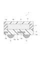
また、図2の(a)に示すように、金属製のキャリア20a上に粘着層20bを設けて仮固定材20を準備する。粘着層20bとしては、例えば常温では粘着力を有するものの加熱により粘着力が低下する剥離シートなどが用いられる。キャリア20aは、平面視した際に円板状のウエハ形状であってもよいし、矩形状のパネル形状であってもよい。そして、図2の(b)に示すように、粘着層20bに複数の半導体素子10の第1面10a及び接続端子10cが向くように(つまりフェイスダウン)、仮固定材20の粘着層20b上に複数の半導体素子10を配置する。その後、図2の(c)に示すように、半導体素子10をエポキシ等の封止樹脂(封止材)により封止して封止材層24を形成する。封止材層24を形成する際、半導体素子10の第2面10bが封止材層24から露出するように封止を行う。これにより、複数の半導体素子10の各第1面10aが仮固定材20に向くように仮固定材20上に取り付けられ、且つ、複数の半導体素子10の各第2面10bが封止材層24から露出するように複数の半導体素子10が封止材によって封止されている、仮固定構造体22が形成される。なお、封止材が半導体素子10を覆うように封止させてから、第2面10bが露出するように封止材を研磨して、仮固定構造体22としてもよい。
Further, as shown in FIG. 2(a), a
続いて、仮固定構造体22が形成(準備)されると、図2の(c)及び図2の(d)に示すように、半導体素子10の第2面10bが露出している封止材層24の上に硬化性接着剤層26を形成する。そして、図3の(a)に示すように、硬化性接着剤層26の上にガラス基板等の光透過性を有するキャリア28を貼り付けると共に、熱及び光の少なくとも一方によって硬化性接着剤層26を硬化させて、硬化層26aとする。これにより、複数の半導体素子10及び封止材層24が硬化層26aを介してキャリア28に対して固定される。この際の複数の半導体素子10及び封止材層24と硬化層26aとの接着強度は、例えば4.0MPa以上であってもよく、20MPa以上であってもよく、8.0MPa以下であってもよい。本製造方法では、この後、ダイ再配置体上に取り付けられた半導体素子10を再度個片化するまでキャリア28上で各種の工程を行うため、キャリア28の厚みを例えば0.1mm以上2.0mm以下としている。但し、キャリア28の厚みはこれに限定されない。また、キャリア28は、ガラス基板であることが好ましいが、光透過性を有する透明樹脂基板であってもよい。キャリア28は、円板状のウエハ形状であってもよいし、矩形状のパネル形状であってもよい。
Subsequently, when the
硬化性接着剤層26は、例えば、硬化性接着剤である樹脂組成物をフィルム状にした部材(硬化性樹脂フィルム)から形成することができ、封止材層24に貼り付け、その後硬化することにより、複数の半導体素子10及び封止材層24をキャリア28に固定するための部材である。硬化性接着剤層26を構成する硬化性接着剤は、熱及び光の少なくとも一方によって硬化する接着剤であり、例えば、熱可塑性樹脂、及び、エポキシ硬化剤を含む樹脂組成物である。この硬化性接着剤に含まれる熱可塑性樹脂は、そのガラス転移温度が-40℃以上40℃以下であってもよい。このような硬化性接着剤層26は、硬化後の厚みが例えば1μm以上400μm以上になるように予め構成されていてもよい。また、硬化性接着剤層26を構成する硬化性樹脂フィルムは、25℃においてタック性を有してもよく、より具体的には、25℃の環境下でガラス基板に貼り合わせられる程度のタック性を有していてもよい。硬化性接着剤層26のキャリア28への接着強度は、硬化性接着剤層26を硬化した場合に1MPa以上であり、且つ、硬化性接着剤層26へレーザを照射した場合に5MPa以下となるように構成されていてもよい。
The
硬化性接着剤層26は後述するレーザ剥離工程(図4の(a)を参照)でレーザ照射により加熱される部分であり、その樹脂組成物は、レーザ光を吸収する光吸収剤を含んでいることが好ましい。硬化性接着剤層26が光吸収剤を含む硬化性樹脂フィルムである場合、硬化性接着剤層26は十分に低い光透過性となる。硬化性接着剤層26に含まれる光吸収剤として、エキシマレーザによるレーザ光を吸収して発熱する材料が選定されてもよく、例えば黒色の顔料又は染料などが添加されていてもよい。光吸収剤の具体例としては、カーボンブラック、アルミニウム、ニッケル、酸化チタンが挙げられる。光吸収剤の含有量は、例えば硬化性接着剤層26を構成する硬化性樹脂フィルムが波長351nmの光に対する透過率が20%以下となる範囲内のものとすることができる。具体的には、光吸収剤の含有量が、硬化性接着剤層26の質量を基準として1質量%以上30質量%以下、又は1質量%以上20質量%であってもよい。ここでの透過率は、硬化性接着剤層26に対して一方の主面側から所定の波長を有する光を入射させたときに、入射光の強度に対する透過光の強度の割合を意味する。
The
硬化性接着剤層26を構成する熱可塑性樹脂は、反応性基を有していてもよい。熱可塑性樹脂の反応性基は、例えばエポキシ基であってもよい。熱可塑性樹脂は、(メタ)アクリル共重合体であってもよく、反応性基を有する(メタ)アクリル共重合体であってもよい。本明細書において、「(メタ)アクリル」は、アクリル又はメタクリルを意味する用語として用いられる。他の類似の用語も同様に解釈される。
The thermoplastic resin forming the
(メタ)アクリル共重合体は、(メタ)アクリロイル基を有する(メタ)アクリルモノマーをモノマー単位として含む共重合体である。(メタ)アクリル共重合体が、50℃以上のガラス転移温度を有するホモポリマーを形成する(メタ)アクリルモノマーと、0℃以下のガラス転移温度を有するホモポリマーを形成する(メタ)アクリルモノマーと、エポキシ基を有する(メタ)アクリルモノマーとをモノマー単位として含む共重合体であってもよい。エポキシ基を有する(メタ)アクリルモノマーによって形成されるホモポリマーのガラス転移温度は制限されない。50℃以上のガラス転移温度を有するホモポリマーを形成する(メタ)アクリルモノマー、及び、0℃以下のガラス転移温度を有するホモポリマーを形成する(メタ)アクリルモノマーは、エポキシ基を有しないモノマーであることができる。 A (meth)acrylic copolymer is a copolymer containing a (meth)acrylic monomer having a (meth)acryloyl group as a monomer unit. The (meth)acrylic copolymer comprises a (meth)acrylic monomer forming a homopolymer having a glass transition temperature of 50°C or higher and a (meth)acrylic monomer forming a homopolymer having a glass transition temperature of 0°C or lower. , and a (meth)acrylic monomer having an epoxy group as monomer units. The glass transition temperature of homopolymers formed by (meth)acrylic monomers having epoxy groups is not limited. The (meth)acrylic monomer forming a homopolymer having a glass transition temperature of 50°C or higher and the (meth)acrylic monomer forming a homopolymer having a glass transition temperature of 0°C or lower are monomers having no epoxy group. can be.
硬化性接着剤層26を構成する熱可塑性樹脂の重量平均分子量は、200,000以上1,000,000以下であってもよい。ここでの重量平均分子量は、ゲル浸透クロマトグラフィーによって測定される、標準ポリスチレン換算値であることができる。また、熱可塑性樹脂の含有量は、硬化性接着剤層26を構成するフィルムの質量を基準として、10質量%以上80質量%以下であってもよい。
The weight-average molecular weight of the thermoplastic resin forming the
硬化性接着剤層26を構成する硬化性樹脂フィルムは、反応性基を有する化合物である硬化性樹脂を更に含んでいてもよい。硬化性樹脂は、2以上のエポキシ基を有するエポキシ樹脂であってもよく、その例としては、ビスフェノールA型エポキシ樹脂、ビスフェノールF型エポキシ樹脂、フェノールノボラック型エポキシ樹脂、及びクレゾールノボラック型エポキシ樹脂が挙げられる。硬化性樹脂の分子量は3000以下であってもよい。硬化性樹脂を含む硬化性接着剤層26は、硬化性を有するとともに、適度なタック性を有し易い。硬化性樹脂の含有量は、硬化性接着剤層26を構成する硬化性樹脂フィルムの質量を基準として、1質量%以上50質量%以下であってもよい。
The curable resin film forming the
硬化性接着剤層26は、シリカフィラーを更に含んでいてもよい。シリカフィラーの含有量は、硬化性接着剤層26を構成するフィルムの質量を基準として、1質量%以上60質量%以下、又は5質量%以上60質量%以下であってもよい。
The
硬化性接着剤層26は、熱可塑性樹脂の反応性基、硬化性樹脂の反応性基、又はこれらの両方と反応する硬化剤を更に含んでいてもよい。硬化剤は、例えばフェノール樹脂であってもよい。硬化性接着剤層26が硬化剤を含む場合、硬化剤の反応を促進する硬化促進剤を更に含んでいてもよい。例えば硬化剤がフェノール樹脂である場合、硬化促進剤がイミダゾール化合物であってもよい。
Curable
続いて、キャリア28の貼り付けが終了すると、図3の(b)及び図3の(c)に示すように、複数の半導体素子10が封止されている封止材層24から仮固定材20を取り除く工程を行う。この工程では、仮固定材20の粘着層20bに所定の熱を付与することにより、仮固定材20の剥離除去を行う。この剥離除去により、複数の半導体素子10の第1面10aが封止材層24から露出するようになる。
Subsequently, when the affixing of the
続いて、仮固定材20が除去されると、図3の(d)に示すように、複数の半導体素子10が硬化層26aを介してキャリア28に固定された状態で、キャリア28に固定された複数の半導体素子10の第1面10a上に再配線層30を形成する。なお、図3の(d)は、図3の(c)の構成を上下反転して示している。再配線層30は、上述した半導体装置1の再配線層13に対応する部分であり、ポリイミド等の絶縁層部分30aと、絶縁層部分30a中の銅配線等の配線部分30bとから構成される。再配線層30の形成工程では、絶縁層の形成と配線部分の形成とを所定回数繰り返して、ピッチ変換を行うための配線層を形成する。この製造方法では、半導体素子10及び封止材層24がキャリア28上に安定して配置されている状態で再配線層30を形成しているため、微細な再配線層を構築し易くなっている。
Subsequently, when the
続いて、再配線層が形成されると、図3の(e)に示すように、複数の半導体素子10がキャリア28に固定された状態で、再配線層30を介して複数の半導体素子10の接続端子10cが半田ボール32に接続するように半田ボール32を形成する。この際、半田ボール32のピッチは、半導体素子10の接続端子10cの端子ピッチよりも広くなるように形成されている。この半田ボール32は、上述した半導体装置1における半田ボール14に対応する。
Subsequently, when the rewiring layer is formed, as shown in (e) of FIG. The
続いて、半田ボール32の取り付けが行われると、硬化層26aに対してキャリア28側からレーザ光を照射して、硬化層26aにレーザマーキングを行い、製品名等の必要な情報を書き込むと共に、レーザ光の照射により、図4の(a)に示すように、キャリア28を硬化層26aから除去する。キャリア28の除去に用いるレーザは、例えばUVレーザの一種であるエキシマレーザであり、ガラス基板からなるキャリア28のレーザ光の透過率は99%以上になっている。より具体的には、例えば波長351nmのレーザ光をエキシマレーザから硬化層26aに向かって照射することにより、硬化層26a中の光吸収剤を発熱させ、硬化層26aとキャリア28との間を剥離させる。なお、エキシマレーザから硬化層26aに照射するレーザ光の波長は532nmでもよく、他の波長でもよい。例えば、ここで用いるレーザは、XeFエキシマレーザ(波長351nm)、XeClエキシマレーザ(波長303nm)、KrFエキシマレーザ(波長248nm)、ArFエキシマレーザ(波長193nm)等のエキシマレーザであってもよいし、その他のUVレーザである、YAGレーザ(3倍波)(波長355nm)、YAGレーザ(4倍波)(波長266nm)等であってもよい。以下で使用されるレーザも同様である。
Subsequently, when the
キャリア28を硬化層26aから除去する際、キャリア28を剥離する剥離エネルギーが1kW/cm2以上200kW/cm2以下となるようにレーザ光を照射して、キャリア28を除去してもよい。この場合、低エネルギーでキャリアを除去できることから半導体素子10等への熱ダメージを最小限に抑えることができ、かつレーザ照射後に生じる粉塵を最小限に抑えることができる。また、照射するレーザは低エネルギーであることから、キャリア除去に要する時間の短縮化ができる。When removing the
上記のキャリア除去工程では、レーザ光によるキャリアを剥離する方法を用いたが、キャリアの除去方法はこれに限定されない。例えば、硬化層26aからキャリア28を削り取ってもよいし、又は、所定の溶剤によってキャリア28等を溶解する(溶かす)ようにしてもよい。この除去工程の際に硬化層26aを一緒に除去してもよい。また、この除去工程の後に、硬化層26aの露出面、又は硬化層26aが除去された場合には封止材による封止材層24の露出面を所定の方法でクリーニングしてもよい。これにより最終製品である半導体装置1の表面側をより綺麗なものとすることができる。なお、キャリア28をこのような方法で除去する場合には、キャリア28は光透過性基板でなくてもよく、また、硬化性接着剤層26が光吸収剤を含んでいなくてもよい。
In the above carrier removing step, a method of removing the carrier by laser light is used, but the method of removing the carrier is not limited to this. For example, the
続いて、キャリア28の除去が終了すると、図4の(b)に示すように、硬化層26aの露出面側にダイシングテープ34を貼り付けて、ウエハ形状またはパネル形状のダイ再配置体とする。そして、図4の(c)及び図4の(d)に示すように、ダイ再配置体を所定の箇所Sでダイシングし、半導体素子10を含む各部分をそれぞれ個片化して、各半導体装置1とする。これにより、複数の半導体素子10を再配置したダイ再配置体から、図4の(e)及び図1に示す複数の半導体装置1を得ることができる。なお、個片化する際、硬化層26aを半導体素子10と共に個片化し、これにより、硬化層26aに第2面10bが保護された複数の半導体素子10のそれぞれから半導体装置1が取得される。
Subsequently, when the removal of the
ここで、本実施形態に係る半導体装置1の製造方法による作用効果について、比較例の方法と対比して説明する。図5~図7は、ファンアウト構造を有する半導体装置を製造する方法(フェイスダウン、支持板なし)を順に説明する図である。図5~図7に示す方法及びそれとの対比について説明する。
Here, the effects of the method for manufacturing the
図5の(a)に示すように、比較例の方法では、まず、金属製のキャリア120a上に粘着層120bを設けて、仮固定材120を準備する。粘着層120bとしては、例えば常温では粘着力を有するものの加熱により粘着力が低下する剥離シートなどが用いられる。そして、図5の(b)に示すように、粘着層120bに複数の半導体素子10の第1面10aが向くように(つまりフェイスダウン)、粘着層120b上に複数の半導体素子10を配置する。その後、図5の(c)に示すように、半導体素子10を封止材で封止して封止材層124を形成し、封止が終了すると、粘着層120b等を加熱して半導体素子10から粘着層120bを剥離してキャリア120aを除去する(図5の(d)を参照)。
As shown in FIG. 5A, in the method of the comparative example, first, a
続いて、図5の(e)に示すように、封止材層124において半導体素子10が露出している側の第1面10aの上に再配線層126を形成する。その後、図6の(a)に示すように、再配線層126の上に半田ボール128を形成する。
Subsequently, as shown in FIG. 5E, a
続いて、半田ボール128が形成されると、図6の(b)に示すように、半田ボール128を保護する保護テープ130(BGテープ)を更に貼り付ける。保護テープ130は、例えば、ポリオレフィンから構成されている。そして、図6の(c)に示すように、半田ボール128が保護テープ130で保護された状態で、半導体素子10の第2面10bが露出する封止材層124を研磨して、封止材層124aとする。その後、図6の(d)及び図6の(e)に示すように、BSC膜132aを介してダイシングテープ132bを貼り付けて、その状態で保護テープ130を除去する工程を行う。BSC膜132aは、例えば、エポキシ樹脂から構成されている。なお、BSC膜132aとダイシングテープ132bとしては、一体型テープ132を用いる。そして、保護テープ130の除去が終了すると、図7の(a)に示すように、BSC膜132aにレーザ光によりレーザマーキングを行い、製品名等の必要な情報を書き込む。BSC膜132aは半導体装置の一部を構成する。その後、図7の(b)~図7の(d)に示すように、半導体素子10を含む各部分をダイシングして個片化し、各半導体装置101を得る。
Subsequently, when the
このように比較例の方法では、仮固定材120が耐熱及び耐薬品性がないことから、図5の(c)及び図5の(d)に示すように、半導体素子10を封止材で封止したダイ再配置体から仮固定材120を早い段階で取り外すようにしている。この取り外しの際、封止材層124は逆側の面等がキャリア等によって固定されている訳ではないため、取外しの際の熱又は力により、反り又は歪みが生じてしまうことがある。このような反り等が生じた封止材層124上に再配線層126を形成しようとすると、反り等があることから、微細な配線層を形成しづらいことがある。これに対し、本実施形態に係る方法では、図3の(a)及び図3の(b)に示すように、封止材層24の他方の面をキャリア28によって固定している。このため、本実施形態に係る製造方法によれば、比較例の方法に比べて、仮固定材20を取り外し際の反り又は歪みを低減して、ダイ再配置体の平坦性を高めることができる。その結果、この製造方法によれば、封止材層24上に再配線層30を形成しようとした場合に微細な配線層とすることが可能となる。
As described above, in the method of the comparative example, the
また、比較例の方法では、図5の(d)~図6の(b)に示すように、複数の半導体素子10を配置するダイ再配置体の背面(例えば、封止材層124)がエポキシ樹脂であり露出したままであるため、工程を汚染する可能性がある。また、工程で使用する薬品によりこのエポキシの樹脂成分が溶出する可能性もあり、この場合、再配線層126でのメッキ工程(配線形成)による銅配線等の歩留まりに影響を与える可能性がある。これに対し、本実施形態に係る方法では、図3の(d)及び図3の(e)に示すように、各工程中、キャリア28がダイ再配置体の背面を継続して覆っているため、上述した汚染又は溶出を防止することができる。つまり、本実施形態に係る方法によれば、半導体装置1を製造する工程を清浄度の高い状態に維持することができる。
Further, in the method of the comparative example, as shown in (d) of FIG. 5 to (b) of FIG. Since it is an epoxy resin and remains exposed, it can contaminate the process. In addition, the resin component of this epoxy may be eluted by the chemicals used in the process, and in this case, the yield of copper wiring, etc. in the plating process (wiring formation) in the
また、比較例の方法では、図5の(e)~図6の(c)に示すように、半導体素子10を再配置するダイ再配置体の背面がエポキシ樹脂であり装置環境等を汚染する可能性もあるため、背面がシリコン等であるファンイン(Fan-in)ウエハレベルパッケージ(WLP)の製造に用いられるケース、製造装置、搬送/吸着機構とは別々に装置等を設ける必要がある。これに対し、本実施形態に係る製造方法では、図3の(d)及び図3の(e)に示すように、各工程中、ガラス等からなるキャリア28がダイ再配置体の背面を覆っているため、上述した汚染等を防止することができる。その結果、本実施形態に係る製造方法であれば、ファンインWLPと同じ製造設備等を用いて、FO-WLP等のファンアウト構造の半導体装置を製造することが可能となる。
In addition, in the method of the comparative example, as shown in FIGS. 5(e) to 6(c), the back surface of the die rearrangement body for rearranging the
また、比較例の方法では、図6の(b)及び図6の(c)に示すように、封止材層124を半導体素子10の第2面10bが露出するように研磨する際に半田ボール128を保護するため、保護テープ130を更に用いている。これに対して、本実施形態に係る製造方法では、図2の(b)~図2の(d)に示すように、半導体素子10を封止材によって封止する際に封止材層24を所定の厚みに予めしておき、その上に硬化性接着剤層26を形成している。このため、本実施形態に係る製造方法によれば、比較例の方法に比べて、使用する部材を減らすことができ、また、各部材の取り付け工程及びその除去工程を減らすことができ、半導体装置1を製造するプロセスを簡略化することができる。
In addition, in the method of the comparative example, as shown in FIGS. 6B and 6C, when the
また、比較例の方法では、図6の(d)に示すように、研磨後にダイシングテープ132bとBSC膜132aとが一体となった一体型テープ132を使うことがある。この一体型テープ132は、ノリ残り、ダイシング性及びピックアップ性等が十分でないことが多く、半導体装置1を低背化することが困難になっている。これに対して、本実施形態に係る方法では、図3の(a)に示すように、半導体素子10のキャリア28への固定に用いた硬化性接着剤層26をそのまま半導体装置1に用いているため、かかる一体製品を使用する必要がなく、個別のダイシングテープを用いることができる。このため、低背化に適したダイシングテープを用いて、半導体装置の低背化を図ることができる。
In the method of the comparative example, as shown in FIG. 6D, an
このように、本実施形態に係る製造方法では、比較例の方法に比べて、ファンアウト構造を有する半導体装置1を製造する工程を簡素化することができる。また、半導体素子10を封止した封止材層24の反り又は歪みを抑制して平坦性を向上し、微細な再配線層30を構築することができる。更に、微細な再配線層30を構築できることにより、半導体装置1の低背化を図ることも可能となる。
As described above, in the manufacturing method according to the present embodiment, the steps of manufacturing the
なお、本実施形態に係る製造方法では、硬化した硬化性接着剤層(硬化層26a)と封止材層24との接着強度が4.0MPa以上であってもよい。この場合、硬化層26aと封止材層24との接着強度を強固に保つことができ、パッケージ組立後の剥離を防止し、硬化層26aを半導体装置1の最終製品の一部(保護層12)としてそのまま機能させることができる。この場合において、硬化層26aと封止材層24との接着強度とが8.0MPa以下であってもよい。なお、硬化層26aと封止材層24との接着強度力が20MPa以上であってもよい。この場合、硬化層26aと封止材層24との接着強度をより強固に保ち、パッケージ組立後の剥離を防止し、硬化層26aを半導体装置1の最終製品の一部(保護層12)としてそのまま機能させることができる。
In addition, in the manufacturing method according to the present embodiment, the adhesion strength between the cured curable adhesive layer (cured
また、本実施形態に係る製造方法では、硬化した硬化性接着剤層(硬化層26a)と複数の半導体素子10との接着強度が4.0MPa以上であってもよい。この場合、硬化層26aと複数の半導体素子10(例えばシリコンチップ)との接着強度を強固に保つことができ、パッケージ組立後の剥離を防止し、硬化層26aを半導体装置1の最終製品の一部としてそのまま機能させることができる。
Further, in the manufacturing method according to the present embodiment, the adhesive strength between the cured curable adhesive layer (cured
また、本実施形態に係る製造方法では、硬化した硬化性接着剤層(硬化層26a)が複数の半導体素子10それぞれの第2面10bを保護した状態である半導体装置1を取得してもよい。この場合、製造に用いた硬化層26aを半導体装置1の最終製品の一部(保護層12)としてそのまま機能させることができる。
Further, in the manufacturing method according to the present embodiment, the
以上、本開示の実施形態について詳細に説明してきたが、本開示は上記実施形態に限定されるものではなく、様々な実施形態に適用することができる。例えば、上記実施形態では、半導体素子10を含む半導体装置1の製造方法について説明したが、複数の電子部品を半導体素子10に加えて又はこれに代えて、複数の電子部品を備える半導体装置又は装置の製造方法に本開示を適用してもよい。この場合、図2の(b)に示す取付け工程において、複数の半導体素子10と共に複数の電子部品を仮固定材20に取り付け、図2の(c)に示す工程では、半導体素子10と共に封止材で封止されるようにし、図2の(d)及び図3の(a)に示す工程では、硬化性接着剤層26を硬化して半導体素子10と共に複数の電子部品をキャリア28に固定する。その他の工程は、上述した工程と同様なものとすることができる。このような製造方法によれば、より複雑な半導体装置等を形成することができる。なお、ここでいう電子部品は、例えば、キャバシタ又は抵抗器等の受動素子であってもよく、MEMS等の部品であってもよい。
Although the embodiments of the present disclosure have been described in detail above, the present disclosure is not limited to the above embodiments, and can be applied to various embodiments. For example, in the above-described embodiment, the method for manufacturing the
以下、実施例を挙げて本発明についてさらに具体的に説明する。ただし、本発明はこれら実施例に限定されるものではない。なお、以下の実施例では、上述した実施形態に係る半導体装置の製造方法に用いる硬化性接着剤層26(硬化後の硬化層26a、保護層12)と封止材層24との接着強度、及び、硬化層26aからのガラス基板(キャリア28)の剥離エネルギーについて説明する。なお、硬化層26aと封止材層24との接着強度は、硬化層26aと半導体素子10との接着強度に適用することができる。
EXAMPLES Hereinafter, the present invention will be described more specifically with reference to examples. However, the present invention is not limited to these examples. In the following examples, the adhesive strength between the curable adhesive layer 26 (the cured
硬化性接着剤層の原料として以下を準備した。
[熱可塑性樹脂]
・エポキシ基を有するアクリルポリマー:(ガラス転移温度:12℃)
[エポキシ樹脂]
・ビスフェノールF型液状エポキシ樹脂:YDF-8170C(商品名、日鉄ケミカル&マテリアル株式会社)
・クレゾールノボラック型エポキシ樹脂:N-500P-10(商品名、DIC株式会社)
[硬化剤]
・フェノール樹脂:PSM-4326(商品名、群栄化学工業株式会社)
・フェノール樹脂:MEH-7800M(商品名、明和化成株式会社)
[シリカフィラー]
・SC2050-HLG(商品名、アドマテックス株式会社)
・R972(商品名、日本アエロジル株式会社)
[光吸収剤]
・カーボンブラック:FP-Black(商品名、山陽色素株式会社)
[カップリング剤]
・(3-メルカプトプロピル)トリメトキシシラン:A-189(商品名、モメンティブ社)
・3-ウレイドプロピルトリエトキシシラン:A-1160(商品名、モメンティブ社)
[硬化促進剤]
・1-シアノエチル-2-フェニルイミダゾール:2PZ-CN(商品名、四国化成工業株式会社)The following materials were prepared as raw materials for the curable adhesive layer.
[Thermoplastic resin]
・ Acrylic polymer having an epoxy group: (glass transition temperature: 12 ° C.)
[Epoxy resin]
・Bisphenol F type liquid epoxy resin: YDF-8170C (trade name, Nippon Steel Chemical & Materials Co., Ltd.)
・ Cresol novolac type epoxy resin: N-500P-10 (trade name, DIC Corporation)
[Curing agent]
・Phenolic resin: PSM-4326 (trade name, Gunei Chemical Industry Co., Ltd.)
・ Phenolic resin: MEH-7800M (trade name, Meiwa Kasei Co., Ltd.)
[Silica filler]
・SC2050-HLG (trade name, Admatechs Co., Ltd.)
・R972 (trade name, Japan Aerosil Co., Ltd.)
[Light absorber]
・ Carbon black: FP-Black (trade name, Sanyo Pigment Co., Ltd.)
[Coupling agent]
- (3-Mercaptopropyl)trimethoxysilane: A-189 (trade name, Momentive)
- 3-ureidopropyltriethoxysilane: A-1160 (trade name, Momentive)
[Curing accelerator]
・ 1-Cyanoethyl-2-phenylimidazole: 2PZ-CN (trade name, Shikoku Chemical Industry Co., Ltd.)
続いて、硬化性接着剤層に用いる材料として、以下の表1に示す配合比で各原料を含み、溶剤としてシクロヘキサノンを含む樹脂ワニスを調製した。樹脂ワニスにおける溶剤以外の成分の合計濃度は、ワニスの質量を基準として40質量%であった。 Subsequently, as a material to be used for the curable adhesive layer, a resin varnish containing each raw material in the compounding ratio shown in Table 1 below and containing cyclohexanone as a solvent was prepared. The total concentration of components other than the solvent in the resin varnish was 40% by weight based on the weight of the varnish.

各ワニスを支持フィルムに塗布し、塗膜を乾燥することにより、支持フィルム上に硬化性樹脂フィルムを形成した。硬化性樹脂フィルム上に保護フィルムを載せて、支持フィルム、硬化性樹脂フィルム及び保護フィルムから構成されるフィルムA又はBを得た。硬化性樹脂フィルムは、硬化した際の厚みが20μmとなるようにした。 A curable resin film was formed on the support film by applying each varnish to the support film and drying the coating film. A protective film was placed on the curable resin film to obtain a film A or B composed of a support film, a curable resin film and a protective film. The curable resin film was made to have a thickness of 20 μm when cured.
[封止材との密着性評価]
ブレードダイサ(製品名、DAD3360、DISCO社製)を用いて12inchサイズのガラス基板(厚さ700μm)を9mm×9mmサイズに切り出した。フィルムA又はフィルムBから保護フィルムを剥がして、露出した硬化性樹脂フィルムを、9mm×9mmサイズのガラス基板の上にフィルムA又はBを載せて、硬化性樹脂フィルムとガラス基板とを真空ラミネータ(製品名、V-130、ニッコーマテリアルズ社製)を用いて貼り付けた。真空ラミネータの条件は、上プラテン温度90℃、下プラテン温度40℃、圧力0.5MPa、加圧時間60秒とした。[Evaluation of adhesion with sealing material]
Using a blade dicer (product name: DAD3360, manufactured by DISCO), a 12-inch size glass substrate (thickness: 700 μm) was cut into 9 mm×9 mm size. The protective film is peeled off from film A or film B, the exposed curable resin film is placed on a glass substrate of 9 mm × 9 mm size, film A or B is placed, and the curable resin film and glass substrate are vacuum laminator ( (Product name: V-130, manufactured by Nikko Materials Co., Ltd.). The conditions of the vacuum laminator were an upper platen temperature of 90° C., a lower platen temperature of 40° C., a pressure of 0.5 MPa, and a pressing time of 60 seconds.
続いて、貼り付けが終了すると、大気オーブン(製品名、PHH-202、エスペック社製)もしくは窒素オーブン(製品名、CLH―21CD、光洋サーモ社製)を用いて各条件で硬化性樹脂フィルムを硬化させた。硬化した硬化性樹脂フィルムである保護層上に封止材(製品名、CEL―400ZHF40、昭和電工マテリアルズ社製)とモールド装置(製品名、ADM-12、メイホー社製)を用いて、保護層上に封止体(封止材層)を形成した。封止体と保護層との接着面積は10mm2であった。モールド装置の条件は封止温度130℃、キュア時間600秒とした。オーブンを用いて形成した封止体を175℃4時間加熱し、さらに封止体を硬化した。これによりガラス基板、保護層、封止体で構成する評価用積層体を得た。Subsequently, when the attachment is completed, a curable resin film is formed under each condition using an atmospheric oven (product name, PHH-202, manufactured by ESPEC CORPORATION) or a nitrogen oven (product name, CLH-21CD, manufactured by Koyo Thermo Co., Ltd.). Hardened. A sealing material (product name, CEL-400ZHF40, manufactured by Showa Denko Materials Co., Ltd.) and a molding device (product name, ADM-12, manufactured by Meiho Co., Ltd.) are used on the protective layer, which is a cured curable resin film, to protect. A sealing body (sealing material layer) was formed on the layer. The adhesion area between the sealing body and the protective layer was 10 mm 2 . The conditions of the molding apparatus were a sealing temperature of 130° C. and a curing time of 600 seconds. The sealed body formed using an oven was heated at 175° C. for 4 hours to further cure the sealed body. Thus, a laminate for evaluation composed of a glass substrate, a protective layer, and a sealing body was obtained.
次に、ボンドテスタ(製品名、System650、ROYCE instruments社製)を用いて、ガラス基板の主面に対して平行にせん断治具を走査し、形成した封止体をはじき出すことで得られるせん断応力を封止体と保護層の接着強度として測定した。封止体と保護層との接着面積は10mm2、せん断治具の操作速度は50μm/s、クリアランスはガラス基板上に形成された保護層を基準にして100μmに設定した。各実施例の保護層硬化条件における接着強度の結果を表2及び表3に示す。下記の表2及び表3に示す封止体との接着強度は、実施例毎に10回試験を行った平均値を示す。また、接着強度の測定時の温度は室温(25℃)であった。なお、本明細書における接着強度は、上記の方法によって測定されたものである。Next, using a bond tester (product name: System650, manufactured by ROYCE Instruments), the shearing jig was scanned parallel to the main surface of the glass substrate, and the shearing stress obtained by ejecting the formed sealing body was measured. It was measured as the adhesive strength between the sealing body and the protective layer. The bonding area between the sealing body and the protective layer was set to 10 mm 2 , the operating speed of the shearing jig was set to 50 μm/s, and the clearance was set to 100 μm based on the protective layer formed on the glass substrate. Tables 2 and 3 show the adhesive strength results under the protective layer curing conditions of each example. The adhesion strength to the sealing body shown in Tables 2 and 3 below is an average value obtained by conducting 10 tests for each example. Moreover, the temperature at the time of measuring the adhesive strength was room temperature (25° C.). In addition, the adhesive strength in this specification is measured by the above method.


上記の表2及び表3に示すように、保護層の硬化条件を所定の範囲とすることにより、保護層となる硬化層を封止材層に対して4.0MPa以上で接着できることが確認できた。また、同様に、保護層となる硬化層を封止材層に対して20MPa以上で接着できることが確認できた。 As shown in Tables 2 and 3 above, it can be confirmed that by setting the curing conditions of the protective layer within a predetermined range, the cured layer that becomes the protective layer can be adhered to the sealing material layer at 4.0 MPa or more. rice field. Similarly, it was confirmed that the cured layer, which becomes the protective layer, can be adhered to the sealing material layer at 20 MPa or more.
[レーザ剥離試験]
次に、上述した実施例1~8の試験と同様のフィルムA及びフィルムBを準備し、フィルムA又はフィルムBから保護フィルムを剥がして露出した硬化性樹脂フィルムをガラス基板(60mm×60mm、厚さ700μm)に載せて硬化性樹脂フィルムとガラス基板との真空ラミネータ(製品名、V-130、ニッコーマテリアルズ社製)によって貼り合わせた。真空ラミネータの条件は上プラテン温度90℃、下プラテン温度40℃、圧力0.5MPa、加圧時間60秒とした。オーブンを用いて130℃で20分間の加熱とそれに続く170℃で2時間の加熱により硬化性樹脂フィルムを硬化させた。硬化した硬化性樹脂フィルムである保護層上に、エポキシ樹脂を含む封止材とモールド装置(製品名、CPM1080、TOWA社製)を用いて、150℃で300秒の条件で封止材層を形成した。形成された封止材層を150℃で6時間の加熱により更に硬化させた。これにより、ガラス基板、保護層及び封止材層から構成される3層構造の評価用積層体を得た。[Laser peeling test]
Next, film A and film B were prepared in the same manner as in the tests of Examples 1 to 8 described above, and the curable resin film exposed by peeling off the protective film from film A or film B was applied to a glass substrate (60 mm × 60 mm, thickness 700 μm), and the curable resin film and the glass substrate were laminated together by a vacuum laminator (product name: V-130, manufactured by Nikko Materials Co., Ltd.). The conditions of the vacuum laminator were an upper platen temperature of 90° C., a lower platen temperature of 40° C., a pressure of 0.5 MPa, and a pressing time of 60 seconds. Using an oven, the curable resin film was cured by heating at 130° C. for 20 minutes followed by heating at 170° C. for 2 hours. A sealing material layer was formed on the protective layer, which is a cured curable resin film, at 150° C. for 300 seconds using a sealing material containing an epoxy resin and a molding device (product name: CPM1080, manufactured by TOWA). formed. The formed encapsulant layer was further cured by heating at 150° C. for 6 hours. As a result, a laminate for evaluation having a three-layer structure composed of the glass substrate, the protective layer, and the sealing material layer was obtained.
評価用積層体に対して、ガラス基板に対して垂直となる方向に波長355nmのUVレーザ光を照射し、ガラス基板の剥離を行った。照射後、保護層付き封止材層とガラス基板が容易に剥離できたものをA、カッターで切り込みを入れることで剥離できたものをBとして、表4及び表5に各UVレーザ光照射条件における剥離結果を示した。なお、レーザ光を照射したことにより、保護層と封止材層との接着強度の低下はなかった。 A UV laser beam with a wavelength of 355 nm was applied to the laminate for evaluation in a direction perpendicular to the glass substrate to separate the glass substrate. After irradiation, the case where the sealing material layer with the protective layer and the glass substrate could be easily peeled off was designated as A, and the case where the glass substrate could be peeled off by cutting with a cutter was designated as B, and Tables 4 and 5 show each UV laser light irradiation condition. showed the peeling results in Note that the irradiation with the laser light did not reduce the adhesive strength between the protective layer and the sealing material layer.


上記の表4及び表5に示すように、キャリアとなるガラス基板を保護層付き封止材層から剥離する際の剥離エネルギーを1kW/cm2以上200kW/cm2以下に収めて、剥離することができることが確認できた。As shown in Tables 4 and 5 above, when the glass substrate serving as a carrier is peeled from the sealing material layer with a protective layer, the peeling energy is kept within 1 kW/cm 2 or more and 200 kW/cm 2 or less. It was confirmed that
1…半導体装置、10…半導体素子、10a…第1面、10b…第2面、10c…接続端子、20…仮固定材、22…仮固定構造体、24…封止材層、26…硬化性接着剤層、26a…硬化層、28…キャリア、30…再配線層、32…半田ボール、34…ダイシングテープ。
DESCRIPTION OF
Claims (26)
前記複数の半導体素子の前記各第2面上に硬化性接着剤層を形成する工程と、
前記硬化性接着剤層の一方の面であって前記複数の半導体素子とは逆側の面にキャリアを貼り合わせる工程と、
前記硬化性接着剤層を硬化して、前記複数の半導体素子を当該硬化した硬化性接着剤層を介して前記キャリアに対して固定する工程と、
前記仮固定材を除去する工程と、を備え、
硬化した前記硬化性接着剤層と前記封止材との接着強度が4.0MPa以上である、半導体装置の製造方法。 A step of preparing a temporary fixing structure in which a plurality of semiconductor elements each having a first surface on which connection terminals are formed and a second surface on the opposite side of the first surface are attached to a temporary fixing material, , in the temporary fixing structure, the first surfaces of the plurality of semiconductor elements are mounted on the temporary fixing material so as to face the temporary fixing material, and the second surfaces of the plurality of semiconductor elements are mounted on the temporary fixing material wherein the plurality of semiconductor elements are encapsulated by an encapsulant such that is exposed from the encapsulant layer;
forming a curable adhesive layer on each of the second surfaces of the plurality of semiconductor elements;
a step of bonding a carrier to one surface of the curable adhesive layer, the surface being opposite to the plurality of semiconductor elements;
curing the curable adhesive layer to fix the plurality of semiconductor elements to the carrier via the cured curable adhesive layer;
and a step of removing the temporary fixing material,
A method for manufacturing a semiconductor device, wherein the adhesive strength between the cured curable adhesive layer and the sealing material is 4.0 MPa or more.
請求項1に記載の半導体装置の製造方法。 The adhesive strength between the cured curable adhesive layer and the plurality of semiconductor elements is 4.0 MPa or more,
2. The method of manufacturing a semiconductor device according to claim 1.
前記複数の半導体素子の前記各第2面上に硬化性接着剤層を形成する工程と、
前記硬化性接着剤層の一方の面であって前記複数の半導体素子とは逆側の面にキャリアを貼り合わせる工程と、
前記硬化性接着剤層を硬化して、前記複数の半導体素子を当該硬化した硬化性接着剤層を介して前記キャリアに対して固定する工程と、
前記仮固定材を除去する工程と、を備え、
硬化した前記硬化性接着剤層と前記複数の半導体素子との接着強度が4.0MPa以上である、半導体装置の製造方法。 A step of preparing a temporary fixing structure in which a plurality of semiconductor elements each having a first surface on which connection terminals are formed and a second surface on the opposite side of the first surface are attached to a temporary fixing material, , in the temporary fixing structure, the first surfaces of the plurality of semiconductor elements are mounted on the temporary fixing material so as to face the temporary fixing material, and the second surfaces of the plurality of semiconductor elements are mounted on the temporary fixing material wherein the plurality of semiconductor elements are encapsulated by an encapsulant such that is exposed from the encapsulant layer;
forming a curable adhesive layer on each of the second surfaces of the plurality of semiconductor elements;
a step of bonding a carrier to one surface of the curable adhesive layer, the surface being opposite to the plurality of semiconductor elements;
curing the curable adhesive layer to fix the plurality of semiconductor elements to the carrier via the cured curable adhesive layer;
and a step of removing the temporary fixing material,
A method for manufacturing a semiconductor device, wherein the adhesive strength between the cured curable adhesive layer and the plurality of semiconductor elements is 4.0 MPa or more.
前記硬化性接着剤層の前記ガラス基板への接着強度は、前記硬化性接着剤層を硬化した場合に1MPa以上であり、且つ、前記硬化性接着剤層へレーザを照射した場合に5MPa以下となる、
請求項1~3の何れか一項に記載の半導体装置の製造方法。 The carrier is a glass substrate,
The adhesive strength of the curable adhesive layer to the glass substrate is 1 MPa or more when the curable adhesive layer is cured, and 5 MPa or less when the curable adhesive layer is irradiated with a laser. Become,
4. The method of manufacturing a semiconductor device according to claim 1.
請求項1~4の何れか一項に記載の半導体装置の製造方法。 The curable adhesive layer is formed from a resin composition containing a thermoplastic resin and an epoxy curing agent, and the thermoplastic resin has a glass transition temperature of −40° C. or higher and 40° C. or lower.
5. The method of manufacturing a semiconductor device according to claim 1.
請求項1~5の何れか一項に記載の半導体装置の製造方法。 The thickness of the curable adhesive layer is 1 μm or more and 400 μm or less after curing.
6. The method of manufacturing a semiconductor device according to claim 1.
請求項1~6の何れか一項に記載の半導体装置の製造方法。 The carrier is a glass substrate or a transparent resin substrate and has a thickness of 0.1 mm or more and 2.0 mm or less.
7. The method of manufacturing a semiconductor device according to claim 1.
請求項1~7の何れか一項に記載の半導体装置の製造方法。 forming a rewiring layer on the first surface of the plurality of semiconductor elements fixed to the carrier while the plurality of semiconductor elements are fixed to the carrier;
8. The method of manufacturing a semiconductor device according to claim 1.
請求項1~8の何れか一項に記載の半導体装置の製造方法。 further comprising connecting solder balls to the connection terminals of the plurality of semiconductor elements while the plurality of semiconductor elements are fixed to the carrier;
9. The method of manufacturing a semiconductor device according to claim 1.
請求項8に記載の半導体装置の製造方法。9. The method of manufacturing a semiconductor device according to claim 8.
前記キャリアが光透過性基板であり、
前記キャリアを除去する工程では、前記硬化した硬化性接着剤層に対して前記キャリア側からレーザ光を照射して、前記キャリアを除去する、
請求項1~10の何れか一項に記載の半導体装置の製造方法。 further comprising removing the carrier;
the carrier is a light transmissive substrate,
In the step of removing the carrier, the cured curable adhesive layer is irradiated with a laser beam from the carrier side to remove the carrier.
A method for manufacturing a semiconductor device according to any one of claims 1 to 10 .
前記キャリアを除去する工程では、前記キャリアを剥離する剥離エネルギーが1kW/cm2以上200kW/cm2以下となるようにレーザ光を照射して、前記キャリアを除去する、
請求項1~11の何れか一項に記載の半導体装置の製造方法。 further comprising removing the carrier;
In the step of removing the carrier, the carrier is removed by irradiating laser light so that the peeling energy for peeling the carrier is 1 kW/cm 2 or more and 200 kW/cm 2 or less.
A method for manufacturing a semiconductor device according to any one of claims 1 to 11 .
前記キャリアを除去する工程では、前記キャリアを削る又は溶かすことにより、前記キャリアを除去する、
請求項1~10の何れか一項に記載の半導体装置の製造方法。 further comprising removing the carrier;
In the step of removing the carrier, the carrier is removed by scraping or melting the carrier.
A method for manufacturing a semiconductor device according to any one of claims 1 to 10 .
請求項11~13の何れか一項に記載の半導体装置の製造方法。 After removing the carrier, cleaning the exposed surface of either the cured curable adhesive layer or the encapsulant layer with the encapsulant.
14. The method of manufacturing a semiconductor device according to claim 11 .
前記硬化性接着剤層に前記第2面が保護された前記複数の半導体素子のそれぞれから前記半導体装置を取得する、
請求項15に記載の半導体装置の製造方法。 In the singulation step, the cured curable adhesive layer is singulated together with the plurality of semiconductor elements;
obtaining the semiconductor device from each of the plurality of semiconductor elements having the second surface protected by the curable adhesive layer;
16. The method of manufacturing a semiconductor device according to claim 15 .
前記仮固定材を準備する工程と、
前記複数の半導体素子の前記各第1面が前記仮固定材に向くように前記複数の半導体素子を前記仮固定材に取り付ける工程と、
前記仮固定材に取り付けられた前記複数の半導体素子の前記各第2面が前記封止材層から露出するように前記複数の半導体素子を前記封止材にて封止する工程と、
を有する、請求項1~16の何れか一項に記載の半導体装置の製造方法。 The preparing step includes:
preparing the temporary fixing material;
attaching the plurality of semiconductor elements to the temporary fixing member such that the first surfaces of the plurality of semiconductor elements face the temporary fixing member;
sealing the plurality of semiconductor elements with the sealing material so that the second surfaces of the plurality of semiconductor elements attached to the temporary fixing material are exposed from the sealing material layer;
17. The method for manufacturing a semiconductor device according to claim 1, comprising:
前記固定する工程では、前記硬化性接着剤層を硬化して前記複数の電子部品を前記キャリアに固定する、
請求項1~17の何れか一項に記載の半導体装置の製造方法。 In the preparing step, the temporary fixing structure in which a plurality of electronic components are attached to the temporary fixing material together with the plurality of semiconductor elements is prepared;
In the fixing step, the curable adhesive layer is cured to fix the plurality of electronic components to the carrier.
A method for manufacturing a semiconductor device according to any one of claims 1 to 17 .
請求項1~18の何れか一項に記載の半導体装置の製造方法。 The adhesive strength between the cured curable adhesive layer and the sealing material is 8.0 MPa or less.
A method for manufacturing a semiconductor device according to any one of claims 1 to 18 .
請求項1~18の何れか一項に記載の半導体装置の製造方法。 The adhesive strength between the cured curable adhesive layer and the sealing material is 20 MPa or more,
A method for manufacturing a semiconductor device according to any one of claims 1 to 18 .
請求項1~20の何れか一項に記載の半導体装置の製造方法。 obtaining the semiconductor device in which the cured curable adhesive layer protects the second surface of each of the plurality of semiconductor elements;
A method for manufacturing a semiconductor device according to any one of claims 1 to 20 .
前記複数の半導体素子の前記各第2面上に硬化性接着剤層を形成する工程と、
前記硬化性接着剤層の一方の面であって前記複数の半導体素子とは逆側の面にキャリアを貼り合わせる工程と、
前記硬化性接着剤層を硬化して、前記複数の半導体素子を当該硬化した硬化性接着剤層を介して前記キャリアに対して固定する工程と、
前記仮固定材を除去する工程と、を備え、
前記キャリアがガラス基板であり、
前記硬化性接着剤層の前記ガラス基板への接着強度は、前記硬化性接着剤層を硬化した場合に1MPa以上であり、且つ、前記硬化性接着剤層へレーザを照射した場合に5MPa以下となる、半導体装置の製造方法。 A step of preparing a temporary fixing structure in which a plurality of semiconductor elements each having a first surface on which connection terminals are formed and a second surface on the opposite side of the first surface are attached to a temporary fixing material, , in the temporary fixing structure, the first surfaces of the plurality of semiconductor elements are mounted on the temporary fixing material so as to face the temporary fixing material, and the second surfaces of the plurality of semiconductor elements are mounted on the temporary fixing material wherein the plurality of semiconductor elements are encapsulated by an encapsulant such that is exposed from the encapsulant layer;
forming a curable adhesive layer on each of the second surfaces of the plurality of semiconductor elements;
a step of bonding a carrier to one surface of the curable adhesive layer, the surface being opposite to the plurality of semiconductor elements;
curing the curable adhesive layer to fix the plurality of semiconductor elements to the carrier via the cured curable adhesive layer;
and a step of removing the temporary fixing material,
The carrier is a glass substrate,
The adhesive strength of the curable adhesive layer to the glass substrate is 1 MPa or more when the curable adhesive layer is cured, and 5 MPa or less when the curable adhesive layer is irradiated with a laser. A method for manufacturing a semiconductor device.
前記複数の半導体素子の前記各第2面上に硬化性接着剤層を形成する工程と、
前記硬化性接着剤層の一方の面であって前記複数の半導体素子とは逆側の面にキャリアを貼り合わせる工程と、
前記硬化性接着剤層を硬化して、前記複数の半導体素子を当該硬化した硬化性接着剤層を介して前記キャリアに対して固定する工程と、
前記仮固定材を除去する工程と、を備え、
前記キャリアは、ガラス基板又は透明樹脂基板であり、その厚さが0.1mm以上2.0mm以下である、半導体装置の製造方法。 A step of preparing a temporary fixing structure in which a plurality of semiconductor elements each having a first surface on which connection terminals are formed and a second surface on the opposite side of the first surface are attached to a temporary fixing material, , in the temporary fixing structure, the first surfaces of the plurality of semiconductor elements are mounted on the temporary fixing material so as to face the temporary fixing material, and the second surfaces of the plurality of semiconductor elements are mounted on the temporary fixing material wherein the plurality of semiconductor elements are encapsulated by an encapsulant such that is exposed from the encapsulant layer;
forming a curable adhesive layer on each of the second surfaces of the plurality of semiconductor elements;
a step of bonding a carrier to one surface of the curable adhesive layer, the surface being opposite to the plurality of semiconductor elements;
curing the curable adhesive layer to fix the plurality of semiconductor elements to the carrier via the cured curable adhesive layer;
and a step of removing the temporary fixing material,
A method of manufacturing a semiconductor device, wherein the carrier is a glass substrate or a transparent resin substrate and has a thickness of 0.1 mm or more and 2.0 mm or less.
前記複数の半導体素子の前記各第2面上に硬化性接着剤層を形成する工程と、
前記硬化性接着剤層の一方の面であって前記複数の半導体素子とは逆側の面にキャリアを貼り合わせる工程と、
前記硬化性接着剤層を硬化して、前記複数の半導体素子を当該硬化した硬化性接着剤層を介して前記キャリアに対して固定する工程と、
前記仮固定材を除去する工程と、
前記キャリアを除去する工程と、を備え、
前記キャリアが光透過性基板であり、
前記キャリアを除去する工程では、前記硬化した硬化性接着剤層に対して前記キャリア側からレーザ光を照射して、前記キャリアを除去する、半導体装置の製造方法。 A step of preparing a temporary fixing structure in which a plurality of semiconductor elements each having a first surface on which connection terminals are formed and a second surface on the opposite side of the first surface are attached to a temporary fixing material, , in the temporary fixing structure, the first surfaces of the plurality of semiconductor elements are mounted on the temporary fixing material so as to face the temporary fixing material, and the second surfaces of the plurality of semiconductor elements are mounted on the temporary fixing material wherein the plurality of semiconductor elements are encapsulated by an encapsulant such that is exposed from the encapsulant layer;
forming a curable adhesive layer on each of the second surfaces of the plurality of semiconductor elements;
a step of bonding a carrier to one surface of the curable adhesive layer, the surface being opposite to the plurality of semiconductor elements;
curing the curable adhesive layer to fix the plurality of semiconductor elements to the carrier via the cured curable adhesive layer;
removing the temporary fixing material;
and removing the carrier;
the carrier is a light transmissive substrate,
In the step of removing the carrier, the method of manufacturing a semiconductor device includes removing the carrier by irradiating the cured curable adhesive layer with a laser beam from the carrier side.
前記複数の半導体素子の前記各第2面上に硬化性接着剤層を形成する工程と、
前記硬化性接着剤層の一方の面であって前記複数の半導体素子とは逆側の面にキャリアを貼り合わせる工程と、
前記硬化性接着剤層を硬化して、前記複数の半導体素子を当該硬化した硬化性接着剤層を介して前記キャリアに対して固定する工程と、
前記仮固定材を除去する工程と、
前記キャリアを除去する工程と、を備え、
前記キャリアを除去する工程では、前記キャリアを剥離する剥離エネルギーが1kW/cm2以上200kW/cm2以下となるようにレーザ光を照射して、前記キャリアを除去する、半導体装置の製造方法。 A step of preparing a temporary fixing structure in which a plurality of semiconductor elements each having a first surface on which connection terminals are formed and a second surface on the opposite side of the first surface are attached to a temporary fixing material, , in the temporary fixing structure, the first surfaces of the plurality of semiconductor elements are mounted on the temporary fixing material so as to face the temporary fixing material, and the second surfaces of the plurality of semiconductor elements are mounted on the temporary fixing material wherein the plurality of semiconductor elements are encapsulated by an encapsulant such that is exposed from the encapsulant layer;
forming a curable adhesive layer on each of the second surfaces of the plurality of semiconductor elements;
a step of bonding a carrier to one surface of the curable adhesive layer, the surface being opposite to the plurality of semiconductor elements;
curing the curable adhesive layer to fix the plurality of semiconductor elements to the carrier via the cured curable adhesive layer;
removing the temporary fixing material;
and removing the carrier;
In the step of removing the carrier, the carrier is removed by irradiating laser light so that the separation energy for removing the carrier is 1 kW/cm 2 or more and 200 kW/cm 2 or less.
前記複数の半導体素子の前記各第2面上に硬化性接着剤層を形成する工程と、
前記硬化性接着剤層の一方の面であって前記複数の半導体素子とは逆側の面にキャリアを貼り合わせる工程と、
前記硬化性接着剤層を硬化して、前記複数の半導体素子を当該硬化した硬化性接着剤層を介して前記キャリアに対して固定する工程と、
前記仮固定材を除去する工程と、
前記キャリアを除去する工程と、を備え、
前記キャリアを除去する工程では、前記キャリアを削る又は溶かすことにより、前記キャリアを除去する、半導体装置の製造方法。
A step of preparing a temporary fixing structure in which a plurality of semiconductor elements each having a first surface on which connection terminals are formed and a second surface on the opposite side of the first surface are attached to a temporary fixing material, , in the temporary fixing structure, the first surfaces of the plurality of semiconductor elements are mounted on the temporary fixing material so as to face the temporary fixing material, and the second surfaces of the plurality of semiconductor elements are mounted on the temporary fixing material wherein the plurality of semiconductor elements are encapsulated by an encapsulant such that is exposed from the encapsulant layer;
forming a curable adhesive layer on each of the second surfaces of the plurality of semiconductor elements;
a step of bonding a carrier to one surface of the curable adhesive layer, the surface being opposite to the plurality of semiconductor elements;
curing the curable adhesive layer to fix the plurality of semiconductor elements to the carrier via the cured curable adhesive layer;
removing the temporary fixing material;
and removing the carrier;
The method of manufacturing a semiconductor device, wherein in the step of removing the carrier, the carrier is removed by scraping or melting the carrier.
Priority Applications (1)
| Application Number | Priority Date | Filing Date | Title |
|---|---|---|---|
| JP2023016965A JP2023054825A (en) | 2020-12-04 | 2023-02-07 | Method of manufacturing semiconductor device |
Applications Claiming Priority (3)
| Application Number | Priority Date | Filing Date | Title |
|---|---|---|---|
| PCT/JP2020/045338 WO2022118480A1 (en) | 2020-12-04 | 2020-12-04 | Method for manufacturing semiconductor device |
| JPPCT/JP2020/045338 | 2020-12-04 | ||
| PCT/JP2021/044312 WO2022118925A1 (en) | 2020-12-04 | 2021-12-02 | Method for manufacturing semiconductor device |
Related Child Applications (1)
| Application Number | Title | Priority Date | Filing Date |
|---|---|---|---|
| JP2023016965A Division JP2023054825A (en) | 2020-12-04 | 2023-02-07 | Method of manufacturing semiconductor device |
Publications (3)
| Publication Number | Publication Date |
|---|---|
| JPWO2022118925A1 JPWO2022118925A1 (en) | 2022-06-09 |
| JPWO2022118925A5 JPWO2022118925A5 (en) | 2022-11-16 |
| JP7226669B2 true JP7226669B2 (en) | 2023-02-21 |
Family
ID=81853340
Family Applications (2)
| Application Number | Title | Priority Date | Filing Date |
|---|---|---|---|
| JP2022554846A Active JP7226669B2 (en) | 2020-12-04 | 2021-12-02 | Semiconductor device manufacturing method |
| JP2023016965A Pending JP2023054825A (en) | 2020-12-04 | 2023-02-07 | Method of manufacturing semiconductor device |
Family Applications After (1)
| Application Number | Title | Priority Date | Filing Date |
|---|---|---|---|
| JP2023016965A Pending JP2023054825A (en) | 2020-12-04 | 2023-02-07 | Method of manufacturing semiconductor device |
Country Status (4)
| Country | Link |
|---|---|
| US (1) | US20240006222A1 (en) |
| JP (2) | JP7226669B2 (en) |
| TW (1) | TW202230672A (en) |
| WO (2) | WO2022118480A1 (en) |
Citations (3)
| Publication number | Priority date | Publication date | Assignee | Title |
|---|---|---|---|---|
| JP2013168594A (en) | 2012-02-17 | 2013-08-29 | Fujitsu Ltd | Semiconductor device manufacturing method and electronic apparatus manufacturing method |
| JP2017152617A (en) | 2016-02-26 | 2017-08-31 | 京セラ株式会社 | Electronic component and method of manufacturing the same |
| JP2018009138A (en) | 2016-07-05 | 2018-01-18 | 日立化成株式会社 | Resin composition for temporarily fixing, resin film for temporarily fixing and resin film sheet for temporarily fixing |
Family Cites Families (2)
| Publication number | Priority date | Publication date | Assignee | Title |
|---|---|---|---|---|
| JP2019033124A (en) * | 2017-08-04 | 2019-02-28 | リンテック株式会社 | Manufacturing method of semiconductor device, and adhesion laminate |
| JP2019129179A (en) * | 2018-01-22 | 2019-08-01 | 日立化成株式会社 | Method for manufacturing semiconductor device |
-
2020
- 2020-12-04 WO PCT/JP2020/045338 patent/WO2022118480A1/en active Application Filing
-
2021
- 2021-12-02 US US18/255,383 patent/US20240006222A1/en active Pending
- 2021-12-02 WO PCT/JP2021/044312 patent/WO2022118925A1/en active Application Filing
- 2021-12-02 JP JP2022554846A patent/JP7226669B2/en active Active
- 2021-12-03 TW TW110145173A patent/TW202230672A/en unknown
-
2023
- 2023-02-07 JP JP2023016965A patent/JP2023054825A/en active Pending
Patent Citations (3)
| Publication number | Priority date | Publication date | Assignee | Title |
|---|---|---|---|---|
| JP2013168594A (en) | 2012-02-17 | 2013-08-29 | Fujitsu Ltd | Semiconductor device manufacturing method and electronic apparatus manufacturing method |
| JP2017152617A (en) | 2016-02-26 | 2017-08-31 | 京セラ株式会社 | Electronic component and method of manufacturing the same |
| JP2018009138A (en) | 2016-07-05 | 2018-01-18 | 日立化成株式会社 | Resin composition for temporarily fixing, resin film for temporarily fixing and resin film sheet for temporarily fixing |
Also Published As
| Publication number | Publication date |
|---|---|
| US20240006222A1 (en) | 2024-01-04 |
| WO2022118925A1 (en) | 2022-06-09 |
| JPWO2022118925A1 (en) | 2022-06-09 |
| TW202230672A (en) | 2022-08-01 |
| JP2023054825A (en) | 2023-04-14 |
| WO2022118480A1 (en) | 2022-06-09 |
Similar Documents
| Publication | Publication Date | Title |
|---|---|---|
| CN101752272B (en) | Method of manufacturing semiconductor device | |
| KR20100066384A (en) | Method of manufacturing semiconductor device in which bottom surface and side surface of semiconductor substrate are covered with resin protective film | |
| TWI773341B (en) | Manufacturing method of semiconductor device | |
| JP7226669B2 (en) | Semiconductor device manufacturing method | |
| JP7226664B2 (en) | Semiconductor device manufacturing method | |
| JP7243934B2 (en) | Semiconductor device manufacturing method | |
| KR20220002256A (en) | A semiconductor device having a dolmen structure, a method for manufacturing the same, and a laminated film for forming a support piece and a method for manufacturing the same | |
| WO2020217397A1 (en) | Method for producing semiconductor device having dolmen structure, method for producing supporting pieces, and multilayer film | |
| KR20220002255A (en) | A semiconductor device having a dolmen structure, a method for manufacturing the same, and a laminated film for forming a support piece and a method for manufacturing the same | |
| WO2022118969A1 (en) | Curable resin film, film material for semiconductor device production, curable resin composition for semiconductor device production, and method for producing semiconductor device | |
| WO2020218524A1 (en) | Semiconductor device having dolmen structure and method for manufacturing same, and laminated film for forming support piece and method for manufacturing same | |
| WO2020218532A1 (en) | Method for producing semiconductor device having dolmen structure and method for producing supporting pieces | |
| WO2020217395A1 (en) | Semiconductor device having dolmen structure and method for manufacturing same, method for manufacturing support piece, and laminate film for support piece formation | |
| JP2024050073A (en) | Laminated film for forming individualized bodies, method for producing same, rolled body, and laminate | |
| CN113574663A (en) | Semiconductor device with stone tomb structure and manufacturing method thereof | |
| JP2016131228A (en) | Method of manufacturing solid-state image pickup device and glass wafer |
Legal Events
| Date | Code | Title | Description |
|---|---|---|---|
| A521 | Request for written amendment filed |
Free format text: JAPANESE INTERMEDIATE CODE: A523 Effective date: 20220912 |
|
| A621 | Written request for application examination |
Free format text: JAPANESE INTERMEDIATE CODE: A621 Effective date: 20220912 |
|
| A871 | Explanation of circumstances concerning accelerated examination |
Free format text: JAPANESE INTERMEDIATE CODE: A871 Effective date: 20220912 |
|
| A131 | Notification of reasons for refusal |
Free format text: JAPANESE INTERMEDIATE CODE: A131 Effective date: 20221018 |
|
| A521 | Request for written amendment filed |
Free format text: JAPANESE INTERMEDIATE CODE: A523 Effective date: 20221201 |
|
| TRDD | Decision of grant or rejection written | ||
| A01 | Written decision to grant a patent or to grant a registration (utility model) |
Free format text: JAPANESE INTERMEDIATE CODE: A01 Effective date: 20230110 |
|
| A61 | First payment of annual fees (during grant procedure) |
Free format text: JAPANESE INTERMEDIATE CODE: A61 Effective date: 20230123 |
|
| R151 | Written notification of patent or utility model registration |
Ref document number: 7226669 Country of ref document: JP Free format text: JAPANESE INTERMEDIATE CODE: R151 |
|
| S531 | Written request for registration of change of domicile |
Free format text: JAPANESE INTERMEDIATE CODE: R313531 |
|
| R350 | Written notification of registration of transfer |
Free format text: JAPANESE INTERMEDIATE CODE: R350 |