JP7220196B2 - Device for detecting medium level - Google Patents
Device for detecting medium level Download PDFInfo
- Publication number
- JP7220196B2 JP7220196B2 JP2020502317A JP2020502317A JP7220196B2 JP 7220196 B2 JP7220196 B2 JP 7220196B2 JP 2020502317 A JP2020502317 A JP 2020502317A JP 2020502317 A JP2020502317 A JP 2020502317A JP 7220196 B2 JP7220196 B2 JP 7220196B2
- Authority
- JP
- Japan
- Prior art keywords
- layer
- electrodes
- electrically insulating
- pcb
- circuit support
- Prior art date
- Legal status (The legal status is an assumption and is not a legal conclusion. Google has not performed a legal analysis and makes no representation as to the accuracy of the status listed.)
- Active
Links
Images


Classifications
-
- G—PHYSICS
- G01—MEASURING; TESTING
- G01F—MEASURING VOLUME, VOLUME FLOW, MASS FLOW OR LIQUID LEVEL; METERING BY VOLUME
- G01F23/00—Indicating or measuring liquid level or level of fluent solid material, e.g. indicating in terms of volume or indicating by means of an alarm
- G01F23/22—Indicating or measuring liquid level or level of fluent solid material, e.g. indicating in terms of volume or indicating by means of an alarm by measuring physical variables, other than linear dimensions, pressure or weight, dependent on the level to be measured, e.g. by difference of heat transfer of steam or water
- G01F23/26—Indicating or measuring liquid level or level of fluent solid material, e.g. indicating in terms of volume or indicating by means of an alarm by measuring physical variables, other than linear dimensions, pressure or weight, dependent on the level to be measured, e.g. by difference of heat transfer of steam or water by measuring variations of capacity or inductance of capacitors or inductors arising from the presence of liquid or fluent solid material in the electric or electromagnetic fields
- G01F23/263—Indicating or measuring liquid level or level of fluent solid material, e.g. indicating in terms of volume or indicating by means of an alarm by measuring physical variables, other than linear dimensions, pressure or weight, dependent on the level to be measured, e.g. by difference of heat transfer of steam or water by measuring variations of capacity or inductance of capacitors or inductors arising from the presence of liquid or fluent solid material in the electric or electromagnetic fields by measuring variations in capacitance of capacitors
- G01F23/266—Indicating or measuring liquid level or level of fluent solid material, e.g. indicating in terms of volume or indicating by means of an alarm by measuring physical variables, other than linear dimensions, pressure or weight, dependent on the level to be measured, e.g. by difference of heat transfer of steam or water by measuring variations of capacity or inductance of capacitors or inductors arising from the presence of liquid or fluent solid material in the electric or electromagnetic fields by measuring variations in capacitance of capacitors measuring circuits therefor
-
- G—PHYSICS
- G01—MEASURING; TESTING
- G01F—MEASURING VOLUME, VOLUME FLOW, MASS FLOW OR LIQUID LEVEL; METERING BY VOLUME
- G01F23/00—Indicating or measuring liquid level or level of fluent solid material, e.g. indicating in terms of volume or indicating by means of an alarm
- G01F23/22—Indicating or measuring liquid level or level of fluent solid material, e.g. indicating in terms of volume or indicating by means of an alarm by measuring physical variables, other than linear dimensions, pressure or weight, dependent on the level to be measured, e.g. by difference of heat transfer of steam or water
- G01F23/26—Indicating or measuring liquid level or level of fluent solid material, e.g. indicating in terms of volume or indicating by means of an alarm by measuring physical variables, other than linear dimensions, pressure or weight, dependent on the level to be measured, e.g. by difference of heat transfer of steam or water by measuring variations of capacity or inductance of capacitors or inductors arising from the presence of liquid or fluent solid material in the electric or electromagnetic fields
- G01F23/263—Indicating or measuring liquid level or level of fluent solid material, e.g. indicating in terms of volume or indicating by means of an alarm by measuring physical variables, other than linear dimensions, pressure or weight, dependent on the level to be measured, e.g. by difference of heat transfer of steam or water by measuring variations of capacity or inductance of capacitors or inductors arising from the presence of liquid or fluent solid material in the electric or electromagnetic fields by measuring variations in capacitance of capacitors
- G01F23/265—Indicating or measuring liquid level or level of fluent solid material, e.g. indicating in terms of volume or indicating by means of an alarm by measuring physical variables, other than linear dimensions, pressure or weight, dependent on the level to be measured, e.g. by difference of heat transfer of steam or water by measuring variations of capacity or inductance of capacitors or inductors arising from the presence of liquid or fluent solid material in the electric or electromagnetic fields by measuring variations in capacitance of capacitors for discrete levels
-
- G—PHYSICS
- G01—MEASURING; TESTING
- G01F—MEASURING VOLUME, VOLUME FLOW, MASS FLOW OR LIQUID LEVEL; METERING BY VOLUME
- G01F23/00—Indicating or measuring liquid level or level of fluent solid material, e.g. indicating in terms of volume or indicating by means of an alarm
- G01F23/22—Indicating or measuring liquid level or level of fluent solid material, e.g. indicating in terms of volume or indicating by means of an alarm by measuring physical variables, other than linear dimensions, pressure or weight, dependent on the level to be measured, e.g. by difference of heat transfer of steam or water
- G01F23/26—Indicating or measuring liquid level or level of fluent solid material, e.g. indicating in terms of volume or indicating by means of an alarm by measuring physical variables, other than linear dimensions, pressure or weight, dependent on the level to be measured, e.g. by difference of heat transfer of steam or water by measuring variations of capacity or inductance of capacitors or inductors arising from the presence of liquid or fluent solid material in the electric or electromagnetic fields
- G01F23/263—Indicating or measuring liquid level or level of fluent solid material, e.g. indicating in terms of volume or indicating by means of an alarm by measuring physical variables, other than linear dimensions, pressure or weight, dependent on the level to be measured, e.g. by difference of heat transfer of steam or water by measuring variations of capacity or inductance of capacitors or inductors arising from the presence of liquid or fluent solid material in the electric or electromagnetic fields by measuring variations in capacitance of capacitors
- G01F23/268—Indicating or measuring liquid level or level of fluent solid material, e.g. indicating in terms of volume or indicating by means of an alarm by measuring physical variables, other than linear dimensions, pressure or weight, dependent on the level to be measured, e.g. by difference of heat transfer of steam or water by measuring variations of capacity or inductance of capacitors or inductors arising from the presence of liquid or fluent solid material in the electric or electromagnetic fields by measuring variations in capacitance of capacitors mounting arrangements of probes
-
- H—ELECTRICITY
- H05—ELECTRIC TECHNIQUES NOT OTHERWISE PROVIDED FOR
- H05K—PRINTED CIRCUITS; CASINGS OR CONSTRUCTIONAL DETAILS OF ELECTRIC APPARATUS; MANUFACTURE OF ASSEMBLAGES OF ELECTRICAL COMPONENTS
- H05K1/00—Printed circuits
- H05K1/16—Printed circuits incorporating printed electric components, e.g. printed resistor, capacitor, inductor
- H05K1/162—Printed circuits incorporating printed electric components, e.g. printed resistor, capacitor, inductor incorporating printed capacitors
-
- H—ELECTRICITY
- H05—ELECTRIC TECHNIQUES NOT OTHERWISE PROVIDED FOR
- H05K—PRINTED CIRCUITS; CASINGS OR CONSTRUCTIONAL DETAILS OF ELECTRIC APPARATUS; MANUFACTURE OF ASSEMBLAGES OF ELECTRICAL COMPONENTS
- H05K3/00—Apparatus or processes for manufacturing printed circuits
- H05K3/22—Secondary treatment of printed circuits
- H05K3/28—Applying non-metallic protective coatings
-
- H—ELECTRICITY
- H05—ELECTRIC TECHNIQUES NOT OTHERWISE PROVIDED FOR
- H05K—PRINTED CIRCUITS; CASINGS OR CONSTRUCTIONAL DETAILS OF ELECTRIC APPARATUS; MANUFACTURE OF ASSEMBLAGES OF ELECTRICAL COMPONENTS
- H05K2201/00—Indexing scheme relating to printed circuits covered by H05K1/00
- H05K2201/10—Details of components or other objects attached to or integrated in a printed circuit board
- H05K2201/10007—Types of components
- H05K2201/10151—Sensor
-
- H—ELECTRICITY
- H05—ELECTRIC TECHNIQUES NOT OTHERWISE PROVIDED FOR
- H05K—PRINTED CIRCUITS; CASINGS OR CONSTRUCTIONAL DETAILS OF ELECTRIC APPARATUS; MANUFACTURE OF ASSEMBLAGES OF ELECTRICAL COMPONENTS
- H05K2203/00—Indexing scheme relating to apparatus or processes for manufacturing printed circuits covered by H05K3/00
- H05K2203/13—Moulding and encapsulation; Deposition techniques; Protective layers
- H05K2203/1305—Moulding and encapsulation
- H05K2203/1322—Encapsulation comprising more than one layer
-
- H—ELECTRICITY
- H05—ELECTRIC TECHNIQUES NOT OTHERWISE PROVIDED FOR
- H05K—PRINTED CIRCUITS; CASINGS OR CONSTRUCTIONAL DETAILS OF ELECTRIC APPARATUS; MANUFACTURE OF ASSEMBLAGES OF ELECTRICAL COMPONENTS
- H05K2203/00—Indexing scheme relating to apparatus or processes for manufacturing printed circuits covered by H05K3/00
- H05K2203/13—Moulding and encapsulation; Deposition techniques; Protective layers
- H05K2203/1305—Moulding and encapsulation
- H05K2203/1327—Moulding over PCB locally or completely
Description
本発明は、液体、流動性物質、粉末状物質、またはバルク状態の物質などの一般的な媒体のレベルを検出するためのセンサ装置に関する。本発明は、特に、車両に使用されるレベルセンサ、好ましくは、容量タイプのレベルセンサに関して開発された。 The present invention relates to a sensor device for detecting the level of media in general, such as liquids, flowable substances, powdered substances or substances in bulk. The invention has been developed especially for level sensors used in vehicles, preferably capacitive type level sensors.
言及されたタイプのレベルセンサ装置は、例えば、本出願人の名前で出願された国際出願公開第2015/181770号から知られている。第1の実施形態によれば、国際出願公開第2015/181770号に開示される装置は、回路支持体またはPCB(プリント回路基板)が部分的に収容される検出対象の液体に浸漬される中空ケーシングを有する。回路支持体は、互いに実質的に同じであり、レベル検出軸に沿って互いに離れて支持体上に配置された金属電極によって表される容量性検出素子のアレイを担持する。中空のケーシングは、熱可塑性材料の成形によって得られる別個のコンポーネントとして構成され、その後、検出電極を担持する回路支持体の対応する部分がその中に挿入される。次に、ケーシングの空洞内に、ポリウレタン樹脂またはゲル、好ましくは、シリコーンゲルなどの非導電性の流体充填材料が導入される。 A level sensor device of the type mentioned is known, for example, from WO 2015/181770 filed in the name of the applicant. According to a first embodiment, the device disclosed in WO2015/181770 comprises a hollow body immersed in the liquid to be detected in which a circuit support or PCB (printed circuit board) is partially housed. have a casing. The circuit support carries an array of capacitive sensing elements substantially identical to each other and represented by metal electrodes spaced on the support along the level sensing axis. The hollow casing is constructed as a separate component obtained by molding a thermoplastic material, after which the corresponding portion of the circuit support carrying the sensing electrodes is inserted therein. A non-conductive fluid fill material such as a polyurethane resin or gel, preferably silicone gel, is then introduced into the casing cavity.
前述の流体充填材料の存在は、主に、空洞内、特に、回路支持体間の接触領域の粗さによって決定されるマイクロキャビティおよび/または対応する電極、およびレベル測定に悪影響を与える可能性のあるケーシング内のギャップおよびエアポケットの存在を防止することを目的とする(これらの概念は、引用文献の図14および図15に示されている詳細によっても明確にされており、支持体および/または電極がケーシングと接触しており、前述の流体充填材料は絶縁層を形成しない)。 The presence of the aforementioned fluid-filled material is mainly due to the possibility of adversely affecting the microcavities and/or corresponding electrodes within the cavities, and in particular the roughness of the contact areas between the circuit supports, and the level measurement. The aim is to prevent the presence of gaps and air pockets within certain casings (these concepts are also clarified by the details shown in Figures 14 and 15 of the cited document, which support and/or or the electrodes are in contact with the casing and the aforementioned fluid-filled material does not form an insulating layer).
装置の上記の実施形態は、製造プロセスが、中空ケーシングの事前の配置、ならびに中空ケーシングへの回路支持体の挿入のためのある特定の操作、およびケーシングの空洞への流体充填材料の導入のためのある特定の操作を必然的に想定しなければならないという結果をもたらす(さらに、明らかに、ケーシング本体と充填材料の供給と移動の管理)。 The above-described embodiments of the apparatus demonstrate that the manufacturing process may include prepositioning of the hollow casing, as well as certain operations for the insertion of the circuit support into the hollow casing, and the introduction of the fluid fill material into the cavities of the casing. (and, obviously, the control of the supply and movement of the casing body and filling material).
第2の実施形態によれば、国際出願公開第2015/181770号は、回路支持体上のプラスチック材料の直接オーバーモールドによって形成された外側コーティングによる前述の中空ケーシングの交換を想定している。このタイプの解決策は、レベルセンサ装置全体の生産を簡素化するが、検出電極の周囲に湿度が存在すると、やがて検出精度の低下を意味する。 According to a second embodiment, WO2015/181770 envisages replacement of the aforementioned hollow casing by an outer coating formed by direct overmolding of plastic material on the circuit support. This type of solution simplifies the production of the overall level sensor device, but the presence of humidity around the sensing electrodes means that over time the sensing accuracy will decrease.
実際、本出願人は、装置の使用後、外側コーティングのオーバーモールドされたプラスチック材料は、検出される液体との実質的に一定の接触のために、湿気を吸収する傾向があることに気付いた。時間の経過とともに悪影響が現れるこの湿度は、装置の耐用年数の間にすでに検出の不正確さにつながる。同じ問題は、国際出願公開第2015/181770号の前述の第1の実施形態に従って構築された装置にも存在する。その中空ケースは、対応するハウジング空洞で区切られた壁に回路支持体を押し付けるように構成されているため、電極は、壁と厳密に接触し、壁自体が時間内に湿気を吸収しやすくなる。 Indeed, applicants have noticed that after use of the device, the overmolded plastic material of the outer coating tends to absorb moisture due to the substantially constant contact with the liquid to be detected. . This humidity, which becomes detrimental over time, leads to detection inaccuracies already during the service life of the device. The same problem exists in a device constructed according to the aforementioned first embodiment of WO2015/181770. Its hollow case is configured to press the circuit support against the wall delimited by the corresponding housing cavity, so that the electrodes are in close contact with the wall, and the wall itself tends to absorb moisture in time. .
容量性測定の感度は、液体が検出電極の表面に置かれた場合に最大になり、液体と電極の表面の間の距離が直線的に増加するにつれて(実質的に指数関数的に)減少する。しかしながら、液体の代わりに、一般に水蒸気または湿度が存在する場合、同じ動作が発生する。言い換えれば、中空ケーシングまたはオーバーモールドされたコーティングの材料、したがって、前述の材料と接触する電極上の湿度の存在は、液体の存在を“エミュレート”する効果があり、それにより、レベル検出精度がある程度損なわれる。 The sensitivity of capacitive measurements is maximized when liquid is placed on the surface of the sensing electrode and decreases (essentially exponentially) as the distance between the liquid and the electrode surface increases linearly. . However, the same behavior occurs when water vapor or humidity is generally present instead of liquid. In other words, the presence of humidity on the material of the hollow casing or overmolded coating, and thus on the electrodes in contact with said material, has the effect of "emulating" the presence of liquid, thereby increasing the level detection accuracy. damaged to some extent.
良好なバリア特性と耐湿性の良好な特性を有するプラスチック材料を使用して、オーバーモールドコーティングを形成することができる。しかしながら、このタイプの材料は、一般に、高価であり、オーバーモールドコーティングを形成するために処理するのは困難である(装置の検出部分は、一般に、かなり長く、特定のポリマを使用したオーバーモールドの操作が困難になる)。 Plastic materials with good barrier properties and good moisture resistance properties can be used to form the overmold coating. However, this type of material is generally expensive and difficult to process to form an overmold coating (the sensing portion of the device is generally quite long and overmolded using certain polymers). difficult to operate).
本出願人はさらに、良好なバリア特性および耐湿性の良好な特性を示す特定のポリマは、モールド操作後および/または膨張および熱衝撃のためにかなりの収縮および/または寸法変形を示すという欠点があることを発見した。これは、そのようなポリマが直接オーバーモールドされる回路支持体(すなわち、対応する電気パス、および/または電極、および/または電子コンポーネント)に障害を引き起こす可能性がある。いずれにせよ、これらの材料は、検出中の液体と長時間接触すると、必然的に長期的に湿度を吸収する。 Applicants have further found that certain polymers exhibiting good barrier properties and moisture resistance suffer from the drawback of exhibiting considerable shrinkage and/or dimensional deformation after molding operations and/or due to expansion and thermal shock. I discovered something. This can cause damage to circuit supports (ie, corresponding electrical paths and/or electrodes and/or electronic components) on which such polymers are directly overmolded. In any event, these materials will inevitably absorb moisture over time upon prolonged contact with the liquid being detected.
他方、他のタイプのプラスチック材料(例えば、特定の熱可塑性ポリマ)を使用して、オーバーモールドされたコーティングを得ることができ、これはより安価で、より容易にモールド可能である。ただし、これらの材料は、一般に、耐湿性の特性が低いため、装置によるレベル検出の精度が急速に低下する。 On the other hand, other types of plastic materials (eg, certain thermoplastic polymers) can be used to obtain overmolded coatings, which are cheaper and more easily moldable. However, these materials generally have poor moisture resistance properties, which rapidly reduces the accuracy of level detection by the device.
上述したことを考慮して、本発明の目的は、同様の用途向けに設計された既知の装置と比較して、単純で経済的に有利な方法で構築されるが、長期にわたって、検出の精度、感度、および信頼性が向上することを特徴とする容量性レベルセンサ装置を提供することである。本発明によれば、添付の特許請求の範囲に特定された特徴を有するレベルセンサ装置によって、上記およびその他の目的がさらに明確になり、これらの目的は、さらに達成される。請求項は、本発明に関連して本明細書で提供される技術的教示の不可欠な部分を形成する。 In view of the above, it is an object of the present invention to be constructed in a simple and economically advantageous manner compared to known devices designed for similar applications, but over the long term to improve the accuracy of detection. The object of the present invention is to provide a capacitive level sensor device characterized by improved , sensitivity and reliability. These and other objects are further defined and further achieved according to the present invention by a level sensor device having the features specified in the appended claims. The claims form an integral part of the technical teaching provided herein in relation to the invention.
本発明のさらなる目的、特徴、および利点は、添付の図面を参照して、以下の説明から明らかになり、これらは、非限定的な例として純粋に提供される。 Further objects, features and advantages of the present invention will become apparent from the following description, with reference to the accompanying drawings, which are given purely as non-limiting examples.
本説明の枠組みにおける“一実施形態”、“一実施形態”、または“様々な実施形態”などへの言及は、実施形態に関して説明された少なくとも1つの詳細、構成、構造、または特性が少なくとも1つの実施形態に含まれことを示すことを意図している。したがって、本説明の様々なポイントに存在し得る“一実施形態において”、“一実施形態において”、“様々な実施形態において”などの句は、必ずしも同一の実施形態を指すものではないが、代わりに、異なる実施形態を参照してもよい。さらに、この説明で定義された特定の立体構造、構造、または特性は、表されたものとは異なる1つまたは複数の実施形態で任意の適切な方法で組み合わせることができる。特に、図面の例を参照して、本明細書で使用される参照番号と空間参照(“上”、“下”、“上”、“下”、“前”、“後ろ”、“縦”など)は、単に便宜のために提供されているため、保護範囲または実施形態の範囲を定義しない。本説明および添付の特許請求の範囲において、一般的な用語“材料”は、多くの異なる材料の混合物、組成物、または組み合わせも含むと理解されるべきである。図では、同じ参照番号を使用して、互いに類似または技術的に同等の要素を示している。 References to “one embodiment,” “one embodiment,” or “various embodiments,” or the like in the framework of this description mean that at least one detail, configuration, structure, or characteristic described with respect to the embodiments are intended to be included in one embodiment. Thus, the phrases "in one embodiment," "in one embodiment," "in various embodiments," and the like, which may appear at various points in this description, do not necessarily refer to the same embodiment; Alternatively, reference may be made to different embodiments. Moreover, the specific conformations, structures, or properties defined in this description can be combined in any suitable manner in one or more embodiments different than those depicted. Reference numbers and spatial references used herein (“top”, “bottom”, “top”, “bottom”, “front”, “back”, “longitudinal”), particularly with reference to the examples of the drawings etc.) are provided merely for convenience and do not define the scope of protection or embodiments. In this description and the appended claims, the general term "materials" should be understood to also include mixtures, compositions or combinations of many different materials. In the figures, the same reference numbers are used to indicate elements that are similar or technically equivalent to each other.
図1では、全体が1で示されているのは、一般的な物質の一般的な容器、特に、自動車のタンクである。容器は、例えば、液体、例えば、燃料、または水、または添加物を入れるタンクであってもよい。様々な実施形態において、容器1(以下、簡単にするため“タンク”とも定義される)は、内燃機関のシステムの動作に必要な水、または内燃機関の排気ガスの処理のためのシステムの動作に必要な添加剤または還元剤を含むように設計される。タンク1が提供するこのようなシステムは、2で示される。処理システム2は、例えば、タンク1が水を収容するADI(水アルコール噴射)システムであってもよく、そうでなければ、タンク1がAdBlue(登録商標)という名前で商業的に知られているような、水溶液中の尿素の溶液を収容するSCR(選択的触媒還元)システムであってもよい。どちらの場合も、タンク1が低温(0℃より低い温度を示す)に曝されると、液体が凍結しやすくなる。この理由から、タンク1は、ヒータ装置を備えていてもよい。しかしながら、容器1は、他の目的のために、および/または自動車のものとは異なるセクタで使用でき、異なる物質を収容するように設計できる。
In FIG. 1, indicated generally at 1 is a common container for a common substance, in particular a tank of a motor vehicle. The container may be, for example, a tank containing a liquid, such as fuel, or water, or an additive. In various embodiments, the container 1 (hereinafter also defined as "tank" for simplicity) is water required for the operation of the system of the internal combustion engine, or for the operation of the system for the treatment of the exhaust gases of the internal combustion engine. designed to contain the necessary additives or reducing agents for Such a system provided by
タンク1の本体1aは、任意の材料、特に、含まれる物質に対して化学的に耐性があり、好ましくは、電気的に絶縁する材料、例えば、高密度ポリエチレン(HDPE)など既知の技術による適切なプラスチック材料で作られてもよい。タンク1には、例えば、凍結の場合に、タンク自体および/またはその内容物を加熱するために使用される、それ自体既知のタイプのヒータが関連付けられている可能性がある。電気ヒータは、EHで指定されたブロックによって図に概略的に表されている。様々な実施形態において、そのようなヒータの1つは、本発明によるセンサ装置に関連付けられるか、または組み込まれる。
The body 1a of the
図示された概略的な例では、タンク1は、上部3、例えば、その上部壁を有し、開口部3aが液体物質の補充のために提供される。タンク1の下部4、例えば、その底壁は、システム2に液体を供給するために、例えば、ポンプを介して溶液が出入りするか、または引き出される出口開口部5を有する。また、下部4において、タンク1は、6で示される第2の開口部を有し、この開口部において、本発明の様々な可能な実施形態に係るセンサ装置の本体が密封固定される。実際、様々な好ましい実施形態では、本発明に係るセンサ装置は、容器内のこの物質のレベルが非常に低い場合でも、その本体の外面が少なくとも部分的に液体物質と接触するように、一般的な容器の下部に設置される。
In the schematic example shown, the
全体が10で示されるセンサ装置は、特に、好ましくは、実質的に垂直であるレベル検出軸Xに従って、タンク1の内部に少なくとも部分的に延びるように設計されたレベル検出部11を備える(ただし、必要に応じて、垂直に対して傾斜させることができる)。優先的に、検出部11の近位端領域は、タンク内の非常に低いレベルの液体の存在を検出できるように、底壁4に比較的近い高さでタンク1の内部に延びる。タンク1の開口部6に直接取り付けられるのではなく、本発明に係る装置10は、タンクの異なる開口部に密閉してあるさらなる本体またはコンポーネント、例えば、おそらく、タンク1の内側に延び、タンク1内に存在する液体の一部を収容できる第2の容器の壁を得るように成形されたヒータおよびポンプのうちの少なくとも1つを備えるコンポーネント、セクタでUDM(尿素供給モジュール)として知られるタイプのコンポーネントまたはモジュール、または車両の移動中の液体レベルの突然の変動を防ぐように設計されたコンポーネントを形成するか、関連付けられるか、または一体化され得ることに留意されたい。
The sensor device, generally designated 10, comprises in particular a
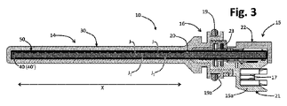
図2および図3では、可能な実施形態に係る装置10が、部分的に切断された斜視図および縦断面図を介して分離して示されている。装置10は、少なくとも1つの検出部14を備えるケーシング本体を有し、検出部14は、電気絶縁性で液密であり、装置10の検出部11に広く属する(図1)。
In Figures 2 and 3, the
様々な実施形態において、装置のケーシング本体は、
-外部システム、例えば、図1のシステム2に属する制御ユニットへの装置10の電気的接続のための接続および/または制御部15(以下、“接続部”と簡単に呼ぶ)と、
-取り付け部16であって、例えば、図1のタンクの開口部6など、異なる装置上での装置10の密封結合および/または位置決めのために構成されている、取り付け部16と、を備える。
In various embodiments, the casing body of the device comprises:
- a connection and/or control unit 15 (hereinafter briefly referred to as "connection") for the electrical connection of the
- a mounting
様々な実施形態において、接続および/または制御部15は、図3で部分的に見える電気端子のそれぞれの部分である概ね中空のコネクタ本体15aを備え、これらは、17で示される。様々な実施形態において、例えば、金属ストラップからのスタンピングまたは打ち抜きにより得られる端子17は、コネクタ本体15aとともに、例えば、システム2の前述の制御ユニットへの装置10の外部接続のためのインターフェースを形成する。好ましくは、各端子17は、コネクタ本体15aの空洞内に配置されるように設計された接触部、好ましくは、薄層部と、例えば、以下に説明する回路支持体または基板上に存在するそれぞれの接触要素との電気的および機械的結合のために設計された、好ましくは、狭い相互接続部とを有する。
In various embodiments, the connection and/or
様々な実施形態において、取り付け部16は、検出部14と接続および/または制御部15との間で軸方向に延び、その外周面に、Oリングガスケットなどの環状シール要素用の少なくとも1つの台座19aを有する。これは、例えば、装置が取り付けられているタンク1に対して、装置10の弾性取り付けの機能を実行する可能性がある。
In various embodiments, the mounting
様々な実施形態、特に、本発明によるセンサ装置が異なる機能コンポーネント(例えば、UMDモジュールまたはADIモジュールなど)と結合するように統合または設計されている実施形態では、検出部14は、そのような機能コンポーネントのハウジング本体に属し得ることに留意されたい。一方、接続部15および/または取り付け部16は省略され得るか、または少なくとも部分的に前述の機能コンポーネントのハウジング本体によって画定され得る。
In various embodiments, particularly those in which the sensor device according to the present invention is integrated or designed to be combined with different functional components (e.g., UMD modules or ADI modules, etc.), the
図2および図3には、20で全体が示されている回路支持体またはPCB(プリント回路基板)も部分的に見える。これは、少なくとも装置のケーシング本体の検出部14に、好ましくは、取り付け部16および接続および/または制御部15にも延びている。
Also partially visible in FIGS. 2 and 3 is a circuit carrier or PCB (printed circuit board) generally indicated at 20 . It extends at least to the
これらの図では、21、22、および23で示されている3つの本体部は、PCB20の近位端部分を介在させて結合されている。
In these figures, three body portions, indicated at 21, 22, and 23, are joined with a proximal end portion of
図3の例では、部分21および22は、ケーシング本体の接続部分15を少なくとも部分的に形成し、部分21は、コネクタ本体15aを優先的に画定し、電気端子17を一体化する。再び図3に示される例を参照すると、同じ部分21は、部分23およびオーバーモールドされたコーティング(30)の部分とともに、取り付け部分16の少なくとも一部を形成する。装置10のケーシング本体の部分15および16は、例えば、上記のオーバーモールドされたコーティングと同じ材料および/またはコーティングの一体部分として作られた部分21、22、23および/または部分15および16の少なくともいくつかで、他の何らかの方法で形成することもできる。それにより、検出部に関して記載された本発明の特徴をおそらく備える。
In the example of FIG. 3,
検出部14、および好ましくは必須ではないが、取り付け部16の少なくとも一部は、第1の電気絶縁材料で作られたオーバーモールドされた外側コーティング30を備え/備える。この外側コーティング30、すなわち、それを形成する材料は、装置10のケーシング本体の外面を画定し、これは、検出される必要がある媒体または物質と接触するように設計されている。
The sensing
PCB20には、必要な電気接続要素(リード線または電気経路など)、および/またはレベル検出に必要な電気および/または電子コンポーネントの少なくとも一部が提供される。PCB20は、プリント回路の製造に適した電気絶縁材料で作られた耐荷重構造または支持構造を有する。様々な実施形態において、PCB20は、ガラス繊維、すなわち、酸化ケイ素を含む少なくとも1つの複合材料、好ましくは、ガラス繊維が含まれるエポキシ樹脂のマトリックスを有する複合材料を使用して形成され、ガラス繊維は樹脂を含浸させた一種の不織布を形成するように配置される。この意味で好ましい材料は、例えば、FR4、ベトロナイト、およびGRP(ガラス強化プラスチック)などの同様の電気絶縁複合材料である。一方、以下に見られるように、本発明の範囲から除外されないのは、必ずしも複合材料ではない、セラミックまたはポリマベースの材料、および/またはシリコンまたはその誘導体または化合物を含む材料など、PCB20の支持構造を得るための他の材料の使用である。
The
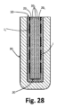
PCB20は、レベル検出軸Xに沿って2つの端部の間を長手方向に延び、それらの間にPCB厚さT(図4にのみ示される)を定義する2つの対向する主側面(図8のみで20aによって示される)と、それらの間にPCB幅W(図4にのみ示される)を定義する2つの対向する長手方向の縁部(図8のみで20bによって示される)を含む概ね平坦な形状を有する。
The
図8に分離して示されているPCB20では、装置10の検出部11に属し、PCB自体の遠位端と第2の領域25とを含む検出領域24を識別することが可能である。以下では、単純化のために、“制御および/または接続領域”としても定義され、PCBの近位端を含む。2つの領域24と25との間には、図8の26で示されるような中間領域、特に装置10のケーシング本体の取り付け部16に対応する位置にあるように設計された中間領域もおそらく提供され得る。
In the
PCB20の領域25には、装置10の電気および電子処理および/または制御コンポーネントの少なくとも一部を関連付けることができ、それに関連するのは、装置10の外部電気接続用の端子17(図3)である。代わりに、PCB20の領域24に広く関連しているのは、レベル検出コンポーネントである。より詳細には、領域24に関連するのは、少なくとも1つの第1の容量素子アレイであり、これは、PCBの主側面(例えば、考慮される実施形態によれば、これ以降、層203または201によって識別される主側面)に対応する位置に少なくとも1つの第1のシリーズの第1の電極を備える。電極に関して使用され、本説明の続編および添付の特許請求の範囲にも存在する“主側面に対応する位置”または“主側面に”などの句は、言及された電極が前述の側面の外側、すなわち、その外側面に配置されることを必ずしも意味しないことに留意されたい。様々な好ましい実施形態では、それ自体自律的に発明性があるPCB20は、いわゆる、多層タイプのPCB、すなわち、例えば、互いに積層された電気絶縁材料の複数の層を含む多層支持構造を有する回路支持体であり、前述の電極は、構造の電気絶縁材料の2つの層の間に配置されている。
従来の多層PCBでは、1つまたは複数の中間層で定義されているのは、対応する導電パスであり、場合によっては、電気回路配置の他のアクティブおよび/またはパッシブコンポーネントもある。これらは、その後、多層構造内に“囲まれ”、ある層に存在するパスおよび/または回路コンポーネントは、いわゆる金属化された“ビア”または穴を介して別の層に存在するパスおよび/または回路コンポーネントに電気的に接続される可能性がある。 In a conventional multilayer PCB, defined in one or more intermediate layers are corresponding conductive paths and possibly other active and/or passive components of an electrical circuit arrangement. These are then "enclosed" in a multi-layer structure such that paths and/or circuit components present in one layer are routed and/or circuit components present in another layer through so-called metallized "vias" or holes. It may be electrically connected to a circuit component.
本明細書で提案する本発明の解決策によれば、レベルセンサ装置で使用されるのは、容量性レベル検出、すなわち、PCB20の多層構造の少なくとも1つの層が前述の第1の電極と外側コーティングのオーバーモールドされた材料との間に設定されるような方法で、使用される少なくとも1つの第1の電極アレイを内部に統合する多層PCB20である。そのような場合は、図2~図3に例示されており、前述の第1の検出電極の一部は、文字“J”で示されている(図8では、PCB20の外層203で覆われている限りこれらの電極は見えない)。表現されていない変形例によれば、多層回路支持体または内部電極を備えたPCBに関して説明されたさまざまな構成は、他の方法でも取得でき、必ずしも複数の層を備えた支持体を想定していない、例えば、複数の電極を想定して成形された金属ストラップなどの導電性パスは、電極およびその他の回路要素の支持構造を提供する電気絶縁性ポリマでオーバーモールドされる(導電性パス、金属化された穴またはビア、電気および/または電子コンポーネントなど)。分かるように、いずれの場合でも、他の実施形態によれば、PCB20は、好ましくは、多層タイプであり、および/またはその検出電極は、その側面の少なくとも1つ、好ましくは、その主側面の少なくとも1つの外側に配置され得る。
According to the inventive solution proposed here, the level sensor device uses capacitive level detection, i.e. at least one layer of the multi-layer structure of the
様々な実施形態において、前述の第1のアレイの電極Jは、互いに実質的に同じであり、レベル検出軸Xに沿って所定の、好ましくは、均一な方法で互いに離れて設定される。しかしながら、可能な実施形態(図示せず)によれば、容量性素子の1つの同じアレイは、いくつかの異なるシリーズの電極も含むことができ、1つのシリーズの電極は、同じアレイの別のシリーズの電極の形状とは異なる形状を有する。他の実施形態では、電極は、レベル検出軸Xの方向に細長い形状を有することができる。 In various embodiments, the electrodes J of said first array are substantially identical to each other and are set apart from each other along the level detection axis X in a predetermined, preferably uniform manner. However, according to a possible embodiment (not shown), one and the same array of capacitive elements can also include several different series of electrodes, one series of electrodes being connected to another of the same array. It has a shape different from that of the series electrodes. In other embodiments, the electrodes can have elongated shapes in the direction of the level detection axis X. FIG.
様々な好ましい実施形態において、センサ10は、PCB20の検出領域24上に第2の容量性素子の第2のアレイも備え、そのような第2のアレイは、好ましくは、互いに実質的に同じである少なくとも1つの第2のシリーズの第2の電極を備え、同一平面上にあり、レベル検出軸Xに沿って互いに間隔を空けて配置され、PCB20の第2の主側面に対応する位置に配置されている。この特性は、例えば、図3から理解することができ、前述の第2の電極のいくつかは、J1によって示される。
In various preferred embodiments,
本発明は、以下に示される場合、すなわち、電極JおよびJ1の2つのアレイを含むPCBを参照して説明される。しかしながら、非表示の実施形態によれば、PCBは、その側面のいずれか1つに対応する位置に単一の電極アレイを含むことができる。 The invention will be described with reference to a PCB containing two arrays of electrodes J and J1 in the cases indicated below. However, according to non-viewing embodiments, the PCB can include a single electrode array at a location corresponding to any one of its sides.
図3に示される例では、第1の電極Jおよび第2の電極J1は、PCB20の2つの対向する主側面を基準として、実質的に鏡面または相互に整列した位置(すなわち、互い違いでない位置)にある。しかしながら、本明細書に示されていない他の実施形態では、第2の電極J1は、レベル検出軸Xを基準として、第1の電極Jに対して互い違いの位置にある。この種の変形例は、装置10のレベルの測定分解能を高めることを可能にする。この目的のために、電極J1は、電極Jに対して中間位置に延在することが好ましく、逆もまた同様であり、電極J1は、電極Jによって検出可能なレベルの中間のレベルを検出することができる。
In the example shown in FIG. 3 , the first electrode J and the second electrode J 1 are substantially mirrored or in mutually aligned positions (i.e., non-staggered positions) with respect to two opposite major sides of the
様々な実施形態において、電極JおよびJ1は、図8に概略的に示されるMCによって示されたコントローラのそれぞれの入力に個別に接続され、制御回路に属し、例えば、PCB20の領域25に配置される。しかしながら、多数の電極Jおよび/またはJ1を互いに並列に接続して、前述のコントローラの1つの同じ入力に接続する場合も除外されない。好ましくは、電極JおよびJ1は、互いに同じ幾何学的形状を有するか、または異なる形状を有するが、同じ表面寸法を有するか、一般に、同じ電気容量を有する。電極Jおよび/またはJ1は、PCB20またはレベル検出軸Xを横断する方向に優先的に延びる。
In various embodiments, electrodes J and J1 are individually connected to respective inputs of a controller indicated by MC schematically shown in FIG. be done. However, it is not excluded that multiple electrodes J and/or J1 are connected in parallel with each other and connected to the same input of one of the aforementioned controllers. Preferably, the electrodes J and J1 have the same geometry as each other or have different shapes, but have the same surface dimensions or generally the same capacitance. Electrodes J and/or J1 preferentially extend in a direction transverse to the
電極JおよびJ1は、導電性材料、例えば、金属材料または金属合金で作られている。電極JおよびJ1は、好ましくは、対応するアレイ内で互いに対して同一平面上にあり、例えば、PCB20の支持構造内に沈められたまたは適用されたプレートまたは薄層の形態であってもよく、あるいは、例えば、シルクスクリーン印刷技術などを使用して、PCB20の支持構造上に堆積された導電層によって構成されてもよい。様々な実施形態において、PCB20またはその層の少なくとも1つは、電極JおよびJ1を一緒に、および/または対応する導電接続パスに、および/またはPCB20に存在する可能性のある他の電気および/または電子コンポーネントに電気接続するための、導電性材料を含むビアまたはスルーホールを有する。
Electrodes J and J1 are made of an electrically conductive material, for example a metallic material or a metallic alloy. Electrodes J and J1 are preferably coplanar with respect to each other in corresponding arrays and may be, for example, in the form of plates or laminations submerged or applied within the support structure of
PCB20の領域25は、好ましくは、PCB自体の近位端と、対応するアレイの第1の電極JまたはJ1との間に備えられる(したがって、この観点では、接続および/または制御領域25は、図8の26で示される中間領域に対応する領域も含み得る)。しかしながら、本発明の範囲には、装置10の回路配置に属する電気および/または電子制御および/または処理コンポーネントがPCB20全体に沿って、またはその検出領域24内、すなわち、電極Jおよび/またはJ1の近く、および/または電極Jおよび/またはJ1の間に配置される場合も含まれる。この観点では、接続および/または制御領域25は、PCB20の長さの実質的に全体にわたって延びていてもよく、その一部は検出領域24と共通である。前述したように、特に、例示されたタイプの、すなわち、多層構造を有するPCB20の場合、前述の電気および/または電子制御および/または処理コンポーネントの少なくともいくつかも多層構造の電気絶縁材料の2つの層の間に配置することができる。
A
既に述べたように、様々な実施形態において、装置10を装備する測定回路配置に属する構成要素は、少なくとも1つの制御ユニットまたはコントローラMC(例えば、マイクロコントローラ、マイクロプロセッサ、CPU、DSP-デジタル信号プロセッサ、メモリ、集積回路、演算回路、A/D変換回路、電子スイッチング回路から選択される、または少なくとも1つを備える)、さらにアクティブおよび/またはパッシブコンポーネント(トランジスタ、MOSFET、抵抗、コンデンサ、ダイオードなど)を含む。
As already mentioned, in various embodiments the components belonging to the measuring circuit arrangement equipping the
様々な実施形態において、コントローラMCは、電極JおよびJ1が個別に接続される複数の入力を有するか、または互いに平行な多数の電極Jおよび/またはJ1がコントローラMCの同一の入力に接続される。コントローラMCは、好ましくは、少なくとも1つの処理論理ユニット、メモリ、および入力/出力を備え、そのうち入力は、アナログ/デジタルタイプである。コントローラMCは、例えば、Microchip Technology Inc.によって製造されたコードPIC16F1517によって識別されるマイクロプロセッサ、またはCypress Semiconductor Corporationによって製造されたシリーズCY8C4200Mのコードによって識別されるマイクロプロセッサであってもよい。しかしながら、容量タイプの電極Jおよび/またはJ1によって装置10によって実施される特定のレベル検出モダリティは、例えば、本出願人の名前で出願された国際出願公開第2015/181770号、国際出願公開第2016/042456号、および国際出願公開第2016/042459号の文献の教示に従って、当該分野で知られている任意のタイプであってもよい。
In various embodiments, the controller MC has multiple inputs to which the electrodes J and J1 are individually connected, or multiple electrodes J and/or J1 parallel to each other are connected to the same input of the controller MC. be done. The controller MC preferably comprises at least one processing logic unit, a memory and inputs/outputs, of which the inputs are of analog/digital type. The controller MC is manufactured by Microchip Technology Inc., for example. or the microprocessor identified by the code Series CY8C4200M manufactured by Cypress Semiconductor Corporation. However, the particular level sensing modalities implemented by the
前述のように、PCB20には、電極JおよびJ1などのさまざまな回路要素、可能なさらなる電気および/または電子コンポーネント、および端子17(これらのパスの一部は図8に、コントローラMCから離れる破線で模式的に表されている)。前述のように、PCB20は、異なる導電パスを接続するため、および/またはPCB20の異なる層または部分に設けられた導電パスおよび/または回路コンポーネントを外界および/または内部に接続するための金属化されたビアまたは穴(図8で破線の円で概略的に表される)も提供し得る。実際、前述のように、様々な好ましい実施形態において、PCB20は、多層支持構造を備えたPCBであり、前述のパスは、PCB自体の内部層または中間層に設けられ得る。
As previously mentioned, the
様々な実施形態において、本発明に係るセンサ装置は、物質のレベルとは異なる少なくとも1つのさらなる量を検出するための少なくとも1つのさらなるセンサ手段を含む。さらなるセンサ手段は、例えば、温度センサ、圧力センサ、品質センサ、組成物の特性および/または流体の化学物理特性を検出するように設計されたセンサ(光学式センサなど)から選択することができる。例えば、様々な実施形態において、装置10の回路構成は、少なくとも1つの温度センサ、特に、NTCまたはPTCタイプのセンサなどの温度可変電気抵抗を有するセンサを含む。そのようなセンサは、PCB20の検出領域24の近位端領域、遠位端領域、および中間領域のうちの少なくとも1つに対応する位置に取り付けることができる。このような温度センサの1つは、図8のブロックTSで概略的に表されている。
In various embodiments, the sensor device according to the invention comprises at least one further sensor means for detecting at least one further quantity different from the level of the substance. Further sensor means can be selected, for example, from temperature sensors, pressure sensors, quality sensors, sensors designed to detect properties of compositions and/or chemical-physical properties of fluids, such as optical sensors. For example, in various embodiments, the circuitry of
一態様によれば、本発明は、オーバーモールドされた外側コーティング30を形成する材料から、それぞれのアレイの検出電極JまたはJ1(少なくとも、そのレベルが測定される媒体に面している表面)を遠ざけるまたは間隔を空けることを提案する。本発明の態様によれば、この手段は、レベル検出の対象となる液体の湿度によって電極に到達することを防止または遅延させることを可能にし、時間の経過とともに、同じ液体と接触するオーバーモールドされた材料によって吸収される。
According to one aspect, the present invention provides sensing electrodes J or J 1 of each array (at least the surface facing the medium whose level is to be measured) from the material forming the overmolded
本発明の前述の態様に基づいて、オーバーモールドされた外側コーティング30とそれぞれのアレイの電極JおよびJ1との間に、コーティング30を形成する材料とは異なる電気絶縁性および実質的に不浸透性の材料からなる少なくとも1つの中間層が設定される。少なくとも1つの中間層は、コーティング30のオーバーモールドの前に得られる。
In accordance with the foregoing aspects of the present invention, between the overmolded
好ましい実施形態では、オーバーモールドされたコーティング30と電極JおよびJ1との間の少なくとも1つの中間層は、シリコン(またはその誘導体または化合物)を含む材料の層、すなわち水に実質的に不溶性であり、酸によって攻撃されない材料を備える。そのような特に興味深い材料の中には、例えば、シリカ、すなわち、酸化ケイ素(二酸化ケイ素)があり、これは、不透過性のガラス質中間層を提供することができる。
In a preferred embodiment, at least one intermediate layer between
本明細書で提案される用途を考慮して、シリカ膜または層の合成のための好ましい前駆体は、シラザン、特に、ポリシラザン、すなわち、その骨格が窒素原子によって架橋されたケイ素原子によって構成されるポリマである。あるいは、本明細書で提案する用途では、シリカ膜または層の合成の前駆体として、好ましくは、液体または粉末の形態で、おそらく、二酸化ケイ素またはシリカ粉末の形態で、特に、PCBに堆積するように、および/またはPCBの少なくとも一部をコーティングするように設計された形態で、シリカ(SiO2)を含む他の化合物を使用できる。 In view of the applications proposed herein, preferred precursors for the synthesis of silica films or layers are silazanes, especially polysilazanes, i.e., whose backbone is composed of silicon atoms bridged by nitrogen atoms. is a polymer. Alternatively, for the applications proposed herein, as a precursor for the synthesis of silica films or layers, preferably in liquid or powder form, possibly in the form of silicon dioxide or silica powder, especially for deposition on PCBs. Other compounds can be used, including silica (SiO 2 ), and/or in forms designed to coat at least a portion of the PCB.
Si-N結合の長さは、一般に、1.70~1.75Åの間であると推定されるが、結合角は、シリコンと窒素の置換基に依存する。Si-N結合の極性と窒素の塩基性のため、ポリシラザンは、水(またはアルコールや酸などのプロトン性溶媒)の存在下での加水分解に関して特に反応性がある。これらの反応により、シリコンと窒素の結合が切断され、すぐにシリカとアンモニアが形成される。この意味で、特に、有望な前駆体は、シリコン、窒素、水素で構成されるペルヒドロポリシラザン(PHPS)であり、その構造は、3次元格子に似ており、シリコン原子は、窒素ブリッジを介して接続されている。 Si—N bond lengths are generally estimated to be between 1.70 and 1.75 Å, but the bond angles depend on the silicon and nitrogen substituents. Due to the polarity of the Si—N bonds and the basic nature of the nitrogen, polysilazanes are particularly reactive with respect to hydrolysis in the presence of water (or protic solvents such as alcohols and acids). These reactions break the bond between silicon and nitrogen, quickly forming silica and ammonia. In this sense, a particularly promising precursor is perhydropolysilazane (PHPS), which is composed of silicon, nitrogen and hydrogen, whose structure resembles a three-dimensional lattice in which silicon atoms are connected via nitrogen bridges to connected.
ペルヒドロポリシラザンは、他のポリシラザンと同様に、一般的な非吸収性表面に室温で塗布できる液体組成物を得るためのベースとして、少なくとも1つの有機溶媒と少なくとも1つの触媒とともに使用できる。そのような液体組成物の塗布後、室温で基板に化学的に結合し、空気中に存在する湿度で重合する、実質的にガラス質シリカで作られた永久バリア層が形成される。このタイプの組成物は、様々な製造業者から市販されており、従来より輸送手段または木材で作られた構造の外面を保護するために使用されている。 Perhydropolysilazanes, like other polysilazanes, can be used with at least one organic solvent and at least one catalyst as a basis for obtaining liquid compositions that can be applied to common non-absorbent surfaces at room temperature. After application of such a liquid composition, a permanent barrier layer is formed, made substantially of vitreous silica, which chemically bonds to the substrate at room temperature and polymerizes at the humidity present in the air. Compositions of this type are commercially available from a variety of manufacturers and are traditionally used to protect the outer surfaces of vehicles or structures made of wood.
前述の組成物を塗布するために、対象の基板、ここではPCB20を事前に洗浄し、グリースや油性物質を除去し、乾燥させる必要がある。塗布温度は、優先的に+5℃~+30℃で構成され、相対湿度は、30%~80%で構成される。溶液は、例えば、噴霧または液体溶液を含む容器にPCB自体を浸漬することによって、すなわち、浸漬コーティング技術を使用して、層の形態でPCB20に塗布されてもよい。実際に完全な重合は、通常、塗布から約8~12時間後に室温で得られる(室温で約7日後に重合が完了する)。一方、本発明の範囲から除外されないのは、重合を加速するための熱処理のステップである。重合後、塗布された層は透明であり、ガラスの薄い層の外観を実質的に有する。
In order to apply the aforementioned composition, the target substrate, here the
加えて、および/または代替として、オーバーモールドされたコーティング30と電極JおよびJ1との間の少なくとも1つの中間層は、シリコンまたはその誘導体または化合物、例えば、酸化シリコンを含む複合材料の層を含み得る。このタイプの実質的に不透過性の複合材料は、例えば、ガラス繊維充填剤が補充されたエポキシ樹脂のベースを有するマトリックスを有してもよい。
Additionally and/or alternatively, at least one intermediate layer between the
様々な実施形態において、オーバーモールドされたコーティング30と電極JおよびJ1との間の少なくとも1つの中間層は、それぞれシリコンまたはその誘導体または化合物を含む少なくとも2つの異なる材料層を備える。上記の2層は、上記で言及したように、ポリシラザンベースの液体溶液から出発して得られるガラス質シリカを主に含む2層であってもよい。他の実施形態では、少なくとも1つの中間層は、上記のポリシラザンから得られるガラス質シリカを含む材料の第1の層と、例えば、ガラス繊維を含む上記タイプの複合材料の第2の層とを備える。様々な好ましい実施形態では、前述の複合材料の第2の層は、材料の第1の層と電極J、J1との間の中間位置にある。
In various embodiments, at least one intermediate layer between
さらに他の実施形態では、少なくとも1つの中間層は、シリコンまたはその誘導体または化合物を含む第1の中間層と、コーティング30の材料がオーバーモールドされるように設計された他の中間層の、少なくとも2つの異なる材料層を備える。これは、例えば、フッ素誘導体または化合物を含む実質的に不浸透性のポリマなど、第1の層の材料よりも剛性が低い、すなわち、より柔軟なポリマで作られている。
In still other embodiments, the at least one intermediate layer comprises at least one of a first intermediate layer comprising silicon or a derivative or compound thereof and another intermediate layer designed to be overmolded with the material of
様々な実施形態において、少なくとも1つの中間層は、コーティング30の材料がオーバーモールドされるように設計されたフルオロポリマまたはエラストマなど、少なくとも部分的に可撓性、変形可能、または圧縮可能な少なくとも1つの材料またはポリマを備える。好ましくは、コーティング30は、前述の中間層の材料よりも硬いポリマで作られている。
In various embodiments, at least one intermediate layer is at least partially flexible, deformable, or compressible, such as a fluoropolymer or elastomer designed to overmold the material of
オーバーモールドされた外側コーティング30と電極Jおよび/またはJ1との間には、シリコンまたはその化合物を含まない電気絶縁性で実質的に不浸透性の材料で作られた少なくとも1つの中間層が設定され得る。特に、有利な実施形態では、この材料は、後述するように、フッ素またはその誘導体または化合物を含むポリマである。他の実施形態では、少なくとも1つの中間層のシリコンを含まない材料は、“ソルダレジスト”として知られるタイプの層などのエポキシ系材料を含む層、すなわち、酸化に対する保護を提供するように設計されたポリマ材料、特に、エポキシベースの材料の薄層である。ソルダレジストまたはエポキシベースの層を構成する材料が、おそらく感光性タイプの塗料またはインクに類似している場合、シルクスクリーン印刷技術などを使用して吹き付けまたは塗布することができる。一方、ソルダレジストまたはエポキシベースの層は、真空積層法を使用して塗布されたフィルムの形で作成することもできる。
Between the overmolded
図2~図3および対応する図4~図7に例示されている場合、オーバーモールドされた外側コーティング30とそれぞれのアレイの電極JおよびJ1との間に以下が提供される。
As illustrated in FIGS. 2-3 and corresponding FIGS. 4-7, the following are provided between the overmolded
i)複合材料の第1の層。
ii)ここでは、ソルダレジストまたはエポキシベースのタイプであると想定される材料の第2の層。
iii)シリカベースの第3の層。
i) a first layer of composite material;
ii) a second layer of material, assumed here to be of the solder-resist or epoxy-based type;
iii) a silica-based third layer;
例示の場合、複合材料の第1の層は、ガラス繊維が充填されたエポキシ樹脂ベースのマトリックスを有する。非常に有利には、前述の第1の複合材料は、PCB20の多層構造自体の層の1つにより構成され得る。図4~図7も参照すると、図示される非限定的な例では、PCB20の支持構造は、その外面にそれぞれ対応する電極JおよびJ1が設定される2つの層201を含む。好ましくは、必ずしも必要ではないが、2つの層201の間に1つまたは複数のさらなる中間層202が提供される(ところで、他の非表示の実施形態では、電極JおよびJ1は、PCB20の同じ層の反対側の主面に配置することもできる)。層201(または前述の同じ層の反対面)は、電極JおよびJ1が対応して覆われるように、同じ多層構造のそれぞれの外側層203によって覆われている。したがって、この例では、層203はPCB20の反対側の主側面(20a、図8)を構成する。PCB20の様々な層201、202および203は、これが必須の特徴ではない場合でも、例えば、FR4などの1つの同じ材料で形成されることが好ましい。
In an exemplary case, the first layer of composite material has an epoxy resin-based matrix filled with glass fibers. Very advantageously, said first composite material may be constituted by one of the layers of the
再び図2~図7に示される非限定的な例を参照すると、PCB20の多層構造の外側層203上に、それぞれ第2の層40があり、ここでは、40によって示されるソルダレジストまたはエポキシベースのタイプであると想定される。電極JおよびJ1はPCB20の支持構造内に配置されるので、層40の主な機能は、これらがソルダレジストまたはエポキシベースのタイプである場合、可能性のある短絡を防止するのではなく、可能性のある酸化現象、および/または湿気および/または液体の浸透現象に対抗することであることが理解されよう。
Referring again to the non-limiting examples shown in FIGS. 2-7, on the outer layers 203 of the multilayer structure of the
この例では、層40は、PCB20の層203の外面のみを好ましくは完全にコーティングするが、他の実施形態では、層40は、PCB20を取り囲む単一のコーティングに属していてもよく、またはその主側面およびその側縁または副側面で少なくともその一部に属していてもよい(以下で説明する層またはコーティング50に関して)。
In this example,
最後に、PCB20上、すなわち、層40のそれぞれの上には、50で示される実質的にシリカで作られた第3の層が存在する。第3の層50、または各第3の層50は、それぞれの層40を被覆する個々の層として適用することができ、または例示した場合のように、それ自体はPCB20を多数の側面およびエッジで囲むコーティングとして適用することができる。このため、以下では、層50は“中間コーティング”としても識別される。また、中間コーティングまたは層50は、PCB20全体またはその関心のある部分のみを包囲またはコーティングしてもよい。
Finally, on the
例として、複合材料の層203は、0.2mm~0.4mmの間の厚さを有することができ、層40は、10μm~30μmの間の厚さを有することができ、中間コーティング50(または少なくともPCB20の主側面の層)は、10μm~30μmの間の厚さを有し得る。オーバーモールドされた外側コーティング30は、1mm~2.4mm、好ましくは、1.4mm~1.8mm、非常に好ましくは、1.5~1.6mmの厚さを有し得る。
By way of example, the layer 203 of composite material may have a thickness between 0.2 mm and 0.4 mm, the
複合材料203でできた層は、PCB20自体の製造中に形成され、それ自体が多層構造の一部を構成する。上述したように、PCB20の多層構造は、FR4、またはGRP(ガラス強化プラスチック)タイプのベトロナイトまたは同様の電気絶縁複合材料などの材料を使用して得ることができる。使用される好ましい複合材料は、ガラス繊維を含むエポキシ樹脂などのエポキシベースである。PCBの構造の様々な層は、多層PCBの製造の分野でそれ自体知られている技術に従って、互いに積層されることが好ましい。
The layer of composite material 203 is formed during the manufacture of the
層40は、層203の外面に吹き付けられてもよいが、例えば、オーバーモールディングによる別の方法で層40のエポキシ材料の塗布を除外することは原則としてない。
また、ポリシラザンまたは二酸化ケイ素に基づく溶液は、一般に、シリカに変換される、すなわち、ガラス質の中間コーティング50を提供するために、スプレーコーティング技術を使用して堆積または塗布されるか、またはPCBを完全に浸漬することによって塗布され、または部分的に液体溶液を含む容器に、すなわち、浸漬コーティング技術を使用して塗布され得る。一方、堆積は、スピンコーティング(PCBの回転による堆積)、フローコーティング(PCBに衝突する流れによる堆積)、CVD(化学蒸着)、PVD(物理蒸着)などの他の既知の手法を使用して実行できる。これらの技術は、層40の堆積にも使用され得る。
Also, polysilazane or silicon dioxide based solutions are commonly deposited or applied using spray coating techniques to provide a vitreous
理解されるように、本発明の態様によれば、レベルセンサ装置10は、電極J、J1、すなわち、それらを支持する構造(201、202)を検出対象の液体から分離する4つの絶縁要素または層(30、50、40、203)を備えてもよい。
As will be appreciated, according to aspects of the present invention, the
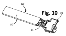
図9~図12に例示されているのは、本発明の可能な実施形態に係る装置のケーシング本体を製造するための可能なシーケンスである。図9に示されているのは、20’によって全体として示されている、PCB20、層40、および中間コーティングまたは層50を含む半製品である。前述の半製品20’は、電極JおよびJ1だけでなく、検出および/または処理回路の残りの部分もすでに備えられていると想定される。半製品20’には、例えば、PCB20(図8)、すなわち、半製品20’の領域25および26を少なくとも部分的に受け入れるように設計された空洞を画定するシェルのような形状の本体部21が適用される。前述のように、好ましくは、部分21は、コネクタ本体15aと端子17を一体化し、後者は、この段階でPCB20の対応する導電パスに電気的に接続される。
Illustrated in Figures 9-12 is a possible sequence for manufacturing the casing body of an apparatus according to a possible embodiment of the invention. Shown in FIG. 9 is a semi-finished
次に(図10を参照)、半製品20’に適用されるのは、本体部23であり、これは、例えば、ここでは、後者が前記部分23と部分21の対応する部分との間に囲まれるように、部分的に中間領域26(図8)のみを受け入れることができる空洞を画定するシェルのような形状である(前記対応する部分は、別個であり、本体部21に結合される構成要素として構成されてもよい)。特に、両方がシェルのような形状である場合、2つの部分21と23には、部分23の対応するシートとピンと結合するように設計された部分21のピンとシートなどの相互結合手段を設けることができる。
Next (see FIG. 10), applied to the
優先的に、本体部21および23は、260℃より高い融点を有するポリマで作られているか、または、いずれの場合も、特に、250℃より低い温度での少なくとも1つのポリマ、特に、装置10のケーシング本体の外側コーティング30を提供するように設計されたポリマの起こり得るオーバーモールドに耐えることができるように、この温度に耐えるように設計されている。この目的のために、様々な実施形態において、本体部21および23の材料は、ポリフタルアミド(PPA)、ポリアミドコポリマ(PA66)、およびポリフェニレンスルフィド(PPS)から選択される。
Preferentially, the
場合によっては、外側コーティング30のオーバーモールドの前に、本体部21、23の空洞、および前記空洞に収容されている半製品20’、すなわち、PCB20の対応する部分の空洞に、これらの領域にある電気および/または電子コンポーネントの保護特性を改善することを目的とした樹脂を塗布し得る。使用される樹脂または同様の材料は、低融点または重合温度、特に、電気および/または電子部品を損傷しないような変態温度(180℃~240℃の間の温度、好ましくは、200℃近傍など)を持つタイプのものが好ましい。目的に適した熱可塑性材料は、比較的弾性があるか、または硬くないことが好ましく、いわゆるホットメルトタイプまたはホットグルータイプのものであってもよい。
Optionally, prior to overmolding of the
次に、検出領域24を含むPCB20、すなわち、半製品20’の少なくとも一部が、外側コーティング30を提供するポリマ材料をオーバーモールドするための型に挿入される。コーティング30のオーバーモールドに使用される材料は、熱可塑性材料または熱硬化性材料であってもよい。好ましい材料は、高密度ポリエチレン(HDPE)、ポリプロピレン(PP)、ポリフタルアミド(PPA)、およびポリフェニレンスルフィド(PPS)である。
好ましくは、型は、本体部21および23が設けられた中間領域26の少なくとも一部も受け入れるように構成される。この場合、オーバーモールディング操作の過程で、PCB20の中間領域26に存在する可能性のある回路部品、すなわち、半製品20’は、オーバーモールディング領域内に位置しているが、いずれにせよ保護される。この中間領域が本体部21と23の間に囲まれているという事実を考慮して、前述の樹脂の存在下で保護がさらに強化される。
Preferably, the mold is configured to also receive at least part of the
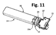
コーティング30のオーバーモールドの動作の結果は、図11に例示されており、ここでは、装置のケーシング本体が一般的な程度に形成されている。注目されるように、オーバーモールドされたコーティング30は、少なくとも検出部分14を画定する。ケーシング本体と、好ましくは、その取り付け部16の少なくとも一部は、主に、本体部23および本体部23の対応する部分の上にモールドされた材料によって得られる。
The result of the operation of overmolding the
装置10のケーシング本体は、特に、対応する接続部15を得る目的で、図11の半製品に1つまたは複数のさらなる本体部を関連付けることにより完成され得る。この目的のために、図12を参照することにより、本体部22は、PCB20、すなわち、半製品20’の制御領域25(図8)の少なくとも一部を間に挟んで、コーティング30の材料で覆われていない本体部21に結合される。本体部22は、例えば、本体部21に固定されたシェルの形態(例えば、スナップ嵌め、またはねじ手段、または溶接、または接着により固定)に固定された別個のコンポーネントとして構成されてもよく、または本体部22も構成され、オーバーモールドされた部分であってもよい。
The casing body of the
図2~図7に示される種類の実施形態は、コーティング30の材料によって吸収された湿度が電極JおよびJ1に到達する可能性を防ぐか、少なくともそのような湿度が電極JおよびJ1に到達するのを大幅に遅らせる限り、特に有利である。この観点では、この解決策は、湿気浸透に対する抵抗が低い場合でも、比較的安価で、および/またはより容易に成形可能なオーバーモールドされたコーティング30を得るために、おそらく使用することを可能にする。
Embodiments of the type shown in FIGS. 2-7 prevent moisture absorbed by the material of coating 30 from potentially reaching electrodes J and J1 , or at least prevent such moisture from reaching electrodes J and J1 . It is particularly advantageous as long as it significantly delays its arrival. In this respect, this solution could possibly be used to obtain a relatively cheap and/or more easily moldable
様々な実施形態では、1つまたは複数の層40は、省略される。この意味での例が図13~図16に示されており、それぞれのアレイの電極JおよびJ1とコーティング30の間に、ここでは、PCB20の層203および中間コーティング50で表されるシリコンまたはその誘導体または化合物を含む2層が提供される。図13~図16に示すタイプの実施形態では、いずれの場合でも、レベル検出を受ける液体と電極JおよびJ1との間には、外側コーティング30に加えて、異なる材料の2つのさらなる層(50および203)がある。図2~図6に例示されているタイプの実施形態と比較して低下しているとはいえ、コーティング30に含浸する可能性のある湿度または液体からの電極JおよびJ1の絶縁は、いずれにしても、例えば、コーティング3を得るためにいくつかの熱可塑性材料を使用するなど、装置の様々な用途に十分な高さを維持する。
In various embodiments, one or
理解されるように、本発明の態様によれば、レベルセンサ装置10は、電極J、J1、すなわち、それらを支持する構造(201、202)を検出対象の液体から分離する少なくとも3つの絶縁要素または層(30、50、40)を備える。
As will be appreciated, according to an aspect of the present invention, the
様々な実施形態では、電極Jおよび/またはJ1は、PCB20の構造内に配置されず、前記構造のそれぞれの外面に配置される。この意味での例を図17~図20に示す。したがって、これらの図に示されている例では、PCB20の外側層203は存在せず、電極JおよびJ1は、PCB自体の外側に、その反対側の主面に対応する位置に直接設けられる(ここでは、電極を担持する層201によって表される)。しかしながら、すでに述べたように、電極は、PCBの片側のみに設定できる。この種の実施形態では、PCB20は、必ずしも多層構造を有さないことが理解されよう。図17~20の場合、例えば、ソルダレジストまたはエポキシタイプの層40が存在し、PCB20の層201上に直接塗布されて、電極JおよびJ1も覆う。層40の形成に必要な材料が塗料またはインクの形態であるタイプの実施形態では、この材料は、必要に応じて、例えば、シルクスクリーン堆積により、図示の場合のように、層40の外面が実質的に平面になるように塗布することができる(すなわち、対応する材料は、電極JおよびJ1の領域で層40の厚さが小さくなるように堆積される)。しかしながら、これは、装置の動作の目的にとって本質的な特性ではない。
In various embodiments, electrodes J and/or J1 are not located within the structure of
また、図17~図20に示すタイプの実施形態では、いずれの場合も、レベル検出対象の液体と電極JおよびJ1との間に設定されるのは、外側コーティング30に加えて、異なる材料の2つのさらなる層(40および50)である。これは、本明細書で提案される使用によって要求されるように、長手方向に延長されたコーティングを得るために、より安価および/またはより容易に加工可能な熱可塑性材料でオーバーモールドされたコーティング30を得ることを可能にする。
Also, in embodiments of the type shown in FIGS. 17 to 20, it is in each case set between the liquid to be level-detected and the electrodes J and J1 , in addition to the
また、この場合、発明の態様によれば、レベルセンサ装置10は、電極J、J1、すなわち、それらを支持する構造(201、202)を、検出対象の液体から分離する3つの絶縁要素または層(30、50、40)を備える。
Also in this case, according to an aspect of the invention, the
様々な実施形態では、中間コーティングまたは層50は、省略される。この意味での例を図21~図24に示し、それぞれのアレイの電極JおよびJ1とコーティング30との間には、ここでは、PCB20の層203と、例えば、ソルダレジストまたはエポキシベースのタイプがいずれにしても提供される層40によって表される異なる材料の2つの層がある。したがって、この場合も、レベル検出を受ける液体と電極JおよびJ1との間に、外側コーティング30に加えて、異なる材料の2つのさらなる層(層40および203)が設定され、これにより、コーティング30の時間の経過とともに含浸する可能性のある湿度が電極に到達するのを防ぐか、いずれにしても遅らせることができる。
In various embodiments, intermediate coating or
したがって、この場合にも、レベルセンサ装置10は、電極J、J1、すなわち、それらを支持する構造201、202を検出対象の液体から分離する3つの絶縁要素または層(30、40、203)を備える。
Therefore, also in this case, the
図25~図28は、層40が省略され、電極Jおよび/またはJ1がPCB20の構造内ではなく、この構造のそれぞれの外面に対応する位置に配置される、さらなる可能な実施形態を例示する。したがって、この場合にも、PCB20の外側層203は存在せず、電極JおよびJ1はその2つの主要な反対側面に対応する位置でPCBの外側に直接設けられる(ここでは、電極を担持する層201によって表される)。したがって、中間コーティングまたは層50は、電極JおよびJ1も覆うように、PCB20の層201に直接塗布される。このタイプの実施形態においても、PCB20は必ずしも多層構造を有さないことが理解されるであろう。図25~図28に示すタイプの実施形態では、レベル検出を受ける液体と電極JおよびJ1との間に設定され、コーティング30に加えて、シリカベースの中間コーティングまたは層50のみである。
Figures 25-28 illustrate further possible embodiments in which
本発明の構成では、レベルセンサ装置10は、電極J、J1、すなわち、それらを支持する構造201、202を検出対象の液体から分離する2つの絶縁要素または層(30、50)を備える。
In the configuration of the invention, the
このようにして得られた吸湿性絶縁は、前述の他の実施形態と比較して減少しているが、特に、中間層50の提供に使用される材料がPCB20を均一に被覆するガラス質またはシリカベースの層である場合、通路や多孔性を残すことなく、装置の様々な用途に十分である。したがって、厚さが薄い場合でも、良好なシール特性を備えている。
Although the hygroscopic insulation thus obtained is reduced compared to the other embodiments described above, in particular the material used to provide the
図29~図32は、さらなる可能性のある実施形態を例示し、層40および中間コーティングまたは層50の両方が省略され、電極JおよびJ1は、PCB20の多層構造内に外層203の下に配置される。したがって、このタイプの実施形態においても、レベル検出を受ける液体と電極JまたはJ1との間に設定されるのは、外側コーティング30に加えて、PCB20の多層構造に属する1つの層203だけである。また、このタイプの構造は、保護、または少なくともオーバーモールドされたコーティング30を得るために使用される材料による湿度または液体の可能な吸収の悪影響を遅らせるのに十分である。
29-32 illustrate a further possible embodiment in which both the
また、本発明の構成では、レベルセンサ装置10は、電極J、J1、すなわち、それらを支持する構造体201、202を検出対象の液体から分離する2つの絶縁要素または層(30、203)を備える。
Also, in the configuration of the present invention, the
同様に、図33~図36は、中間コーティングまたは層50が省略され、電極JおよびJ1がPCB20の構造内ではなく、構造のそれぞれの外面に対応する位置に配置される、さらなる可能な実施形態を例示する。したがって、この場合にも、PCB20の外側層203は存在しないが、電極JおよびJ1を担持する層201上に置かれ、電極自体を覆うように、例えば、ソルダレジストまたはエポキシ系タイプのそれぞれの層40が塗布される。このタイプの実施形態においても、PCB20は、必ずしも多層構造を有さないことが理解されるであろう。このタイプの実施形態では、レベル検出を受ける液体と電極JまたはJ1との間に設定されるのは、外側コーティング30に加えて、層40のみであり、いずれの場合でも様々な用途で十分である。
Similarly, FIGS. 33-36 illustrate further possible implementations in which the intermediate coating or
また、本発明の構成では、レベルセンサ装置10は、電極J、J1、すなわち、それらを支持する構造201、202を検出対象の液体から分離する2つの絶縁要素または層(30、40)を備える。
Also, in the configuration of the invention, the
ポリシラザンベースの組成物から出発して得られるシリカで主に作られた中間コーティングまたは層50を設けることは、対応する重合中にシリコンが対応する基板20および/または40の-OH基に結合するため、特に、有利である。このようにして、中間コーティング50と下にある基板(場合によっては層40または層203で構成される)との間に二次タイプの傾向のある結合が得られ、材料間の固定、ひいては構造の強度の改善に寄与する。この観点では、前述のように、様々な実施形態において、PCB20および/または層40は、エポキシ系材料、すなわち、-OH基を含む材料を使用して優先的に形成され、それにより、中間コーティング50および/または層40との化学結合を保証する。この観点でも、電極JおよびJ1は、金属または金属合金(例えば、銅または銅ベースの合金)で作られていることが好ましい。前述の金属の生産段階では、ポリシラザンベースまたは二酸化ケイ素ベースの溶液が電極Jに部分的に接触して適用される場合にも、-OH官能基のグラフトを伴う擬似酸化プロセスが発生する。金属とポリシラザンまたは二酸化ケイ素との間に基本的な化学結合(-OHまたはO*官能基)が形成され、異なる材料間の固定という点で結果として利点がある。
Providing an intermediate coating or
様々な特に有利な実施形態では、以前に40で示されたエポキシ系層は、好ましくは、パーフルオロオクタンスルホン酸(PFOS)およびパーフルオロオクタン酸(PFOA)なしで、前駆体、誘導体、またはフッ素化ポリマまたはフルオロポリマまたはペルフルオロ化ポリマなどのフッ素化合物を含むポリマで作られた層40’で置換されてもよい。このため、上記の様々な図において、参照番号40に関連付けられているのは括弧内の参照番号40’でもある。好ましい材料は、例えば、フッ素化エチレンプロピレン(FEP)、ポリテトラフッ素エチレン(PTFE)、より一般的には、フッ素アクリレートベースのポリマである。したがって、層40が想定される前述の構成は、これらの層がフッ素の前駆体または誘導体または複合物を含むポリマで作られた層40’によって置換される場合に有効であると理解されるべきである。また、層40’は、PCB20を囲む中間コーティングに属していてもよく、すなわち、PCBの縁部または副側面でも延びている(例えば、図37~図46に示されているように)。層またはコーティング40’は、10μm~70μmの間の厚さを有し得る。
In various particularly advantageous embodiments, the epoxy-based layer previously indicated at 40 is preferably free of perfluorooctanesulfonic acid (PFOS) and perfluorooctanoic acid (PFOA), precursors, derivatives, or fluorine It may be replaced with a layer 40' made of a polymer containing a fluorine compound, such as a fluorinated polymer or a fluoropolymer or a perfluorinated polymer. Thus, in the various figures above, associated with
本出願人によって行われた研究により、フッ素ベースの高分子材料、またはフッ素の誘導体または化合物(完全または部分フッ素化フルオロポリマなど)が、本明細書で提案された用途の目的に特に有利であることを確認することができた。フッ化物は、化学的に非常に耐性があることに加えて、高温でも優れた耐性を示すため、コーティング30のオーバーモールドに耐えるのに完全に適している。さらに、これらの材料は、比較的柔軟であるか、硬くなく、比較的変形可能または圧縮可能である。したがって、非常に良好な熱膨張および熱衝撃に耐えることができる。同様に非常に低い摩擦係数を示し、結果として、異なる熱膨張係数のために、コーティング30のオーバーモールドされた材料とPCB20(および/または層40および/または50などの可能性のある他の層)との間で生じる相対的な動きに耐える可能性がある。
Studies conducted by the applicant show that fluorine-based polymeric materials, or fluorine derivatives or compounds, such as fully or partially fluorinated fluoropolymers, are particularly advantageous for the purposes of the applications proposed herein. I was able to confirm that. Fluorides are perfectly suited to withstand the overmolding of the
本出願人によって実施された実際の浸透試験は、フッ素化ポリマが、AdBlueなどの水尿素溶液に対する耐性に関して優れた結果が得られることを確認することも可能にした。これはまた、疎水性の高いフッ素化ポリマの表面エネルギーが非常に低いためである。この特性は、レベルが検出される液体が水または水ベースの溶液(主に水で構成されるAdBlueなど)である場合に特に有利である。 The actual permeation tests carried out by the applicant also made it possible to confirm that the fluorinated polymer gives excellent results with respect to resistance to aqueous urea solutions such as AdBlue. This is also due to the very low surface energy of highly hydrophobic fluorinated polymers. This property is particularly advantageous when the liquid whose level is to be detected is water or a water-based solution (such as AdBlue, which consists primarily of water).
さらに、フッ素化ポリマで作られた中間層40’の存在は、コーティング30を通る水尿素溶液の浸透の場合、電極および/またはPCB20の化学的攻撃に対する良好な保護を可能にする。
Furthermore, the presence of the intermediate layer 40' made of fluorinated polymer allows good protection of the electrodes and/or the
層またはコーティング40’を製造するためのフルオロポリマの使用は、様々な構成において、材料の重合中に、対応する基板の材料と化学的および/または構造的結合を得ることができるという事実の観点からも特に有利である。これは、PCB20および/または層40がエポキシベースの材料でできている場合に特に有利である。この観点では、すでに述べたように、PCB20の材料は、好ましくは、エポキシベースであり(例えば、FR4、そのマトリックスは、一般に、エポキシ樹脂で構成される)、ソルダレジストタイプの層40もエポキシ樹脂で作られている。
Aspects of the fact that the use of fluoropolymers to manufacture the layer or coating 40' can, in various configurations, obtain chemical and/or structural bonding with the corresponding substrate material during polymerization of the material. It is also particularly advantageous from This is particularly advantageous when
例えば、図37~図40に示されているのは、オーバーモールドされた外側コーティング30と、それぞれのアレイの電極JおよびJ1との間に以下が提供される場合である。
For example, shown in FIGS. 37-40 is where the following are provided between the overmolded
i)複合材料の第1の層203と、
ii)材料40の第2の層と、
iii)フッ素化ポリマベースを備えた第3の層40’。
i) a first layer of composite material 203 ;
ii) a second layer of
iii) a third layer 40' comprising a fluorinated polymer base;
実施形態(図示せず)によれば、複合材料203の層は省略されてもよい。 According to embodiments (not shown), the layer of composite material 203 may be omitted.
図に例示されている場合、複合材料の可能な第1の層は、PCBの多層構造の外層203で構成されているため、電極JおよびJ1は、それに応じてコーティングされるが、層40は、ソルダレジストまたはエポキシベースのタイプの中間コーティングに属する。これは、PCB20の構造をその主側面およびその縁部または副側面でコーティングする。代わりに、第3の層40’は、層40が属するエポキシベースのコーティングを囲む、例えば、FEPで作られたさらなるフッ素化ポリマ中間コーティングに属する。次に、外側コーティング30の材料を、層40’が属するコーティング上にオーバーモールドする。
In the case illustrated in the figure, the possible first layer of composite material consists of the outer layer 203 of the multilayer structure of the PCB, so that the electrodes J and J1 are coated accordingly, but the
図37~図40に例示されたタイプの解決策では、層またはコーティング40’と層またはコーティング40との間に、ここでは、層またはコーティング40で表される、エポキシベースの基板の-OH基と、層またはコーティング40’を提供するフッ素化ポリマのフッ素のより電気陰性の原子、例えば、FEPとの間の水素結合が提供される。水素結合または水素架橋は、非常に電気陰性な元素(フッ素、酸素、窒素など)との共有結合に関与する水素原子である分子間力の特定の場合であり、それは、原子価電子を引き付け、部分的な負電荷(δ-)を獲得し、部分的な正電荷(δ+)を有する水素を残す。同時に、水素は近くの分子の電気陰性原子によって引き付けられる。
In a solution of the type illustrated in FIGS. 37-40, between layer or
したがって、前述の結合は、材料間の固定の改善、したがって、構造の強度に寄与することが理解されよう。40’で示されるタイプの層またはコーティングが、エポキシ樹脂で少なくとも部分的に作られたPCB20に直接塗布されると、今例示したものと同様の結合が形成される。このタイプの場合は、図41および図42に例示されている。図41は、多層PCB20をコーティングするコーティング40’の場合に関するものであり、電極Jおよび/またはJ1は、すでに複合材料203で作られた層で覆われているのに対して、図42は、電極Jおよび/またはJ1が露出したPCBの場合に関する(すなわち、層201の外面に)。
It will therefore be appreciated that the aforementioned bonding contributes to an improved fixation between the materials and thus to the strength of the structure. When a layer or coating of the type indicated at 40' is applied directly to the
一態様によれば、本発明は、例えば、外側コーティング30のオーバーモールディング材料の収縮および/または凍結液体による推力の外部圧力による変形および/または熱ジャンプまたは衝撃による寸法変動(例えば、凍結した液体の加熱、および/または周囲温度の変動に続く)に従う、レベルセンサ装置の内部要素(PCB20、および/またはPCBにより担持される回路コンポーネント、および/またはPCBと外側コーティングとの間の材料の中間層)が受ける可能性のある機械的応力の除去または少なくとも低減を提案する。
According to one aspect, the present invention provides, for example, shrinkage of the overmolding material of the
このため、それ自体が本発明の実施形態では、すでに前述したように、装置の少なくとも1つの中間層は、機械的補償の機能を実行し、この目的のために、少なくとも部分的に可撓性または変形可能な材料または圧縮可能なポリマを備え、その上にコーティング30の材料をオーバーモールドする必要があり、好ましくは、コーティング30は、前述の補償中間層の材料よりも硬いポリマで作られている。
Thus, in an embodiment of the invention per se, as already mentioned above, at least one intermediate layer of the device performs the function of mechanical compensation and for this purpose is at least partially flexible. Or it may comprise a deformable material or a compressible polymer over which the material of the
例えば、前述のように、フルオロポリマは比較的柔軟、および/または変形可能で、低表面摩擦によって区別されるため、対応する層は、例えば、PCB20またはコーティング40などの下にある基板に関してコーティング30によって決まる機械的応力を吸収するために、機械的補償の機能を有利に実行できる。前述のように、これらの機械的応力は、外側コーティング30の収縮、および/または凍結液体またはその凍結部分によって誘発されるセンサ装置の応力、および/または装置の部品の寸法変動を誘発する熱衝撃によるものであり得る。
For example, as mentioned above, fluoropolymers are relatively flexible and/or deformable and are distinguished by low surface friction, so that the corresponding layer is not coated 30 with respect to an underlying substrate, such as
他の実施形態では、前述の可能性のある応力を補償する前述の機能は、フッ素誘導体または化合物を含んでいないものであっても、以前に言及したものとは異なる、比較的弾性、および/または圧縮性、および/または変形可能なエラストマまたはポリマで作られた1つまたは複数の層40’によって得ることができる。 In other embodiments, the aforesaid functions of compensating for the aforesaid potential stresses are different from those previously mentioned, even if they do not include fluorine derivatives or compounds, relatively elastic and/or or by one or more layers 40' made of a compressible and/or deformable elastomer or polymer.
本発明の特に有利な実施形態では、50により以前に示されタイプの中間層またはコーティングを組み合わせることも可能であり、これは比較的より硬くて脆く、したがって機械的変形または歪みに続く亀裂のリスクを潜在的に受けやすい。第1の層50を被覆するフッ素化層またはコーティングを用いて、コーティングのオーバーモールドされた材料の沈降ステップ中の過度の収縮および/または変形を防止する。
In a particularly advantageous embodiment of the invention it is also possible to combine intermediate layers or coatings of the type previously indicated by 50, which are relatively harder and more brittle and therefore risk cracking following mechanical deformation or strain. potentially susceptible to A fluorinated layer or coating covering the
そのような場合は図43~図46に例示されており、多層PCB20には、前述のタイプのシリカまたは酸化ケイ素からなる中間コーティング50が塗布され、その上にフルオロポリマからなる中間コーティング40’が順番に塗布される。この種の解決策により、外側コーティングのオーバーモールドされた材料に含浸する可能性のある湿度および/または液体に関して、電極Jおよび/またはJ1の絶縁の最大化が可能になることが理解されよう。
Such a case is illustrated in FIGS. 43-46 in which a
さらに、検出対象の液体の凍結中、および液体中に形成された氷片との可能な衝撃により生じる可能性のある機械的歪み、変形、および応力から後者を保護する、ガラス質タイプ(50)、複合タイプ(20)、またはエポキシタイプ(20、40)の対応する基板と比較して、フルオロポリマで作られたコーティングの高い柔軟性(または降伏、圧縮性、変形性)が強調されるべきである。 In addition, the vitreous type (50), which protects the latter from mechanical strains, deformations and stresses that may occur during freezing of the liquid to be detected and from possible impacts with ice chips formed in the liquid. , composite type (20), or epoxy type (20, 40), the high flexibility (or yield, compressibility, deformability) of coatings made of fluoropolymers should be emphasized. is.
一般に、図37~図42を参照して上述した機械的補償の機能は、したがって、特に、ガラス質コーティング50の完全性を保護するために、図43~図46に例示される場合にも適用される。 Generally, the function of mechanical compensation described above with reference to FIGS. 37-42 also applies in the case illustrated in FIGS. be done.
上記の説明から、本発明の特徴が明らかになり、その利点は、提案されたレベルセンサ装置の構造の単純さ、含まれるコスト、およびその精度と信頼性によって主に表される。 From the above description, the features of the invention become clear, the advantages of which are mainly expressed by the simplicity of construction of the proposed level sensor device, the costs involved, and its accuracy and reliability.
添付の特許請求の範囲によって定義される本発明の範囲から逸脱することなく、純粋に例として本明細書に記載される装置および方法の分野の当業者によって多数の変形がなされ得ることは明らかである。 It will be evident that numerous modifications may be made by those skilled in the art of the apparatus and methods described herein purely by way of example without departing from the scope of the invention as defined by the appended claims. be.
前述のように、それぞれがPCB20の片側に対応する位置にある2つの電極アレイの存在は、電極Jのみまたは電極J1のみを備えた装置10の本質的な特性を構成しない。したがって、このタイプの装置10では、例えば、本発明の目的のためにPCB20の最も外側の層203の1つだけを利用することにより、および/または1つの層40(および/または40’)のみおよび/またはPCB20の関心のある側面に提供することにより、外側コーティング30と電極JまたはJ1との間の中間体の数を減らすことができる。ところで、電極JまたはJ1の単一アレイを備えた装置10の場合も、絶縁構造は、レベル検出電極が存在しないPCBの側面に層40(および/または40’)および/または50を備えることができる。
As previously mentioned, the presence of two electrode arrays, each at corresponding positions on one side of
本発明に係るセンサ装置のPCBは、エポキシベースの材料、またはシリコンまたはその誘導体もしくは化合物を含む材料を使用して必ずしも作成する必要はない。考えられる変形実施形態では、多層構造を持たないものであっても、PCB20は、例えば、フッ素化ポリマまたはPTFE、またはポリイミド、またはセラミック材料を使用して得ることができる。
The PCB of the sensor device according to the invention need not necessarily be made using epoxy-based materials or materials containing silicon or its derivatives or compounds. In possible variant embodiments,
本発明は、液体媒体、特に、水または尿素および水ベースの添加物のレベルの検出を特に参照して説明されたが、既に述べたように、説明されたセンサは、凍結により固化する可能性のあるものでさえも、異なる物質および材料、組み合わせて使用できる。 Although the invention has been described with particular reference to the detection of levels of liquid media, particularly water or urea and water-based additives, as already mentioned, the described sensors can solidify due to freezing. can be used in combination with different substances and materials.
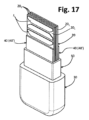
いくつかの用途では、それぞれが異なる測定分解能を有し、装置10の検出部11の異なる位置に位置する、異なる検出領域でのレベル測定が必要になる可能性がある。この必要性は、例えば、所定の領域で必要な測定の分解能または許容範囲を保証するために、PCB20の検出領域24に沿って、形状およびサイズに関して異なる形状を有する電極を配置することにつながる。この選択は、場合によっては、装置の制御電子機器、特に、そのコントローラのコストを最小化する必要性によって制限される(これは、その入力の数、したがって、管理可能な電極の数にリンクされる)。このため、用途によっては、検出の最大分解能が不要な領域(通常は両端)で電極のサイズを大きくすると便利な場合がある。この観点では、可能な変形実施形態によれば、その検出領域24内のPCB20の主面または各主面に対応する位置に設けられた容量性素子のアレイは、形状および/またはサイズの点で互いに多様化された、多数のシリーズの電極JまたはJ1を備えることができる。
Some applications may require level measurements at different sensing regions, each having a different measurement resolution and located at different locations in the
前に説明した実施形態を参照して説明した個々の特徴は、他の実施形態では互いに組み合わせることができる。 Individual features described with reference to the previously described embodiments can be combined with each other in other embodiments.
例えば、フッ素誘導体または化合物、あるいはフッ素誘導体または化合物を必ずしも含まないエラストマをベースとする材料で作られた、1つまたは複数の中間層またはコーティングによって実行される機械的補償の機能について以前に言及されている。このタイプの層またはコーティングは、それらの弾性および/または柔軟な性質により、特に、コーティングするために、領域25および/または26などの検出領域とは異なる回路支持体の領域にも拡張または提供され得る。そして、PCB20などの回路支持体または基板上の露出位置に取り付けられた可能な電気および/または電子コンポーネントを保護し得る。
For example, the function of mechanical compensation performed by one or more intermediate layers or coatings made of fluorine derivatives or compounds or elastomer-based materials not necessarily containing fluorine derivatives or compounds has been mentioned previously. ing. Layers or coatings of this type, due to their elastic and/or flexible nature, may also be extended or provided to areas of the circuit support different from the detection areas, such as
上述したように、本発明による装置の回路支持体には、電極Jおよび/またはJ1と同様に、少なくとも2つの材料層(30、50、40、40’、203)によってレベル検出を受ける液体から絶縁され得る少なくとも1つの温度センサが設けられ得る。 As mentioned above, the circuit support of the device according to the invention, like the electrodes J and/or J1 , is subjected to level detection by at least two layers of material (30, 50, 40, 40', 20 3 ). At least one temperature sensor may be provided which may be insulated from the liquid.
Claims (14)
前記装置(10)は、レベル検出軸(X)に実質的に沿って長手方向に延びる、回路支持体(20)を備え、前記回路支持体(20)は、第1の長手方向端部と第2の長手方向端部を有し、
前記回路支持体(20)は、前記第1の長手方向端部を含むその検出領域(24)に、前記レベル検出軸(X)に沿って互いに間隔をあけて配置された少なくとも1つの第1の電極(J)の第1のアレイを備える、少なくとも1つの第1の複数の第1の容量性素子を有し、前記第1の電極(J)は、導電性材料で作られ、かつ前記回路支持体(20)の支持構造(201、202、203)の少なくとも1つの第1の側面(20a)に対応する位置に少なくとも部分的に配置され、
前記装置(10)は、前記回路支持体(20)の前記検出領域(24)を覆う、電気絶縁性かつ液密の検出部(14)を備えるケーシング本体を有し、
前記ケーシング本体の前記検出部(14)は、第1の電気絶縁ポリマ材料で作られたオーバーモールドされた外側コーティング(30)を備え、前記第1の電気絶縁性ポリマ材料は、レベルを検出する必要がある媒体と接触するように設計された前記ケーシング本体の外面を画定し、
前記第1の電極(J)は、少なくともその前記検出領域(24)で前記回路支持体(20)の支持構造(201、202、203)内に囲まれており、
少なくとも前記検出領域(24)で、前記オーバーモールドされた外側コーティング(30)の少なくとも一部と前記回路支持体(20)の支持構造(201、202、203)との間には、前記第1の電気絶縁ポリマ材料とは異なる電気絶縁材料で作られた少なくとも1つの中間層(203、40、40’、50;203、50;203、40、40’;40、40’、50;203;40、40’;50)が設定され、
前記回路支持体(20)の支持構造は、電気絶縁材料の複数の層(20 1 、20 2 、20 3 )で作られる多層構造であり、
前記第1の電極(J)は、前記多層構造の電気絶縁材料の2つの層(20 1 、20 3 )の間に、前記2つの層の一方が前記少なくとも1つの中間層を得るように設定される、装置。 A capacitive level sensor device for detecting the level of a medium contained in a container (1), comprising:
Said device (10) comprises a circuit support (20) extending longitudinally substantially along a level sensing axis (X), said circuit support (20) having a first longitudinal end and a having a second longitudinal end;
Said circuit support (20) has, in its detection area (24), including said first longitudinal end , at least one first spaced apart along said level detection axis (X). at least one first plurality of first capacitive elements comprising a first array of electrodes (J) of the positioned at least partially at a location corresponding to at least one first side surface (20a) of the support structures ( 201 , 202 , 203 ) of the circuit support (20);
The device (10) has a casing body with an electrically insulating and liquid-tight sensing portion (14) covering the sensing area (24) of the circuit support (20),
The sensing portion (14) of the casing body comprises an overmolded outer coating (30) made of a first electrically insulating polymer material, said first electrically insulating polymer material detecting a level. defining an outer surface of said casing body designed to contact the medium in need;
said first electrode (J) being enclosed within a support structure (20 1 , 20 2 , 20 3 ) of said circuit support (20) at least at said sensing area (24) thereof,
between at least a portion of the overmolded outer coating (30) and support structures (20 1 , 20 2 , 20 3 ) of the circuit carrier (20), at least in the sensing region (24): At least one intermediate layer (20 3 , 40, 40′, 50; 20 3 , 50; 20 3 , 40, 40′; 40, 40 ', 50; 20 3 ; 40, 40'; 50) are set ,
the support structure of said circuit support (20) is a multi-layer structure made of multiple layers (20 1 , 20 2 , 20 3 ) of electrically insulating material,
Said first electrode (J) is set such that between two layers (20 1 , 20 3 ) of electrically insulating material of said multilayer structure, one of said two layers obtains said at least one intermediate layer. device .
前記装置(10)は、レベル検出軸(X)に実質的に沿って長手方向に延びる、回路支持体(20)を備え、前記回路支持体(20)は、第1の長手方向端部および第2の長手方向端部を有し、
前記回路支持体(20)は、前記第1の長手方向端部を含むその検出領域(24)に、前記レベル検出軸(X)に沿って互いに間隔をあけて配置された少なくとも1つの第1の電極(J)の第1のアレイを備える、少なくとも1つの第1の複数の第1の容量性素子を有し、前記第1の電極(J)は、導電性材料で作られ、かつ前記回路支持体(20)の耐荷重構造(201、202、203)の少なくとも1つの第1の側面(20a)に対応する位置に少なくとも部分的に配置され、
前記装置(10)は、前記回路支持体(20)の前記検出領域(24)を覆う、電気絶縁性かつ液密の検出部(14)を備えるケーシング本体を有し、
前記ケーシング本体の前記検出部(14)は、第1の電気絶縁性ポリマ材料で形成されたオーバーモールドされた外側カバー(30)を備え、前記第1の電気絶縁ポリマ材料は、レベルを検出する必要がある媒体と接触するように設計された前記ケーシング本体の外面を画定し、
前記オーバーモールドされた外側カバー(30)の少なくとも一部と前記第1の電極(J)との間には、前記第1の電気絶縁ポリマ材料とは異なる電気絶縁材料で作られた少なくとも1つの中間層(203、40、40’、50;203、50;203、40、40’;40、40’、50;203;40、40’;50)が設定され、
前記少なくとも1つの中間層(203、40、40’、50;203、50;203、40、40’;40、40’、50;203;40、40’;50)は、フッ素誘導体または化合物を含み、前記オーバーモールドされた外側カバー(30)の前記第1の電気絶縁ポリマ材料よりも可撓性または変形可能または圧縮可能または降伏する材料で形成された機械補償層(40’)を備える、装置。 A capacitive level sensor device for detecting the level of a medium contained in a container (1), comprising:
Said device (10) comprises a circuit support (20) extending longitudinally substantially along a level detection axis (X), said circuit support (20) having a first longitudinal end and a having a second longitudinal end;
Said circuit support (20) has, in its detection area (24), including said first longitudinal end , at least one first spaced apart along said level detection axis (X). at least one first plurality of first capacitive elements comprising a first array of electrodes (J) of the positioned at least partially at a location corresponding to at least one first side (20a) of the load bearing structures (20 1 , 20 2 , 20 3 ) of the circuit support (20);
The device (10) has a casing body with an electrically insulating and liquid-tight sensing portion (14) covering the sensing area (24) of the circuit support (20),
The sensing portion (14) of the casing body comprises an overmolded outer cover (30) made of a first electrically insulating polymer material, the first electrically insulating polymer material detecting a level. defining an outer surface of said casing body designed to contact the medium in need;
Between at least a portion of said overmolded outer cover (30) and said first electrode (J) is at least one electrode made of an electrically insulating material different from said first electrically insulating polymer material. An intermediate layer (20 3 , 40, 40′, 50; 20 3 , 50; 20 3 , 40, 40′; 40, 40′, 50; 20 3 ; 40, 40′; 50) is set,
The at least one intermediate layer (20 3 , 40, 40′, 50; 20 3 , 50; 20 3 , 40, 40′; 40, 40′, 50; 20 3 ; 40, 40′ ; A mechanical compensation layer (40′) comprising a dielectric or compound and formed of a material that is more flexible or deformable or compressible or yields than said first electrically insulating polymer material of said overmolded outer cover (30). ).
レベル検出軸(X)に実質的に沿って長手方向に延びる、電気絶縁材料(20)で作られた回路支持体(20)と、
前記回路支持体(20)の検出領域(24)にある電極または容量性素子の第1のアレイであって、電極または容量性素子の前記第1のアレイは、前記回路支持体(20)の第1の側面(20a)に対応する位置に、少なくとも1つのシリーズの電極(J、J1)を備える、第1のアレイと、
前記回路支持体(20)上の少なくとも一部がオーバーモールドされた材料で形成された少なくとも1つのカバー(30)を備えるケーシング本体と、を備え、
前記オーバーモールドされたカバー(30)の少なくとも一部と前記少なくとも1つのシリーズの電極(J、J1)との間には、少なくとも1つの材料の中間層(203、40、40’、50;203、50;203、40、40’;40、40’、50;203;40、40’;50)が設定され、
前記少なくとも1つの中間層(20 3 、40、40’、50;20 3 、50;20 3 、40、40’;40、40’、50;20 3 ;40、40’;50)は、シリコンまたはその誘導体または化合物を含む材料で作られた少なくとも1つの層(50;20 3 )と、フッ素誘導体または化合物を含む材料で作られた少なくとも1つの層を備える、装置。 A capacitive level sensor device for detecting the level of a medium contained in a container (1), said device (10) comprising:
a circuit support (20) made of an electrically insulating material (20) extending longitudinally substantially along the level detection axis (X);
A first array of electrodes or capacitive elements in a sensing area (24) of said circuit support (20), said first array of electrodes or capacitive elements being located on said circuit support (20). a first array comprising at least one series of electrodes (J, J 1 ) at positions corresponding to the first side (20a);
a casing body comprising at least one cover (30) formed of a material at least partially overmolded on said circuit support (20);
at least one intermediate layer of material (20 3 , 40, 40 ′ , 50; 20 3 , 50; 20 3 , 40, 40′; 40, 40′, 50; 20 3 ; 40, 40′; 50) are set ,
The at least one intermediate layer (20 3 , 40, 40′, 50; 20 3 , 50; 20 3 , 40, 40′; 40, 40′, 50; 20 3 ; 40, 40′; A device comprising at least one layer (50;20 3 ) made of a material containing or a derivative or compound thereof and at least one layer made of a material containing a fluorine derivative or compound .
i)レベル検出軸(X)に実質的に沿って長手方向に延びる、電気絶縁材料で作られた回路支持体(20)を提供するステップと、
ii)前記回路支持体(20)の検出領域(24)に電極または容量性素子の第1のアレイを提供するステップであって、電極または容量性素子の前記第1のアレイは、前記回路支持体(20)の第1の側面(20a)に対応する位置に少なくとも1つのシリーズの電極(J、J1)を備える、ステップと、
iii)少なくとも部分的に前記回路支持体(20)上にオーバーモールドされたカバー材料で形成される少なくとも1つの本体部分を有するケーシング本体を提供するステップと、を含み、
ステップiii)の前に、前記オーバーモールドされたカバー材料の少なくとも一部と前記少なくとも1つのシリーズの電極(J、J1)との間には、少なくとも1つの材料の中間層(203、40、40’、50;203、50;203、40、40’;40、40’、50;203;40、40’;50)が設定され、
前記少なくとも1つの中間層(20 3 、40、40’、50;20 3 、50;20 3 、40、40’;40、40’、50;20 3 ;40、40’;50)は、実質的に酸化ケイ素(50)で作られた少なくとも1つの層を備える、方法。 A method for obtaining a capacitive level sensor device for detecting the level of a medium contained in a container (1), said method comprising:
i) providing a circuit support (20) made of an electrically insulating material extending longitudinally substantially along the level sensing axis (X);
ii) providing a first array of electrodes or capacitive elements in a sensing area (24) of said circuit support (20), said first array of electrodes or capacitive elements providing at least one series of electrodes (J, J 1 ) at positions corresponding to the first side (20a) of the body (20);
iii) providing a casing body having at least one body portion formed of a cover material at least partially overmolded onto said circuit support (20);
Before step iii) , at least one intermediate layer of material (20 3 , 40, 40′, 50; 20 3 , 50; 20 3 , 40, 40′; 40, 40′, 50; 20 3 ; 40, 40′; 50) are set ,
The at least one intermediate layer (20 3 , 40, 40′, 50; 20 3 , 50 ; 20 3 , 40, 40′; 40, 40′, 50; 20 3 ; 40, 40′; 50) is substantially at least one layer essentially made of silicon oxide (50) .
Applications Claiming Priority (3)
| Application Number | Priority Date | Filing Date | Title |
|---|---|---|---|
| IT102017000082500A IT201700082500A1 (en) | 2017-07-20 | 2017-07-20 | DEVICE FOR DETECTION OF THE LEVEL OF A MEDIA |
| IT102017000082500 | 2017-07-20 | ||
| PCT/IB2018/055201 WO2019016658A1 (en) | 2017-07-20 | 2018-07-13 | Device for detecting the level of a medium |
Publications (2)
| Publication Number | Publication Date |
|---|---|
| JP2020528143A JP2020528143A (en) | 2020-09-17 |
| JP7220196B2 true JP7220196B2 (en) | 2023-02-09 |
Family
ID=60990935
Family Applications (1)
| Application Number | Title | Priority Date | Filing Date |
|---|---|---|---|
| JP2020502317A Active JP7220196B2 (en) | 2017-07-20 | 2018-07-13 | Device for detecting medium level |
Country Status (7)
| Country | Link |
|---|---|
| US (1) | US11193808B2 (en) |
| EP (1) | EP3655732A1 (en) |
| JP (1) | JP7220196B2 (en) |
| KR (1) | KR20200029575A (en) |
| CN (1) | CN111094910A (en) |
| IT (1) | IT201700082500A1 (en) |
| WO (1) | WO2019016658A1 (en) |
Families Citing this family (4)
| Publication number | Priority date | Publication date | Assignee | Title |
|---|---|---|---|---|
| US11573102B2 (en) * | 2020-11-17 | 2023-02-07 | Ford Global Technologies, Llc | Method of manufacturing multi-layer electrode for a capacitive pressure sensor and multi-layer electrodes formed therefrom |
| RU2763017C1 (en) * | 2020-12-31 | 2021-12-24 | Осаюхинг Омникомм | Liquid flow monitoring system containing one capacitive sensor for the interface level |
| EP4105614A1 (en) * | 2021-06-18 | 2022-12-21 | TE Connectivity Germany GmbH | Sensor device for determining a level of a fluid material |
| CN115529714A (en) * | 2021-06-25 | 2022-12-27 | 全亿大科技(佛山)有限公司 | Circuit board and manufacturing method |
Citations (4)
| Publication number | Priority date | Publication date | Assignee | Title |
|---|---|---|---|---|
| JP2008524618A (en) | 2004-12-22 | 2008-07-10 | イネルジー オートモーティヴ システムズ リサーチ | Capacitive liquid level sensor |
| US20090139325A1 (en) | 2007-10-11 | 2009-06-04 | Cube Investments Limited | Capacitive probes and sensors, and applications therefor, and multimode wireless devices |
| DE102007059669A1 (en) | 2007-12-10 | 2009-06-25 | Endress + Hauser Gmbh + Co. Kg | Capacitive measuring device for determining and/or monitoring filling level of e.g. liquid, provided in container, has intermediate layer electrically conductive and surrounded partially by electrically isolating insulation layer |
| WO2015181770A2 (en) | 2014-05-30 | 2015-12-03 | Eltek S.P.A. | A sensor for detecting the level of a medium |
Family Cites Families (16)
| Publication number | Priority date | Publication date | Assignee | Title |
|---|---|---|---|---|
| FR2386811A1 (en) * | 1977-04-06 | 1978-11-03 | Elf Aquitaine | SEPARATION LEVEL DETECTOR BETWEEN TWO LIQUIDS |
| DE19504608C2 (en) * | 1995-02-11 | 2002-03-21 | Balluff Gebhard Feinmech | Position sensor and method for manufacturing the same |
| GB9513267D0 (en) * | 1995-06-29 | 1995-09-06 | Whitaker Corp | Ultrasonic liquid level detector |
| JP2000517061A (en) * | 1997-06-12 | 2000-12-19 | マチュレック,アンドリュウ,エム. | Liquid level indicator |
| JP3073944B2 (en) * | 1997-09-09 | 2000-08-07 | 東亜電器株式会社 | Flat sheet interface sensor |
| US6130472A (en) * | 1998-07-24 | 2000-10-10 | International Business Machines Corporation | Moisture and ion barrier for protection of devices and interconnect structures |
| US20030104693A1 (en) * | 2001-11-30 | 2003-06-05 | Siegel Harry M. | Use of fluoropolymer coating for planarizing and passivating integrated circuit devices |
| DE10261767A1 (en) * | 2002-12-19 | 2004-07-15 | Hydac Electronic Gmbh | Device and method for measuring capacitance and device for determining the level of a liquid with such a device |
| US6881606B2 (en) * | 2003-03-18 | 2005-04-19 | Micron Technology, Inc. | Method for forming a protective layer for use in packaging a semiconductor die |
| JP2005147779A (en) * | 2003-11-13 | 2005-06-09 | Alps Electric Co Ltd | Liquid level sensor |
| US7963164B2 (en) * | 2008-06-09 | 2011-06-21 | Rochester Gauges, Inc. | Capacitive sensor assembly for determining level of fluent materials |
| CN201707102U (en) * | 2010-01-15 | 2011-01-12 | 宋玉兴 | Novel liquid level sensor |
| CN102322917A (en) * | 2011-05-27 | 2012-01-18 | 皇明太阳能股份有限公司 | Digital communication gradual-change-type sensor |
| CN202204566U (en) * | 2011-05-28 | 2012-04-25 | 宋玉兴 | Novel liquid level sensor |
| FR3013447B1 (en) * | 2013-11-15 | 2016-01-01 | Valeo Sys Controle Moteur Sas | DEVICE FOR MEASURING LIQUID LEVEL |
| KR102633940B1 (en) * | 2018-06-12 | 2024-02-05 | 현대자동차주식회사 | Device and method for monitoring liquid level of liquid storage tanks for vehicle |
-
2017
- 2017-07-20 IT IT102017000082500A patent/IT201700082500A1/en unknown
-
2018
- 2018-07-13 KR KR1020207004961A patent/KR20200029575A/en not_active Application Discontinuation
- 2018-07-13 EP EP18752628.0A patent/EP3655732A1/en active Pending
- 2018-07-13 US US16/632,206 patent/US11193808B2/en active Active
- 2018-07-13 WO PCT/IB2018/055201 patent/WO2019016658A1/en unknown
- 2018-07-13 CN CN201880061231.XA patent/CN111094910A/en active Pending
- 2018-07-13 JP JP2020502317A patent/JP7220196B2/en active Active
Patent Citations (4)
| Publication number | Priority date | Publication date | Assignee | Title |
|---|---|---|---|---|
| JP2008524618A (en) | 2004-12-22 | 2008-07-10 | イネルジー オートモーティヴ システムズ リサーチ | Capacitive liquid level sensor |
| US20090139325A1 (en) | 2007-10-11 | 2009-06-04 | Cube Investments Limited | Capacitive probes and sensors, and applications therefor, and multimode wireless devices |
| DE102007059669A1 (en) | 2007-12-10 | 2009-06-25 | Endress + Hauser Gmbh + Co. Kg | Capacitive measuring device for determining and/or monitoring filling level of e.g. liquid, provided in container, has intermediate layer electrically conductive and surrounded partially by electrically isolating insulation layer |
| WO2015181770A2 (en) | 2014-05-30 | 2015-12-03 | Eltek S.P.A. | A sensor for detecting the level of a medium |
Also Published As
| Publication number | Publication date |
|---|---|
| WO2019016658A1 (en) | 2019-01-24 |
| IT201700082500A1 (en) | 2019-01-20 |
| JP2020528143A (en) | 2020-09-17 |
| CN111094910A (en) | 2020-05-01 |
| KR20200029575A (en) | 2020-03-18 |
| US20200232836A1 (en) | 2020-07-23 |
| EP3655732A1 (en) | 2020-05-27 |
| US11193808B2 (en) | 2021-12-07 |
Similar Documents
| Publication | Publication Date | Title |
|---|---|---|
| JP7220196B2 (en) | Device for detecting medium level | |
| JP7220195B2 (en) | Device for detecting medium level | |
| AU2013208295B2 (en) | Electronic devices with internal moisture-resistant coatings | |
| US5907278A (en) | Capacitive sensor assembly with soot build-up inhibiting coating | |
| US10935411B2 (en) | Device for detecting the level of a medium | |
| JP7304845B2 (en) | Device for detecting medium level | |
| US9006847B2 (en) | Sensor module for accommodating a pressure sensor chip and for installation into a sensor housing | |
| KR20180013925A (en) | Pressure sensing device for fluid medium and method of manufacturing the device | |
| US7967505B2 (en) | Sensor device | |
| WO2001091182A1 (en) | Environmentally-sealed electronic assembly and method of making same | |
| JP2013513247A (en) | Circuit module and method of manufacturing the circuit module | |
| JP2010232663A (en) | Chip module, and method of manufacturing the same | |
| CN102017823B (en) | Seal structure | |
| US11146893B2 (en) | Sensor system, sensor arrangement, and assembly method using solder for sealing | |
| US11946399B2 (en) | Temperature sensing unit and urea sensor | |
| JP2017502316A (en) | Fluid pressure measuring device |
Legal Events
| Date | Code | Title | Description |
|---|---|---|---|
| A621 | Written request for application examination |
Free format text: JAPANESE INTERMEDIATE CODE: A621 Effective date: 20210624 |
|
| A977 | Report on retrieval |
Free format text: JAPANESE INTERMEDIATE CODE: A971007 Effective date: 20220520 |
|
| A131 | Notification of reasons for refusal |
Free format text: JAPANESE INTERMEDIATE CODE: A131 Effective date: 20220705 |
|
| A521 | Request for written amendment filed |
Free format text: JAPANESE INTERMEDIATE CODE: A523 Effective date: 20220926 |
|
| TRDD | Decision of grant or rejection written | ||
| A01 | Written decision to grant a patent or to grant a registration (utility model) |
Free format text: JAPANESE INTERMEDIATE CODE: A01 Effective date: 20230110 |
|
| A61 | First payment of annual fees (during grant procedure) |
Free format text: JAPANESE INTERMEDIATE CODE: A61 Effective date: 20230130 |
|
| R150 | Certificate of patent or registration of utility model |
Ref document number: 7220196 Country of ref document: JP Free format text: JAPANESE INTERMEDIATE CODE: R150 |