JP7210558B2 - radiation shield - Google Patents
radiation shield Download PDFInfo
- Publication number
- JP7210558B2 JP7210558B2 JP2020515295A JP2020515295A JP7210558B2 JP 7210558 B2 JP7210558 B2 JP 7210558B2 JP 2020515295 A JP2020515295 A JP 2020515295A JP 2020515295 A JP2020515295 A JP 2020515295A JP 7210558 B2 JP7210558 B2 JP 7210558B2
- Authority
- JP
- Japan
- Prior art keywords
- cells
- cell
- shielding device
- resonators
- loop
- Prior art date
- Legal status (The legal status is an assumption and is not a legal conclusion. Google has not performed a legal analysis and makes no representation as to the accuracy of the status listed.)
- Active
Links
Images


Classifications
-
- H—ELECTRICITY
- H01—ELECTRIC ELEMENTS
- H01Q—ANTENNAS, i.e. RADIO AERIALS
- H01Q1/00—Details of, or arrangements associated with, antennas
- H01Q1/52—Means for reducing coupling between antennas; Means for reducing coupling between an antenna and another structure
- H01Q1/526—Electromagnetic shields
-
- H—ELECTRICITY
- H01—ELECTRIC ELEMENTS
- H01Q—ANTENNAS, i.e. RADIO AERIALS
- H01Q1/00—Details of, or arrangements associated with, antennas
- H01Q1/12—Supports; Mounting means
- H01Q1/22—Supports; Mounting means by structural association with other equipment or articles
- H01Q1/24—Supports; Mounting means by structural association with other equipment or articles with receiving set
- H01Q1/241—Supports; Mounting means by structural association with other equipment or articles with receiving set used in mobile communications, e.g. GSM
- H01Q1/242—Supports; Mounting means by structural association with other equipment or articles with receiving set used in mobile communications, e.g. GSM specially adapted for hand-held use
- H01Q1/245—Supports; Mounting means by structural association with other equipment or articles with receiving set used in mobile communications, e.g. GSM specially adapted for hand-held use with means for shaping the antenna pattern, e.g. in order to protect user against rf exposure
-
- H—ELECTRICITY
- H01—ELECTRIC ELEMENTS
- H01Q—ANTENNAS, i.e. RADIO AERIALS
- H01Q15/00—Devices for reflection, refraction, diffraction or polarisation of waves radiated from an antenna, e.g. quasi-optical devices
- H01Q15/0006—Devices acting selectively as reflecting surface, as diffracting or as refracting device, e.g. frequency filtering or angular spatial filtering devices
- H01Q15/0086—Devices acting selectively as reflecting surface, as diffracting or as refracting device, e.g. frequency filtering or angular spatial filtering devices said selective devices having materials with a synthesized negative refractive index, e.g. metamaterials or left-handed materials
Landscapes
- Physics & Mathematics (AREA)
- Electromagnetism (AREA)
- Engineering & Computer Science (AREA)
- Computer Networks & Wireless Communication (AREA)
- Shielding Devices Or Components To Electric Or Magnetic Fields (AREA)
- Materials For Medical Uses (AREA)
- Developing Agents For Electrophotography (AREA)
- Control Of Motors That Do Not Use Commutators (AREA)
- Waveguide Connection Structure (AREA)
- Aerials With Secondary Devices (AREA)
Description
本発明は、携帯電話またはラップトップなどの機器から放射されるエネルギーを低減する遮蔽体に関する。 The present invention relates to shields that reduce energy radiated from devices such as mobile phones or laptops.
現代の多くの機器、例えば携帯電話、ラップトップおよびタブレットコンピュータは、無線周波数の電磁放射線を送受信することができる。これらの送信は、ユーザがこれらの型の機器では標準であると見なすようになったインターネット接続などの機能を提供する際の基本となる。 Many modern devices, such as mobile phones, laptops and tablet computers, are capable of transmitting and receiving radio frequency electromagnetic radiation. These transmissions are fundamental in providing features such as Internet connectivity that users have come to regard as standard on these types of devices.
しかし、これらの送信の不運な副作用は、アンテナの交流無線周波数(RF:Radio Frequency)電流がユーザに隣接する組織を貫通する無線周波電界を誘発することである。これらの電界によって放射されるエネルギーは、ユーザの組織に吸収されかねず、組織温度が上昇する原因となり、組織を損傷する可能性がある。 However, an unfortunate side effect of these transmissions is that the antenna's alternating radio frequency (RF) currents induce radio frequency electric fields that penetrate tissue adjacent to the user. The energy radiated by these electric fields can be absorbed by the user's tissue, causing an increase in tissue temperature and potentially damaging tissue.
これらの無線周波数場によって引き起こされる加熱の程度を推測するために、物質(つまり組織)の単位質量あたりに吸収される放射電力を測定するのが標準的な方法であり、これは比吸収率「SAR(Specific Absorption Rate)」として知られている。 To infer the degree of heating caused by these radio frequency fields, standard practice is to measure the radiant power absorbed per unit mass of matter (i.e. tissue), which is known as the specific absorption rate SAR (Specific Absorption Rate).
無線周波数放射の潜在的な悪影響から公衆を保護するために、多くの専門団体が人体組織の比吸収率の安全性限界を定義しており、例えば、米国電気電子技術者協会(IEEE)は、6分間の間隔で、頭部の1グラム(g)を平均した1.6ワットごとキログラム(W/Kg)のSAR制限を提案している。 To protect the public from the potentially harmful effects of radio frequency radiation, many professional bodies have defined safety limits for the specific absorption rate of human tissue, for example the Institute of Electrical and Electronics Engineers (IEEE), It proposes a SAR limit of 1.6 watts per kilogram (W/Kg) averaged over 1 gram (g) of head over a 6 minute interval.
SARを低減するために、無線周波機器では、ユーザとRF放射アンテナとの間に無線周波遮蔽体を配置する必要がある。このような遮蔽機器の多くは、例えば携帯電話などの放射機器とともに使用するために既に市販されている。これらの遮蔽体は、一般的に、携帯機器に隣接して配置された電磁周波数「EMF」遮蔽材料の固体塊を含み、例えば、携帯電話の外周に適合するように設計された「靴下形状のもの」もしくはカバー、または衣服のポケットに縫い付けられた素材の特殊なパッチである。 To reduce SAR, radio frequency equipment requires radio frequency shielding to be placed between the user and the RF radiating antenna. Many such shielding devices are already commercially available for use with emissive devices such as mobile phones. These shields generally include a solid mass of electromagnetic frequency "EMF" shielding material placed adjacent to the mobile device, e.g. "Things" or covers, or special patches of material sewn into pockets of clothing.
しかし、有害な放射線からユーザを保護することに加えて、現在利用可能な機器に関する一般的な問題は、有害な放射線が、アンテナ伝送を阻止することでアンテナ効率を低下させることである。アンテナ効率を低下させることは、無線伝送に依存する無線接続の信頼性を低下させることによって、機器の有用性に明らかに影響する。また、電流遮蔽体は必要以上に大型である傾向があり、携帯機器の形状因子および有用性に深刻な影響を及ぼす。 However, in addition to protecting users from harmful radiation, a common problem with currently available equipment is that harmful radiation reduces antenna efficiency by blocking antenna transmission. Reducing antenna efficiency clearly affects the usability of the device by reducing the reliability of the wireless connection that relies on wireless transmission. Also, current shields tend to be unnecessarily large, seriously impacting the form factor and usability of portable devices.
したがって、アンテナ効率を妨げたり、ほとんどの場合に機器の有用性に影響を与えたりしない無線周波遮蔽機器が必要である。 Therefore, there is a need for radio frequency shielding equipment that does not interfere with antenna efficiency or affect the usability of the equipment in most cases.
また、本明細書で提示される放射線遮蔽体は、携帯機器だけでなく、例えば無線基地局付近で働いているかもしくは生活している人々のための防護服、または壁に組み込まれた放射線遮蔽体などの様々な放射線遮蔽体の用途にも有益であることが理解されるであろう。 Also, the radiation shields presented herein are not only for mobile devices, but also protective clothing for people working or living near radio base stations, for example, or radiation shields built into walls. It will be appreciated that it is also useful for various radiation shield applications such as.
本発明によれば、添付の特許請求の範囲に記載の装置および方法が提供される。本発明の他の特徴は、従属請求項および以下の説明から明らかになるであろう。 According to the present invention there is provided an apparatus and method as set forth in the appended claims. Other features of the invention will become apparent from the dependent claims and the following description.
第1の実施形態によれば、複数のセルを備える電磁放射線を受動的に減衰させるための遮蔽装置が提供され、各セルは互いに間隔を置いて配置された複数の共振器を備え、複数のセルは非対称構造を有する。 According to a first embodiment, there is provided a shielding device for passively attenuating electromagnetic radiation comprising a plurality of cells, each cell comprising a plurality of spaced apart resonators, a plurality of The cell has an asymmetric structure.
複数のセルは複数のユニットセルに配置され、各ユニットセルは、複数のセルのうち少なくとも2つの隣接セルを囲む共通ループを備えてもよい。複数のユニットセルの各々は、少なくとも1つの選択周波数について負の屈折率を有する非対称構造を有してもよく、それによって少なくとも1つの選択周波数の電磁放射線が減衰される。減衰は、電子入力もしくは他の入力を必要とする能動的減衰ではなく、好ましくは受動的であり、すなわち、ユニットセルの構造によって引き起こされる。 The plurality of cells may be arranged into a plurality of unit cells, each unit cell comprising a common loop surrounding at least two adjacent cells of the plurality of cells. Each of the plurality of unit cells may have an asymmetric structure with a negative refractive index for at least one selected frequency, thereby attenuating electromagnetic radiation at the at least one selected frequency. The attenuation is preferably passive, ie caused by the structure of the unit cell, rather than an active attenuation requiring an electronic or other input.
非対称構造は、完全に対称ではない構造である。非対称性は、例えば共振器の周囲もしくは間の間隔、または共振器の寸法など、構造の様々なパラメータを調整することで達成することができる。構造の非対称性を変更して、選択周波数の電磁波を捕捉しかつ反射することができる。したがって、構造は選択周波数で(つまり、選択された電磁帯域内で)共振し、かつ選択周波数による放射線を低減するので、構造を電磁バンドギャップ構造と呼ぶことができる。 Asymmetric structures are structures that are not perfectly symmetrical. Asymmetry can be achieved by adjusting various parameters of the structure, such as the spacing around or between the resonators, or the dimensions of the resonators. The asymmetry of the structure can be altered to capture and reflect electromagnetic waves at selected frequencies. Therefore, the structure can be referred to as an electromagnetic bandgap structure because it resonates at selected frequencies (ie, within a selected electromagnetic band) and reduces radiation at selected frequencies.
各遮蔽装置のセルの配置は、遮蔽体が少なくとも1つの選択周波数について負の屈折率を有するように設計されている。負の屈折率は、表面波を抑制し、かつユーザ機器から放出される過剰な電磁波を、ユーザを避けて放射するのに役立つ。したがって遮蔽装置はメタマテリアルと呼ばれることがあり、すなわち、メタマテリアルは、通常は天然素材には見られない特性、特に負の屈折率を示す人工複合構造である。 The arrangement of cells in each shielding device is designed so that the shield has a negative refractive index for at least one selected frequency. A negative index of refraction helps suppress surface waves and radiate excess electromagnetic waves emitted by the user equipment away from the user. Shielding devices are therefore sometimes referred to as metamaterials, ie metamaterials are man-made composite structures that exhibit properties not normally found in natural materials, in particular negative refractive indices.
メタマテリアルはこれまでに研究されてきたが、受動的減衰が存在する遮蔽装置の文脈にはない。例えば、Hydeらによる米国特許出願番号第2007/0188385号明細書は、電磁波との相互作用の対話型フィードバックに従って調整可能なメタマテリアルを記載している。Hydeでは、メタマテリアルを調整して、例えば光ビームの焦点合わせを行う。さらに、電界を使用してメタマテリアルの物理的特性を変更することによって、つまりメタマテリアルの能動的制御によって焦点合わせが達成される。同様に、Ruleらによる米国特許第7525711号明細書は、能動的に調整可能な電磁材料を記載している。電磁材料は、例えばアンテナ、小型導波管およびビーム整形などの多種多様な用途で使用されてもよく、電磁放射線が制御された場合に静電容量が変化する材料を使用して調整可能である。メタマテリアルを使用したアンテナの分離については、英国特許公開第2495365号明細書において説明されている。 Metamaterials have been studied previously, but not in the context of shielding devices where passive damping is present. For example, US Patent Application No. 2007/0188385 by Hyde et al. describes a metamaterial that can be tuned according to interactive feedback of its interaction with electromagnetic waves. Hyde tunes metamaterials to focus light beams, for example. Furthermore, focusing is achieved by using an electric field to modify the physical properties of the metamaterial, ie by active control of the metamaterial. Similarly, US Pat. No. 7,525,711 to Rule et al. describes actively tunable electromagnetic materials. Electromagnetic materials may be used in a wide variety of applications such as antennas, miniature waveguides and beam shaping, and are tunable using materials whose capacitance changes when electromagnetic radiation is controlled. . Antenna isolation using metamaterials is described in GB2495365.
共通ループは、共振器が少なくとも部分的に重複するように配置された各セルの最も外側に共振器を備えてもよい。したがって、セルの各対(もしくは群)は、実質的に重複する構造であってもよい。 The common loop may comprise the outermost resonators of each cell arranged such that the resonators at least partially overlap. Each pair (or group) of cells may thus be a substantially overlapping structure.
複数のセルのうち少なくとも1つは、第1の対の隣接共振器と第2の対の隣接共振器とを備えてもよく、第1の対の隣接共振器間の間隔は第2の対の隣接共振器間の間隔とは異なるため、複数のセルのうち少なくとも1つは非対称である。同様に、複数のユニットセルのうち少なくとも1つは、第1の組の共振器を有する第1のセルと第2の組の共振器を有する第2のセルとを備えてもよく、第1の組の隣接共振器間の間隔は第2の組の共振器間の間隔とは異なるため、複数のユニットセルのうち少なくとも1つは非対称構造を有する。あるいは、少なくとも一対の隣接共振器間の間隔は不均一であってもよく、すなわち、一方の辺に沿った間隔は他方の辺に沿った間隔よりも大きくてもよい。異なる間隔は、複数のセルまたは複数のユニットセルの全てにおいて使用されてもよい。 At least one of the plurality of cells may comprise a first pair of adjacent resonators and a second pair of adjacent resonators, the spacing between the first pair of adjacent resonators being the distance between the second pair of adjacent resonators. At least one of the plurality of cells is asymmetrical because it is different from the spacing between adjacent resonators of . Similarly, at least one of the plurality of unit cells may comprise a first cell having a first set of resonators and a second cell having a second set of resonators; At least one of the plurality of unit cells has an asymmetric structure because the spacing between adjacent resonators of the second set is different than the spacing between the resonators of the second set. Alternatively, the spacing between at least one pair of adjacent resonators may be non-uniform, ie, the spacing along one side may be greater than the spacing along the other side. Different spacings may be used in all of the cells or unit cells.
複数のセルのうちの少なくとも1つ(したがって、複数のユニットセルのうちの少なくとも1つ)における複数の共振器の各々の幅は自身の長さと異なっていてもよく、そのために複数のセルのうち少なくとも1つは非対称であり、したがって、複数のユニットセルのうち少なくとも1つは非対称構造を有する。例えば共振器は、幅が長さより長い場合がある矩形もしくは楕円形であってもよい。セル内の各共振器の幅と長さとの比率は、各共振器に対して同じであってもよい。複数のセルの全てが、同じ形状および大きさの共振器を含んでいてもよい。したがって、複数のユニットセルの各々が非対称構造を確実に有するように、複数のセルの全てが非対称であってもよい。 The width of each of the plurality of resonators in at least one of the plurality of cells (and thus at least one of the plurality of unit cells) may differ from its length, so that among the plurality of cells At least one is asymmetrical, so at least one of the plurality of unit cells has an asymmetrical structure. For example, the resonator may be rectangular or elliptical, where the width may be greater than the length. The width-to-length ratio of each resonator in the cell may be the same for each resonator. All of the cells may contain resonators of the same shape and size. Therefore, all of the plurality of cells may be asymmetric to ensure that each of the plurality of unit cells has an asymmetric structure.
構造の非対称性は、幅および長さの非対称性を不均一な間隔もしくは異なる間隔と組み合わせることによって、または非対称性を達成するために個々のパラメータを調整することによって達成してもよい。非対称性は、複数のセル内の各セルについて同じであってもよい。あるいは、複数のセルのうち一部または全ては、さらなる非対称性を提供するために異なっていてもよい。 Structural asymmetry may be achieved by combining width and length asymmetry with uneven or different spacing, or by adjusting individual parameters to achieve the asymmetry. The asymmetry may be the same for each cell within multiple cells. Alternatively, some or all of the cells may be different to provide additional asymmetry.
複数のセルのうちの少なくとも1つにおける複数の共振器の各々は、ループ内にギャップを含む導電性材料のループから形成されたスプリットリング共振器であってもよい。適切な導電性材料には、銅またはニッケルが含まれる。各ギャップの幅は同じであってもよい。あるいは、異なる大きさのギャップを使用することによって、例えばセル内に異なる大きさのギャップを配置するか、セル内に同じギャップを配置するが、隣接セル間に異なるギャップを配置することによって、さらなる非対称性をもたらしてもよい。 Each of the plurality of resonators in at least one of the plurality of cells may be a split ring resonator formed from a loop of conductive material including a gap within the loop. Suitable conductive materials include copper or nickel. The width of each gap may be the same. Alternatively, by using different sized gaps, for example by placing different sized gaps within a cell or by placing the same gap within a cell but different gaps between adjacent cells, further Asymmetry may result.
セル内の各ギャップは、セル内の他のギャップと位置合わせされていてもよい。例えば、各セルは例えばその中心を通過する軸線を有しており、ギャップは軸線上に整列していてもよい。セル内の第1の共振器上のギャップは、セル内の第2の共振器上のギャップの位置の対向位置にあってもよく、すなわち、ギャップは互いから180度で有効に配置される。対向位置のこのパターンは、隣接共振器の対ごとに繰り返されてもよい。対向位置のパターンは、複数のセルのうち一部または全てにおいて使用されてもよい。 Each gap within the cell may be aligned with other gaps within the cell. For example, each cell may have an axis passing eg through its center and the gaps may be aligned on the axis. The gaps on the first resonator in the cell may be at opposite positions to the positions of the gaps on the second resonators in the cell, ie the gaps are effectively positioned 180 degrees from each other. This pattern of opposing positions may be repeated for each pair of adjacent resonators. The pattern of opposing positions may be used in some or all of the cells.
複数のセルのうちの少なくとも1つにおける複数の共振器の各々は、互いに同心であってもよい。複数のセルの各々は、同心共振器を有してもよい。 Each of the plurality of resonators in at least one of the plurality of cells may be concentric with each other. Each of the plurality of cells may have concentric resonators.
複数のセルは、各々が共通ループによって囲まれた少なくとも一対の隣接セルを有する複数のユニットセルを備える。各ユニットセルはデュアルバンドユニットセルであってもよく、それによって2つの電磁周波数の放射線が減衰される。これらの周波数は、例えば900MHzまたは1800MHzなど、規格によって定義されているものであってもよいが、LTE1、2、および3などの他の周波数に及んでもよいことが理解されるであろう。
The plurality of cells comprises a plurality of unit cells each having at least one pair of adjacent cells surrounded by a common loop. Each unit cell may be a dual band unit cell, whereby radiation at two electromagnetic frequencies is attenuated. It will be appreciated that these frequencies may be those defined by the standard, eg 900 MHz or 1800 MHz, but may also cover other frequencies such as
複数のユニットセルのうち少なくとも1つは非対称構造を有する。例えば、ユニットセル内の共通ループと各セルの隣接共振器との間の間隔は、不均一であってもよく、例えば一方の辺が他方の辺よりも大きいため、ユニットセルは非対称構造となる。したがって、一対のセル内のセルの一方が、両方のセルの共通y軸に対して180度回転しているように見える。複数のユニットセルの全てが同じ非対称構造を有していてもよい。 At least one of the plurality of unit cells has an asymmetric structure. For example, the spacing between a common loop within a unit cell and adjacent resonators of each cell may be non-uniform, e.g., one side is larger than the other, resulting in an asymmetric structure of the unit cell. . Therefore, one of the cells in a pair of cells appears to be rotated 180 degrees about the common y-axis of both cells. All of the multiple unit cells may have the same asymmetric structure.
各ユニットセルは、共通ループを囲む少なくとも2つの追加の共振器を備えてもよい。追加の共振器はスプリットリング共振器であってもよい。第1の追加の共振器のギャップは、第2の追加の共振器のギャップに対してユニットセルの対向端に位置決めされてもよい。2つ以上の追加の共振器が存在してもよい。 Each unit cell may comprise at least two additional resonators surrounding a common loop. The additional resonator may be a split ring resonator. The gap of the first additional resonator may be positioned at the opposite end of the unit cell with respect to the gap of the second additional resonator. There may be two or more additional resonators.
複数のセルは、基板に取り付けられた遮蔽層内にあってもよい。基板は、例えば誘電率が2.2~4.4の誘電材料から形成されてもよい。基板は可撓性であってもよい。基板は、例えば厚さが0.13mm~1.6mmの間の薄型であってもよい。複数のセル、したがって遮蔽層自体を基板上に印刷してもよい。 A plurality of cells may be in a shielding layer attached to the substrate. The substrate may be formed from a dielectric material with a dielectric constant of 2.2 to 4.4, for example. The substrate may be flexible. The substrate may be thin, eg between 0.13 mm and 1.6 mm thick. A plurality of cells, and thus the shielding layer itself, may be printed on the substrate.
上述の遮蔽装置は、例えば携帯電話、ラップトップなどの電磁放射線を放出する様々な異なるユーザ機器とともに使用することができる。あるいは、遮蔽装置は、例えば送信機もしくは基地局の至近で生活している妊婦用の防護服など、衣料品に組み込まれてもよい。遮蔽装置は、送信機もしくは基地局の至近の家を保護したり、盗聴を防ぐための安全な場所を保護したりするのに十分な大きさ、すなわち十分なセルを備えていてもよい。 The shielding device described above can be used with a variety of different user equipment that emits electromagnetic radiation, such as mobile phones, laptops, and the like. Alternatively, the shielding device may be incorporated into clothing, for example protective clothing for pregnant women living in close proximity to transmitters or base stations. The shielding device may be large enough, ie with enough cells, to protect the nearby home of the transmitter or base station, or to protect a secure area to prevent eavesdropping.
第2の実施形態によれば、先行する主張のいずれかに記載の遮蔽装置を組み込んだユーザ機器が提供され、ユーザ機器は電磁放射線を放出するエミッタを備え、遮蔽装置は、使用時に遮蔽装置がユーザとエミッタとの間にあるように、エミッタに隣接して位置する。 According to a second embodiment, there is provided a user equipment incorporating a shielding device according to any of the preceding claims, the user equipment comprising an emitter for emitting electromagnetic radiation, the shielding device being such that in use the shielding device Located adjacent to the emitter so as to be between the user and the emitter.
複数のセル内のセルの数は、遮蔽機器の表面積とユーザ機器もしくはRFエミッタの表面積とが一致するように選択されてもよい。 The number of cells within the plurality of cells may be selected to match the surface area of the shielding equipment and the surface area of the user equipment or RF emitter.
本発明をより良く理解するために、かつ本発明の実施形態の実施態様を示すために、単なる例として添付の概略図を参照する。 For a better understanding of the invention and to illustrate implementations of embodiments of the invention, reference is made, by way of example only, to the accompanying schematic drawings.
図1aおよび図1bは、本発明の第1の実施形態による遮蔽体14(または遮蔽装置であり、これらの用語は互換的に使用される)を示す。遮蔽体14は、基板12上で支持された遮蔽層10を備える。遮蔽層10は、以下により詳細に説明するように、対になってデュアルバンドユニットセルを形成し、2つの別々のリング構造18内に封入される複数の単セル16を有する回路を備える。図1cは、電磁放射線を放出するアンテナ42を有するユーザ機器40上の遮蔽体44の概略図である。遮蔽体は、ユーザ機器に面した遮蔽層とともにユーザ機器に配置される。遮蔽体は、一般的な携帯電話の場合、約5mmのユーザ機器の奥行きだけアンテナから間隔を置いて配置されている。
Figures 1a and 1b show a shield 14 (or shielding device, the terms are used interchangeably) according to a first embodiment of the invention.
ユーザ機器の放射に関する既知の問題は、電磁放射線からのエネルギーがユーザ機器40を使用しているユーザの内部組織(例えば脳組織)に吸収される可能性があることである。本発明の遮蔽体は、アンテナの放射効率を維持しながら、ユーザによるエネルギーの比吸収率(SAR)を低減する遮蔽効果をもたらすように設計されている。
A known problem with user equipment emissions is that energy from electromagnetic radiation can be absorbed by internal tissues (eg, brain tissue) of a user using
図1aの遮蔽体14は6つのデュアルバンドユニットセルを有し、図1cの遮蔽体44は4つのデュアルバンドユニットセルを有する。図1cでは、アンテナの位置は把握されており、遮蔽体をアンテナに隣接して配置することができるので、望ましい遮蔽効果を得るには短い遮蔽体で十分である。図1aの遮蔽体の大きさは、現在の多くの携帯電話の大きさと一致するようになっている。携帯電話の表面全体を覆うことにより、遮蔽体は、アンテナの位置に関係なく望ましい遮蔽効果をもたらす。したがって、アンテナの位置が把握されていない場合にこのような遮蔽体を使用することができる。
各遮蔽体内のセルの配置は、遮蔽体が、ユーザ機器40が放射線を放出している周波数帯域において負の屈折率を有するように設計されている。例えばユーザ機器40が携帯電話である場合、放射線は、規格によって定義されている900MHzもしくは1800MHzなどの特定の周波数で放出される可能性が高い。負の屈折率は、表面波を抑制し、かつユーザ機器から放出される過剰な電磁波をユーザ機器に戻したり、ユーザ機器を避けて放射したりするのに役立つ。遮蔽体はメタマテリアルと呼ばれることがある。メタマテリアルは、通常は天然素材では見られない特性、特に負の屈折率を示す合成もしくは人工複合構造として定義される。
The placement of the cells within each shield is designed such that the shield has a negative index of refraction in the frequency band in which
セルは、例えば銅またはニッケルなどの導電性材料から形成され、基板に直接印刷されてもよい。このように、図1bに示されている2つの別々の層は、実質的に単一の層である。 The cells may be formed from a conductive material such as copper or nickel and printed directly onto the substrate. Thus, the two separate layers shown in FIG. 1b are substantially a single layer.
基板は、好ましくは厚さが例えば0.13mm~1.6mmの間の薄型であり、好ましくは軽量であり、任意には可撓性であるが、遮蔽層を支持するのに十分な弾性がありかつ頑丈である。基板は、好ましくは、例えば誘電率が2.2~4.4の間の誘電材料である。基板には、遮蔽層の遮蔽効果の性能低下があってはならない。適切な材料には、ガラス強化エポキシ積層品(グレード指定FR4など)、ガラス強化PTFE複合材(RT-duroid 5880またはCuCad217など)、またはガラス強化炭化水素/セラミック積層品などの積層品が含まれる。適切な基板の例の特性を以下に示すが、他の適切な基板を使用してもよいことが理解されるであろう。

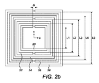
図2aおよび図2bは、図1aの遮蔽層からの単セル16を示している。この構成では、単セル16は5つの同心スプリットリング共振器を有する。図2bは、同心スプリットリング共振器の相対寸法を示すために図2aに対して90度回転している。5つとは単なる例示であり、他の数の共振器が使用されてもよいことが理解されるであろう。
Figures 2a and 2b show a
各スプリットリング共振器は、ループの一方の辺にギャップを有する略正方形のループを画定する導電性材料の薄い軌道(例えば1.5mm)から形成される。最も内側の(または第1の)ループ20は、内部幅がW1であり、長さがL1である。第1のループは、長さが内部幅W1および軌道の幅に等しい一方の辺に沿って中間に位置決めされる単一のギャップ21を有する。2番目に内側の(または第2の)ループ22は内部幅W2と長さL2とを有し、ループ22のギャップ23もまた、一方の辺に沿って中間に位置決めされる。第2のループ22内のギャップ23は、ギャップ21を有する第1のループ20の辺とは反対側にある。ギャップを反対側に位置決めする交互パターンは、次の3つのループについて繰り返される。したがって、幅がW3で長さがL3の第3のループ24および幅がW5で長さがL5の第5のループは、第1のループ20内のギャップ21と同じ側にギャップ25および29を有する。同様に、幅がW4および長さがL4の第4のループは、第2のループ22内のギャップ23と同じ側にギャップ27を有する。各ギャップは同じ幅Gを有し、また、ギャップが互いに位置合わせされることにより、各ギャップの中心点が同一軸線上に整列する。幅W1は、例えば長さL1よりも約5%わずかに長いため、最も内側のループは矩形であり、ほぼ正方形である。他の各ループもまた、長さよりもわずかに幅が長く、この構造では、各ループの幅Wと長さLとの差はループごとに同じである。
Each split ring resonator is formed from a thin track (eg, 1.5 mm) of conductive material defining a generally square loop with a gap on one side of the loop. The innermost (or first)
図2aに示すように、隣接する各ループ間には間隔がある。最初の3つのループの各々の周囲の間隔は、各ループ全体の幅T1が均一な間隔である。幅T1は、例えば0.5mmなど、ギャップGと同じ大きさであってもよい。第4のループと第5のループとの間隔は均一ではない。間隔は、3つの辺に沿った幅T1と、第4の辺に沿ったより狭い幅T2とを有する。図2cは、第4のループ26および第5のループ28のみの概略図であり、この不均一な間隔をより明確に示している。ギャップを含まない2つの辺の間には、より狭い幅T2の間隔がある。
As shown in Figure 2a, there is a gap between each adjacent loop. The spacing around each of the first three loops is a uniform spacing of width T1 across each loop. The width T1 may be as large as the gap G, for example 0.5 mm. The spacing between the fourth and fifth loops is not uniform. The spacing has a width T1 along three sides and a narrower width T2 along the fourth side. Figure 2c, which is a schematic illustration of only the
第4のループおよび第5のループの間隔が不均一であり、かつ各ループの幅および長さが異なるため、図2aのユニットセルの全体構造は非対称的もしくは非周期的である。幅および長さが等しく、ギャップの大きさが等しく、ギャップが位置合わせされ、ループ間の間隔が等しい同心の正方形ループを有する構造は、対称構造または周期構造である。各ループの幅および長さ、および第4のループと第5のループとの間の一方の辺に沿った間隔を調整することは、非対称性を達成するための単なる例にすぎず、例えば他のギャップもしくは各ギャップの間隔および大きさ、または他のループ間もしくは他方の辺のループ間の間隔など、非対称性を達成するために他の変数を変更することができることが理解されるであろう。構造の非対称性を変更して、選択周波数の電磁波を吸収しかつ反射することができる。したがって、構造は選択周波数で(つまり、選択された電磁帯域内で)共振し、かつ選択周波数による放射線を低減するので、構造を電磁バンドギャップ構造と呼ぶことができる。 Due to the non-uniform spacing of the fourth and fifth loops and the different width and length of each loop, the overall structure of the unit cell of Figure 2a is asymmetrical or aperiodic. A structure with concentric square loops of equal width and length, equal gap sizes, aligned gaps, and equal spacing between loops is a symmetrical or periodic structure. Adjusting the width and length of each loop and the spacing along one side between the fourth and fifth loops are merely examples for achieving asymmetry, e.g. It will be understood that other variables can be varied to achieve asymmetry, such as the spacing and size of the or each gap, or the spacing between other loops or between loops on the other side. . The asymmetry of the structure can be altered to absorb and reflect electromagnetic waves at selected frequencies. Therefore, the structure can be referred to as an electromagnetic bandgap structure because it resonates at selected frequencies (ie, within a selected electromagnetic band) and reduces radiation at selected frequencies.
上述の通り、各遮蔽体内のセルの配置は、遮蔽体が、ユーザ機器40が放射線を放出している周波数の領域において負の屈折率を有するように設計されている。各セルは、放射された周波数で共振するように設計されている。特定の周波数における負の屈折率および共振は、ユニットセルのパラメータを調整することで達成することができる。パラメータは、各ループの幅および長さ、ループ間の間隔、ギャップの位置および大きさのうち一部または全てを含んでもよい。
As noted above, the placement of the cells within each shield is designed such that the shield has a negative refractive index in the region of frequencies at which the
屈折率(n)を計算する1つの方法は、標準の検索手順を使用することである。他の技術を使用することもできることが理解されるであろう。一例としては、散乱パラメータ(Sパラメータとしても知られる)を使用した屈折率(n)および相対インピーダンス(Z)が挙げられる。 One way to calculate the refractive index (n) is to use standard search procedures. It will be appreciated that other techniques can also be used. One example is refractive index (n) and relative impedance (Z) using scattering parameters (also known as S-parameters).
相対インピーダンス(Z)および屈折率(n)は次のように記述することができる。


次に、遮蔽体のパラメータ、実効誘電率εeffおよび有効透磁率μeffを、
εeff=n/Z
μeff=nZ
を使用して導いた。
Then, the parameters of the shield, the effective permittivity ε eff and the effective permeability μ eff , are
ε eff =n/Z
μ eff =nZ
led using
上述の式により、単セルについてパラメータを決定し、かつ変更を設計することが可能になる。例えば、スプリットリング間のギャップの間隔を狭くすることにより、1800MHz帯域での電磁遮蔽が高まり、かつアンテナ効率が向上する。しかし、単セルを変更しても、以下に示すように2つのセルを必要とするデュアルバンド保護の問題は解決しない。 The above equations allow parameters to be determined and modifications designed for a single cell. For example, narrowing the gap spacing between split rings increases electromagnetic shielding and improves antenna efficiency in the 1800 MHz band. However, changing the single cell does not solve the problem of dual-band protection requiring two cells as shown below.
図3aは、互いに隣接する2つの単セル16を備えるデュアルバンドユニットセル30を示している。デュアルバンドユニットセルのパラメータはまた、上述の式を使用して選択することができる。デュアルバンドユニットセルは、2つの異なる周波数で共振するように設計されており、例えば900MHzおよび1800MHzは、携帯電話事業者が現在使用している2つの帯域である。デュアルバンドユニットセルは、互いの倍数である周波数だけでなく、任意の2つの周波数で共振するように設計することができる。例えば、携帯電話事業者に一般的に使用される他の2つの帯域は、850MHzおよび1900MHzである。低周波数では、所望の共振を提供するためにさらに大きなセルユニットが必要である。
FIG. 3a shows a dual-
図3aに示すように、各単セルの第1のループ20、第2のループ22、第3のループ24および第4のループ26は、図2aおよび図2bに示されるセルのループと同一である。共通ループ32は、セルごとに第5のループを形成する。共通ループ32は、両方の隣接セルの周囲にループを形成する軌道を有する。軌道には、各々が単セルの第5のループ内のギャップ29と等しい2つのギャップ36がある。共通ループ32内のギャップ36の各々は、それぞれの単セルの第1のループおよび第3のループ内のギャップと位置合わせされ、かつ、大きさが等しい。共通ループ32はまた、共通ループの2つのギャップを有する辺と対向辺との間に延びる分割器34を有する。分割器34は、両方のセルについて第5のループの一方の辺を形成するので、両方のセルについて第4のループの一方の辺の間に延び、かつ第4のループの一方の辺から間隔を置いて配置される。したがって、分割器34は共通ループ32を短絡させる。
As shown in Figure 3a, the
実質的に、デュアルバンドセルユニットは、2つの重複ループ(各セルの第5のループ)の内側に包囲された8つのループ(ユニットセルごとに1~4)の合計で10のループを有する重複構造である。実験的研究により、このような重複配置は、例えば互いに位置合わせされて隣接する2つのセルとの組合せ、または、例えば各セルの外側ループのギャップが対向するように一方のセルが他方に対して相対的に回転している組合せなど、単セルの他の組合せよりも電磁放射線を偏向するのにさらに有効であることが示されている。結果は、重複構造が900MHzおよび1800MHzの両方で電磁波を偏向するのに有効であることを示している。しかし、900MHzでの波長が長いため、電磁波の35%しか偏向されない。したがって、図1aに示すように、デュアルバンドユニットセルを2つ以上のループ内に包囲して、アンテナ効率を低下させることなく全体的な遮蔽性能を向上させることができる。追加のループもまた、システム全体の周波数帯域に影響を及ぼさず、遮蔽体は、900MHzなどの低周波数用の電気的小型アンテナ(ESA)を容易に覆うことができる空間の制約内に留まっている。追加のループは、より小さな内側ループのスプリットリング共振器とは対照的に、開ループ共振器であってもよい。 In effect, the dual-band cell unit has 8 loops (1-4 per unit cell) wrapped inside 2 overlapping loops (the 5th loop of each cell) for a total of 10 loops. Structure. Experimental studies have shown that such overlapping arrangements can be combined, e.g. It has been shown to be more effective in deflecting electromagnetic radiation than other combinations of single cells, such as relative rotating combinations. The results show that the overlapping structure is effective in deflecting electromagnetic waves at both 900MHz and 1800MHz. However, due to the long wavelength at 900 MHz, only 35% of the electromagnetic wave is deflected. Therefore, a dual-band unit cell can be enclosed in two or more loops to improve overall shielding performance without reducing antenna efficiency, as shown in FIG. 1a. The additional loop also has no effect on the overall system frequency band and the shield remains within the space constraints that can easily cover an electrical small antenna (ESA) for low frequencies such as 900MHz. . The additional loop may be an open loop resonator as opposed to a split ring resonator for the smaller inner loop.
単セルの非対称性を反映するために、デュアルバンドユニットセル30は、単セルを非対称に組み合わせる。これは、共通ループ32内の各ギャップ36が分割器34からは8.11mmであるが、共通ループ32のそれぞれの辺からは7.73mmしかないことを示す図3aの例示的な寸法を含めることによって示されている。これらの寸法は単なる例示であり、非対称性は図3bおよび図3cの概略図においてさらに一般的に示されていることが理解されるであろう。単セルの場合と同様に、第4のループ26の3つの辺と第5の共通ループ32の各部分の3つの辺との間の間隔は幅T1を有し、第4の辺の間の間隔はより狭い幅T2を有する。
To reflect the asymmetry of the single cells, the dual-
図3bは、幅がT2の狭い間隔が両方の単セルの同じ辺にある、1つの非対称配置を示している。図3cは、幅がT2の狭い間隔が共通ループ32の対向する短辺に隣接する代替の非対称配置を示している。換言すれば、一方のセルが他方のセルに対してy軸方向に反映されている。実験的研究により、図3bおよび3cの両方の配置が二重周波数帯域で共振可能であることが示されている。ただし図3bの配置では、図3cの配置よりもアンテナの性能が低下する。この研究では、図3bの配置がアンテナのSパラメータに悪影響を及ぼし、かつGSMアンテナの中心周波数に周波数シフトが生じることが示されている。これらの影響は、図3cの配置では回避される。
FIG. 3b shows one asymmetric arrangement in which a narrow spacing of width T2 is on the same side of both single cells. FIG. 3c shows an alternative asymmetric arrangement in which narrow spaces of width T2 adjoin opposite short sides of
上述の遮蔽体は、様々なユーザ機器とともに使用することができる。図4aは、上述の遮蔽体34を組み込んだ携帯機器32を示している。携帯機器32は、ユーザの頭部30の隣に位置決めされる。図4bは、ユーザの手に収まっている遮蔽体を含む携帯機器32を示している。
The shields described above can be used with a variety of user equipment. Figure 4a shows a
遮蔽体付き機器の性能は、シミュレーションおよび測定を使用して、遮蔽体を含まない機器の性能と比較されてきた。シミュレーションでは、2つのストリップモノポールと蛇行したストリップ線路とを有するマルチバンド平面アンテナを使用した。アンテナは、機器の一端の15mm×42mmの領域をカバーした。O Fujiwaraらによる、「Electrical properties of skin and SAR calculation in a realistic human model for microwave exposure」、Electrical Engineering in Japan、第120巻、第66~73頁、1997年、および、Meierらによる、「The dependence of electromagnetic energy absorption upon human-head modelling at 1800 MHz」、IEEE Transactions on Microwave Theory and Techniques、第MTT-45巻、第2058~2062頁、1997年において提供された教示に基づいて、ユーザの頭部について単純で均質な球形モデルを使用した。 The performance of shielded devices has been compared to that of devices without shields using simulations and measurements. The simulation used a multi-band planar antenna with two strip monopoles and a meandering stripline. The antenna covered an area of 15 mm x 42 mm at one end of the instrument. O Fujiwaraらによる、「Electrical properties of skin and SAR calculation in a realistic human model for microwave exposure」、Electrical Engineering in Japan、第120巻、第66~73頁、1997年、および、Meierらによる、「The dependence of electromagnetic energy absorption upon human-head modeling at 1800 MHz, IEEE Transactions on Microwave Theory and Techniques, MTT-45, Vol. A simple homogeneous spherical model was used.
頭部は2層でモデル化されている。外層は外殻であり、内層は液体である。各層の特性を以下に示す。手は、単一の液体層を使用してモデル化される。

移動体通信機器の準拠性試験は、組織質量が1g(ANSI-IEEE C95.1-1992、FCC)または10g(ICNIRP(1998年4月)、CENELEC 50166-2)の平均SAR値によって定義されている。遮蔽体内の様々な基板について、ユーザの頭部で使用されている機器のシミュレーション結果を以下に示す。

上記の表から、1gの組織においてRT5870基板を使用する遮蔽体については、SAR値は900MHzで60%低減し、同じ体積の場合に1800MHzで75%低減したことが明らかである。10gの組織について900MHzおよび1800MHzの両方で、SAR値の同じ割合の低減、つまりSAR値の58%および74%の低減が観察された。他の基板については、全てのパラメータがRT5870基板を有する機器と同じように保たれた。R04350B基板では、SAR値は組織1gについて900MHzで58%低減した。1gおよび10gについて1800MHzでは、SAR値はそれぞれ27.7%および21%低減した。また、組織10gについて900MHzでは、SARは57%低減した。RT5880で作られた可撓性基板の場合、SARは1gについて900MHzで63.4%低減し、同じ体積について1800MHzで55.6%低減した。10gの組織では、両方の周波数で同じ量の低減が観察され、900MHzおよび1800MHzについてそれぞれ64%および59.5%低減した。Cu-clad217基板を使用すると、結果はさらに著しく、SARは1gについて900MHzで63.4%低減し、同様に1800MHzで55.7%低減した。10gの結果に注目すると、900MHzで62%、1800MHzで59%低減したことが分かる。そのため、選択した基板のいずれかを有する遮蔽体は、ユーザの頭部に近接しているユーザ機器上で、両方の周波数で良好に機能する。 From the table above it is clear that for the shield using the RT5870 substrate at 1 g of tissue, the SAR value was reduced by 60% at 900 MHz and by 75% at 1800 MHz for the same volume. The same percentage reductions in SAR values were observed at both 900 MHz and 1800 MHz for 10 g of tissue, namely 58% and 74% reductions in SAR values. For the other substrates all parameters remained the same as the instrument with the RT5870 substrate. For the R04350B substrate, the SAR value was reduced by 58% at 900 MHz for 1 g of tissue. At 1800 MHz for 1 g and 10 g, the SAR values decreased by 27.7% and 21% respectively. Also, at 900 MHz for 10 g of tissue, the SAR was reduced by 57%. For flexible substrates made of RT5880, SAR decreased by 63.4% at 900 MHz for 1 g and decreased by 55.6% at 1800 MHz for the same volume. For 10 g of tissue, the same amount of reduction was observed at both frequencies, with 64% and 59.5% reductions for 900 MHz and 1800 MHz, respectively. Using a Cu-clad217 substrate, the results were even more striking, with a 63.4% reduction in SAR at 900 MHz and a similar 55.7% reduction at 1800 MHz for 1 g. Looking at the 10g results, we can see a reduction of 62% at 900MHz and 59% at 1800MHz. As such, a shield with either of the selected substrates works well at both frequencies on user equipment in close proximity to the user's head.
図4bに示すようにユーザの手に保持されている機器のシミュレーション結果を以下に示す。

第1の基板では、SAR値は1gおよび10gの両方についての周波数で低減した。1gについて900MHzでは51%低減し、1800MHzでは59.7%低減した。SARは、10gについて900MHzで54%の低減が観察され、1800MHzで48%低減した。この構成は、設計によりSAR値が半分に低減し、したがって遮蔽体が両方の帯域に機能することを示している。 For the first substrate, the SAR values decreased at frequencies for both 1g and 10g. At 900 MHz, it was reduced by 51% for 1 g, and at 1800 MHz, it was reduced by 59.7%. SAR was observed to be reduced by 54% at 900 MHz and reduced by 48% at 1800 MHz for 10g. This configuration reduces the SAR value by half by design, thus showing that the shield works for both bands.
可撓性基板R04350Bでは、SARは1gについて900MHzで36.3%低減した。10gについて900MHzでは41.3%低減し、遮蔽体が900MHzで機能することを示している。しかし、1800MHzの結果は期待通りではない。SAR値は1gおよび10gの両方で増加し、1gで94%、10gで70%であるが、依然として欧州基準の2W/kgを下回っている。したがって、この構成では、設計された遮蔽体は900MHz帯域でしか機能しないと結論付けることができる。 For flexible substrate R04350B, SAR decreased by 36.3% at 900 MHz for 1 g. There is a 41.3% reduction at 900 MHz for 10 g, indicating that the shield works at 900 MHz. However, the 1800 MHz results are not as expected. The SAR values increased at both 1 g and 10 g, 94% at 1 g and 70% at 10 g, but still below the European standard of 2 W/kg. Therefore, it can be concluded that in this configuration the designed shield works only in the 900 MHz band.
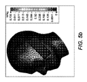
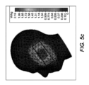
図5aから図5hは、図1aに示した遮蔽体を含むユーザ機器および遮蔽体を含まないユーザ機器のシミュレーション結果である。図5aおよび図5bは、遮蔽体を含まない組織質量および遮蔽体を含む組織質量の1gに対して900MHzでのSAR結果を示している。図5cおよび図5dは、遮蔽体を含まない組織質量および遮蔽体を含む組織質量の10gに対して900MHzでのSAR結果を示している。図5eおよび図5fは、遮蔽体を含まない組織質量および遮蔽体を含む組織質量の1gに対して1800MHzでのSAR結果を示している。図5gおよび図5hは、遮蔽体を含まない組織質量および遮蔽体を含む組織質量の10gに対して1800MHzでのSAR結果を示している。いずれの場合も、遮蔽体付き機器の比吸収率(SAR)が低下する。 Figures 5a to 5h are simulation results of the user equipment with and without the shield shown in Figure la. Figures 5a and 5b show SAR results at 900 MHz for 1 g of tissue mass without and with shield. Figures 5c and 5d show the SAR results at 900 MHz for 10 g of tissue mass without and with shield. Figures 5e and 5f show the SAR results at 1800 MHz for 1 g of tissue mass without and with shield. Figures 5g and 5h show SAR results at 1800 MHz for 10 g of tissue mass without and with shield. In either case, the specific absorption rate (SAR) of the shielded device is reduced.
図6は、遮蔽体を含む機器および遮蔽体を含まない機器内のアンテナの周波数に対する測定された反射減衰量をdBで示している。図6は、アンテナの放射効率を正常に維持することができることを示している。 FIG. 6 shows the measured return loss in dB versus frequency for antennas in devices with and without shields. FIG. 6 shows that the radiation efficiency of the antenna can be maintained normally.
遮蔽体は、様々な機器とともに使用することができる。例えば図7は、ラップトップに組み込まれる前の上述の遮蔽体72の概略図である。アンテナを組み込むラップトップの基層70は遮蔽体72に隣接し、遮蔽層は基層70に隣接している。例えばプラスチックなどの任意の保護層74は、遮蔽体72の基層70の対向表面上にある。ラップトップは、15mmの骨層の周囲の2つの組織(液体)の3mm層としてモデル化されたユーザの脚部76の上に載置されている。

この構成のSAR値についても同様の結果が得られる。上記では、SARは1gの組織について900MHzで26%低減した。10gの組織について900MHzでは、SARが56.4%低減したことが明らかである。しかし、1800MHzでの結果はわずかに異なる。1gの組織について1800MHzでは、SAR値は9%だけ増加した一方で、10gの組織について1800MHzでは、EBGはSAR値を19.9%低減させた。1gについて1800MHzでのこのような奇妙な挙動の考えられる理由の1つは、SARの計算に使用される一定体積の近似によるものである。 Similar results are obtained for the SAR values for this configuration. Above, SAR was reduced by 26% at 900 MHz for 1 g of tissue. A 56.4% reduction in SAR is evident at 900 MHz for 10 g of tissue. However, the results at 1800 MHz are slightly different. At 1800 MHz for 1 g of tissue, the SAR value increased by 9%, while at 1800 MHz for 10 g of tissue, EBG reduced the SAR value by 19.9%. One possible reason for such strange behavior at 1800 MHz for 1 g is due to the constant volume approximation used in the SAR calculations.
上述のシミュレーションから得られた結果は、測定によって得られた結果と比較された。例えば図6aおよび図6bは、遮蔽体を含むユーザ機器(左側)および遮蔽体を含まないユーザ機器(右)のSARの測定結果を示している。使用時、遮蔽体はアンテナから2.4mmに位置決めされ、図1aに示すように12のセルを有する。シミュレーションおよび測定結果の両方から、図1aに示す遮蔽体設計は、900MHz帯域および1800MHz帯域の両方についてSARを極めて高度に低減可能であることが示されている。低減の範囲は、シミュレーションの構成および基板材料に応じて60%~98%である。さらに、性能を損なうことなく、用途の必要性に応じて構造全体の大きさを変更することができることもまた、結果から明らかである。 The results obtained from the simulations described above were compared with the results obtained by measurements. For example, Figures 6a and 6b show measurements of SAR for a user equipment with a shield (left) and a user equipment without a shield (right). In use, the shield is positioned 2.4 mm from the antenna and has 12 cells as shown in FIG. 1a. Both simulation and measurement results show that the shield design shown in FIG. 1a is capable of extremely high SAR reduction for both the 900 MHz and 1800 MHz bands. The reduction ranges from 60% to 98% depending on the simulation configuration and substrate material. Furthermore, it is also clear from the results that the overall structure can be scaled according to the needs of the application without compromising performance.
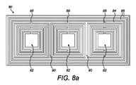
図8aは、並んで配置された3つのユニットセル82に基づく重複構造でもある代替セルユニット80を示している。セルユニット80は、3つの重複ループ(各セルの第5のループ)と、2つのさらなる外側ループ86とで実質的に形成された共通ループ84の内側に包囲された12のループ(ユニットセルごとに1~4)の合計で15のループを有する。各単セルの第1~第4のループは、図2aおよび図2bに示されるセルのループと同一である。共通ループ84は、全ての隣接セルの周囲にループを形成する軌道を有する。軌道には、各々が単セルの第5のループ内のギャップ29と等しい3つのギャップ88がある。共通ループ84内のギャップ88の各々は、それぞれの単セルの第1のループおよび第3のループ内のギャップと位置合わせされ、かつ、大きさが等しい。共通ループ84はまた、各々が2つの隣接セルについて第5のループの一方の辺を形成する2つの分割器90を有する。代替のユニットセルは、アンテナ効率を低下させることなく全体的な遮蔽性能を向上させるために、2つのさらなる外側ループ86内に包囲されている。
Figure 8a shows an
図3aのデュアルバンドセルユニットと同様に、代替セルユニット80もまた、異なる周波数で共振するように設計されたデュアルバンドセルユニットである。さらに、図3aに示したものと同様の方法で、単セルの非対称性を反映するために、代替ユニットセル80は単セルを非対称にグループ化する。すなわち、3つのユニットセルは、上述のように各個別対の内部に、他の二対の各々に対して非対称に配置された三対のセルを形成する。
Similar to the dual-band cell unit of Figure 3a,
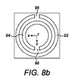
図8bは、ユニットセルの代替設計を示している。このユニットセルは、2つの同心の略円形スプリットリング共振器92および94を備える。異なる数のスプリットリング共振器を使用してもよいことが理解されるであろう。上記と同様に、外側ループ92内のギャップ96は、ギャップ98を有する第1のループ94の位置と対向する位置にある。上記と同様に、例えば円形よりも楕円形となるように形状を調整するか、またはギャップ96および98の位置合わせを変更することにより、非対称性を設計に組み込むことができる。
Figure 8b shows an alternative design of the unit cell. This unit cell comprises two concentric, substantially circular
本明細書では、任意の特徴の様々な組合せが説明されており、記載した特徴を任意の適切な組合せで組み合わせてもよいことが理解されるであろう。具体的には、任意の一実施形態の特徴は、このような組合せが相互に排他的である場合を除いて、必要に応じて他の任意の実施形態の特徴と組み合わされてもよい。この明細書全体を通して、「含んでいる」もしくは「含む」という用語は、指定された構成要素を含むことを意味するが、他の構成要素の存在を除外するものではない。 Various combinations of any of the features are described herein, and it will be appreciated that the features described may be combined in any suitable combination. In particular, features of any one embodiment may be combined with features of any other embodiment as appropriate, except where such combinations are mutually exclusive. As used throughout this specification, the term "comprising" or "comprising" means including the specified component, but does not exclude the presence of other components.
本明細書に開示された全ての特徴(添付の特許請求の範囲、要約および図面を含む)、および/またはそのように開示された任意の方法もしくは工程の全てのステップは、このような特徴および/またはステップの少なくともいくつかが相互に排他的である組合せを除いて、任意の組合せで組み合わされてもよい。本明細書で開示された各特徴(添付の特許請求の範囲、要約および図面を含む)は、特に明記しない限り、同じ、同等または類似の目的に役立つ代替特徴に置き換えられてもよい。したがって、特に明記しない限り、開示された各特徴は、一般的な一連の同等もしくは類似の特徴の一例にすぎない。 All features disclosed in this specification, including any appended claims, abstract and drawings, and/or all steps of any method or process so disclosed may be interpreted as including such features and /or at least some of the steps may be combined in any combination, except combinations where they are mutually exclusive. Each feature disclosed in this specification, including any appended claims, abstract and drawings, may be replaced by alternative features serving the same, equivalent or similar purpose, unless stated otherwise. Thus, unless stated otherwise, each feature disclosed is one example only of a generic series of equivalent or similar features.
本発明は、上述の実施形態の詳細に限定されない。本発明は、本明細書(添付の特許請求の範囲、要約および図面を含む)に開示された特徴の新規な発明もしくは新規な組合せ、または、そのように開示された任意の方法もしくは工程のステップの新規な発明もしくは新規な組合せに及ぶ。本発明のいくつかの好ましい実施形態を示して説明してきたが、当業者は、添付の特許請求の範囲で定義される本発明の範囲から逸脱することなく様々な変更および修正を行ってもよいことを理解するであろう。 The invention is not limited to the details of the above-described embodiments. The present invention resides in a novel invention or novel combination of features disclosed in this specification, including the appended claims, abstract and drawings, or any method or process step so disclosed. to new inventions or new combinations of While several preferred embodiments of the invention have been shown and described, those skilled in the art may make various changes and modifications without departing from the scope of the invention as defined in the appended claims. you will understand.
Claims (15)
各セルが互いに間隔を置いて配置された複数の共振器を含む複数のセルを備え、
前記複数のセルは複数のユニットセルに配置され、各ユニットセルは、前記複数のセルのうち少なくとも2つの隣接セルを囲む共通ループを備え、
前記複数のユニットセルの各々は、前記遮蔽装置が少なくとも1つの選択周波数について負の屈折率を有し、それによって前記少なくとも1つの選択周波数の電磁放射線が減衰されるように非対称構造を有し、
前記複数のユニットセルの各々は、第1の対の隣接共振器を有する第1のセルと第2の対の隣接共振器を有する第2のセルとを備え、前記第1の対の隣接共振器間の間隔が前記第2の対の隣接共振期間の間隔とは異なるため、前記複数のユニットセルのうち少なくとも1つが非対称構造を有し、
前記ユニットセルの各々は、前記共通ループを囲む少なくとも2つの追加の共振器を含み、
前記追加の共振器がスプリットリング共振器であり、第1の追加の共振器のギャップが第2の追加の共振器のギャップに対して前記ユニットセルの対向端に位置決めされる、
遮蔽装置。 A shielding device for passively attenuating electromagnetic radiation, comprising:
comprising a plurality of cells, each cell including a plurality of spaced-apart resonators;
said plurality of cells arranged in a plurality of unit cells, each unit cell comprising a common loop surrounding at least two adjacent cells of said plurality of cells;
each of the plurality of unit cells has an asymmetric structure such that the shielding device has a negative refractive index for at least one selected frequency, thereby attenuating electromagnetic radiation at the at least one selected frequency;
Each of the plurality of unit cells comprises a first cell having a first pair of adjacent resonators and a second cell having a second pair of adjacent resonators, wherein the first pair of adjacent resonators at least one of the plurality of unit cells has an asymmetric structure because the spacing between the cells is different than the spacing of adjacent resonance periods of the second pair;
each of said unit cells comprising at least two additional resonators surrounding said common loop;
wherein said additional resonator is a split ring resonator, and a gap of a first additional resonator is positioned at opposite ends of said unit cell with respect to a gap of a second additional resonator;
Shielding device.
前記遮蔽装置が、使用時に前記遮蔽装置がユーザと前記エミッタとの間にあるように、前記エミッタに隣接して位置する、請求項1~12のいずれか一項に記載の遮蔽装置を組み込んだユーザ機器。 comprising an emitter that emits electromagnetic radiation,
Incorporating a shielding device according to any one of the preceding claims, wherein the shielding device is positioned adjacent to the emitter such that in use the shielding device is between the user and the emitter. User equipment.
Applications Claiming Priority (3)
| Application Number | Priority Date | Filing Date | Title |
|---|---|---|---|
| GBGB1708242.1A GB201708242D0 (en) | 2017-05-23 | 2017-05-23 | Radiation shield |
| GB1708242.1 | 2017-05-23 | ||
| PCT/GB2018/051398 WO2018215765A1 (en) | 2017-05-23 | 2018-05-23 | Radiation shield |
Publications (3)
| Publication Number | Publication Date |
|---|---|
| JP2020521411A JP2020521411A (en) | 2020-07-16 |
| JP2020521411A5 JP2020521411A5 (en) | 2021-07-26 |
| JP7210558B2 true JP7210558B2 (en) | 2023-01-23 |
Family
ID=59220587
Family Applications (1)
| Application Number | Title | Priority Date | Filing Date |
|---|---|---|---|
| JP2020515295A Active JP7210558B2 (en) | 2017-05-23 | 2018-05-23 | radiation shield |
Country Status (9)
| Country | Link |
|---|---|
| US (1) | US11316265B2 (en) |
| EP (1) | EP3631896B1 (en) |
| JP (1) | JP7210558B2 (en) |
| KR (1) | KR102438235B1 (en) |
| CN (1) | CN110998971B (en) |
| ES (1) | ES2924262T3 (en) |
| GB (1) | GB201708242D0 (en) |
| PL (1) | PL3631896T3 (en) |
| WO (1) | WO2018215765A1 (en) |
Families Citing this family (6)
| Publication number | Priority date | Publication date | Assignee | Title |
|---|---|---|---|---|
| TWI693744B (en) * | 2019-01-22 | 2020-05-11 | 緯創資通股份有限公司 | Antenna system |
| CN110364821A (en) * | 2019-07-26 | 2019-10-22 | 重庆邮电大学 | Ultra wide band Terahertz asymmetric transmission device |
| CN110504541B (en) * | 2019-08-27 | 2021-11-02 | 南京邮电大学 | Electromagnetic metamaterial structure for reducing coupling degree of MIMO antenna |
| RU2751128C1 (en) * | 2020-11-24 | 2021-07-08 | Столяров Сергей Михайлович | Radiation protection device |
| US20230253702A1 (en) * | 2022-02-10 | 2023-08-10 | Swiftlink Technologies Co., Ltd. | Periodic Mode-Selective Structure for Surface Wave Scattering Mitigation in Millimeter Wave Antenna Arrays |
| CN114818412B (en) * | 2022-03-18 | 2022-09-27 | 北京航空航天大学 | High-precision calculation method for electromagnetic radiation of human brain |
Citations (5)
| Publication number | Priority date | Publication date | Assignee | Title |
|---|---|---|---|---|
| JP2005260965A (en) | 2004-03-10 | 2005-09-22 | Lucent Technol Inc | Media with controllable refractive properties |
| JP2010272865A (en) | 2009-05-22 | 2010-12-02 | Korea Minting & Security Printing Corp | Electromagnetic bandgap pattern, method of manufacturing the same, and security product using electromagnetic bandgap pattern |
| US20120274523A1 (en) | 2011-04-27 | 2012-11-01 | Mina Ayatollahi | Antenna assembly utilizing metal-dielectric resonant structures for specific absorption rate compliance |
| US20140043194A1 (en) | 2012-08-09 | 2014-02-13 | Soongsil University-Industry Cooperation Foundation | Terminal device having meta-structure |
| JP2015185946A (en) | 2014-03-20 | 2015-10-22 | キヤノン株式会社 | antenna device |
Family Cites Families (29)
| Publication number | Priority date | Publication date | Assignee | Title |
|---|---|---|---|---|
| US6791432B2 (en) * | 2000-03-17 | 2004-09-14 | The Regents Of The University Of California | Left handed composite media |
| GB0130513D0 (en) | 2001-12-20 | 2002-02-06 | Univ Southampton | Device for changing the polarization state of reflected transmitted and diffracted light and for achieving frequency and polarization sensitive reflection and |
| WO2004020186A2 (en) | 2002-08-29 | 2004-03-11 | The Regents Of The University Of California | Indefinite materials |
| US7205941B2 (en) | 2004-08-30 | 2007-04-17 | Hewlett-Packard Development Company, L.P. | Composite material with powered resonant cells |
| US8271241B2 (en) | 2005-01-18 | 2012-09-18 | University Of Massachusetts Lowell | Chiral metamaterials |
| US7525711B1 (en) | 2005-08-31 | 2009-04-28 | The United States Of America As Represented By The Secretary Of The Navy | Actively tunable electromagnetic metamaterial |
| US7683444B2 (en) * | 2005-09-30 | 2010-03-23 | The United States Of America As Represented By The Secretary Of The Navy | Metamaterial structure has resonant and strip line elements comprising a photoconductive semiconductor material formed on substrate to induce negative permeability and negative permittivity in operating frequency range |
| US8207907B2 (en) | 2006-02-16 | 2012-06-26 | The Invention Science Fund I Llc | Variable metamaterial apparatus |
| CN101162797B (en) | 2006-10-10 | 2011-12-14 | 西北工业大学 | Negative magnetic-inductive capacity material mobile phone antenna electromagnetic shielding device |
| KR20100066459A (en) | 2007-08-31 | 2010-06-17 | 유니프랙스 아이 엘엘씨 | Exhaust gas treatment device |
| US20090206963A1 (en) * | 2008-02-15 | 2009-08-20 | Toyota Motor Engineering & Manufacturing North America, Inc. | Tunable metamaterials using microelectromechanical structures |
| DE102008016294A1 (en) | 2008-03-28 | 2009-10-01 | Dritte Patentportfolio Beteiligungsgesellschaft Mbh & Co.Kg | Manufacturing method for a surface sensor, system and use of a surface sensor |
| US8724001B2 (en) | 2008-06-26 | 2014-05-13 | University Of Idaho | Analog-to-digital converter using a ramp generator |
| US9306078B2 (en) | 2008-09-08 | 2016-04-05 | Cbrite Inc. | Stable amorphous metal oxide semiconductor |
| US8130031B2 (en) * | 2009-01-28 | 2012-03-06 | Toyota Motor Engineering & Manufacturing North America, Inc. | Tunable metamaterial |
| US20100314040A1 (en) * | 2009-06-10 | 2010-12-16 | Toyota Motor Engineering & Manufacturing North America, Inc. | Fabrication of metamaterials |
| US8633866B2 (en) * | 2010-02-26 | 2014-01-21 | The Regents Of The University Of Michigan | Frequency-selective surface (FSS) structures |
| TWI455404B (en) * | 2010-11-02 | 2014-10-01 | Ind Tech Res Inst | Structure for adjusting em wave penetration response and antenna structure for adjusting em wave radiation characteristic |
| CN102802066B (en) * | 2011-06-30 | 2016-09-28 | 深圳光启高等理工研究院 | A kind of hand-held CMMB terminal |
| GB201114625D0 (en) | 2011-08-24 | 2011-10-05 | Antenova Ltd | Antenna isolation using metamaterial |
| CN102969572B (en) * | 2011-09-01 | 2015-06-17 | 深圳光启高等理工研究院 | Low frequency negative-magnetic-conductivity metamaterial |
| WO2013072844A1 (en) * | 2011-11-14 | 2013-05-23 | Schlumberger Technology B.V. | Enhanced materials investigation |
| US9362618B2 (en) | 2012-10-18 | 2016-06-07 | William P. Alberth, Jr. | Radio frequency shielded clothing |
| US20150369886A1 (en) * | 2013-01-11 | 2015-12-24 | Mri Innovations | System and method for decoupling magnetic resonance imaging radio frequency coils with a modular magnetic wall |
| US9325047B1 (en) * | 2013-03-11 | 2016-04-26 | University Of South Florida | Dynamically reconfigurable bandpass filters |
| WO2015183915A1 (en) * | 2014-05-27 | 2015-12-03 | The University Of Florida Research Foundation, Inc. | Glass interposer integrated high quality electronic components and systems |
| CN103983364B (en) * | 2014-05-27 | 2017-02-15 | 龚诚 | Metamaterial pixel structure and focal plane array imaging detector using same |
| US11011282B1 (en) * | 2016-06-30 | 2021-05-18 | Iowa State University Research Foundation, Inc. | Wearable microwave meta-skin with tunable frequency selective and cloaking effects |
| US10403981B2 (en) * | 2016-07-01 | 2019-09-03 | Hyundai Motor Company | Electromagnetic wave absorber |
-
2017
- 2017-05-23 GB GBGB1708242.1A patent/GB201708242D0/en not_active Ceased
-
2018
- 2018-05-23 US US16/616,032 patent/US11316265B2/en active Active
- 2018-05-23 EP EP18728705.7A patent/EP3631896B1/en active Active
- 2018-05-23 ES ES18728705T patent/ES2924262T3/en active Active
- 2018-05-23 PL PL18728705.7T patent/PL3631896T3/en unknown
- 2018-05-23 KR KR1020197037390A patent/KR102438235B1/en active IP Right Grant
- 2018-05-23 WO PCT/GB2018/051398 patent/WO2018215765A1/en active Application Filing
- 2018-05-23 JP JP2020515295A patent/JP7210558B2/en active Active
- 2018-05-23 CN CN201880049411.6A patent/CN110998971B/en active Active
Patent Citations (5)
| Publication number | Priority date | Publication date | Assignee | Title |
|---|---|---|---|---|
| JP2005260965A (en) | 2004-03-10 | 2005-09-22 | Lucent Technol Inc | Media with controllable refractive properties |
| JP2010272865A (en) | 2009-05-22 | 2010-12-02 | Korea Minting & Security Printing Corp | Electromagnetic bandgap pattern, method of manufacturing the same, and security product using electromagnetic bandgap pattern |
| US20120274523A1 (en) | 2011-04-27 | 2012-11-01 | Mina Ayatollahi | Antenna assembly utilizing metal-dielectric resonant structures for specific absorption rate compliance |
| US20140043194A1 (en) | 2012-08-09 | 2014-02-13 | Soongsil University-Industry Cooperation Foundation | Terminal device having meta-structure |
| JP2015185946A (en) | 2014-03-20 | 2015-10-22 | キヤノン株式会社 | antenna device |
Also Published As
| Publication number | Publication date |
|---|---|
| JP2020521411A (en) | 2020-07-16 |
| WO2018215765A1 (en) | 2018-11-29 |
| US20200144714A1 (en) | 2020-05-07 |
| EP3631896B1 (en) | 2022-06-29 |
| KR20200009061A (en) | 2020-01-29 |
| US11316265B2 (en) | 2022-04-26 |
| PL3631896T3 (en) | 2022-10-03 |
| EP3631896A1 (en) | 2020-04-08 |
| ES2924262T3 (en) | 2022-10-05 |
| CN110998971A (en) | 2020-04-10 |
| GB201708242D0 (en) | 2017-07-05 |
| KR102438235B1 (en) | 2022-08-30 |
| CN110998971B (en) | 2021-07-20 |
Similar Documents
| Publication | Publication Date | Title |
|---|---|---|
| JP7210558B2 (en) | radiation shield | |
| Yadav et al. | Smartphone frequency shielding with penta-bandstop FSS for security and electromagnetic health applications | |
| Yan et al. | Compact all-textile dual-band antenna loaded with metamaterial-inspired structure | |
| Hwang et al. | Reduction of the peak SAR in the human head with metamaterials | |
| Li et al. | Low-profile all-textile multiband microstrip circular patch antenna for WBAN applications | |
| Das et al. | Application of a compact electromagnetic bandgap array in a phone case for suppression of mobile phone radiation exposure | |
| US10218079B2 (en) | Periodic array assembly comprising arrays of periodic elements having inwardly extending protrusions | |
| Negi et al. | Design and performance analysis of a conformal CPW fed wideband antenna with Mu-Negative metamaterial for wearable applications | |
| Chaturvedi et al. | A dual‐band half‐mode substrate integrated waveguide‐based antenna for WLAN/WBAN applications | |
| Haridim | Use of rod reflectors for SAR reduction in human head | |
| Munde et al. | Low specific absorption rate antenna using electromagnetic band gap structure for long term evolution band 3 application | |
| KR100971931B1 (en) | Apparatus and method for lessening electromagnetic wave | |
| Kaur et al. | Sprocket gear wheel shaped printed monopole ultra‐wideband antenna with band notch characteristics: Design and measurement | |
| Kuther et al. | Radiation effect of fractal sierpinski square patch antenna | |
| Mersani et al. | Dielectric resonator antenna button textile antenna for off‐body applications | |
| Wang et al. | A CRLH-TL inspired dual-band antenna with polarization diversity for wrist-worn wireless body area network devices | |
| Mirhadi | Single-layer, dual-port, and dual-mode antenna with high isolation for WBAN communications | |
| Kwon et al. | Design of a dual-band antenna for wearable wireless body area network repeater systems | |
| Bahmanzadeh et al. | Dual Band-Notched Microstrip-Fed UWB Antenna for Wearable Medical Applications. | |
| Liu et al. | Design of wideband and flexible implantable antenna for wireless medical application | |
| Hazarika et al. | Multi-layered low-profile monopole antenna using metamaterial for wireless body area networks | |
| Karli et al. | A WIFI antenna radiation effects on human head in the ISM band | |
| Messaoudi et al. | Use of a Split Ring Resonators with Dipole and PIFA Antenna to Reduce the SAR in a Spherical Multilayered Head Model | |
| Sun et al. | New Dual-Band EMI Metamaterial with Holes for Shielding 5G Electromagnetic Signals | |
| Inamdar et al. | Fractal Metamaterial Inspired MSA for Wearable Devices |
Legal Events
| Date | Code | Title | Description |
|---|---|---|---|
| A521 | Request for written amendment filed |
Free format text: JAPANESE INTERMEDIATE CODE: A523 Effective date: 20210521 |
|
| A621 | Written request for application examination |
Free format text: JAPANESE INTERMEDIATE CODE: A621 Effective date: 20210521 |
|
| A977 | Report on retrieval |
Free format text: JAPANESE INTERMEDIATE CODE: A971007 Effective date: 20220524 |
|
| A131 | Notification of reasons for refusal |
Free format text: JAPANESE INTERMEDIATE CODE: A131 Effective date: 20220617 |
|
| A521 | Request for written amendment filed |
Free format text: JAPANESE INTERMEDIATE CODE: A523 Effective date: 20220801 |
|
| TRDD | Decision of grant or rejection written | ||
| A01 | Written decision to grant a patent or to grant a registration (utility model) |
Free format text: JAPANESE INTERMEDIATE CODE: A01 Effective date: 20221216 |
|
| A61 | First payment of annual fees (during grant procedure) |
Free format text: JAPANESE INTERMEDIATE CODE: A61 Effective date: 20230111 |
|
| R150 | Certificate of patent or registration of utility model |
Ref document number: 7210558 Country of ref document: JP Free format text: JAPANESE INTERMEDIATE CODE: R150 |