JP7204890B2 - Electrode manufacturing method and photoelectric conversion element manufacturing method - Google Patents
Electrode manufacturing method and photoelectric conversion element manufacturing method Download PDFInfo
- Publication number
- JP7204890B2 JP7204890B2 JP2021510482A JP2021510482A JP7204890B2 JP 7204890 B2 JP7204890 B2 JP 7204890B2 JP 2021510482 A JP2021510482 A JP 2021510482A JP 2021510482 A JP2021510482 A JP 2021510482A JP 7204890 B2 JP7204890 B2 JP 7204890B2
- Authority
- JP
- Japan
- Prior art keywords
- layer
- electrode
- carbon material
- metal
- photoelectric conversion
- Prior art date
- Legal status (The legal status is an assumption and is not a legal conclusion. Google has not performed a legal analysis and makes no representation as to the accuracy of the status listed.)
- Active
Links
- 238000006243 chemical reaction Methods 0.000 title claims description 56
- 238000004519 manufacturing process Methods 0.000 title claims description 33
- 229910052751 metal Inorganic materials 0.000 claims description 90
- 239000002184 metal Substances 0.000 claims description 90
- OKTJSMMVPCPJKN-UHFFFAOYSA-N Carbon Chemical compound [C] OKTJSMMVPCPJKN-UHFFFAOYSA-N 0.000 claims description 89
- 229910021389 graphene Inorganic materials 0.000 claims description 72
- 239000000758 substrate Substances 0.000 claims description 69
- 239000002086 nanomaterial Substances 0.000 claims description 67
- 238000000034 method Methods 0.000 claims description 65
- 239000006185 dispersion Substances 0.000 claims description 60
- 239000003575 carbonaceous material Substances 0.000 claims description 58
- BQCADISMDOOEFD-UHFFFAOYSA-N Silver Chemical compound [Ag] BQCADISMDOOEFD-UHFFFAOYSA-N 0.000 claims description 49
- 230000002209 hydrophobic effect Effects 0.000 claims description 36
- 239000002042 Silver nanowire Substances 0.000 claims description 31
- XLYOFNOQVPJJNP-UHFFFAOYSA-N water Substances O XLYOFNOQVPJJNP-UHFFFAOYSA-N 0.000 claims description 22
- 229920001343 polytetrafluoroethylene Polymers 0.000 claims description 16
- 239000004810 polytetrafluoroethylene Substances 0.000 claims description 16
- 239000000126 substance Substances 0.000 claims description 11
- 229920002873 Polyethylenimine Polymers 0.000 claims description 9
- -1 polytetrafluoroethylene Polymers 0.000 claims description 8
- 229910002804 graphite Inorganic materials 0.000 claims description 7
- 239000010439 graphite Substances 0.000 claims description 7
- 238000003825 pressing Methods 0.000 claims description 7
- 239000002131 composite material Substances 0.000 claims description 4
- 238000012545 processing Methods 0.000 claims description 4
- 230000003746 surface roughness Effects 0.000 claims 1
- 239000010410 layer Substances 0.000 description 235
- 239000002070 nanowire Substances 0.000 description 22
- 229920006254 polymer film Polymers 0.000 description 22
- KFZMGEQAYNKOFK-UHFFFAOYSA-N Isopropanol Chemical compound CC(C)O KFZMGEQAYNKOFK-UHFFFAOYSA-N 0.000 description 21
- 239000000463 material Substances 0.000 description 21
- LFQSCWFLJHTTHZ-UHFFFAOYSA-N Ethanol Chemical compound CCO LFQSCWFLJHTTHZ-UHFFFAOYSA-N 0.000 description 19
- 239000000872 buffer Substances 0.000 description 18
- 238000000576 coating method Methods 0.000 description 16
- 239000011248 coating agent Substances 0.000 description 15
- 239000007788 liquid Substances 0.000 description 13
- 229920000642 polymer Polymers 0.000 description 13
- 239000004065 semiconductor Substances 0.000 description 12
- 229920002799 BoPET Polymers 0.000 description 11
- 229910052709 silver Inorganic materials 0.000 description 11
- 239000004332 silver Substances 0.000 description 11
- 230000004888 barrier function Effects 0.000 description 9
- 239000002612 dispersion medium Substances 0.000 description 9
- 239000007789 gas Substances 0.000 description 9
- 229920001609 Poly(3,4-ethylenedioxythiophene) Polymers 0.000 description 8
- 239000007864 aqueous solution Substances 0.000 description 7
- 238000002788 crimping Methods 0.000 description 7
- 238000010586 diagram Methods 0.000 description 7
- 229920001600 hydrophobic polymer Polymers 0.000 description 7
- 239000002082 metal nanoparticle Substances 0.000 description 7
- 239000002245 particle Substances 0.000 description 7
- RYGMFSIKBFXOCR-UHFFFAOYSA-N Copper Chemical compound [Cu] RYGMFSIKBFXOCR-UHFFFAOYSA-N 0.000 description 6
- KWYUFKZDYYNOTN-UHFFFAOYSA-M Potassium hydroxide Chemical compound [OH-].[K+] KWYUFKZDYYNOTN-UHFFFAOYSA-M 0.000 description 6
- XLOMVQKBTHCTTD-UHFFFAOYSA-N Zinc monoxide Chemical compound [Zn]=O XLOMVQKBTHCTTD-UHFFFAOYSA-N 0.000 description 6
- MVPPADPHJFYWMZ-UHFFFAOYSA-N chlorobenzene Chemical compound ClC1=CC=CC=C1 MVPPADPHJFYWMZ-UHFFFAOYSA-N 0.000 description 6
- 229910052731 fluorine Inorganic materials 0.000 description 6
- 239000011737 fluorine Substances 0.000 description 6
- XOLBLPGZBRYERU-UHFFFAOYSA-N tin dioxide Chemical compound O=[Sn]=O XOLBLPGZBRYERU-UHFFFAOYSA-N 0.000 description 6
- 229910001887 tin oxide Inorganic materials 0.000 description 6
- YCKRFDGAMUMZLT-UHFFFAOYSA-N Fluorine atom Chemical compound [F] YCKRFDGAMUMZLT-UHFFFAOYSA-N 0.000 description 5
- 150000001298 alcohols Chemical class 0.000 description 5
- 229910052802 copper Inorganic materials 0.000 description 5
- 239000010949 copper Substances 0.000 description 5
- 239000002270 dispersing agent Substances 0.000 description 5
- 229920005597 polymer membrane Polymers 0.000 description 5
- 229910001316 Ag alloy Inorganic materials 0.000 description 4
- 239000002253 acid Substances 0.000 description 4
- 229910052782 aluminium Inorganic materials 0.000 description 4
- XAGFODPZIPBFFR-UHFFFAOYSA-N aluminium Chemical compound [Al] XAGFODPZIPBFFR-UHFFFAOYSA-N 0.000 description 4
- 229910052799 carbon Inorganic materials 0.000 description 4
- 125000004432 carbon atom Chemical group C* 0.000 description 4
- 230000006866 deterioration Effects 0.000 description 4
- 238000010438 heat treatment Methods 0.000 description 4
- 239000002904 solvent Substances 0.000 description 4
- 238000004544 sputter deposition Methods 0.000 description 4
- 238000012546 transfer Methods 0.000 description 4
- ZWEHNKRNPOVVGH-UHFFFAOYSA-N 2-Butanone Chemical compound CCC(C)=O ZWEHNKRNPOVVGH-UHFFFAOYSA-N 0.000 description 3
- LYCAIKOWRPUZTN-UHFFFAOYSA-N Ethylene glycol Chemical compound OCCO LYCAIKOWRPUZTN-UHFFFAOYSA-N 0.000 description 3
- OKKJLVBELUTLKV-UHFFFAOYSA-N Methanol Chemical compound OC OKKJLVBELUTLKV-UHFFFAOYSA-N 0.000 description 3
- ZMXDDKWLCZADIW-UHFFFAOYSA-N N,N-Dimethylformamide Chemical compound CN(C)C=O ZMXDDKWLCZADIW-UHFFFAOYSA-N 0.000 description 3
- FOIXSVOLVBLSDH-UHFFFAOYSA-N Silver ion Chemical compound [Ag+] FOIXSVOLVBLSDH-UHFFFAOYSA-N 0.000 description 3
- GWEVSGVZZGPLCZ-UHFFFAOYSA-N Titan oxide Chemical compound O=[Ti]=O GWEVSGVZZGPLCZ-UHFFFAOYSA-N 0.000 description 3
- 239000002041 carbon nanotube Substances 0.000 description 3
- 229910021393 carbon nanotube Inorganic materials 0.000 description 3
- 239000003638 chemical reducing agent Substances 0.000 description 3
- 238000005229 chemical vapour deposition Methods 0.000 description 3
- 239000011521 glass Substances 0.000 description 3
- 229930195733 hydrocarbon Natural products 0.000 description 3
- 150000002430 hydrocarbons Chemical class 0.000 description 3
- 230000005499 meniscus Effects 0.000 description 3
- 229910052757 nitrogen Inorganic materials 0.000 description 3
- 125000004433 nitrogen atom Chemical group N* 0.000 description 3
- 229920000301 poly(3-hexylthiophene-2,5-diyl) polymer Polymers 0.000 description 3
- 229920000139 polyethylene terephthalate Polymers 0.000 description 3
- 239000005020 polyethylene terephthalate Substances 0.000 description 3
- 229920000036 polyvinylpyrrolidone Polymers 0.000 description 3
- 239000001267 polyvinylpyrrolidone Substances 0.000 description 3
- 235000013855 polyvinylpyrrolidone Nutrition 0.000 description 3
- 230000008569 process Effects 0.000 description 3
- 239000011787 zinc oxide Substances 0.000 description 3
- NWZSZGALRFJKBT-KNIFDHDWSA-N (2s)-2,6-diaminohexanoic acid;(2s)-2-hydroxybutanedioic acid Chemical compound OC(=O)[C@@H](O)CC(O)=O.NCCCC[C@H](N)C(O)=O NWZSZGALRFJKBT-KNIFDHDWSA-N 0.000 description 2
- IJGRMHOSHXDMSA-UHFFFAOYSA-N Atomic nitrogen Chemical compound N#N IJGRMHOSHXDMSA-UHFFFAOYSA-N 0.000 description 2
- CURLTUGMZLYLDI-UHFFFAOYSA-N Carbon dioxide Chemical compound O=C=O CURLTUGMZLYLDI-UHFFFAOYSA-N 0.000 description 2
- RTZKZFJDLAIYFH-UHFFFAOYSA-N Diethyl ether Chemical compound CCOCC RTZKZFJDLAIYFH-UHFFFAOYSA-N 0.000 description 2
- VEXZGXHMUGYJMC-UHFFFAOYSA-N Hydrochloric acid Chemical compound Cl VEXZGXHMUGYJMC-UHFFFAOYSA-N 0.000 description 2
- LRHPLDYGYMQRHN-UHFFFAOYSA-N N-Butanol Chemical compound CCCCO LRHPLDYGYMQRHN-UHFFFAOYSA-N 0.000 description 2
- VYPSYNLAJGMNEJ-UHFFFAOYSA-N Silicium dioxide Chemical compound O=[Si]=O VYPSYNLAJGMNEJ-UHFFFAOYSA-N 0.000 description 2
- XUIMIQQOPSSXEZ-UHFFFAOYSA-N Silicon Chemical compound [Si] XUIMIQQOPSSXEZ-UHFFFAOYSA-N 0.000 description 2
- 229910045601 alloy Inorganic materials 0.000 description 2
- 239000000956 alloy Substances 0.000 description 2
- 239000012298 atmosphere Substances 0.000 description 2
- 125000004429 atom Chemical group 0.000 description 2
- QVGXLLKOCUKJST-UHFFFAOYSA-N atomic oxygen Chemical compound [O] QVGXLLKOCUKJST-UHFFFAOYSA-N 0.000 description 2
- 230000005540 biological transmission Effects 0.000 description 2
- 230000000903 blocking effect Effects 0.000 description 2
- 239000011575 calcium Substances 0.000 description 2
- 150000001768 cations Chemical class 0.000 description 2
- 150000001875 compounds Chemical class 0.000 description 2
- 229920001940 conductive polymer Polymers 0.000 description 2
- 229920001577 copolymer Polymers 0.000 description 2
- 238000000151 deposition Methods 0.000 description 2
- 230000008021 deposition Effects 0.000 description 2
- 238000009792 diffusion process Methods 0.000 description 2
- GNTDGMZSJNCJKK-UHFFFAOYSA-N divanadium pentaoxide Chemical compound O=[V](=O)O[V](=O)=O GNTDGMZSJNCJKK-UHFFFAOYSA-N 0.000 description 2
- 238000002338 electrophoretic light scattering Methods 0.000 description 2
- 230000002349 favourable effect Effects 0.000 description 2
- 239000011888 foil Substances 0.000 description 2
- 230000014509 gene expression Effects 0.000 description 2
- 229910052736 halogen Inorganic materials 0.000 description 2
- IKDUDTNKRLTJSI-UHFFFAOYSA-N hydrazine monohydrate Substances O.NN IKDUDTNKRLTJSI-UHFFFAOYSA-N 0.000 description 2
- AMGQUBHHOARCQH-UHFFFAOYSA-N indium;oxotin Chemical compound [In].[Sn]=O AMGQUBHHOARCQH-UHFFFAOYSA-N 0.000 description 2
- 238000002347 injection Methods 0.000 description 2
- 239000007924 injection Substances 0.000 description 2
- 229910010272 inorganic material Inorganic materials 0.000 description 2
- 238000010884 ion-beam technique Methods 0.000 description 2
- 229910044991 metal oxide Inorganic materials 0.000 description 2
- 150000004706 metal oxides Chemical class 0.000 description 2
- VNWKTOKETHGBQD-UHFFFAOYSA-N methane Chemical compound C VNWKTOKETHGBQD-UHFFFAOYSA-N 0.000 description 2
- 239000000203 mixture Substances 0.000 description 2
- 238000012986 modification Methods 0.000 description 2
- 230000004048 modification Effects 0.000 description 2
- JKQOBWVOAYFWKG-UHFFFAOYSA-N molybdenum trioxide Chemical compound O=[Mo](=O)=O JKQOBWVOAYFWKG-UHFFFAOYSA-N 0.000 description 2
- 239000000178 monomer Substances 0.000 description 2
- 239000002105 nanoparticle Substances 0.000 description 2
- 229910000480 nickel oxide Inorganic materials 0.000 description 2
- 229910052760 oxygen Inorganic materials 0.000 description 2
- 239000001301 oxygen Substances 0.000 description 2
- 230000035699 permeability Effects 0.000 description 2
- ZQBAKBUEJOMQEX-UHFFFAOYSA-N phenyl salicylate Chemical compound OC1=CC=CC=C1C(=O)OC1=CC=CC=C1 ZQBAKBUEJOMQEX-UHFFFAOYSA-N 0.000 description 2
- 238000005240 physical vapour deposition Methods 0.000 description 2
- BDERNNFJNOPAEC-UHFFFAOYSA-N propan-1-ol Chemical compound CCCO BDERNNFJNOPAEC-UHFFFAOYSA-N 0.000 description 2
- 230000001681 protective effect Effects 0.000 description 2
- 230000009467 reduction Effects 0.000 description 2
- 238000005096 rolling process Methods 0.000 description 2
- 238000007650 screen-printing Methods 0.000 description 2
- 229910052710 silicon Inorganic materials 0.000 description 2
- 239000010703 silicon Substances 0.000 description 2
- 229920002050 silicone resin Polymers 0.000 description 2
- 239000000243 solution Substances 0.000 description 2
- 239000007921 spray Substances 0.000 description 2
- 238000005507 spraying Methods 0.000 description 2
- BFKJFAAPBSQJPD-UHFFFAOYSA-N tetrafluoroethene Chemical group FC(F)=C(F)F BFKJFAAPBSQJPD-UHFFFAOYSA-N 0.000 description 2
- OGIDPMRJRNCKJF-UHFFFAOYSA-N titanium oxide Inorganic materials [Ti]=O OGIDPMRJRNCKJF-UHFFFAOYSA-N 0.000 description 2
- ZNOKGRXACCSDPY-UHFFFAOYSA-N tungsten trioxide Chemical compound O=[W](=O)=O ZNOKGRXACCSDPY-UHFFFAOYSA-N 0.000 description 2
- 238000007740 vapor deposition Methods 0.000 description 2
- VNFXPOAMRORRJJ-UHFFFAOYSA-N (4-octylphenyl) 2-hydroxybenzoate Chemical compound C1=CC(CCCCCCCC)=CC=C1OC(=O)C1=CC=CC=C1O VNFXPOAMRORRJJ-UHFFFAOYSA-N 0.000 description 1
- AQSGIPQBQYCRLQ-UHFFFAOYSA-N (6,6-dihydroxy-4-methoxycyclohexa-2,4-dien-1-yl)-phenylmethanone Chemical compound C1=CC(OC)=CC(O)(O)C1C(=O)C1=CC=CC=C1 AQSGIPQBQYCRLQ-UHFFFAOYSA-N 0.000 description 1
- UONCERAQKBPLML-UHFFFAOYSA-N (6-ethoxypyridin-3-yl)boronic acid Chemical compound CCOC1=CC=C(B(O)O)C=N1 UONCERAQKBPLML-UHFFFAOYSA-N 0.000 description 1
- BQCIDUSAKPWEOX-UHFFFAOYSA-N 1,1-Difluoroethene Chemical compound FC(F)=C BQCIDUSAKPWEOX-UHFFFAOYSA-N 0.000 description 1
- DUNYNUFVLYAWTI-UHFFFAOYSA-N 1-[(2-methylpropan-2-yl)oxy]ethanol Chemical compound CC(O)OC(C)(C)C DUNYNUFVLYAWTI-UHFFFAOYSA-N 0.000 description 1
- STTGYIUESPWXOW-UHFFFAOYSA-N 2,9-dimethyl-4,7-diphenyl-1,10-phenanthroline Chemical compound C=12C=CC3=C(C=4C=CC=CC=4)C=C(C)N=C3C2=NC(C)=CC=1C1=CC=CC=C1 STTGYIUESPWXOW-UHFFFAOYSA-N 0.000 description 1
- IYAZLDLPUNDVAG-UHFFFAOYSA-N 2-(benzotriazol-2-yl)-4-(2,4,4-trimethylpentan-2-yl)phenol Chemical compound CC(C)(C)CC(C)(C)C1=CC=C(O)C(N2N=C3C=CC=CC3=N2)=C1 IYAZLDLPUNDVAG-UHFFFAOYSA-N 0.000 description 1
- GICQWELXXKHZIN-UHFFFAOYSA-N 2-[2-[(2-methylpropan-2-yl)oxy]ethoxy]ethanol Chemical compound CC(C)(C)OCCOCCO GICQWELXXKHZIN-UHFFFAOYSA-N 0.000 description 1
- XDXWNHPWWKGTKO-UHFFFAOYSA-N 207739-72-8 Chemical compound C1=CC(OC)=CC=C1N(C=1C=C2C3(C4=CC(=CC=C4C2=CC=1)N(C=1C=CC(OC)=CC=1)C=1C=CC(OC)=CC=1)C1=CC(=CC=C1C1=CC=C(C=C13)N(C=1C=CC(OC)=CC=1)C=1C=CC(OC)=CC=1)N(C=1C=CC(OC)=CC=1)C=1C=CC(OC)=CC=1)C1=CC=C(OC)C=C1 XDXWNHPWWKGTKO-UHFFFAOYSA-N 0.000 description 1
- FETUUKHOLDNMQO-UHFFFAOYSA-N 6-benzoyl-1-hydroxy-3-methoxycyclohexa-2,4-diene-1-carboxylic acid Chemical compound C1=CC(OC)=CC(O)(C(O)=O)C1C(=O)C1=CC=CC=C1 FETUUKHOLDNMQO-UHFFFAOYSA-N 0.000 description 1
- 229910018072 Al 2 O 3 Inorganic materials 0.000 description 1
- ZOXJGFHDIHLPTG-UHFFFAOYSA-N Boron Chemical group [B] ZOXJGFHDIHLPTG-UHFFFAOYSA-N 0.000 description 1
- OYPRJOBELJOOCE-UHFFFAOYSA-N Calcium Chemical compound [Ca] OYPRJOBELJOOCE-UHFFFAOYSA-N 0.000 description 1
- 229920000049 Carbon (fiber) Polymers 0.000 description 1
- 239000004215 Carbon black (E152) Substances 0.000 description 1
- 229910004613 CdTe Inorganic materials 0.000 description 1
- 229910000881 Cu alloy Inorganic materials 0.000 description 1
- VGGSQFUCUMXWEO-UHFFFAOYSA-N Ethene Chemical compound C=C VGGSQFUCUMXWEO-UHFFFAOYSA-N 0.000 description 1
- 239000005977 Ethylene Substances 0.000 description 1
- 229910001218 Gallium arsenide Inorganic materials 0.000 description 1
- 229910000530 Gallium indium arsenide Inorganic materials 0.000 description 1
- UFHFLCQGNIYNRP-UHFFFAOYSA-N Hydrogen Chemical compound [H][H] UFHFLCQGNIYNRP-UHFFFAOYSA-N 0.000 description 1
- ZOKXTWBITQBERF-UHFFFAOYSA-N Molybdenum Chemical compound [Mo] ZOKXTWBITQBERF-UHFFFAOYSA-N 0.000 description 1
- GEIAQOFPUVMAGM-UHFFFAOYSA-N Oxozirconium Chemical compound [Zr]=O GEIAQOFPUVMAGM-UHFFFAOYSA-N 0.000 description 1
- 229920000144 PEDOT:PSS Polymers 0.000 description 1
- 239000004743 Polypropylene Substances 0.000 description 1
- 239000004793 Polystyrene Substances 0.000 description 1
- 239000004372 Polyvinyl alcohol Substances 0.000 description 1
- 229910004298 SiO 2 Inorganic materials 0.000 description 1
- 229910000577 Silicon-germanium Inorganic materials 0.000 description 1
- NINIDFKCEFEMDL-UHFFFAOYSA-N Sulfur Chemical compound [S] NINIDFKCEFEMDL-UHFFFAOYSA-N 0.000 description 1
- 229910010413 TiO 2 Inorganic materials 0.000 description 1
- HCHKCACWOHOZIP-UHFFFAOYSA-N Zinc Chemical compound [Zn] HCHKCACWOHOZIP-UHFFFAOYSA-N 0.000 description 1
- XHCLAFWTIXFWPH-UHFFFAOYSA-N [O-2].[O-2].[O-2].[O-2].[O-2].[V+5].[V+5] Chemical compound [O-2].[O-2].[O-2].[O-2].[O-2].[V+5].[V+5] XHCLAFWTIXFWPH-UHFFFAOYSA-N 0.000 description 1
- 150000007513 acids Chemical class 0.000 description 1
- 239000000853 adhesive Substances 0.000 description 1
- 230000001070 adhesive effect Effects 0.000 description 1
- 239000012790 adhesive layer Substances 0.000 description 1
- 238000000149 argon plasma sintering Methods 0.000 description 1
- 230000008901 benefit Effects 0.000 description 1
- 150000001565 benzotriazoles Chemical class 0.000 description 1
- 230000015572 biosynthetic process Effects 0.000 description 1
- FJDQFPXHSGXQBY-UHFFFAOYSA-L caesium carbonate Chemical compound [Cs+].[Cs+].[O-]C([O-])=O FJDQFPXHSGXQBY-UHFFFAOYSA-L 0.000 description 1
- 229910000024 caesium carbonate Inorganic materials 0.000 description 1
- 229910052791 calcium Inorganic materials 0.000 description 1
- 239000001569 carbon dioxide Substances 0.000 description 1
- 229910002092 carbon dioxide Inorganic materials 0.000 description 1
- 239000004917 carbon fiber Substances 0.000 description 1
- 239000002134 carbon nanofiber Substances 0.000 description 1
- 239000000919 ceramic Substances 0.000 description 1
- DVRDHUBQLOKMHZ-UHFFFAOYSA-N chalcopyrite Chemical compound [S-2].[S-2].[Fe+2].[Cu+2] DVRDHUBQLOKMHZ-UHFFFAOYSA-N 0.000 description 1
- 229910052951 chalcopyrite Inorganic materials 0.000 description 1
- 239000011889 copper foil Substances 0.000 description 1
- 238000011161 development Methods 0.000 description 1
- MCPKSFINULVDNX-UHFFFAOYSA-N drometrizole Chemical compound CC1=CC=C(O)C(N2N=C3C=CC=CC3=N2)=C1 MCPKSFINULVDNX-UHFFFAOYSA-N 0.000 description 1
- 238000001035 drying Methods 0.000 description 1
- 239000007772 electrode material Substances 0.000 description 1
- 238000000313 electron-beam-induced deposition Methods 0.000 description 1
- 238000005265 energy consumption Methods 0.000 description 1
- 239000000945 filler Substances 0.000 description 1
- 229920005570 flexible polymer Polymers 0.000 description 1
- 125000001153 fluoro group Chemical group F* 0.000 description 1
- NBVXSUQYWXRMNV-UHFFFAOYSA-N fluoromethane Chemical group FC NBVXSUQYWXRMNV-UHFFFAOYSA-N 0.000 description 1
- 239000003365 glass fiber Substances 0.000 description 1
- PCHJSUWPFVWCPO-UHFFFAOYSA-N gold Chemical compound [Au] PCHJSUWPFVWCPO-UHFFFAOYSA-N 0.000 description 1
- 229910052737 gold Inorganic materials 0.000 description 1
- 239000010931 gold Substances 0.000 description 1
- 150000002367 halogens Chemical class 0.000 description 1
- 229920001519 homopolymer Polymers 0.000 description 1
- 229910052739 hydrogen Inorganic materials 0.000 description 1
- 239000001257 hydrogen Substances 0.000 description 1
- 230000005661 hydrophobic surface Effects 0.000 description 1
- 230000006872 improvement Effects 0.000 description 1
- 230000006698 induction Effects 0.000 description 1
- 150000002484 inorganic compounds Chemical class 0.000 description 1
- 239000011147 inorganic material Substances 0.000 description 1
- 238000009434 installation Methods 0.000 description 1
- 238000007733 ion plating Methods 0.000 description 1
- 150000002500 ions Chemical class 0.000 description 1
- 239000003273 ketjen black Substances 0.000 description 1
- 238000010030 laminating Methods 0.000 description 1
- 239000004816 latex Substances 0.000 description 1
- 229920000126 latex Polymers 0.000 description 1
- PQXKHYXIUOZZFA-UHFFFAOYSA-M lithium fluoride Chemical compound [Li+].[F-] PQXKHYXIUOZZFA-UHFFFAOYSA-M 0.000 description 1
- 229910021645 metal ion Inorganic materials 0.000 description 1
- 150000004702 methyl esters Chemical class 0.000 description 1
- 229910052750 molybdenum Inorganic materials 0.000 description 1
- 239000011733 molybdenum Substances 0.000 description 1
- 229910021421 monocrystalline silicon Inorganic materials 0.000 description 1
- 239000002116 nanohorn Substances 0.000 description 1
- QUAMTGJKVDWJEQ-UHFFFAOYSA-N octabenzone Chemical compound OC1=CC(OCCCCCCCC)=CC=C1C(=O)C1=CC=CC=C1 QUAMTGJKVDWJEQ-UHFFFAOYSA-N 0.000 description 1
- 230000003287 optical effect Effects 0.000 description 1
- 239000011368 organic material Substances 0.000 description 1
- 239000003960 organic solvent Substances 0.000 description 1
- 230000003647 oxidation Effects 0.000 description 1
- 238000007254 oxidation reaction Methods 0.000 description 1
- GNRSAWUEBMWBQH-UHFFFAOYSA-N oxonickel Chemical compound [Ni]=O GNRSAWUEBMWBQH-UHFFFAOYSA-N 0.000 description 1
- DXGLGDHPHMLXJC-UHFFFAOYSA-N oxybenzone Chemical compound OC1=CC(OC)=CC=C1C(=O)C1=CC=CC=C1 DXGLGDHPHMLXJC-UHFFFAOYSA-N 0.000 description 1
- 238000000059 patterning Methods 0.000 description 1
- 238000005325 percolation Methods 0.000 description 1
- 229960000969 phenyl salicylate Drugs 0.000 description 1
- 229920003207 poly(ethylene-2,6-naphthalate) Polymers 0.000 description 1
- 229920003229 poly(methyl methacrylate) Polymers 0.000 description 1
- 229920000515 polycarbonate Polymers 0.000 description 1
- 239000004417 polycarbonate Substances 0.000 description 1
- 239000011112 polyethylene naphthalate Substances 0.000 description 1
- 239000002861 polymer material Substances 0.000 description 1
- 239000004926 polymethyl methacrylate Substances 0.000 description 1
- 229920001155 polypropylene Polymers 0.000 description 1
- 229920002223 polystyrene Polymers 0.000 description 1
- 229920002451 polyvinyl alcohol Polymers 0.000 description 1
- 238000012805 post-processing Methods 0.000 description 1
- 125000002924 primary amino group Chemical group [H]N([H])* 0.000 description 1
- 239000002096 quantum dot Substances 0.000 description 1
- 239000000700 radioactive tracer Substances 0.000 description 1
- 239000002994 raw material Substances 0.000 description 1
- 238000005546 reactive sputtering Methods 0.000 description 1
- 239000005871 repellent Substances 0.000 description 1
- 150000003902 salicylic acid esters Chemical class 0.000 description 1
- 238000001878 scanning electron micrograph Methods 0.000 description 1
- 238000007789 sealing Methods 0.000 description 1
- 239000000377 silicon dioxide Substances 0.000 description 1
- 239000002356 single layer Substances 0.000 description 1
- 150000005846 sugar alcohols Polymers 0.000 description 1
- 229910052717 sulfur Inorganic materials 0.000 description 1
- 239000011593 sulfur Substances 0.000 description 1
- 239000012756 surface treatment agent Substances 0.000 description 1
- 229920001187 thermosetting polymer Polymers 0.000 description 1
- 238000002834 transmittance Methods 0.000 description 1
- TVIVIEFSHFOWTE-UHFFFAOYSA-K tri(quinolin-8-yloxy)alumane Chemical compound [Al+3].C1=CN=C2C([O-])=CC=CC2=C1.C1=CN=C2C([O-])=CC=CC2=C1.C1=CN=C2C([O-])=CC=CC2=C1 TVIVIEFSHFOWTE-UHFFFAOYSA-K 0.000 description 1
- 239000006097 ultraviolet radiation absorber Substances 0.000 description 1
- 238000001771 vacuum deposition Methods 0.000 description 1
- 229910001935 vanadium oxide Inorganic materials 0.000 description 1
- 238000010792 warming Methods 0.000 description 1
- 229910052725 zinc Inorganic materials 0.000 description 1
- 239000011701 zinc Substances 0.000 description 1
Images


Classifications
-
- B—PERFORMING OPERATIONS; TRANSPORTING
- B32—LAYERED PRODUCTS
- B32B—LAYERED PRODUCTS, i.e. PRODUCTS BUILT-UP OF STRATA OF FLAT OR NON-FLAT, e.g. CELLULAR OR HONEYCOMB, FORM
- B32B15/00—Layered products comprising a layer of metal
- B32B15/02—Layer formed of wires, e.g. mesh
-
- B—PERFORMING OPERATIONS; TRANSPORTING
- B32—LAYERED PRODUCTS
- B32B—LAYERED PRODUCTS, i.e. PRODUCTS BUILT-UP OF STRATA OF FLAT OR NON-FLAT, e.g. CELLULAR OR HONEYCOMB, FORM
- B32B9/00—Layered products comprising a layer of a particular substance not covered by groups B32B11/00 - B32B29/00
-
- H—ELECTRICITY
- H01—ELECTRIC ELEMENTS
- H01B—CABLES; CONDUCTORS; INSULATORS; SELECTION OF MATERIALS FOR THEIR CONDUCTIVE, INSULATING OR DIELECTRIC PROPERTIES
- H01B13/00—Apparatus or processes specially adapted for manufacturing conductors or cables
-
- H—ELECTRICITY
- H01—ELECTRIC ELEMENTS
- H01L—SEMICONDUCTOR DEVICES NOT COVERED BY CLASS H10
- H01L21/00—Processes or apparatus adapted for the manufacture or treatment of semiconductor or solid state devices or of parts thereof
- H01L21/02—Manufacture or treatment of semiconductor devices or of parts thereof
- H01L21/04—Manufacture or treatment of semiconductor devices or of parts thereof the devices having potential barriers, e.g. a PN junction, depletion layer or carrier concentration layer
- H01L21/18—Manufacture or treatment of semiconductor devices or of parts thereof the devices having potential barriers, e.g. a PN junction, depletion layer or carrier concentration layer the devices having semiconductor bodies comprising elements of Group IV of the Periodic Table or AIIIBV compounds with or without impurities, e.g. doping materials
- H01L21/28—Manufacture of electrodes on semiconductor bodies using processes or apparatus not provided for in groups H01L21/20 - H01L21/268
- H01L21/283—Deposition of conductive or insulating materials for electrodes conducting electric current
- H01L21/288—Deposition of conductive or insulating materials for electrodes conducting electric current from a liquid, e.g. electrolytic deposition
-
- H—ELECTRICITY
- H01—ELECTRIC ELEMENTS
- H01L—SEMICONDUCTOR DEVICES NOT COVERED BY CLASS H10
- H01L31/00—Semiconductor devices sensitive to infrared radiation, light, electromagnetic radiation of shorter wavelength or corpuscular radiation and specially adapted either for the conversion of the energy of such radiation into electrical energy or for the control of electrical energy by such radiation; Processes or apparatus specially adapted for the manufacture or treatment thereof or of parts thereof; Details thereof
- H01L31/02—Details
- H01L31/0224—Electrodes
-
- H—ELECTRICITY
- H05—ELECTRIC TECHNIQUES NOT OTHERWISE PROVIDED FOR
- H05B—ELECTRIC HEATING; ELECTRIC LIGHT SOURCES NOT OTHERWISE PROVIDED FOR; CIRCUIT ARRANGEMENTS FOR ELECTRIC LIGHT SOURCES, IN GENERAL
- H05B33/00—Electroluminescent light sources
- H05B33/12—Light sources with substantially two-dimensional radiating surfaces
- H05B33/26—Light sources with substantially two-dimensional radiating surfaces characterised by the composition or arrangement of the conductive material used as an electrode
- H05B33/28—Light sources with substantially two-dimensional radiating surfaces characterised by the composition or arrangement of the conductive material used as an electrode of translucent electrodes
-
- H—ELECTRICITY
- H10—SEMICONDUCTOR DEVICES; ELECTRIC SOLID-STATE DEVICES NOT OTHERWISE PROVIDED FOR
- H10K—ORGANIC ELECTRIC SOLID-STATE DEVICES
- H10K30/00—Organic devices sensitive to infrared radiation, light, electromagnetic radiation of shorter wavelength or corpuscular radiation
- H10K30/80—Constructional details
- H10K30/81—Electrodes
- H10K30/82—Transparent electrodes, e.g. indium tin oxide [ITO] electrodes
-
- H—ELECTRICITY
- H10—SEMICONDUCTOR DEVICES; ELECTRIC SOLID-STATE DEVICES NOT OTHERWISE PROVIDED FOR
- H10K—ORGANIC ELECTRIC SOLID-STATE DEVICES
- H10K71/00—Manufacture or treatment specially adapted for the organic devices covered by this subclass
- H10K71/60—Forming conductive regions or layers, e.g. electrodes
-
- H—ELECTRICITY
- H10—SEMICONDUCTOR DEVICES; ELECTRIC SOLID-STATE DEVICES NOT OTHERWISE PROVIDED FOR
- H10K—ORGANIC ELECTRIC SOLID-STATE DEVICES
- H10K2102/00—Constructional details relating to the organic devices covered by this subclass
- H10K2102/301—Details of OLEDs
- H10K2102/311—Flexible OLED
-
- H—ELECTRICITY
- H10—SEMICONDUCTOR DEVICES; ELECTRIC SOLID-STATE DEVICES NOT OTHERWISE PROVIDED FOR
- H10K—ORGANIC ELECTRIC SOLID-STATE DEVICES
- H10K2102/00—Constructional details relating to the organic devices covered by this subclass
- H10K2102/301—Details of OLEDs
- H10K2102/331—Nanoparticles used in non-emissive layers, e.g. in packaging layer
-
- H—ELECTRICITY
- H10—SEMICONDUCTOR DEVICES; ELECTRIC SOLID-STATE DEVICES NOT OTHERWISE PROVIDED FOR
- H10K—ORGANIC ELECTRIC SOLID-STATE DEVICES
- H10K50/00—Organic light-emitting devices
- H10K50/80—Constructional details
- H10K50/805—Electrodes
- H10K50/81—Anodes
-
- H—ELECTRICITY
- H10—SEMICONDUCTOR DEVICES; ELECTRIC SOLID-STATE DEVICES NOT OTHERWISE PROVIDED FOR
- H10K—ORGANIC ELECTRIC SOLID-STATE DEVICES
- H10K50/00—Organic light-emitting devices
- H10K50/80—Constructional details
- H10K50/805—Electrodes
- H10K50/81—Anodes
- H10K50/816—Multilayers, e.g. transparent multilayers
-
- H—ELECTRICITY
- H10—SEMICONDUCTOR DEVICES; ELECTRIC SOLID-STATE DEVICES NOT OTHERWISE PROVIDED FOR
- H10K—ORGANIC ELECTRIC SOLID-STATE DEVICES
- H10K50/00—Organic light-emitting devices
- H10K50/80—Constructional details
- H10K50/805—Electrodes
- H10K50/82—Cathodes
-
- H—ELECTRICITY
- H10—SEMICONDUCTOR DEVICES; ELECTRIC SOLID-STATE DEVICES NOT OTHERWISE PROVIDED FOR
- H10K—ORGANIC ELECTRIC SOLID-STATE DEVICES
- H10K50/00—Organic light-emitting devices
- H10K50/80—Constructional details
- H10K50/805—Electrodes
- H10K50/82—Cathodes
- H10K50/828—Transparent cathodes, e.g. comprising thin metal layers
-
- Y—GENERAL TAGGING OF NEW TECHNOLOGICAL DEVELOPMENTS; GENERAL TAGGING OF CROSS-SECTIONAL TECHNOLOGIES SPANNING OVER SEVERAL SECTIONS OF THE IPC; TECHNICAL SUBJECTS COVERED BY FORMER USPC CROSS-REFERENCE ART COLLECTIONS [XRACs] AND DIGESTS
- Y02—TECHNOLOGIES OR APPLICATIONS FOR MITIGATION OR ADAPTATION AGAINST CLIMATE CHANGE
- Y02E—REDUCTION OF GREENHOUSE GAS [GHG] EMISSIONS, RELATED TO ENERGY GENERATION, TRANSMISSION OR DISTRIBUTION
- Y02E10/00—Energy generation through renewable energy sources
- Y02E10/50—Photovoltaic [PV] energy
- Y02E10/549—Organic PV cells
Landscapes
- Engineering & Computer Science (AREA)
- Physics & Mathematics (AREA)
- Manufacturing & Machinery (AREA)
- Condensed Matter Physics & Semiconductors (AREA)
- General Physics & Mathematics (AREA)
- Computer Hardware Design (AREA)
- Microelectronics & Electronic Packaging (AREA)
- Power Engineering (AREA)
- Electromagnetism (AREA)
- Photovoltaic Devices (AREA)
- Electroluminescent Light Sources (AREA)
- Electrodes Of Semiconductors (AREA)
Description
本発明の実施形態は、電極の製造方法および光電変換素子の製造方法に関するものである。 Embodiments of the present invention relate to a method for manufacturing an electrode and a method for manufacturing a photoelectric conversion element.
近年エネルギーの消費量が増加してきており、地球温暖化対策として従来の化石エネルギーに代わる代替エネルギーの需要が高まっている。このような代替エネルギーのソースとして太陽電池に着目が集まっており、その開発が進められている。太陽電池は、種々の用途への応用が検討されているが、多様な設置場所に対応するために太陽電池のフレキシブル化と耐久性の改良が特に重要となっている。しかし、最も基本的な単結晶シリコン系太陽電池はコストが高く、またフレキシブル化が困難である。また、昨今注目されている有機太陽電池や有機無機ハイブリッド太陽電池は耐久性の点で改良の余地がある。 Energy consumption has been increasing in recent years, and demand for alternative energy to replace conventional fossil energy is increasing as a countermeasure against global warming. Attention is focused on solar cells as a source of such alternative energy, and the development thereof is underway. The application of solar cells to various uses has been investigated, and it is particularly important to make the solar cells flexible and to improve their durability in order to accommodate various installation locations. However, the most basic single crystal silicon solar cell is expensive and difficult to make flexible. In addition, the organic solar cells and organic-inorganic hybrid solar cells, which are attracting attention these days, have room for improvement in terms of durability.
太陽電池だけではなく、有機EL素子、または光センサーなどの光電変換素子についても、フレキシブル化するための検討が行われている。フレキシルな素子製造にはフレキシブルなポリマー基材を用いることが好ましいが、ポリマー基材は一般に耐熱性が不十分であるので、塗布法により素子を製造することが好ましい。従って、素子を構成する電極材料も塗布できる材料が好ましく、例えば金属ナノ材分散液が用いられている。金属ナノ材には種々の形状が知られており、ナノワイヤ状金属ナノ材は透明電極にも好適に適用できるものとして知られている。ナノワイヤ状金属ナノ材は塗布量により光透過性や電気抵抗を制御できるという特徴がある。一方、粒状や板状の金属ナノ材は、不透明な電極として利用されることが多く、特に低抵抗が必要な場合に用いられる。しかしながら、金属ナノ材として、銀を含む材料を用いた場合には、銀原子の拡散や、銀と酸素、ハロゲン、硫黄等との反応による素子劣化が問題となることがある。 Not only solar cells but also organic EL elements and photoelectric conversion elements such as optical sensors are being studied for making them flexible. Although it is preferable to use a flexible polymer base material for manufacturing a flexible element, it is preferable to manufacture the element by a coating method because the polymer base material generally has insufficient heat resistance. Therefore, it is preferable to use a material that can be applied to the electrode material that constitutes the element, and for example, a metal nanomaterial dispersion is used. Metal nanomaterials are known to have various shapes, and nanowire-like metal nanomaterials are known to be suitable for transparent electrodes. Nanowire-shaped metal nanomaterials are characterized by being able to control light transmittance and electrical resistance by adjusting the coating amount. On the other hand, granular or plate-like metal nanomaterials are often used as opaque electrodes, especially when low resistance is required. However, when a material containing silver is used as the metal nanomaterial, element deterioration due to diffusion of silver atoms or reaction between silver and oxygen, halogen, sulfur, or the like may occur.
これに対してカーボン材料を用いて形成された電極は、炭素原子の拡散や反応による劣化は非常に少ないという特徴がある。しかしカーボン材料を用いて形成された電極は一般に電気抵抗が高い傾向にある。カーボン材料を用いて形成された電極もカーボン材の分散液を下地基材に塗布することにより製造できる。しかしこの場合には分散剤の影響により下地基材や素子が劣化する場合がある。銀ナノワイヤとグラフェン、ポリマーなどのカーボン材を組み合わせて透明電極フィルムを製造し、それをラミネートして素子製造をする方法も知られているが、下地基材として用いられるポリマーの種類などによって更なる加工が困難になることがある。またCVD法で作製したグラフェン膜を転写することにより電極を製造する方法も知られているが、一般に工程数が多く、また銅箔犠牲層の形成が必要になるなどコストが高い傾向にある。 On the other hand, an electrode formed using a carbon material is characterized by very little deterioration due to diffusion or reaction of carbon atoms. However, electrodes formed using carbon materials generally tend to have high electrical resistance. An electrode formed using a carbon material can also be produced by applying a dispersion of the carbon material to the base substrate. However, in this case, the underlying substrate and elements may deteriorate due to the influence of the dispersant. A method of producing a transparent electrode film by combining silver nanowires with graphene, a carbon material such as a polymer, and laminating it to produce an element is also known. Processing can be difficult. Also known is a method of manufacturing an electrode by transferring a graphene film produced by a CVD method, but it generally involves a large number of steps and tends to be costly, such as the need to form a copper foil sacrificial layer.
本実施形態は、上記のような課題に鑑みて、抵抗が低く、後加工の容易な電極を、素子の劣化が少ない、簡便な方法で製造する方法、およびそれを利用した光電変換素子の製造方法を提供することを目的とするものである。 In view of the above problems, the present embodiment provides a method for manufacturing an electrode with low resistance and easy post-processing by a simple method with little deterioration of the element, and manufacturing a photoelectric conversion element using the same. It is intended to provide a method.
実施形態による電極の製造方法は、
疎水性基材の表面に金属ナノ材分散液を直接塗布して、金属ナノ材層を形成させる工程と、
前記金属ナノ粒子層の表面にカーボン材分散液を塗布して、カーボン材層を形成させることにより、金属ナノ材層とカーボン材層との積層体を含む電極層を形成させる工程と、
前記カーボン材層の表面と、親水性基材とを直接圧着する工程と、
前記疎水性基材を剥離させ、前記電極層を、前記親水性基材の表面に転写させる工程と、
を含むことを特徴とするものである。A method for manufacturing an electrode according to an embodiment includes:
a step of directly applying a metal nanomaterial dispersion to the surface of a hydrophobic substrate to form a metal nanomaterial layer;
A step of forming an electrode layer including a laminate of a metal nanoparticle layer and a carbon material layer by applying a carbon material dispersion to the surface of the metal nanoparticle layer to form a carbon material layer;
a step of directly press-bonding the surface of the carbon material layer and a hydrophilic substrate;
exfoliating the hydrophobic substrate and transferring the electrode layer to the surface of the hydrophilic substrate;
It is characterized by including
また、実施形態による光電変換素子の製造方法は、
第1電極と、第2電極と、それらの間に挟持された光電変換層とを具備する光電変換素子の製造方法であって、
前記第2電極の表面に前記光電変換層が形成された複合体を準備する工程と、
疎水性基材の表面に金属ナノ材分散液を直接塗布して、金属ナノ材層を形成させる工程と、
前記金属ナノ粒子層の表面にカーボン材分散液を塗布して、カーボン材層を形成させることにより、金属ナノ材層とカーボン材層との積層体を含む電極層を形成させる工程と、
前記カーボン材層の表面と、前記光電変換層とを直接圧着する工程と、
前記疎水性基材を剥離させ、前記電極層を、前記光電変換層の表面に転写させて第1の電極を形成させる工程と、
を含むことを特徴とするものである。Further, the method for manufacturing a photoelectric conversion element according to the embodiment includes:
A method for manufacturing a photoelectric conversion element comprising a first electrode, a second electrode, and a photoelectric conversion layer sandwiched therebetween,
preparing a composite in which the photoelectric conversion layer is formed on the surface of the second electrode;
a step of directly applying a metal nanomaterial dispersion to the surface of a hydrophobic substrate to form a metal nanomaterial layer;
A step of forming an electrode layer including a laminate of a metal nanoparticle layer and a carbon material layer by applying a carbon material dispersion to the surface of the metal nanoparticle layer to form a carbon material layer;
a step of directly pressing the surface of the carbon material layer and the photoelectric conversion layer;
a step of exfoliating the hydrophobic substrate and transferring the electrode layer to the surface of the photoelectric conversion layer to form a first electrode;
It is characterized by including
以下実施形態を詳細に説明する。 Embodiments will be described in detail below.
[実施形態1]
まず、図1を用いて、第1の実施形態に係る透明電極の製造方法について説明する。図1(A)~(D)は、本実施形態に係る電極100の製造方法の説明するための概念図である。この電極の製造方法は、
疎水性のポリマー膜(疎水性基材)101の表面に金属ナノ材を含有する分散液102を直接塗布して金属ナノ材層103を形成させる工程A(図1(A))と、
上記ポリマー膜101の表面に形成された金属ナノ材層103の表面にカーボン材を含有する分散液104を塗布してカーボン材層105を形成させ、金属ナノ材層103とカーボン材層105とを含む電極層107を形成させる工程B(図1(B))と、
親水性基材106をカーボン材層の表面に直接圧着する工程C(図1(C))と、
ポリマー膜101と電極層107を剥離して、基材106に電極層107を転写する工程D(図1(D))を含む。[Embodiment 1]
First, a method for manufacturing a transparent electrode according to the first embodiment will be described with reference to FIG. 1A to 1D are conceptual diagrams for explaining the method of manufacturing an electrode 100 according to this embodiment. The manufacturing method of this electrode is
a step A of forming a metal
A
Step C (FIG. 1(C)) of directly crimping the
A step D (FIG. 1(D)) of separating the
(工程A)
まず、疎水性基材を準備する。疎水性基材は、基材全体が疎水性を示す必要は無く、金属ナノ材層を設ける面が疎水性であればよい。したがって、支持体の表面に疎水性層が形成されたものであってもよい。図1(A)において、疎水性基材は疎水性ポリマーからなるポリマー膜101を用いている。この疎水性基材の疎水性表面に金属ナノ材を含有する分散液102を直接塗布して金属ナノ材層103を形成させる。(Step A)
First, a hydrophobic substrate is prepared. The hydrophobic substrate does not need to exhibit hydrophobicity as a whole, as long as the surface on which the metal nanomaterial layer is provided is hydrophobic. Therefore, the support may have a hydrophobic layer formed on its surface. In FIG. 1A, a
分散液102は、疎水性ポリマー膜101上に直接塗布される。実施形態においては、ポリマー膜と後述する親水性基材との親水性の差を利用して転写を行うため、分散液はポリマー膜101上に直接塗布される。実施形態においては、一般的に用いられる剥離層などは必要としない。
The
分散液102を塗布する方法は特に限定されないが、例えば、図1(A)に示されているように、ポリマー膜101と離間し、かつ平行に配置された塗布バー102dとの間に分散液102を坦持し、バーもしくはポリマー膜を移動させる方法が挙げられる。 ポリマー膜とバーとの間隔はポリマー膜の材質、塗布液の材質、バーの種類によって調整することができる。分散液は、例えば分散液タンク102aから配管102bを介してポリマー膜とバーとの隙間にノズル102cで供給することができる。ここで、ポンプなどの供給量制御装置102eを設けることもできる。また、バー102dがノズルの機能を併せ持っていてもよい。
Although the method of applying the
そのほか、分散液102をポリマー膜101上にスプレー塗布してもよい。この方法を採用する場合、スプレーは複数の固定ノズルから行ってよいし、単一のノズルを往復移動させて行ってもよい。
Alternatively, the
塗布して金属ナノ材層103を形成させた後、必要に応じて層の乾燥をすることができる。具体的には、加熱処理や減圧処理によって、分散媒の一部または全てを留去することもできる。
After coating to form the
ポリマー膜101は疎水性である。実施形態において疎水性であるとは、例えば純水の30℃での接触角が80度以上であり、好ましくは90度以上である。このようなポリマー膜を構成する材質としてはフッ素含有ポリマーが好ましい。フッ素含有ポリマーとして、炭化水素に含まれる水素の一部またはすべてがフッ素で置換されたフッ化炭化水素が典型例としてあげられる。このような炭化水素のうち、テトラフルオロエチレンの重合体が耐熱性や耐溶剤性、離型性から最も好ましい。またテトラフルオロエチレンの重合体から構成されるポリマー膜は洗浄しやすく、繰り返し使用が容易であることからも好ましい。その他フッ素含有ポリマーとしては、フッ素含有モノマー、例えばビニリデンフルオライド、パーフルオロアルキルビニルエーテル等、の単重合体、共重合体、およびフッ素含有モノマーと炭化水素、例えばエチレンやポリプロピレンとの共重合体がある。その他の疎水性ポリマーの材料としてはシリコーン樹脂などがある。ポリマー膜の内部にはガラス繊維や炭素繊維、その他フィラーなど機械的な強度を増すための素材が含有されていてもよい。
これらのポリマーは負に帯電しやすい。したがって金属ナノ材も負に帯電していると剥離しやすくなり転写しやすくなる。帯電しやすさは水中もしくは有機溶媒中でのゼータ電位の測定により見積もることができ、金属ナノ材の電位はポリマー膜の電位より低いことが好ましい。水中においてはpH6でのゼータ電位が二酸化炭素を含む大気中の環境から好ましい。 These polymers tend to be negatively charged. Therefore, if the metal nanomaterials are also negatively charged, they are easily peeled off and easily transferred. The ease of charging can be estimated by measuring the zeta potential in water or an organic solvent, and the potential of the metal nanomaterial is preferably lower than the potential of the polymer membrane. In water, the zeta potential at pH 6 is preferred due to the atmospheric environment containing carbon dioxide.
金属ナノ材を含有する分散液のゼータ電位は分散液に含まれる分散剤や金属ナノ材の表面処理剤によって制御することができ、負に帯電しやすいものが好ましい。ゼータ電位は電気泳動光散乱法でマルバーン社製ゼータサイザーナノZSを用いキャピラリーセルにより測定することができる。水中でのpHは分散液を少量滴下した純水に希塩酸と希水酸化カリウム水溶液を添加して調整する。 The zeta potential of the dispersion liquid containing the metal nanomaterials can be controlled by the dispersant contained in the dispersion liquid or the surface treatment agent for the metal nanomaterials, and those that are easily negatively charged are preferable. The zeta potential can be measured by an electrophoretic light scattering method with a capillary cell using Malvern's Zetasizer Nano ZS. The pH in water is adjusted by adding dilute hydrochloric acid and dilute potassium hydroxide aqueous solution to pure water in which a small amount of the dispersion liquid is dropped.
ポリマー膜のゼータ電位は電気泳動光散乱法でマルバーン社製ゼータサイザーナノZSを用い平板ゼータ電位測定用セルによりポリスチレンラテックスをトレーサー粒子として測定することができる。水中でのpHは純水に希塩酸または希水酸化カリウム水溶液を添加して調整する。 The zeta potential of a polymer membrane can be measured by an electrophoretic light scattering method using a Zetasizer Nano ZS manufactured by Malvern Co., Ltd. with a flat plate zeta potential measuring cell using polystyrene latex as tracer particles. The pH in water is adjusted by adding dilute hydrochloric acid or dilute potassium hydroxide aqueous solution to pure water.
金属ナノ材の形状は粒状、板状、ワイヤ状、ロッド状など種々の形状をとり得る。この中でワイヤ状金属ナノ材は少量でも電気抵抗を低くできることから好適である上、形成される電極を透明電極とすることもできる。一方、粒状や板状の金属ナノ材は製造が簡単であるため低コストである。このため、透明性が重要ではない場合には、粒状や板状の金属ナノ材を多量に用いて、抵抗が極めて低い電極を形成することができる。 Metal nanomaterials can have various shapes such as granular, plate-like, wire-like, and rod-like. Among these, wire-like metal nanomaterials are preferable because even a small amount thereof can reduce electric resistance, and the formed electrode can be a transparent electrode. On the other hand, granular or plate-like metal nanomaterials are inexpensive because they are easy to manufacture. Therefore, when transparency is not important, a large amount of granular or plate-like metal nanomaterials can be used to form an electrode with extremely low resistance.
本実施形態においては、金属ナノ材に含まれる金属の種類は特に限定されないが、価格、導電性などの観点から、銀、銀合金、銅、および銅合金からなる群から選択される金属からなるナノ材が好ましく、銀合金からなるナノ材が特に好ましい。 In the present embodiment, the type of metal contained in the metal nanomaterial is not particularly limited, but from the viewpoint of price, conductivity, etc., it is made of a metal selected from the group consisting of silver, silver alloys, copper, and copper alloys. Nanomaterials are preferred, and nanomaterials made of silver alloys are particularly preferred.
金属ナノ材を含む分散液に含まれる分散媒としては、水、アルコール類、またはこれらの混合物が用いられる。これらの中では水は環境的に最も好ましく、安価である。ただし、分散媒が水のみであると疎水性ポリマー膜上への塗布は一般に難しい。塗布を容易にするためには、疎水性ポリマーを高温にした上で、ノズル塗布に代えてスプレー塗布することが好ましい。 Water, alcohols, or mixtures thereof are used as the dispersion medium contained in the dispersion containing the metal nanomaterial. Of these, water is the most environmentally favorable and inexpensive. However, when the dispersion medium is only water, it is generally difficult to apply it onto the hydrophobic polymer film. In order to facilitate coating, it is preferable to heat the hydrophobic polymer to a high temperature and then spray coating instead of nozzle coating.
また、分散媒としてアルコール類を用いると、分散液の表面張力が小さいため疎水性ポリマー上にも塗布しやすくなる。アルコール類のうち比較的低温で蒸発するものがより好ましく、メタノール、エタノール、n-プロパノール、2-プロパノール、n-ブタノール、またはこれらの混合分散媒が好ましい。水とこれらアルコールとの混合分散媒も使用することができる。分散媒中には分散剤が混合されていてもよい。分散剤としてはポリビニルピロリドン、ポリビニルアルコールやこれらの誘導体などの高分子化合物、t-ブトキシエタノール、ジエチレングリコールモノt-ブチルエーテルなどの低分子化合物が挙げられる。 In addition, when alcohols are used as the dispersion medium, the surface tension of the dispersion is small, so that the dispersion can be easily applied even on the hydrophobic polymer. Alcohols that evaporate at a relatively low temperature are more preferred, and methanol, ethanol, n-propanol, 2-propanol, n-butanol, or a mixed dispersion medium thereof is preferred. A mixed dispersion medium of water and these alcohols can also be used. A dispersant may be mixed in the dispersion medium. Examples of dispersants include high-molecular compounds such as polyvinylpyrrolidone, polyvinyl alcohol and derivatives thereof, and low-molecular compounds such as t-butoxyethanol and diethylene glycol mono-t-butyl ether.
金属ナノ材がワイヤ状である場合には、複数のナノワイヤは金属ナノ材層中において、互いに一部が接触または融合して、網目状や格子状等のネットワーク状構造を形成する。こうして複数の導電性パスが形成され、全体が連なった導電クラスターが形成される(パーコレーション導電理論)。そのような導電クラスターが形成されるためには、ナノワイヤにある程度の数密度が必要とされる。一般的には、導電クラスターが形成されやすいのは、より長いナノワイヤであり、導電性が大きいのは、直径のより大きなナノワイヤである。このように、ナノワイヤを用いることによってネットワーク状構造が形成されるため、金属の量は少ないものの全体として高い導電性を示す。具体的には、実施形態におけるナノワイヤの塗設量は、一般に、0.05~50g/m2、好ましくは、0.1~10g/m2である。さらに好ましくは0.15~1g/m2である。この程度の密度で金属ナノワイヤが塗設されても、得られるナノワイヤ層はフレキシブルであるという利点を有している。When the metal nanomaterial is wire-shaped, a plurality of nanowires partially contact or fuse with each other in the metal nanomaterial layer to form a network-like structure such as a mesh or lattice. In this way, a plurality of conductive paths are formed, forming a continuous conductive cluster (percolation conductive theory). A certain number density of nanowires is required for such conductive clusters to form. In general, longer nanowires are more likely to form conductive clusters, and larger diameter nanowires are more conductive. In this way, a network-like structure is formed by using nanowires, so although the amount of metal is small, overall high conductivity is exhibited. Specifically, the coating weight of nanowires in embodiments is generally 0.05 to 50 g/m 2 , preferably 0.1 to 10 g/m 2 . More preferably 0.15 to 1 g/m 2 . Even if the metal nanowires are applied at such a density, the resulting nanowire layer has the advantage of being flexible.
金属ナノワイヤは、通常、直径10~500nm、長さ0.1~50μmの金属ナノワイヤから構成されている。なお、金属ナノワイヤの直径および長さは、例えば走査型電子顕微鏡(SEM)によって選られるSEM画像の解析により測定することができる。 Metal nanowires are usually composed of metal nanowires with a diameter of 10 to 500 nm and a length of 0.1 to 50 μm. The diameter and length of the metal nanowires can be measured, for example, by analyzing SEM images selected by a scanning electron microscope (SEM).
ナノワイヤの直径が小さすぎる場合には、ナノワイヤ自体の電気抵抗が大きくなる傾向があり、一方、直径が大きすぎる場合には、光散乱等が増大して透明性が低下するおそれがある。このような観点から、ナノワイヤの直径が20~150nmであることが好ましく、30~120nmであることがより好ましい。 If the diameter of the nanowire is too small, the electrical resistance of the nanowire itself tends to increase, while if the diameter is too large, light scattering and the like may increase and transparency may decrease. From this point of view, the diameter of the nanowires is preferably 20-150 nm, more preferably 30-120 nm.
ナノワイヤの長さが短すぎる場合には、十分な導電クラスターが形成されず電気抵抗が高くなる傾向にある。一方、ナノワイヤの長さが長すぎる場合には、電極等を製造する際の溶媒への分散が不安定になる傾向にある。このような観点から、ナノワイヤの長さが1~40μmであることが好ましく、5~30μmであることがより好ましい。 If the length of the nanowires is too short, sufficient conductive clusters will not be formed and the electrical resistance will tend to be high. On the other hand, when the length of the nanowires is too long, there is a tendency that the dispersion in the solvent becomes unstable when the electrode or the like is manufactured. From this point of view, the length of the nanowires is preferably 1-40 μm, more preferably 5-30 μm.
ナノワイヤは、任意の方法で製造することができる。例えば銀ナノワイヤは、銀イオンの水溶液を種々の還元剤を用いて還元することによって、製造することができる。用いる還元剤の種類、保護ポリマーまたは分散剤、共存イオンを選択することによって、銀ナノワイヤの形状やサイズを制御できる。銀ナノワイヤの製造には、還元剤としてはエチレングリコールなどの多価アルコールを用い、保護ポリマーとしてはポリビニルピロリドンを用いることが好ましい。こうした原料を用いることによって、ナノオーダーのいわゆるナノワイヤが得られる。実施形態において、銀ナノワイヤは銀合金からなるナノワイヤを包含する。 Nanowires can be manufactured by any method. For example, silver nanowires can be produced by reducing an aqueous solution of silver ions using various reducing agents. The shape and size of silver nanowires can be controlled by selecting the type of reducing agent, protective polymer or dispersant, and coexisting ions. For the production of silver nanowires, it is preferable to use a polyhydric alcohol such as ethylene glycol as the reducing agent and polyvinylpyrrolidone as the protective polymer. By using such raw materials, nano-order so-called nanowires can be obtained. In embodiments, silver nanowires include nanowires made of silver alloys.
なお、金属ナノワイヤの分散液中に、金属ナノ粒子を含ませることもできる。例えば、銀ナノワイヤ分散液中には、銀ナノ粒子が含まれていてもよい。銀ナノワイヤと銀ナノ粒子とは凝集しやすく、銀ナノ粒子は接着材として作用して、銀ナノワイヤ同士を良好に接合する。その結果、導電フィルムとしての電気抵抗を下げることができる。 Metal nanoparticles can also be included in the dispersion of metal nanowires. For example, the silver nanowire dispersion may contain silver nanoparticles. Silver nanowires and silver nanoparticles tend to agglomerate, and the silver nanoparticles act as an adhesive to bond the silver nanowires well. As a result, the electrical resistance of the conductive film can be lowered.
(工程B)
次に、工程Aで形成された金属ナノ材層103の表面に、カーボン材を含有する分散液104を直接塗布してカーボン材層105を形成させて、金属ナノ材層とカーボンナノ材層とが積層された電極層107を得る。(Step B)
Next, a
カーボン材としてはグラフェン、グラファイト、カーボンナノチューブ、カーボンナノファイバー、カーボンナノホーン、およびケッチェンブラックからなる群から選択される材料が好ましい。この中でグラフェンが光電変換層等から発生する物質の透過を防ぎ、金属ナノ材や下地の劣化を起こしにくくすることから特に好ましい。グラフェンとしてはグラファイト剥離グラフェンや還元型酸化グラフェンが好ましい。製造する電極の透明性が低くてもよい場合、グラフェンとしてはグラファイト剥離の多層グラフェンを用いるが好ましい。多層グラフェン層の膜厚は5~1000nmが好ましい。一方、透明性が高い電極を製造する場合には、還元型酸化グラフェンを用いることが好ましい。ポリエチレンイミン鎖が結合した還元型酸化グラフェンは分散性に優れているのでより好ましい。還元型酸化グラフェンに代えて酸化グラフェンを塗布製膜した後、水和ヒドラジン蒸気で還元して、還元型酸化グラフェンに転換させてもよい。また、透明性が高い電極を製造する場合に、グラフェンに代えてカーボンナノチューブを用いることができる。カーボンナノチューブは、グラフェンよりも低抵抗の電極を実現できるので好ましい。ただし、物質の透過遮蔽性を高く維持するためには、グラフェンを用いることが適当である。 As the carbon material, a material selected from the group consisting of graphene, graphite, carbon nanotube, carbon nanofiber, carbon nanohorn, and ketjen black is preferable. Among these, graphene is particularly preferable because it prevents the transmission of substances generated from the photoelectric conversion layer and the like, and makes it difficult for the metal nanomaterial and the base to deteriorate. As the graphene, graphite exfoliated graphene and reduced graphene oxide are preferable. When the electrode to be manufactured does not need to have low transparency, it is preferable to use multilayer graphene exfoliated from graphite as the graphene. The film thickness of the multilayer graphene layer is preferably 5 to 1000 nm. On the other hand, in the case of manufacturing a highly transparent electrode, it is preferable to use reduced graphene oxide. Reduced graphene oxide to which polyethyleneimine chains are bonded is more preferable because it has excellent dispersibility. Instead of reduced graphene oxide, graphene oxide may be applied to form a film, and then reduced with hydrazine hydrate vapor to convert to reduced graphene oxide. In addition, carbon nanotubes can be used instead of graphene when manufacturing highly transparent electrodes. Carbon nanotubes are preferred because they can provide electrodes with lower resistance than graphene. However, it is suitable to use graphene in order to maintain high permeation shielding properties of the substance.
透明性の高い電極をグラフェンを用いて製造する場合、カーボン材層は、グラフェンの単分子層(以下、単層グラフェン層という)が、平均で1~4層積層された構造を有することが好ましい。グラフェンは無置換グラフェン、グラフェン骨格の炭素原子が一部窒素原子に置換された窒素ドープグラフェン、またはグラフェン骨格の炭素原子が一部ホウ素原子に置換されたホウ素ドープグラフェンが好ましい。グラフェン骨格はそのほとんどが炭素6員環で構成されるが、一部に5員環や7員環も有してもよい。このうち、無置換グラフェンおよびホウ素ドープグラフェンは陽極に好ましく、窒素ドープグラフェンは陰極に好ましい。窒素ドープ量(N/C原子比)はXPSで測定することができ、0.1~30atom%であることが好ましく、1~10atom%であることがより好ましい。窒素ドープグラフェン層は窒素原子を含んでいることから酸や金属イオンに対するトラップ能も高いので、遮蔽性はより高いものとなっている。 When a highly transparent electrode is produced using graphene, the carbon material layer preferably has a structure in which 1 to 4 monomolecular layers of graphene (hereinafter referred to as a monolayer graphene layer) are laminated on average. . The graphene is preferably unsubstituted graphene, nitrogen-doped graphene in which carbon atoms in the graphene skeleton are partially substituted with nitrogen atoms, or boron-doped graphene in which carbon atoms in the graphene skeleton are partially substituted with boron atoms. The graphene skeleton is mostly composed of 6-membered carbon rings, but may also partially have 5-membered rings or 7-membered rings. Among these, unsubstituted graphene and boron-doped graphene are preferred for the anode, and nitrogen-doped graphene is preferred for the cathode. The nitrogen doping amount (N/C atomic ratio) can be measured by XPS, and is preferably 0.1 to 30 atom %, more preferably 1 to 10 atom %. Since the nitrogen-doped graphene layer contains nitrogen atoms, it has a high trapping ability for acids and metal ions, and thus has a higher shielding property.
カーボン材を含有する分散液104に含まれる分散媒としては、水、アルコール類、ジメチルホルムアミド、メチルエチルケトン、クロルベンゼン、またはこれらの混合物など、幅広い溶剤が用いられる。金属ナノ材層上への塗布においては選択できる溶剤は広い。これらの中では水は環境的に最も好ましく、安価である。
A wide range of solvents such as water, alcohols, dimethylformamide, methyl ethyl ketone, chlorobenzene, or mixtures thereof are used as the dispersion medium contained in the
カーボン材を含有する分散液104を塗布する方法として、例えば、金属ナノ材層と離間し、かつ平行に配置されたバー104dとの間に分散液104を坦持し、バーもしくはポリマー膜を移動させる方法が挙げられる。ポリマー膜とバーとの間隔はポリマー膜の材質、塗布液の材質、バーの種類によって調整することができる。分散液は、例えば分散液タンク104aから配管104bを介してポリマー膜とバーとの隙間にノズル104cで供給することができる。ここで、ポンプなどの供給量制御装置104eを設けることもできる。また、バー104dがノズルの機能を併せ持っていてもよい。分散液はポリマー膜とバーとの隙間にノズルで供給して塗布したり、ノズルの機能を併せ持つバーを用いて塗布したりすることができる。疎水性基材上に直接塗布することが困難な分散液でも金属ナノ材層上には塗布しやすい場合が多い。
As a method of applying the
塗布してカーボン材層105を形成させた後、必要に応じて層の乾燥をすることができる。具体的には、加熱処理や減圧処理によって、分散媒の一部または全てを留去することもできる。
After application to form the
必要に応じて、カーボン材層の上にさらに第3の物質の膜を形成させてもよい。第3の物質としては転写される親水性基材との密着性を上げる物質や、電子的な機能を有する物質、例えば電子輸送物質やホール輸送物質等がある。 If necessary, a film of a third substance may be further formed on the carbon material layer. As the third substance, there are substances that increase adhesion to the hydrophilic substrate to be transferred, and substances that have electronic functions such as electron-transporting substances and hole-transporting substances.
(工程C)
次に、工程Bで形成されたカーボン材層105の表面に、親水性基材106を直接圧着する。圧着によって、疎水性基材、金属ナノ材層、カーボン材層、および親水性基材のスタックが一時的に形成される。ここで、親水性基材の表面は、疎水性基材であるポリマー膜よりも親水性が高いことが必要である。そのため親水性基材および疎水性基材という表現は相対的な表現であり、一般的に疎水性材料と考えられているPETフィルムのような、撥水性基材も親水性基材として用いることができることがある。実施形態において、金属ナノ材層103およびカーボン材層105を含む電極層107は、ポリマー膜と親水性基材の親水性の差を利用して転写を行うため、親水性基材の表面には、転写方法において一般的に用いられる接着層は不要である。(Process C)
Next, the
圧着する場合の圧力は特に限定されない。ただし、この圧着は金属ナノ材層と導電性基材が隙間なく密着させてスタックとすることが目的であるので、過度の圧力は不要である。 The pressure for crimping is not particularly limited. However, since the purpose of this press-fitting is to bring the metal nanomaterial layer and the conductive substrate into close contact with each other to form a stack, excessive pressure is not necessary.
親水性基材106としては、種々のポリマーやセラミックス等を含む絶縁性基材を用いることができる。また絶縁性基材の上にインジウム-スズ酸化物(ITO)、アルミニウムドープ酸化亜鉛(AZO)、酸化スズ、バナジウムドープ酸化チタン等の透明導電金属酸化物、PEDOT:PSS等の導電性ポリマーなどの導電膜が表面に形成された基材を用いてもよい。ここで、製造される電極または、その電極を具備した素子に柔軟性を持たせるために、親水性基材として柔軟性基材、例えばポリマーフィルムを用いることが好ましい。
As the
図1(C)に示される工程において、基材に直接圧着する方法は、例えば平板プレスによって行うことができる。具体的には、プレス機のポルスタプレートに、金属ナノ材層およびカーボン材層を形成した疎水性基材を固定し、スライドに親水性基材を固定することで、カーボン材層に親水性基材を圧着することができる。 In the step shown in FIG. 1(C), the method of directly press-bonding to the base material can be performed by, for example, a flat plate press. Specifically, a hydrophobic substrate on which a metal nanomaterial layer and a carbon material layer are formed is fixed to a polster plate of a pressing machine, and a hydrophilic substrate is fixed to a slide to make the carbon material layer hydrophilic. The substrate can be crimped.
(工程D)
次に、カーボン材層をポリマー膜から剥離させ、基材に転写させる。この工程は、図1(D)に示した方法では、圧着のために印加した圧力と逆方向の力を印加することで達成する。(Process D)
The carbon material layer is then peeled off from the polymer film and transferred to the substrate. In the method shown in FIG. 1D, this step is achieved by applying a force in the direction opposite to the pressure applied for crimping.
具体的には、前記したようにプレス機で圧着を行った場合には、スライドをポルスタプレートから引き離す方向に移動させればよい。
その結果、電極層は相対的に親水性の高い親水性基材の表面に転写されて電極が製造される。疎水性基材の表面にカーボン材層のみが形成された場合、剥離しにくいこともあるが、金属ナノ材層が存在することで剥離しやすくなる場合が多い。
図1(C)および(D)では平板での圧着と剥離を示したが、例えば2つのロールで挟んで、圧着と剥離を行うと連続的に処理することができるロールツーロール方式を適用することもできる。Specifically, when crimping is performed by a pressing machine as described above, the slide may be moved in a direction away from the polster plate.
As a result, the electrode layer is transferred to the surface of the hydrophilic substrate having relatively high hydrophilicity to manufacture the electrode. When only the carbon material layer is formed on the surface of the hydrophobic substrate, it may be difficult to peel off, but the presence of the metal nanomaterial layer often facilitates peeling.
Although FIGS. 1(C) and 1(D) show crimping and peeling with a flat plate, for example, a roll-to-roll method is applied that can be processed continuously by sandwiching between two rolls and performing crimping and peeling. can also
(任意の追加工程)
電極層を親水性基材に転写した後、転写された電極層の表面に補助金属配線を製造する工程をさらに組み合わせることもできる。補助金属配線は、一般に素子における集電に使用されるものである。この補助金属の形成に用いられる材料は、銀、金、銅、モリブデン、アルミニウムおよびこれらの合金からなる群から選択される材料であることが好ましい。補助金属配線の一部が金属ナノ材層や親水性基材と接していることも可能であり、補助金属配線との接合をより強固にすることができる。補助金属配線層の形状は、線状、くし状、網目状などの形状を取り得る。(optional additional steps)
After transferring the electrode layer to the hydrophilic substrate, a step of manufacturing auxiliary metal wiring on the surface of the transferred electrode layer may be further combined. Auxiliary metal wiring is generally used for current collection in devices. The material used to form this auxiliary metal is preferably a material selected from the group consisting of silver, gold, copper, molybdenum, aluminum and alloys thereof. A part of the auxiliary metal wiring can be in contact with the metal nanomaterial layer or the hydrophilic base material, and the bonding with the auxiliary metal wiring can be made stronger. The shape of the auxiliary metal wiring layer can be linear, comb-like, or mesh-like.
また図2で示すように、金属ナノ材層103やカーボン材層105をパターニングしてもよい。このようなパターニングには機械的なスクライブやレーザースクライブが適している。これにより種々の素子に応用できる電極を作製することができる。
Moreover, as shown in FIG. 2, the metal
[実施形態2]
第2の実施形態は、第1電極と、第2電極と、それらの間に挟持された光電変換層とを具備する光電変換素子の製造方法に関する。この方法では、
第2電極の表面に前記光電変換層が形成された複合体を準備する工程と、
疎水性基材の表面に金属ナノ材分散液を直接塗布して、金属ナノ材層を形成させる工程と、
前記金属ナノ粒子層の表面にカーボン材分散液を塗布して、カーボン材層を形成させることにより、金属ナノ材層とカーボン材層との積層体を含む電極層を形成させる工程と、
前記カーボン材層の表面と、前記光電変換層とを直接圧着する工程と、
前記疎水性基材を剥離させ、前記電極層を、前記光電変換層の表面に転写させて第1の電極を形成させる工程と、
を含んでいる。[Embodiment 2]
The second embodiment relates to a method for manufacturing a photoelectric conversion element having a first electrode, a second electrode, and a photoelectric conversion layer sandwiched therebetween. in this way,
preparing a composite in which the photoelectric conversion layer is formed on the surface of a second electrode;
a step of directly applying a metal nanomaterial dispersion to the surface of a hydrophobic substrate to form a metal nanomaterial layer;
A step of forming an electrode layer including a laminate of a metal nanoparticle layer and a carbon material layer by applying a carbon material dispersion to the surface of the metal nanoparticle layer to form a carbon material layer;
a step of directly pressing the surface of the carbon material layer and the photoelectric conversion layer;
a step of exfoliating the hydrophobic substrate and transferring the electrode layer to the surface of the photoelectric conversion layer to form a first electrode;
contains.
実施形態1では電極層を親水性基材に転写するが、実施形態2では光電変換層に転写させることを特徴とする。第1電極の形成に関して、電極層を転写する対象が光電変換層であること以外は、実施形態1と同様の方法を採用することができる。 In Embodiment 1, the electrode layer is transferred to the hydrophilic substrate, but in Embodiment 2, the electrode layer is transferred to the photoelectric conversion layer. Regarding the formation of the first electrode, the same method as in Embodiment 1 can be adopted, except that the object to which the electrode layer is transferred is the photoelectric conversion layer.
なお、第2電極を実施形態1の方法で作成することもできる。この場合には、第2電極を実施形態1の方法で作成する場合に基材として、光電変換素子を支持するのに適当な支持体を用いることが好ましい。具体的には、ガラス、シリコン基板、ポリマーフィルムなどが挙げられる。 Note that the second electrode can also be produced by the method of the first embodiment. In this case, when the second electrode is produced by the method of Embodiment 1, it is preferable to use a support suitable for supporting the photoelectric conversion element as the base material. Specific examples include glass, silicon substrates, polymer films, and the like.
また、第2電極として、任意の電極を用いることができる。例えば、銀、銅、アルミニウム、またはそれらの合金からなる金属電極や、インジウム-スズ酸化物(ITO)、アルミニウムドープ酸化亜鉛(AZO)、酸化スズ、バナジウムドープ酸化チタン等の金属酸化物電極、PEDOT:PSS等の導電性ポリマーなどの有機導電膜を用いることもできる。 Any electrode can be used as the second electrode. For example, metal electrodes made of silver, copper, aluminum, or alloys thereof, metal oxide electrodes such as indium-tin oxide (ITO), aluminum-doped zinc oxide (AZO), tin oxide, vanadium-doped titanium oxide, etc., PEDOT : It is also possible to use an organic conductive film such as a conductive polymer such as PSS.
さらに光電変換層は、光を吸収して電力を発生するものであっても、電力を消費して光を放射するものであってもよい。以下に、それらの実施形態について説明する。 Furthermore, the photoelectric conversion layer may absorb light to generate power, or may consume power to emit light. These embodiments are described below.
[実施形態2-1]
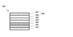
図3を用いて、実施形態の一つに係る製造方法によって製造される光電変換素子である太陽電池300の構成概略について説明する。太陽電池セル300は、このセルに入射してきた太陽光L等の光エネルギーを電力に変換する太陽電池としての機能を有する素子である。太陽電池セル300は、透明電極301と対極302と光電変換層303を有する。ここで透明電極もしくは対極の少なくとも一方は本実施形態で製造される金属ナノ材層とカーボン層の積層構造を有する。対極は不透明であってもよいし透明であってもよい。[Embodiment 2-1]
A schematic configuration of a
光電変換層303は、入射してきた光の光エネルギーを電力に変換して電流を発生させる半導体を含む層である。光電変換層303は、一般に、p型の半導体層とn型の半導体層とを具備している。光電変換層としてはp型ポリマーとn型材料との積層体、ABX3で示されるペロブスカイト型(ここでAは一価のカチオン、Bは二価のカチオン、Xはハロゲンイオンである)、シリコン半導体、InGaAsやGaAsやカルコパイライト系やCdTe系やInP系やSiGe系などの無機化合物半導体、量子ドット含有型、さらには色素増感型の透明半導体を用いてもよい。いずれの場合も効率が高く、より出力の劣化を小さくできる。The
光電変換層303と電極の間には電荷注入を促進もしくはブロックするためにさらにバッファ層等が挿入されていてもよい。
A buffer layer or the like may be further inserted between the
陽極用バッファ層や電荷輸送層としては、例えばバナジウム酸化物、PEDOT/PSS、p型ポリマー、五酸化バナジウム(V2O5)、2,2’,7,7’-Tetrakis[N,N-di(4-methoxyphenyl)amino]-9,9’- spirobifluorene(以下、Spiro-OMeTADという)、酸化ニッケル(NiO)、三酸化モリブデン(MoO3)等からなる層を用いることができる。Examples of anode buffer layers and charge transport layers include vanadium oxide, PEDOT/PSS, p-type polymer, vanadium pentoxide (V 2 O 5 ), 2,2′,7,7′-Tetrakis [N,N- A layer made of di(4-methoxyphenyl)amino]-9,9′-spirobifluorene (hereinafter referred to as Spiro-OMeTAD), nickel oxide (NiO), molybdenum trioxide (MoO 3 ), or the like can be used.
一方、陰極用のバッファ層や電荷輸送層としてはフッ化リチウム(LiF)、カルシウム(Ca)、6,6’-フェニル-C61-ブチル酸メチルエステル(6,6’-phenyl-C61-butyric acid methyl ester、C60-PCBM)、6,6’-フェニル-C71-ブチル酸メチルエステル(6,6’-phenyl-C71-butyric acid methyl ester、以下C70-PCBMという)、インデン-C60ビス付加体(Indene-C60 bisadduct、以下、ICBAという)、炭酸セシウム(Cs2CO3)、二酸化チタン(TiO2)、poly[(9,9-bis(3’-(N,N-dimethylamino)propyl)-2,7-fluorene)-alt-2,7-(9,9-dioctyl- fluorene)](以下、PFNということがある)、バソクプロイン(Bathocuproine、以下BCPということがある)、酸化ジルコニウム(ZrO)、酸化亜鉛(ZnO)、三酸化タングステン(WO3)、ポリエチンイミン等からなる層を用いることができる。On the other hand, lithium fluoride (LiF), calcium (Ca), 6,6'-phenyl-C61-butyric acid methyl ester (6,6'-phenyl-C61-butyric acid methyl ester, C60-PCBM), 6,6'-phenyl-C71-butyric acid methyl ester (6,6'-phenyl-C71-butylic acid methyl ester, hereinafter referred to as C70-PCBM), indene-C60 bis adduct ( Indene-C60 bisadduct, hereinafter referred to as ICBA), cesium carbonate (Cs 2 CO 3 ), titanium dioxide (TiO 2 ), poly[(9,9-bis(3′-(N,N-dimethylamino)propyl)-2, 7-fluorene)-alt-2,7-(9,9-dioctyl-fluorene)] (hereinafter sometimes referred to as PFN), Bathocuproine (hereinafter sometimes referred to as BCP), zirconium oxide (ZrO), oxidation Layers of zinc (ZnO), tungsten trioxide (WO 3 ), polyethynimine, and the like can be used.
本実施形態の製造方法により製造される光電変換素子は、光電池、太陽電池セルなどのほか、光センサーとしても使用できる。ここで光としては赤外線から紫外線、γ線まで広い波長の光を選択することができる。 The photoelectric conversion element manufactured by the manufacturing method of the present embodiment can be used not only as a photovoltaic cell and a photovoltaic cell, but also as a photosensor. Here, the light can be selected from a wide range of wavelengths, from infrared rays to ultraviolet rays and γ rays.
実施形態による光電変換素子の製造方法には、紫外線カット層、またはガスバリア層を形成させる工程をさらに有することができる。紫外線カット層に含まれる紫外線吸収剤の具体例としては、2-ヒドロキシ-4-メトキシベンゾフェノン、2,2-ジヒドロキシ-4-メトキシベンゾフェノン、2-ヒドロキシ-4-メトキシ-2-カルボキシベンゾフェノン、2-ヒドロキシ-4-n-オクトキシベンゾフェノン等のベンゾフェノン系化合物;2-(2-ヒドロキシ-3,5-ジ第3ブチルフェニル)ベンゾトリアゾール、2-(2-ヒドロキシ-5-メチルフェニル)ベンゾトリアゾール、2-(2-ヒドロキシ-5-第3オクチルフェニル)ベンゾトリアゾール等のベンゾトリアゾール系化合物;フェニルサリチレート、p-オクチルフェニルサリチレート等のサリチル酸エステル系化合物が挙げられる。これらは400nm以下の紫外線をカットするものであることが望ましい。 The method for manufacturing a photoelectric conversion element according to the embodiment may further include a step of forming an ultraviolet blocking layer or a gas barrier layer. Specific examples of the ultraviolet absorber contained in the ultraviolet cut layer include 2-hydroxy-4-methoxybenzophenone, 2,2-dihydroxy-4-methoxybenzophenone, 2-hydroxy-4-methoxy-2-carboxybenzophenone, 2- Benzophenone compounds such as hydroxy-4-n-octoxybenzophenone; 2-(2-hydroxy-3,5-di-tert-butylphenyl)benzotriazole, 2-(2-hydroxy-5-methylphenyl)benzotriazole, Benzotriazole compounds such as 2-(2-hydroxy-5-tert-octylphenyl)benzotriazole; and salicylate compounds such as phenyl salicylate and p-octylphenyl salicylate. It is desirable for these to cut ultraviolet rays of 400 nm or less.
ガスバリア層としては特に水蒸気と酸素を遮断するものが好ましく、特に水蒸気を通しにくいものが好ましい。例えば、SiN、SiO2、SiC、SiOxNy、TiO2、Al2O3の無機物からなる層、超薄板ガラス等を好適に利用することができる。ガスバリア層の厚みは特に制限されないが、0.01~3000μmの範囲であることが好ましく、0.1~100μmの範囲であることがより好ましい。0.01μm未満では十分なガスバリア性が得られない傾向にあり、他方、前記3000μmを超えると重厚化して、柔軟性等の特長が消失する傾向にある。ガスバリア層の水蒸気透過量(透湿度)としては、102g/m2・d~10-6g/m2・dが好ましく、より好ましくは10g/m2・d~10-5g/m2・dであり、さらに好ましくは1g/m2・d~10-4g/m2・dである。尚、透湿度はJIS Z0208等に基づいて測定することができる。ガスバリア層を形成するには、乾式法が好適である。乾式法によりガスバリア性のガスバリア層を形成する方法としては、抵抗加熱蒸着、電子ビーム蒸着、誘導加熱蒸着、及びこれらにプラズマやイオンビームによるアシスト法などの真空蒸着法、反応性スパッタリング法、イオンビームスパッタリング法、ECR(電子サイクロトロン)スパッタリング法などのスパッタリング法、イオンプレーティング法などの物理的気相成長法(PVD法)、熱や光、プラズマなどを利用した化学的気相成長法(CVD法)などが挙げられる。中でも、真空下で蒸着法により膜形成する真空蒸着法が好ましい。As the gas barrier layer, a layer that blocks water vapor and oxygen is particularly preferable, and a layer that hardly allows water vapor to pass through is particularly preferable. For example, layers made of inorganic substances such as SiN, SiO 2 , SiC, SiO x N y , TiO 2 and Al 2 O 3 , ultra-thin glass, and the like can be suitably used. Although the thickness of the gas barrier layer is not particularly limited, it is preferably in the range of 0.01 to 3000 μm, more preferably in the range of 0.1 to 100 μm. If the thickness is less than 0.01 μm, sufficient gas barrier properties tend not to be obtained. The water vapor transmission rate (water vapor permeability) of the gas barrier layer is preferably 10 2 g/m 2 ·d to 10 -6 g/m 2 ·d, more preferably 10 g/m 2 ·d to 10 -5 g/m. 2 ·d, more preferably 1 g/m 2 ·d to 10 −4 g/m 2 ·d. Incidentally, the moisture permeability can be measured based on JIS Z0208 or the like. A dry method is suitable for forming the gas barrier layer. Methods for forming a gas barrier layer with gas barrier properties by a dry method include resistance heating deposition, electron beam deposition, induction heating deposition, vacuum deposition methods such as assisted methods using plasma or ion beams, reactive sputtering methods, and ion beams. Sputtering method, sputtering method such as ECR (electron cyclotron) sputtering method, physical vapor deposition method (PVD method) such as ion plating method, chemical vapor deposition method (CVD method) using heat, light, plasma, etc. ) and the like. Among them, a vacuum vapor deposition method, in which a film is formed by a vapor deposition method under vacuum, is preferred.
実施形態による素子の製造に用いられる基材として、例えば、透明基材としては、ガラスなどの無機材料、PET、PEN、ポリカーボネート、PMMAなどの有機材料が用いられる。また基材としてアルミ箔やSUS箔なども用いることができる。柔軟性のある材料を用いると、実施形態による光電変換素子が柔軟性に富むものになるので好ましい。 Examples of substrates used to manufacture the elements according to the embodiments include inorganic materials such as glass and organic materials such as PET, PEN, polycarbonate, and PMMA as transparent substrates. Aluminum foil, SUS foil, or the like can also be used as the base material. It is preferable to use a flexible material because the photoelectric conversion element according to the embodiment is highly flexible.
本実施形態では場合によりカーボン材層の上に光電変換層を形成させた後に、対極側に転写させることもできる。 In the present embodiment, after the photoelectric conversion layer is formed on the carbon material layer, it can be transferred to the counter electrode side as the case may be.
[実施形態2-2]
図4を用いて、実施形態に係る製造方法により製造される別の光電変換素子(有機EL素子400)の構成について説明する。有機EL素子400は、この素子に入力された電気エネルギーを光Lに変換する発光素子としての機能を有する素子である。[Embodiment 2-2]
The configuration of another photoelectric conversion element (organic EL element 400) manufactured by the manufacturing method according to the embodiment will be described with reference to FIG. The
有機EL素子400は、透明電極401と対極402と光電変換層403を有する。ここで透明電極もしくは対極の少なくとも一方は本実施形態で製造される金属ナノ材層とカーボン層の積層構造を有する。対極は不透明であってもよいし透明であってもよい。
The
光電変換層403は、電力を変換して光を発生させる半導体層である。光電変換層403は、一般に、p型の半導体層とn型の半導体層とを具備している。光電変換層403と電極の間には電荷注入を促進もしくはブロックするためにさらにバッファ層が挿入されていてもよい。
The
実施形態を諸例を用いて説明すると以下の通りである。 The embodiment is described below using various examples.
(実施例1)
10cm角のポリエチレンテレフタレートフィルム(PETフィルム)の表面にスパッタ法によりITO層を形成させて、表面抵抗が300Ω/□の導電フィルム(親水性基材)を製造する。(Example 1)
An ITO layer is formed on the surface of a 10 cm square polyethylene terephthalate film (PET film) by a sputtering method to produce a conductive film (hydrophilic substrate) having a surface resistance of 300Ω/□.
直径70nmの銀ナノワイヤを水に分散させ0.3wt%の分散液を作製する。10cm角の厚さ100μmのポリテトラフルオロエチレンフィルム(PTFEフィルム、疎水性基材)を120℃の台の上に設置し、銀ナノワイヤ水性分散液をスプレー塗布して金属ナノ材層を形成させる。pH6の水中でのゼータ電位はPTFEフィルムが-17mV、銀ナノワイヤが-30mVである。 Silver nanowires with a diameter of 70 nm are dispersed in water to prepare a 0.3 wt % dispersion. A 10 cm square polytetrafluoroethylene film (PTFE film, hydrophobic substrate) with a thickness of 100 μm is placed on a table at 120° C., and an aqueous dispersion of silver nanowires is spray-coated to form a metal nanomaterial layer. The zeta potential in pH 6 water is -17 mV for the PTFE film and -30 mV for the silver nanowire.
銀ナノワイヤ層上にポリエチレンイミン鎖が結合した還元型酸化グラフェンのエタノール分散液をバー塗布により室温で塗布して、カーボン材層を形成させる。 An ethanol dispersion of reduced graphene oxide to which polyethylenimine chains are bound is applied onto the silver nanowire layer by bar coating at room temperature to form a carbon material layer.
100℃の台の上に上記グラフェン層と、上記親水性基材のITO層とが対向するスタックとし、その上に金属板を乗せてプレスして直接圧着する。次に、PETフィルムを端から剥がしてITO層上に銀ナノワイヤ層とグラフェン層との積層体を転写する。
銀ナノワイヤ層およびグラフェン層はほぼ完全に転写され、表面抵抗が10Ω/□の透明電極が得られる。A stack in which the graphene layer and the ITO layer of the hydrophilic base are opposed to each other is formed on a table at 100° C., and a metal plate is put on the stack and pressed to directly bond them. Next, the PET film is peeled off from the edge, and the laminate of the silver nanowire layer and the graphene layer is transferred onto the ITO layer.
The silver nanowire layer and the graphene layer are almost completely transferred to obtain a transparent electrode with a surface resistance of 10Ω/□.
(実施例2)
直径30nmの銀ナノワイヤを2-プロパノールに分散させ1wt%の分散液を製造する。10cm角の厚さ100μmのPTFEフィルム(疎水性基材)を60℃の台の上に設置し、直径5mmの円柱状のバーとPTFEフィルムの間(ギャップ:500μm)に銀ナノワイヤ分散液を坦持させる。PTFEフィルムとバーの間にはメニスカスが形成する。バーを83mm/sの速度で移動させ、PTFEフィルムの表面に銀ナノワイヤ分散液を塗布して、銀ナノワイヤ層(金属ナノ材層)を形成させる。(Example 2)
Silver nanowires with a diameter of 30 nm are dispersed in 2-propanol to prepare a 1 wt % dispersion. A 10 cm square 100 μm thick PTFE film (hydrophobic substrate) was placed on a table at 60° C., and a silver nanowire dispersion was placed between a cylindrical bar with a diameter of 5 mm and the PTFE film (gap: 500 μm). have A meniscus forms between the PTFE film and the bar. The bar is moved at a speed of 83 mm/s to apply the silver nanowire dispersion to the surface of the PTFE film to form a silver nanowire layer (metal nanomaterial layer).
銀ナノワイヤ層上にグラファイトを剥離した多層グラフェンの2-プロパノール分散液をバー塗布により室温で塗布してカーボン材層を形成させる。 A 2-propanol dispersion of multilayer graphene from which graphite is exfoliated is applied onto the silver nanowire layer by bar coating at room temperature to form a carbon material layer.
120℃の台の上に上記グラフェン層と厚さ100μmのPETフィルムをスタックとし、その上に金属ローラーを端から転がして直接圧着し、引き続いて剥離を行うことによってPETフィルム上に銀ナノワイヤ層とグラフェン層を転写する。
銀ナノワイヤ層およびグラフェン層はほぼ完全に転写され、表面抵抗が0.3Ω/□の電極が得られる。The above graphene layer and a PET film with a thickness of 100 μm are stacked on a table at 120° C., and a metal roller is rolled from one end to directly press them thereon, followed by peeling to form a silver nanowire layer on the PET film. Transfer the graphene layer.
The silver nanowire layer and the graphene layer are almost completely transferred, resulting in an electrode with a surface resistance of 0.3Ω/□.
(実施例3)
図5に示す半透明な太陽電池500を作成する。(Example 3)
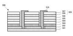
A translucent
PETフィルム501上に形成されたITO層502の表面を、酸でパターニングして短冊状の透明電極を作製する。酸化グラフェンの水溶液をバーコーターで塗布して酸化グラフェン層を形成させ、次いで、90℃で20分乾燥した後、110℃で水和ヒドラジン蒸気で1時間処理して酸化グラフェンの炭素原子の一部が窒素原子に置換された平均2層N-グラフェン層からなる遮蔽層503に変化させる。
The surface of the
遮蔽層503の上に、PEDOT・PSSの水溶液をバーコーターで塗布し、100℃で30分乾燥してPEDOT・PSSを含むバッファ層504(50nm厚)を形成させる。
An aqueous solution of PEDOT/PSS is applied on the
バッファ層503上にポリ(3-ヘキシルチオフェン-2,5-ジイル)(P3HT)とC60-PCBMとを含むクロルベンゼン溶液をバーコーターで塗布し、100℃で20分乾燥することにより光電変換層505を製造する。
A chlorobenzene solution containing poly(3-hexylthiophene-2,5-diyl) (P3HT) and C60-PCBM was applied on the
光電変換層505の上にバッファ層として酸化スズのナノ粒子のエタノール分散液をバーコーターで塗布して乾燥させ、バッファ層506を形成させる。
An ethanol dispersion of tin oxide nanoparticles is applied as a buffer layer on the
直径70nmの銀ナノワイヤを水に分散させ0.3wt%の分散液を作製する。10cm角の厚さ100μmのPTFEフィルム(疎水性基材、図示せず)を120℃の台の上に設置し、銀ナノワイヤ水性分散液をスプレー塗布して銀ナノワイヤ層507を形成させる。
Silver nanowires with a diameter of 70 nm are dispersed in water to prepare a 0.3 wt % dispersion. A 10 cm square PTFE film (hydrophobic substrate, not shown) with a thickness of 100 μm is placed on a table at 120° C., and a silver nanowire aqueous dispersion is sprayed to form a
銀ナノワイヤ層上にポリエチレンイミン鎖が結合した還元型酸化グラフェンのエタノール分散液をバー塗布により室温で塗布し、120℃で乾燥してグラフェン層508を形成させる。これにより電極層509が形成される。
An ethanol dispersion of reduced graphene oxide to which polyethylenimine chains are bonded is applied onto the silver nanowire layer by bar coating at room temperature, and dried at 120° C. to form the
100℃の台の上にポリエチレンイミン鎖が結合した還元型酸化グラフェン層508が上になるように置き、酸化スズのバッファ層506と接するように金属ローラーを転がして端から圧着、剥離を行い銀ナノワイヤ層507およびグラフェン層508、すなわち電極層509を転写させる。
The reduced
次に短冊状に掲載されているITOパターンに従って、ITO上部の膜をメカニカルスクライブする。次に銅をスパッタして金属配線層510を形成させる。これにより短冊状のセルは直列に配線される。
Next, the film on the ITO is mechanically scribed according to the strip-shaped ITO pattern. Copper is then sputtered to form
全体を熱硬化性のシリコーン樹脂でコートした後加熱して厚さ40μmの絶縁層(図示せず)を製造する。絶縁層の上に紫外線カットインクをスクリーン印刷して紫外線カット層(図示せず)を製造する。紫外線カット層の上にCVDでシリカ層を製膜しガスバリア層(図示せず)を製造する。さらに周りを封止することにより太陽電池モジュールを製造する。
得られる太陽電池モジュールは半透明であり、1SUNの擬似太陽光に対して4%以上のエネルギー変換効率を示す。また大気中、60℃、連続1000時間の擬似太陽光照射で効率の低下は2%以内である。After coating the whole with a thermosetting silicone resin, it is heated to produce an insulating layer (not shown) having a thickness of 40 μm. A UV cut layer (not shown) is manufactured by screen-printing a UV cut ink onto the insulating layer. A silica layer is formed on the ultraviolet blocking layer by CVD to produce a gas barrier layer (not shown). A solar cell module is manufactured by further sealing the surroundings.
The obtained solar cell module is translucent and exhibits an energy conversion efficiency of 4% or more for simulated sunlight of 1 SUN. In addition, the decrease in efficiency is within 2% under simulated sunlight irradiation for 1000 hours continuously at 60° C. in the atmosphere.
(実施例4)
片側が透明な太陽電池を作製する。
PETフィルム上に形成されたITOの表面を、酸でパターニングして短冊状の透明電極を作製する。ポリエチレンイミン鎖が結合した還元型酸化グラフェンのエタノール分散液をバーコーターで塗布した後、酸化グラフェンの水分散液を塗布し、次いで、120℃で10分乾燥し、グラフェン層からなる遮蔽層を作製する。(Example 4)
A solar cell is made that is transparent on one side.
The surface of the ITO formed on the PET film is patterned with an acid to produce strip-shaped transparent electrodes. After applying an ethanol dispersion of reduced graphene oxide to which polyethyleneimine chains are bonded using a bar coater, an aqueous dispersion of graphene oxide was applied, followed by drying at 120° C. for 10 minutes to prepare a shielding layer composed of a graphene layer. do.
遮蔽グラフェン層上に、PEDOT・PSSの水溶液をバーコーターで塗布し、100℃で30分乾燥してPEDOT・PSSを含むバッファ層(50nm厚)を形成させる。 An aqueous solution of PEDOT/PSS is applied onto the shielding graphene layer with a bar coater and dried at 100° C. for 30 minutes to form a buffer layer (50 nm thick) containing PEDOT/PSS.
バッファ層上にP3HTとC60-PCBMとを含むクロルベンゼン溶液をバーコーターで塗布し、100℃で20分乾燥することにより光電変換層を作製する。 A chlorobenzene solution containing P3HT and C60-PCBM is coated on the buffer layer with a bar coater and dried at 100° C. for 20 minutes to prepare a photoelectric conversion layer.
光電変換層の上にバッファ層として酸化スズのナノ粒子のエタノール分散液をバーコーターで塗布して乾燥させ、バッファ層を形成させる。 An ethanol dispersion of tin oxide nanoparticles is applied as a buffer layer on the photoelectric conversion layer with a bar coater and dried to form a buffer layer.
直径30nmの銀ナノワイヤを2-プロパノールに分散させ1wt%の分散液を製造する。10cm角の厚さ100μmのPTFEフィルム(疎水性基材)を60℃の台の上に設置し、直径5mmの円柱状のバーPTFEフィルムの間(ギャップ:500μm)に銀ナノワイヤ分散液を坦持させる。PTFEフィルムとバーの間にはメニスカスが形成する。バーを83mm/sの速度で移動させ、銀ナノワイヤ分散液を塗布する。 Silver nanowires with a diameter of 30 nm are dispersed in 2-propanol to prepare a 1 wt % dispersion. A 10 cm square 100 μm thick PTFE film (hydrophobic substrate) was placed on a table at 60° C., and a silver nanowire dispersion was supported between cylindrical bar PTFE films with a diameter of 5 mm (gap: 500 μm). Let A meniscus forms between the PTFE film and the bar. The bar is moved at a speed of 83 mm/s to apply the silver nanowire dispersion.
銀ナノワイヤ層上にグラファイトを剥離した多層グラフェンの2-プロパノール分散液をバー塗布により室温で塗布する。 A 2-propanol dispersion of multilayer graphene from which graphite is exfoliated is applied onto the silver nanowire layer by bar coating at room temperature.
50℃の台の上に上記グラフェン層が上になるように置き、酸化スズのバッファ層と接するように金属ローラーを転がして端から圧着、剥離を行い銀ナノワイヤ層およびグラフェン層を転写させる。 The graphene layer is placed on a table at 50° C., and a metal roller is rolled so as to come into contact with the tin oxide buffer layer.
次に短冊状のITOパターンに従って、ITO上部の膜をメカニカルスクライブする。次に銅をスパッタして金属配線層を製造する。これにより短冊状のセルは直列に配線される。 Next, according to the strip-shaped ITO pattern, the film on the ITO is mechanically scribed. Copper is then sputtered to produce a metal wiring layer. The strip-shaped cells are thereby wired in series.
実施例3と同様にして後工程を行い、片側が透明な太陽電池モジュールを製造する。得られる太陽電池モジュールは1SUNの擬似太陽光に対して5%以上のエネルギー変換効率を示す。また大気中、60℃、連続1000時間の擬似太陽光照射で効率の低下は1%以内である。 Post-processes are carried out in the same manner as in Example 3 to manufacture a solar cell module with one side being transparent. The obtained solar cell module exhibits an energy conversion efficiency of 5% or more for simulated sunlight of 1 SUN. Further, the decrease in efficiency is within 1% under simulated sunlight irradiation for 1000 hours continuously at 60° C. in the atmosphere.
(実施例5)
図6に示す半透明な有機EL素子600を作成する。(Example 5)
A translucent
PETフィルム601上に形成されたITO/銀合金/ITOの積層透明電極602の表面にポリエチレンイミン鎖が結合した還元型酸化グラフェンのエタノール分散液をバーコーターで塗布した後、酸化グラフェンの水分散液を塗布し、次いで、120℃で10分乾燥し、グラフェン層からなる遮蔽層603を作製する。
After applying an ethanol dispersion of reduced graphene oxide to which polyethyleneimine chains are bonded to the surface of the ITO/silver alloy/ITO laminated
遮蔽グラフェン層上に、PEDOT・PSSの水溶液をバーコーターで塗布し、100℃で30分乾燥してPEDOT・PSSを含むバッファ層604(50nm厚)を形成させる。 An aqueous solution of PEDOT/PSS is applied onto the shielding graphene layer using a bar coater and dried at 100° C. for 30 minutes to form a buffer layer 604 (50 nm thick) containing PEDOT/PSS.
バッファ層上にp型半導体であるN,N’-ジ-1-ナフチル-N,N’-ジフェニル-1,1’-4,4’-ジアミンを30nmの厚さで蒸着し、その上にn型半導体として機能し、発光材でもあるトリス(8-ヒドロキシキノリン)アルミニウムを40nmの厚さで蒸着して光電変換層605を作製する。
N,N'-di-1-naphthyl-N,N'-diphenyl-1,1'-4,4'-diamine, which is a p-type semiconductor, is vapor-deposited on the buffer layer to a thickness of 30 nm, and Tris(8-hydroxyquinoline)aluminum, which functions as an n-type semiconductor and is also a light-emitting material, is vapor-deposited to a thickness of 40 nm to form a
直径30nmの銀ナノワイヤを2-プロパノールに分散させ0.3wt%の分散液を製造する。10cm角の厚さ100μmのPTFEフィルムを60℃の台の上に設置し、直径5mmの円柱状のバーとPTFEフィルムの間(ギャップ:500μm)に銀ナノワイヤ分散液を坦持させる。PTFEフィルムとバーの間にはメニスカスが形成する。バーを8mm/sの速度で移動させ、銀ナノワイヤ分散液を塗布する。 Silver nanowires with a diameter of 30 nm are dispersed in 2-propanol to prepare a 0.3 wt % dispersion. A 10 cm square PTFE film with a thickness of 100 μm is placed on a table at 60° C., and a silver nanowire dispersion is supported between a cylindrical bar with a diameter of 5 mm and the PTFE film (gap: 500 μm). A meniscus forms between the PTFE film and the bar. The bar is moved at a speed of 8 mm/s to apply the silver nanowire dispersion.
銀ナノワイヤ層上にポリエチレンイミン鎖が結合した還元型酸化グラフェンのエタノール分散液をバー塗布により室温で製膜し、120℃で乾燥してグラフェン層を形成させる。 An ethanol dispersion of reduced graphene oxide to which polyethyleneimine chains are bound is formed on the silver nanowire layer by bar coating at room temperature, and dried at 120° C. to form a graphene layer.
70℃の台の上にポリエチレンイミン鎖が結合した還元型酸化グラフェン層が上になるように置き、光電変換層605と接するように金属ローラーを転がして端から圧着、剥離を行いグラフェン層606と銀ナノワイヤ層607を転写させる。
The reduced graphene oxide layer to which the polyethyleneimine chain is bound is placed on a table at 70° C. so that the reduced graphene oxide layer is facing upward, and the
次にアルミニウムをスパッタして金属補助配線層(図示せず)を製造する。 Next, aluminum is sputtered to produce a metal auxiliary wiring layer (not shown).
実施例3と同様にして後工程を行い、窓用の照明等に用いることが可能な半透明な有機EL素子を製造する。得られる有機EL素子は大気中、60℃、連続1000時間の駆動で出力の低下は2%以内である。 Post-processes are carried out in the same manner as in Example 3 to manufacture a semi-transparent organic EL element that can be used for window lighting or the like. The resulting organic EL device exhibits a decrease in output of 2% or less after continuous driving at 60° C. for 1000 hours in the air.
(実施例6)
平均粒径が800nmの銀粒子とポリビニルピロリドンをエタノールに分散させ1wt%の分散液を製造する。10cm角の厚さ100μmのPTFEフィルム上にスクリーン印刷で銀粒子分散液を塗布させる。(Example 6)
Silver particles with an average particle size of 800 nm and polyvinylpyrrolidone are dispersed in ethanol to prepare a 1 wt % dispersion. A 10 cm square PTFE film with a thickness of 100 μm is coated with the silver particle dispersion liquid by screen printing.
銀粒子層上にグラファイトを剥離した多層グラフェンの2-プロパノール分散液をバー塗布により室温で製膜する。 A 2-propanol dispersion of multilayer graphene from which graphite has been exfoliated is formed on the silver particle layer by bar coating at room temperature.
120℃の台の上に上記グラフェン層と厚さ100μmのPETフィルムをスタックとし、その上に金属ローラーを端から転がして直接圧着し、引き続いて剥離を行うことによってPET上に銀粒子層とグラフェン層を転写する。
銀粒子層およびグラフェン層はほぼ完全に転写され、表面抵抗が0.1Ω/□の電極が得られる。The above graphene layer and a PET film with a thickness of 100 μm were stacked on a table at 120° C., and a metal roller was rolled from one end on the stack to directly press and bond the silver particle layer and the graphene on the PET. Transfer layers.
The silver particle layer and the graphene layer are almost completely transferred to obtain an electrode with a surface resistance of 0.1 Ω/□.
なお、本発明のいくつかの実施形態を説明したが、これらの実施形態は例として提示したものであり、発明の範囲を限定することは意図していない。これら新規な実施形態は、その他の様々な形態で実施し得るものであり、発明の要旨を逸脱しない範囲で、種々の省略、置き換え、変更を行うことができる。これら実施形態やその変形は、発明の範囲や要旨に含まれると共に、特許請求の範囲に記載された発明とその均等の範囲に含まれる。 It should be noted that while several embodiments of the invention have been described, these embodiments are provided by way of example and are not intended to limit the scope of the invention. These novel embodiments can be implemented in various other forms, and various omissions, replacements, and modifications can be made without departing from the scope of the invention. These embodiments and modifications thereof are included in the scope and gist of the invention, and are included in the scope of the invention described in the claims and equivalents thereof.
101…ポリマー膜(疎水性基材)
102…金属ナノ材を含有する分散液
103…金属ナノ材層
104…カーボン材を含有する分散液
105…カーボン材層
106…親水性基材
107…電極層
300…太陽電池
301…透明電極
302…対極
303…光電変換層を含む層
400…有機EL素子
401…透明電極
402…対極
403…光電変換層
500…太陽電池
501…PETフィルム
502…ITO層
503…遮蔽層
504…バッファ層
505…光電変換層
506…バッファ層
507…銀ナノワイヤ層
508…グラフェン層
509…電極層
510…金属配線層
600…有機EL素子
601…PETフィルム
602…積層透明電極
603…遮蔽層
604…バッファ層
605…光電変換層
606…グラフェン層
607…銀ナノワイヤ層
608…電極層101... Polymer membrane (hydrophobic substrate)
DESCRIPTION OF
Claims (20)
前記金属ナノ材層の表面にカーボン材分散液を塗布して、カーボン材層を形成させることにより、金属ナノ材層とカーボン材層との積層体を含む電極層を形成させる工程と、
前記カーボン材層の表面と、親水性基材とを直接圧着する工程と、
前記疎水性基材を剥離させ、前記電極層を、前記親水性基材の表面に転写させる工程と、
を含む電極の製造方法であって、
水中におけるpH6での、前記金属ナノ材のゼータ電位が前記疎水性基材のゼータ電位より低い、方法。 a step of directly applying a metal nanomaterial dispersion to the surface of a hydrophobic substrate to form a metal nanomaterial layer;
A step of applying a carbon material dispersion to the surface of the metal nano material layer to form a carbon material layer, thereby forming an electrode layer including a laminate of the metal nano material layer and the carbon material layer;
a step of directly press-bonding the surface of the carbon material layer and a hydrophilic substrate;
exfoliating the hydrophobic substrate and transferring the electrode layer to the surface of the hydrophilic substrate;
A method for manufacturing an electrode comprising
A method, wherein the zeta potential of the metal nanomaterial is lower than the zeta potential of the hydrophobic substrate at pH 6 in water.
前記第2電極の表面に前記光電変換層が形成された複合体を準備する工程と、
疎水性基材の表面に金属ナノ材分散液を直接塗布して、金属ナノ材層を形成させる工程と、
前記金属ナノ材層の表面にカーボン材分散液を塗布して、カーボン材層を形成させることにより、金属ナノ材層とカーボン材層との積層体を含む電極層を形成させる工程と、
前記カーボン材層の表面と、前記光電変換層とを直接圧着する工程と、
前記疎水性基材を剥離させ、前記電極層を、前記光電変換層の表面に転写させて第1の電極を形成させる工程と、
を含み、
水中におけるpH6での、前記金属ナノ材のゼータ電位が前記疎水性基材のゼータ電位より低い、方法。 A method for manufacturing a photoelectric conversion element comprising a first electrode, a second electrode, and a photoelectric conversion layer sandwiched therebetween,
preparing a composite in which the photoelectric conversion layer is formed on the surface of the second electrode;
a step of directly applying a metal nanomaterial dispersion to the surface of a hydrophobic substrate to form a metal nanomaterial layer;
A step of applying a carbon material dispersion to the surface of the metal nano material layer to form a carbon material layer, thereby forming an electrode layer including a laminate of the metal nano material layer and the carbon material layer;
a step of directly pressing the surface of the carbon material layer and the photoelectric conversion layer;
a step of exfoliating the hydrophobic substrate and transferring the electrode layer to the surface of the photoelectric conversion layer to form a first electrode;
including
A method, wherein the zeta potential of the metal nanomaterial is lower than the zeta potential of the hydrophobic substrate at pH 6 in water.
Applications Claiming Priority (1)
| Application Number | Priority Date | Filing Date | Title |
|---|---|---|---|
| PCT/JP2019/035558 WO2021048923A1 (en) | 2019-09-10 | 2019-09-10 | Method for producing electrode and method for producing photoelectric conversion element |
Publications (2)
| Publication Number | Publication Date |
|---|---|
| JPWO2021048923A1 JPWO2021048923A1 (en) | 2021-11-18 |
| JP7204890B2 true JP7204890B2 (en) | 2023-01-16 |
Family
ID=74866293
Family Applications (1)
| Application Number | Title | Priority Date | Filing Date |
|---|---|---|---|
| JP2021510482A Active JP7204890B2 (en) | 2019-09-10 | 2019-09-10 | Electrode manufacturing method and photoelectric conversion element manufacturing method |
Country Status (5)
| Country | Link |
|---|---|
| US (1) | US11563129B2 (en) |
| EP (1) | EP4030496A4 (en) |
| JP (1) | JP7204890B2 (en) |
| CN (1) | CN112789744B (en) |
| WO (1) | WO2021048923A1 (en) |
Families Citing this family (1)
| Publication number | Priority date | Publication date | Assignee | Title |
|---|---|---|---|---|
| WO2022054150A1 (en) * | 2020-09-09 | 2022-03-17 | 株式会社 東芝 | Transparent electrode, method for manufacturing transparent electrode, and electronic device |
Citations (8)
| Publication number | Priority date | Publication date | Assignee | Title |
|---|---|---|---|---|
| JP2011029035A (en) | 2009-07-27 | 2011-02-10 | Panasonic Electric Works Co Ltd | Base material with transparent conductive film, and manufacturing method of base material with transparent conductive film |
| JP2012523359A (en) | 2009-04-08 | 2012-10-04 | バイエル・マテリアルサイエンス・アクチェンゲゼルシャフト | Polymer-functionalized carbon nanotubes, their production and use |
| US20140272172A1 (en) | 2013-03-14 | 2014-09-18 | Aruna Zhamu | Method for producing conducting and transparent films from combined graphene and conductive nano filaments |
| JP2015173260A (en) | 2014-02-20 | 2015-10-01 | 大日本印刷株式会社 | Method for manufacturing functional member, and apparatus for manufacturing functional member |
| JP2016524517A (en) | 2013-03-14 | 2016-08-18 | ナノテク インスツルメンツ インク | Ultrasonic spray coating of conductive transparent films with bonded graphene and conductive nanofilaments |
| JP2017091875A (en) | 2015-11-12 | 2017-05-25 | 大倉工業株式会社 | Transparent electrode, laminate for transparent electrode, and manufacturing method therefor |
| JP2019050106A (en) | 2017-09-08 | 2019-03-28 | 株式会社東芝 | Transparent electrode, element including the same, and method for producing element |
| WO2019176078A1 (en) | 2018-03-16 | 2019-09-19 | 株式会社 東芝 | Manufacturing method and manufacturing device for transparent electrode |
Family Cites Families (8)
| Publication number | Priority date | Publication date | Assignee | Title |
|---|---|---|---|---|
| JP5599980B2 (en) | 2009-03-11 | 2014-10-01 | コニカミノルタ株式会社 | Conductive film, method for producing the same, and organic electroluminescence element |
| US20120027994A1 (en) * | 2009-03-17 | 2012-02-02 | Konica Minolta Holdings, Inc. | Transparent conductive film and method for manufacturing transparent conductive film |
| JP2011035073A (en) * | 2009-07-30 | 2011-02-17 | Osaka Univ | Method of manufacturing semiconductor memory element |
| JP5679460B2 (en) * | 2009-11-27 | 2015-03-04 | 国立大学法人大阪大学 | Organic electroluminescent device and method for manufacturing organic electroluminescent device |
| JP2013522814A (en) * | 2010-02-24 | 2013-06-13 | カンブリオス テクノロジーズ コーポレイション | Nanowire-based transparent conductor and method for patterning the same |
| JP2013077435A (en) | 2011-09-30 | 2013-04-25 | Oji Holdings Corp | Conductive transfer sheet and conductive laminate |
| WO2013073480A1 (en) | 2011-11-18 | 2013-05-23 | 日油株式会社 | Cationic lipid having improved intracellular kinetics |
| JP6147542B2 (en) | 2013-04-01 | 2017-06-14 | 株式会社東芝 | Transparent conductive film and electric element |
-
2019
- 2019-09-10 WO PCT/JP2019/035558 patent/WO2021048923A1/en unknown
- 2019-09-10 CN CN201980056531.3A patent/CN112789744B/en active Active
- 2019-09-10 JP JP2021510482A patent/JP7204890B2/en active Active
- 2019-09-10 EP EP19941777.5A patent/EP4030496A4/en active Pending
-
2021
- 2021-02-26 US US17/186,847 patent/US11563129B2/en active Active
Patent Citations (8)
| Publication number | Priority date | Publication date | Assignee | Title |
|---|---|---|---|---|
| JP2012523359A (en) | 2009-04-08 | 2012-10-04 | バイエル・マテリアルサイエンス・アクチェンゲゼルシャフト | Polymer-functionalized carbon nanotubes, their production and use |
| JP2011029035A (en) | 2009-07-27 | 2011-02-10 | Panasonic Electric Works Co Ltd | Base material with transparent conductive film, and manufacturing method of base material with transparent conductive film |
| US20140272172A1 (en) | 2013-03-14 | 2014-09-18 | Aruna Zhamu | Method for producing conducting and transparent films from combined graphene and conductive nano filaments |
| JP2016524517A (en) | 2013-03-14 | 2016-08-18 | ナノテク インスツルメンツ インク | Ultrasonic spray coating of conductive transparent films with bonded graphene and conductive nanofilaments |
| JP2015173260A (en) | 2014-02-20 | 2015-10-01 | 大日本印刷株式会社 | Method for manufacturing functional member, and apparatus for manufacturing functional member |
| JP2017091875A (en) | 2015-11-12 | 2017-05-25 | 大倉工業株式会社 | Transparent electrode, laminate for transparent electrode, and manufacturing method therefor |
| JP2019050106A (en) | 2017-09-08 | 2019-03-28 | 株式会社東芝 | Transparent electrode, element including the same, and method for producing element |
| WO2019176078A1 (en) | 2018-03-16 | 2019-09-19 | 株式会社 東芝 | Manufacturing method and manufacturing device for transparent electrode |
Also Published As
| Publication number | Publication date |
|---|---|
| WO2021048923A1 (en) | 2021-03-18 |
| US11563129B2 (en) | 2023-01-24 |
| US20210184127A1 (en) | 2021-06-17 |
| JPWO2021048923A1 (en) | 2021-11-18 |
| EP4030496A1 (en) | 2022-07-20 |
| CN112789744A (en) | 2021-05-11 |
| EP4030496A4 (en) | 2023-05-31 |
| CN112789744B (en) | 2024-07-02 |
Similar Documents
| Publication | Publication Date | Title |
|---|---|---|
| Azani et al. | Benefits, problems, and solutions of silver nanowire transparent conductive electrodes in indium tin oxide (ITO)‐free flexible solar cells | |
| Xu et al. | Recent progress of electrode materials for flexible perovskite solar cells | |
| Song et al. | Challenges and opportunities for graphene as transparent conductors in optoelectronics | |
| Heo et al. | Recent advancements in and perspectives on flexible hybrid perovskite solar cells | |
| JP5821637B2 (en) | Gas barrier film, method for producing gas barrier film, and organic photoelectric conversion element | |
| KR101342778B1 (en) | Photoelectric conversion element and manufacturing method thereof | |
| JP5302332B2 (en) | Photovoltaic device having a transparent electrode formed of nanoparticles | |
| US11387375B2 (en) | Graphene-containing membrane, process for producing the same, graphene-containing membrane laminate and photoelectric conversion device | |
| US11532787B2 (en) | Process and apparatus for producing transparent electrode | |
| WO2022054150A1 (en) | Transparent electrode, method for manufacturing transparent electrode, and electronic device | |
| US11710797B2 (en) | Transparent electrode, device employing the same, and manufacturing method of the device | |
| US20220209151A1 (en) | Transparent electrode, process for producing transparent electrode, and photoelectric conversion device comprising transparent electrode | |
| JP7204890B2 (en) | Electrode manufacturing method and photoelectric conversion element manufacturing method | |
| WO2022054151A1 (en) | Trasparent electrode, mehod for producing trasparent electrode, and electronic device | |
| WO2022190336A1 (en) | Transparent electrode, method for producing same and electronic device using transparent electrode | |
| KR20230072873A (en) | Solar cell with impoved interfacaial phenomenon and manufacturing method thereof | |
| CN115315815A (en) | Transparent electrode, method for manufacturing same, and electronic device using transparent electrode | |
| Nivetha et al. | Oxide and Metallic Materials for Photovoltaic Applications: A Review |
Legal Events
| Date | Code | Title | Description |
|---|---|---|---|
| A621 | Written request for application examination |
Free format text: JAPANESE INTERMEDIATE CODE: A621 Effective date: 20210225 |
|
| A131 | Notification of reasons for refusal |
Free format text: JAPANESE INTERMEDIATE CODE: A131 Effective date: 20220104 |
|
| A521 | Request for written amendment filed |
Free format text: JAPANESE INTERMEDIATE CODE: A523 Effective date: 20220307 |
|
| A131 | Notification of reasons for refusal |
Free format text: JAPANESE INTERMEDIATE CODE: A131 Effective date: 20220405 |
|
| A521 | Request for written amendment filed |
Free format text: JAPANESE INTERMEDIATE CODE: A523 Effective date: 20220601 |
|
| A131 | Notification of reasons for refusal |
Free format text: JAPANESE INTERMEDIATE CODE: A131 Effective date: 20220708 |
|
| A521 | Request for written amendment filed |
Free format text: JAPANESE INTERMEDIATE CODE: A523 Effective date: 20220830 |
|
| A131 | Notification of reasons for refusal |
Free format text: JAPANESE INTERMEDIATE CODE: A131 Effective date: 20221025 |
|
| A521 | Request for written amendment filed |
Free format text: JAPANESE INTERMEDIATE CODE: A523 Effective date: 20221108 |
|
| TRDD | Decision of grant or rejection written | ||
| A01 | Written decision to grant a patent or to grant a registration (utility model) |
Free format text: JAPANESE INTERMEDIATE CODE: A01 Effective date: 20221206 |
|
| A61 | First payment of annual fees (during grant procedure) |
Free format text: JAPANESE INTERMEDIATE CODE: A61 Effective date: 20221228 |
|
| R150 | Certificate of patent or registration of utility model |
Ref document number: 7204890 Country of ref document: JP Free format text: JAPANESE INTERMEDIATE CODE: R150 |