JP7188689B2 - Light-emitting device and projector - Google Patents
Light-emitting device and projector Download PDFInfo
- Publication number
- JP7188689B2 JP7188689B2 JP2018147680A JP2018147680A JP7188689B2 JP 7188689 B2 JP7188689 B2 JP 7188689B2 JP 2018147680 A JP2018147680 A JP 2018147680A JP 2018147680 A JP2018147680 A JP 2018147680A JP 7188689 B2 JP7188689 B2 JP 7188689B2
- Authority
- JP
- Japan
- Prior art keywords
- columnar
- light
- emitting device
- layer
- light emitting
- Prior art date
- Legal status (The legal status is an assumption and is not a legal conclusion. Google has not performed a legal analysis and makes no representation as to the accuracy of the status listed.)
- Active
Links
Images


Classifications
-
- H—ELECTRICITY
- H01—ELECTRIC ELEMENTS
- H01S—DEVICES USING THE PROCESS OF LIGHT AMPLIFICATION BY STIMULATED EMISSION OF RADIATION [LASER] TO AMPLIFY OR GENERATE LIGHT; DEVICES USING STIMULATED EMISSION OF ELECTROMAGNETIC RADIATION IN WAVE RANGES OTHER THAN OPTICAL
- H01S5/00—Semiconductor lasers
- H01S5/40—Arrangement of two or more semiconductor lasers, not provided for in groups H01S5/02 - H01S5/30
- H01S5/4025—Array arrangements, e.g. constituted by discrete laser diodes or laser bar
-
- G—PHYSICS
- G03—PHOTOGRAPHY; CINEMATOGRAPHY; ANALOGOUS TECHNIQUES USING WAVES OTHER THAN OPTICAL WAVES; ELECTROGRAPHY; HOLOGRAPHY
- G03B—APPARATUS OR ARRANGEMENTS FOR TAKING PHOTOGRAPHS OR FOR PROJECTING OR VIEWING THEM; APPARATUS OR ARRANGEMENTS EMPLOYING ANALOGOUS TECHNIQUES USING WAVES OTHER THAN OPTICAL WAVES; ACCESSORIES THEREFOR
- G03B21/00—Projectors or projection-type viewers; Accessories therefor
- G03B21/14—Details
- G03B21/20—Lamp housings
- G03B21/2006—Lamp housings characterised by the light source
- G03B21/2013—Plural light sources
-
- G—PHYSICS
- G03—PHOTOGRAPHY; CINEMATOGRAPHY; ANALOGOUS TECHNIQUES USING WAVES OTHER THAN OPTICAL WAVES; ELECTROGRAPHY; HOLOGRAPHY
- G03B—APPARATUS OR ARRANGEMENTS FOR TAKING PHOTOGRAPHS OR FOR PROJECTING OR VIEWING THEM; APPARATUS OR ARRANGEMENTS EMPLOYING ANALOGOUS TECHNIQUES USING WAVES OTHER THAN OPTICAL WAVES; ACCESSORIES THEREFOR
- G03B21/00—Projectors or projection-type viewers; Accessories therefor
- G03B21/14—Details
- G03B21/20—Lamp housings
- G03B21/2006—Lamp housings characterised by the light source
- G03B21/2033—LED or laser light sources
-
- H—ELECTRICITY
- H01—ELECTRIC ELEMENTS
- H01S—DEVICES USING THE PROCESS OF LIGHT AMPLIFICATION BY STIMULATED EMISSION OF RADIATION [LASER] TO AMPLIFY OR GENERATE LIGHT; DEVICES USING STIMULATED EMISSION OF ELECTROMAGNETIC RADIATION IN WAVE RANGES OTHER THAN OPTICAL
- H01S5/00—Semiconductor lasers
- H01S5/04—Processes or apparatus for excitation, e.g. pumping, e.g. by electron beams
- H01S5/042—Electrical excitation ; Circuits therefor
- H01S5/0425—Electrodes, e.g. characterised by the structure
- H01S5/04252—Electrodes, e.g. characterised by the structure characterised by the material
- H01S5/04253—Electrodes, e.g. characterised by the structure characterised by the material having specific optical properties, e.g. transparent electrodes
-
- H—ELECTRICITY
- H01—ELECTRIC ELEMENTS
- H01S—DEVICES USING THE PROCESS OF LIGHT AMPLIFICATION BY STIMULATED EMISSION OF RADIATION [LASER] TO AMPLIFY OR GENERATE LIGHT; DEVICES USING STIMULATED EMISSION OF ELECTROMAGNETIC RADIATION IN WAVE RANGES OTHER THAN OPTICAL
- H01S5/00—Semiconductor lasers
- H01S5/04—Processes or apparatus for excitation, e.g. pumping, e.g. by electron beams
- H01S5/042—Electrical excitation ; Circuits therefor
- H01S5/0425—Electrodes, e.g. characterised by the structure
- H01S5/04256—Electrodes, e.g. characterised by the structure characterised by the configuration
-
- H—ELECTRICITY
- H01—ELECTRIC ELEMENTS
- H01S—DEVICES USING THE PROCESS OF LIGHT AMPLIFICATION BY STIMULATED EMISSION OF RADIATION [LASER] TO AMPLIFY OR GENERATE LIGHT; DEVICES USING STIMULATED EMISSION OF ELECTROMAGNETIC RADIATION IN WAVE RANGES OTHER THAN OPTICAL
- H01S5/00—Semiconductor lasers
- H01S5/10—Construction or shape of the optical resonator, e.g. extended or external cavity, coupled cavities, bent-guide, varying width, thickness or composition of the active region
- H01S5/18—Surface-emitting [SE] lasers, e.g. having both horizontal and vertical cavities
- H01S5/183—Surface-emitting [SE] lasers, e.g. having both horizontal and vertical cavities having only vertical cavities, e.g. vertical cavity surface-emitting lasers [VCSEL]
- H01S5/18308—Surface-emitting [SE] lasers, e.g. having both horizontal and vertical cavities having only vertical cavities, e.g. vertical cavity surface-emitting lasers [VCSEL] having a special structure for lateral current or light confinement
- H01S5/18319—Surface-emitting [SE] lasers, e.g. having both horizontal and vertical cavities having only vertical cavities, e.g. vertical cavity surface-emitting lasers [VCSEL] having a special structure for lateral current or light confinement comprising a periodical structure in lateral directions
-
- H—ELECTRICITY
- H01—ELECTRIC ELEMENTS
- H01S—DEVICES USING THE PROCESS OF LIGHT AMPLIFICATION BY STIMULATED EMISSION OF RADIATION [LASER] TO AMPLIFY OR GENERATE LIGHT; DEVICES USING STIMULATED EMISSION OF ELECTROMAGNETIC RADIATION IN WAVE RANGES OTHER THAN OPTICAL
- H01S5/00—Semiconductor lasers
- H01S5/10—Construction or shape of the optical resonator, e.g. extended or external cavity, coupled cavities, bent-guide, varying width, thickness or composition of the active region
- H01S5/18—Surface-emitting [SE] lasers, e.g. having both horizontal and vertical cavities
- H01S5/183—Surface-emitting [SE] lasers, e.g. having both horizontal and vertical cavities having only vertical cavities, e.g. vertical cavity surface-emitting lasers [VCSEL]
- H01S5/18344—Surface-emitting [SE] lasers, e.g. having both horizontal and vertical cavities having only vertical cavities, e.g. vertical cavity surface-emitting lasers [VCSEL] characterized by the mesa, e.g. dimensions or shape of the mesa
-
- H—ELECTRICITY
- H01—ELECTRIC ELEMENTS
- H01S—DEVICES USING THE PROCESS OF LIGHT AMPLIFICATION BY STIMULATED EMISSION OF RADIATION [LASER] TO AMPLIFY OR GENERATE LIGHT; DEVICES USING STIMULATED EMISSION OF ELECTROMAGNETIC RADIATION IN WAVE RANGES OTHER THAN OPTICAL
- H01S5/00—Semiconductor lasers
- H01S5/10—Construction or shape of the optical resonator, e.g. extended or external cavity, coupled cavities, bent-guide, varying width, thickness or composition of the active region
- H01S5/18—Surface-emitting [SE] lasers, e.g. having both horizontal and vertical cavities
- H01S5/183—Surface-emitting [SE] lasers, e.g. having both horizontal and vertical cavities having only vertical cavities, e.g. vertical cavity surface-emitting lasers [VCSEL]
- H01S5/18355—Surface-emitting [SE] lasers, e.g. having both horizontal and vertical cavities having only vertical cavities, e.g. vertical cavity surface-emitting lasers [VCSEL] having a defined polarisation
-
- H—ELECTRICITY
- H01—ELECTRIC ELEMENTS
- H01S—DEVICES USING THE PROCESS OF LIGHT AMPLIFICATION BY STIMULATED EMISSION OF RADIATION [LASER] TO AMPLIFY OR GENERATE LIGHT; DEVICES USING STIMULATED EMISSION OF ELECTROMAGNETIC RADIATION IN WAVE RANGES OTHER THAN OPTICAL
- H01S5/00—Semiconductor lasers
- H01S5/30—Structure or shape of the active region; Materials used for the active region
- H01S5/34—Structure or shape of the active region; Materials used for the active region comprising quantum well or superlattice structures, e.g. single quantum well [SQW] lasers, multiple quantum well [MQW] lasers or graded index separate confinement heterostructure [GRINSCH] lasers
- H01S5/343—Structure or shape of the active region; Materials used for the active region comprising quantum well or superlattice structures, e.g. single quantum well [SQW] lasers, multiple quantum well [MQW] lasers or graded index separate confinement heterostructure [GRINSCH] lasers in AIIIBV compounds, e.g. AlGaAs-laser, InP-based laser
- H01S5/34333—Structure or shape of the active region; Materials used for the active region comprising quantum well or superlattice structures, e.g. single quantum well [SQW] lasers, multiple quantum well [MQW] lasers or graded index separate confinement heterostructure [GRINSCH] lasers in AIIIBV compounds, e.g. AlGaAs-laser, InP-based laser with a well layer based on Ga(In)N or Ga(In)P, e.g. blue laser
-
- H—ELECTRICITY
- H01—ELECTRIC ELEMENTS
- H01S—DEVICES USING THE PROCESS OF LIGHT AMPLIFICATION BY STIMULATED EMISSION OF RADIATION [LASER] TO AMPLIFY OR GENERATE LIGHT; DEVICES USING STIMULATED EMISSION OF ELECTROMAGNETIC RADIATION IN WAVE RANGES OTHER THAN OPTICAL
- H01S5/00—Semiconductor lasers
- H01S5/40—Arrangement of two or more semiconductor lasers, not provided for in groups H01S5/02 - H01S5/30
- H01S5/42—Arrays of surface emitting lasers
- H01S5/423—Arrays of surface emitting lasers having a vertical cavity
-
- G—PHYSICS
- G03—PHOTOGRAPHY; CINEMATOGRAPHY; ANALOGOUS TECHNIQUES USING WAVES OTHER THAN OPTICAL WAVES; ELECTROGRAPHY; HOLOGRAPHY
- G03B—APPARATUS OR ARRANGEMENTS FOR TAKING PHOTOGRAPHS OR FOR PROJECTING OR VIEWING THEM; APPARATUS OR ARRANGEMENTS EMPLOYING ANALOGOUS TECHNIQUES USING WAVES OTHER THAN OPTICAL WAVES; ACCESSORIES THEREFOR
- G03B33/00—Colour photography, other than mere exposure or projection of a colour film
- G03B33/10—Simultaneous recording or projection
- G03B33/12—Simultaneous recording or projection using beam-splitting or beam-combining systems, e.g. dichroic mirrors
-
- H—ELECTRICITY
- H01—ELECTRIC ELEMENTS
- H01S—DEVICES USING THE PROCESS OF LIGHT AMPLIFICATION BY STIMULATED EMISSION OF RADIATION [LASER] TO AMPLIFY OR GENERATE LIGHT; DEVICES USING STIMULATED EMISSION OF ELECTROMAGNETIC RADIATION IN WAVE RANGES OTHER THAN OPTICAL
- H01S2301/00—Functional characteristics
- H01S2301/20—Lasers with a special output beam profile or cross-section, e.g. non-Gaussian
- H01S2301/203—Lasers with a special output beam profile or cross-section, e.g. non-Gaussian with at least one hole in the intensity distribution, e.g. annular or doughnut mode
-
- H—ELECTRICITY
- H01—ELECTRIC ELEMENTS
- H01S—DEVICES USING THE PROCESS OF LIGHT AMPLIFICATION BY STIMULATED EMISSION OF RADIATION [LASER] TO AMPLIFY OR GENERATE LIGHT; DEVICES USING STIMULATED EMISSION OF ELECTROMAGNETIC RADIATION IN WAVE RANGES OTHER THAN OPTICAL
- H01S2304/00—Special growth methods for semiconductor lasers
- H01S2304/02—MBE
-
- H—ELECTRICITY
- H01—ELECTRIC ELEMENTS
- H01S—DEVICES USING THE PROCESS OF LIGHT AMPLIFICATION BY STIMULATED EMISSION OF RADIATION [LASER] TO AMPLIFY OR GENERATE LIGHT; DEVICES USING STIMULATED EMISSION OF ELECTROMAGNETIC RADIATION IN WAVE RANGES OTHER THAN OPTICAL
- H01S2304/00—Special growth methods for semiconductor lasers
- H01S2304/12—Pendeo epitaxial lateral overgrowth [ELOG], e.g. for growing GaN based blue laser diodes
-
- H—ELECTRICITY
- H01—ELECTRIC ELEMENTS
- H01S—DEVICES USING THE PROCESS OF LIGHT AMPLIFICATION BY STIMULATED EMISSION OF RADIATION [LASER] TO AMPLIFY OR GENERATE LIGHT; DEVICES USING STIMULATED EMISSION OF ELECTROMAGNETIC RADIATION IN WAVE RANGES OTHER THAN OPTICAL
- H01S5/00—Semiconductor lasers
- H01S5/04—Processes or apparatus for excitation, e.g. pumping, e.g. by electron beams
- H01S5/042—Electrical excitation ; Circuits therefor
- H01S5/0425—Electrodes, e.g. characterised by the structure
- H01S5/04256—Electrodes, e.g. characterised by the structure characterised by the configuration
- H01S5/04257—Electrodes, e.g. characterised by the structure characterised by the configuration having positive and negative electrodes on the same side of the substrate
-
- H—ELECTRICITY
- H01—ELECTRIC ELEMENTS
- H01S—DEVICES USING THE PROCESS OF LIGHT AMPLIFICATION BY STIMULATED EMISSION OF RADIATION [LASER] TO AMPLIFY OR GENERATE LIGHT; DEVICES USING STIMULATED EMISSION OF ELECTROMAGNETIC RADIATION IN WAVE RANGES OTHER THAN OPTICAL
- H01S5/00—Semiconductor lasers
- H01S5/10—Construction or shape of the optical resonator, e.g. extended or external cavity, coupled cavities, bent-guide, varying width, thickness or composition of the active region
- H01S5/18—Surface-emitting [SE] lasers, e.g. having both horizontal and vertical cavities
- H01S5/183—Surface-emitting [SE] lasers, e.g. having both horizontal and vertical cavities having only vertical cavities, e.g. vertical cavity surface-emitting lasers [VCSEL]
- H01S5/18361—Structure of the reflectors, e.g. hybrid mirrors
- H01S5/18377—Structure of the reflectors, e.g. hybrid mirrors comprising layers of different kind of materials, e.g. combinations of semiconducting with dielectric or metallic layers
-
- H—ELECTRICITY
- H01—ELECTRIC ELEMENTS
- H01S—DEVICES USING THE PROCESS OF LIGHT AMPLIFICATION BY STIMULATED EMISSION OF RADIATION [LASER] TO AMPLIFY OR GENERATE LIGHT; DEVICES USING STIMULATED EMISSION OF ELECTROMAGNETIC RADIATION IN WAVE RANGES OTHER THAN OPTICAL
- H01S5/00—Semiconductor lasers
- H01S5/30—Structure or shape of the active region; Materials used for the active region
- H01S5/34—Structure or shape of the active region; Materials used for the active region comprising quantum well or superlattice structures, e.g. single quantum well [SQW] lasers, multiple quantum well [MQW] lasers or graded index separate confinement heterostructure [GRINSCH] lasers
- H01S5/343—Structure or shape of the active region; Materials used for the active region comprising quantum well or superlattice structures, e.g. single quantum well [SQW] lasers, multiple quantum well [MQW] lasers or graded index separate confinement heterostructure [GRINSCH] lasers in AIIIBV compounds, e.g. AlGaAs-laser, InP-based laser
- H01S5/34346—Structure or shape of the active region; Materials used for the active region comprising quantum well or superlattice structures, e.g. single quantum well [SQW] lasers, multiple quantum well [MQW] lasers or graded index separate confinement heterostructure [GRINSCH] lasers in AIIIBV compounds, e.g. AlGaAs-laser, InP-based laser characterised by the materials of the barrier layers
Description
本発明は、発光装置およびプロジェクターに関する。 The present invention relates to a light emitting device and a projector.
半導体レーザーは、高輝度の次世代光源として期待されている。中でも、ナノコラムを適用した半導体レーザーは、ナノコラムによるフォトニック結晶の効果によって、狭放射角で高出力の発光が実現できると期待されている。このような半導体レーザーは、例えば、プロジェクターの光源として適用される。液晶ライトバルブを用いるプロジェクターでは、光源から出射される光は、直線偏光であることが望まれている。 Semiconductor lasers are expected to be high-intensity next-generation light sources. Among them, semiconductor lasers to which nanocolumns are applied are expected to realize light emission with a narrow emission angle and high output due to the photonic crystal effect of the nanocolumns. Such a semiconductor laser is applied, for example, as a light source for a projector. In a projector using a liquid crystal light valve, light emitted from a light source is desired to be linearly polarized light.
GaN系ナノコラムのフォトニック結晶を利用した半導体レーザーでは、ナノコラムの配列周期や直径を変えることによって、RGBの3原色の波長に合わせた設計が可能である。ただし、赤色領域で発振させるためには、直径の大きなナノコラムを用いる必要があり、欠陥や歪みが少なく発光効率がよいというナノコラムの効果が得られ難い。そのため、直径の小さな複数のナノコラムによって構成されたナノコラム集合体をナノコラムとみなして、周期的に配列させる技術が知られている。 A semiconductor laser using a photonic crystal of GaN-based nanocolumns can be designed to match the wavelengths of the three primary colors of RGB by changing the arrangement period and diameter of the nanocolumns. However, in order to oscillate in the red region, it is necessary to use a nano-column with a large diameter, and it is difficult to obtain the effect of the nano-column that there are few defects and distortions and the luminous efficiency is good. Therefore, there is known a technique of periodically arranging a nano-column aggregate composed of a plurality of nano-columns with a small diameter, which is regarded as a nano-column.
ここで、ナノコラムは、特許文献1に記載されているように、三角形、正方形、六角形など回転対称性を有する格子パターンで配列されているため、発光装置から出射される光は、直線偏光でない。 Here, as described in Patent Document 1, the nanocolumns are arranged in a lattice pattern having rotational symmetry such as triangles, squares, and hexagons, so the light emitted from the light emitting device is not linearly polarized light. .
上記のように、複数のナノコラムによってナノコラム集合体を形成した場合においても、ナノコラム集合体が回転対称性有する格子パターンで配列されていると、発光装置から出射される光は、直線偏光でない。 As described above, even when a nano-column aggregate is formed from a plurality of nano-columns, if the nano-column aggregates are arranged in a lattice pattern having rotational symmetry, the light emitted from the light-emitting device is not linearly polarized light.
本発明に係る発光装置の一態様は、
基体と、
前記基体に設けられ、p個の柱状部からなる柱状部集合体を有する積層体と、
を有し、
前記積層体は、前記柱状部集合体を複数有し、
前記p個の柱状部の各々は、発光層を有し、
前記積層体の積層方向からみて、前記p個の柱状部の各々の中心で構成される図形は、回転対称であり、
前記p個の柱状部のうちq個の柱状部の径は、前記p個の柱状部のうちr個の柱状部の径と異なり、
前記柱状部集合体の形状は、回転対称ではなく、
前記pは、2以上の整数であり、
前記qは、1以上p未満の整数であり、
前記rは、r=p-qを満たす整数である。
One aspect of the light-emitting device according to the present invention is
a substrate;
a laminated body provided on the base body and having a columnar part aggregate composed of p columnar parts;
has
The laminate has a plurality of the columnar section aggregates,
each of the p columnar portions has a light-emitting layer;
When viewed from the stacking direction of the laminate, a figure formed by the center of each of the p columnar portions is rotationally symmetrical,
The diameters of the q columnar portions out of the p columnar portions are different from the diameters of the r columnar portions out of the p columnar portions,
The shape of the columnar part assembly is not rotationally symmetrical,
The p is an integer of 2 or more,
The q is an integer of 1 or more and less than p,
The r is an integer that satisfies r=pq.
本発明に係る発光装置の一態様は、
基体と、
前記基体に設けられ、p個の柱状部からなる柱状部集合体を有する積層体と、
を有し、
前記積層体は、前記柱状部集合体を複数有し、
前記p個の柱状部の各々は、発光層を有し、
前記積層体の積層方向からみて、前記基体に、回転対称である前記p個の格子点を規定した場合、前記p個の柱状部のうちq個の柱状部の各々の中心は、前記格子点に配置され、前記p個の柱状部のうちr個の柱状部の各々の中心は、前記格子点とは異なる位置に配置され、
前記柱状部集合体の形状は、回転対称ではなく、
前記pは、3以上の整数であり、
前記qは、2以上p未満の整数であり、
前記rは、r=p-qを満たす整数である。
One aspect of the light-emitting device according to the present invention is
a substrate;
a laminated body provided on the base body and having a columnar part aggregate composed of p columnar parts;
has
The laminate has a plurality of the columnar section aggregates,
each of the p columnar portions has a light-emitting layer;
When the p pieces of rotationally symmetrical lattice points are defined on the substrate as viewed from the lamination direction of the laminate, the centers of the q pieces of the p pieces of columnar portions correspond to the lattice points. and the center of each of the r columnar portions among the p columnar portions is arranged at a position different from the lattice point,
The shape of the columnar part assembly is not rotationally symmetrical,
The p is an integer of 3 or more,
The q is an integer of 2 or more and less than p,
The r is an integer that satisfies r=pq.
前記発光装置の一態様において、
前記qは、前記pの半数より大きい整数である、発光装置。
In one aspect of the light-emitting device,
The light-emitting device, wherein q is an integer larger than half of p.
本発明に係るプロジェクターは、
前記発光装置の一態様を有する。
A projector according to the present invention includes:
It has one mode of the light-emitting device.
以下、本発明の好適な実施形態について、図面を用いて詳細に説明する。なお、以下に説明する実施形態は、特許請求の範囲に記載された本発明の内容を不当に限定するものではない。また、以下で説明される構成の全てが本発明の必須構成要件であるとは限らない。 Preferred embodiments of the present invention will be described in detail below with reference to the drawings. It should be noted that the embodiments described below do not unduly limit the scope of the invention described in the claims. Moreover, not all the configurations described below are essential constituent elements of the present invention.
1. 第1実施形態
1.1. 発光装置
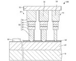
まず、第1実施形態に係る発光装置について、図面を参照しながら説明する。図1は、
第1実施形態に係る発光装置100を模式的に示す断面図である。図2は、第1実施形態に係る発光装置100を模式的に示す平面図である。なお、図1は、図2のI-I線断面図である。
1. First Embodiment 1.1. Light Emitting Device First, the light emitting device according to the first embodiment will be described with reference to the drawings. Figure 1 shows
BRIEF DESCRIPTION OF THE DRAWINGS It is sectional drawing which shows typically the light-emitting
発光装置100は、図1および図2に示すように、基体10と、積層体20と、第1電極50と、第2電極52と、を含む。なお、便宜上、図2では、第2電極52の図示を省略している。
The
基体10は、例えば、板状の形状を有している。基体10は、例えば、Si基板、GaN基板、サファイア基板などである。
The
積層体20は、基体10に設けられている。図示の例では、積層体20は、基体10上に設けられている。積層体20は、例えば、バッファー層22と、柱状部30と、を有している。
The
なお、本発明において、「上」とは、積層体20の積層方向(以下、単に「積層方向」ともいう)において、柱状部30の発光層33からみて基体10から遠ざかる方向のことであり、「下」とは、積層方向において、発光層33からみて基体10に近づく方向のことである。
In the present invention, "upper" means a direction away from the
また、本発明において、「積層体20の積層方向」とは、柱状部30の第1半導体層31と発光層33との積層方向のことである。
Further, in the present invention, the “stacking direction of the stacked
バッファー層22は、基体10上に設けられている。バッファー層22は、例えば、Siがドープされたn型のGaN層などである。バッファー層22上には、柱状部30を形成するためのマスク層60が設けられている。
A
柱状部30は、バッファー層22上に設けられている。柱状部30の積層方向と直交する方向における断面形状は、例えば、多角形、円などである。図2に示す例では、柱状部30の断面形状は、正六角形である。柱状部30の径は、例えば、nmオーダーであり、具体的には10nm以上500nm以下である。柱状部30は、例えば、ナノコラム、ナノワイヤー、ナノロッド、ナノピラーとも呼ばれる。柱状部30の積層方向の大きさは、例えば、0.1μm以上5μm以下である。
The
なお、本発明において、「径」とは、柱状部30の平面形状が円の場合は、直径であり、柱状部30の平面形状が多角形の場合は、該多角形を内部に含む最小の円、すなわち最小包含円の直径である。また、「平面形状」とは、積層方向からみた形状のことである。
In the present invention, the “diameter” is the diameter when the planar shape of the
柱状部30は、図1に示すように、第1半導体層31と、第1ガイド層32と、発光層33と、第2ガイド層34と、第2半導体層35と、を有している。
The
第1半導体層31は、バッファー層22上に設けられている。第1半導体層31は、基体10と発光層33との間に設けられている。第1半導体層31は、例えば、Siがドープされたn型のGaN層などである。
The first semiconductor layer 31 is provided on the
第1ガイド層32は、第1半導体層31上に設けられている。第1ガイド層32は、第1半導体層31の径よりも大きい径を有している。図示の例では、第1ガイド層32の径は、積層方向において変化している。第1ガイド層32は、例えば、GaN層とInGaN層とから構成された半導体超格子(SL)構造を有している。第1ガイド層32を構成するGaN層およびInGaN層の数は、特に限定されない。
The
発光層33は、第1ガイド層32上に設けられている。発光層33は、第1半導体層31と第2半導体層35との間に設けられている。発光層33は、電流が注入されることで光を発生させることが可能な層である。発光層33は、例えば、GaN層とInGaN層とから構成された量子井戸(MQW)構造を有している。発光層33を構成するGaN層およびInGaN層の数は、特に限定されない。
The
第2ガイド層34は、発光層33上に設けられている。第2ガイド層34は、例えば、GaN層とInGaN層とから構成された半導体超格子(SL)構造を有している。第2ガイド層34を構成するGaN層およびInGaN層の数は、特に限定されない。第1ガイド層32および第2ガイド層34は、発光層33と、積層方向とは直交した方向に伝搬する光と、の重なりを大きくする、すなわち光閉じ込め係数を大きくする機能を有する層である。
The
第2半導体層35は、第2ガイド層34上に設けられている。第2半導体層35は、第1半導体層31と導電型の異なる層である。第2半導体層35は、例えば、Mgがドープされたp型のGaN層などである。第1半導体層31および第2半導体層35は、発光層33に光を閉じ込める機能を有するクラッド層である。
The
発光装置100では、p型の第2半導体層35、不純物がドープされていない発光層33および第1,第2ガイド層32,34、ならびにn型の第1半導体層31により、pinダイオードが構成される。発光装置100では、第1電極50と第2電極52との間に、pinダイオードの順バイアス電圧を印加すると、発光層33に電流が注入されて発光層33において電子と正孔との再結合が起こる。この再結合により発光が生じる。発光層33において発生した光は、第1半導体層31および第2半導体層35により積層方向と直交する方向に伝搬し、複数の柱状部30によるフォトニック結晶の効果により定在波を形成し、発光層33において利得を受けてレーザー発振する。そして、発光装置100は、+1次回折光および-1次回折光をレーザー光として、積層方向に出射する。
In light emitting
なお、図示はしないが、基体10とバッファー層22との間、または基体10の下に反射層が設けられていてもよい。該反射層は、例えば、DBR(Distributed Bragg Reflector)層である。該反射層によって、発光層33において発生した光を反射させることができ、発光装置100は、第2電極52側からのみ光を出射することができる。
Although not shown, a reflective layer may be provided between the
柱状部30は、柱状部集合体40を構成している。積層体20は、図2に示すように、柱状部集合体40を複数有している。図示の例では、複数の柱状部集合体40は、三角格子状に配列されている。積層方向からみて、隣り合う柱状部集合体40の中心の間の距離は、250nm以上350nm以下である。ここで、図3は、柱状部集合体40を模式的に示す平面図である。
The
柱状部集合体40は、図2および図3に示すように、p個の柱状部30からなる。「p」は、2以上の整数であり、例えば3以上15以下の整数であり、好ましくは3以上7以下の整数である。図示の例では、「p」は7であり、柱状部集合体40は、7個の柱状部30からなる。柱状部集合体40は、赤色領域の光を発振させることができる柱状部30の集合体である。積層方向からみて、柱状部集合体40において、隣り合う柱状部30の中心の間の距離は、50nm以上150nm以下である。p個の柱状部30の各々は、発光層33を有している。
As shown in FIGS. 2 and 3, the
柱状部集合体40において、図3に示すように、積層方向からみて、例えば、p個の柱状部30の各々の中心Cで構成される図形Fは、回転対称である。すなわち、図形Fは、
nを2以上の整数とした場合に、n回対称である。図示の例では、図形Fは、6回対称である。このように、例えば3個以上の中心Cからなる図形Fが回転対称であるため、図形Fが回転対称でない場合、例えば、3個以上の柱状部が1直線に並んでいる場合に比べて、積層方向と直交する方向において、複数の方向に共振する光をより等方的に閉じ込めることができ、赤色領域の光を発振させることができる柱状部集合体40を構成し易い。例えば、3方向に同じような屈折率周期構造を作ることができるため、3方向で共振する光を同じように閉じ込めることができる。そのため、共振する3方向において光が漏れ易い方向がなく、効率的に光を閉じ込めることができる。図示の例では、柱状部30の中心Cは、図示しない正六角形の各頂点と、該正六角形の中心と、に配置されている。該正六角形の中心は、柱状部集合体40の中心と重なっている。例えば、図示はしないが、隣り合う中心Cを結んだ線分で構成される図形は、回転対称である。
In the
It has n-fold symmetry where n is an integer of 2 or more. In the illustrated example, the figure F has 6-fold symmetry. In this way, for example, since the figure F consisting of three or more centers C is rotationally symmetrical, compared to the case where the figure F is not rotationally symmetrical, for example, when three or more columnar parts are aligned in one straight line, the In the direction perpendicular to the stacking direction, it is possible to more isotropically confine light resonating in a plurality of directions, and it is easy to form the
柱状部集合体40において、積層方向からみて、p個の柱状部30のうちq個の第1柱状部30aの径D1は、p個の柱状部30のうちr個の第2柱状部30bの径D2と異なっている。第2柱状部30bの径D2は、第1柱状部30aの径D1よりも小さい。「q」は、1以上p未満の整数である。「r」は、r=p-qを満たす整数である。
In the
図示の例では、「q」は、6であり、「r」は、1である。柱状部集合体40は、第1柱状部30aよりも径が小さい第2柱状部30bを有しているため、積層方向からみて、柱状部集合体40の形状は、回転対称ではない。すなわち、mを2以上の整数とした場合に、柱状部集合体40の形状は、m回対称ではない。第2柱状部30bは、柱状部集合体40の中心と重ならないように配置されている。
In the illustrated example, "q" is 6 and "r" is 1. Since the
ここで、「柱状部の径」とは、柱状部30の第1半導体層31の径、第1ガイド層32の径、発光層33の径、第2ガイド層34の径、第2半導体層35の径のうちの最大の径である。図示の例では、第2柱状部30bの第1半導体層31の径、第1ガイド層32の径、発光層33の径、第2ガイド層34の径、第2半導体層35の径は、それぞれ、第1柱状部30aの第1半導体層31の径、第1ガイド層32の径、発光層33の径、第2ガイド層34の径、第2半導体層35の径よりも小さい。発光層33の径と、第2ガイド層34の径と、第2半導体層35の径とは、例えば、同じである。
Here, “the diameter of the columnar portion” means the diameter of the first semiconductor layer 31 of the
なお、図示はしないが、柱状部集合体40は、第2柱状部30bを複数有していてもよい。ただし、径が小さい第2柱状部30bが1個の方が、積層方向と直交する方向に伝搬する光と、発光層33とが重なる領域を大きくすることができる。
Although not shown, the
第1電極50は、バッファー層22上に設けられている。バッファー層22は、第1電極50とオーミックコンタクトしていてもよい。第1電極50は、第1半導体層31と電気的に接続されている。図示の例では、第1電極50は、バッファー層22を介して、第1半導体層31と電気的に接続されている。第1電極50は、発光層33に電流を注入するための一方の電極である。第1電極50としては、例えば、バッファー層22側から、Ti層、Al層、Au層の順序で積層したものなどを用いる。なお、基体10が導電性の場合には、図示はしないが、第1電極50は、基体10の下に設けられていてもよい。
The
第2電極52は、第2半導体層35上に設けられている。第2半導体層35は、第2電極52とオーミックコンタクトしていてもよい。第2電極52は、第2半導体層35と電気的に接続されている。第2電極52は、発光層33に電流を注入するための他方の電極である。第2電極52としては、例えば、ITO(indium tin oxide)などを用いる。
The
なお、上記では、InGaN系の発光層33について説明したが、本発明に係る発光層33しては、電流が注入されることで発光可能なあらゆる材料系を用いることができる。
例えば、AlGaN系、AlGaAs系、InGaAs系、InGaAsP系、InP系、GaP系、AlGaP系などの半導体材料を用いることができる。
Although the InGaN-based light-emitting
For example, AlGaN-based, AlGaAs-based, InGaAs-based, InGaAsP-based, InP-based, GaP-based, and AlGaP-based semiconductor materials can be used.
発光装置100は、例えば、以下の特徴を有する。
The
発光装置100では、p個の柱状部30のうちq個の第1柱状部30aの径D1は、p個の柱状部30のうちr個の第2柱状部30bの径D2と異なり、柱状部集合体40の形状は、回転対称ではない。そのため、発光装置100から出射される光は、直線偏光である。したがって、発光装置100は、液晶ライトバルブを用いるプロジェクターの光源として、好適に用いられる。また、発光装置100は、例えば、単峰性の光を出射することができる。
In the
ここで、図4は、柱状部集合体の形状が回転対称の場合の偏光を説明するための図である。図5は、図4に示すV-V線の光の強度を説明するためのグラフである。図6は、発光装置100の偏光を説明するための図である。柱状部集合体の形状が回転対称の場合、例えば、図4に示すように、出射される光Lの各位置における電場Eの振動方向は揃っておらず、図4および図5に示すように、中央部では電場Eが打ち消し合って、出射される光Lの形状、すなわちビームの形状は、ドーナツ状となる。一方、発光装置100では、図6に示すように、電場Eの振動方向は全て揃っており、発光装置100から出射される光は、直線偏光である。図6に示す例では、出射される光Lの形状は、円である。すなわち、単峰性となっている。
Here, FIG. 4 is a diagram for explaining polarization when the shape of the columnar aggregate is rotationally symmetrical. FIG. 5 is a graph for explaining the intensity of light on line VV shown in FIG. FIG. 6 is a diagram for explaining polarization of the
また、発光装置100では、第1柱状部30aの径が第2柱状部30bの径と異なることにより、柱状部集合体40の形状が回転対称ではないため、例えば、回転対称である柱状部集合体の柱状部を1つ減らすことによって柱状部集合体の形状を回転対称でなくした場合に比べて、第2電極52が柱状部30の側面に回り込み難い。そのため、例えば、リーク電流が発生し難い。さらに、積層方向と直交する方向に伝搬する光と、発光層33とが重なる領域を大きくすることができる。
In addition, in the
1.2. 発光装置の製造方法
次に、第1実施形態に係る発光装置100の製造方法について、図面を参照しながら説明する。図7は、第1実施形態に係る発光装置100の製造工程を模式的に示す断面図である。
1.2. Method for Manufacturing Light Emitting Device Next, a method for manufacturing the
図7に示すように、基体10上に、バッファー層22をエピタキシャル成長させる。エピタキシャル成長させる方法としては、例えば、MOCVD(Metal Organic Chemical Vapor Deposition)法、MBE(Molecular Beam Epitaxy)法などが挙げられる。
As shown in FIG. 7, a
次に、バッファー層22上に、マスク層60を形成する。マスク層60は、例えば、電子ビーム蒸着法やプラズマCVD(Chemical Vapor Deposition)法などによる成膜、ならびにフォトリソグラフィー技術およびエッチング技術によるパターニングによって形成される。積層方向からみて、マスク層60の第2柱状部30bを形成するための開口部62の面積は、マスク層60の第1柱状部30aを形成するための開口部62の面積よりも小さい。これにより、第2柱状部30bの径を第1柱状部30aの径よりも小さくすることができる。
A
図1に示すように、マスク層60をマスクとしてバッファー層22上に、第1半導体層31、第1ガイド層32、発光層33、第2ガイド層34、および第2半導体層35を、この順でエピタキシャル成長させる。エピタキシャル成長させる方法としては、例えば、MOCVD法、MBE法などが挙げられる。以上の工程により、複数の柱状部30からな
る柱状部集合体40を形成することができる。
As shown in FIG. 1, a first semiconductor layer 31, a
次に、バッファー層22上に第1電極50を形成し、第2半導体層35上に第2電極52を形成する。第1電極50および第2電極52は、例えば、真空蒸着法などにより形成される。なお、第1電極50および第2電極52の形成順序は、特に限定されない。
Next, a
以上の工程により、発光装置100を製造することができる。
The
1.3. 発光装置の変形例
1.3.1. 第1変形例
次に、第1実施形態の第1変形例に係る発光装置について、図面を参照しながら説明する。図8は、第1実施形態の第1変形例に係る発光装置110の柱状部集合体40を模式的に示す平面図である。
1.3. Modification of Light Emitting Device 1.3.1. First Modification Next, a light emitting device according to a first modification of the first embodiment will be described with reference to the drawings. FIG. 8 is a plan view schematically showing the
以下、第1実施形態の第1変形例に係る発光装置110において、上述した第1実施形態に係る発光装置100の例と異なる点について説明し、同様の点については説明を省略する。このことは、以下に示す第1実施形態の第2,第3変形例に係る発光装置において同様である。
Hereinafter, in the
上述した発光装置100では、図3に示すように、柱状部集合体40は、7個の柱状部30からなっていた。これに対し、発光装置110では、図8に示すように、柱状部集合体40は、4個の柱状部30からなる。図示の例では、4個の柱状部30の中心Cで構成される図形Fは、2回対称である。柱状部30の中心Cは、図示しない菱形の各頂点に配置されている。
In the light-emitting
1.3.2. 第2変形例
次に、第1実施形態の第2変形例に係る発光装置について、図面を参照しながら説明する。図9は、第1実施形態の第2変形例に係る発光装置120の柱状部集合体40を模式的に示す平面図である。
1.3.2. Second Modification Next, a light emitting device according to a second modification of the first embodiment will be described with reference to the drawings. FIG. 9 is a plan view schematically showing a
上述した発光装置100では、図3に示すように、柱状部集合体40は、7個の柱状部30からなっていた。これに対し、発光装置120では、図9に示すように、柱状部集合体40は、3個の柱状部30からなる。図示の例では、3個の柱状部30の中心Cで構成される図形Fは、3回対称である。柱状部30の中心Cは、図示しない正三角形の各頂点に配置されている。
In the light-emitting
なお、本発明に係る柱状部集合体を構成する複数の柱状部の数は、上述した、3個、4個、7個の例に限定されない。 In addition, the number of the plurality of columnar portions constituting the columnar portion assembly according to the present invention is not limited to the above examples of three, four, and seven.
1.3.3. 第3変形例
次に、第1実施形態の第3変形例に係る発光装置について、図面を参照しながら説明する。図10は、第1実施形態の第3変形例に係る発光装置130を模式的に示す断面図である。
1.3.3. Third Modification Next, a light emitting device according to a third modification of the first embodiment will be described with reference to the drawings. FIG. 10 is a cross- sectional view schematically showing a
上述した発光装置100では、図1に示すように、柱状部30において、発光層33の径と第2半導体層35の径とは、同じであった。これに対し、発光装置130では、図10に示すように、第2半導体層35の径は、発光層33の径よりも大きい。
In the light-emitting
図示の例では、第1ガイド層32の径、発光層33の径、および第2ガイド層34の径は、同じである。例えば、第1ガイド層32、発光層33、第2ガイド層34、および第
2半導体層35をエピタキシャル成長させる際の成長温度を調整することにより、第2半導体層35の径を、第1ガイド層32の径、発光層33の径、および第2ガイド層34の径よりも大きくすることができる。
In the illustrated example, the diameter of the
2. 第2実施形態
2.1. 発光装置
次に、第2実施形態に係る発光装置について、図面を参照しながら説明する。図11は、第2実施形態に係る発光装置200の柱状部集合体40を模式的に示す平面図である。
2. Second Embodiment 2.1. Light Emitting Device Next, a light emitting device according to a second embodiment will be described with reference to the drawings. FIG. 11 is a plan view schematically showing the
以下、第2実施形態に係る発光装置200において、上述した第1実施形態に係る発光装置100の例と異なる点について説明し、同様の点については説明を省略する。
Hereinafter, in the
上述した発光装置100では、図3に示すように、積層方向からみて、第1柱状部30aの径D1は、第2柱状部30bの径D2と異なっていた。これに対し、発光装置200では、図11に示すように、積層方向からみて、例えば、第1柱状部30aの径は、第2柱状部30bの径と同じである。
In the
発光装置200は、p個の柱状部30からなる柱状部集合体40を有している。積層方向からみて、基体10に、回転対称であるp個の格子点Gを規定した場合、pの柱状部30のうちq個の第1柱状部30aの各々の中心Cは、格子点Gに配置されている。p個の柱状部30のうちr個の第2柱状部30bの各々の中心Cは、格子点Gとは異なる位置に配置されている。格子点Gは、積層方向からみて、基体10に規定された仮想の点である。「p」は、3以上の整数である。「q」は、2以上p未満の整数であり、例えば、「p」の半数より大きい整数である。「r」は、r=p-qを満たす整数である。
The light-emitting
図示の例では、「p」は、7であり、「q」は、6であり、「r」は1である。p個の格子点Gで構成される図形は、6回対称である。格子点Gは、図示しない正六角形の各頂点と、該正六角形の中心と、に配置されている。第2柱状部30bの中心Cと、第2柱状部30bの中心Cに最も近い格子点Gと、の間の距離は、例えば、5nm以上25nm以下である。
In the example shown, "p" is 7, "q" is 6, and "r" is 1. A figure composed of p lattice points G has 6-fold symmetry. The lattice points G are arranged at each vertex of a regular hexagon (not shown) and the center of the regular hexagon. The distance between the center C of the second
柱状部集合体40は、格子点Gと異なる位置に中心Cを備える第2柱状部30bを有しているため、積層方向からみて、柱状部集合体40の形状は、回転対称ではない。
Since the
発光装置200は、例えば、以下の特徴を有する。
The
発光装置200では、積層方向からみて、基体10に、回転対称であるp個の格子点Gを規定した場合、p個の柱状部30のうちq個の第1柱状部30aの各々の中心Cは、格子点Gに配置され、p個の柱状部30のうちr個の第2柱状部30bの各々の中心Cは、格子点Gとは異なる位置に配置され、柱状部集合体の形状は、回転対称ではない。そのため、発光装置100と同様に、発光装置200から出射される光は、直線偏光である。さらに、格子点Gと異なる位置に中心Cを備える第2柱状部30bを有することにより、柱状部集合体40の形状は回転対称ではないため、例えば、第1柱状部30aの径が第2柱状部30bの径と異なることにより、柱状部集合体40の形状が回転対称ではない場合に比べて、積層方向と直交する方向に伝搬する光と、発光層33とが重なる領域を大きくすることができる。
In the light-emitting
発光装置200では、「q」は、「p」の半数より大きい整数である。そのため、p個の柱状部30のうち半数より多い柱状部30を、格子点Gに配置することができる。これにより、発光装置200では、p個の柱状部30のうち半数より多い柱状部が格子点Gに
配置されていない場合に比べて、例えば、積層方向と直交する方向において、複数の方向に共振する光をより等方的に閉じ込めることができ、赤色領域の光を発振させることができる柱状部集合体40を構成し易い。発光装置200では、例えば、複数の方向に同じような屈折率周期構造を作ることができるため、複数の方向で共振する光を同じように閉じ込めることができ、光の閉じ込めが有利になる。
In light emitting
2.2. 発光装置の製造方法
次に、第2実施形態に係る発光装置200の製造方法について説明する。第2実施形態に係る発光装置200の製造方法は、上述した第1実施形態に係る発光装置100の製造方法と、基本的に同じである。したがって、その詳細な説明を省略する。
2.2. Method for Manufacturing Light Emitting Device Next, a method for manufacturing the
2.3. 発光装置の変形例
2.3.1. 第1変形例
次に、第2実施形態の第1変形例に係る発光装置について、図面を参照しながら説明する。図12は、第2実施形態の第1変形例に係る発光装置210の柱状部集合体40を模式的に示す平面図である。
2.3. Modification of Light Emitting Device 2.3.1. First Modification Next, a light emitting device according to a first modification of the second embodiment will be described with reference to the drawings. FIG. 12 is a plan view schematically showing the
以下、第2実施形態の第1変形例に係る発光装置210において、上述した第2実施形態に係る発光装置200の例と異なる点について説明し、同様の点については説明を省略する。このことは、以下に示す第2実施形態の第2変形例に係る発光装置において同様である。
Hereinafter, in the
上述した発光装置200では、図11に示すように、柱状部集合体40は、7個の柱状部30からなっていた。これに対し、発光装置210では、図12に示すように、柱状部集合体40は、4個の柱状部30からなる。図示の例では、格子点Gは、図示せぬ菱形の各頂点に配置されている。
In the light-emitting
2.3.2. 第2変形例
次に、第2実施形態の第2変形例に係る発光装置について、図面を参照しながら説明する。図13は、第2実施形態の第2変形例に係る発光装置220の柱状部集合体40を模式的に示す平面図である。
2.3.2. Second Modification Next, a light emitting device according to a second modification of the second embodiment will be described with reference to the drawings. FIG. 13 is a plan view schematically showing a
上述した発光装置200では、図11に示すように、柱状部集合体40は、7個の柱状部30からなっていた。これに対し、発光装置220では、図13に示すように、柱状部集合体40は、3個の柱状部30からなる。図示の例では、格子点Gは、図示せぬ正三角形の各頂点に配置されている。
In the light-emitting
3. 第3実施形態
次に、第3実施形態に係るプロジェクターについて、図面を参照しながら説明する。図14は、第3実施形態に係るプロジェクター900を模式的に示す図である。
3. Third Embodiment Next, a projector according to a third embodiment will be described with reference to the drawings. FIG. 14 is a diagram schematically showing a
本発明に係るプロジェクターは、本発明に係る発光装置を有している。以下では、本発明に係る発光装置として発光装置100を有するプロジェクター900について説明する。
A projector according to the present invention has a light emitting device according to the present invention. A
プロジェクター900は、図示しない筐体と、筐体内に備えられている赤色光、緑色光、青色光をそれぞれ出射する赤色光源100R、緑色光源100G、青色光源100Bと、を有している。赤色光源100R、緑色光源100G、および青色光源100Bの各々は、例えば、複数の発光装置100を積層方向と直交する方向にアレイ状に配置させ、複数の発光装置100において基体10を共通基板としたものである。赤色光源100R、
緑色光源100G、青色光源100Bの各々を構成する発光装置100の数は、特に限定されない。なお、便宜上、図14では、赤色光源100R、緑色光源100G、および青色光源100Bを簡略化している。
The
The number of light emitting
プロジェクター900は、さらに、筐体内に備えられている、第1レンズアレイ902Rと、第2レンズアレイ902Gと、第3レンズアレイ902Bと、第1光変調装置904Rと、第2光変調装置904Gと、第3光変調装置904Bと、投射装置908と、を有している。第1光変調装置904R、第2光変調装置904G、および第3光変調装置904Bは、例えば、透過型の液晶ライトバルブである。投射装置908は、例えば、投射レンズである。
The
赤色光源100Rから出射された光は、第1レンズアレイ902Rに入射する。赤色光源100Rから出射された光は、第1レンズアレイ902Rによって、集光され、例えば重畳されることができる。
Light emitted from the
第1レンズアレイ902Rによって集光された光は、第1光変調装置904Rに入射する。第1光変調装置904Rは、入射した光を画像情報に応じて変調させる。そして、投射装置908は、第1光変調装置904Rによって形成された像を拡大してスクリーン910に投射する。
Light collected by the
緑色光源100Gから出射された光は、第2レンズアレイ902Gに入射する。緑色光源100Gから出射された光は、第2レンズアレイ902Gによって、集光され、例えば重畳されることができる。
Light emitted from the
第2レンズアレイ902Gによって集光された光は、第2光変調装置904Gに入射する。第2光変調装置904Gは、入射した光を画像情報に応じて変調させる。そして、投射装置908は、第2光変調装置904Gによって形成された像を拡大してスクリーン910に投射する。
The light collected by the
青色光源100Bから出射された光は、第3レンズアレイ902Bに入射する。青色光源100Bから出射された光は、第3レンズアレイ902Bによって、集光され、例えば重畳されることができる。
Light emitted from the blue
第3レンズアレイ902Bによって集光された光は、第3光変調装置904Bに入射する。第3光変調装置904Bは、入射した光を画像情報に応じて変調させる。そして、投射装置908は、第3光変調装置904Bによって形成された像を拡大してスクリーン910に投射する。
The light collected by the
また、プロジェクター900は、第1光変調装置904R、第2光変調装置904G、および第3光変調装置904Bから出射された光を合成して投射装置908に導くクロスダイクロイックプリズム906を有することができる。
The
第1光変調装置904R、第2光変調装置904G、および第3光変調装置904Bによって変調された3つの色光は、クロスダイクロイックプリズム906に入射する。クロスダイクロイックプリズム906は、4つの直角プリズムを貼り合わせて形成され、その内面に赤色光を反射する誘電体多層膜と青色光を反射する誘電体多層膜とが十字状に配置されている。これらの誘電体多層膜によって3つの色光が合成され、カラー画像を表す光が形成される。そして、合成された光は、投射装置908によりスクリーン910上に投射され、拡大された画像が表示される。
The three colored lights modulated by the
プロジェクター900では、直線偏光である光を出射することができる発光装置100を有する。そのため、プロジェクター900では、第1光変調装置904R、第2光変調装置904G、および第3光変調装置904Bにおいて光の通過および遮断の制御を、より確実に行うことができる。
The
本発明に係る発光装置の用途は、上述した実施形態に限定されず、プロジェクター以外にも用いることが可能である。プロジェクター以外の用途には、例えば、屋内外の照明、ディスプレイのバックライト、レーザープリンター、スキャナー、車載用ライト、光を用いるセンシング機器、通信機器等の光源がある。 Applications of the light emitting device according to the present invention are not limited to the above-described embodiments, and can be used for applications other than projectors. Applications other than projectors include light sources for, for example, indoor and outdoor lighting, display backlights, laser printers, scanners, vehicle lights, sensing devices that use light, and communication devices.
本発明は、本願に記載の特徴や効果を有する範囲で一部の構成を省略したり、各実施形態や変形例を組み合わせたりしてもよい。 The present invention may omit a part of the configuration or combine each embodiment and modifications as long as the features and effects described in the present application are provided.
本発明は、上述した実施形態に限定されるものではなく、さらに種々の変形が可能である。例えば、本発明は、実施形態で説明した構成と実質的に同一の構成を含む。実質的に同一の構成とは、例えば、機能、方法、及び結果が同一の構成、あるいは目的及び効果が同一の構成である。また、本発明は、実施形態で説明した構成の本質的でない部分を置き換えた構成を含む。また、本発明は、実施形態で説明した構成と同一の作用効果を奏する構成又は同一の目的を達成することができる構成を含む。また、本発明は、実施形態で説明した構成に公知技術を付加した構成を含む。 The present invention is not limited to the above-described embodiments, and various modifications are possible. For example, the present invention includes configurations that are substantially the same as the configurations described in the embodiments. "Substantially the same configuration" means, for example, a configuration having the same function, method, and result, or a configuration having the same purpose and effect. Moreover, the present invention includes configurations in which non-essential portions of the configurations described in the embodiments are replaced. In addition, the present invention includes a configuration that achieves the same effects or achieves the same purpose as the configurations described in the embodiments. In addition, the present invention includes configurations obtained by adding known techniques to the configurations described in the embodiments.
10…基体、20…積層体、22…バッファー層、30…柱状部、30a…第1柱状部、30b…第2柱状部、31…第1半導体層、32…第1ガイド層、33…発光層、34…第2ガイド層、35…第2半導体層、40…柱状部集合体、50…第1電極、52…第2電極、60…マスク層、62…開口部、100…発光装置、100R…赤色光源、100G…緑色光源、100B…青色光源、110,120,130,200,210,220…発光装置、900…プロジェクター、902R…第1レンズアレイ、902G…第2レンズアレイ、902B…第3レンズアレイ、904R…第1光変調装置、904G…第2光変調装置、904B…第3光変調装置、906…クロスダイクロイックプリズム、908…投射装置
DESCRIPTION OF
Claims (6)
前記基体に設けられ、p個の柱状部からなる柱状部集合体を有する積層体と、
を有し、
前記積層体は、複数の前記柱状部集合体を有し、
前記p個の柱状部の各々は、発光層を有し、
前記積層体の積層方向からみて、前記p個の柱状部の各々の中心で構成される図形は、回転対称であり、
前記p個の柱状部のうちq個の柱状部の径は、前記p個の柱状部のうちr個の柱状部の径と異なり、
前記柱状部集合体の形状は、回転対称ではなく、
前記pは、3以上の整数であり、
前記qは、1以上p未満の整数であり、
前記rは、r=p-qを満たす整数であり、
前記複数の柱状部集合体のうち一つの前記柱状部集合体における前記柱状部の中心と、他の前記柱状部集合体における前記柱状部の中心と、の最小の距離は、前記複数の柱状部集合体の各々において隣り合う柱状部の中心間の最大の距離よりも大きい、発光装置。 a substrate;
a laminated body provided on the base body and having a columnar part aggregate composed of p columnar parts;
has
The laminate has a plurality of the columnar part aggregates,
each of the p columnar portions has a light-emitting layer;
When viewed from the stacking direction of the laminate, a figure formed by the center of each of the p columnar portions is rotationally symmetrical,
The diameters of the q columnar portions out of the p columnar portions are different from the diameters of the r columnar portions out of the p columnar portions,
The shape of the columnar part assembly is not rotationally symmetrical,
The p is an integer of 3 or more,
The q is an integer of 1 or more and less than p,
The r is an integer that satisfies r=pq ;
The minimum distance between the center of the columnar portion in one of the plurality of columnar portion aggregates and the center of the columnar portion in the other columnar portion aggregate is determined by the plurality of columnar portions A light-emitting device that is greater than the maximum distance between centers of adjacent pillars in each of the clusters .
前記基体に設けられ、p個の柱状部からなる柱状部集合体を有する積層体と、
を有し、
前記積層体は、複数の前記柱状部集合体を有し、
前記p個の柱状部の各々は、発光層を有し、
前記積層体の積層方向からみて、前記基体に、回転対称である前記p個の格子点を規定した場合、前記p個の柱状部のうちq個の柱状部の各々の中心は、前記格子点に配置され、前記p個の柱状部のうちr個の柱状部の各々は、中心が前記格子点とは異なり、かつ前
記格子点と重なる位置に配置され、
前記柱状部集合体の形状は、回転対称ではなく、
前記pは、3以上の整数であり、
前記qは、2以上p未満の整数であり、
前記rは、r=p-qを満たす整数であり、
前記複数の柱状部集合体のうち一つの前記柱状部集合体における前記柱状部の中心と、他の前記柱状部集合体における前記柱状部の中心と、の最小の距離は、前記複数の柱状部集合体の各々において隣り合う柱状部の中心間の最大の距離よりも大きい、発光装置。 a substrate;
a laminated body provided on the base body and having a columnar part aggregate composed of p columnar parts;
has
The laminate has a plurality of the columnar part aggregates,
each of the p columnar portions has a light-emitting layer;
When the p pieces of rotationally symmetrical lattice points are defined on the substrate as viewed from the lamination direction of the laminate, the centers of q pieces of the p pieces of columnar portions are aligned with the lattice points. each of the r columnar portions among the p columnar portions is arranged at a position where the center is different from the lattice point and overlaps with the lattice point,
The shape of the columnar part assembly is not rotationally symmetrical,
The p is an integer of 3 or more,
The q is an integer of 2 or more and less than p,
The r is an integer that satisfies r=pq ;
The minimum distance between the center of the columnar portion in one of the plurality of columnar portion aggregates and the center of the columnar portion in the other columnar portion aggregate is determined by the plurality of columnar portions A light-emitting device that is greater than the maximum distance between centers of adjacent pillars in each of the clusters .
前記qは、前記pの半数より大きい整数である、発光装置。 In claim 2,
The light-emitting device, wherein q is an integer larger than half of p.
前記発光装置は、
基体と、
前記基体に設けられ、p個の柱状部からなる柱状部集合体を有する積層体と、
を有し、
前記積層体は、複数の前記柱状部集合体を有し、
前記p個の柱状部の各々は、発光層を有し、
前記積層体の積層方向からみて、前記基体に、回転対称である前記p個の格子点を規定した場合、前記p個の柱状部のうちq個の柱状部の各々の中心は、前記格子点に配置され、前記p個の柱状部のうちr個の柱状部の各々の中心は、前記格子点とは異なる位置に配置され、
前記柱状部集合体の形状は、回転対称ではなく、
前記pは、3以上の整数であり、
前記qは、2以上p未満の整数であり、
前記rは、r=p-qを満たす整数であり、
前記複数の柱状部集合体のうち一つの前記柱状部集合体における前記柱状部の中心と、他の前記柱状部集合体における前記柱状部の中心と、の最小の距離は、前記複数の柱状部集合体の各々において隣り合う柱状部の中心間の最大の距離よりも大きい、プロジェクター。 having a light emitting device,
The light emitting device
a substrate;
a laminated body provided on the base body and having a columnar part aggregate composed of p columnar parts;
has
The laminate has a plurality of the columnar part aggregates,
each of the p columnar portions has a light-emitting layer;
When the p pieces of rotationally symmetrical lattice points are defined on the substrate as viewed from the lamination direction of the laminate, the centers of the q pieces of the p pieces of columnar portions correspond to the lattice points. and the center of each of the r columnar portions among the p columnar portions is arranged at a position different from the lattice point,
The shape of the columnar part assembly is not rotationally symmetrical,
The p is an integer of 3 or more,
The q is an integer of 2 or more and less than p,
The r is an integer that satisfies r=pq ;
The minimum distance between the center of the columnar portion in one of the plurality of columnar portion aggregates and the center of the columnar portion in the other columnar portion aggregate is determined by the plurality of columnar portions A projector that is greater than the maximum distance between the centers of adjacent columns in each cluster .
前記qは、前記pの半数より大きい整数である、プロジェクター。 In claim 4,
The projector, wherein said q is an integer larger than half of said p.
Priority Applications (3)
| Application Number | Priority Date | Filing Date | Title |
|---|---|---|---|
| JP2018147680A JP7188689B2 (en) | 2018-08-06 | 2018-08-06 | Light-emitting device and projector |
| CN201910706713.2A CN110808536B (en) | 2018-08-06 | 2019-08-01 | Light emitting device and projector |
| US16/531,266 US10734789B2 (en) | 2018-08-06 | 2019-08-05 | Light emitting device and projector |
Applications Claiming Priority (1)
| Application Number | Priority Date | Filing Date | Title |
|---|---|---|---|
| JP2018147680A JP7188689B2 (en) | 2018-08-06 | 2018-08-06 | Light-emitting device and projector |
Publications (3)
| Publication Number | Publication Date |
|---|---|
| JP2020024978A JP2020024978A (en) | 2020-02-13 |
| JP2020024978A5 JP2020024978A5 (en) | 2021-07-26 |
| JP7188689B2 true JP7188689B2 (en) | 2022-12-13 |
Family
ID=69229125
Family Applications (1)
| Application Number | Title | Priority Date | Filing Date |
|---|---|---|---|
| JP2018147680A Active JP7188689B2 (en) | 2018-08-06 | 2018-08-06 | Light-emitting device and projector |
Country Status (3)
| Country | Link |
|---|---|
| US (1) | US10734789B2 (en) |
| JP (1) | JP7188689B2 (en) |
| CN (1) | CN110808536B (en) |
Families Citing this family (5)
| Publication number | Priority date | Publication date | Assignee | Title |
|---|---|---|---|---|
| JP6973452B2 (en) * | 2019-07-30 | 2021-12-01 | セイコーエプソン株式会社 | Luminous device, light source module and projector |
| US20210168338A1 (en) * | 2019-11-29 | 2021-06-03 | Seiko Epson Corporation | Light emitting apparatus and projector |
| TW202141575A (en) * | 2020-03-11 | 2021-11-01 | 日商奈米系統解決股份有限公司 | Exposure apparatus |
| JP2022061175A (en) * | 2020-10-06 | 2022-04-18 | セイコーエプソン株式会社 | Light emitting device and projector |
| JP7320794B2 (en) * | 2021-03-15 | 2023-08-04 | セイコーエプソン株式会社 | Light-emitting devices, projectors, and displays |
Citations (7)
| Publication number | Priority date | Publication date | Assignee | Title |
|---|---|---|---|---|
| JP2004296538A (en) | 2003-03-25 | 2004-10-21 | Japan Science & Technology Agency | 2-dimensional photonick crystalline plane luminescence laser |
| JP2006352148A (en) | 2005-06-17 | 2006-12-28 | Philips Lumileds Lightng Co Llc | Grown photonic crystal in semiconductor light-emitting device |
| JP2010219307A (en) | 2009-03-17 | 2010-09-30 | Seiko Epson Corp | Light source device and projector |
| JP2013239690A (en) | 2012-04-16 | 2013-11-28 | Sharp Corp | Superlattice structure, semiconductor device and semiconductor light emitting device including the superlattice structure, and method of making the superlattice structure |
| JP2016527706A (en) | 2013-06-07 | 2016-09-08 | グロ アーベーGlo Ab | Multi-color LED and manufacturing method thereof |
| JP2017168594A (en) | 2016-03-15 | 2017-09-21 | 株式会社東芝 | Plane emission quantum cascade laser |
| JP2018142660A (en) | 2017-02-28 | 2018-09-13 | 学校法人上智学院 | Optical device and manufacturing method of optical device |
Family Cites Families (9)
| Publication number | Priority date | Publication date | Assignee | Title |
|---|---|---|---|---|
| US5168401A (en) * | 1991-05-07 | 1992-12-01 | Spectra Diode Laboratories, Inc. | Brightness conserving optical system for modifying beam symmetry |
| US6864570B2 (en) * | 1993-12-17 | 2005-03-08 | The Regents Of The University Of California | Method and apparatus for fabricating self-assembling microstructures |
| JP2001111176A (en) * | 1999-10-07 | 2001-04-20 | Hamamatsu Photonics Kk | Semiconductor laser |
| JP4442103B2 (en) * | 2003-03-24 | 2010-03-31 | ソニー株式会社 | Surface emitting laser element and method for manufacturing the same |
| EP1724887A1 (en) | 2004-03-05 | 2006-11-22 | President, Kyoto University | Two-dimensional photonic crystal surface-emitting laser light source |
| TWI500072B (en) * | 2004-08-31 | 2015-09-11 | Sophia School Corp | Manufacturing method for light emitting element |
| JP2012094443A (en) * | 2010-10-28 | 2012-05-17 | Stanley Electric Co Ltd | Led lamp |
| JP5909162B2 (en) | 2012-07-24 | 2016-04-26 | 日本放送協会 | Light emitting element |
| JP6103202B2 (en) * | 2013-02-27 | 2017-03-29 | セイコーエプソン株式会社 | Semiconductor light emitting device, superluminescent diode, and projector |
-
2018
- 2018-08-06 JP JP2018147680A patent/JP7188689B2/en active Active
-
2019
- 2019-08-01 CN CN201910706713.2A patent/CN110808536B/en active Active
- 2019-08-05 US US16/531,266 patent/US10734789B2/en active Active
Patent Citations (7)
| Publication number | Priority date | Publication date | Assignee | Title |
|---|---|---|---|---|
| JP2004296538A (en) | 2003-03-25 | 2004-10-21 | Japan Science & Technology Agency | 2-dimensional photonick crystalline plane luminescence laser |
| JP2006352148A (en) | 2005-06-17 | 2006-12-28 | Philips Lumileds Lightng Co Llc | Grown photonic crystal in semiconductor light-emitting device |
| JP2010219307A (en) | 2009-03-17 | 2010-09-30 | Seiko Epson Corp | Light source device and projector |
| JP2013239690A (en) | 2012-04-16 | 2013-11-28 | Sharp Corp | Superlattice structure, semiconductor device and semiconductor light emitting device including the superlattice structure, and method of making the superlattice structure |
| JP2016527706A (en) | 2013-06-07 | 2016-09-08 | グロ アーベーGlo Ab | Multi-color LED and manufacturing method thereof |
| JP2017168594A (en) | 2016-03-15 | 2017-09-21 | 株式会社東芝 | Plane emission quantum cascade laser |
| JP2018142660A (en) | 2017-02-28 | 2018-09-13 | 学校法人上智学院 | Optical device and manufacturing method of optical device |
Also Published As
| Publication number | Publication date |
|---|---|
| CN110808536B (en) | 2023-07-11 |
| JP2020024978A (en) | 2020-02-13 |
| US20200044418A1 (en) | 2020-02-06 |
| US10734789B2 (en) | 2020-08-04 |
| CN110808536A (en) | 2020-02-18 |
Similar Documents
| Publication | Publication Date | Title |
|---|---|---|
| US10608411B2 (en) | Light-emitting device, method for manufacturing same, and projector | |
| JP7188689B2 (en) | Light-emitting device and projector | |
| JP7105441B2 (en) | Light-emitting device and projector | |
| JP5681002B2 (en) | Light emitting device and projector | |
| WO2019054244A1 (en) | Light-emitting device, method for manufacturing same, and projector | |
| JP6935657B2 (en) | Light emitting device and projector | |
| JP7136020B2 (en) | Light-emitting device and projector | |
| JP7232464B2 (en) | Light-emitting device and projector | |
| JP2022011468A (en) | Light emitting device and projector | |
| JP2021057442A (en) | Light emitting device and projector | |
| US11626533B2 (en) | Light emitting device and projector | |
| JP6981444B2 (en) | Light emitting device, manufacturing method of light emitting device, and projector | |
| JP7176700B2 (en) | Light-emitting device and projector | |
| JP2022061175A (en) | Light emitting device and projector | |
| JP6921603B2 (en) | Light emitting device and projector | |
| JP2022026489A (en) | Light emitting device and projector | |
| JP2020161620A (en) | Light emitting device and projector | |
| JP2020106732A (en) | projector | |
| US11803115B2 (en) | Light-emitting device and projector | |
| US20230139048A1 (en) | Light-emitting device and projector | |
| JP2022110674A (en) | Light emitting device and projector | |
| JP2023065943A (en) | Light emitting device and projector | |
| JP2022102588A (en) | Method for manufacturing light-emitting device | |
| JP2020141049A (en) | Method for manufacturing light emitting device, light emitting device, and projector | |
| JP2022142100A (en) | Light emitting device and projector |
Legal Events
| Date | Code | Title | Description |
|---|---|---|---|
| RD01 | Notification of change of attorney |
Free format text: JAPANESE INTERMEDIATE CODE: A7426 Effective date: 20180815 |
|
| A521 | Request for written amendment filed |
Free format text: JAPANESE INTERMEDIATE CODE: A821 Effective date: 20180815 |
|
| A521 | Request for written amendment filed |
Free format text: JAPANESE INTERMEDIATE CODE: A523 Effective date: 20210531 |
|
| A621 | Written request for application examination |
Free format text: JAPANESE INTERMEDIATE CODE: A621 Effective date: 20210531 |
|
| A977 | Report on retrieval |
Free format text: JAPANESE INTERMEDIATE CODE: A971007 Effective date: 20220309 |
|
| A131 | Notification of reasons for refusal |
Free format text: JAPANESE INTERMEDIATE CODE: A131 Effective date: 20220315 |
|
| A521 | Request for written amendment filed |
Free format text: JAPANESE INTERMEDIATE CODE: A523 Effective date: 20220510 |
|
| A131 | Notification of reasons for refusal |
Free format text: JAPANESE INTERMEDIATE CODE: A131 Effective date: 20220802 |
|
| A521 | Request for written amendment filed |
Free format text: JAPANESE INTERMEDIATE CODE: A523 Effective date: 20220916 |
|
| TRDD | Decision of grant or rejection written | ||
| A01 | Written decision to grant a patent or to grant a registration (utility model) |
Free format text: JAPANESE INTERMEDIATE CODE: A01 Effective date: 20221101 |
|
| A61 | First payment of annual fees (during grant procedure) |
Free format text: JAPANESE INTERMEDIATE CODE: A61 Effective date: 20221122 |
|
| R150 | Certificate of patent or registration of utility model |
Ref document number: 7188689 Country of ref document: JP Free format text: JAPANESE INTERMEDIATE CODE: R150 |